US11112810B2 - Analog control loop with digital feedback - Google Patents
Analog control loop with digital feedbackDownload PDFInfo
- Publication number
- US11112810B2 US11112810B2US15/924,735US201815924735AUS11112810B2US 11112810 B2US11112810 B2US 11112810B2US 201815924735 AUS201815924735 AUS 201815924735AUS 11112810 B2US11112810 B2US 11112810B2
- Authority
- US
- United States
- Prior art keywords
- current
- signal
- switching element
- circuit
- switch drive
- Prior art date
- Legal status (The legal status is an assumption and is not a legal conclusion. Google has not performed a legal analysis and makes no representation as to the accuracy of the status listed.)
- Active
Links
- 230000001939inductive effectEffects0.000claimsabstractdescription32
- 230000000153supplemental effectEffects0.000claimsabstractdescription23
- 230000005355Hall effectEffects0.000claimsdescription25
- 238000000034methodMethods0.000claimsdescription13
- 206010012289DementiaDiseases0.000claims1
- 238000010586diagramMethods0.000description4
- 238000005259measurementMethods0.000description2
- 230000001133accelerationEffects0.000description1
- 239000002131composite materialSubstances0.000description1
- 230000003111delayed effectEffects0.000description1
- 239000000446fuelSubstances0.000description1
- 238000000691measurement methodMethods0.000description1
- 238000012986modificationMethods0.000description1
- 230000004048modificationEffects0.000description1
- 238000009738saturatingMethods0.000description1
- 230000001502supplementing effectEffects0.000description1
Images


Classifications
- G—PHYSICS
- G05—CONTROLLING; REGULATING
- G05F—SYSTEMS FOR REGULATING ELECTRIC OR MAGNETIC VARIABLES
- G05F1/00—Automatic systems in which deviations of an electric quantity from one or more predetermined values are detected at the output of the system and fed back to a device within the system to restore the detected quantity to its predetermined value or values, i.e. retroactive systems
- G05F1/10—Regulating voltage or current
- G05F1/12—Regulating voltage or current wherein the variable actually regulated by the final control device is AC
- G—PHYSICS
- G01—MEASURING; TESTING
- G01R—MEASURING ELECTRIC VARIABLES; MEASURING MAGNETIC VARIABLES
- G01R19/00—Arrangements for measuring currents or voltages or for indicating presence or sign thereof
- G01R19/10—Measuring sum, difference or ratio
- G—PHYSICS
- G01—MEASURING; TESTING
- G01R—MEASURING ELECTRIC VARIABLES; MEASURING MAGNETIC VARIABLES
- G01R19/00—Arrangements for measuring currents or voltages or for indicating presence or sign thereof
- G01R19/25—Arrangements for measuring currents or voltages or for indicating presence or sign thereof using digital measurement techniques
- G—PHYSICS
- G01—MEASURING; TESTING
- G01R—MEASURING ELECTRIC VARIABLES; MEASURING MAGNETIC VARIABLES
- G01R33/00—Arrangements or instruments for measuring magnetic variables
- G01R33/02—Measuring direction or magnitude of magnetic fields or magnetic flux
- G01R33/06—Measuring direction or magnitude of magnetic fields or magnetic flux using galvano-magnetic devices
- G01R33/07—Hall effect devices
- G—PHYSICS
- G05—CONTROLLING; REGULATING
- G05F—SYSTEMS FOR REGULATING ELECTRIC OR MAGNETIC VARIABLES
- G05F1/00—Automatic systems in which deviations of an electric quantity from one or more predetermined values are detected at the output of the system and fed back to a device within the system to restore the detected quantity to its predetermined value or values, i.e. retroactive systems
- G05F1/10—Regulating voltage or current
Definitions
- the present exemplary embodimentrelates to closed loop control based upon an analog control circuit. It finds particular application in conjunction with inductive loads such as solenoid valves, and will be described with particular reference thereto. However, it is to be appreciated that the present exemplary embodiment is also amenable to other like applications.
- Hall effect current sensorsgenerally have a bandwidth of 80 to 100 Kilohertz and a response time of 5 to 10 microseconds.
- the output currentcan exceed the intended control set point value before the Hall effect current sensor output can reach the proper value.
- the control circuitcannot properly respond when a large overshoot of the controlled current occurs.
- an accelerator functioncan be added to the measured analog output of the current sensor, which allows the severity of the overshoot current to be controlled. Since for any given output load there is a load response based upon its physical nature, the value of the acceleration (or supplemental) signal needed for acceptable response can be easily determined. More particularly, the exemplary embodiment includes supplementing the analog control loop with a digital feedback based, for example, upon the state of the controller's output switch, i.e., OFF or ON, and the relationship between the switch state and the measured input parameter of the control. No added analog measurements or complex control circuits are needed.
- a circuit for controlling current flow to an associated inductive loadincludes a switching element having an open state and a closed state that intermittently connects an associated power supply to the inductive load when the switching element is in the closed state, a switch driver that generates a switch drive signal provided to a control element of the switch that controls the state of the switch to be the open state or the close state based on a desired load current set point and a feedback signal, a current sensor that measures a current flowing through the switching element and the load and generates a sensed current signal, and a summing circuit that adds a representation of the sensed current signal and a representation of the switch drive signal to generate the feedback signal.
- a method of controlling current flow to an associated inductive loadincludes via a switching element having an open state and a closed state, intermittently connecting an associated power supply to the inductive load when the switching element is in the closed state; via a switch driver, generating a switch drive signal provided to a control element of the switch that controls the state of the switch to be the open state or the close state based on a desired load current set point and a feedback signal; via a current sensor, measuring a current flowing through the switching element and the load and generates a sensed current signal; via a summing circuit, adding a representation of the sensed current signal and a representation of the switch drive signal to generate the feedback signal.
- the supplemental signalis adjusted relative to the output ON time.
- the supplemental signalis a constant.
- the supplemental signalchanges over time over the course of a single switch closure.
- the inductive loadis a solenoid valve and/or the current sensor is a Hall effect sensor.
- FIG. 1is a schematic diagram of a system for closed loop control in accordance with aspects of the exemplary embodiment
- FIG. 2is a circuit diagram of a system for closed loop control in accordance with aspects of the exemplary embodiment.
- FIG. 3is a flow chart of a method of closed loop control in accordance with aspects of the exemplary embodiment.
- FIG. 1is a schematic diagram of a system 100 for controlling current flow to an associated inductive load 102 .
- inductive loadsresist changes in current and, as such, when measuring the current, it lags the voltage.
- the associated inductive load 102is a solenoid valve.
- the loadcan be any other type of electrical component that is inductive in nature.
- Non-limiting examples of such inductive loadsinclude transformers, electric motors (fans, pumps, etc), solenoids, relays, and the like.
- a drive current 104 to the load 102is desired to follow a certain input signal waveform 106 .
- the system 100includes a current sensor 108 . Due to the circuit configuration needed, a Hall effect current sensor, which has nearly ideal characteristics to measure the output current—with the exception of its output response time—is used. Thus, for example, when driving the low inductance solenoid 102 from a high voltage power supply (or voltage source) 110 , the Hall effect sensor output cannot keep up with the change in the measured current.
- the Hall effect sensor 108(a) has a given response rate, such as approximately 6 microseconds, (b) is used with the load 102 , such as a solenoid valve having an inductance of less than 1 millihenry and a DC resistance of about 1 ohm, and (c) is driven from the voltage source 110 (e.g., around 200 volts).
- this high input voltagemay be converted to a low voltage 111 by the power supply.
- the system 100also includes an output switching element (or output switch) 112 .
- the output switching element 112has an open state and a closed state and intermittently connects the power supply 110 to the inductive load 102 when the switching element 112 is in the closed state.
- the inductance of the solenoid valve coillimits the rate of change for the current through the solenoid valve 102 to a given rate, for example, around 0.15 amps per microsecond (or 15 amps over 100 microseconds).
- a control circuit analog loop (or controller) 114turns the switching element 112 OFF via at least one switch driver 116 and a digital signal 118 .
- the slow response (e.g., 6 microseconds) of the Hall effect current sensor 108causes a small overshoot error of, for example, 0.5 amps.
- a supplemental current signal 122to the actual measured current signal 120 and thus create an artificial current signal 124 so as to force the control circuit 114 to respond more quickly than it could when based upon the measured current signal alone.
- the switch driver 116generates a switch drive signal 118 , which is provided to a control element (not shown) of the switch 112 , which controls the state of the switch to be the opened state or the closed state based on a desired load current set point and a feedback signal.
- the Hall effect current sensor 108measures the current flowing through the switching element 112 and the load 102 and a sensed current signal 120 is generated.
- a summing circuit 126is configured to add a representation of the sensed current signal 120 and a supplemental signal comprising, for example, a representation of the switch drive signal 122 via a feedback circuit 128 , so as to generate a combined feedback signal 124 .
- the exemplary systemis used to drive, for example, an electromagnetic actuator, a solenoid, a relay, and/or a positioner.
- the controlleris based upon a simple single point analog controller.
- the desired output current to the loadis based upon an analog input voltage, which is time varying and used to profile the desired output current versus time.
- thisis a closed loop analog control approach where the actual value of the ultimately controlled parameter, such as fuel flow, throttle position, supplied power, etc., is unknown to the control loop and only the measured current as compared to the desired current is known in this preferred embodiment.
- a supplemental current signalis added to the measured current signal when the switch is closed (based on the known rate of rise of the coil current) to compensate for the slow response time of the Hall effect sensor 108 and force the existing control circuit to open the switch sooner 118 than it would be based on the Hall-effect sensor signal alone.
- the supplemental signalcould be adjusted relative to the output ON time; however, this is not required for proper operation of the basic concept.
- the supplemental signalis allowed to be applied for the first switch closure in embodiments, since the small offset against the larger slower changing current signal from the Hall effect sensor 108 causes only a very small error.
- the supplemental signalis generally a constant.
- the supplemental signalcan change over time over the course of a single switch closure. Furthermore, preventing the overshoot and avoiding undesired excessive current flow does not necessarily require a precise value of the signal.
- An advantage of the exemplary embodimentis that no added measurement of a directly related parameter of the controlled parameter is needed, no calculations are required, and the better response advantage comes by means of knowledge of the output switch state alone.
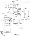
- FIG. 2is a circuit diagram of an exemplary system 200 for controlling current flow to an associated inductive load 202 .
- the inductive load 202is a solenoid valve, although other types of electrical components are contemplated.
- a drive current 204 to the load 202is desired to follow a certain input signal waveform.
- a current sensor 208is used to measure the current flowing through a switching element (or output switch) 210 and the load 202 .
- the current sensor 208is a Hall effect sensor.
- the switching element 210has an open state and a closed state and intermittently connects the power supply 212 to the inductive load 202 when the switching element 210 is in the closed state.
- the inductance of the solenoid valve coillimits the rate of change for the current through the solenoid valve 202 to a given rate.
- a control circuit (or controller) 212turns the switching element 210 OFF.
- the slow response of the current sensor 208can cause an overshoot error.
- a supplemental signal 214is added to the actual measured current signal 216 via an adder circuit such as, for example, operational amplifier 230 , thus creating an feedback signal that is delivered to comparator 218 .
- Comparator 218compares the feedback signal to a desired current setpoint 206 .
- switch driver 222Based on that input, switch driver provides a control signal to switch control element 22 .
- Adding the supplemental signal to the measured current signaltends to, for example, increase the value of the feedback thereby causing the to force the control circuit 200 to respond more quickly than it could when based upon the measured current signal alone.
- the Hall effect current sensor 208measures the current flowing through the switching element 210 and the load 202 and a sensed current signal 226 is generated.
- the measured signal of the Hall effect sensor 208is generally a voltage of 0.5 to 4.5 volts representing 0 to 20 amperes of current flow in a preferred embodiment.
- the supplemental signalis generally a 0 or 15 volt signal, for example, which is connected through a series resistor 223 to a point where a small series resistor 224 is placed between the output 226 of the Hall effect sensor 208 and the input 228 to the amplifier 230 .
- the two resistors acting as a voltage dividerallow for a composite value of the voltage to be created at the input 228 of the amplifier 230 .
- the weighted value of the supplemental circuitis generally less than 10% of the total.
- the 10% figureis a practical example but not a requirement.
- the ratio of the actual resistors usedwill determine the weighting (or percentage) of the speed up offset. Since the delayed response of the Hall effect sensor is an absolute amount of time, the desired offset value from the switch control state depends upon the actual circuit current rise time of the controlled load. The exact shape of the current rise is not necessarily important, rather, it is the value reached during the time that the sensor is lagging that matters. That is to say, for any given load circuit, the Hall effect, or other slow sensor, error can be measured and corrected for. In any given circuit embodiment, the offset from the control signal state can add the appropriate “current offset” to cancel out the overshoot, which would have occurred while waiting for the Hall effect sensor signal, for example, to ultimately reach the correct value.
- the Hall effect sensor outputtakes about 5 microseconds to reach the full value of the actual measured current. If the desired set point is 10 amps and the current rises at an average rate of 0.10 amps per microsecond, then the sensor output will be at some value less than the actual current of 10 amps after 10 microseconds, say 8 amps or 80% of the actual current.
- the Hall effect measured signalgenerally has two components: 100% of the 5 amps more than 5 microseconds old and some part of the next 5 amp increase less than 5 microseconds old, say, for example, 3 amps. If the added signal based upon the output switch condition adds the equivalent of 2 amps, then this exactly cancels the delay error and the switch shuts off at the desired 10 amps through the load.
- the value of the feedback resistorcan be selected to offset the error of any particular load circuit.
- FIG. 3illustrates a flowchart of an exemplary method 300 of controlling current flow to an associated inductive load.
- the method 300includes, via a switching element having an open state and a closed state, such as the switch 112 , intermittently connecting an associated power supply, such as the power supply 110 , to an inductive load, such as the solenoid 102 , when the switching element is in the closed state (step 302 ).
- a switch driversuch as the driver 116
- a switch drive signalsuch as the signal 118
- a control element of the switchthat controls the state of the switch to be an open state or in a closed state based on a desired load current set point and a feedback signal (step 304 ).
- a current sensorsuch as the hall effect sensor 108
- a sensed current signalis generated (step 306 ).
- a summing circuitsuch as the summing circuit 126
- a representation of the sensed current signal and a supplemental signal comprising a representation of the switch drive signalis added to generate the feedback signal (step 308 ).
Landscapes
- Physics & Mathematics (AREA)
- Engineering & Computer Science (AREA)
- General Physics & Mathematics (AREA)
- Electromagnetism (AREA)
- Radar, Positioning & Navigation (AREA)
- Automation & Control Theory (AREA)
- Condensed Matter Physics & Semiconductors (AREA)
- Power Engineering (AREA)
- Electronic Switches (AREA)
- Control Of Voltage And Current In General (AREA)
Abstract
Description
Claims (16)
Priority Applications (2)
| Application Number | Priority Date | Filing Date | Title |
|---|---|---|---|
| US15/924,735US11112810B2 (en) | 2018-03-19 | 2018-03-19 | Analog control loop with digital feedback |
| EP19163336.1AEP3543818A1 (en) | 2018-03-19 | 2019-03-18 | Analog control loop with digital feedback |
Applications Claiming Priority (1)
| Application Number | Priority Date | Filing Date | Title |
|---|---|---|---|
| US15/924,735US11112810B2 (en) | 2018-03-19 | 2018-03-19 | Analog control loop with digital feedback |
Publications (2)
| Publication Number | Publication Date |
|---|---|
| US20190286177A1 US20190286177A1 (en) | 2019-09-19 |
| US11112810B2true US11112810B2 (en) | 2021-09-07 |
Family
ID=65818268
Family Applications (1)
| Application Number | Title | Priority Date | Filing Date |
|---|---|---|---|
| US15/924,735ActiveUS11112810B2 (en) | 2018-03-19 | 2018-03-19 | Analog control loop with digital feedback |
Country Status (2)
| Country | Link |
|---|---|
| US (1) | US11112810B2 (en) |
| EP (1) | EP3543818A1 (en) |
Citations (28)
| Publication number | Priority date | Publication date | Assignee | Title |
|---|---|---|---|---|
| US3691405A (en) | 1971-08-10 | 1972-09-12 | Ultra Electronics Ltd | Thermocouple response time compensation circuit arrangement |
| US4980793A (en) | 1988-04-29 | 1990-12-25 | Chrysler Corporation | Open loop control of solenoid coil driver |
| EP0449543A1 (en) | 1990-03-28 | 1991-10-02 | Trinova Limited | Digital pulse-width-modulation generator for current control |
| US5442290A (en) | 1992-08-04 | 1995-08-15 | The Regents Of The University Of California | MRI gradient drive current control using all digital controller |
| US5703750A (en)* | 1995-09-14 | 1997-12-30 | Samsung Electronics Co., Ltd. | Proportional solenoid valve control system |
| US5969514A (en) | 1997-11-24 | 1999-10-19 | National Semiconductor Corporation | Digital feedback power supply |
| US6208497B1 (en) | 1997-06-26 | 2001-03-27 | Venture Scientifics, Llc | System and method for servo control of nonlinear electromagnetic actuators |
| US6268716B1 (en) | 1998-10-30 | 2001-07-31 | Volterra Semiconductor Corporation | Digital voltage regulator using current control |
| US6972969B1 (en) | 2004-08-19 | 2005-12-06 | Iwatt, Inc. | System and method for controlling current limit with primary side sensing |
| US6977492B2 (en) | 2002-07-10 | 2005-12-20 | Marvell World Trade Ltd. | Output regulator |
| US20060083037A1 (en) | 2004-07-27 | 2006-04-20 | Silicon Laboratories Inc. | Digital PWM controller with efficiency optimization as a function of PWM duty cycle |
| US20060172783A1 (en) | 2004-07-27 | 2006-08-03 | Silicon Laboratories Inc. | Digital DC/DC converter with SYNC control |
| US7319312B2 (en) | 2004-07-27 | 2008-01-15 | Silicon Laboratories Inc. | Digital power supply controller with voltage positioning |
| US7324354B2 (en) | 2005-07-08 | 2008-01-29 | Bio-Rad Laboratories, Inc. | Power supply with a digital feedback loop |
| US20080169798A1 (en)* | 2007-01-11 | 2008-07-17 | Kyle Williams | Method for controlling current in a load |
| US7417877B2 (en) | 2004-07-27 | 2008-08-26 | Silicon Laboratories Inc. | Digital power supply with programmable soft start |
| US7502697B2 (en) | 2006-09-28 | 2009-03-10 | Programmable Division Of Xantrex Technology, Inc. | AC output power supply with digital feedback loop |
| US20090134859A1 (en)* | 2007-11-28 | 2009-05-28 | Fuji Electric Device Technology Co., Ltd. | Switching power supply device |
| US7570035B2 (en) | 2007-08-01 | 2009-08-04 | Zerog Wireless, Inc. | Voltage regulator with a hybrid control loop |
| US7903008B2 (en) | 2007-11-08 | 2011-03-08 | National Instruments Corporation | Source-measure unit based on digital control loop |
| US20130207625A1 (en) | 2012-02-09 | 2013-08-15 | Fujitsu Semiconductor Limited | Switching regulator |
| US20130328534A1 (en)* | 2012-06-08 | 2013-12-12 | Novatek Microelectronics Corp. | Method of controlling a power converting device and related circuit |
| US8653840B2 (en) | 2011-06-06 | 2014-02-18 | National Instruments Corporation | Fast current saturation recovery for a digital source measure unit (SMU) |
| US8797025B2 (en) | 2011-06-06 | 2014-08-05 | National Instruments Corporation | Compensation methods for digital source-measure-units (SMUs) |
| US8816661B2 (en) | 2009-01-28 | 2014-08-26 | International Rectifier Corporation | Hybrid analog/digital power supply circuit including analog summer circuit to produce an error voltage |
| US20140246478A1 (en) | 2013-03-01 | 2014-09-04 | Ethicon Endo-Surgery, Inc. | Multiple processor motor control for modular surgical instruments |
| US9450628B2 (en) | 2011-03-14 | 2016-09-20 | Infineon Technologies Ag | Receiver and transmitter receiver system |
| US20180062509A1 (en) | 2016-08-26 | 2018-03-01 | Samsung Electronics Co., Ltd. | Switching regulator and control circuit thereof |
- 2018
- 2018-03-19USUS15/924,735patent/US11112810B2/enactiveActive
- 2019
- 2019-03-18EPEP19163336.1Apatent/EP3543818A1/ennot_activeWithdrawn
Patent Citations (29)
| Publication number | Priority date | Publication date | Assignee | Title |
|---|---|---|---|---|
| US3691405A (en) | 1971-08-10 | 1972-09-12 | Ultra Electronics Ltd | Thermocouple response time compensation circuit arrangement |
| US4980793A (en) | 1988-04-29 | 1990-12-25 | Chrysler Corporation | Open loop control of solenoid coil driver |
| EP0449543A1 (en) | 1990-03-28 | 1991-10-02 | Trinova Limited | Digital pulse-width-modulation generator for current control |
| US5442290A (en) | 1992-08-04 | 1995-08-15 | The Regents Of The University Of California | MRI gradient drive current control using all digital controller |
| US5703750A (en)* | 1995-09-14 | 1997-12-30 | Samsung Electronics Co., Ltd. | Proportional solenoid valve control system |
| US6208497B1 (en) | 1997-06-26 | 2001-03-27 | Venture Scientifics, Llc | System and method for servo control of nonlinear electromagnetic actuators |
| US5969514A (en) | 1997-11-24 | 1999-10-19 | National Semiconductor Corporation | Digital feedback power supply |
| US6268716B1 (en) | 1998-10-30 | 2001-07-31 | Volterra Semiconductor Corporation | Digital voltage regulator using current control |
| US7906949B1 (en) | 2002-07-10 | 2011-03-15 | Marvell World Trade Ltd. | Adaptive control loop |
| US6977492B2 (en) | 2002-07-10 | 2005-12-20 | Marvell World Trade Ltd. | Output regulator |
| US7319312B2 (en) | 2004-07-27 | 2008-01-15 | Silicon Laboratories Inc. | Digital power supply controller with voltage positioning |
| US20060172783A1 (en) | 2004-07-27 | 2006-08-03 | Silicon Laboratories Inc. | Digital DC/DC converter with SYNC control |
| US20060083037A1 (en) | 2004-07-27 | 2006-04-20 | Silicon Laboratories Inc. | Digital PWM controller with efficiency optimization as a function of PWM duty cycle |
| US7417877B2 (en) | 2004-07-27 | 2008-08-26 | Silicon Laboratories Inc. | Digital power supply with programmable soft start |
| US6972969B1 (en) | 2004-08-19 | 2005-12-06 | Iwatt, Inc. | System and method for controlling current limit with primary side sensing |
| US7324354B2 (en) | 2005-07-08 | 2008-01-29 | Bio-Rad Laboratories, Inc. | Power supply with a digital feedback loop |
| US7502697B2 (en) | 2006-09-28 | 2009-03-10 | Programmable Division Of Xantrex Technology, Inc. | AC output power supply with digital feedback loop |
| US20080169798A1 (en)* | 2007-01-11 | 2008-07-17 | Kyle Williams | Method for controlling current in a load |
| US7570035B2 (en) | 2007-08-01 | 2009-08-04 | Zerog Wireless, Inc. | Voltage regulator with a hybrid control loop |
| US7903008B2 (en) | 2007-11-08 | 2011-03-08 | National Instruments Corporation | Source-measure unit based on digital control loop |
| US20090134859A1 (en)* | 2007-11-28 | 2009-05-28 | Fuji Electric Device Technology Co., Ltd. | Switching power supply device |
| US8816661B2 (en) | 2009-01-28 | 2014-08-26 | International Rectifier Corporation | Hybrid analog/digital power supply circuit including analog summer circuit to produce an error voltage |
| US9450628B2 (en) | 2011-03-14 | 2016-09-20 | Infineon Technologies Ag | Receiver and transmitter receiver system |
| US8653840B2 (en) | 2011-06-06 | 2014-02-18 | National Instruments Corporation | Fast current saturation recovery for a digital source measure unit (SMU) |
| US8797025B2 (en) | 2011-06-06 | 2014-08-05 | National Instruments Corporation | Compensation methods for digital source-measure-units (SMUs) |
| US20130207625A1 (en) | 2012-02-09 | 2013-08-15 | Fujitsu Semiconductor Limited | Switching regulator |
| US20130328534A1 (en)* | 2012-06-08 | 2013-12-12 | Novatek Microelectronics Corp. | Method of controlling a power converting device and related circuit |
| US20140246478A1 (en) | 2013-03-01 | 2014-09-04 | Ethicon Endo-Surgery, Inc. | Multiple processor motor control for modular surgical instruments |
| US20180062509A1 (en) | 2016-08-26 | 2018-03-01 | Samsung Electronics Co., Ltd. | Switching regulator and control circuit thereof |
Non-Patent Citations (1)
| Title |
|---|
| Narcisse, "Digital Feedback Control", Department of Mathematical Information Technology, University of Jyväskylä Finland, Nov. 22, 2012. |
Also Published As
| Publication number | Publication date |
|---|---|
| EP3543818A1 (en) | 2019-09-25 |
| US20190286177A1 (en) | 2019-09-19 |
Similar Documents
| Publication | Publication Date | Title |
|---|---|---|
| KR100306980B1 (en) | Current Limiting Solenoid Driver | |
| CN103154756B (en) | For determining the method and apparatus of the state of electrically operated valve | |
| EP0460130A1 (en) | Dual current sensing driver circuit | |
| CN107978416A (en) | Determine the method and circuit device of the position of the movable armature of electromagnetic actuator | |
| US6147848A (en) | Pulse width modulation driver having programmable current control | |
| US8280611B2 (en) | Method for adapting a drag coefficient of a flow control valve | |
| CN109477440A (en) | Method and apparatus for actuating a piezoelectric actuator of an injection valve of a motor vehicle | |
| US11112810B2 (en) | Analog control loop with digital feedback | |
| US7023682B2 (en) | Solenoid control using voltage control of freewheel current decay | |
| KR101771802B1 (en) | Method and device for controlling a solenoid actuator | |
| US7558043B2 (en) | Amperage control for valves | |
| CN110855197A (en) | Adaptive keep-alive for an electrically commutated electric motor | |
| US20230224197A1 (en) | Circuit and method for determining a dither amplitude | |
| JPH11327666A (en) | Method for monitoring at least one current adjusting stage and monitoring device for at least one current adjusting stage | |
| KR100378452B1 (en) | Electromagnetic load control method and device | |
| JP5915054B2 (en) | Solenoid energization control device | |
| JPH1165684A (en) | Compensation adjusting method for current adjuster | |
| KR102423135B1 (en) | Methods for controlling fuel metering | |
| JP2010170434A (en) | Device and method for controlling current of solenoid | |
| US11581116B2 (en) | Method for transferring data from an actuating element to a control unit, corresponding actuating element and corresponding control unit | |
| US11230986B2 (en) | Method to determine the operating resistance of an electrical harness connecting an ECU to a solenoid controlled valve | |
| JPH10149201A (en) | Method and device for controlling operation variable | |
| EP4290325A1 (en) | System and method for error compensation in pulse-width modulated systems | |
| US12326703B2 (en) | Setting device for setting an effective value of an electric load current at a time-variant load | |
| JPH1173233A (en) | Method and device for control over load |
Legal Events
| Date | Code | Title | Description |
|---|---|---|---|
| AS | Assignment | Owner name:HOERBIGER KOMPRESSORTECHNIK HOLDING GMBH, AUSTRIA Free format text:ASSIGNMENT OF ASSIGNORS INTEREST;ASSIGNORS:LEPLEY, JOSEPH M.;PIRKO, STEVEN B.;SIGNING DATES FROM 20180308 TO 20180309;REEL/FRAME:045273/0352 | |
| FEPP | Fee payment procedure | Free format text:ENTITY STATUS SET TO UNDISCOUNTED (ORIGINAL EVENT CODE: BIG.); ENTITY STATUS OF PATENT OWNER: LARGE ENTITY | |
| AS | Assignment | Owner name:HOERBIGER WIEN GMBH, AUSTRIA Free format text:CHANGE OF NAME;ASSIGNOR:HOERBIGER KOMPRESSORTECHNMIK HOLDING GMBH;REEL/FRAME:047728/0882 Effective date:20180814 | |
| AS | Assignment | Owner name:HOERBIGER WIEN GMBH, AUSTRIA Free format text:CORRECTIVE ASSIGNMENT TO CORRECT THE MISSPELLING OF ASSIGNOR NAME PREVIOUSLY RECORDED ON REEL 047728 FRAME 0882. ASSIGNOR(S) HEREBY CONFIRMS THE ASSIGNMENT;ASSIGNOR:HOERBIGER KOMPRESSORTECHNIK HOLDING GMBH;REEL/FRAME:048030/0741 Effective date:20180814 | |
| STPP | Information on status: patent application and granting procedure in general | Free format text:FINAL REJECTION MAILED | |
| STPP | Information on status: patent application and granting procedure in general | Free format text:DOCKETED NEW CASE - READY FOR EXAMINATION | |
| STPP | Information on status: patent application and granting procedure in general | Free format text:NON FINAL ACTION MAILED | |
| STPP | Information on status: patent application and granting procedure in general | Free format text:RESPONSE TO NON-FINAL OFFICE ACTION ENTERED AND FORWARDED TO EXAMINER | |
| STCV | Information on status: appeal procedure | Free format text:NOTICE OF APPEAL FILED | |
| STCV | Information on status: appeal procedure | Free format text:APPEAL BRIEF (OR SUPPLEMENTAL BRIEF) ENTERED AND FORWARDED TO EXAMINER | |
| STPP | Information on status: patent application and granting procedure in general | Free format text:NOTICE OF ALLOWANCE MAILED -- APPLICATION RECEIVED IN OFFICE OF PUBLICATIONS | |
| STPP | Information on status: patent application and granting procedure in general | Free format text:DOCKETED NEW CASE - READY FOR EXAMINATION | |
| STPP | Information on status: patent application and granting procedure in general | Free format text:NOTICE OF ALLOWANCE MAILED -- APPLICATION RECEIVED IN OFFICE OF PUBLICATIONS | |
| STPP | Information on status: patent application and granting procedure in general | Free format text:PUBLICATIONS -- ISSUE FEE PAYMENT VERIFIED | |
| STCF | Information on status: patent grant | Free format text:PATENTED CASE | |
| AS | Assignment | Owner name:ALTRONIC, LLC, OHIO Free format text:ASSIGNMENT OF ASSIGNORS INTEREST;ASSIGNOR:HOERBIGER WIEN GMBH;REEL/FRAME:059371/0004 Effective date:20220225 | |
| AS | Assignment | Owner name:ALTRONIC, LLC, OHIO Free format text:ASSIGNMENT OF ASSIGNORS INTEREST;ASSIGNOR:HOERBIGER WIEN GMBH;REEL/FRAME:059438/0605 Effective date:20220225 | |
| MAFP | Maintenance fee payment | Free format text:PAYMENT OF MAINTENANCE FEE, 4TH YEAR, LARGE ENTITY (ORIGINAL EVENT CODE: M1551); ENTITY STATUS OF PATENT OWNER: LARGE ENTITY Year of fee payment:4 |