US11108328B2 - Systems and methods for high precision and/or low loss regulation of output currents of power conversion systems - Google Patents
Systems and methods for high precision and/or low loss regulation of output currents of power conversion systemsDownload PDFInfo
- Publication number
- US11108328B2 US11108328B2US16/205,002US201816205002AUS11108328B2US 11108328 B2US11108328 B2US 11108328B2US 201816205002 AUS201816205002 AUS 201816205002AUS 11108328 B2US11108328 B2US 11108328B2
- Authority
- US
- United States
- Prior art keywords
- terminal
- signal
- current
- component
- output
- Prior art date
- Legal status (The legal status is an assumption and is not a legal conclusion. Google has not performed a legal analysis and makes no representation as to the accuracy of the status listed.)
- Expired - Fee Related
Links
Images


Classifications
- H—ELECTRICITY
- H02—GENERATION; CONVERSION OR DISTRIBUTION OF ELECTRIC POWER
- H02M—APPARATUS FOR CONVERSION BETWEEN AC AND AC, BETWEEN AC AND DC, OR BETWEEN DC AND DC, AND FOR USE WITH MAINS OR SIMILAR POWER SUPPLY SYSTEMS; CONVERSION OF DC OR AC INPUT POWER INTO SURGE OUTPUT POWER; CONTROL OR REGULATION THEREOF
- H02M3/00—Conversion of DC power input into DC power output
- H02M3/22—Conversion of DC power input into DC power output with intermediate conversion into AC
- H02M3/24—Conversion of DC power input into DC power output with intermediate conversion into AC by static converters
- H02M3/28—Conversion of DC power input into DC power output with intermediate conversion into AC by static converters using discharge tubes with control electrode or semiconductor devices with control electrode to produce the intermediate AC
- H02M3/325—Conversion of DC power input into DC power output with intermediate conversion into AC by static converters using discharge tubes with control electrode or semiconductor devices with control electrode to produce the intermediate AC using devices of a triode or a transistor type requiring continuous application of a control signal
- H02M3/335—Conversion of DC power input into DC power output with intermediate conversion into AC by static converters using discharge tubes with control electrode or semiconductor devices with control electrode to produce the intermediate AC using devices of a triode or a transistor type requiring continuous application of a control signal using semiconductor devices only
- H02M3/33507—Conversion of DC power input into DC power output with intermediate conversion into AC by static converters using discharge tubes with control electrode or semiconductor devices with control electrode to produce the intermediate AC using devices of a triode or a transistor type requiring continuous application of a control signal using semiconductor devices only with automatic control of the output voltage or current, e.g. flyback converters
- H—ELECTRICITY
- H02—GENERATION; CONVERSION OR DISTRIBUTION OF ELECTRIC POWER
- H02M—APPARATUS FOR CONVERSION BETWEEN AC AND AC, BETWEEN AC AND DC, OR BETWEEN DC AND DC, AND FOR USE WITH MAINS OR SIMILAR POWER SUPPLY SYSTEMS; CONVERSION OF DC OR AC INPUT POWER INTO SURGE OUTPUT POWER; CONTROL OR REGULATION THEREOF
- H02M1/00—Details of apparatus for conversion
- H02M1/08—Circuits specially adapted for the generation of control voltages for semiconductor devices incorporated in static converters
- H—ELECTRICITY
- H05—ELECTRIC TECHNIQUES NOT OTHERWISE PROVIDED FOR
- H05B—ELECTRIC HEATING; ELECTRIC LIGHT SOURCES NOT OTHERWISE PROVIDED FOR; CIRCUIT ARRANGEMENTS FOR ELECTRIC LIGHT SOURCES, IN GENERAL
- H05B45/00—Circuit arrangements for operating light-emitting diodes [LED]
- H05B45/30—Driver circuits
- H05B45/32—Pulse-control circuits
- H05B45/325—Pulse-width modulation [PWM]
- H—ELECTRICITY
- H05—ELECTRIC TECHNIQUES NOT OTHERWISE PROVIDED FOR
- H05B—ELECTRIC HEATING; ELECTRIC LIGHT SOURCES NOT OTHERWISE PROVIDED FOR; CIRCUIT ARRANGEMENTS FOR ELECTRIC LIGHT SOURCES, IN GENERAL
- H05B45/00—Circuit arrangements for operating light-emitting diodes [LED]
- H05B45/30—Driver circuits
- H05B45/37—Converter circuits
- H05B45/3725—Switched mode power supply [SMPS]
- H05B45/38—Switched mode power supply [SMPS] using boost topology
- H—ELECTRICITY
- H05—ELECTRIC TECHNIQUES NOT OTHERWISE PROVIDED FOR
- H05B—ELECTRIC HEATING; ELECTRIC LIGHT SOURCES NOT OTHERWISE PROVIDED FOR; CIRCUIT ARRANGEMENTS FOR ELECTRIC LIGHT SOURCES, IN GENERAL
- H05B45/00—Circuit arrangements for operating light-emitting diodes [LED]
- H05B45/30—Driver circuits
- H05B45/37—Converter circuits
- H05B45/3725—Switched mode power supply [SMPS]
- H05B45/382—Switched mode power supply [SMPS] with galvanic isolation between input and output
- H—ELECTRICITY
- H02—GENERATION; CONVERSION OR DISTRIBUTION OF ELECTRIC POWER
- H02M—APPARATUS FOR CONVERSION BETWEEN AC AND AC, BETWEEN AC AND DC, OR BETWEEN DC AND DC, AND FOR USE WITH MAINS OR SIMILAR POWER SUPPLY SYSTEMS; CONVERSION OF DC OR AC INPUT POWER INTO SURGE OUTPUT POWER; CONTROL OR REGULATION THEREOF
- H02M1/00—Details of apparatus for conversion
- H02M1/0003—Details of control, feedback or regulation circuits
- H02M1/0009—Devices or circuits for detecting current in a converter
- H—ELECTRICITY
- H02—GENERATION; CONVERSION OR DISTRIBUTION OF ELECTRIC POWER
- H02M—APPARATUS FOR CONVERSION BETWEEN AC AND AC, BETWEEN AC AND DC, OR BETWEEN DC AND DC, AND FOR USE WITH MAINS OR SIMILAR POWER SUPPLY SYSTEMS; CONVERSION OF DC OR AC INPUT POWER INTO SURGE OUTPUT POWER; CONTROL OR REGULATION THEREOF
- H02M1/00—Details of apparatus for conversion
- H02M1/0003—Details of control, feedback or regulation circuits
- H02M1/0016—Control circuits providing compensation of output voltage deviations using feedforward of disturbance parameters
- H02M1/0022—Control circuits providing compensation of output voltage deviations using feedforward of disturbance parameters the disturbance parameters being input voltage fluctuations
- H—ELECTRICITY
- H02—GENERATION; CONVERSION OR DISTRIBUTION OF ELECTRIC POWER
- H02M—APPARATUS FOR CONVERSION BETWEEN AC AND AC, BETWEEN AC AND DC, OR BETWEEN DC AND DC, AND FOR USE WITH MAINS OR SIMILAR POWER SUPPLY SYSTEMS; CONVERSION OF DC OR AC INPUT POWER INTO SURGE OUTPUT POWER; CONTROL OR REGULATION THEREOF
- H02M1/00—Details of apparatus for conversion
- H02M1/36—Means for starting or stopping converters
- H02M2001/0009—
- H02M2001/0022—
Definitions
- the present inventionis directed to integrated circuits. More particularly, the invention provides a system and method for current regulation. Merely by way of example, the invention has been applied to power conversion systems. But it would be recognized that the invention has a much broader range of applicability.
- LEDsLight emitting diodes
- the output-current precision of LEDsis usually used for determining the constant-current properties of a LED lighting system.
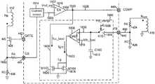
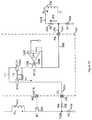
- FIG. 1is a simplified diagram showing a conventional power conversation system for LED lighting.
- the power conversion system 100includes a controller 102 , resistors 104 , 124 , 126 and 132 , capacitors 106 , 120 and 134 , a diode 108 , a transformer 110 including a primary winding 112 , a secondary winding 114 and an auxiliary winding 116 , a power switch 128 , a current sensing resistor 130 , and a rectifying diode 118 .
- the controller 102includes terminals 138 , 140 , 142 , 144 , 146 and 148 .
- the power switch 128is a bipolar junction transistor.
- the power switch 128is a MOS transistor.
- An alternate-current (AC) input voltage 152is applied to the system 100 .
- a bulk voltage 150e.g., a rectified voltage no smaller than 0 V
- the capacitor 106is charged in response to the bulk voltage 150 , and a voltage 154 is provided to the controller 102 at the terminal 138 (e.g., terminal VCC). If the voltage 154 is larger than a predetermined threshold voltage (e.g., a under-voltage lock-out threshold) in magnitude, the controller 102 begins to operate normally, and outputs a driving signal 156 through the terminal 142 (e.g., terminal GATE).
- a predetermined threshold voltagee.g., a under-voltage lock-out threshold
- the driving signal 156is a pulse-width-modulation (PWM) signal with a switching frequency and a duty cycle.
- PWMpulse-width-modulation
- the switch 128is closed (e.g., being turned on) or open (e.g., being turned off) in response to the driving signal 156 so that the output current 158 is regulated to be approximately constant.
- the auxiliary winding 116charges the capacitor 106 through the diode 108 when the switch 128 is closed (e.g., being turned on) in response to the driving signal 156 so that the controller 102 can operate normally.
- a feedback signal 160is provided to the controller 102 through the terminal 140 (e.g., terminal FB) in order to detect the ending of a demagnetization process of the secondary winding 118 for charging or discharging the capacitor 134 using an internal error amplifier in the controller 102 .
- the resistor 130is used for detecting a primary current 162 flowing through the primary winding 112 , and a current-sensing signal 164 is provided to the controller 102 through the terminal 144 (e.g., terminal CS) to be processed during each switching cycle. Peak magnitudes of the current-sensing signal 164 are sampled and provided to the internal error amplifier.
- the capacitor 120is used to keep an output voltage 168 stable.
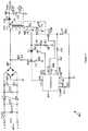
- FIG. 2is a simplified conventional diagram showing the controller 102 as part of the system 100 .
- the controller 102includes an oscillator 202 , an under-voltage lock-out (UVLO) component 204 , a modulation component 206 , a logic controller 208 , a driving component 210 , a demagnetization detector 212 , an error amplifier 216 , and a current-sensing component 214 .
- UVLOunder-voltage lock-out
- the UVLO component 204detects the signal 154 and outputs a signal 218 . If the signal 154 is larger than a predetermined threshold in magnitude, the controller 102 begins to operate normally. If the signal 154 is smaller than the predetermined threshold in magnitude, the controller 102 is turned off.
- the error amplifier 216receives a signal 220 from the current-sensing component 214 and a reference signal 222 and outputs an amplified signal 224 to the modulation component 206 .
- the modulation component 206also receives a signal 228 from the oscillator 202 and outputs a modulation signal 226 which is a PWM signal.
- the signal 228is a ramping signal and increases, linearly or non-linearly, to a peak magnitude during each switching period.
- the modulation signal 226has a fixed switching frequency and the duty cycle of the signal 226 is determined based on a comparison between the signal 224 and the signal 228 .
- the logic controller 208processes the modulation signal 226 and outputs a control signal 230 to the driving component 210 which generates the signal 156 to turn on or off the switch 128 .
- the demagnetization detector 212detects the feedback signal 160 and outputs a signal 232 for determining the beginning and the end of the demagnetization process of the secondary winding 114 .
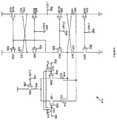
- FIG. 3is a simplified conventional diagram showing the current-sensing component 214 and the error amplifier 216 as parts of the controller 102 .
- the current-sensing component 214includes a switch 302 and a capacitor 304 .
- the error amplifier 216includes switches 306 and 308 , an operational amplifier 310 .
- the current-sensing component 214samples the current-sensing signal 164 and the error amplifier 216 amplifies the difference between the signal 220 and the reference signal 222 .
- the switch 302is closed (e.g., being turned on) or open (e.g., being turned off) in response to a signal 314 in order to sample peak magnitudes of the current-sensing signal 164 in different switching periods. If the switch 302 is closed (e.g., being turned on) in response to the signal 314 and the switch 306 is open (e.g., being turned off) in response to the signal 232 from the demagnetization detector 212 , the capacitor 304 is charged and the signal 220 increases in magnitude.
- the switch 306is closed (e.g., being turned on) in response to the signal 232
- the switch 308is open (e.g., being turned off) in response to a signal 312 and the difference between the signal 220 and the reference signal 222 is amplified by the amplifier 310 .
- the signal 232is at a logic high level.
- the switch 306remains closed (e.g., being turned on) and the switch 308 remains open (e.g., being turned off).
- the amplifier 310together with the capacitor 134 , performs integration associated with the signal 220 .
- I o _1 2 ⁇ N ⁇ V ref ⁇ ⁇ _ ⁇ ⁇ ea R cs ( Equation ⁇ ⁇ 1 )
- Nrepresents a turns ratio between the primary winding 112 and the secondary winding 114
- V ref_earepresents the reference signal 222
- R csrepresents the resistance of the resistor 130 .
- the system 100has problems in regulating the output current to be approximately constant. Hence it is highly desirable to improve the techniques of regulating output currents of power conversion systems.
- the present inventionis directed to integrated circuits. More particularly, the invention provides a system and method for current regulation. Merely by way of example, the invention has been applied to power conversion systems. But it would be recognized that the invention has a much broader range of applicability.
- an error amplifier for processing a reference signal and an input signal associated with a current of a power conversion systemincludes a first operational amplifier, a second operational amplifier, a first transistor, a second transistor, a current mirror component, a switch, a first resistor and a second resistor.
- the first operational amplifierincludes a first input terminal, a second input terminal and a first output terminal, the first input terminal being configured to receive a reference signal.
- the first transistorincludes a first transistor terminal, a second transistor terminal and a third transistor terminal, the first transistor terminal being configured to receive a first amplified signal from the first output terminal, the third transistor terminal being coupled to the second input terminal.
- the second operational amplifierincludes a third input terminal, a fourth input terminal and a second output terminal, the third input terminal being configured to receive an input signal associated with a current flowing through a primary winding of a power conversion system.
- the second transistorincludes a fourth transistor terminal, a fifth transistor terminal and a sixth transistor terminal, the fourth transistor terminal being configured to receive a second amplified signal from the second output terminal, the sixth transistor terminal being coupled to the fourth input terminal.
- the current mirror componentincludes a first component terminal and a second component terminal, the first component terminal being coupled to the second transistor terminal.
- the switchincludes a first switch terminal and a second switch terminal, the first switch terminal being coupled to the second component terminal, the second switch terminal being coupled to the fifth transistor terminal.
- the first resistorincludes a first resistor terminal and a second resistor terminal, the first resistor being associated with a first resistance, the first resistor terminal being coupled to the second input terminal.
- the second resistorincludes a third resistor terminal and a fourth resistor terminal, the second resistor being associated with a second resistance, the third resistor terminal being coupled to the fourth input terminal.
- the first resistanceis larger than the second resistance in magnitude.
- the second component terminalis configured to output an output signal based on at least information associated with the reference signal and the input signal.
- a system controller for regulating a power conversion systemincludes a first controller terminal configured to receive a first voltage associated with a first current, the first current being related to an input voltage of a power conversion system, a compensation component coupled to the first controller terminal and configured to, if the first voltage satisfies one or more first conditions, generate a compensation current based on at least information associated with the first current, and a second controller terminal coupled to the compensation component and configured to provide a compensation voltage based on at least information associated with the compensation current, the compensation voltage being equal in magnitude to the compensation current multiplied by a compensation resistance, the compensation resistance being associated with a compensation resistor.
- the system controllerfurther includes a current sensing component configured to receive a second voltage and generate an output signal, the second voltage being equal to a sum of a third voltage and the compensation voltage in magnitude, the third voltage being proportional to a second current flowing through a primary winding of the power conversion system, and an error amplifier configured to receive the output signal and a reference signal, generate an amplified signal based on at least information associated with the output signal and the reference signal, and output the amplified signal to affect a switch associated with the second current.
- a current sensing componentconfigured to receive a second voltage and generate an output signal, the second voltage being equal to a sum of a third voltage and the compensation voltage in magnitude, the third voltage being proportional to a second current flowing through a primary winding of the power conversion system
- an error amplifierconfigured to receive the output signal and a reference signal, generate an amplified signal based on at least information associated with the output signal and the reference signal, and output the amplified signal to affect a switch associated with the second current.
- a system controller for regulating a power conversion systemincludes a first controller terminal configured to receive a feedback signal associated with an output voltage of a power conversion system, a compensation component coupled to the first controller terminal and configured to sample the feedback signal during a demagnetization process of the power conversion system and generate a compensation current based on at least information associated with the sampled feedback signal, and a second controller terminal coupled to the compensation component and configured to provide a compensation voltage based on at least information associated with the compensation current, the compensation voltage being equal in magnitude to the compensation current multiplied by a compensation resistance, the compensation resistance being associated with a compensation resistor.
- the system controllerincludes a current sensing component configured to receive an input voltage and generate an output signal, the input voltage being equal to a sum of a first voltage and the compensation voltage in magnitude, the first voltage being proportional to a first current flowing through a primary winding of the power conversion system, and an error amplifier configured to receive the output signal and a reference signal, generate an amplified signal based on at least information associated with the output signal and the reference signal, and output the amplified signal to affect a switch associated with the first current.
- a current sensing componentconfigured to receive an input voltage and generate an output signal, the input voltage being equal to a sum of a first voltage and the compensation voltage in magnitude, the first voltage being proportional to a first current flowing through a primary winding of the power conversion system
- an error amplifierconfigured to receive the output signal and a reference signal, generate an amplified signal based on at least information associated with the output signal and the reference signal, and output the amplified signal to affect a switch associated with the first current.
- a system controller for regulating a power conversion systemincludes a first controller terminal configured to receive a feedback signal associated with an output voltage of a power conversion system, a compensation component coupled to the first controller terminal and configured to sample the feedback signal during a demagnetization process of the power conversion system and generate a compensation current based on at least information associated with the sampled feedback signal, and an error amplifier including a first input terminal, a second input terminal, and an output terminal coupled to the compensation component.
- the first input terminalis configured to receive an input voltage
- the second input terminalis configured to receive a reference voltage
- the output terminalis configured to output a first output current related to a difference between the input voltage and the reference voltage in magnitude.
- the error amplifier and the compensation componentare further configured to generate a second output current equal to a difference between the first output current and the compensation current in magnitude.
- a method for regulating a power conversion systemincludes receiving a first voltage associated with a first current, the first current being related to an input voltage of a power conversion system, generating, if the first voltage satisfies one or more first conditions, a compensation current based on at least information associated with the first current, and providing an compensation voltage based on at least information associated with the compensation current, the compensation voltage being equal in magnitude to the compensation current multiplied by a compensation resistance, the compensation resistance being associated with a compensation resistor.
- the methodfurther includes receiving an input voltage, the input voltage being equal to a sum of a second voltage and the compensation voltage in magnitude, the second voltage being proportional to a second current flowing through a primary winding of the power conversion system, generating an output signal based on at least information associated with the input voltage, and receiving the output signal and a reference signal.
- the methodincludes generating an amplified signal based on at least information associated with the output signal and the reference signal, and outputting the amplified signal in order to affect a switch associated with the second current.
- a method for regulating a power conversion systemincludes receiving a feedback signal associated with an output voltage of a power conversion system, sampling the feedback signal during a demagnetization process of the power conversion system, and generating a compensation current based on at least information associated with the sampled feedback signal.
- the methodfurther includes providing a compensation voltage based on at least information associated with the compensation current, the compensation voltage being equal in magnitude to the compensation current multiplied by a compensation resistance, the compensation resistance being associated with a compensation resistor, receiving an input voltage, the input voltage being equal to a sum of a first voltage and the compensation voltage in magnitude, the first voltage being proportional to a first current flowing through a primary winding of the power conversion system, and generating an output signal.
- the methodincludes receiving the output signal and a reference signal, generating an amplified signal based on at least information associated with the output signal and the reference signal, and outputting the amplified signal to affect a switch associated with the first current.
- a method for regulating a power conversion systemincludes receiving a feedback signal associated with an output voltage of a power conversion system, sampling the feedback signal during a demagnetization process of the power conversion system, and generating a compensation current based on at least information associated with the sampled feedback signal. Additionally, the method includes receiving an input voltage at a first input terminal of an error amplifier, and the error amplifier further includes a second input terminal and an output terminal. Moreover, the method includes receiving a reference voltage at the second input terminal, generating a first output current at the output terminal related to a difference between the input voltage and the reference voltage in magnitude, and outputting a second output current equal to a difference between the first output current and the compensation current in magnitude.
- FIG. 1is a simplified diagram showing a conventional power conversation system for LED lighting.
- FIG. 2is a simplified conventional diagram showing the controller as part of the system as shown in FIG. 1 .
- FIG. 3is a simplified conventional diagram showing the current-sensing component and the error amplifier as parts of the controller as shown in FIG. 2 .
- FIG. 4is a simplified diagram showing a power conversion system according to an embodiment of the present invention.
- FIG. 5is a simplified diagram showing the controller as part of the power conversion system as shown in FIG. 4 according to an embodiment of the present invention.
- FIG. 6is a simplified diagram showing the controller as part of the power conversion system as shown in FIG. 4 according to another embodiment of the present invention.
- FIG. 7is a simplified diagram showing certain components of the controller as part of the power conversion system as shown in FIG. 4 according to an embodiment of the present invention.
- FIG. 8is a simplified diagram showing certain components of the controller as part of the power conversion system as shown in FIG. 4 according to another embodiment of the present invention.
- FIG. 9 and FIG. 10are simplified diagrams showing different operation conditions of the operational amplifier as part of the error amplifier as shown in FIG. 8 according to certain embodiments of the present invention.
- FIG. 11is a simplified diagram showing certain components of the controller as part of the power conversion system as shown in FIG. 4 according to yet another embodiment of the present invention.
- FIG. 12is a simplified timing diagram for the system as shown in FIG. 1 showing the difference between the actual peak magnitude of the primary current and the desired peak magnitude as a function of the input line voltage.
- FIG. 13is a simplified diagram showing certain components of the system as shown in FIG. 4 according to another embodiment of the present invention.
- FIG. 14is a simplified timing diagram for the system as shown in FIG. 1 showing the peak magnitude of the secondary current as a function of the output voltage.
- FIG. 15is a simplified diagram showing certain components of the system as shown in FIG. 4 according to yet another embodiment of the present invention.
- FIG. 16is a simplified diagram showing certain components of the system as shown in FIG. 4 according to yet another embodiment of the present invention.
- FIG. 17is a simplified diagram showing a controller as part of the power conversion system as shown in FIG. 4 according to yet another embodiment of the present invention.
- FIG. 18is a simplified diagram showing a controller as part of the power conversion system as shown in FIG. 4 according to yet another embodiment of the present invention.
- FIG. 19is a simplified diagram showing certain components of the system as shown in FIG. 4 according to yet another embodiment of the present invention.
- the present inventionis directed to integrated circuits. More particularly, the invention provides a system and method for current regulation. Merely by way of example, the invention has been applied to power conversion systems. But it would be recognized that the invention has a much broader range of applicability.
- N, R cs and V ref_eamay affect the precision of the constant output current.
- N and R csare parameters of peripheral components, and can be selected through system design.
- the reference signal 222affects significantly the precision of the constant output current.
- the average output current and the turns ratio of the transformer 110are often predetermined, and thus the ratio between R cs and V ref_ea is also approximately fixed. Therefore, the larger the reference signal 222 is in magnitude, the larger the resistance of the resistor 130 .
- a large resistance of the resistor 130often results in large power loss, and thus the reference signal 222 may need to have a small magnitude for better efficiency. But non-ideal factors (e.g., offset errors, gain errors) may have larger negative effects on the precision of the constant output current if the reference signal 222 has a small magnitude.
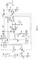
- FIG. 4is a simplified diagram showing a power conversion system according to an embodiment of the present invention.
- the system 400includes a controller 402 , resistors 404 , 424 , 426 and 432 , capacitors 406 , 420 and 434 , a diode 408 , a transformer 410 including a primary winding 412 , a secondary winding 414 and an auxiliary winding 416 , a power switch 428 , a current sensing resistor 430 , and a rectifying diode 418 .
- the controller 402includes terminals 438 , 440 , 442 , 444 , 446 and 448 .
- the power switch 428is a bipolar junction transistor.
- the power switch 428is a MOS transistor.
- the system 400provides power to an output load 422 , e.g., one or more LEDs.
- an alternate-current (AC) input voltage 452is applied to the system 400 .
- a bulk voltage 450e.g., a rectified voltage no smaller than 0 V
- the capacitor 406is charged in response to the bulk voltage 450
- a voltage 454is provided to the controller 402 at the terminal 438 (e.g., terminal VCC).
- the controller 402if the voltage 454 is larger than a predetermined threshold voltage (e.g., a under-voltage lock-out threshold) in magnitude, the controller 402 begins to operate normally, and outputs a driving signal 456 through the terminal 442 (e.g., terminal GATE).
- the switch 428is closed (e.g., being turned on) or open (e.g., being turned off) in response to the driving signal 456 so that the output current 458 is regulated to be approximately constant.
- the auxiliary winding 416charges the capacitor 406 through the diode 408 when the switch 428 is closed (e.g., being turned on) in response to the driving signal 456 so that the controller 402 can operate normally.
- a feedback signal 460is provided to the controller 402 through the terminal 440 (e.g., terminal FB) in order to detect the ending of a demagnetization process of the secondary winding 418 for charging or discharging the capacitor 434 using an internal error amplifier in the controller 402 .
- the resistor 430is used for detecting a primary current 462 flowing through the primary winding 412 , and a current-sensing signal 464 is provided to the controller 402 through the terminal 444 (e.g., terminal CS) to be processed during each switching cycle.
- a current-sensing signal 464is provided to the controller 402 through the terminal 444 (e.g., terminal CS) to be processed during each switching cycle.
- peak magnitudes of the current-sensing signal 464are sampled and provided to the internal error amplifier.
- the capacitor 420is used to keep an output voltage 468 stable.
- the controller 402includes an error amplifier (e.g., as shown in FIGS. 5-8 and 11 ) which, compared with the error amplifier 216 , has higher output impedance and a larger gain.
- the controller 402includes at least part of a line-voltage-compensation component (e.g., as shown in FIG. 13 ) for keeping the output current approximately constant (e.g., with a small error) under a wide range of input line voltages.
- the resistor 432is included in the line-voltage-compensation component.
- the controller 402includes at least part of a load-compensation component (e.g., as shown in FIG.
- the resistor 432is included in the load-compensation component. In some embodiments, the resistor 432 is omitted.
- FIG. 5is a simplified diagram showing the controller 402 as part of the power conversion system 400 according to an embodiment of the present invention.
- the controller 402includes an oscillator 502 , an under-voltage lock-out (UVLO) component 504 , a modulation component 506 , a logic controller 508 , a driving component 510 , a demagnetization detector 512 , an error amplifier 516 , a current-sensing component 514 , and a chopping component 540 .
- the controller 402includes at least part of a line-voltage-compensation component 550 and at least part of a load-compensation component 560 .
- the UVLO component 504detects the signal 454 and outputs a signal 518 . For example, if the signal 454 is larger than a predetermined threshold in magnitude, the controller 402 begins to operate normally. In another example, if the signal 454 is smaller than the predetermined threshold in magnitude, the controller 402 is turned off.
- the error amplifier 516receives a signal 520 from the current-sensing component 514 and a reference signal 522 and outputs an amplified signal 524 to the modulation component 506 .
- the modulation component 506also receives a signal 528 from the oscillator 502 and outputs a modulation signal 526 .
- the signal 528is a ramping signal and increases, linearly or non-linearly, to a peak magnitude during each switching period.
- the modulation signal 526is a pulse-width-modulation (PWM) signal with a fixed switching frequency and the duty cycle of the signal 526 is determined based on a comparison between the signal 524 and the signal 528 .
- the logic controller 508processes the modulation signal 526 and outputs a control signal 530 to the driving component 510 which generates the signal 456 to turn on or off the switch 428 .
- the logic controller 508also outputs the control signal 530 to the current sensing component 514 .
- the control signal 456is at a logic high level if the control signal 530 is at a logic high level.
- the control signal 456is at a logic low level if the control signal 530 is at a logic low level.
- the demagnetization detector 512detects the feedback signal 460 and outputs a demagnetization signal 532 for determining the beginning and the end of the demagnetization process of the secondary winding 414 during each switching period.
- the demagnetization signal 532is at a logic high level during the demagnetization period of each switching cycle, and at a logic low level during the rest of each switching cycle.
- the demagnetization signal 532changes from the logic low level to the logic high level if the control signal 456 changes from the logic high level to the logic low level.
- the demagnetization detector 512outputs a sampling signal 538 to the load-compensation component 560 .
- the chopping component 540receives a clock signal 534 from the oscillator 502 and outputs a signal 536 to the error amplifier 516 .
- the signal 536is also a clock signal that has a 50% duty cycle and a frequency which is 1/N of the frequency of the clock signal 534 .
- the error amplifier 516receives the reference signal 522 at a non-inverting input terminal and receives the signal 520 at an inverting input terminal; if the signal 536 is at a logic low level, the error amplifier 516 receives the reference signal 522 at the inverting input terminal and receives the signal 520 at the non-inverting input terminal.
- the offset voltage of the error amplifier 516 generated during the time period when the signal 536 is at the logic high level, and the offset voltage of the error amplifier 516 generated during the time period when the signal 536 is at the logic low levelare equal in magnitude but have different polarities, in certain embodiments. For example, if the signal 536 has a 50% duty cycle, the offset voltage generated during the time period when the signal 536 is at the logic high level cancels out the offset voltage generated during the time period when the signal 536 is at the logic low level. Thus, an average offset voltage during a complete chopping period of the signal 536 is approximately zero, according to some embodiments.
- the line-voltage-compensation component 550is used for keeping the output current approximately constant (e.g., with a small error) under a wide range of input line voltages.
- the load-compensation component 560is used for keeping the output current approximately constant (e.g., with a small error) under a wide range of output voltages.
- FIG. 5is merely an example, which should not unduly limit the scope of the claims.
- the current-sensing component 514is the same as the current-sensing component 214 .
- the error amplifier 516can be replaced by the error amplifier 216 .
- the line-voltage-compensation component 550is removed.
- the load-compensation component 560is removed.
- FIG. 6is a simplified diagram showing the controller 402 as part of the power conversion system 400 according to another embodiment of the present invention.
- the controller 402includes a ramp-signal generator 602 , an under-voltage lock-out (UVLO) component 604 , a modulation component 606 , a logic controller 608 , a driving component 610 , a demagnetization detector 612 , an error amplifier 616 , a current-sensing component 614 , and a chopping component 640 .
- the controller 402includes at least part of a line-voltage-compensation component 650 and at least part of a load-compensation component 660 .
- the UVLO component 604detects the signal 454 and outputs a signal 618 . For example, if the signal 454 is larger than a predetermined threshold in magnitude, the controller 402 begins to operate normally. In another example, if the signal 454 is smaller than the predetermined threshold in magnitude, the controller 402 is turned off.
- the error amplifier 616receives a signal 620 from the current-sensing component 614 and a reference signal 622 and outputs an amplified signal 624 to the modulation component 606 .
- the modulation component 606also receives a signal 628 from the ramp-signal generator 602 and outputs a modulation signal 626 .
- the signal 628is a ramping signal and increases, linearly or non-linearly, to a peak magnitude during each switching period.
- the modulation signal 626does not have a fixed switching frequency.
- the logic controller 608processes the modulation signal 626 and outputs a control signal 630 to the driving component 610 which generates the signal 456 to turn on or off the switch 428 .
- the logic controller 608also outputs the control signal 630 to the current sensing component 614 .
- the control signal 456is at a logic high level if the control signal 630 is at a logic high level.
- the control signal 456is at a logic low level if the control signal 630 is at a logic low level.
- the demagnetization detector 612detects the feedback signal 460 and outputs a demagnetization signal 632 for determining the beginning and the end of the demagnetization process of the secondary winding 414 during each switching period.
- the demagnetization signal 632is at a logic high level during the demagnetization period of each switching cycle, and at a logic low level during the rest of each switching cycle.
- the demagnetization signal 632changes from the logic low level to the logic high level if the control signal 456 changes from the logic high level to the logic low level.
- the demagnetization detector 612outputs a sampling signal 638 to the load-compensation component 660 .
- the ramp-signal generator 602receives the control signal 630 and outputs the signal 628 .
- the chopping component 640receives the control signal 630 from the logic controller 608 and outputs a signal 636 to the error amplifier 616 .
- the signal 636is also a clock signal that has a 50% duty cycle and a frequency which is 1/N of the frequency of the control signal 630 .
- the signal 636is used for chopping the error amplifier 616 .
- the line-voltage-compensation component 650is used for keeping the precision of the constant output current within a wide range of input line voltages.
- the load-compensation component 660is used for keeping the precision of the constant output current within a wide range of output voltages.
- FIG. 6is merely an example, which should not unduly limit the scope of the claims.
- the current-sensing component 614is the same as the current-sensing component 214 .
- the error amplifier 616can be replaced by the error amplifier 216 .
- the line-voltage-compensation component 650is removed.
- the load-compensation component 660is removed.
- FIG. 7is a simplified diagram showing certain components of the controller 402 as part of the power conversion system 400 according to an embodiment of the present invention. This diagram is merely an example, which should not unduly limit the scope of the claims. One of ordinary skill in the art would recognize many variations, alternatives, and modifications.
- the controller 402includes a current-sensing component 714 and an error amplifier 716 .
- the current-sensing component 714includes a switch 702 and a capacitor 704 .
- the error amplifier 716includes operational amplifiers 710 and 712 , a switch 706 , transistors 754 , 756 , 758 and 760 , and resistors 750 and 752 .
- the current-sensing component 714is the same as the current-sensing component 514
- the error amplifier 716is the same as the error amplifier 516 , as shown in FIG. 5
- the current-sensing component 714is the same as the current-sensing component 614
- the error amplifier 716is the same as the error amplifier 616 , as shown in FIG. 6 .
- the current-sensing component 714samples the current-sensing signal 464 and outputs a signal 720 , and the error amplifier 716 amplifies the difference between a signal 720 and a reference signal 722 .
- the switch 702is closed (e.g., being turned on) or open (e.g., being turned off) in response to a signal 788 in order to sample peak magnitudes of the current-sensing signal 464 in different switching periods.
- the switch 702is closed if the signal 788 is at a logic high level, and the switch 702 is opened if the signal 788 is at a logic low level.
- the switch 702is closed (e.g., being turned on) in response to the signal 788 , the capacitor 704 is charged and the signal 720 increases in magnitude.
- the signal 732is at a logic high level, and the switch 706 is closed (e.g., being turned on).
- a current 764 flowing through the transistor 758is proportional in magnitude to a current 766 flowing through the transistor 756 .
- the resistance of the resistor 750is larger than the resistance of the resistor 752 .
- the resistance of the resistor 750is equal to the resistance of the resistor 752 multiplied by a constant K (e.g., K>1).
- Ke.g., K>1
- an average output current of the system 400can be determined according to the following equation, without taking into account any error current:
- Na turns ratio between the primary winding 412 and the secondary winding 414
- V ref_eathe reference signal 722
- R csthe resistance of the resistor 430 .
- the reference signal 722can be increased in magnitude by increasing the resistance of the resistor 750 , so that the negative effects caused by the offset voltage of the amplifier 710 may be reduced significantly.
- the signal 788 , the signal 720 , the signal 722 , the signal 730 , and the signal 732are the same as the signal 530 , the signal 520 , the signal 522 , the signal 530 , and the signal 532 , respectively.
- the signal 788 , the signal 720 , the signal 722 , the signal 730 , and the signal 732are the same as the signal 630 , the signal 620 , the signal 622 , the signal 630 , and the signal 632 , respectively.
- FIG. 8is a simplified diagram showing certain components of the controller 402 as part of the power conversion system 400 according to another embodiment of the present invention. This diagram is merely an example, which should not unduly limit the scope of the claims. One of ordinary skill in the art would recognize many variations, alternatives, and modifications.
- the controller 402includes a current-sensing component 814 and an error amplifier 816 .
- the current-sensing component 814includes a switch 802 and a capacitor 804 .
- the error amplifier 816includes operational amplifiers 810 and 812 , a switch 806 , transistors 854 , 856 , 858 and 860 , and resistors 850 and 852 .
- the current-sensing component 814is the same as the current-sensing component 514
- the error amplifier 816is the same as the error amplifier 516 , as shown in FIG. 5
- the current-sensing component 814is the same as the current-sensing component 614
- the error amplifier 816is the same as the error amplifier 616 , as shown in FIG. 6 .
- the current-sensing component 814samples the current-sensing signal 464 and outputs a signal 820 , and the error amplifier 816 amplifies the difference between a signal 820 and a reference signal 822 .
- the switch 802is closed (e.g., being turned on) or open (e.g., being turned off) in response to a signal 888 in order to sample peak magnitudes of the current-sensing signal 464 in different switching periods.
- the switch 802is closed if the signal 888 is at a logic high level, and the switch 802 is opened if the signal 888 is at a logic low level.
- the switch 802is closed (e.g., being turned on) in response to the signal 888 , the capacitor 804 is charged and the signal 820 increases in magnitude.
- the signal 832is at a logic high level, and the switch 806 is closed (e.g., being turned on).
- a current 864 flowing through the transistor 858is proportional in magnitude to a current 866 flowing through the transistor 856 .
- the resistance of the resistor 850is larger than the resistance of the resistor 852 .
- the resistance of the resistor 850is equal to the resistance of the resistor 852 multiplied by a constant K' (e.g., K'>1).
- K'e.g., K'>1
- an average output current of the system 400can be determined according to the following equation, without taking into account any error current:
- I o _1 2 ⁇ N ⁇ V ref ⁇ ⁇ _ ⁇ ⁇ ea K ′ ⁇ R cs ( Equation ⁇ ⁇ 3 )
- Nrepresents a turns ratio between the primary winding 412 and the secondary winding 414
- V ref_earepresents the reference signal 822
- R csrepresents the resistance of the resistor 430 .
- the reference signal 822can be increased in magnitude by increasing the resistance of the resistor 850 , so that the negative effects caused by the offset of the amplifier 810 may be reduced significantly.
- the signal 888 , the signal 820 , the signal 822 , the signal 830 , and the signal 832are the same as the signal 530 , the signal 520 , the signal 522 , the signal 530 , and the signal 532 , respectively.
- the signal 888 , the signal 820 , the signal 822 , the signal 830 , and the signal 832are the same as the signal 630 , the signal 620 , the signal 622 , the signal 630 , and the signal 632 , respectively.
- the amplifier 812receives a signal 836 from a chopping component (e.g., the component 540 , or the component 640 ).
- a chopping componente.g., the component 540 , or the component 640 .
- the status of the amplifier 812changes in a switching period in response to the signal 836 so that the negative effects of the offset voltage of the amplifier 812 can be reduced.
- the signal 836is a logic signal with a 50% duty cycle, and is either at a logic high level (e.g., “1”) or at a logic low level (e.g., “0”).
- the operational amplifier 812if the signal 836 is at a particular logic level (e.g., “1”), the operational amplifier 812 has a corresponding status, and if the signal 836 is at another logic level (e.g., “0”), the operational amplifier 812 assumes a different status, as shown in FIG. 9 and FIG. 10 .
- a particular logic levele.g., “1”
- the operational amplifier 812assumes a different status, as shown in FIG. 9 and FIG. 10 .
- FIG. 9 and FIG. 10are simplified diagrams showing different operation conditions of the operational amplifier 812 as part of the error amplifier 816 according to certain embodiments of the present invention. These diagrams are merely examples, which should not unduly limit the scope of the claims. One of ordinary skill in the art would recognize many variations, alternatives, and modifications.
- the amplifier 812includes transistors 902 , 904 , 906 , 916 , 918 , 924 , 926 , 928 , 930 , 936 and 938 , and switches 908 , 910 , 912 , 914 , 920 , 922 , 932 and 934 .
- the amplifier 812includes an inverting input terminal 940 , a non-inverting input terminal 942 and an output terminal 952 .
- each of the switches 908 , 910 , 912 , 914 , 920 , 922 , 932 and 934can toggle between two states.
- the operational amplifier 812in response to the signal 836 being at a particular logic level (e.g., “1”), assumes a certain status, according to one embodiment.
- a gate terminal of the transistor 904is connected to the inverting input terminal 940
- a gate terminal of the transistor 906is connected to the non-inverting input terminal 942 , in response to the states of the switches 908 , 910 , 912 and 914 .
- the transistor 918 and the transistor 938are in a same current path including the transistors 926 and 930 and the output terminal 952 , in response to the states of the switches 920 , 922 , 932 and 934 .
- the operational amplifier 812in response to the signal 836 being at a different logic level (e.g., “0”), assumes a different status, according to another embodiment.
- a gate terminal of the transistor 906is connected to the inverting input terminal 940
- a gate terminal of the transistor 904is connected to the non-inverting input terminal 942 , in response to the states of the switches 908 , 910 , 912 and 914 .
- the transistor 916 and the transistor 936are in a same current path including the transistors 926 and 930 and the output terminal 952 , in response to the states of the switches 920 , 922 , 932 and 934 .
- the transistor 902provides a bias current 954 for the input terminals 940 and 942 , according to certain embodiments.
- signals 944 , 946 , 948 and 950are bias voltage signals.
- FIGS. 7 and 8are merely examples, which should not unduly limit the scope of the claims.
- additional components/devicesmay be included in the error amplifier 716 or the error amplifier 816 to yield large output impedance, to increase gain and/or to reduce the mismatch between the transistors 756 and 758 or the mismatch between the transistors 856 and 858 , respectively, as shown in FIG. 11 .
- FIG. 11is a simplified diagram showing certain components of the controller 402 as part of the power conversion system 400 according to yet another embodiment of the present invention.
- the controller 402includes a current-sensing component 1114 and an error amplifier 1116 .
- the current-sensing component 1114includes a switch 1102 and a capacitor 1104 .
- the error amplifier 1116includes operational amplifiers 1110 , 1112 and 1170 , a switch 1106 , transistors 1154 , 1156 , 1158 , 1160 and 1172 , and resistors 1150 and 1152 .
- the current-sensing component 1114is the same as the current-sensing component 514
- the error amplifier 1116is the same as the error amplifier 516
- the current-sensing component 1114is the same as the current-sensing component 614
- the error amplifier 1116is the same as the error amplifier 616 .
- the current-sensing component 1114samples the current-sensing signal 464 and outputs a signal 1120 , and the error amplifier 1116 amplifies the difference between a signal 1120 and a reference signal 1122 .
- the switch 1102is closed (e.g., being turned on) or open (e.g., being turned off) in response to a signal 1188 in order to sample peak magnitudes of the current-sensing signal 464 in different switching periods.
- the switch 1102is closed if the signal 1188 is at a logic high level, and the switch 1102 is opened if the signal 1188 is at a logic low level.
- the switch 1102if the switch 1102 is closed (e.g., being turned on) in response to the signal 1188 , the capacitor 1104 is charged and the signal 1120 increases in magnitude.
- the signal 1132is at a logic high level, and the switch 1106 is closed (e.g., being turned on).
- the amplifier 1170 and the transistor 1172form a gain boost circuit.
- the gain boost circuitincluding the amplifier 1170 and the transistor 1172 increases the output impedance of the error amplifier 1116 , and makes a voltage 1166 at a drain terminal of the transistor 1156 approximately equal to a voltage 1168 at a drain terminal of the transistor 1158 in order to reduce the mismatch between the transistor 1156 and 1158 .
- the resistance of the resistor 1150is larger than the resistance of the resistor 1152 .
- the resistance of the resistor 1150is equal to the resistance of the resistor 1152 multiplied by a constant K′′ (e.g., K′′>1).
- K′′e.g., K′′>1
- an average output current of the system 400can be determined according to the following equation, without taking into account any error current:
- I o _1 2 ⁇ N ⁇ V ref ⁇ ⁇ _ ⁇ ⁇ ea K ′′ ⁇ R cs ( Equation ⁇ ⁇ 4 )
- Na turns ratio between the primary winding 412 and the secondary winding 414
- V ref_eathe reference signal 1122
- R csthe resistance of the resistor 430 .
- the reference signal 1122can be increased in magnitude by increasing the resistance of the resistor 1150 , so that the negative effects caused by the offset of the amplifier 1110 may be reduced significantly.
- the signal 1188 , the signal 1120 , the signal 1122 , the signal 1130 , and the signal 1132are the same as the signal 530 , the signal 520 , the signal 522 , the signal 530 , and the signal 532 , respectively.
- the signal 1188 , the signal 1120 , the signal 1122 , the signal 1130 , and the signal 1132are the same as the signal 630 , the signal 620 , the signal 622 , the signal 630 , and the signal 632 , respectively.
- the amplifier 1112receives a signal 1136 from a chopping component (e.g., the component 540 , or the component 640 ).
- a chopping componente.g., the component 540 , or the component 640 .
- the status of the amplifier 1112changes in a switching period in response to the signal 1136 so that the negative effects of the offset voltage of the amplifier 1112 can be reduced.
- the signal 1136is a logic signal with a 50% duty cycle, and is either at a logic high level (e.g., “1”) or at a logic low level (e.g., “0”).
- the operational amplifier 1112if the signal 1136 is at a particular logic level (e.g., “1”), the operational amplifier 1112 has a corresponding status, and if the signal 1136 is at another logic level (e.g., “0”), the operational amplifier 1112 assumes a different status, similar to what are shown in FIG. 9 and FIG. 10 .
- a particular logic levele.g., “1”
- the operational amplifier 1112if the signal 1136 is at another logic level (e.g., “0”), the operational amplifier 1112 assumes a different status, similar to what are shown in FIG. 9 and FIG. 10 .
- the input line voltage 152often varies in a range 90 V ⁇ 264 V in actual applications. Due to non-ideal factors, such as transmission delay, the actual output current 158 is different from the designed ideal current value, e.g., by an amount ⁇ I out .
- FIG. 12is a simplified timing diagram for the system 100 showing the difference between the actual peak magnitude of the primary current 162 and the desired peak magnitude as a function of the input line voltage 152 .
- the waveform 1202represents the signal 226 as a function of time
- the waveform 1204represents the signal 156 as a function of time
- the waveform 1206represents the primary current 162 under a high input line voltage as a function of time
- the waveform 1208represents the primary current 162 under a low input line voltage as a function of time.
- the modulation component 206changes, at t 0 , the signal 226 from a logic low level to a logic high level (e.g., as shown by the waveform 1202 ), and the driving component 210 changes the signal 156 from the logic low level to the logic high level (e.g., as shown by the waveform 1204 ). Then, at t 1 , the modulation component 206 changes the signal 226 from the logic high level to the logic low level (e.g., as shown by the waveform 1202 ).
- the driving component 210changes the signal 156 from the logic high level to the logic low level (e.g., at t 2 as shown by the waveform 1204 ).
- the primary current 162increases in magnitude, e.g., as shown by the waveforms 1206 and 1208 .
- the primary current associated with the high line input voltageincreases faster than that associated with the low line input voltage, e.g., as shown by the waveforms 1206 and 1208 .
- the increase of the primary current 162 between t 1 and t 2can be determined according to the following equation:
- Equation 5With the same transmission delay, the change of the primary current 162 between t 1 and t 2 associated with the high line input voltage is larger in magnitude than that associated with the low line input voltage. Thus, the residual amount of the output current changes with the line input voltage.
- FIG. 13is a simplified diagram showing certain components of the system 400 according to another embodiment of the present invention.
- the controller 402further includes transistors 1304 , 1306 and 1308 , and an operational amplifier 1310 .
- the line-voltage-compensation component 550includes the resistors 424 , 430 and 432 , the transistors 1304 , 1306 and 1308 , and the operational amplifier 1310 .
- the line-voltage-compensation component 650includes the resistors 424 , 430 and 432 , the transistors 1304 , 1306 and 1308 , and the operational amplifier 1310 .
- a non-inverting input terminal (e.g., the “+” terminal as shown in FIG. 13 ) of the amplifier 1310is connected to a ground voltage
- an inverting input terminal (e.g., the “ ⁇ ” terminal as shown in FIG. 13 ) of the amplifier 1310is connected to the terminal 440 (e.g., terminal FB).
- the switch 428is closed (e.g., being turned on)
- a voltage 1318 at the auxiliary winding 416is lower than the ground voltage (e.g., 0 V).
- the operational amplifier 1310operates with the transistor 1308 to adjust a voltage 1398 at the terminal 440 (e.g., FB) to be approximately equal to the ground voltage (e.g., 0 V).
- a current 1316flows out of the controller 402 via the terminal 440 (e.g., FB) through the resistor 424 .
- the current 1316is determined according to the following equation:
- I FBV AC R ⁇ ⁇ 6 ⁇ N ap ( Equation ⁇ ⁇ 7 )
- I FBthe current 1316
- V ACrepresents the line input voltage 452
- N aprepresents the turns ratio between the auxiliary winding 416 and the primary winding 412
- R6represents the resistance of the resistor 424 .
- a voltage 1398 at the terminal 440e.g., FB
- the operational amplifier 1310outputs a signal 1396 to turn off the transistor 1308 .
- the size (e.g., the ratio between the width and the length) of the transistor 1304is proportional to that of the transistor 1306 .
- a current mirror circuit including the transistors 1304 and 1306mirrors the current 1316 to generate a current 1314 .
- the current 1314flows from the transistor 1306 to the resistor 432 through the terminal 444 (e.g., terminal CS).
- the current 1314 before and/or after the demagnetization processis determined according to the following equation:
- I CC_ACV AC R ⁇ ⁇ 6 ⁇ N ap ⁇ 1 s ( Equation ⁇ ⁇ 8 )
- I CC_ACrepresents the current 1314
- srepresents the ratio between the size of the transistor 1304 and that of the transistor 1306 .
- a compensation value for a current-sensing signal 1320 before and/or after the demagnetization processis determined according to the following equation:
- ⁇ ⁇ ⁇ CSR ⁇ ⁇ 4 ⁇ V AC R ⁇ ⁇ 6 ⁇ N ap ⁇ 1 s ( Equation ⁇ ⁇ 9 )
- ⁇ CSrepresents the compensation value for the current-sensing signal 1320
- R4represents the resistance of the resistor 432 .
- the voltage at the terminal 444is equal to the current-sensing signal 1320 raised by ⁇ CS in magnitude.
- the current-sensing signal 1320is proportional to the primary current 462 in magnitude.
- an average output current of the system 400is determined according to the following equation:
- I o _1 2 ⁇ N ⁇ V ref ⁇ ⁇ _ ⁇ ⁇ ea R cs + ⁇ ⁇ ⁇ I o ⁇ ( V AC ) ( Equation ⁇ ⁇ 10 )
- Na turns ratio between the primary winding 412 and the secondary winding 414
- V ref_earepresents an internal reference signal (e.g., the reference signal 522 , or the reference signal 622 )
- R csrepresents the resistance of the resistor 430
- ⁇ I o (V AC )represents an error output current as a function of the line input voltage 452 (e.g., V AC ).
- the internal reference signale.g., the reference signal 522 , or the reference signal 622 .
- the average output current of the system 400can be kept approximately constant by adjusting the compensation value ⁇ CS for the current-sensing signal 1320 (e.g., by adjusting the resistances of the resistors 432 and 424 ) according to certain embodiments.
- the energy in the primary sidecannot be fully transferred to the secondary side, and thus the output current 158 is different from the designed ideal current value, e.g., by an amount ⁇ I out .
- Such differencechanges with the output voltage 168 .
- FIG. 14is a simplified timing diagram for the system 100 showing the peak magnitude of the secondary current 169 as a function of the output voltage 168 .
- the waveform 1402represents the primary current 162 as a function of time
- the waveform 1404represents the secondary current 169 as a function of time.
- the secondary current 169is closely related to the output current 158 .
- the switch 128is closed (e.g., being turned on), and the primary current 162 increases in magnitude, e.g., as shown by the waveform 1402 .
- the switch 128is open (e.g., being turned off).
- the primary current 162decreases in magnitude due to the leakage inductance (e.g., as shown by the waveform 1402 ), and the secondary current 169 increases in magnitude from a low magnitude (e.g., t 6 ) to a peak magnitude (e.g., at t 7 ) as shown by the waveform 1404 .
- the secondary current 169decreases in magnitude, e.g., as shown by the waveform 1404 .
- the output voltage 168increases in magnitude, the duration of the time period ⁇ t (e.g., between t 6 and t 7 ) increases and the peak magnitude of the secondary current 169 decreases (e.g., as shown by the waveform 1404 ).
- the output current 158decreases in magnitude, and the difference between the output current 158 and the ideal current value increases.
- FIG. 15is a simplified diagram showing certain components of the system 400 according to yet another embodiment of the present invention. This diagram is merely an example, which should not unduly limit the scope of the claims. One of ordinary skill in the art would recognize many variations, alternatives, and modifications.
- the controller 402further includes transistors 1504 , 1506 , 1510 , 1518 and 1520 , an operational amplifier 1508 , a resistor 1516 , a capacitor 1512 , and a switch 1514 .
- the load-compensation component 560includes the resistor 432 , the transistors 1504 , 1506 , 1510 , 1518 and 1520 , the operational amplifier 1508 , the resistor 1516 , the capacitor 1512 , and the switch 1514 .
- the load-compensation component 660includes the resistor 432 , the transistors 1504 , 1506 , 1510 , 1518 and 1520 , the operational amplifier 1508 , the resistor 1516 , the capacitor 1512 , and the switch 1514 .
- the switch 1514if the switch 1514 is closed (e.g., being turned on) in response to a sampling signal 1538 during the demagnetization process of the secondary winding 414 , the feedback signal 460 is sampled and held at the capacitor 1512 .
- the amplifier 1508receives the sampled-and-held signal 1530 at a non-inverting input terminal (e.g., the “+” terminal as shown in FIG. 15 ).
- the switch 1514is opened (e.g., being turned off) in response to the sampling signal 1538 .
- the sampling signal 1538is the same as the signal 538 .
- the sampling signal 1538is the same as the signal 638 .
- a current 1522flows through the transistors 1504 and 1510 and the resistor 1516 .
- a current-mirror circuit including the transistors 1504 , 1506 , 1518 and 1520mirrors the current 1522 to generate a current 1524 that flows through the transistors 1506 and 1518 , and mirrors the current 1524 to generate a compensation current 1526 (e.g., I CC_load ).
- the compensation current 1526flows from the resistor 432 to the transistor 1520 through the terminal 444 .
- the compensation current 1526is determined according to the following equation:
- I CC_loadrepresents the current 1526
- V FB_samplerepresents the sampled-and-held signal 1530
- R151represents the resistance of the resistor 1516
- prepresents a ratio associated with the current mirror circuit including the transistors 1504 , 1506 , 1518 and 1520 .
- the current 1526flows through the resistor 432 to provide a compensation value for a current-sensing signal 1532 which, during the demagnetization process, can be determined according to the following equation:
- ⁇ ⁇ ⁇ CS ′R ⁇ ⁇ 4 ⁇ V FB ⁇ ⁇ _ ⁇ ⁇ sample R ⁇ ⁇ 151 ⁇ 1 p ( Equation ⁇ ⁇ 15 )
- ⁇ CS'represents the compensation value for the current-sensing signal 1532
- R4represents the resistance of the resistor 432 .
- the voltage at the terminal 444is equal to the current-sensing signal 1532 lowered by ⁇ CS' in magnitude.
- the current-sensing signal 1532is proportional to the primary current 462 in magnitude.
- an average output current of the system 400is determined according to the following equation:
- I o _1 2 ⁇ N ⁇ V ref ⁇ ⁇ _ ⁇ ⁇ ea R cs + ⁇ ⁇ ⁇ I o ⁇ ( V out ) ( Equation ⁇ ⁇ 16 )
- Na turns ratio between the primary winding 412 and the secondary winding 414
- V ref_earepresents an internal reference signal (e.g., the reference signal 522 , or the reference signal 622 )
- R csrepresents the resistance of the resistor 430
- ⁇ I o (V out )represents an error current as a function of the output voltage 468 (e.g., V out ).
- the internal reference signale.g., the reference signal 522 , or the reference signal 622 .
- the average output current of the system 400can be kept approximately constant by adjusting the compensation value ⁇ CS' for the current-sensing signal 1532 (e.g., by adjusting the resistances of the resistors 432 and 1516 ) according to certain embodiments.
- FIG. 16is a simplified diagram showing certain components of the system 400 according to yet another embodiment of the present invention.
- the controller 402further includes transistors 1604 , 1606 , 1618 and 1620 , a transconductance amplifier 1608 , a capacitor 1612 , and a switch 1614 .
- the load-compensation component 560includes the resistor 432 , the transistors 1604 , 1606 , 1618 and 1620 , the transconductance amplifier 1608 , the capacitor 1612 , and the switch 1614 .
- the load-compensation component 660includes the resistor 432 , the transistors 1604 , 1606 , 1618 and 1620 , the transconductance amplifier 1608 , the capacitor 1612 , and the switch 1614 .
- the switch 1614if the switch 1614 is closed (e.g., being turned on) in response to a sampling signal 1638 during the demagnetization process of the secondary winding 414 , the feedback signal 460 is sampled and held at the capacitor 1612 .
- the transconductance amplifier 1608receives the sampled-and-held signal 1630 at an inverting input terminal (e.g., the “ ⁇ ” terminal as shown in FIG. 16 ) and a threshold signal 1610 (e.g., V th_load ) at a non-inverting input terminal (e.g., the “+” terminal as shown in FIG. 16 ) and generates a current 1622 (e.g., I gm ).
- the switch 1614before and/or after the demagnetization process of the secondary winding 414 , the switch 1614 is opened (e.g., being turned off) in response to the sampling signal 1638 .
- the sampling signal 1638is the same as the signal 538 .
- the sampling signal 1638is the same as the signal 638 .
- a current-mirror circuitincluding the transistors 1504 , 1506 , 1518 and 1520 mirrors the current 1622 to generate a current 1624 that flows through the transistors 1604 and 1620 , and mirrors the current 1624 to generate a compensation current 1626 (e.g., I cc_load ).
- the compensation current 1626flows from the transistor 1606 to the resistor 432 through the terminal 444 .
- the compensation current 1626is determined according to the following equation:
- I CC ⁇ ⁇ _ ⁇ ⁇ load( V th ⁇ ⁇ _ ⁇ ⁇ load - V FB ⁇ ⁇ _ ⁇ ⁇ sample ) ⁇ g m ⁇ 1 p ( Equation ⁇ ⁇ 19 )
- I CC_loadrepresents the current 1626
- V FB_samplerepresents the sampled-and-held signal 1630
- g mrepresents the transconductance of the amplifier 1608
- prepresents a ratio associated with the current mirror circuit including the transistors 1604 , 1606 , 1618 and 1620 .
- the compensation current 1626(e.g., I cc_load ) flows through the resistor 432 to provide a compensation value for a current-sensing signal 1632 which, during the demagnetization process, can be determined according to the following equation:
- ⁇ ⁇ ⁇ CS ′′R ⁇ ⁇ 4 ⁇ ( V th ⁇ ⁇ _ ⁇ ⁇ load - V FB ⁇ ⁇ _ ⁇ ⁇ sample ) ⁇ g m ⁇ 1 p ( Equation ⁇ ⁇ 20 )
- ⁇ CS′′represents the compensation value for the current-sensing signal 1632
- R4represents the resistance of the resistor 432 .
- the voltage at the terminal 444is equal to the current-sensing signal 1632 raised by ⁇ CS′′ in magnitude.
- the current-sensing signal 1632is proportional to the primary current 462 in magnitude.
- an average output current of the system 400is determined according to the following equation:
- I o _1 2 ⁇ N ⁇ V ref ⁇ ⁇ _ ⁇ ⁇ ea R cs + ⁇ ⁇ ⁇ I o ⁇ ( V out ) ( Equation ⁇ ⁇ 21 )
- Na turns ratio between the primary winding 412 and the secondary winding 414
- V ref_earepresents an internal reference signal (e.g., the reference signal 522 , or the reference signal 622 )
- R csrepresents the resistance of the resistor 430
- ⁇ I o (V out )represents an error current as a function of the output voltage 468 (e.g., V out ).
- the internal reference signale.g., the reference signal 522 , or the reference signal 622 .
- the average output current of the system 400can be kept approximately constant by adjusting the compensation value ⁇ CS′′ for the current-sensing signal 1632 (e.g., adjusting the resistance of the resistor 432 ), according to certain embodiments.
- FIG. 17is a simplified diagram showing the controller 402 as part of the power conversion system 400 according to yet another embodiment of the present invention.
- This diagramis merely an example, which should not unduly limit the scope of the claims.
- One of ordinary skill in the artwould recognize many variations, alternatives, and modifications.
- the controller 402includes an oscillator 1702 , an under-voltage lock-out (UVLO) component 1704 , a modulation component 1706 , a logic controller 1708 , a driving component 1710 , a demagnetization detector 1712 , an error amplifier 1716 , a current-sensing component 1714 , and a chopping component 1740 .
- the controller 402includes at least part of a line-voltage-compensation component 1750 and at least part of a load-compensation component 1760 .
- the error amplifier 1716is the same as the error amplifier 516 .
- the line-voltage-compensation component 1750is the same as the line-voltage-compensation component 550 .
- the load-compensation component 1760is the same as the load-compensation component 560 .
- the UVLO component 1704detects the signal 454 and outputs a signal 1718 . For example, if the signal 454 is larger than a predetermined threshold in magnitude, the controller 402 begins to operate normally. In another example, if the signal 454 is smaller than the predetermined threshold in magnitude, the controller 402 is turned off.
- the error amplifier 1716receives a signal 1720 from the current-sensing component 1714 and a reference signal 1722 and outputs an amplified signal 1724 to the modulation component 1706 .
- the modulation component 1706also receives a signal 1728 from the oscillator 1702 and outputs a modulation signal 1726 .
- the signal 1728is a ramping signal and increases, linearly or non-linearly, to a peak magnitude during each switching period.
- the modulation signal 1726is a pulse-width-modulation (PWM) signal with a fixed switching frequency and the duty cycle of the signal 1726 is determined based on a comparison between the signal 1724 and the signal 1728 .
- the logic controller 1708processes the modulation signal 1726 and outputs a control signal 1730 to the driving component 1710 which generates the signal 456 to turn on or off the switch 428 .
- the logic controller 1708also outputs the control signal 1730 to the current sensing component 1714 .
- the control signal 456is at a logic high level if the control signal 1730 is at a logic high level.
- the control signal 456is at a logic low level if the control signal 1730 is at a logic low level.
- the demagnetization detector 1712detects the feedback signal 460 and outputs a demagnetization signal 1732 for determining the beginning and the end of the demagnetization process of the secondary winding 414 during each switching period.
- the demagnetization signal 1732is at a logic high level during the demagnetization period of each switching cycle, and at a logic low level during the rest of each switching cycle.
- the demagnetization signal 1732changes from the logic low level to the logic high level if the control signal 456 changes from the logic high level to the logic low level.
- the demagnetization detector 1712outputs a sampling signal 1738 to the load-compensation component 1760 which outputs a compensation signal 1798 to affect the output of the error amplifier 1716 .
- the chopping component 1740receives a clock signal 1734 from the oscillator 1702 and outputs a signal 1736 to the error amplifier 1716 .
- the signal 1736is also a clock signal that has a 50% duty cycle and a frequency which is 1/N of the frequency of the clock signal 1734 .
- the signal 1736is used for chopping the error amplifier 1716 .
- the line-voltage-compensation component 1750is used for keeping the output current approximately constant (e.g., with a small error) under a wide range of input line voltages.
- the load-compensation component 1760is used for keeping the output current approximately constant (e.g., with a small error) under a wide range of output voltages.
- FIG. 17is merely an example, which should not unduly limit the scope of the claims.
- the current-sensing component 1714is the same as the current-sensing component 214 .
- the error amplifier 1716can be replaced by the error amplifier 216 .
- the line-voltage-compensation component 1750is removed.
- the load-compensation component 1760is removed.
- FIG. 18is a simplified diagram showing the controller 402 as part of the power conversion system 400 according to yet another embodiment of the present invention. This diagram is merely an example, which should not unduly limit the scope of the claims. One of ordinary skill in the art would recognize many variations, alternatives, and modifications.
- the controller 402includes a ramp-signal generator 2002 , an under-voltage lock-out (UVLO) component 2004 , a modulation component 2006 , a logic controller 2008 , a driving component 2010 , a demagnetization detector 2012 , an error amplifier 2016 , a current-sensing component 2014 , and a chopping component 2040 .
- the controller 402includes at least part of a line-voltage-compensation component 2050 and at least part of a load-compensation component 2060 .
- the error amplifier 2016is the same as the error amplifier 616 .
- the line-voltage-compensation component 2050is the same as the line-voltage-compensation component 650 .
- the load-compensation component 2060is the same as the load-compensation component 660 .
- the UVLO component 2004detects the signal 454 and outputs a signal 2018 .
- the controller 402begins to operate normally.
- the controller 402is turned off.
- the error amplifier 2016receives a signal 2020 from the current-sensing component 2014 and a reference signal 2022 and outputs an amplified signal 2024 to the modulation component 2006 .
- the modulation component 2006also receives a signal 2028 from the ramp-signal generator 2002 and outputs a modulation signal 2026 .
- the signal 2028is a ramping signal and increases, linearly or non-linearly, to a peak magnitude during each switching period.
- the modulation signal 2026does not have a fixed switching frequency.
- the logic controller 2008processes the modulation signal 2026 and outputs a control signal 2030 to the driving component 2010 which generates the signal 456 to turn on or off the switch 428 .
- the logic controller 2008also outputs the control signal 2030 to the current sensing component 2014 .
- the control signal 456is at a logic high level if the control signal 2030 is at a logic high level.
- the control signal 456is at a logic low level if the control signal 2030 is at a logic low level.
- the demagnetization detector 2012detects the feedback signal 2060 and outputs a demagnetization signal 2032 for determining the beginning and the end of the demagnetization process of the secondary winding 414 during each switching period.
- the demagnetization signal 2032is at a logic high level during the demagnetization period of each switching cycle, and at a logic low level during the rest of each switching cycle.
- the demagnetization signal 2032changes from the logic low level to the logic high level if the control signal 456 changes from the logic high level to the logic low level.
- the demagnetization detector 2012outputs a sampling signal 2038 to the load-compensation component 2060 which outputs a compensation signal 2098 to affect the output of the error amplifier 2016 .
- the ramp-signal generator 2002receives the control signal 2030 and outputs the signal 2028 to the modulation component 2006 .
- the chopping component 2040receives the control signal 2030 from the logic controller 2008 and outputs a signal 2036 to the error amplifier 2016 .
- the signal 2036is a clock signal that has a 50% duty cycle and a frequency which is 1/N of the frequency of the control signal 2030 .
- the signal 2036is used for chopping the error amplifier 2016 .
- the line-voltage-compensation component 2050is used for keeping the precision of the constant output current within a wide range of input line voltages.
- the load-compensation component 2060is used for keeping the precision of the constant output current within a wide range of output voltages.
- FIG. 18is merely an example, which should not unduly limit the scope of the claims.
- the current-sensing component 2014is the same as the current-sensing component 214 .
- the error amplifier 2016can be replaced by the error amplifier 216 .
- the line-voltage-compensation component 2050is removed.
- the load-compensation component 2060is removed.
- FIG. 19is a simplified diagram showing certain components of the system 400 according to yet another embodiment of the present invention. This diagram is merely an example, which should not unduly limit the scope of the claims. One of ordinary skill in the art would recognize many variations, alternatives, and modifications.
- the controller 402includes a load-compensation component 1960 , a current-sensing component 1914 , and an error amplifier 1916 .
- the load-compensation component 1960includes transistors 1818 and 1820 , a transconductance amplifier 1808 , a capacitor 1812 , and a switch 1814 .
- the load-compensation component 1960is the same as the load-compensation component 1760 .
- the load-compensation component 1960is the same as the load-compensation component 2060 .
- the current-sensing component 1914is the same as the current-sensing component 1714 .
- the current-sensing component 1914is the same as the current-sensing component 2014 .
- the error amplifier 1916is the same as the error amplifier 1716 .
- the error amplifier 1916is the same as the error amplifier 2016 .
- an output current 1924 of the error amplifier 1916is related to a difference between a reference signal 1922 and an output signal 1920 generated by the current sensing component 1914 .
- the output current 1924 of the error amplifier 1916is proportional to a difference between the reference signal 1922 and the output signal 1920 in magnitude.
- the switch 1814if the switch 1814 is closed (e.g., being turned on) in response to the sampling signal 1938 during the demagnetization process of the secondary winding 414 , the feedback signal 460 is sampled and held at the capacitor 1812 .
- the transconductance amplifier 1808receives the sampled-and-held signal 1830 at an inverting input terminal (e.g., the “ ⁇ ” terminal as shown in FIG. 19 ) and a threshold signal 1810 (e.g., V th_load ) at a non-inverting input terminal (e.g., the “+” terminal as shown in FIG. 19 ) and generates a current 1822 (e.g., I gm ).
- the switch 1814is opened (e.g., being turned off) in response to the sampling signal 1938 .
- the sampling signal 1938is the same as the signal 1738 .
- the sampling signal 1938is the same as the signal 2038 .
- a current-mirror circuitincluding the transistors 1818 and 1820 mirrors the current 1822 to generate a compensation current 1824 (e.g., I cc_load ).
- the current-mirror circuitis coupled to the error amplifier 1916 at a circuit node 1930 , and the output current 1924 is divided into the compensation current 1824 and a current 1926 .
- the output current 1924flows from the error amplifier 1916 to the circuit node 1930
- the compensation currentflows from the circuit node 1930 to the transistor 1820
- the current 1926flows from the circuit node 1930 to the terminal 448 .
- the current 1926is equal to the output current 1924 minus the compensation current 1824 in magnitude.
- the compensation current 1824is determined according to the following equation:
- I CC ⁇ ⁇ _ ⁇ ⁇ load( V th ⁇ ⁇ _ ⁇ ⁇ load - V FB ⁇ ⁇ _ ⁇ ⁇ sample ) ⁇ g m ⁇ 1 p ( Equation ⁇ ⁇ 24 )
- I CC_loadrepresents the current 1824
- V FB_samplerepresents the sampled-and-held signal 1830
- g mrepresents the transconductance of the amplifier 1808
- prepresents a ratio associated with the current mirror circuit including the transistors 1818 and 1820 .
- the effect of the compensation current 1824 (e.g., I cc_load ) on the error amplifier 1916 , during the demagnetization process,is approximately equivalent to generating a compensation value of a reference signal 1922 (e.g., V ref_ea ).
- the compensation value of the reference signal 1922is determined according to the following equation:
- ⁇ ⁇ ⁇ V ref ⁇ ⁇ _ ⁇ ⁇ ea1 g m ⁇ ⁇ _ ⁇ ⁇ ea ⁇ ( V th ⁇ ⁇ _ ⁇ ⁇ load - V FB ⁇ ⁇ _ ⁇ ⁇ sample ) ⁇ g m ⁇ 1 p ( Equation ⁇ ⁇ 25 )
- ⁇ V ref_earepresents the compensation value for the reference signal 1922
- g m_earepresents a transconductance of the error amplifier 1916 .
- an average output current of the system 400is determined according to the following equation:
- I o _1 2 ⁇ N ⁇ V ref ⁇ ⁇ _ ⁇ ⁇ ea R cs + ⁇ ⁇ ⁇ I o ⁇ ( V out ) ( Equation ⁇ ⁇ 26 )
- Nrepresents a turns ratio between the primary winding 412 and the secondary winding 414
- V ref_earepresents the reference signal 1922
- R csrepresents the resistance of the resistor 430
- ⁇ I o (V out )represents an error current as a function of the output voltage 468 (e.g., V out ).
- an average output current of the system 400is determined according to the following equation:
- I o _1 2 ⁇ N ⁇ V ref ⁇ ⁇ _ ⁇ ⁇ ea + ⁇ ⁇ ⁇ V ref ⁇ ⁇ _ ⁇ ⁇ ea R cs + ⁇ ⁇ ⁇ I o ⁇ ( V out ) ( Equation ⁇ ⁇ 27 )
- the average output current of the system 400can be kept approximately constant by adjusting the compensation value (e.g., ⁇ V ref_ea ) for the reference signal 1922 (e.g., adjusting the ratio between the resistance of the resistor 424 and the resistance of the resistor 426 ), according to certain embodiments.
- the compensation valuee.g., ⁇ V ref_ea
- an error amplifier for processing a reference signal and an input signal associated with a current of a power conversion systemincludes a first operational amplifier, a second operational amplifier, a first transistor, a second transistor, a current mirror component, a switch, a first resistor and a second resistor.
- the first operational amplifierincludes a first input terminal, a second input terminal and a first output terminal, the first input terminal being configured to receive a reference signal.
- the first transistorincludes a first transistor terminal, a second transistor terminal and a third transistor terminal, the first transistor terminal being configured to receive a first amplified signal from the first output terminal, the third transistor terminal being coupled to the second input terminal.
- the second operational amplifierincludes a third input terminal, a fourth input terminal and a second output terminal, the third input terminal being configured to receive an input signal associated with a current flowing through a primary winding of a power conversion system.
- the second transistorincludes a fourth transistor terminal, a fifth transistor terminal and a sixth transistor terminal, the fourth transistor terminal being configured to receive a second amplified signal from the second output terminal, the sixth transistor terminal being coupled to the fourth input terminal.
- the current mirror componentincludes a first component terminal and a second component terminal, the first component terminal being coupled to the second transistor terminal.
- the switchincludes a first switch terminal and a second switch terminal, the first switch terminal being coupled to the second component terminal, the second switch terminal being coupled to the fifth transistor terminal.
- the first resistorincludes a first resistor terminal and a second resistor terminal, the first resistor being associated with a first resistance, the first resistor terminal being coupled to the second input terminal.
- the second resistorincludes a third resistor terminal and a fourth resistor terminal, the second resistor being associated with a second resistance, the third resistor terminal being coupled to the fourth input terminal.
- the first resistanceis larger than the second resistance in magnitude.
- the second component terminalis configured to output an output signal based on at least information associated with the reference signal and the input signal.
- the error amplifieris implemented according to at least FIG. 7 , FIG. 8 , FIG. 9 , FIG. 10 , and/or FIG. 11 .
- a system controller for regulating a power conversion systemincludes a first controller terminal configured to receive a first voltage associated with a first current, the first current being related to an input voltage of a power conversion system, a compensation component coupled to the first controller terminal and configured to, if the first voltage satisfies one or more first conditions, generate a compensation current based on at least information associated with the first current, and a second controller terminal coupled to the compensation component and configured to provide a compensation voltage based on at least information associated with the compensation current, the compensation voltage being equal in magnitude to the compensation current multiplied by a compensation resistance, the compensation resistance being associated with a compensation resistor.
- the system controllerfurther includes a current sensing component configured to receive a second voltage and generate an output signal, the second voltage being equal to a sum of a third voltage and the compensation voltage in magnitude, the third voltage being proportional to a second current flowing through a primary winding of the power conversion system, and an error amplifier configured to receive the output signal and a reference signal, generate an amplified signal based on at least information associated with the output signal and the reference signal, and output the amplified signal to affect a switch associated with the second current.
- the system controlleris implemented according to at least FIG. 13 .
- a system controller for regulating a power conversion systemincludes a first controller terminal configured to receive a feedback signal associated with an output voltage of a power conversion system, a compensation component coupled to the first controller terminal and configured to sample the feedback signal during a demagnetization process of the power conversion system and generate a compensation current based on at least information associated with the sampled feedback signal, and a second controller terminal coupled to the compensation component and configured to provide a compensation voltage based on at least information associated with the compensation current, the compensation voltage being equal in magnitude to the compensation current multiplied by a compensation resistance, the compensation resistance being associated with a compensation resistor.
- the system controllerincludes a current sensing component configured to receive an input voltage and generate an output signal, the input voltage being equal to a sum of a first voltage and the compensation voltage in magnitude, the first voltage being proportional to a first current flowing through a primary winding of the power conversion system, and an error amplifier configured to receive the output signal and a reference signal, generate an amplified signal based on at least information associated with the output signal and the reference signal, and output the amplified signal to affect a switch associated with the first current.
- the system controlleris implemented according to at least FIG. 15 , and/or FIG. 16 .
- a system controller for regulating a power conversion systemincludes a first controller terminal configured to receive a feedback signal associated with an output voltage of a power conversion system, a compensation component coupled to the first controller terminal and configured to sample the feedback signal during a demagnetization process of the power conversion system and generate a compensation current based on at least information associated with the sampled feedback signal, and an error amplifier including a first input terminal, a second input terminal, and an output terminal coupled to the compensation component.
- the first input terminalis configured to receive an input voltage
- the second input terminalis configured to receive a reference voltage
- the output terminalis configured to output a first output current related to a difference between the input voltage and the reference voltage in magnitude.
- the error amplifier and the compensation componentare further configured to generate a second output current equal to a difference between the first output current and the compensation current in magnitude.
- the system controlleris implemented according to at least FIG. 19 .
- a method for regulating a power conversion systemincludes receiving a first voltage associated with a first current, the first current being related to an input voltage of a power conversion system, generating, if the first voltage satisfies one or more first conditions, a compensation current based on at least information associated with the first current, and providing an compensation voltage based on at least information associated with the compensation current, the compensation voltage being equal in magnitude to the compensation current multiplied by a compensation resistance, the compensation resistance being associated with a compensation resistor.
- the methodfurther includes receiving an input voltage, the input voltage being equal to a sum of a second voltage and the compensation voltage in magnitude, the second voltage being proportional to a second current flowing through a primary winding of the power conversion system, generating an output signal based on at least information associated with the input voltage, and receiving the output signal and a reference signal.
- the methodincludes generating an amplified signal based on at least information associated with the output signal and the reference signal, and outputting the amplified signal in order to affect a switch associated with the second current.
- the methodis implemented according to at least FIG. 13 .
- a method for regulating a power conversion systemincludes receiving a feedback signal associated with an output voltage of a power conversion system, sampling the feedback signal during a demagnetization process of the power conversion system, and generating a compensation current based on at least information associated with the sampled feedback signal.
- the methodfurther includes providing a compensation voltage based on at least information associated with the compensation current, the compensation voltage being equal in magnitude to the compensation current multiplied by a compensation resistance, the compensation resistance being associated with a compensation resistor, receiving an input voltage, the input voltage being equal to a sum of a first voltage and the compensation voltage in magnitude, the first voltage being proportional to a first current flowing through a primary winding of the power conversion system, and generating an output signal.
- the methodincludes receiving the output signal and a reference signal, generating an amplified signal based on at least information associated with the output signal and the reference signal, and outputting the amplified signal to affect a switch associated with the first current.
- the methodis implemented according to at least FIG. 15 and/or FIG. 16 .
- a method for regulating a power conversion systemincludes receiving a feedback signal associated with an output voltage of a power conversion system, sampling the feedback signal during a demagnetization process of the power conversion system, and generating a compensation current based on at least information associated with the sampled feedback signal. Additionally, the method includes receiving an input voltage at a first input terminal of an error amplifier, and the error amplifier further includes a second input terminal and an output terminal. Moreover, the method includes receiving a reference voltage at the second input terminal, generating a first output current at the output terminal related to a difference between the input voltage and the reference voltage in magnitude, and outputting a second output current equal to a difference between the first output current and the compensation current in magnitude. For example, the method is implemented according to at least FIG. 19 .
- some or all components of various embodiments of the present inventioneach are, individually and/or in combination with at least another component, implemented using one or more software components, one or more hardware components, and/or one or more combinations of software and hardware components.
- some or all components of various embodiments of the present inventioneach are, individually and/or in combination with at least another component, implemented in one or more circuits, such as one or more analog circuits and/or one or more digital circuits.
- various embodiments and/or examples of the present inventioncan be combined.
Landscapes
- Engineering & Computer Science (AREA)
- Power Engineering (AREA)
- Dc-Dc Converters (AREA)
- Amplifiers (AREA)
Abstract
Description
where N represents a turns ratio between the
where N represents a turns ratio between the primary winding412 and the secondary winding414, Vref_earepresents the
where N represents a turns ratio between the primary winding412 and the secondary winding414, Vref_earepresents the
where N represents a turns ratio between the primary winding412 and the secondary winding414, Vref_earepresents the
where VACrepresents the
where R5 represents the resistance of the
where IFBrepresents the current1316, VACrepresents the
where ICC_ACrepresents the current1314, and s represents the ratio between the size of the
where ΔCS represents the compensation value for the current-
where N represents a turns ratio between the primary winding412 and the secondary winding414, Vref_earepresents an internal reference signal (e.g., the
Thus, under different input line voltages, the average output current of the
VFB_sample=Vout×Nas (Equation 13)
where VFB_samplerepresents the sampled-and-held
where ICC_loadrepresents the current1526, VFB_samplerepresents the sampled-and-held
where ΔCS' represents the compensation value for the current-
where N represents a turns ratio between the primary winding412 and the secondary winding414, Vref_earepresents an internal reference signal (e.g., the
Thus, under different output voltages, the average output current of the
VFB_sample=Vout×Nas (Equation 18)
where VFB_samplerepresents the sampled-and-held
where ICC_loadrepresents the current1626, VFB_samplerepresents the sampled-and-held
where ΔCS″ represents the compensation value for the current-
where N represents a turns ratio between the primary winding412 and the secondary winding414, Vref_earepresents an internal reference signal (e.g., the
Thus, under different output voltages, the average output current of the
VFB_sample=Vout×Nas (Equation 23)
where VFB_samplerepresents the sampled-and-held
where ICC_loadrepresents the current1824, VFB_samplerepresents the sampled-and-held
where ΔVref_earepresents the compensation value for the
where N represents a turns ratio between the primary winding412 and the secondary winding414, Vref_earepresents the
Claims (6)
Priority Applications (1)
| Application Number | Priority Date | Filing Date | Title |
|---|---|---|---|
| US16/205,002US11108328B2 (en) | 2013-07-19 | 2018-11-29 | Systems and methods for high precision and/or low loss regulation of output currents of power conversion systems |
Applications Claiming Priority (5)
| Application Number | Priority Date | Filing Date | Title |
|---|---|---|---|
| CN201310306106.XACN103401424B (en) | 2013-07-19 | 2013-07-19 | Systems and methods for adjusting output current of a power conversion system |
| CN201310306106.X | 2013-07-19 | ||
| US13/969,281US9614445B2 (en) | 2013-07-19 | 2013-08-16 | Systems and methods for high precision and/or low loss regulation of output currents of power conversion systems |
| US15/429,011US10211740B2 (en) | 2013-07-19 | 2017-02-09 | Systems and methods for high precision and/or low loss regulation of output currents of power conversion systems |
| US16/205,002US11108328B2 (en) | 2013-07-19 | 2018-11-29 | Systems and methods for high precision and/or low loss regulation of output currents of power conversion systems |
Related Parent Applications (1)
| Application Number | Title | Priority Date | Filing Date |
|---|---|---|---|
| US15/429,011ContinuationUS10211740B2 (en) | 2013-07-19 | 2017-02-09 | Systems and methods for high precision and/or low loss regulation of output currents of power conversion systems |
Publications (2)
| Publication Number | Publication Date |
|---|---|
| US20190165683A1 US20190165683A1 (en) | 2019-05-30 |
| US11108328B2true US11108328B2 (en) | 2021-08-31 |
Family
ID=49564993
Family Applications (4)
| Application Number | Title | Priority Date | Filing Date |
|---|---|---|---|
| US13/969,281Expired - Fee RelatedUS9614445B2 (en) | 2013-07-19 | 2013-08-16 | Systems and methods for high precision and/or low loss regulation of output currents of power conversion systems |
| US15/428,996ActiveUS10177665B2 (en) | 2013-07-19 | 2017-02-09 | Systems and methods for high precision and/or low loss regulation of output currents of power conversion systems |
| US15/429,011ActiveUS10211740B2 (en) | 2013-07-19 | 2017-02-09 | Systems and methods for high precision and/or low loss regulation of output currents of power conversion systems |
| US16/205,002Expired - Fee RelatedUS11108328B2 (en) | 2013-07-19 | 2018-11-29 | Systems and methods for high precision and/or low loss regulation of output currents of power conversion systems |
Family Applications Before (3)
| Application Number | Title | Priority Date | Filing Date |
|---|---|---|---|
| US13/969,281Expired - Fee RelatedUS9614445B2 (en) | 2013-07-19 | 2013-08-16 | Systems and methods for high precision and/or low loss regulation of output currents of power conversion systems |
| US15/428,996ActiveUS10177665B2 (en) | 2013-07-19 | 2017-02-09 | Systems and methods for high precision and/or low loss regulation of output currents of power conversion systems |
| US15/429,011ActiveUS10211740B2 (en) | 2013-07-19 | 2017-02-09 | Systems and methods for high precision and/or low loss regulation of output currents of power conversion systems |
Country Status (3)
| Country | Link |
|---|---|
| US (4) | US9614445B2 (en) |
| CN (1) | CN103401424B (en) |
| TW (1) | TWI519044B (en) |
Cited By (1)
| Publication number | Priority date | Publication date | Assignee | Title |
|---|---|---|---|---|
| US11652410B2 (en) | 2015-05-15 | 2023-05-16 | On-Bright Electronics (Shanghai) Co., Ltd. | Systems and methods for output current regulation in power conversion systems |
Families Citing this family (31)
| Publication number | Priority date | Publication date | Assignee | Title |
|---|---|---|---|---|
| CN101295872B (en) | 2007-04-28 | 2010-04-14 | 昂宝电子(上海)有限公司 | System and method for providing overcurrent and overpower protection for power converter |
| CN102545567B (en) | 2010-12-08 | 2014-07-30 | 昂宝电子(上海)有限公司 | Systems and methods for providing overcurrent protection for power converters |
| US9553501B2 (en) | 2010-12-08 | 2017-01-24 | On-Bright Electronics (Shanghai) Co., Ltd. | System and method providing over current protection based on duty cycle information for power converter |
| US9356525B2 (en)* | 2012-08-31 | 2016-05-31 | Canon Kabushiki Kaisha | Power supply device and image forming apparatus |
| CN103401424B (en) | 2013-07-19 | 2014-12-17 | 昂宝电子(上海)有限公司 | Systems and methods for adjusting output current of a power conversion system |
| CN103746574A (en)* | 2014-01-07 | 2014-04-23 | 无锡芯朋微电子股份有限公司 | Line voltage compensation circuit |
| CN103780096A (en)* | 2014-01-24 | 2014-05-07 | 上海新进半导体制造有限公司 | Switch power source, control chip and method for voltage compensation for charging cable |
| CN108809100B (en) | 2014-04-18 | 2020-08-04 | 昂宝电子(上海)有限公司 | System and method for regulating output current of a power conversion system |
| US9584005B2 (en) | 2014-04-18 | 2017-02-28 | On-Bright Electronics (Shanghai) Co., Ltd. | Systems and methods for regulating output currents of power conversion systems |
| US9455636B2 (en)* | 2014-12-16 | 2016-09-27 | Stmicroelectronics S.R.L. | Control method and device employing primary side regulation in a quasi-resonant AC/DC flyback converter |
| CN104660022B (en) | 2015-02-02 | 2017-06-13 | 昂宝电子(上海)有限公司 | The system and method that overcurrent protection is provided for supply convertor |
| US9520796B2 (en) | 2015-03-06 | 2016-12-13 | Stmicroelectronics S.R.L. | Control method and device for quasi-resonant high-power-factor flyback converter |
| CN104853493B (en) | 2015-05-15 | 2017-12-08 | 昂宝电子(上海)有限公司 | Systems and methods for output current regulation in power conversion systems |
| US9793815B2 (en)* | 2015-07-24 | 2017-10-17 | Dell Products L.P. | Over current protection in a variable output power supply |
| CN105392231B (en)* | 2015-12-03 | 2017-10-31 | 昂宝电子(上海)有限公司 | System for providing from output current to one or more light emitting diodes |
| CN105655985B (en) | 2016-03-29 | 2018-10-16 | 昂宝电子(上海)有限公司 | Systems and methods for overvoltage protection of LED lighting |
| CN105873276B (en)* | 2016-05-03 | 2018-05-01 | 昂宝电子(上海)有限公司 | System for providing from output current to one or more light emitting diodes |
| US9913329B2 (en) | 2016-06-30 | 2018-03-06 | Stmicroelectronics S.R.L. | Control method and device employing primary side regulation in a quasi-resonant AC/DC flyback converter without analog divider and line-sensing |
| CN106487248B (en)* | 2016-10-10 | 2019-01-29 | 上海晶丰明源半导体股份有限公司 | Controller, Switching Power Supply and line voltage compensation method |
| FR3065290A1 (en)* | 2017-04-14 | 2018-10-19 | STMicroelectronics (Alps) SAS | LOW SHIFT CURRENT DETECTION AMPLIFIER |
| US9941803B1 (en)* | 2017-05-16 | 2018-04-10 | Nxp B.V. | Controller IC device for a switched mode power converter and method for operating a controller IC device of a switched mode power converter |
| CN107580395B (en)* | 2017-09-30 | 2024-07-09 | 富满微电子集团股份有限公司 | Power control device, method and system |
| CN108255224B (en)* | 2018-01-22 | 2019-10-29 | 珠海格力电器股份有限公司 | Power supply device, control method and control system for power supply output voltage and unit |
| CN108899876B (en)* | 2018-06-12 | 2020-02-11 | 昂宝电子(上海)有限公司 | Short-circuit protection system of current detection end in switching power supply |
| CN109246889B (en)* | 2018-09-26 | 2024-03-05 | 华域视觉科技(上海)有限公司 | DC-DC and linear combination LED driving circuit, driving method thereof and storage medium |
| TWI711264B (en)* | 2019-07-12 | 2020-11-21 | 通嘉科技股份有限公司 | Primary controller applied to a primary side of a power converter and operational method thereof |
| CN112234826B (en)* | 2019-07-15 | 2022-02-11 | 通嘉科技股份有限公司 | Primary controller applied to primary side of power converter and method of operation thereof |
| US10944330B1 (en)* | 2019-12-19 | 2021-03-09 | Cypress Semiconductor Corporation | Self-biased gate driver architecture |
| FR3130385B1 (en)* | 2021-12-15 | 2023-11-24 | Commissariat Energie Atomique | Device and method for monitoring an electrical energy converter, associated electrical energy conversion system |
| TWI879040B (en)* | 2023-01-18 | 2025-04-01 | 通嘉科技股份有限公司 | Primary-side controller applied to a power converter and operational method |
| CN115800767A (en)* | 2023-01-31 | 2023-03-14 | 深圳市芯茂微电子有限公司 | Control method of switching power supply and switching power supply |
Citations (174)
| Publication number | Priority date | Publication date | Assignee | Title |
|---|---|---|---|---|
| US3018966A (en) | 1955-05-03 | 1962-01-30 | Gen Electric | Electric function network |
| US3913002A (en) | 1974-01-02 | 1975-10-14 | Gen Electric | Power circuits for obtaining a high power factor electronically |
| US3967173A (en) | 1975-03-14 | 1976-06-29 | Allis-Chalmers Corporation | Transistor bridge inverter motor drive having reduced harmonics |
| US4356542A (en) | 1981-03-11 | 1982-10-26 | Ncr Corporation | Digital controller |
| US4753079A (en) | 1986-03-05 | 1988-06-28 | Hisaka Works, Limited | Evaporating apparatus |
| US4952853A (en) | 1988-08-24 | 1990-08-28 | General Electric Company | Method and apparatus for sensing direct current of one polarity in a conductor and electronically commutated motor control responsive to sensed motor current |
| US4975820A (en) | 1989-09-01 | 1990-12-04 | National Semiconductor Corporation | Adaptive compensating ramp generator for current-mode DC/DC converters |
| US5416689A (en) | 1992-12-17 | 1995-05-16 | Digital Equipment Corporation | Current mode switching power supply overload protection circuit with false fault condition screening |
| US5442538A (en) | 1993-01-07 | 1995-08-15 | Mitsubishi Denki Kabushiki Kaisha | Apparatus for controlling power converter based on output current |
| US5528483A (en) | 1994-08-23 | 1996-06-18 | Siliconix, Inc. | Voltage converter with frequency shift protection against overload current |
| US5550702A (en) | 1994-11-21 | 1996-08-27 | Texas Instruments Incorporated | Adaptive duty-cycle limiting for overload protection of integrated circuits |
| US5574392A (en) | 1995-04-25 | 1996-11-12 | Analog Devices, Inc. | Asymmetrical ramp generator system |
| US5578908A (en) | 1995-06-07 | 1996-11-26 | Nicollet Technologies Corporation | Phase control circuit having independent half cycles |
| US5677606A (en) | 1994-10-21 | 1997-10-14 | Mitsubishi Denki Kabushiki Kaisha | Device and method for detecting unbalanced condition in a load driven by a motor |
| US5796598A (en) | 1996-01-26 | 1998-08-18 | W. Schlafhorst Ag & Co. | Voltage-converting circuit for the power supply of an electrical consumer of high output, particularly a bobbin winding machine |
| US5796595A (en) | 1994-02-25 | 1998-08-18 | Astec International Limited | Interleaved continuous flyback power converter system |
| US5867379A (en) | 1995-01-12 | 1999-02-02 | University Of Colorado | Non-linear carrier controllers for high power factor rectification |
| US5917714A (en) | 1997-05-29 | 1999-06-29 | Funai Electric Co., Ltd. | Switching power supply with input voltage reduction detection |
| US6061257A (en) | 1998-09-28 | 2000-05-09 | Stmicroelectronics S.R.L. | Wholly integrated protection from the effects of a short circuit of the output of a flyback converter |
| US6084783A (en) | 1997-11-07 | 2000-07-04 | Alcatel | Method and device for controlling a power converter with an auxiliary output |
| US6292376B1 (en) | 1999-09-02 | 2001-09-18 | Yokogawa Electric Corporation | Switching power supply |
| US20020131279A1 (en) | 2001-03-13 | 2002-09-19 | Allen Tang | Method and apparatus for reducing standby power in power supplies |
| US6469917B1 (en) | 2001-08-16 | 2002-10-22 | Green Power Technologies Ltd. | PFC apparatus for a converter operating in the borderline conduction mode |
| US6515876B2 (en) | 2000-12-04 | 2003-02-04 | Sanken Electric Co., Ltd. | Dc-to-dc converter |
| CN2552047Y (en) | 2002-06-19 | 2003-05-21 | 深圳市跨宏实业有限公司 | Switch power with wide input voltage range |
| US20030099119A1 (en) | 2001-11-29 | 2003-05-29 | Tomoyasu Yamada | Switching power supply |
| US6583610B2 (en) | 2001-03-12 | 2003-06-24 | Semtech Corporation | Virtual ripple generation in switch-mode power supplies |
| CN1430314A (en) | 2001-12-31 | 2003-07-16 | 深圳市中兴通讯股份有限公司上海第二研究所 | Short-circuit protective circuit |
| EP0871328B1 (en) | 1997-04-09 | 2003-08-13 | STMicroelectronics S.r.l. | Control of the output power of a dc-dc converter upon varying the switching frequency |
| CN2567850Y (en) | 2002-07-05 | 2003-08-20 | 北京通力环电气股份有限公司 | Overcurrent protector for power converter |
| US20030156433A1 (en) | 2000-08-18 | 2003-08-21 | Xiaowu Gong | Circuit configuration for producing a switching signal for a current-controlled switch-mode power supply |
| US6611439B1 (en) | 2002-10-28 | 2003-08-26 | System General Corporation | PWM controller for controlling output power limit of a power supply |
| US20030174520A1 (en) | 2000-10-24 | 2003-09-18 | Igor Bimbaud | Self-oscillating control circuit voltage converter |
| JP2003333839A (en) | 2002-05-17 | 2003-11-21 | Fuji Electric Co Ltd | Power control method and power control device |
| CN1459903A (en) | 2002-05-24 | 2003-12-03 | 台达电子工业股份有限公司 | Huge rushing current, short circuit and overload protection three-in-one circuit |
| US6737845B2 (en) | 2001-06-21 | 2004-05-18 | Champion Microelectronic Corp. | Current inrush limiting and bleed resistor current inhibiting in a switching power converter |
| CN1497827A (en) | 2002-09-30 | 2004-05-19 | 罗姆股份有限公司 | Switch power supply device |
| US20040201369A1 (en) | 2003-04-14 | 2004-10-14 | Semiconductor Components Industries, Llc. | Method of forming a low quiescent current voltage regulator and structure therefor |
| US20040218405A1 (en) | 2001-12-03 | 2004-11-04 | Sanken Electric Co., Ltd. | Dc-to-dc converter |
| US6839247B1 (en) | 2003-07-10 | 2005-01-04 | System General Corp. | PFC-PWM controller having a power saving means |
| US20050036342A1 (en) | 2002-02-25 | 2005-02-17 | Akihiro Uchida | Switching power source apparatus |
| US20050099164A1 (en) | 2003-11-12 | 2005-05-12 | Ta-Yung Yang | Pfc-pwm controller having interleaved switching |
| US6914789B2 (en) | 2002-12-25 | 2005-07-05 | Matsushita Electric Industrial Co., Ltd. | Switching power supply apparatus with blanking pulse generator |
| US6954367B2 (en) | 2002-12-29 | 2005-10-11 | System General Corp. | Soft-switching power converter |
| US20060055433A1 (en) | 2004-09-16 | 2006-03-16 | Ta-Yung Yang | Switching control circuit having off-time modulation to improve efficiency of primary-side controlled power supply |
| US7027313B2 (en) | 2003-03-18 | 2006-04-11 | Smk Corporation | Constant voltage output control method and constant voltage output control device for switching power supply circuit |
| US7061225B2 (en) | 2004-06-29 | 2006-06-13 | System General Corp. | Apparatus and method thereof for measuring output current from primary side of power converter |
| CN1815838A (en) | 2005-02-03 | 2006-08-09 | 昂宝电子(上海)有限公司 | Multi-threshold over-curreut protection system and method for switch powersupply converter |
| JP2006237519A (en) | 2005-02-28 | 2006-09-07 | Mitsumi Electric Co Ltd | Drive circuit and current control method |
| JP2006237619A (en) | 2005-02-25 | 2006-09-07 | Samsung Electro Mech Co Ltd | Printed circuit board, flip chip ball grid array substrate and method of manufacturing the same |
| US7149098B1 (en) | 2006-01-04 | 2006-12-12 | System General Corporation | Over-power protection apparatus with programmable over-current threshold |
| CN1917322A (en) | 2005-08-18 | 2007-02-21 | 昂宝电子(上海)有限公司 | System and method for protecting and controlling power converter with constant maximum current |
| US20070252567A1 (en) | 2006-04-26 | 2007-11-01 | David Dearn | Switching regulator circuits |
| CN101079576A (en) | 2006-05-24 | 2007-11-28 | 昂宝电子(上海)有限公司 | System and method for switch of power adjuster |
| US7342383B1 (en) | 2005-11-07 | 2008-03-11 | National Semiconductor Corporation | Apparatus and method for smooth DCM-to-CCM transition in a multi-phase DC-DC converter |
| JP4064296B2 (en) | 2003-05-16 | 2008-03-19 | 松下電器産業株式会社 | Switching power supply device and semiconductor device for controlling switching power supply |
| US7362592B2 (en) | 2004-09-16 | 2008-04-22 | System General Corp. | Switching control circuit for primary-side controlled power converters |
| US7391630B2 (en) | 2003-10-24 | 2008-06-24 | Pf1, Inc. | Method and system for power factor correction using constant pulse proportional current |
| US20080198638A1 (en) | 2007-01-22 | 2008-08-21 | Anthony Reinberger | Control arrangement for a resonant mode power converter |
| US20080257397A1 (en) | 2007-04-17 | 2008-10-23 | John Stanley Glaser | System, method, and apparatus for extracting power from a photovoltaic source of electrical energy |
| CN101295872A (en) | 2007-04-28 | 2008-10-29 | 昂宝电子(上海)有限公司 | System and method for providing overcurrent and overpower protection for power converter |
| US20080298099A1 (en) | 2007-06-01 | 2008-12-04 | Pei-Lun Huang | Apparatus and method for reducing the die area of a PWM controller |
| US20080309380A1 (en) | 2007-06-14 | 2008-12-18 | System General Corp. | Method and apparatus for detecting switching current of magnetic device operated in continuous current mode |
| US20080316781A1 (en) | 2007-06-21 | 2008-12-25 | Green Mark Technology Inc. | Buck converter led driver circuit |
| CN101340149A (en) | 2007-07-03 | 2009-01-07 | 尼克森微电子股份有限公司 | Output current limiting control device with input compensation |
| US20090021233A1 (en) | 2007-07-20 | 2009-01-22 | Niko Semiconductor Co., Ltd. | Pwm controller with output current limitation |
| JP2009036750A (en) | 2007-07-10 | 2009-02-19 | Seiko Epson Corp | Radio correction watch and control method thereof |
| CN101425750A (en) | 2007-10-31 | 2009-05-06 | 半导体元件工业有限责任公司 | Power supply controller and method therefor |
| US20090128113A1 (en) | 2007-11-15 | 2009-05-21 | Samsung Electronics Co., Ltd. | Power converter having auto conversion function for pulse skip mode and control method |
| TW200929824A (en) | 2007-12-12 | 2009-07-01 | Semiconductor Components Ind | PWM controller and method therefor |
| CN101499713A (en) | 2008-01-31 | 2009-08-05 | 珠海全志科技有限公司 | Mixed switch power source converter and automatic switching control circuit |
| US20090219070A1 (en) | 2008-03-03 | 2009-09-03 | Lite-On Technology Corp. | Control device for use in a resonant direct current/direct current converter |
| CN101552570A (en) | 2009-04-17 | 2009-10-07 | 成都芯源系统有限公司 | Switch voltage stabilizing circuit with frequency limiting function and method |
| US20100036839A1 (en) | 2008-08-09 | 2010-02-11 | Kamimaeda Naoki | Apparatus, method and computer program for content recommendation and recording medium |
| US20100039839A1 (en) | 2006-11-15 | 2010-02-18 | Kuo-Fan Lin | Cycle modulation circuit for limiting peak voltage |
| CN101662223A (en) | 2009-09-24 | 2010-03-03 | 上海导向微电子有限公司 | System and method for compensating maximum output power of switching power supply |
| US7679938B2 (en) | 2006-08-16 | 2010-03-16 | On-Bright Electronics (Shanghai) Co., Ltd. | System and method for providing control for switch-mode power supply |
| US7719249B2 (en) | 2005-01-28 | 2010-05-18 | Semiconductor Components Industries, Llc | Soft-start circuit and method therefor |
| CN201477463U (en) | 2009-06-03 | 2010-05-19 | Bcd半导体制造有限公司 | Circuit in switch power supply for controlling constant-current output |
| US20100123447A1 (en) | 2008-11-20 | 2010-05-20 | Ivo Vecera | Over power compensation in switched mode power supplies |
| US20100141307A1 (en)* | 2008-12-08 | 2010-06-10 | Ta-Yung Yang | Frequency multiplier and method for frequency multiplying |
| US7759891B2 (en) | 2006-08-31 | 2010-07-20 | Yazaki Corporation | Apparatus and method for detecting abnormal conditions of a motor |
| US7778049B2 (en) | 2007-06-28 | 2010-08-17 | Panasonic Corporation | Switching power supply |
| US7791903B2 (en) | 2005-11-28 | 2010-09-07 | Bel Power (Hangzhou) Co., Ltd. | DC-DC flyback converter having a synchronous rectification self-driven circuit |
| US20100253250A1 (en) | 2009-04-04 | 2010-10-07 | Dyson Technology Limited | Current controller for an electric machine |
| CN101924536A (en) | 2009-06-12 | 2010-12-22 | 昂宝电子(上海)有限公司 | Low frequency oscillator applied to burst mode dimming control of CCFL driving system |
| US20100328831A1 (en) | 2009-06-29 | 2010-12-30 | Summit Microelectronics, Inc. | Method and Circuit for Over-Current Protection |
| CN101964647A (en) | 2010-09-14 | 2011-02-02 | 日银Imp微电子有限公司 | Pulse width signal duty ratio detection circuit |
| TWM400069U (en) | 2010-10-25 | 2011-03-11 | Top Victory Invest Ltd | Light-emitting diode (LED) driving circuit with dimming sequence control |
| CN101997412A (en) | 2009-08-19 | 2011-03-30 | 通嘉科技股份有限公司 | Control method |
| US20110101953A1 (en) | 2009-10-29 | 2011-05-05 | Lan-Shan Cheng | Control Device and Switching Power Supply |
| US20110110126A1 (en) | 2009-11-10 | 2011-05-12 | Power Integrations, Inc. | Controller compensation for frequency jitter |
| TW201117670A (en) | 2009-11-03 | 2011-05-16 | Cal Comp Electronics & Comm Co | Lighting apparatus, driving circuit of light emitting diode and driving method using the same |
| US20110169418A1 (en) | 2010-01-11 | 2011-07-14 | System General Corp. | Led drive circuit with a programmable input for led lighting |
| US8004112B2 (en) | 2005-09-15 | 2011-08-23 | Panasonic Corporation | Communication apparatus, communication system, image capture apparatus, video capture apparatus, and setting method thereof |
| US8018743B2 (en) | 2009-03-05 | 2011-09-13 | Iwatt Inc. | Adaptive control for transition between multiple modulation modes in a switching power converter |
| CN102202449A (en) | 2011-06-30 | 2011-09-28 | 杭州士兰微电子股份有限公司 | LED driving control circuit and method |
| CN202009514U (en) | 2011-03-02 | 2011-10-12 | 成都创芯微科技有限公司 | Separation-type AC-DC (alternating current-direct current) flyback LED driving power source |
| US20120008352A1 (en) | 2008-07-09 | 2012-01-12 | System General Corp. | Method and apparatus of providing a biased current limit for limiting maximum output power of power converters |
| US8098502B2 (en) | 2009-06-10 | 2012-01-17 | Infineon Technologies Ag | System and method for emissions suppression in a switched-mode power supply |
| US8102676B2 (en) | 2007-04-23 | 2012-01-24 | Active-Semi, Inc. | Compensating for cord resistance to maintain constant voltage at the end of a power converter cord |
| CN102364990A (en) | 2011-02-01 | 2012-02-29 | 杭州士兰微电子股份有限公司 | Switching power supply controller for constant current driving of LED by primary side control and method for constant current driving of LED |
| US20120075891A1 (en) | 2008-10-21 | 2012-03-29 | On-Bright Electronics (Shanghai) Co., Ltd. | Systems and methods for constant voltage mode and constant current mode in flyback power converters with primary-side sensing and regulation |
| CN102412727A (en) | 2011-11-25 | 2012-04-11 | 成都芯源系统有限公司 | Switching power supply, control circuit thereof and dimming method |
| TW201218860A (en) | 2010-10-22 | 2012-05-01 | Delta Electronics Inc | Lighting apparatus and control method thereof |
| US20120119650A1 (en) | 2009-03-09 | 2012-05-17 | Dong-Won Lee | Active constant power supply apparatus |
| CN102487246A (en) | 2010-12-01 | 2012-06-06 | 比亚迪股份有限公司 | Control method of switching power supply, switching power supply and PWM control chip |
| US20120147630A1 (en) | 2010-12-08 | 2012-06-14 | On-Bright Electronics (Shanghai) Co., Ltd. | System and method providing over current protection based on duty cycle information for power converter |
| TW201225495A (en) | 2010-12-15 | 2012-06-16 | Richtek Technology Corp | Shunt regulator, flyback converter and control method for its output feedback |
| CN102611306A (en) | 2012-03-27 | 2012-07-25 | 成都芯源系统有限公司 | Switch converter and control circuit and control method thereof |
| CN102625514A (en) | 2011-01-26 | 2012-08-01 | 聚积科技股份有限公司 | Adaptive Bleeder Circuit |
| CN102624237A (en) | 2011-02-01 | 2012-08-01 | 昂宝电子(上海)有限公司 | System and method for adjusting dynamic threshold of flybackpower converter |
| US20120194227A1 (en) | 2011-02-01 | 2012-08-02 | Richpower Microelectronics Corporation | Jittering frequency control circuit and method for a switching mode power supply |
| CN102638169A (en) | 2012-05-08 | 2012-08-15 | 矽力杰半导体技术(杭州)有限公司 | Control circuit and control method of flyback convertor and alternating current-direct current power converting circuit applying control circuit of flyback convertor |
| CN102651613A (en) | 2011-02-28 | 2012-08-29 | 昂宝电子(上海)有限公司 | System and method used for constant-voltage mode and constant-current mode in flyback supply convertor |
| US20120224397A1 (en) | 2011-03-04 | 2012-09-06 | Wen-Chung Edward Yeh | Devices and methods of constant output current and voltage control for power supplies |
| CN102684503A (en) | 2012-05-03 | 2012-09-19 | 香港应用科技研究院有限公司 | Flyback Converter with Variable Switching Frequency Control and Duty Cycle Adjustment |
| US20120250362A1 (en) | 2011-04-04 | 2012-10-04 | Fuji Electric Co., Ltd. | Switching regulator control circuit |
| TW201241591A (en) | 2011-02-24 | 2012-10-16 | Lg Innotek Co Ltd | Current regulation apparatus |
| CN102761255A (en) | 2011-04-28 | 2012-10-31 | 三美电机株式会社 | Switched-mode power supply |
| WO2012147453A1 (en) | 2011-04-28 | 2012-11-01 | ミツミ電機株式会社 | Direct current power supply device |
| US20120281438A1 (en) | 2011-05-05 | 2012-11-08 | Lieyi Fang | Systems and methods for constant current control with primary-side sensing and regulation in various operation modes |
| CN102790531A (en) | 2012-07-24 | 2012-11-21 | 昂宝电子(上海)有限公司 | System and method for electric current control of power supply alternation system |
| CN102801300A (en) | 2012-08-30 | 2012-11-28 | 佛山市南海赛威科技技术有限公司 | Primary-side feedback controlled switching power line loss compensating system and method |
| CN102820781A (en) | 2012-08-30 | 2012-12-12 | 东南大学 | Single-inductance double-output switch power supply based on ripple control |
| US20130003421A1 (en) | 2011-01-12 | 2013-01-03 | On-Bright Electronics (Shanghai) Co., Ltd. | Systems and methods for adjusting current consumption of control chips to reduce standby power consumption of power converters |
| US20130051090A1 (en) | 2011-03-10 | 2013-02-28 | Hangzhou Silan Microelectronics Co., Ltd. | Current reference generating circuit and a constant current switch mode power supply control circuit and method thereof |
| US8416596B2 (en) | 2009-10-27 | 2013-04-09 | Giantec Semiconductor Ltd. Inc. | Switching power controller and system |
| CN103036438A (en) | 2012-12-10 | 2013-04-10 | 昂宝电子(上海)有限公司 | Systems and methods for peak current regulation in power conversion systems |
| US20130100715A1 (en) | 2011-10-25 | 2013-04-25 | On-Bright Electronics (Shanghai) Co., Ltd. | Systems and methods for reducing electomagnetic interference using switching frequency jittering |
| US20130135775A1 (en) | 2010-12-08 | 2013-05-30 | On-Bright Electronics (Shanghai) Co., Ltd. | System and method providing over current protection based on duty cycle information for power converter |
| TW201325304A (en) | 2011-12-08 | 2013-06-16 | 昂寶電子(上海)有限公司 | System and method for adjusting LED current |
| CN103166198A (en) | 2013-03-12 | 2013-06-19 | 昂宝电子(上海)有限公司 | System and method for protecting a power conversion system based at least on a feedback signal |
| CN103178717A (en) | 2011-12-20 | 2013-06-26 | 凹凸电子(武汉)有限公司 | DC/DC converter and driver controller |
| US20130181635A1 (en) | 2012-01-13 | 2013-07-18 | Texas Instruments Incorporated | LED Driver with Primary Side Sensing |
| TWI403875B (en) | 2010-06-17 | 2013-08-01 | O2Micro Int Ltd | Light source driving circuit and method for adjusting power of light source |
| US8508142B2 (en) | 2009-03-20 | 2013-08-13 | O2Micro Inc. | Portable lighting device and method thereof |
| US8519691B2 (en) | 2009-07-22 | 2013-08-27 | Wolfson Microelectronics Plc | Current limiting for DC-DC converters |
| US20130223107A1 (en) | 2008-10-21 | 2013-08-29 | On-Bright Electronics (Shanghai) Co., Ltd. | Systems and methods for protecting power conversion systems based on at least feedback signals |
| US20130258723A1 (en) | 2012-03-31 | 2013-10-03 | On-Bright Electronics (Shanghai) Co., Ltd. | Systems and methods for constant voltage control and constant current control |
| CN103401424A (en) | 2013-07-19 | 2013-11-20 | 昂宝电子(上海)有限公司 | Systems and methods for adjusting output current of a power conversion system |
| US20140016366A1 (en)* | 2012-07-10 | 2014-01-16 | Wei-Chuan Su | Constant current controller |
| US8680884B2 (en) | 2010-03-25 | 2014-03-25 | Cree, Inc. | Fault detection circuits for switched mode power supplies and related methods of operation |
| US20140085941A1 (en) | 2012-09-24 | 2014-03-27 | Iwatt Inc. | Ac-dc power supply input voltage detection and monitoring |
| TWI434500B (en) | 2010-12-06 | 2014-04-11 | Power Integrations Inc | Method and apparatus for implementing an unregulated dormant mode with output reset in a power converter |
| CN103781257A (en) | 2011-12-08 | 2014-05-07 | 昂宝电子(上海)有限公司 | System and method for adjusting current of light-emitting diode |
| CN103781256A (en) | 2011-11-15 | 2014-05-07 | 昂宝电子(上海)有限公司 | LED illuminating system and LED illuminating method for controlling constant currents in various operation modes |
| US20140125303A1 (en) | 2012-11-02 | 2014-05-08 | Intersil Americas LLC | Limiting a current |
| CN103887980A (en) | 2014-03-13 | 2014-06-25 | 昂宝电子(上海)有限公司 | System and method for adjusting source transformation system |
| CN103916027A (en) | 2012-12-28 | 2014-07-09 | 三垦电气株式会社 | DC Power-Supply Apparatus |
| TW201429132A (en) | 2013-01-15 | 2014-07-16 | 昂寶電子(上海)有限公司 | System controller, signal generator and method for protecting power converter and method for protecting signal of power converter |
| US20140197811A1 (en) | 2013-01-16 | 2014-07-17 | Intersil Americas LLC | Current limiting scheme for a converter |
| CN203747681U (en) | 2013-10-18 | 2014-07-30 | 比亚迪股份有限公司 | Switching power supply and its control chip |
| CN103956905A (en) | 2014-04-18 | 2014-07-30 | 昂宝电子(上海)有限公司 | Systems and methods for regulating output current of a power conversion system |
| CN103986336A (en) | 2012-12-10 | 2014-08-13 | 昂宝电子(上海)有限公司 | Systems and methods for peak current regulation in power conversion systems |
| US8824167B2 (en) | 2011-07-18 | 2014-09-02 | Crane Electronics, Inc. | Self synchronizing power converter apparatus and method suitable for auxiliary bias for dynamic load applications |
| CN104022648A (en) | 2014-04-23 | 2014-09-03 | 成都芯源系统有限公司 | Switch converter and control circuit and control method thereof |
| US20140355316A1 (en) | 2013-04-28 | 2014-12-04 | Si-En Technology (Xiamen) Limited | Control device for use with switching converters |
| US20150055382A1 (en) | 2009-11-05 | 2015-02-26 | On-Bright Electronics (Shanghai) Co., Ltd. | System and method providing protection in the event of current sensing failure for power converter |
| US20150115919A1 (en) | 2013-10-28 | 2015-04-30 | System General Corporation | Programmable current limit circuit for a programmable power supply |
| CN104617792A (en) | 2014-12-24 | 2015-05-13 | 昂宝电子(上海)有限公司 | System and method for adjusting voltage of power conversion system for primary side adjustment |
| US9083245B2 (en) | 2011-08-15 | 2015-07-14 | Chengdu Monolithic Power Systems Co., Ltd. | Switching power supply with optimized THD and control method thereof |
| US20150207416A1 (en)* | 2014-01-17 | 2015-07-23 | Fairchild Korea Semiconductor Ltd. | Switch control circuit and power supply device including the same |
| CN104853493A (en) | 2015-05-15 | 2015-08-19 | 昂宝电子(上海)有限公司 | Systems and methods for output current regulation in power conversion systems |
| US9136703B2 (en) | 2007-08-22 | 2015-09-15 | Maxout Renewables, Inc. | Architecture for power plant comprising clusters of power-generation devices |
| CN104967328A (en) | 2015-07-15 | 2015-10-07 | 昂宝电子(上海)有限公司 | Systems and methods for regulating output current of a power conversion system |
| US20150301542A1 (en) | 2011-07-26 | 2015-10-22 | System General Corp. | Regulation circuit associated with synchronous rectifier providing cable compensation for the power converter and method thereof |
| US20150340952A1 (en) | 2014-05-23 | 2015-11-26 | Texas Instruments Incorporated | Circuits and methods to linearize conversion gain in a dc-dc converter |
| US20150340957A1 (en) | 2014-04-18 | 2015-11-26 | On-Bright Electronics (Shanghai) Co., Ltd. | Systems and methods for regulating output currents of power conversion systems |
| US20150357912A1 (en) | 2013-04-09 | 2015-12-10 | Massachusetts Institute Of Technology | Method and apparatus to provide power conversion with high power factor |
| US9401648B2 (en) | 2013-06-28 | 2016-07-26 | Chengdu Monolithic Power Systems Co., Ltd. | Current limit module and control module for power converters and associated method |
| US20160226239A1 (en) | 2015-02-02 | 2016-08-04 | On-Bright Electronics (Shanghai) Co., Ltd. | System and Method Providing Reliable Over Current Protection for Power Converter |
| US20160336852A1 (en) | 2015-05-15 | 2016-11-17 | On-Bright Electronics (Shanghai) Co., Ltd. | Systems and Methods for Output Current Regulation in Power Conversion Systems |
| US9935556B1 (en) | 2017-01-27 | 2018-04-03 | Semiconductor Components Industries, Llc | Primary-side control of resonant converters |
- 2013
- 2013-07-19CNCN201310306106.XApatent/CN103401424B/enactiveActive
- 2013-08-16USUS13/969,281patent/US9614445B2/ennot_activeExpired - Fee Related
- 2013-08-30TWTW102131370Apatent/TWI519044B/enactive
- 2017
- 2017-02-09USUS15/428,996patent/US10177665B2/enactiveActive
- 2017-02-09USUS15/429,011patent/US10211740B2/enactiveActive
- 2018
- 2018-11-29USUS16/205,002patent/US11108328B2/ennot_activeExpired - Fee Related
Patent Citations (259)
| Publication number | Priority date | Publication date | Assignee | Title |
|---|---|---|---|---|
| US3018966A (en) | 1955-05-03 | 1962-01-30 | Gen Electric | Electric function network |
| US3913002A (en) | 1974-01-02 | 1975-10-14 | Gen Electric | Power circuits for obtaining a high power factor electronically |
| US3967173A (en) | 1975-03-14 | 1976-06-29 | Allis-Chalmers Corporation | Transistor bridge inverter motor drive having reduced harmonics |
| US4356542A (en) | 1981-03-11 | 1982-10-26 | Ncr Corporation | Digital controller |
| US4753079A (en) | 1986-03-05 | 1988-06-28 | Hisaka Works, Limited | Evaporating apparatus |
| US4952853A (en) | 1988-08-24 | 1990-08-28 | General Electric Company | Method and apparatus for sensing direct current of one polarity in a conductor and electronically commutated motor control responsive to sensed motor current |
| US4975820A (en) | 1989-09-01 | 1990-12-04 | National Semiconductor Corporation | Adaptive compensating ramp generator for current-mode DC/DC converters |
| US5416689A (en) | 1992-12-17 | 1995-05-16 | Digital Equipment Corporation | Current mode switching power supply overload protection circuit with false fault condition screening |
| US5442538A (en) | 1993-01-07 | 1995-08-15 | Mitsubishi Denki Kabushiki Kaisha | Apparatus for controlling power converter based on output current |
| US5796595A (en) | 1994-02-25 | 1998-08-18 | Astec International Limited | Interleaved continuous flyback power converter system |
| US5528483A (en) | 1994-08-23 | 1996-06-18 | Siliconix, Inc. | Voltage converter with frequency shift protection against overload current |
| US5677606A (en) | 1994-10-21 | 1997-10-14 | Mitsubishi Denki Kabushiki Kaisha | Device and method for detecting unbalanced condition in a load driven by a motor |
| US5550702A (en) | 1994-11-21 | 1996-08-27 | Texas Instruments Incorporated | Adaptive duty-cycle limiting for overload protection of integrated circuits |
| US5867379A (en) | 1995-01-12 | 1999-02-02 | University Of Colorado | Non-linear carrier controllers for high power factor rectification |
| US5574392A (en) | 1995-04-25 | 1996-11-12 | Analog Devices, Inc. | Asymmetrical ramp generator system |
| US5578908A (en) | 1995-06-07 | 1996-11-26 | Nicollet Technologies Corporation | Phase control circuit having independent half cycles |
| US5796598A (en) | 1996-01-26 | 1998-08-18 | W. Schlafhorst Ag & Co. | Voltage-converting circuit for the power supply of an electrical consumer of high output, particularly a bobbin winding machine |
| EP0871328B1 (en) | 1997-04-09 | 2003-08-13 | STMicroelectronics S.r.l. | Control of the output power of a dc-dc converter upon varying the switching frequency |
| US5917714A (en) | 1997-05-29 | 1999-06-29 | Funai Electric Co., Ltd. | Switching power supply with input voltage reduction detection |
| US6084783A (en) | 1997-11-07 | 2000-07-04 | Alcatel | Method and device for controlling a power converter with an auxiliary output |
| US6061257A (en) | 1998-09-28 | 2000-05-09 | Stmicroelectronics S.R.L. | Wholly integrated protection from the effects of a short circuit of the output of a flyback converter |
| US6292376B1 (en) | 1999-09-02 | 2001-09-18 | Yokogawa Electric Corporation | Switching power supply |
| CN1448005A (en) | 2000-08-18 | 2003-10-08 | 因芬尼昂技术股份公司 | Circuit arrangement for generating switching signal for current controlled switched mode power supply |
| US20030156433A1 (en) | 2000-08-18 | 2003-08-21 | Xiaowu Gong | Circuit configuration for producing a switching signal for a current-controlled switch-mode power supply |
| US20030174520A1 (en) | 2000-10-24 | 2003-09-18 | Igor Bimbaud | Self-oscillating control circuit voltage converter |
| US6515876B2 (en) | 2000-12-04 | 2003-02-04 | Sanken Electric Co., Ltd. | Dc-to-dc converter |
| US6583610B2 (en) | 2001-03-12 | 2003-06-24 | Semtech Corporation | Virtual ripple generation in switch-mode power supplies |
| US20020131279A1 (en) | 2001-03-13 | 2002-09-19 | Allen Tang | Method and apparatus for reducing standby power in power supplies |
| US6737845B2 (en) | 2001-06-21 | 2004-05-18 | Champion Microelectronic Corp. | Current inrush limiting and bleed resistor current inhibiting in a switching power converter |
| US6469917B1 (en) | 2001-08-16 | 2002-10-22 | Green Power Technologies Ltd. | PFC apparatus for a converter operating in the borderline conduction mode |
| US6714425B2 (en) | 2001-11-29 | 2004-03-30 | Sanken Electric Co., Ltd. | Power factor corrected SMPS with light and heavy load control modes |
| US20030099119A1 (en) | 2001-11-29 | 2003-05-29 | Tomoyasu Yamada | Switching power supply |
| EP1317052B1 (en) | 2001-11-29 | 2006-10-18 | Sanken Electric Co., Ltd. | Switching power supply |
| US20040218405A1 (en) | 2001-12-03 | 2004-11-04 | Sanken Electric Co., Ltd. | Dc-to-dc converter |
| US6842350B2 (en) | 2001-12-03 | 2005-01-11 | Sanken Electric Co., Ltd. | Dc-to-dc converter with flyback period detector circuit |
| CN1430314A (en) | 2001-12-31 | 2003-07-16 | 深圳市中兴通讯股份有限公司上海第二研究所 | Short-circuit protective circuit |
| US6947298B2 (en) | 2002-02-25 | 2005-09-20 | Sanken Electric Co., Ltd. | Switching power source apparatus |
| US20050036342A1 (en) | 2002-02-25 | 2005-02-17 | Akihiro Uchida | Switching power source apparatus |
| JP2003333839A (en) | 2002-05-17 | 2003-11-21 | Fuji Electric Co Ltd | Power control method and power control device |
| CN1459903A (en) | 2002-05-24 | 2003-12-03 | 台达电子工业股份有限公司 | Huge rushing current, short circuit and overload protection three-in-one circuit |
| CN2552047Y (en) | 2002-06-19 | 2003-05-21 | 深圳市跨宏实业有限公司 | Switch power with wide input voltage range |
| CN2567850Y (en) | 2002-07-05 | 2003-08-20 | 北京通力环电气股份有限公司 | Overcurrent protector for power converter |
| CN1497827A (en) | 2002-09-30 | 2004-05-19 | 罗姆股份有限公司 | Switch power supply device |
| US6611439B1 (en) | 2002-10-28 | 2003-08-26 | System General Corporation | PWM controller for controlling output power limit of a power supply |
| US6914789B2 (en) | 2002-12-25 | 2005-07-05 | Matsushita Electric Industrial Co., Ltd. | Switching power supply apparatus with blanking pulse generator |
| US6954367B2 (en) | 2002-12-29 | 2005-10-11 | System General Corp. | Soft-switching power converter |
| US7027313B2 (en) | 2003-03-18 | 2006-04-11 | Smk Corporation | Constant voltage output control method and constant voltage output control device for switching power supply circuit |
| US20040201369A1 (en) | 2003-04-14 | 2004-10-14 | Semiconductor Components Industries, Llc. | Method of forming a low quiescent current voltage regulator and structure therefor |
| JP4064296B2 (en) | 2003-05-16 | 2008-03-19 | 松下電器産業株式会社 | Switching power supply device and semiconductor device for controlling switching power supply |
| US6839247B1 (en) | 2003-07-10 | 2005-01-04 | System General Corp. | PFC-PWM controller having a power saving means |
| US7391630B2 (en) | 2003-10-24 | 2008-06-24 | Pf1, Inc. | Method and system for power factor correction using constant pulse proportional current |
| US20050099164A1 (en) | 2003-11-12 | 2005-05-12 | Ta-Yung Yang | Pfc-pwm controller having interleaved switching |
| US6903536B2 (en) | 2003-11-12 | 2005-06-07 | System General Corp. | PFC-PWM controller having interleaved switching |
| US7061225B2 (en) | 2004-06-29 | 2006-06-13 | System General Corp. | Apparatus and method thereof for measuring output current from primary side of power converter |
| US7362593B2 (en) | 2004-09-16 | 2008-04-22 | System General Corp. | Switching control circuit having off-time modulation to improve efficiency of primary-side controlled power supply |
| US20060055433A1 (en) | 2004-09-16 | 2006-03-16 | Ta-Yung Yang | Switching control circuit having off-time modulation to improve efficiency of primary-side controlled power supply |
| US7362592B2 (en) | 2004-09-16 | 2008-04-22 | System General Corp. | Switching control circuit for primary-side controlled power converters |
| US7719249B2 (en) | 2005-01-28 | 2010-05-18 | Semiconductor Components Industries, Llc | Soft-start circuit and method therefor |
| US20060291258A1 (en) | 2005-02-03 | 2006-12-28 | On-Bright Electronics (Shanghai) Co., Ltd. | Adaptive multi-level threshold system and method for power converter protection |
| US7099164B2 (en) | 2005-02-03 | 2006-08-29 | On-Bright Electronics (Shanghai) Co., Ltd. | Adaptive multi-level threshold system and method for power converter protection |
| CN1815838A (en) | 2005-02-03 | 2006-08-09 | 昂宝电子(上海)有限公司 | Multi-threshold over-curreut protection system and method for switch powersupply converter |
| US7746615B2 (en) | 2005-02-03 | 2010-06-29 | On-Bright Electronics (Shanghai) Co., Ltd. | Adaptive multi-level threshold system and method for power converter protection |
| JP2006237619A (en) | 2005-02-25 | 2006-09-07 | Samsung Electro Mech Co Ltd | Printed circuit board, flip chip ball grid array substrate and method of manufacturing the same |
| JP2006237519A (en) | 2005-02-28 | 2006-09-07 | Mitsumi Electric Co Ltd | Drive circuit and current control method |
| US9647448B2 (en) | 2005-08-18 | 2017-05-09 | On-Bright Electronics (Shanghai) Co., Ltd. | System and method providing over current and over power protection for power converter |
| US8482946B2 (en) | 2005-08-18 | 2013-07-09 | On-Bright Electronics (Shanghai) Co., Ltd. | System and method providing over current and over power protection for power converter |
| US7738227B2 (en) | 2005-08-18 | 2010-06-15 | On-Bright Electronics (Shanghai) Co., Ltd. | Control system and method with constant maximum current for power converter protection |
| US7394634B2 (en) | 2005-08-18 | 2008-07-01 | On-Bright Electronics (Shanghai) Co., Ltd. | Control system and method with constant maximum current for power converter protection |
| CN100559678C (en) | 2005-08-18 | 2009-11-11 | 昂宝电子(上海)有限公司 | Power converter protection control system and method with constant maximum current |
| CN1917322A (en) | 2005-08-18 | 2007-02-21 | 昂宝电子(上海)有限公司 | System and method for protecting and controlling power converter with constant maximum current |
| US20130294121A1 (en) | 2005-08-18 | 2013-11-07 | On-Bright Electronics (Shanghai) Co., Ltd. | System and method providing over current and over power protection for power converter |
| US8018745B2 (en) | 2005-08-26 | 2011-09-13 | On-Bright Electronics (Shanghai) Co., Ltd. | System and method providing over current and over power protection for power converter |
| US7684220B2 (en) | 2005-08-26 | 2010-03-23 | On-Bright Electronics (Shanghai) Co., Ltd. | System and method providing over current and over power protection for power converter |
| US8004112B2 (en) | 2005-09-15 | 2011-08-23 | Panasonic Corporation | Communication apparatus, communication system, image capture apparatus, video capture apparatus, and setting method thereof |
| US7342383B1 (en) | 2005-11-07 | 2008-03-11 | National Semiconductor Corporation | Apparatus and method for smooth DCM-to-CCM transition in a multi-phase DC-DC converter |
| US7791903B2 (en) | 2005-11-28 | 2010-09-07 | Bel Power (Hangzhou) Co., Ltd. | DC-DC flyback converter having a synchronous rectification self-driven circuit |
| US7149098B1 (en) | 2006-01-04 | 2006-12-12 | System General Corporation | Over-power protection apparatus with programmable over-current threshold |
| US20070252567A1 (en) | 2006-04-26 | 2007-11-01 | David Dearn | Switching regulator circuits |
| CN101079576A (en) | 2006-05-24 | 2007-11-28 | 昂宝电子(上海)有限公司 | System and method for switch of power adjuster |
| US7679938B2 (en) | 2006-08-16 | 2010-03-16 | On-Bright Electronics (Shanghai) Co., Ltd. | System and method for providing control for switch-mode power supply |
| US7759891B2 (en) | 2006-08-31 | 2010-07-20 | Yazaki Corporation | Apparatus and method for detecting abnormal conditions of a motor |
| US20100039839A1 (en) | 2006-11-15 | 2010-02-18 | Kuo-Fan Lin | Cycle modulation circuit for limiting peak voltage |
| US20080198638A1 (en) | 2007-01-22 | 2008-08-21 | Anthony Reinberger | Control arrangement for a resonant mode power converter |
| US20080257397A1 (en) | 2007-04-17 | 2008-10-23 | John Stanley Glaser | System, method, and apparatus for extracting power from a photovoltaic source of electrical energy |
| US8102676B2 (en) | 2007-04-23 | 2012-01-24 | Active-Semi, Inc. | Compensating for cord resistance to maintain constant voltage at the end of a power converter cord |
| CN101295872A (en) | 2007-04-28 | 2008-10-29 | 昂宝电子(上海)有限公司 | System and method for providing overcurrent and overpower protection for power converter |
| CN101295872B (en) | 2007-04-28 | 2010-04-14 | 昂宝电子(上海)有限公司 | System and method for providing overcurrent and overpower protection for power converter |
| US20080298099A1 (en) | 2007-06-01 | 2008-12-04 | Pei-Lun Huang | Apparatus and method for reducing the die area of a PWM controller |
| US20080309380A1 (en) | 2007-06-14 | 2008-12-18 | System General Corp. | Method and apparatus for detecting switching current of magnetic device operated in continuous current mode |
| US20080316781A1 (en) | 2007-06-21 | 2008-12-25 | Green Mark Technology Inc. | Buck converter led driver circuit |
| US7778049B2 (en) | 2007-06-28 | 2010-08-17 | Panasonic Corporation | Switching power supply |
| CN101340149A (en) | 2007-07-03 | 2009-01-07 | 尼克森微电子股份有限公司 | Output current limiting control device with input compensation |
| JP2009036750A (en) | 2007-07-10 | 2009-02-19 | Seiko Epson Corp | Radio correction watch and control method thereof |
| US20090021233A1 (en) | 2007-07-20 | 2009-01-22 | Niko Semiconductor Co., Ltd. | Pwm controller with output current limitation |
| US9136703B2 (en) | 2007-08-22 | 2015-09-15 | Maxout Renewables, Inc. | Architecture for power plant comprising clusters of power-generation devices |
| CN101425750A (en) | 2007-10-31 | 2009-05-06 | 半导体元件工业有限责任公司 | Power supply controller and method therefor |
| US20090128113A1 (en) | 2007-11-15 | 2009-05-21 | Samsung Electronics Co., Ltd. | Power converter having auto conversion function for pulse skip mode and control method |
| TW200929824A (en) | 2007-12-12 | 2009-07-01 | Semiconductor Components Ind | PWM controller and method therefor |
| CN101499713A (en) | 2008-01-31 | 2009-08-05 | 珠海全志科技有限公司 | Mixed switch power source converter and automatic switching control circuit |
| US20090219070A1 (en) | 2008-03-03 | 2009-09-03 | Lite-On Technology Corp. | Control device for use in a resonant direct current/direct current converter |
| US20120008352A1 (en) | 2008-07-09 | 2012-01-12 | System General Corp. | Method and apparatus of providing a biased current limit for limiting maximum output power of power converters |
| US20100036839A1 (en) | 2008-08-09 | 2010-02-11 | Kamimaeda Naoki | Apparatus, method and computer program for content recommendation and recording medium |
| US8488342B2 (en) | 2008-10-21 | 2013-07-16 | On-Bright Electronics (Shanghai) Co., Ltd. | Systems and methods for constant voltage mode and constant current mode in flyback power converters with primary-side sensing and regulation |
| US20120075891A1 (en) | 2008-10-21 | 2012-03-29 | On-Bright Electronics (Shanghai) Co., Ltd. | Systems and methods for constant voltage mode and constant current mode in flyback power converters with primary-side sensing and regulation |
| US20130223107A1 (en) | 2008-10-21 | 2013-08-29 | On-Bright Electronics (Shanghai) Co., Ltd. | Systems and methods for protecting power conversion systems based on at least feedback signals |
| US20100123447A1 (en) | 2008-11-20 | 2010-05-20 | Ivo Vecera | Over power compensation in switched mode power supplies |
| US20100141307A1 (en)* | 2008-12-08 | 2010-06-10 | Ta-Yung Yang | Frequency multiplier and method for frequency multiplying |
| US8018743B2 (en) | 2009-03-05 | 2011-09-13 | Iwatt Inc. | Adaptive control for transition between multiple modulation modes in a switching power converter |
| US20120119650A1 (en) | 2009-03-09 | 2012-05-17 | Dong-Won Lee | Active constant power supply apparatus |
| US8508142B2 (en) | 2009-03-20 | 2013-08-13 | O2Micro Inc. | Portable lighting device and method thereof |
| US20100253250A1 (en) | 2009-04-04 | 2010-10-07 | Dyson Technology Limited | Current controller for an electric machine |
| CN101552570A (en) | 2009-04-17 | 2009-10-07 | 成都芯源系统有限公司 | Switch voltage stabilizing circuit with frequency limiting function and method |
| CN201477463U (en) | 2009-06-03 | 2010-05-19 | Bcd半导体制造有限公司 | Circuit in switch power supply for controlling constant-current output |
| US8098502B2 (en) | 2009-06-10 | 2012-01-17 | Infineon Technologies Ag | System and method for emissions suppression in a switched-mode power supply |
| CN101924536A (en) | 2009-06-12 | 2010-12-22 | 昂宝电子(上海)有限公司 | Low frequency oscillator applied to burst mode dimming control of CCFL driving system |
| US20100328831A1 (en) | 2009-06-29 | 2010-12-30 | Summit Microelectronics, Inc. | Method and Circuit for Over-Current Protection |
| US8519691B2 (en) | 2009-07-22 | 2013-08-27 | Wolfson Microelectronics Plc | Current limiting for DC-DC converters |
| CN101997412A (en) | 2009-08-19 | 2011-03-30 | 通嘉科技股份有限公司 | Control method |
| CN101662223A (en) | 2009-09-24 | 2010-03-03 | 上海导向微电子有限公司 | System and method for compensating maximum output power of switching power supply |
| US8416596B2 (en) | 2009-10-27 | 2013-04-09 | Giantec Semiconductor Ltd. Inc. | Switching power controller and system |
| US20110101953A1 (en) | 2009-10-29 | 2011-05-05 | Lan-Shan Cheng | Control Device and Switching Power Supply |
| TW201117670A (en) | 2009-11-03 | 2011-05-16 | Cal Comp Electronics & Comm Co | Lighting apparatus, driving circuit of light emitting diode and driving method using the same |
| US9362737B2 (en) | 2009-11-05 | 2016-06-07 | On-Bright Electronics (Shanghai) Co., Ltd. | System and method providing protection in the event of current sensing failure for power converter |
| US20150055382A1 (en) | 2009-11-05 | 2015-02-26 | On-Bright Electronics (Shanghai) Co., Ltd. | System and method providing protection in the event of current sensing failure for power converter |
| US20110110126A1 (en) | 2009-11-10 | 2011-05-12 | Power Integrations, Inc. | Controller compensation for frequency jitter |
| US20110169418A1 (en) | 2010-01-11 | 2011-07-14 | System General Corp. | Led drive circuit with a programmable input for led lighting |
| US8680884B2 (en) | 2010-03-25 | 2014-03-25 | Cree, Inc. | Fault detection circuits for switched mode power supplies and related methods of operation |
| TWI403875B (en) | 2010-06-17 | 2013-08-01 | O2Micro Int Ltd | Light source driving circuit and method for adjusting power of light source |
| CN101964647A (en) | 2010-09-14 | 2011-02-02 | 日银Imp微电子有限公司 | Pulse width signal duty ratio detection circuit |
| TW201218860A (en) | 2010-10-22 | 2012-05-01 | Delta Electronics Inc | Lighting apparatus and control method thereof |
| TWM400069U (en) | 2010-10-25 | 2011-03-11 | Top Victory Invest Ltd | Light-emitting diode (LED) driving circuit with dimming sequence control |
| CN102487246A (en) | 2010-12-01 | 2012-06-06 | 比亚迪股份有限公司 | Control method of switching power supply, switching power supply and PWM control chip |
| TWI434500B (en) | 2010-12-06 | 2014-04-11 | Power Integrations Inc | Method and apparatus for implementing an unregulated dormant mode with output reset in a power converter |
| US10615684B2 (en) | 2010-12-08 | 2020-04-07 | On-Bright Electronics (Shanghai) Co., Ltd. | System and method providing over current protection based on duty cycle information for power converter |
| US20200259409A1 (en) | 2010-12-08 | 2020-08-13 | On-Bright Electronics (Shanghai) Co., Ltd. | System and method providing over current protection based on duty cycle information for power converter |
| US20180123448A1 (en) | 2010-12-08 | 2018-05-03 | On-Bright Electronics (Shanghai) Co., Ltd. | System and method providing over current protection based on duty cycle information for power converter |
| US9553501B2 (en) | 2010-12-08 | 2017-01-24 | On-Bright Electronics (Shanghai) Co., Ltd. | System and method providing over current protection based on duty cycle information for power converter |
| US9548652B2 (en) | 2010-12-08 | 2017-01-17 | On-Bright Electronics (Shanghai) Co., Ltd. | System and method providing over current protection based on duty cycle information for power converter |
| US10581315B2 (en) | 2010-12-08 | 2020-03-03 | On-Bright Electronics (Shanghai) Co., Ltd. | System and method providing over current protection based on duty cycle information for power converter |
| US20120147630A1 (en) | 2010-12-08 | 2012-06-14 | On-Bright Electronics (Shanghai) Co., Ltd. | System and method providing over current protection based on duty cycle information for power converter |
| US20150180328A1 (en) | 2010-12-08 | 2015-06-25 | On-Bright Electronics (Shanghai) Co., Ltd. | System and Method Providing Over Current Protection Based on Duty Cycle Information for Power Converter |
| US20190020262A1 (en) | 2010-12-08 | 2019-01-17 | On-Bright Electronics (Shanghai) Co., Ltd. | System and method providing over current protection based on duty cycle information for power converter |
| CN102545567A (en) | 2010-12-08 | 2012-07-04 | 昂宝电子(上海)有限公司 | Systems and methods for providing overcurrent protection for power converters |
| TWI458232B (en) | 2010-12-08 | 2014-10-21 | 昂寶電子(上海)有限公司 | A system and method for providing overcurrent protection for power converters |
| US20170194869A1 (en) | 2010-12-08 | 2017-07-06 | On-Bright Electronics (Shanghai) Co., Ltd. | System and method providing over current protection based on duty cycle information for power converter |
| US10277110B2 (en) | 2010-12-08 | 2019-04-30 | On-Bright Electronics (Shanghai) Co., Ltd. | System and method providing over current protection based on duty cycle information for power converter |
| US20190199201A1 (en) | 2010-12-08 | 2019-06-27 | On-Bright Electronics (Shanghai) Co., Ltd. | System and method providing over current protection based on duty cycle information for power converter |
| US20130336029A1 (en) | 2010-12-08 | 2013-12-19 | On-Bright Electronics (Shanghai) Co., Ltd. | System and method providing over current protection based on duty cycle information for power converter |
| US20130135775A1 (en) | 2010-12-08 | 2013-05-30 | On-Bright Electronics (Shanghai) Co., Ltd. | System and method providing over current protection based on duty cycle information for power converter |
| US10811955B2 (en) | 2010-12-08 | 2020-10-20 | On-Bright Electronics (Shanghai) Co., Ltd. | System and method providing over current protection based on duty cycle information for power converter |
| US8559152B2 (en) | 2010-12-08 | 2013-10-15 | On-Bright Electronics (Shanghai) Co., Ltd. | System and method providing over current protection based on duty cycle information for power converter |
| US20190348908A1 (en) | 2010-12-08 | 2019-11-14 | On-Bright Electronics (Shanghai) Co., Ltd. | System and method providing over current protection based on duty cycle information for power converter |
| US10483838B2 (en) | 2010-12-08 | 2019-11-19 | On-Bright Electronics (Shanghai) Co., Ltd. | System and method providing over current protection based on duty cycle information for power converter |
| TW201225495A (en) | 2010-12-15 | 2012-06-16 | Richtek Technology Corp | Shunt regulator, flyback converter and control method for its output feedback |
| US20130003421A1 (en) | 2011-01-12 | 2013-01-03 | On-Bright Electronics (Shanghai) Co., Ltd. | Systems and methods for adjusting current consumption of control chips to reduce standby power consumption of power converters |
| CN102625514A (en) | 2011-01-26 | 2012-08-01 | 聚积科技股份有限公司 | Adaptive Bleeder Circuit |
| CN102624237A (en) | 2011-02-01 | 2012-08-01 | 昂宝电子(上海)有限公司 | System and method for adjusting dynamic threshold of flybackpower converter |
| CN102364990A (en) | 2011-02-01 | 2012-02-29 | 杭州士兰微电子股份有限公司 | Switching power supply controller for constant current driving of LED by primary side control and method for constant current driving of LED |
| US20120194227A1 (en) | 2011-02-01 | 2012-08-02 | Richpower Microelectronics Corporation | Jittering frequency control circuit and method for a switching mode power supply |
| TW201241591A (en) | 2011-02-24 | 2012-10-16 | Lg Innotek Co Ltd | Current regulation apparatus |
| CN102651613A (en) | 2011-02-28 | 2012-08-29 | 昂宝电子(上海)有限公司 | System and method used for constant-voltage mode and constant-current mode in flyback supply convertor |
| CN202009514U (en) | 2011-03-02 | 2011-10-12 | 成都创芯微科技有限公司 | Separation-type AC-DC (alternating current-direct current) flyback LED driving power source |
| US20120224397A1 (en) | 2011-03-04 | 2012-09-06 | Wen-Chung Edward Yeh | Devices and methods of constant output current and voltage control for power supplies |
| US20130051090A1 (en) | 2011-03-10 | 2013-02-28 | Hangzhou Silan Microelectronics Co., Ltd. | Current reference generating circuit and a constant current switch mode power supply control circuit and method thereof |
| US20120250362A1 (en) | 2011-04-04 | 2012-10-04 | Fuji Electric Co., Ltd. | Switching regulator control circuit |
| WO2012147453A1 (en) | 2011-04-28 | 2012-11-01 | ミツミ電機株式会社 | Direct current power supply device |
| CN102761255A (en) | 2011-04-28 | 2012-10-31 | 三美电机株式会社 | Switched-mode power supply |
| US20120281438A1 (en) | 2011-05-05 | 2012-11-08 | Lieyi Fang | Systems and methods for constant current control with primary-side sensing and regulation in various operation modes |
| US8917527B2 (en) | 2011-05-05 | 2014-12-23 | Guangzhou On-Bright Electronics Co., Ltd. | Systems and methods for constant current control with primary-side sensing and regulation in various operation modes |
| CN102202449A (en) | 2011-06-30 | 2011-09-28 | 杭州士兰微电子股份有限公司 | LED driving control circuit and method |
| US8824167B2 (en) | 2011-07-18 | 2014-09-02 | Crane Electronics, Inc. | Self synchronizing power converter apparatus and method suitable for auxiliary bias for dynamic load applications |
| US20150301542A1 (en) | 2011-07-26 | 2015-10-22 | System General Corp. | Regulation circuit associated with synchronous rectifier providing cable compensation for the power converter and method thereof |
| US9083245B2 (en) | 2011-08-15 | 2015-07-14 | Chengdu Monolithic Power Systems Co., Ltd. | Switching power supply with optimized THD and control method thereof |
| CN103078489A (en) | 2011-10-25 | 2013-05-01 | 昂宝电子(上海)有限公司 | System and method for reducing electromagnetic interference by using switching frequency jitter |
| US20130100715A1 (en) | 2011-10-25 | 2013-04-25 | On-Bright Electronics (Shanghai) Co., Ltd. | Systems and methods for reducing electomagnetic interference using switching frequency jittering |
| CN103781256A (en) | 2011-11-15 | 2014-05-07 | 昂宝电子(上海)有限公司 | LED illuminating system and LED illuminating method for controlling constant currents in various operation modes |
| CN102412727A (en) | 2011-11-25 | 2012-04-11 | 成都芯源系统有限公司 | Switching power supply, control circuit thereof and dimming method |
| CN103167665A (en) | 2011-12-08 | 2013-06-19 | 昂宝电子(上海)有限公司 | System and method for adjusting light emitting diode current |
| CN103781257A (en) | 2011-12-08 | 2014-05-07 | 昂宝电子(上海)有限公司 | System and method for adjusting current of light-emitting diode |
| TW201325304A (en) | 2011-12-08 | 2013-06-16 | 昂寶電子(上海)有限公司 | System and method for adjusting LED current |
| CN103178717A (en) | 2011-12-20 | 2013-06-26 | 凹凸电子(武汉)有限公司 | DC/DC converter and driver controller |
| US20130181635A1 (en) | 2012-01-13 | 2013-07-18 | Texas Instruments Incorporated | LED Driver with Primary Side Sensing |
| CN102611306A (en) | 2012-03-27 | 2012-07-25 | 成都芯源系统有限公司 | Switch converter and control circuit and control method thereof |
| US8824173B2 (en) | 2012-03-31 | 2014-09-02 | On-Bright Electronics (Shanghai) Co., Ltd. | Systems and methods for constant voltage control and constant current control |
| CN103368400A (en) | 2012-03-31 | 2013-10-23 | 昂宝电子(上海)有限公司 | System and method for constant voltage control and constant current control |
| US20130258723A1 (en) | 2012-03-31 | 2013-10-03 | On-Bright Electronics (Shanghai) Co., Ltd. | Systems and methods for constant voltage control and constant current control |
| CN102684503A (en) | 2012-05-03 | 2012-09-19 | 香港应用科技研究院有限公司 | Flyback Converter with Variable Switching Frequency Control and Duty Cycle Adjustment |
| CN102638169A (en) | 2012-05-08 | 2012-08-15 | 矽力杰半导体技术(杭州)有限公司 | Control circuit and control method of flyback convertor and alternating current-direct current power converting circuit applying control circuit of flyback convertor |
| US20140016366A1 (en)* | 2012-07-10 | 2014-01-16 | Wei-Chuan Su | Constant current controller |
| US20140029315A1 (en) | 2012-07-24 | 2014-01-30 | On-Bright Electronics (Shanghai) Co., Ltd. | Systems and methods for current control of power conversion systems |
| CN102790531A (en) | 2012-07-24 | 2012-11-21 | 昂宝电子(上海)有限公司 | System and method for electric current control of power supply alternation system |
| US9088218B2 (en) | 2012-07-24 | 2015-07-21 | On-Bright Electronics (Shanghai) Co., Ltd. | Systems and methods for current control of power conversion systems |
| CN102820781A (en) | 2012-08-30 | 2012-12-12 | 东南大学 | Single-inductance double-output switch power supply based on ripple control |
| CN102801300A (en) | 2012-08-30 | 2012-11-28 | 佛山市南海赛威科技技术有限公司 | Primary-side feedback controlled switching power line loss compensating system and method |
| US20140085941A1 (en) | 2012-09-24 | 2014-03-27 | Iwatt Inc. | Ac-dc power supply input voltage detection and monitoring |
| US20140125303A1 (en) | 2012-11-02 | 2014-05-08 | Intersil Americas LLC | Limiting a current |
| CN103036438A (en) | 2012-12-10 | 2013-04-10 | 昂宝电子(上海)有限公司 | Systems and methods for peak current regulation in power conversion systems |
| CN103986336A (en) | 2012-12-10 | 2014-08-13 | 昂宝电子(上海)有限公司 | Systems and methods for peak current regulation in power conversion systems |
| CN103916027A (en) | 2012-12-28 | 2014-07-09 | 三垦电气株式会社 | DC Power-Supply Apparatus |
| TW201429132A (en) | 2013-01-15 | 2014-07-16 | 昂寶電子(上海)有限公司 | System controller, signal generator and method for protecting power converter and method for protecting signal of power converter |
| US20140197811A1 (en) | 2013-01-16 | 2014-07-17 | Intersil Americas LLC | Current limiting scheme for a converter |
| CN103166198A (en) | 2013-03-12 | 2013-06-19 | 昂宝电子(上海)有限公司 | System and method for protecting a power conversion system based at least on a feedback signal |
| US20150357912A1 (en) | 2013-04-09 | 2015-12-10 | Massachusetts Institute Of Technology | Method and apparatus to provide power conversion with high power factor |
| US20140355316A1 (en) | 2013-04-28 | 2014-12-04 | Si-En Technology (Xiamen) Limited | Control device for use with switching converters |
| US9401648B2 (en) | 2013-06-28 | 2016-07-26 | Chengdu Monolithic Power Systems Co., Ltd. | Current limit module and control module for power converters and associated method |
| US20170214328A1 (en) | 2013-07-19 | 2017-07-27 | On-Bright Electronics (Shanghai) Co., Ltd. | Systems and methods for high precision and/or low loss regulation of output currents of power conversion systems |
| US10177665B2 (en) | 2013-07-19 | 2019-01-08 | On-Bright Electronics (Shanghai) Co., Ltd. | Systems and methods for high precision and/or low loss regulation of output currents of power conversion systems |
| US10211740B2 (en) | 2013-07-19 | 2019-02-19 | On-Bright Electronics (Shanghai) Co., Ltd. | Systems and methods for high precision and/or low loss regulation of output currents of power conversion systems |
| CN103401424A (en) | 2013-07-19 | 2013-11-20 | 昂宝电子(上海)有限公司 | Systems and methods for adjusting output current of a power conversion system |
| US9614445B2 (en) | 2013-07-19 | 2017-04-04 | On-Bright Electronics (Shanghai) Co., Ltd. | Systems and methods for high precision and/or low loss regulation of output currents of power conversion systems |
| US20150023069A1 (en) | 2013-07-19 | 2015-01-22 | On-Bright Electronics (Shanghai) Co., Ltd. | Systems and methods for high precision and/or low loss regulation of output currents of power conversion systems |
| US20170214327A1 (en) | 2013-07-19 | 2017-07-27 | On-Bright Electronics (Shanghai) Co., Ltd. | Systems and methods for high precision and/or low loss regulation of output currents of power conversion systems |
| CN203747681U (en) | 2013-10-18 | 2014-07-30 | 比亚迪股份有限公司 | Switching power supply and its control chip |
| US20150115919A1 (en) | 2013-10-28 | 2015-04-30 | System General Corporation | Programmable current limit circuit for a programmable power supply |
| US20150207416A1 (en)* | 2014-01-17 | 2015-07-23 | Fairchild Korea Semiconductor Ltd. | Switch control circuit and power supply device including the same |
| CN103887980A (en) | 2014-03-13 | 2014-06-25 | 昂宝电子(上海)有限公司 | System and method for adjusting source transformation system |
| US10044254B2 (en) | 2014-04-18 | 2018-08-07 | On-Bright Electronics (Shanghai) Co., Ltd. | Systems and methods for regulating output currents of power conversion systems |
| US9584005B2 (en) | 2014-04-18 | 2017-02-28 | On-Bright Electronics (Shanghai) Co., Ltd. | Systems and methods for regulating output currents of power conversion systems |
| US20150340957A1 (en) | 2014-04-18 | 2015-11-26 | On-Bright Electronics (Shanghai) Co., Ltd. | Systems and methods for regulating output currents of power conversion systems |
| US20170141688A1 (en) | 2014-04-18 | 2017-05-18 | On-Bright Electronics (Shanghai) Co., Ltd. | Systems and methods for regulating output currents of power conversion systems |
| US10170999B2 (en) | 2014-04-18 | 2019-01-01 | On-Bright Electronics (Shanghai) Co., Ltd. | Systems and methods for regulating output currents of power conversion systems |
| US20170179808A1 (en) | 2014-04-18 | 2017-06-22 | On-Bright Electronics (Shanghai) Co., Ltd. | Systems and methods for regulating output currents of power conversion systems |
| US20170187294A1 (en) | 2014-04-18 | 2017-06-29 | On-Bright Electronics (Shanghai) Co., Ltd. | Systems and methods for regulating output currents of power conversion systems |
| US9570986B2 (en) | 2014-04-18 | 2017-02-14 | On-Bright Electronics (Shanghai) Co., Ltd. | Systems and methods for regulating output currents of power conversion systems |
| US9564811B2 (en) | 2014-04-18 | 2017-02-07 | On-Bright Electronics (Shanghai) Co., Ltd. | Systems and methods for regulating output currents of power conversion systems |
| CN103956905A (en) | 2014-04-18 | 2014-07-30 | 昂宝电子(上海)有限公司 | Systems and methods for regulating output current of a power conversion system |
| US20180351447A1 (en) | 2014-04-18 | 2018-12-06 | On-Bright Electronics (Shanghai) Co., Ltd. | Systems and methods for regulating output currents of power conversion systems |
| TW201541845A (en) | 2014-04-18 | 2015-11-01 | 昂寶電子(上海)有限公司 | Systems and methods for regulating output currents of power conversion systems |
| US10686359B2 (en) | 2014-04-18 | 2020-06-16 | On-Bright Electronics (Shanghai) Co., Ltd. | Systems and methods for regulating output currents of power conversion systems |
| US20150303787A1 (en) | 2014-04-18 | 2015-10-22 | On-Bright Electronics (Shanghai) Co., Ltd. | Systems and methods for regulating output currents of power conversion systems |
| US20150303898A1 (en) | 2014-04-18 | 2015-10-22 | On-Bright Electronics (Shanghai) Co., Ltd. | Systems and methods for regulating output currents of power conversion systems |
| US9991802B2 (en) | 2014-04-18 | 2018-06-05 | On-Bright Electronics (Shanghai) Co., Ltd. | Systems and methods for regulating output currents of power conversion systems |
| CN104022648A (en) | 2014-04-23 | 2014-09-03 | 成都芯源系统有限公司 | Switch converter and control circuit and control method thereof |
| US20150340952A1 (en) | 2014-05-23 | 2015-11-26 | Texas Instruments Incorporated | Circuits and methods to linearize conversion gain in a dc-dc converter |
| CN104617792A (en) | 2014-12-24 | 2015-05-13 | 昂宝电子(上海)有限公司 | System and method for adjusting voltage of power conversion system for primary side adjustment |
| US10211626B2 (en) | 2015-02-02 | 2019-02-19 | On-Bright Electronics (Shanghai) Co., Ltd. | System and method providing reliable over current protection for power converter |
| US20170163026A1 (en) | 2015-02-02 | 2017-06-08 | On-Bright Electronics (Shanghai) Co. Ltd. | System and method providing reliable over current protection for power converter |
| US20160226239A1 (en) | 2015-02-02 | 2016-08-04 | On-Bright Electronics (Shanghai) Co., Ltd. | System and Method Providing Reliable Over Current Protection for Power Converter |
| US9577536B2 (en) | 2015-02-02 | 2017-02-21 | On-Bright Electronics (Shanghai) Co., Ltd. | System and method providing reliable over current protection for power converter |
| US9960674B2 (en) | 2015-05-15 | 2018-05-01 | On-Bright Electronics (Shanghai) Co., Ltd. | Systems and methods for output current regulation in power conversion systems |
| US20180123456A1 (en) | 2015-05-15 | 2018-05-03 | On-Bright Electronics (Shanghai) Co., Ltd. | Systems and methods for output current regulation in power conversion systems |
| US10270334B2 (en) | 2015-05-15 | 2019-04-23 | On-Bright Electronics (Shanghai) Co., Ltd. | Systems and methods for output current regulation in power conversion systems |
| US20160336864A1 (en) | 2015-05-15 | 2016-11-17 | On-Bright Electronics (Shanghai) Co., Ltd. | Systems and Methods for Output Current Regulation in Power Conversion Systems |
| US10003268B2 (en) | 2015-05-15 | 2018-06-19 | On-Bright Electronics (Shanghai) Co., Ltd. | Systems and methods for output current regulation in power conversion systems |
| US10340795B2 (en) | 2015-05-15 | 2019-07-02 | On-Bright Electronics (Shanghai) Co., Ltd. | Systems and methods for output current regulation in power conversion systems |
| US10432096B2 (en) | 2015-05-15 | 2019-10-01 | On-Bright Electronics (Shanghai) Co., Ltd. | Systems and methods for output current regulation in power conversion systems |
| US20190348914A1 (en) | 2015-05-15 | 2019-11-14 | On-Bright Electronics (Shanghai) Co., Ltd. | Systems and methods for output current regulation in power conversion systems |
| US20190348919A1 (en) | 2015-05-15 | 2019-11-14 | On-Bright Electronics (Shanghai) Co., Ltd. | Systems and methods for output current regulation in power conversion systems |
| US20180287492A1 (en) | 2015-05-15 | 2018-10-04 | On-Bright Electronics (Shanghai) Co., Ltd. | Systems and methods for output current regulation in power conversion systems |
| US20210075319A1 (en) | 2015-05-15 | 2021-03-11 | On-Bright Electronics (Shanghai) Co., Ltd. | Systems and methods for output current regulation in power conversion systems |
| CN104853493A (en) | 2015-05-15 | 2015-08-19 | 昂宝电子(上海)有限公司 | Systems and methods for output current regulation in power conversion systems |
| US20180123464A1 (en) | 2015-05-15 | 2018-05-03 | On-Bright Electronics (Shanghai) Co., Ltd. | Systems and methods for output current regulation in power conversion systems |
| US10680525B2 (en) | 2015-05-15 | 2020-06-09 | On-Bright Electronics (Shanghai) Co., Ltd. | Systems and methods for output current regulation in power conversion systems |
| US10686373B2 (en) | 2015-05-15 | 2020-06-16 | On-Bright Electronics (Shanghai) Co., Ltd. | Systems and methods for output current regulation in power conversion systems |
| US20160336852A1 (en) | 2015-05-15 | 2016-11-17 | On-Bright Electronics (Shanghai) Co., Ltd. | Systems and Methods for Output Current Regulation in Power Conversion Systems |
| US10811965B2 (en) | 2015-05-15 | 2020-10-20 | On-Bright Electronics (Shanghai) Co., Ltd. | Systems and methods for output current regulation in power conversion systems |
| US20160336868A1 (en) | 2015-05-15 | 2016-11-17 | On-Bright Electronics (Shanghai) Co., Ltd. | Systems and methods for output current regulation in power conversion systems |
| CN104967328A (en) | 2015-07-15 | 2015-10-07 | 昂宝电子(上海)有限公司 | Systems and methods for regulating output current of a power conversion system |
| US9935556B1 (en) | 2017-01-27 | 2018-04-03 | Semiconductor Components Industries, Llc | Primary-side control of resonant converters |
Non-Patent Citations (58)
| Title |
|---|
| Chinese Patent Office, Office Action dated Apr. 5, 2017, in Application No. 201510413940.8. |
| Chinese Patent Office, Office Action dated Aug. 1, 2014, in Application No. 201310015152.4. |
| Chinese Patent Office, Office Action dated Aug. 17, 2016, in Application No. 201510053255.9. |
| Chinese Patent Office, Office Action dated Aug. 22, 2018, in Application No. 201710147830.0. |
| Chinese Patent Office, Office Action dated Aug. 31, 2017, in Application No. 201510249026.4. |
| Chinese Patent Office, Office Action dated Dec. 4, 2015, in Application No. 201410198140.4. |
| Chinese Patent Office, Office Action dated Dec. 5, 2017, in Application No. 201410157557.6. |
| Chinese Patent Office, Office Action dated Jan. 17, 2014, in Application No. 201310306106.X. |
| Chinese Patent Office, Office Action dated Jan. 25, 2016, in Application No. 201410157557.6. |
| Chinese Patent Office, Office Action dated Jan. 3, 2014, in Application No. 201010587658.9. |
| Chinese Patent Office, Office Action dated Jun. 21, 2017, in Application No. 201510788449.3. |
| Chinese Patent Office, Office Action dated Nov. 2, 2016, in Application No. 201510249026.4. |
| Chinese Patent Office, Office Action dated Nov. 26, 2015, in Application No. 201410134395.4. |
| Chinese Patent Office, Office Action dated Oct. 31, 2019, in Application No. 201810179096.0. |
| Taiwan Intellectual Property Office, Approval Report dated May 26, 2016, in Application No. 104125785. |
| Taiwan Intellectual Property Office, Office Action dated Jul. 29, 2016, in Application No. 105106390. |
| Taiwan Intellectual Property Office, Office Action dated Mar. 13, 2014, in Application No. 100101960. |
| Taiwan Intellectual Property Office, Office Action dated May 18, 2016, in Application No. 103121063. |
| Taiwan Intellectual Property Office, Office Action dated May 23, 2016, in Application No. 104132444. |
| Taiwan Intellectual Property Office, Office Action dated May 24, 2016, in Application No. 104110694. |
| Taiwan Intellectual Property Office, Office Action dated May 5, 2015, in Application No. 102131370. |
| United States Patent and Trademark, Notice of Allowance dated Apr. 15, 2019, in U.S. Appl. No. 15/374,896. |
| United States Patent and Trademark, Notice of Allowance dated Apr. 22, 2021, in U.S. Appl. No. 16/812,189. |
| United States Patent and Trademark, Notice of Allowance dated Dec. 11, 2018, in U.S. Appl. No. 15/804,712. |
| United States Patent and Trademark, Notice of Allowance dated Dec. 28, 2018, in U.S. Appl. No. 15/815,468. |
| United States Patent and Trademark, Notice of Allowance dated Feb. 21, 2019, in U.S. Appl. No. 15/852,490. |
| United States Patent and Trademark, Notice of Allowance dated Feb. 3, 2020, in U.S. Appl. No. 16/014,337. |
| United States Patent and Trademark, Notice of Allowance dated Jan. 29, 2020, in U.S. Appl. No. 16/288,776. |
| United States Patent and Trademark, Notice of Allowance dated Jan. 3, 2019, in U.S. Appl. No. 15/927,790. |
| United States Patent and Trademark, Notice of Allowance dated Jan. 3, 2020, in U.S. Appl. No. 15/815,468. |
| United States Patent and Trademark, Notice of Allowance dated Jul. 17, 2018, in U.S. Appl. No. 15/815,468. |
| United States Patent and Trademark, Notice of Allowance dated Jun. 11, 2020, in U.S. Appl. No. 16/293,695. |
| United States Patent and Trademark, Notice of Allowance dated Jun. 17, 2020, in U.S. Appl. No. 16/414,296. |
| United States Patent and Trademark, Notice of Allowance dated Jun. 25, 2020, in U.S. Appl. No. 16/293,695. |
| United States Patent and Trademark, Notice of Allowance dated Nov. 27, 2019, in U.S. Appl. No. 16/008,343. |
| United States Patent and Trademark, Notice of Allowance dated Oct. 11, 2018, in U.S. Appl. No. 15/374,896. |
| United States Patent and Trademark, Notice of Allowance dated Oct. 9, 2019, in U.S. Appl. No. 16/014,337. |
| United States Patent and Trademark, Notice of Allowance dated Sep. 11, 2019, in U.S. Appl. No. 15/852,490. |
| United States Patent and Trademark, Notice of Allowance dated Sep. 17, 2018, in U.S. Appl. No. 15/815,468. |
| United States Patent and Trademark, Office Action dated Aug. 31, 2018, in U.S. Appl. No. 15/927,790. |
| United States Patent and Trademark, Office Action dated Feb. 28, 2020, in U.S. Appl. No. 16/293,695. |
| United States Patent and Trademark, Office Action dated Jan. 6, 2021, in U.S. Appl. No. 16/222,866. |
| United States Patent and Trademark, Office Action dated Jan. 6, 2021, in U.S. Appl. No. 16/812,189. |
| United States Patent and Trademark, Office Action dated Jun. 15, 2018, in U.S. Appl. No. 15/374,896. |
| United States Patent and Trademark, Office Action dated Jun. 24, 2021, in U.S. Appl. No. 16/222,866. |
| United States Patent and Trademark, Office Action dated Jun. 29, 2018, in U.S. Appl. No. 15/804,712. |
| United States Patent and Trademark, Office Action dated May 18, 2020, in U.S. Appl. No. 16/222,866. |
| United States Patent and Trademark, Office Action dated May 22, 2019, in U.S. Appl. No. 16/014,337. |
| United States Patent and Trademark, Office Action dated May 4, 2018, in U.S. Appl. No. 15/852,490. |
| United States Patent and Trademark, Office Action dated Nov. 1, 2018, in U.S. Appl. No. 16/014,337. |
| United States Patent and Trademark, Office Action dated Nov. 29, 2018, in U.S. Appl. No. 16/008,343. |
| United States Patent and Trademark, Office Action dated Oct. 4, 2018, in U.S. Appl. No. 15/852,490. |
| United States Patent and Trademark, Office Action dated Oct. 4, 2019, in U.S. Appl. No. 16/414,296. |
| United States Patent and Trademark, Office Action dated Oct. 5, 2017, in U.S. Appl. No. 15/374,896. |
| United States Patent and Trademark, Office Action dated Oct. 7, 2020, in U.S. Appl. No. 16/812,189. |
| United States Patent and Trademark, Office Action dated Sep. 19, 2019, in U.S. Appl. No. 16/288,776. |
| United States Patent and Trademark, Office Action dated Sep. 19, 2019, in U.S. Appl. No. 16/293,695. |
| United States Patent and Trademark, Office Action dated Sep. 3, 2019, in U.S. Appl. No. 16/008,343. |
Cited By (1)
| Publication number | Priority date | Publication date | Assignee | Title |
|---|---|---|---|---|
| US11652410B2 (en) | 2015-05-15 | 2023-05-16 | On-Bright Electronics (Shanghai) Co., Ltd. | Systems and methods for output current regulation in power conversion systems |
Also Published As
| Publication number | Publication date |
|---|---|
| CN103401424A (en) | 2013-11-20 |
| US20150023069A1 (en) | 2015-01-22 |
| US20170214327A1 (en) | 2017-07-27 |
| US10177665B2 (en) | 2019-01-08 |
| US9614445B2 (en) | 2017-04-04 |
| US20190165683A1 (en) | 2019-05-30 |
| CN103401424B (en) | 2014-12-17 |
| US20170214328A1 (en) | 2017-07-27 |
| TW201505331A (en) | 2015-02-01 |
| US10211740B2 (en) | 2019-02-19 |
| TWI519044B (en) | 2016-01-21 |
Similar Documents
| Publication | Publication Date | Title |
|---|---|---|
| US11108328B2 (en) | Systems and methods for high precision and/or low loss regulation of output currents of power conversion systems | |
| US10680525B2 (en) | Systems and methods for output current regulation in power conversion systems | |
| US10686359B2 (en) | Systems and methods for regulating output currents of power conversion systems | |
| US8570771B2 (en) | Systems and methods of primary-side sensing and regulation for flyback power converter with high stability | |
| US10211741B2 (en) | Systems and methods for voltage regulation of primary side regulated power conversion systems with compensation mechanisms | |
| US8971062B2 (en) | Systems and methods for constant voltage mode and constant current mode in flyback power converters with primary-side sensing and regulation | |
| US10170999B2 (en) | Systems and methods for regulating output currents of power conversion systems | |
| US20130258723A1 (en) | Systems and methods for constant voltage control and constant current control | |
| CN103986333B (en) | system and method for adjusting output current of power supply conversion system | |
| US20190146020A1 (en) | Fully differential current sensing |
Legal Events
| Date | Code | Title | Description |
|---|---|---|---|
| FEPP | Fee payment procedure | Free format text:ENTITY STATUS SET TO UNDISCOUNTED (ORIGINAL EVENT CODE: BIG.); ENTITY STATUS OF PATENT OWNER: LARGE ENTITY | |
| AS | Assignment | Owner name:ON-BRIGHT ELECTRONICS (SHANGHAI) CO., LTD., CHINA Free format text:ASSIGNMENT OF ASSIGNORS INTEREST;ASSIGNORS:ZHU, LIQIANG;YANG, JIQING;CHEN, YAOZHANG;AND OTHERS;REEL/FRAME:048223/0475 Effective date:20130925 | |
| STPP | Information on status: patent application and granting procedure in general | Free format text:NON FINAL ACTION MAILED | |
| STPP | Information on status: patent application and granting procedure in general | Free format text:RESPONSE TO NON-FINAL OFFICE ACTION ENTERED AND FORWARDED TO EXAMINER | |
| STPP | Information on status: patent application and granting procedure in general | Free format text:FINAL REJECTION MAILED | |
| STPP | Information on status: patent application and granting procedure in general | Free format text:NON FINAL ACTION MAILED | |
| STPP | Information on status: patent application and granting procedure in general | Free format text:RESPONSE TO NON-FINAL OFFICE ACTION ENTERED AND FORWARDED TO EXAMINER | |
| STPP | Information on status: patent application and granting procedure in general | Free format text:RESPONSE TO NON-FINAL OFFICE ACTION ENTERED AND FORWARDED TO EXAMINER | |
| STPP | Information on status: patent application and granting procedure in general | Free format text:FINAL REJECTION MAILED | |
| STPP | Information on status: patent application and granting procedure in general | Free format text:DOCKETED NEW CASE - READY FOR EXAMINATION | |
| STPP | Information on status: patent application and granting procedure in general | Free format text:NOTICE OF ALLOWANCE MAILED -- APPLICATION RECEIVED IN OFFICE OF PUBLICATIONS | |
| STPP | Information on status: patent application and granting procedure in general | Free format text:PUBLICATIONS -- ISSUE FEE PAYMENT RECEIVED | |
| STCF | Information on status: patent grant | Free format text:PATENTED CASE | |
| FEPP | Fee payment procedure | Free format text:MAINTENANCE FEE REMINDER MAILED (ORIGINAL EVENT CODE: REM.); ENTITY STATUS OF PATENT OWNER: LARGE ENTITY | |
| LAPS | Lapse for failure to pay maintenance fees | Free format text:PATENT EXPIRED FOR FAILURE TO PAY MAINTENANCE FEES (ORIGINAL EVENT CODE: EXP.); ENTITY STATUS OF PATENT OWNER: LARGE ENTITY | |
| STCH | Information on status: patent discontinuation | Free format text:PATENT EXPIRED DUE TO NONPAYMENT OF MAINTENANCE FEES UNDER 37 CFR 1.362 |