US11108167B2 - Waveguide antenna element-based beam forming phased array antenna system for millimeter wave communication - Google Patents
Waveguide antenna element-based beam forming phased array antenna system for millimeter wave communicationDownload PDFInfo
- Publication number
- US11108167B2 US11108167B2US16/391,628US201916391628AUS11108167B2US 11108167 B2US11108167 B2US 11108167B2US 201916391628 AUS201916391628 AUS 201916391628AUS 11108167 B2US11108167 B2US 11108167B2
- Authority
- US
- United States
- Prior art keywords
- waveguide antenna
- radiating
- beam forming
- phased array
- element based
- Prior art date
- Legal status (The legal status is an assumption and is not a legal conclusion. Google has not performed a legal analysis and makes no representation as to the accuracy of the status listed.)
- Active, expires
Links
Images
Classifications
- H—ELECTRICITY
- H01—ELECTRIC ELEMENTS
- H01Q—ANTENNAS, i.e. RADIO AERIALS
- H01Q21/00—Antenna arrays or systems
- H01Q21/06—Arrays of individually energised antenna units similarly polarised and spaced apart
- H01Q21/22—Antenna units of the array energised non-uniformly in amplitude or phase, e.g. tapered array or binomial array
- H—ELECTRICITY
- H01—ELECTRIC ELEMENTS
- H01Q—ANTENNAS, i.e. RADIO AERIALS
- H01Q21/00—Antenna arrays or systems
- H01Q21/0006—Particular feeding systems
- H01Q21/0025—Modular arrays
- H—ELECTRICITY
- H01—ELECTRIC ELEMENTS
- H01Q—ANTENNAS, i.e. RADIO AERIALS
- H01Q1/00—Details of, or arrangements associated with, antennas
- H01Q1/02—Arrangements for de-icing; Arrangements for drying-out ; Arrangements for cooling; Arrangements for preventing corrosion
- H—ELECTRICITY
- H01—ELECTRIC ELEMENTS
- H01Q—ANTENNAS, i.e. RADIO AERIALS
- H01Q1/00—Details of, or arrangements associated with, antennas
- H01Q1/52—Means for reducing coupling between antennas; Means for reducing coupling between an antenna and another structure
- H01Q1/521—Means for reducing coupling between antennas; Means for reducing coupling between an antenna and another structure reducing the coupling between adjacent antennas
- H01Q1/523—Means for reducing coupling between antennas; Means for reducing coupling between an antenna and another structure reducing the coupling between adjacent antennas between antennas of an array
- H—ELECTRICITY
- H01—ELECTRIC ELEMENTS
- H01Q—ANTENNAS, i.e. RADIO AERIALS
- H01Q13/00—Waveguide horns or mouths; Slot antennas; Leaky-waveguide antennas; Equivalent structures causing radiation along the transmission path of a guided wave
- H01Q13/20—Non-resonant leaky-waveguide or transmission-line antennas; Equivalent structures causing radiation along the transmission path of a guided wave
- H—ELECTRICITY
- H01—ELECTRIC ELEMENTS
- H01Q—ANTENNAS, i.e. RADIO AERIALS
- H01Q21/00—Antenna arrays or systems
- H01Q21/06—Arrays of individually energised antenna units similarly polarised and spaced apart
- H01Q21/061—Two dimensional planar arrays
- H01Q21/064—Two dimensional planar arrays using horn or slot aerials
- H—ELECTRICITY
- H01—ELECTRIC ELEMENTS
- H01Q—ANTENNAS, i.e. RADIO AERIALS
- H01Q21/00—Antenna arrays or systems
- H01Q21/24—Combinations of antenna units polarised in different directions for transmitting or receiving circularly and elliptically polarised waves or waves linearly polarised in any direction
- H—ELECTRICITY
- H01—ELECTRIC ELEMENTS
- H01Q—ANTENNAS, i.e. RADIO AERIALS
- H01Q3/00—Arrangements for changing or varying the orientation or the shape of the directional pattern of the waves radiated from an antenna or antenna system
- H01Q3/26—Arrangements for changing or varying the orientation or the shape of the directional pattern of the waves radiated from an antenna or antenna system varying the relative phase or relative amplitude of energisation between two or more active radiating elements; varying the distribution of energy across a radiating aperture
- H01Q3/30—Arrangements for changing or varying the orientation or the shape of the directional pattern of the waves radiated from an antenna or antenna system varying the relative phase or relative amplitude of energisation between two or more active radiating elements; varying the distribution of energy across a radiating aperture varying the relative phase between the radiating elements of an array
- H01Q3/34—Arrangements for changing or varying the orientation or the shape of the directional pattern of the waves radiated from an antenna or antenna system varying the relative phase or relative amplitude of energisation between two or more active radiating elements; varying the distribution of energy across a radiating aperture varying the relative phase between the radiating elements of an array by electrical means
Definitions
- Certain embodiments of the disclosurerelate to an antenna system for millimeter wave-based wireless communication. More specifically, certain embodiments of the disclosure relate to a waveguide antenna element based beam forming phased array antenna system for millimeter wave communication.
- Wireless telecommunication in modern timeshas witnessed advent of various signal transmission techniques, systems, and methods, such as use of beam forming and beam steering techniques, for enhancing capacity of radio channels.
- advanced high-performance fifth generation communication networkssuch as millimeter wave communication
- Current antenna systems or antenna arrayssuch as phased array antenna or TEM antenna, that are capable of supporting millimeter wave communication comprise multiple radiating antenna elements spaced in a grid pattern on a flat or curved surface of communication elements, such as transmitters and receivers.
- Such antenna arraysmay produce a beam of radio waves that may be electronically steered to desired directions, without physical movement of the antennas.
- a beammay be formed by adjusting time delay and/or shifting the phase of a signal emitted from each radiating antenna element, so as to steer the beam in the desired direction.
- mass production of such antenna arrays that comprise multiple antenna elementsmay be difficult and pose certain practical and technical challenges.
- the multiple antenna elements (usually more than hundred) in an antenna arrayneeds to be soldered on a substrate during fabrication, which may be difficult and a time-consuming process. This adversely impacts the total cycle time to produce an antenna array.
- assembly and packaging of such large sized antenna arraysmay be difficult and cost intensive task.
- an advanced antenna systemmay be desirable that may be cost-effective, easy to fabricate, assemble, and capable of millimeter wave communication in effective and efficent manner.
- a waveguide antenna element based beam forming phased array antenna system for millimeter wave communicationsubstantially as shown in and/or described in connection with at least one of the figures, as set forth more completely in the claims.
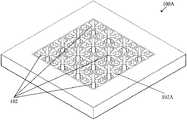
- FIG. 1Adepicts a perspective top view of an exemplary waveguide antenna element based beam forming phased array antenna system for millimeter wave communication, in accordance with an exemplary embodiment of the disclosure.
- FIG. 1Bdepicts a perspective bottom view of the exemplary waveguide antenna element based beam forming phased array antenna system of FIG. 1A , in accordance with an exemplary embodiment of the disclosure.
- FIG. 2Adepicts a perspective top view of an exemplary radiating waveguide antenna cell of the exemplary waveguide antenna element based beam forming phased array antenna system of FIG. 1A , in accordance with an exemplary embodiment of the disclosure.
- FIG. 2Bdepicts a perspective bottom view of the exemplary radiating waveguide antenna cell of FIG. 2A , in accordance with an exemplary embodiment of the disclosure.
- FIG. 3Adepicts a schematic top view of an exemplary radiating waveguide antenna cell of the exemplary waveguide antenna element based beam forming phased array antenna system of FIG. 1A , in accordance with an exemplary embodiment of the disclosure.
- FIG. 3Bdepicts a schematic bottom view of an exemplary radiating waveguide antenna cell of the exemplary waveguide antenna element based beam forming phased array antenna system for millimeter wave communication of FIG. 1A , in accordance with an exemplary embodiment of the disclosure.
- FIG. 4illustrates an exemplary antenna system that depicts a cross-sectional side view of the exemplary radiating waveguide antenna cell of FIG. 2A mounted on a first substrate, in accordance with an exemplary embodiment of the disclosure.
- FIG. 5Aillustrates various components of a first exemplary antenna system, in accordance with an exemplary embodiment of the disclosure.
- FIG. 5Billustrates various components of a second exemplary antenna system, in accordance with an exemplary embodiment of the disclosure.
- FIG. 6illustrates radio frequency (RF) routings from a chip to an exemplary radiating waveguide antenna cell in the first exemplary antenna system of FIG. 5A , in accordance with an exemplary embodiment of the disclosure.
- RFradio frequency
- FIG. 7illustrates protrude pins of an exemplary radiating waveguide antenna cell of an exemplary waveguide antenna array in an antenna system, in accordance with an exemplary embodiment of the disclosure.
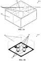
- FIG. 8illustrates a perspective bottom view of the exemplary waveguide antenna element based beam forming phased array antenna system of FIG. 1A integrated with a first substate and a plurality of chips, and mounted on a board in an antenna system, in accordance with an exemplary embodiment of the disclosure.
- FIG. 9illustrates beamforming on an open end of the exemplary waveguide antenna element based beam forming phased array antenna system of FIG. 1A in the first exemplary antenna system of FIG. 5 , in accordance with an exemplary embodiment of the disclosure.
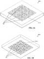
- FIG. 10depicts a perspective top view of an exemplary four-by-four waveguide antenna element based beam forming phased array antenna system with dummy elements, in accordance with an exemplary embodiment of the disclosure.
- FIG. 11illustrates various components of a third exemplary antenna system, in accordance with an exemplary embodiment of the disclosure.
- FIG. 12depicts a perspective top view of an exemplary eight-by-eight waveguide antenna element based beam forming phased array antenna system with dummy elements, in accordance with an exemplary embodiment of the disclosure.
- FIG. 13illustrates various components of a fourth exemplary antenna system, in accordance with an exemplary embodiment of the disclosure.
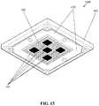
- FIG. 14illustrates positioning of an interposer in an exploded view of an exemplary four-by-four waveguide antenna element based beam forming phased array antenna system module, in accordance with an exemplary embodiment of the disclosure.
- FIG. 15illustrates the interposer of FIG. 14 in an affixed state in an exemplary four-by-four waveguide antenna element based beam forming phased array antenna system module, in accordance with an exemplary embodiment of the disclosure.
- FIG. 16illustrates various components of a fifth exemplary antenna system, in accordance with an exemplary embodiment of the disclosure.
- FIG. 1Adepicts a perspective top view of an exemplary waveguide antenna element based beam forming phased array antenna system for millimeter wave communication, in accordance with an exemplary embodiment of the disclosure.
- a waveguide antenna element based beam forming phased array 100 Amay have a unitary body that comprises a plurality of radiating waveguide antenna cells 102 arranged in a certain layout for millimeter wave communication.
- the unitary bodyrefers to one-piece structure of the waveguide antenna element based beam forming phased array 100 A, where multiple antenna elements, such as the plurality of radiating waveguide antenna cells 102 may be fabricated as a single piece structure, for example, by metal processing or injection moulding.
- FIG. 1Aan example of four-by-four waveguide array comprising sixteen radiating waveguide antenna cells, such as a radiating waveguide antenna cell 102 A, in a first layout, is shown.
- the waveguide antenna element based beam forming phased array 100 Amay be one-piece structure of eight-by-eight waveguide array comprising sixty four radiating waveguide antenna cells in the first layout.
- the number of radiating waveguide antenna cellsmay vary, without departure from the scope of the present disclosure.
- the waveguide antenna element based beam forming phased array 100 Amay be one-piece structure of N-by-N waveguide array comprising “M” number of radiating waveguide antenna cells arranged in certain layout, wherein “N” is a positive integer and “M” is N to the power of 2.
- the waveguide antenna element based beam forming phased array 100 Amay be made of electrically conductive material, such as metal.
- the waveguide antenna element based beam forming phased array 100 Amay be made of copper, aluminum, or mettalic alloy that are considered good electrical conductors.
- the waveguide antenna element based beam forming phased array 100 Amay be made of plastic and coated with electrically conductive material, such as metal, for mass production.
- the exposed or outer surface of the waveguide antenna element based beam forming phased array 100 Amay be coated with electrically conductive material, such as metal, whereas the inner body may be plastic or other inexpensive polymeric substance.
- the waveguide antenna element based beam forming phased array 100 Amay be surface coated with copper, aluminum, silver, and the like. Thus, the waveguide antenna element based beam forming phased array 100 A may be cost-effective and capable of mass production as a result of the unitary body structure of the waveguide antenna element based beam forming phased array 100 A. In some embodiments, the waveguide antenna element based beam forming phased array 100 A may be made of optical fibre for enhanced conduction in the millimeter wave frequency.
- FIG. 1Bdepicts a perspective bottom view of the exemplary waveguide antenna element based beam forming phased array antenna system of FIG. 1A , in accordance with an exemplary embodiment of the disclosure.
- a bottom view of the waveguide antenna element based beam forming phased array 100 Athat depicts a plurality of pins (e.g. four pins in this case) in each radiating waveguide antenna cell (such as the radiating waveguide antenna cell 102 A) of the pluraity of radiating waveguide antenna cells 102 .
- the plurality of pins of each corresponding radiating waveguide antenna cellare connected with a body of a corresponding radiating waveguide antenna cell that acts as ground for the plurality of pins.
- the plurality of pins of each corresponding radiating waveguide antennaare conncted with each other by the ground resulting in the unitary body structure.
- FIG. 2Adepicts a perspective top view of an exemplary radiating waveguide antenna cell of the exemplary waveguide antenna element based beam forming phased array antenna system of FIG. 1A , in accordance with an exemplary embodiment of the disclosure.
- a perspective top view of an exemplary single radiating waveguide antenna cellsuch as the radiating waveguide antenna cell 102 A of FIG. 1A .
- an open end 202 of the radiating waveguide antenna cell 102 AThere is also shown an upper end 204 of a plurality of pins 206 that are connected with a body of the radiating waveguide antenna cell 102 A.
- the body of the radiating waveguide antenna cell 102 Aacts as ground 208 .
- FIG. 2Bdepicts a perspective bottom view of the exemplary radiating waveguide antenna cell of FIG. 2A , in accordance with an exemplary embodiment of the disclosure.
- a bottom view of the radiating waveguide antenna cell 102 A of FIG. 2Athere is shown a first end 210 of the radiating waveguide antenna cell 102 A, which depicts a lower end 212 of the plurality of pins 206 that are connected with the body (i.e., ground 208 ) of the radiating waveguide antenna cell 102 A.
- the plurality of pins 206may be protrude pins that protrude from the first end 210 from a level of the body of the radiating waveguide antenna cell 102 A to establish a firm contact with a substrate on which the plurality of radiating waveguide antenna cells 102 (that includes the radiating waveguide antenna cell 102 A) may be mounted.
- FIG. 3Adepicts a schematic top view of an exemplary radiating waveguide antenna cell of the exemplary waveguide antenna element based beam forming phased array antenna system of FIG. 1A , in accordance with an exemplary embodiment of the disclosure.
- the open end 202 of the radiating waveguide antenna cell 102 Athe upper end 204 of the plurality of pins 206 that are connected with the body (i.e., ground 208 ) of the radiating waveguide antenna cell 102 A.
- the body of the radiating waveguide antenna cell 102 Aacts as the ground 208 .
- the open end 202 of the radiating waveguide antenna cell 102 Arepresents a flat four-leaf like hollow structure surrounded by the ground 208 .
- FIG. 3Bdepicts a schematic bottom view of an exemplary radiating waveguide antenna cell of the exemplary waveguide antenna element based beam forming phased array antenna system of FIG. 1A , in accordance with an exemplary embodiment of the disclosure.
- a schematic bottom view of the radiating waveguide antenna cell 102 A of FIG. 2Bthere is shown the first end 210 of the radiating waveguide antenna cell 102 A.
- the first end 210may be the lower end 212 of the plurality of pins 206 depicting positive and negative terminals.
- the plurality of pins 206 in the radiating waveguide antenna cell 102 Aincludes a pair of vertical polarization pins 302 a and 302 b that acts as a first positive terminal and a first negative terminal.
- the plurality of pins 206 in the radiating waveguide antenna cell 102 Afurther includes a pair of horizontal polarization pins 304 a and 304 b that acts as a second positive terminal and a second negative terminal.
- the pair of vertical polarization pins 302 a and 302 b and the pair of horizontal polarization pins 304 a and 304 bare utilized for dual-polarization.
- the waveguide antenna element based beam forming phased array 100 Amay be a dual-polarized open waveguide array antenna configured to transmit and receive radio frequency (RF) waves for the millimeter wave communication in both horizontal and vertical polarizations.
- the waveguide antenna element based beam forming phased array 100 Amay be a dual-polarized open waveguide array antenna configured to transmit and receive radio frequency (RF) waves in also left hand circular polarization (LHCP) or right hand circular polarization (RHCP), known in the art.
- LHCPleft hand circular polarization
- RHCPright hand circular polarization
- the circular polarizationis known in the art, where an electromagnetic wave is in a polarization state, in which electric field of the electromagnetic wave exhibits a constant magnitude. However, the direction of the electromagnetic wave may rotate with time at a steady rate in a plane perpendicular to the direction of the electromagnetic wave.
- FIG. 4illustrates an exemplary antenna system that depicts a cross-sectional side view of the exemplary radiating waveguide antenna cell of FIG. 2A mounted on a substrate, in accordance with an exemplary embodiment of the disclosure.
- a cross-sectional side view of the ground 208 and two pinssuch as the first pair of horizontal polarization pins 304 a and 304 b, of the radiating waveguide antenna cell 102 A.
- a first substrate 402There is also shown a first substrate 402 , a chip 404 , a plurality of connection ports 406 provided on the chip 404 .
- the plurality of connection ports 406may include at least a negative terminal 406 a and a positive terminal 406 b.
- RFradio frequency
- the first substrate 402comprises an upper side 402 A and a lower side 402 B.
- the first end 210 of the plurality of radiating waveguide antenna cells 102such as the radiating waveguide antenna cell 102 A, of the waveguide antenna element based beam forming phased array 100 A may be mounted on the upper side 402 A of the first substrate 402 .
- the waveguide antenna element based beam forming phased array 100 Amay also be reffered to as a surface mount open waveguide antenna.
- the chip 404may be positioned beneath the lower side 402 B of the first substrate 402 .
- the currentmay flow from the ground 208 towards the negative terminal 406 a of the chip 404 through at least a first pin (e.g., the pin 304 b of the first pair of horizontal polarization pins 304 a and 304 b ), and the electrically conductive connection 408 a.
- the currentmay flow from the positive terminal 406 b of the chip 404 towards the ground 208 through at least a second pin (e.g., the pin 304 a of the first pair of horizontal polarization pins 304 a and 304 b ) of the plurality of pins 206 in the radiating waveguide antenna cell 102 A.
- Thisforms a closed circuit, where the flow of current in the opposite direction in closed circuit within the radiating waveguide antenna cell 102 A in at least one polarization creates a magnetic dipole and differential in at least two electromagnetic waves resulting in propogation of the RF wave 410 via the open end 202 of the radiating waveguide antenna cell 102 A.
- the chip 404may be configured to form a RF beam and further control the propagation and a direction of the RF beam in millimeter wave frequency through the open end 202 of each radiating waveguide antenna cell by adjusting signal parameters of RF signal (i.e. the radiated RF wave 410 ) emitted from each radiating waveguide antenna cell of the plurality of radiating waveguide antenna cells 102 .
- signal parameters of RF signali.e. the radiated RF wave 410
- FIG. 5Aillustrates various components of a first exemplary antenna system, in accordance with an exemplary embodiment of the disclosure.
- the antenna system 500 Amay comprise the first substrate 402 , a plurality of chips 502 , a main system board 504 , and a heat sink 506 .
- a first end 508 of a set of radiating waveguide antenna cells 510 of the waveguide antenna element based beam forming phased array 100 Amay be mounted on the first substrate 402 .
- the first end 508 of the set of radiating waveguide antenna cells 510 of the waveguide antenna element based beam forming phased array 100 Ais mounted on the upper side 402 A of the first substrate 402 .
- the plurality of chips 502may be positioned between the lower side 402 B of the first substrate 402 and the upper surface 504 A of the system board 504 .
- the set of radiating waveguide antenna cells 510may correspond to certain number of radiating waveguide antenna cells, for example, four radiating waveguide antenna cells, of the plurality of radiating waveguide antenna cells 102 ( FIG. 1A ) shown in the side view.
- the plurality of chips 502may be electrically connected with the plurality of pins (such as pins 512 a to 512 h ) and the ground (ground 514 a to 514 d ) of each of the set of radiating waveguide antenna cells 510 to control beamforming through a second end 516 of each of the set of radiating waveguide antenna cells 510 for the millimeter wave communication.
- Each of the plurality of chips 502may include a plurality of connection ports (similar to the plurality of connection ports 406 of FIG.
- the plurality of connection portsmay include a plurality of negative terminals and a plurality of positive terminals (represented by “+” and “ ⁇ ” charges).
- a plurality of electrically conductive routing connectionsare provided from the plurality of connection ports of the plurality of chips 502 to the waveguide antenna elements, such as the pins 512 a to 512 h and the ground 514 a to 514 d of each of the set of radiating waveguide antenna cells 510 .
- the system board 504includes an upper surface 504 A and a lower surface 504 B.
- the upper surface 504 A of the system board 504comprises a plurality of electrically conductive connection points 518 (e.g., solder balls) to connect to the ground (e.g., the ground 514 a to 514 d ) of each of set of radiating waveguide antenna cells 510 of the waveguide antenna element based beam forming phased array 100 A using electrically conductive wiring connections 520 that passes through the first substrate 402 .
- the first substrate 402may be positioned between the waveguide antenna element based beam forming phased array 100 A and the system board 504 .
- the heat sink 506may be attached to the lower surface 504 B of the system board 504 .
- the heat sinkmay have a comb-like structure in which a plurality of protrusions (such as protrusions 506 a and 506 b ) of the heat sink 506 passes through a plurality of perforations in the system board 504 such that the plurality of chips 502 are in contact to the plurality of protrusions (such as protrusions 506 a and 506 b ) of the heat sink 506 to dissipate heat from the plurality of chips 502 through the heat sink 506 .
- a plurality of protrusionssuch as protrusions 506 a and 506 b
- FIG. 5Billustrates various components of a second exemplary antenna system, in accordance with an exemplary embodiment of the disclosure.
- a cross-sectional side view of an antenna system 500 Bthat depicts a cross-sectional side view of the waveguide antenna element based beam forming phased array 100 A in 2D.
- the antenna system 500 Bmay comprise the first substrate 402 , the plurality of chips 502 , the main system board 504 , and other elements as described in FIG. 5A except a dedicated heat sink (such as the heat sink 506 of FIG. 5A ).
- the plurality of chips 502may be on the upper side 402 A of the first substrate 402 (instead of the lower side 402 B as shown in FIG. 5A ).
- the plurality of chips 502 and the plurality of radiating waveguide antenna cells 102(such as the set of radiating waveguide antenna cells 510 ) of the waveguide antenna element based beam forming phased array 100 A may be positioned on the upper side 402 A of the first substrate 402 .
- the plurality of chips 502 and and the waveguide antenna element based beam forming phased array 100 Amay lie on the same side (i.e., the upper side 402 A) of the first substrate 402 .
- Such positioning of the plurality of radiating waveguide antenna cells 102 of the waveguide antenna element based beam forming phased array 110 A and the plurality of chips 502 on a same side of the first substrate 402is advantagoues, as insertion loss (or routing loss) between the first end 508 of the plurality of radiating waveguide antenna cells of the waveguide antenna element based beam forming phased array 110 A and the plurality of chips 502 is reduced to minimum.
- the plurality of chips 502 and and the waveguide antenna element based beam forming phased array 100 Aare present on the same side (i.e., the upper side 402 A) of the first substrate 402 , the plurality of chips 502 are in physical contact to the waveguide antenna element based beam forming phased array 100 A.
- the unitary body of the waveguide antenna element based beam forming phased array 100 Athat has a metallic electrically conductive surface acts as a heat sink to dissipate heat from the plurality of chips 502 to atmospheric air through the metallic electrically conductive surface of the waveguide antenna element based beam forming phased array 110 A. Therefore, no dedicated metallic heat sink (such as the heat sink 506 ), may be required, which is cost-effective.
- FIG. 6illustrates radio frequency (RF) routings from a chip to an exemplary radiating waveguide antenna cell in the first exemplary antenna system of FIG. 5 , in accordance with an exemplary embodiment of the disclosure.
- RFradio frequency
- a vertical length 612 between the chip (such as the chip 404 or one of the plurality of chips 502 ) and a first end of each radiating waveguide antenna cell (such as the first end 210 of the radiating waveguide antenna cell 102 A) of the plurality of radiating waveguide antenna cells 102defines an amount of routing loss between each chip and the first end (such as the first end 210 ) of each radiating waveguide antenna cell.
- the first end of each radiating waveguide antenna cell(such as the first end 210 of the radiating waveguide antenna cell 102 A) includes the lower end 608 of the plurality of pins 610 and the ground at the first end.
- the vertical length 612When the vertical length 612 reduces, the amount of routing loss also reduces, whereas when the vertical length 612 increases, the amount of routing loss also increases. In other words, the amount of routing loss is directly proportional to the vertical length 612 .
- the vertical length 612based on the positioning of the plurality of chips 502 and and the waveguide antenna element based beam forming phased array 100 A on the same side (i.e., the upper side 402 A) of the first substrate 402 , the vertical length 612 is negligible or reduced to minimum between the plurality of chips 502 and the first end 508 of the plurality of radiating waveguide antenna cells of the waveguide antenna element based beam forming phased array 110 A.
- the vertical length 612may be less than a defined threshold to reduce insertion loss (or routing loss) for RF signals or power between the first end of each radiating waveguide antenna cell and the plurality of chips 502 .
- FIG. 6there is further shown a first positive terminal 610 a and a first negative terminal 610 b of a pair of vertical polarization pins of the plurality of pins 610 .
- the positive and negative terminals of the plurality of connection ports 606may be connected to a specific pin of specific and same polarization (as shown), to facilitate dual-polarization.
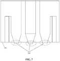
- FIG. 7illustrates protrude pins of an exemplary radiating waveguide antenna cell of an exemplary waveguide antenna element based beam forming phased array in an antenna system, in accordance with an exemplary embodiment of the disclosure.
- a plurality of protrude pins 702that slightly protrudes from a level of the body 704 of a radiating waveguide antenna cell of the waveguide antenna element based beam forming phased array 100 A.
- the plurality of protrude pins 702corresponds to the plurality of pins 206 ( FIG. 2B ) and the pins 512 a to 512 h ( FIG. 5 ).
- the body 704corresponds to the ground 208 ( FIGS.
- the plurality of protrude pins 702 in each radiating waveguide antenna cell of the plurality of radiating waveguide antenna cells 102advantageously secures a firm contact of each radiating waveguide antenna cell with the first substrate 402 ( FIGS. 4 and 5 ).
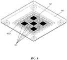
- FIG. 8illustrates a perspective bottom view of the exemplary waveguide antenna element based beam forming phased array antenna system of FIG. 1A integrated with a first substate and a plurality of chips and mounted on a board in an antenna system, in accordance with an exemplary embodiment of the disclosure.
- the plurality of chips 502connected to the lower side 402 B of the first substrate 402 .
- the plurality of chips 502may be electrically connected with the plurality of pins (such as pins 512 a to 512 h ) and the ground (ground 514 a to 514 d ) of each of the plurality of radiating waveguide antenna cells 102 .
- each chip of the plurality of chips 502may be connected to four radiating waveguide antenna cells of the plurality of radiating waveguide antenna cells 102 , via a plurality of vertical routing connections and a plurality of horizontal routing connections.
- An example of the plurality of vertical routing connections 602 and the plurality of horizontal routing connections 604 for one radiating waveguide antenna cell (such as the radiating waveguide antenna cell 102 A)has been shown and described in FIG. 6 .
- the plurality of chips 502may be configured to control beamforming through a second end (e.g., the open end 202 or the second end 516 ) of each radiating waveguide antenna cell of the plurality of radiating waveguide antenna cells 102 for the millimeter wave communication.
- the integrated assemby of the waveguide antenna element based beam forming phased array 100 A with the first substate 402 and the plurality of chips 502may be mounted on a board 802 (e.g., an printed circuit board or an evaluation board) for quality control (QC) testing and to provide a modular arrangement that is easy-to-install.
- a board 802e.g., an printed circuit board or an evaluation board
- QCquality control
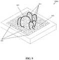
- FIG. 9illustrates beamforming on an open end of the exemplary waveguide antenna element based beam forming phased array antenna system of FIG. 1A in the first exemplary antenna system of FIG. 5A or 5B , in accordance with an exemplary embodiment of the disclosure.
- the plurality of chips 502may be configured to control beamforming through the open end 906 of each radiating waveguide antenna cell of the plurality of radiating waveguide antenna cells 102 for the millimeter wave communication.
- the plurality of chips 502may include a set of receiver (Rx) chips, a set of transmitter (Tx) chips, and a signal mixer chip.
- Rxreceiver
- Txtransmitter
- signal mixer chipa signal mixer chip.
- two or more chipse.g. chips 502 a, 502 b, 502 c, and 502 d
- at least one chipe.g. the chip 502 e
- the signal mixer chipe.g. the chip 502 e
- each of the set of Tx chipsmay comprise various circuits, such as a transmitter (Tx) radio frequency (RF) frontend, a digital to analog converter (DAC), a power amplifier (PA), and other miscellaneous components, such as filters (that reject unwanted spectral components) and mixers (that modulates a frequency carrier signal with an oscillator signal).
- each of the set of Rx chipsmay comprise various circuits, such as a receiver (Rx) RF frontend, an analog to digital converter (ADC), a low noise amplifier (LNA), and other miscellaneous components, such as filters, mixers, and frequency generators.
- the plurality of chips 502 in conjuction with the waveguide antenna element based beam forming phased array 100 A of the antenna system 500 A or 500 Bmay be configured to generate extremely high frequency (EHF), which is the band of radio frequencies in the electromagnetic spectrum from 30 to 300 gigahertz. Such radio frequencies have wavelengths from ten to one millimeter, referred to as millimetre wave (mmW).
- EHFextremely high frequency
- mmWmillimetre wave
- the plurality of chips 502are configured to control propagation, a direction and angle (or tilt, such as 18, 22.5 or 45 degree tilt) of the RF beam (e.g. the main lobe 902 of the RF beam) in millimeter wave frequency through the open end 906 of the plurality of radiating waveguide antenna cells 102 for the millimeter wave communication between the antenna system 500 A or 500 B and a millimeter wave-based communication device.
- Example of the millimeter wave-based communication devicemay include, but are not limited to active reflectors, passive reflectors, or other millimeter wave capable telecommunications hardware, such as customer premises equipment
- the antenna system 500 A or 500 Bmay be used as a part of communication device in a mobile network, such as a part of a base station or an active reflector to send and receive beam of RF signals for high throughput data communication in millimetre wave frequency (for example, broadband).
- a mobile networksuch as a part of a base station or an active reflector to send and receive beam of RF signals for high throughput data communication in millimetre wave frequency (for example, broadband).
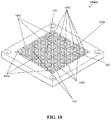
- FIG. 10depicts a perspective top view of an exemplary four-by-four waveguide antenna element based beam forming phased array antenna system with dummy elements, in accordance with an exemplary embodiment of the disclosure.
- a waveguide antenna element based beam forming phased array 1000 Ais shown.
- the waveguide antenna element based beam forming phased array 1000 Ais a one-piece structure that comprises a plurality of non-radiating dummy waveguide antenna cells 1002 arranged in a first layout 1004 in addition to the plurality of radiating waveguide antenna cells 102 (of FIG. 1A ).
- the plurality of non-radiating dummy waveguide antenna cells 1002are positioned at edge regions (including corners) surrounding the plurality of radiating waveguide antenna cells 102 in the first layout 1004 , as shown.
- Such arrangement of the plurality of non-radiating dummy waveguide antenna cells 1002 at edge regions (including corners) surrounding the plurality of radiating waveguide antenna cells 102is advantageous and enables even electromagictec wave (or RF wave) radiation for the millimeter wave communication through the second end (such as the open end 906 ) of each of the plurality of radiating waveguide antenna cells 102 irrespective of positioning of the plurality of radiating waveguide antenna cells 102 in the first layout 1004 .
- radiating waveguide antenna cells that lie in the middle portion in the first layout 1004may have same amount of radiation or achieve similar extent of tilt of a RF beam as compared to the radiating waveguide antenna cells that lie next to the plurality of non-radiating dummy waveguide antenna cells 1002 at edge regions (including corners).
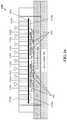
- FIG. 11illustrates various components of a third exemplary antenna system, in accordance with an exemplary embodiment of the disclosure.
- the antenna system 1100may comprise a plurality of radiating waveguide antenna cells (such as radiating waveguide antenna cells 1102 a to 1102 h ) and a plurality of non-radiating dummy waveguide antenna cells (such as non-radiating dummy waveguide antenna cells 1104 a and 1104 b ) in an waveguide antenna element based beam forming phased array.
- the waveguide antenna element based beam forming phased arraymay be an 8 ⁇ 8 (eight-by-eight) waveguide antenna element based beam forming phased array (shown in FIG. 12 ).
- FIG. 11a cross-sectional side view of the waveguide antenna element based beam forming phased array is shown in two dimension (2D).
- the radiating waveguide antenna cells 1102 a to 1102 dmay be mounted on a substrate module 1108 a.
- the radiating waveguide antenna cells 1102 e to 1102 hmay be mounted on a substrate module 1108 b.
- the substrate modules 1108 a and 1108 bcorresponds to the first substrate 402 .
- the plurality of non-radiating dummy waveguide antenna cells(such as non-radiating dummy waveguide antenna cells 1104 a and 1104 b ) are mounted on a second substrate (such as dummy substrates 1106 a and 1106 b ).
- the plurality of non-radiating dummy waveguide antenna cellsmay be mounted on the same type of substrate (such as the first substrate 402 or substrate modules 1108 a and 1108 b ) as of the plurality of radiating waveguide antenna cells.
- the plurality of non-radiating dummy waveguide antenna cells cells(such as non-radiating dummy waveguide antenna cells 1104 a and 1104 b ) may be mounted on a different type of substrate, such as the dummy substrates 1106 a and 1106 b, which may be inexpensive as compared to first substrate the plurality of radiating waveguide antenna cells to reduce cost.
- the second substrate(such as dummy substrates 1106 a and 1106 b ) may be different than the first substrate (such as the substrate modules 1108 a and 1108 b ). This is a significant advantage compared to conventional approaches, where the conventional radiating antenna elements and the dummy antenna elements are on the same expensive substrate.
- the plurality of chips 502 , the main system board 504 , and the heat sink 506are also shown, which are connected in a similar manner as described in FIG. 5 .
- FIG. 12depicts a perspective top view of an exemplary eight-by-eight waveguide antenna element based beam forming phased array antenna system with dummy elements, in accordance with an exemplary embodiment of the disclosure.
- a waveguide antenna element based beam forming phased array 1200 Ais shown.
- the waveguide antenna element based beam forming phased array 1200 Ais a one-piece structure that comprises a plurality of non-radiating dummy waveguide antenna cells 1204 (such as the non-radiating dummy waveguide antenna cells 1104 a and 1104 b of FIG. 11 ) in addition to a plurality of radiating waveguide antenna cells 1202 (such as the radiating waveguide antenna cells 1102 a to 1102 h of FIG.
- the plurality of non-radiating dummy waveguide antenna cells 1204are positioned at edge regions (including corners) surrounding the plurality of radiating waveguide antenna cells 1202 , as shown. Such arrangement of the plurality of non-radiating dummy waveguide antenna cells 1204 at edge regions (including corners) surrounding the plurality of radiating waveguide antenna cells 1202 is advantageous and enables even electromagictec wave (or RF wave) radiation for the millimeter wave communication through the second end (such as an open end 1206 ) of each of the plurality of radiating waveguide antenna cells 1202 irrespective of positioning of the plurality of radiating waveguide antenna cells 1202 in the waveguide antenna element based beam forming phased array 1200 A.
- FIG. 13illustrates various components of a fourth exemplary antenna system, in accordance with an exemplary embodiment of the disclosure.
- FIG. 13is described in conjuction with elements of FIG. 11 .
- FIG. 13there is shown a cross-sectional side view of an antenna system 1300 .
- the antenna system 1300may be similar to the antenna system 1100 .
- the antenna system 1300further includes an interposer 1302 in addition to the various components of the antenna system 1100 as described in FIG. 11 .
- the interposer 1302may be positioned only beneath the edge regions of a waveguide antenna element based beam forming phased array (such as the waveguide antenna element based beam forming phased array 100 A or the waveguide antenna element based beam forming phased array 1200 A at a first end (such as the first end 210 ) to shield radiation leakage from the first end of the plurality of radiating waveguide antenna cells (e.g., the plurality of radiating waveguide antenna cells 1202 ) of the waveguide antenna element based beam forming phased array (such as the waveguide antenna element based beam forming phased arrays 100 A, 1000 A, 1200 A).
- a waveguide antenna element based beam forming phased arraysuch as the waveguide antenna element based beam forming phased array 100 A or the waveguide antenna element based beam forming phased array 1200 A at a first end (such as the first end 210 ) to shield radiation leakage from the first end of the plurality of radiating waveguide antenna cells (e.g., the pluralit
- interposer 1302may facilitate electrical connection routing from one waveguide antenna element based beam forming phased array to another waveguide antenna element based beam forming phased array at the edge regions.
- the interposer 1302may not extend or cover the entire area of the waveguide antenna element based beam forming phased array at the first end (i.e., the end that is mounted on the first substrate (such as the substrate modules 1108 a and 1108 b ). This may be further understood from FIGS. 14 and 15 .
- FIG. 14illustrates positioning of an interposer in an exploded view of an exemplary four-by-four waveguide antenna element based beam forming phased array antenna system module, in accordance with an exemplary embodiment of the disclosure.
- a four-by-four waveguide antenna element based beam forming phased array module 1402with the interposer 1302 .
- the four-by-four waveguide antenna element based beam forming phased array module 1402may correspond to the integrated assemby of the waveguide antenna element based beam forming phased array 100 A with the first substate 402 and the plurality of chips 502 mounted on the board, as shown and descibed in FIG. 8 .
- the interposer 1302may have a square-shaped or a rectangular-shaped hollow frame-like structure (for example a socket frame) with perforations to removably attach to corresponding protruded points on the four-by-four waveguide antenna element based beam forming phased array module 1402 , as shown in an example.
- a square-shaped or a rectangular-shaped hollow frame-like structurefor example a socket frame
- perforationsto removably attach to corresponding protruded points on the four-by-four waveguide antenna element based beam forming phased array module 1402 , as shown in an example.
- FIG. 15illustrates the interposer of FIG. 14 in an affixed state in an exemplary four-by-four waveguide antenna element based beam forming phased array antenna system module, in accordance with an exemplary embodiment of the disclosure.
- the interposer 1302 ain an affixed state on the four-by-four waveguide antenna element based beam forming phased array module 1402 .
- the interposer 1302may be positioned only beneath the edge regions of a waveguide antenna element based beam forming phased array, such as the four-by-four waveguide antenna element based beam forming phased array module 1402 in this case.
- FIG. 16illustrates various components of a fifth exemplary antenna system, in accordance with an exemplary embodiment of the disclosure.
- FIG. 16is described in conjuction with elements of FIGS. 1A, 1B, 2A, 2B, 3A, 3B, and 4 to 15 .
- FIG. 16there is shown a cross-sectional side view of an antenna system 1600 .
- the antenna system 1600may be similar to the antenna system 1100 of FIG. 11 .
- the antenna system 1600further includes a ground (gnd) layer 1602 in addition to the various components of the antenna system 1100 as described in FIG. 11 .
- the gnd layer 1602is provided between the first end (such as the first end 210 ) of the plurality of radiating waveguide antenna cells (such as the radiating waveguide antenna cells 1102 a to 1102 d ) of a waveguide antenna element based beam forming phased array and the first substrate (such as the substrate modules 1108 a and 1108 b or the first substrate 402 ( FIGS. 4 and 5 ) to avoid or minimize ground loop noise from the ground (such as the ground 1106 ) of each radiating waveguide antenna cell of the plurality of the radiating waveguide antenna cells of the waveguide antenna element based beam forming phased array (such as the waveguide antenna element based beam forming phased array 100 A or 1200 A).
- the antenna system(such as the antenna system 500 A, 500 B, 1100 , and 1300 ), may comprise a first substrate (such as the first substrate 402 or the substrate modules 1108 a and 1108 b ), a plurality of chips (such as the chip 404 or the plurality of chips 502 ); and a waveguide antenna element based beam forming phased array (such as the waveguide antenna element based beam forming phased array 100 A, 1000 A, or 1200 A) having a unitary body that comprises a plurality of radiating waveguide antenna cells (such as the plurality of radiating waveguide antenna cells 102 , 1002 , 1202 , or 510 ), in a first layout (such as the first layout 1004 for millimeter wave communication.
- a first substratesuch as the first substrate 402 or the substrate modules 1108 a and 1108 b
- a plurality of chipssuch as the chip 404 or the plurality of chips 502
- a waveguide antenna element based beam forming phased arraysuch as the
- Each radiating waveguide antenna cellcomprises a plurality of pins (such as the plurality of pins 206 ) that are connected with a body (such as the ground 208 ) of a corresponding radiating waveguide antenna cell that acts as ground for the plurality of pins.
- a first end of the plurality of radiating waveguide antenna cells of the waveguide antenna element based beam forming phased array as the unitary body in the first layoutis mounted on the first substrate.
- the plurality of chipsmay be electrically connected with the plurality of pins and the ground of each of the plurality of radiating waveguide antenna cells to control beamforming through a second end (such as the open end 202 or 906 ) of the plurality of radiating waveguide antenna cells for the millimeter wave communication.
- the waveguide antenna element based beam forming phased arraymay be a one-piece structure of four-by-four waveguide array comprising sixteen radiating waveguide antenna cells in the first layout, where the one-piece structure of four-by-four waveguide array corresponds to the unitary body of the waveguide antenna element based beam forming phased array.
- the waveguide antenna element based beam forming phased arraymay be one-piece structure of eight-by-eight waveguide array comprising sixty four radiating waveguide antenna cells in the first layout, where the one-piece structure of eight-by-eight waveguide array corresponds to the unitary body of the waveguide antenna element based beam forming phased array.
- the waveguide antenna element based beam forming phased arraymay be one-piece structure of N-by-N waveguide array comprising M number of radiating waveguide antenna cells in the first layout, wherein N is a positive integer and M is N to the power of 2.
- the waveguide antenna element based beam forming phased arraymay further comprise a plurality of non-radiating dummy waveguide antenna cells (such as the plurality of non-radiating dummy waveguide antenna cells 1002 or 204 or the non-radiating dummy waveguide antenna cells 1104 a and 1104 b ) in the first layout.
- the plurality of non-radiating dummy waveguide antenna cellsmay be positioned at edge regions surrounding the plurality of radiating waveguide antenna cells in the first layout to enable even radiation for the millimeter wave communication through the second end of each of the plurality of radiating waveguide antenna cells irrespective of positioning of the plurality of radiating waveguide antenna cells in the first layout.
- the antenna systemmay further comprise a second substrate (such as dummy substrates 1106 a and 1106 b ).
- the plurality of non-radiating dummy waveguide antenna cells in the first layoutare mounted on the second substrate that is different than the first substrate.
- the antenna systemmay further comprise a system board (such as the system board 504 ) having an upper surface and a lower surface.
- the upper surface of the system boardcomprises a plurality of electrically conductive connection points (such as the plurality of electrically conductive connection points 518 ) to connect to the ground of each of the plurality of radiating waveguide antenna cells of the waveguide antenna element based beam forming phased array using electrically conductive wiring connections that passes through the first substrate, where the first substrate is positioned between the waveguide antenna element based beam forming phased array and the system board.
- the antenna systemmay further comprise a heat sink (such as the heat sink 506 ) that is attached to the lower surface of the system board.
- the heat sinkhave a comb-like structure in which a plurality of protrusions of the heat sink passes through a plurality of perforations in the system board such that the plurality of chips are in contact to the plurality of protrusions of the heat sink to dissipate heat from the plurality of chips through the heat sink.
- the first substratemay comprise an upper side and a lower side, where the first end of the plurality of radiating waveguide antenna cells of the waveguide antenna element based beam forming phased array may be mounted on the upper side of the first substrate, and the plurality of chips are positioned between the lower side of the first substrate and the upper surface of the system board.
- the first substratemay comprises an upper side and a lower side, where the plurality of chips and the plurality of radiating waveguide antenna cells of the waveguide antenna element based beam forming phased array are positioned on the upper side of the first substrate.
- a vertical length between the plurality of chips and the first end of the plurality of radiating waveguide antenna cells of the waveguide antenna element based beam forming phased arraymay be less than a defined threshold to reduce insertion or routing loss between the plurality of radiating waveguide antenna cells of the waveguide antenna element based beam forming phased array and the plurality of chips, based on the positioning of the plurality of radiating waveguide antenna cells of the waveguide antenna element based beam forming phased array and the plurality of chips on a same side of the first substrate.
- the unitary body of the waveguide antenna element based beam forming phased arraymay have a metallic electrically conductive surface that acts as a heat sink to dissipate heat from the plurality of chips to atmospheric air through the metallic electrically conductive surface of the waveguide antenna element based beam forming phased array, based on a contact of the plurality of chips with the plurality of radiating waveguide antenna cells of the waveguide antenna element based beam forming phased array on the upper side of the first substrate.
- the plurality of pins in each radiating waveguide antenna cellmay be protrude pins (such as the plurality of protrude pins 702 ) that protrude from the first end from a level of the body of the corresponding radiating waveguide antenna cell to establish a firm contact with the first substrate.
- the waveguide antenna element based beam forming phased arrayis a dual-polarized open waveguide array antenna configured to transmit and receive radio frequency waves for the millimeter wave communication in both horizontal and vertical polarizations or as left hand circular polarization (LHCP) or right hand circular polarization (RHCP).
- the plurality of pins in each radiating waveguide antenna cellmay include a pair of vertical polarization pins that acts as a first positive terminal and a first negative terminal and a pair of horizontal polarization pins that acts as a second positive terminal and a second negative terminal, wherein the pair of vertical polarization pins and the pair of horizontal polarization pins are utilized for dual-polarization.
- the plurality of chipscomprises a set of receiver (Rx) chips, a set of transmitter (Tx) chips, and a signal mixer chip.
- the plurality of chipsmay be configured to control propagation and a direction of a radio frequency (RF) beam in millimeter wave frequency through the second end of the plurality of radiating waveguide antenna cells for the millimeter wave communication between the antenna system and a millimeter wave-based communication device, where the second end may be an open end of the plurality of radiating waveguide antenna cells for the millimeter wave communication.
- RFradio frequency
- the propagation of the radio frequency (RF) beam in millimeter wave frequencymay be controlled based on at least a flow of current in each radiating waveguide antenna cell, where the current flows from the ground towards a negative terminal of a first chip of the plurality of chips via at least a first pin of the plurality of pins, and from a positive terminal of the first chip towards the ground via at least a second pin of the plurality of pins in each corresponding radiating waveguide antenna cell of the plurality of radiating waveguide antenna cells.
- the antenna systemmay further comprise an interposer (such as the interposer 1302 ) beneath the edge regions of the waveguide antenna element based beam forming phased array at the first end in the first layout to shield radiation leakage from the first end of the plurality of radiating waveguide antenna cells of the waveguide antenna element based beam forming phased array.
- an interposersuch as the interposer 1302
- the antenna systemmay further comprise a ground (gnd) layer (such as the gnd layer 1602 ) between the first end of the plurality of radiating waveguide antenna cells of the waveguide antenna element based beam forming phased array and the first substrate to avoid or minimize ground loop noise from the ground of each radiating waveguide antenna cell of the plurality of the radiating waveguide antenna cells of the waveguide antenna element based beam forming phased array.
- a ground (gnd) layersuch as the gnd layer 1602
- the waveguide antenna element based beam forming phased arrays 100 A, 110 A, 1000 A, 1200 Amay be utilized in, for example, active and passive reflector devices disclosed in, for example, U.S. application Ser. No. 15/607,743, and U.S. application Ser. No. 15/834,894.
- circuitry or hardwaree.g., within or coupled to a central processing unit (“CPU”), microprocessor, micro controller, digital signal processor, processor core, system on chip (“SOC”) or any other device
- implementationsmay also be embodied in software (e.g. computer readable code, program code, and/or instructions disposed in any form, such as source, object or machine language) disposed for example in a non-transitory computer-readable medium configured to store the software.
- Such softwarecan enable, for example, the function, fabrication, modeling, simulation, description and/or testing of the apparatus and methods describe herein. For example, this can be accomplished through the use of general program languages (e.g., C, C++), hardware description languages (HDL) including Verilog HDL, VHDL, and so on, or other available programs.
- Such softwarecan be disposed in any known non-transitory computer-readable medium, such as semiconductor, magnetic disc, or optical disc (e.g., CD-ROM, DVD-ROM, etc.).
- the softwarecan also be disposed as computer data embodied in a non-transitory computer-readable transmission medium (e.g., solid state memory any other non-transitory medium including digital, optical, analogue-based medium, such as removable storage media).
- Embodiments of the present disclosuremay include methods of providing the apparatus described herein by providing software describing the apparatus and subsequently transmitting the software as a computer data signal over a communication network including the internet and intranets.
- system described hereinmay be included in a semiconductor intellectual property core, such as a microprocessor core (e.g., embodied in HDL) and transformed to hardware in the production of integrated circuits. Additionally, the system described herein may be embodied as a combination of hardware and software. Thus, the present disclosure should not be limited by any of the above-described exemplary embodiments, but should be defined only in accordance with the following claims and their equivalents.
Landscapes
- Variable-Direction Aerials And Aerial Arrays (AREA)
- Waveguide Aerials (AREA)
Abstract
Description
- U.S. application Ser. No. 15/607,743, which was filed on May 30, 2017; and
- U.S. application Ser. No. 15/834,894, which was filed on Dec. 7, 2017.
Claims (20)
Priority Applications (3)
| Application Number | Priority Date | Filing Date | Title |
|---|---|---|---|
| US16/391,628US11108167B2 (en) | 2018-02-26 | 2019-04-23 | Waveguide antenna element-based beam forming phased array antenna system for millimeter wave communication |
| US17/365,037US11588254B2 (en) | 2018-02-26 | 2021-07-01 | Waveguide antenna element-based beam forming phased array antenna system for millimeter wave communication |
| US17/978,565US11764486B2 (en) | 2018-02-26 | 2022-11-01 | Waveguide antenna element based beam forming phased array antenna system for millimeter wave communication |
Applications Claiming Priority (2)
| Application Number | Priority Date | Filing Date | Title |
|---|---|---|---|
| US15/904,521US10637159B2 (en) | 2018-02-26 | 2018-02-26 | Waveguide antenna element-based beam forming phased array antenna system for millimeter wave communication |
| US16/391,628US11108167B2 (en) | 2018-02-26 | 2019-04-23 | Waveguide antenna element-based beam forming phased array antenna system for millimeter wave communication |
Related Parent Applications (1)
| Application Number | Title | Priority Date | Filing Date |
|---|---|---|---|
| US15/904,521ContinuationUS10637159B2 (en) | 2018-02-26 | 2018-02-26 | Waveguide antenna element-based beam forming phased array antenna system for millimeter wave communication |
Related Child Applications (1)
| Application Number | Title | Priority Date | Filing Date |
|---|---|---|---|
| US17/365,037ContinuationUS11588254B2 (en) | 2018-02-26 | 2021-07-01 | Waveguide antenna element-based beam forming phased array antenna system for millimeter wave communication |
Publications (2)
| Publication Number | Publication Date |
|---|---|
| US20190267722A1 US20190267722A1 (en) | 2019-08-29 |
| US11108167B2true US11108167B2 (en) | 2021-08-31 |
Family
ID=67477567
Family Applications (4)
| Application Number | Title | Priority Date | Filing Date |
|---|---|---|---|
| US15/904,521ActiveUS10637159B2 (en) | 2018-02-26 | 2018-02-26 | Waveguide antenna element-based beam forming phased array antenna system for millimeter wave communication |
| US16/391,628Active2038-10-09US11108167B2 (en) | 2018-02-26 | 2019-04-23 | Waveguide antenna element-based beam forming phased array antenna system for millimeter wave communication |
| US17/365,037ActiveUS11588254B2 (en) | 2018-02-26 | 2021-07-01 | Waveguide antenna element-based beam forming phased array antenna system for millimeter wave communication |
| US17/978,565ActiveUS11764486B2 (en) | 2018-02-26 | 2022-11-01 | Waveguide antenna element based beam forming phased array antenna system for millimeter wave communication |
Family Applications Before (1)
| Application Number | Title | Priority Date | Filing Date |
|---|---|---|---|
| US15/904,521ActiveUS10637159B2 (en) | 2018-02-26 | 2018-02-26 | Waveguide antenna element-based beam forming phased array antenna system for millimeter wave communication |
Family Applications After (2)
| Application Number | Title | Priority Date | Filing Date |
|---|---|---|---|
| US17/365,037ActiveUS11588254B2 (en) | 2018-02-26 | 2021-07-01 | Waveguide antenna element-based beam forming phased array antenna system for millimeter wave communication |
| US17/978,565ActiveUS11764486B2 (en) | 2018-02-26 | 2022-11-01 | Waveguide antenna element based beam forming phased array antenna system for millimeter wave communication |
Country Status (1)
| Country | Link |
|---|---|
| US (4) | US10637159B2 (en) |
Families Citing this family (13)
| Publication number | Priority date | Publication date | Assignee | Title |
|---|---|---|---|---|
| US10944180B2 (en) | 2017-07-10 | 2021-03-09 | Viasat, Inc. | Phased array antenna |
| EP3804167A1 (en) | 2018-07-13 | 2021-04-14 | Viasat, Inc. | Multi-beam antenna system with a baseband digital signal processor |
| US11495881B1 (en) | 2018-12-10 | 2022-11-08 | Ball Aerospace & Technologies Corp. | Antenna system with integrated electromagnetic interference shielded heat sink |
| CN109687165A (en)* | 2018-12-29 | 2019-04-26 | 瑞声科技(南京)有限公司 | Millimeter wave array antenna mould group and mobile terminal |
| KR102593888B1 (en)* | 2019-06-13 | 2023-10-24 | 삼성전기주식회사 | Antenna module and electronic device including thereof |
| CN112952375B (en)* | 2019-11-26 | 2022-07-22 | 华为技术有限公司 | Method and apparatus for forming a beam |
| US11095014B2 (en)* | 2020-01-07 | 2021-08-17 | Aptiv Technologies Limited | Waveguide antenna with integrated temperature management |
| CN111541032B (en)* | 2020-04-30 | 2021-08-06 | 深圳市睿德通讯科技有限公司 | A millimeter wave and non-millimeter wave antenna integrated module system and electronic equipment |
| CN112563754A (en)* | 2020-10-27 | 2021-03-26 | 安徽隼波科技有限公司 | High-integration-level integrated efficient sum-difference beam waveguide antenna |
| US20240405448A1 (en)* | 2021-09-22 | 2024-12-05 | Jabil Inc. | Modular heat mitigation system with mmwave suppression for active electronically steered antennas |
| CN114094303B (en)* | 2021-11-23 | 2025-01-21 | 北京九天微星科技发展有限公司 | Heat dissipation structure of phased array antenna, phased array antenna and satellite platform |
| US11894873B2 (en)* | 2022-06-29 | 2024-02-06 | Raytheon Company | Photonic integrated circuit with inverted H-tree unit cell design |
| CN117855881A (en)* | 2024-01-30 | 2024-04-09 | 环旭电子股份有限公司 | Millimeter wave optical fiber antenna module and manufacturing method thereof |
Citations (265)
| Publication number | Priority date | Publication date | Assignee | Title |
|---|---|---|---|---|
| US3835469A (en) | 1972-11-02 | 1974-09-10 | Hughes Aircraft Co | Optical limited scan antenna system |
| US4799062A (en) | 1987-04-27 | 1989-01-17 | Axonn Corporation | Radio position determination method and apparatus |
| US5473602A (en) | 1994-03-04 | 1995-12-05 | Nova-Net Communications, Inc. | Wireless radio packet switching network |
| US5479651A (en) | 1993-03-24 | 1995-12-26 | Fujitsu Limited | Disc drive controller to detect defects in read/write circuits for a disc drive |
| US5561850A (en) | 1992-04-29 | 1996-10-01 | Televerket | Method and arrangement for reducing fading between a base station and mobile units |
| US5598173A (en) | 1994-05-17 | 1997-01-28 | Space Engineering S.P.A. | Shaped-beam or scanned beams reflector or lens antenna |
| US5666124A (en) | 1995-12-14 | 1997-09-09 | Loral Aerospace Corp. | High gain array antenna system |
| US5771017A (en) | 1993-08-12 | 1998-06-23 | Northern Telecom Limited | Base station antenna arrangement |
| US5883602A (en) | 1996-06-05 | 1999-03-16 | Apti, Inc. | Wideband flat short foci lens antenna |
| US5905473A (en) | 1997-03-31 | 1999-05-18 | Resound Corporation | Adjustable array antenna |
| US5940033A (en) | 1998-01-20 | 1999-08-17 | The United States Of America As Represented By The Secretary Of The Army | Apparatus, methods and computer program for evaluating multiple null forming antenna processors and jammers |
| US6018316A (en) | 1997-01-24 | 2000-01-25 | Ail Systems, Inc. | Multiple beam antenna system and method |
| US6307502B1 (en) | 1998-12-30 | 2001-10-23 | Agence Spatiale Europeene | Radiometry system with an aperture synthesis type antenna and its application to hyper-frequency imaging |
| US20020034958A1 (en) | 2000-06-05 | 2002-03-21 | Gerald Oberschmidt | Indoor wireless system using active reflector |
| US6405018B1 (en) | 1999-01-11 | 2002-06-11 | Metawave Communications Corporation | Indoor distributed microcell |
| US6433920B1 (en) | 2000-04-27 | 2002-08-13 | Jds Uniphase Corporation | Raman-based utility optical amplifier |
| US20020132600A1 (en) | 2001-01-17 | 2002-09-19 | Rudrapatna Ashok N. | Structure for multiple antenna configurations |
| US6456252B1 (en) | 2000-10-23 | 2002-09-24 | The Boeing Company | Phase-only reconfigurable multi-feed reflector antenna for shaped beams |
| US20020193074A1 (en) | 2001-06-14 | 2002-12-19 | Hewlett-Packard Company | Service system usage control |
| US20030012208A1 (en) | 2001-06-29 | 2003-01-16 | Bernheim Henrik F. | System and method for virtual sector provisioning and network configuration |
| US20030090418A1 (en) | 2001-11-09 | 2003-05-15 | Howell James M. | Beamformer for multi-beam broadcast antenna |
| US6577631B1 (en) | 1998-06-10 | 2003-06-10 | Merlot Communications, Inc. | Communication switching module for the transmission and control of audio, video, and computer data over a single network fabric |
| US20030129989A1 (en) | 2002-01-08 | 2003-07-10 | Aziz Gholmieh | Method and apparatus for controlling communications of data from multiple base stations to a mobile station in a communication system |
| US20030236109A1 (en) | 2002-04-17 | 2003-12-25 | Nec Corporation | Cellular telephone |
| US6718159B1 (en) | 1999-02-03 | 2004-04-06 | Matsushita Electric Industrial Co., Ltd. | Radio communication system and method |
| US20040077379A1 (en) | 2002-06-27 | 2004-04-22 | Martin Smith | Wireless transmitter, transceiver and method |
| US20040082356A1 (en) | 2002-10-25 | 2004-04-29 | Walton J. Rodney | MIMO WLAN system |
| US20040095907A1 (en) | 2000-06-13 | 2004-05-20 | Agee Brian G. | Method and apparatus for optimization of wireless multipoint electromagnetic communication networks |
| US20040110469A1 (en) | 2000-01-14 | 2004-06-10 | Judd Mano D. | Repeaters for wireless communication systems |
| US20040116129A1 (en) | 2002-12-13 | 2004-06-17 | Arlynn Wilson | System and method for controlling transceivers based on a location indicator |
| US20040127174A1 (en) | 2002-12-30 | 2004-07-01 | Motorola, Inc. | Method and system for minimizing overlap nulling in switched beams |
| US20040166808A1 (en) | 2002-04-16 | 2004-08-26 | Yasuhiro Hasegawa | Adaptive array antenna receiving apparatus and antenna array calibration method |
| US6804491B1 (en) | 1999-03-31 | 2004-10-12 | Matsushita Electric Industrial Co., Ltd. | Mobile communication system and repeater used in the mobile communication system |
| US20040204114A1 (en) | 2002-11-04 | 2004-10-14 | James Brennan | Forced beam switching in wireless communication systems having smart antennas |
| US20050048964A1 (en) | 2003-08-25 | 2005-03-03 | Cohen Alain J. | Wireless link simulation with generic caching |
| US20050069252A1 (en) | 2003-09-30 | 2005-03-31 | Hwang Seong-Taek | Dual-port broadband light source with independently controllable output powers |
| US20050134517A1 (en)* | 2003-12-18 | 2005-06-23 | Kathrein-Werke Kg | Antenna having at least one dipole or an antenna element arrangement similar to a dipole |
| US20050136943A1 (en) | 2003-10-07 | 2005-06-23 | Banerjee Debarag N. | Location-assisted wireless communication |
| US20050181755A1 (en) | 2004-02-13 | 2005-08-18 | Pioneer Corporation | Receiver, method of receiving, and computer product |
| US20050232216A1 (en) | 2004-04-14 | 2005-10-20 | Webster Mark A | Dual mode communication systems and methods |
| US20050237971A1 (en) | 2004-02-23 | 2005-10-27 | Kabushiki Kaisha Toshiba | Adaptive MIMO systems |
| US20050243756A1 (en) | 2004-04-30 | 2005-11-03 | Samsung Electronics Co., Ltd. | Apparatus and method for implementing virtual MIMO antennas in a mobile ad hoc network |
| US20050270227A1 (en) | 2003-07-03 | 2005-12-08 | Stephens Scott A | Positioning system with intentional multi-path signal |
| US6992622B1 (en) | 2004-10-15 | 2006-01-31 | Interdigital Technology Corporation | Wireless communication method and antenna system for determining direction of arrival information to form a three-dimensional beam used by a transceiver |
| US20060063494A1 (en) | 2004-10-04 | 2006-03-23 | Xiangdon Zhang | Remote front-end for a multi-antenna station |
| US7020482B2 (en) | 2002-01-23 | 2006-03-28 | Qualcomm Incorporated | Reallocation of excess power for full channel-state information (CSI) multiple-input, multiple-output (MIMO) systems |
| US7058367B1 (en) | 2003-01-31 | 2006-06-06 | At&T Corp. | Rate-adaptive methods for communicating over multiple input/multiple output wireless systems |
| US20060205342A1 (en) | 2005-03-11 | 2006-09-14 | Mckay David L Sr | Remotely controllable and reconfigurable wireless repeater |
| US20060246922A1 (en) | 2005-04-28 | 2006-11-02 | Northrop Grumman Corporation | Systems and methods for condition and location monitoring of mobile entities |
| US20060267839A1 (en) | 2005-05-24 | 2006-11-30 | Leo Vaskelainen | Control of radiation pattern in wireless telecommunications system |
| US20070001924A1 (en)* | 2005-06-30 | 2007-01-04 | Sony Corporation | Antenna device, wireless communication apparatus using the same, and control method of controlling wireless communication apparatus |
| US20070040025A1 (en) | 2004-12-20 | 2007-02-22 | Altierre Corporation | Low power wireless display tag systems and methods |
| US7187949B2 (en) | 2001-01-19 | 2007-03-06 | The Directv Group, Inc. | Multiple basestation communication system having adaptive antennas |
| US20070052519A1 (en) | 2005-09-02 | 2007-03-08 | Gm Global Technology Operations, Inc. | Wireless sensing system |
| US20070066254A1 (en) | 2005-09-16 | 2007-03-22 | Kabushiki Kaisha Toshiba | Analog signal processing circuit and communication device therewith |
| US7206294B2 (en) | 2001-08-15 | 2007-04-17 | Meshnetworks, Inc. | Movable access points and repeaters for minimizing coverage and capacity constraints in a wireless communications network and a method for using the same |
| US20070100548A1 (en) | 2003-08-04 | 2007-05-03 | David Small | System & method for determining attitude using spatial shift key (ssk) modulation signatures |
| US20070116012A1 (en) | 2005-10-14 | 2007-05-24 | Samsung Electronics Co., Ltd. | Data service apparatus and method in heterogeneous wireless networks |
| US20070115800A1 (en) | 2005-10-20 | 2007-05-24 | Fonseka John P | Uplink modulation and receiver structures for asymmetric OFDMA systems |
| US20070127360A1 (en) | 2005-12-05 | 2007-06-07 | Song Hyung-Kyu | Method of adaptive transmission in an orthogonal frequency division multiplexing system with multiple antennas |
| US20070160014A1 (en) | 2003-12-30 | 2007-07-12 | Telefonaktiebolaget Lm Ericsson (Publ) | Method and system for wireless communication networks using cooperative relaying |
| US20070280310A1 (en) | 2006-06-02 | 2007-12-06 | The Boeing Company | Laser intra-cavity electronic wavelength tuner |
| US20080025208A1 (en) | 2006-07-28 | 2008-01-31 | Michael Tin Yau Chan | Wide-area wireless network topology |
| US20080026763A1 (en) | 2006-07-25 | 2008-01-31 | Samsung Electronics Co., Ltd. | System and method for providing SOHO BTS coverage based on angle of arrival of mobile station signals |
| EP1890441A2 (en) | 2006-08-18 | 2008-02-20 | Fujitsu Ltd. | Radio relay system and radio relay station |
| US7339979B1 (en) | 2003-02-11 | 2008-03-04 | Calamp Corp. | Adaptive beamforming methods and systems that enhance performance and reduce computations |
| WO2008027531A2 (en) | 2006-09-01 | 2008-03-06 | Qualcomm Incorporated | Repeater having dual receiver or transmitter antenna configuration with adaptation for increased isolation |
| US20080076370A1 (en) | 2006-09-27 | 2008-03-27 | Kotecha Jayesh H | Methods for optimal collaborative MIMO-SDMA |
| US7363058B2 (en)* | 2002-10-01 | 2008-04-22 | Trango Systems, Inc. | Wireless point multipoint system |
| US20080117961A1 (en) | 2006-11-22 | 2008-05-22 | Samsung Electronics Co.; Ltd | Method and apparatus of adaptively allocating transmission power for beamforming combined with orthogonal space-time block codes based on symbol error rate in distributed wireless communication system |
| US20080167049A1 (en) | 1996-09-09 | 2008-07-10 | Tracbeam Llc | Wireless location using signal fingerprinting and other location estimators |
| US20080212582A1 (en) | 2004-04-05 | 2008-09-04 | Wireless Audio Ip B.V | Wireless Audio Transmission System and Method |
| US7424225B1 (en) | 2003-11-17 | 2008-09-09 | Bbn Technologies Corp. | Systems and methods for implementing contention-based optical channel access |
| US20080225758A1 (en) | 2007-03-02 | 2008-09-18 | Qualcomm Incorporated | Automatic Gain Control and Filtering Techniques for Use in On-Channel Repeater |
| US20080261509A1 (en) | 2007-04-23 | 2008-10-23 | Robi Sen | Distributed Wireless Communications for Tactical Network Dominance |
| US20080258993A1 (en) | 2007-03-16 | 2008-10-23 | Rayspan Corporation | Metamaterial Antenna Arrays with Radiation Pattern Shaping and Beam Switching |
| US20080303701A1 (en) | 2007-06-08 | 2008-12-11 | Jianzhong Zhang | CDD precoding for open loop su mimo |
| US20080315944A1 (en) | 2005-09-20 | 2008-12-25 | Raytheon Company | Spatially-fed high power amplifier with shaped reflectors |
| US20090009392A1 (en) | 2005-04-29 | 2009-01-08 | Lockheed Martin Corporation | Shared phased array cluster beamformer |
| US20090010215A1 (en) | 2007-07-02 | 2009-01-08 | Samsung Electronics Co., Ltd. | Method of allocating wireless resource for space division multiple access communication and wireless resource allocation system of enabling the method |
| US7480486B1 (en) | 2003-09-10 | 2009-01-20 | Sprint Spectrum L.P. | Wireless repeater and method for managing air interface communications |
| US20090029645A1 (en) | 2007-07-25 | 2009-01-29 | Teenay Wireless, Inc. | Multi-Tier Backhaul Network System with Traffic Differentiation and Advanced Processing Capabilities and Methods Therefor |
| US20090028120A1 (en) | 2007-07-26 | 2009-01-29 | Lg-Nortel Co., Ltd. | Method and apparatus for providing neighborhood ap information in a wireless lan system |
| US20090092120A1 (en) | 2007-10-09 | 2009-04-09 | Ntt Docomo, Inc. | Radio communication system, radio communication method and base station |
| US20090093265A1 (en) | 2005-05-25 | 2009-04-09 | Ryohei Kimura | Radio transmitting apparatus, radio receiving apparatus and radio transmitting method |
| US20090136227A1 (en) | 2007-11-15 | 2009-05-28 | Hugh Lambert | Mirror |
| US20090156227A1 (en) | 2007-12-18 | 2009-06-18 | At&T Mobility Ii Llc | Optimal utilization of multiple transceivers in a wireless environment |
| US20090175214A1 (en) | 2008-01-02 | 2009-07-09 | Interdigital Technology Corporation | Method and apparatus for cooperative wireless communications |
| US20090191910A1 (en) | 2008-01-25 | 2009-07-30 | Qualcomm, Incorporated | Power headroom management in wireless communication systems |
| US20090195455A1 (en) | 2008-02-04 | 2009-08-06 | Samsung Electronics Co., Ltd. | Apparatus and method for beamforming in a multi-antenna system |
| US7574236B1 (en) | 2006-06-06 | 2009-08-11 | Nextel Communications Inc. | System and method of operating an antenna in MIMO and beamforming modes |
| US20090224137A1 (en) | 2008-01-25 | 2009-09-10 | Michael Hoermann | Light barrier |
| US20090233545A1 (en) | 2008-03-11 | 2009-09-17 | Ilan Sutskover | Bidirectional iterative beam forming |
| US20090296846A1 (en) | 2006-11-17 | 2009-12-03 | Tsuguo Maru | Mimo communication system having deterministic channels and method |
| US7636573B2 (en) | 2001-11-06 | 2009-12-22 | Qualcomm Incorporated | Multiple-access multiple-input multiple-output (MIMO) communication system |
| US20090325479A1 (en) | 2008-06-25 | 2009-12-31 | Qualcomm Incorporated | Relay antenna indexing for shared antenna communication |
| US20100042881A1 (en) | 2008-08-15 | 2010-02-18 | Freescale Semiconductor, Inc. | Management of ARQ Detection Threshold in Communication Networks |
| US20100046655A1 (en) | 2008-08-19 | 2010-02-25 | Samsung Electronics Co., Ltd. | Apparatus and method for transmitting and receiving in a multi-antenna system |
| US20100080197A1 (en) | 2008-09-29 | 2010-04-01 | Nortel Networks Limited | Method and system for gigabit wireless transmission |
| US20100090898A1 (en) | 2008-10-15 | 2010-04-15 | Lockheed Martin Corporation | Element independent routerless beamforming |
| US20100105403A1 (en) | 2007-02-16 | 2010-04-29 | Telefonaktiebolaget L M Ericsson (Publ) | Method For Repetitive Transmissions |
| US20100117890A1 (en) | 2008-11-10 | 2010-05-13 | Motorola, Inc. | Antenna reciprocity calibration |
| US20100124895A1 (en) | 2008-11-19 | 2010-05-20 | Harris Corporation | Systems and methods for compensating for transmission phasing errors in a communications system using a receive signal |
| US20100136922A1 (en) | 2008-12-02 | 2010-06-03 | Broadcom Corporation | Configurable rf sections for receiver and transmitter and methods for use therewith |
| US20100149039A1 (en) | 2007-05-25 | 2010-06-17 | Rambus Inc. | Multi-antenna beam-forming system for transmitting constant envelope signals decomposed from a variable envelope signal |
| US20100167639A1 (en) | 2008-12-31 | 2010-07-01 | Chris Ranson | System and method for feedback cancellation in repeaters |
| US20100172309A1 (en) | 2004-07-30 | 2010-07-08 | Antonio Forenza | System and method for distributed input distributed output wireless communications |
| US20100208776A1 (en) | 2007-08-07 | 2010-08-19 | Electronic And Telecommunications Research Institute | Method for connecting base station and repeater for spatial division multiple access and repeating method thereof |
| US20100220012A1 (en) | 2006-10-05 | 2010-09-02 | Ivan Reede | System and method to range using multi-carrier phasing synchronization |
| US20100267415A1 (en) | 2007-11-12 | 2010-10-21 | Panasonic Corporation | Portable wireless device |
| US20100266061A1 (en) | 2007-12-28 | 2010-10-21 | Samsung Electronics Co., Ltd. | Method and device for pre-coding in multiple input multiple output system |
| US20100265925A1 (en) | 2009-04-17 | 2010-10-21 | Yong Liu | Segmented Beamforming |
| US20100273504A1 (en) | 2009-04-22 | 2010-10-28 | Trueposition, Inc. | Network Autonomous Wireless Location System |
| US20100284446A1 (en) | 2009-05-06 | 2010-11-11 | Fenghao Mu | Method and Apparatus for MIMO Repeater Chains in a Wireless Communication Network |
| US20100291918A1 (en) | 2008-01-18 | 2010-11-18 | Shigeto Suzuki | Radio communication system, reception device, mobile station device, transmission device, base station device, transmission/reception device control method, and transmission/reception device control program |
| US20100304680A1 (en) | 2009-05-29 | 2010-12-02 | Motorola, Inc. | Method and apparatus for utilizing a transmission polarization to reduce interference with a primary incumbent signal |
| US20100304770A1 (en) | 2009-06-01 | 2010-12-02 | Qualcomm Incorporated | Coexistence manager for controlling operation of multiple radios |
| US20100328157A1 (en) | 2009-06-26 | 2010-12-30 | Src, Inc. | Radar architecture |
| US20110003610A1 (en) | 2008-03-06 | 2011-01-06 | Toumaz Technology Limited | Monitoring and Tracking of Wireless Sensor Devices |
| US20110002410A1 (en) | 2004-04-02 | 2011-01-06 | Antonio Forenza | System and method for power control and antenna grouping in a distributed-input-distributed-output (DIDO) network |
| US20110045764A1 (en) | 2007-11-30 | 2011-02-24 | Ntt Docomo, Inc. | Radio communication system |
| US20110063181A1 (en) | 2009-09-16 | 2011-03-17 | Michael Clyde Walker | Passive repeater for wireless communications |
| US20110069773A1 (en) | 2009-09-23 | 2011-03-24 | Ayelet Doron | Method of identifying a precoding matrix corresponding to a wireless network channel and method of approximating a capacity of a wireless network channel in a wireless network |
| US7920889B2 (en) | 2005-06-01 | 2011-04-05 | Panasonic Corporation | Transmitting apparatus, receiving apparatus and transmission power control method |
| US20110081875A1 (en) | 2009-10-02 | 2011-04-07 | Sharp Laboratories Of America, Inc. | Antenna port mode and transmission mode transitions |
| US20110105032A1 (en) | 2008-07-16 | 2011-05-05 | Nec Corporation | Control method of wireless communication system, wireless communication system, transmitting apparatus, and receiving apparatus |
| US20110105167A1 (en) | 2008-06-20 | 2011-05-05 | Xueming Pan | Method for Transmitting and Receiving Uplink Sounding Reference Signal, Base Station and Mobile Terminal |
| US20110136478A1 (en) | 2009-12-09 | 2011-06-09 | Hafedh Trigui | Self-optimizing networks for fixed wireless access |
| US20110140954A1 (en) | 2008-05-15 | 2011-06-16 | Joaquim Fortuny-Guasch | Radar-imaging of a scene in the far-field of a one-or two-dimensional radar array |
| US20110142104A1 (en) | 2008-07-16 | 2011-06-16 | Telefonaktiebolaget L M Ericsson (Publ) | Base and Repeater Stations |
| US20110149835A1 (en) | 2008-02-26 | 2011-06-23 | Shusaku Shimada | Multi-hop wireless communication system |
| US20110164510A1 (en) | 2010-01-05 | 2011-07-07 | Jun Zheng | Method and system for selecting a user group using quantized channel state information feedbacks from mimo capable mobile devices |
| US7986742B2 (en) | 2002-10-25 | 2011-07-26 | Qualcomm Incorporated | Pilots for MIMO communication system |
| US20110190005A1 (en) | 2010-01-29 | 2011-08-04 | Samsung Electronics Co., Ltd. | Method and apparatus for determining location of user equipment in a communication system |
| US20110194504A1 (en) | 2009-08-12 | 2011-08-11 | Qualcomm Incorporated | Method and apparatus for supporting single-user multiple-input multiple-output (su-mimo) and multi-user mimo (mu-mimo) |
| US20110212684A1 (en) | 2008-10-30 | 2011-09-01 | Electronics And Telecommunications Research Institute | Data transmission and reception method in cooperative communication system |
| US8014366B2 (en) | 2003-08-27 | 2011-09-06 | Wavion Ltd. | WLAN capacity enhancement using SDM |
| US20110222616A1 (en) | 2010-03-11 | 2011-09-15 | Nec Laboratories America, Inc. | MIMO Transmission with Rank Adaptation for Multi-Gigabit 60 GHz Wireless |
| US8045638B2 (en) | 2004-03-05 | 2011-10-25 | Telefonaktiebolaget Lm Ericsson (Publ) | Method and apparatus for impairment correlation estimation in a wireless communication receiver |
| US20110268037A1 (en) | 2009-01-07 | 2011-11-03 | Iwatsu Electric Co., Ltd. | Multi-antenna wireless communication method and multi-antenna wireless communication device |
| US20110299441A1 (en) | 2010-06-07 | 2011-12-08 | Entropic Communications, Inc. | Method and Apparatus for Real Time Multiplexing with Transmitter and Antenna Array Elements |
| US20120034924A1 (en) | 2010-08-06 | 2012-02-09 | Amit Kalhan | Control channel architecture |
| US8121235B1 (en) | 2008-04-01 | 2012-02-21 | Marvell International Ltd. | Dimension reduction for codebook search |
| US20120057508A1 (en) | 2010-08-26 | 2012-03-08 | Mehran Moshfeghi | Method and System for Distributed Communication |
| US20120083306A1 (en) | 2010-09-30 | 2012-04-05 | Ahmadreza Rofougaran | Method and system for antenna switching for 60 ghz distributed communication |
| US20120083233A1 (en) | 2010-09-30 | 2012-04-05 | Ahmadreza Rofougaran | Method and system for communication via subbands in a 60 ghz distributed communication system |
| US20120083207A1 (en) | 2010-09-30 | 2012-04-05 | Ahmadreza Rofougaran | Method and System for 60 GHZ Distributed Communication |
| US20120082072A1 (en) | 2010-09-30 | 2012-04-05 | Ying Shen | Systems and methods for combining signals from multiple active wireless receivers |
| US20120082070A1 (en) | 2010-10-01 | 2012-04-05 | Clear Wireless, Llc | Enabling coexistence between wireless networks |
| US20120083225A1 (en) | 2010-09-30 | 2012-04-05 | Ahmadreza Rofougaran | Method and system for a 60 ghz communication device comprising multi-location antennas for pseudo-beamforming |
| US20120093209A1 (en) | 2010-10-14 | 2012-04-19 | Georg Schmidt | Crest factor reduction method and circuit for a multi-carrier signal |
| US20120120884A1 (en) | 2008-09-22 | 2012-05-17 | Panasonic Corporation | Wireless communication apparatus, wireless communication system, and wireless communication method |
| US20120131650A1 (en) | 2010-11-18 | 2012-05-24 | Gutt Gregory M | Spot beam based authentication |
| US20120129543A1 (en) | 2010-11-19 | 2012-05-24 | Patel Biren R | Selectively formatting media during a group communication session |
| US8190102B2 (en) | 2009-05-19 | 2012-05-29 | Broadcom Corporation | Programmable antenna with configuration control and methods for use therewith |
| US20120149300A1 (en) | 2010-12-13 | 2012-06-14 | Avery Dennison Corporation | Portable radio-frequency repeater |
| US20120184203A1 (en) | 2011-01-19 | 2012-07-19 | Tulino Antonia M | Interference Coordination for Communication Network |
| US20120194385A1 (en) | 2011-01-28 | 2012-08-02 | George Schmidt | Antenna array and method for operating antenna array |
| US20120206299A1 (en) | 2011-02-10 | 2012-08-16 | International Business Machines Corporation | Millimeter-wave communications using a reflector |
| US20120224651A1 (en) | 2011-03-03 | 2012-09-06 | Yutaka Murakami | Signal generation method and signal generation apparatus |
| US20120230274A1 (en) | 2009-12-21 | 2012-09-13 | Fujitsu Limited | Feedback interval control |
| US20120238202A1 (en) | 2009-11-16 | 2012-09-20 | Soongsil University Research Consortium Techno-Park | Relay station data transmission method |
| US20120250659A1 (en) | 2011-04-04 | 2012-10-04 | Qualcomm Incorporated | System and method for enabling softer handover by user equipment in a non-dedicated channel state |
| US20120259547A1 (en) | 2009-08-03 | 2012-10-11 | Clayton Richard Morlock | Methods of pre-processing probe data |
| US20120257516A1 (en) | 2011-04-05 | 2012-10-11 | Cisco Technology, Inc. | Multi-Receiver Combining for Distributed Antenna Systems with Code Division Multiple Access Radio Frequency Uplink Sources |
| US8314736B2 (en) | 2008-03-31 | 2012-11-20 | Golba Llc | Determining the position of a mobile device using the characteristics of received signals and a reference database |
| US20120314570A1 (en) | 2004-04-02 | 2012-12-13 | Antonio Forenza | System and methods to compensate for doppler effects in distributed-input distributed-output wireless systems |
| US20130027250A1 (en) | 2011-06-16 | 2013-01-31 | Huawei Technologies Co., Ltd. | Method and apparatus for aligning phased array antenna, and phased array antenna |
| US20130027240A1 (en) | 2010-03-05 | 2013-01-31 | Sazzadur Chowdhury | Radar system and method of manufacturing same |
| US20130039342A1 (en) | 2011-08-12 | 2013-02-14 | Telefonaktiebolaget L M Ericsson (Publ) | User Equipment, Network Node, Second Network Node and Methods Therein |
| US20130040558A1 (en) | 2011-01-14 | 2013-02-14 | Telefonaktiebolaget Lm Ericsson (Publ) | Method and Device for Distinguish Between Relay Types |
| US20130044028A1 (en) | 2011-08-17 | 2013-02-21 | CBF Networks, Inc. | Intelligent backhaul radio and antenna system |
| US8385452B2 (en) | 2008-10-24 | 2013-02-26 | Qualcomm Incorporated | Method and apparatus for separable channel state feedback in a wireless communication system |
| US8385305B1 (en) | 2012-04-16 | 2013-02-26 | CBF Networks, Inc | Hybrid band intelligent backhaul radio |
| US20130057447A1 (en) | 2010-03-18 | 2013-03-07 | Alcatel Lucent | Calibration of active antenna arrays for mobile telecommunications |
| US20130072112A1 (en) | 2011-09-21 | 2013-03-21 | Fredrik Gunnarsson | System and method for operating a repeater |
| US20130072113A1 (en) | 2010-03-19 | 2013-03-21 | Kt Corporation | Power control method in two-way relay network |
| US20130089123A1 (en) | 2011-10-06 | 2013-04-11 | Massachusetts Institute Of Technology | Coherent transmission from distributed wireless transmitters |
| US20130095770A1 (en) | 2011-10-17 | 2013-04-18 | Mehran Moshfeghi | Method and system for high-throughput and low-power communication links in a distributed transceiver network |
| US20130114468A1 (en) | 2011-11-07 | 2013-05-09 | Dennis Hui | Dynamic space division duplex (sdd) wireless communications with multiple antennas using self-interference cancellation |
| US8457798B2 (en) | 2006-03-14 | 2013-06-04 | Jamie Hackett | Long-range radio frequency receiver-controller module and wireless control system comprising same |
| US20130155891A1 (en) | 2011-12-19 | 2013-06-20 | Esmael Hejazi Dinan | Beamforming Signaling in a Wireless Network |
| US20130272437A1 (en) | 2012-04-13 | 2013-10-17 | Xr Communications, Llc | Directed mimo communications |
| US20130272220A1 (en) | 2012-04-16 | 2013-10-17 | Samsung Electronics Co., Ltd. | Methods and apparatus for flexible beam communications in random access in system with large number of antennas |
| US8570988B2 (en) | 2002-10-25 | 2013-10-29 | Qualcomm Incorporated | Channel calibration for a time division duplexed communication system |
| US20130286962A1 (en) | 2000-09-01 | 2013-10-31 | Robert W. Heath, Jr. | Wireless communications system that supports multiple modes of operation |
| US20130287139A1 (en) | 2011-04-29 | 2013-10-31 | Yuan Zhu | System and method of rank adaptation in mimo communication system |
| US8588193B1 (en) | 2009-02-03 | 2013-11-19 | Sibeam, Inc. | Enhanced wireless data rates using multiple beams |
| US20130322561A1 (en) | 2012-05-29 | 2013-12-05 | Magnolia Broadband Inc. | Beamformer phase optimization for a multi-layer mimo system augmented by radio distribution network |
| US20130324055A1 (en) | 2012-05-29 | 2013-12-05 | Magnolia Broadband Inc. | Beamformer configurable for connecting a variable number of antennas and radio circuits |
| US20130343235A1 (en) | 2012-06-25 | 2013-12-26 | Samsung Electronics Co., Ltd | Full-duplex wireless communication system using polarization |
| US20140003338A1 (en) | 2011-10-06 | 2014-01-02 | Massachusetts Institute Of Technology | Coherent transmission from distributed wireless transmitters using legacy receivers |
| US20140010319A1 (en) | 2012-07-09 | 2014-01-09 | Qualcomm Incorporated | Methods and apparatus for simplified beamforming |
| US20140016573A1 (en) | 2012-07-12 | 2014-01-16 | Samsung Electronics Co., Ltd. | Apparatus and method for random access with multiple antennas in a wireless network |
| US8644262B1 (en) | 2010-05-20 | 2014-02-04 | Marvell International Ltd. | Method and apparatus for estimating a channel quality indicator (CQI) for multiple input multiple output (MIMO) systems |
| US20140035731A1 (en) | 2012-07-31 | 2014-02-06 | Motorola Solutions, Inc. | Method and apparatus for improving reception of an rfid tag response |
| US20140044043A1 (en) | 2012-08-08 | 2014-02-13 | Golba Llc | Method and system for optimizing communication in leaky wave distributed transceiver environments |
| US8654815B1 (en) | 2004-04-02 | 2014-02-18 | Rearden, Llc | System and method for distributed antenna wireless communications |
| US20140072078A1 (en) | 2012-08-29 | 2014-03-13 | Vadim Sergeyevich Sergeyev | Device, system and method of wireless communication utilizing one or more antenna arrays |
| US20140079165A1 (en) | 2012-05-29 | 2014-03-20 | Magnolia Broadband Inc. | System and method for discrete gain control in hybrid mimo rf beamforming for multi layer mimo base station |
| US20140077875A1 (en) | 2012-09-14 | 2014-03-20 | Aviacomm Inc. | High efficiency and high linearity adaptive power amplifier for signals with high papr |
| US20140104124A1 (en) | 2012-10-17 | 2014-04-17 | Samsung Electronics Co., Ltd. | Controlled lens antenna apparatus and system |
| US20140125539A1 (en) | 2012-11-05 | 2014-05-08 | Alcatel-Lucent Usa Inc. | Low Band And High Band Dipole Designs For Triple Band Antenna Systems And Related Methods |
| US8744513B2 (en) | 2010-06-29 | 2014-06-03 | Qualcomm Incorporated | Interaction between maximum power reduction and power scaling in wireless networks |
| US20140161018A1 (en) | 2014-02-18 | 2014-06-12 | Juo-Yu Lee | Multi-user mimo via frequency re-use in smart antennas |
| US20140198696A1 (en) | 2013-01-15 | 2014-07-17 | Samsung Electronics Co., Ltd | Apparatus and method for discontinuous receive in communication systems with large number of antennas |
| US20140241296A1 (en) | 2002-05-14 | 2014-08-28 | Genghiscomm Holdings, LLC | Cooperative Wireless Networks |
| US20140266866A1 (en) | 2013-03-12 | 2014-09-18 | Nokia Corporation | Steerable transmit, steerable receive frequency modulated continuous wave radar transceiver |
| US8885628B2 (en) | 2005-08-08 | 2014-11-11 | Qualcomm Incorporated | Code division multiplexing in a single-carrier frequency division multiple access system |
| US20150011160A1 (en) | 2013-07-08 | 2015-01-08 | Research In Motion Limited | Docking station connectivity monitor/controller |
| US20150042744A1 (en) | 2011-02-28 | 2015-02-12 | Soryn Technologies Llc | System & Method for Real-Time Video Communications |
| US20150091706A1 (en) | 2013-09-30 | 2015-04-02 | Sergey Chemishkian | Real-time wireless power transfer control for passive backscattering devices |
| US20150123496A1 (en) | 2013-05-10 | 2015-05-07 | DvineWave Inc. | Wireless powered house |
| US9065515B2 (en) | 2010-10-04 | 2015-06-23 | Vodafone Ip Licensing Limited | Method and system for enhanced transmission in mobile communication networks |
| US20150229133A1 (en) | 2012-09-19 | 2015-08-13 | Duke University | Subscription based miso and mimo wireless energy transfer |
| US20150296344A1 (en) | 2014-04-09 | 2015-10-15 | Telefonaktiebolaget L M Ericsson (Publ) | Determining position of a wireless device using remote radio head devices |
| US20150303950A1 (en) | 2001-04-26 | 2015-10-22 | Genghiscomm Holdings, LLC | Distributed Software-Defined Radio |
| US20150318897A1 (en) | 2008-09-30 | 2015-11-05 | Searete Llc | Beam power with receiver priority selection |
| US20150341098A1 (en) | 2012-11-26 | 2015-11-26 | Agence Spatiale Europeenne | Beam-Forming Network For An Array Antenna And Array Antenna Comprising The Same |
| US20160014613A1 (en) | 2014-06-30 | 2016-01-14 | Vish PONNAMPALAM | Methods and tools for assisting in the configuration of a wireless radio network |
| US9252908B1 (en) | 2012-04-12 | 2016-02-02 | Tarana Wireless, Inc. | Non-line of sight wireless communication system and method |
| US20160054440A1 (en) | 2014-08-25 | 2016-02-25 | Younis Technologies, Inc. | Indoor position location using delayed scanned directional reflectors |
| US9277510B2 (en) | 2009-10-23 | 2016-03-01 | Telefonaktiebolaget L M Ericsson (Publ) | Methods and arrangements in a communication network system |
| US20160094092A1 (en) | 2014-09-25 | 2016-03-31 | Supply, Inc. | Wireless Power Transmission |
| US20160192400A1 (en) | 2014-12-30 | 2016-06-30 | Electronics And Telecommunications Research Institute | Method for transmitting and receiving random access channel signal in wireless communication system |
| US20160203347A1 (en) | 2015-01-09 | 2016-07-14 | Imsar Llc | Low-frequency receiving for radio frequency identificaiton |
| WO2016115545A2 (en) | 2015-01-16 | 2016-07-21 | Ping Liang | Beamforming in a mu-mimo wireless communication system with relays |
| US20160219567A1 (en) | 2015-01-22 | 2016-07-28 | Korea Advanced Institute Of Science And Technology | Joint pattern beam sectorization method and apparatuses performing the same |
| US9456354B2 (en) | 2012-04-12 | 2016-09-27 | Tarana Wireless, Inc. | Non-line of sight wireless communication system and method |
| US20160285481A1 (en) | 2015-03-25 | 2016-09-29 | Intel IP Corporation | Phased array weighting for power efficiency improvement with high peak-to-average power ratio signals |
| US20170062944A1 (en) | 2015-08-27 | 2017-03-02 | Commscope Technologies Llc | Lensed antennas for use in cellular and other communications systems |
| US20170078897A1 (en) | 2015-09-14 | 2017-03-16 | Red Point Positioning Corporation | Method to estimate and compensate for nlos bias in time difference of arrival estimate |
| US20170201437A1 (en) | 2012-10-09 | 2017-07-13 | Adaptive Spectrum And Signal Alignment, Inc. | Method and system for connectivity diagnostics in communications systems |
| US20170212208A1 (en) | 2016-01-25 | 2017-07-27 | Samsung Electronics Co., Ltd. | Apparatus and method for determining properties of channel |
| US20170237290A1 (en) | 2016-02-17 | 2017-08-17 | Integrated Device Technology, Inc. | Wireless power transfers with frequency range scanning |
| US20170264014A1 (en) | 2016-03-11 | 2017-09-14 | Huawei Technologies Canada Co., Ltd. | Antenna array structures |
| US20170288727A1 (en) | 2003-08-22 | 2017-10-05 | Theodore S. Rappaport | Broadband repeater with security for ultrawideband technologies |
| US9787103B1 (en) | 2013-08-06 | 2017-10-10 | Energous Corporation | Systems and methods for wirelessly delivering power to electronic devices that are unable to communicate with a transmitter |
| US20170324480A1 (en) | 2014-11-26 | 2017-11-09 | University Of Leeds | Passive optical-based data center networks |
| US20170332249A1 (en) | 2016-05-11 | 2017-11-16 | Mediatek Inc. | Methods and Apparatus for Generating Beam Pattern with Wider Beam Width in Phased Antenna Array |
| US20170339625A1 (en) | 2012-10-05 | 2017-11-23 | Dali Wireless, Inc. | Das integrated digital off-air repeater |
| US9829563B2 (en) | 2012-10-08 | 2017-11-28 | Huawei Technologies Co., Ltd. | Positioning method and apparatus |
| US20170353338A1 (en) | 2016-06-06 | 2017-12-07 | Intel Corporation | Phased array antenna cell with adaptive quad polarization |
| US20180026586A1 (en) | 2016-07-20 | 2018-01-25 | Qualcomm Incorporated | Digital pre-distortion for multi-antenna systems |
| US20180027471A1 (en) | 2015-08-13 | 2018-01-25 | Huawei Technologies Co., Ltd. | Communication method and communications device |
| US20180041270A1 (en) | 2015-04-10 | 2018-02-08 | Viasat, Inc. | Beamformer for end-to-end beamforming communications system |
| US20180048390A1 (en) | 2014-01-10 | 2018-02-15 | Palmer Labs, Llc | Diverged-beam communications system |
| US20180063139A1 (en) | 2016-08-23 | 2018-03-01 | Guardtime Ip Holdings Limited | System and Method for Secure Transmission of Streamed Data Frames |
| US20180090992A1 (en) | 2009-12-22 | 2018-03-29 | View, Inc. | Window antennas for emitting radio frequency signals |
| US20180109303A1 (en) | 2015-07-01 | 2018-04-19 | Samsung Electronics Co., Ltd | Apparatus and method for selecting beam in wireless communication system |
| US20180115305A1 (en) | 2016-10-25 | 2018-04-26 | Qualcomm Incorporated | Methods and apparatus supporting controlled transmission and reception of messages |
| US20180176799A1 (en) | 2015-06-16 | 2018-06-21 | Andrew Wireless Systems Gmbh | Telecommunication systems with distributed base station functionality |
| US20180183152A1 (en) | 2016-12-22 | 2018-06-28 | Isotropic Systems Ltd | System and method for providing a compact, flat, microwave lens with wide angular field of regard and wideband operation |
| US20180220416A1 (en) | 2016-04-13 | 2018-08-02 | Qualcomm Incorporated | System and method for beam management |
| US10090887B1 (en) | 2017-12-08 | 2018-10-02 | Movandi Corporation | Controlled power transmission in radio frequency (RF) device network |
| US20190020402A1 (en) | 2017-07-11 | 2019-01-17 | Movandi Corporation | Active repeater device for operational mode based beam pattern changes for communication with a plurality of user equipment |
| US10199717B2 (en) | 2016-11-18 | 2019-02-05 | Movandi Corporation | Phased array antenna panel having reduced passive loss of received signals |
| US20190089434A1 (en) | 2016-03-07 | 2019-03-21 | Satixfy Uk Limited | Digital beam forming system and method |
| US10320090B2 (en) | 2014-03-21 | 2019-06-11 | Huawei Technologies Co., Ltd. | Array antenna |
| US10348371B2 (en) | 2017-12-07 | 2019-07-09 | Movandi Corporation | Optimized multi-beam antenna array network with an extended radio frequency range |
| US20190230626A1 (en) | 2016-10-13 | 2019-07-25 | Telefonaktiebolaget Lm Ericsson (Publ) | A wireless device, a network node and methods therein for optimizing paging in a communications network |
| US20200076491A1 (en) | 2017-03-17 | 2020-03-05 | Guangdong Oppo Mobile Telecommunications Corp., Ltd. | Wireless communication method and device |
| US20200145079A1 (en) | 2016-05-11 | 2020-05-07 | Idac Holdings, Inc. | Systems and methods for beamformed uplink transmission |
| US20200204249A1 (en) | 2017-04-28 | 2020-06-25 | Kt Corporation | Radio relay apparatus and operating method therefor |
| US20200412519A1 (en) | 2019-06-30 | 2020-12-31 | Mixcomm, Inc. | Repeater methods and apparatus |
Family Cites Families (51)
| Publication number | Priority date | Publication date | Assignee | Title |
|---|---|---|---|---|
| US5724337A (en) | 1993-10-29 | 1998-03-03 | Tdk Corporation | Optical pickup with a compact design |
| US6731904B1 (en) | 1999-07-20 | 2004-05-04 | Andrew Corporation | Side-to-side repeater |
| US10931338B2 (en) | 2001-04-26 | 2021-02-23 | Genghiscomm Holdings, LLC | Coordinated multipoint systems |
| US7715466B1 (en) | 2002-02-27 | 2010-05-11 | Sprint Spectrum L.P. | Interference cancellation system and method for wireless antenna configuration |
| JP2005086603A (en) | 2003-09-10 | 2005-03-31 | Tdk Corp | Electronic component module and its manufacturing method |
| US7079079B2 (en) | 2004-06-30 | 2006-07-18 | Skycross, Inc. | Low profile compact multi-band meanderline loaded antenna |
| US7697958B2 (en) | 2004-08-16 | 2010-04-13 | Farrokh Mohamadi | Wireless repeater |
| US7764925B2 (en) | 2004-09-07 | 2010-07-27 | Samsung Electronics Co., Ltd. | Wireless repeater using cross-polarized signals to reduce feedback in an FDD wireless network |
| DE102006037517A1 (en) | 2006-08-10 | 2008-02-21 | Kathrein-Werke Kg | Antenna arrangement, in particular for a mobile radio base station |
| US20080207259A1 (en) | 2007-02-26 | 2008-08-28 | Broadcom Corporation, A California Corporation | Dual RF transceiver system with interference cancellation and methods for use therewith |
| US7675465B2 (en) | 2007-05-22 | 2010-03-09 | Sibeam, Inc. | Surface mountable integrated circuit packaging scheme |
| US20090046624A1 (en) | 2007-08-14 | 2009-02-19 | Canam Technology Incorporated | System and method for inserting break-in signals in communication systems |
| US7852270B2 (en) | 2007-09-07 | 2010-12-14 | Sharp Kabushiki Kaisha | Wireless communication device |
| US8843069B2 (en) | 2008-02-01 | 2014-09-23 | Qualcomm Incorporated | Interference reduction request in a wireless communication system |
| KR101513528B1 (en) | 2008-12-04 | 2015-04-21 | 삼성전자주식회사 | Method Apparatus and System for transmit data in multi hop relay system |
| US8090315B2 (en) | 2008-12-24 | 2012-01-03 | Broadcom Corporation | Method and system for frequency control in a frequency shifting repeater |
| GB2467771B (en) | 2009-02-13 | 2011-03-30 | Socowave Technologies Ltd | Communication system, network element and method for antenna array beam-forming |
| WO2010105699A1 (en) | 2009-03-20 | 2010-09-23 | Telefonaktiebolaget L M Ericsson (Publ) | An improved repeater |
| US10516219B2 (en) | 2009-04-13 | 2019-12-24 | Viasat, Inc. | Multi-beam active phased array architecture with independent polarization control |
| US8872719B2 (en) | 2009-11-09 | 2014-10-28 | Linear Signal, Inc. | Apparatus, system, and method for integrated modular phased array tile configuration |
| US8295335B2 (en) | 2009-12-31 | 2012-10-23 | Intel Corporation | Techniques to control uplink power |
| US9337913B2 (en) | 2011-06-15 | 2016-05-10 | Celeno Communications Ltd. | Repeater for enhancing performance of a wireless LAN network |
| US9585083B2 (en) | 2011-06-17 | 2017-02-28 | Samsung Electronics Co., Ltd. | Apparatus and method for supporting network entry in a millimeter-wave mobile broadband communication system |
| US20130034128A1 (en) | 2011-08-05 | 2013-02-07 | Qualcomm Incorporated | Echo cancellation repeater operation in the absence of an input signal |
| US20130149300A1 (en) | 2011-09-27 | 2013-06-13 | Icon Genetics Gmbh | MONOCLONAL ANTIBODIES WITH ALTERED AFFINITIES FOR HUMAN FCyRI, FCyRIIIa, AND C1q PROTEINS |
| US8774708B2 (en) | 2011-11-10 | 2014-07-08 | Qualcomm Incorporated | Estimation of repeater loop delay for repeater gain control |
| KR101908063B1 (en) | 2012-06-25 | 2018-10-15 | 한국전자통신연구원 | Direction control antenna and method for controlling of the same |
| US8869949B2 (en) | 2012-06-26 | 2014-10-28 | Sram, Llc | Rim brake |
| WO2015009476A1 (en) | 2013-07-16 | 2015-01-22 | 3M Innovative Properties Company | Broadband planar antenna |
| US10644400B2 (en) | 2013-08-05 | 2020-05-05 | Tubis Technology Inc | Hierarchically elaborated phased-array antenna modules and faster beam steering method of operation by a host processor |
| US9472859B2 (en) | 2014-05-20 | 2016-10-18 | International Business Machines Corporation | Integration of area efficient antennas for phased array or wafer scale array antenna applications |
| US9620464B2 (en) | 2014-08-13 | 2017-04-11 | International Business Machines Corporation | Wireless communications package with integrated antennas and air cavity |
| US9178546B1 (en) | 2014-08-15 | 2015-11-03 | Futurewei Technologies, Inc. | Phase-noise cancellation apparatus and method |
| US9847865B2 (en) | 2014-08-20 | 2017-12-19 | Huawei Technologies Co., Ltd. | System and method for digital cancellation of self-interference in full-duplex communications |
| US20180231651A1 (en) | 2015-11-11 | 2018-08-16 | Humatics Corporation | Microwave radar system on a substrate |
| JP2019047141A (en) | 2016-03-29 | 2019-03-22 | 日本電産エレシス株式会社 | Microwave IC waveguide device module, radar device and radar system |
| EP3242358B1 (en) | 2016-05-06 | 2020-06-17 | Amphenol Antenna Solutions, Inc. | High gain, multi-beam antenna for 5g wireless communications |
| US11569146B2 (en) | 2016-06-24 | 2023-01-31 | Agency For Science, Technology And Research | Semiconductor package and method of forming the same |
| US10854995B2 (en) | 2016-09-02 | 2020-12-01 | Movandi Corporation | Wireless transceiver having receive antennas and transmit antennas with orthogonal polarizations in a phased array antenna panel |
| US10080274B2 (en) | 2016-09-09 | 2018-09-18 | Abl Ip Holding Llc | Control modules having integral antenna components for luminaires and wireless intelligent lighting systems containing the same |
| US10389041B2 (en) | 2016-11-18 | 2019-08-20 | Movandi Corporation | Phased array antenna panel with enhanced isolation and reduced loss |
| DE102017200127A1 (en) | 2017-01-05 | 2018-07-05 | Fraunhofer-Gesellschaft zur Förderung der angewandten Forschung e.V. | Module assembly with embedded components and an integrated antenna, device with modular arrangements and method of manufacture |
| US10116051B2 (en) | 2017-03-17 | 2018-10-30 | Isotropic Systems Ltd. | Lens antenna system |
| US10211532B2 (en) | 2017-05-01 | 2019-02-19 | Huawei Technologies Co., Ltd. | Liquid-crystal reconfigurable multi-beam phased array |
| GB2578388A (en) | 2017-06-20 | 2020-05-06 | Cubic Corp | Broadband antenna array |
| US10382112B2 (en) | 2017-07-14 | 2019-08-13 | Facebook, Inc. | Beamforming using passive time-delay structures |
| US10854994B2 (en) | 2017-09-21 | 2020-12-01 | Peraso Technolgies Inc. | Broadband phased array antenna system with hybrid radiating elements |
| US10764932B2 (en) | 2018-03-23 | 2020-09-01 | Qualcomm Incorporated | Beam switch and beam failure recovery |
| KR102650668B1 (en) | 2018-06-22 | 2024-03-25 | 프라운호퍼 게젤샤프트 쭈르 푀르데룽 데어 안겐반텐 포르슝 에. 베. | Method and measurement environment, device to be tested |
| KR102604991B1 (en) | 2019-04-02 | 2023-11-23 | 삼성전자 주식회사 | Electronic device for controlling beam based on data obtained by a camera and method for the same |
| US11637620B2 (en) | 2019-08-21 | 2023-04-25 | Commscope Technologies Llc | Coverage enhancement for distributed antenna systems and repeaters by time-division beamforming |
- 2018
- 2018-02-26USUS15/904,521patent/US10637159B2/enactiveActive
- 2019
- 2019-04-23USUS16/391,628patent/US11108167B2/enactiveActive
- 2021
- 2021-07-01USUS17/365,037patent/US11588254B2/enactiveActive
- 2022
- 2022-11-01USUS17/978,565patent/US11764486B2/enactiveActive
Patent Citations (305)
| Publication number | Priority date | Publication date | Assignee | Title |
|---|---|---|---|---|
| US3835469A (en) | 1972-11-02 | 1974-09-10 | Hughes Aircraft Co | Optical limited scan antenna system |
| US4799062A (en) | 1987-04-27 | 1989-01-17 | Axonn Corporation | Radio position determination method and apparatus |
| US5561850A (en) | 1992-04-29 | 1996-10-01 | Televerket | Method and arrangement for reducing fading between a base station and mobile units |
| US5479651A (en) | 1993-03-24 | 1995-12-26 | Fujitsu Limited | Disc drive controller to detect defects in read/write circuits for a disc drive |
| US5771017A (en) | 1993-08-12 | 1998-06-23 | Northern Telecom Limited | Base station antenna arrangement |
| US5473602A (en) | 1994-03-04 | 1995-12-05 | Nova-Net Communications, Inc. | Wireless radio packet switching network |
| US5598173A (en) | 1994-05-17 | 1997-01-28 | Space Engineering S.P.A. | Shaped-beam or scanned beams reflector or lens antenna |
| US5666124A (en) | 1995-12-14 | 1997-09-09 | Loral Aerospace Corp. | High gain array antenna system |
| US5883602A (en) | 1996-06-05 | 1999-03-16 | Apti, Inc. | Wideband flat short foci lens antenna |
| US20080167049A1 (en) | 1996-09-09 | 2008-07-10 | Tracbeam Llc | Wireless location using signal fingerprinting and other location estimators |
| US6018316A (en) | 1997-01-24 | 2000-01-25 | Ail Systems, Inc. | Multiple beam antenna system and method |
| US5905473A (en) | 1997-03-31 | 1999-05-18 | Resound Corporation | Adjustable array antenna |
| US5940033A (en) | 1998-01-20 | 1999-08-17 | The United States Of America As Represented By The Secretary Of The Army | Apparatus, methods and computer program for evaluating multiple null forming antenna processors and jammers |
| US6577631B1 (en) | 1998-06-10 | 2003-06-10 | Merlot Communications, Inc. | Communication switching module for the transmission and control of audio, video, and computer data over a single network fabric |
| US6307502B1 (en) | 1998-12-30 | 2001-10-23 | Agence Spatiale Europeene | Radiometry system with an aperture synthesis type antenna and its application to hyper-frequency imaging |
| US6405018B1 (en) | 1999-01-11 | 2002-06-11 | Metawave Communications Corporation | Indoor distributed microcell |
| US6718159B1 (en) | 1999-02-03 | 2004-04-06 | Matsushita Electric Industrial Co., Ltd. | Radio communication system and method |
| US6804491B1 (en) | 1999-03-31 | 2004-10-12 | Matsushita Electric Industrial Co., Ltd. | Mobile communication system and repeater used in the mobile communication system |
| US20040110469A1 (en) | 2000-01-14 | 2004-06-10 | Judd Mano D. | Repeaters for wireless communication systems |
| US6433920B1 (en) | 2000-04-27 | 2002-08-13 | Jds Uniphase Corporation | Raman-based utility optical amplifier |
| US20020034958A1 (en) | 2000-06-05 | 2002-03-21 | Gerald Oberschmidt | Indoor wireless system using active reflector |
| US20040095907A1 (en) | 2000-06-13 | 2004-05-20 | Agee Brian G. | Method and apparatus for optimization of wireless multipoint electromagnetic communication networks |
| US7248841B2 (en) | 2000-06-13 | 2007-07-24 | Agee Brian G | Method and apparatus for optimization of wireless multipoint electromagnetic communication networks |
| US20130286962A1 (en) | 2000-09-01 | 2013-10-31 | Robert W. Heath, Jr. | Wireless communications system that supports multiple modes of operation |
| US6456252B1 (en) | 2000-10-23 | 2002-09-24 | The Boeing Company | Phase-only reconfigurable multi-feed reflector antenna for shaped beams |
| US20020132600A1 (en) | 2001-01-17 | 2002-09-19 | Rudrapatna Ashok N. | Structure for multiple antenna configurations |
| US7187949B2 (en) | 2001-01-19 | 2007-03-06 | The Directv Group, Inc. | Multiple basestation communication system having adaptive antennas |
| US10355720B2 (en) | 2001-04-26 | 2019-07-16 | Genghiscomm Holdings, LLC | Distributed software-defined radio |
| US20160094318A1 (en) | 2001-04-26 | 2016-03-31 | Genghiscomm Holdings, LLC | Single-Carrier OFDMA |
| US20150303950A1 (en) | 2001-04-26 | 2015-10-22 | Genghiscomm Holdings, LLC | Distributed Software-Defined Radio |
| US20020193074A1 (en) | 2001-06-14 | 2002-12-19 | Hewlett-Packard Company | Service system usage control |
| US20030012208A1 (en) | 2001-06-29 | 2003-01-16 | Bernheim Henrik F. | System and method for virtual sector provisioning and network configuration |
| US7206294B2 (en) | 2001-08-15 | 2007-04-17 | Meshnetworks, Inc. | Movable access points and repeaters for minimizing coverage and capacity constraints in a wireless communications network and a method for using the same |
| US7636573B2 (en) | 2001-11-06 | 2009-12-22 | Qualcomm Incorporated | Multiple-access multiple-input multiple-output (MIMO) communication system |
| US20030090418A1 (en) | 2001-11-09 | 2003-05-15 | Howell James M. | Beamformer for multi-beam broadcast antenna |
| US20030129989A1 (en) | 2002-01-08 | 2003-07-10 | Aziz Gholmieh | Method and apparatus for controlling communications of data from multiple base stations to a mobile station in a communication system |
| US7020482B2 (en) | 2002-01-23 | 2006-03-28 | Qualcomm Incorporated | Reallocation of excess power for full channel-state information (CSI) multiple-input, multiple-output (MIMO) systems |
| US20040166808A1 (en) | 2002-04-16 | 2004-08-26 | Yasuhiro Hasegawa | Adaptive array antenna receiving apparatus and antenna array calibration method |
| US20030236109A1 (en) | 2002-04-17 | 2003-12-25 | Nec Corporation | Cellular telephone |
| US20170026218A1 (en) | 2002-05-14 | 2017-01-26 | Genghiscomm Holdings, LLC | Pre-Coding in Multi-User MIMO |
| US20140241296A1 (en) | 2002-05-14 | 2014-08-28 | Genghiscomm Holdings, LLC | Cooperative Wireless Networks |
| US20040077379A1 (en) | 2002-06-27 | 2004-04-22 | Martin Smith | Wireless transmitter, transceiver and method |
| US7363058B2 (en)* | 2002-10-01 | 2008-04-22 | Trango Systems, Inc. | Wireless point multipoint system |
| US7986742B2 (en) | 2002-10-25 | 2011-07-26 | Qualcomm Incorporated | Pilots for MIMO communication system |
| US20040082356A1 (en) | 2002-10-25 | 2004-04-29 | Walton J. Rodney | MIMO WLAN system |
| US8570988B2 (en) | 2002-10-25 | 2013-10-29 | Qualcomm Incorporated | Channel calibration for a time division duplexed communication system |
| US20040204114A1 (en) | 2002-11-04 | 2004-10-14 | James Brennan | Forced beam switching in wireless communication systems having smart antennas |
| US20040116129A1 (en) | 2002-12-13 | 2004-06-17 | Arlynn Wilson | System and method for controlling transceivers based on a location indicator |
| US20040127174A1 (en) | 2002-12-30 | 2004-07-01 | Motorola, Inc. | Method and system for minimizing overlap nulling in switched beams |
| US7058367B1 (en) | 2003-01-31 | 2006-06-06 | At&T Corp. | Rate-adaptive methods for communicating over multiple input/multiple output wireless systems |
| US7339979B1 (en) | 2003-02-11 | 2008-03-04 | Calamp Corp. | Adaptive beamforming methods and systems that enhance performance and reduce computations |
| US20050270227A1 (en) | 2003-07-03 | 2005-12-08 | Stephens Scott A | Positioning system with intentional multi-path signal |
| US20070100548A1 (en) | 2003-08-04 | 2007-05-03 | David Small | System & method for determining attitude using spatial shift key (ssk) modulation signatures |
| US20170288727A1 (en) | 2003-08-22 | 2017-10-05 | Theodore S. Rappaport | Broadband repeater with security for ultrawideband technologies |
| US20050048964A1 (en) | 2003-08-25 | 2005-03-03 | Cohen Alain J. | Wireless link simulation with generic caching |
| US8014366B2 (en) | 2003-08-27 | 2011-09-06 | Wavion Ltd. | WLAN capacity enhancement using SDM |
| US7480486B1 (en) | 2003-09-10 | 2009-01-20 | Sprint Spectrum L.P. | Wireless repeater and method for managing air interface communications |
| US20050069252A1 (en) | 2003-09-30 | 2005-03-31 | Hwang Seong-Taek | Dual-port broadband light source with independently controllable output powers |
| US20050136943A1 (en) | 2003-10-07 | 2005-06-23 | Banerjee Debarag N. | Location-assisted wireless communication |
| US7424225B1 (en) | 2003-11-17 | 2008-09-09 | Bbn Technologies Corp. | Systems and methods for implementing contention-based optical channel access |
| US20050134517A1 (en)* | 2003-12-18 | 2005-06-23 | Kathrein-Werke Kg | Antenna having at least one dipole or an antenna element arrangement similar to a dipole |
| US20070160014A1 (en) | 2003-12-30 | 2007-07-12 | Telefonaktiebolaget Lm Ericsson (Publ) | Method and system for wireless communication networks using cooperative relaying |
| US20050181755A1 (en) | 2004-02-13 | 2005-08-18 | Pioneer Corporation | Receiver, method of receiving, and computer product |
| US20050237971A1 (en) | 2004-02-23 | 2005-10-27 | Kabushiki Kaisha Toshiba | Adaptive MIMO systems |
| US8045638B2 (en) | 2004-03-05 | 2011-10-25 | Telefonaktiebolaget Lm Ericsson (Publ) | Method and apparatus for impairment correlation estimation in a wireless communication receiver |
| US20120314570A1 (en) | 2004-04-02 | 2012-12-13 | Antonio Forenza | System and methods to compensate for doppler effects in distributed-input distributed-output wireless systems |
| US20110002410A1 (en) | 2004-04-02 | 2011-01-06 | Antonio Forenza | System and method for power control and antenna grouping in a distributed-input-distributed-output (DIDO) network |
| US8654815B1 (en) | 2004-04-02 | 2014-02-18 | Rearden, Llc | System and method for distributed antenna wireless communications |
| US20080212582A1 (en) | 2004-04-05 | 2008-09-04 | Wireless Audio Ip B.V | Wireless Audio Transmission System and Method |
| US20050232216A1 (en) | 2004-04-14 | 2005-10-20 | Webster Mark A | Dual mode communication systems and methods |
| US20050243756A1 (en) | 2004-04-30 | 2005-11-03 | Samsung Electronics Co., Ltd. | Apparatus and method for implementing virtual MIMO antennas in a mobile ad hoc network |
| US20100172309A1 (en) | 2004-07-30 | 2010-07-08 | Antonio Forenza | System and method for distributed input distributed output wireless communications |
| US20060063494A1 (en) | 2004-10-04 | 2006-03-23 | Xiangdon Zhang | Remote front-end for a multi-antenna station |
| US6992622B1 (en) | 2004-10-15 | 2006-01-31 | Interdigital Technology Corporation | Wireless communication method and antenna system for determining direction of arrival information to form a three-dimensional beam used by a transceiver |
| US20070040025A1 (en) | 2004-12-20 | 2007-02-22 | Altierre Corporation | Low power wireless display tag systems and methods |
| US20060205342A1 (en) | 2005-03-11 | 2006-09-14 | Mckay David L Sr | Remotely controllable and reconfigurable wireless repeater |
| US20060246922A1 (en) | 2005-04-28 | 2006-11-02 | Northrop Grumman Corporation | Systems and methods for condition and location monitoring of mobile entities |
| US20090009392A1 (en) | 2005-04-29 | 2009-01-08 | Lockheed Martin Corporation | Shared phased array cluster beamformer |
| US20060267839A1 (en) | 2005-05-24 | 2006-11-30 | Leo Vaskelainen | Control of radiation pattern in wireless telecommunications system |
| US20090093265A1 (en) | 2005-05-25 | 2009-04-09 | Ryohei Kimura | Radio transmitting apparatus, radio receiving apparatus and radio transmitting method |
| US7920889B2 (en) | 2005-06-01 | 2011-04-05 | Panasonic Corporation | Transmitting apparatus, receiving apparatus and transmission power control method |
| US20070001924A1 (en)* | 2005-06-30 | 2007-01-04 | Sony Corporation | Antenna device, wireless communication apparatus using the same, and control method of controlling wireless communication apparatus |
| US8885628B2 (en) | 2005-08-08 | 2014-11-11 | Qualcomm Incorporated | Code division multiplexing in a single-carrier frequency division multiple access system |
| US20070052519A1 (en) | 2005-09-02 | 2007-03-08 | Gm Global Technology Operations, Inc. | Wireless sensing system |
| US20070066254A1 (en) | 2005-09-16 | 2007-03-22 | Kabushiki Kaisha Toshiba | Analog signal processing circuit and communication device therewith |
| US20080315944A1 (en) | 2005-09-20 | 2008-12-25 | Raytheon Company | Spatially-fed high power amplifier with shaped reflectors |
| US20070116012A1 (en) | 2005-10-14 | 2007-05-24 | Samsung Electronics Co., Ltd. | Data service apparatus and method in heterogeneous wireless networks |
| US20070115800A1 (en) | 2005-10-20 | 2007-05-24 | Fonseka John P | Uplink modulation and receiver structures for asymmetric OFDMA systems |
| US20070127360A1 (en) | 2005-12-05 | 2007-06-07 | Song Hyung-Kyu | Method of adaptive transmission in an orthogonal frequency division multiplexing system with multiple antennas |
| US8457798B2 (en) | 2006-03-14 | 2013-06-04 | Jamie Hackett | Long-range radio frequency receiver-controller module and wireless control system comprising same |
| US20070280310A1 (en) | 2006-06-02 | 2007-12-06 | The Boeing Company | Laser intra-cavity electronic wavelength tuner |
| US7574236B1 (en) | 2006-06-06 | 2009-08-11 | Nextel Communications Inc. | System and method of operating an antenna in MIMO and beamforming modes |
| US20080026763A1 (en) | 2006-07-25 | 2008-01-31 | Samsung Electronics Co., Ltd. | System and method for providing SOHO BTS coverage based on angle of arrival of mobile station signals |
| US20080025208A1 (en) | 2006-07-28 | 2008-01-31 | Michael Tin Yau Chan | Wide-area wireless network topology |
| EP1890441A3 (en) | 2006-08-18 | 2013-03-06 | Fujitsu Ltd. | Radio relay system and radio relay station |
| EP1890441A2 (en) | 2006-08-18 | 2008-02-20 | Fujitsu Ltd. | Radio relay system and radio relay station |
| WO2008027531A3 (en) | 2006-09-01 | 2008-12-04 | Qualcomm Inc | Repeater having dual receiver or transmitter antenna configuration with adaptation for increased isolation |
| WO2008027531A2 (en) | 2006-09-01 | 2008-03-06 | Qualcomm Incorporated | Repeater having dual receiver or transmitter antenna configuration with adaptation for increased isolation |
| US20080076370A1 (en) | 2006-09-27 | 2008-03-27 | Kotecha Jayesh H | Methods for optimal collaborative MIMO-SDMA |
| US20100220012A1 (en) | 2006-10-05 | 2010-09-02 | Ivan Reede | System and method to range using multi-carrier phasing synchronization |
| US20090296846A1 (en) | 2006-11-17 | 2009-12-03 | Tsuguo Maru | Mimo communication system having deterministic channels and method |
| US20080117961A1 (en) | 2006-11-22 | 2008-05-22 | Samsung Electronics Co.; Ltd | Method and apparatus of adaptively allocating transmission power for beamforming combined with orthogonal space-time block codes based on symbol error rate in distributed wireless communication system |
| US20100105403A1 (en) | 2007-02-16 | 2010-04-29 | Telefonaktiebolaget L M Ericsson (Publ) | Method For Repetitive Transmissions |
| US7911985B2 (en) | 2007-03-02 | 2011-03-22 | Qualcomm Incorporated | Automatic gain control and filtering techniques for use in on-channel repeater |
| US20080225758A1 (en) | 2007-03-02 | 2008-09-18 | Qualcomm Incorporated | Automatic Gain Control and Filtering Techniques for Use in On-Channel Repeater |
| US20080258993A1 (en) | 2007-03-16 | 2008-10-23 | Rayspan Corporation | Metamaterial Antenna Arrays with Radiation Pattern Shaping and Beam Switching |
| US20080261509A1 (en) | 2007-04-23 | 2008-10-23 | Robi Sen | Distributed Wireless Communications for Tactical Network Dominance |
| US20100149039A1 (en) | 2007-05-25 | 2010-06-17 | Rambus Inc. | Multi-antenna beam-forming system for transmitting constant envelope signals decomposed from a variable envelope signal |
| US8482462B2 (en) | 2007-05-25 | 2013-07-09 | Rambus Inc. | Multi-antenna beam-forming system for transmitting constant envelope signals decomposed from a variable envelope signal |
| US20080303701A1 (en) | 2007-06-08 | 2008-12-11 | Jianzhong Zhang | CDD precoding for open loop su mimo |
| US20090010215A1 (en) | 2007-07-02 | 2009-01-08 | Samsung Electronics Co., Ltd. | Method of allocating wireless resource for space division multiple access communication and wireless resource allocation system of enabling the method |
| US20090029645A1 (en) | 2007-07-25 | 2009-01-29 | Teenay Wireless, Inc. | Multi-Tier Backhaul Network System with Traffic Differentiation and Advanced Processing Capabilities and Methods Therefor |
| US20090028120A1 (en) | 2007-07-26 | 2009-01-29 | Lg-Nortel Co., Ltd. | Method and apparatus for providing neighborhood ap information in a wireless lan system |
| US20100208776A1 (en) | 2007-08-07 | 2010-08-19 | Electronic And Telecommunications Research Institute | Method for connecting base station and repeater for spatial division multiple access and repeating method thereof |
| US20090092120A1 (en) | 2007-10-09 | 2009-04-09 | Ntt Docomo, Inc. | Radio communication system, radio communication method and base station |
| US20100267415A1 (en) | 2007-11-12 | 2010-10-21 | Panasonic Corporation | Portable wireless device |
| US20090136227A1 (en) | 2007-11-15 | 2009-05-28 | Hugh Lambert | Mirror |
| US20110045764A1 (en) | 2007-11-30 | 2011-02-24 | Ntt Docomo, Inc. | Radio communication system |
| US20090156227A1 (en) | 2007-12-18 | 2009-06-18 | At&T Mobility Ii Llc | Optimal utilization of multiple transceivers in a wireless environment |
| US20100266061A1 (en) | 2007-12-28 | 2010-10-21 | Samsung Electronics Co., Ltd. | Method and device for pre-coding in multiple input multiple output system |
| US20090175214A1 (en) | 2008-01-02 | 2009-07-09 | Interdigital Technology Corporation | Method and apparatus for cooperative wireless communications |
| US20100291918A1 (en) | 2008-01-18 | 2010-11-18 | Shigeto Suzuki | Radio communication system, reception device, mobile station device, transmission device, base station device, transmission/reception device control method, and transmission/reception device control program |
| US20090191910A1 (en) | 2008-01-25 | 2009-07-30 | Qualcomm, Incorporated | Power headroom management in wireless communication systems |
| US20090224137A1 (en) | 2008-01-25 | 2009-09-10 | Michael Hoermann | Light barrier |
| US20090195455A1 (en) | 2008-02-04 | 2009-08-06 | Samsung Electronics Co., Ltd. | Apparatus and method for beamforming in a multi-antenna system |
| US20110149835A1 (en) | 2008-02-26 | 2011-06-23 | Shusaku Shimada | Multi-hop wireless communication system |
| US20110003610A1 (en) | 2008-03-06 | 2011-01-06 | Toumaz Technology Limited | Monitoring and Tracking of Wireless Sensor Devices |
| US8228188B2 (en) | 2008-03-06 | 2012-07-24 | Toumaz Technology Limted | Monitoring and tracking of wireless sensor devices |
| US20090233545A1 (en) | 2008-03-11 | 2009-09-17 | Ilan Sutskover | Bidirectional iterative beam forming |
| US8314736B2 (en) | 2008-03-31 | 2012-11-20 | Golba Llc | Determining the position of a mobile device using the characteristics of received signals and a reference database |
| US8121235B1 (en) | 2008-04-01 | 2012-02-21 | Marvell International Ltd. | Dimension reduction for codebook search |
| US20110140954A1 (en) | 2008-05-15 | 2011-06-16 | Joaquim Fortuny-Guasch | Radar-imaging of a scene in the far-field of a one-or two-dimensional radar array |
| US20110105167A1 (en) | 2008-06-20 | 2011-05-05 | Xueming Pan | Method for Transmitting and Receiving Uplink Sounding Reference Signal, Base Station and Mobile Terminal |
| US20090325479A1 (en) | 2008-06-25 | 2009-12-31 | Qualcomm Incorporated | Relay antenna indexing for shared antenna communication |
| US20110142104A1 (en) | 2008-07-16 | 2011-06-16 | Telefonaktiebolaget L M Ericsson (Publ) | Base and Repeater Stations |
| US20110105032A1 (en) | 2008-07-16 | 2011-05-05 | Nec Corporation | Control method of wireless communication system, wireless communication system, transmitting apparatus, and receiving apparatus |
| US20100042881A1 (en) | 2008-08-15 | 2010-02-18 | Freescale Semiconductor, Inc. | Management of ARQ Detection Threshold in Communication Networks |
| US20100046655A1 (en) | 2008-08-19 | 2010-02-25 | Samsung Electronics Co., Ltd. | Apparatus and method for transmitting and receiving in a multi-antenna system |
| US20120120884A1 (en) | 2008-09-22 | 2012-05-17 | Panasonic Corporation | Wireless communication apparatus, wireless communication system, and wireless communication method |
| US20100080197A1 (en) | 2008-09-29 | 2010-04-01 | Nortel Networks Limited | Method and system for gigabit wireless transmission |
| US20150318897A1 (en) | 2008-09-30 | 2015-11-05 | Searete Llc | Beam power with receiver priority selection |
| US20100090898A1 (en) | 2008-10-15 | 2010-04-15 | Lockheed Martin Corporation | Element independent routerless beamforming |
| US8385452B2 (en) | 2008-10-24 | 2013-02-26 | Qualcomm Incorporated | Method and apparatus for separable channel state feedback in a wireless communication system |
| US20110212684A1 (en) | 2008-10-30 | 2011-09-01 | Electronics And Telecommunications Research Institute | Data transmission and reception method in cooperative communication system |
| US20100117890A1 (en) | 2008-11-10 | 2010-05-13 | Motorola, Inc. | Antenna reciprocity calibration |
| US20100124895A1 (en) | 2008-11-19 | 2010-05-20 | Harris Corporation | Systems and methods for compensating for transmission phasing errors in a communications system using a receive signal |
| US20100136922A1 (en) | 2008-12-02 | 2010-06-03 | Broadcom Corporation | Configurable rf sections for receiver and transmitter and methods for use therewith |
| US20100167639A1 (en) | 2008-12-31 | 2010-07-01 | Chris Ranson | System and method for feedback cancellation in repeaters |
| US20110268037A1 (en) | 2009-01-07 | 2011-11-03 | Iwatsu Electric Co., Ltd. | Multi-antenna wireless communication method and multi-antenna wireless communication device |
| US8588193B1 (en) | 2009-02-03 | 2013-11-19 | Sibeam, Inc. | Enhanced wireless data rates using multiple beams |
| US20100265925A1 (en) | 2009-04-17 | 2010-10-21 | Yong Liu | Segmented Beamforming |
| US20100273504A1 (en) | 2009-04-22 | 2010-10-28 | Trueposition, Inc. | Network Autonomous Wireless Location System |
| US20100284446A1 (en) | 2009-05-06 | 2010-11-11 | Fenghao Mu | Method and Apparatus for MIMO Repeater Chains in a Wireless Communication Network |
| US8190102B2 (en) | 2009-05-19 | 2012-05-29 | Broadcom Corporation | Programmable antenna with configuration control and methods for use therewith |
| US20100304680A1 (en) | 2009-05-29 | 2010-12-02 | Motorola, Inc. | Method and apparatus for utilizing a transmission polarization to reduce interference with a primary incumbent signal |
| US20100304770A1 (en) | 2009-06-01 | 2010-12-02 | Qualcomm Incorporated | Coexistence manager for controlling operation of multiple radios |
| US20100328157A1 (en) | 2009-06-26 | 2010-12-30 | Src, Inc. | Radar architecture |
| US20120259547A1 (en) | 2009-08-03 | 2012-10-11 | Clayton Richard Morlock | Methods of pre-processing probe data |
| US20110194504A1 (en) | 2009-08-12 | 2011-08-11 | Qualcomm Incorporated | Method and apparatus for supporting single-user multiple-input multiple-output (su-mimo) and multi-user mimo (mu-mimo) |
| US20110063181A1 (en) | 2009-09-16 | 2011-03-17 | Michael Clyde Walker | Passive repeater for wireless communications |
| US20110069773A1 (en) | 2009-09-23 | 2011-03-24 | Ayelet Doron | Method of identifying a precoding matrix corresponding to a wireless network channel and method of approximating a capacity of a wireless network channel in a wireless network |
| US20110081875A1 (en) | 2009-10-02 | 2011-04-07 | Sharp Laboratories Of America, Inc. | Antenna port mode and transmission mode transitions |
| US9277510B2 (en) | 2009-10-23 | 2016-03-01 | Telefonaktiebolaget L M Ericsson (Publ) | Methods and arrangements in a communication network system |
| US20120238202A1 (en) | 2009-11-16 | 2012-09-20 | Soongsil University Research Consortium Techno-Park | Relay station data transmission method |
| US20110136478A1 (en) | 2009-12-09 | 2011-06-09 | Hafedh Trigui | Self-optimizing networks for fixed wireless access |
| US20120230274A1 (en) | 2009-12-21 | 2012-09-13 | Fujitsu Limited | Feedback interval control |
| US20180090992A1 (en) | 2009-12-22 | 2018-03-29 | View, Inc. | Window antennas for emitting radio frequency signals |
| US20110164510A1 (en) | 2010-01-05 | 2011-07-07 | Jun Zheng | Method and system for selecting a user group using quantized channel state information feedbacks from mimo capable mobile devices |
| US20110190005A1 (en) | 2010-01-29 | 2011-08-04 | Samsung Electronics Co., Ltd. | Method and apparatus for determining location of user equipment in a communication system |
| US20130027240A1 (en) | 2010-03-05 | 2013-01-31 | Sazzadur Chowdhury | Radar system and method of manufacturing same |
| US20110222616A1 (en) | 2010-03-11 | 2011-09-15 | Nec Laboratories America, Inc. | MIMO Transmission with Rank Adaptation for Multi-Gigabit 60 GHz Wireless |
| US20130057447A1 (en) | 2010-03-18 | 2013-03-07 | Alcatel Lucent | Calibration of active antenna arrays for mobile telecommunications |
| US20130072113A1 (en) | 2010-03-19 | 2013-03-21 | Kt Corporation | Power control method in two-way relay network |
| US8644262B1 (en) | 2010-05-20 | 2014-02-04 | Marvell International Ltd. | Method and apparatus for estimating a channel quality indicator (CQI) for multiple input multiple output (MIMO) systems |
| US20110299441A1 (en) | 2010-06-07 | 2011-12-08 | Entropic Communications, Inc. | Method and Apparatus for Real Time Multiplexing with Transmitter and Antenna Array Elements |
| US8744513B2 (en) | 2010-06-29 | 2014-06-03 | Qualcomm Incorporated | Interaction between maximum power reduction and power scaling in wireless networks |
| US20120034924A1 (en) | 2010-08-06 | 2012-02-09 | Amit Kalhan | Control channel architecture |
| US20120057508A1 (en) | 2010-08-26 | 2012-03-08 | Mehran Moshfeghi | Method and System for Distributed Communication |
| US20120083207A1 (en) | 2010-09-30 | 2012-04-05 | Ahmadreza Rofougaran | Method and System for 60 GHZ Distributed Communication |
| US20120083233A1 (en) | 2010-09-30 | 2012-04-05 | Ahmadreza Rofougaran | Method and system for communication via subbands in a 60 ghz distributed communication system |
| US20120083225A1 (en) | 2010-09-30 | 2012-04-05 | Ahmadreza Rofougaran | Method and system for a 60 ghz communication device comprising multi-location antennas for pseudo-beamforming |
| US20120082072A1 (en) | 2010-09-30 | 2012-04-05 | Ying Shen | Systems and methods for combining signals from multiple active wireless receivers |
| US20120083306A1 (en) | 2010-09-30 | 2012-04-05 | Ahmadreza Rofougaran | Method and system for antenna switching for 60 ghz distributed communication |
| US20120082070A1 (en) | 2010-10-01 | 2012-04-05 | Clear Wireless, Llc | Enabling coexistence between wireless networks |
| US9065515B2 (en) | 2010-10-04 | 2015-06-23 | Vodafone Ip Licensing Limited | Method and system for enhanced transmission in mobile communication networks |
| US20120093209A1 (en) | 2010-10-14 | 2012-04-19 | Georg Schmidt | Crest factor reduction method and circuit for a multi-carrier signal |
| US20120131650A1 (en) | 2010-11-18 | 2012-05-24 | Gutt Gregory M | Spot beam based authentication |
| US20120129543A1 (en) | 2010-11-19 | 2012-05-24 | Patel Biren R | Selectively formatting media during a group communication session |
| US20120149300A1 (en) | 2010-12-13 | 2012-06-14 | Avery Dennison Corporation | Portable radio-frequency repeater |
| US20130040558A1 (en) | 2011-01-14 | 2013-02-14 | Telefonaktiebolaget Lm Ericsson (Publ) | Method and Device for Distinguish Between Relay Types |
| US20120184203A1 (en) | 2011-01-19 | 2012-07-19 | Tulino Antonia M | Interference Coordination for Communication Network |
| US20120194385A1 (en) | 2011-01-28 | 2012-08-02 | George Schmidt | Antenna array and method for operating antenna array |
| US20120206299A1 (en) | 2011-02-10 | 2012-08-16 | International Business Machines Corporation | Millimeter-wave communications using a reflector |
| US20150042744A1 (en) | 2011-02-28 | 2015-02-12 | Soryn Technologies Llc | System & Method for Real-Time Video Communications |
| US20120224651A1 (en) | 2011-03-03 | 2012-09-06 | Yutaka Murakami | Signal generation method and signal generation apparatus |
| US20120250659A1 (en) | 2011-04-04 | 2012-10-04 | Qualcomm Incorporated | System and method for enabling softer handover by user equipment in a non-dedicated channel state |
| US20120257516A1 (en) | 2011-04-05 | 2012-10-11 | Cisco Technology, Inc. | Multi-Receiver Combining for Distributed Antenna Systems with Code Division Multiple Access Radio Frequency Uplink Sources |
| US20130287139A1 (en) | 2011-04-29 | 2013-10-31 | Yuan Zhu | System and method of rank adaptation in mimo communication system |
| US20130027250A1 (en) | 2011-06-16 | 2013-01-31 | Huawei Technologies Co., Ltd. | Method and apparatus for aligning phased array antenna, and phased array antenna |
| US20130039342A1 (en) | 2011-08-12 | 2013-02-14 | Telefonaktiebolaget L M Ericsson (Publ) | User Equipment, Network Node, Second Network Node and Methods Therein |
| US20130044028A1 (en) | 2011-08-17 | 2013-02-21 | CBF Networks, Inc. | Intelligent backhaul radio and antenna system |
| US20130072112A1 (en) | 2011-09-21 | 2013-03-21 | Fredrik Gunnarsson | System and method for operating a repeater |
| US20130089123A1 (en) | 2011-10-06 | 2013-04-11 | Massachusetts Institute Of Technology | Coherent transmission from distributed wireless transmitters |
| US20140003338A1 (en) | 2011-10-06 | 2014-01-02 | Massachusetts Institute Of Technology | Coherent transmission from distributed wireless transmitters using legacy receivers |
| US20130094439A1 (en) | 2011-10-17 | 2013-04-18 | Mehran Moshfeghi | Method and system for centralized distributed transceiver management |
| US20130094522A1 (en) | 2011-10-17 | 2013-04-18 | Mehran Moshfeghi | Method and system for utilizing multiplexing to increase throughput in a network of distributed transceivers with array processing |
| US20130094544A1 (en) | 2011-10-17 | 2013-04-18 | Mehran Moshfeghi | Method and system for mimo transmission in a distributed transceiver network |
| US20130095874A1 (en) | 2011-10-17 | 2013-04-18 | Mehran Moshfeghi | Method and system for providing diversity in a network that utilizes distributed transceivers and array processing |
| US9698948B2 (en) | 2011-10-17 | 2017-07-04 | Golba Llc | Method and system for high-throughput and low-power communication links in a distributed transceiver network |
| US9686060B2 (en) | 2011-10-17 | 2017-06-20 | Golba Llc | Method and system for MIMO transmission in a distributed transceiver network |
| US20170126374A1 (en) | 2011-10-17 | 2017-05-04 | Golba Llc | Method and system for centralized or distributed resource management in a distributed transceiver network |
| US10103853B2 (en) | 2011-10-17 | 2018-10-16 | Golba Llc | Method and system for a repeater network that utilizes distributed transceivers with array processing |
| US20190123866A1 (en) | 2011-10-17 | 2019-04-25 | Golba Llc | Method and system for a repeater network that utilizes distributed transceivers with array processing |
| US20130095747A1 (en) | 2011-10-17 | 2013-04-18 | Mehran Moshfeghi | Method and system for a repeater network that utilizes distributed transceivers with array processing |
| US10277370B2 (en) | 2011-10-17 | 2019-04-30 | Golba Llc | Method and system for utilizing multiplexing to increase throughput in a network of distributed transceivers with array processing |
| US20150031407A1 (en) | 2011-10-17 | 2015-01-29 | Golba Llc | Method and system for centralized or distributed resource management in a distributed transceiver network |
| US20190319754A1 (en) | 2011-10-17 | 2019-10-17 | Golba Llc | Method and System for a Repeater Network That Utilizes Distributed Transceivers With Array Processing |
| US20190319756A1 (en) | 2011-10-17 | 2019-10-17 | Golba Llc | Method and System for a Repeater Network That Utilizes Distributed Transceivers With Array Processing |
| US20190319755A1 (en) | 2011-10-17 | 2019-10-17 | Golba Llc | Method and System for a Repeater Network That Utilizes Distributed Transceivers With Array Processing |
| US9037094B2 (en) | 2011-10-17 | 2015-05-19 | Golba Llc | Method and system for high-throughput and low-power communication links in a distributed transceiver network |
| US20130095770A1 (en) | 2011-10-17 | 2013-04-18 | Mehran Moshfeghi | Method and system for high-throughput and low-power communication links in a distributed transceiver network |
| US9225482B2 (en) | 2011-10-17 | 2015-12-29 | Golba Llc | Method and system for MIMO transmission in a distributed transceiver network |
| US20150003307A1 (en) | 2011-10-17 | 2015-01-01 | Golba Llc | Method and system for utilizing multiplexing to increase throughput in a network of distributed transceivers with array processing |
| US20150318905A1 (en) | 2011-10-17 | 2015-11-05 | Golba Llc | Method and system for high-throughput and low-power communication links in a distributed transceiver network |
| US20130114468A1 (en) | 2011-11-07 | 2013-05-09 | Dennis Hui | Dynamic space division duplex (sdd) wireless communications with multiple antennas using self-interference cancellation |
| US20130155891A1 (en) | 2011-12-19 | 2013-06-20 | Esmael Hejazi Dinan | Beamforming Signaling in a Wireless Network |
| US9456354B2 (en) | 2012-04-12 | 2016-09-27 | Tarana Wireless, Inc. | Non-line of sight wireless communication system and method |
| US9252908B1 (en) | 2012-04-12 | 2016-02-02 | Tarana Wireless, Inc. | Non-line of sight wireless communication system and method |
| US20130272437A1 (en) | 2012-04-13 | 2013-10-17 | Xr Communications, Llc | Directed mimo communications |
| US8385305B1 (en) | 2012-04-16 | 2013-02-26 | CBF Networks, Inc | Hybrid band intelligent backhaul radio |
| US20130272220A1 (en) | 2012-04-16 | 2013-10-17 | Samsung Electronics Co., Ltd. | Methods and apparatus for flexible beam communications in random access in system with large number of antennas |
| US20130322561A1 (en) | 2012-05-29 | 2013-12-05 | Magnolia Broadband Inc. | Beamformer phase optimization for a multi-layer mimo system augmented by radio distribution network |
| US20140079165A1 (en) | 2012-05-29 | 2014-03-20 | Magnolia Broadband Inc. | System and method for discrete gain control in hybrid mimo rf beamforming for multi layer mimo base station |
| US20130324055A1 (en) | 2012-05-29 | 2013-12-05 | Magnolia Broadband Inc. | Beamformer configurable for connecting a variable number of antennas and radio circuits |
| US20130343235A1 (en) | 2012-06-25 | 2013-12-26 | Samsung Electronics Co., Ltd | Full-duplex wireless communication system using polarization |
| US20140010319A1 (en) | 2012-07-09 | 2014-01-09 | Qualcomm Incorporated | Methods and apparatus for simplified beamforming |
| US20140016573A1 (en) | 2012-07-12 | 2014-01-16 | Samsung Electronics Co., Ltd. | Apparatus and method for random access with multiple antennas in a wireless network |
| US20140035731A1 (en) | 2012-07-31 | 2014-02-06 | Motorola Solutions, Inc. | Method and apparatus for improving reception of an rfid tag response |
| US20170156069A1 (en) | 2012-08-08 | 2017-06-01 | Golba Llc | Method and system for optimizing communication in leaky wave distributed transceiver environments |
| US20140044041A1 (en) | 2012-08-08 | 2014-02-13 | Golba Llc | Method and system for distributed transceivers for distributed access points connectivity |
| US20140045478A1 (en) | 2012-08-08 | 2014-02-13 | Golba Llc | Method and system for a distributed configurable transceiver architecture and implementation |
| US20140044042A1 (en) | 2012-08-08 | 2014-02-13 | Golba Llc | Method and system for intelligently controlling propagation environments in distributed transceiver communications |
| US20140044043A1 (en) | 2012-08-08 | 2014-02-13 | Golba Llc | Method and system for optimizing communication in leaky wave distributed transceiver environments |
| US20140045541A1 (en) | 2012-08-08 | 2014-02-13 | Golba Llc | Method and system for distributed transceivers and mobile device connectivity |
| US20160211905A1 (en) | 2012-08-08 | 2016-07-21 | Golba Llc | Method and system for a distributed configurable transceiver architecture and implementation |
| US20140072078A1 (en) | 2012-08-29 | 2014-03-13 | Vadim Sergeyevich Sergeyev | Device, system and method of wireless communication utilizing one or more antenna arrays |
| US20140077875A1 (en) | 2012-09-14 | 2014-03-20 | Aviacomm Inc. | High efficiency and high linearity adaptive power amplifier for signals with high papr |
| US20150229133A1 (en) | 2012-09-19 | 2015-08-13 | Duke University | Subscription based miso and mimo wireless energy transfer |
| US20170339625A1 (en) | 2012-10-05 | 2017-11-23 | Dali Wireless, Inc. | Das integrated digital off-air repeater |
| US9829563B2 (en) | 2012-10-08 | 2017-11-28 | Huawei Technologies Co., Ltd. | Positioning method and apparatus |
| US20170201437A1 (en) | 2012-10-09 | 2017-07-13 | Adaptive Spectrum And Signal Alignment, Inc. | Method and system for connectivity diagnostics in communications systems |
| US20140104124A1 (en) | 2012-10-17 | 2014-04-17 | Samsung Electronics Co., Ltd. | Controlled lens antenna apparatus and system |
| US20140125539A1 (en) | 2012-11-05 | 2014-05-08 | Alcatel-Lucent Usa Inc. | Low Band And High Band Dipole Designs For Triple Band Antenna Systems And Related Methods |
| US20150341098A1 (en) | 2012-11-26 | 2015-11-26 | Agence Spatiale Europeenne | Beam-Forming Network For An Array Antenna And Array Antenna Comprising The Same |
| US20140198696A1 (en) | 2013-01-15 | 2014-07-17 | Samsung Electronics Co., Ltd | Apparatus and method for discontinuous receive in communication systems with large number of antennas |
| US20140266866A1 (en) | 2013-03-12 | 2014-09-18 | Nokia Corporation | Steerable transmit, steerable receive frequency modulated continuous wave radar transceiver |
| US20150123496A1 (en) | 2013-05-10 | 2015-05-07 | DvineWave Inc. | Wireless powered house |
| US20150011160A1 (en) | 2013-07-08 | 2015-01-08 | Research In Motion Limited | Docking station connectivity monitor/controller |
| US9787103B1 (en) | 2013-08-06 | 2017-10-10 | Energous Corporation | Systems and methods for wirelessly delivering power to electronic devices that are unable to communicate with a transmitter |
| US20150091706A1 (en) | 2013-09-30 | 2015-04-02 | Sergey Chemishkian | Real-time wireless power transfer control for passive backscattering devices |
| US20180048390A1 (en) | 2014-01-10 | 2018-02-15 | Palmer Labs, Llc | Diverged-beam communications system |
| US20140161018A1 (en) | 2014-02-18 | 2014-06-12 | Juo-Yu Lee | Multi-user mimo via frequency re-use in smart antennas |
| US10320090B2 (en) | 2014-03-21 | 2019-06-11 | Huawei Technologies Co., Ltd. | Array antenna |
| US20150296344A1 (en) | 2014-04-09 | 2015-10-15 | Telefonaktiebolaget L M Ericsson (Publ) | Determining position of a wireless device using remote radio head devices |
| US20160014613A1 (en) | 2014-06-30 | 2016-01-14 | Vish PONNAMPALAM | Methods and tools for assisting in the configuration of a wireless radio network |
| US20160054440A1 (en) | 2014-08-25 | 2016-02-25 | Younis Technologies, Inc. | Indoor position location using delayed scanned directional reflectors |
| US20160094092A1 (en) | 2014-09-25 | 2016-03-31 | Supply, Inc. | Wireless Power Transmission |
| US20170324480A1 (en) | 2014-11-26 | 2017-11-09 | University Of Leeds | Passive optical-based data center networks |
| US20160192400A1 (en) | 2014-12-30 | 2016-06-30 | Electronics And Telecommunications Research Institute | Method for transmitting and receiving random access channel signal in wireless communication system |
| US20160203347A1 (en) | 2015-01-09 | 2016-07-14 | Imsar Llc | Low-frequency receiving for radio frequency identificaiton |
| US20170257155A1 (en) | 2015-01-16 | 2017-09-07 | RF DSP Inc. | Beamforming in a mu-mimo wireless communication system with relays |
| WO2016115545A2 (en) | 2015-01-16 | 2016-07-21 | Ping Liang | Beamforming in a mu-mimo wireless communication system with relays |
| WO2016115545A3 (en) | 2015-01-16 | 2016-10-13 | Ping Liang | Beamforming in a mu-mimo wireless communication system with relays |
| US20160219567A1 (en) | 2015-01-22 | 2016-07-28 | Korea Advanced Institute Of Science And Technology | Joint pattern beam sectorization method and apparatuses performing the same |
| US20160285481A1 (en) | 2015-03-25 | 2016-09-29 | Intel IP Corporation | Phased array weighting for power efficiency improvement with high peak-to-average power ratio signals |
| US20180041270A1 (en) | 2015-04-10 | 2018-02-08 | Viasat, Inc. | Beamformer for end-to-end beamforming communications system |
| US20180176799A1 (en) | 2015-06-16 | 2018-06-21 | Andrew Wireless Systems Gmbh | Telecommunication systems with distributed base station functionality |
| US20180109303A1 (en) | 2015-07-01 | 2018-04-19 | Samsung Electronics Co., Ltd | Apparatus and method for selecting beam in wireless communication system |
| US20180027471A1 (en) | 2015-08-13 | 2018-01-25 | Huawei Technologies Co., Ltd. | Communication method and communications device |
| US20170062944A1 (en) | 2015-08-27 | 2017-03-02 | Commscope Technologies Llc | Lensed antennas for use in cellular and other communications systems |
| US20170078897A1 (en) | 2015-09-14 | 2017-03-16 | Red Point Positioning Corporation | Method to estimate and compensate for nlos bias in time difference of arrival estimate |
| US20170212208A1 (en) | 2016-01-25 | 2017-07-27 | Samsung Electronics Co., Ltd. | Apparatus and method for determining properties of channel |
| US20170237290A1 (en) | 2016-02-17 | 2017-08-17 | Integrated Device Technology, Inc. | Wireless power transfers with frequency range scanning |
| US20190089434A1 (en) | 2016-03-07 | 2019-03-21 | Satixfy Uk Limited | Digital beam forming system and method |
| US20170264014A1 (en) | 2016-03-11 | 2017-09-14 | Huawei Technologies Canada Co., Ltd. | Antenna array structures |
| US20180220416A1 (en) | 2016-04-13 | 2018-08-02 | Qualcomm Incorporated | System and method for beam management |
| US10069555B2 (en) | 2016-04-13 | 2018-09-04 | Qualcomm Incorporated | System and method for beam management |
| US20200145079A1 (en) | 2016-05-11 | 2020-05-07 | Idac Holdings, Inc. | Systems and methods for beamformed uplink transmission |
| US20170332249A1 (en) | 2016-05-11 | 2017-11-16 | Mediatek Inc. | Methods and Apparatus for Generating Beam Pattern with Wider Beam Width in Phased Antenna Array |
| US20170353338A1 (en) | 2016-06-06 | 2017-12-07 | Intel Corporation | Phased array antenna cell with adaptive quad polarization |
| US20180026586A1 (en) | 2016-07-20 | 2018-01-25 | Qualcomm Incorporated | Digital pre-distortion for multi-antenna systems |
| US20180063139A1 (en) | 2016-08-23 | 2018-03-01 | Guardtime Ip Holdings Limited | System and Method for Secure Transmission of Streamed Data Frames |
| US20190230626A1 (en) | 2016-10-13 | 2019-07-25 | Telefonaktiebolaget Lm Ericsson (Publ) | A wireless device, a network node and methods therein for optimizing paging in a communications network |
| US20180115305A1 (en) | 2016-10-25 | 2018-04-26 | Qualcomm Incorporated | Methods and apparatus supporting controlled transmission and reception of messages |
| US10199717B2 (en) | 2016-11-18 | 2019-02-05 | Movandi Corporation | Phased array antenna panel having reduced passive loss of received signals |
| US20180183152A1 (en) | 2016-12-22 | 2018-06-28 | Isotropic Systems Ltd | System and method for providing a compact, flat, microwave lens with wide angular field of regard and wideband operation |
| US20200076491A1 (en) | 2017-03-17 | 2020-03-05 | Guangdong Oppo Mobile Telecommunications Corp., Ltd. | Wireless communication method and device |
| US20200204249A1 (en) | 2017-04-28 | 2020-06-25 | Kt Corporation | Radio relay apparatus and operating method therefor |
| US20190020402A1 (en) | 2017-07-11 | 2019-01-17 | Movandi Corporation | Active repeater device for operational mode based beam pattern changes for communication with a plurality of user equipment |
| US10560179B2 (en) | 2017-07-11 | 2020-02-11 | Movandi Corporation | Active repeater device for operational mode based beam pattern changes for communication with a plurality of user equipment |
| US10587313B2 (en) | 2017-12-07 | 2020-03-10 | Movandi Corporation | Optimized multi-beam antenna array network with an extended radio frequency range |
| US10348371B2 (en) | 2017-12-07 | 2019-07-09 | Movandi Corporation | Optimized multi-beam antenna array network with an extended radio frequency range |
| US10090887B1 (en) | 2017-12-08 | 2018-10-02 | Movandi Corporation | Controlled power transmission in radio frequency (RF) device network |
| US10666326B2 (en) | 2017-12-08 | 2020-05-26 | Movandi Corporation | Controlled power transmission in radio frequency (RF) device network |
| US20200412519A1 (en) | 2019-06-30 | 2020-12-31 | Mixcomm, Inc. | Repeater methods and apparatus |
Non-Patent Citations (270)
| Title |
|---|
| Baggett, Benjamin M.W. Optimization of Aperiodically Spaced Phased Arrays for Wideband Applications. MS Thesis. Virginia Polytechnic Institute and State University, 2011. pp. 1-137. |
| Corrected Notice of Allowability for U.S. Appl. No. 15/256,222 dated Jul. 10, 2020. |
| Corrected Notice of Allowability for U.S. Appl. No. 15/904,521 dated May 6, 2019. |
| Corrected Notice of Allowability for U.S. Appl. No. 16/111,326 dated Mar. 9, 2020. |
| Corrected Notice of Allowability for U.S. Appl. No. 16/125,757 dated Mar. 11, 2021. |
| Corrected Notice of Allowability for U.S. Appl. No. 16/204,397 dated Mar. 11, 2021. |
| Corrected Notice of Allowability for U.S. Appl. No. 16/377,980 dated Jul. 22, 2020. |
| Corrected Notice of Allowability for U.S. Appl. No. 16/526,544 dated Jul. 16, 2020. |
| Corrected Notice of Allowability for U.S. Appl. No. 16/684,789 dated Jan. 11, 2021. |
| Corrected Notice of Allowance for U.S. Appl. No. 13/473,180 dated Jun. 11, 2014. |
| Corrected Notice of Allowance for U.S. Appl. No. 15/256,222 dated Oct. 28, 2020. |
| Corrected Notice of Allowance for U.S. Appl. No. 15/607,743 dated May 10, 2019. |
| Corrected Notice of Allowance for U.S. Appl. No. 15/616,911 dated Dec. 12, 2019. |
| Corrected Notice of Allowance for U.S. Appl. No. 15/616,911 dated Jan. 24, 2020. |
| Corrected Notice of Allowance for U.S. Appl. No. 15/616,911 dated Oct. 31, 2019. |
| Corrected Notice of Allowance for U.S. Appl. No. 15/836,198 dated May 22, 2020. |
| Corrected Notice of Allowance for U.S. Appl. No. 15/836,198 dated Oct. 2, 2020. |
| Corrected Notice of Allowance for U.S. Appl. No. 15/904,521 dated Aug. 5, 2019. |
| Corrected Notice of Allowance for U.S. Appl. No. 15/904,521 dated Jan. 8, 2020. |
| Corrected Notice of Allowance for U.S. Appl. No. 15/904,521 dated Jun. 21, 2019. |
| Corrected Notice of Allowance for U.S. Appl. No. 15/904,521 dated Mar. 12, 2020. |
| Corrected Notice of Allowance for U.S. Appl. No. 15/904,521 dated May 10, 2019. |
| Corrected Notice of Allowance for U.S. Appl. No. 16/031,007 dated Aug. 5, 2019. |
| Corrected Notice of Allowance for U.S. Appl. No. 16/031,007 dated Jul. 8, 2019. |
| Corrected Notice of Allowance for U.S. Appl. No. 16/031,007 dated Oct. 22, 2019. |
| Corrected Notice of Allowance for U.S. Appl. No. 16/031,007 dated Sep. 16, 2019. |
| Corrected Notice of Allowance for U.S. Appl. No. 16/032,617 dated Jan. 9, 2020. |
| Corrected Notice of Allowance for U.S. Appl. No. 16/032,617 dated Oct. 28, 2019. |
| Corrected Notice of Allowance for U.S. Appl. No. 16/032,668 dated Dec. 30, 2019. |
| Corrected Notice of Allowance for U.S. Appl. No. 16/032,668 dated Mar. 23, 2020. |
| Corrected Notice of Allowance for U.S. Appl. No. 16/111,326 dated Apr. 23, 2020. |
| Corrected Notice of Allowance for U.S. Appl. No. 16/125,757 dated Dec. 31, 2020. |
| Corrected Notice of Allowance for U.S. Appl. No. 16/125,757 dated Feb. 1, 2021. |
| Corrected Notice of Allowance for U.S. Appl. No. 16/125,757 dated Jul. 16, 2021. |
| Corrected Notice of Allowance for U.S. Appl. No. 16/125,757 dated Jun. 28, 2021. |
| Corrected Notice of Allowance for U.S. Appl. No. 16/129,413 dated Nov. 27, 2020. |
| Corrected Notice of Allowance for U.S. Appl. No. 16/129,423 dated Jan. 23, 2020. |
| Corrected Notice of Allowance for U.S. Appl. No. 16/129,423 dated Nov. 7, 2019. |
| Corrected Notice of Allowance for U.S. Appl. No. 16/153,735 dated Nov. 18, 2020. |
| Corrected Notice of Allowance for U.S. Appl. No. 16/204,397 dated Apr. 28, 2021. |
| Corrected Notice of Allowance for U.S. Appl. No. 16/204,397 dated Jun. 7, 2021. |
| Corrected Notice of Allowance for U.S. Appl. No. 16/294,025 dated May 18, 2020. |
| Corrected Notice of Allowance for U.S. Appl. No. 16/354,390 dated Apr. 9, 2021. |
| Corrected Notice of Allowance for U.S. Appl. No. 16/354,390 dated Jul. 13, 2021. |
| Corrected Notice of Allowance for U.S. Appl. No. 16/354,390 dated Jun. 3, 2021. |
| Corrected Notice of Allowance for U.S. Appl. No. 16/364,956 dated Jan. 6, 2021. |
| Corrected Notice of Allowance for U.S. Appl. No. 16/364,956 dated Jun. 23, 2021. |
| Corrected Notice of Allowance for U.S. Appl. No. 16/364,956 dated May 6, 2021. |
| Corrected Notice of Allowance for U.S. Appl. No. 16/377,847 dated Jul. 13, 2021. |
| Corrected Notice of Allowance for U.S. Appl. No. 16/377,847 dated Jul. 6, 2021. |
| Corrected Notice of Allowance for U.S. Appl. No. 16/377,980 dated Oct. 5, 2020. |
| Corrected Notice of Allowance for U.S. Appl. No. 16/382,386 dated Dec. 30, 2019. |
| Corrected Notice of Allowance for U.S. Appl. No. 16/382,386 dated Feb. 6, 2020. |
| Corrected Notice of Allowance for U.S. Appl. No. 16/388,043 dated Apr. 15, 2021. |
| Corrected Notice of Allowance for U.S. Appl. No. 16/388,043 dated Dec. 24, 2020. |
| Corrected Notice of Allowance for U.S. Appl. No. 16/388,043 dated Dec. 30, 2020. |
| Corrected Notice of Allowance for U.S. Appl. No. 16/388,043 dated Feb. 8, 2021. |
| Corrected Notice of Allowance for U.S. Appl. No. 16/526,544 dated Aug. 25, 2020. |
| Corrected Notice of Allowance for U.S. Appl. No. 16/526,544 dated May 13, 2020. |
| Corrected Notice of Allowance for U.S. Appl. No. 16/526,544 dated Sep. 25, 2020. |
| Corrected Notice of Allowance for U.S. Appl. No. 16/675,290 dated Dec. 16, 2020. |
| Corrected Notice of Allowance for U.S. Appl. No. 16/684,789 dated Nov. 20, 2020. |
| Corrected Notice of Allowance for U.S. Appl. No. 16/689,758 dated Apr. 29, 2021. |
| Corrected Notice of Allowance for U.S. Appl. No. 16/689,758 dated Apr. 7, 2021. |
| Corrected Notice of Allowance for U.S. Appl. No. 16/689,758 dated Jul. 6, 2021. |
| Corrected Notice of Allowance for U.S. Appl. No. 16/689,758 dated May 27, 2021. |
| Corrected Notice of Allowance for U.S. Appl. No. 16/866,536 dated Apr. 29, 2021. |
| Corrected Notice of Allowance for U.S. Appl. No. 16/927,470 dated Apr. 26, 2021. |
| Corrected Notice of Allowance for U.S. Appl. No. 16/927,470 dated Feb. 2, 2021. |
| Corrected Notice of Allowance for U.S. Appl. No. 16/927,470 dated Jan. 26, 2021. |
| Corrected Notice of Allowance in U.S. Appl. No. 15/607,743 dated Apr. 3, 2019. |
| Ex Parte Quayle Action for U.S. Appl. No. 16/032,668 dated Jul. 10, 2019. |
| Examiner's Answer to Appeal Brief for U.S. Appl. No. 13/473,144 dated Jul. 26, 2017. |
| Examiner's Answer to Appeal Brief for U.S. Appl. No. 13/473,160 dated Dec. 24, 2015. |
| Examiner's Answer to Appeal Brief for U.S. Appl. No. 13/919,932 dated Jan. 10, 2017. |
| Final Office Action for U.S. Appl. No. 13/473,144 dated Jul. 28, 2016. |
| Final Office Action for U.S. Appl. No. 13/473/144 dated Aug. 14, 2014. |
| Final Office Action for U.S. Appl. No. 13/919,932 dated Oct. 23, 2015. |
| Final Office Action for U.S. Appl. No. 13/919,972 dated Jan. 21, 2016. |
| Final Office Action for U.S. Appl. No. 14/940,130 dated Oct. 14, 2016. |
| Final Office Action for U.S. Appl. No. 15/256,222 dated Oct. 4, 2019. |
| Final Office Action for U.S. Appl. No. 16/125,757 dated Dec. 2, 2019. |
| Final Office Action for U.S. Appl. No. 16/125,757 dated Jul. 15, 2020. |
| Final Office Action for U.S. Appl. No. 16/129,413 dated Aug. 13, 2019. |
| Final Office Action for U.S. Appl. No. 16/233,044 dated Apr. 19, 2021. |
| Final Office Action for U.S. Appl. No. 16/364,956 dated Oct. 2, 2020. |
| Final Office Action for U.S. Appl. No. 16/377,847 dated Jul. 13, 2020. |
| Final Office Action for U.S. Appl. No. 16/377,980 dated Mar. 4, 2020. |
| Final Office Action for U.S. Appl. No. 16/388,043 dated Apr. 15, 2020. |
| Final Office Action for U.S. Appl. No. 16/398,156 dated Apr. 19, 2021. |
| Final Office Action for U.S. Appl. No. 16/526,544 dated Feb. 12, 2020. |
| Final Office Action for U.S. Appl. No. 16/666,680 dated Jun. 29, 2020. |
| Final Office Action for U.S. Appl. No. 17/011,042 dated Jul. 2, 2021. |
| Final Office Action for U.S. Appl. No. dated Oct. 22, 2014. |
| International Preliminary Report on Patentability for International Application No. PCT/US2018/064184 dated Jan 21, 2021. |
| International Preliminary Report on Patentability for International Patent PCT/US2012/058839, 5 pages, dated Apr. 22, 2014. |
| K. Han and K. Huang, "Wirelessly Powered Backscatter Communication networks: Modeling, Coverage and Capacity," Apr. 9, 2016, Arxiv.com. |
| List of References cited by Applicant and considered by Examiner for U.S. Appl. No. 14/325,218 dated Apr. 21, 2017. |
| Misc Communication from USPTO for U.S. Appl. No. 16/382,386 dated Oct. 8, 2019. |
| Morgan et al., "A Same-Frequency Cellular Repeater Using Adaptive Feedback Cancellation," IEEE, Mar. 12, 2012, pp. 3825-3830. |
| Non-Final Office Action for U.S. Appl. No. 13/473,083 dated Mar. 3, 2014. |
| Non-Final Office Action for U.S. Appl. No. 13/473,096 dated Apr. 23, 2014. |
| Non-Final Office Action for U.S. Appl. No. 13/473,096 dated Dec. 9, 2013. |
| Non-Final Office Action for U.S. Appl. No. 13/473,096 dated Nov. 3, 2014. |
| Non-Final Office Action for U.S. Appl. No. 13/473,105 dated Nov. 25, 2013. |
| Non-Final Office Action for U.S. Appl. No. 13/473,113 dated Oct. 2, 2014. |
| Non-Final Office Action for U.S. Appl. No. 13/473,144 dated Feb. 6, 2014. |
| Non-Final Office Action for U.S. Appl. No. 13/473,144 dated Feb. 9, 2015. |
| Non-Final Office Action for U.S. Appl. No. 13/473,144 dated Oct. 7, 2015. |
| Non-Final Office Action for U.S. Appl. No. 13/473,160 dated Jan. 15, 2014. |
| Non-Final Office Action for U.S. Appl. No. 13/473,180 dated Sep. 12, 2013. |
| Non-Final Office Action for U.S. Appl. No. 13/919,922 dated Jan. 30, 2015. |
| Non-Final Office Action for U.S. Appl. No. 13/919,932 dated Feb. 6, 2015. |
| Non-Final Office Action for U.S. Appl. No. 13/919,958 dated Jan. 5, 2015. |
| Non-Final Office Action for U.S. Appl. No. 13/919,967 dated Feb. 9, 2015. |
| Non-Final Office Action for U.S. Appl. No. 13/919,972 dated Jun. 4, 2015. |
| Non-Final Office Action for U.S. Appl. No. 14/455,859 dated Nov. 13, 2015. |
| Non-Final Office Action for U.S. Appl. No. 14/709,136 dated Sep. 28, 2016. |
| Non-Final Office Action for U.S. Appl. No. 14/813,058 dated Jun. 10, 2016. |
| Non-Final Office Action for U.S. Appl. No. 14/940,130 dated Apr. 6, 2016. |
| Non-Final Office Action for U.S. Appl. No. 14/980,281 dated Apr. 20, 2016. |
| Non-Final Office Action for U.S. Appl. No. 14/980,338 dated Mar. 14, 2017. |
| Non-Final Office Action for U.S. Appl. No. 15/229,135 dated Dec. 21, 2017. |
| Non-Final Office Action for U.S. Appl. No. 15/256,222 dated Aug. 27, 2018. |
| Non-Final Office Action for U.S. Appl. No. 15/256,222 dated Mar. 21, 2019. |
| Non-Final Office Action for U.S. Appl. No. 15/372,417 dated May 3, 2018. |
| Non-Final Office Action for U.S. Appl. No. 15/441,209 dated Jul. 3, 2018. |
| Non-Final Office Action for U.S. Appl. No. 15/595,940 dated Nov. 17, 2017. |
| Non-Final Office Action for U.S. Appl. No. 15/616,911 dated Jan. 3, 2019. |
| Non-Final Office Action for U.S. Appl. No. 15/706,759 dated Jun. 12, 2018. |
| Non-Final Office Action for U.S. Appl. No. 15/893,626 dated Jun. 12, 2018. |
| Non-Final Office Action for U.S. Appl. No. 16/016,619 dated Sep. 25, 2018. |
| Non-Final Office Action for U.S. Appl. No. 16/101,044 dated Dec. 26, 2018. |
| Non-Final Office Action for U.S. Appl. No. 16/125,757 dated Aug. 9, 2019. |
| Non-Final Office Action for U.S. Appl. No. 16/125,757 dated Mar. 23, 2020. |
| Non-Final Office Action for U.S. Appl. No. 16/129,413 dated Feb. 12, 2020. |
| Non-Final Office Action for U.S. Appl. No. 16/129,413 dated Feb. 4, 2019. |
| Non-Final Office Action for U.S. Appl. No. 16/129,423 dated Feb. 4, 2019. |
| Non-Final Office Action for U.S. Appl. No. 16/153,735 dated May 13, 2020. |
| Non-Final Office Action for U.S. Appl. No. 16/204,397 dated Sep. 17, 2020. |
| Non-Final Office Action for U.S. Appl. No. 16/231,903 dated Sep. 18, 2019. |
| Non-Final Office Action for U.S. Appl. No. 16/233,044 dated Oct. 14, 2020. |
| Non-Final Office Action for U.S. Appl. No. 16/294,025 dated Sep. 12, 2019. |
| Non-Final Office Action for U.S. Appl. No. 16/364,956 dated Apr. 10, 2020. |
| Non-Final Office Action for U.S. Appl. No. 16/377,847 dated Apr. 20, 2020. |
| Non-Final Office Action for U.S. Appl. No. 16/377,847 dated Dec. 14, 2020. |
| Non-Final Office Action for U.S. Appl. No. 16/377,980 dated Aug. 21, 2019. |
| Non-Final Office Action for U.S. Appl. No. 16/388,043 dated Aug. 3, 2020. |
| Non-Final Office Action for U.S. Appl. No. 16/388,043 dated Dec. 27, 2019. |
| Non-Final Office Action for U.S. Appl. No. 16/398,156 dated Oct. 15, 2020. |
| Non-Final Office Action for U.S. Appl. No. 16/451,998 dated Sep. 11, 2020. |
| Non-Final Office Action for U.S. Appl. No. 16/452,023 dated Sep. 9, 2020. |
| Non-Final Office Action for U.S. Appl. No. 16/461,980 dated Sep. 21, 2020. |
| Non-Final Office Action for U.S. Appl. No. 16/526,544 dated Sep. 18, 2019. |
| Non-Final Office Action for U.S. Appl. No. 16/666,680 dated Feb. 19, 2020. |
| Non-Final Office Action for U.S. Appl. No. 16/666,680 dated Nov. 13, 2020. |
| Non-Final Office Action for U.S. Appl. No. 16/675,290 dated Apr. 30, 2020. |
| Non-Final Office Action for U.S. Appl. No. 16/689,758 dated Sep. 29, 2020. |
| Non-Final Office Action for U.S. Appl. No. 16/819,388 dated Jul. 2, 2020. |
| Non-Final Office Action for U.S. Appl. No. 16/866,536 dated Sep. 1, 2020. |
| Non-Final Office Action for U.S. Appl. No. 16/941,690 dated Nov. 12, 2020. |
| Non-Final Office Action for U.S. Appl. No. 17/011,042 dated Mar. 23, 2021. |
| Non-Final Office Action for U.S. Appl. No. 17/091,520 dated Jul. 8, 2021. |
| Non-Final Office Action in U.S. Appl. No. 15/432,091 dated Nov. 22, 2017. |
| Non-Final Office Action in U.S. Appl. No. 15/836,198 dated Oct. 31, 2019. |
| Non-Final Office Action in U.S. Appl. No. 16/111,326 dated Mar. 1, 2019. |
| Notice of Allowability for U.S. Appl. No. 15/607,750 dated Jan. 11, 2021. |
| Notice of Allowability for U.S. Appl. No. 16/129,413 dated Feb. 18, 2021. |
| Notice of Allowability for U.S. Appl. No. 16/129,413 dated Jan. 6, 2021. |
| Notice of Allowability for U.S. Appl. No. 16/129,413 dated Nov. 9, 2020. |
| Notice of Allowability for U.S. Appl. No. 16/388,043 dated Mar. 11, 2021. |
| Notice of Allowability for U.S. Appl. No. 16/819,388 dated Apr. 28, 2021. |
| Notice of Allowability for U.S. Appl. No. 16/819,388 dated Apr. 5, 2021. |
| Notice of Allowability for U.S. Appl. No. 16/819,388 dated May 27, 2021. |
| Notice of Allowance for U.S. Appl. No. 13/473,083 dated Jan. 7, 2015. |
| Notice of Allowance for U.S. Appl. No. 13/473,096 dated Apr. 17, 2015. |
| Notice of Allowance for U.S. Appl. No. 13/473,105 dated Jun. 10, 2014. |
| Notice of Allowance for U.S. Appl. No. 13/473,113 dated Aug. 10, 2015. |
| Notice of Allowance for U.S. Appl. No. 13/473,160 dated May 25, 2017. |
| Notice of Allowance for U.S. Appl. No. 13/473,180 dated May 1, 2014. |
| Notice of Allowance for U.S. Appl. No. 13/919,922 dated Oct. 27, 2015. |
| Notice of Allowance for U.S. Appl. No. 13/919,932 dated Feb. 28, 2018. |
| Notice of Allowance for U.S. Appl. No. 13/919,958 dated Sep. 2, 2015. |
| Notice of Allowance for U.S. Appl. No. 13/919,967 dated Jul. 29, 2019. |
| Notice of Allowance for U.S. Appl. No. 13/919,972 dated Dec. 20, 2016. |
| Notice of Allowance for U.S. Appl. No. 14/325,218 dated Dec. 19, 2016. |
| Notice of Allowance for U.S. Appl. No. 14/455,859 dated Apr. 20, 2016. |
| Notice of Allowance for U.S. Appl. No. 14/709,136 dated Feb. 16, 2017. |
| Notice of Allowance for U.S. Appl. No. 14/813,058 dated Nov. 7, 2016. |
| Notice of Allowance for U.S. Appl. No. 14/940,130 dated Feb. 1, 2017. |
| Notice of Allowance for U.S. Appl. No. 14/980,281 dated Feb. 7, 2017. |
| Notice of Allowance for U.S. Appl. No. 14/980,338 dated Feb. 22, 2018. |
| Notice of Allowance for U.S. Appl. No. 15/229,135 dated May 22, 2018. |
| Notice of Allowance for U.S. Appl. No. 15/256,222 dated Apr. 3, 2020. |
| Notice of Allowance for U.S. Appl. No. 15/372,417 dated Dec. 7, 2018. |
| Notice of Allowance for U.S. Appl. No. 15/441,209 dated Dec. 28, 2018. |
| Notice of Allowance for U.S. Appl. No. 15/472,148 dated Dec. 10, 2018. |
| Notice of Allowance for U.S. Appl. No. 15/595,919 dated Jun. 5, 2019. |
| Notice of Allowance for U.S. Appl. No. 15/595,919 dated Oct. 25, 2019. |
| Notice of Allowance for U.S. Appl. No. 15/595,940 dated May 1, 2018. |
| Notice of Allowance for U.S. Appl. No. 15/607,750 dated Jun. 1, 2020. |
| Notice of Allowance for U.S. Appl. No. 15/616,911 dated Jul. 24, 2019. |
| Notice of Allowance for U.S. Appl. No. 15/836,198 dated Apr. 17, 2020. |
| Notice of Allowance for U.S. Appl. No. 15/904,521 dated Sep. 20, 2019. |
| Notice of Allowance for U.S. Appl. No. 16/032,668 dated Sep. 20, 2019. |
| Notice of Allowance for U.S. Appl. No. 16/111,326 dated Oct. 10, 2019. |
| Notice of Allowance for U.S. Appl. No. 16/125,757 dated Oct. 28, 2020. |
| Notice of Allowance for U.S. Appl. No. 16/129,413 dated Aug. 12, 2020. |
| Notice of Allowance for U.S. Appl. No. 16/129,423 dated Jul. 15, 2019. |
| Notice of Allowance for U.S. Appl. No. 16/129,423 dated Nov. 27, 2019. |
| Notice of Allowance for U.S. Appl. No. 16/153,735 dated Jul. 2, 2020. |
| Notice of Allowance for U.S. Appl. No. 16/204,397 dated Jan. 12, 2021. |
| Notice of Allowance for U.S. Appl. No. 16/231,903 dated Mar. 24, 2020. |
| Notice of Allowance for U.S. Appl. No. 16/233,044 dated Jun. 4, 2021. |
| Notice of Allowance for U.S. Appl. No. 16/294,025 dated Jan. 13, 2020. |
| Notice of Allowance for U.S. Appl. No. 16/354,390 dated Feb. 25, 2021. |
| Notice of Allowance for U.S. Appl. No. 16/364,956 dated Dec. 11, 2020. |
| Notice of Allowance for U.S. Appl. No. 16/377,847 dated Apr. 5, 2021. |
| Notice of Allowance for U.S. Appl. No. 16/377,980 dated Apr. 14, 2020. |
| Notice of Allowance for U.S. Appl. No. 16/382,386 dated Jul. 24, 2019. |
| Notice of Allowance for U.S. Appl. No. 16/388,043 dated May 7, 2021. |
| Notice of Allowance for U.S. Appl. No. 16/388,043 dated Nov. 5, 2020. |
| Notice of Allowance for U.S. Appl. No. 16/398,156 dated Jul. 6, 2021. |
| Notice of Allowance for U.S. Appl. No. 16/451,980 dated Mar. 23, 2021. |
| Notice of Allowance for U.S. Appl. No. 16/451,998 dated Jan. 14, 2021. |
| Notice of Allowance for U.S. Appl. No. 16/452,023 dated Nov. 16, 2020. |
| Notice of Allowance for U.S. Appl. No. 16/526,544 dated Apr. 9, 2020. |
| Notice of Allowance for U.S. Appl. No. 16/666,680 dated Mar. 2, 2021. |
| Notice of Allowance for U.S. Appl. No. 16/675,290 dated Aug. 10, 2020. |
| Notice of Allowance for U.S. Appl. No. 16/684,789 dated Jul. 10, 2020. |
| Notice of Allowance for U.S. Appl. No. 16/689,758 dated Jan. 22, 2021. |
| Notice of Allowance for U.S. Appl. No. 16/819,388 dated Jan. 25, 2021. |
| Notice of Allowance for U.S. Appl. No. 16/866,536 dated Jan. 29, 2021. |
| Notice of Allowance for U.S. Appl. No. 16/927,470 dated Oct. 29, 2020. |
| Notice of Allowance for U.S. Appl. No. 16/941,690 dated May 5, 2021. |
| Notice of Allowance in U.S. Appl. No. 15/432,091 dated Apr. 11, 2018. |
| Notice of Allowance in U.S. Appl. No. 15/607,743 dated Jan. 22, 2019. |
| Notice of Allowance in U.S. Appl. No. 15/834,894 dated Feb. 20, 2019. |
| Notice of Allowance in U.S. Appl. No. 15/835,971 dated Jul. 23, 2018. |
| Notice of Allowance in U.S. Appl. No. 15/835,971 dated May 29, 2018. |
| Notice of Allowance in U.S. Appl. No. 15/904,521 dated Mar. 20, 2019. |
| Notice of Allowance issued in U.S. Appl. No. 16/129,423 dated Jul. 15, 2019. |
| Patent Board Decision—Examiner Affirmed for U.S. Appl. No. 13/473,144 dated Jun. 4, 2018. |
| Patent Board Decision—Examiner Affirmed in Part for U.S. Appl. No. 13/473,160 dated Feb. 21, 2017. |
| Patent Board Decision—Examiner Reversed for U.S. Appl. No. 13/919,932 dated Dec. 19, 2017. |
| Response to Rule 312 Communication for U.S. Appl. No. 15/834,894 dated Apr. 19, 2019; Miscellaneous Communication to Applicant for U.S. Appl. No. 15/834,894 dated Apr. 19, 2019. |
| Restriction Requirement for U.S. Appl. No. 15/893,626 dated Aug. 12, 2016. |
| Shimin Gong et al., "Backscatter Relay Communications Powered by Wireless Energy Beamforming," IEEE Trans. on Communication, 2018. |
| Supplemental Notice of Allowability for U.S. Appl. No. 16/153,735 dated Jan. 11, 2021. |
| Supplemental Notice of Allowability for U.S. Appl. No. 16/153,735 dated Jul. 22, 2020. |
| Supplemental Notice of Allowance for U.S. Appl. No. 16/032,668 dated Feb. 14, 2020. |
| Supplemental Notice of Allowance for U.S. Appl. No. 16/129,423 dated Mar. 3, 2020. |
| Supplemental Notice of Allowance for U.S. Appl. No. 16/153,735 dated Feb. 24, 2021. |
| Supplemental Notice of Allowance for U.S. Appl. No. 16/153,735 dated Oct. 9, 2020. |
| Supplemental Notice of Allowance for U.S. Appl. No. 16/231,903 dated Apr. 30, 2020. |
| Supplemental Notice of Allowance for U.S. Appl. No. 16/231,903 dated Jul. 1, 2020. |
| Supplemental Notice of Allowance for U.S. Appl. No. 16/294,025 dated Mar. 25, 2020. |
| Supplemental Notice of Allowance for U.S. Appl. No. 16/451,980 dated Jun. 30, 2021. |
| Supplemental Notice of Allowance for U.S. Appl. No. 16/451,980 dated May 18, 2021. |
| Supplemental Notice of Allowance for U.S. Appl. No. 16/451,998 dated Jun. 24, 2021. |
| Supplemental Notice of Allowance for U.S. Appl. No. 16/451,998 dated Mar. 2, 2021. |
| Supplemental Notice of Allowance for U.S. Appl. No. 16/451,998 dated May 18, 2021. |
| Supplemental Notice of Allowance for U.S. Appl. No. 16/452,023 dated Apr. 30, 2021. |
| Supplemental Notice of Allowance for U.S. Appl. No. 16/452,023 dated Feb. 18, 2021. |
| Supplemental Notice of Allowance for U.S. Appl. No. 16/666,680 dated Jul. 9, 2021. |
| Supplemental Notice of Allowance for U.S. Appl. No. 16/666,680 dated Jun. 10, 2021. |
| Supplemental Notice of Allowance for U.S. Appl. No. 16/866,536 dated Jul. 21, 2021. |
| Supplemental Notice of Allowance for U.S. Appl. No. 16/866,536 dated Jun. 7, 2021. |
| Supplemental Notice of Allowance for U.S. Appl. No. 16/866,536 dated Mar. 17, 2021. |
| Supplemental Notice of Allowance for U.S. Appl. No. 16/941,690 dated May 18, 2021. |
Also Published As
| Publication number | Publication date |
|---|---|
| US11588254B2 (en) | 2023-02-21 |
| US10637159B2 (en) | 2020-04-28 |
| US20190267721A1 (en) | 2019-08-29 |
| US20210328363A1 (en) | 2021-10-21 |
| US20230051891A1 (en) | 2023-02-16 |
| US11764486B2 (en) | 2023-09-19 |
| US20190267722A1 (en) | 2019-08-29 |
Similar Documents
| Publication | Publication Date | Title |
|---|---|---|
| US11764486B2 (en) | Waveguide antenna element based beam forming phased array antenna system for millimeter wave communication | |
| US11721906B2 (en) | Beam forming phased array antenna system for millimeter wave communication | |
| US11177572B2 (en) | Broadband stacked patch radiating elements and related phased array antennas | |
| US11855353B2 (en) | Compact radio frequency (RF) communication modules with endfire and broadside antennas | |
| Liu et al. | Antenna-in-package design considerations for Ka-band 5G communication applications | |
| US20230253695A1 (en) | Antenna rf module, rf module assembly, and antenna device including same | |
| KR20170083949A (en) | Wireless communication device with leaky wave phased array antenna | |
| US10797408B1 (en) | Antenna structure and method for manufacturing the same | |
| US12003044B1 (en) | Antenna array for use in mobile devices | |
| US10770798B2 (en) | Flex cable fed antenna system | |
| KR20230048359A (en) | antenna array | |
| Liang et al. | Co-designed millimeter-wave and sub-6 GHz antenna for 5G smartphones | |
| Hwang et al. | Cavity-backed stacked patch array antenna with dual polarization for mmWave 5G base stations | |
| CN111670546A (en) | An antenna system for a wireless communication device | |
| US12100899B2 (en) | Electronic device comprising plurality of antennas | |
| Hong | Millimeter-wave antennas and arrays | |
| US12027774B2 (en) | Antenna structure and electronic device comprising same | |
| US20250239542A1 (en) | Semiconductor package comprising an end-fire antenna array | |
| Koul et al. | Antenna Systems for Smartphones | |
| Liu et al. | SLC‐based AiP for Phased Array Applications | |
| KR20250105015A (en) | Radio module and electronic device including the same |
Legal Events
| Date | Code | Title | Description |
|---|---|---|---|
| FEPP | Fee payment procedure | Free format text:ENTITY STATUS SET TO UNDISCOUNTED (ORIGINAL EVENT CODE: BIG.); ENTITY STATUS OF PATENT OWNER: SMALL ENTITY | |
| FEPP | Fee payment procedure | Free format text:ENTITY STATUS SET TO SMALL (ORIGINAL EVENT CODE: SMAL); ENTITY STATUS OF PATENT OWNER: SMALL ENTITY | |
| AS | Assignment | Owner name:SILICON VALLEY BANK, CALIFORNIA Free format text:SECURITY INTEREST;ASSIGNOR:MOVANDI CORPORATION;REEL/FRAME:054053/0042 Effective date:20201009 | |
| STPP | Information on status: patent application and granting procedure in general | Free format text:NOTICE OF ALLOWANCE MAILED -- APPLICATION RECEIVED IN OFFICE OF PUBLICATIONS | |
| STPP | Information on status: patent application and granting procedure in general | Free format text:AWAITING TC RESP., ISSUE FEE NOT PAID | |
| STPP | Information on status: patent application and granting procedure in general | Free format text:AWAITING TC RESP, ISSUE FEE PAYMENT RECEIVED | |
| STPP | Information on status: patent application and granting procedure in general | Free format text:AWAITING TC RESP, ISSUE FEE PAYMENT VERIFIED | |
| STPP | Information on status: patent application and granting procedure in general | Free format text:PUBLICATIONS -- ISSUE FEE PAYMENT VERIFIED | |
| STCF | Information on status: patent grant | Free format text:PATENTED CASE | |
| STCF | Information on status: patent grant | Free format text:PATENTED CASE | |
| AS | Assignment | Owner name:SILICON VALLEY BANK, AS AGENT, CALIFORNIA Free format text:SECURITY INTEREST;ASSIGNOR:MOVANDI CORPORATION;REEL/FRAME:059310/0035 Effective date:20220302 Owner name:SILICON VALLEY BANK, CALIFORNIA Free format text:SECURITY INTEREST;ASSIGNOR:MOVANDI CORPORATION;REEL/FRAME:059310/0021 Effective date:20220302 | |
| AS | Assignment | Owner name:FIRST-CITIZENS BANK & TRUST COMPANY. AS BANK, CALIFORNIA Free format text:AMENDMENT TO AMENDED AND RESTATED INTELLECTUAL PROPERTY SECURITY AGREEMENT;ASSIGNOR:MOVANDI CORPORATION;REEL/FRAME:067806/0520 Effective date:20240618 Owner name:FIRST-CITIZENS BANK & TRUST COMPANY, AS AGENT, CALIFORNIA Free format text:AMENDMENT TO INTELLECTUAL PROPERTY SECURITY AGREEMENT;ASSIGNOR:MOVANDI CORPORATION;REEL/FRAME:067806/0508 Effective date:20240618 | |
| MAFP | Maintenance fee payment | Free format text:PAYMENT OF MAINTENANCE FEE, 4TH YR, SMALL ENTITY (ORIGINAL EVENT CODE: M2551); ENTITY STATUS OF PATENT OWNER: SMALL ENTITY Year of fee payment:4 |