US11107974B2 - Magnetic tunnel junction devices including a free magnetic trench layer and a planar reference magnetic layer - Google Patents
Magnetic tunnel junction devices including a free magnetic trench layer and a planar reference magnetic layerDownload PDFInfo
- Publication number
- US11107974B2 US11107974B2US16/121,453US201816121453AUS11107974B2US 11107974 B2US11107974 B2US 11107974B2US 201816121453 AUS201816121453 AUS 201816121453AUS 11107974 B2US11107974 B2US 11107974B2
- Authority
- US
- United States
- Prior art keywords
- layer
- magnetic layer
- reference magnetic
- trenches
- sections
- Prior art date
- Legal status (The legal status is an assumption and is not a legal conclusion. Google has not performed a legal analysis and makes no representation as to the accuracy of the status listed.)
- Active
Links
- 230000005291magnetic effectEffects0.000titleclaimsabstractdescription511
- 239000012212insulatorSubstances0.000claimsabstractdescription132
- 230000004888barrier functionEffects0.000claimsabstractdescription55
- 229910045601alloyInorganic materials0.000claimsdescription46
- 239000000956alloySubstances0.000claimsdescription46
- 230000010287polarizationEffects0.000claimsdescription40
- VYPSYNLAJGMNEJ-UHFFFAOYSA-NSilicium dioxideChemical compoundO=[Si]=OVYPSYNLAJGMNEJ-UHFFFAOYSA-N0.000claimsdescription22
- 239000010949copperSubstances0.000claimsdescription22
- CPLXHLVBOLITMK-UHFFFAOYSA-Nmagnesium oxideInorganic materials[Mg]=OCPLXHLVBOLITMK-UHFFFAOYSA-N0.000claimsdescription22
- 239000000395magnesium oxideSubstances0.000claimsdescription22
- AXZKOIWUVFPNLO-UHFFFAOYSA-Nmagnesium;oxygen(2-)Chemical compound[O-2].[Mg+2]AXZKOIWUVFPNLO-UHFFFAOYSA-N0.000claimsdescription22
- TWNQGVIAIRXVLR-UHFFFAOYSA-Noxo(oxoalumanyloxy)alumaneChemical compoundO=[Al]O[Al]=OTWNQGVIAIRXVLR-UHFFFAOYSA-N0.000claimsdescription22
- 230000004044responseEffects0.000claimsdescription22
- 229910052814silicon oxideInorganic materials0.000claimsdescription22
- GWEVSGVZZGPLCZ-UHFFFAOYSA-NTitan oxideChemical compoundO=[Ti]=OGWEVSGVZZGPLCZ-UHFFFAOYSA-N0.000claimsdescription16
- OGIDPMRJRNCKJF-UHFFFAOYSA-Ntitanium oxideInorganic materials[Ti]=OOGIDPMRJRNCKJF-UHFFFAOYSA-N0.000claimsdescription16
- 229910052802copperInorganic materials0.000claimsdescription13
- ZDZZPLGHBXACDA-UHFFFAOYSA-N[B].[Fe].[Co]Chemical compound[B].[Fe].[Co]ZDZZPLGHBXACDA-UHFFFAOYSA-N0.000claimsdescription12
- 229910052707rutheniumInorganic materials0.000claimsdescription11
- RYGMFSIKBFXOCR-UHFFFAOYSA-NCopperChemical compound[Cu]RYGMFSIKBFXOCR-UHFFFAOYSA-N0.000claimsdescription9
- KJTLSVCANCCWHF-UHFFFAOYSA-NRutheniumChemical compound[Ru]KJTLSVCANCCWHF-UHFFFAOYSA-N0.000claimsdescription7
- 229910052782aluminiumInorganic materials0.000claimsdescription4
- XAGFODPZIPBFFR-UHFFFAOYSA-NaluminiumChemical compound[Al]XAGFODPZIPBFFR-UHFFFAOYSA-N0.000claimsdescription4
- 229910000838Al alloyInorganic materials0.000claims1
- 229910000881Cu alloyInorganic materials0.000claims1
- 229910000929Ru alloyInorganic materials0.000claims1
- 239000010410layerSubstances0.000description532
- 238000005516engineering processMethods0.000description49
- 230000015654memoryEffects0.000description47
- 238000000034methodMethods0.000description39
- 230000008569processEffects0.000description35
- -1Cobalt-Manganese-AluminumChemical compound0.000description20
- 239000000463materialSubstances0.000description17
- 238000005530etchingMethods0.000description16
- 238000004519manufacturing processMethods0.000description15
- KDLHZDBZIXYQEI-UHFFFAOYSA-NPalladiumChemical compound[Pd]KDLHZDBZIXYQEI-UHFFFAOYSA-N0.000description13
- 239000011651chromiumSubstances0.000description12
- BASFCYQUMIYNBI-UHFFFAOYSA-NplatinumChemical compound[Pt]BASFCYQUMIYNBI-UHFFFAOYSA-N0.000description11
- AVMBSRQXOWNFTR-UHFFFAOYSA-Ncobalt platinumChemical compound[Pt][Co][Pt]AVMBSRQXOWNFTR-UHFFFAOYSA-N0.000description10
- XEEYBQQBJWHFJM-UHFFFAOYSA-NironSubstances[Fe]XEEYBQQBJWHFJM-UHFFFAOYSA-N0.000description10
- 229910052742ironInorganic materials0.000description10
- 239000010948rhodiumSubstances0.000description10
- 238000000151depositionMethods0.000description8
- 229910052751metalInorganic materials0.000description8
- 239000002184metalSubstances0.000description8
- 229910052804chromiumInorganic materials0.000description7
- 239000004020conductorSubstances0.000description7
- 230000008021depositionEffects0.000description7
- 238000003801millingMethods0.000description7
- 229910052763palladiumInorganic materials0.000description7
- 229910052703rhodiumInorganic materials0.000description7
- 229910052709silverInorganic materials0.000description7
- 229910052715tantalumInorganic materials0.000description7
- 229910052721tungstenInorganic materials0.000description7
- 238000005229chemical vapour depositionMethods0.000description6
- 229910000078germaneInorganic materials0.000description6
- 239000000758substrateSubstances0.000description6
- VYZAMTAEIAYCRO-UHFFFAOYSA-NChromiumChemical compound[Cr]VYZAMTAEIAYCRO-UHFFFAOYSA-N0.000description5
- 229910002555FeNiInorganic materials0.000description5
- 229910001030Iron–nickel alloyInorganic materials0.000description5
- VFPVVQIUXWFLQE-UHFFFAOYSA-N[Co].[Mn].[Fe].[Si]Chemical compound[Co].[Mn].[Fe].[Si]VFPVVQIUXWFLQE-UHFFFAOYSA-N0.000description5
- DZWQMPVUCWRPEX-UHFFFAOYSA-N[Mn].[Co].[Ge]Chemical compound[Mn].[Co].[Ge]DZWQMPVUCWRPEX-UHFFFAOYSA-N0.000description5
- LNRZUINGEHIAKD-UHFFFAOYSA-N[Si].[Mn].[Co]Chemical compound[Si].[Mn].[Co]LNRZUINGEHIAKD-UHFFFAOYSA-N0.000description5
- LDFJQWGCLSAONS-UHFFFAOYSA-N[Si][Co][Fe]Chemical compound[Si][Co][Fe]LDFJQWGCLSAONS-UHFFFAOYSA-N0.000description5
- ZDVYABSQRRRIOJ-UHFFFAOYSA-Nboron;ironChemical compound[Fe]#BZDVYABSQRRRIOJ-UHFFFAOYSA-N0.000description5
- 229910017052cobaltInorganic materials0.000description5
- 239000010941cobaltSubstances0.000description5
- GUTLYIVDDKVIGB-UHFFFAOYSA-Ncobalt atomChemical compound[Co]GUTLYIVDDKVIGB-UHFFFAOYSA-N0.000description5
- FQMNUIZEFUVPNU-UHFFFAOYSA-Ncobalt ironChemical compound[Fe].[Co].[Co]FQMNUIZEFUVPNU-UHFFFAOYSA-N0.000description5
- 150000001875compoundsChemical class0.000description5
- 229910001291heusler alloyInorganic materials0.000description5
- 230000005415magnetizationEffects0.000description5
- 230000000873masking effectEffects0.000description5
- 229910052697platinumInorganic materials0.000description5
- GUVRBAGPIYLISA-UHFFFAOYSA-Ntantalum atomChemical compound[Ta]GUVRBAGPIYLISA-UHFFFAOYSA-N0.000description5
- 239000003623enhancerSubstances0.000description4
- 238000010884ion-beam techniqueMethods0.000description4
- 230000002093peripheral effectEffects0.000description4
- 239000010944silver (metal)Substances0.000description4
- 229910052720vanadiumInorganic materials0.000description4
- BQCADISMDOOEFD-UHFFFAOYSA-NSilverChemical compound[Ag]BQCADISMDOOEFD-UHFFFAOYSA-N0.000description3
- 238000009713electroplatingMethods0.000description3
- 230000004048modificationEffects0.000description3
- 238000012986modificationMethods0.000description3
- 230000002829reductive effectEffects0.000description3
- MHOVAHRLVXNVSD-UHFFFAOYSA-Nrhodium atomChemical compound[Rh]MHOVAHRLVXNVSD-UHFFFAOYSA-N0.000description3
- 239000004332silverSubstances0.000description3
- 239000000126substanceSubstances0.000description3
- WFKWXMTUELFFGS-UHFFFAOYSA-NtungstenChemical compound[W]WFKWXMTUELFFGS-UHFFFAOYSA-N0.000description3
- 239000010937tungstenSubstances0.000description3
- LEONUFNNVUYDNQ-UHFFFAOYSA-Nvanadium atomChemical compound[V]LEONUFNNVUYDNQ-UHFFFAOYSA-N0.000description3
- 239000010861very short lived radioactive wasteSubstances0.000description3
- GYHNNYVSQQEPJS-UHFFFAOYSA-NGalliumChemical compound[Ga]GYHNNYVSQQEPJS-UHFFFAOYSA-N0.000description2
- 238000000277atomic layer chemical vapour depositionMethods0.000description2
- 238000000231atomic layer depositionMethods0.000description2
- 229910001423beryllium ionInorganic materials0.000description2
- 230000008859changeEffects0.000description2
- 239000012792core layerSubstances0.000description2
- 230000003247decreasing effectEffects0.000description2
- 238000005137deposition processMethods0.000description2
- 238000009432framingMethods0.000description2
- 229910052733galliumInorganic materials0.000description2
- 150000002500ionsChemical class0.000description2
- 150000004767nitridesChemical class0.000description2
- 238000007747platingMethods0.000description2
- 238000005498polishingMethods0.000description2
- 238000013473artificial intelligenceMethods0.000description1
- 230000008901benefitEffects0.000description1
- 230000015572biosynthetic processEffects0.000description1
- 230000002349favourable effectEffects0.000description1
- 230000005294ferromagnetic effectEffects0.000description1
- 230000000670limiting effectEffects0.000description1
- 239000007787solidSubstances0.000description1
- 230000003068static effectEffects0.000description1
Images


Classifications
- H—ELECTRICITY
- H10—SEMICONDUCTOR DEVICES; ELECTRIC SOLID-STATE DEVICES NOT OTHERWISE PROVIDED FOR
- H10N—ELECTRIC SOLID-STATE DEVICES NOT OTHERWISE PROVIDED FOR
- H10N50/00—Galvanomagnetic devices
- H10N50/80—Constructional details
- H01L43/02—
- G—PHYSICS
- G11—INFORMATION STORAGE
- G11C—STATIC STORES
- G11C11/00—Digital stores characterised by the use of particular electric or magnetic storage elements; Storage elements therefor
- G11C11/02—Digital stores characterised by the use of particular electric or magnetic storage elements; Storage elements therefor using magnetic elements
- G11C11/16—Digital stores characterised by the use of particular electric or magnetic storage elements; Storage elements therefor using magnetic elements using elements in which the storage effect is based on magnetic spin effect
- G11C11/161—Digital stores characterised by the use of particular electric or magnetic storage elements; Storage elements therefor using magnetic elements using elements in which the storage effect is based on magnetic spin effect details concerning the memory cell structure, e.g. the layers of the ferromagnetic memory cell
- G—PHYSICS
- G11—INFORMATION STORAGE
- G11C—STATIC STORES
- G11C11/00—Digital stores characterised by the use of particular electric or magnetic storage elements; Storage elements therefor
- G11C11/02—Digital stores characterised by the use of particular electric or magnetic storage elements; Storage elements therefor using magnetic elements
- G11C11/16—Digital stores characterised by the use of particular electric or magnetic storage elements; Storage elements therefor using magnetic elements using elements in which the storage effect is based on magnetic spin effect
- G11C11/165—Auxiliary circuits
- G11C11/1659—Cell access
- G—PHYSICS
- G11—INFORMATION STORAGE
- G11C—STATIC STORES
- G11C11/00—Digital stores characterised by the use of particular electric or magnetic storage elements; Storage elements therefor
- G11C11/02—Digital stores characterised by the use of particular electric or magnetic storage elements; Storage elements therefor using magnetic elements
- G11C11/16—Digital stores characterised by the use of particular electric or magnetic storage elements; Storage elements therefor using magnetic elements using elements in which the storage effect is based on magnetic spin effect
- G11C11/165—Auxiliary circuits
- G11C11/1675—Writing or programming circuits or methods
- H—ELECTRICITY
- H01—ELECTRIC ELEMENTS
- H01F—MAGNETS; INDUCTANCES; TRANSFORMERS; SELECTION OF MATERIALS FOR THEIR MAGNETIC PROPERTIES
- H01F10/00—Thin magnetic films, e.g. of one-domain structure
- H01F10/32—Spin-exchange-coupled multilayers, e.g. nanostructured superlattices
- H01F10/324—Exchange coupling of magnetic film pairs via a very thin non-magnetic spacer, e.g. by exchange with conduction electrons of the spacer
- H01F10/3254—Exchange coupling of magnetic film pairs via a very thin non-magnetic spacer, e.g. by exchange with conduction electrons of the spacer the spacer being semiconducting or insulating, e.g. for spin tunnel junction [STJ]
- H01F10/3259—Spin-exchange-coupled multilayers comprising at least a nanooxide layer [NOL], e.g. with a NOL spacer
- H—ELECTRICITY
- H01—ELECTRIC ELEMENTS
- H01F—MAGNETS; INDUCTANCES; TRANSFORMERS; SELECTION OF MATERIALS FOR THEIR MAGNETIC PROPERTIES
- H01F10/00—Thin magnetic films, e.g. of one-domain structure
- H01F10/32—Spin-exchange-coupled multilayers, e.g. nanostructured superlattices
- H01F10/324—Exchange coupling of magnetic film pairs via a very thin non-magnetic spacer, e.g. by exchange with conduction electrons of the spacer
- H01F10/329—Spin-exchange coupled multilayers wherein the magnetisation of the free layer is switched by a spin-polarised current, e.g. spin torque effect
- H01L21/8221—
- H01L27/228—
- H01L43/08—
- H01L43/10—
- H01L43/12—
- H—ELECTRICITY
- H10—SEMICONDUCTOR DEVICES; ELECTRIC SOLID-STATE DEVICES NOT OTHERWISE PROVIDED FOR
- H10B—ELECTRONIC MEMORY DEVICES
- H10B61/00—Magnetic memory devices, e.g. magnetoresistive RAM [MRAM] devices
- H10B61/20—Magnetic memory devices, e.g. magnetoresistive RAM [MRAM] devices comprising components having three or more electrodes, e.g. transistors
- H10B61/22—Magnetic memory devices, e.g. magnetoresistive RAM [MRAM] devices comprising components having three or more electrodes, e.g. transistors of the field-effect transistor [FET] type
- H—ELECTRICITY
- H10—SEMICONDUCTOR DEVICES; ELECTRIC SOLID-STATE DEVICES NOT OTHERWISE PROVIDED FOR
- H10D—INORGANIC ELECTRIC SEMICONDUCTOR DEVICES
- H10D84/00—Integrated devices formed in or on semiconductor substrates that comprise only semiconducting layers, e.g. on Si wafers or on GaAs-on-Si wafers
- H10D84/01—Manufacture or treatment
- H10D84/02—Manufacture or treatment characterised by using material-based technologies
- H10D84/03—Manufacture or treatment characterised by using material-based technologies using Group IV technology, e.g. silicon technology or silicon-carbide [SiC] technology
- H10D84/038—Manufacture or treatment characterised by using material-based technologies using Group IV technology, e.g. silicon technology or silicon-carbide [SiC] technology using silicon technology, e.g. SiGe
- H—ELECTRICITY
- H10—SEMICONDUCTOR DEVICES; ELECTRIC SOLID-STATE DEVICES NOT OTHERWISE PROVIDED FOR
- H10D—INORGANIC ELECTRIC SEMICONDUCTOR DEVICES
- H10D88/00—Three-dimensional [3D] integrated devices
- H10D88/01—Manufacture or treatment
- H—ELECTRICITY
- H10—SEMICONDUCTOR DEVICES; ELECTRIC SOLID-STATE DEVICES NOT OTHERWISE PROVIDED FOR
- H10N—ELECTRIC SOLID-STATE DEVICES NOT OTHERWISE PROVIDED FOR
- H10N50/00—Galvanomagnetic devices
- H10N50/01—Manufacture or treatment
- H—ELECTRICITY
- H10—SEMICONDUCTOR DEVICES; ELECTRIC SOLID-STATE DEVICES NOT OTHERWISE PROVIDED FOR
- H10N—ELECTRIC SOLID-STATE DEVICES NOT OTHERWISE PROVIDED FOR
- H10N50/00—Galvanomagnetic devices
- H10N50/10—Magnetoresistive devices
- H—ELECTRICITY
- H10—SEMICONDUCTOR DEVICES; ELECTRIC SOLID-STATE DEVICES NOT OTHERWISE PROVIDED FOR
- H10N—ELECTRIC SOLID-STATE DEVICES NOT OTHERWISE PROVIDED FOR
- H10N50/00—Galvanomagnetic devices
- H10N50/80—Constructional details
- H10N50/85—Materials of the active region
- G—PHYSICS
- G11—INFORMATION STORAGE
- G11C—STATIC STORES
- G11C11/00—Digital stores characterised by the use of particular electric or magnetic storage elements; Storage elements therefor
- G11C11/02—Digital stores characterised by the use of particular electric or magnetic storage elements; Storage elements therefor using magnetic elements
- G11C11/16—Digital stores characterised by the use of particular electric or magnetic storage elements; Storage elements therefor using magnetic elements using elements in which the storage effect is based on magnetic spin effect
- G11C11/165—Auxiliary circuits
- G11C11/1653—Address circuits or decoders
- G11C11/1657—Word-line or row circuits
- G—PHYSICS
- G11—INFORMATION STORAGE
- G11C—STATIC STORES
- G11C11/00—Digital stores characterised by the use of particular electric or magnetic storage elements; Storage elements therefor
- G11C11/02—Digital stores characterised by the use of particular electric or magnetic storage elements; Storage elements therefor using magnetic elements
- G11C11/16—Digital stores characterised by the use of particular electric or magnetic storage elements; Storage elements therefor using magnetic elements using elements in which the storage effect is based on magnetic spin effect
- G11C11/165—Auxiliary circuits
- G11C11/1673—Reading or sensing circuits or methods
- H—ELECTRICITY
- H01—ELECTRIC ELEMENTS
- H01F—MAGNETS; INDUCTANCES; TRANSFORMERS; SELECTION OF MATERIALS FOR THEIR MAGNETIC PROPERTIES
- H01F10/00—Thin magnetic films, e.g. of one-domain structure
- H01F10/32—Spin-exchange-coupled multilayers, e.g. nanostructured superlattices
- H01F10/324—Exchange coupling of magnetic film pairs via a very thin non-magnetic spacer, e.g. by exchange with conduction electrons of the spacer
- H01F10/3286—Spin-exchange coupled multilayers having at least one layer with perpendicular magnetic anisotropy
Definitions
- Computing systemshave made significant contributions toward the advancement of modern society and are utilized in a number of applications to achieve advantageous results.
- Numerous devicessuch as desktop personal computers (PCs), laptop PCs, tablet PCs, netbooks, smart phones, game consoles, servers, distributed computing systems, Internet of Things (IoT) devices, Artificial Intelligence (AI), and the like have facilitated increased productivity and reduced costs in communicating and analyzing data in most areas of entertainment, education, business, and science.
- One common aspect of computing systemsis the computing device readable memory.
- Computing devicesmay include one or more types of memory, such as volatile random-access memory, non-volatile flash memory, and the like.
- MRAMMagnetoresistive Random Access Memory
- datacan be stored in the magnetization orientation between ferromagnetic layers of a Magnetic Tunnel Junction (MTJ).
- MTJMagnetic Tunnel Junction
- FIG. 1a MTJ, in accordance with the convention art, is shown.
- the MTJcan include two magnetic layers 110 , 120 , and a magnetic tunnel barrier layer 130 .
- One of the magnetic layers 110can have a fixed magnetization polarization 140 , while the polarization of the magnetization of the other magnetic layer 120 can switch between opposite directions.
- MRAM devicesare non-volatile memory devices.
- the state of a MRAM cellcan be read by applying a predetermined current through the cell and measuring the resulting voltage, or by applying a predetermined voltage across the cell and measuring the resulting current.
- the sensed current or voltageis proportional to the resistance of the cell and can be compared to a reference value to determine the state of the cell.
- MRAM devicesare characterized by densities similar to Dynamic Random-Access Memory (DRAM), power consumption similar to flash memory, and speed similar to Static Random-Access Memory (SRAM). Although MRAM devices exhibit favorable performance characteristics as compared to other memory technologies, there is a continuing need for improved MRAM devices and methods of manufacture thereof.
- DRAMDynamic Random-Access Memory
- SRAMStatic Random-Access Memory
- devicecan include a reference magnetic layer having a plurality of trenches disposed therein.
- One or more sections of a tunnel barrier layercan be disposed on the walls of the plurality of trenches.
- One or more sections of a free magnetic layercan be disposed on the one or more sections of the tunnel barrier layer in the plurality of trenches.
- One or more sections of a conductive layercan be disposed on the one or more sections of the free magnetic layer in the plurality of trenches.
- a plurality of insulator blocks arrangedcan be disposed between corresponding sections of the tunnel barrier layer, corresponding sections of the free magnetic layer and corresponding sections of the conductive layer in an array of columns and rows in the plurality of trenches.
- Corresponding sections of the tunnel barrier layer, corresponding section of the free magnetic layer and corresponding sections of the conductive layer disposed between adjacent insulator blocks in one of the plurality of trenchesform a Magnetic Tunnel Junction (MTJ) cell.
- MTJMagnetic Tunnel Junction
- a memory devicecan include an array of Magnetic Tunnel Junction (MTJ) cells.
- the array of MTJ cellscan include a reference magnetic layer including a plurality of trenches.
- One or more sections of a tunnel barrier layercan be disposed on the walls of the plurality of trenches.
- One or more sections of a free magnetic layercan be disposed on the one or more sections of the tunnel barrier layer in the plurality of trenches.
- One or more sections of a conductive layercan be disposed on the one or more sections of the free magnetic layer in the plurality of trenches.
- a plurality of insulator blocks arrangedcan be disposed between corresponding sections of the tunnel barrier layer, corresponding sections of the free magnetic layer and corresponding sections of the conductive layer in an array of columns and rows in the plurality of trenches.
- a bit linecan be coupled to the reference magnetic layer.
- a plurality of select transistorscan be coupled to respective sections of the conductive layer in the plurality of trenches.
- a devicecan include a first reference magnetic layer including a first plurality of trenches, and a second reference magnetic layer including a second plurality of trenches.
- a plurality of sections of a first tunnel barrier layercan be disposed on the walls of the first plurality of trenches.
- a plurality of sections of a first free magnetic layercan be disposed on the plurality of sections of the first tunnel barrier layer in the first plurality of trenches.
- a plurality of sections of a first conductive layercan be disposed on the plurality of sections of the first free magnetic layer in the first plurality of trenches.
- a first plurality of insulator blockscan be disposed between corresponding sections of the first tunnel barrier layer, corresponding sections of the first free magnetic layer and corresponding sections of the first conductive layer in the first plurality of trenches.
- a plurality of sections of a second tunnel barrier layercan be disposed on the walls of the second plurality of trenches.
- a plurality of sections of a second free magnetic layercan be disposed on the plurality of sections of the second tunnel barrier layer in the second plurality of trenches.
- a plurality of sections of a second conductive layercan be disposed on the plurality of sections of the second free magnetic layer in the second plurality of trenches.
- a second plurality of insulator blockscan be disposed between corresponding sections of the second tunnel barrier layer, corresponding sections of the second free magnetic layer and corresponding sections of the second conductive layer in the second plurality of trenches.
- an insulator layercan be disposed between a first side of the second reference magnetic layer and a second side of the first reference magnetic layer.
- a plurality of interconnectscan be disposed through the insulator layer and coupled between respective ones of the plurality of sections of the first conductive layer and the second conductive layer.
- a memory devicecan include an array of Magnetic Tunnel Junction (MTJ) cells arranged in cell columns and cell rows in a plurality of cell levels.
- the MTJ cellsin corresponding cell column and cell row positions in the plurality of cell levels can be coupled together in cell strings.
- the array of MTJ cellscan include a first reference magnetic layer including a first plurality of trenches.
- a plurality of sections of a first tunnel barrier layercan be disposed on the walls of the first plurality of trenches.
- a plurality of sections of a first free magnetic layerdisposed on the plurality of sections of the first tunnel barrier layer in the first plurality of trenches.
- a plurality of sections of a first conductive layercan be disposed on the plurality of sections of the first free magnetic layer in the first plurality of trenches.
- a first plurality of insulator blockscan be disposed between corresponding sections of the first tunnel barrier layer, corresponding sections of the first free magnetic layer and corresponding sections of the first conductive layer in the first plurality of trenches.
- a first insulator layercan be disposed on a first side of the first reference magnetic layer.
- a first plurality of interconnectscan be disposed through the first insulator layer and coupled to respective ones of the plurality of sections of the first conductive layer.
- the array of MTJ cellscan also include a second reference magnetic layer including a second plurality of trenches.
- a plurality of sections of a second tunnel barrier layercan be disposed on the walls of the second plurality of trenches.
- a plurality of sections of a second free magnetic layercan be disposed on the plurality of sections of the second tunnel barrier layer in the second plurality of trenches.
- a plurality of sections of a second conductive layercan be disposed on the plurality of sections of the second free magnetic layer in the second plurality of trenches.
- a second plurality of insulator blockscan be disposed between corresponding sections of the second tunnel barrier layer, corresponding sections of the second free magnetic layer and corresponding sections of the second conductive layer in the second plurality of trenches.
- a second insulator layercan be disposed between a first side of the second reference magnetic layer and a second side of the first reference magnetic layer.
- a second plurality of interconnectsdisposed through the second insulator layer and coupled between respective ones of the plurality of sections of the first conductive layer and the second conductive layer.
- method of manufacturing a MTJcan include forming a planar reference magnetic layer on a planar non-magnetic insulator layer.
- One or more trenchescan be formed through the planar reference magnetic layer.
- One or more portions of a tunnel insulator layercan be formed on the walls of the one or more trenches.
- One or more portions of a free magnetic layercan be formed on the one or more portions of the tunnel insulator layer inside the one or more trenches.
- One or more insulator blockscan be formed adjacent one or more portions of the free magnetic layer in the one or more trenches.
- One or more conductive corescan be formed between the one or more insulator blocks and between the one or more portions of the free magnetic layer in the one or more trenches.
- FIG. 1shows a Magnetic Tunnel Junction (MTJ), in accordance with the conventional art.
- FIG. 2shows a MTJ, in accordance with aspects of the present technology.
- FIG. 3shows one or more MTJs, in accordance with aspects of the present technology.
- FIG. 4shows one or more MTJs, in accordance with aspects of the present technology.
- FIG. 5shows a device including an array of MTJs, in accordance with aspects of the present technology.
- FIG. 6shows a device including an array of MTJs, in accordance with aspects of the present technology.
- FIG. 7shows a memory device, in accordance with aspects of the present technology.
- FIG. 8shows a memory device, in accordance with aspects of the present technology.
- FIG. 9shows a memory device, in accordance with aspects of the present technology.
- FIG. 10shows a device including an array of MTJ cells, in accordance with aspects of the present technology.
- FIG. 11shows a memory cell array, in accordance with aspects of the present technology.
- FIG. 12shows a memory cell array, in accordance with aspects of the present technology.
- FIGS. 13A and 13Bshow a method of fabricating a MTJ, in accordance with aspects of the present technology.
- FIGS. 14A-14Hshows a method of fabricating a MTJ, in accordance with aspects of the present technology.
- FIGS. 15A-15Cshows a method of fabricating a MTJ, in accordance with aspects of the present technology.
- FIGS. 16A-16Fshows a method of fabricating a MTJ, in accordance with aspects of the present technology.
- routines, modules, logic blocks, and other symbolic representations of operations on data within one or more electronic devicesare presented in terms of routines, modules, logic blocks, and other symbolic representations of operations on data within one or more electronic devices.
- the descriptions and representationsare the means used by those skilled in the art to most effectively convey the substance of their work to others skilled in the art.
- a routine, module, logic block and/or the likeis herein, and generally, conceived to be a self-consistent sequence of processes or instructions leading to a desired result.
- the processesare those including physical manipulations of physical quantities.
- these physical manipulationstake the form of electric or magnetic signals capable of being stored, transferred, compared and otherwise manipulated in an electronic device.
- these signalsare referred to as data, bits, values, elements, symbols, characters, terms, numbers, strings, and/or the like with reference to embodiments of the present technology.
- the use of the disjunctiveis intended to include the conjunctive.
- the use of definite or indefinite articlesis not intended to indicate cardinality.
- a reference to “the” object or “a” objectis intended to denote also one of a possible plurality of such objects. It is also to be understood that the phraseology and terminology used herein is for the purpose of description and should not be regarded as limiting.
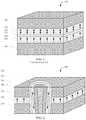
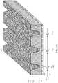
- the MTJ 200can include an annular structure 210 - 240 including an annular non-magnetic layer 210 disposed about an annular conductive layer 220 , an annular free magnetic layer 230 disposed about the annular non-magnetic layer 220 , and an annular tunnel barrier layer 240 disposed about the annular free magnetic layer 230 .
- the MTJ 200can also include a planar reference magnetic layer 250 disposed about the annular structure 210 - 240 and separated from the free magnetic layer 230 by the annular tunnel barrier layer 240 .
- the MTJ 200can further include a first planar non-magnetic insulator layer 260 disposed about the annular structure 210 - 240 and on a first side of the planar reference magnetic layer 250 .
- the MTJcan further include a second planar non-magnetic insulator layer 270 disposed about the annular structure 210 - 240 and on a second side of the planar reference magnetic layer 250 .
- the annular structurecan be a substantially cylindrical structure with tapered sidewalls.
- the conical structurecan have a taper of approximately 10-45 degrees from a first side of the planar reference magnetic layer 250 to a second side of the planar reference magnetic layer 250 .
- the wall angle measured from the normal axis to the horizontal direction of the planar reference magnetic layer 250can be approximately 10-45 degrees.
- the annular tunnel insulator 240 , the annular free magnetic layer 230 , and the annular non-magnetic layer 210can be concentric regions each bounded by inner and outer respective tapered cylinders having substantially the same axis, disposed about a solid tapered cylindrical region of the annular conductive layer 220 .
- the magnetic field of the planar reference magnetic layer 250can have a fixed polarization substantially perpendicular to a major planar orientation of the planar reference magnetic layer 250 .
- the magnetic field of the annular free magnetic layer 230can have a polarization substantially perpendicular to the major planar orientation of the planar reference magnetic layer 250 and selectively switchable between being substantially parallel and substantially antiparallel to the magnetic field of the planar reference layer 250 .
- the magnetic field of the annular free magnetic layer 230can be configured to switch to being substantially parallel to the magnetic field of the planar reference layer 250 in response to a current flow in a first direction through the conductive annular layer 220 and to switch to being substantially anti-parallel to the magnetic field of the planar reference layer 250 in response to a current flow in a second direction through the conductive annular layer 220 .
- the polarization directioneither parallel or anti-parallel, can be changed by a corresponding change in the current direction. Therefore, regardless of the definition of the current flowing direction, the polarization of the annular free magnetic layer 230 can switch to the other polarization orientation by switching the current direction.
- the one or more MTJs 300can include a reference magnetic layer 305 including one or more trenches.
- the one or more MTJs 300can further include one or more sections of a tunnel barrier layer 310 disposed on the walls of the one or more trenches, one or more sections of a free magnetic layer 315 disposed on the one or more sections of the tunnel barrier layer 310 in the one or more trenches, and one or more sections of a conductive layer 320 disposed on the one or more sections of the free magnetic layer 315 in the one or more trenches.
- the one or more MTJs 300can also optionally include one or more sections of a non-magnetic capping layer (not shown) disposed between the one or more sections of the free magnetic layer 315 and the one or more sections of the conductive layer 320 in the one or more trenches.
- the one or more MTJs 300can further include one or more insulator blocks 325 disposed between corresponding sections of the tunnel barrier layer 310 , free magnetic layer 315 and conductive layer 320 .
- an insulator block 325can be disposed between a first and second set of corresponding sections of the tunnel barrier layer 310 , free magnetic layer 315 , the optional non-magnetic capping layer and the conductive layer 320 to form a first MTJ (e.g., Bit 1) and a second MTJ (e.g., Bit 2).
- first MTJe.g., Bit 1
- second MTJe.g., Bit 2
- the one or more MTJs 300can further include a first set of one or more additional layers disposed on a first side of the reference magnetic layer 305 .
- the first set of one or more additional layerscan include a conductive buffer layer (e.g., Perpendicular Magnetic Anisotropy (PMA) enhancer) (not shown), an insulator layer 330 and one or more interconnects 335 .
- the insulator layer 330can be disposed on the first side of the reference magnetic layer 305 , the tunnel barrier layer 310 and free magnetic layer 315 .
- the interconnect 335can be coupled to the conductive layer 320 .
- the one or more MTJs 300can further include one or more bit lines 340 disposed on a second side of the reference magnetic layer 305 , and across one or more insulator blocks 325 .
- one or more bit lines 340can be coupled to one or more portions of reference magnetic layer 305 , and isolated from the tunnel barrier layer 310 , free magnetic layer 315 and conductive layer 320 by the one or more insulator blocks 325 .
- the one or more MTJs 300can also include a second set of one or more additional layers (not shown) disposed on the second side of the reference magnetic layer 305 .
- the second set of one or more additional layerscan include a capping layer (e.g., PMA enhancer) and an insulator layer.
- the reference magnetic layer 305can include one or more layers of a Cobalt-Iron-Boron (Co—Fe—B) alloy, a Cobalt-Iron (CoFe) alloy, a Cobalt-Iron-Nickle (CoFeNi) alloy, an Iron-Nickle (FeNi) alloy, an Iron-Boron (FeB) alloy, a multilayer of Cobalt-Platinum (CoPt) and Cobalt Paradium (CoPd), a Heusler Alloy selected from Cobalt-Manganese-Silicon (CoMnSi), Cobalt-Manganese-Germanium (CoMnGe), Cobalt-Manganese-Aluminum (CoMnAl), Cobalt-Manganese-Iron-Silicon (CoMnFeSi), Cobalt-Iron-Silicon (CoFeSi), Cobalt-Iron-
- the tunnel insulator layer 310can include one or more layers of a Magnesium Oxide (MgO), Silicon Oxide (SiOx), Aluminum Oxide (AlOx), Titanium Oxide (TiOx) or combination of these oxide materials with a thickness of approximately 0.2 to 2.0 nm.
- the free magnetic layer 315can include one or more layers of a Cobalt-Iron-Boron (Co—Fe—B), Cobalt-Nickle-Iron (CoNiFe), Nickle-Iron (NiFe) alloy or their multilayer combinations with a thickness of approximately 1-10 nm, and preferably 1 to 5 nm.
- the non-magnetic capping layer(not shown) can include one or more layers of metal protecting layers that can include one or more elements of a Tantalum (Ta), Chromium (Cr), Tungsten (W), Vanadium (V), Platinum (Pt), Ruthenium (Ru), Palladium (Pd), Copper (Cu), Silver (Ag), Rhodium (Rh), or their alloy, with a thickness of approximately 1 to 5 nm.
- the conductive layer 320can include one or more layers of Copper (Cu), Aluminum (Al), Ruthenium (Ru), and/or one or more alloys thereof with a thickness of approximately 5-20 nm.
- the first and second sets of additional layerscan include one or more insulator layers of MgO, SiOx, AlOx.
- the first and second sets of additional layerscan also include one or more buffer and/or capping layers of Ta, Cr, W, V, Mo, Pt, Ru, Pd, Cu, Ag, Rh, or their alloy, with a thickness of approximately 1 to 10 nm.
- the walls of the one or more trenchescan have a taper of approximately 10-45 degrees from the second side of the reference magnetic layer 305 to the first side of the planar reference magnetic layer 305 .
- the wall angle measured from the normal axis to the horizontal direction of the reference magnetic layer 305can be approximately 10-45 degrees.
- the magnetic field 345 of the reference magnetic layer 305can have a fixed polarization substantially parallel to a major planar orientation of the planar reference magnetic layer 305
- the magnetic field 350 of the free magnetic layer 315can have a polarization substantially parallel to the major planar orientation of the reference magnetic layer 305 , as illustrated in FIG. 3
- the magnetic field 350 of the free magnetic layer 315can be selectively switchable between being substantially parallel and substantially antiparallel to the magnetic field 345 of the planar reference layer 305 .
- the magnetic field 350 of the free magnetic layer 315can be configured to switch to being substantially parallel to the magnetic field 345 of the reference layer 305 in response to a current flow in a first direction through the conductive layer 320 and to switch to being substantially anti-parallel to the magnetic field 345 of the reference layer 305 in response to a current flow in a second direction through the conductive layer 320 .
- the polarization directioneither parallel or anti-parallel, can be changed by a corresponding change in the current direction. Therefore, regardless of the definition of the current flowing direction, the polarization of the free magnetic layer 315 can switch to the other polarization orientation by switching the current direction.
- the magnetic field 345 of the reference magnetic layer 305can have a fixed polarization substantially perpendicular to a major planar orientation of the planar reference magnetic layer 305
- the magnetic field 350 of the free magnetic layer 315can have a polarization substantially perpendicular to the major planar orientation of the reference magnetic layer 305 , as illustrated in FIG. 4 .
- the device 500can be a memory cell array.
- the device 500can include a reference magnetic layer 505 including a plurality of trenches. The trenches can be substantially parallel to each other.
- the device 500can further include a plurality of sections of a tunnel barrier layer 510 disposed on the walls of the trenches, a plurality of sections of a free magnetic layer 515 disposed on the sections of the tunnel barrier layer 510 in the trenches, a plurality of sections of an optional non-magnetic capping layer 520 disposed on the sections of the free magnetic layer 515 and one or more sections of a conductive layer 525 disposed on the one or more sections of the non-magnetic capping layer 520 in the one or more trenches.
- the device 500can further include a plurality of insulator blocks 530 disposed between corresponding sections of the tunnel barrier layer 510 , free magnetic layer 515 , optional non-magnetic capping layer 520 and conductive layer 525 .
- insulator blocks 530can be disposed between a first, second and third set of corresponding sections of the tunnel barrier layer 510 , free magnetic layer 515 , the optional non-magnetic capping layer 520 and the conductive layer 525 to form a first MTJ 535 , a second MTJ 540 and third MTJ 545 .
- the insulator blocks 530can be arranged in an array in the plurality of trenches to form rows of MTJs 535 , 540 , 545 along trenches, and columns of MTJs 545 , 550 , 555 across the trenches.
- the one or more MTJs 500can further include a first set of one or more additional layers disposed on a first side of the reference magnetic layer 505 .
- the first set of one or more additional layerscan include a conductive buffer layer (e.g., Perpendicular Magnetic Anisotropy (PMA) enhancer for one of the implementations) (not shown), an insulator layer 560 and an interconnect 565 .
- the insulator layer 560can be disposed on the first side of the reference magnetic layer 505 , the tunnel barrier layer 510 and free magnetic layer 415 .
- the interconnect 565can be coupled to the conductive layer 545 and the optional non-magnetic capping layer 520 .
- the device 500can further include one or more bit lines 570 disposed on a second side of the reference magnetic layer 505 , and across one or more insulator blocks 530 .
- one or more bit lines 570can be coupled to one or more portions of reference magnetic layer 505 , and isolated from the free magnetic layer 515 , optional non-magnetic capping layer 520 and conductive layer 525 by the one or more insulator blocks 530 .
- the device 500can also include a second set of one or more additional layers (not shown) disposed on the second side of the reference magnetic layer 505 .
- the second set of one or more additional layerscan include a capping layer (e.g., PMA enhancer for one of the implementations) and an insulator layer.
- the devicecan further include a plurality of select elements 575 , 580 , 585 , a plurality of source lines 592 , 594 , 596 , and a plurality of word lines 598 .
- the MTJ cells 535 - 555 arranged along columns and rowscan be coupled by a corresponding select transistor 575 , 580 , 585 to a respective source line 592 , 594 , 596 .
- the gate of the select transistors 575 , 580 , 585can be coupled to a respective word line 598 .
- the reference magnetic layer 505can include one or more layers of a Cobalt-Iron-Boron (Co—Fe—B) alloy, a Cobalt-Iron (CoFe) alloy, a Cobalt-Iron-Nickle (CoFeNi) alloy, an Iron-Nickle (FeNi) alloy, an Iron-Boron (FeB) alloy, a multilayer of Cobalt-Platinum (CoPt) and Cobalt Paradium (CoPd), a Heusler Alloy selected from Cobalt-Manganese-Silicon (CoMnSi), Cobalt-Manganese-Germanium (CoMnGe), Cobalt-Manganese-Aluminum (CoMnAl), Cobalt-Manganese-Iron-Silicon (CoMnFeSi), Cobalt-Iron-Silicon (CoFeSi), Cobalt-Iron-
- the tunnel insulator layer 510can include one or more layers of a Magnesium Oxide (MgO), Silicon Oxide (SiOx), Aluminum Oxide (AlOx), Titanium Oxide (TiOx) or combination of these oxide materials with a thickness of approximately 0.2 to 2.0 nm.
- the free magnetic layer 515can include one or more layers of a Cobalt-Iron-Boron (Co—Fe—B), Cobalt-Nickle-Iron (CoNiFe), Nickle-Iron (NiFe) alloy or their multilayer combinations with a thickness of approximately 1-10 nm, and preferably 1 to 5 nm.
- the non-magnetic capping layer 520can include one or more layers of metal protecting layers that can include one or more elements of a Tantalum (Ta), Chromium (Cr), Tungsten (W), Vanadium (V), Platinum (Pt), Ruthenium (Ru), Palladium (Pd), Copper (Cu), Silver (Ag), Rhodium (Rh), or their alloy, with a thickness of approximately 1 to 5 nm.
- the conductive layer 525can include one or more layers of Copper (Cu), Aluminum (Al), Ruthenium (Ru), and/or one or more alloys thereof with a thickness of approximately 5-20 nm.
- the first and second sets of additional layerscan include one or more insulator layers of MgO, SiOx, AlOx.
- the first and second sets of additional layerscan also include one or more buffer and/or capping layers of Ta, Cr, W, V, Mo, Pt, Ru, Pd, Cu, Ag, Rh, or their alloy, with a thickness of approximately 1 to 10 nm.
- the walls of the one or more trenchescan have a taper of approximately 10-45 degrees from the second side of the reference magnetic layer 505 to the first side of the reference magnetic layer 505 .
- the wall angle measured from the normal axis to the horizontal direction of the reference magnetic layer 505can be approximately 10-45 degrees.
- the magnetic field of the reference magnetic layer 505can have a fixed polarization substantially parallel to a major planar orientation of the planar reference magnetic layer 505
- the magnetic field of the free magnetic layer 515can have a polarization substantially parallel to the major planar orientation of the reference magnetic layer 505 , as illustrated in FIG. 3 .
- the magnetic field of a given portion of the free magnetic layer 515can be selectively switchable between being substantially parallel and substantially antiparallel to the magnetic field of the planar reference layer 505 .
- the magnetic field of a given portion of the free magnetic layer 515can be configured to switch to being substantially parallel to the magnetic field of the reference layer 505 in response to a current flow in a first direction through a corresponding portion of the conductive layer 525 and to switch to being substantially anti-parallel to the magnetic field of the reference layer 505 in response to a current flow in a second direction through the corresponding portion of the conductive layer 525 .
- the magnetic field of the reference magnetic layer 505can have a fixed polarization substantially perpendicular to a major planar orientation of the planar reference magnetic layer 505
- the magnetic field of the free magnetic layer 515can have a polarization substantially perpendicular to the major planar orientation of the reference magnetic layer 505 , as illustrated in FIG. 4 .
- the memory cell array 500can include a plurality of MTJ cells 535 - 555 , a plurality of bit lines 570 , a plurality of source lines 592 , 594 , 596 , a plurality of word lines 598 , and a plurality of select transistor 575 , 580 , 585 .
- the plurality of MTJ cells 535 - 555can be coupled to one or more bit lines 570 .
- the MTJ cells arranged along columns 535 , 540 , 545can be coupled by a corresponding select transistor 598 to a respective source line 592 , 594 , 596 .
- the gate of the select transistors 592 , 594 , 596can be coupled to a respective word line 598 .
- the word lines 598 for the cells that are not being written tocan be biased at a ground potential.
- the other source lines 594 , 596can be biased at a high potential or held in a high impedance state.
- the high potentialcan be equal to the bit line write potential or some portion thereof.
- the word lines for the cells that are not being written tocan be biased at ground potential.
- the other source lines 594 , 596can be biased at a low potential or held in a high impedance state.
- the word lines for the cells that are not being readcan be biased at a ground potential.
- the other source lines 594 , 596can be biased at a high potential or held in a high impedance state. The high potential can be equal to the bit line read potential or some portion thereof.
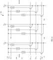
- the memory device 700can include a plurality of memory cell array blocks 705 - 720 .
- Each memory cell array block 705 - 720can include a plurality of MTJ cells as described above in more detail with respect to FIGS. 5 and 6 .
- Two or more bit lines 730 , 735 of the memory cell array blocks 710 , 715 arranged in respective columnscan be coupled together by a corresponding global bit line 740 .
- the source lines 745 of the memory cell array blocks 710 , 715 arranged in respective columnscan be coupled together.
- the word lines 750 of the memory cell array blocks 715 , 725 arranged in respective rowscan be coupled together.
- FIG. 8illustrates a schematic representation of the memory device.
- the memory device 700can include a plurality of memory cell array blocks 705 - 720 .
- Each memory cell array blockcan include a plurality of MTJ cells 810 , a plurality of bit lines 730 , a plurality of source lines 745 , a plurality of word lines 750 , and a plurality of select transistor 820 .
- the MTJ cells arranged along columns 810can be coupled by a corresponding select transistor 820 to a respective source line 745 .
- the gate of the select transistorscan be coupled to a respective word line 750 .
- Two or more bit lines 730 , 735 of the memory cell array blocks 710 , 715 arranged in respective columnscan be coupled together by a corresponding global bit line 740 .
- the source lines 745 of the memory cell array blocks 710 , 715 arranged in respective columnscan be coupled together.
- the word lines 750 of the memory cell array blocks 715 , 725 arranged in respective rowscan be coupled together.
- the word lines for the cells that are not being written tocan be biased at a ground potential.
- the other source linescan be biased at a high potential or held in a high impedance state. The high potential can be equal to the bit line write potential or some portion thereof.
- the word lines for the cells that are not being written tocan be biased at ground potential.
- the other source linescan be biased at a low potential or held in a high impedance state.
- the word lines for the cells that are not being readcan be biased at a ground potential.
- the other source linescan be biased at a high potential or held in a high impedance state. The high potential can be equal to the bit line read potential or some portion thereof.
- the memory devicecan be a Magnetoresistive Random Access Memory (MRAM).
- MRAMMagnetoresistive Random Access Memory
- the memory device 900can include a plurality of memory cell array blocks 710 - 725 , one or more word line decoders 905 , 910 , one or more sense amplifier circuits 915 , 920 , and peripheral circuits 925 .
- the memory device 900can include other well-known circuits that are not necessary for an understanding of the present technology and therefore are not discussed herein.
- Each memory cell array block 710 - 725can include can include a plurality of MTJ cells 810 , a plurality of bit lines 730 , a plurality of source lines 745 , a plurality of word lines 750 , and a plurality of select transistor 820 as described in more detail above with reference to FIGS. 7 and 8 .
- the peripheral circuits 925 , the word line decoders 905 , 910 and sense amplifier circuits 915 , 920can map a given memory address to a particular row of MTJ memory cells in a particular memory cell array block 710 - 725 .
- the output of the word line drivers 905 , 910can drive the word lines to select a given word line of the array.
- the sense amplifier circuits 915 , 920utilize the source lines and bit lines of the array to read from and write to memory cells of a selected word line in a selected memory cell array block 710 - 725 .
- the peripheral circuits 925 and the word line decoders 905 , 910can be configured to apply appropriate write voltages to bit lines, source lines and word lines to write data to cells in a selected word.
- the magnetic polarity, and corresponding logic state, of the free layer of the MTJ cellcan be changed to one of two states depending upon the direction of current flowing through the MTJ cell.
- the peripheral circuits 925 , the word line decoders 905 , 910 and sense amplifier circuits 915 , 920can be configured to apply appropriate read voltages to the bit lines, sources lines and word lines to cause a current to flow in the source lines that can be sensed by the sense amplifier circuits 915 , 920 to read data from cells in a selected word.
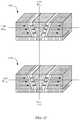
- the device 1000can be a memory cell array.
- the devicecan include a first magnetic layer 1005 including a first plurality of trenches.
- the first plurality of trenchescan be substantially parallel to each other.
- the device 1000can further include a plurality of sections of a first tunnel barrier layer 1010 disposed on the wall of the first plurality of trenches, a plurality of sections of a first free magnetic layer 1015 disposed on the sections of the first tunnel barrier layer 1010 , a plurality of sections of an optional first non-magnetic capping layer 1020 disposed on the sections of the first free magnetic layer 1015 , and a plurality of sections of a first conductive layer 1025 disposed on the sections of the optional first non-magnetic capping layer 1020 in the first plurality of trenches.
- the device 1000can further include a first plurality of insulator blocks disposed between corresponding sections of the first tunnel barrier layer 1010 , the first free magnetic layer 1015 , the optional first non-magnetic capping layer 1020 , and the first conductive layer 1025 .
- the first plurality of insulator blockscan be arranged in an array in the plurality of trenches to form rows of MTJs along the first plurality of trenches, and columns of MTJs across the first plurality of trenches.
- the device 1000can further include a first insulator layer 1030 and a first plurality of interconnects 1035 .
- the first insulator layer 1030can be disposed on the first side of the reference magnetic layer 1005 , the first tunnel barrier layer 1010 , and the first free magnetic layer 1015 .
- the first plurality of interconnects 1035can be coupled to the first conductive layer 1025 and the optional first magnetic capping layer 1020 .
- the device 1000can further include a second magnetic layer 1040 including a second plurality of trenches.
- the second plurality of trenchescan be substantially parallel to each other and to the first plurality of trenches in the first magnetic layer 1005 .
- the device 1000can further include a plurality of sections of a second tunnel barrier layer 1045 disposed on the wall of the second plurality of trenches, a plurality of sections of a second free magnetic layer 1050 disposed on the sections of the second tunnel barrier layer 1045 , a plurality of sections of an optional second non-magnetic capping layer 1055 disposed on the sections of the second free magnetic layer 1050 , and a plurality of sections of a second conductive layer 1060 disposed on the sections of the optional second non-magnetic capping layer 1055 in the second plurality of trenches.
- the device 1000can further include a second plurality of insulator blocks 1065 disposed between corresponding sections of the second tunnel barrier layer 1045 , the second free magnetic layer 1050 , the optional second non-magnetic capping layer 1055 , and the second conductive layer 1060 .
- the second plurality of insulator blocks 1065can be arranged in an array in the second plurality of trenches to form rows of MTJs 1070 - 1080 along the second plurality of trenches, and columns of MTJs 1080 - 1090 across the second plurality of trenches.
- the device 1000can further include a second insulator layer 1092 and a second plurality of interconnects 1094 .
- the second insulator layer 1092can be disposed between the first and second reference magnetic layers 1005 , 1040 , the first and second tunnel barrier layers 1010 , 1045 , and the first and second free magnetic layers 1015 , 1050 .
- the second plurality of interconnects 1094can be coupled between the first and second conductive layers 1025 , 1060 and the optional first and second magnetic capping layers 1020 , 1055 .
- the second plurality of interconnects 1094can be configured to couple corresponding MTJs in a given row and column position in strings.
- the device 1000can further include bit lines 1096 , 1098 disposed on a second side of the first and second reference magnetic layer 1005 , 1040 , and across one or more of the first and second plurality of insulator blocks 1065 .
- a first bit line 1096can be coupled to one or more portions of the first reference magnetic layer 1005 , and isolated from the first free magnetic layer 1015 , the optional first non-magnetic capping layer 1020 and the first conductive layer 1025 by one or more of the first plurality of insulator blocks.
- a second bit line 1098can be coupled to one or more portions of the second reference magnetic layer 1040 , and isolated from the second free magnetic layer 1050 , the optional second non-magnetic capping layer 1055 and the second conductive layer 1060 by one or more of the second plurality of insulator blocks 1065 .
- FIG. 10illustrates a device 1000 including two levels of MTJ cells
- the devicecan further include MTJ cells in any number of levels.
- the device 1000can further include a plurality of select elements, a plurality of source lines and a plurality of word lines as illustrated in FIG. 5 .
- Strings of the MTJ cells arranged along columns and rowscan be coupled by a corresponding select transistor to a respective source line.
- the gate of the select transistorscan be coupled to a respective word line.
- the reference magnetic layers 1005 , 1040can include one or more layers of a Cobalt-Iron-Boron (Co—Fe—B) alloy, a Cobalt-Iron (CoFe) alloy, a Cobalt-Iron-Nickle (CoFeNi) alloy, an Iron-Nickle (FeNi) alloy, an Iron-Boron (FeB) alloy, a multilayer of Cobalt-Platinum (CoPt) and Cobalt Paradium (CoPd), a Heusler Alloy selected from Cobalt-Manganese-Silicon (CoMnSi), Cobalt-Manganese-Germanium (CoMnGe), Cobalt-Manganese-Aluminum (CoMnAl), Cobalt-Manganese-Iron-Silicon (CoMnFeSi), Cobalt-Iron-Silicon (CoFeSi), Cobalt-
- the tunnel insulator layers 1010 , 1045can include one or more layers of a Magnesium Oxide (MgO), Silicon Oxide (SiOx), Aluminum Oxide (AlOx), Titanium Oxide (TiOx) or combination of these oxide materials with a thickness of approximately 0.2 to 2.0 nm.
- the free magnetic layers 1015 , 1050can include one or more layers of a Cobalt-Iron-Boron (Co—Fe—B), Cobalt-Nickle-Iron (CoNiFe), Nickle-Iron (NiFe) alloy or their multilayer combinations with a thickness of approximately 1-10 nm, and preferably 1 to 5 nm.
- the non-magnetic capping layers 1020 , 1055can include one or more layers of metal protecting layers that can include one or more elements of a Tantalum (Ta), Chromium (Cr), Tungsten (W), Vanadium (V), Platinum (Pt), Ruthenium (Ru), Palladium (Pd), Copper (Cu), Silver (Ag), Rhodium (Rh), or their alloy, with a thickness of approximately 1 to 5 nm.
- the conductive layers 1025 , 1060can include one or more layers of Copper (Cu), Aluminum (Al), Ruthenium (Ru), and/or one or more alloys thereof with a thickness of approximately 5-20 nm.
- the walls of the one or more trenchescan have a taper of approximately 10-45 degrees from the second side of the reference magnetic layers 1005 , 1040 to the first side of the reference magnetic layers 1005 , 1040 .
- the wall angle measured from the normal axis to the horizontal direction of the reference magnetic layers 1005 , 1040can be approximately 10-45 degrees.
- the magnetic field of the reference magnetic layers 1005 , 1040can have a fixed polarization substantially parallel to a major planar orientation of the reference magnetic layers 1005 , 1040
- the magnetic field of the free magnetic layers 1015 , 1050can have a polarization substantially parallel to the major planar orientation of the reference magnetic layers 1005 , 1040 , as illustrated in FIG. 3 .
- the magnetic field of a given portion the free magnetic layers 1015 , 1050can be selectively switchable between being substantially parallel and substantially antiparallel to the magnetic field of the reference magnetic layers 1005 , 1040 .
- the magnetic field in a given portion of the first free magnetic layer 1015can be configured to switch to being substantially parallel to the magnetic field of the first reference layer 1005 in response to a current flow in a first direction through a corresponding portion of the first conductive layer 1025 , and to switch to being substantially anti-parallel to the magnetic field of the first reference layer 1005 in response to a current flow in a second direction through the corresponding portion of the first conductive layer 1025 .
- the magnetic field in a given portion of the second free magnetic layer 1050can be configured to switch to being substantially parallel to the magnetic field of the second reference layer 1040 in response to a current flow in a first direction through a corresponding portion of the second conductive layer 1060 , and to switch to being substantially anti-parallel to the magnetic field of the second reference layer 1040 in response to a current flow in a second direction through the corresponding portion of the second conductive layer 1060 .
- the magnetic field of the reference magnetic layers 1005 , 1040can have a fixed polarization substantially perpendicular to a major planar orientation of the reference magnetic layers 1005 , 1040
- the magnetic field of the free magnetic layers 1015 , 1050can have a polarization substantially perpendicular to the major planar orientation of the reference magnetic layers 1005 , 1040 , as illustrated in FIG. 4 .
- the memory cell array 1000can include a plurality of MTJ cells 1105 - 1120 , a plurality of bit lines 1125 , 1130 , a plurality of source lines 1135 - 1145 , a plurality of word lines 1150 , 1155 , and a plurality of select transistor 1160 , 1165 .
- the MTJ cells arranged along a string 1105 , 1110can be coupled by a corresponding select transistor 1160 to a respective source line 1135 .
- the MTJ cells arranged along a second string 1115 , 1120 in the same columncan be coupled by another corresponding select transistor 1165 to the same respective source line 1135 .
- the gate of the select transistors 1160 , 1165can be coupled to a respective word line 1150 , 1155 .
- the memory devicecan further include a plurality of memory cell array blocks, as described above with reference to FIGS. 7 and 9 .
- the word lines for the cells that are not being written tocan be biased at a ground potential.
- the other source lines 1140 , 1145can be biased at a high potential or held in a high impedance state.
- the high potentialcan be equal to the bit line write potential or some portion thereof.
- the word lines for the cells that are not being written tocan be biased at ground potential.
- the other source lines 1140 , 1145can be biased at a low potential or held in a high impedance state.
- the word lines for the cells that are not being readcan be biased at a ground potential.
- the other source lines 1140 , 1145can be biased at a high potential or held in a high impedance state. The high potential can be equal to the bit line read potential or some portion thereof.
- bit line 1120When writing a ‘0’ to a first MTJ cell 1105 , the bit line 1120 can be biased at V BLW and the source line can be biased at ground resulting in a current that flows from the bit line 1120 and out through the source line 1135 .
- the bit lines of the second MTJ cells in the same string 1110can be biased at ground, which will result in half the current that flows into the bit line 1120 of the first MTJ cell 1105 flowing out the source line 1135 and half the current leaking out through the bit line 1125 of the second MTJ cell.
- the leakage currentcan be reduced. For example, if the potential on the bit line 1125 of the second MTJ cell 1110 is increased to one half (1 ⁇ 2) of the applied to the bit line 1120 of the first MTJ cell 1105 , the leakage current out through the second MTJ cell 1110 can be reduced to 25%. Similar leakage paths can be present when writing a ‘1’ to a given MTJ cell in a string. By decreasing the potential applied to the bit lines of the other MTJ cells in the string or holding the bit lines of the other strings in a high impedance state, leakage currents through the other MTJ cells can be also be decreased.
- FIGS. 13A and 13Ba method of fabricating one or more MTJs, in accordance with aspects of the present technology, is shown.
- the method of fabricating the one or more MTJswill be further described with reference to FIGS. 14A-14H , which show the one or more MTJs during various stage of the method of manufacturing.
- the method of fabricationcan include forming a planar reference magnetic layer 1405 on a planar non-magnetic insulator layer 1410 , at 1305 .
- layersit is to be appreciated that the term “layer” as used herein can refer to a uni-layer or a multi-layer.
- one or more trenches 1415can be formed in the reference magnetic layer 1405 .
- the one or more trenches 1415can be formed by Ion Beam Etching (IBE) in combination with a trench mask.
- the one or more trenchescan have a taper of approximately 10-45 degrees from a top side of the reference magnetic layer 1405 to a bottom side of the reference magnetic layer 1405 .
- the wall angle measured from the normal axis to the horizontal direction of the planar reference magnetic layer 1405can be approximately 10-45 degrees.
- a tunnel insulator layer 1420can be formed on the walls of the one or more trenches 1415 .
- a free magnetic layer 1425can be formed on the tunnel insulator in the one or more trenches 1415 .
- an optional non-magnetic layer(not shown) can be formed on the free magnetic layer 1425 in the one or more trenches 1415 .
- a tunnel insulator layer 1420can be deposited on the surface of the planar non-magnetic insulator layer 1405 including the walls of the one or more trenches 1415 .
- the tunnel insulator layercan include one or more layers of a Magnesium Oxide (MgO), Silicon Oxide (SiOx), Aluminum Oxide (AlOx), Titanium Oxide (TiOx) or a combination of these oxide materials.
- a free magnetic layer 1425can be deposited on the surface of the tunnel insulator layer 1420 inside and outside the one or more trenches 1415 .
- the free magnetic layer 1425can include one or more layers of a Cobalt-Iron-Boron (Co—Fe—B), Cobalt-Nickle-Iron (CoNiFe), Nickle-Iron (NiFe) alloy or their multilayer combinations.
- a non-magnetic layercan be deposited on the surface of the free magnetic layer 1425 inside and outside of the one or more trenches 1415 .
- the non-magnetic layercan include one or more layers a Tantalum (Ta), Chromium (Cr), W, V, Pt, Ru, Pd, Cu, Ag, Rh, or their alloy.
- the materials of the tunnel insulator 1420 , the free magnetic layer 1425 and the optional non-magnetic layercan be deposited by an angular deposition process to improve deposition in the one or more trenches. In other implementations, the materials of the tunnel insulator 1420 , the free magnetic layer 1425 and the optional non-magnetic layer can be deposited by atomic layer deposition or Chemical Vapor Deposition (CVD).
- CVDChemical Vapor Deposition
- the portions of the tunnel insulator layer 1420 , the free magnetic layer 1425 and the optional annular non-magnetic layer at the bottom of the one or more trenches 1415 and on top of the planar non-magnetic insular layer 1405can be removed by one or more selective etching, milling or the like processes.
- the portions of the tunnel insulator layer 1420 , the free magnetic layer 1425 and the optional non-magnetic layer at the bottom of the one or more trenches and on top of the planar non-magnetic insular layercan be removed by successive etching, milling or the like processes before the subsequent layer is deposited.
- the magnetic field of the planar reference magnetic layer 1405 and the magnetic field of the free magnetic layer 1425can have a polarization parallel to the major planar orientation of the planar reference magnetic layer 1405 (also referred to as in-plane), and the magnetic field of the free magnetic layer 1425 can be selectively switchable between being substantially parallel and substantially antiparallel to the magnetic field of the planar reference layer 1425 , as illustrated in FIG. 14C .
- the magnetic field of the planar reference magnetic layer 1405 and the magnetic field of the free magnetic layer 1425can have a polarization substantially perpendicular to the major planar orientation of the planar reference magnetic layer 1405 (also referred to as perpendicular-to-plane), and the magnetic field of the free magnetic layer 1425 can be selectively switchable between being substantially parallel and substantially antiparallel to the magnetic field of the planar reference layer 1405 , as illustrated in FIG. 4 .
- one or more portions of the optional non-magnetic layer, one or more portions of the free magnetic layer 1425 , and optionally one or more portions of the tunnel insulator layer 1420can be removed from the walls of the one or more trenches 1415 .
- an insulator block mask 1430can be formed as illustrated in FIG. 14D , and the exposed portions of the optional non-magnetic layer, the free magnetic layer 1425 , and optionally the tunnel insulator layer 1420 can be removed by ion beam milling, reactive ion etch or the like, as illustrated in FIG. 14E .
- the exposed portions of the optional non-magnetic layer and the free magnetic layercan be oxidized and nitride.
- yet another implementationcan be ion implanted with Gallium (Ga) or the like.
- one or more insulator blockscan be formed between the one or more portions of the optional non-magnetic layer, the one or more portions of the free magnetic layer 1425 and optionally the one or more portions of the tunnel insulator 1420 in the one or more trenches.
- a layer of an insulator 1435such a Magnesium Oxide (MgO), Silicon Oxide (SiOx), Aluminum Oxide (AlOx), Titanium Oxide (TiOx) or a combination of these oxide materials can be deposited.
- the insulator layer 1435can be deposited in the portions of the one or more trenches exposed by the insulator block mask 1430 and over the surface of the insulator block mask 1430 , as illustrated in FIG.
- CMPChemical Mechanical Polishing
- one or more conductive cores 1445can be formed between the one or more insulator blocks 1440 , and between the one or more portions of the free magnetic layer 1425 , or the optional non-magnetic layer if applicable, in the one or more trenches, as illustrated in FIG. 14H .
- a metal seed layercan be deposited on the exposed portions of the free magnetic layer, or the optional non-magnetic layer if applicable, between the one or more insulator blocks.
- a conductor layer, such as Copper (Cu)can be deposited by a process such as Chemical Vapor Deposition (CVD) on the metal seed layer to form the one or more conductive cores.
- the respective portions of the reference magnetic layer 1405 , the tunnel insulator 1420 , the free magnetic layer 1425 , the optional non-magnetic layer and the conductive cores 1445 between sets of insulator blocks 1440form corresponding MTJ cells.
- the processes of 1305 - 1340can optionally be repeated a plurality of times to form strings of MTJs as illustrated in FIG. 10 .
- FIGS. 15A-15Ca method of fabricating a memory cell array, in accordance with aspects of the present technology, is shown.
- the method of fabricating the memory cell arraywill be further described with reference to FIGS. 16A-16F , which show the memory cell array during various stage of the method of manufacturing.
- the method of fabricationcan include forming an array of selectors 1602 on a substrate, at 1505 .
- selectors 1602There a numerous selectors and methods of fabrication that can be utilized for the array of selectors. The specific selector and processes are not germane to an understanding of aspects of the present technology and therefore will not be described in further detail.
- a plurality of word lines 1604can be formed on a substrate and coupled to the selectors in respective rows.
- a conductive layercan be deposited on a substrate.
- a word line pattern maskcan be formed on the conductive layer and a selective etching process can be performed to remove the portions of the conductive layer exposed by the word line pattern mask to form the plurality of word lines coupled to the selectors.
- a word linecan be formed by electro-plating on to the framed photo-resist pattern that has a vacancy for word line portion.
- the word linescan be disposed as a plurality of substantially parallel traces in a first direction (e.g., rows) of the substrate.
- a plurality of source lines 1606can be formed on the substrate and coupled to the selectors in respective columns.
- an insulator layercan be formed over the plurality of word lines, and a second conductive layer can be deposited over the insulator layer.
- a source line pattern maskcan be formed on the second conductive layer a selective etching process can be performed to remove the portions of the second conductive layer exposed by the word line pattern mask to form the plurality of source lines.
- the source linescan be disposed as a plurality of substantially parallel traces in a second direction (e.g., columns) on the substrate that is perpendicular to the first direction of the word lines.
- one or more planar non-magnetic insulator layers 1608can be deposited on the plurality of selectors.
- one or more layers of Magnesium Oxide (MgO), Silicon Oxide (SiOx), Aluminum Oxide (AlOx) or alloys thereofcan be deposited on the plurality of selectors.
- a plurality of vias 1610can be formed through the first planar non-magnetic insulator layer.
- one or more planar reference magnetic layers 1612can be deposited on the one or more non-magnetic insulator layers 1610 .
- one or more layersCobalt-Iron-Boron (Co—Fe—B) alloy, a Cobalt-Iron (CoFe) alloy, a Cobalt-Iron-Nickle (CoFeNi) alloy, an Iron-Nickle (FeNi) alloy, an Iron-Boron (FeB) alloy, a multilayer of Cobalt-Platinum (CoPt) and Cobalt Paradium (CoPd), a Heusler Alloy selected from Cobalt-Manganese-Silicon (CoMnSi), Cobalt-Manganese-Germanium (CoMnGe), Cobalt-Manganese-Aluminum (CoMnAl), Cobalt-Manganese-Iron-Silicon (CoMnFeS
- a plurality of trenches 1614can be formed through the one or more reference magnetic layers 1612 .
- the trenches 1614can be aligned the plurality of vias 1610
- the one or more trenchescan be formed by Ion Beam Etching (IBE) in combination with a trench mask.
- the one or more trenchescan have a taper of approximately 10-45 degrees from a top side of the reference magnetic layer to a bottom side of the reference magnetic layer.
- the wall angle measured from the normal axis to the horizontal direction of the planar reference magnetic layercan be approximately 10-45 degrees.
- a plurality of portions of tunnel insulatorscan be formed on the walls of the one or more trenches.
- a plurality of portions of free magnetic layercan be formed on the plurality of portions of tunnel insulators in the plurality of trenches.
- a plurality of portions of optional non-magnetic layercan be formed on the free magnetic layer in the one or more trenches.
- a tunnel insulator layer 1616can be deposited on the surface of the planar non-magnetic insulator layer 1612 and the walls of the one or more trenches 1614 .
- the tunnel insulator layer 116can include one or more layers of a Magnesium Oxide (MgO), Silicon Oxide (SiOx), Aluminum Oxide (AlOx), Titanium Oxide (TiOx) or a combination of these oxide materials.
- a free magnetic layer 1618can be deposited on the surface of the tunnel insulator layer 1616 inside and outside the one or more trenches 1614 .
- the free magnetic layer 1618can include one or more layers of a Cobalt-Iron-Boron (Co—Fe—B), Cobalt-Nickle-Iron (CoNiFe), Nickle-Iron (NiFe) alloy or their multilayer combinations.
- the materials of the tunnel insulator 1616 , the free magnetic layer 1618 and the optional non-magnetic layer 1620can be deposited by atomic layer deposition or Chemical Vapor Deposition (CVD).
- the portions of the tunnel insulator layer 1616 , the free magnetic layer 1618 and the optional non-magnetic layer 1620 at the bottom of the one or more trenches 1614 and on top of the planar reference magnetic layer 1612can be removed by one or more selective etching, milling or the like processes.
- the portions of the tunnel insulator layer 1616 , the free magnetic layer 1618 and the optional non-magnetic layer 1620 at the bottom of the one or more trenches 1614 and on top of the planar reference magnetic layer 1612can be removed by successive etching, milling or the like processes before the subsequent layer is deposited. It is to be appreciated that the thickness along a vertical axis of the free magnetic layer 1618 or the optional non-magnetic layer 1620 is thinner in the horizontal portions at the bottom of the trenches 1614 and on top of the planar reference magnetic layer 1612 as compared to the portions along the walls of the trenches 1614 .
- the free magnetic layer 1618 or the optional non-magnetic layer 1620 at the bottom of the one or more trenches 1614 and on top of the planar reference magnetic layer 1612can be removed, while the free magnetic layer 1618 or the optional non-magnetic layer 1620 is only thinned.
- the magnetic field of the reference magnetic layer and the magnetic field of the free magnetic layercan have a polarization parallel to the major planar orientation of the planar reference magnetic layer (also referred to as in-plane), and the magnetic field of the free magnetic layer can be selectively switchable between being substantially parallel and substantially antiparallel to the magnetic field of the planar reference layer.
- the magnetic field of the reference magnetic layer and the magnetic field of the free magnetic layercan have a polarization substantially perpendicular to the major planar orientation of the planar reference magnetic layer (also referred to as perpendicular-to-plane), and the magnetic field of the free magnetic layer can be selectively switchable between being substantially parallel and substantially antiparallel to the magnetic field of the planar reference layer.
- one or more portions of the optional non-magnetic layer 1620 , one or more portions of the free magnetic layer 1618 , and optionally one or more portions of the tunnel insulator layer 1616can be selectively removed from the walls of the plurality of trenches 1614 .
- an insulator block maskcan be formed, and the exposed portions of the optional non-magnetic layer 1620 , the free magnetic layer 1618 , and optionally the tunnel insulator layer 1616 can be removed by ion beam milling, reactive ion etch or the like.
- the exposed portions of the optional non-magnetic layer and the free magnetic layercan be oxidized and nitride.
- FIG. 16Dillustrates the plurality of portions of the optional non-magnetic layer 1620 and the plurality of portions of the free magnetic layer 1618 without the insulator block mask disposed over them as shown illustrated in the similar structure in FIGS. 14D-14F so that the structure of the formed plurality of portions of the optional non-magnetic layer 1620 and the plurality of portions of the free magnetic layer 1618 can be seen.
- the insulator block masktypically cover the plurality of portions of the optional non-magnetic layer 1620 and the plurality of portions of the free magnetic layer 1618 until after formation of the plurality of insulator blocks formed subsequent processes.
- the one or more insulator layerscan be deposited in the portions of the trenches exposed by the insulator block mask and over the surface of the insulator block mask.
- a processessuch as Chemical Mechanical Polishing (CMP) can be used to remove the excess portion of the one or more insulator layers outside the exposed portions of the one or more trenches, and then a resist stripping process can be utilized to remove the insulator block mask.
- CMPChemical Mechanical Polishing
- a plurality of conductive core 1624can be formed between the one or more insulator blocks, and between the free magnetic layer or the optional non-magnetic layer if applicable, in the one or more trenches, as illustrated in FIG. 16F .
- a metal seed layercan be deposited on the exposed portions of the free magnetic layer, or the optional non-magnetic layer if applicable, between the one or more insulator blocks.
- a conductor layer, such as Copper (Cu)can be deposited by a process such as Chemical Vapor Deposition (CVD) on the metal seed layer to form the one or more conductive cores.
- the processes of 1520 through 1565can optionally be repeated a plurality of times to form a string of MTJs as illustrated in FIG. 10 .
- portions of one or more planar non-magnetic insulator layers and one or more planar reference magnetic layerscan be removed in a periphery region to expose each planar reference magnetic layer.
- the periphery regioncan be outside the array of annular openings.
- a series of one or more etching, milling or the like processescan be used to step down through the planar non-magnetic insulator layers and the planar reference magnetic layers.
- a bit line 1626can be formed on each planar reference magnetic layer 1612 .
- an insulator layercan be deposited in the periphery region, and a bit line insulator patch mask can be formed from the insulator layer.
- a selective etching processcan be performed to remove the portions of the insulator layer on the free magnetic layer, the optional non-magnetic layer and the conductive core layer in the periphery region exposed by the bit line insulator patch mask to form one or more bit line insulator patches 1628 .
- a conductive layercan be deposited on the reference magnetic layer, while electrically isolated from on the free magnetic layer, the optional non-magnetic layer and the conductive core layer the by the insulator patches.
- a bit line pattern maskcan be formed on the conductive layer and a selective etching process can be performed to remove the portions of the conductive layer exposed by the bit line pattern mask to form the plurality of bit lines on corresponding ones of the planar reference magnetic layers.
- a photo-resist frameis made by photo process before depositing a bit line material.
- the photo-resist framehas an opening to form a bit line inside.
- the electric-plating processis used to form a metal bit line inside the photo-resist frame.
- the photo-resist frameis removed.
- the bit linescan be disposed as a plurality of substantially parallel traces in a first direction (e.g., rows) on respective planar reference magnetic layers.
- one or more bit line viascan optionally be formed.
- the one or more bit line viascan be coupled to respective bit lines.
- one or more global bit linescan be formed.
- the one or more global bit linescan be coupled to corresponding bit lines or bit line vias, as illustrated in FIG. 7 .
- two or more bit lines arranged in respective columnscan be coupled together by a corresponding global bit line.
Landscapes
- Engineering & Computer Science (AREA)
- Computer Hardware Design (AREA)
- Chemical & Material Sciences (AREA)
- Crystallography & Structural Chemistry (AREA)
- Power Engineering (AREA)
- Manufacturing & Machinery (AREA)
- Mram Or Spin Memory Techniques (AREA)
- Hall/Mr Elements (AREA)
Abstract
Description
Claims (27)
Priority Applications (2)
| Application Number | Priority Date | Filing Date | Title |
|---|---|---|---|
| US16/121,453US11107974B2 (en) | 2018-03-23 | 2018-09-04 | Magnetic tunnel junction devices including a free magnetic trench layer and a planar reference magnetic layer |
| US17/403,733US11751484B2 (en) | 2018-03-23 | 2021-08-16 | Magnetic tunnel junction devices including a free magnetic trench layer and a planar reference magnetic laver |
Applications Claiming Priority (7)
| Application Number | Priority Date | Filing Date | Title |
|---|---|---|---|
| US201862647210P | 2018-03-23 | 2018-03-23 | |
| US16/059,018US20190296223A1 (en) | 2018-03-23 | 2018-08-08 | Methods of Manufacturing Three-Dimensional Arrays with Magnetic Tunnel Junction Devices Including an Annular Free Magnetic Layer and a Planar Reference Magnetic Layer |
| US16/059,009US20190296228A1 (en) | 2018-03-23 | 2018-08-08 | Three-Dimensional Arrays with Magnetic Tunnel Junction Devices Including an Annular Free Magnetic Layer and a Planar Reference Magnetic Layer |
| US16/059,016US10529915B2 (en) | 2018-03-23 | 2018-08-08 | Bit line structures for three-dimensional arrays with magnetic tunnel junction devices including an annular free magnetic layer and a planar reference magnetic layer |
| US16/059,012US10734573B2 (en) | 2018-03-23 | 2018-08-08 | Three-dimensional arrays with magnetic tunnel junction devices including an annular discontinued free magnetic layer and a planar reference magnetic layer |
| US16/059,004US20190296220A1 (en) | 2018-03-23 | 2018-08-08 | Magnetic Tunnel Junction Devices Including an Annular Free Magnetic Layer and a Planar Reference Magnetic Layer |
| US16/121,453US11107974B2 (en) | 2018-03-23 | 2018-09-04 | Magnetic tunnel junction devices including a free magnetic trench layer and a planar reference magnetic layer |
Related Parent Applications (2)
| Application Number | Title | Priority Date | Filing Date |
|---|---|---|---|
| US16/059,004Continuation-In-PartUS20190296220A1 (en) | 2018-03-23 | 2018-08-08 | Magnetic Tunnel Junction Devices Including an Annular Free Magnetic Layer and a Planar Reference Magnetic Layer |
| US16/059,012Continuation-In-PartUS10734573B2 (en) | 2018-03-23 | 2018-08-08 | Three-dimensional arrays with magnetic tunnel junction devices including an annular discontinued free magnetic layer and a planar reference magnetic layer |
Related Child Applications (1)
| Application Number | Title | Priority Date | Filing Date |
|---|---|---|---|
| US17/403,733ContinuationUS11751484B2 (en) | 2018-03-23 | 2021-08-16 | Magnetic tunnel junction devices including a free magnetic trench layer and a planar reference magnetic laver |
Publications (2)
| Publication Number | Publication Date |
|---|---|
| US20190296224A1 US20190296224A1 (en) | 2019-09-26 |
| US11107974B2true US11107974B2 (en) | 2021-08-31 |
Family
ID=67985747
Family Applications (1)
| Application Number | Title | Priority Date | Filing Date |
|---|---|---|---|
| US16/121,453ActiveUS11107974B2 (en) | 2018-03-23 | 2018-09-04 | Magnetic tunnel junction devices including a free magnetic trench layer and a planar reference magnetic layer |
Country Status (1)
| Country | Link |
|---|---|
| US (1) | US11107974B2 (en) |
Cited By (2)
| Publication number | Priority date | Publication date | Assignee | Title |
|---|---|---|---|---|
| US20220028929A1 (en)* | 2018-03-23 | 2022-01-27 | Integrated Silicon Solution, (Cayman) Inc. | Magnetic Tunnel Junction Devices Including a Free Magnetic Trench Layer and a Planar Reference Magnetic Layer |
| US20220037588A1 (en)* | 2018-03-23 | 2022-02-03 | Integrated Silicon Solution, (Cayman) Inc. | Methods of Manufacturing Three-Dimensional Arrays with MTJ Devices Including a Free Magnetic Trench Layer and a Planar Reference Magnetic Layer |
Families Citing this family (1)
| Publication number | Priority date | Publication date | Assignee | Title |
|---|---|---|---|---|
| US11276817B2 (en)* | 2020-03-13 | 2022-03-15 | International Business Machines Corporation | Magnetic tunnel junction having tapered all-around structure |
Citations (402)
| Publication number | Priority date | Publication date | Assignee | Title |
|---|---|---|---|---|
| JPS5635666B1 (en) | 1971-06-28 | 1981-08-19 | ||
| US4597487A (en) | 1983-07-28 | 1986-07-01 | Creative Technology, Inc. | Method and apparatus for selective scrap metal collections |
| US5541868A (en) | 1995-02-21 | 1996-07-30 | The United States Of America As Represented By The Secretary Of The Navy | Annular GMR-based memory element |
| US5559952A (en) | 1993-03-23 | 1996-09-24 | Kabushiki Kaisha Toshiba | Display controller incorporating cache memory dedicated for VRAM |
| US5629549A (en) | 1995-04-21 | 1997-05-13 | Johnson; Mark B. | Magnetic spin transistor device, logic gate & method of operation |
| US5640343A (en) | 1996-03-18 | 1997-06-17 | International Business Machines Corporation | Magnetic memory array using magnetic tunnel junction devices in the memory cells |
| US5654566A (en) | 1995-04-21 | 1997-08-05 | Johnson; Mark B. | Magnetic spin injected field effect transistor and method of operation |
| US5691936A (en) | 1995-08-21 | 1997-11-25 | Matsushita Electric Industrial Co., Ltd. | Magnetoresistive element and memory element |
| US5695846A (en) | 1995-01-12 | 1997-12-09 | The Procter & Gamble Company | Zero scrap absorbent core formation process and products derived from web-based absorbent materials |
| US5695864A (en) | 1995-09-28 | 1997-12-09 | International Business Machines Corporation | Electronic device using magnetic components |
| US5732016A (en) | 1996-07-02 | 1998-03-24 | Motorola | Memory cell structure in a magnetic random access memory and a method for fabricating thereof |
| US5751647A (en) | 1995-02-13 | 1998-05-12 | Micron Technology, Inc. | On-chip memory redundancy circuitry for programmable non-volatile memories, and methods for programming same |
| US5856897A (en) | 1996-11-27 | 1999-01-05 | International Business Machines Corporation | Self-biased dual spin valve sensor |
| US5896252A (en) | 1995-08-11 | 1999-04-20 | Fujitsu Limited | Multilayer spin valve magneto-resistive effect magnetic head with free magnetic layer including two sublayers and magnetic disk drive including same |
| US5966323A (en) | 1997-12-18 | 1999-10-12 | Motorola, Inc. | Low switching field magnetoresistive tunneling junction for high density arrays |
| US6016269A (en) | 1998-09-30 | 2000-01-18 | Motorola, Inc. | Quantum random address memory with magnetic readout and/or nano-memory elements |
| US6055179A (en) | 1998-05-19 | 2000-04-25 | Canon Kk | Memory device utilizing giant magnetoresistance effect |
| US6064948A (en) | 1998-03-02 | 2000-05-16 | Tanisys Technology, Inc. | Tester systems |
| US6075941A (en) | 1997-01-29 | 2000-06-13 | International Business Machines Corporation | Microcomputer |
| US6097579A (en) | 1998-08-21 | 2000-08-01 | International Business Machines Corporation | Tunnel junction head structure without current shunting |
| US6112295A (en) | 1998-09-24 | 2000-08-29 | Intel Corporation | High frequency pipeline decoupling queue with non-overlapping read and write signals within a single clock cycle |
| US6124711A (en) | 1996-01-19 | 2000-09-26 | Fujitsu Limited | Magnetic sensor using tunnel resistance to detect an external magnetic field |
| US6134138A (en) | 1999-07-30 | 2000-10-17 | Honeywell Inc. | Method and apparatus for reading a magnetoresistive memory |
| US6140838A (en) | 1995-04-21 | 2000-10-31 | Johnson; Mark B. | High density and high speed magneto-electronic logic family |
| US6154139A (en) | 1998-04-21 | 2000-11-28 | Versus Technology | Method and system for locating subjects within a tracking environment |
| US6154349A (en) | 1996-04-26 | 2000-11-28 | Fujitsu Limited | Magnetoresistive transducer including CoFeZ soft magnetic layer |
| US6172902B1 (en) | 1998-08-12 | 2001-01-09 | Ecole Polytechnique Federale De Lausanne (Epfl) | Non-volatile magnetic random access memory |
| US6233690B1 (en) | 1998-09-17 | 2001-05-15 | Intel Corporation | Mechanism for saving power on long latency stalls |
| US6233172B1 (en) | 1999-12-17 | 2001-05-15 | Motorola, Inc. | Magnetic element with dual magnetic states and fabrication method thereof |
| US6243288B1 (en) | 1999-08-26 | 2001-06-05 | Hitachi, Ltd. | Giant magnetoresistive sensor, thin-film read/write head and magnetic recording apparatus using the sensor |
| US6252798B1 (en) | 1997-06-27 | 2001-06-26 | Kabushiki Kaisha Toshiba | Nonvolatile semiconductor memory device capable of controlling mutual timing of write voltage pulse and transfer voltage pulse |
| US6256223B1 (en) | 1998-07-28 | 2001-07-03 | International Business Machines Corporation | Current-induced magnetic switching device and memory including the same |
| US6292389B1 (en) | 1999-07-19 | 2001-09-18 | Motorola, Inc. | Magnetic element with improved field response and fabricating method thereof |
| US6347049B1 (en) | 2001-07-25 | 2002-02-12 | International Business Machines Corporation | Low resistance magnetic tunnel junction device with bilayer or multilayer tunnel barrier |
| US6385082B1 (en) | 2000-11-08 | 2002-05-07 | International Business Machines Corp. | Thermally-assisted magnetic random access memory (MRAM) |
| US20020090533A1 (en) | 1999-11-23 | 2002-07-11 | Jing Zhang | Method and system for reducing assymetry in a spin valve having a synthetic pinned layer |
| US20020105823A1 (en) | 2000-12-07 | 2002-08-08 | Commissariat A L'energie Atomique | Magnetic spin polarisation and magnetisation rotation device with memory and writing process, using such a device |
| US6436526B1 (en) | 1999-06-17 | 2002-08-20 | Matsushita Electric Industrial Co., Ltd. | Magneto-resistance effect element, magneto-resistance effect memory cell, MRAM and method for performing information write to or read from the magneto-resistance effect memory cell |
| US6442681B1 (en) | 1998-12-28 | 2002-08-27 | Bull Hn Information Systems Inc. | Pipelined central processor managing the execution of instructions with proximate successive branches in a cache-based data processing system while performing block mode transfer predictions |
| US6458603B1 (en) | 2000-10-10 | 2002-10-01 | Infineon Technologies Ag | Method of fabricating a micro-technical structure, and micro-technical component |
| US6493197B2 (en) | 1999-06-29 | 2002-12-10 | Fujitsu Limited | Magneto-resistance effect type head and information reproducing apparatus |
| US6522137B1 (en) | 2000-06-28 | 2003-02-18 | Schlumberger Technology Corporation | Two-dimensional magnetic resonance imaging in a borehole |
| US6538918B2 (en) | 2000-08-14 | 2003-03-25 | Micron Technology, Inc. | Pulsed write techniques for magneto-resistive memories |
| US6545906B1 (en) | 2001-10-16 | 2003-04-08 | Motorola, Inc. | Method of writing to scalable magnetoresistance random access memory element |
| US6545903B1 (en) | 2001-12-17 | 2003-04-08 | Texas Instruments Incorporated | Self-aligned resistive plugs for forming memory cell with phase change material |
| US20030085186A1 (en) | 2001-10-31 | 2003-05-08 | Norihiro Fujioka | Chemical reinforcing holders for glass substrate |
| US6563681B1 (en) | 1999-05-31 | 2003-05-13 | Tdk Corporation | Magnetoresistance effect film and magnetoresistance effect type head |
| US6566246B1 (en) | 2001-05-21 | 2003-05-20 | Novellus Systems, Inc. | Deposition of conformal copper seed layers by control of barrier layer morphology |
| US20030117840A1 (en) | 2001-12-20 | 2003-06-26 | Manish Sharma | Magnetic memory device having soft reference layer |
| US6603677B2 (en) | 2000-12-07 | 2003-08-05 | Commissariat A L'energie Atomique | Three-layered stacked magnetic spin polarization device with memory |
| US20030151944A1 (en) | 2001-12-27 | 2003-08-14 | Kabushiki Kaisha Toshiba | Magnetic switching element and a magnetic memory |
| US6608776B2 (en) | 2000-11-14 | 2003-08-19 | Mitsubishi Denki Kabushiki Kaisha | Thin film magnetic memory device having a highly integrated memory array |
| US6635367B2 (en) | 2001-03-19 | 2003-10-21 | Hitachi, Ltd. | Magnetic recording medium |
| US20030197984A1 (en) | 1999-09-16 | 2003-10-23 | Kabushiki Kaisha Toshiba | Magnetoresistive element and magnetic memory device |
| US6653153B2 (en) | 2000-07-03 | 2003-11-25 | Merck & Co., Inc. | Methods for encoding combinatorial libraries |
| US6654278B1 (en) | 2002-07-31 | 2003-11-25 | Motorola, Inc. | Magnetoresistance random access memory |
| US20030218903A1 (en) | 2002-05-24 | 2003-11-27 | International Business Machines | Nonvolatile memory device utilizing spin-valve-type designs and current pulses |
| US6677165B1 (en) | 2003-03-20 | 2004-01-13 | Micron Technology, Inc. | Magnetoresistive random access memory (MRAM) cell patterning |
| US20040012994A1 (en) | 2002-07-17 | 2004-01-22 | Slaughter Jon M. | Multi-state magnetoresistance random access cell with improved memory storage density |
| US20040026369A1 (en) | 2002-08-12 | 2004-02-12 | Chentsau Ying | Method of etching magnetic materials |
| US6710984B1 (en) | 1999-09-24 | 2004-03-23 | Kabushiki Kaisha Toshiba | Magnetoresistive effect device utilizing a magnetization-coupling layer which couples adjacent ferromagnetic layers perpendicularly |
| US6713195B2 (en) | 2001-01-05 | 2004-03-30 | Nve Corporation | Magnetic devices using nanocomposite materials |
| US6714444B2 (en) | 2002-08-06 | 2004-03-30 | Grandis, Inc. | Magnetic element utilizing spin transfer and an MRAM device using the magnetic element |
| US20040061154A1 (en) | 2002-09-27 | 2004-04-01 | Yiming Huai | Thermally stable magnetic elements utilizing spin transfer and an MRAM device using the magnetic element |
| US6731537B2 (en) | 2001-09-12 | 2004-05-04 | Renesas Technology Corp. | Non-volatile memory device and data storing method |
| US20040094785A1 (en) | 2002-11-18 | 2004-05-20 | Xiaochun Zhu | Magentic memory element and memory device including same |
| US6744086B2 (en) | 2001-05-15 | 2004-06-01 | Nve Corporation | Current switched magnetoresistive memory cell |
| US20040130936A1 (en) | 2003-01-07 | 2004-07-08 | Grandis Inc. | Spin-transfer multilayer stack containing magnetic layers with resettable magnetization |
| US6765824B2 (en) | 2002-03-29 | 2004-07-20 | Kabushiki Kaisha Toshiba | Magneto-resistance element capable of controlling the position and size of edge domain and the coercivity and magnetic memory |
| US6772036B2 (en) | 2001-08-30 | 2004-08-03 | Fisher-Rosemount Systems, Inc. | Control system using process model |
| US6773515B2 (en) | 2002-01-16 | 2004-08-10 | Headway Technologies, Inc. | FeTa nano-oxide layer as a capping layer for enhancement of giant magnetoresistance in bottom spin valve structures |
| US6777730B2 (en) | 2001-08-31 | 2004-08-17 | Nve Corporation | Antiparallel magnetoresistive memory cells |
| US6785159B2 (en) | 2002-08-29 | 2004-08-31 | Micron Technology, Inc. | Combination etch stop and in situ resistor in a magnetoresistive memory and methods for fabricating same |
| US20040173315A1 (en) | 2003-03-04 | 2004-09-09 | Charles Leung | Apparatus and method for reducing impurities in a semiconductor material |
| US6812437B2 (en) | 2000-04-28 | 2004-11-02 | The Holmes Group, Inc. | Electronic control circuit |
| US6829161B2 (en) | 2003-01-10 | 2004-12-07 | Grandis, Inc. | Magnetostatically coupled magnetic elements utilizing spin transfer and an MRAM device using the magnetic element |
| US20040257717A1 (en) | 2003-06-18 | 2004-12-23 | Manish Sharma | Coupled ferromagnetic systems having modified interfaces |
| US6835423B2 (en) | 2000-04-28 | 2004-12-28 | Freescale Semiconductor, Inc. | Method of fabricating a magnetic element with insulating veils |
| US6839821B2 (en) | 1999-11-16 | 2005-01-04 | Lexar Media, Inc. | Method and apparatus for memory control circuit |
| US6842366B2 (en) | 2002-09-09 | 2005-01-11 | Renesas Technology Corp. | Thin film magnetic memory device executing self-reference type data read |
| US6842317B2 (en) | 2002-04-22 | 2005-01-11 | Matsushita Electric Industrial Co., Ltd. | Magnetoresistive element, magnetic head, magnetic memory and magnetic recording apparatus using the same |
| US6847547B2 (en) | 2003-02-28 | 2005-01-25 | Grandis, Inc. | Magnetostatically coupled magnetic elements utilizing spin transfer and an MRAM device using the magnetic element |
| JP2005044848A (en) | 2003-07-23 | 2005-02-17 | Toshiba Corp | Magnetic memory device and method of manufacturing magnetic memory device |
| US20050041342A1 (en) | 2003-08-21 | 2005-02-24 | Yiming Huai | Magnetoresistive element having reduced spin transfer induced noise |
| US20050051820A1 (en) | 2003-09-10 | 2005-03-10 | George Stojakovic | Fabrication process for a magnetic tunnel junction device |
| US20050063222A1 (en) | 2003-09-19 | 2005-03-24 | Yiming Huai | Current confined pass layer for magnetic elements utilizing spin-transfer and an MRAM device using such magnetic elements |
| US6888742B1 (en) | 2002-08-28 | 2005-05-03 | Grandis, Inc. | Off-axis pinned layer magnetic element utilizing spin transfer and an MRAM device using the magnetic element |
| US20050104101A1 (en) | 2003-11-19 | 2005-05-19 | International Business Machines Corporation | Spin-current switched magnetic memory element suitable for circuit integration and method of fabricating the memory element |
| US6902807B1 (en) | 2002-09-13 | 2005-06-07 | Flex Products, Inc. | Alignable diffractive pigment flakes |
| JP2005150482A (en) | 2003-11-18 | 2005-06-09 | Sony Corp | Magnetoresistive element and magnetic memory device |
| US6906369B2 (en) | 2003-02-10 | 2005-06-14 | Massachusetts Institute Of Technology | Magnetic memory elements using 360° walls |
| US20050128842A1 (en) | 2003-11-07 | 2005-06-16 | Alexander Wei | Annular magnetic nanostructures |
| US20050136600A1 (en) | 2003-12-22 | 2005-06-23 | Yiming Huai | Magnetic elements with ballistic magnetoresistance utilizing spin-transfer and an MRAM device using such magnetic elements |
| US20050158881A1 (en) | 2004-01-15 | 2005-07-21 | Manish Sharma | Method of making toroidal mram cells |
| US20050180202A1 (en) | 2004-02-13 | 2005-08-18 | Yiming Huai | Method and system for providing heat assisted switching of a magnetic element utilizing spin transfer |
| US6933155B2 (en) | 2003-05-21 | 2005-08-23 | Grandis, Inc. | Methods for providing a sub .15 micron magnetic memory structure |
| US20050184839A1 (en) | 2004-02-19 | 2005-08-25 | Nguyen Paul P. | Spin transfer magnetic element having low saturation magnetization free layers |
| US6938142B2 (en) | 2002-08-28 | 2005-08-30 | Micron Technology, Inc. | Multi-bank memory accesses using posted writes |
| US6958927B1 (en) | 2002-10-09 | 2005-10-25 | Grandis Inc. | Magnetic element utilizing spin-transfer and half-metals and an MRAM device using the magnetic element |
| US6958507B2 (en) | 2003-08-04 | 2005-10-25 | Hitachi, Ltd. | Semiconductor memory pipeline buffer |
| US20050237787A1 (en) | 2004-04-21 | 2005-10-27 | Yiming Huai | Spin transfer magnetic elements with spin depolarization layers |
| US6967863B2 (en) | 2004-02-25 | 2005-11-22 | Grandis, Inc. | Perpendicular magnetization magnetic element utilizing spin transfer |
| US20050280058A1 (en) | 2004-06-16 | 2005-12-22 | Mahendra Pakala | Re-configurable logic elements using heat assisted magnetic tunneling elements |
| US6980469B2 (en) | 2003-08-19 | 2005-12-27 | New York University | High speed low power magnetic devices based on current induced spin-momentum transfer |
| US6985385B2 (en) | 2003-08-26 | 2006-01-10 | Grandis, Inc. | Magnetic memory element utilizing spin transfer switching and storing multiple bits |
| US20060018057A1 (en) | 2004-07-26 | 2006-01-26 | Yiming Huai | Magnetic tunnel junction having diffusion stop layer |
| US6992359B2 (en) | 2004-02-26 | 2006-01-31 | Grandis, Inc. | Spin transfer magnetic element with free layers having high perpendicular anisotropy and in-plane equilibrium magnetization |
| US6995962B2 (en) | 2001-03-12 | 2006-02-07 | Kabushiki Kaisha Toshiba | Ferromagnetic double tunnel junction element with asymmetric energy band |
| US20060033136A1 (en)* | 2004-08-13 | 2006-02-16 | Taiwan Semiconductor Manufacturing Company, Ltd. | MRAM over sloped pillar |
| US7002839B2 (en) | 2003-04-23 | 2006-02-21 | Keio University | Magnetic ring unit and magnetic memory device |
| US7006375B2 (en) | 2003-06-06 | 2006-02-28 | Seagate Technology Llc | Hybrid write mechanism for high speed and high density magnetic random access memory |
| US7005958B2 (en) | 2002-06-14 | 2006-02-28 | Honeywell International Inc. | Dual axis magnetic sensor |
| US7006371B2 (en) | 2002-12-04 | 2006-02-28 | Sharp Kabushiki Kaisha | Semiconductor memory device and method for programming and erasing a memory cell |
| US7009877B1 (en) | 2003-11-14 | 2006-03-07 | Grandis, Inc. | Three-terminal magnetostatically coupled spin transfer-based MRAM cell |
| US20060049472A1 (en) | 2004-09-09 | 2006-03-09 | Zhitao Diao | Magnetic elements with spin engineered insertion layers and MRAM devices using the magnetic elements |
| US20060077734A1 (en) | 2004-09-30 | 2006-04-13 | Fong John Y | Direct mapped repair cache systems and methods |
| US7033126B2 (en) | 2003-04-02 | 2006-04-25 | Asm International N.V. | Method and apparatus for loading a batch of wafers into a wafer boat |
| US20060087880A1 (en) | 2004-10-22 | 2006-04-27 | Mancoff Frederick B | Spin-transfer based MRAM using angular-dependent selectivity |
| US20060092696A1 (en) | 2004-11-01 | 2006-05-04 | Kazuhiro Bessho | Storage element and memory |
| US7041598B2 (en) | 2003-06-25 | 2006-05-09 | Hewlett-Packard Development Company, L.P. | Directional ion etching process for patterning self-aligned via contacts |
| US7045368B2 (en) | 2004-05-19 | 2006-05-16 | Headway Technologies, Inc. | MRAM cell structure and method of fabrication |
| US7057922B2 (en) | 2003-09-12 | 2006-06-06 | Sharp Kabushiki Kaisha | Nonvolatile semiconductor memory device |
| US20060132990A1 (en) | 2004-12-20 | 2006-06-22 | Kabushiki Kaisha Toshiba | Magnetic recording element, magnetic recording apparatus and recording method of information |
| US20060227465A1 (en) | 2005-03-22 | 2006-10-12 | Kabushiki Kaisha Toshiba | Magneto-resistance effect element and magnetic memory |
| US20070019337A1 (en) | 2005-07-19 | 2007-01-25 | Dmytro Apalkov | Magnetic elements having improved switching characteristics and magnetic memory devices using the magnetic elements |
| US7187577B1 (en) | 2005-11-23 | 2007-03-06 | Grandis, Inc. | Method and system for providing current balanced writing for memory cells and magnetic devices |
| US7203802B2 (en) | 2003-04-25 | 2007-04-10 | International Business Machines Corporation | System and method for using a buffer to facilitate log catchup for online operations |
| US7203129B2 (en) | 2004-02-16 | 2007-04-10 | Taiwan Semiconductor Manufacturing Company, Ltd. | Segmented MRAM memory array |
| US20070096229A1 (en) | 2005-10-28 | 2007-05-03 | Masatoshi Yoshikawa | Magnetoresistive element and magnetic memory device |
| US7273780B2 (en) | 2004-06-24 | 2007-09-25 | Samsung Electronics Co., Ltd. | Semiconductor device having box-shaped cylindrical storage nodes and fabrication method thereof |
| US7283333B2 (en) | 2004-02-11 | 2007-10-16 | Hitachi Global Storage Technologies Netherlands B.V. | Self-pinned double tunnel junction head |
| US20070242501A1 (en) | 2006-04-18 | 2007-10-18 | Industrial Technology Research Institute | Structure and access method for magnetic memory cell and circuit of magnetic memory |
| US7324387B1 (en) | 2006-04-18 | 2008-01-29 | Maxim Integrated Products, Inc. | Low power high density random access memory flash cells and arrays |
| US7324389B2 (en) | 2006-03-24 | 2008-01-29 | Sandisk Corporation | Non-volatile memory with redundancy data buffered in remote buffer circuits |
| US7335960B2 (en) | 2003-12-10 | 2008-02-26 | Headway Technologies, Inc. | MRAM cell with flat topography and controlled bit line to free layer distance and method of manufacture |
| US20080049488A1 (en) | 2006-08-28 | 2008-02-28 | Rizzo Nicholas D | Spin-transfer based MRAM with reduced critical current density |
| US7352021B2 (en) | 2003-07-10 | 2008-04-01 | Samsung Electronics Co., Ltd. | Magnetic random access memory devices having titanium-rich lower electrodes with oxide layer and oriented tunneling barrier |
| US20080079530A1 (en) | 2006-10-02 | 2008-04-03 | Weidman Timothy W | Integrated magnetic features |
| US7372722B2 (en) | 2003-09-29 | 2008-05-13 | Samsung Electronics Co., Ltd. | Methods of operating magnetic random access memory devices including heat-generating structures |
| US20080112094A1 (en) | 2003-08-19 | 2008-05-15 | New York University | High speed low power annular magnetic devices based on current induced spin-momentum transfer |
| US7376006B2 (en) | 2005-05-13 | 2008-05-20 | International Business Machines Corporation | Enhanced programming performance in a nonvolatile memory device having a bipolar programmable storage element |
| US7386765B2 (en) | 2003-09-29 | 2008-06-10 | Intel Corporation | Memory device having error checking and correction |
| US20080151614A1 (en) | 2006-12-22 | 2008-06-26 | Magic Technologies, Inc. | Spin transfer MRAM device with magnetic biasing |
| FR2910716A1 (en) | 2006-12-26 | 2008-06-27 | Commissariat Energie Atomique | MULTILAYER MAGNETIC DEVICE, METHOD FOR PRODUCING THE SAME, MAGNETIC FIELD SENSOR, MAGNETIC MEMORY, AND LOGIC HOLDER USING SUCH A DEVICE |
| US7404017B2 (en) | 2004-01-16 | 2008-07-22 | International Business Machines Corporation | Method for managing data flow through a processing system |
| US7421535B2 (en) | 2004-05-10 | 2008-09-02 | International Business Machines Corporation | Method for demoting tracks from cache |
| US7436699B2 (en) | 2006-01-10 | 2008-10-14 | Renesas Technology Corp. | Nonvolatile semiconductor memory device |
| US7449345B2 (en) | 2004-06-15 | 2008-11-11 | Headway Technologies, Inc. | Capping structure for enhancing dR/R of the MTJ device |
| US7453719B2 (en) | 2003-04-21 | 2008-11-18 | Nec Corporation | Magnetic random access memory with improved data reading method |
| US20080297292A1 (en) | 2005-07-21 | 2008-12-04 | Bernard Viala | Radio Frequency Device with Magnetic Element, Method for Making Such a Magnetic Element |
| JP2009027177A (en) | 2007-07-23 | 2009-02-05 | Magic Technologies Inc | STT-MTJ-MRAM cell and manufacturing method thereof |
| US20090046501A1 (en) | 2006-04-27 | 2009-02-19 | Yadav Technology, Inc. | Low-cost non-volatile flash-ram memory |
| US7502249B1 (en) | 2006-07-17 | 2009-03-10 | Grandis, Inc. | Method and system for using a pulsed field to assist spin transfer induced switching of magnetic memory elements |
| US20090072185A1 (en) | 2001-07-31 | 2009-03-19 | Jds Uniphase Corporation | Anisotropic Magnetic Flakes |
| US7511985B2 (en) | 2006-05-18 | 2009-03-31 | Sharp Kabushiki Kaisha | Semiconductor memory device |
| US7515485B2 (en) | 2006-12-18 | 2009-04-07 | Micron Technology, Inc. | External clock tracking pipelined latch scheme |
| US20090091037A1 (en) | 2007-10-03 | 2009-04-09 | Solomon Assefa | Methods for Fabricating Contacts to Pillar Structures in Integrated Circuits |
| US20090098413A1 (en) | 2007-10-16 | 2009-04-16 | Hitachi, Ltd. | Dot-patterned structure magnetic recording medium and method for production thereof |
| US7541117B2 (en) | 2006-04-18 | 2009-06-02 | Sony Corporation | Mask pattern generating method |
| US7542326B2 (en) | 2006-08-22 | 2009-06-02 | Sharp Kabushiki Kaisha | Semiconductor memory device |
| US20090146231A1 (en) | 2007-12-05 | 2009-06-11 | Kuper Cynthia A | Magnetic memory device having a C-shaped structure and method of manufacturing the same |
| US20090161421A1 (en) | 2006-04-06 | 2009-06-25 | Samsung Electronics Co., Ltd. | Phase change memory devices and systems, and related programming methods |
| WO2009080636A1 (en) | 2007-12-21 | 2009-07-02 | Commissariat A L'energie Atomique | Method for modeling a magnetic tunnel junction with spin-polarized current writing |
| US20090209102A1 (en) | 2008-02-14 | 2009-08-20 | Magic Technologies, Inc. | Use of CMP to contact a MTJ structure without forming a via |
| US7582166B2 (en) | 2003-08-01 | 2009-09-01 | Sgl Carbon, Llc | Holder for supporting wafers during semiconductor manufacture |
| US20090231909A1 (en) | 2005-10-14 | 2009-09-17 | Commissariat A L'energie Atomique | Magnetoresistive Tunnel Junction Magnetic Device and Its Application to MRAM |
| US7598555B1 (en) | 2003-08-22 | 2009-10-06 | International Business Machines Corporation | MgO tunnel barriers and method of formation |
| US7619431B2 (en) | 2003-12-23 | 2009-11-17 | Nxp B.V. | High sensitivity magnetic built-in current sensor |
| US7633800B2 (en) | 2007-08-08 | 2009-12-15 | Atmel Corporation | Redundancy scheme in memory |
| US7642612B2 (en) | 2005-06-17 | 2010-01-05 | Semiconductor Energy Laboratory Co., Ltd. | Semiconductor device and manufacturing method thereof |
| US7660161B2 (en) | 2007-01-19 | 2010-02-09 | Silicon Storage Technology, Inc. | Integrated flash memory systems and methods for load compensation |
| US7675792B2 (en) | 2007-09-26 | 2010-03-09 | Intel Corporation | Generating reference currents compensated for process variation in non-volatile memories |
| US7696551B2 (en) | 2007-09-20 | 2010-04-13 | Magic Technologies, Inc. | Composite hard mask for the etching of nanometer size magnetic multilayer based device |
| US20100124091A1 (en) | 2008-11-13 | 2010-05-20 | Ingenia Holdings (Uk) Limited | Magnetic Data Storage Device and Method |
| US7733699B2 (en) | 2006-05-04 | 2010-06-08 | Micron Technology, Inc. | Mimicking program verify drain resistance in a memory device |
| US7739559B2 (en) | 2005-05-30 | 2010-06-15 | Spansion Llc | Semiconductor device and program data redundancy method therefor |
| US20100162065A1 (en) | 2008-12-19 | 2010-06-24 | Unity Semiconductor Corporation | Protecting integrity of data in multi-layered memory with data redundancy |
| US20100193891A1 (en) | 2008-02-18 | 2010-08-05 | Taiwan Semiconductor Manufacturing Company, Ltd. | In-Situ Formed Capping Layer in MTJ Devices |
| US7773439B2 (en) | 2006-04-13 | 2010-08-10 | Hynix Semiconductor Inc. | Test operation of multi-port memory device |
| US7796439B2 (en) | 2007-01-23 | 2010-09-14 | Kabushiki Kaisha Toshiba | Semiconductor memory device and write method thereof |
| US20100246254A1 (en) | 2007-12-13 | 2010-09-30 | Crocus Technology Sa | Magnetic memory with a thermally assisted writing procedure |
| US7810017B2 (en) | 2006-03-20 | 2010-10-05 | Micron Technology, Inc. | Variable sector-count ECC |
| US20100271870A1 (en) | 2009-04-28 | 2010-10-28 | Seagate Technology Llc | Magnetic stack having assist layer |
| US20100290275A1 (en) | 2009-05-15 | 2010-11-18 | Kyoung Wook Park | Phase change memory apparatus |
| US7852662B2 (en) | 2007-04-24 | 2010-12-14 | Magic Technologies, Inc. | Spin-torque MRAM: spin-RAM, array |
| US7861141B2 (en) | 2005-10-21 | 2010-12-28 | Mediatek Inc. | Method and device for error analysis of optical disc |
| WO2011005484A2 (en) | 2009-06-24 | 2011-01-13 | New York University | High speed low power magnetic devices based on current induced spin-momentum transfer |
| US7881095B2 (en) | 2008-08-08 | 2011-02-01 | Seagate Technology Llc | Asymmetric write current compensation using gate overdrive for resistive sense memory cells |
| US20110032645A1 (en) | 2009-08-04 | 2011-02-10 | Canon Anelva Corporation | Magnetic sensor stack body, method of forming the same, film formation control program, and recording medium |
| US20110061786A1 (en) | 2009-09-15 | 2011-03-17 | The Regents Of The University Of California | Process for making customized particles by stochastic excitation |
| US7916515B2 (en) | 2009-03-10 | 2011-03-29 | Seagate Technology Llc | Non-volatile memory read/write verify |
| US20110089511A1 (en) | 2007-02-12 | 2011-04-21 | Avalanche Technology, Inc. | Magnetic Random Access Memory (MRAM) Manufacturing Process for a Small Magnetic Tunnel Junction (MTJ) Design with a Low Programming Current Requirement |
| US7936595B2 (en) | 2005-12-31 | 2011-05-03 | Institute Of Physics, Chinese Academy Of Sciences | Close shaped magnetic multi-layer film comprising or not comprising a metal core and the manufacture method and the application of the same |
| US20110133298A1 (en) | 2009-12-08 | 2011-06-09 | Qualcomm Incorporated | Spin-Transfer Switching Magnetic Element Utilizing a Composite Free Layer Comprising a Superparamagnetic Layer |
| US7986544B2 (en) | 2006-11-03 | 2011-07-26 | New York University | Electronic devices based on current induced magnetization dynamics in single magnetic layers |
| US8028119B2 (en) | 2005-05-20 | 2011-09-27 | Renesas Electronics Corporation | Memory module, cache system and address conversion method |
| US8041879B2 (en) | 2005-02-18 | 2011-10-18 | Sandisk Il Ltd | Flash memory backup system and method |
| US8055957B2 (en) | 2007-05-22 | 2011-11-08 | Renesas Electronics Corporation | Semiconductor integrated circuit device having fail-safe mode and memory control method |
| US8058925B2 (en) | 2009-04-24 | 2011-11-15 | The Boeing Company | Adaptive temporal filtering of single event effects |
| US8059460B2 (en) | 2009-02-02 | 2011-11-15 | Hynix Semiconductor Inc. | Method of programming nonvolatile memory device |
| US8072821B2 (en) | 2008-11-06 | 2011-12-06 | Elpida Memory, Inc. | Semiconductor memory device that can perform successive accesses |
| US8077496B2 (en) | 2008-09-26 | 2011-12-13 | Samsung Electronics Co., Ltd. | Nonvolatile memory device and method of driving the same |
| US8080365B2 (en) | 2007-12-14 | 2011-12-20 | Fujitsu Limited | Thiopyran derivative, polymer, resist composition, and method for manufacturing semiconductor device using such resist composition |
| US8094480B2 (en) | 2008-05-30 | 2012-01-10 | Elpida Memory, Inc. | Semiconductor device |
| US20120052258A1 (en) | 2009-05-18 | 2012-03-01 | Imec | Patterning of and contacting magnetic layers |
| US20120069649A1 (en) | 2006-10-20 | 2012-03-22 | Avalanche Technology, Inc. | Non-uniform switching based non-volatile magnetic based memory |
| US8144509B2 (en) | 2008-06-27 | 2012-03-27 | Qualcomm Incorporated | Write operation for spin transfer torque magnetoresistive random access memory with reduced bit cell size |
| US8148970B2 (en) | 2009-09-02 | 2012-04-03 | Kabushiki Kaisha Toshiba | Reference current generating circuit |
| US8201024B2 (en) | 2010-05-17 | 2012-06-12 | Microsoft Corporation | Managing memory faults |
| US20120155158A1 (en) | 2010-12-20 | 2012-06-21 | Sony Corporation | Storage device and writing control method |
| US20120155156A1 (en) | 2009-08-10 | 2012-06-21 | Grandis, Inc. | Method and system for providing magnetic tunneling junction elements having improved performance through capping layer induced perpendicular anisotropy and memories using such magnetic elements |
| US8223534B2 (en) | 2009-04-03 | 2012-07-17 | Taiwan Semiconductor Manufacturing Company, Ltd. | Raising programming currents of magnetic tunnel junctions using word line overdrive and high-k metal gate |
| US20120181642A1 (en) | 2011-01-13 | 2012-07-19 | Crocus Technology Sa | Magnetic tunnel junction comprising a polarizing layer |
| US20120188818A1 (en) | 2009-10-20 | 2012-07-26 | Avalanche Technology, Inc. | Low-crystallization temperature MTJ for Spin-Transfer Torque Magnetic Random Access Memory (STTMRAM) |
| US8255742B2 (en) | 2009-11-18 | 2012-08-28 | Microsoft Corporation | Dynamically replicated memory |
| US8279666B2 (en) | 2009-05-27 | 2012-10-02 | Institut Polytechnique De Grenoble | Spin polarised magnetic device |
| US8278996B2 (en) | 2009-09-02 | 2012-10-02 | Kabushiki Kaisha Toshiba | Reference current generating circuit |
| US8295082B2 (en) | 2008-08-15 | 2012-10-23 | Qualcomm Incorporated | Gate level reconfigurable magnetic logic |
| US8295073B2 (en) | 2009-01-30 | 2012-10-23 | Unity Semiconductor Corporation | Non-volatile dual port third dimensional memory |
| US20120280336A1 (en) | 2011-05-04 | 2012-11-08 | Magic Technologies, Inc. | Multilayers having reduced perpendicular demagnetizing field using moment dilution for spintronic applications |
| US20120280339A1 (en) | 2011-02-16 | 2012-11-08 | Avalanche Technology, Inc. | PERPENDICULAR MAGNETIC TUNNEL JUNCTION (pMTJ) WITH IN-PLANE MAGNETO-STATIC SWITCHING-ENHANCING LAYER |
| US20120294078A1 (en) | 2003-08-19 | 2012-11-22 | New York University | Bipolar spin-transfer switching |
| US20120299133A1 (en) | 2011-05-24 | 2012-11-29 | Jongpil Son | Magnetic devices and methods of fabricating the same |
| US8334213B2 (en) | 2009-06-05 | 2012-12-18 | Magic Technologies, Inc. | Bottom electrode etching process in MRAM cell |
| US8345474B2 (en) | 2009-04-29 | 2013-01-01 | Samsung Electronics Co., Ltd. | Magnetic memory devices including magnetic layers having different products of saturated magnetization and thickness and related methods |
| US20130001506A1 (en) | 2011-06-29 | 2013-01-03 | Motoyuki Sato | Resistance change memory and method of manufacturing the same |
| US20130001652A1 (en) | 2011-07-01 | 2013-01-03 | Masatoshi Yoshikawa | Magnetoresistive element and method of manufacturing the same |
| US8349536B2 (en) | 2008-05-29 | 2013-01-08 | Fujitsu Limited | Dithiane derivative, polymer, resist composition, and method for manufacturing semiconductor device using such resist composition |
| JP2013012546A (en) | 2011-06-28 | 2013-01-17 | Toshiba Corp | Manufacturing method of nonvolatile storage device |
| US20130021841A1 (en) | 2011-07-20 | 2013-01-24 | Avalanche Technology, Inc. | Perpendicular magnetic random access memory (mram) device with a stable reference cell |
| US8374050B2 (en) | 2010-06-04 | 2013-02-12 | Lsi Corporation | Multi-port memory using single-port memory cells |
| US8415650B2 (en) | 2009-07-02 | 2013-04-09 | Actel Corporation | Front to back resistive random access memory cells |
| US8422330B2 (en) | 2010-12-24 | 2013-04-16 | Fujitsu Limited | Memory controller and memory controlling method |
| US8432727B2 (en) | 2010-04-29 | 2013-04-30 | Qualcomm Incorporated | Invalid write prevention for STT-MRAM array |
| US8441844B2 (en) | 2010-07-07 | 2013-05-14 | Crocus Technology Sa | Method for writing in a MRAM-based memory device with reduced power consumption |
| US8456926B2 (en) | 2010-11-18 | 2013-06-04 | Grandis, Inc. | Memory write error correction circuit |
| US8456383B2 (en) | 2005-04-27 | 2013-06-04 | Semtech International Ag | Circuit and method for controlling a liquid crystal segment display |
| US8492881B2 (en) | 2009-04-01 | 2013-07-23 | Renesas Electronics Corporation | Magnetic storage device |
| US8495432B2 (en) | 2009-12-15 | 2013-07-23 | International Business Machines Corporation | Blocking write access to memory modules of a solid state drive |
| US8535952B2 (en) | 2006-02-25 | 2013-09-17 | Avalanche Technology, Inc. | Method for manufacturing non-volatile magnetic memory |
| US8539303B2 (en) | 2010-12-20 | 2013-09-17 | Intel Corporation | Low overhead error correcting code protection for stored information |
| US20130244344A1 (en) | 2008-02-29 | 2013-09-19 | Roger Klas Malmhall | Method for manufacturing high density non-volatile magnetic memory |
| US8549303B2 (en) | 2000-06-05 | 2013-10-01 | West Services, Inc. | Apparatus, system and method for electronically signing electronic transcripts |
| US20130267042A1 (en) | 2012-04-10 | 2013-10-10 | Kimihiro Satoh | MRAM Fabrication Method with Sidewall Cleaning |
| US8558334B2 (en) | 2011-03-07 | 2013-10-15 | Renesas Electronics Corporation | Semiconductor device and method of manufacturing the semiconductor device |
| US20130270661A1 (en) | 2012-04-16 | 2013-10-17 | Ge Yi | Magnetoresistive random access memory cell design |
| US8582353B2 (en) | 2009-12-30 | 2013-11-12 | Hynix Semiconductor Inc. | Nonvolatile memory device |
| US20130307097A1 (en) | 2012-05-15 | 2013-11-21 | Ge Yi | Magnetoresistive random access memory cell design |
| US8593868B2 (en) | 2011-04-21 | 2013-11-26 | Hynix Semiconductor Inc. | Semiconductor memory device |
| US20130341801A1 (en) | 2012-06-22 | 2013-12-26 | Kimihiro Satoh | Redeposition Control in MRAM Fabrication Process |
| US8617408B2 (en) | 2011-10-18 | 2013-12-31 | HGST Netherlands B.V. | Method for manufacturing a magnetic read sensor with narrow track width using amorphous carbon as a hard mask and localized CMP |
| US8625339B2 (en) | 2011-04-11 | 2014-01-07 | Grandis, Inc. | Multi-cell per memory-bit circuit and method |
| US20140009994A1 (en) | 2012-07-06 | 2014-01-09 | International Business Machines Corporation | Domain wall motion in perpendicularly magnetized wires having artificial antiferromagnetically coupled multilayers with engineered interfaces |
| US8634232B2 (en) | 2011-04-06 | 2014-01-21 | SK Hynix Inc. | Write driver circuit for MRAM, MRAM and layout structure thereof |
| KR20140015246A (en) | 2010-08-02 | 2014-02-06 | 카타리니 마스텔리, 줄리아 | Composition comprising glutathione reductase and oxidized glutathione, and therapeutic uses thereof |
| US20140042571A1 (en) | 2010-12-10 | 2014-02-13 | Avalanche Technology Inc. | Magnetic random access memory having perpendicular enhancement layer |
| JP2014039061A (en) | 2013-10-24 | 2014-02-27 | Renesas Electronics Corp | Semiconductor device manufacturing method |
| US8667331B2 (en) | 2011-06-16 | 2014-03-04 | Hitachi, Ltd. | Storage system and control method for storing write data requested by a host computer |
| US20140070341A1 (en) | 2012-09-11 | 2014-03-13 | Headway Technologies, Inc. | Minimal Thickness Synthetic Antiferromagnetic (SAF) Structure with Perpendicular Magnetic Anisotropy for STT-MRAM |
| US20140103472A1 (en) | 2012-10-17 | 2014-04-17 | New York University | Inverted orthogonal spin transfer layer stack |
| US8705279B2 (en) | 2011-10-26 | 2014-04-22 | SK Hynix Inc. | Nonvolatile memory device and reading method thereof |
| US8716817B2 (en) | 2011-09-21 | 2014-05-06 | Kabushiki Kaisha Toshiba | Magnetic memory element and nonvolatile memory device |
| US8722543B2 (en) | 2010-07-30 | 2014-05-13 | Headway Technologies, Inc. | Composite hard mask with upper sacrificial dielectric layer for the patterning and etching of nanometer size MRAM devices |
| US20140136870A1 (en) | 2012-11-14 | 2014-05-15 | Advanced Micro Devices, Inc. | Tracking memory bank utility and cost for intelligent shutdown decisions |
| US8737137B1 (en) | 2013-01-22 | 2014-05-27 | Freescale Semiconductor, Inc. | Flash memory with bias voltage for word line/row driver |
| US20140151837A1 (en) | 2010-09-30 | 2014-06-05 | Samsung Electronics Co., Ltd. | Image sensor |
| US20140169085A1 (en) | 2012-12-07 | 2014-06-19 | The Regents Of The University Of California | Voltage-controlled magnetic memory element with canted magnetization |
| US20140177316A1 (en) | 2012-12-21 | 2014-06-26 | Sony Corporation | Non-volatile memory system with reset verification mechanism and method of operation thereof |
| US8780617B2 (en) | 2011-12-08 | 2014-07-15 | Samsung Electronics Co., Ltd. | Semiconductor memory device and method of performing burn-in test on the same |
| US8792269B1 (en) | 2013-03-15 | 2014-07-29 | Avalanche Technology, Inc. | Fast programming of magnetic random access memory (MRAM) |
| US20140217531A1 (en) | 2011-05-10 | 2014-08-07 | Headway Technologies, Inc. | Co/Ni Multilayers with Improved Out-of-Plane Anisotropy for Magnetic Device Applications |
| US8817525B2 (en) | 2012-08-03 | 2014-08-26 | Sharp Kabushiki Kaisha | Semiconductor memory device |
| US8832530B2 (en) | 2012-09-26 | 2014-09-09 | Intel Corporation | Techniques associated with a read and write window budget for a two level memory system |
| US20140252439A1 (en) | 2013-03-08 | 2014-09-11 | T3Memory, Inc. | Mram having spin hall effect writing and method of making the same |
| US20140264671A1 (en) | 2013-03-15 | 2014-09-18 | Samsung Electronics Co., Ltd. | Magnetic junctions having insertion layers and magnetic memories using the magnetic junctions |
| US20140281284A1 (en) | 2013-03-13 | 2014-09-18 | Lsi Corporation | Multi-read port memory |
| US8852760B2 (en) | 2012-04-17 | 2014-10-07 | Headway Technologies, Inc. | Free layer with high thermal stability for magnetic device applications by insertion of a boron dusting layer |
| US8862808B2 (en) | 2011-03-28 | 2014-10-14 | Fujitsu Limited | Control apparatus and control method |
| US20140306302A1 (en)* | 2013-04-16 | 2014-10-16 | Headway Technologies, Inc. | Fully Compensated Synthetic Antiferromagnet for Spintronics Applications |
| US8867258B2 (en) | 2010-03-22 | 2014-10-21 | Qualcomm Incorporated | Memory cell that includes multiple non-volatile memories |
| US8902628B2 (en) | 2011-06-09 | 2014-12-02 | Samsung Electronics Co., Ltd. | Resistive memory device and sensing margin trimming method thereof |
| US8966345B2 (en) | 2012-11-28 | 2015-02-24 | Intel Corporation | Selective error correction in memory to reduce power consumption |
| US20150056368A1 (en) | 2012-02-28 | 2015-02-26 | Headway Technologies, Inc. | High Thermal Stability Reference Structure with Out-of-Plane Anisotropy for Magnetic Device Applications |
| US9019754B1 (en) | 2013-12-17 | 2015-04-28 | Micron Technology, Inc. | State determination in resistance variable memory |
| US9026888B2 (en) | 2012-12-21 | 2015-05-05 | Intel Corporation | Method, system and apparatus for providing access to error correction information |
| US9025378B2 (en) | 2012-09-06 | 2015-05-05 | Kabushiki Kaisha Toshiba | Semiconductor memory device |
| US9030899B2 (en) | 2013-10-07 | 2015-05-12 | SK Hynix Inc. | Memory device with post package repair, operation method of the same and memory system including the same |
| US9037812B2 (en) | 2011-11-17 | 2015-05-19 | Intel Corporation | Method, apparatus and system for memory validation |
| US9043674B2 (en) | 2012-12-26 | 2015-05-26 | Intel Corporation | Error detection and correction apparatus and method |
| US9076530B2 (en) | 2013-02-07 | 2015-07-07 | Seagate Technology Llc | Non-volatile write buffer data retention pending scheduled verification |
| US9104595B2 (en) | 2013-03-12 | 2015-08-11 | Intel Corporation | Selective remedial action based on category of detected error for a memory read |
| US9104581B2 (en) | 2010-06-24 | 2015-08-11 | International Business Machines Corporation | eDRAM refresh in a high performance cache architecture |
| US9136463B2 (en) | 2007-11-20 | 2015-09-15 | Qualcomm Incorporated | Method of forming a magnetic tunnel junction structure |
| US9140747B2 (en) | 2013-07-22 | 2015-09-22 | Qualcomm Incorporated | Sense amplifier offset voltage reduction |
| US20150279904A1 (en) | 2014-04-01 | 2015-10-01 | Spin Transfer Technologies, Inc. | Magnetic tunnel junction for mram device |
| US9165629B2 (en) | 2013-03-12 | 2015-10-20 | Taiwan Semiconductor Manufacturing Co., Ltd. | Method and apparatus for MRAM sense reference trimming |
| US9166155B2 (en) | 2012-08-14 | 2015-10-20 | Everspin Technologies, Inc. | Method of manufacturing a magnetoresistive-based device |
| US9165787B2 (en) | 2013-03-15 | 2015-10-20 | SK Hynix Inc. | Electronic devices having semiconductor memory units and method for fabricating the same |
| US9178958B2 (en) | 2010-12-17 | 2015-11-03 | Facebook, Inc. | Distributed storage system |
| US9189326B2 (en) | 2013-10-08 | 2015-11-17 | Advanced Micro Devices, Inc. | Detecting and correcting hard errors in a memory array |
| US9190471B2 (en) | 2012-04-13 | 2015-11-17 | Globalfoundries U.S.2 Llc | Semiconductor structure having a source and a drain with reverse facets |
| US9229806B2 (en) | 2013-11-14 | 2016-01-05 | Sandisk Technologies Inc. | Block closure techniques for a data storage device |
| US9229853B2 (en) | 2011-12-20 | 2016-01-05 | Intel Corporation | Method and system for data de-duplication |
| US9231191B2 (en) | 2012-08-20 | 2016-01-05 | Industrial Technology Research Institute | Magnetic tunnel junction device and method of making same |
| US9245608B2 (en) | 2011-09-22 | 2016-01-26 | Qualcomm Incorporated | Thermally tolerant perpendicular magnetic anisotropy coupled elements for spin-transfer torque switching device |
| US9250990B2 (en) | 2013-09-24 | 2016-02-02 | Intel Corporation | Use of error correction pointers to handle errors in memory |
| US9250997B2 (en) | 2012-11-27 | 2016-02-02 | Samsung Electronics Co., Ltd. | Semiconductor memory device including non-volatile memory, cache memory, and computer system |
| US9251896B2 (en) | 2013-04-26 | 2016-02-02 | Panasonic Intellectual Property Management Co., Ltd. | Variable resistance nonvolatile memory device and method for writing into the same |
| US9257483B2 (en) | 2010-01-13 | 2016-02-09 | Hitachi, Ltd. | Magnetic memory, method of manufacturing the same, and method of driving the same |
| US9263667B1 (en) | 2014-07-25 | 2016-02-16 | Spin Transfer Technologies, Inc. | Method for manufacturing MTJ memory device |
| US20160064452A1 (en)* | 2014-08-26 | 2016-03-03 | Kabushiki Kaisha Toshiba | Memory device |
| US9286186B2 (en) | 2013-11-14 | 2016-03-15 | Accemic Gmbh & Co. Kg | Trace-data processing and profiling device |
| US20160087193A1 (en) | 2014-09-22 | 2016-03-24 | Spin Transfer Technologies, Inc. | Magnetic tunnel junction structure for mram device |
| US9298552B2 (en) | 2013-09-27 | 2016-03-29 | Intel Corporation | Using read values from previous decoding operations to calculate soft bit information in an error recovery operation |
| US9299412B2 (en) | 2014-02-26 | 2016-03-29 | Intel Corporation | Write operations in spin transfer torque memory |
| US9317429B2 (en) | 2011-09-30 | 2016-04-19 | Intel Corporation | Apparatus and method for implementing a multi-level memory hierarchy over common memory channels |
| US9324457B2 (en) | 2014-03-12 | 2016-04-26 | Kabushiki Kaisha Toshiba | Nonvolatile memory |
| US9342403B2 (en) | 2014-03-28 | 2016-05-17 | Intel Corporation | Method and apparatus for managing a spin transfer torque memory |
| US9341939B1 (en) | 2014-10-30 | 2016-05-17 | Seagate Technology Llc | Transmission balancing for phase shift mask with a trim mask |
| US9349482B2 (en) | 2014-07-23 | 2016-05-24 | Samsung Electronics Co., Ltd. | Nonvolatile memory device and operating method thereof |
| US9351899B2 (en) | 2014-01-21 | 2016-05-31 | International Business Machines Corporation | Dynamic temperature adjustments in spin transfer torque magnetoresistive random-access memory (STT-MRAM) |
| US9362486B2 (en) | 2014-09-29 | 2016-06-07 | Samsung Electronics Co., Ltd. | Magnetic memory device having perpendicular magnetic tunnel junction pattern and method of forming the same |
| US9379314B2 (en) | 2013-12-17 | 2016-06-28 | Qualcomm Incorporated | Hybrid synthetic antiferromagnetic layer for perpendicular magnetic tunnel junction (MTJ) |
| US9378817B2 (en) | 2011-03-25 | 2016-06-28 | Panasonic Intellectual Property Management Co., Ltd. | Variable resistance nonvolatile memory element writing method and variable resistance nonvolatile memory device |
| US9389954B2 (en) | 2014-02-26 | 2016-07-12 | Freescale Semiconductor, Inc. | Memory redundancy to replace addresses with multiple errors |
| US9396065B2 (en) | 2014-06-25 | 2016-07-19 | Intel Corporation | Extensible memory hub |
| US9396991B2 (en) | 2014-08-25 | 2016-07-19 | Globalfoundries Inc. | Multilayered contact structure having nickel, copper, and nickel-iron layers |
| US9401336B2 (en) | 2014-11-04 | 2016-07-26 | International Business Machines Corporation | Dual layer stack for contact formation |
| US9418721B2 (en) | 2014-01-21 | 2016-08-16 | International Business Machines Corporation | Determining and storing bit error rate relationships in spin transfer torque magnetoresistive random-access memory (STT-MRAM) |
| US9450180B1 (en) | 2015-11-03 | 2016-09-20 | International Business Machines Corporation | Structure and method to reduce shorting in STT-MRAM device |
| US9449720B1 (en) | 2015-11-17 | 2016-09-20 | Macronix International Co., Ltd. | Dynamic redundancy repair |
| US9455013B2 (en) | 2013-09-27 | 2016-09-27 | Qualcomm Incorporated | System and method to trim reference levels in a resistive memory |
| US20160283385A1 (en) | 2015-03-27 | 2016-09-29 | James A. Boyd | Fail-safe write back caching mode device driver for non volatile storage device |
| US9472282B2 (en) | 2015-01-06 | 2016-10-18 | Samsung Electronics Co., Ltd. | Resistive memory device and method of operating the same |
| US9472748B2 (en) | 2011-12-30 | 2016-10-18 | Intel Corporation | Balancing energy barrier between states in perpendicular magnetic tunnel junctions |
| US20160315118A1 (en) | 2015-04-21 | 2016-10-27 | Spin Transfer Technologies, Inc. | High annealing temperature perpendicular magnetic anisotropy structure for magnetic random access memory |
| US9484527B2 (en) | 2013-11-01 | 2016-11-01 | Institute Of Physics, Chinese Academy Of Sciences | Nanometer magnetic multilayer film for temperature sensor and manufacturing method therefor |
| US9490054B2 (en) | 2012-10-11 | 2016-11-08 | Headway Technologies, Inc. | Seed layer for multilayer magnetic materials |
| US9488416B2 (en) | 2011-11-28 | 2016-11-08 | Mitsubishi Hitachi Power Systems, Ltd. | Multistage pressure condenser and steam turbine plant having the same |
| US9508456B1 (en) | 2015-06-16 | 2016-11-29 | SK Hynix Inc. | Self repair device and method thereof |
| US9520192B2 (en) | 2014-06-30 | 2016-12-13 | Intel Corporation | Resistive memory write operation with merged reset |
| US9520128B2 (en) | 2014-09-23 | 2016-12-13 | Intel Corporation | Frame skipping with extrapolation and outputs on demand neural network for automatic speech recognition |
| US9525126B1 (en)* | 2015-09-07 | 2016-12-20 | Yeu-Chung LIN | Magnetic tunnel junction and 3-D magnetic tunnel junction array |
| US20160378592A1 (en) | 2014-03-20 | 2016-12-29 | Kabushiki Kaisha Toshiba | Cache memory and processor system |
| US9548116B2 (en) | 2014-11-26 | 2017-01-17 | Nxp Usa, Inc. | Resistive memory with program verify and erase verify capability |
| US9548445B2 (en) | 2012-07-27 | 2017-01-17 | Qualcomm Incorporated | Amorphous alloy space for perpendicular MTJs |
| US9553102B2 (en) | 2014-08-19 | 2017-01-24 | Applied Materials, Inc. | Tungsten separation |
| US9564587B1 (en)* | 2011-06-30 | 2017-02-07 | Crossbar, Inc. | Three-dimensional two-terminal memory with enhanced electric field and segmented interconnects |
| US9583167B2 (en) | 2015-04-29 | 2017-02-28 | Globalfoundries Singapore Pte. Ltd. | Low power memory cell with high sensing margin |
| US20170062712A1 (en) | 2013-06-05 | 2017-03-02 | SK Hynix Inc. | Electronic device and method for fabricating the same |
| US9594683B2 (en) | 2013-12-03 | 2017-03-14 | International Business Machines Corporation | Data processing in a multiple processor system to maintain multiple processor cache memory access coherency |
| US9600183B2 (en) | 2014-09-22 | 2017-03-21 | Intel Corporation | Apparatus, system and method for determining comparison information based on memory data |
| US9608038B2 (en) | 2010-12-10 | 2017-03-28 | Avalanche Technology, Inc. | Magnetic tunnel junction (MTJ) memory element having tri-layer perpendicular reference layer |
| US9634237B2 (en) | 2014-12-23 | 2017-04-25 | Qualcomm Incorporated | Ultrathin perpendicular pinned layer structure for magnetic tunneling junction devices |
| US9640267B2 (en) | 2014-03-31 | 2017-05-02 | Renesas Elctronics Corporation | Semiconductor device, pre-write program, and restoration program |
| US20170123991A1 (en) | 2015-10-28 | 2017-05-04 | Sandisk Technologies Inc. | System and method for utilization of a data buffer in a storage device |
| US9646701B2 (en) | 2015-04-09 | 2017-05-09 | SK Hynix Inc. | Non-volatile semiconductor memory device and improved verification and programming method for the same |
| US20170133104A1 (en) | 2015-11-11 | 2017-05-11 | Imagination Technologies Limited | Hardware Monitor to Verify Memory Units |
| US9652321B2 (en) | 2014-09-23 | 2017-05-16 | Intel Corporation | Recovery algorithm in non-volatile memory |
| US20170141157A1 (en)* | 2015-11-18 | 2017-05-18 | Kabushiki Kaisha Toshiba | Magnetic storage device |
| US9697140B2 (en) | 2014-09-23 | 2017-07-04 | Intel Corporation | Encryption integrity check with CRC encryption in memory using a word count- and address-derived nonce |
| US20170199459A1 (en) | 2016-01-13 | 2017-07-13 | Samsung Electronics Co., Ltd. | Methods of forming patterns using compositions for an underlayer of photoresist |
| US9720616B2 (en) | 2008-06-18 | 2017-08-01 | Super Talent Technology, Corp. | Data-retention controller/driver for stand-alone or hosted card reader, solid-state-drive (SSD), or super-enhanced-endurance SSD (SEED) |
| US9728712B2 (en) | 2015-04-21 | 2017-08-08 | Spin Transfer Technologies, Inc. | Spin transfer torque structure for MRAM devices having a spin current injection capping layer |
| US9741926B1 (en) | 2016-01-28 | 2017-08-22 | Spin Transfer Technologies, Inc. | Memory cell having magnetic tunnel junction and thermal stability enhancement layer |
| US9772555B2 (en) | 2015-06-02 | 2017-09-26 | Samsung Electronics Co., Ltd. | Methods of forming patterns using photoresists |
| US9773974B2 (en) | 2015-07-30 | 2017-09-26 | Spin Transfer Technologies, Inc. | Polishing stop layer(s) for processing arrays of semiconductor elements |
| US9780300B2 (en) | 2011-02-16 | 2017-10-03 | Avalanche Technology, Inc. | Magnetic memory element with composite perpendicular enhancement layer |
| US9793319B2 (en) | 2014-05-21 | 2017-10-17 | Avalanche Technology, Inc. | Multilayered seed structure for perpendicular MTJ memory element |
| US9853292B2 (en) | 2009-05-11 | 2017-12-26 | Nexeon Limited | Electrode composition for a secondary battery cell |
| US9853206B2 (en) | 2015-06-16 | 2017-12-26 | Spin Transfer Technologies, Inc. | Precessional spin current structure for MRAM |
| US9858976B2 (en) | 2016-03-16 | 2018-01-02 | Kabushiki Kaisha Toshiba | Nonvolatile RAM comprising a write circuit and a read circuit operating in parallel |
| US9859333B2 (en) | 2013-08-02 | 2018-01-02 | Samsung Electronics Co., Ltd. | Magnetic memory devices having a perpendicular magnetic tunnel junction |
| US9865806B2 (en) | 2013-06-05 | 2018-01-09 | SK Hynix Inc. | Electronic device and method for fabricating the same |
| US20180033957A1 (en) | 2016-07-26 | 2018-02-01 | Shanghai CiYu Information Technologies Co., LTD | Method to make magnetic ramdom accesss memroy array with small footprint |
| US20180097006A1 (en) | 2016-10-05 | 2018-04-05 | Samsung Electronics Co., Ltd. | Semiconductor Memory Devices |
| US20180114589A1 (en) | 2016-09-27 | 2018-04-26 | Spin Transfer Technologies, Inc. | Method of reading data from a memory device using dynamic redundancy registers |
| US20180122450A1 (en) | 2016-09-27 | 2018-05-03 | Spin Transfer Technologies, Inc. | Smart cache design to prevent overflow for a memory device with a dynamic redundancy register |
| US20180121355A1 (en) | 2016-09-27 | 2018-05-03 | Spin Transfer Technologies, Inc. | Method of flushing the contents of a dynamic redundancy register to a secure storage area during a power down in a memory device |
| US20180122449A1 (en) | 2016-09-27 | 2018-05-03 | Spin Transfer Technologies, Inc. | Memory instruction pipeline with an additional write stage in a memory device that uses dynamic redundancy registers |
| US20180122447A1 (en) | 2016-09-27 | 2018-05-03 | Spin Transfer Technologies, Inc. | Method of writing contents in memory during a power up sequence using a dynamic redundancy register in a memory device |
| US20180122448A1 (en) | 2016-09-27 | 2018-05-03 | Spin Transfer Technologies, Inc. | Memory instruction pipeline with a pre-read stage for a write operation for reducing power consumption in a memory device that uses dynamic redundancy registers |
| US20180121117A1 (en) | 2016-09-27 | 2018-05-03 | Spin Transfer Technologies, Inc. | Method of processing incompleted memory operations in a memory device during a power up sequence and a power down sequence using a dynamic redundancy register |
| US20180122446A1 (en) | 2016-09-27 | 2018-05-03 | Spin Transfer Technologies, Inc. | Memory device with a dual y-multiplexer structure for performing two simultaneous operations on the same row of a memory bank |
| US20180121361A1 (en) | 2016-09-27 | 2018-05-03 | Spin Transfer Technologies, Inc. | Memory device with a plurality of memory banks where each memory bank is associated with a corresponding memory instruction pipeline and a dynamic redundancy register |
| US20180119278A1 (en) | 2015-04-13 | 2018-05-03 | Kornmeyer Carbon-Group Gmbh | Pecvd boat |
| US10008662B2 (en) | 2015-03-12 | 2018-06-26 | Taiwan Semiconductor Manufacturing Co., Ltd. | Perpendicular magnetic tunneling junction (MTJ) for improved magnetoresistive random-access memory (MRAM) process |
| US10026609B2 (en) | 2014-10-23 | 2018-07-17 | Board Of Regents, The University Of Texas System | Nanoshape patterning techniques that allow high-speed and low-cost fabrication of nanoshape structures |
| US20180211821A1 (en) | 2017-01-23 | 2018-07-26 | Infineon Technologies Ag | Wafer chuck and processing arrangement |
| US10038137B2 (en) | 2016-09-30 | 2018-07-31 | Taiwan Semiconductor Manufacturing Co., Ltd. | MRAM device and method for fabricating the same |
| US10043967B2 (en) | 2014-08-07 | 2018-08-07 | Qualcomm Incorporated | Self-compensation of stray field of perpendicular magnetic elements |
| US10043851B1 (en) | 2017-08-03 | 2018-08-07 | Headway Technologies, Inc. | Etch selectivity by introducing oxidants to noble gas during physical magnetic tunnel junction (MTJ) etching |
| US10042588B2 (en) | 2016-07-12 | 2018-08-07 | SK Hynix Inc. | Electronic device and operating method thereof |
| US20180233363A1 (en) | 2017-02-15 | 2018-08-16 | International Business Machines Corporation | Method to improve adhesion of photoresist on silicon substrate for extreme ultraviolet and electron beam lithography |
| US10062837B2 (en) | 2015-11-25 | 2018-08-28 | Samsung Electronics Co., Ltd. | Method of forming magnetic patterns, and method of manufacturing magnetic memory devices |
| US20180248113A1 (en) | 2017-02-28 | 2018-08-30 | Spin Transfer Technologies, Inc. | Precessional spin current structure for mram |
| US20180248110A1 (en) | 2017-02-28 | 2018-08-30 | Spin Transfer Technologies, Inc. | Precessional spin current structure for mram |
| US10115446B1 (en) | 2015-04-21 | 2018-10-30 | Spin Transfer Technologies, Inc. | Spin transfer torque MRAM device with error buffer |
| US20180331279A1 (en) | 2017-05-15 | 2018-11-15 | Headway Technologies, Inc. | Combined Physical and Chemical Etch to Reduce Magnetic Tunnel Junction (MTJ) Sidewall Damage |
| US10134988B2 (en) | 2013-12-13 | 2018-11-20 | E I Du Pont De Nemours And Company | System for forming an electroactive layer |
| US10163479B2 (en) | 2015-08-14 | 2018-12-25 | Spin Transfer Technologies, Inc. | Method and apparatus for bipolar memory write-verify |
| US10186614B2 (en) | 2015-02-06 | 2019-01-22 | Semiconductor Energy Laboratory Co., Ltd. | Semiconductor device and manufacturing method thereof |
- 2018
- 2018-09-04USUS16/121,453patent/US11107974B2/enactiveActive
Patent Citations (502)
| Publication number | Priority date | Publication date | Assignee | Title |
|---|---|---|---|---|
| JPS5635666B1 (en) | 1971-06-28 | 1981-08-19 | ||
| US4597487A (en) | 1983-07-28 | 1986-07-01 | Creative Technology, Inc. | Method and apparatus for selective scrap metal collections |
| US5559952A (en) | 1993-03-23 | 1996-09-24 | Kabushiki Kaisha Toshiba | Display controller incorporating cache memory dedicated for VRAM |
| US5695846A (en) | 1995-01-12 | 1997-12-09 | The Procter & Gamble Company | Zero scrap absorbent core formation process and products derived from web-based absorbent materials |
| US5751647A (en) | 1995-02-13 | 1998-05-12 | Micron Technology, Inc. | On-chip memory redundancy circuitry for programmable non-volatile memories, and methods for programming same |
| US5541868A (en) | 1995-02-21 | 1996-07-30 | The United States Of America As Represented By The Secretary Of The Navy | Annular GMR-based memory element |
| US5654566A (en) | 1995-04-21 | 1997-08-05 | Johnson; Mark B. | Magnetic spin injected field effect transistor and method of operation |
| US6140838A (en) | 1995-04-21 | 2000-10-31 | Johnson; Mark B. | High density and high speed magneto-electronic logic family |
| US5629549A (en) | 1995-04-21 | 1997-05-13 | Johnson; Mark B. | Magnetic spin transistor device, logic gate & method of operation |
| US5896252A (en) | 1995-08-11 | 1999-04-20 | Fujitsu Limited | Multilayer spin valve magneto-resistive effect magnetic head with free magnetic layer including two sublayers and magnetic disk drive including same |
| US5691936A (en) | 1995-08-21 | 1997-11-25 | Matsushita Electric Industrial Co., Ltd. | Magnetoresistive element and memory element |
| US5695864A (en) | 1995-09-28 | 1997-12-09 | International Business Machines Corporation | Electronic device using magnetic components |
| US6124711A (en) | 1996-01-19 | 2000-09-26 | Fujitsu Limited | Magnetic sensor using tunnel resistance to detect an external magnetic field |
| US5640343A (en) | 1996-03-18 | 1997-06-17 | International Business Machines Corporation | Magnetic memory array using magnetic tunnel junction devices in the memory cells |
| US6154349A (en) | 1996-04-26 | 2000-11-28 | Fujitsu Limited | Magnetoresistive transducer including CoFeZ soft magnetic layer |
| US5732016A (en) | 1996-07-02 | 1998-03-24 | Motorola | Memory cell structure in a magnetic random access memory and a method for fabricating thereof |
| US5856897A (en) | 1996-11-27 | 1999-01-05 | International Business Machines Corporation | Self-biased dual spin valve sensor |
| US6075941A (en) | 1997-01-29 | 2000-06-13 | International Business Machines Corporation | Microcomputer |
| US6252798B1 (en) | 1997-06-27 | 2001-06-26 | Kabushiki Kaisha Toshiba | Nonvolatile semiconductor memory device capable of controlling mutual timing of write voltage pulse and transfer voltage pulse |
| US5966323A (en) | 1997-12-18 | 1999-10-12 | Motorola, Inc. | Low switching field magnetoresistive tunneling junction for high density arrays |
| US6064948A (en) | 1998-03-02 | 2000-05-16 | Tanisys Technology, Inc. | Tester systems |
| US6154139A (en) | 1998-04-21 | 2000-11-28 | Versus Technology | Method and system for locating subjects within a tracking environment |
| US6055179A (en) | 1998-05-19 | 2000-04-25 | Canon Kk | Memory device utilizing giant magnetoresistance effect |
| US6256223B1 (en) | 1998-07-28 | 2001-07-03 | International Business Machines Corporation | Current-induced magnetic switching device and memory including the same |
| US6172902B1 (en) | 1998-08-12 | 2001-01-09 | Ecole Polytechnique Federale De Lausanne (Epfl) | Non-volatile magnetic random access memory |
| US6097579A (en) | 1998-08-21 | 2000-08-01 | International Business Machines Corporation | Tunnel junction head structure without current shunting |
| US6233690B1 (en) | 1998-09-17 | 2001-05-15 | Intel Corporation | Mechanism for saving power on long latency stalls |
| US6112295A (en) | 1998-09-24 | 2000-08-29 | Intel Corporation | High frequency pipeline decoupling queue with non-overlapping read and write signals within a single clock cycle |
| US6016269A (en) | 1998-09-30 | 2000-01-18 | Motorola, Inc. | Quantum random address memory with magnetic readout and/or nano-memory elements |
| US6442681B1 (en) | 1998-12-28 | 2002-08-27 | Bull Hn Information Systems Inc. | Pipelined central processor managing the execution of instructions with proximate successive branches in a cache-based data processing system while performing block mode transfer predictions |
| US6563681B1 (en) | 1999-05-31 | 2003-05-13 | Tdk Corporation | Magnetoresistance effect film and magnetoresistance effect type head |
| US6436526B1 (en) | 1999-06-17 | 2002-08-20 | Matsushita Electric Industrial Co., Ltd. | Magneto-resistance effect element, magneto-resistance effect memory cell, MRAM and method for performing information write to or read from the magneto-resistance effect memory cell |
| US6493197B2 (en) | 1999-06-29 | 2002-12-10 | Fujitsu Limited | Magneto-resistance effect type head and information reproducing apparatus |
| US6292389B1 (en) | 1999-07-19 | 2001-09-18 | Motorola, Inc. | Magnetic element with improved field response and fabricating method thereof |
| US6376260B1 (en) | 1999-07-19 | 2002-04-23 | Motorola, Inc. | Magnetic element with improved field response and fabricating method thereof |
| US6134138A (en) | 1999-07-30 | 2000-10-17 | Honeywell Inc. | Method and apparatus for reading a magnetoresistive memory |
| US6243288B1 (en) | 1999-08-26 | 2001-06-05 | Hitachi, Ltd. | Giant magnetoresistive sensor, thin-film read/write head and magnetic recording apparatus using the sensor |
| US6751074B2 (en) | 1999-09-16 | 2004-06-15 | Kabushiki Kaisha Toshiba | Magnetic memory having antiferromagnetically coupled recording layer |
| US20030197984A1 (en) | 1999-09-16 | 2003-10-23 | Kabushiki Kaisha Toshiba | Magnetoresistive element and magnetic memory device |
| US6710984B1 (en) | 1999-09-24 | 2004-03-23 | Kabushiki Kaisha Toshiba | Magnetoresistive effect device utilizing a magnetization-coupling layer which couples adjacent ferromagnetic layers perpendicularly |
| US6839821B2 (en) | 1999-11-16 | 2005-01-04 | Lexar Media, Inc. | Method and apparatus for memory control circuit |
| US20020090533A1 (en) | 1999-11-23 | 2002-07-11 | Jing Zhang | Method and system for reducing assymetry in a spin valve having a synthetic pinned layer |
| US6447935B1 (en) | 1999-11-23 | 2002-09-10 | Read-Rite Corporation | Method and system for reducing assymetry in a spin valve having a synthetic pinned layer |
| US6233172B1 (en) | 1999-12-17 | 2001-05-15 | Motorola, Inc. | Magnetic element with dual magnetic states and fabrication method thereof |
| US6835423B2 (en) | 2000-04-28 | 2004-12-28 | Freescale Semiconductor, Inc. | Method of fabricating a magnetic element with insulating veils |
| US6812437B2 (en) | 2000-04-28 | 2004-11-02 | The Holmes Group, Inc. | Electronic control circuit |
| US8549303B2 (en) | 2000-06-05 | 2013-10-01 | West Services, Inc. | Apparatus, system and method for electronically signing electronic transcripts |
| US6522137B1 (en) | 2000-06-28 | 2003-02-18 | Schlumberger Technology Corporation | Two-dimensional magnetic resonance imaging in a borehole |
| US6653153B2 (en) | 2000-07-03 | 2003-11-25 | Merck & Co., Inc. | Methods for encoding combinatorial libraries |
| US6538918B2 (en) | 2000-08-14 | 2003-03-25 | Micron Technology, Inc. | Pulsed write techniques for magneto-resistive memories |
| US6458603B1 (en) | 2000-10-10 | 2002-10-01 | Infineon Technologies Ag | Method of fabricating a micro-technical structure, and micro-technical component |
| US6385082B1 (en) | 2000-11-08 | 2002-05-07 | International Business Machines Corp. | Thermally-assisted magnetic random access memory (MRAM) |
| US6608776B2 (en) | 2000-11-14 | 2003-08-19 | Mitsubishi Denki Kabushiki Kaisha | Thin film magnetic memory device having a highly integrated memory array |
| US20020105823A1 (en) | 2000-12-07 | 2002-08-08 | Commissariat A L'energie Atomique | Magnetic spin polarisation and magnetisation rotation device with memory and writing process, using such a device |
| US6532164B2 (en) | 2000-12-07 | 2003-03-11 | Commissariat A L'energie Atomique | Magnetic spin polarization and magnetization rotation device with memory and writing process, using such a device |
| US6603677B2 (en) | 2000-12-07 | 2003-08-05 | Commissariat A L'energie Atomique | Three-layered stacked magnetic spin polarization device with memory |
| US6713195B2 (en) | 2001-01-05 | 2004-03-30 | Nve Corporation | Magnetic devices using nanocomposite materials |
| US6995962B2 (en) | 2001-03-12 | 2006-02-07 | Kabushiki Kaisha Toshiba | Ferromagnetic double tunnel junction element with asymmetric energy band |
| US6635367B2 (en) | 2001-03-19 | 2003-10-21 | Hitachi, Ltd. | Magnetic recording medium |
| US6744086B2 (en) | 2001-05-15 | 2004-06-01 | Nve Corporation | Current switched magnetoresistive memory cell |
| US6566246B1 (en) | 2001-05-21 | 2003-05-20 | Novellus Systems, Inc. | Deposition of conformal copper seed layers by control of barrier layer morphology |
| US6347049B1 (en) | 2001-07-25 | 2002-02-12 | International Business Machines Corporation | Low resistance magnetic tunnel junction device with bilayer or multilayer tunnel barrier |
| US9662925B2 (en) | 2001-07-31 | 2017-05-30 | Viavi Solutions Inc. | Anisotropic magnetic flakes |
| US20090072185A1 (en) | 2001-07-31 | 2009-03-19 | Jds Uniphase Corporation | Anisotropic Magnetic Flakes |
| US6772036B2 (en) | 2001-08-30 | 2004-08-03 | Fisher-Rosemount Systems, Inc. | Control system using process model |
| US6777730B2 (en) | 2001-08-31 | 2004-08-17 | Nve Corporation | Antiparallel magnetoresistive memory cells |
| US6731537B2 (en) | 2001-09-12 | 2004-05-04 | Renesas Technology Corp. | Non-volatile memory device and data storing method |
| US6545906B1 (en) | 2001-10-16 | 2003-04-08 | Motorola, Inc. | Method of writing to scalable magnetoresistance random access memory element |
| US20030085186A1 (en) | 2001-10-31 | 2003-05-08 | Norihiro Fujioka | Chemical reinforcing holders for glass substrate |
| US6545903B1 (en) | 2001-12-17 | 2003-04-08 | Texas Instruments Incorporated | Self-aligned resistive plugs for forming memory cell with phase change material |
| US6750491B2 (en) | 2001-12-20 | 2004-06-15 | Hewlett-Packard Development Company, L.P. | Magnetic memory device having soft reference layer |
| US20030117840A1 (en) | 2001-12-20 | 2003-06-26 | Manish Sharma | Magnetic memory device having soft reference layer |
| US6807091B2 (en) | 2001-12-27 | 2004-10-19 | Kabushiki Kaisha Toshiba | Magnetic switching element and a magnetic memory |
| US20030151944A1 (en) | 2001-12-27 | 2003-08-14 | Kabushiki Kaisha Toshiba | Magnetic switching element and a magnetic memory |
| US6773515B2 (en) | 2002-01-16 | 2004-08-10 | Headway Technologies, Inc. | FeTa nano-oxide layer as a capping layer for enhancement of giant magnetoresistance in bottom spin valve structures |
| US7262941B2 (en) | 2002-01-16 | 2007-08-28 | Headway Technologies, Inc. | FeTa nano-oxide layer as a capping layer for enhancement of giant magnetoresistance in bottom spin valve structures |
| US6765824B2 (en) | 2002-03-29 | 2004-07-20 | Kabushiki Kaisha Toshiba | Magneto-resistance element capable of controlling the position and size of edge domain and the coercivity and magnetic memory |
| US6842317B2 (en) | 2002-04-22 | 2005-01-11 | Matsushita Electric Industrial Co., Ltd. | Magnetoresistive element, magnetic head, magnetic memory and magnetic recording apparatus using the same |
| US20030218903A1 (en) | 2002-05-24 | 2003-11-27 | International Business Machines | Nonvolatile memory device utilizing spin-valve-type designs and current pulses |
| US6879512B2 (en) | 2002-05-24 | 2005-04-12 | International Business Machines Corporation | Nonvolatile memory device utilizing spin-valve-type designs and current pulses |
| US7005958B2 (en) | 2002-06-14 | 2006-02-28 | Honeywell International Inc. | Dual axis magnetic sensor |
| US7095646B2 (en) | 2002-07-17 | 2006-08-22 | Freescale Semiconductor, Inc. | Multi-state magnetoresistance random access cell with improved memory storage density |
| JP2005535111A (en) | 2002-07-17 | 2005-11-17 | フリースケール セミコンダクター インコーポレイテッド | Multilevel MRAM with improved memory density |
| US20040012994A1 (en) | 2002-07-17 | 2004-01-22 | Slaughter Jon M. | Multi-state magnetoresistance random access cell with improved memory storage density |
| US6654278B1 (en) | 2002-07-31 | 2003-11-25 | Motorola, Inc. | Magnetoresistance random access memory |
| US6714444B2 (en) | 2002-08-06 | 2004-03-30 | Grandis, Inc. | Magnetic element utilizing spin transfer and an MRAM device using the magnetic element |
| US7106624B2 (en) | 2002-08-06 | 2006-09-12 | Grandis, Inc. | Magnetic element utilizing spin transfer and an mram device using the magnetic element |
| US20050201023A1 (en) | 2002-08-06 | 2005-09-15 | Yiming Huai | Magnetic element utilizing spin transfer and an MRAM device using the magnetic element |
| US6920063B2 (en) | 2002-08-06 | 2005-07-19 | Grandis, Inc. | Magnetic element utilizing spin transfer and an MRAM device using the magnetic element |
| US20040026369A1 (en) | 2002-08-12 | 2004-02-12 | Chentsau Ying | Method of etching magnetic materials |
| US6938142B2 (en) | 2002-08-28 | 2005-08-30 | Micron Technology, Inc. | Multi-bank memory accesses using posted writes |
| US6888742B1 (en) | 2002-08-28 | 2005-05-03 | Grandis, Inc. | Off-axis pinned layer magnetic element utilizing spin transfer and an MRAM device using the magnetic element |
| US6785159B2 (en) | 2002-08-29 | 2004-08-31 | Micron Technology, Inc. | Combination etch stop and in situ resistor in a magnetoresistive memory and methods for fabricating same |
| US6842366B2 (en) | 2002-09-09 | 2005-01-11 | Renesas Technology Corp. | Thin film magnetic memory device executing self-reference type data read |
| US6902807B1 (en) | 2002-09-13 | 2005-06-07 | Flex Products, Inc. | Alignable diffractive pigment flakes |
| US6838740B2 (en) | 2002-09-27 | 2005-01-04 | Grandis, Inc. | Thermally stable magnetic elements utilizing spin transfer and an MRAM device using the magnetic element |
| US20040061154A1 (en) | 2002-09-27 | 2004-04-01 | Yiming Huai | Thermally stable magnetic elements utilizing spin transfer and an MRAM device using the magnetic element |
| US7227773B1 (en) | 2002-10-09 | 2007-06-05 | Grandis, Inc. | Magnetic element utilizing spin-transfer and half-metals and an MRAM device using the magnetic element |
| US6958927B1 (en) | 2002-10-09 | 2005-10-25 | Grandis Inc. | Magnetic element utilizing spin-transfer and half-metals and an MRAM device using the magnetic element |
| US20040094785A1 (en) | 2002-11-18 | 2004-05-20 | Xiaochun Zhu | Magentic memory element and memory device including same |
| US6956257B2 (en) | 2002-11-18 | 2005-10-18 | Carnegie Mellon University | Magnetic memory element and memory device including same |
| US7006371B2 (en) | 2002-12-04 | 2006-02-28 | Sharp Kabushiki Kaisha | Semiconductor memory device and method for programming and erasing a memory cell |
| US7190611B2 (en) | 2003-01-07 | 2007-03-13 | Grandis, Inc. | Spin-transfer multilayer stack containing magnetic layers with resettable magnetization |
| US20040130936A1 (en) | 2003-01-07 | 2004-07-08 | Grandis Inc. | Spin-transfer multilayer stack containing magnetic layers with resettable magnetization |
| US6829161B2 (en) | 2003-01-10 | 2004-12-07 | Grandis, Inc. | Magnetostatically coupled magnetic elements utilizing spin transfer and an MRAM device using the magnetic element |
| US6906369B2 (en) | 2003-02-10 | 2005-06-14 | Massachusetts Institute Of Technology | Magnetic memory elements using 360° walls |
| US6847547B2 (en) | 2003-02-28 | 2005-01-25 | Grandis, Inc. | Magnetostatically coupled magnetic elements utilizing spin transfer and an MRAM device using the magnetic element |
| US20040173315A1 (en) | 2003-03-04 | 2004-09-09 | Charles Leung | Apparatus and method for reducing impurities in a semiconductor material |
| US6887719B2 (en) | 2003-03-20 | 2005-05-03 | Micron Technology, Inc. | Magnetoresistive random access memory (MRAM) cell patterning |
| US6677165B1 (en) | 2003-03-20 | 2004-01-13 | Micron Technology, Inc. | Magnetoresistive random access memory (MRAM) cell patterning |
| US7033126B2 (en) | 2003-04-02 | 2006-04-25 | Asm International N.V. | Method and apparatus for loading a batch of wafers into a wafer boat |
| US7453719B2 (en) | 2003-04-21 | 2008-11-18 | Nec Corporation | Magnetic random access memory with improved data reading method |
| US7002839B2 (en) | 2003-04-23 | 2006-02-21 | Keio University | Magnetic ring unit and magnetic memory device |
| US7203802B2 (en) | 2003-04-25 | 2007-04-10 | International Business Machines Corporation | System and method for using a buffer to facilitate log catchup for online operations |
| US6933155B2 (en) | 2003-05-21 | 2005-08-23 | Grandis, Inc. | Methods for providing a sub .15 micron magnetic memory structure |
| US7006375B2 (en) | 2003-06-06 | 2006-02-28 | Seagate Technology Llc | Hybrid write mechanism for high speed and high density magnetic random access memory |
| US7054119B2 (en) | 2003-06-18 | 2006-05-30 | Hewlett-Packard Development Company, L.P. | Coupled ferromagnetic systems having modified interfaces |
| US20040257717A1 (en) | 2003-06-18 | 2004-12-23 | Manish Sharma | Coupled ferromagnetic systems having modified interfaces |
| US7041598B2 (en) | 2003-06-25 | 2006-05-09 | Hewlett-Packard Development Company, L.P. | Directional ion etching process for patterning self-aligned via contacts |
| US7352021B2 (en) | 2003-07-10 | 2008-04-01 | Samsung Electronics Co., Ltd. | Magnetic random access memory devices having titanium-rich lower electrodes with oxide layer and oriented tunneling barrier |
| US7351594B2 (en) | 2003-07-10 | 2008-04-01 | Samsung Electronics Co., Ltd. | Methods of forming magnetic random access memory devices having titanium-rich lower electrodes with oxide layer and oriented tunneling barrier |
| JP2005044848A (en) | 2003-07-23 | 2005-02-17 | Toshiba Corp | Magnetic memory device and method of manufacturing magnetic memory device |
| US7582166B2 (en) | 2003-08-01 | 2009-09-01 | Sgl Carbon, Llc | Holder for supporting wafers during semiconductor manufacture |
| US6958507B2 (en) | 2003-08-04 | 2005-10-25 | Hitachi, Ltd. | Semiconductor memory pipeline buffer |
| US7911832B2 (en) | 2003-08-19 | 2011-03-22 | New York University | High speed low power magnetic devices based on current induced spin-momentum transfer |
| US20080112094A1 (en) | 2003-08-19 | 2008-05-15 | New York University | High speed low power annular magnetic devices based on current induced spin-momentum transfer |
| US8363465B2 (en) | 2003-08-19 | 2013-01-29 | New York University | High speed low power magnetic devices based on current induced spin-momentum transfer |
| US20080259508A2 (en) | 2003-08-19 | 2008-10-23 | New York University | High speed low power magnetic devices based on current induced spin-momentum transfer |
| US7170778B2 (en) | 2003-08-19 | 2007-01-30 | New York University | High speed low power magnetic devices based on current induced spin-momentum transfer |
| US6980469B2 (en) | 2003-08-19 | 2005-12-27 | New York University | High speed low power magnetic devices based on current induced spin-momentum transfer |
| US8755222B2 (en) | 2003-08-19 | 2014-06-17 | New York University | Bipolar spin-transfer switching |
| US20120294078A1 (en) | 2003-08-19 | 2012-11-22 | New York University | Bipolar spin-transfer switching |
| JP2008524830A (en) | 2003-08-19 | 2008-07-10 | ニューヨーク・ユニバーシティ | High-speed and low-power magnetic devices based on current-induced spin moment transfer |
| US7573737B2 (en) | 2003-08-19 | 2009-08-11 | New York University | High speed low power magnetic devices based on current induced spin-momentum transfer |
| US7307876B2 (en) | 2003-08-19 | 2007-12-11 | New York University | High speed low power annular magnetic devices based on current induced spin-momentum transfer |
| US7245462B2 (en) | 2003-08-21 | 2007-07-17 | Grandis, Inc. | Magnetoresistive element having reduced spin transfer induced noise |
| US20050041342A1 (en) | 2003-08-21 | 2005-02-24 | Yiming Huai | Magnetoresistive element having reduced spin transfer induced noise |
| US7598555B1 (en) | 2003-08-22 | 2009-10-06 | International Business Machines Corporation | MgO tunnel barriers and method of formation |
| US6985385B2 (en) | 2003-08-26 | 2006-01-10 | Grandis, Inc. | Magnetic memory element utilizing spin transfer switching and storing multiple bits |
| US20050051820A1 (en) | 2003-09-10 | 2005-03-10 | George Stojakovic | Fabrication process for a magnetic tunnel junction device |
| US6984529B2 (en) | 2003-09-10 | 2006-01-10 | Infineon Technologies Ag | Fabrication process for a magnetic tunnel junction device |
| US7057922B2 (en) | 2003-09-12 | 2006-06-06 | Sharp Kabushiki Kaisha | Nonvolatile semiconductor memory device |
| US20050063222A1 (en) | 2003-09-19 | 2005-03-24 | Yiming Huai | Current confined pass layer for magnetic elements utilizing spin-transfer and an MRAM device using such magnetic elements |
| US7161829B2 (en) | 2003-09-19 | 2007-01-09 | Grandis, Inc. | Current confined pass layer for magnetic elements utilizing spin-transfer and an MRAM device using such magnetic elements |
| US7386765B2 (en) | 2003-09-29 | 2008-06-10 | Intel Corporation | Memory device having error checking and correction |
| US7372722B2 (en) | 2003-09-29 | 2008-05-13 | Samsung Electronics Co., Ltd. | Methods of operating magnetic random access memory devices including heat-generating structures |
| US20050128842A1 (en) | 2003-11-07 | 2005-06-16 | Alexander Wei | Annular magnetic nanostructures |
| US7009877B1 (en) | 2003-11-14 | 2006-03-07 | Grandis, Inc. | Three-terminal magnetostatically coupled spin transfer-based MRAM cell |
| JP2005150482A (en) | 2003-11-18 | 2005-06-09 | Sony Corp | Magnetoresistive element and magnetic memory device |
| US7602000B2 (en) | 2003-11-19 | 2009-10-13 | International Business Machines Corporation | Spin-current switched magnetic memory element suitable for circuit integration and method of fabricating the memory element |
| US20050104101A1 (en) | 2003-11-19 | 2005-05-19 | International Business Machines Corporation | Spin-current switched magnetic memory element suitable for circuit integration and method of fabricating the memory element |
| US7335960B2 (en) | 2003-12-10 | 2008-02-26 | Headway Technologies, Inc. | MRAM cell with flat topography and controlled bit line to free layer distance and method of manufacture |
| US20050136600A1 (en) | 2003-12-22 | 2005-06-23 | Yiming Huai | Magnetic elements with ballistic magnetoresistance utilizing spin-transfer and an MRAM device using such magnetic elements |
| US7619431B2 (en) | 2003-12-23 | 2009-11-17 | Nxp B.V. | High sensitivity magnetic built-in current sensor |
| US20050158881A1 (en) | 2004-01-15 | 2005-07-21 | Manish Sharma | Method of making toroidal mram cells |
| US6936479B2 (en) | 2004-01-15 | 2005-08-30 | Hewlett-Packard Development Company, L.P. | Method of making toroidal MRAM cells |
| US7404017B2 (en) | 2004-01-16 | 2008-07-22 | International Business Machines Corporation | Method for managing data flow through a processing system |
| US7283333B2 (en) | 2004-02-11 | 2007-10-16 | Hitachi Global Storage Technologies Netherlands B.V. | Self-pinned double tunnel junction head |
| US7110287B2 (en) | 2004-02-13 | 2006-09-19 | Grandis, Inc. | Method and system for providing heat assisted switching of a magnetic element utilizing spin transfer |
| US20050180202A1 (en) | 2004-02-13 | 2005-08-18 | Yiming Huai | Method and system for providing heat assisted switching of a magnetic element utilizing spin transfer |
| US7203129B2 (en) | 2004-02-16 | 2007-04-10 | Taiwan Semiconductor Manufacturing Company, Ltd. | Segmented MRAM memory array |
| US20050184839A1 (en) | 2004-02-19 | 2005-08-25 | Nguyen Paul P. | Spin transfer magnetic element having low saturation magnetization free layers |
| US7242045B2 (en) | 2004-02-19 | 2007-07-10 | Grandis, Inc. | Spin transfer magnetic element having low saturation magnetization free layers |
| US6967863B2 (en) | 2004-02-25 | 2005-11-22 | Grandis, Inc. | Perpendicular magnetization magnetic element utilizing spin transfer |
| US6992359B2 (en) | 2004-02-26 | 2006-01-31 | Grandis, Inc. | Spin transfer magnetic element with free layers having high perpendicular anisotropy and in-plane equilibrium magnetization |
| US7233039B2 (en) | 2004-04-21 | 2007-06-19 | Grandis, Inc. | Spin transfer magnetic elements with spin depolarization layers |
| US20050237787A1 (en) | 2004-04-21 | 2005-10-27 | Yiming Huai | Spin transfer magnetic elements with spin depolarization layers |
| US7421535B2 (en) | 2004-05-10 | 2008-09-02 | International Business Machines Corporation | Method for demoting tracks from cache |
| US7045368B2 (en) | 2004-05-19 | 2006-05-16 | Headway Technologies, Inc. | MRAM cell structure and method of fabrication |
| US7476919B2 (en) | 2004-05-19 | 2009-01-13 | Headway Technologies, Inc. | MRAM cell structure and method of fabrication |
| US7449345B2 (en) | 2004-06-15 | 2008-11-11 | Headway Technologies, Inc. | Capping structure for enhancing dR/R of the MTJ device |
| US20050280058A1 (en) | 2004-06-16 | 2005-12-22 | Mahendra Pakala | Re-configurable logic elements using heat assisted magnetic tunneling elements |
| US7098494B2 (en) | 2004-06-16 | 2006-08-29 | Grandis, Inc. | Re-configurable logic elements using heat assisted magnetic tunneling elements |
| US7273780B2 (en) | 2004-06-24 | 2007-09-25 | Samsung Electronics Co., Ltd. | Semiconductor device having box-shaped cylindrical storage nodes and fabrication method thereof |
| US7576956B2 (en) | 2004-07-26 | 2009-08-18 | Grandis Inc. | Magnetic tunnel junction having diffusion stop layer |
| US20060018057A1 (en) | 2004-07-26 | 2006-01-26 | Yiming Huai | Magnetic tunnel junction having diffusion stop layer |
| US20060033136A1 (en)* | 2004-08-13 | 2006-02-16 | Taiwan Semiconductor Manufacturing Company, Ltd. | MRAM over sloped pillar |
| US20060049472A1 (en) | 2004-09-09 | 2006-03-09 | Zhitao Diao | Magnetic elements with spin engineered insertion layers and MRAM devices using the magnetic elements |
| US7369427B2 (en) | 2004-09-09 | 2008-05-06 | Grandis, Inc. | Magnetic elements with spin engineered insertion layers and MRAM devices using the magnetic elements |
| US20060077734A1 (en) | 2004-09-30 | 2006-04-13 | Fong John Y | Direct mapped repair cache systems and methods |
| US7149106B2 (en) | 2004-10-22 | 2006-12-12 | Freescale Semiconductor, Inc. | Spin-transfer based MRAM using angular-dependent selectivity |
| US20060087880A1 (en) | 2004-10-22 | 2006-04-27 | Mancoff Frederick B | Spin-transfer based MRAM using angular-dependent selectivity |
| US7313015B2 (en) | 2004-11-01 | 2007-12-25 | Sony Corporation | Storage element and memory including a storage layer a magnetization fixed layer and a drive layer |
| JP2006128579A (en) | 2004-11-01 | 2006-05-18 | Sony Corp | Storage element and memory |
| US20060092696A1 (en) | 2004-11-01 | 2006-05-04 | Kazuhiro Bessho | Storage element and memory |
| US20060132990A1 (en) | 2004-12-20 | 2006-06-22 | Kabushiki Kaisha Toshiba | Magnetic recording element, magnetic recording apparatus and recording method of information |
| US7532503B2 (en) | 2004-12-20 | 2009-05-12 | Kabushiki Kaisha Toshiba | Magnetic recording element, magnetic recording apparatus and recording method of information |
| US8041879B2 (en) | 2005-02-18 | 2011-10-18 | Sandisk Il Ltd | Flash memory backup system and method |
| US20060227465A1 (en) | 2005-03-22 | 2006-10-12 | Kabushiki Kaisha Toshiba | Magneto-resistance effect element and magnetic memory |
| US7663171B2 (en) | 2005-03-22 | 2010-02-16 | Kabushiki Kaisha Toshiba | Magneto-resistance effect element and magnetic memory |
| US8456383B2 (en) | 2005-04-27 | 2013-06-04 | Semtech International Ag | Circuit and method for controlling a liquid crystal segment display |
| US7376006B2 (en) | 2005-05-13 | 2008-05-20 | International Business Machines Corporation | Enhanced programming performance in a nonvolatile memory device having a bipolar programmable storage element |
| US8028119B2 (en) | 2005-05-20 | 2011-09-27 | Renesas Electronics Corporation | Memory module, cache system and address conversion method |
| US7739559B2 (en) | 2005-05-30 | 2010-06-15 | Spansion Llc | Semiconductor device and program data redundancy method therefor |
| US7642612B2 (en) | 2005-06-17 | 2010-01-05 | Semiconductor Energy Laboratory Co., Ltd. | Semiconductor device and manufacturing method thereof |
| US7776665B2 (en) | 2005-06-17 | 2010-08-17 | Semiconductor Energy Laboratory Co., Ltd. | Semiconductor device and manufacturing method thereof |
| US20070019337A1 (en) | 2005-07-19 | 2007-01-25 | Dmytro Apalkov | Magnetic elements having improved switching characteristics and magnetic memory devices using the magnetic elements |
| US20080297292A1 (en) | 2005-07-21 | 2008-12-04 | Bernard Viala | Radio Frequency Device with Magnetic Element, Method for Making Such a Magnetic Element |
| US20090231909A1 (en) | 2005-10-14 | 2009-09-17 | Commissariat A L'energie Atomique | Magnetoresistive Tunnel Junction Magnetic Device and Its Application to MRAM |
| US7821818B2 (en) | 2005-10-14 | 2010-10-26 | Comissariat a l'Energie Atomique et aux Energies Alternatives | Magnetoresistive tunnel junction magnetic device and its application to MRAM |
| US7861141B2 (en) | 2005-10-21 | 2010-12-28 | Mediatek Inc. | Method and device for error analysis of optical disc |
| US20070096229A1 (en) | 2005-10-28 | 2007-05-03 | Masatoshi Yoshikawa | Magnetoresistive element and magnetic memory device |
| US7187577B1 (en) | 2005-11-23 | 2007-03-06 | Grandis, Inc. | Method and system for providing current balanced writing for memory cells and magnetic devices |
| US7936595B2 (en) | 2005-12-31 | 2011-05-03 | Institute Of Physics, Chinese Academy Of Sciences | Close shaped magnetic multi-layer film comprising or not comprising a metal core and the manufacture method and the application of the same |
| US7436699B2 (en) | 2006-01-10 | 2008-10-14 | Renesas Technology Corp. | Nonvolatile semiconductor memory device |
| US8535952B2 (en) | 2006-02-25 | 2013-09-17 | Avalanche Technology, Inc. | Method for manufacturing non-volatile magnetic memory |
| US7810017B2 (en) | 2006-03-20 | 2010-10-05 | Micron Technology, Inc. | Variable sector-count ECC |
| US7324389B2 (en) | 2006-03-24 | 2008-01-29 | Sandisk Corporation | Non-volatile memory with redundancy data buffered in remote buffer circuits |
| US20090161421A1 (en) | 2006-04-06 | 2009-06-25 | Samsung Electronics Co., Ltd. | Phase change memory devices and systems, and related programming methods |
| US8159867B2 (en) | 2006-04-06 | 2012-04-17 | Samsung Electronics Co., Ltd. | Phase change memory devices and systems, and related programming methods |
| US7773439B2 (en) | 2006-04-13 | 2010-08-10 | Hynix Semiconductor Inc. | Test operation of multi-port memory device |
| US7324387B1 (en) | 2006-04-18 | 2008-01-29 | Maxim Integrated Products, Inc. | Low power high density random access memory flash cells and arrays |
| US7515458B2 (en) | 2006-04-18 | 2009-04-07 | Industrial Technology Research Institute | Structure and access method for magnetic memory cell and circuit of magnetic memory |
| US7541117B2 (en) | 2006-04-18 | 2009-06-02 | Sony Corporation | Mask pattern generating method |
| US20070242501A1 (en) | 2006-04-18 | 2007-10-18 | Industrial Technology Research Institute | Structure and access method for magnetic memory cell and circuit of magnetic memory |
| US20090046501A1 (en) | 2006-04-27 | 2009-02-19 | Yadav Technology, Inc. | Low-cost non-volatile flash-ram memory |
| US8120949B2 (en) | 2006-04-27 | 2012-02-21 | Avalanche Technology, Inc. | Low-cost non-volatile flash-RAM memory |
| US7733699B2 (en) | 2006-05-04 | 2010-06-08 | Micron Technology, Inc. | Mimicking program verify drain resistance in a memory device |
| US7511985B2 (en) | 2006-05-18 | 2009-03-31 | Sharp Kabushiki Kaisha | Semiconductor memory device |
| US7502249B1 (en) | 2006-07-17 | 2009-03-10 | Grandis, Inc. | Method and system for using a pulsed field to assist spin transfer induced switching of magnetic memory elements |
| US7542326B2 (en) | 2006-08-22 | 2009-06-02 | Sharp Kabushiki Kaisha | Semiconductor memory device |
| US7502253B2 (en) | 2006-08-28 | 2009-03-10 | Everspin Technologies, Inc. | Spin-transfer based MRAM with reduced critical current density |
| US20080049488A1 (en) | 2006-08-28 | 2008-02-28 | Rizzo Nicholas D | Spin-transfer based MRAM with reduced critical current density |
| US20080079530A1 (en) | 2006-10-02 | 2008-04-03 | Weidman Timothy W | Integrated magnetic features |
| US8477530B2 (en) | 2006-10-20 | 2013-07-02 | Avalanche Technology, Inc. | Non-uniform switching based non-volatile magnetic based memory |
| US20120069649A1 (en) | 2006-10-20 | 2012-03-22 | Avalanche Technology, Inc. | Non-uniform switching based non-volatile magnetic based memory |
| US7986544B2 (en) | 2006-11-03 | 2011-07-26 | New York University | Electronic devices based on current induced magnetization dynamics in single magnetic layers |
| US7515485B2 (en) | 2006-12-18 | 2009-04-07 | Micron Technology, Inc. | External clock tracking pipelined latch scheme |
| US20080151614A1 (en) | 2006-12-22 | 2008-06-26 | Magic Technologies, Inc. | Spin transfer MRAM device with magnetic biasing |
| US7508042B2 (en) | 2006-12-22 | 2009-03-24 | Magic Technologies, Inc. | Spin transfer MRAM device with magnetic biasing |
| FR2910716A1 (en) | 2006-12-26 | 2008-06-27 | Commissariat Energie Atomique | MULTILAYER MAGNETIC DEVICE, METHOD FOR PRODUCING THE SAME, MAGNETIC FIELD SENSOR, MAGNETIC MEMORY, AND LOGIC HOLDER USING SUCH A DEVICE |
| US7660161B2 (en) | 2007-01-19 | 2010-02-09 | Silicon Storage Technology, Inc. | Integrated flash memory systems and methods for load compensation |
| US7796439B2 (en) | 2007-01-23 | 2010-09-14 | Kabushiki Kaisha Toshiba | Semiconductor memory device and write method thereof |
| US20110089511A1 (en) | 2007-02-12 | 2011-04-21 | Avalanche Technology, Inc. | Magnetic Random Access Memory (MRAM) Manufacturing Process for a Small Magnetic Tunnel Junction (MTJ) Design with a Low Programming Current Requirement |
| US8542524B2 (en) | 2007-02-12 | 2013-09-24 | Avalanche Technology, Inc. | Magnetic random access memory (MRAM) manufacturing process for a small magnetic tunnel junction (MTJ) design with a low programming current requirement |
| US7852662B2 (en) | 2007-04-24 | 2010-12-14 | Magic Technologies, Inc. | Spin-torque MRAM: spin-RAM, array |
| US8055957B2 (en) | 2007-05-22 | 2011-11-08 | Renesas Electronics Corporation | Semiconductor integrated circuit device having fail-safe mode and memory control method |
| JP2009027177A (en) | 2007-07-23 | 2009-02-05 | Magic Technologies Inc | STT-MTJ-MRAM cell and manufacturing method thereof |
| US7633800B2 (en) | 2007-08-08 | 2009-12-15 | Atmel Corporation | Redundancy scheme in memory |
| US7696551B2 (en) | 2007-09-20 | 2010-04-13 | Magic Technologies, Inc. | Composite hard mask for the etching of nanometer size magnetic multilayer based device |
| US7675792B2 (en) | 2007-09-26 | 2010-03-09 | Intel Corporation | Generating reference currents compensated for process variation in non-volatile memories |
| US20090091037A1 (en) | 2007-10-03 | 2009-04-09 | Solomon Assefa | Methods for Fabricating Contacts to Pillar Structures in Integrated Circuits |
| US8008095B2 (en) | 2007-10-03 | 2011-08-30 | International Business Machines Corporation | Methods for fabricating contacts to pillar structures in integrated circuits |
| US20090098413A1 (en) | 2007-10-16 | 2009-04-16 | Hitachi, Ltd. | Dot-patterned structure magnetic recording medium and method for production thereof |
| US9136463B2 (en) | 2007-11-20 | 2015-09-15 | Qualcomm Incorporated | Method of forming a magnetic tunnel junction structure |
| US20090146231A1 (en) | 2007-12-05 | 2009-06-11 | Kuper Cynthia A | Magnetic memory device having a C-shaped structure and method of manufacturing the same |
| US20100246254A1 (en) | 2007-12-13 | 2010-09-30 | Crocus Technology Sa | Magnetic memory with a thermally assisted writing procedure |
| US8102701B2 (en) | 2007-12-13 | 2012-01-24 | Crocus Technology Sa | Magnetic memory with a thermally assisted writing procedure |
| US8088556B2 (en) | 2007-12-14 | 2012-01-03 | Fujitsu Limited | Thiopyran derivative, polymer, resist composition, and method for manufacturing semiconductor device using such resist composition |
| US8080365B2 (en) | 2007-12-14 | 2011-12-20 | Fujitsu Limited | Thiopyran derivative, polymer, resist composition, and method for manufacturing semiconductor device using such resist composition |
| WO2009080636A1 (en) | 2007-12-21 | 2009-07-02 | Commissariat A L'energie Atomique | Method for modeling a magnetic tunnel junction with spin-polarized current writing |
| US20090209102A1 (en) | 2008-02-14 | 2009-08-20 | Magic Technologies, Inc. | Use of CMP to contact a MTJ structure without forming a via |
| US8105948B2 (en) | 2008-02-14 | 2012-01-31 | Magic Technologies, Inc. | Use of CMP to contact a MTJ structure without forming a via |
| US8143683B2 (en) | 2008-02-18 | 2012-03-27 | Taiwan Semiconductor Manufacturing Co., Ltd. | In-situ formed capping layer in MTJ devices |
| US20100193891A1 (en) | 2008-02-18 | 2010-08-05 | Taiwan Semiconductor Manufacturing Company, Ltd. | In-Situ Formed Capping Layer in MTJ Devices |
| US20130244344A1 (en) | 2008-02-29 | 2013-09-19 | Roger Klas Malmhall | Method for manufacturing high density non-volatile magnetic memory |
| US8802451B2 (en) | 2008-02-29 | 2014-08-12 | Avalanche Technology Inc. | Method for manufacturing high density non-volatile magnetic memory |
| US8349536B2 (en) | 2008-05-29 | 2013-01-08 | Fujitsu Limited | Dithiane derivative, polymer, resist composition, and method for manufacturing semiconductor device using such resist composition |
| US8094480B2 (en) | 2008-05-30 | 2012-01-10 | Elpida Memory, Inc. | Semiconductor device |
| US9720616B2 (en) | 2008-06-18 | 2017-08-01 | Super Talent Technology, Corp. | Data-retention controller/driver for stand-alone or hosted card reader, solid-state-drive (SSD), or super-enhanced-endurance SSD (SEED) |
| US8144509B2 (en) | 2008-06-27 | 2012-03-27 | Qualcomm Incorporated | Write operation for spin transfer torque magnetoresistive random access memory with reduced bit cell size |
| US7881095B2 (en) | 2008-08-08 | 2011-02-01 | Seagate Technology Llc | Asymmetric write current compensation using gate overdrive for resistive sense memory cells |
| US8295082B2 (en) | 2008-08-15 | 2012-10-23 | Qualcomm Incorporated | Gate level reconfigurable magnetic logic |
| US8077496B2 (en) | 2008-09-26 | 2011-12-13 | Samsung Electronics Co., Ltd. | Nonvolatile memory device and method of driving the same |
| US8072821B2 (en) | 2008-11-06 | 2011-12-06 | Elpida Memory, Inc. | Semiconductor memory device that can perform successive accesses |
| US20100124091A1 (en) | 2008-11-13 | 2010-05-20 | Ingenia Holdings (Uk) Limited | Magnetic Data Storage Device and Method |
| US20100162065A1 (en) | 2008-12-19 | 2010-06-24 | Unity Semiconductor Corporation | Protecting integrity of data in multi-layered memory with data redundancy |
| US8295073B2 (en) | 2009-01-30 | 2012-10-23 | Unity Semiconductor Corporation | Non-volatile dual port third dimensional memory |
| US8059460B2 (en) | 2009-02-02 | 2011-11-15 | Hynix Semiconductor Inc. | Method of programming nonvolatile memory device |
| US7916515B2 (en) | 2009-03-10 | 2011-03-29 | Seagate Technology Llc | Non-volatile memory read/write verify |
| US8492881B2 (en) | 2009-04-01 | 2013-07-23 | Renesas Electronics Corporation | Magnetic storage device |
| US8223534B2 (en) | 2009-04-03 | 2012-07-17 | Taiwan Semiconductor Manufacturing Company, Ltd. | Raising programming currents of magnetic tunnel junctions using word line overdrive and high-k metal gate |
| US8058925B2 (en) | 2009-04-24 | 2011-11-15 | The Boeing Company | Adaptive temporal filtering of single event effects |
| US8416620B2 (en) | 2009-04-28 | 2013-04-09 | Seagate Technology Llc | Magnetic stack having assist layer |
| US7936598B2 (en) | 2009-04-28 | 2011-05-03 | Seagate Technology | Magnetic stack having assist layer |
| US20100271870A1 (en) | 2009-04-28 | 2010-10-28 | Seagate Technology Llc | Magnetic stack having assist layer |
| US20110058412A1 (en) | 2009-04-28 | 2011-03-10 | Seagate Technology Llc | Magnetic stack having assist layer |
| US8345474B2 (en) | 2009-04-29 | 2013-01-01 | Samsung Electronics Co., Ltd. | Magnetic memory devices including magnetic layers having different products of saturated magnetization and thickness and related methods |
| US9853292B2 (en) | 2009-05-11 | 2017-12-26 | Nexeon Limited | Electrode composition for a secondary battery cell |
| US7983077B2 (en) | 2009-05-15 | 2011-07-19 | Hynix Semiconductor Inc. | Phase change memory apparatus |
| US20100290275A1 (en) | 2009-05-15 | 2010-11-18 | Kyoung Wook Park | Phase change memory apparatus |
| US20120052258A1 (en) | 2009-05-18 | 2012-03-01 | Imec | Patterning of and contacting magnetic layers |
| US8590139B2 (en) | 2009-05-18 | 2013-11-26 | Imec | Patterning of and contacting magnetic layers |
| US8279666B2 (en) | 2009-05-27 | 2012-10-02 | Institut Polytechnique De Grenoble | Spin polarised magnetic device |
| US8334213B2 (en) | 2009-06-05 | 2012-12-18 | Magic Technologies, Inc. | Bottom electrode etching process in MRAM cell |
| WO2011005484A2 (en) | 2009-06-24 | 2011-01-13 | New York University | High speed low power magnetic devices based on current induced spin-momentum transfer |
| US8415650B2 (en) | 2009-07-02 | 2013-04-09 | Actel Corporation | Front to back resistive random access memory cells |
| US8810974B2 (en) | 2009-08-04 | 2014-08-19 | Canon Anelva Corporation | Magnetic sensor stack body, method of forming the same, film formation control program, and recording medium |
| US20110032645A1 (en) | 2009-08-04 | 2011-02-10 | Canon Anelva Corporation | Magnetic sensor stack body, method of forming the same, film formation control program, and recording medium |
| US20120155156A1 (en) | 2009-08-10 | 2012-06-21 | Grandis, Inc. | Method and system for providing magnetic tunneling junction elements having improved performance through capping layer induced perpendicular anisotropy and memories using such magnetic elements |
| US8148970B2 (en) | 2009-09-02 | 2012-04-03 | Kabushiki Kaisha Toshiba | Reference current generating circuit |
| US8278996B2 (en) | 2009-09-02 | 2012-10-02 | Kabushiki Kaisha Toshiba | Reference current generating circuit |
| US20110061786A1 (en) | 2009-09-15 | 2011-03-17 | The Regents Of The University Of California | Process for making customized particles by stochastic excitation |
| US20120188818A1 (en) | 2009-10-20 | 2012-07-26 | Avalanche Technology, Inc. | Low-crystallization temperature MTJ for Spin-Transfer Torque Magnetic Random Access Memory (STTMRAM) |
| US8422286B2 (en) | 2009-10-20 | 2013-04-16 | Avalanche Technology, Inc. | Low-crystallization temperature MTJ for spin-transfer torque magnetic random access memory (STTMRAM) |
| US8255742B2 (en) | 2009-11-18 | 2012-08-28 | Microsoft Corporation | Dynamically replicated memory |
| US20110133298A1 (en) | 2009-12-08 | 2011-06-09 | Qualcomm Incorporated | Spin-Transfer Switching Magnetic Element Utilizing a Composite Free Layer Comprising a Superparamagnetic Layer |
| US8362580B2 (en) | 2009-12-08 | 2013-01-29 | Qualcomm Incorporated | Spin-transfer switching magnetic element utilizing a composite free layer comprising a superparamagnetic layer |
| US8495432B2 (en) | 2009-12-15 | 2013-07-23 | International Business Machines Corporation | Blocking write access to memory modules of a solid state drive |
| US8582353B2 (en) | 2009-12-30 | 2013-11-12 | Hynix Semiconductor Inc. | Nonvolatile memory device |
| US9257483B2 (en) | 2010-01-13 | 2016-02-09 | Hitachi, Ltd. | Magnetic memory, method of manufacturing the same, and method of driving the same |
| US8867258B2 (en) | 2010-03-22 | 2014-10-21 | Qualcomm Incorporated | Memory cell that includes multiple non-volatile memories |
| US8432727B2 (en) | 2010-04-29 | 2013-04-30 | Qualcomm Incorporated | Invalid write prevention for STT-MRAM array |
| US8201024B2 (en) | 2010-05-17 | 2012-06-12 | Microsoft Corporation | Managing memory faults |
| US8386836B2 (en) | 2010-05-17 | 2013-02-26 | Microsoft Corporation | Managing memory faults |
| US8374050B2 (en) | 2010-06-04 | 2013-02-12 | Lsi Corporation | Multi-port memory using single-port memory cells |
| US9104581B2 (en) | 2010-06-24 | 2015-08-11 | International Business Machines Corporation | eDRAM refresh in a high performance cache architecture |
| US8441844B2 (en) | 2010-07-07 | 2013-05-14 | Crocus Technology Sa | Method for writing in a MRAM-based memory device with reduced power consumption |
| US8722543B2 (en) | 2010-07-30 | 2014-05-13 | Headway Technologies, Inc. | Composite hard mask with upper sacrificial dielectric layer for the patterning and etching of nanometer size MRAM devices |
| KR20140015246A (en) | 2010-08-02 | 2014-02-06 | 카타리니 마스텔리, 줄리아 | Composition comprising glutathione reductase and oxidized glutathione, and therapeutic uses thereof |
| US20140151837A1 (en) | 2010-09-30 | 2014-06-05 | Samsung Electronics Co., Ltd. | Image sensor |
| US8456926B2 (en) | 2010-11-18 | 2013-06-04 | Grandis, Inc. | Memory write error correction circuit |
| US9608038B2 (en) | 2010-12-10 | 2017-03-28 | Avalanche Technology, Inc. | Magnetic tunnel junction (MTJ) memory element having tri-layer perpendicular reference layer |
| US9070855B2 (en) | 2010-12-10 | 2015-06-30 | Avalanche Technology, Inc. | Magnetic random access memory having perpendicular enhancement layer |
| US20140042571A1 (en) | 2010-12-10 | 2014-02-13 | Avalanche Technology Inc. | Magnetic random access memory having perpendicular enhancement layer |
| US9178958B2 (en) | 2010-12-17 | 2015-11-03 | Facebook, Inc. | Distributed storage system |
| US20120155158A1 (en) | 2010-12-20 | 2012-06-21 | Sony Corporation | Storage device and writing control method |
| US8539303B2 (en) | 2010-12-20 | 2013-09-17 | Intel Corporation | Low overhead error correcting code protection for stored information |
| US8422330B2 (en) | 2010-12-24 | 2013-04-16 | Fujitsu Limited | Memory controller and memory controlling method |
| US20120181642A1 (en) | 2011-01-13 | 2012-07-19 | Crocus Technology Sa | Magnetic tunnel junction comprising a polarizing layer |
| US8609439B2 (en) | 2011-01-13 | 2013-12-17 | Crocus Technology Sa | Magnetic tunnel junction comprising a polarizing layer |
| US9780300B2 (en) | 2011-02-16 | 2017-10-03 | Avalanche Technology, Inc. | Magnetic memory element with composite perpendicular enhancement layer |
| US9196332B2 (en) | 2011-02-16 | 2015-11-24 | Avalanche Technology, Inc. | Perpendicular magnetic tunnel junction (pMTJ) with in-plane magneto-static switching-enhancing layer |
| US20120280339A1 (en) | 2011-02-16 | 2012-11-08 | Avalanche Technology, Inc. | PERPENDICULAR MAGNETIC TUNNEL JUNCTION (pMTJ) WITH IN-PLANE MAGNETO-STATIC SWITCHING-ENHANCING LAYER |
| US8558334B2 (en) | 2011-03-07 | 2013-10-15 | Renesas Electronics Corporation | Semiconductor device and method of manufacturing the semiconductor device |
| US9378817B2 (en) | 2011-03-25 | 2016-06-28 | Panasonic Intellectual Property Management Co., Ltd. | Variable resistance nonvolatile memory element writing method and variable resistance nonvolatile memory device |
| US8862808B2 (en) | 2011-03-28 | 2014-10-14 | Fujitsu Limited | Control apparatus and control method |
| US8634232B2 (en) | 2011-04-06 | 2014-01-21 | SK Hynix Inc. | Write driver circuit for MRAM, MRAM and layout structure thereof |
| US8625339B2 (en) | 2011-04-11 | 2014-01-07 | Grandis, Inc. | Multi-cell per memory-bit circuit and method |
| US8593868B2 (en) | 2011-04-21 | 2013-11-26 | Hynix Semiconductor Inc. | Semiconductor memory device |
| US20120280336A1 (en) | 2011-05-04 | 2012-11-08 | Magic Technologies, Inc. | Multilayers having reduced perpendicular demagnetizing field using moment dilution for spintronic applications |
| US8592927B2 (en) | 2011-05-04 | 2013-11-26 | Magic Technologies, Inc. | Multilayers having reduced perpendicular demagnetizing field using moment dilution for spintronic applications |
| US20140217531A1 (en) | 2011-05-10 | 2014-08-07 | Headway Technologies, Inc. | Co/Ni Multilayers with Improved Out-of-Plane Anisotropy for Magnetic Device Applications |
| US8987849B2 (en) | 2011-05-10 | 2015-03-24 | Headway Technologies, Inc. | Co/Ni multilayers with improved out-of-plane anisotropy for magnetic device applications |
| US8853807B2 (en) | 2011-05-24 | 2014-10-07 | Samsung Electronics Co., Ltd. | Magnetic devices and methods of fabricating the same |
| US20120299133A1 (en) | 2011-05-24 | 2012-11-29 | Jongpil Son | Magnetic devices and methods of fabricating the same |
| US8902628B2 (en) | 2011-06-09 | 2014-12-02 | Samsung Electronics Co., Ltd. | Resistive memory device and sensing margin trimming method thereof |
| US8667331B2 (en) | 2011-06-16 | 2014-03-04 | Hitachi, Ltd. | Storage system and control method for storing write data requested by a host computer |
| JP2013012546A (en) | 2011-06-28 | 2013-01-17 | Toshiba Corp | Manufacturing method of nonvolatile storage device |
| US8779410B2 (en) | 2011-06-29 | 2014-07-15 | Kabushiki Kaisha Toshiba | Resistance change memory and method of manufacturing the same |
| US20130001506A1 (en) | 2011-06-29 | 2013-01-03 | Motoyuki Sato | Resistance change memory and method of manufacturing the same |
| US9564587B1 (en)* | 2011-06-30 | 2017-02-07 | Crossbar, Inc. | Three-dimensional two-terminal memory with enhanced electric field and segmented interconnects |
| US20130001652A1 (en) | 2011-07-01 | 2013-01-03 | Masatoshi Yoshikawa | Magnetoresistive element and method of manufacturing the same |
| US8716818B2 (en) | 2011-07-01 | 2014-05-06 | Kabushiki Kaisha Toshiba | Magnetoresistive element and method of manufacturing the same |
| US8559215B2 (en) | 2011-07-20 | 2013-10-15 | Avalanche Technology, Inc. | Perpendicular magnetic random access memory (MRAM) device with a stable reference cell |
| US20130021841A1 (en) | 2011-07-20 | 2013-01-24 | Avalanche Technology, Inc. | Perpendicular magnetic random access memory (mram) device with a stable reference cell |
| US8716817B2 (en) | 2011-09-21 | 2014-05-06 | Kabushiki Kaisha Toshiba | Magnetic memory element and nonvolatile memory device |
| US9245608B2 (en) | 2011-09-22 | 2016-01-26 | Qualcomm Incorporated | Thermally tolerant perpendicular magnetic anisotropy coupled elements for spin-transfer torque switching device |
| US9935258B2 (en) | 2011-09-22 | 2018-04-03 | Qualcomm Incorporated | Thermally tolerant perpendicular magnetic anisotropy coupled elements for spin-transfer torque switching device |
| US9317429B2 (en) | 2011-09-30 | 2016-04-19 | Intel Corporation | Apparatus and method for implementing a multi-level memory hierarchy over common memory channels |
| US8617408B2 (en) | 2011-10-18 | 2013-12-31 | HGST Netherlands B.V. | Method for manufacturing a magnetic read sensor with narrow track width using amorphous carbon as a hard mask and localized CMP |
| US8705279B2 (en) | 2011-10-26 | 2014-04-22 | SK Hynix Inc. | Nonvolatile memory device and reading method thereof |
| US9037812B2 (en) | 2011-11-17 | 2015-05-19 | Intel Corporation | Method, apparatus and system for memory validation |
| US9488416B2 (en) | 2011-11-28 | 2016-11-08 | Mitsubishi Hitachi Power Systems, Ltd. | Multistage pressure condenser and steam turbine plant having the same |
| US8780617B2 (en) | 2011-12-08 | 2014-07-15 | Samsung Electronics Co., Ltd. | Semiconductor memory device and method of performing burn-in test on the same |
| US9229853B2 (en) | 2011-12-20 | 2016-01-05 | Intel Corporation | Method and system for data de-duplication |
| US9472748B2 (en) | 2011-12-30 | 2016-10-18 | Intel Corporation | Balancing energy barrier between states in perpendicular magnetic tunnel junctions |
| US20150056368A1 (en) | 2012-02-28 | 2015-02-26 | Headway Technologies, Inc. | High Thermal Stability Reference Structure with Out-of-Plane Anisotropy for Magnetic Device Applications |
| US9466789B2 (en) | 2012-02-28 | 2016-10-11 | Headway Technologies, Inc. | Method of making a high thermal stability reference structure with out-of-plane anisotropy for magnetic device applications |
| US8574928B2 (en) | 2012-04-10 | 2013-11-05 | Avalanche Technology Inc. | MRAM fabrication method with sidewall cleaning |
| US20130267042A1 (en) | 2012-04-10 | 2013-10-10 | Kimihiro Satoh | MRAM Fabrication Method with Sidewall Cleaning |
| US9190471B2 (en) | 2012-04-13 | 2015-11-17 | Globalfoundries U.S.2 Llc | Semiconductor structure having a source and a drain with reverse facets |
| US20130270661A1 (en) | 2012-04-16 | 2013-10-17 | Ge Yi | Magnetoresistive random access memory cell design |
| US8852760B2 (en) | 2012-04-17 | 2014-10-07 | Headway Technologies, Inc. | Free layer with high thermal stability for magnetic device applications by insertion of a boron dusting layer |
| US20130307097A1 (en) | 2012-05-15 | 2013-11-21 | Ge Yi | Magnetoresistive random access memory cell design |
| US20130341801A1 (en) | 2012-06-22 | 2013-12-26 | Kimihiro Satoh | Redeposition Control in MRAM Fabrication Process |
| US8883520B2 (en) | 2012-06-22 | 2014-11-11 | Avalanche Technology, Inc. | Redeposition control in MRAM fabrication process |
| US20140009994A1 (en) | 2012-07-06 | 2014-01-09 | International Business Machines Corporation | Domain wall motion in perpendicularly magnetized wires having artificial antiferromagnetically coupled multilayers with engineered interfaces |
| US8687415B2 (en) | 2012-07-06 | 2014-04-01 | International Business Machines Corporation | Domain wall motion in perpendicularly magnetized wires having artificial antiferromagnetically coupled multilayers with engineered interfaces |
| US9548445B2 (en) | 2012-07-27 | 2017-01-17 | Qualcomm Incorporated | Amorphous alloy space for perpendicular MTJs |
| US8817525B2 (en) | 2012-08-03 | 2014-08-26 | Sharp Kabushiki Kaisha | Semiconductor memory device |
| US9166155B2 (en) | 2012-08-14 | 2015-10-20 | Everspin Technologies, Inc. | Method of manufacturing a magnetoresistive-based device |
| US9231191B2 (en) | 2012-08-20 | 2016-01-05 | Industrial Technology Research Institute | Magnetic tunnel junction device and method of making same |
| US9025378B2 (en) | 2012-09-06 | 2015-05-05 | Kabushiki Kaisha Toshiba | Semiconductor memory device |
| US20140070341A1 (en) | 2012-09-11 | 2014-03-13 | Headway Technologies, Inc. | Minimal Thickness Synthetic Antiferromagnetic (SAF) Structure with Perpendicular Magnetic Anisotropy for STT-MRAM |
| US8860156B2 (en) | 2012-09-11 | 2014-10-14 | Headway Technologies, Inc. | Minimal thickness synthetic antiferromagnetic (SAF) structure with perpendicular magnetic anisotropy for STT-MRAM |
| US8832530B2 (en) | 2012-09-26 | 2014-09-09 | Intel Corporation | Techniques associated with a read and write window budget for a two level memory system |
| US9490054B2 (en) | 2012-10-11 | 2016-11-08 | Headway Technologies, Inc. | Seed layer for multilayer magnetic materials |
| US20140103472A1 (en) | 2012-10-17 | 2014-04-17 | New York University | Inverted orthogonal spin transfer layer stack |
| US9082888B2 (en) | 2012-10-17 | 2015-07-14 | New York University | Inverted orthogonal spin transfer layer stack |
| WO2014062681A1 (en) | 2012-10-17 | 2014-04-24 | New York University | Inverted orthogonal spin transfer layer stack |
| US20140136870A1 (en) | 2012-11-14 | 2014-05-15 | Advanced Micro Devices, Inc. | Tracking memory bank utility and cost for intelligent shutdown decisions |
| US9250997B2 (en) | 2012-11-27 | 2016-02-02 | Samsung Electronics Co., Ltd. | Semiconductor memory device including non-volatile memory, cache memory, and computer system |
| US8966345B2 (en) | 2012-11-28 | 2015-02-24 | Intel Corporation | Selective error correction in memory to reduce power consumption |
| US20140169085A1 (en) | 2012-12-07 | 2014-06-19 | The Regents Of The University Of California | Voltage-controlled magnetic memory element with canted magnetization |
| US9036407B2 (en) | 2012-12-07 | 2015-05-19 | The Regents Of The University Of California | Voltage-controlled magnetic memory element with canted magnetization |
| US9026888B2 (en) | 2012-12-21 | 2015-05-05 | Intel Corporation | Method, system and apparatus for providing access to error correction information |
| US9070441B2 (en) | 2012-12-21 | 2015-06-30 | Sony Corporation | Non-volatile memory system with reset verification mechanism and method of operation thereof |
| US20140177316A1 (en) | 2012-12-21 | 2014-06-26 | Sony Corporation | Non-volatile memory system with reset verification mechanism and method of operation thereof |
| US9043674B2 (en) | 2012-12-26 | 2015-05-26 | Intel Corporation | Error detection and correction apparatus and method |
| US8737137B1 (en) | 2013-01-22 | 2014-05-27 | Freescale Semiconductor, Inc. | Flash memory with bias voltage for word line/row driver |
| US9076530B2 (en) | 2013-02-07 | 2015-07-07 | Seagate Technology Llc | Non-volatile write buffer data retention pending scheduled verification |
| US20140252439A1 (en) | 2013-03-08 | 2014-09-11 | T3Memory, Inc. | Mram having spin hall effect writing and method of making the same |
| US9104595B2 (en) | 2013-03-12 | 2015-08-11 | Intel Corporation | Selective remedial action based on category of detected error for a memory read |
| US9165629B2 (en) | 2013-03-12 | 2015-10-20 | Taiwan Semiconductor Manufacturing Co., Ltd. | Method and apparatus for MRAM sense reference trimming |
| US20140281284A1 (en) | 2013-03-13 | 2014-09-18 | Lsi Corporation | Multi-read port memory |
| US9165787B2 (en) | 2013-03-15 | 2015-10-20 | SK Hynix Inc. | Electronic devices having semiconductor memory units and method for fabricating the same |
| US8792269B1 (en) | 2013-03-15 | 2014-07-29 | Avalanche Technology, Inc. | Fast programming of magnetic random access memory (MRAM) |
| US20140264671A1 (en) | 2013-03-15 | 2014-09-18 | Samsung Electronics Co., Ltd. | Magnetic junctions having insertion layers and magnetic memories using the magnetic junctions |
| US9130155B2 (en) | 2013-03-15 | 2015-09-08 | Samsung Electronics Co., Ltd. | Magnetic junctions having insertion layers and magnetic memories using the magnetic junctions |
| US20140306302A1 (en)* | 2013-04-16 | 2014-10-16 | Headway Technologies, Inc. | Fully Compensated Synthetic Antiferromagnet for Spintronics Applications |
| US9251896B2 (en) | 2013-04-26 | 2016-02-02 | Panasonic Intellectual Property Management Co., Ltd. | Variable resistance nonvolatile memory device and method for writing into the same |
| US20180130945A1 (en) | 2013-06-05 | 2018-05-10 | SK Hynix Inc. | Electronic device and method for fabricating the same |
| US20170062712A1 (en) | 2013-06-05 | 2017-03-02 | SK Hynix Inc. | Electronic device and method for fabricating the same |
| US9865806B2 (en) | 2013-06-05 | 2018-01-09 | SK Hynix Inc. | Electronic device and method for fabricating the same |
| US9140747B2 (en) | 2013-07-22 | 2015-09-22 | Qualcomm Incorporated | Sense amplifier offset voltage reduction |
| US9859333B2 (en) | 2013-08-02 | 2018-01-02 | Samsung Electronics Co., Ltd. | Magnetic memory devices having a perpendicular magnetic tunnel junction |
| US9250990B2 (en) | 2013-09-24 | 2016-02-02 | Intel Corporation | Use of error correction pointers to handle errors in memory |
| US9298552B2 (en) | 2013-09-27 | 2016-03-29 | Intel Corporation | Using read values from previous decoding operations to calculate soft bit information in an error recovery operation |
| US9455013B2 (en) | 2013-09-27 | 2016-09-27 | Qualcomm Incorporated | System and method to trim reference levels in a resistive memory |
| US9030899B2 (en) | 2013-10-07 | 2015-05-12 | SK Hynix Inc. | Memory device with post package repair, operation method of the same and memory system including the same |
| US9189326B2 (en) | 2013-10-08 | 2015-11-17 | Advanced Micro Devices, Inc. | Detecting and correcting hard errors in a memory array |
| JP2014039061A (en) | 2013-10-24 | 2014-02-27 | Renesas Electronics Corp | Semiconductor device manufacturing method |
| JP5635666B2 (en) | 2013-10-24 | 2014-12-03 | ルネサスエレクトロニクス株式会社 | Manufacturing method of semiconductor device |
| US9484527B2 (en) | 2013-11-01 | 2016-11-01 | Institute Of Physics, Chinese Academy Of Sciences | Nanometer magnetic multilayer film for temperature sensor and manufacturing method therefor |
| US9229806B2 (en) | 2013-11-14 | 2016-01-05 | Sandisk Technologies Inc. | Block closure techniques for a data storage device |
| US9286186B2 (en) | 2013-11-14 | 2016-03-15 | Accemic Gmbh & Co. Kg | Trace-data processing and profiling device |
| US9594683B2 (en) | 2013-12-03 | 2017-03-14 | International Business Machines Corporation | Data processing in a multiple processor system to maintain multiple processor cache memory access coherency |
| US10134988B2 (en) | 2013-12-13 | 2018-11-20 | E I Du Pont De Nemours And Company | System for forming an electroactive layer |
| US9379314B2 (en) | 2013-12-17 | 2016-06-28 | Qualcomm Incorporated | Hybrid synthetic antiferromagnetic layer for perpendicular magnetic tunnel junction (MTJ) |
| US9019754B1 (en) | 2013-12-17 | 2015-04-28 | Micron Technology, Inc. | State determination in resistance variable memory |
| US9418721B2 (en) | 2014-01-21 | 2016-08-16 | International Business Machines Corporation | Determining and storing bit error rate relationships in spin transfer torque magnetoresistive random-access memory (STT-MRAM) |
| US9431084B2 (en) | 2014-01-21 | 2016-08-30 | International Business Machines Corporation | Determining and storing bit error rate relationships in spin transfer torque magnetoresistive random-access memory (STT-MRAM) |
| US9351899B2 (en) | 2014-01-21 | 2016-05-31 | International Business Machines Corporation | Dynamic temperature adjustments in spin transfer torque magnetoresistive random-access memory (STT-MRAM) |
| US9389954B2 (en) | 2014-02-26 | 2016-07-12 | Freescale Semiconductor, Inc. | Memory redundancy to replace addresses with multiple errors |
| US9299412B2 (en) | 2014-02-26 | 2016-03-29 | Intel Corporation | Write operations in spin transfer torque memory |
| US9324457B2 (en) | 2014-03-12 | 2016-04-26 | Kabushiki Kaisha Toshiba | Nonvolatile memory |
| US20160378592A1 (en) | 2014-03-20 | 2016-12-29 | Kabushiki Kaisha Toshiba | Cache memory and processor system |
| US9342403B2 (en) | 2014-03-28 | 2016-05-17 | Intel Corporation | Method and apparatus for managing a spin transfer torque memory |
| US9640267B2 (en) | 2014-03-31 | 2017-05-02 | Renesas Elctronics Corporation | Semiconductor device, pre-write program, and restoration program |
| US20150279904A1 (en) | 2014-04-01 | 2015-10-01 | Spin Transfer Technologies, Inc. | Magnetic tunnel junction for mram device |
| US9793319B2 (en) | 2014-05-21 | 2017-10-17 | Avalanche Technology, Inc. | Multilayered seed structure for perpendicular MTJ memory element |
| US9396065B2 (en) | 2014-06-25 | 2016-07-19 | Intel Corporation | Extensible memory hub |
| US9520192B2 (en) | 2014-06-30 | 2016-12-13 | Intel Corporation | Resistive memory write operation with merged reset |
| US9349482B2 (en) | 2014-07-23 | 2016-05-24 | Samsung Electronics Co., Ltd. | Nonvolatile memory device and operating method thereof |
| US9406876B2 (en) | 2014-07-25 | 2016-08-02 | Spin Transfer Technologies, Inc. | Method for manufacturing MTJ memory device |
| US9263667B1 (en) | 2014-07-25 | 2016-02-16 | Spin Transfer Technologies, Inc. | Method for manufacturing MTJ memory device |
| CN105706259A (en) | 2014-07-25 | 2016-06-22 | 斯平转换技术公司 | Method for manufacturing MTJ memory device |
| US20160163973A1 (en) | 2014-07-25 | 2016-06-09 | Spin Transfer Technologies, Inc. | Method for manufacturing mtj memory device |
| US10043967B2 (en) | 2014-08-07 | 2018-08-07 | Qualcomm Incorporated | Self-compensation of stray field of perpendicular magnetic elements |
| US9553102B2 (en) | 2014-08-19 | 2017-01-24 | Applied Materials, Inc. | Tungsten separation |
| US9853006B2 (en) | 2014-08-25 | 2017-12-26 | Globalfoundries Inc. | Semiconductor device contact structure having stacked nickel, copper, and tin layers |
| US9396991B2 (en) | 2014-08-25 | 2016-07-19 | Globalfoundries Inc. | Multilayered contact structure having nickel, copper, and nickel-iron layers |
| US20160064452A1 (en)* | 2014-08-26 | 2016-03-03 | Kabushiki Kaisha Toshiba | Memory device |
| US9337412B2 (en) | 2014-09-22 | 2016-05-10 | Spin Transfer Technologies, Inc. | Magnetic tunnel junction structure for MRAM device |
| US20160087193A1 (en) | 2014-09-22 | 2016-03-24 | Spin Transfer Technologies, Inc. | Magnetic tunnel junction structure for mram device |
| US9600183B2 (en) | 2014-09-22 | 2017-03-21 | Intel Corporation | Apparatus, system and method for determining comparison information based on memory data |
| US20160218278A1 (en) | 2014-09-22 | 2016-07-28 | Spin Transfer Technologies, Inc. | Magnetic tunnel junction structure for mram device |
| US9652321B2 (en) | 2014-09-23 | 2017-05-16 | Intel Corporation | Recovery algorithm in non-volatile memory |
| US9520128B2 (en) | 2014-09-23 | 2016-12-13 | Intel Corporation | Frame skipping with extrapolation and outputs on demand neural network for automatic speech recognition |
| US9697140B2 (en) | 2014-09-23 | 2017-07-04 | Intel Corporation | Encryption integrity check with CRC encryption in memory using a word count- and address-derived nonce |
| US9362486B2 (en) | 2014-09-29 | 2016-06-07 | Samsung Electronics Co., Ltd. | Magnetic memory device having perpendicular magnetic tunnel junction pattern and method of forming the same |
| US10026609B2 (en) | 2014-10-23 | 2018-07-17 | Board Of Regents, The University Of Texas System | Nanoshape patterning techniques that allow high-speed and low-cost fabrication of nanoshape structures |
| US9341939B1 (en) | 2014-10-30 | 2016-05-17 | Seagate Technology Llc | Transmission balancing for phase shift mask with a trim mask |
| US9401336B2 (en) | 2014-11-04 | 2016-07-26 | International Business Machines Corporation | Dual layer stack for contact formation |
| US9548116B2 (en) | 2014-11-26 | 2017-01-17 | Nxp Usa, Inc. | Resistive memory with program verify and erase verify capability |
| US9634237B2 (en) | 2014-12-23 | 2017-04-25 | Qualcomm Incorporated | Ultrathin perpendicular pinned layer structure for magnetic tunneling junction devices |
| US9472282B2 (en) | 2015-01-06 | 2016-10-18 | Samsung Electronics Co., Ltd. | Resistive memory device and method of operating the same |
| US10186614B2 (en) | 2015-02-06 | 2019-01-22 | Semiconductor Energy Laboratory Co., Ltd. | Semiconductor device and manufacturing method thereof |
| US10008662B2 (en) | 2015-03-12 | 2018-06-26 | Taiwan Semiconductor Manufacturing Co., Ltd. | Perpendicular magnetic tunneling junction (MTJ) for improved magnetoresistive random-access memory (MRAM) process |
| US20160283385A1 (en) | 2015-03-27 | 2016-09-29 | James A. Boyd | Fail-safe write back caching mode device driver for non volatile storage device |
| US9646701B2 (en) | 2015-04-09 | 2017-05-09 | SK Hynix Inc. | Non-volatile semiconductor memory device and improved verification and programming method for the same |
| US20180119278A1 (en) | 2015-04-13 | 2018-05-03 | Kornmeyer Carbon-Group Gmbh | Pecvd boat |
| US20160315118A1 (en) | 2015-04-21 | 2016-10-27 | Spin Transfer Technologies, Inc. | High annealing temperature perpendicular magnetic anisotropy structure for magnetic random access memory |
| US9728712B2 (en) | 2015-04-21 | 2017-08-08 | Spin Transfer Technologies, Inc. | Spin transfer torque structure for MRAM devices having a spin current injection capping layer |
| US10115446B1 (en) | 2015-04-21 | 2018-10-30 | Spin Transfer Technologies, Inc. | Spin transfer torque MRAM device with error buffer |
| US9583167B2 (en) | 2015-04-29 | 2017-02-28 | Globalfoundries Singapore Pte. Ltd. | Low power memory cell with high sensing margin |
| US9772555B2 (en) | 2015-06-02 | 2017-09-26 | Samsung Electronics Co., Ltd. | Methods of forming patterns using photoresists |
| US9853206B2 (en) | 2015-06-16 | 2017-12-26 | Spin Transfer Technologies, Inc. | Precessional spin current structure for MRAM |
| US9508456B1 (en) | 2015-06-16 | 2016-11-29 | SK Hynix Inc. | Self repair device and method thereof |
| US9773974B2 (en) | 2015-07-30 | 2017-09-26 | Spin Transfer Technologies, Inc. | Polishing stop layer(s) for processing arrays of semiconductor elements |
| US10163479B2 (en) | 2015-08-14 | 2018-12-25 | Spin Transfer Technologies, Inc. | Method and apparatus for bipolar memory write-verify |
| US9525126B1 (en)* | 2015-09-07 | 2016-12-20 | Yeu-Chung LIN | Magnetic tunnel junction and 3-D magnetic tunnel junction array |
| US20170123991A1 (en) | 2015-10-28 | 2017-05-04 | Sandisk Technologies Inc. | System and method for utilization of a data buffer in a storage device |
| US9450180B1 (en) | 2015-11-03 | 2016-09-20 | International Business Machines Corporation | Structure and method to reduce shorting in STT-MRAM device |
| US20170133104A1 (en) | 2015-11-11 | 2017-05-11 | Imagination Technologies Limited | Hardware Monitor to Verify Memory Units |
| US9449720B1 (en) | 2015-11-17 | 2016-09-20 | Macronix International Co., Ltd. | Dynamic redundancy repair |
| US20170141157A1 (en)* | 2015-11-18 | 2017-05-18 | Kabushiki Kaisha Toshiba | Magnetic storage device |
| US10062837B2 (en) | 2015-11-25 | 2018-08-28 | Samsung Electronics Co., Ltd. | Method of forming magnetic patterns, and method of manufacturing magnetic memory devices |
| US20170199459A1 (en) | 2016-01-13 | 2017-07-13 | Samsung Electronics Co., Ltd. | Methods of forming patterns using compositions for an underlayer of photoresist |
| US9741926B1 (en) | 2016-01-28 | 2017-08-22 | Spin Transfer Technologies, Inc. | Memory cell having magnetic tunnel junction and thermal stability enhancement layer |
| US9858976B2 (en) | 2016-03-16 | 2018-01-02 | Kabushiki Kaisha Toshiba | Nonvolatile RAM comprising a write circuit and a read circuit operating in parallel |
| US10042588B2 (en) | 2016-07-12 | 2018-08-07 | SK Hynix Inc. | Electronic device and operating method thereof |
| US20180033957A1 (en) | 2016-07-26 | 2018-02-01 | Shanghai CiYu Information Technologies Co., LTD | Method to make magnetic ramdom accesss memroy array with small footprint |
| US20180114589A1 (en) | 2016-09-27 | 2018-04-26 | Spin Transfer Technologies, Inc. | Method of reading data from a memory device using dynamic redundancy registers |
| US20180121361A1 (en) | 2016-09-27 | 2018-05-03 | Spin Transfer Technologies, Inc. | Memory device with a plurality of memory banks where each memory bank is associated with a corresponding memory instruction pipeline and a dynamic redundancy register |
| US20180122450A1 (en) | 2016-09-27 | 2018-05-03 | Spin Transfer Technologies, Inc. | Smart cache design to prevent overflow for a memory device with a dynamic redundancy register |
| US20180122446A1 (en) | 2016-09-27 | 2018-05-03 | Spin Transfer Technologies, Inc. | Memory device with a dual y-multiplexer structure for performing two simultaneous operations on the same row of a memory bank |
| US20180121117A1 (en) | 2016-09-27 | 2018-05-03 | Spin Transfer Technologies, Inc. | Method of processing incompleted memory operations in a memory device during a power up sequence and a power down sequence using a dynamic redundancy register |
| US20180122448A1 (en) | 2016-09-27 | 2018-05-03 | Spin Transfer Technologies, Inc. | Memory instruction pipeline with a pre-read stage for a write operation for reducing power consumption in a memory device that uses dynamic redundancy registers |
| US20180122447A1 (en) | 2016-09-27 | 2018-05-03 | Spin Transfer Technologies, Inc. | Method of writing contents in memory during a power up sequence using a dynamic redundancy register in a memory device |
| US20180122449A1 (en) | 2016-09-27 | 2018-05-03 | Spin Transfer Technologies, Inc. | Memory instruction pipeline with an additional write stage in a memory device that uses dynamic redundancy registers |
| US20180121355A1 (en) | 2016-09-27 | 2018-05-03 | Spin Transfer Technologies, Inc. | Method of flushing the contents of a dynamic redundancy register to a secure storage area during a power down in a memory device |
| US10038137B2 (en) | 2016-09-30 | 2018-07-31 | Taiwan Semiconductor Manufacturing Co., Ltd. | MRAM device and method for fabricating the same |
| US20180097006A1 (en) | 2016-10-05 | 2018-04-05 | Samsung Electronics Co., Ltd. | Semiconductor Memory Devices |
| US20180211821A1 (en) | 2017-01-23 | 2018-07-26 | Infineon Technologies Ag | Wafer chuck and processing arrangement |
| US20180233362A1 (en) | 2017-02-15 | 2018-08-16 | International Business Machines Corporation | Method to improve adhesion of photoresist on silicon substrate for extreme ultraviolet and electron beam lithography |
| US20180233363A1 (en) | 2017-02-15 | 2018-08-16 | International Business Machines Corporation | Method to improve adhesion of photoresist on silicon substrate for extreme ultraviolet and electron beam lithography |
| US20180248110A1 (en) | 2017-02-28 | 2018-08-30 | Spin Transfer Technologies, Inc. | Precessional spin current structure for mram |
| US20180248113A1 (en) | 2017-02-28 | 2018-08-30 | Spin Transfer Technologies, Inc. | Precessional spin current structure for mram |
| US20180331279A1 (en) | 2017-05-15 | 2018-11-15 | Headway Technologies, Inc. | Combined Physical and Chemical Etch to Reduce Magnetic Tunnel Junction (MTJ) Sidewall Damage |
| US10043851B1 (en) | 2017-08-03 | 2018-08-07 | Headway Technologies, Inc. | Etch selectivity by introducing oxidants to noble gas during physical magnetic tunnel junction (MTJ) etching |
Non-Patent Citations (11)
| Title |
|---|
| "Magnetic: Technology Spintronics, Media and Interface", Data Storage Institute, R&D Highlights, Sep. 2010, 3 pages. |
| Bhatti Sabpreet et al., "Spintronics Based Random Access Memory: a Review," Material Today, Nov. 2107, pp. 530-548, vol. 20, No. 9, Elsevier. |
| Daniel Scott Matic, "A Magnetic Tunnel Junction Compact Model for STT-RAM and MeRAM", Master Thesis University of California, Los Angeles, 2013, pp. 43. |
| Helia Naeimi, et al., "STTRAM Scaling and Retention Failure," Intel Technology Journal, vol. 17, Issue 1, 2013, pp. 54-75 (22 pages). |
| K.J. Lee, et al., "Analytical Investigation of Spin-Transfer Dynamics Using a Perpendicular-to-Plane Polarizer", Applied Physics Letters, American Insitute of Physics, vol. 86, (2005), pp. 022505-1 to 022505-3 (3 pages). |
| Kirsten Martens, et al., "Thermally Induced Magnetic Switching in Thin Ferromagnetic Annuli", NSF grants PHY-0351964 (DLS), 2005, 11 pages. |
| Kristen Martens, et al., "Magnetic Reversal in Nanoscroolc Ferromagnetic Rings", NSF grants PHY-0351964 (DLS), 2006, 23 pages. |
| R.H. Kock, et al., "Thermally Assisted Magnetization Reversal in Submicron-Sized Magnetic Thin Films", Physical Review Letters, The American Physical Society, vol. 84, No. 23, Jun. 5, 2000, pp. 5419-5422 (4 pages). |
| S. Ikeda, et al., "A Perpendicular-Anisotropy CoFeB—MgO Magnetic Tunnel Junction", Nature Materials, vol. 9, Sep. 2010, pp. 721-724 (4 pages). |
| US 2016/0218273 A1, 06/2016, Pinarbasi (withdrawn) |
| US 7,026,672 B2, 04/2006, Grandis (withdrawn) |
Cited By (4)
| Publication number | Priority date | Publication date | Assignee | Title |
|---|---|---|---|---|
| US20220028929A1 (en)* | 2018-03-23 | 2022-01-27 | Integrated Silicon Solution, (Cayman) Inc. | Magnetic Tunnel Junction Devices Including a Free Magnetic Trench Layer and a Planar Reference Magnetic Layer |
| US20220037588A1 (en)* | 2018-03-23 | 2022-02-03 | Integrated Silicon Solution, (Cayman) Inc. | Methods of Manufacturing Three-Dimensional Arrays with MTJ Devices Including a Free Magnetic Trench Layer and a Planar Reference Magnetic Layer |
| US11751484B2 (en)* | 2018-03-23 | 2023-09-05 | Integrated Silicon Solution, (Cayman) Inc. | Magnetic tunnel junction devices including a free magnetic trench layer and a planar reference magnetic laver |
| US11751481B2 (en)* | 2018-03-23 | 2023-09-05 | Integrated Silicon Solution, (Cayman) Inc. | Methods of manufacturing three-dimensional arrays with MTJ devices including a free magnetic trench layer and a planar reference magnetic layer |
Also Published As
| Publication number | Publication date |
|---|---|
| US20190296224A1 (en) | 2019-09-26 |
Similar Documents
| Publication | Publication Date | Title |
|---|---|---|
| US10529915B2 (en) | Bit line structures for three-dimensional arrays with magnetic tunnel junction devices including an annular free magnetic layer and a planar reference magnetic layer | |
| US10381551B1 (en) | Spin orbit torque magnetoresistive random access memory containing shielding element and method of making thereof | |
| US10361358B2 (en) | Spin orbit torque (SOT) MRAM having a source line connected to a spin orbit conductive layer and arranged above a magnetoresistive element | |
| US10515678B2 (en) | Magnetic memory devices | |
| US11107978B2 (en) | Methods of manufacturing three-dimensional arrays with MTJ devices including a free magnetic trench layer and a planar reference magnetic layer | |
| KR20030009094A (en) | Cladded read-write conductor for a pinned-on-the-fly soft reference layer | |
| CN100397674C (en) | Magneto-resistive memory device with magnetic field attenuation layer | |
| KR20140095792A (en) | Memory device using spin hall effect and methods of manufacturing and operating the same | |
| US11107974B2 (en) | Magnetic tunnel junction devices including a free magnetic trench layer and a planar reference magnetic layer | |
| US10784437B2 (en) | Three-dimensional arrays with MTJ devices including a free magnetic trench layer and a planar reference magnetic layer | |
| US10367139B2 (en) | Methods of manufacturing magnetic tunnel junction devices | |
| US10438996B2 (en) | Methods of fabricating magnetic tunnel junctions integrated with selectors | |
| JP3906172B2 (en) | Magnetic random access memory and manufacturing method thereof | |
| US20190295618A1 (en) | Magnetic Tunnel Junction Devices Including an Annular Free Magnetic Layer and a Planar Reference Magnetic Layer | |
| US10438995B2 (en) | Devices including magnetic tunnel junctions integrated with selectors | |
| US20040222450A1 (en) | MRAM architecture with a bit line located underneath the magnetic tunneling junction device | |
| US11751484B2 (en) | Magnetic tunnel junction devices including a free magnetic trench layer and a planar reference magnetic laver | |
| US11751481B2 (en) | Methods of manufacturing three-dimensional arrays with MTJ devices including a free magnetic trench layer and a planar reference magnetic layer | |
| US10840436B2 (en) | Perpendicular magnetic anisotropy interface tunnel junction devices and methods of manufacture | |
| US6787372B1 (en) | Method for manufacturing MTJ cell of magnetic random access memory | |
| US10424723B2 (en) | Magnetic tunnel junction devices including an optimization layer | |
| CN114613400B (en) | Radiation-resistant magnetic storage unit, memory and device | |
| US11545620B2 (en) | Methods of manufacture precessional spin current magnetic tunnel junction devices | |
| US7056749B2 (en) | Simplified magnetic memory cell |
Legal Events
| Date | Code | Title | Description |
|---|---|---|---|
| AS | Assignment | Owner name:SPIN TRANSFER TECHNOLOGIES, INC., CALIFORNIA Free format text:ASSIGNMENT OF ASSIGNORS INTEREST;ASSIGNOR:ARAKI, SATORU;REEL/FRAME:046783/0275 Effective date:20180904 | |
| FEPP | Fee payment procedure | Free format text:ENTITY STATUS SET TO UNDISCOUNTED (ORIGINAL EVENT CODE: BIG.); ENTITY STATUS OF PATENT OWNER: LARGE ENTITY Free format text:ENTITY STATUS SET TO UNDISCOUNTED (ORIGINAL EVENT CODE: BIG.); ENTITY STATUS OF PATENT OWNER: SMALL ENTITY | |
| AS | Assignment | Owner name:SPIN MEMORY, INC., CALIFORNIA Free format text:CHANGE OF NAME;ASSIGNOR:SPIN TRANSFER TECHNOLOGIES, INC.;REEL/FRAME:049421/0501 Effective date:20181108 | |
| STPP | Information on status: patent application and granting procedure in general | Free format text:NON FINAL ACTION MAILED | |
| STPP | Information on status: patent application and granting procedure in general | Free format text:RESPONSE TO NON-FINAL OFFICE ACTION ENTERED AND FORWARDED TO EXAMINER | |
| STPP | Information on status: patent application and granting procedure in general | Free format text:NON FINAL ACTION MAILED | |
| STPP | Information on status: patent application and granting procedure in general | Free format text:FINAL REJECTION MAILED | |
| STPP | Information on status: patent application and granting procedure in general | Free format text:DOCKETED NEW CASE - READY FOR EXAMINATION | |
| FEPP | Fee payment procedure | Free format text:ENTITY STATUS SET TO SMALL (ORIGINAL EVENT CODE: SMAL); ENTITY STATUS OF PATENT OWNER: LARGE ENTITY Free format text:ENTITY STATUS SET TO SMALL (ORIGINAL EVENT CODE: SMAL); ENTITY STATUS OF PATENT OWNER: SMALL ENTITY | |
| STPP | Information on status: patent application and granting procedure in general | Free format text:NOTICE OF ALLOWANCE MAILED -- APPLICATION RECEIVED IN OFFICE OF PUBLICATIONS | |
| STCB | Information on status: application discontinuation | Free format text:ABANDONED -- FAILURE TO PAY ISSUE FEE | |
| AS | Assignment | Owner name:SPIN (ASSIGNMENT FOR THE BENEFIT OF CREDITORS), LLC, CALIFORNIA Free format text:ASSIGNMENT OF ASSIGNORS INTEREST;ASSIGNOR:SPIN MEMORY, INC.;REEL/FRAME:056927/0038 Effective date:20210625 | |
| STCF | Information on status: patent grant | Free format text:PATENTED CASE | |
| AS | Assignment | Owner name:INTEGRATED SILICON SOLUTION, (CAYMAN) INC., CAYMAN ISLANDS Free format text:ASSIGNMENT OF ASSIGNORS INTEREST;ASSIGNOR:SPIN (ASSIGNMENT FOR BENEFIT OF CREDITORS), LLC;REEL/FRAME:057407/0829 Effective date:20210821 | |
| FEPP | Fee payment procedure | Free format text:ENTITY STATUS SET TO UNDISCOUNTED (ORIGINAL EVENT CODE: BIG.); ENTITY STATUS OF PATENT OWNER: LARGE ENTITY | |
| MAFP | Maintenance fee payment | Free format text:PAYMENT OF MAINTENANCE FEE, 4TH YEAR, LARGE ENTITY (ORIGINAL EVENT CODE: M1551); ENTITY STATUS OF PATENT OWNER: LARGE ENTITY Year of fee payment:4 |