US11107673B2 - Formation of SiOCN thin films - Google Patents
Formation of SiOCN thin filmsDownload PDFInfo
- Publication number
- US11107673B2 US11107673B2US16/576,328US201916576328AUS11107673B2US 11107673 B2US11107673 B2US 11107673B2US 201916576328 AUS201916576328 AUS 201916576328AUS 11107673 B2US11107673 B2US 11107673B2
- Authority
- US
- United States
- Prior art keywords
- siocn
- silicon
- reactant
- plasma
- substrate
- Prior art date
- Legal status (The legal status is an assumption and is not a legal conclusion. Google has not performed a legal analysis and makes no representation as to the accuracy of the status listed.)
- Active, expires
Links
Images


Classifications
- H—ELECTRICITY
- H01—ELECTRIC ELEMENTS
- H01L—SEMICONDUCTOR DEVICES NOT COVERED BY CLASS H10
- H01L21/00—Processes or apparatus adapted for the manufacture or treatment of semiconductor or solid state devices or of parts thereof
- H01L21/02—Manufacture or treatment of semiconductor devices or of parts thereof
- H01L21/02104—Forming layers
- H01L21/02107—Forming insulating materials on a substrate
- H01L21/02109—Forming insulating materials on a substrate characterised by the type of layer, e.g. type of material, porous/non-porous, pre-cursors, mixtures or laminates
- H01L21/02112—Forming insulating materials on a substrate characterised by the type of layer, e.g. type of material, porous/non-porous, pre-cursors, mixtures or laminates characterised by the material of the layer
- H01L21/02123—Forming insulating materials on a substrate characterised by the type of layer, e.g. type of material, porous/non-porous, pre-cursors, mixtures or laminates characterised by the material of the layer the material containing silicon
- H01L21/02126—Forming insulating materials on a substrate characterised by the type of layer, e.g. type of material, porous/non-porous, pre-cursors, mixtures or laminates characterised by the material of the layer the material containing silicon the material containing Si, O, and at least one of H, N, C, F, or other non-metal elements, e.g. SiOC, SiOC:H or SiONC
- H—ELECTRICITY
- H01—ELECTRIC ELEMENTS
- H01L—SEMICONDUCTOR DEVICES NOT COVERED BY CLASS H10
- H01L21/00—Processes or apparatus adapted for the manufacture or treatment of semiconductor or solid state devices or of parts thereof
- H01L21/02—Manufacture or treatment of semiconductor devices or of parts thereof
- H01L21/02104—Forming layers
- H01L21/02107—Forming insulating materials on a substrate
- H01L21/02109—Forming insulating materials on a substrate characterised by the type of layer, e.g. type of material, porous/non-porous, pre-cursors, mixtures or laminates
- H01L21/02205—Forming insulating materials on a substrate characterised by the type of layer, e.g. type of material, porous/non-porous, pre-cursors, mixtures or laminates the layer being characterised by the precursor material for deposition
- H01L21/02208—Forming insulating materials on a substrate characterised by the type of layer, e.g. type of material, porous/non-porous, pre-cursors, mixtures or laminates the layer being characterised by the precursor material for deposition the precursor containing a compound comprising Si
- H01L21/02214—Forming insulating materials on a substrate characterised by the type of layer, e.g. type of material, porous/non-porous, pre-cursors, mixtures or laminates the layer being characterised by the precursor material for deposition the precursor containing a compound comprising Si the compound comprising silicon and oxygen
- H01L21/02216—Forming insulating materials on a substrate characterised by the type of layer, e.g. type of material, porous/non-porous, pre-cursors, mixtures or laminates the layer being characterised by the precursor material for deposition the precursor containing a compound comprising Si the compound comprising silicon and oxygen the compound being a molecule comprising at least one silicon-oxygen bond and the compound having hydrogen or an organic group attached to the silicon or oxygen, e.g. a siloxane
- H—ELECTRICITY
- H01—ELECTRIC ELEMENTS
- H01L—SEMICONDUCTOR DEVICES NOT COVERED BY CLASS H10
- H01L21/00—Processes or apparatus adapted for the manufacture or treatment of semiconductor or solid state devices or of parts thereof
- H01L21/02—Manufacture or treatment of semiconductor devices or of parts thereof
- H01L21/02104—Forming layers
- H01L21/02107—Forming insulating materials on a substrate
- H01L21/02109—Forming insulating materials on a substrate characterised by the type of layer, e.g. type of material, porous/non-porous, pre-cursors, mixtures or laminates
- H01L21/02205—Forming insulating materials on a substrate characterised by the type of layer, e.g. type of material, porous/non-porous, pre-cursors, mixtures or laminates the layer being characterised by the precursor material for deposition
- H01L21/02208—Forming insulating materials on a substrate characterised by the type of layer, e.g. type of material, porous/non-porous, pre-cursors, mixtures or laminates the layer being characterised by the precursor material for deposition the precursor containing a compound comprising Si
- H01L21/02219—Forming insulating materials on a substrate characterised by the type of layer, e.g. type of material, porous/non-porous, pre-cursors, mixtures or laminates the layer being characterised by the precursor material for deposition the precursor containing a compound comprising Si the compound comprising silicon and nitrogen
- H—ELECTRICITY
- H01—ELECTRIC ELEMENTS
- H01L—SEMICONDUCTOR DEVICES NOT COVERED BY CLASS H10
- H01L21/00—Processes or apparatus adapted for the manufacture or treatment of semiconductor or solid state devices or of parts thereof
- H01L21/02—Manufacture or treatment of semiconductor devices or of parts thereof
- H01L21/02104—Forming layers
- H01L21/02107—Forming insulating materials on a substrate
- H01L21/02225—Forming insulating materials on a substrate characterised by the process for the formation of the insulating layer
- H01L21/0226—Forming insulating materials on a substrate characterised by the process for the formation of the insulating layer formation by a deposition process
- H01L21/02263—Forming insulating materials on a substrate characterised by the process for the formation of the insulating layer formation by a deposition process deposition from the gas or vapour phase
- H01L21/02271—Forming insulating materials on a substrate characterised by the process for the formation of the insulating layer formation by a deposition process deposition from the gas or vapour phase deposition by decomposition or reaction of gaseous or vapour phase compounds, i.e. chemical vapour deposition
- H01L21/02274—Forming insulating materials on a substrate characterised by the process for the formation of the insulating layer formation by a deposition process deposition from the gas or vapour phase deposition by decomposition or reaction of gaseous or vapour phase compounds, i.e. chemical vapour deposition in the presence of a plasma [PECVD]
- H—ELECTRICITY
- H01—ELECTRIC ELEMENTS
- H01L—SEMICONDUCTOR DEVICES NOT COVERED BY CLASS H10
- H01L21/00—Processes or apparatus adapted for the manufacture or treatment of semiconductor or solid state devices or of parts thereof
- H01L21/02—Manufacture or treatment of semiconductor devices or of parts thereof
- H01L21/02104—Forming layers
- H01L21/02107—Forming insulating materials on a substrate
- H01L21/02225—Forming insulating materials on a substrate characterised by the process for the formation of the insulating layer
- H01L21/0226—Forming insulating materials on a substrate characterised by the process for the formation of the insulating layer formation by a deposition process
- H01L21/02263—Forming insulating materials on a substrate characterised by the process for the formation of the insulating layer formation by a deposition process deposition from the gas or vapour phase
- H01L21/02271—Forming insulating materials on a substrate characterised by the process for the formation of the insulating layer formation by a deposition process deposition from the gas or vapour phase deposition by decomposition or reaction of gaseous or vapour phase compounds, i.e. chemical vapour deposition
- H01L21/0228—Forming insulating materials on a substrate characterised by the process for the formation of the insulating layer formation by a deposition process deposition from the gas or vapour phase deposition by decomposition or reaction of gaseous or vapour phase compounds, i.e. chemical vapour deposition deposition by cyclic CVD, e.g. ALD, ALE, pulsed CVD
- H—ELECTRICITY
- H01—ELECTRIC ELEMENTS
- H01L—SEMICONDUCTOR DEVICES NOT COVERED BY CLASS H10
- H01L21/00—Processes or apparatus adapted for the manufacture or treatment of semiconductor or solid state devices or of parts thereof
- H01L21/02—Manufacture or treatment of semiconductor devices or of parts thereof
- H01L21/027—Making masks on semiconductor bodies for further photolithographic processing not provided for in group H01L21/18 or H01L21/34
- H01L21/033—Making masks on semiconductor bodies for further photolithographic processing not provided for in group H01L21/18 or H01L21/34 comprising inorganic layers
- H01L21/0334—Making masks on semiconductor bodies for further photolithographic processing not provided for in group H01L21/18 or H01L21/34 comprising inorganic layers characterised by their size, orientation, disposition, behaviour, shape, in horizontal or vertical plane
- H01L21/0337—Making masks on semiconductor bodies for further photolithographic processing not provided for in group H01L21/18 or H01L21/34 comprising inorganic layers characterised by their size, orientation, disposition, behaviour, shape, in horizontal or vertical plane characterised by the process involved to create the mask, e.g. lift-off masks, sidewalls, or to modify the mask, e.g. pre-treatment, post-treatment
- H—ELECTRICITY
- H01—ELECTRIC ELEMENTS
- H01L—SEMICONDUCTOR DEVICES NOT COVERED BY CLASS H10
- H01L21/00—Processes or apparatus adapted for the manufacture or treatment of semiconductor or solid state devices or of parts thereof
- H01L21/02—Manufacture or treatment of semiconductor devices or of parts thereof
- H01L21/04—Manufacture or treatment of semiconductor devices or of parts thereof the devices having potential barriers, e.g. a PN junction, depletion layer or carrier concentration layer
- H01L21/18—Manufacture or treatment of semiconductor devices or of parts thereof the devices having potential barriers, e.g. a PN junction, depletion layer or carrier concentration layer the devices having semiconductor bodies comprising elements of Group IV of the Periodic Table or AIIIBV compounds with or without impurities, e.g. doping materials
- H01L21/30—Treatment of semiconductor bodies using processes or apparatus not provided for in groups H01L21/20 - H01L21/26
- H01L21/31—Treatment of semiconductor bodies using processes or apparatus not provided for in groups H01L21/20 - H01L21/26 to form insulating layers thereon, e.g. for masking or by using photolithographic techniques; After treatment of these layers; Selection of materials for these layers
- H01L21/3105—After-treatment
- H01L21/311—Etching the insulating layers by chemical or physical means
- H01L21/31105—Etching inorganic layers
- H01L21/31111—Etching inorganic layers by chemical means
Definitions
- the present disclosurerelates generally to the field of semiconductor device manufacturing and, more particularly, to formation of silicon oxycarbonitride (SiOCN) films having desirable chemical resistance properties.
- SiOCNsilicon oxycarbonitride
- SiOCNsilicon oxycarbonitride may satisfy certain of these requirements.
- deposition processes for SiOCNrequire precursors comprising halides and/or oxygen plasma.
- PEALDplasma enhanced atomic layer deposition
- a PEALD processmay comprise at least one deposition cycle comprising contacting a surface of the substrate with a vapor phase silicon precursor to on the surface of the substrate, contacting the adsorbed silicon species with at least one reactive species generated by plasma formed from a gas that does not comprise oxygen, and optionally repeating the contacting steps until a SiOCN film of a desired thickness has been formed.
- the silicon precursor use in a PEALD processhas a formula as in one of the following general formulas: (R I O) 4-x Si(R II —NH 2 ) x (1)
- xis an integer from 1 to 4.
- R Iis independently selected from the group consisting of alkyl
- R IIis an independently selected hydrocarbon; (R I O) 3 Si—R II —NH 2 (2)
- R Iis independently selected from the group consisting of alkyl
- R IIis an independently selected hydrocarbon; and (R I O) 4-x Si(—[CH 2 ] n —NH 2 ) x (3)
- xis an integer from 1 to 4.
- nis an integer from 1-5;
- R Iis independently selected from the group consisting of alkyl.
- a ratio of a wet etch rate of the SiOCN thin film to a wet etch rate of thermal silicon oxidemay be less than about 5. In some embodiments a ratio of a wet etch rate of the SiOCN thin film to a wet etch rate of thermal silicon oxide may be less than about 0.3. In some embodiments a ratio of a wet etch rate of the SiOCN thin film to a wet etch rate of thermal silicon oxide may be less than about 0.1.
- the SiOCN thin filmmay be deposited on a three-dimensional structure on the substrate.
- a wet etch rate ratio of a wet etch rate of SiOCN formed on a top surface of the three-dimensional structure to a wet etch rate of the SiOCN formed on a sidewall surface of the three-dimensional structuremay be about 1:1 in dilute HF.
- the vapor phase silicon precursormay not comprise a halogen.
- the silicon precursormay comprise (3-aminopropyl)trimethoxysilane (APTMS).
- the reactive speciesmay comprise hydrogen plasma, hydrogen atoms, hydrogen radicals, or hydrogen ions.
- the reactive speciesmay be generated from a second reactant comprising a noble gas.
- the reactive speciesmay further comprise nitrogen plasma, nitrogen atoms, nitrogen radicals, or nitrogen ions.
- the reactive speciesmay be generated by plasma from a second reactant comprising hydrogen.
- the second reactantmay comprise H 2 .
- the SiOCN thin filmmay comprise at least 20 at % oxygen. In some embodiments the SiOCN thin film may comprise at least 5 at % carbon. In some embodiments the SiOCN thin film may comprise at least 5 at % nitrogen.
- a processmay comprise a plurality of deposition cycles, at least one deposition cycle may comprise alternately and sequentially contacting a surface of the substrate with a silicon precursor and a second reactant comprising at least one reactive species.
- a deposition cyclemay be repeated two or more times to form the SiOCN thin film.
- the silicon precursormay have a general formula: L n Si(OR I ) 4-x-y-z-n (R II NR III R IV ) x H y (OH) z
- nis an integer from 0 to 3
- xis an integer from 1 to 4
- yis an integer from 0 to 3
- zis an integer from 0 to 3
- 4-x-y-z-nis from 0 to 3;
- R Iis independently selected from the group consisting of alkyl
- R IIis an independently hydrocarbon
- R III and R IVare independently selected from the group consisting of alkyl and hydrogen
- Lis independently selected from the group consisting of alkyl and halogens.
- the at least one reactive speciesmay be generated by plasma formed from a gas that does not comprise oxygen.
- the silicon precursormay have a general formula: L n Si(OR I ) 4-x-n (R II NR III R IV ) x
- nis an integer from 0 to 3
- xis an integer from 1 to 3
- Lis independently selected from the group consisting of alkyl and halogens
- R Iis independently selected from the group consisting of alkyl
- R IIis an independently selected hydrocarbon
- R III and R IVare independently selected from the group consisting of alkyl and hydrogen.
- the silicon precursormay have a general formula: Si(OR I ) 4-x-y-z (R II NR III R IV ) x H y (OH) z
- xis an integer from 1 to 4
- yis an integer from 0 to 3
- zis an integer from 0 to 3;
- R Iis independently selected from the group consisting of alkyl
- R IIis an independently selected hydrocarbon
- R III and R IVare independently selected from the group consisting of alkyl and hydrogen.
- the silicon precursormay have a general formula: Si(OR I ) 4-x (R I NR III R IV ) x
- xis an integer from 1 to 4.
- R Iis independently selected from the group consisting of alkyl
- R IIis an independently selected hydrocarbon
- R III and R IVare independently selected from the group consisting of alkyl and hydrogen.
- the silicon precursormay comprise APTMS.
- at least one deposition cyclemay be a PEALD cycle.
- a reactive speciesmay be generated by applying RF power of from about 100 Watts (W) to about 1000 W to the second reactant.
- WWatts
- a deposition cyclemay be carried out at a process temperature of about 300° C. to about 400° C.
- the deposition cyclemay be carried out at a process temperature of less than about 100° C.
- the substratemay comprise an organic material.
- processesare provided for depositing a silicon oxycarbonitride (SiOCN) thin film on a substrate in a reaction space.
- a silicon precursorcomprising at least one ligand bonded through carbon to a silicon atom and containing an NH 2 -group attached to a carbon chain and at least one ligand bonded to the silicon atom through an oxygen atom and in which an alkyl group is bonded to the oxygen atom.
- a processmay further comprise exposing the substrate to a purge gas and/or vacuum to remove excess titanium reactant and reaction byproducts, if any, contacting a surface of the substrate with a second reactant comprising hydrogen, wherein the second reactant comprises at least one reactive species generated by plasma, exposing the substrate to a purge gas and/or vacuum to remove excess second reactant and reaction byproducts, if any, and repeating the contacting steps until a SiOCN thin film of desired thickness has been formed.
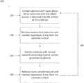
- FIG. 1is a process flow diagram for depositing a silicon oxycarbonitride (SiOCN) thin film by a plasma enhanced atomic layer deposition (PEALD) process according to some embodiments of the present disclosure.
- SiOCNsilicon oxycarbonitride
- PEALDplasma enhanced atomic layer deposition
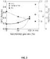
- FIG. 2illustrates film growth per cycle (GPC), refractive index, and wet etch rate ratio (WERR) as a function of second reactant gas mixture ratio for SiOCN thin films deposited according to some embodiments of the present disclosure.
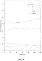
- FIG. 3illustrates etch amount (dHF wet etch) versus etch time for thermal oxide (TOX) and a SiOCN thin film deposited according to some embodiments of the present disclosure.
- FIG. 4is a compositional X-ray photoelectron spectroscopy (XPS) depth profile for a SiOCN thin film deposited according to some embodiments of the present disclosure.
- XPSX-ray photoelectron spectroscopy
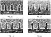
- FIGS. 5A-Billustrate transmission electron microscope (TEM) images of a SiOCN thin film deposited according to some embodiments of the present disclosure before and after exposure to a 2-minute dHF dip.
- TEMtransmission electron microscope
- FIGS. 5C-Dillustrate transmission electron microscope (TEM) images of a SiOCN thin film deposited according to some embodiments of the present disclosure before and after exposure to a 2-minute dHF dip.
- TEMtransmission electron microscope
- SiOCN filmshave a wide variety of applications, as will be apparent to the skilled artisan, for example in integrated circuit fabrication. More specifically, SiOCN films that display a low etch rate have a wide variety of application, both in the semiconductor industry and outside of the semiconductor industry. SiOCN films may be useful as, for example, etch stop layers, sacrificial layers, low-k spacers, anti-reflection layers (ARL), and passivation layers.
- SiOCN filmshaving a relatively low wet etch rate, for example in dHF.
- SiOCN thin filmsare deposited on a substrate by plasma-enhanced atomic layer deposition (PEALD) processes. In some embodiments SiOCN thin films are not deposited by liquid phase methods. In some embodiments a SiOCN thin film is deposited over a three dimensional structure, such as a fin in the formation of a finFET device.
- PEALDplasma-enhanced atomic layer deposition
- SiOCNThe formula of the silicon oxycarbonitride films is generally referred to herein as SiOCN for convenience and simplicity.
- SiOCNis not intended to limit, restrict, or define the bonding or chemical state, for example the oxidation state of any of Si, O, C, N, and/or any other element in the film.
- SiOCN thin filmsmay comprise one or more elements in addition to Si, O, C, and/or N.
- the SiOCN filmsmay comprise Si—C bonds, Si—O bonds, and/or Si—N bonds.
- the SiOCN filmsmay comprise Si—C bonds and Si—O bonds and may not comprise Si—N bonds.
- the SiOCN filmsmay comprise more Si—O bonds than Si—C bonds, for example a ratio of Si—O bonds to Si—C bonds may be from about 1:1 to about 10:1.
- the SiOCN filmsmay comprise from about 0% to about 10% nitrogen on an atomic basis (at %).
- the SiOCNmay comprise from about 0% to about 30% carbon on an atomic basis.
- the SiOCN filmsmay comprise from about 0% to about 60% oxygen on an atomic basis.
- the SiOCN filmsmay comprise about 0% to about 50% silicon on an atomic basis.
- ALD-type processesare based on controlled, generally self-limiting surface reactions. Gas phase reactions are typically avoided by contacting the substrate alternately and sequentially with the reactants. Vapor phase reactants are separated from each other in the reaction chamber, for example, by removing excess reactants and/or reactant byproducts between reactant pulses. The reactants may be removed from proximity with the substrate surface with the aid of a purge gas and/or vacuum. In some embodiments excess reactants and/or reactant byproducts are removed from the reaction space by purging, for example with an inert gas.
- PEALD processesare used to deposit SiOCN films.
- PEALD processes as described hereindo not comprise oxygen plasma.
- a substrate or workpieceis placed in a reaction chamber and subjected to alternately repeated surface reactions.
- thin SiOCN filmsare formed by repetition of a self-limiting ALD cycle.
- each ALD cyclecomprises at least two distinct phases. The contacting and removal of a reactant from the substrate may be considered a phase.
- a vapor phase first reactant comprising siliconcontacts the substrate and forms no more than about one monolayer on the substrate surface.
- This reactantis also referred to herein as “the silicon precursor,” “silicon-containing precursor,” or “silicon reactant” and may be, for example, (3-Aminopropyl)trimethoxysilane (APTMS).
- a second reactant comprising a reactive speciescontacts the substrate and may convert adsorbed silicon to SiOCN.
- the second reactantcomprises a hydrogen precursor.
- the reactive speciescomprises an excited species.
- the second reactantcomprises a species from a hydrogen containing plasma.
- the second reactantcomprises hydrogen radicals, hydrogen atoms and/or hydrogen plasma.
- the second reactantmay comprise other species that are not hydrogen precursors.
- the second reactantmay comprise a plasma of nitrogen, radicals of nitrogen, or atomic nitrogen in one form or another.
- the second reactantmay comprise a species from a noble gas, such as He, Ne, Ar, Kr, or Xe, for example as radicals, in plasma form, or in elemental form.
- a noble gassuch as He, Ne, Ar, Kr, or Xe
- these reactive species from noble gasesdo not necessarily contribute material to the deposited film, but can in some circumstances contribute to film growth as well as help in the formation and ignition of plasma.
- a gas that is used to form a plasmamay flow constantly throughout the deposition process but only be activated intermittently.
- a gas that is used to form a plasmadoes not comprise oxygen.
- the adsorbed silicon precursoris not contacted with a reactive species generated by a plasma from oxygen.
- a second reactant comprising reactive speciesis generated in a gas that does not comprise oxygen.
- a second reactantmay comprise a plasma generated in a gas that does not comprise oxygen.
- the second reactantmay be generated in a gas comprising less than about 1 atomic % (at %) oxygen, less than about 0.1 at % oxygen, less than about 0.01 at % oxygen, or less than about 0.001 at % oxygen.
- Additional phasesmay be added and phases may be removed as desired to adjust the composition of the final film.
- One or more of the reactantsmay be provided with the aid of a carrier gas, such as Ar or He.
- a carrier gassuch as Ar or He.
- the silicon precursor and the second reactantare provided with the aid of a carrier gas.
- two of the phasesmay overlap, or be combined.
- the silicon precursor and the second reactantmay be contact the substrate simultaneously in phases that partially or completely overlap.
- the order of the phasesmay be varied, and an ALD cycle may begin with any one of the phases. That is, unless specified otherwise, the reactants can contact the substrate in any order, and the process may begin with any of the reactants.
- one or more deposition cyclesbegin by contacting the substrate with the silicon precursor, followed by the second precursor.
- depositionmay begin by contacting the substrate with the second precursor, followed by the silicon precursor.
- the substrate on which deposition is desiredis loaded into a reaction space or reactor.
- the reactormay be part of a cluster tool in which a variety of different processes in the formation of an integrated circuit are carried out.
- a flow-type reactoris utilized.
- a shower head type of reactoris utilized.
- a space divided reactoris utilized.
- a high-volume manufacturing-capable single wafer ALD reactoris used.
- a batch reactorcomprising multiple substrates is used.
- the number of substratesis in the range of 10 to 200, in the range of 50 to 150, or in the range of 100 to 130.
- suitable reactorsinclude commercially available equipment such as the F120® reactor, F450® reactor, Pulsar® reactors—such as the Pulsar® 2000 and the Pulsar® 3000—EmerALD® reactor and Advance® 400 Series reactors, available from ASM America, Inc of Phoenix, Ariz. and ASM Europe B.V., Almere, Netherlands.
- Other commercially available reactorsinclude those from ASM Japan K.K (Tokyo, Japan) under the tradename Eagle® XP and XP8.
- the exposed surfaces of the workpiececan be pretreated to provide reactive sites to react with the first phase of the ALD process. In some embodiments a separate pretreatment step is not required. In some embodiments the substrate is pretreated to provide a desired surface termination. In some embodiments the substrate is pretreated with plasma.
- Excess reactant and reaction byproducts, if any,are removed from the vicinity of the substrate, and in particular from the substrate surface, between reactant contacting phases.
- excess reactant and reaction byproducts, if any,are removed from the substrate surface by, for example, purging the reaction chamber between reactant contacting phases, such as by purging with an inert gas.
- the flow rate and contacting time of each reactantis tunable, as is the removal step, allowing for control of the quality and various properties of the films.
- a gasis provided to the reaction chamber continuously during each deposition cycle, or during the entire ALD process, and reactive species are provided by generating a plasma in the gas, either in the reaction chamber or upstream of the reaction chamber.
- the gascomprises nitrogen.
- the gasis nitrogen.
- the gasmay comprise noble gas, such as helium or argon.
- the gasis helium or nitrogen.
- the flowing gasmay also serve as a purge gas for the first and/or second reactant (or reactive species). For example, flowing nitrogen may serve as a purge gas for a first silicon precursor and also serve as a second reactant (as a source of reactive species).
- nitrogen, argon, or heliummay serve as a purge gas for a first precursor and a source of excited species for converting the silicon precursor to the SiOCN film.
- the gas in which the plasma is generateddoes not comprise nitrogen and the adsorbed silicon precursor is not contacted with a reactive species generated by a plasma from nitrogen.
- the gas in which the plasma is generateddoes not comprise oxygen and the adsorbed silicon precursor is not contacted with a reactive species generated by a plasma from oxygen.
- the cycleis repeated until a film of the desired thickness and composition is obtained.
- the deposition parameterssuch as the precursor flow rate, contacting time, removal time, and/or reactants themselves, may be varied in one or more deposition cycles during the ALD process in order to obtain a film with the desired characteristics.
- the surface of the substrateis contacted with a reactant.
- a pulse of reactantis provided to a reaction space containing the substrate.
- the term “pulse”may be understood to comprise feeding reactant into the reaction chamber for a predetermined amount of time. The term “pulse” does not restrict the length or duration of the pulse and a pulse can be any length of time.
- the substrateis moved to a reaction space containing a reactant. In some embodiments the substrate is subsequently moved from a reaction space containing a first reactant to a second, different reaction space containing the second reactant.
- the substrateis contacted with the silicon reactant first. After an initial surface termination, if necessary or desired, the substrate is contacted with a first silicon reactant.
- a first silicon reactant pulseis supplied to the workpiece.
- the first reactant pulsecomprises a carrier gas flow and a volatile silicon species, such as APTMS, that is reactive with the workpiece surfaces of interest. Accordingly, the silicon reactant adsorbs upon these workpiece surfaces.
- the first reactant pulseself-saturates the workpiece surfaces such that any excess constituents of the first reactant pulse do not further react with the molecular layer formed by this process.
- the first silicon reactant pulsecan be supplied in gaseous form.
- the silicon precursor gasis considered “volatile” for purposes of the present description if the species exhibits sufficient vapor pressure under the process conditions to transport the species to the workpiece in sufficient concentration to saturate exposed surfaces.
- the silicon reactantcontacts the surface from about 0.05 seconds to about 5.0 seconds, about 0.1 seconds to about 3 seconds or about 0.2 seconds to about 1.0 seconds.
- the optimum contacting timecan be readily determined by the skilled artisan based on the particular circumstances.
- excess first silicon reactant, and reaction byproducts, if any,are removed from the substrate surface.
- removing excess reactant and reaction byproducts, if anymay comprise purging the reaction chamber.
- the reaction chambermay be purged by stopping the flow of the first reactant while continuing to flow a carrier gas or purge gas for a sufficient time to diffuse or purge excess reactants and reactant by-products, if any, from the reaction space.
- the excess first precursoris purged with the aid of inert gas, such as nitrogen or argon, which is flowing throughout the ALD cycle.
- the substratemay be moved from the reaction space containing the first reactant to a second, different reaction space.
- the first reactantis removed for about 0.1 seconds to about 10 seconds, about 0.3 seconds to about 5 seconds or about 0.3 seconds to about 1 second. Contacting and removal of the silicon reactant can be considered the first or silicon phase of the ALD cycle.
- a second reactantcomprising a reactive species, such as hydrogen plasma is provided to the workpiece.
- Hydrogen plasmamay be formed by generating a plasma in hydrogen in the reaction chamber or upstream of the reaction chamber, for example by flowing the hydrogen (H 2 ) through a remote plasma generator.
- plasmais generated in flowing H 2 gas.
- H 2is provided to the reaction chamber before the plasma is ignited or hydrogen atoms or radicals are formed.
- the H 2is provided to the reaction chamber continuously and hydrogen containing plasma, atoms or radicals is created or supplied when needed.
- the second reactantfor example comprising hydrogen plasma, contacts the substrate for about 0.1 seconds to about 10 seconds.
- the second reactantsuch as hydrogen containing plasma, contacts the substrate for about 0.1 seconds to about 10 seconds, 0.5 seconds to about 5 seconds or 0.5 seconds to about 2.0 seconds.
- the second reactant contacting timemay be even higher than about 10 seconds. In some embodiments, contacting times can be on the order of minutes. The optimum contacting time can be readily determined by the skilled artisan based on the particular circumstances.
- the second reactantis provided in two or more distinct pulses, without introducing another reactant in between any of the two or more pulses.
- a plasmasuch as a hydrogen containing plasma, is provided in two or more sequential pulses, without introducing a Si-precursor in between the sequential pulses.
- two or more sequential plasma pulsesare generated by providing a plasma discharge for a first period of time, extinguishing the plasma discharge for a second period of time, for example from about 0.1 seconds to about 10 seconds, from about 0.5 seconds to about 5 seconds or about 1.0 seconds to about 4.0 seconds, and exciting it again for a third period of time before introduction of another precursor or a removal step, such as before the Si-precursor or a purge step. Additional pulses of plasma can be introduced in the same way.
- a plasmais ignited for an equivalent period of time in each of the pulses.
- plasmafor example hydrogen containing plasma may be generated by applying RF power of from about 10 W to about 2000 W, from about 50 W to about 1000 W, or from about 100 W to about 500 W in some embodiments.
- a plasma power used for generating a nitrogen-containing plasmacan be about 500 W to about 1,500 W, 700 W to about 1200 W or about 800 W to about 1,000 W.
- the RF power densitymay be from about 0.02 W/cm 2 to about 2.0 W/cm 2 , or from about 0.05 W/cm 2 to about 1.5 W/cm 2 .
- the RF powermay be applied to second reactant that flows during the plasma contacting time, that flows continuously through the reaction chamber, and/or that flows through a remote plasma generator.
- the plasmais generated in situ, while in other embodiments the plasma is generated remotely.
- a showerhead reactoris utilized and plasma is generated between a susceptor (on top of which the substrate is located) and a showerhead plate.
- the gap between the susceptor and showerhead plateis from about 0.1 cm to about 20 cm, from about 0.5 cm to about 5 cm, or from about 0.8 cm to about 3.0 cm.
- any excess reactant and reaction byproductsare removed from the substrate surface.
- removing excess reactant and reaction byproducts, if any,may comprise purging the reaction chamber.
- the reaction chambermay be purged by stopping the flow of the second reactant while continuing to flow a carrier gas or purge gas for a sufficient time to diffuse or purge excess reactants and reactant by-products, if any, from the reaction space.
- the excess second precursoris purged with the aid of inert gas, such as nitrogen or argon, which is flowing throughout the ALD cycle.
- the substratemay be moved from the reaction space containing the second reactant to a different reaction space.
- the removalmay, in some embodiments, be from about 0.1 seconds to about 10 seconds, about 0.1 seconds to about 4 seconds or about 0.1 seconds to about 0.5 seconds.
- the reactive species contacting and removalrepresent a second, reactive species phase in a SiOCN atomic layer deposition cycle.
- the first precursor phasegenerally reacts with the termination left by the last phase in the previous cycle.
- the reactive species phaseis the first phase in the first ALD cycle, in subsequent cycles the reactive species phase will effectively follow the silicon phase.
- one or more different ALD cyclesare provided in the deposition process.
- PEALD reactionsmay be performed at temperatures ranging from about 25° C. to about 700° C., from about 50° C. to about 600° C., from about 100° C. to about 450° C., or from about 200° C. to about 400° C.
- the optimum reactor temperaturemay be limited by the maximum allowed thermal budget. Therefore, in some embodiments the reaction temperature is from about 300° C. to about 400° C. In some applications, the maximum temperature is around about 400° C., and, therefore the PEALD process is run at that reaction temperature.
- the substrate on which a thin film is depositedmay comprise various types of materials.
- the substratemay comprise an integrated circuit workpiece.
- the substratemay comprise silicon.
- the substratemay comprise silicon oxide, for example, thermal oxide.
- the substratemay comprise a high-k dielectric material.
- the substratemay comprise carbon.
- the substratemay comprise an amorphous carbon layer, graphene, and/or carbon nanotubes.
- the substratemay comprise a metal, including, but not limited to W, Cu, Ni, Co, and/or Al.
- the substratemay comprise a metal nitride, including, but not limited to TiN and/or TaN.
- the substratemay comprise a metal carbide, including, but not limited to TiC and/or TaC.
- the substratemay comprise a metal chalcogenide, including, but not limited to MoS 2 , Sb 2 Te 3 , and/or GeTe.
- the substratemay comprise a material that would be oxidized by exposure to an oxygen plasma process, but not by a PEALD process as described herein.
- a substrate used in the PEALD processes described hereinmay comprise an organic material.
- the substratemay comprise an organic material such as a plastic, polymer, and/or photoresist.
- the reaction temperature of a PEALD processmay be less than about 200° C. In some embodiments the reaction temperature may be less than about 150° C., less than about 100° C., less than about 75° C., or less than about 50° C.
- a substratecomprises an organic material
- the maximum process temperaturemay be as low as 100° C.
- the absence of a plasma generated from oxygenmay allow for deposition of a SiOCN thin film on an organic material that may not otherwise degrade in a deposition process including plasma generated from oxygen.
- the pressure of the reaction chamber during processingis maintained at from about 0.01 Torr to about 50 Torr, or from about 0.1 Torr to about 10 Torr. In some embodiments the pressure of the reaction chamber is greater than about 6 Torr, or about 20 Torr. In some embodiments, a SiOCN deposition process can be performed at a pressure of about 20 Torr to about 500 Torr, about 20 Torr to about 50 Torr, or about 20 Torr to about 30 Torr.
- a SiOCN deposition processcan comprise a plurality of deposition cycles, wherein at least one deposition cycle is performed in an elevated pressure regime.
- a deposition cycle of a PEALD processmay comprise alternately and sequentially contacting the substrate with a silicon precursor and a second reactant under the elevated pressure.
- one or more deposition cycles of the PEALD processcan be performed at a process pressure of about 6 Torr to about 500 Torr, about 6 Torr to about 50 Torr, or about 6 Torr to about 100 Torr.
- the one or more deposition cyclescan be performed at a process pressure of greater than about 20 Torr, including about 20 Torr to about 500 Torr, about 30 Torr to about 500 Torr, about 40 Torr to about 500 Torr, or about 50 Torr to about 500 Torr. In some embodiments, the one or more deposition cycles can be performed at a process pressure of about 20 Torr to about 30 Torr, about 20 Torr to about 100 Torr, about 30 Torr to about 100 Torr, about 40 Torr to about 100 Torr or about 50 Torr to about 100 Torr.
- SiOCN thin filmscan be deposited on a substrate in a reaction space by a plasma enhanced atomic deposition layer (PEALD) process.
- PEALDplasma enhanced atomic deposition layer
- a SiOCN thin filmis deposited using a PEALD process on a substrate having three-dimensional features, such as in a FinFET application.
- a PEALD process as described hereinmay be used in a variety of applications.
- a PEALD process as described hereinmay be used in the formation of hardmask layers, sacrificial layers, protective layers, or low-k spacers.
- a PEALD process as described hereinmay be used in, for example, memory device applications.
- a SiOCN thin filmmay be deposited by a PEALD process as described herein on a substrate that is not able to withstand O plasma without damage, for example a substrate comprising an organic and/or photoresist material.
- a SiOCN thin filmis deposited on a substrate in a reaction space by a PEALD deposition process 100 comprising at least one cycle comprising:
- step 160optionally repeating the contacting and removing steps at step 160 to form a SiOCN thin film of a desired thickness and composition.
- step 140may comprise remotely generating or forming plasma or reactive species before contacting the substrate with the second reactant.
- a SiOCN plasma enhanced ALD deposition cyclecan be used to deposit a SiOCN thin film.
- a SiOCN thin filmis formed on a substrate by an ALD-type process comprising multiple SiOCN deposition cycles, each SiOCN deposition cycle comprising:
- the exposing the substrate to a purge gas and/or vacuum stepsmay comprise continuing the flow of an inert carrier gas while stopping the flow of a precursor or reactant. In some embodiments the exposing the substrate to a purge gas and/or vacuum steps may comprise stopping the flow of a precursor and a carrier gas into a reaction chamber and evacuating the reaction chamber, for example with a vacuum pump. In some embodiments the exposing the substrate to a purge gas and/or vacuum steps may comprise moving the substrate from a first reaction chamber to a second, different reaction chamber containing a purge gas. In some embodiments the exposing the substrate to a purge gas and/or vacuum steps may comprise moving the substrate from a first reaction chamber to a second, different reaction chamber under a vacuum.
- contacting the substrate with a second reactantmay comprise remotely generating or forming plasma or reactive species before contacting the substrate with the second reactant.
- a SiOCN thin filmis formed on a substrate by an ALD-type process comprising multiple SiOCN deposition cycles, each SiOCN deposition cycle comprising: alternately and sequentially contacting the substrate with a first vapor phase silicon precursor and a second reactant comprising reactive species.
- the silicon precursormay comprise APTMS and the second reactive species may comprise hydrogen.
- the PEALD processis performed at a temperature between about 100° C. to about 650° C., about 100° C. to about 550° C., about 100° C. to about 450° C., about 200° C. to about 600° C., or at about 200° C. to about 400° C., In some embodiments the temperature is about 300° C.
- the PEALD processmay be performed at a temperature less than about 100° C.
- the PEALD processis performed at a temperature less than about 75° C., or less than about 50° C.
- a plasmamay be generated by applying RF power to the second reactant.
- the RF powermay be applied to second reactant to thereby generate reactive species.
- the RF powermay be applied to the second reactant that flows continuously through the reaction chamber, and/or that flows through a remote plasma generator.
- the plasmais generated in situ, while in other embodiments the plasma is generated remotely.
- the RF power applied to the second reactantis from about 10 W to about 2000 W, from about 100 W to about 1000 W or from about 200 W to about 500 W.
- the RF power applied to the second reactantis about 200 W.
- a plasma power used for generating a nitrogen-containing plasmacan be about 500 W to about 1500 W, about 800 W to about 1200 W.
- one or more PEALD deposition cyclesbegin with provision of the silicon precursor, followed by the second reactant.
- depositionmay begin with provision of the second reactant, followed by the silicon precursor.
- the first precursor phasegenerally reacts with the termination left by the last phase in the previous cycle.
- the reactive species phaseis the first phase in the first PEALD cycle
- the reactive species phasewill effectively follow the silicon phase.
- one or more different PEALD sub-cyclesare provided in the process for forming a SiOCN thin film.
- R Imay be an independently selected alkyl group
- R IImay be an independently selected hydrocarbon group
- R III and R IVmay be independently selected alkyl groups and/or hydrogens.
- R I and R IIare C 1 -C 3 alkyl ligands, such as methyl, ethyl, n-propyl, or isopropyl.
- R Imay be a C 1 -C 4 alkyl ligand, such as methyl, ethyl, n-propyl, isopropyl, or tertbutyl.
- R IIis not a C 3 hydrocarbon.
- R IIis a C 1 -C 2 hydrocarbon or a C 4 -C 6 hydrocarbon.
- R IImay be an unsaturated hydrocarbon, such as a hydrocarbon containing one or more double bonds.
- R IImay be an alkyl group where one of the hydrogens is removed.
- R III and R IVare hydrogen.
- some Si precursorsmay have the following general formula: Si(OR I ) 4-x-y-z (R II NR III R IV ) x H y (OH) z (2)
- R I and R IImay be an independently selected alkyl group
- R IImay be an independently selected hydrocarbon
- R III and R IVmay be independently selected alkyl groups and/or hydrogens.
- R IImay be an unsaturated hydrocarbon, such as a hydrocarbon containing one or more double bonds.
- R IImay be an alkyl group where one of the hydrogens is removed.
- some Si precursorsmay have the following general formula: L n Si(OR I ) 4-x-n (R II NR III R IV ) x (3)
- R Imay be an independently selected alkyl group
- R IImay be an independently selected hydrocarbon
- R III and R IVmay be independently selected alkyl groups and/or hydrogens
- Lis an independently selected alkyl group or halogen.
- R IImay be an unsaturated hydrocarbon, such as a hydrocarbon containing one or more double bonds.
- R IImay be an alkyl group where one of the hydrogens is removed.
- some Si precursorsmay have the following general formula: L n Si(OR I ) 4-x-y-z-n (R II NR III R IV ) x H y (OH) z (4)
- R Imay be an independently selected alkyl group
- R IImay be an independently selected hydrocarbon
- R III and R IVmay be independently selected alkyl groups and/or hydrogens
- Lis an independently selected alkyl group or halogen.
- R IImay be an unsaturated hydrocarbon, such as a hydrocarbon containing one or more double bonds.
- R IImay be an alkyl group where one of the hydrogens is removed.
- some Si precursorsmay have the following general formula: (R I O) 4-x Si(R II —NH 2 ) x (5)
- R Imay be an independently selected alkyl group
- R IImay be an independently selected hydrocarbon.
- R I and R IIare C 1 -C 3 alkyl ligands, such as methyl, ethyl, n-propyl, or isopropyl.
- R Iis methyl
- R IImay be an unsaturated hydrocarbon, such as a hydrocarbon containing one or more double bonds.
- R IImay be an alkyl group where one of the hydrogens is removed.
- some Si precursorsmay have the following general formula: (R I O) 3 Si—R II —NH 2 6)
- R Imay be an independently selected alkyl group
- R IImay be an independently selected hydrocarbon.
- R I and R IIare C 1 -C 3 alkyl ligands, such as methyl, ethyl, n-propyl, or isopropyl.
- R IImay be an unsaturated hydrocarbon, such as a hydrocarbon containing one or more double bonds.
- R IImay be an alkyl group where one of the hydrogens is removed.
- some Si precursorsmay have the following general formula: (R I O) 4-x Si(—[CH 2 ] n —NH 2 ) x 7)
- R Imay be an independently selected alkyl group.
- R Iis a C 1 -C 4 alkyl ligand, such as methyl, ethyl, n-propyl, or isopropyl.
- the silicon precursordoes not comprise a halogen.
- the silicon precursormay comprise at least one aminoalkyl ligand
- a suitable silicon precursormay comprise at least one ligand which is bonded through carbon to silicon and contains at least one p attached to a carbon chain, for example an aminoalkyl ligand.
- a suitable silicon precursormay comprise at least one ligand which is bonded through carbon to silicon and contains an NH 2 -group attached to a carbon chain, for example an aminoalkyl ligand, and may also comprise at least one ligand which is bonded to silicon through an oxygen atom and in which an alkyl group is bonded to oxygen, for example an alkoxide ligand.
- a suitable silicon precursormay comprise at least one ligand which is bonded through carbon to silicon and contains at least one NR III R IV -group, wherein R III and R IV may be independently selected alkyl groups and/or hydrogens, attached to a carbon chain, for example an aminoalkyl ligand.
- a suitable silicon precursormay comprise at least one ligand which is bonded through carbon to silicon and in which ligand at least one nitrogen is bonded to carbon. Further the one ligand which is bonded through carbon to silicon and in which ligand at least one nitrogen is bonded to carbon may comprise hydrogen bonded to nitrogen.
- a suitable silicon precursorin addition to a ligand which is bonded to silicon through carbon, may comprise also an alkoxy ligand, such as methoxy, ethoxy, n-propoxy, i-propoxy or tertbutoxy ligand.
- a suitable silicon precursorcomprises a carbon chain which is bonded to silicon through carbon, and in which there is an amino group, such as alkylamino or —NH 2 group, attached to the carbon chain and the carbon chain is a C1-C6 hydrocarbon, C2-C6 hydrocarbon or C2-C4 hydrocarbon, linear, branched or cyclic, containing only carbon and hydrogen.
- the carbon chainmay be unsaturated and contain double carbon-carbon bonds.
- the carbon chainmay contain other atoms than carbon and hydrogen.
- suitable silicon precursorscan include at least compounds having any of the general formulas (1) through (7).
- halides/halogenscan include F, Cl, Br, and I.
- the silicon precursorcan comprise (3-aminopropyl)trimethoxysilane (APTMS).
- more than one silicon precursormay contact the substrate surface at the same time during an ALD phase.
- the silicon precursormay comprise more than one of the silicon precursors described herein.
- a first silicon precursoris used in a first ALD cycle and a second, different ALD precursor is used in a later ALD cycle.
- multiple silicon precursorsmay be used during a single ALD phase, for example in order to optimize certain properties of the deposited SiOCN film.
- only one silicon precursormay contact the substrate during the deposition.
- the silicon precursoris not used as a silylating agent.
- the deposition temperature and/or the duration of the silicon precursor contacting stepare selected such that the silicon precursor does not decompose.
- the silicon precursormay decompose during the silicon precursor contacting step.
- the silicon precursordoes not comprise a halogen, such as chlorine or fluorine.
- the second reactant for depositing SiOCNmay comprise a hydrogen precursor, which may comprise a reactive species.
- a reactive speciesincludes, but is not limited to, radicals, plasmas, and/or excited atoms or species. Such reactive species may be generated by, for example, plasma discharge, hot-wire, or other suitable methods.
- the reactive speciesmay be generated remotely from the reaction chamber, for example upstream from the reaction chamber (“remote plasma”). In some embodiments the reactive species may be generated in the reaction chamber, in the direct vicinity of the substrate, or directly above the substrate (“direct plasma”).
- Suitable plasma compositions of a PEALD processinclude hydrogen reactive species, that is plasma, radicals of hydrogen, or atomic hydrogen in one form or another.
- a second reactantmay comprise a reactive species formed at least in part from H 2 .
- nitrogen reactive species in the form of plasma, radicals of nitrogen, or atomic nitrogen in one form or anotherare also provided.
- a plasmamay also contain noble gases, such as He, Ne, Ar, Kr and Xe, or Ar or He, in plasma form, as radicals, or in atomic form.
- the second reactantdoes not comprise any species generated from oxygen.
- reactive speciesare not generated from a gas containing oxygen.
- a second reactant comprising reactive speciesis generated from a gas that does not contain oxygen.
- a second reactantmay comprise a plasma generated from a gas that does not contain oxygen.
- the second reactantmay be generated from a gas containing less than about 1 atomic % (at %) oxygen, less than about 0.1 at % oxygen, less than about 0.01 at % oxygen, or less than about 0.001 at % oxygen.
- a second reactantdoes not comprise O 2 , H 2 O or O 3 .
- the second reactantmay comprise reactive species formed from compounds having both N and H, such as NH 3 and N 2 H 4 , a mixture of N 2 /H 2 or other precursors having an N—H bond.
- the second reactantmay be formed, at least in part, from N 2 .
- the second reactantmay be formed, at least in part, from H 2 and N 2 , where the H 2 and N 2 are provided at a flow ratio (H 2 /N 2 ), from about 100:1 to about 1:100, from about 20:1 to about 1:20, from about 10:1 to about 1:10, from about 5:1 to about 1:5 and/or from about 2:1 to about 4:1, and in some cases 1:1.
- a hydrogen-containing plasma for depositing SiOCNcan be generated using both N 2 and H 2 at one or more ratios described herein.
- a hydrogen plasmamay be free or substantially free of nitrogen-containing species (e.g., nitrogen ions, radicals, atomic nitrogen).
- nitrogen-containing gasis not used to generate the hydrogen plasma.
- nitrogen-containing gase.g., N 2 gas
- N 2 gasis not flowed into the reaction chamber during the hydrogen plasma step.
- a hydrogen plasmamay be free or substantially free of oxygen-containing species (e.g., oxygen ions, radicals, atomic oxygen).
- oxygen-containing gasis not used to generate the hydrogen plasma.
- oxygen-containing gase.g., O 2 gas
- O 2 gasoxygen-containing gas
- the second reactantdoes not comprise any species generated from nitrogen.
- reactive speciesare not generated from a gas containing nitrogen.
- a second reactant comprising reactive speciesis generated from a gas that does not contain nitrogen.
- a second reactantmay comprise a plasma generated from a gas that does not contain nitrogen.
- the second reactantmay be generated from a gas containing less than about 1 atomic % (at %) nitrogen, less than about 0.1 at % nitrogen, less than about 0.01 at % nitrogen, or less than about 0.001 at % nitrogen.
- a second reactantdoes not comprise N 2 , NH 3 or N 2 H 4 .
- oxygen-containing gasis not used to generate the hydrogen plasma.
- oxygen-containing gase.g., O 2 gas
- O 2 gasoxygen-containing gas
- the gas used to generated reactive species, such as plasmamay consist essentially of hydrogen. In some embodiments the gas used to generated reactive species, such as plasma, may consist essentially of nitrogen. In some embodiments the gas used to generated reactive species, such as plasma, may consist essentially of argon or another noble gas.
- a plasma power used for generating a hydrogen-containing plasmacan be about 10 Watts (W) to about 2,000 W, about 50 W to about ⁇ 1000 W, about 100 W to about 1000 W or about 100 W to about 500 W. In some embodiments, a plasma power used for generating a hydrogen-containing plasma can be about 100 W to about 300 W.
- SiOCN thin films deposited according to some of the embodiments discussed hereinmay achieve impurity levels or concentrations below about 3 at %, below about 1 at %, below about 0.5 at %, or below about 0.1 at %.
- the total impurity level excluding hydrogenmay be below about 5 at %, below about 2 at %, below about 1 at %, or below about 0.2 at %.
- hydrogen levelsmay be below about 30 at %, below about 20 at %, below about 15 at %, or below about 10 at %.
- an impuritymay be considered any element other than Si, O, C, and/or N.
- the deposited SiOCN filmsdo not comprise an appreciable amount of hydrogen. However, in some embodiments a SiOCN film comprising hydrogen is deposited. In some embodiments, the deposited SiOCN films comprises less than about 30 at %, less than about 20 at %, less than about 15 at %, less than about 10 at % or less than about 5 at % of hydrogen. In some embodiments the thin films do not comprise argon.
- the SiOCN thin filmsmay exhibit step coverage and pattern loading effects of greater than about 50%, greater than about 80%, greater than about 90%, or greater than about 95%. In some cases step coverage and pattern loading effects can be greater than about 98% and in some case about 100% (within the accuracy of the measurement tool or method). In some embodiments step coverage and pattern loading effects can be greater than about 100%, greater than about 110%, greater than about 120%, greater than about 130%, or greater than about 140%. These values can be achieved in features with aspect ratios of 2 or greater, in some embodiments in aspect ratios of about 3 or greater, in some embodiments in aspect ratios of about 5 or greater and in some embodiments in aspect ratios of about 8 or greater.
- the step coveragemay be between about 50% and about 110%, between about between about 80% and about 110%, between about 90% and about 110%, between about 95% and 110%, between about 98% and 110%, or between about 100% and 110%. In some embodiments the step coverage may be between about 50% and about 100%, between about between about 80% and about 100%, between about 90% and about 100%, between about 95% and 100%, or between about 98% and 100%.
- the growth rate of the filmis from about 0.01 ⁇ /cycle to about 5 ⁇ /cycle, from about 0.05 ⁇ /cycle to about 2 ⁇ /cycle. In some embodiments the growth rate of the film is more than about 0.05 ⁇ /cycle, more than about 0.1 ⁇ /cycle, more than about 0.15 ⁇ /cycle, more than about 0.3 ⁇ /cycle, more than about 0.3 ⁇ /cycle, more than about 0.4 ⁇ /cycle.
- pattern loading effectis used in accordance with its ordinary meaning in this field.
- pattern loading effectwhen used herein refers to the variation in film thickness in an area of the substrate where structures are present.
- the pattern loading effectcan be given as the film thickness in the sidewall or bottom of a feature inside a three-dimensional structure relative to the film thickness on the sidewall or bottom of the three-dimensional structure/feature facing the open field.
- a 100% pattern loading effector a ratio of 1 would represent about a completely uniform film property throughout the substrate regardless of features i.e. in other words there is no pattern loading effect (variance in a particular film property, such as thickness, in features vs. open field).
- SiOCN filmsare deposited to a thickness of from about 3 nm to about 50 nm, from about 5 nm to about 30 nm, from about 5 nm to about 20 nm. These thicknesses can be achieved in feature sizes (width) below about 100 nm, about 50 nm, below about 30 nm, below about 20 nm, and in some cases below about 15 nm. According to some embodiments, a SiOCN film is deposited on a three-dimensional structure and the thickness at a sidewall may be slightly even more than 10 nm. In some embodiments SiOCN films of greater than 50 nm can be deposited. In some embodiments SiOCN films of greater than 100 nm can be deposited.
- SiOCN filmsare deposited to a thickness of more than about 1 nm, more than about 2 nm, more than about 3 nm, more than about 5 nm, more than about 10 nm.
- SiOCN films with various wet etch ratesmay be deposited.
- WERwet etch rates
- SiOCN filmsmay have WER values of less than about 5, less than about 4, less than about 2, or less than about 1.
- SiOCN filmsmay have WER values significantly less than 1.
- SiOCN filmsmay have WER values less than about 0.3, less than about 0.2, or less than about 0.1.
- SiOCN filmsmay have WER values less than about 0.05, less than about 0.025, or less than about 0.02.
- the blanket WER in 0.5% dHF (nm/min) relative to the WER of thermal oxidemay be less than about 3, less than about 2, less than about 1, and less than about 0.5. In some embodiments the blanket WER in 0.5% dHF relative to the WER of TOX may be less than about 0.1.
- the blanket WER in 0.5% dHF (nm/min) relative to the WER of thermal oxidemay be less than about 10, less than about 5, less than about 3, and less than about 2, or less than about 1.
- the sidewall WER of a three dimensional feature, such as a fin or trench relative to the top region WER of a three dimensional feature, such as fin or trench, in 0.5% dHFmay be less than about 10, less than about 5, less than about 3, less than about 3, or less than about 1.
- SiOCN formed according to one or more processes described hereincan advantageously demonstrate a horizontal region to vertical region WERR of about 1, for example in 0.5% dHF.
- a ratio of a wet etch rate of SiOCN thin film formed over horizontal surfaces (e.g., top surfaces) to a wet etch rate of the SiOCN thin film formed over vertical surfaces (e.g., sidewall surfaces) of three-dimensional structures on a substrate surfacecan be the same or substantially the same.
- the ratiocan be about 0.25 to about 2, about 0.5 to about 1.5, about 0.75 to about 1.25, or about 0.9 to about 1.1.
- These ratioscan be achieved in features with aspect ratios of about 2 or more, about 3 or more, about 5 or more or even about 8 or more.
- the amount of etching of SiOCN films according to the present disclosuremay be about 1, 2, 5, 10 or more times less than an amount of etching observed for thermal SiO 2 (TOX) in a 0.5% HF-dip process (for example in a process in which about 2 to about 3 nm TOX is removed, 1, 2, 5, 10 or more times less SiOCN is removed when deposited according to the methods disclosed herein).
- TOXthermal SiO 2
- less than about 2 nm of SiOCN filmmay be removed in a 0.5% HF-dip process with an etching time of 5 minutes. In some embodiments less than about 2 nm of SiOCN film may be removed in a 0.5% HF-dip process with an etching time of 60 minutes.
- the hydrogen content of the filmsis less than about 20 at %, less than about 10 at % or less than about 5 at %.
- the deposited SiOCN thin filmmay contain up to about 70% oxygen on an atomic basis (at %).
- a SiOCN filmmay comprise oxygen from about 10% to about 70%, from about 15% to about 50%, or from about 20% to about 40% on an atomic basis.
- a SiOCN filmmay comprise at least about 20%, about 40% or about 50% oxygen on an atomic basis.
- the deposited SiOCN thin filmmay contain up to about 40% carbon on an atomic basis (at %).
- a SiOCN filmmay comprise carbon from about 0.5% to about 40%, from about 1% to about 30%, or from about 5% to about 20% on an atomic basis.
- a SiOCN filmmay comprise at least about 1%, about 10% or about 20% carbon on an atomic basis.
- the deposited SiOCN thin filmmay contain up to about 30% nitrogen on an atomic basis (at %).
- a SiOCN filmmay comprise nitrogen from about 0.51% to about 30%, from about 1% to about 20%, or from about 3% to about 15% on an atomic basis.
- an SiOCN filmmay comprise at least about 1%, about 5% or about 10% nitrogen on an atomic basis.
- the deposited SiOCN thin filmmay contain up to about 50% silicon on an atomic basis (at %).
- a SiOCN filmmay comprise silicon from about 10X % to about 50%, from about 15% to about 40%, or from about 20% to about 35% on an atomic basis.
- a SiOCN filmmay comprise at least about 15%, about 20%, about 25% or about 30% silicon on an atomic basis.
- the deposited SiOCN thin filmmay comprise from about 30 at % to about 40 at % silicon, from about 25 at % to about 40 at % oxygen, from about 10 at % to about 20 at % C, and about 10 at % nitrogen. In some embodiments the deposited SiOCN film may comprise about 33% silicon and about 67% oxygen. As discussed above, in some embodiments a SiOCN film may comprise Si—C bonds, Si—O bonds, and/or Si—N bonds. In some embodiments a SiOCN film may comprise Si—C bonds and Si—O bonds and may not comprise Si—N bonds. In some embodiments a SiOCN film may comprise Si—N bonds and Si—O bonds and may not comprise Si—C bonds.
- a SiOCN filmmay comprise Si—N bonds and Si—C bonds and may not comprise Si—O bonds. In some embodiments the SiOCN films may comprise more Si—O bonds than Si—C bonds, for example a ratio of Si—O bonds to Si—C bonds may be from about 1:1 to about 10:1. In some embodiments a deposited SiOCN film may comprise one or more of SiN, SiO, SiC, SiCN, SiON, and/or SiOC.
- a SiOCN filmis not a low-k film, for example a SiOCN film is not a porous film.
- a SiOCNis a continuous film.
- a SiOCN filmhas a k-value that is less than about 10.
- a SiOCN filmhas a k-value that is less than about 7.
- a SiOCN filmhas a k-values from about 3.9 to about 10.
- a SiOCN filmhas a k-value that is less than about 5.5, less than about 5.0, less than about 4.8, less than about 4.6.
- a SiOCN filmhas a k-value that from about 3.8 to about 7, from about 3.8 to about 5.5, from about 3.8 to about 5.0, from about 4.0 to about 4.8, from about 4.1 to about 4.7. In some embodiments a SiOCN film has a k-value that is more than k-value of any low-k film. In some embodiments a SiOCN film has a k-value that is more than pure SiO 2 .
- SiOCN films deposited according to the present disclosuredo not comprise a laminate or nanolaminate structure.
- a SiOCN film deposited according to the present disclosureis not a self-assembled monolayer (SAM). In some embodiments a SiOCN film deposited according to the present disclosure does not consist of separate, individual molecules which are not bonded to each other. In some embodiments a SiOCN film deposited according to the present disclosure comprises a material which is substantially bonded or linked together. In some embodiments a SiOCN film deposited according to the present disclosure is not a functional layer, is not amino-functionalized, and/or is not used as a functional surface. In some embodiments a SiOCN film deposited according to the present disclosure is not terminated with —NH 2 groups. In some embodiments a SiOCN film deposited according to the present disclosure does not contain a substantial amount of —NH 2 groups.
- SAMself-assembled monolayer
- Exemplary SiOCN thin filmswere deposited by a PEALD process as described herein.
- the deposition temperaturewas 300° C. and APTMS was used as a silicon precursor.
- a plasmawas generated by applying 200 W of RF power to the second reactant.
- a mixture of H 2 and N 2was used as the second reactant, which was supplied with an Ar carrier gas.
- FIG. 2illustrates the growth per cycle ( ⁇ /cycle), refractive index, and WERR as compared with TOX as a function of second reactant gas ratio for SiOCN films deposited by a PEALD process as described herein.
- the second reactant gas ratiois shown along the X-axis of FIG. 2 , and represents the ratio of N 2 to both H 2 and N 2 (N 2 :(H 2 +N 2 )) in the second reactant.
- the growth rate of the SiOCN filmsincreased as the N 2 :(H 2 +N 2 ) ratio in the second reactant increased.
- the refractive index of the deposited filmsdecreased as the N 2 :(H 2 +N 2 ) ratio in the second reactant increased.
- the ratio of the WER of the deposited SiOCN films to the WER of TOXwas observed to increase as the N 2 :(H 2 +N 2 ) ratio in the second reactant increased.
- the WERR to TOXwas for SiOCN films deposited with N 2 :(H 2 +N 2 ) ratios of 50% and 0% (no N 2 present in the second reactant) was observed to be less than 1.
- FIG. 3illustrates the etching amount versus etching time for both SiOCN thin films deposited by PEALD processes as described herein and TOX.
- the etching processwas a 0.5% HF-dip process.
- the deposited SiOCNexhibit significantly greater etch resistance than TOX. After exposure to a 60 minute dip in 0.5% HF less than 2 nm of SiOCN film was removed.
- the composition of a SiOCN film deposited by a PEALD process as described hereinwas analysed using X-ray photoelectron spectroscopy (XPS).
- the deposition temperaturewas 300° C. and APTMS was used as a silicon precursor.
- Table 1, belowTwo distinct Si bonding energies were identified, indicating the presence of Si—C and SiO bonds in the deposited film.
- FIG. 4also illustrates film composition as a function depth for an exemplary SiOCN film deposited by a PEALD process as described herein.
- FIGS. 5A and 5Bare scanning electron microscopy (SEM) images showing cross-section view of SiOCN films formed on trench structure prior to and after exposure to a 2 minutes dip in dHF wet etch solution, respectively.
- the SiOCN films of FIGS. 5A and 5Bwere formed according to the PEALD processes as described herein.
- the deposition temperaturewas 300° C. and APTMS was used as a silicon precursor.
- a plasmawas generated by applying 400 W of RF power to the second reactant comprising H 2 .
- the plasma pulse timewas 8 seconds.
- FIGS. 5C and 5Dare scanning electron microscopy (SEM) images showing cross-section view of SiOCN films formed on trench structure prior to and after exposure to a 2 minutes dip in dHF wet etch solution, respectively.
- the SiOCN films of FIGS. 5C and 5Dwere formed according to the PEALD processes as described herein.
- the deposition temperaturewas 300° C. and APTMS was used as a silicon precursor.
- a plasmawas generated by applying 400 W of RF power to the second reactant comprising H 2 and N 2 .
- the plasma pulse timewas 8 seconds.
- the SiOCN film formed using a PEALD process with a second reactant that did not comprise N 2demonstrated improved conformality prior to the wet etch dip, as compared to the SiOCN film formed using a PEALD process with a second reactant comprising H 2 and N 2 .
- the SiOCN film formed with a second reactant that did not comprise N 2had a step coverage of 114% to 136%, while the SiOCN film formed with a second reactant comprising H 2 and N 2 had a step coverage of 54%.
- the conformality of the SiOCN film formed using a second reactant that did not comprise N 2was maintained subsequent to the wet etch dip, while that of the SiOCN film formed using a second reactant comprising H 2 and N 2 was decreased.
- the SiOCN film formed using a second reactant that did not comprise N 2demonstrated a wet etch rate ratio to TOX (WERR to TOX) of 0.2 for the horizontal regions of the film and a WERR to TOX of 1.0 for the vertical regions of the film (sidewall surfaces).
- the SiOCN film formed using a second reactant comprising H 2 and N 2demonstrated a wet etch rate ratio to TOX (WERR to TOX) of 2.0 for the horizontal regions of the film deposited on top of the trench structure, a WERR to TOX of 1.4 for the regions of the film deposited on the bottom of the trench structure, and a WERR to TOX of 1.6 for the vertical regions of the film (sidewall surfaces).
- film and “thin film”are used herein for simplicity. “Film” and “thin film” are meant to mean any continuous or non-continuous structures and material deposited by the methods disclosed herein.
- film and “thin film”could include 2D materials, nanorods, nanotubes or nanoparticles or even single partial or full molecular layers or partial or full atomic layers or clusters of atoms and/or molecules.
- Finm and “thin film”may comprise material or layer with pinholes, but still be at least partially continuous.
Landscapes
- Engineering & Computer Science (AREA)
- Physics & Mathematics (AREA)
- Microelectronics & Electronic Packaging (AREA)
- General Physics & Mathematics (AREA)
- Manufacturing & Machinery (AREA)
- Computer Hardware Design (AREA)
- Condensed Matter Physics & Semiconductors (AREA)
- Power Engineering (AREA)
- Chemical & Material Sciences (AREA)
- Chemical Kinetics & Catalysis (AREA)
- Plasma & Fusion (AREA)
- Inorganic Chemistry (AREA)
- Spectroscopy & Molecular Physics (AREA)
- Chemical Vapour Deposition (AREA)
- Formation Of Insulating Films (AREA)
Abstract
Description
The present application is a continuation of U.S. application Ser. No. 15/707,749, filed Sep. 18, 2017, which is a continuation of U.S. application Ser. No. 14/939,984, filed Nov. 12, 2015, now U.S. Pat. No. 9,786,491, each of which is hereby incorporated by reference in its entirety.
The present disclosure relates generally to the field of semiconductor device manufacturing and, more particularly, to formation of silicon oxycarbonitride (SiOCN) films having desirable chemical resistance properties.
There is increasing need for dielectric materials with relatively low dielectric constant (k) values and relatively low acid-based wet etch rates. Silicon oxycarbonitride may satisfy certain of these requirements. Typically, deposition processes for SiOCN require precursors comprising halides and/or oxygen plasma.
In some embodiments plasma enhanced atomic layer deposition (PEALD) processes are provided for forming a silicon oxycarbonitride (SiOCN) thin film on a substrate in a reaction space. In some embodiments a PEALD process may comprise at least one deposition cycle comprising contacting a surface of the substrate with a vapor phase silicon precursor to on the surface of the substrate, contacting the adsorbed silicon species with at least one reactive species generated by plasma formed from a gas that does not comprise oxygen, and optionally repeating the contacting steps until a SiOCN film of a desired thickness has been formed. In some embodiments the silicon precursor use in a PEALD process has a formula as in one of the following general formulas:
(RIO)4-xSi(RII—NH2)x (1)
(RIO)4-xSi(RII—NH2)x (1)
wherein x is an integer from 1 to 4;
RIis independently selected from the group consisting of alkyl; and
RIIis an independently selected hydrocarbon;
(RIO)3Si—RII—NH2 (2)
(RIO)3Si—RII—NH2 (2)
wherein RIis independently selected from the group consisting of alkyl; and
RIIis an independently selected hydrocarbon; and
(RIO)4-xSi(—[CH2]n—NH2)x (3)
(RIO)4-xSi(—[CH2]n—NH2)x (3)
wherein x is an integer from 1 to 4;
n is an integer from 1-5; and
RIis independently selected from the group consisting of alkyl.
In some embodiments a ratio of a wet etch rate of the SiOCN thin film to a wet etch rate of thermal silicon oxide may be less than about 5. In some embodiments a ratio of a wet etch rate of the SiOCN thin film to a wet etch rate of thermal silicon oxide may be less than about 0.3. In some embodiments a ratio of a wet etch rate of the SiOCN thin film to a wet etch rate of thermal silicon oxide may be less than about 0.1.
In some embodiments the SiOCN thin film may be deposited on a three-dimensional structure on the substrate. In some embodiments a wet etch rate ratio of a wet etch rate of SiOCN formed on a top surface of the three-dimensional structure to a wet etch rate of the SiOCN formed on a sidewall surface of the three-dimensional structure may be about 1:1 in dilute HF.
In some embodiments the vapor phase silicon precursor may not comprise a halogen. In some embodiments the silicon precursor may comprise (3-aminopropyl)trimethoxysilane (APTMS). In some embodiments the reactive species may comprise hydrogen plasma, hydrogen atoms, hydrogen radicals, or hydrogen ions. In some embodiments the reactive species may be generated from a second reactant comprising a noble gas. In some embodiments the reactive species may further comprise nitrogen plasma, nitrogen atoms, nitrogen radicals, or nitrogen ions. In some embodiments the reactive species may be generated by plasma from a second reactant comprising hydrogen. In some embodiments the second reactant may comprise H2.
In some embodiments the SiOCN thin film may comprise at least 20 at % oxygen. In some embodiments the SiOCN thin film may comprise at least 5 at % carbon. In some embodiments the SiOCN thin film may comprise at least 5 at % nitrogen.
In some embodiments processes are provided for forming a silicon oxycarbonitride (SiOCN) thin film on a substrate in a reaction space. In some embodiments a process may comprise a plurality of deposition cycles, at least one deposition cycle may comprise alternately and sequentially contacting a surface of the substrate with a silicon precursor and a second reactant comprising at least one reactive species. In some embodiments a deposition cycle may be repeated two or more times to form the SiOCN thin film. In some embodiments the silicon precursor may have a general formula:
LnSi(ORI)4-x-y-z-n(RIINRIIIRIV)xHy(OH)z
LnSi(ORI)4-x-y-z-n(RIINRIIIRIV)xHy(OH)z
wherein n is an integer from 0 to 3, x is an integer from 1 to 4, y is an integer from 0 to 3, z is an integer from 0 to 3; and 4-x-y-z-n is from 0 to 3;
RIis independently selected from the group consisting of alkyl;
RIIis an independently hydrocarbon;
RIIIand RIVare independently selected from the group consisting of alkyl and hydrogen; and
L is independently selected from the group consisting of alkyl and halogens.
In some embodiments the at least one reactive species may be generated by plasma formed from a gas that does not comprise oxygen.
In some embodiments the silicon precursor may have a general formula:
LnSi(ORI)4-x-n(RIINRIIIRIV)x
LnSi(ORI)4-x-n(RIINRIIIRIV)x
wherein n is an integer from 0 to 3, x is an integer from 1 to 3;
L is independently selected from the group consisting of alkyl and halogens;
RIis independently selected from the group consisting of alkyl;
RIIis an independently selected hydrocarbon; and
RIIIand RIVare independently selected from the group consisting of alkyl and hydrogen.
In some embodiments the silicon precursor may have a general formula:
Si(ORI)4-x-y-z(RIINRIIIRIV)xHy(OH)z
Si(ORI)4-x-y-z(RIINRIIIRIV)xHy(OH)z
wherein x is an integer from 1 to 4, y is an integer from 0 to 3, z is an integer from 0 to 3;
RIis independently selected from the group consisting of alkyl;
RIIis an independently selected hydrocarbon; and
RIIIand RIVare independently selected from the group consisting of alkyl and hydrogen.
In some embodiments the silicon precursor may have a general formula:
Si(ORI)4-x(RINRIIIRIV)x
Si(ORI)4-x(RINRIIIRIV)x
wherein x is an integer from 1 to 4;
RIis independently selected from the group consisting of alkyl;
RIIis an independently selected hydrocarbon; and
RIIIand RIVare independently selected from the group consisting of alkyl and hydrogen.
In some embodiments the silicon precursor may comprise APTMS. In some embodiments at least one deposition cycle may be a PEALD cycle. In some embodiments a reactive species may be generated by applying RF power of from about 100 Watts (W) to about 1000 W to the second reactant. In some embodiments a deposition cycle may be carried out at a process temperature of about 300° C. to about 400° C. In some embodiments the deposition cycle may be carried out at a process temperature of less than about 100° C. In some embodiments the substrate may comprise an organic material.
In some embodiments processes are provided for depositing a silicon oxycarbonitride (SiOCN) thin film on a substrate in a reaction space. In some embodiments such a process may comprise contacting a surface of the substrate with a silicon precursor comprising at least one ligand bonded through carbon to a silicon atom and containing an NH2-group attached to a carbon chain and at least one ligand bonded to the silicon atom through an oxygen atom and in which an alkyl group is bonded to the oxygen atom. In some embodiments a process may further comprise exposing the substrate to a purge gas and/or vacuum to remove excess titanium reactant and reaction byproducts, if any, contacting a surface of the substrate with a second reactant comprising hydrogen, wherein the second reactant comprises at least one reactive species generated by plasma, exposing the substrate to a purge gas and/or vacuum to remove excess second reactant and reaction byproducts, if any, and repeating the contacting steps until a SiOCN thin film of desired thickness has been formed.
Silicon oxycarbonitride (SiOCN) films have a wide variety of applications, as will be apparent to the skilled artisan, for example in integrated circuit fabrication. More specifically, SiOCN films that display a low etch rate have a wide variety of application, both in the semiconductor industry and outside of the semiconductor industry. SiOCN films may be useful as, for example, etch stop layers, sacrificial layers, low-k spacers, anti-reflection layers (ARL), and passivation layers.
According to some embodiments of the present disclosure, various SiOCN films, precursors, and methods for depositing said films are provided. In some embodiments the SiOCN films have a relatively low wet etch rate, for example in dHF.
In some embodiments SiOCN thin films are deposited on a substrate by plasma-enhanced atomic layer deposition (PEALD) processes. In some embodiments SiOCN thin films are not deposited by liquid phase methods. In some embodiments a SiOCN thin film is deposited over a three dimensional structure, such as a fin in the formation of a finFET device.
The formula of the silicon oxycarbonitride films is generally referred to herein as SiOCN for convenience and simplicity. As used herein, SiOCN is not intended to limit, restrict, or define the bonding or chemical state, for example the oxidation state of any of Si, O, C, N, and/or any other element in the film. Further, in some embodiments SiOCN thin films may comprise one or more elements in addition to Si, O, C, and/or N. In some embodiments the SiOCN films may comprise Si—C bonds, Si—O bonds, and/or Si—N bonds. In some embodiments the SiOCN films may comprise Si—C bonds and Si—O bonds and may not comprise Si—N bonds. In some embodiments the SiOCN films may comprise more Si—O bonds than Si—C bonds, for example a ratio of Si—O bonds to Si—C bonds may be from about 1:1 to about 10:1. In some embodiments the SiOCN films may comprise from about 0% to about 10% nitrogen on an atomic basis (at %). In some embodiments the SiOCN may comprise from about 0% to about 30% carbon on an atomic basis. In some embodiments the SiOCN films may comprise from about 0% to about 60% oxygen on an atomic basis. In some embodiments the SiOCN films may comprise about 0% to about 50% silicon on an atomic basis.
ALD-type processes are based on controlled, generally self-limiting surface reactions. Gas phase reactions are typically avoided by contacting the substrate alternately and sequentially with the reactants. Vapor phase reactants are separated from each other in the reaction chamber, for example, by removing excess reactants and/or reactant byproducts between reactant pulses. The reactants may be removed from proximity with the substrate surface with the aid of a purge gas and/or vacuum. In some embodiments excess reactants and/or reactant byproducts are removed from the reaction space by purging, for example with an inert gas.
In some embodiments, plasma enhanced ALD (PEALD) processes are used to deposit SiOCN films. In some embodiments PEALD processes as described herein do not comprise oxygen plasma. Briefly, a substrate or workpiece is placed in a reaction chamber and subjected to alternately repeated surface reactions. In some embodiments, thin SiOCN films are formed by repetition of a self-limiting ALD cycle. In some embodiments, for forming SiOCN films, each ALD cycle comprises at least two distinct phases. The contacting and removal of a reactant from the substrate may be considered a phase. In a first phase, a vapor phase first reactant comprising silicon contacts the substrate and forms no more than about one monolayer on the substrate surface. This reactant is also referred to herein as “the silicon precursor,” “silicon-containing precursor,” or “silicon reactant” and may be, for example, (3-Aminopropyl)trimethoxysilane (APTMS).
In a second phase, a second reactant comprising a reactive species contacts the substrate and may convert adsorbed silicon to SiOCN. In some embodiments the second reactant comprises a hydrogen precursor. In some embodiments, the reactive species comprises an excited species. In some embodiments the second reactant comprises a species from a hydrogen containing plasma. In some embodiments, the second reactant comprises hydrogen radicals, hydrogen atoms and/or hydrogen plasma. The second reactant may comprise other species that are not hydrogen precursors. In some embodiments, the second reactant may comprise a plasma of nitrogen, radicals of nitrogen, or atomic nitrogen in one form or another. In some embodiments, the second reactant may comprise a species from a noble gas, such as He, Ne, Ar, Kr, or Xe, for example as radicals, in plasma form, or in elemental form. These reactive species from noble gases do not necessarily contribute material to the deposited film, but can in some circumstances contribute to film growth as well as help in the formation and ignition of plasma. In some embodiments a gas that is used to form a plasma may flow constantly throughout the deposition process but only be activated intermittently. In some embodiments a gas that is used to form a plasma does not comprise oxygen. In some embodiments the adsorbed silicon precursor is not contacted with a reactive species generated by a plasma from oxygen. In some embodiments a second reactant comprising reactive species is generated in a gas that does not comprise oxygen. For example in some embodiments a second reactant may comprise a plasma generated in a gas that does not comprise oxygen. In some embodiments the second reactant may be generated in a gas comprising less than about 1 atomic % (at %) oxygen, less than about 0.1 at % oxygen, less than about 0.01 at % oxygen, or less than about 0.001 at % oxygen.
Additional phases may be added and phases may be removed as desired to adjust the composition of the final film.
One or more of the reactants may be provided with the aid of a carrier gas, such as Ar or He. In some embodiments the silicon precursor and the second reactant are provided with the aid of a carrier gas.
In some embodiments, two of the phases may overlap, or be combined. For example, the silicon precursor and the second reactant may be contact the substrate simultaneously in phases that partially or completely overlap. In addition, although referred to as the first and second phases, and the first and second reactants, the order of the phases may be varied, and an ALD cycle may begin with any one of the phases. That is, unless specified otherwise, the reactants can contact the substrate in any order, and the process may begin with any of the reactants.
As discussed in more detail below, in some embodiments for depositing a SiOCN film, one or more deposition cycles begin by contacting the substrate with the silicon precursor, followed by the second precursor. In other embodiments deposition may begin by contacting the substrate with the second precursor, followed by the silicon precursor.
In some embodiments the substrate on which deposition is desired, such as a semiconductor workpiece, is loaded into a reaction space or reactor. The reactor may be part of a cluster tool in which a variety of different processes in the formation of an integrated circuit are carried out. In some embodiments a flow-type reactor is utilized. In some embodiments a shower head type of reactor is utilized. In some embodiments, a space divided reactor is utilized. In some embodiments a high-volume manufacturing-capable single wafer ALD reactor is used. In other embodiments a batch reactor comprising multiple substrates is used. For embodiments in which batch ALD reactors are used, the number of substrates is in the range of 10 to 200, in the range of 50 to 150, or in the range of 100 to 130.
Examples of suitable reactors that may be used include commercially available equipment such as the F120® reactor, F450® reactor, Pulsar® reactors—such as the Pulsar® 2000 and the Pulsar® 3000—EmerALD® reactor and Advance® 400 Series reactors, available from ASM America, Inc of Phoenix, Ariz. and ASM Europe B.V., Almere, Netherlands. Other commercially available reactors include those from ASM Japan K.K (Tokyo, Japan) under the tradename Eagle® XP and XP8.
In some embodiments, if necessary, the exposed surfaces of the workpiece can be pretreated to provide reactive sites to react with the first phase of the ALD process. In some embodiments a separate pretreatment step is not required. In some embodiments the substrate is pretreated to provide a desired surface termination. In some embodiments the substrate is pretreated with plasma.
Excess reactant and reaction byproducts, if any, are removed from the vicinity of the substrate, and in particular from the substrate surface, between reactant contacting phases. In some embodiments excess reactant and reaction byproducts, if any, are removed from the substrate surface by, for example, purging the reaction chamber between reactant contacting phases, such as by purging with an inert gas. The flow rate and contacting time of each reactant is tunable, as is the removal step, allowing for control of the quality and various properties of the films.
As mentioned above, in some embodiments a gas is provided to the reaction chamber continuously during each deposition cycle, or during the entire ALD process, and reactive species are provided by generating a plasma in the gas, either in the reaction chamber or upstream of the reaction chamber. In some embodiments the gas comprises nitrogen. In some embodiments the gas is nitrogen. In some embodiments the gas may comprise noble gas, such as helium or argon. In some embodiments the gas is helium or nitrogen. The flowing gas may also serve as a purge gas for the first and/or second reactant (or reactive species). For example, flowing nitrogen may serve as a purge gas for a first silicon precursor and also serve as a second reactant (as a source of reactive species). In some embodiments, nitrogen, argon, or helium may serve as a purge gas for a first precursor and a source of excited species for converting the silicon precursor to the SiOCN film. In some embodiments the gas in which the plasma is generated does not comprise nitrogen and the adsorbed silicon precursor is not contacted with a reactive species generated by a plasma from nitrogen. In some embodiments the gas in which the plasma is generated does not comprise oxygen and the adsorbed silicon precursor is not contacted with a reactive species generated by a plasma from oxygen.
The cycle is repeated until a film of the desired thickness and composition is obtained. In some embodiments the deposition parameters, such as the precursor flow rate, contacting time, removal time, and/or reactants themselves, may be varied in one or more deposition cycles during the ALD process in order to obtain a film with the desired characteristics.
In some embodiments the surface of the substrate is contacted with a reactant. In some embodiments a pulse of reactant is provided to a reaction space containing the substrate. The term “pulse” may be understood to comprise feeding reactant into the reaction chamber for a predetermined amount of time. The term “pulse” does not restrict the length or duration of the pulse and a pulse can be any length of time. In some embodiments the substrate is moved to a reaction space containing a reactant. In some embodiments the substrate is subsequently moved from a reaction space containing a first reactant to a second, different reaction space containing the second reactant.
In some embodiments, the substrate is contacted with the silicon reactant first. After an initial surface termination, if necessary or desired, the substrate is contacted with a first silicon reactant. In some embodiments a first silicon reactant pulse is supplied to the workpiece. In accordance with some embodiments, the first reactant pulse comprises a carrier gas flow and a volatile silicon species, such as APTMS, that is reactive with the workpiece surfaces of interest. Accordingly, the silicon reactant adsorbs upon these workpiece surfaces. The first reactant pulse self-saturates the workpiece surfaces such that any excess constituents of the first reactant pulse do not further react with the molecular layer formed by this process.
The first silicon reactant pulse can be supplied in gaseous form. The silicon precursor gas is considered “volatile” for purposes of the present description if the species exhibits sufficient vapor pressure under the process conditions to transport the species to the workpiece in sufficient concentration to saturate exposed surfaces.
In some embodiments the silicon reactant contacts the surface from about 0.05 seconds to about 5.0 seconds, about 0.1 seconds to about 3 seconds or about 0.2 seconds to about 1.0 seconds. The optimum contacting time can be readily determined by the skilled artisan based on the particular circumstances.
After sufficient time for about a molecular layer to adsorb on the substrate surface, excess first silicon reactant, and reaction byproducts, if any, are removed from the substrate surface. In some embodiments removing excess reactant and reaction byproducts, if any, may comprise purging the reaction chamber. In some embodiments the reaction chamber may be purged by stopping the flow of the first reactant while continuing to flow a carrier gas or purge gas for a sufficient time to diffuse or purge excess reactants and reactant by-products, if any, from the reaction space. In some embodiments the excess first precursor is purged with the aid of inert gas, such as nitrogen or argon, which is flowing throughout the ALD cycle. In some embodiments the substrate may be moved from the reaction space containing the first reactant to a second, different reaction space. In some embodiments, the first reactant is removed for about 0.1 seconds to about 10 seconds, about 0.3 seconds to about 5 seconds or about 0.3 seconds to about 1 second. Contacting and removal of the silicon reactant can be considered the first or silicon phase of the ALD cycle.
In the second phase, a second reactant comprising a reactive species, such as hydrogen plasma is provided to the workpiece. Hydrogen plasma may be formed by generating a plasma in hydrogen in the reaction chamber or upstream of the reaction chamber, for example by flowing the hydrogen (H2) through a remote plasma generator.
In some embodiments, plasma is generated in flowing H2gas. In some embodiments H2is provided to the reaction chamber before the plasma is ignited or hydrogen atoms or radicals are formed. In some embodiments the H2is provided to the reaction chamber continuously and hydrogen containing plasma, atoms or radicals is created or supplied when needed.
Typically, the second reactant, for example comprising hydrogen plasma, contacts the substrate for about 0.1 seconds to about 10 seconds. In some embodiments the second reactant, such as hydrogen containing plasma, contacts the substrate for about 0.1 seconds to about 10 seconds, 0.5 seconds to about 5 seconds or 0.5 seconds to about 2.0 seconds. However, depending on the reactor type, substrate type and its surface area, the second reactant contacting time may be even higher than about 10 seconds. In some embodiments, contacting times can be on the order of minutes. The optimum contacting time can be readily determined by the skilled artisan based on the particular circumstances.
In some embodiments the second reactant is provided in two or more distinct pulses, without introducing another reactant in between any of the two or more pulses. For example, in some embodiments a plasma, such as a hydrogen containing plasma, is provided in two or more sequential pulses, without introducing a Si-precursor in between the sequential pulses. In some embodiments during provision of plasma two or more sequential plasma pulses are generated by providing a plasma discharge for a first period of time, extinguishing the plasma discharge for a second period of time, for example from about 0.1 seconds to about 10 seconds, from about 0.5 seconds to about 5 seconds or about 1.0 seconds to about 4.0 seconds, and exciting it again for a third period of time before introduction of another precursor or a removal step, such as before the Si-precursor or a purge step. Additional pulses of plasma can be introduced in the same way. In some embodiments a plasma is ignited for an equivalent period of time in each of the pulses.
In some embodiments plasma, for example hydrogen containing plasma may be generated by applying RF power of from about 10 W to about 2000 W, from about 50 W to about 1000 W, or from about 100 W to about 500 W in some embodiments. In some embodiments, a plasma power used for generating a nitrogen-containing plasma can be about 500 W to about 1,500 W, 700 W to about 1200 W or about 800 W to about 1,000 W. In some embodiments the RF power density may be from about 0.02 W/cm2to about 2.0 W/cm2, or from about 0.05 W/cm2to about 1.5 W/cm2. The RF power may be applied to second reactant that flows during the plasma contacting time, that flows continuously through the reaction chamber, and/or that flows through a remote plasma generator. Thus in some embodiments the plasma is generated in situ, while in other embodiments the plasma is generated remotely. In some embodiments a showerhead reactor is utilized and plasma is generated between a susceptor (on top of which the substrate is located) and a showerhead plate. In some embodiments the gap between the susceptor and showerhead plate is from about 0.1 cm to about 20 cm, from about 0.5 cm to about 5 cm, or from about 0.8 cm to about 3.0 cm.
After a time period sufficient to completely saturate and react the previously adsorbed molecular layer with the plasma pulse, any excess reactant and reaction byproducts are removed from the substrate surface.
In some embodiments removing excess reactant and reaction byproducts, if any, may comprise purging the reaction chamber. In some embodiments the reaction chamber may be purged by stopping the flow of the second reactant while continuing to flow a carrier gas or purge gas for a sufficient time to diffuse or purge excess reactants and reactant by-products, if any, from the reaction space. In some embodiments the excess second precursor is purged with the aid of inert gas, such as nitrogen or argon, which is flowing throughout the ALD cycle. In some embodiments the substrate may be moved from the reaction space containing the second reactant to a different reaction space. The removal may, in some embodiments, be from about 0.1 seconds to about 10 seconds, about 0.1 seconds to about 4 seconds or about 0.1 seconds to about 0.5 seconds. Together, the reactive species contacting and removal represent a second, reactive species phase in a SiOCN atomic layer deposition cycle.
The two phases together represent one ALD cycle, which is repeated to form SiOCN thin films of a desired thickness. While the ALD cycle is generally referred to herein as beginning with the silicon phase, it is contemplated that in other embodiments the cycle may begin with the reactive species phase. One of skill in the art will recognize that the first precursor phase generally reacts with the termination left by the last phase in the previous cycle. Thus, while no reactant may be previously adsorbed on the substrate surface or present in the reaction space if the reactive species phase is the first phase in the first ALD cycle, in subsequent cycles the reactive species phase will effectively follow the silicon phase. In some embodiments one or more different ALD cycles are provided in the deposition process.
According to some embodiments of the present disclosure, PEALD reactions may be performed at temperatures ranging from about 25° C. to about 700° C., from about 50° C. to about 600° C., from about 100° C. to about 450° C., or from about 200° C. to about 400° C. In some embodiments, the optimum reactor temperature may be limited by the maximum allowed thermal budget. Therefore, in some embodiments the reaction temperature is from about 300° C. to about 400° C. In some applications, the maximum temperature is around about 400° C., and, therefore the PEALD process is run at that reaction temperature.
The substrate on which a thin film is deposited may comprise various types of materials. In some embodiments the substrate may comprise an integrated circuit workpiece. In some embodiments the substrate may comprise silicon. In some embodiments the substrate may comprise silicon oxide, for example, thermal oxide. In some embodiments the substrate may comprise a high-k dielectric material. In some embodiments the substrate may comprise carbon. For example the substrate may comprise an amorphous carbon layer, graphene, and/or carbon nanotubes.
In some embodiments the substrate may comprise a metal, including, but not limited to W, Cu, Ni, Co, and/or Al. In some embodiments the substrate may comprise a metal nitride, including, but not limited to TiN and/or TaN. In some embodiments the substrate may comprise a metal carbide, including, but not limited to TiC and/or TaC. In some embodiments the substrate may comprise a metal chalcogenide, including, but not limited to MoS2, Sb2Te3, and/or GeTe. In some embodiments the substrate may comprise a material that would be oxidized by exposure to an oxygen plasma process, but not by a PEALD process as described herein.
In some embodiments a substrate used in the PEALD processes described herein may comprise an organic material. For example, the substrate may comprise an organic material such as a plastic, polymer, and/or photoresist. In some embodiments where the substrate comprises an organic material the reaction temperature of a PEALD process may be less than about 200° C. In some embodiments the reaction temperature may be less than about 150° C., less than about 100° C., less than about 75° C., or less than about 50° C.
In some embodiments where a substrate comprises an organic material the maximum process temperature may be as low as 100° C. In some embodiments where the substrate comprises an organic material, the absence of a plasma generated from oxygen may allow for deposition of a SiOCN thin film on an organic material that may not otherwise degrade in a deposition process including plasma generated from oxygen.
According to some embodiments of the present disclosure, the pressure of the reaction chamber during processing is maintained at from about 0.01 Torr to about 50 Torr, or from about 0.1 Torr to about 10 Torr. In some embodiments the pressure of the reaction chamber is greater than about 6 Torr, or about 20 Torr. In some embodiments, a SiOCN deposition process can be performed at a pressure of about 20 Torr to about 500 Torr, about 20 Torr to about 50 Torr, or about 20 Torr to about 30 Torr.
In some embodiments a SiOCN deposition process can comprise a plurality of deposition cycles, wherein at least one deposition cycle is performed in an elevated pressure regime. For example, a deposition cycle of a PEALD process may comprise alternately and sequentially contacting the substrate with a silicon precursor and a second reactant under the elevated pressure. In some embodiments, one or more deposition cycles of the PEALD process can be performed at a process pressure of about 6 Torr to about 500 Torr, about 6 Torr to about 50 Torr, or about 6 Torr to about 100 Torr. In some embodiments, the one or more deposition cycles can be performed at a process pressure of greater than about 20 Torr, including about 20 Torr to about 500 Torr, about 30 Torr to about 500 Torr, about 40 Torr to about 500 Torr, or about 50 Torr to about 500 Torr. In some embodiments, the one or more deposition cycles can be performed at a process pressure of about 20 Torr to about 30 Torr, about 20 Torr to about 100 Torr, about 30 Torr to about 100 Torr, about 40 Torr to about 100 Torr or about 50 Torr to about 100 Torr.
PEALD of SiOCN
As mentioned above, and discussed in more detail below, in some embodiments SiOCN thin films can be deposited on a substrate in a reaction space by a plasma enhanced atomic deposition layer (PEALD) process. According to some embodiments, a SiOCN thin film is deposited using a PEALD process on a substrate having three-dimensional features, such as in a FinFET application. In some embodiments a PEALD process as described herein may be used in a variety of applications. For example, a PEALD process as described herein may be used in the formation of hardmask layers, sacrificial layers, protective layers, or low-k spacers. A PEALD process as described herein may be used in, for example, memory device applications.
In some embodiments a SiOCN thin film may be deposited by a PEALD process as described herein on a substrate that is not able to withstand O plasma without damage, for example a substrate comprising an organic and/or photoresist material.
Referring toFIG. 1 and according to some embodiments a SiOCN thin film is deposited on a substrate in a reaction space by aPEALD deposition process 100 comprising at least one cycle comprising:
contacting the substrate with a vapor phase silicon-containing precursor atstep 120 such that silicon species adsorb onto the surface of the substrate;
removing excess silicon-containing precursor and reaction byproducts, if any, from the substrate surface atstep 130;
contacting the substrate with a second reactant comprising reactive species generated by plasma atstep 140, thereby converting the adsorbed silicon species into SiOCN;
removing excess second reactant and reaction byproducts, if any, from the substrate surface atstep 150; and
optionally repeating the contacting and removing steps atstep 160 to form a SiOCN thin film of a desired thickness and composition.
In some embodiments step140 may comprise remotely generating or forming plasma or reactive species before contacting the substrate with the second reactant.
According to some embodiments a SiOCN plasma enhanced ALD deposition cycle can be used to deposit a SiOCN thin film. In certain embodiments, a SiOCN thin film is formed on a substrate by an ALD-type process comprising multiple SiOCN deposition cycles, each SiOCN deposition cycle comprising:
contacting a substrate with a vapor phase silicon reactant such that a silicon compound adsorbs on the substrate surface;
exposing the substrate to a purge gas and/or vacuum;
contacting the substrate with reactive species generated by forming a plasma in a second reactant; and
exposing the substrate to a purge gas and/or vacuum;
optionally repeating the contacting and exposing steps until a SiOCN thin film of a desired thickness and composition is obtained.
In some embodiments the exposing the substrate to a purge gas and/or vacuum steps may comprise continuing the flow of an inert carrier gas while stopping the flow of a precursor or reactant. In some embodiments the exposing the substrate to a purge gas and/or vacuum steps may comprise stopping the flow of a precursor and a carrier gas into a reaction chamber and evacuating the reaction chamber, for example with a vacuum pump. In some embodiments the exposing the substrate to a purge gas and/or vacuum steps may comprise moving the substrate from a first reaction chamber to a second, different reaction chamber containing a purge gas. In some embodiments the exposing the substrate to a purge gas and/or vacuum steps may comprise moving the substrate from a first reaction chamber to a second, different reaction chamber under a vacuum.
According to some embodiments a SiOCN thin film is deposited on a substrate in a reaction space by a PEALD deposition process comprising at least one cycle comprising:
contacting the substrate with APTMS such that silicon species adsorb onto the surface of the substrate;
removing excess APTMS and reaction byproducts, if any, from the substrate surface;
contacting the substrate with a second reactant comprising reactive species generated by plasma, wherein the reactive species comprises hydrogen;
removing excess second reactant and reaction byproducts, if any, from the substrate surface; and
optionally repeating the contacting and removing steps to form a SiOCN thin film of a desired thickness and composition.
In some embodiments contacting the substrate with a second reactant may comprise remotely generating or forming plasma or reactive species before contacting the substrate with the second reactant.
In certain embodiments, a SiOCN thin film is formed on a substrate by an ALD-type process comprising multiple SiOCN deposition cycles, each SiOCN deposition cycle comprising: alternately and sequentially contacting the substrate with a first vapor phase silicon precursor and a second reactant comprising reactive species. In some embodiments the silicon precursor may comprise APTMS and the second reactive species may comprise hydrogen.
In some embodiments, the PEALD process is performed at a temperature between about 100° C. to about 650° C., about 100° C. to about 550° C., about 100° C. to about 450° C., about 200° C. to about 600° C., or at about 200° C. to about 400° C., In some embodiments the temperature is about 300° C. In some embodiments, for example where a substrate comprises an organic material such as an organic photoresist, the PEALD process may be performed at a temperature less than about 100° C. In some embodiments the PEALD process is performed at a temperature less than about 75° C., or less than about 50° C. In some embodiments a plasma may be generated by applying RF power to the second reactant. The RF power may be applied to second reactant to thereby generate reactive species. In some embodiments the RF power may be applied to the second reactant that flows continuously through the reaction chamber, and/or that flows through a remote plasma generator. Thus in some embodiments the plasma is generated in situ, while in other embodiments the plasma is generated remotely. In some embodiments the RF power applied to the second reactant is from about 10 W to about 2000 W, from about 100 W to about 1000 W or from about 200 W to about 500 W. In some embodiments the RF power applied to the second reactant is about 200 W. In some embodiments, a plasma power used for generating a nitrogen-containing plasma can be about 500 W to about 1500 W, about 800 W to about 1200 W.
As discussed in more detail below, in some embodiments for depositing a SiOCN film, one or more PEALD deposition cycles begin with provision of the silicon precursor, followed by the second reactant. In other embodiments deposition may begin with provision of the second reactant, followed by the silicon precursor. One of skill in the art will recognize that the first precursor phase generally reacts with the termination left by the last phase in the previous cycle. Thus, while no reactant may be previously adsorbed on the substrate surface or present in the reaction space if the reactive species phase is the first phase in the first PEALD cycle, in subsequent PEALD cycles the reactive species phase will effectively follow the silicon phase. In some embodiments one or more different PEALD sub-cycles are provided in the process for forming a SiOCN thin film.
Si Precursors
A number of different suitable Si precursors can be used in the presently disclosed PEALD processes. In some embodiments, at least some Si precursors suitable for deposition of SiOCN by PEALD processes have the following general formula:
Si(ORI)4-x(RIINRIIIRIV)x (1)
Si(ORI)4-x(RIINRIIIRIV)x (1)
Wherein x=1-4, RImay be an independently selected alkyl group, RIImay be an independently selected hydrocarbon group, and RIIIand RIVmay be independently selected alkyl groups and/or hydrogens. In some embodiments RIand RIIare C1-C3alkyl ligands, such as methyl, ethyl, n-propyl, or isopropyl. In some embodiments RImay be a C1-C4alkyl ligand, such as methyl, ethyl, n-propyl, isopropyl, or tertbutyl. In some embodiments RIIis not a C3hydrocarbon. In some embodiments RIIis a C1-C2hydrocarbon or a C4-C6hydrocarbon. In some embodiments RIImay be an unsaturated hydrocarbon, such as a hydrocarbon containing one or more double bonds. In some embodiments RIImay be an alkyl group where one of the hydrogens is removed. In some embodiments RIIIand RIVare hydrogen. In some embodiments RIis methyl, RIIis n-propyl, RIIis hydrogen, RIVis hydrogen, and x=1.
For example, an Si precursor may have the formula (written in a more detailed manner in order to show bonding): (RI—O—)4-xSi(—RII—NRIIIRIV)x, wherein x=1-4, RImay be an independently selected alkyl group, RIImay be an independently selected hydrocarbon, and RIIIand RIVmay be independently selected alkyl groups and/or hydrogens.
According to some embodiments, some Si precursors may have the following general formula:
Si(ORI)4-x-y-z(RIINRIIIRIV)xHy(OH)z (2)
Si(ORI)4-x-y-z(RIINRIIIRIV)xHy(OH)z (2)
wherein x=1-4, y=0-3, and z=0-3, RIand RIImay be an independently selected alkyl group, RIImay be an independently selected hydrocarbon, and RIIIand RIVmay be independently selected alkyl groups and/or hydrogens. In some embodiments RIImay be an unsaturated hydrocarbon, such as a hydrocarbon containing one or more double bonds. In some embodiments RIImay be an alkyl group where one of the hydrogens is removed.
According to some embodiments, some Si precursors may have the following general formula:
LnSi(ORI)4-x-n(RIINRIIIRIV)x (3)
LnSi(ORI)4-x-n(RIINRIIIRIV)x (3)
wherein n=1-3, x=0-3, RImay be an independently selected alkyl group, RIImay be an independently selected hydrocarbon, and RIIIand RIVmay be independently selected alkyl groups and/or hydrogens, and L is an independently selected alkyl group or halogen. In some embodiments RIImay be an unsaturated hydrocarbon, such as a hydrocarbon containing one or more double bonds. In some embodiments RIImay be an alkyl group where one of the hydrogens is removed.
According to some embodiments, some Si precursors may have the following general formula:
LnSi(ORI)4-x-y-z-n(RIINRIIIRIV)xHy(OH)z (4)
LnSi(ORI)4-x-y-z-n(RIINRIIIRIV)xHy(OH)z (4)
wherein n=0-3 x=1-4, y=0-3, z=0-3, RImay be an independently selected alkyl group, RIImay be an independently selected hydrocarbon, and RIIIand RIVmay be independently selected alkyl groups and/or hydrogens, and L is an independently selected alkyl group or halogen. In some embodiments RIImay be an unsaturated hydrocarbon, such as a hydrocarbon containing one or more double bonds. In some embodiments RIImay be an alkyl group where one of the hydrogens is removed.
According to some embodiments, some Si precursors may have the following general formula:
(RIO)4-xSi(RII—NH2)x (5)
(RIO)4-xSi(RII—NH2)x (5)
wherein x=1-4, RImay be an independently selected alkyl group, and RIImay be an independently selected hydrocarbon. In some embodiments RIand RIIare C1-C3alkyl ligands, such as methyl, ethyl, n-propyl, or isopropyl. In some embodiments RIis methyl, RIIis n-propyl and x=1. In some embodiments RIImay be an unsaturated hydrocarbon, such as a hydrocarbon containing one or more double bonds. In some embodiments RIImay be an alkyl group where one of the hydrogens is removed.
According to some embodiments, some Si precursors may have the following general formula:
(RIO)3Si—RII—NH2 6)
(RIO)3Si—RII—NH2 6)
Wherein, RImay be an independently selected alkyl group, and RIImay be an independently selected hydrocarbon. In some embodiments RIand RIIare C1-C3alkyl ligands, such as methyl, ethyl, n-propyl, or isopropyl. In some embodiments RIImay be an unsaturated hydrocarbon, such as a hydrocarbon containing one or more double bonds. In some embodiments RIImay be an alkyl group where one of the hydrogens is removed.
According to some embodiments, some Si precursors may have the following general formula:
(RIO)4-xSi(—[CH2]n—NH2)x 7)
(RIO)4-xSi(—[CH2]n—NH2)x 7)
wherein x=1-4, n=1-5, and RImay be an independently selected alkyl group. In some embodiments RIis a C1-C4alkyl ligand, such as methyl, ethyl, n-propyl, or isopropyl. In some embodiments RIis methyl, and x=1.
In some embodiments the silicon precursor does not comprise a halogen. In some embodiments the silicon precursor may comprise at least one aminoalkyl ligand, According to some embodiments a suitable silicon precursor may comprise at least one ligand which is bonded through carbon to silicon and contains at least one p attached to a carbon chain, for example an aminoalkyl ligand. According to some embodiments a suitable silicon precursor may comprise at least one ligand which is bonded through carbon to silicon and contains an NH2-group attached to a carbon chain, for example an aminoalkyl ligand, and may also comprise at least one ligand which is bonded to silicon through an oxygen atom and in which an alkyl group is bonded to oxygen, for example an alkoxide ligand. According to some embodiments a suitable silicon precursor may comprise at least one ligand which is bonded through carbon to silicon and contains at least one NRIIIRIV-group, wherein RIIIand RIVmay be independently selected alkyl groups and/or hydrogens, attached to a carbon chain, for example an aminoalkyl ligand. According to some embodiments a suitable silicon precursor may comprise at least one ligand which is bonded through carbon to silicon and in which ligand at least one nitrogen is bonded to carbon. Further the one ligand which is bonded through carbon to silicon and in which ligand at least one nitrogen is bonded to carbon may comprise hydrogen bonded to nitrogen. According to some embodiments, in addition to a ligand which is bonded to silicon through carbon, a suitable silicon precursor may comprise also an alkoxy ligand, such as methoxy, ethoxy, n-propoxy, i-propoxy or tertbutoxy ligand. According to some embodiments, including some of the formulas of the above, a suitable silicon precursor comprises a carbon chain which is bonded to silicon through carbon, and in which there is an amino group, such as alkylamino or —NH2group, attached to the carbon chain and the carbon chain is a C1-C6 hydrocarbon, C2-C6 hydrocarbon or C2-C4 hydrocarbon, linear, branched or cyclic, containing only carbon and hydrogen. In some embodiments the carbon chain may be unsaturated and contain double carbon-carbon bonds. In some other embodiments the carbon chain may contain other atoms than carbon and hydrogen.
According to some embodiments suitable silicon precursors can include at least compounds having any of the general formulas (1) through (7). In some embodiments halides/halogens can include F, Cl, Br, and I. In some embodiments the silicon precursor can comprise (3-aminopropyl)trimethoxysilane (APTMS).
In some embodiments more than one silicon precursor may contact the substrate surface at the same time during an ALD phase. In some embodiments the silicon precursor may comprise more than one of the silicon precursors described herein. In some embodiments a first silicon precursor is used in a first ALD cycle and a second, different ALD precursor is used in a later ALD cycle. In some embodiments multiple silicon precursors may be used during a single ALD phase, for example in order to optimize certain properties of the deposited SiOCN film. In some embodiments only one silicon precursor may contact the substrate during the deposition. In some embodiments there may only be one silicon precursor and one second reactant or composition of second reactants in the deposition process. In some embodiments there is no metal precursor in the deposition process. In some embodiments the silicon precursor is not used as a silylating agent. In some embodiments the deposition temperature and/or the duration of the silicon precursor contacting step are selected such that the silicon precursor does not decompose. In some embodiments the silicon precursor may decompose during the silicon precursor contacting step. In some embodiments the silicon precursor does not comprise a halogen, such as chlorine or fluorine.
Second Reactants
As discussed above, the second reactant for depositing SiOCN according to the present disclosure may comprise a hydrogen precursor, which may comprise a reactive species. In some embodiments a reactive species includes, but is not limited to, radicals, plasmas, and/or excited atoms or species. Such reactive species may be generated by, for example, plasma discharge, hot-wire, or other suitable methods. In some embodiments the reactive species may be generated remotely from the reaction chamber, for example upstream from the reaction chamber (“remote plasma”). In some embodiments the reactive species may be generated in the reaction chamber, in the direct vicinity of the substrate, or directly above the substrate (“direct plasma”).
Suitable plasma compositions of a PEALD process include hydrogen reactive species, that is plasma, radicals of hydrogen, or atomic hydrogen in one form or another. In some embodiments a second reactant may comprise a reactive species formed at least in part from H2. In some embodiments, nitrogen reactive species in the form of plasma, radicals of nitrogen, or atomic nitrogen in one form or another are also provided. And in some embodiments, a plasma may also contain noble gases, such as He, Ne, Ar, Kr and Xe, or Ar or He, in plasma form, as radicals, or in atomic form. In some embodiments, the second reactant does not comprise any species generated from oxygen. Thus, in some embodiments reactive species are not generated from a gas containing oxygen. In some embodiments a second reactant comprising reactive species is generated from a gas that does not contain oxygen. For example in some embodiments a second reactant may comprise a plasma generated from a gas that does not contain oxygen. In some embodiments the second reactant may be generated from a gas containing less than about 1 atomic % (at %) oxygen, less than about 0.1 at % oxygen, less than about 0.01 at % oxygen, or less than about 0.001 at % oxygen. In some embodiments a second reactant does not comprise O2, H2O or O3.
Thus, in some embodiments the second reactant may comprise reactive species formed from compounds having both N and H, such as NH3and N2H4, a mixture of N2/H2or other precursors having an N—H bond. In some embodiments the second reactant may be formed, at least in part, from N2. In some embodiments the second reactant may be formed, at least in part, from H2and N2, where the H2and N2are provided at a flow ratio (H2/N2), from about 100:1 to about 1:100, from about 20:1 to about 1:20, from about 10:1 to about 1:10, from about 5:1 to about 1:5 and/or from about 2:1 to about 4:1, and in some cases 1:1. For example, a hydrogen-containing plasma for depositing SiOCN can be generated using both N2and H2at one or more ratios described herein.
In some embodiments, a hydrogen plasma may be free or substantially free of nitrogen-containing species (e.g., nitrogen ions, radicals, atomic nitrogen). For example, nitrogen-containing gas is not used to generate the hydrogen plasma. In some embodiments, nitrogen-containing gas (e.g., N2gas) is not flowed into the reaction chamber during the hydrogen plasma step.
In some embodiments, a hydrogen plasma may be free or substantially free of oxygen-containing species (e.g., oxygen ions, radicals, atomic oxygen). For example, oxygen-containing gas is not used to generate the hydrogen plasma. In some embodiments, oxygen-containing gas (e.g., O2gas) is not flowed into the reaction chamber during the hydrogen plasma step.
In some embodiments, the second reactant does not comprise any species generated from nitrogen. Thus, in some embodiments reactive species are not generated from a gas containing nitrogen. In some embodiments a second reactant comprising reactive species is generated from a gas that does not contain nitrogen. For example in some embodiments a second reactant may comprise a plasma generated from a gas that does not contain nitrogen. In some embodiments the second reactant may be generated from a gas containing less than about 1 atomic % (at %) nitrogen, less than about 0.1 at % nitrogen, less than about 0.01 at % nitrogen, or less than about 0.001 at % nitrogen. In some embodiments a second reactant does not comprise N2, NH3or N2H4.
In some embodiments oxygen-containing gas is not used to generate the hydrogen plasma. In some embodiments, oxygen-containing gas (e.g., O2gas) is not flowed into the reaction chamber during the hydrogen plasma step.
In some embodiments the gas used to generated reactive species, such as plasma, may consist essentially of hydrogen. In some embodiments the gas used to generated reactive species, such as plasma, may consist essentially of nitrogen. In some embodiments the gas used to generated reactive species, such as plasma, may consist essentially of argon or another noble gas. In some embodiments, a plasma power used for generating a hydrogen-containing plasma can be about 10 Watts (W) to about 2,000 W, about 50 W to about −1000 W, about 100 W to about 1000 W or about 100 W to about 500 W. In some embodiments, a plasma power used for generating a hydrogen-containing plasma can be about 100 W to about 300 W.
SiOCN Film Characteristics
SiOCN thin films deposited according to some of the embodiments discussed herein may achieve impurity levels or concentrations below about 3 at %, below about 1 at %, below about 0.5 at %, or below about 0.1 at %. In some thin films, the total impurity level excluding hydrogen may be below about 5 at %, below about 2 at %, below about 1 at %, or below about 0.2 at %. And in some thin films, hydrogen levels may be below about 30 at %, below about 20 at %, below about 15 at %, or below about 10 at %. As used herein, an impurity may be considered any element other than Si, O, C, and/or N.
In some embodiments, the deposited SiOCN films do not comprise an appreciable amount of hydrogen. However, in some embodiments a SiOCN film comprising hydrogen is deposited. In some embodiments, the deposited SiOCN films comprises less than about 30 at %, less than about 20 at %, less than about 15 at %, less than about 10 at % or less than about 5 at % of hydrogen. In some embodiments the thin films do not comprise argon.
According to some embodiments, the SiOCN thin films may exhibit step coverage and pattern loading effects of greater than about 50%, greater than about 80%, greater than about 90%, or greater than about 95%. In some cases step coverage and pattern loading effects can be greater than about 98% and in some case about 100% (within the accuracy of the measurement tool or method). In some embodiments step coverage and pattern loading effects can be greater than about 100%, greater than about 110%, greater than about 120%, greater than about 130%, or greater than about 140%. These values can be achieved in features with aspect ratios of 2 or greater, in some embodiments in aspect ratios of about 3 or greater, in some embodiments in aspect ratios of about 5 or greater and in some embodiments in aspect ratios of about 8 or greater.
In some embodiments the step coverage may be between about 50% and about 110%, between about between about 80% and about 110%, between about 90% and about 110%, between about 95% and 110%, between about 98% and 110%, or between about 100% and 110%. In some embodiments the step coverage may be between about 50% and about 100%, between about between about 80% and about 100%, between about 90% and about 100%, between about 95% and 100%, or between about 98% and 100%.
In some embodiments the growth rate of the film is from about 0.01 Å/cycle to about 5 Å/cycle, from about 0.05 Å/cycle to about 2 Å/cycle. In some embodiments the growth rate of the film is more than about 0.05 Å/cycle, more than about 0.1 Å/cycle, more than about 0.15 Å/cycle, more than about 0.3 Å/cycle, more than about 0.3 Å/cycle, more than about 0.4 Å/cycle. As used herein, “pattern loading effect” is used in accordance with its ordinary meaning in this field. While pattern loading effects may be seen with respect to impurity content, density, electrical properties and etch rate, unless indicated otherwise the term pattern loading effect when used herein refers to the variation in film thickness in an area of the substrate where structures are present. Thus, the pattern loading effect can be given as the film thickness in the sidewall or bottom of a feature inside a three-dimensional structure relative to the film thickness on the sidewall or bottom of the three-dimensional structure/feature facing the open field. As used herein, a 100% pattern loading effect (or a ratio of 1) would represent about a completely uniform film property throughout the substrate regardless of features i.e. in other words there is no pattern loading effect (variance in a particular film property, such as thickness, in features vs. open field).
In some embodiments, SiOCN films are deposited to a thickness of from about 3 nm to about 50 nm, from about 5 nm to about 30 nm, from about 5 nm to about 20 nm. These thicknesses can be achieved in feature sizes (width) below about 100 nm, about 50 nm, below about 30 nm, below about 20 nm, and in some cases below about 15 nm. According to some embodiments, a SiOCN film is deposited on a three-dimensional structure and the thickness at a sidewall may be slightly even more than 10 nm. In some embodiments SiOCN films of greater than 50 nm can be deposited. In some embodiments SiOCN films of greater than 100 nm can be deposited. In some embodiments, SiOCN films are deposited to a thickness of more than about 1 nm, more than about 2 nm, more than about 3 nm, more than about 5 nm, more than about 10 nm. According to some embodiments SiOCN films with various wet etch rates (WER) may be deposited. When using a blanket WER in 0.5% dHF (nm/min), SiOCN films may have WER values of less than about 5, less than about 4, less than about 2, or less than about 1. In some embodiments SiOCN films may have WER values significantly less than 1. In some embodiments SiOCN films may have WER values less than about 0.3, less than about 0.2, or less than about 0.1. In some embodiments SiOCN films may have WER values less than about 0.05, less than about 0.025, or less than about 0.02.
The blanket WER in 0.5% dHF (nm/min) relative to the WER of thermal oxide may be less than about 3, less than about 2, less than about 1, and less than about 0.5. In some embodiments the blanket WER in 0.5% dHF relative to the WER of TOX may be less than about 0.1.
In some embodiments wherein a PEALD process is carried out at temperatures less than about 100° C., The blanket WER in 0.5% dHF (nm/min) relative to the WER of thermal oxide may be less than about 10, less than about 5, less than about 3, and less than about 2, or less than about 1.
And in some embodiments, the sidewall WER of a three dimensional feature, such as a fin or trench relative to the top region WER of a three dimensional feature, such as fin or trench, in 0.5% dHF may be less than about 10, less than about 5, less than about 3, less than about 3, or less than about 1. In some embodiments, SiOCN formed according to one or more processes described herein can advantageously demonstrate a horizontal region to vertical region WERR of about 1, for example in 0.5% dHF. For example, a ratio of a wet etch rate of SiOCN thin film formed over horizontal surfaces (e.g., top surfaces) to a wet etch rate of the SiOCN thin film formed over vertical surfaces (e.g., sidewall surfaces) of three-dimensional structures on a substrate surface can be the same or substantially the same. In some embodiments, the ratio can be about 0.25 to about 2, about 0.5 to about 1.5, about 0.75 to about 1.25, or about 0.9 to about 1.1. These ratios can be achieved in features with aspect ratios of about 2 or more, about 3 or more, about 5 or more or even about 8 or more.
In some embodiments, the amount of etching of SiOCN films according to the present disclosure may be about 1, 2, 5, 10 or more times less than an amount of etching observed for thermal SiO2(TOX) in a 0.5% HF-dip process (for example in a process in which about 2 to about 3 nm TOX is removed, 1, 2, 5, 10 or more times less SiOCN is removed when deposited according to the methods disclosed herein).
In some embodiments less than about 2 nm of SiOCN film may be removed in a 0.5% HF-dip process with an etching time of 5 minutes. In some embodiments less than about 2 nm of SiOCN film may be removed in a 0.5% HF-dip process with an etching time of 60 minutes.
All atomic percentage (i.e., at %) values provided herein exclude hydrogen for simplicity and because hydrogen is difficult to accurately analyze quantitatively, unless otherwise indicated. However, in some embodiments, if it is possible to analyze the hydrogen with reasonable accuracy, the hydrogen content of the films is less than about 20 at %, less than about 10 at % or less than about 5 at %. In some embodiments the deposited SiOCN thin film may contain up to about 70% oxygen on an atomic basis (at %). In some embodiments a SiOCN film may comprise oxygen from about 10% to about 70%, from about 15% to about 50%, or from about 20% to about 40% on an atomic basis. In some embodiments a SiOCN film may comprise at least about 20%, about 40% or about 50% oxygen on an atomic basis.
In some embodiments the deposited SiOCN thin film may contain up to about 40% carbon on an atomic basis (at %). In some embodiments a SiOCN film may comprise carbon from about 0.5% to about 40%, from about 1% to about 30%, or from about 5% to about 20% on an atomic basis. In some embodiments a SiOCN film may comprise at least about 1%, about 10% or about 20% carbon on an atomic basis.
In some embodiments the deposited SiOCN thin film may contain up to about 30% nitrogen on an atomic basis (at %). In some embodiments a SiOCN film may comprise nitrogen from about 0.51% to about 30%, from about 1% to about 20%, or from about 3% to about 15% on an atomic basis. In some embodiments an SiOCN film may comprise at least about 1%, about 5% or about 10% nitrogen on an atomic basis.
In some embodiments the deposited SiOCN thin film may contain up to about 50% silicon on an atomic basis (at %). In some embodiments a SiOCN film may comprise silicon from about 10X % to about 50%, from about 15% to about 40%, or from about 20% to about 35% on an atomic basis. In some embodiments a SiOCN film may comprise at least about 15%, about 20%, about 25% or about 30% silicon on an atomic basis.
In some embodiments the deposited SiOCN thin film may comprise from about 30 at % to about 40 at % silicon, from about 25 at % to about 40 at % oxygen, from about 10 at % to about 20 at % C, and about 10 at % nitrogen. In some embodiments the deposited SiOCN film may comprise about 33% silicon and about 67% oxygen. As discussed above, in some embodiments a SiOCN film may comprise Si—C bonds, Si—O bonds, and/or Si—N bonds. In some embodiments a SiOCN film may comprise Si—C bonds and Si—O bonds and may not comprise Si—N bonds. In some embodiments a SiOCN film may comprise Si—N bonds and Si—O bonds and may not comprise Si—C bonds. In some embodiments a SiOCN film may comprise Si—N bonds and Si—C bonds and may not comprise Si—O bonds. In some embodiments the SiOCN films may comprise more Si—O bonds than Si—C bonds, for example a ratio of Si—O bonds to Si—C bonds may be from about 1:1 to about 10:1. In some embodiments a deposited SiOCN film may comprise one or more of SiN, SiO, SiC, SiCN, SiON, and/or SiOC.
In some embodiments a SiOCN film is not a low-k film, for example a SiOCN film is not a porous film. In some embodiments a SiOCN is a continuous film. In some embodiments a SiOCN film has a k-value that is less than about 10. In some embodiments a SiOCN film has a k-value that is less than about 7. In some embodiments a SiOCN film has a k-values from about 3.9 to about 10. In some embodiments a SiOCN film has a k-value that is less than about 5.5, less than about 5.0, less than about 4.8, less than about 4.6. In some embodiments a SiOCN film has a k-value that from about 3.8 to about 7, from about 3.8 to about 5.5, from about 3.8 to about 5.0, from about 4.0 to about 4.8, from about 4.1 to about 4.7. In some embodiments a SiOCN film has a k-value that is more than k-value of any low-k film. In some embodiments a SiOCN film has a k-value that is more than pure SiO2.
In some embodiments SiOCN films deposited according to the present disclosure do not comprise a laminate or nanolaminate structure.
In some embodiments a SiOCN film deposited according to the present disclosure is not a self-assembled monolayer (SAM). In some embodiments a SiOCN film deposited according to the present disclosure does not consist of separate, individual molecules which are not bonded to each other. In some embodiments a SiOCN film deposited according to the present disclosure comprises a material which is substantially bonded or linked together. In some embodiments a SiOCN film deposited according to the present disclosure is not a functional layer, is not amino-functionalized, and/or is not used as a functional surface. In some embodiments a SiOCN film deposited according to the present disclosure is not terminated with —NH2groups. In some embodiments a SiOCN film deposited according to the present disclosure does not contain a substantial amount of —NH2groups.
Exemplary SiOCN thin films were deposited by a PEALD process as described herein. The deposition temperature was 300° C. and APTMS was used as a silicon precursor. A plasma was generated by applying 200 W of RF power to the second reactant. A mixture of H2and N2was used as the second reactant, which was supplied with an Ar carrier gas.FIG. 2 illustrates the growth per cycle (Å/cycle), refractive index, and WERR as compared with TOX as a function of second reactant gas ratio for SiOCN films deposited by a PEALD process as described herein. The second reactant gas ratio is shown along the X-axis ofFIG. 2 , and represents the ratio of N2to both H2and N2(N2:(H2+N2)) in the second reactant.
As can be seen inFIG. 2 , the growth rate of the SiOCN films increased as the N2:(H2+N2) ratio in the second reactant increased. The refractive index of the deposited films decreased as the N2:(H2+N2) ratio in the second reactant increased. The ratio of the WER of the deposited SiOCN films to the WER of TOX (WERR to TOX) was observed to increase as the N2:(H2+N2) ratio in the second reactant increased. Significantly, the WERR to TOX was for SiOCN films deposited with N2:(H2+N2) ratios of 50% and 0% (no N2present in the second reactant) was observed to be less than 1. Without being bound by any one theory, it is believed that the presence of H2 in the second reactant results in high wet chemical resistance in the deposited SiOCN thin film.
The composition of a SiOCN film deposited by a PEALD process as described herein was analysed using X-ray photoelectron spectroscopy (XPS). The deposition temperature was 300° C. and APTMS was used as a silicon precursor. The results are shown in Table 1, below. Two distinct Si bonding energies were identified, indicating the presence of Si—C and SiO bonds in the deposited film.
| TABLE 1 |
| Film composition measure by XPS |
| Depth (Å) | O | N | C | SiSiC | SiSiOCN | ||
| 0 | 46.3 | 5.3 | 18.6 | 5.3 | 24.5 | ||
| 25 | 41.4 | 9.0 | 11.5 | 6.7 | 31.5 | ||
| 50 | 41.5 | 8.8 | 11.0 | 7.0 | 31.7 | ||
| 75 | 41.0 | 8.9 | 11.0 | 5.3 | 33.8 | ||
| 100 | 41.9 | 8.9 | 10.7 | 6.3 | 32.3 | ||
| 125 | 42.0 | 9.3 | 10.0 | 5.9 | 32.8 | ||
| 150 | 43.0 | 8.1 | 10.7 | 5.7 | 32.5 | ||
| 175 | 43.9 | 8.3 | 9.7 | 4.7 | 33.4 | ||
| 200 | 44.5 | 8.2 | 9.0 | 5.9 | 32.4 | ||
| 225 | 45.0 | 8.3 | 9.1 | 5.2 | 32.4 | ||
| 250 | 46.0 | 7.9 | 8.4 | 4.1 | 33.6 | ||
| 275 | 47.3 | 7.5 | 8.3 | 5.0 | 31.8 | ||
| 300 | 47.8 | 7.4 | 7.5 | 4.6 | 32.8 | ||
As shown inFIGS. 5A and 5C , the SiOCN film formed using a PEALD process with a second reactant that did not comprise N2demonstrated improved conformality prior to the wet etch dip, as compared to the SiOCN film formed using a PEALD process with a second reactant comprising H2and N2. The SiOCN film formed with a second reactant that did not comprise N2had a step coverage of 114% to 136%, while the SiOCN film formed with a second reactant comprising H2and N2had a step coverage of 54%. As shown inFIGS. 5B and 5D , the conformality of the SiOCN film formed using a second reactant that did not comprise N2was maintained subsequent to the wet etch dip, while that of the SiOCN film formed using a second reactant comprising H2and N2was decreased.
Additionally, the SiOCN film formed using a second reactant that did not comprise N2demonstrated a wet etch rate ratio to TOX (WERR to TOX) of 0.2 for the horizontal regions of the film and a WERR to TOX of 1.0 for the vertical regions of the film (sidewall surfaces). The SiOCN film formed using a second reactant comprising H2and N2demonstrated a wet etch rate ratio to TOX (WERR to TOX) of 2.0 for the horizontal regions of the film deposited on top of the trench structure, a WERR to TOX of 1.4 for the regions of the film deposited on the bottom of the trench structure, and a WERR to TOX of 1.6 for the vertical regions of the film (sidewall surfaces).
The terms “film” and “thin film” are used herein for simplicity. “Film” and “thin film” are meant to mean any continuous or non-continuous structures and material deposited by the methods disclosed herein. For example, “film” and “thin film” could include 2D materials, nanorods, nanotubes or nanoparticles or even single partial or full molecular layers or partial or full atomic layers or clusters of atoms and/or molecules. “Film” and “thin film” may comprise material or layer with pinholes, but still be at least partially continuous.
It will be understood by those of skill in the art that numerous and various modifications can be made without departing from the spirit of the present invention. The described features, structures, characteristics and precursors can be combined in any suitable manner. Therefore, it should be clearly understood that the forms of the present invention are illustrative only and are not intended to limit the scope of the present invention. All modifications and changes are intended to fall within the scope of the invention, as defined by the appended claims.
Claims (21)
1. A method of forming a thin film comprising Si—O bonds on a substrate in a reaction space by a plasma enhanced atomic layer deposition (PEALD) process, wherein the PEALD process comprises at least one deposition cycle comprising:
contacting a surface of the substrate with a vapor phase silicon precursor to thereby adsorb a silicon species on the surface of the substrate; and
contacting the adsorbed silicon species with at least one reactive species generated by plasma formed from gas that does not comprise oxygen, wherein the adsorbed silicon species is not contacted with oxygen-containing reactive species generated from gas; and
repeating the contacting steps until the thin film has been formed,
wherein the silicon precursor comprises a silicon atom and a ligand comprising an amino or alkylamino group,
wherein the silicon atom is bonded to oxygen,
wherein at least one alkyl group is attached to the silicon atom, and
wherein the silicon precursor does not comprise a halogen.
2. The method ofclaim 1 , wherein the silicon precursor comprises at least one —NH2group attached to a carbon chain.
3. The method ofclaim 1 , wherein the silicon precursor comprises at least one alkylamino ligand.
4. The method ofclaim 1 , wherein the silicon precursor comprises an alkoxide group bonded to the silicon atom.
5. The method ofclaim 1 , wherein the silicon precursor comprises at least one hydrogen bonded to silicon.
6. The method ofclaim 1 , wherein the thin film comprises up to 10 at % nitrogen.
7. The method ofclaim 6 , wherein the thin comprises more than 5 at % nitrogen.
8. The method ofclaim 6 , wherein the thin film comprises more than 1 at % nitrogen.
9. The method ofclaim 1 , wherein the thin film comprises at least 20 at % oxygen.
10. The method ofclaim 1 , wherein the thin film comprises from about 0.5 to about 40 at % carbon.
11. The method ofclaim 10 , wherein the thin film comprises at least 5 at % carbon.
12. The method ofclaim 1 , wherein a ratio of a wet etch rate of the thin film to a wet etch rate of thermal silicon oxide is less than about 5.
13. The method ofclaim 1 , wherein a ratio of a wet etch rate of the thin film to a wet etch rate of thermal silicon oxide is less than about 0.3.
14. The method ofclaim 1 , wherein the thin film is deposited on a three-dimensional structure.
15. The method ofclaim 14 , wherein a wet etch rate ratio of a wet etch rate of the thin film formed on a top surface of the three-dimensional structure to a wet etch rate of the thin film formed on a sidewall surface of the three-dimensional structure is about 1:1 in dilute HF.
16. The method ofclaim 1 , wherein the reactive species comprises hydrogen plasma, hydrogen atoms, hydrogen radicals, or hydrogen ions.
17. The method ofclaim 16 , wherein the reactive species further comprises nitrogen plasma, nitrogen atoms, nitrogen radicals, or nitrogen ions.
18. The method ofclaim 1 , wherein the reactive species is generated from a second reactant comprising a noble gas.
19. The method ofclaim 1 , wherein the reactive species is generated by plasma from a second reactant comprising hydrogen.
20. The method ofclaim 19 , wherein the second reactant comprises H2.
21. The method ofclaim 1 , wherein the substrate comprises an organic material.
Priority Applications (2)
| Application Number | Priority Date | Filing Date | Title |
|---|---|---|---|
| US16/576,328US11107673B2 (en) | 2015-11-12 | 2019-09-19 | Formation of SiOCN thin films |
| US17/401,901US11996284B2 (en) | 2015-11-12 | 2021-08-13 | Formation of SiOCN thin films |
Applications Claiming Priority (3)
| Application Number | Priority Date | Filing Date | Title |
|---|---|---|---|
| US14/939,984US9786491B2 (en) | 2015-11-12 | 2015-11-12 | Formation of SiOCN thin films |
| US15/707,749US10424476B2 (en) | 2015-11-12 | 2017-09-18 | Formation of SiOCN thin films |
| US16/576,328US11107673B2 (en) | 2015-11-12 | 2019-09-19 | Formation of SiOCN thin films |
Related Parent Applications (1)
| Application Number | Title | Priority Date | Filing Date |
|---|---|---|---|
| US15/707,749ContinuationUS10424476B2 (en) | 2015-11-12 | 2017-09-18 | Formation of SiOCN thin films |
Related Child Applications (1)
| Application Number | Title | Priority Date | Filing Date |
|---|---|---|---|
| US17/401,901ContinuationUS11996284B2 (en) | 2015-11-12 | 2021-08-13 | Formation of SiOCN thin films |
Publications (2)
| Publication Number | Publication Date |
|---|---|
| US20200075322A1 US20200075322A1 (en) | 2020-03-05 |
| US11107673B2true US11107673B2 (en) | 2021-08-31 |
Family
ID=58692015
Family Applications (4)
| Application Number | Title | Priority Date | Filing Date |
|---|---|---|---|
| US14/939,984Active2035-11-21US9786491B2 (en) | 2015-11-12 | 2015-11-12 | Formation of SiOCN thin films |
| US15/707,749ActiveUS10424476B2 (en) | 2015-11-12 | 2017-09-18 | Formation of SiOCN thin films |
| US16/576,328Active2036-01-14US11107673B2 (en) | 2015-11-12 | 2019-09-19 | Formation of SiOCN thin films |
| US17/401,901Active2036-11-17US11996284B2 (en) | 2015-11-12 | 2021-08-13 | Formation of SiOCN thin films |
Family Applications Before (2)
| Application Number | Title | Priority Date | Filing Date |
|---|---|---|---|
| US14/939,984Active2035-11-21US9786491B2 (en) | 2015-11-12 | 2015-11-12 | Formation of SiOCN thin films |
| US15/707,749ActiveUS10424476B2 (en) | 2015-11-12 | 2017-09-18 | Formation of SiOCN thin films |
Family Applications After (1)
| Application Number | Title | Priority Date | Filing Date |
|---|---|---|---|
| US17/401,901Active2036-11-17US11996284B2 (en) | 2015-11-12 | 2021-08-13 | Formation of SiOCN thin films |
Country Status (1)
| Country | Link |
|---|---|
| US (4) | US9786491B2 (en) |
Cited By (4)
| Publication number | Priority date | Publication date | Assignee | Title |
|---|---|---|---|---|
| US11195845B2 (en) | 2017-04-13 | 2021-12-07 | Asm Ip Holding B.V. | Substrate processing method and device manufactured by the same |
| US11562900B2 (en) | 2016-05-06 | 2023-01-24 | Asm Ip Holding B.V. | Formation of SiOC thin films |
| US11776807B2 (en) | 2017-05-05 | 2023-10-03 | ASM IP Holding, B.V. | Plasma enhanced deposition processes for controlled formation of oxygen containing thin films |
| US12359312B2 (en) | 2022-01-07 | 2025-07-15 | Asm Ip Holding B.V. | Method and system for forming a silicon oxycarbide layer and structure formed using same |
Families Citing this family (376)
| Publication number | Priority date | Publication date | Assignee | Title |
|---|---|---|---|---|
| US9394608B2 (en) | 2009-04-06 | 2016-07-19 | Asm America, Inc. | Semiconductor processing reactor and components thereof |
| US8802201B2 (en) | 2009-08-14 | 2014-08-12 | Asm America, Inc. | Systems and methods for thin-film deposition of metal oxides using excited nitrogen-oxygen species |
| US9312155B2 (en) | 2011-06-06 | 2016-04-12 | Asm Japan K.K. | High-throughput semiconductor-processing apparatus equipped with multiple dual-chamber modules |
| US10854498B2 (en) | 2011-07-15 | 2020-12-01 | Asm Ip Holding B.V. | Wafer-supporting device and method for producing same |
| US20130023129A1 (en) | 2011-07-20 | 2013-01-24 | Asm America, Inc. | Pressure transmitter for a semiconductor processing environment |
| US9017481B1 (en) | 2011-10-28 | 2015-04-28 | Asm America, Inc. | Process feed management for semiconductor substrate processing |
| US9112003B2 (en) | 2011-12-09 | 2015-08-18 | Asm International N.V. | Selective formation of metallic films on metallic surfaces |
| US10325773B2 (en) | 2012-06-12 | 2019-06-18 | Novellus Systems, Inc. | Conformal deposition of silicon carbide films |
| US20180347035A1 (en) | 2012-06-12 | 2018-12-06 | Lam Research Corporation | Conformal deposition of silicon carbide films using heterogeneous precursor interaction |
| US10832904B2 (en) | 2012-06-12 | 2020-11-10 | Lam Research Corporation | Remote plasma based deposition of oxygen doped silicon carbide films |
| US12334332B2 (en) | 2012-06-12 | 2025-06-17 | Lam Research Corporation | Remote plasma based deposition of silicon carbide films using silicon-containing and carbon-containing precursors |
| US9234276B2 (en) | 2013-05-31 | 2016-01-12 | Novellus Systems, Inc. | Method to obtain SiC class of films of desired composition and film properties |
| US10714315B2 (en) | 2012-10-12 | 2020-07-14 | Asm Ip Holdings B.V. | Semiconductor reaction chamber showerhead |
| US20160376700A1 (en) | 2013-02-01 | 2016-12-29 | Asm Ip Holding B.V. | System for treatment of deposition reactor |
| US10804094B2 (en)* | 2016-05-06 | 2020-10-13 | Applied Materials, Inc. | Methods of depositing SiCON with C, O and N compositional control |
| US11549181B2 (en) | 2013-11-22 | 2023-01-10 | Applied Materials, Inc. | Methods for atomic layer deposition of SiCO(N) using halogenated silylamides |
| TWI661072B (en) | 2014-02-04 | 2019-06-01 | 荷蘭商Asm Ip控股公司 | Selective deposition of metals, metal oxides, and dielectrics |
| US10683571B2 (en) | 2014-02-25 | 2020-06-16 | Asm Ip Holding B.V. | Gas supply manifold and method of supplying gases to chamber using same |
| US10167557B2 (en) | 2014-03-18 | 2019-01-01 | Asm Ip Holding B.V. | Gas distribution system, reactor including the system, and methods of using the same |
| US11015245B2 (en) | 2014-03-19 | 2021-05-25 | Asm Ip Holding B.V. | Gas-phase reactor and system having exhaust plenum and components thereof |
| US10047435B2 (en) | 2014-04-16 | 2018-08-14 | Asm Ip Holding B.V. | Dual selective deposition |
| US10858737B2 (en) | 2014-07-28 | 2020-12-08 | Asm Ip Holding B.V. | Showerhead assembly and components thereof |
| US9890456B2 (en) | 2014-08-21 | 2018-02-13 | Asm Ip Holding B.V. | Method and system for in situ formation of gas-phase compounds |
| US9657845B2 (en) | 2014-10-07 | 2017-05-23 | Asm Ip Holding B.V. | Variable conductance gas distribution apparatus and method |
| US10941490B2 (en) | 2014-10-07 | 2021-03-09 | Asm Ip Holding B.V. | Multiple temperature range susceptor, assembly, reactor and system including the susceptor, and methods of using the same |
| US9490145B2 (en) | 2015-02-23 | 2016-11-08 | Asm Ip Holding B.V. | Removal of surface passivation |
| US10276355B2 (en) | 2015-03-12 | 2019-04-30 | Asm Ip Holding B.V. | Multi-zone reactor, system including the reactor, and method of using the same |
| US20160314964A1 (en) | 2015-04-21 | 2016-10-27 | Lam Research Corporation | Gap fill using carbon-based films |
| US10458018B2 (en) | 2015-06-26 | 2019-10-29 | Asm Ip Holding B.V. | Structures including metal carbide material, devices including the structures, and methods of forming same |
| US10600673B2 (en) | 2015-07-07 | 2020-03-24 | Asm Ip Holding B.V. | Magnetic susceptor to baseplate seal |
| US10428421B2 (en) | 2015-08-03 | 2019-10-01 | Asm Ip Holding B.V. | Selective deposition on metal or metallic surfaces relative to dielectric surfaces |
| US10121699B2 (en) | 2015-08-05 | 2018-11-06 | Asm Ip Holding B.V. | Selective deposition of aluminum and nitrogen containing material |
| US10566185B2 (en) | 2015-08-05 | 2020-02-18 | Asm Ip Holding B.V. | Selective deposition of aluminum and nitrogen containing material |
| US10695794B2 (en) | 2015-10-09 | 2020-06-30 | Asm Ip Holding B.V. | Vapor phase deposition of organic films |
| US10814349B2 (en) | 2015-10-09 | 2020-10-27 | Asm Ip Holding B.V. | Vapor phase deposition of organic films |
| US10211308B2 (en) | 2015-10-21 | 2019-02-19 | Asm Ip Holding B.V. | NbMC layers |
| KR102412614B1 (en)* | 2015-10-22 | 2022-06-23 | 삼성전자주식회사 | Material layer, semiconductor device including the same, and fabrication methods thereof |
| US9786491B2 (en) | 2015-11-12 | 2017-10-10 | Asm Ip Holding B.V. | Formation of SiOCN thin films |
| US9786492B2 (en) | 2015-11-12 | 2017-10-10 | Asm Ip Holding B.V. | Formation of SiOCN thin films |
| US11139308B2 (en) | 2015-12-29 | 2021-10-05 | Asm Ip Holding B.V. | Atomic layer deposition of III-V compounds to form V-NAND devices |
| US10699897B2 (en)* | 2016-01-24 | 2020-06-30 | Applied Materials, Inc. | Acetylide-based silicon precursors and their use as ALD/CVD precursors |
| US10529554B2 (en) | 2016-02-19 | 2020-01-07 | Asm Ip Holding B.V. | Method for forming silicon nitride film selectively on sidewalls or flat surfaces of trenches |
| US10343920B2 (en) | 2016-03-18 | 2019-07-09 | Asm Ip Holding B.V. | Aligned carbon nanotubes |
| US10865475B2 (en) | 2016-04-21 | 2020-12-15 | Asm Ip Holding B.V. | Deposition of metal borides and silicides |
| US10190213B2 (en) | 2016-04-21 | 2019-01-29 | Asm Ip Holding B.V. | Deposition of metal borides |
| US10367080B2 (en) | 2016-05-02 | 2019-07-30 | Asm Ip Holding B.V. | Method of forming a germanium oxynitride film |
| US10032628B2 (en) | 2016-05-02 | 2018-07-24 | Asm Ip Holding B.V. | Source/drain performance through conformal solid state doping |
| US11081342B2 (en) | 2016-05-05 | 2021-08-03 | Asm Ip Holding B.V. | Selective deposition using hydrophobic precursors |
| US11453943B2 (en) | 2016-05-25 | 2022-09-27 | Asm Ip Holding B.V. | Method for forming carbon-containing silicon/metal oxide or nitride film by ALD using silicon precursor and hydrocarbon precursor |
| US10373820B2 (en) | 2016-06-01 | 2019-08-06 | Asm Ip Holding B.V. | Deposition of organic films |
| US10453701B2 (en) | 2016-06-01 | 2019-10-22 | Asm Ip Holding B.V. | Deposition of organic films |
| US9803277B1 (en) | 2016-06-08 | 2017-10-31 | Asm Ip Holding B.V. | Reaction chamber passivation and selective deposition of metallic films |
| US9859151B1 (en) | 2016-07-08 | 2018-01-02 | Asm Ip Holding B.V. | Selective film deposition method to form air gaps |
| US10612137B2 (en) | 2016-07-08 | 2020-04-07 | Asm Ip Holdings B.V. | Organic reactants for atomic layer deposition |
| US10714385B2 (en) | 2016-07-19 | 2020-07-14 | Asm Ip Holding B.V. | Selective deposition of tungsten |
| US9812320B1 (en) | 2016-07-28 | 2017-11-07 | Asm Ip Holding B.V. | Method and apparatus for filling a gap |
| KR102532607B1 (en) | 2016-07-28 | 2023-05-15 | 에이에스엠 아이피 홀딩 비.브이. | Substrate processing apparatus and method of operating the same |
| US9887082B1 (en) | 2016-07-28 | 2018-02-06 | Asm Ip Holding B.V. | Method and apparatus for filling a gap |
| US10643826B2 (en) | 2016-10-26 | 2020-05-05 | Asm Ip Holdings B.V. | Methods for thermally calibrating reaction chambers |
| US11532757B2 (en) | 2016-10-27 | 2022-12-20 | Asm Ip Holding B.V. | Deposition of charge trapping layers |
| US10643904B2 (en) | 2016-11-01 | 2020-05-05 | Asm Ip Holdings B.V. | Methods for forming a semiconductor device and related semiconductor device structures |
| US10229833B2 (en) | 2016-11-01 | 2019-03-12 | Asm Ip Holding B.V. | Methods for forming a transition metal nitride film on a substrate by atomic layer deposition and related semiconductor device structures |
| US10714350B2 (en) | 2016-11-01 | 2020-07-14 | ASM IP Holdings, B.V. | Methods for forming a transition metal niobium nitride film on a substrate by atomic layer deposition and related semiconductor device structures |
| US10134757B2 (en) | 2016-11-07 | 2018-11-20 | Asm Ip Holding B.V. | Method of processing a substrate and a device manufactured by using the method |
| KR102546317B1 (en) | 2016-11-15 | 2023-06-21 | 에이에스엠 아이피 홀딩 비.브이. | Gas supply unit and substrate processing apparatus including the same |
| US11430656B2 (en) | 2016-11-29 | 2022-08-30 | Asm Ip Holding B.V. | Deposition of oxide thin films |
| US10186420B2 (en)* | 2016-11-29 | 2019-01-22 | Asm Ip Holding B.V. | Formation of silicon-containing thin films |
| KR102762543B1 (en) | 2016-12-14 | 2025-02-05 | 에이에스엠 아이피 홀딩 비.브이. | Substrate processing apparatus |
| US11581186B2 (en) | 2016-12-15 | 2023-02-14 | Asm Ip Holding B.V. | Sequential infiltration synthesis apparatus |
| US11447861B2 (en) | 2016-12-15 | 2022-09-20 | Asm Ip Holding B.V. | Sequential infiltration synthesis apparatus and a method of forming a patterned structure |
| KR102700194B1 (en) | 2016-12-19 | 2024-08-28 | 에이에스엠 아이피 홀딩 비.브이. | Substrate processing apparatus |
| US10269558B2 (en) | 2016-12-22 | 2019-04-23 | Asm Ip Holding B.V. | Method of forming a structure on a substrate |
| US10867788B2 (en) | 2016-12-28 | 2020-12-15 | Asm Ip Holding B.V. | Method of forming a structure on a substrate |
| US11390950B2 (en) | 2017-01-10 | 2022-07-19 | Asm Ip Holding B.V. | Reactor system and method to reduce residue buildup during a film deposition process |
| US10655221B2 (en) | 2017-02-09 | 2020-05-19 | Asm Ip Holding B.V. | Method for depositing oxide film by thermal ALD and PEALD |
| JP7169072B2 (en) | 2017-02-14 | 2022-11-10 | エーエスエム アイピー ホールディング ビー.ブイ. | Selective passivation and selective deposition |
| US10468261B2 (en) | 2017-02-15 | 2019-11-05 | Asm Ip Holding B.V. | Methods for forming a metallic film on a substrate by cyclical deposition and related semiconductor device structures |
| US10529563B2 (en) | 2017-03-29 | 2020-01-07 | Asm Ip Holdings B.V. | Method for forming doped metal oxide films on a substrate by cyclical deposition and related semiconductor device structures |
| USD876504S1 (en) | 2017-04-03 | 2020-02-25 | Asm Ip Holding B.V. | Exhaust flow control ring for semiconductor deposition apparatus |
| KR102457289B1 (en) | 2017-04-25 | 2022-10-21 | 에이에스엠 아이피 홀딩 비.브이. | Method for depositing a thin film and manufacturing a semiconductor device |
| US10504901B2 (en) | 2017-04-26 | 2019-12-10 | Asm Ip Holding B.V. | Substrate processing method and device manufactured using the same |
| US11501965B2 (en) | 2017-05-05 | 2022-11-15 | Asm Ip Holding B.V. | Plasma enhanced deposition processes for controlled formation of metal oxide thin films |
| US10770286B2 (en) | 2017-05-08 | 2020-09-08 | Asm Ip Holdings B.V. | Methods for selectively forming a silicon nitride film on a substrate and related semiconductor device structures |
| US10892156B2 (en) | 2017-05-08 | 2021-01-12 | Asm Ip Holding B.V. | Methods for forming a silicon nitride film on a substrate and related semiconductor device structures |
| KR102684628B1 (en)* | 2017-05-16 | 2024-07-15 | 에이에스엠 아이피 홀딩 비.브이. | Selective PEALD of oxides on dielectrics |
| US12040200B2 (en) | 2017-06-20 | 2024-07-16 | Asm Ip Holding B.V. | Semiconductor processing apparatus and methods for calibrating a semiconductor processing apparatus |
| US11306395B2 (en) | 2017-06-28 | 2022-04-19 | Asm Ip Holding B.V. | Methods for depositing a transition metal nitride film on a substrate by atomic layer deposition and related deposition apparatus |
| US10685834B2 (en) | 2017-07-05 | 2020-06-16 | Asm Ip Holdings B.V. | Methods for forming a silicon germanium tin layer and related semiconductor device structures |
| WO2019012797A1 (en)* | 2017-07-13 | 2019-01-17 | 株式会社Kokusai Electric | Semiconductor device production method, substrate processing device, and program |
| US10900120B2 (en) | 2017-07-14 | 2021-01-26 | Asm Ip Holding B.V. | Passivation against vapor deposition |
| KR20190009245A (en) | 2017-07-18 | 2019-01-28 | 에이에스엠 아이피 홀딩 비.브이. | Methods for forming a semiconductor device structure and related semiconductor device structures |
| US11018002B2 (en) | 2017-07-19 | 2021-05-25 | Asm Ip Holding B.V. | Method for selectively depositing a Group IV semiconductor and related semiconductor device structures |
| US10541333B2 (en) | 2017-07-19 | 2020-01-21 | Asm Ip Holding B.V. | Method for depositing a group IV semiconductor and related semiconductor device structures |
| US11374112B2 (en) | 2017-07-19 | 2022-06-28 | Asm Ip Holding B.V. | Method for depositing a group IV semiconductor and related semiconductor device structures |
| US10590535B2 (en) | 2017-07-26 | 2020-03-17 | Asm Ip Holdings B.V. | Chemical treatment, deposition and/or infiltration apparatus and method for using the same |
| TWI815813B (en) | 2017-08-04 | 2023-09-21 | 荷蘭商Asm智慧財產控股公司 | Showerhead assembly for distributing a gas within a reaction chamber |
| US10770336B2 (en) | 2017-08-08 | 2020-09-08 | Asm Ip Holding B.V. | Substrate lift mechanism and reactor including same |
| US10692741B2 (en) | 2017-08-08 | 2020-06-23 | Asm Ip Holdings B.V. | Radiation shield |
| US10249524B2 (en) | 2017-08-09 | 2019-04-02 | Asm Ip Holding B.V. | Cassette holder assembly for a substrate cassette and holding member for use in such assembly |
| US11769682B2 (en) | 2017-08-09 | 2023-09-26 | Asm Ip Holding B.V. | Storage apparatus for storing cassettes for substrates and processing apparatus equipped therewith |
| US11139191B2 (en) | 2017-08-09 | 2021-10-05 | Asm Ip Holding B.V. | Storage apparatus for storing cassettes for substrates and processing apparatus equipped therewith |
| USD900036S1 (en) | 2017-08-24 | 2020-10-27 | Asm Ip Holding B.V. | Heater electrical connector and adapter |
| US11830730B2 (en) | 2017-08-29 | 2023-11-28 | Asm Ip Holding B.V. | Layer forming method and apparatus |
| KR102491945B1 (en) | 2017-08-30 | 2023-01-26 | 에이에스엠 아이피 홀딩 비.브이. | Substrate processing apparatus |
| US11056344B2 (en) | 2017-08-30 | 2021-07-06 | Asm Ip Holding B.V. | Layer forming method |
| US11295980B2 (en) | 2017-08-30 | 2022-04-05 | Asm Ip Holding B.V. | Methods for depositing a molybdenum metal film over a dielectric surface of a substrate by a cyclical deposition process and related semiconductor device structures |
| KR102401446B1 (en) | 2017-08-31 | 2022-05-24 | 에이에스엠 아이피 홀딩 비.브이. | Substrate processing apparatus |
| US10679988B2 (en) | 2017-09-18 | 2020-06-09 | Taiwan Semiconductor Manufacturing Co., Ltd. | Semiconductor device including FinFETS having different channel heights and manufacturing method thereof |
| KR102630301B1 (en) | 2017-09-21 | 2024-01-29 | 에이에스엠 아이피 홀딩 비.브이. | Method of sequential infiltration synthesis treatment of infiltrateable material and structures and devices formed using same |
| US10844484B2 (en) | 2017-09-22 | 2020-11-24 | Asm Ip Holding B.V. | Apparatus for dispensing a vapor phase reactant to a reaction chamber and related methods |
| US10658205B2 (en) | 2017-09-28 | 2020-05-19 | Asm Ip Holdings B.V. | Chemical dispensing apparatus and methods for dispensing a chemical to a reaction chamber |
| US10403504B2 (en) | 2017-10-05 | 2019-09-03 | Asm Ip Holding B.V. | Method for selectively depositing a metallic film on a substrate |
| US10319588B2 (en) | 2017-10-10 | 2019-06-11 | Asm Ip Holding B.V. | Method for depositing a metal chalcogenide on a substrate by cyclical deposition |
| US10923344B2 (en) | 2017-10-30 | 2021-02-16 | Asm Ip Holding B.V. | Methods for forming a semiconductor structure and related semiconductor structures |
| KR102443047B1 (en) | 2017-11-16 | 2022-09-14 | 에이에스엠 아이피 홀딩 비.브이. | Method of processing a substrate and a device manufactured by the same |
| US10910262B2 (en) | 2017-11-16 | 2021-02-02 | Asm Ip Holding B.V. | Method of selectively depositing a capping layer structure on a semiconductor device structure |
| US11189658B2 (en)* | 2017-11-22 | 2021-11-30 | Taiwan Semiconductor Manufacturing Co., Ltd. | Magnetic random access memory and manufacturing method thereof |
| US11022879B2 (en) | 2017-11-24 | 2021-06-01 | Asm Ip Holding B.V. | Method of forming an enhanced unexposed photoresist layer |
| CN111344522B (en) | 2017-11-27 | 2022-04-12 | 阿斯莫Ip控股公司 | Including clean mini-environment device |
| WO2019103613A1 (en) | 2017-11-27 | 2019-05-31 | Asm Ip Holding B.V. | A storage device for storing wafer cassettes for use with a batch furnace |
| TWI761636B (en) | 2017-12-04 | 2022-04-21 | 荷蘭商Asm Ip控股公司 | PLASMA ENHANCED ATOMIC LAYER DEPOSITION PROCESS AND METHOD OF DEPOSITING SiOC THIN FILM |
| US10872771B2 (en) | 2018-01-16 | 2020-12-22 | Asm Ip Holding B. V. | Method for depositing a material film on a substrate within a reaction chamber by a cyclical deposition process and related device structures |
| TWI799494B (en) | 2018-01-19 | 2023-04-21 | 荷蘭商Asm 智慧財產控股公司 | Deposition method |
| KR102695659B1 (en) | 2018-01-19 | 2024-08-14 | 에이에스엠 아이피 홀딩 비.브이. | Method for depositing a gap filling layer by plasma assisted deposition |
| USD903477S1 (en) | 2018-01-24 | 2020-12-01 | Asm Ip Holdings B.V. | Metal clamp |
| US11018047B2 (en) | 2018-01-25 | 2021-05-25 | Asm Ip Holding B.V. | Hybrid lift pin |
| USD880437S1 (en) | 2018-02-01 | 2020-04-07 | Asm Ip Holding B.V. | Gas supply plate for semiconductor manufacturing apparatus |
| US11081345B2 (en) | 2018-02-06 | 2021-08-03 | Asm Ip Holding B.V. | Method of post-deposition treatment for silicon oxide film |
| US10896820B2 (en) | 2018-02-14 | 2021-01-19 | Asm Ip Holding B.V. | Method for depositing a ruthenium-containing film on a substrate by a cyclical deposition process |
| WO2019158960A1 (en) | 2018-02-14 | 2019-08-22 | Asm Ip Holding B.V. | A method for depositing a ruthenium-containing film on a substrate by a cyclical deposition process |
| US10731249B2 (en) | 2018-02-15 | 2020-08-04 | Asm Ip Holding B.V. | Method of forming a transition metal containing film on a substrate by a cyclical deposition process, a method for supplying a transition metal halide compound to a reaction chamber, and related vapor deposition apparatus |
| US10658181B2 (en) | 2018-02-20 | 2020-05-19 | Asm Ip Holding B.V. | Method of spacer-defined direct patterning in semiconductor fabrication |
| KR102636427B1 (en) | 2018-02-20 | 2024-02-13 | 에이에스엠 아이피 홀딩 비.브이. | Substrate processing method and apparatus |
| US10975470B2 (en) | 2018-02-23 | 2021-04-13 | Asm Ip Holding B.V. | Apparatus for detecting or monitoring for a chemical precursor in a high temperature environment |
| US11473195B2 (en) | 2018-03-01 | 2022-10-18 | Asm Ip Holding B.V. | Semiconductor processing apparatus and a method for processing a substrate |
| US11629406B2 (en) | 2018-03-09 | 2023-04-18 | Asm Ip Holding B.V. | Semiconductor processing apparatus comprising one or more pyrometers for measuring a temperature of a substrate during transfer of the substrate |
| US11114283B2 (en) | 2018-03-16 | 2021-09-07 | Asm Ip Holding B.V. | Reactor, system including the reactor, and methods of manufacturing and using same |
| KR102646467B1 (en) | 2018-03-27 | 2024-03-11 | 에이에스엠 아이피 홀딩 비.브이. | Method of forming an electrode on a substrate and a semiconductor device structure including an electrode |
| US11230766B2 (en) | 2018-03-29 | 2022-01-25 | Asm Ip Holding B.V. | Substrate processing apparatus and method |
| US11088002B2 (en) | 2018-03-29 | 2021-08-10 | Asm Ip Holding B.V. | Substrate rack and a substrate processing system and method |
| KR102501472B1 (en) | 2018-03-30 | 2023-02-20 | 에이에스엠 아이피 홀딩 비.브이. | Substrate processing method |
| KR102600229B1 (en) | 2018-04-09 | 2023-11-10 | 에이에스엠 아이피 홀딩 비.브이. | Substrate supporting device, substrate processing apparatus including the same and substrate processing method |
| JP7146690B2 (en) | 2018-05-02 | 2022-10-04 | エーエスエム アイピー ホールディング ビー.ブイ. | Selective layer formation using deposition and removal |
| US12025484B2 (en) | 2018-05-08 | 2024-07-02 | Asm Ip Holding B.V. | Thin film forming method |
| TWI811348B (en) | 2018-05-08 | 2023-08-11 | 荷蘭商Asm 智慧財產控股公司 | Methods for depositing an oxide film on a substrate by a cyclical deposition process and related device structures |
| US12272527B2 (en) | 2018-05-09 | 2025-04-08 | Asm Ip Holding B.V. | Apparatus for use with hydrogen radicals and method of using same |
| KR20190129718A (en) | 2018-05-11 | 2019-11-20 | 에이에스엠 아이피 홀딩 비.브이. | Methods for forming a doped metal carbide film on a substrate and related semiconductor device structures |
| KR102596988B1 (en) | 2018-05-28 | 2023-10-31 | 에이에스엠 아이피 홀딩 비.브이. | Method of processing a substrate and a device manufactured by the same |
| TWI840362B (en) | 2018-06-04 | 2024-05-01 | 荷蘭商Asm Ip私人控股有限公司 | Wafer handling chamber with moisture reduction |
| US11718913B2 (en) | 2018-06-04 | 2023-08-08 | Asm Ip Holding B.V. | Gas distribution system and reactor system including same |
| US11286562B2 (en) | 2018-06-08 | 2022-03-29 | Asm Ip Holding B.V. | Gas-phase chemical reactor and method of using same |
| US10797133B2 (en) | 2018-06-21 | 2020-10-06 | Asm Ip Holding B.V. | Method for depositing a phosphorus doped silicon arsenide film and related semiconductor device structures |
| KR102568797B1 (en) | 2018-06-21 | 2023-08-21 | 에이에스엠 아이피 홀딩 비.브이. | Substrate processing system |
| KR102854019B1 (en) | 2018-06-27 | 2025-09-02 | 에이에스엠 아이피 홀딩 비.브이. | Periodic deposition method for forming a metal-containing material and films and structures comprising the metal-containing material |
| TWI873894B (en) | 2018-06-27 | 2025-02-21 | 荷蘭商Asm Ip私人控股有限公司 | Cyclic deposition methods for forming metal-containing material and films and structures including the metal-containing material |
| US11749563B2 (en) | 2018-06-27 | 2023-09-05 | Taiwan Semiconductor Manufacturing Co., Ltd. | Interlayer dielectric layer |
| US10612136B2 (en) | 2018-06-29 | 2020-04-07 | ASM IP Holding, B.V. | Temperature-controlled flange and reactor system including same |
| KR102686758B1 (en) | 2018-06-29 | 2024-07-18 | 에이에스엠 아이피 홀딩 비.브이. | Method for depositing a thin film and manufacturing a semiconductor device |
| US10388513B1 (en) | 2018-07-03 | 2019-08-20 | Asm Ip Holding B.V. | Method for depositing silicon-free carbon-containing film as gap-fill layer by pulse plasma-assisted deposition |
| US10755922B2 (en) | 2018-07-03 | 2020-08-25 | Asm Ip Holding B.V. | Method for depositing silicon-free carbon-containing film as gap-fill layer by pulse plasma-assisted deposition |
| US10767789B2 (en) | 2018-07-16 | 2020-09-08 | Asm Ip Holding B.V. | Diaphragm valves, valve components, and methods for forming valve components |
| US10840087B2 (en) | 2018-07-20 | 2020-11-17 | Lam Research Corporation | Remote plasma based deposition of boron nitride, boron carbide, and boron carbonitride films |
| WO2020023385A1 (en)* | 2018-07-24 | 2020-01-30 | Lam Research Corporation | Conformal deposition of silicon carbide films using heterogeneous precursor interaction |
| US11053591B2 (en) | 2018-08-06 | 2021-07-06 | Asm Ip Holding B.V. | Multi-port gas injection system and reactor system including same |
| US10883175B2 (en) | 2018-08-09 | 2021-01-05 | Asm Ip Holding B.V. | Vertical furnace for processing substrates and a liner for use therein |
| US10829852B2 (en) | 2018-08-16 | 2020-11-10 | Asm Ip Holding B.V. | Gas distribution device for a wafer processing apparatus |
| US11430674B2 (en) | 2018-08-22 | 2022-08-30 | Asm Ip Holding B.V. | Sensor array, apparatus for dispensing a vapor phase reactant to a reaction chamber and related methods |
| KR102707956B1 (en) | 2018-09-11 | 2024-09-19 | 에이에스엠 아이피 홀딩 비.브이. | Method for deposition of a thin film |
| US11024523B2 (en) | 2018-09-11 | 2021-06-01 | Asm Ip Holding B.V. | Substrate processing apparatus and method |
| US11049751B2 (en) | 2018-09-14 | 2021-06-29 | Asm Ip Holding B.V. | Cassette supply system to store and handle cassettes and processing apparatus equipped therewith |
| CN110970344B (en) | 2018-10-01 | 2024-10-25 | Asmip控股有限公司 | Substrate holding apparatus, system comprising the same and method of using the same |
| JP2020056104A (en) | 2018-10-02 | 2020-04-09 | エーエスエム アイピー ホールディング ビー.ブイ. | Selective passivation and selective deposition |
| US11232963B2 (en) | 2018-10-03 | 2022-01-25 | Asm Ip Holding B.V. | Substrate processing apparatus and method |
| KR102592699B1 (en) | 2018-10-08 | 2023-10-23 | 에이에스엠 아이피 홀딩 비.브이. | Substrate support unit and apparatuses for depositing thin film and processing the substrate including the same |
| US10847365B2 (en) | 2018-10-11 | 2020-11-24 | Asm Ip Holding B.V. | Method of forming conformal silicon carbide film by cyclic CVD |
| US10811256B2 (en) | 2018-10-16 | 2020-10-20 | Asm Ip Holding B.V. | Method for etching a carbon-containing feature |
| KR102546322B1 (en) | 2018-10-19 | 2023-06-21 | 에이에스엠 아이피 홀딩 비.브이. | Substrate processing apparatus and substrate processing method |
| KR102605121B1 (en) | 2018-10-19 | 2023-11-23 | 에이에스엠 아이피 홀딩 비.브이. | Substrate processing apparatus and substrate processing method |
| KR20230085954A (en) | 2018-10-19 | 2023-06-14 | 램 리써치 코포레이션 | Doped or undoped silicon carbide deposition and remote hydrogen plasma exposure for gapfill |
| USD948463S1 (en) | 2018-10-24 | 2022-04-12 | Asm Ip Holding B.V. | Susceptor for semiconductor substrate supporting apparatus |
| US12378665B2 (en) | 2018-10-26 | 2025-08-05 | Asm Ip Holding B.V. | High temperature coatings for a preclean and etch apparatus and related methods |
| US11087997B2 (en) | 2018-10-31 | 2021-08-10 | Asm Ip Holding B.V. | Substrate processing apparatus for processing substrates |
| KR102748291B1 (en) | 2018-11-02 | 2024-12-31 | 에이에스엠 아이피 홀딩 비.브이. | Substrate support unit and substrate processing apparatus including the same |
| US11572620B2 (en) | 2018-11-06 | 2023-02-07 | Asm Ip Holding B.V. | Methods for selectively depositing an amorphous silicon film on a substrate |
| US11031242B2 (en) | 2018-11-07 | 2021-06-08 | Asm Ip Holding B.V. | Methods for depositing a boron doped silicon germanium film |
| US10818758B2 (en) | 2018-11-16 | 2020-10-27 | Asm Ip Holding B.V. | Methods for forming a metal silicate film on a substrate in a reaction chamber and related semiconductor device structures |
| US10847366B2 (en) | 2018-11-16 | 2020-11-24 | Asm Ip Holding B.V. | Methods for depositing a transition metal chalcogenide film on a substrate by a cyclical deposition process |
| US10559458B1 (en) | 2018-11-26 | 2020-02-11 | Asm Ip Holding B.V. | Method of forming oxynitride film |
| US12040199B2 (en) | 2018-11-28 | 2024-07-16 | Asm Ip Holding B.V. | Substrate processing apparatus for processing substrates |
| US11217444B2 (en) | 2018-11-30 | 2022-01-04 | Asm Ip Holding B.V. | Method for forming an ultraviolet radiation responsive metal oxide-containing film |
| KR102636428B1 (en) | 2018-12-04 | 2024-02-13 | 에이에스엠 아이피 홀딩 비.브이. | A method for cleaning a substrate processing apparatus |
| US11158513B2 (en) | 2018-12-13 | 2021-10-26 | Asm Ip Holding B.V. | Methods for forming a rhenium-containing film on a substrate by a cyclical deposition process and related semiconductor device structures |
| CN111326406A (en)* | 2018-12-13 | 2020-06-23 | 夏泰鑫半导体(青岛)有限公司 | Anti-reflection coating of semiconductor structure |
| TWI874340B (en) | 2018-12-14 | 2025-03-01 | 荷蘭商Asm Ip私人控股有限公司 | Method of forming device structure, structure formed by the method and system for performing the method |
| TWI866480B (en) | 2019-01-17 | 2024-12-11 | 荷蘭商Asm Ip 私人控股有限公司 | Methods of forming a transition metal containing film on a substrate by a cyclical deposition process |
| KR102727227B1 (en) | 2019-01-22 | 2024-11-07 | 에이에스엠 아이피 홀딩 비.브이. | Semiconductor processing device |
| CN111524788B (en) | 2019-02-01 | 2023-11-24 | Asm Ip私人控股有限公司 | Method for forming topologically selective films of silicon oxide |
| TWI838458B (en) | 2019-02-20 | 2024-04-11 | 荷蘭商Asm Ip私人控股有限公司 | Apparatus and methods for plug fill deposition in 3-d nand applications |
| TWI845607B (en) | 2019-02-20 | 2024-06-21 | 荷蘭商Asm Ip私人控股有限公司 | Cyclical deposition method and apparatus for filling a recess formed within a substrate surface |
| TWI873122B (en) | 2019-02-20 | 2025-02-21 | 荷蘭商Asm Ip私人控股有限公司 | Method of filling a recess formed within a surface of a substrate, semiconductor structure formed according to the method, and semiconductor processing apparatus |
| KR102626263B1 (en) | 2019-02-20 | 2024-01-16 | 에이에스엠 아이피 홀딩 비.브이. | Cyclical deposition method including treatment step and apparatus for same |
| TWI842826B (en) | 2019-02-22 | 2024-05-21 | 荷蘭商Asm Ip私人控股有限公司 | Substrate processing apparatus and method for processing substrate |
| KR102858005B1 (en) | 2019-03-08 | 2025-09-09 | 에이에스엠 아이피 홀딩 비.브이. | Method for Selective Deposition of Silicon Nitride Layer and Structure Including Selectively-Deposited Silicon Nitride Layer |
| KR102782593B1 (en) | 2019-03-08 | 2025-03-14 | 에이에스엠 아이피 홀딩 비.브이. | Structure Including SiOC Layer and Method of Forming Same |
| US11742198B2 (en) | 2019-03-08 | 2023-08-29 | Asm Ip Holding B.V. | Structure including SiOCN layer and method of forming same |
| JP2020167398A (en) | 2019-03-28 | 2020-10-08 | エーエスエム・アイピー・ホールディング・ベー・フェー | Door openers and substrate processing equipment provided with door openers |
| KR102809999B1 (en) | 2019-04-01 | 2025-05-19 | 에이에스엠 아이피 홀딩 비.브이. | Method of manufacturing semiconductor device |
| US11965238B2 (en) | 2019-04-12 | 2024-04-23 | Asm Ip Holding B.V. | Selective deposition of metal oxides on metal surfaces |
| KR20200123380A (en) | 2019-04-19 | 2020-10-29 | 에이에스엠 아이피 홀딩 비.브이. | Layer forming method and apparatus |
| KR20200125453A (en) | 2019-04-24 | 2020-11-04 | 에이에스엠 아이피 홀딩 비.브이. | Gas-phase reactor system and method of using same |
| KR20200130121A (en) | 2019-05-07 | 2020-11-18 | 에이에스엠 아이피 홀딩 비.브이. | Chemical source vessel with dip tube |
| US11289326B2 (en) | 2019-05-07 | 2022-03-29 | Asm Ip Holding B.V. | Method for reforming amorphous carbon polymer film |
| KR20200130652A (en) | 2019-05-10 | 2020-11-19 | 에이에스엠 아이피 홀딩 비.브이. | Method of depositing material onto a surface and structure formed according to the method |
| JP7598201B2 (en) | 2019-05-16 | 2024-12-11 | エーエスエム・アイピー・ホールディング・ベー・フェー | Wafer boat handling apparatus, vertical batch furnace and method |
| JP7612342B2 (en) | 2019-05-16 | 2025-01-14 | エーエスエム・アイピー・ホールディング・ベー・フェー | Wafer boat handling apparatus, vertical batch furnace and method |
| USD947913S1 (en) | 2019-05-17 | 2022-04-05 | Asm Ip Holding B.V. | Susceptor shaft |
| USD975665S1 (en) | 2019-05-17 | 2023-01-17 | Asm Ip Holding B.V. | Susceptor shaft |
| USD935572S1 (en) | 2019-05-24 | 2021-11-09 | Asm Ip Holding B.V. | Gas channel plate |
| USD922229S1 (en) | 2019-06-05 | 2021-06-15 | Asm Ip Holding B.V. | Device for controlling a temperature of a gas supply unit |
| KR20200141002A (en) | 2019-06-06 | 2020-12-17 | 에이에스엠 아이피 홀딩 비.브이. | Method of using a gas-phase reactor system including analyzing exhausted gas |
| KR20200141931A (en) | 2019-06-10 | 2020-12-21 | 에이에스엠 아이피 홀딩 비.브이. | Method for cleaning quartz epitaxial chambers |
| KR20200143254A (en) | 2019-06-11 | 2020-12-23 | 에이에스엠 아이피 홀딩 비.브이. | Method of forming an electronic structure using an reforming gas, system for performing the method, and structure formed using the method |
| USD944946S1 (en) | 2019-06-14 | 2022-03-01 | Asm Ip Holding B.V. | Shower plate |
| USD931978S1 (en) | 2019-06-27 | 2021-09-28 | Asm Ip Holding B.V. | Showerhead vacuum transport |
| KR20210005515A (en) | 2019-07-03 | 2021-01-14 | 에이에스엠 아이피 홀딩 비.브이. | Temperature control assembly for substrate processing apparatus and method of using same |
| JP7499079B2 (en) | 2019-07-09 | 2024-06-13 | エーエスエム・アイピー・ホールディング・ベー・フェー | Plasma device using coaxial waveguide and substrate processing method |
| CN112216646A (en) | 2019-07-10 | 2021-01-12 | Asm Ip私人控股有限公司 | Substrate supporting assembly and substrate processing device comprising same |
| KR20210010307A (en) | 2019-07-16 | 2021-01-27 | 에이에스엠 아이피 홀딩 비.브이. | Substrate processing apparatus |
| KR102860110B1 (en) | 2019-07-17 | 2025-09-16 | 에이에스엠 아이피 홀딩 비.브이. | Methods of forming silicon germanium structures |
| KR20210010816A (en) | 2019-07-17 | 2021-01-28 | 에이에스엠 아이피 홀딩 비.브이. | Radical assist ignition plasma system and method |
| US11643724B2 (en) | 2019-07-18 | 2023-05-09 | Asm Ip Holding B.V. | Method of forming structures using a neutral beam |
| KR20210010817A (en) | 2019-07-19 | 2021-01-28 | 에이에스엠 아이피 홀딩 비.브이. | Method of Forming Topology-Controlled Amorphous Carbon Polymer Film |
| TWI839544B (en) | 2019-07-19 | 2024-04-21 | 荷蘭商Asm Ip私人控股有限公司 | Method of forming topology-controlled amorphous carbon polymer film |
| TWI851767B (en) | 2019-07-29 | 2024-08-11 | 荷蘭商Asm Ip私人控股有限公司 | Methods for selective deposition utilizing n-type dopants and/or alternative dopants to achieve high dopant incorporation |
| CN112309899A (en) | 2019-07-30 | 2021-02-02 | Asm Ip私人控股有限公司 | Substrate processing apparatus |
| US12169361B2 (en) | 2019-07-30 | 2024-12-17 | Asm Ip Holding B.V. | Substrate processing apparatus and method |
| CN112309900A (en) | 2019-07-30 | 2021-02-02 | Asm Ip私人控股有限公司 | Substrate processing apparatus |
| US11587815B2 (en) | 2019-07-31 | 2023-02-21 | Asm Ip Holding B.V. | Vertical batch furnace assembly |
| US11587814B2 (en) | 2019-07-31 | 2023-02-21 | Asm Ip Holding B.V. | Vertical batch furnace assembly |
| US11227782B2 (en) | 2019-07-31 | 2022-01-18 | Asm Ip Holding B.V. | Vertical batch furnace assembly |
| CN112323048B (en) | 2019-08-05 | 2024-02-09 | Asm Ip私人控股有限公司 | Liquid level sensor for chemical source container |
| CN112342526A (en) | 2019-08-09 | 2021-02-09 | Asm Ip私人控股有限公司 | Heater assembly including cooling device and method of using same |
| USD965044S1 (en) | 2019-08-19 | 2022-09-27 | Asm Ip Holding B.V. | Susceptor shaft |
| USD965524S1 (en) | 2019-08-19 | 2022-10-04 | Asm Ip Holding B.V. | Susceptor support |
| JP2021031769A (en) | 2019-08-21 | 2021-03-01 | エーエスエム アイピー ホールディング ビー.ブイ. | Production apparatus of mixed gas of film deposition raw material and film deposition apparatus |
| USD949319S1 (en) | 2019-08-22 | 2022-04-19 | Asm Ip Holding B.V. | Exhaust duct |
| USD930782S1 (en) | 2019-08-22 | 2021-09-14 | Asm Ip Holding B.V. | Gas distributor |
| USD979506S1 (en) | 2019-08-22 | 2023-02-28 | Asm Ip Holding B.V. | Insulator |
| USD940837S1 (en) | 2019-08-22 | 2022-01-11 | Asm Ip Holding B.V. | Electrode |
| KR20210024423A (en) | 2019-08-22 | 2021-03-05 | 에이에스엠 아이피 홀딩 비.브이. | Method for forming a structure with a hole |
| KR20210024420A (en) | 2019-08-23 | 2021-03-05 | 에이에스엠 아이피 홀딩 비.브이. | Method for depositing silicon oxide film having improved quality by peald using bis(diethylamino)silane |
| US11286558B2 (en) | 2019-08-23 | 2022-03-29 | Asm Ip Holding B.V. | Methods for depositing a molybdenum nitride film on a surface of a substrate by a cyclical deposition process and related semiconductor device structures including a molybdenum nitride film |
| US11186909B2 (en)* | 2019-08-26 | 2021-11-30 | Applied Materials, Inc. | Methods of depositing low-K films |
| KR102806450B1 (en) | 2019-09-04 | 2025-05-12 | 에이에스엠 아이피 홀딩 비.브이. | Methods for selective deposition using a sacrificial capping layer |
| KR102733104B1 (en) | 2019-09-05 | 2024-11-22 | 에이에스엠 아이피 홀딩 비.브이. | Substrate processing apparatus |
| US11562901B2 (en) | 2019-09-25 | 2023-01-24 | Asm Ip Holding B.V. | Substrate processing method |
| CN112593212B (en) | 2019-10-02 | 2023-12-22 | Asm Ip私人控股有限公司 | Method for forming topologically selective silicon oxide film by cyclic plasma enhanced deposition process |
| TWI846953B (en) | 2019-10-08 | 2024-07-01 | 荷蘭商Asm Ip私人控股有限公司 | Substrate processing device |
| TW202128273A (en) | 2019-10-08 | 2021-08-01 | 荷蘭商Asm Ip私人控股有限公司 | Gas injection system, reactor system, and method of depositing material on surface of substratewithin reaction chamber |
| KR20210042810A (en) | 2019-10-08 | 2021-04-20 | 에이에스엠 아이피 홀딩 비.브이. | Reactor system including a gas distribution assembly for use with activated species and method of using same |
| TWI846966B (en) | 2019-10-10 | 2024-07-01 | 荷蘭商Asm Ip私人控股有限公司 | Method of forming a photoresist underlayer and structure including same |
| US12009241B2 (en) | 2019-10-14 | 2024-06-11 | Asm Ip Holding B.V. | Vertical batch furnace assembly with detector to detect cassette |
| TWI834919B (en) | 2019-10-16 | 2024-03-11 | 荷蘭商Asm Ip私人控股有限公司 | Method of topology-selective film formation of silicon oxide |
| US11637014B2 (en) | 2019-10-17 | 2023-04-25 | Asm Ip Holding B.V. | Methods for selective deposition of doped semiconductor material |
| KR102845724B1 (en) | 2019-10-21 | 2025-08-13 | 에이에스엠 아이피 홀딩 비.브이. | Apparatus and methods for selectively etching films |
| KR20210050453A (en) | 2019-10-25 | 2021-05-07 | 에이에스엠 아이피 홀딩 비.브이. | Methods for filling a gap feature on a substrate surface and related semiconductor structures |
| US11646205B2 (en) | 2019-10-29 | 2023-05-09 | Asm Ip Holding B.V. | Methods of selectively forming n-type doped material on a surface, systems for selectively forming n-type doped material, and structures formed using same |
| US11139163B2 (en) | 2019-10-31 | 2021-10-05 | Asm Ip Holding B.V. | Selective deposition of SiOC thin films |
| KR20210054983A (en) | 2019-11-05 | 2021-05-14 | 에이에스엠 아이피 홀딩 비.브이. | Structures with doped semiconductor layers and methods and systems for forming same |
| US11501968B2 (en) | 2019-11-15 | 2022-11-15 | Asm Ip Holding B.V. | Method for providing a semiconductor device with silicon filled gaps |
| KR102861314B1 (en) | 2019-11-20 | 2025-09-17 | 에이에스엠 아이피 홀딩 비.브이. | Method of depositing carbon-containing material on a surface of a substrate, structure formed using the method, and system for forming the structure |
| US11450529B2 (en) | 2019-11-26 | 2022-09-20 | Asm Ip Holding B.V. | Methods for selectively forming a target film on a substrate comprising a first dielectric surface and a second metallic surface |
| CN112951697B (en) | 2019-11-26 | 2025-07-29 | Asmip私人控股有限公司 | Substrate processing apparatus |
| CN112885692B (en) | 2019-11-29 | 2025-08-15 | Asmip私人控股有限公司 | Substrate processing apparatus |
| CN120432376A (en) | 2019-11-29 | 2025-08-05 | Asm Ip私人控股有限公司 | Substrate processing apparatus |
| JP7527928B2 (en) | 2019-12-02 | 2024-08-05 | エーエスエム・アイピー・ホールディング・ベー・フェー | Substrate processing apparatus and substrate processing method |
| KR20210070898A (en) | 2019-12-04 | 2021-06-15 | 에이에스엠 아이피 홀딩 비.브이. | Substrate processing apparatus |
| KR20210078405A (en) | 2019-12-17 | 2021-06-28 | 에이에스엠 아이피 홀딩 비.브이. | Method of forming vanadium nitride layer and structure including the vanadium nitride layer |
| KR20210080214A (en) | 2019-12-19 | 2021-06-30 | 에이에스엠 아이피 홀딩 비.브이. | Methods for filling a gap feature on a substrate and related semiconductor structures |
| JP7730637B2 (en) | 2020-01-06 | 2025-08-28 | エーエスエム・アイピー・ホールディング・ベー・フェー | Gas delivery assembly, components thereof, and reactor system including same |
| JP7636892B2 (en) | 2020-01-06 | 2025-02-27 | エーエスエム・アイピー・ホールディング・ベー・フェー | Channeled Lift Pins |
| US11993847B2 (en) | 2020-01-08 | 2024-05-28 | Asm Ip Holding B.V. | Injector |
| KR20210093163A (en) | 2020-01-16 | 2021-07-27 | 에이에스엠 아이피 홀딩 비.브이. | Method of forming high aspect ratio features |
| US12341005B2 (en) | 2020-01-17 | 2025-06-24 | Asm Ip Holding B.V. | Formation of SiCN thin films |
| US12142479B2 (en) | 2020-01-17 | 2024-11-12 | Asm Ip Holding B.V. | Formation of SiOCN thin films |
| KR102675856B1 (en) | 2020-01-20 | 2024-06-17 | 에이에스엠 아이피 홀딩 비.브이. | Method of forming thin film and method of modifying surface of thin film |
| TWI889744B (en) | 2020-01-29 | 2025-07-11 | 荷蘭商Asm Ip私人控股有限公司 | Contaminant trap system, and baffle plate stack |
| TW202513845A (en) | 2020-02-03 | 2025-04-01 | 荷蘭商Asm Ip私人控股有限公司 | Semiconductor structures and methods for forming the same |
| KR20210100010A (en) | 2020-02-04 | 2021-08-13 | 에이에스엠 아이피 홀딩 비.브이. | Method and apparatus for transmittance measurements of large articles |
| US11776846B2 (en) | 2020-02-07 | 2023-10-03 | Asm Ip Holding B.V. | Methods for depositing gap filling fluids and related systems and devices |
| TW202146691A (en) | 2020-02-13 | 2021-12-16 | 荷蘭商Asm Ip私人控股有限公司 | Gas distribution assembly, shower plate assembly, and method of adjusting conductance of gas to reaction chamber |
| KR20210103956A (en) | 2020-02-13 | 2021-08-24 | 에이에스엠 아이피 홀딩 비.브이. | Substrate processing apparatus including light receiving device and calibration method of light receiving device |
| TWI855223B (en) | 2020-02-17 | 2024-09-11 | 荷蘭商Asm Ip私人控股有限公司 | Method for growing phosphorous-doped silicon layer |
| CN113410160A (en) | 2020-02-28 | 2021-09-17 | Asm Ip私人控股有限公司 | System specially used for cleaning parts |
| KR20210113043A (en) | 2020-03-04 | 2021-09-15 | 에이에스엠 아이피 홀딩 비.브이. | Alignment fixture for a reactor system |
| KR20210116240A (en) | 2020-03-11 | 2021-09-27 | 에이에스엠 아이피 홀딩 비.브이. | Substrate handling device with adjustable joints |
| US11876356B2 (en) | 2020-03-11 | 2024-01-16 | Asm Ip Holding B.V. | Lockout tagout assembly and system and method of using same |
| KR102775390B1 (en) | 2020-03-12 | 2025-02-28 | 에이에스엠 아이피 홀딩 비.브이. | Method for Fabricating Layer Structure Having Target Topological Profile |
| US12173404B2 (en) | 2020-03-17 | 2024-12-24 | Asm Ip Holding B.V. | Method of depositing epitaxial material, structure formed using the method, and system for performing the method |
| TW202140832A (en) | 2020-03-30 | 2021-11-01 | 荷蘭商Asm Ip私人控股有限公司 | Selective deposition of silicon oxide on metal surfaces |
| TWI865747B (en) | 2020-03-30 | 2024-12-11 | 荷蘭商Asm Ip私人控股有限公司 | Simultaneous selective deposition of two different materials on two different surfaces |
| TWI862807B (en) | 2020-03-30 | 2024-11-21 | 荷蘭商Asm Ip私人控股有限公司 | Selective deposition of silicon oxide on dielectric surfaces relative to metal surfaces |
| KR102755229B1 (en) | 2020-04-02 | 2025-01-14 | 에이에스엠 아이피 홀딩 비.브이. | Thin film forming method |
| TWI887376B (en) | 2020-04-03 | 2025-06-21 | 荷蘭商Asm Ip私人控股有限公司 | Method for manufacturing semiconductor device |
| TWI888525B (en) | 2020-04-08 | 2025-07-01 | 荷蘭商Asm Ip私人控股有限公司 | Apparatus and methods for selectively etching silcon oxide films |
| KR20210127620A (en) | 2020-04-13 | 2021-10-22 | 에이에스엠 아이피 홀딩 비.브이. | method of forming a nitrogen-containing carbon film and system for performing the method |
| US11821078B2 (en) | 2020-04-15 | 2023-11-21 | Asm Ip Holding B.V. | Method for forming precoat film and method for forming silicon-containing film |
| KR20210128343A (en) | 2020-04-15 | 2021-10-26 | 에이에스엠 아이피 홀딩 비.브이. | Method of forming chromium nitride layer and structure including the chromium nitride layer |
| US11996289B2 (en) | 2020-04-16 | 2024-05-28 | Asm Ip Holding B.V. | Methods of forming structures including silicon germanium and silicon layers, devices formed using the methods, and systems for performing the methods |
| KR20210130646A (en) | 2020-04-21 | 2021-11-01 | 에이에스엠 아이피 홀딩 비.브이. | Method for processing a substrate |
| KR102866804B1 (en) | 2020-04-24 | 2025-09-30 | 에이에스엠 아이피 홀딩 비.브이. | Vertical batch furnace assembly comprising a cooling gas supply |
| KR20210132600A (en) | 2020-04-24 | 2021-11-04 | 에이에스엠 아이피 홀딩 비.브이. | Methods and systems for depositing a layer comprising vanadium, nitrogen, and a further element |
| TW202208671A (en) | 2020-04-24 | 2022-03-01 | 荷蘭商Asm Ip私人控股有限公司 | Methods of forming structures including vanadium boride and vanadium phosphide layers |
| KR20210132612A (en) | 2020-04-24 | 2021-11-04 | 에이에스엠 아이피 홀딩 비.브이. | Methods and apparatus for stabilizing vanadium compounds |
| CN113555279A (en) | 2020-04-24 | 2021-10-26 | Asm Ip私人控股有限公司 | Methods of forming vanadium nitride-containing layers and structures comprising the same |
| KR102783898B1 (en) | 2020-04-29 | 2025-03-18 | 에이에스엠 아이피 홀딩 비.브이. | Solid source precursor vessel |
| KR20210134869A (en) | 2020-05-01 | 2021-11-11 | 에이에스엠 아이피 홀딩 비.브이. | Fast FOUP swapping with a FOUP handler |
| JP7726664B2 (en) | 2020-05-04 | 2025-08-20 | エーエスエム・アイピー・ホールディング・ベー・フェー | Substrate processing system for processing a substrate |
| KR20210137395A (en) | 2020-05-07 | 2021-11-17 | 에이에스엠 아이피 홀딩 비.브이. | Apparatus and methods for performing an in-situ etch of reaction chambers with fluorine-based radicals |
| KR102788543B1 (en) | 2020-05-13 | 2025-03-27 | 에이에스엠 아이피 홀딩 비.브이. | Laser alignment fixture for a reactor system |
| TW202146699A (en) | 2020-05-15 | 2021-12-16 | 荷蘭商Asm Ip私人控股有限公司 | Method of forming a silicon germanium layer, semiconductor structure, semiconductor device, method of forming a deposition layer, and deposition system |
| KR20210143653A (en) | 2020-05-19 | 2021-11-29 | 에이에스엠 아이피 홀딩 비.브이. | Substrate processing apparatus |
| KR102795476B1 (en) | 2020-05-21 | 2025-04-11 | 에이에스엠 아이피 홀딩 비.브이. | Structures including multiple carbon layers and methods of forming and using same |
| KR20210145079A (en) | 2020-05-21 | 2021-12-01 | 에이에스엠 아이피 홀딩 비.브이. | Flange and apparatus for processing substrates |
| TWI873343B (en) | 2020-05-22 | 2025-02-21 | 荷蘭商Asm Ip私人控股有限公司 | Reaction system for forming thin film on substrate |
| KR20210146802A (en) | 2020-05-26 | 2021-12-06 | 에이에스엠 아이피 홀딩 비.브이. | Method for depositing boron and gallium containing silicon germanium layers |
| TWI876048B (en) | 2020-05-29 | 2025-03-11 | 荷蘭商Asm Ip私人控股有限公司 | Substrate processing device |
| TW202212620A (en) | 2020-06-02 | 2022-04-01 | 荷蘭商Asm Ip私人控股有限公司 | Apparatus for processing substrate, method of forming film, and method of controlling apparatus for processing substrate |
| TW202208659A (en) | 2020-06-16 | 2022-03-01 | 荷蘭商Asm Ip私人控股有限公司 | Method for depositing boron containing silicon germanium layers |
| TW202218133A (en) | 2020-06-24 | 2022-05-01 | 荷蘭商Asm Ip私人控股有限公司 | Method for forming a layer provided with silicon |
| TWI873359B (en) | 2020-06-30 | 2025-02-21 | 荷蘭商Asm Ip私人控股有限公司 | Substrate processing method |
| US12431354B2 (en) | 2020-07-01 | 2025-09-30 | Asm Ip Holding B.V. | Silicon nitride and silicon oxide deposition methods using fluorine inhibitor |
| TW202202649A (en) | 2020-07-08 | 2022-01-16 | 荷蘭商Asm Ip私人控股有限公司 | Substrate processing method |
| KR20220010438A (en) | 2020-07-17 | 2022-01-25 | 에이에스엠 아이피 홀딩 비.브이. | Structures and methods for use in photolithography |
| KR20220011092A (en) | 2020-07-20 | 2022-01-27 | 에이에스엠 아이피 홀딩 비.브이. | Method and system for forming structures including transition metal layers |
| TWI878570B (en) | 2020-07-20 | 2025-04-01 | 荷蘭商Asm Ip私人控股有限公司 | Method and system for depositing molybdenum layers |
| US12322591B2 (en) | 2020-07-27 | 2025-06-03 | Asm Ip Holding B.V. | Thin film deposition process |
| KR20220021863A (en) | 2020-08-14 | 2022-02-22 | 에이에스엠 아이피 홀딩 비.브이. | Method for processing a substrate |
| US12040177B2 (en) | 2020-08-18 | 2024-07-16 | Asm Ip Holding B.V. | Methods for forming a laminate film by cyclical plasma-enhanced deposition processes |
| TW202228863A (en) | 2020-08-25 | 2022-08-01 | 荷蘭商Asm Ip私人控股有限公司 | Method for cleaning a substrate, method for selectively depositing, and reaction system |
| US11725280B2 (en) | 2020-08-26 | 2023-08-15 | Asm Ip Holding B.V. | Method for forming metal silicon oxide and metal silicon oxynitride layers |
| TW202229601A (en) | 2020-08-27 | 2022-08-01 | 荷蘭商Asm Ip私人控股有限公司 | Method of forming patterned structures, method of manipulating mechanical property, device structure, and substrate processing system |
| TW202217045A (en) | 2020-09-10 | 2022-05-01 | 荷蘭商Asm Ip私人控股有限公司 | Methods for depositing gap filing fluids and related systems and devices |
| USD990534S1 (en) | 2020-09-11 | 2023-06-27 | Asm Ip Holding B.V. | Weighted lift pin |
| KR20220036866A (en) | 2020-09-16 | 2022-03-23 | 에이에스엠 아이피 홀딩 비.브이. | Silicon oxide deposition method |
| USD1012873S1 (en) | 2020-09-24 | 2024-01-30 | Asm Ip Holding B.V. | Electrode for semiconductor processing apparatus |
| TWI889903B (en) | 2020-09-25 | 2025-07-11 | 荷蘭商Asm Ip私人控股有限公司 | Semiconductor processing method |
| US12009224B2 (en) | 2020-09-29 | 2024-06-11 | Asm Ip Holding B.V. | Apparatus and method for etching metal nitrides |
| KR20220045900A (en) | 2020-10-06 | 2022-04-13 | 에이에스엠 아이피 홀딩 비.브이. | Deposition method and an apparatus for depositing a silicon-containing material |
| CN114293174A (en) | 2020-10-07 | 2022-04-08 | Asm Ip私人控股有限公司 | Gas supply unit and substrate processing apparatus including the same |
| TW202229613A (en) | 2020-10-14 | 2022-08-01 | 荷蘭商Asm Ip私人控股有限公司 | Method of depositing material on stepped structure |
| TW202232565A (en) | 2020-10-15 | 2022-08-16 | 荷蘭商Asm Ip私人控股有限公司 | Method of manufacturing semiconductor device, and substrate treatment apparatus using ether-cat |
| TW202217037A (en) | 2020-10-22 | 2022-05-01 | 荷蘭商Asm Ip私人控股有限公司 | Method of depositing vanadium metal, structure, device and a deposition assembly |
| TW202223136A (en) | 2020-10-28 | 2022-06-16 | 荷蘭商Asm Ip私人控股有限公司 | Method for forming layer on substrate, and semiconductor processing system |
| TW202229620A (en) | 2020-11-12 | 2022-08-01 | 特文特大學 | Deposition system, method for controlling reaction condition, method for depositing |
| US11447865B2 (en) | 2020-11-17 | 2022-09-20 | Applied Materials, Inc. | Deposition of low-κ films |
| TW202229795A (en) | 2020-11-23 | 2022-08-01 | 荷蘭商Asm Ip私人控股有限公司 | A substrate processing apparatus with an injector |
| TW202235649A (en) | 2020-11-24 | 2022-09-16 | 荷蘭商Asm Ip私人控股有限公司 | Methods for filling a gap and related systems and devices |
| TW202235675A (en) | 2020-11-30 | 2022-09-16 | 荷蘭商Asm Ip私人控股有限公司 | Injector, and substrate processing apparatus |
| US12255053B2 (en) | 2020-12-10 | 2025-03-18 | Asm Ip Holding B.V. | Methods and systems for depositing a layer |
| TW202233884A (en) | 2020-12-14 | 2022-09-01 | 荷蘭商Asm Ip私人控股有限公司 | Method of forming structures for threshold voltage control |
| US11946137B2 (en) | 2020-12-16 | 2024-04-02 | Asm Ip Holding B.V. | Runout and wobble measurement fixtures |
| TW202232639A (en) | 2020-12-18 | 2022-08-16 | 荷蘭商Asm Ip私人控股有限公司 | Wafer processing apparatus with a rotatable table |
| TW202231903A (en) | 2020-12-22 | 2022-08-16 | 荷蘭商Asm Ip私人控股有限公司 | Transition metal deposition method, transition metal layer, and deposition assembly for depositing transition metal on substrate |
| TW202226899A (en) | 2020-12-22 | 2022-07-01 | 荷蘭商Asm Ip私人控股有限公司 | Plasma treatment device having matching box |
| TW202242184A (en) | 2020-12-22 | 2022-11-01 | 荷蘭商Asm Ip私人控股有限公司 | Precursor capsule, precursor vessel, vapor deposition assembly, and method of loading solid precursor into precursor vessel |
| US20220220132A1 (en)* | 2020-12-29 | 2022-07-14 | American Air Liquide, Inc. | Organosilane precursors for ald/cvd/sod of silicon-containing film applications |
| USD980814S1 (en) | 2021-05-11 | 2023-03-14 | Asm Ip Holding B.V. | Gas distributor for substrate processing apparatus |
| USD980813S1 (en) | 2021-05-11 | 2023-03-14 | Asm Ip Holding B.V. | Gas flow control plate for substrate processing apparatus |
| USD981973S1 (en) | 2021-05-11 | 2023-03-28 | Asm Ip Holding B.V. | Reactor wall for substrate processing apparatus |
| USD1023959S1 (en) | 2021-05-11 | 2024-04-23 | Asm Ip Holding B.V. | Electrode for substrate processing apparatus |
| USD990441S1 (en) | 2021-09-07 | 2023-06-27 | Asm Ip Holding B.V. | Gas flow control plate |
| USD1060598S1 (en) | 2021-12-03 | 2025-02-04 | Asm Ip Holding B.V. | Split showerhead cover |
| GB2613821B (en)* | 2021-12-15 | 2024-05-08 | Oxford Instruments Nanotechnology Tools Ltd | Methods of depositing materials onto 2-dimensional layered materials |
| EP4300823A1 (en)* | 2022-06-29 | 2024-01-03 | Silicon Austria Labs GmbH | A layer for an acoustic device and a method for depositing the same |
| US20250112041A1 (en) | 2023-07-20 | 2025-04-03 | Gelest, Inc. | Inherent area selective deposition of silicon-containing dielectric on patterned substrate |
Citations (270)
| Publication number | Priority date | Publication date | Assignee | Title |
|---|---|---|---|---|
| US3708728A (en) | 1971-06-10 | 1973-01-02 | Int Standard Electric Corp | Electrolytic capacitor electrode comprising semiconductor core with film-forming metal coating |
| US3925337A (en) | 1969-07-31 | 1975-12-09 | Air Prod & Chem | Post chlorinated vinyl chloride copolymers |
| US4058430A (en) | 1974-11-29 | 1977-11-15 | Tuomo Suntola | Method for producing compound thin films |
| US4282267A (en) | 1979-09-20 | 1981-08-04 | Western Electric Co., Inc. | Methods and apparatus for generating plasmas |
| JPS5833841A (en) | 1981-08-24 | 1983-02-28 | Hitachi Ltd | Semiconductor device |
| US4389973A (en) | 1980-03-18 | 1983-06-28 | Oy Lohja Ab | Apparatus for performing growth of compound thin films |
| US4565747A (en) | 1983-11-11 | 1986-01-21 | Research Development Corporation | Boron nitride containing titanium nitride, method of producing the same and composite ceramics produced therefrom |
| US4747367A (en) | 1986-06-12 | 1988-05-31 | Crystal Specialties, Inc. | Method and apparatus for producing a constant flow, constant pressure chemical vapor deposition |
| US4761269A (en) | 1986-06-12 | 1988-08-02 | Crystal Specialties, Inc. | Apparatus for depositing material on a substrate |
| US4767494A (en) | 1986-07-04 | 1988-08-30 | Nippon Telegraph & Telephone Corporation | Preparation process of compound semiconductor |
| US4851095A (en) | 1988-02-08 | 1989-07-25 | Optical Coating Laboratory, Inc. | Magnetron sputtering apparatus and process |
| US4935661A (en) | 1985-06-29 | 1990-06-19 | Stc Plc | Pulsed plasma apparatus and process |
| EP0387403A1 (en) | 1988-10-27 | 1990-09-19 | Air Products And Chemicals, Inc. | Deposition of silicon oxide films using alkylsilane liquid sources |
| EP0394054A1 (en) | 1989-04-21 | 1990-10-24 | Nec Corporation | Method of manufacturing siliconboron nitride film having excellent step coverage characteristic |
| EP0442490A1 (en) | 1990-02-14 | 1991-08-21 | Sumitomo Electric Industries, Ltd. | Method for producing single crystal boron nitride film |
| US5071670A (en) | 1990-06-11 | 1991-12-10 | Kelly Michael A | Method for chemical vapor deposition under a single reactor vessel divided into separate reaction chambers each with its own depositing and exhausting means |
| US5166092A (en) | 1988-01-28 | 1992-11-24 | Fujitsu Limited | Method of growing compound semiconductor epitaxial layer by atomic layer epitaxy |
| EP0526779A1 (en) | 1991-08-05 | 1993-02-10 | International Business Machines Corporation | Pulsed gas plasma-enhanced chemical vapor deposition of silicon |
| EP0528779A1 (en) | 1991-08-21 | 1993-02-24 | Daifuku Co., Ltd. | Apparatus for storing articles |
| US5221556A (en) | 1987-06-24 | 1993-06-22 | Epsilon Technology, Inc. | Gas injectors for reaction chambers in CVD systems |
| EP0573033A1 (en) | 1992-06-03 | 1993-12-08 | Showa Shell Sekiyu Kabushiki Kaisha | Method of forming p-type silicon carbide |
| US5270247A (en) | 1991-07-12 | 1993-12-14 | Fujitsu Limited | Atomic layer epitaxy of compound semiconductor |
| US5281274A (en) | 1990-06-22 | 1994-01-25 | The United States Of America As Represented By The Secretary Of The Navy | Atomic layer epitaxy (ALE) apparatus for growing thin films of elemental semiconductors |
| JPH0637041A (en) | 1992-07-15 | 1994-02-10 | Hitachi Ltd | Wiring member forming method |
| JPH0669157A (en) | 1992-08-21 | 1994-03-11 | Sony Corp | Method for forming titanium film |
| US5306666A (en) | 1992-07-24 | 1994-04-26 | Nippon Steel Corporation | Process for forming a thin metal film by chemical vapor deposition |
| US5316793A (en) | 1992-07-27 | 1994-05-31 | Texas Instruments Incorporated | Directed effusive beam atomic layer epitaxy system and method |
| US5342652A (en) | 1992-06-15 | 1994-08-30 | Materials Research Corporation | Method of nucleating tungsten on titanium nitride by CVD without silane |
| JPH07230957A (en) | 1994-02-15 | 1995-08-29 | Nippon Steel Corp | Method for forming boron-containing polysilicon film |
| US5482262A (en) | 1991-12-20 | 1996-01-09 | Ntn Corporation | Hydraulic autotensioner |
| WO1996017107A1 (en) | 1994-11-28 | 1996-06-06 | Mikrokemia Oy | Method and apparatus for growing thin films |
| WO1996018756A1 (en) | 1994-12-16 | 1996-06-20 | Nkt Research Center A/S | A PA-CVD PROCESS FOR DEPOSITION OF A SOLID METAL-CONTAINING FILM ONTO A SUBSTRATE CONTAINING AT LEAST 50 % of Fe or WC |
| JPH08264530A (en) | 1995-03-20 | 1996-10-11 | Fujitsu Ltd | Semiconductor device manufacturing method and semiconductor device manufacturing apparatus |
| US5595784A (en) | 1995-08-01 | 1997-01-21 | Kaim; Robert | Titanium nitride and multilayers formed by chemical vapor deposition of titanium halides |
| US5603771A (en) | 1992-09-24 | 1997-02-18 | Office National D'etudes Et De Recherches Aerospatiales | Chemical vapor deposition apparatus activated by a microwave plasma |
| JPH0955365A (en) | 1995-08-10 | 1997-02-25 | Hewlett Packard Co <Hp> | Surface cleaning method of semiconductor substrate |
| JPH0987857A (en) | 1995-09-27 | 1997-03-31 | Res Dev Corp Of Japan | Carbide coating method by plasma CVD |
| US5618395A (en) | 1989-10-11 | 1997-04-08 | U.S. Philips Corporation | Method of plasma-activated reactive deposition of electrically conducting multicomponent material from a gas phase |
| EP0774533A1 (en) | 1995-10-30 | 1997-05-21 | Dow Corning Corporation | Method for depositing Si-O containing coatings |
| US5691235A (en) | 1994-11-30 | 1997-11-25 | Micron Technology, Inc. | Method of depositing tungsten nitride using a source gas comprising silicon |
| US5693139A (en) | 1984-07-26 | 1997-12-02 | Research Development Corporation Of Japan | Growth of doped semiconductor monolayers |
| US5711811A (en) | 1994-11-28 | 1998-01-27 | Mikrokemia Oy | Method and equipment for growing thin films |
| US5723384A (en) | 1995-11-03 | 1998-03-03 | Samsung Electronics Co., Ltd. | Method for manufacturing a capacitor in a semiconductor device using selective tungsten nitride thin film |
| US5744254A (en) | 1995-05-24 | 1998-04-28 | Virginia Tech Intellectual Properties, Inc. | Composite materials including metallic matrix composite reinforcements |
| US5769950A (en) | 1985-07-23 | 1998-06-23 | Canon Kabushiki Kaisha | Device for forming deposited film |
| US5789024A (en) | 1996-05-15 | 1998-08-04 | New Jersey Institute Of Technology | Subnanoscale composite, N2-permselective membrane for the separation of volatile organic compounds |
| WO1998051838A1 (en) | 1997-05-16 | 1998-11-19 | Applied Materials, Inc. | Low resistivity w using b2h¿6? |
| US5855680A (en) | 1994-11-28 | 1999-01-05 | Neste Oy | Apparatus for growing thin films |
| EP0899779A2 (en) | 1997-08-28 | 1999-03-03 | Texas Instruments Incorporated | Method for fabricating thermally stable contacts |
| US5916365A (en) | 1996-08-16 | 1999-06-29 | Sherman; Arthur | Sequential chemical vapor deposition |
| WO1999037655A1 (en) | 1998-01-23 | 1999-07-29 | Advanced Technology Materials, Inc. | Tantalum amide precursors for deposition of tantalum nitride on a substrate |
| US5946598A (en) | 1996-11-18 | 1999-08-31 | United Microelectronics Corporation | Process of fabricating metal gate electrode |
| US5947710A (en) | 1995-12-07 | 1999-09-07 | Carrier Corporation | Rotary compressor with reduced lubrication sensitivity |
| US5965004A (en) | 1996-03-13 | 1999-10-12 | Sterling Pulp Chemicals, Ltd. | Chlorine dioxide generation for water treatment |
| US5964943A (en) | 1994-12-27 | 1999-10-12 | Siemens Aktiengesellschaft | Method of producing boron-doped monocrystalline silicon carbide |
| US5973400A (en) | 1996-09-24 | 1999-10-26 | Sharp Kabushiki Kaisha | Semiconductor device having a copper wiring layer formed on a base via a barrier layer of amorphous tantalum carbide |
| US5972430A (en) | 1997-11-26 | 1999-10-26 | Advanced Technology Materials, Inc. | Digital chemical vapor deposition (CVD) method for forming a multi-component oxide layer |
| US6006763A (en) | 1995-01-11 | 1999-12-28 | Seiko Epson Corporation | Surface treatment method |
| WO2000001006A1 (en) | 1998-06-26 | 2000-01-06 | The Regents Of The University Of California | Low resistance barrier layer for isolating, adhering, and passivating copper metal in semiconductor fabrication |
| WO2000004704A1 (en) | 1998-07-17 | 2000-01-27 | Heidelberger Druckmaschinen Ag | Method for controlling devices in the field of reproduction techniques |
| US6087257A (en) | 1996-11-12 | 2000-07-11 | Samsung Electronics Co., Ltd. | Methods of fabricating a selectively deposited tungsten nitride layer and metal wiring using a tungsten nitride layer |
| WO2000040772A1 (en) | 1999-01-04 | 2000-07-13 | Genus, Inc. | Processing chamber for atomic layer deposition processes |
| US6099904A (en) | 1997-12-02 | 2000-08-08 | Applied Materials, Inc. | Low resistivity W using B2 H6 nucleation step |
| US6104074A (en) | 1997-12-11 | 2000-08-15 | Apa Optics, Inc. | Schottky barrier detectors for visible-blind ultraviolet detection |
| WO2000047404A1 (en) | 1999-02-12 | 2000-08-17 | Gelest, Inc. | Chemical vapor deposition of tungsten nitride |
| WO2000047796A1 (en) | 1999-02-11 | 2000-08-17 | Hardide Limited | Tungsten carbide coatings and method for producing the same |
| US6113977A (en) | 1996-09-11 | 2000-09-05 | Planar International Oy Ltd. | Method of growing a ZnS:Mn phosphor layer for use in thin-film electroluminescent components |
| WO2000054320A1 (en) | 1999-03-11 | 2000-09-14 | Genus, Inc. | Radical-assisted sequential cvd |
| WO2000055895A1 (en) | 1999-03-16 | 2000-09-21 | Genitech, Inc. | Method of forming an aluminum oxide film |
| US6124158A (en) | 1999-06-08 | 2000-09-26 | Lucent Technologies Inc. | Method of reducing carbon contamination of a thin dielectric film by using gaseous organic precursors, inert gas, and ozone to react with carbon contaminants |
| WO2000063957A1 (en) | 1999-04-06 | 2000-10-26 | Genitech, Inc. | Method of forming a thin film |
| US6139624A (en) | 1995-04-13 | 2000-10-31 | Siemens Aktiengesellschaft | Process for producing an electrical contact on a SIC surface |
| US6139700A (en) | 1997-10-01 | 2000-10-31 | Samsung Electronics Co., Ltd. | Method of and apparatus for forming a metal interconnection in the contact hole of a semiconductor device |
| US6144060A (en) | 1997-07-31 | 2000-11-07 | Samsung Electronics Co., Ltd. | Integrated circuit devices having buffer layers therein which contain metal oxide stabilized by heat treatment under low temperature |
| US6159871A (en) | 1998-05-29 | 2000-12-12 | Dow Corning Corporation | Method for producing hydrogenated silicon oxycarbide films having low dielectric constant |
| US6162501A (en) | 1998-03-17 | 2000-12-19 | Samsung Electronics Co., Ltd. | Method for manufacturing thin films of multi-element group oxide or nitride |
| US6174809B1 (en) | 1997-12-31 | 2001-01-16 | Samsung Electronics, Co., Ltd. | Method for forming metal layer using atomic layer deposition |
| US6188134B1 (en) | 1998-08-20 | 2001-02-13 | The United States Of America As Represented By The Secretary Of The Navy | Electronic devices with rubidium barrier film and process for making same |
| US6194310B1 (en) | 2000-06-01 | 2001-02-27 | Sharp Laboratories Of America, Inc. | Method of forming amorphous conducting diffusion barriers |
| US6200389B1 (en) | 1994-07-18 | 2001-03-13 | Silicon Valley Group Thermal Systems Llc | Single body injector and deposition chamber |
| US6203613B1 (en) | 1999-10-19 | 2001-03-20 | International Business Machines Corporation | Atomic layer deposition with nitrate containing precursors |
| WO2001027347A1 (en) | 1999-10-15 | 2001-04-19 | Asm Microchemistry Oy | Method of depositing transition metal nitride thin films |
| WO2001029280A1 (en) | 1999-10-15 | 2001-04-26 | Asm America, Inc. | Deposition of transition metal carbides |
| WO2001029891A1 (en) | 1999-10-15 | 2001-04-26 | Asm America, Inc. | Conformal lining layers for damascene metallization |
| WO2001029893A1 (en) | 1999-10-15 | 2001-04-26 | Asm America, Inc. | Method for depositing nanolaminate thin films on sensitive surfaces |
| US6234646B1 (en) | 1998-07-24 | 2001-05-22 | Stanley Electric Co., Ltd. | Vehicular signal lamp having a plurality of light-emitting diodes |
| US20010004479A1 (en) | 1998-02-11 | 2001-06-21 | David Cheung | Plasma processes for depositing low dielectric constant films |
| WO2001053565A1 (en) | 2000-01-21 | 2001-07-26 | Korea Advanced Institute Of Science And Technology | Process for preparing metal nitride thin film employing amine-adduct single-source precursor |
| US6270572B1 (en) | 1998-08-07 | 2001-08-07 | Samsung Electronics Co., Ltd. | Method for manufacturing thin film using atomic layer deposition |
| US6284646B1 (en) | 1997-08-19 | 2001-09-04 | Samsung Electronics Co., Ltd | Methods of forming smooth conductive layers for integrated circuit devices |
| US6287965B1 (en) | 1997-07-28 | 2001-09-11 | Samsung Electronics Co, Ltd. | Method of forming metal layer using atomic layer deposition and semiconductor device having the metal layer as barrier metal layer or upper or lower electrode of capacitor |
| WO2001066832A2 (en) | 2000-03-07 | 2001-09-13 | Asm America, Inc. | Graded thin films |
| US20010024387A1 (en) | 1999-12-03 | 2001-09-27 | Ivo Raaijmakers | Conformal thin films over textured capacitor electrodes |
| WO2001078213A1 (en) | 2000-04-12 | 2001-10-18 | Robert Bosch Gmbh | Electromotor |
| US20010034097A1 (en) | 1997-09-29 | 2001-10-25 | Hyun-Seok Lim | Method of forming metal nitride film by chemical vapor deposition and method of forming metal contact and capacitor of semiconductor device using the same |
| WO2001088972A1 (en) | 2000-05-15 | 2001-11-22 | Asm Microchemistry Oy | Process for producing integrated circuits |
| EP1167567A1 (en) | 2000-06-28 | 2002-01-02 | Applied Materials, Inc. | Method and apparatus for depositing refractory metal layers employing sequential deposition techniques to form a nucleation layer |
| US6342277B1 (en) | 1996-08-16 | 2002-01-29 | Licensee For Microelectronics: Asm America, Inc. | Sequential chemical vapor deposition |
| US6355561B1 (en) | 2000-11-21 | 2002-03-12 | Micron Technology, Inc. | ALD method to improve surface coverage |
| US6391785B1 (en) | 1999-08-24 | 2002-05-21 | Interuniversitair Microelektronica Centrum (Imec) | Method for bottomless deposition of barrier layers in integrated circuit metallization schemes |
| US6410462B1 (en) | 2000-05-12 | 2002-06-25 | Sharp Laboratories Of America, Inc. | Method of making low-K carbon doped silicon oxide |
| US6416577B1 (en) | 1997-12-09 | 2002-07-09 | Asm Microchemistry Ltd. | Method for coating inner surfaces of equipment |
| US20020104481A1 (en) | 2000-12-06 | 2002-08-08 | Chiang Tony P. | System and method for modulated ion-induced atomic layer deposition (MII-ALD) |
| US6464779B1 (en) | 2001-01-19 | 2002-10-15 | Novellus Systems, Inc. | Copper atomic layer chemical vapor desposition |
| US6475276B1 (en) | 1999-10-15 | 2002-11-05 | Asm Microchemistry Oy | Production of elemental thin films using a boron-containing reducing agent |
| US6482733B2 (en) | 2000-05-15 | 2002-11-19 | Asm Microchemistry Oy | Protective layers prior to alternating layer deposition |
| US20020182320A1 (en) | 2001-03-16 | 2002-12-05 | Markku Leskela | Method for preparing metal nitride thin films |
| US20030015764A1 (en)* | 2001-06-21 | 2003-01-23 | Ivo Raaijmakers | Trench isolation for integrated circuit |
| US6511539B1 (en) | 1999-09-08 | 2003-01-28 | Asm America, Inc. | Apparatus and method for growth of a thin film |
| US20030026989A1 (en) | 2000-06-21 | 2003-02-06 | George Steven M. | Insulating and functionalizing fine metal-containing particles with conformal ultra-thin films |
| US20030031793A1 (en) | 2001-03-20 | 2003-02-13 | Mattson Technology, Inc. | Method for depositing a coating having a relatively high dielectric constant onto a substrate |
| KR20030016346A (en) | 2003-01-29 | 2003-02-26 | 윤태식 | Automatic menagement system for car running |
| US20030049931A1 (en) | 2001-09-19 | 2003-03-13 | Applied Materials, Inc. | Formation of refractory metal nitrides using chemisorption techniques |
| US20030072975A1 (en) | 2001-10-02 | 2003-04-17 | Shero Eric J. | Incorporation of nitrogen into high k dielectric film |
| US20030082296A1 (en) | 2001-09-14 | 2003-05-01 | Kai Elers | Metal nitride deposition by ALD with reduction pulse |
| US20030104126A1 (en) | 2001-10-10 | 2003-06-05 | Hongbin Fang | Method for depositing refractory metal layers employing sequential deposition techniques |
| US6576053B1 (en) | 1999-10-06 | 2003-06-10 | Samsung Electronics Co., Ltd. | Method of forming thin film using atomic layer deposition method |
| US6583048B2 (en) | 2001-01-17 | 2003-06-24 | Air Products And Chemicals, Inc. | Organosilicon precursors for interlayer dielectric films with low dielectric constants |
| US20030119305A1 (en) | 2001-12-21 | 2003-06-26 | Huang Robert Y. S. | Mask layer and dual damascene interconnect structure in a semiconductor device |
| US20030123216A1 (en) | 2001-12-27 | 2003-07-03 | Yoon Hyungsuk A. | Deposition of tungsten for the formation of conformal tungsten silicide |
| KR20030057938A (en) | 2001-12-29 | 2003-07-07 | 주식회사 하이닉스반도체 | Method for manufacturing silicon nitride layer of semiconductor device |
| US20030127043A1 (en) | 2001-07-13 | 2003-07-10 | Applied Materials, Inc. | Pulsed nucleation deposition of tungsten layers |
| US6599572B2 (en) | 2000-01-18 | 2003-07-29 | Asm Microchemistry Oy | Process for growing metalloid thin films utilizing boron-containing reducing agents |
| US20030153181A1 (en) | 2002-02-11 | 2003-08-14 | Applied Materials, Inc. | Deposition of tungsten films |
| US20030157760A1 (en) | 2002-02-20 | 2003-08-21 | Applied Materials, Inc. | Deposition of tungsten films for dynamic random access memory (DRAM) applications |
| US20030161952A1 (en) | 2002-02-26 | 2003-08-28 | Applied Materials, Inc. | Cyclical deposition of tungsten nitride for metal oxide gate electrode |
| US6613383B1 (en) | 1999-06-21 | 2003-09-02 | Regents Of The University Of Colorado | Atomic layer controlled deposition on particle surfaces |
| US6616982B2 (en) | 1995-11-17 | 2003-09-09 | Massachusetts Institute Of Technology | Poly(ethylene oxide) coated surfaces |
| US20030181035A1 (en) | 2001-12-21 | 2003-09-25 | Applied Materials, Inc. | Selective deposition of abarrier layer on a metal film |
| US6632595B2 (en) | 2001-03-13 | 2003-10-14 | Fuji Photo Film Co., Ltd. | Silver halide photographic emulsion |
| US20030194825A1 (en) | 2002-04-10 | 2003-10-16 | Kam Law | Deposition of gate metallization for active matrix liquid crystal display (AMLCD) applications |
| US20030203616A1 (en) | 2002-04-24 | 2003-10-30 | Applied Materials, Inc. | Atomic layer deposition of tungsten barrier layers using tungsten carbonyls and boranes for copper metallization |
| JP2003342731A (en) | 2002-05-24 | 2003-12-03 | Dainippon Printing Co Ltd | Laminated body and method for manufacturing the same |
| KR20030093575A (en) | 2002-06-03 | 2003-12-11 | 주식회사 하이닉스반도체 | Method for fabricating capacitor using high selectivity nitride |
| US6727169B1 (en) | 1999-10-15 | 2004-04-27 | Asm International, N.V. | Method of making conformal lining layers for damascene metallization |
| KR20040060402A (en) | 2002-12-30 | 2004-07-06 | 주식회사 하이닉스반도체 | A method for forming a contact of a semiconductor device |
| WO2004077515A2 (en) | 2003-02-21 | 2004-09-10 | Gadgil, Prasad, N. | Apparatus and method for delivery of reactive chemical precursors to the surface to be treated |
| KR20040079173A (en) | 2003-03-06 | 2004-09-14 | 주식회사 하이닉스반도체 | The method for forming bitline in semiconductor device |
| KR20040079175A (en) | 2003-03-06 | 2004-09-14 | 주식회사 하이닉스반도체 | The method for forming electrode in semiconductor device |
| US20040185183A1 (en) | 1998-09-03 | 2004-09-23 | Anand Srinivasan | Methods of forming fluorine doped insulating materials |
| JP2004288979A (en) | 2003-03-24 | 2004-10-14 | L'air Liquide Sa Pour L'etude & L'exploitation Des Procede S Georges Claude | Method for forming insulating film |
| US20040206008A1 (en) | 2001-07-16 | 2004-10-21 | Chien-Min Sung | SiCN compositions and methods |
| US20040208994A1 (en) | 2003-02-06 | 2004-10-21 | Planar Systems, Inc. | Deposition of carbon-and transition metal-containing thin films |
| US20040224504A1 (en) | 2000-06-23 | 2004-11-11 | Gadgil Prasad N. | Apparatus and method for plasma enhanced monolayer processing |
| US20040231799A1 (en) | 2001-08-06 | 2004-11-25 | Lee Chun Soo | Plasma enhanced atomic layer deposition (peald) equipment and method of forming a conducting thin film using the same thereof |
| KR20040100767A (en) | 2003-05-24 | 2004-12-02 | 주식회사 하이닉스반도체 | method for forming low pressure-silicon nitride layer |
| US20040240820A1 (en) | 2001-07-12 | 2004-12-02 | Johnson Frederick G. | Silicon-oxycarbide high index contrast, low-loss optical waveguides and integrated thermo-optic devices |
| US20040238876A1 (en) | 2003-05-29 | 2004-12-02 | Sunpil Youn | Semiconductor structure having low resistance and method of manufacturing same |
| KR20050000168A (en) | 2003-06-23 | 2005-01-03 | 주식회사 포스코 | Telemeter system of water process apparatus |
| US20050037557A1 (en) | 2003-08-15 | 2005-02-17 | Mark Doczy | Transition metal alloys for use as a gate electrode and devices incorporating these alloys |
| US20050106877A1 (en) | 1999-10-15 | 2005-05-19 | Kai-Erik Elers | Method for depositing nanolaminate thin films on sensitive surfaces |
| US20050215008A1 (en) | 2004-03-26 | 2005-09-29 | Orlowski Marius K | Method for forming a semiconductor device having a notched control electrode and structure thereof |
| US20050236694A1 (en) | 2004-04-27 | 2005-10-27 | Zhen-Cheng Wu | Silicon oxycarbide and silicon carbonitride based materials for MOS devices |
| US20050271813A1 (en) | 2004-05-12 | 2005-12-08 | Shreyas Kher | Apparatuses and methods for atomic layer deposition of hafnium-containing high-k dielectric materials |
| US20060019494A1 (en) | 2002-03-04 | 2006-01-26 | Wei Cao | Sequential deposition of tantalum nitride using a tantalum-containing precursor and a nitrogen-containing precursor |
| JP2006040936A (en) | 2004-07-22 | 2006-02-09 | L'air Liquide Sa Pour L'etude & L'exploitation Des Procede S Georges Claude | Method and apparatus of depositing insulating film |
| US7015153B1 (en) | 2004-10-20 | 2006-03-21 | Freescale Semiconductor, Inc. | Method for forming a layer using a purging gas in a semiconductor process |
| US20060079099A1 (en) | 2004-10-13 | 2006-04-13 | International Business Machines Corporation | Ultra low k plasma enhanced chemical vapor deposition processes using a single bifunctional precursor containing both a SiCOH matrix functionality and organic porogen functionality |
| US7045406B2 (en) | 2002-12-03 | 2006-05-16 | Asm International, N.V. | Method of forming an electrode with adjusted work function |
| US7074690B1 (en) | 2004-03-25 | 2006-07-11 | Novellus Systems, Inc. | Selective gap-fill process |
| US20060165892A1 (en) | 2005-01-27 | 2006-07-27 | Applied Materials, Inc. | Ruthenium containing layer deposition method |
| WO2006080782A1 (en) | 2005-01-26 | 2006-08-03 | Ips Ltd. | Method of depositing thin layer using atomic layer deposition |
| WO2006097525A2 (en) | 2005-03-17 | 2006-09-21 | L'air Liquide, Societe Anonyme Pour L'etude Et L'exploitation Des Procedes Georges Claude | Method of forming silicon oxide containing films |
| US20060211224A1 (en) | 2005-03-21 | 2006-09-21 | Tokyo Electron Limited | Plasma enhanced atomic layer deposition system and method |
| US7115534B2 (en) | 2003-05-19 | 2006-10-03 | Applied Materials, Inc. | Dielectric materials to prevent photoresist poisoning |
| US20060223300A1 (en) | 2005-03-31 | 2006-10-05 | Harsono Simka | Organometallic precursors for the chemical phase deposition of metal films in interconnect applications |
| US20060240187A1 (en) | 2005-01-27 | 2006-10-26 | Applied Materials, Inc. | Deposition of an intermediate catalytic layer on a barrier layer for copper metallization |
| US20070054046A1 (en) | 2005-09-06 | 2007-03-08 | Tokyo Electron Limited | Method of forming a tantalum-containing layer from a metalorganic precursor |
| US20070072427A1 (en) | 2005-09-29 | 2007-03-29 | Dai Fukushima | Method for fabricating semiconductor device and polishing method |
| WO2007041089A2 (en) | 2005-09-29 | 2007-04-12 | Praxair Technology, Inc. | Organometallic compounds and methods of use thereof |
| US7211508B2 (en) | 2003-06-18 | 2007-05-01 | Applied Materials, Inc. | Atomic layer deposition of tantalum based barrier materials |
| US20070148350A1 (en) | 2005-10-27 | 2007-06-28 | Antti Rahtu | Enhanced thin film deposition |
| US7268078B2 (en) | 1996-01-02 | 2007-09-11 | Micron Technology, Inc. | Chemical vapor deposition of titanium from titanium tetrachloride and hydrocarbon reactants |
| US20070218670A1 (en) | 2006-03-20 | 2007-09-20 | Tokyo Electron Limited | Method of plasma enhanced atomic layer deposition of TaC and TaCN films having good adhesion to copper |
| US20070232082A1 (en) | 2006-03-31 | 2007-10-04 | Mihaela Balseanu | Method to improve the step coverage and pattern loading for dielectric films |
| US20070251444A1 (en) | 2006-04-25 | 2007-11-01 | Stmicroelectronics S.A. | PEALD Deposition of a Silicon-Based Material |
| US20080081470A1 (en) | 2006-09-29 | 2008-04-03 | Tokyo Electron Limited | Method for forming strained silicon nitride films and a device containing such films |
| US20080102613A1 (en) | 2006-11-01 | 2008-05-01 | Kai-Erik Elers | Controlled composition using plasma-enhanced atomic layer deposition |
| US20080102204A1 (en) | 2006-11-01 | 2008-05-01 | Kai-Erik Elers | Vapor deposition of metal carbide films |
| WO2008051851A1 (en) | 2006-10-25 | 2008-05-02 | Asm America, Inc. | Plasma-enhanced deposition of metal carbide films |
| US7405158B2 (en) | 2000-06-28 | 2008-07-29 | Applied Materials, Inc. | Methods for depositing tungsten layers employing atomic layer deposition techniques |
| US20080182411A1 (en) | 2007-01-26 | 2008-07-31 | Asm America, Inc. | Plasma-enhanced ald of tantalum nitride films |
| US7416981B2 (en) | 2004-10-14 | 2008-08-26 | Samsung Electronics Co., Ltd. | Method of forming metal layer used in the fabrication of semiconductor device |
| WO2008121478A2 (en) | 2007-03-28 | 2008-10-09 | Dow Corning Corporation | Roll-to-roll plasma enhanced chemical vapor deposition method of barrier layers comprising silicon and carbon |
| US20080274617A1 (en) | 2007-05-02 | 2008-11-06 | Asm America, Inc. | Periodic plasma annealing in an ald-type process |
| US20090081868A1 (en) | 2007-09-25 | 2009-03-26 | Applied Materials, Inc. | Vapor deposition processes for tantalum carbide nitride materials |
| US20090104791A1 (en) | 2007-10-22 | 2009-04-23 | Applied Materials, Inc. A Delaware Corporation | Methods for Forming a Silicon Oxide Layer Over a Substrate |
| JP2009083511A (en) | 2008-12-25 | 2009-04-23 | Toyo Seikan Kaisha Ltd | Plastic mold having deposition film |
| US20090211526A1 (en) | 2003-05-13 | 2009-08-27 | Tokyo Electron Limited | Processing apparatus using source gas and reactive gas |
| US20090315093A1 (en) | 2008-04-16 | 2009-12-24 | Asm America, Inc. | Atomic layer deposition of metal carbide films using aluminum hydrocarbon compounds |
| US20100148903A1 (en) | 2008-12-12 | 2010-06-17 | General Electric Company | Electrical energy transformation apparatus |
| US7776396B2 (en) | 2004-06-04 | 2010-08-17 | Applied Microstructures, Inc. | Controlled vapor deposition of multilayered coatings adhered by an oxide layer |
| US7794798B2 (en) | 2007-09-29 | 2010-09-14 | Tel Epion Inc. | Method for depositing films using gas cluster ion beam processing |
| US20100239742A1 (en) | 2009-03-23 | 2010-09-23 | The Boeing Company | Durable transparent intelligent coatings for polymeric transparencies |
| JP2010219533A (en) | 2009-03-13 | 2010-09-30 | Air Products & Chemicals Inc | Methods for making dielectric film |
| US7824492B2 (en) | 1999-12-03 | 2010-11-02 | Asm International N.V. | Method of growing oxide thin films |
| US20100297545A1 (en) | 2009-05-25 | 2010-11-25 | Sukgyung AT Co., Ltd. | Preparation Method of Composite Silica Nanoparticles with Monodispersity |
| US20110159202A1 (en) | 2009-12-29 | 2011-06-30 | Asm Japan K.K. | Method for Sealing Pores at Surface of Dielectric Layer by UV Light-Assisted CVD |
| US20110262642A1 (en) | 2006-05-23 | 2011-10-27 | Air Products And Chemicals, Inc. | Process for Producing Silicon and Oxide Films from Organoaminosilane Precursors |
| US20110278533A1 (en) | 2007-04-05 | 2011-11-17 | Purdue Research Foundation | Double gyroid structure nanoporous films and nanowire networks |
| US20120003831A1 (en) | 2010-07-05 | 2012-01-05 | Daehyuk Kang | Methods of Forming Nonvolatile Memory Devices Using Nonselective and Selective Etching Techniques to Define Vertically Stacked Word Lines |
| US20120119283A1 (en) | 2010-11-17 | 2012-05-17 | Samsung Electronics Co., Ltd. | Methods for forming etch stop layers, semiconductor devices having the same, and methods for fabricating semiconductor devices |
| US20120141770A1 (en) | 2009-08-13 | 2012-06-07 | Mamonjy Cadet | Method for Manufacturing a Substrate Coated with Mesoporous Antistatic Film, and Use Thereof in Ophthalmic Optics |
| US8217446B2 (en) | 2008-11-10 | 2012-07-10 | Kabushiki Kaisha Toshiba | Nonvolatile semiconductor memory device and method of manufacturing the same |
| US20120208347A1 (en) | 2011-02-11 | 2012-08-16 | Samsung Electronics Co., Ltd. | Three-dimensional semiconductor memory devices and methods of fabricating the same |
| US20120269962A1 (en) | 2009-10-20 | 2012-10-25 | Asm International N.V. | Process for passivating dielectric films |
| US20130034963A1 (en) | 2011-08-02 | 2013-02-07 | Chung Byung-Hong | Methods of forming fine patterns for semiconductor device |
| WO2013043330A1 (en) | 2011-09-23 | 2013-03-28 | Novellus Systems, Inc. | Plasma activated conformal dielectric film deposition |
| US20130078454A1 (en) | 2011-09-23 | 2013-03-28 | Applied Materials, Inc. | Metal-Aluminum Alloy Films From Metal Amidinate Precursors And Aluminum Precursors |
| US20130084714A1 (en) | 2011-09-30 | 2013-04-04 | Asm Japan K.K. | Method for Forming Single-Phase Multi-Element Film by PEALD |
| US20130112605A1 (en) | 2010-07-26 | 2013-05-09 | Waters Technologies Corporation | Superficially porous materials comprising a substantially nonporous core having narrow particle size distribution; process for the preparation thereof; and use thereof for chromatographic separations |
| US20130115763A1 (en) | 2011-11-04 | 2013-05-09 | ASM International. N.V. | Methods for forming doped silicon oxide thin films |
| US20130134372A1 (en) | 2011-11-29 | 2013-05-30 | Kiwamu Sakuma | Semiconductor device and method of manufacturing the same |
| EP2620440A1 (en) | 2012-01-27 | 2013-07-31 | Air Products And Chemicals, Inc. | Volatile monoamino-dialkoxysilanes and their use for creating silicon-containing films |
| US20130330935A1 (en) | 2012-06-12 | 2013-12-12 | Bhadri Varadarajan | REMOTE PLASMA BASED DEPOSITION OF SiOC CLASS OF FILMS |
| TW201403759A (en) | 2012-07-13 | 2014-01-16 | Macronix Int Co Ltd | Damascene word line |
| US20140030432A1 (en) | 2012-07-25 | 2014-01-30 | National Chiao Tung University | Method for Making Porous Materials |
| US8647993B2 (en) | 2011-04-11 | 2014-02-11 | Novellus Systems, Inc. | Methods for UV-assisted conformal film deposition |
| US20140048131A1 (en) | 2011-04-28 | 2014-02-20 | Fujifilm Corporation | Conductive member, production method of the same, touch panel, and solar cell |
| JP2014135475A (en) | 2012-12-13 | 2014-07-24 | Hitachi Kokusai Electric Inc | Semiconductor device manufacturing method, substrate processing device and program |
| US20140273477A1 (en) | 2013-03-14 | 2014-09-18 | Asm Ip Holding B.V. | Si PRECURSORS FOR DEPOSITION OF SiN AT LOW TEMPERATURES |
| US20140272194A1 (en) | 2011-05-24 | 2014-09-18 | Air Products And Chemicals, Inc. | Organoaminosilane precursors and methods for making and using same |
| US20140295109A1 (en) | 2006-07-14 | 2014-10-02 | Dai Nippon Printing Co., Ltd. | Film with transparent electroconductive membrane and its use |
| US20140302267A1 (en) | 2011-07-26 | 2014-10-09 | Virginia Commonwealth University | Abhesive coatings |
| US20140349107A1 (en) | 2011-11-16 | 2014-11-27 | Saint-Gobain Glass France | Barrier layer to sioc alkali metals |
| JP2014229834A (en) | 2013-05-24 | 2014-12-08 | 株式会社日立国際電気 | Method for manufacturing semiconductor device, substrate processing device, and program |
| US20140367764A1 (en) | 2010-08-30 | 2014-12-18 | Samsung Electronics Co., Ltd. | Semiconductor devices and methods of fabricating the same |
| US20150087156A1 (en) | 2012-07-20 | 2015-03-26 | Fujifilm Corporation | Etching method, and method of producing semiconductor substrate product and semiconductor device using the same, as well as kit for preparation of etching liquid |
| US20150118865A1 (en) | 2013-10-29 | 2015-04-30 | Tokyo Electron Limited | Method and apparatus for forming silicon oxycarbonitride film, silicon oxycarbide film and silicon oxynitride film |
| US20150126042A1 (en) | 2013-11-07 | 2015-05-07 | Novellus Systems, Inc. | Soft landing nanolaminates for advanced patterning |
| US20150214103A1 (en) | 2014-01-24 | 2015-07-30 | Kabushiki Kaisha Toshiba | Semiconductor device and method of manufacturing the same |
| US20150217330A1 (en) | 2014-02-04 | 2015-08-06 | Asm Ip Holding B.V. | Selective deposition of metals, metal oxides, and dielectrics |
| US20150217240A1 (en) | 2012-08-09 | 2015-08-06 | Stichting Energieonderzoek Centrum Nederland | Membranes for dewatering acid mixtures |
| JP2015144268A (en) | 2013-12-30 | 2015-08-06 | ラム リサーチ コーポレーションLam Research Corporation | Plasma atomic layer deposition with pulsed plasma exposure |
| US9111746B2 (en) | 2012-03-22 | 2015-08-18 | Tokyo Electron Limited | Method for reducing damage to low-k gate spacer during etching |
| JP2015523917A (en) | 2012-04-30 | 2015-08-20 | ザ・ボーイング・カンパニーTheBoeing Company | Composite material comprising a silicon oxycarbide layer and method for forming a composite material |
| CN104900513A (en) | 2014-03-06 | 2015-09-09 | 应用材料公司 | In-situ carbon and oxide doping of atomic layer deposition silicon nitride films |
| US20150275355A1 (en) | 2014-03-26 | 2015-10-01 | Air Products And Chemicals, Inc. | Compositions and methods for the deposition of silicon oxide films |
| US20150303101A1 (en) | 2014-04-17 | 2015-10-22 | Asm Ip Holding B.V. | Fluorine-containing conductive films |
| US20150303056A1 (en) | 2012-06-12 | 2015-10-22 | Novellus Systems, Inc. | Conformal deposition of silicon carbide films |
| US9171736B2 (en) | 2014-03-03 | 2015-10-27 | Tokyo Electron Limited | Spacer material modification to improve K-value and etch properties |
| US20150376211A1 (en) | 2015-03-30 | 2015-12-31 | L'Air Liquide, Société Anonyme pour l'Etude et l'Exploitation des Procédés Georges Claude | Si-CONTAINING FILM FORMING PRECURSORS AND METHODS OF USING THE SAME |
| US20150380302A1 (en) | 2014-06-30 | 2015-12-31 | Lam Research Corporation | Selective formation of dielectric barriers for metal interconnects in semiconductor devices |
| US9243324B2 (en) | 2012-07-30 | 2016-01-26 | Air Products And Chemicals, Inc. | Methods of forming non-oxygen containing silicon-based films |
| US20160064281A1 (en) | 2014-08-26 | 2016-03-03 | Sandisk Technologies Inc. | Multiheight contact via structures for a multilevel interconnect structure |
| US20160093485A1 (en) | 2014-09-26 | 2016-03-31 | Asm Ip Holding B.V. | Method for Hydrophobization of Surface of Silicon-Containing Film by ALD |
| US20160225616A1 (en) | 2015-01-29 | 2016-08-04 | Air Products And Chemicals, Inc. | Method and precursors for manufacturing 3d devices |
| US9425097B1 (en) | 2015-04-29 | 2016-08-23 | Globalfoundries Inc. | Cut first alternative for 2D self-aligned via |
| US9455138B1 (en) | 2015-11-10 | 2016-09-27 | Asm Ip Holding B.V. | Method for forming dielectric film in trenches by PEALD using H-containing gas |
| US20160336338A1 (en) | 2015-05-13 | 2016-11-17 | Ju Hak Song | Semiconductor Apparatus |
| US20170140924A1 (en) | 2015-11-12 | 2017-05-18 | Asm Ip Holding B.V. | FORMATION OF SiOCN THIN FILMS |
| EP3196336A1 (en) | 2016-01-20 | 2017-07-26 | Versum Materials US, LLC | High temperature atomic layer deposition of silicon-containing films |
| US20170213726A1 (en) | 2016-01-24 | 2017-07-27 | Applied Materials, Inc. | Acetylide-Based Silicon Precursors And Their Use As ALD/CVD Precursors |
| US9786492B2 (en) | 2015-11-12 | 2017-10-10 | Asm Ip Holding B.V. | Formation of SiOCN thin films |
| US9784695B2 (en) | 2011-11-08 | 2017-10-10 | Technische Hochschule Koeln | Test body and method for checking the transmission properties of volume tomographs |
| US20170309476A1 (en) | 2016-04-21 | 2017-10-26 | Applied Materials, Inc. | Doped And Undoped Vanadium Oxides For Low-K Spacer Applications |
| US20170323782A1 (en) | 2016-05-06 | 2017-11-09 | Asm Ip Holding B.V. | FORMATION OF SiOC THIN FILMS |
| US20170352680A1 (en) | 2016-06-02 | 2017-12-07 | Yoo Cheol Shin | Memory device |
| US20170365462A1 (en) | 2012-06-12 | 2017-12-21 | Novellus Systems, Inc. | Remote plasma based deposition of oxygen doped silicon carbide films |
| US20180005814A1 (en) | 2016-07-01 | 2018-01-04 | Lam Research Corporation | Selective atomic layer deposition with post-dose treatment |
| US20180013078A1 (en) | 2016-07-05 | 2018-01-11 | Samsung Electronics Co., Ltd. | Organometallic compound, organic light-emitting device including the same, and diagnostic composition including the organometallic compound |
| US20180122742A1 (en) | 2016-10-28 | 2018-05-03 | Jooyeon Ha | Semiconductor memory devices |
| US20180151355A1 (en) | 2016-11-29 | 2018-05-31 | Asm Ip Holding B.V. | Formation of silicon-containing thin films |
| US10008428B2 (en) | 2012-11-08 | 2018-06-26 | Novellus Systems, Inc. | Methods for depositing films on sensitive substrates |
| US20180182618A1 (en) | 2016-12-22 | 2018-06-28 | Asm Ip Holding B.V. | Method of forming a structure on a substrate |
| WO2018204709A1 (en) | 2017-05-05 | 2018-11-08 | Asm Ip Holding B.V. | Plasma enhanced deposition processes for controlled formation of oxygen containing thin films |
| WO2018213018A1 (en) | 2017-05-16 | 2018-11-22 | Asm Ip Holding B.V. | Selective peald of oxide on dielectric |
| US20180350587A1 (en) | 2017-05-05 | 2018-12-06 | Asm Ip Holding B.V. | Plasma enhanced deposition processes for controlled formation of metal oxide thin films |
| US10424477B2 (en) | 2013-03-14 | 2019-09-24 | Asm Ip Holding B.V. | Si precursors for deposition of SiN at low temperatures |
| US10453675B2 (en) | 2013-09-20 | 2019-10-22 | Versum Materials Us, Llc | Organoaminosilane precursors and methods for depositing films comprising same |
Family Cites Families (44)
| Publication number | Priority date | Publication date | Assignee | Title |
|---|---|---|---|---|
| JP4108999B2 (en) | 2002-03-26 | 2008-06-25 | 大日本印刷株式会社 | Laminated film |
| JP5005170B2 (en) | 2002-07-19 | 2012-08-22 | エーエスエム アメリカ インコーポレイテッド | Method for forming ultra-high quality silicon-containing compound layer |
| CN100558940C (en) | 2004-08-18 | 2009-11-11 | 陶氏康宁公司 | Coated substrates and methods of making the same |
| US7422776B2 (en) | 2004-08-24 | 2008-09-09 | Applied Materials, Inc. | Low temperature process to produce low-K dielectrics with low stress by plasma-enhanced chemical vapor deposition (PECVD) |
| US7892648B2 (en) | 2005-01-21 | 2011-02-22 | International Business Machines Corporation | SiCOH dielectric material with improved toughness and improved Si-C bonding |
| JP4258518B2 (en) | 2005-03-09 | 2009-04-30 | 東京エレクトロン株式会社 | Film forming method, film forming apparatus, and storage medium |
| FR2887252A1 (en) | 2005-06-21 | 2006-12-22 | Air Liquide | METHOD FOR FORMING A DIELECTRIC FILM AND NEW PRECURSORS FOR CARRYING OUT SAID METHOD |
| JPWO2007080944A1 (en) | 2006-01-13 | 2009-06-11 | 東京エレクトロン株式会社 | Method for forming porous film and computer-readable recording medium |
| DE102006004430B4 (en) | 2006-01-31 | 2010-06-10 | Advanced Micro Devices, Inc., Sunnyvale | Method and system for advanced process control in an etching system by gas flow control based on CD measurements |
| CN101340468A (en)* | 2007-07-04 | 2009-01-07 | 深圳富泰宏精密工业有限公司 | Portable electronic device |
| KR100920033B1 (en) | 2007-12-10 | 2009-10-07 | (주)피앤테크 | Thin Film Formation Method Using Precursor for SIO Thin Film Manufacturing |
| US20090286402A1 (en) | 2008-05-13 | 2009-11-19 | Applied Materials, Inc | Method for critical dimension shrink using conformal pecvd films |
| US8298628B2 (en) | 2008-06-02 | 2012-10-30 | Air Products And Chemicals, Inc. | Low temperature deposition of silicon-containing films |
| JP5102393B2 (en) | 2008-06-03 | 2012-12-19 | エア プロダクツ アンド ケミカルズ インコーポレイテッド | Low temperature deposition of silicon-containing films |
| US8129555B2 (en) | 2008-08-12 | 2012-03-06 | Air Products And Chemicals, Inc. | Precursors for depositing silicon-containing films and methods for making and using same |
| US8637396B2 (en) | 2008-12-01 | 2014-01-28 | Air Products And Chemicals, Inc. | Dielectric barrier deposition using oxygen containing precursor |
| FR2950633B1 (en) | 2009-09-30 | 2011-11-25 | Alchimer | SOLUTION AND METHOD FOR ACTIVATION OF THE OXIDIZED SURFACE OF A SEMICONDUCTOR SUBSTRATE |
| US9076646B2 (en) | 2010-04-15 | 2015-07-07 | Lam Research Corporation | Plasma enhanced atomic layer deposition with pulsed plasma exposure |
| US8637411B2 (en) | 2010-04-15 | 2014-01-28 | Novellus Systems, Inc. | Plasma activated conformal dielectric film deposition |
| KR20120030193A (en) | 2010-09-17 | 2012-03-28 | 삼성전자주식회사 | Method for manufacturing three dimensional semiconductor device |
| US9478413B2 (en) | 2011-10-14 | 2016-10-25 | Hitachi Kokusai Electric Inc. | Method of manufacturing semiconductor device, substrate processing method, substrate processing apparatus, and recording medium |
| JP6043546B2 (en) | 2011-10-21 | 2016-12-14 | 株式会社日立国際電気 | Semiconductor device manufacturing method, substrate processing method, substrate processing apparatus, and program |
| US12334332B2 (en) | 2012-06-12 | 2025-06-17 | Lam Research Corporation | Remote plasma based deposition of silicon carbide films using silicon-containing and carbon-containing precursors |
| JP6022274B2 (en) | 2012-09-18 | 2016-11-09 | 株式会社日立国際電気 | Semiconductor device manufacturing method, substrate processing apparatus, and program |
| JP6022276B2 (en) | 2012-09-20 | 2016-11-09 | 株式会社日立国際電気 | Semiconductor device manufacturing method, substrate processing apparatus, and program |
| KR102207992B1 (en) | 2012-10-23 | 2021-01-26 | 램 리써치 코포레이션 | Sub-saturated atomic layer deposition and conformal film deposition |
| JP6024484B2 (en) | 2013-01-29 | 2016-11-16 | 東京エレクトロン株式会社 | Film forming method and film forming apparatus |
| JP5788448B2 (en) | 2013-09-09 | 2015-09-30 | 株式会社日立国際電気 | Semiconductor device manufacturing method, substrate processing apparatus, and program |
| JP6069157B2 (en) | 2013-09-30 | 2017-02-01 | Necパーソナルコンピュータ株式会社 | Information processing apparatus, control method, and program |
| JP6037041B2 (en) | 2013-10-18 | 2016-11-30 | 三菱電機株式会社 | Character string display device |
| US9847222B2 (en) | 2013-10-25 | 2017-12-19 | Lam Research Corporation | Treatment for flowable dielectric deposition on substrate surfaces |
| JP5883049B2 (en) | 2014-03-04 | 2016-03-09 | 株式会社日立国際電気 | Semiconductor device manufacturing method, substrate processing apparatus, program, and recording medium |
| US10032626B2 (en) | 2014-09-19 | 2018-07-24 | Hitachi Kokusai Electric Inc. | Method of manufacturing semiconductor device by forming a film on a substrate, substrate processing apparatus, and recording medium |
| KR102079501B1 (en) | 2014-10-24 | 2020-02-20 | 버슘머트리얼즈 유에스, 엘엘씨 | Compositions and methods using same for deposition of silicon-containing film |
| US10566187B2 (en) | 2015-03-20 | 2020-02-18 | Lam Research Corporation | Ultrathin atomic layer deposition film accuracy thickness control |
| US9799511B2 (en) | 2015-05-02 | 2017-10-24 | Applied Materials, Inc. | Methods for depositing low k and low wet etch rate dielectric thin films |
| JP5957128B2 (en) | 2015-07-29 | 2016-07-27 | 株式会社日立国際電気 | Semiconductor device manufacturing method, substrate processing apparatus, program, and recording medium |
| US9909214B2 (en) | 2015-10-15 | 2018-03-06 | Asm Ip Holding B.V. | Method for depositing dielectric film in trenches by PEALD |
| US10157736B2 (en) | 2016-05-06 | 2018-12-18 | Lam Research Corporation | Methods of encapsulation |
| US10249489B2 (en) | 2016-11-02 | 2019-04-02 | Versum Materials Us, Llc | Use of silyl bridged alkyl compounds for dense OSG films |
| US10134757B2 (en) | 2016-11-07 | 2018-11-20 | Asm Ip Holding B.V. | Method of processing a substrate and a device manufactured by using the method |
| US10847529B2 (en) | 2017-04-13 | 2020-11-24 | Asm Ip Holding B.V. | Substrate processing method and device manufactured by the same |
| US10504901B2 (en) | 2017-04-26 | 2019-12-10 | Asm Ip Holding B.V. | Substrate processing method and device manufactured using the same |
| TWI761636B (en) | 2017-12-04 | 2022-04-21 | 荷蘭商Asm Ip控股公司 | PLASMA ENHANCED ATOMIC LAYER DEPOSITION PROCESS AND METHOD OF DEPOSITING SiOC THIN FILM |
- 2015
- 2015-11-12USUS14/939,984patent/US9786491B2/enactiveActive
- 2017
- 2017-09-18USUS15/707,749patent/US10424476B2/enactiveActive
- 2019
- 2019-09-19USUS16/576,328patent/US11107673B2/enactiveActive
- 2021
- 2021-08-13USUS17/401,901patent/US11996284B2/enactiveActive
Patent Citations (319)
| Publication number | Priority date | Publication date | Assignee | Title |
|---|---|---|---|---|
| US6482262B1 (en) | 1959-10-10 | 2002-11-19 | Asm Microchemistry Oy | Deposition of transition metal carbides |
| US3925337A (en) | 1969-07-31 | 1975-12-09 | Air Prod & Chem | Post chlorinated vinyl chloride copolymers |
| US3708728A (en) | 1971-06-10 | 1973-01-02 | Int Standard Electric Corp | Electrolytic capacitor electrode comprising semiconductor core with film-forming metal coating |
| US4058430A (en) | 1974-11-29 | 1977-11-15 | Tuomo Suntola | Method for producing compound thin films |
| US4282267A (en) | 1979-09-20 | 1981-08-04 | Western Electric Co., Inc. | Methods and apparatus for generating plasmas |
| US4389973A (en) | 1980-03-18 | 1983-06-28 | Oy Lohja Ab | Apparatus for performing growth of compound thin films |
| JPS5833841A (en) | 1981-08-24 | 1983-02-28 | Hitachi Ltd | Semiconductor device |
| US4565747A (en) | 1983-11-11 | 1986-01-21 | Research Development Corporation | Boron nitride containing titanium nitride, method of producing the same and composite ceramics produced therefrom |
| US5693139A (en) | 1984-07-26 | 1997-12-02 | Research Development Corporation Of Japan | Growth of doped semiconductor monolayers |
| US4935661A (en) | 1985-06-29 | 1990-06-19 | Stc Plc | Pulsed plasma apparatus and process |
| US5769950A (en) | 1985-07-23 | 1998-06-23 | Canon Kabushiki Kaisha | Device for forming deposited film |
| US4747367A (en) | 1986-06-12 | 1988-05-31 | Crystal Specialties, Inc. | Method and apparatus for producing a constant flow, constant pressure chemical vapor deposition |
| US4761269A (en) | 1986-06-12 | 1988-08-02 | Crystal Specialties, Inc. | Apparatus for depositing material on a substrate |
| US4767494A (en) | 1986-07-04 | 1988-08-30 | Nippon Telegraph & Telephone Corporation | Preparation process of compound semiconductor |
| US5221556A (en) | 1987-06-24 | 1993-06-22 | Epsilon Technology, Inc. | Gas injectors for reaction chambers in CVD systems |
| US5166092A (en) | 1988-01-28 | 1992-11-24 | Fujitsu Limited | Method of growing compound semiconductor epitaxial layer by atomic layer epitaxy |
| US4851095A (en) | 1988-02-08 | 1989-07-25 | Optical Coating Laboratory, Inc. | Magnetron sputtering apparatus and process |
| EP0387403A1 (en) | 1988-10-27 | 1990-09-19 | Air Products And Chemicals, Inc. | Deposition of silicon oxide films using alkylsilane liquid sources |
| EP0394054A1 (en) | 1989-04-21 | 1990-10-24 | Nec Corporation | Method of manufacturing siliconboron nitride film having excellent step coverage characteristic |
| US5618395A (en) | 1989-10-11 | 1997-04-08 | U.S. Philips Corporation | Method of plasma-activated reactive deposition of electrically conducting multicomponent material from a gas phase |
| EP0442490A1 (en) | 1990-02-14 | 1991-08-21 | Sumitomo Electric Industries, Ltd. | Method for producing single crystal boron nitride film |
| US5071670A (en) | 1990-06-11 | 1991-12-10 | Kelly Michael A | Method for chemical vapor deposition under a single reactor vessel divided into separate reaction chambers each with its own depositing and exhausting means |
| US5281274A (en) | 1990-06-22 | 1994-01-25 | The United States Of America As Represented By The Secretary Of The Navy | Atomic layer epitaxy (ALE) apparatus for growing thin films of elemental semiconductors |
| US5270247A (en) | 1991-07-12 | 1993-12-14 | Fujitsu Limited | Atomic layer epitaxy of compound semiconductor |
| EP0526779A1 (en) | 1991-08-05 | 1993-02-10 | International Business Machines Corporation | Pulsed gas plasma-enhanced chemical vapor deposition of silicon |
| EP0528779A1 (en) | 1991-08-21 | 1993-02-24 | Daifuku Co., Ltd. | Apparatus for storing articles |
| US5482262A (en) | 1991-12-20 | 1996-01-09 | Ntn Corporation | Hydraulic autotensioner |
| EP0573033A1 (en) | 1992-06-03 | 1993-12-08 | Showa Shell Sekiyu Kabushiki Kaisha | Method of forming p-type silicon carbide |
| US5342652A (en) | 1992-06-15 | 1994-08-30 | Materials Research Corporation | Method of nucleating tungsten on titanium nitride by CVD without silane |
| JPH0637041A (en) | 1992-07-15 | 1994-02-10 | Hitachi Ltd | Wiring member forming method |
| US5306666A (en) | 1992-07-24 | 1994-04-26 | Nippon Steel Corporation | Process for forming a thin metal film by chemical vapor deposition |
| US5316793A (en) | 1992-07-27 | 1994-05-31 | Texas Instruments Incorporated | Directed effusive beam atomic layer epitaxy system and method |
| JPH0669157A (en) | 1992-08-21 | 1994-03-11 | Sony Corp | Method for forming titanium film |
| US5603771A (en) | 1992-09-24 | 1997-02-18 | Office National D'etudes Et De Recherches Aerospatiales | Chemical vapor deposition apparatus activated by a microwave plasma |
| JPH07230957A (en) | 1994-02-15 | 1995-08-29 | Nippon Steel Corp | Method for forming boron-containing polysilicon film |
| US6200389B1 (en) | 1994-07-18 | 2001-03-13 | Silicon Valley Group Thermal Systems Llc | Single body injector and deposition chamber |
| US5855680A (en) | 1994-11-28 | 1999-01-05 | Neste Oy | Apparatus for growing thin films |
| US6015590A (en) | 1994-11-28 | 2000-01-18 | Neste Oy | Method for growing thin films |
| US5711811A (en) | 1994-11-28 | 1998-01-27 | Mikrokemia Oy | Method and equipment for growing thin films |
| WO1996017107A1 (en) | 1994-11-28 | 1996-06-06 | Mikrokemia Oy | Method and apparatus for growing thin films |
| US5691235A (en) | 1994-11-30 | 1997-11-25 | Micron Technology, Inc. | Method of depositing tungsten nitride using a source gas comprising silicon |
| WO1996018756A1 (en) | 1994-12-16 | 1996-06-20 | Nkt Research Center A/S | A PA-CVD PROCESS FOR DEPOSITION OF A SOLID METAL-CONTAINING FILM ONTO A SUBSTRATE CONTAINING AT LEAST 50 % of Fe or WC |
| US5964943A (en) | 1994-12-27 | 1999-10-12 | Siemens Aktiengesellschaft | Method of producing boron-doped monocrystalline silicon carbide |
| US6006763A (en) | 1995-01-11 | 1999-12-28 | Seiko Epson Corporation | Surface treatment method |
| JPH08264530A (en) | 1995-03-20 | 1996-10-11 | Fujitsu Ltd | Semiconductor device manufacturing method and semiconductor device manufacturing apparatus |
| US6139624A (en) | 1995-04-13 | 2000-10-31 | Siemens Aktiengesellschaft | Process for producing an electrical contact on a SIC surface |
| US5744254A (en) | 1995-05-24 | 1998-04-28 | Virginia Tech Intellectual Properties, Inc. | Composite materials including metallic matrix composite reinforcements |
| US5595784A (en) | 1995-08-01 | 1997-01-21 | Kaim; Robert | Titanium nitride and multilayers formed by chemical vapor deposition of titanium halides |
| JPH0955365A (en) | 1995-08-10 | 1997-02-25 | Hewlett Packard Co <Hp> | Surface cleaning method of semiconductor substrate |
| JPH0987857A (en) | 1995-09-27 | 1997-03-31 | Res Dev Corp Of Japan | Carbide coating method by plasma CVD |
| EP0774533A1 (en) | 1995-10-30 | 1997-05-21 | Dow Corning Corporation | Method for depositing Si-O containing coatings |
| US5723384A (en) | 1995-11-03 | 1998-03-03 | Samsung Electronics Co., Ltd. | Method for manufacturing a capacitor in a semiconductor device using selective tungsten nitride thin film |
| US6616982B2 (en) | 1995-11-17 | 2003-09-09 | Massachusetts Institute Of Technology | Poly(ethylene oxide) coated surfaces |
| US5947710A (en) | 1995-12-07 | 1999-09-07 | Carrier Corporation | Rotary compressor with reduced lubrication sensitivity |
| US7268078B2 (en) | 1996-01-02 | 2007-09-11 | Micron Technology, Inc. | Chemical vapor deposition of titanium from titanium tetrachloride and hydrocarbon reactants |
| US5965004A (en) | 1996-03-13 | 1999-10-12 | Sterling Pulp Chemicals, Ltd. | Chlorine dioxide generation for water treatment |
| US5789024A (en) | 1996-05-15 | 1998-08-04 | New Jersey Institute Of Technology | Subnanoscale composite, N2-permselective membrane for the separation of volatile organic compounds |
| US5916365A (en) | 1996-08-16 | 1999-06-29 | Sherman; Arthur | Sequential chemical vapor deposition |
| US6342277B1 (en) | 1996-08-16 | 2002-01-29 | Licensee For Microelectronics: Asm America, Inc. | Sequential chemical vapor deposition |
| US6652924B2 (en) | 1996-08-16 | 2003-11-25 | Licensee For Microelectronics: Asm America, Inc. | Sequential chemical vapor deposition |
| US6113977A (en) | 1996-09-11 | 2000-09-05 | Planar International Oy Ltd. | Method of growing a ZnS:Mn phosphor layer for use in thin-film electroluminescent components |
| US5973400A (en) | 1996-09-24 | 1999-10-26 | Sharp Kabushiki Kaisha | Semiconductor device having a copper wiring layer formed on a base via a barrier layer of amorphous tantalum carbide |
| US6087257A (en) | 1996-11-12 | 2000-07-11 | Samsung Electronics Co., Ltd. | Methods of fabricating a selectively deposited tungsten nitride layer and metal wiring using a tungsten nitride layer |
| US5946598A (en) | 1996-11-18 | 1999-08-31 | United Microelectronics Corporation | Process of fabricating metal gate electrode |
| WO1998051838A1 (en) | 1997-05-16 | 1998-11-19 | Applied Materials, Inc. | Low resistivity w using b2h¿6? |
| US6156382A (en) | 1997-05-16 | 2000-12-05 | Applied Materials, Inc. | Chemical vapor deposition process for depositing tungsten |
| US6287965B1 (en) | 1997-07-28 | 2001-09-11 | Samsung Electronics Co, Ltd. | Method of forming metal layer using atomic layer deposition and semiconductor device having the metal layer as barrier metal layer or upper or lower electrode of capacitor |
| US6144060A (en) | 1997-07-31 | 2000-11-07 | Samsung Electronics Co., Ltd. | Integrated circuit devices having buffer layers therein which contain metal oxide stabilized by heat treatment under low temperature |
| US6284646B1 (en) | 1997-08-19 | 2001-09-04 | Samsung Electronics Co., Ltd | Methods of forming smooth conductive layers for integrated circuit devices |
| EP0899779A2 (en) | 1997-08-28 | 1999-03-03 | Texas Instruments Incorporated | Method for fabricating thermally stable contacts |
| US20010034097A1 (en) | 1997-09-29 | 2001-10-25 | Hyun-Seok Lim | Method of forming metal nitride film by chemical vapor deposition and method of forming metal contact and capacitor of semiconductor device using the same |
| US6139700A (en) | 1997-10-01 | 2000-10-31 | Samsung Electronics Co., Ltd. | Method of and apparatus for forming a metal interconnection in the contact hole of a semiconductor device |
| US5972430A (en) | 1997-11-26 | 1999-10-26 | Advanced Technology Materials, Inc. | Digital chemical vapor deposition (CVD) method for forming a multi-component oxide layer |
| US6206967B1 (en) | 1997-12-02 | 2001-03-27 | Applied Materials, Inc. | Low resistivity W using B2H6 nucleation step |
| US6099904A (en) | 1997-12-02 | 2000-08-08 | Applied Materials, Inc. | Low resistivity W using B2 H6 nucleation step |
| US6416577B1 (en) | 1997-12-09 | 2002-07-09 | Asm Microchemistry Ltd. | Method for coating inner surfaces of equipment |
| US6104074A (en) | 1997-12-11 | 2000-08-15 | Apa Optics, Inc. | Schottky barrier detectors for visible-blind ultraviolet detection |
| US6174809B1 (en) | 1997-12-31 | 2001-01-16 | Samsung Electronics, Co., Ltd. | Method for forming metal layer using atomic layer deposition |
| WO1999037655A1 (en) | 1998-01-23 | 1999-07-29 | Advanced Technology Materials, Inc. | Tantalum amide precursors for deposition of tantalum nitride on a substrate |
| US20010005546A1 (en) | 1998-02-11 | 2001-06-28 | Applied Materials, Inc. | Plasma processes for depositing low dielectric constant films |
| US20010004479A1 (en) | 1998-02-11 | 2001-06-21 | David Cheung | Plasma processes for depositing low dielectric constant films |
| US6162501A (en) | 1998-03-17 | 2000-12-19 | Samsung Electronics Co., Ltd. | Method for manufacturing thin films of multi-element group oxide or nitride |
| US6159871A (en) | 1998-05-29 | 2000-12-12 | Dow Corning Corporation | Method for producing hydrogenated silicon oxycarbide films having low dielectric constant |
| WO2000001006A1 (en) | 1998-06-26 | 2000-01-06 | The Regents Of The University Of California | Low resistance barrier layer for isolating, adhering, and passivating copper metal in semiconductor fabrication |
| US6380627B1 (en) | 1998-06-26 | 2002-04-30 | The Regents Of The University Of California | Low resistance barrier layer for isolating, adhering, and passivating copper metal in semiconductor fabrication |
| WO2000004704A1 (en) | 1998-07-17 | 2000-01-27 | Heidelberger Druckmaschinen Ag | Method for controlling devices in the field of reproduction techniques |
| US6234646B1 (en) | 1998-07-24 | 2001-05-22 | Stanley Electric Co., Ltd. | Vehicular signal lamp having a plurality of light-emitting diodes |
| US6270572B1 (en) | 1998-08-07 | 2001-08-07 | Samsung Electronics Co., Ltd. | Method for manufacturing thin film using atomic layer deposition |
| US6188134B1 (en) | 1998-08-20 | 2001-02-13 | The United States Of America As Represented By The Secretary Of The Navy | Electronic devices with rubidium barrier film and process for making same |
| US20040185183A1 (en) | 1998-09-03 | 2004-09-23 | Anand Srinivasan | Methods of forming fluorine doped insulating materials |
| WO2000040772A1 (en) | 1999-01-04 | 2000-07-13 | Genus, Inc. | Processing chamber for atomic layer deposition processes |
| US6800383B1 (en) | 1999-02-11 | 2004-10-05 | Hardide Limited | Tungsten carbide coating and method for producing the same |
| WO2000047796A1 (en) | 1999-02-11 | 2000-08-17 | Hardide Limited | Tungsten carbide coatings and method for producing the same |
| EP1158070A1 (en) | 1999-02-11 | 2001-11-28 | Hardide Limited | Tungsten carbide coatings and method for producing the same |
| WO2000047404A1 (en) | 1999-02-12 | 2000-08-17 | Gelest, Inc. | Chemical vapor deposition of tungsten nitride |
| WO2000054320A1 (en) | 1999-03-11 | 2000-09-14 | Genus, Inc. | Radical-assisted sequential cvd |
| WO2000055895A1 (en) | 1999-03-16 | 2000-09-21 | Genitech, Inc. | Method of forming an aluminum oxide film |
| WO2000063957A1 (en) | 1999-04-06 | 2000-10-26 | Genitech, Inc. | Method of forming a thin film |
| US6124158A (en) | 1999-06-08 | 2000-09-26 | Lucent Technologies Inc. | Method of reducing carbon contamination of a thin dielectric film by using gaseous organic precursors, inert gas, and ozone to react with carbon contaminants |
| US6613383B1 (en) | 1999-06-21 | 2003-09-02 | Regents Of The University Of Colorado | Atomic layer controlled deposition on particle surfaces |
| US6391785B1 (en) | 1999-08-24 | 2002-05-21 | Interuniversitair Microelektronica Centrum (Imec) | Method for bottomless deposition of barrier layers in integrated circuit metallization schemes |
| US6511539B1 (en) | 1999-09-08 | 2003-01-28 | Asm America, Inc. | Apparatus and method for growth of a thin film |
| US6576053B1 (en) | 1999-10-06 | 2003-06-10 | Samsung Electronics Co., Ltd. | Method of forming thin film using atomic layer deposition method |
| US6800552B2 (en) | 1999-10-15 | 2004-10-05 | Asm International, N.V. | Deposition of transition metal carbides |
| US20050106877A1 (en) | 1999-10-15 | 2005-05-19 | Kai-Erik Elers | Method for depositing nanolaminate thin films on sensitive surfaces |
| US6821889B2 (en) | 1999-10-15 | 2004-11-23 | Asm International N.V. | Production of elemental thin films using a boron-containing reducing agent |
| US7329590B2 (en) | 1999-10-15 | 2008-02-12 | Asm International N.V. | Method for depositing nanolaminate thin films on sensitive surfaces |
| WO2001029893A1 (en) | 1999-10-15 | 2001-04-26 | Asm America, Inc. | Method for depositing nanolaminate thin films on sensitive surfaces |
| WO2001029891A1 (en) | 1999-10-15 | 2001-04-26 | Asm America, Inc. | Conformal lining layers for damascene metallization |
| US20060079090A1 (en) | 1999-10-15 | 2006-04-13 | Kai-Erik Elers | Method for depositing nanolaminate thin films on sensitive surfaces |
| WO2001027347A1 (en) | 1999-10-15 | 2001-04-19 | Asm Microchemistry Oy | Method of depositing transition metal nitride thin films |
| WO2001029280A1 (en) | 1999-10-15 | 2001-04-26 | Asm America, Inc. | Deposition of transition metal carbides |
| US6475276B1 (en) | 1999-10-15 | 2002-11-05 | Asm Microchemistry Oy | Production of elemental thin films using a boron-containing reducing agent |
| US6727169B1 (en) | 1999-10-15 | 2004-04-27 | Asm International, N.V. | Method of making conformal lining layers for damascene metallization |
| US6902763B1 (en) | 1999-10-15 | 2005-06-07 | Asm International N.V. | Method for depositing nanolaminate thin films on sensitive surfaces |
| US20040130029A1 (en) | 1999-10-15 | 2004-07-08 | Ivo Raaijmakers | Conformal lining layers for damascene metallization |
| US7749871B2 (en) | 1999-10-15 | 2010-07-06 | Asm International N.V. | Method for depositing nanolaminate thin films on sensitive surfaces |
| US6863727B1 (en) | 1999-10-15 | 2005-03-08 | Asm International N.V. | Method of depositing transition metal nitride thin films |
| US6203613B1 (en) | 1999-10-19 | 2001-03-20 | International Business Machines Corporation | Atomic layer deposition with nitrate containing precursors |
| US6780704B1 (en) | 1999-12-03 | 2004-08-24 | Asm International Nv | Conformal thin films over textured capacitor electrodes |
| US7824492B2 (en) | 1999-12-03 | 2010-11-02 | Asm International N.V. | Method of growing oxide thin films |
| US20010024387A1 (en) | 1999-12-03 | 2001-09-27 | Ivo Raaijmakers | Conformal thin films over textured capacitor electrodes |
| US6794287B2 (en) | 2000-01-18 | 2004-09-21 | Asm International Nv | Process for growing metal or metal carbide thin films utilizing boron-containing reducing agents |
| US6599572B2 (en) | 2000-01-18 | 2003-07-29 | Asm Microchemistry Oy | Process for growing metalloid thin films utilizing boron-containing reducing agents |
| WO2001053565A1 (en) | 2000-01-21 | 2001-07-26 | Korea Advanced Institute Of Science And Technology | Process for preparing metal nitride thin film employing amine-adduct single-source precursor |
| US20010041250A1 (en) | 2000-03-07 | 2001-11-15 | Werkhoven Christian J. | Graded thin films |
| US6534395B2 (en) | 2000-03-07 | 2003-03-18 | Asm Microchemistry Oy | Method of forming graded thin films using alternating pulses of vapor phase reactants |
| WO2001066832A2 (en) | 2000-03-07 | 2001-09-13 | Asm America, Inc. | Graded thin films |
| WO2001078213A1 (en) | 2000-04-12 | 2001-10-18 | Robert Bosch Gmbh | Electromotor |
| US6410462B1 (en) | 2000-05-12 | 2002-06-25 | Sharp Laboratories Of America, Inc. | Method of making low-K carbon doped silicon oxide |
| US6482740B2 (en) | 2000-05-15 | 2002-11-19 | Asm Microchemistry Oy | Method of growing electrical conductors by reducing metal oxide film with organic compound containing -OH, -CHO, or -COOH |
| WO2001088972A1 (en) | 2000-05-15 | 2001-11-22 | Asm Microchemistry Oy | Process for producing integrated circuits |
| US6482733B2 (en) | 2000-05-15 | 2002-11-19 | Asm Microchemistry Oy | Protective layers prior to alternating layer deposition |
| US20020004293A1 (en) | 2000-05-15 | 2002-01-10 | Soininen Pekka J. | Method of growing electrical conductors |
| US6194310B1 (en) | 2000-06-01 | 2001-02-27 | Sharp Laboratories Of America, Inc. | Method of forming amorphous conducting diffusion barriers |
| US20030026989A1 (en) | 2000-06-21 | 2003-02-06 | George Steven M. | Insulating and functionalizing fine metal-containing particles with conformal ultra-thin films |
| US20040224504A1 (en) | 2000-06-23 | 2004-11-11 | Gadgil Prasad N. | Apparatus and method for plasma enhanced monolayer processing |
| US7405158B2 (en) | 2000-06-28 | 2008-07-29 | Applied Materials, Inc. | Methods for depositing tungsten layers employing atomic layer deposition techniques |
| EP1167567A1 (en) | 2000-06-28 | 2002-01-02 | Applied Materials, Inc. | Method and apparatus for depositing refractory metal layers employing sequential deposition techniques to form a nucleation layer |
| US6355561B1 (en) | 2000-11-21 | 2002-03-12 | Micron Technology, Inc. | ALD method to improve surface coverage |
| US20020104481A1 (en) | 2000-12-06 | 2002-08-08 | Chiang Tony P. | System and method for modulated ion-induced atomic layer deposition (MII-ALD) |
| US6583048B2 (en) | 2001-01-17 | 2003-06-24 | Air Products And Chemicals, Inc. | Organosilicon precursors for interlayer dielectric films with low dielectric constants |
| US6464779B1 (en) | 2001-01-19 | 2002-10-15 | Novellus Systems, Inc. | Copper atomic layer chemical vapor desposition |
| US6632595B2 (en) | 2001-03-13 | 2003-10-14 | Fuji Photo Film Co., Ltd. | Silver halide photographic emulsion |
| US6706115B2 (en) | 2001-03-16 | 2004-03-16 | Asm International N.V. | Method for preparing metal nitride thin films |
| US20020182320A1 (en) | 2001-03-16 | 2002-12-05 | Markku Leskela | Method for preparing metal nitride thin films |
| US20030031793A1 (en) | 2001-03-20 | 2003-02-13 | Mattson Technology, Inc. | Method for depositing a coating having a relatively high dielectric constant onto a substrate |
| US20030015764A1 (en)* | 2001-06-21 | 2003-01-23 | Ivo Raaijmakers | Trench isolation for integrated circuit |
| US20040240820A1 (en) | 2001-07-12 | 2004-12-02 | Johnson Frederick G. | Silicon-oxycarbide high index contrast, low-loss optical waveguides and integrated thermo-optic devices |
| US7211144B2 (en) | 2001-07-13 | 2007-05-01 | Applied Materials, Inc. | Pulsed nucleation deposition of tungsten layers |
| US20030127043A1 (en) | 2001-07-13 | 2003-07-10 | Applied Materials, Inc. | Pulsed nucleation deposition of tungsten layers |
| US20040206008A1 (en) | 2001-07-16 | 2004-10-21 | Chien-Min Sung | SiCN compositions and methods |
| US20040231799A1 (en) | 2001-08-06 | 2004-11-25 | Lee Chun Soo | Plasma enhanced atomic layer deposition (peald) equipment and method of forming a conducting thin film using the same thereof |
| US7138336B2 (en) | 2001-08-06 | 2006-11-21 | Asm Genitech Korea Ltd. | Plasma enhanced atomic layer deposition (PEALD) equipment and method of forming a conducting thin film using the same thereof |
| US7410666B2 (en) | 2001-09-14 | 2008-08-12 | Asm International N.V. | Metal nitride carbide deposition by ALD |
| US20030082296A1 (en) | 2001-09-14 | 2003-05-01 | Kai Elers | Metal nitride deposition by ALD with reduction pulse |
| US6986914B2 (en) | 2001-09-14 | 2006-01-17 | Asm International N.V. | Metal nitride deposition by ALD with reduction pulse |
| US20060078679A1 (en) | 2001-09-14 | 2006-04-13 | Kai Elers | Metal nitride carbide deposition by ALD |
| US20030049931A1 (en) | 2001-09-19 | 2003-03-13 | Applied Materials, Inc. | Formation of refractory metal nitrides using chemisorption techniques |
| US20030072975A1 (en) | 2001-10-02 | 2003-04-17 | Shero Eric J. | Incorporation of nitrogen into high k dielectric film |
| US6797340B2 (en) | 2001-10-10 | 2004-09-28 | Applied Materials, Inc. | Method for depositing refractory metal layers employing sequential deposition techniques |
| US20030104126A1 (en) | 2001-10-10 | 2003-06-05 | Hongbin Fang | Method for depositing refractory metal layers employing sequential deposition techniques |
| US6809026B2 (en) | 2001-12-21 | 2004-10-26 | Applied Materials, Inc. | Selective deposition of a barrier layer on a metal film |
| US20030181035A1 (en) | 2001-12-21 | 2003-09-25 | Applied Materials, Inc. | Selective deposition of abarrier layer on a metal film |
| US20030119305A1 (en) | 2001-12-21 | 2003-06-26 | Huang Robert Y. S. | Mask layer and dual damascene interconnect structure in a semiconductor device |
| US20030123216A1 (en) | 2001-12-27 | 2003-07-03 | Yoon Hyungsuk A. | Deposition of tungsten for the formation of conformal tungsten silicide |
| KR20030057938A (en) | 2001-12-29 | 2003-07-07 | 주식회사 하이닉스반도체 | Method for manufacturing silicon nitride layer of semiconductor device |
| US20030153181A1 (en) | 2002-02-11 | 2003-08-14 | Applied Materials, Inc. | Deposition of tungsten films |
| US6827978B2 (en) | 2002-02-11 | 2004-12-07 | Applied Materials, Inc. | Deposition of tungsten films |
| US20030157760A1 (en) | 2002-02-20 | 2003-08-21 | Applied Materials, Inc. | Deposition of tungsten films for dynamic random access memory (DRAM) applications |
| US6833161B2 (en) | 2002-02-26 | 2004-12-21 | Applied Materials, Inc. | Cyclical deposition of tungsten nitride for metal oxide gate electrode |
| US20030161952A1 (en) | 2002-02-26 | 2003-08-28 | Applied Materials, Inc. | Cyclical deposition of tungsten nitride for metal oxide gate electrode |
| US20060019494A1 (en) | 2002-03-04 | 2006-01-26 | Wei Cao | Sequential deposition of tantalum nitride using a tantalum-containing precursor and a nitrogen-containing precursor |
| US20030194825A1 (en) | 2002-04-10 | 2003-10-16 | Kam Law | Deposition of gate metallization for active matrix liquid crystal display (AMLCD) applications |
| US20030203616A1 (en) | 2002-04-24 | 2003-10-30 | Applied Materials, Inc. | Atomic layer deposition of tungsten barrier layers using tungsten carbonyls and boranes for copper metallization |
| JP2003342731A (en) | 2002-05-24 | 2003-12-03 | Dainippon Printing Co Ltd | Laminated body and method for manufacturing the same |
| KR20030093575A (en) | 2002-06-03 | 2003-12-11 | 주식회사 하이닉스반도체 | Method for fabricating capacitor using high selectivity nitride |
| US7045406B2 (en) | 2002-12-03 | 2006-05-16 | Asm International, N.V. | Method of forming an electrode with adjusted work function |
| KR20040060402A (en) | 2002-12-30 | 2004-07-06 | 주식회사 하이닉스반도체 | A method for forming a contact of a semiconductor device |
| KR20030016346A (en) | 2003-01-29 | 2003-02-26 | 윤태식 | Automatic menagement system for car running |
| US20040208994A1 (en) | 2003-02-06 | 2004-10-21 | Planar Systems, Inc. | Deposition of carbon-and transition metal-containing thin films |
| WO2004077515A2 (en) | 2003-02-21 | 2004-09-10 | Gadgil, Prasad, N. | Apparatus and method for delivery of reactive chemical precursors to the surface to be treated |
| KR20040079173A (en) | 2003-03-06 | 2004-09-14 | 주식회사 하이닉스반도체 | The method for forming bitline in semiconductor device |
| KR20040079175A (en) | 2003-03-06 | 2004-09-14 | 주식회사 하이닉스반도체 | The method for forming electrode in semiconductor device |
| JP2004288979A (en) | 2003-03-24 | 2004-10-14 | L'air Liquide Sa Pour L'etude & L'exploitation Des Procede S Georges Claude | Method for forming insulating film |
| US20090211526A1 (en) | 2003-05-13 | 2009-08-27 | Tokyo Electron Limited | Processing apparatus using source gas and reactive gas |
| US7115534B2 (en) | 2003-05-19 | 2006-10-03 | Applied Materials, Inc. | Dielectric materials to prevent photoresist poisoning |
| KR20040100767A (en) | 2003-05-24 | 2004-12-02 | 주식회사 하이닉스반도체 | method for forming low pressure-silicon nitride layer |
| US20040238876A1 (en) | 2003-05-29 | 2004-12-02 | Sunpil Youn | Semiconductor structure having low resistance and method of manufacturing same |
| US7211508B2 (en) | 2003-06-18 | 2007-05-01 | Applied Materials, Inc. | Atomic layer deposition of tantalum based barrier materials |
| KR20050000168A (en) | 2003-06-23 | 2005-01-03 | 주식회사 포스코 | Telemeter system of water process apparatus |
| US20050037557A1 (en) | 2003-08-15 | 2005-02-17 | Mark Doczy | Transition metal alloys for use as a gate electrode and devices incorporating these alloys |
| US7074690B1 (en) | 2004-03-25 | 2006-07-11 | Novellus Systems, Inc. | Selective gap-fill process |
| US20050215008A1 (en) | 2004-03-26 | 2005-09-29 | Orlowski Marius K | Method for forming a semiconductor device having a notched control electrode and structure thereof |
| US7115974B2 (en) | 2004-04-27 | 2006-10-03 | Taiwan Semiconductor Manfacturing Company, Ltd. | Silicon oxycarbide and silicon carbonitride based materials for MOS devices |
| US20050236694A1 (en) | 2004-04-27 | 2005-10-27 | Zhen-Cheng Wu | Silicon oxycarbide and silicon carbonitride based materials for MOS devices |
| US20050271813A1 (en) | 2004-05-12 | 2005-12-08 | Shreyas Kher | Apparatuses and methods for atomic layer deposition of hafnium-containing high-k dielectric materials |
| US7776396B2 (en) | 2004-06-04 | 2010-08-17 | Applied Microstructures, Inc. | Controlled vapor deposition of multilayered coatings adhered by an oxide layer |
| JP2006040936A (en) | 2004-07-22 | 2006-02-09 | L'air Liquide Sa Pour L'etude & L'exploitation Des Procede S Georges Claude | Method and apparatus of depositing insulating film |
| US20060079099A1 (en) | 2004-10-13 | 2006-04-13 | International Business Machines Corporation | Ultra low k plasma enhanced chemical vapor deposition processes using a single bifunctional precursor containing both a SiCOH matrix functionality and organic porogen functionality |
| US7416981B2 (en) | 2004-10-14 | 2008-08-26 | Samsung Electronics Co., Ltd. | Method of forming metal layer used in the fabrication of semiconductor device |
| US7015153B1 (en) | 2004-10-20 | 2006-03-21 | Freescale Semiconductor, Inc. | Method for forming a layer using a purging gas in a semiconductor process |
| WO2006080782A1 (en) | 2005-01-26 | 2006-08-03 | Ips Ltd. | Method of depositing thin layer using atomic layer deposition |
| US20060240187A1 (en) | 2005-01-27 | 2006-10-26 | Applied Materials, Inc. | Deposition of an intermediate catalytic layer on a barrier layer for copper metallization |
| US20060165892A1 (en) | 2005-01-27 | 2006-07-27 | Applied Materials, Inc. | Ruthenium containing layer deposition method |
| WO2006097525A2 (en) | 2005-03-17 | 2006-09-21 | L'air Liquide, Societe Anonyme Pour L'etude Et L'exploitation Des Procedes Georges Claude | Method of forming silicon oxide containing films |
| US20060211224A1 (en) | 2005-03-21 | 2006-09-21 | Tokyo Electron Limited | Plasma enhanced atomic layer deposition system and method |
| US20060223300A1 (en) | 2005-03-31 | 2006-10-05 | Harsono Simka | Organometallic precursors for the chemical phase deposition of metal films in interconnect applications |
| US20070054046A1 (en) | 2005-09-06 | 2007-03-08 | Tokyo Electron Limited | Method of forming a tantalum-containing layer from a metalorganic precursor |
| US20070072427A1 (en) | 2005-09-29 | 2007-03-29 | Dai Fukushima | Method for fabricating semiconductor device and polishing method |
| WO2007041089A2 (en) | 2005-09-29 | 2007-04-12 | Praxair Technology, Inc. | Organometallic compounds and methods of use thereof |
| US20070148350A1 (en) | 2005-10-27 | 2007-06-28 | Antti Rahtu | Enhanced thin film deposition |
| US20070218670A1 (en) | 2006-03-20 | 2007-09-20 | Tokyo Electron Limited | Method of plasma enhanced atomic layer deposition of TaC and TaCN films having good adhesion to copper |
| US20070232082A1 (en) | 2006-03-31 | 2007-10-04 | Mihaela Balseanu | Method to improve the step coverage and pattern loading for dielectric films |
| US20070251444A1 (en) | 2006-04-25 | 2007-11-01 | Stmicroelectronics S.A. | PEALD Deposition of a Silicon-Based Material |
| US20110262642A1 (en) | 2006-05-23 | 2011-10-27 | Air Products And Chemicals, Inc. | Process for Producing Silicon and Oxide Films from Organoaminosilane Precursors |
| US20140295109A1 (en) | 2006-07-14 | 2014-10-02 | Dai Nippon Printing Co., Ltd. | Film with transparent electroconductive membrane and its use |
| US20080081470A1 (en) | 2006-09-29 | 2008-04-03 | Tokyo Electron Limited | Method for forming strained silicon nitride films and a device containing such films |
| US20080113110A1 (en) | 2006-10-25 | 2008-05-15 | Asm America, Inc. | Plasma-enhanced deposition of metal carbide films |
| WO2008051851A1 (en) | 2006-10-25 | 2008-05-02 | Asm America, Inc. | Plasma-enhanced deposition of metal carbide films |
| US20080102613A1 (en) | 2006-11-01 | 2008-05-01 | Kai-Erik Elers | Controlled composition using plasma-enhanced atomic layer deposition |
| US7611751B2 (en) | 2006-11-01 | 2009-11-03 | Asm America, Inc. | Vapor deposition of metal carbide films |
| US20080102204A1 (en) | 2006-11-01 | 2008-05-01 | Kai-Erik Elers | Vapor deposition of metal carbide films |
| US20080182411A1 (en) | 2007-01-26 | 2008-07-31 | Asm America, Inc. | Plasma-enhanced ald of tantalum nitride films |
| WO2008121478A2 (en) | 2007-03-28 | 2008-10-09 | Dow Corning Corporation | Roll-to-roll plasma enhanced chemical vapor deposition method of barrier layers comprising silicon and carbon |
| US20100092781A1 (en) | 2007-03-28 | 2010-04-15 | Dow Corning Corporation | Roll-To-Roll Plasma Enhanced Chemical Vapor Deposition Method of Barrier Layers Comprising Silicon And Carbon |
| US20110278533A1 (en) | 2007-04-05 | 2011-11-17 | Purdue Research Foundation | Double gyroid structure nanoporous films and nanowire networks |
| WO2008137399A1 (en) | 2007-05-02 | 2008-11-13 | Asm America, Inc. | Periodic plasma annealing in an ald-type process |
| US20080274617A1 (en) | 2007-05-02 | 2008-11-06 | Asm America, Inc. | Periodic plasma annealing in an ald-type process |
| US20090081868A1 (en) | 2007-09-25 | 2009-03-26 | Applied Materials, Inc. | Vapor deposition processes for tantalum carbide nitride materials |
| US7794798B2 (en) | 2007-09-29 | 2010-09-14 | Tel Epion Inc. | Method for depositing films using gas cluster ion beam processing |
| US20090104791A1 (en) | 2007-10-22 | 2009-04-23 | Applied Materials, Inc. A Delaware Corporation | Methods for Forming a Silicon Oxide Layer Over a Substrate |
| US20090315093A1 (en) | 2008-04-16 | 2009-12-24 | Asm America, Inc. | Atomic layer deposition of metal carbide films using aluminum hydrocarbon compounds |
| US8217446B2 (en) | 2008-11-10 | 2012-07-10 | Kabushiki Kaisha Toshiba | Nonvolatile semiconductor memory device and method of manufacturing the same |
| US20100148903A1 (en) | 2008-12-12 | 2010-06-17 | General Electric Company | Electrical energy transformation apparatus |
| JP2009083511A (en) | 2008-12-25 | 2009-04-23 | Toyo Seikan Kaisha Ltd | Plastic mold having deposition film |
| JP2010219533A (en) | 2009-03-13 | 2010-09-30 | Air Products & Chemicals Inc | Methods for making dielectric film |
| US8703624B2 (en) | 2009-03-13 | 2014-04-22 | Air Products And Chemicals, Inc. | Dielectric films comprising silicon and methods for making same |
| US20100239742A1 (en) | 2009-03-23 | 2010-09-23 | The Boeing Company | Durable transparent intelligent coatings for polymeric transparencies |
| US20100297545A1 (en) | 2009-05-25 | 2010-11-25 | Sukgyung AT Co., Ltd. | Preparation Method of Composite Silica Nanoparticles with Monodispersity |
| US20120141770A1 (en) | 2009-08-13 | 2012-06-07 | Mamonjy Cadet | Method for Manufacturing a Substrate Coated with Mesoporous Antistatic Film, and Use Thereof in Ophthalmic Optics |
| US20120269962A1 (en) | 2009-10-20 | 2012-10-25 | Asm International N.V. | Process for passivating dielectric films |
| US20110159202A1 (en) | 2009-12-29 | 2011-06-30 | Asm Japan K.K. | Method for Sealing Pores at Surface of Dielectric Layer by UV Light-Assisted CVD |
| US20120003831A1 (en) | 2010-07-05 | 2012-01-05 | Daehyuk Kang | Methods of Forming Nonvolatile Memory Devices Using Nonselective and Selective Etching Techniques to Define Vertically Stacked Word Lines |
| US20130112605A1 (en) | 2010-07-26 | 2013-05-09 | Waters Technologies Corporation | Superficially porous materials comprising a substantially nonporous core having narrow particle size distribution; process for the preparation thereof; and use thereof for chromatographic separations |
| US20140367764A1 (en) | 2010-08-30 | 2014-12-18 | Samsung Electronics Co., Ltd. | Semiconductor devices and methods of fabricating the same |
| US20120119283A1 (en) | 2010-11-17 | 2012-05-17 | Samsung Electronics Co., Ltd. | Methods for forming etch stop layers, semiconductor devices having the same, and methods for fabricating semiconductor devices |
| US20120208347A1 (en) | 2011-02-11 | 2012-08-16 | Samsung Electronics Co., Ltd. | Three-dimensional semiconductor memory devices and methods of fabricating the same |
| US8647993B2 (en) | 2011-04-11 | 2014-02-11 | Novellus Systems, Inc. | Methods for UV-assisted conformal film deposition |
| US20140048131A1 (en) | 2011-04-28 | 2014-02-20 | Fujifilm Corporation | Conductive member, production method of the same, touch panel, and solar cell |
| US20140272194A1 (en) | 2011-05-24 | 2014-09-18 | Air Products And Chemicals, Inc. | Organoaminosilane precursors and methods for making and using same |
| US20140302267A1 (en) | 2011-07-26 | 2014-10-09 | Virginia Commonwealth University | Abhesive coatings |
| US20130034963A1 (en) | 2011-08-02 | 2013-02-07 | Chung Byung-Hong | Methods of forming fine patterns for semiconductor device |
| US20130078454A1 (en) | 2011-09-23 | 2013-03-28 | Applied Materials, Inc. | Metal-Aluminum Alloy Films From Metal Amidinate Precursors And Aluminum Precursors |
| WO2013043330A1 (en) | 2011-09-23 | 2013-03-28 | Novellus Systems, Inc. | Plasma activated conformal dielectric film deposition |
| US20130084714A1 (en) | 2011-09-30 | 2013-04-04 | Asm Japan K.K. | Method for Forming Single-Phase Multi-Element Film by PEALD |
| US20130115763A1 (en) | 2011-11-04 | 2013-05-09 | ASM International. N.V. | Methods for forming doped silicon oxide thin films |
| US9784695B2 (en) | 2011-11-08 | 2017-10-10 | Technische Hochschule Koeln | Test body and method for checking the transmission properties of volume tomographs |
| US20140349107A1 (en) | 2011-11-16 | 2014-11-27 | Saint-Gobain Glass France | Barrier layer to sioc alkali metals |
| US20130134372A1 (en) | 2011-11-29 | 2013-05-30 | Kiwamu Sakuma | Semiconductor device and method of manufacturing the same |
| EP2620440A1 (en) | 2012-01-27 | 2013-07-31 | Air Products And Chemicals, Inc. | Volatile monoamino-dialkoxysilanes and their use for creating silicon-containing films |
| US20130196082A1 (en)* | 2012-01-27 | 2013-08-01 | Air Products And Chemicals, Inc. | Alkoxyaminosilane compounds and applications thereof |
| US9111746B2 (en) | 2012-03-22 | 2015-08-18 | Tokyo Electron Limited | Method for reducing damage to low-k gate spacer during etching |
| US10787591B2 (en) | 2012-04-30 | 2020-09-29 | The Boeing Company | Composites including silicon-oxy-carbide layers and methods of making the same |
| JP2015523917A (en) | 2012-04-30 | 2015-08-20 | ザ・ボーイング・カンパニーTheBoeing Company | Composite material comprising a silicon oxycarbide layer and method for forming a composite material |
| US20150303056A1 (en) | 2012-06-12 | 2015-10-22 | Novellus Systems, Inc. | Conformal deposition of silicon carbide films |
| US20130330935A1 (en) | 2012-06-12 | 2013-12-12 | Bhadri Varadarajan | REMOTE PLASMA BASED DEPOSITION OF SiOC CLASS OF FILMS |
| US20170365462A1 (en) | 2012-06-12 | 2017-12-21 | Novellus Systems, Inc. | Remote plasma based deposition of oxygen doped silicon carbide films |
| TW201403759A (en) | 2012-07-13 | 2014-01-16 | Macronix Int Co Ltd | Damascene word line |
| US20150087156A1 (en) | 2012-07-20 | 2015-03-26 | Fujifilm Corporation | Etching method, and method of producing semiconductor substrate product and semiconductor device using the same, as well as kit for preparation of etching liquid |
| US20140030432A1 (en) | 2012-07-25 | 2014-01-30 | National Chiao Tung University | Method for Making Porous Materials |
| US9243324B2 (en) | 2012-07-30 | 2016-01-26 | Air Products And Chemicals, Inc. | Methods of forming non-oxygen containing silicon-based films |
| US20150217240A1 (en) | 2012-08-09 | 2015-08-06 | Stichting Energieonderzoek Centrum Nederland | Membranes for dewatering acid mixtures |
| US10008428B2 (en) | 2012-11-08 | 2018-06-26 | Novellus Systems, Inc. | Methods for depositing films on sensitive substrates |
| JP2014135475A (en) | 2012-12-13 | 2014-07-24 | Hitachi Kokusai Electric Inc | Semiconductor device manufacturing method, substrate processing device and program |
| US9443718B2 (en) | 2012-12-13 | 2016-09-13 | Hitachi Kokusai Electric Inc. | Method of manufacturing semiconductor device, substrate processing apparatus, and non-transitory computer-readable recording medium |
| US10424477B2 (en) | 2013-03-14 | 2019-09-24 | Asm Ip Holding B.V. | Si precursors for deposition of SiN at low temperatures |
| US20140273477A1 (en) | 2013-03-14 | 2014-09-18 | Asm Ip Holding B.V. | Si PRECURSORS FOR DEPOSITION OF SiN AT LOW TEMPERATURES |
| JP2014229834A (en) | 2013-05-24 | 2014-12-08 | 株式会社日立国際電気 | Method for manufacturing semiconductor device, substrate processing device, and program |
| US9472391B2 (en) | 2013-05-24 | 2016-10-18 | Hitachi Kokusai Electric Inc. | Semiconductor device manufacturing method |
| US10453675B2 (en) | 2013-09-20 | 2019-10-22 | Versum Materials Us, Llc | Organoaminosilane precursors and methods for depositing films comprising same |
| US20150118865A1 (en) | 2013-10-29 | 2015-04-30 | Tokyo Electron Limited | Method and apparatus for forming silicon oxycarbonitride film, silicon oxycarbide film and silicon oxynitride film |
| US9425038B2 (en) | 2013-10-29 | 2016-08-23 | Tokyo Electron Limited | Method and apparatus for forming silicon oxycarbonitride film, silicon oxycarbide film and silicon oxynitride film |
| US20150126042A1 (en) | 2013-11-07 | 2015-05-07 | Novellus Systems, Inc. | Soft landing nanolaminates for advanced patterning |
| JP2015144268A (en) | 2013-12-30 | 2015-08-06 | ラム リサーチ コーポレーションLam Research Corporation | Plasma atomic layer deposition with pulsed plasma exposure |
| US20150214103A1 (en) | 2014-01-24 | 2015-07-30 | Kabushiki Kaisha Toshiba | Semiconductor device and method of manufacturing the same |
| US20150217330A1 (en) | 2014-02-04 | 2015-08-06 | Asm Ip Holding B.V. | Selective deposition of metals, metal oxides, and dielectrics |
| US9171736B2 (en) | 2014-03-03 | 2015-10-27 | Tokyo Electron Limited | Spacer material modification to improve K-value and etch properties |
| US20150252477A1 (en) | 2014-03-06 | 2015-09-10 | Applied Materials, Inc. | In-situ carbon and oxide doping of atomic layer deposition silicon nitride films |
| CN104900513A (en) | 2014-03-06 | 2015-09-09 | 应用材料公司 | In-situ carbon and oxide doping of atomic layer deposition silicon nitride films |
| US20150275355A1 (en) | 2014-03-26 | 2015-10-01 | Air Products And Chemicals, Inc. | Compositions and methods for the deposition of silicon oxide films |
| US20150303101A1 (en) | 2014-04-17 | 2015-10-22 | Asm Ip Holding B.V. | Fluorine-containing conductive films |
| US20150380302A1 (en) | 2014-06-30 | 2015-12-31 | Lam Research Corporation | Selective formation of dielectric barriers for metal interconnects in semiconductor devices |
| US20160064281A1 (en) | 2014-08-26 | 2016-03-03 | Sandisk Technologies Inc. | Multiheight contact via structures for a multilevel interconnect structure |
| US20160093485A1 (en) | 2014-09-26 | 2016-03-31 | Asm Ip Holding B.V. | Method for Hydrophobization of Surface of Silicon-Containing Film by ALD |
| US20160225616A1 (en) | 2015-01-29 | 2016-08-04 | Air Products And Chemicals, Inc. | Method and precursors for manufacturing 3d devices |
| US20150376211A1 (en) | 2015-03-30 | 2015-12-31 | L'Air Liquide, Société Anonyme pour l'Etude et l'Exploitation des Procédés Georges Claude | Si-CONTAINING FILM FORMING PRECURSORS AND METHODS OF USING THE SAME |
| US9425097B1 (en) | 2015-04-29 | 2016-08-23 | Globalfoundries Inc. | Cut first alternative for 2D self-aligned via |
| US20160336338A1 (en) | 2015-05-13 | 2016-11-17 | Ju Hak Song | Semiconductor Apparatus |
| US9455138B1 (en) | 2015-11-10 | 2016-09-27 | Asm Ip Holding B.V. | Method for forming dielectric film in trenches by PEALD using H-containing gas |
| US9786492B2 (en) | 2015-11-12 | 2017-10-10 | Asm Ip Holding B.V. | Formation of SiOCN thin films |
| US9786491B2 (en)* | 2015-11-12 | 2017-10-10 | Asm Ip Holding B.V. | Formation of SiOCN thin films |
| US20170140924A1 (en) | 2015-11-12 | 2017-05-18 | Asm Ip Holding B.V. | FORMATION OF SiOCN THIN FILMS |
| US10424476B2 (en)* | 2015-11-12 | 2019-09-24 | Asm Ip Holding B.V. | Formation of SiOCN thin films |
| EP3196336A1 (en) | 2016-01-20 | 2017-07-26 | Versum Materials US, LLC | High temperature atomic layer deposition of silicon-containing films |
| US20170213726A1 (en) | 2016-01-24 | 2017-07-27 | Applied Materials, Inc. | Acetylide-Based Silicon Precursors And Their Use As ALD/CVD Precursors |
| US20170309476A1 (en) | 2016-04-21 | 2017-10-26 | Applied Materials, Inc. | Doped And Undoped Vanadium Oxides For Low-K Spacer Applications |
| US10600637B2 (en) | 2016-05-06 | 2020-03-24 | Asm Ip Holding B.V. | Formation of SiOC thin films |
| US20170323782A1 (en) | 2016-05-06 | 2017-11-09 | Asm Ip Holding B.V. | FORMATION OF SiOC THIN FILMS |
| US20170352680A1 (en) | 2016-06-02 | 2017-12-07 | Yoo Cheol Shin | Memory device |
| US20180005814A1 (en) | 2016-07-01 | 2018-01-04 | Lam Research Corporation | Selective atomic layer deposition with post-dose treatment |
| KR20180005128A (en) | 2016-07-05 | 2018-01-15 | 삼성전자주식회사 | Organometallic compound, organic light emitting device including the same and a composition for diagnosing including the same |
| US20180013078A1 (en) | 2016-07-05 | 2018-01-11 | Samsung Electronics Co., Ltd. | Organometallic compound, organic light-emitting device including the same, and diagnostic composition including the organometallic compound |
| US20180122742A1 (en) | 2016-10-28 | 2018-05-03 | Jooyeon Ha | Semiconductor memory devices |
| US20180151355A1 (en) | 2016-11-29 | 2018-05-31 | Asm Ip Holding B.V. | Formation of silicon-containing thin films |
| US20180182618A1 (en) | 2016-12-22 | 2018-06-28 | Asm Ip Holding B.V. | Method of forming a structure on a substrate |
| WO2018204709A1 (en) | 2017-05-05 | 2018-11-08 | Asm Ip Holding B.V. | Plasma enhanced deposition processes for controlled formation of oxygen containing thin films |
| US20180350587A1 (en) | 2017-05-05 | 2018-12-06 | Asm Ip Holding B.V. | Plasma enhanced deposition processes for controlled formation of metal oxide thin films |
| WO2018213018A1 (en) | 2017-05-16 | 2018-11-22 | Asm Ip Holding B.V. | Selective peald of oxide on dielectric |
Non-Patent Citations (89)
| Title |
|---|
| 1988RD-0296076 (Nov. 20, 1998), Field effect transistor structure with improved transconductant—contg. spacer-less conducting gate oxide, and tungsten deposited on source and drain, EAST Version 2.0.1.4 Patent-Assignee: Anonymous[Anon], Sep. 19, 2005. |
| Aarik et al., "Influence of substrate temperature on atomic layer growth and properties of HfO2 thin films", Thin Solid Films, vol. 340, 1999, pp. 110-116. |
| Alen et al., "Atomic Layer Deposition of Ta(Al)N(C) Thin Films Using Trimethylaluminum as a Reducing Agent", Journal of the Electrochemical Society, vol. 148, No. 10, pp. G566-G571, 2001. |
| Amano et al., "Improved brushing durability of titanium dioxide coating on polymethyl methacrylate substrate by prior treatment with acryloxypropyl trimethoxysilane-based agent for denture application", Dental Materials Journal 2010, 29(1): pp. 97-103. |
| Andricacos et al., Damascene copper electroplating for chip, IBM Jour. Research and Dev., 1998, vol. 42, Issue 5, pp. 567-574. |
| Bain et al., Deposition of tungsten by plasma enhanced chemical vapour deposition, J. Phys. IV France, 1999, vol. 9, pp. 827-833. |
| Chang et al, "Chemical Vapor Deposition of Tantalum Carbide and Carbonitride Thin Films from Me3CE=Ta(CH2CMe3)3 (E = CH, N)," J. Mater. Chem. 13:365-369 (2003). |
| Chookarjorn et al, "Design of Stable Nanocrystalline Alloys," Science Magazine, vol. 337, pp. 951-954, Aug. 24, 2012. |
| Closser et al., "Molecular Layer Deposition of a Highly Stable Oxycarbide Thin Film Using an Organic Chlorosilane and Water", ACS Appl. Mater. Interfaces 2018, 10, pp. 24266-24274. |
| Diaz-Benito et al., "Hydrolysis study of bis-1,2-(triethoxylsilyl)ethane silane by NMR", Colloids and Surfaces A; Physicochemical and Engineering Aspects, 369 (2010), pp. 53-56. |
| Elers et al., NbC15 as a precursor in atomic layer epitaxy, Applied Surface Science, Jul. 9, 1994, vol. 82/83, pp. 468-474. |
| Favis et al., Atomic layer epitaxy of silicon, silicon/germanium and silicon carbide via extraction/exchange processes, Avail. NTIS. Report, 1991, pp. 33. |
| File History of U.S. Appl. No. 14/939,984, filed Nov. 12, 2015. |
| File History of U.S. Appl. No. 15/588,026, filed May 5, 2017. |
| File History of U.S. Appl. No. 15/707,749, filed Sep. 18, 2017. |
| File History of U.S. Appl. No. 15/707,878, filed Sep. 18, 2017. |
| File History of U.S. Appl. No. 15/787,342, filed Oct. 18, 2017. |
| File History of U.S. Appl. No. 15/951,626, filed Apr. 12, 2018. |
| File History of U.S. Appl. No. 15/951,644, filed Apr. 12, 2018. |
| File History of U.S. Appl. No. 16/208,350, filed Dec. 3, 2018. |
| File History of U.S. Appl. No. 16/603,555, filed Oct. 7, 2019. |
| File History of U.S. Appl. No. 16/811,258, filed Mar. 6, 2020. |
| File History of U.S. Appl. No. 17/072,480, filed Oct. 16, 2020. |
| Fuyuki et al., Atomic layer epitaxy controlled by surface superstructures in silicon carbide, Thin Solid Films, 1993, vol. 225, Issue 1-2, pp. 225-229. |
| Fuyuki et al., Atomic layer epitaxy of cubic silicon carbide by gas source MBE using surface superstructure, J. Cryst. Growth, 1989, vol. 95, Issue 1-4, pp. 461-463. |
| Gallis et al., "White light emission from amorphous silicon oxycarbide (a-SiCxOy) thin films: Role of composition and postdeposition annealing", Applied Physics Letters 97, 2010, pp. 0810905-1-0810905-3. |
| Girolami et al., Tailored Organometallics as Low-Temperature CVD Precursors to Thin Films, Materials Research Society Symposium Proceedings, 1988, vol. 121, pp. 429-438. |
| Gordon et al., "A Kinetic Model for Step Coverage by Atomic Layer Deposition in Narrow Holes or Trenches", Chemical Vapor Deposition, 2003, vol. 9, No. 2, pp. 73-78. |
| Hara et al., Atomic layer control of .beta.-silicon carbide (001) surface, Springer Proc. Phys., 1992, pp. 90-95. |
| Hiltunen et al., Nitrides of titanium, niobium, tantalum and molybdenum grown as thin films by the atomic layer epitaxy method, Thin Solid Films, 1988, vol. 166, pp. 149-154. |
| Hultman et al., "Review of the Thermal and Mechanical Stability of TiN-based Thin Films" Zeitscrift Fur Metallkunde 90 (10): 803-813 (1999). |
| Ibrahim et al., "Organosilica bis(triethoxysilypethane (BTESE) membranes for gas permeation (GS) and reverse osmosis (RO): The effect of preparation conditions on structure, and the correlation between gas and liquid permeation properties", Journal of Membrane Science, 526 (2017), pp. 242-251. |
| Ihanus et al., "ALE growth of ZnS1-xSex thin films by substituting surface sulfur with elemental selenium," Appl. Surface Sci., 112:154-158 (1997). |
| International Search Report and Written Opinion dated Apr. 7, 2008, Application No. PCT/US2007/082131. |
| International Search Report and Written Opinion dated Jun. 25, 2015 in Application No. PCT/US2015/023492. |
| Jehn et al., Gmelin Handbook of Inorganic and Organometallic Chemistry, 8th Edition, 1993, vol. A 5b, Issue 54, pp. 131-154. |
| Jeon et al., A Study on the Characteristics of TiN Thin Film Deposited by Atomic Layer Chemical Vapor Deposition Method, J. Vac .Sci. Technol. A, 2000, vol. 18, Issue 4, pp. 1595-1598. |
| Juppo et al., Deposition of copper films by an alternate supply of CuCl and Zn, J. Vac. Sci. Technol A, Jul./Aug. 1997, vol. 15, Issue 4, pp. 2330-2333. |
| Kattelus et al., "Electrical Properties of Tantalum Based Composite Oxide Films," Mat. Res. Soc. Symp. Proc. vol. 284, pp. 511-516 (1993). |
| Kattelus et al., "Layered tantalum-aluminum oxide films deposited by atomic layer epitaxy," Thin Solid Films, Vo. 225, pp. 296-298 (1993). |
| Kim et al., "Novel capacitor technology for high density stand-alone and embedded DRAMs," IEEE International Electron Devices Meeting, IEDM (2000). |
| Kim et al., Atomic-layer-deposited WNxCy thin films as diffusion barrier for copper metallization, Applied Physics Letters, Jun. 23, 2003, vol. 82, Issue 25, pp. 4486-4488. |
| Kirk-Othmer, Encyclopedia of Chemical Technology, John Wiley & Sons, Inc., 1992, vol. 4, pp. 841-878. |
| Klaus et al., Atomic layer deposition of tungsten and tungsten nitride using sequential surface reactions, AVS 46th International Symposium, 1999, Seattle, WA, US. |
| Klaus et al., Atomic Layer Deposition of Tungsten Nitride Films Using Sequential Surface Reactions, Journal of the Electrochemical Society, 2000, vol. 147, Issue 3, pp. 1175-1181. |
| Klaus et al., Atomic layer deposition of tungsten using sequential surface chemistry with a sacrificial stripping reaction, Thin Solid Films, 2000, vol. 360, pp. 145-153. |
| Klaus et al., Atomically controlled growth of tungsten and tungsten nitride using sequential surface reactions, Applied Surface Science, 2000, vol. 162-163, pp. 479-491. |
| Kukli et al., Properties of (Nb1-xTax)2O5 Solid Solutions and (Nb1-xTax)2O5—ZrO2 Nanolaminates Growth by Atomic Layer Epitaxy, , NanoStructured Materials, 1997, vol. 8, pp. 785-793. |
| Lai et al., Precursors for Organometallic Chemical Vapor Deposition of Tungsten Carbide Films, Chem. Mater., 1995, vol. 7, pp. 2284-2292. |
| Lakomaa et al., "Surface reactions in AI203 growth from trimethylaluminum and water by atomic layer epitaxy," Applied Surface Science, vol. 107, pp. 107-115 (1996). |
| Lee et al., "Characteristics of low-k SiOC films deposited via atomic layer deposition", Thin Solid Films 645 (2018), pp. 334-339. |
| Leskelä et al., ALD precursor chemistry: Evolution and future challenges, Jour. Phys. IV France 9, 1999, pp. 837-852. |
| Ludviksson et al., Low-Temperature Thermal CVD of Ti—Al Metal Films Using a Strong Reducing Agent, Chem. Vap. Deposition, 1998, vol. 4, Issue 4, pp. 129-132. |
| Martensson et al., Atomic Layer Epitaxy of Copper and Tantalum, Chemical Vapor Deposition, 1997, vol. 3, Issue 1, pp. 45-50. |
| Martensson et al., CU(THD)2 As Copper Source in Atomic Layer Epitaxy, Electrochemical Society Proceedings, vol. 97-25, (1997) pp. 1529-1536. |
| Martensson, Use of atomic layer epitaxy for fabrication of Si/TiN/Cu structures, J. Vac. Sci. Technol. B, Sep./Oct. 1999, vol. 17, Issue 5, pp. 2122-2128. |
| Matsunami et al., Hetero-interface control and atomic layer epitaxy of SiC, Applied Surface Science, 1997, vol. 112, pp. 171-175. |
| Min et al., Atomic Layer Deposition of TiN Films by Alternate Supply of Tetrakis (ethylmethylamino)-Titanium and Ammonia, Jpn. J. Appl. Phys., 1998, vol. 37, pp. 4999-5004. |
| Min et al., Atomic Layer Deposition of TiN Thin Films by Sequential Introduction of Ti Precursor and HN3, Mat. Res. Soc. Symp. Proc., 1998, vol. 514, pp. 337-342. |
| Nakajima et al., Chemical Vapor Deposition of Tungsten Carbide, Molybdenum Carbide Nitride, and Molybdenum Nitride Films, J. Electrochem. Soc., Jun. 1997, vol. 144, Issue 6, pp. 2096-2100. |
| Polyakov et al., Growth of GaBN Ternary Solutions by Organometallic Vapor Phase Epitaxy, Journal of Electronic Materials, 1997, vol. 26, Issue 3, pp. 237-242. |
| Ritala et al., "Controlled Growth of TaN, Ta3N5, and TaOxNy Thin Films by Atomic Layer Deposition", Chem. Mater., 1999, vol. 11, pp. 1712-1718. |
| Ritala et al., Atomic Layer Epitaxy Growth of TiN Thin Films from Til4 and NH3, J. Electrochem. Soc., Aug. 1998, vol. 145, Issue 8, pp. 2914-2920. |
| Ritala et al., Atomic layer epitaxy growth of TiN thin films, J. Electrochem. Soc., 1995, vol. 142, Issue 8, pp. 2731-2737. |
| Ritala et al., Effects of intermediate zinc pulses on properties of TiN and NbN films deposited by atomic layer epitaxy, Appl. Surf. Sci., 1997, vol. 120, pp. 199-212. |
| Ritala et al., Perfectly conformal TiN and Al2O3 films deposited by atomic layer deposition, Chem. Vapor Deposition, 1999, vol. 5, pp. 7-9. |
| Ritala et al., Surface roughness reduction in atomic layer epitaxy grown of titanium dioxide thin films, Thin Solid Films, vol. 249, pp. 155-162 (1994). |
| Sadayuki et al., Sub-atomic layer growth of SiC at low temperatures, Japanese Journal of Applied Physics, 1995, vol. 34, Issue 11, pp. 6166-6170. |
| Sherman et al., Plasma enhanced atomic layer deposition of Ta for diffusion barrier applications, AVS 46th International Symposium, Oct. 26, 1999, Seattle, WA, US. |
| Song et al., "Formation of Tantalum Carbide and Nitride Phases in Atomic Layer Deposition Using Hydrogen Plasm and tert-Butylimido-tris(diethylamido)-tantalum (TBTDET), and its Effect on Material Properties", Chemical Vapor Deposition, 2008, vol. 14, pp. 334-338. |
| Suntola, "Atomic Layer Epitaxy," Handbook of Crystal Growth 3, Ch. 14, pp. 601-663 (1994). |
| Teo et al., "Pre-treatments applied to oxidized aluminum surfaces to modify the interfacial bonding with bis-1, 2-(triethoxysilyl) ethane (BTSE)—Part I. High-purity Al with native oxide", Applied Surface Science 252(5), 2005, pp. 1293-1304. |
| Teo et al., "Pre-treatments applied to oxidized aluminum surfaces to modify the interfacial bonding with bis-1,2-(triethoxysilyl) ethane (BTSE)—Part II. Anodized 7075-T6 Al alloy", Applied Surface Science 252(5), 2005, pp. 1305-1312. |
| Tulhoff et al., Ullmann's Encyclopedia of Industrial Chemistry, 5th, Completely Revised Edition, 1986, vol. A5, pp. 61-77. |
| U.S. Appl. No. 10/049,125, filed Aug. 20, 2002 file history, including but not limited to, Office Action dated Apr. 8, 2004, Office Action dated Jun. 18, 2003, and Office Action dated Oct. 27, 2003. |
| U.S. Appl. No. 10/242,368, filed Sep. 12, 2002 file history, including but not limited to, Office Action dated Oct. 20, 2004, Office Action dated Apr. 27, 2004, and Notice of Allowance dated Jul. 19, 2005. |
| U.S. Appl. No. 10/969,297, filed Oct. 19, 2004 file history, including but not limited to, Office Action dated Oct. 11, 2006, Office Action dated Apr. 12, 2007, and Notice of Allowance dated Sep. 18, 2007. |
| U.S. Appl. No. 11/286,203, filed Nov. 22, 2005 file history, including but not limited to Office Action dated Sep. 28, 2007. |
| U.S. Appl. No. 11/288,872, filed Nov. 28, 2005 file history, including but not limited to, Office Action dated Jul. 2, 2007, Office Action dated Jan. 30, 2008, Office Action dated Sep. 9, 2008, Office Action dated Dec. 4, 2008, and Office Action dated Aug. 20, 2009. |
| U.S. Appl. No. 11/591,845, filed Nov. 1, 2006 file history, including but not limited to, Office Action dated Sep. 4, 2008, Office Action dated May 28, 2009, and Notice of Allowance dated Sep. 4, 2009. |
| U.S. Appl. No. 14/255,799, filed Apr. 17, 2014 file history, including but not limited to, Office Action dated Dec. 1, 2016, Final Office Action dated Aug. 29, 2017, and Advisory Action dated Dec. 21, 2017. |
| U.S. Appl. No. 14/939,984, filed Nov. 12, 2015 file history, including but not limited to, Office Action dated Feb. 3, 2017, and Notice of Allowance dated Jun. 7, 2017. |
| U.S. Appl. No. 15/342,943, filed Nov. 3, 2016 file history, including but not limited to Notice of Allowance dated Jun. 13, 2017. |
| Utriainen et al., "Controlled Electrical Conductivity in SnO2 Thin Films by Oxygen or Hydrocarbon Assisted Atomic Layer Epitaxy," J. Electrochem. Soc. 146(1):189-193 (1999). |
| Wahab et al., "Hybrid periodic mesoporous organosilica materials prepared from 1,2-bis(triethoxysilyl)ethane and (3-cyanopropyl)triethoxysilane", Microporous and Mesoporous Materials 69 (2004), pp. 19-27. |
| Wong et al., Barriers for copper interconnections, Solid State Technology, 1999, pp. 1-7. |
| Wrobel et al., "Silicon Oxycarbide Films Produced by Remote Microwave Hydrogen Plasma CVD using a Tetramethyldisiloxane Precursor: Growth Kinetics, Structure, Surface Morphology, and Properties", Chem. Vap. Deposition 2015, 21, pp. 307-318. |
| Yang et al., Atomic Layer Deposition of Tungsten Film from WF6/B2H6: Nucleation Layer for Advanced Semiconductor Devices, Advanced Metallization Conference 2001 (AMC 2001), Conference Proceedings ULSI XVII@2002 Materials Research Society, 2001, pp. 655-660. |
| Zhang et al., "High permittivity thin film nanolaminates," Journal of Applied Physics, vol. 87, No. 4, pp. 1921-1924 (2000). |
Cited By (5)
| Publication number | Priority date | Publication date | Assignee | Title |
|---|---|---|---|---|
| US11562900B2 (en) | 2016-05-06 | 2023-01-24 | Asm Ip Holding B.V. | Formation of SiOC thin films |
| US12272546B2 (en) | 2016-05-06 | 2025-04-08 | Asm Ip Holding B.V. | Formation of SiOC thin films |
| US11195845B2 (en) | 2017-04-13 | 2021-12-07 | Asm Ip Holding B.V. | Substrate processing method and device manufactured by the same |
| US11776807B2 (en) | 2017-05-05 | 2023-10-03 | ASM IP Holding, B.V. | Plasma enhanced deposition processes for controlled formation of oxygen containing thin films |
| US12359312B2 (en) | 2022-01-07 | 2025-07-15 | Asm Ip Holding B.V. | Method and system for forming a silicon oxycarbide layer and structure formed using same |
Also Published As
| Publication number | Publication date |
|---|---|
| US10424476B2 (en) | 2019-09-24 |
| US9786491B2 (en) | 2017-10-10 |
| US20180197733A1 (en) | 2018-07-12 |
| US11996284B2 (en) | 2024-05-28 |
| US20200075322A1 (en) | 2020-03-05 |
| US20170140924A1 (en) | 2017-05-18 |
| US20220076946A1 (en) | 2022-03-10 |
Similar Documents
| Publication | Publication Date | Title |
|---|---|---|
| US11996284B2 (en) | Formation of SiOCN thin films | |
| KR102837302B1 (en) | Formation of SiOCN thin films | |
| US12272546B2 (en) | Formation of SiOC thin films | |
| US10186420B2 (en) | Formation of silicon-containing thin films | |
| US11776807B2 (en) | Plasma enhanced deposition processes for controlled formation of oxygen containing thin films |
Legal Events
| Date | Code | Title | Description |
|---|---|---|---|
| FEPP | Fee payment procedure | Free format text:ENTITY STATUS SET TO UNDISCOUNTED (ORIGINAL EVENT CODE: BIG.); ENTITY STATUS OF PATENT OWNER: LARGE ENTITY | |
| AS | Assignment | Owner name:ASM IP HOLDING B.V., NETHERLANDS Free format text:ASSIGNMENT OF ASSIGNORS INTEREST;ASSIGNORS:SUZUKI, TOSHIYA;PORE, VILJAMI J.;REEL/FRAME:050443/0020 Effective date:20151214 | |
| STPP | Information on status: patent application and granting procedure in general | Free format text:NON FINAL ACTION MAILED | |
| STPP | Information on status: patent application and granting procedure in general | Free format text:RESPONSE TO NON-FINAL OFFICE ACTION ENTERED AND FORWARDED TO EXAMINER | |
| STPP | Information on status: patent application and granting procedure in general | Free format text:NOTICE OF ALLOWANCE MAILED -- APPLICATION RECEIVED IN OFFICE OF PUBLICATIONS | |
| STCF | Information on status: patent grant | Free format text:PATENTED CASE | |
| CC | Certificate of correction | ||
| MAFP | Maintenance fee payment | Free format text:PAYMENT OF MAINTENANCE FEE, 4TH YEAR, LARGE ENTITY (ORIGINAL EVENT CODE: M1551); ENTITY STATUS OF PATENT OWNER: LARGE ENTITY Year of fee payment:4 |