US11105567B2 - Thermal management assembly comprising bulk graphene material - Google Patents
Thermal management assembly comprising bulk graphene materialDownload PDFInfo
- Publication number
- US11105567B2 US11105567B2US14/431,123US201314431123AUS11105567B2US 11105567 B2US11105567 B2US 11105567B2US 201314431123 AUS201314431123 AUS 201314431123AUS 11105567 B2US11105567 B2US 11105567B2
- Authority
- US
- United States
- Prior art keywords
- thermal
- management assembly
- thermal management
- substrate
- bulk graphene
- Prior art date
- Legal status (The legal status is an assumption and is not a legal conclusion. Google has not performed a legal analysis and makes no representation as to the accuracy of the status listed.)
- Active, expires
Links
Images

Classifications
- B—PERFORMING OPERATIONS; TRANSPORTING
- B32—LAYERED PRODUCTS
- B32B—LAYERED PRODUCTS, i.e. PRODUCTS BUILT-UP OF STRATA OF FLAT OR NON-FLAT, e.g. CELLULAR OR HONEYCOMB, FORM
- B32B15/00—Layered products comprising a layer of metal
- B32B15/04—Layered products comprising a layer of metal comprising metal as the main or only constituent of a layer, which is next to another layer of the same or of a different material
- F—MECHANICAL ENGINEERING; LIGHTING; HEATING; WEAPONS; BLASTING
- F28—HEAT EXCHANGE IN GENERAL
- F28F—DETAILS OF HEAT-EXCHANGE AND HEAT-TRANSFER APPARATUS, OF GENERAL APPLICATION
- F28F21/00—Constructions of heat-exchange apparatus characterised by the selection of particular materials
- F28F21/02—Constructions of heat-exchange apparatus characterised by the selection of particular materials of carbon, e.g. graphite
- H—ELECTRICITY
- H05—ELECTRIC TECHNIQUES NOT OTHERWISE PROVIDED FOR
- H05K—PRINTED CIRCUITS; CASINGS OR CONSTRUCTIONAL DETAILS OF ELECTRIC APPARATUS; MANUFACTURE OF ASSEMBLAGES OF ELECTRICAL COMPONENTS
- H05K1/00—Printed circuits
- H05K1/02—Details
- H05K1/0201—Thermal arrangements, e.g. for cooling, heating or preventing overheating
- H05K1/0203—Cooling of mounted components
- H05K1/0209—External configuration of printed circuit board adapted for heat dissipation, e.g. lay-out of conductors, coatings
- F—MECHANICAL ENGINEERING; LIGHTING; HEATING; WEAPONS; BLASTING
- F28—HEAT EXCHANGE IN GENERAL
- F28F—DETAILS OF HEAT-EXCHANGE AND HEAT-TRANSFER APPARATUS, OF GENERAL APPLICATION
- F28F21/00—Constructions of heat-exchange apparatus characterised by the selection of particular materials
- F28F21/08—Constructions of heat-exchange apparatus characterised by the selection of particular materials of metal
- F28F21/089—Coatings, claddings or bonding layers made from metals or metal alloys
- H—ELECTRICITY
- H01—ELECTRIC ELEMENTS
- H01L—SEMICONDUCTOR DEVICES NOT COVERED BY CLASS H10
- H01L23/00—Details of semiconductor or other solid state devices
- H01L23/34—Arrangements for cooling, heating, ventilating or temperature compensation ; Temperature sensing arrangements
- H01L23/36—Selection of materials, or shaping, to facilitate cooling or heating, e.g. heatsinks
- H01L23/373—Cooling facilitated by selection of materials for the device or materials for thermal expansion adaptation, e.g. carbon
- H01L23/3731—Ceramic materials or glass
- H—ELECTRICITY
- H01—ELECTRIC ELEMENTS
- H01L—SEMICONDUCTOR DEVICES NOT COVERED BY CLASS H10
- H01L23/00—Details of semiconductor or other solid state devices
- H01L23/34—Arrangements for cooling, heating, ventilating or temperature compensation ; Temperature sensing arrangements
- H01L23/36—Selection of materials, or shaping, to facilitate cooling or heating, e.g. heatsinks
- H01L23/373—Cooling facilitated by selection of materials for the device or materials for thermal expansion adaptation, e.g. carbon
- H01L23/3735—Laminates or multilayers, e.g. direct bond copper ceramic substrates
- H—ELECTRICITY
- H01—ELECTRIC ELEMENTS
- H01L—SEMICONDUCTOR DEVICES NOT COVERED BY CLASS H10
- H01L23/00—Details of semiconductor or other solid state devices
- H01L23/34—Arrangements for cooling, heating, ventilating or temperature compensation ; Temperature sensing arrangements
- H01L23/36—Selection of materials, or shaping, to facilitate cooling or heating, e.g. heatsinks
- H01L23/373—Cooling facilitated by selection of materials for the device or materials for thermal expansion adaptation, e.g. carbon
- H01L23/3736—Metallic materials
- H—ELECTRICITY
- H05—ELECTRIC TECHNIQUES NOT OTHERWISE PROVIDED FOR
- H05K—PRINTED CIRCUITS; CASINGS OR CONSTRUCTIONAL DETAILS OF ELECTRIC APPARATUS; MANUFACTURE OF ASSEMBLAGES OF ELECTRICAL COMPONENTS
- H05K3/00—Apparatus or processes for manufacturing printed circuits
- H05K3/46—Manufacturing multilayer circuits
- H05K3/4602—Manufacturing multilayer circuits characterized by a special circuit board as base or central core whereon additional circuit layers are built or additional circuit boards are laminated
- B—PERFORMING OPERATIONS; TRANSPORTING
- B32—LAYERED PRODUCTS
- B32B—LAYERED PRODUCTS, i.e. PRODUCTS BUILT-UP OF STRATA OF FLAT OR NON-FLAT, e.g. CELLULAR OR HONEYCOMB, FORM
- B32B2307/00—Properties of the layers or laminate
- B32B2307/30—Properties of the layers or laminate having particular thermal properties
- B32B2307/302—Conductive
- B—PERFORMING OPERATIONS; TRANSPORTING
- B82—NANOTECHNOLOGY
- B82Y—SPECIFIC USES OR APPLICATIONS OF NANOSTRUCTURES; MEASUREMENT OR ANALYSIS OF NANOSTRUCTURES; MANUFACTURE OR TREATMENT OF NANOSTRUCTURES
- B82Y30/00—Nanotechnology for materials or surface science, e.g. nanocomposites
- H—ELECTRICITY
- H01—ELECTRIC ELEMENTS
- H01L—SEMICONDUCTOR DEVICES NOT COVERED BY CLASS H10
- H01L2924/00—Indexing scheme for arrangements or methods for connecting or disconnecting semiconductor or solid-state bodies as covered by H01L24/00
- H—ELECTRICITY
- H01—ELECTRIC ELEMENTS
- H01L—SEMICONDUCTOR DEVICES NOT COVERED BY CLASS H10
- H01L2924/00—Indexing scheme for arrangements or methods for connecting or disconnecting semiconductor or solid-state bodies as covered by H01L24/00
- H01L2924/0001—Technical content checked by a classifier
- H01L2924/0002—Not covered by any one of groups H01L24/00, H01L24/00 and H01L2224/00
- H—ELECTRICITY
- H05—ELECTRIC TECHNIQUES NOT OTHERWISE PROVIDED FOR
- H05K—PRINTED CIRCUITS; CASINGS OR CONSTRUCTIONAL DETAILS OF ELECTRIC APPARATUS; MANUFACTURE OF ASSEMBLAGES OF ELECTRICAL COMPONENTS
- H05K2201/00—Indexing scheme relating to printed circuits covered by H05K1/00
- H05K2201/03—Conductive materials
- H05K2201/032—Materials
- H05K2201/0323—Carbon
- H—ELECTRICITY
- H05—ELECTRIC TECHNIQUES NOT OTHERWISE PROVIDED FOR
- H05K—PRINTED CIRCUITS; CASINGS OR CONSTRUCTIONAL DETAILS OF ELECTRIC APPARATUS; MANUFACTURE OF ASSEMBLAGES OF ELECTRICAL COMPONENTS
- H05K3/00—Apparatus or processes for manufacturing printed circuits
- H05K3/0058—Laminating printed circuit boards onto other substrates, e.g. metallic substrates
- H05K3/0061—Laminating printed circuit boards onto other substrates, e.g. metallic substrates onto a metallic substrate, e.g. a heat sink
- Y—GENERAL TAGGING OF NEW TECHNOLOGICAL DEVELOPMENTS; GENERAL TAGGING OF CROSS-SECTIONAL TECHNOLOGIES SPANNING OVER SEVERAL SECTIONS OF THE IPC; TECHNICAL SUBJECTS COVERED BY FORMER USPC CROSS-REFERENCE ART COLLECTIONS [XRACs] AND DIGESTS
- Y10—TECHNICAL SUBJECTS COVERED BY FORMER USPC
- Y10T—TECHNICAL SUBJECTS COVERED BY FORMER US CLASSIFICATION
- Y10T428/00—Stock material or miscellaneous articles
- Y10T428/30—Self-sustaining carbon mass or layer with impregnant or other layer
Definitions
- the present inventionrelates to a thermal management assembly that can be used to transfer heat away from a heat source; an assembly having the thermal management assembly in contact with the heat source; and methods of manufacturing such assemblies.
- the present inventionrelates to a thermal management assembly comprising bulk graphene materials.
- New electronic devicesare constantly becoming more powerful and more compact.
- High power componentsincluding RF/microwave electronics, diode laser, light emitting diode (LED), insulated gate bipolar transistors (IGBT), central processing units (CPU), etc.
- RF/microwave electronicsdiode laser, light emitting diode (LED), insulated gate bipolar transistors (IGBT), central processing units (CPU), etc.
- LEDlight emitting diode
- IGBTinsulated gate bipolar transistors
- CPUcentral processing units
- New capabilitiesare constrained by the ability of designers to remove heat in a cost-effective manner. Generally, every 10° C. increase in chip junction temperature cuts the life of the device in half.
- thermal management productsare typically constructed of either copper (Cu) or aluminum (Al). But good thermal management and heat dissipation requires that the semiconductor die is bonded directly to the heat spreader, and conventional materials do not match the coefficient of thermal expansion of semiconductors. When directly bonded for optimum thermal management, thermal stress can impact the life of the assembly. Low coefficient of thermal expansion materials such as tungsten copper (WCu), molybdenum copper (MoCu), and aluminum silicon carbide (AlSiC) were developed to reduce the thermal stress between heat spreader and semiconductor die. To achieve necessary dielectric performance, aluminum nitride (AlN) and beryllium oxide (BeO) are also common choices as substrate materials for microelectronics.
- AlNaluminum nitride
- BeOberyllium oxide
- U.S. Pat. No. 5,296,310discloses a hybrid structural device of a high thermal conductivity material sandwiched between a pair of face sheets comprising a metal or matrix-reinforced metal.
- the core materialcan be a highly oriented pyrolytic graphite (HOPG), compression annealed pyrolytic graphite (CAPG), synthetic diamond, composites using these materials, or the like.
- HOPGhighly oriented pyrolytic graphite
- CAGcompression annealed pyrolytic graphite
- synthetic diamondcomposites using these materials, or the like.
- U.S. Pat. No. 6,215,661discloses a heat spreader comprising an L-shaped plate of thermal pyrolytic graphite encapsulated in aluminum.
- 5,958,572discloses a heat spreading substrate comprising an insert of thermal pyrolytic graphite (“TPG”), a diamond like-carbon, or other similar material having a plurality of vias formed within to optimize heat flow transfer through the plurality of vias.
- TPGthermal pyrolytic graphite
- diamond like-carbonor other similar material having a plurality of vias formed within to optimize heat flow transfer through the plurality of vias.
- TPGThermal pyrolytic graphite
- TC1050®available from Momentive Performance Materials
- TPGis an advanced thermal management material serving military and aerospace industries for over a decade.
- TPGis formed via a two-step process that provides well-aligned graphene planes to provide a material with superior thermal conductivity (e.g., greater than 1500 W/m-K).
- TC1050®available from Momentive Performance Materials
- TPGcan provide four times the cooling power at 1 ⁇ 4th the weight of copper.
- Bulk graphene materialis a relatively soft material, due to its weak Van de Waals force between the graphene layers.
- heat spreaders comprising bulk grapheneare formed by encapsulating bulk graphene into a metal casing, such as aluminum, copper, etc. via a diffusion bonding process. Such a process is described in U.S. Pat. No. 6,661,317.
- the encapsulated bulk graphene composite partsbehave like solid metal and can be further machined, plated, or bonded to other components to meet various customers' requirement.
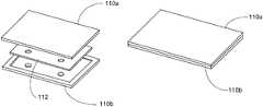
- a typical manufacturing processis illustrated in FIGS. 1A-1C .
- a bulk graphene-metal composite 100can be formed by (A) disposing a bulk graphene core 112 between metal face sheets 110 a and 110 b , (B) subjecting the assemble to a diffusion bonding process; and (C) machining the composite to provide a structure of a desired shape.
- Encapsulated bulk graphene compositessuch as cold plates, heat spreaders, thermal straps, etc.
- bulk graphene-metal compositeshave been successfully implemented into the cooling systems in satellites, avionics, and phased array radars, which can take full advantage of its high thermal performance, high durability, and light weight.
- the present inventionprovides a thermal management assembly comprising a metal-based thermal bond disposed between a bulk graphene core material and a surrounding metal or ceramic substrate.
- the metal-based interlayercomprises a material that is reactive with the graphene to form a carbide.
- the metal-based interlayerprovides an interface with the bulk graphene core that allows for excellent thermal conductivity and low thermal resistance.
- the present inventionprovides a thermal management assembly that exhibits low thermal interface resistance.
- the present inventioncan even provide a thermal interface that is orders of magnitude lower than conventional thermal interface assemblies.
- the present inventionprovides a thermal management assembly comprising a first substrate; a second substrate; a bulk graphene material disposed between the first and second substrates; and a thermal bond disposed between (a) a first surface of the bulk graphene layer and the first substrate, and (b) a second surface of the bulk graphene layer and the second substrate, the thermal bonds comprising a metal-based material comprising an agent that is reactive with the graphene to form a carbide.
- the present inventionprovides a thermal management assembly comprising a bulk graphene core material having a first surface and a second surface opposite the first surface; a first outer layer disposed on the first surface of the core material; and a second outer layer disposed on the second surface of the core material; wherein the first outer layer and the second outer layer are independently formed from a metal-based material comprising an agent that is reactive with graphene to form a carbide.
- the thermal management assemblycan have a thermal interface resistance of less than 10 ⁇ 10 ⁇ 6 K-m 2 /W; less than 8 ⁇ 10 ⁇ 6 K-m 2 /W; less than 5 ⁇ 10 ⁇ 6 K-m 2 /W; less than 2 ⁇ 10 ⁇ 6 K-m 2 /W; less than 1 ⁇ 10 ⁇ 6 K-m 2 /W; less than 0.5 ⁇ 10 ⁇ 6 K-m 2 /W; even less than 0.1 ⁇ 10 ⁇ 6 K-m 2 /W.
- FIGS. 1A-1Cillustrates a heat spreader comprising bulk graphene encapsulated by metal via a diffusion bonding process
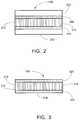
- FIG. 2is a cross-sectional view of a thermal management assembly in accordance with an embodiment of the present invention
- FIG. 3is cross-sectional view of another embodiment of a thermal management assembly in accordance with aspects of the present invention.
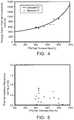
- FIG. 4is a graph illustrating the through plane thermal conductivity of a thermal management assembly in accordance with an embodiment of the invention.
- FIG. 5is a graph illustrating the thermal interface resistance of a thermal management assembly in accordance with the an embodiment of the present invention at different bulk graphene loadings.
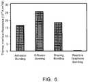
- FIG. 6is a graph illustrating the thermal resistance of thermal management assemblies formed by different manufacturing methods.
- the present inventionprovides a thermal management assembly comprising a bulk graphene core material and a metal-based coating layer disposed on surfaces of the graphene layer.
- the metal-based coatingcomprises a material that is reactive with graphene to form a carbide.
- the metal-based coatingprovides an interface with the bulk graphene core that allows for excellent thermal conductivity and low thermal resistance.
- the thermal management assemblycan comprise a structure comprising a bulk graphene core having the metal-based coating layer disposed on the surfaces of the bulk graphene material.
- a thermal management assemblycomprises the metal-based coating disposed between a bulk graphene core material and outer metal or ceramic substrates.
- thermal management assemblyrefers to a thermal management device or a heat transfer device comprising a high thermal conductivity material for dissipating or removing heat from a heat source.
- a thermal management assemblycan include, but is not limited to, heat spreaders, heat sinks, cold plates, etc.
- the metal-based coating layercomprising a material that is reactive with graphene to form a carbide may also be referred to herein as a “thermal bond layer.”
- the metal-based coating layercan also be referred to as an interlayer disposed between a surface of the graphene core material and a substrate.
- FIG. 2illustrates an embodiment of a thermal management assembly in accordance with aspects and embodiments of the invention.
- Thermal management assembly 200comprises a bulk graphene core 210 disposed between substrates 220 and 230 .
- the thermal management assembly 200comprises thermal bond layers 240 and 250 disposed at the interface between the substrates and the bulk graphene core.
- Thermal bond layers 240 and 250are metal-based coating interlayers comprising an additive or agent that can react with graphene to produce a carbide surface.
- the layers 240 and 250are also referred to as “interlayers”, “interface layers” or “filler”.
- the bulk graphene corecan be formed from a plurality of graphene layers being parallel to each other of at most 1 degree per mm in thickness.
- the term “bulk graphene”encompasses materials such as pyrolytic graphite (“PG”), thermal pyrolytic graphite (“TPG”), highly oriented pyrolytic graphite (“HOPG”), compression annealed pyrolytic graphite (“CAPG”), etc.
- bulk graphenemay also refer to graphite materials consisting of crystallites of considerable size, the crystallites being highly aligned or oriented with respect to each other and having well ordered carbon layers or a high degree of preferred crystallite orientation.
- Bulk graphene materialmostly comprises carbon atoms arranged in hexagonal patterns within each plane.
- the bulk graphene materialcomprises at least 3000 graphene layers, the graphene layers being parallel to each other at an angle of at most 1 degree per mm in thickness.
- the graphene layersare at an angle between 0.001 degree and 1 degree per mm in thickness.
- the thickness of the bulk grapheneis more than 1 um and size at least 1 mm ⁇ 1 mm. It exhibits high thermal conductivity, usually higher than 1000 W/m-K.
- the bulk graphenehas an in-plane (a-b direction) thermal conductivity greater than 1000 W/m-K; greater than 1100 W/m-K; greater than 1200 W/m-K; even greater than 1500 W/m-K. In one embodiment, the bulk graphene has a thermal conductivity of from about 1000 W/m-K to about 1800 W/m-K; from about 1100 W/m-K to about 1700 W/m-K; even from about 1200 W/m-K to about 1500 W/m-K.
- the bulk graphene and thermal management assemblycan also exhibit excellent through-plane thermal conductivity.
- the bulk graphene and/or thermal management assemblyhas a through-plane thermal conductivity of from about 200 W/m-K to about 1200 W/m-K; from about 400 W/m-K to about 1000 W/m-K; even from about 500 W/m-K to about 800 W/m-K.
- through-plane thermal conductivityof from about 200 W/m-K to about 1200 W/m-K; from about 400 W/m-K to about 1000 W/m-K; even from about 500 W/m-K to about 800 W/m-K.
- the bulk graphenecan be provided in any suitable form.
- the bulk grapheneis provided as a sheet.
- the bulk graphene corecan have any size or thickness as desired for a particular purpose or intended use.
- the corecan have a thickness of from about 0.001 mm to about 1 mm, 1 mm to about 5 mm; from about 1.5 mm to about 4 mm; even from about 2 to about 3 mm.
- the core layercan have a thickness of from about 25% to about 95% of the total thickness of the thermal management assembly; from about 35% to about 90% of the total thickness of the thermal management assembly; from about 40% to about 80% of the total thickness of the thermal management assembly; even from about 50% to about 75% of the total thickness of the thermal management assembly.
- numerical valuescan be combined to form new and non-disclosed ranges.
- the corecan be configured as desired for a particular purpose or intended application.
- the bulk graphene coreis disposed in the assembly such that graphene planes are oriented substantially parallel to the substrates.
- the bulk grapheneis disposed in the assembly such that the graphene planes are oriented perpendicular to the substrates.
- the graphene layers 212are oriented perpendicular to the plane of the substrates.
- the bulk graphene corecan be provided with vias.
- the loading density of the viasmay range from less than 0.01% area of occupation to approximately 40% area of occupation. In another embodiment the via loading density may be from about 0.1% to about 20%.
- the spacing of the viasmay range from about 0.5 to about 125 mm. In another embodiment, the spacing of the vias may range from about 1 to about 25 mm.
- a bulk graphene material with viasis described in U.S. Patent Publication No. 2010/0326645, which is incorporated herein by reference in its entirety.
- the substrate layerscan be formed from any suitable metal or ceramic material as desired for a particular purpose or intended application.
- suitable metals for the substrate layerinclude, but are not limited to, copper, aluminum, tungsten, molybdenum, nickel, iron, tin, silver, gold, beryllium or alloys of two or more thereof.
- suitable ceramicsinclude, but are not limited to, silicon nitride, silicon carbide, aluminum nitride, aluminum oxide, beryllium oxide, boron nitride, etc.
- the first and second substratescan be made from the same or different metal or ceramic materials.
- the thickness of the substratescan be selected as desired for a particular purpose or intended application. The thicknesses can be the same or different. In one embodiment, the substrates may each have a thickness of from about 2 microns to about 2 mm.
- the assembly of FIG. 2shows substrates 220 and 230 , it will be appreciated that the assembly can include one or more additional substrates overlying the substrates 220 and 230 .
- the additional substratescan be formed from the same or different materials as substrates 220 or 230 .
- the thermal management assemblycomprises a metal-based coating disposed on opposing surfaces of the core.
- the metal-based materialcan serve as an outer layer or a layer for bonding the core layer to the substrates.
- the metal-based coating layercomprises an agent that can form a carbide with graphene at a sufficiently high temperature.
- the metal-based coating materialhas a lower melting temperature than either the bulk graphene or the substrates.
- the metal-based coating materialhas a thermal conductivity of about 20 W/m-K or greater.
- the metal-based coating materialcan comprise any suitable metal or alloy including, but not limited to, silver, silver-copper, tin, lead, combinations of two or more thereof, etc., that melts and bonds to the surrounding metal or ceramic substrate at an elevated temperature lower than the substrate melting temperature.
- the activating agentcomprises a material that forms a carbide with graphene at a sufficiently high temperature.
- the activating agentis chosen from titanium, zirconium, chromium, hafnium, aluminum, tantalum, iron, silicon, or a combination of two or more thereof.
- suitable metal-based coatingsthat can be used to bond bulk graphene to various materials include but are not limited to Al, Si, Fe, Al—Si, Fe—Si, Ag—Cu—Ti, Ti—Ni, Ni—Pd—Ti, Sn—Ti, Sn—Al, TiH 2 , Sn—Ag—Ti, or a combination of two or more thereof.
- the metal-based coating materialhas a composition different than the composition of the substrate layers.
- FIG. 3illustrates another embodiment of a thermal management assembly in accordance with aspects of the invention.
- thermal management assembly 300comprises a bulk graphene core 310 having a first surface 312 and a second surface 314 , a first outer layer 320 disposed on the first surface of the core, and a second outer layer 330 disposed on the second surface of the core.
- the core layerhas the graphene layers 316 oriented perpendicular or parallel to the plane of the outer layers.
- the first and second outer layersare formed from a metal-based coating material.
- the metal-based coating materialcan be formed from an alloy comprising an agent that is reactive with the graphene to form a carbide.
- any of the materials that can be used as the interface material described abovecan be used to form the first and second outer layers.
- the metal-based coating layerscan have a thickness of from about 0.01 mm to about 2 mm; from about 0.02 mm to about 1 mm; even from about 0.05 mm to about 0.5 mm.
- numerical valuescan be combined to form new and non-disclosed ranges.
- the assembly of FIG. 3can be used alone as a thermal management assembly or can be further modified to include one or more substrates in the assembly.
- a substratecould be disposed adjacent to the first outer layer 320 .
- the assembly 300could be modified by providing a first substrate adjacent to the first outer layer 320 , and a second substrate adjacent to outer layer 330 to provide a thermal management assembly similar to that shown in FIG. 2 .
- the thermal management assemblyexhibits good thermal conductivity.
- the thermal management assemblyhas a through-plane thermal conductivity of from about 200 W/m-K to about 1200 W/m-K; from about 400 W/m-K to about 1100 W/m-K; from about 500 W/m-K to about 1000 W/m-K; even from about 600 W/m-K to about 800 W/m-K.
- the thermal management assemblycan have a relatively low thermal interface resistance.
- the thermal management assemblyhas a thermal interface resistance of less than 10 ⁇ 10 ⁇ 6 K-m 2 /W; less than 8 ⁇ 10 ⁇ 6 K-m 2 /W; less than 5 ⁇ 10 ⁇ 6 K-m 2 /W; less than 2 ⁇ 10 ⁇ 6 K-m 2 /W; less than 1 ⁇ 10 ⁇ 6 K-m 2 /W; less than 0.5 ⁇ 10 ⁇ 6 K-m 2 /W; even less than 0.1 ⁇ 10 ⁇ 6 K-m 2 /W.
- the thermal management assemblyhas a thermal interface resistance of from about 0.1 ⁇ 10 ⁇ 6 K-m 2 /W to about 1 ⁇ 10 ⁇ 6 K-m 2 /W; from about 0.2 ⁇ 10 ⁇ 6 K-m 2 /W to about 0.8 ⁇ 10 ⁇ 6 K-m 2 /W; even from about 0.3 ⁇ 10 ⁇ 6 K-m 2 /W to about 0.6 ⁇ 10 ⁇ 6 K-m 2 /W.
- a thermal interface resistanceof from about 0.1 ⁇ 10 ⁇ 6 K-m 2 /W to about 1 ⁇ 10 ⁇ 6 K-m 2 /W; from about 0.2 ⁇ 10 ⁇ 6 K-m 2 /W to about 0.8 ⁇ 10 ⁇ 6 K-m 2 /W; even from about 0.3 ⁇ 10 ⁇ 6 K-m 2 /W to about 0.6 ⁇ 10 ⁇ 6 K-m 2 /W.
- a thermal management assemblycan be formed by disposing a bulk graphene core material between two substrate layers and joining the substrate layers via the metal-based coating material.
- the metal-based coating materialcan be applied to opposing surfaces of the bulk graphene material, and the substrate material can be disposed on the surfaces of the bulk graphene comprising the metal-based coating material, the assembly can be subjected to joining under vacuum at a temperature above the melting temperature of the metal-based coating material and below the melting temperature of the core or the substrates.
- the present inventionprovides a thermal management assembly with good thermal conductivity and, in one embodiment, a low thermal interface resistance. Due to the differences in electronic and vibrational properties in different materials, when an energy carrier attempts to traverse the interface, it scatters at the interface. For thermal management assemblies comprising layers formed from different thermal management materials a poor thermal interface can contribute to interface scattering. Theoretically the thermal resistance through multiple layers can be presented as:
- a poor interfacecan add a significant resistance to the heat flow and, thus, offset or even override the benefit of using the high thermal conductivity materials such as bulk graphene.
- the interface between bulk graphene and Cushowed high resistance due to lack of reaction and diffusion, which can result in an overall thermal conductivity lower than that of Cu.
- the diffusion bonding processexhibits issues of high complexity, high cost, application difficulty to ceramics and high temperature metals, and high interface resistance.
- Brazing and solderingon the other hand, rely on a molten filler metal to wet the mating surfaces of a joint, leading to the formation of metallurgical bonds.
- the metallic property of the brazing/soldering bondprovides the continuity of high concentration of energy carriers (electrons), and, thus, renders a highly thermal conductive bond which can be referred to herein as a “thermal bond”.
- Typical brazing or soldering fillers at molten formatdo not wet bulk graphene and do not spread freely to fill the gaps between bulk graphene and substrates. Such assemblies still exhibit relatively high thermal interface resistance due to the thermal barrier between bulk graphene and braze or solder.
- bulk graphene heat spreadersemploying a metal-based interlayer between the core and the substrates with an agent that is reactive with graphene to form a carbide layer can provide an interface layer that bonds the core to the substrate and exhibits extremely low interface thermal resistance.
- the thermal management assemblycan be sized and shape as desired for a particular purpose or intended use.
- the thermal management assemblycan be used in an apparatus to aid in the thermal management of the apparatus.
- the thermal management assemblycan be disposed adjacent a heat generating component in an apparatus and can dissipate the heat from heat generating component.
- the thermal management assemblycan be used in devices in electronics such as computers, semiconductors, or any device where heat transfer between components is needed.
- the electronic componentincludes a semiconductor chip as a heat producing component.
- the heat producing componentcan be a chip carrier, an area array package, a chip scale package, or other semiconductor packaging structure.
- the semiconductor chipitself is the heat producing component.
- the hot devicecan be any hot device including, but not limited to, light emitting diodes, laser diodes, power amplifiers, MMIC's, IGBT's, etc.
- Compositesare formed comprising two copper (Cu) substrates and a bulk graphene board disposed between the two metal layers.
- the bulk graphene materialwas thermal pyrolytic graphite.
- the bulk graphene boardis oriented perpendicular to the Cu substrates so that the high thermal conductive path of the bulk graphene is aligned with the heat flow that comes through the layered structure.
- Ag—Cu with Ti additivesis used to join the Cu and the bulk graphene at 850° C. under vacuum.
- the prepared sampleshave a construction similar to the embodiment depicted in FIG. 2 .
- the thickness of the bulk grapheneranged from 37% to 87% of the total thickness of the composite.
- the thermal conductivity of the compositesis evaluated by Netzsch NanoFlash LFA 447.
- the overall thermal conductivity of the bulk graphene compositecan be calculated as:
- FIG. 3shows that the measured through-plane thermal conductivity with various bulk graphene loading matches the calculated value, indicating an excellent thermal bond between Cu and bulk graphene by employing the metal-based interlayer with the activating agent.
- the thermal resistancecan be estimated by comparing the difference between the theoretical and experimental thermal conductivity, according to the following formula:
- R intt total k experimental - t total k theoretical where k is the thermal conductivity and t is the total thickness.
- FIG. 4-5illustrates the thermal resistance of the composites formed according to aspects of the present invention.
- the present inventioncan provide composites with extremely low thermal resistance in the range of 10 ⁇ 7 K-m 2 /W, and that the resistance is independent of the amount of bulk graphene loading.
- FIG. 6compares the thermal resistance of these composites to those in accordance with aspects of the invention, and illustrates that the comparative composites have a thermal resistance at least an order of magnitude higher than the composites formed in accordance with aspects of the present invention.
Landscapes
- Engineering & Computer Science (AREA)
- Chemical & Material Sciences (AREA)
- Microelectronics & Electronic Packaging (AREA)
- Physics & Mathematics (AREA)
- Materials Engineering (AREA)
- Computer Hardware Design (AREA)
- Condensed Matter Physics & Semiconductors (AREA)
- General Physics & Mathematics (AREA)
- Power Engineering (AREA)
- Ceramic Engineering (AREA)
- Manufacturing & Machinery (AREA)
- Thermal Sciences (AREA)
- Mechanical Engineering (AREA)
- General Engineering & Computer Science (AREA)
- Cooling Or The Like Of Semiconductors Or Solid State Devices (AREA)
- Laminated Bodies (AREA)
- Cooling Or The Like Of Electrical Apparatus (AREA)
- Carbon And Carbon Compounds (AREA)
Abstract
Description
where t is the thickness of individual layer and k is the corresponding thermal conductivity.
where, kc, km, kgare the thermal conductivity of composite, encapsulation material, and bulk graphene, respectively; and Vm, Vgare the volume (thickness) percentage of the substrate and bulk graphene, respectively.
where k is the thermal conductivity and t is the total thickness.
Claims (19)
Priority Applications (1)
| Application Number | Priority Date | Filing Date | Title |
|---|---|---|---|
| US14/431,123US11105567B2 (en) | 2012-09-25 | 2013-09-24 | Thermal management assembly comprising bulk graphene material |
Applications Claiming Priority (3)
| Application Number | Priority Date | Filing Date | Title |
|---|---|---|---|
| US201261705362P | 2012-09-25 | 2012-09-25 | |
| PCT/US2013/061335WO2014052282A1 (en) | 2012-09-25 | 2013-09-24 | Thermal management assembly comprising bulk graphene material |
| US14/431,123US11105567B2 (en) | 2012-09-25 | 2013-09-24 | Thermal management assembly comprising bulk graphene material |
Publications (2)
| Publication Number | Publication Date |
|---|---|
| US20150253089A1 US20150253089A1 (en) | 2015-09-10 |
| US11105567B2true US11105567B2 (en) | 2021-08-31 |
Family
ID=50388897
Family Applications (1)
| Application Number | Title | Priority Date | Filing Date |
|---|---|---|---|
| US14/431,123Active2034-12-17US11105567B2 (en) | 2012-09-25 | 2013-09-24 | Thermal management assembly comprising bulk graphene material |
Country Status (5)
| Country | Link |
|---|---|
| US (1) | US11105567B2 (en) |
| EP (1) | EP2901826B1 (en) |
| JP (1) | JP6529433B2 (en) |
| CN (1) | CN104813751B (en) |
| WO (1) | WO2014052282A1 (en) |
Cited By (9)
| Publication number | Priority date | Publication date | Assignee | Title |
|---|---|---|---|---|
| US20220377912A1 (en)* | 2021-05-18 | 2022-11-24 | Mellanox Technologies, Ltd. | Process for laminating graphene-coated printed circuit boards |
| US11849536B1 (en) | 2022-10-12 | 2023-12-19 | Lunar Energy, Inc. | Gantry for thermal management |
| US11889662B1 (en)* | 2022-10-12 | 2024-01-30 | Lunar Energy, Inc. | Thermal interface sandwich |
| US11963309B2 (en) | 2021-05-18 | 2024-04-16 | Mellanox Technologies, Ltd. | Process for laminating conductive-lubricant coated metals for printed circuit boards |
| US11997812B2 (en) | 2022-10-12 | 2024-05-28 | Lunar Energy, Inc. | Cover for sealing a power module |
| US12163228B2 (en) | 2021-05-18 | 2024-12-10 | Mellanox Technologies, Ltd. | CVD system with substrate carrier and associated mechanisms for moving substrate therethrough |
| WO2024263886A1 (en)* | 2023-06-23 | 2024-12-26 | Momentive Performance Materials Quartz, Inc. | Thermal leveler blank for integration with thermal management |
| US12221695B2 (en) | 2021-05-18 | 2025-02-11 | Mellanox Technologies, Ltd. | CVD system with flange assembly for facilitating uniform and laminar flow |
| US12289839B2 (en) | 2021-05-18 | 2025-04-29 | Mellanox Technologies, Ltd. | Process for localized repair of graphene-coated lamination stacks and printed circuit boards |
Families Citing this family (42)
| Publication number | Priority date | Publication date | Assignee | Title |
|---|---|---|---|---|
| US9634214B2 (en)* | 2012-11-05 | 2017-04-25 | Ledengin, Inc. | Graphite-containing substrates for LED packages |
| CN104754913B (en)* | 2013-12-27 | 2018-06-05 | 华为技术有限公司 | Heat-conductive composite material piece and preparation method thereof |
| KR102374256B1 (en)* | 2015-02-23 | 2022-03-15 | 삼성전기주식회사 | Circuit board and manufacturing method thereof |
| US10403806B2 (en) | 2015-05-15 | 2019-09-03 | Momentive Performance Materials Inc. | Light emitting diode assembly using thermal pyrolytic graphite for thermal management |
| CN107686699B (en)* | 2016-08-05 | 2021-07-16 | 中兴通讯股份有限公司 | Heat-conducting interface material and preparation method thereof |
| US10139168B2 (en)* | 2016-09-26 | 2018-11-27 | International Business Machines Corporation | Cold plate with radial expanding channels for two-phase cooling |
| US11114365B2 (en) | 2016-12-22 | 2021-09-07 | Kyocera Corporation | Electronic element mounting substrate, electronic device, and electronic module |
| EP3352213B1 (en)* | 2017-01-23 | 2021-10-06 | ABB Power Grids Switzerland AG | Semiconductor power module comprising graphene |
| JP6754973B2 (en)* | 2017-02-02 | 2020-09-16 | パナソニックIpマネジメント株式会社 | Graphite radiator plate |
| KR102469901B1 (en)* | 2017-04-07 | 2022-11-22 | 에스케이넥실리스 주식회사 | Graphite Heat Dissipation Film With Copper Foil Lamination |
| KR20190003186A (en)* | 2017-06-30 | 2019-01-09 | 주식회사 솔루에타 | Heat radiation thin film and method of fabricating of the same |
| US10455736B2 (en) | 2017-07-21 | 2019-10-22 | Raytheon Company | Reduced cost and schedule manufacturing of graphene paper based thermal straps/harnesses |
| CN111356544B (en)* | 2017-11-20 | 2022-01-14 | 三菱综合材料株式会社 | Composite heat transfer member and method for manufacturing composite heat transfer member |
| ES2946239T3 (en)* | 2017-11-24 | 2023-07-14 | Airbus Operations Sl | Joining method for thermoplastic elements |
| US11476399B2 (en)* | 2017-11-29 | 2022-10-18 | Panasonic Intellectual Property Management Co., Ltd. | Jointing material, fabrication method for semiconductor device using the jointing material, and semiconductor device |
| JP7108907B2 (en)* | 2017-11-29 | 2022-07-29 | パナソニックIpマネジメント株式会社 | Bonding material, method for manufacturing semiconductor device using bonding material, and semiconductor device |
| US11612056B2 (en)* | 2018-01-30 | 2023-03-21 | Kyocera Corporation | Substrate for mounting electronic element, electronic device, and electronic module |
| DE102018102600A1 (en)* | 2018-02-06 | 2019-08-08 | Tdk Electronics Ag | temperature sensor |
| US11152279B2 (en)* | 2018-03-26 | 2021-10-19 | Raytheon Company | Monolithic microwave integrated circuit (MMIC) cooling structure |
| US20190301814A1 (en)* | 2018-04-03 | 2019-10-03 | Nanotek Instruments, Inc. | Metallized graphene foam having high through-plane conductivity |
| US11075141B2 (en)* | 2018-09-14 | 2021-07-27 | Raytheon Company | Module base with integrated thermal spreader and heat sink for thermal and structural management of high-performance integrated circuits or other devices |
| KR102600004B1 (en)* | 2018-12-26 | 2023-11-08 | 삼성전자주식회사 | Semiconductor package |
| CN110004442A (en)* | 2018-12-27 | 2019-07-12 | 岑对凤 | A kind of superconduction composite plate and its manufacturing method |
| CN113308658B (en)* | 2019-01-30 | 2022-12-27 | 浙江华达新型材料股份有限公司 | Steel plate with double-plating coating on surface |
| CN110602871B (en)* | 2019-09-16 | 2021-10-01 | 沪士电子股份有限公司 | Graphene heat-conducting PCB and preparation method thereof |
| JP7533124B2 (en) | 2019-11-05 | 2024-08-14 | 三菱マテリアル株式会社 | Graphene-containing carbonaceous member/ceramic joint, and copper/graphene-containing carbonaceous member/ceramic joint |
| WO2021090759A1 (en)* | 2019-11-05 | 2021-05-14 | 三菱マテリアル株式会社 | Graphene-containing carbonaceous member/ceramic assembly and copper/graphene-containing carbonaceous member/ceramic assembly |
| JP7563124B2 (en) | 2019-11-25 | 2024-10-08 | 三菱マテリアル株式会社 | Graphene Joints |
| WO2021106904A1 (en)* | 2019-11-25 | 2021-06-03 | 三菱マテリアル株式会社 | Graphene bonded body |
| WO2021149802A1 (en)* | 2020-01-24 | 2021-07-29 | 三菱マテリアル株式会社 | Copper/graphene joined body and method for manufacturing same, and copper/graphene joined structure |
| JP6947318B2 (en)* | 2020-01-24 | 2021-10-13 | 三菱マテリアル株式会社 | Copper / graphene junction and its manufacturing method, and copper / graphene junction structure |
| US11032947B1 (en)* | 2020-02-17 | 2021-06-08 | Raytheon Company | Tailored coldplate geometries for forming multiple coefficient of thermal expansion (CTE) zones |
| CN112543580B (en)* | 2020-11-17 | 2022-04-15 | 河北北方学院 | A kind of production process of high thermal conductivity graphene-metal copper composite layer radiator |
| CN112693636A (en)* | 2020-12-28 | 2021-04-23 | 上海卫星工程研究所 | Light-weight thermal control device for satellite and manufacturing method thereof |
| TWI833063B (en)* | 2021-01-27 | 2024-02-21 | 大陸商河南烯力新材料科技有限公司 | Thermal conductive structure and electronic device |
| CN114823574A (en)* | 2021-01-27 | 2022-07-29 | 河南烯力新材料科技有限公司 | Thermally conductive structures and electronic devices |
| JP2023006510A (en)* | 2021-06-30 | 2023-01-18 | 日亜化学工業株式会社 | Light-emitting module, vehicle lamp, and heat dissipation member |
| CN116940053A (en)* | 2022-04-08 | 2023-10-24 | 西安聚变材料科技有限公司 | Carbon-based packaging thermal management component with customizable high conductivity and transverse and longitudinal heat conductivity and manufacturing method thereof |
| TWI880098B (en)* | 2022-07-01 | 2025-04-11 | 長庚大學 | A heat dissipation structure with graphene and copper, and a formation method thereof |
| CN118354563A (en)* | 2023-01-13 | 2024-07-16 | 华为技术有限公司 | Graphene sheet, preparation method, heat dissipation module and electronic equipment |
| CN115799974B (en)* | 2023-02-07 | 2023-05-26 | 度亘激光技术(苏州)有限公司 | Heat conduction structure, preparation method thereof and indirect heat conduction structure |
| WO2025008052A1 (en)* | 2023-07-04 | 2025-01-09 | Huawei Technologies Co., Ltd. | Heat transfer device for an electronic device |
Citations (21)
| Publication number | Priority date | Publication date | Assignee | Title |
|---|---|---|---|---|
| US4104417A (en)* | 1973-03-12 | 1978-08-01 | Union Carbide Corporation | Method of chemically bonding aluminum to carbon substrates via monocarbides |
| EP0403208A1 (en) | 1989-06-12 | 1990-12-19 | General Electric Company | Heat sinking substrate |
| US4990402A (en)* | 1988-08-01 | 1991-02-05 | Schwarzkopf Development Corporation | Process for the manufacture of a soldered joint |
| US5195021A (en) | 1989-08-21 | 1993-03-16 | Texas Instruments Incorporated | Constraining core for surface mount technology |
| US5296310A (en) | 1992-02-14 | 1994-03-22 | Materials Science Corporation | High conductivity hydrid material for thermal management |
| US5494753A (en)* | 1994-06-20 | 1996-02-27 | General Electric Company | Articles having thermal conductors of graphite |
| US5958572A (en) | 1997-09-30 | 1999-09-28 | Motorola, Inc. | Hybrid substrate for cooling an electronic component |
| US6131651A (en) | 1998-09-16 | 2000-10-17 | Advanced Ceramics Corporation | Flexible heat transfer device and method |
| US6215661B1 (en) | 1999-08-11 | 2001-04-10 | Motorola, Inc. | Heat spreader |
| US6661317B2 (en) | 2002-03-13 | 2003-12-09 | The Boeing Co. | Microwave monolithic integrated circuit assembly with multi-orientation pyrolytic graphite heat-dissipating assembly |
| US20050064230A1 (en) | 2003-09-19 | 2005-03-24 | General Electric Company | Bulk high thermal conductivity feedstock and method of making thereof |
| WO2005048298A2 (en) | 2003-11-04 | 2005-05-26 | Advanced Energy Technology Inc. | Sandwiched thermal solution |
| JP2005159318A (en) | 2003-11-04 | 2005-06-16 | Otsuka Denki Kk | Heat conductor |
| JP2006196593A (en) | 2005-01-12 | 2006-07-27 | Sumitomo Electric Ind Ltd | Semiconductor device and heat sink |
| US20070053168A1 (en) | 2004-01-21 | 2007-03-08 | General Electric Company | Advanced heat sinks and thermal spreaders |
| US20070289730A1 (en) | 2006-06-06 | 2007-12-20 | Chang-Hsin Wu | Combination heat-transfer plate member |
| US7670681B2 (en)* | 2004-09-06 | 2010-03-02 | Plansee Se | Material composite and method of producing the composite |
| US20100326645A1 (en) | 2004-01-21 | 2010-12-30 | Wei Fan | Thermal pyrolytic graphite laminates with vias |
| JP2011023670A (en) | 2009-07-17 | 2011-02-03 | Thermo Graphitics Co Ltd | Anisotropic thermally-conductive element, and method of manufacturing the same |
| US20120234524A1 (en) | 2011-03-16 | 2012-09-20 | Wei Fan | High thermal conductivity/low coefficient of thermal expansion composites |
| JP2012238733A (en) | 2011-05-12 | 2012-12-06 | Thermo Graphitics Co Ltd | Anisotropic thermally-conductive element and manufacturing method thereof |
Family Cites Families (5)
| Publication number | Priority date | Publication date | Assignee | Title |
|---|---|---|---|---|
| JPH03136397A (en)* | 1989-08-21 | 1991-06-11 | Texas Instr Inc <Ti> | Forced core for surface carrying technique and its manufacturing method |
| US6075701A (en)* | 1999-05-14 | 2000-06-13 | Hughes Electronics Corporation | Electronic structure having an embedded pyrolytic graphite heat sink material |
| CN100496186C (en)* | 2003-09-19 | 2009-06-03 | 通用电气公司 | Raw material with large volume and high thermal conductivity and its preparation method |
| JP5098642B2 (en)* | 2005-06-16 | 2012-12-12 | パナソニック株式会社 | Method for producing heat-dissipating graphite sheet |
| US20110070459A1 (en)* | 2009-09-18 | 2011-03-24 | Irwin In Kim | Thermal Management System |
- 2013
- 2013-09-24USUS14/431,123patent/US11105567B2/enactiveActive
- 2013-09-24WOPCT/US2013/061335patent/WO2014052282A1/enactiveApplication Filing
- 2013-09-24CNCN201380061372.9Apatent/CN104813751B/enactiveActive
- 2013-09-24JPJP2015534593Apatent/JP6529433B2/enactiveActive
- 2013-09-24EPEP13840941.2Apatent/EP2901826B1/enactiveActive
Patent Citations (22)
| Publication number | Priority date | Publication date | Assignee | Title |
|---|---|---|---|---|
| US4104417A (en)* | 1973-03-12 | 1978-08-01 | Union Carbide Corporation | Method of chemically bonding aluminum to carbon substrates via monocarbides |
| US4990402A (en)* | 1988-08-01 | 1991-02-05 | Schwarzkopf Development Corporation | Process for the manufacture of a soldered joint |
| EP0403208A1 (en) | 1989-06-12 | 1990-12-19 | General Electric Company | Heat sinking substrate |
| US5195021A (en) | 1989-08-21 | 1993-03-16 | Texas Instruments Incorporated | Constraining core for surface mount technology |
| US5296310A (en) | 1992-02-14 | 1994-03-22 | Materials Science Corporation | High conductivity hydrid material for thermal management |
| US5494753A (en)* | 1994-06-20 | 1996-02-27 | General Electric Company | Articles having thermal conductors of graphite |
| US5958572A (en) | 1997-09-30 | 1999-09-28 | Motorola, Inc. | Hybrid substrate for cooling an electronic component |
| US6131651A (en) | 1998-09-16 | 2000-10-17 | Advanced Ceramics Corporation | Flexible heat transfer device and method |
| US6215661B1 (en) | 1999-08-11 | 2001-04-10 | Motorola, Inc. | Heat spreader |
| US6661317B2 (en) | 2002-03-13 | 2003-12-09 | The Boeing Co. | Microwave monolithic integrated circuit assembly with multi-orientation pyrolytic graphite heat-dissipating assembly |
| US20050064230A1 (en) | 2003-09-19 | 2005-03-24 | General Electric Company | Bulk high thermal conductivity feedstock and method of making thereof |
| WO2005048298A2 (en) | 2003-11-04 | 2005-05-26 | Advanced Energy Technology Inc. | Sandwiched thermal solution |
| JP2005159318A (en) | 2003-11-04 | 2005-06-16 | Otsuka Denki Kk | Heat conductor |
| US20070053168A1 (en) | 2004-01-21 | 2007-03-08 | General Electric Company | Advanced heat sinks and thermal spreaders |
| US20100326645A1 (en) | 2004-01-21 | 2010-12-30 | Wei Fan | Thermal pyrolytic graphite laminates with vias |
| US7670681B2 (en)* | 2004-09-06 | 2010-03-02 | Plansee Se | Material composite and method of producing the composite |
| JP2006196593A (en) | 2005-01-12 | 2006-07-27 | Sumitomo Electric Ind Ltd | Semiconductor device and heat sink |
| US20070289730A1 (en) | 2006-06-06 | 2007-12-20 | Chang-Hsin Wu | Combination heat-transfer plate member |
| JP2011023670A (en) | 2009-07-17 | 2011-02-03 | Thermo Graphitics Co Ltd | Anisotropic thermally-conductive element, and method of manufacturing the same |
| US20120234524A1 (en) | 2011-03-16 | 2012-09-20 | Wei Fan | High thermal conductivity/low coefficient of thermal expansion composites |
| WO2012125817A1 (en) | 2011-03-16 | 2012-09-20 | Momentive Performance Materials, Inc. | High thermal conductivity/low coefficient of thermal expansion composites |
| JP2012238733A (en) | 2011-05-12 | 2012-12-06 | Thermo Graphitics Co Ltd | Anisotropic thermally-conductive element and manufacturing method thereof |
Non-Patent Citations (1)
| Title |
|---|
| ISA/US, International Search Report and Written Opinion prepared for International Application No. PCT/US13/61335, dated Feb. 7, 2014. |
Cited By (10)
| Publication number | Priority date | Publication date | Assignee | Title |
|---|---|---|---|---|
| US20220377912A1 (en)* | 2021-05-18 | 2022-11-24 | Mellanox Technologies, Ltd. | Process for laminating graphene-coated printed circuit boards |
| US11963309B2 (en) | 2021-05-18 | 2024-04-16 | Mellanox Technologies, Ltd. | Process for laminating conductive-lubricant coated metals for printed circuit boards |
| US12004308B2 (en)* | 2021-05-18 | 2024-06-04 | Mellanox Technologies, Ltd. | Process for laminating graphene-coated printed circuit boards |
| US12163228B2 (en) | 2021-05-18 | 2024-12-10 | Mellanox Technologies, Ltd. | CVD system with substrate carrier and associated mechanisms for moving substrate therethrough |
| US12221695B2 (en) | 2021-05-18 | 2025-02-11 | Mellanox Technologies, Ltd. | CVD system with flange assembly for facilitating uniform and laminar flow |
| US12289839B2 (en) | 2021-05-18 | 2025-04-29 | Mellanox Technologies, Ltd. | Process for localized repair of graphene-coated lamination stacks and printed circuit boards |
| US11849536B1 (en) | 2022-10-12 | 2023-12-19 | Lunar Energy, Inc. | Gantry for thermal management |
| US11889662B1 (en)* | 2022-10-12 | 2024-01-30 | Lunar Energy, Inc. | Thermal interface sandwich |
| US11997812B2 (en) | 2022-10-12 | 2024-05-28 | Lunar Energy, Inc. | Cover for sealing a power module |
| WO2024263886A1 (en)* | 2023-06-23 | 2024-12-26 | Momentive Performance Materials Quartz, Inc. | Thermal leveler blank for integration with thermal management |
Also Published As
| Publication number | Publication date |
|---|---|
| CN104813751A (en) | 2015-07-29 |
| WO2014052282A1 (en) | 2014-04-03 |
| JP6529433B2 (en) | 2019-06-12 |
| JP2015532531A (en) | 2015-11-09 |
| US20150253089A1 (en) | 2015-09-10 |
| CN104813751B (en) | 2019-12-31 |
| EP2901826A1 (en) | 2015-08-05 |
| EP2901826A4 (en) | 2016-06-15 |
| EP2901826B1 (en) | 2020-12-16 |
Similar Documents
| Publication | Publication Date | Title |
|---|---|---|
| US11105567B2 (en) | Thermal management assembly comprising bulk graphene material | |
| JP6602362B2 (en) | Composite material with high thermal conductivity / low thermal expansion coefficient | |
| JP6079505B2 (en) | Bonded body and power module substrate | |
| EP3057125B1 (en) | Substrate for heat sink-equipped power module, and production method for same | |
| EP2980844B1 (en) | Substrate for power modules, substrate with heat sink for power modules, and power module | |
| EP2978019B1 (en) | Method for manufacturing bonded body and method for manufacturing power-module substrate | |
| JP5612471B2 (en) | Layered heat spreader and manufacturing method thereof | |
| EP3041042A1 (en) | Method for manufacturing assembly and method for manufacturing power-module substrate | |
| KR20110033117A (en) | Power Module Substrate, Power Module, and Power Module Substrate Manufacturing Method | |
| US20160059535A1 (en) | Conductive bond foils | |
| EP3041044A1 (en) | Assembly and power-module substrate | |
| US20190078212A1 (en) | Transient liquid phase bonding compositions and power electronics assemblies incorporating the same | |
| JP2011035308A (en) | Radiator plate, semiconductor device, and method of manufacturing radiator plate | |
| TW201739725A (en) | Bonded body, substrate for power module, method of manufacturing bonded body, and method of manufacturing substrate for power module | |
| US11305373B2 (en) | Ultrasonic additively manufactured coldplates on heat spreaders | |
| JP7201658B2 (en) | Cooling system | |
| CN111682002A (en) | Heat radiation plate | |
| JP6508182B2 (en) | Semiconductor module and method of manufacturing the same | |
| Fan et al. | Thermal pyrolytic graphite composite with coefficient of thermal expansion matching for advanced thermal management | |
| EP3471138B1 (en) | Heat sink plate | |
| US10804236B2 (en) | Power electronic assemblies with high purity aluminum plated substrates | |
| Fan et al. | How can millions of aligned graphene layers cool high power microelectronics? | |
| KR20200088606A (en) | Heat sink plate | |
| JP2020100145A (en) | Laminate | |
| JP2020004963A (en) | Heat sink and manufacturing method thereof |
Legal Events
| Date | Code | Title | Description |
|---|---|---|---|
| STPP | Information on status: patent application and granting procedure in general | Free format text:NON FINAL ACTION MAILED | |
| STPP | Information on status: patent application and granting procedure in general | Free format text:RESPONSE TO NON-FINAL OFFICE ACTION ENTERED AND FORWARDED TO EXAMINER | |
| AS | Assignment | Owner name:BNP PARIBAS, AS ADMINISTRATIVE AGENT, NEW YORK Free format text:FIRST LIEN TERM LOAN PATENT AGREEMENT;ASSIGNOR:MOMENTIVE PERFORMANCE MATERIALS INC.;REEL/FRAME:049387/0782 Effective date:20190515 Owner name:KOOKMIN BANK, NEW YORK BRANCH, AS ADMINISTRATIVE A Free format text:SECOND LIEN TERM LOAN PATENT AGREEMENT;ASSIGNOR:MOMENTIVE PERFORMANCE MATERIALS INC.;REEL/FRAME:049388/0220 Effective date:20190515 Owner name:CITIBANK, N.A., AS ADMINISTRATIVE AGENT, NEW YORK Free format text:ABL PATENT AGREEMENT;ASSIGNORS:MOMENTIVE PERFORMANCE MATERIALS INC.;MOMENTIVE PERFORMANCE MATERIALS GMBH;REEL/FRAME:049388/0252 Effective date:20190515 Owner name:KOOKMIN BANK, NEW YORK BRANCH, AS ADMINISTRATIVE AGENT, NEW YORK Free format text:SECOND LIEN TERM LOAN PATENT AGREEMENT;ASSIGNOR:MOMENTIVE PERFORMANCE MATERIALS INC.;REEL/FRAME:049388/0220 Effective date:20190515 | |
| STPP | Information on status: patent application and granting procedure in general | Free format text:FINAL REJECTION MAILED | |
| STPP | Information on status: patent application and granting procedure in general | Free format text:DOCKETED NEW CASE - READY FOR EXAMINATION | |
| STPP | Information on status: patent application and granting procedure in general | Free format text:NON FINAL ACTION MAILED | |
| STPP | Information on status: patent application and granting procedure in general | Free format text:FINAL REJECTION MAILED | |
| STPP | Information on status: patent application and granting procedure in general | Free format text:NON FINAL ACTION MAILED | |
| AS | Assignment | Owner name:MOMENTIVE PERFORMANCE MATERIALS QUARTZ, INC., OHIO Free format text:NUNC PRO TUNC ASSIGNMENT;ASSIGNOR:MOMENTIVE PERFORMANCE MATERIALS INC.;REEL/FRAME:055222/0140 Effective date:20210122 | |
| STPP | Information on status: patent application and granting procedure in general | Free format text:RESPONSE TO NON-FINAL OFFICE ACTION ENTERED AND FORWARDED TO EXAMINER | |
| STPP | Information on status: patent application and granting procedure in general | Free format text:NOTICE OF ALLOWANCE MAILED -- APPLICATION RECEIVED IN OFFICE OF PUBLICATIONS | |
| AS | Assignment | Owner name:MOMENTIVE PERFORMANCE MATERIALS INC., NEW YORK Free format text:ASSIGNMENT OF ASSIGNORS INTEREST;ASSIGNORS:FAN, WEI;LIU, XIANG;MARINER, JOHN;AND OTHERS;SIGNING DATES FROM 20200721 TO 20200807;REEL/FRAME:056199/0747 | |
| STCF | Information on status: patent grant | Free format text:PATENTED CASE | |
| AS | Assignment | Owner name:MOMENTIVE PERFORMANCE MATERIALS INC., NEW YORK Free format text:RELEASE BY SECURED PARTY;ASSIGNOR:KOOKMIN BANK NEW YORK;REEL/FRAME:063197/0373 Effective date:20230329 | |
| AS | Assignment | Owner name:MOMENTIVE PERFORMANCE MATERIALS INC., NEW YORK Free format text:TERMINATION AND RELEASE OF SECURITY INTEREST IN PATENTS;ASSIGNOR:BNP PARIBAS;REEL/FRAME:063259/0133 Effective date:20230329 | |
| MAFP | Maintenance fee payment | Free format text:PAYMENT OF MAINTENANCE FEE, 4TH YEAR, LARGE ENTITY (ORIGINAL EVENT CODE: M1551); ENTITY STATUS OF PATENT OWNER: LARGE ENTITY Year of fee payment:4 | |
| AS | Assignment | Owner name:STANDARD CHARTERED BANK, AS COLLATERAL AGENT AND ADMINISTRATIVE AGENT, NEW JERSEY Free format text:PATENT SECURITY AGREEMENT;ASSIGNOR:MOMENTIVE PERFORMANCE MATERIALS QUARTZ, INC.;REEL/FRAME:071368/0854 Effective date:20250520 |