US11101411B2 - Solid-state light emitting devices including light emitting diodes in package structures - Google Patents
Solid-state light emitting devices including light emitting diodes in package structuresDownload PDFInfo
- Publication number
- US11101411B2 US11101411B2US16/453,447US201916453447AUS11101411B2US 11101411 B2US11101411 B2US 11101411B2US 201916453447 AUS201916453447 AUS 201916453447AUS 11101411 B2US11101411 B2US 11101411B2
- Authority
- US
- United States
- Prior art keywords
- led
- light
- package
- led chip
- submount
- Prior art date
- Legal status (The legal status is an assumption and is not a legal conclusion. Google has not performed a legal analysis and makes no representation as to the accuracy of the status listed.)
- Active
Links
Images


Classifications
- H01L33/502—
- H—ELECTRICITY
- H10—SEMICONDUCTOR DEVICES; ELECTRIC SOLID-STATE DEVICES NOT OTHERWISE PROVIDED FOR
- H10H—INORGANIC LIGHT-EMITTING SEMICONDUCTOR DEVICES HAVING POTENTIAL BARRIERS
- H10H20/00—Individual inorganic light-emitting semiconductor devices having potential barriers, e.g. light-emitting diodes [LED]
- H10H20/80—Constructional details
- H10H20/85—Packages
- H10H20/851—Wavelength conversion means
- H10H20/8511—Wavelength conversion means characterised by their material, e.g. binder
- H10H20/8512—Wavelength conversion materials
- H—ELECTRICITY
- H01—ELECTRIC ELEMENTS
- H01L—SEMICONDUCTOR DEVICES NOT COVERED BY CLASS H10
- H01L25/00—Assemblies consisting of a plurality of semiconductor or other solid state devices
- H01L25/03—Assemblies consisting of a plurality of semiconductor or other solid state devices all the devices being of a type provided for in a single subclass of subclasses H10B, H10D, H10F, H10H, H10K or H10N, e.g. assemblies of rectifier diodes
- H01L25/04—Assemblies consisting of a plurality of semiconductor or other solid state devices all the devices being of a type provided for in a single subclass of subclasses H10B, H10D, H10F, H10H, H10K or H10N, e.g. assemblies of rectifier diodes the devices not having separate containers
- H01L25/075—Assemblies consisting of a plurality of semiconductor or other solid state devices all the devices being of a type provided for in a single subclass of subclasses H10B, H10D, H10F, H10H, H10K or H10N, e.g. assemblies of rectifier diodes the devices not having separate containers the devices being of a type provided for in group H10H20/00
- H01L25/0753—Assemblies consisting of a plurality of semiconductor or other solid state devices all the devices being of a type provided for in a single subclass of subclasses H10B, H10D, H10F, H10H, H10K or H10N, e.g. assemblies of rectifier diodes the devices not having separate containers the devices being of a type provided for in group H10H20/00 the devices being arranged next to each other
- H01L33/26—
- H01L33/60—
- H—ELECTRICITY
- H10—SEMICONDUCTOR DEVICES; ELECTRIC SOLID-STATE DEVICES NOT OTHERWISE PROVIDED FOR
- H10H—INORGANIC LIGHT-EMITTING SEMICONDUCTOR DEVICES HAVING POTENTIAL BARRIERS
- H10H20/00—Individual inorganic light-emitting semiconductor devices having potential barriers, e.g. light-emitting diodes [LED]
- H10H20/80—Constructional details
- H10H20/81—Bodies
- H10H20/822—Materials of the light-emitting regions
- H—ELECTRICITY
- H10—SEMICONDUCTOR DEVICES; ELECTRIC SOLID-STATE DEVICES NOT OTHERWISE PROVIDED FOR
- H10H—INORGANIC LIGHT-EMITTING SEMICONDUCTOR DEVICES HAVING POTENTIAL BARRIERS
- H10H20/00—Individual inorganic light-emitting semiconductor devices having potential barriers, e.g. light-emitting diodes [LED]
- H10H20/80—Constructional details
- H10H20/85—Packages
- H10H20/855—Optical field-shaping means, e.g. lenses
- H10H20/856—Reflecting means
- H—ELECTRICITY
- H10—SEMICONDUCTOR DEVICES; ELECTRIC SOLID-STATE DEVICES NOT OTHERWISE PROVIDED FOR
- H10H—INORGANIC LIGHT-EMITTING SEMICONDUCTOR DEVICES HAVING POTENTIAL BARRIERS
- H10H29/00—Integrated devices, or assemblies of multiple devices, comprising at least one light-emitting semiconductor element covered by group H10H20/00
- H10H29/10—Integrated devices comprising at least one light-emitting semiconductor component covered by group H10H20/00
- H10H29/14—Integrated devices comprising at least one light-emitting semiconductor component covered by group H10H20/00 comprising multiple light-emitting semiconductor components
- H—ELECTRICITY
- H10—SEMICONDUCTOR DEVICES; ELECTRIC SOLID-STATE DEVICES NOT OTHERWISE PROVIDED FOR
- H10H—INORGANIC LIGHT-EMITTING SEMICONDUCTOR DEVICES HAVING POTENTIAL BARRIERS
- H10H20/00—Individual inorganic light-emitting semiconductor devices having potential barriers, e.g. light-emitting diodes [LED]
- H10H20/80—Constructional details
- H10H20/81—Bodies
- H10H20/813—Bodies having a plurality of light-emitting regions, e.g. multi-junction LEDs or light-emitting devices having photoluminescent regions within the bodies
- H—ELECTRICITY
- H10—SEMICONDUCTOR DEVICES; ELECTRIC SOLID-STATE DEVICES NOT OTHERWISE PROVIDED FOR
- H10H—INORGANIC LIGHT-EMITTING SEMICONDUCTOR DEVICES HAVING POTENTIAL BARRIERS
- H10H20/00—Individual inorganic light-emitting semiconductor devices having potential barriers, e.g. light-emitting diodes [LED]
- H10H20/80—Constructional details
- H10H20/85—Packages
- H10H20/851—Wavelength conversion means
- H—ELECTRICITY
- H10—SEMICONDUCTOR DEVICES; ELECTRIC SOLID-STATE DEVICES NOT OTHERWISE PROVIDED FOR
- H10H—INORGANIC LIGHT-EMITTING SEMICONDUCTOR DEVICES HAVING POTENTIAL BARRIERS
- H10H20/00—Individual inorganic light-emitting semiconductor devices having potential barriers, e.g. light-emitting diodes [LED]
- H10H20/80—Constructional details
- H10H20/85—Packages
- H10H20/852—Encapsulations
- H10H20/853—Encapsulations characterised by their shape
- H—ELECTRICITY
- H10—SEMICONDUCTOR DEVICES; ELECTRIC SOLID-STATE DEVICES NOT OTHERWISE PROVIDED FOR
- H10H—INORGANIC LIGHT-EMITTING SEMICONDUCTOR DEVICES HAVING POTENTIAL BARRIERS
- H10H20/00—Individual inorganic light-emitting semiconductor devices having potential barriers, e.g. light-emitting diodes [LED]
- H10H20/80—Constructional details
- H10H20/85—Packages
- H10H20/855—Optical field-shaping means, e.g. lenses
- H—ELECTRICITY
- H10—SEMICONDUCTOR DEVICES; ELECTRIC SOLID-STATE DEVICES NOT OTHERWISE PROVIDED FOR
- H10H—INORGANIC LIGHT-EMITTING SEMICONDUCTOR DEVICES HAVING POTENTIAL BARRIERS
- H10H20/00—Individual inorganic light-emitting semiconductor devices having potential barriers, e.g. light-emitting diodes [LED]
- H10H20/80—Constructional details
- H10H20/85—Packages
- H10H20/857—Interconnections, e.g. lead-frames, bond wires or solder balls
- H—ELECTRICITY
- H10—SEMICONDUCTOR DEVICES; ELECTRIC SOLID-STATE DEVICES NOT OTHERWISE PROVIDED FOR
- H10H—INORGANIC LIGHT-EMITTING SEMICONDUCTOR DEVICES HAVING POTENTIAL BARRIERS
- H10H20/00—Individual inorganic light-emitting semiconductor devices having potential barriers, e.g. light-emitting diodes [LED]
- H10H20/80—Constructional details
- H10H20/882—Scattering means
Definitions
- the present disclosurerelates to solid-state lighting devices including light-emitting diodes, and more particularly to packaged light-emitting diodes.
- Solid-state lighting devicessuch as light-emitting diodes (LEDs) are increasingly used in both consumer and commercial applications. Advancements in LED technology have resulted in highly efficient and mechanically robust light sources with a long service life. Accordingly, modern LEDs have enabled a variety of new display applications and are being increasingly utilized for general illumination applications, often replacing incandescent and fluorescent light sources.
- LEDslight-emitting diodes
- LEDsare solid-state devices that convert electrical energy to light and generally include one or more active layers of semiconductor material (or an active region) arranged between oppositely doped n-type and p-type layers. When a bias is applied across the doped layers, holes and electrons are injected into the one or more active layers where they recombine to generate emissions such as visible light or ultraviolet emissions.
- An LED chiptypically includes an active region that may be fabricated, for example, from silicon carbide, gallium nitride, gallium phosphide, aluminum nitride, gallium arsenide-based materials, and/or from organic semiconductor materials. Photons generated by the active region are initiated in all directions.
- LEDstypically operate LEDs at the highest light emission efficiency possible, which can be measured by the emission intensity in relation to the output power (e.g., in lumens per watt).
- a practical goal to enhance emission efficiencyis to maximize extraction of light emitted by the active region in the direction of the desired transmission of light.
- Light extraction and external quantum efficiency of an LEDcan be limited by a number of factors, including internal reflection. According to the well-understood implications of Snell's law, photons reaching the surface (interface) between an LED surface and the surrounding environment are either refracted or internally reflected. If photons are internally reflected in a repeated manner, then such photons eventually are absorbed and never provide visible light that exits an LED.
- the artcontinues to seek improved light-emitting diodes and solid-state lighting devices having reduced optical losses and providing desirable illumination characteristics capable of overcoming challenges associated with conventional lighting devices.
- LED packagesinclude an LED chip that includes multiple discrete active layer portions mounted on a submount.
- the LED packagesmay further include wavelength conversion elements and light-altering materials.
- the multiple discrete active layer portionsmay be electrically connected in series, parallel, or in individually addressable arrangements.
- the LED chip with the multiple discrete active layer portionsmay provide the LED package with improved brightness, improved alignment, simplified manufacturing, and reduced costs compared with conventional LED packages that include multiple discrete LED chips.
- an LED packagecomprises: a submount; an LED chip on the submount, the LED chip comprising an active layer on a monolithic substrate, the active layer forming a plurality of discrete active layer portions that are arranged between the submount and the monolithic substrate; a wavelength conversion element on the monolithic substrate; and a light-altering material on the submount, the light-altering material arranged around a perimeter of the LED chip and around a perimeter of the wavelength conversion element.
- the monolithic substrateis a light transmissive substrate.
- the LED chipmay form a plurality of recesses that extend through an entire thickness of the active layer to define the plurality of discrete active layer portions.
- the LED chipcomprises a plurality of epitaxial layers on the monolithic substrate and the plurality of recesses extend through an entire thickness of the plurality of epitaxial layers.
- the active layeris arranged between a p-type layer and an n-type layer of the LED chip and the plurality of recesses extend through an entire thickness of the p-type layer, the active layer, and the n-type layer.
- the light-altering materialis arranged at least partially in the plurality of recesses.
- the light-altering material and a reflective layerare arranged in each of the plurality of recesses.
- a reflective layeris registered in at least one recess of the plurality of recesses. In certain embodiments, the reflective layer is arranged between the monolithic substrate and the light-altering material. In certain embodiments, each discrete active layer portion of the plurality of discrete active layer portions comprises an anode contact and a cathode contact. The plurality of discrete active layer portions may be electrically connected in series or each discrete active layer portion of the plurality of discrete active layer portions may be independently addressable.
- the wavelength conversion elementcomprises a superstrate and a lumiphoric material. In certain embodiments, the lumiphoric material is arranged between the superstrate and the monolithic substrate of the LED chip.
- the wavelength conversion elementcomprises phosphor-in-glass or a ceramic phosphor plate.
- the submountfurther comprises electrical traces that are electrically connected to the LED chip, and one or more package contacts that are electrically connected to the electrical traces, wherein the one or more package contacts are arranged on a same face of the submount as the electrical traces and the one or more package contacts are uncovered by the light-altering material.
- the submountfurther comprises electrical traces that are electrically connected to the LED chip, one or more package contacts that are arranged on an opposite face of the submount than the electrical traces, and one or more electrically conductive vias arranged in the submount and electrically coupled between the electrical traces and the one or more package contacts.
- the LED chipis mounted on an LED mounting surface of the submount and the light-altering material is arranged to entirely cover the LED mounting surface outside peripheral edges of the LED chip.
- an LED packagecomprises: a submount; an LED chip on the submount, the LED chip comprising: an active layer forming a plurality of active layer portions; and a substrate forming a plurality of discrete substrate portions and each discrete substrate portion of the plurality of discrete substrate portions is registered with a corresponding active layer portion of the plurality of active layer portions, wherein the plurality of active layer portions are arranged between the submount and the plurality of discrete substrate portions; a wavelength conversion element on the plurality of discrete substrate portions; and a light-altering material on the submount, the light-altering material arranged around a perimeter of the LED chip and around a perimeter of the wavelength conversion element.
- the substrateis a light transmissive substrate.
- the light-altering materialis arranged between adjacent discrete substrate portions of the plurality of discrete substrate portions. In certain embodiments, the light-altering material is arranged between the plurality of active layer portions and the submount. In certain embodiments, the light-altering material is arranged between the plurality of active layer portions and the submount. In certain embodiments, the plurality of active layer portions are electrically connected in series. In certain embodiments, each active layer portion of the plurality of active layer portions is independently addressable. In certain embodiments, the wavelength conversion element comprises a superstrate and a lumiphoric material. In certain embodiments, the lumiphoric material is arranged between the superstrate and the plurality of discrete substrate portions.
- the wavelength conversion elementcomprises phosphor-in-glass or a ceramic phosphor plate.
- the submountfurther comprises electrical traces that are electrically connected to the LED chip, and one or more package contacts that are electrically connected to the electrical traces, wherein the one or more package contacts are arranged on a same face of the submount as the electrical traces and the one or more package contacts are uncovered by the light-altering material.
- the submountfurther comprises electrical traces that are electrically connected to the LED chip, one or more package contacts that are arranged on an opposite face of the submount than the electrical traces, and one or more electrically conductive vias arranged in the submount and electrically coupled between the electrical traces and the one or more package contacts.
- FIG. 8Aillustrates a top view of an LED package that is similar to the LED package of FIG. 4B , except package contacts are not present on the same mounting face as where an LED chip is mounted according to embodiments disclosed herein.
- FIG. 8Dis a backside or bottom view of the LED package of FIGS. 8A-8B with an alternative configuration according to embodiments disclosed herein.
- a layer or region of a light-emitting devicemay be considered to be “transparent” when at least 80% of emitted radiation that impinges on the layer or region emerges through the layer or region.
- a layer or region of an LEDis considered to be “reflective” or embody a “mirror” or a “reflector” when at least 80% of the emitted radiation that impinges on the layer or region is reflected.
- the emitted radiationcomprises visible light such as blue and/or green LEDs with or without lumiphoric materials. In other embodiments, the emitted radiation may comprise nonvisible light.
- an initially “light-transmissive” materialmay be altered to be a “light-absorbing material” that transmits less than 50% of emitted radiation of a desired wavelength with the addition of one or more light-absorbing materials, such as opaque or non-reflective materials including grey, dark, or black particles or materials.
- a wavelength conversion element 24is arranged over the plurality of LED chips 20 - 1 to 20 - 3 on the submount 12 .
- the light-altering material 22is also arranged around a perimeter of the wavelength conversion element 24 .
- the wavelength conversion element 24includes one or more lumiphoric materials. Lumiphoric materials as described herein may include one or more of a phosphor, a scintillator, a lumiphoric ink, a quantum dot material, a day glow tape, and the like.
- FIG. 2illustrates a top view of the LED package 10 of FIG. 1 in a partially assembled state.
- the metal pattern 14 on the submount 12is visible.
- the metal pattern 14includes a plurality of metal traces 14 - 1 to 14 - 5 , which may also be referred to as electrical traces.
- Each metal trace 14 - 1 to 14 - 5includes a continuous metal formed on a surface of the submount 12 , and each metal trace 14 - 1 to 14 - 5 is discontinuous with each other.
- the metal pattern 14forms a plurality of die attach pads 26 - 1 to 26 - 3 , or a plurality of mounting areas, that are indicated by dashed-line boxes in FIG. 2 .
- the die attach pads 26 - 1 to 26 - 3are configured to receive a plurality of discrete LED chips.
- the die attach pad 26 - 1includes a portion of the metal trace 14 - 1 and a portion of the metal trace 14 - 4 .
- an anode of an LED chipmay be mounted or attached to the metal trace 14 - 1 while a cathode of the LED chip may be mounted or attached to the metal trace 14 - 4 .
- the die attach pad 26 - 2includes a portion of the metal trace 14 - 4 and a portion of the metal trace 14 - 5
- the die attach pad 26 - 3includes a portion of the metal trace 14 - 2 and a portion of the metal trace 14 - 5 .
- a portion of the metal trace 14 - 1 and a portion of the metal trace 14 - 2form bond pads 28 - 1 , 28 - 2 , respectively.
- the bond pads 28 - 1 , 28 - 2form a portion of the package contacts 16 - 1 , 16 - 2 of FIG. 1 .
- the metal trace 14 - 1is continuous with at least a portion of the die attach pad 26 - 1 and the bond pad 28 - 1
- the metal trace 14 - 2is continuous with at least a portion of the die attach pad 26 - 3 and the bond pad 28 - 2 .
- the metal pattern 14includes one or more test tabs 30 - 1 , 30 - 2 that allow for individual testing of LED chips that are mounted to the die attach pads 26 - 1 to 26 - 3 .
- the metal trace 14 - 4includes the test tab 30 - 1
- the metal trace 14 - 5includes the test tab 30 - 2 .
- the one or more test tabs 30 - 1 , 30 - 2are outside an area of the die attach pads 26 - 1 to 26 - 3 . In that regard, the one or more test tabs 30 - 1 , 30 - 2 are accessible after LED chips are mounted in the LED package 10 .
- tolerancesare usually provided to assist with LED chip alignment on the die attach pads 26 - 1 to 26 - 3 .
- Pick and place tools or other placement techniquesare usually employed to separately mount each individual LED chip on a corresponding one of the die attach pads 26 - 1 to 26 - 3 , or mounting areas. Any misalignment of LED chips could result in poor electrical connections with the underlying metal pattern 14 as well as an irregular emission area of the LED package 10 formed when LED chips are misaligned with each other. Additionally, spaces that are formed between sidewalls of individual LED chips form additional interfaces for light to interact before escaping the LED package 10 .
- the additional interfacesmay even form areas where light from the LED chips can be lost to absorption without exiting the LED package 10 .
- sidewalls of the LED chipsare formed by a sawing or dicing process that can include mechanical or laser sawing. In this manner, sidewalls of the LED chips may form uneven surfaces or surfaces with imperfections that can further absorb light from the LED chips. Additionally, any material that may be arranged to fill the spaces between the individual chips may also form interfaces where light absorption can take place.
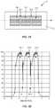
- FIG. 3Ais a top view of an exemplary LED device 32 with the plurality of LED chips 20 - 1 to 20 - 3 arranged on the submount 12 in a manner similar to LED chips being mounted on the die attach pads 26 - 1 to 26 - 3 or mounting areas of FIG. 2 .
- Spaces 34 - 1 , 34 - 2are formed between adjacent ones of the LED chips 20 - 1 to 20 - 3 .
- the spaces 34 - 1 , 34 - 2correspond to areas that are devoid of light generating active regions of the LED chips 20 - 1 to 20 - 3 .
- the spaces 34 - 1 , 34 - 2correspond to generally darker emission regions.
- FIG. 1is a top view of an exemplary LED device 32 with the plurality of LED chips 20 - 1 to 20 - 3 arranged on the submount 12 in a manner similar to LED chips being mounted on the die attach pads 26 - 1 to 26 - 3 or mounting areas of FIG. 2 .
- the mounting area 38corresponds to a die attach area for a single LED chip that includes multiple light emitting junctions formed on a common layer or a substrate.
- the LED chipmay comprise a monolithic multiple junction LED chip. In this manner, dark lines or areas of reduced luminance that are associated with spaces between discrete LED chips may be avoided.
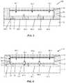
- FIG. 4Bis a top view of the LED package 36 after an LED chip 40 that includes multiple light emitting junctions 40 - 1 to 40 - 3 is mounted on the mounting area 38 of FIG. 4A .
- the LED chip 40may be mounted to and electrically coupled to the metal traces 14 - 1 , 14 - 2 , 14 - 4 , and 14 - 5 .
- Vertical dashed linesare superimposed on the LED chip 40 to indicate boundaries of the multiple light emitting junctions 40 - 1 to 40 - 3 formed therein.
- the multiple light emitting junctions 40 - 1 to 40 - 3are discrete from one another on a common layer or substrate of the LED chip 40 and each of the multiple light emitting junctions 40 - 1 to 40 - 3 may comprise separate anode and cathode contacts.
- a first metal trace 14 - 1is continuous between the bond pad 28 - 1 and a first light emitting junction 40 - 1
- a second metal trace 14 - 2is continuous between the bond pad 28 - 2 and a third light emitting junction 40 - 3
- Fourth and fifth metal traces 14 - 4 and 14 - 5are arranged as intermediate metal traces for providing electrical connections between adjacent ones of the multiple light emitting junctions 40 - 1 to 40 - 3 .
- external electrical connectsmay be applied at the bond pads 28 - 1 , 28 - 2 (or the package contacts 16 - 1 , 16 - 2 of FIG. 1 ) for electrically activating the multiple light emitting junctions 40 - 1 to 40 - 3 of LED chip 40 .
- the four and fifth metal traces 14 - 4 and 14 - 5are arranged to serially connect the multiple light emitting junctions 40 - 1 to 40 - 3 .
- the multiple light emitting junctions 40 - 1 to 40 - 3may be connected in other arrangements, including parallel, and independently addressable configurations.
- the LED package 36may further include one or more electrostatic discharge (ESD) chips 42 - 1 , 42 - 2 .
- ESDelectrostatic discharge
- a first ESD chip 42 - 1is attached or mounted to the first metal trace 14 - 1 and a third metal trace 14 - 3
- a second ESD chip 42 - 2is attached or mounted to the third metal trace 14 - 3 and the second metal trace 14 - 2 .
- each of the ESD chips 42 - 1 , 42 - 2are electrically connected in series between the first metal trace 14 - 1 and the second metal trace 14 - 2 .
- the ESD chips 42 - 1 , 42 - 2are arranged in parallel with the multiple light emitting junctions 40 - 1 to 40 - 3 between the first metal trace 14 - 1 and the second metal trace 14 - 2 .
- the one or more test tabs 30 - 1 , 30 - 2are configured to allow for individual testing of the multiple light emitting junctions 40 - 1 to 40 - 3 after the LED chip 40 and the ESD chips 42 - 1 , 42 - 2 are mounted to the LED package 36 .
- the first light emitting junction 40 - 1may be individually tested via electrical contacts to the first metal trace 14 - 1 and the test tab 30 - 1 ; a second light emitting junction 40 - 2 may be individually tested via electrical contacts to the test tabs 30 - 1 , 30 - 2 ; and finally, the third light emitting junction 40 - 3 may be individually tested via electrical contacts to the test tab 30 - 2 and the second metal trace 14 - 2 .
- subgroups of the light emitting junctions 40 - 1 to 40 - 3may be tested together.
- the light emitting junctions 40 - 1 and 40 - 2may be tested as a pair via electrical contacts to the metal trace 14 - 1 and the test tab 30 - 2 .
- FIG. 4Cis a top view of the LED package 36 of FIG. 4B with addition of the light-altering material 22 and the wavelength conversion element 24 according to embodiments disclosed herein.
- the wavelength conversion element 24is provided on or over the LED chip 40 and the light-altering material 22 is arranged around a perimeter of the LED chip 40 and around a perimeter of the wavelength conversion element 24 .
- the light-altering material 22may be configured to redirect or reflect laterally-emitting light from the LED chip 40 toward a desired emission direction or absorb laterally-emitting light from the LED chip 40 for improved contrast.
- the light-altering material 22is provide on the submount 12 to laterally surround peripheral boundaries of the LED chip 40 while also leaving at least a portion of each of the bond pads 28 - 1 , 28 - 1 (or the package contacts 16 - 1 , 16 - 2 of FIG. 1 ) uncovered to allow for electrical connections to the LED package 36 .
- FIG. 4Dis a cross-sectional view of the LED package 36 taken along the sectional line I-I of FIG. 4C .
- the submount 12the metal traces 14 - 1 , 14 - 2 , 14 - 4 , 14 - 5 ; the light emitting junctions 40 - 1 to 40 - 3 ; the light-altering material 22 ; and the wavelength conversion element 24 are visible.
- the wavelength conversion element 24includes a superstrate 43 that includes a lumiphoric material 44 disposed thereon.
- the term “superstrate” as used hereinrefers to an element placed on an LED chip that includes a lumiphoric material.
- the superstrate 43may be thinned before or after the patterning process is performed.
- the superstrate 43comprises a generally planar upper surface that corresponds to a light emission area of the LED package 36 .
- the lumiphoric material 44may then be placed on the superstrate 43 by, for example, spraying and/or otherwise coating the superstrate 43 with the lumiphoric material 44 .
- the superstrate 43 and the lumiphoric material 44may be attached to the LED chip 40 using, for example, a layer of transparent adhesive 46 .
- the layer of the transparent adhesive 46may include silicone with a refractive index in a range of about 1.3 to about 1.6 that is less than a refractive index of the LED chip 40 .
- the wavelength conversion element 24may comprise alternative configurations, such as phosphor-in-glass or ceramic phosphor plate arrangements.
- Phosphor-in-glass or ceramic phosphor plate arrangementsmay be formed by mixing phosphor particles with glass frit or ceramic materials, pressing the mixture into planar shapes, and firing or sintering the mixture to form a hardened structure that can be cut or separated into individual wavelength conversion elements 24 .
- the LED chip 40is configured as a multiple-junction monolithic LED chip that includes the multiple light emitting junctions 40 - 1 to 40 - 3 that are discrete from one another.
- the light emitting junctions 40 - 1 to 40 - 3are separated and initially isolated from one another by one or more recesses 48 - 1 , 48 - 2 that are formed in the LED chip 40 .
- the LED chip 40may include a plurality of various epitaxial layers that collectively form the light emitting structure.
- an active layer 50is illustrated as a dashed horizontal line across the LED chip 40 .
- the recesses 48 - 1 , 48 - 2are formed through an entire thickness of the p-type layer 52 , through an entire thickness of the active layer 50 , and at least a portion of the n-type layer 54 to form the discrete light emitting junctions 40 - 1 to 40 - 3 .
- the recesses 48 - 1 , 48 - 2divide the active layer 50 in to a plurality of discrete active layer portions 50 - 1 to 50 - 3 that are electrically isolated from one another.
- the recesses 48 - 1 , 48 - 2are formed through an entire thickness of the n-type layer 54 to reach a less conductive portion of the LED chip 40 , such as an undoped or unintentionally doped layer of the LED chip 40 .
- the recesses 48 - 1 , 48 - 2are formed through an entire thickness of any epitaxial layers of the LED chip 40 to either reach or extend into the substrate 56 .
- the substrate 56forms a monolithic substrate that supports each of the light emitting junctions 40 - 1 to 40 - 3 .
- one or more epitaxial layers of the LED chip 40may also extend across all of the light emitting junctions 40 - 1 to 40 - 3 .
- Each of the light emitting junctions 40 - 1 to 40 - 3may include a separate anode 58 and a separate cathode 60 that are configured to provide various electrical connections to the metal traces 14 - 1 , 14 - 2 , 14 - 4 , 14 - 5 when the LED chip 40 is flip-chip mounted to the substrate 56 in a direct attach configuration.
- the combination of the reflective layers of the LED chip 40 that are registered with the p-type layer 52 and the reflective layers 68 - 1 , 68 - 2 that are registered with the recesses 48 - 1 , 48 - 2provide improved light output for the LED package 66 .
- the recesses 48 - 1 , 48 - 2comprise the reflective layers 68 - 1 , 68 - 2 and the light-altering material 22 .
- the recesses 48 - 1 , 48 - 2may extend to and initially form exposed surfaces of an epitaxial layer or the substrate 56 that are registered between the light emitting junctions 40 - 1 to 40 - 3 .
Landscapes
- Engineering & Computer Science (AREA)
- Power Engineering (AREA)
- Microelectronics & Electronic Packaging (AREA)
- Physics & Mathematics (AREA)
- Condensed Matter Physics & Semiconductors (AREA)
- General Physics & Mathematics (AREA)
- Computer Hardware Design (AREA)
- Led Device Packages (AREA)
Abstract
Description
Claims (19)
Priority Applications (2)
| Application Number | Priority Date | Filing Date | Title |
|---|---|---|---|
| US16/453,447US11101411B2 (en) | 2019-06-26 | 2019-06-26 | Solid-state light emitting devices including light emitting diodes in package structures |
| PCT/US2020/038960WO2020263748A1 (en) | 2019-06-26 | 2020-06-22 | Light emitting diode packages |
Applications Claiming Priority (1)
| Application Number | Priority Date | Filing Date | Title |
|---|---|---|---|
| US16/453,447US11101411B2 (en) | 2019-06-26 | 2019-06-26 | Solid-state light emitting devices including light emitting diodes in package structures |
Publications (2)
| Publication Number | Publication Date |
|---|---|
| US20200411730A1 US20200411730A1 (en) | 2020-12-31 |
| US11101411B2true US11101411B2 (en) | 2021-08-24 |
Family
ID=71528092
Family Applications (1)
| Application Number | Title | Priority Date | Filing Date |
|---|---|---|---|
| US16/453,447ActiveUS11101411B2 (en) | 2019-06-26 | 2019-06-26 | Solid-state light emitting devices including light emitting diodes in package structures |
Country Status (2)
| Country | Link |
|---|---|
| US (1) | US11101411B2 (en) |
| WO (1) | WO2020263748A1 (en) |
Cited By (1)
| Publication number | Priority date | Publication date | Assignee | Title |
|---|---|---|---|---|
| US12040425B2 (en)* | 2016-07-12 | 2024-07-16 | Samsung Display Co., Ltd. | Self-aligned display appartus |
Families Citing this family (4)
| Publication number | Priority date | Publication date | Assignee | Title |
|---|---|---|---|---|
| US20220254962A1 (en)* | 2021-02-11 | 2022-08-11 | Creeled, Inc. | Optical arrangements in cover structures for light emitting diode packages and related methods |
| CN113066920A (en)* | 2021-03-15 | 2021-07-02 | Tcl华星光电技术有限公司 | LED chip, driver substrate and display panel |
| US12355013B2 (en)* | 2022-04-21 | 2025-07-08 | Creeled, Inc. | Emission height arrangements in light-emitting diode packages and related devices and methods |
| US20240154076A1 (en)* | 2022-11-08 | 2024-05-09 | Creeled, Inc. | Lumiphoric material structures for light-emitting diode packages and related methods |
Citations (195)
| Publication number | Priority date | Publication date | Assignee | Title |
|---|---|---|---|---|
| US2857541A (en) | 1954-03-29 | 1958-10-21 | Westinghouse Electric Corp | Thin sheet of phosphor embedded glass and method of preparing |
| US4918497A (en) | 1988-12-14 | 1990-04-17 | Cree Research, Inc. | Blue light emitting diode formed in silicon carbide |
| US4966862A (en) | 1989-08-28 | 1990-10-30 | Cree Research, Inc. | Method of production of light emitting diodes |
| US5027168A (en) | 1988-12-14 | 1991-06-25 | Cree Research, Inc. | Blue light emitting diode formed in silicon carbide |
| US5177500A (en) | 1991-09-11 | 1993-01-05 | Eastman Kodak Company | LED array printhead with thermally coupled arrays |
| US5210051A (en) | 1990-03-27 | 1993-05-11 | Cree Research, Inc. | High efficiency light emitting diodes from bipolar gallium nitride |
| US5338944A (en) | 1993-09-22 | 1994-08-16 | Cree Research, Inc. | Blue light-emitting diode with degenerate junction structure |
| US5359345A (en) | 1992-08-05 | 1994-10-25 | Cree Research, Inc. | Shuttered and cycled light emitting diode display and method of producing the same |
| US5393993A (en) | 1993-12-13 | 1995-02-28 | Cree Research, Inc. | Buffer structure between silicon carbide and gallium nitride and resulting semiconductor devices |
| US5416342A (en) | 1993-06-23 | 1995-05-16 | Cree Research, Inc. | Blue light-emitting diode with high external quantum efficiency |
| US5523589A (en) | 1994-09-20 | 1996-06-04 | Cree Research, Inc. | Vertical geometry light emitting diode with group III nitride active layer and extended lifetime |
| US5604135A (en) | 1994-08-12 | 1997-02-18 | Cree Research, Inc. | Method of forming green light emitting diode in silicon carbide |
| US5631190A (en) | 1994-10-07 | 1997-05-20 | Cree Research, Inc. | Method for producing high efficiency light-emitting diodes and resulting diode structures |
| US5739554A (en) | 1995-05-08 | 1998-04-14 | Cree Research, Inc. | Double heterojunction light emitting diode with gallium nitride active layer |
| US6034422A (en) | 1995-09-29 | 2000-03-07 | Dai Nippon Printing Co., Ltd. | Lead frame, method for partial noble plating of said lead frame and semiconductor device having said lead frame |
| US6187606B1 (en) | 1997-10-07 | 2001-02-13 | Cree, Inc. | Group III nitride photonic devices on silicon carbide substrates with conductive buffer interlayer structure |
| US6274399B1 (en) | 1998-06-05 | 2001-08-14 | Lumileds Lighting, U.S. Llc | Method of strain engineering and impurity control in III-V nitride semiconductor films and optoelectronic devices |
| US6600175B1 (en) | 1996-03-26 | 2003-07-29 | Advanced Technology Materials, Inc. | Solid state white light emitter and display using same |
| US6646330B2 (en) | 2000-09-21 | 2003-11-11 | Matsushita Electric Industrial Co., Ltd. | Lead frame for semiconductor device, process for producing the same and semiconductor device using the same |
| US6649440B1 (en) | 1999-06-08 | 2003-11-18 | Lumileds Lighting U.S., Llc | Aluminum indium gallium nitride-based LED having thick epitaxial layer for improved light extraction |
| US20040048219A1 (en) | 2002-09-11 | 2004-03-11 | Chang-Ju Yun | Baking apparatus for manufacturing a semiconductor device |
| US6791119B2 (en) | 2001-02-01 | 2004-09-14 | Cree, Inc. | Light emitting diodes including modifications for light extraction |
| US6853010B2 (en) | 2002-09-19 | 2005-02-08 | Cree, Inc. | Phosphor-coated light emitting diodes including tapered sidewalls, and fabrication methods therefor |
| US20050127385A1 (en) | 1996-06-26 | 2005-06-16 | Osram Opto Semiconductors Gmbh & Co., Ohg, A Germany Corporation | Light-radiating semiconductor component with a luminescence conversion element |
| US6958497B2 (en) | 2001-05-30 | 2005-10-25 | Cree, Inc. | Group III nitride based light emitting diode structures with a quantum well and superlattice, group III nitride based quantum well structures and group III nitride based superlattice structures |
| US7095056B2 (en) | 2003-12-10 | 2006-08-22 | Sensor Electronic Technology, Inc. | White light emitting device and method |
| US20060221272A1 (en) | 2005-04-04 | 2006-10-05 | Negley Gerald H | Light emitting diode backlighting systems and methods that use more colors than display picture elements |
| EP1710846A1 (en) | 2005-04-08 | 2006-10-11 | Sharp Kabushiki Kaisha | Light-emitting diode |
| WO2007034367A1 (en) | 2005-09-19 | 2007-03-29 | Koninklijke Philips Electronics N.V. | Variable color light emitting device and method for controlling the same |
| US7213940B1 (en) | 2005-12-21 | 2007-05-08 | Led Lighting Fixtures, Inc. | Lighting device and lighting method |
| US20070104828A1 (en) | 2005-11-04 | 2007-05-10 | Fornaguera Joan F | Center-filled confectionery product and method |
| US20070241661A1 (en) | 2006-04-12 | 2007-10-18 | Yin Chua B | High light output lamps having a phosphor embedded glass/ceramic layer |
| US20080036940A1 (en) | 2006-08-09 | 2008-02-14 | Samsung Electronics Co., Ltd. | Backlight unit and display device having the same |
| US7344902B2 (en) | 2004-11-15 | 2008-03-18 | Philips Lumileds Lighting Company, Llc | Overmolded lens over LED die |
| US7361938B2 (en) | 2004-06-03 | 2008-04-22 | Philips Lumileds Lighting Company Llc | Luminescent ceramic for a light emitting device |
| USD572387S1 (en) | 2006-06-20 | 2008-07-01 | Matsushita Electric Industrial Co., Ltd. | Lighting apparatus |
| USD573731S1 (en) | 2006-06-20 | 2008-07-22 | Matsushita Electric Industrial Co., Ltd. | Lighting apparatus |
| US20080258130A1 (en) | 2007-04-23 | 2008-10-23 | Bergmann Michael J | Beveled LED Chip with Transparent Substrate |
| US7456499B2 (en) | 2004-06-04 | 2008-11-25 | Cree, Inc. | Power light emitting die package with reflecting lens and the method of making the same |
| US20090001490A1 (en) | 2004-07-26 | 2009-01-01 | Georg Bogner | Optoelectronic Component that Emits Electromagnetic Radiation and Illumination Module |
| US20090021841A1 (en) | 2007-07-17 | 2009-01-22 | Cree Led Lighting Solutions, Inc. | Optical elements with internal optical features and methods of fabricating same |
| US20090039375A1 (en) | 2007-08-07 | 2009-02-12 | Cree, Inc. | Semiconductor light emitting devices with separated wavelength conversion materials and methods of forming the same |
| US7495387B2 (en) | 2001-02-05 | 2009-02-24 | Samsung Sdi Co., Ltd. | Organic electroluminescent element and organic electroluminescent device including the same |
| US20090051022A1 (en) | 2007-08-24 | 2009-02-26 | Denso Corporation | Lead frame structure |
| US20090050908A1 (en) | 2005-01-10 | 2009-02-26 | Cree, Inc. | Solid state lighting component |
| US20090166665A1 (en) | 2007-12-31 | 2009-07-02 | Lumination Llc | Encapsulated optoelectronic device |
| US7564180B2 (en) | 2005-01-10 | 2009-07-21 | Cree, Inc. | Light emission device and method utilizing multiple emitters and multiple phosphors |
| USD597502S1 (en) | 2007-06-14 | 2009-08-04 | Panasonic Corporation | Light source of light emitting diode |
| US20090261708A1 (en) | 2008-04-21 | 2009-10-22 | Motorola, Inc. | Glass-phosphor capping structure for leds |
| US20090316409A1 (en) | 2008-06-24 | 2009-12-24 | Yu-Sik Kim | Sub-mount, light emitting device including sub-mount and methods of manufacturing such sub-mount and/or light emitting device |
| US7655957B2 (en) | 2006-04-27 | 2010-02-02 | Cree, Inc. | Submounts for semiconductor light emitting device packages and semiconductor light emitting device packages including the same |
| USD611628S1 (en) | 2006-06-20 | 2010-03-09 | Panasonic Corporation | Lighting apparatus |
| US20100154035A1 (en) | 2007-03-06 | 2010-06-17 | Ayodele Damola | Personalized Interaction Using Codes |
| US7754507B2 (en) | 2005-06-09 | 2010-07-13 | Philips Lumileds Lighting Company, Llc | Method of removing the growth substrate of a semiconductor light emitting device |
| EP2216834A1 (en) | 2007-11-29 | 2010-08-11 | Nichia Corporation | Light-emitting device and its manufacturing method |
| US7791061B2 (en) | 2004-05-18 | 2010-09-07 | Cree, Inc. | External extraction light emitting diode based upon crystallographic faceted surfaces |
| US7802901B2 (en) | 2007-09-25 | 2010-09-28 | Cree, Inc. | LED multi-chip lighting units and related methods |
| US20100244060A1 (en) | 2004-12-14 | 2010-09-30 | Seoul Opto Device Co., Ltd. | Light emitting device having a plurality of light emitting cells and package mounting the same |
| US7821023B2 (en) | 2005-01-10 | 2010-10-26 | Cree, Inc. | Solid state lighting component |
| US7847303B2 (en) | 2008-07-29 | 2010-12-07 | Seoul Semiconductor Co., Ltd. | Warm white light emitting apparatus and back light module comprising the same |
| US20100320928A1 (en) | 2008-02-13 | 2010-12-23 | Canon Components, Inc. | White light emitting apparatus and line illuminator using the same in image reading apparatus |
| WO2011007275A1 (en) | 2009-07-16 | 2011-01-20 | Philips Lumileds Lighting Company, Llc | Reflective substrate for leds |
| US20110018017A1 (en) | 2009-07-23 | 2011-01-27 | Koninklijke Philips Electronics N.V. | Led with molded reflective sidewall coating |
| US20110031516A1 (en) | 2009-08-07 | 2011-02-10 | Koninklijke Philips Electronics N.V. | Led with silicone layer and laminated remote phosphor layer |
| US20110049545A1 (en) | 2009-09-02 | 2011-03-03 | Koninklijke Philips Electronics N.V. | Led package with phosphor plate and reflective substrate |
| US20110068702A1 (en) | 2009-09-24 | 2011-03-24 | Cree Led Lighting Solutions, Inc. | Solid state lighting apparatus with controllable bypass circuits and methods of operation thereof |
| US7928648B2 (en) | 2006-04-17 | 2011-04-19 | Korea Advanced Institute Of Science And Technology | Yellow light emitting Ce3+-activated silicate phosphor with new composition, manufacturing method thereof and white LEDs including phosphor |
| US7952544B2 (en) | 2007-02-15 | 2011-05-31 | Cree, Inc. | Partially filterless liquid crystal display devices and methods of operating the same |
| US7960819B2 (en) | 2006-07-13 | 2011-06-14 | Cree, Inc. | Leadframe-based packages for solid state emitting devices |
| US20110169033A1 (en) | 2008-12-25 | 2011-07-14 | Takahiro Fukunaga | Lead, wiring member, package part, metal part provided with resin and resin-sealed semiconductor device, and methods for producing same |
| US20110180822A1 (en) | 2002-06-28 | 2011-07-28 | Osram Opto Semiconductors Gmbh | Optoelectronic Component |
| US7999283B2 (en) | 2007-06-14 | 2011-08-16 | Cree, Inc. | Encapsulant with scatterer to tailor spatial emission pattern and color uniformity in light emitting diodes |
| US8018135B2 (en) | 2007-10-10 | 2011-09-13 | Cree, Inc. | Lighting device and method of making |
| CN102214651A (en) | 2011-05-25 | 2011-10-12 | 映瑞光电科技(上海)有限公司 | LED (light emitting diode) pixel unit device structure and preparation method thereof |
| US20110254022A1 (en) | 2010-04-16 | 2011-10-20 | Haruaki Sasano | Light emitting device |
| US8044418B2 (en) | 2006-07-13 | 2011-10-25 | Cree, Inc. | Leadframe-based packages for solid state light emitting devices |
| US8058088B2 (en) | 2008-01-15 | 2011-11-15 | Cree, Inc. | Phosphor coating systems and methods for light emitting structures and packaged light emitting diodes including phosphor coating |
| US8075165B2 (en) | 2008-10-14 | 2011-12-13 | Ledengin, Inc. | Total internal reflection lens and mechanical retention and locating device |
| US20110309388A1 (en) | 2010-06-16 | 2011-12-22 | Ito Kosaburo | Semiconductor light-emitting device and manufacturing method |
| US8125137B2 (en) | 2005-01-10 | 2012-02-28 | Cree, Inc. | Multi-chip light emitting device lamps for providing high-CRI warm white light and light fixtures including the same |
| US20120061692A1 (en) | 2010-09-10 | 2012-03-15 | Advanced Optoelectronic Technology, Inc. | Light emitting diode package having interconnection structures |
| US20120086023A1 (en) | 2010-10-08 | 2012-04-12 | Guardian Industries Corp. | Insulating glass (IG) or vacuum insulating glass (VIG) unit including light source, and/or methods of making the same |
| US20120104452A1 (en) | 2010-10-29 | 2012-05-03 | Nichia Corporation | Light emitting apparatus and production method thereof |
| WO2012058040A1 (en) | 2010-10-28 | 2012-05-03 | Corning Incorporated | Phosphor containing glass frit materials for led lighting applications |
| US8232564B2 (en) | 2007-01-22 | 2012-07-31 | Cree, Inc. | Wafer level phosphor coating technique for warm light emitting diodes |
| US20120193651A1 (en) | 2010-11-22 | 2012-08-02 | Edmond John A | Light emitting devices, systems, and methods |
| US8264138B2 (en) | 2006-01-20 | 2012-09-11 | Cree, Inc. | Shifting spectral content in solid state light emitters by spatially separating lumiphor films |
| US20120306355A1 (en) | 2011-06-03 | 2012-12-06 | Seibel Ii Harry A | Methods of determining and making red nitride compositions |
| US20120305949A1 (en) | 2011-01-31 | 2012-12-06 | Matthew Donofrio | Light Emitting Diode (LED) Arrays Including Direct Die Attach And Related Assemblies |
| US8337071B2 (en) | 2005-12-21 | 2012-12-25 | Cree, Inc. | Lighting device |
| US8362512B2 (en) | 2006-04-24 | 2013-01-29 | Cree, Inc. | Side-view surface mount white LED |
| US20130033169A1 (en) | 2011-08-05 | 2013-02-07 | Ito Kosaburo | Light emitting device and method for manufacturing the same |
| US8384097B2 (en) | 2009-04-08 | 2013-02-26 | Ledengin, Inc. | Package for multiple light emitting diodes |
| US20130057593A1 (en) | 2011-09-05 | 2013-03-07 | Canon Kabushiki Kaisha | Lighting apparatus |
| US20130069781A1 (en) | 2011-09-15 | 2013-03-21 | Kevin Terwilliger | Multidimensional Barcodes For Information Handling System Manufacture, Assembly And Service |
| US20130077299A1 (en) | 2011-02-16 | 2013-03-28 | Cree, Inc. | High voltage array light emitting diode (led) devices, fixtures and methods |
| US8410679B2 (en) | 2010-09-21 | 2013-04-02 | Cree, Inc. | Semiconductor light emitting devices with densely packed phosphor layer at light emitting surface |
| US20130092960A1 (en) | 2007-10-31 | 2013-04-18 | Ruud Lighting, Inc. | Multi-Die LED Package |
| US8425271B2 (en) | 2006-09-01 | 2013-04-23 | Cree, Inc. | Phosphor position in light emitting diodes |
| US20130221509A1 (en) | 2010-11-02 | 2013-08-29 | Dai Nippon Printing Co., Ltd. | Lead frame for mounting led elements, lead frame with resin, method for manufacturing semiconductor devices, and lead frame for mounting semiconductor elements |
| US20130256710A1 (en) | 2007-10-31 | 2013-10-03 | Cree, Inc. | Multi-chip light emitter packages and related methods |
| US20130256711A1 (en) | 2012-03-30 | 2013-10-03 | Cree, Inc. | Substrate based light emitter devices, components, and related methods |
| US20130264589A1 (en) | 2012-04-09 | 2013-10-10 | Cree, Inc. | Wafer level packaging of light emitting diodes (leds) |
| WO2013154818A1 (en) | 2012-04-09 | 2013-10-17 | Cree, Inc. | Wafer level packaging of multiple light emitting diodes (leds) on a single carrier die |
| US20130271991A1 (en) | 2012-04-13 | 2013-10-17 | Cree, Inc. | Led lamp |
| US8563339B2 (en) | 2005-08-25 | 2013-10-22 | Cree, Inc. | System for and method for closed loop electrophoretic deposition of phosphor materials on semiconductor devices |
| US20130301257A1 (en) | 2012-05-14 | 2013-11-14 | Cree, Inc. | Light emitting devices including multiple anodes and cathodes |
| US8598793B2 (en) | 2011-05-12 | 2013-12-03 | Ledengin, Inc. | Tuning of emitter with multiple LEDs to a single color bin |
| WO2014024108A1 (en) | 2012-08-07 | 2014-02-13 | Koninklijke Philips N.V. | Led package and manufacturing method |
| USD703841S1 (en) | 2012-04-11 | 2014-04-29 | Osram Gmbh | LED lighting module |
| US20140138725A1 (en) | 2012-11-12 | 2014-05-22 | Citizen Electronics Co., Ltd. | Semiconductor light-emitting device and producing method thereof |
| CN103864302A (en) | 2014-04-02 | 2014-06-18 | 福建鸿博光电科技有限公司 | Glass phosphor and preparation method thereof |
| US20140217325A1 (en) | 2011-09-05 | 2014-08-07 | Merck Patent Gmbh | Liquid-crystalline medium and high-frequency components comprising same |
| US20140217435A1 (en) | 2011-01-21 | 2014-08-07 | Cree, Inc. | Light Emitting Diodes with Low Junction Temperature and Solid State Backlight Components Including Light Emitting Diodes with Low Junction Temperature |
| US20140217436A1 (en) | 2013-02-05 | 2014-08-07 | Cree, Inc. | Submount-free light emitting diode (led) components and methods of fabricating same |
| US20140217443A1 (en) | 2013-02-05 | 2014-08-07 | Cree, Inc. | Chip with integrated phosphor |
| EP2768037A1 (en) | 2011-10-11 | 2014-08-20 | Panasonic Corporation | Light-emission device, and illumination device using same |
| WO2014133294A1 (en) | 2013-02-26 | 2014-09-04 | 포항공과대학교 산학협력단 | Glass-phosphor composite containing rare-earth ion and light-emitting diode including same |
| WO2014159894A1 (en) | 2013-03-14 | 2014-10-02 | Corning Incorporated | Led lighting devices |
| US8866410B2 (en) | 2007-11-28 | 2014-10-21 | Cree, Inc. | Solid state lighting devices and methods of manufacturing the same |
| EP2804225A1 (en) | 2013-05-13 | 2014-11-19 | Nichia Corporation | Light emitting device and method for manufacturing same |
| US20140367713A1 (en) | 2011-02-16 | 2014-12-18 | Cree, Inc. | Multi-layer conversion material for down conversion in solid state lighting |
| EP2819191A1 (en) | 2012-02-20 | 2014-12-31 | Sharp Kabushiki Kaisha | Light emission device and illumination device |
| CN204088306U (en) | 2014-01-15 | 2015-01-07 | 四川新力光源股份有限公司 | A kind of white light LEDs module |
| US8940561B2 (en) | 2008-01-15 | 2015-01-27 | Cree, Inc. | Systems and methods for application of optical materials to optical elements |
| US20150028372A1 (en) | 2013-07-26 | 2015-01-29 | Shinko Electric Industries Co., Ltd. | Light emitting device package and package for mounting light emitting device |
| WO2015026033A1 (en) | 2013-08-20 | 2015-02-26 | Lg Electronics Inc. | Display device using semiconductor light emitting device |
| US8970131B2 (en) | 2013-02-15 | 2015-03-03 | Cree, Inc. | Solid state lighting apparatuses and related methods |
| US20150062915A1 (en) | 2013-09-05 | 2015-03-05 | Cree, Inc. | Light emitting diode devices and methods with reflective material for increased light output |
| US8998444B2 (en) | 2006-04-18 | 2015-04-07 | Cree, Inc. | Solid state lighting devices including light mixtures |
| US9024349B2 (en) | 2007-01-22 | 2015-05-05 | Cree, Inc. | Wafer level phosphor coating method and devices fabricated utilizing method |
| US20150155447A1 (en) | 2013-11-29 | 2015-06-04 | Nichia Corporation | Method of manufacturing light emitting device, and light emitting device |
| US20150204525A1 (en) | 2013-03-11 | 2015-07-23 | Yi Shen | High-Definition LED Display Screen and Surface-Mounted LED Composite Lamp with Ultra-Small Point Distance Thereof |
| US20150207045A1 (en) | 2014-01-21 | 2015-07-23 | Toyoda Gosei Co., Ltd. | Light-Emitting Device and Method of Manufacturing the Same |
| US20150249196A1 (en)* | 2011-06-24 | 2015-09-03 | Cree, Inc. | High voltage monolithic led chip with improved reliability |
| US9131561B2 (en) | 2011-09-16 | 2015-09-08 | Cree, Inc. | Solid-state lighting apparatus and methods using energy storage |
| US20150257211A1 (en) | 2014-03-05 | 2015-09-10 | Cree, Inc. | Solid state lighting apparatuses and related methods |
| US20150263247A1 (en) | 2014-03-17 | 2015-09-17 | Toyoda Gosei Co., Ltd. | Light Emitting Device |
| US20150262987A1 (en) | 2014-03-12 | 2015-09-17 | Toyoda Gosei Co., Ltd. | Light Emitting Device And Method For Manufacturing The Same |
| EP2927970A1 (en) | 2012-12-03 | 2015-10-07 | Citizen Holdings Co., Ltd. | Led module |
| US9159888B2 (en) | 2007-01-22 | 2015-10-13 | Cree, Inc. | Wafer level phosphor coating method and devices fabricated utilizing method |
| US9192013B1 (en) | 2014-06-06 | 2015-11-17 | Cree, Inc. | Lighting devices with variable gamut |
| US20150349218A1 (en) | 2014-05-30 | 2015-12-03 | Cree, Inc. | Submount based light emitter components and methods |
| US20150364660A1 (en) | 2014-06-12 | 2015-12-17 | Genesis Photonics Inc. | Light emitting component |
| US9277605B2 (en) | 2011-09-16 | 2016-03-01 | Cree, Inc. | Solid-state lighting apparatus and methods using current diversion controlled by lighting device bias states |
| US20160064623A1 (en) | 2014-09-03 | 2016-03-03 | Cree, Inc. | Light emitting diode (led) component comprising a phosphor with improved excitation properties |
| US20160079486A1 (en) | 2013-04-17 | 2016-03-17 | Nichia Corporation | Light emitting device |
| US20160074833A1 (en) | 2014-09-12 | 2016-03-17 | Paul Gregory O'BRIEN | Nanostructured solar selective catalytic supports |
| US20160093777A1 (en) | 2014-09-30 | 2016-03-31 | Nichia Corporation | Light emitting device and method of manufacturing the same |
| US9310026B2 (en) | 2006-12-04 | 2016-04-12 | Cree, Inc. | Lighting assembly and lighting method |
| US20160111600A1 (en)* | 2013-07-29 | 2016-04-21 | Seoul Viosys Co., Ltd. | Light emitting diode, method of fabricating the same and led module having the same |
| US20160126434A1 (en) | 2014-10-31 | 2016-05-05 | Nichia Corporation | Light emitting device and adaptive driving beam headlamp system |
| US20160126010A1 (en) | 2011-06-15 | 2016-05-05 | James Jen-Ho Wang | Flexible circuit assembly and method therof |
| USD756547S1 (en) | 2014-06-05 | 2016-05-17 | Osram Gmbh | Lighting device |
| US20160161098A1 (en) | 2010-11-22 | 2016-06-09 | Cree, Inc. | Solid state lighting apparatuses, systems, and related methods for improved heat distribution |
| US9414454B2 (en) | 2013-02-15 | 2016-08-09 | Cree, Inc. | Solid state lighting apparatuses and related methods |
| US9461222B1 (en) | 2015-06-30 | 2016-10-04 | Epistar Corporation | Light-emitting element and the light-emitting module thereof |
| US20160293811A1 (en) | 2015-03-31 | 2016-10-06 | Cree, Inc. | Light emitting diodes and methods with encapsulation |
| US20160351846A1 (en) | 2015-05-28 | 2016-12-01 | Lg Display Co., Ltd. | Organic light emitting display apparatus and method of manufacturing the same |
| US20170040183A1 (en) | 2015-08-07 | 2017-02-09 | Shinko Electric Industries Co., Ltd. | Lead frame and semiconductor device |
| US20170092820A1 (en)* | 2015-09-30 | 2017-03-30 | Samsung Electronics Co., Ltd. | Light emitting device package |
| US20170098746A1 (en) | 2015-10-01 | 2017-04-06 | Cree, Inc. | Low optical loss flip chip solid state lighting device |
| US20170154880A1 (en) | 2015-11-30 | 2017-06-01 | Nichia Corporation | Method of manufacturing light emitting device |
| USD797321S1 (en) | 2016-02-19 | 2017-09-12 | Epistar Corporation | Light emitting unit |
| US20170263828A1 (en) | 2016-03-14 | 2017-09-14 | Innolux Corporation | Display device |
| US20170294417A1 (en) | 2016-04-12 | 2017-10-12 | Cree, Inc. | High density pixelated led and devices and methods thereof |
| US20170301832A1 (en)* | 2014-01-07 | 2017-10-19 | Koninklijke Philips N.V. | Glueless light emitting device with phosphor converter |
| US20170299798A1 (en)* | 2016-04-15 | 2017-10-19 | Lg Innotek Co., Ltd. | Light-Emitting Apparatus and Illumination Apparatus Including the Same |
| US9816691B2 (en) | 2011-05-12 | 2017-11-14 | Ledengin, Inc. | Method and system for forming LED light emitters |
| US20170358624A1 (en)* | 2016-06-13 | 2017-12-14 | Seoul Semiconductor Co., Ltd. | Display apparatus and manufacturing method thereof |
| US20170373225A1 (en) | 2015-07-23 | 2017-12-28 | Nichia Corporation | Method of manufacturing light emitting device |
| US20180012949A1 (en)* | 2016-07-06 | 2018-01-11 | Seoul Semiconductor Co., Ltd. | Display apparatus |
| US20180033924A1 (en) | 2016-07-26 | 2018-02-01 | Cree, Inc. | Light emitting diodes, components and related methods |
| US9893243B2 (en) | 2010-11-08 | 2018-02-13 | Bridgelux, Inc. | LED-based light source utilizing asymmetric conductors |
| US20180043178A1 (en) | 2015-02-26 | 2018-02-15 | Sharp Kabushiki Kaisha | Light irradiation substrate |
| US20180076368A1 (en) | 2015-03-31 | 2018-03-15 | Cree, Inc. | Light emitting diodes and methods |
| US20180102449A1 (en) | 2016-10-12 | 2018-04-12 | Kateeva, Inc. | Display Devices Utilizing Quantum Dots and Inkjet Printing Techniques Thereof |
| US20180103513A1 (en) | 2016-10-12 | 2018-04-12 | Everlight Electronics Co., Ltd. | Light emitting device and led package structure |
| US20180102348A1 (en) | 2016-10-06 | 2018-04-12 | Osram Opto Semiconductors Gmbh | Optoelectronic component and method of producing an optoelectronic component |
| US20180130776A1 (en) | 2016-11-09 | 2018-05-10 | Nichia Corporation | Light emitting device |
| US20180190880A1 (en) | 2016-12-30 | 2018-07-05 | Lumileds Llc | Phosphor deposition system for leds |
| US20180190881A1 (en) | 2016-12-30 | 2018-07-05 | Lite-On Opto Technology (Changzhou) Co., Ltd. | Phosphor plate assembly, led package structure, and method for manufacturing led package structure |
| US20180190885A1 (en) | 2016-12-30 | 2018-07-05 | Lite-On Technology Corporation | Led package structure and chip-scale light emitting unit |
| US10057983B1 (en) | 2014-06-13 | 2018-08-21 | Verily Life Sciences Llc | Fabrication methods for bio-compatible devices using an etch stop and/or a coating |
| US10211187B2 (en) | 2014-07-18 | 2019-02-19 | Koninklijke Philips N.V. | Light emitting diodes and reflector |
| US20190122592A1 (en) | 2017-10-25 | 2019-04-25 | Samsung Electronics Co., Ltd. | Led panel and display apparatus having the same |
| US20190148346A1 (en) | 2016-05-06 | 2019-05-16 | Epcos Ag | Multi-led system |
| US20190165231A1 (en) | 2017-11-08 | 2019-05-30 | SemiLEDs Optoelectronics Co., Ltd. | Method For Making Light Emitting Device LED Arrays |
| USD851790S1 (en) | 2017-09-08 | 2019-06-18 | Cree, Inc. | Light emitting device |
| US20190312187A1 (en) | 2018-04-04 | 2019-10-10 | Stanley Electric Co., Ltd. | Semiconductor light-emitting apparatus having light reflection adjusting member of gray resin and its manufacturing method |
| US20190363232A1 (en) | 2018-05-25 | 2019-11-28 | Cree, Inc. | Light-emitting diode packages with individually controllable light-emitting diode chips |
| US20200075822A1 (en) | 2018-08-31 | 2020-03-05 | Cree, Inc. | Light-emitting diodes, light-emitting diode arrays and related devices |
| US20200075813A1 (en) | 2018-08-31 | 2020-03-05 | Cree, Inc. | Light-emitting diodes, light-emitting diode arrays and related devices |
| US10651353B2 (en) | 2015-07-22 | 2020-05-12 | Panasonic Intellectual Property Management Co., Ltd. | Light-emitting device including a reflective element |
| US20200152840A1 (en) | 2018-11-13 | 2020-05-14 | Cree, Inc. | Light emitting diode packages |
- 2019
- 2019-06-26USUS16/453,447patent/US11101411B2/enactiveActive
- 2020
- 2020-06-22WOPCT/US2020/038960patent/WO2020263748A1/ennot_activeCeased
Patent Citations (210)
| Publication number | Priority date | Publication date | Assignee | Title |
|---|---|---|---|---|
| US2857541A (en) | 1954-03-29 | 1958-10-21 | Westinghouse Electric Corp | Thin sheet of phosphor embedded glass and method of preparing |
| US4918497A (en) | 1988-12-14 | 1990-04-17 | Cree Research, Inc. | Blue light emitting diode formed in silicon carbide |
| US5027168A (en) | 1988-12-14 | 1991-06-25 | Cree Research, Inc. | Blue light emitting diode formed in silicon carbide |
| US4966862A (en) | 1989-08-28 | 1990-10-30 | Cree Research, Inc. | Method of production of light emitting diodes |
| US5210051A (en) | 1990-03-27 | 1993-05-11 | Cree Research, Inc. | High efficiency light emitting diodes from bipolar gallium nitride |
| US5177500A (en) | 1991-09-11 | 1993-01-05 | Eastman Kodak Company | LED array printhead with thermally coupled arrays |
| US5359345A (en) | 1992-08-05 | 1994-10-25 | Cree Research, Inc. | Shuttered and cycled light emitting diode display and method of producing the same |
| US5416342A (en) | 1993-06-23 | 1995-05-16 | Cree Research, Inc. | Blue light-emitting diode with high external quantum efficiency |
| US5338944A (en) | 1993-09-22 | 1994-08-16 | Cree Research, Inc. | Blue light-emitting diode with degenerate junction structure |
| US5393993A (en) | 1993-12-13 | 1995-02-28 | Cree Research, Inc. | Buffer structure between silicon carbide and gallium nitride and resulting semiconductor devices |
| US5604135A (en) | 1994-08-12 | 1997-02-18 | Cree Research, Inc. | Method of forming green light emitting diode in silicon carbide |
| US5523589A (en) | 1994-09-20 | 1996-06-04 | Cree Research, Inc. | Vertical geometry light emitting diode with group III nitride active layer and extended lifetime |
| US5631190A (en) | 1994-10-07 | 1997-05-20 | Cree Research, Inc. | Method for producing high efficiency light-emitting diodes and resulting diode structures |
| US5912477A (en) | 1994-10-07 | 1999-06-15 | Cree Research, Inc. | High efficiency light emitting diodes |
| US5739554A (en) | 1995-05-08 | 1998-04-14 | Cree Research, Inc. | Double heterojunction light emitting diode with gallium nitride active layer |
| US6120600A (en) | 1995-05-08 | 2000-09-19 | Cree, Inc. | Double heterojunction light emitting diode with gallium nitride active layer |
| US6034422A (en) | 1995-09-29 | 2000-03-07 | Dai Nippon Printing Co., Ltd. | Lead frame, method for partial noble plating of said lead frame and semiconductor device having said lead frame |
| US6600175B1 (en) | 1996-03-26 | 2003-07-29 | Advanced Technology Materials, Inc. | Solid state white light emitter and display using same |
| US20050127385A1 (en) | 1996-06-26 | 2005-06-16 | Osram Opto Semiconductors Gmbh & Co., Ohg, A Germany Corporation | Light-radiating semiconductor component with a luminescence conversion element |
| US6201262B1 (en) | 1997-10-07 | 2001-03-13 | Cree, Inc. | Group III nitride photonic devices on silicon carbide substrates with conductive buffer interlay structure |
| US6187606B1 (en) | 1997-10-07 | 2001-02-13 | Cree, Inc. | Group III nitride photonic devices on silicon carbide substrates with conductive buffer interlayer structure |
| US6274399B1 (en) | 1998-06-05 | 2001-08-14 | Lumileds Lighting, U.S. Llc | Method of strain engineering and impurity control in III-V nitride semiconductor films and optoelectronic devices |
| US6649440B1 (en) | 1999-06-08 | 2003-11-18 | Lumileds Lighting U.S., Llc | Aluminum indium gallium nitride-based LED having thick epitaxial layer for improved light extraction |
| US6646330B2 (en) | 2000-09-21 | 2003-11-11 | Matsushita Electric Industrial Co., Ltd. | Lead frame for semiconductor device, process for producing the same and semiconductor device using the same |
| US6791119B2 (en) | 2001-02-01 | 2004-09-14 | Cree, Inc. | Light emitting diodes including modifications for light extraction |
| US7495387B2 (en) | 2001-02-05 | 2009-02-24 | Samsung Sdi Co., Ltd. | Organic electroluminescent element and organic electroluminescent device including the same |
| US6958497B2 (en) | 2001-05-30 | 2005-10-25 | Cree, Inc. | Group III nitride based light emitting diode structures with a quantum well and superlattice, group III nitride based quantum well structures and group III nitride based superlattice structures |
| US20110180822A1 (en) | 2002-06-28 | 2011-07-28 | Osram Opto Semiconductors Gmbh | Optoelectronic Component |
| US20040048219A1 (en) | 2002-09-11 | 2004-03-11 | Chang-Ju Yun | Baking apparatus for manufacturing a semiconductor device |
| US6853010B2 (en) | 2002-09-19 | 2005-02-08 | Cree, Inc. | Phosphor-coated light emitting diodes including tapered sidewalls, and fabrication methods therefor |
| US7095056B2 (en) | 2003-12-10 | 2006-08-22 | Sensor Electronic Technology, Inc. | White light emitting device and method |
| US7791061B2 (en) | 2004-05-18 | 2010-09-07 | Cree, Inc. | External extraction light emitting diode based upon crystallographic faceted surfaces |
| US7361938B2 (en) | 2004-06-03 | 2008-04-22 | Philips Lumileds Lighting Company Llc | Luminescent ceramic for a light emitting device |
| US7456499B2 (en) | 2004-06-04 | 2008-11-25 | Cree, Inc. | Power light emitting die package with reflecting lens and the method of making the same |
| US20090001490A1 (en) | 2004-07-26 | 2009-01-01 | Georg Bogner | Optoelectronic Component that Emits Electromagnetic Radiation and Illumination Module |
| US7344902B2 (en) | 2004-11-15 | 2008-03-18 | Philips Lumileds Lighting Company, Llc | Overmolded lens over LED die |
| US20100244060A1 (en) | 2004-12-14 | 2010-09-30 | Seoul Opto Device Co., Ltd. | Light emitting device having a plurality of light emitting cells and package mounting the same |
| US8125137B2 (en) | 2005-01-10 | 2012-02-28 | Cree, Inc. | Multi-chip light emitting device lamps for providing high-CRI warm white light and light fixtures including the same |
| US20090050908A1 (en) | 2005-01-10 | 2009-02-26 | Cree, Inc. | Solid state lighting component |
| US7564180B2 (en) | 2005-01-10 | 2009-07-21 | Cree, Inc. | Light emission device and method utilizing multiple emitters and multiple phosphors |
| US7821023B2 (en) | 2005-01-10 | 2010-10-26 | Cree, Inc. | Solid state lighting component |
| US20060221272A1 (en) | 2005-04-04 | 2006-10-05 | Negley Gerald H | Light emitting diode backlighting systems and methods that use more colors than display picture elements |
| EP1710846A1 (en) | 2005-04-08 | 2006-10-11 | Sharp Kabushiki Kaisha | Light-emitting diode |
| US7754507B2 (en) | 2005-06-09 | 2010-07-13 | Philips Lumileds Lighting Company, Llc | Method of removing the growth substrate of a semiconductor light emitting device |
| US8563339B2 (en) | 2005-08-25 | 2013-10-22 | Cree, Inc. | System for and method for closed loop electrophoretic deposition of phosphor materials on semiconductor devices |
| WO2007034367A1 (en) | 2005-09-19 | 2007-03-29 | Koninklijke Philips Electronics N.V. | Variable color light emitting device and method for controlling the same |
| US20070104828A1 (en) | 2005-11-04 | 2007-05-10 | Fornaguera Joan F | Center-filled confectionery product and method |
| US8337071B2 (en) | 2005-12-21 | 2012-12-25 | Cree, Inc. | Lighting device |
| US7213940B1 (en) | 2005-12-21 | 2007-05-08 | Led Lighting Fixtures, Inc. | Lighting device and lighting method |
| US8264138B2 (en) | 2006-01-20 | 2012-09-11 | Cree, Inc. | Shifting spectral content in solid state light emitters by spatially separating lumiphor films |
| US20070241661A1 (en) | 2006-04-12 | 2007-10-18 | Yin Chua B | High light output lamps having a phosphor embedded glass/ceramic layer |
| US7928648B2 (en) | 2006-04-17 | 2011-04-19 | Korea Advanced Institute Of Science And Technology | Yellow light emitting Ce3+-activated silicate phosphor with new composition, manufacturing method thereof and white LEDs including phosphor |
| US8998444B2 (en) | 2006-04-18 | 2015-04-07 | Cree, Inc. | Solid state lighting devices including light mixtures |
| US8362512B2 (en) | 2006-04-24 | 2013-01-29 | Cree, Inc. | Side-view surface mount white LED |
| US8390022B2 (en) | 2006-04-24 | 2013-03-05 | Cree, Inc. | Side view surface mount LED |
| US7655957B2 (en) | 2006-04-27 | 2010-02-02 | Cree, Inc. | Submounts for semiconductor light emitting device packages and semiconductor light emitting device packages including the same |
| USD611628S1 (en) | 2006-06-20 | 2010-03-09 | Panasonic Corporation | Lighting apparatus |
| USD612958S1 (en) | 2006-06-20 | 2010-03-30 | Panasonic Corporation | Lighting apparatus |
| USD572387S1 (en) | 2006-06-20 | 2008-07-01 | Matsushita Electric Industrial Co., Ltd. | Lighting apparatus |
| USD573731S1 (en) | 2006-06-20 | 2008-07-22 | Matsushita Electric Industrial Co., Ltd. | Lighting apparatus |
| US8044418B2 (en) | 2006-07-13 | 2011-10-25 | Cree, Inc. | Leadframe-based packages for solid state light emitting devices |
| US7960819B2 (en) | 2006-07-13 | 2011-06-14 | Cree, Inc. | Leadframe-based packages for solid state emitting devices |
| US20080036940A1 (en) | 2006-08-09 | 2008-02-14 | Samsung Electronics Co., Ltd. | Backlight unit and display device having the same |
| US8425271B2 (en) | 2006-09-01 | 2013-04-23 | Cree, Inc. | Phosphor position in light emitting diodes |
| US9310026B2 (en) | 2006-12-04 | 2016-04-12 | Cree, Inc. | Lighting assembly and lighting method |
| US9024349B2 (en) | 2007-01-22 | 2015-05-05 | Cree, Inc. | Wafer level phosphor coating method and devices fabricated utilizing method |
| US8232564B2 (en) | 2007-01-22 | 2012-07-31 | Cree, Inc. | Wafer level phosphor coating technique for warm light emitting diodes |
| US9159888B2 (en) | 2007-01-22 | 2015-10-13 | Cree, Inc. | Wafer level phosphor coating method and devices fabricated utilizing method |
| US7952544B2 (en) | 2007-02-15 | 2011-05-31 | Cree, Inc. | Partially filterless liquid crystal display devices and methods of operating the same |
| US20100154035A1 (en) | 2007-03-06 | 2010-06-17 | Ayodele Damola | Personalized Interaction Using Codes |
| US20080258130A1 (en) | 2007-04-23 | 2008-10-23 | Bergmann Michael J | Beveled LED Chip with Transparent Substrate |
| USD597502S1 (en) | 2007-06-14 | 2009-08-04 | Panasonic Corporation | Light source of light emitting diode |
| US7999283B2 (en) | 2007-06-14 | 2011-08-16 | Cree, Inc. | Encapsulant with scatterer to tailor spatial emission pattern and color uniformity in light emitting diodes |
| US20120111471A1 (en) | 2007-07-17 | 2012-05-10 | Cree, Inc. | Optical elements with internal optical features and methods of fabricating same |
| US20090021841A1 (en) | 2007-07-17 | 2009-01-22 | Cree Led Lighting Solutions, Inc. | Optical elements with internal optical features and methods of fabricating same |
| US20090039375A1 (en) | 2007-08-07 | 2009-02-12 | Cree, Inc. | Semiconductor light emitting devices with separated wavelength conversion materials and methods of forming the same |
| US20090051022A1 (en) | 2007-08-24 | 2009-02-26 | Denso Corporation | Lead frame structure |
| US7802901B2 (en) | 2007-09-25 | 2010-09-28 | Cree, Inc. | LED multi-chip lighting units and related methods |
| US8018135B2 (en) | 2007-10-10 | 2011-09-13 | Cree, Inc. | Lighting device and method of making |
| US20130256710A1 (en) | 2007-10-31 | 2013-10-03 | Cree, Inc. | Multi-chip light emitter packages and related methods |
| US20130092960A1 (en) | 2007-10-31 | 2013-04-18 | Ruud Lighting, Inc. | Multi-Die LED Package |
| US8866410B2 (en) | 2007-11-28 | 2014-10-21 | Cree, Inc. | Solid state lighting devices and methods of manufacturing the same |
| US20180069164A1 (en) | 2007-11-29 | 2018-03-08 | Nichia Corporation | Light emitting apparatus and method for producing the same |
| EP2216834A1 (en) | 2007-11-29 | 2010-08-11 | Nichia Corporation | Light-emitting device and its manufacturing method |
| US9024340B2 (en) | 2007-11-29 | 2015-05-05 | Nichia Corporation | Light emitting apparatus and method for producing the same |
| US20090166665A1 (en) | 2007-12-31 | 2009-07-02 | Lumination Llc | Encapsulated optoelectronic device |
| US8058088B2 (en) | 2008-01-15 | 2011-11-15 | Cree, Inc. | Phosphor coating systems and methods for light emitting structures and packaged light emitting diodes including phosphor coating |
| US8940561B2 (en) | 2008-01-15 | 2015-01-27 | Cree, Inc. | Systems and methods for application of optical materials to optical elements |
| US20100320928A1 (en) | 2008-02-13 | 2010-12-23 | Canon Components, Inc. | White light emitting apparatus and line illuminator using the same in image reading apparatus |
| US20090261708A1 (en) | 2008-04-21 | 2009-10-22 | Motorola, Inc. | Glass-phosphor capping structure for leds |
| US20090316409A1 (en) | 2008-06-24 | 2009-12-24 | Yu-Sik Kim | Sub-mount, light emitting device including sub-mount and methods of manufacturing such sub-mount and/or light emitting device |
| US7847303B2 (en) | 2008-07-29 | 2010-12-07 | Seoul Semiconductor Co., Ltd. | Warm white light emitting apparatus and back light module comprising the same |
| US8075165B2 (en) | 2008-10-14 | 2011-12-13 | Ledengin, Inc. | Total internal reflection lens and mechanical retention and locating device |
| US20110169033A1 (en) | 2008-12-25 | 2011-07-14 | Takahiro Fukunaga | Lead, wiring member, package part, metal part provided with resin and resin-sealed semiconductor device, and methods for producing same |
| US8384097B2 (en) | 2009-04-08 | 2013-02-26 | Ledengin, Inc. | Package for multiple light emitting diodes |
| WO2011007275A1 (en) | 2009-07-16 | 2011-01-20 | Philips Lumileds Lighting Company, Llc | Reflective substrate for leds |
| US20110018017A1 (en) | 2009-07-23 | 2011-01-27 | Koninklijke Philips Electronics N.V. | Led with molded reflective sidewall coating |
| US20110031516A1 (en) | 2009-08-07 | 2011-02-10 | Koninklijke Philips Electronics N.V. | Led with silicone layer and laminated remote phosphor layer |
| US20110049545A1 (en) | 2009-09-02 | 2011-03-03 | Koninklijke Philips Electronics N.V. | Led package with phosphor plate and reflective substrate |
| US20110068702A1 (en) | 2009-09-24 | 2011-03-24 | Cree Led Lighting Solutions, Inc. | Solid state lighting apparatus with controllable bypass circuits and methods of operation thereof |
| US9713211B2 (en) | 2009-09-24 | 2017-07-18 | Cree, Inc. | Solid state lighting apparatus with controllable bypass circuits and methods of operation thereof |
| US20110254022A1 (en) | 2010-04-16 | 2011-10-20 | Haruaki Sasano | Light emitting device |
| US20110309388A1 (en) | 2010-06-16 | 2011-12-22 | Ito Kosaburo | Semiconductor light-emitting device and manufacturing method |
| US20120061692A1 (en) | 2010-09-10 | 2012-03-15 | Advanced Optoelectronic Technology, Inc. | Light emitting diode package having interconnection structures |
| US8410679B2 (en) | 2010-09-21 | 2013-04-02 | Cree, Inc. | Semiconductor light emitting devices with densely packed phosphor layer at light emitting surface |
| US20120086023A1 (en) | 2010-10-08 | 2012-04-12 | Guardian Industries Corp. | Insulating glass (IG) or vacuum insulating glass (VIG) unit including light source, and/or methods of making the same |
| US20120107622A1 (en) | 2010-10-28 | 2012-05-03 | Nicholas Francis Borrelli | Phosphor containing glass frit materials for led lighting applications |
| WO2012058040A1 (en) | 2010-10-28 | 2012-05-03 | Corning Incorporated | Phosphor containing glass frit materials for led lighting applications |
| US8822032B2 (en) | 2010-10-28 | 2014-09-02 | Corning Incorporated | Phosphor containing glass frit materials for LED lighting applications |
| US20120104452A1 (en) | 2010-10-29 | 2012-05-03 | Nichia Corporation | Light emitting apparatus and production method thereof |
| US20140239320A1 (en) | 2010-10-29 | 2014-08-28 | Nichia Corporation | Light emitting apparatus and production method thereof |
| US20130221509A1 (en) | 2010-11-02 | 2013-08-29 | Dai Nippon Printing Co., Ltd. | Lead frame for mounting led elements, lead frame with resin, method for manufacturing semiconductor devices, and lead frame for mounting semiconductor elements |
| US9893243B2 (en) | 2010-11-08 | 2018-02-13 | Bridgelux, Inc. | LED-based light source utilizing asymmetric conductors |
| US20160161098A1 (en) | 2010-11-22 | 2016-06-09 | Cree, Inc. | Solid state lighting apparatuses, systems, and related methods for improved heat distribution |
| US20120193651A1 (en) | 2010-11-22 | 2012-08-02 | Edmond John A | Light emitting devices, systems, and methods |
| US20140217435A1 (en) | 2011-01-21 | 2014-08-07 | Cree, Inc. | Light Emitting Diodes with Low Junction Temperature and Solid State Backlight Components Including Light Emitting Diodes with Low Junction Temperature |
| US9053958B2 (en) | 2011-01-31 | 2015-06-09 | Cree, Inc. | Light emitting diode (LED) arrays including direct die attach and related assemblies |
| US20120305949A1 (en) | 2011-01-31 | 2012-12-06 | Matthew Donofrio | Light Emitting Diode (LED) Arrays Including Direct Die Attach And Related Assemblies |
| US20130077299A1 (en) | 2011-02-16 | 2013-03-28 | Cree, Inc. | High voltage array light emitting diode (led) devices, fixtures and methods |
| US20140367713A1 (en) | 2011-02-16 | 2014-12-18 | Cree, Inc. | Multi-layer conversion material for down conversion in solid state lighting |
| US8729589B2 (en) | 2011-02-16 | 2014-05-20 | Cree, Inc. | High voltage array light emitting diode (LED) devices and fixtures |
| US9816691B2 (en) | 2011-05-12 | 2017-11-14 | Ledengin, Inc. | Method and system for forming LED light emitters |
| US8598793B2 (en) | 2011-05-12 | 2013-12-03 | Ledengin, Inc. | Tuning of emitter with multiple LEDs to a single color bin |
| CN102214651A (en) | 2011-05-25 | 2011-10-12 | 映瑞光电科技(上海)有限公司 | LED (light emitting diode) pixel unit device structure and preparation method thereof |
| US20120306355A1 (en) | 2011-06-03 | 2012-12-06 | Seibel Ii Harry A | Methods of determining and making red nitride compositions |
| US20160126010A1 (en) | 2011-06-15 | 2016-05-05 | James Jen-Ho Wang | Flexible circuit assembly and method therof |
| US20150249196A1 (en)* | 2011-06-24 | 2015-09-03 | Cree, Inc. | High voltage monolithic led chip with improved reliability |
| US20130033169A1 (en) | 2011-08-05 | 2013-02-07 | Ito Kosaburo | Light emitting device and method for manufacturing the same |
| US20130057593A1 (en) | 2011-09-05 | 2013-03-07 | Canon Kabushiki Kaisha | Lighting apparatus |
| US20140217325A1 (en) | 2011-09-05 | 2014-08-07 | Merck Patent Gmbh | Liquid-crystalline medium and high-frequency components comprising same |
| US20130069781A1 (en) | 2011-09-15 | 2013-03-21 | Kevin Terwilliger | Multidimensional Barcodes For Information Handling System Manufacture, Assembly And Service |
| US9277605B2 (en) | 2011-09-16 | 2016-03-01 | Cree, Inc. | Solid-state lighting apparatus and methods using current diversion controlled by lighting device bias states |
| US9131561B2 (en) | 2011-09-16 | 2015-09-08 | Cree, Inc. | Solid-state lighting apparatus and methods using energy storage |
| EP2768037A1 (en) | 2011-10-11 | 2014-08-20 | Panasonic Corporation | Light-emission device, and illumination device using same |
| EP2819191A1 (en) | 2012-02-20 | 2014-12-31 | Sharp Kabushiki Kaisha | Light emission device and illumination device |
| US20130256711A1 (en) | 2012-03-30 | 2013-10-03 | Cree, Inc. | Substrate based light emitter devices, components, and related methods |
| US20130264589A1 (en) | 2012-04-09 | 2013-10-10 | Cree, Inc. | Wafer level packaging of light emitting diodes (leds) |
| WO2013154818A1 (en) | 2012-04-09 | 2013-10-17 | Cree, Inc. | Wafer level packaging of multiple light emitting diodes (leds) on a single carrier die |
| USD703841S1 (en) | 2012-04-11 | 2014-04-29 | Osram Gmbh | LED lighting module |
| US20130271991A1 (en) | 2012-04-13 | 2013-10-17 | Cree, Inc. | Led lamp |
| US20130301257A1 (en) | 2012-05-14 | 2013-11-14 | Cree, Inc. | Light emitting devices including multiple anodes and cathodes |
| WO2014024108A1 (en) | 2012-08-07 | 2014-02-13 | Koninklijke Philips N.V. | Led package and manufacturing method |
| US20140138725A1 (en) | 2012-11-12 | 2014-05-22 | Citizen Electronics Co., Ltd. | Semiconductor light-emitting device and producing method thereof |
| EP2927970A1 (en) | 2012-12-03 | 2015-10-07 | Citizen Holdings Co., Ltd. | Led module |
| US20140217443A1 (en) | 2013-02-05 | 2014-08-07 | Cree, Inc. | Chip with integrated phosphor |
| US20140217436A1 (en) | 2013-02-05 | 2014-08-07 | Cree, Inc. | Submount-free light emitting diode (led) components and methods of fabricating same |
| US9414454B2 (en) | 2013-02-15 | 2016-08-09 | Cree, Inc. | Solid state lighting apparatuses and related methods |
| US8970131B2 (en) | 2013-02-15 | 2015-03-03 | Cree, Inc. | Solid state lighting apparatuses and related methods |
| WO2014133294A1 (en) | 2013-02-26 | 2014-09-04 | 포항공과대학교 산학협력단 | Glass-phosphor composite containing rare-earth ion and light-emitting diode including same |
| US20150204525A1 (en) | 2013-03-11 | 2015-07-23 | Yi Shen | High-Definition LED Display Screen and Surface-Mounted LED Composite Lamp with Ultra-Small Point Distance Thereof |
| WO2014159894A1 (en) | 2013-03-14 | 2014-10-02 | Corning Incorporated | Led lighting devices |
| US20160079486A1 (en) | 2013-04-17 | 2016-03-17 | Nichia Corporation | Light emitting device |
| EP2804225A1 (en) | 2013-05-13 | 2014-11-19 | Nichia Corporation | Light emitting device and method for manufacturing same |
| US20150028372A1 (en) | 2013-07-26 | 2015-01-29 | Shinko Electric Industries Co., Ltd. | Light emitting device package and package for mounting light emitting device |
| US20160111600A1 (en)* | 2013-07-29 | 2016-04-21 | Seoul Viosys Co., Ltd. | Light emitting diode, method of fabricating the same and led module having the same |
| WO2015026033A1 (en) | 2013-08-20 | 2015-02-26 | Lg Electronics Inc. | Display device using semiconductor light emitting device |
| US20150062915A1 (en) | 2013-09-05 | 2015-03-05 | Cree, Inc. | Light emitting diode devices and methods with reflective material for increased light output |
| US20150155447A1 (en) | 2013-11-29 | 2015-06-04 | Nichia Corporation | Method of manufacturing light emitting device, and light emitting device |
| US20170301832A1 (en)* | 2014-01-07 | 2017-10-19 | Koninklijke Philips N.V. | Glueless light emitting device with phosphor converter |
| CN204088306U (en) | 2014-01-15 | 2015-01-07 | 四川新力光源股份有限公司 | A kind of white light LEDs module |
| US20150207045A1 (en) | 2014-01-21 | 2015-07-23 | Toyoda Gosei Co., Ltd. | Light-Emitting Device and Method of Manufacturing the Same |
| US20150257211A1 (en) | 2014-03-05 | 2015-09-10 | Cree, Inc. | Solid state lighting apparatuses and related methods |
| US20150262987A1 (en) | 2014-03-12 | 2015-09-17 | Toyoda Gosei Co., Ltd. | Light Emitting Device And Method For Manufacturing The Same |
| US20150263247A1 (en) | 2014-03-17 | 2015-09-17 | Toyoda Gosei Co., Ltd. | Light Emitting Device |
| CN103864302A (en) | 2014-04-02 | 2014-06-18 | 福建鸿博光电科技有限公司 | Glass phosphor and preparation method thereof |
| US20150349218A1 (en) | 2014-05-30 | 2015-12-03 | Cree, Inc. | Submount based light emitter components and methods |
| USD756547S1 (en) | 2014-06-05 | 2016-05-17 | Osram Gmbh | Lighting device |
| US9192013B1 (en) | 2014-06-06 | 2015-11-17 | Cree, Inc. | Lighting devices with variable gamut |
| US20150364660A1 (en) | 2014-06-12 | 2015-12-17 | Genesis Photonics Inc. | Light emitting component |
| US10057983B1 (en) | 2014-06-13 | 2018-08-21 | Verily Life Sciences Llc | Fabrication methods for bio-compatible devices using an etch stop and/or a coating |
| US10211187B2 (en) | 2014-07-18 | 2019-02-19 | Koninklijke Philips N.V. | Light emitting diodes and reflector |
| US20160064623A1 (en) | 2014-09-03 | 2016-03-03 | Cree, Inc. | Light emitting diode (led) component comprising a phosphor with improved excitation properties |
| US20160074833A1 (en) | 2014-09-12 | 2016-03-17 | Paul Gregory O'BRIEN | Nanostructured solar selective catalytic supports |
| US20160093777A1 (en) | 2014-09-30 | 2016-03-31 | Nichia Corporation | Light emitting device and method of manufacturing the same |
| US20160126434A1 (en) | 2014-10-31 | 2016-05-05 | Nichia Corporation | Light emitting device and adaptive driving beam headlamp system |
| US20180043178A1 (en) | 2015-02-26 | 2018-02-15 | Sharp Kabushiki Kaisha | Light irradiation substrate |
| US20160293811A1 (en) | 2015-03-31 | 2016-10-06 | Cree, Inc. | Light emitting diodes and methods with encapsulation |
| US20180076368A1 (en) | 2015-03-31 | 2018-03-15 | Cree, Inc. | Light emitting diodes and methods |
| US20160351846A1 (en) | 2015-05-28 | 2016-12-01 | Lg Display Co., Ltd. | Organic light emitting display apparatus and method of manufacturing the same |
| US9461222B1 (en) | 2015-06-30 | 2016-10-04 | Epistar Corporation | Light-emitting element and the light-emitting module thereof |
| US10651353B2 (en) | 2015-07-22 | 2020-05-12 | Panasonic Intellectual Property Management Co., Ltd. | Light-emitting device including a reflective element |
| US20170373225A1 (en) | 2015-07-23 | 2017-12-28 | Nichia Corporation | Method of manufacturing light emitting device |
| US20170040183A1 (en) | 2015-08-07 | 2017-02-09 | Shinko Electric Industries Co., Ltd. | Lead frame and semiconductor device |
| US20170092820A1 (en)* | 2015-09-30 | 2017-03-30 | Samsung Electronics Co., Ltd. | Light emitting device package |
| US20170098746A1 (en) | 2015-10-01 | 2017-04-06 | Cree, Inc. | Low optical loss flip chip solid state lighting device |
| US20170154880A1 (en) | 2015-11-30 | 2017-06-01 | Nichia Corporation | Method of manufacturing light emitting device |
| USD797321S1 (en) | 2016-02-19 | 2017-09-12 | Epistar Corporation | Light emitting unit |
| US20170263828A1 (en) | 2016-03-14 | 2017-09-14 | Innolux Corporation | Display device |
| US20170294417A1 (en) | 2016-04-12 | 2017-10-12 | Cree, Inc. | High density pixelated led and devices and methods thereof |
| US20170299798A1 (en)* | 2016-04-15 | 2017-10-19 | Lg Innotek Co., Ltd. | Light-Emitting Apparatus and Illumination Apparatus Including the Same |
| US20190148346A1 (en) | 2016-05-06 | 2019-05-16 | Epcos Ag | Multi-led system |
| US20170358624A1 (en)* | 2016-06-13 | 2017-12-14 | Seoul Semiconductor Co., Ltd. | Display apparatus and manufacturing method thereof |
| US20180012949A1 (en)* | 2016-07-06 | 2018-01-11 | Seoul Semiconductor Co., Ltd. | Display apparatus |
| WO2018022456A1 (en) | 2016-07-26 | 2018-02-01 | Cree, Inc. | Light emitting diodes, components and related methods |
| US20180033924A1 (en) | 2016-07-26 | 2018-02-01 | Cree, Inc. | Light emitting diodes, components and related methods |
| US20180102348A1 (en) | 2016-10-06 | 2018-04-12 | Osram Opto Semiconductors Gmbh | Optoelectronic component and method of producing an optoelectronic component |
| US20180102449A1 (en) | 2016-10-12 | 2018-04-12 | Kateeva, Inc. | Display Devices Utilizing Quantum Dots and Inkjet Printing Techniques Thereof |
| US20180103513A1 (en) | 2016-10-12 | 2018-04-12 | Everlight Electronics Co., Ltd. | Light emitting device and led package structure |
| US20180130776A1 (en) | 2016-11-09 | 2018-05-10 | Nichia Corporation | Light emitting device |
| US20180190880A1 (en) | 2016-12-30 | 2018-07-05 | Lumileds Llc | Phosphor deposition system for leds |
| US20180190881A1 (en) | 2016-12-30 | 2018-07-05 | Lite-On Opto Technology (Changzhou) Co., Ltd. | Phosphor plate assembly, led package structure, and method for manufacturing led package structure |
| US20180190885A1 (en) | 2016-12-30 | 2018-07-05 | Lite-On Technology Corporation | Led package structure and chip-scale light emitting unit |
| USD851790S1 (en) | 2017-09-08 | 2019-06-18 | Cree, Inc. | Light emitting device |
| US20190122592A1 (en) | 2017-10-25 | 2019-04-25 | Samsung Electronics Co., Ltd. | Led panel and display apparatus having the same |
| US20190165231A1 (en) | 2017-11-08 | 2019-05-30 | SemiLEDs Optoelectronics Co., Ltd. | Method For Making Light Emitting Device LED Arrays |
| US20190312187A1 (en) | 2018-04-04 | 2019-10-10 | Stanley Electric Co., Ltd. | Semiconductor light-emitting apparatus having light reflection adjusting member of gray resin and its manufacturing method |
| US20190363232A1 (en) | 2018-05-25 | 2019-11-28 | Cree, Inc. | Light-emitting diode packages with individually controllable light-emitting diode chips |
| US20200075822A1 (en) | 2018-08-31 | 2020-03-05 | Cree, Inc. | Light-emitting diodes, light-emitting diode arrays and related devices |
| US20200075813A1 (en) | 2018-08-31 | 2020-03-05 | Cree, Inc. | Light-emitting diodes, light-emitting diode arrays and related devices |
| US20200152840A1 (en) | 2018-11-13 | 2020-05-14 | Cree, Inc. | Light emitting diode packages |
Non-Patent Citations (52)
| Title |
|---|
| Advisory Action and Applicant-Initiated Interview Summary for U.S. Appl. No. 16/118,747, dated Aug. 24, 2020, 5 pages. |
| Advisory Action and Applicant-Initiated Interview Summary for U.S. Appl. No. 16/118,762, dated Mar. 22, 2021, 5 pages. |
| Advisory Action and Applicant-Initiated Interview Summary for U.S. Appl. No. 16/118,779, dated Nov. 20, 2020, 5 pages. |
| Advisory Action and Applicant-Initiated Interview Summary for U.S. Appl. No. 16/545,357, dated Mar. 3, 2021, 4 pages. |
| Advisory Action for U.S. Appl. No. 16/118,747, dated Aug. 18, 2020, 3 pages. |
| Advisory Action, Applicant-Initiated Interview Summary, and AFCP 2.0 Decision for U.S. Appl. No. 16/118,762, dated Apr. 24, 2020, 9 pages. |
| Author Unknown, "Black Silicon," Wikipedia [online], <https://web.archive.org/web/20150401161824/http://en.wikipedia.org/wiki/Black_Silicon> Apr. 1, 2015, 1 page. |
| Dupont, "DuPont™ Ti-Pure® titanium dioxide: Titanium Dioxide for Coatings," Product Brochure H-65969-2, Jun. 2007, 28 pages. |
| Examination Report for European Patent Application No. 17748998.6, dated Feb. 4, 2021, 6 pages. |
| Examination Report for European Patent Application No. 17748998.6, dated Jan. 3, 2020, 7 pages. |
| Examination Report for European Patent Application No. 17748998.6, dated Jun. 25, 2020, 7 pages. |
| Final Office Action for U.S. Appl. No. 15/657,027, dated Oct. 19, 2018, 17 pages. |
| Final Office Action for U.S. Appl. No. 16,118,779, dated Jul. 16, 2020, 35 pages. |
| Final Office Action for U.S. Appl. No. 16/118,747, dated Jun. 9, 2020, 43 pages. |
| Final Office Action for U.S. Appl. No. 16/118,762, dated Feb. 14, 2020, 44 pages. |
| Final Office Action for U.S. Appl. No. 16/118,762, dated Jan. 4, 2021, 20 pages. |
| Final Office Action for U.S. Appl. No. 16/118,779, dated Jul. 15, 2021, 25 pages. |
| Final Office Action for U.S. Appl. No. 16/545,357, dated Dec. 7, 2020, 41 pages. |
| First Office Action for Chinese Patent Application No. 2017800585182, dated Jan. 27, 2021, 15 pages. |
| International Preliminary Report on Patentability for International Patent Application No. PCT/US2017/043316, dated Feb. 7, 2019, 9 pages. |
| International Preliminary Report on Patentability for International Patent Application No. PCT/US2019/028704, dated Dec. 10, 2020, 11 pages. |
| International Preliminary Report on Patentability for International Patent Application No. PCT/US2019/028708, dated Dec. 10, 2020, 12 pages. |
| International Search Report and Written Opinion for International Patent Application No. PCT/US2017/043316, dated Sep. 1, 2017, 13 pages. |
| International Search Report and Written Opinion for International Patent Application No. PCT/US2019/028704, dated Sep. 9, 2019, 18 pages. |
| International Search Report and Written Opinion for International Patent Application No. PCT/US2019/028708, dated Sep. 9, 2019, 20 pages. |
| International Search Report and Written Opinion for International Patent Application No. PCT/US2020/038960, dated Aug. 11, 2020, 17 pages. |
| Invitation to Pay Additional Fees and Partial International Search for International Patent Application No. PCT/US2019/028704, mailed Jul. 17, 2019, 14 pages. |
| Invitation to Pay Additional Fees and Partial International Search for International Patent Application No. PCT/US2019/028708, mailed Jul. 17, 2019, 17 pages. |
| Nichia Corporation, "NC2W321AT: Specifications for White LED," NICHIA STS-DA1-4323A <Cat.No. 160711>, [online], [retrieved on May 21, 2018] Retrieved from Nichia Corporation using Internet <URL: http://www.nichia.co.jp/en/product/led.html>, 16 pages. |
| Nichia Corporation, "NC3W321AT: Specifications for White LED," NICHIA STS-DA1-4281A <Cat.No. 160603>, [online], [retrieved on May 21, 2018] Retrieved from Nichia Corporation using Internet <URL: http://www.nichia.co.jp/en/product/led.html>, 16 pages. |
| Nichia Corporation, "NC4W321AT: Specifications for White LED," NICHIA STS-DA1-4325A <Cat.No. 160711>, [online], [retrieved on May 21, 2018] Retrieved from Nichia Corporation using Internet <URL: http://www.nichia.co.jp/en/product/led.html>, 16 pages. |
| Non-Final Office Action for U.S. Appl. No. 15/657,027, dated Apr. 10, 2018, 11 pages. |
| Non-Final Office Action for U.S. Appl. No. 16,118,779, dated Jan. 10, 2020, 27 pages. |
| Non-Final Office Action for U.S. Appl. No. 16/118,747, dated Jan. 29, 2020, 28 pages. |
| Non-Final Office Action for U.S. Appl. No. 16/118,747, dated Sep. 8, 2020, 32 pages. |
| Non-Final Office Action for U.S. Appl. No. 16/118,762, dated May 26, 2020, 25 pages. |
| Non-Final Office Action for U.S. Appl. No. 16/118,762, dated Oct. 1, 2019, 36 pages. |
| Non-Final Office Action for U.S. Appl. No. 16/118,779, dated Jan. 22, 2021, 27 pages. |
| Non-Final Office Action for U.S. Appl. No. 16/380,400, dated Jul. 27, 2020, 12 pages. |
| Non-Final Office Action for U.S. Appl. No. 16/380,400, dated Sep. 9, 2019, 13 pages. |
| Non-Final Office Action for U.S. Appl. No. 16/545,357, dated Mar. 15, 2021, 28 pages. |
| Non-Final Office Action for U.S. Appl. No. 161545,357, dated Jun. 24, 2020, 33 pages. |
| Notice of Allowance for U.S. Appl. No. 15/657,027, dated Dec. 28, 2018, 9 pages. |
| Notice of Allowance for U.S. Appl. No. 16/118,747, dated Jan. 6, 2021, 8 pages. |
| Notice of Allowance for U.S. Appl. No. 16/118,762, dated Apr. 16, 2021, 8 pages. |
| Notice of Allowance for U.S. Appl. No. 16/380,400, dated Mar. 17, 2020, 8 pages. |
| Notice of Allowance for U.S. Appl. No. 16/380,400, dated Nov. 27, 2019, 8 pages. |
| Notice of Allowance for U.S. Appl. No. 16/380,400, dated Oct. 28, 2020, 9 pages. |
| Notice of Allowance for U.S. Appl. No. 16/797,173, dated Aug. 24, 2020, 9 pages. |
| Notice of Allowance for U.S. Appl. No. 16/797,173, dated Jun. 22, 2020, 10 pages. |
| Notice of Allowance for U.S. Appl. No. 29/661,900, dated Apr. 29, 2020, 6 pages. |
| Restriction Requirement for U.S. Appl. No. 29/661,900, dated Nov. 25, 2019, 6 pages. |
Cited By (1)
| Publication number | Priority date | Publication date | Assignee | Title |
|---|---|---|---|---|
| US12040425B2 (en)* | 2016-07-12 | 2024-07-16 | Samsung Display Co., Ltd. | Self-aligned display appartus |
Also Published As
| Publication number | Publication date |
|---|---|
| US20200411730A1 (en) | 2020-12-31 |
| WO2020263748A1 (en) | 2020-12-30 |
Similar Documents
| Publication | Publication Date | Title |
|---|---|---|
| US10043955B2 (en) | Light emitting diode chip having wavelength converting layer and method of fabricating the same, and package having the light emitting diode chip and method of fabricating the same | |
| US11411148B2 (en) | Light-emitting diode package with light-altering material | |
| US12176472B2 (en) | Light-emitting diode packages | |
| US11791441B2 (en) | Support structures for light emitting diode packages | |
| US11101411B2 (en) | Solid-state light emitting devices including light emitting diodes in package structures | |
| US11081626B2 (en) | Light emitting diode packages | |
| US20220045253A1 (en) | Light emitting diode packages | |
| JP2015012143A (en) | Semiconductor light emitting device and manufacturing method of the same | |
| US11894499B2 (en) | Lens arrangements for light-emitting diode packages | |
| US11024613B2 (en) | Lumiphoric material region arrangements for light emitting diode packages | |
| US11367810B2 (en) | Light-altering particle arrangements for light-emitting devices | |
| US11837684B2 (en) | Submount structures for light emitting diode packages | |
| JP6432654B2 (en) | Semiconductor light emitting device | |
| JP6978708B2 (en) | Semiconductor light emitting device | |
| US20240047606A1 (en) | Wafer level fabrication for multiple chip light-emitting devices | |
| US20240120452A1 (en) | Reflectors for support structures in light-emitting diode packages | |
| JP2022010198A (en) | Semiconductor light emitting device |
Legal Events
| Date | Code | Title | Description |
|---|---|---|---|
| AS | Assignment | Owner name:CREE, INC., NORTH CAROLINA Free format text:ASSIGNMENT OF ASSIGNORS INTEREST;ASSIGNORS:ANDREWS, PETER SCOTT;BLAKELY, COLIN;REIHERZER, JESSE;AND OTHERS;SIGNING DATES FROM 20190624 TO 20190626;REEL/FRAME:049598/0163 | |
| FEPP | Fee payment procedure | Free format text:ENTITY STATUS SET TO UNDISCOUNTED (ORIGINAL EVENT CODE: BIG.); ENTITY STATUS OF PATENT OWNER: LARGE ENTITY | |
| STPP | Information on status: patent application and granting procedure in general | Free format text:NON FINAL ACTION MAILED | |
| STPP | Information on status: patent application and granting procedure in general | Free format text:RESPONSE TO NON-FINAL OFFICE ACTION ENTERED AND FORWARDED TO EXAMINER | |
| STPP | Information on status: patent application and granting procedure in general | Free format text:NOTICE OF ALLOWANCE MAILED -- APPLICATION RECEIVED IN OFFICE OF PUBLICATIONS | |
| AS | Assignment | Owner name:CREELED, INC., NORTH CAROLINA Free format text:ASSIGNMENT OF ASSIGNORS INTEREST;ASSIGNOR:CREE, INC.;REEL/FRAME:056443/0118 Effective date:20210301 | |
| STPP | Information on status: patent application and granting procedure in general | Free format text:PUBLICATIONS -- ISSUE FEE PAYMENT RECEIVED | |
| STPP | Information on status: patent application and granting procedure in general | Free format text:PUBLICATIONS -- ISSUE FEE PAYMENT VERIFIED | |
| STCF | Information on status: patent grant | Free format text:PATENTED CASE | |
| CC | Certificate of correction | ||
| AS | Assignment | Owner name:CITIZENS BANK, N.A., MASSACHUSETTS Free format text:SECURITY INTEREST;ASSIGNORS:SMART MODULAR TECHNOLOGIES, INC.;SMART HIGH RELIABILITY SOLUTIONS, LLC;SMART EMBEDDED COMPUTING, INC.;AND OTHERS;REEL/FRAME:058983/0001 Effective date:20220207 | |
| MAFP | Maintenance fee payment | Free format text:PAYMENT OF MAINTENANCE FEE, 4TH YEAR, LARGE ENTITY (ORIGINAL EVENT CODE: M1551); ENTITY STATUS OF PATENT OWNER: LARGE ENTITY Year of fee payment:4 | |
| AS | Assignment | Owner name:SMART MODULAR TECHNOLOGIES, INC., CALIFORNIA Free format text:RELEASE OF PATENT SECURITY INTEREST RECORDED AT R/F 058983/0001;ASSIGNOR:CITIZENS BANK, N.A.;REEL/FRAME:071725/0207 Effective date:20250624 Owner name:SMART EMBEDDED COMPUTING, INC., ARIZONA Free format text:RELEASE OF PATENT SECURITY INTEREST RECORDED AT R/F 058983/0001;ASSIGNOR:CITIZENS BANK, N.A.;REEL/FRAME:071725/0207 Effective date:20250624 Owner name:SMART HIGH RELIABILITY SOLUTIONS LLC, CALIFORNIA Free format text:RELEASE OF PATENT SECURITY INTEREST RECORDED AT R/F 058983/0001;ASSIGNOR:CITIZENS BANK, N.A.;REEL/FRAME:071725/0207 Effective date:20250624 Owner name:CREELED, INC., CALIFORNIA Free format text:RELEASE OF PATENT SECURITY INTEREST RECORDED AT R/F 058983/0001;ASSIGNOR:CITIZENS BANK, N.A.;REEL/FRAME:071725/0207 Effective date:20250624 | |
| AS | Assignment | Owner name:JPMORGAN CHASE BANK, N.A., ILLINOIS Free format text:PATENT SECURITY AGREEMENT;ASSIGNORS:CREELED, INC.;PENGUIN SOLUTIONS CORPORATION (DE);SMART EMBEDDED COMPUTING, INC.;AND OTHERS;REEL/FRAME:071755/0001 Effective date:20250624 |