US11094830B2 - Semiconductor device - Google Patents
Semiconductor deviceDownload PDFInfo
- Publication number
- US11094830B2 US11094830B2US16/277,108US201916277108AUS11094830B2US 11094830 B2US11094830 B2US 11094830B2US 201916277108 AUS201916277108 AUS 201916277108AUS 11094830 B2US11094830 B2US 11094830B2
- Authority
- US
- United States
- Prior art keywords
- layer
- oxide
- oxide semiconductor
- semiconductor layer
- oxide layer
- Prior art date
- Legal status (The legal status is an assumption and is not a legal conclusion. Google has not performed a legal analysis and makes no representation as to the accuracy of the status listed.)
- Expired - Fee Related
Links
Images


Classifications
- H01L29/7869—
- H—ELECTRICITY
- H10—SEMICONDUCTOR DEVICES; ELECTRIC SOLID-STATE DEVICES NOT OTHERWISE PROVIDED FOR
- H10D—INORGANIC ELECTRIC SEMICONDUCTOR DEVICES
- H10D30/00—Field-effect transistors [FET]
- H10D30/60—Insulated-gate field-effect transistors [IGFET]
- H10D30/67—Thin-film transistors [TFT]
- H10D30/674—Thin-film transistors [TFT] characterised by the active materials
- H10D30/6755—Oxide semiconductors, e.g. zinc oxide, copper aluminium oxide or cadmium stannate
- H01L29/1054—
- H01L29/78696—
- H—ELECTRICITY
- H10—SEMICONDUCTOR DEVICES; ELECTRIC SOLID-STATE DEVICES NOT OTHERWISE PROVIDED FOR
- H10D—INORGANIC ELECTRIC SEMICONDUCTOR DEVICES
- H10D30/00—Field-effect transistors [FET]
- H10D30/60—Insulated-gate field-effect transistors [IGFET]
- H10D30/67—Thin-film transistors [TFT]
- H10D30/6704—Thin-film transistors [TFT] having supplementary regions or layers in the thin films or in the insulated bulk substrates for controlling properties of the device
- H—ELECTRICITY
- H10—SEMICONDUCTOR DEVICES; ELECTRIC SOLID-STATE DEVICES NOT OTHERWISE PROVIDED FOR
- H10D—INORGANIC ELECTRIC SEMICONDUCTOR DEVICES
- H10D30/00—Field-effect transistors [FET]
- H10D30/60—Insulated-gate field-effect transistors [IGFET]
- H10D30/67—Thin-film transistors [TFT]
- H10D30/6757—Thin-film transistors [TFT] characterised by the structure of the channel, e.g. transverse or longitudinal shape or doping profile
- H—ELECTRICITY
- H10—SEMICONDUCTOR DEVICES; ELECTRIC SOLID-STATE DEVICES NOT OTHERWISE PROVIDED FOR
- H10D—INORGANIC ELECTRIC SEMICONDUCTOR DEVICES
- H10D30/00—Field-effect transistors [FET]
- H10D30/60—Insulated-gate field-effect transistors [IGFET]
- H10D30/751—Insulated-gate field-effect transistors [IGFET] having composition variations in the channel regions
Definitions
- the present inventionrelates to a semiconductor device and a fabrication method of the semiconductor device.
- a semiconductor devicerefers to any device that can function by utilizing semiconductor characteristics
- an electro-optical device, a semiconductor circuit, an electronic device, and the likeare all semiconductor devices.
- a technique by which a transistor is formed using a semiconductor layer formed over a substrate having an insulating surfacehas been attracting attention.
- the transistoris applied to a wide range of semiconductor devices such as an integrated circuit and a display device.
- a silicon filmis widely known as a semiconductor layer applicable to the transistor.
- an amorphous silicon film or a polycrystalline silicon filmis used as a semiconductor layer of a transistor depends on the purpose. For example, for a transistor in a large-sized display device, an amorphous silicon film is preferably used because a technique for forming a film on a large-sized substrate has been established. On the other hand, for a transistor included in a high-performance display device where driver circuits are formed over the same substrate, a polycrystalline silicon film which can form a transistor having a high field-effect mobility is preferably used. As a method for forming a polycrystalline silicon film, high-temperature heat treatment or a laser process which is performed on an amorphous silicon film has been known.
- an oxide semiconductor layerhas been attracting attention.
- a transistor including an oxide semiconductor layer which contains indium, gallium, and zinc and has a carrier density less than 10 18 /cm 3is disclosed (see Patent Document 1).
- An oxide semiconductor layercan be formed by a sputtering method, and thus can be used for a transistor in a large-sized display device. Moreover, a transistor including an oxide semiconductor layer has a high field-effect mobility; therefore, a high-performance display device where driver circuits are formed over the same substrate can be obtained. In addition, there is an advantage that capital investment can be reduced because part of production equipment for a transistor including an amorphous silicon film can be retrofitted and utilized.
- a transistor including an oxide semiconductor layerhas an extremely low leakage current when the transistor is off.
- a CPU with low-power consumption utilizing low leakage currentwhich is characteristic of the transistor including an oxide semiconductor layer is disclosed (see Patent Document 2).
- Patent Document 1Japanese Published Patent Application No. 2006-165528
- Patent Document 2United States Patent Application Publication No. 2012/0032730
- transistor including an oxide semiconductor layerAs application of a transistor including an oxide semiconductor layer becomes widespread, reliability has been requested from various aspects. Thus, it is an object of one embodiment of the present invention to obtain a transistor including an oxide semiconductor layer, which has stable electrical characteristics. It is another object thereof to provide a highly reliable semiconductor device including the transistor.
- a semiconductor deviceincludes a multi-layer film including an oxide layer and an oxide semiconductor layer, a gate insulating film in contact with the multi-layer film, and a gate electrode overlapping with the multi-layer film with the gate insulating film provided therebetween.
- the oxide semiconductor layercontains indium.
- the oxide semiconductor layeris in contact with the oxide layer.
- the oxide layercontains indium and has a larger energy gap than the oxide semiconductor layer.
- typical examples of the oxide semiconductor layer or the oxide layer containing indiuminclude an In—Ga oxide, an In—Zn oxide, and an In-M-Zn oxide (M is Al, Ti, Ga, Y, Zr, Sn, La, Ce, Nd, or Hf).
- a semiconductor deviceincludes a multi-layer film including an oxide layer and an oxide semiconductor layer, a gate insulating film in contact with the multi-layer film, and a gate electrode overlapping with the multi-layer film with the gate insulating film provided therebetween.
- the oxide semiconductor layercontains indium.
- the oxide semiconductor layeris in contact with the oxide layer.
- the oxide layercontains indium.
- An energy at a bottom of a conduction band of the oxide layeris closer to a vacuum level than an energy at a bottom of a conduction band of the oxide semiconductor layer. Note that an energy gap between a vacuum level and a bottom of a conduction band is referred to as an electron affinity.
- a semiconductor deviceincludes a multi-layer film including a first oxide layer, a second oxide layer, and an oxide semiconductor layer; a gate insulating film in contact with the multi-layer film; and a gate electrode overlapping with the multi-layer film with the gate insulating film provided therebetween.
- the oxide semiconductor layercontains indium.
- the oxide semiconductor layeris in contact with the first oxide layer.
- the first oxide layercontains indium and has a larger energy gap than the oxide semiconductor layer.
- the oxide semiconductor layeris in contact with the second oxide layer facing the first oxide layer.
- the second oxide layercontains indium and has a larger energy gap than the oxide semiconductor layer.
- a semiconductor deviceincludes a multi-layer film including a first oxide layer, a second oxide layer, and an oxide semiconductor layer; a gate insulating film in contact with the multi-layer film; and a gate electrode overlapping with the multi-layer film with the gate insulating film provided therebetween.
- the oxide semiconductor layercontains indium.
- the oxide semiconductor layeris in contact with the first oxide layer.
- the first oxide layercontains indium.
- An energy at a bottom of a conduction band of the first oxide layeris closer to a vacuum level than an energy at a bottom of a conduction band of the oxide semiconductor layer.
- the oxide semiconductor layeris in contact with the second oxide layer facing the first oxide layer.
- the second oxide layercontains indium. An energy at a bottom of a conduction band of the second oxide layer is closer to the vacuum level than the energy at the bottom of the conduction band of the oxide semiconductor layer.
- Obtaining a highly purified intrinsic oxide semiconductor layerrefers to purifying or substantially purifying the oxide semiconductor layer to be an intrinsic or substantially intrinsic oxide semiconductor layer. Note that in the case of the substantially purified intrinsic oxide semiconductor layer, the carrier density thereof is lower than 1 ⁇ 10 17 /cm 3 , lower than 1 ⁇ 10 15 /cm 3 , or lower than 1 ⁇ 10 13 /cm 3 .
- the oxide semiconductor layerhydrogen, nitrogen, carbon, silicon, and a metal element other than the main component become an impurity and increase the carrier density in some cases.
- siliconforms an impurity level in the oxide semiconductor layer.
- the impurity levelbecomes a trap, which deteriorates electrical characteristics of a transistor.
- the concentration of silicon in the oxide semiconductor layeris set to be lower than 1 ⁇ 10 19 atoms/cm 3 , preferably lower than 5 ⁇ 10 18 atoms/cm 3 , more preferably lower than 1 ⁇ 10 18 atoms/cm 3 .
- an insulating film containing siliconsuch as a silicon oxide film, a silicon oxynitride film, a silicon nitride film, or a silicon nitride oxide film is used in many cases; therefore, it is preferable that the oxide semiconductor layer be not in contact with the gate insulating film.
- hydrogen and nitrogen in the oxide semiconductor layerform donor levels, which increase carrier density.
- the oxide semiconductor layerbe not formed in contact with the gate insulating film and that a channel be separate from the gate insulating film.
- the transistorwhen the channel of the transistor is separate from the gate insulating film, the transistor can have stable electrical characteristics and a high field-effect mobility. With the use of the transistor as a switching element of a display device, a highly reliable display device can be obtained because the transistor has stable electrical characteristics.
- the multi-layer film including the oxide semiconductor layercan have the following structure, for example.
- the oxide semiconductor layerpreferably contains at least indium because carrier mobility can be increased.
- the multi-layer film including the oxide semiconductor layerincludes at least the oxide semiconductor layer (for convenience, referred to as a second oxide layer) and the first oxide layer (also referred to as a barrier layer) between the second oxide layer and the gate insulating film.
- the first oxide layerincludes one or more elements other than oxygen included in the second oxide layer.
- the energy at the bottom of the conduction band of the first oxide layeris closer to a vacuum level than that of the second oxide layer by 0.05 eV or more, 0.07 eV or more, 0.1 eV or more, or 0.15 eV or more and 2 eV or less, 1 eV or less, 0.5 eV or less, or 0.4 eV or less.
- the transistorWhen an electric field is applied to the gate electrode at this time, a channel is formed in the second oxide layer of the multi-layer film including the oxide semiconductor layer, whose energy at the bottom of the conduction band is low. That is, the first oxide layer is formed between the second oxide layer and the gate insulating film, whereby a channel of the transistor can be formed in a layer which is not in contact with the gate insulating film (here, the second oxide layer). Further, since the first oxide layer includes one or more elements other than oxygen included in the second oxide layer, interface scattering is unlikely to occur at the interface between the second oxide layer and the first oxide layer. Thus, the transistor can have a high field-effect mobility because the movement of carriers is not hindered at the interface.
- the first oxide layermay contain, for example, aluminum, silicon, titanium, gallium, germanium, yttrium, zirconium, tin, lanthanum, cerium, or hafnium at a higher atomic ratio than the second oxide layer.
- the amount of any of the above elements in the first oxide layer in an atomic ratiois 1.5 times or more, preferably 2 times or more, more preferably 3 times or more as much as that in the second oxide layer in an atomic ratio.
- Any of the above elementsis strongly bonded to oxygen and thus has a function of suppressing generation of an oxygen vacancy in the first oxide layer. That is, an oxygen vacancy is more unlikely to be generated in the first oxide layer than in the second oxide layer.
- each of the first oxide layer and the second oxide layeris an In-M-Zn oxide and the first oxide layer and the second oxide layer contain In, M, and Zn in an atomic ratio of x 1 :y 1 :z 1 and an atomic ratio of x 2 :y 2 :z 2 , respectively, y 1 /x 1 needs to be larger than y 2 /x 2 .
- the element Mis a metal element whose bonding strength to oxygen is larger than that of In, and Al, Ti, Ga, Y, Zr, Sn, La, Ce, Nd, and Hf can be given as examples.
- the first oxide layer and the second oxide layer in which y 1 /x 1 is 1.5 times or more as large as y 2 /x 2are selected. More preferably, the first oxide layer and the second oxide layer in which y 1 /x 1 is 2 times or more as large as y 2 /x 2 are selected. Further preferably, the first oxide layer and the second oxide layer in which y 1 /x 1 is 3 times or more as large as y 2 /x 2 are selected.
- y 1is preferably larger than or equal to x 1 because the transistor can have stable electrical characteristics. However, when y 1 is 3 times or more as large as x 1 , the field-effect mobility of the transistor is reduced; accordingly, y 1 is preferably equal to x 1 or smaller than 3 times x 1 .
- the thickness of the first oxide layeris greater than or equal to 3 nm and less than or equal to 100 nm, preferably greater than or equal to 3 nm and less than or equal to 50 nm.
- the thickness of the second oxide layeris greater than or equal to 3 nm and less than or equal to 200 nm, preferably greater than or equal to 3 nm and less than or equal to 100 nm, more preferably greater than or equal to 3 nm and less than or equal to 50 nm.
- the multi-layer film including the oxide semiconductor layermay include a third oxide layer (also referred to as a barrier layer) facing the gate insulating film, which is in contact with an insulating film and the second oxide layer.
- the third oxide layerincludes one or more elements other than oxygen included in the second oxide layer.
- the energy at the bottom of the conduction band of the third oxide layeris closer to a vacuum level than that of the second oxide layer by 0.05 eV or more, 0.07 eV or more, 0.1 eV or more, or 0.15 eV or more and 2 eV or less, 1 eV or less, 0.5 eV or less, or 0.4 eV or less.
- the third oxide layerincludes one or more elements other than oxygen included in the second oxide layer, an interface level is unlikely to be formed at the interface between the second oxide layer and the third oxide layer.
- the interfacehas an interface level, in some cases, a second transistor in which the interface serves as a channel and which has a different threshold voltage is formed; accordingly, the apparent threshold voltage of the transistor is changed.
- fluctuation in electrical characteristics of the transistors, such as a threshold voltagecan be reduced. Note that in the case where the third oxide layer is included, in some cases, the multi-layer film including the oxide semiconductor layer does not need to include the first oxide layer.
- the third oxide layermay contain, for example, aluminum, silicon, titanium, gallium, germanium, yttrium, zirconium, tin, lanthanum, cerium, or hafnium at a higher atomic ratio than the second oxide layer.
- the amount of any of the above elements in the third oxide layer in an atomic ratiois 1.5 times or more, preferably 2 times or more, more preferably 3 times or more as much as that in the second oxide layer in an atomic ratio.
- Any of the above elementsis strongly bonded to oxygen and thus has a function of suppressing generation of an oxygen vacancy in the third oxide layer. That is, an oxygen vacancy is more unlikely to be generated in the third oxide layer than in the second oxide layer.
- each of the second oxide layer and the third oxide layeris an In-M-Zn oxide and the second oxide layer and the third oxide layer contain In, M, and Zn in an atomic ratio of x 2 :y 2 :z 2 and an atomic ratio of x 3 :y 3 :z 3 , respectively, y 3 /x 3 needs to be larger than y 2 /x 2 .
- the element Mis a metal element whose bonding strength to oxygen is larger than that of In, and Al, Ti, Ga, Y, Zr, Sn, La, Ce, Nd, and Hf can be given as examples.
- the second oxide layer and the third oxide layer in which y 3 /x 3 is 1.5 times or more as large as y 2 /x 2are selected. More preferably, the second oxide layer and the third oxide layer in which y 3 /x 3 is 2 times or more as large as y 2 /x 2 are selected. Further preferably, the second oxide layer and the third oxide layer in which y 3 /x 3 is 3 times or more as large as y 2 /x 2 are selected.
- y 2is preferably larger than or equal to x 2 because the transistor can have stable electrical characteristics. However, when y 2 is 3 times or more as large as x 2 , the field-effect mobility of the transistor is reduced; accordingly, y 2 is preferably equal to x 2 or smaller than 3 times x 2 .
- the thickness of the third oxide layeris greater than or equal to 3 nm and less than or equal to 100 nm, preferably greater than or equal to 3 nm and less than or equal to 50 nm.
- the first oxide layer or the third oxide layeris provided in contact with a source electrode (a source region) and a drain electrode (a drain region) of the transistor.
- the source electrode (the source region) and the drain electrode (the drain region) of the transistorare provided in contact with at least side edges of the oxide semiconductor layer, the source electrode (the source region) and the drain electrode (the drain region) are in contact with a channel formation region, which is preferable.
- the present inventionit is possible to obtain a transistor having stable electrical characteristics with a multi-layer film including an oxide semiconductor layer. In addition, it is possible to provide a highly reliable semiconductor device including the transistor.
- FIG. 1is a cross-sectional view illustrating a multi-layer film of one embodiment of the present invention.
- FIG. 2shows ToF-SIMS results of a multi-layer film of one embodiment of the present invention.
- FIGS. 3A to 3Ceach show diffusion of oxygen in a multi-layer film of one embodiment of the present invention.
- FIG. 4shows the number of particles in an oxide layer and an oxide semiconductor layer of one embodiment of the present invention.
- FIGS. 5A and 5Beach show a band structure of a multi-layer film of one embodiment of the present invention.
- FIGS. 6A and 6Beach illustrate a band structure of a multi-layer film of one embodiment of the present invention.
- FIG. 7shows a band structure of a multi-layer film of one embodiment of the present invention.
- FIGS. 8A to 8Dare each a transmission electron image of a multi-layer film of one embodiment of the present invention, which is obtained with a TEM.
- FIGS. 9A to 9Dare each a transmission electron image of a multi-layer film of one embodiment of the present invention, which is obtained with a TEM.
- FIGS. 10A and 10Billustrate a state in which a sputtered particle is separated from a target.
- FIGS. 11A and 11Billustrate an example of a crystal structure of an In—Ga—Zn oxide.
- FIGS. 12A and 12Bare schematic diagrams illustrating a state in which a sputtered particle reaches a deposition surface and is deposited.
- FIGS. 13A and 13Bshow CPM measurement results of a multi-layer film of one embodiment of the present invention.
- FIG. 14is a top view illustrating an example of a film formation apparatus.
- FIGS. 15A to 15Care cross-sectional views illustrating an example of a film formation chamber and the like.
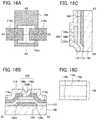
- FIGS. 16A to 16Dare a top view and cross-sectional views illustrating a semiconductor device of one embodiment of the present invention.
- FIGS. 17A to 17Care cross-sectional views illustrating a fabrication method of a semiconductor device of one embodiment of the present invention.
- FIGS. 18A and 18Bare cross-sectional views illustrating a fabrication method of a semiconductor device of one embodiment of the present invention.
- FIGS. 19A to 19Care a top view and cross-sectional views illustrating a semiconductor device of one embodiment of the present invention.
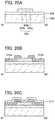
- FIGS. 20A to 20Care cross-sectional views illustrating a fabrication method of a semiconductor device of one embodiment of the present invention.
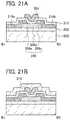
- FIGS. 21A and 21Bare cross-sectional views illustrating a fabrication method of a semiconductor device of one embodiment of the present invention.
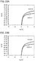
- FIGS. 22A and 22Beach show Vg-Id characteristics of a transistor.
- FIGS. 23A and 23Beach show results of a gate BT test.
- FIG. 24is a block diagram illustrating an example of a semiconductor device of one embodiment of the present invention.
- FIG. 25is a cross-sectional view illustrating an example of a semiconductor device of one embodiment of the present invention.
- FIGS. 26A to 26Care block diagrams illustrating an example of a semiconductor device of one embodiment of the present invention.
- FIGS. 27A to 27Ceach illustrate an example of an electronic device of one embodiment of the present invention.
- ordinal numbers such as “first” and “second” in this specificationare used for convenience and do not indicate the order of steps or the stacking order of layers.
- ordinal numbers in this specificationdo not indicate particular names which specify the present invention.
- a voltagerefers to a potential difference between a certain potential and a reference potential (e.g., a ground potential (GND) or a source potential). Accordingly, a voltage can also be called a potential.
- a reference potentiale.g., a ground potential (GND) or a source potential.
- a voltagecan also be called a potential.
- source and draincan be switched in this specification.
- a multi-layer film including an oxide semiconductor layer used for a transistoris described with reference to FIG. 1 .
- a multi-layer film 106 illustrated in FIG. 1includes an oxide layer 106 a , an oxide semiconductor layer 106 b over the oxide layer 106 a , and an oxide layer 106 c over the oxide semiconductor layer 106 b .
- the multi-layer film 106has three layers in the description below, the multi-layer film 106 may have two layers or four or more layers.
- the multi-layer film 106may be a two-layer film including the oxide layer 106 a and the oxide semiconductor layer 106 b over the oxide layer 106 a .
- the multi-layer film 106may be a two-layer film including the oxide semiconductor layer 106 b and the oxide layer 106 c over the oxide semiconductor layer 106 b.
- the oxide layer 106 awas formed by a sputtering method using an In—Ga—Zn oxide (the atomic ratio of In to Ga and Zn is 1:3:2) target. Note that an argon gas (flow rate: 30 sccm) and an oxygen gas (flow rate: 15 sccm) were used as a deposition gas, the pressure was set at 0.4 Pa, the substrate temperature was set at 200° C., and a DC power of 0.5 kW was applied.
- an argon gasflow rate: 30 sccm
- an oxygen gasflow rate: 15 sccm
- the oxide semiconductor layer 106 bwas formed by a sputtering method using an In—Ga—Zn oxide (the atomic ratio of In to Ga and Zn is 1:1:1) target. Note that an argon gas (flow rate: 30 sccm) and an oxygen gas (flow rate: 15 sccm) were used as a deposition gas, the pressure was set at 0.4 Pa, the substrate temperature was set at 300° C., and a DC power of 0.5 kW was applied.
- an argon gasflow rate: 30 sccm
- an oxygen gasflow rate: 15 sccm
- the oxide layer 106 cwas formed by a sputtering method using an In—Ga—Zn oxide (the atomic ratio of In to Ga and Zn is 1:3:2) target. Note that an argon gas (flow rate: 30 sccm) and an oxygen gas (flow rate: 15 sccm) were used as a deposition gas, the pressure was set at 0.4 Pa, the substrate temperature was set at 200° C., and a DC power of 0.5 kW was applied.
- an argon gasflow rate: 30 sccm
- an oxygen gasflow rate: 15 sccm
- the multi-layer film 106is provided over a silicon wafer, and a sample not subjected to heat treatment and a sample subjected to heat treatment at 450° C. for two hours are prepared.
- FIG. 2shows the secondary ion intensities of In, Ga, and Zn in a depth direction, and the silicon concentration (atoms/cm 3 ) in a depth direction, which is converted from the secondary ion intensity of SiO 3 , of the samples measured by ToF-SIMS (Time-of-flight secondary ion mass spectrometry).
- the multi-layer film 106includes the oxide layer 106 a having a thickness of 10 nm, the oxide semiconductor layer 106 b having a thickness of 10 nm over the oxide layer 106 a , and the oxide layer 106 c having a thickness of 10 nm over the oxide semiconductor layer 106 b.
- FIG. 2shows that the compositions of the layers included in the multi-layer film 106 are changed depending on the compositions of the respective targets used at the time of the film formation. Note that the compositions of the layers cannot be simply compared using FIG. 2 .
- FIG. 2indicates that the interface between the silicon wafer and the oxide layer 106 a of the multi-layer film 106 and the upper surface of the oxide layer 106 c have higher silicon concentrations. Moreover, FIG. 2 shows that the concentration of silicon in the oxide semiconductor layer 106 b is about 1 ⁇ 10 18 atoms/cm 3 which is the lower limit of detection by Tof-SIMS. This is probably because, owing to existence of the oxide layers 106 a and 106 c , the oxide semiconductor layer 106 b is not influenced by silicon due to the silicon wafer or the surface contamination.
- comparison of the sample after the heat treatment with an as-deposited sampleindicates that entry of silicon mainly occurs at the time of the film formation, though there is a small effect of silicon diffusion through the heat treatment.
- the carrier density of the oxide semiconductor layer 106 bcan be set to be lower than 1 ⁇ 10 17 /cm 3 , lower than 1 ⁇ 10 15 /cm 3 , or lower than 1 ⁇ 10 13 /cm 3 .
- hydrogen, nitrogen, carbon, silicon, and a metal element other than the main componentbecome an impurity.
- the concentration of impurities in the oxide semiconductor layer 106 bit is preferable to also reduce the concentration of impurities in the oxide layers 106 a and 106 c which are close to the oxide semiconductor layer 106 b to a value almost equal to that in the oxide semiconductor layer 106 b.
- the concentration of silicon in the oxide semiconductor layer 106 bcan be set to be lower than 1 ⁇ 10 19 atoms/cm 3 , preferably lower than 5 ⁇ 10 18 atoms/cm 3 , more preferably lower than 1 ⁇ 10 18 atoms/cm 3 .
- the concentrations of silicon at the interface between the oxide layer 106 a and the oxide semiconductor layer 106 b and the interface between the oxide semiconductor layer 106 b and the oxide layer 106 care each set to be lower than 1 ⁇ 10 19 atoms/cm 3 , preferably lower than 5 ⁇ 10 18 atoms/cm 3 , more preferably lower than 1 ⁇ 10 18 atoms/cm 3 .
- the concentration of hydrogen in the oxide semiconductor layer 106 bis set to be lower than or equal to 2 ⁇ 10 20 atoms/cm 3 , preferably lower than or equal to 5 ⁇ 10 19 atoms/cm 3 , more preferably lower than or equal to 1 ⁇ 10 19 atoms/cm 3 , still more preferably lower than or equal to 5 ⁇ 10 18 atoms/cm 3 .
- the concentration of nitrogen in the oxide semiconductor layer 106 bwhich is measured by SIMS, is set to be lower than 5 ⁇ 10 19 atoms/cm 3 , preferably lower than or equal to 5 ⁇ 10 18 atoms/cm 3 , more preferably lower than or equal to 1 ⁇ 10 18 atoms/cm 3 , further preferably lower than or equal to 5 ⁇ 10 17 atoms/cm 3 .
- the concentration of silicon in the oxide semiconductor layer 106 bcan be set to be lower than 1 ⁇ 10 19 atoms/cm 3 , preferably lower than 5 ⁇ 10 18 atoms/cm 3 , more preferably lower than 1 ⁇ 10 18 atoms/cm 3 .
- the concentration of carbon in the oxide semiconductor layer 106 bcan be set to be lower than 1 ⁇ 10 19 atoms/cm 3 , preferably lower than 5 ⁇ 10 18 atoms/cm 3 , more preferably lower than 1 ⁇ 10 18 atoms/cm 3 . Description of the crystallinity of the multi-layer film 106 will be made later.
- An oxygen vacancy in the oxide semiconductor layer and the oxide layerbehaves in some cases like an impurity.
- diffusion of oxygen in the multi-layer film 106 through heat treatment at 350° C. or heat treatment at 450° C.is described with reference to FIGS. 3A to 3C .
- FIGS. 3A to 3Ceach show SIMS measurement results of concentration distribution of 18 O in a depth direction in samples in which any of the layers of the multi-layer film 106 is formed using an 18 O 2 gas.
- the oxide layer 106 ais formed by a sputtering method using an In—Ga—Zn oxide (the atomic ratio of In to Ga and Zn is 1:1:1) target.
- the oxide semiconductor layer 106 bis formed by a sputtering method using an In—Ga—Zn oxide (the atomic ratio of In to Ga and Zn is 3:1:2) target.
- the oxide layer 106 cis formed by a sputtering method using an In—Ga—Zn oxide (the atomic ratio of In to Ga and Zn is 1:1:1) target.
- FIG. 3Ashows 18 O concentration distributions in a depth direction of the oxide layer 106 a , the oxide semiconductor layer 106 b , and the interface therebetween of samples in each of which an 18 O 2 gas is used for forming the oxide layer 106 a but an 18 O 2 gas is not used for forming the other layers.
- the SIMS measurement resultsshow as follows: 18 O is more diffused from the oxide layer 106 a to the oxide semiconductor layer 106 b in a sample subjected to the heat treatment at 350° C. (shown as “after heat treatment at 350° C.” with a solid line) and a sample subjected to the heat treatment at 450° C. (shown as “after heat treatment at 450° C.” with a broken line) than in a sample not subjected to heat treatment (shown as “as-depo” with a dotted line).
- FIG. 3Bshows 18 O concentration distributions in a depth direction of the oxide semiconductor layer 106 b , the oxide layer 106 c , and the interface therebetween of samples in each of which an 18 O 2 gas is used for forming the oxide semiconductor layer 106 b but an 18 O 2 gas is not used for forming the other layers.
- the SIMS measurement resultsshow as follows: 18 O is more diffused from the oxide semiconductor layer 106 b to the oxide layer 106 c in a sample subjected to the heat treatment at 350° C. (shown as “after heat treatment at 350° C.” with a solid line) and a sample subjected to the heat treatment at 450° C. (shown as “after heat treatment at 450° C.” with a broken line) than in a sample not subjected to heat treatment (shown as “as-depo” with a dotted line).
- FIG. 3Cshows 18 O concentration distributions in a depth direction of the oxide layer 106 a , the oxide semiconductor layer 106 b , and the interface therebetween of samples in each of which an 18 O 2 gas is used for forming the oxide semiconductor layer 106 b but an 18 O 2 gas is not used for forming the other layers.
- the SIMS measurement resultsshow as follows: 18 O is more diffused from the oxide semiconductor layer 106 b to the oxide layer 106 a in a sample subjected to the heat treatment at 450° C.
- oxygenis diffused from one layer to the other layer.
- an oxide layer applicable to each of the oxide layers 106 a and 106 c used in the multi-layer film 106was formed by a sputtering method, and the number of particles with a size of 1 ⁇ m or more was measured.
- the measurementwas performed on the following samples: a sample formed using a gallium oxide target; a sample formed using a Ga—Zn oxide (the atomic ratio of Ga to Zn is 2:5) target; a sample formed using an In—Ga—Zn oxide (the atomic ratio of In to Ga and Zn is 3:1:2) target; a sample formed using an In—Ga—Zn oxide (the atomic ratio of In to Ga and Zn is 1:1:1) target; and a sample formed using an In—Ga—Zn oxide (the atomic ratio of In to Ga and Zn is 1:3:2) target.
- FIG. 4shows that in the sample formed using a gallium oxide target and the sample formed using a Ga—Zn oxide target, the number of particles with a size of 1 ⁇ m or more is rapidly increased as the thickness of the oxide layer is increased.
- the samples formed using an In—Ga—Zn oxide targetthe number of particles with a size of 1 ⁇ m or more is unlikely to be rapidly increased even when the thickness of the oxide layer is increased.
- a target containing indiumis preferably used in terms of an increase in the number of particles.
- the conductivity of the targetcan be increased and DC discharge and AC discharge are facilitated; therefore, film formation over a large-sized substrate can be easily performed.
- semiconductor devicescan be manufactured with improved productivity.
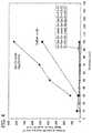
- the band structure of the multi-layer film 106is described with reference to FIGS. 5A and 5B and FIGS. 6A and 6B .
- the oxide layer 106 awas formed using an In—Ga—Zn oxide having an energy gap of 3.15 eV
- the oxide semiconductor layer 106 bwas formed using an In—Ga—Zn oxide having an energy gap of 2.8 eV
- the oxide layer 106 cwas formed using an oxide layer whose physical properties are similar to those of the oxide layer 106 a .
- the energy gap in the vicinity of the interface between the oxide layer 106 a and the oxide semiconductor layer 106 b and the energy gap in the vicinity of the interface between the oxide layer 106 c and the oxide semiconductor layer 106 bwere each 3 eV.
- the energy gapswere measured using a spectroscopic ellipsometer (UT-300 manufactured by HORIBA JOBIN YVON SAS.).
- the thicknesses of the oxide layer 106 a , the oxide semiconductor layer 106 b , and the oxide layer 106 cwere each 10 nm.
- the energy gap between a vacuum level and a top of a valence band of each layerwas measured while the multi-layer film 106 was etched from the oxide layer 106 c side, and was plotted.
- the energy gap between the vacuum level and the top of the valence bandwas measured using an ultraviolet photoelectron spectroscopy (UPS) device (VersaProbe manufactured by ULVAC-PHI, Inc.).
- UPSultraviolet photoelectron spectroscopy
- FIG. 5Ba value obtained in such a manner that an energy gap between the vacuum level and a bottom of a conduction band of each layer was calculated by subtracting the energy gap of each layer from the energy gap between the vacuum level and the top of the valence band, and was plotted.
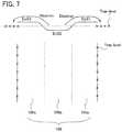
- FIG. 6Ashows the case where silicon oxide films are provided in contact with the oxide layers 106 a and 106 c .
- EcI 1denotes the energy of the bottom of the conduction band of the silicon oxide film
- EcS 1denotes the energy of the bottom of the conduction band of the oxide layer 106 a
- EcS 2denotes the energy of the bottom of the conduction band of the oxide semiconductor layer 106 b
- EcS 3denotes the energy of the bottom of the conduction band of the oxide layer 106 c
- EcI 2denotes the energy of the bottom of the conduction band of the silicon oxide film.
- the energies of the bottoms of the conduction bands of the oxide layer 106 a , the oxide semiconductor layer 106 b , and the oxide layer 106 care changed continuously. This can be understood also from the results shown in FIGS. 3A to 3C that oxygen is diffused at the interface between the oxide layer 106 a and the oxide semiconductor layer 106 b and at the interface between the oxide semiconductor layer 106 b and the oxide layer 106 c.
- FIG. 6Ashows the case where the oxide layers 106 a and 106 c have similar physical properties; however, the oxide layers 106 a and 106 c may have different physical properties.
- part of the band structure in the case where EcS 1 has a higher energy than EcS 3is shown as in FIG. 6B .
- EcS 3may have a higher energy than EcS 1 .
- the oxide semiconductor layer 106 b of the multi-layer film 106serves as a well and a channel of the transistor including the multi-layer film 106 is formed in the oxide semiconductor layer 106 b .
- the multi-layer film 106can also be referred to as a U-shaped well.
- the oxide semiconductor layer 106 bcan be distanced away from the trap levels owing to existence of the oxide layers 106 a and 106 c .
- the energy gap between EcS 1 or EcS 3 , and EcS 2is small, an electron might reach the trap level by passing over the energy gap. By being trapped in the trap level, a negative fixed charge is caused at the interface with the insulating film, whereby the threshold voltage of the transistor is shifted in the positive direction.
- the energy gap between EcS 1 and EcS 2 and the energy gap between EcS 3 and EcS 2are each preferably greater than or equal to 0.1 eV, more preferably greater than or equal to 0.15 eV because the amount of change of the threshold voltage of the transistor is reduced and the transistor has stable electrical characteristics.
- the oxide semiconductor layer 106 b of the multi-layer film 106have crystallinity.
- the transistor including the multi-layer film 106can have stable electrical characteristics as compared to the case of the oxide semiconductor layer 106 b without crystallinity.
- this sectionan example in which the oxide semiconductor layer 106 b has crystallinity in the multi-layer film 106 is described.
- the oxide layer 106 awas formed by a sputtering method using an In—Ga—Zn oxide (the atomic ratio of In to Ga and Zn is 1:3:2) target. Note that an argon gas (flow rate: 30 sccm) and an oxygen gas (flow rate: 15 sccm) were used as a deposition gas, the pressure was set at 0.4 Pa, the substrate temperature was set at 200° C., and a DC power of 0.5 kW was applied.
- an argon gasflow rate: 30 sccm
- an oxygen gasflow rate: 15 sccm
- the oxide semiconductor layer 106 bwas formed by a sputtering method using an In—Ga—Zn oxide (the atomic ratio of In to Ga and Zn is 1:1:1) target. Note that an argon gas (flow rate: 30 sccm) and an oxygen gas (flow rate: 15 sccm) were used as a deposition gas, the pressure was set at 0.4 Pa, the substrate temperature was set at 300° C. or 400° C., and a DC power of 0.5 kW was applied.
- an argon gasflow rate: 30 sccm
- an oxygen gasflow rate: 15 sccm
- the oxide layer 106 cwas formed by a sputtering method using an In—Ga—Zn oxide (the atomic ratio of In to Ga and Zn is 1:3:2) target. Note that an argon gas (flow rate: 30 sccm) and an oxygen gas (flow rate: 15 sccm) were used as a deposition gas, the pressure was set at 0.4 Pa, the substrate temperature was set at 200° C., and a DC power of 0.5 kW was applied.
- an argon gasflow rate: 30 sccm
- an oxygen gasflow rate: 15 sccm
- FIGS. 8A to 8D and FIGS. 9A to 9Dare transmission electron images of samples each including the multi-layer film 106 provided over a silicon oxide film provided over a silicon wafer which is the substrate. Note that the evaluated samples shown in FIGS. 8A to 8D and the evaluated samples in FIGS. 9A to 9D are different from each other only in that the temperatures of the substrate at the time of the formation of the oxide semiconductor layer 106 b are 300° C. ( FIGS. 8A to 8D ) and 400° C. ( FIGS. 9A to 9D ). Note that each sample was not subjected to heat treatment after the film formation. The transmission electron images were measured using Hitachi H-9500 transmission electron microscope (TEM).
- TEMHitachi H-9500 transmission electron microscope
- the multi-layer film 106includes an In—Ga—Zn oxide having a thickness of 20 nm as the oxide layer 106 a , an In—Ga—Zn oxide having a thickness of 15 nm as the oxide semiconductor layer 106 b , and an In—Ga—Zn oxide having a thickness of 5 nm as the oxide layer 106 c .
- FIG. 8Ais a transmission electron image including the oxide layer 106 a , the oxide semiconductor layer 106 b , and the oxide layer 106 c .
- FIG. 8Bis an enlarged image of a portion in the vicinity of the interface between the oxide semiconductor layer 106 b and the oxide layer 106 c , FIG.
- FIG. 8Cis an enlarged image of a portion in the vicinity of the interface between the oxide layer 106 a and the oxide semiconductor layer 106 b
- FIG. 8Dis an enlarged image of a portion in the vicinity of the interface between the silicon oxide film and the oxide layer 106 a
- FIG. 9Ais a transmission electron image including the oxide layer 106 a , the oxide semiconductor layer 106 b , and the oxide layer 106 c
- FIG. 9Bis an enlarged image of a portion in the vicinity of the interface between the oxide semiconductor layer 106 b and the oxide layer 106 c
- FIG. 9Ais a transmission electron image including the oxide layer 106 a , the oxide semiconductor layer 106 b , and the oxide layer 106 c
- FIG. 9Bis an enlarged image of a portion in the vicinity of the interface between the oxide semiconductor layer 106 b and the oxide layer 106 c
- FIG. 9Cis an enlarged image of a portion in the vicinity of the interface between the oxide layer 106 a and the oxide semiconductor layer 106 b
- FIG. 9Dis an enlarged image of a portion in the vicinity of the interface between the silicon oxide film and the oxide layer 106 a.
- the oxide layers 106 a and 106 cdid not have a clear crystal part. Further, the oxide semiconductor layer 106 b was entirely crystalline with a high degree of crystallinity from the interface with the oxide layer 106 a to the interface with the oxide layer 106 c . Note that the atomic arrangement in the crystal part of the oxide semiconductor layer 106 b was found to be in a layered manner in a plane parallel to the upper surface of the oxide semiconductor layer 106 b . Moreover, a clear grain boundary was not seen between crystal parts in the oxide semiconductor layer 106 b . Further, it was found that the oxide semiconductor layer 106 b in FIGS. 9A to 9D had a higher degree of crystallinity than the oxide semiconductor layer 106 b in FIGS. 8A to 8D .
- the oxide semiconductor layer 106 bwas crystalline is also compatible with the ToF-SIMS results shown in FIG. 2 . That is, the crystallinity of the oxide semiconductor layer 106 b was not lowered probably because entry of silicon into the oxide semiconductor layer 106 b was reduced owing to existence of the oxide layers 106 a and 106 c.
- the oxide semiconductor layer 106 b where a channel is formedhas a high degree of crystallinity and there are few levels due to impurities or defects; therefore, the transistor including the multi-layer film 106 has stable electrical characteristics.
- FIGS. 10A and 10Bthe model of crystal growth in the oxide semiconductor layer 106 b with a high degree of crystallinity is described with reference to FIGS. 10A and 10B , FIGS. 11A and 11B , and FIGS. 12A and 12B .
- FIG. 10Ais a schematic diagram illustrating a state in which an ion 1001 collides with a target 1000 containing a polycrystalline oxide semiconductor having high alignment to separate sputtered particles 1002 with crystallinity from the sputtering target 1000 .
- a crystal grainhas a cleavage plane parallel to a surface of the target 1000 .
- the crystal grainhas a portion where an interatomic bond is weak.
- an interatomic bond of the portion where an interatomic bond is weakis cut. Accordingly, the sputtered particle 1002 which is cut along the cleavage plane and the portion where an interatomic bond is weak and separated in a flat-plate (or pellet) form is generated.
- the equivalent circle diameter of a flat plane of the sputtered particle 1002is greater than or equal to 1/3000 and less than or equal to 1/20, preferably greater than or equal to 1/1000 and less than or equal to 1/30 of an average grain size of the crystal grains.
- the term “equivalent circle diameter of a plane”refers to the diameter of a perfect circle having the same area as the plane.
- an oxygen cationas the ion 1001 , plasma damage at the time of the film formation can be alleviated.
- a lowering in crystallinity of the target 1000can be suppressed or a change of the target 1000 into an amorphous state can be suppressed.
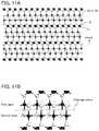
- FIG. 11Aillustrates a crystal structure of an In—Ga—Zn oxide viewed from a direction parallel to an a-b plane of the crystal as an example of the target 1000 containing a polycrystalline oxide semiconductor with a high orientation.
- FIG. 11Billustrates an enlarged view of a portion surrounded by a dashed line in FIG. 11A .
- a cleavage planeis a plane between a first layer and a second layer as illustrated in FIG. 11B .
- the first layerincludes a gallium atom and/or zinc atom and an oxygen atom
- the second layerincludes a gallium atom and/or zinc atom and an oxygen atom.
- oxygen atoms having negative charge in the first layer and oxygen atoms having negative charge in the second layerare close to each other (see surrounded portions in FIG. 11B ).
- the cleavage planeis parallel to the a-b plane.
- the crystal of the In—Ga—Zn oxide shown in FIGS. 11A and 11Bis a hexagonal crystal; thus, the flat plate-like crystal grain is likely to have a hexagonal prism shape with a regular hexagonal plane whose internal angle is 120°.
- the separated sputtered particles 1002be positively charged.
- the sputtered particle 1002is positively charged by receiving an electric charge when the ion 1001 collides.
- the sputtered particle 1002is preferably exposed to plasma to be positively charged.
- the ion 1001 which is an oxygen cationis preferably bonded to a side surface, a top surface, or a bottom surface of the sputtered particle 1002 , whereby the sputtered particle 1002 is positively charged.
- FIGS. 12A and 12BA state in which sputtered particles are deposited on a deposition surface is described below with reference to FIGS. 12A and 12B . Note that in FIGS. 12A and 12B , sputtered particles which have been already deposited are shown by dotted lines.
- a deposition surface 1003is a surface where several oxide semiconductor layers are deposited. As illustrated in FIG. 12A , in the case where the sputtered particles 1002 are positively charged, the sputtered particles 1002 are deposited in a region of the deposition surface 1003 , where no sputtered particle 1002 has been deposited yet. This is because the sputtered particles 1002 which are positively charged repel with each other.
- FIG. 12Bis a cross-sectional view taken along dashed-dotted line X-Y in FIG. 12A .
- the sputtered particles 1002 which are deposited in the above mannerhave crystals whose c-axes are aligned in a direction perpendicular to the deposition surface 1003 ; accordingly, the oxide semiconductor layer 106 b is a c-axis aligned crystalline oxide semiconductor (CAAC-OS) layer.
- CAAC-OSc-axis aligned crystalline oxide semiconductor
- An oxide semiconductor layer which is obtained by deposition in the above mannerhas a uniform thickness and a uniform crystal orientation.
- the sputtered particlesare not deposited randomly.
- the sputtered particles which are positively chargedinteract with each other and are deposited orderly so that c-axes are aligned in a direction perpendicular to the deposition surface.
- the oxide semiconductor layer 106 b having a uniform thickness and a uniform crystal orientationcan be formed.
- the details of a sputtering apparatuswill be described later.
- the CAAC-OS layeris one of oxide semiconductor films including a plurality of crystal parts, and most of the crystal part each fits inside a cube whose one side is less than 100 nm. Thus, there is a case where a crystal part included in the CAAC-OS layer fits inside a cube whose one side is less than 10 nm, less than 5 nm, or less than 3 nm. The density of defect states of the CAAC-OS layer is low.
- the CAAC-OS layeris described in detail below.
- metal atomsare arranged in a layered manner in the crystal parts.
- Each metal atom layerhas a morphology reflected by a surface over which the CAAC-OS layer is formed (hereinafter, a surface over which the CAAC-OS layer is formed is referred to as a formation surface) or a top surface of the CAAC-OS layer, and is arranged in parallel to the formation surface or the top surface of the CAAC-OS layer.
- metal atomsare arranged in a triangular or hexagonal configuration in the crystal parts.
- plane TEM imagethere is no regularity of arrangement of metal atoms between different crystal parts.
- a CAAC-OS layeris subjected to structural analysis with an X-ray diffraction (XRD) apparatus.
- XRDX-ray diffraction
- each metal atom layer arranged in a layered manner observed in the cross-sectional TEM imagecorresponds to a plane parallel to the a-b plane of the crystal.
- the crystal partis formed concurrently with deposition of the CAAC-OS layer or is formed through crystallization treatment such as heat treatment.
- the c-axis of the crystalis aligned in a direction parallel to a normal vector of a formation surface or a normal vector of a top surface.
- the c-axismight not be necessarily parallel to a normal vector of a formation surface or a normal vector of a top surface of the CAAC-OS layer.
- the degree of crystallinity in the CAAC-OS layeris not necessarily uniform.
- the degree of the crystallinity in the vicinity of the top surfaceis higher than that in the vicinity of the formation surface in some cases.
- the crystallinity in a region to which the impurity is addedis changed, and the degree of crystallinity in the CAAC-OS layer varies depending on regions.
- a peak of 2 ⁇may also be observed at around 36°, in addition to the peak of 2 ⁇ at around 31°.
- the peak of 2 ⁇ at around 36°indicates that a crystal having no c-axis alignment is included in part of the CAAC-OS layer. It is preferable that in the CAAC-OS layer, a peak of 2 ⁇ appears at around 31° and a peak of 2 ⁇ do not appear at around 36°.
- the transistorIn a transistor using the CAAC-OS layer, change in electrical characteristics due to irradiation with visible light or ultraviolet light is small. Thus, the transistor has high reliability.
- the transistor including the multi-layer film 106can have stable electrical characteristics.
- the density of the localized level of the multi-layer film 106was measured by a constant photocurrent method (CPM).
- the absorption coefficient due to the localized level of the multi-layer film 106 measured by CPMis preferably lower than 1 ⁇ 10 ⁇ 3 cm ⁇ 1 , more preferably lower than 3 ⁇ 10 ⁇ 4 cm ⁇ 1 .
- the oxide layer 106 awas formed by a sputtering method using an In—Ga—Zn oxide (the atomic ratio of In to Ga and Zn is 1:3:2) target. Note that an argon gas (flow rate: 30 sccm) and an oxygen gas (flow rate: 15 sccm) were used as a deposition gas, the pressure was set at 0.4 Pa, the substrate temperature was set at 200° C., and a DC power of 0.5 kW was applied.
- an argon gasflow rate: 30 sccm
- an oxygen gasflow rate: 15 sccm
- the oxide semiconductor layer 106 bwas formed by a sputtering method using an In—Ga—Zn oxide (the atomic ratio of In to Ga and Zn is 1:1:1) target. Note that an argon gas (flow rate: 30 sccm) and an oxygen gas (flow rate: 15 sccm) were used as a deposition gas, the pressure was set at 0.4 Pa, the substrate temperature was set at 200° C., and a DC power of 0.5 kW was applied.
- an argon gasflow rate: 30 sccm
- an oxygen gasflow rate: 15 sccm
- the oxide layer 106 cwas formed by a sputtering method using an In—Ga—Zn oxide (the atomic ratio of In to Ga and Zn is 1:3:2) target. Note that an argon gas (flow rate: 30 sccm) and an oxygen gas (flow rate: 15 sccm) were used as a deposition gas, the pressure was set at 0.4 Pa, the substrate temperature was set at 200° C., and a DC power of 0.5 kW was applied.
- an argon gasflow rate: 30 sccm
- an oxygen gasflow rate: 15 sccm
- the multi-layer film 106needs to have a certain thickness. Specifically, the thicknesses of the oxide layer 106 a , the oxide semiconductor layer 106 b , and the oxide layer 106 c which are included in the multi-layer film 106 were set at 30 nm, 100 nm, and 30 nm, respectively.
- the amount of light with which a surface of the sample between terminals is irradiatedis adjusted so that a photocurrent value is kept constant in the state where voltage is applied between a first electrode and a second electrode provided in contact with the multi-layer film 106 that is the sample, and then an absorption coefficient is derived from the amount of the irradiation light at each wavelength.
- the absorption coefficient due to the energy which corresponds to the level at which the defect existsis increased.
- the increase in the absorption coefficientis multiplied by a constant, whereby the defect density of the sample can be obtained.
- FIG. 13Ashows results of fitting the absorption coefficient (broken line) measured using a spectrophotometer and the absorption coefficient (solid line) measured by CPM in the range of energy higher than or equal to the energy gap of each layer in the multi-layer film 106 .
- the Urbach energy obtained based on the absorption coefficient measured by CPMwas 78.7 meV.
- the integral value of the absorption coefficient in the energy rangewas derived in such a manner that a background (dotted line) was subtracted from the absorption coefficient measured by CPM in the energy range shown with a dashed-line circle in FIG. 13A (see FIG. 13B ).
- the absorption coefficient due to the localized level of this samplewas found to be 2.02 ⁇ 10 ⁇ 4 cm ⁇ 1 .
- the localized level obtained hereis probably due to an impurity or a defect. From the above, there are extremely few levels due to an impurity or a defect in the multi-layer film 106 . That is, the transistor including the multi-layer film 106 has stable electrical characteristics.
- a film formation apparatus for forming the oxide semiconductor layer 106 b with a high degree of crystallinitywill be described below.
- FIG. 14is a top view schematically illustrating a single wafer multi-chamber film formation apparatus 4000 .
- the film formation apparatus 4000includes an atmosphere-side substrate supply chamber 4001 including a cassette port 4101 for holding a substrate and an alignment port 4102 for performing alignment of a substrate, an atmosphere-side substrate transfer chamber 4002 through which a substrate is transferred from the atmosphere-side substrate supply chamber 4001 , a load lock chamber 4003 a where a substrate is carried and the pressure inside the chamber is switched from atmospheric pressure to reduced pressure or from reduced pressure to atmospheric pressure, an unload lock chamber 4003 b where a substrate is carried out and the pressure inside the chamber is switched from reduced pressure to atmospheric pressure or from atmospheric pressure to reduced pressure, a transfer chamber 4004 through which a substrate is transferred in a vacuum, a substrate heating chamber 4005 where a substrate is heated, and film formation chambers 4006 a , 4006 b , and 4006 c in each of which a target is placed for film formation.
- cassette ports 4101may be provided as illustrated in FIG. 14 (in FIG. 14 , three cassette ports 4101 are provided).
- the atmosphere-side substrate transfer chamber 4002is connected to the load lock chamber 4003 a and the unload lock chamber 4003 b , the load lock chamber 4003 a and the unload lock chamber 4003 b are connected to the transfer chamber 4004 , and the transfer chamber 4004 is connected to the substrate heating chamber 4005 and the film formation chambers 4006 a , 4006 b , and 4006 c.
- Gate valves 4104are provided for connecting portions between chambers so that each chamber except the atmosphere-side substrate supply chamber 4001 and the atmosphere-side substrate transfer chamber 4002 can be independently kept under vacuum. Moreover, the atmosphere-side substrate transfer chamber 4002 and the transfer chamber 4004 each include a transfer robot 4103 , with which a glass substrate can be transferred.
- the substrate heating chamber 4005also serve as a plasma treatment chamber.
- the film formation apparatus 4000it is possible to transfer a substrate without exposure to the air between treatment and treatment; therefore, adsorption of impurities on a substrate can be suppressed.
- the order of film formation, heat treatment, or the likecan be freely determined. Note that the number of the transfer chambers, the number of the film formation chambers, the number of the load lock chambers, the number of the unload lock chambers, and the number of the substrate heating chambers are not limited to the above, and the numbers thereof can be set as appropriate depending on the space for placement or the process conditions.
- FIG. 15A , FIG. 15B , and FIG. 15Care a cross-sectional view taken along dashed-dotted line X 1 -X 2 , a cross-sectional view taken along dashed-dotted line Y 1 -Y 2 , and a cross-sectional view taken along dashed-dotted line Y 2 -Y 3 , respectively, in the film formation apparatus 4000 illustrated in FIG. 14 .
- FIG. 15Ais a cross section of the substrate heating chamber 4005 and the transfer chamber 4004 , and the substrate heating chamber 4005 includes a plurality of heating stages 4105 which can hold a substrate. Note that although the number of heating stages 4105 illustrated in FIG. 15A is seven, it is not limited thereto and may be greater than or equal to one and less than seven, or greater than or equal to eight. It is preferable to increase the number of the heating stages 4105 because a plurality of substrates can be subjected to heat treatment at the same time, which leads to an increase in productivity. Further, the substrate heating chamber 4005 is connected to a vacuum pump 4200 through a valve. As the vacuum pump 4200 , a dry pump and a mechanical booster pump can be used, for example.
- a vacuum pump 4200As the vacuum pump 4200 , a dry pump and a mechanical booster pump can be used, for example.
- a resistance heatermay be used for heating, for example.
- heat conduction or heat radiation from a medium such as a heated gasmay be used as the heating mechanism.
- a rapid thermal annealing (RTA) apparatussuch as a gas rapid thermal annealing (GRTA) apparatus or a lamp rapid thermal annealing (LRTA) apparatus can be used.
- the LRTA apparatusis an apparatus for heating an object by radiation of light (an electromagnetic wave) emitted from a lamp such as a halogen lamp, a metal halide lamp, a xenon arc lamp, a carbon arc lamp, a high-pressure sodium lamp, or a high-pressure mercury lamp.
- heat treatmentis performed using a high-temperature gas.
- An inert gasis used as the gas.
- the substrate heating chamber 4005is connected to a refiner 4301 through a mass flow controller 4300 .
- the mass flow controller 4300 and the refiner 4301can be provided for each of a plurality of kinds of gases, only one mass flow controller 4300 and one refiner 4301 are provided for easy understanding.
- a gas whose dew point is ⁇ 80° C. or lower, preferably ⁇ 100° C. or lowercan be used; for example, an oxygen gas, a nitrogen gas, and a rare gas (e.g., an argon gas) are used.
- the transfer chamber 4004includes the transfer robot 4103 .
- the transfer robot 4103includes a plurality of movable portions and an arm for holding a substrate and can transfer a substrate to each chamber.
- the transfer chamber 4004is connected to a vacuum pump 4200 and a cryopump 4201 through valves.
- evacuationcan be performed using the vacuum pump 4200 when the pressure inside the transfer chamber 4004 is in the range of atmospheric pressure to a low vacuum (about 0.1 Pa to several hundred Pa) and then, by switching the valves, evacuation can be performed using the cryopump 4201 when the pressure inside the transfer chamber 4004 is in the range of middle vacuum to ultra-high vacuum (0.1 Pa to 1 ⁇ 10 ⁇ 7 Pa).
- cryopumps 4201may be connected in parallel to the transfer chamber 4004 .
- evacuationcan be performed using any of the other cryopumps.
- the above regenerationrefers to treatment for discharging molecules (or atoms) entrapped in the cryopump.
- molecules (or atoms)are entrapped too much in a cryopump, the evacuation capability of the cryopump is lowered; therefore, regeneration is performed regularly.
- FIG. 15Bis a cross section of the film formation chamber 4006 b , the transfer chamber 4004 , and the load lock chamber 4003 a.
- the film formation chamber 4006 b illustrated in FIG. 15Bincludes a target 4106 , an attachment protection plate 4107 , and a substrate stage 4108 .
- a substrate 4109is provided on the substrate stage 4108 .
- the substrate stage 4108may include a substrate holding mechanism which holds the substrate 4109 , a rear heater which heats the substrate 4109 from the back surface, or the like.
- the substrate stage 4108is held substantially vertically to a floor during film formation and is held substantially parallel to the floor when the substrate is delivered.
- the position where the substrate stage 4108 is held when the substrate is deliveredis denoted by a dashed line.
- the attachment protection plate 4107can suppress deposition of a particle which is sputtered from the target 4106 on a region where deposition is not needed. Moreover, the attachment protection plate 4107 is preferably processed to prevent accumulated sputtered particles from being separated. For example, blasting treatment which increases surface roughness may be performed, or roughness may be formed on the surface of the attachment protection plate 4107 .
- the film formation chamber 4006 bis connected to a mass flow controller 4300 through a gas heating system 4302 , and the gas heating system 4302 is connected to a refiner 4301 through the mass flow controller 4300 .
- a gas which is introduced to the film formation chamber 4006 bcan be heated to a temperature higher than or equal to 40° C. and lower than or equal to 400° C., preferably higher than or equal to 50° C. and lower than or equal to 200° C.
- the gas heating system 4302 , the mass flow controller 4300 , and the refiner 4301can be provided for each of a plurality of kinds of gases, only one gas heating system 4302 , one mass flow controller 4300 , and one refiner 4301 are provided for easy understanding.
- a gas whose dew point is ⁇ 80° C. or lower, preferably ⁇ 100° C. or lowercan be used; for example, an oxygen gas, a nitrogen gas, and a rare gas (e.g., an argon gas) are used.
- a facing-target-type sputtering apparatusmay be provided in the film formation chamber 4006 b .
- plasmais confined between the targets; therefore, plasma damage to a substrate can be reduced. Further, step coverage can be improved because an incident angle of a sputtered particle to the substrate can be made smaller depending on the inclination of the target.
- a parallel plate type sputtering apparatus or an ion beam sputtering apparatusmay be provided in the film formation chamber 4006 b.
- the length of a pipe between the refiner and the film formation chamber 4006 bis less than or equal to 10 m, preferably less than or equal to 5 m, more preferably less than or equal to 1 m.
- the length of the pipeis less than or equal to 10 m, less than or equal to 5 m, or less than or equal to 1 m, the effect of the release of gas from the pipe can be reduced accordingly.
- a metal pipethe inside of which is covered with iron fluoride, aluminum oxide, chromium oxide, or the like can be used.
- the amount of released gas containing impuritiesis made small and the entry of impurities into the gas can be reduced as compared with a SUS316L-EP pipe, for example.
- a high-performance ultra-compact metal gasket jointmay be used as a joint of the pipe.
- a structure where all the materials of the pipe are metalsis preferable because the effect of the generated released gas or the external leakage can be reduced as compared with a structure where resin or the like is used.
- the film formation chamber 4006 bis connected to a turbo molecular pump 4202 and a vacuum pump 4200 through valves.
- the film formation chamber 4006 bis provided with a cryotrap 4110 .
- the cryotrap 4110is a mechanism which can adsorb a molecule (or an atom) having a relatively high melting point, such as water.
- the turbo molecular pump 4202is capable of stably evacuating a large-sized molecule (or atom), needs low frequency of maintenance, and thus enables high productivity, whereas it has a low capability in evacuating hydrogen and water.
- the cryotrap 4110is connected to the film formation chamber 4006 b so as to have a high capability in evacuating water or the like.
- the temperature of a refrigerator of the cryotrap 4110is set to be lower than or equal to 100 K, preferably lower than or equal to 80 K.
- the cryotrap 4110includes a plurality of refrigerators
- the temperature of a first-stage refrigeratormay be set to be lower than or equal to 100 K and the temperature of a second-stage refrigerator may be set to be lower than or equal to 20 K.
- the evacuation method of the film formation chamber 4006 bis not limited to the above, and a structure similar to that in the evacuation method described in the transfer chamber 4004 (the evacuation method using the cryopump and the vacuum pump) may be employed. Needless to say, the evacuation method of the transfer chamber 4004 may have a structure similar to that of the film formation chamber 4006 b (the evacuation method using the turbo molecular pump and the vacuum pump).
- the back pressure (total pressure) and the partial pressure of each gas molecule (atom)are preferably set as follows.
- the back pressure and the partial pressure of each gas molecule (atom) in the film formation chamber 4006 bneed to be noted because impurities might enter a film to be formed.
- the back pressureis less than or equal to 1 ⁇ 10 ⁇ 4 Pa, preferably less than or equal to 3 ⁇ 10 ⁇ 5 Pa, more preferably less than or equal to 1 ⁇ 10 ⁇ 5 Pa.
- the partial pressure of a gas molecule (atom) having a mass-to-charge ratio (m/z) of 18is less than or equal to 3 ⁇ 10 ⁇ 5 Pa, preferably less than or equal to 1 ⁇ 10 ⁇ 5 Pa, more preferably less than or equal to 3 ⁇ 10 ⁇ 6 Pa.
- the partial pressure of a gas molecule (atom) having a mass-to-charge ratio (m/z) of 28is less than or equal to 3 ⁇ 10 ⁇ 5 Pa, preferably less than or equal to 1 ⁇ 10 ⁇ 5 Pa, more preferably less than or equal to 3 ⁇ 10 ⁇ 6 Pa.
- the partial pressure of a gas molecule (atom) having a mass-to-charge ratio (m/z) of 44is less than or equal to 3 ⁇ 10 ⁇ 5 Pa, preferably less than or equal to 1 ⁇ 10 ⁇ 5 Pa, more preferably less than or equal to 3 ⁇ 10 ⁇ 6 Pa.
- a total pressure and a partial pressure in a vacuum chambercan be measured using a mass analyzer.
- a mass analyzerfor example, Qulee CGM-051, a quadrupole mass analyzer (also referred to as Q-mass) manufactured by ULVAC, Inc. may be used.
- the above transfer chamber 4004 , the substrate heating chamber 4005 , and the film formation chamber 4006 bpreferably have a small amount of external leakage or internal leakage.
- the leakage rateis less than or equal to 3 ⁇ 10 ⁇ 6 Pa ⁇ m 3 /s, preferably less than or equal to 1 ⁇ 10 ⁇ 6 Pa ⁇ m 3 /s.
- the leakage rate of a gas molecule (atom) having a mass-to-charge ratio (m/z) of 18is less than or equal to 1 ⁇ 10 ⁇ 7 Pa ⁇ m 3 /s, preferably less than or equal to 3 ⁇ 10 ⁇ 8 Pa ⁇ m 3 /s.
- the leakage rate of a gas molecule (atom) having a mass-to-charge ratio (m/z) of 28is less than or equal to 1 ⁇ 10 ⁇ 5 Pa ⁇ m 3 /s, preferably less than or equal to 1 ⁇ 10 ⁇ 6 Pa ⁇ m 3 /s.
- the leakage rate of a gas molecule (atom) having a mass-to-charge ratio (m/z) of 44is less than or equal to 3 ⁇ 10 ⁇ 6 Pa ⁇ m 3 /s, preferably less than or equal to 1 ⁇ 10 ⁇ 6 Pa ⁇ m 3 /s.
- a leakage ratecan be derived from the total pressure and partial pressure measured using the mass analyzer.
- the leakage ratedepends on external leakage and internal leakage.
- the external leakagerefers to inflow of gas from the outside of a vacuum system through a minute hole, a sealing defect, or the like.
- the internal leakageis due to leakage through a partition, such as a valve, in a vacuum system or due to released gas from an internal member. Measures need to be taken from both aspects of external leakage and internal leakage in order that the leakage rate is set to be less than or equal to the above value.
- an open/close portion of the film formation chamber 4006 bcan be sealed with a metal gasket.
- metal gasketmetal covered with iron fluoride, aluminum oxide, or chromium oxide is preferably used.
- the metal gasketrealizes higher adhesion than an O-ring, and can reduce the external leakage. Further, with the use of the metal covered with iron fluoride, aluminum oxide, chromium oxide, or the like, which is in the passive state, the release of gas containing impurities released from the metal gasket is suppressed, so that the internal leakage can be reduced.
- a member of the film formation apparatus 4000aluminum, chromium, titanium, zirconium, nickel, or vanadium, which releases a smaller amount of gas containing impurities, is used.
- an alloy containing iron, chromium, nickel, and the like covered with the above materialmay be used.
- the alloy containing iron, chromium, nickel, and the likeis rigid, resistant to heat, and suitable for processing.
- surface unevenness of the memberis decreased by polishing or the like to reduce the surface area, the release of gas can be reduced.
- the above member of the film formation apparatus 4000may be covered with iron fluoride, aluminum oxide, chromium oxide, or the like.
- the member of the film formation apparatus 4000is preferably formed with only metal as much as possible.
- a viewing window formed with quartz or the likeit is preferable that the surface of the viewing window be thinly covered with iron fluoride, aluminum oxide, chromium oxide, or the like so as to suppress release of gas.
- the adsorbateWhen an adsorbate is present in the film formation chamber, the adsorbate does not affect the pressure in the film formation chamber because it is adsorbed onto an inner wall or the like; however, the adsorbate causes gas to be released when the inside of the film formation chamber is evacuated. Therefore, although there is no correlation between the leakage rate and the evacuation rate, it is important that the adsorbate present in the film formation chamber be desorbed as much as possible and evacuation be performed in advance with the use of a pump with high evacuation capability.
- the film formation chambermay be subjected to baking to promote desorption of the adsorbate. By the baking, the desorption rate of the adsorbate can be increased about tenfold.
- the bakingcan be performed at a temperature in the range of 100° C. to 450° C.
- the desorption rate of water or the likewhich is difficult to be desorbed simply by evacuation, can be further increased.
- the inert gas which is introducedis heated to substantially the same temperature as the baking temperature of the film formation chamber, the desorption rate of the adsorbate can be further increased.
- a rare gasis preferably used as an inert gas.
- oxygen or the likemay be used instead of an inert gas.
- the use of oxygen which is the main component of the oxideis preferable in some cases.
- treatment for evacuating the inside of the film formation chamberis preferably performed a certain period of time after heated oxygen, a heated inert gas such as a heated rare gas, or the like is introduced to increase a pressure in the film formation chamber.
- a heated inert gassuch as a heated rare gas, or the like
- the introduction of the heated gascan desorb the adsorbate in the film formation chamber, and the impurities present in the film formation chamber can be reduced.
- an advantageous effectcan be achieved when this treatment is repeated more than or equal to 2 times and less than or equal to 30 times, preferably more than or equal to 5 times and less than or equal to 15 times.
- an inert gas, oxygen, or the likewith a temperature higher than or equal to 40° C.
- the film formation chamberpreferably higher than or equal to 50° C. and lower than or equal to 200° C. is introduced to the film formation chamber, so that the pressure therein can be kept to be greater than or equal to 0.1 Pa and less than or equal to 10 kPa, preferably greater than or equal to 1 Pa and less than or equal to 1 kPa, more preferably greater than or equal to 5 Pa and less than or equal to 100 Pa in the time range of 1 minute to 300 minutes, preferably 5 minutes to 120 minutes.
- the inside of the film formation chamberis evacuated in the time range of 5 minutes to 300 minutes, preferably 10 minutes to 120 minutes.
- the desorption rate of the adsorbatecan be further increased also by dummy film formation.
- the dummy film formationrefers to film formation on a dummy substrate by a sputtering method or the like, in which a film is deposited on the dummy substrate and the inner wall of the film formation chamber so that impurities in the film formation chamber and an adsorbate on the inner wall of the film formation chamber are confined in the film.
- a substrate which releases a smaller amount of gasis preferably used for a dummy substrate.
- the concentration of impurities in a film which will be formed latercan be reduced. Note that the dummy film formation may be performed at the same time as the baking of the film formation chamber.
- FIG. 15Cis a cross section of the atmosphere-side substrate transfer chamber 4002 and the atmosphere-side substrate supply chamber 4001 .
- the load lock chamber 4003 aincludes a substrate delivery stage 4111 .
- the substrate delivery stage 4111receives a substrate from the transfer robot 4103 provided in the atmosphere-side substrate transfer chamber 4002 .
- the load lock chamber 4003 ais evacuated into vacuum so that the pressure therein becomes reduced pressure and then the transfer robot 4103 provided in the transfer chamber 4004 receives the substrate from the substrate delivery stage 4111 .
- the load lock chamber 4003 ais connected to a vacuum pump 4200 and a cryopump 4201 through valves.
- a vacuum pump 4200 and a cryopump 4201For a method for connecting evacuation systems such as the vacuum pump 4200 and the cryopump 4201 , the description of the method for connecting the transfer chamber 4004 can be referred to, and the description thereof is omitted here.
- the unload lock chamber 4003 b illustrated in FIG. 14can have a structure similar to that in the load lock chamber 4003 a.
- the atmosphere-side substrate transfer chamber 4002includes the transfer robot 4103 .
- the transfer robot 4103can deliver a substrate from the cassette port 4101 to the load lock chamber 4003 a or deliver a substrate from the load lock chamber 4003 a to the cassette port 4101 .
- a mechanism for suppressing entry of dust or a particlesuch as high efficiency particulate air (HEPA) filter, may be provided above the atmosphere-side substrate transfer chamber 4002 and the atmosphere-side substrate supply chamber 4001 .
- HEPAhigh efficiency particulate air
- the atmosphere-side substrate supply chamber 4001includes a plurality of the cassette ports 4101 .
- the cassette port 4101can hold a plurality of substrates.
- the entry of impurities into the oxide layercan be suppressed. Further, when a film in contact with the oxide layer is formed with the use of the above film formation apparatus, the entry of impurities into the oxide layer from the film in contact therewith can be suppressed.
- the surface temperature of the sputtering targetis set to be lower than or equal to 100° C., preferably lower than or equal to 50° C., more preferably about room temperature (typically, 25° C.).
- a large sputtering targetis often used.
- a plurality of sputtering targetsare arranged so that there is as little space as possible therebetween to obtain a large shape; however, a slight space is inevitably generated.
- the sputtering targetWhen the surface temperature of the sputtering target increases, in some cases, Zn or the like is volatilized from such a slight space and the space might be expanded gradually. When the space expands, a metal of a backing plate or a metal used for adhesion might be sputtered and might cause an increase in impurity concentration. Thus, it is preferable that the sputtering target be cooled sufficiently.
- a metal having high conductivity and a high heat dissipation property(specifically Cu) is used for the backing plate.
- the sputtering targetcan be cooled efficiently by making a sufficient amount of cooling water flow through a water channel which is formed in the backing plate.
- the oxide layeris formed in an oxygen gas atmosphere with a substrate heating temperature higher than or equal to 100° C. and lower than or equal to 600° C., preferably higher than or equal to 150° C. and lower than or equal to 550° C., more preferably higher than or equal to 200° C. and lower than or equal to 500° C.
- the thickness of the oxide layeris greater than or equal to 1 nm and less than or equal to 40 nm, preferably greater than or equal to 3 nm and less than or equal to 20 nm. As the substrate heating temperature at the time of the film formation is higher, the concentration of impurities in the obtained oxide layer is lower.
- the film formationis performed in an oxygen gas atmosphere, plasma damage is alleviated and a surplus atom such as a rare gas atom is not contained in the oxide layer, whereby a CAAC-OS layer with a high degree of crystallinity is formed easily.
- the film formationmay be performed in a mixed atmosphere including an oxygen gas and a rare gas.
- the percentage of an oxygen gasis set to be greater than or equal to 30 vol. %, preferably greater than or equal to 50 vol. %, more preferably greater than or equal to 80 vol. %.
- the sputtering targetincludes Zn
- plasma damageis alleviated by the film formation in an oxygen gas atmosphere; thus, an oxide layer in which Zn is unlikely to be volatilized can be obtained.
- the oxide layeris formed under conditions in which the film formation pressure is set to be less than or equal to 0.8 Pa, preferably less than or equal to 0.4 Pa, and the distance between the sputtering target and a substrate is set to be less than or equal to 100 mm, preferably less than or equal to 40 mm, more preferably less than or equal to 25 mm.
- the frequency of the collision between a sputtered particle and another sputtered particle, a gas molecule, or an ioncan be reduced.
- the distance between the sputtering target and the substrateis made shorter than the mean free path of a sputtered particle, a gas molecule, or an ion, so that the concentration of impurities entering the film can be reduced.
- a hydrogen molecule (H 2 )has a mean free path of 48.7 mm
- a helium atom (He)has a mean free path of 57.9 mm
- a water molecule (H 2 O)has a mean free path of 31.3 mm
- a methane molecule (CH 4 )has a mean free path of 13.2 mm
- a neon atom (Ne)has a mean free path of 42.3 mm
- a nitrogen molecule (N 2 )has a mean free path of 23.2 mm
- a carbon monoxide molecule (CO)has a mean free path of 16.0 mm
- an oxygen molecule (O 2 )has a mean free path of 26.4 mm
- an argon atom (Ar)has a mean free path of 28.3 mm
- a carbon dioxide molecule (CO 2 )has a mean free path of 10.9
- the mean free pathdepends on pressure, temperature, and the diameter of a molecule (atom). In the case where pressure and temperature are constant, as the diameter of a molecule (atom) is larger, the mean free path is shorter.
- the diameters of the molecules (atoms)are as follows: H 2 : 0.218 nm; He: 0.200 nm; H 2 O: 0.272 nm; CH 4 : 0.419 nm; Ne: 0.234 nm; N 2 : 0.316 nm; CO: 0.380 nm; O 2 : 0.296 nm; Ar: 0.286 nm; CO 2 : 0.460 nm; Kr: 0.415 nm; and Xe: 0.491 nm.
- the heat treatmentis performed under reduced pressure or in an inert atmosphere or an oxidation atmosphere.
- the heat treatmentthe concentration of impurities in the CAAC-OS layer can be reduced.
- the heat treatmentis preferably performed in a manner such that after heat treatment is performed under reduced pressure or in an inert atmosphere, the atmosphere is switched to an oxidation atmosphere with the temperature maintained and heat treatment is further performed.
- the heat treatmentis performed under reduced pressure or in an inert atmosphere, the concentration of impurities in the CAAC-OS layer can be reduced; however, oxygen vacancies are caused at the same time.
- the heat treatment in an oxidation atmospherethe caused oxygen vacancies can be reduced.
- the concentration of impurities in the filmcan be reduced.
- the concentration of hydrogen in the CAAC-OS layerwhich is measured by secondary ion mass spectrometry (SIMS)
- SIMSsecondary ion mass spectrometry
- the concentration of hydrogen in the CAAC-OS layercan be set to be lower than or equal to 2 ⁇ 10 20 atoms/cm 3 , preferably lower than or equal to 5 ⁇ 10 19 atoms/cm 3 , more preferably lower than or equal to 1 ⁇ 10 19 atoms/cm 3 , further preferably lower than or equal to 5 ⁇ 10 18 atoms/cm 3 .
- the concentration of nitrogen in the CAAC-OS layerwhich is measured by SIMS, can be set to be lower than 5 ⁇ 10 19 atoms/cm 3 , preferably lower than or equal to 5 ⁇ 10 18 atoms/cm 3 , more preferably lower than or equal to 1 ⁇ 10 18 atoms/cm 3 , further preferably lower than or equal to 5 ⁇ 10 17 atoms/cm 3 .
- the concentration of carbon in the CAAC-OS layerwhich is measured by SIMS, can be set to be lower than 5 ⁇ 10 19 atoms/cm 3 , preferably lower than or equal to 5 ⁇ 10 18 atoms/cm 3 , more preferably lower than or equal to 1 ⁇ 10 18 atoms/cm 3 , further preferably lower than or equal to 5 ⁇ 10 17 atoms/cm 3 .
- the amount of each of the following gas molecules (atoms) released from the CAAC-OS layercan be less than or equal to 1 ⁇ 10 19 /cm 3 , preferably less than or equal to 1 ⁇ 10 18 /cm 3 , which is measured by thermal desorption spectroscopy (TDS) analysis: a gas molecule (atom) having a mass-to-charge ratio (m/z) of 2 (e.g., hydrogen molecule), a gas molecule (atom) having a mass-to-charge ratio (m/z) of 18, a gas molecule (atom) having a mass-to-charge ratio (m/z) of 28, and a gas molecule (atom) having a mass-to-charge ratio (m/z) of 44.
- TDSthermal desorption spectroscopy
- a measurement method of the amount of released oxygen atomswhich will be described later, is referred to for a measurement method of the release amount using TDS analysis.
- a transistor including the multi-layer film 106is described below.
- BGTCbottom-gate top-contact
- FIGS. 16A to 16Dare a top view and cross-sectional views of the BGTC transistor.
- FIG. 16Ais the top view of the transistor.
- FIG. 16Bis the cross-sectional view taken along dashed-dotted line A 1 -A 2 in FIG. 16A .
- FIG. 16Cis the cross-sectional view taken along dashed-dotted line A 3 -A 4 in FIG. 16A .
- the transistor illustrated in FIG. 16Bincludes a gate electrode 104 over a substrate 100 ; a gate insulating film 112 over the gate electrode 104 ; the multi-layer film 106 including the oxide layer 106 a over the gate insulating film 112 , the oxide semiconductor layer 106 b over the oxide layer 106 a , and the oxide layer 106 c over the oxide semiconductor layer 106 b ; a source electrode 116 a and a drain electrode 116 b over the gate insulating film 112 and the multi-layer film 106 ; and a protective insulating film 118 over the multi-layer film 106 , the source electrode 116 a , and the drain electrode 116 b.
- the source electrode 116 a and the drain electrode 116 bare in contact with side edges of the oxide semiconductor layer 106 b.
- oxygenis taken away from part of the oxide layer 106 c depending on the kind of conductive film used for the source electrode 116 a and the drain electrode 116 b so that a source region 106 d and a drain region 106 e are formed in the oxide layer 106 c.
- the distance between the source electrode 116 a and the drain electrode 116 b in a region of the multi-layer film 106 overlapping with the gate electrode 104is referred to as a channel length.
- the distance between the source region 106 d and the drain region 106 e in the region overlapping with the gate electrode 104may be referred to as a channel length.
- a channel formation regionrefers to a region which overlaps with the gate electrode 104 and is located between the source electrode 116 a and the drain electrode 116 b when seen from above in the multi-layer film 106 (see FIG. 16B ). Further, a channel region refers to a region through which current mainly flows in the channel formation region. Here, the channel region refers to a portion of the oxide semiconductor layer 106 b in the channel formation region.
- the multi-layer film 106 , and the oxide layer 106 a , the oxide semiconductor layer 106 b , and the oxide layer 106 c in the multi-layer film 106will be described below. Note that the description in another section can be referred to for the multi-layer film 106 .
- the oxide layer 106 aincludes one or more elements other than oxygen included in the oxide semiconductor layer 106 b .
- the energy at the bottom of the conduction band of the oxide layer 106 ais closer to a vacuum level than that of the oxide semiconductor layer 106 b by 0.05 eV or more, 0.07 eV or more, 0.1 eV or more, or 0.15 eV or more and 2 eV or less, 1 eV or less, 0.5 eV or less, or 0.4 eV or less.
- the oxide semiconductor layer 106 bpreferably contains at least indium because carrier mobility can be increased.
- the oxide layer 106 ais formed between the oxide semiconductor layer 106 b and the gate insulating film 112 , whereby a channel of the transistor can be formed in the oxide semiconductor layer 106 b which is not in contact with the gate insulating film 112 .
- the oxide layer 106 aincludes one or more elements other than oxygen included in the oxide semiconductor layer 106 b , interface scattering is unlikely to occur at the interface between the oxide semiconductor layer 106 b and the oxide layer 106 a .
- the transistorcan have a high field-effect mobility because the movement of carriers is not hindered at the interface.
- the oxide layer 106 amay contain, for example, aluminum, silicon, titanium, gallium, germanium, yttrium, zirconium, tin, lanthanum, cerium, or hafnium at a higher atomic ratio than the oxide semiconductor layer 106 b .
- the amount of any of the above elements in the oxide layer 106 a in an atomic ratiois 1.5 times or more, preferably 2 times or more, more preferably 3 times or more as much as that in the oxide semiconductor layer 106 b in an atomic ratio.
- Any of the above elementsis strongly bonded to oxygen and thus has a function of suppressing generation of an oxygen vacancy in the oxide layer 106 a . That is, an oxygen vacancy is more unlikely to be generated in the oxide layer 106 a than in the oxide semiconductor layer 106 b.
- the oxide layer 106 a and the oxide semiconductor layer 106 bis an In-M-Zn oxide and the oxide layer 106 a and the oxide semiconductor layer 106 b contain In, M, and Zn in an atomic ratio of x 1 :y 1 :z 1 and an atomic ratio of x 2 :y 2 :z 2 , respectively, y 1 /x 1 needs to be larger than y 2 /x 2 .
- the element Mis a metal element whose bonding strength to oxygen is larger than that of In, and Al, Ti, Ga, Y, Zr, Sn, La, Ce, Nd, and Hf can be given as examples.
- the oxide layer 106 a and the oxide semiconductor layer 106 b in which y 1 /x 1 is 1.5 times or more as large as y 2 /x 2are selected. More preferably, the oxide layer 106 a and the oxide semiconductor layer 106 b in which y 1 /x 1 is 2 times or more as large as y 2 /x 2 are selected. Further preferably, the oxide layer 106 a and the oxide semiconductor layer 106 b in which y 1 /x 1 is 3 times or more as large as y 2 /x 2 are selected. In the oxide semiconductor layer 106 b at this time, y 1 is preferably larger than or equal to x 1 because the transistor can have stable electrical characteristics. However, when y 1 is 3 times or more as large as x 1 , the field-effect mobility of the transistor is reduced; accordingly, y 1 is preferably equal to x 1 or smaller than 3 times x 1 .
- the thickness of the oxide layer 106 ais greater than or equal to 3 nm and less than or equal to 100 nm, preferably greater than or equal to 3 nm and less than or equal to 50 nm.
- the thickness of the oxide semiconductor layer 106 bis greater than or equal to 3 nm and less than or equal to 200 nm, preferably greater than or equal to 3 nm and less than or equal to 100 nm, more preferably greater than or equal to 3 nm and less than or equal to 50 nm.
- the oxide layer 106 cincludes one or more elements other than oxygen included in the oxide semiconductor layer 106 b .
- the energy at the bottom of the conduction band of the oxide layer 106 cis closer to a vacuum level than that of the oxide semiconductor layer 106 b by 0.05 eV or more, 0.07 eV or more, 0.1 eV or more, or 0.15 eV or more and 2 eV or less, 1 eV or less, 0.5 eV or less, or 0.4 eV or less.
- the oxide layer 106 cincludes one or more elements other than oxygen included in the oxide semiconductor layer 106 b , an interface level is unlikely to be formed at the interface between the oxide semiconductor layer 106 b and the oxide layer 106 c .
- the interfacehas an interface level
- a second transistor in which the interface serves as a channel and which has a different threshold voltageis formed; accordingly, the apparent threshold voltage of the transistor is changed.
- fluctuation in electrical characteristics of the transistors, such as a threshold voltagecan be reduced.
- the oxide layer 106 cmay contain, for example, aluminum, silicon, titanium, gallium, germanium, yttrium, zirconium, tin, lanthanum, cerium, or hafnium at a higher atomic ratio than the oxide semiconductor layer 106 b .
- the amount of any of the above elements in the oxide layer 106 c in an atomic ratiois 1.5 times or more, preferably 2 times or more, more preferably 3 times or more as much as that in the oxide semiconductor layer 106 b in an atomic ratio.
- Any of the above elementsis strongly bonded to oxygen and thus has a function of suppressing generation of an oxygen vacancy in the oxide layer 106 c . That is, an oxygen vacancy is more unlikely to be generated in the oxide layer 106 c than in the oxide semiconductor layer 106 b.
- the oxide semiconductor layer 106 b and the oxide layer 106 cis an In-M-Zn oxide and the oxide semiconductor layer 106 b and the oxide layer 106 c contain In, M, and Zn in an atomic ratio of x 2 :y 2 :z 2 and an atomic ratio of x 3 :y 3 :z 3 , respectively, y 3 /x 3 needs to be larger than y 2 /x 2 .
- the element Mis a metal element whose bonding strength to oxygen is larger than that of In, and Al, Ti, Ga, Y, Zr, Sn, La, Ce, Nd, and Hf can be given as examples.
- the oxide semiconductor layer 106 b and the oxide layer 106 c in which y 3 /x 3 is 1.5 times or more as large as y 2 /x 2are selected. More preferably, the oxide semiconductor layer 106 b and the oxide layer 106 c in which y 3 /x 3 is 2 times or more as large as y 2 /x 2 are selected. Further preferably, the oxide semiconductor layer 106 b and the oxide layer 106 c in which y 3 /x 3 is 3 times or more as large as y 2 /x 2 are selected.
- y 2is preferably larger than or equal to x 2 because the transistor can have stable electrical characteristics. However, when y 2 is 3 times or more as large as x 2 , the field-effect mobility of the transistor is reduced; accordingly, y 2 is preferably equal to x 2 or smaller than 3 times x 2 .
- the thickness of the oxide layer 106 cis greater than or equal to 3 nm and less than or equal to 100 nm, preferably greater than or equal to 3 nm and less than or equal to 50 nm.
- the oxide layer 106 a , the oxide semiconductor layer 106 b , and the oxide layer 106 ceach have a crystalline structure or a structure in which no clear crystal part can be seen in a TEM image.
- the oxide layer 106 ahas a structure in which no clear crystal part can be seen in a TEM image
- the oxide semiconductor layer 106 bhas a crystalline structure
- the oxide layer 106 chas a crystalline structure or a structure in which no clear crystal part can be seen in a TEM image. Since the oxide semiconductor layer 106 b where a channel is formed has a crystalline structure, a transistor can have stable electrical characteristics.
- the substrate 100there is no particular limitation on the substrate 100 .
- a glass substrate, a ceramic substrate, a quartz substrate, or a sapphire substratemay be used as the substrate 100 .
- a single crystal semiconductor substrate or a polycrystalline semiconductor substrate made of silicon, silicon carbide, or the like, a compound semiconductor substrate made of silicon germanium or the like, a silicon-on-insulator (SOI) substrate, or the likemay be used as the substrate 100 .
- SOIsilicon-on-insulator
- any of these substrates provided with a semiconductor elementmay be used as the substrate 100 .
- a large glass substratesuch as the fifth generation (1000 mm ⁇ 1200 mm or 1300 mm ⁇ 1500 mm); the sixth generation (1500 mm ⁇ 1800 mm); the seventh generation (1870 mm ⁇ 2200 mm); the eighth generation (2200 mm ⁇ 2500 mm); the ninth generation (2400 mm ⁇ 2800 mm); or the tenth generation (2880 mm ⁇ 3130 mm) as the substrate 100
- microfabricationis sometimes difficult due to shrinkage of the substrate 100 , which is caused by heat treatment or the like in the manufacturing process of a semiconductor device. Therefore, in the case where the above-described large glass substrate is used as the substrate 100 , a substrate which is unlikely to shrink through the heat treatment is preferably used.
- the substrate 100it is possible to use a large glass substrate in which the amount of shrinkage after heat treatment for one hour at 400° C., preferably 450° C., more preferably 500° C. is less than or equal to 10 ppm, preferably less than or equal to 5 ppm, more preferably less than or equal to 3 ppm.
- a flexible substratemay be used as the substrate 100 .
- the method for providing a transistor over a flexible substratethere is also a method in which a transistor is formed over a non-flexible substrate, and then, the transistor is separated from the non-flexible substrate and transferred to the substrate 100 which is a flexible substrate.
- a separation layeris preferably provided between the non-flexible substrate and the transistor.
- the gate electrode 104may be formed using a single layer or a stacked layer of a conductive film containing one or more kinds of aluminum, titanium, chromium, cobalt, nickel, copper, yttrium, zirconium, molybdenum, ruthenium, silver, tantalum, and tungsten.
- the gate electrode 104is provided such that the edge of the multi-layer film 106 is located on the inner side than the edge of the gate electrode 104 as illustrated in FIG. 16A .
- the gate electrode 104By providing the gate electrode 104 at such a position, when light irradiation is performed from the substrate 100 side, generation of carriers in the multi-layer film 106 due to light can be suppressed.
- the edge of the multi-layer film 106may be located on the outer side than the edge of the gate electrode 104 .
- the gate insulating film 112may be formed using a single layer or a stacked layer of an insulating film containing one or more kinds of aluminum oxide, magnesium oxide, silicon oxide, silicon oxynitride, silicon nitride oxide, silicon nitride, gallium oxide, germanium oxide, yttrium oxide, zirconium oxide, lanthanum oxide, neodymium oxide, hafnium oxide, and tantalum oxide.
- the gate insulating film 112may be, for example, a multi-layer film including a silicon nitride layer as a first layer and a silicon oxide layer as a second layer.
- the silicon oxide layermay be a silicon oxynitride layer.
- the silicon nitride layermay be a silicon nitride oxide layer.
- As the silicon oxide layera silicon oxide layer whose defect density is low is preferably used. Specifically, a silicon oxide layer whose spin density attributed to a signal with a g factor of 2.001 in electron spin resonance (ESR) is less than or equal to 3 ⁇ 10 17 spins/cm 3 , preferably less than or equal to 5 ⁇ 10 16 spins/cm 3 is used.
- silicon oxide layera silicon oxide layer having excess oxygen is preferably used.
- silicon nitride layera silicon nitride layer from which hydrogen and ammonia are less likely to be released is used. The amount of discharge of hydrogen or ammonia may be measured by thermal desorption spectroscopy (TDS).
- the source electrode 116 a and the drain electrode 116 bmay be formed using a single layer or a stacked layer of a conductive film containing one or more kinds of aluminum, titanium, chromium, cobalt, nickel, copper, yttrium, zirconium, molybdenum, ruthenium, silver, tantalum, and tungsten. Note that the source electrode 116 a and the drain electrode 116 b may have the same composition or different compositions.
- the protective insulating film 118may be formed using a single layer or a stacked layer of an insulating film containing one or more kinds of aluminum oxide, magnesium oxide, silicon oxide, silicon oxynitride, silicon nitride oxide, silicon nitride, gallium oxide, germanium oxide, yttrium oxide, zirconium oxide, lanthanum oxide, neodymium oxide, hafnium oxide, and tantalum oxide.
- the protective insulating film 118may be, for example, a multi-layer film including a silicon oxide layer as a first layer and a silicon nitride layer as a second layer.
- the silicon oxide layermay be a silicon oxynitride layer.
- the silicon nitride layermay be a silicon nitride oxide layer.
- As the silicon oxide layera silicon oxide layer whose defect density is low is preferably used. Specifically, a silicon oxide layer whose spin density attributed to a signal with a g factor of 2.001 in ESR is less than or equal to 3 ⁇ 10 17 spins/cm 3 , preferably less than or equal to 5 ⁇ 10 16 spins/cm 3 is used.
- silicon nitride layera silicon nitride layer from which hydrogen and ammonia are less likely to be released is used.
- the amount of discharge of hydrogen or ammoniamay be measured by TDS.
- silicon nitride layera silicon nitride layer which does not transmit or hardly transmits oxygen is used.
- the protective insulating film 118may be, for example, a multi-layer film including a first silicon oxide layer 118 a as a first layer, a second silicon oxide layer 118 b as a second layer, and a silicon nitride layer 118 c as a third layer (see FIG. 16D ).
- the first silicon oxide layer 118 a and/or the second silicon oxide layer 118 bmay be a silicon oxynitride layer.
- the silicon nitride layermay be a silicon nitride oxide layer.
- a silicon oxide layer whose defect density is lowis preferably used as the first silicon oxide layer 118 a .
- a silicon oxide layer whose spin density attributed to a signal with a g factor of 2.001 in ESR is less than or equal to 3 ⁇ 10 17 spins/cm 3 , preferably less than or equal to 5 ⁇ 10 16 spins/cm 3is used.
- the second silicon oxide layer 118 ba silicon oxide layer having excess oxygen is used.
- the silicon nitride layer 118 ca silicon nitride layer from which hydrogen and ammonia are less likely to be released is used. Further, as the silicon nitride layer, a silicon nitride layer which does not transmit or hardly transmits oxygen is used.
- the silicon oxide layer having excess oxygenmeans a silicon oxide layer from which oxygen can be released by heat treatment or the like.
- An insulating film having excess oxygenmeans an insulating film from which oxygen is released by heat treatment.
- a film from which oxygen is released by heat treatmentmay release oxygen, the amount of which is greater than or equal to 1 ⁇ 10 18 atoms/cm 3 , greater than or equal to 1 ⁇ 10 19 atoms/cm 3 , or greater than or equal to 1 ⁇ 10 20 atoms/cm 3 in TDS analysis (converted into the number of oxygen atoms).
- the total amount of released gas from a measurement sample in TDS analysisis proportional to the integral value of the ion intensity of the released gas. Then, comparison with a reference sample is made, whereby the total amount of released gas can be calculated.
- the number of released oxygen molecules (N O2 ) from a measurement samplecan be calculated according to Formula 1 using the TDS results of a silicon wafer containing hydrogen at a predetermined density, which is a reference sample, and the TDS results of the measurement sample.
- all gases having a mass number of 32 which are obtained in the TDS analysisare assumed to originate from an oxygen molecule.
- CH 3 OHwhich is a gas having a mass number of 32, is not taken into consideration because it is unlikely to be present.
- an oxygen molecule including an oxygen atom having a mass number of 17 or 18 which is an isotope of an oxygen atomis also not taken into consideration because the proportion of such a molecule in the natural world is minimal
- N O ⁇ ⁇ 2N H ⁇ ⁇ 2 S H ⁇ ⁇ 2 ⁇ S O ⁇ ⁇ 2 ⁇ ⁇ [ FORMULA ⁇ ⁇ 1 ]
- N H2is the value obtained by conversion of the number of hydrogen molecules desorbed from the reference sample into densities.
- S H2is the integral value of ion intensity in the TDS analysis of the reference sample.
- the reference value of the reference sampleis expressed as N H2 /S H2 .
- S O2is the integral value of ion intensity in the TDS analysis of the measurement sample, and ⁇ is a coefficient affecting the ion intensity in the TDS analysis.
- the amount of released oxygenwas measured with a thermal desorption spectroscopy apparatus produced by ESCO Ltd., EMD-WA1000S/W using a silicon wafer containing hydrogen atoms at a concentration of 1 ⁇ 10 16 atoms/cm 2 as the reference sample.
- part of oxygenis detected as an oxygen atom.
- the ratio between oxygen molecules and oxygen atomscan be calculated from the ionization rate of the oxygen molecules. Since the above ⁇ includes the ionization rate of the oxygen molecules, the number of the released oxygen atoms can also be estimated through the evaluation of the number of the released oxygen molecules.
- N O2is the number of the released oxygen molecules.
- the amount of released oxygen converted into oxygen atomsis twice the number of the released oxygen molecules.
- the film from which oxygen is released by heat treatmentmay contain a peroxide radical.
- the spin density attributed to the peroxide radicalis greater than or equal to 5 ⁇ 10 17 spins/cm 3 .
- the film containing a peroxide radicalmay have an asymmetric signal with a g factor of approximately 2.01 in ESR.
- the insulating film containing excess oxygenmay be oxygen-excess silicon oxide (SiO X (X>2)).
- SiO X (X>2)oxygen-excess silicon oxide
- the number of oxygen atoms per unit volumeis more than twice the number of silicon atoms per unit volume.
- the number of silicon atoms and the number of oxygen atoms per unit volumeare measured by Rutherford backscattering spectrometry (RBS).
- the gate insulating film 112 and the protective insulating film 118is the insulating film containing excess oxygen, oxygen vacancies in the oxide semiconductor layer 106 b can be reduced.
- the channelis formed in the oxide semiconductor layer 106 b of the multi-layer film 106 ; thus, the transistor has stable electrical characteristics and a high field-effect mobility.
- FIGS. 17A to 17C and FIGS. 18A and 18BNext, a method for manufacturing the transistor is described with reference to FIGS. 17A to 17C and FIGS. 18A and 18B .
- the substrate 100is prepared.
- a conductive film to be the gate electrode 104is formed.
- the conductive film to be the gate electrode 104may be formed using any of the conductive films given as examples of the gate electrode 104 by a sputtering method, a chemical vapor deposition (CVD) method, a molecular beam epitaxy (MBE) method, an atomic layer deposition (ALD) method, or a pulsed laser deposition (PLD) method.
- CVDchemical vapor deposition
- MBEmolecular beam epitaxy
- ALDatomic layer deposition
- PLDpulsed laser deposition
- the conductive film to be the gate electrode 104is partly etched to form the gate electrode 104 (see FIG. 17A ).
- the gate insulating film 112is formed (see FIG. 17B ).
- the gate insulating film 112may be formed using any of the above insulating films given as examples of the gate insulating film 112 by a sputtering method, a CVD method, an MBE method, an ALD method, or a PLD method.
- an oxide layer to be the oxide layer 106 ais formed.
- the oxide layer to be the oxide layer 106 amay be formed using any of the above oxide layers given as examples of the oxide layer 106 a by a sputtering method, a CVD method, an MBE method, an ALD method, or a PLD method.
- an oxide semiconductor layer to be the oxide semiconductor layer 106 bis formed.
- the description in the above sectionis referred to.
- an oxide layer to be the oxide layer 106 cis formed.
- the oxide layer to be the oxide layer 106 cmay be formed using any of the above oxide layers given as examples of the oxide layer 106 c by a sputtering method, a CVD method, an MBE method, an ALD method, or a PLD method.
- the oxide layer to be the oxide layer 106 a , the oxide semiconductor layer to be the oxide semiconductor layer 106 b , and the oxide layer to be the oxide layer 106 cbe successively formed without being exposed to the air in order that impurities are less likely to be taken into each interface.
- the oxide layer to be the oxide layer 106 a , the oxide semiconductor layer to be the oxide semiconductor layer 106 b , and the oxide layer to be the oxide layer 106 care partly etched to form the multi-layer film 106 including the oxide layer 106 a , the oxide semiconductor layer 106 b , and the oxide layer 106 c (see FIG. 17C ).
- first heat treatmentis preferably performed.
- the first heat treatmentcan be performed at a temperature higher than or equal to 250° C. and lower than or equal to 650° C., preferably higher than or equal to 300° C. and lower than or equal to 500° C.
- the first heat treatmentis performed in an inert gas atmosphere, in an atmosphere containing an oxidizing gas at 10 ppm or more, 1% or more, or 10% or more, or under reduced pressure.
- the first heat treatmentmay be performed in such a manner that heat treatment is performed in an inert gas atmosphere, and then another heat treatment is performed in an atmosphere containing an oxidizing gas at 10 ppm or more, 1% or more, or 10% or more in order to compensate desorbed oxygen.
- the crystallinity of the oxide semiconductor layer 106 bcan be improved, and in addition, impurities such as hydrogen and water can be removed from the gate insulating film 112 and/or the multi-layer film 106 .
- a conductive film to be the source electrode 116 a and the drain electrode 116 bis formed.
- the conductive film to be the source electrode 116 a and the drain electrode 116 bmay be formed using any of the above conductive films given as examples of the source electrode 116 a and the drain electrode 116 b by a sputtering method, a CVD method, an MBE method, an ALD method, or a PLD method.
- the conductive film to be the source electrode 116 a and the drain electrode 116 bis partly etched to form the source electrode 116 a and the drain electrode 116 b (see FIG. 18A ).
- second heat treatmentis preferably performed.
- the description of the first heat treatmentcan be referred to for the second heat treatment.
- impuritiessuch as hydrogen and water can be removed from the multi-layer film 106 .
- wateris a compound containing hydrogen, and thus might behave as an impurity in the oxide semiconductor layer 106 b.
- the protective insulating film 118is formed (see FIG. 18B ).
- the protective insulating film 118may be formed using any of the above insulating films given as examples of the protective insulating film 118 by a sputtering method, a CVD method, an MBE method, an ALD method, or a PLD method.
- the protective insulating film 118has a three-layer structure as illustrated in FIG. 16D is described.
- the first silicon oxide layer 118 ais formed.
- the second silicon oxide layer 118 bis formed.
- treatment for adding oxygen ions to the second silicon oxide layer 118 bis preferably performed.
- the treatment for adding oxygen ionsmay be performed with an ion doping apparatus or a plasma treatment apparatus.
- an ion doping apparatusan ion doping apparatus with a mass separation function may be used.
- an oxygen gassuch as 16 O 2 or 18 O 2 , a nitrous oxide gas, an ozone gas, or the like may be used.
- the silicon nitride layer 118 cis formed. In this manner, the protective insulating film 118 may be formed.
- third heat treatmentis preferably performed.
- the description of the first heat treatmentcan be referred to for the third heat treatment.
- excess oxygenis released from the gate insulating film 112 and/or the protective insulating film 118 ; thus, oxygen vacancies in the multi-layer film 106 can be reduced. Note that in the multi-layer film 106 , an oxygen vacancy captures an adjacent oxygen atom, so that the oxygen vacancy seems to move. Therefore, excess oxygen can reach the oxide semiconductor layer 106 b through the oxide layer 106 a or the oxide layer 106 c.
- the BGTC transistorcan be fabricated.
- This transistorhas stable electrical characteristics because oxygen vacancies in the oxide semiconductor layer 106 b of the multi-layer film 106 are reduced.
- top-gate top-contact (TGTC) structure transistorwhich is one kind of top-gate transistor, is described with reference to FIGS. 19A to 19C .
- FIGS. 19A to 19Care a top view and cross-sectional views of the TGTC transistor.
- FIG. 19Ais the top view of the transistor.
- FIG. 19Bis the cross-sectional view taken along dashed-dotted line B 1 -B 2 in FIG. 19A .
- FIG. 19Cis the cross-sectional view taken along dashed-dotted line B 3 -B 4 in FIG. 19A .
- the transistor illustrated in FIG. 19Bincludes a base insulating film 202 over a substrate 200 ; a multi-layer film 206 including an oxide layer 206 a over the base insulating film 202 , an oxide semiconductor layer 206 b over the oxide layer 206 a , and an oxide layer 206 c over the oxide semiconductor layer 206 b ; a source electrode 216 a and a drain electrode 216 b over the base insulating film 202 and the multi-layer film 206 ; a gate insulating film 212 over the multi-layer film 206 , the source electrode 216 a , and the drain electrode 216 b ; a gate electrode 204 over the gate insulating film 212 ; and a protective insulating film 218 over the gate insulating film 212 and the gate electrode 204 .
- the transistordoes not necessarily include the base insulating film 202 and/or the protective insulating film 218 .
- the source electrode 216 a and the drain electrode 216 bare in contact with side edges of the oxide semiconductor layer 206 b.
- oxygenis taken away from part of the oxide layer 206 c depending on the kind of conductive film used for the source electrode 216 a and the drain electrode 216 b so that a source region and a drain region are formed in the oxide layer 206 c.
- the distance between the source electrode 216 a and the drain electrode 216 b in a region of the multi-layer film 206 overlapping with the gate electrode 204is referred to as a channel length. Note that in the case where the transistor includes the source region and the drain region, the distance between the source region and the drain region in the region overlapping with the gate electrode 204 may be referred to as a channel length.
- a channel formation regionrefers to a region which overlaps with the gate electrode 204 and is located between the source electrode 216 a and the drain electrode 216 b when seen from above in the multi-layer film 206 . Further, a channel region refers to a region through which current mainly flows in the channel formation region. Here, the channel region refers to a portion of the oxide semiconductor layer 206 b in the channel formation region.
- the description of the multi-layer film 106is referred to. Specifically, for the oxide layer 206 a , the description of the oxide layer 106 c is referred to; for the oxide semiconductor layer 206 b , the description of the oxide semiconductor layer 106 b is referred to; and for the oxide layer 206 c , the description of the oxide layer 106 a is referred to.
- the description of the substrate 100is referred to.
- the description of the source electrode 216 a and the drain electrode 216 bis referred to.
- the description of the source electrode 116 a and the drain electrode 116 bis referred to.
- the description of the gate insulating film 112is referred to.
- the description of the gate electrode 104is referred to.
- the description of the protective insulating film 218is referred to.
- the edge of the multi-layer film 206is located on the outer side than the edge of the gate electrode 204 in FIG. 19A , the edge of the multi-layer film 206 may be located on the inner side than the edge of the gate electrode 204 in order to suppress generation of carriers in the multi-layer film 206 due to light.
- the base insulating film 202may be formed using a single layer or a stacked layer of an insulating film containing one or more kinds of aluminum oxide, magnesium oxide, silicon oxide, silicon oxynitride, silicon nitride oxide, silicon nitride, gallium oxide, germanium oxide, yttrium oxide, zirconium oxide, lanthanum oxide, neodymium oxide, hafnium oxide, and tantalum oxide.
- the base insulating film 202may be, for example, a multi-layer film including a silicon nitride layer as a first layer and a silicon oxide layer as a second layer.
- the silicon oxide layermay be a silicon oxynitride layer.
- the silicon nitride layermay be a silicon nitride oxide layer.
- As the silicon oxide layera silicon oxide layer whose defect density is low is preferably used. Specifically, a silicon oxide layer whose spin density attributed to a signal with a g factor of 2.001 in ESR is less than or equal to 3 ⁇ 10 17 spins/cm 3 , preferably less than or equal to 5 ⁇ 10 16 spins/cm 3 is used.
- silicon nitride layera silicon nitride layer from which hydrogen and ammonia are less likely to be released is used.
- the amount of discharge of hydrogen or ammoniamay be measured by TDS.
- silicon nitride layera silicon nitride layer which does not transmit or hardly transmits oxygen is used.
- the base insulating film 202may be, for example, a multi-layer film including a silicon nitride layer as a first layer, a first silicon oxide layer as a second layer, and a second silicon oxide layer as a third layer.
- the first silicon oxide layer and/or the second silicon oxide layermay be a silicon oxynitride layer.
- the silicon nitride layermay be a silicon nitride oxide layer.
- As the first silicon oxide layera silicon oxide layer whose defect density is low is preferably used.
- a silicon oxide layer whose spin density attributed to a signal with a g factor of 2.001 in ESR is less than or equal to 3 ⁇ 10 17 spins/cm 3 , preferably less than or equal to 5 ⁇ 10 16 spins/cm 3is used.
- a silicon oxide layer having excess oxygenis used.
- the silicon nitride layera silicon nitride layer from which hydrogen and ammonia are less likely to be released is used. Further, as the silicon nitride layer, a silicon nitride layer which does not transmit or hardly transmits oxygen is used.
- the channelis formed in the oxide semiconductor layer 206 b of the multi-layer film 206 ; thus, the transistor has stable electrical characteristics and a high field-effect mobility.
- the substrate 200is prepared.
- an oxide layer to be the oxide layer 206 ais formed.
- the description of the method for forming the oxide layer to be the oxide layer 106 cis referred to.
- an oxide semiconductor layer to be the oxide semiconductor layer 206 bis formed.
- the description of the method for forming the oxide semiconductor layer to be the oxide semiconductor layer 106 bis referred to.
- an oxide layer to be the oxide layer 206 cis formed.
- the description of the method for forming the oxide layer to be the oxide layer 106 ais referred to.
- first heat treatmentis preferably performed.
- the first heat treatmentcan be performed at a temperature higher than or equal to 250° C. and lower than or equal to 650° C., preferably higher than or equal to 300° C. and lower than or equal to 500° C.
- the first heat treatmentis performed in an inert gas atmosphere, in an atmosphere containing an oxidizing gas at 10 ppm or more, preferably 1% or more, further preferably 10% or more, or under reduced pressure.
- the first heat treatmentmay be performed in such a manner that heat treatment is performed in an inert gas atmosphere, and then another heat treatment is performed in an atmosphere containing an oxidizing gas at 10 ppm or more, preferably 1% or more, further preferably 10% or more in order to compensate desorbed oxygen.
- the crystallinity of the oxide semiconductor layer to be the oxide semiconductor layer 206 bcan be improved, and in addition, impurities such as hydrogen and water can be removed from the base insulating film 202 , the oxide layer to be the oxide layer 206 a , the oxide semiconductor layer to be the oxide semiconductor layer 206 b , and/or the oxide layer to be the oxide layer 206 c.
- the oxide layer to be the oxide layer 206 a , the oxide semiconductor layer to be the oxide semiconductor layer 206 b , and the oxide layer to be the oxide layer 206 care partly etched to form the multi-layer film 206 including the oxide layer 206 a , the oxide semiconductor layer 206 b , and the oxide layer 206 c (see FIG. 20A ).
- a conductive film to be the source electrode 216 a and the drain electrode 216 bis formed.
- the description of the method for forming the conductive film to be the source electrode 116 a and the drain electrode 116 bis referred to.
- the conductive film to be the source electrode 216 a and the drain electrode 216 bis partly etched to form the source electrode 216 a and the drain electrode 216 b (see FIG. 20B ).
- second heat treatmentis preferably performed.
- the description of the first heat treatmentcan be referred to for the second heat treatment.
- impuritiessuch as hydrogen and water can be removed from the multi-layer film 206 .
- the gate insulating film 212is formed (see FIG. 20C ).
- the description of the method for forming the gate insulating film 112is referred to.
- a conductive film to be the gate electrode 204is formed.
- the description of the method for forming the conductive film to be the gate electrode 104is referred to.
- the conductive film to be the gate electrode 204is partly etched to form the gate electrode 204 (see FIG. 21A ).
- the protective insulating film 218is formed (see FIG. 21B ).
- the description of the method for forming the protective insulating film 118is referred to.
- the transistorcan be fabricated.
- This transistorhas stable electrical characteristics because oxygen vacancies in the oxide semiconductor layer 206 b of the multi-layer film 206 are reduced.
- TGTC structure transistorwas fabricated and the electrical characteristics thereof were measured.
- the transistor structureis described with reference to FIG. 19B .
- a glass substratewas used as the substrate 200 .
- the oxide layer 206 aa 5-nm-thick oxide layer formed by a sputtering method using an In—Ga—Zn oxide (the atomic ratio of In to Ga and Zn is 1:3:2) target was used. Note that an argon gas (flow rate: 30 sccm) and an oxygen gas (flow rate: 15 sccm) were used as a deposition gas, the pressure was set at 0.4 Pa, the substrate temperature was set at 200° C., and a DC power of 0.5 kW was applied.
- an argon gasflow rate: 30 sccm
- an oxygen gasflow rate: 15 sccm
- oxide semiconductor layer 206 bAs the oxide semiconductor layer 206 b , a 15-nm-thick oxide semiconductor layer formed by a sputtering method using an In—Ga—Zn oxide (the atomic ratio of In to Ga and Zn is 1:1:1) target was used. Note that an argon gas (flow rate: 30 sccm) and an oxygen gas (flow rate: 15 sccm) were used as a deposition gas, the pressure was set at 0.4 Pa, the substrate temperature was set at 300° C. or 400° C., and a DC power of 0.5 kW was applied.
- an argon gasflow rate: 30 sccm
- oxygen gasflow rate: 15 sccm
- the oxide layer 206 ca 5-nm-thick oxide layer formed by a sputtering method using an In—Ga—Zn oxide (the atomic ratio of In to Ga and Zn is 1:3:2) target was used. Note that an argon gas (flow rate: 30 sccm) and an oxygen gas (flow rate: 15 sccm) were used as a deposition gas, the pressure was set at 0.4 Pa, the substrate temperature was set at 200° C., and a DC power of 0.5 kW was applied.
- an argon gasflow rate: 30 sccm
- an oxygen gasflow rate: 15 sccm
- tungsten film formed by a sputtering methodAs the source electrode 216 a and the drain electrode 216 b , a 100-nm-thick tungsten film formed by a sputtering method was used.
- the gate insulating film 212a 20-nm-thick silicon oxynitride film formed by a CVD method was used. Note that an SiH 4 gas (flow rate: 1 sccm) and an N 2 O gas (flow rate: 800 sccm) were used as a deposition gas, the pressure was set at 100 Pa, the substrate temperature was set at 350° C., and a 60 MHz high-frequency power of 150 W was applied.
- the gate electrode 204As the gate electrode 204 , a multi-layer film in which a 30-nm-thick tantalum nitride layer and a 135-nm-thick tungsten layer, which were formed by a sputtering method, were stacked in this order was used.
- the transistorwas fabricated.
- the Vg-Id curves of the transistorswere obtained by the measurement performed at 25 points on the substrate 200 and are shown together in FIGS. 22A and 22B .
- the drain current Idwas measured under conditions that the drain voltage Vd was 0.1 V or 3.3 V and the gate voltage Vg was swept from ⁇ 4 V to 4 V.
- a drain voltagerefers to a potential difference between a source electrode and a drain electrode when the potential of the source electrode is used as a reference potential.
- a gate voltagerefers to a potential difference between the source electrode and a gate electrode when the potential of the source electrode is used as a reference potential.
- a drain currentrefers to the value of a current flowing between the source electrode and the drain electrode.
- FIG. 22Ashows Vg-Id characteristics of the transistors with a channel length L of 0.61 ⁇ m and a channel width W of 1 ⁇ m.
- FIG. 22Bshows Vg-Id characteristics of the transistors with a channel length L of 1.06 ⁇ m and a channel width W of 1 ⁇ m. Note that the field-effect mobility ( ⁇ FE ) of the transistors with the drain voltage Vd of 0.1 V can be read off from the scale on the right axis of the graph.
- ⁇ FEfield-effect mobility
- FIGS. 22A and 22Bshow that fluctuation in the Vg-Id characteristics of the transistors is small.
- the substrate temperaturewas first set at 40° C. and the Vg-Id characteristics were measured. Then, the substrate temperature was set at 150° C., the gate voltage Vg was set at 3.3 V, the drain voltage Vd was set at 0 V, and the transistors were held for one hour. After that, the gate voltage Vg was set at 0 V, the substrate temperature was set at 40° C., and the Vg-Id characteristics were measured.
- the substrate temperaturewas first set at 40° C. and the Vg-Id characteristics were measured, and then the substrate temperature was set at 150° C., the gate voltage Vg was set at ⁇ 3.3 V, the drain voltage Vd was set at 0 V, and the transistors were held for one hour. After that, the substrate temperature was set at 40° C., the gate voltage Vg was set at 0 V, and the Vg-Id characteristics were measured.
- FIG. 23Ashows the results of the positive gate BT test carried out on the transistors.
- FIG. 23Bshows the results of the negative gate BT test carried out on the transistors. Note that in each of FIGS. 23A and 23B , the Vg-Id characteristics before the gate BT test are denoted by solid lines, and the Vg-Id characteristics after the gate BT test are denoted by broken lines. After either reliability test, the threshold voltage of the transistor was slightly changed by, specifically, 0.5 V or less.
- a transistor disclosed in this specificationcan be applied to a variety of electronic devices (including game machines) and electric devices.
- the electronic devicesinclude display devices of televisions, monitors, and the like, lighting devices, desktop personal computers and notebook personal computers, word processors, image reproduction devices which reproduce still images or moving images stored in recording media such as digital versatile discs (DVDs), portable compact disc (CD) players, radio receivers, tape recorders, headphone stereos, stereos, cordless phone handsets, transceivers, mobile phones, car phones, portable game machines, calculators, portable information terminals, electronic notebooks, e-book readers, electronic translators, audio input devices, cameras such as video cameras and digital still cameras, electric shavers, and IC chips.
- DVDsdigital versatile discs
- CDportable compact disc
- CDcompact disc
- tape recordersheadphone stereos, stereos, cordless phone handsets, transceivers
- mobile phonescar phones
- portable game machinescalculators
- portable information terminalselectronic notebooks, e-book readers, electronic translators, audio input devices,
- Examples of the electric devicesinclude high-frequency heating appliances such as microwave ovens, electric rice cookers, electric washing machines, electric vacuum cleaners, air-conditioning systems such as air conditioners, dishwashers, dish dryers, clothes dryers, futon dryers, electric refrigerators, electric freezers, electric refrigerator-freezers, freezers for preserving DNA, radiation counters, and medical equipment such as dialyzers.
- the examples of the electric devicesinclude alarm devices such as smoke detectors, gas alarm devices, and security alarm devices.
- the examplesalso include industrial equipment such as guide lights, traffic lights, belt conveyors, elevators, escalators, industrial robots, and power storage systems.
- moving objects and the like driven by oil engines and electric motors using power from non-aqueous secondary batteriesare also included in the category of electric devices.
- the moving objectsinclude electric vehicles (EV), hybrid electric vehicles (HEV) which include both an internal-combustion engine and a motor, plug-in hybrid electric vehicles (PHEV), tracked vehicles in which caterpillar tracks are substituted for wheels of these vehicles, motorized bicycles including motor-assisted bicycles, motorcycles, electric wheelchairs, golf carts, boats or ships, submarines, helicopters, aircrafts, rockets, artificial satellites, space probes, planetary probes, and spacecrafts.
- EVelectric vehicles
- HEVhybrid electric vehicles
- PHEVplug-in hybrid electric vehicles
- tracked vehiclesin which caterpillar tracks are substituted for wheels of these vehicles
- motorized bicyclesincluding motor-assisted bicycles, motorcycles, electric wheelchairs, golf carts, boats or ships, submarines, helicopters, aircrafts, rockets, artificial satellites, space probes, planetary probes, and spacecrafts.
- FIG. 24A structure and operation of an alarm device typified by a smoke detector are described.
- a structure of a fire alarmis described with reference to FIG. 24 , FIG. 25 , FIGS. 26A to 26C , and FIG. 27A .
- a fire alarm in this specificationrefers to any device which raises an alarm over fire occurrence instantly, and for example, a residential fire alarm, an automatic fire alarm system, and a fire detector used for the automatic fire alarm system are included in its category.
- An alarm device illustrated in FIG. 24includes at least a microcomputer 500 .
- the microcomputer 500is provided in the alarm device.
- the microcomputer 500includes a power gate controller 503 electrically connected to a high potential power supply line VDD, a power gate 504 electrically connected to the high potential power supply line VDD and the power gate controller 503 , a CPU (central processing unit) 505 electrically connected to the power gate 504 , and a sensor portion 509 electrically connected to the power gate 504 and the CPU 505 .
- the CPU 505includes a volatile memory portion 506 and a nonvolatile memory portion 507 .
- the CPU 505is electrically connected to a bus line 502 through an interface 508 .
- the interface 508 as well as the CPU 505is electrically connected to the power gate 504 .
- an I 2 C buscan be used, for example.
- a light-emitting element 530 electrically connected to the power gate 504 through the interface 508is provided in the alarm device described in this section.
- the light-emitting element 530is preferably an element which emits light with high directivity, and for example, an organic EL element, an inorganic EL element, or a light-emitting diode (LED) can be used.
- an organic EL elementan inorganic EL element, or a light-emitting diode (LED) can be used.
- LEDlight-emitting diode
- the power gate controller 503includes a timer and controls the power gate 504 with the use of the timer.
- the power gate 504allows or stops supply of power from the high potential power supply line VDD to the CPU 505 , the sensor portion 509 , and the interface 508 , in accordance with the control by the power gate controller 503 .
- a switching elementsuch as a transistor can be given.
- the power gate controller 503 and the power gate 504With the use of the power gate controller 503 and the power gate 504 , power is supplied to the sensor portion 509 , the CPU 505 , and the interface 508 in a period during which the amount of light is measured, and supply of power to the sensor portion 509 , the CPU 505 , and the interface 508 can be stopped during an interval between measurement periods.
- the alarm deviceoperates in such a manner, whereby a reduction in power consumption of the alarm device can be achieved as compared with the case where power is continuously supplied to the above structures.
- a transistorwhich has an extremely low off-state current and is used for the nonvolatile memory portion 507 , for example, a transistor including an oxide semiconductor. With the use of such a transistor, leakage current can be reduced when supply of power is stopped by the power gate 504 , so that a reduction in power consumption of the alarm device can be achieved.
- a direct-current power source 501may be provided in the alarm device described in this section so that power is supplied from the direct-current power source 501 to the high potential power supply line VDD.
- An electrode of the direct-current power source 501 on a high potential sideis electrically connected to the high potential power supply line VDD, and an electrode of the direct-current power source 501 on a low potential side is electrically connected to a low potential power supply line VSS.
- the low potential power supply line VSSis electrically connected to the microcomputer 500 .
- the high potential power supply line VDDis supplied with a high potential H.
- the low potential power supply line VSSis supplied with a low potential L, for example, a ground potential (GND).
- a battery caseincluding an electrode electrically connected to the high potential power supply line VDD, an electrode electrically connected to the low potential power supply line VSS, and a housing which can hold the battery, is provided in a housing.
- the alarm device described in this sectiondoes not necessarily include the direct-current power source 501 and may have, for example, a structure in which power is supplied from an alternate-current power source provided outside the alarm device through a wiring.
- a secondary batterysuch as a lithium ion secondary battery (also called a lithium ion storage battery or a lithium ion battery) can be used. Further, a solar battery is preferably provided to charge the secondary battery.
- a lithium ion secondary batteryalso called a lithium ion storage battery or a lithium ion battery
- a solar batteryis preferably provided to charge the secondary battery.
- the sensor portion 509measures a physical quantity relating to an abnormal situation and transmits a measurement value to the CPU 505 .
- a physical quantity relating to an abnormal situationdepends on the usage of the alarm device, and in an alarm device functioning as a fire alarm, a physical quantity relating to a fire is measured. Accordingly, the sensor portion 509 measures the amount of light as a physical quantity relating to a fire and senses smoke.
- the sensor portion 509includes an optical sensor 511 electrically connected to the power gate 504 , an amplifier 512 electrically connected to the power gate 504 , and an AD converter 513 electrically connected to the power gate 504 and the CPU 505 .
- the optical sensor 511 , the amplifier 512 , and the AD converter 513 which are provided in the sensor portion 509 , and the light-emitting element 530operate when the power gate 504 allows supply of power to the sensor portion 509 .
- FIG. 25illustrates part of the cross section of the alarm device.
- element isolation regions 203are formed in a p-type semiconductor substrate 201 , and an re-channel transistor 519 including a gate insulating film 207 , a gate electrode 209 , n-type impurity regions 211 a and 211 b , an insulating film 215 , and an insulating film 217 is formed.
- the n-channel transistor 519is formed using a semiconductor other than an oxide semiconductor, such as single crystal silicon, so that the transistor 519 can operate at a sufficiently high speed. Accordingly, a volatile memory portion of a CPU that can achieve sufficiently high speed access can be formed.
- contact plugs 219 a and 219 bare formed in openings which are formed by partly etching the insulating films 215 and 217 , and an insulating film 221 having groove portions is formed over the insulating film 217 and the contact plugs 219 a and 219 b .
- Wirings 223 a and 223 bare formed in the groove portions of the insulating film 221 .
- An insulating film 220is formed over the insulating film 221 and the wirings 223 a and 223 b by a sputtering method, a CVD method, or the like, and an insulating film 222 having a groove portion is formed over the insulating film 220 .
- An electrode 224is formed in the groove portion of the insulating film 222 .
- the electrode 224functions as a back gate electrode of a second transistor 517 .
- the electrode 224can control the threshold voltage of the second transistor 517 .
- an insulating film 225is formed over the insulating film 222 and the electrode 224 by a sputtering method, a CVD method, or the like.
- the second transistor 517 and a photoelectric conversion element 514are provided over the insulating film 225 .
- the second transistor 517includes an oxide layer 206 a , an oxide semiconductor layer 206 b , an oxide layer 206 c , a source electrode 216 a and a drain electrode 216 b in contact with the top surface of the stack of the oxide layer 206 a , the oxide semiconductor layer 206 b , and the oxide layer 206 c , a gate insulating film 212 , a gate electrode 204 , and a protective insulating film 218 .
- an insulating film 245covers the photoelectric conversion element 514 and the second transistor 517 , and a wiring 249 is formed over the insulating film 245 so as to be in contact with the drain electrode 216 b .
- the wiring 249functions as the node which electrically connects the drain electrode 216 b of the second transistor 517 to the gate electrode 209 of the n-channel transistor 519 .
- the optical sensor 511includes the photoelectric conversion element 514 , a capacitor, a first transistor, the second transistor 517 , a third transistor, and the n-channel transistor 519 .
- the photoelectric conversion element 514a photodiode can be used here, for example.
- One of terminals of the photoelectric conversion element 514is electrically connected to the low potential power supply line VSS, and the other of the terminals thereof is electrically connected to one of the source electrode and the drain electrode of the second transistor 517 .
- the gate electrode of the second transistor 517is supplied with an electric charge accumulation control signal Tx, and the other of the source electrode and the drain electrode thereof is electrically connected to one of a pair of electrodes of the capacitor, one of a source electrode and a drain electrode of the first transistor, and the gate electrode of the re-channel transistor 519 (hereinafter the node is referred to as a node FD in some cases).
- the other of the pair of electrodes of the capacitoris electrically connected to the low potential power supply line VSS.
- a gate electrode of the first transistoris supplied with a reset signal Res, and the other of the source electrode and the drain electrode thereof is electrically connected to the high potential power supply line VDD.
- One of a source electrode and a drain electrode of the n-channel transistor 519is electrically connected to one of a source electrode and a drain electrode of the third transistor and the amplifier 512 .
- the other of the source electrode and the drain electrode of the n-channel transistor 519is electrically connected to the high potential power supply line VDD.
- a gate electrode of the third transistoris supplied with a bias signal Bias, and the other of the source electrode and the drain electrode thereof is electrically connected to the low potential power supply line VSS.
- the capacitoris not necessarily provided.
- a structure without the capacitormay be employed.
- the transistor with an extremely low off-state currentis preferably used.
- a transistor including an oxide semiconductoris preferably used. With such a structure, the potential of the node FD can be held for a long time.
- the photoelectric conversion element 514is electrically connected to the second transistor 517 and is provided over the insulating film 225 .
- the photoelectric conversion element 514includes a semiconductor layer 260 over the insulating film 225 , and the source electrode 216 a and an electrode 216 c which are in contact with the top surface of the semiconductor layer 260 .
- the source electrode 216 ais an electrode functioning as the source electrode or the drain electrode of the second transistor 517 and electrically connects the photoelectric conversion element 514 to the second transistor 517 .
- the source electrode 216 a , and the electrode 216 care provided. Further, a wiring 256 is formed over the insulating film 245 and is in contact with the electrode 216 c through an opening provided in the gate insulating film 212 , the protective insulating film 218 , and the insulating film 245 .
- the electrode 216 ccan be formed in steps similar to those of the source electrode 216 a and the drain electrode 216 b , and the wiring 256 can be formed in steps similar to those of the wiring 249 .
- the semiconductor layer 260a semiconductor layer which can perform photoelectric conversion is provided, and for example, silicon or germanium can be used.
- the semiconductor layer 260functions as an optical sensor which senses visible light. Further, there is a difference, between silicon and germanium, in wavelengths of electromagnetic waves that can be absorbed.
- the semiconductor layer 260includes germanium, a sensor which senses an infrared ray can be obtained.
- the sensor portion 509 including the optical sensor 511can be incorporated into the microcomputer 500 , so that the number of components can be reduced and the size of the housing of the alarm device can be reduced.
- the CPU 505in which a plurality of circuits including the above transistor are combined and mounted on one IC chip is used.
- FIGS. 26A to 26Care block diagrams illustrating a specific configuration of a CPU at least partly including the above transistor.
- the CPU illustrated in FIG. 26Aincludes an arithmetic logic unit (ALU) 1191 , an ALU controller 1192 , an instruction decoder 1193 , an interrupt controller 1194 , a timing controller 1195 , a register 1196 , a register controller 1197 , a bus interface 1198 , a rewritable ROM 1199 , and an ROM interface 1189 over a substrate 1190 .
- a semiconductor substrate, an SOI substrate, a glass substrate, or the likeis used as the substrate 1190 .
- the ROM 1199 and the ROM interface 1189may be provided over a separate chip.
- the CPU in FIG. 26Ais just an example in which the configuration has been simplified, and an actual CPU may have various configurations depending on the application.
- An instruction that is input to the CPU through the bus interface 1198is input to the instruction decoder 1193 and decoded therein, and then, input to the ALU controller 1192 , the interrupt controller 1194 , the register controller 1197 , and the timing controller 1195 .
- the ALU controller 1192 , the interrupt controller 1194 , the register controller 1197 , and the timing controller 1195conduct various controls in accordance with the decoded instruction. Specifically, the ALU controller 1192 generates signals for controlling the operation of the ALU 1191 . While the CPU is executing a program, the interrupt controller 1194 judges an interrupt request from an external input/output device or a peripheral circuit on the basis of its priority or a mask state, and processes the request. The register controller 1197 generates an address of the register 1196 , and reads/writes data from/to the register 1196 in accordance with the state of the CPU.
- the timing controller 1195generates signals for controlling operation timings of the ALU 1191 , the ALU controller 1192 , the instruction decoder 1193 , the interrupt controller 1194 , and the register controller 1197 .
- the timing controller 1195includes an internal clock generator for generating an internal clock signal CLK 2 based on a reference clock signal CLK 1 , and supplies the internal clock signal CLK 2 to the above circuits.
- a memory cellis provided in the register 1196 .
- the above transistorcan be used as the memory cell of the register 1196 .
- the register controller 1197selects operation of holding data in the register 1196 in accordance with an instruction from the ALU 1191 . That is, the register controller 1197 selects whether data is held by a flip-flop or by a capacitor in the memory cell included in the register 1196 . When data holding by the flip-flop is selected, a power supply voltage is supplied to the memory cell in the register 1196 . When data holding by the capacitor is selected, the data is rewritten in the capacitor, and supply of power supply voltage to the memory cell in the register 1196 can be stopped.
- the power supplycan be stopped by a switching element provided between a memory cell group and a node to which a power supply potential VDD or a power supply potential VSS is supplied, as illustrated in FIG. 26B or FIG. 26C . Circuits illustrated in FIGS. 26B and 26C are described below.
- FIGS. 26B and 26Ceach illustrate an example of the configuration of a memory circuit in which any one of the above transistors is used as a switching element which controls supply of a power supply potential to a memory cell.
- the memory device illustrated in FIG. 26Bincludes a switching element 1141 and a memory cell group 1143 including a plurality of memory cells 1142 .
- the above transistorcan be used as each of the memory cells 1142 .
- Each of the memory cells 1142 included in the memory cell group 1143is supplied with the high-level power supply potential VDD via the switching element 1141 . Further, each of the memory cells 1142 included in the memory cell group 1143 is supplied with a potential of a signal IN and the low-level power supply potential VSS.
- any of the above transistorsis used as the switching element 1141 , and the switching of the transistor is controlled by a signal SigA supplied to a gate electrode layer thereof.
- FIG. 26Billustrates the configuration in which the switching element 1141 includes only one transistor; however, without particular limitation thereon, the switching element 1141 may include a plurality of transistors.
- the plurality of transistorsmay be connected to each other in parallel, in series, or in combination of parallel connection and series connection.
- the switching element 1141controls the supply of the high-level power supply potential VDD to each of the memory cells 1142 included in the memory cell group 1143 in FIG. 26B , the switching element 1141 may control the supply of the low-level power supply potential VSS.
- FIG. 26Can example of a memory device in which each of the memory cells 1142 included in the memory cell group 1143 is supplied with the low-level power supply potential VSS via the switching element 1141 is illustrated.
- the supply of the low-level power supply potential VSS to each of the memory cells 1142 included in the memory cell group 1143can be controlled by the switching element 1141 .
- the transistorcan also be applied to an LSI such as a digital signal processor (DSP), a custom LSI, or a field programmable gate array (FPGA).
- DSPdigital signal processor
- FPGAfield programmable gate array
- a display portion 8002is incorporated in a housing 8001 .
- the display portion 8002displays an image and a speaker portion 8003 can output sound.
- the above transistorcan be used for the display portion 8002 .
- a semiconductor display devicesuch as a liquid crystal display device, a light-emitting device in which a light-emitting element such as an organic EL element is provided in each pixel, an electrophoretic display device, a digital micromirror device (DMD), or a plasma display panel (PDP) can be used for the display portion 8002 .
- a liquid crystal display devicea light-emitting device in which a light-emitting element such as an organic EL element is provided in each pixel
- an electrophoretic display devicesuch as an organic EL element is provided in each pixel
- DMDdigital micromirror device
- PDPplasma display panel
- the television set 8000may include a memory or a CPU 8004 for performing information communication.
- the above transistor, memory device, or CPUis used for the CPU 8004 or the memory, whereby a reduction in power consumption of the television set 8000 can be achieved.
- an alarm device 8100is a residential fire alarm, which is an example of an electric device including a sensor portion and a microcomputer 8101 .
- the microcomputer 8101is an example of an electronic device including a CPU in which the above transistor is used.
- an air conditioner which includes an indoor unit 8200 and an outdoor unit 8204is an example of an electric device including the CPU in which the above transistor is used.
- the indoor unit 8200includes a housing 8201 , an air outlet 8202 , a CPU 8203 , and the like.
- the CPU 8203is provided in the indoor unit 8200 in FIG. 27A
- the CPU 8203may be provided in the outdoor unit 8204 .
- the CPU 8203may be provided in both the indoor unit 8200 and the outdoor unit 8204 .
- an electric refrigerator-freezer 8300is an example of an electric device which is provided with the CPU including an oxide semiconductor.
- the electric refrigerator-freezer 8300includes a housing 8301 , a door for a refrigerator 8302 , a door for a freezer 8303 , a CPU 8304 , and the like.
- the CPU 8304is provided in the housing 8301 .
- FIGS. 27B and 27Cillustrate an example of an electric vehicle which is an example of an electric device.
- An electric vehicle 9700is equipped with a secondary battery 9701 .
- the output of the electric power of the secondary battery 9701is adjusted by a control circuit 9702 and the electric power is supplied to a driving device 9703 .
- the control circuit 9702is controlled by a processing unit 9704 including a ROM, a RAM, a CPU, or the like which is not illustrated.
- a processing unit 9704including a ROM, a RAM, a CPU, or the like which is not illustrated.
- the driving device 9703includes a DC motor or an AC motor either alone or in combination with an internal-combustion engine.
- the processing unit 9704outputs a control signal to the control circuit 9702 based on input data such as data of operation (e.g., acceleration, deceleration, or stop) by a driver or data during driving (e.g., data on an upgrade or a downgrade, or data on a load on a driving wheel) of the electric vehicle 9700 .
- the control circuit 9702adjusts the electric energy supplied from the secondary battery 9701 in accordance with the control signal of the processing unit 9704 to control the output of the driving device 9703 .
- an inverterwhich converts direct current into alternate current is also incorporated.
Landscapes
- Thin Film Transistor (AREA)
- Metal-Oxide And Bipolar Metal-Oxide Semiconductor Integrated Circuits (AREA)
- Devices For Indicating Variable Information By Combining Individual Elements (AREA)
- Mechanical Treatment Of Semiconductor (AREA)
- Bipolar Transistors (AREA)
- Noodles (AREA)
- Solid State Image Pick-Up Elements (AREA)
Abstract
Description
Claims (13)
Priority Applications (2)
| Application Number | Priority Date | Filing Date | Title |
|---|---|---|---|
| US16/277,108US11094830B2 (en) | 2012-09-24 | 2019-02-15 | Semiconductor device |
| US17/182,270US12125918B2 (en) | 2012-09-24 | 2021-02-23 | Semiconductor device |
Applications Claiming Priority (7)
| Application Number | Priority Date | Filing Date | Title |
|---|---|---|---|
| JP2012210230 | 2012-09-24 | ||
| JPJP2012-210230 | 2012-09-24 | ||
| JP2012-210230 | 2012-09-24 | ||
| US14/028,776US9269821B2 (en) | 2012-09-24 | 2013-09-17 | Semiconductor device |
| US15/040,092US9831351B2 (en) | 2012-09-24 | 2016-02-10 | Semiconductor device |
| US15/820,575US10211345B2 (en) | 2012-09-24 | 2017-11-22 | Semiconductor device |
| US16/277,108US11094830B2 (en) | 2012-09-24 | 2019-02-15 | Semiconductor device |
Related Parent Applications (1)
| Application Number | Title | Priority Date | Filing Date |
|---|---|---|---|
| US15/820,575ContinuationUS10211345B2 (en) | 2012-09-24 | 2017-11-22 | Semiconductor device |
Related Child Applications (1)
| Application Number | Title | Priority Date | Filing Date |
|---|---|---|---|
| US17/182,270ContinuationUS12125918B2 (en) | 2012-09-24 | 2021-02-23 | Semiconductor device |
Publications (2)
| Publication Number | Publication Date |
|---|---|
| US20190326439A1 US20190326439A1 (en) | 2019-10-24 |
| US11094830B2true US11094830B2 (en) | 2021-08-17 |
Family
ID=50337992
Family Applications (5)
| Application Number | Title | Priority Date | Filing Date |
|---|---|---|---|
| US14/028,776Active2033-12-21US9269821B2 (en) | 2012-09-24 | 2013-09-17 | Semiconductor device |
| US15/040,092Expired - Fee RelatedUS9831351B2 (en) | 2012-09-24 | 2016-02-10 | Semiconductor device |
| US15/820,575Expired - Fee RelatedUS10211345B2 (en) | 2012-09-24 | 2017-11-22 | Semiconductor device |
| US16/277,108Expired - Fee RelatedUS11094830B2 (en) | 2012-09-24 | 2019-02-15 | Semiconductor device |
| US17/182,270ActiveUS12125918B2 (en) | 2012-09-24 | 2021-02-23 | Semiconductor device |
Family Applications Before (3)
| Application Number | Title | Priority Date | Filing Date |
|---|---|---|---|
| US14/028,776Active2033-12-21US9269821B2 (en) | 2012-09-24 | 2013-09-17 | Semiconductor device |
| US15/040,092Expired - Fee RelatedUS9831351B2 (en) | 2012-09-24 | 2016-02-10 | Semiconductor device |
| US15/820,575Expired - Fee RelatedUS10211345B2 (en) | 2012-09-24 | 2017-11-22 | Semiconductor device |
Family Applications After (1)
| Application Number | Title | Priority Date | Filing Date |
|---|---|---|---|
| US17/182,270ActiveUS12125918B2 (en) | 2012-09-24 | 2021-02-23 | Semiconductor device |
Country Status (7)
| Country | Link |
|---|---|
| US (5) | US9269821B2 (en) |
| JP (5) | JP6293443B2 (en) |
| KR (3) | KR102368752B1 (en) |
| CN (2) | CN104662668B (en) |
| DE (1) | DE112013004655T5 (en) |
| TW (6) | TW202431646A (en) |
| WO (1) | WO2014046220A1 (en) |
Families Citing this family (45)
| Publication number | Priority date | Publication date | Assignee | Title |
|---|---|---|---|---|
| WO2014046222A1 (en) | 2012-09-24 | 2014-03-27 | Semiconductor Energy Laboratory Co., Ltd. | Display device |
| TW202431646A (en) | 2012-09-24 | 2024-08-01 | 日商半導體能源研究所股份有限公司 | Semiconductor device |
| KR102094568B1 (en) | 2012-10-17 | 2020-03-27 | 가부시키가이샤 한도오따이 에네루기 켄큐쇼 | Semiconductor device and method for manufacturing the same |
| JP6283191B2 (en) | 2012-10-17 | 2018-02-21 | 株式会社半導体エネルギー研究所 | Semiconductor device |
| KR102220279B1 (en) | 2012-10-19 | 2021-02-24 | 가부시키가이샤 한도오따이 에네루기 켄큐쇼 | Method for forming multilayer film including oxide semiconductor film and method for manufacturing semiconductor device |
| US9406810B2 (en) | 2012-12-03 | 2016-08-02 | Semiconductor Energy Laboratory Co., Ltd. | Semiconductor device and manufacturing method thereof |
| DE112013006219T5 (en) | 2012-12-25 | 2015-09-24 | Semiconductor Energy Laboratory Co., Ltd. | Semiconductor device and its manufacturing method |
| JP2014143410A (en) | 2012-12-28 | 2014-08-07 | Semiconductor Energy Lab Co Ltd | Semiconductor device and manufacturing method of the same |
| TWI646690B (en) | 2013-09-13 | 2019-01-01 | 半導體能源研究所股份有限公司 | Semiconductor device and manufacturing method thereof |
| KR102244460B1 (en) | 2013-10-22 | 2021-04-23 | 가부시키가이샤 한도오따이 에네루기 켄큐쇼 | Semiconductor device |
| TWI666770B (en) | 2013-12-19 | 2019-07-21 | 日商半導體能源研究所股份有限公司 | Semiconductor device |
| WO2015115330A1 (en)* | 2014-01-31 | 2015-08-06 | 独立行政法人物質・材料研究機構 | Thin-film transistor, oxide semiconductor, and method for producing same |
| US9929279B2 (en)* | 2014-02-05 | 2018-03-27 | Semiconductor Energy Laboratory Co., Ltd. | Semiconductor device and manufacturing method thereof |
| TWI663726B (en) | 2014-05-30 | 2019-06-21 | Semiconductor Energy Laboratory Co., Ltd. | Semiconductor device, module and electronic device |
| US20160005871A1 (en)* | 2014-07-04 | 2016-01-07 | Semiconductor Energy Laboratory Co., Ltd. | Semiconductor device |
| KR102399893B1 (en) | 2014-07-15 | 2022-05-20 | 가부시키가이샤 한도오따이 에네루기 켄큐쇼 | Semiconductor device, manufacturing method thereof, and display device including the semiconductor device |
| DE112015005620B4 (en)* | 2014-12-16 | 2023-09-28 | Lg Display Co., Ltd. | Thin film transistor array substrate |
| KR102653836B1 (en) | 2015-03-03 | 2024-04-03 | 가부시키가이샤 한도오따이 에네루기 켄큐쇼 | Semiconductor device, method for manufacturing the same, or display device including the same |
| JP6705663B2 (en)* | 2015-03-06 | 2020-06-03 | 株式会社半導体エネルギー研究所 | Semiconductor device and manufacturing method thereof |
| KR20160114511A (en) | 2015-03-24 | 2016-10-05 | 가부시키가이샤 한도오따이 에네루기 켄큐쇼 | Method for manufacturing semiconductor device |
| US9806200B2 (en) | 2015-03-27 | 2017-10-31 | Semiconductor Energy Laboratory Co., Ltd. | Semiconductor device |
| WO2016199680A1 (en)* | 2015-06-08 | 2016-12-15 | シャープ株式会社 | Semiconductor device and method for manufacturing same |
| US10714633B2 (en) | 2015-12-15 | 2020-07-14 | Semiconductor Energy Laboratory Co., Ltd. | Semiconductor device and display device |
| KR102233786B1 (en) | 2016-01-18 | 2021-03-29 | 가부시키가이샤 한도오따이 에네루기 켄큐쇼 | Metal oxide film, semiconductor device, and display device |
| WO2017149413A1 (en)* | 2016-03-04 | 2017-09-08 | Semiconductor Energy Laboratory Co., Ltd. | Semiconductor device and manufacturing method thereof |
| KR20180123028A (en) | 2016-03-11 | 2018-11-14 | 가부시키가이샤 한도오따이 에네루기 켄큐쇼 | Semiconductor equipment, a method of manufacturing the semiconductor device, and a display device including the semiconductor device |
| KR102358289B1 (en) | 2016-03-11 | 2022-02-03 | 가부시키가이샤 한도오따이 에네루기 켄큐쇼 | Composites and Transistors |
| DE112017001488T5 (en) | 2016-03-22 | 2018-12-20 | Semiconductor Energy Laboratory Co., Ltd. | Semiconductor device and display device comprising the same |
| US10942408B2 (en) | 2016-04-01 | 2021-03-09 | Semiconductor Energy Laboratory Co., Ltd. | Composite oxide semiconductor, semiconductor device using the composite oxide semiconductor, and display device including the semiconductor device |
| US20170338252A1 (en)* | 2016-05-17 | 2017-11-23 | Innolux Corporation | Display device |
| US10461197B2 (en)* | 2016-06-03 | 2019-10-29 | Semiconductor Energy Laboratory Co., Ltd. | Sputtering target, oxide semiconductor, oxynitride semiconductor, and transistor |
| TWI726026B (en)* | 2016-06-27 | 2021-05-01 | 日商半導體能源硏究所股份有限公司 | Transistor and semiconductor device |
| TWI602306B (en)* | 2016-07-05 | 2017-10-11 | 群創光電股份有限公司 | Array substrate structure and display device |
| CN109643735B (en) | 2016-09-12 | 2022-12-16 | 株式会社半导体能源研究所 | Display device and electronic equipment |
| JP2018129430A (en)* | 2017-02-09 | 2018-08-16 | 株式会社ジャパンディスプレイ | Semiconductor device |
| US11530134B2 (en) | 2017-03-13 | 2022-12-20 | Semiconductor Energy Laboratory Co., Ltd. | Composite oxide comprising In and Zn, and transistor |
| US20180298520A1 (en)* | 2017-04-17 | 2018-10-18 | Nanjing University | Self-limited organic molecular beam epitaxy for precisely growing ultrathin C8-BTBT, PTCDA and their heterojunctions on surface |
| US11152513B2 (en) | 2017-09-05 | 2021-10-19 | Semiconductor Energy Laboratory Co., Ltd. | Semiconductor device and method for manufacturing semiconductor device |
| KR102393552B1 (en)* | 2017-11-09 | 2022-05-02 | 엘지디스플레이 주식회사 | Thin film trnasistor having hydrogen blocking layer and display device comprising the same |
| JP6706638B2 (en)* | 2018-03-07 | 2020-06-10 | シャープ株式会社 | Semiconductor device and manufacturing method thereof |
| CN109103223B (en)* | 2018-08-17 | 2021-03-02 | 京东方科技集团股份有限公司 | OLED light-emitting device and preparation method thereof |
| US11031506B2 (en) | 2018-08-31 | 2021-06-08 | Semiconductor Energy Laboratory Co., Ltd. | Semiconductor device including transistor using oxide semiconductor |
| CN111508820B (en)* | 2020-03-25 | 2021-07-16 | 长江存储科技有限责任公司 | the cleaning method |
| KR102743089B1 (en)* | 2023-08-10 | 2024-12-16 | 경북대학교 산학협력단 | Electronic device with vertically controlled carrier concentrations and manufacturing method thereof |
| TWI869085B (en)* | 2023-11-30 | 2025-01-01 | 友達光電股份有限公司 | Semiconductor device |
Citations (177)
| Publication number | Priority date | Publication date | Assignee | Title |
|---|---|---|---|---|
| JPS60198861A (en) | 1984-03-23 | 1985-10-08 | Fujitsu Ltd | Thin film transistor |
| JPS63210023A (en) | 1987-02-24 | 1988-08-31 | Natl Inst For Res In Inorg Mater | Compound having a hexagonal layered structure represented by InGaZn↓4O↓7 and its manufacturing method |
| JPS63210022A (en) | 1987-02-24 | 1988-08-31 | Natl Inst For Res In Inorg Mater | Compound having hexagonal layered structure represented by InGaZn↓3O↓6 and method for producing the same |
| JPS63210024A (en) | 1987-02-24 | 1988-08-31 | Natl Inst For Res In Inorg Mater | Compound having a hexagonal layered structure represented by InGaZn↓5O↓8 and its manufacturing method |
| JPS63215519A (en) | 1987-02-27 | 1988-09-08 | Natl Inst For Res In Inorg Mater | Compound having hexagonal layered structure represented by InGaZn↓6O↓9 and method for producing the same |
| JPS63239117A (en) | 1987-01-28 | 1988-10-05 | Natl Inst For Res In Inorg Mater | Compound having hexagonal layered structure represented by InGaZn↓2O↓5 and method for producing the same |
| JPS63265818A (en) | 1987-04-22 | 1988-11-02 | Natl Inst For Res In Inorg Mater | Compound having a hexagonal layered structure represented by InGaZn↓7O↓1↓0 and its manufacturing method |
| JPH05251705A (en) | 1992-03-04 | 1993-09-28 | Fuji Xerox Co Ltd | Thin-film transistor |
| JPH06104434A (en) | 1992-09-18 | 1994-04-15 | Sharp Corp | Film transistor element and active matrix display and image sensor |
| JPH06275697A (en) | 1993-03-23 | 1994-09-30 | Denshi Kagaku Kk | Programmed temperature desorption gas analyzer |
| US5488030A (en) | 1990-09-20 | 1996-01-30 | Sumitomo Electric Industries, Inc. | Superconductor junction structure including two oxide superconductor layers separated by a non-superconducting layer |
| JPH08264794A (en) | 1995-03-27 | 1996-10-11 | Res Dev Corp Of Japan | Metal oxide semiconductor device in which a pn junction is formed with a thin film transistor made of a metal oxide semiconductor such as cuprous oxide, and methods for manufacturing the same |
| US5731856A (en) | 1995-12-30 | 1998-03-24 | Samsung Electronics Co., Ltd. | Methods for forming liquid crystal displays including thin film transistors and gate pads having a particular structure |
| US5744864A (en) | 1995-08-03 | 1998-04-28 | U.S. Philips Corporation | Semiconductor device having a transparent switching element |
| JP2000044236A (en) | 1998-07-24 | 2000-02-15 | Hoya Corp | Article having transparent conductive oxide thin film and method for producing the same |
| JP2000150900A (en) | 1998-11-17 | 2000-05-30 | Japan Science & Technology Corp | Transistor and semiconductor device |
| EP1134073A1 (en) | 2000-03-14 | 2001-09-19 | Dai Nippon Printing Co., Ltd. | Gas barrier film |
| US6294274B1 (en) | 1998-11-16 | 2001-09-25 | Tdk Corporation | Oxide thin film |
| US20010046027A1 (en) | 1999-09-03 | 2001-11-29 | Ya-Hsiang Tai | Liquid crystal display having stripe-shaped common electrodes formed above plate-shaped pixel electrodes |
| JP2002076356A (en) | 2000-09-01 | 2002-03-15 | Japan Science & Technology Corp | Semiconductor device |
| US20020056838A1 (en) | 2000-11-15 | 2002-05-16 | Matsushita Electric Industrial Co., Ltd. | Thin film transistor array, method of producing the same, and display panel using the same |
| JP2002192646A (en) | 2000-03-14 | 2002-07-10 | Dainippon Printing Co Ltd | Gas barrier film |
| US20020132454A1 (en) | 2001-03-19 | 2002-09-19 | Fuji Xerox Co., Ltd. | Method of forming crystalline semiconductor thin film on base substrate, lamination formed with crystalline semiconductor thin film and color filter |
| JP2002289859A (en) | 2001-03-23 | 2002-10-04 | Minolta Co Ltd | Thin film transistor |
| JP2003086808A (en) | 2001-09-10 | 2003-03-20 | Masashi Kawasaki | Thin film transistor and matrix display device |
| JP2003086000A (en) | 2001-09-10 | 2003-03-20 | Sharp Corp | Semiconductor memory device and test method therefor |
| US20030189401A1 (en) | 2002-03-26 | 2003-10-09 | International Manufacturing And Engineering Services Co., Ltd. | Organic electroluminescent device |
| US20030218222A1 (en) | 2002-05-21 | 2003-11-27 | The State Of Oregon Acting And Through The Oregon State Board Of Higher Education On Behalf Of | Transistor structures and methods for making the same |
| US20040038446A1 (en) | 2002-03-15 | 2004-02-26 | Sanyo Electric Co., Ltd.- | Method for forming ZnO film, method for forming ZnO semiconductor layer, method for fabricating semiconductor device, and semiconductor device |
| JP2004103957A (en) | 2002-09-11 | 2004-04-02 | Japan Science & Technology Corp | Transparent thin film field effect transistor using homologous thin film as active layer |
| US20040127038A1 (en) | 2002-10-11 | 2004-07-01 | Carcia Peter Francis | Transparent oxide semiconductor thin film transistors |
| JP2004273614A (en) | 2003-03-06 | 2004-09-30 | Sharp Corp | Semiconductor device and method of manufacturing the same |
| JP2004273732A (en) | 2003-03-07 | 2004-09-30 | Sharp Corp | Active matrix substrate and manufacturing method thereof |
| WO2004114391A1 (en) | 2003-06-20 | 2004-12-29 | Sharp Kabushiki Kaisha | Semiconductor device, its manufacturing method, and electronic device |
| US20050017302A1 (en) | 2003-07-25 | 2005-01-27 | Randy Hoffman | Transistor including a deposited channel region having a doped portion |
| US20050199959A1 (en) | 2004-03-12 | 2005-09-15 | Chiang Hai Q. | Semiconductor device |
| US20050287817A1 (en)* | 2004-06-17 | 2005-12-29 | Burgener Robert H Ii | Low dielectric constant zinc oxide |
| US20060043377A1 (en) | 2004-03-12 | 2006-03-02 | Hewlett-Packard Development Company, L.P. | Semiconductor device |
| US20060071291A1 (en) | 2004-09-29 | 2006-04-06 | Atsushi Yagishita | Semiconductor device and method of manufacturing the same |
| US20060091793A1 (en) | 2004-11-02 | 2006-05-04 | 3M Innovative Properties Company | Methods and displays utilizing integrated zinc oxide row and column drivers in conjunction with organic light emitting diodes |
| US20060108529A1 (en) | 2004-11-10 | 2006-05-25 | Canon Kabushiki Kaisha | Sensor and image pickup device |
| US20060110867A1 (en) | 2004-11-10 | 2006-05-25 | Canon Kabushiki Kaisha | Field effect transistor manufacturing method |
| US20060108636A1 (en) | 2004-11-10 | 2006-05-25 | Canon Kabushiki Kaisha | Amorphous oxide and field effect transistor |
| US20060113565A1 (en) | 2004-11-10 | 2006-06-01 | Canon Kabushiki Kaisha | Electric elements and circuits utilizing amorphous oxides |
| US20060113539A1 (en) | 2004-11-10 | 2006-06-01 | Canon Kabushiki Kaisha | Field effect transistor |
| US20060113536A1 (en) | 2004-11-10 | 2006-06-01 | Canon Kabushiki Kaisha | Display |
| US20060113549A1 (en) | 2004-11-10 | 2006-06-01 | Canon Kabushiki Kaisha | Light-emitting device |
| US7061014B2 (en) | 2001-11-05 | 2006-06-13 | Japan Science And Technology Agency | Natural-superlattice homologous single crystal thin film, method for preparation thereof, and device using said single crystal thin film |
| JP2006165528A (en) | 2004-11-10 | 2006-06-22 | Canon Inc | Image display device |
| US20060170111A1 (en) | 2005-01-28 | 2006-08-03 | Semiconductor Energy Laboratory Co., Ltd. | Semiconductor device, electronic device, and method of manufacturing semiconductor device |
| US20060169973A1 (en) | 2005-01-28 | 2006-08-03 | Semiconductor Energy Laboratory Co., Ltd. | Semiconductor device, electronic device, and method of manufacturing semiconductor device |
| US20060197092A1 (en) | 2005-03-03 | 2006-09-07 | Randy Hoffman | System and method for forming conductive material on a substrate |
| US7105868B2 (en) | 2002-06-24 | 2006-09-12 | Cermet, Inc. | High-electron mobility transistor with zinc oxide |
| US20060208977A1 (en) | 2005-03-18 | 2006-09-21 | Semiconductor Energy Laboratory Co., Ltd. | Semiconductor device, and display device, driving method and electronic apparatus thereof |
| US20060228974A1 (en) | 2005-03-31 | 2006-10-12 | Theiss Steven D | Methods of making displays |
| US20060231882A1 (en) | 2005-03-28 | 2006-10-19 | Il-Doo Kim | Low voltage flexible organic/transparent transistor for selective gas sensing, photodetecting and CMOS device applications |
| US20060238135A1 (en) | 2005-04-20 | 2006-10-26 | Semiconductor Energy Laboratory Co., Ltd. | Semiconductor device and display device |
| US20060284171A1 (en) | 2005-06-16 | 2006-12-21 | Levy David H | Methods of making thin film transistors comprising zinc-oxide-based semiconductor materials and transistors made thereby |
| US20060284172A1 (en) | 2005-06-10 | 2006-12-21 | Casio Computer Co., Ltd. | Thin film transistor having oxide semiconductor layer and manufacturing method thereof |
| EP1737044A1 (en) | 2004-03-12 | 2006-12-27 | Japan Science and Technology Agency | Amorphous oxide and thin film transistor |
| US20060292777A1 (en) | 2005-06-27 | 2006-12-28 | 3M Innovative Properties Company | Method for making electronic devices using metal oxide nanoparticles |
| US20070024187A1 (en) | 2005-07-28 | 2007-02-01 | Shin Hyun S | Organic light emitting display (OLED) and its method of fabrication |
| US20070046191A1 (en) | 2005-08-23 | 2007-03-01 | Canon Kabushiki Kaisha | Organic electroluminescent display device and manufacturing method thereof |
| US20070054507A1 (en) | 2005-09-06 | 2007-03-08 | Canon Kabushiki Kaisha | Method of fabricating oxide semiconductor device |
| US20070052025A1 (en) | 2005-09-06 | 2007-03-08 | Canon Kabushiki Kaisha | Oxide semiconductor thin film transistor and method of manufacturing the same |
| US20070090365A1 (en) | 2005-10-20 | 2007-04-26 | Canon Kabushiki Kaisha | Field-effect transistor including transparent oxide and light-shielding member, and display utilizing the transistor |
| US7211825B2 (en) | 2004-06-14 | 2007-05-01 | Yi-Chi Shih | Indium oxide-based thin film transistors and circuits |
| US20070108446A1 (en) | 2005-11-15 | 2007-05-17 | Semiconductor Energy Laboratory Co., Ltd. | Semiconductor device and manufacturing method thereof |
| JP2007134496A (en) | 2005-11-10 | 2007-05-31 | Fuji Electric Holdings Co Ltd | Thin film transistor |
| JP2007150158A (en) | 2005-11-30 | 2007-06-14 | Toppan Printing Co Ltd | Transistor and manufacturing method thereof |
| US20070152217A1 (en) | 2005-12-29 | 2007-07-05 | Chih-Ming Lai | Pixel structure of active matrix organic light-emitting diode and method for fabricating the same |
| US20070172591A1 (en) | 2006-01-21 | 2007-07-26 | Samsung Electronics Co., Ltd. | METHOD OF FABRICATING ZnO FILM AND THIN FILM TRANSISTOR ADOPTING THE ZnO FILM |
| US20070187678A1 (en) | 2006-02-15 | 2007-08-16 | Kochi Industrial Promotion Center | Semiconductor device including active layer made of zinc oxide with controlled orientations and manufacturing method thereof |
| US20070187760A1 (en) | 2006-02-02 | 2007-08-16 | Kochi Industrial Promotion Center | Thin film transistor including low resistance conductive thin films and manufacturing method thereof |
| US20070252928A1 (en) | 2006-04-28 | 2007-11-01 | Toppan Printing Co., Ltd. | Structure, transmission type liquid crystal display, reflection type display and manufacturing method thereof |
| US7297977B2 (en) | 2004-03-12 | 2007-11-20 | Hewlett-Packard Development Company, L.P. | Semiconductor device |
| US20070272922A1 (en) | 2006-04-11 | 2007-11-29 | Samsung Electronics Co. Ltd. | ZnO thin film transistor and method of forming the same |
| US20070287296A1 (en) | 2006-06-13 | 2007-12-13 | Canon Kabushiki Kaisha | Dry etching method for oxide semiconductor film |
| JP2007335780A (en) | 2006-06-19 | 2007-12-27 | Mitsubishi Electric Corp | TFT substrate and method for manufacturing the same, display device using the same, and evaluation method for interlayer insulating film |
| US20080006877A1 (en) | 2004-09-17 | 2008-01-10 | Peter Mardilovich | Method of Forming a Solution Processed Device |
| US7323356B2 (en) | 2002-02-21 | 2008-01-29 | Japan Science And Technology Agency | LnCuO(S,Se,Te)monocrystalline thin film, its manufacturing method, and optical device or electronic device using the monocrystalline thin film |
| US20080038929A1 (en) | 2006-08-09 | 2008-02-14 | Canon Kabushiki Kaisha | Method of dry etching oxide semiconductor film |
| US20080038882A1 (en) | 2006-08-09 | 2008-02-14 | Kazushige Takechi | Thin-film device and method of fabricating the same |
| WO2008023553A1 (en) | 2006-08-23 | 2008-02-28 | Canon Kabushiki Kaisha | Production method of thin film transistor using amorphous oxide semiconductor film |
| US20080050595A1 (en) | 2006-01-11 | 2008-02-28 | Murata Manufacturing Co., Ltd. | Transparent conductive film and method for manufacturing the same |
| US20080073653A1 (en) | 2006-09-27 | 2008-03-27 | Canon Kabushiki Kaisha | Semiconductor apparatus and method of manufacturing the same |
| US20080083950A1 (en) | 2006-10-10 | 2008-04-10 | Alfred I-Tsung Pan | Fused nanocrystal thin film semiconductor and method |
| US20080099803A1 (en) | 2006-10-12 | 2008-05-01 | Xerox Corporation | Thin film transistor |
| US20080106191A1 (en) | 2006-09-27 | 2008-05-08 | Seiko Epson Corporation | Electronic device, organic electroluminescence device, and organic thin film semiconductor device |
| US20080128689A1 (en) | 2006-11-29 | 2008-06-05 | Je-Hun Lee | Flat panel displays comprising a thin-film transistor having a semiconductive oxide in its channel and methods of fabricating the same for use in flat panel displays |
| US20080129195A1 (en) | 2006-12-04 | 2008-06-05 | Toppan Printing Co., Ltd. | Color el display and method for producing the same |
| US7385224B2 (en) | 2004-09-02 | 2008-06-10 | Casio Computer Co., Ltd. | Thin film transistor having an etching protection film and manufacturing method thereof |
| US20080166834A1 (en) | 2007-01-05 | 2008-07-10 | Samsung Electronics Co., Ltd. | Thin film etching method |
| US7402506B2 (en) | 2005-06-16 | 2008-07-22 | Eastman Kodak Company | Methods of making thin film transistors comprising zinc-oxide-based semiconductor materials and transistors made thereby |
| US20080182358A1 (en) | 2007-01-26 | 2008-07-31 | Cowdery-Corvan Peter J | Process for atomic layer deposition |
| US7411209B2 (en) | 2006-09-15 | 2008-08-12 | Canon Kabushiki Kaisha | Field-effect transistor and method for manufacturing the same |
| US20080224133A1 (en) | 2007-03-14 | 2008-09-18 | Jin-Seong Park | Thin film transistor and organic light-emitting display device having the thin film transistor |
| US20080258139A1 (en) | 2007-04-17 | 2008-10-23 | Toppan Printing Co., Ltd. | Structure with transistor |
| US20080258141A1 (en) | 2007-04-19 | 2008-10-23 | Samsung Electronics Co., Ltd. | Thin film transistor, method of manufacturing the same, and flat panel display having the same |
| US20080258143A1 (en) | 2007-04-18 | 2008-10-23 | Samsung Electronics Co., Ltd. | Thin film transitor substrate and method of manufacturing the same |
| US20080258140A1 (en) | 2007-04-20 | 2008-10-23 | Samsung Electronics Co., Ltd. | Thin film transistor including selectively crystallized channel layer and method of manufacturing the thin film transistor |
| WO2008133345A1 (en) | 2007-04-25 | 2008-11-06 | Canon Kabushiki Kaisha | Oxynitride semiconductor |
| US7453087B2 (en) | 2005-09-06 | 2008-11-18 | Canon Kabushiki Kaisha | Thin-film transistor and thin-film diode having amorphous-oxide semiconductor layer |
| US20080296568A1 (en) | 2007-05-29 | 2008-12-04 | Samsung Electronics Co., Ltd | Thin film transistors and methods of manufacturing the same |
| US7501293B2 (en) | 2002-06-13 | 2009-03-10 | Murata Manufacturing Co., Ltd. | Semiconductor device in which zinc oxide is used as a semiconductor material and method for manufacturing the semiconductor device |
| US20090073325A1 (en) | 2005-01-21 | 2009-03-19 | Semiconductor Energy Laboratory Co., Ltd. | Semiconductor device and method for manufacturing the same, and electric device |
| US20090114910A1 (en) | 2005-09-06 | 2009-05-07 | Canon Kabushiki Kaisha | Semiconductor device |
| US20090134399A1 (en) | 2005-02-18 | 2009-05-28 | Semiconductor Energy Laboratory Co., Ltd. | Semiconductor Device and Method for Manufacturing the Same |
| WO2009072532A1 (en) | 2007-12-04 | 2009-06-11 | Canon Kabushiki Kaisha | Oxide semiconductor device including insulating layer and display apparatus using the same |
| US20090152541A1 (en) | 2005-02-03 | 2009-06-18 | Semiconductor Energy Laboratory Co., Ltd. | Electronic device, semiconductor device and manufacturing method thereof |
| US20090152506A1 (en) | 2007-12-17 | 2009-06-18 | Fujifilm Corporation | Process for producing oriented inorganic crystalline film, and semiconductor device using the oriented inorganic crystalline film |
| US20090180045A1 (en) | 2008-01-15 | 2009-07-16 | Samsung Electronics Co., Ltd. | Display substrate having quantum well for improved electron mobility and display device including the same |
| US20090206332A1 (en) | 2008-02-01 | 2009-08-20 | Son Kyoung-Seok | Oxide semiconductor transistor and method of manufacturing the same |
| US20090250693A1 (en) | 2008-04-03 | 2009-10-08 | Hong-Han Jeong | Thin film transistor, display device, including the same, and associated methods |
| JP2009231613A (en) | 2008-03-24 | 2009-10-08 | Fujifilm Corp | Thin film field effect transistor and display unit |
| US20090321732A1 (en) | 2008-06-30 | 2009-12-31 | Samsung Mobile Display Co., Ltd. | Thin film transistor, method of manufacturing the same and flat panel display device having the same |
| JP2010016348A (en) | 2008-06-30 | 2010-01-21 | Samsung Mobile Display Co Ltd | Thin film transistor and method of manufacturing the same, and flat panel display device having thin film transistor |
| JP2010021520A (en) | 2008-07-08 | 2010-01-28 | Samsung Mobile Display Co Ltd | Thin film transistor, method of manufacturing the same, and flat panel display having the same |
| JP4415062B1 (en) | 2009-06-22 | 2010-02-17 | 富士フイルム株式会社 | THIN FILM TRANSISTOR AND METHOD FOR PRODUCING THIN FILM TRANSISTOR |
| US20100038641A1 (en) | 2008-08-14 | 2010-02-18 | Fujifilm Corporation | Thin film field effect transistor |
| US7674650B2 (en) | 2005-09-29 | 2010-03-09 | Semiconductor Energy Laboratory Co., Ltd. | Semiconductor device and manufacturing method thereof |
| US20100065844A1 (en) | 2008-09-18 | 2010-03-18 | Sony Corporation | Thin film transistor and method of manufacturing thin film transistor |
| JP2010073881A (en) | 2008-09-18 | 2010-04-02 | Fujifilm Corp | Thin-film field-effect transistor, and display device using the same |
| US20100092800A1 (en) | 2008-10-09 | 2010-04-15 | Canon Kabushiki Kaisha | Substrate for growing wurtzite type crystal and method for manufacturing the same and semiconductor device |
| JP2010177431A (en) | 2009-01-29 | 2010-08-12 | Fujifilm Corp | Thin film transistor, method for manufacturing polycrystalline oxide semiconductor thin film, and method for manufacturing thin film transistor |
| JP4571221B1 (en) | 2009-06-22 | 2010-10-27 | 富士フイルム株式会社 | IGZO-based oxide material and method for producing IGZO-based oxide material |
| US20100276003A1 (en) | 2009-05-01 | 2010-11-04 | Fujifilm Corporation | Layered film and manufacturing method thereof, photoelectric conversion device and manufacturing method thereof, and solar cell apparatus |
| JP2011049448A (en) | 2009-08-28 | 2011-03-10 | Mitsubishi Chemicals Corp | Zinc oxide-based substrate and method of manufacturing zinc oxide-based substrate |
| US20110079778A1 (en) | 2009-10-05 | 2011-04-07 | Semiconductor Energy Laboratory Co., Ltd. | Semiconductor device and manufacturing method thereof |
| US20110127523A1 (en)* | 2009-11-28 | 2011-06-02 | Semiconductor Energy Laboratory Co., Ltd. | Semiconductor device and manufacturing method thereof |
| US20110140100A1 (en)* | 2009-12-10 | 2011-06-16 | Masahiro Takata | Thin-film transistor, method of producing the same, and devices provided with the same |
| US20110156026A1 (en) | 2009-12-28 | 2011-06-30 | Semiconductor Energy Laboratory Co., Ltd. | Method for manufacturing semiconductor device |
| WO2011099343A1 (en) | 2010-02-12 | 2011-08-18 | Semiconductor Energy Laboratory Co., Ltd. | Semiconductor device and driving method thereof |
| US20110215328A1 (en) | 2010-03-04 | 2011-09-08 | Sony Corporation | Thin film transistor, method of manufacturing the thin film transistor, and display device |
| US20110240990A1 (en) | 2010-04-02 | 2011-10-06 | Semiconductor Energy Laboratory Co., Ltd. | Semiconductor device |
| WO2011145632A1 (en) | 2010-05-21 | 2011-11-24 | Semiconductor Energy Laboratory Co., Ltd. | Semiconductor device and method of manufacturing the same |
| US20110284848A1 (en) | 2010-05-21 | 2011-11-24 | Semiconductor Energy Laboratory Co., Ltd. | Semiconductor device and manufacturing method thereof |
| US20110284844A1 (en)* | 2010-05-21 | 2011-11-24 | Semiconductor Energy Laboratory Co., Ltd. | Semiconductor device |
| JP2011243745A (en) | 2010-05-18 | 2011-12-01 | Fujifilm Corp | Method of manufacturing thin film transistor, thin film transistor, image sensor, x-ray sensor, and x-ray digital photographing device |
| US20110309411A1 (en) | 2010-06-16 | 2011-12-22 | Semiconductor Energy Laboratory Co., Ltd. | Field effect transistor |
| WO2012002186A1 (en) | 2010-07-02 | 2012-01-05 | Semiconductor Energy Laboratory Co., Ltd. | Semiconductor device |
| US20120032730A1 (en) | 2010-08-06 | 2012-02-09 | Semiconductor Energy Laboratory Co., Ltd. | Semiconductor integrated device |
| KR20120026005A (en) | 2010-09-08 | 2012-03-16 | 후지필름 가부시키가이샤 | Thin film transistor, method of manufacturing the same, and device having the thin film transistor |
| US20120085974A1 (en) | 2009-06-19 | 2012-04-12 | Shingo Kizaki | Silicon oxide and negative electrode material for lithium-ion secondary battery |
| US20120119205A1 (en) | 2009-12-28 | 2012-05-17 | Sony Corporation | Thin film transistor, display device, and electronic device |
| TW201222826A (en) | 2010-10-20 | 2012-06-01 | Semiconductor Energy Lab | Semiconductor device |
| WO2012073918A1 (en) | 2010-11-30 | 2012-06-07 | Semiconductor Energy Laboratory Co., Ltd. | Semiconductor device and method for manufacturing semiconductor device |
| US20120138922A1 (en) | 2010-12-03 | 2012-06-07 | Semiconductor Energy Laboratory Co., Ltd. | Oxide semiconductor film and semiconductor device |
| EP2466587A2 (en) | 2010-12-17 | 2012-06-20 | Semiconductor Energy Laboratory Co., Ltd. | Semiconductor storage device |
| JP2012119672A (en) | 2010-11-12 | 2012-06-21 | Semiconductor Energy Lab Co Ltd | Semiconductor device, and method of manufacturing the same |
| US20120161133A1 (en) | 2010-12-28 | 2012-06-28 | Semiconductor Energy Laboratory Co., Ltd. | Semiconductor device |
| CN102593186A (en) | 2011-01-12 | 2012-07-18 | 株式会社半导体能源研究所 | Manufacturing method of semiconductor device |
| WO2012096208A1 (en) | 2011-01-13 | 2012-07-19 | シャープ株式会社 | Semiconductor device |
| US20120187395A1 (en) | 2011-01-20 | 2012-07-26 | Semiconductor Energy Laboratory Co., Ltd. | Oxide semiconductor element and semiconductor device |
| JP2012160679A (en) | 2011-02-03 | 2012-08-23 | Sony Corp | Thin-film transistor, display device, and electronic apparatus |
| US20120228606A1 (en) | 2011-03-11 | 2012-09-13 | Semiconductor Energy Laboratory Co., Ltd. | Semiconductor device and manufacturing method thereof |
| US20120286262A1 (en)* | 2011-05-13 | 2012-11-15 | Semiconductor Energy Laboratory Co., Ltd. | Display device and electronic device |
| US20120319183A1 (en) | 2011-06-17 | 2012-12-20 | Semiconductor Energy Laboratory Co., Ltd. | Semiconductor device and manufacturing method thereof |
| US20130200365A1 (en) | 2012-02-02 | 2013-08-08 | Semiconductor Energy Laboratory Co., Ltd. | Semiconductor device |
| US8525304B2 (en) | 2010-05-21 | 2013-09-03 | Semiconductor Energy Laboratory Co., Ltd. | Semiconductor device |
| US20130320334A1 (en) | 2012-05-31 | 2013-12-05 | Semiconductor Energy Laboratory Co., Ltd. | Semiconductor device |
| US20130334533A1 (en) | 2012-06-15 | 2013-12-19 | Semiconductor Energy Laboratory Co., Ltd. | Semiconductor device |
| US20140008647A1 (en) | 2012-07-06 | 2014-01-09 | Semiconductor Energy Laboratory Co., Ltd. | Semiconductor device and method for manufacturing the same |
| US20140014947A1 (en) | 2012-07-13 | 2014-01-16 | Semiconductor Energy Laboratory Co., Ltd. | Semiconductor device |
| US20140027762A1 (en) | 2012-07-27 | 2014-01-30 | Semiconductor Energy Laboratory Co. Ltd. | Semiconductor device |
| US20140042435A1 (en) | 2012-08-10 | 2014-02-13 | Semiconductor Energy Laboratory Co., Ltd. | Semiconductor device and method for manufacturing the same |
| US20140042438A1 (en) | 2012-08-10 | 2014-02-13 | Semiconductor Energy Laboratory Co., Ltd. | Semiconductor device and manufacturing method thereof |
| US20140042433A1 (en) | 2012-08-10 | 2014-02-13 | Semiconductor Energy Laboratory Co., Ltd. | Semiconductor device and method for fabricating the same |
| US20140042434A1 (en) | 2012-08-10 | 2014-02-13 | Semiconductor Energy Laboratory Co., Ltd. | Semiconductor device and method for manufacturing the same |
| US20140042437A1 (en) | 2012-08-10 | 2014-02-13 | Semiconductor Energy Laboratory Co., Ltd. | Semiconductor device and manufacturing method thereof |
| US20140042436A1 (en) | 2012-08-10 | 2014-02-13 | Semiconductor Energy Laboratory Co., Ltd. | Semiconductor device and method for fabricating the same |
| US20140091301A1 (en) | 2012-09-24 | 2014-04-03 | Semiconductor Energy Laboratory Co., Ltd. | Display device |
| US8952381B2 (en) | 2012-06-29 | 2015-02-10 | Semiconductor Energy Laboratory Co., Ltd. | Semiconductor device |
| US8987731B2 (en) | 2012-05-31 | 2015-03-24 | Semiconductor Energy Laboratory Co., Ltd. | Semiconductor device and method for manufacturing the same |
| US9029852B2 (en) | 2011-09-29 | 2015-05-12 | Semiconductor Energy Laboratory Co., Ltd. | Semiconductor device |
| US9076874B2 (en) | 2011-06-17 | 2015-07-07 | Semiconductor Energy Laboratory Co., Ltd. | Semiconductor device and method for manufacturing the same |
| US9269821B2 (en) | 2012-09-24 | 2016-02-23 | Semiconductor Energy Laboratory Co., Ltd. | Semiconductor device |
Family Cites Families (17)
| Publication number | Priority date | Publication date | Assignee | Title |
|---|---|---|---|---|
| KR101496148B1 (en) | 2008-05-15 | 2015-02-27 | 삼성전자주식회사 | Semiconductor device and manufacturing method thereof |
| JP5322787B2 (en) | 2009-06-11 | 2013-10-23 | 富士フイルム株式会社 | THIN FILM TRANSISTOR AND MANUFACTURING METHOD THEREOF, ELECTRO-OPTICAL DEVICE, AND SENSOR |
| SG10201406869QA (en) | 2009-10-29 | 2014-12-30 | Semiconductor Energy Lab | Semiconductor device |
| CN102576708B (en)* | 2009-10-30 | 2015-09-23 | 株式会社半导体能源研究所 | Semiconductor device |
| KR101488521B1 (en) | 2009-11-06 | 2015-02-02 | 가부시키가이샤 한도오따이 에네루기 켄큐쇼 | Semiconductor device |
| KR102250803B1 (en) | 2009-12-04 | 2021-05-11 | 가부시키가이샤 한도오따이 에네루기 켄큐쇼 | Semiconductor device |
| KR101481399B1 (en) | 2009-12-18 | 2015-01-14 | 가부시키가이샤 한도오따이 에네루기 켄큐쇼 | Semiconductor device |
| KR101754380B1 (en) | 2010-04-23 | 2017-07-05 | 가부시키가이샤 한도오따이 에네루기 켄큐쇼 | Method for manufacturing semiconductor device |
| WO2011132591A1 (en) | 2010-04-23 | 2011-10-27 | Semiconductor Energy Laboratory Co., Ltd. | Method for manufacturing semiconductor device |
| JP5923248B2 (en) | 2010-05-20 | 2016-05-24 | 株式会社半導体エネルギー研究所 | Semiconductor device |
| JP5671418B2 (en)* | 2010-08-06 | 2015-02-18 | 株式会社半導体エネルギー研究所 | Driving method of semiconductor device |
| JP5727892B2 (en) | 2010-08-26 | 2015-06-03 | 株式会社半導体エネルギー研究所 | Semiconductor device |
| KR101552961B1 (en) | 2010-09-29 | 2015-09-14 | 주식회사 케이티 | Method and apparatus for providing information for overlapping construction |
| KR101973212B1 (en)* | 2010-11-05 | 2019-04-26 | 가부시키가이샤 한도오따이 에네루기 켄큐쇼 | Semiconductor device |
| US8883556B2 (en) | 2010-12-28 | 2014-11-11 | Semiconductor Energy Laboratory Co., Ltd. | Semiconductor device and manufacturing method thereof |
| JP2012146805A (en) | 2011-01-12 | 2012-08-02 | Sony Corp | Radiation imaging apparatus, radiation imaging display system and transistor |
| JP5859839B2 (en) | 2011-01-14 | 2016-02-16 | 株式会社半導体エネルギー研究所 | Storage element driving method and storage element |
- 2013
- 2013-09-12TWTW112138197Apatent/TW202431646A/enunknown
- 2013-09-12TWTW107110333Apatent/TWI671910B/ennot_activeIP Right Cessation
- 2013-09-12TWTW102133007Apatent/TWI627750B/ennot_activeIP Right Cessation
- 2013-09-12TWTW109134621Apatent/TWI746200B/ennot_activeIP Right Cessation
- 2013-09-12TWTW108123616Apatent/TWI709244B/ennot_activeIP Right Cessation
- 2013-09-12TWTW110141000Apatent/TWI821777B/enactive
- 2013-09-13CNCN201380049515.4Apatent/CN104662668B/ennot_activeExpired - Fee Related
- 2013-09-13KRKR1020217002685Apatent/KR102368752B1/enactiveActive
- 2013-09-13KRKR1020157009999Apatent/KR102210578B1/ennot_activeExpired - Fee Related
- 2013-09-13KRKR1020227005887Apatent/KR102445681B1/enactiveActive
- 2013-09-13CNCN201810356741.1Apatent/CN108321209B/enactiveActive
- 2013-09-13DEDE112013004655.5Tpatent/DE112013004655T5/ennot_activeCeased
- 2013-09-13WOPCT/JP2013/075396patent/WO2014046220A1/enactiveApplication Filing
- 2013-09-17USUS14/028,776patent/US9269821B2/enactiveActive
- 2013-09-20JPJP2013194755Apatent/JP6293443B2/ennot_activeExpired - Fee Related
- 2016
- 2016-02-10USUS15/040,092patent/US9831351B2/ennot_activeExpired - Fee Related
- 2017
- 2017-11-22USUS15/820,575patent/US10211345B2/ennot_activeExpired - Fee Related
- 2018
- 2018-02-14JPJP2018023798Apatent/JP2018125534A/ennot_activeWithdrawn
- 2019
- 2019-02-15USUS16/277,108patent/US11094830B2/ennot_activeExpired - Fee Related
- 2019-08-27JPJP2019154377Apatent/JP2019197937A/ennot_activeWithdrawn
- 2021
- 2021-02-23USUS17/182,270patent/US12125918B2/enactiveActive
- 2021-06-28JPJP2021106274Apatent/JP2021153204A/ennot_activeWithdrawn
- 2023
- 2023-11-16JPJP2023195053Apatent/JP2024016261A/ennot_activeWithdrawn
Patent Citations (291)
| Publication number | Priority date | Publication date | Assignee | Title |
|---|---|---|---|---|
| JPS60198861A (en) | 1984-03-23 | 1985-10-08 | Fujitsu Ltd | Thin film transistor |
| JPS63239117A (en) | 1987-01-28 | 1988-10-05 | Natl Inst For Res In Inorg Mater | Compound having hexagonal layered structure represented by InGaZn↓2O↓5 and method for producing the same |
| JPS63210023A (en) | 1987-02-24 | 1988-08-31 | Natl Inst For Res In Inorg Mater | Compound having a hexagonal layered structure represented by InGaZn↓4O↓7 and its manufacturing method |
| JPS63210022A (en) | 1987-02-24 | 1988-08-31 | Natl Inst For Res In Inorg Mater | Compound having hexagonal layered structure represented by InGaZn↓3O↓6 and method for producing the same |
| JPS63210024A (en) | 1987-02-24 | 1988-08-31 | Natl Inst For Res In Inorg Mater | Compound having a hexagonal layered structure represented by InGaZn↓5O↓8 and its manufacturing method |
| JPS63215519A (en) | 1987-02-27 | 1988-09-08 | Natl Inst For Res In Inorg Mater | Compound having hexagonal layered structure represented by InGaZn↓6O↓9 and method for producing the same |
| JPS63265818A (en) | 1987-04-22 | 1988-11-02 | Natl Inst For Res In Inorg Mater | Compound having a hexagonal layered structure represented by InGaZn↓7O↓1↓0 and its manufacturing method |
| US5488030A (en) | 1990-09-20 | 1996-01-30 | Sumitomo Electric Industries, Inc. | Superconductor junction structure including two oxide superconductor layers separated by a non-superconducting layer |
| JPH05251705A (en) | 1992-03-04 | 1993-09-28 | Fuji Xerox Co Ltd | Thin-film transistor |
| JPH06104434A (en) | 1992-09-18 | 1994-04-15 | Sharp Corp | Film transistor element and active matrix display and image sensor |
| JPH06275697A (en) | 1993-03-23 | 1994-09-30 | Denshi Kagaku Kk | Programmed temperature desorption gas analyzer |
| US5528032A (en) | 1993-03-23 | 1996-06-18 | Esco Ltd | Thermal desorption gas spectrometer |
| JPH08264794A (en) | 1995-03-27 | 1996-10-11 | Res Dev Corp Of Japan | Metal oxide semiconductor device in which a pn junction is formed with a thin film transistor made of a metal oxide semiconductor such as cuprous oxide, and methods for manufacturing the same |
| US5744864A (en) | 1995-08-03 | 1998-04-28 | U.S. Philips Corporation | Semiconductor device having a transparent switching element |
| JPH11505377A (en) | 1995-08-03 | 1999-05-18 | フィリップス エレクトロニクス ネムローゼ フェンノートシャップ | Semiconductor device |
| US5731856A (en) | 1995-12-30 | 1998-03-24 | Samsung Electronics Co., Ltd. | Methods for forming liquid crystal displays including thin film transistors and gate pads having a particular structure |
| JP2000044236A (en) | 1998-07-24 | 2000-02-15 | Hoya Corp | Article having transparent conductive oxide thin film and method for producing the same |
| US6294274B1 (en) | 1998-11-16 | 2001-09-25 | Tdk Corporation | Oxide thin film |
| JP2000150900A (en) | 1998-11-17 | 2000-05-30 | Japan Science & Technology Corp | Transistor and semiconductor device |
| US6727522B1 (en) | 1998-11-17 | 2004-04-27 | Japan Science And Technology Corporation | Transistor and semiconductor device |
| US7064346B2 (en) | 1998-11-17 | 2006-06-20 | Japan Science And Technology Agency | Transistor and semiconductor device |
| US20010046027A1 (en) | 1999-09-03 | 2001-11-29 | Ya-Hsiang Tai | Liquid crystal display having stripe-shaped common electrodes formed above plate-shaped pixel electrodes |
| US20050019503A1 (en) | 2000-03-14 | 2005-01-27 | Minoru Komada | Gas barrier film |
| EP1134073A1 (en) | 2000-03-14 | 2001-09-19 | Dai Nippon Printing Co., Ltd. | Gas barrier film |
| US20010038894A1 (en) | 2000-03-14 | 2001-11-08 | Minoru Komada | Gas barrier film |
| JP2002192646A (en) | 2000-03-14 | 2002-07-10 | Dainippon Printing Co Ltd | Gas barrier film |
| EP1522403A2 (en) | 2000-03-14 | 2005-04-13 | Dai Nippon Printing Co., Ltd. | Gas barrier film |
| JP2002076356A (en) | 2000-09-01 | 2002-03-15 | Japan Science & Technology Corp | Semiconductor device |
| US20020056838A1 (en) | 2000-11-15 | 2002-05-16 | Matsushita Electric Industrial Co., Ltd. | Thin film transistor array, method of producing the same, and display panel using the same |
| US20020132454A1 (en) | 2001-03-19 | 2002-09-19 | Fuji Xerox Co., Ltd. | Method of forming crystalline semiconductor thin film on base substrate, lamination formed with crystalline semiconductor thin film and color filter |
| JP2002289859A (en) | 2001-03-23 | 2002-10-04 | Minolta Co Ltd | Thin film transistor |
| US6563174B2 (en) | 2001-09-10 | 2003-05-13 | Sharp Kabushiki Kaisha | Thin film transistor and matrix display device |
| JP2003086000A (en) | 2001-09-10 | 2003-03-20 | Sharp Corp | Semiconductor memory device and test method therefor |
| JP2003086808A (en) | 2001-09-10 | 2003-03-20 | Masashi Kawasaki | Thin film transistor and matrix display device |
| US7061014B2 (en) | 2001-11-05 | 2006-06-13 | Japan Science And Technology Agency | Natural-superlattice homologous single crystal thin film, method for preparation thereof, and device using said single crystal thin film |
| US7323356B2 (en) | 2002-02-21 | 2008-01-29 | Japan Science And Technology Agency | LnCuO(S,Se,Te)monocrystalline thin film, its manufacturing method, and optical device or electronic device using the monocrystalline thin film |
| US7049190B2 (en) | 2002-03-15 | 2006-05-23 | Sanyo Electric Co., Ltd. | Method for forming ZnO film, method for forming ZnO semiconductor layer, method for fabricating semiconductor device, and semiconductor device |
| US20040038446A1 (en) | 2002-03-15 | 2004-02-26 | Sanyo Electric Co., Ltd.- | Method for forming ZnO film, method for forming ZnO semiconductor layer, method for fabricating semiconductor device, and semiconductor device |
| US20030189401A1 (en) | 2002-03-26 | 2003-10-09 | International Manufacturing And Engineering Services Co., Ltd. | Organic electroluminescent device |
| US20030218222A1 (en) | 2002-05-21 | 2003-11-27 | The State Of Oregon Acting And Through The Oregon State Board Of Higher Education On Behalf Of | Transistor structures and methods for making the same |
| US7501293B2 (en) | 2002-06-13 | 2009-03-10 | Murata Manufacturing Co., Ltd. | Semiconductor device in which zinc oxide is used as a semiconductor material and method for manufacturing the semiconductor device |
| US7105868B2 (en) | 2002-06-24 | 2006-09-12 | Cermet, Inc. | High-electron mobility transistor with zinc oxide |
| JP2004103957A (en) | 2002-09-11 | 2004-04-02 | Japan Science & Technology Corp | Transparent thin film field effect transistor using homologous thin film as active layer |
| US20040127038A1 (en) | 2002-10-11 | 2004-07-01 | Carcia Peter Francis | Transparent oxide semiconductor thin film transistors |
| US20060035452A1 (en) | 2002-10-11 | 2006-02-16 | Carcia Peter F | Transparent oxide semiconductor thin film transistor |
| JP2004273614A (en) | 2003-03-06 | 2004-09-30 | Sharp Corp | Semiconductor device and method of manufacturing the same |
| JP2004273732A (en) | 2003-03-07 | 2004-09-30 | Sharp Corp | Active matrix substrate and manufacturing method thereof |
| WO2004114391A1 (en) | 2003-06-20 | 2004-12-29 | Sharp Kabushiki Kaisha | Semiconductor device, its manufacturing method, and electronic device |
| US20060244107A1 (en) | 2003-06-20 | 2006-11-02 | Toshinori Sugihara | Semiconductor device, manufacturing method, and electronic device |
| US20050017302A1 (en) | 2003-07-25 | 2005-01-27 | Randy Hoffman | Transistor including a deposited channel region having a doped portion |
| US7297977B2 (en) | 2004-03-12 | 2007-11-20 | Hewlett-Packard Development Company, L.P. | Semiconductor device |
| US20060043377A1 (en) | 2004-03-12 | 2006-03-02 | Hewlett-Packard Development Company, L.P. | Semiconductor device |
| US7462862B2 (en) | 2004-03-12 | 2008-12-09 | Hewlett-Packard Development Company, L.P. | Transistor using an isovalent semiconductor oxide as the active channel layer |
| US7282782B2 (en) | 2004-03-12 | 2007-10-16 | Hewlett-Packard Development Company, L.P. | Combined binary oxide semiconductor device |
| US20070194379A1 (en) | 2004-03-12 | 2007-08-23 | Japan Science And Technology Agency | Amorphous Oxide And Thin Film Transistor |
| EP1737044A1 (en) | 2004-03-12 | 2006-12-27 | Japan Science and Technology Agency | Amorphous oxide and thin film transistor |
| EP2226847A2 (en) | 2004-03-12 | 2010-09-08 | Japan Science And Technology Agency | Amorphous oxide and thin film transistor |
| US20080254569A1 (en) | 2004-03-12 | 2008-10-16 | Hoffman Randy L | Semiconductor Device |
| US20090280600A1 (en) | 2004-03-12 | 2009-11-12 | Japan Science And Technology Agency | Amorphous oxide and thin film transistor |
| US20090278122A1 (en) | 2004-03-12 | 2009-11-12 | Japan Science And Technology Agency | Amorphous oxide and thin film transistor |
| US20050199959A1 (en) | 2004-03-12 | 2005-09-15 | Chiang Hai Q. | Semiconductor device |
| US7211825B2 (en) | 2004-06-14 | 2007-05-01 | Yi-Chi Shih | Indium oxide-based thin film transistors and circuits |
| US20050287817A1 (en)* | 2004-06-17 | 2005-12-29 | Burgener Robert H Ii | Low dielectric constant zinc oxide |
| US7385224B2 (en) | 2004-09-02 | 2008-06-10 | Casio Computer Co., Ltd. | Thin film transistor having an etching protection film and manufacturing method thereof |
| US20080006877A1 (en) | 2004-09-17 | 2008-01-10 | Peter Mardilovich | Method of Forming a Solution Processed Device |
| US20060071291A1 (en) | 2004-09-29 | 2006-04-06 | Atsushi Yagishita | Semiconductor device and method of manufacturing the same |
| US20060091793A1 (en) | 2004-11-02 | 2006-05-04 | 3M Innovative Properties Company | Methods and displays utilizing integrated zinc oxide row and column drivers in conjunction with organic light emitting diodes |
| US20060113565A1 (en) | 2004-11-10 | 2006-06-01 | Canon Kabushiki Kaisha | Electric elements and circuits utilizing amorphous oxides |
| US20060113536A1 (en) | 2004-11-10 | 2006-06-01 | Canon Kabushiki Kaisha | Display |
| US20060108529A1 (en) | 2004-11-10 | 2006-05-25 | Canon Kabushiki Kaisha | Sensor and image pickup device |
| US7601984B2 (en) | 2004-11-10 | 2009-10-13 | Canon Kabushiki Kaisha | Field effect transistor with amorphous oxide active layer containing microcrystals and gate electrode opposed to active layer through gate insulator |
| US20060110867A1 (en) | 2004-11-10 | 2006-05-25 | Canon Kabushiki Kaisha | Field effect transistor manufacturing method |
| US7453065B2 (en) | 2004-11-10 | 2008-11-18 | Canon Kabushiki Kaisha | Sensor and image pickup device |
| US20060108636A1 (en) | 2004-11-10 | 2006-05-25 | Canon Kabushiki Kaisha | Amorphous oxide and field effect transistor |
| JP2006165528A (en) | 2004-11-10 | 2006-06-22 | Canon Inc | Image display device |
| US8237166B2 (en) | 2004-11-10 | 2012-08-07 | Canon Kabushiki Kaisha | Display |
| US20060113549A1 (en) | 2004-11-10 | 2006-06-01 | Canon Kabushiki Kaisha | Light-emitting device |
| US20060113539A1 (en) | 2004-11-10 | 2006-06-01 | Canon Kabushiki Kaisha | Field effect transistor |
| US20090073325A1 (en) | 2005-01-21 | 2009-03-19 | Semiconductor Energy Laboratory Co., Ltd. | Semiconductor device and method for manufacturing the same, and electric device |
| US20060169973A1 (en) | 2005-01-28 | 2006-08-03 | Semiconductor Energy Laboratory Co., Ltd. | Semiconductor device, electronic device, and method of manufacturing semiconductor device |
| US20060170111A1 (en) | 2005-01-28 | 2006-08-03 | Semiconductor Energy Laboratory Co., Ltd. | Semiconductor device, electronic device, and method of manufacturing semiconductor device |
| US20090152541A1 (en) | 2005-02-03 | 2009-06-18 | Semiconductor Energy Laboratory Co., Ltd. | Electronic device, semiconductor device and manufacturing method thereof |
| US20090134399A1 (en) | 2005-02-18 | 2009-05-28 | Semiconductor Energy Laboratory Co., Ltd. | Semiconductor Device and Method for Manufacturing the Same |
| US20060197092A1 (en) | 2005-03-03 | 2006-09-07 | Randy Hoffman | System and method for forming conductive material on a substrate |
| US20060208977A1 (en) | 2005-03-18 | 2006-09-21 | Semiconductor Energy Laboratory Co., Ltd. | Semiconductor device, and display device, driving method and electronic apparatus thereof |
| US20060231882A1 (en) | 2005-03-28 | 2006-10-19 | Il-Doo Kim | Low voltage flexible organic/transparent transistor for selective gas sensing, photodetecting and CMOS device applications |
| US20060228974A1 (en) | 2005-03-31 | 2006-10-12 | Theiss Steven D | Methods of making displays |
| US20060238135A1 (en) | 2005-04-20 | 2006-10-26 | Semiconductor Energy Laboratory Co., Ltd. | Semiconductor device and display device |
| US20060284172A1 (en) | 2005-06-10 | 2006-12-21 | Casio Computer Co., Ltd. | Thin film transistor having oxide semiconductor layer and manufacturing method thereof |
| US7402506B2 (en) | 2005-06-16 | 2008-07-22 | Eastman Kodak Company | Methods of making thin film transistors comprising zinc-oxide-based semiconductor materials and transistors made thereby |
| US20060284171A1 (en) | 2005-06-16 | 2006-12-21 | Levy David H | Methods of making thin film transistors comprising zinc-oxide-based semiconductor materials and transistors made thereby |
| US20060292777A1 (en) | 2005-06-27 | 2006-12-28 | 3M Innovative Properties Company | Method for making electronic devices using metal oxide nanoparticles |
| US20070024187A1 (en) | 2005-07-28 | 2007-02-01 | Shin Hyun S | Organic light emitting display (OLED) and its method of fabrication |
| US20070046191A1 (en) | 2005-08-23 | 2007-03-01 | Canon Kabushiki Kaisha | Organic electroluminescent display device and manufacturing method thereof |
| US7453087B2 (en) | 2005-09-06 | 2008-11-18 | Canon Kabushiki Kaisha | Thin-film transistor and thin-film diode having amorphous-oxide semiconductor layer |
| US7468304B2 (en) | 2005-09-06 | 2008-12-23 | Canon Kabushiki Kaisha | Method of fabricating oxide semiconductor device |
| US20090114910A1 (en) | 2005-09-06 | 2009-05-07 | Canon Kabushiki Kaisha | Semiconductor device |
| US20070054507A1 (en) | 2005-09-06 | 2007-03-08 | Canon Kabushiki Kaisha | Method of fabricating oxide semiconductor device |
| US20070052025A1 (en) | 2005-09-06 | 2007-03-08 | Canon Kabushiki Kaisha | Oxide semiconductor thin film transistor and method of manufacturing the same |
| US7732819B2 (en) | 2005-09-29 | 2010-06-08 | Semiconductor Energy Laboratory Co., Ltd. | Semiconductor device and manufacturing method thereof |
| US7674650B2 (en) | 2005-09-29 | 2010-03-09 | Semiconductor Energy Laboratory Co., Ltd. | Semiconductor device and manufacturing method thereof |
| US20070090365A1 (en) | 2005-10-20 | 2007-04-26 | Canon Kabushiki Kaisha | Field-effect transistor including transparent oxide and light-shielding member, and display utilizing the transistor |
| JP2007134496A (en) | 2005-11-10 | 2007-05-31 | Fuji Electric Holdings Co Ltd | Thin film transistor |
| US20070108446A1 (en) | 2005-11-15 | 2007-05-17 | Semiconductor Energy Laboratory Co., Ltd. | Semiconductor device and manufacturing method thereof |
| JP2007150158A (en) | 2005-11-30 | 2007-06-14 | Toppan Printing Co Ltd | Transistor and manufacturing method thereof |
| US20070152217A1 (en) | 2005-12-29 | 2007-07-05 | Chih-Ming Lai | Pixel structure of active matrix organic light-emitting diode and method for fabricating the same |
| US20090068773A1 (en) | 2005-12-29 | 2009-03-12 | Industrial Technology Research Institute | Method for fabricating pixel structure of active matrix organic light-emitting diode |
| US20080050595A1 (en) | 2006-01-11 | 2008-02-28 | Murata Manufacturing Co., Ltd. | Transparent conductive film and method for manufacturing the same |
| US20070172591A1 (en) | 2006-01-21 | 2007-07-26 | Samsung Electronics Co., Ltd. | METHOD OF FABRICATING ZnO FILM AND THIN FILM TRANSISTOR ADOPTING THE ZnO FILM |
| US20070187760A1 (en) | 2006-02-02 | 2007-08-16 | Kochi Industrial Promotion Center | Thin film transistor including low resistance conductive thin films and manufacturing method thereof |
| US20070187678A1 (en) | 2006-02-15 | 2007-08-16 | Kochi Industrial Promotion Center | Semiconductor device including active layer made of zinc oxide with controlled orientations and manufacturing method thereof |
| US20070272922A1 (en) | 2006-04-11 | 2007-11-29 | Samsung Electronics Co. Ltd. | ZnO thin film transistor and method of forming the same |
| US20070252928A1 (en) | 2006-04-28 | 2007-11-01 | Toppan Printing Co., Ltd. | Structure, transmission type liquid crystal display, reflection type display and manufacturing method thereof |
| US20070287296A1 (en) | 2006-06-13 | 2007-12-13 | Canon Kabushiki Kaisha | Dry etching method for oxide semiconductor film |
| JP2007335780A (en) | 2006-06-19 | 2007-12-27 | Mitsubishi Electric Corp | TFT substrate and method for manufacturing the same, display device using the same, and evaluation method for interlayer insulating film |
| US20080038929A1 (en) | 2006-08-09 | 2008-02-14 | Canon Kabushiki Kaisha | Method of dry etching oxide semiconductor film |
| US20080038882A1 (en) | 2006-08-09 | 2008-02-14 | Kazushige Takechi | Thin-film device and method of fabricating the same |
| WO2008023553A1 (en) | 2006-08-23 | 2008-02-28 | Canon Kabushiki Kaisha | Production method of thin film transistor using amorphous oxide semiconductor film |
| CN101506986A (en) | 2006-08-23 | 2009-08-12 | 佳能株式会社 | Method for manufacturing thin film transistor using amorphous oxide semiconductor film |
| US8415198B2 (en) | 2006-08-23 | 2013-04-09 | Canon Kabushiki Kaisha | Production method of thin film transistor using amorphous oxide semiconductor film |
| US7411209B2 (en) | 2006-09-15 | 2008-08-12 | Canon Kabushiki Kaisha | Field-effect transistor and method for manufacturing the same |
| US20080106191A1 (en) | 2006-09-27 | 2008-05-08 | Seiko Epson Corporation | Electronic device, organic electroluminescence device, and organic thin film semiconductor device |
| US20080073653A1 (en) | 2006-09-27 | 2008-03-27 | Canon Kabushiki Kaisha | Semiconductor apparatus and method of manufacturing the same |
| US20080083950A1 (en) | 2006-10-10 | 2008-04-10 | Alfred I-Tsung Pan | Fused nanocrystal thin film semiconductor and method |
| US20080099803A1 (en) | 2006-10-12 | 2008-05-01 | Xerox Corporation | Thin film transistor |
| US20080128689A1 (en) | 2006-11-29 | 2008-06-05 | Je-Hun Lee | Flat panel displays comprising a thin-film transistor having a semiconductive oxide in its channel and methods of fabricating the same for use in flat panel displays |
| US20080129195A1 (en) | 2006-12-04 | 2008-06-05 | Toppan Printing Co., Ltd. | Color el display and method for producing the same |
| US20080166834A1 (en) | 2007-01-05 | 2008-07-10 | Samsung Electronics Co., Ltd. | Thin film etching method |
| US20080182358A1 (en) | 2007-01-26 | 2008-07-31 | Cowdery-Corvan Peter J | Process for atomic layer deposition |
| US20080224133A1 (en) | 2007-03-14 | 2008-09-18 | Jin-Seong Park | Thin film transistor and organic light-emitting display device having the thin film transistor |
| US20080258139A1 (en) | 2007-04-17 | 2008-10-23 | Toppan Printing Co., Ltd. | Structure with transistor |
| US20080258143A1 (en) | 2007-04-18 | 2008-10-23 | Samsung Electronics Co., Ltd. | Thin film transitor substrate and method of manufacturing the same |
| US20080258141A1 (en) | 2007-04-19 | 2008-10-23 | Samsung Electronics Co., Ltd. | Thin film transistor, method of manufacturing the same, and flat panel display having the same |
| US20080258140A1 (en) | 2007-04-20 | 2008-10-23 | Samsung Electronics Co., Ltd. | Thin film transistor including selectively crystallized channel layer and method of manufacturing the thin film transistor |
| US8274078B2 (en) | 2007-04-25 | 2012-09-25 | Canon Kabushiki Kaisha | Metal oxynitride semiconductor containing zinc |
| US20100109002A1 (en) | 2007-04-25 | 2010-05-06 | Canon Kabushiki Kaisha | Oxynitride semiconductor |
| WO2008133345A1 (en) | 2007-04-25 | 2008-11-06 | Canon Kabushiki Kaisha | Oxynitride semiconductor |
| US20080296568A1 (en) | 2007-05-29 | 2008-12-04 | Samsung Electronics Co., Ltd | Thin film transistors and methods of manufacturing the same |
| US8502217B2 (en) | 2007-12-04 | 2013-08-06 | Canon Kabushiki Kaisha | Oxide semiconductor device including insulating layer and display apparatus using the same |
| WO2009072532A1 (en) | 2007-12-04 | 2009-06-11 | Canon Kabushiki Kaisha | Oxide semiconductor device including insulating layer and display apparatus using the same |
| CN101884109A (en) | 2007-12-04 | 2010-11-10 | 佳能株式会社 | Oxide semiconductor device including insulating layer and display apparatus using the same |
| US20100283049A1 (en)* | 2007-12-04 | 2010-11-11 | Canon Kabushiki Kaisha | Oxide semiconductor device including insulating layer and display apparatus using the same |
| JP2009141002A (en) | 2007-12-04 | 2009-06-25 | Canon Inc | Oxide semiconductor element having insulating layer and display device using the same |
| US8202365B2 (en) | 2007-12-17 | 2012-06-19 | Fujifilm Corporation | Process for producing oriented inorganic crystalline film, and semiconductor device using the oriented inorganic crystalline film |
| US20090152506A1 (en) | 2007-12-17 | 2009-06-18 | Fujifilm Corporation | Process for producing oriented inorganic crystalline film, and semiconductor device using the oriented inorganic crystalline film |
| JP2009170905A (en) | 2008-01-15 | 2009-07-30 | Samsung Electronics Co Ltd | Display substrate and display device including the same |
| KR20090078568A (en) | 2008-01-15 | 2009-07-20 | 삼성전자주식회사 | Display substrate and display device including same |
| US20090180045A1 (en) | 2008-01-15 | 2009-07-16 | Samsung Electronics Co., Ltd. | Display substrate having quantum well for improved electron mobility and display device including the same |
| US8319905B2 (en) | 2008-01-15 | 2012-11-27 | Samsung Display Co., Ltd. | Display substrate having quantum well for improved electron mobility and display device including the same |
| CN101487961A (en) | 2008-01-15 | 2009-07-22 | 三星电子株式会社 | Display substrate having quantum well for improved electron mobility and display device including the same |
| TW200947086A (en) | 2008-01-15 | 2009-11-16 | Samsung Electronics Co Ltd | Display substrate having quantum well for improved electron mobility and display device including the same |
| US20090206332A1 (en) | 2008-02-01 | 2009-08-20 | Son Kyoung-Seok | Oxide semiconductor transistor and method of manufacturing the same |
| US8188480B2 (en) | 2008-03-24 | 2012-05-29 | Fujifilm Corporation | Thin film field effect transistor and display |
| JP2009231613A (en) | 2008-03-24 | 2009-10-08 | Fujifilm Corp | Thin film field effect transistor and display unit |
| US8058645B2 (en) | 2008-04-03 | 2011-11-15 | Samsung Mobile Display Co., Ltd. | Thin film transistor, display device, including the same, and associated methods |
| US20090250693A1 (en) | 2008-04-03 | 2009-10-08 | Hong-Han Jeong | Thin film transistor, display device, including the same, and associated methods |
| EP2141744A1 (en) | 2008-06-30 | 2010-01-06 | Samsung Mobile Display Co., Ltd. | Thin film transistor, method of manufacturing the same and flat panel display device having the same |
| US20090321732A1 (en) | 2008-06-30 | 2009-12-31 | Samsung Mobile Display Co., Ltd. | Thin film transistor, method of manufacturing the same and flat panel display device having the same |
| KR20100002503A (en) | 2008-06-30 | 2010-01-07 | 삼성모바일디스플레이주식회사 | Thin film transistor, method of manufacturing the thin film transistor and flat panel display device having the thin film transistor |
| JP2010016348A (en) | 2008-06-30 | 2010-01-21 | Samsung Mobile Display Co Ltd | Thin film transistor and method of manufacturing the same, and flat panel display device having thin film transistor |
| US8541258B2 (en) | 2008-06-30 | 2013-09-24 | Samsung Display Co., Ltd. | Thin film transistor, method of manufacturing the same and flat panel display device having the same |
| US8148779B2 (en) | 2008-06-30 | 2012-04-03 | Samsung Mobile Display Co., Ltd. | Thin film transistor, method of manufacturing the same and flat panel display device having the same |
| US20110193083A1 (en) | 2008-06-30 | 2011-08-11 | Samsung Mobile Display Co., Ltd. | Thin film transistor, method of manufacturing the same and flat panel display device having the same |
| US7994500B2 (en) | 2008-06-30 | 2011-08-09 | Samsung Mobile Display Co., Ltd. | Thin film transistor, method of manufacturing the same and flat panel display device having the same |
| US20130240879A1 (en) | 2008-06-30 | 2013-09-19 | Samsung Display Co., Ltd. | Thin film transistor, method of manufacturing the same and flat panel display device having the same |
| US9035313B2 (en) | 2008-06-30 | 2015-05-19 | Samsung Display Co., Ltd. | Thin film transistor, method of manufacturing the same and flat panel display device having the same |
| CN101621076A (en) | 2008-06-30 | 2010-01-06 | 三星移动显示器株式会社 | Thin film transistor, method of manufacturing the same and flat panel display device having the same |
| JP2010016347A (en) | 2008-06-30 | 2010-01-21 | Samsung Mobile Display Co Ltd | Thin film transistor, method of manufacturing the same, and flat panel display device having thin film transistor |
| JP2010021520A (en) | 2008-07-08 | 2010-01-28 | Samsung Mobile Display Co Ltd | Thin film transistor, method of manufacturing the same, and flat panel display having the same |
| US8193535B2 (en) | 2008-07-08 | 2012-06-05 | Samsung Mobile Display Co., Ltd. | Thin film transistor, including compound semiconductor oxide, method of manufacturing the same and flat panel display device having the same |
| US8728862B2 (en) | 2008-07-08 | 2014-05-20 | Samsung Display Co., Ltd. | Thin film transistor, method of manufacturing the same and flat panel display device having the same |
| US8178884B2 (en) | 2008-07-08 | 2012-05-15 | Samsung Mobile Display Co., Ltd. | Thin film transistor including compound semiconductor oxide, method of manufacturing the same and flat panel display device having the same |
| US20100038641A1 (en) | 2008-08-14 | 2010-02-18 | Fujifilm Corporation | Thin film field effect transistor |
| US8203143B2 (en) | 2008-08-14 | 2012-06-19 | Fujifilm Corporation | Thin film field effect transistor |
| JP2010067954A (en) | 2008-08-14 | 2010-03-25 | Fujifilm Corp | Thin film field effect transistor |
| US20100065844A1 (en) | 2008-09-18 | 2010-03-18 | Sony Corporation | Thin film transistor and method of manufacturing thin film transistor |
| JP2010073881A (en) | 2008-09-18 | 2010-04-02 | Fujifilm Corp | Thin-film field-effect transistor, and display device using the same |
| US20100092800A1 (en) | 2008-10-09 | 2010-04-15 | Canon Kabushiki Kaisha | Substrate for growing wurtzite type crystal and method for manufacturing the same and semiconductor device |
| JP2010177431A (en) | 2009-01-29 | 2010-08-12 | Fujifilm Corp | Thin film transistor, method for manufacturing polycrystalline oxide semiconductor thin film, and method for manufacturing thin film transistor |
| US20100276003A1 (en) | 2009-05-01 | 2010-11-04 | Fujifilm Corporation | Layered film and manufacturing method thereof, photoelectric conversion device and manufacturing method thereof, and solar cell apparatus |
| US20120085974A1 (en) | 2009-06-19 | 2012-04-12 | Shingo Kizaki | Silicon oxide and negative electrode material for lithium-ion secondary battery |
| US20100320458A1 (en) | 2009-06-22 | 2010-12-23 | Fujifilm Corporation | Igzo-based oxide material and method of producing igzo-based oxide material |
| JP4415062B1 (en) | 2009-06-22 | 2010-02-17 | 富士フイルム株式会社 | THIN FILM TRANSISTOR AND METHOD FOR PRODUCING THIN FILM TRANSISTOR |
| US20100320459A1 (en) | 2009-06-22 | 2010-12-23 | Fujifilm Corporation | Thin film transistor and method of producing thin film transistor |
| JP4571221B1 (en) | 2009-06-22 | 2010-10-27 | 富士フイルム株式会社 | IGZO-based oxide material and method for producing IGZO-based oxide material |
| US20110204355A1 (en) | 2009-08-28 | 2011-08-25 | Rohm Co., Ltd. | Zinc oxide based substrate and method for manufacturing zinc oxide based substrate |
| JP2011049448A (en) | 2009-08-28 | 2011-03-10 | Mitsubishi Chemicals Corp | Zinc oxide-based substrate and method of manufacturing zinc oxide-based substrate |
| US20110079778A1 (en) | 2009-10-05 | 2011-04-07 | Semiconductor Energy Laboratory Co., Ltd. | Semiconductor device and manufacturing method thereof |
| US8779420B2 (en) | 2009-11-28 | 2014-07-15 | Semiconductor Energy Laboratory Co., Ltd. | Semiconductor device |
| US20110127523A1 (en)* | 2009-11-28 | 2011-06-02 | Semiconductor Energy Laboratory Co., Ltd. | Semiconductor device and manufacturing method thereof |
| US9214520B2 (en) | 2009-11-28 | 2015-12-15 | Semiconductor Energy Laboratory Co., Ltd. | Semiconductor device |
| WO2011065243A1 (en) | 2009-11-28 | 2011-06-03 | Semiconductor Energy Laboratory Co., Ltd. | Semiconductor device and manufacturing method thereof |
| US9887298B2 (en) | 2009-11-28 | 2018-02-06 | Semiconductor Energy Laboratory Co., Ltd. | Semiconductor device and manufacturing method thereof |
| US8748881B2 (en) | 2009-11-28 | 2014-06-10 | Semiconductor Energy Laboratory Co., Ltd. | Semiconductor device |
| KR20120103754A (en) | 2009-11-28 | 2012-09-19 | 가부시키가이샤 한도오따이 에네루기 켄큐쇼 | Semiconductor device |
| US10263120B2 (en) | 2009-11-28 | 2019-04-16 | Semiconductor Energy Laboratory Co., Ltd. | Method for manufacturing semiconductor device and method for manufacturing liquid crystal display panel |
| US20190172952A1 (en) | 2009-11-28 | 2019-06-06 | Semiconductor Energy Laboratory Co., Ltd. | Semiconductor device and manufacturing method thereof |
| JP2011124360A (en) | 2009-12-10 | 2011-06-23 | Fujifilm Corp | Thin-film transistor and method for manufacturing the same, and device including the same |
| US20110140100A1 (en)* | 2009-12-10 | 2011-06-16 | Masahiro Takata | Thin-film transistor, method of producing the same, and devices provided with the same |
| US8692252B2 (en) | 2009-12-10 | 2014-04-08 | Fujifilm Corporation | Thin-film transistor, method of producing the same, and devices provided with the same |
| US20110156026A1 (en) | 2009-12-28 | 2011-06-30 | Semiconductor Energy Laboratory Co., Ltd. | Method for manufacturing semiconductor device |
| US20120119205A1 (en) | 2009-12-28 | 2012-05-17 | Sony Corporation | Thin film transistor, display device, and electronic device |
| US20120305913A1 (en) | 2009-12-28 | 2012-12-06 | Semiconductor Energy Laboratory Co., Ltd. | Method for manufacturing semiconductor device |
| US8581170B2 (en) | 2010-02-12 | 2013-11-12 | Semiconductor Energy Laboratory Co., Ltd. | Semiconductor device having a photodiode electrically connected to a back gate of a transistor and driving method thereof |
| WO2011099343A1 (en) | 2010-02-12 | 2011-08-18 | Semiconductor Energy Laboratory Co., Ltd. | Semiconductor device and driving method thereof |
| JP2011211171A (en) | 2010-02-12 | 2011-10-20 | Semiconductor Energy Lab Co Ltd | Semiconductor device and method of driving the same |
| US9524993B2 (en) | 2010-02-12 | 2016-12-20 | Semiconductor Energy Laboratory Co., Ltd. | Semiconductor device having a transistor with an oxide semiconductor layer between a first gate electrode and a second gate electrode |
| US20110215328A1 (en) | 2010-03-04 | 2011-09-08 | Sony Corporation | Thin film transistor, method of manufacturing the thin film transistor, and display device |
| KR20130032304A (en) | 2010-04-02 | 2013-04-01 | 가부시키가이샤 한도오따이 에네루기 켄큐쇼 | Semiconductor device |
| US20110240990A1 (en) | 2010-04-02 | 2011-10-06 | Semiconductor Energy Laboratory Co., Ltd. | Semiconductor device |
| WO2011122364A1 (en) | 2010-04-02 | 2011-10-06 | Semiconductor Energy Laboratory Co., Ltd. | Semiconductor device |
| JP2011228695A (en) | 2010-04-02 | 2011-11-10 | Semiconductor Energy Lab Co Ltd | Semiconductor device |
| CN102834922A (en) | 2010-04-02 | 2012-12-19 | 株式会社半导体能源研究所 | Semiconductor device |
| TW201214705A (en) | 2010-04-02 | 2012-04-01 | Semiconductor Energy Lab | Semiconductor device |
| KR20130054458A (en) | 2010-04-02 | 2013-05-24 | 가부시키가이샤 한도오따이 에네루기 켄큐쇼 | Semiconductor device |
| US8502221B2 (en) | 2010-04-02 | 2013-08-06 | Semiconductor Energy Laboratory Co., Ltd. | Semiconductor device with two metal oxide films and an oxide semiconductor film |
| JP2011243745A (en) | 2010-05-18 | 2011-12-01 | Fujifilm Corp | Method of manufacturing thin film transistor, thin film transistor, image sensor, x-ray sensor, and x-ray digital photographing device |
| US8525304B2 (en) | 2010-05-21 | 2013-09-03 | Semiconductor Energy Laboratory Co., Ltd. | Semiconductor device |
| US20110284846A1 (en) | 2010-05-21 | 2011-11-24 | Semiconductor Energy Laboratory Co., Ltd. | Semiconductor device and method of manufacturing the same |
| US8476719B2 (en) | 2010-05-21 | 2013-07-02 | Semiconductor Energy Laboratory Co., Ltd. | Semiconductor device and method of manufacturing the same |
| US20110284844A1 (en)* | 2010-05-21 | 2011-11-24 | Semiconductor Energy Laboratory Co., Ltd. | Semiconductor device |
| JP2012009838A (en) | 2010-05-21 | 2012-01-12 | Semiconductor Energy Lab Co Ltd | Semiconductor device and manufacturing method thereof |
| US20110284848A1 (en) | 2010-05-21 | 2011-11-24 | Semiconductor Energy Laboratory Co., Ltd. | Semiconductor device and manufacturing method thereof |
| WO2011145632A1 (en) | 2010-05-21 | 2011-11-24 | Semiconductor Energy Laboratory Co., Ltd. | Semiconductor device and method of manufacturing the same |
| US20110309411A1 (en) | 2010-06-16 | 2011-12-22 | Semiconductor Energy Laboratory Co., Ltd. | Field effect transistor |
| JP2012023352A (en) | 2010-06-16 | 2012-02-02 | Semiconductor Energy Lab Co Ltd | Field effect transistor |
| WO2011158888A1 (en) | 2010-06-16 | 2011-12-22 | Semiconductor Energy Laboratory Co., Ltd. | Field effect transistor |
| KR20130051468A (en) | 2010-06-16 | 2013-05-20 | 가부시키가이샤 한도오따이 에네루기 켄큐쇼 | Field effect transistor |
| CN102934232A (en) | 2010-06-16 | 2013-02-13 | 株式会社半导体能源研究所 | Field effect transistor |
| US8378403B2 (en) | 2010-07-02 | 2013-02-19 | Semiconductor Energy Laboratory | Semiconductor device |
| US10319723B2 (en) | 2010-07-02 | 2019-06-11 | Semiconductor Energy Laboratory Co., Ltd. | Semiconductor device |
| US9780093B2 (en) | 2010-07-02 | 2017-10-03 | Semiconductor Energy Laboratory Co., Ltd. | Semiconductor device |
| US8637865B2 (en) | 2010-07-02 | 2014-01-28 | Semiconductor Energy Laboratory Co., Ltd. | Semiconductor device |
| WO2012002186A1 (en) | 2010-07-02 | 2012-01-05 | Semiconductor Energy Laboratory Co., Ltd. | Semiconductor device |
| US20190287974A1 (en) | 2010-07-02 | 2019-09-19 | Semiconductor Energy Laboratory Co., Ltd. | Semiconductor device |
| TW201216454A (en) | 2010-07-02 | 2012-04-16 | Semiconductor Energy Lab | Semiconductor device |
| US20120032730A1 (en) | 2010-08-06 | 2012-02-09 | Semiconductor Energy Laboratory Co., Ltd. | Semiconductor integrated device |
| KR20120026005A (en) | 2010-09-08 | 2012-03-16 | 후지필름 가부시키가이샤 | Thin film transistor, method of manufacturing the same, and device having the thin film transistor |
| JP2012059860A (en) | 2010-09-08 | 2012-03-22 | Fujifilm Corp | Thin film transistor and method of manufacturing the same, and device with thin film transistor |
| CN102403361A (en) | 2010-09-08 | 2012-04-04 | 富士胶片株式会社 | Thin Film Transistor, Method For Making The Same, Device Having The Same |
| TW201222823A (en) | 2010-09-08 | 2012-06-01 | Fujifilm Corp | Film transistor, method for preparing the same, and device having the film transistor |
| US9397224B2 (en) | 2010-10-20 | 2016-07-19 | Semiconductor Energy Laboratory Co., Ltd. | Semiconductor device |
| US8803143B2 (en) | 2010-10-20 | 2014-08-12 | Semiconductor Energy Laboratory Co., Ltd. | Thin film transistor including buffer layers with high resistivity |
| TW201222826A (en) | 2010-10-20 | 2012-06-01 | Semiconductor Energy Lab | Semiconductor device |
| JP2012119672A (en) | 2010-11-12 | 2012-06-21 | Semiconductor Energy Lab Co Ltd | Semiconductor device, and method of manufacturing the same |
| US8728883B2 (en) | 2010-11-30 | 2014-05-20 | Semiconductor Energy Laboratory Co., Ltd. | Semiconductor device and method for manufacturing semiconductor device |
| US9281358B2 (en) | 2010-11-30 | 2016-03-08 | Semiconductor Energy Laboratory Co., Ltd. | Semiconductor device and method for manufacturing semiconductor device |
| WO2012073918A1 (en) | 2010-11-30 | 2012-06-07 | Semiconductor Energy Laboratory Co., Ltd. | Semiconductor device and method for manufacturing semiconductor device |
| JP2012134467A (en) | 2010-11-30 | 2012-07-12 | Semiconductor Energy Lab Co Ltd | Manufacturing method for semiconductor device |
| US9634082B2 (en) | 2010-11-30 | 2017-04-25 | Semiconductor Energy Laboratory Co., Ltd. | Semiconductor device and method for manufacturing semiconductor device |
| US20120138922A1 (en) | 2010-12-03 | 2012-06-07 | Semiconductor Energy Laboratory Co., Ltd. | Oxide semiconductor film and semiconductor device |
| US9424923B2 (en) | 2010-12-17 | 2016-08-23 | Semiconductor Energy Laboratory Co., Ltd. | Semiconductor storage device |
| JP2012142562A (en) | 2010-12-17 | 2012-07-26 | Semiconductor Energy Lab Co Ltd | Semiconductor memory device |
| US9620186B2 (en) | 2010-12-17 | 2017-04-11 | Semiconductor Energy Laboratory Co., Ltd. | Semiconductor storage device |
| EP2466587A2 (en) | 2010-12-17 | 2012-06-20 | Semiconductor Energy Laboratory Co., Ltd. | Semiconductor storage device |
| US20120155150A1 (en) | 2010-12-17 | 2012-06-21 | Semiconductor Energy Laboratory Co., Ltd. | Semiconductor storage device |
| US20120161133A1 (en) | 2010-12-28 | 2012-06-28 | Semiconductor Energy Laboratory Co., Ltd. | Semiconductor device |
| JP2012151462A (en) | 2010-12-28 | 2012-08-09 | Semiconductor Energy Lab Co Ltd | Semiconductor device |
| CN102593186A (en) | 2011-01-12 | 2012-07-18 | 株式会社半导体能源研究所 | Manufacturing method of semiconductor device |
| US8536571B2 (en) | 2011-01-12 | 2013-09-17 | Semiconductor Energy Laboratory Co., Ltd. | Manufacturing method of semiconductor device |
| US9166026B2 (en) | 2011-01-12 | 2015-10-20 | Semiconductor Energy Laboratory Co., Ltd. | Manufacturing method of semiconductor device |
| WO2012096208A1 (en) | 2011-01-13 | 2012-07-19 | シャープ株式会社 | Semiconductor device |
| US20160197199A1 (en) | 2011-01-13 | 2016-07-07 | Sharp Kabushiki Kaisha | Semiconductor device |
| US20140014951A1 (en) | 2011-01-13 | 2014-01-16 | Sharp Kabushiki Kaisha | Semiconductor device |
| JP2012164978A (en) | 2011-01-20 | 2012-08-30 | Semiconductor Energy Lab Co Ltd | Oxide semiconductor element and semiconductor device |
| US20120187395A1 (en) | 2011-01-20 | 2012-07-26 | Semiconductor Energy Laboratory Co., Ltd. | Oxide semiconductor element and semiconductor device |
| KR20120084678A (en) | 2011-01-20 | 2012-07-30 | 가부시키가이샤 한도오따이 에네루기 켄큐쇼 | Oxide semiconductor element and semiconductor device |
| JP2012160679A (en) | 2011-02-03 | 2012-08-23 | Sony Corp | Thin-film transistor, display device, and electronic apparatus |
| US20120228606A1 (en) | 2011-03-11 | 2012-09-13 | Semiconductor Energy Laboratory Co., Ltd. | Semiconductor device and manufacturing method thereof |
| US20120286262A1 (en)* | 2011-05-13 | 2012-11-15 | Semiconductor Energy Laboratory Co., Ltd. | Display device and electronic device |
| US9076874B2 (en) | 2011-06-17 | 2015-07-07 | Semiconductor Energy Laboratory Co., Ltd. | Semiconductor device and method for manufacturing the same |
| US20120319183A1 (en) | 2011-06-17 | 2012-12-20 | Semiconductor Energy Laboratory Co., Ltd. | Semiconductor device and manufacturing method thereof |
| US9029852B2 (en) | 2011-09-29 | 2015-05-12 | Semiconductor Energy Laboratory Co., Ltd. | Semiconductor device |
| US20130200365A1 (en) | 2012-02-02 | 2013-08-08 | Semiconductor Energy Laboratory Co., Ltd. | Semiconductor device |
| US8987731B2 (en) | 2012-05-31 | 2015-03-24 | Semiconductor Energy Laboratory Co., Ltd. | Semiconductor device and method for manufacturing the same |
| US20130320334A1 (en) | 2012-05-31 | 2013-12-05 | Semiconductor Energy Laboratory Co., Ltd. | Semiconductor device |
| US20130334533A1 (en) | 2012-06-15 | 2013-12-19 | Semiconductor Energy Laboratory Co., Ltd. | Semiconductor device |
| US8952381B2 (en) | 2012-06-29 | 2015-02-10 | Semiconductor Energy Laboratory Co., Ltd. | Semiconductor device |
| US20140008647A1 (en) | 2012-07-06 | 2014-01-09 | Semiconductor Energy Laboratory Co., Ltd. | Semiconductor device and method for manufacturing the same |
| US20140014947A1 (en) | 2012-07-13 | 2014-01-16 | Semiconductor Energy Laboratory Co., Ltd. | Semiconductor device |
| US20140027762A1 (en) | 2012-07-27 | 2014-01-30 | Semiconductor Energy Laboratory Co. Ltd. | Semiconductor device |
| US20140042435A1 (en) | 2012-08-10 | 2014-02-13 | Semiconductor Energy Laboratory Co., Ltd. | Semiconductor device and method for manufacturing the same |
| US20140042438A1 (en) | 2012-08-10 | 2014-02-13 | Semiconductor Energy Laboratory Co., Ltd. | Semiconductor device and manufacturing method thereof |
| US20140042433A1 (en) | 2012-08-10 | 2014-02-13 | Semiconductor Energy Laboratory Co., Ltd. | Semiconductor device and method for fabricating the same |
| US20140042434A1 (en) | 2012-08-10 | 2014-02-13 | Semiconductor Energy Laboratory Co., Ltd. | Semiconductor device and method for manufacturing the same |
| US20140042437A1 (en) | 2012-08-10 | 2014-02-13 | Semiconductor Energy Laboratory Co., Ltd. | Semiconductor device and manufacturing method thereof |
| US20140042436A1 (en) | 2012-08-10 | 2014-02-13 | Semiconductor Energy Laboratory Co., Ltd. | Semiconductor device and method for fabricating the same |
| US20140091301A1 (en) | 2012-09-24 | 2014-04-03 | Semiconductor Energy Laboratory Co., Ltd. | Display device |
| US9269821B2 (en) | 2012-09-24 | 2016-02-23 | Semiconductor Energy Laboratory Co., Ltd. | Semiconductor device |
| US9831351B2 (en) | 2012-09-24 | 2017-11-28 | Semiconductor Energy Laboratory Co., Ltd. | Semiconductor device |
| US10211345B2 (en)* | 2012-09-24 | 2019-02-19 | Semiconductor Energy Laboratory Co., Ltd. | Semiconductor device |
Non-Patent Citations (78)
| Title |
|---|
| Asakuma.N et al., "Crystallization and Reduction of Sol-Gel-Derived Zinc Oxide Films by Irradiation with Ultraviolet Lamp", Journal of Sol-Gel Science and Technology, 2003, vol. 26, pp. 181-184. |
| Asaoka.Y et al., "29.1:Polarizer-Free Reflective LCD Combined with Ultra Low-Power Driving Technology", SID Digest '09 : SID International Symposium Digest of Technical Papers, May 31, 2009, pp. 395-398. |
| Chern.H et al., "An Analytical Model for the Above-Threshold Characteristics of Polysilicon Thin-Film Transistors", IEEE Transactions on Electron Devices, Jul. 1, 1995, vol. 42, No. 7, pp. 1240-1246. |
| Chinese Office Action (Application No. 201380049515.4) dated Jan. 4, 2017. |
| Chinese Office Action (Application No. 201380049515.4) dated Sep. 13, 2017. |
| Chinese Office Action (Application No. 201810356741.1) dated Jul. 24, 2020. |
| Cho.D et al., "21.2:Al and Sn-Doped Zinc Indium Oxide Thin Film Transistors for Amoled Back-Plane", SID Digest '09 : SID International Symposium Digest of Technical Papers, May 31, 2009, pp. 280-283. |
| Clark.S et al., "First Principles Methods Using CASTEP", Zeitschrift fur Kristallographie, 2005, vol. 220, pp. 567-570. |
| Coates.D et al., "Optical Studies of the Amorphous Liquid-Cholesteric Liquid Crystal Transition:The Blue Phase", Physics Letters, Sep. 10, 1973, vol. 45A, No. 2, pp. 115-116. |
| Costello.M et al., "Electron Microscopy of a Cholesteric Liquid Crystal and Its Blue Phase", Phys. Rev. A (Physical Review. A), May 1, 1984, vol. 29, No. 5, pp. 2957-2959. |
| Dembo.H et al., "RFCPUS on Glass and Plastic Substrates Fabricated by TFT Transfer Technology", IEDM 05: Technical Digest of International Electron Devices Meeting, Dec. 5, 2005, pp. 1067-1069. |
| Fortunato.E et al., "Wide-Bandgap High-Mobility ZnO Thin-Film Transistors Produced at Room Temperature", Appl. Phys. Lett. (Applied Physics Letters) , Sep. 27, 2004, vol. 85, No. 13, pp. 2541-2543. |
| Fung.T et al., "2-D Numerical Simulation of High Performance Amorphous In—Ga—Zn—O TFTs for Flat Panel Displays", AM-FPD '08 Digest of Technical Papers, Jul. 2, 2008, pp. 251-252, The Japan Society of Applied Physics. |
| German Office Action (Application No. 112013004655.5) dated Dec. 4, 2020. |
| Godo.H et al., "P-9:Numerical Analysis on Temperature Dependence of Characteristics of Amorphous In—Ga—Zn-Oxide TFT", SID Digest '09 : SID International Symposium Digest of Technical Papers, May 31, 2009, pp. 1110-1112. |
| Godo.H et al., "Temperature Dependence of Characteristics and Electronic Structure for Amorphous In—Ga—Zn-Oxide TFT", AM-FPD '09 Digest of Technical Papers, Jul. 1, 2009, pp. 41-44. |
| Hayashi.R et al., "42.1: Invited Paper: Improved Amorphous In—Ga—Zn—O TFTS", SID Digest '08 : SID International Symposium Digest of Technical Papers, May 20, 2008, vol. 39, pp. 621-624. |
| Hirao.T et al., "Novel Top-Gate Zinc Oxide Thin-Film Transistors (ZnO TFTS) for AMLCDS", J. Soc. Inf. Display (Journal of the Society for Information Display), 2007, vol. 15, No. 1, pp. 17-22. |
| Hosono.H et al., "Working hypothesis to explore novel wide band gap electrically conducting amorphous oxides and examples", J. Non-Cryst. Solids (Journal of Non-Crystalline Solids), 1996, vol. 198-200, pp. 165-169. |
| Hosono.H, "68.3:Invited Paper:Transparent Amorphous Oxide Semiconductors for High Performance TFT", SID Digest '07 : SID International Symposium Digest of Technical Papers, 2007, vol. 38, pp. 1830-1833. |
| Hsieh.H et al., "P-29:Modeling of Amorphous Oxide Semiconductor Thin Film Transistors and Subgap Density of States", SID Digest '08 : SID International Symposium Digest of Technical Papers, May 20, 2008, vol. 39, pp. 1277-1280. |
| Ikeda.T et al., "Full-Functional System Liquid Crystal Display Using CG-Silicon Technology", SID Digest '04 : SID International Symposium Digest of Technical Papers, 2004, vol. 35, pp. 860-863. |
| International Search Report (Application No. PCT/JP2013/075396) dated Oct. 29, 2013. |
| Janotti.A et al., "Native Point Defects in ZnO", Phys. Rev. B (Physical Review. B), Oct. 4, 2007, vol. 76, No. 16, pp. 165202-1-165202-22. |
| Janotti.A et al., "Oxygen Vacancies in ZnO", Appl. Phys. Lett. (Applied Physics Letters) , 2005, vol. 87, pp. 122102-1-122102-3. |
| Jeong.J et al., "3.1: Distinguished Paper: 12.1-Inch WXGA AMOLED Display Driven by Indium-Gallium-Zinc Oxide TFTs Array", SID Digest '08 : SID International Symposium Digest of Technical Papers, May 20, 2008, vol. 39, No. 1, pp. 1-4. |
| Jin.D et al., "65.2:Distinguished Paper:World-Largest (6.5″) Flexible Full Color Top Emission AMOLED Display on Plastic Film and its Bending Properties", SID Digest '09 : SID International Symposium Digest of Technical Papers, May 31, 2009, pp. 983-985. |
| Kanno.H et al., "White Stacked Electrophosphorecent Organic Light-Emitting Devices Employing MoO3 as a Charge-Generation Layer", Adv. Mater. (Advanced Materials), 2006, vol. 18, No. 3, pp. 339-342. |
| Kikuchi.H et al., "39.1:Invited Paper:Optically Isotropic Nano-Structured Liquid Crystal Composites for Display Applications", SID Digest '09 : SID International Symposium Digest of Technical Papers, May 31, 2009, pp. 578-581. |
| Kikuchi.H et al., "62.2:Invited Paper:Fast Electro-Optical Switching in Polymer-Stabilized Liquid Crystalline Blue Phases for Display Application", SID Digest '07 : SID International Symposium Digest of Technical Papers, 2007, vol. 38, pp. 1737-1740. |
| Kikuchi.H et al., "Polymer-Stabilized Liquid Crystal Blue Phases", Nature Materials, Sep. 2, 2002, vol. 1, pp. 64-68. |
| Kim.S et al., "High-Performance oxide thin film transistors passivated by various gas plasmas", 214th ECS Meeting, 2008, No. 2317, ECS. |
| Kimizuka.N et al., "Spinel,YbFe2O4, and Yb2Fe3O7 Types of Structures for Compounds in the In2O3 and Sc2O3-A2O3-BO Systems [A; Fe, Ga, or Al; B: Mg, Mn, Fe, Ni, Cu, or Zn] at Temperatures over 1000° C.", Journal of Solid State Chemistry, 1985, vol. 60, pp. 382-384. |
| Kimizuka.N et al., "Syntheses and Single-Crystal Data of Homologous Compounds, In2O3(ZnO)m (m=3, 4, and 5), InGaO3(ZnO)3, and Ga2O3(ZnO)m (m=7, 8, 9, and 16) in the In2O3—ZnGa2O4—ZnO System", Journal of Solid State Chemistry, Apr. 1, 1995, vol. 116, No. 1, pp. 170-178. |
| Kitzerow.H et al., "Observation of Blue Phases in Chiral Networks", Liquid Crystals, 1993, vol. 14, No. 3, pp. 911-916. |
| Kurokawa.Y et al., "UHF RFCPUS on Flexible and Glass Substrates for Secure RFID Systems", Journal of Solid-State Circuits, 2008, vol. 43, No. 1, pp. 292-299. |
| Lany.S et al., "Dopability, Intrinsic Conductivity, and Nonstoichiometry of Transparent Conducting Oxides", Phys. Rev. Lett. (Physical Review Letters), Jan. 26, 2007, vol. 98, pp. 045501-1-045501-4. |
| Lee.H et al., "Current Status of, Challenges to, and Perspective View of AM-OLED", IDW '06 : Proceedings of the 13th International Display Workshops, Dec. 7, 2006, pp. 663-666. |
| Lee.J et al., "World's Largest (15-Inch) XGA AMLCD Panel Using Igzo Oxide TFT", SID Digest '08 : SID International Symposium Digest of Technical Papers, May 20, 2008, vol. 39, pp. 625-628. |
| Lee.M et al., "15.4:Excellent Performance of Indium-Oxide-Based Thin-Film Transistors by DC Sputtering", SID Digest '09 : SID International Symposium Digest of Technical Papers, May 31, 2009, pp. 191-193. |
| Li.C et al., "Modulated Structures of Homologous Compounds InMO3(ZnO)m (M=In,Ga; m=Integer) Described by Four-Dimensional Superspace Group", Journal of Solid State Chemistry, 1998, vol. 139, pp. 347-355. |
| Masuda.S et al., "Transparent thin film transistors using ZnO as an active channel layer and their electrical properties", J. Appl. Phys. (Journal of Applied Physics) , Feb. 1, 2003, vol. 93, No. 3, pp. 1624-1630. |
| Meiboom.S et al., "Theory of the Blue Phase of Cholesteric Liquid Crystals", Phys. Rev. Lett. (Physical Review Letters), May 4, 1981, vol. 46, No. 18, pp. 1216-1219. |
| Miyasaka.M, "SUFTLA Flexible Microelectronics on Their Way to Business", SID Digest '07 : SID International Symposium Digest of Technical Papers, 2007, vol. 38, pp. 1673-1676. |
| Mo.Y et al., "Amorphous Oxide TFT Backplanes for Large Size AMOLED Displays", IDW '08 : Proceedings of the 6th International Display Workshops, Dec. 3, 2008, pp. 581-584. |
| Nakamura.M et al., "The phase relations in the In2O3—Ga2ZnO4—ZnO system at 1350° C.", Journal of Solid State Chemistry, Aug. 1, 1991, vol. 93, No. 2, pp. 298-315. |
| Nakamura.M, "Synthesis of Homologous Compound with New Long-Period Structure", NIRIM Newsletter, Mar. 1, 1995, vol. 150, pp. 1-4. |
| Nakayama.M et al., "17a-TL-8 Effect of GaO Layer on IGZO-TFT Channel", Extended Abstracts (The 57th Spring Meeting 2010), The Japan Society of Applied Physics and Related Societies, Mar. 17, 2010, pp. 21-008. |
| Nomura.K et al., "Amorphous Oxide Semiconductors for High-Performance Flexible Thin-Film Transistors", Jpn. J. Appl. Phys. (Japanese Journal of Applied Physics) , 2006, vol. 45, No. 5B, pp. 4303-4308. |
| Nomura.K et al., "Carrier transport in transparent oxide semiconductor with intrinsic structural randomness probed using single-crystalline InGaO3(ZnO)5 films", Appl. Phys. Lett. (Applied Physics Letters) , Sep. 13, 2004, vol. 85, No. 11, pp. 1993-1995. |
| Nomura.K et al., "Room-Temperature Fabrication of Transparent Flexible Thin-Film Transistors Using Amorphous Oxide Semiconductors", Nature, Nov. 25, 2004, vol. 432, pp. 488-492. |
| Nomura.K et al., "Thin-Film Transistor Fabricated in Single-Crystalline Transparent Oxide Semiconductor", Science, May 23, 2003, vol. 300, No. 5623, pp. 1269-1272. |
| Nowatari.H et al., "60.2: Intermediate Connector with Suppressed Voltage Loss for White Tandem OLEDS", SID Digest '09 : SID International Symposium Digest of Technical Papers, May 31, 2009, vol. 40, pp. 899-902. |
| Oba.F et al., "Defect energetics in ZnO: A hybrid Hartree-Fock density functional study", Phys. Rev. B (Physical Review. B), 2008, vol. 77, pp. 245202-1-245202-6. |
| Oh.M et al., "Improving the Gate Stability of ZnO Thin-Film Transistors with Aluminum Oxide Dielectric Layers", J. Electrochem. Soc. (Journal of the Electrochemical Society), 2008, vol. 155, No. 12, pp. H1009-H1014. |
| Ohara.H et al., "21.3:4.0 In. QVGA AMOLED Display Using In—Ga—Zn-Oxide TFTs with a Novel Passivation Layer", SID Digest '09 : SID International Symposium Digest of Technical Papers, May 31, 2009, pp. 284-287. |
| Ohara.H et al., "Amorphous In—Ga-Zn—Oxide TFTs with Suppressed Variation for 4.0 inch QVGA AMOLED Display", AM-FPD '09 Digest of Technical Papers, Jul. 1, 2009, pp. 227-230, The Japan Society of Applied Physics. |
| Orita.M et al., "Amorphous transparent conductive oxide InGaO3(ZnO)m (m<4):a Zn4s conductor", Philosophical Magazine, 2001, vol. 81, No. 5, pp. 501-515. |
| Orita.M et al., "Mechanism of Electrical Conductivity of Transparent InGaZnO4", Phys. Rev. B (Physical Review. B), Jan. 15, 2000, vol. 61, No. 3, pp. 1811-1816. |
| Osada.T et al., "15.2: Development of Driver-Integrated Panel using Amorphous In—Ga—Zn-Oxide TFT", SID Digest '09 : SID International Symposium Digest of Technical Papers, May 31, 2009, vol. 40, pp. 184-187. |
| Osada.T et al., "Development of Driver-Integrated Panel Using Amorphous In—Ga—Zn-Oxide TFT", AM-FPD '09 Digest of Technical Papers, Jul. 1, 2009, pp. 33-36. |
| Park.J et al., "Amorphous Indium-Gallium-Zinc Oxide TFTs and Their Application for Large Size AMOLED", AM-FPD '08 Digest of Technical Papers, Jul. 2, 2008, pp. 275-278. |
| Park.J et al., "Dry etching of ZnO films and plasma-induced damage to optical properties", J. Vac. Sci. Technol. B (Journal of Vacuum Science & Technology B), Mar. 1, 2003, vol. 21, No. 2, pp. 800-803. |
| Park.J et al., "Electronic Transport Properties of Amorphous Indium-Gallium-Zinc Oxide Semiconductor Upon Exposure to Water", Appl. Phys. Lett. (Applied Physics Letters) , 2008, vol. 92, pp. 072104-1-072104-3. |
| Park.J et al., "High performance amorphous oxide thin film transistors with self-aligned top-gate structure", IEDM 09: Technical Digest of International Electron Devices Meeting, Dec. 7, 2009, pp. 191-194. |
| Park.J et al., "Improvements in the Device Characteristics of Amorphous Indium Gallium Zinc Oxide Thin-Film Transistors by Ar Plasma Treatment", Appl. Phys. Lett. (Applied Physics Letters) , Jun. 26, 2007, vol. 90, No. 26, pp. 262106-1-262106-3. |
| Park.S et al., "42.3: Transparent ZnO Thin Film Transistor for the Application of High Aperture Ratio Bottom Emission AM-OLED Display", SID Digest '08 : SID International Symposium Digest of Technical Papers, May 20, 2008, vol. 39, pp. 629-632. |
| Park.S et al., "Challenge to Future Displays: Transparent AM-OLED Driven by Peald Grown ZnO TFT", IMID '07 Digest, 2007, pp. 1249-1252. |
| Prins.M et al., "A Ferroelectric Transparent Thin-Film Transistor", Appl. Phys. Lett. (Applied Physics Letters) , Jun. 17, 1996, vol. 68, No. 25, pp. 3650-3652. |
| Sakata.J et al., "Development of 4.0-In. AMOLED Display with Driver Circuit Using Amorphous In—Ga—Zn-Oxide TFTs", IDW '09 : Proceedings of the 16th International Display Workshops, 2009, pp. 689-692. |
| Son.K et al., "42.4L: Late-News Paper: 4 Inch QVGA AMOLED Driven by the Threshold Voltage Controlled Amorphous GiZO (Ga2O3—In2O3—ZnO) TFT", SID Digest '08 : SID International Symposium Digest of Technical Papers, May 20, 2008, vol. 39, pp. 633-636. |
| Taiwanese Office Action (Application No. 108123616) dated Apr. 13, 2020. |
| Taiwanese Office Action (Application No. 109134621) dated Mar. 5, 2021. |
| Takahashi.M et al., "Theoretical Analysis of IGZO Transparent Amorphous Oxide Semiconductor", IDW '08 : Proceedings of the 15th International Display Workshops, Dec. 3, 2008, pp. 1637-1640. |
| Tsuda.K et al., "Ultra Low Power Consumption Technologies for Mobile TFT-LCDs", IDW '02 : Proceedings of the 9th International Display Workshops, Dec. 4, 2002, pp. 295-298. |
| Ueno.K et al., "Field-Effect Transistor on SrTiO3 with Sputtered Al2O3 Gate Insulator", Appl. Phys. Lett. (Applied Physics Letters) , Sep. 1, 2003, vol. 83, No. 9, pp. 1755-1757. |
| Van de Walle.C, "Hydrogen as a Cause of Doping in Zinc Oxide", Phys. Rev. Lett. (Physical Review Letters), Jul. 31, 2000, vol. 85, No. 5, pp. 1012-1015. |
| Written Opinion (Application No. PCT/JP2013/075396) dated Oct. 29, 2013. |
Also Published As
Similar Documents
| Publication | Publication Date | Title |
|---|---|---|
| US12125918B2 (en) | Semiconductor device | |
| US9331100B2 (en) | Display device | |
| US9477294B2 (en) | Microcontroller and method for manufacturing the same | |
| JP6285153B2 (en) | Semiconductor device | |
| US20140103338A1 (en) | Semiconductor device | |
| JP2014158018A (en) | Semiconductor device and method of manufacturing the same | |
| JP6211665B2 (en) | Semiconductor device |
Legal Events
| Date | Code | Title | Description |
|---|---|---|---|
| FEPP | Fee payment procedure | Free format text:ENTITY STATUS SET TO UNDISCOUNTED (ORIGINAL EVENT CODE: BIG.); ENTITY STATUS OF PATENT OWNER: LARGE ENTITY | |
| AS | Assignment | Owner name:SEMICONDUCTOR ENERGY LABORATORY CO., LTD., JAPAN Free format text:ASSIGNMENT OF ASSIGNORS INTEREST;ASSIGNOR:YAMAZAKI, SHUNPEI;REEL/FRAME:048363/0602 Effective date:20130910 | |
| STPP | Information on status: patent application and granting procedure in general | Free format text:RESPONSE TO NON-FINAL OFFICE ACTION ENTERED AND FORWARDED TO EXAMINER | |
| STPP | Information on status: patent application and granting procedure in general | Free format text:NON FINAL ACTION MAILED | |
| STPP | Information on status: patent application and granting procedure in general | Free format text:FINAL REJECTION MAILED | |
| STPP | Information on status: patent application and granting procedure in general | Free format text:NOTICE OF ALLOWANCE MAILED -- APPLICATION RECEIVED IN OFFICE OF PUBLICATIONS | |
| STCF | Information on status: patent grant | Free format text:PATENTED CASE | |
| STPP | Information on status: patent application and granting procedure in general | Free format text:WITHDRAW FROM ISSUE AWAITING ACTION | |
| STPP | Information on status: patent application and granting procedure in general | Free format text:DOCKETED NEW CASE - READY FOR EXAMINATION | |
| STPP | Information on status: patent application and granting procedure in general | Free format text:NOTICE OF ALLOWANCE MAILED -- APPLICATION RECEIVED IN OFFICE OF PUBLICATIONS | |
| STPP | Information on status: patent application and granting procedure in general | Free format text:AWAITING TC RESP., ISSUE FEE NOT PAID | |
| STPP | Information on status: patent application and granting procedure in general | Free format text:NOTICE OF ALLOWANCE MAILED -- APPLICATION RECEIVED IN OFFICE OF PUBLICATIONS | |
| STPP | Information on status: patent application and granting procedure in general | Free format text:PUBLICATIONS -- ISSUE FEE PAYMENT VERIFIED | |
| STCF | Information on status: patent grant | Free format text:PATENTED CASE | |
| FEPP | Fee payment procedure | Free format text:MAINTENANCE FEE REMINDER MAILED (ORIGINAL EVENT CODE: REM.); ENTITY STATUS OF PATENT OWNER: LARGE ENTITY | |
| LAPS | Lapse for failure to pay maintenance fees | Free format text:PATENT EXPIRED FOR FAILURE TO PAY MAINTENANCE FEES (ORIGINAL EVENT CODE: EXP.); ENTITY STATUS OF PATENT OWNER: LARGE ENTITY | |
| STCH | Information on status: patent discontinuation | Free format text:PATENT EXPIRED DUE TO NONPAYMENT OF MAINTENANCE FEES UNDER 37 CFR 1.362 |