US11094697B2 - Vertical two-transistor single capacitor memory cells and memory arrays - Google Patents
Vertical two-transistor single capacitor memory cells and memory arraysDownload PDFInfo
- Publication number
- US11094697B2 US11094697B2US16/183,468US201816183468AUS11094697B2US 11094697 B2US11094697 B2US 11094697B2US 201816183468 AUS201816183468 AUS 201816183468AUS 11094697 B2US11094697 B2US 11094697B2
- Authority
- US
- United States
- Prior art keywords
- transistor
- node
- source
- capacitor
- transistors
- Prior art date
- Legal status (The legal status is an assumption and is not a legal conclusion. Google has not performed a legal analysis and makes no representation as to the accuracy of the status listed.)
- Active
Links
- 239000003990capacitorSubstances0.000titleclaimsabstractdescription79
- 238000003491arrayMethods0.000titledescription4
- 239000003989dielectric materialSubstances0.000claimsabstractdescription23
- 230000000052comparative effectEffects0.000claimsdescription64
- 239000000463materialSubstances0.000claimsdescription42
- 239000004065semiconductorSubstances0.000claimsdescription41
- 239000000758substrateSubstances0.000claimsdescription9
- NJPPVKZQTLUDBO-UHFFFAOYSA-NnovaluronChemical compoundC1=C(Cl)C(OC(F)(F)C(OC(F)(F)F)F)=CC=C1NC(=O)NC(=O)C1=C(F)C=CC=C1FNJPPVKZQTLUDBO-UHFFFAOYSA-N0.000description26
- 239000000203mixtureSubstances0.000description17
- 229910052751metalInorganic materials0.000description10
- 239000002184metalSubstances0.000description10
- VYPSYNLAJGMNEJ-UHFFFAOYSA-NSilicium dioxideChemical compoundO=[Si]=OVYPSYNLAJGMNEJ-UHFFFAOYSA-N0.000description8
- 238000004519manufacturing processMethods0.000description5
- 229910052581Si3N4Inorganic materials0.000description4
- -1for exampleSubstances0.000description4
- 238000005259measurementMethods0.000description4
- 229910052710siliconInorganic materials0.000description4
- 239000010703siliconSubstances0.000description4
- 235000012239silicon dioxideNutrition0.000description4
- 239000000377silicon dioxideSubstances0.000description4
- HQVNEWCFYHHQES-UHFFFAOYSA-Nsilicon nitrideChemical compoundN12[Si]34N5[Si]62N3[Si]51N64HQVNEWCFYHHQES-UHFFFAOYSA-N0.000description4
- 230000005669field effectEffects0.000description3
- 229910052732germaniumInorganic materials0.000description3
- GNPVGFCGXDBREM-UHFFFAOYSA-Ngermanium atomChemical compound[Ge]GNPVGFCGXDBREM-UHFFFAOYSA-N0.000description3
- 239000011229interlayerSubstances0.000description3
- 238000000034methodMethods0.000description3
- RTAQQCXQSZGOHL-UHFFFAOYSA-NTitaniumChemical compound[Ti]RTAQQCXQSZGOHL-UHFFFAOYSA-N0.000description2
- 238000000429assemblyMethods0.000description2
- 230000000712assemblyEffects0.000description2
- 238000000231atomic layer depositionMethods0.000description2
- 238000005229chemical vapour depositionMethods0.000description2
- 238000010276constructionMethods0.000description2
- 239000002019doping agentSubstances0.000description2
- 229910000449hafnium oxideInorganic materials0.000description2
- WIHZLLGSGQNAGK-UHFFFAOYSA-Nhafnium(4+);oxygen(2-)Chemical compound[O-2].[O-2].[Hf+4]WIHZLLGSGQNAGK-UHFFFAOYSA-N0.000description2
- 230000010354integrationEffects0.000description2
- 150000002739metalsChemical class0.000description2
- 150000004767nitridesChemical class0.000description2
- RVTZCBVAJQQJTK-UHFFFAOYSA-Noxygen(2-);zirconium(4+)Chemical compound[O-2].[O-2].[Zr+4]RVTZCBVAJQQJTK-UHFFFAOYSA-N0.000description2
- 238000005240physical vapour depositionMethods0.000description2
- 229910021332silicideInorganic materials0.000description2
- FVBUAEGBCNSCDD-UHFFFAOYSA-Nsilicide(4-)Chemical compound[Si-4]FVBUAEGBCNSCDD-UHFFFAOYSA-N0.000description2
- 239000000126substanceSubstances0.000description2
- 229910052719titaniumInorganic materials0.000description2
- 239000010936titaniumSubstances0.000description2
- WFKWXMTUELFFGS-UHFFFAOYSA-NtungstenChemical compound[W]WFKWXMTUELFFGS-UHFFFAOYSA-N0.000description2
- 229910052721tungstenInorganic materials0.000description2
- 239000010937tungstenSubstances0.000description2
- 229910001928zirconium oxideInorganic materials0.000description2
- OYPRJOBELJOOCE-UHFFFAOYSA-NCalciumChemical compound[Ca]OYPRJOBELJOOCE-UHFFFAOYSA-N0.000description1
- 229910052691ErbiumInorganic materials0.000description1
- FYYHWMGAXLPEAU-UHFFFAOYSA-NMagnesiumChemical compound[Mg]FYYHWMGAXLPEAU-UHFFFAOYSA-N0.000description1
- XUIMIQQOPSSXEZ-UHFFFAOYSA-NSiliconChemical compound[Si]XUIMIQQOPSSXEZ-UHFFFAOYSA-N0.000description1
- QCWXUUIWCKQGHC-UHFFFAOYSA-NZirconiumChemical compound[Zr]QCWXUUIWCKQGHC-UHFFFAOYSA-N0.000description1
- 229910052782aluminiumInorganic materials0.000description1
- XAGFODPZIPBFFR-UHFFFAOYSA-NaluminiumChemical compound[Al]XAGFODPZIPBFFR-UHFFFAOYSA-N0.000description1
- 229910052454barium strontium titanateInorganic materials0.000description1
- 230000004888barrier functionEffects0.000description1
- 239000005380borophosphosilicate glassSubstances0.000description1
- 229910052791calciumInorganic materials0.000description1
- 239000011575calciumSubstances0.000description1
- 239000004020conductorSubstances0.000description1
- 238000010586diagramMethods0.000description1
- 238000009792diffusion processMethods0.000description1
- UYAHIZSMUZPPFV-UHFFFAOYSA-NerbiumChemical compound[Er]UYAHIZSMUZPPFV-UHFFFAOYSA-N0.000description1
- 229910052735hafniumInorganic materials0.000description1
- VBJZVLUMGGDVMO-UHFFFAOYSA-Nhafnium atomChemical compound[Hf]VBJZVLUMGGDVMO-UHFFFAOYSA-N0.000description1
- 238000010348incorporationMethods0.000description1
- 239000012212insulatorSubstances0.000description1
- 229910052746lanthanumInorganic materials0.000description1
- FZLIPJUXYLNCLC-UHFFFAOYSA-Nlanthanum atomChemical compound[La]FZLIPJUXYLNCLC-UHFFFAOYSA-N0.000description1
- 239000010410layerSubstances0.000description1
- HFGPZNIAWCZYJU-UHFFFAOYSA-Nlead zirconate titanateChemical compound[O-2].[O-2].[O-2].[O-2].[O-2].[Ti+4].[Zr+4].[Pb+2]HFGPZNIAWCZYJU-UHFFFAOYSA-N0.000description1
- 229910052749magnesiumInorganic materials0.000description1
- 239000011777magnesiumSubstances0.000description1
- 229910021421monocrystalline siliconInorganic materials0.000description1
- 229910052758niobiumInorganic materials0.000description1
- 239000010955niobiumSubstances0.000description1
- GUCVJGMIXFAOAE-UHFFFAOYSA-Nniobium atomChemical compound[Nb]GUCVJGMIXFAOAE-UHFFFAOYSA-N0.000description1
- TWNQGVIAIRXVLR-UHFFFAOYSA-Noxo(oxoalumanyloxy)alumaneChemical compoundO=[Al]O[Al]=OTWNQGVIAIRXVLR-UHFFFAOYSA-N0.000description1
- BPUBBGLMJRNUCC-UHFFFAOYSA-Noxygen(2-);tantalum(5+)Chemical compound[O-2].[O-2].[O-2].[O-2].[O-2].[Ta+5].[Ta+5]BPUBBGLMJRNUCC-UHFFFAOYSA-N0.000description1
- 229910052761rare earth metalInorganic materials0.000description1
- 239000003870refractory metalSubstances0.000description1
- 229910052712strontiumInorganic materials0.000description1
- CIOAGBVUUVVLOB-UHFFFAOYSA-Nstrontium atomChemical compound[Sr]CIOAGBVUUVVLOB-UHFFFAOYSA-N0.000description1
- 229910001936tantalum oxideInorganic materials0.000description1
- 229910000314transition metal oxideInorganic materials0.000description1
- 229910052727yttriumInorganic materials0.000description1
- VWQVUPCCIRVNHF-UHFFFAOYSA-Nyttrium atomChemical compound[Y]VWQVUPCCIRVNHF-UHFFFAOYSA-N0.000description1
- 229910052726zirconiumInorganic materials0.000description1
Images


Classifications
- H01L27/108—
- H—ELECTRICITY
- H10—SEMICONDUCTOR DEVICES; ELECTRIC SOLID-STATE DEVICES NOT OTHERWISE PROVIDED FOR
- H10B—ELECTRONIC MEMORY DEVICES
- H10B12/00—Dynamic random access memory [DRAM] devices
- H10B12/30—DRAM devices comprising one-transistor - one-capacitor [1T-1C] memory cells
- H10B12/37—DRAM devices comprising one-transistor - one-capacitor [1T-1C] memory cells the capacitor being at least partially in a trench in the substrate
- H10B12/377—DRAM devices comprising one-transistor - one-capacitor [1T-1C] memory cells the capacitor being at least partially in a trench in the substrate having a storage electrode extension located over the transistor
- H—ELECTRICITY
- H10—SEMICONDUCTOR DEVICES; ELECTRIC SOLID-STATE DEVICES NOT OTHERWISE PROVIDED FOR
- H10B—ELECTRONIC MEMORY DEVICES
- H10B12/00—Dynamic random access memory [DRAM] devices
- G—PHYSICS
- G11—INFORMATION STORAGE
- G11C—STATIC STORES
- G11C11/00—Digital stores characterised by the use of particular electric or magnetic storage elements; Storage elements therefor
- G11C11/21—Digital stores characterised by the use of particular electric or magnetic storage elements; Storage elements therefor using electric elements
- G11C11/34—Digital stores characterised by the use of particular electric or magnetic storage elements; Storage elements therefor using electric elements using semiconductor devices
- G11C11/40—Digital stores characterised by the use of particular electric or magnetic storage elements; Storage elements therefor using electric elements using semiconductor devices using transistors
- G11C11/401—Digital stores characterised by the use of particular electric or magnetic storage elements; Storage elements therefor using electric elements using semiconductor devices using transistors forming cells needing refreshing or charge regeneration, i.e. dynamic cells
- G11C11/403—Digital stores characterised by the use of particular electric or magnetic storage elements; Storage elements therefor using electric elements using semiconductor devices using transistors forming cells needing refreshing or charge regeneration, i.e. dynamic cells with charge regeneration common to a multiplicity of memory cells, i.e. external refresh
- H01L28/90—
- H01L29/42376—
- H01L29/7827—
- H—ELECTRICITY
- H10—SEMICONDUCTOR DEVICES; ELECTRIC SOLID-STATE DEVICES NOT OTHERWISE PROVIDED FOR
- H10B—ELECTRONIC MEMORY DEVICES
- H10B12/00—Dynamic random access memory [DRAM] devices
- H10B12/01—Manufacture or treatment
- H10B12/02—Manufacture or treatment for one transistor one-capacitor [1T-1C] memory cells
- H10B12/03—Making the capacitor or connections thereto
- H10B12/033—Making the capacitor or connections thereto the capacitor extending over the transistor
- H—ELECTRICITY
- H10—SEMICONDUCTOR DEVICES; ELECTRIC SOLID-STATE DEVICES NOT OTHERWISE PROVIDED FOR
- H10B—ELECTRONIC MEMORY DEVICES
- H10B12/00—Dynamic random access memory [DRAM] devices
- H10B12/01—Manufacture or treatment
- H10B12/02—Manufacture or treatment for one transistor one-capacitor [1T-1C] memory cells
- H10B12/05—Making the transistor
- H—ELECTRICITY
- H10—SEMICONDUCTOR DEVICES; ELECTRIC SOLID-STATE DEVICES NOT OTHERWISE PROVIDED FOR
- H10D—INORGANIC ELECTRIC SEMICONDUCTOR DEVICES
- H10D1/00—Resistors, capacitors or inductors
- H10D1/60—Capacitors
- H10D1/68—Capacitors having no potential barriers
- H10D1/692—Electrodes
- H10D1/711—Electrodes having non-planar surfaces, e.g. formed by texturisation
- H10D1/716—Electrodes having non-planar surfaces, e.g. formed by texturisation having vertical extensions
- H—ELECTRICITY
- H10—SEMICONDUCTOR DEVICES; ELECTRIC SOLID-STATE DEVICES NOT OTHERWISE PROVIDED FOR
- H10D—INORGANIC ELECTRIC SEMICONDUCTOR DEVICES
- H10D30/00—Field-effect transistors [FET]
- H10D30/60—Insulated-gate field-effect transistors [IGFET]
- H10D30/63—Vertical IGFETs
- H—ELECTRICITY
- H10—SEMICONDUCTOR DEVICES; ELECTRIC SOLID-STATE DEVICES NOT OTHERWISE PROVIDED FOR
- H10D—INORGANIC ELECTRIC SEMICONDUCTOR DEVICES
- H10D64/00—Electrodes of devices having potential barriers
- H10D64/20—Electrodes characterised by their shapes, relative sizes or dispositions
- H10D64/27—Electrodes not carrying the current to be rectified, amplified, oscillated or switched, e.g. gates
- H10D64/311—Gate electrodes for field-effect devices
- H10D64/411—Gate electrodes for field-effect devices for FETs
- H10D64/511—Gate electrodes for field-effect devices for FETs for IGFETs
- H10D64/517—Gate electrodes for field-effect devices for FETs for IGFETs characterised by the conducting layers
- H10D64/518—Gate electrodes for field-effect devices for FETs for IGFETs characterised by the conducting layers characterised by their lengths or sectional shapes
- G—PHYSICS
- G11—INFORMATION STORAGE
- G11C—STATIC STORES
- G11C11/00—Digital stores characterised by the use of particular electric or magnetic storage elements; Storage elements therefor
- G11C11/21—Digital stores characterised by the use of particular electric or magnetic storage elements; Storage elements therefor using electric elements
- G11C11/34—Digital stores characterised by the use of particular electric or magnetic storage elements; Storage elements therefor using electric elements using semiconductor devices
- G11C11/40—Digital stores characterised by the use of particular electric or magnetic storage elements; Storage elements therefor using electric elements using semiconductor devices using transistors
- G11C11/401—Digital stores characterised by the use of particular electric or magnetic storage elements; Storage elements therefor using electric elements using semiconductor devices using transistors forming cells needing refreshing or charge regeneration, i.e. dynamic cells
- G11C11/403—Digital stores characterised by the use of particular electric or magnetic storage elements; Storage elements therefor using electric elements using semiconductor devices using transistors forming cells needing refreshing or charge regeneration, i.e. dynamic cells with charge regeneration common to a multiplicity of memory cells, i.e. external refresh
- G11C11/405—Digital stores characterised by the use of particular electric or magnetic storage elements; Storage elements therefor using electric elements using semiconductor devices using transistors forming cells needing refreshing or charge regeneration, i.e. dynamic cells with charge regeneration common to a multiplicity of memory cells, i.e. external refresh with three charge-transfer gates, e.g. MOS transistors, per cell
- G—PHYSICS
- G11—INFORMATION STORAGE
- G11C—STATIC STORES
- G11C11/00—Digital stores characterised by the use of particular electric or magnetic storage elements; Storage elements therefor
- G11C11/21—Digital stores characterised by the use of particular electric or magnetic storage elements; Storage elements therefor using electric elements
- G11C11/34—Digital stores characterised by the use of particular electric or magnetic storage elements; Storage elements therefor using electric elements using semiconductor devices
- G11C11/40—Digital stores characterised by the use of particular electric or magnetic storage elements; Storage elements therefor using electric elements using semiconductor devices using transistors
- G11C11/401—Digital stores characterised by the use of particular electric or magnetic storage elements; Storage elements therefor using electric elements using semiconductor devices using transistors forming cells needing refreshing or charge regeneration, i.e. dynamic cells
- G11C11/4063—Auxiliary circuits, e.g. for addressing, decoding, driving, writing, sensing or timing
- G11C11/407—Auxiliary circuits, e.g. for addressing, decoding, driving, writing, sensing or timing for memory cells of the field-effect type
- G11C11/409—Read-write [R-W] circuits
- G11C11/4097—Bit-line organisation, e.g. bit-line layout, folded bit lines
- H—ELECTRICITY
- H01—ELECTRIC ELEMENTS
- H01L—SEMICONDUCTOR DEVICES NOT COVERED BY CLASS H10
- H01L23/00—Details of semiconductor or other solid state devices
- H01L23/52—Arrangements for conducting electric current within the device in operation from one component to another, i.e. interconnections, e.g. wires, lead frames
- H01L23/522—Arrangements for conducting electric current within the device in operation from one component to another, i.e. interconnections, e.g. wires, lead frames including external interconnections consisting of a multilayer structure of conductive and insulating layers inseparably formed on the semiconductor body
- H01L23/528—Layout of the interconnection structure
- H01L27/0688—
- H01L29/0847—
- H01L29/1037—
- H—ELECTRICITY
- H10—SEMICONDUCTOR DEVICES; ELECTRIC SOLID-STATE DEVICES NOT OTHERWISE PROVIDED FOR
- H10D—INORGANIC ELECTRIC SEMICONDUCTOR DEVICES
- H10D62/00—Semiconductor bodies, or regions thereof, of devices having potential barriers
- H10D62/10—Shapes, relative sizes or dispositions of the regions of the semiconductor bodies; Shapes of the semiconductor bodies
- H10D62/13—Semiconductor regions connected to electrodes carrying current to be rectified, amplified or switched, e.g. source or drain regions
- H10D62/149—Source or drain regions of field-effect devices
- H10D62/151—Source or drain regions of field-effect devices of IGFETs
- H—ELECTRICITY
- H10—SEMICONDUCTOR DEVICES; ELECTRIC SOLID-STATE DEVICES NOT OTHERWISE PROVIDED FOR
- H10D—INORGANIC ELECTRIC SEMICONDUCTOR DEVICES
- H10D62/00—Semiconductor bodies, or regions thereof, of devices having potential barriers
- H10D62/10—Shapes, relative sizes or dispositions of the regions of the semiconductor bodies; Shapes of the semiconductor bodies
- H10D62/17—Semiconductor regions connected to electrodes not carrying current to be rectified, amplified or switched, e.g. channel regions
- H10D62/213—Channel regions of field-effect devices
- H10D62/221—Channel regions of field-effect devices of FETs
- H10D62/235—Channel regions of field-effect devices of FETs of IGFETs
- H10D62/292—Non-planar channels of IGFETs
- H—ELECTRICITY
- H10—SEMICONDUCTOR DEVICES; ELECTRIC SOLID-STATE DEVICES NOT OTHERWISE PROVIDED FOR
- H10D—INORGANIC ELECTRIC SEMICONDUCTOR DEVICES
- H10D88/00—Three-dimensional [3D] integrated devices
Definitions
- Memory cellssuch as memory cells having two transistors and one capacitor (i.e., 2T-1C memory cells).
- Memory arrayscomprising 2T-1C memory cells.
- DRAMDynamic Random Access Memory
- DRAMmay provide advantages of structural simplicity, low cost and speed in comparison to alternative types of memory.
- DRAMcommonly utilizes memory cells having one capacitor in combination with a transistor (so-called 1T-1C memory cells), with the capacitor being coupled with a source/drain region of the transistor.
- 1T-1C memory cellsa transistor
- One of the limitations to scalability of present 1T-1C configurationsis that it is proving difficult to incorporate capacitors having sufficiently high capacitance into highly-integrated architectures. Accordingly, it would be desirable to develop new memory cell configurations suitable for incorporation into highly-integrated modern memory architectures.
- a 2T-1C memory cell configurationis schematically illustrated in FIG. 1 according to the prior art, which includes two transistors and one capacitor.
- FIG. 1is a schematic diagram of a prior art memory cell having 2 transistors and 1 capacitor.
- FIG. 2is a diagrammatic cross-sectional side view of a region of a memory array showing an example configuration for memory cells having 2 transistors and 1 capacitor.
- FIG. 3is a diagrammatic top view of the memory array of FIG. 2 .
- FIG. 4is a diagrammatic cross-sectional side view of a memory array showing another example configuration for memory cells having 2 transistors and 1 capacitor.
- FIG. 5is a diagrammatic cross-sectional side view of a region of a memory array showing another example configuration for memory cells having 2 transistors and 1 capacitor.
- FIG. 6is a cross-sectional side view of a region another example configuration for a memory cell having 2 transistors and 1 capacitor.
- FIG. 7is a diagrammatic cross-sectional side view of a region of another memory array showing another example configuration for memory cells having 2 transistors and 1 capacitor.
- FIG. 8is a diagrammatic cross-sectional side view of a memory array showing another example configuration for memory cells having 2 transistors and 1 capacitor.
- FIG. 8Ais a diagrammatic cross-sectional side view of a memory array having an alternative configuration of the example embodiment depicted in FIG. 8 .
- FIGS. 9-13are expanded regions of one of the transistors of a 2T-1C memory cell showing example embodiment configurations of such transistor.
- Some embodimentsinclude 2T-1C configurations in which two or more components are vertically stacked relative to one another in order to increase integration. Specific example embodiments of stacking arrangements are described below with reference to FIGS. 2-13 .
- an example prior art 2T-1C memory cell configuration 2includes two transistors and one capacitor.
- the two transistorsare labeled as T 1 and T 2
- the capacitoris labeled as CAP.
- a source/drain region of T 1connects with a first node of the capacitor (CAP), and the other source/drain region of T 1 connects with a first comparative bitline (BL- 1 ).
- a gate of T 1connects with a wordline (WL).
- a source/drain region of T 2connects with a second node of the capacitor (CAP), and the other source/drain region of T 2 connects with a second comparative bitline BL- 2 .
- a gate of T 2connects with the wordline (WL).
- the comparative bitlines BL- 1 and BL- 2extend to circuitry 4 which compares electrical properties (e.g., voltage) of the two to ascertain a memory state of memory cell 2 .
- electrical propertiese.g., voltage
- An advantage of the 2T-1C memory cellis that a memory state may be ascertained by comparing the electrical properties of the two comparative bitlines BL- 1 an BL- 2 to one another, and accordingly a reference bitline associated with prior art memory (for instance, 1T-1C memory) may be omitted.
- the 2T-1C configuration of FIG. 1may be utilized in DRAM (dynamic random access memory) and/or other types of memory.
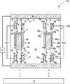
- FIG. 2shows a region of a memory array 10 comprising example 2T-1C memory cells. Specifically, a pair of adjacent memory cells 12 and 12 a are illustrated. A dashed line 13 demarcates an approximate boundary of the memory cell 12 .
- the memory cells 12 and 12 aare substantially identical to one another, with the term “substantially identical” meaning that the memory cells are identical to within reasonable tolerances of fabrication and measurement.
- the illustrated portion of memory array 10is supported by a base 15 .
- the basemay comprise semiconductor material; and may, for example, comprise, consist essentially of, or consist of monocrystalline silicon.
- the basemay be referred to as a semiconductor substrate.
- semiconductor substratemeans any construction comprising semiconductive material, including, but not limited to, bulk semiconductive materials such as a semiconductive wafer (either alone or in assemblies comprising other materials), and semiconductive material layers (either alone or in assemblies comprising other materials).
- substraterefers to any supporting structure, including, but not limited to, the semiconductor substrates described above. In some applications the base may correspond to a semiconductor substrate containing one or more materials associated with integrated circuit fabrication.
- Such materialsmay include, for example, one or more of refractory metal materials, barrier materials, diffusion materials, insulator materials, etc.
- the base 15is shown to be spaced from components of array 10 to indicate that other circuitry or components may be between array 10 and the base 15 .
- An interlayer insulating film 17may intervene between the base 15 and the array 10 .
- the film 17is only shown in FIG. 2 , it is to be understood that it may be present in the embodiments shown in other figures as well.
- the film 17may comprise any suitable electrically insulative material or combination of insulative materials, including, for example, silicon dioxide, silicon nitride, etc.
- the insulating film 17has a substantially planar upper surface, and the comparative bitlines (BL- 1 , BL- 2 , BL- 1 a and BL- 2 a ) are disposed on such upper surface, and in parallel with one another.
- substantially planarmeans planar to within reasonable tolerances of fabrication and measurement.
- the memory cell 12comprises a pair of comparative bitlines BL- 1 and BL- 2 , and comprises transistors T 1 and T 2 over the bitlines BL- 1 and BL- 2 , respectively.
- the memory cell 12 acomprises a pair of comparative bitlines BL- 1 a and BL- 2 a , and comprises transistors T 1 a and T 2 a .
- the comparative bitlines BL- 1 and BL- 2are electrically coupled with circuitry 4 of the type described above with reference to FIG. 1 for comparing electrical properties of the comparative bitlines one another, and similarly the comparative bitlines BL- 1 a and BL- 2 a are electrically coupled with circuitry 4 a for comparing electrical properties of the comparative bitlines one another.
- Circuitry 4 and 4 aeach serving as a sense amplifier, may be in any suitable location relative to array 10 , and may, for example, be between array 10 and base 15 , laterally offset from array 10 , etc. Circuitry 4 and 4 a may be further incorporated into the base 15 as a sense amplifier together with other electrical circuits that may be used to access to the array 10 to read or write data from or into the array 10 . In applications in which an interlayer insulating film intervenes between the array 10 and the base 15 , a plurality of vias may be formed in the interlayer insulating film to electrically connect wordlines WL and bitlines BL of the array 10 to the circuits, such as the sense amplifiers 4 and 4 a , that may be formed in the base 15 .
- the comparative bitlines BL- 1 and BL- 2 of memory cell 12are laterally displaced relative to one another, and similarly the transistors T 1 and T 2 are laterally displaced relative to one another.
- the transistors T 1 and T 2are shown to be in a common horizontal plane as one another (i.e., are horizontally aligned with one another), but in other embodiments may be vertically offset relative to one another.
- the transistors T 1 and T 2comprise gates 14 and 16 ; and similarly the transistors T 1 a and T 2 a comprise gates 14 a and 16 a .
- the memory cells 12 and 12 aare in a common row as one another within the memory array, and accordingly a wordline (WL) extends across all of the transistors T 1 , T 1 a , T 2 and T 2 a , and comprises the gates of such transistors.
- WLwordline
- the wordline and the bitlinesmay comprise any suitable electrically conductive material, including, for example, one or more of various metals (e.g., tungsten, titanium, etc.), metal-containing compositions (e.g., metal nitride, metal carbide, metal silicide, etc.), conductively-doped semiconductor materials (e.g., conductively-doped silicon, conductively-doped germanium, etc.), etc.
- the wordline and bitlinesmay comprise the same composition as one another, or may comprise different compositions relative to one another.
- Semiconductor pillars 18 and 20extend upwardly from the comparative bitlines BL- 1 and BL- 2 .
- Such semiconductor pillarsmay comprise any suitable semiconductor materials including, for example, one or both of silicon and germanium.
- Similar semiconductor pillars 18 a and 20 aextend upwardly from the comparative bitlines BL- 1 a and BL- 2 a.
- the transistor gate 14is spaced from the semiconductor pillar 18 by gate dielectric material 22
- the transistor gate 16is spaced from the semiconductor pillar 20 by gate dielectric material 24 .
- the gate dielectric materials 22 and 24may comprise any suitable compositions or combinations of compositions; including, for example, silicon dioxide, silicon nitride, high-K dielectric material, ferroelectric material, etc. Analogous gate dielectric materials 22 a and 24 a are within the transistors T 1 a and T 2 a.
- the transistor T 1comprises a channel region 26 within semiconductor material of pillar 18 , and comprises source/drain regions 28 and 30 on opposing sides of the channel region.
- the source/drain regions and channel regionmay be doped with any suitable dopants.
- the source/drain regionsmay be n-type majority doped, and in other embodiments may be p-type majority doped.
- the transistor T 2comprises a channel region 32 within semiconductor material of pillar 20 , and comprises source/drain regions 34 and 36 on opposing sides of the channel region.
- the source/drain regions 28 and 30may be referred to as first and second source/drain regions, respectively; and the source/drain regions 34 and 36 may be referred to as third and fourth source/drain regions, respectively.
- the transistors T 1 a and T 2 acomprise source/drain regions ( 28 a / 30 a / 34 a / 36 a ) and channel regions ( 26 a / 32 a ) analogous those described with reference to transistors T 1 and T 2 .
- Memory cell 12comprises a capacitor 38 which is vertically displaced relative to transistors T 1 and T 2 , and in the illustrated embodiment is over the transistors T 1 and T 2 .
- the capacitorcomprises an outer node (or first node) 40 , an inner node (or second node) 42 , and capacitor dielectric material 44 between the inner and outer nodes.
- the outer node 40is container-shaped, and the inner node 42 and capacitor dielectric material 44 extend into the container-shaped outer node.
- the outer nodemay have a different configuration (e.g., a planar configuration).
- the inner and outer nodes 40 and 42may comprise any suitable electrically conductive compositions or combinations of electrically conductive compositions; including, for example, one or more of various metals (e.g., tungsten, titanium, etc.), metal-containing materials (for instance, metal nitride, metal silicide, metal carbide, etc.), conductively-doped semiconductor materials (for instance, conductively-doped silicon, conductively-doped germanium, etc.), etc.
- the inner and outer nodes 40 and 42may comprise the same composition as one another in some embodiments, and in other embodiments may comprise different compositions relative to one another.
- the capacitor dielectric material 44may comprise any suitable composition or combination of compositions.
- the capacitor dielectric materialmay comprise non-ferroelectric material and may, for example, consist of one or more of silicon dioxide, silicon nitride, aluminum oxide, hafnium oxide, zirconium oxide, etc.
- the capacitor dielectric materialmay comprise ferroelectric material.
- the capacitor dielectric materialmay comprise, consist essentially of, or consist of one or more materials selected from the group consisting of transition metal oxide, zirconium, zirconium oxide, hafnium, hafnium oxide, lead zirconium titanate, tantalum oxide, and barium strontium titanate; and having dopant therein which comprises one or more of silicon, aluminum, lanthanum, yttrium, erbium, calcium, magnesium, niobium, strontium, and a rare earth element.
- the outer electrode 40is electrically coupled with the first source/drain region 28 of transistor T 1
- the inner electrode 42is electrically coupled with the third source/drain region 34 of transistor T 2
- the second source/drain region 30 of transistor T 1is electrically coupled with comparative bitline BL- 1
- the fourth source/drain region 36 of transistor T 2is electrically coupled with comparative bitline BL- 2
- the capacitor 38together with transistors T 1 and T 2 , and comparative bitlines BL- 1 and BL- 2 , forms a 2T-1C memory cell of the type described above with reference to FIG. 1 .
- the inner electrode 42is shown having a single homogenous composition that extends from inside of the container-shaped outer electrode 40 to outside of the container-shaped outer electrode and into electrical contact with source/drain region 34 . In other embodiments at least some of the illustrated portion of the inner electrode 42 outside of the container-shaped outer electrode 40 may be replaced with an electrically conductive interconnect which may or may not have a same composition as the inner electrode 42 .
- the memory cell 12 acomprises a capacitor 38 a analogous to the capacitor 30 of memory cell 12 (with capacitor 38 a comprising a first node 40 a , a second node 42 a and capacitor dielectric material 44 a ), and also comprises a 2T-1C memory cell of the type described above with reference to FIG. 1 .
- Insulative material 48is shown to surround the various components of memory cells 12 and 12 a .
- Such insulative materialmay comprise any suitable composition or combination of compositions; including, for example, one or more of silicon dioxide, silicon nitride, borophosphosilicate glass, spin-on dielectric, etc.
- insulative material 48is shown as a single homogeneous material, in other embodiments the insulative material may include two or more discrete insulative compositions.
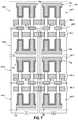
- FIG. 3is a top view of a region of memory array 10 showing an example embodiment relationship between a series of wordlines (WL) and comparative bitlines (BL- 1 , BL- 2 , BL- 1 a and BL- 2 a ).
- the cross-section of FIG. 2is along the line 2 - 2 of FIG. 3 .
- configurations analogous to that of FIGS. 2 and 3may be incorporated into stacked memory array tiers.
- a second tiermay be over a first tier and inverted such that comparative bitlines may be shared between the tiers.
- FIG. 4shows a region of an example arrangement 50 of stacked memory array tiers, with a second tier 54 being over a first tier 52 .
- the first tier 52comprises memory cells 12 and 12 a of the type described in FIGS. 2 and 3 .
- the second tier 54comprises similar memory cells 12 b and 12 c , except that the second memory cells are inverted relative to the first memory cells.
- the memory cell 12 bcomprises first and second transistors T 1 b and T 2 b
- the memory cell 12 ccomprises first and second transistors T 1 c and T 2 c .
- the memory cells 12 b and 12 ccomprise capacitors 38 b and 38 c , respectively.
- the wordline extending across the memory cells 12 and 12 ais labeled as a first wordline (WL 1 )
- the wordline across the memory cells 12 b and 12 cis labeled as a second wordline (WL 2 ).
- an axis 53 through the comparative bitlines BL- 1 , BL- 2 , BL- 1 a and BL- 2 amay be considered to define a mirror plane and the memory cells 12 b and 12 c may be considered to be substantially mirror images of the memory cells 12 and 12 a , respectively, across the mirror plane.
- the term “substantially mirror images”is utilized to indicate that the indicated cells may be mirror images of one another to within reasonable tolerances of fabrication and measurement.
- FIGS. 2 and 3may be considered to comprise memory cells within 4F 2 architecture
- the configuration of FIG. 4may be considered to comprise memory cells within 8F 2 architecture.
- FIG. 2shows comparative bitlines BL- 1 and BL- 2 within a common horizontal plane as one another (i.e., are horizontally aligned with one another).
- the comparative bitlines BL- 1 and BL- 2may be vertically displaced relative to one another, as described with reference to FIGS. 5-7 .
- a memory array 100comprises adjacent memory cells 12 and 12 a .
- the memory cells 12 and 12 a of memory array 100are similar to the memory cells 12 and 12 a of the memory array 10 discussed above with reference to FIG. 2 , except that the second comparative bitlines BL- 2 /BL- 2 a are vertically displaced relative to the first comparative bitlines BL- 1 /BL- 1 a in the configuration of FIG. 5 .
- the first and second comparative bitlinesare not vertically displaced relative to one another in the configuration of FIG. 2 .
- the configuration of FIG. 5may be formed with any suitable method.
- the configuration of FIG. 5may be formed by including insulative subcomponents of material 48 having first surfaces 49 and second surfaces 51 , with first surfaces 49 being above second surfaces 51 .
- Such subcomponents of material 48may correspond to one or more insulative films in some embodiments.
- the second comparative bitlines BL- 2 /BL- 2 aare deeper than the first comparative bitlines BL- 1 /BL- 1 a , and accordingly pedestals 20 / 20 a are longer than pedestals 18 / 18 a within memory cells 12 / 12 a .
- the distance between second comparative bitlines BL- 2 /BL- 2 a and the channel regions 32 / 32 a of transistors T 2 /T 2 ais lengthened relative to the embodiment of FIG. 2 , resulting in the lengthening of the source/drain regions 36 / 36 a of transistors T 2 /T 2 a .
- electrically conductive interconnectsmay be provided along upper surfaces of BL- 2 /BL- 2 a to reduce the length of the source/drain regions 36 / 36 a.
- the first comparative bitlines BL- 1 /BL- 1 aare entirely laterally displaced relative to the second comparative bitlines BL- 2 /BL- 2 a for each of the memory cells 12 / 12 a in the embodiment of FIG. 5 .
- FIG. 6shows an alternative embodiment in which the comparative bitlines BL- 1 and BL- 2 laterally overlap one another.
- the pedestal 20is laterally offset from a center of comparative bitline BL- 2 .
- the pedestal 20may extend to the central region of BL- 2 even though the comparative bitlines BL- 1 and BL- 2 laterally overlap.
- the pedestal 18may be laterally offset from a center of comparative bitline BL- 1 in addition to, or alternatively to, the pedestal 20 being offset from the center of comparative bitline BL- 2 .
- the lateral overlap of the comparative bitlines BL- 1 and BL- 2 in the embodiment of FIG. 6may provide larger landing pads for the pedestals 18 and 20 which may better compensate for mask misalignment as compared to embodiments having smaller dimensions of the comparative bitlines.
- Example surfaces 49 and 51are diagrammatically illustrated in FIG. 6 to illustrate an example method of forming the construction of FIG. 6 through utilization of subcomponents of insulative material 48 having upper surfaces 49 and 51 .
- FIG. 7shows a region of an example embodiment memory array 150 with stacked memory cells.
- the array 150comprises memory cells 12 and 12 a - g ; with memory cells 12 b , 12 , 12 f and 12 d (i.e., cell- 1 , cell- 2 , cell- 3 and cell- 4 ) being in a first vertical stack, and memory cells 12 c , 12 a , 12 g and 12 e (i.e., cell- 5 , cell- 6 , cell- 7 and cell- 8 ) being in a second vertical stack.
- the memory cells of the first vertical stackare electrically coupled with a first set of comparative bitlines (i.e., comparative bitlines BL- 1 , BL- 2 , BL- 1 b and BL- 2 b ); and the memory cells of the second vertical stack are electrically coupled with a second set of comparative bitlines (i.e., comparative bitlines BL- 1 a , BL- 2 a , BL- 1 c and BL- 2 c ).
- First sensing amplifier circuitry 4is electrically coupled with the first set of comparative bitlines
- second sensing amplifier circuitry 4 ais electrically coupled with the second set of comparative bitlines.
- Wordlines WL- 1 , WL- 2 , WL- 3 and WL- 4extend along rows of the memory array 150 .
- FIGS. 2-7have the transistors (e.g., T 1 and T 2 ) laterally offset from one another, and the capacitor (e.g., 38 of FIG. 2 ) provided above (or below) both of such transistors.
- the two transistors of a 2T-1C memory cellmay be vertically offset relative to one another, and the capacitor may be provided vertically between such transistors.
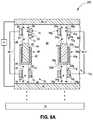
- FIG. 8shows a portion of a memory array 200 illustrating an example embodiment in which the capacitors of 2T-1C memory cells are provided between vertically displaced transistors.
- the illustrated region of memory array 200comprises comparative bitlines BL- 1 and BL- 2 , with such comparative bitlines being vertically offset relative to another and connected to circuitry 4 .
- a pair of adjacent memory cells 12 and 12 aare shown, with such adjacent memory cells being in a common column as one another within the memory array (i.e., being along a common bitline, with such bitline being comprised by the comparative bitlines BL- 1 and BL- 2 in combination).
- Suchis in contrast to the embodiments of FIGS. 2, 4 and 5 in which the adjacent memory cells 12 and 12 a are in a common row as one another (i.e., are along a common wordline).
- the memory cells 12 and 12 amay be referred to as substantially identical memory cells along a column of a memory array, with the term “substantially identical” meaning that the memory cells are identical to one another within reasonable tolerances of fabrication and measurement.
- the lower comparative bitline (BL- 2 )is shown to be over and supported by a base 15 .
- Such basemay be a semiconductor substrate of the type described above with reference to FIG. 2 .
- the memory cell 12comprises transistors T 1 and T 2 , with such transistors being along a first wordline WL 1 .
- the adjacent memory cell 12 acomprises transistors T 1 a and T 2 a , with such transistors being along a second wordline WL 2 .
- a capacitor 38is vertically between the transistors T 1 and T 2 of memory cell 12 , and a similar capacitor 38 a is vertically between the transistors T 1 a and T 2 a of memory cell 12 a.
- the capacitorscomprise first nodes 40 / 40 a , second nodes 42 / 42 a and capacitor dielectric material 44 / 44 a .
- first nodes 40 / 40 aare shown to be container-shaped and the second nodes 42 / 42 a are shown to extend within such container shapes, in other embodiments the first and second nodes may have other configurations.
- the first and second nodesmay have planar configurations. In the illustrated configuration the first nodes 40 / 40 a may be referred to as outer nodes and the second nodes 42 / 42 a may be referred to as inner nodes.
- the pillars 18 / 18 aextend from comparative bitline BL- 1 to the outer nodes 40 / 40 a of capacitors 38 / 38 a
- the pillars 20 / 20 aextend from the comparative bitline BL- 2 to the inner nodes 42 / 42 a of capacitors 38 / 38 a.
- the transistors T 1 /T 1 ahave first source/drain regions 28 / 28 a extending to the outer nodes 40 / 40 a of capacitors 38 / 38 a , and have second source/drain regions 30 / 30 a extending to the comparative bitline BL- 1 .
- the transistors T 1 /T 1 aalso have channel regions 26 / 26 a between the first and second source/drain regions.
- Gates 14 / 14 aare along the channel regions and offset from the channel regions by gate dielectric materials 22 / 22 a.
- the transistors T 2 /T 2 ahave third source/drain regions 34 / 34 a extending to the inner nodes 42 / 42 a of capacitors 38 / 38 a , and have fourth source/drain regions 36 / 36 a extending to the comparative bitline BL- 2 .
- the transistors T 2 /T 2 aalso have channel regions 32 / 32 a between the third and fourth source/drain regions.
- Gates 16 / 16 aare along the channel regions and offset from the channel regions by gate dielectric materials 24 / 24 a.
- FIG. 8advantageously enables the transistors and capacitor of a 2T-1C memory cell to all be vertically stacked, which may enable the memory cells to be packed to high levels of integration.
- FIG. 8comprises a configuration with BL- 2 over a supporting substrate 15 and BL- 1 over BL- 2
- the relative orientations of BL- 2 and BL- 1could be reversed so that BL- 1 is over the supporting substrate and BL- 2 is over BL- 1 .
- the illustrated capacitors 38 / 38 awould be inverted relative to the configuration depicted in FIG. 8 and accordingly container-shaped outer nodes 40 would open upwardly instead of downwardly as illustrated in FIG. 8A .
- An advantage of various embodiments of memory arrays described above with reference to FIGS. 2-8is that such embodiments may have symmetric layouts relative to the comparative bitlines (e.g., BL- 1 and BL- 2 ) extending throughout the memory arrays, and such may reduce resistance/signal mismatches between the comparative bitlines as compared to less symmetric layouts.
- the comparative bitlinese.g., BL- 1 and BL- 2
- any of the capacitorsmay be replaced with a capacitive unit having two or more capacitors in combination.
- the transistors T 1 and T 2 of the above-described embodiments of FIGS. 2-8may comprise any suitable configurations.
- the transistorsare field effect transistors, but in other embodiments other suitable transistors may be substituted for one or more of the transistors T 1 and T 2 ; with bipolar junction transistors being an example of a transistor configuration which may be used alternatively to field effect transistors.
- the field effect transistors described hereinmay utilize gate dielectric material comprising non-ferroelectric material and/or ferroelectric material depending on the application.
- the gates of the transistorsmay have any of numerous configurations, with some example configurations being described with reference to FIGS. 9-13 .
- the figuresspecifically pertain to the T 1 transistor gates, but in other embodiments analogous configurations may be utilized for the T 2 transistor gates.
- the T 1 transistor gate 14is shown in a configuration of the type utilized in the embodiments of FIGS. 2 and 4-8 .
- the transistor gateis a block of uniform width, with such width being approximately equal to a length “L” of the channel region 26 .
- each of the embodiments of FIGS. 10-13has the gate narrower than the length of the channel region, and has at least one extension region 90 that extends from the gate and along the channel region.
- each of the embodiments of FIGS. 10-13has at least one bent region 92 where the gate 14 joins to an extension region.
- the embodiment of FIG. 10shows the gate 14 and extension regions 90 forming a substantially T-shaped configuration, the embodiment of FIG.
- FIG. 11shows the extension region 90 and gate 14 together forming a substantially U-shaped configuration
- FIGS. 12 and 13show the gate 14 and extension regions 90 forming substantially shelf-shaped configurations (with FIG. 13 showing the gate 14 as a top shelf over extension regions 90 and FIG. 12 showing the gate 14 as a bottom shelf beneath regions 90 ).
- Advantages of the embodiments of FIGS. 10-13 relative to that of FIG. 9may include reduced gate resistance and associated reduced current requirements for desired access drive parameters.
- the structures and architectures described abovemay be incorporated into memory (e.g., DRAM, SRAM, etc.) and/or otherwise may be utilized in electronic systems.
- Such electronic systemsmay be any of a broad range of systems, such as, for example, clocks, televisions, cell phones, personal computers, automobiles, industrial control systems, aircraft, etc.
- the various materials, substances, compositions, etc. described hereinmay be formed with any suitable methodologies, either now known or yet to be developed, including, for example, atomic layer deposition (ALD), chemical vapor deposition (CVD), physical vapor deposition (PVD), etc.
- ALDatomic layer deposition
- CVDchemical vapor deposition
- PVDphysical vapor deposition
- dielectricdielectric
- electrically insulativedielectrically insulative
- the termsare considered synonymous in this disclosure.
- the utilization of the term “dielectric” in some instances, and the term “electrically insulative” in other instances,may be to provide language variation within this disclosure to simplify antecedent basis within the claims that follow, and is not utilized to indicate any significant chemical or electrical differences.
- Some embodimentsinclude a memory cell having first and second transistors, and a capacitor vertically displaced relative to the first and second transistors.
- the capacitorhas a first node electrically coupled with a source/drain region of the first transistor, a second node electrically coupled with a source/drain region of the second transistor, and capacitor dielectric material between the first and second nodes.
- Some embodimentsinclude a memory cell having first and second transistors laterally displaced relative to one another, and a capacitor over the first and second transistors.
- the capacitorhas an outer node electrically coupled with a source/drain region of the first transistor, an inner node electrically coupled with a source/drain region of the second transistor, and capacitor dielectric material between the inner and outer nodes.
- Some embodimentsinclude a memory cell having first and second transistors vertically displaced relative to one another, and a capacitor between the first and second transistors.
- the capacitorhas a first node electrically coupled with a source/drain region of the first transistor, a second node electrically coupled with a source/drain region of the second transistor, and capacitor dielectric material between the first and second nodes.
- Some embodimentsincludes an apparatus comprising a semiconductor base, a memory array including a plurality of memory cells, and an insulating film intervening between the semiconductor base and the plurality of memory cells.
- Each of the memory cellscomprises a first transistor, a second transistor and a capacitor, and each of the first transistor, the second transistor and the capacitor is over the insulating film covering the semiconductor base.
Landscapes
- Engineering & Computer Science (AREA)
- Manufacturing & Machinery (AREA)
- Microelectronics & Electronic Packaging (AREA)
- Computer Hardware Design (AREA)
- Semiconductor Memories (AREA)
Abstract
Description
Claims (8)
Priority Applications (1)
| Application Number | Priority Date | Filing Date | Title |
|---|---|---|---|
| US16/183,468US11094697B2 (en) | 2016-08-31 | 2018-11-07 | Vertical two-transistor single capacitor memory cells and memory arrays |
Applications Claiming Priority (3)
| Application Number | Priority Date | Filing Date | Title |
|---|---|---|---|
| US201662381720P | 2016-08-31 | 2016-08-31 | |
| US15/664,161US10157926B2 (en) | 2016-08-31 | 2017-07-31 | Memory cells and memory arrays |
| US16/183,468US11094697B2 (en) | 2016-08-31 | 2018-11-07 | Vertical two-transistor single capacitor memory cells and memory arrays |
Related Parent Applications (1)
| Application Number | Title | Priority Date | Filing Date |
|---|---|---|---|
| US15/664,161DivisionUS10157926B2 (en) | 2016-08-31 | 2017-07-31 | Memory cells and memory arrays |
Publications (2)
| Publication Number | Publication Date |
|---|---|
| US20190088652A1 US20190088652A1 (en) | 2019-03-21 |
| US11094697B2true US11094697B2 (en) | 2021-08-17 |
Family
ID=61243451
Family Applications (2)
| Application Number | Title | Priority Date | Filing Date |
|---|---|---|---|
| US15/664,161ActiveUS10157926B2 (en) | 2016-08-31 | 2017-07-31 | Memory cells and memory arrays |
| US16/183,468ActiveUS11094697B2 (en) | 2016-08-31 | 2018-11-07 | Vertical two-transistor single capacitor memory cells and memory arrays |
Family Applications Before (1)
| Application Number | Title | Priority Date | Filing Date |
|---|---|---|---|
| US15/664,161ActiveUS10157926B2 (en) | 2016-08-31 | 2017-07-31 | Memory cells and memory arrays |
Country Status (5)
| Country | Link |
|---|---|
| US (2) | US10157926B2 (en) |
| EP (2) | EP3840046B1 (en) |
| KR (2) | KR20180130581A (en) |
| CN (1) | CN109219883B (en) |
| WO (1) | WO2018044456A1 (en) |
Cited By (1)
| Publication number | Priority date | Publication date | Assignee | Title |
|---|---|---|---|---|
| US20220302120A1 (en)* | 2021-03-22 | 2022-09-22 | Kioxia Corporation | Semiconductor device and semiconductor memory device |
Families Citing this family (46)
| Publication number | Priority date | Publication date | Assignee | Title |
|---|---|---|---|---|
| CN109155145B (en) | 2016-08-31 | 2022-11-01 | 美光科技公司 | Memory array |
| WO2018044479A1 (en) | 2016-08-31 | 2018-03-08 | Micron Technology, Inc. | Sense amplifier constructions |
| CN109155312B (en) | 2016-08-31 | 2023-05-02 | 美光科技公司 | Memory cell and memory array |
| EP3840046B1 (en)* | 2016-08-31 | 2025-03-19 | Micron Technology, Inc. | Memory cells and memory arrays |
| US10056386B2 (en) | 2016-08-31 | 2018-08-21 | Micron Technology, Inc. | Memory cells and memory arrays |
| US10355002B2 (en)* | 2016-08-31 | 2019-07-16 | Micron Technology, Inc. | Memory cells, methods of forming an array of two transistor-one capacitor memory cells, and methods used in fabricating integrated circuitry |
| CN109155311A (en) | 2016-08-31 | 2019-01-04 | 美光科技公司 | memory cell and memory array |
| US11211384B2 (en) | 2017-01-12 | 2021-12-28 | Micron Technology, Inc. | Memory cells, arrays of two transistor-one capacitor memory cells, methods of forming an array of two transistor-one capacitor memory cells, and methods used in fabricating integrated circuitry |
| US10177159B2 (en) | 2017-04-21 | 2019-01-08 | Micron Technology, Inc. | Memory cells and memory arrays |
| US10347635B2 (en) | 2017-06-30 | 2019-07-09 | Micron Technology, Inc. | Apparatuses comprising memory cells, and apparatuses comprising memory arrays |
| CN110753962A (en) | 2017-08-29 | 2020-02-04 | 美光科技公司 | memory circuit |
| EP3676872A4 (en) | 2017-08-31 | 2020-11-25 | Micron Technology, Inc. | DEVICES WITH STORAGE CELLS WITH TWO TRANSISTORS AND A CAPACITOR AND WITH BODY AREAS OF THE TRANSISTORS COUPLED WITH REFERENCE VOLTAGES |
| US10366983B2 (en) | 2017-12-29 | 2019-07-30 | Micron Technology, Inc. | Semiconductor devices including control logic structures, electronic systems, and related methods |
| US10340267B1 (en) | 2017-12-29 | 2019-07-02 | Micron Technology, Inc. | Semiconductor devices including control logic levels, and related memory devices, control logic assemblies, electronic systems, and methods |
| US10297290B1 (en) | 2017-12-29 | 2019-05-21 | Micron Technology, Inc. | Semiconductor devices, and related control logic assemblies, control logic devices, electronic systems, and methods |
| US10229874B1 (en) | 2018-03-22 | 2019-03-12 | Micron Technology, Inc. | Arrays of memory cells individually comprising a capacitor and a transistor and methods of forming such arrays |
| US10748931B2 (en) | 2018-05-08 | 2020-08-18 | Micron Technology, Inc. | Integrated assemblies having ferroelectric transistors with body regions coupled to carrier reservoirs |
| US11038027B2 (en)* | 2019-03-06 | 2021-06-15 | Micron Technology, Inc. | Integrated assemblies having polycrystalline first semiconductor material adjacent conductively-doped second semiconductor material |
| US11031374B2 (en)* | 2019-03-06 | 2021-06-08 | Micron Technology, Inc. | Methods of compensating for misalignment of bonded semiconductor wafers |
| US11348932B2 (en) | 2019-03-06 | 2022-05-31 | Micron Technology, Inc. | Integrated assemblies having transistor body regions coupled to carrier-sink-structures; and methods of forming integrated assemblies |
| US10854617B2 (en) | 2019-04-09 | 2020-12-01 | Micron Technology, Inc. | Integrated components which have both horizontally-oriented transistors and vertically-oriented transistors |
| US11062763B2 (en) | 2019-04-09 | 2021-07-13 | Micron Technology, Inc. | Memory array with multiplexed digit lines |
| US11049864B2 (en)* | 2019-05-17 | 2021-06-29 | Micron Technology, Inc. | Apparatuses including capacitor structures, and related memory devices, electronic systems, and methods |
| KR102801636B1 (en) | 2019-10-29 | 2025-05-02 | 삼성전자주식회사 | Three-dimensional Semiconductor memory device |
| US11088142B2 (en)* | 2019-12-26 | 2021-08-10 | Micron Technology, Inc. | Integrated assemblies having voids along regions of gates, and methods of forming conductive structures |
| US11094699B1 (en) | 2020-05-28 | 2021-08-17 | Micron Technology, Inc. | Apparatuses including stacked horizontal capacitor structures and related methods, memory devices, and electronic systems |
| US11569244B2 (en)* | 2020-05-29 | 2023-01-31 | Taiwan Semiconductor Manufacturing Company Limited | Vertical heterostructure semiconductor memory cell and methods for making the same |
| TW202145506A (en)* | 2020-05-29 | 2021-12-01 | 台灣積體電路製造股份有限公司 | Memory cell |
| KR102768882B1 (en) | 2020-07-10 | 2025-02-19 | 삼성전자주식회사 | Semiconductor memory device |
| US11903221B2 (en)* | 2020-08-17 | 2024-02-13 | Taiwan Semiconductor Manufacturing Co., Ltd. | Three dimensional semiconductor device with memory stack |
| US11495600B2 (en)* | 2020-11-10 | 2022-11-08 | Micron Technology, Inc. | Vertical three-dimensional memory with vertical channel |
| US12120865B2 (en) | 2020-12-23 | 2024-10-15 | Intel Corporation | Arrays of double-sided dram cells including capacitors on the frontside and backside of a stacked transistor structure |
| US11770923B2 (en)* | 2021-03-03 | 2023-09-26 | Micron Technology, Inc. | Thin film transistor random access memory |
| WO2023028869A1 (en) | 2021-08-31 | 2023-03-09 | Yangtze Memory Technologies Co., Ltd. | Memory devices having vertical transistors and methods for forming the same |
| CN116075928A (en) | 2021-08-31 | 2023-05-05 | 长江存储科技有限责任公司 | Memory device with vertical transistor and method of forming the same |
| CN116097917A (en)* | 2021-08-31 | 2023-05-09 | 长江存储科技有限责任公司 | Memory device with vertical transistor and method of forming the same |
| CN116097915A (en) | 2021-08-31 | 2023-05-09 | 长江存储科技有限责任公司 | Memory device with vertical transistors and method of forming the same |
| CN116097921A (en) | 2021-08-31 | 2023-05-09 | 长江存储科技有限责任公司 | Memory device with vertical transistor and method of forming the same |
| CN116097920A (en) | 2021-08-31 | 2023-05-09 | 长江存储科技有限责任公司 | Memory device with vertical transistors and method of forming the same |
| WO2023028853A1 (en) | 2021-08-31 | 2023-03-09 | Yangtze Memory Technologies Co., Ltd. | Memory devices having vertical transistors and methods for forming the same |
| KR20230045690A (en)* | 2021-09-27 | 2023-04-05 | 삼성전자주식회사 | Semiconductor memory device of 2T-1C structure and method of fabricating the same |
| US12114480B2 (en)* | 2021-12-21 | 2024-10-08 | Tokyo Electron Limited | Method of making of plurality of 3D vertical logic elements integrated with 3D memory |
| US12356706B2 (en) | 2021-12-21 | 2025-07-08 | Tokyo Electron Limited | Methods for forming high performance three dimensionally stacked transistors based on dielectric nano sheets |
| US12272692B2 (en) | 2022-02-15 | 2025-04-08 | Tokyo Electron Limited | 3D selective material transformation to integrate 2D material elements |
| US20230361118A1 (en)* | 2022-05-04 | 2023-11-09 | Micron Technology, Inc. | Microelectronic devices including vertical inverters, and electronic systems |
| KR20250118677A (en)* | 2024-01-30 | 2025-08-06 | 삼성전자주식회사 | Semiconductor memory device |
Citations (109)
| Publication number | Priority date | Publication date | Assignee | Title |
|---|---|---|---|---|
| US4103342A (en) | 1976-06-17 | 1978-07-25 | International Business Machines Corporation | Two-device memory cell with single floating capacitor |
| US4554570A (en) | 1982-06-24 | 1985-11-19 | Rca Corporation | Vertically integrated IGFET device |
| JPH03205867A (en) | 1990-01-08 | 1991-09-09 | Nec Corp | Semiconductor memory |
| US5066607A (en) | 1987-11-30 | 1991-11-19 | Texas Instruments Incorporated | Method of making a trench DRAM cell with dynamic gain |
| US5146300A (en) | 1989-11-27 | 1992-09-08 | Mitsubishi Denki Kabushiki Kaisha | Semiconductor integrated circuit device having improved stacked capacitor and manufacturing method therefor |
| US5299155A (en) | 1991-03-01 | 1994-03-29 | Sharp Kabushiki Kaisha | Dynamic random access memory device with capacitor between vertically aligned FETs |
| US5389810A (en) | 1992-03-27 | 1995-02-14 | Matsushita Electric Industrial Co., Ltd. | Semiconductor device having at least one symmetrical pair of MOSFETs |
| US5398200A (en) | 1992-03-02 | 1995-03-14 | Motorola, Inc. | Vertically formed semiconductor random access memory device |
| EP0706187A2 (en) | 1994-09-22 | 1996-04-10 | Matsushita Electric Industrial Co., Ltd. | Ferroelectric memory |
| JPH08147983A (en) | 1994-09-22 | 1996-06-07 | Matsushita Electric Ind Co Ltd | Ferroelectric memory device |
| JPH08264764A (en) | 1995-03-22 | 1996-10-11 | Toshiba Corp | Semiconductor device |
| US5571743A (en) | 1993-01-19 | 1996-11-05 | International Business Machines Corporation | Method of making buried-sidewall-strap two transistor one capacitor trench cell |
| US5586078A (en) | 1994-09-22 | 1996-12-17 | Kabushiki Kaisha Toshiba | Dynamic type memory |
| US5646900A (en) | 1995-01-12 | 1997-07-08 | Mitsubishi Denki Kabushiki Kaisha | Sense amplifier including MOS transistors having threshold voltages controlled dynamically in a semiconductor memory device |
| US5830791A (en)* | 1995-09-06 | 1998-11-03 | Lg Semicon Co., Ltd. | Manufacturing process for a DRAM with a buried region |
| US6028806A (en) | 1998-05-22 | 2000-02-22 | Micron Technology, Inc. | Semiconductor memory with local phase generation from global phase signals and local isolation signals |
| US6141286A (en) | 1998-08-21 | 2000-10-31 | Micron Technology, Inc. | Embedded DRAM architecture with local data drivers and programmable number of data read and data write lines |
| US6154387A (en) | 1998-02-19 | 2000-11-28 | Sharp Kabushiki Kaisha | Semiconductor memory device utilizing a polarization state of a ferroelectric film |
| US20010053088A1 (en) | 1998-04-14 | 2001-12-20 | Micron Technology, Inc. | Circuits and methods for a memory cell with a trench plate trench capacitor and a vertical bipolar read device |
| US20020044477A1 (en) | 2000-10-17 | 2002-04-18 | Yoshiaki Takeuchi | Ferroelectric memory device |
| US20020093865A1 (en) | 2001-01-16 | 2002-07-18 | Matsushita Electric Industrial Co., Ltd. | Semiconductor memory device |
| US20020113260A1 (en)* | 2001-02-20 | 2002-08-22 | Haining Yang | Rhodium-rich oxygen barriers |
| US20020125508A1 (en) | 1999-09-02 | 2002-09-12 | Micron Technology, Inc. | Container capacitor structure and method of formation thereof |
| US20020140106A1 (en) | 2001-03-30 | 2002-10-03 | Wlodek Kurjanowicz | Twisted wordline strapping arrangement |
| US20030087499A1 (en) | 2001-11-07 | 2003-05-08 | Lane Richard H | Process for forming metallized contacts to periphery transistors |
| US6563727B1 (en) | 2002-07-31 | 2003-05-13 | Alan Roth | Method and structure for reducing noise effects in content addressable memories |
| US20030169616A1 (en) | 2002-03-08 | 2003-09-11 | Fujitsu Limited | Ferroelectric memory wherein bit line capacitance can be maximized |
| US20030173593A1 (en) | 2002-03-15 | 2003-09-18 | Shinichi Miyatake | Semiconductor memory device |
| US20030185041A1 (en) | 2002-03-29 | 2003-10-02 | Kazuhiko Takahashi | Semiconductor memory device |
| JP2003303901A (en) | 2002-04-08 | 2003-10-24 | Hitachi Ltd | Semiconductor integrated circuit device and method of manufacturing the same |
| US20030202391A1 (en) | 2002-03-19 | 2003-10-30 | Akitoshi Nishimura | Dummy cell structure for 1T1C FeRAM cell array |
| US20030234413A1 (en) | 2002-04-15 | 2003-12-25 | Stmicroelectronics S.R.I. | FeRAM semiconductor memory |
| US6710465B2 (en) | 2001-06-21 | 2004-03-23 | Samsung Electronics Co., Ltd. | Scalable two transistor memory device |
| US20040062101A1 (en) | 2002-09-30 | 2004-04-01 | Fujitsu Limited | Semiconductor memory device and method for arranging memory cells |
| US6720609B2 (en) | 1999-06-16 | 2004-04-13 | Micron Technology, Inc. | Structure for reducing contact aspect ratios |
| US20040090810A1 (en) | 2002-11-12 | 2004-05-13 | Shinzo Sakuma | Ferroelectric memory |
| US20040099886A1 (en) | 2002-11-26 | 2004-05-27 | Howard Rhodes | CMOS imager pixel designs |
| US6744087B2 (en) | 2002-09-27 | 2004-06-01 | International Business Machines Corporation | Non-volatile memory using ferroelectric gate field-effect transistors |
| US20040151020A1 (en) | 2002-11-27 | 2004-08-05 | Peter Beer | Dynamic memory cell |
| US20040174733A1 (en) | 2003-03-05 | 2004-09-09 | International Business Machines Corporation | Structure and System-on-Chip Integration of a Two-Transistor and Two-Capacitor Memory Cell for Trench Technology |
| US20040232497A1 (en) | 2001-12-14 | 2004-11-25 | Satoru Akiyama | Semiconductor device and method for manufacturing the same |
| US20040252542A1 (en) | 2003-06-16 | 2004-12-16 | Katsuhiko Hoya | Ferroelectric memory device |
| US20050023589A1 (en) | 2003-07-28 | 2005-02-03 | Yuki Yamada | Semiconductor memory device having a ferroelectric capacitor and method of manufacturing the same |
| WO2005093836A2 (en) | 2004-03-11 | 2005-10-06 | Micron Technology, Inc. | Semiconductor constructions having a buried bit line, and methods of forming same |
| US6961271B2 (en) | 2002-09-09 | 2005-11-01 | Samsung Electronics Co., Ltd. | Memory device in which memory cells having complementary data are arranged |
| US20060028859A1 (en) | 2002-11-12 | 2006-02-09 | Micron Technology, Inc. | 6F2 3-Transistor DRAM gain cell |
| US20060046424A1 (en) | 2004-08-24 | 2006-03-02 | Chance Randal W | Methods of forming semiconductor constructions |
| US20060046391A1 (en)* | 2004-08-30 | 2006-03-02 | Tang Sanh D | Vertical wrap-around-gate field-effect-transistor for high density, low voltage logic and memory array |
| US20060138466A1 (en) | 2004-12-23 | 2006-06-29 | Jin Choi | Layout of semiconductor memory device and method of controlling capacitance of dummy cell |
| US20060164876A1 (en) | 2003-09-25 | 2006-07-27 | Infineon Technologies Ag | Multi-transistor memory cells |
| US20060211194A1 (en) | 2004-12-13 | 2006-09-21 | Haller Gordon A | Methods of reducing floating body effect |
| US7164595B1 (en) | 2005-08-25 | 2007-01-16 | Micron Technology, Inc. | Device and method for using dynamic cell plate sensing in a DRAM memory cell |
| US20070034928A1 (en) | 2005-08-10 | 2007-02-15 | Micron Technology, Inc. | Capacitor structure for two-transistor dram memory cell and method of forming same |
| KR20070070021A (en) | 2005-12-28 | 2007-07-03 | 난야 테크놀러지 코포레이션 | Semiconductor device and manufacturing method thereof |
| US20070235790A1 (en) | 2006-04-05 | 2007-10-11 | Kim Yoon-Hae | Capacitor structure of semiconductor device and method of fabricating the same |
| US20070295995A1 (en) | 2006-06-09 | 2007-12-27 | Samsung Electronics Co., Ltd. | Methods of forming a semiconductor device including buried bit lines |
| US7330388B1 (en) | 2005-09-23 | 2008-02-12 | Cypress Semiconductor Corporation | Sense amplifier circuit and method of operation |
| US20080079049A1 (en) | 2006-08-25 | 2008-04-03 | Lee Se-Young | Embedded Semiconductor Device Including Planarization Resistance Patterns and Method of Manufacturing the Same |
| US7378702B2 (en) | 2004-06-21 | 2008-05-27 | Sang-Yun Lee | Vertical memory device structures |
| US20080253170A1 (en) | 2006-10-03 | 2008-10-16 | Kabushiki Kaisha Toshiba | Semiconductor device |
| US20090008691A1 (en) | 2007-07-02 | 2009-01-08 | Tzung-Han Lee | Dram structure and method of making the same |
| US20090108881A1 (en) | 2007-10-24 | 2009-04-30 | Agere Systems Inc. | Latch-Based Sense Amplifier |
| US20090168489A1 (en) | 2007-12-31 | 2009-07-02 | Texas Instruments Incorporated | Ferroelectric memory devices with partitioned platelines |
| US7558097B2 (en) | 2006-12-28 | 2009-07-07 | Intel Corporation | Memory having bit line with resistor(s) between memory cells |
| US20090212338A1 (en) | 2008-02-26 | 2009-08-27 | Benson Russell A | Semiconductor Constructions, And Methods Of Forming Semiconductor Constructions |
| US7697318B2 (en) | 2006-12-26 | 2010-04-13 | Kabushiki Kaisha Toshiba | Semiconductor memory device |
| US20100112753A1 (en) | 2003-06-24 | 2010-05-06 | Sang-Yun Lee | Semiconductor memory device |
| US20100165704A1 (en) | 2008-12-30 | 2010-07-01 | Cheng-Hsu Wu | Circuit and Method for a High Speed Memory Cell |
| US20100238697A1 (en) | 2008-02-19 | 2010-09-23 | Micron Technology, Inc. | Systems and devices including local data lines and methods of using, making, and operating the same |
| US20100264484A1 (en) | 2009-04-17 | 2010-10-21 | Fujio Masuoka | Semiconductor device |
| US20100295110A1 (en) | 2009-05-22 | 2010-11-25 | Elpida Memory, Inc. | Device and manufacturing method thereof |
| EP2296176A1 (en) | 2009-09-14 | 2011-03-16 | Unisantis Electronics (Japan) Ltd. | SRAM cell with four SGTs and manufacturing method thereof |
| JP2011142256A (en) | 2010-01-08 | 2011-07-21 | Elpida Memory Inc | Semiconductor device and method of manufacturing the same |
| US8018058B2 (en) | 2004-06-21 | 2011-09-13 | Besang Inc. | Semiconductor memory device |
| US20120153371A1 (en) | 2010-12-15 | 2012-06-21 | Powerchip Technology Corporation | Dynamic random access memory cell and array having vertical channel transistor |
| US8394699B2 (en) | 2006-08-21 | 2013-03-12 | Micron Technology, Inc. | Memory arrays and methods of fabricating memory arrays |
| US20130099305A1 (en)* | 2011-10-19 | 2013-04-25 | Sua KIM | Semiconductor devices including a vertical channel transistor and methods of fabricating the same |
| US20130161607A1 (en) | 2011-12-23 | 2013-06-27 | Semiconductor Energy Laboratory Co., Ltd. | Semiconductor device |
| US20130214420A1 (en) | 2012-02-16 | 2013-08-22 | Elpida Memory, Inc. | Semiconductor device |
| US20130221356A1 (en) | 2012-02-29 | 2013-08-29 | Semiconductor Energy Laboratory Co., Ltd. | Semiconductor device |
| US20130235642A1 (en) | 2012-03-06 | 2013-09-12 | Micron Technology, Inc. | Arrays Of Vertically-Oriented Transistors, Memory Arrays Including Vertically-Oriented Transistors, And Memory Cells |
| US20130235641A1 (en) | 2012-03-06 | 2013-09-12 | Elpida Memory, Inc. | Semiconductor device |
| US20130286734A1 (en)* | 2012-04-30 | 2013-10-31 | Chun-Yen Chang | Nand flash memory |
| US20140027839A1 (en) | 2010-06-08 | 2014-01-30 | Samsung Electronics Co., Ltd. | Sram devices and methods of manufacturing the same |
| US20140035018A1 (en) | 2012-07-31 | 2014-02-06 | SK Hynix Inc. | Semiconductor devices including vertical transistors and methods of fabricating the same |
| US20140054718A1 (en) | 2012-08-27 | 2014-02-27 | Micron Technology, Inc. | Arrays of Vertically-Oriented Transistors, And Memory Arrays Including Vertically-Oriented Transistors |
| US20140220749A1 (en) | 2011-08-02 | 2014-08-07 | Nxp B.V. | A vertical mosfet transistor with a vertical capacitor region |
| US20150041885A1 (en) | 2012-01-26 | 2015-02-12 | Ps4 Luxco S.A.R.L. | Semiconductor memory device |
| US20150078056A1 (en) | 2010-12-02 | 2015-03-19 | Micron Technology, Inc. | Arrays Of Nonvolatile Memory Cells |
| US20150102282A1 (en) | 2013-10-14 | 2015-04-16 | Samsung Electronics Co., Ltd. | Semiconductor memory device having three-dimensional cross point array |
| US20150179655A1 (en) | 2013-12-20 | 2015-06-25 | Samsung Electronics Co., Ltd. | Static random access memory (sram) cells including vertical channel transistors and methods of forming the same |
| US20150318285A1 (en) | 2014-04-30 | 2015-11-05 | Stmicroelectronics, Inc. | Dram interconnect structure having ferroelectric capacitors |
| US9245893B1 (en) | 2014-11-19 | 2016-01-26 | Micron Technology, Inc. | Semiconductor constructions having grooves dividing active regions |
| US20160079247A1 (en) | 2014-09-16 | 2016-03-17 | Samsung Electronics Co., Ltd. | Semiconductor Device |
| US9343507B2 (en) | 2014-03-12 | 2016-05-17 | Sandisk 3D Llc | Dual channel vertical field effect transistor including an embedded electrode |
| US9378780B1 (en) | 2015-06-16 | 2016-06-28 | National Tsing Hua University | Sense amplifier |
| US9419003B1 (en) | 2015-05-15 | 2016-08-16 | Taiwan Semiconductor Manufacturing Company, Ltd. | Semiconductor devices and methods of manufacture thereof |
| US20170033111A1 (en) | 2015-07-29 | 2017-02-02 | Semiconductor Energy Laboratory Co., Ltd. | Semiconductor Device, Circuit Board, and Electronic Device |
| US20170053920A1 (en) | 2015-08-19 | 2017-02-23 | Samsung Electronics Co., Ltd. | Method of fabricating semiconductor device |
| US20170186782A1 (en) | 2015-12-24 | 2017-06-29 | Innolux Corporation | Pixel circuit of active-matrix light-emitting diode and display panel having the same |
| US9698272B1 (en) | 2016-03-16 | 2017-07-04 | Kabushiki Kaisha Toshiba | Transistor and semiconductor memory device |
| US20180061840A1 (en) | 2016-08-31 | 2018-03-01 | Micron Technology, Inc. | Memory Cells, Methods Of Forming An Array Of Two Transistor-One Capacitor Memory Cells, And Methods Used In Fabricating Integrated Circuitry |
| US10020311B1 (en) | 2017-08-02 | 2018-07-10 | Ap Memory Technology Corporation | Semiconductor memory device provided with DRAM cell including two transistors and common capacitor |
| US20180197864A1 (en) | 2017-01-12 | 2018-07-12 | Micron Technology, Inc. | Memory Cells, Arrays Of Two Transistor-One Capacitor Memory Cells, Methods Of Forming An Array Of Two Transistor-One Capacitor Memory Cells, And Methods Used In Fabricating Integrated Circuitry |
| US10079235B2 (en) | 2016-08-31 | 2018-09-18 | Micron Technology, Inc. | Memory cells and memory arrays |
| US10157926B2 (en) | 2016-08-31 | 2018-12-18 | Micron Technology, Inc. | Memory cells and memory arrays |
| US20190019544A1 (en) | 2017-07-17 | 2019-01-17 | Micron Technology, Inc. | Memory Circuitry |
| US10319724B2 (en) | 2016-08-31 | 2019-06-11 | Micron Technology, Inc. | Memory cells and memory arrays |
| US10381357B2 (en) | 2017-08-31 | 2019-08-13 | Micron Technology, Inc. | Apparatuses having memory cells with two transistors and one capacitor, and having body regions of the transistors coupled with reference voltages |
Family Cites Families (6)
| Publication number | Priority date | Publication date | Assignee | Title |
|---|---|---|---|---|
| US7038943B2 (en)* | 2002-05-28 | 2006-05-02 | Koninklijke Philips Electronics N.V. | Memory array having 2T memory cells |
| KR100681039B1 (en)* | 2005-07-04 | 2007-02-09 | 엘지전자 주식회사 | Organic electroluminescent element, display device thereof, driving method thereof |
| US7821039B2 (en)* | 2008-06-23 | 2010-10-26 | Taiwan Semiconductor Manufacturing Company, Ltd. | Layout architecture for improving circuit performance |
| KR20180043383A (en)* | 2010-01-22 | 2018-04-27 | 가부시키가이샤 한도오따이 에네루기 켄큐쇼 | Method for manufacturing semiconductor device |
| US20130193400A1 (en)* | 2012-01-27 | 2013-08-01 | Micron Technology, Inc. | Memory Cell Structures and Memory Arrays |
| US11217588B2 (en)* | 2019-07-03 | 2022-01-04 | Micron Technology, Inc. | Integrated assemblies comprising voids between active regions and conductive shield plates, and methods of forming integrated assemblies |
- 2017
- 2017-07-31EPEP21153826.9Apatent/EP3840046B1/enactiveActive
- 2017-07-31WOPCT/US2017/044638patent/WO2018044456A1/ennot_activeCeased
- 2017-07-31KRKR1020187033620Apatent/KR20180130581A/ennot_activeCeased
- 2017-07-31EPEP17847158.7Apatent/EP3507831B1/enactiveActive
- 2017-07-31CNCN201780030983.5Apatent/CN109219883B/enactiveActive
- 2017-07-31KRKR1020207027194Apatent/KR102223551B1/enactiveActive
- 2017-07-31USUS15/664,161patent/US10157926B2/enactiveActive
- 2018
- 2018-11-07USUS16/183,468patent/US11094697B2/enactiveActive
Patent Citations (123)
| Publication number | Priority date | Publication date | Assignee | Title |
|---|---|---|---|---|
| US4103342A (en) | 1976-06-17 | 1978-07-25 | International Business Machines Corporation | Two-device memory cell with single floating capacitor |
| US4554570A (en) | 1982-06-24 | 1985-11-19 | Rca Corporation | Vertically integrated IGFET device |
| US5066607A (en) | 1987-11-30 | 1991-11-19 | Texas Instruments Incorporated | Method of making a trench DRAM cell with dynamic gain |
| US5146300A (en) | 1989-11-27 | 1992-09-08 | Mitsubishi Denki Kabushiki Kaisha | Semiconductor integrated circuit device having improved stacked capacitor and manufacturing method therefor |
| JPH03205867A (en) | 1990-01-08 | 1991-09-09 | Nec Corp | Semiconductor memory |
| US5299155A (en) | 1991-03-01 | 1994-03-29 | Sharp Kabushiki Kaisha | Dynamic random access memory device with capacitor between vertically aligned FETs |
| US5398200A (en) | 1992-03-02 | 1995-03-14 | Motorola, Inc. | Vertically formed semiconductor random access memory device |
| US5389810A (en) | 1992-03-27 | 1995-02-14 | Matsushita Electric Industrial Co., Ltd. | Semiconductor device having at least one symmetrical pair of MOSFETs |
| US5571743A (en) | 1993-01-19 | 1996-11-05 | International Business Machines Corporation | Method of making buried-sidewall-strap two transistor one capacitor trench cell |
| EP0706187A2 (en) | 1994-09-22 | 1996-04-10 | Matsushita Electric Industrial Co., Ltd. | Ferroelectric memory |
| JPH08147983A (en) | 1994-09-22 | 1996-06-07 | Matsushita Electric Ind Co Ltd | Ferroelectric memory device |
| US5586078A (en) | 1994-09-22 | 1996-12-17 | Kabushiki Kaisha Toshiba | Dynamic type memory |
| US5898608A (en) | 1994-09-22 | 1999-04-27 | Matsushita Electric Industrial Co., Ltd. | Method for operating a ferroelectric memory |
| US5646900A (en) | 1995-01-12 | 1997-07-08 | Mitsubishi Denki Kabushiki Kaisha | Sense amplifier including MOS transistors having threshold voltages controlled dynamically in a semiconductor memory device |
| JPH08264764A (en) | 1995-03-22 | 1996-10-11 | Toshiba Corp | Semiconductor device |
| US5830791A (en)* | 1995-09-06 | 1998-11-03 | Lg Semicon Co., Ltd. | Manufacturing process for a DRAM with a buried region |
| US6154387A (en) | 1998-02-19 | 2000-11-28 | Sharp Kabushiki Kaisha | Semiconductor memory device utilizing a polarization state of a ferroelectric film |
| US20010053088A1 (en) | 1998-04-14 | 2001-12-20 | Micron Technology, Inc. | Circuits and methods for a memory cell with a trench plate trench capacitor and a vertical bipolar read device |
| US6028806A (en) | 1998-05-22 | 2000-02-22 | Micron Technology, Inc. | Semiconductor memory with local phase generation from global phase signals and local isolation signals |
| US6141286A (en) | 1998-08-21 | 2000-10-31 | Micron Technology, Inc. | Embedded DRAM architecture with local data drivers and programmable number of data read and data write lines |
| US6720609B2 (en) | 1999-06-16 | 2004-04-13 | Micron Technology, Inc. | Structure for reducing contact aspect ratios |
| US20020125508A1 (en) | 1999-09-02 | 2002-09-12 | Micron Technology, Inc. | Container capacitor structure and method of formation thereof |
| US20020044477A1 (en) | 2000-10-17 | 2002-04-18 | Yoshiaki Takeuchi | Ferroelectric memory device |
| US6483737B2 (en) | 2000-10-17 | 2002-11-19 | Kabushiki Kaisha Toshiba | Ferroelectric memory device |
| US20020093865A1 (en) | 2001-01-16 | 2002-07-18 | Matsushita Electric Industrial Co., Ltd. | Semiconductor memory device |
| US20020113260A1 (en)* | 2001-02-20 | 2002-08-22 | Haining Yang | Rhodium-rich oxygen barriers |
| US20020140106A1 (en) | 2001-03-30 | 2002-10-03 | Wlodek Kurjanowicz | Twisted wordline strapping arrangement |
| US6710465B2 (en) | 2001-06-21 | 2004-03-23 | Samsung Electronics Co., Ltd. | Scalable two transistor memory device |
| US20030087499A1 (en) | 2001-11-07 | 2003-05-08 | Lane Richard H | Process for forming metallized contacts to periphery transistors |
| US7408218B2 (en) | 2001-12-14 | 2008-08-05 | Renesas Technology Corporation | Semiconductor device having plural dram memory cells and a logic circuit |
| US20040232497A1 (en) | 2001-12-14 | 2004-11-25 | Satoru Akiyama | Semiconductor device and method for manufacturing the same |
| US20030169616A1 (en) | 2002-03-08 | 2003-09-11 | Fujitsu Limited | Ferroelectric memory wherein bit line capacitance can be maximized |
| US20030173593A1 (en) | 2002-03-15 | 2003-09-18 | Shinichi Miyatake | Semiconductor memory device |
| US20030202391A1 (en) | 2002-03-19 | 2003-10-30 | Akitoshi Nishimura | Dummy cell structure for 1T1C FeRAM cell array |
| US20030185041A1 (en) | 2002-03-29 | 2003-10-02 | Kazuhiko Takahashi | Semiconductor memory device |
| JP2003303901A (en) | 2002-04-08 | 2003-10-24 | Hitachi Ltd | Semiconductor integrated circuit device and method of manufacturing the same |
| US20030234413A1 (en) | 2002-04-15 | 2003-12-25 | Stmicroelectronics S.R.I. | FeRAM semiconductor memory |
| US6563727B1 (en) | 2002-07-31 | 2003-05-13 | Alan Roth | Method and structure for reducing noise effects in content addressable memories |
| US6961271B2 (en) | 2002-09-09 | 2005-11-01 | Samsung Electronics Co., Ltd. | Memory device in which memory cells having complementary data are arranged |
| US6744087B2 (en) | 2002-09-27 | 2004-06-01 | International Business Machines Corporation | Non-volatile memory using ferroelectric gate field-effect transistors |
| US20040062101A1 (en) | 2002-09-30 | 2004-04-01 | Fujitsu Limited | Semiconductor memory device and method for arranging memory cells |
| US20040090810A1 (en) | 2002-11-12 | 2004-05-13 | Shinzo Sakuma | Ferroelectric memory |
| US20060028859A1 (en) | 2002-11-12 | 2006-02-09 | Micron Technology, Inc. | 6F2 3-Transistor DRAM gain cell |
| US20040099886A1 (en) | 2002-11-26 | 2004-05-27 | Howard Rhodes | CMOS imager pixel designs |
| US20040151020A1 (en) | 2002-11-27 | 2004-08-05 | Peter Beer | Dynamic memory cell |
| US20040174733A1 (en) | 2003-03-05 | 2004-09-09 | International Business Machines Corporation | Structure and System-on-Chip Integration of a Two-Transistor and Two-Capacitor Memory Cell for Trench Technology |
| US20040252542A1 (en) | 2003-06-16 | 2004-12-16 | Katsuhiko Hoya | Ferroelectric memory device |
| US20100112753A1 (en) | 2003-06-24 | 2010-05-06 | Sang-Yun Lee | Semiconductor memory device |
| US20050023589A1 (en) | 2003-07-28 | 2005-02-03 | Yuki Yamada | Semiconductor memory device having a ferroelectric capacitor and method of manufacturing the same |
| US20060164876A1 (en) | 2003-09-25 | 2006-07-27 | Infineon Technologies Ag | Multi-transistor memory cells |
| WO2005093836A2 (en) | 2004-03-11 | 2005-10-06 | Micron Technology, Inc. | Semiconductor constructions having a buried bit line, and methods of forming same |
| KR20060126795A (en) | 2004-03-11 | 2006-12-08 | 미크론 테크놀로지,인코포레이티드 | A semiconductor structure having buried bit lines and a method for forming the semiconductor structure |
| US7453103B2 (en) | 2004-03-11 | 2008-11-18 | Micron Technology, Inc. | Semiconductor constructions |
| US7378702B2 (en) | 2004-06-21 | 2008-05-27 | Sang-Yun Lee | Vertical memory device structures |
| US8018058B2 (en) | 2004-06-21 | 2011-09-13 | Besang Inc. | Semiconductor memory device |
| US20060046424A1 (en) | 2004-08-24 | 2006-03-02 | Chance Randal W | Methods of forming semiconductor constructions |
| US20060046391A1 (en)* | 2004-08-30 | 2006-03-02 | Tang Sanh D | Vertical wrap-around-gate field-effect-transistor for high density, low voltage logic and memory array |
| US20060211194A1 (en) | 2004-12-13 | 2006-09-21 | Haller Gordon A | Methods of reducing floating body effect |
| US20060138466A1 (en) | 2004-12-23 | 2006-06-29 | Jin Choi | Layout of semiconductor memory device and method of controlling capacitance of dummy cell |
| US20070034928A1 (en) | 2005-08-10 | 2007-02-15 | Micron Technology, Inc. | Capacitor structure for two-transistor dram memory cell and method of forming same |
| US7164595B1 (en) | 2005-08-25 | 2007-01-16 | Micron Technology, Inc. | Device and method for using dynamic cell plate sensing in a DRAM memory cell |
| US7330388B1 (en) | 2005-09-23 | 2008-02-12 | Cypress Semiconductor Corporation | Sense amplifier circuit and method of operation |
| US20070161179A1 (en) | 2005-12-28 | 2007-07-12 | Nanya Technology Corporation | Semiconductor device and method for making the same |
| KR20070070021A (en) | 2005-12-28 | 2007-07-03 | 난야 테크놀러지 코포레이션 | Semiconductor device and manufacturing method thereof |
| US20070235790A1 (en) | 2006-04-05 | 2007-10-11 | Kim Yoon-Hae | Capacitor structure of semiconductor device and method of fabricating the same |
| US20070295995A1 (en) | 2006-06-09 | 2007-12-27 | Samsung Electronics Co., Ltd. | Methods of forming a semiconductor device including buried bit lines |
| US8394699B2 (en) | 2006-08-21 | 2013-03-12 | Micron Technology, Inc. | Memory arrays and methods of fabricating memory arrays |
| US20100297820A1 (en) | 2006-08-25 | 2010-11-25 | Lee Se-Young | Embedded Semiconductor Device Including Planarization Resistance Patterns and Method of Manufacturing the Same |
| US20080079049A1 (en) | 2006-08-25 | 2008-04-03 | Lee Se-Young | Embedded Semiconductor Device Including Planarization Resistance Patterns and Method of Manufacturing the Same |
| US20080253170A1 (en) | 2006-10-03 | 2008-10-16 | Kabushiki Kaisha Toshiba | Semiconductor device |
| US7697318B2 (en) | 2006-12-26 | 2010-04-13 | Kabushiki Kaisha Toshiba | Semiconductor memory device |
| US7558097B2 (en) | 2006-12-28 | 2009-07-07 | Intel Corporation | Memory having bit line with resistor(s) between memory cells |
| US20090008691A1 (en) | 2007-07-02 | 2009-01-08 | Tzung-Han Lee | Dram structure and method of making the same |
| US20090108881A1 (en) | 2007-10-24 | 2009-04-30 | Agere Systems Inc. | Latch-Based Sense Amplifier |
| US20090168489A1 (en) | 2007-12-31 | 2009-07-02 | Texas Instruments Incorporated | Ferroelectric memory devices with partitioned platelines |
| US20100238697A1 (en) | 2008-02-19 | 2010-09-23 | Micron Technology, Inc. | Systems and devices including local data lines and methods of using, making, and operating the same |
| US20090212338A1 (en) | 2008-02-26 | 2009-08-27 | Benson Russell A | Semiconductor Constructions, And Methods Of Forming Semiconductor Constructions |
| US20100165704A1 (en) | 2008-12-30 | 2010-07-01 | Cheng-Hsu Wu | Circuit and Method for a High Speed Memory Cell |
| US20100264484A1 (en) | 2009-04-17 | 2010-10-21 | Fujio Masuoka | Semiconductor device |
| US8212311B2 (en) | 2009-04-17 | 2012-07-03 | Unisantis Electronics Singapore Pte Ltd. | Semiconductor device having increased gate length implemented by surround gate transistor arrangements |
| US20100295110A1 (en) | 2009-05-22 | 2010-11-25 | Elpida Memory, Inc. | Device and manufacturing method thereof |
| EP2296176A1 (en) | 2009-09-14 | 2011-03-16 | Unisantis Electronics (Japan) Ltd. | SRAM cell with four SGTs and manufacturing method thereof |
| US20110062523A1 (en) | 2009-09-14 | 2011-03-17 | Fujio Masuoka | Semiconductor memory device and production method thereof |
| JP2011142256A (en) | 2010-01-08 | 2011-07-21 | Elpida Memory Inc | Semiconductor device and method of manufacturing the same |
| US20160071843A1 (en) | 2010-01-08 | 2016-03-10 | Ps4 Luxco S.A.R.L. | Semiconductor Device and Method of Fabricating the Same |
| US20140027839A1 (en) | 2010-06-08 | 2014-01-30 | Samsung Electronics Co., Ltd. | Sram devices and methods of manufacturing the same |
| US20150078056A1 (en) | 2010-12-02 | 2015-03-19 | Micron Technology, Inc. | Arrays Of Nonvolatile Memory Cells |
| US20120153371A1 (en) | 2010-12-15 | 2012-06-21 | Powerchip Technology Corporation | Dynamic random access memory cell and array having vertical channel transistor |
| US20140220749A1 (en) | 2011-08-02 | 2014-08-07 | Nxp B.V. | A vertical mosfet transistor with a vertical capacitor region |
| US20130099305A1 (en)* | 2011-10-19 | 2013-04-25 | Sua KIM | Semiconductor devices including a vertical channel transistor and methods of fabricating the same |
| US20130161607A1 (en) | 2011-12-23 | 2013-06-27 | Semiconductor Energy Laboratory Co., Ltd. | Semiconductor device |
| US20150041885A1 (en) | 2012-01-26 | 2015-02-12 | Ps4 Luxco S.A.R.L. | Semiconductor memory device |
| US20130214420A1 (en) | 2012-02-16 | 2013-08-22 | Elpida Memory, Inc. | Semiconductor device |
| US20130221356A1 (en) | 2012-02-29 | 2013-08-29 | Semiconductor Energy Laboratory Co., Ltd. | Semiconductor device |
| US20130235641A1 (en) | 2012-03-06 | 2013-09-12 | Elpida Memory, Inc. | Semiconductor device |
| US20130235642A1 (en) | 2012-03-06 | 2013-09-12 | Micron Technology, Inc. | Arrays Of Vertically-Oriented Transistors, Memory Arrays Including Vertically-Oriented Transistors, And Memory Cells |
| US20130286734A1 (en)* | 2012-04-30 | 2013-10-31 | Chun-Yen Chang | Nand flash memory |
| US20140035018A1 (en) | 2012-07-31 | 2014-02-06 | SK Hynix Inc. | Semiconductor devices including vertical transistors and methods of fabricating the same |
| US8866208B2 (en) | 2012-07-31 | 2014-10-21 | SK Hynix Inc. | Semiconductor devices including vertical transistors and methods of fabricating the same |
| US20140054718A1 (en) | 2012-08-27 | 2014-02-27 | Micron Technology, Inc. | Arrays of Vertically-Oriented Transistors, And Memory Arrays Including Vertically-Oriented Transistors |
| US20150102282A1 (en) | 2013-10-14 | 2015-04-16 | Samsung Electronics Co., Ltd. | Semiconductor memory device having three-dimensional cross point array |
| US9184218B2 (en) | 2013-10-14 | 2015-11-10 | Samsung Electronics Co., Ltd. | Semiconductor memory device having three-dimensional cross point array |
| US20150179655A1 (en) | 2013-12-20 | 2015-06-25 | Samsung Electronics Co., Ltd. | Static random access memory (sram) cells including vertical channel transistors and methods of forming the same |
| US9343507B2 (en) | 2014-03-12 | 2016-05-17 | Sandisk 3D Llc | Dual channel vertical field effect transistor including an embedded electrode |
| US20150318285A1 (en) | 2014-04-30 | 2015-11-05 | Stmicroelectronics, Inc. | Dram interconnect structure having ferroelectric capacitors |
| US20160079247A1 (en) | 2014-09-16 | 2016-03-17 | Samsung Electronics Co., Ltd. | Semiconductor Device |
| US9245893B1 (en) | 2014-11-19 | 2016-01-26 | Micron Technology, Inc. | Semiconductor constructions having grooves dividing active regions |
| US9419003B1 (en) | 2015-05-15 | 2016-08-16 | Taiwan Semiconductor Manufacturing Company, Ltd. | Semiconductor devices and methods of manufacture thereof |
| US9378780B1 (en) | 2015-06-16 | 2016-06-28 | National Tsing Hua University | Sense amplifier |
| US20170033111A1 (en) | 2015-07-29 | 2017-02-02 | Semiconductor Energy Laboratory Co., Ltd. | Semiconductor Device, Circuit Board, and Electronic Device |
| US20170053920A1 (en) | 2015-08-19 | 2017-02-23 | Samsung Electronics Co., Ltd. | Method of fabricating semiconductor device |
| US10096603B2 (en) | 2015-08-19 | 2018-10-09 | Samsung Electronics Co., Ltd. | Method of fabricating semiconductor device |
| US20170186782A1 (en) | 2015-12-24 | 2017-06-29 | Innolux Corporation | Pixel circuit of active-matrix light-emitting diode and display panel having the same |
| US9698272B1 (en) | 2016-03-16 | 2017-07-04 | Kabushiki Kaisha Toshiba | Transistor and semiconductor memory device |
| US20180061840A1 (en) | 2016-08-31 | 2018-03-01 | Micron Technology, Inc. | Memory Cells, Methods Of Forming An Array Of Two Transistor-One Capacitor Memory Cells, And Methods Used In Fabricating Integrated Circuitry |
| US10079235B2 (en) | 2016-08-31 | 2018-09-18 | Micron Technology, Inc. | Memory cells and memory arrays |
| US10157926B2 (en) | 2016-08-31 | 2018-12-18 | Micron Technology, Inc. | Memory cells and memory arrays |
| US10319724B2 (en) | 2016-08-31 | 2019-06-11 | Micron Technology, Inc. | Memory cells and memory arrays |
| US10355002B2 (en) | 2016-08-31 | 2019-07-16 | Micron Technology, Inc. | Memory cells, methods of forming an array of two transistor-one capacitor memory cells, and methods used in fabricating integrated circuitry |
| US20180197864A1 (en) | 2017-01-12 | 2018-07-12 | Micron Technology, Inc. | Memory Cells, Arrays Of Two Transistor-One Capacitor Memory Cells, Methods Of Forming An Array Of Two Transistor-One Capacitor Memory Cells, And Methods Used In Fabricating Integrated Circuitry |
| US20190019544A1 (en) | 2017-07-17 | 2019-01-17 | Micron Technology, Inc. | Memory Circuitry |
| US10020311B1 (en) | 2017-08-02 | 2018-07-10 | Ap Memory Technology Corporation | Semiconductor memory device provided with DRAM cell including two transistors and common capacitor |
| US10381357B2 (en) | 2017-08-31 | 2019-08-13 | Micron Technology, Inc. | Apparatuses having memory cells with two transistors and one capacitor, and having body regions of the transistors coupled with reference voltages |
Non-Patent Citations (4)
| Title |
|---|
| Chun et al.; "A 3T Gain Cell Embedded DRAM Utilizing Preferential Boosting for High Density and Low Power On-Die Caches"; IEEE Journal of Solid-State Circuits; vol. 46, No. 6, Jun. 2011; pp. 1495-1505. |
| Henkels et al., "Large-Signal 2T, 1C DRAM Cell: Signal and Layout Analysis", IEEE Journal of Solid-State Circuits, vol. 29(7), Jul. 1994, pp. 829-832. |
| Hewes, "Circuit Diagrams", available online at https://electronicsclub.info/circuitdiagrams.htm, Dec. 14, 2018, pp. 1-3. |
| Wei et al., "A New High-Reliable 2T/1C FeRAM Cell", Integrated Ferroelectrics vol. 81, 2006, Switzerland, pp. 149-155. |
Cited By (2)
| Publication number | Priority date | Publication date | Assignee | Title |
|---|---|---|---|---|
| US20220302120A1 (en)* | 2021-03-22 | 2022-09-22 | Kioxia Corporation | Semiconductor device and semiconductor memory device |
| US12089395B2 (en)* | 2021-03-22 | 2024-09-10 | Kioxia Corporation | Semiconductor device and semiconductor memory device |
Also Published As
| Publication number | Publication date |
|---|---|
| EP3507831A1 (en) | 2019-07-10 |
| KR102223551B1 (en) | 2021-03-08 |
| US20180061835A1 (en) | 2018-03-01 |
| CN109219883A (en) | 2019-01-15 |
| EP3507831B1 (en) | 2021-03-03 |
| WO2018044456A1 (en) | 2018-03-08 |
| EP3840046A1 (en) | 2021-06-23 |
| KR20200113006A (en) | 2020-10-05 |
| EP3507831A4 (en) | 2020-06-17 |
| US10157926B2 (en) | 2018-12-18 |
| KR20180130581A (en) | 2018-12-07 |
| US20190088652A1 (en) | 2019-03-21 |
| EP3840046B1 (en) | 2025-03-19 |
| CN109219883B (en) | 2023-03-21 |
Similar Documents
| Publication | Publication Date | Title |
|---|---|---|
| US11094697B2 (en) | Vertical two-transistor single capacitor memory cells and memory arrays | |
| US10847516B2 (en) | Memory cells and memory arrays | |
| US10607994B2 (en) | Vertical 2T-2C memory cells and memory arrays | |
| US10854611B2 (en) | Memory cells and memory arrays | |
| US11264394B2 (en) | Integrated components which have both horizontally-oriented transistors and vertically-oriented transistors | |
| US10714167B2 (en) | Apparatuses having memory strings compared to one another through a sense amplifier |
Legal Events
| Date | Code | Title | Description |
|---|---|---|---|
| FEPP | Fee payment procedure | Free format text:ENTITY STATUS SET TO UNDISCOUNTED (ORIGINAL EVENT CODE: BIG.); ENTITY STATUS OF PATENT OWNER: LARGE ENTITY | |
| STPP | Information on status: patent application and granting procedure in general | Free format text:APPLICATION DISPATCHED FROM PREEXAM, NOT YET DOCKETED | |
| AS | Assignment | Owner name:JPMORGAN CHASE BANK, N.A., AS COLLATERAL AGENT, IL Free format text:SUPPLEMENT NO. 2 TO PATENT SECURITY AGREEMENT;ASSIGNOR:MICRON TECHNOLOGY, INC.;REEL/FRAME:048082/0889 Effective date:20190115 Owner name:MORGAN STANLEY SENIOR FUNDING, INC., AS COLLATERAL Free format text:SUPPLEMENT NO. 11 TO PATENT SECURITY AGREEMENT;ASSIGNOR:MICRON TECHNOLOGY, INC.;REEL/FRAME:048082/0860 Effective date:20190115 Owner name:MORGAN STANLEY SENIOR FUNDING, INC., AS COLLATERAL AGENT, MARYLAND Free format text:SUPPLEMENT NO. 11 TO PATENT SECURITY AGREEMENT;ASSIGNOR:MICRON TECHNOLOGY, INC.;REEL/FRAME:048082/0860 Effective date:20190115 Owner name:JPMORGAN CHASE BANK, N.A., AS COLLATERAL AGENT, ILLINOIS Free format text:SUPPLEMENT NO. 2 TO PATENT SECURITY AGREEMENT;ASSIGNOR:MICRON TECHNOLOGY, INC.;REEL/FRAME:048082/0889 Effective date:20190115 | |
| STPP | Information on status: patent application and granting procedure in general | Free format text:DOCKETED NEW CASE - READY FOR EXAMINATION | |
| STPP | Information on status: patent application and granting procedure in general | Free format text:NON FINAL ACTION MAILED | |
| AS | Assignment | Owner name:MICRON TECHNOLOGY, INC., IDAHO Free format text:RELEASE BY SECURED PARTY;ASSIGNOR:MORGAN STANLEY SENIOR FUNDING, INC., AS COLLATERAL AGENT;REEL/FRAME:050718/0764 Effective date:20190731 | |
| STPP | Information on status: patent application and granting procedure in general | Free format text:RESPONSE TO NON-FINAL OFFICE ACTION ENTERED AND FORWARDED TO EXAMINER | |
| AS | Assignment | Owner name:MICRON TECHNOLOGY, INC., IDAHO Free format text:RELEASE BY SECURED PARTY;ASSIGNOR:JPMORGAN CHASE BANK, N.A., AS COLLATERAL AGENT;REEL/FRAME:051026/0568 Effective date:20190731 | |
| STPP | Information on status: patent application and granting procedure in general | Free format text:FINAL REJECTION MAILED | |
| STPP | Information on status: patent application and granting procedure in general | Free format text:NON FINAL ACTION MAILED | |
| STPP | Information on status: patent application and granting procedure in general | Free format text:RESPONSE TO NON-FINAL OFFICE ACTION ENTERED AND FORWARDED TO EXAMINER | |
| STPP | Information on status: patent application and granting procedure in general | Free format text:FINAL REJECTION MAILED | |
| STPP | Information on status: patent application and granting procedure in general | Free format text:RESPONSE AFTER FINAL ACTION FORWARDED TO EXAMINER | |
| STPP | Information on status: patent application and granting procedure in general | Free format text:NON FINAL ACTION MAILED | |
| STPP | Information on status: patent application and granting procedure in general | Free format text:RESPONSE TO NON-FINAL OFFICE ACTION ENTERED AND FORWARDED TO EXAMINER | |
| STPP | Information on status: patent application and granting procedure in general | Free format text:RESPONSE AFTER FINAL ACTION FORWARDED TO EXAMINER | |
| STPP | Information on status: patent application and granting procedure in general | Free format text:ADVISORY ACTION MAILED | |
| STPP | Information on status: patent application and granting procedure in general | Free format text:NOTICE OF ALLOWANCE MAILED -- APPLICATION RECEIVED IN OFFICE OF PUBLICATIONS | |
| STPP | Information on status: patent application and granting procedure in general | Free format text:PUBLICATIONS -- ISSUE FEE PAYMENT VERIFIED | |
| STCF | Information on status: patent grant | Free format text:PATENTED CASE | |
| MAFP | Maintenance fee payment | Free format text:PAYMENT OF MAINTENANCE FEE, 4TH YEAR, LARGE ENTITY (ORIGINAL EVENT CODE: M1551); ENTITY STATUS OF PATENT OWNER: LARGE ENTITY Year of fee payment:4 |