US11090919B2 - Device for bonding window and method for manufacturing display device using the same - Google Patents
Device for bonding window and method for manufacturing display device using the sameDownload PDFInfo
- Publication number
- US11090919B2 US11090919B2US15/467,721US201715467721AUS11090919B2US 11090919 B2US11090919 B2US 11090919B2US 201715467721 AUS201715467721 AUS 201715467721AUS 11090919 B2US11090919 B2US 11090919B2
- Authority
- US
- United States
- Prior art keywords
- display panel
- curved surface
- window
- fixing unit
- adhesive layer
- Prior art date
- Legal status (The legal status is an assumption and is not a legal conclusion. Google has not performed a legal analysis and makes no representation as to the accuracy of the status listed.)
- Active, expires
Links
- 238000000034methodMethods0.000titleclaimsdescription25
- 238000004519manufacturing processMethods0.000titleclaimsdescription19
- 230000001678irradiating effectEffects0.000claimsabstractdescription24
- 239000000463materialSubstances0.000claimsabstractdescription19
- 239000012790adhesive layerSubstances0.000claimsdescription62
- 239000011248coating agentSubstances0.000claimsdescription12
- 238000000576coating methodMethods0.000claimsdescription12
- 230000000295complement effectEffects0.000abstractdescription3
- 238000010586diagramMethods0.000description10
- 238000007599dischargingMethods0.000description6
- 239000007788liquidSubstances0.000description3
- 239000004973liquid crystal related substanceSubstances0.000description2
- -1acrylChemical group0.000description1
- 239000000853adhesiveSubstances0.000description1
- 230000001070adhesive effectEffects0.000description1
- 238000007796conventional methodMethods0.000description1
- 230000008878couplingEffects0.000description1
- 238000010168coupling processMethods0.000description1
- 238000005859coupling reactionMethods0.000description1
- 230000007547defectEffects0.000description1
- 230000006866deteriorationEffects0.000description1
- 239000013013elastic materialSubstances0.000description1
- 230000007717exclusionEffects0.000description1
- 230000005484gravityEffects0.000description1
- 238000012986modificationMethods0.000description1
- 230000004048modificationEffects0.000description1
- 239000000126substanceSubstances0.000description1
- 238000002834transmittanceMethods0.000description1
Images


Classifications
- B—PERFORMING OPERATIONS; TRANSPORTING
- B32—LAYERED PRODUCTS
- B32B—LAYERED PRODUCTS, i.e. PRODUCTS BUILT-UP OF STRATA OF FLAT OR NON-FLAT, e.g. CELLULAR OR HONEYCOMB, FORM
- B32B37/00—Methods or apparatus for laminating, e.g. by curing or by ultrasonic bonding
- B32B37/12—Methods or apparatus for laminating, e.g. by curing or by ultrasonic bonding characterised by using adhesives
- G—PHYSICS
- G09—EDUCATION; CRYPTOGRAPHY; DISPLAY; ADVERTISING; SEALS
- G09F—DISPLAYING; ADVERTISING; SIGNS; LABELS OR NAME-PLATES; SEALS
- G09F9/00—Indicating arrangements for variable information in which the information is built-up on a support by selection or combination of individual elements
- B—PERFORMING OPERATIONS; TRANSPORTING
- B32—LAYERED PRODUCTS
- B32B—LAYERED PRODUCTS, i.e. PRODUCTS BUILT-UP OF STRATA OF FLAT OR NON-FLAT, e.g. CELLULAR OR HONEYCOMB, FORM
- B32B37/00—Methods or apparatus for laminating, e.g. by curing or by ultrasonic bonding
- B32B37/14—Methods or apparatus for laminating, e.g. by curing or by ultrasonic bonding characterised by the properties of the layers
- B—PERFORMING OPERATIONS; TRANSPORTING
- B32—LAYERED PRODUCTS
- B32B—LAYERED PRODUCTS, i.e. PRODUCTS BUILT-UP OF STRATA OF FLAT OR NON-FLAT, e.g. CELLULAR OR HONEYCOMB, FORM
- B32B2309/00—Parameters for the laminating or treatment process; Apparatus details
- B32B2309/60—In a particular environment
- B32B2309/68—Vacuum
- B—PERFORMING OPERATIONS; TRANSPORTING
- B32—LAYERED PRODUCTS
- B32B—LAYERED PRODUCTS, i.e. PRODUCTS BUILT-UP OF STRATA OF FLAT OR NON-FLAT, e.g. CELLULAR OR HONEYCOMB, FORM
- B32B2310/00—Treatment by energy or chemical effects
- B32B2310/08—Treatment by energy or chemical effects by wave energy or particle radiation
- B32B2310/0806—Treatment by energy or chemical effects by wave energy or particle radiation using electromagnetic radiation
- B32B2310/0831—Treatment by energy or chemical effects by wave energy or particle radiation using electromagnetic radiation using UV radiation
- B—PERFORMING OPERATIONS; TRANSPORTING
- B32—LAYERED PRODUCTS
- B32B—LAYERED PRODUCTS, i.e. PRODUCTS BUILT-UP OF STRATA OF FLAT OR NON-FLAT, e.g. CELLULAR OR HONEYCOMB, FORM
- B32B2457/00—Electrical equipment
- B32B2457/20—Displays, e.g. liquid crystal displays, plasma displays
Definitions
- Example embodimentsrelate to a device for bonding a window and a method for manufacturing a display device using the same, and more particularly, to a device and a method for attaching a window member to a display panel.
- Various kinds of display devicese.g., an organic light emitting display device and a liquid crystal display device, have been used in monitors of a computer, a portable terminal, and various kinds of information apparatuses.
- a window for protecting a display panelis attached to the display panel displaying images, e.g., in a direction in which the images are output.
- Example embodimentshave been made in an effort to provide a device and a method having a uniformly cured adhesive layer between a window and a display panel.
- example embodimentshave been made in an effort to provide a device and a method having substantially no bubbles in an adhesive layer between a window and a display panel.
- An exemplary embodimentprovides a device for bonding a window, including a chamber having an internal space, a display panel fixing unit in the chamber and including a first curved surface, the first curved surface being configured to attach to a flexible display panel, a window fixing unit in the chamber and including a second curved surface, at least part of the window fixing unit including an ultraviolet transmitting material, the second curved surface facing the first curved surface and being complementary with the first curved surface, and the second curved surface being configured to attach to a window, and an ultraviolet irradiating unit on the window fixing unit, the ultraviolet irradiating unit being configured to irradiate ultraviolet light through the window fixing unit toward the first curved surface of the display panel fixing unit.
- the window fixing unitmay further include a moving unit configured to move the window fixing unit toward the display panel fixing unit.
- Each of the first curved surface and the second curved surfacemay include a flat surface in a center portion and curved edges extending from the flat surface.
- the window fixing unitmay include side parts formed of an ultraviolet transmitting material and a center part formed of an ultraviolet non-transmitting material, the center part defining the flat surface of the second curved surface, and the side parts defining the curved edges of the second curved surface.
- Another exemplary embodimentprovides a device for bonding a window, including a chamber having an internal space, a display panel fixing unit in the chamber and including a first curved surface, the first curved surface having a flat center portion and curved edges extending from the flat center portion, and the first curved surface being configured to attach to a flexible display panel, a window fixing unit in the chamber and including a second curved surface, the second curved surface facing the first curved surface and being complementary with the first curved surface, the second curved surface being configured to attach to a window, and an ultraviolet irradiating unit in the chamber, the ultraviolet irradiating unit being configured to irradiate ultraviolet light toward edges of the first curved surface.
- the window fixing unitmay further include a moving unit configured to move the window fixing unit toward the display panel fixing unit.
- Another exemplary embodimentprovides a method for manufacturing a display device, the method including disposing a display panel on a first curved surface of a display panel fixing unit, coating an adhesive layer on the display panel, disposing a window on a second curved surface of a window fixing unit, such that the first curved surface and the second curved surface face each other, moving the window fixing unit toward the display panel fixing unit, such that the window contacts the display panel via the adhesive layer, and curing the adhesive layer by irradiating ultraviolet light to the adhesive layer.
- the window fixing unitmay be formed of an ultraviolet transmitting material, and during curing of the adhesive layer, the ultraviolet light is irradiated through the window fixing unit.
- the first curved surface and the second curved surfacemay have respective edges that are curved surfaces and respective centers that are flat surfaces.
- Curing the adhesive layermay include irradiating the ultraviolet light to the respective edges.
- Curing the adhesive layermay include irradiating the ultraviolet light through the window fixing unit.
- Moving the window fixing unit toward the display panel fixing unit and curing the adhesive layermay be performed in vacuum atmosphere.
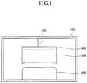
- FIG. 1is a schematic diagram illustrating a device for bonding a window according to a first exemplary embodiment.
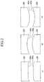
- FIG. 2is a diagram illustrating modified examples of a window fixing unit and a display panel fixing unit in the device for bonding a window according to the first exemplary embodiment.
- FIG. 3is a schematic diagram illustrating a device for bonding a window according to a second exemplary embodiment.
- FIG. 4is a schematic diagram illustrating a device for bonding a window according to a third exemplary embodiment.
- FIG. 5is a flowchart illustrating a method for manufacturing a display device according to an exemplary embodiment.
- FIGS. 6A to 6Care diagrams illustrating a method for manufacturing a display device according to an exemplary embodiment.
- the word “comprise” and variations such as “comprises” or “comprising”,will be understood to imply the inclusion of stated elements but not the exclusion of any other elements.
- the word “on”will be understood to be positioned above or below a target element and will not be limited to a position at an upper side based on a gravity direction.
- FIG. 1is a schematic diagram illustrating a device for bonding a window according to a first exemplary embodiment
- FIG. 2is a diagram illustrating modified examples of a window fixing unit and a display panel fixing unit in the device for bonding a window according to the first exemplary embodiment.
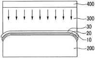
- a device for bonding a windowincludes a chamber 100 , a display panel fixing unit 200 , a window fixing unit 300 , and an ultraviolet irradiating unit 400 .
- the chamber 100i.e., a means having a processing space therein, may be sealed so as to form vacuum in the processing space therein.
- a gate(not shown), e.g., through which the window or a flexible display panel moves in and out the processing space, may be further included at a side wall of the chamber 100 .
- a discharging hole(not illustrated) and a discharging pump (not illustrated) connected to the discharging hole are provided at one side wall of the chamber 100 .
- the discharging pumpmay provide vacuum inside the chamber 100 or discharge the remaining processing gas after a processing is performed in the chamber 100 through the discharging hole.
- the display panel fixing unit 200i.e., a means for fixing the display panel, includes a first curved surface 200 a , on which a flexible display panel is disposed in order to fix the flexible display panel having a curved surface.
- the flexible display panelmay be, e.g., an organic light emitting display device, a liquid crystal display, or a touch screen panel, but is not limited thereto and may be selected from various display panels having curved surfaces.
- the flexible display panelmay be fixed through a fixing unit (not illustrated) such as a clamp.
- An adhesive layer for attaching the window and the displayis coated on the display panel, and the detailed description thereof will be provided below.
- the window fixing unit 300i.e., a means for fixing the window that protects the display panel, includes a second curved surface 300 a , on which a window is disposed in order to fix the window having a curved surface.
- the windowis disposed in a direction in which an image is output from the display panel 100 and defines an external surface of the display device together with a case (not illustrated) by coupling the case protecting the display panel.
- the windowis attached to the display panel 100 through the adhesive layer.
- the first curved surface 200 a formed on the display panel fixing unit 200 and the second curved surface 300 a formed on the window fixing unit 300have physically complimentary structures, e.g., match or fit within each other.
- the second curved surface 300 awhen the first curved surface 200 a includes a flat surface at a center and a curved surface at each edge, the second curved surface 300 a includes a flat surface at the center and a curved surface coinciding, e.g., aligned, with each curved edge of the first curved surface 200 a , such that the first curved surface 200 a matches exactly the second curved surface 300 a .
- FIG. 2Awhen the first curved surface 200 a includes a flat surface at a center and a curved surface at each edge, the second curved surface 300 a includes a flat surface at the center and a curved surface coinciding, e.g., aligned, with each curved edge of the first curved surface 200 a , such that the first curved
- the second curved surface 300 awhen the first curved surface 200 a includes a convex-shaped curved surface, the second curved surface 300 a includes a concave-shaped curved surface coinciding with the first curved surface 200 a .
- the first curved surface 200 a and the second curved surface 300 aare not limited thereto and may be variously changed and implemented so long as the two curved surfaces match with each other.
- the windowmay be fixed through a fixing unit (not illustrated), e.g., a clamp, and may be absorbed and fixed by vacuum.
- the window fixing unit 300may further include a moving unit 500 so as to move backward and forward in a direction facing the display panel fixing unit 200 .
- the moving unit 500allows the second curved surface 300 a of the window fixing unit 300 to contact the first curved surface 200 a of the display panel fixing unit 200 .
- the window disposed on the second curved surface 300 acontacts the flexible display panel disposed on the first curved surface 200 a , thereby enabling bonding between the window and the flexible display panel.
- a pressure sensor(not illustrated) for measuring contact strength between the second curved surface 300 a and the first curved surface 200 a may be further included in the window fixing unit 300 .
- the pressure sensorcontacts the second curved surface 300 a and the first curved surface 200 a at optimal pressure to prevent the window and the flexible display panel from being damaged due to strong pressure or to prevent the window and the flexible display panel from being weakly bonded to each other due to weak pressure.
- At least a part of the window fixing unit 300is made of an ultraviolet transmitting material.
- the window fixing unit 300transmits ultraviolet light generated by the ultraviolet irradiating unit 400 to be described below, so the ultraviolet light reaches the first curved surface 200 a through the second curved surface 300 a .
- the entire window fixing unit 300may be formed of an ultraviolet transmitting material.
- the ultraviolet transmitting material used in the window fixing unit 300may be, e.g., an acryl plastic material, but is not limited thereto, e.g., may be any suitable material capable of transmitting ultraviolet light.
- any one of the display panel fixing unit 200 or the window fixing unit 300includes a sensor for arranging the display panel fixing unit 200 or the window fixing unit 300 . As a result, the display panel and the window may be accurately arranged.
- the ultraviolet irradiating unit 400is disposed at one side of the window fixing unit 300 , e.g., the ultraviolet irradiating unit 400 may be on a surface of the window fixing unit 300 opposite the second curved surface 300 a .
- the ultraviolet irradiating unit 400may continuously overlap the entire second curved surface 300 a .
- the ultraviolet irradiating unit 400provides ultraviolet light for curing the adhesive layer between the display panel and the window, thereby attaching the display panel and the window to each other.
- the ultraviolet light generated from the ultraviolet irradiating unit 400passes through the window fixing unit 300 made of the ultraviolet transmitting material to be emitted from the second curved surface 300 a toward the first curved surface 200 a , thereby curing the adhesive layer coated on the display panel.
- FIG. 3is a schematic diagram illustrating a device for bonding a window according to a second exemplary embodiment
- FIG. 4is a schematic diagram illustrating a device for bonding a window according to a third exemplary embodiment.
- Detailed description of elements of the devices for bonding a window according to the second exemplary embodiment and the third exemplary embodiment that are the same as those described previously with reference to the first exemplary embodimentwill be omitted.
- the first curved surface 200 a formed on the display panel fixing unit 200 and the second curved surface 300 a formed on a window fixing unit 300 ′may be configured in a form in which the edges are curved surfaces and the centers are flat surfaces, respectively.
- the window fixing unit 300 ′may include an ultraviolet transmitting unit 310 , i.e., corresponding to edges of the second curved surface 300 a , made of an ultraviolet transmitting material and an ultraviolet non-transmitting unit 320 , i.e., corresponding to the center of the second curved surface 300 a , made of an ultraviolet non-transmitting material.
- the ultraviolet light generated from the ultraviolet irradiating unit 400passes, e.g., only, through the ultraviolet transmitting unit 310 to reach the curved edges of the second curved surface 300 a .
- the window or the display panelis used to firstly attach the curved surface portion because internal stress is generated at the curved surface portion.
- a window fixing unit 303may be entirely made of an ultraviolet non-transmitting material.
- an ultraviolet irradiating unit 403is not attached to one side of the window fixing unit 303 , but disposed at one side of the inside of the chamber 100 , e.g., at a bottom of the chamber 100 , to irradiate ultraviolet light to the first curved surface 200 a and the second curved surface 300 a.
- FIG. 5is a flowchart illustrating a method for manufacturing a display device according to an exemplary embodiment
- FIGS. 6A to 6Care diagrams of a method for manufacturing a display device according to an exemplary embodiment.
- the method for manufacturing a display deviceincludes disposing a display panel with an adhesive layer coated thereon (S 10 ), disposing a window (S 20 ), arranging the window and the display panel to face each other (S 30 ), contacting the window with the display panel (S 40 ), and curing the adhesive layer (S 50 ).
- a flexible display panel 10is disposed on the first curved surface 200 a included in the display panel fixing unit 200 , and an adhesive layer 20 is coated on the flexible display panel 10 (S 10 ).
- a window 30is disposed on the second curved surface 300 a included in the window fixing unit 300 (S 20 ).
- the adhesive layer 20may be made of a transparent adhesive material having high transmittance in order to prevent luminance of an image output from the display panel 10 from being reduced.
- the adhesive layer 20may be prepared in a liquid state, but may be made in a semi-liquid state having a predetermined viscosity in order to prevent the adhesive layer from flowing down toward the flexible display panel 10 .
- the disposing of the display panel 10 and the adhesive layer 20 , and the disposing of the window 30may be performed in a vacuum state or may be performed in a non-vacuum state.
- the flexible display panel 10is carried into the chamber 100 to be directly disposed on the display panel fixing unit 200 , and the adhesive layer 20 may be coated thereon inside the chamber 100 .
- the display panel fixing unit 200may be carried outside the chamber 100 for disposing the flexible display panel 10 and coating the adhesive layer 20 thereon, followed by disposing the display panel fixing unit 200 with the flexible display panel 10 and the adhesive layer 20 inside the chamber 100 .
- the window 30is carried into the chamber 100 to be directly disposed on the window fixing unit 300 , or alternatively, the window fixing unit 300 may be carried into the chamber 100 , after disposing the window 30 on the window fixing unit 300 outside the chamber 100 .
- the disposing of the display panel 10 and the adhesive layer 20 and the disposing of the window 30may be reversed in a different order.
- the inside of the chamber 100may be processed to provide vacuum conditions, e.g., by using a discharging pump.
- the reasonis to prevent bubbles from being generated in the adhesive layer 20 or to prevent a foreign substance from being included.
- the degree of the vacuum conditions in the chamber 100may be properly controlled by considering the material of the adhesive layer 20 or the ultraviolet irradiation strength.
- the first curved surface 200 a with the display panel 10 and the adhesive layer 20 thereonis arranged to face the second curved surface 300 a with the window 30 thereon (S 30 ).
- the first and second curved surfaces 200 a and 300 aare arranged to have the adhesive layer 20 on the first curved surface 200 a face directly the window 30 on the second curved surface 300 a.
- the window fixing unit 300is moved toward the display panel fixing unit 200 , e.g., by using a moving means (S 40 ), to contact the display panel fixing unit 200 .
- the second curved surface 300 a and the first curved surface 200 amay contact each other at optimal pressure, i.e., via the window 30 , adhesive layer 20 , and display panel 10 , by using a pressure sensor.
- the adhesive layer 20is cured by irradiating ultraviolet light to the adhesive layer 20 disposed between the flexible display panel 10 and the window 30 , thereby bonding the window 30 and the flexible display panel 10 to each other (S 50 ).
- the window fixing unit 300is made of an ultraviolet transmitting material, and the ultraviolet light generated from the ultraviolet irradiating unit 400 passes through the window fixing unit 300 to reach the adhesive layer 20 .
- the strength of the ultraviolet lightmay be properly controlled according to a material, a thickness, and the like.
- the curingis performed under vacuum conditions.
- the window fixing unit 300may be configured to transmit ultraviolet light only to the curved edges, as described previously with reference to FIG. 3 . After a predetermined time elapses, when the adhesive layer 20 is cured by the ultraviolet light, the flexible display panel 10 and the window 20 are bonded to each other.
- the exemplary embodimentsit is possible to reduce defects during bonding of the display panel and the window by uniformly curing the adhesive layer between the display panel and the window, thereby preventing generation of bubbles in the adhesive layer. As a result, it is possible to prevent deterioration in the display quality, e.g., a screen spot, by preventing a minute curve which may be generated between the window and the display panel. Further, it is possible to increase adhesion between the window and the display panel.
- the display panel and the windowmay be bonded to each other at atmospheric pressure, rather than under vacuum conditions, during curing of the adhesive layer.
- use of the adhesive layer at atmospheric pressuremay generate bubbles in the adhesive layer or cause non-uniform adhesion of the adhesive layer.
Landscapes
- Physics & Mathematics (AREA)
- General Physics & Mathematics (AREA)
- Engineering & Computer Science (AREA)
- Theoretical Computer Science (AREA)
- Devices For Indicating Variable Information By Combining Individual Elements (AREA)
- Liquid Crystal (AREA)
Abstract
Description
| <Description of symbols> |
| 10: Display panel | 20: Adhesive layer | ||
| 30: Window | 200: Display panel fixing unit | ||
| 100: Chamber | 400: Ultraviolet irradiating unit | ||
| 300: Window fixing unit | |||
| 500: Moving means | |||
Claims (9)
Priority Applications (1)
| Application Number | Priority Date | Filing Date | Title |
|---|---|---|---|
| US15/467,721US11090919B2 (en) | 2012-10-05 | 2017-03-23 | Device for bonding window and method for manufacturing display device using the same |
Applications Claiming Priority (4)
| Application Number | Priority Date | Filing Date | Title |
|---|---|---|---|
| KR1020120110715AKR101979726B1 (en) | 2012-10-05 | 2012-10-05 | Device for bonding window and method for manufacturing display device using the same |
| KR10-2012-0110715 | 2012-10-05 | ||
| US13/920,200US9616647B2 (en) | 2012-10-05 | 2013-06-18 | Device for bonding window and method for manufacturing display device using the same |
| US15/467,721US11090919B2 (en) | 2012-10-05 | 2017-03-23 | Device for bonding window and method for manufacturing display device using the same |
Related Parent Applications (1)
| Application Number | Title | Priority Date | Filing Date |
|---|---|---|---|
| US13/920,200DivisionUS9616647B2 (en) | 2012-10-05 | 2013-06-18 | Device for bonding window and method for manufacturing display device using the same |
Publications (2)
| Publication Number | Publication Date |
|---|---|
| US20170190164A1 US20170190164A1 (en) | 2017-07-06 |
| US11090919B2true US11090919B2 (en) | 2021-08-17 |
Family
ID=50431808
Family Applications (2)
| Application Number | Title | Priority Date | Filing Date |
|---|---|---|---|
| US13/920,200Active2034-09-27US9616647B2 (en) | 2012-10-05 | 2013-06-18 | Device for bonding window and method for manufacturing display device using the same |
| US15/467,721Active2034-09-18US11090919B2 (en) | 2012-10-05 | 2017-03-23 | Device for bonding window and method for manufacturing display device using the same |
Family Applications Before (1)
| Application Number | Title | Priority Date | Filing Date |
|---|---|---|---|
| US13/920,200Active2034-09-27US9616647B2 (en) | 2012-10-05 | 2013-06-18 | Device for bonding window and method for manufacturing display device using the same |
Country Status (2)
| Country | Link |
|---|---|
| US (2) | US9616647B2 (en) |
| KR (1) | KR101979726B1 (en) |
Families Citing this family (31)
| Publication number | Priority date | Publication date | Assignee | Title |
|---|---|---|---|---|
| KR20140063228A (en)* | 2012-11-16 | 2014-05-27 | 삼성디스플레이 주식회사 | Organic light emitting diode display |
| KR101701247B1 (en) | 2013-05-27 | 2017-02-02 | 삼성디스플레이 주식회사 | Laminating device and Laminating method using the same |
| KR102131962B1 (en) | 2013-06-25 | 2020-07-09 | 삼성디스플레이 주식회사 | Manufacturing device for a cover window and manufacturing method for the cover window |
| DE102014213187A1 (en)* | 2014-07-08 | 2016-01-14 | Bayerische Motoren Werke Aktiengesellschaft | Press tool with optimized resin flow |
| KR101677014B1 (en)* | 2014-08-14 | 2016-11-17 | 안성룡 | The method for manufacturing a flexible display device |
| KR102348799B1 (en)* | 2015-01-14 | 2022-01-07 | 삼성디스플레이 주식회사 | Apparatus for manufacturing flexible display device |
| KR102345440B1 (en) | 2015-02-13 | 2021-12-30 | 삼성디스플레이 주식회사 | display panel manufacturing apparatus |
| KR101588600B1 (en) | 2015-07-23 | 2016-02-01 | 주식회사 톱텍 | bonding device for window, bonding method using it |
| KR102410628B1 (en)* | 2015-08-31 | 2022-06-17 | 엘지디스플레이 주식회사 | Apparatus and method of fabricating curved display |
| KR101737009B1 (en) | 2015-09-22 | 2017-05-17 | 주식회사 톱텍 | bonding device for window |
| KR102537377B1 (en) | 2016-03-10 | 2023-05-26 | 삼성디스플레이 주식회사 | Apparatus for manufacturing display device and manufacturing method thereof |
| JP2017181888A (en)* | 2016-03-31 | 2017-10-05 | 大日本印刷株式会社 | Light control film and laminate of light control film |
| KR101653597B1 (en) | 2016-04-06 | 2016-09-09 | 주식회사 톱텍 | Laminating device having press pad for varying volume and laminating method using it |
| KR102632896B1 (en)* | 2016-08-16 | 2024-02-02 | 삼성전자주식회사 | Protecting Cover and Protecting Cover Package, and Electronic device including the same |
| CN106541670A (en)* | 2016-09-22 | 2017-03-29 | 南昌欧菲光学技术有限公司 | 3D glass decoration films process equipment and method |
| KR102529080B1 (en)* | 2016-10-05 | 2023-05-09 | 삼성디스플레이 주식회사 | Laminating apparatus and laminating method using the same |
| CN108932072A (en)* | 2017-05-22 | 2018-12-04 | 蓝思科技(长沙)有限公司 | The preparation method and abutted equipment of touch display screen |
| KR102404974B1 (en) | 2017-09-12 | 2022-06-03 | 삼성디스플레이 주식회사 | Display device |
| CN108615463B (en)* | 2018-04-20 | 2020-10-27 | 广州国显科技有限公司 | Attaching device and attaching method for special-shaped curved surface cover plate and flexible screen |
| CN108648630B (en)* | 2018-05-31 | 2020-03-17 | 武汉华星光电半导体显示技术有限公司 | Curved screen laminating device and laminating method |
| CN109878068A (en)* | 2019-04-08 | 2019-06-14 | 万维科研有限公司 | A kind of bonding method and device of flexible sheet |
| CN110103564B (en)* | 2019-05-27 | 2021-06-11 | 业成科技(成都)有限公司 | Bonding jig and bonding method using same |
| CN110576672B (en)* | 2019-10-10 | 2020-06-02 | 深圳市灵触科技有限公司 | Laminating method for laminating curved capacitive screen to panel display screen and laminating jig device |
| KR102346436B1 (en)* | 2020-03-31 | 2022-01-05 | 에이피시스템 주식회사 | Apparatus for laminating pannel to window and method for laminating pannel to window |
| CN111546748A (en)* | 2020-05-22 | 2020-08-18 | 上海科世达-华阳汽车电器有限公司 | A kind of surface bonding equipment and bonding method |
| KR102698113B1 (en)* | 2020-06-03 | 2024-08-26 | 삼성디스플레이 주식회사 | Support, bonding device including support, and method of manufacturing display device using the same |
| US11485123B2 (en)* | 2020-07-07 | 2022-11-01 | Samsung Display Co., Ltd. | Lamination apparatus |
| CN114248527B (en)* | 2020-09-21 | 2024-07-30 | 北京小米移动软件有限公司 | Method for preparing curved screen and curved screen |
| KR102401690B1 (en) | 2020-10-21 | 2022-05-26 | 주식회사 나래나노텍 | Substrate bonding device and method using adhesive with flowability |
| CN112652242B (en)* | 2020-12-09 | 2022-08-23 | 深圳一鑫新材料有限公司 | Flexible curved surface display screen laminating process |
| CN114187842B (en)* | 2021-12-20 | 2023-05-16 | 武汉天马微电子有限公司 | Display screen attaching device and display screen attaching method |
Citations (14)
| Publication number | Priority date | Publication date | Assignee | Title |
|---|---|---|---|---|
| US4923552A (en) | 1987-06-12 | 1990-05-08 | Matsushita Electric Industrial Co., Ltd. | Method of producing liquid crystal display element |
| US20020008838A1 (en)* | 2000-07-19 | 2002-01-24 | Nec Corporation | Apparatus and method of manufacturing liquid crystal display |
| KR20030090856A (en) | 2002-05-22 | 2003-12-01 | 엘지.필립스 엘시디 주식회사 | Device for Hot Pressing Liquid Crystal Display and Assembling Method by Using the same |
| US20030226633A1 (en) | 2002-06-11 | 2003-12-11 | Fujitsu Limited | Method and apparatus for fabricating bonded substrate |
| US20050077553A1 (en) | 2003-10-14 | 2005-04-14 | Kim Sung-Min | Methods of forming multi fin FETs using sacrificial fins and devices so formed |
| US20060027318A1 (en) | 2000-11-30 | 2006-02-09 | Fujitsu Limited | Apparatus for manufacturing bonded substrate |
| KR20080062424A (en) | 2006-12-29 | 2008-07-03 | 엘지디스플레이 주식회사 | Board Bonding Device and Board Bonding Method |
| KR20100024581A (en) | 2008-08-26 | 2010-03-08 | 한동희 | Flat panels bonding apparatus and method |
| US20100253902A1 (en) | 2009-04-07 | 2010-10-07 | Semiconductor Energy Laboratory Co., Ltd. | Liquid crystal display device and manufacturing method thereof |
| KR20100131567A (en) | 2009-06-08 | 2010-12-16 | (주)아이디에스 | Liquid Crystal Display Manufacturing Method |
| KR20110029668A (en) | 2009-09-16 | 2011-03-23 | 한동희 | Panel Attachment Method |
| US20110177261A1 (en) | 2010-01-15 | 2011-07-21 | Hitachi Displays, Ltd. | Display device with front window and manufacturing method thereof |
| KR20110115630A (en) | 2010-04-16 | 2011-10-24 | 삼성전자주식회사 | Glass plate forming apparatus and glass plate forming method |
| KR20120106304A (en) | 2011-03-18 | 2012-09-26 | 삼성디스플레이 주식회사 | Flat panel display apparatus and the manufacturing method thereof |
- 2012
- 2012-10-05KRKR1020120110715Apatent/KR101979726B1/enactiveActive
- 2013
- 2013-06-18USUS13/920,200patent/US9616647B2/enactiveActive
- 2017
- 2017-03-23USUS15/467,721patent/US11090919B2/enactiveActive
Patent Citations (15)
| Publication number | Priority date | Publication date | Assignee | Title |
|---|---|---|---|---|
| US4923552A (en) | 1987-06-12 | 1990-05-08 | Matsushita Electric Industrial Co., Ltd. | Method of producing liquid crystal display element |
| US20020008838A1 (en)* | 2000-07-19 | 2002-01-24 | Nec Corporation | Apparatus and method of manufacturing liquid crystal display |
| US20060027318A1 (en) | 2000-11-30 | 2006-02-09 | Fujitsu Limited | Apparatus for manufacturing bonded substrate |
| KR20030090856A (en) | 2002-05-22 | 2003-12-01 | 엘지.필립스 엘시디 주식회사 | Device for Hot Pressing Liquid Crystal Display and Assembling Method by Using the same |
| US20030226633A1 (en) | 2002-06-11 | 2003-12-11 | Fujitsu Limited | Method and apparatus for fabricating bonded substrate |
| KR20050035712A (en) | 2003-10-14 | 2005-04-19 | 삼성전자주식회사 | Multi silicon fins for finfet and method for fabricating the same |
| US20050077553A1 (en) | 2003-10-14 | 2005-04-14 | Kim Sung-Min | Methods of forming multi fin FETs using sacrificial fins and devices so formed |
| KR20080062424A (en) | 2006-12-29 | 2008-07-03 | 엘지디스플레이 주식회사 | Board Bonding Device and Board Bonding Method |
| KR20100024581A (en) | 2008-08-26 | 2010-03-08 | 한동희 | Flat panels bonding apparatus and method |
| US20100253902A1 (en) | 2009-04-07 | 2010-10-07 | Semiconductor Energy Laboratory Co., Ltd. | Liquid crystal display device and manufacturing method thereof |
| KR20100131567A (en) | 2009-06-08 | 2010-12-16 | (주)아이디에스 | Liquid Crystal Display Manufacturing Method |
| KR20110029668A (en) | 2009-09-16 | 2011-03-23 | 한동희 | Panel Attachment Method |
| US20110177261A1 (en) | 2010-01-15 | 2011-07-21 | Hitachi Displays, Ltd. | Display device with front window and manufacturing method thereof |
| KR20110115630A (en) | 2010-04-16 | 2011-10-24 | 삼성전자주식회사 | Glass plate forming apparatus and glass plate forming method |
| KR20120106304A (en) | 2011-03-18 | 2012-09-26 | 삼성디스플레이 주식회사 | Flat panel display apparatus and the manufacturing method thereof |
Also Published As
| Publication number | Publication date |
|---|---|
| KR20140044579A (en) | 2014-04-15 |
| US20140096892A1 (en) | 2014-04-10 |
| US9616647B2 (en) | 2017-04-11 |
| US20170190164A1 (en) | 2017-07-06 |
| KR101979726B1 (en) | 2019-05-20 |
Similar Documents
| Publication | Publication Date | Title |
|---|---|---|
| US11090919B2 (en) | Device for bonding window and method for manufacturing display device using the same | |
| CN101950094B (en) | Display apparatus with protection plate and manufacturing method thereof | |
| CN106019666B (en) | Display device and method for manufacturing display device | |
| US9568757B2 (en) | Display device having mold frame with elastic protective member | |
| US20180145276A1 (en) | Encapsulation film for organic light emitting display device, method of manufacturing the same, and organic light emitting display device using the same | |
| CN105278138B (en) | Liquid crystal display device | |
| US20190018275A1 (en) | Display device | |
| KR102154606B1 (en) | Flexible organic light emitting diode display device and method of fabricating thereof | |
| US10036911B2 (en) | Tiled display device | |
| US20070031997A1 (en) | Jig and vacuum equipment for surface adhesion and adhesion method using the vacuum operative adhesion | |
| JP2018004728A (en) | Display device and bonding method | |
| KR102357930B1 (en) | Display device | |
| US20170248808A1 (en) | Display device | |
| US20160165677A1 (en) | Organic light emitting diode display device and fabrication method thereof | |
| CN108020957A (en) | Display device | |
| JP2016194670A (en) | Display device and manufacturing method of display device | |
| US8964150B2 (en) | Liquid crystal display device and method of manufacturing the same | |
| CN108020879B (en) | Display device | |
| KR20130098095A (en) | Curing device and method of edge-portion of workpiece, and bonding apparatus and method of workpiece having the same | |
| CN110596965A (en) | display device | |
| JP5338407B2 (en) | Flat display module and manufacturing method thereof | |
| CN206584142U (en) | Display device | |
| US10191513B2 (en) | Waterproof display apparatus and method of assembling the same | |
| JP6362534B2 (en) | Curved display device | |
| JP2012237562A (en) | Radiation detection panel and radiographic image detector |
Legal Events
| Date | Code | Title | Description |
|---|---|---|---|
| STPP | Information on status: patent application and granting procedure in general | Free format text:DOCKETED NEW CASE - READY FOR EXAMINATION | |
| STPP | Information on status: patent application and granting procedure in general | Free format text:NON FINAL ACTION MAILED | |
| STPP | Information on status: patent application and granting procedure in general | Free format text:NON FINAL ACTION MAILED | |
| STPP | Information on status: patent application and granting procedure in general | Free format text:FINAL REJECTION MAILED | |
| STPP | Information on status: patent application and granting procedure in general | Free format text:ADVISORY ACTION MAILED | |
| STPP | Information on status: patent application and granting procedure in general | Free format text:DOCKETED NEW CASE - READY FOR EXAMINATION | |
| STPP | Information on status: patent application and granting procedure in general | Free format text:RESPONSE TO NON-FINAL OFFICE ACTION ENTERED AND FORWARDED TO EXAMINER | |
| STPP | Information on status: patent application and granting procedure in general | Free format text:FINAL REJECTION MAILED | |
| STPP | Information on status: patent application and granting procedure in general | Free format text:ADVISORY ACTION MAILED | |
| STPP | Information on status: patent application and granting procedure in general | Free format text:FINAL REJECTION MAILED | |
| STPP | Information on status: patent application and granting procedure in general | Free format text:RESPONSE AFTER FINAL ACTION FORWARDED TO EXAMINER | |
| STPP | Information on status: patent application and granting procedure in general | Free format text:NOTICE OF ALLOWANCE MAILED -- APPLICATION RECEIVED IN OFFICE OF PUBLICATIONS | |
| STPP | Information on status: patent application and granting procedure in general | Free format text:PUBLICATIONS -- ISSUE FEE PAYMENT RECEIVED | |
| STPP | Information on status: patent application and granting procedure in general | Free format text:PUBLICATIONS -- ISSUE FEE PAYMENT VERIFIED | |
| STCF | Information on status: patent grant | Free format text:PATENTED CASE | |
| MAFP | Maintenance fee payment | Free format text:PAYMENT OF MAINTENANCE FEE, 4TH YEAR, LARGE ENTITY (ORIGINAL EVENT CODE: M1551); ENTITY STATUS OF PATENT OWNER: LARGE ENTITY Year of fee payment:4 |