US11083082B2 - Enclosure-to-board interface with tamper-detect circuit(s) - Google Patents
Enclosure-to-board interface with tamper-detect circuit(s)Download PDFInfo
- Publication number
- US11083082B2 US11083082B2US16/567,034US201916567034AUS11083082B2US 11083082 B2US11083082 B2US 11083082B2US 201916567034 AUS201916567034 AUS 201916567034AUS 11083082 B2US11083082 B2US 11083082B2
- Authority
- US
- United States
- Prior art keywords
- enclosure
- tamper
- circuit board
- main surface
- conductive trace
- Prior art date
- Legal status (The legal status is an assumption and is not a legal conclusion. Google has not performed a legal analysis and makes no representation as to the accuracy of the status listed.)
- Active
Links
Images


Classifications
- H—ELECTRICITY
- H05—ELECTRIC TECHNIQUES NOT OTHERWISE PROVIDED FOR
- H05K—PRINTED CIRCUITS; CASINGS OR CONSTRUCTIONAL DETAILS OF ELECTRIC APPARATUS; MANUFACTURE OF ASSEMBLAGES OF ELECTRICAL COMPONENTS
- H05K5/00—Casings, cabinets or drawers for electric apparatus
- H05K5/02—Details
- H05K5/0208—Interlock mechanisms; Means for avoiding unauthorised use or function, e.g. tamperproof
- G—PHYSICS
- G06—COMPUTING OR CALCULATING; COUNTING
- G06F—ELECTRIC DIGITAL DATA PROCESSING
- G06F21/00—Security arrangements for protecting computers, components thereof, programs or data against unauthorised activity
- G—PHYSICS
- G06—COMPUTING OR CALCULATING; COUNTING
- G06F—ELECTRIC DIGITAL DATA PROCESSING
- G06F21/00—Security arrangements for protecting computers, components thereof, programs or data against unauthorised activity
- G06F21/70—Protecting specific internal or peripheral components, in which the protection of a component leads to protection of the entire computer
- G06F21/86—Secure or tamper-resistant housings
- H—ELECTRICITY
- H01—ELECTRIC ELEMENTS
- H01L—SEMICONDUCTOR DEVICES NOT COVERED BY CLASS H10
- H01L23/00—Details of semiconductor or other solid state devices
- H01L23/57—Protection from inspection, reverse engineering or tampering
- H01L23/576—Protection from inspection, reverse engineering or tampering using active circuits
- H—ELECTRICITY
- H05—ELECTRIC TECHNIQUES NOT OTHERWISE PROVIDED FOR
- H05K—PRINTED CIRCUITS; CASINGS OR CONSTRUCTIONAL DETAILS OF ELECTRIC APPARATUS; MANUFACTURE OF ASSEMBLAGES OF ELECTRICAL COMPONENTS
- H05K1/00—Printed circuits
- H05K1/02—Details
- H05K1/0275—Security details, e.g. tampering prevention or detection
- H—ELECTRICITY
- H05—ELECTRIC TECHNIQUES NOT OTHERWISE PROVIDED FOR
- H05K—PRINTED CIRCUITS; CASINGS OR CONSTRUCTIONAL DETAILS OF ELECTRIC APPARATUS; MANUFACTURE OF ASSEMBLAGES OF ELECTRICAL COMPONENTS
- H05K1/00—Printed circuits
- H05K1/02—Details
- H05K1/11—Printed elements for providing electric connections to or between printed circuits
- H05K1/115—Via connections; Lands around holes or via connections
- H—ELECTRICITY
- H05—ELECTRIC TECHNIQUES NOT OTHERWISE PROVIDED FOR
- H05K—PRINTED CIRCUITS; CASINGS OR CONSTRUCTIONAL DETAILS OF ELECTRIC APPARATUS; MANUFACTURE OF ASSEMBLAGES OF ELECTRICAL COMPONENTS
- H05K1/00—Printed circuits
- H05K1/18—Printed circuits structurally associated with non-printed electric components
- H05K1/181—Printed circuits structurally associated with non-printed electric components associated with surface mounted components
- H—ELECTRICITY
- H05—ELECTRIC TECHNIQUES NOT OTHERWISE PROVIDED FOR
- H05K—PRINTED CIRCUITS; CASINGS OR CONSTRUCTIONAL DETAILS OF ELECTRIC APPARATUS; MANUFACTURE OF ASSEMBLAGES OF ELECTRICAL COMPONENTS
- H05K2201/00—Indexing scheme relating to printed circuits covered by H05K1/00
- H05K2201/09—Shape and layout
- H05K2201/09209—Shape and layout details of conductors
- H05K2201/09218—Conductive traces
- H05K2201/09263—Meander
- H—ELECTRICITY
- H05—ELECTRIC TECHNIQUES NOT OTHERWISE PROVIDED FOR
- H05K—PRINTED CIRCUITS; CASINGS OR CONSTRUCTIONAL DETAILS OF ELECTRIC APPARATUS; MANUFACTURE OF ASSEMBLAGES OF ELECTRICAL COMPONENTS
- H05K2201/00—Indexing scheme relating to printed circuits covered by H05K1/00
- H05K2201/10—Details of components or other objects attached to or integrated in a printed circuit board
- H05K2201/10227—Other objects, e.g. metallic pieces
- H—ELECTRICITY
- H05—ELECTRIC TECHNIQUES NOT OTHERWISE PROVIDED FOR
- H05K—PRINTED CIRCUITS; CASINGS OR CONSTRUCTIONAL DETAILS OF ELECTRIC APPARATUS; MANUFACTURE OF ASSEMBLAGES OF ELECTRICAL COMPONENTS
- H05K3/00—Apparatus or processes for manufacturing printed circuits
- H—ELECTRICITY
- H05—ELECTRIC TECHNIQUES NOT OTHERWISE PROVIDED FOR
- H05K—PRINTED CIRCUITS; CASINGS OR CONSTRUCTIONAL DETAILS OF ELECTRIC APPARATUS; MANUFACTURE OF ASSEMBLAGES OF ELECTRICAL COMPONENTS
- H05K5/00—Casings, cabinets or drawers for electric apparatus
Definitions
- an encryption/decryption systemmay be implemented on an electronic assembly or printed circuit board assembly that is included in equipment connected to a communications network. Such an electronic assembly is an enticing target for malefactors since it may contain codes or keys to decrypt intercepted messages, or to encode fraudulent messages.
- an electronic assemblymay be mounted in an enclosure, which is then wrapped in a security sensor and encapsulated with polyurethane resin.
- a security sensormay be, in one or more embodiments, a web or sheet of insulating material with circuit elements, such as closely-spaced, conductive lines fabricated on it. The circuit elements are disrupted if the sensor is torn, and the tear can be sensed in order to generate an alarm signal.
- the alarm signalmay be conveyed to a monitor circuit in order to reveal an attack on the integrity of the assembly.
- the alarm signalmay also trigger an erasure of encryption/decryption keys stored within the electronic assembly.
- a tamper-respondent assemblywhich includes a circuit board and an enclosure mounted to the circuit board along an enclosure-to-board interface.
- the enclosurealong with a tamper-respondent electronic circuit structure, facilitates enclosing at least one electronic component coupled to the circuit board within a secure volume.
- the tamper-respondent electronic circuit structureincludes one or more tamper-detect circuits, including at least one conductive trace disposed, at least in part, within the enclosure-to-board interface.
- the at least one conductive traceincludes stress rise regions to facilitate detecting a tamper event at the enclosure-to-board interface.
- An adhesivefacilitates securing the enclosure to the circuit board.
- the adhesivecontacts, at least in part, the at least one conductive trace of the one or more tamper-detect circuits within the enclosure-to-board interface, including at the stress rise regions of the at least one conductive trace.
- a tamper-respondent assemblywhich includes: a circuit board; at least one electronic component to be protected; an enclosure mounted to the circuit board along an enclosure-to-board interface; a tamper-respondent electronic circuit structure; and an adhesive.
- the at least one electronic componentis associated with the circuit board, and the enclosure facilitates enclosing the at least one electronic component within a secure volume.
- the tamper-respondent electronic circuit structureassists in defining the secure volume, and includes one or more tamper-detect circuits, including at least one conductive trace disposed, at least in part, within the enclosure-to-board interface.
- the at least one conductive traceincludes stress rise regions to facilitate detecting a tamper event at the enclosure-to-board interface.
- the adhesivesecures the enclosure to the circuit board, and contacts, at least in part, the at least one conductive trace of the one or more tamper-detect circuits within the enclosure-to-board interface, including at the stress rise regions of the at least one conductive trace.
- a fabrication methodwhich includes fabricating a tamper-respondent assembly.
- Fabricating the tamper-respondent assemblyincludes providing a circuit board, and providing an enclosure mounted to the circuit board along an enclosure-to-board interface, the enclosure facilitating enclosing at least one electronic component coupled to the circuit board within a secure volume.
- the methodfurther includes providing a tamper-respondent electronic circuit structure that facilitates defining the secure volume.
- the tamper-respondent electronic circuit structureincludes one or more tamper-detect circuits, including at least one conductive trace disposed, at least in part, within the enclosure-to-board interface, and the at least one conductive trace includes stress rise regions to facilitate detecting a tamper event at the enclosure-to-board interface. Further, the method includes securing the enclosure to the circuit board using an adhesive, the adhesive contacting, at least in part, the at least one conductive trace of the one or more tamper-detect circuits within the enclosure to board interface, including at the stress rise regions of the at least one conductive trace.
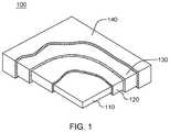
- FIG. 1is a partial cut-away of one embodiment of a tamper-proof electronic package
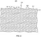
- FIG. 2depicts one embodiment of a tamper-respondent sensor with conductive lines forming, at least in part, at least one tamper-detect circuit, in accordance with one or more aspects of the present invention
- FIG. 3Ais a cross-sectional elevational view of another embodiment of a tamper-proof electronic package, or tamper-respondent assembly, which includes (in part) an enclosure, and a multilayer circuit board with an embedded tamper-detect circuit, in accordance with one or more aspects of the present invention
- FIG. 3Bis a top plan view of the multilayer circuit board of FIG. 3A , depicting one embodiment of the secure volume defined, in part, within the multilayer circuit board, in accordance with one or more aspects of the present invention
- FIG. 4is a partial cross-sectional elevational view of a more detailed embodiment of the tamper-respondent assembly of FIGS. 3A & 3B including (in part) an enclosure and a multilayer circuit board with embedded tamper-detect circuit, in accordance with one or more aspects of the present invention
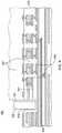
- FIG. 5depicts one embodiment of a process of fabricating a multilayer circuit board with an embedded tamper-detect circuit, in accordance with one or more aspects of the present invention
- FIG. 6is an isometric view of one embodiment of a tamper-respondent assembly, in accordance with one or more aspects of the present invention.
- FIG. 7Adepicts an underside, perspective view of one embodiment of a tamper-respondent assembly comprising an enclosure and multiple tamper-respondent sensors, in accordance with one or more aspects of the present invention
- FIG. 7Bdepicts an exploded view of the tamper-respondent assembly of FIG. 7A , in accordance with one or more aspects of the present invention
- FIG. 8is a plan view of one embodiment of the circuit board of FIGS. 3A & 3B shown with a tamper-detect circuit of a tamper-respondent electronic circuit structure, in accordance with one or more aspects of the present invention
- FIG. 9is a partial cross-sectional elevational view of one embodiment of a tamper-respondent assembly such as depicted in FIG. 8 , shown with an adhesive securing (in part) the enclosure to the circuit board at an inner periphery of the enclosure-to-board interface, and covering, at least in part, the tamper-detect circuit, in accordance with one or more aspects of the present invention;
- FIG. 10is a cross-sectional elevational view of a further embodiment of a tamper proof electronic package, or tamper-respondent assembly, which includes (in part) a first enclosure mounted to one side of a circuit board, and a second enclosure mounted to a second side of the circuit board each with tamper-respondent sensors, in accordance with one or more aspects of the present invention;
- FIG. 11Ais a partially exploded, isometric view of one embodiment of a tamper-respondent assembly to be provided with enclosure-to-board interface protection, in accordance with one or more aspects of the present invention
- FIG. 11Bdepicts a plan view of the assembly of FIG. 11A with a tamper-detect circuit shown that includes a conductive trace with stress rise regions, in accordance with one or more aspects of the present invention
- FIG. 12Adepicts a plan view of an alternate embodiment of a tamper-proof enclosure-to-board interface of a tamper-respondent assembly, in accordance with one or more aspects of the present invention
- FIG. 12Bdepicts a further embodiment of a tamper-proof enclosure-to-board interface of a tamper-respondent assembly, in accordance with one or more aspects of the present invention
- FIG. 13Ais a cross-sectional elevational view of another embodiment of a tamper-proof enclosure-to-board interface of a tamper-respondent assembly, in accordance with one or more aspects of the present invention
- FIG. 13Bis a partial plan view of the enclosure-to-board interface of FIG. 13A , in accordance with one or more aspects of the present invention.
- FIG. 14Ais a cross-sectional elevational view of still another embodiment of a tamper-proof enclosure-to-board interface of a tamper-respondent assembly, in accordance with one or more aspects of the present invention.
- FIG. 14Bis a partial top plan view of the enclosure-to-board interface with tamper protection of FIG. 14A , in accordance with one or more aspects of the present invention
- FIG. 15Ais a plan view of another embodiment of a tamper-proof enclosure-to-board interface of a tamper-respondent assembly, in accordance with one or more aspects of the present invention.
- FIG. 15Bis a yet further embodiment of a tamper-proof enclosure-to-board interface of a tamper-respondent assembly, in accordance with one or more aspects of the present invention.
- an electronic assembly enclosure 110is provided containing, for instance, an electronic assembly, which in one embodiment may include a plurality of electronic components, such as an encryption and/or decryption module and associated memory.
- the encryption and/or decryption modulemay include security-sensitive information with, for instance, access to the information stored in the module requiring use of a variable key, and with the nature of the key being stored in the associated memory within the enclosure.
- a tamper-proof electronic package or tamper-respondent assemblyis configured or arranged to detect attempts to tamper with or penetrate into electronic assembly enclosure 110 .
- electronic assembly enclosure 110also includes, for instance, a monitor circuit which, if tampering is detected, activates an erase circuit to erase information stored within the associated memory, as well as the encryption and/or decryption module within the communications card.
- monitor circuitwhich, if tampering is detected, activates an erase circuit to erase information stored within the associated memory, as well as the encryption and/or decryption module within the communications card.
- These componentsmay be mounted on, and interconnected by, a multilayer circuit board, such as a printed circuit board or other multilayer substrate, and be internally or externally powered via a power supply provided within the electronic assembly enclosure.
- electronic assembly enclosure 110may be surrounded by a tamper-detection sensor 120 , an encapsulant 130 , and an outer, thermally conductive enclosure 140 .
- tamper-detection sensor 120may include a tamper-detection laminate that is folded around electronic assembly enclosure 110 , and encapsulant 130 may be provided in the form of a molding.
- Tamper-detection sensor 120may include various detection layers, which are monitored through, for instance, a ribbon cable by the enclosure monitor, against attempts to penetrate enclosure 110 and damage the enclosure monitor or erase circuit, before information can be erased from the encryption module.
- the tamper-detection sensormay be, for example, any such article commercially available or described in various publications and issued patents, or any enhanced article such as disclosed herein.
- tamper-detection sensor 120may be formed as a tamper-detection laminate comprising a number of separate layers with, for instance, an outermost lamination-detection layer including a matrix of, for example, diagonally-extending or sinusoidally-extending, conductive or semi-conductive lines printed onto a regular, thin insulating film.
- the matrix of linesforms a number of continuous conductors which would be broken if attempts are made to penetrate the film.
- the linesmay be formed, for instance, by printing conductive traces onto the film and selectively connecting the lines on each side, by conductive vias, near the edges of the film. Connections between the lines and an enclosure monitor of the communications card may be provided via, for instance, one or more ribbon cables.
- the ribbon cableitself may be formed of lines of conductive material printed onto an extension of the film, if desired. Connections between the matrix and the ribbon cable may be made via connectors formed on one edge of the film. As noted, the laminate may be wrapped around the electronic assembly enclosure to define the tamper-detection sensor 120 surrounding enclosure 110 .
- the various elements of the laminatemay be adhered together and wrapped around enclosure 110 , in a similar manner to gift-wrapping a parcel, to define the tamper-detection sensor shape 120 .
- the assemblymay be placed in a mold which is then filled with, for instance, cold-pour polyurethane, and the polyurethane may be cured and hardened to form an encapsulant 130 .
- the encapsulantmay, in one or more embodiments, completely surround the tamper-detection sensor 120 and enclosure 110 , and thus form a complete environmental seal, protecting the interior of the enclosure.
- the hardened polyurethaneis resilient and increases robustness of the electronic package in normal use.
- Outer, thermally conductive enclosure 140may optionally be provided over encapsulant 130 to, for instance, provide further structural rigidity to the electronic package.
- NIST FIPS 140-2National Institutes of Standards and Technology (NIST) Publication FIPS 140-2, which is a U.S. Government Computer Security Standard, used to accredit cryptographic modules.
- the NIST FIPS 140-2defines four levels of security, named Level 1 to Level 4, with Security Level 1 providing the lowest level of security, and Security Level 4 providing the highest level of security.
- Security Level 4physical security mechanisms are provided to establish a complete envelope of protection around the cryptographic module, with the intent of detecting and responding to any unauthorized attempt at physical access. Penetration of the cryptographic module enclosure from any direction has a very high probability of being detected, resulting in the immediate zeroization of all plain text critical security parameters (CSPs).
- CSPsplain text critical security parameters
- a secure volumefor accommodating one or more electronic components, such as one or more encryption and/or decryption modules and associated components of, for instance, a communications card or other electronic assembly to be protected.
- FIG. 2depicts a portion of one embodiment of a tamper-detection layer 205 (or laser and pierce-respondent layer) of a tamper-respondent sensor 200 or security sensor, such as discussed herein.
- tamper-detection layer 205includes circuit lines or traces 201 provided on one or both opposite sides of a flexible layer 202 , which in one or more embodiments, may be a flexible insulating layer or film.
- FIG. 2illustrates circuit lines 201 on, for instance, one side of flexible layer 202 , with the traces on the opposite side of the film being, for instance, the same pattern, but (in one or more embodiments) offset to lie directly below spaces 203 , between circuit lines 201 .
- the circuit lines on one side of the flexible layermay be of a line width W 1 and have a pitch or line-to-line spacing W s such that piercing of the layer 205 at any point results in damage to at least one of the circuit lines traces 201 .
- the circuit linesmay be electrically connected in-series or parallel to define one or more conductors which may be electrically connected in a network to an enclosure monitor, which may, in one or more implementations, monitor the resistance of the lines. Detection of an increase, or other change, in resistance, caused by cutting or damaging one of the traces, will cause information within the encryption and/or decryption module to be erased.
- conductive lines 201 in a patternmay advantageously make it more difficult to breach tamper-detection layer 205 without detection.
- conductive lines 201could be provided in any desired pattern.
- conductive lines 201could be provided as parallel, straight conductive lines, if desired, and the pattern or orientation of the pattern may vary between sides of a layer, and/or between layers.
- the above-summarized tamper-respondent sensor 200 of FIG. 2may be disposed over an outer surface of an enclosure, such as an enclosure described above in connection with FIG. 1 .
- the tamper-respondent sensormay cover or line an inner surface of an enclosure to provide a secure volume about at least one electronic component to be protected.
- the tamper-respondent sensor, or more particularly, the tamper-detect circuit(s) of the sensorcould be embedded within a multilayer circuit board described below.
- a tamper-respondent sensor 200with circuit lines 201 having reduced line widths W s of, for instance, 200 ⁇ m, or less, such as less than or equal to 100 ⁇ m, or even more particularly, in the range of 30-70 ⁇ m.
- W sline widths
- conventional trace widthswhich are typically on the order of 250 ⁇ m or larger.
- line-to-line spacing width W s 203is also reduced to less than or equal to 200 ⁇ m, such as less than or equal to 100 ⁇ m, or for instance, in a range of 30-70 ⁇ m.
- the circuit line width and pitchis on the same order of magnitude as the smallest intrusion instruments currently available, and therefore, any intrusion attempt will necessarily remove a sufficient amount of a circuit line(s) to cause resistance to change, and thereby the tamper intrusion to be detected.
- any cutting or damage to the smaller-dimensioned circuit linewill also be more likely to be detected, that is, due to a greater change in resistance.
- an intrusion attemptcuts a 100 ⁇ m width line
- a change in a narrower line widthis more likely to result in a detectable change in resistance, compared with, for instance, a 50% reduction in a more conventional line width of 350 ⁇ m to, for instance, 175 ⁇ m.
- the circuit linesmay be formed of a conductive ink (such as a carbon-loaded conductive ink) printed onto one or both opposite sides of one or more of the flexible layers 202 in a stack of such layers.
- a metal or metal alloycould be used to form the circuit lines, such as copper, silver, intrinsically conductive polymers, carbon ink, or nickel-phosphorus (NiP), such as Omega-Ply®, offered by Omega Technologies, Inc. of Culver City, Calif. (USA), or nickel-chrome, such as TicerTM offered by Ticer Technologies, Chandler, Ariz. (USA).
- the process employed to form the fine circuit lines or traces on the order described hereinis dependent, in part, on the choice of material used for the circuit lines. For instance, if copper circuit lines are being fabricated, then additive processing, such as plating up copper traces, or subtractive processing, such as etching away unwanted copper between trace lines, may be employed. By way of further example, if conductive ink is employed as the circuit line material, fine circuit lines on the order disclosed herein can be achieved by focusing on the rheological properties of the conductive ink formulation.
- the screen emulsionmay be characterized as very thin (for instance, 150 to 200 ⁇ m), and a squeegee angle may be used such that the ink is sheared to achieve conductive ink breakaway rather than pumping the conductive ink through the screen apertures.
- the screen for fine line width printingsuch as described herein may have the following characteristics in one specific embodiment: a fine polyester thread for both warp and weave on the order of 75 micrometers; a thread count between 250-320 threads per inch; a mesh thickness of, for instance, 150 micrometers; an open area between threads that is at least 1.5 ⁇ to 2.0 ⁇ the conductive ink particle size; and to maintain dimensional stability of the print, the screen snap-off is kept to a minimum due the screen strain during squeegee passage.
- the flexible layer 202itself may be further reduced in thickness from a typical polyester layer by selecting a crystalline polymer to form the flexible layer or substrate.
- the crystalline polymercould include polyvinylidene difluoride (PVDF), or Kapton, or other crystalline polymer material.
- PVDFpolyvinylidene difluoride
- use of a crystalline polymer as the substrate filmmay reduce thickness of the flexible layer 202 to, for instance, 2 mils thick from a more conventional amorphous polyester layer of, for instance, 5-6 mils.
- a crystalline polymercan be made much thinner, while still maintaining structural integrity of the flexible substrate, which advantageously allows for far more folding, and greater reliability of the sensor after folding.
- the radius of any fold or curvature of the sensoris necessarily constrained by the thickness of the layers comprising the sensor.
- the stack thicknesscan be reduced from, for instance, 20 mils in the case of a typical polyester film, to 10 mils or less with the use of crystalline polymer films.
- FIGS. 3A & 3Bdepict one embodiment of a tamper-proof electronic package 300 , or tamper-respondent assembly, which includes one or more electronic components, such as a circuit 315 and/or electronic devices (or elements) 302 to be protected, in accordance with one or more further aspects of the present invention.
- circuit 315resides on or is embedded within a multilayer circuit board 310 , which also has an embedded tamper-respondent sensor 311 that facilitates defining, in part, a secure volume 301 associated with multilayer circuit board 310 that (in one or more embodiments) extends into multilayer circuit board 310 .
- secure volume 301may exist partially within multilayer circuit board 310 , and partially above multilayer circuit board 310 .
- One or more electronic devices 302are mounted to multilayer circuit board 310 within secure volume 301 and may include, for instance, one or more encryption modules and/or decryption modules, and/or associated components, to be protected within the tamper-proof electronic package.
- the one or more electronic components to be protectedmay include, for instance, a secure communications card of a computer system.
- Tamper-proof electronic package 300further includes an enclosure 320 , such as a pedestal-type enclosure, mounted to multilayer circuit board 310 within, for instance, a continuous groove (or trench) 312 formed within an upper surface of multilayer circuit board 310 , and secured to the multilayer circuit board 310 via, for instance, a structural adhesive disposed within continuous groove 312 .
- enclosure 320may include a thermally conductive material and operate as a heat sink for facilitating cooling of the one or more electronic components 302 within the secure volume.
- a security mesh or tamper-respondent sensor 321may be associated with enclosure 320 , for example, wrapping around the inner surface of enclosure 320 , to facilitate defining, in combination with tamper-respondent sensor 311 embedded within multilayer circuit board 310 , secure volume 301 .
- tamper-respondent sensor 321may extend down into continuous groove 312 in multilayer circuit board 310 and may, for instance, even wrap partially or fully around the lower edge of enclosure 320 within continuous groove 312 to provide enhanced tamper detection where enclosure 320 couples to multilayer circuit board 310 .
- enclosure 320may be securely affixed to multilayer circuit board 310 using, for instance, a bonding material such as an epoxy or other adhesive.
- tamper-respondent sensor 321may include, in one or more examples, one or more tamper-detection layers which include circuit lines or traces provided on one or both sides of a flexible layer, which in one or more implementations, may be a flexible insulating layer or film.
- the circuit lines on one or both sides of the flexible layermay be of a line width and have a pitch or line-to-line spacing such that piercing of the layer at any point results in damage to one or more of the circuit lines or traces.
- the circuit linesmay define one or more conductors which may be electrically connected in a network to an enclosure monitor or detector 303 , which monitors, for instance, resistance on the lines, or as described below, in the case of conductors, may monitor for a nonlinearity, or non-linear conductivity change, on the conductive lines. Detection of a change in resistance or a nonlinearity caused by cutting or damaging one or more of the lines, will cause information within the secure volume to be automatically erased.
- the conductive lines of the tamper-respondent sensormay be in any desired pattern, such as a sinusoidal pattern, to make it more difficult to breach the tamper-detection layer without detection.
- the circuit linesmay be formed of a metal or metal alloy, such as copper, or silver, or could be formed, for example, of an intrinsically-conductive polymer, carbon ink, or nickel phosphorous (NiP), or Omega-ply®, offered by Omega Technologies, Inc., of Culver City, Calif. (USA), or TicerTM, offered by Ticer Technologies, Chandler, Ariz. (USA).
- NiPnickel phosphorous
- TicerTMTicer Technologies, Chandler, Ariz.
- the process employed to form the fine circuit lines or tracesis dependent, in part, on the choice of materials used for the circuit lines. For instance, if copper circuit lines are fabricated, then additive processing, such as plating of copper traces, or subtractive processing, such as etching away unwanted copper between trace lines, may be employed.
- the circuit lines of the tamper-respondent sensor(s) lining the inner surface(s) of enclosure 320 , or even printed directly onto one or more layers formed over the inner surface of enclosure 320 ,may be connected to define one or more detect networks.
- the flexible layermay be formed of a crystalline polymer material.
- the crystalline polymercould include polyvinylidene difluoride (PVDF), or Kapton, or other crystalline polymer material.
- PVDFpolyvinylidene difluoride
- KaptonKapton
- a crystalline polymermay be made much thinner, while still maintaining structural integrity of the flexible substrate, which also allows for enhanced folding, and greater reliability of the sensor after folding.
- one or more external circuit connection vias 313may be provided within multilayer circuit board 310 for electrically connecting to the one or more electronic components within secure volume 301 .
- These one or more external circuit connection vias 313may electrically connect to one or more external signal lines or planes (not shown) embedded within multilayer circuit board 310 and extending, for instance, into a secure base region of (or below) secure volume 301 , as explained further below. Electrical connections to and from secure volume 301 may be provided by coupling to such external signal lines or planes within the multilayer circuit board 310 .
- secure volume 301may be sized to house one or more electronic components to be protected, and may be constructed to extend into multilayer circuit board 310 .
- multilayer circuit board 310includes electrical interconnect within the secure volume 301 defined in the board, for instance, for electrically connecting one or more tamper-detection layers of the embedded tamper-respondent sensor 311 to associated monitor circuitry also disposed within secure volume 301 , along with, for instance, one or more daughter cards, such as memory DIMMs, PCIe cards, processor cards, etc.
- enclosure 320may be securely affixed to an upper surface of multilayer circuit board 310 (without a continuous groove) using, for instance, a structural bonding material such as an epoxy or other adhesive.
- FIG. 4depicts a partial cross-sectional elevational view of a more detailed embodiment of tamper-proof electronic package 300 , and in particular, of multilayer circuit board 310 , to which enclosure 320 is secured.
- the embedded tamper-respondent sensorincludes multiple tamper-detection layers including, by way of example, at least one tamper-detection mat (or base) layer 400 , and at least one tamper-detection frame 401 .
- two tamper-detection mat layers 400 and two tamper-detection frames 401are illustrated, by way of example only.
- the lower-most tamper-detection mat layer 400may be a continuous sense or detect layer extending completely below the secure volume being defined within and/or above multilayer circuit board 310 .
- One or both tamper-detection mat layers 400 below secure volume 301may be partitioned into multiple circuit zones.
- each tamper-detection mat layer, or more particularly, within each circuit zone of each tamper-detection mat layermultiple circuits or conductive traces may be provided in any desired configuration. Further, the conductive traces within the tamper-detection layers may be implemented as, for instance, a resistive layer.
- one or more external signal lines or planes 405may enter secure volume 301 between, in one embodiment, two tamper-detection mat layers 400 , and then electrically connect upwards into the secure volume 301 through one or more conductive vias, arranged in any desired location and pattern.
- the one or more tamper-detection frames 401are disposed at least inside of the area defined by continuous groove 312 accommodating the base of enclosure 320 .
- secure volume 301may extend, in part, into multilayer circuit board 310 .
- the external signal line(s) 405may be securely electrically connected to, for instance, the one or more electronic components mounted to, or of, multilayer circuit board 310 within secure volume 301 .
- secure volume 301may accommodate electrical interconnection of the conductive traces of the multiple tamper-detection layers 400 , 401 , for instance, via appropriate monitor circuitry.
- Added securitymay be provided by extending tamper-detection mat layers 400 (and if desired, tamper-detection frames 401 ) outward past the periphery of enclosure 320 .
- a line of attackmay be made more difficult at the interface between enclosure 320 and multilayer circuit board 310 since the attack would need to clear, for instance, tamper-detection mat layers 400 , the enclosure 320 , as well as the tamper-detection frames 401 of the embedded tamper-detect circuit.
- the embedded tamper-detect circuitmay include one or more tamper-detection mat layers 400 and one or more tamper-detection frames 401 , such as described above, and a tri-plate structure comprising one or more external signal lines or layers sandwiched between an upper ground plane and a lower ground plane.
- a tri-plate structurecomprising one or more external signal lines or layers sandwiched between an upper ground plane and a lower ground plane.
- conductive vias within the secure volume between layers of multilayer circuit board 310may be either aligned, or offset, as desired, dependent upon the implementation. Alignment of conductive vias may facilitate, for instance, providing a shortest connection path, while offsetting conductive vias between layers may further enhance security of the tamper-proof electronic package by making an attack into the secure volume through or around one or more tamper-detection layers of the multiple tamper-detection layers more difficult.
- the tamper-detection layers of the embedded tamper-detect circuit formed within the multilayer circuit board of the electronic circuit or electronic packagemay include multiple conductive traces or lines formed between, for instance, respective sets of input and output contacts or vias at the trace termination points. Any pattern and any number of conductive traces or circuits may be employed in defining a tamper-detection layer or a tamper-detection circuit zone within a tamper-detection layer. For instance, 4, 6, 8, etc., conductive traces may be formed in parallel (or otherwise) within a given tamper-detection layer or circuit zone between the respective sets of input and output contacts to those conductive traces.
- the multilayer circuit boardmay be a multilayer wiring board or printed circuit board formed, for instance, by building up the multiple layers of the board.
- FIG. 5illustrates one embodiment for forming and patterning a tamper-detection layer within such a multilayer circuit board.
- a tamper-detection layersuch as a tamper-detection mat layer or a tamper-detection frame disclosed herein, may be formed by providing a material stack comprising, at least in part, a structural layer 501 , such as a pre-preg (or pre-impregnated) material layer, a trace material layer 502 for use in defining the desired trace patterns, and an overlying conductive material layer 503 , to be patterned to define conductive contacts or vias electrically connecting to the pattern of traces being formed within the trace material layer 502 , for instance, at trace terminal points.
- a structural layer 501such as a pre-preg (or pre-impregnated) material layer
- a trace material layer 502for use in defining the desired trace patterns
- an overlying conductive material layer 503to be patterned to define conductive contacts or vias electrically connecting to the pattern of traces being formed within the trace material layer 502 , for instance, at trace terminal
- the trace material layer 502may include nickel phosphorous (NiP), and the overlying conductive layer 503 may include copper. Note that these materials are identified by way of example only, and that other trace and/or conductive materials may be used within the build-up 500 .
- a first photoresist 504is provided over build-up 500 , and patterned with one or more openings 505 , through which the overlying conductive layer 503 may be etched. Depending on the materials employed, and the etch processes used, a second etch process may be desired to remove portions of trace material layer 502 to define the conductive traces of the subject tamper-detection layer. First photoresist 504 may then be removed, and a second photoresist 504 ′ is provided over the conductive layer 503 features to remain, such as the input and output contacts.
- conductive layer 503Exposed portions of conductive layer 503 are then etched, and the second photoresist 504 ′ may be removed, with any opening in the layer being filled, for instance, with an adhesive (or pre-preg) 506 and a next build-up layer is provided, as shown.
- adhesiveor pre-preg
- a next build-up layeris provided, as shown.
- most of overlying conductive layer 503is etched away, with only the conductive contacts or vias remaining where desired, for instance, at the terminal points of the traces formed within the layer by the patterning of the trace material layer 502 .
- any of a variety of materialsmay be employed to form the conductive lines or traces within a tamper-detection layer.
- Nickel-phosphorousis particularly advantageous as a material since it is resistant to contact by solder, or use of a conductive adhesive to bond to it, making it harder to bridge from one circuit or trace to the next during an attempt to penetrate into the protected secure volume of the electronic circuit.
- Other materials which could be employedinclude OhmegaPly®, offered by Ohmega Technologies, Inc., of Culver City, Calif. (USA), or TicerTM, offered by Ticer Technologies of Chandler, Ariz. (USA).
- the trace lines or circuits within the tamper-detection layers, and in particular, the tamper-detection circuit zones, of the embedded tamper-detect circuit, along with the tamper detector monitoring the enclosure,may be electrically connected to detect or compare circuitry provided, for instance, within secure volume 301 ( FIG. 3A ) of the tamper-proof electronic package.
- the detect circuitrymay include various bridges or compare circuits, and conventional printed wiring board electrical interconnect inside secure volume 301 ( FIG. 3A ), for instance, located within the secure volume defined by the tamper-detection frames 401 ( FIG. 4 ), and the tamper-detection mat layers 400 ( FIG. 4 ).
- tamper-detection circuit zones on different tamper-detection layersmay be electrically interconnected into, for instance, the same detect circuitry.
- any of a large number of interconnect configurationsmay be possible. For instance, if each of two tamper-detection mat layers contains 30 tamper-detection circuit zones, and each of two tamper-detection frames contains 4 tamper-detection circuit zones, then, for instance, the resultant 68 tamper-detection circuit zones may be connected in any configuration within the secure volume to create the desired arrangement of circuit networks within the secure volume being monitored for changes in resistance or tampering.
- the power supply or battery for the tamper-respondent sensor(s)may be located internal or external to the secure volume, with the sensor being configured to trip and destroy any protected or critical data if the power supply or battery is tampered with.
- FIG. 6an isometric view of one embodiment of a tamper-proof electronic package is depicted in FIG. 6 , wherein an enclosure 600 (such as enclosure 320 of FIG. 3A ) is shown sealed to multilayer circuit board 310 to define a secure volume about one or more electronic components, as described herein.
- enclosure 600may be formed of a thermally conductive material, and includes a main surface 601 and sidewall(s) 602 which include sidewall corners 603 .
- An inner surface of enclosure 600would include an inner main surface, and an inner sidewall surface corresponding to main surface 601 and sidewall(s) 602 respectively, with the inner main surface and inner sidewall surfaces being covered, at least in part, by one or more tamper-respondent sensors, such as described above.
- a power supply 605 or battery for the tamper-respondent sensormay be located, as depicted in this embodiment, external to the secure volume, with the tamper detector being configured to trip and destroy any protected or critical data if the power supply or battery is tampered with.
- Enclosure 600may be adhered to multilayer circuit board 310 , which as noted herein, may include its own tamper protection.
- FIGS. 7A & 7Bdepict underside, isometric views of one embodiment of a tamper-respondent assembly employing an enclosure 600 .
- tamper-respondent assembly 700includes enclosure 600 which, as noted, is to enclose, at least in part, one or more electronic components or an electronic assembly to be protected, and associated with, for instance, a multilayer circuit board.
- Enclosure 600includes an inner main surface, and an inner-sidewall surface including at least one inner-sidewall corner, such as described above in connection with FIG. 6 .
- tamper-respondent assembly 700includes a tamper-respondent electronic circuit structure which includes at least one tamper-respondent sensor mounted to and covering, at least in part, the inner surface(s) of enclosure 600 .
- the tamper-respondent sensor(s)is configured so as to facilitate good contact, and good adhesion, of the sensor to the inner surfaces of the enclosure, such as, for instance, the one or more inner-sidewall corners of the enclosure 600 , to provide secure coverage of the tamper-respondent sensor(s) over the inner surface(s) of the enclosure.
- the tamper-respondent electronic circuit structure associated with enclosure 600may include an inner-sidewall tamper-respondent (or tamper-detect) sensor 710 and an inner main surface tamper-respondent (or tamper-detect) sensor 720 , along with a security band or element 730 .
- inner-sidewall tamper-respondent sensor 710may be formed with an integrated flex ribbon cable or extension 711 to facilitate electrical connection of the at least one resistive network within inner-sidewall tamper-respondent sensor 710 to appropriate monitor circuitry (not shown) disposed within, for instance, the secure volume defined, at least in part, by the tamper-respondent assembly of FIGS. 7A & 7B .
- inner main surface tamper-respondent sensor 720may be configured with an integrated flex ribbon cable or extension 721 to facilitate electrical connection of inner main surface tamper-respondent sensor 720 to the monitor circuitry, as well.
- a bonding agentsuch as a thermoset adhesive, may be employed to adhere inner-sidewall tamper-respondent sensor 720 to the inner-sidewall surface and to inner-sidewall corners.
- a similar adhesivecould be used to adhere inner main surface tamper-respondent sensor 720 to inner main surface and to inner-sidewall tamper-respondent sensor 710 where the sensors overlap.
- Security band 730may further be adhesively secured over the overlap between inner main surface tamper-respondent sensor 720 and inner-sidewall tamper-respondent sensor 710 covering, in one or more implementations, transition regions between the inner-sidewall surface and the inner main surface around the inner perimeter of electronics enclosure 600 .
- inner-sidewall tamper-respondent sensor 710 and inner main surface tamper-respondent sensor 720are discrete tamper-respondent sensors that overlap, at least in part, and facilitate defining a secure volume about the at least one electronic component to be protected.
- the secure volumemay be defined by flipping over and securing the illustrated tamper-respondent assembly of FIGS. 7A & 7B to a multilayer circuit board with an embedded tamper-respondent sensor, such as described above.
- enhancementsare provided herein to protect against an attack at the enclosure-to-board interface, and/or to facilitate detection of such an attack by the tamper-respondent electronic circuit structure providing, or defining, the secure volume of the tamper-respondent assembly.
- FIGS. 8 & 9depict a tamper-respondent assembly which includes, for instance, multilayer circuit board 310 with a continuous groove or trench 312 configured and sized to receive an edge of enclosure 600 when the enclosure is mounted to multilayer circuit board 310 .
- Secure volume 301is defined between, for instance, enclosure 600 and multilayer circuit board 310 by a tamper-respondent electronic circuit structure, which may include, for instance, an inner side wall tamper-respondent sensor 710 ( FIGS. 7A & 7B ), an inner surface tamper-respondent sensor 720 ( FIGS. 7A & 7B ), and one or more embedded tamper-respondent sensors, such as described above.
- the tamper-respondent assemblyfurther includes in one or more embodiments, a tamper-detect circuit 800 disposed along the inside periphery of continuous groove 312 , at the inner periphery of the enclosure-to-board interface ( FIG. 9 ).
- tamper-detect circuit 800includes circuit lines 801 which electrically interconnect, for instance, in series, a plurality of surface-mount components, such as resistors 802 , which may be zero-ohm, surface-mount technology (SMT) resistors.
- SMTsurface-mount technology
- a zero-ohm resistormight include a surface-mount wire segment that is electrically connected at its ends to respective contact pads on the upper surface of the circuit board.
- the depicted ring of zero-ohm resistors, components or other structures, of tamper-detect circuit 800may, in one or more implementations, electrically connect 803 to monitor circuitry (not shown) of the tamper-respondent assembly disposed within secure volume 301 .
- an adhesive 900may be applied to the inner surface of the enclosure 600 and inner-sidewall tamper-respondent sensor 710 subassembly, so as to contact, and even cover, at least in part, the tamper-detect circuit structure 800 with mounting of enclosure 600 to circuit board 310 .
- adhesive 900may be the same or a different adhesive than structural adhesive 901 used within continuous groove 312 to secure enclosure 600 to multilayer circuit board 310 .
- adhesive 900 and adhesive 901may be different adhesives with different material properties, which further facilitates providing enhanced protection against a chemical attack at the enclosure 600 to multilayer circuit board 310 interface.
- the surface-mount components within tamper-detect circuit 800may include the same or different types of surface-mount components. Any component which provides structure for adhesive 900 to affix to, and which may be broken away from respective contact pads of tamper-detect circuit 800 , may potentially be used, with zero-ohm resistors or wire segments being one type of component, presented by way of example only.
- tamper-detect circuit 800may be electrically connected in-series between a power source and the monitor circuitry of the tamper-respondent assembly. In such a configuration, no additional power is required for monitoring tamper-detect circuit 800 since the monitor circuitry already monitor for loss of power from the power source. Thus, any intrusion attempt which results in breaking or open-circuiting tamper-detect circuit 800 is automatically detected as an intrusion event by the monitor circuitry through the loss of power. Thus, tamper intrusion detection is achieved without adding an additional sensing device, power comparator, etc., to the monitor circuitry, thereby further saving power. In one or more implementations, tamper-detect circuit 800 may be disposed adjacent to continuous groove 312 in multilayer circuit board 310 , as depicted in FIG. 8 .
- FIG. 10depicts a further embodiment of a tamper-proof electronic package, or tamper-respondent assembly, which includes one or more electronic components 1002 , 1002 ′ to be protected, in accordance with one or more further aspects of the present invention.
- electronic components 1002 , 1002 ′reside on a first side 1003 and a second side 1004 , respectively, of circuit board 1000 , which are opposite sides of circuit board 1000 .
- circuit board 1000may be a multilayer circuit board, such as multilayer circuit board 310 ( FIGS. 3A-5 ) discussed above, or may be of different construction.
- circuit board 1000may be a card, such as a communications card which resides within a larger electronic assembly.
- enclosure 600 ′mounts to second side 1004 of circuit board 1000 within a continuous groove or trench, such as trench 312 discussed above with reference to FIGS. 3A & 3B , and enclosure 600 flush mounts to first side 1003 of circuit board 1000 , and defines an enclosure-to-board interface where the edge of the enclosure 600 contacts circuit board 1000 .
- Any appropriate structural adhesivemay be used to secure the enclosures 600 , 600 ′ to the respective sides of circuit board 1000 .
- circuit board 1000may also be provided with one or more lines of conductive vias 1020 arranged around the perimeter of the secure volume 1001 , 1001 ′ as a protective picket-fence-type tamper-detect circuit(s) within the board, which may be for instance, aligned between the respective enclosures 600 , 600 ′ where contacting circuit board 1000 .
- a single enclosuremay flush mount to a single side of circuit board 1000 , or each enclosure 600 , 600 ′ may flush mount to a respective side of circuit board 1000 , or even to a common side, with each flush mount defining a respective enclosure-to-board interface.
- a flush mount configurationis different from the tamper-respondent assembly of FIGS. 3A & 3B in that with a flush mount, the enclosure mounts directly to a surface of a circuit board, without the use of one or more trenches.
- the enclosuresmay each be a solid structure without any openings (in one or more implementations).
- the enclosuresmay be pedestal-type or five-sided enclosures which substantially completely seal and form the secure volumes, such as secure volumes 1001 , 1001 ′ when the respective enclosures are mounted to the different sides of circuit board 1000 .
- FIGS. 11A-15Bdepict various embodiments of tamper-proof enclosure-to-board interfaces which may be used, for example, in connection with a tamper-respondent assembly such as depicted in FIG. 10 , or variations thereof.
- FIG. 11Adepicts one embodiment of a tamper-respondent assembly to be provided with enclosure-to-board interface protection, in accordance with one or more aspects of the present invention.
- This tamper-respondent assemblyagain includes, for instance, circuit board 1000 , which is sized and configured to receive on one side 1003 an edge of an enclosure 600 with mounting of enclosure 600 to circuit board 1000 within enclosure-to-board interface 1100 .
- an adhesive 1101may reside on circuit board 1000 within enclosure-to-board interface 1100 where enclosure 600 mounts to circuit board 1000 .
- adhesive 1101is a structural adhesive that facilitates securing enclosure 600 to circuit board 1000 .
- the secure volume within which electronic components 1002 resideis defined, in part, within the region encircled by enclosure-to-board interface 1100 . This may be achieved, at least in part, by using a tamper-respondent electronic circuit structure such as disclosed herein.
- a tamper-respondent electronic circuit structuresuch as disclosed herein.
- inner sidewall tamper-respondent sensor 710FIGS. 7A & 7B
- inner main surface tamper-respondent sensor 720FIGS. 7A & 7B
- one or more embedded tamper-respondent sensors (or tamper-detect circuits) within circuit board 1000may be used (such as described above in connection with multilayer circuit board 310 ).
- one or more electronic components 1002 within the secure volumemay include monitor circuitry of the tamper-respondent electronic circuit structure, as well as, for instance, one or more encryption modules and/or decryption modules, and associated components.
- a tamper-respondent assemblywhich includes one or more enclosures that mount directly to an upper and/or lower surface or side of a circuit board.
- the assemblymay include a circuit board, an enclosure mounted to the circuit board along an enclosure-to-board interface, a tamper-respondent electronic circuit structure facilitating defining a secure volume, and an adhesive securing the enclosure to the circuit board.
- the enclosurefacilitates enclosing at least one electronic component coupled to the circuit board within a secure volume
- the tamper-respondent electronic circuit structureincludes one or more tamper-detect circuits, including at least one conductive trace disposed, at least in part, within the enclosure-to-board interface.
- the at least one conductive tracesuch as a serpentine trace, includes stress rise regions that facilitate detecting a tamper event at the enclosure-to-board interface.
- the adhesivecontacts, at least in part, the at least one conductive trace of the one or more tamper-detect circuits within the enclosure-to-board interface, including at the stress rise regions of the at least one conductive trace.
- the at least one conductive tracemay include unexposed regions and exposed regions within the enclosure-to-board interface, and with the at least one conductive trace being exposed to the adhesive in the exposed regions and unexposed to the adhesive to the unexposed regions to facilitate defining the stress rise regions.
- a solder maskmay be employed to partially cover the at least one conductive trace, and define the unexposed regions of the at least one conductive trace within the enclosure-to-board interface.
- the at least one conductive tracemay be or include a serpentine conductive trace with angle bends within the enclosure-to-board interface. The angle bends may be, for instance, right angle bends and/or acute angle bends to further define the stress rise regions.
- the serpentine conductive tracemay include multiple conductive vias that intersect the serpentine conductive trace and extend into the circuit board.
- the multiple conductive viasmay facilitate defining, at least in part, the stress rise regions of the at least one conductive trace.
- the multiple conductive viasmay extend through the circuit board and contact the serpentine conductive trace at respective angle bends.
- the serpentine conductive tracemay reside on a surface of the circuit board, and be disposed in part within an area of the enclosure-to-board interface and in part within the secure volume, for instance, at an inner periphery of the enclosure-to-board interface.
- the angle bends of the serpentine conductive tracewhen present, may include a first set of angle bends within the enclosure-to-board interface, and a second side of angle bends disposed within the secure volume, for instance, at the inner periphery of the enclosure-to-board interface.
- the conductive tracemay be a conductive circuit that resides, in part, on one side of the circuit board, and includes the multiple conductive vias that extend into the circuit board.
- the conductive circuitmay also reside on another side of the circuit board, where the one side and the other side are opposite sides of the circuit board, and be stitched together by the multiple conductive vias.
- one or more embodiments disclosed hereinutilize serpentine conductive traces (such as traces formed of a metal or metal alloy material, or a resistive material such as NiP, NiCr or Carbon ink, etc.) on a surface of the circuit board, such as an epoxy base card, under the footprint of the enclosure or enclosures to be affixed to the circuit board with an adhesive.
- serpentine conductive tracessuch as traces formed of a metal or metal alloy material, or a resistive material such as NiP, NiCr or Carbon ink, etc.
- the adhesivemight contain, for instance, approximately 50-micron glass beads for bond-line thickness control, or as discussed herein, a patterned solder mask may be disposed over the conductive trace(s) within the enclosure-to-board interface, which may also serve as a standoff for the enclosure (and provide a level of protection to the exposed conductive trace prior to adhesive and enclosure attach).
- conductive tracesmay be employed on the first side and/or second side of the circuit board within the respective enclosure-to-board interfaces.
- these tracesmay be different traces connected to the monitor circuitry disposed, for instance, within the secure volume(s), or in one or more aspects, a common trace, or part of a common conductive circuit, such as described further herein.
- the surface-mount components of the tamper-detect circuit of FIGS. 8 & 9may be eliminated, thereby consuming less real estate on the circuit board in the area of the enclosure. Further, improved reliability in tamper detection may be achieved using the tamper-respondent electronic circuit structures such as disclosed herein.
- an additional level of tamper protectionis provided using one or more conductive traces and related structures on one or both surfaces of the circuit board depending on whether there are one or two enclosures, or more, to mount to the circuit board.
- the enclosureis adhesively bonded to the surface of the board directly over, at least in part, these conductive traces.
- stress rise regionsEnhanced tamper detection capability is provided by configuring the conductive trace(s) with discrete stress concentration points, referred to herein as stress rise regions. These stress rise regions (or stress risers) may be achieved by a variety of techniques, which may be used alone, or in combination, as discussed further below.
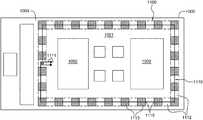
- FIG. 11Bis a plan view of one embodiment of a tamper-respondent assembly such as disclosed herein which includes a circuit board 1000 to which an enclosure (not shown) is mounted within an enclosure-to-board interface 1100 .
- the enclosuremay include one or more tamper-respondent sensors on an inner surface thereof, such as sensors 710 , 720 of FIGS. 7A & 7B .
- circuit board 1000may include an embedded tamper-detect circuit (such as described above) in order to facilitate defining secure volume 1001 within which one or more electronic components 1002 reside.
- a second enclosuresuch as depicted in FIG. 10 may be mounted to an opposite side of circuit board 1000 , which along with picket-fence-type tamper-detect circuits within the board cooperate to define the secure volume associated with the circuit board, including secure volume 1001 .
- a tamper-respondent electronic circuit structurewhich includes one or more tamper-detect circuits 1110 that include at least one conductive trace disposed, at least in part, within enclosure-to-board interface 1100 .
- the tamper-detect circuit 1110includes terminal leads 1111 which connect to monitor circuitry (not shown) disposed within secure volume 1001 to monitor for, for instance, a change in resistance in the conductive trace(s) of tamper-detect circuit 1110 indicative of a tamper event.
- monitor circuitrynot shown
- the conductive traceis a single conductive trace which extends around the perimeter of secure volume 1001 within the enclosure-to-board interface 1100 .
- the conductive trace(s)includes exposed regions 1112 and unexposed regions 1113 , which in the embodiment depicted, are provided in an alternating pattern (by way of example only).
- the conductive trace(s) being exposedmeans that the trace is exposed to the adhesive to be applied in the enclosure-to-board interface 1100 when mounting the enclosure to circuit board 1000 .
- unexposed regions 1113mean that the trace(s) is not directly exposed to the adhesive, but rather, is coupled to the adhesive across a mask, such as a solder mask.
- the solder maskmay be formed over the tamper-detect circuit 1110 , and in particular, over the conductive trace(s) before the adhesive is applied within enclosure-to-board interface 1100 .
- the adhesivedifferently attaches to the conductive trace(s) in the different regions, and facilitates defining stress rise regions that facilitate detecting a tamper event at the enclosure-to-board interface.
- the adhesivemay adhere better to the conductive trace in the exposed regions 1112 which may result in stress rise regions 1115 being formed within the conductive trace where the conductive trace transitions from the exposed region to the unexposed regions on either side of the exposed region.
- the adhesivecould adhere more strongly to the solder mask such that the conductive trace(s) may be more likely to separate in the unexposed regions 1113 , with the stress rise regions 1115 being defined again at the interface between the exposed regions 1112 and unexposed regions 1113 .
- FIG. 12Adepicts another embodiment of a tamper-respondent assembly such as disclosed herein, wherein the tamper-detect circuit 1200 within enclosure-to-board 1100 is shown differently configured from tamper-detect circuit 1110 of FIG. 11B .
- tamper-detect circuit 1200includes a serpentine conductive trace which has angle bends shown in the example to be right angle bends disposed within enclosure-to-board interface 1100 .
- the conductive trace with right angle bendsmay be formed on one side 1003 (or both) of circuit board 1000 within enclosure-to-board interface 1100 to facilitate defining secure volume 1001 having one or more electronic components 1002 to be protected.
- the tamper-detect circuit 1200includes terminal leads 1211 which connect to monitor circuitry (not shown) within secure volume 1001 for monitoring, for instance, for a tamper event by detection of a change in resistance in tamper-detect circuit 1200 .
- angle bends 1201in this case, right angle bends, are further examples of stress rise regions 1215 . Should a tamper event occur, the stress resulting from an attempted forcing of the enclosure away from the circuit board will propagate to the closest angle bend at which the stress is most likely to cause a break, and therefore, detection of the tamper event.
- the solder mask embodiment of FIG. 11Bmay be used in combination with tamper-detect circuit 1200 of FIG. 12A , if desired to define exposed and unexposed regions of the conductive trace.
- FIG. 12Bdepicts a variation on the embodiment of FIG. 12A wherein the conductive trace of tamper-detect circuit 1200 ′ again includes angle bends, such as right angle bends 1201 ′ within enclosure-to-board interface 1100 on side 1003 of circuit board 1000 (by way of example only). Tamper-detect circuit 1200 ′ again includes terminal leads 1211 , and facilitates providing enhanced tamper detection for secure volume 1001 , and in particular, for the electronic components 1002 within secure volume 1001 .
- FIGS. 13A & 13Bdepict side elevational and plan views respectively, of a portion of a tamper-detect circuit 1300 on one side 1003 of circuit board 1000 within enclosure-to-board interface 1100 , such as described above.
- tamper-detect circuit 1300includes a conductive trace, along with multiple conductive vias 1301 which anchor the conductive trace to circuit board 1000 , and thereby facilitate defining the stress rise regions 1315 at the points of anchoring, that is, at the conductive vias 1301 .
- a vertically serpentine conductive traceis provided as shown in FIG. 13A , extending through circuit board 1000 .
- the serpentine conductive trace or circuitextends between one side 1003 and the other side 1004 of circuit board 1000 , and then back out.
- the serpentine conductive circuitcould extend only into circuit board 1000 , for instance, to one or more metal layers of circuit board 1000 , and then back out.
- various configurationsmay be used in combination.
- the solder mask of FIG. 11Bcould be used on one or both surfaces of a tamper-respondent assembly with a tamper-detect circuit 1300 such as depicted in FIGS. 13A & 13B
- one or more of the conductive tracesmay be configured with angle bends, such as right angle bends, disposed, for instance, on one or more both sides of the circuit board.
- FIGS. 14A & 14Bdepict a variation on the embodiment of FIGS. 13A & 13B wherein a tamper-detect circuit 1400 is provided on one side of circuit board 1000 with conductive vias 1401 intersecting the tamper-detect circuit 1400 and extending into and (in the embodiment depicted), through circuit board 1000 .
- the conductive viasserve as anchor points which define stress rise regions 1415 for the conductive trace of the tamper-detect circuit 1400 .
- the conductive viasmay be provided in any desired pattern to intersect the conductive trace.
- the stress rise regionscould be defined by multiple conductive vias extending partially into, but not through the circuit board.
- FIG. 15Adepicts a further embodiment, wherein a tamper-detect circuit 1500 is shown on one side 1003 of circuit board 1000 within enclosure-to-board interface 1100 , as well as extending within secure volume 1001 at the inner periphery of enclosure-to-board interface 1100 .
- tamper-detect circuit 1500includes a serpentine conductive circuit or trace which includes, for instance, a first set of angle bends 1501 , such as right angle bends, and a second set of angle bends 1502 , such as right angle bends.
- first sent of angle bends 1501are located within enclosure-to-board interface 1100
- second set of angle bends 1502are located within secure volume 1001 .
- the adhesive to be providedmay remain within enclosure-to-board interface 1100 , or may be as well at the inner periphery of enclosure-to-board interface 1100 , within secure volume 1001 , that is, when the enclosure is mounted to the circuit board.
- conductive vias 1503are shown on multiple sides of the enclosure-to-board interface 1100 . These conductive vias 1503 serve as anchor points and may extend into and/or through circuit board 1000 as noted above, and may be provided in any pattern desired to intersect the tamper-detect circuit 1500 . In the example shown, the conductive vias are located at the angle bends 1501 , 1502 . Alternatively, the conductive vias could intersect straight line portions of the tamper-detect circuit 1500 , and/or could be located only within the enclosure-to-board interface 1100 , or only outside of the enclosure-to-board interface within the secure volume 1001 .
- tamper-detect circuit 1500further includes terminal leads 1511 which connect to monitor circuitry (not shown) within secure volume 1001 , such as within one or more electronic components 1002 .
- monitor circuitrynot shown
- the stress rise regionscould be further defined or enhanced by providing a mask such as a solder mask, over the tamper-detect circuit in any desired pattern, such as described above.
- a tamper-detect circuit 1500 ′is shown similar to tamper-detect circuit 1500 of FIG. 15A , but the serpentine conductive circuit is shown with acute angle bends 1501 ′, 1502 ′, rather than right angle bends.
- the serpentine conductive traceextends between enclosure-to-board interface 1100 and an area of secure volume 1001 along the inner periphery of enclosure-to-board interface 1100 .
- one or more conductive vias 1503may be provided as anchor points at desired locations (such as at the angle bends) to further enhance or define the stress rise regions associated with the conductive trace of the tamper-detect circuit 1500 .
- each disclosed aspect or featuremay be combined with any other disclosed aspect or feature as desired to achieve a particular application, for instance, to achieve a particular tamper-detect circuit at an enclosure-to-board interface with the desired stress rise region characteristics to, for instance, enhance tamper proof enclosure-to-board interface protection.
- a method or device that “comprises”, “has”, “includes” or “contains” one or more steps or elementspossesses those one or more steps or elements, but is not limited to possessing only those one or more steps or elements.
- a step of a method or an element of a device that “comprises”, “has”, “includes” or “contains” one or more featurespossesses those one or more features, but is not limited to possessing only those one or more features.
- a device or structure that is configured in a certain wayis configured in at least that way, but may also be configured in ways that are not listed.
Landscapes
- Engineering & Computer Science (AREA)
- Microelectronics & Electronic Packaging (AREA)
- Computer Security & Cryptography (AREA)
- Theoretical Computer Science (AREA)
- Computer Hardware Design (AREA)
- General Physics & Mathematics (AREA)
- Physics & Mathematics (AREA)
- General Engineering & Computer Science (AREA)
- Software Systems (AREA)
- Condensed Matter Physics & Semiconductors (AREA)
- Power Engineering (AREA)
- Structure Of Printed Boards (AREA)
- Storage Device Security (AREA)
- Pinball Game Machines (AREA)
Abstract
Description
Claims (20)
Priority Applications (1)
| Application Number | Priority Date | Filing Date | Title |
|---|---|---|---|
| US16/567,034US11083082B2 (en) | 2018-02-22 | 2019-09-11 | Enclosure-to-board interface with tamper-detect circuit(s) |
Applications Claiming Priority (3)
| Application Number | Priority Date | Filing Date | Title |
|---|---|---|---|
| US15/901,985US10306753B1 (en) | 2018-02-22 | 2018-02-22 | Enclosure-to-board interface with tamper-detect circuit(s) |
| US16/285,437US10531561B2 (en) | 2018-02-22 | 2019-02-26 | Enclosure-to-board interface with tamper-detect circuit(s) |
| US16/567,034US11083082B2 (en) | 2018-02-22 | 2019-09-11 | Enclosure-to-board interface with tamper-detect circuit(s) |
Related Parent Applications (1)
| Application Number | Title | Priority Date | Filing Date |
|---|---|---|---|
| US16/285,437ContinuationUS10531561B2 (en) | 2018-02-22 | 2019-02-26 | Enclosure-to-board interface with tamper-detect circuit(s) |
Publications (2)
| Publication Number | Publication Date |
|---|---|
| US20200008295A1 US20200008295A1 (en) | 2020-01-02 |
| US11083082B2true US11083082B2 (en) | 2021-08-03 |
Family
ID=66636184
Family Applications (3)
| Application Number | Title | Priority Date | Filing Date |
|---|---|---|---|
| US15/901,985ActiveUS10306753B1 (en) | 2018-02-22 | 2018-02-22 | Enclosure-to-board interface with tamper-detect circuit(s) |
| US16/285,437ActiveUS10531561B2 (en) | 2018-02-22 | 2019-02-26 | Enclosure-to-board interface with tamper-detect circuit(s) |
| US16/567,034ActiveUS11083082B2 (en) | 2018-02-22 | 2019-09-11 | Enclosure-to-board interface with tamper-detect circuit(s) |
Family Applications Before (2)
| Application Number | Title | Priority Date | Filing Date |
|---|---|---|---|
| US15/901,985ActiveUS10306753B1 (en) | 2018-02-22 | 2018-02-22 | Enclosure-to-board interface with tamper-detect circuit(s) |
| US16/285,437ActiveUS10531561B2 (en) | 2018-02-22 | 2019-02-26 | Enclosure-to-board interface with tamper-detect circuit(s) |
Country Status (1)
| Country | Link |
|---|---|
| US (3) | US10306753B1 (en) |
Cited By (1)
| Publication number | Priority date | Publication date | Assignee | Title |
|---|---|---|---|---|
| US20220318589A1 (en)* | 2021-03-31 | 2022-10-06 | Paul Abner | Methods and systems of a tamper-evident seal |
Families Citing this family (10)
| Publication number | Priority date | Publication date | Assignee | Title |
|---|---|---|---|---|
| US10306753B1 (en) | 2018-02-22 | 2019-05-28 | International Business Machines Corporation | Enclosure-to-board interface with tamper-detect circuit(s) |
| JP6882232B2 (en)* | 2018-06-28 | 2021-06-02 | パナソニック液晶ディスプレイ株式会社 | Liquid crystal display device |
| CN111079205B (en)* | 2018-10-22 | 2022-06-21 | 南宁富联富桂精密工业有限公司 | Anti-dismantling mechanism and electronic device with same |
| US10976215B2 (en)* | 2019-02-08 | 2021-04-13 | Dell Products L.P. | System and method of determining coolant leaks within information handling systems |
| US10595401B1 (en) | 2019-05-29 | 2020-03-17 | International Business Machines Corporation | Tamper detection at enclosure-to-board interface |
| US12321505B2 (en)* | 2021-04-12 | 2025-06-03 | Microsoft Technology Licensing, Llc | Systems and methods for chassis intrusion detection |
| US11991277B2 (en)* | 2021-08-17 | 2024-05-21 | International Business Machines Corporation | Cryptographic hardware security module with secure embedded heat pipe |
| US12431939B2 (en)* | 2022-06-06 | 2025-09-30 | Ingenutec, LLC | Near field communication module |
| EP4439366A1 (en)* | 2023-03-31 | 2024-10-02 | nCipher Security Limited | A device for secure storage of data |
| US20250181782A1 (en)* | 2023-11-30 | 2025-06-05 | Intel Corporation | Physical computer intrusion detection |
Citations (313)
| Publication number | Priority date | Publication date | Assignee | Title |
|---|---|---|---|---|
| US3165569A (en) | 1960-04-18 | 1965-01-12 | Air Logisties Corp | Method and apparatus for thermal expansion molding |
| US4097894A (en) | 1976-11-01 | 1978-06-27 | Tanner Electronics Systems Technology, Inc. | Secured scramble decoder filter |
| US4160503A (en) | 1978-08-07 | 1979-07-10 | Ohlbach Ralph C | Shipping container for printed circuit boards and other items |
| US4211324A (en) | 1978-08-07 | 1980-07-08 | Ohlbach Ralph C | Assembly protecting and inventorying printed circuit boards |
| US4324823A (en) | 1981-01-13 | 1982-04-13 | General Foods Corporation | Selective tamper resistance for on-package peelable premiums |
| EP0056360A1 (en) | 1981-01-14 | 1982-07-21 | Battelle Memorial Institute | Cross-linked carboxymethylcellulose carbonate and preparation thereof |
| US4450504A (en) | 1982-09-30 | 1984-05-22 | Honeywell Inc. | Meter tampering indicator |
| US4496900A (en) | 1982-04-30 | 1985-01-29 | International Business Machines Corporation | Nonlinearity detection using fault-generated second harmonic |
| US4516679A (en) | 1982-11-04 | 1985-05-14 | Simpson Carolyn N | Tamper-proof wrap |
| US4542337A (en) | 1982-09-30 | 1985-09-17 | Honeywell Inc. | Electro-mechanical anti-tampering device for electric meters |
| US4593384A (en)* | 1984-12-21 | 1986-06-03 | Ncr Corporation | Security device for the secure storage of sensitive data |
| US4609104A (en) | 1985-06-04 | 1986-09-02 | Ade, Inc. | RFI shielded, multiple part container and components thereof |
| JPS61297035A (en) | 1985-06-25 | 1986-12-27 | Mitsubishi Electric Corp | Manufacturing method of cylindrical member |
| US4653252A (en) | 1984-01-19 | 1987-03-31 | Douwe Egberts Koninklijke Tabaksfabriek Koffiebranderijen-Theehandel N.V. | Packing method and a blank for use therein |
| US4677809A (en) | 1985-05-10 | 1987-07-07 | General Dyanmics, Pomona Division | Method of making packing material with anti-static coating |
| US4691350A (en) | 1985-10-30 | 1987-09-01 | Ncr Corporation | Security device for stored sensitive data |
| US4807284A (en) | 1986-09-24 | 1989-02-21 | Ncr Corporation | Security device for sensitive data |
| US4811288A (en)* | 1985-09-25 | 1989-03-07 | Ncr Corporation | Data security device for protecting stored data |
| US4847139A (en) | 1986-09-12 | 1989-07-11 | Bayer Aktiengesellschaft | Flexible circuits |
| US4860351A (en) | 1986-11-05 | 1989-08-22 | Ibm Corporation | Tamper-resistant packaging for protection of information stored in electronic circuitry |
| US4865197A (en) | 1988-03-04 | 1989-09-12 | Unisys Corporation | Electronic component transportation container |
| US5009311A (en) | 1990-06-11 | 1991-04-23 | Schenk Robert J | Removable rigid support structure for circuit cards |
| US5027397A (en) | 1989-09-12 | 1991-06-25 | International Business Machines Corporation | Data protection by detection of intrusion into electronic assemblies |
| US5060114A (en) | 1990-06-06 | 1991-10-22 | Zenith Electronics Corporation | Conformable pad with thermally conductive additive for heat dissipation |
| US5075822A (en) | 1989-03-04 | 1991-12-24 | Telefunken Electronic Gmbh | Housing for installation in motor vehicles |
| US5117457A (en) | 1986-11-05 | 1992-05-26 | International Business Machines Corp. | Tamper resistant packaging for information protection in electronic circuitry |
| US5185717A (en) | 1988-08-05 | 1993-02-09 | Ryoichi Mori | Tamper resistant module having logical elements arranged in multiple layers on the outer surface of a substrate to protect stored information |
| US5201868A (en) | 1991-01-22 | 1993-04-13 | Rock-Tenn Company | Insulated shipping container |
| US5201879A (en) | 1991-09-18 | 1993-04-13 | S&C Electric Company | Vent for enclosures |
| US5211618A (en) | 1992-08-03 | 1993-05-18 | The Mead Corporation | Self-centering laminated process for corrugated containers and blank therefor |
| US5239664A (en) | 1988-12-20 | 1993-08-24 | Bull S.A. | Arrangement for protecting an electronic card and its use for protecting a terminal for reading magnetic and/or microprocessor cards |
| US5243162A (en) | 1990-09-04 | 1993-09-07 | Alps Electric Co., Ltd. | Transparent touch switch |
| EP0629497A2 (en) | 1993-06-03 | 1994-12-21 | Trigon Industries Limited | A multi-wall film |
| US5389738A (en) | 1992-05-04 | 1995-02-14 | Motorola, Inc. | Tamperproof arrangement for an integrated circuit device |
| US5458912A (en) | 1993-03-08 | 1995-10-17 | Dow Corning Corporation | Tamper-proof electronic coatings |
| US5506566A (en) | 1993-05-06 | 1996-04-09 | Northern Telecom Limited | Tamper detectable electronic security package |
| US5568124A (en) | 1993-05-20 | 1996-10-22 | Hughes Aircraft Company | Method to detect penetration of a surface and apparatus implementing same |
| US5594439A (en) | 1994-08-24 | 1997-01-14 | Crystal Semiconductor Corporation | Diagnosing problems in an electrical system by monitoring changes in nonlinear characteristics |
| US5675319A (en) | 1996-04-26 | 1997-10-07 | David Sarnoff Research Center, Inc. | Tamper detection device |
| US5715652A (en) | 1994-11-18 | 1998-02-10 | Ruediger Haaga Gmbh | Apparatus for producing and applying a protective covering to a cut edge of an opening of a container wall |
| US5761054A (en) | 1995-03-28 | 1998-06-02 | Intel Corporation | Integrated circuit assembly preventing intrusions into electronic circuitry |
| US5813113A (en) | 1996-12-09 | 1998-09-29 | International Business Machines Corporation | Fixture for making laminated integrated circuit devices |
| US5858500A (en) | 1993-03-12 | 1999-01-12 | W. L. Gore & Associates, Inc. | Tamper respondent enclosure |
| WO1999003675A1 (en) | 1997-07-14 | 1999-01-28 | E.I. Du Pont De Nemours And Company | Method for bonding a polymeric material to a metallic substrate |
| US5880523A (en) | 1997-02-24 | 1999-03-09 | General Instrument Corporation | Anti-tamper integrated circuit |
| WO1999021142A1 (en) | 1997-10-17 | 1999-04-29 | W. L. Gore & Associates (Uk) Limited | Tamper respondent enclosure |
| DE19816571A1 (en) | 1998-04-07 | 1999-10-14 | Francotyp Postalia Gmbh | Access protection for security modules |
| DE19816572A1 (en) | 1998-04-07 | 1999-10-14 | Francotyp Postalia Gmbh | Security module to prevent manipulation of data |
| US5975420A (en) | 1995-04-13 | 1999-11-02 | Dai Nippon Printing Co., Ltd. | Apparatus and method of manufacturing an integrated circuit (IC) card with a protective IC module |
| US5988510A (en) | 1997-02-13 | 1999-11-23 | Micron Communications, Inc. | Tamper resistant smart card and method of protecting data in a smart card |
| JP2000238141A (en) | 1999-02-24 | 2000-09-05 | Society Of Japanese Aerospace Co Inc | Method and apparatus for molding composite resin product |
| US6121544A (en) | 1998-01-15 | 2000-09-19 | Petsinger; Julie Ann | Electromagnetic shield to prevent surreptitious access to contactless smartcards |
| US6195267B1 (en) | 1999-06-23 | 2001-02-27 | Ericsson Inc. | Gel structure for combined EMI shielding and thermal control of microelectronic assemblies |
| US6201296B1 (en) | 1996-09-23 | 2001-03-13 | Siemens Aktiengesellschaft | Semiconductor chip with protection against analyzing |
| US6233339B1 (en) | 1996-10-25 | 2001-05-15 | Fuji Xerox Co., Ltd. | Physical property based cryptographics |
| US6259363B1 (en) | 1998-05-20 | 2001-07-10 | Apollo Fire Detectors Limited | Detector removal signalling device |
| US6261215B1 (en) | 1996-03-21 | 2001-07-17 | Rodney Haydn Imer | Rectangular thin film pack |
| WO2001063994A2 (en) | 2000-02-23 | 2001-08-30 | Iridian Technologies, Inc. | Tamper proof case for electronic devices having memories with sensitive information |
| US6301096B1 (en) | 2000-03-18 | 2001-10-09 | Philips Electronics North America Corporation | Tamper-proof ballast enclosure |
| US20010049021A1 (en) | 2000-04-07 | 2001-12-06 | Valimont James L. | Methods of improving bonding strength in primer/sealant adhesive systems |
| US20010050425A1 (en) | 1994-07-07 | 2001-12-13 | Masud Beroz | Framed sheets |
| US20010056542A1 (en) | 2000-05-11 | 2001-12-27 | International Business Machines Corporation | Tamper resistant card enclosure with improved intrusion detection circuit |
| US20020002683A1 (en)* | 2000-02-14 | 2002-01-03 | Benson Justin H. | Security module system, apparatus and process |
| US6355316B1 (en) | 1999-05-15 | 2002-03-12 | Scheidt & Bachmann Gmbh | Device for protecting electronic circuits from unauthorized access |
| US6384397B1 (en) | 2000-05-10 | 2002-05-07 | National Semiconductor Corporation | Low cost die sized module for imaging application having a lens housing assembly |
| US6396400B1 (en) | 1999-07-26 | 2002-05-28 | Epstein, Iii Edwin A. | Security system and enclosure to protect data contained therein |
| US20020068384A1 (en) | 1997-10-17 | 2002-06-06 | Masud Beroz | Enhancements in framed sheet processing |
| US20020084090A1 (en) | 2001-01-03 | 2002-07-04 | Farquhar Donald S. | Tamper-responding encapsulated enclosure having flexible protective mesh structure |
| US6420971B1 (en) | 1999-06-23 | 2002-07-16 | Tripseal Limited | Electronic seal, methods and security system |
| US6424954B1 (en) | 1998-02-17 | 2002-07-23 | Neopost Inc. | Postage metering system |
| US6469625B1 (en) | 2000-02-18 | 2002-10-22 | Optex Co., Ltd | Security sensor having disturbance detecting capability |
| US6473995B2 (en) | 2000-02-23 | 2002-11-05 | Dai Nippon Printing Co., Ltd. | Vacuum drying apparatus and vacuum drying method |
| US20030009683A1 (en) | 2001-07-03 | 2003-01-09 | Gary Schwenck | Tamper-evident/tamper-resistant electronic components |
| US20030009684A1 (en) | 2001-07-03 | 2003-01-09 | Gary Schwenck | Tamper-evident and/or tamper-resistant electronic components |
| US6512454B2 (en) | 2000-05-24 | 2003-01-28 | International Business Machines Corporation | Tamper resistant enclosure for an electronic device and electrical assembly utilizing same |
| WO2003012606A2 (en) | 2001-07-31 | 2003-02-13 | Stonewood Electronics Ltd | Security apparatus |
| WO2003025080A1 (en) | 2001-09-17 | 2003-03-27 | Dow Corning Corporation | Die attach adhesives for semiconductor applications, processes for producing semiconductor devices and semiconductor devices produced by such processes |
| US20030137416A1 (en) | 2000-06-01 | 2003-07-24 | Shuzhen Fu | Point of sale (POS) terminal security system |
| US20030198022A1 (en) | 2002-04-22 | 2003-10-23 | Runqing Ye | Power converter package with enhanced thermal management |
| WO2004040505A1 (en) | 2002-10-30 | 2004-05-13 | The Secretary Of State For Trade And Industry | Identification device, anti-counterfeiting apparatus and method |
| US6746960B2 (en) | 1998-04-09 | 2004-06-08 | California Institute Of Technology | Electronic techniques for analyte detection |
| US6798660B2 (en) | 2003-02-13 | 2004-09-28 | Dell Products L.P. | Liquid cooling module |
| US20040218366A1 (en) | 2003-04-07 | 2004-11-04 | Wolfgang Speigl | Multilayer circuit board |
| US6817204B2 (en) | 2001-02-22 | 2004-11-16 | Hewlett-Packard Development Company, L.P. | Modular sprayjet cooling system |
| US20040228634A1 (en)* | 2003-05-13 | 2004-11-18 | Jean-Philippe Fricker | Optical fiber management in a chassis-based network system |
| US6853093B2 (en) | 2002-12-20 | 2005-02-08 | Lipman Electronic Engineering Ltd. | Anti-tampering enclosure for electronic circuitry |
| US20050068735A1 (en) | 2003-08-14 | 2005-03-31 | Sergio Fissore | Module for solid state relay for engine cooling fan control |
| US6879032B2 (en) | 2003-07-18 | 2005-04-12 | Agilent Technologies, Inc. | Folded flex circuit interconnect having a grid array interface |
| US20050088303A1 (en) | 2003-10-22 | 2005-04-28 | International Business Machines Corporation | Tamper sensing method and apparatus |
| US6895509B1 (en) | 2000-09-21 | 2005-05-17 | Pitney Bowes Inc. | Tamper detection system for securing data |
| US20050111194A1 (en) | 2003-11-21 | 2005-05-26 | Lg Electronics Inc. | Heat radiating system and method for a mobile communication terminal |
| US20050161253A1 (en) | 2004-01-23 | 2005-07-28 | Pitney Bowes Incorporated | Tamper barrier for electronic device |
| US20050180104A1 (en) | 2002-05-08 | 2005-08-18 | Olesen Klaus K. | Cooling unit and flow distributing element for use in such unit |
| US6946960B2 (en) | 2002-12-28 | 2005-09-20 | Pitney Bowes Inc. | Active tamper detection system for electronic modules |
| US6970360B2 (en) | 2004-03-18 | 2005-11-29 | International Business Machines Corporation | Tamper-proof enclosure for a circuit card |
| US6982642B1 (en) | 2000-11-20 | 2006-01-03 | International Business Machines Corporation | Security cloth design and assembly |
| US6985362B2 (en) | 2000-09-07 | 2006-01-10 | International Business Machines Corporation | Printed circuit board and electronic package using same |
| US6991961B2 (en) | 2003-06-18 | 2006-01-31 | Medtronic, Inc. | Method of forming a high-voltage/high-power die package |
| US6996953B2 (en) | 2004-01-23 | 2006-02-14 | Pitney Bowes Inc. | System and method for installing a tamper barrier wrap in a PCB assembly, including a PCB assembly having improved heat sinking |
| US20060034731A1 (en) | 1995-03-27 | 2006-02-16 | California Institute Of Technology | Sensor arrays for detecting analytes in fluids |
| US7007171B1 (en) | 2000-09-01 | 2006-02-28 | International Business Machines Corporaton | Method and apparatus for improved fold retention on a security enclosure |
| US7005733B2 (en) | 1999-12-30 | 2006-02-28 | Koemmerling Oliver | Anti tamper encapsulation for an integrated circuit |
| US20060049941A1 (en) | 2004-09-03 | 2006-03-09 | Hunter Steve B | Reusable tamper respondent enclosure |
| US7015823B1 (en) | 2004-10-15 | 2006-03-21 | Systran Federal Corporation | Tamper resistant circuit boards |
| US20060072288A1 (en) | 2004-10-04 | 2006-04-06 | Stewart William P | Electric machine with power and control electronics integrated into the primary machine housing |
| US7057896B2 (en) | 2002-08-21 | 2006-06-06 | Matsushita Electric Industrial Co., Ltd. | Power module and production method thereof |
| US7094459B2 (en) | 2001-12-27 | 2006-08-22 | Polymatech Co., Ltd. | Method for cooling electronic components and thermally conductive sheet for use therewith |
| US7095615B2 (en) | 2003-11-13 | 2006-08-22 | Honeywell International, Inc. | Environmentally tuned circuit card assembly and method for manufacturing the same |
| US7094143B2 (en) | 2004-10-27 | 2006-08-22 | Francotyp-Postalia Gmbh | Security housing having ventilation openings |
| US20060218779A1 (en) | 2001-02-16 | 2006-10-05 | Etsuo Ooba | Resistor element, stress sensor, and method for manufacturing them |
| US20060261259A1 (en) | 2004-05-03 | 2006-11-23 | Beinhocker Gilbert D | Tamper-proof container |
| EP1734578A1 (en) | 2005-06-17 | 2006-12-20 | Delphi Technologies, Inc. | Cooled electronic assembly and method for cooling a printed circuit board |
| US7156233B2 (en) | 2004-06-15 | 2007-01-02 | Pitney Bowes Inc. | Tamper barrier enclosure with corner protection |
| US20070038865A1 (en) | 2005-07-27 | 2007-02-15 | International Business Machines Corporation | Tamper-proof caps for large assembly |
| US20070035933A1 (en) | 2005-08-09 | 2007-02-15 | Inventec Corporation | Blade interface device |
| US7189360B1 (en) | 2002-01-24 | 2007-03-13 | Sandia Corporation | Circular chemiresistors for microchemical sensors |
| US20070064399A1 (en) | 2003-10-10 | 2007-03-22 | Delphi Technologies, Inc. | Flip chip heat sink package and method |
| US20070064396A1 (en) | 2005-09-22 | 2007-03-22 | Oman Todd P | Electronics assembly and heat pipe device |
| US20070091559A1 (en) | 2005-10-25 | 2007-04-26 | Malone Christopher G | Server with vertical drive arrangement |
| US7214874B2 (en) | 2004-11-04 | 2007-05-08 | International Business Machines Corporation | Venting device for tamper resistant electronic modules |
| US20070108619A1 (en) | 2005-11-15 | 2007-05-17 | Hsu Jun C | Bonding pad with high bonding strength to solder ball and bump |
| US20070125867A1 (en) | 2005-12-05 | 2007-06-07 | Rcd Technology Corp. | Tuned radio frequency identification (RFID) circuit used as a security device for wristbands and package security |
| US20070140787A1 (en) | 2005-12-15 | 2007-06-21 | International Business Machines Corporation | Low profile cam latch assembly |
| JP2007173416A (en) | 2005-12-20 | 2007-07-05 | Fujitsu Ltd | Semiconductor device |
| US7247791B2 (en) | 2004-05-27 | 2007-07-24 | Pitney Bowes Inc. | Security barrier for electronic circuitry |
| US20070201210A1 (en)* | 2006-02-16 | 2007-08-30 | Norman Chow | Liquid cooling loops for server applications |
| US20070211436A1 (en) | 2006-03-09 | 2007-09-13 | Robinson Kenneth M | Combined board level shielding and thermal management |
| US20070223165A1 (en) | 2006-03-22 | 2007-09-27 | Itri Benedict A | Line powering in a multi-line environment |
| US20070230127A1 (en) | 2006-03-28 | 2007-10-04 | Delphi Technologies, Inc. | Fluid cooled electronic assembly |
| US7281667B2 (en) | 2005-04-14 | 2007-10-16 | International Business Machines Corporation | Method and structure for implementing secure multichip modules for encryption applications |
| JP2007305761A (en) | 2006-05-11 | 2007-11-22 | Fujitsu Ltd | Semiconductor device |
| US20070268671A1 (en) | 2006-05-16 | 2007-11-22 | Brandenburg Scott D | Heat sink electronic package having compliant pedestal |
| US20070271544A1 (en) | 2006-05-19 | 2007-11-22 | Rolf Engstrom | Security sensing module envelope |
| US7304373B2 (en) | 2004-10-28 | 2007-12-04 | Intel Corporation | Power distribution within a folded flex package method and apparatus |
| US7310737B2 (en) | 2003-06-30 | 2007-12-18 | Hewlett-Packard Development Company, L.P. | Cooling system for computer systems |
| US20080036598A1 (en) | 2006-06-09 | 2008-02-14 | International Business Machines Corporation | Tamper-proof structures for protectig electronic modules |
| US20080050512A1 (en) | 2006-08-23 | 2008-02-28 | Rockwell Collins, Inc. | Integrated circuit tampering protection and reverse engineering prvention coatings and methods |
| US20080061972A1 (en) | 2006-08-30 | 2008-03-13 | Chi-Kuang Hwang | Substrate damage detection mechanism using RFID tag |
| US20080086876A1 (en) | 2006-10-16 | 2008-04-17 | Mysticmd Inc. | Bondable conductive ink |
| US20080106400A1 (en)* | 2006-11-03 | 2008-05-08 | Hunter Steve B | Tamper respondent sensor and enclosure |
| US20080129501A1 (en) | 2006-11-30 | 2008-06-05 | Honeywell International Inc. | Secure chassis with integrated tamper detection sensor |
| US20080128897A1 (en) | 2006-12-05 | 2008-06-05 | Tong Wa Chao | Heat spreader for a multi-chip package |
| US20080144290A1 (en) | 2003-08-01 | 2008-06-19 | Jens Brandt | Electronic Unit and Method For Manufacturing an Electronic Unit |
| US20080160274A1 (en) | 2006-12-31 | 2008-07-03 | Chi Hung Dang | Coefficient of thermal expansion adaptor |
| US20080159539A1 (en) | 2006-12-29 | 2008-07-03 | Taiwan Semiconductor Manufacturing Company, Ltd. | System and method for providing secured integrated engineering analysis |
| US20080191174A1 (en) | 2005-07-08 | 2008-08-14 | Cypak Ab | Use Of Heat-Activated Adhesive For Manufacture And A Device So Manufactured |
| EP1968362A2 (en) | 2007-03-08 | 2008-09-10 | Delphi Technologies, Inc. | Interconnect for an electrical circuit substrate |
| US20080251906A1 (en) | 2007-04-13 | 2008-10-16 | Zilog, Inc. | Package-on-package secure module having BGA mesh cap |
| US20080278353A1 (en) | 2007-05-11 | 2008-11-13 | Measurement Specialties, Inc. | Tamper resistant electronic transaction assembly |
| US7465887B2 (en) | 2006-09-22 | 2008-12-16 | Denso Corporation | Waterproof casing having respiration filter for containing electronic components |
| US20090031135A1 (en) | 2007-07-27 | 2009-01-29 | Raghunathan Kothandaraman | Tamper Proof Seal For An Electronic Document |
| US20090073659A1 (en) | 2007-09-14 | 2009-03-19 | Touch Electronic Co. Ltd. | Heat sink structure for a power supply |
| WO2009042335A1 (en) | 2007-09-28 | 2009-04-02 | United States Of America As Represented By The Administrator Of The National Aeronautics And Space Administration | Wireless tamper detection sensor and sensing system |
| US7515418B2 (en) | 2005-09-26 | 2009-04-07 | Curtiss-Wright Controls, Inc. | Adjustable height liquid cooler in liquid flow through plate |
| US20090097200A1 (en) | 2007-04-11 | 2009-04-16 | Viswa Sharma | Modular blade for providing scalable mechanical, electrical and environmental functionality in the enterprise using advancedtca boards |
| US20090106563A1 (en) | 2007-10-17 | 2009-04-23 | Spansion Llc | Tamper reactive memory device to secure data from tamper attacks |
| US7549064B2 (en) | 2005-05-10 | 2009-06-16 | Hewlett-Packard Development Company, L.P. | Secure circuit assembly |
| US20090152339A1 (en) | 2007-12-14 | 2009-06-18 | Richard Hawkins | Method and apparatus for tamper proof electronic voting with intuitive user interfaces |
| US20090161312A1 (en)* | 2006-02-16 | 2009-06-25 | Liebert Corporation | Liquid cooling systems for server applications |
| US20090166065A1 (en) | 2008-01-02 | 2009-07-02 | Clayton James E | Thin multi-chip flex module |
| WO2009092472A1 (en) | 2008-01-23 | 2009-07-30 | Robert Bosch Gmbh | Sensor arrangement and method for producing a sensor arrangement |
| US20090212945A1 (en) | 2008-02-26 | 2009-08-27 | Steen Michael L | Intrusion detection systems for detecting intrusion conditions with respect to electronic component enclosures |
| EP2104407A1 (en) | 2004-10-18 | 2009-09-23 | E.I. Du Pont De Nemours And Company | Capacitive/resistive devices and printed wiring boards incorporating such devices, and methods of making thereof |
| US7643290B1 (en) | 2008-07-23 | 2010-01-05 | Cisco Technology, Inc. | Techniques utilizing thermal, EMI and FIPS friendly electronic modules |
| US7640658B1 (en) | 2005-10-18 | 2010-01-05 | Teledyne Technologies Incorporated | Methods for forming an anti-tamper pattern |
| US7663883B2 (en) | 2004-02-13 | 2010-02-16 | Fujitsu Limited | Heat transfer mechanism, heat dissipation system, and communication apparatus |
| US7672129B1 (en) | 2006-09-19 | 2010-03-02 | Sun Microsystems, Inc. | Intelligent microchannel cooling |
| US7671324B2 (en) | 2006-09-27 | 2010-03-02 | Honeywell International Inc. | Anti-tamper enclosure system comprising a photosensitive sensor and optical medium |
| CN201430639Y (en) | 2009-04-15 | 2010-03-24 | 北京北广科技股份有限公司 | Portable type digital transmitter with small size and multiple functions |
| US20100088528A1 (en) | 2007-05-03 | 2010-04-08 | Radu Sion | Method and apparatus for tamper-proof wirte-once-read-many computer storage |
| US20100110647A1 (en) | 2007-05-03 | 2010-05-06 | Super Talent Electronics, Inc. | Molded Memory Card With Write Protection Switch Assembly |
| US20100134959A1 (en) | 2008-11-11 | 2010-06-03 | Fife John M | Solar power inverters, including temperature-controlled solar power inverters, and associated systems and methods |
| US7731517B2 (en) | 2005-07-27 | 2010-06-08 | Physical Optics Corporation | Inherently sealed electrical connector |
| US7746657B2 (en) | 2008-03-11 | 2010-06-29 | Alcatel Lucent | 10G XFP compliant PCB |
| US20100177487A1 (en) | 2009-01-13 | 2010-07-15 | Nauman Arshad | Tamper respondent module |
| US7768005B2 (en) | 2005-12-21 | 2010-08-03 | International Business Machines Corporation | Physically highly secure multi-chip assembly |
| US7783994B2 (en) | 2006-12-14 | 2010-08-24 | Northrop Grumman Systems Corporation | Method for providing secure and trusted ASICs using 3D integration |
| US7787256B2 (en) | 2007-08-10 | 2010-08-31 | Gore Enterprise Holdings, Inc. | Tamper respondent system |
| WO2010128939A1 (en) | 2009-05-08 | 2010-11-11 | Business Security Ol Ab | Arrangement for cooling tamper protected circuitry |
| US20100319986A1 (en) | 2009-06-17 | 2010-12-23 | Bleau Charles A | Modular vented circuit board enclosure |
| US20100321874A1 (en) | 2009-06-18 | 2010-12-23 | Neeloy Bhattacharyya | Computer server chassis |
| US20110001237A1 (en) | 2008-03-06 | 2011-01-06 | Commissariat A L'energie Atomique Et Aux Energies Alternatives | Assembly of a wire element with a microelectronic chip with a groove comprising at least one bump securing the wire element |
| US7868411B2 (en) | 2007-05-08 | 2011-01-11 | Samsung Electronics Co., Ltd. | Semiconductor devices |
| US20110038123A1 (en) | 2009-08-17 | 2011-02-17 | Seagate Technology Llc | Solid state data storage assembly |
| US7898413B2 (en) | 2007-01-25 | 2011-03-01 | Verifone, Inc. | Anti-tamper protected enclosure |
| US7901977B1 (en) | 2000-01-27 | 2011-03-08 | Marie Angelopoulos | Data protection by detection of intrusion into electronic assemblies |
| US20110103027A1 (en) | 2009-10-29 | 2011-05-05 | Sony Corporation | Card-type peripheral apparatus |
| US7978070B2 (en) | 2004-04-08 | 2011-07-12 | W. L. Gore & Associates (Uk) Ltd. | Tamper respondent enclosure |
| US8006101B2 (en) | 2008-06-20 | 2011-08-23 | General Instrument Corporation | Radio transceiver or other encryption device having secure tamper-detection module |
| US20110241446A1 (en) | 2010-03-30 | 2011-10-06 | Blue Spark Technologies, Inc. | Irreversible circuit activation switch |
| US20110299244A1 (en) | 2010-06-08 | 2011-12-08 | Toyota Motor Engineering & Manufacturing | Cooling member for heat containing device |
| US8094450B2 (en) | 2007-06-22 | 2012-01-10 | Cole Kepro International, Llc | Gaming machine vent cover |
| US8101267B2 (en) | 2005-12-30 | 2012-01-24 | E. I. Du Pont De Nemours And Company | Multilayer polymeric laminates and high strength laminates produced therefrom |
| US20120047374A1 (en) | 2011-11-03 | 2012-02-23 | Cram Worldwide, Llc | Tamper resistance extension via tamper sensing material housing integration |
| US8123133B2 (en) | 2006-10-02 | 2012-02-28 | Ingenico France | Protection device for an electronic card |
| US20120050998A1 (en) | 2011-11-03 | 2012-03-01 | Cram Worldwide, Llc | Heat dissipation for a chip protected by an anti-tamper background |
| US20120048685A1 (en)* | 2010-08-31 | 2012-03-01 | Hon Hai Precision Industry Co., Ltd. | Conveyor |
| US20120052252A1 (en) | 2010-08-26 | 2012-03-01 | Jeffrey Todd Kohli | Methods for extracting strengthened glass substrates from glass sheets |
| US8133621B2 (en) | 2009-02-27 | 2012-03-13 | Research In Motion Limited | Location of a fuel cell on a mobile device |
| US20120068846A1 (en) | 2010-09-20 | 2012-03-22 | Honeywell International Inc. | Tamper event detection |
| EP1672464B1 (en) | 2004-12-15 | 2012-04-25 | NEC Corporation | Mobile terminal device and method for radiating heat therefrom |
| US20120117666A1 (en) | 2009-07-07 | 2012-05-10 | International Business Machines Corporation | Multilayer securing structure and method thereof for the protection of cryptographic keys and code |
| US20120113581A1 (en) | 2010-11-04 | 2012-05-10 | International Business Machines Corporation | Implementing enhanced cover-mounted, auto-docking for multiple dasd configurations |
| US20120140421A1 (en) | 2010-12-02 | 2012-06-07 | Micron Technology, Inc. | Assemblies including heat sink elements and methods of assembling |
| US20120170217A1 (en) | 2007-08-09 | 2012-07-05 | Hitachi, Ltd. | Power Inverter |
| US20120185636A1 (en) | 2010-08-04 | 2012-07-19 | Isc8, Inc. | Tamper-Resistant Memory Device With Variable Data Transmission Rate |
| US20120244742A1 (en) | 2011-03-22 | 2012-09-27 | Hon Hai Precision Industry Co., Ltd. | Low profile heat dissipating system with freely-oriented heat pipe |
| US20120256305A1 (en) | 2007-12-06 | 2012-10-11 | Broadcom Corporation | Integrated Circuit Package Security Fence |
| US20120319986A1 (en) | 2009-01-15 | 2012-12-20 | Research In Motion Limited | Multidimensional volume and vibration controls for a handheld electronic device |
| US20120320529A1 (en) | 2010-07-28 | 2012-12-20 | Wolverine Tube, Inc. | Enhanced clad metal base plate |
| US8345423B2 (en) | 2010-06-29 | 2013-01-01 | International Business Machines Corporation | Interleaved, immersion-cooling apparatuses and methods for cooling electronic subsystems |
| WO2013004292A1 (en) | 2011-07-04 | 2013-01-10 | Cicor Management AG | Security casing |
| US20130021758A1 (en) | 2011-07-19 | 2013-01-24 | Bernstein Jonathan J | Interconnect Schemes, and Materials and Methods for Producing the Same |
| US20130033818A1 (en) | 2011-08-01 | 2013-02-07 | Denso Corporation | Power supply unit using housing in which printed circuit board is housed |
| EP2560467A1 (en) | 2011-08-18 | 2013-02-20 | BIOTRONIK SE & Co. KG | Method for mounting a component to an electric circuit board, electric circuit board and electric circuit board arrangement |
| US8393918B2 (en) | 2008-06-11 | 2013-03-12 | Pulse Electronics, Inc. | Miniaturized connectors and methods |
| US20130104252A1 (en) | 2011-10-24 | 2013-04-25 | Subbayya Chowdary Yanamadala | Tamper detection countermeasures to deter physical attack on a security asic |
| US20130141137A1 (en) | 2011-06-01 | 2013-06-06 | ISC8 Inc. | Stacked Physically Uncloneable Function Sense and Respond Module |
| US20130154834A1 (en) | 2011-12-19 | 2013-06-20 | Tyco Safety Products Canada Ltd. | Cabinet with tamper detection system and method |
| US20130158936A1 (en) | 2011-12-19 | 2013-06-20 | David Gerard Rich | Methods and apparatus for detecting unauthorized batteries or tampering by monitoring a thermal profile |
| JP2013125807A (en) | 2011-12-14 | 2013-06-24 | Mitsubishi Electric Corp | Housing |
| JP2013140112A (en) | 2012-01-06 | 2013-07-18 | Babcock Hitachi Kk | Ultrasonic damage detecting apparatus and ultrasonic damage detection method |
| US20130208422A1 (en) | 2008-08-04 | 2013-08-15 | John Phillip Neville Hughes | Contact cooled electronic enclosure |
| US8516269B1 (en) | 2010-07-28 | 2013-08-20 | Sandia Corporation | Hardware device to physical structure binding and authentication |
| US20130235527A1 (en) | 2012-03-06 | 2013-09-12 | Mission Motor Company | Power electronic system and method of assembly |
| DE102012203955A1 (en) | 2012-03-14 | 2013-09-19 | Zf Friedrichshafen Ag | Mounting frame for electronic device e.g. data encryption apparatus, has support portion that is provided for supporting heat guide plate for heat dissipation of electric circuit of circuit board |
| US20130283386A1 (en) | 2012-04-24 | 2013-10-24 | Cheol Jae LEE | Tamper respondent covering |
| WO2013189483A1 (en) | 2012-06-21 | 2013-12-27 | Mecomo Ag | Signature resistance element and associated production method |
| US20140022733A1 (en) | 2012-07-19 | 2014-01-23 | Samsung Electronics Co., Ltd. | Storage Device |
| US20140028335A1 (en) | 2012-07-27 | 2014-01-30 | Johnson Electric S.A. | Security wrap with breakable conductors |
| US20140027159A1 (en) | 2012-07-27 | 2014-01-30 | Johnson Electric S.A. | Security wrap |
| US20140033331A1 (en) | 2012-07-27 | 2014-01-30 | Johnson Electric S.A. | Multilayer security wrap |
| US8646108B2 (en) | 2007-07-30 | 2014-02-04 | Secutor Systems, Llc | Multi-domain secure computer system |
| US8659506B2 (en) | 2010-03-04 | 2014-02-25 | Seiko Epson Corporation | Image transfer method, image transfer system, and projector |
| US8659908B2 (en) | 2009-10-14 | 2014-02-25 | Lockheed Martin Corporation | Protective circuit board cover |
| US20140151320A1 (en) | 2012-11-30 | 2014-06-05 | Corning Incorporated | Glass containers with delamination resistance and improved damage tolerance |
| US20140160679A1 (en) | 2012-12-11 | 2014-06-12 | Infinera Corporation | Interface card cooling uisng heat pipes |
| WO2014086987A2 (en) | 2012-12-07 | 2014-06-12 | Cryptera A/S | A security module for protecting circuit components from unauthorized access |
| US8755191B2 (en) | 2009-05-08 | 2014-06-17 | Fujitsu Technology Solutions Intellectual Property Gmbh | Server frame and rack-mounted server suitable for use in the server frame |
| US20140184263A1 (en) | 2012-12-27 | 2014-07-03 | Robert Bosch Gmbh | Sensor system and cover device for a sensor system |
| US20140204533A1 (en) | 2011-06-30 | 2014-07-24 | Vestas Wind Systems A/S | Heat sink for cooling of power semiconductor modules |
| US20140206800A1 (en) | 2013-01-22 | 2014-07-24 | Sabic Innovative Plastics Ip B.V. | Thermoplastic Compositions Containing Nanoscale-Sized Particle Additives For Laser Direct Structuring And Methods For The Manufacture And Use Thereof |
| US8797059B2 (en) | 2012-03-01 | 2014-08-05 | International Business Machines Corporation | Implementing carbon nanotube based sensors for cryptographic applications |
| US20140233165A1 (en) | 2013-02-18 | 2014-08-21 | Sandor Farkas | Flex circuit |
| US8836509B2 (en) | 2009-04-09 | 2014-09-16 | Direct Payment Solutions Limited | Security device |
| US20140296410A1 (en) | 2013-04-01 | 2014-10-02 | Sabic Innovative Plastics Ip B.V. | High modulus laser direct structuring polycarbonate composites with enhanced plating performance and broad laser window and methods for the manufacture and use thereof |
| WO2014158159A1 (en) | 2013-03-28 | 2014-10-02 | Hewlett-Packard Development Company, L.P. | Shield for an electronic device |
| US8853839B2 (en) | 2011-10-07 | 2014-10-07 | Analog Devices, Inc. | Air-release features in cavity packages |
| US20140306014A1 (en) | 2013-04-15 | 2014-10-16 | Johnson Electric S.A. | Security Wrap with Tearable Substrate |
| US20140321064A1 (en) | 2011-11-21 | 2014-10-30 | Thomson Licensing | Hold down for retaining a heat sink |
| US20140325688A1 (en) | 2013-04-26 | 2014-10-30 | Ultra Stereo Labs, Inc. | Tamperproof housing module |
| US8879266B2 (en) | 2012-05-24 | 2014-11-04 | Apple Inc. | Thin multi-layered structures providing rigidity and conductivity |
| US8890298B2 (en) | 2007-12-06 | 2014-11-18 | Broadcom Corporation | Embedded package security tamper mesh |
| US8934244B2 (en) | 2011-10-28 | 2015-01-13 | Dell Products L.P. | System and method for cooling information handling resources |
| US8947889B2 (en) | 2010-10-14 | 2015-02-03 | Lockheed Martin Corporation | Conformal electromagnetic (EM) detector |
| CN104346587A (en) | 2013-08-08 | 2015-02-11 | 华邦电子股份有限公司 | Certifiable non-volatile memory components and methods of operation and manufacture thereof |
| US9003559B2 (en) | 2008-07-29 | 2015-04-07 | International Business Machines Corporation | Continuity check monitoring for microchip exploitation detection |
| US9003199B2 (en) | 2004-03-23 | 2015-04-07 | Harris Corporation | Modular cryptographic device providing multi-mode wireless LAN operation features and related methods |
| US9011762B2 (en) | 2006-07-21 | 2015-04-21 | Valtion Teknillinen Tutkimuskeskus | Method for manufacturing conductors and semiconductors |
| US20150120072A1 (en) | 2012-07-12 | 2015-04-30 | Nova Lumos Ltd. | System and method for on-demand electrical power |
| US20150143551A1 (en) | 2013-11-21 | 2015-05-21 | Nxp B.V. | Electronic tamper detection |
| US9052070B2 (en) | 2009-11-25 | 2015-06-09 | Cooper Technologies Company | Systems, methods, and devices for sealing LED light sources in a light module |
| US20150161415A1 (en) | 2011-03-11 | 2015-06-11 | Emsycon Gmbh | Tamper-protected hardware and method for using same |
| US20150163933A1 (en) | 2013-12-09 | 2015-06-11 | Timothy Wayne Steiner | Tamper respondent apparatus |
| US20150195943A1 (en) | 2014-01-03 | 2015-07-09 | Advanced Micro Devices, Inc. | Lever mechanism to facilitate edge coupling of circuit board |
| US20150199887A1 (en) | 2012-08-15 | 2015-07-16 | Direct Payment Solutions Limited | Tamper evident systems |
| US20150213243A1 (en) | 2006-09-29 | 2015-07-30 | Oracle International Corporation | Method and apparatus for secure information distribution |
| US20150235053A1 (en) | 2012-05-04 | 2015-08-20 | Heon Soo LEE | System on chip, method of operating the same, and devices including the system on chip |
| US20150244374A1 (en) | 2012-10-02 | 2015-08-27 | Hewlett-Packard Sevelopment Company, L.P. | Security shield assembly |
| US9166586B2 (en) | 2012-05-09 | 2015-10-20 | Gilbarco Inc. | Fuel dispenser input device tamper detection arrangement |
| US20150307250A1 (en) | 2012-12-26 | 2015-10-29 | Konstantin Pavlovich SOKOL | Anti-tamper method and packaging for important and valuable items |
| US20160005262A1 (en) | 2014-07-03 | 2016-01-07 | Universal Entertainment Corporation | Gaming machine |
| US20160012693A1 (en) | 2014-07-11 | 2016-01-14 | Emanate Wireless, Inc. | Tamper Detection in AC-Powered Tags |
| US9298956B2 (en) | 2013-10-04 | 2016-03-29 | Square, Inc. | Tamper protection mesh in an electronic device |
| US9455233B1 (en)* | 2015-12-02 | 2016-09-27 | Freescale Semiconductor, Inc. | System for preventing tampering with integrated circuit |
| US20170006712A1 (en) | 2014-03-18 | 2017-01-05 | Dexerials Corporation | Method for manufacturing flexible mounting module body |
| US20170019987A1 (en) | 2015-07-15 | 2017-01-19 | International Business Machines Corporation | Circuitized structure with 3-dimensional configuration |
| US9554477B1 (en) | 2015-12-18 | 2017-01-24 | International Business Machines Corporation | Tamper-respondent assemblies with enclosure-to-board protection |
| US9555606B1 (en) | 2015-12-09 | 2017-01-31 | International Business Machines Corporation | Applying pressure to adhesive using CTE mismatch between components |
| US9560737B2 (en) | 2015-03-04 | 2017-01-31 | International Business Machines Corporation | Electronic package with heat transfer element(s) |
| US9578764B1 (en)* | 2015-09-25 | 2017-02-21 | International Business Machines Corporation | Enclosure with inner tamper-respondent sensor(s) and physical security element(s) |
| US9578735B2 (en) | 2015-07-13 | 2017-02-21 | International Business Machines Corporation | Embedded venting system |
| US9586857B2 (en) | 2014-11-17 | 2017-03-07 | International Business Machines Corporation | Controlling fragmentation of chemically strengthened glass |
| US9591776B1 (en) | 2015-09-25 | 2017-03-07 | International Business Machines Corporation | Enclosure with inner tamper-respondent sensor(s) |
| US20170068881A1 (en) | 2015-08-18 | 2017-03-09 | Franklin J. Camper | Microprocessor-Controlled Tamper Detection System |
| US20170089977A1 (en) | 2015-05-07 | 2017-03-30 | International Business Machines Corporation | Debugging scan latch circuits using flip devices |
| US20170103683A1 (en) | 2015-10-12 | 2017-04-13 | Evigia Systems, Inc. | Tamper-proof electronic bolt-seal |
| US9681649B2 (en) | 2015-11-23 | 2017-06-20 | Cocus Co., Ltd. | Fishing reel |
| US9730315B1 (en) | 2016-08-29 | 2017-08-08 | Square, Inc. | Environment-tolerant tamper-proof circuit board |
| US20170286725A1 (en) | 2015-04-14 | 2017-10-05 | Hewlett Packard Enterprise Development Lp | Penetration detection boundary having a heat sink |
| US9858776B1 (en) | 2016-06-28 | 2018-01-02 | International Business Machines Corporation | Tamper-respondent assembly with nonlinearity monitoring |
| US9881880B2 (en) | 2016-05-13 | 2018-01-30 | International Business Machines Corporation | Tamper-proof electronic packages with stressed glass component substrate(s) |
| US9894749B2 (en) | 2015-09-25 | 2018-02-13 | International Business Machines Corporation | Tamper-respondent assemblies with bond protection |
| US9904811B2 (en) | 2016-04-27 | 2018-02-27 | International Business Machines Corporation | Tamper-proof electronic packages with two-phase dielectric fluid |
| US9913370B2 (en) | 2016-05-13 | 2018-03-06 | International Business Machines Corporation | Tamper-proof electronic packages formed with stressed glass |
| US9913389B2 (en) | 2015-12-01 | 2018-03-06 | International Business Corporation Corporation | Tamper-respondent assembly with vent structure |
| US9911012B2 (en) | 2015-09-25 | 2018-03-06 | International Business Machines Corporation | Overlapping, discrete tamper-respondent sensors |
| US9916744B2 (en) | 2016-02-25 | 2018-03-13 | International Business Machines Corporation | Multi-layer stack with embedded tamper-detect protection |
| US9924591B2 (en) | 2015-09-25 | 2018-03-20 | International Business Machines Corporation | Tamper-respondent assemblies |
| US9978231B2 (en) | 2015-10-21 | 2018-05-22 | International Business Machines Corporation | Tamper-respondent assembly with protective wrap(s) over tamper-respondent sensor(s) |
| US9999124B2 (en) | 2016-11-02 | 2018-06-12 | International Business Machines Corporation | Tamper-respondent assemblies with trace regions of increased susceptibility to breaking |
| US10098235B2 (en)* | 2015-09-25 | 2018-10-09 | International Business Machines Corporation | Tamper-respondent assemblies with region(s) of increased susceptibility to damage |
| US10136519B2 (en) | 2015-10-19 | 2018-11-20 | International Business Machines Corporation | Circuit layouts of tamper-respondent sensors |
| US10168185B2 (en) | 2015-09-25 | 2019-01-01 | International Business Machines Corporation | Circuit boards and electronic packages with embedded tamper-respondent sensor |
| US10172239B2 (en) | 2015-09-25 | 2019-01-01 | International Business Machines Corporation | Tamper-respondent sensors with formed flexible layer(s) |
| US10271424B2 (en) | 2016-09-26 | 2019-04-23 | International Business Machines Corporation | Tamper-respondent assemblies with in situ vent structure(s) |
| US20190127121A1 (en) | 2016-04-19 | 2019-05-02 | Juan Francisco SALCIDO PINERA | Security closure system and devices for containers |
| US10299372B2 (en) | 2016-09-26 | 2019-05-21 | International Business Machines Corporation | Vented tamper-respondent assemblies |
| US10306753B1 (en) | 2018-02-22 | 2019-05-28 | International Business Machines Corporation | Enclosure-to-board interface with tamper-detect circuit(s) |
| US10321589B2 (en) | 2016-09-19 | 2019-06-11 | International Business Machines Corporation | Tamper-respondent assembly with sensor connection adapter |
| US10327329B2 (en) | 2017-02-13 | 2019-06-18 | International Business Machines Corporation | Tamper-respondent assembly with flexible tamper-detect sensor(s) overlying in-situ-formed tamper-detect sensor |
| US10327343B2 (en) | 2015-12-09 | 2019-06-18 | International Business Machines Corporation | Applying pressure to adhesive using CTE mismatch between components |
| US10417459B2 (en)* | 2015-04-29 | 2019-09-17 | Utimaco, Inc. | Physical barrier to inhibit a penetration attack |
Family Cites Families (8)
| Publication number | Priority date | Publication date | Assignee | Title |
|---|---|---|---|---|
| JP2009502584A (en) | 2005-08-01 | 2009-01-29 | ストゥラ エンソ アクチボラグ | Laminated structure |
| US7923830B2 (en) | 2007-04-13 | 2011-04-12 | Maxim Integrated Products, Inc. | Package-on-package secure module having anti-tamper mesh in the substrate of the upper package |
| US9013336B2 (en) | 2008-01-22 | 2015-04-21 | Verifone, Inc. | Secured keypad devices |
| US8455990B2 (en) | 2009-02-25 | 2013-06-04 | Conexant Systems, Inc. | Systems and methods of tamper proof packaging of a semiconductor device |
| US8572264B2 (en) | 2011-07-15 | 2013-10-29 | American Express Travel Related Services Company, Inc. | Systems and methods for state awareness across communication channels and statefully transitioning between communication channels |
| US8651706B2 (en) | 2011-12-28 | 2014-02-18 | Wen-Sung Lee | Illuminator arrangement with less heat intervention |
| US8730715B2 (en) | 2012-03-26 | 2014-05-20 | Honeywell International Inc. | Tamper-resistant MRAM utilizing chemical alteration |
| FR3042891B1 (en) | 2015-10-22 | 2018-03-23 | Stmicroelectronics (Rousset) Sas | SECURE ELECTRONIC CHIP |
- 2018
- 2018-02-22USUS15/901,985patent/US10306753B1/enactiveActive
- 2019
- 2019-02-26USUS16/285,437patent/US10531561B2/enactiveActive
- 2019-09-11USUS16/567,034patent/US11083082B2/enactiveActive
Patent Citations (372)
| Publication number | Priority date | Publication date | Assignee | Title |
|---|---|---|---|---|
| US3165569A (en) | 1960-04-18 | 1965-01-12 | Air Logisties Corp | Method and apparatus for thermal expansion molding |
| US4097894A (en) | 1976-11-01 | 1978-06-27 | Tanner Electronics Systems Technology, Inc. | Secured scramble decoder filter |
| US4160503A (en) | 1978-08-07 | 1979-07-10 | Ohlbach Ralph C | Shipping container for printed circuit boards and other items |
| US4211324A (en) | 1978-08-07 | 1980-07-08 | Ohlbach Ralph C | Assembly protecting and inventorying printed circuit boards |
| US4324823A (en) | 1981-01-13 | 1982-04-13 | General Foods Corporation | Selective tamper resistance for on-package peelable premiums |
| EP0056360A1 (en) | 1981-01-14 | 1982-07-21 | Battelle Memorial Institute | Cross-linked carboxymethylcellulose carbonate and preparation thereof |
| US4496900A (en) | 1982-04-30 | 1985-01-29 | International Business Machines Corporation | Nonlinearity detection using fault-generated second harmonic |
| US4450504A (en) | 1982-09-30 | 1984-05-22 | Honeywell Inc. | Meter tampering indicator |
| US4542337A (en) | 1982-09-30 | 1985-09-17 | Honeywell Inc. | Electro-mechanical anti-tampering device for electric meters |
| US4516679A (en) | 1982-11-04 | 1985-05-14 | Simpson Carolyn N | Tamper-proof wrap |
| US4653252A (en) | 1984-01-19 | 1987-03-31 | Douwe Egberts Koninklijke Tabaksfabriek Koffiebranderijen-Theehandel N.V. | Packing method and a blank for use therein |
| US4593384A (en)* | 1984-12-21 | 1986-06-03 | Ncr Corporation | Security device for the secure storage of sensitive data |
| US4677809A (en) | 1985-05-10 | 1987-07-07 | General Dyanmics, Pomona Division | Method of making packing material with anti-static coating |
| US4609104A (en) | 1985-06-04 | 1986-09-02 | Ade, Inc. | RFI shielded, multiple part container and components thereof |
| JPS61297035A (en) | 1985-06-25 | 1986-12-27 | Mitsubishi Electric Corp | Manufacturing method of cylindrical member |
| US4811288A (en)* | 1985-09-25 | 1989-03-07 | Ncr Corporation | Data security device for protecting stored data |
| US4691350A (en) | 1985-10-30 | 1987-09-01 | Ncr Corporation | Security device for stored sensitive data |
| US4847139A (en) | 1986-09-12 | 1989-07-11 | Bayer Aktiengesellschaft | Flexible circuits |
| US4807284A (en) | 1986-09-24 | 1989-02-21 | Ncr Corporation | Security device for sensitive data |
| US5117457A (en) | 1986-11-05 | 1992-05-26 | International Business Machines Corp. | Tamper resistant packaging for information protection in electronic circuitry |
| US4860351A (en) | 1986-11-05 | 1989-08-22 | Ibm Corporation | Tamper-resistant packaging for protection of information stored in electronic circuitry |
| US4865197A (en) | 1988-03-04 | 1989-09-12 | Unisys Corporation | Electronic component transportation container |
| US5185717A (en) | 1988-08-05 | 1993-02-09 | Ryoichi Mori | Tamper resistant module having logical elements arranged in multiple layers on the outer surface of a substrate to protect stored information |
| US5239664A (en) | 1988-12-20 | 1993-08-24 | Bull S.A. | Arrangement for protecting an electronic card and its use for protecting a terminal for reading magnetic and/or microprocessor cards |
| US5075822A (en) | 1989-03-04 | 1991-12-24 | Telefunken Electronic Gmbh | Housing for installation in motor vehicles |
| US5027397A (en) | 1989-09-12 | 1991-06-25 | International Business Machines Corporation | Data protection by detection of intrusion into electronic assemblies |
| US5159629A (en) | 1989-09-12 | 1992-10-27 | International Business Machines Corp. | Data protection by detection of intrusion into electronic assemblies |
| US5060114A (en) | 1990-06-06 | 1991-10-22 | Zenith Electronics Corporation | Conformable pad with thermally conductive additive for heat dissipation |
| US5009311A (en) | 1990-06-11 | 1991-04-23 | Schenk Robert J | Removable rigid support structure for circuit cards |
| US5243162A (en) | 1990-09-04 | 1993-09-07 | Alps Electric Co., Ltd. | Transparent touch switch |
| US5201868A (en) | 1991-01-22 | 1993-04-13 | Rock-Tenn Company | Insulated shipping container |
| US5201879A (en) | 1991-09-18 | 1993-04-13 | S&C Electric Company | Vent for enclosures |
| US5389738A (en) | 1992-05-04 | 1995-02-14 | Motorola, Inc. | Tamperproof arrangement for an integrated circuit device |
| US5406630A (en) | 1992-05-04 | 1995-04-11 | Motorola, Inc. | Tamperproof arrangement for an integrated circuit device |
| US5211618A (en) | 1992-08-03 | 1993-05-18 | The Mead Corporation | Self-centering laminated process for corrugated containers and blank therefor |
| US5458912A (en) | 1993-03-08 | 1995-10-17 | Dow Corning Corporation | Tamper-proof electronic coatings |
| US5858500A (en) | 1993-03-12 | 1999-01-12 | W. L. Gore & Associates, Inc. | Tamper respondent enclosure |
| US5506566A (en) | 1993-05-06 | 1996-04-09 | Northern Telecom Limited | Tamper detectable electronic security package |
| US5568124A (en) | 1993-05-20 | 1996-10-22 | Hughes Aircraft Company | Method to detect penetration of a surface and apparatus implementing same |
| EP0629497A2 (en) | 1993-06-03 | 1994-12-21 | Trigon Industries Limited | A multi-wall film |
| US20010050425A1 (en) | 1994-07-07 | 2001-12-13 | Masud Beroz | Framed sheets |
| US5594439A (en) | 1994-08-24 | 1997-01-14 | Crystal Semiconductor Corporation | Diagnosing problems in an electrical system by monitoring changes in nonlinear characteristics |
| US5715652A (en) | 1994-11-18 | 1998-02-10 | Ruediger Haaga Gmbh | Apparatus for producing and applying a protective covering to a cut edge of an opening of a container wall |
| US20060034731A1 (en) | 1995-03-27 | 2006-02-16 | California Institute Of Technology | Sensor arrays for detecting analytes in fluids |
| US5761054A (en) | 1995-03-28 | 1998-06-02 | Intel Corporation | Integrated circuit assembly preventing intrusions into electronic circuitry |
| US6438825B1 (en) | 1995-03-28 | 2002-08-27 | Intel Corporation | Method to prevent intrusions into electronic circuitry |
| US5975420A (en) | 1995-04-13 | 1999-11-02 | Dai Nippon Printing Co., Ltd. | Apparatus and method of manufacturing an integrated circuit (IC) card with a protective IC module |
| US6261215B1 (en) | 1996-03-21 | 2001-07-17 | Rodney Haydn Imer | Rectangular thin film pack |
| US5675319A (en) | 1996-04-26 | 1997-10-07 | David Sarnoff Research Center, Inc. | Tamper detection device |
| US6201296B1 (en) | 1996-09-23 | 2001-03-13 | Siemens Aktiengesellschaft | Semiconductor chip with protection against analyzing |
| US6233339B1 (en) | 1996-10-25 | 2001-05-15 | Fuji Xerox Co., Ltd. | Physical property based cryptographics |
| US5813113A (en) | 1996-12-09 | 1998-09-29 | International Business Machines Corporation | Fixture for making laminated integrated circuit devices |
| US5988510A (en) | 1997-02-13 | 1999-11-23 | Micron Communications, Inc. | Tamper resistant smart card and method of protecting data in a smart card |
| US5880523A (en) | 1997-02-24 | 1999-03-09 | General Instrument Corporation | Anti-tamper integrated circuit |
| WO1999003675A1 (en) | 1997-07-14 | 1999-01-28 | E.I. Du Pont De Nemours And Company | Method for bonding a polymeric material to a metallic substrate |
| US20020068384A1 (en) | 1997-10-17 | 2002-06-06 | Masud Beroz | Enhancements in framed sheet processing |
| WO1999021142A1 (en) | 1997-10-17 | 1999-04-29 | W. L. Gore & Associates (Uk) Limited | Tamper respondent enclosure |
| US6121544A (en) | 1998-01-15 | 2000-09-19 | Petsinger; Julie Ann | Electromagnetic shield to prevent surreptitious access to contactless smartcards |
| US6424954B1 (en) | 1998-02-17 | 2002-07-23 | Neopost Inc. | Postage metering system |
| DE19816571A1 (en) | 1998-04-07 | 1999-10-14 | Francotyp Postalia Gmbh | Access protection for security modules |
| DE19816572A1 (en) | 1998-04-07 | 1999-10-14 | Francotyp Postalia Gmbh | Security module to prevent manipulation of data |
| US6746960B2 (en) | 1998-04-09 | 2004-06-08 | California Institute Of Technology | Electronic techniques for analyte detection |
| US6259363B1 (en) | 1998-05-20 | 2001-07-10 | Apollo Fire Detectors Limited | Detector removal signalling device |
| JP2000238141A (en) | 1999-02-24 | 2000-09-05 | Society Of Japanese Aerospace Co Inc | Method and apparatus for molding composite resin product |
| US6355316B1 (en) | 1999-05-15 | 2002-03-12 | Scheidt & Bachmann Gmbh | Device for protecting electronic circuits from unauthorized access |
| US6195267B1 (en) | 1999-06-23 | 2001-02-27 | Ericsson Inc. | Gel structure for combined EMI shielding and thermal control of microelectronic assemblies |
| US6420971B1 (en) | 1999-06-23 | 2002-07-16 | Tripseal Limited | Electronic seal, methods and security system |
| US6396400B1 (en) | 1999-07-26 | 2002-05-28 | Epstein, Iii Edwin A. | Security system and enclosure to protect data contained therein |
| US7005733B2 (en) | 1999-12-30 | 2006-02-28 | Koemmerling Oliver | Anti tamper encapsulation for an integrated circuit |
| US7901977B1 (en) | 2000-01-27 | 2011-03-08 | Marie Angelopoulos | Data protection by detection of intrusion into electronic assemblies |
| US20020002683A1 (en)* | 2000-02-14 | 2002-01-03 | Benson Justin H. | Security module system, apparatus and process |
| US7054162B2 (en) | 2000-02-14 | 2006-05-30 | Safenet, Inc. | Security module system, apparatus and process |
| US6469625B1 (en) | 2000-02-18 | 2002-10-22 | Optex Co., Ltd | Security sensor having disturbance detecting capability |
| WO2001063994A2 (en) | 2000-02-23 | 2001-08-30 | Iridian Technologies, Inc. | Tamper proof case for electronic devices having memories with sensitive information |
| US6473995B2 (en) | 2000-02-23 | 2002-11-05 | Dai Nippon Printing Co., Ltd. | Vacuum drying apparatus and vacuum drying method |
| US6301096B1 (en) | 2000-03-18 | 2001-10-09 | Philips Electronics North America Corporation | Tamper-proof ballast enclosure |
| US20010049021A1 (en) | 2000-04-07 | 2001-12-06 | Valimont James L. | Methods of improving bonding strength in primer/sealant adhesive systems |
| US6384397B1 (en) | 2000-05-10 | 2002-05-07 | National Semiconductor Corporation | Low cost die sized module for imaging application having a lens housing assembly |
| US20010056542A1 (en) | 2000-05-11 | 2001-12-27 | International Business Machines Corporation | Tamper resistant card enclosure with improved intrusion detection circuit |
| US6957345B2 (en) | 2000-05-11 | 2005-10-18 | International Business Machines Corporation | Tamper resistant card enclosure with improved intrusion detection circuit |
| US6512454B2 (en) | 2000-05-24 | 2003-01-28 | International Business Machines Corporation | Tamper resistant enclosure for an electronic device and electrical assembly utilizing same |
| US20030137416A1 (en) | 2000-06-01 | 2003-07-24 | Shuzhen Fu | Point of sale (POS) terminal security system |
| US7007171B1 (en) | 2000-09-01 | 2006-02-28 | International Business Machines Corporaton | Method and apparatus for improved fold retention on a security enclosure |
| US6985362B2 (en) | 2000-09-07 | 2006-01-10 | International Business Machines Corporation | Printed circuit board and electronic package using same |
| US6895509B1 (en) | 2000-09-21 | 2005-05-17 | Pitney Bowes Inc. | Tamper detection system for securing data |
| US20060080348A1 (en) | 2000-11-20 | 2006-04-13 | International Business Machines Corporation | Security cloth design and assembly |
| US6982642B1 (en) | 2000-11-20 | 2006-01-03 | International Business Machines Corporation | Security cloth design and assembly |
| US6929900B2 (en) | 2001-01-03 | 2005-08-16 | International Business Machines Corporation | Tamper-responding encapsulated enclosure having flexible protective mesh structure |
| US20020084090A1 (en) | 2001-01-03 | 2002-07-04 | Farquhar Donald S. | Tamper-responding encapsulated enclosure having flexible protective mesh structure |
| US6686539B2 (en) | 2001-01-03 | 2004-02-03 | International Business Machines Corporation | Tamper-responding encapsulated enclosure having flexible protective mesh structure |
| US20060218779A1 (en) | 2001-02-16 | 2006-10-05 | Etsuo Ooba | Resistor element, stress sensor, and method for manufacturing them |
| US6817204B2 (en) | 2001-02-22 | 2004-11-16 | Hewlett-Packard Development Company, L.P. | Modular sprayjet cooling system |
| US20030009683A1 (en) | 2001-07-03 | 2003-01-09 | Gary Schwenck | Tamper-evident/tamper-resistant electronic components |
| US20030009684A1 (en) | 2001-07-03 | 2003-01-09 | Gary Schwenck | Tamper-evident and/or tamper-resistant electronic components |
| WO2003012606A2 (en) | 2001-07-31 | 2003-02-13 | Stonewood Electronics Ltd | Security apparatus |
| WO2003025080A1 (en) | 2001-09-17 | 2003-03-27 | Dow Corning Corporation | Die attach adhesives for semiconductor applications, processes for producing semiconductor devices and semiconductor devices produced by such processes |
| US7094459B2 (en) | 2001-12-27 | 2006-08-22 | Polymatech Co., Ltd. | Method for cooling electronic components and thermally conductive sheet for use therewith |
| US7189360B1 (en) | 2002-01-24 | 2007-03-13 | Sandia Corporation | Circular chemiresistors for microchemical sensors |
| US20030198022A1 (en) | 2002-04-22 | 2003-10-23 | Runqing Ye | Power converter package with enhanced thermal management |
| US20050180104A1 (en) | 2002-05-08 | 2005-08-18 | Olesen Klaus K. | Cooling unit and flow distributing element for use in such unit |
| US7057896B2 (en) | 2002-08-21 | 2006-06-06 | Matsushita Electric Industrial Co., Ltd. | Power module and production method thereof |
| WO2004040505A1 (en) | 2002-10-30 | 2004-05-13 | The Secretary Of State For Trade And Industry | Identification device, anti-counterfeiting apparatus and method |
| US20060196945A1 (en) | 2002-10-30 | 2006-09-07 | Mendels David A | Identification device, anti-counterfeiting apparatus and method |
| US6853093B2 (en) | 2002-12-20 | 2005-02-08 | Lipman Electronic Engineering Ltd. | Anti-tampering enclosure for electronic circuitry |
| US6946960B2 (en) | 2002-12-28 | 2005-09-20 | Pitney Bowes Inc. | Active tamper detection system for electronic modules |
| US6798660B2 (en) | 2003-02-13 | 2004-09-28 | Dell Products L.P. | Liquid cooling module |
| US20040218366A1 (en) | 2003-04-07 | 2004-11-04 | Wolfgang Speigl | Multilayer circuit board |
| US20040228634A1 (en)* | 2003-05-13 | 2004-11-18 | Jean-Philippe Fricker | Optical fiber management in a chassis-based network system |
| US6991961B2 (en) | 2003-06-18 | 2006-01-31 | Medtronic, Inc. | Method of forming a high-voltage/high-power die package |
| US7310737B2 (en) | 2003-06-30 | 2007-12-18 | Hewlett-Packard Development Company, L.P. | Cooling system for computer systems |
| US6879032B2 (en) | 2003-07-18 | 2005-04-12 | Agilent Technologies, Inc. | Folded flex circuit interconnect having a grid array interface |
| US20080144290A1 (en) | 2003-08-01 | 2008-06-19 | Jens Brandt | Electronic Unit and Method For Manufacturing an Electronic Unit |
| US20050068735A1 (en) | 2003-08-14 | 2005-03-31 | Sergio Fissore | Module for solid state relay for engine cooling fan control |
| US20070064399A1 (en) | 2003-10-10 | 2007-03-22 | Delphi Technologies, Inc. | Flip chip heat sink package and method |
| US20050088303A1 (en) | 2003-10-22 | 2005-04-28 | International Business Machines Corporation | Tamper sensing method and apparatus |
| US7095615B2 (en) | 2003-11-13 | 2006-08-22 | Honeywell International, Inc. | Environmentally tuned circuit card assembly and method for manufacturing the same |
| US20050111194A1 (en) | 2003-11-21 | 2005-05-26 | Lg Electronics Inc. | Heat radiating system and method for a mobile communication terminal |
| US6996953B2 (en) | 2004-01-23 | 2006-02-14 | Pitney Bowes Inc. | System and method for installing a tamper barrier wrap in a PCB assembly, including a PCB assembly having improved heat sinking |
| US20050161253A1 (en) | 2004-01-23 | 2005-07-28 | Pitney Bowes Incorporated | Tamper barrier for electronic device |
| US7475474B2 (en) | 2004-01-23 | 2009-01-13 | Pitney Bowes Inc. | Method of making tamper detection circuit for an electronic device |
| US7180008B2 (en) | 2004-01-23 | 2007-02-20 | Pitney Bowes Inc. | Tamper barrier for electronic device |
| US7663883B2 (en) | 2004-02-13 | 2010-02-16 | Fujitsu Limited | Heat transfer mechanism, heat dissipation system, and communication apparatus |
| US6970360B2 (en) | 2004-03-18 | 2005-11-29 | International Business Machines Corporation | Tamper-proof enclosure for a circuit card |
| US9003199B2 (en) | 2004-03-23 | 2015-04-07 | Harris Corporation | Modular cryptographic device providing multi-mode wireless LAN operation features and related methods |
| US7978070B2 (en) | 2004-04-08 | 2011-07-12 | W. L. Gore & Associates (Uk) Ltd. | Tamper respondent enclosure |
| US20060261259A1 (en) | 2004-05-03 | 2006-11-23 | Beinhocker Gilbert D | Tamper-proof container |
| US7247791B2 (en) | 2004-05-27 | 2007-07-24 | Pitney Bowes Inc. | Security barrier for electronic circuitry |
| US7156233B2 (en) | 2004-06-15 | 2007-01-02 | Pitney Bowes Inc. | Tamper barrier enclosure with corner protection |
| US20060049941A1 (en) | 2004-09-03 | 2006-03-09 | Hunter Steve B | Reusable tamper respondent enclosure |
| US20060072288A1 (en) | 2004-10-04 | 2006-04-06 | Stewart William P | Electric machine with power and control electronics integrated into the primary machine housing |
| US7015823B1 (en) | 2004-10-15 | 2006-03-21 | Systran Federal Corporation | Tamper resistant circuit boards |
| EP2104407A1 (en) | 2004-10-18 | 2009-09-23 | E.I. Du Pont De Nemours And Company | Capacitive/resistive devices and printed wiring boards incorporating such devices, and methods of making thereof |
| US7094143B2 (en) | 2004-10-27 | 2006-08-22 | Francotyp-Postalia Gmbh | Security housing having ventilation openings |
| US7304373B2 (en) | 2004-10-28 | 2007-12-04 | Intel Corporation | Power distribution within a folded flex package method and apparatus |
| US8961280B2 (en) | 2004-11-04 | 2015-02-24 | International Business Machines Corporation | Method of manufacturing a venting device for tamper resistant electronic modules |
| US7214874B2 (en) | 2004-11-04 | 2007-05-08 | International Business Machines Corporation | Venting device for tamper resistant electronic modules |
| US8287336B2 (en) | 2004-11-04 | 2012-10-16 | International Business Machines Corporation | Method of manufacturing a venting device for tamper resistant electronic modules |
| US20150007427A1 (en) | 2004-11-04 | 2015-01-08 | International Business Machines Corporation | Method of manufacturing a venting device for tamper resistant electronic modules |
| EP1672464B1 (en) | 2004-12-15 | 2012-04-25 | NEC Corporation | Mobile terminal device and method for radiating heat therefrom |
| US7281667B2 (en) | 2005-04-14 | 2007-10-16 | International Business Machines Corporation | Method and structure for implementing secure multichip modules for encryption applications |
| US7549064B2 (en) | 2005-05-10 | 2009-06-16 | Hewlett-Packard Development Company, L.P. | Secure circuit assembly |
| EP1734578A1 (en) | 2005-06-17 | 2006-12-20 | Delphi Technologies, Inc. | Cooled electronic assembly and method for cooling a printed circuit board |
| US20080191174A1 (en) | 2005-07-08 | 2008-08-14 | Cypak Ab | Use Of Heat-Activated Adhesive For Manufacture And A Device So Manufactured |
| US20070038865A1 (en) | 2005-07-27 | 2007-02-15 | International Business Machines Corporation | Tamper-proof caps for large assembly |
| US7731517B2 (en) | 2005-07-27 | 2010-06-08 | Physical Optics Corporation | Inherently sealed electrical connector |
| US20070035933A1 (en) | 2005-08-09 | 2007-02-15 | Inventec Corporation | Blade interface device |
| US20070064396A1 (en) | 2005-09-22 | 2007-03-22 | Oman Todd P | Electronics assembly and heat pipe device |
| US7515418B2 (en) | 2005-09-26 | 2009-04-07 | Curtiss-Wright Controls, Inc. | Adjustable height liquid cooler in liquid flow through plate |
| US7640658B1 (en) | 2005-10-18 | 2010-01-05 | Teledyne Technologies Incorporated | Methods for forming an anti-tamper pattern |
| US7947911B1 (en) | 2005-10-18 | 2011-05-24 | Teledyne Technologies Incorporated | Anti-tamper mesh |
| US20070091559A1 (en) | 2005-10-25 | 2007-04-26 | Malone Christopher G | Server with vertical drive arrangement |
| US20070108619A1 (en) | 2005-11-15 | 2007-05-17 | Hsu Jun C | Bonding pad with high bonding strength to solder ball and bump |
| US20070125867A1 (en) | 2005-12-05 | 2007-06-07 | Rcd Technology Corp. | Tuned radio frequency identification (RFID) circuit used as a security device for wristbands and package security |
| US20070140787A1 (en) | 2005-12-15 | 2007-06-21 | International Business Machines Corporation | Low profile cam latch assembly |
| JP2007173416A (en) | 2005-12-20 | 2007-07-05 | Fujitsu Ltd | Semiconductor device |
| US7768005B2 (en) | 2005-12-21 | 2010-08-03 | International Business Machines Corporation | Physically highly secure multi-chip assembly |
| US8101267B2 (en) | 2005-12-30 | 2012-01-24 | E. I. Du Pont De Nemours And Company | Multilayer polymeric laminates and high strength laminates produced therefrom |
| US20090161312A1 (en)* | 2006-02-16 | 2009-06-25 | Liebert Corporation | Liquid cooling systems for server applications |
| US20070201210A1 (en)* | 2006-02-16 | 2007-08-30 | Norman Chow | Liquid cooling loops for server applications |
| US20070211436A1 (en) | 2006-03-09 | 2007-09-13 | Robinson Kenneth M | Combined board level shielding and thermal management |
| US20070223165A1 (en) | 2006-03-22 | 2007-09-27 | Itri Benedict A | Line powering in a multi-line environment |
| US20070230127A1 (en) | 2006-03-28 | 2007-10-04 | Delphi Technologies, Inc. | Fluid cooled electronic assembly |
| JP2007305761A (en) | 2006-05-11 | 2007-11-22 | Fujitsu Ltd | Semiconductor device |
| US20070268671A1 (en) | 2006-05-16 | 2007-11-22 | Brandenburg Scott D | Heat sink electronic package having compliant pedestal |
| US20070271544A1 (en) | 2006-05-19 | 2007-11-22 | Rolf Engstrom | Security sensing module envelope |
| US20080036598A1 (en) | 2006-06-09 | 2008-02-14 | International Business Machines Corporation | Tamper-proof structures for protectig electronic modules |
| US9011762B2 (en) | 2006-07-21 | 2015-04-21 | Valtion Teknillinen Tutkimuskeskus | Method for manufacturing conductors and semiconductors |
| US20080050512A1 (en) | 2006-08-23 | 2008-02-28 | Rockwell Collins, Inc. | Integrated circuit tampering protection and reverse engineering prvention coatings and methods |
| US8084855B2 (en) | 2006-08-23 | 2011-12-27 | Rockwell Collins, Inc. | Integrated circuit tampering protection and reverse engineering prevention coatings and methods |
| US8664047B2 (en) | 2006-08-23 | 2014-03-04 | Rockwell Collins, Inc. | Integrated circuit tampering protection and reverse engineering prevention coatings and methods |
| US20080061972A1 (en) | 2006-08-30 | 2008-03-13 | Chi-Kuang Hwang | Substrate damage detection mechanism using RFID tag |
| US7672129B1 (en) | 2006-09-19 | 2010-03-02 | Sun Microsystems, Inc. | Intelligent microchannel cooling |
| US7465887B2 (en) | 2006-09-22 | 2008-12-16 | Denso Corporation | Waterproof casing having respiration filter for containing electronic components |
| US7671324B2 (en) | 2006-09-27 | 2010-03-02 | Honeywell International Inc. | Anti-tamper enclosure system comprising a photosensitive sensor and optical medium |
| US20150213243A1 (en) | 2006-09-29 | 2015-07-30 | Oracle International Corporation | Method and apparatus for secure information distribution |
| US8123133B2 (en) | 2006-10-02 | 2012-02-28 | Ingenico France | Protection device for an electronic card |
| US20080086876A1 (en) | 2006-10-16 | 2008-04-17 | Mysticmd Inc. | Bondable conductive ink |
| US20080106400A1 (en)* | 2006-11-03 | 2008-05-08 | Hunter Steve B | Tamper respondent sensor and enclosure |
| US7760086B2 (en) | 2006-11-03 | 2010-07-20 | Gore Enterprise Holdings, Inc | Tamper respondent sensor and enclosure |
| US20080129501A1 (en) | 2006-11-30 | 2008-06-05 | Honeywell International Inc. | Secure chassis with integrated tamper detection sensor |
| US20080128897A1 (en) | 2006-12-05 | 2008-06-05 | Tong Wa Chao | Heat spreader for a multi-chip package |
| US7783994B2 (en) | 2006-12-14 | 2010-08-24 | Northrop Grumman Systems Corporation | Method for providing secure and trusted ASICs using 3D integration |
| US20080159539A1 (en) | 2006-12-29 | 2008-07-03 | Taiwan Semiconductor Manufacturing Company, Ltd. | System and method for providing secured integrated engineering analysis |
| US20080160274A1 (en) | 2006-12-31 | 2008-07-03 | Chi Hung Dang | Coefficient of thermal expansion adaptor |
| US7898413B2 (en) | 2007-01-25 | 2011-03-01 | Verifone, Inc. | Anti-tamper protected enclosure |
| EP1968362A2 (en) | 2007-03-08 | 2008-09-10 | Delphi Technologies, Inc. | Interconnect for an electrical circuit substrate |
| US20090097200A1 (en) | 2007-04-11 | 2009-04-16 | Viswa Sharma | Modular blade for providing scalable mechanical, electrical and environmental functionality in the enterprise using advancedtca boards |
| US20080251906A1 (en) | 2007-04-13 | 2008-10-16 | Zilog, Inc. | Package-on-package secure module having BGA mesh cap |
| US20100088528A1 (en) | 2007-05-03 | 2010-04-08 | Radu Sion | Method and apparatus for tamper-proof wirte-once-read-many computer storage |
| US20100110647A1 (en) | 2007-05-03 | 2010-05-06 | Super Talent Electronics, Inc. | Molded Memory Card With Write Protection Switch Assembly |
| US7868411B2 (en) | 2007-05-08 | 2011-01-11 | Samsung Electronics Co., Ltd. | Semiconductor devices |
| US20080278353A1 (en) | 2007-05-11 | 2008-11-13 | Measurement Specialties, Inc. | Tamper resistant electronic transaction assembly |
| US8094450B2 (en) | 2007-06-22 | 2012-01-10 | Cole Kepro International, Llc | Gaming machine vent cover |
| US20090031135A1 (en) | 2007-07-27 | 2009-01-29 | Raghunathan Kothandaraman | Tamper Proof Seal For An Electronic Document |
| US8646108B2 (en) | 2007-07-30 | 2014-02-04 | Secutor Systems, Llc | Multi-domain secure computer system |
| US20120170217A1 (en) | 2007-08-09 | 2012-07-05 | Hitachi, Ltd. | Power Inverter |
| US7787256B2 (en) | 2007-08-10 | 2010-08-31 | Gore Enterprise Holdings, Inc. | Tamper respondent system |
| US20090073659A1 (en) | 2007-09-14 | 2009-03-19 | Touch Electronic Co. Ltd. | Heat sink structure for a power supply |
| WO2009042335A1 (en) | 2007-09-28 | 2009-04-02 | United States Of America As Represented By The Administrator Of The National Aeronautics And Space Administration | Wireless tamper detection sensor and sensing system |
| US20090106563A1 (en) | 2007-10-17 | 2009-04-23 | Spansion Llc | Tamper reactive memory device to secure data from tamper attacks |
| US8890298B2 (en) | 2007-12-06 | 2014-11-18 | Broadcom Corporation | Embedded package security tamper mesh |
| US20120256305A1 (en) | 2007-12-06 | 2012-10-11 | Broadcom Corporation | Integrated Circuit Package Security Fence |
| US20090152339A1 (en) | 2007-12-14 | 2009-06-18 | Richard Hawkins | Method and apparatus for tamper proof electronic voting with intuitive user interfaces |
| US20090166065A1 (en) | 2008-01-02 | 2009-07-02 | Clayton James E | Thin multi-chip flex module |
| WO2009092472A1 (en) | 2008-01-23 | 2009-07-30 | Robert Bosch Gmbh | Sensor arrangement and method for producing a sensor arrangement |
| US20090212945A1 (en) | 2008-02-26 | 2009-08-27 | Steen Michael L | Intrusion detection systems for detecting intrusion conditions with respect to electronic component enclosures |
| US20110001237A1 (en) | 2008-03-06 | 2011-01-06 | Commissariat A L'energie Atomique Et Aux Energies Alternatives | Assembly of a wire element with a microelectronic chip with a groove comprising at least one bump securing the wire element |
| US7746657B2 (en) | 2008-03-11 | 2010-06-29 | Alcatel Lucent | 10G XFP compliant PCB |
| US8393918B2 (en) | 2008-06-11 | 2013-03-12 | Pulse Electronics, Inc. | Miniaturized connectors and methods |
| US8006101B2 (en) | 2008-06-20 | 2011-08-23 | General Instrument Corporation | Radio transceiver or other encryption device having secure tamper-detection module |
| US7643290B1 (en) | 2008-07-23 | 2010-01-05 | Cisco Technology, Inc. | Techniques utilizing thermal, EMI and FIPS friendly electronic modules |
| US9003559B2 (en) | 2008-07-29 | 2015-04-07 | International Business Machines Corporation | Continuity check monitoring for microchip exploitation detection |
| US20130208422A1 (en) | 2008-08-04 | 2013-08-15 | John Phillip Neville Hughes | Contact cooled electronic enclosure |
| US20100134959A1 (en) | 2008-11-11 | 2010-06-03 | Fife John M | Solar power inverters, including temperature-controlled solar power inverters, and associated systems and methods |
| US8325486B2 (en) | 2009-01-13 | 2012-12-04 | Dy 4 Systems Inc. | Tamper respondent module |
| US20100177487A1 (en) | 2009-01-13 | 2010-07-15 | Nauman Arshad | Tamper respondent module |
| US20130058052A1 (en) | 2009-01-13 | 2013-03-07 | Dy 4 Systems Inc. | Tamper Respondent Module |
| US20120319986A1 (en) | 2009-01-15 | 2012-12-20 | Research In Motion Limited | Multidimensional volume and vibration controls for a handheld electronic device |
| US8133621B2 (en) | 2009-02-27 | 2012-03-13 | Research In Motion Limited | Location of a fuel cell on a mobile device |
| US8836509B2 (en) | 2009-04-09 | 2014-09-16 | Direct Payment Solutions Limited | Security device |
| CN201430639Y (en) | 2009-04-15 | 2010-03-24 | 北京北广科技股份有限公司 | Portable type digital transmitter with small size and multiple functions |
| US8755191B2 (en) | 2009-05-08 | 2014-06-17 | Fujitsu Technology Solutions Intellectual Property Gmbh | Server frame and rack-mounted server suitable for use in the server frame |
| WO2010128939A1 (en) | 2009-05-08 | 2010-11-11 | Business Security Ol Ab | Arrangement for cooling tamper protected circuitry |
| US20100319986A1 (en) | 2009-06-17 | 2010-12-23 | Bleau Charles A | Modular vented circuit board enclosure |
| US20100321874A1 (en) | 2009-06-18 | 2010-12-23 | Neeloy Bhattacharyya | Computer server chassis |
| US20120117666A1 (en) | 2009-07-07 | 2012-05-10 | International Business Machines Corporation | Multilayer securing structure and method thereof for the protection of cryptographic keys and code |
| US8199506B2 (en) | 2009-08-17 | 2012-06-12 | Seagate Technology, Llc | Solid state data storage assembly |
| US20110038123A1 (en) | 2009-08-17 | 2011-02-17 | Seagate Technology Llc | Solid state data storage assembly |
| US8659908B2 (en) | 2009-10-14 | 2014-02-25 | Lockheed Martin Corporation | Protective circuit board cover |
| US8716606B2 (en) | 2009-10-14 | 2014-05-06 | Lockheed Martin Corporation | Serviceable conformal EM shield |
| US20110103027A1 (en) | 2009-10-29 | 2011-05-05 | Sony Corporation | Card-type peripheral apparatus |
| US9052070B2 (en) | 2009-11-25 | 2015-06-09 | Cooper Technologies Company | Systems, methods, and devices for sealing LED light sources in a light module |
| US8659506B2 (en) | 2010-03-04 | 2014-02-25 | Seiko Epson Corporation | Image transfer method, image transfer system, and projector |
| US20110241446A1 (en) | 2010-03-30 | 2011-10-06 | Blue Spark Technologies, Inc. | Irreversible circuit activation switch |
| US20110299244A1 (en) | 2010-06-08 | 2011-12-08 | Toyota Motor Engineering & Manufacturing | Cooling member for heat containing device |
| US8345423B2 (en) | 2010-06-29 | 2013-01-01 | International Business Machines Corporation | Interleaved, immersion-cooling apparatuses and methods for cooling electronic subsystems |
| US20120320529A1 (en) | 2010-07-28 | 2012-12-20 | Wolverine Tube, Inc. | Enhanced clad metal base plate |
| US8516269B1 (en) | 2010-07-28 | 2013-08-20 | Sandia Corporation | Hardware device to physical structure binding and authentication |
| US20120185636A1 (en) | 2010-08-04 | 2012-07-19 | Isc8, Inc. | Tamper-Resistant Memory Device With Variable Data Transmission Rate |
| US20120052252A1 (en) | 2010-08-26 | 2012-03-01 | Jeffrey Todd Kohli | Methods for extracting strengthened glass substrates from glass sheets |
| US20120048685A1 (en)* | 2010-08-31 | 2012-03-01 | Hon Hai Precision Industry Co., Ltd. | Conveyor |
| US20120068846A1 (en) | 2010-09-20 | 2012-03-22 | Honeywell International Inc. | Tamper event detection |
| US8947889B2 (en) | 2010-10-14 | 2015-02-03 | Lockheed Martin Corporation | Conformal electromagnetic (EM) detector |
| US20120113581A1 (en) | 2010-11-04 | 2012-05-10 | International Business Machines Corporation | Implementing enhanced cover-mounted, auto-docking for multiple dasd configurations |
| US20120140421A1 (en) | 2010-12-02 | 2012-06-07 | Micron Technology, Inc. | Assemblies including heat sink elements and methods of assembling |
| US20150161415A1 (en) | 2011-03-11 | 2015-06-11 | Emsycon Gmbh | Tamper-protected hardware and method for using same |
| US20120244742A1 (en) | 2011-03-22 | 2012-09-27 | Hon Hai Precision Industry Co., Ltd. | Low profile heat dissipating system with freely-oriented heat pipe |
| US20130141137A1 (en) | 2011-06-01 | 2013-06-06 | ISC8 Inc. | Stacked Physically Uncloneable Function Sense and Respond Module |
| US20140204533A1 (en) | 2011-06-30 | 2014-07-24 | Vestas Wind Systems A/S | Heat sink for cooling of power semiconductor modules |
| WO2013004292A1 (en) | 2011-07-04 | 2013-01-10 | Cicor Management AG | Security casing |
| US20130021758A1 (en) | 2011-07-19 | 2013-01-24 | Bernstein Jonathan J | Interconnect Schemes, and Materials and Methods for Producing the Same |
| US20130033818A1 (en) | 2011-08-01 | 2013-02-07 | Denso Corporation | Power supply unit using housing in which printed circuit board is housed |
| EP2560467A1 (en) | 2011-08-18 | 2013-02-20 | BIOTRONIK SE & Co. KG | Method for mounting a component to an electric circuit board, electric circuit board and electric circuit board arrangement |
| US8853839B2 (en) | 2011-10-07 | 2014-10-07 | Analog Devices, Inc. | Air-release features in cavity packages |
| US20130104252A1 (en) | 2011-10-24 | 2013-04-25 | Subbayya Chowdary Yanamadala | Tamper detection countermeasures to deter physical attack on a security asic |
| US8934244B2 (en) | 2011-10-28 | 2015-01-13 | Dell Products L.P. | System and method for cooling information handling resources |
| US20120047374A1 (en) | 2011-11-03 | 2012-02-23 | Cram Worldwide, Llc | Tamper resistance extension via tamper sensing material housing integration |
| US20120050998A1 (en) | 2011-11-03 | 2012-03-01 | Cram Worldwide, Llc | Heat dissipation for a chip protected by an anti-tamper background |
| US20140321064A1 (en) | 2011-11-21 | 2014-10-30 | Thomson Licensing | Hold down for retaining a heat sink |
| JP2013125807A (en) | 2011-12-14 | 2013-06-24 | Mitsubishi Electric Corp | Housing |
| US20130154834A1 (en) | 2011-12-19 | 2013-06-20 | Tyco Safety Products Canada Ltd. | Cabinet with tamper detection system and method |
| US20130158936A1 (en) | 2011-12-19 | 2013-06-20 | David Gerard Rich | Methods and apparatus for detecting unauthorized batteries or tampering by monitoring a thermal profile |
| JP2013140112A (en) | 2012-01-06 | 2013-07-18 | Babcock Hitachi Kk | Ultrasonic damage detecting apparatus and ultrasonic damage detection method |
| US8797059B2 (en) | 2012-03-01 | 2014-08-05 | International Business Machines Corporation | Implementing carbon nanotube based sensors for cryptographic applications |
| US20130235527A1 (en) | 2012-03-06 | 2013-09-12 | Mission Motor Company | Power electronic system and method of assembly |
| DE102012203955A1 (en) | 2012-03-14 | 2013-09-19 | Zf Friedrichshafen Ag | Mounting frame for electronic device e.g. data encryption apparatus, has support portion that is provided for supporting heat guide plate for heat dissipation of electric circuit of circuit board |
| US20130283386A1 (en) | 2012-04-24 | 2013-10-24 | Cheol Jae LEE | Tamper respondent covering |
| US8589703B2 (en) | 2012-04-24 | 2013-11-19 | Cheol Jae LEE | Tamper respondent covering |
| US20150235053A1 (en) | 2012-05-04 | 2015-08-20 | Heon Soo LEE | System on chip, method of operating the same, and devices including the system on chip |
| US9166586B2 (en) | 2012-05-09 | 2015-10-20 | Gilbarco Inc. | Fuel dispenser input device tamper detection arrangement |
| US8879266B2 (en) | 2012-05-24 | 2014-11-04 | Apple Inc. | Thin multi-layered structures providing rigidity and conductivity |
| WO2013189483A1 (en) | 2012-06-21 | 2013-12-27 | Mecomo Ag | Signature resistance element and associated production method |
| US20150120072A1 (en) | 2012-07-12 | 2015-04-30 | Nova Lumos Ltd. | System and method for on-demand electrical power |
| US20140022733A1 (en) | 2012-07-19 | 2014-01-23 | Samsung Electronics Co., Ltd. | Storage Device |
| US20140033331A1 (en) | 2012-07-27 | 2014-01-30 | Johnson Electric S.A. | Multilayer security wrap |
| US20140028335A1 (en) | 2012-07-27 | 2014-01-30 | Johnson Electric S.A. | Security wrap with breakable conductors |
| US20140027159A1 (en) | 2012-07-27 | 2014-01-30 | Johnson Electric S.A. | Security wrap |
| US20150199887A1 (en) | 2012-08-15 | 2015-07-16 | Direct Payment Solutions Limited | Tamper evident systems |
| US20150244374A1 (en) | 2012-10-02 | 2015-08-27 | Hewlett-Packard Sevelopment Company, L.P. | Security shield assembly |
| US20140151320A1 (en) | 2012-11-30 | 2014-06-05 | Corning Incorporated | Glass containers with delamination resistance and improved damage tolerance |
| WO2014086987A2 (en) | 2012-12-07 | 2014-06-12 | Cryptera A/S | A security module for protecting circuit components from unauthorized access |
| US20140160679A1 (en) | 2012-12-11 | 2014-06-12 | Infinera Corporation | Interface card cooling uisng heat pipes |
| US20150307250A1 (en) | 2012-12-26 | 2015-10-29 | Konstantin Pavlovich SOKOL | Anti-tamper method and packaging for important and valuable items |
| US20140184263A1 (en) | 2012-12-27 | 2014-07-03 | Robert Bosch Gmbh | Sensor system and cover device for a sensor system |
| US20140206800A1 (en) | 2013-01-22 | 2014-07-24 | Sabic Innovative Plastics Ip B.V. | Thermoplastic Compositions Containing Nanoscale-Sized Particle Additives For Laser Direct Structuring And Methods For The Manufacture And Use Thereof |
| US20140233165A1 (en) | 2013-02-18 | 2014-08-21 | Sandor Farkas | Flex circuit |
| WO2014158159A1 (en) | 2013-03-28 | 2014-10-02 | Hewlett-Packard Development Company, L.P. | Shield for an electronic device |
| US20140296410A1 (en) | 2013-04-01 | 2014-10-02 | Sabic Innovative Plastics Ip B.V. | High modulus laser direct structuring polycarbonate composites with enhanced plating performance and broad laser window and methods for the manufacture and use thereof |
| US20140306014A1 (en) | 2013-04-15 | 2014-10-16 | Johnson Electric S.A. | Security Wrap with Tearable Substrate |
| US20140325688A1 (en) | 2013-04-26 | 2014-10-30 | Ultra Stereo Labs, Inc. | Tamperproof housing module |
| CN104346587A (en) | 2013-08-08 | 2015-02-11 | 华邦电子股份有限公司 | Certifiable non-volatile memory components and methods of operation and manufacture thereof |
| US9298956B2 (en) | 2013-10-04 | 2016-03-29 | Square, Inc. | Tamper protection mesh in an electronic device |
| US20150143551A1 (en) | 2013-11-21 | 2015-05-21 | Nxp B.V. | Electronic tamper detection |
| US20150163933A1 (en) | 2013-12-09 | 2015-06-11 | Timothy Wayne Steiner | Tamper respondent apparatus |
| US20150195943A1 (en) | 2014-01-03 | 2015-07-09 | Advanced Micro Devices, Inc. | Lever mechanism to facilitate edge coupling of circuit board |
| US20170006712A1 (en) | 2014-03-18 | 2017-01-05 | Dexerials Corporation | Method for manufacturing flexible mounting module body |
| US20160005262A1 (en) | 2014-07-03 | 2016-01-07 | Universal Entertainment Corporation | Gaming machine |
| US20160012693A1 (en) | 2014-07-11 | 2016-01-14 | Emanate Wireless, Inc. | Tamper Detection in AC-Powered Tags |
| US9586857B2 (en) | 2014-11-17 | 2017-03-07 | International Business Machines Corporation | Controlling fragmentation of chemically strengthened glass |
| US9560737B2 (en) | 2015-03-04 | 2017-01-31 | International Business Machines Corporation | Electronic package with heat transfer element(s) |
| US10237964B2 (en) | 2015-03-04 | 2019-03-19 | International Business Machines Corporation | Manufacturing electronic package with heat transfer element(s) |
| US20170286725A1 (en) | 2015-04-14 | 2017-10-05 | Hewlett Packard Enterprise Development Lp | Penetration detection boundary having a heat sink |
| US10417459B2 (en)* | 2015-04-29 | 2019-09-17 | Utimaco, Inc. | Physical barrier to inhibit a penetration attack |
| US20170089977A1 (en) | 2015-05-07 | 2017-03-30 | International Business Machines Corporation | Debugging scan latch circuits using flip devices |
| US9949357B2 (en) | 2015-07-13 | 2018-04-17 | International Business Machines Corporation | Embedding an integrated venting system into a printed circuit board |
| US9930768B2 (en) | 2015-07-13 | 2018-03-27 | International Business Machine Corporation | Embedded venting system |
| US9578735B2 (en) | 2015-07-13 | 2017-02-21 | International Business Machines Corporation | Embedded venting system |
| US20170019987A1 (en) | 2015-07-15 | 2017-01-19 | International Business Machines Corporation | Circuitized structure with 3-dimensional configuration |
| US20170068881A1 (en) | 2015-08-18 | 2017-03-09 | Franklin J. Camper | Microprocessor-Controlled Tamper Detection System |
| US9911012B2 (en) | 2015-09-25 | 2018-03-06 | International Business Machines Corporation | Overlapping, discrete tamper-respondent sensors |
| US9924591B2 (en) | 2015-09-25 | 2018-03-20 | International Business Machines Corporation | Tamper-respondent assemblies |
| US10178818B2 (en) | 2015-09-25 | 2019-01-08 | International Business Machines Corporation | Enclosure with inner tamper-respondent sensor(s) and physical security element(s) |
| US9717154B2 (en) | 2015-09-25 | 2017-07-25 | International Business Machines Corporation | Enclosure with inner tamper-respondent sensor(s) |
| US10395067B2 (en) | 2015-09-25 | 2019-08-27 | International Business Machines Corporation | Method of fabricating a tamper-respondent sensor assembly |
| US9591776B1 (en) | 2015-09-25 | 2017-03-07 | International Business Machines Corporation | Enclosure with inner tamper-respondent sensor(s) |
| US10378924B2 (en) | 2015-09-25 | 2019-08-13 | International Business Machines Corporation | Circuit boards and electronic packages with embedded tamper-respondent sensor |
| US10378925B2 (en) | 2015-09-25 | 2019-08-13 | International Business Machines Corporation | Circuit boards and electronic packages with embedded tamper-respondent sensor |
| US20190220628A1 (en) | 2015-09-25 | 2019-07-18 | International Business Machines Corporation | Overlapping, discrete tamper-respondent sensors |
| US9894749B2 (en) | 2015-09-25 | 2018-02-13 | International Business Machines Corporation | Tamper-respondent assemblies with bond protection |
| US9578764B1 (en)* | 2015-09-25 | 2017-02-21 | International Business Machines Corporation | Enclosure with inner tamper-respondent sensor(s) and physical security element(s) |
| US9913416B2 (en) | 2015-09-25 | 2018-03-06 | International Business Machines Corporation | Enclosure with inner tamper-respondent sensor(s) and physical security element(s) |
| US10331915B2 (en) | 2015-09-25 | 2019-06-25 | International Business Machines Corporation | Overlapping, discrete tamper-respondent sensors |
| US9913362B2 (en) | 2015-09-25 | 2018-03-06 | International Business Machines Corporation | Tamper-respondent assemblies with bond protection |
| US10168185B2 (en) | 2015-09-25 | 2019-01-01 | International Business Machines Corporation | Circuit boards and electronic packages with embedded tamper-respondent sensor |
| US10172239B2 (en) | 2015-09-25 | 2019-01-01 | International Business Machines Corporation | Tamper-respondent sensors with formed flexible layer(s) |
| US10175064B2 (en) | 2015-09-25 | 2019-01-08 | International Business Machines Corporation | Circuit boards and electronic packages with embedded tamper-respondent sensor |
| US10257939B2 (en) | 2015-09-25 | 2019-04-09 | International Business Machines Corporation | Method of fabricating tamper-respondent sensor |
| US10334722B2 (en) | 2015-09-25 | 2019-06-25 | International Business Machines Corporation | Tamper-respondent assemblies |
| US9936573B2 (en) | 2015-09-25 | 2018-04-03 | International Business Machines Corporation | Tamper-respondent assemblies |
| US20180103538A1 (en) | 2015-09-25 | 2018-04-12 | International Business Machines Corporation | Tamper-respondent assemblies with bond protection |
| US10264665B2 (en) | 2015-09-25 | 2019-04-16 | International Business Machines Corporation | Tamper-respondent assemblies with bond protection |
| US10098235B2 (en)* | 2015-09-25 | 2018-10-09 | International Business Machines Corporation | Tamper-respondent assemblies with region(s) of increased susceptibility to damage |
| US10271434B2 (en) | 2015-09-25 | 2019-04-23 | International Business Machines Corporation | Method of fabricating a tamper-respondent assembly with region(s) of increased susceptibility to damage |
| US20170103683A1 (en) | 2015-10-12 | 2017-04-13 | Evigia Systems, Inc. | Tamper-proof electronic bolt-seal |
| US10136519B2 (en) | 2015-10-19 | 2018-11-20 | International Business Machines Corporation | Circuit layouts of tamper-respondent sensors |
| US10143090B2 (en) | 2015-10-19 | 2018-11-27 | International Business Machines Corporation | Circuit layouts of tamper-respondent sensors |
| US9978231B2 (en) | 2015-10-21 | 2018-05-22 | International Business Machines Corporation | Tamper-respondent assembly with protective wrap(s) over tamper-respondent sensor(s) |
| US9681649B2 (en) | 2015-11-23 | 2017-06-20 | Cocus Co., Ltd. | Fishing reel |
| US10251288B2 (en) | 2015-12-01 | 2019-04-02 | International Business Machines Corporation | Tamper-respondent assembly with vent structure |
| US9913389B2 (en) | 2015-12-01 | 2018-03-06 | International Business Corporation Corporation | Tamper-respondent assembly with vent structure |
| US9455233B1 (en)* | 2015-12-02 | 2016-09-27 | Freescale Semiconductor, Inc. | System for preventing tampering with integrated circuit |
| US9555606B1 (en) | 2015-12-09 | 2017-01-31 | International Business Machines Corporation | Applying pressure to adhesive using CTE mismatch between components |
| US10327343B2 (en) | 2015-12-09 | 2019-06-18 | International Business Machines Corporation | Applying pressure to adhesive using CTE mismatch between components |
| US10172232B2 (en) | 2015-12-18 | 2019-01-01 | International Business Machines Corporation | Tamper-respondent assemblies with enclosure-to-board protection |
| US9661747B1 (en)* | 2015-12-18 | 2017-05-23 | International Business Machines Corporation | Tamper-respondent assemblies with enclosure-to-board protection |
| US9554477B1 (en) | 2015-12-18 | 2017-01-24 | International Business Machines Corporation | Tamper-respondent assemblies with enclosure-to-board protection |
| US9877383B2 (en) | 2015-12-18 | 2018-01-23 | International Business Machines Corporation | Tamper-respondent assemblies with enclosure-to-board protection |
| US10169967B1 (en) | 2016-02-25 | 2019-01-01 | International Business Machines Corporation | Multi-layer stack with embedded tamper-detect protection |
| US10217336B2 (en) | 2016-02-25 | 2019-02-26 | International Business Machines Corporation | Multi-layer stack with embedded tamper-detect protection |
| US10169968B1 (en) | 2016-02-25 | 2019-01-01 | International Business Machines Corporation | Multi-layer stack with embedded tamper-detect protection |
| US9916744B2 (en) | 2016-02-25 | 2018-03-13 | International Business Machines Corporation | Multi-layer stack with embedded tamper-detect protection |
| US10115275B2 (en) | 2016-02-25 | 2018-10-30 | International Business Machines Corporation | Multi-layer stack with embedded tamper-detect protection |
| US20190127121A1 (en) | 2016-04-19 | 2019-05-02 | Juan Francisco SALCIDO PINERA | Security closure system and devices for containers |
| US10169624B2 (en) | 2016-04-27 | 2019-01-01 | International Business Machines Corporation | Tamper-proof electronic packages with two-phase dielectric fluid |
| US9904811B2 (en) | 2016-04-27 | 2018-02-27 | International Business Machines Corporation | Tamper-proof electronic packages with two-phase dielectric fluid |
| US20180358311A1 (en) | 2016-05-13 | 2018-12-13 | International Business Machines Corporation | Tamper-proof electronic packages with stressed glass component substrate(s) |
| US20180350757A1 (en) | 2016-05-13 | 2018-12-06 | International Business Machines Corporation | Tamper-proof electronic packages with stressed glass component substrate(s) |
| US10177102B2 (en) | 2016-05-13 | 2019-01-08 | International Business Machines Corporation | Tamper-proof electronic packages with stressed glass component substrate(s) |
| US9881880B2 (en) | 2016-05-13 | 2018-01-30 | International Business Machines Corporation | Tamper-proof electronic packages with stressed glass component substrate(s) |
| US10257924B2 (en) | 2016-05-13 | 2019-04-09 | International Business Machines Corporation | Tamper-proof electronic packages formed with stressed glass |
| US9913370B2 (en) | 2016-05-13 | 2018-03-06 | International Business Machines Corporation | Tamper-proof electronic packages formed with stressed glass |
| US9858776B1 (en) | 2016-06-28 | 2018-01-02 | International Business Machines Corporation | Tamper-respondent assembly with nonlinearity monitoring |
| US10242543B2 (en) | 2016-06-28 | 2019-03-26 | International Business Machines Corporation | Tamper-respondent assembly with nonlinearity monitoring |
| US9730315B1 (en) | 2016-08-29 | 2017-08-08 | Square, Inc. | Environment-tolerant tamper-proof circuit board |
| US10321589B2 (en) | 2016-09-19 | 2019-06-11 | International Business Machines Corporation | Tamper-respondent assembly with sensor connection adapter |
| US20190191552A1 (en) | 2016-09-26 | 2019-06-20 | International Business Machines Corporation | Vented tamper-respondent assemblies |
| US10299372B2 (en) | 2016-09-26 | 2019-05-21 | International Business Machines Corporation | Vented tamper-respondent assemblies |
| US10271424B2 (en) | 2016-09-26 | 2019-04-23 | International Business Machines Corporation | Tamper-respondent assemblies with in situ vent structure(s) |
| US9999124B2 (en) | 2016-11-02 | 2018-06-12 | International Business Machines Corporation | Tamper-respondent assemblies with trace regions of increased susceptibility to breaking |
| US10327329B2 (en) | 2017-02-13 | 2019-06-18 | International Business Machines Corporation | Tamper-respondent assembly with flexible tamper-detect sensor(s) overlying in-situ-formed tamper-detect sensor |
| US10306753B1 (en) | 2018-02-22 | 2019-05-28 | International Business Machines Corporation | Enclosure-to-board interface with tamper-detect circuit(s) |
| US20190261506A1 (en) | 2018-02-22 | 2019-08-22 | International Business Machines Corporation | Enclosure-to-board interface with tamper-detect circuit(s) |
Non-Patent Citations (21)
| Title |
|---|
| Anonymous, "Consolidated Non-Volatile Memory in a Chip Stack", IBM Technical Disclosure: IP.com No. IPCOM000185250, Jul. 16, 2009 (6 pages). |
| Anonymous, "Selective Memory Encryption", IBM Technical Disclosure: IP.com IPCOM000244183, Nov. 20, 2015 (6 pages). |
| Brodsky et al., "Tamper-Respondent Sensors with Liquid Crystal Polymer Layers", U.S. Appl. No. 15/944,898, filed Apr. 4, 2018 (59 pages). |
| Clark, Andrew J., "Physical Protection of Cryptographic Devices", Advanced in Cyprtology, Eurocrypt '87, Springer, Berlin Heidelberg (1987) (11 pages). |
| Drimer et al., "Thinking Inside the Box: System-Level Failures of Tamper Proofing", 2008 IEEE Symposium on Security and Privacy, (Feb. 2008) (pp. 281-295). |
| Fadden et al., "List of IBM Patents and/or Patent Applications Treated as Related", U.S. Appl. No. 16/567,034, filed Sep. 11, 2019, dated Sep. 11, 2019 (2 pages). |
| Gold Phoenix Printed Circuit Board, "Why multilayer pcb is used so widely?", May 7, 2012, accessed online @ [http://www.goldphoenixpcb.com/html/Support_Resource/others/arc_110.html] on Feb. 15, 2017. |
| Halperin et al., "Latent Open Testing of Electronic Packaging", MCMC-194, IEEE (1994) (pp. 83-33). |
| Harting Mitronics, "Saftey Caps for Payment Terminals", http://harting-mitronics.ch/fileadmin/hartingmitronics/case_studies/Saftey_caps_for_payment_terminals.pdf, downloaded Aug. 2016 (2 pages). |
| Holm, Ragnar, "Electric Contacts: Theory and Application", Spinger-Verlag, New York, 4th Edition, 1981 (pp. 10-19). |
| Isaacs et al., "Tamper Proof, Tamper Evident Encryption Technology", Pan Pacific Symposium SMTA Proceedings (2013) (9 pages). |
| Jhang et al., "Nonlinear Ultrasonic Techniques for Non-Destructive Assessment of Micro Damage in Material: A Review", International Journal of Prec. Eng. & Manuf., vol. 10, No. 1, Jan. 2009 (pp. 123-135). |
| Khanna P.K. et al., "Studies on Three-Dimensional Moulding, Bonding and Assembling of Low-Temperature-Cofired Ceramics MEMS and MST Applications." Materials Chemistry and Physics, vol. 89, No. 1 (2005) (pp. 72-79). |
| Loher et al., "Highly Integrated Flexible Electronic Circuits and Modules", 3rd International IEEE on Microsystems, Packaging, Assembly & Circuits Technology Conference (Oct. 22-24, 2008) (Abstract Only) (1 page). |
| Nist, "Security Requirements for Cryptographic Modules", FIPS Pub. 140-2, Issued May 25, 2001. |
| Pamula et al., "Cooling of Integrated Circuits Using Droplet-Based Microfluidics", Association for Computing Machinery (ACM), GLSVLSI'03, Apr. 28-29, 2003 (pp. 84-87). |
| Sample et al., "Design of an RFID-Based Battery-Free Programmable Sensing Platform", IEEE Transactions on Instrumentation and Measurement, vol. 57, No. 11, Nov. 2008 (pp. 2608-2615). |
| Saran et al., "Fabrication and Characterization of Thin Films of Single-Walled Carbon Nanotube Bundles on Flexible Plastic Substrates", Journal of the American Chemical Society, vol. 126, No. 14 (Mar. 23, 2004) (pp. 4462-4463). |
| Simek, Bob, "Tamper Restrictive Thermal Ventilation System for Enclosures Requiring Ventilation and Physical Security", IBM Publication No. IPCOM000008607D, Mar. 1, 1998 (2 pages). |
| Wikipedia, "Toughened Glass", http://web.archive.org/web/20140605093019/https://en.wikipedia.org/wild/toughened_glass, downloaded/printed Jun. 5, 2014 (4 pages). |
| Zhou et al., "Nonlinear Analysis for Hardware Trojan Detection", ICSPCC2015, IEEE (2015) (4 pages). |
Cited By (1)
| Publication number | Priority date | Publication date | Assignee | Title |
|---|---|---|---|---|
| US20220318589A1 (en)* | 2021-03-31 | 2022-10-06 | Paul Abner | Methods and systems of a tamper-evident seal |
Also Published As
| Publication number | Publication date |
|---|---|
| US10306753B1 (en) | 2019-05-28 |
| US20190261506A1 (en) | 2019-08-22 |
| US20200008295A1 (en) | 2020-01-02 |
| US10531561B2 (en) | 2020-01-07 |
Similar Documents
| Publication | Publication Date | Title |
|---|---|---|
| US11083082B2 (en) | Enclosure-to-board interface with tamper-detect circuit(s) | |
| US10172232B2 (en) | Tamper-respondent assemblies with enclosure-to-board protection | |
| US10251288B2 (en) | Tamper-respondent assembly with vent structure | |
| US10378925B2 (en) | Circuit boards and electronic packages with embedded tamper-respondent sensor | |
| US10667389B2 (en) | Vented tamper-respondent assemblies | |
| US9555606B1 (en) | Applying pressure to adhesive using CTE mismatch between components | |
| US10321589B2 (en) | Tamper-respondent assembly with sensor connection adapter | |
| US10327343B2 (en) | Applying pressure to adhesive using CTE mismatch between components | |
| US9999124B2 (en) | Tamper-respondent assemblies with trace regions of increased susceptibility to breaking | |
| US10271424B2 (en) | Tamper-respondent assemblies with in situ vent structure(s) | |
| US11122682B2 (en) | Tamper-respondent sensors with liquid crystal polymer layers | |
| US10327329B2 (en) | Tamper-respondent assembly with flexible tamper-detect sensor(s) overlying in-situ-formed tamper-detect sensor | |
| US10798816B1 (en) | Tamper detection at enclosure-to-board interface | |
| US11147158B2 (en) | Tamper-respondent assembly with interconnect characteristic(s) obscuring circuit layout |
Legal Events
| Date | Code | Title | Description |
|---|---|---|---|
| AS | Assignment | Owner name:INTERNATIONAL BUSINESS MACHINES CORPORATION, NEW Y Free format text:ASSIGNMENT OF ASSIGNORS INTEREST;ASSIGNORS:FADDEN, KATHLEEN ANN;BUSBY, JAMES A.;LONG, DAVID C.;AND OTHERS;SIGNING DATES FROM 20180214 TO 20180221;REEL/FRAME:050338/0744 Owner name:INTERNATIONAL BUSINESS MACHINES CORPORATION, NEW YORK Free format text:ASSIGNMENT OF ASSIGNORS INTEREST;ASSIGNORS:FADDEN, KATHLEEN ANN;BUSBY, JAMES A.;LONG, DAVID C.;AND OTHERS;SIGNING DATES FROM 20180214 TO 20180221;REEL/FRAME:050338/0744 | |
| FEPP | Fee payment procedure | Free format text:ENTITY STATUS SET TO UNDISCOUNTED (ORIGINAL EVENT CODE: BIG.); ENTITY STATUS OF PATENT OWNER: LARGE ENTITY | |
| AS | Assignment | Owner name:INTERNATIONAL BUSINESS MACHINES CORPORATION, NEW Y Free format text:CORRECTIVE ASSIGNMENT TO CORRECT THE INVENTOR NAME ALEXANDRA ECHEGARAY FROM ALEXANDRIA ECHEGARAY PREVIOUSLY RECORDED ON REEL 050338 FRAME 0744. ASSIGNOR(S) HEREBY CONFIRMS THE ASSIGNMENT;ASSIGNORS:FADDEN, KATHLEEN ANN;BUSBY, JAMES A.;LONG, DAVID C.;AND OTHERS;SIGNING DATES FROM 20180214 TO 20180221;REEL/FRAME:050600/0564 Owner name:INTERNATIONAL BUSINESS MACHINES CORPORATION, NEW YORK Free format text:CORRECTIVE ASSIGNMENT TO CORRECT THE INVENTOR NAME ALEXANDRA ECHEGARAY FROM ALEXANDRIA ECHEGARAY PREVIOUSLY RECORDED ON REEL 050338 FRAME 0744. ASSIGNOR(S) HEREBY CONFIRMS THE ASSIGNMENT;ASSIGNORS:FADDEN, KATHLEEN ANN;BUSBY, JAMES A.;LONG, DAVID C.;AND OTHERS;SIGNING DATES FROM 20180214 TO 20180221;REEL/FRAME:050600/0564 | |
| STPP | Information on status: patent application and granting procedure in general | Free format text:DOCKETED NEW CASE - READY FOR EXAMINATION | |
| STPP | Information on status: patent application and granting procedure in general | Free format text:NON FINAL ACTION MAILED | |
| STPP | Information on status: patent application and granting procedure in general | Free format text:RESPONSE AFTER FINAL ACTION FORWARDED TO EXAMINER | |
| STPP | Information on status: patent application and granting procedure in general | Free format text:RESPONSE TO NON-FINAL OFFICE ACTION ENTERED AND FORWARDED TO EXAMINER | |
| STPP | Information on status: patent application and granting procedure in general | Free format text:NOTICE OF ALLOWANCE MAILED -- APPLICATION RECEIVED IN OFFICE OF PUBLICATIONS | |
| STPP | Information on status: patent application and granting procedure in general | Free format text:PUBLICATIONS -- ISSUE FEE PAYMENT RECEIVED | |
| STPP | Information on status: patent application and granting procedure in general | Free format text:PUBLICATIONS -- ISSUE FEE PAYMENT VERIFIED | |
| STCF | Information on status: patent grant | Free format text:PATENTED CASE | |
| MAFP | Maintenance fee payment | Free format text:PAYMENT OF MAINTENANCE FEE, 4TH YEAR, LARGE ENTITY (ORIGINAL EVENT CODE: M1551); ENTITY STATUS OF PATENT OWNER: LARGE ENTITY Year of fee payment:4 |