US11078721B2 - Multi-zone EC windows - Google Patents
Multi-zone EC windowsDownload PDFInfo
- Publication number
- US11078721B2 US11078721B2US16/191,138US201816191138AUS11078721B2US 11078721 B2US11078721 B2US 11078721B2US 201816191138 AUS201816191138 AUS 201816191138AUS 11078721 B2US11078721 B2US 11078721B2
- Authority
- US
- United States
- Prior art keywords
- tinting
- zone
- zones
- lite
- resistive
- Prior art date
- Legal status (The legal status is an assumption and is not a legal conclusion. Google has not performed a legal analysis and makes no representation as to the accuracy of the status listed.)
- Active, expires
Links
Images


Classifications
- E—FIXED CONSTRUCTIONS
- E06—DOORS, WINDOWS, SHUTTERS, OR ROLLER BLINDS IN GENERAL; LADDERS
- E06B—FIXED OR MOVABLE CLOSURES FOR OPENINGS IN BUILDINGS, VEHICLES, FENCES OR LIKE ENCLOSURES IN GENERAL, e.g. DOORS, WINDOWS, BLINDS, GATES
- E06B9/00—Screening or protective devices for wall or similar openings, with or without operating or securing mechanisms; Closures of similar construction
- E06B9/24—Screens or other constructions affording protection against light, especially against sunshine; Similar screens for privacy or appearance; Slat blinds
- G—PHYSICS
- G09—EDUCATION; CRYPTOGRAPHY; DISPLAY; ADVERTISING; SEALS
- G09F—DISPLAYING; ADVERTISING; SIGNS; LABELS OR NAME-PLATES; SEALS
- G09F19/00—Advertising or display means not otherwise provided for
- G09F19/22—Advertising or display means on roads, walls or similar surfaces, e.g. illuminated
- G09F19/227—Advertising or display means on roads, walls or similar surfaces, e.g. illuminated on windows
- B—PERFORMING OPERATIONS; TRANSPORTING
- B23—MACHINE TOOLS; METAL-WORKING NOT OTHERWISE PROVIDED FOR
- B23K—SOLDERING OR UNSOLDERING; WELDING; CLADDING OR PLATING BY SOLDERING OR WELDING; CUTTING BY APPLYING HEAT LOCALLY, e.g. FLAME CUTTING; WORKING BY LASER BEAM
- B23K26/00—Working by laser beam, e.g. welding, cutting or boring
- B23K26/352—Working by laser beam, e.g. welding, cutting or boring for surface treatment
- B23K26/359—Working by laser beam, e.g. welding, cutting or boring for surface treatment by providing a line or line pattern, e.g. a dotted break initiation line
- E—FIXED CONSTRUCTIONS
- E06—DOORS, WINDOWS, SHUTTERS, OR ROLLER BLINDS IN GENERAL; LADDERS
- E06B—FIXED OR MOVABLE CLOSURES FOR OPENINGS IN BUILDINGS, VEHICLES, FENCES OR LIKE ENCLOSURES IN GENERAL, e.g. DOORS, WINDOWS, BLINDS, GATES
- E06B3/00—Window sashes, door leaves, or like elements for closing wall or like openings; Layout of fixed or moving closures, e.g. windows in wall or like openings; Features of rigidly-mounted outer frames relating to the mounting of wing frames
- E06B3/66—Units comprising two or more parallel glass or like panes permanently secured together
- E06B3/67—Units comprising two or more parallel glass or like panes permanently secured together characterised by additional arrangements or devices for heat or sound insulation or for controlled passage of light
- E06B3/6715—Units comprising two or more parallel glass or like panes permanently secured together characterised by additional arrangements or devices for heat or sound insulation or for controlled passage of light specially adapted for increased thermal insulation or for controlled passage of light
- E06B3/6722—Units comprising two or more parallel glass or like panes permanently secured together characterised by additional arrangements or devices for heat or sound insulation or for controlled passage of light specially adapted for increased thermal insulation or for controlled passage of light with adjustable passage of light
- G—PHYSICS
- G02—OPTICS
- G02F—OPTICAL DEVICES OR ARRANGEMENTS FOR THE CONTROL OF LIGHT BY MODIFICATION OF THE OPTICAL PROPERTIES OF THE MEDIA OF THE ELEMENTS INVOLVED THEREIN; NON-LINEAR OPTICS; FREQUENCY-CHANGING OF LIGHT; OPTICAL LOGIC ELEMENTS; OPTICAL ANALOGUE/DIGITAL CONVERTERS
- G02F1/00—Devices or arrangements for the control of the intensity, colour, phase, polarisation or direction of light arriving from an independent light source, e.g. switching, gating or modulating; Non-linear optics
- G02F1/01—Devices or arrangements for the control of the intensity, colour, phase, polarisation or direction of light arriving from an independent light source, e.g. switching, gating or modulating; Non-linear optics for the control of the intensity, phase, polarisation or colour
- G02F1/15—Devices or arrangements for the control of the intensity, colour, phase, polarisation or direction of light arriving from an independent light source, e.g. switching, gating or modulating; Non-linear optics for the control of the intensity, phase, polarisation or colour based on an electrochromic effect
- G02F1/153—Constructional details
- G02F1/1533—Constructional details structural features not otherwise provided for
- G—PHYSICS
- G09—EDUCATION; CRYPTOGRAPHY; DISPLAY; ADVERTISING; SEALS
- G09F—DISPLAYING; ADVERTISING; SIGNS; LABELS OR NAME-PLATES; SEALS
- G09F23/00—Advertising on or in specific articles, e.g. ashtrays, letter-boxes
- G09F23/02—Advertising on or in specific articles, e.g. ashtrays, letter-boxes the advertising matter being displayed by the operation of the article
- E—FIXED CONSTRUCTIONS
- E06—DOORS, WINDOWS, SHUTTERS, OR ROLLER BLINDS IN GENERAL; LADDERS
- E06B—FIXED OR MOVABLE CLOSURES FOR OPENINGS IN BUILDINGS, VEHICLES, FENCES OR LIKE ENCLOSURES IN GENERAL, e.g. DOORS, WINDOWS, BLINDS, GATES
- E06B9/00—Screening or protective devices for wall or similar openings, with or without operating or securing mechanisms; Closures of similar construction
- E06B9/24—Screens or other constructions affording protection against light, especially against sunshine; Similar screens for privacy or appearance; Slat blinds
- E06B2009/2405—Areas of differing opacity for light transmission control
- E—FIXED CONSTRUCTIONS
- E06—DOORS, WINDOWS, SHUTTERS, OR ROLLER BLINDS IN GENERAL; LADDERS
- E06B—FIXED OR MOVABLE CLOSURES FOR OPENINGS IN BUILDINGS, VEHICLES, FENCES OR LIKE ENCLOSURES IN GENERAL, e.g. DOORS, WINDOWS, BLINDS, GATES
- E06B9/00—Screening or protective devices for wall or similar openings, with or without operating or securing mechanisms; Closures of similar construction
- E06B9/24—Screens or other constructions affording protection against light, especially against sunshine; Similar screens for privacy or appearance; Slat blinds
- E06B2009/2464—Screens or other constructions affording protection against light, especially against sunshine; Similar screens for privacy or appearance; Slat blinds featuring transparency control by applying voltage, e.g. LCD, electrochromic panels
- Y—GENERAL TAGGING OF NEW TECHNOLOGICAL DEVELOPMENTS; GENERAL TAGGING OF CROSS-SECTIONAL TECHNOLOGIES SPANNING OVER SEVERAL SECTIONS OF THE IPC; TECHNICAL SUBJECTS COVERED BY FORMER USPC CROSS-REFERENCE ART COLLECTIONS [XRACs] AND DIGESTS
- Y10—TECHNICAL SUBJECTS COVERED BY FORMER USPC
- Y10T—TECHNICAL SUBJECTS COVERED BY FORMER US CLASSIFICATION
- Y10T29/00—Metal working
- Y10T29/49—Method of mechanical manufacture
- Y10T29/49002—Electrical device making
Definitions
- Embodiments disclosed hereinrelate generally to optical devices, and more particularly to methods of fabricating optical devices and particularly to electrochromic (EC) windows having multiple tinting zones.
- ECelectrochromic
- Electrochromismis a phenomenon in which a material exhibits a reversible electrochemically-mediated change in an optical property when placed in a different electronic state, typically by being subjected to a voltage change.
- the optical propertyis typically one or more of tint, transmittance, absorbance, and reflectance.
- one well known electrochromic materialis tungsten oxide (WO 3 ).
- Tungsten oxideis a cathodically tinting electrochromic material in which a tinting transition, bleached (untinted) to blue, occurs by electrochemical reduction. When electrochemical oxidation takes place, tungsten oxide transitions from blue to a bleached state.
- Electrochromic materialsmay be incorporated into, for example, windows for home, commercial and other uses.
- the tint, transmittance, absorbance, and/or reflectance of such windowsmay be changed by inducing a change in the electrochromic material, that is, electrochromic windows are windows that can be darkened and lightened reversibly via application of an electric charge.
- electrochromic windowsare windows that can be darkened and lightened reversibly via application of an electric charge.
- a small voltage applied to an electrochromic device of the windowwill cause it to darken; reversing the voltage causes it to lighten. This capability allows control of the amount of light that passes through the windows, and presents an opportunity for electrochromic windows to be used as energy-saving devices.
- electrochromismwas discovered in the 1960s, electrochromic devices, and particularly electrochromic windows, still unfortunately suffer various problems and have not begun to realize their full commercial potential despite much recent advancement in electrochromic technology, apparatus, and related methods of making and/or using electrochromic devices.
- Embodimentsinclude electrochromic window lites having two or more tinting (or coloration) zones, where there is only a single monolithic electrochromic device on the lite.
- Certain embodimentsinclude constructs, e.g. laminates, IGUs and the like, that have two EC lites, panes, where one of the panes has EC zones, and the other pane may have a monolithic EC device coating or also be a zoned EC coating. Tinting zones are defined by virtue of the means for applying potential to the device and/or by a resistive zone between adjacent tinting zones.
- sets of bus barsare configured to apply potential across separate zones (areas) of the device and thereby tint them selectively.
- the advantagesinclude no visible scribe lines in the viewable area of the EC window due to, e.g., cutting through the EC device to make separate devices that serve as tinting zones.
- Embodiments that include two EC panesmay include a multi-zone EC pane where the zones are formed by cutting through the EC device coating, i.e. the other EC pane is used to mask or otherwise conceal or ameliorate the visual distraction caused by the through cuts on the other pane.
- One embodimentis an electrochromic window lite including a monolithic EC device on a transparent substrate, the monolithic EC device including two or more tinting zones, each of said two or more tinting zones configured for operation independent of the others and each having a pair of associated bus bars, where the two or more tinting zones are not separated from each other by isolation scribes. That is, the EC device stack is not cut through, but rather is intact as a monolithic device. For example, there may be two tinting zones on the lite and the associated bus bars arranged are located at opposing edges of the lite (e.g., vertically oriented), wherein a set of bus bars is associated with each of the two tinting zones.
- Bus barsmay be configured to enhance coloring of tinting zones.
- bus barshave varying width along their length; the varying width of the bus bars may enhance the tinting front and/or promote selective tinting in a particular tinting zone via voltage gradients.
- bus barsmay be composites, having both high electrically conductive regions and resistive regions, configured to enhance tinting fronts and/or promote selective tinting in a particular tinting zone via voltage gradients.
- One embodimentis directed to an electrochromic window lite comprising a monolithic EC device on a transparent substrate and at least one pair of lengthwise variable bus bars configured to produce a tint gradient zone on the monolithic EC device when energized.
- the two or more tinting zonesare separated by a resistive zone which inhibits, at least partially, the flow of electrons, ions or both across the resistive zone.
- Resistive zonesmay, e.g., be parallel to bus bars and/or orthogonal to bus bars. Resistive zones may include modification of the EC device and/or one or both transparent conductor layers (TCOs) of the EC device.
- Monolithic EC lites having two or more tinting zonesmay be integrated into insulating glass units (IGUs) and/or laminates (singly or as part of an IGU).
- the mate litemay or may not also be an electrochromic lite, and may or may not also have tinting zones.
- One embodimentis directed to an electrochromic window lite comprising a monolithic EC device disposed on a transparent substrate and a resistive zone.
- the monolithic EC deviceis comprised of first and second transparent conductor layers and an EC stack between the first and second transparent conductor layers.
- the resistive zonein one of the first and second transparent conducting layers.
- the resistive zonehas a higher electrical resistance than a portion of the one of the first and second transparent conducting layers outside the resistive zone.
- the resistive zoneis a linear region in the one of the first and second transparent conducting layer with thinner or absent material.
- an electrochromic window litethat may be characterized by the following features: a monolithic EC device on a transparent substrate, the monolithic EC device comprising: two or more tinting zones, each of the two or more tinting zones configured for operation independent of the others and having an associated pair of bus bars.
- the two or more tinting zonescontain only a partial cut through the uppermost TCO of the monolithic EC device to form a resistive zone between each of said two or more tinting zones.
- An associated pair of bus barsmeans that each zone may have a pair of bus bars that are exclusive to that zone and not shared with any other zone, or two or more zones may share a common bus bar, but in either case no two zones share the same pair of bus bars.
- the electrochromic window liteis incorporated into an insulated glass unit, which may have a mate lite that is (i) not an electrochromic lite or (ii) a monolithic electrochromic lite with a single tinting zone, or (iii) a monolithic electrochromic lite with two or more tinting zones (where the tinting zones of the mate lite may be aligned with those of the electrochromic window lite), or (iv) an electrochromic lite with three or more tinting zones.
- the electrochromic window litemay be configured to tint in one or more tinting zones to ⁇ 1% T.
- the resistive zonesubstantially spans across the monolithic EC device. In some implementations, the resistive zone is between about 1 nm wide and about 10 nm wide. In certain embodiments, the resistive zone is formed by removing between about 10% and about 90% of the uppermost TCO material along the resistive zone. As an example, the resistive zone may be formed by laser irradiation of the uppermost TCO. As a further example, each of the two or more tinting zones associated bus bars are formed by laser irradiation during formation of the resistive zone by cutting through a single bus bar.
- aspects of the disclosurepertain to methods of forming a monolithic EC device comprising two tinting zones, where the methods may be characterized by the following operations: (a) forming the monolithic EC device; (b) applying a single bus bar to the top TCO of the monolithic EC device; (c) cutting through the single bus bar along its width; and, (d) cutting at least part way through the top TCO, but not through the electrode layer adjacent to the top TCO, to form a resistive zone between the two tinting zones.
- operation (c)forms separate bus bars for each of the two tinting zones from the single bus bar.
- operations (c) and (d)are performed in a single cutting step.
- the resistive zonesubstantially spans the width of the monolithic EC device. In certain embodiments, the resistive zone is between about 1 nm wide and about 10 nm wide. In certain embodiments, the resistive zone is formed by removing between about 10% and about 90% of the uppermost TCO material along the resistive zone. As an example, the resistive zone may be formed by laser irradiation of the uppermost TCO.
- Zoning in EC windowsmay be used in certain applications, e.g., a window is made darker at the top to control glare, while the bottom portion is lighter so user view is maintained and more light still enters the room than would otherwise with a monolithic EC coating fully tinted to reduce glare.
- electrochromic window litescharacterized by the following features: an EC device on a transparent substrate, the EC device comprising bus bars; a region of the transparent substrate that is not covered by the EC device, where the region capable of providing, when not mitigated, a bright spot or bright region when the EC device is tinted; and an obscuring material over the region, wherein the material has a lower transmittance than the substrate.
- the regionis a pinhole, a scribe line, or an edge line.
- Yet another aspect of the disclosureconcerns methods of obscuring a potentially bright area produced by a region of a transparent substrate that is not covered by an EC device.
- Such methodsmay be characterized by the following operations: (a) providing an electrochromic lite having the EC device coating on a substrate; (b) identifying a site of the potentially bright area on the substrate; and (c) applying an obscuring material to the site.
- the obscuring materialhas a lower transmittance than the substrate.
- the regionis a pinhole, a scribe line, or an edge line.
- FIG. 1depicts fabrication of an IGU with an EC lite and associated tinting schemes.
- FIGS. 2A and 2Bdepict an IGU having an EC lite with two tinting zones delineated by laser scribe, and associated tinting schemes, respectively.
- FIGS. 3A and 3Bdepict fabrication of an IGU with an EC lite having tinting zones configured on a monolithic EC device and associated tinting schemes, respectively.
- FIG. 3Cdepicts various tinting schemes as a function of tinting front of tinting zones.
- FIGS. 3D and 3Edepict fabrication of an IGU having two EC lites, where each of the EC lites has two tinting zones, and associated tinting schemes, respectively.
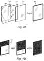
- FIGS. 4A-Cdepict fabrication of an IGU with an EC lite and associated tinting schemes, respectively.
- FIGS. 4D-Hdepict EC lites, each having a gradient tinting zone.
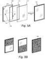
- FIGS. 5A and 5Bdepict fabrication of an IGU with an EC lite and associated tinting schemes, respectively.
- FIG. 5Cdepicts a perspective and a cross section of an EC device having two tinting zones separated by a resistive zone.
- FIG. 5Ddepicts a perspective and a cross section of an EC device having two tinting zones by virtue of a resistive zone.
- FIG. 5Eshows graphs of V TCL for two transparent conducting oxide layers of an EC device configured with a resistive zone created by inhibiting the electrical conductivity of only one of the transparent conducting oxide layers.
- FIG. 5Fdepicts a tinting pattern of the EC lite described in relation to FIG. 5C .
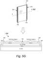
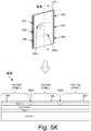
- FIGS. 5G to 5Kdepict EC devices configured with a resistive zone created by inhibiting the electrical conductivity of only one of the transparent conducting oxides.
- FIG. 6Adepicts a resistive zone establishing a closed perimeter defining a separate tinting zone.
- FIG. 6Bdepicts a resistive zone establishing an open perimeter defining a separate tinting zone.
- FIG. 7depicts using resistive zones for multi EC lite patterns/displays.
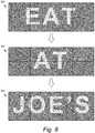
- FIG. 8depicts a building facade using resistive zones to create words and/or ornamental designs.
- FIG. 9depicts a building facade using gradient zoning across multiple IGUs.
- an optical devicethat is, thin-film devices having at least one transparent conductor layer.
- an optical deviceincludes a substrate and one or more material layers sandwiched between two conductor layers, one of which is transparent.
- an optical deviceincludes a transparent substrate and two transparent conductor layers.
- FIG. 1depicts fabrication of an IGU, 120 , with an EC lite, 100 , which includes a monolithic EC device and associated pair of bus bars, 105 , which energize the device each via a transparent conductor, the pair of transparent conductors sandwich the EC materials between them so that a potential can be applied across the device materials.
- the IGUis fabricated by combining EC lite 100 with a spacer, 110 , and a mate lite, 115 , along with the appropriate sealants and wiring (not shown) to the bus bars.
- a second set of spacer and mate litemay be added (i.e. Triple Pane IGU).
- the two mate litesmay be of different types. As depicted on the bottom half of FIG.
- the IGUcan be transparent (left), tinted to an intermediate state (middle) or fully tinted (right).
- intermediate statetinted
- righttinted
- Conventional technologydoes exist to achieve this end, however.
- FIG. 2Adepicts an IGU, 220 , having an EC lite, 200 , with two tinting zones delineated by laser scribe, 225 .
- Each tinting zonehas an associated pair of bus bars, 205 and 207 , respectively.
- the EC lite 200may be incorporated into an IGU, 220 , as described in relation to FIG. 1 .
- Scribe line 225cuts through both of the transparent conductor layers which sandwich the electrochromic materials, along with the EC device layer(s), so that there effectively two EC devices, one corresponding to each tinting zone, on the EC lite 200 . Scribe line 225 may not be visually discernible when the EC lite is not tinted, as depicted in FIG. 2A , i.e. in the untinted state (bleached or neutral state).
- FIG. 2Bdepicts three possible tinting schemes of IGU 220 .
- IGU 220may have the top zone tinted and the bottom zone untinted (left), the top zone untinted and the bottom zone tinted (middle) or both the top and bottom zones tinted (right).
- scribe line 225is visually discernible and is unattractive to an end user because there is a bright line across the middle of the viewable area of the window. This is because the EC material in the area has been destroyed and/or deactivated from the scribe line that cut through the device.
- the bright linecan be quite distracting; either when one is looking at the window itself, or as in most cases, when the end user is trying to view things through the window.
- the bright line against a tinted backgroundcatches one's eye immediately.
- Many approacheshave been taken to create tinting zones in optical devices, but they all involve some sort of physical segmentation of a monolithic optical device into two or more individually operable devices. That is, the functionality of the EC device is destroyed along the scribe line, thus effectively creating two devices from a monolithic single device. Certain embodiments described herein avoid destroying the EC device function between adjacent tinting zones.
- One approach to overcoming the visually distracting bright line created by a laser scribe in the viewable area of an EC liteis to apply a tinted material to the lite, e.g. on the scribe line or on an opposing side of the lite, in order to obscure or minimize the light passing through the scribe area.
- a tinted materiale.g. on the scribe line or on an opposing side of the lite, in order to obscure or minimize the light passing through the scribe area.
- the scribe linewill be less discernible to the end user.
- the tinted material in the scribe line areawill be almost or completely indiscernible because it is a thin tinted line against a large untinted background, which is harder to see than a bright line against a tinted background.
- the thin tinted lineneed not be opaque, a limited amount of absorption of the visible spectrum can be used, e.g., absorption that will tone down the bright line created when the full spectrum emanates through scribe line 225 .
- Methods for obscuring pinhole defects in optical devicesare described in, for example, described in U.S. Provisional Patent Application Ser. No. 61/610,241, filed Mar. 13, 2012, and described in PCT Application Ser. No. PCT/US2013/031098 filed on Mar. 13, 2013, which are both hereby incorporated by reference in their entirety. Whether obscuring pin holes, scribe lines, edge lines, or the like, the methods obscure bright areas on EC devices, e.g.
- Edge linesexist where a coating such as a monolithic electrochromic coating, does not extend to the spacer of an IGU (e.g., element 110 of FIG. 2A ). In this region, a bright line or wider area is visible when viewing the IGU directly.
- the obscuring methods described in the present application and in PCT/US2013/031098have equal applicability to pin holes, edge lines, scribe lines, and the like. The methods described in the aforementioned patent application are particularly useful for obscuring scribe or edge lines in the visible area of an optical device such as an EC device.
- One embodimentis a method of obscuring a scribe line in the viewable area of an EC window, the method including applying a method used to obscure pinholes as described in the aforementioned US/PCT Patent application.
- one methodincludes applying a tinted material to the scribe line and optionally the area adjacent the scribe line.
- the glass at the bottom of the scribe line trench (and optionally some adjoining area)is altered so as to diffuse light that passes therethrough, thus ameliorating the “bright line” effect.
- tinting zonesmay be created by: 1) configuring the powering mechanism (e.g. bus bars, wiring thereto and associated powering algorithms) of the optical device appropriately, 2) configuring the EC device such that adjacent tinting zones are separated by a resistive zone, or 3) combination of 1) and 2).
- the powering mechanisme.g. bus bars, wiring thereto and associated powering algorithms
- number 1)may be achieved by appropriately configuring one or more bus bars such that they can be activated independently of other bus bars on the same monolithic EC device.
- tinting zonesare created without the need to physically separate individual EC devices to create corresponding tinting zones.
- a resistive zoneallows coloration and bleaching of adjacent tinting zones on a single EC device without destroying functionality in the resistive zone itself.
- a resistive zonecan refer to an area of the monolithic optical device, e.g. an EC device, where the function is impaired but not destroyed. Typically, the functionality in the resistive zone is merely slowed relative to the rest of the device.
- Impairmentmight include diminished capacity for ion movement in one or more of the layers of the EC device and/or reduced density of the ions.
- the change in EC stack properties and/or ion densitymaybe done during deposition/fabrication of the EC stack or post-deposition through a thermal/laser irradiation treatment.
- one or more EC device layersmay be made denser than it otherwise would be in the bulk functioning device and therefore be able to hold fewer ions and/or allow ion passage through the denser material, and therefore color less intensely than the bulk device, but still function.
- a resistive zoneis achieved in at least one of the following ways: i) the electrical resistivity of one or both of the transparent conductor layers is impaired, ii) one or both of the transparent conductor layers is cut, without cutting through the optical device stack therebetween, iii) the function of the optical device stack (not including the transparent conductor layers) is impaired, and iv) combinations of i)-iv).
- a resistive zonemay be created where one or both of the transparent conductor layers is fabricated thinner or absent, e.g. along a linear region, so as to increase electrical resistivity along the linear region of the resistive zone.
- one of the transparent conductor layersmay be cut along the width of the device, while the other transparent conductor is left intact, either of uniform thickness or thinner, along the resistive zone.
- the function of the EC devicemay be inhibited along a line, so that it resists ion transport, while the transparent conductor layers may or may not be altered along the same line. Resistive zones are described in more detail below in terms of specific, but non-limiting examples. If the resistive zone is in one of the transparent layers, the other transparent layer may be left intact (e.g., uniform composition and thickness).
- One embodimentis an electrochromic window lite including a monolithic EC device on a transparent substrate, the monolithic EC device including two or more tinting zones, each of the two or more tinting zones configured for operation independent of the others and having an associated pair of bus bars.
- the two or more tinting zonesare not separated from each other by isolation scribes; that is, the EC device and associated transparent conductors do not have isolation scribes that cut through any of these layers.
- each pairis associated with a tinting zone and both pairs are located at or near opposing edges of the EC lite e.g., the bus bars may be vertically oriented at or near opposing vertical edges with a set of bus bars for each of the two tinting zones.
- Such litesmay be integrated into insulating glass units (IGUs).
- FIG. 3Adepicts fabrication of an IGU, 300 , with an EC lite, 305 having two tinting zones (upper and lower tinting zones) configured on a monolithic EC device.
- Each of bus bar pairs, 205 and 207is configured to energize independently of each other.
- IGU 300has three tinting schemes besides the untinted state (bleached or neutral state) depicted in FIG. 3A .
- FIG. 3Bdepicts fabrication of an IGU, 300 , with an EC lite, 305 having two tinting zones (upper and lower tinting zones) configured on a monolithic EC device.
- Each of bus bar pairs, 205 and 207is configured
- each tinting zone of lite 305when tinted, has a “tinting front” 310 .
- a tinting frontcan refer to an area of the EC device where the potential applied across the devices TCOs by the bus bars reaches a level that is insufficient to tint the device (e.g. by movement of ions through the layers of the device to balance charge).
- the tinting front 310corresponds roughly to where the charge is bleeding off into the area of the transparent conductor that is between the pair of bus bars that are not energized.
- the shape of a tinting frontmay depend upon the charging characteristics of the transparent conductors, the configuration of the bus bars, wiring and powering thereto, and the like.
- the tinting frontmay be linear, curved (convex, concave, etc.), zigzag, irregular, etc.
- FIG. 3Bdepicts the tinting front 310 as a linear phenomenon; that is, the tinting front 310 is depicted as located along a straight line.
- FIG. 3Cdepicts various tinting schemes as a function of tinting front of each of the tinting zones, in this case lower and upper tinting zones.
- the tinting frontis curved (e.g., concave or convex) along the tinting front.
- tinting of the EC liteis total and uniform.
- a convex tinting frontmay be desirable, so a complimentary concave tinting front may be used in an adjacent zone, or another convex tinting front may be used to ensure sufficient charge reaches the entire device for uniform tinting.
- the tinting frontmay not be a clean line as depicted in FIGS. 3B and 3C , but rather have a diffuse appearance along the tinting front due to the charge bleeding off into the adjacent tinting zone which is not powered at the time.
- one zone's tinting levelis different than the other, e.g., where one zone is tinted to 5% T and the other adjacent zone tinted to 20% T, there may be no noticeable tinting front. That is, the two zones' tinting may blends into each other for a uniform gradient tinting appearance, e.g. resembling a shading effect, where the coloration is darkest in one zone and appears to gradually lighten into and including the adjacent zone.
- a uniform gradient tinting appearancee.g. resembling a shading effect
- the colorationis darkest in one zone and appears to gradually lighten into and including the adjacent zone.
- One embodimentis a method of controlling a monolithic EC device coating, including tinting two adjacent zones simultaneously by virtue of selective application of voltage to different areas of the monolithic EC device.
- the mate litewhen the EC lite with tinting zones is incorporated into an IGU or a laminate for example, the mate lite may also be an EC lite, having tinting zones or not.
- Insulated glass unit constructions having two or more (monolithic) EC litesare described in U.S. Pat. No. 8,270,059, which is hereby incorporated by reference in its entirety. Having two EC lites in a single IGU has advantages including the ability to make a near opaque window (e.g. privacy glass), where the percent transmission (% T) of the IGU is ⁇ 1%. Also, if the EC lites are two-state (tinted or bleached) there may be certain tinting combinations made possible, e.g.
- the tinting possibilitiesmay be virtually endless.
- One embodimentis an IGU having a first EC lite having two or more tinting zones and a mate lite that is a monolithic EC lite.
- the mate litealso has two or more tinting zones.
- the tinting zonesmay or may not be the same in number or aligned with the tinting zones of the first EC lite with which it is registered in the IGU. Exemplary constructs illustrating these descriptions follow.
- FIG. 3Ddepicts fabrication of an IGU, 325 , having two EC lites, 305 and 320 , where each of the EC lites has two tinting zones, each of the tinting zones created by appropriately configured bus bar pairs, 205 and 207 at or near two opposing edges.
- the tinting zones of EC lites 305 and 320are registered, that is, they are aligned with each other and of the same area, but this need not be the configuration.
- the tinting fronts from opposing EC lites 305 and 320could overlap each other when tinted in another embodiment.
- FIG. 3Ddepicts IGU 325 in an untinted state (bleached or neutral state).
- each of the tinting zonesis capable of only two states, tinted or bleached. Even so, this enables a wide range of tinting schemes for IGU 325 .
- IGU 325is capable of many tint states (e.g., eight tint states).
- FIG. 3Bdepicts three of the possible tint states (i.e. where one EC lite of IGU 325 is tinted in one of the three configurations shown in FIG. 3B ).
- FIG. 3Edepicts another five possible tint states for IGU 325 . If the top tinting zones of both EC lites are tinted simultaneously, and the bottom two zones are not, then the top half of the IGU is very dark, while the bottom is untinted (top left IGU).
- both of the top tinting zonesare not tinted, and the bottom two zones are tinted, then the bottom half of the IGU is very dark, while the top is untinted (top middle IGU). If all four zones of the EC lites are tinted, then the entire window is very dark (top right IGU). For example, the combined tinting of all tinting zones in two registered EC lites can achieve ⁇ 1% T. If one of the top zones in the EC lites is tinted and both of the bottom zones are tinted, then the tint state on the bottom left of FIG. 3E is created. Likewise, if one of the bottom zones is tinted and both of the top zones are tinted, then the tint state on the bottom right of FIG. 3E is created.
- One embodimentis an IGU having two or more EC lites, wherein at least two of the two or more EC lites includes multiple tinting zones as described herein.
- the tinting zonesmay be formed physically in the coating, i.e. by bifurcation of a monolithic coating, forming a resistive zone in a monolithic EC coating, or both; or a monolithic coating with no resistive zones may be controlled by selective application of voltages to different areas to form tinting zones.
- One embodimentis an IGU or laminate having two or more EC lites, where a first of the two or more EC lites includes multiple tinting zones created by conventional isolation scribes, and a second of the two or more EC lites includes tinting zones as described herein by techniques other than isolation scribes.
- One embodimentis an IGU or laminate having two or more EC lites, where a first of the two or more EC lites includes multiple tinting zones, and a second of the two or more EC lites includes a monolithic EC coating without tinting zones.
- Configurations such as those depicted in FIGS. 3B and 3Emay be particularly useful in applications such as creating day lighting zones vs. occupant (glare) control zones.
- the day lighting zonesmay also be tinted but at lower tint level than the glare control zones for the optimal user experience, e.g. day lighting zones may be tinted to % Tvis ⁇ 4%-30% while the glare control zones may be tinted to % Tvis ⁇ 0.1-1%.
- Day lighting transomsare very common. For example, creating “virtual transoms” with a piece of glass and thus removing the frame and associated glazier labor has a cost benefit as well as better sight lines. Also, having a variety of tint states such as those depicted in FIGS. 3B and 3E allows for customization of room lighting based on the amount and location of the sun striking individual windows.
- Certain embodimentspertain to methods of transitioning an EC lite having two or more tinting zones.
- an EC lite having three or more tinting zonesis transitioned across the three or more tinted zones from a first zone at one edge of the device, to a second adjacent tinting zone, and then to a third tinting zone, adjacent to the second zone.
- the tinting zonesare used to give the effect of drawing a physical shade across the window, without actually having a physical shade, since EC windows may eliminate the need for physical shades.
- Such methodsmay be implemented with conventional zoned EC lites or those described herein. This is illustrated in FIGS. 4A-C with respect to an EC lite of an embodiment.
- an EC lite, 400is configured with a first set of bus bars, 405 , a second set of bus bars 407 , and a third set of bus bars, 409 .
- the three sets of bus barsare configured so as to create three tinting zones, respectively.
- EC lite 400 in FIG. 4Ais incorporated into an IGU, 420 , using a spacer 410 and a mate lite 415 , lamination to a mate lite (EC lite or otherwise) or use as a single EC lite is also possible.
- each of the tinting zonesis tinted as a two-state zone
- the three tinting zonesmay be activated sequentially, e.g. from top to bottom as depicted, to create a physical shade effect, i.e. as if one were lowering a roller shade or drawing a Roman shade over the window.
- the top zonemay be fully tinted
- the second zonemay be fully tinted
- the third zonemay be fully tinted.
- the tinting zonescould be sequentially tinted from the bottom up or in the middle and then the upper and lower zones tinted, depending upon the desired effect.
- Another methodis to tint the tinting zones as described with respect to FIG. 4B , except that before transition in a particular tinting zone is complete, transition in an adjacent tinting zone begins, which can also create a shading effect.
- the top tinting zone's tintingis initiated (top left), but before tinting is complete in the top zone, the middle zone's tinting is initiated. Once the top zone's tinting is complete, the middle zone's tinting is not yet complete (top center). At some point during the transition of the middle zone, the bottom zone's tinting is initiated.
- tinting zones with intermediate state capabilityrather than two-state “tint or not,” will increase the possible variations of tinting schemes.
- an EC litemay be configured to have one or more tint gradient zones.
- the EC litehas an EC device, such as, e.g., a monolithic EC device on a transparent substrate, and also has at least one pair of bus bars with geometry and/or material composition that varies along their lengths to vary electrical resistance lengthwise (lengthwise variable bus bars). This variation in resistance can produce a lengthwise gradient in the voltage applied to the EC device supplied across bus bars (V app ) and a lengthwise gradient in the local effective voltage (V eff ) in the EC device.
- V effrefers to the potential between the positive and negative transparent conducting layers at any particular location on the EC device.
- the lengthwise gradient of the V effmay generate a corresponding tint gradient zone that varies lengthwise in a region between the pair of bus bars when energized.
- the lengthwise variable bus barswill have resistance profiles along their lengths that are functions of both the local bus bar geometry and resistivity.
- the bus barsare designed so that the resistance is lowest at one end of the bus bar and highest at the other end of the bus bar. Other designs are possible, such as designs where the resistance is lowest in the middle of a bus bar and highest at the ends of the bus bar.
- a description of voltage profiles in various EC devices powered by bus barscan be found in U.S.
- EC devicesconfigured, e.g., as described in relation to FIGS. 4D and 4E , in addition to being capable of tinting in a gradient fashion as depicted, may also, e.g. upon application of sufficient voltage, tint to a uniform coloration. For example, a maximum (and uniform) tinting may be achieved across the monolithic device coating by application of sufficient voltage using bus bars also configured to apply a gradient voltage (and give the gradient tinting shown).
- the local material composition of a bus barmay determine its local resistivity. It is contemplated that the bus bar material composition, and therefore the bus bar resistivity may vary along the length of the bus bar in certain embodiments.
- the resistivitycan be tailored based on various compositional adjustments known to those of skill in the art. For example, resistivity can be adjusted by adjusting the concentration of a conductive material in the bus bar composition.
- bus barsare made from a conductive ink such as a silver ink. By varying the concentration of silver in the ink along the length of the bus bar, one can produce a bus bar in which the resistivity likewise varies along the length.
- the resistivitycan also be varied by other compositional adjustments such as the local inclusion of resistive materials in the bus bar or the variation of the composition of a conductive component to adjust its resistivity. Slight variations in composition can change the resistivity of certain conductive materials such as conductive polymers.
- the electrical conductivity of the bus bar materialis constant, but the thickness and/or width of the bus bar varies along its length.
- the value of the voltage that can be applied at any position on the bus baris a function of the location where the bus bar connects to an external power source and the resistance profile of the bus bar.
- a bus barmay be connected to the source of electrical power at locations where the bus bar has least resistance, although this is not required.
- the value of the voltagewill be greatest at the locations where the power source connection attaches to the bus bars. The decrease in voltage away from the connection is determined by the distance from the connection and the resistance profile of the bus bars along the path from the connection to the point where voltage is measured.
- the value of voltage in a bus barwill be greatest at the location where an electrical connection to the power source attaches and least at the distal point of the bus bar.
- a bus barwill have lower electrical resistance at an end proximal to the connection to the electrical source and a higher resistance at a distal end (i.e. the resistance is higher at the distal end than at the proximal end).
- Each of the lengthwise variable bus barsmay have linearly, stepped, or otherwise varying geometry and/or material composition along its length.
- a bus bar with lengthwise-varying geometrymay have its width, height, and/or other cross-sectional dimension linearly tapering from the proximal end to the distal end.
- a bus barmay be comprised of multiple segments with stepwise decreasing widths or other dimensions from the proximal end to the distal end.
- a bus barmay have a material composition that varies lengthwise to increase electrical resistivity between proximal and distal ends.
- FIGS. 4D and 4Edepict EC lites, 425 and 435 respectively, each having a monolithic EC device on a transparent substrate and a pair of bus bars.
- the width of each of the bus barsvaries along its length. This geometric lengthwise variation in the bus bars may produce a tint gradient zone (gradient in lengthwise direction) on the monolithic EC device when energized.
- FIG. 4Ddepicts an EC lite, 425 , including bus bars 430 .
- Each of the bus bars 430has a varying width along its length that linearly tapers lengthwise.
- the variation in width between the two endsmay be between about 10% and about 100% from the average width over the length of the bus bar.
- the variation in widthmay be between about 10% and about 80% from the average width over the length of the bus bar.
- the variation in widthmay be between about 25% and about 75% from the average width over the length of the bus bar.
- the bus bars 430are widest at the top of EC lite 425 and linearly taper lengthwise to their thinnest width near the bottom of lite 425 .
- bus bars 430when energized, establish a voltage gradient. For example, when energized, bus bars 430 have their highest effective voltage at the top, and their lowest voltage at their bottom portion; a voltage gradient is established along the bus bars. As depicted in the right portion of FIG. 4D , a corresponding tinting gradient is established by virtue of the voltage gradient. Thus a tint gradient zone is established.
- Bus bars of varying widthcan be used in one or more zones of an EC lite having two or more zones as described herein. In this illustrated example, a single tint gradient zone is established across an EC lite.
- a linearly tapered widthis illustrated in FIG. 4D , a non-linearly tapered width can be used in other cases.
- a bus barmay have a stepped down width along its length (i.e. stepwise width variation along its length).
- FIG. 4Edepicts an EC lite, 435 , having a monolithic EC device and bus bars that have stepped widths along their lengths. Each bus bar has three segments with stepped down widths along its length. Each bus bar has a first width that spans a first portion, 440 , of the length of the bus bar. Adjacent to the first portion, is a second portion, 445 , of the length of each bus bar. The second portion has a second width shorter than the first width.
- a third portion, 450 of each bus baradjacent to the second portion and having a third width, is a third portion, 450 of each bus bar.
- the net tinting gradient effectmay be the same as or similar to the smooth linearly taper bus bars described in relation to FIG. 4D .
- varying the width of the bus barscan be done in other patterns, such as thicker in the middle than at the ends, etc. without escaping the scope of embodiments described herein, that is for an EC lite having bus bars of varying widths configured to create one or more tint gradient zones, and corresponding tinting effects, on a monolithic EC device.
- the electrically resistive bus barwill act as a resistance path in the circuit and be able to provide adequate drop in voltage along its length. Since the Transmission of the EC window is proportional to the V_eff, and the drop in the voltage along the Bus bar ( ⁇ V) reduces the V_eff as described previously, the ( ⁇ V/L 0 ) terms represents the gradient of the shading/Tvis from one end to the other, e.g. a small part (small L 0 ) with a large voltage drop along the bus bar from end to the other will have a very pronounced Tvis shading/gradient, while for a large part will need a larger voltage drop along the bus bar to maintain the same shading along its length.
- the bus bar propertiese.g.
- height, width, material, though having a uniform cross section,can be selected during fabrication to provide the required shading from one end to the other. This enables ease of design/manufacturing to avoid complex-geometry bus bars, while still providing a gradient in the optical properties across the window. For example, one can fabricate a thin bus bar that has a voltage drop across its length to create a gradient shading.
- the bus barscan be powered from one end of the bus bars (as described above) or both ends of each bus bar (as described in relation to FIG. 4H ). Powering bus bars from both ends provides additional control over the gradients/shading of the EC window. For example, as depicted in FIG. 4H (top left), a voltage is applied to the top ends of the two bus bars that power each of the TCO's of the EC device coating. The bottom ends are also in electrical communication through leads (depicted here as “open”). A voltage gradient is established over the length of the bus bars, in this example substantially equal gradients across the bus bars of substantially the same length.
- V_applied_1, V_applied_2 and bus bar pattern and R Bare tinted darker than a middle portion, when V_applied_1 and V_applied_2 are applied to both ends of both bus bars (only one bus bar's application depicted).
- an IGUincludes two EC lites, each EC lite having a tint gradient zone as described in relation to FIGS. 4D and 4E .
- the tint gradient zone of each EC liteis configured in opposition to each other, that is, one EC lite has a tinting front that starts at the opposite side (e.g., edge) of where the tinting front of the other EC lite starts.
- a unique curtaining effectis established where the tinting fronts approach each other from opposite sides and cross paths in the middle of the IGU.
- the IGUmay have a “privacy glass” tint level, of e.g. ⁇ 1% T.
- each EC litemay be tinted independently to provide a “top down” tint gradient or “bottom up” tint gradient.
- the tint gradient zones of the EC litesare registered together i.e. aligned so that the tinting fronts of the EC lites start on the same side of the IGU and end at the other opposing side.
- tinting of the IGUmay be done for different tint levels with one lite, e.g., to provide a top down tint gradient of one intensity (absorption gradient e.g.) for one tint level, and another (darker) tint level of tinting gradient when both lites are tinted.
- Either of the two aforementioned IGU embodimentsmay have their individual EC lites tinted together or alternatively tinted asynchronously for yet another shading effect that is not possible with conventional monolithic EC devices.
- a bus barmay include an inner portion of electrically conductive material with a cross-sectional dimension (e.g., width) that varies lengthwise, and an outer portion of electrically resistive material.
- the outer portionmay have geometry which is designed to couple and form with the inner portion a uniform cross-section along the length of the bus bar.
- an electrochromic window liteincludes a monolithic EC device on a transparent substrate, wherein the EC lite includes at least one pair of bus bars configured to produce a tint gradient zone on the monolithic EC device when energized.
- tinting gradientsare established using bus bars, where each bus bar has at least two portions that are highly conductive. The at least two portions are separated by a portion that is more resistive than the highly conductive at least two portions, while still being electrically conductive. The more resistive portion is configured adjacent to or overlapping the at least two highly conductive portions.
- the at least two highly conductive portionsare separated, they do not touch, but rather each only touches, and is in electrical communication with the more resistive portion in between them.
- An electrical power sourceis configured to power only one portion of the at least two highly conductive portions of each of the at least one pair of bus bars.
- Each of the only one portion of the at least two highly conductive portionsis proximate the same side of the monolithic EC device as the other of the only one portion.
- Tint gradient zonescan be created using bus bars having varying material composition along their lengths.
- FIG. 4Fdepicts an EC lite, 455 , having two bus bars, each configured along opposing edges (e.g., vertically, horizontally, etc.) and parallel to each other on lite 455 .
- each bus barhas highly electrically conductive portions, 460 a , 460 b , and 460 c (collectively, 460 ), and less electrically conductive portions, 465 a and 465 b (collectively, 465 ).
- less electrically conductive portions, 465 ais between highly electrically conductive portions 460 a and 460 b
- less electrically conductive portions, 465 bis between highly electrically conductive portions 460 b and 460 c .
- the less electrically conductive portions, 465 a and 465 bmay be portions of a monolithic bus bar where the conductivity has been reduced by, e.g. changing the morphology of the bus bar material and/or perforating the material, etc.
- separate bus barsare used, for example as described in relation to FIGS.
- highly electrically conductive portions 460 a , 460 b , and 460 cmay be conventional silver based conductive bus bar ink, while portions 465 a and 465 b may be a less conductive ink.
- the bus barsmay be connected to an electrical source at the top portion, 460 a , of each bus bar.
- a voltage gradientmay be established along the length of the bus bars by virtue of the resistive portions 465 a and 465 b .
- the top highly conductive portions 460 amay have the highest voltage
- the middle highly conductive portions 460 bmay have a somewhat lower voltage because the more resistive portions 465 a creates an IR voltage drop between the middle portions 460 b and portions 460 a
- the bottom-most highly conductive portions 460 cmay have the lowest voltage because the more resistive portions 465 b lie between them and the middle highly conductive portions 460 b preventing some of the electrical current from flowing from middle portion 460 b to lower portion 460 c .
- the net effectmay be a tint gradient zone, for example, the one depicted in FIG. 4F .
- Highly electrically conductive portions 460may be of the same or different conductive material, and likewise, less electrically conductive portions 465 may be comprised of the same or different conductive material. The key is that portions 465 are less electrically conductive than their adjacent neighbors 460 .
- a wide variety of voltage and/or resistance patternsmay be established in order to create corresponding tint gradient zones in an EC lite.
- a combination of bus bars of lengthwise varying width and those bus bars configured as described in relation to FIG. 4Fmay be used. For example, each as partners in a bus bar pair and/or in individual tint gradient zones on an EC lite.
- the less electrically conductive portions, 465have variable resistance whose resistance can be varied between 1 mOhm-1 kOhm to dynamically adjust the tint gradient zones, i.e. when no zoning is required, elements 465 are in the low resistance state. That is the bus bar segments 460 and 465 , collectively, act as a single bus bar of low resistitivity. When zoning is desired, elements 465 are switched to a higher resistance state (than bus bar segments 460 ) when zoning is desired. The resistance of the element can also be varied to modulate the gradient in the Tvis (lower resistance for lower gradient).
- the element 465can be an electronic control element that can modulated remotely (e.g.
- the control elementmay be a component of an onboard controller, that is, an EC controller that is integrated with, in, part of the IGU.
- onboard controllersare described in U.S. patent application Ser. No. 13/049,750 titled “ONBOARD CONTROLLER FOR MULTISTATE WINDOWS,” filed on Mar. 16, 2011 and in U.S. patent application Ser. No. 14/951,410 titled “SELF-CONTAINED EC IGU,” filed on Nov. 24, 2015, both of which are hereby incorporated by reference in their entirety.
- the top and bottom TCO bus bar configurationsmay be different, which can be used synergistically to provide even more control over the zoning/gradients. For example, consider a specific cross section (orthogonal to the bus bars) of a monolithic EC device coating having bus bars of different configuration along each side. If the voltage profile, gradient, along one bus bar is different than the voltage profile of the other bus bar, then various tint gradients can be achieved. Thus, with different combinations of bus bar configurations on a single EC coating, almost endless variations in the gradients are possible.
- the EC device tinting or clearing operationcan be divided into a drive step and hold step, e.g. where there is a ramp in voltage followed by a constant voltage, respectively.
- a drive step and hold stepe.g. where there is a ramp in voltage followed by a constant voltage, respectively.
- the leakage current of the deviceis as low as possible. This is because, the leakage current can normalize or diffuse out any gradients setup due to conduction over the TCOs and change in the V_applied.
- leakage currents ⁇ 5 ⁇ A/cm 2are desirable to ‘freeze’ the gradients setup in the window.
- an EC litemay be configured to have a combination of tint gradient zones and tint zones that do not have tint gradient capability (non-gradient tint zones).
- One embodimentis a monolithic EC device having two or more tinting zones, where at least one tinting zone is a tint gradient zone and at least one tinting zone is a non-gradient tint zone.
- One embodimentis a monolithic EC device having two or more tint gradient zones, with or without also having a non-gradient tint zone.
- the bus bars described in relation to FIG. 4Fare configured such that each highly electrically conductive portion, 460 a , 460 b , and 460 c , has its own electrical connection to a power source.
- the bus bars described in relation to FIG. 4Fwhen configured with each highly electrically conductive portion 460 having its own power source (or sources, e.g. as described in relation to FIG. 4H ), may be used to create tint gradient zones with tinting patterns similar to those described in relation to FIGS. 4B and 4C .
- the tinting frontmay not be a clean line, but rather have a diffuse appearance along the tinting front due to the charge bleeding off into the EC device's adjacent zone which is not powered at the time.
- resistive zonesmay be used to aid in maintaining more well-defined tinting fronts. Resistive zones are described in more detail below.
- resistive zonesare configured in the monolithic EC device. These resistive zones may allow for more uniform tinting fronts, e.g., when used in combination with bus bar powering mechanisms described herein.
- an EC lite, 500much like EC lite 200 of FIG. 2A , is configured with two pairs of bus bars for creating two tinting zones, in this example (as depicted) a top and a bottom zone.
- EC lite 500may be incorporated into an IGU, 510 , with a spacer 110 and a mate lite 115 as depicted. A major difference between lite 200 of FIG. 2A and lite 500 of FIG.
- lite 500does not have a laser scribe 225 across the lite to bifurcate the EC device into two devices.
- Lite 500has a single EC device over the viewable area of the lite.
- the EC device on lite 500includes a resistive zone, 505 , that spans the width of the EC device.
- the heavy dotted line in FIG. 5Aindicates the approximate position of resistive zone 505 .
- resistive zone 505may not be visible to the naked eye when the EC lite's zones are not tinted. However, unlike laser scribe 225 , when adjacent tinting zones of EC lite are tinted, resistive zone 505 may not be visually discernible to the naked eye. This is illustrated schematically in the right portion of FIG. 5B . The reason resistive zone 505 tints is because it is not a physical bifurcation of the EC device into two devices, but rather a physical modification of the single EC device coating and/or its associated transparent conductors within a resistive zone.
- the resistive zoneis an area of the EC device where the activity of the device is impeded, specifically through higher electrical resistivity and/or greater resistance to ion movement and/or lower ion density compared to the remainder of the EC device.
- one or both of the transparent conductorsmay be modified to have increased electrical resistivity in the resistive zone, and/or the EC device stack may be modified so that ion movement is slower in the resistive zone relative to the EC device stack in the adjacent tinting zones.
- the modificationsmay be made during deposition of the EC device or post deposition through a thermal and/or laser treatment.
- the EC devicestill functions, tints and bleaches, in this resistive zone, but at a slower rate and/or with less intensity of tint than the remaining portions of the EC device.
- the resistive zonemay tint as fully as the remainder of EC device in the adjacent tinting zones, but the resistive zone tints more slowly than the adjacent tinting zones.
- the resistive zonemay tint less fully than the adjacent tinting zones, and at a slower rate.
- FIG. 5Cis a perspective and a cross section, X-X, of EC lite 500 as described with respect to FIGS. 5A and 5B .
- the cross section, X-Xspans the upper and lower tinting zones (tinting zones 1 and 2 , respectively) of EC lite 500 as well as resistive zone 505 (only the bus bars on the top TCO are depicted in cross section X-X, they are orthogonal to resistive zone 505 in this example).
- Cross section X-X(lower portion of FIG. 5C ) is not to scale, but rather a schematic representation of the structure of EC lite 500 .
- an EC deviceincluding a first transparent conducting oxide layer, TCO 1 , a second transparent conductive oxide layer, TCO 2 , and sandwiched in between the TCOs is an EC stack which contains one or more electrochromic materials, e.g., the transitions of which are driven by intercalation/de-intercalation of ions, such as lithium ions.
- Resistive zone 505is an area in the EC device where one or more layers of the EC device have their function impaired, either partially or completely, but device function is not cut off across the zone. For example, one or both of the TCOs has a higher resistance to electrical flow in resistive zone 505 than in the tinting zones.
- tinting zone 1if tinting zone 1 is activated, electrons flow across the TCOs at a given rate, but that flow is restricted along resistive zone 505 . This allows the electrons to be sufficiently retained in tinting zone 1 and thus leak more slowly across resistive zone 505 than otherwise would be the case if TCO function had not been impaired there.
- Resistive zone 505could be thought of as a “dam” for electrical and/or ionic flow, impairing rate of flow (either ionic current or electronic current) across it, the flow can be partially or fully impaired in one or both TCOs, for example. Due to the restricted or slowed rate of electrical flow across resistive zone 505 , ion intercalation in the EC stack between the TCOs at resistive zone 505 is also impaired. Because the EC device is not physically cut into two devices, this is unlike conventional devices having zones created by physical bifurcation of one more layers of a single device coating. Resistive zone 505 may have physical impairment of ion flow in one or more of the EC material layers.
- both the top and bottom TCO's electrical conductivityis impaired, either partially or fully, in resistive zone 505 , but the function of the EC device stack layers is substantially unchanged.
- the devicewill tint under resistive zone 505 .
- adjacent tinting zonesare both tinted, there is no bright line discernible to the end user, because the device tints under resistive zone 505 .
- the devicemay still color, but more slowly than the bulk device. This rate difference in coloring may or may not be visually discernible to the end user.
- Resistive zone 505may be fabricated, for example, by exposure of the area at the resistive zone 505 to irradiation, e.g. laser or heat source, in order to modify but not destroy the function at resistive zone 505 .
- irradiatione.g. laser or heat source
- one or both of the TCO layersmay be heated sufficiently to change the morphology while retaining the function, albeit impaired relative to the remainder of the TCO layers in the tinting zones.
- Resistive zonesmay also be created by impairing the function of one or more layers of the EC device (including, or not, one or both TCOs) by chemical doping.
- the lower TCOis treated along a line (at resistive zone 505 , e.g.) with heat and oxygen to create a more resistive TCO at the resistive zone.
- one or both TCOsare fabricated thinner along the resistive zone than the rest of the TCOs, e.g. TCO material may be removed, but not cut through, along the resistive zone.
- heating along the zonemay densify the EC materials while having no effect on the TCO layers; or may affect the TCO layers as well.
- the resistive zonesmay be narrow, e.g. between about 1 ⁇ m and 1000 ⁇ m wide, or may be wider, e.g. between about 1 mm and about 10 mm wide. Because the EC materials in resistive zones tint and do not necessarily leave a bright line contrast effect typical of conventional laser isolation scribes, there is less concern as to the width of the described resistive zones. Thus, in other embodiments, a resistive zone may be, for example, wider than 1 mm, wider than 10 mm, wider than 15 mm, etc.
- each of the tinting zoneshas its own unique pair of bus bars.
- tinting zonescan be colored independently by virtue of operation or the respective bus bar pairs at each tinting zone.
- multiple tinting zonesmay be configured to share a common bus bar, while still being independently controllable.
- FIG. 5Ddepicts a perspective (top portion) and a cross section Y-Y (bottom portion) of an EC lite, 510 , having two tinting zones of variable tinting level by virtue of a resistive zone, 515 .
- a single set of three bus bars, 525 ( a ), 525 ( b ), and 520is used with two tinting zones.
- Cross section, Y-Y, of EC lite 510spans left and right tinting zones (tinting zones 1 and 2 , respectively) of lite 510 as well as resistive zone 515 .
- Resistive zone 515runs parallel to and between (approximately in the middle of EC lite 510 ) bus bars 520 and 525 ( a ) and bus bar 525 ( b ) (from top to bottom as depicted in the perspective at the top of FIG. 5D ).
- Cross section Y-Y(lower portion of FIG. 5D ) is not to scale, but rather is a schematic representation of the structure of EC lite 510 .
- an EC deviceincluding a first transparent conducting oxide layer, TCO 1 , a second transparent conductive oxide layer, TCO 2 , and sandwiched in between TCO 1 and TCO 2 is an EC stack which contains one or more electrochromic materials, e.g., the transitions of which are driven by intercalation/de-intercalation of ions, such as lithium ions.
- resistive zone 515is an area of TCO 2 , where the TCO function is impaired but not eliminated.
- TCO 2may have its function impaired along a line.
- FIG. 5Eincludes two graphs showing plots of the local voltage V TCL , in TCO 1 and TCO 2 of the EC lite, 510 , of FIG. 5D that drives transition.
- a graphshows a curve 526 of the local values of V TCL , in the TCO 1 .
- a graphshows a curve 528 of the local values of V TCL in the TCO 2 .
- the bottom TCO 1has a local voltage potential V TCL , across its span similar to that of a typical transparent conductor for an EC device.
- V TCLin TCO 2 , the slight voltage drops between the left hand side where bus bar 520 is disposed on TCO 2 and the resistive zone due to sheet resistance and current passing through TCO 2 .
- the voltagesharply drops.
- the voltageslightly drops between the resistive zone 515 and the right hand side due to sheet resistance and current passing through TCO 2 .
- the value of V eff at any location between the bus barsis the difference in values of curves 130 and 125 at that position on the x-axis corresponding to the location of interest.
- tinting zone 1has a higher V eff than tinting zone 2 and thus tinting zone 1 colors more darkly than tinting zone 2 . This is represented in FIG. 5F .
- a visible coloration differenceis seen in window 510 corresponding to the location of resistive zone 515 and the rather abrupt drop in voltage in TCO 2 as reflected in FIG. 5E .
- this visual coloration differenceneed not be so; that is, for example, if resistive zone 515 is sufficiently “leaky”, and allows voltage to flow across the top TCO in a smooth gradient (or if window 510 is configured without resistive zone 515 and the voltage applied to TCO 2 is insufficient to overcome a voltage drop across TCO 2 ) then a gradual transition from darker to lighter results (see FIG. 4F , right side) due to the voltage drop over.
- the two tinting zonescan be configured as upper and lower portions when installed in a building, and they need not be side by side as depicted.
- FIG. 5Gdepicts an EC lite, 530 , configured with a resistive zone created by inhibiting the electrical conductivity of only one of the transparent conducting oxides.
- the EC liteis much like the one described in relation to FIG. 5E , but in this embodiment one of the TCOs is cut through along the resistive zone (cut 550 ), while the other TCO is left intact.
- the EC device stackis unchanged in the resistive zone, only the top TCO is cut.
- the EC lite 530has two sets of bus bars, 535 and 540 .
- Bus bar set 535powers the lower TCO 1
- bus bar set 540powers the top TCO 2 .
- the lower portion of FIG. 5Gshows cross section Z-Z.
- the EC devicewill still at least partially color along the resistive zone by virtue of one of the TCOs being fully intact, monolithic, along with the EC stack. While there is a narrow region of the opposite TCO 2 missing, there is sufficient voltage potential established between the intact TCO 1 and the edge of the cut (opposing) TCO 2 along the resistive zone to allow coloration of the EC device in the resistive zone, albeit more slowly than if both TCOs were intact along the resistive zone.
- the resistive zonemay color more lightly when only one of the tinting zones is powered, while with both tinting zones powered, the resistive zone may fully tint or approximate full tinting. Each portion of TCO 2 can be powered independently of TCO 1 .
- tinting zone 1 and tinting zone 2may, e.g., be tinted more effectively. Since there is a cut through the TCO 2 , if only one zone is powered, a tinting level of V TCL , is only established in that tinting zone. The cut in TCO 2 aids in establishing and maintaining a uniform tinting front.
- EC lite 530may be incorporated into an IGU where the EC device is hermetically sealed within the volume of the IGU, and/or a top coat may be used to hermetically seal the device, with our without lamination to a substrate. A top coat would fill the open trench cut through TCO 2 .
- FIG. 5Hshows EC lite, 530 a , where the cut, 550 a , is made only through the bottom TCO 1 .
- the top TCO 2may maintain its hermeticity by virtue of an intact top transparent conductor layer.
- the EC materialmay fill in the trench made by cut 550 a , and thus tint along with the trench in TCO 1 that it fills, providing an area of inhibited coloration rate such as a resistive zone.
- FIG. 5Gshows EC lite, 530 , where the cut, 550 , is made only through the top TCO 2 .
- An advantage of this embodimentmay be that the cut can be made after the EC device is fabricated, for example, by laser processing performed after sputter coating.
- the bus bars 535 and 540 depicted in FIGS. 5G and 5Hneed not be parallel, e.g. the bus bars powering each TCO can be orthogonal to each other. Also, the single monolithic TCO need not have two bus bars, but it is desirable so as to have more control over tinting of the individual tinting zones. Bleaching function would work the same way but in reverse polarity to bleach the tinting zones.
- the bus barsare configured parallel to the resistive zone; in FIGS. 5I and 5J , like in FIG. 5C , e.g., the bus bars are configured orthogonally to the resistive zone.
- bus bars in the viewable area of the EC devicethere are no bus bars in the viewable area of the EC device, that is, in the area within the spacer of the IGU.
- Certain conventional EC technologiesrely on bus bars running through the viewable area because of slow switching kinetics that would otherwise occur and/or due to ion conductor layer leakage currents that do not allow the EC device to switch across the entire viewable area of larger IGUs (e.g. about a meter wide or more where bus bars would otherwise be configured outside the viewable area at the edges of this width) without such bus bars in the viewable area to provide the extra voltage needed to compensate for the leakage current.
- FIG. 5Idepicts an EC lite, 555 , configured with a resistive zone, 570 , created by inhibiting the electrical conductivity across one of the transparent conducting oxides, in this example a cut is made through the TCO nearer the substrate.
- the EC liteis much like the one described in relation to FIG. 5C , but in this embodiment one of the TCOs is cut through along the resistive zone (cut 570 ), while the other TCO is left intact.
- the EC device stackis unchanged in the resistive zone area, only the bottom TCO is cut.
- the EC lite 555has two sets of bus bars, 560 and 565 .
- Bus bar set 560powers both the upper and the lower TCOs in tint zone 1 (TCO 1 and TCO 2 ), while bus bar set 565 powers tint zone 2 .
- the lower portion of FIG. 5Ishows cross section V-V (only the bus bars on TCO 2 are depicted).
- the EC devicewill still at least partially color along the resistive zone by virtue of one of the TCOs being fully intact, monolithic, along with the EC stack. While there is a narrow region of the opposite TCO 1 missing, there is sufficient voltage potential established between the intact TCO 2 and the edge of the cut (opposing) TCO 1 along the resistive zone to allow coloration of the EC device in the resistive zone, albeit more slowly than if both TCOs were intact along the resistive zone.
- the resistive zonemay color more lightly when only one of the tinting zones is powered, while with both tinting zones powered, the resistive zone may fully tint or approximate full tint.
- Each portion of TCO 1can be powered independently of TCO 2 . In this way, separate zones, tinting zone 1 and tinting zone 2 , may, e.g., be tinted more effectively. Since there is a cut through the TCO 1 , if only one zone is powered, a tinting level V TCL , is only established in that tinting zone. The cut in TCO 1 aids in establishing and maintaining a uniform tinting front.
- EC lite 555may be incorporated into an IGU where the EC device is hermetically sealed within the volume of the IGU, and a top coat may not be necessary because TCO 2 remains intact, although in one embodiment a top coat is applied to TCO 2 . Because the bus bars in EC lite 555 are orthogonal to the resistive zone 570 , the tinting front is also orthogonal to the bus bars.
- FIG. 5Jdepicts an EC lite, 555 a , configured with a resistive zone, 570 a , created by inhibiting the electrical conductivity across one of the transparent conducting oxides, in this example a cut is made through the TCO distal the substrate.
- the EC liteis much like the one described in relation to FIG. 5I , but in this embodiment TCO 2 is cut through while TCO 1 is left intact.
- the EC device stackis unchanged in the resistive zone area, only the top TCO is cut.
- the EC lite 555 ahas two sets of bus bars, 560 and 565 .
- Bus bar set 560powers both the upper and the lower TCOs in tint zone 1 (TCO 1 and TCO 2 ), while bus bar set 565 powers tint zone 2 .
- FIG. 5Jshows cross section T-T (only the bus bars on TCO 2 are depicted).
- the EC devicewill still at least partially color along the resistive zone by virtue of one of the TCOs being fully intact, monolithic, along with the EC stack. While there is a narrow region of the opposite TCO 2 missing, there is sufficient voltage potential established between the intact TCO 1 and the edge of the cut (opposing) TCO 2 along the resistive zone to allow coloration of the EC device in the resistive zone, albeit more slowly than if both TCOs were intact along the resistive zone.
- the resistive zonemay color more lightly when only one of the tinting zones is powered, while with both tinting zones powered, the resistive zone may fully tint or approximate full tinting.
- Each portion of TCO 2can be powered independently of TCO 1 . In this way, separate zones, tinting zone 1 and tinting zone 2 , may, e.g., be tinted more effectively. Since there is a cut through the TCO 2 , if only one zone is powered, a tinting level of V TCL , is only established in that tinting zone. The cut in TCO 2 aids in establishing and maintaining a uniform tinting front.
- EC lite 555 amay be incorporated into an IGU where the EC device is hermetically sealed within the volume of the IGU, and a top coat may be necessary because TCO 2 is cut through, in one embodiment a top coat is applied to TCO 2 . Because the bus bars in EC lite 555 a are orthogonal to the resistive zone 570 a , the tinting front is also orthogonal to the bus bars.
- Hot spotsare described in U.S. patent application Ser. No. 13/452,032, filed Apr. 20, 2012 which is incorporated by reference herein in its entirety.
- TCOsthat are cut through, e.g. as depicted in FIG. 5J
- hot spotsmay be avoided because the proximate bus bars of a TCO layer cannot electrically communicate with each other through the TCO.
- the ends of the bus barsmay be configured so they are not directly over (aligned with) the cut made for the resistive zone.
- One embodimentis an EC lite as described herein, where a resistive zone is formed by partially cutting through one or both of the TCOs.
- a resistive zoneis formed by partially cutting through one or both of the TCOs.
- the top TCOis only cut part way through, rather than cut through. In this way a resistive zone is established and the hermiticity of the EC device, imparted by the top TCO is left at least partially intact.
- FIG. 5Kdepicts another example.
- FIG. 5Kdepicts an EC lite, 575 , configured with two resistive zones, 580 a and 580 b , created by inhibiting the electrical conductivity across one of the transparent conducting oxides.
- partial cutsare made through the TCO distal the substrate (TCO 2 ).
- the EC liteis much like the one described in relation to FIG. 5J , but in this embodiment TCO 2 is not cut through, but only some TCO material is removed to form resistive zones 580 a and 580 b .
- laser ablationis used to remove material only down to a fraction of the depth of the ITO.
- a resistive zoneis fabricated while not exposing the EC stack to the ambient.
- Lite 575has three tint zones, by virtue of having two resistive zones.
- the EC lite 575has three sets of bus bars, 560 , 565 and 566 .
- Bus bar set 560powers both the upper and the lower TCOs in tint zone 1 (TCO 1 and TCO 2 ), bus bar set 565 powers tint zone 2 , and bus bar set 566 powers tint zone 3 .
- Each tint zonecan be independently controlled via powering the bottom TCO, and independently charging the TCO 2 bus bars, depending upon which zone tinting is desired. Because the resistive zones have a higher sheet resistance relative to the bulk TCO, charge loss over this barrier is slow and allows the powered zone to fully tint while the tinting front approximates the position of the resistive zone.
- FIG. 5Kshows cross section S-S (only the bus bars on TCO 2 are depicted).
- the EC devicewill still at least partially color along the resistive zone by virtue of TCO 2 being fully intact, monolithic, along with the EC stack.
- the resistive zonemay color more lightly when only one of the tinting zones is powered, or not at all, depending on its width and the thickness of the TCO in the resistive zone. With adjacent tinting zones powered, the resistive zone may fully tint or approximate full tinting.
- EC lite 575may be incorporated into an IGU where the EC device is hermetically sealed within the volume of the IGU, and a top coat may be necessary because TCO 2 is at least partially cut through, in one embodiment a top coat is applied to TCO 2 . Because the bus bars in EC lite 575 are orthogonal to the resistive zones 580 a and 580 b , the tinting front is also orthogonal to the bus bars and approximates the line defined by the resistive zones.
- bus bars endsare substantially coextant with the resistive zones.
- bus bar materialis applied and then the resistive zones are formed by cutting through the bus bar material and at least some of the top TCO.
- the top TCOis cut through, while not cutting the EC device stack through (a portion of the EC stack may be cut, but sometimes not through the IC material so as not to form electrical shorts along the resistive zone).
- the resistive zones and individual bus bar pairscan be fabricated in the same process by cutting through the bus bar material and into or through the top TCO simultaneously. This saves process steps.
- the bus bar on the bottom TCO 1is cut through without cutting through the bottom TCO.
- the bus bars on the top TCOare formed by cutting through along with the top TCO, either fully or partially cut, while the bottom bus bars are applied separately to each tinting zone.
- each tinting zone's bus barsare applied individually to each tinting zone. The latter may be done to avoid the aforementioned hot spots, e.g. when cutting through the bus bar and TCO in the same process, the ends of the newly formed bus bars are necessarily aligned with the cut in the TCO, since they were from the same cutting process.
- a resistive zonecan be created by changing the electrochromic behavior of one or more layers of the EC stack vs. applied voltage.
- the resistive zoneprovides a resistance to coloration rather than electrical resistance per se.
- the resistive zonemay color slowly or less deeply (higher Tvis) compared to the rest of the device at same V eff . This can be achieved by, for example, 1) reducing the dose of ions (typically Li + ) causing the electrochromic reaction, 2) changing the properties of the electrochromic layers (EC, CE) such that the optical change per ion is reduced (i.e.
- One embodimentis a method of forming an EC lite having two or more tinting zones, the method including a) forming a EC device (e.g., a monolithic EC device), b) applying a single bus bar to the top TCO of the monolithic EC device, and c) cutting through the bus bar and at least part way through the top TCO thereby fabricating said two or more tinting zones each having separate bus bars on the top TCO by virtue of c.
- a EC devicee.g., a monolithic EC device
- Resistive zonesneed not be linear as depicted, but rather may be of any shape. For example, for desired effects, one might choose a resistive zone that is zigzagged, curved or irregularly shaped along adjacent tinting zones.
- resistive zonesare used to define a perimeter, closed or open, of a region of an EC window, that is, a sub-portion (area) of a monolithic EC device.
- these resistive zonescan be used to highlight particular symbols or shapes in the viewable region of the EC window.
- FIGS. 6A and 6BOne embodiment with such a resistive zone is illustrated in FIGS. 6A and 6B .
- an end usermay wish to have an area of the EC window that does not tint, or that becomes tinted more slowly, than the remainder of the tintable EC window.
- FIG. 6Adepicts an EC lite, 600 , which includes a single pair of bus bars, 105 , as well as a resistive zone, 605 .
- the resistive zoneis in the shape of a closed rectangle (as indicated by the dotted line). Resistive zone 605 may not be visually discernible to the naked eye.
- resistive zone 605is configured such that the portions of the TCOs of the EC device in the resistive zone (as indicated by the dotted line) have a higher electrical resistance than the portions of the TCOs in the remainder of the EC device on either side of the resistive zone (in this example both outside and inside the rectangular perimeter zone), but the resistive zone still passes charge.
- the area around the resistive zone 605tints first, the tinting front slowing when it reaches the rectangular closed resistive zone 605 .
- resistive zone 605is configured such that the portions of the TCOs of the EC device in the resistive zone (as indicated by the dotted line) have a very high resistance to electrical charge as compared to the portions of the TCOs in the remainder of the EC device on either side of the resistive zone (in this example both outside and inside the rectangular perimeter zone), that is, the resistive zone effectively blocks electrical charge.
- the resistive zoneeffectively blocks electrical charge.
- the area outside the zonewhen the area outside the zone is tinted, the area inside the zone may never tint because the charge may not be able to pass the resistive barrier 605 . This gives the effect of a small untinted view port in a larger tinted window, so long as the EC device is tinted.
- resistive zone 605is configured such that the portions of the TCOs of the EC device in the resistive zone (as indicated by the dotted line) and in the region within the resistive zone have a very high resistance to electrical charge as compared to the portions of the TCOs in the remainder of the EC device on the outside of the resistive zone.
- FIG. 6Bshows a similar EC lite, 610 , having a resistive zone, 615 , which is “open” by virtue of a gap, 620 , in the perimeter.
- the resistive zone 615is configured to block electrical charge.
- the area around the resistive zone 615tints first, the tinting front slowing when it reaches the rectangular closed resistive zone 615 , except at the open portion 620 , where the tinting front gives the effect of “pouring in” or “filling in” (as indicated by the two dotted arrows) the rectangular region within resistive zone 615 .
- resistive zone 615may no longer be discernible to the naked eye, as the EC device colors under the zone, as described above.
- Configuring resistive zones in such a waycan be used to achieve permanent or transient tinting effects on EC windows, e.g., to display a logo or words in a transient manner for presentation during marketing purposes, or to achieve tinted and non-tinting zones on an EC lite.
- EC lites so configuredcan be incorporated into IGUs as describe and/or laminated with mate lites.
- Embodiments describedcan also be used to create patterns that encompass more than one IGU, laminate or other construct containing one or more monolithic EC lites.
- an EC lite, 700is configured with a resistive zone or zones, such that a portion, 710 , of the EC lite does not color, or colors less intensely than the bulk device (the dotted lines are only to depict where the portion 710 is on the EC lite).
- Four similarly configured lites 700are arranged so that when colored, they form a display, such as the letter “O” in this example.
- EC monolithic EC litescan be made quite large, e.g., 6 feet ⁇ 10 feet, very large words, symbols, ornamental designs and the like can be made for retail facades, schools, military installations, airports and the like.
- laminates and/or IGUscan have two or more registered EC lites, and each EC lite of any laminate and/or IGU can have tinting features as described herein, many possibilities for changing words, symbols and/or ornamental designs are possible. For example, as depicted in FIG.
- a glass facade, 800has eight 5′ ⁇ 10′ triple pane IGUs, each IGU having three EC lites, each EC lite is patterned with resistive zones such that different words can be displayed on the facade.
- the letters of the wordsare approximately 6′ high, however any pattern, size or arrangement is possible.
- the facadeincludes a “normal” mode where no words are displayed, rather the glass is tinted uniformly across all eight IGUs.
- the multi-EC lite patterncan be used for skylights, facades, or any place where such displays are desired, e.g. in large skylights at airports or other buildings, words and/or symbols, changing or not, can be communicated to aircraft.
- Gradient zoningcan also be done across multiple EC lites, e.g. laminates and/or IGUs, for example as depicted in FIG. 9 .
- FIG. 9depicts a glass facade, 900 , having eight 5′ ⁇ 10′ IGUs.
- each IGUhas a single EC lite, each configured with a monolithic EC device coating and appropriate bus bars and electrical control (e.g. dual feed bus bars as described above) so that each IGU can fully bleach, fully tint, or create gradient coloration across the entire monolithic EC coating.
- bus bars and electrical controle.g. dual feed bus bars as described above
- the facadecan be made to tint in a gradient from dark to light, from top to bottom, respectively (top façade), tint uniformly across all IGUs (middle façade) or e.g. tint in a gradient from dark to light, from bottom to top, respectively.
- tint gradient zonescan be used with resistive zones and this combination is within the scope of the embodiments described herein.
- a single EC lite, or a facadecan be made to both tint with gradients and display words, symbols and the like.
Landscapes
- Physics & Mathematics (AREA)
- Engineering & Computer Science (AREA)
- Nonlinear Science (AREA)
- Structural Engineering (AREA)
- General Physics & Mathematics (AREA)
- Optics & Photonics (AREA)
- Civil Engineering (AREA)
- Theoretical Computer Science (AREA)
- Architecture (AREA)
- Plasma & Fusion (AREA)
- Mechanical Engineering (AREA)
- Marketing (AREA)
- Business, Economics & Management (AREA)
- Accounting & Taxation (AREA)
- Electrochromic Elements, Electrophoresis, Or Variable Reflection Or Absorption Elements (AREA)
Abstract
Description
ΔVL=(RB*J*W0*L)2/2 where:
- ΔVLis voltage drop along Bus bar at a distance L from point of application of power
- RBis the resistance per unit length of the Bus bar
- J is the leakage current density of the EC window
- W0is the width of the EC window
Thus, for a window where the bus bar is powered at one end only, if:
RB>(ΔV/L0)*(2/IEC) where: - ΔV is the required voltage drop along the bus bar
- IECis the net current draw for the EC device
- L0is the length of the EC window
Claims (5)
Priority Applications (5)
| Application Number | Priority Date | Filing Date | Title |
|---|---|---|---|
| US16/191,138US11078721B2 (en) | 2012-03-13 | 2018-11-14 | Multi-zone EC windows |
| US17/303,944US12345990B2 (en) | 2012-03-13 | 2021-06-10 | Multi-zone EC windows |
| US17/931,371US20230003080A1 (en) | 2012-03-13 | 2022-09-12 | Multi-zone ec windows |
| US17/931,423US12393087B2 (en) | 2012-03-13 | 2022-09-12 | Multi-zone EC windows |
| US17/993,518US12153320B2 (en) | 2012-03-13 | 2022-11-23 | Multi-zone EC windows |
Applications Claiming Priority (10)
| Application Number | Priority Date | Filing Date | Title |
|---|---|---|---|
| US201261610241P | 2012-03-13 | 2012-03-13 | |
| US201261725980P | 2012-11-13 | 2012-11-13 | |
| US201261740651P | 2012-12-21 | 2012-12-21 | |
| PCT/US2013/031098WO2013138535A1 (en) | 2012-03-13 | 2013-03-13 | Pinhole mitigation for optical devices |
| PCT/US2013/069913WO2014078429A1 (en) | 2012-11-13 | 2013-11-13 | Multi-zone ec windows |
| US14/137,644US9341912B2 (en) | 2012-03-13 | 2013-12-20 | Multi-zone EC windows |
| PCT/US2014/071314WO2015095615A1 (en) | 2012-03-13 | 2014-12-18 | Multi-zone ec windows |
| US15/094,897US10301871B2 (en) | 2012-03-13 | 2016-04-08 | Multi-zone EC windows |
| US201615039370A | 2016-05-25 | 2016-05-25 | |
| US16/191,138US11078721B2 (en) | 2012-03-13 | 2018-11-14 | Multi-zone EC windows |
Related Parent Applications (4)
| Application Number | Title | Priority Date | Filing Date |
|---|---|---|---|
| US15/039,370ContinuationUS10914118B2 (en) | 2012-03-13 | 2014-12-18 | Multi-zone EC windows |
| PCT/US2014/071314ContinuationWO2015095615A1 (en) | 2012-03-13 | 2014-12-18 | Multi-zone ec windows |
| US15/094,897ContinuationUS10301871B2 (en) | 2012-03-13 | 2016-04-08 | Multi-zone EC windows |
| US201615039370AContinuation | 2012-03-13 | 2016-05-25 |
Related Child Applications (2)
| Application Number | Title | Priority Date | Filing Date |
|---|---|---|---|
| US17/303,944ContinuationUS12345990B2 (en) | 2012-03-13 | 2021-06-10 | Multi-zone EC windows |
| US17/930,883ContinuationUS20230004057A1 (en) | 2012-03-13 | 2022-09-09 | Angled bus bar |
Publications (2)
| Publication Number | Publication Date |
|---|---|
| US20190169926A1 US20190169926A1 (en) | 2019-06-06 |
| US11078721B2true US11078721B2 (en) | 2021-08-03 |
Family
ID=50974329
Family Applications (10)
| Application Number | Title | Priority Date | Filing Date |
|---|---|---|---|
| US14/137,644Active2033-04-29US9341912B2 (en) | 2012-03-13 | 2013-12-20 | Multi-zone EC windows |
| US15/039,370ActiveUS10914118B2 (en) | 2012-03-13 | 2014-12-18 | Multi-zone EC windows |
| US15/094,897ActiveUS10301871B2 (en) | 2012-03-13 | 2016-04-08 | Multi-zone EC windows |
| US16/191,138Active2032-12-14US11078721B2 (en) | 2012-03-13 | 2018-11-14 | Multi-zone EC windows |
| US16/388,743Active2033-12-27US11306532B2 (en) | 2012-03-13 | 2019-04-18 | Multi-zone EC windows |
| US17/303,944ActiveUS12345990B2 (en) | 2012-03-13 | 2021-06-10 | Multi-zone EC windows |
| US17/654,563ActiveUS11899330B2 (en) | 2012-03-13 | 2022-03-11 | Multi-zone EC windows |
| US17/654,682ActiveUS12259627B2 (en) | 2012-03-13 | 2022-03-14 | Multi-zone EC windows |
| US17/931,371PendingUS20230003080A1 (en) | 2012-03-13 | 2022-09-12 | Multi-zone ec windows |
| US17/931,423ActiveUS12393087B2 (en) | 2012-03-13 | 2022-09-12 | Multi-zone EC windows |
Family Applications Before (3)
| Application Number | Title | Priority Date | Filing Date |
|---|---|---|---|
| US14/137,644Active2033-04-29US9341912B2 (en) | 2012-03-13 | 2013-12-20 | Multi-zone EC windows |
| US15/039,370ActiveUS10914118B2 (en) | 2012-03-13 | 2014-12-18 | Multi-zone EC windows |
| US15/094,897ActiveUS10301871B2 (en) | 2012-03-13 | 2016-04-08 | Multi-zone EC windows |
Family Applications After (6)
| Application Number | Title | Priority Date | Filing Date |
|---|---|---|---|
| US16/388,743Active2033-12-27US11306532B2 (en) | 2012-03-13 | 2019-04-18 | Multi-zone EC windows |
| US17/303,944ActiveUS12345990B2 (en) | 2012-03-13 | 2021-06-10 | Multi-zone EC windows |
| US17/654,563ActiveUS11899330B2 (en) | 2012-03-13 | 2022-03-11 | Multi-zone EC windows |
| US17/654,682ActiveUS12259627B2 (en) | 2012-03-13 | 2022-03-14 | Multi-zone EC windows |
| US17/931,371PendingUS20230003080A1 (en) | 2012-03-13 | 2022-09-12 | Multi-zone ec windows |
| US17/931,423ActiveUS12393087B2 (en) | 2012-03-13 | 2022-09-12 | Multi-zone EC windows |
Country Status (5)
| Country | Link |
|---|---|
| US (10) | US9341912B2 (en) |
| EP (2) | EP4332342A3 (en) |
| CN (3) | CN105829959B (en) |
| CA (1) | CA2934349C (en) |
| WO (1) | WO2015095615A1 (en) |
Cited By (4)
| Publication number | Priority date | Publication date | Assignee | Title |
|---|---|---|---|---|
| US11306532B2 (en) | 2012-03-13 | 2022-04-19 | View, Inc. | Multi-zone EC windows |
| US11635666B2 (en) | 2012-03-13 | 2023-04-25 | View, Inc | Methods of controlling multi-zone tintable windows |
| US12153320B2 (en) | 2012-03-13 | 2024-11-26 | View, Inc. | Multi-zone EC windows |
| US12429742B2 (en) | 2012-03-13 | 2025-09-30 | View Operating Corporation | Methods of controlling multi-zone tintable windows |
Families Citing this family (109)
| Publication number | Priority date | Publication date | Assignee | Title |
|---|---|---|---|---|
| US8514476B2 (en) | 2008-06-25 | 2013-08-20 | View, Inc. | Multi-pane dynamic window and method for making same |
| US10690540B2 (en) | 2015-10-06 | 2020-06-23 | View, Inc. | Multi-sensor having a light diffusing element around a periphery of a ring of photosensors |
| US20210063836A1 (en) | 2017-04-26 | 2021-03-04 | View, Inc. | Building network |
| US10533892B2 (en) | 2015-10-06 | 2020-01-14 | View, Inc. | Multi-sensor device and system with a light diffusing element around a periphery of a ring of photosensors and an infrared sensor |
| US20130271813A1 (en) | 2012-04-17 | 2013-10-17 | View, Inc. | Controller for optically-switchable windows |
| US8164818B2 (en) | 2010-11-08 | 2012-04-24 | Soladigm, Inc. | Electrochromic window fabrication methods |
| US9645465B2 (en) | 2011-03-16 | 2017-05-09 | View, Inc. | Controlling transitions in optically switchable devices |
| US8705162B2 (en) | 2012-04-17 | 2014-04-22 | View, Inc. | Controlling transitions in optically switchable devices |
| US12105394B2 (en) | 2011-03-16 | 2024-10-01 | View, Inc. | Commissioning window networks |
| US11822202B2 (en) | 2011-03-16 | 2023-11-21 | View, Inc. | Controlling transitions in optically switchable devices |
| US9454055B2 (en) | 2011-03-16 | 2016-09-27 | View, Inc. | Multipurpose controller for multistate windows |
| US9885934B2 (en) | 2011-09-14 | 2018-02-06 | View, Inc. | Portable defect mitigators for electrochromic windows |
| EP2756289B1 (en) | 2011-09-14 | 2023-03-29 | View, Inc. | Portable defect mitigator for electrochromic windows |
| CN106930675B (en) | 2011-10-21 | 2019-05-28 | 唯景公司 | Mitigate the thermal shock in pigmentable window |
| US20130222877A1 (en) | 2012-02-28 | 2013-08-29 | Sage Electrochromics, Inc. | Multi-zone electrochromic devices |
| EP3410183B1 (en) | 2012-03-13 | 2022-06-15 | View, Inc. | Visible defect mitigation for electrochromic windows |
| US11950340B2 (en) | 2012-03-13 | 2024-04-02 | View, Inc. | Adjusting interior lighting based on dynamic glass tinting |
| US10048561B2 (en)* | 2013-02-21 | 2018-08-14 | View, Inc. | Control method for tintable windows |
| US11674843B2 (en) | 2015-10-06 | 2023-06-13 | View, Inc. | Infrared cloud detector systems and methods |
| WO2018200702A1 (en)* | 2017-04-26 | 2018-11-01 | View, Inc. | Tintable window system computing platform |
| US9638978B2 (en) | 2013-02-21 | 2017-05-02 | View, Inc. | Control method for tintable windows |
| US11300848B2 (en) | 2015-10-06 | 2022-04-12 | View, Inc. | Controllers for optically-switchable devices |
| HK1208403A1 (en) | 2012-05-18 | 2016-03-04 | View, Inc. | Circumscribing defects in optical devices |
| EP2754524B1 (en) | 2013-01-15 | 2015-11-25 | Corning Laser Technologies GmbH | Method of and apparatus for laser based processing of flat substrates being wafer or glass element using a laser beam line |
| US11960190B2 (en) | 2013-02-21 | 2024-04-16 | View, Inc. | Control methods and systems using external 3D modeling and schedule-based computing |
| US12372846B2 (en) | 2013-02-21 | 2025-07-29 | View Operating Corporation | Control methods and systems using external 3D modeling and schedule-based computing |
| US12422725B2 (en) | 2013-02-21 | 2025-09-23 | View Operating Corporation | Control methods and systems using outside temperature as a driver for changing window tint states |
| US11966142B2 (en) | 2013-02-21 | 2024-04-23 | View, Inc. | Control methods and systems using outside temperature as a driver for changing window tint states |
| US11719990B2 (en) | 2013-02-21 | 2023-08-08 | View, Inc. | Control method for tintable windows |
| EP2781296B1 (en) | 2013-03-21 | 2020-10-21 | Corning Laser Technologies GmbH | Device and method for cutting out contours from flat substrates using a laser |
| US10442719B2 (en) | 2013-12-17 | 2019-10-15 | Corning Incorporated | Edge chamfering methods |
| US10293436B2 (en) | 2013-12-17 | 2019-05-21 | Corning Incorporated | Method for rapid laser drilling of holes in glass and products made therefrom |
| US11556039B2 (en)* | 2013-12-17 | 2023-01-17 | Corning Incorporated | Electrochromic coated glass articles and methods for laser processing the same |
| USD913722S1 (en)* | 2014-05-02 | 2021-03-23 | Audrey Buck | Blind for windows |
| CN106687419A (en) | 2014-07-08 | 2017-05-17 | 康宁股份有限公司 | Methods and apparatuses for laser processing materials |
| KR20170028943A (en) | 2014-07-14 | 2017-03-14 | 코닝 인코포레이티드 | System for and method of processing transparent materials using laser beam focal lines adjustable in length and diameter |
| WO2016011211A1 (en)* | 2014-07-15 | 2016-01-21 | Iglass Technology Llc | Systems and methods for controlling electrochromic devices using integrated power source |
| CN105373459A (en)* | 2014-08-15 | 2016-03-02 | 新益先创科技股份有限公司 | Control device |
| US20170364201A1 (en)* | 2014-08-15 | 2017-12-21 | Touchplus Information Corp. | Touch-sensitive remote control |
| US11781903B2 (en) | 2014-09-29 | 2023-10-10 | View, Inc. | Methods and systems for controlling tintable windows with cloud detection |
| US11566938B2 (en) | 2014-09-29 | 2023-01-31 | View, Inc. | Methods and systems for controlling tintable windows with cloud detection |
| US10234596B2 (en) | 2014-09-29 | 2019-03-19 | View, Inc. | Sunlight intensity or cloud detection with variable distance sensing |
| TW202130977A (en) | 2014-09-29 | 2021-08-16 | 美商唯景公司 | Combi-sensor systems |
| GB201423311D0 (en)* | 2014-12-29 | 2015-02-11 | Pilkington Group Ltd | Switchable device |
| HUE055461T2 (en) | 2015-03-24 | 2021-11-29 | Corning Inc | Laser cutting and processing of display glass compositions |
| TWI746446B (en) | 2015-07-07 | 2021-11-21 | 美商唯景公司 | Viewcontrol methods for tintable windows |
| EP3328459B1 (en)* | 2015-07-31 | 2020-05-06 | Dornoch Medical Systems, Inc. | Medical waste fluid collection and disposal system |
| CN108027542B (en)* | 2015-08-07 | 2021-08-06 | 基内斯托技术公司 | Electrochromic device components |
| US10663832B1 (en)* | 2015-08-07 | 2020-05-26 | Kinestral Technologies, Inc. | Indicator for windows |
| EP4220248A1 (en)* | 2015-10-01 | 2023-08-02 | View, Inc. | Methods of controlling multi-zone tintable windows |
| US11255722B2 (en) | 2015-10-06 | 2022-02-22 | View, Inc. | Infrared cloud detector systems and methods |
| KR102862536B1 (en)* | 2015-10-29 | 2025-09-29 | 뷰, 인크. | Controller for optically switchable devices |
| US9682612B2 (en)* | 2015-11-24 | 2017-06-20 | Thunder Power New Energy Vehicle Development Company Limited | Photochromic vehicle window |
| US20170168364A1 (en)* | 2015-12-10 | 2017-06-15 | Sage Electrochromics, Inc. | Electrochromic glazings |
| EP3426874B1 (en)* | 2016-03-09 | 2022-07-13 | View, Inc. | Method of commissioning electrochromic windows |
| CN114265251B (en) | 2016-04-19 | 2024-12-06 | Sage电致变色显示有限公司 | Electrochromic device including a transparent conductive oxide layer and a bus bar and a method of forming the same |
| KR102336524B1 (en)* | 2016-05-20 | 2021-12-07 | 젠텍스 코포레이션 | Resistive coating for voltage uniformity |
| US10730783B2 (en) | 2016-09-30 | 2020-08-04 | Corning Incorporated | Apparatuses and methods for laser processing transparent workpieces using non-axisymmetric beam spots |
| TWI762517B (en)* | 2016-10-07 | 2022-05-01 | 美商康寧公司 | Electrochromic coated glass articles and methods for laser processing the same |
| EP3529214B1 (en) | 2016-10-24 | 2020-12-23 | Corning Incorporated | Substrate processing station for laser-based machining of sheet-like glass substrates |
| EP3559736A4 (en)* | 2016-12-22 | 2020-07-15 | Sage Electrochromics, Inc. | DEVICE WITH AN ELECTROCHROM, CONFIGURED DEVICE FOR MAINTAINING A CONTINUOUSLY LEVELED TRANSMISSION STATE |
| EP3577300A4 (en) | 2017-01-25 | 2020-06-24 | Sage Electrochromics, Inc. | Apparatus including a control device and a method of using the same |
| US11513412B2 (en) | 2017-04-26 | 2022-11-29 | View, Inc. | Displays for tintable windows |
| US11747696B2 (en) | 2017-04-26 | 2023-09-05 | View, Inc. | Tandem vision window and media display |
| US11892738B2 (en) | 2017-04-26 | 2024-02-06 | View, Inc. | Tandem vision window and media display |
| US12339557B2 (en) | 2017-04-26 | 2025-06-24 | View, Inc. | Configuration associated with media display of a facility |
| US11747698B2 (en) | 2017-04-26 | 2023-09-05 | View, Inc. | Tandem vision window and media display |
| US12147142B2 (en) | 2017-04-26 | 2024-11-19 | View, Inc. | Remote management of a facility |
| EP3639087B1 (en)* | 2017-06-16 | 2022-11-02 | E Ink Corporation | Variable transmission electrophoretic devices |
| JP2020526791A (en)* | 2017-06-29 | 2020-08-31 | キネストラル・テクノロジーズ・インコーポレイテッドKinestral Technologies,Inc. | Tile-shaped electrochromic device on carrier glass and its manufacturing method |
| US10754219B2 (en) | 2017-06-29 | 2020-08-25 | Gentex Corporation | Addressable electro-optic device |
| EP3682295B1 (en)* | 2017-09-12 | 2023-09-06 | Sage Electrochromics, Inc. | Non-light-emitting variable transmission device and a method of forming the same |
| CN107991821A (en)* | 2018-01-19 | 2018-05-04 | 姜卫东 | It is a kind of can independent control subregion discoloration electrochromic device |
| CN108020976A (en)* | 2018-01-19 | 2018-05-11 | 姜卫东 | It is a kind of can independent control electrochromic layer subregion discoloration electrochromic device |
| JP7056166B2 (en)* | 2018-01-22 | 2022-04-19 | 株式会社リコー | Electrochromic element |
| WO2019162887A1 (en) | 2018-02-22 | 2019-08-29 | Gentex Corporation | Nanoparticle resistive films for electrochromic devices, and methods of making the same |
| CN108169976B (en)* | 2018-02-27 | 2023-09-29 | 五邑大学 | Electrochromic fiber with coaxial structure and application thereof |
| CN108319089B (en)* | 2018-02-27 | 2019-09-10 | 五邑大学 | A kind of electrochromic device and its application based on lithium ion three-dimensional motion |
| US20190263232A1 (en)* | 2018-02-28 | 2019-08-29 | Deep View, Llc | Adjustable Polar Blind Assembly for a Window |
| US11886054B2 (en)* | 2018-03-30 | 2024-01-30 | Murakami Corporation | Light transmissive element |
| CN108681175A (en)* | 2018-07-03 | 2018-10-19 | Oppo广东移动通信有限公司 | Electrochromic device, shell, electronic equipment |
| CN108873547B (en)* | 2018-07-03 | 2021-04-16 | Oppo广东移动通信有限公司 | Electrochromic devices, housings, electronic equipment |
| CN108681174A (en)* | 2018-07-03 | 2018-10-19 | Oppo广东移动通信有限公司 | Electrochromic device, housing, and electronic apparatus |
| CA3105912A1 (en)* | 2018-07-10 | 2020-01-16 | Prof. Michael Lange Ingenieurgesellschaft mbh | Building envelope |
| CN108646495A (en)* | 2018-07-17 | 2018-10-12 | 合肥威驰科技有限公司 | For the vehicles can subregion change colour dimming glass |
| US11098526B2 (en)* | 2018-08-01 | 2021-08-24 | Lusid, Llc | System and method for installing a transparent organic lighting diode (TOLED) display with transparency control on architectural glass |
| CN119987093A (en)* | 2018-08-03 | 2025-05-13 | Sage电致变色显示有限公司 | Device for maintaining a continuous gradient transmission state |
| EP3857277B1 (en)* | 2018-09-26 | 2024-08-14 | Sage Electrochromics, Inc. | Electroactive device and methods |
| CN109031837A (en)* | 2018-10-22 | 2018-12-18 | 五邑大学 | A kind of method and apparatus that control ion migrates in metal-oxide film |
| US12122221B2 (en)* | 2018-10-26 | 2024-10-22 | Saint-Gobain Glass France | Composite pane with functional element which can be switched in segments and has electrically controllable optical properties |
| TWI734299B (en) | 2018-12-31 | 2021-07-21 | 美商塞奇電致變色公司 | Apparatus to maintain a continuously graded transmission state |
| EP3928309A4 (en)* | 2019-02-22 | 2022-11-16 | Sage Electrochromics, Inc. | IMPROVED CONTROL OF A PROGRESSIVE COLORING GUI |
| WO2020171926A1 (en)* | 2019-02-22 | 2020-08-27 | Sage Electrochromics, Inc. | Apparatus to maintain a continuously graded transmission state |
| USD945853S1 (en)* | 2019-03-22 | 2022-03-15 | View, Inc. | Faceplate for a smart mullion controller |
| CN109901339A (en)* | 2019-04-04 | 2019-06-18 | 林嘉佑 | A kind of electrochemistry light adjusting system and windowpane |
| US11631493B2 (en) | 2020-05-27 | 2023-04-18 | View Operating Corporation | Systems and methods for managing building wellness |
| US20200393731A1 (en)* | 2019-06-12 | 2020-12-17 | Gentex Corporation | Electrochromic device with separately controllable zones |
| JP7345045B2 (en)* | 2019-07-25 | 2023-09-14 | ジェンテックス コーポレイション | Segmented variation controlled electro-optic element |
| WO2021076542A1 (en)* | 2019-10-15 | 2021-04-22 | Sage Electrochromics, Inc. | Control system for non-light-emitting variable transmission devices and a method of using the same |
| WO2021105070A1 (en) | 2019-11-27 | 2021-06-03 | Merck Patent Gmbh | Device for the regulation of light transmission |
| WO2021119111A1 (en)* | 2019-12-10 | 2021-06-17 | Sage Electrochromics, Inc. | Enhanced control of an igu with graded tinting |
| TW202206925A (en) | 2020-03-26 | 2022-02-16 | 美商視野公司 | Access and messaging in a multi client network |
| CN112198572B (en)* | 2020-10-23 | 2025-09-05 | 深圳市光羿科技有限公司 | Reflector and rearview mirror |
| US11988935B2 (en) | 2020-12-15 | 2024-05-21 | Sage Electrochromics, Inc. | Bus bar design of an IGU with graded transmission state |
| CN112904636B (en)* | 2021-02-06 | 2023-03-24 | 深圳市光羿科技有限公司 | Electrochromic device and electronic terminal comprising same |
| JP2023016171A (en)* | 2021-07-21 | 2023-02-02 | キヤノン株式会社 | electrochromic element |
| EP4427090A4 (en)* | 2021-11-02 | 2025-10-08 | View Inc | Electrochromic window with adjustable color range |
| WO2025101835A1 (en)* | 2023-11-10 | 2025-05-15 | Sage Electrochromics, Inc. | Gradient electrochromic device and method of manufacturing said device |
| WO2025191511A1 (en)* | 2024-03-15 | 2025-09-18 | Gentex Corporation | Zoned electro-optic element |
Citations (201)
| Publication number | Priority date | Publication date | Assignee | Title |
|---|---|---|---|---|
| US4129861A (en) | 1976-01-27 | 1978-12-12 | American Cyanamid Company | Multiplex addressing of electrochromic displays |
| JPS55153982A (en) | 1979-05-18 | 1980-12-01 | Seiko Instr & Electronics | Electrochromic display unit |
| JPS6182821U (en) | 1984-11-06 | 1986-05-31 | ||
| JPS61176012A (en) | 1985-01-31 | 1986-08-07 | 日立コンデンサ株式会社 | Manufacture of transparent electrode |
| JPS61190815A (en) | 1985-02-18 | 1986-08-25 | 大阪特殊合金株式会社 | Formation of transparent conductive film pattern |
| JPS61229610A (en) | 1985-04-01 | 1986-10-13 | Toyoda Gosei Co Ltd | Electrochlomic light shield plate |
| JPS61171034U (en) | 1985-04-13 | 1986-10-23 | ||
| JPS6219631U (en) | 1985-07-19 | 1987-02-05 | ||
| GB2190760A (en) | 1986-05-21 | 1987-11-25 | Nippon Kogaku Kk | Electrochromic element |
| JPH01270032A (en) | 1988-04-22 | 1989-10-27 | Sankyo Seiki Mfg Co Ltd | Electrochromic display device |
| EP0356099A2 (en) | 1988-08-17 | 1990-02-28 | Nikon Corporation | Electrochromic device |
| US4923289A (en) | 1988-10-05 | 1990-05-08 | Ford Motor Company | Electrochromic devices having a gradient of color intensities |
| JPH02176728A (en) | 1988-12-28 | 1990-07-09 | Toyoda Gosei Co Ltd | Driving control method for dimming window |
| JPH02308228A (en) | 1989-05-24 | 1990-12-21 | Sankyo Seiki Mfg Co Ltd | Electrochromic display device |
| US5076673A (en) | 1990-08-10 | 1991-12-31 | Donnelly Corporation | Prolonged coloration electrochromic assembly |
| US5140455A (en) | 1989-11-29 | 1992-08-18 | Donnelly Corporation | High performance electrochemichromic solutions and devices thereof |
| US5142407A (en) | 1989-12-22 | 1992-08-25 | Donnelly Corporation | Method of reducing leakage current in electrochemichromic solutions and solutions based thereon |
| US5145609A (en) | 1990-11-07 | 1992-09-08 | Donnelly Corporation | Linear polyether-containing electrochemichromic solutions and related devices |
| US5151816A (en) | 1989-12-29 | 1992-09-29 | Donnelly Corporation | Method for reducing current leakage and enhancing uv stability in electrochemichromic solutions and devices |
| US5187607A (en) | 1989-03-13 | 1993-02-16 | Nikon Corporation | Electrochromic device with low resistance electrical connections |
| JPH05173191A (en) | 1991-12-25 | 1993-07-13 | Matsushita Electric Ind Co Ltd | Light controlling device |
| US5233461A (en) | 1991-09-06 | 1993-08-03 | Donnelly Corporation | Methods for sealing electrochromic devices and devices manufactured thereby |
| US5239405A (en) | 1991-09-06 | 1993-08-24 | Donnelly Corporation | Electrochemichromic solutions, processes for preparing and using the same, and devices manufactured with the same |
| US5379146A (en) | 1992-04-28 | 1995-01-03 | Saint-Gobain Vitrage International | Electrochromic pane |
| JPH07139201A (en) | 1993-11-17 | 1995-05-30 | Kajima Corp | Sunroom where the amount of transmitted light can be controlled arbitrarily |
| US5471338A (en) | 1993-11-12 | 1995-11-28 | Ppg Industries, Inc. | Electrochromic device with plastic substrate |
| US5500760A (en) | 1991-09-06 | 1996-03-19 | Donnelly Corporation | Electrochemichromic solutions, processes for preparing and using the same, and devices manufactured with the same |
| US5657149A (en) | 1992-05-21 | 1997-08-12 | Saint-Gobain Recherche | Architectural electrochromic pane |
| US5657150A (en) | 1993-09-10 | 1997-08-12 | Eyeonics Corporation | Electrochromic edge isolation-interconnect system, process, and device for its manufacture |
| US5668663A (en) | 1994-05-05 | 1997-09-16 | Donnelly Corporation | Electrochromic mirrors and devices |
| US5724175A (en) | 1997-01-02 | 1998-03-03 | Optical Coating Laboratory, Inc. | Electrochromic device manufacturing process |
| US5724176A (en) | 1993-03-30 | 1998-03-03 | Nippon Oil Co., Ltd. | Counterelectrode for smart window and smart window |
| EP0851271A2 (en) | 1996-12-24 | 1998-07-01 | Nippon Oil Co. Ltd. | Electrode for electrochromic device and electrochromic device |
| US5777603A (en) | 1993-11-05 | 1998-07-07 | Intertactile Technologies Corporation | Flat panel display with optical signal transparent zone |
| WO1998038547A1 (en) | 1997-02-26 | 1998-09-03 | Reveo, Inc. | Electro-optical glazing structures having reflection and transparent modes of operation |
| US5805330A (en) | 1996-03-15 | 1998-09-08 | Gentex Corporation | Electro-optic window incorporating a discrete photovoltaic device |
| US5814195A (en) | 1995-04-25 | 1998-09-29 | The Boc Group, Inc. | Sputtering system using cylindrical rotating magnetron electrically powered using alternating current |
| US5830336A (en) | 1995-12-05 | 1998-11-03 | Minnesota Mining And Manufacturing Company | Sputtering of lithium |
| WO1999005566A1 (en) | 1997-07-22 | 1999-02-04 | Sustainable Technologies Australia Limited | Electrophotochromic smart windows and methods |
| US5953150A (en) | 1997-12-22 | 1999-09-14 | Ppg Industries Ohio, Inc. | Edge design for electrochromic devices |
| US5969847A (en) | 1997-12-22 | 1999-10-19 | Ppg Industries Ohio, Inc. | Method for sealing a laminated electrochromic device edge |
| EP0950568A1 (en) | 1998-04-14 | 1999-10-20 | Murakami Kaimeido Co., Ltd | All-solid electrochromic anti-glare mirror |
| US5995271A (en) | 1997-10-07 | 1999-11-30 | Optical Coating Laboratory, Inc. | Protective coating materials for electrochromic devices |
| US6002511A (en) | 1993-02-26 | 1999-12-14 | Donnelly Corporation | Electrochromic polymeric solid films, manufacturing electrochromic devices using such solid films, and processes for making such solid films and devices |
| US6001487A (en) | 1996-10-17 | 1999-12-14 | Saint-Gobain Vitrage | Glazing assembly having a thermally, electrically and/or electrochemically active system |
| US6045896A (en) | 1996-12-12 | 2000-04-04 | Saint-Gobain Vitrage | Glazing assembly comprising a substrate provided with a stack of thin layers for solar protection and/or thermal insulation |
| US6055089A (en) | 1999-02-25 | 2000-04-25 | Minnesota Mining And Manufacturing Company | Photovoltaic powering and control system for electrochromic windows |
| US6055088A (en) | 1996-08-22 | 2000-04-25 | Saint-Gobain Vitrage | Glazing with variable optical and/or energetic properties |
| US6074279A (en) | 1997-02-28 | 2000-06-13 | Tosoh Corporation | Process for producing sputtering target |
| US6094292A (en) | 1997-10-15 | 2000-07-25 | Trustees Of Tufts College | Electrochromic window with high reflectivity modulation |
| US6166849A (en) | 1998-12-15 | 2000-12-26 | Ppg Industries Ohio, Inc. | Aromatic glycidyl amine-based epoxy edge seals for electrooptic devices |
| US6178034B1 (en) | 1996-04-10 | 2001-01-23 | Donnelly Corporation | Electrochromic devices |
| US6244716B1 (en) | 1999-05-17 | 2001-06-12 | Gentex Corporation | Exterior mirror sub-assembly with combined electronic circuitry and mirror element |
| US6337758B1 (en) | 1998-07-10 | 2002-01-08 | Saint-Gobain Vitrage | Method for treating an electrochemical device |
| US20020021481A1 (en) | 2000-12-15 | 2002-02-21 | Lin Chia Cheng | Electrochromic transparency incorporating security system |
| US20020075552A1 (en) | 2000-07-25 | 2002-06-20 | Poll David L. | Electrochromic windows and method of making the same |
| US6433913B1 (en) | 1996-03-15 | 2002-08-13 | Gentex Corporation | Electro-optic device incorporating a discrete photovoltaic device and method and apparatus for making same |
| JP2002249346A (en) | 2001-02-21 | 2002-09-06 | Junichiro Tamiya | Liquid crystal shield glass |
| US20020135881A1 (en) | 2000-08-03 | 2002-09-26 | Rukavina Thomas G. | Switchable electrochromic devices with uniform switching and preferential area shading |
| US20020149829A1 (en) | 2000-11-10 | 2002-10-17 | Takuo Mochizuka | Solid state electrochromic device, and mirror system and crt display using same |
| US6493128B1 (en) | 1996-08-20 | 2002-12-10 | Donnelly Corporation | Chromogenic window assembly construction and other chromogenic devices |
| WO2003001290A1 (en) | 2001-06-25 | 2003-01-03 | University Of Washington | Electrochromic organic polymer synthesis and devices utilizing electrochromic organic polymers |
| US6515787B1 (en) | 2000-03-07 | 2003-02-04 | Eclipse Energy Systems, Inc. | Electrochromic layer |
| US6559411B2 (en) | 2001-08-10 | 2003-05-06 | First Solar, Llc | Method and apparatus for laser scribing glass sheet substrate coatings |
| US6561460B2 (en) | 2000-08-03 | 2003-05-13 | Ppg Industries Ohio, Inc. | Switchable electrochromic devices for use in aircraft transparency windows |
| JP2003146072A (en) | 2001-11-13 | 2003-05-21 | Kyowa Sangyo Kk | Vehicle side visor |
| US6639709B2 (en) | 2001-03-19 | 2003-10-28 | Dow Global Technologies Inc. | Matrix addressable electrochromic display device |
| US20030227663A1 (en) | 2000-05-04 | 2003-12-11 | Anoop Agrawal | Chromogenic glazing |
| US20040047050A1 (en) | 2000-10-03 | 2004-03-11 | Bauer Frederick T. | Devices incorporating electrochromic elements and optical sensors |
| JP2004093873A (en) | 2002-08-30 | 2004-03-25 | Asahi Glass Co Ltd | Light control window |
| EP1420287A1 (en) | 2002-11-18 | 2004-05-19 | Murakami Corporation | Solid type electrochromic element and process for producing the same |
| US6749103B1 (en) | 1998-09-11 | 2004-06-15 | Tosoh Smd, Inc. | Low temperature sputter target bonding method and target assemblies produced thereby |
| US20040150866A1 (en) | 2003-01-31 | 2004-08-05 | Innovative Technology Licensing, Llc | Locally-switched reversible electrodeposition optical modulator |
| EP1484634A1 (en) | 2003-06-06 | 2004-12-08 | C.R.F. Società Consortile per Azioni | Electrically controllable light transmission panel, and relative control method |
| US20040257633A1 (en) | 2002-06-21 | 2004-12-23 | Anoop Agrawal | Durable electrooptic devices comprising ionic liquids |
| US20050002081A1 (en) | 2001-09-14 | 2005-01-06 | Fabien Beteille | Functional safety glazing unit |
| US6853472B2 (en) | 2002-06-21 | 2005-02-08 | The Regents Of The University Of California | Electrolytes for electrooptic devices comprising ionic liquids |
| US6862125B2 (en) | 2003-05-05 | 2005-03-01 | The Regents Of The University Of California | Reversible electro-optic device employing aprotic molten salts and method |
| US6906842B2 (en) | 2000-05-24 | 2005-06-14 | Schott North America, Inc. | Electrochromic devices |
| US20050168793A1 (en) | 2003-12-09 | 2005-08-04 | Kabushiki Kaisha Toshiba | Drive circuit of switch and relay circuit |
| WO2005076061A1 (en) | 2004-02-05 | 2005-08-18 | Saint-Gobain Glass France | Transparent window panel with a field of view that can be partially darkened and method of controlling a surface element that can be electrochromically lightened inside a transparent window panel |
| US6937380B2 (en) | 2001-03-07 | 2005-08-30 | Saint-Gobain Glass France | Electrically controllable device with variable optical and/or energy properties |
| US6995891B2 (en) | 2001-04-24 | 2006-02-07 | Schott North America Inc. | Electrochromic safety glazing |
| US7002720B2 (en) | 2001-07-12 | 2006-02-21 | Saint-Gobain Glass France | Electrically controllable device having variable optical and/or energy properties |
| US7033655B2 (en) | 2000-10-18 | 2006-04-25 | Saint-Gobain Glass France | Laminated glazing and means for its peripheral sealing |
| WO2006052067A1 (en) | 2004-11-11 | 2006-05-18 | Lg Chem, Ltd. | Electrochromic mirror or window displaying information |
| US20060187608A1 (en) | 2002-03-22 | 2006-08-24 | Stark David H | Insulated glazing units |
| JP2006243485A (en) | 2005-03-04 | 2006-09-14 | Toshiba Corp | Transmitted light automatic dimming cell and member |
| US7114643B2 (en) | 2000-12-15 | 2006-10-03 | Tosoh Smd, Inc. | Friction fit target assembly for high power sputtering operation |
| US7133181B2 (en) | 2004-07-23 | 2006-11-07 | Sage Electrochromics, Inc. | Control system for electrochromic devices |
| US7146703B2 (en) | 2000-12-18 | 2006-12-12 | Tosoh Smd | Low temperature sputter target/backing plate method and assembly |
| US20070002422A1 (en) | 2005-07-01 | 2007-01-04 | O'shaughnessy Dennis J | Transparent electrode for an electrochromic switchable cell |
| US20070002420A1 (en) | 2005-07-01 | 2007-01-04 | Rukavina Thomas G | Electrochromic vision panel having a plurality of connectors |
| US20070020442A1 (en) | 2003-07-16 | 2007-01-25 | Saint-Gobain Glass France | Functionalized security glazing |
| US20070067048A1 (en) | 2000-07-25 | 2007-03-22 | Bechtel Jon H | Variable Transmission Window Constructions |
| US7202987B2 (en) | 1997-03-26 | 2007-04-10 | Donnelly Corporation | Electrochromic polymeric solid films, manufacturing electrochromic devices using such solid films, and processes for making such solid films and devices |
| US20070103761A1 (en) | 2003-07-09 | 2007-05-10 | Saint-Gobain Glass France | Electrically-controllable device with variable optical and/or energy properties |
| US7230748B2 (en) | 2000-07-13 | 2007-06-12 | Saint-Gobain Glass France | Electrochemical device such as electrochromic or photovoltaic device and electrical connection means thereof |
| US7248392B2 (en) | 2005-07-01 | 2007-07-24 | Ppg Industries Ohio, Inc. | Vision panel having a multi-layer primer |
| US7256923B2 (en) | 2001-06-25 | 2007-08-14 | University Of Washington | Switchable window based on electrochromic polymers |
| WO2007100921A2 (en) | 2006-03-03 | 2007-09-07 | Gentex Corporation | Improved thin-film coatings, electro-optic elements and assemblies incorporating these elements |
| JP2007248604A (en) | 2006-03-14 | 2007-09-27 | Stanley Electric Co Ltd | Aperture optical element for camera and manufacturing method thereof |
| US7300166B2 (en) | 2003-03-05 | 2007-11-27 | Electrochromix, Inc. | Electrochromic mirrors and other electrooptic devices |
| US7324261B2 (en) | 1999-07-09 | 2008-01-29 | Gentex Corporation | Electrochromic devices with thin bezel-covered edge |
| US7333258B2 (en) | 2005-10-31 | 2008-02-19 | National Research Council Of Canada | Electrochromic material |
| US20080042012A1 (en) | 2004-03-12 | 2008-02-21 | The Boeing Company | Electrochromic window assembly |
| DE102006042538A1 (en) | 2006-09-11 | 2008-03-27 | Futech Gmbh | Composite glass used as safety glass comprises a first thick glass made from hardened soda-lime glass and a first thin glass having a functionalized surface |
| WO2008043951A2 (en) | 2006-10-09 | 2008-04-17 | Saint-Gobain Glass France | Multiple glazing unit having increased selectivity and use of a substrate for producing such a glazing unit |
| US7362491B2 (en) | 2006-02-10 | 2008-04-22 | Radiant Glass Industries, Llc | Heated glass panels and methods for making electrical contact with electro-conductive films |
| US20080092456A1 (en) | 2006-09-01 | 2008-04-24 | Pleotint, Llc | Thermochromic window structures |
| US7372610B2 (en) | 2005-02-23 | 2008-05-13 | Sage Electrochromics, Inc. | Electrochromic devices and methods |
| US20080115428A1 (en) | 2006-11-17 | 2008-05-22 | New Visual Media Group, L.L.C. | Low cost dynamic insulated glazing unit |
| US20080204850A1 (en) | 2005-07-29 | 2008-08-28 | Anoop Agrawal | Persistent Electro-Optic Devices and Processes for Optical Media |
| US7450294B2 (en) | 2004-03-12 | 2008-11-11 | Boeing Co | Multi-color electrochromic apparatus and methods |
| US7467741B2 (en) | 2002-10-21 | 2008-12-23 | Cabot Corporation | Method of forming a sputtering target assembly and assembly made therefrom |
| US20090058295A1 (en) | 2005-08-23 | 2009-03-05 | Saint-Gobain Glass France | Flat coplanar-discharge lamp and uses of same |
| US20090067031A1 (en) | 2005-11-16 | 2009-03-12 | Saint - Gobain Glass France | Electrochemical system on a plastic substrate |
| US20090097098A1 (en) | 2007-10-16 | 2009-04-16 | Saint Gobain Glass France | Electrochromic layers, device and process of producing same |
| US20090110918A1 (en) | 2005-04-11 | 2009-04-30 | Saint-Gobain Glass France | Microbicidal Substrate |
| US20090114928A1 (en) | 2005-10-21 | 2009-05-07 | Saint- Gobain Glass France | Lighting structure comprising at least one light-emitting diode, method for making same and uses thereof |
| US7531101B2 (en) | 2002-10-09 | 2009-05-12 | Saint-Gobain Glass France | Method for eliminating punctual defects comprised in an electrochemical device |
| US20090127126A1 (en) | 2004-02-20 | 2009-05-21 | Stig Torvund | Current busbar |
| US20090130409A1 (en) | 2006-03-06 | 2009-05-21 | Saint-Gobain Glass France | Substrate comprising a stack having thermal properties |
| US20090148642A1 (en) | 2005-10-05 | 2009-06-11 | Saint-Gobain Glass France | Laminated glass pane having an integrated retaining element |
| US20090174300A1 (en) | 2005-12-29 | 2009-07-09 | Saint-Gobain Glass France | Luminous Structure Comprising at Least One Light-Emitting Diode, Its Manufacture and Its Applications |
| US20090181203A1 (en) | 2006-04-10 | 2009-07-16 | Saint-Gobain Glass France | Laminated glazing and sealing and peripheral reinforcing means for same |
| US20090251758A1 (en) | 2006-07-21 | 2009-10-08 | Saint-Gobain Glass France. | Glass type electrochemical/ electrically controllable device with variable optical and/or energetic characteristic |
| US20090262411A1 (en) | 2006-07-28 | 2009-10-22 | Chromogenics Sweden Ab | Manufacturing of curved electrochromic devices |
| WO2009145876A1 (en) | 2008-05-30 | 2009-12-03 | Corning Incorporated | Glass laminated articles and layered articles |
| WO2009148861A2 (en) | 2008-06-06 | 2009-12-10 | Applied Materials, Inc. | Method for manufacturing electrochromic devices |
| WO2009158510A2 (en) | 2008-06-25 | 2009-12-30 | Soladigm, Inc. | Multi-pane dynamic window and method for making same |
| US20090323155A1 (en) | 2008-06-25 | 2009-12-31 | Phillips Roger W | Multi-Cell Solid-State Electrochromic Device |
| US20100067090A1 (en) | 2008-09-17 | 2010-03-18 | Peter Egerton | Electrical Contact Technique For Electrochromic Windows |
| US7710671B1 (en) | 2008-12-12 | 2010-05-04 | Applied Materials, Inc. | Laminated electrically tintable windows |
| US7724416B2 (en) | 2007-04-05 | 2010-05-25 | Advanced Micro Devices, Inc. | Electrically programmable reticle and system |
| US20100203296A1 (en) | 2009-02-10 | 2010-08-12 | Industrial Technology Research Institute | Transferring structure for flexible electronic device and method for fabricating flexible electronic device |
| US20100225988A1 (en) | 2006-07-07 | 2010-09-09 | Kalkanoglu Husnu M | Solar Heat Responsive Exterior Surface Covering |
| US20100243427A1 (en) | 2009-03-31 | 2010-09-30 | Soladigm, Inc. | Fabrication of low defectivity electrochromic devices |
| US20100311204A1 (en) | 2009-06-08 | 2010-12-09 | Applied Materials, Inc. | Method for forming transparent conductive oxide |
| US7869114B2 (en) | 2004-08-04 | 2011-01-11 | Saint-Gobain Glass France | Electrochemical system comprising at least one partial making up zone |
| WO2011010067A2 (en) | 2009-07-22 | 2011-01-27 | Saint-Gobain Glass France | Electrochromic device |
| US20110043885A1 (en) | 2009-04-16 | 2011-02-24 | Saint-Gobain Glass France | Controlled-transparency electrochromic device |
| US20110048614A1 (en) | 2009-08-27 | 2011-03-03 | Veerasamy Vijayen S | Electrochromic devices, assemblies incorporating electrochromic devices, and/or methods of making the same |
| US7929194B2 (en) | 2006-12-15 | 2011-04-19 | Saint-Gobain Glass France | Functionalized glazing |
| WO2011050291A2 (en) | 2009-10-23 | 2011-04-28 | Applied Materials, Inc. | Materials and device stack for market viable electrochromic devices |
| US20110100709A1 (en) | 2009-10-30 | 2011-05-05 | Dongyan Wang | Spd films and light valve laminates with improved bus-bar connections |
| US20110148218A1 (en) | 2009-12-22 | 2011-06-23 | Soladigm, Inc. | Wireless powered electrochromic windows |
| EP2348357A2 (en) | 2008-11-05 | 2011-07-27 | Park, Sun Hoo | Transparent electrochromic plate and method for manufacture thereof |
| US7990603B2 (en) | 2006-06-09 | 2011-08-02 | Gentex Corporation | Variable transmission window system |
| US20110216389A1 (en) | 2008-12-04 | 2011-09-08 | Saint-Gobain Glass France | Electrically controllable device having a controlled thickness of an electroactive medium and that is of simplified manufacture and manufacturing process thereof |
| WO2011109688A1 (en) | 2010-03-05 | 2011-09-09 | Sage Electrochromics, Inc. | Lamination of electrochromic device to glass substrates |
| FR2957159A1 (en) | 2010-03-04 | 2011-09-09 | Saint Gobain | Electrocontrollable device useful in simple/multiple glazing, comprises a first substrate having glass function, first electronically conductive layer, electroactive system, second electronically conductive layer, and second substrate |
| US8035882B2 (en) | 2006-07-28 | 2011-10-11 | Saint-Gobain Glass France | Active device having variable energy/optical properties |
| US20110260961A1 (en) | 2010-04-22 | 2011-10-27 | Sage Electrochromics, Inc. | Series connected electrochromic devices |
| US20110266138A1 (en) | 2010-04-30 | 2011-11-03 | Soladigm, Inc. | Electrochromic devices |
| US20120033287A1 (en) | 2010-08-05 | 2012-02-09 | Soladigm, Inc. | Multi-pane electrochromic windows |
| US20120069420A1 (en) | 2010-09-17 | 2012-03-22 | Alps Electric Co., Ltd. | Display device |
| US8164818B2 (en) | 2010-11-08 | 2012-04-24 | Soladigm, Inc. | Electrochromic window fabrication methods |
| US20120147449A1 (en) | 2010-12-08 | 2012-06-14 | Soladigm, Inc. | Spacers for insulated glass units |
| US8213074B1 (en) | 2011-03-16 | 2012-07-03 | Soladigm, Inc. | Onboard controller for multistate windows |
| US20120194895A1 (en) | 2011-01-24 | 2012-08-02 | Sage Electrochromics, Inc. | Control system for electrochromic device |
| US20120200908A1 (en) | 2011-02-09 | 2012-08-09 | Bergh Howard S | Electrochromic multi-layer devices with spatially coordinated switching |
| US20120239209A1 (en) | 2011-03-16 | 2012-09-20 | Soladigm, Inc. | Multipurpose controller for multistate windows |
| WO2012145155A1 (en) | 2011-04-20 | 2012-10-26 | Sage Electrochromics, Inc. | System for controlling electrochromic glazings based on identifiers |
| US20120300280A1 (en) | 2011-05-26 | 2012-11-29 | Sage Electrochromics, Inc. | Bridged bus bar for electrochromic devices |
| US20120327499A1 (en) | 2010-11-08 | 2012-12-27 | Soladigm, Inc. | Electrochromic window fabrication methods |
| WO2013090209A1 (en) | 2011-12-12 | 2013-06-20 | View, Inc. | Thin-film devices and fabrication |
| US20130201545A1 (en) | 2012-02-03 | 2013-08-08 | Itn Energy Systems, Inc. | Integrated device architectures for electrochromic devices |
| CN103262280A (en) | 2010-12-22 | 2013-08-21 | 巴斯夫欧洲公司 | Semiconductor structure and production method thereof |
| US20130222877A1 (en) | 2012-02-28 | 2013-08-29 | Sage Electrochromics, Inc. | Multi-zone electrochromic devices |
| US20130222878A1 (en) | 2012-02-28 | 2013-08-29 | Sage Electrochromics, Inc. | Multi-zone electrochromic devices |
| WO2013138535A1 (en) | 2012-03-13 | 2013-09-19 | View, Inc. | Pinhole mitigation for optical devices |
| US20130258436A1 (en) | 2012-04-03 | 2013-10-03 | Sage Electrochromics, Inc. | Patterned obscuration lines for electrochromic devices |
| US20130271813A1 (en) | 2012-04-17 | 2013-10-17 | View, Inc. | Controller for optically-switchable windows |
| US20130271814A1 (en) | 2012-04-17 | 2013-10-17 | View, Inc. | Controller for optically-switchable windows |
| US20130271815A1 (en) | 2012-04-17 | 2013-10-17 | View, Inc. | Driving thin film switchable optical devices |
| US20140043667A1 (en) | 2012-08-08 | 2014-02-13 | Kinestral Technologies, Inc. | Electrochromic multi-layer devices with composite electrically conductive layers |
| US20140055443A1 (en) | 2008-12-15 | 2014-02-27 | Sony Corporation | Display device, display data processing device, and display data processing method |
| US20140133005A1 (en) | 2012-11-14 | 2014-05-15 | Sage Electrochromics, Inc. | Color matched coating for bus bars |
| WO2014078429A1 (en) | 2012-11-13 | 2014-05-22 | View, Inc. | Multi-zone ec windows |
| US20140177028A1 (en) | 2012-03-13 | 2014-06-26 | View, Inc. | Multi-zone ec windows |
| US8780432B1 (en) | 2011-03-22 | 2014-07-15 | Paul Phong Nguyen | Electrochromic devices and methods for forming such devices |
| EP2815960A1 (en) | 2013-06-20 | 2014-12-24 | Airbus Operations GmbH | Window shade and window element |
| CN104321497A (en) | 2012-04-17 | 2015-01-28 | 唯景公司 | Controlling the Switching of Optically Switchable Devices |
| US20150077829A1 (en) | 2013-09-16 | 2015-03-19 | Sage Electrochromics, Inc. | Color rendering in optical glazings |
| US20150092259A1 (en) | 2013-10-01 | 2015-04-02 | Sage Electrochromics, Inc. | Control System For Color Rendering Of Optical Glazings |
| WO2015171886A1 (en) | 2014-05-09 | 2015-11-12 | View, Inc. | Control method for tintable windows |
| US20150338713A1 (en) | 2012-11-26 | 2015-11-26 | View, Inc. | Multi-pane windows including electrochromic devices and electromechanical systems devices |
| US20150362818A1 (en) | 2014-06-17 | 2015-12-17 | Sage Electrochromics, Inc. | Controlled switching for electrochromic devices |
| US20150362817A1 (en) | 2014-06-17 | 2015-12-17 | Sage Electrochromics, Inc. | Moisture resistant electrochromic device |
| US20150362819A1 (en) | 2014-06-17 | 2015-12-17 | Sage Electrochromics, Inc. | Controlled switching for electrochromic devices |
| DE102014220818A1 (en) | 2014-10-14 | 2016-04-14 | Signum Bildtechnik GmbH | Apparatus and method for reducing glare |
| US20160154290A1 (en) | 2009-12-22 | 2016-06-02 | View, Inc. | Self-contained ec igu |
| WO2016085964A1 (en) | 2014-11-25 | 2016-06-02 | View, Inc. | Window antennas |
| US20160363799A1 (en) | 2015-06-12 | 2016-12-15 | Kent State University | Frequency-controlled electro-optical device |
| WO2017059362A1 (en) | 2015-10-01 | 2017-04-06 | View, Inc. | Methods of controlling multi-zone tintable windows |
| WO2017075472A1 (en) | 2015-10-28 | 2017-05-04 | View, Inc. | Photovoltaic-electrochromic windows |
| WO2018039433A1 (en) | 2016-08-24 | 2018-03-01 | Delos Living Llc | Systems, methods and articles for enhancing wellness associated with habitable environments |
| WO2018119095A1 (en) | 2016-12-22 | 2018-06-28 | Sage Electrochromics, Inc. | Apparatus including an electrochromic device configured to maintain a continuously graded transmission state |
| US20180284555A1 (en) | 2012-03-13 | 2018-10-04 | View, Inc. | Methods of controlling multi-zone tintable windows |
| US20190230776A1 (en) | 2016-12-09 | 2019-07-25 | Lutron Technology Company Llc | Controlling lighting loads to achieve a desired lighting pattern |
Family Cites Families (94)
| Publication number | Priority date | Publication date | Assignee | Title |
|---|---|---|---|---|
| US3271286A (en) | 1964-02-25 | 1966-09-06 | Bell Telephone Labor Inc | Selective removal of material using cathodic sputtering |
| US3302002A (en) | 1966-08-11 | 1967-01-31 | Sierracin Corp | Uniformly heated conductive panels |
| US3521941A (en) | 1967-02-07 | 1970-07-28 | American Cyanamid Co | Electro-optical device having variable optical density |
| US3652929A (en) | 1970-02-09 | 1972-03-28 | Western Electric Co | Method for healing short circuits in capacitors |
| GB1586104A (en) | 1976-07-12 | 1981-03-18 | Matsushita Electric Industrial Co Ltd | Electrochromic display apparatus and method |
| US4166918A (en) | 1978-07-19 | 1979-09-04 | Rca Corporation | Method of removing the effects of electrical shorts and shunts created during the fabrication process of a solar cell |
| JPS5588028A (en) | 1978-12-27 | 1980-07-03 | Nippon Kogaku Kk <Nikon> | Solid electrochromic element |
| JPS55153982U (en) | 1979-04-23 | 1980-11-06 | ||
| JPS5635125A (en) | 1979-08-31 | 1981-04-07 | Nec Corp | Production of electrochromic display body |
| JPS6219631Y2 (en) | 1980-02-06 | 1987-05-20 | ||
| JPS5893591A (en) | 1981-11-27 | 1983-06-03 | Matsushita Electric Ind Co Ltd | Cutter for concentrical circular groove |
| CA1211547A (en) | 1982-06-29 | 1986-09-16 | Masataka Miyamura | Electrochromic display element |
| US4570046A (en) | 1983-09-09 | 1986-02-11 | Gte Products Corporation | Method of processing PTC heater |
| US4543171A (en) | 1984-03-22 | 1985-09-24 | Rca Corporation | Method for eliminating defects in a photodetector |
| AU580903B2 (en) | 1986-01-29 | 1989-02-02 | Semiconductor Energy Laboratory Co. Ltd. | Method for manufacturing photoelectric conversion devices |
| JP2698357B2 (en) | 1987-08-17 | 1998-01-19 | キヤノン株式会社 | Isolation method of short circuit between electrodes and manufacturing method of liquid crystal panel |
| FR2625573B1 (en) | 1988-01-05 | 1994-01-14 | Nikon Corp | METHOD FOR MANUFACTURING AN ELECTROCHROMIC EFFECT DEVICE |
| US5017755A (en) | 1988-10-26 | 1991-05-21 | Kabushiki Kaisha Toshiba | Method of repairing liquid crystal display and apparatus using the method |
| US5128513A (en) | 1990-06-22 | 1992-07-07 | Ford Motor Company | Bus bar arrangement for an electrically heated vision unit |
| DE4025032A1 (en) | 1990-08-07 | 1992-02-13 | Max Planck Gesellschaft | ELECTROCHROME DEVICE |
| US5290986A (en) | 1991-10-22 | 1994-03-01 | International Business Machines Corporation | Thermally assisted shorts removal process for glass ceramic product using an RF field |
| JPH0728099A (en) | 1993-07-13 | 1995-01-31 | Nikon Corp | ALL-SOLID ELECTROCHROMIC DEVICE AND METHOD FOR MANUFACTURING THE SAME |
| US5837960A (en) | 1995-08-14 | 1998-11-17 | The Regents Of The University Of California | Laser production of articles from powders |
| US5747770A (en) | 1995-10-17 | 1998-05-05 | United States Surgical Corporation | Method of energy beam forming surgical incision members |
| US5798860A (en)* | 1996-01-16 | 1998-08-25 | Ppg Industries, Inc. | Iridium oxide film for electrochromic device |
| JP3592846B2 (en) | 1996-08-26 | 2004-11-24 | 株式会社アマダ | Teaching method and apparatus for laser beam machine |
| JPH10253936A (en) | 1997-03-11 | 1998-09-25 | Sharp Corp | Manufacturing method of liquid crystal display element |
| US8294975B2 (en) | 1997-08-25 | 2012-10-23 | Donnelly Corporation | Automotive rearview mirror assembly |
| JPH11281584A (en) | 1998-03-30 | 1999-10-15 | Minolta Co Ltd | Method and apparatus for inspection |
| JP3880242B2 (en) | 1998-05-20 | 2007-02-14 | キヤノン株式会社 | Through hole formation method |
| US6317248B1 (en)* | 1998-07-02 | 2001-11-13 | Donnelly Corporation | Busbars for electrically powered cells |
| US6228662B1 (en) | 1999-03-24 | 2001-05-08 | Kaneka Corporation | Method for removing short-circuited sections of a solar cell |
| US6225640B1 (en) | 1999-05-19 | 2001-05-01 | Hughes Electronics Corporation | Method for electrical shunt detection and removal on semiconductors |
| JP4521741B2 (en) | 1999-06-25 | 2010-08-11 | 大日本印刷株式会社 | Color filter defect correction method |
| NL1013204C2 (en) | 1999-10-04 | 2001-04-05 | Stichting Energie | Device for locating production errors in a photovoltaic element. |
| CA2397315C (en) | 2000-01-27 | 2009-07-07 | National Research Council Of Canada | Method and apparatus for repair of defects in materials with short laser pulses |
| US6204480B1 (en) | 2000-02-01 | 2001-03-20 | Southwall Technologies, Inc. | Vacuum deposition of bus bars onto conductive transparent films |
| US6834158B1 (en) | 2000-09-22 | 2004-12-21 | Advanced Micro Devices, Inc. | Pinhole defect repair by resist flow |
| US6635194B2 (en) | 2001-08-28 | 2003-10-21 | Gentex Corporation | Electrochromic medium having a self-healing cross-linked polymer gel and associated electrochromic device |
| US7360081B2 (en) | 2001-09-04 | 2008-04-15 | Centralised Authentication Of Products (Pty) Ltd. | System and method of authenticating an article |
| JPWO2003023836A1 (en) | 2001-09-10 | 2004-12-24 | 三菱電機株式会社 | Board defect repair equipment |
| JP2003130808A (en) | 2001-10-29 | 2003-05-08 | Hitachi Ltd | Defect inspection method and apparatus |
| US6627844B2 (en) | 2001-11-30 | 2003-09-30 | Matsushita Electric Industrial Co., Ltd. | Method of laser milling |
| US6791066B2 (en) | 2002-07-24 | 2004-09-14 | Ppg Industries Ohio, Inc. | Eliminating hot spots at end portions of bus bars of a heatable transparency having an electrically conductive member |
| TW577136B (en) | 2002-10-25 | 2004-02-21 | Ritdisplay Corp | Detecting repairing system and method |
| US7687740B2 (en) | 2004-06-18 | 2010-03-30 | Electro Scientific Industries, Inc. | Semiconductor structure processing using multiple laterally spaced laser beam spots delivering multiple blows |
| KR101076430B1 (en) | 2004-06-30 | 2011-10-25 | 엘지디스플레이 주식회사 | Pinhole Repair Method of Color Filter Substrate |
| CN100419503C (en) | 2004-09-27 | 2008-09-17 | 株式会社日立显示器 | Graphic correction device and method of manufacturing display device |
| US7777928B2 (en) | 2005-02-28 | 2010-08-17 | Chad Byron Moore | Electrode enhancements for fiber-based displays |
| JP5090628B2 (en) | 2005-03-03 | 2012-12-05 | 株式会社ジャパンディスプレイイースト | Method for driving organic EL device and display device |
| US7554656B2 (en) | 2005-10-06 | 2009-06-30 | Kla-Tencor Technologies Corp. | Methods and systems for inspection of a wafer |
| US7593154B2 (en) | 2005-10-11 | 2009-09-22 | Sage Electrochromics, Inc. | Electrochromic devices having improved ion conducting layers |
| US8290239B2 (en) | 2005-10-21 | 2012-10-16 | Orbotech Ltd. | Automatic repair of electric circuits |
| US8106853B2 (en) | 2005-12-12 | 2012-01-31 | Nupix, LLC | Wire-based flat panel displays |
| US20070151558A1 (en)* | 2005-12-22 | 2007-07-05 | Solbeam, Inc. | Variable apex angle prism |
| JP2007205724A (en) | 2006-01-30 | 2007-08-16 | Central Glass Co Ltd | Shape measuring device and measuring method of glass substrate |
| CN101395521B (en) | 2006-03-03 | 2010-09-29 | 金泰克斯公司 | Improved thin film coatings, photovoltaic elements and assemblies containing these elements |
| KR100838656B1 (en) | 2006-04-03 | 2008-06-16 | (주)쎄미시스코 | Glass board quality inspection device |
| GB0615153D0 (en) | 2006-07-31 | 2006-09-06 | Rolls Royce Plc | Laser cleaning of components |
| WO2008032443A1 (en) | 2006-09-12 | 2008-03-20 | Mitsubishi Engineering-Plastics Corporation | Panel-shaped molded product |
| US7764416B2 (en) | 2006-12-04 | 2010-07-27 | 3M Innovative Properties Company | Electrochromic device based on layer by layer deposition |
| JP4514767B2 (en) | 2007-03-28 | 2010-07-28 | 日立ビアメカニクス株式会社 | Laser energy measuring device and laser processing device |
| US7609433B2 (en) | 2007-06-07 | 2009-10-27 | Soladigm, Inc. | Electrochromic device and method of making the same |
| US7808693B2 (en) | 2007-06-07 | 2010-10-05 | Soladigm, Inc. | Electrochromic devices and fabrication methods |
| JP5110977B2 (en) | 2007-06-22 | 2012-12-26 | 株式会社日立ハイテクノロジーズ | Defect observation apparatus and method |
| DE202007012687U1 (en) | 2007-09-11 | 2008-01-03 | Ofer, Vladislav, Dr. | Laser welding device |
| US20100074515A1 (en) | 2008-02-05 | 2010-03-25 | Kla-Tencor Corporation | Defect Detection and Response |
| JP5319930B2 (en) | 2008-02-20 | 2013-10-16 | 株式会社日立ハイテクノロジーズ | Defect inspection apparatus and defect inspection method |
| JP5352111B2 (en) | 2008-04-16 | 2013-11-27 | 株式会社日立ハイテクノロジーズ | Defect inspection method and defect inspection apparatus using the same |
| DE102008061035C5 (en) | 2008-12-08 | 2013-09-05 | Sick Ag | Method and optical sensor for detecting objects |
| US8582193B2 (en) | 2010-04-30 | 2013-11-12 | View, Inc. | Electrochromic devices |
| US8300298B2 (en) | 2010-04-30 | 2012-10-30 | Soladigm, Inc. | Electrochromic devices |
| US8764950B2 (en) | 2010-04-30 | 2014-07-01 | View, Inc. | Electrochromic devices |
| US8891153B2 (en) | 2009-06-16 | 2014-11-18 | Ajjer, Llc | Method of manufacturing electrooptic devices |
| CN101697040A (en) | 2009-11-02 | 2010-04-21 | 嘉兴市伟博工贸有限公司 | Device for repairing liquid crystal panel based on optical-fibre laser |
| KR101207198B1 (en) | 2010-01-18 | 2012-12-03 | 주식회사 고영테크놀러지 | Board inspection apparatus |
| US9778532B2 (en) | 2011-03-16 | 2017-10-03 | View, Inc. | Controlling transitions in optically switchable devices |
| BR112013024613A2 (en) | 2011-03-31 | 2016-12-27 | Sage Electrochromics Inc | system and method for detecting and repairing a defect in an electrochromic device |
| JP4919307B1 (en) | 2011-05-13 | 2012-04-18 | レーザーテック株式会社 | Substrate inspection apparatus and mask inspection apparatus |
| US8430707B2 (en) | 2011-05-27 | 2013-04-30 | Sage Electrochromics, Inc. | Apparatus and method for repair of defects in an electronic energy control or display device |
| US9885934B2 (en) | 2011-09-14 | 2018-02-06 | View, Inc. | Portable defect mitigators for electrochromic windows |
| EP2756289B1 (en) | 2011-09-14 | 2023-03-29 | View, Inc. | Portable defect mitigator for electrochromic windows |
| US12429742B2 (en) | 2012-03-13 | 2025-09-30 | View Operating Corporation | Methods of controlling multi-zone tintable windows |
| US12153320B2 (en) | 2012-03-13 | 2024-11-26 | View, Inc. | Multi-zone EC windows |
| CN110716362B (en)* | 2012-04-25 | 2022-11-18 | 唯景公司 | Electrochromic window manufacturing method |
| HK1208403A1 (en) | 2012-05-18 | 2016-03-04 | View, Inc. | Circumscribing defects in optical devices |
| US9507233B2 (en) | 2012-08-08 | 2016-11-29 | Kinestral Technologies, Inc. | Electrochromic multi-layer devices with current modulating structure |
| US20140090702A1 (en)* | 2012-09-28 | 2014-04-03 | Suniva, Inc. | Bus bar for a solar cell |
| US8929406B2 (en) | 2013-01-24 | 2015-01-06 | Kla-Tencor Corporation | 193NM laser and inspection system |
| WO2015041991A1 (en) | 2013-09-19 | 2015-03-26 | Polyceed Inc | Chromatic systems |
| US10884311B2 (en) | 2013-12-24 | 2021-01-05 | View, Inc. | Obscuring bus bars in electrochromic glass structures |
| DE102014015469A1 (en) | 2014-10-18 | 2016-04-21 | Audi Ag | Method for operating a hybrid drive device and corresponding hybrid drive device |
| US20180046206A1 (en) | 2016-08-13 | 2018-02-15 | Applied Materials, Inc. | Method and apparatus for controlling gas flow to a process chamber |
| EP3857277B1 (en) | 2018-09-26 | 2024-08-14 | Sage Electrochromics, Inc. | Electroactive device and methods |
- 2013
- 2013-12-20USUS14/137,644patent/US9341912B2/enactiveActive
- 2014
- 2014-12-18EPEP24152822.3Apatent/EP4332342A3/enactivePending
- 2014-12-18CNCN201480068660.1Apatent/CN105829959B/enactiveActive
- 2014-12-18WOPCT/US2014/071314patent/WO2015095615A1/enactiveApplication Filing
- 2014-12-18EPEP14872953.6Apatent/EP3084518B1/enactiveActive
- 2014-12-18CNCN202310853076.8Apatent/CN116880109A/ennot_activeWithdrawn
- 2014-12-18CNCN202010587216.8Apatent/CN111650797B/enactiveActive
- 2014-12-18USUS15/039,370patent/US10914118B2/enactiveActive
- 2014-12-18CACA2934349Apatent/CA2934349C/enactiveActive
- 2016
- 2016-04-08USUS15/094,897patent/US10301871B2/enactiveActive
- 2018
- 2018-11-14USUS16/191,138patent/US11078721B2/enactiveActive
- 2019
- 2019-04-18USUS16/388,743patent/US11306532B2/enactiveActive
- 2021
- 2021-06-10USUS17/303,944patent/US12345990B2/enactiveActive
- 2022
- 2022-03-11USUS17/654,563patent/US11899330B2/enactiveActive
- 2022-03-14USUS17/654,682patent/US12259627B2/enactiveActive
- 2022-09-12USUS17/931,371patent/US20230003080A1/enactivePending
- 2022-09-12USUS17/931,423patent/US12393087B2/enactiveActive
Patent Citations (284)
| Publication number | Priority date | Publication date | Assignee | Title |
|---|---|---|---|---|
| US4129861A (en) | 1976-01-27 | 1978-12-12 | American Cyanamid Company | Multiplex addressing of electrochromic displays |
| JPS55153982A (en) | 1979-05-18 | 1980-12-01 | Seiko Instr & Electronics | Electrochromic display unit |
| JPS6182821U (en) | 1984-11-06 | 1986-05-31 | ||
| JPS61176012A (en) | 1985-01-31 | 1986-08-07 | 日立コンデンサ株式会社 | Manufacture of transparent electrode |
| JPS61190815A (en) | 1985-02-18 | 1986-08-25 | 大阪特殊合金株式会社 | Formation of transparent conductive film pattern |
| JPS61229610A (en) | 1985-04-01 | 1986-10-13 | Toyoda Gosei Co Ltd | Electrochlomic light shield plate |
| US4832468A (en) | 1985-04-13 | 1989-05-23 | Toyoda Gosei Co., Ltd. | Dimming window |
| JPS61171034U (en) | 1985-04-13 | 1986-10-23 | ||
| JPS6219631U (en) | 1985-07-19 | 1987-02-05 | ||
| GB2190760A (en) | 1986-05-21 | 1987-11-25 | Nippon Kogaku Kk | Electrochromic element |
| JPH01270032A (en) | 1988-04-22 | 1989-10-27 | Sankyo Seiki Mfg Co Ltd | Electrochromic display device |
| EP0356099A2 (en) | 1988-08-17 | 1990-02-28 | Nikon Corporation | Electrochromic device |
| US4923289A (en) | 1988-10-05 | 1990-05-08 | Ford Motor Company | Electrochromic devices having a gradient of color intensities |
| JPH02176728A (en) | 1988-12-28 | 1990-07-09 | Toyoda Gosei Co Ltd | Driving control method for dimming window |
| US5187607A (en) | 1989-03-13 | 1993-02-16 | Nikon Corporation | Electrochromic device with low resistance electrical connections |
| JPH02308228A (en) | 1989-05-24 | 1990-12-21 | Sankyo Seiki Mfg Co Ltd | Electrochromic display device |
| US6207083B1 (en) | 1989-11-29 | 2001-03-27 | Donnelly Corporation | Method for filling large area electrochromic windows |
| US5140455A (en) | 1989-11-29 | 1992-08-18 | Donnelly Corporation | High performance electrochemichromic solutions and devices thereof |
| US5567360A (en) | 1989-11-29 | 1996-10-22 | Varaprasad; Desaraju V. | Electrochemichromic mirror |
| US5472643A (en) | 1989-11-29 | 1995-12-05 | Donnelly Corporation | Electrochemichromic sunroof |
| US5340503A (en) | 1989-11-29 | 1994-08-23 | Donnelly Corporation | High performance electrochemichromic solutions and devices thereof |
| US5142407A (en) | 1989-12-22 | 1992-08-25 | Donnelly Corporation | Method of reducing leakage current in electrochemichromic solutions and solutions based thereon |
| US5151816A (en) | 1989-12-29 | 1992-09-29 | Donnelly Corporation | Method for reducing current leakage and enhancing uv stability in electrochemichromic solutions and devices |
| EP0470867A2 (en) | 1990-08-10 | 1992-02-12 | Donnelly Corporation | Electrochromic assembly |
| US5076673A (en) | 1990-08-10 | 1991-12-31 | Donnelly Corporation | Prolonged coloration electrochromic assembly |
| US5145609A (en) | 1990-11-07 | 1992-09-08 | Donnelly Corporation | Linear polyether-containing electrochemichromic solutions and related devices |
| US5239405A (en) | 1991-09-06 | 1993-08-24 | Donnelly Corporation | Electrochemichromic solutions, processes for preparing and using the same, and devices manufactured with the same |
| US6143209A (en) | 1991-09-06 | 2000-11-07 | Donnelly Corporation | Electrochemichromic solutions, process for preparing and using the same, and devices manufactured with the same |
| US5985184A (en) | 1991-09-06 | 1999-11-16 | Donnelly Corporation | Electrochemichromic solutions, processes for preparing and using the same, and device manufactured with the same |
| US5500760A (en) | 1991-09-06 | 1996-03-19 | Donnelly Corporation | Electrochemichromic solutions, processes for preparing and using the same, and devices manufactured with the same |
| US5233461A (en) | 1991-09-06 | 1993-08-03 | Donnelly Corporation | Methods for sealing electrochromic devices and devices manufactured thereby |
| JPH05173191A (en) | 1991-12-25 | 1993-07-13 | Matsushita Electric Ind Co Ltd | Light controlling device |
| US5379146A (en) | 1992-04-28 | 1995-01-03 | Saint-Gobain Vitrage International | Electrochromic pane |
| US5657149A (en) | 1992-05-21 | 1997-08-12 | Saint-Gobain Recherche | Architectural electrochromic pane |
| US6154306A (en) | 1993-02-26 | 2000-11-28 | Donnelly Corporation | Electrochromic polymeric solid films, manufacturing electrochromic devices using such solid films, and processes for making such solid films and devices |
| US6002511A (en) | 1993-02-26 | 1999-12-14 | Donnelly Corporation | Electrochromic polymeric solid films, manufacturing electrochromic devices using such solid films, and processes for making such solid films and devices |
| US5724176A (en) | 1993-03-30 | 1998-03-03 | Nippon Oil Co., Ltd. | Counterelectrode for smart window and smart window |
| US5657150A (en) | 1993-09-10 | 1997-08-12 | Eyeonics Corporation | Electrochromic edge isolation-interconnect system, process, and device for its manufacture |
| US5777603A (en) | 1993-11-05 | 1998-07-07 | Intertactile Technologies Corporation | Flat panel display with optical signal transparent zone |
| US5471338A (en) | 1993-11-12 | 1995-11-28 | Ppg Industries, Inc. | Electrochromic device with plastic substrate |
| JPH07139201A (en) | 1993-11-17 | 1995-05-30 | Kajima Corp | Sunroom where the amount of transmitted light can be controlled arbitrarily |
| US5668663A (en) | 1994-05-05 | 1997-09-16 | Donnelly Corporation | Electrochromic mirrors and devices |
| US7004592B2 (en) | 1994-05-05 | 2006-02-28 | Donnelly Corporation | Electrochromic mirrors and devices |
| US20020041443A1 (en) | 1994-05-05 | 2002-04-11 | Varaprasad Desaraju V. | Electrochromic mirrors and devices |
| US5724187A (en) | 1994-05-05 | 1998-03-03 | Donnelly Corporation | Electrochromic mirrors and devices |
| US5814195A (en) | 1995-04-25 | 1998-09-29 | The Boc Group, Inc. | Sputtering system using cylindrical rotating magnetron electrically powered using alternating current |
| US6039850A (en) | 1995-12-05 | 2000-03-21 | Minnesota Mining And Manufacturing Company | Sputtering of lithium |
| US5830336A (en) | 1995-12-05 | 1998-11-03 | Minnesota Mining And Manufacturing Company | Sputtering of lithium |
| US6433913B1 (en) | 1996-03-15 | 2002-08-13 | Gentex Corporation | Electro-optic device incorporating a discrete photovoltaic device and method and apparatus for making same |
| US5805330A (en) | 1996-03-15 | 1998-09-08 | Gentex Corporation | Electro-optic window incorporating a discrete photovoltaic device |
| US6045643A (en) | 1996-03-15 | 2000-04-04 | Gentex Corporation | Electro-optic window incorporating a discrete photovoltaic device and apparatus for making same |
| US6178034B1 (en) | 1996-04-10 | 2001-01-23 | Donnelly Corporation | Electrochromic devices |
| US6493128B1 (en) | 1996-08-20 | 2002-12-10 | Donnelly Corporation | Chromogenic window assembly construction and other chromogenic devices |
| US6055088A (en) | 1996-08-22 | 2000-04-25 | Saint-Gobain Vitrage | Glazing with variable optical and/or energetic properties |
| US6001487A (en) | 1996-10-17 | 1999-12-14 | Saint-Gobain Vitrage | Glazing assembly having a thermally, electrically and/or electrochemically active system |
| US6045896A (en) | 1996-12-12 | 2000-04-04 | Saint-Gobain Vitrage | Glazing assembly comprising a substrate provided with a stack of thin layers for solar protection and/or thermal insulation |
| EP0851271A2 (en) | 1996-12-24 | 1998-07-01 | Nippon Oil Co. Ltd. | Electrode for electrochromic device and electrochromic device |
| US6118573A (en) | 1996-12-24 | 2000-09-12 | Nippon Oil Co., Ltd. | Electrode for electrochromic device and electrochromic device |
| US5724175A (en) | 1997-01-02 | 1998-03-03 | Optical Coating Laboratory, Inc. | Electrochromic device manufacturing process |
| WO1998038547A1 (en) | 1997-02-26 | 1998-09-03 | Reveo, Inc. | Electro-optical glazing structures having reflection and transparent modes of operation |
| US6074279A (en) | 1997-02-28 | 2000-06-13 | Tosoh Corporation | Process for producing sputtering target |
| US7202987B2 (en) | 1997-03-26 | 2007-04-10 | Donnelly Corporation | Electrochromic polymeric solid films, manufacturing electrochromic devices using such solid films, and processes for making such solid films and devices |
| EP1012661A1 (en) | 1997-07-22 | 2000-06-28 | Sustainable Technologies Australia Limited | Electrophotochromic smart windows and methods |
| WO1999005566A1 (en) | 1997-07-22 | 1999-02-04 | Sustainable Technologies Australia Limited | Electrophotochromic smart windows and methods |
| US5995271A (en) | 1997-10-07 | 1999-11-30 | Optical Coating Laboratory, Inc. | Protective coating materials for electrochromic devices |
| US6204953B1 (en) | 1997-10-07 | 2001-03-20 | Optical Coating Laboratory, Inc. | Protective coating materials for electrochromic devices |
| US6261641B1 (en) | 1997-10-07 | 2001-07-17 | Optical Coating Laboratory, Inc. | Protective coating materials for electrochromic devices |
| US6094292A (en) | 1997-10-15 | 2000-07-25 | Trustees Of Tufts College | Electrochromic window with high reflectivity modulation |
| US5969847A (en) | 1997-12-22 | 1999-10-19 | Ppg Industries Ohio, Inc. | Method for sealing a laminated electrochromic device edge |
| US5953150A (en) | 1997-12-22 | 1999-09-14 | Ppg Industries Ohio, Inc. | Edge design for electrochromic devices |
| EP0950568A1 (en) | 1998-04-14 | 1999-10-20 | Murakami Kaimeido Co., Ltd | All-solid electrochromic anti-glare mirror |
| US6337758B1 (en) | 1998-07-10 | 2002-01-08 | Saint-Gobain Vitrage | Method for treating an electrochemical device |
| US6529308B2 (en) | 1998-07-10 | 2003-03-04 | Saint-Gobain Glass France | Electrochemical device |
| US6749103B1 (en) | 1998-09-11 | 2004-06-15 | Tosoh Smd, Inc. | Low temperature sputter target bonding method and target assemblies produced thereby |
| US6166849A (en) | 1998-12-15 | 2000-12-26 | Ppg Industries Ohio, Inc. | Aromatic glycidyl amine-based epoxy edge seals for electrooptic devices |
| US6055089A (en) | 1999-02-25 | 2000-04-25 | Minnesota Mining And Manufacturing Company | Photovoltaic powering and control system for electrochromic windows |
| US6244716B1 (en) | 1999-05-17 | 2001-06-12 | Gentex Corporation | Exterior mirror sub-assembly with combined electronic circuitry and mirror element |
| US7324261B2 (en) | 1999-07-09 | 2008-01-29 | Gentex Corporation | Electrochromic devices with thin bezel-covered edge |
| US6822778B2 (en) | 2000-03-07 | 2004-11-23 | Eclipse Energy Systems, Inc. | Electrochromic layer |
| US6515787B1 (en) | 2000-03-07 | 2003-02-04 | Eclipse Energy Systems, Inc. | Electrochromic layer |
| US6795226B2 (en) | 2000-05-04 | 2004-09-21 | Schott Corporation | Chromogenic glazing |
| US20030227663A1 (en) | 2000-05-04 | 2003-12-11 | Anoop Agrawal | Chromogenic glazing |
| US6906842B2 (en) | 2000-05-24 | 2005-06-14 | Schott North America, Inc. | Electrochromic devices |
| US7230748B2 (en) | 2000-07-13 | 2007-06-12 | Saint-Gobain Glass France | Electrochemical device such as electrochromic or photovoltaic device and electrical connection means thereof |
| US20020075552A1 (en) | 2000-07-25 | 2002-06-20 | Poll David L. | Electrochromic windows and method of making the same |
| US20060077511A1 (en) | 2000-07-25 | 2006-04-13 | Poll David L | Electrochromic windows and method of making the same |
| US20070067048A1 (en) | 2000-07-25 | 2007-03-22 | Bechtel Jon H | Variable Transmission Window Constructions |
| US20020135881A1 (en) | 2000-08-03 | 2002-09-26 | Rukavina Thomas G. | Switchable electrochromic devices with uniform switching and preferential area shading |
| US6783099B2 (en) | 2000-08-03 | 2004-08-31 | Ppg Industries Ohio, Inc. | Switchable electrochromic devices for use in aircraft transparency windows |
| US6561460B2 (en) | 2000-08-03 | 2003-05-13 | Ppg Industries Ohio, Inc. | Switchable electrochromic devices for use in aircraft transparency windows |
| US7130101B2 (en) | 2000-08-03 | 2006-10-31 | Ppg Industries Ohio, Inc. | Switchable electrochromic devices with uniform switching and preferential area shading |
| US6471360B2 (en) | 2000-08-03 | 2002-10-29 | Ppg Industries Ohio, Inc. | Switchable electrochromic devices with uniform switching and preferential area shading |
| US20040047050A1 (en) | 2000-10-03 | 2004-03-11 | Bauer Frederick T. | Devices incorporating electrochromic elements and optical sensors |
| US7033655B2 (en) | 2000-10-18 | 2006-04-25 | Saint-Gobain Glass France | Laminated glazing and means for its peripheral sealing |
| US20020149829A1 (en) | 2000-11-10 | 2002-10-17 | Takuo Mochizuka | Solid state electrochromic device, and mirror system and crt display using same |
| US20020021481A1 (en) | 2000-12-15 | 2002-02-21 | Lin Chia Cheng | Electrochromic transparency incorporating security system |
| US6535126B2 (en) | 2000-12-15 | 2003-03-18 | Ppg Industries Ohio, Inc. | Electrochromic transparency incorporating security system |
| US7114643B2 (en) | 2000-12-15 | 2006-10-03 | Tosoh Smd, Inc. | Friction fit target assembly for high power sputtering operation |
| US7146703B2 (en) | 2000-12-18 | 2006-12-12 | Tosoh Smd | Low temperature sputter target/backing plate method and assembly |
| JP2002249346A (en) | 2001-02-21 | 2002-09-06 | Junichiro Tamiya | Liquid crystal shield glass |
| US6995892B2 (en) | 2001-03-07 | 2006-02-07 | Saint-Gobain Glass France | Electrically controllable device having variable optical and/or energy properties |
| US6937380B2 (en) | 2001-03-07 | 2005-08-30 | Saint-Gobain Glass France | Electrically controllable device with variable optical and/or energy properties |
| US6639709B2 (en) | 2001-03-19 | 2003-10-28 | Dow Global Technologies Inc. | Matrix addressable electrochromic display device |
| US6995891B2 (en) | 2001-04-24 | 2006-02-07 | Schott North America Inc. | Electrochromic safety glazing |
| US7256923B2 (en) | 2001-06-25 | 2007-08-14 | University Of Washington | Switchable window based on electrochromic polymers |
| US20070268550A1 (en) | 2001-06-25 | 2007-11-22 | University Of Washington | Switchable window based on electrochromic polymers |
| JP2004531770A (en) | 2001-06-25 | 2004-10-14 | ユニヴァーシティ オブ ワシントン | Synthesis of electrochromic organic polymer and device using electrochromic organic polymer |
| WO2003001290A1 (en) | 2001-06-25 | 2003-01-03 | University Of Washington | Electrochromic organic polymer synthesis and devices utilizing electrochromic organic polymers |
| US7002720B2 (en) | 2001-07-12 | 2006-02-21 | Saint-Gobain Glass France | Electrically controllable device having variable optical and/or energy properties |
| WO2003012541A2 (en) | 2001-07-31 | 2003-02-13 | Ppg Industries Ohio, Inc. | Switchable electrochromic devices |
| WO2003012541A3 (en) | 2001-07-31 | 2003-07-03 | Ppg Ind Ohio Inc | Switchable electrochromic devices |
| CN1537257A (en) | 2001-07-31 | 2004-10-13 | Ppg工业俄亥俄公司 | Switchable electrochromic devices with uniform switching and preferential area shading |
| US6919530B2 (en) | 2001-08-10 | 2005-07-19 | First Solar Llc | Method and apparatus for laser scribing glass sheet substrate coatings |
| US6559411B2 (en) | 2001-08-10 | 2003-05-06 | First Solar, Llc | Method and apparatus for laser scribing glass sheet substrate coatings |
| US20050002081A1 (en) | 2001-09-14 | 2005-01-06 | Fabien Beteille | Functional safety glazing unit |
| JP2003146072A (en) | 2001-11-13 | 2003-05-21 | Kyowa Sangyo Kk | Vehicle side visor |
| US20110059275A1 (en) | 2002-03-22 | 2011-03-10 | Electronics Packaging Solutions, Inc. | Insulated glazing units |
| US20060187608A1 (en) | 2002-03-22 | 2006-08-24 | Stark David H | Insulated glazing units |
| US6853472B2 (en) | 2002-06-21 | 2005-02-08 | The Regents Of The University Of California | Electrolytes for electrooptic devices comprising ionic liquids |
| US20040257633A1 (en) | 2002-06-21 | 2004-12-23 | Anoop Agrawal | Durable electrooptic devices comprising ionic liquids |
| JP2004093873A (en) | 2002-08-30 | 2004-03-25 | Asahi Glass Co Ltd | Light control window |
| US7531101B2 (en) | 2002-10-09 | 2009-05-12 | Saint-Gobain Glass France | Method for eliminating punctual defects comprised in an electrochemical device |
| US7467741B2 (en) | 2002-10-21 | 2008-12-23 | Cabot Corporation | Method of forming a sputtering target assembly and assembly made therefrom |
| EP1420287A1 (en) | 2002-11-18 | 2004-05-19 | Murakami Corporation | Solid type electrochromic element and process for producing the same |
| US20040150866A1 (en) | 2003-01-31 | 2004-08-05 | Innovative Technology Licensing, Llc | Locally-switched reversible electrodeposition optical modulator |
| US6798556B2 (en) | 2003-01-31 | 2004-09-28 | Rockwell Scientific Licensing, Llc. | Locally-switched reversible electrodeposition optical modulator |
| US20080074724A1 (en) | 2003-03-05 | 2008-03-27 | Anoop Agrawal | Electrochromic Mirrors and other Electrooptic Devices |
| US7300166B2 (en) | 2003-03-05 | 2007-11-27 | Electrochromix, Inc. | Electrochromic mirrors and other electrooptic devices |
| US6862125B2 (en) | 2003-05-05 | 2005-03-01 | The Regents Of The University Of California | Reversible electro-optic device employing aprotic molten salts and method |
| US7317106B2 (en) | 2003-05-05 | 2008-01-08 | Los Alamos National Security, Llc | Reversible electro-optic device employing aprotic molten salts and method |
| EP1484634A1 (en) | 2003-06-06 | 2004-12-08 | C.R.F. Società Consortile per Azioni | Electrically controllable light transmission panel, and relative control method |
| US20070103761A1 (en) | 2003-07-09 | 2007-05-10 | Saint-Gobain Glass France | Electrically-controllable device with variable optical and/or energy properties |
| US20070020442A1 (en) | 2003-07-16 | 2007-01-25 | Saint-Gobain Glass France | Functionalized security glazing |
| US20050168793A1 (en) | 2003-12-09 | 2005-08-04 | Kabushiki Kaisha Toshiba | Drive circuit of switch and relay circuit |
| US7649668B2 (en) | 2004-02-05 | 2010-01-19 | Saint-Gobain Glass France | Transparent window panel with a field of view that can be partially darkened and method of controlling a surface element that can be electrochromically lightened inside a transparent window panel |
| US20070133078A1 (en) | 2004-02-05 | 2007-06-14 | Saint-Gobain Glass France | Transparent window panel with a field of view that can be partially darkened and method of controlling a surface element that can be electrochromically lightened inside a transparent window panel |
| WO2005076061A1 (en) | 2004-02-05 | 2005-08-18 | Saint-Gobain Glass France | Transparent window panel with a field of view that can be partially darkened and method of controlling a surface element that can be electrochromically lightened inside a transparent window panel |
| US20090127126A1 (en) | 2004-02-20 | 2009-05-21 | Stig Torvund | Current busbar |
| US20080042012A1 (en) | 2004-03-12 | 2008-02-21 | The Boeing Company | Electrochromic window assembly |
| US7450294B2 (en) | 2004-03-12 | 2008-11-11 | Boeing Co | Multi-color electrochromic apparatus and methods |
| US7133181B2 (en) | 2004-07-23 | 2006-11-07 | Sage Electrochromics, Inc. | Control system for electrochromic devices |
| US7277215B2 (en) | 2004-07-23 | 2007-10-02 | Sage Electrochromics, Inc. | Control system for electrochromic devices |
| US7869114B2 (en) | 2004-08-04 | 2011-01-11 | Saint-Gobain Glass France | Electrochemical system comprising at least one partial making up zone |
| WO2006052067A1 (en) | 2004-11-11 | 2006-05-18 | Lg Chem, Ltd. | Electrochromic mirror or window displaying information |
| JP2008507000A (en) | 2004-11-11 | 2008-03-06 | エルジー・ケム・リミテッド | Electric discoloration mirror or window capable of displaying information |
| US7372610B2 (en) | 2005-02-23 | 2008-05-13 | Sage Electrochromics, Inc. | Electrochromic devices and methods |
| JP2006243485A (en) | 2005-03-04 | 2006-09-14 | Toshiba Corp | Transmitted light automatic dimming cell and member |
| US20090110918A1 (en) | 2005-04-11 | 2009-04-30 | Saint-Gobain Glass France | Microbicidal Substrate |
| US20070002420A1 (en) | 2005-07-01 | 2007-01-04 | Rukavina Thomas G | Electrochromic vision panel having a plurality of connectors |
| US20070002422A1 (en) | 2005-07-01 | 2007-01-04 | O'shaughnessy Dennis J | Transparent electrode for an electrochromic switchable cell |
| US7248392B2 (en) | 2005-07-01 | 2007-07-24 | Ppg Industries Ohio, Inc. | Vision panel having a multi-layer primer |
| US7173750B2 (en) | 2005-07-01 | 2007-02-06 | Ppg Industries Ohio, Inc. | Electrochromic vision panel having a plurality of connectors |
| US20080204850A1 (en) | 2005-07-29 | 2008-08-28 | Anoop Agrawal | Persistent Electro-Optic Devices and Processes for Optical Media |
| US20090058295A1 (en) | 2005-08-23 | 2009-03-05 | Saint-Gobain Glass France | Flat coplanar-discharge lamp and uses of same |
| US20090148642A1 (en) | 2005-10-05 | 2009-06-11 | Saint-Gobain Glass France | Laminated glass pane having an integrated retaining element |
| US20090114928A1 (en) | 2005-10-21 | 2009-05-07 | Saint- Gobain Glass France | Lighting structure comprising at least one light-emitting diode, method for making same and uses thereof |
| US7333258B2 (en) | 2005-10-31 | 2008-02-19 | National Research Council Of Canada | Electrochromic material |
| US20090067031A1 (en) | 2005-11-16 | 2009-03-12 | Saint - Gobain Glass France | Electrochemical system on a plastic substrate |
| US20090174300A1 (en) | 2005-12-29 | 2009-07-09 | Saint-Gobain Glass France | Luminous Structure Comprising at Least One Light-Emitting Diode, Its Manufacture and Its Applications |
| US7362491B2 (en) | 2006-02-10 | 2008-04-22 | Radiant Glass Industries, Llc | Heated glass panels and methods for making electrical contact with electro-conductive films |
| WO2007100921A2 (en) | 2006-03-03 | 2007-09-07 | Gentex Corporation | Improved thin-film coatings, electro-optic elements and assemblies incorporating these elements |
| US20090130409A1 (en) | 2006-03-06 | 2009-05-21 | Saint-Gobain Glass France | Substrate comprising a stack having thermal properties |
| JP2007248604A (en) | 2006-03-14 | 2007-09-27 | Stanley Electric Co Ltd | Aperture optical element for camera and manufacturing method thereof |
| US20090181203A1 (en) | 2006-04-10 | 2009-07-16 | Saint-Gobain Glass France | Laminated glazing and sealing and peripheral reinforcing means for same |
| US7990603B2 (en) | 2006-06-09 | 2011-08-02 | Gentex Corporation | Variable transmission window system |
| US20100225988A1 (en) | 2006-07-07 | 2010-09-09 | Kalkanoglu Husnu M | Solar Heat Responsive Exterior Surface Covering |
| US20090251758A1 (en) | 2006-07-21 | 2009-10-08 | Saint-Gobain Glass France. | Glass type electrochemical/ electrically controllable device with variable optical and/or energetic characteristic |
| US7894119B2 (en) | 2006-07-21 | 2011-02-22 | Saint-Gobain Glass France | Glass type electrochemical/electrically controllable device with variable optical and/or energetic characteristic |
| US20090262411A1 (en) | 2006-07-28 | 2009-10-22 | Chromogenics Sweden Ab | Manufacturing of curved electrochromic devices |
| US8035882B2 (en) | 2006-07-28 | 2011-10-11 | Saint-Gobain Glass France | Active device having variable energy/optical properties |
| US20080092456A1 (en) | 2006-09-01 | 2008-04-24 | Pleotint, Llc | Thermochromic window structures |
| DE102006042538A1 (en) | 2006-09-11 | 2008-03-27 | Futech Gmbh | Composite glass used as safety glass comprises a first thick glass made from hardened soda-lime glass and a first thin glass having a functionalized surface |
| WO2008043951A2 (en) | 2006-10-09 | 2008-04-17 | Saint-Gobain Glass France | Multiple glazing unit having increased selectivity and use of a substrate for producing such a glazing unit |
| US20080115428A1 (en) | 2006-11-17 | 2008-05-22 | New Visual Media Group, L.L.C. | Low cost dynamic insulated glazing unit |
| US7929194B2 (en) | 2006-12-15 | 2011-04-19 | Saint-Gobain Glass France | Functionalized glazing |
| US7724416B2 (en) | 2007-04-05 | 2010-05-25 | Advanced Micro Devices, Inc. | Electrically programmable reticle and system |
| US20090097098A1 (en) | 2007-10-16 | 2009-04-16 | Saint Gobain Glass France | Electrochromic layers, device and process of producing same |
| US20090297806A1 (en) | 2008-05-30 | 2009-12-03 | David Francis Dawson-Elli | Glass laminated articles and layered articles |
| WO2009145876A1 (en) | 2008-05-30 | 2009-12-03 | Corning Incorporated | Glass laminated articles and layered articles |
| WO2009148861A2 (en) | 2008-06-06 | 2009-12-10 | Applied Materials, Inc. | Method for manufacturing electrochromic devices |
| US20150177586A1 (en) | 2008-06-25 | 2015-06-25 | View, Inc. | Multi-pane dynamic window and method for making same |
| US9618819B2 (en) | 2008-06-25 | 2017-04-11 | View, Inc. | Multi-pane dynamic window and method for making same |
| US20140320947A1 (en) | 2008-06-25 | 2014-10-30 | View, Inc. | Multi-pane dynamic window and method for making same |
| US7961375B2 (en) | 2008-06-25 | 2011-06-14 | Soladigm, Inc. | Multi-cell solid-state electrochromic device |
| US8749870B2 (en) | 2008-06-25 | 2014-06-10 | View, Inc. | Multi-pane dynamic window and method for making same |
| US9110345B2 (en) | 2008-06-25 | 2015-08-18 | View, Inc. | Multi-pane dynamic window and method for making same |
| US20090323160A1 (en) | 2008-06-25 | 2009-12-31 | Peter Egerton | Multi-Pane Dynamic Window and Method For Making Same |
| US9341909B2 (en) | 2008-06-25 | 2016-05-17 | View, Inc. | Multi-pane dynamic window and method for making same |
| US20160306249A1 (en) | 2008-06-25 | 2016-10-20 | View, Inc. | Multi-pane dynamic window and method for making same |
| US20130301104A1 (en) | 2008-06-25 | 2013-11-14 | View, Inc. | Multi-pane dynamic window and method for making same |
| US20090323155A1 (en) | 2008-06-25 | 2009-12-31 | Phillips Roger W | Multi-Cell Solid-State Electrochromic Device |
| US20170168367A1 (en) | 2008-06-25 | 2017-06-15 | View, Inc. | Multi-pane dynamic window and method for making same |
| WO2009158510A2 (en) | 2008-06-25 | 2009-12-30 | Soladigm, Inc. | Multi-pane dynamic window and method for making same |
| US8514476B2 (en) | 2008-06-25 | 2013-08-20 | View, Inc. | Multi-pane dynamic window and method for making same |
| US20100067090A1 (en) | 2008-09-17 | 2010-03-18 | Peter Egerton | Electrical Contact Technique For Electrochromic Windows |
| US7719751B2 (en) | 2008-09-17 | 2010-05-18 | Soladigm, Inc. | Electrical contact technique for electrochromic windows |
| US20110299149A1 (en) | 2008-11-05 | 2011-12-08 | Sun Hoo PARK | Transparent electrochromic plate and method for manufacture thereof |
| EP2348357A2 (en) | 2008-11-05 | 2011-07-27 | Park, Sun Hoo | Transparent electrochromic plate and method for manufacture thereof |
| US20110216389A1 (en) | 2008-12-04 | 2011-09-08 | Saint-Gobain Glass France | Electrically controllable device having a controlled thickness of an electroactive medium and that is of simplified manufacture and manufacturing process thereof |
| US20100208326A1 (en) | 2008-12-12 | 2010-08-19 | Applied Materials, Inc. | Laminated Electrically Tintable Windows |
| US20110304899A1 (en) | 2008-12-12 | 2011-12-15 | Applied Materials, Inc. | Laminated electrically tintable windows |
| US7710671B1 (en) | 2008-12-12 | 2010-05-04 | Applied Materials, Inc. | Laminated electrically tintable windows |
| US20140055443A1 (en) | 2008-12-15 | 2014-02-27 | Sony Corporation | Display device, display data processing device, and display data processing method |
| US20100203296A1 (en) | 2009-02-10 | 2010-08-12 | Industrial Technology Research Institute | Transferring structure for flexible electronic device and method for fabricating flexible electronic device |
| CN102388340A (en) | 2009-03-31 | 2012-03-21 | 索拉迪格姆公司 | Electrochromic device |
| US20100243427A1 (en) | 2009-03-31 | 2010-09-30 | Soladigm, Inc. | Fabrication of low defectivity electrochromic devices |
| US20110043885A1 (en) | 2009-04-16 | 2011-02-24 | Saint-Gobain Glass France | Controlled-transparency electrochromic device |
| US20100311204A1 (en) | 2009-06-08 | 2010-12-09 | Applied Materials, Inc. | Method for forming transparent conductive oxide |
| WO2011010067A2 (en) | 2009-07-22 | 2011-01-27 | Saint-Gobain Glass France | Electrochromic device |
| WO2011028253A2 (en) | 2009-08-27 | 2011-03-10 | Guardian Industries Corp. | Electrochromic devices, assemblies incorporating electrochromic devices, and/or methods of making the same |
| WO2011028254A2 (en) | 2009-08-27 | 2011-03-10 | Guardian Industries Corp. | Electrochromic devices, assemblies incorporating electrochromic devices, and/or methods of making the same |
| US20110051221A1 (en) | 2009-08-27 | 2011-03-03 | Veerasamy Vijayen S | Electrochromic devices, assemblies incorporating electrochromic devices, and/or methods of making the same |
| US20110048614A1 (en) | 2009-08-27 | 2011-03-03 | Veerasamy Vijayen S | Electrochromic devices, assemblies incorporating electrochromic devices, and/or methods of making the same |
| WO2011050291A2 (en) | 2009-10-23 | 2011-04-28 | Applied Materials, Inc. | Materials and device stack for market viable electrochromic devices |
| US20110100709A1 (en) | 2009-10-30 | 2011-05-05 | Dongyan Wang | Spd films and light valve laminates with improved bus-bar connections |
| US20160154290A1 (en) | 2009-12-22 | 2016-06-02 | View, Inc. | Self-contained ec igu |
| US20110148218A1 (en) | 2009-12-22 | 2011-06-23 | Soladigm, Inc. | Wireless powered electrochromic windows |
| FR2957159A1 (en) | 2010-03-04 | 2011-09-09 | Saint Gobain | Electrocontrollable device useful in simple/multiple glazing, comprises a first substrate having glass function, first electronically conductive layer, electroactive system, second electronically conductive layer, and second substrate |
| US20110267672A1 (en) | 2010-03-05 | 2011-11-03 | Sage Electrochromics, Inc. | Lamination of electrochromic device to glass substrates |
| WO2011109688A1 (en) | 2010-03-05 | 2011-09-09 | Sage Electrochromics, Inc. | Lamination of electrochromic device to glass substrates |
| WO2011133294A1 (en) | 2010-04-22 | 2011-10-27 | Sage Electrochromics, Inc. | Series connected electrochromic devices |
| US20110260961A1 (en) | 2010-04-22 | 2011-10-27 | Sage Electrochromics, Inc. | Series connected electrochromic devices |
| US20110266138A1 (en) | 2010-04-30 | 2011-11-03 | Soladigm, Inc. | Electrochromic devices |
| US20120033287A1 (en) | 2010-08-05 | 2012-02-09 | Soladigm, Inc. | Multi-pane electrochromic windows |
| CN103168269A (en) | 2010-08-05 | 2013-06-19 | 唯景公司 | Multi-pane electrochromic windows |
| US8270059B2 (en) | 2010-08-05 | 2012-09-18 | Soladigm, Inc. | Multi-pane electrochromic windows |
| US20130021659A1 (en) | 2010-08-05 | 2013-01-24 | Soladigm, Inc. | Multi-pane electrochromic windows |
| US20120069420A1 (en) | 2010-09-17 | 2012-03-22 | Alps Electric Co., Ltd. | Display device |
| CN103238107A (en) | 2010-11-08 | 2013-08-07 | 唯景公司 | Method for making electrochromic windows |
| US20120327499A1 (en) | 2010-11-08 | 2012-12-27 | Soladigm, Inc. | Electrochromic window fabrication methods |
| US8164818B2 (en) | 2010-11-08 | 2012-04-24 | Soladigm, Inc. | Electrochromic window fabrication methods |
| US20120147449A1 (en) | 2010-12-08 | 2012-06-14 | Soladigm, Inc. | Spacers for insulated glass units |
| CN103262280A (en) | 2010-12-22 | 2013-08-21 | 巴斯夫欧洲公司 | Semiconductor structure and production method thereof |
| US20120194895A1 (en) | 2011-01-24 | 2012-08-02 | Sage Electrochromics, Inc. | Control system for electrochromic device |
| US20120200908A1 (en) | 2011-02-09 | 2012-08-09 | Bergh Howard S | Electrochromic multi-layer devices with spatially coordinated switching |
| US8213074B1 (en) | 2011-03-16 | 2012-07-03 | Soladigm, Inc. | Onboard controller for multistate windows |
| US20120239209A1 (en) | 2011-03-16 | 2012-09-20 | Soladigm, Inc. | Multipurpose controller for multistate windows |
| US8780432B1 (en) | 2011-03-22 | 2014-07-15 | Paul Phong Nguyen | Electrochromic devices and methods for forming such devices |
| WO2012145155A1 (en) | 2011-04-20 | 2012-10-26 | Sage Electrochromics, Inc. | System for controlling electrochromic glazings based on identifiers |
| US20120300280A1 (en) | 2011-05-26 | 2012-11-29 | Sage Electrochromics, Inc. | Bridged bus bar for electrochromic devices |
| WO2013090209A1 (en) | 2011-12-12 | 2013-06-20 | View, Inc. | Thin-film devices and fabrication |
| US20130201545A1 (en) | 2012-02-03 | 2013-08-08 | Itn Energy Systems, Inc. | Integrated device architectures for electrochromic devices |
| WO2013130781A1 (en) | 2012-02-28 | 2013-09-06 | Sage Electrochromics, Inc. | Multi-zone electrochromic devices |
| US20130222878A1 (en) | 2012-02-28 | 2013-08-29 | Sage Electrochromics, Inc. | Multi-zone electrochromic devices |
| US20130222877A1 (en) | 2012-02-28 | 2013-08-29 | Sage Electrochromics, Inc. | Multi-zone electrochromic devices |
| WO2015095615A1 (en) | 2012-03-13 | 2015-06-25 | View, Inc. | Multi-zone ec windows |
| WO2013138535A1 (en) | 2012-03-13 | 2013-09-19 | View, Inc. | Pinhole mitigation for optical devices |
| US10914118B2 (en) | 2012-03-13 | 2021-02-09 | View, Inc. | Multi-zone EC windows |
| US20160251894A1 (en) | 2012-03-13 | 2016-09-01 | View, Inc. | Multi-zone ec windows |
| US20170130523A1 (en) | 2012-03-13 | 2017-05-11 | View, Inc. | Multi-zone ec windows |
| US20190242184A1 (en) | 2012-03-13 | 2019-08-08 | View, Inc. | Multi-zone ec windows |
| US20190169926A1 (en) | 2012-03-13 | 2019-06-06 | View, Inc. | Multi-zone ec windows |
| US10301871B2 (en) | 2012-03-13 | 2019-05-28 | View, Inc. | Multi-zone EC windows |
| US20180284555A1 (en) | 2012-03-13 | 2018-10-04 | View, Inc. | Methods of controlling multi-zone tintable windows |
| US9341912B2 (en) | 2012-03-13 | 2016-05-17 | View, Inc. | Multi-zone EC windows |
| US20140177028A1 (en) | 2012-03-13 | 2014-06-26 | View, Inc. | Multi-zone ec windows |
| US20130258436A1 (en) | 2012-04-03 | 2013-10-03 | Sage Electrochromics, Inc. | Patterned obscuration lines for electrochromic devices |
| US20150060648A1 (en) | 2012-04-17 | 2015-03-05 | View, Inc. | Controlling transitions in optically switchable devices |
| US20130271813A1 (en) | 2012-04-17 | 2013-10-17 | View, Inc. | Controller for optically-switchable windows |
| CN104321497A (en) | 2012-04-17 | 2015-01-28 | 唯景公司 | Controlling the Switching of Optically Switchable Devices |
| US20130271814A1 (en) | 2012-04-17 | 2013-10-17 | View, Inc. | Controller for optically-switchable windows |
| US20130271815A1 (en) | 2012-04-17 | 2013-10-17 | View, Inc. | Driving thin film switchable optical devices |
| US20140043667A1 (en) | 2012-08-08 | 2014-02-13 | Kinestral Technologies, Inc. | Electrochromic multi-layer devices with composite electrically conductive layers |
| CN104781493A (en) | 2012-11-13 | 2015-07-15 | 唯景公司 | Multi-zone electrochromic windows |
| WO2014078429A1 (en) | 2012-11-13 | 2014-05-22 | View, Inc. | Multi-zone ec windows |
| US20140133005A1 (en) | 2012-11-14 | 2014-05-15 | Sage Electrochromics, Inc. | Color matched coating for bus bars |
| US20150338713A1 (en) | 2012-11-26 | 2015-11-26 | View, Inc. | Multi-pane windows including electrochromic devices and electromechanical systems devices |
| EP2815960A1 (en) | 2013-06-20 | 2014-12-24 | Airbus Operations GmbH | Window shade and window element |
| US20150077829A1 (en) | 2013-09-16 | 2015-03-19 | Sage Electrochromics, Inc. | Color rendering in optical glazings |
| US20150092259A1 (en) | 2013-10-01 | 2015-04-02 | Sage Electrochromics, Inc. | Control System For Color Rendering Of Optical Glazings |
| WO2015050946A1 (en) | 2013-10-01 | 2015-04-09 | Sage Electrochromics, Inc. | Control system for color rendering of optical glazings |
| WO2015171886A1 (en) | 2014-05-09 | 2015-11-12 | View, Inc. | Control method for tintable windows |
| US20150362818A1 (en) | 2014-06-17 | 2015-12-17 | Sage Electrochromics, Inc. | Controlled switching for electrochromic devices |
| US20150362817A1 (en) | 2014-06-17 | 2015-12-17 | Sage Electrochromics, Inc. | Moisture resistant electrochromic device |
| US20150362819A1 (en) | 2014-06-17 | 2015-12-17 | Sage Electrochromics, Inc. | Controlled switching for electrochromic devices |
| WO2016058695A1 (en) | 2014-10-14 | 2016-04-21 | Signum Bildtechnik GmbH | Device and method for reducing the dazzle effect in a room of a building |
| DE102014220818A1 (en) | 2014-10-14 | 2016-04-14 | Signum Bildtechnik GmbH | Apparatus and method for reducing glare |
| WO2016085964A1 (en) | 2014-11-25 | 2016-06-02 | View, Inc. | Window antennas |
| US20160363799A1 (en) | 2015-06-12 | 2016-12-15 | Kent State University | Frequency-controlled electro-optical device |
| WO2017059362A1 (en) | 2015-10-01 | 2017-04-06 | View, Inc. | Methods of controlling multi-zone tintable windows |
| WO2017075472A1 (en) | 2015-10-28 | 2017-05-04 | View, Inc. | Photovoltaic-electrochromic windows |
| WO2018039433A1 (en) | 2016-08-24 | 2018-03-01 | Delos Living Llc | Systems, methods and articles for enhancing wellness associated with habitable environments |
| US20190230776A1 (en) | 2016-12-09 | 2019-07-25 | Lutron Technology Company Llc | Controlling lighting loads to achieve a desired lighting pattern |
| WO2018119095A1 (en) | 2016-12-22 | 2018-06-28 | Sage Electrochromics, Inc. | Apparatus including an electrochromic device configured to maintain a continuously graded transmission state |
Non-Patent Citations (75)
| Title |
|---|
| Canadian Office Action dated Jul. 13, 2020 in CA Application No. 2890749. |
| Canadian Office Action dated Oct. 1, 2019 in CA Application No. 2890749. |
| Chinese Office Action dated Aug. 23, 2019 in CN Application No. 201680063892.7. |
| Chinese Office Action dated Dec. 16, 2020, in CN Application No. 201680063892.7, with English Translation. |
| Chinese Office Action dated Jan. 9, 2020 in CN Application No. 201480068660.1. |
| Chinese Office Action dated Jul. 14, 2020, in CN Application No. 201680063892.7, No Translation. |
| Chinese Office Action dated Jul. 14, 2020, in CN Application No. 201680063892.7, with English Translation. |
| Chinese Office Action dated Sep. 29, 2019 in CN Application No. 201480068660.1. |
| CN Office Action dated Apr. 18, 2016 in CN Application No. 201380059263.3. |
| CN Office Action dated Dec. 14, 2016 in CN Application No. 201380059263.3. |
| CN Office Action dated Dec. 5, 2012 in CN200980124126.7. |
| CN Office Action dated Jun. 26, 2017 in CN201380059263.3. |
| CN Office Action dated Mar. 5, 2019 in CN Application No. 201480068660.1), with translations. |
| CN Office Action dated Sep. 4, 2013 in CN200980124126.7. |
| E.S. Lee et al., Advancement of Electrochromic Windows. California Energy Commission, PIER. Publication No. CEC-500-2006-052, Apr. 2006. |
| EP Extended Search Report dated Jun. 21, 2017 in EP14872953.6. |
| EP Extended Search Report dated May 16, 2019 in EP Application No. 16852784.4. |
| EP Intention to Grant & Annex with Complementary Search dated Apr. 19, 2018 in EP09815048.5. |
| EP Office Action dated Mar. 20, 2020 in EP Application No. 16852784.4. |
| EP Partial Supplemental Search Report dated Apr. 12, 2019 in EP Application No. 16852784.4. |
| EP Search Report dated Jun. 25, 2015 in EP09815048.5. |
| EP Search Report dated Mar. 20, 2012 in EP09771042.0. |
| EP Search Report dated Sep. 23, 2015 in EP15160755.3. |
| Extended EP Search Report dated Jul. 13, 2016 in EP13855151.0. |
| Extended EP Search Report dated Nov. 23, 2020 in EP20176102.0. |
| International Preliminary Report on Patentability dated Apr. 12, 2018 in PCT/US16/55005. |
| International Preliminary Report on Patentability dated Jan. 13, 2011 in PCT/US2009/048679. |
| International Preliminary Report on Patentability dated Jun. 30, 2016 in PCT/US2014/071314. |
| International Preliminary Report on Patentability dated Mar. 22, 2011 in PCT/US2009/56928. |
| International Preliminary Report on Patentability dated May 28, 2015 in PCT/US2013/069913. |
| International Search Report and Written Opinion dated Dec. 13, 2016 in PCT/US16/55005. |
| International Search Report and Written Opinion dated Feb. 17, 2010 in PCT/US2009/048679. |
| International Search Report and Written Opinion dated Feb. 18, 2014 in PCT/US2013/069913. |
| International Search Report and Written Opinion dated May 4, 2010 in PCT/US2009/56928. |
| International Search Report dated Mar. 17, 2015 in PCT/US2014/071314. |
| JP Office Action dated Apr. 5, 2013 in JP2011-516666. |
| JP Office Action dated Oct. 9, 2012 for JP2011-516666. |
| Notice of Allowance dated Apr. 28, 2020, in CN Application No. 201480068660.1, with search report indication no additional prior art, No Translation. |
| Notice of Allowance dated Jan. 14, 2016 for U.S. Appl. No. 14/137,644. |
| Partial EP Search Report dated May 20, 2016 in EP13855151.0. |
| Preliminary Amendment for U.S. Appl. No. 15/039,370, filed Mar. 30, 2017. |
| Preliminary Amendment for U.S. Appl. No. 15/444,152, filed Apr. 13, 2017. |
| Summons to Attend Oral Proceedings and Communication dated Apr. 17, 2019 in in EP Application No. 13855151.0. |
| Tseng, C-Y et al., "Improved performance mechanism of III-V compound triple-junction solar cell using hybrid electrode structure," Solar Energy, vol. 89, Jan. 19, 2013, pp. 17-22. |
| U.S. Appl. No. 16/388,743, filed Apr. 18, 2019, Shrivastava et al. |
| U.S. Final Office Action dated Dec. 29, 2017 for U.S. Appl. No. 15/039,370. |
| U.S. Final Office Action dated Jan. 22, 2015 for U.S. Appl. No. 14/266,576. |
| U.S. Final Office Action dated Jun. 14, 2018 for U.S. Appl. No. 15/444,152. |
| U.S. Final Office Action dated May 2, 2019 for U.S. Appl. No. 15/039,370. |
| U.S. Final Office Action dated May 3, 2018 for U.S. Appl. No. 15/094,897. |
| U.S. Notice of Allowance dated Apr. 14, 2014 for U.S. Appl. No. 13/903,905. |
| U.S. Notice of Allowance dated Apr. 15, 2020 for U.S. Appl. No. 15/039,370. |
| U.S. Notice of Allowance dated Apr. 30, 2015 for U.S. Appl. No. 14/266,576. |
| U.S. Notice of Allowance dated Feb. 25, 2013 for U.S. Appl. No. 12/145,892. |
| U.S. Notice of Allowance dated Jan. 15, 2016 for U.S. Appl. No. 14/608,452. |
| U.S. Notice of Allowance dated Jan. 15, 2019 for U.S. Appl. No. 15/094,897. |
| U.S. Notice of Allowance dated Mar. 11, 2010 for U.S. Appl. No. 12/212,482. |
| U.S. Notice of Allowance dated May 12, 2021 for U.S. Appl. No. 15/762,077. |
| U.S. Notice of Allowance dated May 29, 2019 for U.S. Appl. No. 15/444,152. |
| U.S. Notice of Allowance dated Nov. 30, 2016 for for U.S. Appl. No. 15/130,819. |
| U.S. Office Action dated Aug. 11, 2014 for U.S. Appl. No. 14/266,576. |
| U.S. Office Action dated Aug. 19, 2010 for U.S. Appl. No. 12/145,892. |
| U.S. Office Action dated Feb. 3, 2011 for U.S. Appl. No. 12/145,892. |
| U.S. Office Action dated Jan. 23, 2020 for U.S. Appl. No. 15/762,077. |
| U.S. Office Action dated Jul. 2, 2015 for U.S. Appl. No. 14/608,452. |
| U.S. Office Action dated Jul. 3, 2017 for U.S. Appl. No. 15/094,897. |
| U.S. Office Action dated Jun. 16, 2017 for U.S. Appl. No. 15/039,370. |
| U.S. Office Action dated Jun. 5, 2015 for U.S. Appl. No. 14/137,644. |
| U.S. Office Action dated May 25, 2012 for U.S. Appl. No. 12/145,892. |
| U.S. Office Action dated Nov. 3, 2017 for U.S. Appl. No. 15/444,152. |
| U.S. Office Action dated Nov. 8, 2012 for U.S. Appl. No. 12/145,892. |
| U.S. Office Action dated Oct. 19, 2018 for U.S. Appl. No. 15/039,370. |
| U.S. Office Action dated Oct. 27, 2020 for U.S. Appl. No. 15/762,077. |
| U.S. Office Action dated Oct. 3, 2013 for U.S. Appl. No. 13/903,905. |
| U.S. Office Action dated Oct. 3, 2019 in U.S. Appl. No. 15/039,370. |
Cited By (8)
| Publication number | Priority date | Publication date | Assignee | Title |
|---|---|---|---|---|
| US11306532B2 (en) | 2012-03-13 | 2022-04-19 | View, Inc. | Multi-zone EC windows |
| US11635666B2 (en) | 2012-03-13 | 2023-04-25 | View, Inc | Methods of controlling multi-zone tintable windows |
| US11899330B2 (en) | 2012-03-13 | 2024-02-13 | View, Inc. | Multi-zone EC windows |
| US12153320B2 (en) | 2012-03-13 | 2024-11-26 | View, Inc. | Multi-zone EC windows |
| US12259627B2 (en) | 2012-03-13 | 2025-03-25 | View Operating Corporation | Multi-zone EC windows |
| US12345990B2 (en) | 2012-03-13 | 2025-07-01 | View Operating Corporation | Multi-zone EC windows |
| US12393087B2 (en) | 2012-03-13 | 2025-08-19 | View Operating Corporation | Multi-zone EC windows |
| US12429742B2 (en) | 2012-03-13 | 2025-09-30 | View Operating Corporation | Methods of controlling multi-zone tintable windows |
Also Published As
| Publication number | Publication date |
|---|---|
| US20190242184A1 (en) | 2019-08-08 |
| US20220195792A1 (en) | 2022-06-23 |
| US20230003081A1 (en) | 2023-01-05 |
| US20140177028A1 (en) | 2014-06-26 |
| CA2934349A1 (en) | 2015-06-25 |
| US20160251894A1 (en) | 2016-09-01 |
| US12393087B2 (en) | 2025-08-19 |
| US10914118B2 (en) | 2021-02-09 |
| US20170130523A1 (en) | 2017-05-11 |
| EP4332342A2 (en) | 2024-03-06 |
| US20190169926A1 (en) | 2019-06-06 |
| US20220034156A1 (en) | 2022-02-03 |
| US11899330B2 (en) | 2024-02-13 |
| EP4332342A3 (en) | 2024-05-29 |
| US12259627B2 (en) | 2025-03-25 |
| CA2934349C (en) | 2023-12-19 |
| EP3084518B1 (en) | 2024-02-21 |
| US20220195791A1 (en) | 2022-06-23 |
| EP3084518A4 (en) | 2017-07-19 |
| US20230003080A1 (en) | 2023-01-05 |
| CN111650797A (en) | 2020-09-11 |
| EP3084518A1 (en) | 2016-10-26 |
| CN105829959B (en) | 2020-07-10 |
| CN116880109A (en) | 2023-10-13 |
| US10301871B2 (en) | 2019-05-28 |
| US12345990B2 (en) | 2025-07-01 |
| CN105829959A (en) | 2016-08-03 |
| US9341912B2 (en) | 2016-05-17 |
| CN111650797B (en) | 2023-07-25 |
| US11306532B2 (en) | 2022-04-19 |
| WO2015095615A1 (en) | 2015-06-25 |
Similar Documents
| Publication | Publication Date | Title |
|---|---|---|
| US12393087B2 (en) | Multi-zone EC windows | |
| EP3757672B1 (en) | Electrochromic windows with a tint gradient zone | |
| US12153320B2 (en) | Multi-zone EC windows | |
| US20250321454A1 (en) | Multi-zone ec windows | |
| WO2023081700A1 (en) | Electrochromic window with adjustable tint area | |
| HK1211332B (en) | Multi-zone electrochromic windows |
Legal Events
| Date | Code | Title | Description |
|---|---|---|---|
| FEPP | Fee payment procedure | Free format text:ENTITY STATUS SET TO UNDISCOUNTED (ORIGINAL EVENT CODE: BIG.); ENTITY STATUS OF PATENT OWNER: LARGE ENTITY | |
| STPP | Information on status: patent application and granting procedure in general | Free format text:DOCKETED NEW CASE - READY FOR EXAMINATION | |
| AS | Assignment | Owner name:GREENSILL CAPITAL (UK) LIMITED, ENGLAND Free format text:SECURITY INTEREST;ASSIGNOR:VIEW, INC.;REEL/FRAME:051012/0359 Effective date:20191023 | |
| AS | Assignment | Owner name:VIEW, INC., CALIFORNIA Free format text:ASSIGNMENT OF ASSIGNORS INTEREST;ASSIGNORS:SHRIVASTAVA, DHAIRYA;FRIEDMAN, ROBIN;KHOSLA, VINOD;AND OTHERS;SIGNING DATES FROM 20150602 TO 20160603;REEL/FRAME:052335/0572 | |
| STPP | Information on status: patent application and granting procedure in general | Free format text:NON FINAL ACTION MAILED | |
| STPP | Information on status: patent application and granting procedure in general | Free format text:NON FINAL ACTION MAILED | |
| STPP | Information on status: patent application and granting procedure in general | Free format text:RESPONSE TO NON-FINAL OFFICE ACTION ENTERED AND FORWARDED TO EXAMINER | |
| AS | Assignment | Owner name:VIEW, INC., CALIFORNIA Free format text:RELEASE BY SECURED PARTY;ASSIGNOR:GREENSILL CAPITAL (UK) LIMITED;REEL/FRAME:055542/0516 Effective date:20210308 | |
| STPP | Information on status: patent application and granting procedure in general | Free format text:NOTICE OF ALLOWANCE MAILED -- APPLICATION RECEIVED IN OFFICE OF PUBLICATIONS | |
| STPP | Information on status: patent application and granting procedure in general | Free format text:PUBLICATIONS -- ISSUE FEE PAYMENT RECEIVED | |
| STPP | Information on status: patent application and granting procedure in general | Free format text:PUBLICATIONS -- ISSUE FEE PAYMENT VERIFIED | |
| STPP | Information on status: patent application and granting procedure in general | Free format text:PUBLICATIONS -- ISSUE FEE PAYMENT VERIFIED | |
| STPP | Information on status: patent application and granting procedure in general | Free format text:AWAITING TC RESP, ISSUE FEE PAYMENT VERIFIED | |
| STPP | Information on status: patent application and granting procedure in general | Free format text:PUBLICATIONS -- ISSUE FEE PAYMENT VERIFIED | |
| STCF | Information on status: patent grant | Free format text:PATENTED CASE | |
| AS | Assignment | Owner name:CANTOR FITZGERALD SECURITIES, NEW YORK Free format text:SECURITY INTEREST;ASSIGNOR:VIEW, INC.;REEL/FRAME:065266/0810 Effective date:20231016 | |
| FEPP | Fee payment procedure | Free format text:ENTITY STATUS SET TO SMALL (ORIGINAL EVENT CODE: SMAL); ENTITY STATUS OF PATENT OWNER: SMALL ENTITY | |
| FEPP | Fee payment procedure | Free format text:ENTITY STATUS SET TO UNDISCOUNTED (ORIGINAL EVENT CODE: BIG.); ENTITY STATUS OF PATENT OWNER: LARGE ENTITY | |
| AS | Assignment | Owner name:VIEW OPERATING CORPORATION, CALIFORNIA Free format text:MERGER AND CHANGE OF NAME;ASSIGNORS:VIEW, INC.;PVMS MERGER SUB, INC.;VIEW OPERATING CORPORATION;REEL/FRAME:069743/0586 Effective date:20210308 | |
| FEPP | Fee payment procedure | Free format text:SURCHARGE FOR LATE PAYMENT, LARGE ENTITY (ORIGINAL EVENT CODE: M1554); ENTITY STATUS OF PATENT OWNER: LARGE ENTITY | |
| MAFP | Maintenance fee payment | Free format text:PAYMENT OF MAINTENANCE FEE, 4TH YEAR, LARGE ENTITY (ORIGINAL EVENT CODE: M1551); ENTITY STATUS OF PATENT OWNER: LARGE ENTITY Year of fee payment:4 |