US11075515B2 - Overvoltage protection device and method thereof - Google Patents
Overvoltage protection device and method thereofDownload PDFInfo
- Publication number
- US11075515B2 US11075515B2US16/134,353US201816134353AUS11075515B2US 11075515 B2US11075515 B2US 11075515B2US 201816134353 AUS201816134353 AUS 201816134353AUS 11075515 B2US11075515 B2US 11075515B2
- Authority
- US
- United States
- Prior art keywords
- overvoltage protection
- protection apparatus
- rectifier
- receiver
- switching frequency
- Prior art date
- Legal status (The legal status is an assumption and is not a legal conclusion. Google has not performed a legal analysis and makes no representation as to the accuracy of the status listed.)
- Active, expires
Links
- 238000000034methodMethods0.000titleclaimsdescription19
- 239000003990capacitorSubstances0.000claimsdescription35
- 230000003213activating effectEffects0.000claimsdescription14
- 230000007246mechanismEffects0.000description10
- 230000008878couplingEffects0.000description7
- 238000010168coupling processMethods0.000description7
- 238000005859coupling reactionMethods0.000description7
- 238000010586diagramMethods0.000description7
- 230000008901benefitEffects0.000description6
- 238000012986modificationMethods0.000description4
- 230000004048modificationEffects0.000description4
- 230000008569processEffects0.000description4
- 238000004519manufacturing processMethods0.000description3
- 239000000203mixtureSubstances0.000description3
- JMASRVWKEDWRBT-UHFFFAOYSA-NGallium nitrideChemical compound[Ga]#NJMASRVWKEDWRBT-UHFFFAOYSA-N0.000description2
- 230000008859changeEffects0.000description2
- 238000006243chemical reactionMethods0.000description2
- 230000005669field effectEffects0.000description2
- 229910044991metal oxideInorganic materials0.000description2
- 150000004706metal oxidesChemical class0.000description2
- 239000004065semiconductorSubstances0.000description2
- XUIMIQQOPSSXEZ-UHFFFAOYSA-NSiliconChemical compound[Si]XUIMIQQOPSSXEZ-UHFFFAOYSA-N0.000description1
- 230000002159abnormal effectEffects0.000description1
- 230000004075alterationEffects0.000description1
- 238000010276constructionMethods0.000description1
- 238000004146energy storageMethods0.000description1
- 238000005516engineering processMethods0.000description1
- 239000000446fuelSubstances0.000description1
- 238000002955isolationMethods0.000description1
- 229910052710siliconInorganic materials0.000description1
- 239000010703siliconSubstances0.000description1
- 238000006467substitution reactionMethods0.000description1
- 230000007704transitionEffects0.000description1
Images


Classifications
- H—ELECTRICITY
- H02—GENERATION; CONVERSION OR DISTRIBUTION OF ELECTRIC POWER
- H02J—CIRCUIT ARRANGEMENTS OR SYSTEMS FOR SUPPLYING OR DISTRIBUTING ELECTRIC POWER; SYSTEMS FOR STORING ELECTRIC ENERGY
- H02J50/00—Circuit arrangements or systems for wireless supply or distribution of electric power
- H02J50/10—Circuit arrangements or systems for wireless supply or distribution of electric power using inductive coupling
- H02J50/12—Circuit arrangements or systems for wireless supply or distribution of electric power using inductive coupling of the resonant type
- H—ELECTRICITY
- H02—GENERATION; CONVERSION OR DISTRIBUTION OF ELECTRIC POWER
- H02M—APPARATUS FOR CONVERSION BETWEEN AC AND AC, BETWEEN AC AND DC, OR BETWEEN DC AND DC, AND FOR USE WITH MAINS OR SIMILAR POWER SUPPLY SYSTEMS; CONVERSION OF DC OR AC INPUT POWER INTO SURGE OUTPUT POWER; CONTROL OR REGULATION THEREOF
- H02M1/00—Details of apparatus for conversion
- H02M1/32—Means for protecting converters other than automatic disconnection
- H—ELECTRICITY
- H02—GENERATION; CONVERSION OR DISTRIBUTION OF ELECTRIC POWER
- H02H—EMERGENCY PROTECTIVE CIRCUIT ARRANGEMENTS
- H02H3/00—Emergency protective circuit arrangements for automatic disconnection directly responsive to an undesired change from normal electric working condition with or without subsequent reconnection ; integrated protection
- H02H3/02—Details
- H02H3/021—Details concerning the disconnection itself, e.g. at a particular instant, particularly at zero value of current, disconnection in a predetermined order
- H02H3/023—Details concerning the disconnection itself, e.g. at a particular instant, particularly at zero value of current, disconnection in a predetermined order by short-circuiting
- H—ELECTRICITY
- H02—GENERATION; CONVERSION OR DISTRIBUTION OF ELECTRIC POWER
- H02H—EMERGENCY PROTECTIVE CIRCUIT ARRANGEMENTS
- H02H3/00—Emergency protective circuit arrangements for automatic disconnection directly responsive to an undesired change from normal electric working condition with or without subsequent reconnection ; integrated protection
- H02H3/20—Emergency protective circuit arrangements for automatic disconnection directly responsive to an undesired change from normal electric working condition with or without subsequent reconnection ; integrated protection responsive to excess voltage
- H—ELECTRICITY
- H02—GENERATION; CONVERSION OR DISTRIBUTION OF ELECTRIC POWER
- H02H—EMERGENCY PROTECTIVE CIRCUIT ARRANGEMENTS
- H02H7/00—Emergency protective circuit arrangements specially adapted for specific types of electric machines or apparatus or for sectionalised protection of cable or line systems, and effecting automatic switching in the event of an undesired change from normal working conditions
- H02H7/10—Emergency protective circuit arrangements specially adapted for specific types of electric machines or apparatus or for sectionalised protection of cable or line systems, and effecting automatic switching in the event of an undesired change from normal working conditions for converters; for rectifiers
- H02H7/12—Emergency protective circuit arrangements specially adapted for specific types of electric machines or apparatus or for sectionalised protection of cable or line systems, and effecting automatic switching in the event of an undesired change from normal working conditions for converters; for rectifiers for static converters or rectifiers
- H02H7/125—Emergency protective circuit arrangements specially adapted for specific types of electric machines or apparatus or for sectionalised protection of cable or line systems, and effecting automatic switching in the event of an undesired change from normal working conditions for converters; for rectifiers for static converters or rectifiers for rectifiers
- H02H7/1252—Emergency protective circuit arrangements specially adapted for specific types of electric machines or apparatus or for sectionalised protection of cable or line systems, and effecting automatic switching in the event of an undesired change from normal working conditions for converters; for rectifiers for static converters or rectifiers for rectifiers responsive to overvoltage in input or output, e.g. by load dump
- H—ELECTRICITY
- H02—GENERATION; CONVERSION OR DISTRIBUTION OF ELECTRIC POWER
- H02J—CIRCUIT ARRANGEMENTS OR SYSTEMS FOR SUPPLYING OR DISTRIBUTING ELECTRIC POWER; SYSTEMS FOR STORING ELECTRIC ENERGY
- H02J7/00—Circuit arrangements for charging or depolarising batteries or for supplying loads from batteries
- H02J7/0029—Circuit arrangements for charging or depolarising batteries or for supplying loads from batteries with safety or protection devices or circuits
- H02J7/00308—Overvoltage protection
- H—ELECTRICITY
- H02—GENERATION; CONVERSION OR DISTRIBUTION OF ELECTRIC POWER
- H02M—APPARATUS FOR CONVERSION BETWEEN AC AND AC, BETWEEN AC AND DC, OR BETWEEN DC AND DC, AND FOR USE WITH MAINS OR SIMILAR POWER SUPPLY SYSTEMS; CONVERSION OF DC OR AC INPUT POWER INTO SURGE OUTPUT POWER; CONTROL OR REGULATION THEREOF
- H02M7/00—Conversion of AC power input into DC power output; Conversion of DC power input into AC power output
- H02M7/02—Conversion of AC power input into DC power output without possibility of reversal
- H02M7/04—Conversion of AC power input into DC power output without possibility of reversal by static converters
- H02M7/06—Conversion of AC power input into DC power output without possibility of reversal by static converters using discharge tubes without control electrode or semiconductor devices without control electrode
- H—ELECTRICITY
- H02—GENERATION; CONVERSION OR DISTRIBUTION OF ELECTRIC POWER
- H02M—APPARATUS FOR CONVERSION BETWEEN AC AND AC, BETWEEN AC AND DC, OR BETWEEN DC AND DC, AND FOR USE WITH MAINS OR SIMILAR POWER SUPPLY SYSTEMS; CONVERSION OF DC OR AC INPUT POWER INTO SURGE OUTPUT POWER; CONTROL OR REGULATION THEREOF
- H02M7/00—Conversion of AC power input into DC power output; Conversion of DC power input into AC power output
- H02M7/02—Conversion of AC power input into DC power output without possibility of reversal
- H02M7/04—Conversion of AC power input into DC power output without possibility of reversal by static converters
- H02M7/12—Conversion of AC power input into DC power output without possibility of reversal by static converters using discharge tubes with control electrode or semiconductor devices with control electrode
- H02M7/21—Conversion of AC power input into DC power output without possibility of reversal by static converters using discharge tubes with control electrode or semiconductor devices with control electrode using devices of a triode or transistor type requiring continuous application of a control signal
- H02M7/217—Conversion of AC power input into DC power output without possibility of reversal by static converters using discharge tubes with control electrode or semiconductor devices with control electrode using devices of a triode or transistor type requiring continuous application of a control signal using semiconductor devices only
- H02M7/219—Conversion of AC power input into DC power output without possibility of reversal by static converters using discharge tubes with control electrode or semiconductor devices with control electrode using devices of a triode or transistor type requiring continuous application of a control signal using semiconductor devices only in a bridge configuration
- H02M7/2195—Conversion of AC power input into DC power output without possibility of reversal by static converters using discharge tubes with control electrode or semiconductor devices with control electrode using devices of a triode or transistor type requiring continuous application of a control signal using semiconductor devices only in a bridge configuration the switches being synchronously commutated at the same frequency of the AC input voltage
- H—ELECTRICITY
- H02—GENERATION; CONVERSION OR DISTRIBUTION OF ELECTRIC POWER
- H02H—EMERGENCY PROTECTIVE CIRCUIT ARRANGEMENTS
- H02H9/00—Emergency protective circuit arrangements for limiting excess current or voltage without disconnection
- H02H9/04—Emergency protective circuit arrangements for limiting excess current or voltage without disconnection responsive to excess voltage
- H—ELECTRICITY
- H02—GENERATION; CONVERSION OR DISTRIBUTION OF ELECTRIC POWER
- H02J—CIRCUIT ARRANGEMENTS OR SYSTEMS FOR SUPPLYING OR DISTRIBUTING ELECTRIC POWER; SYSTEMS FOR STORING ELECTRIC ENERGY
- H02J7/00—Circuit arrangements for charging or depolarising batteries or for supplying loads from batteries
- H02J7/02—Circuit arrangements for charging or depolarising batteries or for supplying loads from batteries for charging batteries from AC mains by converters
- H—ELECTRICITY
- H02—GENERATION; CONVERSION OR DISTRIBUTION OF ELECTRIC POWER
- H02M—APPARATUS FOR CONVERSION BETWEEN AC AND AC, BETWEEN AC AND DC, OR BETWEEN DC AND DC, AND FOR USE WITH MAINS OR SIMILAR POWER SUPPLY SYSTEMS; CONVERSION OF DC OR AC INPUT POWER INTO SURGE OUTPUT POWER; CONTROL OR REGULATION THEREOF
- H02M1/00—Details of apparatus for conversion
- H02M1/0048—Circuits or arrangements for reducing losses
- H02M1/0054—Transistor switching losses
- H02M1/0058—Transistor switching losses by employing soft switching techniques, i.e. commutation of transistors when applied voltage is zero or when current flow is zero
- H—ELECTRICITY
- H02—GENERATION; CONVERSION OR DISTRIBUTION OF ELECTRIC POWER
- H02M—APPARATUS FOR CONVERSION BETWEEN AC AND AC, BETWEEN AC AND DC, OR BETWEEN DC AND DC, AND FOR USE WITH MAINS OR SIMILAR POWER SUPPLY SYSTEMS; CONVERSION OF DC OR AC INPUT POWER INTO SURGE OUTPUT POWER; CONTROL OR REGULATION THEREOF
- H02M1/00—Details of apparatus for conversion
- H02M1/0067—Converter structures employing plural converter units, other than for parallel operation of the units on a single load
- H02M1/007—Plural converter units in cascade
- Y—GENERAL TAGGING OF NEW TECHNOLOGICAL DEVELOPMENTS; GENERAL TAGGING OF CROSS-SECTIONAL TECHNOLOGIES SPANNING OVER SEVERAL SECTIONS OF THE IPC; TECHNICAL SUBJECTS COVERED BY FORMER USPC CROSS-REFERENCE ART COLLECTIONS [XRACs] AND DIGESTS
- Y02—TECHNOLOGIES OR APPLICATIONS FOR MITIGATION OR ADAPTATION AGAINST CLIMATE CHANGE
- Y02B—CLIMATE CHANGE MITIGATION TECHNOLOGIES RELATED TO BUILDINGS, e.g. HOUSING, HOUSE APPLIANCES OR RELATED END-USER APPLICATIONS
- Y02B70/00—Technologies for an efficient end-user side electric power management and consumption
- Y02B70/10—Technologies improving the efficiency by using switched-mode power supplies [SMPS], i.e. efficient power electronics conversion e.g. power factor correction or reduction of losses in power supplies or efficient standby modes
Definitions
- the present inventionrelates to an overvoltage protection device, and, in particular embodiments, to an overvoltage protection device in a receiver of a wireless power transfer system.
- a wireless power transfer systemtypically comprises a primary side transmitter and a secondary side receiver.
- the primary side transmitteris magnetically coupled to the secondary side receiver through a magnetic coupling.
- the magnetic couplingmay be implemented as a loosely coupled transformer having a primary side coil formed in the primary side transmitter and a secondary side coil formed in the secondary side receiver.
- the primary side transmittermay comprise a power conversion unit such as a primary side of a power converter.
- the power conversion unitis coupled to a power source and is capable of converting electrical power to wireless power signals.
- the secondary side receiveris able to receive the wireless power signals through the loosely coupled transformer and convert the received wireless power signals to electrical power suitable for a load.
- An overvoltage eventmay occur in the receiver of the wireless power transfer system.
- the overvoltage eventmay be caused due to various reasons such as a dramatic operating frequency change, a coupling coefficient variation and the like.
- the overvoltage eventmay apply abnormal voltage stresses to the circuit of the receiver.
- a devicecomprises a rectifier configured to convert an alternating current voltage into a direct current voltage, a first overvoltage protection apparatus connected to inputs of the rectifier and a second overvoltage protection apparatus connected to an output of the rectifier, wherein the first overvoltage protection apparatus and the second overvoltage protection apparatus are controlled based upon a switching frequency of the device.
- a methodcomprises detecting a switching frequency of a receiver of a wireless power transfer system, wherein the receiver comprises a first overvoltage protection apparatus and a second overvoltage protection apparatus, activating the first overvoltage protection apparatus when the switching frequency is less than a predetermined frequency threshold and activating the second overvoltage protection apparatus when the switching frequency is greater than the predetermined frequency threshold.
- a systemcomprises a receiver coil configured to be magnetically coupled to a transmitter coil, a rectifier connected to the receiver coil, a first overvoltage protection apparatus connected to inputs of the rectifier and a second overvoltage protection apparatus connected to an output of the rectifier, wherein the first overvoltage protection apparatus and the second overvoltage protection apparatus are either activated or disabled based upon a frequency of a voltage across the receiver coil.
- An advantage of an embodiment of the present disclosureis an overvoltage protection device in a receiver of a wireless power transfer system for effectively protecting the receiver and electronic devices connected to the receiver from being damaged during overvoltage events.
- FIG. 1illustrates a block diagram of a wireless power transfer system in accordance with various embodiments of the present disclosure
- FIG. 2illustrates a block diagram of the receiver shown in FIG. 1 in accordance with various embodiments of the present disclosure
- FIG. 3illustrates a schematic diagram of the overvoltage protection device shown in FIG. 2 in accordance with various embodiments of the present disclosure
- FIG. 4illustrates a flow chart of applying a first overvoltage protection control mechanism to the receiver shown in FIG. 3 in accordance with various embodiments of the present disclosure
- FIG. 5illustrates a flow chart of applying a second overvoltage protection control mechanism to the receiver shown in FIG. 3 in accordance with various embodiments of the present disclosure
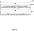
- FIG. 6illustrates a flow chart of applying a third overvoltage protection control mechanism to the receiver shown in FIG. 3 in accordance with various embodiments of the present disclosure.
- FIG. 1illustrates a block diagram of a wireless power transfer system in accordance with various embodiments of the present disclosure.
- the wireless power transfer system 100comprises a power converter 104 and a wireless power transfer device 101 connected in cascade between an input power source 102 and a load 114 .
- the power converter 104is employed to further improve the performance of the wireless power transfer system 100 .
- the power converter 104is an optional element.
- the wireless power transfer device 101may be connected to the input power source 102 directly.
- the wireless power transfer device 101includes a power transmitter 110 and a power receiver 120 .
- the power transmitter 110comprises a transmitter circuit 107 and a transmitter coil L 1 connected in cascade.
- the input of the transmitter circuit 107is coupled to an output of the power converter 104 .
- the power receiver 120comprises a receiver coil L 2 , a resonant capacitor Cs, a rectifier 112 and a power converter 113 connected in cascade.
- the resonant capacitor Csis connected in series with the receiver coil L 2 and further connected to the inputs of the rectifier 112 .
- the outputs of the rectifier 112are connected to the inputs of the power converter 113 .
- the outputs of the power converter 113are coupled to the load 114 .
- the power transmitter 110is magnetically coupled to the power receiver 120 through a magnetic field when the power receiver 120 is placed near the power transmitter 110 .
- a loosely coupled transformer 115is formed by the transmitter coil L 1 , which is part of the power transmitter 110 , and the receiver coil L 2 , which is part of the power receiver 120 . As a result, electrical power may be transferred from the power transmitter 110 to the power receiver 120 .
- the power transmitter 110may be inside a charging pad.
- the transmitter coil L 1is placed underneath the top surface of the charging pad.
- the power receiver 120may be embedded in a mobile phone. When the mobile phone is placed near the charging pad, a magnetic coupling may be established between the transmitter coil L 1 and the receiver coil L 2 .
- the transmitter coil L 1 and the receiver coil L 2may form a loosely coupled transformer through which a power transfer occurs between the power transmitter 110 and the power receiver 120 .
- the strength of coupling between the transmitter coil L 1 and the receiver coil L 2is quantified by the coupling coefficient k. In some embodiments, k is in a range from about 0.05 to about 0.9.
- the power transmitter 110 and the power receiver 120may form a power system through which power is wirelessly transferred from the input power source 102 to the load 114 .
- the input power source 102may be a power adapter converting a utility line voltage to a direct-current (dc) voltage.
- the input power source 102may be a renewable power source such as a solar panel array.
- the input power source 102may be any suitable energy storage devices such as rechargeable batteries, fuel cells, any combinations thereof and/or the like.
- the load 114represents the power consumed by the mobile device (e.g., a mobile phone) coupled to the power receiver 120 .
- the load 114may refer to a rechargeable battery and/or batteries connected in series/parallel, and coupled to the output of the power receiver 120 .
- the load 114may be a downstream power converter such as a battery charger.
- the transmitter circuit 107may comprise primary side switches of a full-bridge converter according to some embodiments.
- the transmitter circuit 107may comprise the primary side switches of any other suitable power converters such as a half-bridge converter, a push-pull converter, any combinations thereof and/or the like.
- power converters described aboveare merely examples.
- suitable power converterssuch as class E topology based power converters (e.g., a class E amplifier), may alternatively be used depending on design needs and different applications.
- the transmitter circuit 107may further comprise a resonant capacitor (not shown).
- the resonant capacitor and the magnetic inductance of the transmitter coilmay form a resonant tank.
- the resonant tankmay further include a resonant inductor.
- the resonant inductormay be implemented as an external inductor.
- the resonant inductormay be implemented as a connection wire.
- the power receiver 120comprises the receiver coil L 2 magnetically coupled to the transmitter coil L 1 after the power receiver 120 is placed near the power transmitter 110 . As a result, power may be transferred to the receiver coil and further delivered to the load 114 through the rectifier 112 .
- the power receiver 120may comprise a secondary resonant capacitor Cs as shown in FIG. 1 . Throughout the description, the secondary resonant capacitor Cs may be alternatively referred to as a receiver resonant capacitor.
- the rectifier 112converts an alternating polarity waveform received from the resonant tank comprising the receiver coil L 2 and the receiver resonant capacitor Cs to a single polarity waveform.
- the rectifier 112comprises a full-wave diode bridge and an output capacitor.
- the full-wave diode bridgemay be replaced by a full-wave bridge formed by switching elements such as n-type metal oxide semiconductor (NMOS) transistors.
- NMOSn-type metal oxide semiconductor
- the rectifier 112may be formed by other types of controllable devices such as metal oxide semiconductor field effect transistor (MOSFET) devices, bipolar junction transistor (BJT) devices, super junction transistor (SJT) devices, insulated gate bipolar transistor (IGBT) devices, gallium nitride (GaN) based power devices and/or the like.
- MOSFETmetal oxide semiconductor field effect transistor
- BJTbipolar junction transistor
- SJTsuper junction transistor
- IGBTinsulated gate bipolar transistor
- GaNgallium nitride
- the power converter 113is coupled between the rectifier 112 and the load 114 .
- the power converter 113is a non-isolated power converter.
- the power converter 113is implemented as a step-down power converter such as a buck converter.
- the power converter 113is implemented as a four-switch buck-boost power converter.
- the power converter 113may be implemented as a hybrid power converter.
- the hybrid converteris a non-isolated power converter.
- the hybrid convertercan be configured as a buck converter, a charge pump converter or a hybrid converter.
- the hybrid convertermay operate in different operating modes. More particularly, the hybrid converter may operate in a buck mode when the load current is less than a predetermined current threshold and/or the input voltage is less than a predetermined voltage threshold. In the buck mode, the hybrid converter is configured as a buck converter. The hybrid converter may operate in a charge pump mode or a hybrid mode when the input voltage is greater than the predetermined voltage threshold and/or the load current is greater than the predetermined current threshold. More particularly, in some embodiments, the hybrid converter may operate in a charge pump mode or a hybrid mode when a ratio of the output voltage of the hybrid converter to the input voltage of the hybrid converter is less than 0.5. In the charge pump mode, the hybrid converter is configured as a charge pump converter. In the hybrid mode, the hybrid converter is configured as a hybrid converter.
- the hybrid convertercomprises a first switch, a capacitor and a second switch connected in series between the output of the rectifier 112 and the input of the load 114 .
- the hybrid converterfurther comprises a third switch and a fourth switch.
- the third switchis connected between a common node of the first switch and the capacitor, and a common node of the second switch and the output terminal of the hybrid converter.
- the fourth switchis connected between a common node of the capacitor and the second switch, and ground.
- the power converter 113may comprise a first power stage and a second power stage connected in cascade.
- the first power stageis configured to operate in different modes for efficiently charging the load 114 (e.g., a rechargeable battery).
- the first stagemay be implemented as a step-down power converter (e.g., a buck converter), a four-switch buck-boost converter, a hybrid converter and any combinations thereof.
- the second power stageis configured as a voltage divider or an isolation switch.
- FIG. 2illustrates a block diagram of the receiver shown in FIG. 1 in accordance with various embodiments of the present disclosure.
- the receiver coil L 2 and the receiver resonant capacitor Csare connected in series.
- the receiver coil L 2is configured to be magnetically coupled to a transmitter coil (not shown).
- the receiver resonant capacitor Cs and the receiver coil L 2form a receiver resonant tank.
- the two inputs of the rectifier 112are connected to the receiver coil L 2 and the receiver resonant capacitor Cs respectively.
- the outputs of the rectifier 112are connected to the inputs of the power converter 113 .
- the outputs of the power converter 113are connected to the load 114 .
- a first overvoltage protection apparatus 121is connected between the inputs of the rectifier 112 and ground. More particularly, the first overvoltage protection apparatus 121 has two terminals connected to the two input terminals of the rectifier 112 respectively.
- a second overvoltage protection apparatus 122is connected between the output of the rectifier 112 and ground. The detailed schematic diagram of the first overvoltage protection apparatus 121 and the second overvoltage protection apparatus 122 will be described below with respect to FIG. 2 .
- a switching frequency of the receiveris detected and compared with a predetermined switch frequency threshold.
- the first overvoltage protection apparatus 121is activated and the second overvoltage protection apparatus 122 is disabled when the switching frequency is less than the predetermined switching frequency threshold.
- the second overvoltage protection apparatus 122is activated and the first overvoltage protection apparatus 121 is disabled when the switching frequency is greater than the predetermined switching frequency threshold.
- both the first overvoltage protection apparatus 121 and the second overvoltage protection apparatus 122are activated when the switching frequency is less than the predetermined switching frequency threshold.
- the second overvoltage protection apparatus 122is activated and the first overvoltage protection apparatus 121 is disabled when the switching frequency is greater than the predetermined switching frequency threshold.
- the first overvoltage protection apparatus 121is activated and the second overvoltage protection apparatus 122 is activated in a controllable manner when the switching frequency is less than the predetermined switching frequency threshold.
- the second overvoltage protection apparatus 122is activated and the first overvoltage protection apparatus 121 is disabled when the switching frequency is greater than the predetermined switching frequency threshold.
- FIG. 3illustrates a schematic diagram of the overvoltage protection device of the receiver shown in FIG. 2 in accordance with various embodiments of the present disclosure.
- the receivercomprises the receiver coil L 2 , the receiver resonant capacitor Cs, the rectifier 112 and the power converter 113 .
- the receiver resonant capacitor Cs, the rectifier 112 and the power converter 113are connected in cascade between the receiver coil L 2 and the load 114 .
- the receiverfurther comprises the first overvoltage protection apparatus 121 , the second overvoltage protection apparatus 122 and a control apparatus 301 . Both the first overvoltage protection apparatus 121 and the second overvoltage protection apparatus 122 are employed to protect the receiver from being damaged during an overvoltage event.
- the control apparatus 301is employed to control the operation of the first overvoltage protection apparatus 121 and the second overvoltage protection apparatus 122 based upon different operating parameters such as the switching frequency of the receiver.
- the rectifier 112is implemented as a full-wave rectifier.
- the rectifier 112includes four diodes, namely D 1 , D 2 , D 3 and D 4 .
- the diodes D 1 and D 3are connected in series between the output terminal of the rectifier 112 and ground.
- the diodes D 2 and D 4are connected in series between the output terminal of the rectifier 112 and ground.
- the common node of the diodes D 1 and D 3is coupled to the receiver coil L 2 .
- the common node of the diodes D 2 and D 4is coupled to the receiver resonant capacitor Cs.
- the rectifier 112may include four switching elements.
- the connection of the four switching elementsis similar to that of the diode rectifier shown in FIG. 3 , and hence is not discussed again herein.
- the switching elements of the rectifier 112are implemented as MOSFET or MOSFETs connected in parallel, any combinations thereof and/or the like.
- the switching elementsmay be an insulated gate bipolar transistor (IGBT) device.
- the primary switchescan be any controllable switches such as integrated gate commutated thyristor (IGCT) devices, gate turn-off thyristor (GTO) devices, silicon controlled rectifier (SCR) devices, junction gate field-effect transistor (JFET) devices, MOS controlled thyristor (MCT) devices, gallium nitride (GaN) based power devices and/or the like.
- IGCTintegrated gate commutated thyristor
- GTOgate turn-off thyristor
- SCRsilicon controlled rectifier
- JFETjunction gate field-effect transistor
- MCTMOS controlled thyristor
- GaNgallium nitride
- full-wave rectifiere.g., full-wave rectifier 112 shown in FIG. 3
- the implementation of the receiver shown in FIG. 3may have many variations, alternatives, and modifications.
- half-wave rectifiersmay be alternatively employed.
- the full-wave rectifier 112 illustrated hereinis limited solely for the purpose of clearly illustrating the inventive aspects of the various embodiments.
- the present disclosureis not limited to any particular power topology.
- the first overvoltage protection apparatus 121comprises a first capacitor C 1 and a first switch S 1 connected in series between a first input of the rectifier and ground. As shown in FIG. 3 , the first input of the rectifier 112 is the common node of the diodes D 2 and D 4 . As shown in FIG. 3 , the first overvoltage protection apparatus 121 further comprises a second capacitor C 2 and a second switch S 2 connected in series between a second input of the rectifier 112 and ground. As shown in FIG. 3 , the second input of the rectifier 112 is the common node of the diodes D 1 and D 3 .
- both the first switch S 1 and the second switch S 2are turned off when there is no overvoltage condition.
- the switches S 1 and S 2may be turned on.
- the first capacitor C 1 and the second capacitor C 2help to change the impedance of the receiver, thereby reducing the received power as well as the voltage across the output of the rectifier 112 .
- the second overvoltage protection apparatus 122comprises a resistor R 1 and a third switch S 3 connected in series between the output of the rectifier 112 and ground.
- the resistor R 1is implemented as a power resistor.
- the third switch S 3is turned off when there is no overvoltage condition.
- the third switch S 3may be turned on.
- the resistor R 1shunts the unexpected power, thereby reducing the voltage across the output of the rectifier 112 .
- the operation of the first overvoltage protection apparatus 121 and the second overvoltage protection apparatus 122is controlled by the control apparatus 301 .
- the control apparatus 301comprises a comparator 302 and a control circuit 304 .
- the comparator 302is implemented as a comparator with suitable hysteresis. The hysteresis of the comparator 302 helps to make smooth transitions between the first overvoltage protection apparatus 121 and the second overvoltage protection apparatus 122 (e.g., activating one protection apparatus and disable the other protection apparatus).
- the inverting input of the comparator 302is configured to receive the switching frequency signal of the receiver. More particularly, a sensing apparatus (not shown) is used to detect the switching frequency of the current/voltage of the receiver coil L 2 and generate the switching frequency signal. The switching frequency signal is fed into the comparator 302 .
- the non-inverting input of the comparator 302is configured to receive a predetermined switching frequency threshold. In some embodiments, the predetermined switching frequency threshold is about 150 KHz.
- the control circuit 304is configured to receive the comparison result of the comparator 302 and other suitable operating parameters such as the temperature of the resistor R 1 , the overvoltage event trigger signal and the like. Based upon the received signals, the control circuit 304 determines the on/off of the switches S 1 , S 2 and S 3 . In other words, the control circuit 304 is employed to generate protection control mechanisms based upon the received signals. The detailed protection control mechanisms will be described below with respect to FIGS. 4-6 .
- FIG. 4illustrates a flow chart of applying a first overvoltage protection control mechanism to the receiver shown in FIG. 3 in accordance with various embodiments of the present disclosure.
- This flowchart shown in FIG. 4is merely an example, which should not unduly limit the scope of the claims.
- One of ordinary skill in the artwould recognize many variations, alternatives, and modifications. For example, various steps illustrated in FIG. 4 may be added, removed, replaced, rearranged and repeated.
- a switching frequency of a wireless power systemis detected by a suitable sensing apparatus or a plurality of sensing devices.
- the detected switching frequencyis processed by a controller.
- the detected switching frequencyis compared with a predetermined switching frequency threshold.
- the receiver of the wireless power systemcomprises a first overvoltage protection apparatus 121 and a second overvoltage protection apparatus 122 as shown in FIG. 3 .
- the first overvoltage protection apparatus 121comprises two controllable switch-capacitor networks.
- the second overvoltage protection apparatus 122comprises a controllable power resistor.
- the first overvoltage protection apparatus 121is activated and the second overvoltage protection apparatus 122 is disabled when the switching frequency is less than the predetermined switching frequency threshold.
- the second overvoltage protection apparatus 122is activated and the first overvoltage protection apparatus 121 is disabled when the switching frequency is greater than the predetermined switching frequency threshold.
- FIG. 5illustrates a flow chart of applying a second overvoltage protection control mechanism to the receiver shown in FIG. 3 in accordance with various embodiments of the present disclosure.
- This flowchart shown in FIG. 5is merely an example, which should not unduly limit the scope of the claims.
- One of ordinary skill in the artwould recognize many variations, alternatives, and modifications. For example, various steps illustrated in FIG. 5 may be added, removed, replaced, rearranged and repeated.
- a switching frequency of a wireless power systemis detected by a suitable sensing apparatus or a plurality of sensing devices.
- the detected switching frequencyis processed by a controller.
- the detected switching frequencyis compared with a predetermined switching frequency threshold.
- the receiver of the wireless power systemcomprises a first overvoltage protection apparatus 121 and a second overvoltage protection apparatus 122 as shown in FIG. 3 .
- the first overvoltage protection apparatus 121comprises two controllable switch-capacitor networks.
- the second overvoltage protection apparatus 122comprises a controllable power resistor.
- both the first overvoltage protection apparatus 121 and the second overvoltage protection apparatus 122are activated when the switching frequency is less than the predetermined switching frequency threshold.
- the second overvoltage protection apparatus 122is activated and the first overvoltage protection apparatus 121 is disabled when the switching frequency is greater than the predetermined switching frequency threshold.
- One advantageous feature of activating the second overvoltage protection apparatus 122 when the switching frequency is greater than the predetermined switching frequency thresholdis that a relatively small power resistor can achieve the overvoltage protection function because the received power at the high frequency operation is low.
- the relatively small power resistorcan shunt the power, thereby reducing the voltage at the output of the rectifier.
- the resistor R 1 of the second overvoltage protection apparatus 122is implemented as a power resistor.
- the power resistoris a 100 Ohm resistor rated for about 2 W.
- FIG. 6illustrates a flow chart of applying a third overvoltage protection control mechanism to the receiver shown in FIG. 3 in accordance with various embodiments of the present disclosure.
- This flowchart shown in FIG. 6is merely an example, which should not unduly limit the scope of the claims.
- One of ordinary skill in the artwould recognize many variations, alternatives, and modifications. For example, various steps illustrated in FIG. 6 may be added, removed, replaced, rearranged and repeated.
- a switching frequency of a wireless power systemis detected by a suitable sensing apparatus or a plurality of sensing devices.
- the detected switching frequencyis processed by a controller.
- the detected switching frequencyis compared with a predetermined switching frequency threshold.
- the receiver of the wireless power systemcomprises a first overvoltage protection apparatus 121 and a second overvoltage protection apparatus 122 as shown in FIG. 3 .
- the first overvoltage protection apparatus 121comprises two controllable switch-capacitor networks.
- the second overvoltage protection apparatus 122comprises a controllable power resistor.
- the first overvoltage protection apparatus 121is activated and the second overvoltage protection apparatus 122 is activated in a controllable manner when the switching frequency is less than the predetermined switching frequency threshold.
- the second overvoltage protection apparatus 122may be controlled by other operating parameters such as the temperature of the resistor R 1 .
- a temperature of the second overvoltage protection apparatus 122is detected by suitable temperature sensing devices.
- the second overvoltage protection apparatus 122may be temporarily disabled when the temperature of the second overvoltage protection apparatus 122 is greater than a predetermined temperature threshold. In other words, the second overvoltage protection apparatus is controlled by both the switching frequency and the temperature.
- One advantageous feature of configuring the second overvoltage protection apparatus 122 to operate in a controllable manneris that the temperature control mechanism described above helps to improve the reliability of the receiver of the wireless power transfer system.
- the second overvoltage protection apparatus 122is activated and the first overvoltage protection apparatus 121 is disabled when the switching frequency is greater than the predetermined switching frequency threshold.
Landscapes
- Engineering & Computer Science (AREA)
- Power Engineering (AREA)
- Computer Networks & Wireless Communication (AREA)
- Protection Of Static Devices (AREA)
Abstract
Description
Claims (19)
Priority Applications (3)
| Application Number | Priority Date | Filing Date | Title |
|---|---|---|---|
| US16/134,353US11075515B2 (en) | 2018-06-05 | 2018-09-18 | Overvoltage protection device and method thereof |
| CN201811372249.XACN110571755B (en) | 2018-06-05 | 2018-11-16 | Overvoltage protection device and method thereof |
| US17/320,373US11594917B2 (en) | 2018-06-05 | 2021-05-14 | Overvoltage protection device and method thereof |
Applications Claiming Priority (2)
| Application Number | Priority Date | Filing Date | Title |
|---|---|---|---|
| US201862680638P | 2018-06-05 | 2018-06-05 | |
| US16/134,353US11075515B2 (en) | 2018-06-05 | 2018-09-18 | Overvoltage protection device and method thereof |
Related Child Applications (1)
| Application Number | Title | Priority Date | Filing Date |
|---|---|---|---|
| US17/320,373ContinuationUS11594917B2 (en) | 2018-06-05 | 2021-05-14 | Overvoltage protection device and method thereof |
Publications (2)
| Publication Number | Publication Date |
|---|---|
| US20190372331A1 US20190372331A1 (en) | 2019-12-05 |
| US11075515B2true US11075515B2 (en) | 2021-07-27 |
Family
ID=68695289
Family Applications (2)
| Application Number | Title | Priority Date | Filing Date |
|---|---|---|---|
| US16/134,353Active2039-08-01US11075515B2 (en) | 2018-06-05 | 2018-09-18 | Overvoltage protection device and method thereof |
| US17/320,373Active2039-01-15US11594917B2 (en) | 2018-06-05 | 2021-05-14 | Overvoltage protection device and method thereof |
Family Applications After (1)
| Application Number | Title | Priority Date | Filing Date |
|---|---|---|---|
| US17/320,373Active2039-01-15US11594917B2 (en) | 2018-06-05 | 2021-05-14 | Overvoltage protection device and method thereof |
Country Status (2)
| Country | Link |
|---|---|
| US (2) | US11075515B2 (en) |
| CN (1) | CN110571755B (en) |
Cited By (2)
| Publication number | Priority date | Publication date | Assignee | Title |
|---|---|---|---|---|
| US20210273445A1 (en)* | 2018-06-05 | 2021-09-02 | Nuvolta Technologies (Hefei) Co., Ltd. | Overvoltage Protection Device and Method Thereof |
| US12348125B2 (en) | 2023-01-20 | 2025-07-01 | Apple Inc. | Charge pump-enabled circuit protection switch |
Families Citing this family (15)
| Publication number | Priority date | Publication date | Assignee | Title |
|---|---|---|---|---|
| KR101984140B1 (en)* | 2017-05-12 | 2019-05-30 | 주식회사 맵스 | Wireless Power Receiver Unit using charge pump power stage |
| US10868429B2 (en) | 2018-05-21 | 2020-12-15 | Nuvolta Technologies (Hefei) Co., Ltd. | High efficiency power converting apparatus |
| US11056981B2 (en)* | 2018-07-07 | 2021-07-06 | Intelesol, Llc | Method and apparatus for signal extraction with sample and hold and release |
| US11671029B2 (en) | 2018-07-07 | 2023-06-06 | Intelesol, Llc | AC to DC converters |
| US11581725B2 (en) | 2018-07-07 | 2023-02-14 | Intelesol, Llc | Solid-state power interrupters |
| US11349296B2 (en) | 2018-10-01 | 2022-05-31 | Intelesol, Llc | Solid-state circuit interrupters |
| US10834792B2 (en) | 2018-12-17 | 2020-11-10 | Intelesol, Llc | AC-driven light-emitting diode systems |
| US11551899B2 (en) | 2019-05-18 | 2023-01-10 | Amber Semiconductor, Inc. | Intelligent circuit breakers with solid-state bidirectional switches |
| EP4088125A4 (en) | 2020-01-21 | 2024-03-06 | Amber Semiconductor, Inc. | INTELLIGENT CIRCUIT INTERRUPTION |
| KR20210146571A (en)* | 2020-05-27 | 2021-12-06 | 삼성전자주식회사 | Electronic device for wirelessly receiving power and method for operating thereof |
| EP4197086A4 (en) | 2020-08-11 | 2024-09-04 | Amber Semiconductor, Inc. | INTELLIGENT ENERGY SOURCE MONITORING AND SELECTION CONTROL SYSTEM |
| EP4283829A4 (en) | 2021-05-04 | 2024-07-31 | Samsung Electronics Co., Ltd. | WIRELESS POWER RECEIVING DEVICE HAVING DISTURNING CIRCUIT |
| US12113525B2 (en) | 2021-09-30 | 2024-10-08 | Amber Semiconductor, Inc. | Intelligent electrical switches |
| US12348028B2 (en) | 2021-10-22 | 2025-07-01 | Amber Semiconductor, Inc. | Multi-output programmable power manager |
| US12362646B2 (en) | 2022-01-26 | 2025-07-15 | Amber Semiconductor, Inc. | Controlling AC power to inductive loads |
Citations (32)
| Publication number | Priority date | Publication date | Assignee | Title |
|---|---|---|---|---|
| US20120050931A1 (en)* | 2010-08-31 | 2012-03-01 | Stephen Christopher Terry | Methods and apparatus to clamp overvoltages for alternating current systems |
| US20120153903A1 (en)* | 2010-12-16 | 2012-06-21 | Samsung Electronics Co., Ltd. | Protector of rectifier and wireless power receiver including protector |
| US20120293009A1 (en)* | 2011-05-17 | 2012-11-22 | Samsung Electronics Co., Ltd. | Apparatus and method of protecting power receiver of wireless power transmission system |
| US20120293900A1 (en)* | 2011-05-17 | 2012-11-22 | Samsung Electronics Co., Ltd. | Apparatus for and method of protecting wireless-coupled power devices from overvoltage, overcurrent, and overtemperature using hysteresis |
| US20140327390A1 (en)* | 2013-05-02 | 2014-11-06 | Electronics And Telecommunications Research Institute | Apparatus and method for wireless charging |
| US20150008755A1 (en)* | 2013-07-02 | 2015-01-08 | Renesas Electronics Corporation | Electric power receiving device and non-contact power supply system |
| US20150035372A1 (en)* | 2013-08-02 | 2015-02-05 | Integrated Device Technology, Inc. | Multimode wireless power receivers and related methods |
| US20150280429A1 (en)* | 2013-05-20 | 2015-10-01 | Nec Tokin Corporation | Communication apparatus and electronic device |
| US20160336816A1 (en)* | 2015-05-12 | 2016-11-17 | Powermat Technologies Ltd. | System and method for responding to activation of over voltage protection mechanisms during wireless power transfer |
| US20170033612A1 (en)* | 2015-07-02 | 2017-02-02 | Ningbo WeiE Electronic Technology Co., Ltd | Contactless power transmission device and power transmission method thereof |
| US20170093225A1 (en)* | 2014-07-03 | 2017-03-30 | Ihi Corporation | Power-receiving device, wireless power-transmitting system, and power-transmission device |
| US20170187244A1 (en)* | 2015-12-23 | 2017-06-29 | Ningbo Weie Electronic Technology Co., Ltd. | Electrical energy receiving end capable of overvoltage protection and wireless electrical energy transmission device |
| US20170271920A1 (en)* | 2016-03-17 | 2017-09-21 | Samsung Electronics Co., Ltd. | Electronic apparatus and operating method thereof |
| US20170346343A1 (en)* | 2016-05-27 | 2017-11-30 | Witricity Corporation | Voltage Regulation in Wireless Power Receivers |
| US9847668B2 (en)* | 2012-01-11 | 2017-12-19 | Samsung Electronics Co., Ltd | Over-voltage protection device for resonant wireless power transmission device and method for controlling the over-voltage protection device |
| US20180048185A1 (en)* | 2015-03-05 | 2018-02-15 | Maps, Inc. | Dual band wireless power reception unit |
| US20180083487A1 (en)* | 2016-09-16 | 2018-03-22 | Integrated Device Technology, Inc. | Multimode wireless power receiver circuit |
| US20180131234A1 (en)* | 2016-11-08 | 2018-05-10 | Rohm Co., Ltd. | Wireless power receiver, control method thereof, power receiving control circuit, and electronic apparatus |
| US10020849B2 (en)* | 2016-03-14 | 2018-07-10 | X2 Power Technologies Limited | Self-canceling magnetic structures for transferring power and communication signals |
| US20180198273A1 (en)* | 2015-06-29 | 2018-07-12 | Maps, Inc. | Near field communication module protection apparatus using magnetic field, and portable terminal thereof |
| US20180212469A1 (en)* | 2017-01-22 | 2018-07-26 | Richtek Technology Corporation | Multi-mode wireless power receiver circuit and control method thereof |
| US20180262002A1 (en)* | 2017-03-10 | 2018-09-13 | Stmicroelectronics (Rousset) Sas | Protection of an nfc router against overvoltage |
| US20180323828A1 (en)* | 2015-11-16 | 2018-11-08 | Maps, Inc. | Single antenna-based wireless charging and near-field communication control apparatus and user terminal therefor |
| US20190036381A1 (en)* | 2016-02-12 | 2019-01-31 | Maps, Inc. | Apparatus for protecting wireless communication device and wireless communication device comprising same |
| US20190260232A1 (en)* | 2018-02-21 | 2019-08-22 | X2 Power Technologies Limited | Hybrid Control Apparatus and Method |
| US20190305598A1 (en)* | 2018-03-29 | 2019-10-03 | X2 Power Technologies Limited | Hybrid Power Converter |
| US10454312B2 (en)* | 2016-03-15 | 2019-10-22 | X2 Power Technologies Limited | Wireless power transfer control apparatus and method |
| US20190356149A1 (en)* | 2018-05-21 | 2019-11-21 | X2 Power Technologies Limited | High Efficiency Power Converting Apparatus |
| US20190386517A1 (en)* | 2018-06-15 | 2019-12-19 | X2 Power Technologies Limited | Demodulation Apparatus and Method for Wireless Power Transmitter |
| US20200028358A1 (en)* | 2016-09-26 | 2020-01-23 | Mitsubishi Electric Corporation | Electronic device |
| US20200112202A1 (en)* | 2018-10-05 | 2020-04-09 | X2 Power Technologies Limited | High Efficiency Power Converting Apparatus and Control Method |
| US20200274402A1 (en)* | 2016-07-27 | 2020-08-27 | Maps, Inc. | Wireless power receiver controlling magnitude of communication signal |
Family Cites Families (6)
| Publication number | Priority date | Publication date | Assignee | Title |
|---|---|---|---|---|
| WO2012121371A1 (en)* | 2011-03-10 | 2012-09-13 | Necトーキン株式会社 | Power-receiving device and non-contact power transmission system using same |
| KR102042498B1 (en)* | 2012-01-11 | 2019-11-11 | 삼성전자주식회사 | Overvoltage protecting device for resonance wireless power receiving apparatus and controlling method thereof |
| DE102012004716B4 (en)* | 2012-03-07 | 2021-02-11 | Dehn Se + Co Kg | Circuit arrangement for status control and logging of surge protection devices or surge protection systems |
| CN104659923B (en)* | 2013-11-18 | 2017-09-22 | 立锜科技股份有限公司 | Power management unit and wireless power system applying same |
| CN106910953B (en)* | 2017-04-10 | 2020-02-07 | 宁波微鹅电子科技有限公司 | Battery pack and wireless charging system |
| US11075515B2 (en)* | 2018-06-05 | 2021-07-27 | Nuvolta Technologies (Hefei) Co., Ltd. | Overvoltage protection device and method thereof |
- 2018
- 2018-09-18USUS16/134,353patent/US11075515B2/enactiveActive
- 2018-11-16CNCN201811372249.XApatent/CN110571755B/enactiveActive
- 2021
- 2021-05-14USUS17/320,373patent/US11594917B2/enactiveActive
Patent Citations (32)
| Publication number | Priority date | Publication date | Assignee | Title |
|---|---|---|---|---|
| US20120050931A1 (en)* | 2010-08-31 | 2012-03-01 | Stephen Christopher Terry | Methods and apparatus to clamp overvoltages for alternating current systems |
| US20120153903A1 (en)* | 2010-12-16 | 2012-06-21 | Samsung Electronics Co., Ltd. | Protector of rectifier and wireless power receiver including protector |
| US20120293009A1 (en)* | 2011-05-17 | 2012-11-22 | Samsung Electronics Co., Ltd. | Apparatus and method of protecting power receiver of wireless power transmission system |
| US20120293900A1 (en)* | 2011-05-17 | 2012-11-22 | Samsung Electronics Co., Ltd. | Apparatus for and method of protecting wireless-coupled power devices from overvoltage, overcurrent, and overtemperature using hysteresis |
| US9847668B2 (en)* | 2012-01-11 | 2017-12-19 | Samsung Electronics Co., Ltd | Over-voltage protection device for resonant wireless power transmission device and method for controlling the over-voltage protection device |
| US20140327390A1 (en)* | 2013-05-02 | 2014-11-06 | Electronics And Telecommunications Research Institute | Apparatus and method for wireless charging |
| US20150280429A1 (en)* | 2013-05-20 | 2015-10-01 | Nec Tokin Corporation | Communication apparatus and electronic device |
| US20150008755A1 (en)* | 2013-07-02 | 2015-01-08 | Renesas Electronics Corporation | Electric power receiving device and non-contact power supply system |
| US20150035372A1 (en)* | 2013-08-02 | 2015-02-05 | Integrated Device Technology, Inc. | Multimode wireless power receivers and related methods |
| US20170093225A1 (en)* | 2014-07-03 | 2017-03-30 | Ihi Corporation | Power-receiving device, wireless power-transmitting system, and power-transmission device |
| US20180048185A1 (en)* | 2015-03-05 | 2018-02-15 | Maps, Inc. | Dual band wireless power reception unit |
| US20160336816A1 (en)* | 2015-05-12 | 2016-11-17 | Powermat Technologies Ltd. | System and method for responding to activation of over voltage protection mechanisms during wireless power transfer |
| US20180198273A1 (en)* | 2015-06-29 | 2018-07-12 | Maps, Inc. | Near field communication module protection apparatus using magnetic field, and portable terminal thereof |
| US20170033612A1 (en)* | 2015-07-02 | 2017-02-02 | Ningbo WeiE Electronic Technology Co., Ltd | Contactless power transmission device and power transmission method thereof |
| US20180323828A1 (en)* | 2015-11-16 | 2018-11-08 | Maps, Inc. | Single antenna-based wireless charging and near-field communication control apparatus and user terminal therefor |
| US20170187244A1 (en)* | 2015-12-23 | 2017-06-29 | Ningbo Weie Electronic Technology Co., Ltd. | Electrical energy receiving end capable of overvoltage protection and wireless electrical energy transmission device |
| US20190036381A1 (en)* | 2016-02-12 | 2019-01-31 | Maps, Inc. | Apparatus for protecting wireless communication device and wireless communication device comprising same |
| US10020849B2 (en)* | 2016-03-14 | 2018-07-10 | X2 Power Technologies Limited | Self-canceling magnetic structures for transferring power and communication signals |
| US10454312B2 (en)* | 2016-03-15 | 2019-10-22 | X2 Power Technologies Limited | Wireless power transfer control apparatus and method |
| US20170271920A1 (en)* | 2016-03-17 | 2017-09-21 | Samsung Electronics Co., Ltd. | Electronic apparatus and operating method thereof |
| US20170346343A1 (en)* | 2016-05-27 | 2017-11-30 | Witricity Corporation | Voltage Regulation in Wireless Power Receivers |
| US20200274402A1 (en)* | 2016-07-27 | 2020-08-27 | Maps, Inc. | Wireless power receiver controlling magnitude of communication signal |
| US20180083487A1 (en)* | 2016-09-16 | 2018-03-22 | Integrated Device Technology, Inc. | Multimode wireless power receiver circuit |
| US20200028358A1 (en)* | 2016-09-26 | 2020-01-23 | Mitsubishi Electric Corporation | Electronic device |
| US20180131234A1 (en)* | 2016-11-08 | 2018-05-10 | Rohm Co., Ltd. | Wireless power receiver, control method thereof, power receiving control circuit, and electronic apparatus |
| US20180212469A1 (en)* | 2017-01-22 | 2018-07-26 | Richtek Technology Corporation | Multi-mode wireless power receiver circuit and control method thereof |
| US20180262002A1 (en)* | 2017-03-10 | 2018-09-13 | Stmicroelectronics (Rousset) Sas | Protection of an nfc router against overvoltage |
| US20190260232A1 (en)* | 2018-02-21 | 2019-08-22 | X2 Power Technologies Limited | Hybrid Control Apparatus and Method |
| US20190305598A1 (en)* | 2018-03-29 | 2019-10-03 | X2 Power Technologies Limited | Hybrid Power Converter |
| US20190356149A1 (en)* | 2018-05-21 | 2019-11-21 | X2 Power Technologies Limited | High Efficiency Power Converting Apparatus |
| US20190386517A1 (en)* | 2018-06-15 | 2019-12-19 | X2 Power Technologies Limited | Demodulation Apparatus and Method for Wireless Power Transmitter |
| US20200112202A1 (en)* | 2018-10-05 | 2020-04-09 | X2 Power Technologies Limited | High Efficiency Power Converting Apparatus and Control Method |
Cited By (3)
| Publication number | Priority date | Publication date | Assignee | Title |
|---|---|---|---|---|
| US20210273445A1 (en)* | 2018-06-05 | 2021-09-02 | Nuvolta Technologies (Hefei) Co., Ltd. | Overvoltage Protection Device and Method Thereof |
| US11594917B2 (en)* | 2018-06-05 | 2023-02-28 | Nuvolta Technologies (Hefei) Co., Ltd. | Overvoltage protection device and method thereof |
| US12348125B2 (en) | 2023-01-20 | 2025-07-01 | Apple Inc. | Charge pump-enabled circuit protection switch |
Also Published As
| Publication number | Publication date |
|---|---|
| US11594917B2 (en) | 2023-02-28 |
| CN110571755B (en) | 2022-02-01 |
| US20210273445A1 (en) | 2021-09-02 |
| US20190372331A1 (en) | 2019-12-05 |
| CN110571755A (en) | 2019-12-13 |
Similar Documents
| Publication | Publication Date | Title |
|---|---|---|
| US11594917B2 (en) | Overvoltage protection device and method thereof | |
| US11309716B2 (en) | High efficiency power converting apparatus | |
| US10554115B2 (en) | Harmonic reduction apparatus for wireless power transfer systems | |
| US11563337B2 (en) | High efficiency wireless charging system and method | |
| US11469617B2 (en) | Hybrid control apparatus and method | |
| US11811241B2 (en) | Rectifier in low gain wireless power transfer system | |
| US11764611B2 (en) | Low gain wireless power transfer system and method | |
| US11223237B2 (en) | High efficiency power converting apparatus and control method | |
| US11588518B2 (en) | Communication apparatus and method thereof | |
| US20220385113A1 (en) | Foreign Object Detection Apparatus and Method for Wireless Power Transfer System | |
| US20190305598A1 (en) | Hybrid Power Converter | |
| US11527907B2 (en) | High voltage hybrid charging system and method | |
| US12191677B2 (en) | Structures for in-band communications in wireless charging | |
| US20230134591A1 (en) | Wireless Power Transfer System and Control Method Thereof | |
| US20220352756A1 (en) | Wireless Power Transfer Apparatus for TWS Phone |
Legal Events
| Date | Code | Title | Description |
|---|---|---|---|
| AS | Assignment | Owner name:X2 POWER TECHNOLOGIES LIMITED, CAYMAN ISLANDS Free format text:ASSIGNMENT OF ASSIGNORS INTEREST;ASSIGNORS:LIU, SICHAO;HUANG, JINBIAO;REEL/FRAME:046900/0877 Effective date:20180918 | |
| FEPP | Fee payment procedure | Free format text:ENTITY STATUS SET TO UNDISCOUNTED (ORIGINAL EVENT CODE: BIG.); ENTITY STATUS OF PATENT OWNER: SMALL ENTITY | |
| FEPP | Fee payment procedure | Free format text:ENTITY STATUS SET TO SMALL (ORIGINAL EVENT CODE: SMAL); ENTITY STATUS OF PATENT OWNER: SMALL ENTITY | |
| AS | Assignment | Owner name:NUVOLTA TECHNOLOGIES (HEFEI) CO., LTD., CHINA Free format text:ASSIGNMENT OF ASSIGNORS INTEREST;ASSIGNOR:X2 POWER TECHNOLOGIES LIMITED;REEL/FRAME:054041/0727 Effective date:20201012 | |
| STPP | Information on status: patent application and granting procedure in general | Free format text:RESPONSE TO NON-FINAL OFFICE ACTION ENTERED AND FORWARDED TO EXAMINER | |
| STPP | Information on status: patent application and granting procedure in general | Free format text:NON FINAL ACTION MAILED | |
| STPP | Information on status: patent application and granting procedure in general | Free format text:RESPONSE TO NON-FINAL OFFICE ACTION ENTERED AND FORWARDED TO EXAMINER | |
| STPP | Information on status: patent application and granting procedure in general | Free format text:NOTICE OF ALLOWANCE MAILED -- APPLICATION RECEIVED IN OFFICE OF PUBLICATIONS | |
| STPP | Information on status: patent application and granting procedure in general | Free format text:PUBLICATIONS -- ISSUE FEE PAYMENT RECEIVED | |
| STPP | Information on status: patent application and granting procedure in general | Free format text:PUBLICATIONS -- ISSUE FEE PAYMENT VERIFIED | |
| STCF | Information on status: patent grant | Free format text:PATENTED CASE | |
| MAFP | Maintenance fee payment | Free format text:PAYMENT OF MAINTENANCE FEE, 4TH YR, SMALL ENTITY (ORIGINAL EVENT CODE: M2551); ENTITY STATUS OF PATENT OWNER: SMALL ENTITY Year of fee payment:4 |