US11073573B2 - Packages for coil actuated position sensors - Google Patents
Packages for coil actuated position sensorsDownload PDFInfo
- Publication number
- US11073573B2 US11073573B2US16/851,473US202016851473AUS11073573B2US 11073573 B2US11073573 B2US 11073573B2US 202016851473 AUS202016851473 AUS 202016851473AUS 11073573 B2US11073573 B2US 11073573B2
- Authority
- US
- United States
- Prior art keywords
- magnetic field
- coil
- substrates
- target
- coils
- Prior art date
- Legal status (The legal status is an assumption and is not a legal conclusion. Google has not performed a legal analysis and makes no representation as to the accuracy of the status listed.)
- Active
Links
Images


Classifications
- G—PHYSICS
- G01—MEASURING; TESTING
- G01R—MEASURING ELECTRIC VARIABLES; MEASURING MAGNETIC VARIABLES
- G01R33/00—Arrangements or instruments for measuring magnetic variables
- G01R33/02—Measuring direction or magnitude of magnetic fields or magnetic flux
- G01R33/025—Compensating stray fields
- G—PHYSICS
- G01—MEASURING; TESTING
- G01B—MEASURING LENGTH, THICKNESS OR SIMILAR LINEAR DIMENSIONS; MEASURING ANGLES; MEASURING AREAS; MEASURING IRREGULARITIES OF SURFACES OR CONTOURS
- G01B7/00—Measuring arrangements characterised by the use of electric or magnetic techniques
- G01B7/003—Measuring arrangements characterised by the use of electric or magnetic techniques for measuring position, not involving coordinate determination
- G—PHYSICS
- G01—MEASURING; TESTING
- G01B—MEASURING LENGTH, THICKNESS OR SIMILAR LINEAR DIMENSIONS; MEASURING ANGLES; MEASURING AREAS; MEASURING IRREGULARITIES OF SURFACES OR CONTOURS
- G01B7/00—Measuring arrangements characterised by the use of electric or magnetic techniques
- G01B7/02—Measuring arrangements characterised by the use of electric or magnetic techniques for measuring length, width or thickness
- G01B7/023—Measuring arrangements characterised by the use of electric or magnetic techniques for measuring length, width or thickness for measuring distance between sensor and object
- G—PHYSICS
- G01—MEASURING; TESTING
- G01D—MEASURING NOT SPECIALLY ADAPTED FOR A SPECIFIC VARIABLE; ARRANGEMENTS FOR MEASURING TWO OR MORE VARIABLES NOT COVERED IN A SINGLE OTHER SUBCLASS; TARIFF METERING APPARATUS; MEASURING OR TESTING NOT OTHERWISE PROVIDED FOR
- G01D5/00—Mechanical means for transferring the output of a sensing member; Means for converting the output of a sensing member to another variable where the form or nature of the sensing member does not constrain the means for converting; Transducers not specially adapted for a specific variable
- G01D5/12—Mechanical means for transferring the output of a sensing member; Means for converting the output of a sensing member to another variable where the form or nature of the sensing member does not constrain the means for converting; Transducers not specially adapted for a specific variable using electric or magnetic means
- G01D5/14—Mechanical means for transferring the output of a sensing member; Means for converting the output of a sensing member to another variable where the form or nature of the sensing member does not constrain the means for converting; Transducers not specially adapted for a specific variable using electric or magnetic means influencing the magnitude of a current or voltage
- G01D5/142—Mechanical means for transferring the output of a sensing member; Means for converting the output of a sensing member to another variable where the form or nature of the sensing member does not constrain the means for converting; Transducers not specially adapted for a specific variable using electric or magnetic means influencing the magnitude of a current or voltage using Hall-effect devices
- G01D5/147—Mechanical means for transferring the output of a sensing member; Means for converting the output of a sensing member to another variable where the form or nature of the sensing member does not constrain the means for converting; Transducers not specially adapted for a specific variable using electric or magnetic means influencing the magnitude of a current or voltage using Hall-effect devices influenced by the movement of a third element, the position of Hall device and the source of magnetic field being fixed in respect to each other
- G—PHYSICS
- G01—MEASURING; TESTING
- G01N—INVESTIGATING OR ANALYSING MATERIALS BY DETERMINING THEIR CHEMICAL OR PHYSICAL PROPERTIES
- G01N27/00—Investigating or analysing materials by the use of electric, electrochemical, or magnetic means
- G01N27/72—Investigating or analysing materials by the use of electric, electrochemical, or magnetic means by investigating magnetic variables
- G01N27/82—Investigating or analysing materials by the use of electric, electrochemical, or magnetic means by investigating magnetic variables for investigating the presence of flaws
- G01N27/90—Investigating or analysing materials by the use of electric, electrochemical, or magnetic means by investigating magnetic variables for investigating the presence of flaws using eddy currents
- G—PHYSICS
- G01—MEASURING; TESTING
- G01P—MEASURING LINEAR OR ANGULAR SPEED, ACCELERATION, DECELERATION, OR SHOCK; INDICATING PRESENCE, ABSENCE, OR DIRECTION, OF MOVEMENT
- G01P3/00—Measuring linear or angular speed; Measuring differences of linear or angular speeds
- G01P3/42—Devices characterised by the use of electric or magnetic means
- G01P3/44—Devices characterised by the use of electric or magnetic means for measuring angular speed
- G01P3/49—Devices characterised by the use of electric or magnetic means for measuring angular speed using eddy currents
- G—PHYSICS
- G01—MEASURING; TESTING
- G01R—MEASURING ELECTRIC VARIABLES; MEASURING MAGNETIC VARIABLES
- G01R33/00—Arrangements or instruments for measuring magnetic variables
- G01R33/0005—Geometrical arrangement of magnetic sensor elements; Apparatus combining different magnetic sensor types
- G—PHYSICS
- G01—MEASURING; TESTING
- G01R—MEASURING ELECTRIC VARIABLES; MEASURING MAGNETIC VARIABLES
- G01R33/00—Arrangements or instruments for measuring magnetic variables
- G01R33/0017—Means for compensating offset magnetic fields or the magnetic flux to be measured; Means for generating calibration magnetic fields
- G—PHYSICS
- G01—MEASURING; TESTING
- G01R—MEASURING ELECTRIC VARIABLES; MEASURING MAGNETIC VARIABLES
- G01R33/00—Arrangements or instruments for measuring magnetic variables
- G01R33/0023—Electronic aspects, e.g. circuits for stimulation, evaluation, control; Treating the measured signals; calibration
- G01R33/0029—Treating the measured signals, e.g. removing offset or noise
- G—PHYSICS
- G01—MEASURING; TESTING
- G01R—MEASURING ELECTRIC VARIABLES; MEASURING MAGNETIC VARIABLES
- G01R33/00—Arrangements or instruments for measuring magnetic variables
- G01R33/02—Measuring direction or magnitude of magnetic fields or magnetic flux
- G01R33/032—Measuring direction or magnitude of magnetic fields or magnetic flux using magneto-optic devices, e.g. Faraday or Cotton-Mouton effect
- G—PHYSICS
- G01—MEASURING; TESTING
- G01R—MEASURING ELECTRIC VARIABLES; MEASURING MAGNETIC VARIABLES
- G01R33/00—Arrangements or instruments for measuring magnetic variables
- G01R33/12—Measuring magnetic properties of articles or specimens of solids or fluids
- G01R33/1284—Spin resolved measurements; Influencing spins during measurements, e.g. in spintronics devices
- H—ELECTRICITY
- H01—ELECTRIC ELEMENTS
- H01F—MAGNETS; INDUCTANCES; TRANSFORMERS; SELECTION OF MATERIALS FOR THEIR MAGNETIC PROPERTIES
- H01F5/00—Coils
- H01F5/003—Printed circuit coils
- G—PHYSICS
- G01—MEASURING; TESTING
- G01R—MEASURING ELECTRIC VARIABLES; MEASURING MAGNETIC VARIABLES
- G01R33/00—Arrangements or instruments for measuring magnetic variables
- G01R33/0011—Arrangements or instruments for measuring magnetic variables comprising means, e.g. flux concentrators, flux guides, for guiding or concentrating the magnetic flux, e.g. to the magnetic sensor
- G—PHYSICS
- G01—MEASURING; TESTING
- G01R—MEASURING ELECTRIC VARIABLES; MEASURING MAGNETIC VARIABLES
- G01R33/00—Arrangements or instruments for measuring magnetic variables
- G01R33/0094—Sensor arrays
- H—ELECTRICITY
- H01—ELECTRIC ELEMENTS
- H01F—MAGNETS; INDUCTANCES; TRANSFORMERS; SELECTION OF MATERIALS FOR THEIR MAGNETIC PROPERTIES
- H01F27/00—Details of transformers or inductances, in general
- H01F27/34—Special means for preventing or reducing unwanted electric or magnetic effects, e.g. no-load losses, reactive currents, harmonics, oscillations, leakage fields
- H01F2027/348—Preventing eddy currents
Definitions
- This disclosurerelates to magnetic field sensing and, more particularly, to structural arrangements for magnetic field sensors that generate reflected magnetic fields.
- Magnetic field sensorsare often used to detect a ferromagnetic target. They often act as sensors to detect motion or position of the target. Such sensors are ubiquitous in many areas of technology including robotics, automotive, manufacturing, etc.
- a magnetic field sensormay be used to detect when a vehicle's wheel locks up, triggering the vehicle's control processor to engage the anti-lock braking system.
- the magnetic field sensormay detect rotation of the wheel.
- Magnetic field sensormay also detect distance to an object.
- a magnetic field sensormay be used to detect the position of a hydraulic piston.
- an apparatuscomprises one or more substrates; one or more coils, at least one of the coils configured to produce a first magnetic field that induces eddy currents in a conductive target that generates a reflected magnetic field; one or more magnetic field sensing elements supported by the one or more substrates to detect the reflected magnetic field; and a conductive support structure to support the one or more substrates, the support structure having a gap in an area adjacent to the one or more coils so that the support structure does not generate a reflected magnetic field in response to the first magnetic field.
- the one or more magnetic field sensing elementsmay be arranged in a grid pattern on the one or more substrates.
- At least one of the coilsmay comprise a plurality of traces and wherein the one or more magnetic field sensing elements are positioned on the substrate in a space between traces of the coil.
- the coilmay include a counter coil to produce a local magnetic field in a direction opposite to the direction of the first magnetic field.
- At least one of the coilsmay comprise a plurality of traces and wherein the one or more magnetic field sensing elements are positioned in a space between one or more traces of the counter coil.
- the one or more substratesmay comprise one or more of: a semiconductor material, a glass material, or a ceramic material.
- a first substrate of the one or more substratesmay support the one or more coils and one or more second substrates of the one or more substrates support the one or more magnetic field sensing elements.
- a third substrate of the one or more substratesmay support a processing circuit.
- the first substratemay support two or more coils.
- the first substratemay support one or more coils and one or more magnetic field sensing elements.
- the second one or more substratesmay support one or more processing circuits.
- Each of the magnetic field sensing elementsmay be supported by a different substrate.
- the substrates, coils, and magnetic field sensing elementsmay form one or more magnetic field sensors.
- An adhesivemay adhere at least two of the one or more substrates to each other.
- the conductive support structuremay include a lead frame or a pad frame.
- At least one of the one or more coilsmay be supported by at least one of the one or more substrates.
- an apparatuscomprises a first substrate; two coils supported by the first substrate and arranged next to each other, the coils configured to each generate a magnetic field which produces eddy currents in and a reflected magnetic field from a conductive target, the two coils arranged so their respectively generated magnetic fields substantially cancel each other in an area between the coils; and one or more magnetic field sensing elements positioned in the area between the coils and configured to detect the reflected magnetic field.
- the one or more magnetic field sensing elementsmay comprise a bridge circuit.
- the one or more magnetic field sensing elementsmay comprise at least two pairs of magnetic field sensing elements.
- a center area of the conductive targetmay be adjacent to one of the pairs of magnetic field sensing elements and an edge of the conductive target may be adjacent to another of the pairs of magnetic field sensing elements.
- the apparatusmay include second substrate, wherein the one or more magnetic field sensing elements and/or a processing circuit are supported by the second substrate.
- the second substratemay be centered in the area between the coils.
- the first and/or second substratesmay comprise one or more of: a semiconductor material, a glass material, or a ceramic material.
- an apparatuscomprises a first substrate; a first magnetic field sensor supported by the first substrate, the first magnetic field sensor comprising a first pair of two coils supported by the first substrate and arranged next to each other, the coils configured to each generate a magnetic field which produces eddy currents in and a first reflected magnetic field from a first conductive target, the first pair of two coils arranged so their respectively generated magnetic fields substantially cancel each other in an area between the coils.
- the apparatusincludes a second substrate supporting one or more magnetic field sensing elements positioned in the area between the first pair of two coils and configured to detect the first reflected magnetic field; and a second magnetic field sensor supported by the first substrate, the second magnetic field sensor comprising a second pair of two coils supported by the first substrate and arranged next to each other, the second pair of two coils configured to each generate a magnetic field which produces eddy currents in and a reflected magnetic field from a second conductive target, the second pair of two coils arranged so their respectively generated magnetic fields substantially cancel each other in an area between the coils.
- the apparatusincludes a third substrate supporting one or more magnetic field sensing elements positioned in the area between the second pair of two coils and configured to detect the second reflected magnetic field.
- a systemcomprises one or more substrates; one or more magnetic field sensing elements supported by the one or more substrates to detect an alternating magnetic field; and a conductive support structure to support the one or more substrates, the support structure having a shape in an area adjacent to the magnetic field sensing elements that does not generate a reflected magnetic field in response to the alternating magnetic field.
- the apparatusmay include one or more coils, wherein at least one of the one or more coils generates the alternating magnetic field.
- At least one of the one or more coilsmay be supported by at least one of the one or more substrates.
- FIG. 1is a block diagram of a system for sensing a target.
- FIG. 2is an isometric diagram of a system for sensing a target.
- FIG. 2Ashows cross-sectional views of the system of FIG. 2 .
- FIG. 3is a schematic diagram of a coil and magnetoresistance (MR) elements for sensing a target.
- MRmagnetoresistance
- FIG. 3Ais a schematic diagram of an embodiment of a coil and MR elements for sensing a target, including bond pads.
- FIG. 3Bis schematic diagram of an embodiment of coil and MR elements for sensing a target.
- FIG. 4is a cross-sectional view of a system for sensing a target.
- FIG. 5is a schematic diagram of a coil and MR elements for sensing a target.
- FIG. 5Ais schematic diagram of an embodiment of a coil and MR elements for sensing a target.
- FIG. 5Bis schematic diagram of an embodiment of a coil and MR elements for sensing a target, including a lead frame.
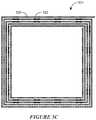
- FIG. 5Cis schematic diagram of an embodiment of a coil and MR elements for sensing a target.
- FIG. 6is schematic diagram of an embodiment of a coil and MR elements for sensing a target.
- FIG. 7is a cross-sectional view of coils and MR elements for sensing a target.
- FIG. 8is an isometric view of a pressure sensor.
- FIG. 8Ais an isometric view of embodiments of the pressure sensor of FIG. 8 .
- FIG. 9is a cross-sectional view of an embodiment of a pressure sensor including substrates.
- FIG. 10is a block diagram of a circuit for sensing a magnetic target.
- FIG. 10Ais a block diagram of an embodiment of a circuit for sensing a magnetic target.
- FIG. 11is a block diagram of an embodiment of a circuit for sensing a magnetic target.
- FIG. 11Ais a block diagram of an embodiment of a circuit for sensing a magnetic target.
- FIG. 11Bis a block diagram of an embodiment of a circuit for sensing a magnetic target.
- FIG. 11Cis a block diagram of an embodiment of a circuit for sensing a magnetic target.
- FIG. 11Dis a block diagram of an embodiment of a circuit for sensing a magnetic target.
- FIG. 11Eis a block diagram of an embodiment of a circuit for sensing a magnetic target.
- FIG. 11Fis a block diagram of an embodiment of a circuit for sensing a magnetic target.
- FIG. 12is a diagram representing an output signal for a system with sensitivity detection.
- FIG. 12Ais a block diagram of a magnetic field detection circuit with sensitivity detection.
- FIG. 12Bis a block diagram of an embodiment of a magnetic field detection circuit with sensitivity detection.
- FIG. 12Cis a block diagram of an embodiment of a magnetic field detection circuit with sensitivity detection.
- FIG. 13is a schematic diagram of an embodiment of a magnetic field detection circuit with sensitivity detection including a coil and MR elements.
- FIG. 13Ais a schematic diagram of an embodiment of a coil having countercoils and gaps between traces.
- FIG. 13Bis a block diagram of an embodiment of a magnetic field detection circuit with sensitivity detection.
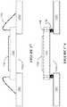
- FIG. 14is a side view of a magnetic field sensor and a magnetic target having material of varying thickness.
- FIG. 14Ais a side view of a magnetic field sensor and a magnetic target having material of varying thickness.
- FIG. 14Bis a side view of a magnetic field sensor and a magnetic target having material of varying thickness.
- FIG. 15is a side view of a magnetic field sensor and a magnetic target having material with multiple thicknesses.
- FIG. 15Ais a side view of a magnetic field sensor and a magnetic target having material with multiple thicknesses.
- FIG. 15Bis a side view of a magnetic field sensor and a magnetic target having material with multiple thicknesses.
- FIG. 15Cis a side view of a magnetic field sensor and a magnetic target having material with multiple thicknesses.
- FIG. 16is a side view of a magnetic field sensor and a magnetic target having an inclined plane.
- FIG. 16Ais a side view of a magnetic field sensor and a magnetic target having an inclined plane.
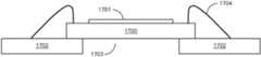
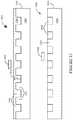
- FIG. 17is a side view of a substrate and lead frame connected by lead wires.
- FIG. 17Ais a side view of a substrate and lead frame connected by solder bumps.
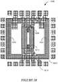
- FIG. 18is a schematic diagram of a dual-die package including one or more coils.
- FIG. 18Ais a schematic diagram of a dual-die package including one or more coils.
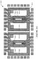
- FIG. 19is a schematic diagram of a multi-die package including one or more coils.
- magnetic field sensing elementis used to describe a variety of electronic elements that can sense a magnetic field.
- the magnetic field sensing elementcan be, but is not limited to, a Hall Effect element, a magnetoresistance (MR) element, or a magnetotransistor.
- MRmagnetoresistance
- MRmagnetoresistance
- magnetotransistorAs is known, there are different types of Hall Effect elements, for example, a planar Hall element, a vertical Hall element, and a Circular Vertical Hall (CVH) element.
- CVHCircular Vertical Hall
- magnetoresistance elementsfor example, a semiconductor magnetoresistance element such as Indium Antimonide (InSb), a giant magnetoresistance (MR) element, an anisotropic magnetoresistance element (AMR), a tunneling magnetoresistance (TMR) element, and a magnetic tunnel junction (MTJ).
- the magnetic field sensing elementmay be a single element or, alternatively, may include two or more magnetic field sensing elements arranged in various configurations, e.g., a half bridge or full (Wheatstone) bridge.
- the magnetic field sensing elementmay be a device made of a type IV semiconductor material such as Silicon (Si) or Germanium (Ge), or a type III-V semiconductor material like Gallium-Arsenide (GaAs) or an Indium compound, e.g., Indium-Antimonide (InSb).
- a type IV semiconductor materialsuch as Silicon (Si) or Germanium (Ge)
- a type III-V semiconductor materiallike Gallium-Arsenide (GaAs) or an Indium compound, e.g., Indium-Antimonide (InSb).
- some of the above-described magnetic field sensing elementstend to have an axis of maximum sensitivity parallel to a substrate that supports the magnetic field sensing element, and others of the above-described magnetic field sensing elements tend to have an axis of maximum sensitivity perpendicular to a substrate that supports the magnetic field sensing element.
- planar Hall elementstend to have axes of sensitivity perpendicular to a substrate
- metal based or metallic magnetoresistance elementse.g., MR, TMR, AMR
- vertical Hall elementstend to have axes of sensitivity parallel to a substrate.
- magnetic field sensoris used to describe a circuit that uses a magnetic field sensing element, generally in combination with other circuits.
- Magnetic field sensorsare used in a variety of applications, including, but not limited to, an angle sensor that senses an angle of a direction of a magnetic field, a current sensor that senses a magnetic field generated by a current carried by a current-carrying conductor, a magnetic switch that senses the proximity of a ferromagnetic object, a rotation detector that senses passing ferromagnetic articles, for example, magnetic domains of a ring magnet or a ferromagnetic target (e.g., gear teeth) where the magnetic field sensor is used in combination with a back-biased or other magnet, and a magnetic field sensor that senses a magnetic field density of a magnetic field.
- an angle sensorthat senses an angle of a direction of a magnetic field
- a current sensorthat senses a magnetic field generated by a current carried by a current-carrying conductor
- a magnetic switchthat
- targetand “magnetic target” are used to describe an object to be sensed or detected by a magnetic field sensor or magnetic field sensing element.
- the targetmay comprise a conductive material that allows for eddy currents to flow within the target, for example a metallic target that conducts electricity.
- FIG. 1is a block diagram of a system 100 for detecting a conductive target 102 .
- Target 102may be magnetic or non-magnetic in various embodiments.
- System 100includes one or more magnetoresistance (MR) elements 104 and an MR driver circuit 106 .
- MR driver circuitmay include a power supply or other circuit that provides power to MR elements 104 .
- MR elements 104may be replaced with other types of magnetic field sensing elements such as Hall effect elements, etc.
- MR elements 104may comprise a single MR element or multiple MR elements. The MR elements may be arranged in a bridge configuration, in certain embodiments.
- System 100may also include one or more coils 108 and a coil driver circuit 110 .
- Coils 108may be electrical coils, windings, wires, traces, etc. configured to generate a magnetic field when current flows through the coils 108 .
- coils 108comprise two or more coils, each a conductive trace supported by substrate, such as a semiconductor substrate, a glass substrate, a ceramic substrate, or the like.
- coils 108may not be supported by a substrate.
- coils 108may be supported by a chip package, a frame, a PCB, or any other type of structure that can support traces of a coil.
- coils 108may be free standing wire, i.e. not supported by a separate supporting structure.
- Coil driver 110is a power circuit that supplies current to coils 108 to generate the magnetic field.
- coil driver 110may produce an alternating current so that coils 108 produce alternating magnetic fields (i.e. magnetic fields with magnetic moments that change over time).
- Coil driver 110may be a circuit implemented, in whole or in part, on the semiconductor die.
- System 100may also include processor 112 coupled to receive signal 104 a from MR elements 104 , which may represent the magnetic field as detected by MR elements 104 .
- Processor 100may receive signal 104 a and use it to determine a position, speed, direction, or other property of target 102 .
- MR elements 104 and coils 108may be positioned on substrate 114 .
- Substrate 114may comprise semiconductor substrates, such as silicon substrates, a chip package, PCB or other type of board-level substrates, or any type of platform that can support MR elements 104 and coils 108 .
- Substrate 114may include a single substrate or multiple substrates, as well as a single type of substrate or multiple types of substrates.
- MR driver 106provides power to MR elements 104 and coil driver 110 provides current to coils 108 .
- coils 108produce a magnetic field that can be detected by MR elements 104 , which produce signal 104 a representing the detected magnetic field.
- system 100can detect movement or position of target 102 along axis 116 .
- system 100may detect the position of target 102 in proximity to MR elements 104 as target 102 moves toward or away from MR elements 104 and coils 108 .
- System 102may also be able to detect other types of position or movement of target 102 .
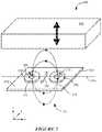
- system 200may be the same as or similar to system 100 .
- Substrate 202may be the same as or similar to substrate 114 , and may support coil 204 , coil 206 , and MR element 208 . Although one MR element is shown, MR element 208 may comprise two or more MR elements depending on the embodiment of system 200 .
- Target 203may be the same as or similar to target 102 .
- an MR driver circuit 106may provide current to MR element 208 and coil driver circuit 110 may provide current to coils 204 and 206 .
- Coil 204 and 206may be arranged so that the current flows through coils 204 and 206 in opposite directions, as shown by arrow 208 (indicating a clockwise current in coil 204 ) and arrow 210 (indicating a counterclockwise current in coil 206 ).
- coil 204may produce a magnetic field having a magnetic moment in the negative Z direction (i.e. down, in FIG. 2 ), as indicated by arrow 212 .
- coil 206may produce a magnetic field having a magnetic moment in the opposite direction, the positive Z direction, as indicated by arrow 214 .
- An aggregate magnetic field 211 produced by both coilsmay have a shape similar to that shown by magnetic field lines 211 .
- coils 204 , 206may be formed by a single coil structure respectively wound so that the current through the coils flows in opposite directions. Alternatively, coils 204 , 206 may be formed by separate coil structures.
- MR element 208may be placed between coils 204 and 206 .
- the net magnetic field at MR element 208may be zero.
- the negative Z component of the magnetic field produced by coil 204may be canceled out by the positive Z component of the magnetic field produced by coil 206
- the negative X component of the magnetic field shown above substrate 202may be canceled out by the positive X component of the magnetic field shown below substrate 202 .
- additional coilsmay be added to substrate 202 and arranged so that the net magnetic field at MR element 208 is substantially nil.
- coil 204 and coil 206may be placed so that current through the coils flows in circular patterns substantially in the same plane.
- the current through coil 204 and 206is flowing in circular patterns through the coils.
- those circular patternsare substantially coplanar with each other, and with the top surface 216 of substrate 202 .
- coil driver 110may produce an alternating field.
- the magnetic field shown by magnetic field lines 211may change direction and magnitude over time. However, during these changes, the magnetic field at the location of MR element 208 may remain substantially nil.
- magnetic field 211will cause eddy currents to flow within target 203 .
- These eddy currentswill create their own magnetic fields, which will produce a non-zero magnetic field in the plane of the MR element 208 , which non-zero magnetic field can be sensed to detect the motion or position of target 203 .
- a cross-sectional view 250 of system 200illustrates the eddy currents within target 203 .
- the ‘x’ symbolrepresents a current flowing into the page and the ‘•’ symbol represents a current flowing out of the page.
- the current through coils 204 and 206may be an alternating current, which may result in an alternating strength of magnetic field 211 .
- the phase of the alternating current through coil 204matches the phase of the alternating current through coil 206 so that magnetic field 211 is an alternating or periodic field.
- Alternating magnetic field 211may produce reflected eddy currents 240 and 242 within magnetic target 203 .
- Eddy currents 240 and 242may be opposite in direction to the current flowing through coils 204 and 206 , respectively.
- eddy current 246flows out of the page and eddy current 248 flows into the page, while coil current 251 flows into the page and current 252 flows out of the page.
- the direction of eddy current 242is opposite the direction of the current through coil 206 .
- Eddy currents 240 and 242form a reflected magnetic field 254 that has a direction opposite to magnetic field 211 .
- MR element 208detects a net magnetic field of zero due to magnetic field 211 .
- MR element 208will detect a non-zero magnetic field in the presence of reflected magnetic field 254 .
- magnetic field line 256the value of reflected magnetic field 254 is non-zero at MR element 208 .
- magnetic field 211may produce stronger eddy currents in target 203 .
- the strength of magnetic field 254may change.
- magnetic field 211 ′(in the right-hand panel of FIG. 2A ) may represent a stronger magnetic field than magnetic field 211 due, for example, to the closer proximity of target 203 to coils 204 and 206 .
- eddy currents 240 ′ and 242 ′may be stronger currents than eddy currents 240 and 242
- magnetic field 254 ′may be stronger than magnetic field 254 .
- This phenomenonmay result in MR element 208 detecting a stronger magnetic field (i.e. magnetic field 254 ′) when target 203 is closer to coils 204 and 206 , and a weaker magnetic field (i.e. magnetic field 254 ) when target 203 is further away from coils 204 and 206 .
- eddy currents 240 ′ and 242 ′generally occur on or near the surface of target 203 . Therefore, as target 203 moves closer to co MR element 208 , MR element 208 may experience a stronger magnetic field from the eddy currents because the source of the magnetic field is closer to MR element 208 .
- FIG. 3is a schematic diagram of a circuit 300 including coils 302 and 304 , and MR elements 306 and 308 .
- Coils 302 and 304may be the same as or similar to coils 204 and 206
- MR elements 306 and 308may each be the same as or similar to MR element 208 .
- coils 302 and 304 , and MR elements 306 and 308may be supported by a substrate.
- coils 302 and 304may comprise conductive traces supported by a substrate and MR elements 306 and 308 may be formed on a surface of or in the substrate.
- coils 302 and 304may comprise a single conductive trace that carries current.
- the portion of the trace forming coil 302may loop or spiral in a direction opposite to the portion of the trace forming coil 304 , so that the current through each coil is equal and flows in opposite directions.
- multiple tracesmay be used.
- Coils 302 and 304are symmetrically positioned on opposite sides of MR elements 306 and 308 , with MR elements 308 and 304 in the middle. This may result in MR elements 306 and 308 being in the center of the magnetic field produced by coils 302 and 304 , so that, absent any other stimulus, the magnetic field detected by MR elements 306 and 308 as a result of magnetic fields produced by coils 302 and 304 (referred to herein as the directly coupled magnetic field) is substantially nil.
- FIG. 3Ais a schematic diagram of an embodiment of a magnetic field detection circuit 300 ′, which may be the same as or similar to system 100 in FIG. 1 .
- Coils 302 and 304may be supported by a substrate as described above.
- Circuit 300 ′may include four MR elements 310 , 312 , 314 , and 316 , which may be coupled in a bridge configuration 318 .
- bridge 318may produce a differential output consisting of signals 318 a and 318 b.
- Arranging the MR elements in a bridgemay, in certain embodiments, increase the sensitivity of the magnetic field sensor.
- a targetis movable with respect to the circuit 300 ′ such that as the target approaches the circuit it mainly moves towards MR elements 310 , 312 , but not towards MR elements 314 , 316 .
- the resistance of MR elements 310 and 312may change and the resistance of MR elements 314 and 316 may remain relatively constant as the target approaches and recedes from the MR elements.
- MR elementsare aligned so that the MR resistance of 310 , 312 decreases and the resistance of MR elements 314 , 316 increases as the target approaches, then signal 318 a will decrease and signal 318 b will increase in voltage as the target approaches.
- the opposite reaction of the MR elements (and the differential signals 318 a and 318 b )may increase sensitivity of the magnetic field detection circuit while also allowing the processor that receives the differential signal to ignore any common mode noise.
- arranging MR elements 310 - 316 in a bridgemay allow for detection of the difference in the position of the target over the set of resistors and/or detection of a phase difference between the bridge outputs. This may be utilized, for example, to detect tilt or deformation of a target.
- Circuit 300 ′may also include a bond pads 320 having multiple leads 322 that can be accessed and form connections external to a chip package (not shown).
- Lead wires or conductive traces 324may connect MR elements 310 , 312 , 314 , and 316 to external leads or pads 322 so they can be coupled to other circuits like, for example, MR driver 106 .
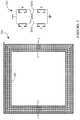
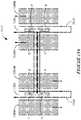
- a circuit 323includes four coils 324 - 330 and three rows 332 , 334 , and 336 of MR elements. Circuit 323 may be used to detect location or motion of a target.
- the coilsmay produce magnetic fields in alternating patterns.
- coil 324may produce a field going into the page
- coil 326may produce a field coming out of the page
- coil 328may produce a field going into the page
- coil 330may produce a field coming out of the page.
- the magnetic field detected by the MR elements in rows 332 , 334 , and 336 as a result of magnetic fields produced by coils 324 , 326 , 328 , 330may be substantially nil.
- Circuit 323may also be extended by adding additional coils and additional MR elements.
- the additional coilsmay be configured to create magnetic fields with alternating directions, as described above, and the MR elements between the coils may be placed so that they detect a magnetic field that is substantially nil.
- the MR elements in rows 332 , 334 , and 336may form a grid. As a target moves above the grid and approaches the MR elements, the MR elements will be exposed to and detect the reflected magnetic field produced by the eddy currents flowing in the target as a result of the magnetic fields produced by the coils 324 - 330 . For example, if a target moves over MR elements 338 and 340 , those MR elements may detect the reflected magnetic field and produce an output signal indicating as much. A processor receiving the output signals from the MR elements can then identify the location of the target as above or near MR elements 338 and 340 .
- MR element 342will detect the reflected magnetic field from the target and produce an output signal indicating the target was detected.
- the processor receiving the output signalscan then identify the location of the target as above or near MR element 342 .
- a single large targetmay be placed in front of the grid 332 , 334 and 336 . Then the difference of reflected fields experienced by each MR element is a mapping of the parallelism of the target and the plane of the grid. It can be also used to map the deformations of the target as function of an external constraint.
- a system 400 for detecting a target 402may use a single coil and MR element to detect target 402 .
- MR element 404may be placed proximate to coil 406 .
- MR element 404may be placed between coil 406 and target 402 .
- the traces of coil 406may be placed between MR element 404 and target 402 (not shown).
- MR element 404may be subject to a magnetic field even in the absence of magnetic target 402 . If magnetic target 402 is absent, there will be no eddy current and no reflected magnetic field. However, because MR element 404 is placed proximate to a single coil 406 , and not placed between two opposing coils, it may be subject to a directly coupled magnetic field 405 produced by the coil 406 .
- the presence of target 402may result in a reflected magnetic field and this additional field can be detected by MR element 404 to indicate the presence of target 402 .
- current through coil 406may produce eddy currents (shown by currents 408 and 410 ) in target 402 , which may produce reflected magnetic field 412 .
- Reflected magnetic field 412may increase the strength of the magnetic field experienced by MR element 404 .
- MR element 404may detect a stronger magnetic field than when target 402 is absent.
- the proximity of target 402may also increase or decrease the strength of the reflected magnetic field detected by MR element 404 .
- the eddy currentsshown by currents 408 ′ and 410 ′
- the eddy currentswill increase in strength, which will produce a reflected magnetic field 412 ′ with greater strength.
- MR element 404will detect stronger magnetic field as target 402 moves closer to coil 406 .
- MR element 404is positioned adjacent to loops of coil 406 . This may result in greater sensitivity of MR element 404 to detect reflected field 412 . However, because the field produced by coil 406 is not zero at the position of MR element 404 , MR element 404 may also detect not only the reflected field, but also the magnetic field directly produced by the coil 406 , i.e. a “directly coupled” magnetic field. Various techniques may be used to reduce MR element 404 's sensitivity to the directly coupled magnetic field.
- circuit 500includes a coil 502 and four MR elements 1 - 4 placed above or below traces of coil 502 .
- the MR elementsmay be connected in a bridge configuration 504 .
- the bridge configurationmay provide a differential output consisting of signals 504 a and 504 b.
- circuit 500may be used as a single-coil circuit for detecting a target.
- output signal 504 amay change, and as the target approaches MR elements 3 and 4 , output signal 504 b may change.
- MR elements 1 - 4may be aligned so that, as the target approaches elements 1 - 4 , output signal 504 a increase in value and output signal 504 b decreases in value, or vice versa.
- the field created by the coil near the elements 1 and 2is opposite is sign compared to the field created by the coil near the elements 3 and 4 .
- the reflected fieldsare in opposite direction enhancing the sensitivity of the bridge differential output to the reflected field while suppressing the variation due to external common fields.
- circuit 500 ′includes a coil 506 arranged so that, if current flows through coil 506 in the direction shown by arrow 508 , the current will flow through coil portion 510 in a clockwise direction and through a counter-loop coil portion 512 in a counterclockwise direction.
- coil portions 510 and 512may produce local magnetic fields having opposite direction, as described above.
- MR elements 1 - 4may be arranged as shown to form a bridge that provides a differential signal as the target approaches.
- the counter-loopmay reduce the directly-coupled magnetic field produced by the coil and detected by the MR elements.
- a magnetic field produced by coil 506may be directly detected by (e.g. directly coupled to) MR elements 1 - 4 .
- Coil portions 510 and 512may each create a local magnetic field in the opposite direction of the magnetic field produced by coil 506 .
- the local magnetic fieldsmay (at least partially) cancel out the directly coupled field produced by coil 506 at least in the local area around MR elements 1 - 4 . This may reduce or eliminate the directly-coupled field as detected by MR elements 1 - 4 so that the magnetic field detected by MR elements 1 - 4 is the reflected field from the target.
- the counter-loopis used to measure reflected field and the direct field of the coil to provide sensitivity detection. Also, in this configuration, MR elements 1 - 4 can be placed so they do not see the field created by the main coil.
- the targetmay be positioned adjacent to MR elements 1 and 3 , but not 2 and 4 (or vice versa). If MR elements 1 - 4 are arranged in a bridge formation, a differential output of the bridge may change as the target moves toward or away from MR elements 1 and 3 , for example.
- the targetmay be positioned so that MR elements 1 and 2 experience the reflected magnetic field in one direction (e.g. experience one side of the reflected magnetic field) and MR elements 3 and 4 experience the reflected magnetic field in the opposite direction (e.g. experience the other side of the reflected magnetic field).
- signal 504 amay increase and signal 504 b may decrease (or vice versa) to produce a differential signal.
- circuit 500 ′′includes two MR bridges.
- MR bridge 514includes MR elements 1 - 4 and produces a differential output signal consisting of signals 514 a and 514 b
- MR bridge 516includes MR elements 508 and produces a differential output signal consisting of signals 516 a and 516 b.
- the output signals of MR bridges 514 and 516may change to indicate the presence and proximity of the target.
- Circuit 500 ′′is also shown with bond pads 518 .
- the targetmay be positioned adjacent to bridge 514 (MR elements 1 - 4 ) so that the differential output of bridge 514 is affected as the target moves closer to or further from bridge 514 .
- the output of bridge 516may remain relatively stable as the target moves.
- the output of bridge 516may be used as a reference.
- this arrangementmay work in situations where the target to be detected is relatively close to bridge 514 , so that movement of the target has a greater effect on bridge 514 and a smaller or zero effect on bridge 516 .
- the same configurationcan be used to measure a difference of distance, the first distance being between a large target and the lock of MR elements 1 , 2 , 3 , and 4 and the second distance being between the corresponding target and MR elements 5 , 6 , 7 , and 8 .
- FIG. 5Bcan be used to determine accurately the centering of a target along a plane perpendicular to the plane of the coil and crossing the plane of the coil along the line 530 situated at equal distance between the bridges 514 and 516 .
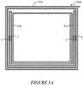
- circuit 501includes a coil 520 and multiple MR elements 522 arranged at intervals around coil 520 .
- MR elements 522may form a grid, similar to the grid described above and shown in FIG. 3B .
- MR elements 522may be connected in bridge configurations.
- MR elements 522may act (or be part of) individual circuits that are not shared with other MR elements. In either case, MR elements 522 may produce a signal when a target (and its reflected magnetic field) are detected.
- a processormay receive these signals and calculate the location, position, speed, parallelism, angle or other properties of the target.
- circuit 501may be used to detect the position of the target in three dimensions with respect to the coil. Because the MR elements are positioned in a plane along coil 520 , they may act as a grid. As the target approaches one (or more) of the MR elements, they will produce an output signal that can be used to determine the location of the target along the two dimensions of the grid. Also, as described above, coil 520 and the MR elements may be used to detect distance from the MR elements in a direction orthogonal to the two dimensions of the coil and grid (i.e. a direction into and out of the page).
- a circuit 600 for detecting a targetmay include a coil 602 and one or more MR elements 604 and 606 .
- Coil 602may have two coiled portions 608 and 610 , separated by a gap 612 .
- the current through portions 608 and 610flows in the same direction. For example, if the current through portion 608 flows in a clockwise direction around the coil, the current through portion 610 may also flow in a clockwise direction.
- MR elements 604 and 606may be placed within the gap so that they are not directly above (or below) traces of coil 602 . Placing MR elements within gap 612 may reduce capacitive or inductive coupling between coil 602 and MR elements 604 and 606 . Also, gap 612 may have a width W that is smaller than the distance between the MR elements and the target. As a result of gap 612 being relatively small, the eddy currents induced in the target and the resulting reflected magnetic field may appear (i.e. may be detected by the MR elements) as if a single coil without any gap between portions were producing the magnetic field.
- positioning MR elements within gap 612may reduce sensitivity of the MR elements to the directly coupled magnetic field produced by gap 612 , thus allowing the MR elements to maintain sensitivity to the reflected field.
- coil 602may include a jog in one or more of the traces.
- MR elements 604 and 606may be aligned with the jog.
- FIG. 7is a cross-sectional view of a circuit having MR elements 604 and 606 sandwiched between traces of coil 700 .
- coil 700may be the same as or similar to coil 602 .
- Coil traces 602 a and 602 bmay be positioned on the surface of a substrate (not shown).
- MR elements 604 and 606may be placed atop traces 602 a and 602 b so that traces 602 a and 602 b are positioned between MR elements 604 and 606 and the substrate.
- An additional layer of traces 614 a and 614 bmay be positioned atop MR elements 604 and 606 .
- Traces 602 a, 602 b, 614 a, and 614 bmay be part of the same coil so that current flowing through the traces flows in a circular or spiral pattern to induce a magnetic field. Placing MR elements 604 and 606 between traces of the coil may reduce directly coupled magnetic field produced by the coil.
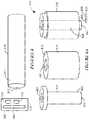
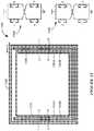
- a pressure sensor 800includes a magnetic field sensor 802 , having a substrate 803 that supports a coil 804 and MR elements 806 and 808 .
- magnetic field sensor 802may be the same as or similar to circuit 500 in FIG. 5 , circuit 300 in FIG. 3 , or any of the magnetic field detection circuits described above that can detect proximity of a target.
- coil 804 and MR elements 806 , 808may be supported by the same substrate 803 .
- MR element 806 , MR element 808 , and coil 804may be supported on different substrates (not shown).
- coil 804may be supported by one substrate while MR elements 806 and 808 may be supported by a different substrate.
- MR element 806 , MR element 808 , and coil 804may each be supported by a separate substrate. Any other combinations of substrates supporting circuit elements are also possible.
- Pressure sensor 800includes a chamber 810 having a conductive portion 811 and a deformable portion 812 .
- chamber 810is formed by an elongate tube.
- the conductive portion and the deformable portion 812may comprise a membrane disposed at one end of the tube that can act a diaphragm, and can be deformed to move toward or away from magnetic field detection circuit 802 .
- Deformable portion 812may be formed of stainless steel, copper beryllium, titanium alloys, super alloys, and/or sapphire. When the pressure inside chamber 810 is greater than the pressure outside chamber 810 , deformable portion 812 may extend toward magnetic field detection circuit 802 . If the pressure outside chamber 810 is greater, deformable portion 812 may retract away from magnetic field detection circuit 812 , and if the pressure inside and outside chamber 810 is in equilibrium, deformable portion may adopt a neutral position between the extended and retracted positions.
- his the thickness of the deformable portion
- ⁇is the Poisson module
- Eis the young module
- ais the radius of the deformable portion
- ris the point where the deformation is measured.
- the maximal deformationmay be low enough that the deformable portion is always in the elastic domain of the material even at temperature above 180° C. For that reason, super alloys like maraging alloys or titanium alloys may be suitable materials.
- Magnetic field detection circuit 802may include at least one magnetic field sensing element 806 and/or 808 disposed proximate to coil 804 , as described above. Coil 804 may produce a magnetic field that induces eddy current and a reflected magnetic field in the conductive portion 812 , similar to the eddy currents and reflected fields described above. Magnetic field detection circuit 802 may also include a circuit to generate an output signal indicative of the pressure differential between the interior and exterior of chamber 810 .
- magnetic field detection circuit 802comprises two spaced apart MR elements 806 and 808 and detects a distance between the conductive portion 812 and one of the MR elements 806 and 808 as deformable portion extends toward and/or retracts away from the MR elements.
- magnetic field detection circuit 802may be configured to detect a difference between a) the distance between the conductive portion 812 and magnetic field sensor 808 , and b) the distance between conductive portion 812 and magnetic field sensor 806 . The difference between these distances may be used to produce an output signal of magnetic field detection circuit 802 .
- the output signal produced by magnetic field detection circuit 802may represent the distance, which can then be received by a processor to calculate an associated pressure within chamber 810 .
- MR elements 806 and 808may comprise multiple MR elements and may be arranged in a bridge configuration, as described above, to produce a differential output.
- MR element 806is aligned with an edge of conductive, deformable portion 812 and MR element 808 is aligned with the center or a central region of conducive, deformable portion 812 .
- MR element 808will react as deformable portion 812 moves toward and away from MR element 808 , and MR element 806 will not be affected or will be affected to a significantly lesser degree than element 808 , and thus may have a relatively constant resistance value.
- Positioning the MR elements in this waymay be used to remove errors due to stray field. It may also help compensate for air gap tolerance between MR elements. For example, the difference in distance detected by the two sensors may be used to compensate for small changes in air gap over time, temperature, etc.
- a pressure sensor 818includes a first elongated tube 820 having a deformable sidewall 821 and an opening 823 that allows a fluid to enter a chamber within elongated tube 820 .
- the sidewall 821may expand like a balloon or extend.
- An end 828 of tube 820may be conductive.
- Pressure sensor 818also includes a second elongated tube 822 having an opening 824 .
- Elongated tube 822may have a rigid wall 826 , and an opening 824 .
- Opening 824may have a diameter or size large enough for tube 820 to be inserted into opening 824 .
- Pressure sensor 818may include a magnetic field sensor 830 , which may be the same as or similar to magnetic field sensor 802 , and/or any of the magnetic field sensors described above.
- conductive end 828 of tube 820may be positioned proximate to MR element 808 .
- the rigid wall of tube 822 ′smay keep deformable sidewall 821 from expanding laterally.
- end 828may expand and extend toward MR element 808 and retract away from MR element 808 as pressure within tube chamber 823 changes.
- Magnetic field sensor 830may detect the change in distance and produce an output signal representing the distance between end 828 and MR element 808 .
- magnetic field detection circuit 802may be configured to detect a difference between a) the distance between conductive end 828 and magnetic field sensor 808 , and b) the distance between conductive 808 and magnetic field sensor 806 . The difference between these distances may be used to produce an output signal of magnetic field detection circuit 830 .
- a processor circuitmay receive the signal and calculate a pressure within tube 820 based on the distance.
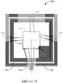
- pressure sensor 900includes a first substrate 902 , that may be the same or similar to substrate 803 of FIG. 8 , and a second substrate 904 attached to the first substrate 902 .
- Second substrate 904may include a surface 908 and recess 906 formed in the surface. Recess 906 may be etched into the substrate.
- wafer 904may be etched so that it is thin enough to deflect under pressure, as shown by dotted lines 910 .
- MR elements supported by substrate 902may detect (via a reflected magnetic field as describe above) the deflection of wafer 904 . The detected deflection may be subsequently correlated to a pressure.
- the MR elements on substrate 902may be positioned so that one or more MR elements are adjacent to an edge (e.g. a non-deflecting portion) of recess 906 and one or more MR elements are adjacent to the center (e.g. a deflecting portion) of recess 906 , similar to the arrangement described above and illustrated in FIG. 8A .
- substrate 904may be formed from a conductive material, for example copper. Therefore, motion of a conductive deformable portion of substrate 904 caused by pressure on substrate 904 (and/or pressure within recess 906 ) can be detected by a magnetic field sensors on substrate 902 .
- the substrate 904may be formed by a crystalline material like sapphire coated by a thick enough conductive material like copper for example.
- recess 906is evacuated during the manufacturing process to determine a reference pressure.
- the reference pressureis a vacuum or a pressure that is less than standard pressure (e.g. less than 100 kPa).
- one or more of the output signals of an MR bridgee.g. bridge 318 in FIG. 3A ) may be used to generate to represent the value of the reference pressure.
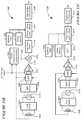
- Magnetic field sensorincludes a coil 1002 to produce a magnetic field, coil driver 1004 to provide power to the coil, MR element 1006 , and MR driver circuit 1008 to provide power to MR element 1006 .
- MR element 1006may be a single MR element or may comprise multiple MR elements, which may be arranged in a bridge configuration. As described above, coil 1002 and MR element 1006 may be configured to detect the distance of a conductive target.
- coil driver 1004 and/or MR driver 1008may produce an AC output to drive coil 1002 and MR element 1008 , as described above and as indicated by AC source 1010 .
- AC source 1010may be a common source used to drive both coil 1002 and MR element 1006 .
- signal 1012may be an AC signal.
- Magnetic field sensor 1000also includes an amplifier to amplify the output signal 1012 of MR element 1006 .
- Output signal 1012may be a differential signal and amplifier 1014 may be a differential amplifier.
- Output signal 1012 and amplified signal 1016may a DC signal.
- Magnetic field sensor 1000may also include a low pass filter 1018 to filter noise and other artifacts from signal 1016 , and an offset module 1024 which may scale the output signal according to temperature (e.g. a temperature measure by temperature sensor 1020 ) and a type of material according to material type module 1022 .
- a segmented linearization circuit 1026may also be included, which may perform a linear regression on compensated signal 1028 and produce output signal 1030 .
- the reflected magnetic field from the targetwill have a frequency f (the same frequency as the coil driver 1004 ). Because the magnetic field produced by coil 1002 and the reflected field have the same frequency, the output of MR element 1006 may include a 0 Hz (or DC) component, a component at frequency f, and harmonic components at multiples of frequency f One skilled in the art will recognize that the lowest frequency harmonic component may occur at frequency 2*f. However, any difference in the equilibrium of the MR bridge may generate a frequency component that may be present in the signal.
- low pass filter 1018may be configured to remove the frequency f and higher (i.e. low pass filter 1018 may include a cut-off frequency f cutoff , where f cutoff ⁇ f.
- the filtermay be designed to remove possible f signals. Accordingly, the frequency f may be chosen as a frequency greater than the frequency range of motion of the target.
- the sensitivity of MR element 1008changes with temperature.
- the strength of the reflected fieldmay also change with temperature depending of target material type and frequency.
- module 1022may contain parameters to compensate for the effects of the temperature and/or material used.
- the parametersmay include linear and/or second order compensation values.
- processing circuit 1032may process the signal representing the magnetic field. Because a common source 1010 is used to drive MR element 1006 and coil 1002 , the frequency of coil 1002 and MR element 1006 is substantially the same. In this case, post processing of the signal may include filtering, linear regression, gain and amplification, or other signal shaping techniques.
- MR element 1006may detect the magnetic field directly produced by coil 1002 and also the reflected magnetic field produced by eddy currents in a conductive target, induced by the magnetic field generated by current through coil 1002 .
- magnetic field sensor 1000 ′may include coil 1002 , coil driver 1004 , common AC source 1010 , MR driver 1008 , MR element 1006 , amplifier 1014 , and low pass filter 1018 as described above.
- Magnetic field sensor 1000 ′may differ from sensor 1000 of FIG. 10 in that it is a closed loop sensor and so may also include a second coil 1035 , which may operate at a different AC frequency than coil 1002 .
- coil 1035may be 180 degrees out of phase with coil 1002 as indicated by the “ ⁇ f” symbol.
- Coil 1035may also produce a first magnetic field that can be used to detect a target.
- coil 1035may be relatively smaller than coil 1002 .
- Coil 1035may be placed adjacent to MR element 1006 to produce a magnetic field that can be detected by MR element 1006 , but which does not produce eddy currents in the target.
- coil 1035may be used to offset errors due to the magneto-resistance of the MR element. For example, the magnitude of current driven through coil 1035 may be changed until the output of MR element 1006 is zero volts. At this point, the current through coil 1035 may be measured (for example, by measuring voltage across a shunt resistor in series with coil 1035 ). The measured current may be processed similarly to the output of MR element 1006 to remove a magnetoresistance error associated with MR 1006 .
- Magnetic field sensor 1000 ′may also include an amplifier 1036 to receive signal 1038 .
- Magnetic field sensor 1000 ′may also include low pass filter 1019 , material type module 1022 , temperature sensor 1020 , offset module 1024 , and segmented linearization module 1026 as described above.
- FIGS. 11-11Finclude various examples of magnetic field sensors having signal processing to reduce inductive coupling or other noise from affecting signal accuracy.
- the example magnetic field sensors in FIGS. 11-11Fmay also employ various features related to detecting a reflected field from a target, such as frequency hopping, etc.
- Such magnetic field sensorsmay also include circuitry to compute a sensitivity value.
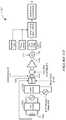
- a magnetic field sensor 1100may include coil 1002 , coil driver 1004 , AC driver 1010 , MR driver 1008 , MR element 1006 , amplifier 1014 , low pass filter 1018 , temperature sensor 1020 , material type module 1022 , offset module 1024 , and segmented linearization module 1026 .
- MR element 1006may be responsive to a sensing element drive signal and configured to detect a directly-coupled magnetic field generated by coil 1002 , to produce signal 1012 in response.
- Processing circuitrymay compute a sensitivity value associated with detection, by MR element 1006 , of the directly-coupled magnetic field produced by coil 1002 .
- the sensitivity valuemay be substantially independent of a reflected field produced by eddy currents in the target.
- AC driver 1010is coupled to coil driver 1004 , but is not coupled to MR driver 1008 in sensor 1100 .
- MR driver 1008may produce a DC signal (e.g. a signal with a frequency of about zero) to drive MR element 1006 .
- Coil 1002may produce a DC (or substantially low frequency AC) magnetic field that can be detected by MR element 1006 , but which does not produce eddy currents in the target.
- the signal produced by detection of the DC (or substantially low frequency AC) magnetic fieldmay be used to adjust sensitivity of the magnetic field sensor.
- Coil 1002may also produce an AC magnetic field at higher frequencies that induces eddy currents in the target, which produce a reflected magnetic field at those higher frequencies that can be detected by MR element 1006 .
- MR element 1006may produce signal 1012 , which may include frequency components at the DC or substantially low AC frequency (e.g. a “directly coupled” signal or signal component) representing the lower frequency magnetic field that does not cause eddy currents in the target, and/or frequency components at the higher AC frequency (e.g. a “reflected” signal or signal component) that represent the detected reflected field.
- the directly coupled signalsmay be used to adjust sensitivity of the sensor while the reflected signals may be used to detect the target.
- Coil driver 1004 and/or MR driver 1008may use the directly coupled signals as a sensitivity signal adjust their respective output drive signals in response to the sensitivity signal.
- the directly coupled signal and the reflected signalmay be included as frequency components of the same signal.
- coil 1002may be driven to produce both frequency components at the same time.
- generation of the directly coupled signal and the reflected signalsmay be generated at different times, for example using a time-division multiplexing scheme.
- Sensor 1100may also include a demodulator circuit 1050 that can modulate signal 1016 to remove the AC component from the signal or shift the AC component within the signal to a different frequency.
- demodulator circuit 1050may modulate signal 1016 at frequency f.
- signal 1016includes signal components at frequency f representing the detected magnetic field
- modulating signal 1016 at frequency fmay shift the signal elements representing the detected magnetic field to 0 Hz or DC.
- Other frequency components within signal 1016may be shifted to higher frequencies so they can be removed by low-pass filter 1018 .
- the DC or low frequency component of signal 1016which may represent a sensitivity value, can be fed back to coil driver 1004 to adjust the output of coil 1002 in response to the signal, and/or to MR driver 1008 to adjust drive signal 1009 in response to the sensitivity value.
- DC output signal 1052may represent proximity of the target to MR element 1006 .
- a time-division multiplexing schememay be used.
- coil driver 1004may drive coil 1002 at a first frequency during a first time period, at a second frequency during a second time period, etc.
- the first and second (and subsequent) time periodsdo not overlap.
- the first and second time periodsmay overlap.
- coil driver 1004may drive coil 1002 at two or more frequencies simultaneously.
- demodulator 1050may operate at the same frequency as the coil driver 1004 .
- multiple modulatorscan be used, the first running at the first frequency, and the second running at the second frequency in order to separate out the signals at each frequency.
- the simultaneous measure of both the field reflected and the field created by the coilallows to determine accurately the distance of the object independent of the sensitivity of the MR elements, coil drive current, etc. . . .
- the sensitivity of MR elementsmay vary with temperature and/or with the presence of unwanted DC or AC stray fields in the plane of the MR array.
- the ratio between the reflected field and the coil fieldis just dependent on geometrical design and is hence a good parameter to accurately determine a distance.
- a frequency hopping schememay be used.
- coil driver 1004may drive coil 1002 at different frequencies (e.g. alternate between frequencies over time, or produce a signal containing multiple frequencies).
- sensor 1100may include multiple demodulator circuits and/or filters to detect a signal at each frequency.
- a magnetic field sensor 1100 ′includes coil 1002 , coil driver 1004 , AC driver 1010 , MR driver 1008 , MR element 1006 , amplifier 1014 , low pass filter 1018 , temperature sensor 1020 , material type module 1022 and offset module 1024 .
- AC driver 1010is coupled to coil driver 1004 to drive coil 1002 at a frequency f 1 .
- MR driver 1008is coupled to AC driver 1102 to drive MR element 1006 at a frequency f 2 .
- Frequencies f 1 and f 2may be different frequencies and may be non-harmonic frequencies (in other words, f 1 may not be a harmonic frequency of f 2 and vice versa).
- frequency f 1is lower than frequency f 2 .
- frequency f 1 and f 2may be relatively close to each other so that the difference between the two frequencies falls well below f 1 and f 2 .
- Frequency f 2may be a zero value or non-zero-value frequency but alternatively, we may choose f 1 larger than f 2 . Then the demodulation is done at f 2 -f 1 .
- frequency f 1may be selected to avoid generating an eddy current greater than a predetermined level in the target and/or selected to provide full reflection in the target.
- the reflected fieldmay be related to the skin depth in the target according to the following formula:
- ⁇is the conductivity of the target material
- ⁇is the magnetic permittivity of the target material
- fis the working frequency. If the thickness of the target material is larger than about 5 times the skin depth ⁇ , the field may be totally reflected. In the case where the thickness of the target is equal to the skin depth, only about the half of the field may be reflected. Hence a frequency f chosen to be low enough so the skin depth becomes larger than the thickness of the target may induce low eddy currents and a reflected field with reduced strength.
- the formula given abovemay be valid for high conductive and low magnetic materials. For material with low conductivity or for ferromagnetic material, losses of the eddy currents, which may be translated at a complex skin depth, may result in reduction of reflected field strength.
- Circuit 1100 ′may also include a band pass filter 1104 and a demodulator circuit 1106 .
- Band pass filter 1104may have a pass band that excludes frequencies f 1 and f 2 but conserves frequency
- Circuit 1100 ′may also include a demodulator circuit 1106 that demodulates at frequency
- may include information about the target and/or the directly coupled magnetic field, but may have reduced noise from inductive coupling or other noise sources.
- a magnetic field sensor 1100 ′′includes coil 1002 , coil driver 1004 , AC driver 1010 , MR driver 1008 , MR element 1006 , amplifier 1014 , low pass filter 1018 , temperature sensor 1020 , material type module 1022 , offset module 1024 , and segmented linearization module 1026 .
- AC driver 1010is coupled to coil driver 1004 , but is not coupled to MR driver 1008 in sensor 1100 .
- MR driver 1008may produce a DC signal (e.g. a signal with a frequency of about zero) to drive MR element 1006 .
- Coil 1002may produce an AC magnetic field that induces eddy currents and a reflected magnetic field in a target.
- Sensor 1100 ′′may also include a demodulation circuit 1060 that can demodulate signal 1016 .
- Demodulation circuit 1060may multiply signal 1016 by a signal at frequency f, which may shift information about the target in signal 1016 to DC, and may shift noise or other information in the signal to higher frequencies.
- Low pass filter 1018may the remove the noise at higher frequencies from the signal.
- demodulation circuit 1060may be a digital circuit that demodulates signal 1016 in the digital domain or an analog signal the demodulates signal 1016 in the analog domain.
- Sensor 1100 ′′may also include a phase detection and compensation circuit 1062 that detects the phase and/or frequency of the current in coil 1002 and the magnetic field it produces. Circuit 1062 may detect and compensate for discrepancies in phase in coil 1002 and f and produce a corrected signal 1063 that can be used to modulate signal 1016 .
- the frequency f, the type of material of the target, the shape of the target, wiring and electronics, and/or other factorsmay cause a phase shift between the drive signal 1010 to coil 1002 and the reflected magnetic field detected by MR element 1008 .
- the phase between the signalscan be measured and used to adjust the phase of signal 1063 from phase detection and compensation circuit 1062 to match the phase of signal 1016 .
- a frequency hopping schememay also be used.
- coil driver 1004 and/or MR driver 1008may drive signals at multiple frequencies.
- phase detection and compensation module 1062may adjust the phase of signal 1063 to match the phase of signal 1016 .
- a magnetic field sensor 1100 ′′′includes coil 1002 , coil driver 1004 , AC driver 1010 , MR driver 1008 , MR element 1006 , amplifier 1014 , temperature sensor 1020 , material type module 1022 , offset module 1024 , and segmented linearization module 1026 .
- AC driver 1010is coupled to coil driver 1004 , but is not coupled to MR driver 1008 in sensor 1100 .
- MR driver 1008may produce a DC signal (e.g. a signal with a frequency of about zero) to drive MR element 1006 .
- Coil 1002may produce an AC magnetic field that induces eddy currents and a reflected magnetic field in a target.
- the reflected magnetic fieldcan be detected by MR element 1006 , which produces signal 1012 representing the detected magnetic field.
- Sensor 1100 ′′′may also include a fast Fourier transform (FFT) circuit 1070 that can perform an FFT on signal 1016 . Performing the FFT may identify one or more frequency components in signal 1016 . In an embodiment, FFT circuit 1070 may identify the frequency component with the greatest amplitude in signal 1016 , which may represent the detected magnetic field at frequency f. FFT circuit 1070 may produce an output signal 1072 including the detected signal at frequency f, as well as any other frequency components of signal 1016 .
- FFTfast Fourier transform
- the drivercan generate simultaneously different frequencies fa, fb, fc, and the FFT module may calculate the amplitudes at fa, fb, fc, which may be used to determine different parameters of the target including position, material, thickness, etc.
- the FFT modulemay calculate the amplitudes at fa, fb, fc, which may be used to determine different parameters of the target including position, material, thickness, etc.
- a disturbancee.g. from a deformation of the target, a stray magnetic field, a noise source, etc.
- the amplitudes calculated by the FFT modulemay also be used to determine if there is a disturbance at any particular frequency, which can be ignored by subsequent processing.
- he FFT temperature gain compensation and linearizationmay be calculated in the analog and/or digital domain.
- a magnetic field sensor 1100 Dincludes coil 1002 , coil driver 1004 , MR driver 1008 , and MR element 1006 .
- the output signal 1007 of MR sensor 1006may represent a detected magnetic field.
- sensor 1100 Dmay also include amplifier 1014 , low pass filter 1018 , temperature sensor 1020 , material type module 1022 , offset module 1024 , and segmented linearization module 1026 .
- An oscillator 1182may be used to operate coil driver 1004 at a frequency f.
- oscillator 1182is coupled to coil driver 1004 , but is not coupled to MR driver 1008 in sensor 1100 D.
- MR driver 1008may produce a DC signal (e.g. a signal with a frequency of about zero) to drive MR element 1006 .
- Sensor 1100 Dalso includes a quadrature demodulation circuit 1180 .
- Quadrature demodulation circuit 1180includes shift circuit 1188 to produce a 90° shift of the driving frequency f.
- Oscillator 1182may produce a cosine signal at frequency f.
- the output of 1188may be a sine signal at frequency f.
- the detected signal of the MR sensor 1006may be separated into in-phase and out-of-phase components (e.g. signals 1184 a and 1186 a ). The resulting phase and magnitude can be used to determine information about the reflected field and the target.
- phase informationmay be used to determine if there is a defect or abnormality in the target, to determine magnetic properties of the material of the target, whether the target is aligned properly, etc.
- Oscillator 1182may also produce a square wave with period 1/f, and shift circuit 1188 may shift the square wave in time by 1/(4f).
- magnetic field sensor 1100 Emay produce a quadrature modulated signal via two signal paths as an alternative to providing both the in-phase and out-of-phase information.
- circuit 1100 Ehalf of the MR elements may be driven by a signal at frequency f and half of the MR elements may be driven with a frequency 90° out of phase.
- the demodulation chaine.g. the circuits that comprise a demodulation function of the system
- quadrature modulationmay be used to determine the absolute magnitude and phase of the returned signal. This may allow for automatic correction of unwanted dephasing of the signal, which may provide a more accurate determination of target properties and retrieval of information related to magnetic or loss properties of the material.
- a magnetic field sensor 1100 Fincludes coil driver 1004 that drives coil 1002 at a frequency of f 1 .
- MR driver 1008may drive MR element at the same frequency f 1 , but 90 degrees out of phase with respect to coil drive 1004 .
- the signal 1016 produced by MR element 1006may have a frequency that is two times f 1 (i.e. 2*f 1 ), which may be a result of multiplying a sine and a cosine.
- Sensor 1100 Fmay include a demodulator circuit 1195 that may demodulate the signal to convert the reflected field information to a frequency around DC.
- signal 1270may represent a signal used by coil driver 1004 to drive coil 1002 .
- coil driver 1004may drive coil 1002 with current flowing in one direction, and when the signal is low, coil driver may drive coil 1002 with current flowing in the opposite direction.
- coil driver 1004may drive coil 1002 with direct current (i.e. at DC) or at a frequency sufficiently low so that the magnetic field produced by coil 1002 does not create eddy currents in the target.
- the skin depth of copper at r 50 Hzmay be about 10 mm and at 10 kHz it may be about 600 ⁇ m.
- a frequency below 5 kHzmay create reflected magnetic fields with relatively low strength.
- Coil driver 1004may drive coil 1002 at a relatively low or DC frequency, as shown by signal portions 1272 and 1274 .
- the frequencymay be sufficiently low, and thus the duration of portions 1272 and 1274 may be sufficiently long, so that any eddy currents generated in the target by switching of signal 1270 (for example, switching from a high value during portion 1272 to a low value during portion 1274 ) have time to settle and dissipate.
- the directly-coupled signal shown during portions 1272 and 1274may switch from high to low (representing a change in the detected magnetic field) in order to remove any offset due to the directly-coupled magnetic field of coil 1002 .
- Portion 1276 of signal 1270may represent the magnetic field detected by MR element 1006 while coil driver 1004 drives coil 1002 at a frequency sufficiently high to induce eddy currents in the target. While portion 1276 is active, MR element 1006 may detect the directly-coupled magnetic field produced directly by coil 1002 , and also the magnetic field produced by eddy currents in the target. The detected signal may be subsequently processed to separate the directly-coupled field from the field produced by the eddy currents. Although not shown, portion 1276 may have a larger or smaller magnitude than portion 1272 because the portions may contain different information. For example, portion 1276 may include the reflected signal as well as the directly-coupled signal.
- low frequency portions 1272 and 1274 of different polaritiesmay be adjacent to each other within signal 1270 .
- low frequency portions 1272 ′ and 1274 ′ of different polaritiesmay not be adjacent to each other within the signal. For example, they may be separated by high frequency signal portion 1276 .
- the coilmay be driven at both the low frequency (of low frequency portions 1272 and 1274 ) and at the high frequency (of high frequency portion 1276 ) simultaneously.
- the frequenciesmay then be separated using signal processing techniques to measure a MR element's response.
- the ration of the low frequency portions 1272 and 1274 to the high frequency portion 1276can be used to determine or indicate the magnitude of the reflected signal. Measuring the ratio in this way may reduce sensitivity of the magnitude measurement to external, unwanted variations such as variations due to temperate, stray magnetic fields, etc
- magnetic field sensor 1200may be configured to adjust the output signal of the magnetic field sensor in response to the sensitivity value.
- Sensor 1200may include a coil 1202 and coil driver 1204 .
- MR element 1206may detect a magnetic field produced by coil 1202 , and as reflected by a target, as described above.
- the output signal 1208 of MR element 1206may comprise a first frequency and a second frequency.
- the first frequencymay be the frequency of the coil driver, and the second frequency may be 0 Hz, or DC.
- MR element 1206may be driven by a DC bias circuit 1210 .
- the second frequencymay be a non-zero frequency.
- coil driver 1204may drive coil 1202 at one frequency during a first time period, and by another frequency during a second time period.
- the time periodsmay alternate and not overlap.
- Sensor 1200may also include a separator circuit, which may include one or more low pass filters 1214 and 1216 , as well as demodulators 1224 and 1226 .
- Sensor 1200may also include mixer circuit 1212 .
- Oscillators 1218 and 1220may provide oscillating signals used to drive coil 1202 and process signal 1208 .
- oscillator 1220may provide a signal with a higher frequency (f high ) than that of oscillator 1218 (f low ).
- f lowis a sufficiently low frequency so that any reflected field produced by the target as a result of frequency flow is zero, sufficiently small that it is not detected, or sufficiently small so that its effect on the output is negligible or within system tolerances.
- Mixer 1212may mix (e.g. add) the signals from oscillator 1218 and 1220 to produce signal 1222 , which it feeds to coil driver 1204 .
- Coil driver 1204may then drive coil 1202 according to the mixed signal 1202 .
- output signal 1208may include oscillations at f high and f low as detected by MR sensor 1206 .
- Demodulator 1226may demodulate signal 1208 at frequency f high in order to separate the portion of signal 1208 at frequency f high from other frequencies in the signal.
- Low pass filter 1214may then remove these frequencies from the signal and produce a filtered signal 1228 comprising primarily information at frequency f high or at DC.
- demodulator 1224may demodulate signal 1208 at frequency f low in order to separate the portion of signal 1208 at frequency f low from other frequencies in the signal.
- Low pass filter 1216may then remove these frequencies from the signal and produce a filtered signal 1230 comprising primarily information at frequency f low or at DC.
- Processing circuit 1232may process signals 1228 and 1230 to produce output signal 1232 representing the detected target.
- Processing circuit 1232may process signals 1228 and 1230 in various ways including, taking the ratio of the signals to provide an output that is substantially insensitive to undesirable variations caused by stray magnetic field interference, temperature shifts, package stresses, or other external stimuli. Taking the ratio of the signals can also provide an output that is substantially insensitive to variations in the coil driver (e.g. variations in current or voltage provided by the coil driver) due to temperature, changes in supply voltage, external stimuli, etc.
- Signal 1230may also be used as a sensitivity signal fed into DC bias circuit 1220 , as shown by arrow 1234 .
- DC Bias circuit 1210may adjust the voltage level used to drive MR element 1206 based on the value of signal 1230 , to compensate for changes in system sensitivity due to temperature, stray magnetic fields, package stress, etc.
- magnetic field sensor 1200 ′may be similar to sensor 1200 , and may also include an additional in-plane field coil 1236 .
- DC bias circuit 1236may drive coil 1232 with a DC current to create a constant magnetic field.
- the constant magnetic fieldmay be detected directly by MR element 1206 and may be a biasing magnetic field.
- the magnetic field produced by in-plane field coil 1232may be used to generate a signal proportional to the MR sensitivity, which can be detected by MR element 1206 and subsequently fed back and used to adjust the sensitivity of circuit 1200 ′.
- the magnetic field produced by in-plane field coil 1232may be perpendicular to the magnetic field produced by coil 1202 and used to increase/decrease the sensitivity of the MR element.
- DC bias circuit 1236may drive coil 1232 in such a way to compensate for changes in sensitivity seen by the closed loop system.
- DC bias circuitmay change the magnitude of the driving current supplied to coil 1232 in response to feedback signal 1234 to compensate for sensitivity errors up to the bandwidth of the feedback loop system.
- the bandwidthmay be determined (or at least heavily influenced) by the cutoff frequency of filter 1216 .
- DC bias circuit 1236may receive signal 1230 and adjust the amount of current provided to in-plane field coil 1232 , which may subsequently adjust thus the strength the magnetic field produced by in-plane field coil 1232 .
- DC bias circuit 1210 ′may also receive signal 1230 and use it to adjust the current that drives MR element 1206 .
- DC bias circuit 1210 ′, DC bias circuit 1236 , or bothmay adjust their outputs based on signal 1230 .
- a magnetic field sensor 1240includes oscillator 1220 , oscillator 1218 , and mixer 1212 .
- Coil driver 1204receives the signal produced by mixer 1212 and drives coil 1202 with a signal comprising frequencies f high and f low .
- Sensor 1240may include two (or more) MR elements 1254 and 1256 .
- MR driver 1250may be coupled to oscillator 1220 and may drive MR sensor 1254 at frequency f high
- MR driver 1252may be coupled to oscillator 1218 and my driver MR sensor 1256 at frequency f low .
- Low pass filter 1216may filter output signal 1258 from MR sensor 1254 and low pass filter 1264 may filter output signal 1260 from MR sensor 1256 . Due to the frequencies at which MR sensors 1254 and 1256 are driven, output signal 1258 may include a frequency component at f high and output signal 1260 may include a frequency component at f low .
- Filtered signal 1230may be a sensitivity signal that can be used to adjust the sensitivity of sensor 1240 .
- signal 1230may be fed back to MR driver 1252 , MR driver 1250 , and/or coil driver 1204 , which may each adjust their output based on the value of signal 1230 .
- signal 1230may be a DC or oscillating signal.
- a circuit 1300includes a coil 1302 and MR elements 1 - 8 arranged in bridge configurations.
- Coil 1302may include so called countercoil portions 1304 A, B and 1306 A, B.
- First countercoil portion 1304 Amay produce a field to the left for MR elements below it.
- portion 1304 Bmay produce a field to the right
- portion 1306 Amay produce a field to the right
- portion 1306 Bmay produce a field to the left.
- MR elements 1 and 3are positioned near countercoil portion 1304 A and MR elements 2 and 4 are positioned near countercoil portion 1304 B.
- MR elements 5 , 6are positioned near countercoil portion 1306 A, and MR elements 7 , 8 are positioned near countercoil portion 1306 B.
- the MR bridgesare split so that some of the elements in each bridge are located near countercoil portion 1304 and some of the elements are located near countercoil portion 1306 .
- MR bridge 1308comprises MR elements 1 and 3 (positioned near countercoil portion 1304 ) and MR elements 5 and 6 (positioned near countercoil portion 1306 ). Providing countercoil portions 1304 and 1306 may influence the magnitude and polarity of the directly coupled field on the MR elements.
- MR elements 1 , 3may have a first coupling factor with relation to coil 1302
- MR elements 2 , 4may have a second coupling factor
- MR elements 5 and 6may have a third coupling factor
- MR elements 7 , 8may have a fourth coupling factor with relation to coil 1302
- the coupling factor of MR elements 1 , 3 , 7 , and 8may be equal and opposite to the coupling factor of MR elements 2 , 4 , 5 , and 6 . This may be due, for example, to coil portions 1304 A, B and 1306 A, B carrying equal current in opposite coil directions, as well as the positioning of the MR elements in relation to them.
- bridges 1308 and 1310will respond to a reflected field equally. However, they may respond oppositely to the directly coupled field.
- the addition of the outputs of the two bridgesmay contain information about the reflected field and the subtraction of the two bridges may contain information about the directly coupled field. The directly coupled field information can then be used as a measure of system sensitivity and be used to normalize the reflected field information.
- bridges 1308 and 1310respond to a reflected field equally. However, they may respond differently (not necessarily exactly oppositely) to the directly coupled field.
- the subtraction of the two bridgesstill results in a signal only containing information about the directly coupled field, which can be used as a measure of system sensitivity.
- the addition of the two bridgesmay include some directly coupled field information along with information about the reflected field. However, this can be compensated for with the linearization block, as it shows up as a constant offset.
- V bridge1( C r +C 1 )* i*S 1
- V bridge2( C r +C 2 )* i*S 2
- C rrepresents the reflected field
- C 1represents the directly coupled field detected by the first MR bridge
- C 2represents the directly coupled field detected by the second MR bridge
- iis the current through the coil
- S 1represents the sensitivity of the first MR bridge
- S 2represents the sensitivity of the second MR bridge.
- the equation aboveprovides a formula for C r independent of current and sensitivity of the MR elements.
- the geometry of the systemmay provide other ratios of C 1 and C 2 . With a known ratio, C r can be computed to provide a value for the reflected field.
- a coil 1302 ′may include countercoil portions 1304 ′A, B and 1306 ′A, B and gap between coil elements.
- FIG. 13Aonly the middle portion of coil 1302 ′ and MR elements 1 - 8 are shown.
- the countercoil portions 1304 ′ and 1306 ′may each be placed in a respective gap 1350 and 1352 between traces of the main coil.
- MR elements 1 - 8may be placed within the gaps of the main coil.
- placing the MR elements within gaps 1350 and 1350may reduce sensitivity of the MR elements to the directly coupled magnetic field.
- a coil design for coil 1302 ′may adjust sensitivity of the MR elements to the directly coupled field by including gaps 1350 and 1352 to reduce the sensitivity and countercoil portions 1304 ′ and 1306 ′ to increase the sensitivity in order to achieve the desired direct coupling on each element.
- the direct coupling fieldis similar in magnitude to the reflected field.
- magnetic field sensor 1320may include coil 1302 , MR bridge 1308 , and MR bridge 1310 as arranged in FIG. 13 .
- Coil driver 1322may drive coil 1302 at frequency f
- MR driver 1324may drive one or both MR bridges 1308 and 1310 at 0 Hz (i.e. DC) or at another frequency.
- Demodulator 1324 and demodulator 1326may demodulate the output signals from MR bridges 1308 and 1310 , respectively, at frequency f. This may shift the frequency components of the signals at frequency f to 0 Hz or DC, and may shift other frequency components in the signal to higher frequency bands.
- Low pass filters 1328 and 1330may the remove the higher frequency components from the signals and provide a DC signal V 1 (corresponding to the magnetic field detected by MR bridge 1308 and a DC signal V 2 (corresponding to the magnetic field detected by MR bridge 1310 ) to processing block 1332 .
- Processing block 1332may process signals V 1 and V 2 to produce a signal representing the detected target.
- the position of the MR of the bridges 1308 and 1310are chosen in a way that the first bridge sees a negative signal from the coil (directly coupled field) and the second an opposite signal from the coil. Both bridges may see the same reflected signal.
- V 1 +V 2may substantially comprise the reflective signal and V 1 ⁇ V 2 the coil signal.
- the ratiogives then a quantity X which is independent on the sensitivity change of the MR elements due to the temperature or stray fields for example, as well as variations in coil current.
- the position of the MRs (and/or coils)may be chosen so that each MR is seeing (e.g. can detect) a coil signal and a reflected signal of the same range of amplitude i.e. typically a reflected field varying from 0.1% to 100% of the direct detected field.
- system 1400includes a magnetic field sensor 1402 and target 1404 .
- Magnetic field sensor 1402may be the same as or similar to magnetic field sensor 100 and/or any of the magnetic field sensors described above. Accordingly, magnetic field sensor 1402 may include a coil to produce a magnetic field and produce eddy currents within conductive target 1404 , and one or more magnetic field sensing elements to detect a reflected field from the eddy currents.
- the skin effect of target 1404may be used to detect linear, speed, and angle (in the case of a rotating target) measurements by controlling the amount of reflected magnetic signal, and using the amount of reflected signal to encode the target position.
- a targetcan be created by combining a high conductivity material (shallow skin depth, measured with high frequency signal) and relatively low-conductivity materials (deep skin depth, measured using a medium or low frequency signal).
- the targetcan be created by milling or etching a linear slope or digital tooth pattern into the low conductivity material.
- a high conductivity materialcan be deposited over the surface then milled or polished to create a planar surface.
- the low conductivity materialcan be omitted.
- Measurement techniquescan also utilize various frequencies (of coil 1002 for example) and the skin effect of the target.
- a relatively high frequency and shallow skin depthcan be used to measure the air gap distance between the sensor and the face of the target. This signal can then be used to calibrate the sensitivity of the system.
- a medium frequency with a skin depth that exceeds the maximum thickness of the high conductivity materialmay be used to sense the position of the portion of the target formed by the low conductivity material.
- a relatively low frequency signal(e.g. low enough that it is not reflected by the target) may be used to measure the overall sensitivity of the MR sensors and provide feedback to compensate for any changes in sensitivity due to stray field, temperature, or package stresses.
- target 1404may comprise a first material portion 1406 and a second material portion 1408 .
- First material portion 1406may be a high-conductivity material, such as a metal; and second material portion 1408 may be a relatively low-conductivity material, such as a plastic, ceramic, or other insulating material; or vice versa.
- the first and second material portions 1406 and 1408may be a unitary structure as may be integrally formed or may be separate elements physically coupled to each other, as shown in FIG. 14 .
- the thickness 1410 of first material portion 1406may vary along the length of target 1404 so that, at one end 1412 , first material portion 1406 is relatively thick and, at another end 1414 , first material portion 1406 is relatively thin.
- the eddy currents induced by magnetic field sensor 1402 at the thick end 1412 of first material portion 1406may differ from those induced at the thin end 1414 .
- the reflected magnetic field produced at thick end 1406may also differ from the reflected magnetic field produced at thin end 1414 . Because the thickness of first material portion 1406 varies linearly along the length of target 1404 , the reflected magnetic field may also vary linearly along the length of target 1404 .
- the magnetic field sensing elements of magnetic field sensor 1402may detect the difference in the reflected magnetic field to determine where magnetic field sensor 1402 is positioned along the length of target 1404 .
- the thickness at end 1414may be chosen to be greater than one skin depth and less than five skin depths at the chosen frequency.
- the thickness at end 1412may be chosen to be than one skin depth at a relatively lower frequency.
- target 1404may move in a linear direction (shown by arrow 1416 ) with respect to magnetic field sensor 1402 .
- magnetic field sensor 1402may detect changes in the reflected field to determine the position of target 1404 with respect to magnetic field sensor 1402 .
- target 1416may be stationary and magnetic field sensor 1402 may move with respect to target 1404 .
- multiple frequenciesmay be used to determine air gap and solve for position of the target 1404 .
- the response at frequency f 1may vary only as a function of air gap between target 1404 and the MR elements.
- the responsemay vary as a function of both air gap and position of target 1404 .
- system 1400 ′may include magnetic field sensor 1402 and a rotating target 1418 , which may be in the shape of a cylinder, a gear, etc.
- Target 1418may include a first material portion 1420 and a second material portion 1422 .
- First material portion 1420may be a high-conductivity material, such as a metal; and second material portion 1422 may be a relatively low-conductivity material, such as a plastic, ceramic, or other insulating material; or vice versa.
- the first and second material portions 1420 and 1422may be a unitary structure as may be integrally formed or may be separate elements physically coupled to each other, as shown in FIG. 14 .
- the thickness 1423 of first material portion 1420may vary around the circumference of target 1418 as a function of angle around target 1418 so that, at point 1424 , first material portion 1420 is relatively thin and, at point 1426 , first material portion 1420 is relatively thick.
- the eddy currents induced by magnetic field sensor 1402 in thicker portions of first material 1420may differ from those induced at thinner portions. Accordingly, the reflected magnetic field produced at point 1424 may also differ from the reflected magnetic field produced at point 1426 . Because the thickness of first material portion 1420 varies around the circumference of target 1418 as a function of an angle around target 1418 , the reflected magnetic field may also vary around the circumference.
- Magnetic field sensor 1402may be placed outside the radius of target 1418 , and adjacent to the outside surface of target 1418 . Thus, the magnetic field sensing elements of magnetic field sensor 1402 may detect the difference in the reflected magnetic field to determine the rotational angle of target 1418 . Magnetic field sensor 1402 may also detect rotational speed and/or direction of target 1418 .
- system 1400 ′′may include magnetic field sensor 1402 and a rotating target 1428 .
- Target 1428may include a first material portion 1430 and a second material portion 1432 .
- First material portion 1430may be a high-conductivity material, such as a metal; and second material portion 1432 may be a relatively low-conductivity material, such as a plastic, ceramic, or other insulating material; or vice versa.
- the first and second material portions 1430 and 1432may be a unitary structure as may be integrally formed or may be separate elements physically coupled to each other, as shown in FIG. 14 .
- the thickness of first material portion 1430may extend into the page.
- the thickness of first material portion 1430may vary around the circumference of target 1428 as a function of an angle around target 1428 so that, at point 1434 , first material portion 1430 is relatively thick and, at point 1436 , first material portion 1430 is relatively thin.
- the eddy currents induced by magnetic field sensor 1402 in thicker portions of first material 1430may differ from those induced at thinner portions. Accordingly, the reflected magnetic field produced at point 1434 may also differ from the reflected magnetic field produced at point 1436 . Because the thickness of first material portion 1430 varies around the circumference of target 1428 , the reflected magnetic field may also vary around the circumference.
- Magnetic field sensor 1402may be placed inside the radius of target 1428 , and adjacent to the substantially flat face 1440 of target 1428 . In other words, if target 1428 is placed at the end of a rotating shaft, magnetic field sensor 1402 may be positioned adjacent to the face of one end of the shaft. Thus, the magnetic field sensing elements of magnetic field sensor 1402 may detect the difference in the reflected magnetic field to determine the rotational angle of target 1428 . Magnetic field sensor 1402 may also detect rotational speed and/or direction of target 1418 .
- Magnetic sensor 1402can be mounted in a gradiometer mode as illustrated, for example, in FIG. 3A .
- Half of the gradiometermay be situated at in a position where the distance between the conductive part 1450 and the target remains substantially constant and half of the gradiometer may be situated in a position where the slope 1404 of the conductive material is present. The difference between the two signals may be used to suppress unwanted fluctuations due to the vibration of the target.
- system 1500may include magnetic field sensing element 1502 and target 1504 .
- Magnetic field sensor 1502may be the same as or similar to magnetic field sensor 100 and/or any of the magnetic field sensors described above. Accordingly, magnetic field sensor 1502 may include a coil to produce a magnetic field and produce eddy currents within target 1504 , and one or more magnetic field sensing elements to detect a reflected field from the eddy currents.
- Target 1504may comprise a first material portion 1506 and a second material portion 1508 .
- First material portion 1506may be a high-conductivity material, such as a metal; and second material portion 1508 may be a relatively low-conductivity material, such as a plastic, ceramic, or other insulating material; or vice versa.
- the first and second material portions 1506 and 1508may be a unitary structure as may be integrally formed or may be separate elements physically coupled to each other, as shown in FIG. 14 .
- First material portion 1506may comprise a series of alternating wells 1510 and valleys 1512 .
- Wells 1510may have a thickness 1514 relatively greater than the thickness of valleys 1512 . Accordingly, the reflected magnetic field produced within wells 1510 may differ from the reflected magnetic field produced at valleys 1512 .
- the magnetic field sensing elements of magnetic field sensor 1502may detect the differing magnetic fields produced by wells 1510 and valleys 1512 as target 1504 moves relative to magnetic field sensor 1502 .
- the detected magnetic fieldsmay be used to detect speed, position, rotational angle, and/or direction of magnetic target 1500 , for example.
- System 1500 ′may include magnetic field sensor 1502 and target 1516 .
- Target 1516may comprise one or more first material portions 1518 and a second material portion 1520 .
- First material portions 1518may be a high-conductivity material, such as a metal; and second material portion 1522 may be a relatively low-conductivity material, such as a plastic, ceramic, or other insulating material; or vice versa.
- First material portions 1518may comprise a series of discrete wells positioned in a spaced arrangement along the length of target 1516 . Accordingly, when magnetic field sensor 1502 is adjacent to a tooth 1518 , a reflected magnetic field will be produced and detected. When magnetic field sensing element is adjacent to an insulating area (e.g. area 1522 ), a reflected magnetic field may not be produced by the insulating area 1522 . Thus, the magnetic field sensing elements of magnetic field sensor 1502 may detect the reflected magnetic fields produced by wells 1518 and detect when no reflected magnetic field is produced as target 1516 moves relative to magnetic field sensor 1502 . The detected magnetic fields may be used to detect speed and/or direction of magnetic target 1516 , for example.
- system 1522may include magnetic field sensor 1502 and rotating target 1524 .
- Target 1524may comprise first material portion 1526 and a second material portion 1528 .
- First material portion 1526may be a high-conductivity material, such as a metal; and second material portion 1528 may be a relatively low-conductivity material, such as a plastic, ceramic, or other insulating material; or vice versa.
- First material portions 1526may comprise one or more teeth 1530 positioned in a spaced arrangement around the circumference of target 1524 at various angles around target 1524 . Although two teeth are shown, target 1524 may include one tooth, two teeth, or more teeth in spaced relation around the circumference of target 1524 . The teeth may be spaced evenly or in an uneven pattern.
- magnetic field sensor 1502when magnetic field sensor 1502 is adjacent to a tooth 1530 , a reflected magnetic field will be produced and detected.
- magnetic field sensing elementWhen magnetic field sensing element is not adjacent to tooth, a reflected magnetic field with a different strength may be produced by first material portion 1526 .
- the magnetic field sensing elements of magnetic field sensor 1502may detect the reflected magnetic fields produced by teeth 1530 , and the reflected magnetic field produced by areas of first material 1526 without teeth, as target 1524 rotates relative to magnetic field sensor 1502 .
- the detected magnetic fieldsmay be used to detect speed and/or direction of magnetic target 1500 , for example.
- system 1522 ′may include magnetic field sensor 1502 and rotational 1532 .
- Target 1532may comprise one or more first material portions 1534 and a second material portion 1536 .
- First material portions 1534may be a high-conductivity material, such as a metal; and second material portion 1536 may be a relatively low-conductivity material, such as a plastic, ceramic, or other insulating material; or vice versa.
- First material portions 1534may comprise a series of discrete wells positioned in a spaced arrangement around a radial circumference of target 1532 .
- First material portions 1530may be spaced evenly, or according to any type of pattern. Accordingly, when magnetic field sensor 1502 is adjacent to one of the first material portions 1534 , a reflected magnetic field will be produced and detected. When magnetic field sensor 1502 is adjacent to an insulating area (e.g. area 1538 ), a reflected magnetic field may not be produced by the insulating area 1538 .
- an insulating areae.g. area 1538
- the magnetic field sensing elements of magnetic field sensor 1502may detect the reflected magnetic fields produced by first material portions 1534 and detect when no reflected magnetic field is produced by insulating areas 1538 as target 1532 rotates relative to magnetic field sensor 1502 .
- the detected magnetic fieldsmay be used to detect rotational speed and/or direction of magnetic target 1532 , for example.
- Magnetic field sensor 1502may be placed inside the outermost radius of target 1532 , and adjacent to a substantially flat face 1540 of target 1532 . In other words, if target 1532 is placed at the end of a rotating shaft, magnetic field sensor 1502 may be positioned adjacent to the face of one end of the shaft. Thus, as target 1532 rotates, the magnetic field sensing elements of magnetic field sensor 1502 may detect first material portions 1534 as they pass by.
- system 1522 ′′may include magnetic field sensor 1502 and rotational target 1532 .
- Target 1532may comprise one or more first material portions 1534 ′ and a second material portion 1536 .
- First material portions 1534may be a high-conductivity material, such as a metal; and second material portion 1536 may be a relatively low-conductivity material, such as a plastic, ceramic, or other insulating material; or vice versa.
- First material portions 1534 ′may comprise several series of discrete wells positioned in a spaced arrangement around different radial circumference of target 1532 .
- First material portions 1530may be spaced evenly, or according to any type of pattern. Accordingly, when magnetic field sensor 1502 is adjacent to one of the first material portions 1534 , a reflected magnetic field will be produced and detected. When magnetic field sensor 1502 is adjacent to an insulating area (e.g. area 1538 ), a reflected magnetic field may not be produced by the insulating area 1538 .
- an insulating areae.g. area 1538
- the magnetic field sensing elements of magnetic field sensor 1502may detect the reflected magnetic fields produced by first material portions 1534 and detect when no reflected magnetic field is produced by insulating areas 1538 as target 1532 rotates relative to magnetic field sensor 1502 .
- the second radial series of wellsmay be arranged so that each well 1560 in the second radial series is placed adjacent to a gap 1562 between the wells 1534 in the first radial series.
- Magnetic field sensor 1502may be placed inside the outermost radius of target 1532 , and adjacent to a substantially flat face 1540 of target 1532 . In other words, if target 1532 is placed at the end of a rotating shaft, magnetic field sensor 1502 may be positioned adjacent to the face of one end of the shaft. Thus, as target 1532 rotates, the magnetic field sensing elements of magnetic field sensor 1502 may detect first material portions 1534 as they pass by.
- system 1600may include a first magnetic field sensor 1602 , a second magnetic field sensor 1604 , and a rotating target 1606 .
- Magnetic field sensors 1602 and 1604may be the same as or similar to magnetic field sensor 100 and/or any of the magnetic field sensors described above.
- Target 1606may include a spiral inclined plane 1608 positioned around a central axis 1610 .
- central axis 1610may be a rotating shaft.
- Target 1606may also include a conductive reference portion 1612 .
- Reference portion 1612 and inclined plane 1608may be formed from conductive material.
- magnetic field sensor 1602is positioned adjacent to reference portion 1612 .
- a coil of magnetic field sensor 1602produces a magnetic field, which in turn produces eddy currents in reference portion 1612 .
- Magnetic field sensor 1602may detect the reflected magnetic field produced by the eddy currents.
- magnetic field sensor 1604may be positioned relative to inclined plane 1608 .
- a coil of magnetic field sensor 1608may produce a magnetic field, which in turn may produce eddy currents in a portion 1614 of inclined plane adjacent to magnetic field sensor 1604 .
- Magnetic field sensor 1604may detect the reflected magnetic field produced by the eddy currents in inclined plane 1608 .
- portion 1614 of inclined plane 1608 adjacent to magnetic field sensor 1604will move toward and/or away from magnetic field sensor 1604 .
- the proximity D of portion 1614 to magnetic field sensor 1604can be detected by magnetic field sensor 1604 .
- Processing circuitry(not shown) can correlate the proximity D to a rotational angle of target 1606 and determine position, speed of rotation, direction of rotation, etc.
- system 1600 ′may include a grid of magnetic field sensors 1616 , and a rotating target 1606 .
- Target 1606may include a spiral inclined plane 1608 positioned around a central axis 1610 .
- central axis 1610may be a rotating shaft.
- Target 1606may also include a conductive reference portion 1612 .
- Reference portion 1612 and inclined plane 1608may be formed from conductive material.
- magnetic field sensor 1602 of grid 1616is positioned adjacent to reference portion 1612 .
- a coil of magnetic field sensor 1602produces a magnetic field, which in turn produces eddy currents in reference portion 1612 .
- Magnetic field sensor 1602may detect the reflected magnetic field produced by the eddy currents.
- the other magnetic field sensors 1618 a - hmay be positioned in various locations on the grid 1616 relative to inclined plane 1608 .
- a coil of each of magnetic field sensors 1618 a - hmay produce a magnetic field, which in turn may produce eddy currents in a portion of the inclined plane adjacent to each magnetic field sensor 1618 a - h, which may each detect the local reflected magnetic field produced by the eddy currents in inclined plane 1608 .
- any portion 1614 to any magnetic field sensor 1618 a - hcan be detected by each magnetic field sensor.
- Processing circuitry(not shown) can correlate the proximity D to a rotational angle of target 1606 and determine position, speed of rotation, direction of rotation, etc.
- a plurality of sensors 1618 a - h forming a gridmay be used to measure the distance of the spiral at different points so it allows to correct vibrations of the spiral on directions perpendicular to the axe of rotation whereas the central sensor of the grid is suppressing the vibrations along the axe of rotation.
- a substrate 1700may support one or more of the magnetic field sensor circuits described above, including coils and magnetic field sensing elements.
- Substrate 1700may be positioned (and adhered to) frame 1702 .
- Substrate 1700may be a semiconductor substrate, a glass substrate, a ceramic substrate, or the like.
- Bond wires 1704may electrically couple connection pads on substrate 1700 to leads of frame 1702 .
- Frame 1702may be a lead frame, a pad frame, or any structure that can support substrate 1700 .
- substrate 1700may support coil 1701 , which may be the same as or similar to the coils described above.
- Coil 1701may produce a magnetic field that may induce eddy current and a reflected magnetic field in a target and/or a magnetic field that may be directly coupled to (e.g. directly detected by) MR elements.
- coil 1701may be positioned adjacent to (or opposite) a gap 1703 in frame 1702 . If frame 1702 is a conductive material (such as metal), the magnetic field produced by coil 1701 could induce eddy currents and a reflected field from frame 1702 . Placing coil 1701 near gap 1703 may reduce or eliminate any unwanted reflected field that might otherwise by generated by frame 1702 .
- substrate 1706may support one or more of the magnetic field sensor circuits described above, including coils and magnetic field sensing elements.
- Substrate 1706may be positioned (and adhered to) lead frame 1707 .
- Substrate 1706may include one or more vias 1708 , which may be coupled to solder balls (or solder bumps) 1710 .
- Solder balls 1710may be coupled to leads of lead frame 1707 to provide an electrical connection between vias 1708 and leads of lead frame 1707 .
- the electrical connectionmay couple the sensor circuitry (generally supported by one surface of substrate 1700 ) to external system and components through leads 1707 .
- substrate 1706may support coil 1709 , which may be the same as or similar to the coils described above.
- Coil 1709may produce a magnetic field that may induce eddy current and a reflected magnetic field in a target and/or a magnetic field that may be directly coupled to (e.g. directly detected by) MR elements.
- coil 1709may be positioned adjacent to (or opposite) a gap 1705 in frame 1707 . If frame 1707 is a conductive material (such as metal), the magnetic field produced by coil 1709 could induce eddy currents and a reflected field from frame 1707 . Placing coil 1709 near gap 1705 may reduce or eliminate any unwanted reflected field that might otherwise by generated by frame 1707 .
- the grid of sensors 1608 a - h in FIG. 16Amay be formed on the surface of substrate 1700 or 1706 .
- a magnetic field sensor circuit 1800may be supported by one or more substrates.
- a first substrate 1802may support one or more coils 1804 , 1806 , which may produce a magnetic field.
- a second substrate 1808may support one or more magnetic field sensing elements 1810 , which may detect the reflected magnetic field as discussed above.
- the semiconductor dies 1802 , 1808may also include additional circuitry discussed above.
- Circuits supported by substrate 1802may be electrically coupled to circuits supported by substrate 1808 with lead wires (not shown).
- the supported circuitsmay also be coupled to leads of a frame 1811 by lead wires.
- a semiconductor package(not shown) may enclose the substrates.
- second die 1808may be glued to a top surface of first die 1802 .
- die 1808may be reversed and electrically connected to die 1802 with die-to-die electrical connections.
- the magnetic fields produced by coils 1804 and 1808may cancel each other out in the area between coils 1804 and 1806 , i.e. the area where MR elements 1810 are positioned.
- substrate 1808may be positioned so that MR elements 1810 fall within the area where the magnetic fields cancel, to minimize any stray or directly coupled field detected by MR elements 1810 .
- substrates 1802 and 1808may be different types of substrates.
- substrate 1802may be an inexpensive substrate for supporting metal traces such as coils 1804 and 1806
- substrate 1808may be a substrate for supporting MR elements and/or other integrated circuits.
- a magnetic field sensor circuit 1800 ′may be supported by multiple semiconductor dies.
- a first die 1812may support two (or more) sets of coils.
- a first set of coilsmay include coils 1814 and 1816 .
- a second setmay include coils 1818 and 1820 .
- a second die 1822may support a first set of magnetic field sensing elements 1824
- a third die 1826may support a second set of magnetic field sensing elements 1828 .
- magnetic field sensor circuit 1800 ′may include two magnetic field sensors.
- the first sensormay include coils 1814 and 1816 , die 1822 , and magnetic field sensing elements 1824 .
- the second magnetic field sensormay include coils 1818 and 1820 , die 1826 , and magnetic field sensing elements 1828 .
- magnetic field sensor circuit 1800 ′may include additional magnetic field sensors comprising additional coils, dies, and magnetic field sensing elements.
- Magnetic field sensor circuit 1800 ′may be used in any of the systems described above that employ two (or more) magnetic field sensors. Additionally or alternatively, the two magnetic field sensors in circuit 1800 ′ may be driven at different frequencies to avoid cross-talk between the two sensors.
- a magnetic field sensor circuit 1900may be supported by multiple substrates.
- a first substratemay support coil 1902 .
- Four smaller substrates 1904 - 1910may each support one or more magnetic field sensing elements.
- substrates 1904 - 1910may be positioned adjacent to traces of coil 1902 .
- substrates 1904 - 1910may be positioned so the magnetic field sensing elements they support are placed adjacent to gap 1912 between traces of coil 1902 .
- a fifth substrate 1914may support circuitry to drive coil 1902 and the magnetic field sensing elements, as well as processing circuitry to process signals received from the magnetic field sensing elements. Circuits on the various die may be coupled together by lead wires 1916 .
- the larger substrate 1402may support the coils and MR elements.
- the smaller substrate 1904 - 1908may support circuitry to drive the coils and MR elements and/or circuits to process the magnetic field signals.
- the magnetic field sensing elements and coil 1902may be the same as or similar to the magnetic field sensing elements (e.g. MR elements) and coils described in some or all of the magnetic field detection systems described above.
Landscapes
- Physics & Mathematics (AREA)
- General Physics & Mathematics (AREA)
- Condensed Matter Physics & Semiconductors (AREA)
- Chemical & Material Sciences (AREA)
- Engineering & Computer Science (AREA)
- Power Engineering (AREA)
- Health & Medical Sciences (AREA)
- Electrochemistry (AREA)
- Chemical Kinetics & Catalysis (AREA)
- Life Sciences & Earth Sciences (AREA)
- Analytical Chemistry (AREA)
- Biochemistry (AREA)
- General Health & Medical Sciences (AREA)
- Immunology (AREA)
- Pathology (AREA)
- Measuring Magnetic Variables (AREA)
- Hall/Mr Elements (AREA)
- Transmission And Conversion Of Sensor Element Output (AREA)
- Measurement Of Length, Angles, Or The Like Using Electric Or Magnetic Means (AREA)
Abstract
Description
Vbridge1=(Cr+C1)*i*S1
Vbridge2=(Cr+C2)*i*S2
Claims (35)
Priority Applications (1)
| Application Number | Priority Date | Filing Date | Title |
|---|---|---|---|
| US16/851,473US11073573B2 (en) | 2017-05-26 | 2020-04-17 | Packages for coil actuated position sensors |
Applications Claiming Priority (3)
| Application Number | Priority Date | Filing Date | Title |
|---|---|---|---|
| US15/606,262US10324141B2 (en) | 2017-05-26 | 2017-05-26 | Packages for coil actuated position sensors |
| US16/394,338US10649042B2 (en) | 2017-05-26 | 2019-04-25 | Packages for coil actuated position sensors |
| US16/851,473US11073573B2 (en) | 2017-05-26 | 2020-04-17 | Packages for coil actuated position sensors |
Related Parent Applications (1)
| Application Number | Title | Priority Date | Filing Date |
|---|---|---|---|
| US16/394,338DivisionUS10649042B2 (en) | 2017-05-26 | 2019-04-25 | Packages for coil actuated position sensors |
Publications (2)
| Publication Number | Publication Date |
|---|---|
| US20200241084A1 US20200241084A1 (en) | 2020-07-30 |
| US11073573B2true US11073573B2 (en) | 2021-07-27 |
Family
ID=62455813
Family Applications (3)
| Application Number | Title | Priority Date | Filing Date |
|---|---|---|---|
| US15/606,262Active2037-07-11US10324141B2 (en) | 2017-05-26 | 2017-05-26 | Packages for coil actuated position sensors |
| US16/394,338ActiveUS10649042B2 (en) | 2017-05-26 | 2019-04-25 | Packages for coil actuated position sensors |
| US16/851,473ActiveUS11073573B2 (en) | 2017-05-26 | 2020-04-17 | Packages for coil actuated position sensors |
Family Applications Before (2)
| Application Number | Title | Priority Date | Filing Date |
|---|---|---|---|
| US15/606,262Active2037-07-11US10324141B2 (en) | 2017-05-26 | 2017-05-26 | Packages for coil actuated position sensors |
| US16/394,338ActiveUS10649042B2 (en) | 2017-05-26 | 2019-04-25 | Packages for coil actuated position sensors |
Country Status (6)
| Country | Link |
|---|---|
| US (3) | US10324141B2 (en) |
| EP (1) | EP3631486B1 (en) |
| JP (1) | JP7372838B2 (en) |
| KR (1) | KR102532328B1 (en) |
| CN (1) | CN110785673B (en) |
| WO (1) | WO2018217356A2 (en) |
Cited By (1)
| Publication number | Priority date | Publication date | Assignee | Title |
|---|---|---|---|---|
| US11953565B2 (en) | 2021-03-23 | 2024-04-09 | Allegro Microsystems, Llc | Electrical offset compensating in a bridge using more than four magnetoresistance elements |
Families Citing this family (30)
| Publication number | Priority date | Publication date | Assignee | Title |
|---|---|---|---|---|
| US10324141B2 (en) | 2017-05-26 | 2019-06-18 | Allegro Microsystems, Llc | Packages for coil actuated position sensors |
| US11112230B2 (en) | 2018-02-23 | 2021-09-07 | Allegro Microsystems, Llc | Angle sensor using eddy currents |
| WO2020040168A1 (en) | 2018-08-22 | 2020-02-27 | 旭化成エレクトロニクス株式会社 | Magnetic field measurement device, magnetic field measurement method, and magnetic field measurement program |
| JP6958538B2 (en)* | 2018-12-25 | 2021-11-02 | Tdk株式会社 | Magnetic field detector and magnetic field detection method |
| JP6936405B2 (en)* | 2018-12-26 | 2021-09-15 | 旭化成エレクトロニクス株式会社 | Magnetic field measuring device |
| US11061084B2 (en) | 2019-03-07 | 2021-07-13 | Allegro Microsystems, Llc | Coil actuated pressure sensor and deflectable substrate |
| US10955306B2 (en) | 2019-04-22 | 2021-03-23 | Allegro Microsystems, Llc | Coil actuated pressure sensor and deformable substrate |
| EP3767242B1 (en)* | 2019-07-18 | 2022-10-12 | Mecos AG | Determination of axial and rotary positions of a body |
| US11150110B2 (en)* | 2019-08-01 | 2021-10-19 | Allegro Microsystems, Llc | Sensor having a shaped coil |
| JP7613658B2 (en)* | 2019-09-26 | 2025-01-15 | 太陽誘電株式会社 | Multilayer ceramic electronic component and method for manufacturing the same |
| CN110632338A (en)* | 2019-11-12 | 2019-12-31 | 中国电子科技集团公司第四十九研究所 | Sensitive probe for eddy current high-temperature speed sensor with co-fired structure and preparation method thereof |
| SG10202012510VA (en) | 2019-12-16 | 2021-07-29 | Ebara Corp | Output signal processing circuit for eddy current sensor and output signal processing method for eddy current sensor |
| US11454679B2 (en)* | 2020-01-20 | 2022-09-27 | Asahi Kasei Microdevices Corporation | Magnetic field measuring apparatus, magnetic field measuring method and recording medium with magnetic field measuring program recorded thereon |
| FR3108897B1 (en)* | 2020-04-03 | 2022-04-08 | Commissariat Energie Atomique | Sensor control method |
| JP7525297B2 (en) | 2020-05-08 | 2024-07-30 | 旭化成エレクトロニクス株式会社 | Magnetic field measurement device, magnetic field measurement method, and magnetic field measurement program |
| CN111812193B (en)* | 2020-07-15 | 2023-05-09 | 湘潭大学 | Array eddy current probe for actively relieving electromagnetic coupling between adjacent coils |
| US12241865B2 (en)* | 2020-08-04 | 2025-03-04 | Brown University | Magnetic gradiometer based on magnetic tunnel junctions in magnetic vortex state (vortex MTJ) |
| DE102020134217A1 (en)* | 2020-12-18 | 2022-06-23 | Balluff Gmbh | Inductive sensor device for determining a longitudinal position of a movable object along a sensitive axis of the sensor device and method for operating such a sensor device |
| US12174275B2 (en) | 2021-01-04 | 2024-12-24 | Allegro Microsystems, Llc | Magnetic field closed loop sensors with offset reduction |
| US11927650B2 (en) | 2021-01-04 | 2024-03-12 | Allegro Microsystems, Llc | Magnetic-field closed-loop sensors with diagnostics |
| CN112612101B (en)* | 2021-01-05 | 2022-06-03 | 广州立景创新科技有限公司 | Lens positioning device |
| JP7626622B2 (en) | 2021-01-20 | 2025-02-04 | 旭化成エレクトロニクス株式会社 | Magnetic field measurement device, magnetic field measurement method, magnetic field measurement program |
| US11493361B2 (en)* | 2021-02-26 | 2022-11-08 | Allegro Microsystems, Llc | Stray field immune coil-activated sensor |
| US12038308B2 (en)* | 2021-03-24 | 2024-07-16 | Analog Devices International Unlimited Company | Magnetic sensor system having an initialization conductor |
| US11578997B1 (en) | 2021-08-24 | 2023-02-14 | Allegro Microsystems, Llc | Angle sensor using eddy currents |
| US11650269B2 (en) | 2021-08-25 | 2023-05-16 | Analog Devices International Unlimited Company | Split coil arrangement for non-disruptive measurement of axial magnetic flux as part of system to infer machine health |
| US20230103759A1 (en)* | 2021-10-05 | 2023-04-06 | Toyota Research Institute, Inc. | Robotic Tool Control with Compliant Force/Geometry Sensor |
| US12140646B2 (en)* | 2023-02-06 | 2024-11-12 | Allegro Microsystems, Llc | Magnetic sensing having hall plate routing to reduce inductive coupling |
| CN119665789A (en)* | 2024-10-23 | 2025-03-21 | 浙江大学绍兴研究院 | A high frequency magnetic field positioning circuit and method based on harmonic effect |
| CN120446275B (en)* | 2025-07-08 | 2025-09-19 | 南昌航空大学 | A dynamic compensation method for eddy current signals based on temperature adaptation |
Citations (402)
| Publication number | Priority date | Publication date | Assignee | Title |
|---|---|---|---|---|
| US3132337A (en) | 1960-09-12 | 1964-05-05 | Ibm | Variable reluctance slotted drum position indicating device |
| US3195043A (en) | 1961-05-19 | 1965-07-13 | Westinghouse Electric Corp | Hall effect proximity transducer |
| US3281628A (en) | 1964-08-14 | 1966-10-25 | Telefunken Patent | Automated semiconductor device method and structure |
| US3607528A (en) | 1968-02-08 | 1971-09-21 | James S Gassaway | Magnetic memory members and methods of making the same |
| US3611138A (en) | 1970-03-05 | 1971-10-05 | Gen Motors Corp | Tachometer system including an rf signal modulator and detector |
| US3661061A (en) | 1969-05-05 | 1972-05-09 | Atomic Energy Commission | Picture position finder |
| US3728786A (en) | 1970-11-16 | 1973-04-24 | Crouzet Sa | Method of manufacture of a permanent-magnetized rotor for a synchronous motor |
| DE2518054A1 (en) | 1975-04-23 | 1976-11-04 | Siemens Ag | Detector for linear motion or direction of rotation - with hysteresis switching stage to detect direction of motion has differential stage output in series with hysteresis stage |
| US4048670A (en) | 1975-06-30 | 1977-09-13 | Sprague Electric Company | Stress-free hall-cell package |
| US4188605A (en) | 1978-07-21 | 1980-02-12 | Stout Glenn M | Encapsulated Hall effect device |
| US4204317A (en) | 1977-11-18 | 1980-05-27 | The Arnold Engineering Company | Method of making a lead frame |
| US4236832A (en) | 1977-06-29 | 1980-12-02 | Tokyo Shibaura Denki Kabushiki Kaisha | Strain insensitive integrated circuit resistor pair |
| US4283643A (en) | 1979-05-25 | 1981-08-11 | Electric Power Research Institute, Inc. | Hall sensing apparatus |
| US4315523A (en) | 1980-03-06 | 1982-02-16 | American Flow Systems, Inc. | Electronically controlled flow meter and flow control system |
| JPS5771504A (en) | 1980-10-22 | 1982-05-04 | Fujitsu Ltd | Read out system for magnetoresistive element |
| US4438347A (en) | 1980-08-13 | 1984-03-20 | Siemens Aktiengesellschaft | Device for changing the electrical circuit configuration of integrated semiconductor circuits |
| GB2135060A (en) | 1983-02-07 | 1984-08-22 | Nl Industries Inc | Sensing rotation of a shaft electromagnetically |
| JPS60182503A (en) | 1984-03-01 | 1985-09-18 | Sony Corp | Magneto-resistance effect type magnetic head |
| US4573258A (en) | 1984-01-18 | 1986-03-04 | Atsugi Motor Parts Co., Ltd. | Method of manufacturing motor |
| JPS6148777A (en) | 1984-08-16 | 1986-03-10 | エルゲーツエツト・ランデイス・ウント・ギール・ツーク・アクチエンゲゼルシヤフト | Compensator for variation of conversion coefficient of magnetic field sensor |
| US4614111A (en) | 1985-02-15 | 1986-09-30 | Wolff George D | Position sensor for fuel injection apparatus |
| US4649796A (en) | 1986-06-18 | 1987-03-17 | The United States Of America As Represented By The Secretary Of The Army | Method and apparatus for setting a projectile fuze during muzzle exit |
| US4670715A (en) | 1983-01-28 | 1987-06-02 | Caterpillar Inc. | Frictionally supported gear tooth sensor with self-adjusting air gap |
| US4703378A (en) | 1984-03-01 | 1987-10-27 | Sony Corporation | Magnetic transducer head utilizing magnetoresistance effect |
| US4719419A (en) | 1985-07-15 | 1988-01-12 | Harris Graphics Corporation | Apparatus for detecting a rotary position of a shaft |
| US4733455A (en) | 1985-08-07 | 1988-03-29 | Victor Company Of Japan, Limited | Method of manufacturing a magnetic head with an MR element |
| JPS6384176A (en) | 1986-09-29 | 1988-04-14 | Toshiba Corp | Magnetic field convergence type Hall element and its manufacturing method |
| US4745363A (en) | 1986-07-16 | 1988-05-17 | North American Philips Corporation | Non-oriented direct coupled gear tooth sensor using a Hall cell |
| US4746859A (en) | 1986-12-22 | 1988-05-24 | Sundstrand Corporation | Power and temperature independent magnetic position sensor for a rotor |
| US4758943A (en) | 1985-04-03 | 1988-07-19 | Hightech Network Ab | Method and an apparatus for automatically tuning a process regulator |
| US4760285A (en) | 1987-03-30 | 1988-07-26 | Honeywell Inc. | Hall effect device with epitaxal layer resistive means for providing temperature independent sensitivity |
| US4764767A (en) | 1985-08-27 | 1988-08-16 | Kabushiki Kaisha Sg | Absolute rotational position detection device |
| US4769344A (en) | 1984-06-04 | 1988-09-06 | Mitsubishi Denki Kabushiki Kaisha | Method of resin encapsulating a semiconductor device |
| US4772929A (en) | 1987-01-09 | 1988-09-20 | Sprague Electric Company | Hall sensor with integrated pole pieces |
| JPS63263782A (en) | 1987-04-22 | 1988-10-31 | Hitachi Ltd | magnetoelectric conversion element |
| EP0289414A2 (en) | 1987-04-28 | 1988-11-02 | Commissariat A L'energie Atomique | Method and device for the digitization and linearization of a quasi-sinusoidal sensor |
| WO1988009026A1 (en) | 1987-05-15 | 1988-11-17 | SSD Limited | Improvements relating to rotary encoders |
| US4789826A (en) | 1987-03-19 | 1988-12-06 | Ampex Corporation | System for sensing the angular position of a rotatable member using a hall effect transducer |
| JPS63300911A (en) | 1987-05-30 | 1988-12-08 | Yaskawa Electric Mfg Co Ltd | Multi-rotation absolute value encoder |
| US4796354A (en) | 1986-03-19 | 1989-01-10 | Honda Giken Kogyo Kabushiki Kaisha | Method of manufacturing a position sensor for detecting angular position |
| US4823075A (en) | 1987-10-13 | 1989-04-18 | General Electric Company | Current sensor using hall-effect device with feedback |
| US4833406A (en) | 1986-04-17 | 1989-05-23 | Household Commercial Financial Services Inc. | Temperature compensated Hall-effect sensor apparatus |
| US4893027A (en) | 1986-09-25 | 1990-01-09 | Gebhard Balluff Fabrik Feinmechanischer Erzeugnisse Gmbh & Co. | Proximity switch insensitive to interference fields |
| EP0357013A2 (en) | 1988-09-02 | 1990-03-07 | Honeywell Inc. | Magnetic field measuring circuit |
| US4908685A (en) | 1985-05-10 | 1990-03-13 | Asahi Kasei Kogyo Kabushiki Kaisha | Magnetoelectric transducer |
| US4910861A (en) | 1988-10-07 | 1990-03-27 | Emerson Electric Co. | Method of manufacturing retention structure for electric motor rotor magnets |
| EP0361456A2 (en) | 1988-09-30 | 1990-04-04 | Murata Manufacturing Co., Ltd. | Magnetic sensor |
| JPH02116753A (en) | 1988-10-26 | 1990-05-01 | Mitsubishi Electric Corp | Rotation direction detection device |
| US4935698A (en) | 1989-03-03 | 1990-06-19 | Sprague Electric Company | Sensor having dual Hall IC, pole piece and magnet |
| US4944028A (en) | 1985-12-28 | 1990-07-24 | Nippon Gakki Seizo Kabushiki Kaisha | Non-contact type pattern sensor with variable clearance compensation |
| US4954777A (en) | 1987-12-22 | 1990-09-04 | Institut Dr. Friedrich Forster Prufgeratebau Gmbh & Co. Kg | Device for defect testing of non-ferromagnetic test samples and for ferromagnetic inclusions |
| US4970411A (en) | 1988-04-21 | 1990-11-13 | Lgz Landis & Gyr Zug Ag | Arrangement for improving the longterm stability of a Hall element |
| US4983916A (en) | 1988-01-26 | 1991-01-08 | Yamaha Corporation | Compact magnetic encoder |
| JPH0329817A (en) | 1989-06-28 | 1991-02-07 | Fanuc Ltd | Wireless manual encoder |
| JPH0335182A (en) | 1989-06-30 | 1991-02-15 | Sharp Corp | Superconducting magnetic field measuring device |
| US5012322A (en) | 1987-05-18 | 1991-04-30 | Allegro Microsystems, Inc. | Semiconductor die and mounting assembly |
| US5021493A (en) | 1990-03-21 | 1991-06-04 | The Goodyear Tire & Rubber Company | Rubber composition and tire with component(s) thereof |
| US5028868A (en) | 1988-10-11 | 1991-07-02 | Mitsubishi Denki K.K. | Hall effect type sensing device and magnetic circuit device for a hall effect type sensor |
| US5045920A (en) | 1990-06-28 | 1991-09-03 | Allegro Microsystems, Inc. | Dual-Hall ferrous-article-proximity sensor |
| US5078944A (en) | 1987-11-02 | 1992-01-07 | Matsushita Electric Industrial Co., Ltd. | Method for making permanent magnet type demagnetizing head |
| US5084289A (en) | 1989-02-01 | 1992-01-28 | Korea Food Research Institute | Method for the inhibition of oxidation of edible oils utilizing a fat soluble anti-oxidant and a water soluble anti-oxdant in a reverse micelle system |
| JPH0495817A (en) | 1990-08-13 | 1992-03-27 | Nippondenso Co Ltd | Revolution detection apparatus |
| DE4031560A1 (en) | 1990-10-05 | 1992-04-09 | Dieter Prof Dr Ing Seitzer | Integrated current sensor for current limiting and measuring - has components sensitive to magnetic field and excitation paths formed by film technique on substrate |
| US5121289A (en) | 1990-01-31 | 1992-06-09 | Honeywell Inc. | Encapsulatable sensor assembly |
| US5137677A (en) | 1989-03-09 | 1992-08-11 | Mitsubishi Denki K.K. | Hall sensor device and method of producing the same |
| US5139973A (en) | 1990-12-17 | 1992-08-18 | Allegro Microsystems, Inc. | Method for making a semiconductor package with the distance between a lead frame die pad and heat spreader determined by the thickness of an intermediary insulating sheet |
| US5167896A (en) | 1991-01-16 | 1992-12-01 | Kyowa Electric & Chemical Co., Ltd. | Method of manufacturing a front cabinet for use with a display |
| US5185919A (en) | 1990-11-19 | 1993-02-16 | Ford Motor Company | Method of manufacturing a molded fuel injector |
| US5196794A (en) | 1989-03-14 | 1993-03-23 | Mitsubishi Denki K.K. | Hall-effect sensor with integrally molded frame, magnet, flux guide and insulative film |
| US5200698A (en) | 1989-01-17 | 1993-04-06 | Gec Alsthom Sa | System for sensing the position of a rotating steel shaft including a track formed by a strip having discontinuous electrical properties, and a method of manufacturing such a track |
| US5210493A (en) | 1992-02-27 | 1993-05-11 | General Motors Corporation | Method for embedding wires within a powder metal core and sensor assembly produced by such a method |
| US5216405A (en) | 1991-01-14 | 1993-06-01 | General Motors Corporation | Package for the magnetic field sensitive device |
| WO1993012403A1 (en) | 1991-12-19 | 1993-06-24 | Swf Auto-Electric Gmbh | Sensor of the speed of rotation, in particular of toothed wheels |
| US5244834A (en) | 1989-05-10 | 1993-09-14 | Nippondenso Co., Ltd. | Semiconductor device |
| US5247278A (en) | 1991-11-26 | 1993-09-21 | Honeywell Inc. | Magnetic field sensing device |
| US5247202A (en) | 1991-10-09 | 1993-09-21 | Landis & Gyr Betriebs Ag | Plurality of arrangements each including an ic magnetic field sensor and two ferromagnetic field concentrators, and a procedure for incorporating each arrangement into a package |
| US5250925A (en) | 1992-05-11 | 1993-10-05 | General Motors Corporation | Package for speed sensing device having minimum air gap |
| US5286426A (en) | 1992-04-01 | 1994-02-15 | Allegro Microsystems, Inc. | Assembling a lead frame between a pair of molding cavity plates |
| US5289344A (en) | 1992-10-08 | 1994-02-22 | Allegro Microsystems Inc. | Integrated-circuit lead-frame package with failure-resistant ground-lead and heat-sink means |
| CH683469A5 (en) | 1992-07-03 | 1994-03-15 | Landis & Gyr Business Support | Semiconductor wafer contg. magnetic field sensor - is installed between pole shoes of laminated ferromagnetic magnetic flux concentrator to measure magnetic field in proximity |
| WO1994008203A1 (en) | 1992-09-29 | 1994-04-14 | Honeywell Inc. | Asymmetrical magnetic position detector |
| US5329416A (en) | 1993-07-06 | 1994-07-12 | Alliedsignal Inc. | Active broadband magnetic flux rate feedback sensing arrangement |
| US5332956A (en) | 1991-11-08 | 1994-07-26 | Gold Star Co., Ltd. | Motor rotation controlling device |
| US5332965A (en) | 1992-06-22 | 1994-07-26 | Durakool Incorporated | Contactless linear angular position sensor having an adjustable flux concentrator for sensitivity adjustment and temperature compensation |
| JPH06273437A (en) | 1993-03-22 | 1994-09-30 | Yazaki Corp | Rotation detection apparatus |
| GB2276727A (en) | 1993-04-01 | 1994-10-05 | Rolls Royce & Ass | Magnetoresistive magnetometer |
| EP0629834A1 (en) | 1992-03-02 | 1994-12-21 | Seiko Epson Corporation | Displacement sensor |
| WO1994029672A1 (en) | 1993-06-14 | 1994-12-22 | Honeywell Inc. | Magnetoresistive proximity sensor |
| US5399968A (en) | 1992-01-31 | 1995-03-21 | Northrop Grumman Corporation | Eddy current probe having body of high permeability supporting drive coil and plural sensors |
| US5412255A (en) | 1991-05-07 | 1995-05-02 | Vdo Adolf Schindling Ag | Switch device suitable for use in automotive vehicles |
| US5414355A (en) | 1994-03-03 | 1995-05-09 | Honeywell Inc. | Magnet carrier disposed within an outer housing |
| US5424558A (en) | 1993-05-17 | 1995-06-13 | High Yield Technology, Inc. | Apparatus and a method for dynamically tuning a particle sensor in response to varying process conditions |
| US5432444A (en) | 1990-10-23 | 1995-07-11 | Kaisei Engineer Co., Ltd. | Inspection device having coaxial induction and exciting coils forming a unitary coil unit |
| WO1995018982A1 (en) | 1994-01-11 | 1995-07-13 | Honeywell Inc. | Sensor with magnetoresistive elements |
| US5434105A (en) | 1994-03-04 | 1995-07-18 | National Semiconductor Corporation | Process for attaching a lead frame to a heat sink using a glob-top encapsulation |
| US5453727A (en) | 1991-07-16 | 1995-09-26 | Asahi Kasai Kogyo Kabushiki Kaisha | Semiconductor sensors and method for fabricating the same |
| EP0680103A1 (en) | 1994-04-25 | 1995-11-02 | General Motors Corporation | Magnetic field sensor |
| US5469058A (en) | 1992-12-30 | 1995-11-21 | Dunnam; Curt | Feedback enhanced sensor, alternating magnetic field detector |
| US5479695A (en) | 1991-05-02 | 1996-01-02 | At&T Corp. | Method of making a multilayer monolithic magnetic component |
| US5486759A (en) | 1992-10-21 | 1996-01-23 | Robert Bosch Gmbh | Device for detecting the movement of a movable component and signalling the detected movement over a single line |
| US5488294A (en) | 1995-01-18 | 1996-01-30 | Honeywell Inc. | Magnetic sensor with means for retaining a magnet at a precise calibrated position |
| WO1996002849A1 (en) | 1994-07-19 | 1996-02-01 | Honeywell Inc. | Temperature compensation circuit for a hall effect element |
| US5491633A (en) | 1991-05-20 | 1996-02-13 | General Motors Corporation | Position sensor for electromechanical suspension |
| US5497081A (en) | 1992-06-22 | 1996-03-05 | Durakool Incorporated | Mechanically adjustable linear-output angular position sensor |
| US5500589A (en) | 1995-01-18 | 1996-03-19 | Honeywell Inc. | Method for calibrating a sensor by moving a magnet while monitoring an output signal from a magnetically sensitive component |
| US5500994A (en) | 1993-12-30 | 1996-03-26 | Mabuchi Motor Co., Ltd. | Method of manufacturing a rotor |
| JPH0897486A (en) | 1994-09-22 | 1996-04-12 | Hitachi Cable Ltd | Hall sensor |
| US5521501A (en) | 1993-06-09 | 1996-05-28 | Institut Fuer Mikrostrukturtechnologie Und Optoelektronik E.V. | Magnetic field sensor constructed from a remagnetization line and one magnetoresistive resistor or a plurality of magnetoresistive resistors |
| US5551146A (en) | 1991-07-08 | 1996-09-03 | Murata Manufacturing Co., Ltd. | Method of manufacturing a solid inductor |
| US5581179A (en) | 1995-05-31 | 1996-12-03 | Allegro Microsystems, Inc. | Hall-effect ferrous-article-proximity sensor assembly |
| US5581170A (en) | 1994-12-12 | 1996-12-03 | Unitrode Corporation | Battery protector |
| US5596272A (en) | 1995-09-21 | 1997-01-21 | Honeywell Inc. | Magnetic sensor with a beveled permanent magnet |
| US5621319A (en) | 1995-12-08 | 1997-04-15 | Allegro Microsystems, Inc. | Chopped hall sensor with synchronously chopped sample-and-hold circuit |
| DE19539458A1 (en) | 1995-10-24 | 1997-04-30 | Bosch Gmbh Robert | Self-testing Hall sensor, e.g for vehicle steering angle monitor |
| US5627315A (en) | 1995-04-18 | 1997-05-06 | Honeywell Inc. | Accelerometer with a cantilever beam formed as part of the housing structure |
| US5631557A (en) | 1996-02-16 | 1997-05-20 | Honeywell Inc. | Magnetic sensor with encapsulated magnetically sensitive component and magnet |
| US5640090A (en) | 1995-01-31 | 1997-06-17 | Mitsumi Electric Company, Ltd. | Sensor IC |
| JPH09166612A (en) | 1995-12-18 | 1997-06-24 | Nissan Motor Co Ltd | Magnetic sensor |
| FR2748105A1 (en) | 1996-04-25 | 1997-10-31 | Siemens Automotive Sa | Magnetic sensor for use in automobile shaft, wheel rotational measurements. |
| US5691637A (en) | 1992-08-28 | 1997-11-25 | True Position Magnetics, Inc. | Magnetic field position transducer for two or more dimensions |
| US5696790A (en) | 1995-10-04 | 1997-12-09 | Tut Systems, Inc. | Method and apparatus for time dependent data transmission |
| US5712562A (en) | 1995-10-13 | 1998-01-27 | Bently Nevada Corporation | Encapsulated transducer with an alignment plug and method of manufacture |
| US5714102A (en) | 1992-01-02 | 1998-02-03 | International Business Machines Corporation | Method for manufacturing electro-magnetic shield having multiple polymeric layers of differing fill compositions |
| US5719496A (en) | 1995-06-07 | 1998-02-17 | Durakool Incorporated | Dual-element proximity sensor for sensing the direction of rotation of a ferrous target wheel |
| DE19634715A1 (en) | 1996-08-28 | 1998-03-05 | Teves Gmbh Alfred | Arrangement for detecting the turning behavior of a wheel |
| US5729128A (en) | 1996-11-22 | 1998-03-17 | Honeywell Inc. | Magnetic sensor with a magnetically sensitive component that is movable during calibration and rigidly attachable to a formed magnet |
| US5757181A (en) | 1992-06-22 | 1998-05-26 | Durakool Incorporated | Electronic circuit for automatically compensating for errors in a sensor with an analog output signal |
| DE19650935A1 (en) | 1996-12-07 | 1998-06-10 | Teves Gmbh Alfred | Method and circuit arrangement for the transmission of speed information and additional data |
| US5781005A (en) | 1995-06-07 | 1998-07-14 | Allegro Microsystems, Inc. | Hall-effect ferromagnetic-article-proximity sensor |
| US5789658A (en) | 1995-10-31 | 1998-08-04 | Siemens Aktiengesellschaft | Adaptation method for correcting tolerances of a transducer wheel |
| US5789915A (en) | 1989-02-17 | 1998-08-04 | Nartron Corporation | Magnetic field energy responsive position sensing apparatus and method |
| US5796249A (en) | 1995-03-23 | 1998-08-18 | Institut Fuer Physikalische Hochtechnologle E.V. | Magnetoresistive angular position sensor and rotation speed sensor |
| US5818222A (en) | 1995-06-07 | 1998-10-06 | The Cherry Corporation | Method for adjusting ferrous article proximity detector |
| US5841276A (en) | 1995-05-12 | 1998-11-24 | Nippondenso Co., Ltd | Magnetic gear rotation sensor |
| US5839185A (en) | 1997-02-26 | 1998-11-24 | Sundstrand Corporation | Method of fabricating a magnetic flux concentrating core |
| JPH10318784A (en) | 1997-05-20 | 1998-12-04 | Matsushita Electric Ind Co Ltd | Rotation detection device |
| JPH10332725A (en) | 1997-04-01 | 1998-12-18 | Denso Corp | Detection signal processing device for rotation sensor |
| US5859387A (en) | 1996-11-29 | 1999-01-12 | Allegro Microsystems, Inc. | Semiconductor device leadframe die attach pad having a raised bond pad |
| EP0898180A2 (en) | 1997-08-19 | 1999-02-24 | Allegro Microsystems Inc. | Package for a magnetic field sensing device |
| JPH1164363A (en) | 1997-08-25 | 1999-03-05 | Aisin Seiki Co Ltd | Rotation detector |
| JPH1174142A (en) | 1997-08-27 | 1999-03-16 | Hitachi Metals Ltd | Device for molding cylindrical resin magnet |
| US5883567A (en) | 1997-10-10 | 1999-03-16 | Analog Devices, Inc. | Packaged integrated circuit with magnetic flux concentrator |
| US5886070A (en) | 1996-07-04 | 1999-03-23 | Aichi Steel Works, Ltd. | Production method for anisotropic resin-bonded magnets |
| US5896030A (en) | 1996-10-09 | 1999-04-20 | Honeywell Inc. | Magnetic sensor with components attached to transparent plate for laser trimming during calibration |
| US5912556A (en) | 1996-11-06 | 1999-06-15 | Honeywell Inc. | Magnetic sensor with a chip attached to a lead assembly within a cavity at the sensor's sensing face |
| WO1999049322A1 (en) | 1998-03-20 | 1999-09-30 | Continental Teves Ag & Co. Ohg | Sensor system for detecting movements |
| DE19851839A1 (en) | 1998-04-23 | 1999-11-11 | Mitsubishi Electric Corp | Magnetic detector for use with a toothed magnetic material rotating device to determine the angle of rotation |
| US6011770A (en) | 1997-12-10 | 2000-01-04 | Texas Instrumental Incorporated | Method and apparatus for high-order bandpass filter with linearly adjustable bandwidth |
| US6016055A (en) | 1995-02-02 | 2000-01-18 | Siemens Aktiengesellschaft | Device for increasing the magnetic flux density in the vicinity of a hall sensor cooperating with a magnet wheel |
| US6043644A (en) | 1996-04-29 | 2000-03-28 | Cesm Centre Suisse D'electronique Et De Microtechnique Sa - Recherche Et Developpement | Device for detecting position and movement by using magnetic field variation |
| US6043646A (en) | 1994-08-31 | 2000-03-28 | Siemens Aktiengesellschaft | Proximity switch with magnetic field-sensitive sensor |
| US6064198A (en) | 1995-08-02 | 2000-05-16 | Durakool, Inc. | Gear tooth sensor with improved resolution and stability |
| JP2000183241A (en) | 1998-12-21 | 2000-06-30 | Sanyo Electric Co Ltd | Semiconductor device and manufacture thereof |
| US6136250A (en) | 1998-01-30 | 2000-10-24 | Comair Rotron, Inc. | Apparatus and method of encapsulating motors |
| US6150809A (en) | 1996-09-20 | 2000-11-21 | Tpl, Inc. | Giant magnetorestive sensors and sensor arrays for detection and imaging of anomalies in conductive materials |
| US6169396B1 (en) | 1997-02-19 | 2001-01-02 | Mitsubishi Denki Kabushiki Kaisha | Sensing device for detecting change in an applied magnetic field achieving high accuracy by improved configuration |
| US6175233B1 (en) | 1996-10-18 | 2001-01-16 | Cts Corporation | Two axis position sensor using sloped magnets to generate a variable magnetic field and hall effect sensors to detect the variable magnetic field |
| US6180041B1 (en) | 1992-07-07 | 2001-01-30 | Nippon Seiki K.K. | Process for manufacturing a pointer |
| US6184679B1 (en) | 1995-10-30 | 2001-02-06 | Sentron Ag | Magnetic field sensor comprising two hall elements |
| JP2001043475A (en) | 1999-07-27 | 2001-02-16 | Nsk Ltd | Transmission method of sensor detection signal |
| US6198373B1 (en) | 1997-08-19 | 2001-03-06 | Taiyo Yuden Co., Ltd. | Wire wound electronic component |
| JP2001141738A (en) | 1999-11-18 | 2001-05-25 | Sumitomo Electric Ind Ltd | Rotation sensor and method of manufacturing the same |
| US6242905B1 (en) | 1998-04-23 | 2001-06-05 | Siemens Aktiengesellschaft | Method for identifying the direction of rotation of a wheel using hall probes |
| US6242604B1 (en) | 1996-09-30 | 2001-06-05 | Mallinckrodt Inc. | Process for preparing a morphinan derivative |
| US20010002791A1 (en) | 1999-12-07 | 2001-06-07 | Hiroyuki Tsuge | Detected signal processing device for rotating sensor and detected signal outputting method therefor |
| WO2001040790A1 (en) | 1999-11-30 | 2001-06-07 | Quantum Design, Inc. | Method and apparatus for making measurements of accumulations of magnetic particles |
| JP2001165702A (en) | 1999-12-10 | 2001-06-22 | Sumitomo Electric Ind Ltd | Magnetic variable detection sensor |
| DE19961504A1 (en) | 1999-12-20 | 2001-06-28 | Bosch Gmbh Robert | Rotational speed signal error detection method for anti-slip or anti-lock regulation system of vehicle, involves detecting speed change based on specific condition involving pulse width of falling pulses of measurement signal |
| US20010009367A1 (en) | 1999-02-26 | 2001-07-26 | Dieter Seitzer | Sensor device to record speed and motion direction of an object, especially rotational speed and direction of a rotating object |
| US6278269B1 (en) | 1999-03-08 | 2001-08-21 | Allegro Microsystems, Inc. | Magnet structure |
| US6297627B1 (en) | 1996-01-17 | 2001-10-02 | Allegro Microsystems, Inc. | Detection of passing magnetic articles with a peak-to-peak percentage threshold detector having a forcing circuit and automatic gain control |
| WO2001074139A2 (en) | 2000-04-04 | 2001-10-11 | Honeywell International Inc. | Hall-effect element with integrated offset control and method for operating hall-effect element to reduce null offset |
| US6351506B1 (en) | 1999-04-19 | 2002-02-26 | National Semiconductor Corporation | Switched capacitor filter circuit having reduced offsets and providing offset compensation when used in a closed feedback loop |
| US20020027488A1 (en) | 2000-08-31 | 2002-03-07 | Kambiz Hayat-Dawoodi | Method and system for isolated coupling |
| US6356068B1 (en) | 1997-09-15 | 2002-03-12 | Ams International Ag | Current monitor system and a method for manufacturing it |
| JP2002117500A (en) | 2000-10-05 | 2002-04-19 | Ntt Data Corp | Flight path setting device and recording medium |
| US6392478B1 (en) | 1999-11-23 | 2002-05-21 | U.S. Philips Corporation | Amplification device having an adjustable bandwidth |
| JP2002149013A (en) | 2000-11-06 | 2002-05-22 | Minolta Co Ltd | Image forming apparatus |
| US20020084923A1 (en) | 2000-12-29 | 2002-07-04 | Jin Li | Method and apparatus for adaptive DC level control |
| US6429640B1 (en) | 2000-08-21 | 2002-08-06 | The United States Of America As Represented By The Secretary Of The Air Force | GMR high current, wide dynamic range sensor |
| US6437558B2 (en) | 1998-07-31 | 2002-08-20 | Spinix Corporation | Passive solid-state magnetic field sensors and applications therefor |
| US6436748B1 (en) | 1999-08-31 | 2002-08-20 | Micron Technology, Inc. | Method for fabricating CMOS transistors having matching characteristics and apparatus formed thereby |
| US6452381B1 (en) | 1997-11-28 | 2002-09-17 | Denso Corporation | Magnetoresistive type position detecting device |
| US6462536B1 (en) | 1997-06-21 | 2002-10-08 | Micro-Epsilon Messtechnik Gmbh & Co. Kg | Eddy current sensor |
| JP2002357920A (en) | 2001-05-31 | 2002-12-13 | Nippon Zeon Co Ltd | Developing method and image forming method |
| US6501270B1 (en) | 2000-05-15 | 2002-12-31 | Siemens Vdo Automotive Corporation | Hall effect sensor assembly with cavities for integrated capacitors |
| US20030001563A1 (en) | 2001-06-27 | 2003-01-02 | Turner Jason D. | Rotational velocity and direction sensing system |
| US6504363B1 (en) | 2000-03-07 | 2003-01-07 | Teodor Dogaru | Sensor for eddy current testing and method of use thereof |
| US6525531B2 (en) | 1996-01-17 | 2003-02-25 | Allegro, Microsystems, Inc. | Detection of passing magnetic articles while adapting the detection threshold |
| US20030038675A1 (en) | 2001-08-20 | 2003-02-27 | Gailus Paul H. | Feedback loop with adjustable bandwidth |
| US20030062891A1 (en) | 2001-10-02 | 2003-04-03 | Slates Richard Dale | Multi-coil proximity probe system: apparatus and method |
| US6545462B2 (en) | 2000-08-21 | 2003-04-08 | Sentron Ag | Sensor for the detection of the direction of a magnetic field having magnetic flux concentrators and hall elements |
| US6545457B2 (en) | 2000-07-07 | 2003-04-08 | Sanken Electric Co., Ltd. | Current detector utilizing hall effect |
| US6545332B2 (en) | 2001-01-17 | 2003-04-08 | Siliconware Precision Industries Co., Ltd. | Image sensor of a quad flat package |
| EP1306687A2 (en) | 2001-10-29 | 2003-05-02 | Yamaha Corporation | Magnetic sensor |
| US6566872B1 (en) | 2001-12-31 | 2003-05-20 | Xenosensors, Inc. | Magnetic sensor device |
| US20030102909A1 (en) | 2000-07-05 | 2003-06-05 | Mario Motz | Amplifier circuit with offset compensation |
| JP2003177171A (en) | 2001-12-11 | 2003-06-27 | Sumitomo Electric Ind Ltd | Magnetic variable sensor and manufacturing method thereof |
| WO2003069358A2 (en) | 2002-01-31 | 2003-08-21 | Allegro Microsystems, Inc. | Method and apparatus for providing information from a speed and direction sensor |
| DE10210184A1 (en) | 2002-03-07 | 2003-09-18 | Philips Intellectual Property | Magnetic field arrangement for detection of the position and rotational velocity of a rotating element has a coil arrangement for generation of an additional time varying magnetic field to reduce finishing tolerance effects |
| US6640451B1 (en) | 2000-01-28 | 2003-11-04 | Visteon Global Technologies, Inc. | System and method for sensing the angular position of a rotatable member |
| US6653968B1 (en) | 1999-08-06 | 2003-11-25 | Robert Bosch Gmbh | System for generating a signal to superimpose information |
| US20030227286A1 (en) | 2002-04-29 | 2003-12-11 | Siemens Aktiengesellschaft | Rotary motion detector |
| WO2003107018A1 (en) | 2002-06-18 | 2003-12-24 | 旭化成株式会社 | Current measuring method and current measuring device |
| US6674679B1 (en) | 2002-10-01 | 2004-01-06 | Hewlett-Packard Development Company, L.P. | Adjustable current mode differential amplifier for multiple bias point sensing of MRAM having equi-potential isolation |
| US20040021461A1 (en) | 2002-06-04 | 2004-02-05 | Jentek Sensors, Inc. | High resolution inductive sensor arrays for UXO |
| JP2004055932A (en) | 2002-07-22 | 2004-02-19 | Asahi Kasei Corp | Magnetoelectric conversion element and method of manufacturing the same |
| US20040032251A1 (en) | 2002-08-14 | 2004-02-19 | Zimmerman Mike W. | Calibrated, low-profile magnetic sensor |
| US20040046248A1 (en) | 2002-09-05 | 2004-03-11 | Corning Intellisense Corporation | Microsystem packaging and associated methods |
| JP2004093381A (en) | 2002-08-30 | 2004-03-25 | Toshiba Corp | Radiation detector and radiation detection method |
| WO2004027436A1 (en) | 2002-09-20 | 2004-04-01 | Allegro Microsystems, Inc. | Integrated current sensor |
| US20040062362A1 (en) | 2002-09-18 | 2004-04-01 | Yasuyuki Matsuya | Data communication method, data transmitting apparatus, data receiving apparatus, and data transmission program |
| US20040080314A1 (en) | 2002-10-24 | 2004-04-29 | Mitsubishi Denki Kabushiki Kaisha | Magnetic detection apparatus |
| JP2004152688A (en) | 2002-10-31 | 2004-05-27 | Toshiba Plant Systems & Services Corp | Cable connection part and its insulation method |
| US6759843B2 (en) | 2002-11-15 | 2004-07-06 | Honeywell International Inc. | Sensing methods and systems for hall and/or MR sensors |
| US20040135220A1 (en) | 2002-12-25 | 2004-07-15 | Sanken Electric Co., Ltd. | Noise-proof semiconductor device having a Hall effect element |
| US6770163B1 (en) | 2000-09-08 | 2004-08-03 | Asm Technology Singapore Pte Ltd | Mold and method for encapsulation of electronic device |
| EP1443332A1 (en) | 2001-11-01 | 2004-08-04 | Asahi Kasei EMD Corporation | Current sensor and current sensor manufacturing method |
| US6781233B2 (en) | 2001-08-28 | 2004-08-24 | Infineon Technologies Ag | Semiconductor device and converter device with an integrated capacitor |
| WO2004072672A1 (en) | 2003-02-11 | 2004-08-26 | Allegro Microsystems, Inc. | Integrated sensor |
| US20040174164A1 (en) | 2003-03-03 | 2004-09-09 | Denso Corporation | Magnetic sensor and method for fabricating the same |
| US20040184196A1 (en) | 2003-03-18 | 2004-09-23 | Jayasekara Wipul P. | Magnetoresistive sensor having a high resistance soft magnetic layer between sensor stack and shield |
| US20040196045A1 (en) | 2000-05-09 | 2004-10-07 | Larsen James Wagner | Systems and methods useful for detecting presence and / or location of various materials |
| DE10314602A1 (en) | 2003-03-31 | 2004-10-21 | Infineon Technologies Ag | Monolithically integrated differential magnetic field sensor device, has layer of permeable material covering two magnetic field sensor elements, parallel to substrate |
| US6822443B1 (en) | 2000-09-11 | 2004-11-23 | Albany Instruments, Inc. | Sensors and probes for mapping electromagnetic fields |
| JP2004356338A (en) | 2003-05-28 | 2004-12-16 | Res Inst Electric Magnetic Alloys | Thin film magnetic sensor and method of manufacturing the same |
| JP2004357858A (en) | 2003-06-03 | 2004-12-24 | Samii Kk | Attachment/detachment facilitating mechanism for game board |
| US20050017709A1 (en) | 2003-07-25 | 2005-01-27 | Honeywell International Inc. | Magnetoresistive turbocharger compressor wheel speed sensor |
| US6853178B2 (en) | 2000-06-19 | 2005-02-08 | Texas Instruments Incorporated | Integrated circuit leadframes patterned for measuring the accurate amplitude of changing currents |
| WO2005013363A2 (en) | 2003-07-31 | 2005-02-10 | Siemens Aktiengesellschaft | Circuit arrangement placed on a substrate and method for producing the same |
| US6896407B2 (en) | 2001-11-05 | 2005-05-24 | Yamatake Corporation | Temperature information detecting device for angle sensor and position detecting device |
| US6902951B2 (en) | 2002-10-29 | 2005-06-07 | Infineon Technologies Ag | Electronic device configured as a multichip module, leadframe, panel with leadframe positions, and method for producing the electronic device |
| US20050122099A1 (en) | 2001-09-25 | 2005-06-09 | Kazunobu Imamoto | Non-destructive inspection method |
| US20050120782A1 (en) | 2003-12-08 | 2005-06-09 | Kokusan Denki Co., Ltd. | Engine rotation information detection device |
| US20050122095A1 (en) | 2003-12-05 | 2005-06-09 | Dooley Kevin A. | Rotation sensor and method |
| US6917321B1 (en) | 2000-05-21 | 2005-07-12 | Analog Devices, Inc. | Method and apparatus for use in switched capacitor systems |
| US20050167790A1 (en) | 2003-12-31 | 2005-08-04 | Carsem (M) Sdn.Bhd. | Integrated circuit package with transparent encapsulant and method for making thereof |
| US20050179429A1 (en) | 2002-04-18 | 2005-08-18 | Continental Teves, Ag & Co Ohg | Method and device for the detection of local displacements and rotations |
| EP1580560A1 (en) | 2004-03-24 | 2005-09-28 | Aisin Seiki Kabushiki Kaisha | Rotation-detecting-apparatus |
| US20050225318A1 (en) | 2004-04-08 | 2005-10-13 | Bailey James M | Methods and apparatus for vibration detection |
| JP2005337866A (en) | 2004-05-26 | 2005-12-08 | Asahi Kasei Corp | Magnetic detector and semiconductor package |
| JP2005345302A (en) | 2004-06-03 | 2005-12-15 | Denso Corp | Rotation detection apparatus and method for manufacturing rotation detection apparatus |
| US20050280411A1 (en) | 2004-06-16 | 2005-12-22 | Bicking Robert E | GMR sensor with flux concentrators |
| JP2006003096A (en) | 2004-06-15 | 2006-01-05 | Mitsubishi Electric Corp | Magnetic detector |
| JP2006031161A (en) | 2004-07-13 | 2006-02-02 | Mitsubishi Cable Ind Ltd | Communication system, transmitter used therefor, and communication method |
| US20060038559A1 (en) | 2004-08-20 | 2006-02-23 | Honeywell International, Inc. | Magnetically biased eddy current sensor |
| EP1637898A1 (en) | 2004-09-16 | 2006-03-22 | Liaisons Electroniques-Mecaniques Lem S.A. | Continuously calibrated magnetic field sensor |
| US20060068237A1 (en) | 2004-09-29 | 2006-03-30 | Murphy Michael W | Integrated current sensors for a fuel cell stack |
| US7023205B1 (en) | 2000-08-01 | 2006-04-04 | General Dynamics Advanced Information Systems, Inc. | Eddy current sensor capable of sensing through a conductive barrier |
| US7031170B2 (en) | 2001-09-28 | 2006-04-18 | Infineon Technologies Ag | Electronic device having a plastic housing and components of a height-structured metallic leadframe and methods for the production of the electronic device |
| US7038448B2 (en) | 2001-05-25 | 2006-05-02 | Sentron Ag | Magnetic field sensor |
| US20060097717A1 (en) | 2004-11-02 | 2006-05-11 | Denso Corporation | Rotation detecting device |
| US7049924B2 (en) | 2004-06-30 | 2006-05-23 | Okuma Corporation | Electromagnetic induction type position sensor |
| EP1662353A1 (en) | 2004-11-25 | 2006-05-31 | Alcatel | Method and device for recognition of the direction of travel |
| US20060125473A1 (en) | 2002-10-07 | 2006-06-15 | Didier Frachon | Variable reluctance position sensor |
| EP1679524A1 (en) | 2005-01-11 | 2006-07-12 | Ecole Polytechnique Federale De Lausanne Epfl - Sti - Imm - Lmis3 | Hall sensor and method of operating a Hall sensor |
| WO2006083479A1 (en) | 2005-02-04 | 2006-08-10 | Allegro Microsystems, Inc. | Integrated sensor having a magnetic flux concentrator |
| US20060181263A1 (en) | 2003-08-26 | 2006-08-17 | Allegro Microsystems, Inc. | Current sensor |
| US20060202692A1 (en) | 2005-02-23 | 2006-09-14 | Infineon Technologies Ag. | Magnetoresistive sensor element and concept for manufacturing and testing the same |
| US7112955B2 (en) | 2001-08-23 | 2006-09-26 | Koninklijke Philips Electronics N.V. | Magnetic sensing device including a magnetoresistive sensor and a supporting magnet |
| JP2006275764A (en) | 2005-03-29 | 2006-10-12 | Yamaha Corp | Triaxial magnetic sensor |
| JP2006284466A (en) | 2005-04-04 | 2006-10-19 | Nikkoshi Co Ltd | Magnetic detecting sensor, and magnetic substance detector |
| US7126327B1 (en) | 2005-07-22 | 2006-10-24 | Honeywell International Inc. | Asymmetrical AMR wheatstone bridge layout for position sensor |
| US7132825B2 (en) | 2001-08-08 | 2006-11-07 | Universite De Liege | Detection device |
| US20060261801A1 (en) | 2005-05-20 | 2006-11-23 | Honeywell International Inc. | Magnetoresistive sensor |
| JP2007012582A (en) | 2005-05-30 | 2007-01-18 | Internatl Superconductivity Technology Center | RE oxide superconducting wire joining method |
| US7193412B2 (en) | 2004-03-24 | 2007-03-20 | Stoneridge Control Devices, Inc. | Target activated sensor |
| US7199579B2 (en) | 2004-03-08 | 2007-04-03 | Allegro Microsystems, Inc. | Proximity detector |
| US20070110199A1 (en) | 2005-11-15 | 2007-05-17 | Afshin Momtaz | Receive equalizer with adaptive loops |
| US20070114992A1 (en) | 2005-11-23 | 2007-05-24 | Honeywell International Inc. | Closed-loop magnetic sensor system |
| EP1797496A1 (en) | 2004-09-27 | 2007-06-20 | Koninklijke Philips Electronics N.V. | Magnetic sensor for input devices |
| US20070170533A1 (en) | 2006-01-20 | 2007-07-26 | Allegro Microsystems, Inc. | Arrangements for an intergrated sensor |
| JP2007218799A (en) | 2006-02-17 | 2007-08-30 | Asahi Kasei Electronics Co Ltd | Semiconductor magnetoresistive element and magnetic sensor module using the same |
| WO2007095971A1 (en) | 2006-02-24 | 2007-08-30 | Commissariat A L'energie Atomique | Method and device for non destructive evaluation of defects in a metallic object |
| US7269992B2 (en) | 2005-06-15 | 2007-09-18 | Honeywell International Inc. | Magnet orientation and calibration for small package turbocharger speed sensor |
| US7285952B1 (en) | 2006-02-23 | 2007-10-23 | Denso Corporation | Rotation angle detecting device |
| EP1850143A1 (en) | 2005-02-08 | 2007-10-31 | Rohm Co., Ltd. | Magnetic sensor circuit and portable terminal provided with such magnetic sensor circuit |
| US7292095B2 (en) | 2006-01-26 | 2007-11-06 | Texas Instruments Incorporated | Notch filter for ripple reduction in chopper stabilized amplifiers |
| US7295000B2 (en) | 2004-05-26 | 2007-11-13 | Infineon Technologies Ag | Method for detecting disturbances when determining the rotational speed of a rotor and evaluation circuit |
| WO2007138508A1 (en) | 2006-05-30 | 2007-12-06 | Koninklijke Philips Electronics N. V. | Sensor device with adaptive field compensation |
| US20070285089A1 (en) | 2006-03-31 | 2007-12-13 | Daihen Corporation | Current detection printed board, voltage detection printed board, current/voltage detection printed board, current/voltage detector, current detector and voltage detector |
| US7319319B2 (en) | 2001-10-30 | 2008-01-15 | Tt Electronics Technology Limited | Sensing apparatus and method |
| US20080013298A1 (en) | 2006-07-14 | 2008-01-17 | Nirmal Sharma | Methods and apparatus for passive attachment of components for integrated circuits |
| US7323780B2 (en) | 2005-11-10 | 2008-01-29 | International Business Machines Corporation | Electrical interconnection structure formation |
| US7325175B2 (en) | 2005-05-04 | 2008-01-29 | Broadcom Corporation | Phase adjust using relative error |
| DE102006037226A1 (en) | 2006-08-09 | 2008-02-14 | Fraunhofer-Gesellschaft zur Förderung der angewandten Forschung e.V. | Calibratable magnetic 3D-point sensor during measuring operation |
| US7345468B2 (en) | 2004-03-02 | 2008-03-18 | Denso Corporation | Detection signal processing circuit and detection signal processing apparatus for a rotation sensor |
| US7355388B2 (en) | 2005-04-21 | 2008-04-08 | Denso Corporation | Rotation detecting device using magnetic sensor |
| US7362094B2 (en) | 2006-01-17 | 2008-04-22 | Allegro Microsystems, Inc. | Methods and apparatus for magnetic article detection |
| US7361531B2 (en) | 2005-11-01 | 2008-04-22 | Allegro Microsystems, Inc. | Methods and apparatus for Flip-Chip-On-Lead semiconductor package |
| WO2008048379A1 (en) | 2006-10-19 | 2008-04-24 | Allegro Microsystems, Inc. | Chopped hall effect sensor |
| US7365530B2 (en) | 2004-04-08 | 2008-04-29 | Allegro Microsystems, Inc. | Method and apparatus for vibration detection |
| US7385394B2 (en) | 2005-06-15 | 2008-06-10 | Infineon Technologies Ag | Integrated magnetic sensor component |
| US20080137784A1 (en) | 2006-12-08 | 2008-06-12 | Krone Andrew W | Reducing noise during a gain change |
| FR2909756A1 (en) | 2006-12-06 | 2008-06-13 | Bosch Gmbh Robert | Movement detecting system i.e. movement sensor, for wheel of motor vehicle, has high frequency transmission circuit linked to electronic reading circuit for receiving reading signal and sending high frequency signal to transmitting antenna |
| JP2008180550A (en) | 2007-01-23 | 2008-08-07 | Denso Corp | Magnetic sensor device |
| US20080238410A1 (en) | 2006-10-16 | 2008-10-02 | Ami Semiconductor Belgium Bvba | Auto-calibration of magnetic sensor |
| US20080237818A1 (en) | 2007-03-29 | 2008-10-02 | Engel Raymond W | Methods and apparatus for multi-stage molding of integrated circuit package |
| DE102007018238A1 (en) | 2007-04-18 | 2008-10-23 | Robert Bosch Gmbh | Device for detecting the rotational speed of a rotatable part |
| US20080270067A1 (en) | 1998-10-30 | 2008-10-30 | Volusense As | Volumetric physiological measuring system and method |
| JP2008264569A (en) | 1997-10-08 | 2008-11-06 | Kaneka Corp | Balloon catheter and manufacturing method for it |
| WO2008145662A1 (en) | 2007-05-29 | 2008-12-04 | Ecole Polytechnique Federale De Lausanne | Magnetic field sensor for measuring direction of a magnetic field in a plane |
| US20090001964A1 (en) | 2007-06-29 | 2009-01-01 | Bernhard Strzalkowski | Integrated Hybrid Current Sensor |
| US7474093B2 (en) | 2006-09-25 | 2009-01-06 | Infineon Technologies Ag | Magnetic field sensor apparatus |
| US20090009163A1 (en) | 2006-03-06 | 2009-01-08 | Alps Electric Co., Ltd. | Magnetic sensing device and electronic compass using the same |
| US20090058404A1 (en) | 2007-08-30 | 2009-03-05 | Denso Corporation | Rotation detection sensor |
| US20090085706A1 (en) | 2007-09-28 | 2009-04-02 | Access Business Group International Llc | Printed circuit board coil |
| DE102007041230B3 (en) | 2007-08-31 | 2009-04-09 | Fraunhofer-Gesellschaft zur Förderung der angewandten Forschung e.V. | Calibratable multi-dimensional magnetic point sensor and corresponding method and computer program therefor |
| US20090102467A1 (en) | 2007-10-22 | 2009-04-23 | Johnson Controls Inc. | Method and apparatus for sensing shaft rotation |
| EP2063229A1 (en) | 2007-11-21 | 2009-05-27 | Micronas GmbH | Magnetic field sensor system |
| US20090140725A1 (en) | 2007-12-04 | 2009-06-04 | Infineon Technologies Ag | Integrated circuit including sensor having injection molded magnetic material |
| US20090146647A1 (en) | 2007-12-05 | 2009-06-11 | Infineon Technologies Ag | System including sensing elements at different distances from vertical magnetic field lines |
| US20090152696A1 (en) | 2005-07-08 | 2009-06-18 | Nxp B.V. | Semiconductor device |
| US20090167298A1 (en) | 2006-03-10 | 2009-07-02 | European Advanced Superconductors Gmbh & Co., Kg | System and method for the nondestructive testing of elongate bodies and their weldbond joints |
| US20090168286A1 (en) | 2007-10-22 | 2009-07-02 | Berkley Andrew J | Systems, methods, and apparatus for superconducting magnetic shielding |
| WO2009108422A2 (en) | 2008-02-26 | 2009-09-03 | Allegro Microsystems, Inc. | Magnetic field sensor with automatic sensitivity adjustment |
| US20090243601A1 (en) | 2008-03-28 | 2009-10-01 | Martin Feldtkeller | Inductive Proximity Switch |
| JP2009222524A (en) | 2008-03-14 | 2009-10-01 | Denso Corp | Rotation detecting apparatus |
| US7598601B2 (en) | 2003-08-26 | 2009-10-06 | Allegro Microsystems, Inc. | Current sensor |
| US20090251134A1 (en) | 2008-04-03 | 2009-10-08 | Denso Corporation | Rotation detection apparatus |
| US7605647B1 (en) | 2008-04-29 | 2009-10-20 | Allegro Microsystems, Inc. | Chopper-stabilized amplifier and magnetic field sensor |
| US7635993B2 (en) | 2004-05-18 | 2009-12-22 | Nxp B.V. | Digital magnetic current sensor and logic |
| US20090315543A1 (en) | 2008-06-24 | 2009-12-24 | Magic Technologies, Inc. | Gear tooth sensor (GTS) with magnetoresistive bridge |
| WO2010014309A1 (en) | 2008-07-31 | 2010-02-04 | Allegro Microsystems, Inc. | Apparatus and method for providing an output signal indicative of a speed of rotation and a direction of rotation of a ferromagnetic object |
| US20100033175A1 (en) | 2007-03-30 | 2010-02-11 | Nxp, B.V. | Magneto-resistive sensor |
| US20100052667A1 (en) | 2005-11-07 | 2010-03-04 | Hiroaki Kohama | Electromagnetic induction type inspection device and method |
| WO2010027658A2 (en) | 2008-08-26 | 2010-03-11 | Allegro Microsystems, Inc. | Methods and apparatus for integrated circuit having integrated energy storage device |
| US20100072988A1 (en) | 2008-09-22 | 2010-03-25 | Infineon Technologies Ag | System that obtains a switching point with the encoder in a static position |
| US7694200B2 (en) | 2007-07-18 | 2010-04-06 | Allegro Microsystems, Inc. | Integrated circuit having built-in self-test features |
| WO2010065315A1 (en) | 2008-12-05 | 2010-06-10 | Allegro Microsystems, Inc. | Magnetic field sensors and methods for fabricating the magnetic field sensors |
| US7764118B2 (en) | 2008-09-11 | 2010-07-27 | Analog Devices, Inc. | Auto-correction feedback loop for offset and ripple suppression in a chopper-stabilized amplifier |
| US20100188078A1 (en) | 2009-01-28 | 2010-07-29 | Andrea Foletto | Magnetic sensor with concentrator for increased sensing range |
| US7769110B2 (en) | 2005-05-13 | 2010-08-03 | Broadcom Corporation | Threshold adjust system and method |
| US20100201356A1 (en) | 2009-02-11 | 2010-08-12 | Infineon Technologies Ag | Sensor |
| WO2010096367A1 (en) | 2009-02-17 | 2010-08-26 | Allegro Microsystems, Inc. | Circuits and methods for generating a self-test of a magnetic field sensor |
| US7800389B2 (en) | 2007-07-13 | 2010-09-21 | Allegro Microsystems, Inc. | Integrated circuit having built-in self-test features |
| US7808074B2 (en) | 2005-07-08 | 2010-10-05 | Infineon Technologies Ag | Advanced leadframe having predefined bases for attaching passive components |
| US20100259909A1 (en)* | 2006-08-28 | 2010-10-14 | Avago Technologies Ecbu (Singapore) Pte. Ltd. | Widebody Coil Isolators |
| US7816905B2 (en) | 2008-06-02 | 2010-10-19 | Allegro Microsystems, Inc. | Arrangements for a current sensing circuit and integrated current sensor |
| US20100276769A1 (en) | 2009-04-30 | 2010-11-04 | Infineon Technologies Ag | Semiconductor device |
| US7839141B2 (en) | 2007-08-14 | 2010-11-23 | Infineon Technologies Ag | Method of biasing a magneto resistive sensor element |
| US20100295140A1 (en) | 2009-05-20 | 2010-11-25 | Infineon Technologies Ag | Semiconductor device |
| WO2011011479A1 (en) | 2009-07-22 | 2011-01-27 | Allegro Microsystems, Inc. | Circuits and methods for generating a diagnostic mode of operation in a magnetic field sensor |
| JP2011086479A (en) | 2009-10-15 | 2011-04-28 | Tokai Rika Co Ltd | Proximity sensor |
| US7936144B2 (en) | 2008-03-06 | 2011-05-03 | Allegro Microsystems, Inc. | Self-calibration algorithms in a small motor driver IC with an integrated position sensor |
| US20110127998A1 (en) | 2009-11-30 | 2011-06-02 | Infineon Technologies Ag | Gmr sensor within molded magnetic material employing non-magnetic spacer |
| US7956604B2 (en) | 2008-07-09 | 2011-06-07 | Infineon Technologies, Ag | Integrated sensor and magnetic field concentrator devices |
| US20110133732A1 (en) | 2009-12-03 | 2011-06-09 | Allegro Microsystems, Inc. | Methods and apparatus for enhanced frequency response of magnetic sensors |
| US7961823B2 (en) | 2004-06-02 | 2011-06-14 | Broadcom Corporation | System and method for adjusting multiple control loops using common criteria |
| US7982454B2 (en) | 2007-06-26 | 2011-07-19 | Allegro Microsystems, Inc. | Calibration circuits and methods for a proximity detector using a first rotation detector for a determined time period and a second rotation detector after the determined time period |
| US7990209B2 (en) | 2009-06-19 | 2011-08-02 | Allegro Microsystems, Inc. | Switched capacitor notch filter |
| US20110267040A1 (en) | 2008-09-24 | 2011-11-03 | Moving Magnet Technologies (Mmt) | Linear or rotary position sensor with a permanent magnet for detecting a ferromagnetic target |
| US8058870B2 (en) | 2008-05-30 | 2011-11-15 | Infineon Technologies Ag | Methods and systems for magnetic sensing |
| US8063634B2 (en) | 2008-07-31 | 2011-11-22 | Allegro Microsystems, Inc. | Electronic circuit and method for resetting a magnetoresistance element |
| US20110285384A1 (en) | 2010-05-19 | 2011-11-24 | Denso Corporation | Current sensor |
| US8080993B2 (en) | 2008-03-27 | 2011-12-20 | Infineon Technologies Ag | Sensor module with mold encapsulation for applying a bias magnetic field |
| GB2481482A (en) | 2011-04-27 | 2011-12-28 | Univ Manchester | Electromagnetic sensor for detecting microstructure of metal target |
| EP2402719A1 (en) | 2009-02-26 | 2012-01-04 | Alps Electric Co., Ltd. | Rotation detection device |
| US20120019236A1 (en) | 2010-07-26 | 2012-01-26 | Radiation Monitoring Devices, Inc. | Eddy current detection |
| US8106654B2 (en) | 2008-05-27 | 2012-01-31 | Infineon Technologies Ag | Magnetic sensor integrated circuit device and method |
| US8128549B2 (en) | 2007-02-20 | 2012-03-06 | Neuronetics, Inc. | Capacitor failure detection |
| US20120062215A1 (en) | 2009-06-12 | 2012-03-15 | Alps Green Devices Co., Ltd. | Magnetic-balance-system current sensor |
| US20120194198A1 (en) | 2010-12-29 | 2012-08-02 | Timothy Moran | Sensor arrangements for measuring magnetic susceptibility |
| US8274279B2 (en) | 2006-10-17 | 2012-09-25 | Athena Industrial Technologies, Inc. | Inspection apparatus and method |
| US8299783B2 (en) | 2009-08-27 | 2012-10-30 | Allegro Microsystems, Inc. | Circuits and methods for calibration of a motion detector |
| WO2012148646A1 (en) | 2011-04-27 | 2012-11-01 | Allegro Microsystems, Inc. | Circuits and methods for self-calibrating or self-testing a magnetic field sensor |
| DE102011102483A1 (en) | 2011-05-24 | 2012-11-29 | Austriamicrosystems Ag | Method for operating a Hall sensor arrangement and Hall sensor arrangement |
| US20130113474A1 (en) | 2011-11-04 | 2013-05-09 | Infineon Technologies Ag | Magnetic Sensor Device |
| US20130214777A1 (en) | 2010-09-30 | 2013-08-22 | Fujikura Ltd. | Semiconductor integrated circuit, magnetic detecting device, electronic compass, and ammeter |
| US20130241543A1 (en) | 2012-03-14 | 2013-09-19 | Analog Devices, Inc. | Sensor and a method of manufacture of a sensor |
| US20130249029A1 (en)* | 2012-03-20 | 2013-09-26 | Allegro Microsystems, Llc | Magnetic Field Sensor Integrated Circuit with Integral Ferromagnetic Material |
| US20130278246A1 (en) | 2012-04-23 | 2013-10-24 | Infineon Technologies Ag | Bias Field Generator and Method |
| US20130285970A1 (en) | 2010-12-24 | 2013-10-31 | Graphene Square Inc. | Touch sensor using graphene for simultaneously detecting a pressure and a position |
| US8577634B2 (en) | 2010-12-15 | 2013-11-05 | Allegro Microsystems, Llc | Systems and methods for synchronizing sensor data |
| US20130300401A1 (en) | 2010-10-28 | 2013-11-14 | Robert Bosch Gmbh | Sensor Apparatus, in Particular Metal Sensor, with a Field-Compensated Magnetic Field Sensor |
| WO2013169455A1 (en) | 2012-05-10 | 2013-11-14 | Allegro Microsystems, Llc | Methods and apparatus for magnetic sensor having integrated coil |
| US8610430B2 (en) | 2008-05-30 | 2013-12-17 | Infineon Technologies Ag | Bias field generation for a magneto sensor |
| US8629539B2 (en) | 2012-01-16 | 2014-01-14 | Allegro Microsystems, Llc | Methods and apparatus for magnetic sensor having non-conductive die paddle |
| US8680848B2 (en) | 2010-06-03 | 2014-03-25 | Allegro Microsystems, Llc | Motion sensor, method, and computer-readable storage medium providing a motion sensor that adjusts gains of two circuit channels to bring the gains close to each other |
| US8754640B2 (en) | 2012-06-18 | 2014-06-17 | Allegro Microsystems, Llc | Magnetic field sensors and related techniques that can provide self-test information in a formatted output signal |
| WO2014105302A1 (en) | 2012-12-26 | 2014-07-03 | Allegro Microsystems, Llc | Systems and methods for processing temperature data or other signals |
| US8773124B2 (en) | 2007-05-30 | 2014-07-08 | Infineon Technologies Ag | Magnetic-field sensor |
| US20140327435A1 (en) | 2011-10-10 | 2014-11-06 | Ams Ag | Hall sensor |
| US20150022198A1 (en) | 2013-07-19 | 2015-01-22 | Allegro Microsystems, Llc | Method and Apparatus for Magnetic Sensor Producing a Changing Magnetic Field |
| US20150022197A1 (en) | 2013-07-19 | 2015-01-22 | Allegro Microsystems, Llc | Magnet with opposing directions of magnetization for a magnetic sensor |
| US20150022193A1 (en)* | 2013-07-19 | 2015-01-22 | Allegro Microsystems, Llc | Methods and Apparatus for Magnetic Sensor Having an Integrated Coil or Magnet to Detect a Non-Ferromagnetic Target |
| US20150048390A1 (en) | 2012-02-02 | 2015-02-19 | Citizen Electronics Co., Ltd. | Semiconductor light emitting device and fabrication method for same |
| WO2015058733A1 (en) | 2013-10-25 | 2015-04-30 | Czech Technical University In Prague, University Centre For Energy Efficient Buildings | Contactless magnetic sensor of the magnetic or electrically conductive objects´position |
| US9081041B2 (en) | 2012-04-04 | 2015-07-14 | Allegro Microsystems, Llc | High accuracy differential current sensor for applications like ground fault interrupters |
| US9164156B2 (en) | 2011-09-30 | 2015-10-20 | Infineon Technologies Ag | Apparatus having a back-bias magnet and a semiconductor chip element |
| US9201123B2 (en) | 2011-11-04 | 2015-12-01 | Infineon Technologies Ag | Magnetic sensor device and a method for fabricating the same |
| US9201122B2 (en) | 2012-02-16 | 2015-12-01 | Allegro Microsystems, Llc | Circuits and methods using adjustable feedback for self-calibrating or self-testing a magnetic field sensor with an adjustable time constant |
| US9411025B2 (en) | 2013-04-26 | 2016-08-09 | Allegro Microsystems, Llc | Integrated circuit package having a split lead frame and a magnet |
| US9494660B2 (en) | 2012-03-20 | 2016-11-15 | Allegro Microsystems, Llc | Integrated circuit package having a split lead frame |
| US9664494B2 (en) | 2013-05-10 | 2017-05-30 | Allegro Microsystems, Llc | Magnetic field sensor with immunity to external magnetic influences |
| US9810519B2 (en) | 2013-07-19 | 2017-11-07 | Allegro Microsystems, Llc | Arrangements for magnetic field sensors that act as tooth detectors |
| US9823092B2 (en) | 2014-10-31 | 2017-11-21 | Allegro Microsystems, Llc | Magnetic field sensor providing a movement detector |
| US9927498B2 (en)* | 2014-06-06 | 2018-03-27 | Infineon Technologies Ag | Magnetic sensor device comprising a ring-shaped magnet and a sensor chip in a common package |
| US20180340986A1 (en) | 2017-05-26 | 2018-11-29 | Allegro Microsystems, Llc | Coil Actuated Sensor With Sensitivity Detection |
| US20180340987A1 (en) | 2017-05-26 | 2018-11-29 | Allegro Microsystems, Llc | Packages For Coil Actuated Position Sensors |
| US20180340911A1 (en) | 2017-05-26 | 2018-11-29 | Allegro Microsystems, Llc | Magnetic field sensor with error calculation |
| US10234513B2 (en) | 2012-03-20 | 2019-03-19 | Allegro Microsystems, Llc | Magnetic field sensor integrated circuit with integral ferromagnetic material |
Family Cites Families (13)
| Publication number | Priority date | Publication date | Assignee | Title |
|---|---|---|---|---|
| JPS59190718A (en)* | 1983-04-13 | 1984-10-29 | Omron Tateisi Electronics Co | Proximity switch |
| JPH01184885A (en)* | 1988-01-13 | 1989-07-24 | Murata Mfg Co Ltd | Semiconductor device |
| JP2897996B2 (en)* | 1988-10-05 | 1999-05-31 | 旭化成電子株式会社 | Magnetic field detector |
| US6727717B2 (en) | 2001-09-27 | 2004-04-27 | Sun Microsystems, Inc. | Integrated circuit chip test adapter |
| JP2004340607A (en) | 2003-05-13 | 2004-12-02 | Matsushita Electric Ind Co Ltd | Self-heating semiconductor device, its manufacturing method and inspection method |
| JP4451111B2 (en)* | 2003-10-20 | 2010-04-14 | 株式会社荏原製作所 | Eddy current sensor |
| JP2006003116A (en) | 2004-06-15 | 2006-01-05 | Hitachi Metals Ltd | Magnetic sensor |
| JP4674533B2 (en)* | 2005-12-02 | 2011-04-20 | パナソニック電工株式会社 | AC current detection coil |
| DE102010031147A1 (en)* | 2010-05-07 | 2011-11-10 | Robert Bosch Gmbh | Detecting a metallic or magnetic object |
| JP2012150007A (en) | 2011-01-19 | 2012-08-09 | Panasonic Corp | Power measuring device |
| EP2778704B1 (en)* | 2013-03-11 | 2015-09-16 | Ams Ag | Magnetic field sensor system |
| JP2014207737A (en) | 2013-04-11 | 2014-10-30 | 日立オートモティブシステムズ株式会社 | Power conversion device |
| JP6418063B2 (en) | 2015-05-20 | 2018-11-07 | 株式会社デンソー | Sensor device, electric power steering device using the same, and control device |
- 2017
- 2017-05-26USUS15/606,262patent/US10324141B2/enactiveActive
- 2018
- 2018-04-23KRKR1020197035014Apatent/KR102532328B1/enactiveActive
- 2018-04-23WOPCT/US2018/028822patent/WO2018217356A2/ennot_activeCeased
- 2018-04-23EPEP18728256.1Apatent/EP3631486B1/enactiveActive
- 2018-04-23JPJP2019565290Apatent/JP7372838B2/enactiveActive
- 2018-04-23CNCN201880034744.1Apatent/CN110785673B/enactiveActive
- 2019
- 2019-04-25USUS16/394,338patent/US10649042B2/enactiveActive
- 2020
- 2020-04-17USUS16/851,473patent/US11073573B2/enactiveActive
Patent Citations (484)
| Publication number | Priority date | Publication date | Assignee | Title |
|---|---|---|---|---|
| US3132337A (en) | 1960-09-12 | 1964-05-05 | Ibm | Variable reluctance slotted drum position indicating device |
| US3195043A (en) | 1961-05-19 | 1965-07-13 | Westinghouse Electric Corp | Hall effect proximity transducer |
| US3281628A (en) | 1964-08-14 | 1966-10-25 | Telefunken Patent | Automated semiconductor device method and structure |
| US3607528A (en) | 1968-02-08 | 1971-09-21 | James S Gassaway | Magnetic memory members and methods of making the same |
| US3661061A (en) | 1969-05-05 | 1972-05-09 | Atomic Energy Commission | Picture position finder |
| US3611138A (en) | 1970-03-05 | 1971-10-05 | Gen Motors Corp | Tachometer system including an rf signal modulator and detector |
| US3728786A (en) | 1970-11-16 | 1973-04-24 | Crouzet Sa | Method of manufacture of a permanent-magnetized rotor for a synchronous motor |
| DE2518054A1 (en) | 1975-04-23 | 1976-11-04 | Siemens Ag | Detector for linear motion or direction of rotation - with hysteresis switching stage to detect direction of motion has differential stage output in series with hysteresis stage |
| US4048670A (en) | 1975-06-30 | 1977-09-13 | Sprague Electric Company | Stress-free hall-cell package |
| US4236832A (en) | 1977-06-29 | 1980-12-02 | Tokyo Shibaura Denki Kabushiki Kaisha | Strain insensitive integrated circuit resistor pair |
| US4204317A (en) | 1977-11-18 | 1980-05-27 | The Arnold Engineering Company | Method of making a lead frame |
| US4188605A (en) | 1978-07-21 | 1980-02-12 | Stout Glenn M | Encapsulated Hall effect device |
| US4283643A (en) | 1979-05-25 | 1981-08-11 | Electric Power Research Institute, Inc. | Hall sensing apparatus |
| US4315523A (en) | 1980-03-06 | 1982-02-16 | American Flow Systems, Inc. | Electronically controlled flow meter and flow control system |
| US4438347A (en) | 1980-08-13 | 1984-03-20 | Siemens Aktiengesellschaft | Device for changing the electrical circuit configuration of integrated semiconductor circuits |
| JPS5771504A (en) | 1980-10-22 | 1982-05-04 | Fujitsu Ltd | Read out system for magnetoresistive element |
| US4670715A (en) | 1983-01-28 | 1987-06-02 | Caterpillar Inc. | Frictionally supported gear tooth sensor with self-adjusting air gap |
| GB2135060A (en) | 1983-02-07 | 1984-08-22 | Nl Industries Inc | Sensing rotation of a shaft electromagnetically |
| US4573258A (en) | 1984-01-18 | 1986-03-04 | Atsugi Motor Parts Co., Ltd. | Method of manufacturing motor |
| JPS60182503A (en) | 1984-03-01 | 1985-09-18 | Sony Corp | Magneto-resistance effect type magnetic head |
| US4703378A (en) | 1984-03-01 | 1987-10-27 | Sony Corporation | Magnetic transducer head utilizing magnetoresistance effect |
| US4769344A (en) | 1984-06-04 | 1988-09-06 | Mitsubishi Denki Kabushiki Kaisha | Method of resin encapsulating a semiconductor device |
| JPS6148777A (en) | 1984-08-16 | 1986-03-10 | エルゲーツエツト・ランデイス・ウント・ギール・ツーク・アクチエンゲゼルシヤフト | Compensator for variation of conversion coefficient of magnetic field sensor |
| US4752733A (en) | 1984-08-16 | 1988-06-21 | Jan Petr | Compensating circuit for a magnetic field sensor |
| US4614111A (en) | 1985-02-15 | 1986-09-30 | Wolff George D | Position sensor for fuel injection apparatus |
| US4758943A (en) | 1985-04-03 | 1988-07-19 | Hightech Network Ab | Method and an apparatus for automatically tuning a process regulator |
| US4908685A (en) | 1985-05-10 | 1990-03-13 | Asahi Kasei Kogyo Kabushiki Kaisha | Magnetoelectric transducer |
| US4719419A (en) | 1985-07-15 | 1988-01-12 | Harris Graphics Corporation | Apparatus for detecting a rotary position of a shaft |
| US4733455A (en) | 1985-08-07 | 1988-03-29 | Victor Company Of Japan, Limited | Method of manufacturing a magnetic head with an MR element |
| US4764767A (en) | 1985-08-27 | 1988-08-16 | Kabushiki Kaisha Sg | Absolute rotational position detection device |
| US4944028A (en) | 1985-12-28 | 1990-07-24 | Nippon Gakki Seizo Kabushiki Kaisha | Non-contact type pattern sensor with variable clearance compensation |
| US4796354A (en) | 1986-03-19 | 1989-01-10 | Honda Giken Kogyo Kabushiki Kaisha | Method of manufacturing a position sensor for detecting angular position |
| US4833406A (en) | 1986-04-17 | 1989-05-23 | Household Commercial Financial Services Inc. | Temperature compensated Hall-effect sensor apparatus |
| US4649796A (en) | 1986-06-18 | 1987-03-17 | The United States Of America As Represented By The Secretary Of The Army | Method and apparatus for setting a projectile fuze during muzzle exit |
| US4745363A (en) | 1986-07-16 | 1988-05-17 | North American Philips Corporation | Non-oriented direct coupled gear tooth sensor using a Hall cell |
| US4893027A (en) | 1986-09-25 | 1990-01-09 | Gebhard Balluff Fabrik Feinmechanischer Erzeugnisse Gmbh & Co. | Proximity switch insensitive to interference fields |
| JPS6384176A (en) | 1986-09-29 | 1988-04-14 | Toshiba Corp | Magnetic field convergence type Hall element and its manufacturing method |
| US4746859A (en) | 1986-12-22 | 1988-05-24 | Sundstrand Corporation | Power and temperature independent magnetic position sensor for a rotor |
| US4772929A (en) | 1987-01-09 | 1988-09-20 | Sprague Electric Company | Hall sensor with integrated pole pieces |
| US4789826A (en) | 1987-03-19 | 1988-12-06 | Ampex Corporation | System for sensing the angular position of a rotatable member using a hall effect transducer |
| US4760285A (en) | 1987-03-30 | 1988-07-26 | Honeywell Inc. | Hall effect device with epitaxal layer resistive means for providing temperature independent sensitivity |
| JPS63263782A (en) | 1987-04-22 | 1988-10-31 | Hitachi Ltd | magnetoelectric conversion element |
| EP0289414A3 (en) | 1987-04-28 | 1988-11-09 | Commissariat A L'energie Atomique | Method and device for the digitization and linearization of a quasi-sinusoidal sensor |
| EP0289414A2 (en) | 1987-04-28 | 1988-11-02 | Commissariat A L'energie Atomique | Method and device for the digitization and linearization of a quasi-sinusoidal sensor |
| WO1988009026A1 (en) | 1987-05-15 | 1988-11-17 | SSD Limited | Improvements relating to rotary encoders |
| US5012322A (en) | 1987-05-18 | 1991-04-30 | Allegro Microsystems, Inc. | Semiconductor die and mounting assembly |
| JPS63300911A (en) | 1987-05-30 | 1988-12-08 | Yaskawa Electric Mfg Co Ltd | Multi-rotation absolute value encoder |
| US4823075A (en) | 1987-10-13 | 1989-04-18 | General Electric Company | Current sensor using hall-effect device with feedback |
| US5078944A (en) | 1987-11-02 | 1992-01-07 | Matsushita Electric Industrial Co., Ltd. | Method for making permanent magnet type demagnetizing head |
| US4954777A (en) | 1987-12-22 | 1990-09-04 | Institut Dr. Friedrich Forster Prufgeratebau Gmbh & Co. Kg | Device for defect testing of non-ferromagnetic test samples and for ferromagnetic inclusions |
| US4983916A (en) | 1988-01-26 | 1991-01-08 | Yamaha Corporation | Compact magnetic encoder |
| US4970411A (en) | 1988-04-21 | 1990-11-13 | Lgz Landis & Gyr Zug Ag | Arrangement for improving the longterm stability of a Hall element |
| EP0357013A3 (en) | 1988-09-02 | 1991-05-15 | Honeywell Inc. | Magnetic field measuring circuit |
| EP0357013A2 (en) | 1988-09-02 | 1990-03-07 | Honeywell Inc. | Magnetic field measuring circuit |
| EP0361456A2 (en) | 1988-09-30 | 1990-04-04 | Murata Manufacturing Co., Ltd. | Magnetic sensor |
| EP0361456A3 (en) | 1988-09-30 | 1992-03-04 | Murata Manufacturing Co., Ltd. | Magnetic sensor |
| US4910861A (en) | 1988-10-07 | 1990-03-27 | Emerson Electric Co. | Method of manufacturing retention structure for electric motor rotor magnets |
| US5028868A (en) | 1988-10-11 | 1991-07-02 | Mitsubishi Denki K.K. | Hall effect type sensing device and magnetic circuit device for a hall effect type sensor |
| JPH02116753A (en) | 1988-10-26 | 1990-05-01 | Mitsubishi Electric Corp | Rotation direction detection device |
| US5200698A (en) | 1989-01-17 | 1993-04-06 | Gec Alsthom Sa | System for sensing the position of a rotating steel shaft including a track formed by a strip having discontinuous electrical properties, and a method of manufacturing such a track |
| US5084289A (en) | 1989-02-01 | 1992-01-28 | Korea Food Research Institute | Method for the inhibition of oxidation of edible oils utilizing a fat soluble anti-oxidant and a water soluble anti-oxdant in a reverse micelle system |
| US5789915A (en) | 1989-02-17 | 1998-08-04 | Nartron Corporation | Magnetic field energy responsive position sensing apparatus and method |
| US4935698A (en) | 1989-03-03 | 1990-06-19 | Sprague Electric Company | Sensor having dual Hall IC, pole piece and magnet |
| US5137677A (en) | 1989-03-09 | 1992-08-11 | Mitsubishi Denki K.K. | Hall sensor device and method of producing the same |
| US5196794A (en) | 1989-03-14 | 1993-03-23 | Mitsubishi Denki K.K. | Hall-effect sensor with integrally molded frame, magnet, flux guide and insulative film |
| US5244834A (en) | 1989-05-10 | 1993-09-14 | Nippondenso Co., Ltd. | Semiconductor device |
| JPH0329817A (en) | 1989-06-28 | 1991-02-07 | Fanuc Ltd | Wireless manual encoder |
| JPH0335182A (en) | 1989-06-30 | 1991-02-15 | Sharp Corp | Superconducting magnetic field measuring device |
| US5121289A (en) | 1990-01-31 | 1992-06-09 | Honeywell Inc. | Encapsulatable sensor assembly |
| US5021493A (en) | 1990-03-21 | 1991-06-04 | The Goodyear Tire & Rubber Company | Rubber composition and tire with component(s) thereof |
| US5045920A (en) | 1990-06-28 | 1991-09-03 | Allegro Microsystems, Inc. | Dual-Hall ferrous-article-proximity sensor |
| JPH0495817A (en) | 1990-08-13 | 1992-03-27 | Nippondenso Co Ltd | Revolution detection apparatus |
| DE4031560A1 (en) | 1990-10-05 | 1992-04-09 | Dieter Prof Dr Ing Seitzer | Integrated current sensor for current limiting and measuring - has components sensitive to magnetic field and excitation paths formed by film technique on substrate |
| US5432444A (en) | 1990-10-23 | 1995-07-11 | Kaisei Engineer Co., Ltd. | Inspection device having coaxial induction and exciting coils forming a unitary coil unit |
| US5185919A (en) | 1990-11-19 | 1993-02-16 | Ford Motor Company | Method of manufacturing a molded fuel injector |
| US5139973A (en) | 1990-12-17 | 1992-08-18 | Allegro Microsystems, Inc. | Method for making a semiconductor package with the distance between a lead frame die pad and heat spreader determined by the thickness of an intermediary insulating sheet |
| US5216405A (en) | 1991-01-14 | 1993-06-01 | General Motors Corporation | Package for the magnetic field sensitive device |
| US5167896A (en) | 1991-01-16 | 1992-12-01 | Kyowa Electric & Chemical Co., Ltd. | Method of manufacturing a front cabinet for use with a display |
| US5479695A (en) | 1991-05-02 | 1996-01-02 | At&T Corp. | Method of making a multilayer monolithic magnetic component |
| US5412255A (en) | 1991-05-07 | 1995-05-02 | Vdo Adolf Schindling Ag | Switch device suitable for use in automotive vehicles |
| US5491633A (en) | 1991-05-20 | 1996-02-13 | General Motors Corporation | Position sensor for electromechanical suspension |
| US5551146A (en) | 1991-07-08 | 1996-09-03 | Murata Manufacturing Co., Ltd. | Method of manufacturing a solid inductor |
| US5453727A (en) | 1991-07-16 | 1995-09-26 | Asahi Kasai Kogyo Kabushiki Kaisha | Semiconductor sensors and method for fabricating the same |
| US5247202A (en) | 1991-10-09 | 1993-09-21 | Landis & Gyr Betriebs Ag | Plurality of arrangements each including an ic magnetic field sensor and two ferromagnetic field concentrators, and a procedure for incorporating each arrangement into a package |
| US5332956A (en) | 1991-11-08 | 1994-07-26 | Gold Star Co., Ltd. | Motor rotation controlling device |
| US5247278A (en) | 1991-11-26 | 1993-09-21 | Honeywell Inc. | Magnetic field sensing device |
| WO1993012403A1 (en) | 1991-12-19 | 1993-06-24 | Swf Auto-Electric Gmbh | Sensor of the speed of rotation, in particular of toothed wheels |
| US5714102A (en) | 1992-01-02 | 1998-02-03 | International Business Machines Corporation | Method for manufacturing electro-magnetic shield having multiple polymeric layers of differing fill compositions |
| US5399968A (en) | 1992-01-31 | 1995-03-21 | Northrop Grumman Corporation | Eddy current probe having body of high permeability supporting drive coil and plural sensors |
| US5210493A (en) | 1992-02-27 | 1993-05-11 | General Motors Corporation | Method for embedding wires within a powder metal core and sensor assembly produced by such a method |
| US5315245A (en) | 1992-02-27 | 1994-05-24 | General Motors Corporation | Sensor assembly having embedded wires within a powder metal core and a method therefor |
| EP0629834A1 (en) | 1992-03-02 | 1994-12-21 | Seiko Epson Corporation | Displacement sensor |
| US5545983A (en) | 1992-03-02 | 1996-08-13 | Seiko Epson Corporation | Displacement sensor with temperature compensation by combining outputs in a predetermined ratio |
| US5286426A (en) | 1992-04-01 | 1994-02-15 | Allegro Microsystems, Inc. | Assembling a lead frame between a pair of molding cavity plates |
| US5250925A (en) | 1992-05-11 | 1993-10-05 | General Motors Corporation | Package for speed sensing device having minimum air gap |
| US5818223A (en) | 1992-06-22 | 1998-10-06 | Durakool, Inc. | Rotary position sensor with circular magnet |
| US5757181A (en) | 1992-06-22 | 1998-05-26 | Durakool Incorporated | Electronic circuit for automatically compensating for errors in a sensor with an analog output signal |
| US5497081A (en) | 1992-06-22 | 1996-03-05 | Durakool Incorporated | Mechanically adjustable linear-output angular position sensor |
| US5332965A (en) | 1992-06-22 | 1994-07-26 | Durakool Incorporated | Contactless linear angular position sensor having an adjustable flux concentrator for sensitivity adjustment and temperature compensation |
| CH683469A5 (en) | 1992-07-03 | 1994-03-15 | Landis & Gyr Business Support | Semiconductor wafer contg. magnetic field sensor - is installed between pole shoes of laminated ferromagnetic magnetic flux concentrator to measure magnetic field in proximity |
| US6180041B1 (en) | 1992-07-07 | 2001-01-30 | Nippon Seiki K.K. | Process for manufacturing a pointer |
| US5691637A (en) | 1992-08-28 | 1997-11-25 | True Position Magnetics, Inc. | Magnetic field position transducer for two or more dimensions |
| WO1994008203A1 (en) | 1992-09-29 | 1994-04-14 | Honeywell Inc. | Asymmetrical magnetic position detector |
| US5289344A (en) | 1992-10-08 | 1994-02-22 | Allegro Microsystems Inc. | Integrated-circuit lead-frame package with failure-resistant ground-lead and heat-sink means |
| US5486759A (en) | 1992-10-21 | 1996-01-23 | Robert Bosch Gmbh | Device for detecting the movement of a movable component and signalling the detected movement over a single line |
| US5469058A (en) | 1992-12-30 | 1995-11-21 | Dunnam; Curt | Feedback enhanced sensor, alternating magnetic field detector |
| JPH06273437A (en) | 1993-03-22 | 1994-09-30 | Yazaki Corp | Rotation detection apparatus |
| GB2276727A (en) | 1993-04-01 | 1994-10-05 | Rolls Royce & Ass | Magnetoresistive magnetometer |
| US5424558A (en) | 1993-05-17 | 1995-06-13 | High Yield Technology, Inc. | Apparatus and a method for dynamically tuning a particle sensor in response to varying process conditions |
| US5521501A (en) | 1993-06-09 | 1996-05-28 | Institut Fuer Mikrostrukturtechnologie Und Optoelektronik E.V. | Magnetic field sensor constructed from a remagnetization line and one magnetoresistive resistor or a plurality of magnetoresistive resistors |
| WO1994029672A1 (en) | 1993-06-14 | 1994-12-22 | Honeywell Inc. | Magnetoresistive proximity sensor |
| JPH08511348A (en) | 1993-06-14 | 1996-11-26 | ハネウエル・インコーポレーテッド | Magnetoresistive proximity sensor |
| US5329416A (en) | 1993-07-06 | 1994-07-12 | Alliedsignal Inc. | Active broadband magnetic flux rate feedback sensing arrangement |
| US5500994A (en) | 1993-12-30 | 1996-03-26 | Mabuchi Motor Co., Ltd. | Method of manufacturing a rotor |
| WO1995018982A1 (en) | 1994-01-11 | 1995-07-13 | Honeywell Inc. | Sensor with magnetoresistive elements |
| US5414355A (en) | 1994-03-03 | 1995-05-09 | Honeywell Inc. | Magnet carrier disposed within an outer housing |
| US5434105A (en) | 1994-03-04 | 1995-07-18 | National Semiconductor Corporation | Process for attaching a lead frame to a heat sink using a glob-top encapsulation |
| US5508611A (en) | 1994-04-25 | 1996-04-16 | General Motors Corporation | Ultrathin magnetoresistive sensor package |
| EP0680103A1 (en) | 1994-04-25 | 1995-11-02 | General Motors Corporation | Magnetic field sensor |
| WO1996002849A1 (en) | 1994-07-19 | 1996-02-01 | Honeywell Inc. | Temperature compensation circuit for a hall effect element |
| US6043646A (en) | 1994-08-31 | 2000-03-28 | Siemens Aktiengesellschaft | Proximity switch with magnetic field-sensitive sensor |
| JPH0897486A (en) | 1994-09-22 | 1996-04-12 | Hitachi Cable Ltd | Hall sensor |
| US5581170A (en) | 1994-12-12 | 1996-12-03 | Unitrode Corporation | Battery protector |
| US5488294A (en) | 1995-01-18 | 1996-01-30 | Honeywell Inc. | Magnetic sensor with means for retaining a magnet at a precise calibrated position |
| US5500589A (en) | 1995-01-18 | 1996-03-19 | Honeywell Inc. | Method for calibrating a sensor by moving a magnet while monitoring an output signal from a magnetically sensitive component |
| US5640090A (en) | 1995-01-31 | 1997-06-17 | Mitsumi Electric Company, Ltd. | Sensor IC |
| US6016055A (en) | 1995-02-02 | 2000-01-18 | Siemens Aktiengesellschaft | Device for increasing the magnetic flux density in the vicinity of a hall sensor cooperating with a magnet wheel |
| US5796249A (en) | 1995-03-23 | 1998-08-18 | Institut Fuer Physikalische Hochtechnologle E.V. | Magnetoresistive angular position sensor and rotation speed sensor |
| US5627315A (en) | 1995-04-18 | 1997-05-06 | Honeywell Inc. | Accelerometer with a cantilever beam formed as part of the housing structure |
| US5841276A (en) | 1995-05-12 | 1998-11-24 | Nippondenso Co., Ltd | Magnetic gear rotation sensor |
| US5581179A (en) | 1995-05-31 | 1996-12-03 | Allegro Microsystems, Inc. | Hall-effect ferrous-article-proximity sensor assembly |
| US5781005A (en) | 1995-06-07 | 1998-07-14 | Allegro Microsystems, Inc. | Hall-effect ferromagnetic-article-proximity sensor |
| US5719496A (en) | 1995-06-07 | 1998-02-17 | Durakool Incorporated | Dual-element proximity sensor for sensing the direction of rotation of a ferrous target wheel |
| US5818222A (en) | 1995-06-07 | 1998-10-06 | The Cherry Corporation | Method for adjusting ferrous article proximity detector |
| US6064198A (en) | 1995-08-02 | 2000-05-16 | Durakool, Inc. | Gear tooth sensor with improved resolution and stability |
| US5596272A (en) | 1995-09-21 | 1997-01-21 | Honeywell Inc. | Magnetic sensor with a beveled permanent magnet |
| US5696790A (en) | 1995-10-04 | 1997-12-09 | Tut Systems, Inc. | Method and apparatus for time dependent data transmission |
| US5712562A (en) | 1995-10-13 | 1998-01-27 | Bently Nevada Corporation | Encapsulated transducer with an alignment plug and method of manufacture |
| DE19539458A1 (en) | 1995-10-24 | 1997-04-30 | Bosch Gmbh Robert | Self-testing Hall sensor, e.g for vehicle steering angle monitor |
| US6184679B1 (en) | 1995-10-30 | 2001-02-06 | Sentron Ag | Magnetic field sensor comprising two hall elements |
| US5789658A (en) | 1995-10-31 | 1998-08-04 | Siemens Aktiengesellschaft | Adaptation method for correcting tolerances of a transducer wheel |
| US5621319A (en) | 1995-12-08 | 1997-04-15 | Allegro Microsystems, Inc. | Chopped hall sensor with synchronously chopped sample-and-hold circuit |
| JPH09166612A (en) | 1995-12-18 | 1997-06-24 | Nissan Motor Co Ltd | Magnetic sensor |
| US6297627B1 (en) | 1996-01-17 | 2001-10-02 | Allegro Microsystems, Inc. | Detection of passing magnetic articles with a peak-to-peak percentage threshold detector having a forcing circuit and automatic gain control |
| US6525531B2 (en) | 1996-01-17 | 2003-02-25 | Allegro, Microsystems, Inc. | Detection of passing magnetic articles while adapting the detection threshold |
| US5631557A (en) | 1996-02-16 | 1997-05-20 | Honeywell Inc. | Magnetic sensor with encapsulated magnetically sensitive component and magnet |
| FR2748105A1 (en) | 1996-04-25 | 1997-10-31 | Siemens Automotive Sa | Magnetic sensor for use in automobile shaft, wheel rotational measurements. |
| US6043644A (en) | 1996-04-29 | 2000-03-28 | Cesm Centre Suisse D'electronique Et De Microtechnique Sa - Recherche Et Developpement | Device for detecting position and movement by using magnetic field variation |
| US5886070A (en) | 1996-07-04 | 1999-03-23 | Aichi Steel Works, Ltd. | Production method for anisotropic resin-bonded magnets |
| US6339322B1 (en) | 1996-08-28 | 2002-01-15 | Continental Teves Ag & Co., Ohg | System for a detecting wheel rotation |
| DE19634715A1 (en) | 1996-08-28 | 1998-03-05 | Teves Gmbh Alfred | Arrangement for detecting the turning behavior of a wheel |
| US6150809A (en) | 1996-09-20 | 2000-11-21 | Tpl, Inc. | Giant magnetorestive sensors and sensor arrays for detection and imaging of anomalies in conductive materials |
| US6242604B1 (en) | 1996-09-30 | 2001-06-05 | Mallinckrodt Inc. | Process for preparing a morphinan derivative |
| US5896030A (en) | 1996-10-09 | 1999-04-20 | Honeywell Inc. | Magnetic sensor with components attached to transparent plate for laser trimming during calibration |
| US6175233B1 (en) | 1996-10-18 | 2001-01-16 | Cts Corporation | Two axis position sensor using sloped magnets to generate a variable magnetic field and hall effect sensors to detect the variable magnetic field |
| US5912556A (en) | 1996-11-06 | 1999-06-15 | Honeywell Inc. | Magnetic sensor with a chip attached to a lead assembly within a cavity at the sensor's sensing face |
| US5729128A (en) | 1996-11-22 | 1998-03-17 | Honeywell Inc. | Magnetic sensor with a magnetically sensitive component that is movable during calibration and rigidly attachable to a formed magnet |
| US5859387A (en) | 1996-11-29 | 1999-01-12 | Allegro Microsystems, Inc. | Semiconductor device leadframe die attach pad having a raised bond pad |
| US6687644B1 (en) | 1996-12-07 | 2004-02-03 | Continental Teves Ag & Co., Ohg | Method and circuit for transmitting information on rotational speed and additional data |
| EP0944888B1 (en) | 1996-12-07 | 2001-10-10 | Continental Teves AG & Co. oHG | Method and circuit for transmitting information on rotational speed and additional data |
| DE19650935A1 (en) | 1996-12-07 | 1998-06-10 | Teves Gmbh Alfred | Method and circuit arrangement for the transmission of speed information and additional data |
| US6169396B1 (en) | 1997-02-19 | 2001-01-02 | Mitsubishi Denki Kabushiki Kaisha | Sensing device for detecting change in an applied magnetic field achieving high accuracy by improved configuration |
| US5839185A (en) | 1997-02-26 | 1998-11-24 | Sundstrand Corporation | Method of fabricating a magnetic flux concentrating core |
| JPH10332725A (en) | 1997-04-01 | 1998-12-18 | Denso Corp | Detection signal processing device for rotation sensor |
| JPH10318784A (en) | 1997-05-20 | 1998-12-04 | Matsushita Electric Ind Co Ltd | Rotation detection device |
| US6462536B1 (en) | 1997-06-21 | 2002-10-08 | Micro-Epsilon Messtechnik Gmbh & Co. Kg | Eddy current sensor |
| EP0898180A2 (en) | 1997-08-19 | 1999-02-24 | Allegro Microsystems Inc. | Package for a magnetic field sensing device |
| US6198373B1 (en) | 1997-08-19 | 2001-03-06 | Taiyo Yuden Co., Ltd. | Wire wound electronic component |
| US6265865B1 (en) | 1997-08-19 | 2001-07-24 | Allegro Microsystems, Inc. | Single unitary plastic package for a magnetic field sensing device |
| US5963028A (en) | 1997-08-19 | 1999-10-05 | Allegro Microsystems, Inc. | Package for a magnetic field sensing device |
| JPH1164363A (en) | 1997-08-25 | 1999-03-05 | Aisin Seiki Co Ltd | Rotation detector |
| US6242904B1 (en) | 1997-08-25 | 2001-06-05 | Aisin Seiki Kabushiki Kaisha | Rotation detecting device for detecting direction of rotation |
| DE19838433A1 (en) | 1997-08-25 | 1999-03-25 | Aisin Seiki | Rotation detection device, for use in aircraft or machine tool |
| JPH1174142A (en) | 1997-08-27 | 1999-03-16 | Hitachi Metals Ltd | Device for molding cylindrical resin magnet |
| US6356068B1 (en) | 1997-09-15 | 2002-03-12 | Ams International Ag | Current monitor system and a method for manufacturing it |
| JP2008264569A (en) | 1997-10-08 | 2008-11-06 | Kaneka Corp | Balloon catheter and manufacturing method for it |
| US5883567A (en) | 1997-10-10 | 1999-03-16 | Analog Devices, Inc. | Packaged integrated circuit with magnetic flux concentrator |
| US6452381B1 (en) | 1997-11-28 | 2002-09-17 | Denso Corporation | Magnetoresistive type position detecting device |
| US6011770A (en) | 1997-12-10 | 2000-01-04 | Texas Instrumental Incorporated | Method and apparatus for high-order bandpass filter with linearly adjustable bandwidth |
| US6136250A (en) | 1998-01-30 | 2000-10-24 | Comair Rotron, Inc. | Apparatus and method of encapsulating motors |
| US6542847B1 (en) | 1998-03-20 | 2003-04-01 | Continental Teves Ag & Co., Ohg | Sensor system for detecting movements |
| WO1999049322A1 (en) | 1998-03-20 | 1999-09-30 | Continental Teves Ag & Co. Ohg | Sensor system for detecting movements |
| US6528992B2 (en) | 1998-04-23 | 2003-03-04 | Mitsubishi Denki Kabushiki Kaisha | Magnetic detector having magnetic field sensing device centrally aligned with magnetic field generator |
| DE19851839A1 (en) | 1998-04-23 | 1999-11-11 | Mitsubishi Electric Corp | Magnetic detector for use with a toothed magnetic material rotating device to determine the angle of rotation |
| US6242905B1 (en) | 1998-04-23 | 2001-06-05 | Siemens Aktiengesellschaft | Method for identifying the direction of rotation of a wheel using hall probes |
| US6437558B2 (en) | 1998-07-31 | 2002-08-20 | Spinix Corporation | Passive solid-state magnetic field sensors and applications therefor |
| US20080270067A1 (en) | 1998-10-30 | 2008-10-30 | Volusense As | Volumetric physiological measuring system and method |
| JP2000183241A (en) | 1998-12-21 | 2000-06-30 | Sanyo Electric Co Ltd | Semiconductor device and manufacture thereof |
| US20010009367A1 (en) | 1999-02-26 | 2001-07-26 | Dieter Seitzer | Sensor device to record speed and motion direction of an object, especially rotational speed and direction of a rotating object |
| US6692676B1 (en) | 1999-03-08 | 2004-02-17 | Allegro Microsystems, Inc. | Method for fabricating a magnet structure |
| US6278269B1 (en) | 1999-03-08 | 2001-08-21 | Allegro Microsystems, Inc. | Magnet structure |
| US6351506B1 (en) | 1999-04-19 | 2002-02-26 | National Semiconductor Corporation | Switched capacitor filter circuit having reduced offsets and providing offset compensation when used in a closed feedback loop |
| JP2001043475A (en) | 1999-07-27 | 2001-02-16 | Nsk Ltd | Transmission method of sensor detection signal |
| US6653968B1 (en) | 1999-08-06 | 2003-11-25 | Robert Bosch Gmbh | System for generating a signal to superimpose information |
| US6436748B1 (en) | 1999-08-31 | 2002-08-20 | Micron Technology, Inc. | Method for fabricating CMOS transistors having matching characteristics and apparatus formed thereby |
| JP2001141738A (en) | 1999-11-18 | 2001-05-25 | Sumitomo Electric Ind Ltd | Rotation sensor and method of manufacturing the same |
| US6392478B1 (en) | 1999-11-23 | 2002-05-21 | U.S. Philips Corporation | Amplification device having an adjustable bandwidth |
| WO2001040790A1 (en) | 1999-11-30 | 2001-06-07 | Quantum Design, Inc. | Method and apparatus for making measurements of accumulations of magnetic particles |
| US20010002791A1 (en) | 1999-12-07 | 2001-06-07 | Hiroyuki Tsuge | Detected signal processing device for rotating sensor and detected signal outputting method therefor |
| US6492804B2 (en) | 1999-12-07 | 2002-12-10 | Denso Corporation | Detected signal processing device for rotating sensor and detected signal outputting method therefor |
| JP2001165951A (en) | 1999-12-07 | 2001-06-22 | Denso Corp | Rotation sensor detection signal processing device and rotation sensor detection signal output method |
| JP2001165702A (en) | 1999-12-10 | 2001-06-22 | Sumitomo Electric Ind Ltd | Magnetic variable detection sensor |
| DE19961504A1 (en) | 1999-12-20 | 2001-06-28 | Bosch Gmbh Robert | Rotational speed signal error detection method for anti-slip or anti-lock regulation system of vehicle, involves detecting speed change based on specific condition involving pulse width of falling pulses of measurement signal |
| US6640451B1 (en) | 2000-01-28 | 2003-11-04 | Visteon Global Technologies, Inc. | System and method for sensing the angular position of a rotatable member |
| US6504363B1 (en) | 2000-03-07 | 2003-01-07 | Teodor Dogaru | Sensor for eddy current testing and method of use thereof |
| WO2001074139A3 (en) | 2000-04-04 | 2002-09-26 | Honeywell Int Inc | Hall-effect element with integrated offset control and method for operating hall-effect element to reduce null offset |
| WO2001074139A2 (en) | 2000-04-04 | 2001-10-11 | Honeywell International Inc. | Hall-effect element with integrated offset control and method for operating hall-effect element to reduce null offset |
| US20040196045A1 (en) | 2000-05-09 | 2004-10-07 | Larsen James Wagner | Systems and methods useful for detecting presence and / or location of various materials |
| US6501270B1 (en) | 2000-05-15 | 2002-12-31 | Siemens Vdo Automotive Corporation | Hall effect sensor assembly with cavities for integrated capacitors |
| US6917321B1 (en) | 2000-05-21 | 2005-07-12 | Analog Devices, Inc. | Method and apparatus for use in switched capacitor systems |
| US6853178B2 (en) | 2000-06-19 | 2005-02-08 | Texas Instruments Incorporated | Integrated circuit leadframes patterned for measuring the accurate amplitude of changing currents |
| US20030102909A1 (en) | 2000-07-05 | 2003-06-05 | Mario Motz | Amplifier circuit with offset compensation |
| US6545457B2 (en) | 2000-07-07 | 2003-04-08 | Sanken Electric Co., Ltd. | Current detector utilizing hall effect |
| US7023205B1 (en) | 2000-08-01 | 2006-04-04 | General Dynamics Advanced Information Systems, Inc. | Eddy current sensor capable of sensing through a conductive barrier |
| US6545462B2 (en) | 2000-08-21 | 2003-04-08 | Sentron Ag | Sensor for the detection of the direction of a magnetic field having magnetic flux concentrators and hall elements |
| US6429640B1 (en) | 2000-08-21 | 2002-08-06 | The United States Of America As Represented By The Secretary Of The Air Force | GMR high current, wide dynamic range sensor |
| US20020027488A1 (en) | 2000-08-31 | 2002-03-07 | Kambiz Hayat-Dawoodi | Method and system for isolated coupling |
| US6770163B1 (en) | 2000-09-08 | 2004-08-03 | Asm Technology Singapore Pte Ltd | Mold and method for encapsulation of electronic device |
| US6822443B1 (en) | 2000-09-11 | 2004-11-23 | Albany Instruments, Inc. | Sensors and probes for mapping electromagnetic fields |
| JP2002117500A (en) | 2000-10-05 | 2002-04-19 | Ntt Data Corp | Flight path setting device and recording medium |
| JP2002149013A (en) | 2000-11-06 | 2002-05-22 | Minolta Co Ltd | Image forming apparatus |
| US7190784B2 (en) | 2000-12-29 | 2007-03-13 | Legerity, Inc. | Method and apparatus for adaptive DC level control |
| US20020084923A1 (en) | 2000-12-29 | 2002-07-04 | Jin Li | Method and apparatus for adaptive DC level control |
| US6545332B2 (en) | 2001-01-17 | 2003-04-08 | Siliconware Precision Industries Co., Ltd. | Image sensor of a quad flat package |
| US7038448B2 (en) | 2001-05-25 | 2006-05-02 | Sentron Ag | Magnetic field sensor |
| JP2002357920A (en) | 2001-05-31 | 2002-12-13 | Nippon Zeon Co Ltd | Developing method and image forming method |
| US20030001563A1 (en) | 2001-06-27 | 2003-01-02 | Turner Jason D. | Rotational velocity and direction sensing system |
| US7132825B2 (en) | 2001-08-08 | 2006-11-07 | Universite De Liege | Detection device |
| US20030038675A1 (en) | 2001-08-20 | 2003-02-27 | Gailus Paul H. | Feedback loop with adjustable bandwidth |
| US7112955B2 (en) | 2001-08-23 | 2006-09-26 | Koninklijke Philips Electronics N.V. | Magnetic sensing device including a magnetoresistive sensor and a supporting magnet |
| US6781233B2 (en) | 2001-08-28 | 2004-08-24 | Infineon Technologies Ag | Semiconductor device and converter device with an integrated capacitor |
| US20050122099A1 (en) | 2001-09-25 | 2005-06-09 | Kazunobu Imamoto | Non-destructive inspection method |
| US7031170B2 (en) | 2001-09-28 | 2006-04-18 | Infineon Technologies Ag | Electronic device having a plastic housing and components of a height-structured metallic leadframe and methods for the production of the electronic device |
| US20030062891A1 (en) | 2001-10-02 | 2003-04-03 | Slates Richard Dale | Multi-coil proximity probe system: apparatus and method |
| EP1306687A2 (en) | 2001-10-29 | 2003-05-02 | Yamaha Corporation | Magnetic sensor |
| US6707298B2 (en) | 2001-10-29 | 2004-03-16 | Yamaha Corporation | Magnetic sensor |
| JP2003202365A (en) | 2001-10-29 | 2003-07-18 | Yamaha Corp | Magnetometric sensor |
| US7319319B2 (en) | 2001-10-30 | 2008-01-15 | Tt Electronics Technology Limited | Sensing apparatus and method |
| EP1443332A1 (en) | 2001-11-01 | 2004-08-04 | Asahi Kasei EMD Corporation | Current sensor and current sensor manufacturing method |
| US6896407B2 (en) | 2001-11-05 | 2005-05-24 | Yamatake Corporation | Temperature information detecting device for angle sensor and position detecting device |
| JP2003177171A (en) | 2001-12-11 | 2003-06-27 | Sumitomo Electric Ind Ltd | Magnetic variable sensor and manufacturing method thereof |
| US6566872B1 (en) | 2001-12-31 | 2003-05-20 | Xenosensors, Inc. | Magnetic sensor device |
| US6815944B2 (en) | 2002-01-31 | 2004-11-09 | Allegro Microsystems, Inc. | Method and apparatus for providing information from a speed and direction sensor |
| US7026808B2 (en) | 2002-01-31 | 2006-04-11 | Allegro Microsystems, Inc. | Method and apparatus for providing information from a speed and direction sensor |
| WO2003069358A3 (en) | 2002-01-31 | 2004-02-26 | Allegro Microsystems Inc | Method and apparatus for providing information from a speed and direction sensor |
| JP2005517928A (en) | 2002-01-31 | 2005-06-16 | アレグロ・マイクロシステムズ・インコーポレーテッド | Method and apparatus for supplying information from speed and direction sensors |
| WO2003069358A2 (en) | 2002-01-31 | 2003-08-21 | Allegro Microsystems, Inc. | Method and apparatus for providing information from a speed and direction sensor |
| US20030222642A1 (en) | 2002-03-07 | 2003-12-04 | Stefan Butzmann | Arrangement for determining the position of a motion sensor element |
| DE10210184A1 (en) | 2002-03-07 | 2003-09-18 | Philips Intellectual Property | Magnetic field arrangement for detection of the position and rotational velocity of a rotating element has a coil arrangement for generation of an additional time varying magnetic field to reduce finishing tolerance effects |
| US6956366B2 (en) | 2002-03-07 | 2005-10-18 | Koninklijke Philips Electronics N.V. | Arrangement for determining the position of a motion sensor element influencing the formation of a magnetic field of a working magnet along its motion coordinate |
| US20050179429A1 (en) | 2002-04-18 | 2005-08-18 | Continental Teves, Ag & Co Ohg | Method and device for the detection of local displacements and rotations |
| US20030227286A1 (en) | 2002-04-29 | 2003-12-11 | Siemens Aktiengesellschaft | Rotary motion detector |
| US20040021461A1 (en) | 2002-06-04 | 2004-02-05 | Jentek Sensors, Inc. | High resolution inductive sensor arrays for UXO |
| US20060033487A1 (en) | 2002-06-18 | 2006-02-16 | Shuichi Nagano | Current measuring method and current measuring device |
| WO2003107018A1 (en) | 2002-06-18 | 2003-12-24 | 旭化成株式会社 | Current measuring method and current measuring device |
| JP2004055932A (en) | 2002-07-22 | 2004-02-19 | Asahi Kasei Corp | Magnetoelectric conversion element and method of manufacturing the same |
| US20040032251A1 (en) | 2002-08-14 | 2004-02-19 | Zimmerman Mike W. | Calibrated, low-profile magnetic sensor |
| US6798193B2 (en) | 2002-08-14 | 2004-09-28 | Honeywell International Inc. | Calibrated, low-profile magnetic sensor |
| JP2004093381A (en) | 2002-08-30 | 2004-03-25 | Toshiba Corp | Radiation detector and radiation detection method |
| US20040046248A1 (en) | 2002-09-05 | 2004-03-11 | Corning Intellisense Corporation | Microsystem packaging and associated methods |
| US20040062362A1 (en) | 2002-09-18 | 2004-04-01 | Yasuyuki Matsuya | Data communication method, data transmitting apparatus, data receiving apparatus, and data transmission program |
| US6781359B2 (en) | 2002-09-20 | 2004-08-24 | Allegro Microsystems, Inc. | Integrated current sensor |
| WO2004027436A1 (en) | 2002-09-20 | 2004-04-01 | Allegro Microsystems, Inc. | Integrated current sensor |
| US7265531B2 (en) | 2002-09-20 | 2007-09-04 | Allegro Microsystems, Inc. | Integrated current sensor |
| US6674679B1 (en) | 2002-10-01 | 2004-01-06 | Hewlett-Packard Development Company, L.P. | Adjustable current mode differential amplifier for multiple bias point sensing of MRAM having equi-potential isolation |
| US20060125473A1 (en) | 2002-10-07 | 2006-06-15 | Didier Frachon | Variable reluctance position sensor |
| US20040080314A1 (en) | 2002-10-24 | 2004-04-29 | Mitsubishi Denki Kabushiki Kaisha | Magnetic detection apparatus |
| US6902951B2 (en) | 2002-10-29 | 2005-06-07 | Infineon Technologies Ag | Electronic device configured as a multichip module, leadframe, panel with leadframe positions, and method for producing the electronic device |
| JP2004152688A (en) | 2002-10-31 | 2004-05-27 | Toshiba Plant Systems & Services Corp | Cable connection part and its insulation method |
| US6759843B2 (en) | 2002-11-15 | 2004-07-06 | Honeywell International Inc. | Sensing methods and systems for hall and/or MR sensors |
| US20040135220A1 (en) | 2002-12-25 | 2004-07-15 | Sanken Electric Co., Ltd. | Noise-proof semiconductor device having a Hall effect element |
| WO2004072672A1 (en) | 2003-02-11 | 2004-08-26 | Allegro Microsystems, Inc. | Integrated sensor |
| US7259545B2 (en) | 2003-02-11 | 2007-08-21 | Allegro Microsystems, Inc. | Integrated sensor |
| US7746056B2 (en) | 2003-02-11 | 2010-06-29 | Allegro Microsystems, Inc. | Integrated sensor |
| US7518354B2 (en) | 2003-02-11 | 2009-04-14 | Allegro Microsystems, Inc. | Multi-substrate integrated sensor |
| US20040174164A1 (en) | 2003-03-03 | 2004-09-09 | Denso Corporation | Magnetic sensor and method for fabricating the same |
| US20040184196A1 (en) | 2003-03-18 | 2004-09-23 | Jayasekara Wipul P. | Magnetoresistive sensor having a high resistance soft magnetic layer between sensor stack and shield |
| DE10314602A1 (en) | 2003-03-31 | 2004-10-21 | Infineon Technologies Ag | Monolithically integrated differential magnetic field sensor device, has layer of permeable material covering two magnetic field sensor elements, parallel to substrate |
| JP2004356338A (en) | 2003-05-28 | 2004-12-16 | Res Inst Electric Magnetic Alloys | Thin film magnetic sensor and method of manufacturing the same |
| JP2004357858A (en) | 2003-06-03 | 2004-12-24 | Samii Kk | Attachment/detachment facilitating mechanism for game board |
| US20050017709A1 (en) | 2003-07-25 | 2005-01-27 | Honeywell International Inc. | Magnetoresistive turbocharger compressor wheel speed sensor |
| WO2005013363A3 (en) | 2003-07-31 | 2005-09-15 | Siemens Ag | Circuit arrangement placed on a substrate and method for producing the same |
| WO2005013363A2 (en) | 2003-07-31 | 2005-02-10 | Siemens Aktiengesellschaft | Circuit arrangement placed on a substrate and method for producing the same |
| US20060181263A1 (en) | 2003-08-26 | 2006-08-17 | Allegro Microsystems, Inc. | Current sensor |
| US7598601B2 (en) | 2003-08-26 | 2009-10-06 | Allegro Microsystems, Inc. | Current sensor |
| US20050122095A1 (en) | 2003-12-05 | 2005-06-09 | Dooley Kevin A. | Rotation sensor and method |
| US20050120782A1 (en) | 2003-12-08 | 2005-06-09 | Kokusan Denki Co., Ltd. | Engine rotation information detection device |
| US20050167790A1 (en) | 2003-12-31 | 2005-08-04 | Carsem (M) Sdn.Bhd. | Integrated circuit package with transparent encapsulant and method for making thereof |
| US7345468B2 (en) | 2004-03-02 | 2008-03-18 | Denso Corporation | Detection signal processing circuit and detection signal processing apparatus for a rotation sensor |
| US7199579B2 (en) | 2004-03-08 | 2007-04-03 | Allegro Microsystems, Inc. | Proximity detector |
| EP1580560A1 (en) | 2004-03-24 | 2005-09-28 | Aisin Seiki Kabushiki Kaisha | Rotation-detecting-apparatus |
| US7193412B2 (en) | 2004-03-24 | 2007-03-20 | Stoneridge Control Devices, Inc. | Target activated sensor |
| US20050225318A1 (en) | 2004-04-08 | 2005-10-13 | Bailey James M | Methods and apparatus for vibration detection |
| US7365530B2 (en) | 2004-04-08 | 2008-04-29 | Allegro Microsystems, Inc. | Method and apparatus for vibration detection |
| US7592801B2 (en) | 2004-04-08 | 2009-09-22 | Allegro Microsystems, Inc. | Methods and apparatus for vibration detection |
| US7635993B2 (en) | 2004-05-18 | 2009-12-22 | Nxp B.V. | Digital magnetic current sensor and logic |
| JP2005337866A (en) | 2004-05-26 | 2005-12-08 | Asahi Kasei Corp | Magnetic detector and semiconductor package |
| US7295000B2 (en) | 2004-05-26 | 2007-11-13 | Infineon Technologies Ag | Method for detecting disturbances when determining the rotational speed of a rotor and evaluation circuit |
| US7961823B2 (en) | 2004-06-02 | 2011-06-14 | Broadcom Corporation | System and method for adjusting multiple control loops using common criteria |
| JP2005345302A (en) | 2004-06-03 | 2005-12-15 | Denso Corp | Rotation detection apparatus and method for manufacturing rotation detection apparatus |
| JP2006003096A (en) | 2004-06-15 | 2006-01-05 | Mitsubishi Electric Corp | Magnetic detector |
| US20050280411A1 (en) | 2004-06-16 | 2005-12-22 | Bicking Robert E | GMR sensor with flux concentrators |
| US7112957B2 (en) | 2004-06-16 | 2006-09-26 | Honeywell International Inc. | GMR sensor with flux concentrators |
| US7049924B2 (en) | 2004-06-30 | 2006-05-23 | Okuma Corporation | Electromagnetic induction type position sensor |
| JP2006031161A (en) | 2004-07-13 | 2006-02-02 | Mitsubishi Cable Ind Ltd | Communication system, transmitter used therefor, and communication method |
| US20060038559A1 (en) | 2004-08-20 | 2006-02-23 | Honeywell International, Inc. | Magnetically biased eddy current sensor |
| WO2006056829A1 (en) | 2004-09-16 | 2006-06-01 | Liaisons Electroniques-Mécaniques LEM S.A. | Continuously calibrated magnetic field sensor |
| US20070247141A1 (en) | 2004-09-16 | 2007-10-25 | Liaisons Electroniques-Mecaniques Lem S.A. | Continuosly Calibrated Magnetic Field Sensor |
| EP1637898A1 (en) | 2004-09-16 | 2006-03-22 | Liaisons Electroniques-Mecaniques Lem S.A. | Continuously calibrated magnetic field sensor |
| EP1797496A1 (en) | 2004-09-27 | 2007-06-20 | Koninklijke Philips Electronics N.V. | Magnetic sensor for input devices |
| US7705586B2 (en) | 2004-09-27 | 2010-04-27 | Nxp B.V. | Magnetic sensor for input devices |
| US20060068237A1 (en) | 2004-09-29 | 2006-03-30 | Murphy Michael W | Integrated current sensors for a fuel cell stack |
| US20060097717A1 (en) | 2004-11-02 | 2006-05-11 | Denso Corporation | Rotation detecting device |
| EP1662353A1 (en) | 2004-11-25 | 2006-05-31 | Alcatel | Method and device for recognition of the direction of travel |
| EP1679524A1 (en) | 2005-01-11 | 2006-07-12 | Ecole Polytechnique Federale De Lausanne Epfl - Sti - Imm - Lmis3 | Hall sensor and method of operating a Hall sensor |
| US7476953B2 (en) | 2005-02-04 | 2009-01-13 | Allegro Microsystems, Inc. | Integrated sensor having a magnetic flux concentrator |
| WO2006083479A1 (en) | 2005-02-04 | 2006-08-10 | Allegro Microsystems, Inc. | Integrated sensor having a magnetic flux concentrator |
| EP1850143A1 (en) | 2005-02-08 | 2007-10-31 | Rohm Co., Ltd. | Magnetic sensor circuit and portable terminal provided with such magnetic sensor circuit |
| US7701208B2 (en) | 2005-02-08 | 2010-04-20 | Rohm Co., Ltd. | Magnetic sensor circuit and portable terminal provided with such magnetic sensor circuit |
| US7323870B2 (en) | 2005-02-23 | 2008-01-29 | Infineon Technologies Ag | Magnetoresistive sensor element and method of assembling magnetic field sensor elements with on-wafer functional test |
| US20060202692A1 (en) | 2005-02-23 | 2006-09-14 | Infineon Technologies Ag. | Magnetoresistive sensor element and concept for manufacturing and testing the same |
| JP2006275764A (en) | 2005-03-29 | 2006-10-12 | Yamaha Corp | Triaxial magnetic sensor |
| JP2006284466A (en) | 2005-04-04 | 2006-10-19 | Nikkoshi Co Ltd | Magnetic detecting sensor, and magnetic substance detector |
| US7355388B2 (en) | 2005-04-21 | 2008-04-08 | Denso Corporation | Rotation detecting device using magnetic sensor |
| US7325175B2 (en) | 2005-05-04 | 2008-01-29 | Broadcom Corporation | Phase adjust using relative error |
| US7769110B2 (en) | 2005-05-13 | 2010-08-03 | Broadcom Corporation | Threshold adjust system and method |
| US20060261801A1 (en) | 2005-05-20 | 2006-11-23 | Honeywell International Inc. | Magnetoresistive sensor |
| JP2007012582A (en) | 2005-05-30 | 2007-01-18 | Internatl Superconductivity Technology Center | RE oxide superconducting wire joining method |
| US7385394B2 (en) | 2005-06-15 | 2008-06-10 | Infineon Technologies Ag | Integrated magnetic sensor component |
| US7269992B2 (en) | 2005-06-15 | 2007-09-18 | Honeywell International Inc. | Magnet orientation and calibration for small package turbocharger speed sensor |
| US7808074B2 (en) | 2005-07-08 | 2010-10-05 | Infineon Technologies Ag | Advanced leadframe having predefined bases for attaching passive components |
| US20090152696A1 (en) | 2005-07-08 | 2009-06-18 | Nxp B.V. | Semiconductor device |
| US7126327B1 (en) | 2005-07-22 | 2006-10-24 | Honeywell International Inc. | Asymmetrical AMR wheatstone bridge layout for position sensor |
| US7361531B2 (en) | 2005-11-01 | 2008-04-22 | Allegro Microsystems, Inc. | Methods and apparatus for Flip-Chip-On-Lead semiconductor package |
| US20100052667A1 (en) | 2005-11-07 | 2010-03-04 | Hiroaki Kohama | Electromagnetic induction type inspection device and method |
| US7323780B2 (en) | 2005-11-10 | 2008-01-29 | International Business Machines Corporation | Electrical interconnection structure formation |
| US20070110199A1 (en) | 2005-11-15 | 2007-05-17 | Afshin Momtaz | Receive equalizer with adaptive loops |
| US20070114992A1 (en) | 2005-11-23 | 2007-05-24 | Honeywell International Inc. | Closed-loop magnetic sensor system |
| US7362094B2 (en) | 2006-01-17 | 2008-04-22 | Allegro Microsystems, Inc. | Methods and apparatus for magnetic article detection |
| US20070170533A1 (en) | 2006-01-20 | 2007-07-26 | Allegro Microsystems, Inc. | Arrangements for an intergrated sensor |
| US8629520B2 (en) | 2006-01-20 | 2014-01-14 | Allegro Microsystems, Llc | Arrangements for an integrated sensor |
| US7768083B2 (en) | 2006-01-20 | 2010-08-03 | Allegro Microsystems, Inc. | Arrangements for an integrated sensor |
| US7292095B2 (en) | 2006-01-26 | 2007-11-06 | Texas Instruments Incorporated | Notch filter for ripple reduction in chopper stabilized amplifiers |
| JP2007218799A (en) | 2006-02-17 | 2007-08-30 | Asahi Kasei Electronics Co Ltd | Semiconductor magnetoresistive element and magnetic sensor module using the same |
| US7285952B1 (en) | 2006-02-23 | 2007-10-23 | Denso Corporation | Rotation angle detecting device |
| US20090206831A1 (en) | 2006-02-24 | 2009-08-20 | Commissariat A L'energie Atomique | Method and device for non destructive evaluation of defects in a metallic object |
| WO2007095971A1 (en) | 2006-02-24 | 2007-08-30 | Commissariat A L'energie Atomique | Method and device for non destructive evaluation of defects in a metallic object |
| US8063631B2 (en) | 2006-02-24 | 2011-11-22 | Commissariat A L'energie Atomique Et Aux Energies Alternatives | Method and device for non destructive evaluation of defects in a metallic object |
| US20090009163A1 (en) | 2006-03-06 | 2009-01-08 | Alps Electric Co., Ltd. | Magnetic sensing device and electronic compass using the same |
| US20090167298A1 (en) | 2006-03-10 | 2009-07-02 | European Advanced Superconductors Gmbh & Co., Kg | System and method for the nondestructive testing of elongate bodies and their weldbond joints |
| US20070285089A1 (en) | 2006-03-31 | 2007-12-13 | Daihen Corporation | Current detection printed board, voltage detection printed board, current/voltage detection printed board, current/voltage detector, current detector and voltage detector |
| WO2007138508A1 (en) | 2006-05-30 | 2007-12-06 | Koninklijke Philips Electronics N. V. | Sensor device with adaptive field compensation |
| WO2008008140A3 (en) | 2006-07-14 | 2008-05-08 | Allegro Microsystems Inc | Methods and apparatus for passive attachment of components for integrated circuits |
| WO2008008140A2 (en) | 2006-07-14 | 2008-01-17 | Allegro Microsystems, Inc. | Methods and apparatus for passive attachment of components for integrated circuits |
| US9228860B2 (en) | 2006-07-14 | 2016-01-05 | Allegro Microsystems, Llc | Sensor and method of providing a sensor |
| US20080013298A1 (en) | 2006-07-14 | 2008-01-17 | Nirmal Sharma | Methods and apparatus for passive attachment of components for integrated circuits |
| DE102006037226A1 (en) | 2006-08-09 | 2008-02-14 | Fraunhofer-Gesellschaft zur Förderung der angewandten Forschung e.V. | Calibratable magnetic 3D-point sensor during measuring operation |
| US20100259909A1 (en)* | 2006-08-28 | 2010-10-14 | Avago Technologies Ecbu (Singapore) Pte. Ltd. | Widebody Coil Isolators |
| US7474093B2 (en) | 2006-09-25 | 2009-01-06 | Infineon Technologies Ag | Magnetic field sensor apparatus |
| US20080238410A1 (en) | 2006-10-16 | 2008-10-02 | Ami Semiconductor Belgium Bvba | Auto-calibration of magnetic sensor |
| US8134358B2 (en) | 2006-10-16 | 2012-03-13 | Semiconductor Components Industries, Llc | Method of auto calibrating a magnetic field sensor for drift and structure therefor |
| US8274279B2 (en) | 2006-10-17 | 2012-09-25 | Athena Industrial Technologies, Inc. | Inspection apparatus and method |
| WO2008048379A1 (en) | 2006-10-19 | 2008-04-24 | Allegro Microsystems, Inc. | Chopped hall effect sensor |
| US7425821B2 (en) | 2006-10-19 | 2008-09-16 | Allegro Microsystems, Inc. | Chopped Hall effect sensor |
| FR2909756A1 (en) | 2006-12-06 | 2008-06-13 | Bosch Gmbh Robert | Movement detecting system i.e. movement sensor, for wheel of motor vehicle, has high frequency transmission circuit linked to electronic reading circuit for receiving reading signal and sending high frequency signal to transmitting antenna |
| US7729675B2 (en) | 2006-12-08 | 2010-06-01 | Silicon Laboratories Inc. | Reducing noise during a gain change |
| US20080137784A1 (en) | 2006-12-08 | 2008-06-12 | Krone Andrew W | Reducing noise during a gain change |
| JP2008180550A (en) | 2007-01-23 | 2008-08-07 | Denso Corp | Magnetic sensor device |
| US8128549B2 (en) | 2007-02-20 | 2012-03-06 | Neuronetics, Inc. | Capacitor failure detection |
| US7816772B2 (en) | 2007-03-29 | 2010-10-19 | Allegro Microsystems, Inc. | Methods and apparatus for multi-stage molding of integrated circuit package |
| US8143169B2 (en) | 2007-03-29 | 2012-03-27 | Allegro Microsystems, Inc. | Methods for multi-stage molding of integrated circuit package |
| WO2008121443A1 (en) | 2007-03-29 | 2008-10-09 | Allegro Microsystems, Inc. | Methods and apparatus for multi-stage molding of integrated circuit package |
| US20080237818A1 (en) | 2007-03-29 | 2008-10-02 | Engel Raymond W | Methods and apparatus for multi-stage molding of integrated circuit package |
| US20100033175A1 (en) | 2007-03-30 | 2010-02-11 | Nxp, B.V. | Magneto-resistive sensor |
| DE102007018238A1 (en) | 2007-04-18 | 2008-10-23 | Robert Bosch Gmbh | Device for detecting the rotational speed of a rotatable part |
| WO2008145662A1 (en) | 2007-05-29 | 2008-12-04 | Ecole Polytechnique Federale De Lausanne | Magnetic field sensor for measuring direction of a magnetic field in a plane |
| US8773124B2 (en) | 2007-05-30 | 2014-07-08 | Infineon Technologies Ag | Magnetic-field sensor |
| US7982454B2 (en) | 2007-06-26 | 2011-07-19 | Allegro Microsystems, Inc. | Calibration circuits and methods for a proximity detector using a first rotation detector for a determined time period and a second rotation detector after the determined time period |
| US20090001964A1 (en) | 2007-06-29 | 2009-01-01 | Bernhard Strzalkowski | Integrated Hybrid Current Sensor |
| US7800389B2 (en) | 2007-07-13 | 2010-09-21 | Allegro Microsystems, Inc. | Integrated circuit having built-in self-test features |
| US7694200B2 (en) | 2007-07-18 | 2010-04-06 | Allegro Microsystems, Inc. | Integrated circuit having built-in self-test features |
| US7839141B2 (en) | 2007-08-14 | 2010-11-23 | Infineon Technologies Ag | Method of biasing a magneto resistive sensor element |
| US20090058404A1 (en) | 2007-08-30 | 2009-03-05 | Denso Corporation | Rotation detection sensor |
| US20110031960A1 (en) | 2007-08-31 | 2011-02-10 | Hans-Peter Hohe | Calibratable Multidimensional Magnetic Point Sensor |
| DE102007041230B3 (en) | 2007-08-31 | 2009-04-09 | Fraunhofer-Gesellschaft zur Förderung der angewandten Forschung e.V. | Calibratable multi-dimensional magnetic point sensor and corresponding method and computer program therefor |
| US20090085706A1 (en) | 2007-09-28 | 2009-04-02 | Access Business Group International Llc | Printed circuit board coil |
| US20090102467A1 (en) | 2007-10-22 | 2009-04-23 | Johnson Controls Inc. | Method and apparatus for sensing shaft rotation |
| US20090168286A1 (en) | 2007-10-22 | 2009-07-02 | Berkley Andrew J | Systems, methods, and apparatus for superconducting magnetic shielding |
| EP2063229A1 (en) | 2007-11-21 | 2009-05-27 | Micronas GmbH | Magnetic field sensor system |
| US20090140725A1 (en) | 2007-12-04 | 2009-06-04 | Infineon Technologies Ag | Integrated circuit including sensor having injection molded magnetic material |
| US20090146647A1 (en) | 2007-12-05 | 2009-06-11 | Infineon Technologies Ag | System including sensing elements at different distances from vertical magnetic field lines |
| WO2009108422A3 (en) | 2008-02-26 | 2009-12-10 | Allegro Microsystems, Inc. | Magnetic field sensor with automatic sensitivity adjustment |
| WO2009108422A2 (en) | 2008-02-26 | 2009-09-03 | Allegro Microsystems, Inc. | Magnetic field sensor with automatic sensitivity adjustment |
| US8030918B2 (en) | 2008-02-26 | 2011-10-04 | Allegro Microsystems, Inc. | Magnetic field sensor with automatic sensitivity adjustment |
| US7923996B2 (en) | 2008-02-26 | 2011-04-12 | Allegro Microsystems, Inc. | Magnetic field sensor with automatic sensitivity adjustment |
| US7936144B2 (en) | 2008-03-06 | 2011-05-03 | Allegro Microsystems, Inc. | Self-calibration algorithms in a small motor driver IC with an integrated position sensor |
| JP2009222524A (en) | 2008-03-14 | 2009-10-01 | Denso Corp | Rotation detecting apparatus |
| US8080993B2 (en) | 2008-03-27 | 2011-12-20 | Infineon Technologies Ag | Sensor module with mold encapsulation for applying a bias magnetic field |
| US20090243601A1 (en) | 2008-03-28 | 2009-10-01 | Martin Feldtkeller | Inductive Proximity Switch |
| US20090251134A1 (en) | 2008-04-03 | 2009-10-08 | Denso Corporation | Rotation detection apparatus |
| US7605647B1 (en) | 2008-04-29 | 2009-10-20 | Allegro Microsystems, Inc. | Chopper-stabilized amplifier and magnetic field sensor |
| US8106654B2 (en) | 2008-05-27 | 2012-01-31 | Infineon Technologies Ag | Magnetic sensor integrated circuit device and method |
| US8058870B2 (en) | 2008-05-30 | 2011-11-15 | Infineon Technologies Ag | Methods and systems for magnetic sensing |
| US8610430B2 (en) | 2008-05-30 | 2013-12-17 | Infineon Technologies Ag | Bias field generation for a magneto sensor |
| US7816905B2 (en) | 2008-06-02 | 2010-10-19 | Allegro Microsystems, Inc. | Arrangements for a current sensing circuit and integrated current sensor |
| US20090315543A1 (en) | 2008-06-24 | 2009-12-24 | Magic Technologies, Inc. | Gear tooth sensor (GTS) with magnetoresistive bridge |
| US7956604B2 (en) | 2008-07-09 | 2011-06-07 | Infineon Technologies, Ag | Integrated sensor and magnetic field concentrator devices |
| US8624588B2 (en) | 2008-07-31 | 2014-01-07 | Allegro Microsystems, Llc | Apparatus and method for providing an output signal indicative of a speed of rotation and a direction of rotation as a ferromagnetic object |
| US8063634B2 (en) | 2008-07-31 | 2011-11-22 | Allegro Microsystems, Inc. | Electronic circuit and method for resetting a magnetoresistance element |
| WO2010014309A1 (en) | 2008-07-31 | 2010-02-04 | Allegro Microsystems, Inc. | Apparatus and method for providing an output signal indicative of a speed of rotation and a direction of rotation of a ferromagnetic object |
| JP2012501446A (en) | 2008-08-26 | 2012-01-19 | アレグロ・マイクロシステムズ・インコーポレーテッド | Method and apparatus for an integrated circuit having an integrated energy storage device |
| WO2010027658A2 (en) | 2008-08-26 | 2010-03-11 | Allegro Microsystems, Inc. | Methods and apparatus for integrated circuit having integrated energy storage device |
| US7764118B2 (en) | 2008-09-11 | 2010-07-27 | Analog Devices, Inc. | Auto-correction feedback loop for offset and ripple suppression in a chopper-stabilized amplifier |
| US20100072988A1 (en) | 2008-09-22 | 2010-03-25 | Infineon Technologies Ag | System that obtains a switching point with the encoder in a static position |
| US20110267040A1 (en) | 2008-09-24 | 2011-11-03 | Moving Magnet Technologies (Mmt) | Linear or rotary position sensor with a permanent magnet for detecting a ferromagnetic target |
| US9116018B2 (en) | 2008-09-24 | 2015-08-25 | Moving Magnet Technologies (Mmt) | Linear or rotary position sensor with a permanent magnet for detecting a ferromagnetic target |
| US8486755B2 (en) | 2008-12-05 | 2013-07-16 | Allegro Microsystems, Llc | Magnetic field sensors and methods for fabricating the magnetic field sensors |
| US8461677B2 (en) | 2008-12-05 | 2013-06-11 | Allegro Microsystems, Llc | Magnetic field sensors and methods for fabricating the magnetic field sensors |
| WO2010065315A1 (en) | 2008-12-05 | 2010-06-10 | Allegro Microsystems, Inc. | Magnetic field sensors and methods for fabricating the magnetic field sensors |
| US20100188078A1 (en) | 2009-01-28 | 2010-07-29 | Andrea Foletto | Magnetic sensor with concentrator for increased sensing range |
| US20100201356A1 (en) | 2009-02-11 | 2010-08-12 | Infineon Technologies Ag | Sensor |
| WO2010096367A1 (en) | 2009-02-17 | 2010-08-26 | Allegro Microsystems, Inc. | Circuits and methods for generating a self-test of a magnetic field sensor |
| US8447556B2 (en) | 2009-02-17 | 2013-05-21 | Allegro Microsystems, Inc. | Circuits and methods for generating a self-test of a magnetic field sensor |
| EP2402719A1 (en) | 2009-02-26 | 2012-01-04 | Alps Electric Co., Ltd. | Rotation detection device |
| US8253210B2 (en) | 2009-04-30 | 2012-08-28 | Infineon Technologies Ag | Semiconductor device including a magnetic sensor chip |
| US20100276769A1 (en) | 2009-04-30 | 2010-11-04 | Infineon Technologies Ag | Semiconductor device |
| US20100295140A1 (en) | 2009-05-20 | 2010-11-25 | Infineon Technologies Ag | Semiconductor device |
| DE102010016584A1 (en) | 2009-05-20 | 2010-11-25 | Infineon Technologies Ag | Semiconductor device |
| US8362579B2 (en) | 2009-05-20 | 2013-01-29 | Infineon Technologies Ag | Semiconductor device including a magnetic sensor chip |
| US20120062215A1 (en) | 2009-06-12 | 2012-03-15 | Alps Green Devices Co., Ltd. | Magnetic-balance-system current sensor |
| US7990209B2 (en) | 2009-06-19 | 2011-08-02 | Allegro Microsystems, Inc. | Switched capacitor notch filter |
| US20110018533A1 (en) | 2009-07-22 | 2011-01-27 | Allegro Microsystems, Inc. | Circuits and Methods for Generating a Diagnostic Mode of Operation in a Magnetic Field Sensor |
| US8542010B2 (en) | 2009-07-22 | 2013-09-24 | Allegro Microsystems, Llc | Circuits and methods for generating a diagnostic mode of operation in a magnetic field sensor |
| WO2011011479A1 (en) | 2009-07-22 | 2011-01-27 | Allegro Microsystems, Inc. | Circuits and methods for generating a diagnostic mode of operation in a magnetic field sensor |
| US8299783B2 (en) | 2009-08-27 | 2012-10-30 | Allegro Microsystems, Inc. | Circuits and methods for calibration of a motion detector |
| JP2011086479A (en) | 2009-10-15 | 2011-04-28 | Tokai Rika Co Ltd | Proximity sensor |
| US20110127998A1 (en) | 2009-11-30 | 2011-06-02 | Infineon Technologies Ag | Gmr sensor within molded magnetic material employing non-magnetic spacer |
| US20110133732A1 (en) | 2009-12-03 | 2011-06-09 | Allegro Microsystems, Inc. | Methods and apparatus for enhanced frequency response of magnetic sensors |
| US20110285384A1 (en) | 2010-05-19 | 2011-11-24 | Denso Corporation | Current sensor |
| US8680848B2 (en) | 2010-06-03 | 2014-03-25 | Allegro Microsystems, Llc | Motion sensor, method, and computer-readable storage medium providing a motion sensor that adjusts gains of two circuit channels to bring the gains close to each other |
| US20120019236A1 (en) | 2010-07-26 | 2012-01-26 | Radiation Monitoring Devices, Inc. | Eddy current detection |
| US20130214777A1 (en) | 2010-09-30 | 2013-08-22 | Fujikura Ltd. | Semiconductor integrated circuit, magnetic detecting device, electronic compass, and ammeter |
| US20130300401A1 (en) | 2010-10-28 | 2013-11-14 | Robert Bosch Gmbh | Sensor Apparatus, in Particular Metal Sensor, with a Field-Compensated Magnetic Field Sensor |
| US8577634B2 (en) | 2010-12-15 | 2013-11-05 | Allegro Microsystems, Llc | Systems and methods for synchronizing sensor data |
| US20130285970A1 (en) | 2010-12-24 | 2013-10-31 | Graphene Square Inc. | Touch sensor using graphene for simultaneously detecting a pressure and a position |
| US20120194198A1 (en) | 2010-12-29 | 2012-08-02 | Timothy Moran | Sensor arrangements for measuring magnetic susceptibility |
| US8680846B2 (en) | 2011-04-27 | 2014-03-25 | Allegro Microsystems, Llc | Circuits and methods for self-calibrating or self-testing a magnetic field sensor |
| GB2481482A (en) | 2011-04-27 | 2011-12-28 | Univ Manchester | Electromagnetic sensor for detecting microstructure of metal target |
| WO2012148646A1 (en) | 2011-04-27 | 2012-11-01 | Allegro Microsystems, Inc. | Circuits and methods for self-calibrating or self-testing a magnetic field sensor |
| DE102011102483A1 (en) | 2011-05-24 | 2012-11-29 | Austriamicrosystems Ag | Method for operating a Hall sensor arrangement and Hall sensor arrangement |
| US9164156B2 (en) | 2011-09-30 | 2015-10-20 | Infineon Technologies Ag | Apparatus having a back-bias magnet and a semiconductor chip element |
| US20140327435A1 (en) | 2011-10-10 | 2014-11-06 | Ams Ag | Hall sensor |
| US20130113474A1 (en) | 2011-11-04 | 2013-05-09 | Infineon Technologies Ag | Magnetic Sensor Device |
| US9201123B2 (en) | 2011-11-04 | 2015-12-01 | Infineon Technologies Ag | Magnetic sensor device and a method for fabricating the same |
| US8629539B2 (en) | 2012-01-16 | 2014-01-14 | Allegro Microsystems, Llc | Methods and apparatus for magnetic sensor having non-conductive die paddle |
| US20150048390A1 (en) | 2012-02-02 | 2015-02-19 | Citizen Electronics Co., Ltd. | Semiconductor light emitting device and fabrication method for same |
| US9201122B2 (en) | 2012-02-16 | 2015-12-01 | Allegro Microsystems, Llc | Circuits and methods using adjustable feedback for self-calibrating or self-testing a magnetic field sensor with an adjustable time constant |
| US20130241543A1 (en) | 2012-03-14 | 2013-09-19 | Analog Devices, Inc. | Sensor and a method of manufacture of a sensor |
| US9812588B2 (en) | 2012-03-20 | 2017-11-07 | Allegro Microsystems, Llc | Magnetic field sensor integrated circuit with integral ferromagnetic material |
| US10234513B2 (en) | 2012-03-20 | 2019-03-19 | Allegro Microsystems, Llc | Magnetic field sensor integrated circuit with integral ferromagnetic material |
| US20130249029A1 (en)* | 2012-03-20 | 2013-09-26 | Allegro Microsystems, Llc | Magnetic Field Sensor Integrated Circuit with Integral Ferromagnetic Material |
| US9494660B2 (en) | 2012-03-20 | 2016-11-15 | Allegro Microsystems, Llc | Integrated circuit package having a split lead frame |
| US9081041B2 (en) | 2012-04-04 | 2015-07-14 | Allegro Microsystems, Llc | High accuracy differential current sensor for applications like ground fault interrupters |
| US20130278246A1 (en) | 2012-04-23 | 2013-10-24 | Infineon Technologies Ag | Bias Field Generator and Method |
| EP3139190A1 (en) | 2012-05-10 | 2017-03-08 | Allegro Microsystems, LLC | Methods and apparatus for magnetic sensor having integrated coil |
| US9817078B2 (en) | 2012-05-10 | 2017-11-14 | Allegro Microsystems Llc | Methods and apparatus for magnetic sensor having integrated coil |
| WO2013169455A1 (en) | 2012-05-10 | 2013-11-14 | Allegro Microsystems, Llc | Methods and apparatus for magnetic sensor having integrated coil |
| US8754640B2 (en) | 2012-06-18 | 2014-06-17 | Allegro Microsystems, Llc | Magnetic field sensors and related techniques that can provide self-test information in a formatted output signal |
| WO2014105302A1 (en) | 2012-12-26 | 2014-07-03 | Allegro Microsystems, Llc | Systems and methods for processing temperature data or other signals |
| US9411025B2 (en) | 2013-04-26 | 2016-08-09 | Allegro Microsystems, Llc | Integrated circuit package having a split lead frame and a magnet |
| US9664494B2 (en) | 2013-05-10 | 2017-05-30 | Allegro Microsystems, Llc | Magnetic field sensor with immunity to external magnetic influences |
| US10145908B2 (en) | 2013-07-19 | 2018-12-04 | Allegro Microsystems, Llc | Method and apparatus for magnetic sensor producing a changing magnetic field |
| US9810519B2 (en) | 2013-07-19 | 2017-11-07 | Allegro Microsystems, Llc | Arrangements for magnetic field sensors that act as tooth detectors |
| US20150022198A1 (en) | 2013-07-19 | 2015-01-22 | Allegro Microsystems, Llc | Method and Apparatus for Magnetic Sensor Producing a Changing Magnetic Field |
| US20150022193A1 (en)* | 2013-07-19 | 2015-01-22 | Allegro Microsystems, Llc | Methods and Apparatus for Magnetic Sensor Having an Integrated Coil or Magnet to Detect a Non-Ferromagnetic Target |
| US20150022197A1 (en) | 2013-07-19 | 2015-01-22 | Allegro Microsystems, Llc | Magnet with opposing directions of magnetization for a magnetic sensor |
| WO2015058733A1 (en) | 2013-10-25 | 2015-04-30 | Czech Technical University In Prague, University Centre For Energy Efficient Buildings | Contactless magnetic sensor of the magnetic or electrically conductive objects´position |
| US9927498B2 (en)* | 2014-06-06 | 2018-03-27 | Infineon Technologies Ag | Magnetic sensor device comprising a ring-shaped magnet and a sensor chip in a common package |
| US9823092B2 (en) | 2014-10-31 | 2017-11-21 | Allegro Microsystems, Llc | Magnetic field sensor providing a movement detector |
| US20180340986A1 (en) | 2017-05-26 | 2018-11-29 | Allegro Microsystems, Llc | Coil Actuated Sensor With Sensitivity Detection |
| US20180340987A1 (en) | 2017-05-26 | 2018-11-29 | Allegro Microsystems, Llc | Packages For Coil Actuated Position Sensors |
| US20180340911A1 (en) | 2017-05-26 | 2018-11-29 | Allegro Microsystems, Llc | Magnetic field sensor with error calculation |
| US10324141B2 (en)* | 2017-05-26 | 2019-06-18 | Allegro Microsystems, Llc | Packages for coil actuated position sensors |
| US20190250220A1 (en) | 2017-05-26 | 2019-08-15 | Allegro Microsystems, Llc | Packages For Coil Actuated Position Sensors |
Non-Patent Citations (150)
| Title |
|---|
| Ahn et al.; "A New Toroidal-Meander Type Integrated Inductor with a Multilevel Meander Magnetic Core;" IEEE Transaction on Magnetics; vol. 30; No. 1; Jan. 1, 1994; 7 pages. |
| Allegro "Two-Wire True Zero Speed Miniature Differential Peak-Detecting Gear Tooth Sensor;" ATS645LSH; 2004; Allegro MicroSystems, Inc., Worcester, MA 01615; 14 pages. |
| Allegro Microsystems, Inc., "Gear-Tooth Sensor for Automotive Applications," Aug. 3, 2001; 2 pages. |
| Allegro MicroSystems, Inc., Hall-Effect IC Applications Guide, http://www.allegromicro.com/en/Products/Design/an/an27701.pdf, Copyright 1987, 1997; 36 pages. |
| Alllegro "True Zero-Speed Low-Jitter High Accuracy Gear Tooth Sensor;" ATS625LSG; 2005; Allegro MicroSystems, Inc. Worcester, MA 01615; 21 pages. |
| Amendment and RCE dated Jun. 9, 2015; for U.S. Appl. No. 13/946,400; 12 pages. |
| Ausserlechner et al.; "Compensation of the Piezo-Hall Effect in Integrated Hall Sensors on (100)—Si;" IEEE Sensors Journal, vol. 7, No. 11; Nov. 2007; ISBN: 1530-437X; 8 pages. |
| Ausserlechner et al.; "Drift of Magnetic Sensitivity of Small Hall Sensors Due to Moisture Absorbed by the IC-Package;" Proceedings of IEEE Sensors, 2004; vol. 1; Oct. 24, 2004; 4 pages. |
| Ausserlechner; "Limits of Offset Cancellation by the Principle of Spinning Current Hall Probe;" Proceedings of IEEE Sensors; Oct. 2004; 4 pages. |
| Ausserlechner; "The piezo-Hall effect in n-silicon for arbitrary crystal orientation;" Proceedings of IEEE Sensors; vol. 3; Oct. 24, 2004; ISBN: 0-7803-8692-2; 4 pages. |
| Bahreyni, et al.; "A Resonant Micromachined Magnetic Field Sensor;" IEEE Sensors Journal; vol. 7, No. 9, Sep. 2007; 9 pages. |
| Barrettino, et al.; "CMOS-Based Monolithic Controllers for Smart Sensors Comprising Micromembranes and Microcantilevers;" IEEE Transactions on Circuits and Systems-I Regular Papers vol. 54, No. 1; Jan. 2007; 12 pages. |
| Baschirotto et al.; "Development and Analysis of PCB Vector 2-D Magnetic Field Sensor System for Electronic Compass;" IEEE Sensors Journal vol. 6, No. 2; Apr. 2006; 7 pages. |
| Bilotti et al.; "Monolithic Magnetic Hall Sensor Using Dynamic Quadrature Offset Cancellation;" IEEE Journal of Solid-State Circuits; vol. 32, Issue 6; Jun. 1997; 8 pages. |
| Bowers et al., "Microfabrication and Process Integration of Powder-Based Permanent Magnets", Interdisciplinary Microsystems Group, Dept. Electrical and Computer Engineering, University of Florida, USA; Technologies for Future Micro-Nano Manufacturing Workshop, Aug. 8-10; 4 pages. |
| Communication Pursuant to Rule 161(1) and 162 EPC dated Feb. 23, 2016; for European Pat. App. No. 14742423.8; 2 pages. |
| Communication Pursuant to Rules 161(1) and 162 dated Nov. 12, 2015 for European Application No. 14726492.3-1560; 2 pages. |
| Daughton J: "Spin-dependent sensors", Proceedings of the IEEE New York, US, vol. 91. No. 5 May 1, 2003; 6 pages. |
| Decision to Grant dated Oct. 27, 2016; for European Pat. App. No. 13722619.7; 2 pages. |
| Demierre, et al.; "Reference Magnetic Actuator for Self-Calibration of a Very Small Hall Sensor Array;" Sensors and Actuators A97-98; Apr. 2002; 8 pages. |
| Dwyer, "Back-Biased Packaging Advances (SE, SG & SH versus SA & SB)," http://www.allegromicro.com/en/Products/Design/packaging_advances/index.asp, Copyright 2008; 5 pages. |
| European Communication pursuant to Rules 161(1) and 162 EPC dated Jan. 10, 2020 for European Application No. 18728256.1; 3 pages. |
| European Communication under Rule 71(3) EPC, Intention to Grant dated Jun. 2, 2016 corresponding to European Application No. 13722619.7; 26 Pages. |
| European Extended Search Report dated Dec. 22, 2016; for European Pat. App. No. 16193227.2; 11 pages. |
| European Response filed on Aug. 24, 2016 to the official communication dated Feb. 23, 2016; for European Pat. App. No. 14742423.8; 13 pages. |
| European Response to Written Opinion filed on May 21, 2015; for European Pat. App. No. 13722619.7, 9 pages. |
| Final Office Action dated Aug. 28, 2015; for U.S. Appl. No. 13/946,417; 30 pages. |
| Final Office Action dated Jun. 9, 2015; for U.S. Appl. No. 13/946,400; 17 pages. |
| Final Office Action dated Oct. 20, 2016 for U.S. Appl. No. 13/946,400; 34 pages. |
| Final Office Action dated Oct. 6, 2016; for U.S. Appl. No. 13/946,417; 29 pages. |
| Frick, et al.; "CMOS Microsystem for AC Current Measurement with Galvanic Isolation;" IEEE Sensors Journal; vol. 3, No. 6; Dec. 2003; 9 pages. |
| Halg; "Piezo-Hall Coefficients of n-Type Silicon;" Journal of Applied Physics; vol. 64, No. 1; Jul. 1, 1988; 7 pages. |
| Honeywell International, Inc., "Hall Effect Sensing and Application," Micro Switch Sensing and Control, Chapter 3, http://content.honeywell.com/sensing/prodinfo/solidstate/technical/hallbook.pdf, date unavailable but believed to be before Jan. 2008; 11 pages. |
| Hosticka; "CMOS Sensor Systems;" Sensors and Actuators A66; Apr. 1998; 7 pages. |
| Infineon Product Brief, TLE 4941plusC, Differential Hall IC for Wheel Speed Sensing, Oct. 2010, www.infineon.com/sensors, 2 pages. |
| International Preliminary Report on Patentability dated Jan. 19, 2016 for Int'l PCT Application PCT/US2014/044993; 8 pages. |
| International Search Report and Written Opinion dated Nov. 3, 2014 for Int'l PCT Application PCT/US2014/044993; 13 pages. |
| International Search Report and Written Opinion dated Oct. 28, 2014 for Int'l PCT Application PCT/US2014/044991; 13 pages. |
| Japanese Office Action (with English Translation) dated Jan. 13, 2017 for Japanese Application No. 2015-511491; 14 Pages. |
| Japanese Office Action (with English Translation) dated May 18, 2017 for Japanese Application No. 2015-511491; 8 Pages. |
| Japanese Office Action dated Jan. 18, 2017 for Japanese Application No. 2016-512930; 7 pages. |
| Japanese Voluntary Amendment with English Claims dated Dec. 28, 2016; for Japanese Pat. App. No. 2016-528006; 8 pages. |
| Johnson et al., "Hybrid Hall Effect Device," Appl. Phys. Lett., vol. 71, No. 7, Aug. 1997; 3 pages. |
| Kammerer et al.: "A Hall effect sensors network insensitive to mechanical stress;" Proceedings of IEEE Sensors; vol. 3, Oct. 2004; 4 pages. |
| Kanda et al.; "The Piezo-Hall Effect in n-Silicon;" 22nd International Conference on the Physics of Semiconductors; vol. 1, Jan. 1995; 4 pages. |
| Kapser et al.; "Integrated GMR Based Wheel Speed Sensor for Automotive Applications;" IEEE 2007 Conference on Sensors; Oct. 2007; 4 pages. |
| Lagorce et al.; "Magnetic and Mechanical Properties of Micromachined Strontium Ferrite/Polyimide Composites;" Journal of Microelectromechanical Systems; vol. 6, No. 4; Dec. 1997; 6 pages. |
| Lequesne et al.; "High-Accuracy Magnetic Position Encoder Concept;" IEEE Transactions on Industry Applications; vol. 35, No. 3; May/Jun. 1999; 9 pages. |
| Magnani et al.; "Mechanical Stress Measurement Electronics Based on Piezo-Resistive and Piezo-Hall Effects;" 9th International Conference on Electronics, Circuits and Systems 2002; vol. 1; SBN: 0-7803-7596-3; Dec. 2002; 4 pages. |
| Manic et al.; "Short and Long-Term Stability Problems of Hall Plates in Plastic Packages;" IEEE 38th Annual International Reliability Physics Symposium; Apr. 2000; 6 pages. |
| Manic; "Drift in Silicon Integrated Sensors and Circuits Due to the Thermo-Mechanical Stresses;" Lausanne, École Polytechnique Fédérale De Lausanne 2000; 176 pages. |
| Melexis Microelectronic Systems, Hall Applications Guide, Section 3—Applications,1997; 48 pages. |
| Motz et al.; "An Integrated Magnetic Sensor with Two Continuous-Time ΔΣ—Converters and Stress Compensation Capability;" IEEE International Solid-State Circuits Conference; Digest of Technical Papers; Feb. 6, 2006; ISBN: 1-4244-0079-1; 7 pages. |
| Motz, et al.; "A Chopped Hall Sensor with Small Jitter and Programmable "True Power-on" Function;" IEEE Journal of Solid-State Circuits; vol. 40, No. 7; Jul. 2005; 8 pages. |
| Motz, et al.; "An Integrated Hall Sensor Platform Design for Position, Angle and Current Sensing;" IEEE Sensors 2006; Exco, Daegu, Korea / Oct. 22-25, 2006; 4 pages. |
| Munter; "A Low-offset Spinning-current Hall Plate;" Sensors and Actuators A21-A23; 1990; 4 pages. |
| Munter; "Electronic Circuitry for a Smart Spinning-current Hall Plate with Low Offset;" Sensors and Actuators A; Jun. 1991; 5 pages. |
| Non-Final Office Action dated Dec. 3, 2015; for U.S. Appl. No. 13/946,417; 26 pages. |
| Non-Final Office Action dated Nov. 19, 2015; for U.S. Appl. No. 13/946,400; 24 pages. |
| Notice of Allowance dated Apr. 17, 2019 for U.S. Appl. No. 15/606,262; 8 pages. |
| Notice of Allowance dated Apr. 19, 2017 for U.S. Appl. No. 13/891,519; 11 pages. |
| Notice of Allowance dated Jul. 25, 2017 for U.S. Appl. No. 13/468,478; 10 Pages. |
| Notice of Allowance dated Mar. 1, 2017 for U.S. Appl. No. 13/891,519; 7 pages. |
| Notice of Allowance dated May 15, 2017 for U.S. Appl. No. 13/468,478; 15 pages. |
| Office Action dated Mar. 20, 2015; for U.S. Appl. No. 13/946,417; 20 pages. |
| Office Action dated Oct. 20, 2016; for U.S. Appl. No. 13/946,400; 34 pages. |
| Office Action in U.S. Appl. No. 13/468,478 dated Jan. 15, 2014, 36 pages. |
| Oniku et al.; "High-Energy-Density Permanent Micromagnets Formed from Heterogeneous Magnetic Powder Mixtures;" IEEE 25th International Conference on Micro Electro Mechanical Systems, Jan. 2012; 4 pages. |
| Park et al.; "Ferrite-Based Integrated Planar Inductors and Transformers Fabricated at Low Temperature;" IEEE Transactions on Magnetics; vol. 33; No. 5; Sep. 1997; 3 pages. |
| Park et al.;"Batch-Fabricated Microinductors with Electroplated Magnetically Anisotropic and Laminated Alloy Cores", IEEE Transactions on Magnetics, vol. 35, No. 5, Sep. 1999, 10 pages. |
| Partin et al.; "Temperature Stable Hall Effect Sensors;" IEEE Sensors Journal, vol. 6, No. 1; Feb. 2006; 5 pages. |
| Pastre, et al.; "A Hall Sensor Analog Front End for Current Measurement with Continuous Gain Calibration;" IEEE Sensors Journal; vol. 7, No. 5; May 2007; 8 pages. |
| Pastre, et al.; "A Hall Sensor-Based Current Measurement Microsystem With Continuous Gain Calibration;" Research in Microelectronics and Electronics, IEEE vol. 2; Jul. 25, 2005; ISBN: 0-7803-9345-7; 4 pages. |
| PCT International Preliminary Report and Written Opinion dated Jan. 28, 2016 for International Application No. PCT/US2014/044991; 9 pages. |
| PCT International Preliminary Report dated Nov. 19, 2015 for International Application No. PCT/US2014/035594; 13 pages. |
| PCT International Preliminary Report on Patentability and Written Opinion of the ISA dated Nov. 20, 2014; for PCT Pat. App. No. PCT/US2013/037065; 10 pages. |
| PCT International Preliminary Report on Patentability dated Dec. 5, 2019 for PCT Application No. PCT/US2018/028822; 15 pages. |
| PCT International Search Report and Written Opinion dated Jul. 13, 2013 for International Application No. PCT/US2013/037065; 13 pages. |
| PCT International Search Report and Written Opinion dated Sep. 12, 2014 for International Application No. PCT/US2014/035594; 16 pages. |
| PCT International Search Report and Written Opinion of the International Searching Authority dated Feb. 12, 2019 for International Application No. PCT/US2018/028822; 20 pages. |
| PCT International Search Report and Written Opinion of the International Searching Authority dated Jan. 18, 2019 for International Application No. PCT/US2018/028822; 20 pages. |
| Popovic; "Sensor Microsystems;" Proc. 20th International Conference on Microelectronics (MWIL 95); vol. 2, NIS, Serbia, Sep. 12-14, 1995; 7 pages. |
| Randhawa; "Monolithic Integrated Hall Devices in Silicon Circuits;" Microelectronics Journal; vol. 12, No. 6; Sep. 14-17, 1981; 6 pages. |
| Response (with Amended Claims in English) to Japanese Office Action dated Feb. 13, 2017 for Japanese Application No. 2015-511491; Response filed on Apr. 11, 2017; 10 Pages. |
| Response (with RCE) to U.S. Final Office Action dated Sep. 16, 2015 for U.S. Appl. No. 13/468,478; Response filed Jan. 14, 2016; 18 Pages. |
| Response and RCE to Oct. 6, 2016 Final Office Action from U.S. Appl. No. 13/946,417, filed Jan. 24, 2017; 14 Pages. |
| Response and RCE to U.S. Final Office Action dated Feb. 16, 2016 for U.S. Appl. No. 13/891,519; Response filed on May 12, 2016; 13 pages. |
| Response and RCE to U.S. Final Office Action dated Jul. 17, 2014 for U.S. Appl. No. 13/468,478; Response Filed Jan. 19, 2015; 12 Pages. |
| Response and RCE to U.S. Final Office Action dated Nov. 25, 2016 for U.S. Appl. No. 13/891,519; Response filed on Feb. 6, 2017; 18 pages. |
| Response filed Apr. 3, 2015; to Office Action dated Jan. 5, 2015; for U.S. Appl. No. 13/946,400; 13 pages. |
| Response filed Mar. 3, 2016 to Office Action dated Dec. 3, 2015; For U.S. Appl. No. 13/946,417; 17 pages. |
| Response filed Nov. 9, 2015 to Final Office Action dated Aug. 28, 2015; For U.S. Appl. No. 13/946,417; 14 pages. |
| Response filed on Jan. 19, 2017 to Final Office Action dated Oct. 20, 2016; for U.S Appl. No. 13/946,400; 12 Pages. |
| Response filed on Jun. 19, 2015 to Office Action dated Mar. 20, 2015; for U.S. Appl. No. 13/946,417; 15 pages. |
| Response filed on Oct. 3, 2016 to the Office Action dated May 10, 2016; for U.S. Appl. No. 13/468,478; 17 pages. |
| Response to Communication dated Dec. 11, 2015 for European Application No. 14726492.3-1560; 17 pages. |
| Response to communication pursuant to Rules 161(1) and 162 EPC filed on Jul. 16, 2020 for European Application No. 18728256.1; 16 pages. |
| Response to Japanese Office Action dated Jan. 18, 2017 for Japanese Application No. 2016-512930; Response Filed Apr. 18, 2017; 13 pages. |
| Response to Office Action filed on Jun. 30, 2017 for U.S. Appl. No. 13/946,400; 12 pages. |
| Response to Official Communication dated Mar. 13, 2017 for European Application No. 16193227.2; 7 pages. |
| Response to U.S. Final Office Action dated Feb. 10, 2017 for U.S. Appl. No. 13/468,478; Response filed on May 3, 2017; 9 Pages. |
| Response to U.S. Final Office Action dated Oct. 20, 2016 (w/RCE) for U.S. Appl. No. 13/946,400; Response filed on Feb. 23, 2017; 17 Pages. |
| Response to U.S. Non-Final Office Action dated Apr. 24, 2015 for U.S. Appl. No. 13/891,519; Response filed on Nov. 20, 2015; 11 pages. |
| Response to U.S. Non-Final Office Action dated Feb. 12, 2015 for U.S. Appl. No. 13/468,478; Response filed Jun. 18, 2015; 11 Pages. |
| Response to U.S. Non-Final Office Action dated Jan. 15, 2014 for U.S. Appl. No. 13/468,478; Response filed on Jun. 12, 2014; 11 Pages. |
| Response to U.S. Non-Final Office Action dated Jun. 3, 2016 for U.S. Appl. No. 13/891,519; Response filed on Sep. 1, 2016; 14 pages. |
| Response to U.S. Non-Final Office Action dated Mar. 12, 2019 for U.S. Appl. No. 15/606,262; Response filed Mar. 29, 2019; 11 pages. |
| Response to U.S. Non-Final Office Action dated Mar. 15, 2017 for U.S. Appl. No. 13/946,417; Response filed on Jun. 14, 2017; 10 pages. |
| Response to U.S. Non-Final Office Action dated Nov. 19, 2015 for U.S. Appl. No. 13/946,400; Response filed Feb. 17, 2016; 11 Pages. |
| Response to U.S. Non-Final Office Action dated Nov. 21, 2019 for U.S. Appl. No. 16/394,338; Response filed Jan. 20, 2020; 9 Pages. |
| Response to U.S. Restriction Requirement dated Dec. 11, 2018 for U.S. Appl. No. 15/606,262; Response filed Jan. 22, 2019; 8 pages. |
| Ruther et al.; "Integrated CMOS-Based Sensor Array for Mechanical Stress Mapping;" 5th IEEE Conference on Sensors, Oct. 2007; 4 pages. |
| Ruther et al.; "Thermomagnetic Residual Offset in Integrated Hall Plates;" IEEE Sensors Journal; vol. 3, No. 6; Dec. 2003; 7 pages. |
| Sargent; "Switched-capacitor IC controls feedback loop;" EDN; Design Ideas; Feb. 17, 2000; 2 pages. |
| Schneider; "Temperature Calibration of CMOS Magnetic Vector Probe for Contactless Angle Measurement System," IEDM 1996 4 Pages. |
| Schott et al.; "Linearizing Integrated Hall Devices;" 1997 International Conference on Solid-State Sensors and Actuators, Jun. 16-19, 1997; 4 Pages. |
| Schott, et al.; "CMOS Single-Chip Electronic Compass with Microcontroller;" IEEE Journal of Solid-State Circuits; vol. 42, No. 12; Dec. 2007; 11 pages. |
| Simon et al.; "Autocalibration of Silicon Hall Devices;" 8th International Conference on Solid-State Sensors and Actuators; vol. 2; Jun. 25, 1995; 4 pages. |
| Smith et al.; "Low Magnetic Field Sensing with GMR Sensors;" Sensor Magazine; Part 1; Sep. 1999; http://archives.sensorsmag.com/articles/0999/76mail.shtml; pp. 1-8. |
| Smith et al.; "Low Magnetic Field Sensing with GMR Sensors;" Sensor Magazine; Part 2; Oct. 1999; http://archives.sensorsmag.com/articles/1099/84/mail.shtml; pp. 1-11. |
| Steiner et al.; "Double-Hall Sensor with Self-Compensated Offset;" International Electron Devices Meeting; Dec. 7, 1997; ISBN: 0-7803-4100-7; 4 pages. |
| Steiner et al; Offset Reduction in Hall Devices by Continuous Spinning Current Method; Sensors and Actuators A66; 1998; 6 pages. |
| Stellrecht et al.; Characterization of Hygroscopic Swelling Behavior of Mold Compounds and Plastic Packages; IEEE Transactions on Components and Packaging Technologies; vol. 27, No. 3; Sep. 2004; 8 pages. |
| Tian et al.; "Multiple Sensors on Pulsed Eddy-Current Detection for 3-D Subsurface Crack Assessment;" IEEE Sensors Journal, vol. 5, No. 1; Feb. 2005; 7 pages. |
| Trontelj et al; "CMOS Integrated Magnetic Field Source Used as a Reference in Magnetic Field Sensors on Common Substrate;" WEP 1-6; IMTC; May 1994; 3 pages. |
| U.S. Advisory Action dated Feb. 16, 2017 for U.S. Appl. No. 13/946,400; 4 Pages. |
| U.S. Appl. No. 15/709,739, filed Sep. 20, 2017, Pepka et al. |
| U.S. Final Office Action dated Feb. 10, 2017 for U.S. Appl. No. 13/468,478; 27 Pages. |
| U.S. Final Office Action dated Feb. 16, 2016 for U.S. Appl. No. 13/891,519; 14 pages. |
| U.S. Final Office Action dated Jul. 17, 2014 for U.S. Appl. No. 13/468,478; 13 Pages. |
| U.S. Final Office Action dated Nov. 25, 2016 for U.S. Appl. No. 13/891,519; 13 pages. |
| U.S. Final Office Action dated Oct. 5, 2017 for U.S. Appl. No. 13/946,400; 39 pages. |
| U.S. Final Office Action dated Sep. 16, 2015 for U.S. Appl. No. 13/468,478; 19 Pages. |
| U.S. Final Office Action dated Sep. 8, 2017 for U.S. Appl. No. 13/946,417; 56 pages. |
| U.S. Non-Final Office Action dated Apr. 6, 2017 for U.S. Appl. No. 13/946,400; 36 Pages. |
| U.S. Non-Final Office Action dated Aug. 24, 2015 for U.S. Appl. No. 13/891,519; 14 pages. |
| U.S. Non-Final Office Action dated Feb. 12, 2015 for U.S. Appl. No. 13/468,478; 14 Pages. |
| U.S. Non-Final Office Action dated Jan. 5, 2015 for U.S. Appl. No. 13/946,400; 56 Pages. |
| U.S. Non-Final Office Action dated Jun. 3, 2016 for U.S. Appl. No. 13/891,519; 19 pages. |
| U.S. Non-Final Office Action dated Mar. 12, 2019 for U.S. Appl. No. 15/606,262; 10 pages. |
| U.S. Non-Final Office Action dated Mar. 15, 2017 from U.S. Appl. No. 13/946,417; 25 Pages. |
| U.S. Non-Final Office Action dated May 10, 2016 corresponding to U.S. Appl. No. 13/468,478; 20 Pages. |
| U.S. Non-Final Office Action dated Nov. 21, 2019 for U.S. Appl. No. 16/394,338; 7 Pages. |
| U.S. Notice of Allowance dated Mar. 24, 2020 for U.S. Appl. No. 16/394,338; 10 Pages. |
| U.S. Restriction Requirement dated Dec. 11, 2018 for U.S. Appl. No. 15/606,262; 6 pages. |
| Udo; "Limits of Offset Cancellation by the Principle of Spinning Current Hall Probe;" Proceedings of IEEE Sensors; Oct. 2004; 4 pages. |
| Voluntary Amendment dated Nov. 2, 2016 with English claims for Chinese Application No. 201480040243.6; 13 pages. |
| Voluntary Amendment with English Claims dated Nov. 7, 2016 for Korean App. No. 10-2016-7004178; 11 Pages. |
| Wu, et al.; "A Chopper Current-Feedback Instrumentation Amplifier with a 1mHz 1/f Noise Corner and an AC-Coupled Ripple-Reduction Loop;" IEEE International Solid-State Circuits Conference; Feb. 10, 2009; 3 pages. |
| Zou et al.; "Three-Dimensional Die Surface Stress Measurements in Delaminated and Non-Delaminated Plastic Packages;" 48th Electronic Components and Technology Conference; May 25, 1998; 12 pages. |
Cited By (1)
| Publication number | Priority date | Publication date | Assignee | Title |
|---|---|---|---|---|
| US11953565B2 (en) | 2021-03-23 | 2024-04-09 | Allegro Microsystems, Llc | Electrical offset compensating in a bridge using more than four magnetoresistance elements |
Also Published As
| Publication number | Publication date |
|---|---|
| WO2018217356A3 (en) | 2019-02-28 |
| WO2018217356A2 (en) | 2018-11-29 |
| US10649042B2 (en) | 2020-05-12 |
| EP3631486A2 (en) | 2020-04-08 |
| EP3631486B1 (en) | 2025-06-18 |
| JP2020521967A (en) | 2020-07-27 |
| CN110785673B (en) | 2022-07-01 |
| US20190250220A1 (en) | 2019-08-15 |
| CN110785673A (en) | 2020-02-11 |
| US20180340987A1 (en) | 2018-11-29 |
| US20200241084A1 (en) | 2020-07-30 |
| JP7372838B2 (en) | 2023-11-01 |
| KR102532328B1 (en) | 2023-05-12 |
| US10324141B2 (en) | 2019-06-18 |
| KR20200015502A (en) | 2020-02-12 |
Similar Documents
| Publication | Publication Date | Title |
|---|---|---|
| US11073573B2 (en) | Packages for coil actuated position sensors | |
| US11768256B2 (en) | Coil actuated sensor with sensitivity detection | |
| US11320496B2 (en) | Targets for coil actuated position sensors | |
| US10310028B2 (en) | Coil actuated pressure sensor | |
| US10996289B2 (en) | Coil actuated position sensor with reflected magnetic field |
Legal Events
| Date | Code | Title | Description |
|---|---|---|---|
| AS | Assignment | Owner name:ALLEGRO MICROSYSTEMS, LLC, NEW HAMPSHIRE Free format text:ASSIGNMENT OF ASSIGNORS INTEREST;ASSIGNORS:LATHAM, ALEXANDER;DOOGUE, MICHAEL C.;BOUDREAU, JASON;SIGNING DATES FROM 20170512 TO 20170515;REEL/FRAME:052428/0182 | |
| FEPP | Fee payment procedure | Free format text:ENTITY STATUS SET TO UNDISCOUNTED (ORIGINAL EVENT CODE: BIG.); ENTITY STATUS OF PATENT OWNER: LARGE ENTITY | |
| AS | Assignment | Owner name:MIZUHO BANK LTD., AS COLLATERAL AGENT, NEW YORK Free format text:PATENT SECURITY AGREEMENT;ASSIGNOR:ALLEGRO MICROSYSTEMS, LLC;REEL/FRAME:053957/0620 Effective date:20200930 Owner name:CREDIT SUISSE AG, CAYMAN ISLANDS BRANCH, AS COLLATERAL AGENT, NEW YORK Free format text:PATENT SECURITY AGREEMENT;ASSIGNOR:ALLEGRO MICROSYSTEMS, LLC;REEL/FRAME:053957/0874 Effective date:20200930 | |
| STPP | Information on status: patent application and granting procedure in general | Free format text:NON FINAL ACTION MAILED | |
| STPP | Information on status: patent application and granting procedure in general | Free format text:RESPONSE TO NON-FINAL OFFICE ACTION ENTERED AND FORWARDED TO EXAMINER | |
| STPP | Information on status: patent application and granting procedure in general | Free format text:FINAL REJECTION MAILED | |
| STPP | Information on status: patent application and granting procedure in general | Free format text:RESPONSE AFTER FINAL ACTION FORWARDED TO EXAMINER | |
| STPP | Information on status: patent application and granting procedure in general | Free format text:NOTICE OF ALLOWANCE MAILED -- APPLICATION RECEIVED IN OFFICE OF PUBLICATIONS | |
| STPP | Information on status: patent application and granting procedure in general | Free format text:PUBLICATIONS -- ISSUE FEE PAYMENT RECEIVED | |
| STPP | Information on status: patent application and granting procedure in general | Free format text:PUBLICATIONS -- ISSUE FEE PAYMENT VERIFIED | |
| STCF | Information on status: patent grant | Free format text:PATENTED CASE | |
| CC | Certificate of correction | ||
| AS | Assignment | Owner name:ALLEGRO MICROSYSTEMS, LLC, NEW HAMPSHIRE Free format text:RELEASE OF SECURITY INTEREST IN PATENTS (R/F 053957/0620);ASSIGNOR:MIZUHO BANK, LTD., AS COLLATERAL AGENT;REEL/FRAME:064068/0360 Effective date:20230621 Owner name:MORGAN STANLEY SENIOR FUNDING, INC., AS THE COLLATERAL AGENT, MARYLAND Free format text:PATENT SECURITY AGREEMENT;ASSIGNOR:ALLEGRO MICROSYSTEMS, LLC;REEL/FRAME:064068/0459 Effective date:20230621 | |
| AS | Assignment | Owner name:ALLEGRO MICROSYSTEMS, LLC, NEW HAMPSHIRE Free format text:RELEASE OF SECURITY INTEREST IN PATENTS AT REEL 053957/FRAME 0874;ASSIGNOR:CREDIT SUISSE AG, CAYMAN ISLANDS BRANCH, AS COLLATERAL AGENT;REEL/FRAME:065420/0572 Effective date:20231031 | |
| MAFP | Maintenance fee payment | Free format text:PAYMENT OF MAINTENANCE FEE, 4TH YEAR, LARGE ENTITY (ORIGINAL EVENT CODE: M1551); ENTITY STATUS OF PATENT OWNER: LARGE ENTITY Year of fee payment:4 |