US11069696B2 - Device structure for a 3-dimensional NOR memory array and methods for improved erase operations applied thereto - Google Patents
Device structure for a 3-dimensional NOR memory array and methods for improved erase operations applied theretoDownload PDFInfo
- Publication number
- US11069696B2 US11069696B2US16/509,282US201916509282AUS11069696B2US 11069696 B2US11069696 B2US 11069696B2US 201916509282 AUS201916509282 AUS 201916509282AUS 11069696 B2US11069696 B2US 11069696B2
- Authority
- US
- United States
- Prior art keywords
- thin
- storage transistor
- film storage
- semiconductor layer
- layer
- Prior art date
- Legal status (The legal status is an assumption and is not a legal conclusion. Google has not performed a legal analysis and makes no representation as to the accuracy of the status listed.)
- Active
Links
Images


Classifications
- H01L27/11556—
- H—ELECTRICITY
- H10—SEMICONDUCTOR DEVICES; ELECTRIC SOLID-STATE DEVICES NOT OTHERWISE PROVIDED FOR
- H10B—ELECTRONIC MEMORY DEVICES
- H10B41/00—Electrically erasable-and-programmable ROM [EEPROM] devices comprising floating gates
- H10B41/20—Electrically erasable-and-programmable ROM [EEPROM] devices comprising floating gates characterised by three-dimensional arrangements, e.g. with cells on different height levels
- H10B41/23—Electrically erasable-and-programmable ROM [EEPROM] devices comprising floating gates characterised by three-dimensional arrangements, e.g. with cells on different height levels with source and drain on different levels, e.g. with sloping channels
- H10B41/27—Electrically erasable-and-programmable ROM [EEPROM] devices comprising floating gates characterised by three-dimensional arrangements, e.g. with cells on different height levels with source and drain on different levels, e.g. with sloping channels the channels comprising vertical portions, e.g. U-shaped channels
- G—PHYSICS
- G11—INFORMATION STORAGE
- G11C—STATIC STORES
- G11C11/00—Digital stores characterised by the use of particular electric or magnetic storage elements; Storage elements therefor
- G11C11/56—Digital stores characterised by the use of particular electric or magnetic storage elements; Storage elements therefor using storage elements with more than two stable states represented by steps, e.g. of voltage, current, phase, frequency
- G11C11/5621—Digital stores characterised by the use of particular electric or magnetic storage elements; Storage elements therefor using storage elements with more than two stable states represented by steps, e.g. of voltage, current, phase, frequency using charge storage in a floating gate
- G11C11/5628—Programming or writing circuits; Data input circuits
- G11C11/5635—Erasing circuits
- G—PHYSICS
- G11—INFORMATION STORAGE
- G11C—STATIC STORES
- G11C16/00—Erasable programmable read-only memories
- G11C16/02—Erasable programmable read-only memories electrically programmable
- G11C16/04—Erasable programmable read-only memories electrically programmable using variable threshold transistors, e.g. FAMOS
- G11C16/0408—Erasable programmable read-only memories electrically programmable using variable threshold transistors, e.g. FAMOS comprising cells containing floating gate transistors
- G11C16/0416—Erasable programmable read-only memories electrically programmable using variable threshold transistors, e.g. FAMOS comprising cells containing floating gate transistors comprising cells containing a single floating gate transistor and no select transistor, e.g. UV EPROM
- G—PHYSICS
- G11—INFORMATION STORAGE
- G11C—STATIC STORES
- G11C16/00—Erasable programmable read-only memories
- G11C16/02—Erasable programmable read-only memories electrically programmable
- G11C16/04—Erasable programmable read-only memories electrically programmable using variable threshold transistors, e.g. FAMOS
- G11C16/0466—Erasable programmable read-only memories electrically programmable using variable threshold transistors, e.g. FAMOS comprising cells with charge storage in an insulating layer, e.g. metal-nitride-oxide-silicon [MNOS], silicon-oxide-nitride-oxide-silicon [SONOS]
- G—PHYSICS
- G11—INFORMATION STORAGE
- G11C—STATIC STORES
- G11C16/00—Erasable programmable read-only memories
- G11C16/02—Erasable programmable read-only memories electrically programmable
- G11C16/04—Erasable programmable read-only memories electrically programmable using variable threshold transistors, e.g. FAMOS
- G11C16/0483—Erasable programmable read-only memories electrically programmable using variable threshold transistors, e.g. FAMOS comprising cells having several storage transistors connected in series
- H01L27/0688—
- H01L27/11582—
- H01L27/1214—
- H—ELECTRICITY
- H10—SEMICONDUCTOR DEVICES; ELECTRIC SOLID-STATE DEVICES NOT OTHERWISE PROVIDED FOR
- H10B—ELECTRONIC MEMORY DEVICES
- H10B20/00—Read-only memory [ROM] devices
- H10B20/27—ROM only
- H10B20/40—ROM only having the source region and drain region on different levels, e.g. vertical channel
- H—ELECTRICITY
- H10—SEMICONDUCTOR DEVICES; ELECTRIC SOLID-STATE DEVICES NOT OTHERWISE PROVIDED FOR
- H10B—ELECTRONIC MEMORY DEVICES
- H10B43/00—EEPROM devices comprising charge-trapping gate insulators
- H10B43/20—EEPROM devices comprising charge-trapping gate insulators characterised by three-dimensional arrangements, e.g. with cells on different height levels
- H10B43/23—EEPROM devices comprising charge-trapping gate insulators characterised by three-dimensional arrangements, e.g. with cells on different height levels with source and drain on different levels, e.g. with sloping channels
- H10B43/27—EEPROM devices comprising charge-trapping gate insulators characterised by three-dimensional arrangements, e.g. with cells on different height levels with source and drain on different levels, e.g. with sloping channels the channels comprising vertical portions, e.g. U-shaped channels
- H—ELECTRICITY
- H10—SEMICONDUCTOR DEVICES; ELECTRIC SOLID-STATE DEVICES NOT OTHERWISE PROVIDED FOR
- H10D—INORGANIC ELECTRIC SEMICONDUCTOR DEVICES
- H10D30/00—Field-effect transistors [FET]
- H10D30/60—Insulated-gate field-effect transistors [IGFET]
- H10D30/67—Thin-film transistors [TFT]
- H10D30/6728—Vertical TFTs
- H—ELECTRICITY
- H10—SEMICONDUCTOR DEVICES; ELECTRIC SOLID-STATE DEVICES NOT OTHERWISE PROVIDED FOR
- H10D—INORGANIC ELECTRIC SEMICONDUCTOR DEVICES
- H10D84/00—Integrated devices formed in or on semiconductor substrates that comprise only semiconducting layers, e.g. on Si wafers or on GaAs-on-Si wafers
- H10D84/01—Manufacture or treatment
- H10D84/02—Manufacture or treatment characterised by using material-based technologies
- H10D84/03—Manufacture or treatment characterised by using material-based technologies using Group IV technology, e.g. silicon technology or silicon-carbide [SiC] technology
- H10D84/038—Manufacture or treatment characterised by using material-based technologies using Group IV technology, e.g. silicon technology or silicon-carbide [SiC] technology using silicon technology, e.g. SiGe
- H—ELECTRICITY
- H10—SEMICONDUCTOR DEVICES; ELECTRIC SOLID-STATE DEVICES NOT OTHERWISE PROVIDED FOR
- H10D—INORGANIC ELECTRIC SEMICONDUCTOR DEVICES
- H10D86/00—Integrated devices formed in or on insulating or conducting substrates, e.g. formed in silicon-on-insulator [SOI] substrates or on stainless steel or glass substrates
- H10D86/40—Integrated devices formed in or on insulating or conducting substrates, e.g. formed in silicon-on-insulator [SOI] substrates or on stainless steel or glass substrates characterised by multiple TFTs
- H10D86/60—Integrated devices formed in or on insulating or conducting substrates, e.g. formed in silicon-on-insulator [SOI] substrates or on stainless steel or glass substrates characterised by multiple TFTs wherein the TFTs are in active matrices
- H—ELECTRICITY
- H10—SEMICONDUCTOR DEVICES; ELECTRIC SOLID-STATE DEVICES NOT OTHERWISE PROVIDED FOR
- H10D—INORGANIC ELECTRIC SEMICONDUCTOR DEVICES
- H10D88/00—Three-dimensional [3D] integrated devices
- H—ELECTRICITY
- H10—SEMICONDUCTOR DEVICES; ELECTRIC SOLID-STATE DEVICES NOT OTHERWISE PROVIDED FOR
- H10D—INORGANIC ELECTRIC SEMICONDUCTOR DEVICES
- H10D88/00—Three-dimensional [3D] integrated devices
- H10D88/01—Manufacture or treatment
Definitions
- Provisional Application Ientitled “Device Structure for a 3-Dimensional NOR Memory Array and Methods for Improved Erase Operations Applied Thereto,” filed on Jul. 12, 2018.
- the present inventionrelates to memory structures providing non-volatile memory strings.
- the present inventionrelates to structure modifications to improve erase or program operation performance in a 3-dimensional structure containing such non-volatile memory strings, e.g., NOR-type memory strings.
- the lightly-doped channel region of a thin-film transistor in a high-density 3-dimensional memory structurehas only a small number of donor or acceptor sites and may become depleted of charge carriers (i.e., holes or electrons) under normal biasing conditions during read, program and erase operations.
- charge carriersi.e., holes or electrons
- non-volatile thin-film memory transistorse.g., those disclosed in the Related Applications
- the gate, source and drain bias conditions of an NMOS thin-film memory transistormay completely deplete the floating channel region of electrons, so that there are insufficient number of holes to accumulate at the surface of the channel region, thereby leading to a slow erase operation.
- the present inventionprovides one or more sources of holes in close proximity to a floating P ⁇ channel region of a thin-film storage transistor to facilitate a more efficient erase operation.
- a thin-film storage transistorincludes (a) first and second semiconductor layers (e.g., polysilicon) of a first conductivity serving, respectively, as a source terminal and a drain terminal of the thin-film storage transistor; (b) a third semiconductor layer of a second conductivity, adjacent both the first and second semiconductor layers, serving as a channel region of the thin-film storage transistor; (c) a conductor serving as a gate terminal of the thin-film storage transistor; and (d) a charge-trapping structure including, for example, an oxide-nitride-oxide (ONO) multi-layer separating the gate conductor from the channel region.
- first and second semiconductor layerse.g., polysilicon
- a third semiconductor layer of a second conductivityadjacent both the first and second semiconductor layers, serving as a channel region of the thin-film storage transistor
- a conductorserving as a gate terminal of the thin-film storage transistor
- a charge-trapping structureincluding, for example, an oxide-nitride-oxide (ONO
- a charge-trapping nitride layeris separated from the conductor by a first blocking dielectric layer and from the third semiconductor layer by a second tunnel dielectric layer.
- the third semiconductor layermay have a dopant concentration greater than 1.0 ⁇ 10 18 cm ⁇ 3 or it may be undoped. This channel region may be made sufficiently thin, typically in the range of 3-15 nm, with its dopant concentration sufficiently low to facilitate its complete depletion when the thin-film storage transistor is biased to a non-conducting state.
- the third semiconductor layermay comprise polysilicon or another semiconductor material (e.g., germanium, silicon germanium. recrystallized silicon, or indium gallium zinc oxide (also called “Igzo”).
- the third semiconductor layer(i.e., the channel material) is formed inside a recess of an insulation layer.
- a shallow recesse.g., 3-15 nm deep
- a fourth semiconductor layer of the second conductivity(“a body layer”) having a dopant concentration that is at least that of the third semiconductor layer may be included in direct or indirect contact with the channel region.
- the fourth semiconductor layer's primary functionis to provide free charge carriers to the channel region, so as to speed up device operations such as an erase operation.
- the body layermay have a dopant concentration that is one or more orders of magnitude greater than the dopant concentration of the channel material.
- Dopant redistributionmay be avoided by exposing the memory structure to prolonged high temperature steps in the manufacturing process or, alternatively, by providing a thin dielectric diffusion barrier film, typically just a few nanometers thick, to separate the channel region from the body region.
- the body regionis adjacent to an ONO multi-layer.
- the body layeris substantially separated from the ONO multi-layer by the channel region, so as to avoid or reduce the higher dopant concentration of the body layer from unduly impacting the threshold voltage of the thin-film storage transistor.
- the charge-trapping structuremay include a thin tunneling dielectric film (e.g., a silicon oxide layer, a nitrogen-rich silicon oxide, or a silicon oxide-silicon nitride-silicon oxide (“ONO”) triple-layer) that is bandgap-engineered, as is known to those of ordinary skill in the art).
- the thin tunneling dielectric filmis preferably 3 nm or less, and is followed after its deposition by a deposition of a 3-10 nm thick layer of charge-trapping material (e.g., silicon nitride, silicon-rich nitride or oxide, nanocrystals, nanodots embedded in a thin dielectric film, or isolated floating gates), then followed by a blocking dielectric film.
- the blocking dielectric filmmay be a 4-15 nm thick layer consisting of, for example, an ONO layer, or a high dielectric constant film (e.g., aluminum oxide, hafnium oxide or some combination thereof with silicon oxide).
- the charge-trapping structuremay also include SONOS, TANOS, nanodot storage, isolated floating gates or any suitable charge-trapping structures known to those of ordinary skill in the art.
- Thin-film storage transistors of the present inventionmay be organized as a NOR memory string, in which the thin-film storage transistors share the common source and drain regions, provided by the first and second semiconductor layers, respectively.
- a conductive materialis provided as part of a staircase or inverse staircase structure to electrically connect the body layer to either the common source or drain layers or regions.
- the conductive materialis provided at a connection region of a memory structure where the body layers of the NOR memory strings of the memory structure are connected to circuitry formed in or on a semiconductor substrate using a staircase structure or an inverse staircase structure.
- the conductive structuremay include a silicide, such as a nickel silicide, a cobalt silicide or a tungsten silicide, another silicide, or a refractive metal (e.g., tungsten, tantalum or cobalt).
- the conductive materialmay be a polysilicon spacer with a dopant concentration of 1.0 ⁇ 10 19 cm ⁇ 3 or higher.
- a channel region of the second conductivity typehas a higher than conventional dopant concentration, so as to provide sufficient donors or acceptors to facilitate erase or program operations.
- thin-film storage transistor of the present inventionmay have a mean intrinsic threshold voltage between 1.5 to 6.0 volts, or higher.
- An erase operationmay optionally be used to bring the thin-film storage transistor to a state in which its threshold voltage is below the intrinsic threshold voltage, and during programming the device is programmed substantially back to its intrinsic threshold voltage.
- an added P-doped body layer or P-doped regionprovides sufficient electrical carriers (i.e., holes for NMOS thin-film transistors and electrons for PMOS thin-film transistors) to the channel region, when the channel region is otherwise completely depleted under electric field conditions applied to the source, the drain and the gate regions.
- a p ⁇ channel region (e.g., lightly boron doped) of a non-volatile NMOS thin-film transistor with a floating channelmay be depleted of electrons during an erase operation, when the gate terminal is biased at a high negative voltage relative to the source and drain terminals, and there are very few holes in the lightly doped channel region.
- the more heavily P-doped body layer or P-doped regionprovides additional holes to the channel region to facilitate the erase operation. Therefore, the P doped body or the P-doped layer of a floating thin film transistor serves the function of a P-doped bulk silicon substrate of a conventional non-volatile NMOS transistor.
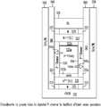
- FIG. 1shows a cross-sectional view of various material layers along the Y-direction (which is parallel to the planar surface of the semiconductor substrate) in memory structure 500 , according to one embodiment of the present invention.
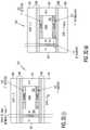
- FIGS. 2A, 2B & 2Ceach illustrate, schematically, an improved device structure of a pair of side-by-side thin-film storage transistors in a NOR memory string that may be formed using the processes taught, for example, in Provisional Application III.
- the charge trapping layers, gate conductors, and the low-resistivity conductors that are strapped to the common N+ source and drain layersare omitted.
- FIGS. 2D (i) and 2 D(ii)illustrate schematically, another improved device structure 550 of the thin-film storage transistors in a NOR memory string, in accordance with one embodiment of the present invention.
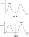
- FIG. 3Ashows that, at a boron dopant concentration of 1.0 ⁇ 10 18 cm ⁇ 3 .
- the intrinsic threshold voltageis around 2.0 volts, so that a programmed state may be set at a higher voltage than the intrinsic threshold voltage.
- FIG. 3Bshows that, at a boron dopant concentration greater than 1.0 ⁇ 10 18 cm ⁇ 3 , where the mean intrinsic threshold voltage is 3.0-6.0 volts, the programmed state can be designated as the state having a threshold voltage that is lower than the intrinsic mean threshold voltage state (which normally would be designated as the “erased” state).
- FIGS. 4A, 4B, 4C & 4Deach illustrate, according to one embodiment of the present invention, embedding a P-doped semiconductor strip (or a P-doped semiconductor body) within the structure of thin film storage transistors to provide a supply of holes during an erase operation in a selected transistor.
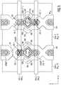
- FIG. 5shows storage transistors 684 and 685 of one or more vertical NOR memory strings, in accordance with one embodiment of the present invention.
- the present inventionprovides one or more sources of holes in close proximity to a floating P ⁇ channel in a thin-film storage transistor in order to facilitate a more efficient erase operation.
- One way to supply excess holes to a channel region to facilitate eraseis by generating holes using the well-known GIDL mechanism (GIDL is the acronym for “gate-induced drain leakage current”). Although it is a relatively slow mechanism (typically a few milliseconds), GIDL is employed extensively in 3-D NAND memory structures to generate holes in the channel region during an erase operation. GIDL bias conditions can be employed equally well to generate excess holes during an erase operation for the thin-film transistors disclosed in the Related Applications.
- the GIDL mechanismcan be applied whether erasing an entire thin-film transistor string or individually selected thin-film transistors.
- Non-provisional Application Idiscloses providing optional connection 290 to P ⁇ sublayers 222 to access back-bias voltage V bb , from substrate 201.
- paragraph [0072]teaches: “ . . .
- a high positive V bb voltagecan be applied during an erase operation to tunnel-erase TFTs whose control gates are held at ground potential . . . .”
- Non-provisional Application IIteaches: “ . . .
- buried contact 556optionally connects P ⁇ body region on the active strip to body bias source 506 (V bb ) in the substrate . . . .” Connecting the P ⁇ channels to the bulk P substrate is a viable source of excess holes for erasing a vertical NOR thin film transistor string but is somewhat more complicated to implement with a horizontal NOR thin film transistor string.
- patterningrefers to (i) providing a masking layer (e.g., a photoresist layer or a hard mask layer) over the target layer, and (ii) creating a pattern in the masking layer using suitable photolithography techniques.
- the pattern created in the masking layeris typically transferred to one or more target layers using one or more etching steps.
- memory structures and methods of fabricating the memory structures over a semiconductor substrateare described as illustrative examples of the present invention.
- various devices and circuitryare formed on or in the semiconductor substrate using conventional techniques.
- One or more layers of individually addressed conductorsmay be provided to connect bit lines and other electrical elements of the memory structure to devices or circuitry on or in the semiconductor substrate and may be formed beneath or above the memory structure.
- the layers of conductorsare insulated from each other by a dielectric material, which is provided between the conductors and between the layers of conductor.
- the surface of the dielectricis then planarized using, for example, chemical-mechanical polishing (CMP), known to those skilled in the art.
- CMPchemical-mechanical polishing
- this planarized surfaceis represented by the surface of dielectric layer 201 .
- the surface of dielectric layer 201defines an X-Y plane—X and Y being mutually orthogonal directions parallel to the surface of dielectric layer 201 —and the direction perpendicular to the X-Y plane defines the Z direction.
- FIG. 1shows a Y-Z cross-sectional view of various material layers in memory structure 500 , according to one embodiment of the present invention.
- active layers 502 - 0 to 502 - 7are provided, each active layer including drain sublayer 521 , source sublayer 523 and sacrificial material 1 (“SAC1”) sublayer 522 (to be subsequently partially or completely replaced by a channel sublayer).
- SAC1sacrificial material 1
- SAC4sacrificial material 4 sublayer 524 is provided, to be subsequently replaced by a conductive sublayer which electrically contacts drain sublayer 521 throughout substantially its entire length.
- Sacrificial material 4can also be provided (not shown) adjacent to source layers 523 to be also subsequently replaced by a conductor sublayer which electrically contacts portions of, or substantially the entire length of, source sublayer 523 .
- the conductive sublayer replacing sacrificial material 4provides a low-resistivity path for its adjacent source or drain sublayer. Initially, the material layers of memory structure 500 are deposited over the entire surface of planarized dielectric layer 201 .
- Deep trenchesare then etched in the material layers (e.g., lengthwise along the Y direction and along the Z direction in depth to buried contacts in dielectric layer 201 , or even through dielectric layer 201 to expose conductors in dielectric layer 201 to contacts formed on the surface of the semiconductor substrate, or both) to form individual stacks of the material layers (“active stacks”) separated from each other along the X direction.
- each active stackeach active layers form a strip of material layers (“active strip”).
- FIG. 1may represent, for example, a cross section in the Y-Z plane through an active stack.
- Storage transistorsare then formed out of each active strip in each active stack along one or both side walls of the active strip.
- the storage transistorsmay be organized as multiple NOR memory strings each extending along the Y direction.
- sacrificial sublayer 522is recessed along its length in the Y direction, or completely excavated, so that a lightly-doped polysilicon may be deposited to fill the resulting void, thus forming channel regions that are in contact with the common source and drain regions
- a charge-trapping materiale.g., an ONO multi-layer
- word linesare formed as conductor columns in the trenches, each extending along the Z directions and arrayed side-by-side along the Y direction.
- Each storage transistor of the NOR memory stringis thus formed by (i) a common source region, provided by source sublayer 523 of an active strip, (ii) a common drain region (“bit line”), provided by drain sublayer 521 of the active strip, (iii) a channel region, provided by a portion of the lightly-doped polysilicon in the recess or excavated cavity of sacrificial layer 522 , (iv) a charge trapping material (e.g., an ONO multi-layer), and (v) a gate terminal, provided by one of the conductor columns.
- the source and drain regionsare interchangeable with each other—i.e. region 523 can serve as the drain region and region 521 can serve as the source region.
- FIGS. 3-11 and 12A-12D of Provisional Application IIIin conjunction with the description of the specification therein, illustrate a process that forms NOR memory strings that extend along a direction (e.g., Y direction) parallel to the surface of a semiconductor substrate.
- FIGS. 2A-2Cillustrate schematically, in accordance with embodiments of the present invention, improved device structures of the thin-film storage transistors in a NOR memory string that may be formed, with slight modifications, using the processes taught in Provisional Application III, for example.
- the charge trapping materiale.g., an ONO multi-layer
- the gate terminalse.g., the gate terminals
- the conductor layerse.g., conductor layer 524 illustrated in FIG. 1
- strapping source layer 523 and drain layer 521are not shown for reasons of highlighting only features in focus; these omitted elements; however, are understood to be present and required for proper device operations.
- a P ⁇ doped polysilicon material 222is provided as a channel material in the recessed portions of sacrificial sublayer (SAC1) 522 .
- the boron dopant concentration in the channel regionis typically around 10 18 (e.g., 1.0 ⁇ 10 17 cm ⁇ 3 -1.5 ⁇ 10 18 cm ⁇ 3 ), which provides a mean threshold voltage (“mean intrinsic threshold voltage”) of 1.5-2.0 volts, with the corresponding charge-trapping material being uncharged.
- mean intrinsic threshold voltagee.g., 1.5-2.0 volts
- Increasing the thickness of the channel materiale.g., to greater than 10 nm both widens the spread of the threshold voltage distribution in both the programmed and erased state and weakens the “macaroni” effect 1 known to a person of ordinary skill in the art.
- the “macaroni” effectrefers to the substantial reduction in the parasitic subthreshold leakage current of the transistor when the channel region is sufficiently thin (e.g., 20 nm or less) as to be completely depleted during the transistor's non-conducting state.
- the mean intrinsic threshold voltageis typically less than 2.0 volts, and the programmed state may be set at a higher voltage than 2.0 volts, as illustrated in FIG. 3A .
- V Rread-voltage
- polysilicon material 222 of FIG. 2Amay be provided a higher boron dopant concentration (e.g., 5.0 ⁇ 10 18 cm ⁇ 3 to 1.0 ⁇ 10 19 cm ⁇ 3 ) than a conventional thin-film storage transistor.
- the mean intrinsic threshold voltageis between 3.0-6.0 volts.
- An alternative to a programmed state having a mean threshold voltage that is above the mean intrinsic threshold voltage of around 3.0-6.0 voltsmay be achieved by designating the mean intrinsic threshold voltage as the programmed state and a lower mean threshold voltage state as the erased state, as illustrated in FIG. 3B . As shown in FIG.
- N + common drain and source regions 521 and 523may each be 40 nm thick along the vertical or Z direction
- sacrificial layer 522may be 80 nm thick (along the Z-direction) about 30 nm wide (along a horizontal or X-direction)
- P-doped polysilicon 222may be 9.0-13.0 nm thick (along the horizontal or X direction)
- the number of thin-film storage transistors along the Y direction in each NOR memory stringmay be 1000 or more.
- Each NOR memory stringis isolated from other NOR memory strings above or below it by interlayer dielectric 503 .
- P-doped polysilicon 222When P-doped polysilicon 222 has a boron dopant concentration of 1.0 ⁇ 10 19 cm ⁇ 3 and its thickness along the Z-direction is greater than the depleted region of a PN junction, it is estimated 40 free charge carriers may be available in the channel region of each thin-film storage transistor, so that the total free charge carriers in the shared channel regions of the NOR memory string approximate 40,000, contributing to an enhanced erase efficiency.
- one or both of common drain and source regions 521 and 523may also include a 30 nm sacrificial layer 524 , which may be replaced by a high conductivity layer (e.g., tungsten (W)) prior or subsequent to deposition of P-doped polysilicon 222 .
- a high conductivity layere.g., tungsten (W)
- FIG. 2Bshows, in one embodiment of the present invention, N + common drain sublayer 521 being implemented as N + sublayer 521 a and P ⁇ sublayer 521 b , each being about 20 nm thick, with P-doped sublayer 521 b to be adjacent and in contact with P-doped polysilicon 222 to supply additional free charge carriers to the channel region of the storage transistor being erased.
- P + sublayer 521 bmay have the same or higher boron dopant concentration as P ⁇ -doped polysilicon layer 222 (e.g., 1.0 ⁇ 10 19 cm ⁇ 3 ).
- each thin-film storage transistorwould have 920 free charge carriers in the channel region, with a total of 920,000 free carriers per NOR memory string.
- P + layer 521 baids in the erase operation, a high boron concentration or an excessive thickness may hinder the formation of a continuous inverted channel between the source region (i.e., N + polysilicon) 523 and the drain region (N + polysilicon 521 a ) in a read operation. Care must also be taken to avoid excessive diffusion of dopants between N + polysilicon 521 a and P + polysilicon 521 b during any high temperature manufacturing processing step.
- Such cross diffusioncan be mitigated considerably by depositing or growing an ultra-thin dopant diffusion-blocking dielectric (not shown), typically 1-3 nm thick silicon oxide or silicon nitride between N + polysilicon 521 a and P + polysilicon 521 b (see below).
- an ultra-thin dopant diffusion-blocking dielectrictypically 1-3 nm thick silicon oxide or silicon nitride between N + polysilicon 521 a and P + polysilicon 521 b (see below).
- FIG. 2Cshows, in one embodiment of the present invention, sacrificial layer 522 being completely replaced by P-doped polysilicon body 520 (e.g., with a boron dopant concentration of up to around 1.0 ⁇ 10 19 cm ⁇ 3 ).
- P-doped polysilicon body 520e.g., with a boron dopant concentration of up to around 1.0 ⁇ 10 19 cm ⁇ 3 .
- the macaroni effectis diminished and the native threshold voltage is quite high (e.g. 3.0-6.0 volts)
- each thin-film storage transistorwould have 9000 free charge carriers (holes) in the channel region, for a total of 9 million or more free charge carriers in the channel regions of the NOR memory string.
- FIGS. 2D (i) and 2 D(ii)illustrate schematically, another improved device structure 550 of the thin-film storage transistors in a NOR memory string, in accordance with one embodiment of the present invention.
- P + layer 551is separated from sacrificial layer 522 by N + common source layer 553 .
- sacrificial layer 522is recessed or excavated at a subsequent step and filled by an undoped or P ⁇ -doped material 222 (e.g., boron, at 1.0 ⁇ 10 17 cm ⁇ 3 to around 1.5 ⁇ 10 18 cm ⁇ 3 ), which serves as a channel material in the completed device.
- P ⁇ -doped material 222e.g., boron, at 1.0 ⁇ 10 17 cm ⁇ 3 to around 1.5 ⁇ 10 18 cm ⁇ 3
- N + common source region 553has a lower dopant concentration (e.g., arsenic, at 1.0 ⁇ 10 18 cm ⁇ 3 to 1.0 ⁇ 10 19 cm ⁇ 3 ) than N ++ common drain layer 552 (e.g., 1.0 ⁇ 10 20 cm ⁇ 3 ).
- P + layer 551has a dopant concentration (e.g., boron, at 1.0 ⁇ 10 18 cm ⁇ 3 to 1.0 ⁇ 10 19 cm ⁇ 3 ) that is approximately equal to the dopant concentration of N + common source layer 553 .
- a depletion layer 570naturally forms between P + layer 551 and N + common source layer 553 . As in the devices in FIGS.
- the material layers of device structure 550may be formed by layer-by-layer depositions, using the processes of Provisional Applications II and III.
- FIG. 2D (i)also shows the charge-trapping layers 560 and gate electrodes 558 , provided on the side walls of device structure 550 and adjacent charge-trapping layers 560 , respectively.
- a thin-film storage transistor having device structure 550 of FIG. 2D (i), as shown,has a mean intrinsic threshold voltage of typically less than 2.0 volts. Such a device may be programmed to threshold voltages higher than 2.0 volts.
- gate electrode 558is biased to a read voltage slightly above the device's threshold voltage (e.g., 2.0 to 4.0 volts).
- the voltage at gate electrode 558is set to a relatively high value (e.g., 10.0 to 15.0 volts), while N + common source layer 553 , P + layer 551 and the N + common drain layer 552 are biased at or near the ground reference voltage.
- the surface of undoped or P ⁇ material at the interface with charge-trapping material 560(e.g., an ONO multi-layer) is inverted (i.e., becomes N-type conductivity) to provide a conduction path between N + common source layer 553 and N + common drain layer 552 .
- charge-trapping material 560e.g., an ONO multi-layer
- the inverted N-type conductivity layer ends on N + common source layer 553 and the P + layer 551is isolated and does not affect the device operation of the thin-film storage transistor.
- FIG. 2D (ii)illustrates device structure 550 of FIG. 2D (ii) during an erase operation.
- gate electrode 558is biased to a relatively large negative value (e.g., between ⁇ 15.0 and ⁇ 10.0 volts), while N + common source layer 553 , P + layer 551 and N + common drain layer 552 are biased at a low voltage (e.g., the ground reference voltage).
- N + common source layer 553 and undoped or P ⁇ layer 222electrons at the surface of N + common source layer 553 and undoped or P ⁇ layer 222 , are driven away, so that the surface of N + common source layer 553 at the interface with charge-trapping material 560 (e.g., an ONO multi-layer) becomes inverted (i.e., P-type conductivity) and the surface of undoped or P ⁇ layer 222 at the interface with charge-trapping layer 560 becomes accumulated.
- charge carrierse.g., holes
- P + layer 551 to undoped or P ⁇ layer 222to facilitate the erase operation.
- N + common drain layer 552 , N + common source layer 553 and P + layer 551are biased to a high positive voltage (e.g., 10.0-15.0 volts).
- Non-provisional Application Hdiscloses storage transistors TFT 685 (T L ) and TFT 584 (T R ) of the same or a pair of vertical NOR strings, storage transistor having a P ⁇ -doped polysilicon layer ( 656 L or 656 R) channel region between N + common source line 655 and N + common drain line 654 .
- the channel regionsi.e., P ⁇ -doped polysilicon layers 656 L and 656 R are provided on the surface of a dielectric core (i.e., isolation material 640 ).
- the present inventionmay be incorporated into the storage transistors of vertical NOR memory strings, as illustrated in FIG. 5 .
- in situ boron-doped P ++ region 520 ais provided as a P + body to supply holes to P ⁇ channel layers 656 L and 656 R.
- an ultra-thin diffusion barrier layer 550is also provided to prevent out-diffusion of dopants from P ++ region 520 to P ⁇ channel regions 656 L and 656 R.
- the holes supplied from P ++ region 520 to R channel regions 656 L or 656 Rdraw electrons trapped in charge trapping layer 634 to direct-tunnel out (as indicated by arrow 540 c ) into depleted P ⁇ doped channel 656 R or 656 L.
- all storage transistors of a NOR memory stringmay be erased in parallel, if desired. (Storage transistors may be inhibited from erase by providing their gate electrodes a non-erase bias voltage or left floating).
- the localized P + body region of the present inventioncan be similarly applied to vertical 3-D NAND-type memory structures to enhance erase efficiency in NAND series transistors sharing a vertical P ⁇ channel layer (“NAND memory string”).
- NAND memory stringa vertical P ⁇ channel layer
- the holes at the center of a conventional memory structure for a vertical NAND memory stringhas a cylindrical dielectric core with a thin polysilicon P ⁇ channel (e.g., 6-9 nm) provided on its surface.
- the dielectric coremay comprise an oxide, a nitride or air).
- the P ⁇ channeltakes advantage of the macaroni effect seen with fully depleted P ⁇ channel along the full height of the NAND memory string.
- holesmay be generated, for example, using a GIDL biasing technique using designated transistors provided at the top or bottom (or both) of the memory structure.
- the holesthus generated make their way through the entire length of the highly resistive P ⁇ channel, which is a rather inefficient process that can require milliseconds to completely erase the storage transistors of the NAND memory string.
- a P ⁇ bodyis provided instead of the dielectric core; however, while the P ⁇ body facilitates hole movements along the length of the memory structure, the advantages of the macaroni effect is sacrificed, as it is difficult to completely deplete the P ⁇ body.
- the present inventionprovides 3-D memory structure for NAND memory strings that can greatly improve erase efficiency.
- ultra-thin diffusion barrier layere.g., diffusion barrier layers 522 a and 522 b
- dopant out-diffusion from N + common source or common drain regionswould not contaminate the P-doped body.
- an adverse impact on mean threshold voltage in the resulting thin-film storage transistormay be avoided.
- dopant profiles in the N + common drain and source regionse.g., arsenic
- P-doped bodye.g., boron
Landscapes
- Engineering & Computer Science (AREA)
- Microelectronics & Electronic Packaging (AREA)
- Computer Hardware Design (AREA)
- Non-Volatile Memory (AREA)
- Semiconductor Memories (AREA)
Abstract
Description
Claims (38)
Priority Applications (1)
| Application Number | Priority Date | Filing Date | Title |
|---|---|---|---|
| US16/509,282US11069696B2 (en) | 2018-07-12 | 2019-07-11 | Device structure for a 3-dimensional NOR memory array and methods for improved erase operations applied thereto |
Applications Claiming Priority (2)
| Application Number | Priority Date | Filing Date | Title |
|---|---|---|---|
| US201862697060P | 2018-07-12 | 2018-07-12 | |
| US16/509,282US11069696B2 (en) | 2018-07-12 | 2019-07-11 | Device structure for a 3-dimensional NOR memory array and methods for improved erase operations applied thereto |
Publications (2)
| Publication Number | Publication Date |
|---|---|
| US20200051990A1 US20200051990A1 (en) | 2020-02-13 |
| US11069696B2true US11069696B2 (en) | 2021-07-20 |
Family
ID=69406789
Family Applications (1)
| Application Number | Title | Priority Date | Filing Date |
|---|---|---|---|
| US16/509,282ActiveUS11069696B2 (en) | 2018-07-12 | 2019-07-11 | Device structure for a 3-dimensional NOR memory array and methods for improved erase operations applied thereto |
Country Status (1)
| Country | Link |
|---|---|
| US (1) | US11069696B2 (en) |
Cited By (1)
| Publication number | Priority date | Publication date | Assignee | Title |
|---|---|---|---|---|
| US20220199643A1 (en)* | 2017-06-20 | 2022-06-23 | Sunrise Memory Corporation | 3-dimensional nor memory array architecture and methods for fabrication thereof |
Families Citing this family (183)
| Publication number | Priority date | Publication date | Assignee | Title |
|---|---|---|---|---|
| US10910364B2 (en) | 2009-10-12 | 2021-02-02 | Monolitaic 3D Inc. | 3D semiconductor device |
| US11984445B2 (en) | 2009-10-12 | 2024-05-14 | Monolithic 3D Inc. | 3D semiconductor devices and structures with metal layers |
| US11018133B2 (en) | 2009-10-12 | 2021-05-25 | Monolithic 3D Inc. | 3D integrated circuit |
| US11374118B2 (en) | 2009-10-12 | 2022-06-28 | Monolithic 3D Inc. | Method to form a 3D integrated circuit |
| US12027518B1 (en) | 2009-10-12 | 2024-07-02 | Monolithic 3D Inc. | 3D semiconductor devices and structures with metal layers |
| US11482440B2 (en) | 2010-12-16 | 2022-10-25 | Monolithic 3D Inc. | 3D semiconductor device and structure with a built-in test circuit for repairing faulty circuits |
| US12362219B2 (en) | 2010-11-18 | 2025-07-15 | Monolithic 3D Inc. | 3D semiconductor memory device and structure |
| US11158674B2 (en) | 2010-10-11 | 2021-10-26 | Monolithic 3D Inc. | Method to produce a 3D semiconductor device and structure |
| US11315980B1 (en) | 2010-10-11 | 2022-04-26 | Monolithic 3D Inc. | 3D semiconductor device and structure with transistors |
| US11469271B2 (en) | 2010-10-11 | 2022-10-11 | Monolithic 3D Inc. | Method to produce 3D semiconductor devices and structures with memory |
| US11600667B1 (en) | 2010-10-11 | 2023-03-07 | Monolithic 3D Inc. | Method to produce 3D semiconductor devices and structures with memory |
| US11024673B1 (en) | 2010-10-11 | 2021-06-01 | Monolithic 3D Inc. | 3D semiconductor device and structure |
| US11227897B2 (en) | 2010-10-11 | 2022-01-18 | Monolithic 3D Inc. | Method for producing a 3D semiconductor memory device and structure |
| US10896931B1 (en) | 2010-10-11 | 2021-01-19 | Monolithic 3D Inc. | 3D semiconductor device and structure |
| US11257867B1 (en) | 2010-10-11 | 2022-02-22 | Monolithic 3D Inc. | 3D semiconductor device and structure with oxide bonds |
| US11018191B1 (en) | 2010-10-11 | 2021-05-25 | Monolithic 3D Inc. | 3D semiconductor device and structure |
| US11437368B2 (en) | 2010-10-13 | 2022-09-06 | Monolithic 3D Inc. | Multilevel semiconductor device and structure with oxide bonding |
| US10978501B1 (en) | 2010-10-13 | 2021-04-13 | Monolithic 3D Inc. | Multilevel semiconductor device and structure with waveguides |
| US12360310B2 (en) | 2010-10-13 | 2025-07-15 | Monolithic 3D Inc. | Multilevel semiconductor device and structure with oxide bonding |
| US12080743B2 (en) | 2010-10-13 | 2024-09-03 | Monolithic 3D Inc. | Multilevel semiconductor device and structure with image sensors and wafer bonding |
| US11133344B2 (en) | 2010-10-13 | 2021-09-28 | Monolithic 3D Inc. | Multilevel semiconductor device and structure with image sensors |
| US10833108B2 (en) | 2010-10-13 | 2020-11-10 | Monolithic 3D Inc. | 3D microdisplay device and structure |
| US11163112B2 (en) | 2010-10-13 | 2021-11-02 | Monolithic 3D Inc. | Multilevel semiconductor device and structure with electromagnetic modulators |
| US11929372B2 (en) | 2010-10-13 | 2024-03-12 | Monolithic 3D Inc. | Multilevel semiconductor device and structure with image sensors and wafer bonding |
| US11869915B2 (en) | 2010-10-13 | 2024-01-09 | Monolithic 3D Inc. | Multilevel semiconductor device and structure with image sensors and wafer bonding |
| US11984438B2 (en) | 2010-10-13 | 2024-05-14 | Monolithic 3D Inc. | Multilevel semiconductor device and structure with oxide bonding |
| US10943934B2 (en) | 2010-10-13 | 2021-03-09 | Monolithic 3D Inc. | Multilevel semiconductor device and structure |
| US11327227B2 (en) | 2010-10-13 | 2022-05-10 | Monolithic 3D Inc. | Multilevel semiconductor device and structure with electromagnetic modulators |
| US12094892B2 (en) | 2010-10-13 | 2024-09-17 | Monolithic 3D Inc. | 3D micro display device and structure |
| US11855100B2 (en) | 2010-10-13 | 2023-12-26 | Monolithic 3D Inc. | Multilevel semiconductor device and structure with oxide bonding |
| US11063071B1 (en) | 2010-10-13 | 2021-07-13 | Monolithic 3D Inc. | Multilevel semiconductor device and structure with waveguides |
| US10998374B1 (en) | 2010-10-13 | 2021-05-04 | Monolithic 3D Inc. | Multilevel semiconductor device and structure |
| US11043523B1 (en) | 2010-10-13 | 2021-06-22 | Monolithic 3D Inc. | Multilevel semiconductor device and structure with image sensors |
| US11164898B2 (en) | 2010-10-13 | 2021-11-02 | Monolithic 3D Inc. | Multilevel semiconductor device and structure |
| US11855114B2 (en) | 2010-10-13 | 2023-12-26 | Monolithic 3D Inc. | Multilevel semiconductor device and structure with image sensors and wafer bonding |
| US11605663B2 (en) | 2010-10-13 | 2023-03-14 | Monolithic 3D Inc. | Multilevel semiconductor device and structure with image sensors and wafer bonding |
| US11694922B2 (en) | 2010-10-13 | 2023-07-04 | Monolithic 3D Inc. | Multilevel semiconductor device and structure with oxide bonding |
| US11404466B2 (en) | 2010-10-13 | 2022-08-02 | Monolithic 3D Inc. | Multilevel semiconductor device and structure with image sensors |
| US11923230B1 (en) | 2010-11-18 | 2024-03-05 | Monolithic 3D Inc. | 3D semiconductor device and structure with bonding |
| US11901210B2 (en) | 2010-11-18 | 2024-02-13 | Monolithic 3D Inc. | 3D semiconductor device and structure with memory |
| US11862503B2 (en) | 2010-11-18 | 2024-01-02 | Monolithic 3D Inc. | Method for producing a 3D semiconductor device and structure with memory cells and multiple metal layers |
| US11443971B2 (en) | 2010-11-18 | 2022-09-13 | Monolithic 3D Inc. | 3D semiconductor device and structure with memory |
| US11094576B1 (en) | 2010-11-18 | 2021-08-17 | Monolithic 3D Inc. | Methods for producing a 3D semiconductor memory device and structure |
| US11482439B2 (en) | 2010-11-18 | 2022-10-25 | Monolithic 3D Inc. | Methods for producing a 3D semiconductor memory device comprising charge trap junction-less transistors |
| US11521888B2 (en) | 2010-11-18 | 2022-12-06 | Monolithic 3D Inc. | 3D semiconductor device and structure with high-k metal gate transistors |
| US12033884B2 (en) | 2010-11-18 | 2024-07-09 | Monolithic 3D Inc. | Methods for producing a 3D semiconductor device and structure with memory cells and multiple metal layers |
| US11004719B1 (en) | 2010-11-18 | 2021-05-11 | Monolithic 3D Inc. | Methods for producing a 3D semiconductor memory device and structure |
| US11495484B2 (en) | 2010-11-18 | 2022-11-08 | Monolithic 3D Inc. | 3D semiconductor devices and structures with at least two single-crystal layers |
| US11018042B1 (en) | 2010-11-18 | 2021-05-25 | Monolithic 3D Inc. | 3D semiconductor memory device and structure |
| US11610802B2 (en) | 2010-11-18 | 2023-03-21 | Monolithic 3D Inc. | Method for producing a 3D semiconductor device and structure with single crystal transistors and metal gate electrodes |
| US11164770B1 (en) | 2010-11-18 | 2021-11-02 | Monolithic 3D Inc. | Method for producing a 3D semiconductor memory device and structure |
| US11569117B2 (en) | 2010-11-18 | 2023-01-31 | Monolithic 3D Inc. | 3D semiconductor device and structure with single-crystal layers |
| US11107721B2 (en) | 2010-11-18 | 2021-08-31 | Monolithic 3D Inc. | 3D semiconductor device and structure with NAND logic |
| US12068187B2 (en) | 2010-11-18 | 2024-08-20 | Monolithic 3D Inc. | 3D semiconductor device and structure with bonding and DRAM memory cells |
| US11735462B2 (en) | 2010-11-18 | 2023-08-22 | Monolithic 3D Inc. | 3D semiconductor device and structure with single-crystal layers |
| US11784082B2 (en) | 2010-11-18 | 2023-10-10 | Monolithic 3D Inc. | 3D semiconductor device and structure with bonding |
| US11854857B1 (en) | 2010-11-18 | 2023-12-26 | Monolithic 3D Inc. | Methods for producing a 3D semiconductor device and structure with memory cells and multiple metal layers |
| US12100611B2 (en) | 2010-11-18 | 2024-09-24 | Monolithic 3D Inc. | Methods for producing a 3D semiconductor device and structure with memory cells and multiple metal layers |
| US12136562B2 (en) | 2010-11-18 | 2024-11-05 | Monolithic 3D Inc. | 3D semiconductor device and structure with single-crystal layers |
| US11615977B2 (en) | 2010-11-18 | 2023-03-28 | Monolithic 3D Inc. | 3D semiconductor memory device and structure |
| US11804396B2 (en) | 2010-11-18 | 2023-10-31 | Monolithic 3D Inc. | Methods for producing a 3D semiconductor device and structure with memory cells and multiple metal layers |
| US11508605B2 (en) | 2010-11-18 | 2022-11-22 | Monolithic 3D Inc. | 3D semiconductor memory device and structure |
| US12125737B1 (en) | 2010-11-18 | 2024-10-22 | Monolithic 3D Inc. | 3D semiconductor device and structure with metal layers and memory cells |
| US12243765B2 (en) | 2010-11-18 | 2025-03-04 | Monolithic 3D Inc. | 3D semiconductor device and structure with metal layers and memory cells |
| US12154817B1 (en) | 2010-11-18 | 2024-11-26 | Monolithic 3D Inc. | Methods for producing a 3D semiconductor memory device and structure |
| US11355381B2 (en) | 2010-11-18 | 2022-06-07 | Monolithic 3D Inc. | 3D semiconductor memory device and structure |
| US11031275B2 (en) | 2010-11-18 | 2021-06-08 | Monolithic 3D Inc. | 3D semiconductor device and structure with memory |
| US11211279B2 (en) | 2010-11-18 | 2021-12-28 | Monolithic 3D Inc. | Method for processing a 3D integrated circuit and structure |
| US11355380B2 (en) | 2010-11-18 | 2022-06-07 | Monolithic 3D Inc. | Methods for producing 3D semiconductor memory device and structure utilizing alignment marks |
| US11482438B2 (en) | 2010-11-18 | 2022-10-25 | Monolithic 3D Inc. | Methods for producing a 3D semiconductor memory device and structure |
| US12272586B2 (en) | 2010-11-18 | 2025-04-08 | Monolithic 3D Inc. | 3D semiconductor memory device and structure with memory and metal layers |
| US12144190B2 (en) | 2010-11-18 | 2024-11-12 | Monolithic 3D Inc. | 3D semiconductor device and structure with bonding and memory cells preliminary class |
| US11088050B2 (en) | 2012-04-09 | 2021-08-10 | Monolithic 3D Inc. | 3D semiconductor device with isolation layers |
| US11476181B1 (en) | 2012-04-09 | 2022-10-18 | Monolithic 3D Inc. | 3D semiconductor device and structure with metal layers |
| US11735501B1 (en) | 2012-04-09 | 2023-08-22 | Monolithic 3D Inc. | 3D semiconductor device and structure with metal layers and a connective path |
| US11881443B2 (en) | 2012-04-09 | 2024-01-23 | Monolithic 3D Inc. | 3D semiconductor device and structure with metal layers and a connective path |
| US11164811B2 (en) | 2012-04-09 | 2021-11-02 | Monolithic 3D Inc. | 3D semiconductor device with isolation layers and oxide-to-oxide bonding |
| US11694944B1 (en) | 2012-04-09 | 2023-07-04 | Monolithic 3D Inc. | 3D semiconductor device and structure with metal layers and a connective path |
| US11616004B1 (en) | 2012-04-09 | 2023-03-28 | Monolithic 3D Inc. | 3D semiconductor device and structure with metal layers and a connective path |
| US11594473B2 (en) | 2012-04-09 | 2023-02-28 | Monolithic 3D Inc. | 3D semiconductor device and structure with metal layers and a connective path |
| US11410912B2 (en) | 2012-04-09 | 2022-08-09 | Monolithic 3D Inc. | 3D semiconductor device with vias and isolation layers |
| US11063024B1 (en) | 2012-12-22 | 2021-07-13 | Monlithic 3D Inc. | Method to form a 3D semiconductor device and structure |
| US11916045B2 (en) | 2012-12-22 | 2024-02-27 | Monolithic 3D Inc. | 3D semiconductor device and structure with metal layers |
| US11217565B2 (en) | 2012-12-22 | 2022-01-04 | Monolithic 3D Inc. | Method to form a 3D semiconductor device and structure |
| US11967583B2 (en) | 2012-12-22 | 2024-04-23 | Monolithic 3D Inc. | 3D semiconductor device and structure with metal layers |
| US12051674B2 (en) | 2012-12-22 | 2024-07-30 | Monolithic 3D Inc. | 3D semiconductor device and structure with metal layers |
| US11784169B2 (en) | 2012-12-22 | 2023-10-10 | Monolithic 3D Inc. | 3D semiconductor device and structure with metal layers |
| US11018116B2 (en) | 2012-12-22 | 2021-05-25 | Monolithic 3D Inc. | Method to form a 3D semiconductor device and structure |
| US11309292B2 (en) | 2012-12-22 | 2022-04-19 | Monolithic 3D Inc. | 3D semiconductor device and structure with metal layers |
| US11961827B1 (en) | 2012-12-22 | 2024-04-16 | Monolithic 3D Inc. | 3D semiconductor device and structure with metal layers |
| US11087995B1 (en) | 2012-12-29 | 2021-08-10 | Monolithic 3D Inc. | 3D semiconductor device and structure |
| US11430668B2 (en) | 2012-12-29 | 2022-08-30 | Monolithic 3D Inc. | 3D semiconductor device and structure with bonding |
| US11177140B2 (en) | 2012-12-29 | 2021-11-16 | Monolithic 3D Inc. | 3D semiconductor device and structure |
| US11004694B1 (en) | 2012-12-29 | 2021-05-11 | Monolithic 3D Inc. | 3D semiconductor device and structure |
| US12249538B2 (en) | 2012-12-29 | 2025-03-11 | Monolithic 3D Inc. | 3D semiconductor device and structure including power distribution grids |
| US10903089B1 (en) | 2012-12-29 | 2021-01-26 | Monolithic 3D Inc. | 3D semiconductor device and structure |
| US11430667B2 (en) | 2012-12-29 | 2022-08-30 | Monolithic 3D Inc. | 3D semiconductor device and structure with bonding |
| US11869965B2 (en) | 2013-03-11 | 2024-01-09 | Monolithic 3D Inc. | 3D semiconductor device and structure with metal layers and memory cells |
| US12094965B2 (en) | 2013-03-11 | 2024-09-17 | Monolithic 3D Inc. | 3D semiconductor device and structure with metal layers and memory cells |
| US11935949B1 (en) | 2013-03-11 | 2024-03-19 | Monolithic 3D Inc. | 3D semiconductor device and structure with metal layers and memory cells |
| US8902663B1 (en) | 2013-03-11 | 2014-12-02 | Monolithic 3D Inc. | Method of maintaining a memory state |
| US11923374B2 (en) | 2013-03-12 | 2024-03-05 | Monolithic 3D Inc. | 3D semiconductor device and structure with metal layers |
| US12100646B2 (en) | 2013-03-12 | 2024-09-24 | Monolithic 3D Inc. | 3D semiconductor device and structure with metal layers |
| US11398569B2 (en) | 2013-03-12 | 2022-07-26 | Monolithic 3D Inc. | 3D semiconductor device and structure |
| US11088130B2 (en) | 2014-01-28 | 2021-08-10 | Monolithic 3D Inc. | 3D semiconductor device and structure |
| US10840239B2 (en) | 2014-08-26 | 2020-11-17 | Monolithic 3D Inc. | 3D semiconductor device and structure |
| US11720736B2 (en) | 2013-04-15 | 2023-08-08 | Monolithic 3D Inc. | Automation methods for 3D integrated circuits and devices |
| US11341309B1 (en) | 2013-04-15 | 2022-05-24 | Monolithic 3D Inc. | Automation for monolithic 3D devices |
| US11270055B1 (en) | 2013-04-15 | 2022-03-08 | Monolithic 3D Inc. | Automation for monolithic 3D devices |
| US11487928B2 (en) | 2013-04-15 | 2022-11-01 | Monolithic 3D Inc. | Automation for monolithic 3D devices |
| US11574109B1 (en) | 2013-04-15 | 2023-02-07 | Monolithic 3D Inc | Automation methods for 3D integrated circuits and devices |
| US11031394B1 (en) | 2014-01-28 | 2021-06-08 | Monolithic 3D Inc. | 3D semiconductor device and structure |
| US11107808B1 (en) | 2014-01-28 | 2021-08-31 | Monolithic 3D Inc. | 3D semiconductor device and structure |
| US12094829B2 (en) | 2014-01-28 | 2024-09-17 | Monolithic 3D Inc. | 3D semiconductor device and structure |
| US11056468B1 (en) | 2015-04-19 | 2021-07-06 | Monolithic 3D Inc. | 3D semiconductor device and structure |
| US10825779B2 (en) | 2015-04-19 | 2020-11-03 | Monolithic 3D Inc. | 3D semiconductor device and structure |
| US11011507B1 (en) | 2015-04-19 | 2021-05-18 | Monolithic 3D Inc. | 3D semiconductor device and structure |
| US11956952B2 (en) | 2015-08-23 | 2024-04-09 | Monolithic 3D Inc. | Semiconductor memory device and structure |
| US11114427B2 (en) | 2015-11-07 | 2021-09-07 | Monolithic 3D Inc. | 3D semiconductor processor and memory device and structure |
| US12100658B2 (en) | 2015-09-21 | 2024-09-24 | Monolithic 3D Inc. | Method to produce a 3D multilayer semiconductor device and structure |
| US11978731B2 (en) | 2015-09-21 | 2024-05-07 | Monolithic 3D Inc. | Method to produce a multi-level semiconductor memory device and structure |
| US12178055B2 (en) | 2015-09-21 | 2024-12-24 | Monolithic 3D Inc. | 3D semiconductor memory devices and structures |
| US12250830B2 (en) | 2015-09-21 | 2025-03-11 | Monolithic 3D Inc. | 3D semiconductor memory devices and structures |
| US11937422B2 (en) | 2015-11-07 | 2024-03-19 | Monolithic 3D Inc. | Semiconductor memory device and structure |
| US9892800B2 (en) | 2015-09-30 | 2018-02-13 | Sunrise Memory Corporation | Multi-gate NOR flash thin-film transistor strings arranged in stacked horizontal active strips with vertical control gates |
| US11120884B2 (en) | 2015-09-30 | 2021-09-14 | Sunrise Memory Corporation | Implementing logic function and generating analog signals using NOR memory strings |
| US9842651B2 (en) | 2015-11-25 | 2017-12-12 | Sunrise Memory Corporation | Three-dimensional vertical NOR flash thin film transistor strings |
| US10121553B2 (en) | 2015-09-30 | 2018-11-06 | Sunrise Memory Corporation | Capacitive-coupled non-volatile thin-film transistor NOR strings in three-dimensional arrays |
| US11296115B1 (en) | 2015-10-24 | 2022-04-05 | Monolithic 3D Inc. | 3D semiconductor device and structure |
| US12035531B2 (en) | 2015-10-24 | 2024-07-09 | Monolithic 3D Inc. | 3D semiconductor device and structure with logic and memory |
| US11114464B2 (en) | 2015-10-24 | 2021-09-07 | Monolithic 3D Inc. | 3D semiconductor device and structure |
| US12120880B1 (en) | 2015-10-24 | 2024-10-15 | Monolithic 3D Inc. | 3D semiconductor device and structure with logic and memory |
| US12219769B2 (en) | 2015-10-24 | 2025-02-04 | Monolithic 3D Inc. | 3D semiconductor device and structure with logic and memory |
| US11991884B1 (en) | 2015-10-24 | 2024-05-21 | Monolithic 3D Inc. | 3D semiconductor device and structure with logic and memory |
| US10847540B2 (en) | 2015-10-24 | 2020-11-24 | Monolithic 3D Inc. | 3D semiconductor memory device and structure |
| US12016181B2 (en) | 2015-10-24 | 2024-06-18 | Monolithic 3D Inc. | 3D semiconductor device and structure with logic and memory |
| US11930648B1 (en) | 2016-10-10 | 2024-03-12 | Monolithic 3D Inc. | 3D memory devices and structures with metal layers |
| US11329059B1 (en) | 2016-10-10 | 2022-05-10 | Monolithic 3D Inc. | 3D memory devices and structures with thinned single crystal substrates |
| US11812620B2 (en) | 2016-10-10 | 2023-11-07 | Monolithic 3D Inc. | 3D DRAM memory devices and structures with control circuits |
| US11869591B2 (en) | 2016-10-10 | 2024-01-09 | Monolithic 3D Inc. | 3D memory devices and structures with control circuits |
| US11251149B2 (en) | 2016-10-10 | 2022-02-15 | Monolithic 3D Inc. | 3D memory device and structure |
| US11711928B2 (en) | 2016-10-10 | 2023-07-25 | Monolithic 3D Inc. | 3D memory devices and structures with control circuits |
| US12225704B2 (en) | 2016-10-10 | 2025-02-11 | Monolithic 3D Inc. | 3D memory devices and structures with memory arrays and metal layers |
| US10692874B2 (en) | 2017-06-20 | 2020-06-23 | Sunrise Memory Corporation | 3-dimensional NOR string arrays in segmented stacks |
| US10608008B2 (en) | 2017-06-20 | 2020-03-31 | Sunrise Memory Corporation | 3-dimensional nor strings with segmented shared source regions |
| US10896916B2 (en) | 2017-11-17 | 2021-01-19 | Sunrise Memory Corporation | Reverse memory cell |
| WO2019133534A1 (en) | 2017-12-28 | 2019-07-04 | Sunrise Memory Corporation | 3-dimensional nor memory array with very fine pitch: device and method |
| US10475812B2 (en) | 2018-02-02 | 2019-11-12 | Sunrise Memory Corporation | Three-dimensional vertical NOR flash thin-film transistor strings |
| CN112567516B (en) | 2018-07-12 | 2025-02-25 | 日升存储公司 | Method for manufacturing three-dimensional NOR memory array |
| US11751391B2 (en) | 2018-07-12 | 2023-09-05 | Sunrise Memory Corporation | Methods for fabricating a 3-dimensional memory structure of nor memory strings |
| TWI713195B (en) | 2018-09-24 | 2020-12-11 | 美商森恩萊斯記憶體公司 | Wafer bonding in fabrication of 3-dimensional nor memory circuits and integrated circuit formed therefrom |
| EP3891780A4 (en) | 2018-12-07 | 2022-12-21 | Sunrise Memory Corporation | METHOD OF FABRICATION OF MULTILAYER VERTICAL NOR STORAGE STRING ARRAYS |
| WO2020160169A1 (en) | 2019-01-30 | 2020-08-06 | Sunrise Memory Corporation | Device with embedded high-bandwidth, high-capacity memory using wafer bonding |
| EP3925004A4 (en) | 2019-02-11 | 2023-03-08 | Sunrise Memory Corporation | VERTICAL THIN-FILM TRANSISTOR AND APPLICATION AS A BITLINE CONNECTOR FOR THREE-DIMENSIONAL MEMORY ARRAYS |
| US11018156B2 (en) | 2019-04-08 | 2021-05-25 | Monolithic 3D Inc. | 3D memory semiconductor devices and structures |
| US11158652B1 (en) | 2019-04-08 | 2021-10-26 | Monolithic 3D Inc. | 3D memory semiconductor devices and structures |
| US11763864B2 (en) | 2019-04-08 | 2023-09-19 | Monolithic 3D Inc. | 3D memory semiconductor devices and structures with bit-line pillars |
| US11296106B2 (en) | 2019-04-08 | 2022-04-05 | Monolithic 3D Inc. | 3D memory semiconductor devices and structures |
| US10892016B1 (en) | 2019-04-08 | 2021-01-12 | Monolithic 3D Inc. | 3D memory semiconductor devices and structures |
| US11917821B2 (en) | 2019-07-09 | 2024-02-27 | Sunrise Memory Corporation | Process for a 3-dimensional array of horizontal nor-type memory strings |
| WO2021007399A1 (en) | 2019-07-09 | 2021-01-14 | Sunrise Memory Corporation | Process for a 3-dimensional array of horizontal nor-type memory strings |
| WO2021127218A1 (en) | 2019-12-19 | 2021-06-24 | Sunrise Memory Corporation | Process for preparing a channel region of a thin-film transistor |
| TWI767512B (en) | 2020-01-22 | 2022-06-11 | 美商森恩萊斯記憶體公司 | Cool electron erasing in thin-film storage transistors |
| WO2021158994A1 (en) | 2020-02-07 | 2021-08-12 | Sunrise Memory Corporation | Quasi-volatile system-level memory |
| TWI836184B (en) | 2020-02-07 | 2024-03-21 | 美商森恩萊斯記憶體公司 | High capacity memory circuit with low effective latency |
| US11561911B2 (en) | 2020-02-24 | 2023-01-24 | Sunrise Memory Corporation | Channel controller for shared memory access |
| US11508693B2 (en) | 2020-02-24 | 2022-11-22 | Sunrise Memory Corporation | High capacity memory module including wafer-section memory circuit |
| US11507301B2 (en) | 2020-02-24 | 2022-11-22 | Sunrise Memory Corporation | Memory module implementing memory centric architecture |
| US11705496B2 (en) | 2020-04-08 | 2023-07-18 | Sunrise Memory Corporation | Charge-trapping layer with optimized number of charge-trapping sites for fast program and erase of a memory cell in a 3-dimensional NOR memory string array |
| US11729988B2 (en)* | 2020-06-18 | 2023-08-15 | Taiwan Semiconductor Manufacturing Company, Ltd. | Memory device comprising conductive pillars and method of forming the same |
| US11729987B2 (en)* | 2020-06-30 | 2023-08-15 | Taiwan Semiconductor Manufacturing Company, Ltd. | Memory array source/drain electrode structures |
| US11937424B2 (en) | 2020-08-31 | 2024-03-19 | Sunrise Memory Corporation | Thin-film storage transistors in a 3-dimensional array of nor memory strings and process for fabricating the same |
| US11545499B2 (en)* | 2020-10-06 | 2023-01-03 | International Business Machines Corporation | Read-only memory with vertical transistors |
| WO2022108848A1 (en) | 2020-11-17 | 2022-05-27 | Sunrise Memory Corporation | Methods for reducing disturb errors by refreshing data alongside programming or erase operations |
| US11848056B2 (en) | 2020-12-08 | 2023-12-19 | Sunrise Memory Corporation | Quasi-volatile memory with enhanced sense amplifier operation |
| US11980035B2 (en)* | 2021-03-04 | 2024-05-07 | Taiwan Semiconductor Manufacturing Company, Ltd. | Three-dimensional memory devices and methods of manufacturing thereof |
| US11856782B2 (en)* | 2021-03-04 | 2023-12-26 | Taiwan Semiconductor Manufacturing Co., Ltd. | Three-dimensional memory device and method |
| CN112909015B (en)* | 2021-03-08 | 2023-10-17 | 中国科学院微电子研究所 | NOR type memory device, method of manufacturing the same, and electronic apparatus including the same |
| TW202310429A (en) | 2021-07-16 | 2023-03-01 | 美商日升存儲公司 | 3-dimensional memory string array of thin-film ferroelectric transistors |
| US11647637B2 (en)* | 2021-08-20 | 2023-05-09 | Taiwan Semiconductor Manufacturing Company, Ltd. | Semiconductor memory devices and methods of manufacturing thereof |
| US12402319B2 (en) | 2021-09-14 | 2025-08-26 | Sunrise Memory Corporation | Three-dimensional memory string array of thin-film ferroelectric transistors formed with an oxide semiconductor channel |
| US20230078883A1 (en)* | 2021-09-14 | 2023-03-16 | Sunrise Memory Corporation | Three-dimensional memory string array of thin-film ferroelectric transistors formed with an oxide semiconductor channel in a channel last process |
| US20230262977A1 (en)* | 2022-02-15 | 2023-08-17 | Taiwan Semiconductor Manufacturing Company, Ltd. | Memory devices and methods of manufacturing thereof |
Citations (69)
| Publication number | Priority date | Publication date | Assignee | Title |
|---|---|---|---|---|
| US5656842A (en)* | 1995-06-20 | 1997-08-12 | Mitsubishi Denki Kabushiki Kaisha | Vertical mosfet including a back gate electrode |
| US5789776A (en) | 1995-09-22 | 1998-08-04 | Nvx Corporation | Single poly memory cell and array |
| US6107133A (en)* | 1998-05-28 | 2000-08-22 | International Business Machines Corporation | Method for making a five square vertical DRAM cell |
| US6118171A (en)* | 1998-12-21 | 2000-09-12 | Motorola, Inc. | Semiconductor device having a pedestal structure and method of making |
| US20010030340A1 (en) | 1998-11-04 | 2001-10-18 | Ichiro Fujiwara | Nonvolatile semiconductor memory device and process of production and write method thereof |
| US20010053092A1 (en) | 2000-06-12 | 2001-12-20 | Sony Corporation | Memory system and programming method thereof |
| US20020012271A1 (en) | 2000-02-29 | 2002-01-31 | Leonard Forbes | Static NVRAM with ultra thin tunnel oxides |
| US20020028541A1 (en)* | 2000-08-14 | 2002-03-07 | Lee Thomas H. | Dense arrays and charge storage devices, and methods for making same |
| US20020051378A1 (en) | 2000-08-17 | 2002-05-02 | Takashi Ohsawa | Semiconductor memory device and method of manufacturing the same |
| US6434053B1 (en) | 1999-12-06 | 2002-08-13 | Sony Corporation | Nonvolatile semiconductor memory device and method of operation thereof |
| US20030038318A1 (en) | 2001-08-24 | 2003-02-27 | Leonard Forbes | Vertical transistor with horizontal gate layers |
| US6580124B1 (en) | 2000-08-14 | 2003-06-17 | Matrix Semiconductor Inc. | Multigate semiconductor device with vertical channel current and method of fabrication |
| US20040246807A1 (en) | 2003-06-03 | 2004-12-09 | Seung-Hoon Lee | Multi-port memory device with stacked banks |
| US20040262681A1 (en)* | 2003-05-28 | 2004-12-30 | Fujio Masuoka | Semiconductor device |
| US20040264247A1 (en) | 2003-06-30 | 2004-12-30 | Kim Ki Seog | Method for reading flash memory cell, NAND-type flash memory apparatus, and NOR-type flash memory apparatus |
| US6873004B1 (en) | 2002-02-04 | 2005-03-29 | Nexflash Technologies, Inc. | Virtual ground single transistor memory cell, memory array incorporating same, and method of operation thereof |
| US20050128815A1 (en) | 2003-12-09 | 2005-06-16 | Renesas Technology Corp. | Semiconductor data processing device |
| US6946703B2 (en) | 2003-01-09 | 2005-09-20 | Samsung Electronics Co., Ltd. | SONOS memory device having side gate stacks and method of manufacturing the same |
| US20050280061A1 (en)* | 2004-06-21 | 2005-12-22 | Sang-Yun Lee | Vertical memory device structures |
| US20060155921A1 (en) | 2004-12-16 | 2006-07-13 | Gorobets Sergey A | Non-volatile memory and method with multi-stream update tracking |
| US20070134876A1 (en) | 2005-12-09 | 2007-06-14 | Macronix International Co., Ltd. | Stacked thin film transistor, non-volatile memory devices and methods for fabricating the same |
| US20080239812A1 (en) | 2007-03-30 | 2008-10-02 | Kabushiki Kaisha Toshiba | Nonvolatile semiconductor memory system |
| US7489002B2 (en)* | 2001-02-09 | 2009-02-10 | Micron Technology, Inc. | Memory having a vertical transistor |
| US20090057722A1 (en)* | 2007-05-30 | 2009-03-05 | Unisantis Electronics (Japan) Ltd. | Semiconductor device |
| US7524725B2 (en)* | 2005-03-31 | 2009-04-28 | Hynix Semiconductor Inc. | Vertical transistor of semiconductor device and method for forming the same |
| US7542348B1 (en) | 2007-12-19 | 2009-06-02 | Juhan Kim | NOR flash memory including bipolar segment read circuit |
| US20090157946A1 (en) | 2007-12-12 | 2009-06-18 | Siamak Arya | Memory having improved read capability |
| US20090237996A1 (en) | 2008-03-20 | 2009-09-24 | Micron Technology, Inc. | Memory structure having volatile and non-volatile memory portions |
| US20090279360A1 (en) | 2008-05-07 | 2009-11-12 | Aplus Flash Technology, Inc. | NAND based NMOS NOR flash memory cell, a NAND based NMOS nor flash memory array, and a method of forming a NAND based NMOS NOR flash memory array |
| US20090316487A1 (en) | 2008-06-20 | 2009-12-24 | Aplus Flash Technology, Inc. | Apparatus and method for inhibiting excess leakage current in unselected nonvolatile memory cells in an array |
| US20100124116A1 (en) | 2008-11-14 | 2010-05-20 | Kabushiki Kaisha Toshiba | Non-volatile semiconductor storage device |
| US20100207172A1 (en)* | 2007-10-29 | 2010-08-19 | Fujio Masuoka | Semiconductor structure and method of fabricating the semiconductor structure |
| US20110115011A1 (en)* | 2009-11-13 | 2011-05-19 | Fujio Masuoka | Semiconductor element and semiconductor device |
| US20110208905A1 (en) | 2008-12-09 | 2011-08-25 | Rambus Inc. | Non-Volatile Memory Device For Concurrent And Pipelined Memory Operations |
| US8139418B2 (en)* | 2009-04-27 | 2012-03-20 | Micron Technology, Inc. | Techniques for controlling a direct injection semiconductor memory device |
| US20120182801A1 (en) | 2011-01-19 | 2012-07-19 | Macronix International Co., Ltd. | Memory Architecture of 3D NOR Array |
| KR20120085603A (en) | 2011-01-24 | 2012-08-01 | 김진선 | Non-volatile memory device, method of operating the same, and method of fabricating the same |
| KR20120085591A (en) | 2011-01-24 | 2012-08-01 | 김진선 | Non-volatile memory device, method of operating the same, and method of fabricating the same |
| US20120243314A1 (en) | 2011-03-25 | 2012-09-27 | Kabushiki Kaisha Toshiba | Nonvolatile semiconductor memory device |
| US20120307568A1 (en)* | 2011-06-06 | 2012-12-06 | Micron Technology, Inc. | Techniques for providing a semiconductor memory device |
| US8395942B2 (en) | 2010-05-17 | 2013-03-12 | Sandisk Technologies Inc. | Junctionless TFT NAND flash memory |
| US20140015036A1 (en)* | 2012-07-13 | 2014-01-16 | United Silicon Carbide, Inc. | Trenched and implanted accumulation mode metal-oxide-semiconductor field-effect transistor |
| US20140117366A1 (en)* | 2012-10-31 | 2014-05-01 | Kabushiki Kaisha Toshiba | Semiconductor device and method for manufacturing same |
| US20140151774A1 (en) | 2012-12-04 | 2014-06-05 | Mosaid Technologies Incorporated | Nand flash memory with vertical cell stack structure and method for manufacturing same |
| US20140247674A1 (en)* | 2013-03-01 | 2014-09-04 | Micron Technology, Inc. | Vertical access device and apparatuses having a body connection line, and related method of operating the same |
| US20140340952A1 (en)* | 2013-05-17 | 2014-11-20 | Micron Technology, Inc. | Apparatuses having a ferroelectric field-effect transistor memory array and related method |
| US20150054507A1 (en) | 2012-11-23 | 2015-02-26 | Samsung Electronics Co., Ltd. | Method and apparatus for capturing magnetic resonance image |
| US20150249143A1 (en)* | 2014-02-28 | 2015-09-03 | Sandisk 3D Llc | Method For Forming Oxide Below Control Gate In Vertical Channel Thin Film Transistor |
| US9190293B2 (en) | 2013-12-18 | 2015-11-17 | Applied Materials, Inc. | Even tungsten etch for high aspect ratio trenches |
| US9202694B2 (en)* | 2013-03-04 | 2015-12-01 | Sandisk 3D Llc | Vertical bit line non-volatile memory systems and methods of fabrication |
| US9230985B1 (en)* | 2014-10-15 | 2016-01-05 | Sandisk 3D Llc | Vertical TFT with tunnel barrier |
| US20160086970A1 (en)* | 2014-09-23 | 2016-03-24 | Haibing Peng | Three-dimensional non-volatile nor-type flash memory |
| US20160225860A1 (en)* | 2013-08-12 | 2016-08-04 | Micron Technology, Inc. | Vertical Ferroelectric Field Effect Transistor Constructions, Constructions Comprising A Pair Of Vertical Ferroelectric Field Effect Transistors, Vertical Strings Of Ferroelectric Field Effect Transistors, And Vertical Strings Of Laterally Opposing Pairs Of Vertical Ferroelectric Field Effect Transistors |
| US9412752B1 (en) | 2015-09-22 | 2016-08-09 | Macronix International Co., Ltd. | Reference line and bit line structure for 3D memory |
| US20160314042A1 (en) | 2015-04-27 | 2016-10-27 | Invensas Corporation | Preferred state encoding in non-volatile memories |
| US20170092371A1 (en)* | 2015-09-30 | 2017-03-30 | Eli Harari | Capacitive-coupled non-volatile thin-film transistor strings in three dimensional arrays |
| US20170092370A1 (en)* | 2015-09-30 | 2017-03-30 | Eli Harari | Multi-gate nor flash thin-film transistor strings arranged in stacked horizontal active strips with vertical control gates |
| US20170148517A1 (en) | 2015-11-25 | 2017-05-25 | Eli Harari | Three-dimensional vertical nor flash thin film transistor strings |
| US9748172B2 (en) | 2015-02-25 | 2017-08-29 | Sandisk Technologies Llc | Floating staircase word lines and process in a 3D non-volatile memory having vertical bit lines |
| US10074667B1 (en) | 2017-03-10 | 2018-09-11 | Toshiba Memory Corporation | Semiconductor memory device |
| US20180269229A1 (en) | 2015-09-21 | 2018-09-20 | Monolithic 3D Inc. | 3D Semiconductor Device and Structure |
| US10254968B1 (en) | 2015-06-10 | 2019-04-09 | Firquest Llc | Hybrid memory device for lookup operations |
| US20190157296A1 (en)* | 2017-11-17 | 2019-05-23 | Sunrise Memory Corporation | Reverse memory cell |
| US10373956B2 (en)* | 2011-03-01 | 2019-08-06 | Micron Technology, Inc. | Gated bipolar junction transistors, memory arrays, and methods of forming gated bipolar junction transistors |
| US20190259769A1 (en)* | 2017-08-31 | 2019-08-22 | Micron Technology, Inc. | Apparatuses Having Memory Cells with Two Transistors and One Capacitor, and Having Body Regions of the Transistors Coupled with Reference Voltages |
| US20190348424A1 (en)* | 2018-05-08 | 2019-11-14 | Micron Technology, Inc. | Integrated Assemblies Having Ferroelectric Transistors with Body Regions Coupled to Carrier Reservoirs; and Methods of Forming Integrated Assemblies |
| US20190370117A1 (en) | 2016-06-28 | 2019-12-05 | International Business Machines Corporation | File level access to block level incremental backups of a virtual disk |
| US20200098738A1 (en)* | 2018-09-24 | 2020-03-26 | Sunrise Memory Corporation | Wafer Bonding in Fabrication of 3-Dimensional NOR Memory Circuits |
| US20200258897A1 (en)* | 2019-02-11 | 2020-08-13 | Sunrise Memory Corporation | Device with embedded high-bandwidth, high-capacity memory using wafer bonding |
- 2019
- 2019-07-11USUS16/509,282patent/US11069696B2/enactiveActive
Patent Citations (73)
| Publication number | Priority date | Publication date | Assignee | Title |
|---|---|---|---|---|
| US5656842A (en)* | 1995-06-20 | 1997-08-12 | Mitsubishi Denki Kabushiki Kaisha | Vertical mosfet including a back gate electrode |
| US5789776A (en) | 1995-09-22 | 1998-08-04 | Nvx Corporation | Single poly memory cell and array |
| US6107133A (en)* | 1998-05-28 | 2000-08-22 | International Business Machines Corporation | Method for making a five square vertical DRAM cell |
| US20010030340A1 (en) | 1998-11-04 | 2001-10-18 | Ichiro Fujiwara | Nonvolatile semiconductor memory device and process of production and write method thereof |
| US6118171A (en)* | 1998-12-21 | 2000-09-12 | Motorola, Inc. | Semiconductor device having a pedestal structure and method of making |
| US6434053B1 (en) | 1999-12-06 | 2002-08-13 | Sony Corporation | Nonvolatile semiconductor memory device and method of operation thereof |
| US20020012271A1 (en) | 2000-02-29 | 2002-01-31 | Leonard Forbes | Static NVRAM with ultra thin tunnel oxides |
| US20010053092A1 (en) | 2000-06-12 | 2001-12-20 | Sony Corporation | Memory system and programming method thereof |
| US20020028541A1 (en)* | 2000-08-14 | 2002-03-07 | Lee Thomas H. | Dense arrays and charge storage devices, and methods for making same |
| US6580124B1 (en) | 2000-08-14 | 2003-06-17 | Matrix Semiconductor Inc. | Multigate semiconductor device with vertical channel current and method of fabrication |
| US20020051378A1 (en) | 2000-08-17 | 2002-05-02 | Takashi Ohsawa | Semiconductor memory device and method of manufacturing the same |
| US7489002B2 (en)* | 2001-02-09 | 2009-02-10 | Micron Technology, Inc. | Memory having a vertical transistor |
| US20030038318A1 (en) | 2001-08-24 | 2003-02-27 | Leonard Forbes | Vertical transistor with horizontal gate layers |
| US6744094B2 (en) | 2001-08-24 | 2004-06-01 | Micron Technology Inc. | Floating gate transistor with horizontal gate layers stacked next to vertical body |
| US6873004B1 (en) | 2002-02-04 | 2005-03-29 | Nexflash Technologies, Inc. | Virtual ground single transistor memory cell, memory array incorporating same, and method of operation thereof |
| US6946703B2 (en) | 2003-01-09 | 2005-09-20 | Samsung Electronics Co., Ltd. | SONOS memory device having side gate stacks and method of manufacturing the same |
| US20040262681A1 (en)* | 2003-05-28 | 2004-12-30 | Fujio Masuoka | Semiconductor device |
| US20040246807A1 (en) | 2003-06-03 | 2004-12-09 | Seung-Hoon Lee | Multi-port memory device with stacked banks |
| US20040264247A1 (en) | 2003-06-30 | 2004-12-30 | Kim Ki Seog | Method for reading flash memory cell, NAND-type flash memory apparatus, and NOR-type flash memory apparatus |
| US20050128815A1 (en) | 2003-12-09 | 2005-06-16 | Renesas Technology Corp. | Semiconductor data processing device |
| US20050280061A1 (en)* | 2004-06-21 | 2005-12-22 | Sang-Yun Lee | Vertical memory device structures |
| US20060155921A1 (en) | 2004-12-16 | 2006-07-13 | Gorobets Sergey A | Non-volatile memory and method with multi-stream update tracking |
| US7524725B2 (en)* | 2005-03-31 | 2009-04-28 | Hynix Semiconductor Inc. | Vertical transistor of semiconductor device and method for forming the same |
| US20070134876A1 (en) | 2005-12-09 | 2007-06-14 | Macronix International Co., Ltd. | Stacked thin film transistor, non-volatile memory devices and methods for fabricating the same |
| US20080239812A1 (en) | 2007-03-30 | 2008-10-02 | Kabushiki Kaisha Toshiba | Nonvolatile semiconductor memory system |
| US20090057722A1 (en)* | 2007-05-30 | 2009-03-05 | Unisantis Electronics (Japan) Ltd. | Semiconductor device |
| US20100207172A1 (en)* | 2007-10-29 | 2010-08-19 | Fujio Masuoka | Semiconductor structure and method of fabricating the semiconductor structure |
| US20090157946A1 (en) | 2007-12-12 | 2009-06-18 | Siamak Arya | Memory having improved read capability |
| US7542348B1 (en) | 2007-12-19 | 2009-06-02 | Juhan Kim | NOR flash memory including bipolar segment read circuit |
| US20090237996A1 (en) | 2008-03-20 | 2009-09-24 | Micron Technology, Inc. | Memory structure having volatile and non-volatile memory portions |
| US20090279360A1 (en) | 2008-05-07 | 2009-11-12 | Aplus Flash Technology, Inc. | NAND based NMOS NOR flash memory cell, a NAND based NMOS nor flash memory array, and a method of forming a NAND based NMOS NOR flash memory array |
| US20090316487A1 (en) | 2008-06-20 | 2009-12-24 | Aplus Flash Technology, Inc. | Apparatus and method for inhibiting excess leakage current in unselected nonvolatile memory cells in an array |
| US20100124116A1 (en) | 2008-11-14 | 2010-05-20 | Kabushiki Kaisha Toshiba | Non-volatile semiconductor storage device |
| US20110208905A1 (en) | 2008-12-09 | 2011-08-25 | Rambus Inc. | Non-Volatile Memory Device For Concurrent And Pipelined Memory Operations |
| US8139418B2 (en)* | 2009-04-27 | 2012-03-20 | Micron Technology, Inc. | Techniques for controlling a direct injection semiconductor memory device |
| US20110115011A1 (en)* | 2009-11-13 | 2011-05-19 | Fujio Masuoka | Semiconductor element and semiconductor device |
| US8395942B2 (en) | 2010-05-17 | 2013-03-12 | Sandisk Technologies Inc. | Junctionless TFT NAND flash memory |
| US20120182801A1 (en) | 2011-01-19 | 2012-07-19 | Macronix International Co., Ltd. | Memory Architecture of 3D NOR Array |
| US8630114B2 (en) | 2011-01-19 | 2014-01-14 | Macronix International Co., Ltd. | Memory architecture of 3D NOR array |
| KR20120085603A (en) | 2011-01-24 | 2012-08-01 | 김진선 | Non-volatile memory device, method of operating the same, and method of fabricating the same |
| KR20120085591A (en) | 2011-01-24 | 2012-08-01 | 김진선 | Non-volatile memory device, method of operating the same, and method of fabricating the same |
| US10373956B2 (en)* | 2011-03-01 | 2019-08-06 | Micron Technology, Inc. | Gated bipolar junction transistors, memory arrays, and methods of forming gated bipolar junction transistors |
| US20120243314A1 (en) | 2011-03-25 | 2012-09-27 | Kabushiki Kaisha Toshiba | Nonvolatile semiconductor memory device |
| US20120307568A1 (en)* | 2011-06-06 | 2012-12-06 | Micron Technology, Inc. | Techniques for providing a semiconductor memory device |
| US20140015036A1 (en)* | 2012-07-13 | 2014-01-16 | United Silicon Carbide, Inc. | Trenched and implanted accumulation mode metal-oxide-semiconductor field-effect transistor |
| US20140117366A1 (en)* | 2012-10-31 | 2014-05-01 | Kabushiki Kaisha Toshiba | Semiconductor device and method for manufacturing same |
| US20150054507A1 (en) | 2012-11-23 | 2015-02-26 | Samsung Electronics Co., Ltd. | Method and apparatus for capturing magnetic resonance image |
| US20140151774A1 (en) | 2012-12-04 | 2014-06-05 | Mosaid Technologies Incorporated | Nand flash memory with vertical cell stack structure and method for manufacturing same |
| US20140247674A1 (en)* | 2013-03-01 | 2014-09-04 | Micron Technology, Inc. | Vertical access device and apparatuses having a body connection line, and related method of operating the same |
| US9202694B2 (en)* | 2013-03-04 | 2015-12-01 | Sandisk 3D Llc | Vertical bit line non-volatile memory systems and methods of fabrication |
| US20140340952A1 (en)* | 2013-05-17 | 2014-11-20 | Micron Technology, Inc. | Apparatuses having a ferroelectric field-effect transistor memory array and related method |
| US20160225860A1 (en)* | 2013-08-12 | 2016-08-04 | Micron Technology, Inc. | Vertical Ferroelectric Field Effect Transistor Constructions, Constructions Comprising A Pair Of Vertical Ferroelectric Field Effect Transistors, Vertical Strings Of Ferroelectric Field Effect Transistors, And Vertical Strings Of Laterally Opposing Pairs Of Vertical Ferroelectric Field Effect Transistors |
| US9190293B2 (en) | 2013-12-18 | 2015-11-17 | Applied Materials, Inc. | Even tungsten etch for high aspect ratio trenches |
| US20150249143A1 (en)* | 2014-02-28 | 2015-09-03 | Sandisk 3D Llc | Method For Forming Oxide Below Control Gate In Vertical Channel Thin Film Transistor |
| US20160086970A1 (en)* | 2014-09-23 | 2016-03-24 | Haibing Peng | Three-dimensional non-volatile nor-type flash memory |
| US9230985B1 (en)* | 2014-10-15 | 2016-01-05 | Sandisk 3D Llc | Vertical TFT with tunnel barrier |
| US9748172B2 (en) | 2015-02-25 | 2017-08-29 | Sandisk Technologies Llc | Floating staircase word lines and process in a 3D non-volatile memory having vertical bit lines |
| US20160314042A1 (en) | 2015-04-27 | 2016-10-27 | Invensas Corporation | Preferred state encoding in non-volatile memories |
| US10254968B1 (en) | 2015-06-10 | 2019-04-09 | Firquest Llc | Hybrid memory device for lookup operations |
| US20180269229A1 (en) | 2015-09-21 | 2018-09-20 | Monolithic 3D Inc. | 3D Semiconductor Device and Structure |
| US9412752B1 (en) | 2015-09-22 | 2016-08-09 | Macronix International Co., Ltd. | Reference line and bit line structure for 3D memory |
| US20170092371A1 (en)* | 2015-09-30 | 2017-03-30 | Eli Harari | Capacitive-coupled non-volatile thin-film transistor strings in three dimensional arrays |
| US9892800B2 (en) | 2015-09-30 | 2018-02-13 | Sunrise Memory Corporation | Multi-gate NOR flash thin-film transistor strings arranged in stacked horizontal active strips with vertical control gates |
| US10121553B2 (en) | 2015-09-30 | 2018-11-06 | Sunrise Memory Corporation | Capacitive-coupled non-volatile thin-film transistor NOR strings in three-dimensional arrays |
| US20170092370A1 (en)* | 2015-09-30 | 2017-03-30 | Eli Harari | Multi-gate nor flash thin-film transistor strings arranged in stacked horizontal active strips with vertical control gates |
| US20170148517A1 (en) | 2015-11-25 | 2017-05-25 | Eli Harari | Three-dimensional vertical nor flash thin film transistor strings |
| US20190370117A1 (en) | 2016-06-28 | 2019-12-05 | International Business Machines Corporation | File level access to block level incremental backups of a virtual disk |
| US10074667B1 (en) | 2017-03-10 | 2018-09-11 | Toshiba Memory Corporation | Semiconductor memory device |
| US20190259769A1 (en)* | 2017-08-31 | 2019-08-22 | Micron Technology, Inc. | Apparatuses Having Memory Cells with Two Transistors and One Capacitor, and Having Body Regions of the Transistors Coupled with Reference Voltages |
| US20190157296A1 (en)* | 2017-11-17 | 2019-05-23 | Sunrise Memory Corporation | Reverse memory cell |
| US20190348424A1 (en)* | 2018-05-08 | 2019-11-14 | Micron Technology, Inc. | Integrated Assemblies Having Ferroelectric Transistors with Body Regions Coupled to Carrier Reservoirs; and Methods of Forming Integrated Assemblies |
| US20200098738A1 (en)* | 2018-09-24 | 2020-03-26 | Sunrise Memory Corporation | Wafer Bonding in Fabrication of 3-Dimensional NOR Memory Circuits |
| US20200258897A1 (en)* | 2019-02-11 | 2020-08-13 | Sunrise Memory Corporation | Device with embedded high-bandwidth, high-capacity memory using wafer bonding |
Non-Patent Citations (7)
| Title |
|---|
| "EP Extended Search Report EP168690149.3", dated Oct. 18, 2019. |
| "European Search Report, EP 16852238.1", dated Mar. 28, 2019. |
| "European Search Report, EP17844550.8", dated Aug. 12, 2020, 11 pages. |
| "Notification of Reasons for Refusal, Japanese Patent Application 2018-527740", (English translation), dated Nov. 4, 2020, 8 pages. |
| "Partial European Search Report EP 16869049.3", dated Jul. 1, 2019, pp. 1-12. |
| "PCT Search Report and Written Opinion, PCT/US2018/038373", dated Sep. 10, 2018. |
| "PCT Search Report and Written Opinion, PCT/US2019/014319", dated Apr. 15, 2019. |
Cited By (2)
| Publication number | Priority date | Publication date | Assignee | Title |
|---|---|---|---|---|
| US20220199643A1 (en)* | 2017-06-20 | 2022-06-23 | Sunrise Memory Corporation | 3-dimensional nor memory array architecture and methods for fabrication thereof |
| US11729980B2 (en)* | 2017-06-20 | 2023-08-15 | Sunrise Memory Corporation | 3-dimensional NOR memory array architecture and methods for fabrication thereof |
Also Published As
| Publication number | Publication date |
|---|---|
| US20200051990A1 (en) | 2020-02-13 |
Similar Documents
| Publication | Publication Date | Title |
|---|---|---|
| US11069696B2 (en) | Device structure for a 3-dimensional NOR memory array and methods for improved erase operations applied thereto | |
| US7714377B2 (en) | Integrated circuits and methods of manufacturing thereof | |
| EP1870935B1 (en) | A stacked non-volatile memory device and methods for fabricating the same | |
| KR100876851B1 (en) | Stacked thin film transistor nonvolatile memory device and method for manufacturing same | |
| US9293204B2 (en) | Non-volatile memory cell with self aligned floating and erase gates, and method of making same | |
| US8923072B2 (en) | Non-volatile memory device and method of fabricating the same | |
| US9401370B2 (en) | Non-volatile memory device and method for fabricating the same | |
| US20050064654A1 (en) | Process for manufacturing a dual charge storage location memory cell | |
| US7851846B2 (en) | Non-volatile memory cell with buried select gate, and method of making same | |
| US10685695B2 (en) | Semiconductor device | |
| US9276206B2 (en) | Scalable and reliable non-volatile memory cell | |
| US9171855B2 (en) | Three-dimensional non-volatile memory | |
| CN101197326A (en) | Non-volatile memory unit and manufacturing method | |
| US9093319B2 (en) | Semiconductor device and manufacturing method thereof | |
| WO2007005191A1 (en) | Source side injection storage device with spacer gates and method therefor | |
| US9444041B2 (en) | Back-gated non-volatile memory cell | |
| US8154070B2 (en) | Semiconductor memory device and method of manufacturing the same | |
| JP2020017691A (en) | Semiconductor device and manufacturing method thereof | |
| US7094648B2 (en) | Method for fabricating an NROM memory cell array | |
| US11342430B2 (en) | Semiconductor device | |
| US20080191263A1 (en) | Nonvolatile memory devices and methods of fabricating the same | |
| CN107863344A (en) | The manufacture method of semiconductor memory and semiconductor memory | |
| US20140167135A1 (en) | Process Charging Protection for Split Gate Charge Trapping Flash | |
| US20160020225A1 (en) | Nonvolatile semiconductor memory device | |
| US20080020529A1 (en) | Non-volatile memory and fabrication thereof |
Legal Events
| Date | Code | Title | Description |
|---|---|---|---|
| AS | Assignment | Owner name:SUNRISE MEMORY CORPORATION, CALIFORNIA Free format text:ASSIGNMENT OF ASSIGNORS INTEREST;ASSIGNORS:HARARI, ELI;SAMACHISA, GEORGE;CERNEA, ADRIAN;AND OTHERS;SIGNING DATES FROM 20181201 TO 20181219;REEL/FRAME:049730/0862 | |
| FEPP | Fee payment procedure | Free format text:ENTITY STATUS SET TO UNDISCOUNTED (ORIGINAL EVENT CODE: BIG.); ENTITY STATUS OF PATENT OWNER: SMALL ENTITY | |
| FEPP | Fee payment procedure | Free format text:ENTITY STATUS SET TO SMALL (ORIGINAL EVENT CODE: SMAL); ENTITY STATUS OF PATENT OWNER: SMALL ENTITY | |
| STPP | Information on status: patent application and granting procedure in general | Free format text:DOCKETED NEW CASE - READY FOR EXAMINATION | |
| STPP | Information on status: patent application and granting procedure in general | Free format text:RESPONSE TO NON-FINAL OFFICE ACTION ENTERED AND FORWARDED TO EXAMINER | |
| STPP | Information on status: patent application and granting procedure in general | Free format text:NON FINAL ACTION MAILED | |
| STPP | Information on status: patent application and granting procedure in general | Free format text:RESPONSE TO NON-FINAL OFFICE ACTION ENTERED AND FORWARDED TO EXAMINER | |
| STPP | Information on status: patent application and granting procedure in general | Free format text:NOTICE OF ALLOWANCE MAILED -- APPLICATION RECEIVED IN OFFICE OF PUBLICATIONS | |
| STPP | Information on status: patent application and granting procedure in general | Free format text:PUBLICATIONS -- ISSUE FEE PAYMENT RECEIVED | |
| STPP | Information on status: patent application and granting procedure in general | Free format text:PUBLICATIONS -- ISSUE FEE PAYMENT VERIFIED | |
| STCF | Information on status: patent grant | Free format text:PATENTED CASE | |
| MAFP | Maintenance fee payment | Free format text:PAYMENT OF MAINTENANCE FEE, 4TH YR, SMALL ENTITY (ORIGINAL EVENT CODE: M2551); ENTITY STATUS OF PATENT OWNER: SMALL ENTITY Year of fee payment:4 |