US11067860B2 - Liquid crystal diffractive devices with nano-scale pattern and methods of manufacturing the same - Google Patents
Liquid crystal diffractive devices with nano-scale pattern and methods of manufacturing the sameDownload PDFInfo
- Publication number
- US11067860B2 US11067860B2US15/795,067US201715795067AUS11067860B2US 11067860 B2US11067860 B2US 11067860B2US 201715795067 AUS201715795067 AUS 201715795067AUS 11067860 B2US11067860 B2US 11067860B2
- Authority
- US
- United States
- Prior art keywords
- liquid crystal
- layer
- light
- molecules
- domain
- Prior art date
- Legal status (The legal status is an assumption and is not a legal conclusion. Google has not performed a legal analysis and makes no representation as to the accuracy of the status listed.)
- Active
Links
Images


Classifications
- G—PHYSICS
- G02—OPTICS
- G02F—OPTICAL DEVICES OR ARRANGEMENTS FOR THE CONTROL OF LIGHT BY MODIFICATION OF THE OPTICAL PROPERTIES OF THE MEDIA OF THE ELEMENTS INVOLVED THEREIN; NON-LINEAR OPTICS; FREQUENCY-CHANGING OF LIGHT; OPTICAL LOGIC ELEMENTS; OPTICAL ANALOGUE/DIGITAL CONVERTERS
- G02F1/00—Devices or arrangements for the control of the intensity, colour, phase, polarisation or direction of light arriving from an independent light source, e.g. switching, gating or modulating; Non-linear optics
- G02F1/01—Devices or arrangements for the control of the intensity, colour, phase, polarisation or direction of light arriving from an independent light source, e.g. switching, gating or modulating; Non-linear optics for the control of the intensity, phase, polarisation or colour
- G02F1/13—Devices or arrangements for the control of the intensity, colour, phase, polarisation or direction of light arriving from an independent light source, e.g. switching, gating or modulating; Non-linear optics for the control of the intensity, phase, polarisation or colour based on liquid crystals, e.g. single liquid crystal display cells
- G02F1/133—Constructional arrangements; Operation of liquid crystal cells; Circuit arrangements
- G02F1/1333—Constructional arrangements; Manufacturing methods
- G02F1/1337—Surface-induced orientation of the liquid crystal molecules, e.g. by alignment layers
- G02F1/133711—Surface-induced orientation of the liquid crystal molecules, e.g. by alignment layers by organic films, e.g. polymeric films
- G02F1/133726—Surface-induced orientation of the liquid crystal molecules, e.g. by alignment layers by organic films, e.g. polymeric films made of a mesogenic material
- B—PERFORMING OPERATIONS; TRANSPORTING
- B81—MICROSTRUCTURAL TECHNOLOGY
- B81C—PROCESSES OR APPARATUS SPECIALLY ADAPTED FOR THE MANUFACTURE OR TREATMENT OF MICROSTRUCTURAL DEVICES OR SYSTEMS
- B81C1/00—Manufacture or treatment of devices or systems in or on a substrate
- B81C1/00436—Shaping materials, i.e. techniques for structuring the substrate or the layers on the substrate
- B81C1/00444—Surface micromachining, i.e. structuring layers on the substrate
- B81C1/0046—Surface micromachining, i.e. structuring layers on the substrate using stamping, e.g. imprinting
- B—PERFORMING OPERATIONS; TRANSPORTING
- B82—NANOTECHNOLOGY
- B82Y—SPECIFIC USES OR APPLICATIONS OF NANOSTRUCTURES; MEASUREMENT OR ANALYSIS OF NANOSTRUCTURES; MANUFACTURE OR TREATMENT OF NANOSTRUCTURES
- B82Y20/00—Nanooptics, e.g. quantum optics or photonic crystals
- G—PHYSICS
- G02—OPTICS
- G02B—OPTICAL ELEMENTS, SYSTEMS OR APPARATUS
- G02B27/00—Optical systems or apparatus not provided for by any of the groups G02B1/00 - G02B26/00, G02B30/00
- G02B27/0081—Optical systems or apparatus not provided for by any of the groups G02B1/00 - G02B26/00, G02B30/00 with means for altering, e.g. enlarging, the entrance or exit pupil
- G—PHYSICS
- G02—OPTICS
- G02B—OPTICAL ELEMENTS, SYSTEMS OR APPARATUS
- G02B27/00—Optical systems or apparatus not provided for by any of the groups G02B1/00 - G02B26/00, G02B30/00
- G02B27/0093—Optical systems or apparatus not provided for by any of the groups G02B1/00 - G02B26/00, G02B30/00 with means for monitoring data relating to the user, e.g. head-tracking, eye-tracking
- G—PHYSICS
- G02—OPTICS
- G02B—OPTICAL ELEMENTS, SYSTEMS OR APPARATUS
- G02B27/00—Optical systems or apparatus not provided for by any of the groups G02B1/00 - G02B26/00, G02B30/00
- G02B27/10—Beam splitting or combining systems
- G02B27/1006—Beam splitting or combining systems for splitting or combining different wavelengths
- G—PHYSICS
- G02—OPTICS
- G02B—OPTICAL ELEMENTS, SYSTEMS OR APPARATUS
- G02B3/00—Simple or compound lenses
- G—PHYSICS
- G02—OPTICS
- G02B—OPTICAL ELEMENTS, SYSTEMS OR APPARATUS
- G02B30/00—Optical systems or apparatus for producing three-dimensional [3D] effects, e.g. stereoscopic images
- G02B30/20—Optical systems or apparatus for producing three-dimensional [3D] effects, e.g. stereoscopic images by providing first and second parallax images to an observer's left and right eyes
- G02B30/34—Stereoscopes providing a stereoscopic pair of separated images corresponding to parallactically displaced views of the same object, e.g. 3D slide viewers
- G02B30/36—Stereoscopes providing a stereoscopic pair of separated images corresponding to parallactically displaced views of the same object, e.g. 3D slide viewers using refractive optical elements, e.g. prisms, in the optical path between the images and the observer
- G—PHYSICS
- G02—OPTICS
- G02B—OPTICAL ELEMENTS, SYSTEMS OR APPARATUS
- G02B5/00—Optical elements other than lenses
- G02B5/18—Diffraction gratings
- G02B5/1809—Diffraction gratings with pitch less than or comparable to the wavelength
- G—PHYSICS
- G02—OPTICS
- G02B—OPTICAL ELEMENTS, SYSTEMS OR APPARATUS
- G02B5/00—Optical elements other than lenses
- G02B5/18—Diffraction gratings
- G02B5/1833—Diffraction gratings comprising birefringent materials
- G—PHYSICS
- G02—OPTICS
- G02B—OPTICAL ELEMENTS, SYSTEMS OR APPARATUS
- G02B5/00—Optical elements other than lenses
- G02B5/18—Diffraction gratings
- G02B5/1847—Manufacturing methods
- G—PHYSICS
- G02—OPTICS
- G02B—OPTICAL ELEMENTS, SYSTEMS OR APPARATUS
- G02B5/00—Optical elements other than lenses
- G02B5/18—Diffraction gratings
- G02B5/1861—Reflection gratings characterised by their structure, e.g. step profile, contours of substrate or grooves, pitch variations, materials
- G—PHYSICS
- G02—OPTICS
- G02B—OPTICAL ELEMENTS, SYSTEMS OR APPARATUS
- G02B5/00—Optical elements other than lenses
- G02B5/30—Polarising elements
- G02B5/3016—Polarising elements involving passive liquid crystal elements
- G—PHYSICS
- G02—OPTICS
- G02B—OPTICAL ELEMENTS, SYSTEMS OR APPARATUS
- G02B5/00—Optical elements other than lenses
- G02B5/30—Polarising elements
- G02B5/3083—Birefringent or phase retarding elements
- G—PHYSICS
- G02—OPTICS
- G02B—OPTICAL ELEMENTS, SYSTEMS OR APPARATUS
- G02B6/00—Light guides; Structural details of arrangements comprising light guides and other optical elements, e.g. couplings
- G—PHYSICS
- G02—OPTICS
- G02F—OPTICAL DEVICES OR ARRANGEMENTS FOR THE CONTROL OF LIGHT BY MODIFICATION OF THE OPTICAL PROPERTIES OF THE MEDIA OF THE ELEMENTS INVOLVED THEREIN; NON-LINEAR OPTICS; FREQUENCY-CHANGING OF LIGHT; OPTICAL LOGIC ELEMENTS; OPTICAL ANALOGUE/DIGITAL CONVERTERS
- G02F1/00—Devices or arrangements for the control of the intensity, colour, phase, polarisation or direction of light arriving from an independent light source, e.g. switching, gating or modulating; Non-linear optics
- G02F1/01—Devices or arrangements for the control of the intensity, colour, phase, polarisation or direction of light arriving from an independent light source, e.g. switching, gating or modulating; Non-linear optics for the control of the intensity, phase, polarisation or colour
- G02F1/13—Devices or arrangements for the control of the intensity, colour, phase, polarisation or direction of light arriving from an independent light source, e.g. switching, gating or modulating; Non-linear optics for the control of the intensity, phase, polarisation or colour based on liquid crystals, e.g. single liquid crystal display cells
- G02F1/133—Constructional arrangements; Operation of liquid crystal cells; Circuit arrangements
- G02F1/1333—Constructional arrangements; Manufacturing methods
- G02F1/1337—Surface-induced orientation of the liquid crystal molecules, e.g. by alignment layers
- G02F1/133703—Surface-induced orientation of the liquid crystal molecules, e.g. by alignment layers by introducing organic surfactant additives into the liquid crystal material
- G—PHYSICS
- G02—OPTICS
- G02F—OPTICAL DEVICES OR ARRANGEMENTS FOR THE CONTROL OF LIGHT BY MODIFICATION OF THE OPTICAL PROPERTIES OF THE MEDIA OF THE ELEMENTS INVOLVED THEREIN; NON-LINEAR OPTICS; FREQUENCY-CHANGING OF LIGHT; OPTICAL LOGIC ELEMENTS; OPTICAL ANALOGUE/DIGITAL CONVERTERS
- G02F1/00—Devices or arrangements for the control of the intensity, colour, phase, polarisation or direction of light arriving from an independent light source, e.g. switching, gating or modulating; Non-linear optics
- G02F1/01—Devices or arrangements for the control of the intensity, colour, phase, polarisation or direction of light arriving from an independent light source, e.g. switching, gating or modulating; Non-linear optics for the control of the intensity, phase, polarisation or colour
- G02F1/13—Devices or arrangements for the control of the intensity, colour, phase, polarisation or direction of light arriving from an independent light source, e.g. switching, gating or modulating; Non-linear optics for the control of the intensity, phase, polarisation or colour based on liquid crystals, e.g. single liquid crystal display cells
- G02F1/133—Constructional arrangements; Operation of liquid crystal cells; Circuit arrangements
- G02F1/1333—Constructional arrangements; Manufacturing methods
- G02F1/1337—Surface-induced orientation of the liquid crystal molecules, e.g. by alignment layers
- G02F1/133711—Surface-induced orientation of the liquid crystal molecules, e.g. by alignment layers by organic films, e.g. polymeric films
- G—PHYSICS
- G02—OPTICS
- G02F—OPTICAL DEVICES OR ARRANGEMENTS FOR THE CONTROL OF LIGHT BY MODIFICATION OF THE OPTICAL PROPERTIES OF THE MEDIA OF THE ELEMENTS INVOLVED THEREIN; NON-LINEAR OPTICS; FREQUENCY-CHANGING OF LIGHT; OPTICAL LOGIC ELEMENTS; OPTICAL ANALOGUE/DIGITAL CONVERTERS
- G02F1/00—Devices or arrangements for the control of the intensity, colour, phase, polarisation or direction of light arriving from an independent light source, e.g. switching, gating or modulating; Non-linear optics
- G02F1/01—Devices or arrangements for the control of the intensity, colour, phase, polarisation or direction of light arriving from an independent light source, e.g. switching, gating or modulating; Non-linear optics for the control of the intensity, phase, polarisation or colour
- G02F1/13—Devices or arrangements for the control of the intensity, colour, phase, polarisation or direction of light arriving from an independent light source, e.g. switching, gating or modulating; Non-linear optics for the control of the intensity, phase, polarisation or colour based on liquid crystals, e.g. single liquid crystal display cells
- G02F1/133—Constructional arrangements; Operation of liquid crystal cells; Circuit arrangements
- G02F1/1333—Constructional arrangements; Manufacturing methods
- G02F1/1347—Arrangement of liquid crystal layers or cells in which the final condition of one light beam is achieved by the addition of the effects of two or more layers or cells
- G—PHYSICS
- G02—OPTICS
- G02F—OPTICAL DEVICES OR ARRANGEMENTS FOR THE CONTROL OF LIGHT BY MODIFICATION OF THE OPTICAL PROPERTIES OF THE MEDIA OF THE ELEMENTS INVOLVED THEREIN; NON-LINEAR OPTICS; FREQUENCY-CHANGING OF LIGHT; OPTICAL LOGIC ELEMENTS; OPTICAL ANALOGUE/DIGITAL CONVERTERS
- G02F1/00—Devices or arrangements for the control of the intensity, colour, phase, polarisation or direction of light arriving from an independent light source, e.g. switching, gating or modulating; Non-linear optics
- G02F1/29—Devices or arrangements for the control of the intensity, colour, phase, polarisation or direction of light arriving from an independent light source, e.g. switching, gating or modulating; Non-linear optics for the control of the position or the direction of light beams, i.e. deflection
- G—PHYSICS
- G02—OPTICS
- G02B—OPTICAL ELEMENTS, SYSTEMS OR APPARATUS
- G02B6/00—Light guides; Structural details of arrangements comprising light guides and other optical elements, e.g. couplings
- G02B2006/0098—Light guides; Structural details of arrangements comprising light guides and other optical elements, e.g. couplings for scanning
- G—PHYSICS
- G02—OPTICS
- G02B—OPTICAL ELEMENTS, SYSTEMS OR APPARATUS
- G02B27/00—Optical systems or apparatus not provided for by any of the groups G02B1/00 - G02B26/00, G02B30/00
- G02B27/01—Head-up displays
- G02B27/0101—Head-up displays characterised by optical features
- G02B2027/0132—Head-up displays characterised by optical features comprising binocular systems
- G02B2027/0134—Head-up displays characterised by optical features comprising binocular systems of stereoscopic type
- G—PHYSICS
- G02—OPTICS
- G02B—OPTICAL ELEMENTS, SYSTEMS OR APPARATUS
- G02B27/00—Optical systems or apparatus not provided for by any of the groups G02B1/00 - G02B26/00, G02B30/00
- G02B27/01—Head-up displays
- G02B27/017—Head mounted
- G02B27/0172—Head mounted characterised by optical features
- G02B2027/0174—Head mounted characterised by optical features holographic
- G—PHYSICS
- G02—OPTICS
- G02B—OPTICAL ELEMENTS, SYSTEMS OR APPARATUS
- G02B27/00—Optical systems or apparatus not provided for by any of the groups G02B1/00 - G02B26/00, G02B30/00
- G02B27/01—Head-up displays
- G02B27/0179—Display position adjusting means not related to the information to be displayed
- G02B2027/0185—Displaying image at variable distance
- G—PHYSICS
- G02—OPTICS
- G02F—OPTICAL DEVICES OR ARRANGEMENTS FOR THE CONTROL OF LIGHT BY MODIFICATION OF THE OPTICAL PROPERTIES OF THE MEDIA OF THE ELEMENTS INVOLVED THEREIN; NON-LINEAR OPTICS; FREQUENCY-CHANGING OF LIGHT; OPTICAL LOGIC ELEMENTS; OPTICAL ANALOGUE/DIGITAL CONVERTERS
- G02F1/00—Devices or arrangements for the control of the intensity, colour, phase, polarisation or direction of light arriving from an independent light source, e.g. switching, gating or modulating; Non-linear optics
- G02F1/01—Devices or arrangements for the control of the intensity, colour, phase, polarisation or direction of light arriving from an independent light source, e.g. switching, gating or modulating; Non-linear optics for the control of the intensity, phase, polarisation or colour
- G02F1/13—Devices or arrangements for the control of the intensity, colour, phase, polarisation or direction of light arriving from an independent light source, e.g. switching, gating or modulating; Non-linear optics for the control of the intensity, phase, polarisation or colour based on liquid crystals, e.g. single liquid crystal display cells
- G02F1/133—Constructional arrangements; Operation of liquid crystal cells; Circuit arrangements
- G02F1/1333—Constructional arrangements; Manufacturing methods
- G02F1/1334—Constructional arrangements; Manufacturing methods based on polymer dispersed liquid crystals, e.g. microencapsulated liquid crystals
- G—PHYSICS
- G02—OPTICS
- G02F—OPTICAL DEVICES OR ARRANGEMENTS FOR THE CONTROL OF LIGHT BY MODIFICATION OF THE OPTICAL PROPERTIES OF THE MEDIA OF THE ELEMENTS INVOLVED THEREIN; NON-LINEAR OPTICS; FREQUENCY-CHANGING OF LIGHT; OPTICAL LOGIC ELEMENTS; OPTICAL ANALOGUE/DIGITAL CONVERTERS
- G02F2202/00—Materials and properties
- G02F2202/36—Micro- or nanomaterials
- G—PHYSICS
- G02—OPTICS
- G02F—OPTICAL DEVICES OR ARRANGEMENTS FOR THE CONTROL OF LIGHT BY MODIFICATION OF THE OPTICAL PROPERTIES OF THE MEDIA OF THE ELEMENTS INVOLVED THEREIN; NON-LINEAR OPTICS; FREQUENCY-CHANGING OF LIGHT; OPTICAL LOGIC ELEMENTS; OPTICAL ANALOGUE/DIGITAL CONVERTERS
- G02F2202/00—Materials and properties
- G02F2202/40—Materials having a particular birefringence, retardation
- G—PHYSICS
- G02—OPTICS
- G02F—OPTICAL DEVICES OR ARRANGEMENTS FOR THE CONTROL OF LIGHT BY MODIFICATION OF THE OPTICAL PROPERTIES OF THE MEDIA OF THE ELEMENTS INVOLVED THEREIN; NON-LINEAR OPTICS; FREQUENCY-CHANGING OF LIGHT; OPTICAL LOGIC ELEMENTS; OPTICAL ANALOGUE/DIGITAL CONVERTERS
- G02F2203/00—Function characteristic
- G02F2203/24—Function characteristic beam steering
- G—PHYSICS
- G02—OPTICS
- G02F—OPTICAL DEVICES OR ARRANGEMENTS FOR THE CONTROL OF LIGHT BY MODIFICATION OF THE OPTICAL PROPERTIES OF THE MEDIA OF THE ELEMENTS INVOLVED THEREIN; NON-LINEAR OPTICS; FREQUENCY-CHANGING OF LIGHT; OPTICAL LOGIC ELEMENTS; OPTICAL ANALOGUE/DIGITAL CONVERTERS
- G02F2203/00—Function characteristic
- G02F2203/28—Function characteristic focussing or defocussing
Definitions
- the present disclosurerelates to optical devices, including virtual reality and augmented reality imaging and visualization systems.
- a virtual reality, or “VR”, scenariotypically involves presentation of digital or virtual image information without transparency to other actual real-world visual input;
- an augmented reality, or “AR”, scenariotypically involves presentation of digital or virtual image information as an augmentation to visualization of the actual world around the user.
- a mixed reality, or “MR”, scenariois a type of AR scenario and typically involves virtual objects that are integrated into, and responsive to, the natural world. For example, in an MR scenario, AR image content may be blocked by or otherwise be perceived as interacting with objects in the real world.
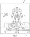
- an augmented reality scene 10is depicted wherein a user of an AR technology sees a real-world park-like setting 20 featuring people, trees, buildings in the background, and a concrete platform 30 .
- the user of the AR technologyalso perceives that he “sees” “virtual content” such as a robot statue 40 standing upon the real-world platform 30 , and a cartoon-like avatar character 50 flying by which seems to be a personification of a bumble bee, even though these elements 40 , 50 do not exist in the real world.
- the human visual perception systemis complex, it is challenging to produce an AR technology that facilitates a comfortable, natural-feeling, rich presentation of virtual image elements amongst other virtual or real-world imagery elements.
- an optical devicecomprising a liquid crystal layer having a first major surface, a second major surface and a thickness, the first and the second major surfaces extending across a transverse direction and the thickness extending along a direction parallel to a surface normal of the first or the second major surface, the liquid crystal layer comprising a plurality of sub-layers distributed across the thickness of the liquid crystal layer, each of the plurality of sub-layers comprising a single layer of liquid crystal molecules, each of the liquid crystal molecules having a longitudinal axis.
- Each sub-layercomprises a first domain in which the longitudinal axes of a plurality of the liquid crystal molecules are arranged to form a first pattern; and a second domain in which the longitudinal axes of a plurality of the liquid crystal molecules are arranged to form a second pattern.
- the first domainis spaced apart laterally along the transverse direction from the second domain by a domain gap having a distance D between about 10 nm and about 50 nm.
- the longitudinal axes of the liquid crystal molecules in the domain gapprogressively transition from the first pattern to the second pattern.
- the longitudinal axes of the molecules of the first domain of a sub-layercan be twisted with respect to the longitudinal axes of the molecules of the first domain of an adjacent sub-layer.
- Various embodiments of the devicecan further comprise a second liquid crystal layer comprising, wherein liquid crystal molecules of the second liquid crystal layer are configured to self-align to the first direction and the second direction in first and second domains respectively.
- the liquid crystal layer or the second liquid crystal layercan comprise a polymerizable liquid crystal material.
- Various embodiments of the devicecan further comprise a third liquid crystal layer over the second liquid crystal layer, wherein a plurality of liquid crystal molecules of the third liquid crystal can be arranged along a third direction.
- the devicecan further comprise a fourth liquid crystal layer over the third liquid crystal layer, wherein a plurality of liquid crystals of the fourth liquid crystal layer can be configured to self-align to the third direction.
- the second liquid crystal layer and/or the fourth liquid crystal layercan be disposed over a waveguide.
- the second liquid crystal layer and/or the fourth liquid crystal layercan comprise in-coupling optical elements configured to in-couple an incident beam of light into the waveguide such that the incident beam of light propagates through the waveguide by total internal reflection.
- Various embodiments of the devicecan comprise a light modulation device configured to direct light into the waveguide via the in-coupling optical elements.
- the second liquid crystal layer and/or the fourth liquid crystal layercan comprise out-coupling optical elements configured to out-couple an incident beam of light propagating through the waveguide by total internal reflection.
- the second liquid crystal layer and/or the fourth liquid crystal layercan comprise orthogonal pupil expanders configured to redirect light propagating through the waveguide by total internal reflection, wherein the redirected light continues to propagate through the waveguide by total internal reflection.
- the liquid crystal layercan comprise in-coupling optical elements configured to in-couple an incident beam of light into a waveguide such that an incident beam of light propagates through the waveguide by total internal reflection.
- the liquid crystal layercan comprise out-coupling optical elements configured to out-couple beam of light propagating through a waveguide by total internal reflection.
- the longitudinal axes of the plurality of the liquid crystal molecules in the first domaincan be aligned along a first direction and the longitudinal axes of the plurality of the liquid crystal molecules in the second domain can be aligned along a second direction.
- the longitudinal axes of the liquid crystal molecules in the domain gapcan progressively transition from the first direction to the second direction.
- Another innovative aspect of the subject matter of this applicationincludes a method for fabricating an optical device, the method comprising: providing a polymerizable liquid crystal layer over a substrate; patterning the polymerizable liquid crystal layer; and depositing a liquid crystal layer on the patterned polymerizable liquid crystal layer. Molecules of the deposited liquid crystal layer are self-aligned to the patterned polymerizable liquid crystal layer.
- Patterning the polymerizable liquid crystal layercomprises imprinting the polymerizable liquid crystal layer by an imprint template having a first domain comprising a first plurality of features and a second domain comprising a second plurality of features, the first domain spaced apart from the second domain by a region devoid of features, a dimension of the region devoid of features having a value between about 20 nm and about 100 nm.
- the dimensioncan comprise at least one of a length or a width.
- a width of the first plurality of featurescan be greater than or equal to about 20 nm and less than or equal to about 100 nm.
- a width of the second plurality of featurescan be greater than or equal to about 20 nm and less than or equal to about 100 nm.
- a distance between centers of two consecutive features of the first plurality of featurescan be greater than or equal to about 20 nm and less than or equal to about 100 nm.
- a height of the first plurality of featurescan be greater than or equal to about 10 nm and less than or equal to about 100 nm.
- a distance between centers of two consecutive features of the second plurality of featurescan be greater than or equal to about 20 nm and less than or equal to about 100 nm.
- a height of the second plurality of featurescan be greater than or equal to about 10 nm and less than or equal to about 100 nm.
- the first plurality of features of the first domaincan be arranged to form a first pattern and the second plurality of features of the second domain can be arranged to form a second pattern.
- the first patterncan be distinct from the second pattern.
- the first plurality of featurescan be oriented along a first direction and the second plurality of features of the second domain can be oriented along a second pattern.
- the first directioncan be distinct from the second direction.
- the first plurality of featurescan comprise at least one of linear grooves, curvilinear grooves, linear facets or curvilinear facets.
- the second plurality of featurescan comprise at least one of linear grooves, curvilinear grooves, linear facets or curvilinear facets.
- the imprint templatecan comprise a semiconductor material. In various embodiments, the imprint template can be manufactured using at least one of optical lithography, nano-imprint, or ion- and electron-beam lithography.
- the methodcomprises depositing a layer of liquid crystal material on a substrate; and using an imprint template comprising a pattern to imprint a pattern on the layer of liquid crystal material such that molecules of the liquid crystal material are self-aligned to the pattern.
- the patterncomprises a first domain having a first plurality of features arranged to form a first pattern and a second domain having a second plurality of features arranged to form a second pattern.
- the first domainis spaced apart from the second domain by a region devoid of features. At least one of a width or a length of the region devoid of features is between about 20 nm and about 100 nm.
- the methodfurther comprises depositing a layer of material having a refractive index lower than refractive index of the liquid crystal material.
- the layer of low refractive index materialcan be configured as a planarization layer using a planarization template.
- the first plurality of features or the second plurality of featurescan include surface relief features. At least one of a length, width or height of the first plurality of features or the second plurality of features can be between about 10 nm and about 100 nm.
- the first domain or the second domaincan include PBPE structures.
- the liquid crystal devicecan comprise a metasurface and/or a metamaterial.
- the first domain or the second domainincludes a grating array. In various embodiments, the first domain or the second domain can comprise curvilinear grooves or arcs.
- depositing a layer of liquid crystal materialcan include jet depositing the layer of liquid crystal material.
- the methodfurther comprises depositing an additional layer of liquid crystal material over the layer of liquid crystal material.
- the additional layer of liquid crystal materialcan be self-aligned to the pattern of the layer of liquid crystal material.
- a patterncan be imprinted on the additional layer of liquid crystal material.
- the pattern imprinted on the additional layer of liquid crystal materialcan be different from the pattern imprinted on the layer of liquid crystal material.
- the pattern imprinted on the layer of liquid crystal materialcan be configured to act on a first wavelength
- the pattern imprinted on the additional layer of liquid crystal materialcan be configured to act on a second wavelength.
- the methodcomprises depositing a layer of polymerizable liquid crystal material on a substrate; imprinting a pattern on the polymerizable liquid crystal material using an imprint template; and depositing a layer of liquid crystal material on the patterned polymerizable liquid crystal material such that molecules of the liquid crystal material are self-aligned to the pattern.
- the imprint templatecomprises an imprint pattern including a first domain having a first plurality of features arranged to form a first pattern and a second domain having a second plurality of features arranged to form a second pattern.
- the first domainis spaced apart from the second domain by a domain gap region devoid of features. At least one of a width or a length of the domain gap region is between about 20 nm and about 100 nm.
- depositing a layer of polymerizable liquid crystal materialcan include jet depositing the polymerizable liquid crystal material.
- the first or the second plurality of featurescan comprise surface relief features.
- the first or the second plurality of featurescan have a size between about 10 nm and about 100 nm.
- the first or the second domaincan include PBPE structures.
- the liquid crystal devicecan comprise a metasurface and/or a metamaterial.
- the first or the second domaincan include a grating array.
- the first or the second plurality of featurescan include curvilinear grooves or arcs.
- depositing a layer of liquid crystal materialcan include jet depositing the layer of liquid crystal material.
- the methodcan further comprise depositing an additional layer of liquid crystal material over the layer of liquid crystal material.
- the additional layer of liquid crystal materialcan be self-aligned to the pattern of the layer of liquid crystal material.
- a patterncan be imprinted on the additional layer of liquid crystal material.
- the pattern imprinted on the additional layer of liquid crystal materialcan be different from the pattern imprinted on the layer of liquid crystal material.
- the pattern imprinted on the layer of liquid crystal materialcan be configured to act on a first wavelength, and the pattern imprinted on the additional layer of liquid crystal material can be configured to act on a second wavelength.
- Yet another innovative aspect of the subject matter of this applicationincludes a method of manufacturing a liquid crystal device.
- the methodcomprises depositing a layer on a substrate; imprinting a pattern on the layer using an imprint template comprising an imprint pattern; and depositing a layer of liquid crystal material on the patterned layer such that molecules of the liquid crystal material are self-aligned to the pattern.
- the imprint patterncomprises a first domain having a first plurality of features arranged to form a first pattern and a second domain having a second plurality of features arranged to form a second pattern.
- the first domainis spaced apart from the second domain by a domain gap region devoid of features, and at least one of a width or a length of the domain gap region is between about 20 nm and about 100 nm.
- the layercan comprise a polymerizable liquid crystal material.
- depositing a layerincludes jet depositing the layer.
- the first or the second plurality of featurescan include surface relief features.
- the first or the second plurality of featurescan have a size between about 10 nm and about 100 nm.
- the first or the second domaincan include PBPE structures or a metasurface.
- the first or the second domaincan include a grating array.
- the first or the second plurality of featurescan include curvilinear grooves or arcs.
- depositing a layer of liquid crystal materialcan include jet depositing the layer of liquid crystal material.
- Various embodiments of the methodcan further comprise depositing an additional layer of liquid crystal material over the layer of liquid crystal material.
- the additional layer of liquid crystal materialcan be self-aligned to the pattern of the layer of liquid crystal material.
- a patterncan be imprinted on the additional layer of liquid crystal material.
- the pattern imprinted on the additional layer of liquid crystal materialcan be different from the pattern imprinted on the layer of liquid crystal material.
- the pattern imprinted on the layer of liquid crystal materialcan be configured to act on a first wavelength, and the pattern imprinted on the additional layer of liquid crystal material can be configured to act on a second wavelength.
- a liquid crystal devicecomprising a substrate; and a layer of liquid crystal material have a first surface adjacent the substrate and a second surface opposite the first surface.
- a first plurality of molecules of the layer of liquid crystal material on the second surfaceare arranged to form a first pattern and a second first plurality of molecules of the layer of liquid crystal material on the second surface are arranged to form a second pattern.
- the first plurality of moleculesare spaced apart from the second plurality of molecules by a gap having a distance between about 20 nm and about 100 nm, and wherein molecules of the layer of liquid crystal material in the gap are arranged to progressively transition from the first pattern to the second pattern.
- the layer of liquid crystal materialis configured as a polarization grating.
- a liquid crystal devicecomprising a substrate; a material have a first surface adjacent the substrate and a second surface opposite the first surface; and a liquid crystal material on the second surface of the material.
- the materialcomprises a first pattern on the second surface; and a second pattern on the second surface.
- the first patternis spaced apart from the second pattern by a gap having a distance between about 20 nm and about 100 nm.
- the materialcan comprise a polymerizable liquid crystal material.
- the methodcomprises providing an imprint layer over a substrate.
- the imprint layercomprises at least a first zone comprising a first plurality of features oriented along a first direction and a second zone comprising a second plurality of features oriented along a second direction.
- the second directioncan be rotated by an angle between about 1 degree and about 45 degrees with respect to the first direction.
- the methodfurther comprises depositing a liquid crystal layer on the imprint layer, wherein molecules of the deposited liquid crystal layer are self-aligned to the first and the second plurality of features.
- the imprint layercan comprise between about five and thirty zones.
- the first and the second zonescan be spaced apart by a gap less than or equal to about 10 nm.
- the first and the second zonescan be spaced apart by a gap less than or equal to about 5 nm, less than or equal to about 2 nm and/or less than or equal to about 1 nm.
- the first or the second plurality of featurescan comprise nano-features, such as, for example, grooves.
- a length or a width of the first plurality of features and the second plurality of featurescan be less than or equal to about 200 nm.
- the length or the width of the first plurality of features and the second plurality of featurescan be less than or equal to about 100 nm.
- a height or a depth of the first plurality of features and the second plurality of featurescan be less than or equal to about 200 nm.
- the height or the depth of the first plurality of features and the second plurality of featurescan be less than or equal to about 100 nm.
- the imprint layercan comprise a semiconductor material.
- the liquid crystal layercan comprise a polymerizable liquid crystal material.
- the methodfurther comprises polymerizing the polymerizable liquid crystal material after the molecules of the polymerizable liquid crystal material are self-aligned to the first and the second plurality of features.
- Polymerizing the polymerizable liquid crystal materialcan comprise exposing the polymerizable liquid crystal material to ultra-violet light.
- the liquid crystal lenscan comprise a diffractive lens.
- Depositing a liquid crystal layer on the imprint layercan comprise jet depositing the liquid crystal.
- the liquid crystal lenscomprises a patterned substrate comprising at least a first zone comprising a first plurality of features oriented along a first direction and a second zone comprising a second plurality of features oriented along a second direction.
- the first plurality of features and the second plurality of featureshave a dimension less than or equal to about 100 nm.
- the lenscomprises a liquid crystal layer over the patterned substrate, wherein molecules of the liquid crystal layer are self-aligned to the first and the second plurality of features.
- the dimensioncan comprise a length, a height, a depth or a width of the feature.
- the liquid crystalcan comprise a polymerizable liquid crystal.
- the patterned substratecan comprise a substrate having a layer disposed thereon that is patterned.
- the first and the second zonescan comprise concentric ring-shaped zones.
- the lenscan comprise between about 3 and 30 zones.
- the lenscan comprise at least five zones.
- a width of the zonescan progressively decrease with distance from a center of the patterned substrate.
- the zonescan have no gap therebetween.
- a gap between the zonescan be less than or equal to 5 nm.
- the gap between the zonescan be less than or equal to 1 nm.
- the lenscan be configured as a diffractive lens.
- the lenscan be configured to provide positive or negative optical power.
- liquid crystal devices described hereincan be included with a waveguide of a display system.
- the embodiments of the liquid crystal devices described hereincan be configured to selectively in-couple at least one light stream from a multiplexed light stream into the waveguide and transmit one or more other light streams from the multiplexed light stream.
- Various embodiments of the liquid crystal device described hereincan be included with an eyepiece of a head mounted display.
- FIG. 1illustrates a user's view of augmented reality (AR) through an AR device.
- ARaugmented reality
- FIG. 2illustrates an example of a wearable display system.
- FIG. 3illustrates a conventional display system for simulating three-dimensional imagery for a user.
- FIG. 4illustrates aspects of an approach for simulating three-dimensional imagery using multiple depth planes.
- FIGS. 5A-5Cillustrate relationships between radius of curvature and focal radius.
- FIG. 6illustrates an example of a waveguide stack for outputting image information to a user.
- FIG. 7illustrates an example of exit beams outputted by a waveguide.
- FIG. 8illustrates an example of a stacked waveguide assembly in which each depth plane includes images formed using multiple different component colors.
- FIG. 9Aillustrates a cross-sectional side view of an example of a set of stacked waveguides that each includes an in-coupling optical element.
- FIG. 9Billustrates a perspective view of an example of the plurality of stacked waveguides of FIG. 9A .
- FIG. 9Cillustrates a top-down plan view of an example of the plurality of stacked waveguides of FIGS. 9A and 9B .
- FIG. 10Aillustrates a top view of an example of a liquid crystal layer comprising a plurality of domains of liquid crystal molecules.
- FIG. 10Billustrates a magnified top view of the liquid crystal layer depicted in FIG. 10A showing the orientation of the liquid crystal molecules in each domain.
- FIGS. 10C, 10D, 10E and 10Fillustrate side views of various embodiment of the liquid crystal layer depicted in FIG. 10A .
- FIG. 11Aillustrates a top view of an imprint template including a plurality surface features configured to manufacture the liquid crystal layer depicted in FIG. 10A .
- FIG. 11Billustrates a side view of the imprint template depicted in FIG. 11A .
- FIGS. 12A-12Dillustrate an embodiment of a method of manufacturing a liquid crystal layer including a plurality of liquid crystal molecules arranged in different patterns.
- FIG. 12Eillustrates an embodiment of a stacked liquid crystal device comprising a plurality of liquid crystal layers.
- FIG. 13Aillustrates a scanning electron microscope (SEM) image of an embodiment of an imprint template.
- FIG. 13Bis a SEM image of a patterned PLC layer manufactured using the imprint template of FIG. 13A and the method discussed above with reference to FIGS. 12A-12C .
- FIG. 13Cis a polarizing microscope image of the patterned PLC layer shown in FIG. 13B .
- FIG. 14illustrates an embodiment of an electrically-controllable liquid crystal device.
- FIGS. 15A-15Cillustrate an example of a method of manufacturing various liquid crystal devices described herein.
- FIG. 16Aillustrates a top view of an implementation of a diffractive lens comprising a liquid crystal material.
- FIG. 16Billustrates a microscopic image of an implementation of the lens between crossed polarizers.
- FIGS. 16B-1 and 16B-2depict a scanning electron microscope (SEM) image showing the pattern of the imprint layer that achieves the desired alignment of the longitudinal axes in various regions of the liquid crystal lens.
- SEMscanning electron microscope
- FIGS. 17A-17Cillustrate an example of a method of manufacturing a liquid crystal lens
- FIG. 18Aillustrates a scanning electron microscope (SEM) image of an imprint layer that is used to manufacture an implementation of a liquid crystal lens.
- FIG. 18Billustrates a scanning electron microscope (SEM) image of a liquid crystal layer disposed over the imprint layer of FIG. 18A .
- Liquid crystalscomprise liquid crystal molecules having a longitudinal axis which is arbitrarily oriented under certain conditions. However, under certain other conditions, the LC molecules can be ordered such that the longitudinal axes are oriented along an average direction (referred to herein as the director). Some liquid crystal molecules can be symmetric about the longitudinal axis.
- LCsare an anisotropic material that can have different optical properties for different wavelengths or polarizations of light depending on the direction of propagation of light through the LC and the polarization of light with respect to the direction along which the LC molecules are generally oriented.
- LC moleculesexhibit birefringence in which light polarized along a direction of the general orientation of the longitudinal axes of LC molecules has a refractive index different from the refractive index of light polarized a direction perpendicular to the general orientation of the longitudinal axes of LC molecules.
- birefringent nature of LC materialsthey are widely used in various systems include displays, optical communications, optical data storage, sensors, etc.
- the refractive index of a LC materialcan be varied by varying the orientation of the longitudinal axes of the molecules of the LC material.
- LC materialscan be configured as phase gratings.
- LC grating structurescan be used to selectively diffract light along different directions based on wavelength and/or polarization.
- One way of fabricating LC grating structuresincludes a mechanical method such as a rubbing process in which surface features are produced on an alignment layer (e.g., a polymer) by rubbing or a scratching the surface of the alignment layer using a mechanical object (e.g., a metal object, cloth, tip of an atomic force microscope, etc.).
- a mechanical objecte.g., a metal object, cloth, tip of an atomic force microscope, etc.
- the molecules of a layer LC material deposited on the alignment layerare aligned to surface features on the alignment layer to form a grating pattern.
- the rubbing processcan cause mechanical damage to the surface of the alignment layer and/or introduce electrostatic charges or impurities on the surface of the alignment layer which can reduce the diffraction efficiency of the liquid crystal grating structure.
- a liquid crystal material with space-variant nano-scale patterncan include a liquid crystal metasurface.
- Other embodiments of a liquid crystal material with space-variant nano-scale patterncan include a liquid crystal comprising a plurality of adjacent domains, wherein the liquid crystal molecules in each domain can be arranged to form a nano-scale pattern.
- the LC grating structuresmay be utilized as constituent parts of a display system.
- the display systemmay include a waveguide, and an image injection device configured to direct a light beam into the waveguide.
- the LC grating structuresmay be used as one or more of an in-coupling optical element, an out-coupling optical element, and an optical element for receiving incident light propagating in the waveguide and for redirecting that incident light so that the redirected light continues to propagate through the waveguide by total internal reflection.
- Examples of the latter type of optical elementinclude pupil expanders such as orthogonal pupil expanders (OPEs).
- the LC grating structuresmay be used to in-couple, out-couple, and/or redirect light propagating within the waveguide.
- the lightmay be light of a single wavelength or a single range of wavelengths.
- the lightmay be a light stream that is part of a multiplexed light stream that includes a plurality of light streams having different light properties (e.g., each stream may have a different wavelength).
- the waveguidemay include the LC grating structures, which may be configured to selectively redirect a light beam formed of light having a particular light property (e.g., a first wavelength), while being substantially transmissive to one or more other streams of light (e.g., having wavelengths different from the first wavelength).
- the waveguideis part of a stack of waveguides, which can include a second waveguide including in-coupling optical elements configured to selectively turn a second of the streams of light while being transmissive to one or more other streams of light.
- the in-coupling LC grating structures of the waveguideare configured to transmit at least one of the streams of light to the in-coupling LC grating structures of the second waveguide.
- embodiments disclosed hereininclude optical systems, including display systems, generally.
- the display systemsare wearable, which may advantageously provide a more immersive VR or AR experience.
- displays containing one or more waveguidese.g., a stack of waveguides
- two stacks of waveguides, one for each eye of a viewermay be utilized to provide different images to each eye.
- FIG. 2illustrates an example of wearable display system 60 .
- the display system 60includes a display 70 , and various mechanical and electronic modules and systems to support the functioning of that display 70 .
- the display 70may be coupled to a frame 80 , which is wearable by a display system user or viewer 90 and which is configured to position the display 70 in front of the eyes of the user 90 .
- the display 70may be considered eyewear in some embodiments.
- a speaker 100is coupled to the frame 80 and configured to be positioned adjacent the ear canal of the user 90 (in some embodiments, another speaker, not shown, is positioned adjacent the other ear canal of the user to provide stereo/shapeable sound control).
- the display systemmay also include one or more microphones 110 or other devices to detect sound.
- the microphoneis configured to allow the user to provide inputs or commands to the system 60 (e.g., the selection of voice menu commands, natural language questions, etc.), and/or may allow audio communication with other persons (e.g., with other users of similar display systems.
- the microphonemay further be configured as a peripheral sensor to collect audio data (e.g., sounds from the user and/or environment).
- the display systemmay also include a peripheral sensor 120 a , which may be separate from the frame 80 and attached to the body of the user 90 (e.g., on the head, torso, an extremity, etc. of the user 90 ).
- the peripheral sensor 120 amay be configured to acquire data characterizing the physiological state of the user 90 in some embodiments.
- the sensor 120 amay be an electrode.
- the display 70is operatively coupled by communications link 130 , such as by a wired lead or wireless connectivity, to a local data processing module 140 which may be mounted in a variety of configurations, such as fixedly attached to the frame 80 , fixedly attached to a helmet or hat worn by the user, embedded in headphones, or otherwise removably attached to the user 90 (e.g., in a backpack-style configuration, in a belt-coupling style configuration).
- the sensor 120 amay be operatively coupled by communications link 120 b , e.g., a wired lead or wireless connectivity, to the local processor and data module 140 .
- the local processing and data module 140may comprise a hardware processor, as well as digital memory, such as non-volatile memory (e.g., flash memory or hard disk drives), both of which may be utilized to assist in the processing, caching, and storage of data.
- the datainclude data a) captured from sensors (which may be, e.g., operatively coupled to the frame 80 or otherwise attached to the user 90 ), such as image capture devices (such as cameras), microphones, inertial measurement units, accelerometers, compasses, GPS units, radio devices, gyros, and/or other sensors disclosed herein; and/or b) acquired and/or processed using remote processing module 150 and/or remote data repository 160 (including data relating to virtual content), possibly for passage to the display 70 after such processing or retrieval.
- sensorswhich may be, e.g., operatively coupled to the frame 80 or otherwise attached to the user 90
- image capture devicessuch as cameras
- microphonessuch as cameras
- inertial measurement unitssuch as cameras
- accelerometerscompasse
- the local processing and data module 140may be operatively coupled by communication links 170 , 180 , such as via a wired or wireless communication links, to the remote processing module 150 and remote data repository 160 such that these remote modules 150 , 160 are operatively coupled to each other and available as resources to the local processing and data module 140 .
- the local processing and data module 140may include one or more of the image capture devices, microphones, inertial measurement units, accelerometers, compasses, GPS units, radio devices, and/or gyros. In some other embodiments, one or more of these sensors may be attached to the frame 80 , or may be standalone structures that communicate with the local processing and data module 140 by wired or wireless communication pathways.
- the remote processing module 150may comprise one or more processors configured to analyze and process data and/or image information.
- the remote data repository 160may comprise a digital data storage facility, which may be available through the internet or other networking configuration in a “cloud” resource configuration.
- the remote data repository 160may include one or more remote servers, which provide information, e.g., information for generating augmented reality content, to the local processing and data module 140 and/or the remote processing module 150 .
- all datais stored and all computations are performed in the local processing and data module, allowing fully autonomous use from a remote module.
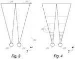
- FIG. 3illustrates a conventional display system for simulating three-dimensional imagery for a user.
- Two distinct images 190 , 200are outputted to the user.
- the images 190 , 200are spaced from the eyes 210 , 220 by a distance 230 along an optical or z-axis that is parallel to the line of sight of the viewer.
- the images 190 , 200are flat and the eyes 210 , 220 may focus on the images by assuming a single accommodated state.
- Such 3-D display systemsrely on the human visual system to combine the images 190 , 200 to provide a perception of depth and/or scale for the combined image.
- Such systemsare uncomfortable for many viewers, however, since they, among other things, simply provide a different presentation of a scene, but with the eyes viewing all the image information at a single accommodated state, and work against the “accommodation-vergence reflex.”
- Display systems that provide a better match between accommodation and vergencemay form more realistic and comfortable simulations of three-dimensional imagery contributing to increased duration of wear and in turn compliance to diagnostic and therapy protocols.
- FIG. 4illustrates aspects of an approach for simulating three-dimensional imagery using multiple depth planes.
- objects at various distances from eyes 210 , 220 on the z-axisare accommodated by the eyes 210 , 220 so that those objects are in focus.
- the eyes 210 , 220assume particular accommodated states to bring into focus objects at different distances along the z-axis. Consequently, a particular accommodated state may be said to be associated with a particular one of depth planes 240 , with has an associated focal distance, such that objects or parts of objects in a particular depth plane are in focus when the eye is in the accommodated state for that depth plane.
- three-dimensional imagerymay be simulated by providing different presentations of an image for each of the eyes 210 , 220 , and also by providing different presentations of the image corresponding to each of the depth planes. While shown as being separate for clarity of illustration, it will be appreciated that the fields of view of the eyes 210 , 220 may overlap, for example, as distance along the z-axis increases. In addition, while shown as flat for ease of illustration, it will be appreciated that the contours of a depth plane may be curved in physical space, such that all features in a depth plane are in focus with the eye in a particular accommodated state.
- the distance between an object and the eye 210 or 220may also change the amount of divergence of light from that object, as viewed by that eye.
- FIGS. 5A-5Cillustrate relationships between distance and the divergence of light rays.
- the distance between the object and the eye 210is represented by, in order of decreasing distance, R 1 , R 2 , and R 3 .
- R 1 , R 2 , and R 3the distance between the object and the eye 210
- the light raysbecome more divergent as distance to the object decreases.
- the light raysbecome more collimated.
- the light field produced by a point(the object or a part of the object) has a spherical wavefront curvature, which is a function of how far away the point is from the eye of the user.
- the curvatureincreases with decreasing distance between the object and the eye 210 . Consequently, at different depth planes, the degree of divergence of light rays is also different, with the degree of divergence increasing with decreasing distance between depth planes and the viewer's eye 210 . While only a single eye 210 is illustrated for clarity of illustration in FIGS. 5A-5C and other figures herein, it will be appreciated that the discussions regarding eye 210 may be applied to both eyes 210 and 220 of a viewer.
- the human eyetypically can interpret a finite number of depth planes to provide depth perception. Consequently, a highly believable simulation of perceived depth may be achieved by providing, to the eye, different presentations of an image corresponding to each of these limited number of depth planes.
- the different presentationsmay be separately focused by the viewer's eyes, thereby helping to provide the user with depth cues based on the accommodation of the eye required to bring into focus different image features for the scene located on different depth plane and/or based on observing different image features on different depth planes being out of focus.
- FIG. 6illustrates an example of a waveguide stack for outputting image information to a user.
- a display system 250includes a stack of waveguides, or stacked waveguide assembly, 260 that may be utilized to provide three-dimensional perception to the eye/brain using a plurality of waveguides 270 , 280 , 290 , 300 , 310 .
- the display system 250is the system 60 of FIG. 2 , with FIG. 6 schematically showing some parts of that system 60 in greater detail.
- the waveguide assembly 260may be part of the display 70 of FIG. 2 .
- the display system 250may be considered a light field display in some embodiments.
- the waveguide assembly 260may also include a plurality of features 320 , 330 , 340 , 350 between the waveguides.
- the features 320 , 330 , 340 , 350may be one or more lenses.
- the waveguides 270 , 280 , 290 , 300 , 310 and/or the plurality of lenses 320 , 330 , 340 , 350may be configured to send image information to the eye with various levels of wavefront curvature or light ray divergence. Each waveguide level may be associated with a particular depth plane and may be configured to output image information corresponding to that depth plane.
- Image injection devices 360 , 370 , 380 , 390 , 400may function as a source of light for the waveguides and may be utilized to inject image information into the waveguides 270 , 280 , 290 , 300 , 310 , each of which may be configured, as described herein, to distribute incoming light across each respective waveguide, for output toward the eye 210 .
- each of the input surfaces 460 , 470 , 480 , 490 , 500may be an edge of a corresponding waveguide, or may be part of a major surface of the corresponding waveguide (that is, one of the waveguide surfaces directly facing the world 510 or the viewer's eye 210 ).
- a single beam of light(e.g. a collimated beam) may be injected into each waveguide to output an entire field of cloned collimated beams that are directed toward the eye 210 at particular angles (and amounts of divergence) corresponding to the depth plane associated with a particular waveguide.
- a single one of the image injection devices 360 , 370 , 380 , 390 , 400may be associated with and inject light into a plurality (e.g., three) of the waveguides 270 , 280 , 290 , 300 , 310 .
- the image injection devices 360 , 370 , 380 , 390 , 400are discrete displays that each produce image information for injection into a corresponding waveguide 270 , 280 , 290 , 300 , 310 , respectively.
- the image injection devices 360 , 370 , 380 , 390 , 400are the output ends of a single multiplexed display which may, e.g., pipe image information via one or more optical conduits (such as fiber optic cables) to each of the image injection devices 360 , 370 , 380 , 390 , 400 .
- the image information provided by the image injection devices 360 , 370 , 380 , 390 , 400may include light of different wavelengths, or colors (e.g., different component colors, as discussed herein).
- the light injected into the waveguides 270 , 280 , 290 , 300 , 310is provided by a light projector system 520 , which comprises a light module 530 , which may include a light emitter, such as a light emitting diode (LED).
- the light from the light module 530may be directed to and modified by a light modulator 540 , e.g., a spatial light modulator, via a beam splitter 550 .
- the light modulator 540may be configured to change the perceived intensity of the light injected into the waveguides 270 , 280 , 290 , 300 , 310 .
- Examples of spatial light modulatorsinclude liquid crystal displays (LCD) including a liquid crystal on silicon (LCOS) displays.
- the display system 250may be a scanning fiber display comprising one or more scanning fibers configured to project light in various patterns (e.g., raster scan, spiral scan, Lissajous patterns, etc.) into one or more waveguides 270 , 280 , 290 , 300 , 310 and ultimately to the eye 210 of the viewer.
- the illustrated image injection devices 360 , 370 , 380 , 390 , 400may schematically represent a single scanning fiber or a bundle of scanning fibers configured to inject light into one or a plurality of the waveguides 270 , 280 , 290 , 300 , 310 .
- the illustrated image injection devices 360 , 370 , 380 , 390 , 400may schematically represent a plurality of scanning fibers or a plurality of bundles of scanning fibers, each of which are configured to inject light into an associated one of the waveguides 270 , 280 , 290 , 300 , 310 .
- one or more optical fibersmay be configured to transmit light from the light module 530 to the one or more waveguides 270 , 280 , 290 , 300 , 310 .
- one or more intervening optical structuresmay be provided between the scanning fiber, or fibers, and the one or more waveguides 270 , 280 , 290 , 300 , 310 to, e.g., redirect light exiting the scanning fiber into the one or more waveguides 270 , 280 , 290 , 300 , 310 .
- a controller 560controls the operation of one or more of the stacked waveguide assembly 260 , including operation of the image injection devices 360 , 370 , 380 , 390 , 400 , the light source 530 , and the light modulator 540 .
- the controller 560is part of the local data processing module 140 .
- the controller 560includes programming (e.g., instructions in a non-transitory medium) that regulates the timing and provision of image information to the waveguides 270 , 280 , 290 , 300 , 310 according to, e.g., any of the various schemes disclosed herein.
- the controllermay be a single integral device, or a distributed system connected by wired or wireless communication channels.
- the controller 560may be part of the processing modules 140 or 150 ( FIG. 2 ) in some embodiments.
- the waveguides 270 , 280 , 290 , 300 , 310may be configured to propagate light within each respective waveguide by total internal reflection (TIR).
- the waveguides 270 , 280 , 290 , 300 , 310may each be planar or have another shape (e.g., curved), with major top and bottom surfaces and edges extending between those major top and bottom surfaces.
- the waveguides 270 , 280 , 290 , 300 , 310may each include out-coupling optical elements 570 , 580 , 590 , 600 , 610 that are configured to extract light out of a waveguide by redirecting the light, propagating within each respective waveguide, out of the waveguide to output image information to the eye 210 .
- Extracted lightmay also be referred to as out-coupled light and the out-coupling optical elements light may also be referred to light extracting optical elements.
- An extracted beam of lightmay be outputted by the waveguide at locations at which the light propagating in the waveguide strikes a light extracting optical element.
- the out-coupling optical elements 570 , 580 , 590 , 600 , 610may, for example, be gratings, including diffractive optical features, as discussed further herein. While illustrated disposed at the bottom major surfaces of the waveguides 270 , 280 , 290 , 300 , 310 , for ease of description and drawing clarity, in some embodiments, the out-coupling optical elements 570 , 580 , 590 , 600 , 610 may be disposed at the top and/or bottom major surfaces, and/or may be disposed directly in the volume of the waveguides 270 , 280 , 290 , 300 , 310 , as discussed further herein.
- the out-coupling optical elements 570 , 580 , 590 , 600 , 610may be formed in a layer of material that is attached to a transparent substrate to form the waveguides 270 , 280 , 290 , 300 , 310 .
- the waveguides 270 , 280 , 290 , 300 , 310may be a monolithic piece of material and the out-coupling optical elements 570 , 580 , 590 , 600 , 610 may be formed on a surface and/or in the interior of that piece of material.
- each waveguide 270 , 280 , 290 , 300 , 310is configured to output light to form an image corresponding to a particular depth plane.
- the waveguide 270 nearest the eyemay be configured to deliver collimated light (which was injected into such waveguide 270 ), to the eye 210 .
- the collimated lightmay be representative of the optical infinity focal plane.
- the next waveguide up 280may be configured to send out collimated light which passes through the first lens 350 (e.g., a negative lens) before it can reach the eye 210 ; such first lens 350 may be configured to create a slight convex wavefront curvature so that the eye/brain interprets light coming from that next waveguide up 280 as coming from a first focal plane closer inward toward the eye 210 from optical infinity.
- first lens 350e.g., a negative lens
- the third up waveguide 290passes its output light through both the first 350 and second 340 lenses before reaching the eye 210 ; the combined optical power of the first 350 and second 340 lenses may be configured to create another incremental amount of wavefront curvature so that the eye/brain interprets light coming from the third waveguide 290 as coming from a second focal plane that is even closer inward toward the person from optical infinity than was light from the next waveguide up 280 .
- the other waveguide layers 300 , 310 and lenses 330 , 320are similarly configured, with the highest waveguide 310 in the stack sending its output through all of the lenses between it and the eye for an aggregate focal power representative of the closest focal plane to the person.
- a compensating lens layer 620may be disposed at the top of the stack to compensate for the aggregate power of the lens stack 320 , 330 , 340 , 350 below.
- Such a configurationprovides as many perceived focal planes as there are available waveguide/lens pairings.
- Both the out-coupling optical elements of the waveguides and the focusing aspects of the lensesmay be static (i.e., not dynamic or electro-active). In some alternative embodiments, either or both may be dynamic using electro-active features.
- two or more of the waveguides 270 , 280 , 290 , 300 , 310may have the same associated depth plane.
- multiple waveguides 270 , 280 , 290 , 300 , 310may be configured to output images set to the same depth plane, or multiple subsets of the waveguides 270 , 280 , 290 , 300 , 310 may be configured to output images set to the same plurality of depth planes, with one set for each depth plane. This can provide advantages for forming a tiled image to provide an expanded field of view at those depth planes.
- the out-coupling optical elements 570 , 580 , 590 , 600 , 610may be configured to both redirect light out of their respective waveguides and to output this light with the appropriate amount of divergence or collimation for a particular depth plane associated with the waveguide.
- waveguides having different associated depth planesmay have different configurations of out-coupling optical elements 570 , 580 , 590 , 600 , 610 , which output light with a different amount of divergence depending on the associated depth plane.
- the light extracting optical elements 570 , 580 , 590 , 600 , 610may be volumetric or surface features, which may be configured to output light at specific angles.
- the light extracting optical elements 570 , 580 , 590 , 600 , 610may be volume holograms, surface holograms, and/or diffraction gratings.
- the features 320 , 330 , 340 , 350may not be lenses; rather, they may simply be spacers (e.g., cladding layers and/or structures for forming air gaps).
- the out-coupling optical elements 570 , 580 , 590 , 600 , 610are diffractive features that form a diffraction pattern, or “diffractive optical element” (also referred to herein as a “DOE”).
- the DOE'shave a sufficiently low diffraction efficiency so that only a portion of the light of the beam is deflected away toward the eye 210 with each intersection of the DOE, while the rest continues to move through a waveguide via TIR.
- the light carrying the image informationis thus divided into a number of related exit beams that exit the waveguide at a multiplicity of locations and the result is a fairly uniform pattern of exit emission toward the eye 210 for this particular collimated beam bouncing around within a waveguide.
- one or more DOEsmay be switchable between “on” states in which they actively diffract, and “off” states in which they do not significantly diffract.
- a switchable DOEmay comprise a layer of polymer dispersed liquid crystal, in which microdroplets comprise a diffraction pattern in a host medium, and the refractive index of the microdroplets may be switched to substantially match the refractive index of the host material (in which case the pattern does not appreciably diffract incident light) or the microdroplet may be switched to an index that does not match that of the host medium (in which case the pattern actively diffracts incident light).
- a camera assembly 630may be provided to capture images of the eye 210 and/or tissue around the eye 210 to, e.g., detect user inputs and/or to monitor the physiological state of the user.
- a cameramay be any image capture device.
- the camera assembly 630may include an image capture device and a light source to project light (e.g., infrared light) to the eye, which may then be reflected by the eye and detected by the image capture device.
- the camera assembly 630may be attached to the frame 80 ( FIG.
- the processing modules 140 and/or 150may process image information from the camera assembly 630 to make various determinations regarding, e.g., the physiological state of the user, as discussed herein.
- information regarding the physiological state of usermay be used to determine the behavioral or emotional state of the user. Examples of such information include movements of the user and/or facial expressions of the user.
- the behavioral or emotional state of the usermay then be triangulated with collected environmental and/or virtual content data so as to determine relationships between the behavioral or emotional state, physiological state, and environmental or virtual content data.
- one camera assembly 630may be utilized for each eye, to separately monitor each eye.
- FIG. 7an example of exit beams outputted by a waveguide is shown.
- One waveguideis illustrated, but it will be appreciated that other waveguides in the waveguide assembly 260 ( FIG. 6 ) may function similarly, where the waveguide assembly 260 includes multiple waveguides.
- Light 640is injected into the waveguide 270 at the input surface 460 of the waveguide 270 and propagates within the waveguide 270 by TIR. At points where the light 640 impinges on the DOE 570 , a portion of the light exits the waveguide as exit beams 650 .
- the exit beams 650are illustrated as substantially parallel but, as discussed herein, they may also be redirected to propagate to the eye 210 at an angle (e.g., forming divergent exit beams), depending on the depth plane associated with the waveguide 270 . It will be appreciated that substantially parallel exit beams may be indicative of a waveguide with out-coupling optical elements that out-couple light to form images that appear to be set on a depth plane at a large distance (e.g., optical infinity) from the eye 210 .
- waveguides or other sets of out-coupling optical elementsmay output an exit beam pattern that is more divergent, which would require the eye 210 to accommodate to a closer distance to bring it into focus on the retina and would be interpreted by the brain as light from a distance closer to the eye 210 than optical infinity.
- a full color imagemay be formed at each depth plane by overlaying images in each of the component colors, e.g., three or more component colors.
- FIG. 8illustrates an example of a stacked waveguide assembly in which each depth plane includes images formed using multiple different component colors.
- the illustrated embodimentshows depth planes 240 a - 240 f , although more or fewer depths are also contemplated.
- Each depth planemay have three or more component color images associated with it, including: a first image of a first color, G; a second image of a second color, R; and a third image of a third color, B.
- Different depth planesare indicated in the figure by different numbers for diopters (dpt) following the letters G, R, and B.
- the numbers following each of these lettersindicate diopters (1/m), or inverse distance of the depth plane from a viewer, and each box in the figures represents an individual component color image.
- the exact placement of the depth planes for different component colorsmay vary. For example, different component color images for a given depth plane may be placed on depth planes corresponding to different distances from the user. Such an arrangement may increase visual acuity and user comfort and/or may decrease chromatic aberrations.
- each depth planemay have multiple waveguides associated with it.
- each box in the figures including the letters G, R, or Bmay be understood to represent an individual waveguide, and three waveguides may be provided per depth plane where three component color images are provided per depth plane. While the waveguides associated with each depth plane are shown adjacent to one another in this drawing for ease of description, it will be appreciated that, in a physical device, the waveguides may all be arranged in a stack with one waveguide per level. In some other embodiments, multiple component colors may be outputted by the same waveguide, such that, e.g., only a single waveguide may be provided per depth plane.
- Gis the color green
- Ris the color red
- Bis the color blue.
- other colors associated with other wavelengths of lightincluding magenta and cyan, may be used in addition to or may replace one or more of red, green, or blue.
- features 320 , 330 , 340 , and 350may be active or passive optical filters configured to block or selectively light from the ambient environment to the viewer's eyes.
- references to a given color of light throughout this disclosurewill be understood to encompass light of one or more wavelengths within a range of wavelengths of light that are perceived by a viewer as being of that given color.
- red lightmay include light of one or more wavelengths in the range of about 620-780 nm
- green lightmay include light of one or more wavelengths in the range of about 492-577 nm
- blue lightmay include light of one or more wavelengths in the range of about 435-493 nm.
- the light source 530may be configured to emit light of one or more wavelengths outside the visual perception range of the viewer, for example, infrared and/or ultraviolet wavelengths.
- the in-coupling, out-coupling, and other light redirecting structures of the waveguides of the display 250may be configured to direct and emit this light out of the display towards the user's eye 210 , e.g., for imaging and/or user stimulation applications.
- FIG. 9Aillustrates a cross-sectional side view of an example of a plurality or set 660 of stacked waveguides that each includes an in-coupling optical element.
- the waveguidesmay each be configured to output light of one or more different wavelengths, or one or more different ranges of wavelengths. It will be appreciated that the stack 660 may correspond to the stack 260 ( FIG.
- the illustrated waveguides of the stack 660may correspond to part of the plurality of waveguides 270 , 280 , 290 , 300 , 310 , except that light from one or more of the image injection devices 360 , 370 , 380 , 390 , 400 is injected into the waveguides from a position that requires light to be redirected for in-coupling.
- the illustrated set 660 of stacked waveguidesincludes waveguides 670 , 680 , and 690 .
- Each waveguideincludes an associated in-coupling optical element (which may also be referred to as a light input area on the waveguide), with, e.g., in-coupling optical element 700 disposed on a major surface (e.g., an upper major surface) of waveguide 670 , in-coupling optical element 710 disposed on a major surface (e.g., an upper major surface) of waveguide 680 , and in-coupling optical element 720 disposed on a major surface (e.g., an upper major surface) of waveguide 690 .
- in-coupling optical element 700disposed on a major surface (e.g., an upper major surface) of waveguide 670
- in-coupling optical element 710disposed on a major surface (e.g., an upper major surface) of waveguide 680
- in-coupling optical element 720disposed on a major surface (e.g
- one or more of the in-coupling optical elements 700 , 710 , 720may be disposed on the bottom major surface of the respective waveguide 670 , 680 , 690 (particularly where the one or more in-coupling optical elements are reflective, deflecting optical elements). As illustrated, the in-coupling optical elements 700 , 710 , 720 may be disposed on the upper major surface of their respective waveguide 670 , 680 , 690 (or the top of the next lower waveguide), particularly where those in-coupling optical elements are transmissive, deflecting optical elements. In some embodiments, the in-coupling optical elements 700 , 710 , 720 may be disposed in the body of the respective waveguide 670 , 680 , 690 .
- the in-coupling optical elements 700 , 710 , 720are wavelength selective, such that they selectively redirect one or more wavelengths of light, while transmitting other wavelengths of light. While illustrated on one side or corner of their respective waveguide 670 , 680 , 690 , it will be appreciated that the in-coupling optical elements 700 , 710 , 720 may be disposed in other areas of their respective waveguide 670 , 680 , 690 in some embodiments.
- each in-coupling optical element 700 , 710 , 720may be laterally offset from one another.
- each in-coupling optical elementmay be offset such that it receives light without that light passing through another in-coupling optical element.
- each in-coupling optical element 700 , 710 , 720may be configured to receive light from a different image injection device 360 , 370 , 380 , 390 , and 400 as shown in FIG. 6 , and may be separated (e.g., laterally spaced apart) from other in-coupling optical elements 700 , 710 , 720 such that it substantially does not receive light from the other ones of the in-coupling optical elements 700 , 710 , 720 .
- Each waveguidealso includes associated light distributing elements, with, e.g., light distributing elements 730 disposed on a major surface (e.g., a top major surface) of waveguide 670 , light distributing elements 740 disposed on a major surface (e.g., a top major surface) of waveguide 680 , and light distributing elements 750 disposed on a major surface (e.g., a top major surface) of waveguide 690 .
- the light distributing elements 730 , 740 , 750may be disposed on a bottom major surface of associated waveguides 670 , 680 , 690 , respectively.
- the light distributing elements 730 , 740 , 750may be disposed on both top and bottom major surface of associated waveguides 670 , 680 , 690 , respectively; or the light distributing elements 730 , 740 , 750 , may be disposed on different ones of the top and bottom major surfaces in different associated waveguides 670 , 680 , 690 , respectively.
- the waveguides 670 , 680 , 690may be spaced apart and separated by, e.g., gas, liquid, and/or solid layers of material.
- layer 760 amay separate waveguides 670 and 680 ; and layer 760 b may separate waveguides 680 and 690 .
- the layers 760 a and 760 bare formed of low refractive index materials (that is, materials having a lower refractive index than the material forming the immediately adjacent one of waveguides 670 , 680 , 690 ).
- the refractive index of the material forming the layers 760 a , 760 bis 0.05 or more, or 0.10 or less than the refractive index of the material forming the waveguides 670 , 680 , 690 .
- the lower refractive index layers 760 a , 760 bmay function as cladding layers that facilitate TIR of light through the waveguides 670 , 680 , 690 (e.g., TIR between the top and bottom major surfaces of each waveguide).
- the layers 760 a , 760 bare formed of air. While not illustrated, it will be appreciated that the top and bottom of the illustrated set 660 of waveguides may include immediately neighboring cladding layers.
- the material forming the waveguides 670 , 680 , 690are similar or the same, and the material forming the layers 760 a , 760 b are similar or the same.
- the material forming the waveguides 670 , 680 , 690may be different between one or more waveguides, and/or the material forming the layers 760 a , 760 b may be different, while still holding to the various refractive index relationships noted above.
- light rays 770 , 780 , 790are incident on the set 660 of waveguides. It will be appreciated that the light rays 770 , 780 , 790 may be injected into the waveguides 670 , 680 , 690 by one or more image injection devices 360 , 370 , 380 , 390 , 400 ( FIG. 6 ).
- the light rays 770 , 780 , 790have different properties, e.g., different wavelengths or different ranges of wavelengths, which may correspond to different colors.
- the in-coupling optical elements 700 , 710 , 720each deflect the incident light such that the light propagates through a respective one of the waveguides 670 , 680 , 690 by TIR.
- in-coupling optical element 700may be configured to deflect ray 770 , which has a first wavelength or range of wavelengths.
- the transmitted ray 780impinges on and is deflected by the in-coupling optical element 710 , which is configured to deflect light of a second wavelength or range of wavelengths.
- the ray 790is deflected by the in-coupling optical element 720 , which is configured to selectively deflect light of third wavelength or range of wavelengths.
- the deflected light rays 770 , 780 , 790are deflected so that they propagate through a corresponding waveguide 670 , 680 , 690 ; that is, the in-coupling optical elements 700 , 710 , 720 of each waveguide deflects light into that corresponding waveguide 670 , 680 , 690 to in-couple light into that corresponding waveguide.
- the light rays 770 , 780 , 790are deflected at angles that cause the light to propagate through the respective waveguide 670 , 680 , 690 by TIR.
- the light rays 770 , 780 , 790propagate through the respective waveguide 670 , 680 , 690 by TIR until impinging on the waveguide's corresponding light distributing elements 730 , 740 , 750 .
- FIG. 9Ba perspective view of an example of the plurality of stacked waveguides of FIG. 9A is illustrated.
- the in-coupled light rays 770 , 780 , 790are deflected by the in-coupling optical elements 700 , 710 , 720 , respectively, and then propagate by TIR within the waveguides 670 , 680 , 690 , respectively.
- the light rays 770 , 780 , 790then impinge on the light distributing elements 730 , 740 , 750 , respectively.
- the light distributing elements 730 , 740 , 750deflect the light rays 770 , 780 , 790 so that they propagate towards the out-coupling optical elements 800 , 810 , 820 , respectively.
- the light distributing elements 730 , 740 , 750are orthogonal pupil expanders (OPE's).
- OPE'sboth deflect or distribute light to the out-coupling optical elements 800 , 810 , 820 and also increase the beam or spot size of this light as it propagates to the out-coupling optical elements.
- the light distributing elements 730 , 740 , 750may be omitted and the in-coupling optical elements 700 , 710 , 720 may be configured to deflect light directly to the out-coupling optical elements 800 , 810 , 820 .
- the light distributing elements 730 , 740 , 750may be replaced with out-coupling optical elements 800 , 810 , 820 , respectively.
- the out-coupling optical elements 800 , 810 , 820are exit pupils (EP's) or exit pupil expanders (EPE's) that direct light in a viewer's eye 210 ( FIG. 7 ).
- the OPE'smay be configured to increase the dimensions of the eye box in at least one axis and the EPE's may be to increase the eye box in an axis crossing, e.g., orthogonal to, the axis of the OPEs.
- the set 660 of waveguidesincludes waveguides 670 , 680 , 690 ; in-coupling optical elements 700 , 710 , 720 ; light distributing elements (e.g., OPE's) 730 , 740 , 750 ; and out-coupling optical elements (e.g., EP's) 800 , 810 , 820 for each component color.
- the waveguides 670 , 680 , 690may be stacked with an air gap/cladding layer between each one.
- the in-coupling optical elements 700 , 710 , 720redirect or deflect incident light (with different in-coupling optical elements receiving light of different wavelengths) into its waveguide. The light then propagates at an angle which will result in TIR within the respective waveguide 670 , 680 , 690 .
- light ray 770e.g., blue light
- the first in-coupling optical element 700is deflected by the first in-coupling optical element 700 , and then continues to bounce down the waveguide, interacting with the light distributing element (e.g., OPE's) 730 and then the out-coupling optical element (e.g., EPs) 800 , in a manner described earlier.
- the light distributing elemente.g., OPE's
- the out-coupling optical elemente.g., EPs
- the light rays 780 and 790(e.g., green and red light, respectively) will pass through the waveguide 670 , with light ray 780 impinging on and being deflected by in-coupling optical element 710 .
- the light ray 780then bounces down the waveguide 680 via TIR, proceeding on to its light distributing element (e.g., OPEs) 740 and then the out-coupling optical element (e.g., EP's) 810 .
- light ray 790(e.g., red light) passes through the waveguide 690 to impinge on the light in-coupling optical elements 720 of the waveguide 690 .
- the light in-coupling optical elements 720deflect the light ray 790 such that the light ray propagates to light distributing element (e.g., OPEs) 750 by TIR, and then to the out-coupling optical element (e.g., EPs) 820 by TIR.
- the out-coupling optical element 820then finally out-couples the light ray 790 to the viewer, who also receives the out-coupled light from the other waveguides 670 , 680 .
- FIG. 9Cillustrates a top-down plan view of an example of the plurality of stacked waveguides of FIGS. 9A and 9B .
- the waveguides 670 , 680 , 690along with each waveguide's associated light distributing element 730 , 740 , 750 and associated out-coupling optical element 800 , 810 , 820 , may be vertically aligned.
- the in-coupling optical elements 700 , 710 , 720are not vertically aligned; rather, the in-coupling optical elements are preferably non-overlapping (e.g., laterally spaced apart as seen in the top-down view).
- this nonoverlapping spatial arrangementfacilitates the injection of light from different resources into different waveguides on a one-to-one basis, thereby allowing a specific light source to be uniquely coupled to a specific waveguide.
- arrangements including nonoverlapping spatially-separated in-coupling optical elementsmay be referred to as a shifted pupil system, and the in-coupling optical elements within these arrangements may correspond to sub pupils.
- Liquid crystalsare partly ordered materials whose molecules are often shaped like rods or plates that may be aligned along a certain direction.
- the direction and pattern along which the molecules of the liquid crystal are orientedmay be manipulated by the use of a template pattern that interacts with the molecules (e.g., through steric and/or anchoring energy interactions).
- the liquid crystal materialsmay comprise chiral dopants and/or reactive mesogens (RMs).
- the chiral dopantsmay cause rotation of the liquid crystal molecules over the thickness of the liquid crystal material and the reactive mesogens may allow the orientations and positions of the liquid crystal molecules to be fixed through polymerization.
- the rotationmay be by increments corresponding to a twist angle ( ⁇ ) such as shown in FIG. 10C .
- the in-coupling optical elements 700 , 710 , 720 ; light distributing elements (e.g., OPE's) 730 , 740 , 750 ; and out-coupling optical elements (e.g., EP's) 800 , 810 , 820 discussed above with reference to FIGS. 9A and 9Bcan include liquid crystal grating structures for steering light into and/or out of the waveguides 670 , 680 , 690 .
- the liquid crystal grating structurescan preferably diffract or redirect light at large angles relative to a normal to the grating to, e.g., facilitate the in-coupling of light into a waveguide such that the light propagates through the waveguide by TIR.
- liquid crystal grating structureshave high diffraction efficiencies for a wide range of incident angles.
- Some types of liquid crystal gratingsi.e., polarization gratings, can exhibit high diffraction efficiencies over a wide range of incident angles at large diffraction angles, which can guide light into a waveguide by TIR.
- Conventional alignment methodsincluding photo-alignment and micro-rubbing techniques have challenges for scaling for volume manufacturing and fundamental limits in spatial patterns of LC materials.
- LC alignment with imprint templates having sub-wavelength featurese.g., nano-scale patterns
- metasurfacescomprising sub-wavelength features are capable of shaping the optical wavefront by altering phase, amplitude and/or polarization of an incoming light.
- LC material in which the LC molecules are aligned using an imprint template having nano-scale features that form a metasurfacemay be used to obtain a liquid crystal metasurface which may have optical properties that are different from the optical properties of a liquid crystal bulk material.
- a liquid crystal metasurfacebe broadband and have the ability to diffract incoming light in a wide range of wavelength incident in a wide range of incident angles with high efficiency.
- a LC metasurfacemay be capable of diffracting red, green and blue wavelengths of incoming light along a desired direction with approximately same diffraction efficiency.
- LC metasurfacecan include liquid crystal metamaterials and/or liquid crystal based Pancharatnam-Berry phase optical elements (PBPE).
- PBPEPancharatnam-Berry phase optical elements
- grating periodcan refer to the distance between centers of two consecutive liquid crystal molecules of a grating structure having longitudinal axes oriented along the same direction. In some embodiments of liquid crystal materials having a plurality of neighboring alignment patterns, grating period can refer to the distance between centers of consecutive liquid crystal molecules of each alignment pattern.
- various liquid crystal grating structures discussed hereinare preferably configured to provide high diffraction efficiency for a wide range of incident angles (e.g., between at least about ⁇ 20-degrees about the surface normal, between at least about ⁇ 30-degrees about the surface normal, between at least about ⁇ 45-degrees about the surface normal, etc.).
- the liquid crystal grating structurescan be configured to provide a diffraction efficiency of at least about 10% (e.g., at least 20%, 30%, 40%, 50%, 60% or 75%) for light incident at an angle between about ⁇ 50 degrees with respect to a surface normal for wavelengths between about 400 nm and about 700 nm.
- the liquid crystal grating structures described hereinmay advantageously have low sensitivity to the angle of incidence of light.
- the liquid crystal grating structures discussed hereinare configured to be narrowband.
- the liquid crystal grating structures discussed hereincan be configured to diffract wavelengths in the visible spectral range between about 400 nm and about 450 nm; between about 450 nm and about 500 nm; between about 500 nm and about 550 nm; between about 550 nm and about 600 nm; between about 600 nm and about 650 nm; between about 650 nm and about 700 nm.
- the liquid crystal grating structures discussed hereinare configured to be broadband.
- the liquid crystal grating structures discussed hereincan be configured to diffract wavelengths in the visible spectral range between about 400 nm and about 700 nm.
- the liquid crystal grating structures discussed hereincan be configured to diffract wavelengths in the ultraviolet spectral range between about 250 nm-400 nm.
- the liquid crystal grating structures discussed hereincan be configured to diffract wavelengths in the infrared spectral range, such as, for example, between about 700 nm-1 micron, between about 1 micron-3 micron, between about 1.5 micron-5 micron, between about 3 micron-10 micron or any combination of these ranges or any subrange within these ranges or combination of sub-ranges.
- the grating structurescan be configured to diffract incident light having a wavelength in a range between about 300 nm and about 10 ⁇ m.
- the grating structureis configured to diffract visible light (e.g., in red, green and/or blue spectral ranges).
- the liquid crystal grating structurescan diffract visible light (such as in red, green and/or blue spectral ranges) so that the light propagates away from the grating structure at wide diffraction angles, e.g., angles suitable for TIR within a waveguide on which the grating structure may be formed.
- the liquid crystal grating structures discussed hereincan have a grating period in the range between about 100 nm and about 100 ⁇ m depending on the wavelength range that the grating structure is configured to operate on.
- the periodicity of the grating structuremay be between about 10 nm and about 50 nm; between about 20 nm and about 60 nm; between about 30 nm and about 70 nm; between about 40 nm and about 80 nm; between about 50 nm and about 90 nm; between about 60 nm and about 100 nm; between about 100 nm and about 200 nm; between about 200 nm and about 350 nm; between about 330 nm and about 410 nm; between about 370 nm and about 480 nm; between about 450 nm and about 510 nm; between about 500 nm and about 570 nm; between about 550 nm and about 700 nm; between about 650 nm and about 1 ⁇ m;
- the grating structuresmay be fabricated using a variety of methods including but not limited to aligning liquid crystal molecules in a layer of polymerizable liquid crystal material using a patterned alignment layer, which may underlie the liquid crystal material.
- the alignment layermay be patterned using imprint technology or by using optical methods.
- the liquid crystal grating structuresmay form light redirecting elements for the various waveguides of the waveguide stacks 260 ( FIG. 6 ) or 660 ( FIGS. 9A-9C ).
- such liquid crystal grating structuresmay advantageously be applied to form the in-coupling optical elements 3012 , 3014 , 3016 , and/or 3018 ( FIG. 8A-8E ) and/or the in-coupling optical elements 700 , 710 , 720 ; the light distributing elements 730 , 740 , 750 ; and/or the out-coupling optical elements 800 , 810 , 820 ( FIGS. 9A-9C ).
- liquid crystal grating structuresmay be applied in other applications in which diffractive optical elements are utilized.
- the liquid crystal grating structuresmay be utilized to steer light in other optical systems, including VR display systems, flat panel computer monitors or televisions, illuminated signs, imaging systems, etc.
- FIG. 10Aillustrates a top-down perspective view of an example of a liquid crystal layer 1000 comprising a plurality of domains (e.g., domains 1001 a , 1001 b , 1001 c , 1001 d , 1001 e and 1001 f ) adjacent each other.
- the longitudinal axes of the liquid crystal molecules in each domainmay be generally oriented along the same direction.
- the longitudinal axes of the liquid crystal molecules in adjacent domainsneed not be oriented along the same direction.
- the longitudinal axes of liquid crystal molecules in each domain 1001 b and 1001 dare oriented along a direction different from the direction along which the longitudinal axes of the liquid crystal molecules of domain 1001 a are oriented.
- FIG. 10Aonly nine domains are illustrated, other embodiments may have fewer than or greater than nine domains.
- FIG. 10Aother embodiments may comprise domains with more or less than three different orientations.
- different domainscan have different shapes and/or sizes.
- the different domainscan have different shapes (e.g., square, rectangular, hexagon, octagon, oval, circle, etc.).
- different domainscan have irregular shapes.
- FIG. 10Billustrates a magnified top view of the liquid crystal layer 1000 illustrated in FIG. 10A .
- This top view of FIG. 10Bshows the liquid crystal molecules on the top of the liquid crystal layer 1000 which may be referred to herein as the top-sublayer.
- the liquid crystal molecules beneath the top or uppermost liquid crystal moleculesmay have different orientations as shown in FIG. 10C .
- FIGS. 10C-10Fillustrate a cross-section view of the liquid along the axis X-X′ of the liquid crystal layer 1000 .
- the liquid crystal layer 1000has two major surfaces 1002 a and 1002 b as seen in the cross-sectional view depicted in FIGS. 10C-10F .
- the two major surfaces 1002 a and 1002 bare intersected by a surface normal 1003 .
- the two major surfaces 1002 a and 1002 bextend in the x-y plane and the surface normal 1003 extends parallel to the z-axis.
- the longitudinal axes of uppermost liquid crystal molecules in the first domain 1001 aare generally oriented parallel to the y-axis.
- the longitudinal axes of liquid crystal molecules in the second domain 1001 bare generally oriented at an angle (e.g., between about 30 degrees and 60 degrees) with respect to the y-axis.
- the longitudinal axes of liquid crystal molecules in the third domain 1001 care generally oriented perpendicular to the y- and z-axis.
- the liquid crystal layer 1000can be considered to have a plurality of sub-layers, such as, for example, sub-layers 1010 a , 1010 b , 1010 c , and 1010 d .
- Each sublayere.g., 1010 a , 1010 b , 1010 c , or 1010 d
- the sublayersform an aggregate layer of liquid crystal material having a thickness T, which may be equal to the total thickness of all sublayers. While three/four sublayers are illustrated, it will be appreciated that the liquid crystal layer 1000 may include more or fewer sublayers.
- the liquid crystal layer 1000can comprise a chiral nematic liquid crystal material.
- the plurality of sublayers of liquid crystal materialmay comprise a cholesteric liquid crystal material.
- the liquid crystal moleculesmay have a twist angle defined by the angular rotation between the longitudinal axis of a liquid crystal molecule (e.g., 1005 a ) of a sub-layer (e.g., 1010 a ) of the liquid crystal layer 1000 , and the longitudinal axis of an underlying liquid crystal molecule (e.g., 1005 b ) of an adjacent sub-layer (e.g., 1010 b ) as shown in FIG. 10C .
- the liquid crystal materialmay also be polymerizable.
- the liquid crystal materialmay comprise a reactive mesogen (RM), such as, for example, liquid crystalline di-acrylate.
- RMreactive mesogen
- the liquid crystal layer 1000can include chiral dopants. Examples of chiral dopants include cholesteryl benzoate, cholesteryl nonanoate, cholesteryl chloride, and cholesteryl oleyl carbonate.
- the liquid crystalhowever need not be chiral liquid crystal material.
- the longitudinal axes of the molecules of sub-layer 1010 aare not twisted with respect to the molecules of the underlying sub-layers 1010 b or 1010 c .
- the longitudinal axes of the liquid crystal moleculescan be aligned along any of the x, y or z-axis.
- the longitudinal axis of the liquid crystal moleculesis aligned parallel to the y-axis.
- the longitudinal axis of the liquid crystal moleculesis aligned parallel to the x-axis.
- the longitudinal axis of the liquid crystal moleculesis aligned parallel to the z-axis.
- the side-views shown in FIGS. 10C-10Fcan correspond equally to FIGS. 10A or 10B .
- the presence of the small gap between adjacent domains with different alignment patternscan advantageously reduce occurrence of disclinations or other surface defects along the domain boundary during manufacture of the liquid crystal layer 1000 . Reduced disclinations or other surface defects along the domain boundaries of the liquid crystal layer 1000 can reduce unwanted light scattering and other undesirable optical effects.
- the domain gap ‘d’can refer to the shortest distance between the nearest edges of an adjacent pair of domains.
- the domain gap between the domain 1001 e and the domain 1001 bis d 1
- the domain distance between the domain 1001 e and the domain 1001 dis d 2
- the domain distance between the domain 1001 e and the domain 1001 fis d 3 .
- the domain gap ‘d’ between adjacent domains with different alignment patternscan be configured to achieve progressive transition of the longitudinal axes of the liquid crystal molecules between adjacent domains with different alignment patterns and have reduced occurrence of disclinations or other surface defects along the domain boundary.
- the domain gap ‘d’ between adjacent domains with different alignment patternscan be configured to achieve continuous transition of the longitudinal axes of the liquid crystal molecules between adjacent domains with different alignment patterns.
- the domain gap between adjacent domains with different alignment patterns that is configured to achieve continuous transition of liquid crystal moleculecan be less than 200 nm.
- the domain gap between adjacent domains with different alignment patternscan be between about 1 nm and about 20 nm, between about 5 nm and about 30 nm, between about 10 nm and about 50 nm, between about 25 nm and about 75 nm, between about 45 nm and about 100 nm, between about 60 nm and about 120 nm, between about 80 nm and about 150 nm, between 100 nm and about 200 nm or any combination of these ranges or any subrange within these ranges or combination of sub-ranges.
- the domain gapsare configured such that while the longitudinal axes of the liquid crystal molecules in each domain are aligned in accordance with the alignment pattern in each pattern, the longitudinal axes of the liquid crystal molecules in the gaps between adjacent domains are oriented to provide a gradient or graded transition such as generally smooth or continuous transition of the longitudinal axis of the liquid crystal molecules between adjacent domains.
- the liquid crystal layer 1000can be manufactured using an alignment layer comprising surface relief features.
- the surface relief features of the alignment layercan induce alignment of molecules of a liquid crystal material deposited on the alignment layer.
- the anchoring energy (W) provided by surface relief structures of an alignment layeris given by the equation
- W2 ⁇ ⁇ ⁇ 3 ⁇ K ⁇ D 3 ⁇ 3 , where K is the deformation constant of the liquid crystal material, D is the depth of the surface relief features of the alignment layer and ⁇ is the width or pitch (distance between two consecutive surface relief features) of the surface relief features.
- the anchoring energy (W) discussed abovecan provide a measure of the energy required to change the longitudinal axes of the LC molecule from an initial direction to the desired direction in the plane of the liquid crystal surface. From the above equation, it is noted that as the width or pitch of surface relief structures ( ⁇ ) is reduced (assuming the same aspect ratio of the pattern, i.e., depth/period
- an alignment layercomprising surface relief features can be used to manufacture liquid crystal devices in which the liquid crystal molecules are aligned to the pattern formed by the surface relief features.
- the surface relief features of the alignment layercan comprise a wide variety of groove geometries that can vary in width, pitch and/or direction along length scales of the order of a few nanometers, a few hundred nanometers and/or a few microns. Since, the anchoring energy discussed above is inversely proportional to the cube of the width or pitch of the surface relief features, large variations in anchoring energy can be obtained across the surface of the liquid crystal by making small variations in the width or pitch of the surface relief features.
- an alignment layerincluding a first domain including a first set of surface relief features arranged to form a first pattern spaced apart by a region not including surface relief features from a second domain including a second set of surface relief features arranged to form a first pattern.
- Such an embodiment of the alignment layercan be used to fabricate a liquid crystal device with a first domain in which longitudinal axes of the liquid crystal molecules are aligned along directions of the first set of surface relief features and a second domain in which longitudinal axes of the liquid crystal molecules are aligned along directions of the second set of surface relief features.
- the longitudinal axes of the liquid crystal molecules in the region of the liquid crystal device between the first and the second domainscan progressively transition from the directions of the first set of surface relief features to the directions of the second set of surface relief features.
- the domain gapcan be selected such that the transition between the orientation of the longitudinal axes of the liquid crystal molecules of the first domain and the longitudinal axes of the liquid crystal molecules of the second domain is not abrupt or discontinuous but generally smooth.
- the domain gap corresponding to the region of the alignment layer not including surface relief featurescan be selected such that the transition between the orientation of the longitudinal axes of the liquid crystal molecules of the first domain and the longitudinal axes of the liquid crystal molecules of the second domain is continuous.
- the alignment layercan comprise a polymerizable liquid crystal (PLC), also known as reactive mesogen (RM).
- PLCpolymerizable liquid crystal
- RMreactive mesogen
- the alignment layercan be manufactured by contacting a layer of PLC material with an imprint template comprising a wide variety of grooves that can vary in width or period and direction along length scales of the order of a few nanometers, a few hundred nanometers and/or a few microns.
- the longitudinal axes of the molecules of the PLC layercan be allowed to self-align to the grooves of the imprint template.
- the longitudinal axes of the molecules of the PLC layercan self-align to the grooves of the imprint template upon application of heat, upon irradiation with UV light and/or after sufficient passage of time.
- the PLC layeris polymerized for example by heat and/or irradiation with UV illumination. Polymerization advantageously fixes the longitudinal axes of the molecules of the PLC layer such that the orientation of the molecules of the PLC layer is maintained even after the PLC layer is separated from the imprint template.
- the alignment layercomprising surface relief features having dimensions (e.g., length, width and/or depth) of the order of a few nanometers, a few hundred nanometers and/or a few microns and/or surface relief features arranged to form complex geometric patterns in which the direction and/or the period between consecutive features changes along length scales of the order of a few nanometers, a few hundred nanometers and/or a few microns can be advantageous over other liquid crystal manufacturing methods such as, for example, the rubbing method or the photo-alignment method.
- dimensionse.g., length, width and/or depth
- FIG. 11Aillustrates a plan view of an embodiment of an imprint template 1100 comprising a plurality of features that can be used to manufacture a liquid crystal layer 1000 , such as, for example, the layer 1000 shown in FIG. 10A .
- FIG. 11Billustrates a cross-sectional view of the imprint template 1100 along the axis B-B′.
- the imprint template 1100comprises a plurality of domains (e.g., 1101 a , 1101 b and 1101 c ).
- Each of the plurality of domainsincludes a plurality of surface relief features.
- the surface relief featurescan include linear or curvilinear elongate grooves and/or protrusions, prisms, arcs, raised bumps or depressions.
- the surface relief features in each of the plurality of domainscan be arranged to form a simple or complex geometric pattern.
- the arrangement of the surface relief featurescan be configured to manipulate amplitude, phase and/or polarization of incident light to achieve a
- each of the domainscan include sub-wavelength features.
- a size of the surface relief features or a gap between adjacent surface relief featurescan have short length scales of the order of a few nanometers, a few hundred nanometers or a few microns.
- a width ‘ ⁇ ’ of each surface relief feature in each of the plurality of domainscan be between about 20 nm and about 100 nm, between about 30 nm and about 90 nm, between about 40 nm and about 80 nm, between about 50 nm and about 75 nm, between about 60 nm and about 70 nm or any combination of these ranges or any subrange within these ranges or combination of sub-ranges.
- a gap ‘ ⁇ ’ between consecutive features in each of the plurality of domainscan be between about 20 nm and about 100 nm, between about 30 nm and about 90 nm, between about 40 nm and about 80 nm, between about 50 nm and about 75 nm, between about 60 nm and about 70 nm or any combination of these ranges or any subrange within these ranges or combination of sub-ranges.
- the gap ‘ ⁇ ’ between consecutive featuresmay correspond to the pitch.
- a depth (or height) ‘D’ of the features in each of the plurality of domainscan be between about 10 nm and about 100 nm, between about 20 nm and about 90 nm, between about 30 nm and about 80 nm, between about 40 nm and about 75 nm, between about 50 nm and about 70 nm or any combination of these ranges or any subrange within these ranges or combination of sub-ranges.
- the domain gap ‘d’ between adjacent domainscan be between about 10 nm and about 100 nm, between about 20 nm and about 90 nm, between about 30 nm and about 80 nm, between about 40 nm and about 75 nm, between about 50 nm and about 70 nm or any combination of these ranges or any subrange within these ranges or combination of sub-ranges.
- the plurality of domains comprising surface relief featurescan be arranged as a square grid across the surface of the imprint template 1100 such that the domain gap ‘d’ between each pair of adjacent domains is uniform.
- the plurality of domains comprising surface relief featurescan be arranged irregularly across the surface of the imprint template 1100 such that the domain gap ‘d’ between different pairs of adjacent domains is not uniform.
- the domain gap introduced between adjacent domainscan help in reducing disclination or other surface defects that may occur along the domain boundaries during manufacture of the liquid crystal.
- FIGS. 12A-12Dillustrates an example of a method of manufacturing various liquid crystal devices described herein.
- a polymer liquid crystal (PLC) layer 1203is disposed over a substrate 1201 .
- the substrate 1201is preferably optically transmissive.
- suitable materials for the substrate 1201include glass, quartz, sapphire, indium tin oxide (ITO), or polymeric materials, including polycarbonate, polyacetate, and acrylic.
- the substrate 1201can be transmissive to light of at least one of visible wavelengths or infrared wavelengths.
- the substratecan include a pair of major surfaces and surrounding edges.
- the major surfacemay be the largest area surface of the substrate, or may be one of a pair of similarly-sized opposing surfaces each having larger areas than other surfaces.
- the liquid crystal devicescan be configured to reflect, refract, diffract or otherwise redirect light incident on or with respect to the major surfaces of the substrate.
- the PLC layer 1203is configured as an alignment layer that causes the liquid crystal molecules to assume a particular orientation or pattern, for example, due to steric interactions with the liquid crystal molecules, and/or anchoring energy exerted on the subsequently deposited liquid crystal molecules by the photo-alignment layer.
- the PLC layer 1203can include polymerizable liquid crystal materials (reactive mesogen).
- the PLC layer 1203can include Azo-containing polymers.
- the PLC layer 1203can be disposed on one of the major surfaces of the substrate, e.g., by a spin-coating process or jet deposition.
- the PLC layer 1203can have a thickness between about 10 nm and 10 micron.
- the PLC layer 1203is imprinted with a plurality of surface relief features by bringing an exposed surface of the PLC layer into contact with an imprint template 1205 as depicted in FIGS. 12A and 12B .
- the imprint template 1205can include features that are inverse of the features imprinted on the exposed surface of the PLC layer.
- the imprint template 1205can include features sub-wavelength dimensions.
- the imprint template 1205can include features having dimensions (e.g., length, width and/or depth) of the order of a few nanometers, a few hundred nanometers and/or a few microns.
- the imprint template 1205can include features having a length greater than or equal to about 20 nm and less than or equal to about 100 nm.
- the imprint template 1205can include features having a width greater than or equal to about 20 nm and less than or equal to about 100 nm.
- the imprint template 1205can include features having a depth greater than or equal to about 10 nm and less than or equal to about 100 nm.
- the length and/or width of the featurescan be greater than the depth of the features. However, in some embodiments, the depth can be approximately equal to the length and/or width of the features.
- each domain of the imprint template 1205can be arranged to form complex geometric patterns within each domain in which the direction and/or the period between consecutive features changes along length scales of the order of a few nanometers, a few hundred nanometers and/or a few microns.
- the imprint template 1205can include a plurality of spaced-apart domains. Each domain can include a plurality of features having sub-wavelength dimensions. Each domain can be spaced-apart from a neighboring domain by a domain gap.
- the domain gapcan have a value between about 10 nm and about 100 nm, between about 20 nm and about 90 nm, between about 30 nm and about 80 nm, between about 40 nm and about 75 nm, between about 50 nm and about 70 nm or any combination of these ranges or any subrange within these ranges or combination of sub-ranges.
- the domain gapcan be less than or equal to 10 nm and/or greater than or equal to 100 nm.
- the domain gapcan be less than or equal to 5 nm, less than or equal to 2 nm, less than or equal to 1 nm or a value greater than or equal to 0 nm and less than or equal to 10 nm.
- the imprint template 1205can have characteristics similar to the imprint template 1100 discussed above with reference to FIGS. 11A and 11B .
- the plurality of domains of the imprint template 1205can be arranged as a square grid across the surface of the imprint template 1205 such that the domain gap between neighboring domains is uniform.
- the plurality of domains of the imprint template 1505can be arranged as concentric circular or elliptical regions. In other embodiments, the plurality of domains can be arranged irregularly across the surface of the imprint template 1205 such that the domain gap between neighboring domains is not uniform.
- the imprint template 1205 with sub-wavelength featurescan be designed and fabricated using nano-patterning techniques including optical lithography, nano-imprint, and ion- and electron-beam lithography.
- the imprint templatecan comprise a semiconductor material such as silicon or a glass material.
- the longitudinal axes of the liquid crystal molecules of the PLC layer 1203are aligned to the features of the imprint template.
- the exposed surface of the PLC layeris imprinted with the pattern that corresponds to or is complementary to the pattern of the imprint template.
- the PLC layer 1203is polymerized. Polymerization of the PLC layer 1203 can be achieved by a variety of methods including but not limited to exposure to ultraviolet (UV) radiation as shown in FIG. 12B , application of heat, passage of time, etc. Polymerization of the PLC layer 1203 can advantageously fix the orientation of the longitudinal axes of the liquid crystal molecules of the PLC layer 1203 even after the PLC layer 1203 is separated from the imprint template as shown in FIG. 12C .
- UVultraviolet
- a layer of liquid crystal material 1207is disposed over the polymerized patterned PLC layer 1203 .
- the liquid crystal layercan be deposited over the PLC layer 1203 by spin-coating, slot-coating, bar-coating or jet deposition.
- the layer of liquid crystal material 1207can have a thickness between about 10 nm and 10 micron.
- the layer of liquid crystal material 1207can include a doped or an un-doped liquid crystal material.
- the layer of liquid crystal material 1207can be a polymerizable liquid crystal material, polymer-stabilized liquid crystal material or a non-polymerizable liquid crystal material.
- the longitudinal axes of the molecules of the layer of liquid crystal material 1207align themselves to the pattern imprinted on the PLC layer 1203 . Accordingly, the PLC layer 1203 serves as an alignment layer for the layer of liquid crystal material 1207 . In some embodiments, the alignment of the longitudinal axes of the molecules of the layer of liquid crystal material 1207 can be facilitated by application of heat and/or sufficient passage of time.
- Using the PLC layer 1203 as an alignment layer for the layer of liquid crystal material 1207can have several advantages.
- a first advantageis that the PLC layer 1203 can provide stronger alignment conditions for the layer of liquid crystal material 1207 as compared to alignment layers that do not comprise a polymerizable liquid crystal material.
- a second advantageis that a homogeneous interface can be achieved when the material of the PLC layer 1203 has similar optical properties as the material of the layer of liquid crystal material 1207 . This can advantageously reduce refractions/diffractions from the boundary between the PLC layer 1203 and the layer of liquid crystal material 1207 .
- additional PLC layers 1209 and 1213 that serve as alignment layers for additional liquid crystal layers 1211 and 1215may be successively deposited over the aligned layer of liquid crystal material 1207 by repeating the processes of FIGS. 12A-12D .
- the second PLC layer 1209is disposed over the layer of liquid crystal material 1207 and subsequently patterned with an imprint template and polymerized.
- a second layer of liquid crystal material 1211is disposed over the patterned and polymerized PLC layer 1209 and allowed to self-organize such that the molecules of the second layer of liquid crystal material 1211 are aligned to the pattern imprinted on the second PLC layer 1209 .
- the second PLC layer 1213is disposed over the layer of liquid crystal material 1209 and subsequently patterned with an imprint template and polymerized.
- a third layer of liquid crystal material 1215is disposed over the patterned and polymerized PLC layer 1213 and allowed to self-organize such that the molecules of the third layer of liquid crystal material 1215 are aligned to the pattern imprinted on the third PLC layer 1213 .
- This sequencemay be repeated for further liquid crystal layers.
- the additional PLC layers 1209 and 1213can comprise polymerizable liquid crystal materials (reactive mesogens).
- the liquid crystal material 1207 , 1211 and 1215can comprise polymerizable liquid crystal materials (reactive mesogens).
- the pattern imprinted on the PLC layers 1209 and/or 1213can be different from the pattern imprinted on the PLC layer 1203 .
- the pattern imprinted on the PLC layers 1209 and/or 1213can be identical to the pattern imprinted on the PLC layer 1203 .
- an isolation layersuch as thin oxide film (with a thickness ranging from a few nm to a few hundred nm) may be deposited over the layers of liquid crystal material (e.g., layer 1207 or layer 1211 ) before providing additional PLC layers to reduce the effect of the pattern on the liquid crystal layers (e.g., layer 1207 or layer 1211 ) underneath.
- a planarization templatecan be used to planarize the exposed surface of the layers of liquid crystal material (e.g., layer 1207 , layer 1211 or layer 1215 ) before providing additional PLC layers.
- FIG. 13Aillustrates a scanning electron microscope (SEM) image of an embodiment of an imprint template.
- the imprint templatecomprises three domains 1301 , 1303 and 1305 spaced-apart from each other by a domain gap.
- the domain gap between the first domain 1301 and the second domain 1303is d 1
- the domain gap between the second domain 1303 and the third domain 1305is d 2 .
- Each of the three domains 1301 , 1303 and 1305comprise a plurality of features.
- a dimension (e.g., length, width or depth) of each of the plurality of featuresis less than 100 nm.
- the domain gaps d 1 and d 2are less than or equal to 100 nm.
- FIG. 13Bis a SEM image of a patterned PLC layer manufactured using the imprint template of FIG. 13A and the method discussed above with reference to FIGS. 12A-12C .
- FIG. 13Cis a polarizing microscope image of the patterned PLC layer shown in FIG. 13B .
- FIG. 13Cdepicts a gray-scale pattern that indicates the relative LC orientations with respect to the polarizer/analyzer of a polarizing microscope. It is noted from FIG. 13C that the polarizing microscope image exhibits a uniform pattern which indicates LC alignment that is substantially free of alignment defects (i.e., disclinations).
- FIG. 14illustrates an embodiment of an electrically-controllable liquid crystal device in which a liquid crystal layer 1407 whose molecules are aligned to a patterned alignment layer 1403 is sandwiched between two electrode layers 1420 and 1425 .
- the alignment layer 1403can comprise a patterned polymerizable liquid crystal layer.
- the alignment layer 1403can include a patterned polymer layer which directly aligns LC materials with nano-scale surface structures.
- the two electrode layers 1420 and 1425can comprise a material (e.g., Indium Tin Oxide (ITO) that is transmissive to light in the visible spectral range (e.g., between about 400 nm and about 700 nm).
- the two electrode layers 1420 and 1425can each comprise a substrate 1401 a and 1401 b coated with a layer of ITO 1404 a and 1404 b respectively.
- the electrically-controllable liquid crystal devicecan be manufactured by constructing a liquid crystal cell structure comprising the two electrode layers and the patterned alignment layer 1403 . Liquid crystal material that forms the layer 1407 can be injected in the cell structure to fabricate the electrically-controllable liquid crystal device.
- the alignment layer 1403can have a thickness between about 20 nm and about 10 micron.
- the liquid crystal layer 1407can have a thickness between about 100 nm and 10 micron.
- the alignment layer 1403can be patterned using an imprint template comprising a plurality of sub-wavelength features similar to the template 1100 and/or the template 1205 discussed above.
- the imprint template used to pattern the alignment layer 1403can include a plurality of space-apart domains. Each domain can include a plurality of features having a dimension (e.g., length, width and/or depth) of the order of a few nanometers, a few hundred nanometers or a few microns.
- the alignment layer 1403can be polymerized after patterning to fix the longitudinal axes of the molecules of the alignment layer 1403 .
- the molecules of the liquid crystal layer 1407can be allowed to self-organize to the pattern imprinted on the alignment layer 1403 . After self-organizing the molecules of the liquid crystal layer 1407 form distinct domains corresponding to the distinct domains of the imprint template and the longitudinal axes of the liquid crystal molecules in each domain are aligned along the directions of the individual features in the corresponding domain.
- the longitudinal axes of the liquid crystal molecules in the gaps between adjacent domainscan progressively transition from the orientation of the longitudinal axes of the molecules in one domain to the orientation of the longitudinal axis of the adjacent domain without any abrupt discontinuities.
- the longitudinal axes of the liquid crystal molecules in the gaps between adjacent domainscan progressively transition from the orientation of the longitudinal axes of the molecules in one domain to the orientation of the longitudinal axis of the adjacent domain substantially continuously.
- the liquid crystal layer 1407can comprise complex, space-variant nano-scale patterns.
- the orientation of the longitudinal axes of the liquid crystal molecules in one or more domainscan be varied by applying an electric voltage across the electrode layers 1420 and 1425 .
- the LC moleculesare aligned along the direction of electric fields across the electrode layers 1420 and 1425 . Accordingly, by applying an electric voltage across the electrode layers 1420 and 1425 , the grating structure in the liquid crystal layer 1407 can be switched on or switched off
- FIGS. 15A-15Cillustrate an example of a method of manufacturing various liquid crystal devices described herein.
- the methodcomprises providing an imprint layer 1505 over a substrate 1501 .
- Various physical and/or chemical characteristics of the imprint layer 1505 and the substrate 1501can be similar to the imprint template 1205 and the substrate 1201 respectively that are discussed above.
- the substrate 1501is optically transmissive.
- suitable materials for the substrate 1501include glass, quartz, sapphire, indium tin oxide (ITO), or polymeric materials, including polycarbonate, polyacetate, and acrylic.
- the substrate 1501can be transmissive to light of at least one of visible wavelengths or infrared wavelengths.
- the substratecan include a pair of major surfaces and surrounding edges.
- the major surfacemay be the largest area surface of the substrate, or may be one of a pair of similarly-sized opposing surfaces each having larger areas than other surfaces (e.g., edges).
- the liquid crystal devicescan be configured to reflect, refract, diffract or otherwise redirect light incident on or with respect to the major surfaces of the substrate.
- the imprint layer 1505can be disposed over a major surface of the substrate 1501 .
- the imprint layer 1505can include features having sub-wavelength dimensions.
- the imprint layer 1505can include features having dimensions (e.g., length, width and/or depth) of the order of a few nanometers, a few hundred nanometers and/or a few microns.
- the imprint layer 1505can include features having a length greater than or equal to about 20 nm and less than or equal to about 100 nm.
- the imprint layer 1505can include features having a width greater than or equal to about 20 nm and less than or equal to about 100 nm.
- the imprint layer 1505can include features having a depth greater than or equal to about 10 nm and less than or equal to about 100 nm.
- the length and/or width of the featurescan be greater than the depth of the features.
- the depthcan be approximately equal to the length and/or width of the features.
- each domain of the imprint layer 1505can be arranged to form complex geometric patterns within each domain in which the direction and/or the period between consecutive features changes along length scales of the order of a few nanometers, a few hundred nanometers and/or a few microns.
- the imprint layer 1505can include a plurality of spaced-apart domains. Each domain can include a plurality of features having sub-wavelength dimensions. Each domain can be spaced-apart from a neighboring domain by a domain gap.
- the domain gapcan have a value between about 10 nm and about 100 nm, between about 20 nm and about 90 nm, between about 30 nm and about 80 nm, between about 40 nm and about 75 nm, between about 50 nm and about 70 nm or any combination of these ranges or any subrange within these ranges or combination of sub-ranges.
- the domain gapcan be less than or equal to 10 nm and/or greater than or equal to 100 nm.
- the domain gapcan be less than or equal to 5 nm, less than or equal to 2 nm, less than or equal to 1 nm or a value greater than or equal to 0 nm and less than or equal to 10 nm.
- the plurality of domains of the imprint template 1505can be arranged as a square grid across the surface of the imprint template 1505 such that the domain gap between neighboring domains is uniform. In some implementations, the plurality of domains of the imprint template 1505 can be arranged as concentric circular or elliptical regions. The plurality of domains can be arranged irregularly across the surface of the imprint template 1505 such that the domain gap between neighboring domains is not uniform.
- the imprint layer 1505can have characteristics similar to the imprint template 1100 and/or the imprint 1205 discussed above.
- the imprint layer 1505 with sub-wavelength featurescan be designed and fabricated using nano-patterning techniques including optical lithography, nano-imprint, and ion- and electron-beam lithography.
- the imprint layer 1505can comprise a semiconductor material such as photoresist, silicon or a glass material.
- a polymerizable liquid crystal (PLC) layer 1503is disposed over the imprint layer 1505 .
- the PLC layer 1503can be disposed over the imprint layer 1505 , by a spin-coating process or jet deposition.
- the PLC layer 1503can have a thickness between about 10 nm and 10 micron.
- the PLC layer 1503can include polymerizable liquid crystal materials (e.g., reactive mesogen) and/or Azo-containing polymers.
- the imprint layer 1505acts as an alignment layer that causes the liquid crystal molecules of the PLC layer 1503 to align to the pattern of the imprint layer 1505 .
- the longitudinal axes of the liquid crystal molecules of the PLC layer 1503may be aligned to the features of the imprint layer 1505 .
- the surface of the PLC layer 1503is imprinted with the pattern that corresponds to the pattern of the imprint layer 1503 .
- the alignment of the liquid crystal molecules of the PLC layer 1503 to the pattern of the imprint layer 1505can be attributed to steric interactions with the liquid crystal molecules, and/or anchoring energy exerted on deposited liquid crystal molecules by the imprint layer 1505 .
- the PLC layer 1503can be polymerized after deposition on the imprint layer 1505 .
- Polymerization of the PLC layer 1503can be achieved by a variety of methods including but not limited to exposure to ultraviolet (UV) radiation, application of heat, passage of time, or combinations thereof. Polymerization of the PLC layer 1503 can advantageously fix the orientation of the longitudinal axes of the liquid crystal molecules of the PLC layer 1503 .
- UVultraviolet
- another layer of liquid crystal material 1520is disposed over the polymerized patterned PLC layer 1503 .
- the layer 1520 of the liquid crystal materialcan be deposited over the PLC layer 1503 by spin-coating, slot-coating, bar-coating, blade-coating, jet deposition, or possibly other methods.
- the layer of liquid crystal material 1520can have a thickness between about 10 nm and 10 micron.
- the layer of liquid crystal material 1520can include a doped or an un-doped liquid crystal material.
- the layer of liquid crystal material 1520can be a polymerizable liquid crystal material, polymer-stabilized liquid crystal material or a non-polymerizable liquid crystal material.
- the longitudinal axes of the molecules of the layer of liquid crystal material 1520align themselves to the pattern imprinted on the PLC layer 1503 .
- only the molecules of the sub-layer of the layer of liquid crystal material 1520 that is in contact with the imprint layer 1505may their longitudinal axes aligned to the pattern of the imprint layer 1505 .
- Other sub-layers of the layer of liquid crystal material 1520may have different orientations as discussed above with reference to FIG. 10C .
- the PLC layer 1503serves as an alignment layer for the layer of liquid crystal material 1520 .
- the alignment of the longitudinal axes of the molecules of the layer of liquid crystal material 1520can be facilitated by application of heat and/or sufficient passage of time.
- a first advantageis that the PLC layer 1503 can provide stronger alignment conditions for the layer of liquid crystal material 1520 as compared to alignment layers that do not comprise a polymerizable liquid crystal material.
- a second advantageis that a homogeneous interface can be achieved when the material of the PLC layer 1503 has similar optical properties as the material of the layer of liquid crystal material 1520 . This can advantageously reduce refractions/diffractions from the boundary between the PLC layer 1503 and the layer of liquid crystal material 1520 .
- liquid crystal layerscomprising different spaced apart domains, the domain including a plurality of sub-wavelength scale pattern, may be formed on a substrate, which may be adjacent a transmissive waveguide or the waveguide itself as a substrate.
- the liquid crystal layers with sub-wavelength scale patternmay be configured, for example, to diffract light incident at an angle between about ⁇ 30 degrees with respect to a normal to the waveguide such that the diffracted light can be coupled into a guided mode of a waveguide disposed adjacent to the liquid crystal layer.
- the waveguidecan be disposed directly adjacent the liquid crystal layer without any intervening layers.
- intervening layerscan be disposed between the waveguide and the liquid crystal layer adjacent to the waveguide.
- the liquid crystal layers with sub-wavelength scale patternmay also be configured to out-couple light propagating through the waveguide.
- the liquid crystal layers with sub-wavelength scale patternmay be configured to be narrowband such that they can be wavelength selective or broadband such that they can efficiently diffract light over a wide range of wavelengths (e.g., wavelengths in the red/green/blue spectral range of the visible spectrum).
- the methods discussed hereincan be used to fabricate other liquid crystal devices. For example, the methods discussed herein can be used to fabricate implementations of diffractive liquid crystal lens as discussed below.
- FIG. 16Aillustrates a top view of an implementation of a diffractive lens 1600 comprising a liquid crystal material.
- the lens 1600comprises a plurality of zones, such as, for example, zones 1605 and 1610 in the x-y plane.
- the number of the plurality of zonescan be between 2 and about 50.
- the number of the plurality of zonescan be greater than or equal to 3, greater than or equal to 5, greater than or equal to 8, greater than or equal to 10, greater than or equal to 15, greater than or equal to 18, greater than or equal to 22, less than or equal to 50, less than or equal to 42, less than or equal to 30, less than or equal to 20, or any number in the ranges/sub-ranges defined by these values.
- the molecules of the liquid crystal material in each of the plurality of zones of the lens 1600are oriented along a particular orientation or range thereabout.
- the orientation of the molecules of the liquid crystal material in adjacent zonescan be different.
- the longitudinal axes of the liquid crystal molecules in the zone 1605can be aligned parallel to the y-axis while the longitudinal axes of the liquid crystal molecules in the zone 1610 can be rotated in a clock-wise direction by an angle of about 18 degrees with respect to the y-axis.
- the longitudinal axes of the molecules in each of the successive zonescan be rotated in a clock-wise direction by an angle of about 18 degrees with respect to the longitudinal axes of the liquid crystal molecules of the preceding zone.
- the angle between the longitudinal axes of the liquid crystal molecules in a zone and the longitudinal axes of the liquid crystal molecules in a preceding zonecan be other than 18 degrees.
- angle between the longitudinal axes of the liquid crystal molecules in a zone and the longitudinal axes of the liquid crystal molecules in a preceding zonecan be less than or equal to about 45 degrees.
- angle between the longitudinal axes of the liquid crystal molecules in a zone and the longitudinal axes of the liquid crystal molecules in a preceding zonecan be greater than or equal to about 1 degree, greater than or equal to about 2 degrees, greater than or equal to about 5 degrees, less than or equal to about 10 degrees, less than or equal to about 17 degrees, less than or equal to about 20 degrees, less than or equal to about 25 degrees, less than or equal to about 30 degrees, less than or equal to about 35 degrees, less than or equal to about 40 degrees and/or less than or equal to about 45 degrees or any angle in any range defined by any of these values.
- the angle between the direction of the longitudinal axes of the liquid crystal molecules and the y-axisprogressively increases by a fixed amount (e.g., 18 degrees) such that the liquid crystal molecules in the tenth zone 1655 have the same orientation as the liquid crystal molecules in the first zone 1605 .
- the angular difference in the orientation of the longitudinal axes of the liquid crystal molecules in neighboring zonesneed not be fixed or constant. Instead, the difference in the orientation angle of the longitudinal axes of the liquid crystal molecules between neighboring zones can vary across the lens.
- the angular difference in the orientation of the longitudinal axes of the liquid crystal molecules between two neighboring zonescan be 35 degrees, while the angular difference in the orientation of the longitudinal axes of the liquid crystal molecules between two other neighboring zones can be 10 degrees. Accordingly, in various implementations of the liquid crystal lens, the angular difference in the orientation of the longitudinal axes of the liquid crystal molecules between successive zones can be variable, non-constant, and/or random.
- the plurality of zonescan be ring shaped or annular.
- the plurality of zonescan be concentric.
- the first zone 1605is configured as a central zone that is surrounded by the other plurality of zones.
- the plurality of zonescan be concentric rings or annuluses as depicted in FIG. 16A .
- the plurality of zonescan be elliptical or possibly have other shapes.
- the plurality of zonesneed not be closed curves. Instead, some of the plurality of zones can be open curves (e.g., arcs).
- the width of the plurality of zonescan reduce as the distance from the first (or central) zone increases.
- the width of the first (or central) zonecan be the largest and the width of each consecutive zone can successively reduce.
- the width of the plurality of zonescan reduce linearly or non-linearly as the distance from the central zone increases and/or center of the lens.
- the width of the plurality of zonescan be governed by a mathematical equation in some cases.
- the regions and the features contained thereinare configured, e.g., have a shape, size, orientation, etc., such that the plurality of zones form an optical element such as a lens having optical power.
- This powermay be positive or negative.
- the optical powermay be positive or negative also depending on the polarization of incident light. For example, the optical power is positive for right-handed circular polarized light while negative for left-handed circular polarized light, and vice versa.
- This optical element, e.g., lensmay be a diffractive optical element such as a diffractive lens.
- Each of the plurality of zonescan be considered as a domain as discussed above.
- the plurality of the zonescan be spaced apart from each other with a gap (corresponding to the domain gap) between about 1 nm and about 200 nm.
- the plurality of zonescan be arranged such that they are spaced apart by a gap less than 5.0 nm or less than 1.0 nm.
- the gap between adjacent zonescan be 0.
- the domain gapmay vary depending on the angular difference in the orientation of the longitudinal axes of the liquid crystal molecules in neighboring zones. Accordingly, depending on the difference in the orientation of the longitudinal axes of the liquid crystal molecules between neighboring zones, the gap can be between 0 and about 200 nm.
- FIG. 16Billustrates a microscopic image of the lens 1600 between crossed polarizers disposed on either side of the lens 1600 .
- the crossed polarizerscan be linear polarizers whose polarization axes are disposed orthogonal to each other.
- the crossed polarizerwill show the different regions, which rotate polarization by different amounts, as having different intensities depending on how much the polarization of light matches the polarizer orientation. The more the polarization of light matches the polarizer, the brighter the light and vice versa.
- To obtain the microscopic image of the lens 1600circularly polarized light transmitted through one of the two crossed polarizers is incident on lens 1600 .
- the output of the lens 1600is transmitted through the other of the two crossed polarizers and observed through a microscope.
- the orientation of the longitudinal axes of the liquid crystal molecules in dark regions of the image depicted (e.g., region 1660 ) in FIG. 16Bare parallel or perpendicular to the optic axes of the polarizers.
- the orientation of the longitudinal axes of the liquid crystal molecules in bright regions of the image depicted in FIG. 16Bare approximately ⁇ 45 degrees with respect to the optic axes of the polarizers. Variation between the brighter and darker regions is associated with variation in the polarization orientation which is caused by the different orientations of the liquid crystal molecules and the optic axis of the birefringence in the particular region.
- FIG. 16B-1depicts a scanning electron microscope (SEM) image showing the pattern of the imprint layer 1670 that achieves the desired alignment of the longitudinal axes of the plurality of the liquid crystals in the region 1664 comprising the zones 1605 and 1610 .
- the SEM image in FIG. 16B-2shows the pattern of the imprint layer 1670 that achieves the desired alignment of the longitudinal axes of the plurality of the liquid crystals in the region 1666 .
- the region 1672 of the imprint layer 1670comprises features (e.g., grooves) that are parallel to the y-axis.
- the longitudinal axes of the liquid crystal molecules that overlap with the region 1672 of the imprint layer 1670are aligned parallel to the y-axis to form the zone 1605 .
- the region 1674 of the imprint layer 1670comprises features (e.g., grooves) that are rotated clock-wise by an angle (e.g., about 18 degrees) with respect to the y-axis. Accordingly, the longitudinal axes of the liquid crystal molecules that overlap with the region 1674 of the imprint layer 1670 are rotated clock-wise by an angle (e.g., about 18 degrees) with respect to the y-axis to form the zone 1610 .
- the regions 1680 , 1682 , 1684 , 1686 , and 1688 of the imprint layer 1670show different arrangements of features (e.g., grooves).
- the longitudinal axes of the liquid crystal molecules that overlap with the regions 1680 , 1682 , 1684 , 1686 , and 1688 of the imprint layer 1670would be aligned parallel to the grooves in the respective regions 1680 , 1682 , 1684 , 1686 , and 1688 .
- the features in the various regions 1672 , 1674 , 1680 , 1682 , 1684 , 1686 , and 1688 of the imprint layer 1670can be sub-wavelength size.
- a length, a height, a width and/or a depth of the features in the various regions 1672 , 1674 , 1680 , 1682 , 1684 , 1686 , and 1688 of the imprint layer 1670can be of the order of a few nanometers, a few hundred nanometers or a few microns.
- a length, a height, a width and/or a depth of the features in the various regions 1672 , 1674 , 1680 , 1682 , 1684 , 1686 , and 1688 of the imprint layer 1670can be between about 20 nm and about 100 nm, between about 30 nm and about 90 nm, between about 40 nm and about 80 nm, between about 50 nm and about 75 nm, between about 60 nm and about 70 nm or any combination of these ranges or any subrange within these ranges or combination of sub-ranges.
- a length, a height, a width and/or a depth of the features in the various regions 1672 , 1674 , 1680 , 1682 , 1684 , 1686 , and 1688 of the imprint layer 1670can be less than or equal to about 20 nm or greater than or equal to about 100 nm.
- the length, a height, a width and/or a depth of the features in the various regions 1672 , 1674 , 1680 , 1682 , 1684 , 1686 , and 1688 of the imprint layer 1670can be greater than or equal to 1 nm, greater than or equal to 5 nm, greater than or equal to 10 nm, greater than or equal to 15 nm, less than or equal to 100 nm, less than or equal to 125 nm, less than or equal to 150 nm, less than or equal to 200 nm, less than or equal to 250 nm, less than or equal to 1 micron, or a value in any range/sub-range defined by these values.
- FIGS. 17A-17Cillustrate an example of a method of manufacturing the lens 1600 .
- the methodcomprises providing an imprint layer 1670 over a substrate 1701 .
- Various physical and/or chemical characteristics of the imprint layer 1670 and the substrate 1701can be similar to the liquid crystal layer 1203 and the substrate 1201 respectively that are discussed above.
- the substrate 1701is optically transmissive and/or transparent.
- suitable materials for the substrate 1701include glass, quartz, sapphire, indium tin oxide (ITO), or polymeric materials, including polycarbonate, polyacetate, and acrylic.
- the substrate 1701can be transmissive to light of at least one of visible wavelengths or infrared wavelengths.
- the substratecan include a pair of major surfaces and surrounding edges.
- the major surfacemay be the largest area surface of the substrate, or may be one of a pair of similarly-sized opposing surfaces each having larger areas than other surfaces (e.g., edges).
- the liquid crystal devicescan be configured to reflect, refract, diffract or otherwise redirect light incident on or with respect to the major surfaces of the substrate.
- the imprint layer 1670can be disposed over a major surface of the substrate 1701 .
- the imprint layer 1670comprises a plurality of zones comprising features (e.g., grooves).
- the featurescan have sub-wavelength dimensions.
- the imprint layer 1670can include features having dimensions (e.g., length, width and/or depth) of the order of a few nanometers, a few hundred nanometers and/or a few microns.
- the imprint layer 1670can include features having a length greater than or equal to about 20 nm and less than or equal to about 100 nm.
- the imprint layer 1670can include features having a width greater than or equal to about 20 nm and less than or equal to about 100 nm. As yet another example, the imprint layer 1670 can include features having a depth greater than or equal to about 10 nm and less than or equal to about 100 nm. In various embodiments, the length and/or width of the features can be greater than the depth of the features. However, in some embodiments, the depth can be approximately equal to the length and/or width of the features. Other dimensions outside these ranges are also possible.
- the features in each of the plurality of zonesare oriented along the same direction.
- the direction along which the features in one of the plurality of zones are orientedmay be rotated by an angle with respect to the direction along which the features in a zone adjacent to one of the plurality of zones is oriented.
- the plurality of zones domaincan be spaced-apart from each other by a gap having a value between about 1 nm and about 100 nm, between about 20 nm and about 90 nm, between about 30 nm and about 80 nm, between about 40 nm and about 75 nm, between about 50 nm and about 70 nm or any combination of these ranges or any subrange within these ranges or combination of sub-ranges.
- the plurality of zonescan be spaced-apart by a gap less than about 5 nm or 1 nm. In some implementations, the plurality of zones can be spaced-apart by no gap (or a gap of 0 nm).
- the plurality of zonescan ring shaped and can be arranged concentrically. The width of plurality of zones can decrease as the distance from the center of the imprint layer 1670 increases.
- the imprint layer 1670 with sub-wavelength featurescan be fabricated using nano-patterning techniques including optical lithography, nano-imprint, and ion- and electron-beam lithography.
- the imprint layer 1670can comprise a semiconductor material such as photoresist, silicon or a glass material.
- a liquid crystal (LC) layer 1703is disposed over the imprint layer 1670 .
- the liquid crystal layer 1703can be a polymerizable liquid crystal layer.
- the LC layer 1703can be disposed over the imprint layer 1670 , by a spin-coating process, slot-die coating process, bar-coating process, blade-die coating process or jet deposition.
- the LC layer 1703can have a thickness between about 10 nm and 10 micron.
- the LC layer 1503can include polymerizable liquid crystal materials (e.g., reactive mesogen) and/or Azo-containing polymers.
- the imprint layer 1670acts as an alignment layer that causes the liquid crystal molecules of the LC layer 1703 to align to the pattern of the imprint layer 1705 .
- the longitudinal axes of the liquid crystal molecules of the LC layer 1703can align with the features of the imprint layer 1670 .
- the surface of the LC layer 1703is imprinted with the pattern that corresponds to the pattern of the imprint layer 1670 .
- the LC layer 1703can be polymerized after deposition on the imprint layer 1505 .
- Polymerization of the LC layer 1703can be achieved by a variety of methods including but not limited to exposure to ultraviolet (UV) radiation 1710 such as schematically illustrated in FIG. 17C , application of heat, passage of time, or combinations thereof.
- Polymerization of the LC layer 1703can advantageously fix the orientation of the longitudinal axes of the liquid crystal molecules of the PLC layer 1703 .
- FIG. 18Aillustrates a scanning electron microscope (SEM) image of an imprint layer 1670 provided on a substrate comprising silicon (Si).
- the imprint layer 1670comprises a first zone having a first plurality of features oriented along a first direction and a second zone comprising a second plurality of features oriented along a second direction different from the first direction.
- the first and the second zonesare spaced by a gap less than 1 nm (e.g., no gap).
- FIG. 18Billustrates a scanning electron microscope (SEM) image of a liquid crystal layer 1703 disposed over the imprint layer 1670 .
- SEMscanning electron microscope
- various embodimentsmay be implemented in or associated with a variety of applications such as imaging systems and devices, display systems and devices, spatial light modulators, liquid crystal based devices, polarizers, wave guide plates, etc.
- the structures, devices and methods described hereinmay particularly find use in displays such as wearable displays (e.g., head mounted displays) that can be used for augmented and/or virtually reality.
- the described embodimentsmay be implemented in any device, apparatus, or system that can be configured to display an image, whether in motion (such as video) or stationary (such as still images), and whether textual, graphical or pictorial.
- the described embodimentsmay be included in or associated with a variety of electronic devices such as, but not limited to: mobile telephones, multimedia Internet enabled cellular telephones, mobile television receivers, wireless devices, smartphones, Bluetooth® devices, personal data assistants (PDAs), wireless electronic mail receivers, hand-held or portable computers, netbooks, notebooks, smartbooks, tablets, printers, copiers, scanners, facsimile devices, global positioning system (GPS) receivers/navigators, cameras, digital media players (such as MP3 players), camcorders, game consoles, wrist watches, clocks, calculators, television monitors, flat panel displays, electronic reading devices (e.g., e-readers), computer monitors, auto displays (including odometer and speedometer displays, etc.), cockpit controls and/or displays, camera view displays (such as the display of a rear view camera in a vehicle), electronic photographs, electronic billboards or signs, projectors, architectural structures, microwaves, refrigerators, stereo systems, cassette recorders or players, DVD players
- PDAspersonal data assistant
- exemplaryis used exclusively herein to mean “serving as an example, instance, or illustration.” Any embodiment described herein as “exemplary” is not necessarily to be construed as preferred or advantageous over other embodiments. Additionally, a person having ordinary skill in the art will readily appreciate, the terms “upper” and “lower”, “above” and “below”, etc., are sometimes used for ease of describing the figures, and indicate relative positions corresponding to the orientation of the figure on a properly oriented page, and may not reflect the orientation of the structures described herein, as those structures are implemented.
- the inventionincludes methods that may be performed using the subject devices.
- the methodsmay comprise the act of providing such a suitable device. Such provision may be performed by the end user.
- the “providing” actmerely requires the end user obtain, access, approach, position, set-up, activate, power-up or otherwise act to provide the requisite device in the subject method.
- Methods recited hereinmay be carried out in any order of the recited events which is logically possible, as well as in the recited order of events.
- any optional feature of the inventive variations describedmay be set forth and claimed independently, or in combination with any one or more of the features described herein.
- Reference to a singular itemincludes the possibility that there are plural of the same items present. More specifically, as used herein and in claims associated hereto, the singular forms “a,” “an,” “said,” and “the” include plural referents unless the specifically stated otherwise.
- use of the articlesallow for “at least one” of the subject item in the description above as well as claims associated with this disclosure. It is further noted that such claims may be drafted to exclude any optional element. As such, this statement is intended to serve as antecedent basis for use of such exclusive terminology as “solely,” “only” and the like in connection with the recitation of claim elements, or use of a “negative” limitation.
Landscapes
- Physics & Mathematics (AREA)
- Optics & Photonics (AREA)
- General Physics & Mathematics (AREA)
- Nonlinear Science (AREA)
- Chemical & Material Sciences (AREA)
- Crystallography & Structural Chemistry (AREA)
- Engineering & Computer Science (AREA)
- Mathematical Physics (AREA)
- Manufacturing & Machinery (AREA)
- Spectroscopy & Molecular Physics (AREA)
- Microelectronics & Electronic Packaging (AREA)
- Nanotechnology (AREA)
- Life Sciences & Earth Sciences (AREA)
- Biophysics (AREA)
- Liquid Crystal (AREA)
- Diffracting Gratings Or Hologram Optical Elements (AREA)
- Polarising Elements (AREA)
Abstract
Description
where K is the deformation constant of the liquid crystal material, D is the depth of the surface relief features of the alignment layer and Λ is the width or pitch (distance between two consecutive surface relief features) of the surface relief features. Without any loss of generality, the anchoring energy (W) discussed above can provide a measure of the energy required to change the longitudinal axes of the LC molecule from an initial direction to the desired direction in the plane of the liquid crystal surface. From the above equation, it is noted that as the width or pitch of surface relief structures (Λ) is reduced (assuming the same aspect ratio of the pattern, i.e., depth/period
is a constant), a higher anchoring energy is provided by the surface relief features.
Claims (21)
Priority Applications (20)
| Application Number | Priority Date | Filing Date | Title |
|---|---|---|---|
| US15/795,067US11067860B2 (en) | 2016-11-18 | 2017-10-26 | Liquid crystal diffractive devices with nano-scale pattern and methods of manufacturing the same |
| KR1020197016738AKR102591480B1 (en) | 2016-11-18 | 2017-11-13 | Liquid crystal diffraction devices with nano-scale patterns and methods of manufacturing the same |
| IL307438AIL307438A (en) | 2016-11-18 | 2017-11-13 | Liquid crystal light-refracting devices with a nanoscale pattern and methods for their manufacture |
| CN202210597668.3ACN114935862A (en) | 2016-11-18 | 2017-11-13 | Liquid crystal diffraction device with nanoscale pattern and method of making the same |
| CN201780083577.5ACN110192145B (en) | 2016-11-18 | 2017-11-13 | Liquid crystal diffraction device with nanoscale pattern and method of making the same |
| EP23178818.3AEP4235264B1 (en) | 2016-11-18 | 2017-11-13 | Liquid crystal diffractive devices with nano-scale pattern and methods of manufacturing the same |
| PCT/US2017/061369WO2018093730A1 (en) | 2016-11-18 | 2017-11-13 | Liquid crystal diffractive devices with nano-scale pattern and methods of manufacturing the same |
| KR1020237035131AKR102716957B1 (en) | 2016-11-18 | 2017-11-13 | Liquid crystal diffractive devices with nano-scale pattern and methods of manufacturing the same |
| EP17871119.8AEP3542214B1 (en) | 2016-11-18 | 2017-11-13 | Liquid crystal diffractive devices with nano-scale pattern and methods of manufacturing the same |
| JP2019526473AJP7173967B2 (en) | 2016-11-18 | 2017-11-13 | Liquid crystal diffraction device with nanoscale pattern and method for manufacturing same |
| AU2017362910AAU2017362910B2 (en) | 2016-11-18 | 2017-11-13 | Liquid crystal diffractive devices with nano-scale pattern and methods of manufacturing the same |
| IL299643AIL299643B2 (en) | 2016-11-18 | 2017-11-13 | Liquid crystal diffractive devices with nano-scale pattern and methods of manufacturing the same |
| CA3044436ACA3044436A1 (en) | 2016-11-18 | 2017-11-13 | Liquid crystal diffractive devices with nano-scale pattern and methods of manufacturing the same |
| TW106139880ATWI769191B (en) | 2016-11-18 | 2017-11-17 | Liquid crystal diffractive devices with nano-scale pattern and methods of manufacturing the same |
| IL266670AIL266670B2 (en) | 2016-11-18 | 2019-05-15 | Liquid crystal diffractive devices with nano-scale pattern and methods of manufacturing the same |
| US17/379,895US11693282B2 (en) | 2016-11-18 | 2021-07-19 | Liquid crystal diffractive devices with nano-scale pattern and methods of manufacturing the same |
| JP2022161547AJP7560520B2 (en) | 2016-11-18 | 2022-10-06 | Liquid crystal diffractive device having nanoscale patterns and method for fabricating same - Patents.com |
| US18/323,531US12353101B2 (en) | 2016-11-18 | 2023-05-25 | Liquid crystal diffractive devices with nano-scale pattern and methods of manufacturing the same |
| JP2024123037AJP2024149550A (en) | 2016-11-18 | 2024-07-30 | Liquid crystal diffractive device having nanoscale patterns and method for fabricating same - Patents.com |
| US19/222,827US20250291218A1 (en) | 2016-11-18 | 2025-05-29 | Liquid crystal diffractive devices with nano-scale pattern and methods of manufacturing the same |
Applications Claiming Priority (2)
| Application Number | Priority Date | Filing Date | Title |
|---|---|---|---|
| US201662424341P | 2016-11-18 | 2016-11-18 | |
| US15/795,067US11067860B2 (en) | 2016-11-18 | 2017-10-26 | Liquid crystal diffractive devices with nano-scale pattern and methods of manufacturing the same |
Related Child Applications (1)
| Application Number | Title | Priority Date | Filing Date |
|---|---|---|---|
| US17/379,895ContinuationUS11693282B2 (en) | 2016-11-18 | 2021-07-19 | Liquid crystal diffractive devices with nano-scale pattern and methods of manufacturing the same |
Publications (2)
| Publication Number | Publication Date |
|---|---|
| US20180143470A1 US20180143470A1 (en) | 2018-05-24 |
| US11067860B2true US11067860B2 (en) | 2021-07-20 |
Family
ID=62146668
Family Applications (4)
| Application Number | Title | Priority Date | Filing Date |
|---|---|---|---|
| US15/795,067ActiveUS11067860B2 (en) | 2016-11-18 | 2017-10-26 | Liquid crystal diffractive devices with nano-scale pattern and methods of manufacturing the same |
| US17/379,895Active2037-11-05US11693282B2 (en) | 2016-11-18 | 2021-07-19 | Liquid crystal diffractive devices with nano-scale pattern and methods of manufacturing the same |
| US18/323,531ActiveUS12353101B2 (en) | 2016-11-18 | 2023-05-25 | Liquid crystal diffractive devices with nano-scale pattern and methods of manufacturing the same |
| US19/222,827PendingUS20250291218A1 (en) | 2016-11-18 | 2025-05-29 | Liquid crystal diffractive devices with nano-scale pattern and methods of manufacturing the same |
Family Applications After (3)
| Application Number | Title | Priority Date | Filing Date |
|---|---|---|---|
| US17/379,895Active2037-11-05US11693282B2 (en) | 2016-11-18 | 2021-07-19 | Liquid crystal diffractive devices with nano-scale pattern and methods of manufacturing the same |
| US18/323,531ActiveUS12353101B2 (en) | 2016-11-18 | 2023-05-25 | Liquid crystal diffractive devices with nano-scale pattern and methods of manufacturing the same |
| US19/222,827PendingUS20250291218A1 (en) | 2016-11-18 | 2025-05-29 | Liquid crystal diffractive devices with nano-scale pattern and methods of manufacturing the same |
Country Status (10)
| Country | Link |
|---|---|
| US (4) | US11067860B2 (en) |
| EP (2) | EP4235264B1 (en) |
| JP (3) | JP7173967B2 (en) |
| KR (2) | KR102591480B1 (en) |
| CN (2) | CN114935862A (en) |
| AU (1) | AU2017362910B2 (en) |
| CA (1) | CA3044436A1 (en) |
| IL (3) | IL307438A (en) |
| TW (1) | TWI769191B (en) |
| WO (1) | WO2018093730A1 (en) |
Cited By (6)
| Publication number | Priority date | Publication date | Assignee | Title |
|---|---|---|---|---|
| US20210247234A1 (en)* | 2020-02-11 | 2021-08-12 | Valve Corporation | Polarimetry camera for high fidelity surface characterization measurements |
| US20210341775A1 (en)* | 2016-11-18 | 2021-11-04 | Magic Leap, Inc. | Liquid crystal diffractive devices with nano-scale pattern and methods of manufacturing the same |
| US11385390B2 (en)* | 2018-04-05 | 2022-07-12 | Fujifilm Corporation | Optical element and light guide element |
| US11586065B2 (en) | 2016-11-18 | 2023-02-21 | Magic Leap, Inc. | Spatially variable liquid crystal diffraction gratings |
| US20230194912A1 (en)* | 2021-12-21 | 2023-06-22 | Meta Platforms Technologies, Llc | Organic solid crystal optical modulator |
| US11714302B2 (en) | 2017-12-28 | 2023-08-01 | Fujifilm Corporation | Optical element and light guide element |
Families Citing this family (48)
| Publication number | Priority date | Publication date | Assignee | Title |
|---|---|---|---|---|
| CN112925100B (en) | 2014-09-29 | 2023-10-31 | 奇跃公司 | Optical system |
| NZ773836A (en) | 2015-03-16 | 2022-07-01 | Magic Leap Inc | Methods and systems for diagnosing and treating health ailments |
| EP3308220B1 (en) | 2015-06-15 | 2020-11-18 | Magic Leap, Inc. | Display system with optical elements for in-coupling multiplexed light streams |
| JP6923552B2 (en) | 2016-04-08 | 2021-08-18 | マジック リープ, インコーポレイテッドMagic Leap,Inc. | Augmented reality systems and methods with varifocal lens elements |
| AU2017264780B2 (en) | 2016-05-12 | 2022-05-12 | Magic Leap, Inc. | Distributed light manipulation over imaging waveguide |
| EP3542213B1 (en) | 2016-11-18 | 2025-10-08 | Magic Leap, Inc. | Waveguide light multiplexer using crossed gratings |
| CN115685626A (en) | 2016-11-18 | 2023-02-03 | 奇跃公司 | Multilayer liquid crystal diffraction grating for redirecting light with a wide range of incident angles |
| CN116107101A (en) | 2016-12-08 | 2023-05-12 | 奇跃公司 | Diffraction device based on cholesteric liquid crystal |
| US10895784B2 (en) | 2016-12-14 | 2021-01-19 | Magic Leap, Inc. | Patterning of liquid crystals using soft-imprint replication of surface alignment patterns |
| US10371896B2 (en) | 2016-12-22 | 2019-08-06 | Magic Leap, Inc. | Color separation in planar waveguides using dichroic filters |
| EP4250242A3 (en) | 2017-01-23 | 2023-11-29 | Magic Leap, Inc. | Eyepiece for virtual, augmented, or mixed reality systems |
| IL311431A (en) | 2017-02-23 | 2024-05-01 | Magic Leap Inc | Display system with variable power reflector |
| EP3602175A4 (en) | 2017-03-21 | 2021-04-21 | Magic Leap, Inc. | EYE IMAGING DEVICE USING OPTICAL DIFFRACTION ELEMENTS |
| US10678057B2 (en)* | 2017-05-17 | 2020-06-09 | Facebook Technologies, Llc | Liquid crystal cells for polarization rotation |
| EP3685215B1 (en) | 2017-09-21 | 2024-01-03 | Magic Leap, Inc. | Augmented reality display with waveguide configured to capture images of eye and/or environment |
| US10852547B2 (en) | 2017-12-15 | 2020-12-01 | Magic Leap, Inc. | Eyepieces for augmented reality display system |
| US10817052B1 (en)* | 2018-01-09 | 2020-10-27 | Facebook Technologies, Llc | Eye emulator devices |
| US10877214B2 (en)* | 2018-05-04 | 2020-12-29 | Facebook Technologies, Llc | Diffraction gratings for beam redirection |
| US11531244B2 (en) | 2018-06-15 | 2022-12-20 | Magic Leap, Inc. | Wide field-of-view polarization switches with liquid crystal optical elements with pretilt |
| WO2020023546A1 (en)* | 2018-07-24 | 2020-01-30 | Magic Leap, Inc. | Diffractive optical elements with mitigation of rebounce-induced light loss and related systems and methods |
| EP4567499A3 (en) | 2018-09-14 | 2025-08-13 | Magic Leap, Inc. | Systems and methods for external light management |
| CN111123535B (en)* | 2018-10-31 | 2021-06-11 | 上海微电子装备(集团)股份有限公司 | Optical alignment system |
| EP3884337A4 (en) | 2018-11-20 | 2022-08-17 | Magic Leap, Inc. | Eyepieces for augmented reality display system |
| US11199721B1 (en) | 2018-12-18 | 2021-12-14 | Facebook Technologies, Llc | Polarization volume hologram lens |
| US11650423B2 (en) | 2019-06-20 | 2023-05-16 | Magic Leap, Inc. | Eyepieces for augmented reality display system |
| US11639559B2 (en)* | 2020-02-25 | 2023-05-02 | Meta Platforms Technologies, Llc | High refractive index optical device formed based on solid crystal and fabrication method thereof |
| US11662586B2 (en)* | 2020-03-06 | 2023-05-30 | Magic Leap, Inc. | Angularly selective attenuation of light transmission artifacts in wearable displays |
| US11650372B2 (en) | 2020-09-21 | 2023-05-16 | Corning Incorporated | Optical coupling device having diffraction gratings for coupling light with a light guide and fabrication method thereof |
| US20220146889A1 (en)* | 2020-11-06 | 2022-05-12 | Japan Display Inc. | Liquid crystal optical element |
| CN112162427B (en)* | 2020-11-10 | 2021-05-11 | 中国科学院长春光学精密机械与物理研究所 | Liquid crystal polarization grating with VA initial state |
| WO2022120120A1 (en)* | 2020-12-03 | 2022-06-09 | The Regents Of The University Of California | Devices comprising a liquid crystal layer and uses thereof |
| WO2022186464A1 (en)* | 2021-03-03 | 2022-09-09 | 포항공과대학 | Stimulus-responsive dynamic meta-holographic device |
| US20220321849A1 (en)* | 2021-04-02 | 2022-10-06 | Samsung Electronics Co., Ltd. | Display device and electronic device including the same |
| US11609421B2 (en) | 2021-04-12 | 2023-03-21 | Toyota Motor Engineering & Manufacturing North America, Inc. | Fluid filled active metasurface |
| US20250076651A1 (en)* | 2021-04-16 | 2025-03-06 | Magic Leap, Inc. | Nanopattern encapsulation function, method and process in combined optical components |
| CN115236901A (en) | 2021-04-22 | 2022-10-25 | 华为技术有限公司 | Device for controlling electromagnetic wave |
| EP4329947A4 (en)* | 2021-04-30 | 2025-03-26 | Magic Leap, Inc. | PRINTING LITHOGRAPHY PROCESS AND PROCESSES ON CURVED SURFACES |
| US12405400B2 (en)* | 2021-05-10 | 2025-09-02 | Massachusetts Institute Of Technology | Methods and systems for metasurface-based nanofabrication |
| WO2023009838A1 (en)* | 2021-07-29 | 2023-02-02 | Meta Platforms Technologies, Llc | Sensing with liquid crystal polarization holograms and metasurface |
| US12231749B2 (en) | 2021-07-29 | 2025-02-18 | Meta Platforms Technologies, Llc | Sensing with liquid crystal polarization holograms and metasurface |
| CN114859607A (en)* | 2022-04-25 | 2022-08-05 | 北京京东方技术开发有限公司 | Superlens, manufacturing method thereof and display device |
| GB2620124B (en)* | 2022-06-28 | 2025-10-01 | Envisics Ltd | Light turning element |
| US11796819B1 (en)* | 2022-06-30 | 2023-10-24 | Meta Platforms, Inc. | Liquid crystal based metasurfaces for optical systems, methods, and devices |
| US20240094438A1 (en)* | 2022-09-06 | 2024-03-21 | The Trustees Of The University Of Pennsylvania | Multistable Elastic Pixel (MEP)-Based Reversibly Reconfigurable Metasurfaces |
| US12313812B2 (en) | 2022-09-20 | 2025-05-27 | Apple Inc. | MOE-based illumination projector |
| US12123589B1 (en) | 2023-05-22 | 2024-10-22 | Apple Inc. | Flood projector with microlens array |
| JP2025005548A (en)* | 2023-06-28 | 2025-01-17 | 大日本印刷株式会社 | Optical Elements |
| WO2025057940A1 (en)* | 2023-09-11 | 2025-03-20 | 大日本印刷株式会社 | Optical element |
Citations (213)
| Publication number | Priority date | Publication date | Assignee | Title |
|---|---|---|---|---|
| EP0132077A1 (en) | 1983-07-12 | 1985-01-23 | The Secretary of State for Defence in Her Britannic Majesty's Government of the United Kingdom of Great Britain and | Thermochromic liquid crystal displays |
| US4693544A (en) | 1982-12-14 | 1987-09-15 | Nippon Sheet Glass Co., Ltd. | Optical branching device with internal waveguide |
| JPS62269174A (en) | 1986-05-18 | 1987-11-21 | Ricoh Co Ltd | Optical path splitting and color separating optical device in color copying machine |
| US4991924A (en) | 1989-05-19 | 1991-02-12 | Cornell Research Foundation, Inc. | Optical switches using cholesteric or chiral nematic liquid crystals and method of using same |
| EP0415735A2 (en) | 1989-08-29 | 1991-03-06 | KAISER AEROSPACE & ELECTRONICS CORPORATION | Optical switch and color selection assembly |
| JPH0384516A (en) | 1989-08-29 | 1991-04-10 | Fujitsu Ltd | 3D display device |
| US5187372A (en) | 1990-10-11 | 1993-02-16 | Holtronic Technologies Ltd. | Apparatus for and a method of transverse position measurement in proximity lithographic systems |
| EP0549283A2 (en) | 1991-12-20 | 1993-06-30 | Fujitsu Limited | Domain divided liquid crystal display device |
| US5544268A (en) | 1994-09-09 | 1996-08-06 | Deacon Research | Display panel with electrically-controlled waveguide-routing |
| US5566982A (en) | 1993-07-16 | 1996-10-22 | Idmatics S. A. | Flexible card with validity checking device |
| US5808797A (en) | 1992-04-28 | 1998-09-15 | Silicon Light Machines | Method and apparatus for modulating a light beam |
| US5825448A (en) | 1995-05-19 | 1998-10-20 | Kent State University | Reflective optically active diffractive device |
| US5915051A (en) | 1997-01-21 | 1999-06-22 | Massascusetts Institute Of Technology | Wavelength-selective optical add/drop switch |
| US6014197A (en) | 1995-02-28 | 2000-01-11 | U.S. Philips Corporation | Electro-optical device wherein orientation layers have grating structure and comprises birefringent material with refractive indices equal to electro-optic medium |
| JP2000075405A (en) | 1998-08-27 | 2000-03-14 | Nippon Telegr & Teleph Corp <Ntt> | Display device |
| US6040885A (en) | 1996-09-19 | 2000-03-21 | Fujitsu Limited | Liquid crystal display with three domains wherein molecules in the third domain are substantially vertically aligned regardless of voltage application |
| US6181393B1 (en) | 1997-12-26 | 2001-01-30 | Kabushiki Kaisha Toshiba | Liquid crystal display device and method of manufacturing the same |
| US6188462B1 (en) | 1998-09-02 | 2001-02-13 | Kent State University | Diffraction grating with electrically controlled periodicity |
| US6334960B1 (en) | 1999-03-11 | 2002-01-01 | Board Of Regents, The University Of Texas System | Step and flash imprint lithography |
| US20020097962A1 (en) | 1998-10-09 | 2002-07-25 | Tetsuzo Yoshimura | Single and multilayer waveguides and fabrication process |
| US20020126249A1 (en) | 2001-01-11 | 2002-09-12 | Rong-Chang Liang | Transmissive or reflective liquid crystal display and novel process for its manufacture |
| US20020167638A1 (en) | 2001-05-10 | 2002-11-14 | Young-Sang Byun | Method of forming a liquid crystal layer using an ink jet system |
| US20020172237A1 (en) | 2001-03-01 | 2002-11-21 | Applied Optoelectronics, Inc. | Planar lightwave circuit for conditioning tunable laser output |
| US6542671B1 (en) | 2001-12-12 | 2003-04-01 | Super Light Wave Corp. | Integrated 3-dimensional multi-layer thin-film optical couplers and attenuators |
| US20030147112A1 (en) | 2000-07-05 | 2003-08-07 | Hiroshi Mukawa | Image display element, and image display device |
| US20030161573A1 (en) | 2002-02-28 | 2003-08-28 | Kaoru Ishida | Three-dimensional optical waveguide, method of manufacturing same, optical module, and optical transmission system |
| US20040007465A1 (en) | 2000-08-01 | 2004-01-15 | Doron Goldberg | Electrophoresis apparatus and a plate therefor |
| US6680767B2 (en) | 2001-04-06 | 2004-01-20 | Central Research Laboratories Limited | Method of forming a liquid crystal polymer layer without support substrate |
| US20040022888A1 (en) | 2002-08-01 | 2004-02-05 | Sreenivasan Sidlgata V. | Alignment systems for imprint lithography |
| US6690845B1 (en) | 1998-10-09 | 2004-02-10 | Fujitsu Limited | Three-dimensional opto-electronic modules with electrical and optical interconnections and methods for making |
| US6750941B2 (en) | 1999-09-27 | 2004-06-15 | Nippon Mitsubishi Oil Corporation | Complex diffraction device |
| US20040120647A1 (en) | 2002-11-28 | 2004-06-24 | Seiko Epson Corporation | Optical element and illuminator and projection display device |
| US20040150141A1 (en) | 2003-01-17 | 2004-08-05 | Chih-Yu Chao | Non-rubbing liquid crystal alignment method |
| US20040184163A1 (en) | 2003-02-13 | 2004-09-23 | Olympus Corporation | Optical apparatus |
| US20040191429A1 (en) | 1999-08-17 | 2004-09-30 | Western Washington University | Liquid crystal imprinting |
| US6850221B1 (en) | 1995-09-05 | 2005-02-01 | Interlink Electronics, Inc. | Trigger operated electronic device |
| US20050042391A1 (en) | 2002-01-18 | 2005-02-24 | Ryan Timothy George | Method of making a patterned optical element |
| WO2005024469A2 (en) | 2003-09-04 | 2005-03-17 | Sioptical, Inc. | Interfacing multiple wavelength sources to thin optical waveguides utilizing evanescent coupling |
| US6873087B1 (en) | 1999-10-29 | 2005-03-29 | Board Of Regents, The University Of Texas System | High precision orientation alignment and gap control stages for imprint lithography processes |
| US20050072959A1 (en) | 2001-01-29 | 2005-04-07 | Franco Moia | Optical device and method for manufacturing same |
| US20050073577A1 (en) | 2003-09-03 | 2005-04-07 | Toshiyuki Sudo | Stereoscopic image display device |
| US6900881B2 (en) | 2002-07-11 | 2005-05-31 | Molecular Imprints, Inc. | Step and repeat imprint lithography systems |
| US20050232530A1 (en) | 2004-04-01 | 2005-10-20 | Jason Kekas | Electronically controlled volume phase grating devices, systems and fabrication methods |
| JP2005316314A (en) | 2004-04-30 | 2005-11-10 | Casio Comput Co Ltd | Imaging device |
| JP2005316304A (en) | 2004-04-30 | 2005-11-10 | Sony Corp | Image display apparatus |
| US20050253112A1 (en) | 2002-07-01 | 2005-11-17 | Kelly Stephen M | Luminescent compositions |
| US20050270312A1 (en) | 2004-06-03 | 2005-12-08 | Molecular Imprints, Inc. | Fluid dispensing and drop-on-demand dispensing for nano-scale manufacturing |
| US20050270461A1 (en) | 2000-03-27 | 2005-12-08 | Kitson Stephen C | Liquid crystal alignment |
| US6982818B2 (en) | 2002-10-10 | 2006-01-03 | Nuonics, Inc. | Electronically tunable optical filtering modules |
| USD514570S1 (en) | 2004-06-24 | 2006-02-07 | Microsoft Corporation | Region of a fingerprint scanning device with an illuminated ring |
| US20060028436A1 (en) | 1992-03-05 | 2006-02-09 | Armstrong Brad A | Image controller |
| US7023466B2 (en) | 2000-11-03 | 2006-04-04 | Actuality Systems, Inc. | Three-dimensional display systems |
| US20060120247A1 (en) | 2004-12-03 | 2006-06-08 | Konica Minolta Photo Imaging, Inc. | Method for producing an optical device, optical device, image display apparatus, and head-mounted display |
| US20060121358A1 (en) | 2001-12-28 | 2006-06-08 | Chris Rich | Diffractive optical element and method of manufacture |
| US20060126179A1 (en) | 2004-12-13 | 2006-06-15 | Nokia Corporation | Method and system for beam expansion in a display device |
| WO2006064301A1 (en) | 2004-12-13 | 2006-06-22 | Nokia Corporation | System and method for beam expansion with near focus in a display device |
| US20060157443A1 (en) | 2005-01-18 | 2006-07-20 | Ping Mei | Pattern reversal process for self aligned imprint lithography and device |
| WO2006092758A2 (en) | 2005-03-01 | 2006-09-08 | Dutch Polymer Institute | Polarization gratings in mesogenic films |
| US20060221448A1 (en) | 2005-04-04 | 2006-10-05 | Mirage Innovations Ltd. | Multi-plane optical apparatus |
| US20060227283A1 (en) | 2003-11-27 | 2006-10-12 | Asahi Glass Company Limited | Optical element employing liquid crystal having optical isotropy |
| US7122482B2 (en) | 2003-10-27 | 2006-10-17 | Molecular Imprints, Inc. | Methods for fabricating patterned features utilizing imprint lithography |
| US7140861B2 (en) | 2004-04-27 | 2006-11-28 | Molecular Imprints, Inc. | Compliant hard template for UV imprinting |
| US20070031097A1 (en) | 2003-12-08 | 2007-02-08 | University Of Cincinnati | Light Emissive Signage Devices Based on Lightwave Coupling |
| US20070081123A1 (en) | 2005-10-07 | 2007-04-12 | Lewis Scott W | Digital eyewear |
| US20070229955A1 (en) | 2006-03-30 | 2007-10-04 | Fujinon Sano Corporation | Diffraction device |
| US20070273957A1 (en) | 2003-10-17 | 2007-11-29 | Zeev Zalevsky | Optical System and Method for Use in Projection Systems |
| US20080043166A1 (en) | 2006-07-28 | 2008-02-21 | Hewlett-Packard Development Company Lp | Multi-level layer |
| US20080043334A1 (en) | 2006-08-18 | 2008-02-21 | Mirage Innovations Ltd. | Diffractive optical relay and method for manufacturing the same |
| US7341348B2 (en) | 2003-03-25 | 2008-03-11 | Bausch & Lomb Incorporated | Moiré aberrometer |
| US7375784B2 (en) | 2004-03-06 | 2008-05-20 | Sharp Kabushiki Kaisha | Control of liquid crystal alignment in an optical device |
| US20080169479A1 (en) | 2007-01-12 | 2008-07-17 | Tsinghua University | Light-emitting diode |
| JP2008209710A (en) | 2007-02-27 | 2008-09-11 | Seiko Epson Corp | Manufacturing method of liquid crystal device |
| WO2008130561A1 (en) | 2007-04-16 | 2008-10-30 | North Carolina State University | Multi-layer achromatic liquid crystal polarization gratings and related fabrication methods |
| WO2008130555A1 (en) | 2007-04-16 | 2008-10-30 | North Carolina State University | Low-twist chiral liquid crystal polarization gratings and related fabrication methods |
| US7471362B1 (en) | 1999-11-30 | 2008-12-30 | Qinetiq Limited | Bistable nematic liquid crystal device |
| US7519096B2 (en) | 2003-06-06 | 2009-04-14 | The General Hospital Corporation | Process and apparatus for a wavelength tuning source |
| EP2065750A2 (en) | 2007-11-29 | 2009-06-03 | Sony Corporation | Image display apparatus |
| US20090141216A1 (en) | 2006-04-26 | 2009-06-04 | Consiglio Nazionale Delle Ricerche | Liquid crystal geometrical phase optical elements and a system for generating and rapidly switching helical modes of an electromagnetic wave, based on these optical elements |
| US7705943B2 (en) | 2003-12-08 | 2010-04-27 | Sharp Kabushiki Kaisha | LCD device having vertically aligned liquid crystal layer between first and second substrates in which the first substrate has a first opening and a second opening and/or cut in which the second opening and/or cut width is greater than the first opening width |
| US20100142570A1 (en) | 2007-01-18 | 2010-06-10 | Epicrystals Oy | Pulsed laser light source based on frequency conversion |
| WO2010067114A1 (en) | 2008-12-12 | 2010-06-17 | Bae Systems Plc | Improvements in or relating to waveguides |
| US20100207964A1 (en) | 2007-06-14 | 2010-08-19 | Jyrki Kimmel | Displays with integrated backlighting |
| US20100277803A1 (en) | 2006-12-14 | 2010-11-04 | Nokia Corporation | Display Device Having Two Operating Modes |
| US20100284090A1 (en) | 2007-10-18 | 2010-11-11 | Michael David Simmonds | Improvements in or relating to display systems |
| JP2010271565A (en) | 2009-05-22 | 2010-12-02 | Seiko Epson Corp | Head-mounted display device |
| US20100321781A1 (en) | 2006-12-28 | 2010-12-23 | Nokia Corporation | Device for expanding an exit pupil in two dimensions |
| US20110002143A1 (en) | 2006-12-28 | 2011-01-06 | Nokia Corporation | Light guide plate and a method of manufacturing thereof |
| US20110024950A1 (en) | 2009-07-29 | 2011-02-03 | Ezekiel Kruglick | Self-assembled nano-lithographic imprint masks |
| US20110049761A1 (en) | 2009-08-31 | 2011-03-03 | Fujifilm Corporation | Pattern transfer apparatus and pattern forming method |
| US20110194058A1 (en) | 2002-10-17 | 2011-08-11 | Zbd Displays Ltd. | Liquid crystal alignment layer |
| US20110213664A1 (en) | 2010-02-28 | 2011-09-01 | Osterhout Group, Inc. | Local advertising content on an interactive head-mounted eyepiece |
| US20110242461A1 (en) | 2005-03-01 | 2011-10-06 | Michael James Escuti | Polarization-Independent Liquid Crystal Display Devices Including Multiple Polarization Grating Arrangements and Related Devices |
| US8076386B2 (en) | 2004-02-23 | 2011-12-13 | Molecular Imprints, Inc. | Materials for imprint lithography |
| US20120021140A1 (en) | 2010-07-26 | 2012-01-26 | Amsl Netherlands B.V. | Imprint lithography alignment method and apparatus |
| US20120033306A1 (en) | 2009-04-14 | 2012-02-09 | Bae Systems Plc | Optical waveguide and display device |
| US20120127062A1 (en) | 2010-11-18 | 2012-05-24 | Avi Bar-Zeev | Automatic focus improvement for augmented reality displays |
| US20120162549A1 (en) | 2010-12-24 | 2012-06-28 | Chunyu Gao | Ergonomic Head Mounted Display Device And Optical System |
| US8233204B1 (en) | 2009-09-30 | 2012-07-31 | Rockwell Collins, Inc. | Optical displays |
| US20120206812A1 (en) | 2009-10-21 | 2012-08-16 | Canon Kabushiki Kaisha | Laminated diffractive optical element and optical system |
| US20120206485A1 (en) | 2010-02-28 | 2012-08-16 | Osterhout Group, Inc. | Ar glasses with event and sensor triggered user movement control of ar eyepiece facilities |
| US8248458B2 (en) | 2004-08-06 | 2012-08-21 | University Of Washington Through Its Center For Commercialization | Variable fixation viewing distance scanned light displays |
| CN102683803A (en) | 2012-04-28 | 2012-09-19 | 深圳光启创新技术有限公司 | Commercial liquid crystal display screen based on metamaterial satellite antenna |
| US20120242918A1 (en) | 2011-03-24 | 2012-09-27 | The Hong Kong University Of Science And Technology | Cholesteric liquid crystal structure |
| US20120327330A1 (en) | 2010-03-03 | 2012-12-27 | Ken Takahashi | Lighting device and liquid-crystal display device with the same |
| US20130051730A1 (en) | 2011-08-23 | 2013-02-28 | Vuzix Corporation | Dynamic apertured waveguide for near-eye display |
| US20130082922A1 (en) | 2011-09-29 | 2013-04-04 | Samuel A. Miller | Tactile glove for human-computer interaction |
| WO2013054115A1 (en) | 2011-10-10 | 2013-04-18 | Lamda Guard Canada Inc | Filter made of metamaterials |
| US20130117377A1 (en) | 2011-10-28 | 2013-05-09 | Samuel A. Miller | System and Method for Augmented and Virtual Reality |
| US20130125027A1 (en) | 2011-05-06 | 2013-05-16 | Magic Leap, Inc. | Massive simultaneous remote digital presence world |
| US20130169909A1 (en) | 2011-12-29 | 2013-07-04 | The Hong Kong University Of Science And Technology | Fast Switchable and High Diffraction Efficiency Grating Ferroelectric Liquid Crystal Cell |
| US8508848B2 (en) | 2007-12-18 | 2013-08-13 | Nokia Corporation | Exit pupil expanders with wide field-of-view |
| US20130208234A1 (en) | 2005-10-07 | 2013-08-15 | Percept Technologies Inc. | Enhanced optical and perceptual digital eyewear |
| US20130222384A1 (en) | 2010-11-08 | 2013-08-29 | Seereal Technologies S.A. | Display device, in particular a head-mounted display, based on temporal and spatial multiplexing of hologram tiles |
| US20130235440A1 (en) | 2012-03-07 | 2013-09-12 | Seiko Epson Corporation | Virtual image display device |
| US20130242262A1 (en) | 2005-10-07 | 2013-09-19 | Percept Technologies Inc. | Enhanced optical and perceptual digital eyewear |
| US20130242392A1 (en) | 2012-03-15 | 2013-09-19 | Google Inc. | Near-to-eye display with diffractive lens |
| EP2664430A1 (en) | 2011-01-14 | 2013-11-20 | JX Nippon Oil & Energy Corporation | Method for producing mold for fine pattern transfer, method for producing diffraction grating using same, and method for manufacturing organic el element which comprises the diffraction grating |
| US20130314789A1 (en) | 2010-03-04 | 2013-11-28 | Nokia Corporation | Optical Apparatus and Method for Expanding an Exit Pupil |
| US20130314765A1 (en) | 2012-05-25 | 2013-11-28 | The Trustees Of Boston College | Metamaterial Devices with Environmentally Responsive Materials |
| US20130322810A1 (en) | 2012-06-04 | 2013-12-05 | Steven John Robbins | Multiple waveguide imaging structure |
| US20130321747A1 (en) | 2011-02-15 | 2013-12-05 | Sharp Kabushiki Kaisha | Liquid crystal display device |
| WO2014016403A1 (en) | 2012-07-27 | 2014-01-30 | Seereal Technologies S.A. | Polarization gratings for oblique incidence angles |
| US20140055740A1 (en) | 2012-08-27 | 2014-02-27 | Russell T. Spaulding | Usage compliance indicator for contact lenses |
| WO2014036537A1 (en) | 2012-08-31 | 2014-03-06 | Nguyen Ian A | Polarization system for wavelength pass-through in a near-to-eye display |
| US20140071539A1 (en) | 2012-09-11 | 2014-03-13 | Magic Leap, Inc. | Ergonomic head mounted display device and optical system |
| US20140104665A1 (en) | 2012-04-25 | 2014-04-17 | Milan Momcilo Popovich | Holographic wide angle display |
| US20140140654A1 (en) | 2012-11-16 | 2014-05-22 | Sbg Labs, Inc. | Transparent waveguide display |
| US20140140653A1 (en) | 2012-11-16 | 2014-05-22 | Rockwell Collins, Inc. | Transparent waveguide display |
| WO2014091204A1 (en) | 2012-12-10 | 2014-06-19 | Bae Systems Plc | Display comprising an optical waveguide and switchable diffraction gratings and method of producing the same |
| US8757812B2 (en) | 2008-05-19 | 2014-06-24 | University of Washington UW TechTransfer—Invention Licensing | Scanning laser projection display devices and methods for projecting one or more images onto a surface with a light-scanning optical fiber |
| US20140177023A1 (en) | 2012-04-05 | 2014-06-26 | Augmented Vision Inc. | Apparatus for optical see-through head mounted display with mutual occlusion and opaqueness control capability |
| US20140211322A1 (en) | 2013-01-28 | 2014-07-31 | David D. Bohn | Projection optical system for coupling image light to a near-eye display |
| US20140232993A1 (en) | 2013-02-15 | 2014-08-21 | Samsung Electronics Co., Ltd. | Fiber scanning projector |
| US20140233879A1 (en) | 2011-10-31 | 2014-08-21 | Gary Gibson | Luminescent Stacked Waveguide Display |
| US20140237817A1 (en)* | 2013-02-15 | 2014-08-28 | Hpo Assets Llc | Liquid crystal alignment layers and method of fabrication |
| JP2014156167A (en) | 2013-02-14 | 2014-08-28 | Honda Motor Co Ltd | Saddle riding vehicle |
| US20140267420A1 (en) | 2013-03-15 | 2014-09-18 | Magic Leap, Inc. | Display system and method |
| US20140300695A1 (en) | 2007-08-11 | 2014-10-09 | Massachusetts Institute Of Technology | Full-Parallax Acousto-Optic/Electro-Optic Holographic Video Display |
| US20140306866A1 (en) | 2013-03-11 | 2014-10-16 | Magic Leap, Inc. | System and method for augmented and virtual reality |
| WO2014172252A1 (en) | 2013-04-15 | 2014-10-23 | Kent State University | Patterned liquid crystal alignment using ink-jet printed nanoparticles and use thereof to produce patterned, electro-optically addressable devices; ink-jet printable compositions |
| US8885161B2 (en) | 2011-10-12 | 2014-11-11 | Spectroclick, Inc. | Energy dispersion device |
| JP2014224846A (en) | 2013-05-15 | 2014-12-04 | セイコーエプソン株式会社 | Display device |
| US20150002528A1 (en) | 2013-06-28 | 2015-01-01 | David D. Bohn | Display efficiency optimization by color filtering |
| US20150015879A1 (en) | 2012-03-29 | 2015-01-15 | Ecole Polytechnique Federale De Lausanne (Epfl) | Methods and apparatus for imaging with multimode optical fibers |
| US8950867B2 (en) | 2011-11-23 | 2015-02-10 | Magic Leap, Inc. | Three dimensional virtual and augmented reality display system |
| US20150062500A1 (en) | 2013-08-27 | 2015-03-05 | Samsung Electronics Co., Ltd. | Wire grid polarizer and liquid crystal display panel and liquid crystal display device having the same |
| US20150103306A1 (en) | 2013-10-16 | 2015-04-16 | Magic Leap, Inc. | Virtual or augmented reality headsets having adjustable interpupillary distance |
| JP2015089638A (en) | 2013-11-06 | 2015-05-11 | 凸版印刷株式会社 | Device for preventing forgery and method for manufacturing the same |
| US20150146147A1 (en) | 2013-11-27 | 2015-05-28 | Lg Display Co., Ltd. | Liquid Crystal Display Device and Method for Manufacturing the Same |
| WO2015081313A2 (en) | 2013-11-27 | 2015-06-04 | Magic Leap, Inc. | Virtual and augmented reality systems and methods |
| US20150178939A1 (en) | 2013-11-27 | 2015-06-25 | Magic Leap, Inc. | Virtual and augmented reality systems and methods |
| US20150222883A1 (en) | 2014-01-31 | 2015-08-06 | Magic Leap, Inc. | Multi-focal display system and method |
| US20150222884A1 (en) | 2014-01-31 | 2015-08-06 | Magic Leap, Inc. | Multi-focal display system and method |
| US20150241705A1 (en) | 2013-07-12 | 2015-08-27 | Magic Leap, Inc. | Planar waveguide apparatus having a plurality of diffractive optical elements |
| US20150268415A1 (en) | 2013-01-15 | 2015-09-24 | Magic Leap, Inc. | Ultra-high resolution scanning fiber display |
| US20150293409A1 (en) | 2012-09-05 | 2015-10-15 | Naru Usukura | Spatial light modulator comprising a liquid crystal device having reduced stray light |
| US20150301249A1 (en) | 2012-11-19 | 2015-10-22 | The Arizona Board Of Regents On Behalf Of The University Of Arizona | Optical elements comprising cholesteric liquid crystal polymers |
| US20150302652A1 (en) | 2014-04-18 | 2015-10-22 | Magic Leap, Inc. | Systems and methods for augmented and virtual reality |
| US20150309263A2 (en) | 2012-06-11 | 2015-10-29 | Magic Leap, Inc. | Planar waveguide apparatus with diffraction element(s) and system employing same |
| US9195092B2 (en) | 2008-10-09 | 2015-11-24 | North Carolina State University | Polarization-independent liquid crystal display devices including multiple polarizing grating arrangements and related devices |
| US20150346495A1 (en) | 2014-05-30 | 2015-12-03 | Magic Leap, Inc. | Methods and system for creating focal planes in virtual and augmented reality |
| US20150346490A1 (en) | 2014-05-30 | 2015-12-03 | Magic Leap, Inc. | Methods and systems for generating virtual content display with a virtual or augmented reality apparatus |
| US20160011419A1 (en) | 2010-12-24 | 2016-01-14 | Magic Leap, Inc. | Methods and systems for displaying stereoscopy with a freeform optical system with addressable focus for virtual and augmented reality |
| US20160026253A1 (en) | 2014-03-11 | 2016-01-28 | Magic Leap, Inc. | Methods and systems for creating virtual and augmented reality |
| US20160033698A1 (en) | 2014-07-31 | 2016-02-04 | North Carolina State University | Bragg liquid crystal polarization gratings |
| US20160033771A1 (en) | 2013-03-25 | 2016-02-04 | Ecole Polytechnique Federale De Lausanne | Method and apparatus for head worn display with multiple exit pupils |
| US20160041390A1 (en) | 2014-08-07 | 2016-02-11 | Yarn Chee Poon | Spherical Birdbath Mirror Having A Decoupled Aspheric |
| US20160055801A1 (en) | 2014-08-22 | 2016-02-25 | Samsung Electronics Co., Ltd. | Acousto-optic element array, display apparatus including an acousto-optic element array and method for driving an acousto-optic element array |
| US20160077338A1 (en) | 2014-09-16 | 2016-03-17 | Steven John Robbins | Compact Projection Light Engine For A Diffractive Waveguide Display |
| US20160085300A1 (en) | 2014-09-24 | 2016-03-24 | Steven Robbins | Waveguide eye tracking employing switchable diffraction gratings |
| USD752529S1 (en) | 2014-06-09 | 2016-03-29 | Comcast Cable Communications, Llc | Electronic housing with illuminated region |
| WO2016054092A1 (en) | 2014-09-29 | 2016-04-07 | Magic Leap, Inc. | Architectures and methods for outputting different wavelength light out of waveguides |
| US20160097930A1 (en) | 2014-10-06 | 2016-04-07 | Steven John Robbins | Microdisplay optical system having two microlens arrays |
| US9310559B2 (en) | 2012-06-11 | 2016-04-12 | Magic Leap, Inc. | Multiple depth plane three-dimensional display using a wave guide reflector array projector |
| US20160116979A1 (en) | 2014-01-21 | 2016-04-28 | Osterhout Group, Inc. | Eye glint imaging in see-through computer display systems |
| US9345402B2 (en) | 2012-09-11 | 2016-05-24 | Augmented Vision, Inc. | Compact eye imaging and eye tracking apparatus |
| WO2016082031A1 (en) | 2014-11-24 | 2016-06-02 | Lensvector Inc. | Liquid crystal beam control device with improved zone transition and method of manufacture thereof |
| USD758367S1 (en) | 2015-05-14 | 2016-06-07 | Magic Leap, Inc. | Virtual reality headset |
| US20160167422A1 (en) | 2013-05-22 | 2016-06-16 | Leonhard Kurz Stiftung & Co. Kg | Optically Variable Element |
| USD759657S1 (en) | 2014-05-19 | 2016-06-21 | Microsoft Corporation | Connector with illumination region |
| WO2016113533A2 (en) | 2015-01-12 | 2016-07-21 | Milan Momcilo Popovich | Holographic waveguide light field displays |
| US20160209648A1 (en) | 2010-02-28 | 2016-07-21 | Microsoft Technology Licensing, Llc | Head-worn adaptive display |
| US20160270656A1 (en) | 2015-03-16 | 2016-09-22 | Magic Leap, Inc. | Methods and systems for diagnosing and treating health ailments |
| US20160282808A1 (en) | 2015-03-24 | 2016-09-29 | Brigham Young University | Tileable, coplanar, flat-panel 3-d display with tactile and audio interfaces |
| US20160320536A1 (en) | 2013-12-19 | 2016-11-03 | Bae Systems Plc | Improvements in and relating to waveguides |
| WO2016205249A1 (en) | 2015-06-15 | 2016-12-22 | Magic Leap, Inc. | Virtual and augmented reality systems and methods |
| US20170131595A1 (en)* | 2015-11-06 | 2017-05-11 | Samsung Display Co., Ltd. | Display substrate and liquid crystal display device comprising the same |
| USD794288S1 (en) | 2016-03-11 | 2017-08-15 | Nike, Inc. | Shoe with illuminable sole light sequence |
| USD805734S1 (en) | 2016-03-04 | 2017-12-26 | Nike, Inc. | Shirt |
| US20170373459A1 (en) | 2016-06-27 | 2017-12-28 | University Of Central Florida Research Foundation, Inc. | Volume polarization grating, methods of making, and applications |
| US20180004289A1 (en) | 2016-07-01 | 2018-01-04 | Fove, Inc. | Video display system, video display method, video display program |
| US20180046859A1 (en) | 2015-02-26 | 2018-02-15 | Nokia Technologies Oy | Apparatus for a Near-Eye Display |
| US20180113309A1 (en) | 2016-10-26 | 2018-04-26 | Microsoft Technology Licensing, Llc | Field of view tiling in waveguide-based near-eye displays |
| US20180113310A1 (en) | 2015-04-02 | 2018-04-26 | University Of Rochester | Freeform nanostructured surface for virtual and augmented reality near eye display |
| WO2018094079A1 (en) | 2016-11-18 | 2018-05-24 | Magic Leap, Inc. | Spatially variable liquid crystal diffraction gratings |
| US20180143438A1 (en) | 2016-11-18 | 2018-05-24 | Magic Leap, Inc. | Multilayer liquid crystal diffractive gratings for redirecting light of wide incident angle ranges |
| US20180143509A1 (en) | 2016-11-18 | 2018-05-24 | Magic Leap, Inc. | Waveguide light multiplexer using crossed gratings |
| WO2018093730A1 (en) | 2016-11-18 | 2018-05-24 | Magic Leap, Inc. | Liquid crystal diffractive devices with nano-scale pattern and methods of manufacturing the same |
| US20180164627A1 (en) | 2016-12-08 | 2018-06-14 | Magic Leap, Inc. | Diffractive devices based on cholesteric liquid crystal |
| US20180164645A1 (en) | 2016-12-14 | 2018-06-14 | Magic Leap, Inc. | Patterning of liquid crystals using soft-imprint replication of surface alignment patterns |
| US20180188542A1 (en) | 2017-01-05 | 2018-07-05 | Digilens, Inc. | Wearable Heads Up Displays |
| US20180188528A1 (en) | 2016-12-28 | 2018-07-05 | Magic Leap, Inc. | Dual depth exit pupil expander |
| US10025160B2 (en)* | 2015-08-26 | 2018-07-17 | Samsung Electronics Co., Ltd. | Backlight unit and 3D image display apparatus |
| US20180217395A1 (en) | 2017-01-27 | 2018-08-02 | Magic Leap, Inc. | Antireflection coatings for metasurfaces |
| US20180239177A1 (en) | 2017-02-23 | 2018-08-23 | Magic Leap, Inc. | Variable-focus virtual image devices based on polarization conversion |
| US20180275350A1 (en) | 2017-03-21 | 2018-09-27 | Magic Leap, Inc. | Stacked waveguides having different diffraction gratings for combined field of view |
| US20180275409A1 (en) | 2017-03-21 | 2018-09-27 | Magic Leap, Inc. | Eye-imaging apparatus using diffractive optical elements |
| US10191288B2 (en) | 2015-12-17 | 2019-01-29 | Carl Zeiss Ag | Optical system and method for transmitting a source image |
| US20190033684A1 (en) | 2017-01-30 | 2019-01-31 | The Charles Stark Draper Laboratory, Inc. | Saw Modulator Having Optical Power Component for Extended Angular Redirection of Light |
| US20190086674A1 (en) | 2017-09-21 | 2019-03-21 | Magic Leap, Inc. | Augmented reality display with waveguide configured to capture images of eye and/or environment |
| US10260864B2 (en) | 2015-11-04 | 2019-04-16 | Magic Leap, Inc. | Dynamic display calibration based on eye-tracking |
| US10466478B2 (en) | 2015-09-23 | 2019-11-05 | Magic Leap, Inc. | Eye imaging with an off-axis imager |
| WO2020069026A1 (en) | 2018-09-26 | 2020-04-02 | Magic Leap, Inc. | Diffractive optical elements with optical power |
Family Cites Families (56)
| Publication number | Priority date | Publication date | Assignee | Title |
|---|---|---|---|---|
| US1239371A (en) | 1917-07-20 | 1917-09-04 | Henry R Evans | Combined reflector and source of light in the same. |
| EP0525478B1 (en)* | 1991-07-26 | 1997-06-11 | F. Hoffmann-La Roche Ag | Liquid crystal display cell |
| EP0756193B1 (en) | 1995-07-28 | 2016-02-17 | Rolic AG | Method for inducing tilt angles in photo-oriented polymer network layers |
| JPH0961822A (en) | 1995-08-22 | 1997-03-07 | Stanley Electric Co Ltd | Liquid crystal display device and manufacturing method thereof |
| US5745207A (en)* | 1995-11-30 | 1998-04-28 | Matsushita Electric Industrial Co., Ltd. | Active matrix liquid crystal display having electric fields parallel to substrates |
| US6214439B1 (en) | 1997-04-08 | 2001-04-10 | 3B S.P.A. | Composite laminate, method for decorating panels with the laminate, and panel obtained by the method |
| KR100262825B1 (en) | 1997-08-13 | 2000-08-01 | 구자홍 | Projection type display device |
| EP1139152A1 (en)* | 2000-03-27 | 2001-10-04 | Hewlett-Packard Company, A Delaware Corporation | Liquid crystal alignment structure |
| EP1139150A1 (en)* | 2000-03-27 | 2001-10-04 | Hewlett-Packard Company, A Delaware Corporation | Liquid crystal alignment structure |
| JP4383005B2 (en)* | 2001-06-01 | 2009-12-16 | 日本放送協会 | Diffractive liquid crystal lens and multifocal diffractive liquid crystal lens |
| JP4122762B2 (en) | 2001-11-28 | 2008-07-23 | ソニー株式会社 | Polarization selective hologram optical element and image display device |
| JP2003232910A (en) | 2002-02-13 | 2003-08-22 | Sony Corp | Diffraction grating element, method for manufacturing the same and device for selecting polarized light by using the same |
| FI114946B (en) | 2002-12-16 | 2005-01-31 | Nokia Corp | Diffractive grating element for balancing diffraction efficiency |
| JP4194377B2 (en) | 2003-01-15 | 2008-12-10 | 株式会社リコー | Method for producing optical functional element |
| US7929094B2 (en) | 2004-04-22 | 2011-04-19 | Sharp Kabushiki Kaisha | Vertically-aligned liquid crystal display device having a rugged structure which is in contact with the liquid crystal layer |
| TWI282002B (en)* | 2004-10-26 | 2007-06-01 | Au Optronics Corp | A multi-domain vertical alignment liquid crystal display device |
| JP2006201388A (en) | 2005-01-19 | 2006-08-03 | Nagaoka Univ Of Technology | Optical diffraction liquid crystal element |
| JP2006215186A (en) | 2005-02-02 | 2006-08-17 | Ricoh Co Ltd | Diffraction element, method of manufacturing the same, and polarization selection apparatus using the diffraction element |
| JP2006252638A (en) | 2005-03-09 | 2006-09-21 | Asahi Glass Co Ltd | Polarization diffraction element and optical head device |
| JP5037149B2 (en)* | 2006-03-01 | 2012-09-26 | シチズンホールディングス株式会社 | Imaging lens device |
| EP1843198A1 (en)* | 2006-03-03 | 2007-10-10 | Université Laval | Method and apparatus for spatially modulated electric field generation and electro-optical tuning using liquid crystals |
| US8194209B2 (en)* | 2006-07-05 | 2012-06-05 | Nikon Corporation | Optical low-pass filter, camera, imaging apparatus, and method for producing optical low-pass filter |
| TWI360005B (en)* | 2007-02-09 | 2012-03-11 | Chimei Innolux Corp | Liquid crystal display panel and manufacturing met |
| JP5096026B2 (en)* | 2007-03-23 | 2012-12-12 | 日本放送協会 | Manufacturing method of liquid crystal display element |
| US9298041B2 (en) | 2007-04-16 | 2016-03-29 | North Carolina State University | Multi-twist retarders for broadband polarization transformation and related fabrication methods |
| EP2012173A3 (en) | 2007-07-03 | 2009-12-09 | JDS Uniphase Corporation | Non-etched flat polarization-selective diffractive optical elements |
| CN101911191B (en) | 2007-12-27 | 2012-10-24 | 旭硝子株式会社 | Liquid crystal element, optical head device, and variable optical modulation element |
| CN101566760B (en)* | 2008-04-23 | 2010-09-29 | 清华大学 | LCD |
| JP5158641B2 (en)* | 2008-05-29 | 2013-03-06 | 国立大学法人東京工業大学 | Nanoimprint mold |
| EP2163923B1 (en)* | 2008-09-12 | 2014-12-17 | JDS Uniphase Corporation | Optical vortex retarder micro-array |
| WO2010047011A1 (en)* | 2008-10-21 | 2010-04-29 | シャープ株式会社 | Orientation film, orientation film material, liquid crystal display having orientation film, and method for forming the same |
| JP5543097B2 (en)* | 2008-11-07 | 2014-07-09 | 富士フイルム株式会社 | Anti-counterfeit foil |
| WO2010070772A1 (en) | 2008-12-19 | 2010-06-24 | 株式会社有沢製作所 | Liquid crystal filter, phase difference plate, and optical low pass filter |
| UA106486C2 (en)* | 2009-02-18 | 2014-09-10 | Ролик Аг | Surface relief microstructures, ASSOCIATED DEVICEs AND a METHOD for MANUFACTURING those |
| EP2400321A1 (en) | 2009-02-20 | 2011-12-28 | Toppan Printing Co., Ltd. | Phase-type diffraction device, manufacturing method thereof and image pick-up apparatus |
| KR101630322B1 (en)* | 2009-08-26 | 2016-06-14 | 엘지디스플레이 주식회사 | Method of fabricating alignment layer for liquid crystal display |
| US8467133B2 (en) | 2010-02-28 | 2013-06-18 | Osterhout Group, Inc. | See-through display with an optical assembly including a wedge-shaped illumination system |
| JP2011186328A (en)* | 2010-03-10 | 2011-09-22 | Hitachi Maxell Ltd | Polarization diffraction grating array, polarization sensor, and polarization analysis device |
| EP2558893A4 (en) | 2010-04-16 | 2014-06-11 | Flex Lighting Ii Llc | TEACH COMPRISING A LIGHT GUIDE BASED ON A FILM |
| JP2012073515A (en) | 2010-09-29 | 2012-04-12 | Dainippon Printing Co Ltd | Retardation film, retardation film with polarizer, and liquid crystal display device |
| JP2012073522A (en) | 2010-09-29 | 2012-04-12 | Toppan Printing Co Ltd | Phase type diffraction element, manufacturing method therefor, and imaging device |
| US20120212696A1 (en) | 2011-01-27 | 2012-08-23 | Pixeloptics, Inc. | Variable optical element comprising a liquid crystal alignment layer |
| JP5837766B2 (en) | 2011-03-25 | 2015-12-24 | 株式会社有沢製作所 | Optical diffraction element and optical low-pass filter |
| JP2012215614A (en) | 2011-03-31 | 2012-11-08 | Toppan Printing Co Ltd | Phase type diffraction element, manufacturing method of the same, and an imaging device using the same |
| CN102890366B (en)* | 2012-10-16 | 2015-12-02 | 京东方科技集团股份有限公司 | Semitransparent semi-inverse liquid crystal display panel and preparation method thereof, liquid crystal indicator |
| JP6689186B2 (en) | 2013-03-13 | 2020-04-28 | イマジンオプティクス・コーポレイション | Polarization conversion system and manufacturing method thereof |
| WO2014156167A1 (en) | 2013-03-28 | 2014-10-02 | パナソニック株式会社 | Image display device |
| JP6171740B2 (en) | 2013-09-02 | 2017-08-02 | セイコーエプソン株式会社 | Optical device and image display apparatus |
| CN103558704B (en) | 2013-11-22 | 2016-05-11 | 深圳超多维光电子有限公司 | The driving method of liquid crystal lens and corresponding 3 d display device |
| WO2016018487A2 (en) | 2014-05-09 | 2016-02-04 | Eyefluene, Inc. | Systems and methods for biomechanically-based eye signals for interacting with real and virtual objects |
| CN104460115B (en)* | 2014-12-31 | 2017-09-01 | 苏州大学 | A multi-view pixel pointing type backlight module and naked-eye 3D display device |
| WO2016151347A1 (en)* | 2015-03-25 | 2016-09-29 | Essilor International (Compagnie Generale D'optique) | Thin-film alignment layer provided with integrally-formed spacing structures and forming an intermediate layer for an optical article comprising liquid crystals |
| CN108474984B (en)* | 2016-01-21 | 2021-04-20 | 夏普株式会社 | Manufacturing method of liquid crystal panel, manufacturing method of retardation plate, and wire grid polarizing plate |
| US20170277003A1 (en) | 2016-03-23 | 2017-09-28 | Hong Kong Applied Science and Technology Research Institute Company Limited | Phase modulator for holographic see through display |
| CN105849628A (en) | 2016-03-23 | 2016-08-10 | 香港应用科技研究院有限公司 | Phase modulator for holographic see-through display |
| CN106444177B (en)* | 2016-10-28 | 2019-03-15 | 京东方科技集团股份有限公司 | Display panel and display device |
- 2017
- 2017-10-26USUS15/795,067patent/US11067860B2/enactiveActive
- 2017-11-13KRKR1020197016738Apatent/KR102591480B1/enactiveActive
- 2017-11-13EPEP23178818.3Apatent/EP4235264B1/enactiveActive
- 2017-11-13EPEP17871119.8Apatent/EP3542214B1/enactiveActive
- 2017-11-13AUAU2017362910Apatent/AU2017362910B2/ennot_activeExpired - Fee Related
- 2017-11-13WOPCT/US2017/061369patent/WO2018093730A1/ennot_activeCeased
- 2017-11-13CNCN202210597668.3Apatent/CN114935862A/enactivePending
- 2017-11-13ILIL307438Apatent/IL307438A/enunknown
- 2017-11-13CNCN201780083577.5Apatent/CN110192145B/enactiveActive
- 2017-11-13ILIL299643Apatent/IL299643B2/enunknown
- 2017-11-13CACA3044436Apatent/CA3044436A1/enactivePending
- 2017-11-13KRKR1020237035131Apatent/KR102716957B1/enactiveActive
- 2017-11-13JPJP2019526473Apatent/JP7173967B2/ennot_activeCeased
- 2017-11-17TWTW106139880Apatent/TWI769191B/enactive
- 2019
- 2019-05-15ILIL266670Apatent/IL266670B2/enunknown
- 2021
- 2021-07-19USUS17/379,895patent/US11693282B2/enactiveActive
- 2022
- 2022-10-06JPJP2022161547Apatent/JP7560520B2/enactiveActive
- 2023
- 2023-05-25USUS18/323,531patent/US12353101B2/enactiveActive
- 2024
- 2024-07-30JPJP2024123037Apatent/JP2024149550A/enactivePending
- 2025
- 2025-05-29USUS19/222,827patent/US20250291218A1/enactivePending
Patent Citations (279)
| Publication number | Priority date | Publication date | Assignee | Title |
|---|---|---|---|---|
| US4693544A (en) | 1982-12-14 | 1987-09-15 | Nippon Sheet Glass Co., Ltd. | Optical branching device with internal waveguide |
| EP0132077A1 (en) | 1983-07-12 | 1985-01-23 | The Secretary of State for Defence in Her Britannic Majesty's Government of the United Kingdom of Great Britain and | Thermochromic liquid crystal displays |
| JPS62269174A (en) | 1986-05-18 | 1987-11-21 | Ricoh Co Ltd | Optical path splitting and color separating optical device in color copying machine |
| US4991924A (en) | 1989-05-19 | 1991-02-12 | Cornell Research Foundation, Inc. | Optical switches using cholesteric or chiral nematic liquid crystals and method of using same |
| EP0415735A2 (en) | 1989-08-29 | 1991-03-06 | KAISER AEROSPACE & ELECTRONICS CORPORATION | Optical switch and color selection assembly |
| JPH0384516A (en) | 1989-08-29 | 1991-04-10 | Fujitsu Ltd | 3D display device |
| US5187372A (en) | 1990-10-11 | 1993-02-16 | Holtronic Technologies Ltd. | Apparatus for and a method of transverse position measurement in proximity lithographic systems |
| EP0549283A2 (en) | 1991-12-20 | 1993-06-30 | Fujitsu Limited | Domain divided liquid crystal display device |
| US9081426B2 (en) | 1992-03-05 | 2015-07-14 | Anascape, Ltd. | Image controller |
| US20060028436A1 (en) | 1992-03-05 | 2006-02-09 | Armstrong Brad A | Image controller |
| US5808797A (en) | 1992-04-28 | 1998-09-15 | Silicon Light Machines | Method and apparatus for modulating a light beam |
| US5566982A (en) | 1993-07-16 | 1996-10-22 | Idmatics S. A. | Flexible card with validity checking device |
| US5544268A (en) | 1994-09-09 | 1996-08-06 | Deacon Research | Display panel with electrically-controlled waveguide-routing |
| US6014197A (en) | 1995-02-28 | 2000-01-11 | U.S. Philips Corporation | Electro-optical device wherein orientation layers have grating structure and comprises birefringent material with refractive indices equal to electro-optic medium |
| US5825448A (en) | 1995-05-19 | 1998-10-20 | Kent State University | Reflective optically active diffractive device |
| US6850221B1 (en) | 1995-09-05 | 2005-02-01 | Interlink Electronics, Inc. | Trigger operated electronic device |
| US6040885A (en) | 1996-09-19 | 2000-03-21 | Fujitsu Limited | Liquid crystal display with three domains wherein molecules in the third domain are substantially vertically aligned regardless of voltage application |
| US5915051A (en) | 1997-01-21 | 1999-06-22 | Massascusetts Institute Of Technology | Wavelength-selective optical add/drop switch |
| US6181393B1 (en) | 1997-12-26 | 2001-01-30 | Kabushiki Kaisha Toshiba | Liquid crystal display device and method of manufacturing the same |
| JP2000075405A (en) | 1998-08-27 | 2000-03-14 | Nippon Telegr & Teleph Corp <Ntt> | Display device |
| US6188462B1 (en) | 1998-09-02 | 2001-02-13 | Kent State University | Diffraction grating with electrically controlled periodicity |
| US20020097962A1 (en) | 1998-10-09 | 2002-07-25 | Tetsuzo Yoshimura | Single and multilayer waveguides and fabrication process |
| US6690845B1 (en) | 1998-10-09 | 2004-02-10 | Fujitsu Limited | Three-dimensional opto-electronic modules with electrical and optical interconnections and methods for making |
| US6334960B1 (en) | 1999-03-11 | 2002-01-01 | Board Of Regents, The University Of Texas System | Step and flash imprint lithography |
| US20040191429A1 (en) | 1999-08-17 | 2004-09-30 | Western Washington University | Liquid crystal imprinting |
| US6750941B2 (en) | 1999-09-27 | 2004-06-15 | Nippon Mitsubishi Oil Corporation | Complex diffraction device |
| US6873087B1 (en) | 1999-10-29 | 2005-03-29 | Board Of Regents, The University Of Texas System | High precision orientation alignment and gap control stages for imprint lithography processes |
| US7098572B2 (en) | 1999-10-29 | 2006-08-29 | Board Of Regents, The University Of Texas System | Apparatus to control displacement of a body spaced-apart from a surface |
| US7471362B1 (en) | 1999-11-30 | 2008-12-30 | Qinetiq Limited | Bistable nematic liquid crystal device |
| US20050270461A1 (en) | 2000-03-27 | 2005-12-08 | Kitson Stephen C | Liquid crystal alignment |
| US20030147112A1 (en) | 2000-07-05 | 2003-08-07 | Hiroshi Mukawa | Image display element, and image display device |
| US20040007465A1 (en) | 2000-08-01 | 2004-01-15 | Doron Goldberg | Electrophoresis apparatus and a plate therefor |
| US7023466B2 (en) | 2000-11-03 | 2006-04-04 | Actuality Systems, Inc. | Three-dimensional display systems |
| US20020126249A1 (en) | 2001-01-11 | 2002-09-12 | Rong-Chang Liang | Transmissive or reflective liquid crystal display and novel process for its manufacture |
| US20050072959A1 (en) | 2001-01-29 | 2005-04-07 | Franco Moia | Optical device and method for manufacturing same |
| US20020172237A1 (en) | 2001-03-01 | 2002-11-21 | Applied Optoelectronics, Inc. | Planar lightwave circuit for conditioning tunable laser output |
| US6735224B2 (en) | 2001-03-01 | 2004-05-11 | Applied Optoelectronics, Inc. | Planar lightwave circuit for conditioning tunable laser output |
| US6680767B2 (en) | 2001-04-06 | 2004-01-20 | Central Research Laboratories Limited | Method of forming a liquid crystal polymer layer without support substrate |
| US20020167638A1 (en) | 2001-05-10 | 2002-11-14 | Young-Sang Byun | Method of forming a liquid crystal layer using an ink jet system |
| US6542671B1 (en) | 2001-12-12 | 2003-04-01 | Super Light Wave Corp. | Integrated 3-dimensional multi-layer thin-film optical couplers and attenuators |
| US20060121358A1 (en) | 2001-12-28 | 2006-06-08 | Chris Rich | Diffractive optical element and method of manufacture |
| US20050042391A1 (en) | 2002-01-18 | 2005-02-24 | Ryan Timothy George | Method of making a patterned optical element |
| US20030161573A1 (en) | 2002-02-28 | 2003-08-28 | Kaoru Ishida | Three-dimensional optical waveguide, method of manufacturing same, optical module, and optical transmission system |
| US20050253112A1 (en) | 2002-07-01 | 2005-11-17 | Kelly Stephen M | Luminescent compositions |
| US6900881B2 (en) | 2002-07-11 | 2005-05-31 | Molecular Imprints, Inc. | Step and repeat imprint lithography systems |
| US7070405B2 (en) | 2002-08-01 | 2006-07-04 | Molecular Imprints, Inc. | Alignment systems for imprint lithography |
| US20040022888A1 (en) | 2002-08-01 | 2004-02-05 | Sreenivasan Sidlgata V. | Alignment systems for imprint lithography |
| US6982818B2 (en) | 2002-10-10 | 2006-01-03 | Nuonics, Inc. | Electronically tunable optical filtering modules |
| US20110194058A1 (en) | 2002-10-17 | 2011-08-11 | Zbd Displays Ltd. | Liquid crystal alignment layer |
| US20040120647A1 (en) | 2002-11-28 | 2004-06-24 | Seiko Epson Corporation | Optical element and illuminator and projection display device |
| US20040150141A1 (en) | 2003-01-17 | 2004-08-05 | Chih-Yu Chao | Non-rubbing liquid crystal alignment method |
| US20040184163A1 (en) | 2003-02-13 | 2004-09-23 | Olympus Corporation | Optical apparatus |
| US7341348B2 (en) | 2003-03-25 | 2008-03-11 | Bausch & Lomb Incorporated | Moiré aberrometer |
| US7519096B2 (en) | 2003-06-06 | 2009-04-14 | The General Hospital Corporation | Process and apparatus for a wavelength tuning source |
| US20050073577A1 (en) | 2003-09-03 | 2005-04-07 | Toshiyuki Sudo | Stereoscopic image display device |
| WO2005024469A2 (en) | 2003-09-04 | 2005-03-17 | Sioptical, Inc. | Interfacing multiple wavelength sources to thin optical waveguides utilizing evanescent coupling |
| US20070273957A1 (en) | 2003-10-17 | 2007-11-29 | Zeev Zalevsky | Optical System and Method for Use in Projection Systems |
| US7122482B2 (en) | 2003-10-27 | 2006-10-17 | Molecular Imprints, Inc. | Methods for fabricating patterned features utilizing imprint lithography |
| US20060227283A1 (en) | 2003-11-27 | 2006-10-12 | Asahi Glass Company Limited | Optical element employing liquid crystal having optical isotropy |
| US7705943B2 (en) | 2003-12-08 | 2010-04-27 | Sharp Kabushiki Kaisha | LCD device having vertically aligned liquid crystal layer between first and second substrates in which the first substrate has a first opening and a second opening and/or cut in which the second opening and/or cut width is greater than the first opening width |
| US20070031097A1 (en) | 2003-12-08 | 2007-02-08 | University Of Cincinnati | Light Emissive Signage Devices Based on Lightwave Coupling |
| US8076386B2 (en) | 2004-02-23 | 2011-12-13 | Molecular Imprints, Inc. | Materials for imprint lithography |
| US7375784B2 (en) | 2004-03-06 | 2008-05-20 | Sharp Kabushiki Kaisha | Control of liquid crystal alignment in an optical device |
| US20050232530A1 (en) | 2004-04-01 | 2005-10-20 | Jason Kekas | Electronically controlled volume phase grating devices, systems and fabrication methods |
| US7140861B2 (en) | 2004-04-27 | 2006-11-28 | Molecular Imprints, Inc. | Compliant hard template for UV imprinting |
| JP2005316314A (en) | 2004-04-30 | 2005-11-10 | Casio Comput Co Ltd | Imaging device |
| JP2005316304A (en) | 2004-04-30 | 2005-11-10 | Sony Corp | Image display apparatus |
| US20050270312A1 (en) | 2004-06-03 | 2005-12-08 | Molecular Imprints, Inc. | Fluid dispensing and drop-on-demand dispensing for nano-scale manufacturing |
| USD514570S1 (en) | 2004-06-24 | 2006-02-07 | Microsoft Corporation | Region of a fingerprint scanning device with an illuminated ring |
| US8248458B2 (en) | 2004-08-06 | 2012-08-21 | University Of Washington Through Its Center For Commercialization | Variable fixation viewing distance scanned light displays |
| US20060120247A1 (en) | 2004-12-03 | 2006-06-08 | Konica Minolta Photo Imaging, Inc. | Method for producing an optical device, optical device, image display apparatus, and head-mounted display |
| US20060126179A1 (en) | 2004-12-13 | 2006-06-15 | Nokia Corporation | Method and system for beam expansion in a display device |
| WO2006064301A1 (en) | 2004-12-13 | 2006-06-22 | Nokia Corporation | System and method for beam expansion with near focus in a display device |
| US7206107B2 (en) | 2004-12-13 | 2007-04-17 | Nokia Corporation | Method and system for beam expansion in a display device |
| US20060157443A1 (en) | 2005-01-18 | 2006-07-20 | Ping Mei | Pattern reversal process for self aligned imprint lithography and device |
| US8064035B2 (en) | 2005-03-01 | 2011-11-22 | Stichting Dutch Polymer Institute | Polarization gratings in mesogenic films |
| CN101133348A (en) | 2005-03-01 | 2008-02-27 | 荷兰聚合物研究所 | Polarization grating in mesomorphic films |
| CN101133348B (en) | 2005-03-01 | 2010-09-08 | 荷兰聚合物研究所 | Polarization Gratings in Mesogenic Films |
| US20110242461A1 (en) | 2005-03-01 | 2011-10-06 | Michael James Escuti | Polarization-Independent Liquid Crystal Display Devices Including Multiple Polarization Grating Arrangements and Related Devices |
| US7692759B2 (en) | 2005-03-01 | 2010-04-06 | Stichting Dutch Polymer Institute | Polarization gratings in mesogenic films |
| WO2006092758A2 (en) | 2005-03-01 | 2006-09-08 | Dutch Polymer Institute | Polarization gratings in mesogenic films |
| WO2006106501A1 (en) | 2005-04-04 | 2006-10-12 | Mirage Innovations Ltd. | Multi-plane optical apparatus |
| US7573640B2 (en) | 2005-04-04 | 2009-08-11 | Mirage Innovations Ltd. | Multi-plane optical apparatus |
| US20060221448A1 (en) | 2005-04-04 | 2006-10-05 | Mirage Innovations Ltd. | Multi-plane optical apparatus |
| US20130242262A1 (en) | 2005-10-07 | 2013-09-19 | Percept Technologies Inc. | Enhanced optical and perceptual digital eyewear |
| US20130208234A1 (en) | 2005-10-07 | 2013-08-15 | Percept Technologies Inc. | Enhanced optical and perceptual digital eyewear |
| US20070081123A1 (en) | 2005-10-07 | 2007-04-12 | Lewis Scott W | Digital eyewear |
| US20070229955A1 (en) | 2006-03-30 | 2007-10-04 | Fujinon Sano Corporation | Diffraction device |
| US20090141216A1 (en) | 2006-04-26 | 2009-06-04 | Consiglio Nazionale Delle Ricerche | Liquid crystal geometrical phase optical elements and a system for generating and rapidly switching helical modes of an electromagnetic wave, based on these optical elements |
| US8264623B2 (en) | 2006-04-26 | 2012-09-11 | Consiglio Nazionale Delle Ricerche—INFM Instituo Nazionale per la Fisica Della Materia | Liquid crystal geometrical phase optical elements and a system for generating and rapidly switching helical modes of an electromagnetic wave, based on these optical elements |
| US20080043166A1 (en) | 2006-07-28 | 2008-02-21 | Hewlett-Packard Development Company Lp | Multi-level layer |
| US20080043334A1 (en) | 2006-08-18 | 2008-02-21 | Mirage Innovations Ltd. | Diffractive optical relay and method for manufacturing the same |
| US20100277803A1 (en) | 2006-12-14 | 2010-11-04 | Nokia Corporation | Display Device Having Two Operating Modes |
| US8160411B2 (en) | 2006-12-28 | 2012-04-17 | Nokia Corporation | Device for expanding an exit pupil in two dimensions |
| US20100321781A1 (en) | 2006-12-28 | 2010-12-23 | Nokia Corporation | Device for expanding an exit pupil in two dimensions |
| US20110002143A1 (en) | 2006-12-28 | 2011-01-06 | Nokia Corporation | Light guide plate and a method of manufacturing thereof |
| US20080169479A1 (en) | 2007-01-12 | 2008-07-17 | Tsinghua University | Light-emitting diode |
| US20100142570A1 (en) | 2007-01-18 | 2010-06-10 | Epicrystals Oy | Pulsed laser light source based on frequency conversion |
| JP2008209710A (en) | 2007-02-27 | 2008-09-11 | Seiko Epson Corp | Manufacturing method of liquid crystal device |
| US20100225876A1 (en) | 2007-04-16 | 2010-09-09 | Michael James Escuti | Low-twist chiral liquid crystal polarization gratings and related fabrication methods |
| WO2008130555A1 (en) | 2007-04-16 | 2008-10-30 | North Carolina State University | Low-twist chiral liquid crystal polarization gratings and related fabrication methods |
| WO2008130561A1 (en) | 2007-04-16 | 2008-10-30 | North Carolina State University | Multi-layer achromatic liquid crystal polarization gratings and related fabrication methods |
| US8339566B2 (en) | 2007-04-16 | 2012-12-25 | North Carolina State University | Low-twist chiral liquid crystal polarization gratings and related fabrication methods |
| US20100207964A1 (en) | 2007-06-14 | 2010-08-19 | Jyrki Kimmel | Displays with integrated backlighting |
| US20140300695A1 (en) | 2007-08-11 | 2014-10-09 | Massachusetts Institute Of Technology | Full-Parallax Acousto-Optic/Electro-Optic Holographic Video Display |
| US20100284090A1 (en) | 2007-10-18 | 2010-11-11 | Michael David Simmonds | Improvements in or relating to display systems |
| EP2065750A2 (en) | 2007-11-29 | 2009-06-03 | Sony Corporation | Image display apparatus |
| US8508848B2 (en) | 2007-12-18 | 2013-08-13 | Nokia Corporation | Exit pupil expanders with wide field-of-view |
| US8757812B2 (en) | 2008-05-19 | 2014-06-24 | University of Washington UW TechTransfer—Invention Licensing | Scanning laser projection display devices and methods for projecting one or more images onto a surface with a light-scanning optical fiber |
| US9195092B2 (en) | 2008-10-09 | 2015-11-24 | North Carolina State University | Polarization-independent liquid crystal display devices including multiple polarizing grating arrangements and related devices |
| WO2010067114A1 (en) | 2008-12-12 | 2010-06-17 | Bae Systems Plc | Improvements in or relating to waveguides |
| US20120033306A1 (en) | 2009-04-14 | 2012-02-09 | Bae Systems Plc | Optical waveguide and display device |
| JP2010271565A (en) | 2009-05-22 | 2010-12-02 | Seiko Epson Corp | Head-mounted display device |
| US20110024950A1 (en) | 2009-07-29 | 2011-02-03 | Ezekiel Kruglick | Self-assembled nano-lithographic imprint masks |
| US20110049761A1 (en) | 2009-08-31 | 2011-03-03 | Fujifilm Corporation | Pattern transfer apparatus and pattern forming method |
| US8233204B1 (en) | 2009-09-30 | 2012-07-31 | Rockwell Collins, Inc. | Optical displays |
| US20120206812A1 (en) | 2009-10-21 | 2012-08-16 | Canon Kabushiki Kaisha | Laminated diffractive optical element and optical system |
| US20120206485A1 (en) | 2010-02-28 | 2012-08-16 | Osterhout Group, Inc. | Ar glasses with event and sensor triggered user movement control of ar eyepiece facilities |
| US20160209648A1 (en) | 2010-02-28 | 2016-07-21 | Microsoft Technology Licensing, Llc | Head-worn adaptive display |
| US20110213664A1 (en) | 2010-02-28 | 2011-09-01 | Osterhout Group, Inc. | Local advertising content on an interactive head-mounted eyepiece |
| US20120327330A1 (en) | 2010-03-03 | 2012-12-27 | Ken Takahashi | Lighting device and liquid-crystal display device with the same |
| US20130314789A1 (en) | 2010-03-04 | 2013-11-28 | Nokia Corporation | Optical Apparatus and Method for Expanding an Exit Pupil |
| US20120021140A1 (en) | 2010-07-26 | 2012-01-26 | Amsl Netherlands B.V. | Imprint lithography alignment method and apparatus |
| US20130222384A1 (en) | 2010-11-08 | 2013-08-29 | Seereal Technologies S.A. | Display device, in particular a head-mounted display, based on temporal and spatial multiplexing of hologram tiles |
| US20120127062A1 (en) | 2010-11-18 | 2012-05-24 | Avi Bar-Zeev | Automatic focus improvement for augmented reality displays |
| US20120162549A1 (en) | 2010-12-24 | 2012-06-28 | Chunyu Gao | Ergonomic Head Mounted Display Device And Optical System |
| US9348143B2 (en) | 2010-12-24 | 2016-05-24 | Magic Leap, Inc. | Ergonomic head mounted display device and optical system |
| US20160011419A1 (en) | 2010-12-24 | 2016-01-14 | Magic Leap, Inc. | Methods and systems for displaying stereoscopy with a freeform optical system with addressable focus for virtual and augmented reality |
| EP2664430A1 (en) | 2011-01-14 | 2013-11-20 | JX Nippon Oil & Energy Corporation | Method for producing mold for fine pattern transfer, method for producing diffraction grating using same, and method for manufacturing organic el element which comprises the diffraction grating |
| US20130321747A1 (en) | 2011-02-15 | 2013-12-05 | Sharp Kabushiki Kaisha | Liquid crystal display device |
| US20120242918A1 (en) | 2011-03-24 | 2012-09-27 | The Hong Kong University Of Science And Technology | Cholesteric liquid crystal structure |
| US20130125027A1 (en) | 2011-05-06 | 2013-05-16 | Magic Leap, Inc. | Massive simultaneous remote digital presence world |
| US20130051730A1 (en) | 2011-08-23 | 2013-02-28 | Vuzix Corporation | Dynamic apertured waveguide for near-eye display |
| US20130082922A1 (en) | 2011-09-29 | 2013-04-04 | Samuel A. Miller | Tactile glove for human-computer interaction |
| WO2013054115A1 (en) | 2011-10-10 | 2013-04-18 | Lamda Guard Canada Inc | Filter made of metamaterials |
| US8885161B2 (en) | 2011-10-12 | 2014-11-11 | Spectroclick, Inc. | Energy dispersion device |
| US20130117377A1 (en) | 2011-10-28 | 2013-05-09 | Samuel A. Miller | System and Method for Augmented and Virtual Reality |
| US9215293B2 (en) | 2011-10-28 | 2015-12-15 | Magic Leap, Inc. | System and method for augmented and virtual reality |
| US20140233879A1 (en) | 2011-10-31 | 2014-08-21 | Gary Gibson | Luminescent Stacked Waveguide Display |
| US8950867B2 (en) | 2011-11-23 | 2015-02-10 | Magic Leap, Inc. | Three dimensional virtual and augmented reality display system |
| US20130169909A1 (en) | 2011-12-29 | 2013-07-04 | The Hong Kong University Of Science And Technology | Fast Switchable and High Diffraction Efficiency Grating Ferroelectric Liquid Crystal Cell |
| US9575366B2 (en) | 2011-12-29 | 2017-02-21 | The Hong Kong University Of Science And Technology | Fast switchable and high diffraction efficiency grating ferroelectric liquid crystal cell |
| US20130235440A1 (en) | 2012-03-07 | 2013-09-12 | Seiko Epson Corporation | Virtual image display device |
| CN104145208A (en) | 2012-03-15 | 2014-11-12 | 谷歌公司 | Near-to-eye display with diffractive lens |
| US20130242392A1 (en) | 2012-03-15 | 2013-09-19 | Google Inc. | Near-to-eye display with diffractive lens |
| US20150015879A1 (en) | 2012-03-29 | 2015-01-15 | Ecole Polytechnique Federale De Lausanne (Epfl) | Methods and apparatus for imaging with multimode optical fibers |
| US20140218468A1 (en) | 2012-04-05 | 2014-08-07 | Augmented Vision Inc. | Wide-field of view (fov) imaging devices with active foveation capability |
| US20140177023A1 (en) | 2012-04-05 | 2014-06-26 | Augmented Vision Inc. | Apparatus for optical see-through head mounted display with mutual occlusion and opaqueness control capability |
| US9547174B2 (en) | 2012-04-05 | 2017-01-17 | Magic Leap, Inc. | Apparatus for optical see-through head mounted display with mutual occlusion and opaqueness control capability |
| US9851563B2 (en) | 2012-04-05 | 2017-12-26 | Magic Leap, Inc. | Wide-field of view (FOV) imaging devices with active foveation capability |
| US20140104665A1 (en) | 2012-04-25 | 2014-04-17 | Milan Momcilo Popovich | Holographic wide angle display |
| CN102683803A (en) | 2012-04-28 | 2012-09-19 | 深圳光启创新技术有限公司 | Commercial liquid crystal display screen based on metamaterial satellite antenna |
| US20130314765A1 (en) | 2012-05-25 | 2013-11-28 | The Trustees Of Boston College | Metamaterial Devices with Environmentally Responsive Materials |
| US20150168731A1 (en) | 2012-06-04 | 2015-06-18 | Microsoft Technology Licensing, Llc | Multiple Waveguide Imaging Structure |
| US20130322810A1 (en) | 2012-06-04 | 2013-12-05 | Steven John Robbins | Multiple waveguide imaging structure |
| US20150309263A2 (en) | 2012-06-11 | 2015-10-29 | Magic Leap, Inc. | Planar waveguide apparatus with diffraction element(s) and system employing same |
| US9310559B2 (en) | 2012-06-11 | 2016-04-12 | Magic Leap, Inc. | Multiple depth plane three-dimensional display using a wave guide reflector array projector |
| US9671566B2 (en) | 2012-06-11 | 2017-06-06 | Magic Leap, Inc. | Planar waveguide apparatus with diffraction element(s) and system employing same |
| WO2014016403A1 (en) | 2012-07-27 | 2014-01-30 | Seereal Technologies S.A. | Polarization gratings for oblique incidence angles |
| US20150205182A1 (en) | 2012-07-27 | 2015-07-23 | Seereal Technologies S.A. | Polarization gratings for oblique incidence angles |
| US20140055740A1 (en) | 2012-08-27 | 2014-02-27 | Russell T. Spaulding | Usage compliance indicator for contact lenses |
| US20140064655A1 (en) | 2012-08-31 | 2014-03-06 | Ian A. Nguyen | Ned polarization system for wavelength pass-through |
| US8885997B2 (en) | 2012-08-31 | 2014-11-11 | Microsoft Corporation | NED polarization system for wavelength pass-through |
| WO2014036537A1 (en) | 2012-08-31 | 2014-03-06 | Nguyen Ian A | Polarization system for wavelength pass-through in a near-to-eye display |
| US20150293409A1 (en) | 2012-09-05 | 2015-10-15 | Naru Usukura | Spatial light modulator comprising a liquid crystal device having reduced stray light |
| US9345402B2 (en) | 2012-09-11 | 2016-05-24 | Augmented Vision, Inc. | Compact eye imaging and eye tracking apparatus |
| US9740006B2 (en) | 2012-09-11 | 2017-08-22 | Magic Leap, Inc. | Ergonomic head mounted display device and optical system |
| US20140071539A1 (en) | 2012-09-11 | 2014-03-13 | Magic Leap, Inc. | Ergonomic head mounted display device and optical system |
| US9933684B2 (en) | 2012-11-16 | 2018-04-03 | Rockwell Collins, Inc. | Transparent waveguide display providing upper and lower fields of view having a specific light output aperture configuration |
| US20140140654A1 (en) | 2012-11-16 | 2014-05-22 | Sbg Labs, Inc. | Transparent waveguide display |
| JP2014132328A (en) | 2012-11-16 | 2014-07-17 | Rockwell Collins Inc | Transparent waveguide display |
| US20140140653A1 (en) | 2012-11-16 | 2014-05-22 | Rockwell Collins, Inc. | Transparent waveguide display |
| US20150301249A1 (en) | 2012-11-19 | 2015-10-22 | The Arizona Board Of Regents On Behalf Of The University Of Arizona | Optical elements comprising cholesteric liquid crystal polymers |
| WO2014091204A1 (en) | 2012-12-10 | 2014-06-19 | Bae Systems Plc | Display comprising an optical waveguide and switchable diffraction gratings and method of producing the same |
| US20150268415A1 (en) | 2013-01-15 | 2015-09-24 | Magic Leap, Inc. | Ultra-high resolution scanning fiber display |
| US20140211322A1 (en) | 2013-01-28 | 2014-07-31 | David D. Bohn | Projection optical system for coupling image light to a near-eye display |
| JP2014156167A (en) | 2013-02-14 | 2014-08-28 | Honda Motor Co Ltd | Saddle riding vehicle |
| US20140237817A1 (en)* | 2013-02-15 | 2014-08-28 | Hpo Assets Llc | Liquid crystal alignment layers and method of fabrication |
| US20140232993A1 (en) | 2013-02-15 | 2014-08-21 | Samsung Electronics Co., Ltd. | Fiber scanning projector |
| US20140306866A1 (en) | 2013-03-11 | 2014-10-16 | Magic Leap, Inc. | System and method for augmented and virtual reality |
| US9417452B2 (en) | 2013-03-15 | 2016-08-16 | Magic Leap, Inc. | Display system and method |
| US20140267420A1 (en) | 2013-03-15 | 2014-09-18 | Magic Leap, Inc. | Display system and method |
| US20160033771A1 (en) | 2013-03-25 | 2016-02-04 | Ecole Polytechnique Federale De Lausanne | Method and apparatus for head worn display with multiple exit pupils |
| WO2014172252A1 (en) | 2013-04-15 | 2014-10-23 | Kent State University | Patterned liquid crystal alignment using ink-jet printed nanoparticles and use thereof to produce patterned, electro-optically addressable devices; ink-jet printable compositions |
| JP2014224846A (en) | 2013-05-15 | 2014-12-04 | セイコーエプソン株式会社 | Display device |
| US20160167422A1 (en) | 2013-05-22 | 2016-06-16 | Leonhard Kurz Stiftung & Co. Kg | Optically Variable Element |
| US20150002528A1 (en) | 2013-06-28 | 2015-01-01 | David D. Bohn | Display efficiency optimization by color filtering |
| US9664905B2 (en) | 2013-06-28 | 2017-05-30 | Microsoft Technology Licensing, Llc | Display efficiency optimization by color filtering |
| US20150241705A1 (en) | 2013-07-12 | 2015-08-27 | Magic Leap, Inc. | Planar waveguide apparatus having a plurality of diffractive optical elements |
| US20150062500A1 (en) | 2013-08-27 | 2015-03-05 | Samsung Electronics Co., Ltd. | Wire grid polarizer and liquid crystal display panel and liquid crystal display device having the same |
| US9470906B2 (en) | 2013-10-16 | 2016-10-18 | Magic Leap, Inc. | Virtual or augmented reality headsets having adjustable interpupillary distance |
| US20150103306A1 (en) | 2013-10-16 | 2015-04-16 | Magic Leap, Inc. | Virtual or augmented reality headsets having adjustable interpupillary distance |
| JP2015089638A (en) | 2013-11-06 | 2015-05-11 | 凸版印刷株式会社 | Device for preventing forgery and method for manufacturing the same |
| US20150235431A1 (en) | 2013-11-27 | 2015-08-20 | Magic Leap, Inc. | Varying a focus through a variable focus element based on user accommodation |
| US9874749B2 (en) | 2013-11-27 | 2018-01-23 | Magic Leap, Inc. | Virtual and augmented reality systems and methods |
| US20150146147A1 (en) | 2013-11-27 | 2015-05-28 | Lg Display Co., Ltd. | Liquid Crystal Display Device and Method for Manufacturing the Same |
| WO2015081313A2 (en) | 2013-11-27 | 2015-06-04 | Magic Leap, Inc. | Virtual and augmented reality systems and methods |
| US9846967B2 (en) | 2013-11-27 | 2017-12-19 | Magic Leap, Inc. | Varying a focus through a variable focus element based on user accommodation |
| US9791700B2 (en) | 2013-11-27 | 2017-10-17 | Magic Leap, Inc. | Virtual and augmented reality systems and methods |
| US20150234205A1 (en) | 2013-11-27 | 2015-08-20 | Magic Leap, Inc. | Contact lens device for displaying augmented or virtual reality |
| US20150205126A1 (en) | 2013-11-27 | 2015-07-23 | Magic Leap, Inc. | Virtual and augmented reality systems and methods |
| US20150178939A1 (en) | 2013-11-27 | 2015-06-25 | Magic Leap, Inc. | Virtual and augmented reality systems and methods |
| US20160320536A1 (en) | 2013-12-19 | 2016-11-03 | Bae Systems Plc | Improvements in and relating to waveguides |
| US20160116979A1 (en) | 2014-01-21 | 2016-04-28 | Osterhout Group, Inc. | Eye glint imaging in see-through computer display systems |
| US20150222883A1 (en) | 2014-01-31 | 2015-08-06 | Magic Leap, Inc. | Multi-focal display system and method |
| US20150222884A1 (en) | 2014-01-31 | 2015-08-06 | Magic Leap, Inc. | Multi-focal display system and method |
| US20160026253A1 (en) | 2014-03-11 | 2016-01-28 | Magic Leap, Inc. | Methods and systems for creating virtual and augmented reality |
| US20150302652A1 (en) | 2014-04-18 | 2015-10-22 | Magic Leap, Inc. | Systems and methods for augmented and virtual reality |
| USD759657S1 (en) | 2014-05-19 | 2016-06-21 | Microsoft Corporation | Connector with illumination region |
| US9857591B2 (en) | 2014-05-30 | 2018-01-02 | Magic Leap, Inc. | Methods and system for creating focal planes in virtual and augmented reality |
| US20150346490A1 (en) | 2014-05-30 | 2015-12-03 | Magic Leap, Inc. | Methods and systems for generating virtual content display with a virtual or augmented reality apparatus |
| US20150346495A1 (en) | 2014-05-30 | 2015-12-03 | Magic Leap, Inc. | Methods and system for creating focal planes in virtual and augmented reality |
| USD752529S1 (en) | 2014-06-09 | 2016-03-29 | Comcast Cable Communications, Llc | Electronic housing with illuminated region |
| US20160033698A1 (en) | 2014-07-31 | 2016-02-04 | North Carolina State University | Bragg liquid crystal polarization gratings |
| US20160041390A1 (en) | 2014-08-07 | 2016-02-11 | Yarn Chee Poon | Spherical Birdbath Mirror Having A Decoupled Aspheric |
| US20160055801A1 (en) | 2014-08-22 | 2016-02-25 | Samsung Electronics Co., Ltd. | Acousto-optic element array, display apparatus including an acousto-optic element array and method for driving an acousto-optic element array |
| US20160077338A1 (en) | 2014-09-16 | 2016-03-17 | Steven John Robbins | Compact Projection Light Engine For A Diffractive Waveguide Display |
| US20160085300A1 (en) | 2014-09-24 | 2016-03-24 | Steven Robbins | Waveguide eye tracking employing switchable diffraction gratings |
| WO2016054092A1 (en) | 2014-09-29 | 2016-04-07 | Magic Leap, Inc. | Architectures and methods for outputting different wavelength light out of waveguides |
| US20160116739A1 (en) | 2014-09-29 | 2016-04-28 | Magic Leap, Inc. | Architectures and methods for outputting different wavelength light out of waveguides |
| US10156725B2 (en) | 2014-09-29 | 2018-12-18 | Magic Leap, Inc. | Architectures and methods for outputting different wavelength light out of waveguides |
| US20190243142A1 (en) | 2014-09-29 | 2019-08-08 | Magic Leap, Inc. | Architectures and methods for outputting different wavelength light out of waveguides |
| US20190243141A1 (en) | 2014-09-29 | 2019-08-08 | Magic Leap, Inc. | Architectures and methods for outputting different wavelength light out of waveguides |
| US10261318B2 (en) | 2014-09-29 | 2019-04-16 | Magic Leap, Inc. | Architectures and methods for outputting different wavelength light out of waveguides |
| US20170322419A1 (en) | 2014-09-29 | 2017-11-09 | Magic Leap, Inc. | Architectures and methods for outputting different wavelength light out of waveguides |
| US20190121142A1 (en) | 2014-09-29 | 2019-04-25 | Magic Leap, Inc. | Architectures and methods for outputting different wavelength light out of waveguides |
| US20160097930A1 (en) | 2014-10-06 | 2016-04-07 | Steven John Robbins | Microdisplay optical system having two microlens arrays |
| WO2016082031A1 (en) | 2014-11-24 | 2016-06-02 | Lensvector Inc. | Liquid crystal beam control device with improved zone transition and method of manufacture thereof |
| WO2016113533A2 (en) | 2015-01-12 | 2016-07-21 | Milan Momcilo Popovich | Holographic waveguide light field displays |
| US20180046859A1 (en) | 2015-02-26 | 2018-02-15 | Nokia Technologies Oy | Apparatus for a Near-Eye Display |
| US20170007182A1 (en) | 2015-03-16 | 2017-01-12 | Magic Leap, Inc. | Augmented and virtual reality display systems and methods for diagnosing a user using electrical potentials |
| US10345592B2 (en) | 2015-03-16 | 2019-07-09 | Magic Leap, Inc. | Augmented and virtual reality display systems and methods for diagnosing a user using electrical potentials |
| US20160270656A1 (en) | 2015-03-16 | 2016-09-22 | Magic Leap, Inc. | Methods and systems for diagnosing and treating health ailments |
| US20160282808A1 (en) | 2015-03-24 | 2016-09-29 | Brigham Young University | Tileable, coplanar, flat-panel 3-d display with tactile and audio interfaces |
| US20180113310A1 (en) | 2015-04-02 | 2018-04-26 | University Of Rochester | Freeform nanostructured surface for virtual and augmented reality near eye display |
| USD758367S1 (en) | 2015-05-14 | 2016-06-07 | Magic Leap, Inc. | Virtual reality headset |
| US20190227211A1 (en) | 2015-06-15 | 2019-07-25 | Magic Leap, Inc. | Display system with optical elements for in-coupling multiplexed light streams |
| US10690826B2 (en) | 2015-06-15 | 2020-06-23 | Magic Leap, Inc. | Virtual and augmented reality systems and methods |
| US20170010488A1 (en) | 2015-06-15 | 2017-01-12 | Magic Leap, Inc. | Virtual and augmented reality systems and methods |
| US20170010466A1 (en) | 2015-06-15 | 2017-01-12 | Magic Leap, Inc. | Display system with optical elements for in-coupling multiplexed light streams |
| US10254454B2 (en)* | 2015-06-15 | 2019-04-09 | Magic Leap, Inc. | Display system with optical elements for in-coupling multiplexed light streams |
| WO2016205256A1 (en) | 2015-06-15 | 2016-12-22 | Magic Leap, Inc. | Display system with optical elements for in-coupling multiplexed light streams |
| WO2016205249A1 (en) | 2015-06-15 | 2016-12-22 | Magic Leap, Inc. | Virtual and augmented reality systems and methods |
| US10025160B2 (en)* | 2015-08-26 | 2018-07-17 | Samsung Electronics Co., Ltd. | Backlight unit and 3D image display apparatus |
| US10466478B2 (en) | 2015-09-23 | 2019-11-05 | Magic Leap, Inc. | Eye imaging with an off-axis imager |
| US10260864B2 (en) | 2015-11-04 | 2019-04-16 | Magic Leap, Inc. | Dynamic display calibration based on eye-tracking |
| US20170131595A1 (en)* | 2015-11-06 | 2017-05-11 | Samsung Display Co., Ltd. | Display substrate and liquid crystal display device comprising the same |
| US10191288B2 (en) | 2015-12-17 | 2019-01-29 | Carl Zeiss Ag | Optical system and method for transmitting a source image |
| USD805734S1 (en) | 2016-03-04 | 2017-12-26 | Nike, Inc. | Shirt |
| USD794288S1 (en) | 2016-03-11 | 2017-08-15 | Nike, Inc. | Shoe with illuminable sole light sequence |
| US20170373459A1 (en) | 2016-06-27 | 2017-12-28 | University Of Central Florida Research Foundation, Inc. | Volume polarization grating, methods of making, and applications |
| US20180004289A1 (en) | 2016-07-01 | 2018-01-04 | Fove, Inc. | Video display system, video display method, video display program |
| US20180113309A1 (en) | 2016-10-26 | 2018-04-26 | Microsoft Technology Licensing, Llc | Field of view tiling in waveguide-based near-eye displays |
| WO2018094093A1 (en) | 2016-11-18 | 2018-05-24 | Magic Leap, Inc. | Waveguide light multiplexer using crossed gratings |
| WO2018094079A1 (en) | 2016-11-18 | 2018-05-24 | Magic Leap, Inc. | Spatially variable liquid crystal diffraction gratings |
| US20180143485A1 (en) | 2016-11-18 | 2018-05-24 | Magic Leap, Inc. | Spatially variable liquid crystal diffraction gratings |
| US20180143438A1 (en) | 2016-11-18 | 2018-05-24 | Magic Leap, Inc. | Multilayer liquid crystal diffractive gratings for redirecting light of wide incident angle ranges |
| US20180143509A1 (en) | 2016-11-18 | 2018-05-24 | Magic Leap, Inc. | Waveguide light multiplexer using crossed gratings |
| WO2018093730A1 (en) | 2016-11-18 | 2018-05-24 | Magic Leap, Inc. | Liquid crystal diffractive devices with nano-scale pattern and methods of manufacturing the same |
| US20180164627A1 (en) | 2016-12-08 | 2018-06-14 | Magic Leap, Inc. | Diffractive devices based on cholesteric liquid crystal |
| WO2018106963A1 (en) | 2016-12-08 | 2018-06-14 | Magic Leap, Inc. | Diffractive devices based on cholesteric liquid crystal |
| US20200174304A1 (en) | 2016-12-08 | 2020-06-04 | Magic Leap, Inc. | Diffractive devices based on cholesteric liquid crystal |
| US10466561B2 (en) | 2016-12-08 | 2019-11-05 | Magic Leap, Inc. | Diffractive devices based on cholesteric liquid crystal |
| WO2018112101A1 (en) | 2016-12-14 | 2018-06-21 | Magic Leap, Inc. | Patterning of liquid crystals using soft-imprint replication of surface alignment patterns |
| US20180164645A1 (en) | 2016-12-14 | 2018-06-14 | Magic Leap, Inc. | Patterning of liquid crystals using soft-imprint replication of surface alignment patterns |
| US20180188528A1 (en) | 2016-12-28 | 2018-07-05 | Magic Leap, Inc. | Dual depth exit pupil expander |
| US20180188542A1 (en) | 2017-01-05 | 2018-07-05 | Digilens, Inc. | Wearable Heads Up Displays |
| US20180217395A1 (en) | 2017-01-27 | 2018-08-02 | Magic Leap, Inc. | Antireflection coatings for metasurfaces |
| US20190033684A1 (en) | 2017-01-30 | 2019-01-31 | The Charles Stark Draper Laboratory, Inc. | Saw Modulator Having Optical Power Component for Extended Angular Redirection of Light |
| US20180239147A1 (en) | 2017-02-23 | 2018-08-23 | Magic Leap, Inc. | Display system with variable power reflector |
| US20180239177A1 (en) | 2017-02-23 | 2018-08-23 | Magic Leap, Inc. | Variable-focus virtual image devices based on polarization conversion |
| WO2018156784A1 (en) | 2017-02-23 | 2018-08-30 | Magic Leap, Inc. | Variable-focus virtual image devices based on polarization conversion |
| WO2018156779A1 (en) | 2017-02-23 | 2018-08-30 | Magic Leap, Inc. | Display system with variable power reflector |
| US20180275350A1 (en) | 2017-03-21 | 2018-09-27 | Magic Leap, Inc. | Stacked waveguides having different diffraction gratings for combined field of view |
| WO2018175343A1 (en) | 2017-03-21 | 2018-09-27 | Magic Leap, Inc. | Eye-imaging apparatus using diffractive optical elements |
| US20180275409A1 (en) | 2017-03-21 | 2018-09-27 | Magic Leap, Inc. | Eye-imaging apparatus using diffractive optical elements |
| WO2018175488A1 (en) | 2017-03-21 | 2018-09-27 | Magic Leap, Inc. | Stacked waveguides having different diffraction gratings for combined field of view |
| US20190086674A1 (en) | 2017-09-21 | 2019-03-21 | Magic Leap, Inc. | Augmented reality display with waveguide configured to capture images of eye and/or environment |
| WO2020069026A1 (en) | 2018-09-26 | 2020-04-02 | Magic Leap, Inc. | Diffractive optical elements with optical power |
Non-Patent Citations (80)
| Title |
|---|
| "Metamaterials". Duke University. Center forMetamaterials and Integrated Plasmonics. May 11, 2015 (Retrieved from the internet Aug. 12, 2016). URL: http://web.archive.org/web/20150511045547/http://metamaterials.duke.edu/research/metamaterials. |
| Aieta, F. et al., "Multiwavelength achromatic metasurfaces by dispersive phase compensation," Science, vol. 347, Issue 6228, Mar. 20, 2015, in 5 pages. URL: www.sciencemag.org. |
| Arbabi, A. et al., "Dielectric metasurfaces for complete control of phase and polarization with subwavelength spatial resolution and high transmission," Nature Nanotechnology, published online Aug. 31, 2015, in 8 pages. URL: www.nature.com/naturenanotechnology. |
| ARToolKit: https://web.archive.org/web/20051013062315/http://www.hitl.washington.edu:80/artoolkit/documentation/hardware.htm, archived Oct. 13, 2005. |
| Azuma, "a Survey of Augmented Reality," Teleoperators and Virtual Environments 6, 4 (Aug. 1997), pp. 335-385. https://web.archive.org/web/20010604100006/http://www.cs.unc.edu/˜azuma/AResponse.pdf. |
| Azuma, "Predictive Tracking for Augmented Reality," TR95-007, Department of Computer Science, UNC-Chapel Hill, NC, Feb. 1995. |
| Bimber, et al., "Spatial Augmented Reality—Merging Real and Virtual Worlds," 2005 https://web.media.mit.edu/˜raskar/book/BimberRaskarAugmentedRealityBook.pdf. |
| Chigrinov, V.: Photoaligning and Photopatterning Technology: Applications in Displays and Photonics, Proceedings of Spie, Emerging Liquid Crystal Technologies I, vol. 9769, Mar. 7, 2016, in 11 pages. |
| Chiu et al.: "P-33: Large Area Self-aligning of Liquid Crystal Molecules induced by Nanoimprinting Lithography and a Multiple Function Film Made Therein," Eurodisplay, Sep. 20, 2005-Sep. 22, 2020, pp. 323-325. |
| Choi, Y. et al.: "Determination of Surface Nematic Liquid Crystal Anchoring Strength Using Nano-scale Surface Grooves," Optical Society of America, May 2013, in 10 pages. |
| Crawford, et al.: "Liquid-crystal diffraction gratings using polarization holography alighnment techniques," Journal of Applied Physics 98, 123102, 2005. |
| Cunningham et al., "A plastic colorimetric resonant optical biosensor for multiparallel detection of label-free biochemical interactions," Sensors and Actuators B, vol. 85, 2190226, Jul. 2002, in 8 pages. |
| Dierking, I.: "Chiral Liquid Crystals: Structures, Phases, Effects," Symmetry, (Jun. 2014) 6(2): 444-472. |
| Escuti J., "Polarization-Independent Modulation & Simplified Spectropolarimetry Using LC Polarization Gratings," paper #39.4, posters P-209, P-167, SID Symposium Digest, 2006. |
| Escuti, M. et al., "39.4: Polarization-independent switching with high contrast from a liquid crystal polarization grating", SID Symposium Digest, vol. 37, pp. 1443-1446, Jun. 2006, in 5 pages. |
| Escuti, M. et al., "Polarization-Independent Lc Microdisplays Using Liquid Crystal Polarization Gratings: a Viable Solution", ILCC presentation, Jul. 1, 2008, in 15 pages. |
| European Extended Search Report for EP Application No. 15847759.6, dated Apr. 20, 2018. |
| European Extended Search Report for EP Application No. 16812261.2, dated Feb. 12, 2019. |
| European Extended Search Report for EP Application No. 16812263.8, dated Dec. 7, 2018. |
| Gear, C. et al.: "Engineered Liquid Crystal Anchoring Energies with Nanopatterned Surfaces," Optical Society of America, Jan. 2015, in 8 pages. |
| International Preliminary Report on Patentability for PCT Application No. PCT/US17/66211, dated Jun. 18, 2019. |
| International Preliminary Report on Patentability for PCT Application No. PCT/US18/19250, dated Aug. 27, 2019. |
| International Preliminary Report on Patentability for PCT Application No. PCT/US18/19257, dated Aug. 27, 2019. |
| International Preliminary Report on Patentability for PCT Application No. PCT/US18/23178, dated Sep. 24, 2019. |
| International Preliminary Report on Patentability for PCT Application No. PCT/US2015/053016, dated Apr. 13, 2017. |
| International Preliminary Report on Patentability for PCT Application No. PCT/US2017/061369, dated May 31, 2019. |
| International Preliminary Report on Patentability for PCT Application No. PCT/US2017/062063, dated May 21, 2019. |
| International Preliminary Report on Patentability for PCT Application No. PCT/US2017/062080, dated May 31, 2019. |
| International Preliminary Report on Patentability for PCT Application No. PCT/US2017/65182, dated Jun. 11, 2019. |
| International Preliminary Report on Patentability for PCT Application No. PCT/US2018/023425, dated Sep. 24, 2019. |
| International Search Report and Written Opinion for PCT Application No. PCT/US 19/53014, dated Jan. 2, 2020. |
| International Search Report and Written Opinion for PCT Application No. PCT/US15/53016, dated Dec. 30, 2015. |
| International Search Report and Written Opinion for PCT Application No. PCT/US17/66211, dated Apr. 13, 2018. |
| International Search Report and Written Opinion for PCT Application No. PCT/US18/19250, dated Jun. 29, 2018. |
| International Search Report and Written Opinion for PCT Application No. PCT/US18/19257, dated Jul. 2, 2018. |
| International Search Report and Written Opinion for PCT Application No. PCT/US18/23178, dated Aug. 3, 2018. |
| International Search Report and Written Opinion for PCT Application No. PCT/US2016/037443, dated Nov. 3, 2016. |
| International Search Report and Written Opinion for PCT Application No. PCT/US2016/037452, dated Sep. 1, 2016. |
| International Search Report and Written Opinion for PCT Application No. PCT/US2017/062063, dated Jan. 25, 2018. |
| International Search Report and Written Opinion for PCT Application No. PCT/US2017/062080, dated Feb. 2, 2018. |
| International Search Report and Written Opinion for PCT Application No. PCT/US2017/61369, dated Jan. 30, 2018. |
| International Search Report and Written Opinion for PCT Application No. PCT/US2017/65182, dated Apr. 6, 2018. |
| International Search Report and Written Opinion for PCT Application No. PCT/US2018/023425, dated Jun. 22, 2018. |
| Invitation to Pay Additional Fees and, Where Applicable, Protest Fee for PCT Application No. PCT/US18/19250, dated May 2, 2018. |
| Invitation to Pay Additional Fees and, Where Applicable, Protest Fee for PCT Application No. PCT/US18/19257, dated May 3, 2018. |
| Invitation to Pay Additional Fees and, Where Applicable, Protest Fee for PCT Application No. PCT/US18/23178, dated Jun. 4, 2018. |
| Invitation to Pay Additional Fees and, Where Applicable, Protest Fee for PCT Application No. PCT/US2017/65182, dated Feb. 14, 2018. |
| Invitation to Pay Additional Fees for PCT Application No. PCT/US2016/037443, dated Aug. 5, 2016. |
| Jacob, "Eye Tracking in Advanced Interface Design," Human-Computer Interaction Lab Naval Research Laboratory, Washington, D.C. / paper/ in Virtual Environments and Advanced Interface Design, ed. By W. Barfield and T.A. Furness, pp. 258-288, Oxford University Press, New York (1995). |
| Kim, J. et al., "Wide-angle, nonmechanical beam steering with high throughput utilizing polarization gratings", Applied Optics, vol. 50, No. 17, Jun. 10, 2011, in 4 pages. |
| Komanduri, et al., "Multi-twist retarders: broadband retaration control using self-aligning reactive liquid crystal layers," Optical Society of America, Optics Express 404, vol. 21, No. 1, Jan. 14, 2013. |
| Komanduri, R. et al., "18:3: Late-News Paper: Polarization Independent Liquid Crystal Microdisplays", SID Digest, vol. 39, No. 1, pp. 236-239, May 2008, in 4 pages. |
| Komanduri, R. et al., "34.4L: Late-News Paper: Polarization Independent Projection Systems using Thin Film Polymer Polarization Gratings and Standard Liquid Crystal Microdisplays", SID Digest, vol. 40, No. 1, Jun. 2009, in 4 pages. |
| Komanduri, R. et al., "Elastic Continuum Analysis of the Liquid Crystal Polarization Grating", Physical review. E, Statistical, nonlinear, and soft matter physics, May 25, 2007, in 8 pages. |
| Komanduri, R. et al., "Polarization Independent Projection Systems using Thin Film Polymer Polarization Gratings and Standard Liquid Crystal Microdisplays", SID-Display week presentation, Jun. 3, 2009, in 12 pages. |
| Komanduri, R. et al., "Polarization-independent modulation for projection displays using small-period Lc polarization gratings", Journal of the Society for information display, vol. 15, No. 8, pp. 589-594, Aug. 2007, in 7 pages. |
| Kurioz, Y. et al.: "P-128: Orientation of a Reactive Mesogen on Photosensitive Surface," Society for Information Display (SID) Symposium Digest of Technical Papers, May 2007, in 3 pages. |
| Lee, et al. Negative dispersion of birefringence in two-dimensionally self-organized smectic liquid crystal andi monomer thin film, Optics Letters, vol. 39, No. 17, Sep. 1, 2014. |
| Lim, Y. et al., "Anisotropic Nano-Imprinting Technique for Fabricating a Patterned Optical Film of a Liquid Crystalline Polymer", Journal of Nanoscience and Nanotechnology, vol. 8, pp. 4775-4778, Oct. 2008, in 4 pages. |
| Lin, D. et al., "Dielectric gradient metasurface optical elements", Science, vol. 345, Issue 6194, Jul. 18, 2014, in 6 pages. |
| Lin, D. et al., "Supplementary Materials for Dielectric gradient metasurface optical elements", Science, vol. 345, Issue 6194, Jul. 18, 2014, in 22 pages. |
| Lin, R. et al. Molecular-Scale soft imprint lithography for alignment layers in liquid crystal devices; Nano Letters, vol. 7, No. 6; Publication [online]. May 23, 2007 [retrieved Feb. 7, 2018]. Retrieved from the Internet: URL:https://pubs.acs.org/doi/abs/10.1021/n1070559y; pp. 1613-1621. |
| Lub J. et al.: "Formation of Optical Films by Photo-Polymerisation of Liquid Crystalline Acrylates and Application of These Films in Liquid Crystal Display Technology," Mol Cryst Liq Cryst., (May 2005) 429(1):77-99. |
| Nikolova et al., "Diffraction Efficiency and Selectivity of Polarization Holographic Recording", Optica Acta: Intl J Optics (1984) 31(5):579-588. |
| Oh C. et al.: "Achromatic Diffraction from Polarization Gratings with High Efficiency", Opt Lett. (Oct. 2008) 33(20):2287-2289 & Erratum Opt Lett. (Dec. 2009) 34(23):3637. |
| Oh C., Thesis: "Broadband Polarization Gratings for Efficient Liquid Crystal Display, Beam Steering, Spectropolarimetry, and Fresnel Zone Plate", N. C. State University, Electrical Engineering (2009) in 190 pages. |
| Oh et al., "Polarization-Independent Modulation Using Standard Liquid Crystal Microdisplays and Polymer Polarization Gratings," NC State University; International Display Research Conference, vol. 28, pp. 298-301, 2008. in 16 pages. |
| Oh, C. et al., "Numerical analysis of polarization gratings using the finite-difference time-domain method", Physical review A, vol. 76, Oct. 12, 2007, in 8 pages. |
| Oh, C. et al., "Polarization-Independent Modulation using Standard LCDs and Polymer PGs", 2008, in 6 pages. |
| Oh, C. et al., 16.2: Polarization-Independent Modulation Using Standard Liquid Crystal Microdisplays and Polymer Polarization Gratings, IDRC, 2008, in 4 pages. |
| Rongsheng, et al., "Molecular-Scale Soft Imprint Litography for Alignment: Layers in Liquid Crystal Devices," NANO Letters, vol. 7, No. 6, May 23, 2007. |
| Scheeline, et al., "Stacked Mutually Rotated Diffraction Gratings as Enablers of Portable Visible Spectrometry," Appl. Spectrosc. 70, 766-777, May 11, 2016. |
| Tanriverdi and Jacob, "Interacting With Eye Movements in Virtual Environments," Department of Electrical Engineering and Computer Science, Tufts University, Medford, MA—paper/Proc. ACM CHI 2000 Human Factors in Computing Systems Conference, pp. 265-272, Addison-Wesley/ACM Press (2000). |
| U.S. Appl. No. 15/841,037, filed Dec. 13, 2017, Oh et al. |
| U.S. Appl. No. 15/879,005, filed Jan. 24, 2018, Lin et al. |
| U.S. Appl. No. 15/926,920, filed Mar. 20, 2018, Oh et al. |
| Wikipedia Blind spot (vision), URL: https://en.wikipedia.org/wiki/Blind_spot(vision) printed Apr. 16, 2019 in 1 page. |
| Yang et al. Negative dispersion of birefringence of smectic liquid crystal-polyner compostie: dependence on the constituent molecules and temperature, Optical Society of America, Optics Express 2466, vol. 23, No. 3, Feb. 9, 2015. |
| Yu, N. et al., "Flat optics with designer metasurfaces", Review Article; Nature Materials, (Feb. 2014) 13: 139-150. |
| Yu, N. et al., "Light Propagation with Phase Discontinuities: Generalized Laws of Reflection and Refraction," Science, vol. 334, No. 333, Oct. 21, 2011, in 6 pages, URL: www.sciencemag.org. |
Cited By (11)
| Publication number | Priority date | Publication date | Assignee | Title |
|---|---|---|---|---|
| US20210341775A1 (en)* | 2016-11-18 | 2021-11-04 | Magic Leap, Inc. | Liquid crystal diffractive devices with nano-scale pattern and methods of manufacturing the same |
| US11586065B2 (en) | 2016-11-18 | 2023-02-21 | Magic Leap, Inc. | Spatially variable liquid crystal diffraction gratings |
| US11693282B2 (en)* | 2016-11-18 | 2023-07-04 | Magic Leap, Inc. | Liquid crystal diffractive devices with nano-scale pattern and methods of manufacturing the same |
| US12001091B2 (en) | 2016-11-18 | 2024-06-04 | Magic Leap, Inc. | Spatially variable liquid crystal diffraction gratings |
| US12222594B2 (en) | 2016-11-18 | 2025-02-11 | Magic Leap, Inc. | Spatially variable liquid crystal diffraction gratings |
| US12353101B2 (en) | 2016-11-18 | 2025-07-08 | Magic Leap, Inc. | Liquid crystal diffractive devices with nano-scale pattern and methods of manufacturing the same |
| US11714302B2 (en) | 2017-12-28 | 2023-08-01 | Fujifilm Corporation | Optical element and light guide element |
| US11385390B2 (en)* | 2018-04-05 | 2022-07-12 | Fujifilm Corporation | Optical element and light guide element |
| US20210247234A1 (en)* | 2020-02-11 | 2021-08-12 | Valve Corporation | Polarimetry camera for high fidelity surface characterization measurements |
| US11796393B2 (en)* | 2020-02-11 | 2023-10-24 | Valve Corporation | Polarimetry camera for high fidelity surface characterization measurements |
| US20230194912A1 (en)* | 2021-12-21 | 2023-06-22 | Meta Platforms Technologies, Llc | Organic solid crystal optical modulator |
Also Published As
Similar Documents
| Publication | Publication Date | Title |
|---|---|---|
| US12353101B2 (en) | Liquid crystal diffractive devices with nano-scale pattern and methods of manufacturing the same | |
| US11119327B2 (en) | Multilayer liquid crystal diffractive gratings for redirecting light of wide incident angle ranges | |
| JP2024149550A5 (en) | ||
| NZ794153A (en) | Liquid crystal diffractive devices with nano-scale pattern and methods of manufacturing the same |
Legal Events
| Date | Code | Title | Description |
|---|---|---|---|
| FEPP | Fee payment procedure | Free format text:ENTITY STATUS SET TO UNDISCOUNTED (ORIGINAL EVENT CODE: BIG.); ENTITY STATUS OF PATENT OWNER: LARGE ENTITY | |
| STPP | Information on status: patent application and granting procedure in general | Free format text:DOCKETED NEW CASE - READY FOR EXAMINATION | |
| AS | Assignment | Owner name:MAGIC LEAP, INC., FLORIDA Free format text:ASSIGNMENT OF ASSIGNORS INTEREST;ASSIGNORS:OH, CHULWOO;MELLI, MAURO;PEROZ, CHRISTOPHE;AND OTHERS;SIGNING DATES FROM 20180111 TO 20180523;REEL/FRAME:046254/0449 | |
| STPP | Information on status: patent application and granting procedure in general | Free format text:EX PARTE QUAYLE ACTION MAILED | |
| STPP | Information on status: patent application and granting procedure in general | Free format text:RESPONSE TO EX PARTE QUAYLE ACTION ENTERED AND FORWARDED TO EXAMINER | |
| AS | Assignment | Owner name:JP MORGAN CHASE BANK, N.A., NEW YORK Free format text:PATENT SECURITY AGREEMENT;ASSIGNORS:MAGIC LEAP, INC.;MOLECULAR IMPRINTS, INC.;MENTOR ACQUISITION ONE, LLC;REEL/FRAME:050138/0287 Effective date:20190820 | |
| STPP | Information on status: patent application and granting procedure in general | Free format text:NOTICE OF ALLOWANCE MAILED -- APPLICATION RECEIVED IN OFFICE OF PUBLICATIONS | |
| AS | Assignment | Owner name:CITIBANK, N.A., NEW YORK Free format text:ASSIGNMENT OF SECURITY INTEREST IN PATENTS;ASSIGNOR:JPMORGAN CHASE BANK, N.A.;REEL/FRAME:050967/0138 Effective date:20191106 | |
| STPP | Information on status: patent application and granting procedure in general | Free format text:PUBLICATIONS -- ISSUE FEE PAYMENT VERIFIED | |
| STPP | Information on status: patent application and granting procedure in general | Free format text:DOCKETED NEW CASE - READY FOR EXAMINATION | |
| STPP | Information on status: patent application and granting procedure in general | Free format text:NOTICE OF ALLOWANCE MAILED -- APPLICATION RECEIVED IN OFFICE OF PUBLICATIONS | |
| STPP | Information on status: patent application and granting procedure in general | Free format text:DOCKETED NEW CASE - READY FOR EXAMINATION | |
| STPP | Information on status: patent application and granting procedure in general | Free format text:DOCKETED NEW CASE - READY FOR EXAMINATION | |
| STPP | Information on status: patent application and granting procedure in general | Free format text:NOTICE OF ALLOWANCE MAILED -- APPLICATION RECEIVED IN OFFICE OF PUBLICATIONS | |
| STPP | Information on status: patent application and granting procedure in general | Free format text:PUBLICATIONS -- ISSUE FEE PAYMENT RECEIVED | |
| STPP | Information on status: patent application and granting procedure in general | Free format text:PUBLICATIONS -- ISSUE FEE PAYMENT VERIFIED | |
| STCF | Information on status: patent grant | Free format text:PATENTED CASE | |
| CC | Certificate of correction | ||
| MAFP | Maintenance fee payment | Free format text:PAYMENT OF MAINTENANCE FEE, 4TH YEAR, LARGE ENTITY (ORIGINAL EVENT CODE: M1551); ENTITY STATUS OF PATENT OWNER: LARGE ENTITY Year of fee payment:4 |