US11066747B2 - Chemical delivery chamber for self-assembled monolayer processes - Google Patents
Chemical delivery chamber for self-assembled monolayer processesDownload PDFInfo
- Publication number
- US11066747B2 US11066747B2US15/468,758US201715468758AUS11066747B2US 11066747 B2US11066747 B2US 11066747B2US 201715468758 AUS201715468758 AUS 201715468758AUS 11066747 B2US11066747 B2US 11066747B2
- Authority
- US
- United States
- Prior art keywords
- showerhead
- liner
- substrate support
- process volume
- disposed
- Prior art date
- Legal status (The legal status is an assumption and is not a legal conclusion. Google has not performed a legal analysis and makes no representation as to the accuracy of the status listed.)
- Active, expires
Links
Images


Classifications
- H—ELECTRICITY
- H01—ELECTRIC ELEMENTS
- H01L—SEMICONDUCTOR DEVICES NOT COVERED BY CLASS H10
- H01L21/00—Processes or apparatus adapted for the manufacture or treatment of semiconductor or solid state devices or of parts thereof
- H01L21/67—Apparatus specially adapted for handling semiconductor or electric solid state devices during manufacture or treatment thereof; Apparatus specially adapted for handling wafers during manufacture or treatment of semiconductor or electric solid state devices or components ; Apparatus not specifically provided for elsewhere
- H01L21/67005—Apparatus not specifically provided for elsewhere
- H01L21/67011—Apparatus for manufacture or treatment
- H01L21/67155—Apparatus for manufacturing or treating in a plurality of work-stations
- H01L21/6719—Apparatus for manufacturing or treating in a plurality of work-stations characterized by the construction of the processing chambers, e.g. modular processing chambers
- C—CHEMISTRY; METALLURGY
- C23—COATING METALLIC MATERIAL; COATING MATERIAL WITH METALLIC MATERIAL; CHEMICAL SURFACE TREATMENT; DIFFUSION TREATMENT OF METALLIC MATERIAL; COATING BY VACUUM EVAPORATION, BY SPUTTERING, BY ION IMPLANTATION OR BY CHEMICAL VAPOUR DEPOSITION, IN GENERAL; INHIBITING CORROSION OF METALLIC MATERIAL OR INCRUSTATION IN GENERAL
- C23C—COATING METALLIC MATERIAL; COATING MATERIAL WITH METALLIC MATERIAL; SURFACE TREATMENT OF METALLIC MATERIAL BY DIFFUSION INTO THE SURFACE, BY CHEMICAL CONVERSION OR SUBSTITUTION; COATING BY VACUUM EVAPORATION, BY SPUTTERING, BY ION IMPLANTATION OR BY CHEMICAL VAPOUR DEPOSITION, IN GENERAL
- C23C16/00—Chemical coating by decomposition of gaseous compounds, without leaving reaction products of surface material in the coating, i.e. chemical vapour deposition [CVD] processes
- C23C16/44—Chemical coating by decomposition of gaseous compounds, without leaving reaction products of surface material in the coating, i.e. chemical vapour deposition [CVD] processes characterised by the method of coating
- C23C16/455—Chemical coating by decomposition of gaseous compounds, without leaving reaction products of surface material in the coating, i.e. chemical vapour deposition [CVD] processes characterised by the method of coating characterised by the method used for introducing gases into reaction chamber or for modifying gas flows in reaction chamber
- C23C16/45561—Gas plumbing upstream of the reaction chamber
- C—CHEMISTRY; METALLURGY
- C23—COATING METALLIC MATERIAL; COATING MATERIAL WITH METALLIC MATERIAL; CHEMICAL SURFACE TREATMENT; DIFFUSION TREATMENT OF METALLIC MATERIAL; COATING BY VACUUM EVAPORATION, BY SPUTTERING, BY ION IMPLANTATION OR BY CHEMICAL VAPOUR DEPOSITION, IN GENERAL; INHIBITING CORROSION OF METALLIC MATERIAL OR INCRUSTATION IN GENERAL
- C23C—COATING METALLIC MATERIAL; COATING MATERIAL WITH METALLIC MATERIAL; SURFACE TREATMENT OF METALLIC MATERIAL BY DIFFUSION INTO THE SURFACE, BY CHEMICAL CONVERSION OR SUBSTITUTION; COATING BY VACUUM EVAPORATION, BY SPUTTERING, BY ION IMPLANTATION OR BY CHEMICAL VAPOUR DEPOSITION, IN GENERAL
- C23C16/00—Chemical coating by decomposition of gaseous compounds, without leaving reaction products of surface material in the coating, i.e. chemical vapour deposition [CVD] processes
- C23C16/44—Chemical coating by decomposition of gaseous compounds, without leaving reaction products of surface material in the coating, i.e. chemical vapour deposition [CVD] processes characterised by the method of coating
- C23C16/4401—Means for minimising impurities, e.g. dust, moisture or residual gas, in the reaction chamber
- C23C16/4405—Cleaning of reactor or parts inside the reactor by using reactive gases
- C—CHEMISTRY; METALLURGY
- C23—COATING METALLIC MATERIAL; COATING MATERIAL WITH METALLIC MATERIAL; CHEMICAL SURFACE TREATMENT; DIFFUSION TREATMENT OF METALLIC MATERIAL; COATING BY VACUUM EVAPORATION, BY SPUTTERING, BY ION IMPLANTATION OR BY CHEMICAL VAPOUR DEPOSITION, IN GENERAL; INHIBITING CORROSION OF METALLIC MATERIAL OR INCRUSTATION IN GENERAL
- C23C—COATING METALLIC MATERIAL; COATING MATERIAL WITH METALLIC MATERIAL; SURFACE TREATMENT OF METALLIC MATERIAL BY DIFFUSION INTO THE SURFACE, BY CHEMICAL CONVERSION OR SUBSTITUTION; COATING BY VACUUM EVAPORATION, BY SPUTTERING, BY ION IMPLANTATION OR BY CHEMICAL VAPOUR DEPOSITION, IN GENERAL
- C23C16/00—Chemical coating by decomposition of gaseous compounds, without leaving reaction products of surface material in the coating, i.e. chemical vapour deposition [CVD] processes
- C23C16/44—Chemical coating by decomposition of gaseous compounds, without leaving reaction products of surface material in the coating, i.e. chemical vapour deposition [CVD] processes characterised by the method of coating
- C23C16/4412—Details relating to the exhausts, e.g. pumps, filters, scrubbers, particle traps
- C—CHEMISTRY; METALLURGY
- C23—COATING METALLIC MATERIAL; COATING MATERIAL WITH METALLIC MATERIAL; CHEMICAL SURFACE TREATMENT; DIFFUSION TREATMENT OF METALLIC MATERIAL; COATING BY VACUUM EVAPORATION, BY SPUTTERING, BY ION IMPLANTATION OR BY CHEMICAL VAPOUR DEPOSITION, IN GENERAL; INHIBITING CORROSION OF METALLIC MATERIAL OR INCRUSTATION IN GENERAL
- C23C—COATING METALLIC MATERIAL; COATING MATERIAL WITH METALLIC MATERIAL; SURFACE TREATMENT OF METALLIC MATERIAL BY DIFFUSION INTO THE SURFACE, BY CHEMICAL CONVERSION OR SUBSTITUTION; COATING BY VACUUM EVAPORATION, BY SPUTTERING, BY ION IMPLANTATION OR BY CHEMICAL VAPOUR DEPOSITION, IN GENERAL
- C23C16/00—Chemical coating by decomposition of gaseous compounds, without leaving reaction products of surface material in the coating, i.e. chemical vapour deposition [CVD] processes
- C23C16/44—Chemical coating by decomposition of gaseous compounds, without leaving reaction products of surface material in the coating, i.e. chemical vapour deposition [CVD] processes characterised by the method of coating
- C23C16/448—Chemical coating by decomposition of gaseous compounds, without leaving reaction products of surface material in the coating, i.e. chemical vapour deposition [CVD] processes characterised by the method of coating characterised by the method used for generating reactive gas streams, e.g. by evaporation or sublimation of precursor materials
- C23C16/4481—Chemical coating by decomposition of gaseous compounds, without leaving reaction products of surface material in the coating, i.e. chemical vapour deposition [CVD] processes characterised by the method of coating characterised by the method used for generating reactive gas streams, e.g. by evaporation or sublimation of precursor materials by evaporation using carrier gas in contact with the source material
- C—CHEMISTRY; METALLURGY
- C23—COATING METALLIC MATERIAL; COATING MATERIAL WITH METALLIC MATERIAL; CHEMICAL SURFACE TREATMENT; DIFFUSION TREATMENT OF METALLIC MATERIAL; COATING BY VACUUM EVAPORATION, BY SPUTTERING, BY ION IMPLANTATION OR BY CHEMICAL VAPOUR DEPOSITION, IN GENERAL; INHIBITING CORROSION OF METALLIC MATERIAL OR INCRUSTATION IN GENERAL
- C23C—COATING METALLIC MATERIAL; COATING MATERIAL WITH METALLIC MATERIAL; SURFACE TREATMENT OF METALLIC MATERIAL BY DIFFUSION INTO THE SURFACE, BY CHEMICAL CONVERSION OR SUBSTITUTION; COATING BY VACUUM EVAPORATION, BY SPUTTERING, BY ION IMPLANTATION OR BY CHEMICAL VAPOUR DEPOSITION, IN GENERAL
- C23C16/00—Chemical coating by decomposition of gaseous compounds, without leaving reaction products of surface material in the coating, i.e. chemical vapour deposition [CVD] processes
- C23C16/44—Chemical coating by decomposition of gaseous compounds, without leaving reaction products of surface material in the coating, i.e. chemical vapour deposition [CVD] processes characterised by the method of coating
- C23C16/448—Chemical coating by decomposition of gaseous compounds, without leaving reaction products of surface material in the coating, i.e. chemical vapour deposition [CVD] processes characterised by the method of coating characterised by the method used for generating reactive gas streams, e.g. by evaporation or sublimation of precursor materials
- C23C16/4485—Chemical coating by decomposition of gaseous compounds, without leaving reaction products of surface material in the coating, i.e. chemical vapour deposition [CVD] processes characterised by the method of coating characterised by the method used for generating reactive gas streams, e.g. by evaporation or sublimation of precursor materials by evaporation without using carrier gas in contact with the source material
- C—CHEMISTRY; METALLURGY
- C23—COATING METALLIC MATERIAL; COATING MATERIAL WITH METALLIC MATERIAL; CHEMICAL SURFACE TREATMENT; DIFFUSION TREATMENT OF METALLIC MATERIAL; COATING BY VACUUM EVAPORATION, BY SPUTTERING, BY ION IMPLANTATION OR BY CHEMICAL VAPOUR DEPOSITION, IN GENERAL; INHIBITING CORROSION OF METALLIC MATERIAL OR INCRUSTATION IN GENERAL
- C23C—COATING METALLIC MATERIAL; COATING MATERIAL WITH METALLIC MATERIAL; SURFACE TREATMENT OF METALLIC MATERIAL BY DIFFUSION INTO THE SURFACE, BY CHEMICAL CONVERSION OR SUBSTITUTION; COATING BY VACUUM EVAPORATION, BY SPUTTERING, BY ION IMPLANTATION OR BY CHEMICAL VAPOUR DEPOSITION, IN GENERAL
- C23C16/00—Chemical coating by decomposition of gaseous compounds, without leaving reaction products of surface material in the coating, i.e. chemical vapour deposition [CVD] processes
- C23C16/44—Chemical coating by decomposition of gaseous compounds, without leaving reaction products of surface material in the coating, i.e. chemical vapour deposition [CVD] processes characterised by the method of coating
- C23C16/455—Chemical coating by decomposition of gaseous compounds, without leaving reaction products of surface material in the coating, i.e. chemical vapour deposition [CVD] processes characterised by the method of coating characterised by the method used for introducing gases into reaction chamber or for modifying gas flows in reaction chamber
- C23C16/45502—Flow conditions in reaction chamber
- C—CHEMISTRY; METALLURGY
- C23—COATING METALLIC MATERIAL; COATING MATERIAL WITH METALLIC MATERIAL; CHEMICAL SURFACE TREATMENT; DIFFUSION TREATMENT OF METALLIC MATERIAL; COATING BY VACUUM EVAPORATION, BY SPUTTERING, BY ION IMPLANTATION OR BY CHEMICAL VAPOUR DEPOSITION, IN GENERAL; INHIBITING CORROSION OF METALLIC MATERIAL OR INCRUSTATION IN GENERAL
- C23C—COATING METALLIC MATERIAL; COATING MATERIAL WITH METALLIC MATERIAL; SURFACE TREATMENT OF METALLIC MATERIAL BY DIFFUSION INTO THE SURFACE, BY CHEMICAL CONVERSION OR SUBSTITUTION; COATING BY VACUUM EVAPORATION, BY SPUTTERING, BY ION IMPLANTATION OR BY CHEMICAL VAPOUR DEPOSITION, IN GENERAL
- C23C16/00—Chemical coating by decomposition of gaseous compounds, without leaving reaction products of surface material in the coating, i.e. chemical vapour deposition [CVD] processes
- C23C16/44—Chemical coating by decomposition of gaseous compounds, without leaving reaction products of surface material in the coating, i.e. chemical vapour deposition [CVD] processes characterised by the method of coating
- C23C16/455—Chemical coating by decomposition of gaseous compounds, without leaving reaction products of surface material in the coating, i.e. chemical vapour deposition [CVD] processes characterised by the method of coating characterised by the method used for introducing gases into reaction chamber or for modifying gas flows in reaction chamber
- C23C16/45517—Confinement of gases to vicinity of substrate
- C—CHEMISTRY; METALLURGY
- C23—COATING METALLIC MATERIAL; COATING MATERIAL WITH METALLIC MATERIAL; CHEMICAL SURFACE TREATMENT; DIFFUSION TREATMENT OF METALLIC MATERIAL; COATING BY VACUUM EVAPORATION, BY SPUTTERING, BY ION IMPLANTATION OR BY CHEMICAL VAPOUR DEPOSITION, IN GENERAL; INHIBITING CORROSION OF METALLIC MATERIAL OR INCRUSTATION IN GENERAL
- C23C—COATING METALLIC MATERIAL; COATING MATERIAL WITH METALLIC MATERIAL; SURFACE TREATMENT OF METALLIC MATERIAL BY DIFFUSION INTO THE SURFACE, BY CHEMICAL CONVERSION OR SUBSTITUTION; COATING BY VACUUM EVAPORATION, BY SPUTTERING, BY ION IMPLANTATION OR BY CHEMICAL VAPOUR DEPOSITION, IN GENERAL
- C23C16/00—Chemical coating by decomposition of gaseous compounds, without leaving reaction products of surface material in the coating, i.e. chemical vapour deposition [CVD] processes
- C23C16/44—Chemical coating by decomposition of gaseous compounds, without leaving reaction products of surface material in the coating, i.e. chemical vapour deposition [CVD] processes characterised by the method of coating
- C23C16/455—Chemical coating by decomposition of gaseous compounds, without leaving reaction products of surface material in the coating, i.e. chemical vapour deposition [CVD] processes characterised by the method of coating characterised by the method used for introducing gases into reaction chamber or for modifying gas flows in reaction chamber
- C23C16/45563—Gas nozzles
- C23C16/45565—Shower nozzles
- C—CHEMISTRY; METALLURGY
- C23—COATING METALLIC MATERIAL; COATING MATERIAL WITH METALLIC MATERIAL; CHEMICAL SURFACE TREATMENT; DIFFUSION TREATMENT OF METALLIC MATERIAL; COATING BY VACUUM EVAPORATION, BY SPUTTERING, BY ION IMPLANTATION OR BY CHEMICAL VAPOUR DEPOSITION, IN GENERAL; INHIBITING CORROSION OF METALLIC MATERIAL OR INCRUSTATION IN GENERAL
- C23C—COATING METALLIC MATERIAL; COATING MATERIAL WITH METALLIC MATERIAL; SURFACE TREATMENT OF METALLIC MATERIAL BY DIFFUSION INTO THE SURFACE, BY CHEMICAL CONVERSION OR SUBSTITUTION; COATING BY VACUUM EVAPORATION, BY SPUTTERING, BY ION IMPLANTATION OR BY CHEMICAL VAPOUR DEPOSITION, IN GENERAL
- C23C16/00—Chemical coating by decomposition of gaseous compounds, without leaving reaction products of surface material in the coating, i.e. chemical vapour deposition [CVD] processes
- C23C16/44—Chemical coating by decomposition of gaseous compounds, without leaving reaction products of surface material in the coating, i.e. chemical vapour deposition [CVD] processes characterised by the method of coating
- C23C16/455—Chemical coating by decomposition of gaseous compounds, without leaving reaction products of surface material in the coating, i.e. chemical vapour deposition [CVD] processes characterised by the method of coating characterised by the method used for introducing gases into reaction chamber or for modifying gas flows in reaction chamber
- C23C16/45587—Mechanical means for changing the gas flow
- C23C16/45591—Fixed means, e.g. wings, baffles
- C—CHEMISTRY; METALLURGY
- C23—COATING METALLIC MATERIAL; COATING MATERIAL WITH METALLIC MATERIAL; CHEMICAL SURFACE TREATMENT; DIFFUSION TREATMENT OF METALLIC MATERIAL; COATING BY VACUUM EVAPORATION, BY SPUTTERING, BY ION IMPLANTATION OR BY CHEMICAL VAPOUR DEPOSITION, IN GENERAL; INHIBITING CORROSION OF METALLIC MATERIAL OR INCRUSTATION IN GENERAL
- C23C—COATING METALLIC MATERIAL; COATING MATERIAL WITH METALLIC MATERIAL; SURFACE TREATMENT OF METALLIC MATERIAL BY DIFFUSION INTO THE SURFACE, BY CHEMICAL CONVERSION OR SUBSTITUTION; COATING BY VACUUM EVAPORATION, BY SPUTTERING, BY ION IMPLANTATION OR BY CHEMICAL VAPOUR DEPOSITION, IN GENERAL
- C23C16/00—Chemical coating by decomposition of gaseous compounds, without leaving reaction products of surface material in the coating, i.e. chemical vapour deposition [CVD] processes
- C23C16/44—Chemical coating by decomposition of gaseous compounds, without leaving reaction products of surface material in the coating, i.e. chemical vapour deposition [CVD] processes characterised by the method of coating
- C23C16/458—Chemical coating by decomposition of gaseous compounds, without leaving reaction products of surface material in the coating, i.e. chemical vapour deposition [CVD] processes characterised by the method of coating characterised by the method used for supporting substrates in the reaction chamber
- C—CHEMISTRY; METALLURGY
- C23—COATING METALLIC MATERIAL; COATING MATERIAL WITH METALLIC MATERIAL; CHEMICAL SURFACE TREATMENT; DIFFUSION TREATMENT OF METALLIC MATERIAL; COATING BY VACUUM EVAPORATION, BY SPUTTERING, BY ION IMPLANTATION OR BY CHEMICAL VAPOUR DEPOSITION, IN GENERAL; INHIBITING CORROSION OF METALLIC MATERIAL OR INCRUSTATION IN GENERAL
- C23C—COATING METALLIC MATERIAL; COATING MATERIAL WITH METALLIC MATERIAL; SURFACE TREATMENT OF METALLIC MATERIAL BY DIFFUSION INTO THE SURFACE, BY CHEMICAL CONVERSION OR SUBSTITUTION; COATING BY VACUUM EVAPORATION, BY SPUTTERING, BY ION IMPLANTATION OR BY CHEMICAL VAPOUR DEPOSITION, IN GENERAL
- C23C16/00—Chemical coating by decomposition of gaseous compounds, without leaving reaction products of surface material in the coating, i.e. chemical vapour deposition [CVD] processes
- C23C16/44—Chemical coating by decomposition of gaseous compounds, without leaving reaction products of surface material in the coating, i.e. chemical vapour deposition [CVD] processes characterised by the method of coating
- C23C16/46—Chemical coating by decomposition of gaseous compounds, without leaving reaction products of surface material in the coating, i.e. chemical vapour deposition [CVD] processes characterised by the method of coating characterised by the method used for heating the substrate
- C—CHEMISTRY; METALLURGY
- C23—COATING METALLIC MATERIAL; COATING MATERIAL WITH METALLIC MATERIAL; CHEMICAL SURFACE TREATMENT; DIFFUSION TREATMENT OF METALLIC MATERIAL; COATING BY VACUUM EVAPORATION, BY SPUTTERING, BY ION IMPLANTATION OR BY CHEMICAL VAPOUR DEPOSITION, IN GENERAL; INHIBITING CORROSION OF METALLIC MATERIAL OR INCRUSTATION IN GENERAL
- C23C—COATING METALLIC MATERIAL; COATING MATERIAL WITH METALLIC MATERIAL; SURFACE TREATMENT OF METALLIC MATERIAL BY DIFFUSION INTO THE SURFACE, BY CHEMICAL CONVERSION OR SUBSTITUTION; COATING BY VACUUM EVAPORATION, BY SPUTTERING, BY ION IMPLANTATION OR BY CHEMICAL VAPOUR DEPOSITION, IN GENERAL
- C23C16/00—Chemical coating by decomposition of gaseous compounds, without leaving reaction products of surface material in the coating, i.e. chemical vapour deposition [CVD] processes
- C23C16/44—Chemical coating by decomposition of gaseous compounds, without leaving reaction products of surface material in the coating, i.e. chemical vapour deposition [CVD] processes characterised by the method of coating
- C23C16/50—Chemical coating by decomposition of gaseous compounds, without leaving reaction products of surface material in the coating, i.e. chemical vapour deposition [CVD] processes characterised by the method of coating using electric discharges
- C23C16/505—Chemical coating by decomposition of gaseous compounds, without leaving reaction products of surface material in the coating, i.e. chemical vapour deposition [CVD] processes characterised by the method of coating using electric discharges using radio frequency discharges
- H—ELECTRICITY
- H01—ELECTRIC ELEMENTS
- H01L—SEMICONDUCTOR DEVICES NOT COVERED BY CLASS H10
- H01L21/00—Processes or apparatus adapted for the manufacture or treatment of semiconductor or solid state devices or of parts thereof
- H01L21/02—Manufacture or treatment of semiconductor devices or of parts thereof
- H01L21/02104—Forming layers
- H01L21/02107—Forming insulating materials on a substrate
- H01L21/02109—Forming insulating materials on a substrate characterised by the type of layer, e.g. type of material, porous/non-porous, pre-cursors, mixtures or laminates
- H01L21/02205—Forming insulating materials on a substrate characterised by the type of layer, e.g. type of material, porous/non-porous, pre-cursors, mixtures or laminates the layer being characterised by the precursor material for deposition
- H—ELECTRICITY
- H01—ELECTRIC ELEMENTS
- H01L—SEMICONDUCTOR DEVICES NOT COVERED BY CLASS H10
- H01L21/00—Processes or apparatus adapted for the manufacture or treatment of semiconductor or solid state devices or of parts thereof
- H01L21/67—Apparatus specially adapted for handling semiconductor or electric solid state devices during manufacture or treatment thereof; Apparatus specially adapted for handling wafers during manufacture or treatment of semiconductor or electric solid state devices or components ; Apparatus not specifically provided for elsewhere
- H01L21/67005—Apparatus not specifically provided for elsewhere
- H01L21/67011—Apparatus for manufacture or treatment
- H01L21/67017—Apparatus for fluid treatment
- H—ELECTRICITY
- H01—ELECTRIC ELEMENTS
- H01L—SEMICONDUCTOR DEVICES NOT COVERED BY CLASS H10
- H01L21/00—Processes or apparatus adapted for the manufacture or treatment of semiconductor or solid state devices or of parts thereof
- H01L21/67—Apparatus specially adapted for handling semiconductor or electric solid state devices during manufacture or treatment thereof; Apparatus specially adapted for handling wafers during manufacture or treatment of semiconductor or electric solid state devices or components ; Apparatus not specifically provided for elsewhere
- H01L21/67005—Apparatus not specifically provided for elsewhere
- H01L21/67011—Apparatus for manufacture or treatment
- H01L21/67098—Apparatus for thermal treatment
- H—ELECTRICITY
- H01—ELECTRIC ELEMENTS
- H01L—SEMICONDUCTOR DEVICES NOT COVERED BY CLASS H10
- H01L21/00—Processes or apparatus adapted for the manufacture or treatment of semiconductor or solid state devices or of parts thereof
- H01L21/67—Apparatus specially adapted for handling semiconductor or electric solid state devices during manufacture or treatment thereof; Apparatus specially adapted for handling wafers during manufacture or treatment of semiconductor or electric solid state devices or components ; Apparatus not specifically provided for elsewhere
- H01L21/67005—Apparatus not specifically provided for elsewhere
- H01L21/67011—Apparatus for manufacture or treatment
- H01L21/6715—Apparatus for applying a liquid, a resin, an ink or the like
- H—ELECTRICITY
- H01—ELECTRIC ELEMENTS
- H01L—SEMICONDUCTOR DEVICES NOT COVERED BY CLASS H10
- H01L21/00—Processes or apparatus adapted for the manufacture or treatment of semiconductor or solid state devices or of parts thereof
- H01L21/67—Apparatus specially adapted for handling semiconductor or electric solid state devices during manufacture or treatment thereof; Apparatus specially adapted for handling wafers during manufacture or treatment of semiconductor or electric solid state devices or components ; Apparatus not specifically provided for elsewhere
- H01L21/67005—Apparatus not specifically provided for elsewhere
- H01L21/67011—Apparatus for manufacture or treatment
- H01L21/67155—Apparatus for manufacturing or treating in a plurality of work-stations
- H01L21/67207—Apparatus for manufacturing or treating in a plurality of work-stations comprising a chamber adapted to a particular process
- B—PERFORMING OPERATIONS; TRANSPORTING
- B05—SPRAYING OR ATOMISING IN GENERAL; APPLYING FLUENT MATERIALS TO SURFACES, IN GENERAL
- B05D—PROCESSES FOR APPLYING FLUENT MATERIALS TO SURFACES, IN GENERAL
- B05D1/00—Processes for applying liquids or other fluent materials
- B05D1/18—Processes for applying liquids or other fluent materials performed by dipping
- B05D1/185—Processes for applying liquids or other fluent materials performed by dipping applying monomolecular layers
- B—PERFORMING OPERATIONS; TRANSPORTING
- B05—SPRAYING OR ATOMISING IN GENERAL; APPLYING FLUENT MATERIALS TO SURFACES, IN GENERAL
- B05D—PROCESSES FOR APPLYING FLUENT MATERIALS TO SURFACES, IN GENERAL
- B05D1/00—Processes for applying liquids or other fluent materials
- B05D1/60—Deposition of organic layers from vapour phase
Definitions
- Implementations of the present disclosuregenerally relate to apparatus for processing substrates. More specifically, implementations described herein relate to a chemical delivery chamber for self-assembled monolayer processes.
- VLSIvery large scale integration
- ULSIultra large scale integration
- interconnectssuch as vias, trenches, contacts, gate structures and other features, as well as the dielectric materials therebetween
- the widths of interconnectsdecrease to 45 nm and 32 nm dimensions and beyond.
- three dimensional (3D) stacking of features in semiconductor chipsis often utilized.
- FinFETsfin field effect transistors
- ICsintegrated circuits
- SAMsSelf-assembled monolayers
- SAMsare generally surface chemistry dependent and can be formed preferentially on various materials.
- current apparatus for depositing SAMsoften suffer from slow deposition rates and the ability to reliably deliver SAMs in a vapor state to a process volume for deposition on a substrate.
- current vapor deposition systemsdeliver the SAM molecule at very low pressures (e.g., 2 mTorr) using the vapor pressure of a heated SAM molecule solution to expose the chemistry to the substrate. This low vapor pressure results in low concentration in the gas phase and is time intensive, taking several days in certain examples. Thus, it takes a significant time to form dense high quality SAM films without pinholes.
- a substrate processing apparatusincludes a chamber body defining a process volume, a substrate support disposed within the process volume, and a showerhead disposed opposite the substrate support.
- a lid platemay be coupled to the chamber body, a backing plate may be disposed between the lid plate and the showerhead, and an injection assembly may be coupled to the lid plate opposite the backing plate.
- the injection assemblymay be in fluid communication with the process volume via the backing plate and the showerhead.
- a first vapor generation assemblymay be in fluid communication with the injection assembly and the first vapor generation assembly may be configured to deliver a self-assembled monolayer (SAM) precursor to the process volume in a vapor state.
- a first heated delivery conduitmay be disposed between the first vapor generation assembly and the injection assembly.
- a second vapor generation assemblymay be in fluid communication with the injection assembly and the second vapor generation assembly may be configured to deliver a co-reactant to the process volume in a vapor state.
- a second heated delivery conduitmay be disposed between the second vapor generation assembly and the injection assembly.
- a substrate processing apparatusin another implementation, includes a chamber body defining a process volume, a substrate support disposed in the process volume, and a heater disposed in the process volume opposite the substrate support.
- a manifoldmay be coupled to the chamber body and the manifold may extend into the process volume between the substrate support and the heater.
- a lid platemay be coupled to the chamber body and the heater may be disposed between the substrate support and the lid plate.
- a fluid conduitmay extend through the lid plate and the manifold radially outward of the heater and a vapor generation assembly may also be coupled to the chamber body.
- the vapor generation assemblyincludes an injector in fluid communication with the process volume via the fluid conduit.
- An exhaust portmay be disposed in the manifold opposite the injector and a vapor injected into the process volume may flow from the injector to the exhaust port.
- a substrate processing apparatusin yet another implementation, includes a chamber body defining a process volume, a substrate support disposed in the process volume, and a heater disposed in the process volume opposite the substrate support.
- a lid platemay be coupled to the chamber body and the heater may be disposed between the substrate support and the lid plate.
- a vapor generation assemblymay be coupled to a center region of the lid plate and the vapor generation assembly may include an injector in fluid communication with the process volume.
- a SAM precursor sourcemay be in fluid communication with the process volume via the vapor generation assembly and a co-reactant precursor source may also be in fluid communication with the process volume via the vapor generation assembly.
- FIG. 1illustrates a cross-sectional view of a processing chamber according to one implementation described herein.
- FIG. 2Aillustrates a perspective view of a showerhead of the processing chamber of FIG. 1 according to one implementation described herein.
- FIG. 2Billustrates a cross-sectional view of the showerhead of FIG. 2A taken along line 2 B- 2 B according to one implementation described herein.
- FIG. 3Aillustrates a perspective view of a showerhead liner of the processing chamber of FIG. 1 according to one implementation described herein.
- FIG. 3Billustrates a cross-sectional view of the showerhead liner of FIG. 3A taken along line 3 B- 3 B according to one implementation described herein.
- FIG. 4illustrates a perspective view of a pumping liner of the processing chamber of FIG. 1 according to one implementation described herein.
- FIG. 5Aillustrates a cross-sectional view of a processing chamber according to one implementation described herein.
- FIG. 5Billustrates an enlarged portion of the processing chamber of FIG. 5A according to one implementation described herein.
- FIG. 5Cillustrates a plan view of a substrate support and a manifold of the processing chamber of FIG. 5A according to one implementation described herein.
- FIG. 6illustrates a cross-sectional view of a processing chamber according to one implementation described herein.
- Implementations described hereinrelate to apparatus and methods for self-assembled monolayer (SAM) deposition.
- Apparatus described hereinincludes processing chambers having various vapor phase delivery apparatus fluidly coupled thereto.
- SAM precursorsmay be delivered to process volumes of the chambers via various apparatus which is heated to maintain the precursors in vapor phase.
- a first ampoule or vaporizerconfigured to deliver a SAM precursor may be fluidly coupled to the process volume of a process chamber.
- a second ampoule or vaporizerconfigured to deliver a material different from the SAM precursor may also be fluidly coupled to the process volume of the process chamber.
- SAMself-assembled monolayer
- the SAMtypically includes an organized layer of amphiphilic molecules in which one end of the molecule, the “head group” shows a specific, reversible affinity for a substrate. Selection of the head group will depend on the application of the SAM, with the type of SAM compounds based on the substrate utilized. Generally, the head group is connected to an alkyl chain in which a tail or “terminal end” can be functionalized, for example, to vary wetting and interfacial properties.
- the molecules that form the SAMwill selectively attach to one material over another material (e.g., metal vs. dielectric) and if of sufficient density, can successfully operation subsequent deposition allowing for selective deposition on materials not coated with the SAM.
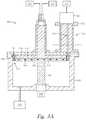
- FIG. 1illustrates a cross-sectional view of a processing chamber 100 according to one implementation described herein.
- the chamber 100includes a chamber body 102 which defines a process volume 110 .
- a substrate support 104may be disposed in the process volume 110 and a showerhead 112 may be disposed opposite the substrate support 104 .
- a pumping liner 150may be coupled to the chamber body 102 and may disposed radially outward of the substrate support 104 .
- a lid plate 124may be coupled to the showerhead 112 and supported by the chamber body 102 .
- a backing plate 114may be disposed between the showerhead 112 and the lid plate 124 .
- An injection assembly 126may be coupled to the lid plate 124 and the injection assembly may be in fluid communication with the process volume 110 .
- the chamber body 102may be manufactured from a material suitable to withstand temperatures of up to about 300° C.
- the chamber body 102may be formed from aluminum, alloys thereof, stainless steel, and other suitable metallic materials.
- a slit valve opening 160may be formed in the chamber body 102 to allow for ingress and egress of a substrate to and from the process volume 110 .
- a slit valve door 158may be coupled to the chamber body 102 and may be moveable to seal and unseal the slit valve opening 160 .
- the slit valve door 158may be formed from the same materials as the chamber body 102 .
- the slit valve door 158may be formed from materials different form the chamber body 102 .
- the substrate support 104may be moveably disposed within the process volume 110 . As illustrated, the substrate support 104 is disposed in an elevated processing position. The substrate support 104 may be lowered such that a substrate supporting surface of the substrate support 104 is coplanar with or below the slit valve opening 160 to allow for positioning of a substrate on the substrate support 104 .
- the substrate supportmay be formed from a material suitable for operation at elevated processing temperatures and may be a metallic material, a ceramic material, or combinations thereof.
- the pedestalmay be formed from aluminum, aluminum alloys, stainless steel, or ceramic materials, such as aluminum oxide or aluminum nitride.
- the substrate support 104may have a heating member 106 disposed therein and the heating member 106 may be coupled to a power source 154 .
- the power source 154may also provide power for raising and lowering the substrate support 104 within the process volume 110 .
- the heating member 106may be a resistive heater or the like and may be disposed within the substrate support 104 in any desirable orientation.
- the heating member 106may be formed in the substrate support 104 in a spiral orientation or other suitable orientation configured to heat the substrate support uniformly, such as a tortured path orientation.
- the heating member 106may be configured to heat the substrate support 104 to a temperature between about 100° C. and about 300° C.
- the pumping liner 150is sized to surround the substrate support 104 and the process volume 110 . Similar to the substrate support 104 , the pumping liner 150 may be formed from metallic materials, ceramic materials, or combinations thereof. For example, the pedestal may be formed from aluminum, aluminum alloys, stainless steel, or ceramic materials, such as aluminum oxide or aluminum nitride.
- the pumping liner 150may have an opening 162 formed therein to allow for ingress and egress of a substrate into the process volume 110 .
- the opening 162may be positioned substantially co-planar with the slit valve opening 160 .
- a plurality of holes 152may be formed along an inner diameter of the pumping liner 150 .
- the plurality of holes 152provide for evacuation of gases and other materials from the process volume 110 to an exhaust. Accordingly, the process volume 110 is in fluid communication with the exhaust 156 via the holes 152 of the pumping liner 150 .
- the showerhead 112which is disposed opposite the substrate support 104 , may be coupled directly or indirectly to and supported by the chamber body 102 .
- the showerhead 112may be formed from materials similar to the materials utilized for the substrate support 104 and the pumping liner 150 .
- the showerhead 112may have a plurality of first passages 121 formed therein which extend from the process volume 110 to a first plenum 120 formed between the showerhead 112 and the backing plate 114 .
- the first passages 121enable fluid communication and the transfer of vapor from the first plenum 120 to the process volume 110 .
- a showerhead liner 108may also be disposed in the process volume 110 .
- the showerhead liner 108may be formed from the same or similar materials as the showerhead 112 and the showerhead liner may be coupled to the showerhead 112 .
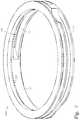
- the showerhead liner 108is a ring-like body.
- the showerhead liner 108may have an inner diameter which is substantially similar to an outer diameter of the substrate support 104 .
- the inner diameter of the showerhead liner 108may also be sized such that the innermost surface of the showerhead liner 108 is radially outward of the first passages 121 in order to not interfere with vapor delivery to the process volume 110 .
- the showerhead liner 108occupies physical space within the process volume 110 and reduces the volume of the process volume 110 , thereby reducing the amount of SAM precursor needed to form SAM molecules on a substrate. Thus, efficiency of a SAM formation process may be increased.
- the showerhead 112may also have a heater 116 disposed therein.
- the heater 116may be may be a resistive heater of the like and may be disposed within the showerhead 112 radially outward of the first passages 121 .
- the heater 116may be disposed within the showerhead 112 in a circumferential orientation which substantially surrounds the first passages 121 .
- the heater 116may be coupled to a power source 118 to enable resistive heating of the showerhead 112 .
- the showerhead 112may be configured to be heated to a temperature between about 150° C. and about 250° C.
- the backing plate 114which is disposed between the showerhead and the lid plate 124 , and partially defines the first plenum 120 , may have a second plurality of passages 123 disposed therein.
- a second plenum 122may be formed between the backing plate 114 and the lid plate 124 .
- the passages 123enable the second plenum 122 to be in fluid communication with the first plenum 120 .
- a third plurality of passages 125may be formed in the lid plate 124 between the second plenum 122 and the injection assembly 126 .
- the injection assembly 126is configured to deliver vaporized materials to the process volume 110 .
- vaporized materialssuch as SAM precursors and/or co-reactant precursors
- the vaporized materialstravel through the second plurality of passages 123 of the backing plate 114 to the first plenum 120 and through the first plurality of passages 121 of the showerhead 112 to the process volume 110 .
- the vaporized materials and other effluentmay be removed from the process volume 110 through the holes 152 of the pumping liner 150 via the exhaust 156 .
- the injection assembly 126includes a housing 127 coupled to the lid plate 124 and an injector 128 coupled to the housing 127 .
- the injector 128may be disposed within the housing 127 and the injector 128 may include a third plenum 148 .
- the third plenum 148may be funnel shaped.
- the shape of the third plenum 148may be configured to facilitate and encourage mixing of vaporized materials prior to delivery to the process volume 110 .
- the third plenum 148is illustrated as a funnel shape, other shapes which facilitate mixing of vaporized materials are contemplated.
- a first ampoule 130may be coupled to the injection assembly 126 via a first conduit 132 . More specifically, the first ampoule 130 may be in fluid communication with the third plenum 148 of the injector 128 via the first conduit 132 . The first conduit 132 may extend from the first ampoule 130 to the third plenum 148 .
- a first heater jacket 134may surround the first conduit 132 on portions of the first conduit 132 disposed beyond the injector 128 . In one implementation, the first heater jacket 134 may be resistively heated to maintain a temperature of the first conduit 132 between about 50° C. and about 250° C.
- the first ampoule 130is configured to vaporize and deliver SAM precursors to the process volume 110 .
- SAM precursorswhich may be utilized in accordance with the implementations described herein include the materials described hereinafter, including combinations, mixtures, and grafts thereof, in addition to other SAM precursor materials having characteristics suitable for blocking deposition of subsequently deposited materials in a semiconductor fabrication process.
- the SAM precursorsmay be carboxylic acid materials, such as methylcarboxylic acids, ethycarboxylic acids, propylcarboxylic acids, butylcarboxylic acids, pentylcarboxylic acids, hexylcarboxylic acids, heptylcarboxylic acids, octylcarboxylic acids, nonylcarboxylic acids, decylcarboxylic acids, undecylcarboxylic acids, dodecylcarboxylic acids, tridecylcarboxylic acids, tetradecylcarboxylic acids, pentadecylcarboxylic acids, hexadecylcarboxylic acids, heptadecylcarboxylic acids, octadecylcarboxylic acids, and nonadecylcarboxylic acids.
- carboxylic acid materialssuch as methylcarboxylic acids, ethycarboxylic acids
- the SAM precursorsmay be phosphonic acid materials, such as methylphosphonic acid, ethylphosphonic acid, propylphosphonic acid, butylphosphonic acid, pentylphosphonic acid, hexylphosphonic acid, heptylphosphonic acid, octylphosphonic acid, nonylphosphonic acid, decylphosphonic acid, undecylphosphonic acid, dodecylphosphonic acid, tridecylphosphonic acid, tetradecyphosphonic acid, pentadecylphosphonic acid, hexadecylphosphonic acid, heptadecylphosphonic acid, octadecylphosphonic acid, and nonadecylphosphonic acid.
- phosphonic acid materialssuch as methylphosphonic acid, ethylphosphonic acid, propylphosphonic acid, butylphosphonic acid, pentylphosphonic acid, hexylphosphonic acid, heptylphosphonic acid,
- the SAM precursorsmay be thiol materials, such as methanethiol, ethanethiol, propanethiol, butanethiol, pentanethiol, hexanethiol, heptanethiol, octanethiol, nonanethiol, decanethiol, undecanethiol, dodecanethiol, tridecanethiol, tetradecanethiol, pentadecanethiol, hexadecanethiol, heptadecanethiol, octadecanethiol, and nonadecanethiol.
- thiol materialssuch as methanethiol, ethanethiol, propanethiol, butanethiol, pentanethiol, hexanethiol, heptanethiol, octanethiol, nonade
- the SAM precursorsmay be silylamine materials, such as tris(dimethylamino)methylsilane, tris(dimethylamino)ethylsilane, tris(dimethylamino)propylsilane, tris(dimethylamino)butylsilane, tris(dimethylamino)pentylsilane, tris(dimethylamino)hexylsilane, tris(dimethylamino)heptylsilane, tris(dimethylamino)octylsilane, tris(dimethylamino)nonylsilane, tris(dimethylamino)decylsilane, tris(dimethylamino)undecylsilane tris(dimethylamino)dodecylsilane, tris(dimethylamino)tridecylsilane, tris((di
- the SAM precursorsmay be chlorosilane materials, such as methyltrichlorosilane, ethyltrichlorosilane, propyltrichlorosilane, butyltrichlorosilane, pentyltrichlorosilane, hexyltrichlorosilane, heptyltrichlorosilane, octyltrichlorosilane, nonyltrichlorosilane, decyltrichlorosilane, undecyltrichlorosilane, dodecyltrichlorosilane, tridecyltrichlorosilane, tetradecyltrichlorosilane, pentadecyltrichlorosilane, hexadecyltrichlorosilane, heptadecyltrichlorosilane, octadecyltrichlorosilane,
- the SAM precursorsmay be oxysilane materials, such as methyltrimethoxysilane, methyltriethoxysilane, ethyltrimethoxysilane, ethyltriethoxysilane, propyltrimethoxysilane, propyltriethoxysilane, butyltrimethoxysilane, butyltriethoxysilane, pentyltrimethoxysilane, pentyltriethoxysilane, hexyltrimethoxysilane, hexyltriethoxysilane, heptyltrimethoxysilane, heptyltriethoxysilane, octyltrimethoxysilane, octyltriethoxysilane, nonyltrimethoxysilane, nonyltriethoxysilane, decyltrimethoxysilane, decyltriethoxysi
- the SAM precursorsmay have a fluorinated R group, such as (1,1,2,2-perfluorodecyl)trichlorosilane, trichloro(1,1,2,2-perfluorooctyl)silane, (trideca-fluoro-1, 1,2,2-tetrahydrooctyl)trichlorosilane, (tridecafluoro-1, 1,2,2-tetrahydro-octyl)triethoxysilane, (tridecafluoro-1, 1,2,2-tetrahydrooctyl)methyldichlorosilane, (tridecafluoro-1, 1,2,2-tetrahydrooctyl)dimethylchlorosilane, and (heptadecafluoro-1, 1,2,2-tetrahydrodecyl)trichlorosilane, among others.
- a fluorinated R groupsuch as (1,1,2,2-perfluorodecyl
- a second ampoule 136may be coupled to the injection assembly 126 via a second conduit 138 . More specifically, the second ampoule 136 may be in fluid communication with the third plenum 148 of the injector 128 via the second conduit 138 . The second conduit 138 may extend from the second ampoule 136 to the third plenum 148 .
- a second heater jacket 140may surround the second conduit 138 on portions of the second conduit 138 disposed beyond the injector 128 . In one implementation, the second heater jacket 140 may be resistively heated to maintain a temperature of the second conduit 138 between about 50° C. and about 250° C.
- the second ampoule 136is configured to vaporize and deliver co-reactant precursors to the process volume 110 .
- co-reactant precursorsinclude hydroxyl moiety materials, such as ambient air, water solution or vapor, hydrogen peroxide solution or vapor, organic alcohol solutions or vapors, such as methanol, isopropanol, ethanol, and diols, among others. Hydrogen gas and oxygen gas may also be utilized in combination to form hydroxyl moieties. It is contemplated that other non-hydroxyl moiety precursors may also be utilized in accordance with the implementations described herein. Non-hydroxyl moiety precursors may include nitrogen gas, (di)isocyanates, hydrogen sulfide, and ammonia, among others.
- a cleaning gas source 142may be coupled to the injection assembly 126 via a third conduit 144 . More specifically, the cleaning gas source 142 may be in fluid communication with the third plenum 148 of the injector 128 via the third conduit 144 . The third conduit 144 may extend from the cleaning gas source 142 to the third plenum 148 . A third heater jacket 146 may optionally surround the third conduit 144 on portions of the third conduit 144 disposed beyond the injector 128 . In one implementation, the third heater jacket 146 may be resistively heated to maintain a temperature of the third conduit 144 between about 50° C. and about 250° C. Gases provided by the cleaning gas source 142 may include chlorine containing materials, fluorine containing materials, and other materials suitable for cleaning components of the processing chamber 100 .
- the cleaning gas source 142may be a remote plasma source.
- the remote plasma sourcemay energize cleaning gas to generate radicals and/or ions and the deliver the plasma products to the process volume 110 .
- the remote plasma sourcemay be optional.
- the cleaning gas source 142may be a carrier gas source.
- a carrier gasmay be utilized to facilitate delivery of vapor phase SAM precursors and the carrier gas, depending on the process volume 110 , may be delivered at a flow rate suitable to facilitate transport of the SAM precursors from the third plenum 148 , through the third passages 125 , through the second plenum 122 and the second passages 123 , and through the first plenum 120 and the first passages 121 to the process volume 110 .
- Suitable carrier gasesinclude gases, such as noble gases or the like, that are generally inert under SAM adsorption conditions that facilitate delivery of the SAM molecules to surfaces of the substrate.
- the heated showerhead 112 and the heated substrate support 104may heat the process volume 110 to a temperature of between about 50° and about 250° C.
- the ampoules 130 , 136 and conduits 132 , 138may be heated to similar temperatures.
- the showerhead liner 108 , backing plate 114 , lid plate 124 , and injection assembly 126may also be conductively heated by the showerhead 112 .
- the temperature of the flow path along which the SAM precursors travelis maintained at an elevated temperature to prevent condensation of the vaporized SAM precursors on the various apparatus.
- the process volume 110may also be maintained at a pressure of less than about 600 Torr which may also facilitate maintenance of the vapor state of the SAM precursor and co-reactant precursor.
- the SAM precursormay be continually flowed through the process volume 110 from the first ampoule 130 to the exhaust 156 .
- the pressure of the process volume 110may be maintained in an isobaric state.
- the SAM precursormay fill the process volume 110 and be maintained in the process volume 110 for a period of time prior to being exhausted from the process volume 110 .
- co-reactant precursorsmay be continually flowed to the process volume 110 or provided in a discontinuous manner, such as pulsing.
- the SAM precursor and the co-reactant precursormay be provided to the process volume 110 in an alternating manner either continually or statically.
- FIG. 2Aillustrates a perspective view of the showerhead 112 of FIG. 1 according to one implementation described herein.
- a surface 206 of the showerhead which has the first passages 121 formed thereinis the surface which is positioned adjacent and at least partially defining the process volume 110 .
- the heater 116extending from the showerhead 112 .
- a connection member 202such as a thermally or electrically conductive wire or the like, may extend from the heater 116 to the power source 118 (not illustrated).
- FIG. 2Billustrates a cross-sectional view of the showerhead 112 of FIG. 2A taken along line 2 B- 2 B according to one implementation described herein.
- the heater 116is disposed within the showerhead 112 .
- Voidsmay be machined in the body of the showerhead 112 and the heater 116 may be inserted into the showerhead 112 .
- a cap 204may be coupled to the showerhead 112 opposite the surface 206 .
- the cap 204may encase the heater 116 within the showerhead 112 and prevent the heater 116 from being exposed to various processing environments.
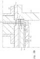
- FIG. 3Aillustrates a perspective view of the showerhead liner 108 according to one implementation described herein. As illustrated, the showerhead liner 108 is predominantly ring-shaped. It is contemplated that various other implementations of geometric shape may be utilized, such as annular, oblong, and polygonal.
- FIG. 3Billustrates a cross-sectional view of the showerhead liner 108 of FIG. 3A taken along line 3 B- 3 B according to one implementation described herein.
- the showerhead line 108includes a first surface 310 and a second surface 308 which is disposed normally to and extends from the first surface 310 .
- a third surface 306is disposed normally to and extends radially inward form the second surface 308 .
- the first surface 310 and the third surfaceare substantially parallel.
- a fourth surface 314is disposed normally to and extend from the third surface 306 parallel to the second surface 308 .
- a fifth surface 304is disposed normally to and extends from the fourth surface 314 .
- a sixth surface 302is disposed normal to and extends from the fifth surface 304 to the first surface 310 .
- the first surface 310may be disposed adjacent to and contact the showerhead 112 within the chamber 100 .
- the second surface 308may be disposed adjacent to and contact the pumping liner 150 .
- the second surface 308defined the outer diameter of the showerhead liner 108 and the second surface 308 may have a diameter less than an inner diameter of the pumping liner 150 .
- the sixth surface 302defined the inner diameter of the showerhead liner 108 and the sixth surface 302 may be disposed radially outward of the first passages 121 .
- One or more holes 312may be formed in the showerhead liner 108 and extend between the first surface 310 and the fifth surface 304 . The holes 312 may provide for coupling apparatus, such as screws or the like, to secure the showerhead liner 108 to the showerhead 112 .
- FIG. 4illustrates a perspective view of the pumping liner 150 according to one implementation described herein.
- the pumping liner 150is predominantly ring-shaped.
- the opening 162 formed in the pumping liner 150may extend along the circumference between about 25% and about 50% of the circumference. It is contemplated that the opening 162 may be sufficiently sized to allow for passage of a substrate and robot transfer blade therethrough.
- the holes 152may be disposed along an inner surface 402 which defined the inner diameter of the pumping liner 150 and the holes 152 may extend through the pumping liner 150 to an outer diameter a portion of the pumping liner 150 . Although not illustrated, the holes 152 extend completely through the pumping liner 150 which is more clearly illustrated in FIG. 1 .
- FIG. 5Aillustrates a cross-sectional view of a processing chamber 500 according to one implementation described herein.
- the chamber 500includes a chamber body 502 which defines a process volume 506 .
- a substrate support 504may be disposed within the process volume 506 and a heater 514 may be disposed in the process volume 506 opposite the substrate support 504 .
- a lid plate 516may be coupled to the chamber body 502 and a vapor generation assembly 518 may be coupled to the lid plate 516 .
- the chamber body 502may be formed from the same or similar materials as the chamber body 102 .
- the substrate support 504may be formed from the same or similar materials as the substrate support 104 .
- the substrate support 504includes a heating member 508 disposed therein.
- the heating member 508may be coupled to a power source 510 and be configured to heat the substrate support 504 to temperatures between about 100° C. and about 500° C.
- the heater 514which is disposed opposite the substrate support 504 , may further define the process volume 506 between the heater 514 and the substrate support 504 .
- the heater 514may be coupled to a power source 528 and be configured to heat the heater 514 to temperatures between about 100° C. and about 500° C.
- a temperature of the process volume 506may be maintained during processing at a temperature of between about 50° C. and about 500° C., such as between about 100° C. and about 250° C.
- a gas source 526may also be coupled to the heater 514 and the gas source 526 may be in fluid communication with the process volume 506 .
- the gas source 526may be configured to deliver a co-reactant precursor to the process volume 506 .
- the gas source 526may be configured to deliver a purge gas, a carrier gas, or a cleaning gas to the process volume 506 , depending on the desired implementation.
- the vapor generation assembly 518such as a vaporizer, a direct liquid injection vaporizer or the like, may be coupled to the lid plate 516 .
- the vapor generation assembly 518is coupled to the lid plate 516 radially outward of the process volume 506 .
- the position of the vapor generation assembly 518 , and injection location of vapor to the process volume 506provides for a cross-flow type exposure of a substrate to SAM precursors.
- the vapor generation assembly 518includes a vaporizer 522 and an injector 520 extending from the vaporizer 522 .
- the vaporizer 522may be coupled to a SAM precursor source 524 and receive SAM precursors in liquid form for vaporization.
- the vaporizer 522may be maintained at a temperature of between about 100° C. and about 500° C. to vaporize the SAM precursor and the temperature of the vaporizer 522 may be determine, at least in part, by the vapor pressure of the SAM precursor.
- Vaporized SAM precursormay exit the vaporizer 522 and travel through the injector 520 .
- the injector 520extends from the vaporizer 522 through the vapor generation assembly 518 , which may be maintained at an elevated temperature by a heater jacket 512 to maintain the SAM precursor in a vapor state, and to the lid plate 516 . While a single injector is illustrated, additional injectors, such as illustrated in FIG. 6 are contemplated.
- the SAM precursor travel pathwill be discussed in greater detail with regard to FIG. 5B .
- a manifold 536may be coupled to the chamber body 502 radially outward of the substrate support 504 and the heater 514 .
- the manifold 536may be formed from the same of similar materials as the substrate support 504 and the heater 514 .
- the manifold 536is sized to circumscribe the process volume 506 such that an inner diameter of the manifold 536 is larger than an outer diameter of the substrate support 504 and an outer diameter of the heater 514 .
- Vapormay flow through the manifold 536 from the injector 520 to an outlet 530 disposed opposite the injector 520 .
- An exhaust 532may also be coupled to and in fluid communication with the process volume 506 . More specifically, the exhaust 532 may be in fluid communication with the process volume 506 via the outlet 530 . Accordingly, process volume effluent may be evacuated from the process volume 506 through the outlet 530 to the exhaust 532 .
- a thermal insulator 534may be coupled to the lid plate 516 radially outward of the heater 514 .
- the thermal insulator 534may be sized similarly to the manifold 536 and may be disposed between the manifold 536 and the lid plate 516 .
- the thermal insulator 534may also be coupled to or in contact with the chamber body 502 .
- the thermal insulator 534may be formed from a thermally insulative material, such as a ceramic material or the like, configured to reduce of prevent the conduction of heat from the substrate support 504 , the heater 514 , and the manifold 536 from to the lid plate 516 .
- the thermal insulator 534may be optional.
- an air gapmay function as a thermal break between the lid plate 516 and the substrate support 504 , the heater 514 , and the manifold 536 .
- FIG. 5Billustrates an enlarged portion of the processing chamber 500 of FIG. 5A according to one implementation described herein.
- the injector 520extends to the lid plate 516 adjacent a first channel 548 formed in the lid plate 516 .
- a second channel 546may be formed in the thermal insulator 534 adjacent to and aligned with the first channel 548 .
- a third channel 544may be formed in the manifold 536 adjacent to and aligned with the second channel 546 .
- the third channel 544may extend from the second channel 546 of the thermal insulator 534 to an outlet 542 disposed adjacent the process volume 506 .
- the outlet 542may be positioned such that vapor provided from the vapor generation assembly 518 enters the process volume 506 between the substrate support 504 and the heater 514 when the substrate support 504 is in an elevated process position. Accordingly, vapor from the vapor generation assembly 518 travels through the injector 520 , the first channel 548 , the second channel 546 , and the third channel 544 , and through the outlet 542 to the process volume 506 .
- FIG. 5Cillustrates a plan view of the substrate support 504 and the manifold 536 of the processing chamber 500 of FIG. 5A according to one implementation described herein.
- the third channel 544 and outlet 542are disposed opposite the outlet 530 . Accordingly, vapor exiting the outlet 542 travels across a substrate disposed on the substrate support 504 to the outlet 530 .
- the outlet 530may be formed in the manifold 536 and extend curvilinearly a distance less than one half of the circumference of the manifold 536 .
- a plurality of holes 540may also be formed in the substrate support 504 to allow for lift pins to extend therethrough.
- FIG. 6illustrates a cross-sectional view of a processing chamber 600 according to one implementation described herein.
- the chamber 600includes a chamber body 602 which defines a process volume 606 .
- a substrate support 604may be disposed within the process volume 606 and a lid plate 616 may be coupled to the chamber body 602 opposite the substrate support 604 .
- a vapor generation assembly 618may be coupled to the lid plate 616 .
- the chamber body 602may be formed from the same or similar materials as the chamber body 502 .
- the substrate support 604may be formed from the same or similar materials as the substrate support 504 .
- the substrate support 604includes a heating member 608 disposed therein.
- the heating member 608may be coupled to a power source 610 and be configured to heat the substrate support 604 to temperatures between about 100° C. and about 500° C.
- the vapor generation assembly 618such as a vaporizer, a direct liquid injection vaporizer or the like, may be coupled to the lid plate 616 adjacent a center of the process volume 606 .
- the position of the vapor generation assembly 618 , and injection location of vapor to the process volume 606provides for a top-down type exposure of a substrate to SAM precursors.
- the vapor generation assembly 618includes a vaporizer 622 and one or more injectors 612 , 614 extending from the vaporizer 622 .
- the vaporizer 622may be coupled to a SAM precursor source 624 and receive SAM precursors in liquid form for vaporization.
- the vaporizer 622may be maintained at a temperature of between about 100° C. and about 500° C. to vaporize the SAM precursor and the temperature of the vaporizer 622 may be determine, at least in part, by the vapor pressure of the SAM precursor.
- Vaporized SAM precursormay exit the vaporizer 622 and travel through one or both of the injectors 612 , 614 .
- the injectors 612 , 614extend from the vaporizer 622 through the vapor generation assembly 618 , which may be maintained at an elevated temperature by a heater jacket 628 to maintain the SAM precursor in a vapor state, and to the lid plate 616 .
- SAM precursor from the source 624may be introduced to the process volume via the injector 612 through an outlet 630 .
- a gas source 626may also be in fluid communication with the process volume 606 .
- the gas source 626may introduce a liquid or gas to the vapor generation assembly 618 and the generated vapor may be introduced to the process volume 606 via the injector 614 and the outlet 630 .
- the gas source 626may provide a co-reactant precursor.
- the gas source 626may provide a purge gas, a carrier gas, or a cleaning gas, depending upon the desired implementation.
- the process volume 606may also be in fluid communication with an exhaust 632 . Accordingly, process volume effluent may be evacuated from the process volume 606 via the exhaust 632 . Both chambers 500 and 600 may be maintained at a pressure of less than about 600 Torr. Processes performed in the chambers 500 , 600 may be isobaric or non-isobaric. Similarly, the processes performed in the chambers 500 , 600 may be isothermal or non-isothermal.
Landscapes
- Chemical & Material Sciences (AREA)
- Engineering & Computer Science (AREA)
- General Chemical & Material Sciences (AREA)
- Chemical Kinetics & Catalysis (AREA)
- Materials Engineering (AREA)
- Mechanical Engineering (AREA)
- Metallurgy (AREA)
- Organic Chemistry (AREA)
- Physics & Mathematics (AREA)
- Condensed Matter Physics & Semiconductors (AREA)
- General Physics & Mathematics (AREA)
- Manufacturing & Machinery (AREA)
- Computer Hardware Design (AREA)
- Microelectronics & Electronic Packaging (AREA)
- Power Engineering (AREA)
- Plasma & Fusion (AREA)
- Chemical Vapour Deposition (AREA)
Abstract
Description
Claims (14)
Priority Applications (1)
| Application Number | Priority Date | Filing Date | Title |
|---|---|---|---|
| US15/468,758US11066747B2 (en) | 2016-04-25 | 2017-03-24 | Chemical delivery chamber for self-assembled monolayer processes |
Applications Claiming Priority (2)
| Application Number | Priority Date | Filing Date | Title |
|---|---|---|---|
| US201662327194P | 2016-04-25 | 2016-04-25 | |
| US15/468,758US11066747B2 (en) | 2016-04-25 | 2017-03-24 | Chemical delivery chamber for self-assembled monolayer processes |
Publications (2)
| Publication Number | Publication Date |
|---|---|
| US20170306491A1 US20170306491A1 (en) | 2017-10-26 |
| US11066747B2true US11066747B2 (en) | 2021-07-20 |
Family
ID=60089414
Family Applications (1)
| Application Number | Title | Priority Date | Filing Date |
|---|---|---|---|
| US15/468,758Active2037-08-09US11066747B2 (en) | 2016-04-25 | 2017-03-24 | Chemical delivery chamber for self-assembled monolayer processes |
Country Status (7)
| Country | Link |
|---|---|
| US (1) | US11066747B2 (en) |
| EP (1) | EP3449500A4 (en) |
| JP (3) | JP2019515493A (en) |
| KR (3) | KR20180128515A (en) |
| CN (2) | CN109417042B (en) |
| TW (2) | TWI722880B (en) |
| WO (1) | WO2017189135A1 (en) |
Cited By (2)
| Publication number | Priority date | Publication date | Assignee | Title |
|---|---|---|---|---|
| US11584993B2 (en) | 2020-10-19 | 2023-02-21 | Applied Materials, Inc. | Thermally uniform deposition station |
| US20240234192A1 (en)* | 2023-01-10 | 2024-07-11 | Taiwan Semiconductor Manufacturing Co., Ltd. | Method and Treatment System for Uniform Processing of Semiconductor Devices |
Families Citing this family (23)
| Publication number | Priority date | Publication date | Assignee | Title |
|---|---|---|---|---|
| JP7046188B2 (en) | 2018-08-02 | 2022-04-01 | 東京エレクトロン株式会社 | Film forming equipment |
| US10872747B2 (en)* | 2018-08-08 | 2020-12-22 | Lam Research Corporation | Controlling showerhead heating via resistive thermal measurements |
| KR102732061B1 (en)* | 2019-05-31 | 2024-11-18 | 어플라이드 머티어리얼스, 인코포레이티드 | Methods and systems for forming films on substrates |
| KR102280035B1 (en)* | 2019-10-10 | 2021-07-21 | 세메스 주식회사 | Apparatus and method for treating substrate |
| WO2021118993A1 (en)* | 2019-12-10 | 2021-06-17 | Tokyo Electron Limited | Self-assembled monolayers as sacrificial capping layers |
| US11420217B2 (en) | 2019-12-19 | 2022-08-23 | Applied Materials, Inc. | Showerhead for ALD precursor delivery |
| US11718023B2 (en)* | 2020-05-18 | 2023-08-08 | Qatar Foundation For Education, Science And Community Development | 3D printing based on self-assembled molecular building blocks for materials design and bio-applications |
| US11939666B2 (en)* | 2020-06-01 | 2024-03-26 | Applied Materials, Inc. | Methods and apparatus for precleaning and treating wafer surfaces |
| US12142467B2 (en) | 2020-06-02 | 2024-11-12 | Applied Materials, Inc. | Self-assembled monolayer deposition from low vapor pressure organic molecules |
| US11242600B2 (en)* | 2020-06-17 | 2022-02-08 | Applied Materials, Inc. | High temperature face plate for deposition application |
| TWI797640B (en)* | 2020-06-18 | 2023-04-01 | 法商液態空氣喬治斯克勞帝方法研究開發股份有限公司 | Silicon-based self-assembling monolayer compositions and surface preparation using the same |
| CA3193411A1 (en)* | 2020-09-22 | 2022-03-31 | Tohid DIDAR | Lubricant-infused surface biosensing interface, methods of making and uses thereof |
| US20220108872A1 (en)* | 2020-10-05 | 2022-04-07 | Applied Materials, Inc. | Bevel backside deposition elimination |
| WO2022133434A1 (en)* | 2020-12-17 | 2022-06-23 | Lam Research Corporation | Optimizing edge radical flux in a downstream plasma chamber |
| US11781212B2 (en) | 2021-04-07 | 2023-10-10 | Applied Material, Inc. | Overlap susceptor and preheat ring |
| US11851758B2 (en)* | 2021-04-20 | 2023-12-26 | Applied Materials, Inc. | Fabrication of a high temperature showerhead |
| US20220356572A1 (en)* | 2021-05-09 | 2022-11-10 | Applied Materials, Inc. | Pumping Liners with Self-Adjusting Pumping Conductance |
| CN114261039B (en)* | 2021-12-30 | 2025-07-25 | 广东粤港澳大湾区国家纳米科技创新研究院 | Template passivation process |
| US20230212747A1 (en)* | 2021-12-31 | 2023-07-06 | Applied Materials, Inc. | Apparatus and Methods for Self-Assembled Monolayer (SAM) Deposition in Semiconductor Equipment |
| JP7744102B2 (en)* | 2022-01-06 | 2025-09-25 | 東京エレクトロン株式会社 | Film forming method and film forming apparatus |
| KR102743115B1 (en) | 2022-10-18 | 2024-12-16 | 에스케이스페셜티 주식회사 | Substrate processing method and area selective thin film deposition method using the substrate processing method |
| WO2024137347A1 (en)* | 2022-12-21 | 2024-06-27 | Applied Materials, Inc. | Tunable hardware to control radial flow distribution in a processing chamber |
| WO2025183681A1 (en)* | 2024-02-26 | 2025-09-04 | Applied Materials, Inc. | Plasma chamber backing plate improvement |
Citations (39)
| Publication number | Priority date | Publication date | Assignee | Title |
|---|---|---|---|---|
| JPH09143737A (en) | 1995-11-22 | 1997-06-03 | Tokyo Electron Ltd | Film forming apparatus |
| US6200893B1 (en) | 1999-03-11 | 2001-03-13 | Genus, Inc | Radical-assisted sequential CVD |
| US20010035127A1 (en)* | 1998-10-27 | 2001-11-01 | Craig R. Metzner | Deposition reactor having vaporizing, mixing and cleaning capabilities |
| US6319327B1 (en)* | 1999-07-27 | 2001-11-20 | Tokyo Electron Limited | MOCVD system |
| EP1202321A2 (en) | 2000-10-23 | 2002-05-02 | Applied Materials, Inc. | Vaporization of precursors at point of use |
| US6391785B1 (en) | 1999-08-24 | 2002-05-21 | Interuniversitair Microelektronica Centrum (Imec) | Method for bottomless deposition of barrier layers in integrated circuit metallization schemes |
| US20030101938A1 (en)* | 1998-10-27 | 2003-06-05 | Applied Materials, Inc. | Apparatus for the deposition of high dielectric constant films |
| US20040221807A1 (en) | 2003-05-09 | 2004-11-11 | Mohith Verghese | Reactor surface passivation through chemical deactivation |
| US20060096541A1 (en)* | 2004-11-08 | 2006-05-11 | Jung-Hun Seo | Apparatus and method of forming a layer on a semiconductor substrate |
| US7071022B2 (en) | 2003-07-18 | 2006-07-04 | Corning Incorporated | Silicon crystallization using self-assembled monolayers |
| US20080026146A1 (en) | 2004-06-04 | 2008-01-31 | Applied Microstrctures, Inc. | Method of depositing a multilayer coating with a variety of oxide adhesion layers and organic layers |
| US20080044569A1 (en) | 2004-05-12 | 2008-02-21 | Myo Nyi O | Methods for atomic layer deposition of hafnium-containing high-k dielectric materials |
| US20090057266A1 (en) | 2007-08-27 | 2009-03-05 | Eda Tuncel | Line edge roughness control |
| US7648866B2 (en) | 2006-12-22 | 2010-01-19 | Samsung Electronics Co., Ltd. | Method of manufacturing driving-device for unit pixel of organic light emitting display |
| US7775508B2 (en) | 2006-10-31 | 2010-08-17 | Applied Materials, Inc. | Ampoule for liquid draw and vapor draw with a continuous level sensor |
| KR20100107228A (en) | 2009-03-25 | 2010-10-05 | 포항공과대학교 산학협력단 | Method for forming contacts of semiconductor devices using the selective deposition |
| KR20110014771A (en) | 2009-08-06 | 2011-02-14 | 한국과학기술원 | Pattern Forming Method and Pattern Forming Device |
| US20110124187A1 (en) | 2009-11-25 | 2011-05-26 | International Business Machines Corporation | Vapor phase deposition processes for doping silicon |
| US7960295B2 (en) | 2006-03-10 | 2011-06-14 | Lg Display Co., Ltd. | Film transistor and method for fabricating the same |
| WO2011103062A2 (en) | 2010-02-17 | 2011-08-25 | Asm America, Inc. | Reactive site deactivation against vapor deposition |
| US20110253044A1 (en) | 2010-04-14 | 2011-10-20 | Applied Materials, Inc. | Showerhead assembly with metrology port purge |
| US20120009765A1 (en)* | 2010-07-12 | 2012-01-12 | Applied Materials, Inc. | Compartmentalized chamber |
| US20120178650A1 (en) | 2005-11-09 | 2012-07-12 | The Trustees Of Columbia University In The City Of New York | Photochemical methods and photoactive compounds for modifying surfaces |
| US20120238109A1 (en) | 2009-09-28 | 2012-09-20 | Shigeki Hattori | Method of forming pattern |
| US20120273052A1 (en)* | 2011-04-29 | 2012-11-01 | Applied Materials, Inc. | Method and apparatus for gas delivery |
| WO2013030576A1 (en) | 2011-09-01 | 2013-03-07 | Memsstar Limited | Improved deposition technique for depositing a coating on a device |
| US20130193108A1 (en) | 2012-01-27 | 2013-08-01 | Applied Materials, Inc. | Methods of end point detection for substrate fabrication processes |
| JP2013154315A (en) | 2012-01-31 | 2013-08-15 | Ricoh Co Ltd | Thin film forming apparatus, thin film forming method, electro-mechanical transducer element, liquid ejecting head, and inkjet recording apparatus |
| KR20140003040A (en) | 2012-06-29 | 2014-01-09 | (주)아모레퍼시픽 | Composition for prevention of skin aging comprising tea water |
| US20140357016A1 (en) | 2013-06-04 | 2014-12-04 | Tokyo Electron Limited | Organic molecular film forming apparatus and organic molecular film forming method |
| US20140370718A1 (en) | 2013-06-14 | 2014-12-18 | Tokyo Electron Limited | Etch process for reducing directed self assembly pattern defectivity using direct current positioning |
| US20150064838A1 (en)* | 2013-09-04 | 2015-03-05 | South Dakota Board Of Regents | Self-assembled organic monolayer hybrid materials and methods thereof |
| US20150090330A1 (en) | 2013-09-27 | 2015-04-02 | Richard Hamilton SEWELL | Solar cell contact structures formed from metal paste |
| WO2015065790A1 (en) | 2013-11-01 | 2015-05-07 | Applied Materials, Inc. | Low temperature silicon nitride films using remote plasma cvd technology |
| US20150179500A1 (en) | 2005-05-18 | 2015-06-25 | Intermolecular, Inc. | Formation of a Masking Layer on a Dielectric Region to Facilitate Formation of a Capping Layer on Electrically Conductive Regions Separated by the Dielectric Region |
| US9112003B2 (en) | 2011-12-09 | 2015-08-18 | Asm International N.V. | Selective formation of metallic films on metallic surfaces |
| US20150262869A1 (en)* | 2014-03-11 | 2015-09-17 | Applied Materials, Inc. | Methods for forming interconnection structures in an integrated cluster system for semicondcutor applications |
| US20160056071A1 (en) | 2014-08-20 | 2016-02-25 | Lam Research Corporation | Flowable dielectric for selective ultra low-k pore sealing |
| US20160104648A1 (en)* | 2014-10-14 | 2016-04-14 | Applied Materials, Inc. | Systems and methods for internal surface conditioning in plasma processing equipment |
Family Cites Families (11)
| Publication number | Priority date | Publication date | Assignee | Title |
|---|---|---|---|---|
| JPH08148480A (en)* | 1994-11-22 | 1996-06-07 | Mitsubishi Electric Corp | Semiconductor manufacturing apparatus and semiconductor manufacturing method using the same |
| JPH0997767A (en)* | 1995-09-28 | 1997-04-08 | Kokusai Electric Co Ltd | Vertical furnace for semiconductor manufacturing equipment |
| KR101714660B1 (en)* | 2008-11-07 | 2017-03-22 | 에이에스엠 아메리카, 인코포레이티드 | Reaction chamber |
| US8562742B2 (en)* | 2010-04-30 | 2013-10-22 | Applied Materials, Inc. | Apparatus for radial delivery of gas to a chamber and methods of use thereof |
| KR101387518B1 (en)* | 2012-08-28 | 2014-05-07 | 주식회사 유진테크 | Apparatus for processing substrate |
| US20140099794A1 (en)* | 2012-09-21 | 2014-04-10 | Applied Materials, Inc. | Radical chemistry modulation and control using multiple flow pathways |
| US20140137801A1 (en)* | 2012-10-26 | 2014-05-22 | Applied Materials, Inc. | Epitaxial chamber with customizable flow injection |
| JP5602903B2 (en)* | 2013-03-14 | 2014-10-08 | アプライド マテリアルズ インコーポレイテッド | Epitaxial film formation method and epitaxial growth apparatus |
| JP6456956B2 (en)* | 2013-08-19 | 2019-01-23 | アプライド マテリアルズ インコーポレイテッドApplied Materials,Incorporated | Equipment for epitaxy with stacked impurities |
| KR102437125B1 (en)* | 2014-06-27 | 2022-08-25 | 어플라이드 머티어리얼스, 인코포레이티드 | Plasma corrosion resistive heater for high temperature processing |
| US20160056032A1 (en)* | 2014-08-22 | 2016-02-25 | Lam Research Corporation | Methods and apparatuses for stable deposition rate control in low temperature ald systems by showerhead active heating and/or pedestal cooling |
- 2017
- 2017-03-24USUS15/468,758patent/US11066747B2/enactiveActive
- 2017-03-24WOPCT/US2017/024077patent/WO2017189135A1/ennot_activeCeased
- 2017-03-24KRKR1020187033883Apatent/KR20180128515A/ennot_activeCeased
- 2017-03-24CNCN201780025455.0Apatent/CN109417042B/enactiveActive
- 2017-03-24KRKR1020207026523Apatent/KR102201927B1/enactiveActive
- 2017-03-24KRKR1020217000275Apatent/KR102306693B1/enactiveActive
- 2017-03-24EPEP17790059.4Apatent/EP3449500A4/enactivePending
- 2017-03-24CNCN202210470647.5Apatent/CN114975176A/enactivePending
- 2017-03-24JPJP2018555679Apatent/JP2019515493A/enactivePending
- 2017-04-20TWTW109113612Apatent/TWI722880B/enactive
- 2017-04-20TWTW106113223Apatent/TWI693297B/enactive
- 2020
- 2020-09-14JPJP2020153837Apatent/JP7198246B2/enactiveActive
- 2022
- 2022-11-04JPJP2022176882Apatent/JP7473614B2/enactiveActive
Patent Citations (49)
| Publication number | Priority date | Publication date | Assignee | Title |
|---|---|---|---|---|
| JPH09143737A (en) | 1995-11-22 | 1997-06-03 | Tokyo Electron Ltd | Film forming apparatus |
| US20030101938A1 (en)* | 1998-10-27 | 2003-06-05 | Applied Materials, Inc. | Apparatus for the deposition of high dielectric constant films |
| US20010035127A1 (en)* | 1998-10-27 | 2001-11-01 | Craig R. Metzner | Deposition reactor having vaporizing, mixing and cleaning capabilities |
| US6200893B1 (en) | 1999-03-11 | 2001-03-13 | Genus, Inc | Radical-assisted sequential CVD |
| US6319327B1 (en)* | 1999-07-27 | 2001-11-20 | Tokyo Electron Limited | MOCVD system |
| US6391785B1 (en) | 1999-08-24 | 2002-05-21 | Interuniversitair Microelektronica Centrum (Imec) | Method for bottomless deposition of barrier layers in integrated circuit metallization schemes |
| EP1202321A2 (en) | 2000-10-23 | 2002-05-02 | Applied Materials, Inc. | Vaporization of precursors at point of use |
| US20040221807A1 (en) | 2003-05-09 | 2004-11-11 | Mohith Verghese | Reactor surface passivation through chemical deactivation |
| US20100304132A1 (en)* | 2003-06-27 | 2010-12-02 | Applied Microstructures, Inc. | Controlled vapor deposition of multilayered coatings adhered by an oxide layer |
| US7071022B2 (en) | 2003-07-18 | 2006-07-04 | Corning Incorporated | Silicon crystallization using self-assembled monolayers |
| US20080044569A1 (en) | 2004-05-12 | 2008-02-21 | Myo Nyi O | Methods for atomic layer deposition of hafnium-containing high-k dielectric materials |
| US20080026146A1 (en) | 2004-06-04 | 2008-01-31 | Applied Microstrctures, Inc. | Method of depositing a multilayer coating with a variety of oxide adhesion layers and organic layers |
| US20060096541A1 (en)* | 2004-11-08 | 2006-05-11 | Jung-Hun Seo | Apparatus and method of forming a layer on a semiconductor substrate |
| US20150179500A1 (en) | 2005-05-18 | 2015-06-25 | Intermolecular, Inc. | Formation of a Masking Layer on a Dielectric Region to Facilitate Formation of a Capping Layer on Electrically Conductive Regions Separated by the Dielectric Region |
| US20120178650A1 (en) | 2005-11-09 | 2012-07-12 | The Trustees Of Columbia University In The City Of New York | Photochemical methods and photoactive compounds for modifying surfaces |
| US7960295B2 (en) | 2006-03-10 | 2011-06-14 | Lg Display Co., Ltd. | Film transistor and method for fabricating the same |
| US7775508B2 (en) | 2006-10-31 | 2010-08-17 | Applied Materials, Inc. | Ampoule for liquid draw and vapor draw with a continuous level sensor |
| US7648866B2 (en) | 2006-12-22 | 2010-01-19 | Samsung Electronics Co., Ltd. | Method of manufacturing driving-device for unit pixel of organic light emitting display |
| US20090057266A1 (en) | 2007-08-27 | 2009-03-05 | Eda Tuncel | Line edge roughness control |
| KR20100107228A (en) | 2009-03-25 | 2010-10-05 | 포항공과대학교 산학협력단 | Method for forming contacts of semiconductor devices using the selective deposition |
| KR20110014771A (en) | 2009-08-06 | 2011-02-14 | 한국과학기술원 | Pattern Forming Method and Pattern Forming Device |
| US20120238109A1 (en) | 2009-09-28 | 2012-09-20 | Shigeki Hattori | Method of forming pattern |
| US20110124187A1 (en) | 2009-11-25 | 2011-05-26 | International Business Machines Corporation | Vapor phase deposition processes for doping silicon |
| JP2013520028A (en) | 2010-02-17 | 2013-05-30 | エーエスエム アメリカ インコーポレイテッド | Deactivation of reactive sites for deposition. |
| WO2011103062A2 (en) | 2010-02-17 | 2011-08-25 | Asm America, Inc. | Reactive site deactivation against vapor deposition |
| KR20130005262A (en) | 2010-02-17 | 2013-01-15 | 에이에스엠 아메리카, 인코포레이티드 | Reactive site deactivation against vapor deposition |
| US20110253044A1 (en) | 2010-04-14 | 2011-10-20 | Applied Materials, Inc. | Showerhead assembly with metrology port purge |
| US20120009765A1 (en)* | 2010-07-12 | 2012-01-12 | Applied Materials, Inc. | Compartmentalized chamber |
| TW201204868A (en) | 2010-07-12 | 2012-02-01 | Applied Materials Inc | Compartmentalized chamber |
| US20120273052A1 (en)* | 2011-04-29 | 2012-11-01 | Applied Materials, Inc. | Method and apparatus for gas delivery |
| KR20140068014A (en) | 2011-09-01 | 2014-06-05 | 멤스스타 리미티드 | Improved deposition technique for depositing a coating on a device |
| JP2014531508A (en) | 2011-09-01 | 2014-11-27 | メムススター リミテッドMemsstar Limited | Improved deposition method for depositing a coating on a device |
| WO2013030576A1 (en) | 2011-09-01 | 2013-03-07 | Memsstar Limited | Improved deposition technique for depositing a coating on a device |
| US9112003B2 (en) | 2011-12-09 | 2015-08-18 | Asm International N.V. | Selective formation of metallic films on metallic surfaces |
| US9502289B2 (en) | 2011-12-09 | 2016-11-22 | Asm International N.V. | Selective formation of metallic films on metallic surfaces |
| US20130193108A1 (en) | 2012-01-27 | 2013-08-01 | Applied Materials, Inc. | Methods of end point detection for substrate fabrication processes |
| JP2013154315A (en) | 2012-01-31 | 2013-08-15 | Ricoh Co Ltd | Thin film forming apparatus, thin film forming method, electro-mechanical transducer element, liquid ejecting head, and inkjet recording apparatus |
| KR20140003040A (en) | 2012-06-29 | 2014-01-09 | (주)아모레퍼시픽 | Composition for prevention of skin aging comprising tea water |
| US20140357016A1 (en) | 2013-06-04 | 2014-12-04 | Tokyo Electron Limited | Organic molecular film forming apparatus and organic molecular film forming method |
| US20140370718A1 (en) | 2013-06-14 | 2014-12-18 | Tokyo Electron Limited | Etch process for reducing directed self assembly pattern defectivity using direct current positioning |
| US20150064838A1 (en)* | 2013-09-04 | 2015-03-05 | South Dakota Board Of Regents | Self-assembled organic monolayer hybrid materials and methods thereof |
| US20150090330A1 (en) | 2013-09-27 | 2015-04-02 | Richard Hamilton SEWELL | Solar cell contact structures formed from metal paste |
| KR20160078428A (en) | 2013-11-01 | 2016-07-04 | 어플라이드 머티어리얼스, 인코포레이티드 | Low temperature silicon nitride films using remote plasma cvd technology |
| WO2015065790A1 (en) | 2013-11-01 | 2015-05-07 | Applied Materials, Inc. | Low temperature silicon nitride films using remote plasma cvd technology |
| US20150262869A1 (en)* | 2014-03-11 | 2015-09-17 | Applied Materials, Inc. | Methods for forming interconnection structures in an integrated cluster system for semicondcutor applications |
| TW201546876A (en) | 2014-03-11 | 2015-12-16 | Applied Materials Inc | Methods for forming interconnection structures in an integrated cluster system for semicondcutor applications |
| US20160056071A1 (en) | 2014-08-20 | 2016-02-25 | Lam Research Corporation | Flowable dielectric for selective ultra low-k pore sealing |
| KR20160022788A (en) | 2014-08-20 | 2016-03-02 | 램 리써치 코포레이션 | Flowable dielectric for selective ultra low-k pore sealing |
| US20160104648A1 (en)* | 2014-10-14 | 2016-04-14 | Applied Materials, Inc. | Systems and methods for internal surface conditioning in plasma processing equipment |
Non-Patent Citations (36)
| Title |
|---|
| A. Jain et al., Control of selectivity during chemical vapor deposition of copper from copper (I) compounds via silicon dioxide surface modification, Applied Physics Letters 61, pp. 2662-2664 (1992) American Institute of Physics. |
| Communication pursuant to Rule 164(1) EPC for Application No. 17790059.4-1103 /3449500 dated Dec. 9, 2019. |
| Elina Färm, et al., Self-Assembled Octadecyltrimethoxysilane Monolayers Enabling Selective-Area Atomic Layer Deposition of Iridium, Chemical Vapor Deposition, 12, 2006, 3 pp. |
| Elina Farm, Selective-Area Atomic Layer Deposition, University of Helsinki, Nov. 2011. |
| European Office Action in application EP 00955875.0, dated May 8, 2004. |
| Extended European Search Report for European Application No. 17790059.4 dated Mar. 19, 2020. |
| Final Office Action for Korean Application No. 10-2018-7033883 dated Aug. 13, 2020 (w/ translation), 9 pages. |
| Final Office Action for Korean Application No. 10-2018-7033883 dated Jun. 17, 2020. |
| Hashemi et al, Self Correcting Process for High Quality Patterning by Atomic Layer Deposition, American Chemical Society, Jul. 16, 2015. |
| International Search Report and Written Opinion for International Application No. PCT/US2017/019982 dated Jun. 26, 2017. |
| International Search Report and Written Opinion for International application No. PCT/US2017/024077 dated Jul. 11, 2017. |
| Jae-Sik Min et al., Metal-organic atomic-layer deposition of titanium-silicon-nitride films. Applied Physics Letters vol. 75, No. 11 Sep. 13, 1999. |
| Japanese Office Action dated May 12, 2020 for Application No. 2018-555679. |
| Junsic Hong, et al., ALD Resist Formed by Vapor-Deposited Self-Assembled Monolayers, Langmuir 2007, 23, 6 pp. |
| JW Klaus et al., Atomically controlled growth of tungsten and tungsten nitride using sequential surface reactions; Applied Surface Sciences 162-163 (2000) 479-491. |
| Korean Office Action for Application No. 10-2021-70000275 dated Feb. 1, 2021. |
| M. Leskela et al., ALD precursor chemistry: Evolution and future challenges, Article published online by EDP Sciences and available at http://dx_doi.org/10.1051/jp4:19998106. |
| Mikko Ritala et al., Atomic layer epitaxy—a valuable tool for nanotechnology?; Nanotechnology 10 (1999) 19-24 printed in the UK. |
| Mikko Ritala et al., Perfectly Conformal TiN and Al2O3 Films Deposited by Atomic Layer Deposition, Chemical Vapor Deposition 1999, 5, No. 1 Ó Wiley-VCH Verlag GmbH, D-69469 Weinheim, 1999. |
| Ming Fang, et al., Area-Selective Atomic Layer Deposition: Conformal Coating, Subnanometer Thickness Control and Smart Positioning, ACS Nano 2015 Vo. 9. No. 9 pp. 8651-8654. |
| Non-final Office Action in U.S. Appl. No. 10/731,656 dated May 11, 2004. |
| Notice of Grant for Taiwan Application No. 109113612 dated Nov. 19, 2020. |
| Office Action for Japanese Application No. 2018-546484 dated Oct. 8, 2019. |
| Office Action for Japanese Application No. 2018-555679 dated Dec. 24, 2019. |
| Office Action for Korean Application No. 10-2018-7028591 dated Dec. 12, 2019. |
| Office Action for Korean Application No. 10-2018-7033883 dated Feb. 17, 2020. |
| Office Action for Taiwan Application No. 106113223 dated Jul. 9, 2019. |
| Per Martensson et al., Atomic Layer Epitaxy of Copper, J. Elect rochem. Soc., vol. 145, No. 8, Aug. 1998 The Electrochemical Society, Inc. pp. 2926-2931. |
| Satu Ek, et al., Atomic Layer Deposition of a High-Density Aminopropylsiloxane Network on Silica through Sequential Reactions of ?-Aminopropyltrialkoxysilanes and Water, Langmuir 2003, 19, 9 pp. |
| SE Kirkwood et al., Mechanism for femtosecond laser pulse patterning of SAM on gold coated substrate, IOP Publishing Ltd 2007 p. 428-430. |
| Search Report for Taiwan Application No. 106113223 dated Jul. 8, 2019. |
| Search Report for Taiwan Application No. 109113612 dated Nov. 18, 2020. |
| Shin Yokoyama, et al., Atomic-layer selective deposition of silicon nitride on hydrogen-terminated Si surfaces, Applied Surface Science 130-132 1998. 352-356. |
| Stephen M. Gates, Surface Chemistry in the Chemical Vapor Deposition of Electronic Materials, Chem. Rev. 1996, 96, pp. 1519-1532. |
| T. M. Mayer, et al., Chemical Vapor Deposition of Fluoroalkylsilane Monolayer Films; for Adhesion Control in Microelectromechanical Systems, Journal of Vacuum Science & Technology B, 18 (5), Sep./Oct. 2000, 9 pages. |
| Woo-Hee Kim, et al., A Process for Topographically-Selective Deposition on 3D Nanostructures by Ion Implantation, ACS Nano, 2016, 10 (4), 22 pp. |
Cited By (2)
| Publication number | Priority date | Publication date | Assignee | Title |
|---|---|---|---|---|
| US11584993B2 (en) | 2020-10-19 | 2023-02-21 | Applied Materials, Inc. | Thermally uniform deposition station |
| US20240234192A1 (en)* | 2023-01-10 | 2024-07-11 | Taiwan Semiconductor Manufacturing Co., Ltd. | Method and Treatment System for Uniform Processing of Semiconductor Devices |
Also Published As
| Publication number | Publication date |
|---|---|
| KR20200108512A (en) | 2020-09-18 |
| CN114975176A (en) | 2022-08-30 |
| KR102201927B1 (en) | 2021-01-11 |
| TW202028518A (en) | 2020-08-01 |
| JP2023027047A (en) | 2023-03-01 |
| EP3449500A1 (en) | 2019-03-06 |
| JP7473614B2 (en) | 2024-04-23 |
| EP3449500A4 (en) | 2020-04-22 |
| CN109417042B (en) | 2022-05-10 |
| WO2017189135A1 (en) | 2017-11-02 |
| CN109417042A (en) | 2019-03-01 |
| TWI693297B (en) | 2020-05-11 |
| KR20210003966A (en) | 2021-01-12 |
| TWI722880B (en) | 2021-03-21 |
| KR20180128515A (en) | 2018-12-03 |
| JP2021007156A (en) | 2021-01-21 |
| US20170306491A1 (en) | 2017-10-26 |
| KR102306693B1 (en) | 2021-09-28 |
| JP7198246B2 (en) | 2022-12-28 |
| TW201802288A (en) | 2018-01-16 |
| JP2019515493A (en) | 2019-06-06 |
Similar Documents
| Publication | Publication Date | Title |
|---|---|---|
| US11066747B2 (en) | Chemical delivery chamber for self-assembled monolayer processes | |
| US11725274B2 (en) | Integrated cluster tool for selective area deposition | |
| US10818510B2 (en) | Self-assembled monolayer blocking with intermittent air-water exposure | |
| CN206494968U (en) | The CVD of low-steam pressure aerosol auxiliary | |
| US6409837B1 (en) | Processing system and method for chemical vapor deposition of a metal layer using a liquid precursor | |
| KR101210456B1 (en) | Method of manufacturing semiconductor device, method of processing substrate and substrate processing apparatus | |
| TW201903966A (en) | Self-aligned via process flow | |
| US20250054739A1 (en) | Self-assembled monolayer deposition from low vapor pressure organic molecules |
Legal Events
| Date | Code | Title | Description |
|---|---|---|---|
| AS | Assignment | Owner name:APPLIED MATERIALS, INC., CALIFORNIA Free format text:ASSIGNMENT OF ASSIGNORS INTEREST;ASSIGNORS:LIANG, QIWEI;KHAN, ADIB;KAUFMAN-OSBORN, TOBIN;AND OTHERS;SIGNING DATES FROM 20170405 TO 20170410;REEL/FRAME:042793/0708 | |
| STPP | Information on status: patent application and granting procedure in general | Free format text:NON FINAL ACTION MAILED | |
| STPP | Information on status: patent application and granting procedure in general | Free format text:RESPONSE TO NON-FINAL OFFICE ACTION ENTERED AND FORWARDED TO EXAMINER | |
| STPP | Information on status: patent application and granting procedure in general | Free format text:FINAL REJECTION MAILED | |
| STPP | Information on status: patent application and granting procedure in general | Free format text:ADVISORY ACTION MAILED | |
| STPP | Information on status: patent application and granting procedure in general | Free format text:DOCKETED NEW CASE - READY FOR EXAMINATION | |
| STPP | Information on status: patent application and granting procedure in general | Free format text:NON FINAL ACTION MAILED | |
| STPP | Information on status: patent application and granting procedure in general | Free format text:RESPONSE TO NON-FINAL OFFICE ACTION ENTERED AND FORWARDED TO EXAMINER | |
| STPP | Information on status: patent application and granting procedure in general | Free format text:FINAL REJECTION MAILED | |
| STPP | Information on status: patent application and granting procedure in general | Free format text:RESPONSE AFTER FINAL ACTION FORWARDED TO EXAMINER | |
| STPP | Information on status: patent application and granting procedure in general | Free format text:DOCKETED NEW CASE - READY FOR EXAMINATION | |
| STPP | Information on status: patent application and granting procedure in general | Free format text:NOTICE OF ALLOWANCE MAILED -- APPLICATION RECEIVED IN OFFICE OF PUBLICATIONS | |
| STPP | Information on status: patent application and granting procedure in general | Free format text:PUBLICATIONS -- ISSUE FEE PAYMENT VERIFIED | |
| STCF | Information on status: patent grant | Free format text:PATENTED CASE | |
| MAFP | Maintenance fee payment | Free format text:PAYMENT OF MAINTENANCE FEE, 4TH YEAR, LARGE ENTITY (ORIGINAL EVENT CODE: M1551); ENTITY STATUS OF PATENT OWNER: LARGE ENTITY Year of fee payment:4 |