US11062942B2 - Methods for controllable metal and barrier-liner recess - Google Patents
Methods for controllable metal and barrier-liner recessDownload PDFInfo
- Publication number
- US11062942B2 US11062942B2US16/214,522US201816214522AUS11062942B2US 11062942 B2US11062942 B2US 11062942B2US 201816214522 AUS201816214522 AUS 201816214522AUS 11062942 B2US11062942 B2US 11062942B2
- Authority
- US
- United States
- Prior art keywords
- dielectric material
- barrier layer
- feature
- metal layer
- metal
- Prior art date
- Legal status (The legal status is an assumption and is not a legal conclusion. Google has not performed a legal analysis and makes no representation as to the accuracy of the status listed.)
- Active, expires
Links
- 229910052751metalInorganic materials0.000titleclaimsabstractdescription131
- 239000002184metalSubstances0.000titleclaimsabstractdescription131
- 238000000034methodMethods0.000titleclaimsabstractdescription67
- 230000004888barrier functionEffects0.000claimsabstractdescription111
- 239000003989dielectric materialSubstances0.000claimsabstractdescription107
- 239000000758substrateSubstances0.000claimsabstractdescription43
- 238000005530etchingMethods0.000claimsabstractdescription17
- 229910052707rutheniumInorganic materials0.000claimsdescription7
- 229910052710siliconInorganic materials0.000claimsdescription7
- 238000003672processing methodMethods0.000claimsdescription5
- 229910052814silicon oxideInorganic materials0.000claimsdescription5
- VYPSYNLAJGMNEJ-UHFFFAOYSA-NSilicium dioxideChemical compoundO=[Si]=OVYPSYNLAJGMNEJ-UHFFFAOYSA-N0.000claimsdescription4
- 150000001875compoundsChemical class0.000claimsdescription4
- 229910052802copperInorganic materials0.000claimsdescription3
- 239000011521glassSubstances0.000claimsdescription3
- 229910017107AlOxInorganic materials0.000claimsdescription2
- 229910052782aluminiumInorganic materials0.000claimsdescription2
- 229910052741iridiumInorganic materials0.000claimsdescription2
- 229910052748manganeseInorganic materials0.000claimsdescription2
- 229910052759nickelInorganic materials0.000claimsdescription2
- 229910052697platinumInorganic materials0.000claimsdescription2
- 229910052721tungstenInorganic materials0.000claimsdescription2
- ATJFFYVFTNAWJD-UHFFFAOYSA-NTinChemical compound[Sn]ATJFFYVFTNAWJD-UHFFFAOYSA-N0.000claims2
- BPQQTUXANYXVAA-UHFFFAOYSA-NOrthosilicateChemical compound[O-][Si]([O-])([O-])[O-]BPQQTUXANYXVAA-UHFFFAOYSA-N0.000claims1
- 239000010410layerSubstances0.000description192
- 239000000463materialSubstances0.000description19
- 239000004065semiconductorSubstances0.000description7
- XUIMIQQOPSSXEZ-UHFFFAOYSA-NSiliconChemical compound[Si]XUIMIQQOPSSXEZ-UHFFFAOYSA-N0.000description6
- 239000000203mixtureSubstances0.000description6
- 238000002161passivationMethods0.000description6
- 150000002978peroxidesChemical class0.000description6
- 239000010703siliconSubstances0.000description6
- VHUUQVKOLVNVRT-UHFFFAOYSA-NAmmonium hydroxideChemical compound[NH4+].[OH-]VHUUQVKOLVNVRT-UHFFFAOYSA-N0.000description5
- 239000010949copperSubstances0.000description4
- MZLGASXMSKOWSE-UHFFFAOYSA-Ntantalum nitrideChemical compound[Ta]#NMZLGASXMSKOWSE-UHFFFAOYSA-N0.000description4
- PXHVJJICTQNCMI-UHFFFAOYSA-NNickelChemical compound[Ni]PXHVJJICTQNCMI-UHFFFAOYSA-N0.000description3
- KJTLSVCANCCWHF-UHFFFAOYSA-NRutheniumChemical compound[Ru]KJTLSVCANCCWHF-UHFFFAOYSA-N0.000description3
- NRTOMJZYCJJWKI-UHFFFAOYSA-NTitanium nitrideChemical compound[Ti]#NNRTOMJZYCJJWKI-UHFFFAOYSA-N0.000description3
- 239000000908ammonium hydroxideSubstances0.000description3
- 229910017052cobaltInorganic materials0.000description3
- 239000010941cobaltSubstances0.000description3
- GUTLYIVDDKVIGB-UHFFFAOYSA-Ncobalt atomChemical compound[Co]GUTLYIVDDKVIGB-UHFFFAOYSA-N0.000description3
- 239000004020conductorSubstances0.000description3
- 238000000151depositionMethods0.000description3
- 230000008021depositionEffects0.000description3
- 150000004767nitridesChemical class0.000description3
- 239000000126substanceSubstances0.000description3
- IJGRMHOSHXDMSA-UHFFFAOYSA-NAtomic nitrogenChemical compoundN#NIJGRMHOSHXDMSA-UHFFFAOYSA-N0.000description2
- 230000002378acidificating effectEffects0.000description2
- 238000000231atomic layer depositionMethods0.000description2
- 210000005069earsAnatomy0.000description2
- 230000000694effectsEffects0.000description2
- 239000011572manganeseSubstances0.000description2
- 238000012986modificationMethods0.000description2
- 230000004048modificationEffects0.000description2
- 239000011148porous materialSubstances0.000description2
- 239000002243precursorSubstances0.000description2
- 238000011282treatmentMethods0.000description2
- 238000007704wet chemistry methodMethods0.000description2
- 229910017109AlONInorganic materials0.000description1
- JBRZTFJDHDCESZ-UHFFFAOYSA-NAsGaChemical compound[As]#[Ga]JBRZTFJDHDCESZ-UHFFFAOYSA-N0.000description1
- OKTJSMMVPCPJKN-UHFFFAOYSA-NCarbonChemical compound[C]OKTJSMMVPCPJKN-UHFFFAOYSA-N0.000description1
- RYGMFSIKBFXOCR-UHFFFAOYSA-NCopperChemical compound[Cu]RYGMFSIKBFXOCR-UHFFFAOYSA-N0.000description1
- 229910001218Gallium arsenideInorganic materials0.000description1
- PWHULOQIROXLJO-UHFFFAOYSA-NManganeseChemical compound[Mn]PWHULOQIROXLJO-UHFFFAOYSA-N0.000description1
- 229910005883NiSiInorganic materials0.000description1
- 239000002253acidSubstances0.000description1
- 229910045601alloyInorganic materials0.000description1
- 239000000956alloySubstances0.000description1
- XAGFODPZIPBFFR-UHFFFAOYSA-NaluminiumChemical compound[Al]XAGFODPZIPBFFR-UHFFFAOYSA-N0.000description1
- 229910021417amorphous siliconInorganic materials0.000description1
- 238000013459approachMethods0.000description1
- 125000004429atomChemical group0.000description1
- 230000015572biosynthetic processEffects0.000description1
- 230000000903blocking effectEffects0.000description1
- 229910052799carbonInorganic materials0.000description1
- 238000010276constructionMethods0.000description1
- KZFNONVXCZVHRD-UHFFFAOYSA-Ndimethylamino(dimethyl)siliconChemical compoundCN(C)[Si](C)CKZFNONVXCZVHRD-UHFFFAOYSA-N0.000description1
- 239000007789gasSubstances0.000description1
- 229910052732germaniumInorganic materials0.000description1
- GNPVGFCGXDBREM-UHFFFAOYSA-Ngermanium atomChemical compound[Ge]GNPVGFCGXDBREM-UHFFFAOYSA-N0.000description1
- 239000012212insulatorSubstances0.000description1
- 230000010354integrationEffects0.000description1
- 238000004519manufacturing processMethods0.000description1
- 229910001092metal group alloyInorganic materials0.000description1
- 150000002739metalsChemical class0.000description1
- 229910052757nitrogenInorganic materials0.000description1
- 125000004433nitrogen atomChemical groupN*0.000description1
- 229910000510noble metalInorganic materials0.000description1
- 238000000059patterningMethods0.000description1
- 230000000704physical effectEffects0.000description1
- 239000000376reactantSubstances0.000description1
- 239000010980sapphireSubstances0.000description1
- 229910052594sapphireInorganic materials0.000description1
- 238000007789sealingMethods0.000description1
- 239000005368silicate glassSubstances0.000description1
- LIVNPJMFVYWSIS-UHFFFAOYSA-Nsilicon monoxideChemical class[Si-]#[O+]LIVNPJMFVYWSIS-UHFFFAOYSA-N0.000description1
- 239000002356single layerSubstances0.000description1
- WFKWXMTUELFFGS-UHFFFAOYSA-NtungstenChemical compound[W]WFKWXMTUELFFGS-UHFFFAOYSA-N0.000description1
- 239000010937tungstenSubstances0.000description1
- 235000012431wafersNutrition0.000description1
Images


Classifications
- H—ELECTRICITY
- H01—ELECTRIC ELEMENTS
- H01L—SEMICONDUCTOR DEVICES NOT COVERED BY CLASS H10
- H01L21/00—Processes or apparatus adapted for the manufacture or treatment of semiconductor or solid state devices or of parts thereof
- H01L21/70—Manufacture or treatment of devices consisting of a plurality of solid state components formed in or on a common substrate or of parts thereof; Manufacture of integrated circuit devices or of parts thereof
- H01L21/71—Manufacture of specific parts of devices defined in group H01L21/70
- H01L21/768—Applying interconnections to be used for carrying current between separate components within a device comprising conductors and dielectrics
- H01L21/76801—Applying interconnections to be used for carrying current between separate components within a device comprising conductors and dielectrics characterised by the formation and the after-treatment of the dielectrics, e.g. smoothing
- H01L21/76829—Applying interconnections to be used for carrying current between separate components within a device comprising conductors and dielectrics characterised by the formation and the after-treatment of the dielectrics, e.g. smoothing characterised by the formation of thin functional dielectric layers, e.g. dielectric etch-stop, barrier, capping or liner layers
- H—ELECTRICITY
- H01—ELECTRIC ELEMENTS
- H01L—SEMICONDUCTOR DEVICES NOT COVERED BY CLASS H10
- H01L21/00—Processes or apparatus adapted for the manufacture or treatment of semiconductor or solid state devices or of parts thereof
- H01L21/70—Manufacture or treatment of devices consisting of a plurality of solid state components formed in or on a common substrate or of parts thereof; Manufacture of integrated circuit devices or of parts thereof
- H01L21/71—Manufacture of specific parts of devices defined in group H01L21/70
- H01L21/768—Applying interconnections to be used for carrying current between separate components within a device comprising conductors and dielectrics
- H01L21/76838—Applying interconnections to be used for carrying current between separate components within a device comprising conductors and dielectrics characterised by the formation and the after-treatment of the conductors
- H01L21/76841—Barrier, adhesion or liner layers
- H01L21/76843—Barrier, adhesion or liner layers formed in openings in a dielectric
- H01L21/76849—Barrier, adhesion or liner layers formed in openings in a dielectric the layer being positioned on top of the main fill metal
- H—ELECTRICITY
- H01—ELECTRIC ELEMENTS
- H01L—SEMICONDUCTOR DEVICES NOT COVERED BY CLASS H10
- H01L21/00—Processes or apparatus adapted for the manufacture or treatment of semiconductor or solid state devices or of parts thereof
- H01L21/02—Manufacture or treatment of semiconductor devices or of parts thereof
- H01L21/04—Manufacture or treatment of semiconductor devices or of parts thereof the devices having potential barriers, e.g. a PN junction, depletion layer or carrier concentration layer
- H01L21/18—Manufacture or treatment of semiconductor devices or of parts thereof the devices having potential barriers, e.g. a PN junction, depletion layer or carrier concentration layer the devices having semiconductor bodies comprising elements of Group IV of the Periodic Table or AIIIBV compounds with or without impurities, e.g. doping materials
- H01L21/30—Treatment of semiconductor bodies using processes or apparatus not provided for in groups H01L21/20 - H01L21/26
- H01L21/302—Treatment of semiconductor bodies using processes or apparatus not provided for in groups H01L21/20 - H01L21/26 to change their surface-physical characteristics or shape, e.g. etching, polishing, cutting
- H01L21/306—Chemical or electrical treatment, e.g. electrolytic etching
- H—ELECTRICITY
- H01—ELECTRIC ELEMENTS
- H01L—SEMICONDUCTOR DEVICES NOT COVERED BY CLASS H10
- H01L21/00—Processes or apparatus adapted for the manufacture or treatment of semiconductor or solid state devices or of parts thereof
- H01L21/02—Manufacture or treatment of semiconductor devices or of parts thereof
- H01L21/02104—Forming layers
- H01L21/02107—Forming insulating materials on a substrate
- H01L21/02109—Forming insulating materials on a substrate characterised by the type of layer, e.g. type of material, porous/non-porous, pre-cursors, mixtures or laminates
- H01L21/02112—Forming insulating materials on a substrate characterised by the type of layer, e.g. type of material, porous/non-porous, pre-cursors, mixtures or laminates characterised by the material of the layer
- H01L21/02123—Forming insulating materials on a substrate characterised by the type of layer, e.g. type of material, porous/non-porous, pre-cursors, mixtures or laminates characterised by the material of the layer the material containing silicon
- H01L21/02126—Forming insulating materials on a substrate characterised by the type of layer, e.g. type of material, porous/non-porous, pre-cursors, mixtures or laminates characterised by the material of the layer the material containing silicon the material containing Si, O, and at least one of H, N, C, F, or other non-metal elements, e.g. SiOC, SiOC:H or SiONC
- H—ELECTRICITY
- H01—ELECTRIC ELEMENTS
- H01L—SEMICONDUCTOR DEVICES NOT COVERED BY CLASS H10
- H01L21/00—Processes or apparatus adapted for the manufacture or treatment of semiconductor or solid state devices or of parts thereof
- H01L21/02—Manufacture or treatment of semiconductor devices or of parts thereof
- H01L21/02104—Forming layers
- H01L21/02107—Forming insulating materials on a substrate
- H01L21/02109—Forming insulating materials on a substrate characterised by the type of layer, e.g. type of material, porous/non-porous, pre-cursors, mixtures or laminates
- H01L21/02112—Forming insulating materials on a substrate characterised by the type of layer, e.g. type of material, porous/non-porous, pre-cursors, mixtures or laminates characterised by the material of the layer
- H01L21/02123—Forming insulating materials on a substrate characterised by the type of layer, e.g. type of material, porous/non-porous, pre-cursors, mixtures or laminates characterised by the material of the layer the material containing silicon
- H01L21/02142—Forming insulating materials on a substrate characterised by the type of layer, e.g. type of material, porous/non-porous, pre-cursors, mixtures or laminates characterised by the material of the layer the material containing silicon the material containing silicon and at least one metal element, e.g. metal silicate based insulators or metal silicon oxynitrides
- H01L21/02145—Forming insulating materials on a substrate characterised by the type of layer, e.g. type of material, porous/non-porous, pre-cursors, mixtures or laminates characterised by the material of the layer the material containing silicon the material containing silicon and at least one metal element, e.g. metal silicate based insulators or metal silicon oxynitrides the material containing aluminium, e.g. AlSiOx
- H—ELECTRICITY
- H01—ELECTRIC ELEMENTS
- H01L—SEMICONDUCTOR DEVICES NOT COVERED BY CLASS H10
- H01L21/00—Processes or apparatus adapted for the manufacture or treatment of semiconductor or solid state devices or of parts thereof
- H01L21/02—Manufacture or treatment of semiconductor devices or of parts thereof
- H01L21/02104—Forming layers
- H01L21/02107—Forming insulating materials on a substrate
- H01L21/02109—Forming insulating materials on a substrate characterised by the type of layer, e.g. type of material, porous/non-porous, pre-cursors, mixtures or laminates
- H01L21/02112—Forming insulating materials on a substrate characterised by the type of layer, e.g. type of material, porous/non-porous, pre-cursors, mixtures or laminates characterised by the material of the layer
- H01L21/02172—Forming insulating materials on a substrate characterised by the type of layer, e.g. type of material, porous/non-porous, pre-cursors, mixtures or laminates characterised by the material of the layer the material containing at least one metal element, e.g. metal oxides, metal nitrides, metal oxynitrides or metal carbides
- H—ELECTRICITY
- H01—ELECTRIC ELEMENTS
- H01L—SEMICONDUCTOR DEVICES NOT COVERED BY CLASS H10
- H01L21/00—Processes or apparatus adapted for the manufacture or treatment of semiconductor or solid state devices or of parts thereof
- H01L21/02—Manufacture or treatment of semiconductor devices or of parts thereof
- H01L21/04—Manufacture or treatment of semiconductor devices or of parts thereof the devices having potential barriers, e.g. a PN junction, depletion layer or carrier concentration layer
- H01L21/18—Manufacture or treatment of semiconductor devices or of parts thereof the devices having potential barriers, e.g. a PN junction, depletion layer or carrier concentration layer the devices having semiconductor bodies comprising elements of Group IV of the Periodic Table or AIIIBV compounds with or without impurities, e.g. doping materials
- H01L21/28—Manufacture of electrodes on semiconductor bodies using processes or apparatus not provided for in groups H01L21/20 - H01L21/268
- H01L21/283—Deposition of conductive or insulating materials for electrodes conducting electric current
- H01L21/285—Deposition of conductive or insulating materials for electrodes conducting electric current from a gas or vapour, e.g. condensation
- H—ELECTRICITY
- H01—ELECTRIC ELEMENTS
- H01L—SEMICONDUCTOR DEVICES NOT COVERED BY CLASS H10
- H01L21/00—Processes or apparatus adapted for the manufacture or treatment of semiconductor or solid state devices or of parts thereof
- H01L21/70—Manufacture or treatment of devices consisting of a plurality of solid state components formed in or on a common substrate or of parts thereof; Manufacture of integrated circuit devices or of parts thereof
- H01L21/71—Manufacture of specific parts of devices defined in group H01L21/70
- H01L21/76—Making of isolation regions between components
- H01L21/762—Dielectric regions, e.g. EPIC dielectric isolation, LOCOS; Trench refilling techniques, SOI technology, use of channel stoppers
- H—ELECTRICITY
- H01—ELECTRIC ELEMENTS
- H01L—SEMICONDUCTOR DEVICES NOT COVERED BY CLASS H10
- H01L21/00—Processes or apparatus adapted for the manufacture or treatment of semiconductor or solid state devices or of parts thereof
- H01L21/70—Manufacture or treatment of devices consisting of a plurality of solid state components formed in or on a common substrate or of parts thereof; Manufacture of integrated circuit devices or of parts thereof
- H01L21/71—Manufacture of specific parts of devices defined in group H01L21/70
- H01L21/768—Applying interconnections to be used for carrying current between separate components within a device comprising conductors and dielectrics
- H01L21/76801—Applying interconnections to be used for carrying current between separate components within a device comprising conductors and dielectrics characterised by the formation and the after-treatment of the dielectrics, e.g. smoothing
- H01L21/76802—Applying interconnections to be used for carrying current between separate components within a device comprising conductors and dielectrics characterised by the formation and the after-treatment of the dielectrics, e.g. smoothing by forming openings in dielectrics
- H01L21/76814—Applying interconnections to be used for carrying current between separate components within a device comprising conductors and dielectrics characterised by the formation and the after-treatment of the dielectrics, e.g. smoothing by forming openings in dielectrics post-treatment or after-treatment, e.g. cleaning or removal of oxides on underlying conductors
- H—ELECTRICITY
- H01—ELECTRIC ELEMENTS
- H01L—SEMICONDUCTOR DEVICES NOT COVERED BY CLASS H10
- H01L21/00—Processes or apparatus adapted for the manufacture or treatment of semiconductor or solid state devices or of parts thereof
- H01L21/70—Manufacture or treatment of devices consisting of a plurality of solid state components formed in or on a common substrate or of parts thereof; Manufacture of integrated circuit devices or of parts thereof
- H01L21/71—Manufacture of specific parts of devices defined in group H01L21/70
- H01L21/768—Applying interconnections to be used for carrying current between separate components within a device comprising conductors and dielectrics
- H01L21/76801—Applying interconnections to be used for carrying current between separate components within a device comprising conductors and dielectrics characterised by the formation and the after-treatment of the dielectrics, e.g. smoothing
- H01L21/76822—Modification of the material of dielectric layers, e.g. grading, after-treatment to improve the stability of the layers, to increase their density etc.
- H01L21/76825—Modification of the material of dielectric layers, e.g. grading, after-treatment to improve the stability of the layers, to increase their density etc. by exposing the layer to particle radiation, e.g. ion implantation, irradiation with UV light or electrons etc.
- H—ELECTRICITY
- H01—ELECTRIC ELEMENTS
- H01L—SEMICONDUCTOR DEVICES NOT COVERED BY CLASS H10
- H01L21/00—Processes or apparatus adapted for the manufacture or treatment of semiconductor or solid state devices or of parts thereof
- H01L21/70—Manufacture or treatment of devices consisting of a plurality of solid state components formed in or on a common substrate or of parts thereof; Manufacture of integrated circuit devices or of parts thereof
- H01L21/71—Manufacture of specific parts of devices defined in group H01L21/70
- H01L21/768—Applying interconnections to be used for carrying current between separate components within a device comprising conductors and dielectrics
- H01L21/76801—Applying interconnections to be used for carrying current between separate components within a device comprising conductors and dielectrics characterised by the formation and the after-treatment of the dielectrics, e.g. smoothing
- H01L21/76822—Modification of the material of dielectric layers, e.g. grading, after-treatment to improve the stability of the layers, to increase their density etc.
- H01L21/76826—Modification of the material of dielectric layers, e.g. grading, after-treatment to improve the stability of the layers, to increase their density etc. by contacting the layer with gases, liquids or plasmas
- H—ELECTRICITY
- H01—ELECTRIC ELEMENTS
- H01L—SEMICONDUCTOR DEVICES NOT COVERED BY CLASS H10
- H01L21/00—Processes or apparatus adapted for the manufacture or treatment of semiconductor or solid state devices or of parts thereof
- H01L21/70—Manufacture or treatment of devices consisting of a plurality of solid state components formed in or on a common substrate or of parts thereof; Manufacture of integrated circuit devices or of parts thereof
- H01L21/71—Manufacture of specific parts of devices defined in group H01L21/70
- H01L21/768—Applying interconnections to be used for carrying current between separate components within a device comprising conductors and dielectrics
- H01L21/76801—Applying interconnections to be used for carrying current between separate components within a device comprising conductors and dielectrics characterised by the formation and the after-treatment of the dielectrics, e.g. smoothing
- H01L21/76829—Applying interconnections to be used for carrying current between separate components within a device comprising conductors and dielectrics characterised by the formation and the after-treatment of the dielectrics, e.g. smoothing characterised by the formation of thin functional dielectric layers, e.g. dielectric etch-stop, barrier, capping or liner layers
- H01L21/76831—Applying interconnections to be used for carrying current between separate components within a device comprising conductors and dielectrics characterised by the formation and the after-treatment of the dielectrics, e.g. smoothing characterised by the formation of thin functional dielectric layers, e.g. dielectric etch-stop, barrier, capping or liner layers in via holes or trenches, e.g. non-conductive sidewall liners
- H—ELECTRICITY
- H01—ELECTRIC ELEMENTS
- H01L—SEMICONDUCTOR DEVICES NOT COVERED BY CLASS H10
- H01L21/00—Processes or apparatus adapted for the manufacture or treatment of semiconductor or solid state devices or of parts thereof
- H01L21/70—Manufacture or treatment of devices consisting of a plurality of solid state components formed in or on a common substrate or of parts thereof; Manufacture of integrated circuit devices or of parts thereof
- H01L21/71—Manufacture of specific parts of devices defined in group H01L21/70
- H01L21/768—Applying interconnections to be used for carrying current between separate components within a device comprising conductors and dielectrics
- H01L21/76801—Applying interconnections to be used for carrying current between separate components within a device comprising conductors and dielectrics characterised by the formation and the after-treatment of the dielectrics, e.g. smoothing
- H01L21/76829—Applying interconnections to be used for carrying current between separate components within a device comprising conductors and dielectrics characterised by the formation and the after-treatment of the dielectrics, e.g. smoothing characterised by the formation of thin functional dielectric layers, e.g. dielectric etch-stop, barrier, capping or liner layers
- H01L21/76832—Multiple layers
- H—ELECTRICITY
- H01—ELECTRIC ELEMENTS
- H01L—SEMICONDUCTOR DEVICES NOT COVERED BY CLASS H10
- H01L21/00—Processes or apparatus adapted for the manufacture or treatment of semiconductor or solid state devices or of parts thereof
- H01L21/70—Manufacture or treatment of devices consisting of a plurality of solid state components formed in or on a common substrate or of parts thereof; Manufacture of integrated circuit devices or of parts thereof
- H01L21/71—Manufacture of specific parts of devices defined in group H01L21/70
- H01L21/768—Applying interconnections to be used for carrying current between separate components within a device comprising conductors and dielectrics
- H01L21/76801—Applying interconnections to be used for carrying current between separate components within a device comprising conductors and dielectrics characterised by the formation and the after-treatment of the dielectrics, e.g. smoothing
- H01L21/76829—Applying interconnections to be used for carrying current between separate components within a device comprising conductors and dielectrics characterised by the formation and the after-treatment of the dielectrics, e.g. smoothing characterised by the formation of thin functional dielectric layers, e.g. dielectric etch-stop, barrier, capping or liner layers
- H01L21/76834—Applying interconnections to be used for carrying current between separate components within a device comprising conductors and dielectrics characterised by the formation and the after-treatment of the dielectrics, e.g. smoothing characterised by the formation of thin functional dielectric layers, e.g. dielectric etch-stop, barrier, capping or liner layers formation of thin insulating films on the sidewalls or on top of conductors
- H—ELECTRICITY
- H01—ELECTRIC ELEMENTS
- H01L—SEMICONDUCTOR DEVICES NOT COVERED BY CLASS H10
- H01L21/00—Processes or apparatus adapted for the manufacture or treatment of semiconductor or solid state devices or of parts thereof
- H01L21/70—Manufacture or treatment of devices consisting of a plurality of solid state components formed in or on a common substrate or of parts thereof; Manufacture of integrated circuit devices or of parts thereof
- H01L21/71—Manufacture of specific parts of devices defined in group H01L21/70
- H01L21/768—Applying interconnections to be used for carrying current between separate components within a device comprising conductors and dielectrics
- H01L21/76838—Applying interconnections to be used for carrying current between separate components within a device comprising conductors and dielectrics characterised by the formation and the after-treatment of the conductors
- H01L21/76841—Barrier, adhesion or liner layers
- H01L21/7685—Barrier, adhesion or liner layers the layer covering a conductive structure
- H—ELECTRICITY
- H01—ELECTRIC ELEMENTS
- H01L—SEMICONDUCTOR DEVICES NOT COVERED BY CLASS H10
- H01L21/00—Processes or apparatus adapted for the manufacture or treatment of semiconductor or solid state devices or of parts thereof
- H01L21/70—Manufacture or treatment of devices consisting of a plurality of solid state components formed in or on a common substrate or of parts thereof; Manufacture of integrated circuit devices or of parts thereof
- H01L21/71—Manufacture of specific parts of devices defined in group H01L21/70
- H01L21/768—Applying interconnections to be used for carrying current between separate components within a device comprising conductors and dielectrics
- H01L21/76838—Applying interconnections to be used for carrying current between separate components within a device comprising conductors and dielectrics characterised by the formation and the after-treatment of the conductors
- H01L21/76841—Barrier, adhesion or liner layers
- H01L21/76853—Barrier, adhesion or liner layers characterized by particular after-treatment steps
- H01L21/76865—Selective removal of parts of the layer
- H—ELECTRICITY
- H01—ELECTRIC ELEMENTS
- H01L—SEMICONDUCTOR DEVICES NOT COVERED BY CLASS H10
- H01L21/00—Processes or apparatus adapted for the manufacture or treatment of semiconductor or solid state devices or of parts thereof
- H01L21/70—Manufacture or treatment of devices consisting of a plurality of solid state components formed in or on a common substrate or of parts thereof; Manufacture of integrated circuit devices or of parts thereof
- H01L21/71—Manufacture of specific parts of devices defined in group H01L21/70
- H01L21/768—Applying interconnections to be used for carrying current between separate components within a device comprising conductors and dielectrics
- H01L21/76838—Applying interconnections to be used for carrying current between separate components within a device comprising conductors and dielectrics characterised by the formation and the after-treatment of the conductors
- H01L21/76877—Filling of holes, grooves or trenches, e.g. vias, with conductive material
- H01L21/76883—Post-treatment or after-treatment of the conductive material
- H—ELECTRICITY
- H01—ELECTRIC ELEMENTS
- H01L—SEMICONDUCTOR DEVICES NOT COVERED BY CLASS H10
- H01L21/00—Processes or apparatus adapted for the manufacture or treatment of semiconductor or solid state devices or of parts thereof
- H01L21/70—Manufacture or treatment of devices consisting of a plurality of solid state components formed in or on a common substrate or of parts thereof; Manufacture of integrated circuit devices or of parts thereof
- H01L21/71—Manufacture of specific parts of devices defined in group H01L21/70
- H01L21/768—Applying interconnections to be used for carrying current between separate components within a device comprising conductors and dielectrics
- H01L21/76897—Formation of self-aligned vias or contact plugs, i.e. involving a lithographically uncritical step
- H—ELECTRICITY
- H01—ELECTRIC ELEMENTS
- H01L—SEMICONDUCTOR DEVICES NOT COVERED BY CLASS H10
- H01L2924/00—Indexing scheme for arrangements or methods for connecting or disconnecting semiconductor or solid-state bodies as covered by H01L24/00
- H01L2924/01—Chemical elements
- H01L2924/01027—Cobalt [Co]
- H—ELECTRICITY
- H01—ELECTRIC ELEMENTS
- H01L—SEMICONDUCTOR DEVICES NOT COVERED BY CLASS H10
- H01L2924/00—Indexing scheme for arrangements or methods for connecting or disconnecting semiconductor or solid-state bodies as covered by H01L24/00
- H01L2924/01—Chemical elements
- H01L2924/01029—Copper [Cu]
- H—ELECTRICITY
- H01—ELECTRIC ELEMENTS
- H01L—SEMICONDUCTOR DEVICES NOT COVERED BY CLASS H10
- H01L2924/00—Indexing scheme for arrangements or methods for connecting or disconnecting semiconductor or solid-state bodies as covered by H01L24/00
- H01L2924/01—Chemical elements
- H01L2924/01044—Ruthenium [Ru]
Definitions
- the present disclosurerelates generally to methods for recessing metal and barrier/liner materials.
- the disclosurerelated to methods to controllably recess the metal and barrier/liner materials as part of a patterning process.
- Metal-based liners or blocking layersare often used between dielectric layers and metal layers. These liners are frequently used in deposition-etch schemes used for producing self-aligned vias. In use, the metal layer is frequently etched or recessed to remove at least some of the metal layer. However, the liner is often unaffected by the etch process or becomes exposed on the sidewall surfaces after the metal layer is recessed.
- the lineris only partially etched, leaving liner material on the sidewalls.
- a longer etch timemay decrease the amount of material left on the sidewalls.
- longer etch timescan have a disparate etch result on features of different widths. For example, wider features tend to etch more than narrower features.
- the size of the featurescan vary due to many factors, including process irregularity, the different etch depths can cause additional non-uniformity. Additionally, many etch processes for barrier layer removal can damage metal or dielectric layers.
- One or more embodiments of the disclosureare directed to processing methods comprising providing a substrate with a first dielectric material with a second dielectric material formed thereon.
- the second dielectric materialhas a thickness.
- the substratecomprises at least one feature formed in the first dielectric material and the second dielectric material.
- the at least one featurehas at least one sidewall and a bottom.
- a depth of the featureis defined from a top surface of the second dielectric material to the bottom of the feature.
- a barrier layeris formed on the at least one sidewall and the bottom.
- a metal layeris formed on the barrier layer to fill the depth of the at least one feature.
- the metal layer and the barrier layerare etched to decrease a depth of the metal layer to a recessed depth and remove the barrier layer from the sidewall of the second dielectric material.
- Additional embodiments of the disclosureare directed to processing methods comprising providing a substrate comprising a dielectric material with at least one feature formed thereon.
- the at least one featurehas at least one sidewall and a bottom. A distance from a surface of the dielectric material to the bottom of the feature defines a depth of the feature.
- the dielectric materialis passivated at the sidewall of the feature to form a passivated dielectric layer.
- a barrier layeris formed on the at least one sidewall on the passivated dielectric layer and the bottom of the at least one feature.
- a metal layeris deposited in the feature to fill the at least one feature. A portion of the metal layer and the barrier layer is removed to a predetermined depth and remove the barrier layer from the passivated dielectric layer.
- FIG. 1For embodiments of the disclosure are directed to processing methods comprising providing a substrate comprising a dielectric material.
- the substratehas at least one feature with at least one sidewall and a bottom defining a volume.
- a barrier layeris formed on the at least one sidewall and the bottom.
- a metal layeris formed on the barrier layer to fill the volume of the at least one feature.
- the metal layeris etched to expose a portion of the barrier layer within the feature.
- the exposed portion of the barrier layeris etched to remove the exposed portion of the barrier layer. Etching the metal layer and etching the barrier layer is repeated until a predetermined depth of the metal layer has been removed.
- FIG. 1shows a schematic cross-sectional view of a substrate with features formed therein in accordance with one or more embodiment of the disclosure
- FIG. 2Ashows a schematic cross-sectional view of a substrate with different materials and features formed over one of the material in accordance with one or more embodiment of the disclosure
- FIG. 2Bshows a top view of the substrate of FIG. 2A ;
- FIGS. 3A and 3Bshow a cross-sectional schematic view of a metal recessing process in accordance with one or more embodiment of the disclosure.
- FIGS. 4A and 4Bshow a cross-sectional schematic view of a metal recessing process in accordance with one or more embodiment of the disclosure
- FIGS. 5A through 5Dshow a cross-sectional schematic view of a metal recessing process in accordance with one or more embodiment of the disclosure.
- FIGS. 6A through 6Fshow a cross-sectional schematic view of a metal recessing process in accordance with one or more embodiment of the disclosure.
- a “substrate” as used herein,refers to any substrate or material surface formed on a substrate upon which film processing is performed during a fabrication process.
- a substrate surface on which processing can be performedinclude materials such as silicon, silicon oxide, strained silicon, silicon on insulator (SOI), carbon doped silicon oxides, amorphous silicon, doped silicon, germanium, gallium arsenide, glass, sapphire, and any other materials such as metals, metal nitrides, metal alloys, and other conductive materials, depending on the application.
- Substratesinclude, without limitation, semiconductor wafers. Substrates may be exposed to a pretreatment process to polish, etch, reduce, oxidize, hydroxylate, anneal and/or bake the substrate surface.
- any of the film processing steps disclosedmay also be performed on an under-layer formed on the substrate as disclosed in more detail below, and the term “substrate surface” is intended to include such under-layer as the context indicates.
- substrate surfaceis intended to include such under-layer as the context indicates.
- the terms “precursor”, “reactant”, “reactive gas” and the likeare used interchangeably to refer to any gaseous species that can react with the substrate surface, or with a film formed on the substrate surface.
- metal recessis selective relative to the metal barrier layers resulting in the formation of “ears” of the barrier layer above the top of the metal layer.
- Metal recess processes with long process times to a target recess depthresults in micro-loading in which wider features have a greater amount of etching than smaller features. The loading effect is progressively worse with longer process times. Additionally, metal barrier recess processes tend to attack the core metal causing damage.
- one or more embodiments of the disclosureadvantageously provide methods for recessing a metal layer and a metal-containing liner to about the same height. Some embodiments of the disclosure advantageously provide methods of recessing metal layers and barrier layers without unduly damaging the metal or adjacent dielectric layers. Some embodiments of the disclosure advantageously provide methods to rapidly and uniformly remove metal and liner layers. Some embodiments of the disclosure provide methods of recessing a metal layer and metal-containing barrier layer to a predetermined depth with minimal damage to the core metal and minimal micro-loading effects.
- One or more embodiments of the disclosureprovide methods that use an additional dielectric layer with different surface adhesion to improve the etch rate of a liner. Some embodiments provide methods that use selective passivation (e.g., by UV or plasma) of dielectric surfaces (i.e., features sidewalls) to modify surface adhesion on passivated surfaces. Some embodiments of the disclosure provide methods of cyclically etching the metal and barrier layers.
- Some embodiments of the disclosureprovide methods and approaches for interconnect integration schemes to recess metal and barriers to the same height by: (1) using sequential recess of core metal (Co or Cu) recess followed by metal barrier recess (TiN or TaN/Co/Ru); (2) exposing the core metal to wet chemistry containing peroxide and formulated chemicals at room temperature and acid pH levels to be selective to the core metal; (3) metal barrier recess wet chemistry containing peroxide and ammonium hydroxide at 30-60° C. adjusted to alkaline pH levels to be selective to the core metal.
- an ultra low-k sidewall dielectriccan be treated by one or more of (a) surface nitridation by N2/NH3 plasma post dielectric etch; (b) thin (e.g., 5-30 ⁇ ) conformal nitrogen-rich film deposition and via bottom etch through; (c) other surface passivating films such as AlN, AlON, AlO, SiCN, SiOC, SiOCN or combinations thereof that seal the ultra low-k surface pores and help with barrier recess; (d) UV pore sealing by (dimethylamino)dimethylsilane (DMADMS) and similar precursors in elevated temperature (200-400° C.) using broadband UV; and (e) use of nitride dielectric cap to make the top portion of the recess front different.
- DMADMSdimethylamino)dimethylsilane
- FIG. 1illustrates a substrate 100 comprising a dielectric material 110 with at least one feature 114 formed therein.
- the feature 114forms an opening in the top surface 112 of the dielectric material 110 .
- the feature 114extends from the top surface 112 to a depth D to a bottom 116 .
- the feature 114has at least one sidewall 118 that define a width W of the feature 114 .
- the open area formed by the at least one sidewall 118 and bottom 116is also referred to as a gap.
- the gap formed by the at least one sidewall 118 and the bottom 116has a volume, measured to a plane at the level of the top surface 112 of the dielectric material 110 .
- the shape of the features 114can be cylindrical, conical, truncated conical, inverted conical, truncated inverted conical (as shown), trenches, or other shapes.
- the width W of the featureis measured as the average width between sidewalls as a function of the depth in the feature 114 measured from the top surface 112 .
- the embodiment illustrated in FIG. 1shows a substrate 100 comprising a dielectric material 110 that forms the boundaries of the top surface 112 , bottom 116 and sidewalls 118 of the features 114 .
- the sidewalls 118 and bottom 116 of the feature 114can be bounded by different materials.
- the term “bounded”refers to the material on the sides and/or bottom of the stated component.
- the embodiment illustrated in FIG. 2Ahas a bottom 116 of the feature 114 be defined by a conductive material 120 while the sidewalls 118 of the feature 114 are defined by a dielectric material 110 .
- the opposite arrangement of materialscan also be used.
- the feature 114 of some embodimentsis a via. When viewed from the top surface 112 , as shown in FIG. 2B , the feature 114 appears as a circular or oval shaped opening.
- the feature 114 of FIG. 2Bhas one sidewall 118 that is a continuous section of material.
- the width W of this type of feature 114is measured as the average width or diameter across the feature 114 .
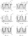
- FIGS. 3A and 3Billustrate a conventional etch process to recess a metal layer 140 in a feature 114 formed in a dielectric material 110 .
- the feature 114 illustrated in FIG. 3Aincludes a barrier layer 130 that lines the sidewall 118 and bottom 116 of the feature 114 .
- a metal layer 140fills the volume of the feature 114 to a top surface 142 that is about coplanar with the top surface 112 of the dielectric material 110 .
- the top surface 142 of the metal layer 140is recessed below the top surface 112 of the dielectric material 110 .
- the etch processalso removes some of the barrier layer 130 , leaving barrier layer residue 135 on the sidewalls 118 between the top surface 142 of the recessed metal layer 140 and the top surface 112 of the dielectric material 110 .
- the barrier layer residue 135is also referred to as “ears”.
- a substrate 200is provided that has a first dielectric material 210 with a second dielectric material 220 deposited thereon.
- the second dielectric material 220has a thickness T.
- the substrate 200includes at least one feature 214 formed in the first dielectric material 210 and through the second dielectric material 220 .
- the feature 214has at least one sidewall 218 and a bottom 216 .
- the sidewall 218is bounded by the second dielectric material 220 near the top surface 222 of the second dielectric material 220 .
- the sidewall 218is bounded by the second dielectric material 220 through the thickness T of the second dielectric material 220 and by the first dielectric material 210 below the thickness T of the second dielectric material 220 .
- the depth of the featureis defined from the top surface 222 of the second dielectric material 220 to the bottom 216 of the feature.
- the width and depth of the feature 214can vary.
- the aspect ratio (depth:width) of the featurecan be any suitable aspect ratio.
- the aspect ratio of the feature 214is in range of 0.5:1 up to 20:1, with typical range of 1:1-4:1.
- the thickness T of the second dielectric material 220can be any suitable thickness. In some embodiments, the thickness T of the second dielectric material 220 is in the range of about 5% to about 90% of the depth of the feature 214 , or in the range of about 5% to about 70% of the depth of the feature 214 , or in the range of about 5% to about 50% of the depth of the feature 214 , or in the range of about 10% to about 30% of the depth of the feature 214 .
- the second dielectric material 220is different than the first dielectric material 210 in one or more of composition and physical properties.
- the second dielectric material 220can be a different composition than the first dielectric material 210 .
- the first dielectric material 210 and the second dielectric material 220are the same composition but the second dielectric material 220 is denser and/or less porous than the first dielectric material. 210 .
- the second dielectric material 220has different adhesion properties (relative to the barrier layer 230 ) than the first dielectric material 210 .
- the first dielectric material 210can be any suitable material.
- the first dielectric material 210comprises silicon oxycarbide (SiOC), porous organosilicate glass (p-SiCOH), doped or undoped silicate glass, silicon oxide (SiOx).
- the second dielectric material 220can be any suitable material.
- the second dielectric materialcomprises one or more of SiN, SiCN, SiOC, AlOx, AlN, AlC or combination of above.
- SiNsilicon and nitrogen atoms.
- a barrier layer 230is formed on the at least one sidewall 218 and the bottom 216 of the feature 214 .
- the barrier layer 230 on the sidewall 218 of the feature 214is bounded by the second dielectric material 220 near the top surface 222 of the second dielectric material 220 through the thickness T of the second dielectric material 220 .
- the barrier layer 230 on the sidewall 218is also bounded by the first dielectric material 210 below the thickness T of the second dielectric material 220 .
- the barrier layer 230can include any suitable components.
- the barrier layer 230comprises one or more of titanium nitride (TiN) or tantalum nitride (TaN).
- the barrier layer 230includes a liner material (not shown) as either a separate layer or mixed with the barrier layer 230 .
- the liner of some embodimentsis one or more of cobalt (Co) or ruthenium (Ru).
- the barrier layercomprises tantalum nitride (TaN) with a cobalt (Co) or ruthenium (Ru) liner.
- the barrier layercan also comprise aluminum-containing compounds (including metallic Al) or manganese-containing compounds (including metallic Mn).
- a metal layer 240is deposited on the barrier layer 230 to fill the depth of the at least one feature 214 . Stated differently, the volume of the feature 214 is filled with the barrier layer 230 and the metal layer 240 .
- the metal layer 240can be deposited in the feature 214 by any suitable technique known to the skilled artisan.
- the metal layer 240can include any suitable metal.
- the metal layer 240comprises one or more of cobalt (Co), copper (Cu), tungsten (W), ruthenium (Ru), nickel (Ni), noble metals (Ir, Pt), alloys or compound conductors (e.g. NiSi).
- the metal layer 240comprises Co and the barrier layer 230 comprises TiN.
- the metal layer 240comprises Cu and the barrier layer 230 comprises TaN with a liner comprising one or more of Co or Ru.
- the metal layer 240has been recessed to a recessed depth.
- the top surface 242 of the metal layer 240 at the recessed depthis below the top surface 222 of the second dielectric material 220 .
- the metal layer 240has been recessed so that the top surface 242 of the metal layer 240 is below the thickness T of the second dielectric material 220 , or below the interface 215 between the second dielectric material 220 and the first dielectric material 210 .
- the etch processmay also remove the barrier layer 230 from the sidewall 218 of the second dielectric material 220 .
- Some barrier layer residual 235may remain in contact with the first dielectric material 210 .
- the barrier layer residual 235 that might remainis below the top surface 222 of the second dielectric material 220 .
- the etch processcomprises a cyclical or sequential process to selectively etch the metal layer 240 and to selectively etch the barrier layer 230 .
- the sequential metal layer 240 etch and barrier layer 230 etch processesare repeated.
- etching the metal layer 240or core metal recessing, comprise a wet chemical method in which peroxide (H 2 O 2 ) is exposed to the metal layer 240 at acidic pH at about room temperature (i.e., in the range of about 20° C. to about 100° C.).
- etching of the barrier layer 230comprises exposes the substrate to a mixture of peroxide (H 2 O 2 ) and ammonium hydroxide (NH 4 OH) at a temperature in the range of about 30° C. to about 80° C. with an alkaline pH level.
- Some embodiments of the disclosureare directed to semiconductor devices comprising a substrate 200 with a first dielectric material 210 and a second dielectric material 220 thereon.
- the substrate 200has at least one feature 214 formed in the first dielectric material 210 and through the second dielectric material 220 .
- the feature 214having at least one sidewall 218 and a bottom 216 .
- the at least one sidewall 218bounded by the second dielectric material 220 and the first dielectric material 210 .
- the semiconductor deviceincludes a barrier layer 230 located within the feature 214 so that the barrier layer 230 is on the sidewall 218 bounded by the first dielectric material 210 .
- the barrier layer 230is substantially only bounded by the first dielectric material 210 .
- the barrier layer 230is not on the sidewall 218 of the feature 214 bounded by the second dielectric material 220 .
- the barrier layer 230 of some embodimentsis a substantially conformal film on the sidewalls 218 and bottom 216 of the feature 214 .
- a “conformal film”means that the thickness of the film at any point is within ⁇ 10%, ⁇ 5%, ⁇ 2% or ⁇ 1% of the average thickness of the film.
- a metal layer 240is within the feature 214 bounded by the barrier layer 230 .
- the metal layer 240has barrier layer 230 on the sides and bottom of the metal layer 240 .
- the metal layer 240has barrier layer 230 on the sides of the metal layer.
- the top surface 242 of the metal layer 240is even with or below the top of the barrier layer 230 .
- the barrier layer residual 235is above the top surface 242 of the metal layer 240 and below the second dielectric material 220 .
- FIGS. 5A through 5Dillustrate another embodiment of the disclosure.
- a substrate 300is provided that has a dielectric material 310 with a top surface 312 and at least one feature 314 formed therein.
- the feature 314has a sidewall 318 and a bottom 316 which define a volume of the feature 314 .
- the depth of the feature 314is defined by the distance from the top surface 312 of the dielectric material 310 to the bottom 316 of the feature 314 .
- the substrate 300can be subject to a passivation process to form the substrate 300 shown in FIG. 5B .
- the passivation processpassivates the dielectric material 310 at the sidewall 318 of the feature 314 to form a passivated dielectric layer 320 .
- the passivation processcan be any suitable process that can change the properties of the dielectric material 310 at the sidewalls 318 .
- Suitable passivation methodsinclude, but are not limited to, scalable physical films formed at the sidewall, sidewall treatments to reduce the capacitance penalty while maintaining the composition or a gradient treatment to modify the top portion of the sidewall to a depth of the recess thickness.
- passivating the dielectric material 310comprises one or more of UV or plasma exposure.
- a barrier layer 330can be formed on the sidewalls 318 and bottom 316 of the feature 314 .
- the barrier layer 330covers the passivated dielectric layer 320 on the sidewalls 318 .
- the barrier layer 330can be formed by any suitable technique including, but not limited to, conformal atomic layer deposition (ALD) followed by chemical-mechanical planarization to remove deposition from the top surface 312 of the dielectric material 310 .
- ALDconformal atomic layer deposition
- the feature 314can then be gapfilled with a metal layer 340 so that the top surface 342 of the metal layer 340 is about even with the top surface 312 of the dielectric material 310 .
- the metal layer 340can be deposited by any suitable technique including, but not limited to, blanket deposition followed by chemical-mechanical planarization.
- passivating the dielectric material 310 at the sidewall 318 of the feature 314forms a gradient passivated dielectric layer 320 so that a portion of the sidewall 318 from the top surface 312 of the dielectric material 310 to a predetermined depth is modified so that removal of a barrier layer from the passivated dielectric layer 320 is easier than removal of the barrier layer from the dielectric material 310 .
- the predetermined depth of the gradient passivationis about the same as the predetermined depth of that the metal layer 340 will be recessed to.
- the metal layer 340has been recessed to a predetermined recessed depth.
- the top surface 342 of the metal layer 340 at the recessed depthis below the top surface 312 of the dielectric material 310 .
- the etch processmay also remove the barrier layer 330 from the passivated dielectric layer 320 .
- the etch processcomprises a cyclical or sequential process to selectively etch the metal layer 340 and to selectively etch the barrier layer 330 .
- the sequential metal layer 340 etch and barrier layer 330 etch processesare repeated.
- etching the metal layer 340or core metal recessing, comprise a wet chemical method in which peroxide (H 2 O 2 ) is exposed to the metal layer 340 at acidic pH at about room temperature (i.e., in the range of about 20° C. to about 100° C.).
- etching of the barrier layer 330comprises exposes the substrate to a mixture of peroxide (H 2 O 2 ) and ammonium hydroxide (NH 4 OH) at a temperature in the range of about 30° C. to about 80° C. with an alkaline pH level.
- Some embodiments of the disclosureare directed to semiconductor devices comprising a substrate 300 with a dielectric material 310 having at least one feature 314 formed therein.
- the at least one feature 314having at least one sidewall 318 and a bottom 316 .
- the substrate 300has a passivated dielectric layer 320 forming at least a portion of the sidewall 318 .
- the passivated dielectric layer 320is formed at a top portion of the sidewall 318 near the top surface 312 of the dielectric material 310 and does not extend to the bottom 316 of the feature.
- the semiconductor deviceincludes a barrier layer 330 located within the feature 314 so that the barrier layer 330 is on the sidewall 318 bounded by the dielectric material 310 or the passivated dielectric layer 320 .
- the barrier layer 330is substantially only bounded by the passivated dielectric layer 320 .
- the barrier layer 330 of some embodimentsis a substantially conformal film on the sidewalls 318 and bottom 316 of the feature 314 .
- a metal layer 340is within the feature 314 bounded by the barrier layer 330 .
- the metal layer 340has barrier layer 330 on the sides and bottom of the metal layer 340 .
- the metal layer 340has barrier layer 330 on the sides of the metal layer.
- the top surface 342 of the metal layer 340is even with or below the top of the barrier layer 330 .
- FIGS. 6A through 6Fillustrate another embodiment of the disclosure.
- FIG. 6Aillustrates a substrate 400 that can be used with the processes described herein.
- the substrate 400has a dielectric material 410 with a top surface 412 .
- At least one feature 414is formed in the dielectric material 410 .
- the feature 414has a bottom 416 and at least one sidewall 418 , as described above.
- a barrier layer 430is formed on the bottom 416 and sidewall 418 of the feature 414 and a metal layer 440 is gapfilled on the barrier layer 430 to fill the feature 414 .
- the substrate 400has been exposed to an etching process to remove a portion of the metal layer 440 to lower the top surface 442 of the metal layer 440 relative to the top surface 412 of the dielectric material 410 .
- the metal layer 440is etched by a recess depth D R by any suitable amount.
- the recess depth D Ris less than one monolayer of metal atoms thick.
- the recess depth D Ris in the range of about 1 ⁇ to about 100 ⁇ .
- the etching processexposes a portion 431 of the barrier layer 430 above the top surface 442 of the recessed metal layer 440 .
- the exposed portion 431 of the barrier layer 430is etched to lower the top of the barrier layer to the top surface 442 of the metal layer 440 .
- FIGS. 6D and 6Eshow a repetition of the metal layer 440 etch followed by the barrier layer 430 etch until a predetermined depth of the metal layer 440 has been removed and the top surface 442 of the metal layer 440 is at a predetermined depth, as shown in FIG. 6F .
- Some embodiments of the disclosureare directed to semiconductor devices comprising a substrate 400 with a dielectric material 410 having at least one feature 414 formed therein.
- the at least one feature 414having at least one sidewall 418 and a bottom 416 .
- the semiconductor deviceincludes a barrier layer 430 located within the feature 414 so that the barrier layer 430 is on a portion of the sidewall 418 bounded by the dielectric material 410 .
- the barrier layer 430is substantially only bounded by the dielectric material 410 .
- the barrier layer 430 of some embodimentsis a substantially conformal film on the sidewalls 418 and bottom 416 of the feature 414 .
- a metal layer 440is within the feature 414 bounded by the barrier layer 430 .
- the metal layer 440has barrier layer 430 on the sides and bottom of the metal layer 440 .
- the metal layer 440has barrier layer 430 on the sides of the metal layer 440 .
- the top surface 442 of the metal layer 440is substantially even with the top of the barrier layer 430 .
- the term “substantially even with”means that the top of the metal layer is even with the top of the barrier layer within ⁇ 10 ⁇ , ⁇ 5 ⁇ , ⁇ 4 ⁇ , ⁇ 3 ⁇ , ⁇ 2 ⁇ or ⁇ 1 ⁇ .
- the top of the barrier layer 430is below the top surface 442 of the metal layer 440 .
Landscapes
- Engineering & Computer Science (AREA)
- Physics & Mathematics (AREA)
- Condensed Matter Physics & Semiconductors (AREA)
- General Physics & Mathematics (AREA)
- Manufacturing & Machinery (AREA)
- Computer Hardware Design (AREA)
- Microelectronics & Electronic Packaging (AREA)
- Power Engineering (AREA)
- Plasma & Fusion (AREA)
- Internal Circuitry In Semiconductor Integrated Circuit Devices (AREA)
Abstract
Description
Claims (8)
Priority Applications (2)
| Application Number | Priority Date | Filing Date | Title |
|---|---|---|---|
| US16/214,522US11062942B2 (en) | 2017-12-07 | 2018-12-10 | Methods for controllable metal and barrier-liner recess |
| US17/345,683US11705366B2 (en) | 2017-12-07 | 2021-06-11 | Methods for controllable metal and barrier-liner recess |
Applications Claiming Priority (2)
| Application Number | Priority Date | Filing Date | Title |
|---|---|---|---|
| US201762596113P | 2017-12-07 | 2017-12-07 | |
| US16/214,522US11062942B2 (en) | 2017-12-07 | 2018-12-10 | Methods for controllable metal and barrier-liner recess |
Related Child Applications (1)
| Application Number | Title | Priority Date | Filing Date |
|---|---|---|---|
| US17/345,683DivisionUS11705366B2 (en) | 2017-12-07 | 2021-06-11 | Methods for controllable metal and barrier-liner recess |
Publications (2)
| Publication Number | Publication Date |
|---|---|
| US20190198389A1 US20190198389A1 (en) | 2019-06-27 |
| US11062942B2true US11062942B2 (en) | 2021-07-13 |
Family
ID=64664065
Family Applications (2)
| Application Number | Title | Priority Date | Filing Date |
|---|---|---|---|
| US16/214,522Active2039-02-13US11062942B2 (en) | 2017-12-07 | 2018-12-10 | Methods for controllable metal and barrier-liner recess |
| US17/345,683Active2039-05-07US11705366B2 (en) | 2017-12-07 | 2021-06-11 | Methods for controllable metal and barrier-liner recess |
Family Applications After (1)
| Application Number | Title | Priority Date | Filing Date |
|---|---|---|---|
| US17/345,683Active2039-05-07US11705366B2 (en) | 2017-12-07 | 2021-06-11 | Methods for controllable metal and barrier-liner recess |
Country Status (6)
| Country | Link |
|---|---|
| US (2) | US11062942B2 (en) |
| EP (1) | EP3496136A1 (en) |
| JP (1) | JP2019106538A (en) |
| KR (1) | KR20190067725A (en) |
| CN (1) | CN110034017A (en) |
| TW (1) | TW201929059A (en) |
Families Citing this family (6)
| Publication number | Priority date | Publication date | Assignee | Title |
|---|---|---|---|---|
| US10916477B2 (en)* | 2018-09-28 | 2021-02-09 | Taiwan Semiconductor Manufacturing Company, Ltd. | Fin field-effect transistor devices and methods of forming the same |
| DE102019101555B4 (en) | 2018-09-28 | 2023-01-12 | Taiwan Semiconductor Manufacturing Company, Ltd. | METAL GATE CUTTING SHAPE |
| US11450562B2 (en)* | 2019-09-16 | 2022-09-20 | Tokyo Electron Limited | Method of bottom-up metallization in a recessed feature |
| KR102749980B1 (en) | 2020-01-02 | 2025-01-03 | 삼성전자주식회사 | Semiconductor devices having air spacer |
| US11764157B2 (en)* | 2020-07-23 | 2023-09-19 | Applied Materials, Inc. | Ruthenium liner and cap for back-end-of-line applications |
| JP7624833B2 (en)* | 2020-12-28 | 2025-01-31 | 株式会社Screenホールディングス | Wiring forming method and substrate processing apparatus |
Citations (106)
| Publication number | Priority date | Publication date | Assignee | Title |
|---|---|---|---|---|
| US4671970A (en) | 1986-02-05 | 1987-06-09 | Ncr Corporation | Trench filling and planarization process |
| US5824597A (en) | 1995-04-12 | 1998-10-20 | Lg Semicon Co., Ltd. | Method of forming contact hole plug |
| KR100223334B1 (en) | 1996-06-29 | 1999-10-15 | 김영환 | Metal wiring formation method of semiconductor device |
| KR20000026588A (en) | 1998-10-21 | 2000-05-15 | 윤종용 | Semiconductor device having contact holes and method for manufacturing the same |
| US6130151A (en) | 1999-05-07 | 2000-10-10 | Taiwan Semiconductor Manufacturing Company | Method of manufacturing air gap in multilevel interconnection |
| US6143653A (en) | 1998-10-04 | 2000-11-07 | Promos Technologies, Inc. | Method of forming tungsten interconnect with tungsten oxidation to prevent tungsten loss |
| KR20020020969A (en) | 1999-08-18 | 2002-03-16 | 추후제출 | Method of producing copper features on semiconductor wafers |
| US20020098642A1 (en) | 2000-08-31 | 2002-07-25 | Agere Systems Guardian Corp. | Methods of fabricating a metal-oxide-metal capacitor and associated apparatuses |
| US20020163081A1 (en) | 2001-02-27 | 2002-11-07 | Junichi Aoyama | Semiconductor device and method of manufacturing the same |
| US6528884B1 (en) | 2001-06-01 | 2003-03-04 | Advanced Micro Devices, Inc. | Conformal atomic liner layer in an integrated circuit interconnect |
| US6576113B1 (en) | 1999-10-29 | 2003-06-10 | California Institute Of Technology | Method of electroplating of high aspect ratio metal structures into semiconductors |
| US20030143862A1 (en) | 1996-02-12 | 2003-07-31 | Ravi Iyer | Planarization using plasma oxidized amorphous silicon |
| US6653200B2 (en) | 2001-01-26 | 2003-11-25 | Applied Materials, Inc. | Trench fill process for reducing stress in shallow trench isolation |
| US20040067649A1 (en) | 2001-06-14 | 2004-04-08 | Hellring Stuart D. | Silica and silica-based slurry |
| US20040192034A1 (en) | 1999-06-29 | 2004-09-30 | Kabushiki Kaisha Toshiba | Method of manufacturing semiconductor device |
| US20050121768A1 (en) | 2003-12-05 | 2005-06-09 | International Business Machines Corporation | Silicon chip carrier with conductive through-vias and method for fabricating same |
| US20050266627A1 (en) | 2004-01-29 | 2005-12-01 | International Business Machines Corporation | Vertical field effect transistors incorporating semiconducting nanotubes grown in a spacer-defined passage |
| US20060169576A1 (en) | 2005-02-03 | 2006-08-03 | Applied Materials, Inc. | Physical vapor deposition plasma reactor with VHF source power applied through the workpiece |
| US20060286806A1 (en) | 2005-06-21 | 2006-12-21 | Matsushita Electric Industrial Co., Ltd | Plasma etching method and plasma etching apparatus |
| US7192803B1 (en) | 2000-10-13 | 2007-03-20 | Bridge Semiconductor Corporation | Method of making a semiconductor chip assembly with simultaneously formed interconnect and connection joint |
| US20070166981A1 (en) | 2006-01-19 | 2007-07-19 | Toshiharu Furukawa | Methods for forming uniform lithographic features |
| US20070199922A1 (en) | 2006-02-27 | 2007-08-30 | Applied Materials, Inc. | Etch methods to form anisotropic features for high aspect ratio applications |
| US7288463B1 (en) | 2006-04-28 | 2007-10-30 | Novellus Systems, Inc. | Pulsed deposition layer gap fill with expansion material |
| JP2008108757A (en) | 2006-10-23 | 2008-05-08 | Matsushita Electric Works Ltd | Compound semiconductor light-emitting element, illumination apparatus employing the same and manufacturing method of compound semiconductor element |
| US20080160783A1 (en) | 2004-03-16 | 2008-07-03 | Ishikawajima-Harima Heavy Industries Co., Ltd. | Method For Manufacturing Semiconductor Device |
| US20080182411A1 (en) | 2007-01-26 | 2008-07-31 | Asm America, Inc. | Plasma-enhanced ald of tantalum nitride films |
| US20080242097A1 (en) | 2007-03-28 | 2008-10-02 | Tim Boescke | Selective deposition method |
| US20090017631A1 (en) | 2007-06-01 | 2009-01-15 | Bencher Christopher D | Self-aligned pillar patterning using multiple spacer masks |
| US20090072409A1 (en) | 2007-09-14 | 2009-03-19 | International Business Machines Corporation | Interconnect Structures Incorporating Air-Gap Spacers |
| US7541297B2 (en) | 2007-10-22 | 2009-06-02 | Applied Materials, Inc. | Method and system for improving dielectric film quality for void free gap fill |
| US20090174040A1 (en) | 2007-12-11 | 2009-07-09 | Bishnu Prasanna Gogoi | Sacrificial pillar dielectric platform |
| US7605082B1 (en)* | 2005-10-13 | 2009-10-20 | Novellus Systems, Inc. | Capping before barrier-removal IC fabrication method |
| US20090269569A1 (en) | 2004-07-01 | 2009-10-29 | Janos Fucsko | Low Temperature Process for Polysilazane Oxidation/Densification |
| US20090321931A1 (en)* | 2008-06-27 | 2009-12-31 | Samsung Electronics Co., Ltd. | Semiconductor device and method of manufacturing the same |
| US20100078617A1 (en) | 2008-10-01 | 2010-04-01 | Breitwisch Matthew J | Method to reduce a via area in a phase change memory cell |
| US20100096691A1 (en) | 2008-10-22 | 2010-04-22 | Shin Jong Han | Semiconductor device having vertically aligned pillar structures that have flat side surfaces and method for manufacturing the same |
| US20100171220A1 (en) | 2006-05-08 | 2010-07-08 | Taiwan Semiconductor Manufacturing Company, Ltd. | Reducing Resistivity in Interconnect Structures of Integrated Circuits |
| US20100173494A1 (en) | 2007-06-09 | 2010-07-08 | Rolith, Inc | Method and apparatus for anisotropic etching |
| US20100203725A1 (en) | 2009-02-12 | 2010-08-12 | Suk-Hun Choi | Methods of fabricating semiconductor devices and semiconductor devices including a contact plug processed by rapid thermal annealing |
| US20100301480A1 (en) | 2009-05-27 | 2010-12-02 | Suk-Hun Choi | Semiconductor device having a conductive structure |
| US20100330805A1 (en) | 2007-11-02 | 2010-12-30 | Kenny Linh Doan | Methods for forming high aspect ratio features on a substrate |
| US20110049568A1 (en) | 2005-05-17 | 2011-03-03 | Taiwan Semiconductor Manufacturing Company, Ltd. | Lattice-Mismatched Semiconductor Structures with Reduced Dislocation Defect Densities and Related Methods for Device Fabrication |
| US20110057317A1 (en) | 2009-09-07 | 2011-03-10 | Tohoku University | Contact plug structure, semiconductor device, and method for forming contact plug |
| JP2011060803A (en) | 2009-09-07 | 2011-03-24 | Toshiba Corp | Semiconductor device |
| US20110089393A1 (en) | 2009-10-19 | 2011-04-21 | Macronix International Co., Ltd. | Memory and Method of Fabricating the Same |
| US20110207318A1 (en) | 2008-11-13 | 2011-08-25 | Renesas Electronics Corporation | Semiconductor device and method of manufacturing the same |
| US8034705B2 (en) | 2008-07-17 | 2011-10-11 | Samsung Electronics Co., Ltd. | Method of forming a seam-free tungsten plug |
| US20110281417A1 (en) | 2002-03-28 | 2011-11-17 | Gordon Roy G | Vapor deposition of silicon dioxide nanolaminates |
| JP2011233922A (en) | 2011-07-20 | 2011-11-17 | Ihi Corp | Method of forming inter-device isolating region |
| US20120156857A1 (en) | 2008-08-26 | 2012-06-21 | International Business Machines Corporation | Continuous metal semiconductor alloy via for interconnects |
| US20120178235A1 (en) | 2011-01-12 | 2012-07-12 | Jayavel Pachamuthu | Air Isolation In High Density Non-Volatile Memory |
| US20120205804A1 (en)* | 2011-02-11 | 2012-08-16 | International Business Machines Corporation | Method to fabricate copper wiring structures and structures formed tehreby |
| US20130072019A1 (en) | 2011-09-16 | 2013-03-21 | Globalfoundries Inc. | Methods for forming semiconductor devices |
| US20130109148A1 (en) | 2011-10-28 | 2013-05-02 | Samsung Electronics Co., Ltd. | Methods of forming a pattern and methods of manufacturing semiconductor devices using the same |
| US20130241037A1 (en) | 2009-03-18 | 2013-09-19 | Samsung Electronics Co., Ltd. | Semiconductor Devices Having Metal Oxide Patterns |
| US20130264533A1 (en) | 2012-04-09 | 2013-10-10 | Cheong Min Hong | Reram device structure |
| US20140029181A1 (en) | 2012-07-27 | 2014-01-30 | Florian Gstrein | Interlayer interconnects and associated techniques and configurations |
| US20140264896A1 (en) | 2013-03-12 | 2014-09-18 | Taiwan Semiconductor Manufacturing Company, Ltd. | Structure and Method for a Low-K Dielectric with Pillar-Type Air-Gaps |
| US20140264747A1 (en) | 2013-03-13 | 2014-09-18 | Intermolecular, Inc. | Deposition of Anisotropic Dielectric Layers Orientationally Matched to the Physically Separated Substrate |
| US20140327140A1 (en) | 2013-05-03 | 2014-11-06 | GlobalFoundries, Inc. | Integrated circuits and methods for fabricating integrated circuits with improved contact structures |
| US8951429B1 (en) | 2013-10-29 | 2015-02-10 | Applied Materials, Inc. | Tungsten oxide processing |
| US9012322B2 (en) | 2013-04-05 | 2015-04-21 | Intermolecular, Inc. | Selective etching of copper and copper-barrier materials by an aqueous base solution with fluoride addition |
| US20150111374A1 (en) | 2013-10-18 | 2015-04-23 | International Business Machines Corporation | Surface treatment in a dep-etch-dep process |
| US20150132901A1 (en) | 2013-01-14 | 2015-05-14 | Taiwan Semiconductor Manufacturing Company, Ltd. | Semiconductor Device and Fabricating the Same |
| US20150137113A1 (en) | 2013-11-15 | 2015-05-21 | Gang Yu | Motft with un-patterned etch-stop |
| US20150170956A1 (en) | 2013-12-16 | 2015-06-18 | Applied Materials, Inc. | Air gap structure integration using a processing system |
| US9117884B1 (en) | 2003-04-11 | 2015-08-25 | Novellus Systems, Inc. | Conformal films on semiconductor substrates |
| US20150279736A1 (en) | 2014-03-28 | 2015-10-01 | Tokyo Electron Limited | Tungsten film forming method |
| US20150287675A1 (en) | 2014-04-02 | 2015-10-08 | Applied Materials, Inc. | Method for forming interconnects |
| US20150325622A1 (en) | 2014-05-08 | 2015-11-12 | GlobalFoundries, Inc. | Integrated circuits having magnetic tunnel junctions (mtj) and methods for fabricating the same |
| US20150357439A1 (en) | 2014-06-04 | 2015-12-10 | Stmicroelectronics, Inc. | Method for making semiconductor device with isolation pillars between adjacent semiconductor fins |
| US20150364420A1 (en) | 2014-06-16 | 2015-12-17 | Taiwan Semiconductor Manufacturing Company Ltd. | Interconnect structure with footing region |
| US20150371896A1 (en) | 2013-06-10 | 2015-12-24 | International Business Machines Corporation | Double self aligned via patterning |
| US9236292B2 (en) | 2013-12-18 | 2016-01-12 | Intel Corporation | Selective area deposition of metal films by atomic layer deposition (ALD) and chemical vapor deposition (CVD) |
| US20160049427A1 (en) | 2014-08-18 | 2016-02-18 | Globalfoundries Inc. | Integrated circuits with self aligned contact structures for improved windows and fabrication methods |
| US20160056104A1 (en) | 2014-08-20 | 2016-02-25 | Globalfoundries Inc. | Self-aligned back end of line cut |
| US20160056074A1 (en) | 2014-08-21 | 2016-02-25 | Lam Research Corporation | Method for void-free cobalt gap fill |
| US20160068710A1 (en) | 2014-09-05 | 2016-03-10 | Fujifilm Planar Solutions, LLC | Polishing compositions and methods for polishing cobalt films |
| US20160093635A1 (en) | 2014-09-26 | 2016-03-31 | SanDisk Technologies, Inc. | Vertical memory device with bit line air gap |
| US20160111342A1 (en) | 2014-10-17 | 2016-04-21 | Lam Research Corporation | Method and apparatus for characterizing metal oxide reduction |
| US9324650B2 (en) | 2014-08-15 | 2016-04-26 | International Business Machines Corporation | Interconnect structures with fully aligned vias |
| US20160133563A1 (en)* | 2014-11-07 | 2016-05-12 | Applied Materials, Inc. | Methods for thermally forming a selective cobalt layer |
| US20160141416A1 (en) | 2012-11-29 | 2016-05-19 | Micron Technology, Inc. | Semiconductor devices and fabrication methods |
| US9362165B1 (en) | 2015-05-08 | 2016-06-07 | Globalfoundries Inc. | 2D self-aligned via first process flow |
| US20160163587A1 (en) | 2014-12-08 | 2016-06-09 | International Business Machines Corporation | Self-aligned via interconnect structures |
| US9368395B1 (en) | 2014-05-06 | 2016-06-14 | Globalfoundries Inc. | Self-aligned via and air gap |
| WO2016106092A1 (en) | 2014-12-22 | 2016-06-30 | Tokyo Electron Limited | Patterning a substrate using grafting polymer material |
| US20160190009A1 (en) | 2013-09-27 | 2016-06-30 | Intel Corporation | Previous Layer Self-Aligned Via and Plug Patterning for Back End of Line (BEOL)Interconnects |
| US20160190008A1 (en) | 2012-03-27 | 2016-06-30 | Novellus Systems, Inc. | Tungsten feature fill |
| US20160260779A1 (en) | 2015-03-06 | 2016-09-08 | Kabushiki Kaisha Toshiba | Non-volatile resistive random access memory device |
| US9490202B2 (en) | 2011-04-15 | 2016-11-08 | GlobalFoundries, Inc. | Self-aligned airgap interconnect structures |
| US20170077037A1 (en) | 2015-09-14 | 2017-03-16 | International Business Machines Corporation | Via bottom structure and methods of forming |
| US20170076945A1 (en) | 2015-09-01 | 2017-03-16 | Lam Research Corporation | Mask shrink layer for high aspect ratio dielectric etch |
| US9666451B2 (en) | 2013-09-27 | 2017-05-30 | Intel Corporation | Self-aligned via and plug patterning for back end of line (BEOL) interconnects |
| US9679781B2 (en) | 2005-09-01 | 2017-06-13 | Micron Technology, Inc. | Methods for integrated circuit fabrication with protective coating for planarization |
| US20170186849A1 (en) | 2015-12-29 | 2017-06-29 | Taiwan Semiconductor Manufacturing Co., Ltd. | Semiconductor device and a method for fabricating the same |
| US9721888B2 (en) | 2015-12-08 | 2017-08-01 | International Business Machines Corporation | Trench silicide with self-aligned contact vias |
| WO2017136577A1 (en) | 2016-02-02 | 2017-08-10 | Tokyo Electron Limited | Self-alignment of metal and via using selective deposition |
| US20170263563A1 (en) | 2014-07-01 | 2017-09-14 | Micron Technology, Inc. | Semiconductor Constructions |
| US20170317026A1 (en)* | 2016-04-18 | 2017-11-02 | International Business Machines Corporation | Selective and non-selective barrier layer wet removal |
| US20170338149A1 (en) | 2016-05-17 | 2017-11-23 | Taiwan Semiconductor Manufacturing Company Ltd. | Semiconductor device and fabricating method thereof |
| US20180096847A1 (en) | 2016-09-30 | 2018-04-05 | Applied Materials, Inc. | Methods Of Forming Self-Aligned Vias |
| US20180130671A1 (en) | 2016-11-08 | 2018-05-10 | Applied Materials, Inc. | Methods For Self-Aligned Patterning |
| US20180144980A1 (en) | 2016-11-03 | 2018-05-24 | Applied Materials, Inc. | Deposition And Treatment Of Films For Patterning |
| US20180323151A1 (en)* | 2017-05-03 | 2018-11-08 | International Business Machines Corporation | WET ETCH REMOVAL OF Ru SELECTIVE TO OTHER METALS |
| US20180358260A1 (en) | 2017-06-10 | 2018-12-13 | Applied Materials, Inc. | Methods Of Forming Self-Aligned Vias And Air Gaps |
Family Cites Families (11)
| Publication number | Priority date | Publication date | Assignee | Title |
|---|---|---|---|---|
| JPH08340047A (en)* | 1995-06-13 | 1996-12-24 | Sony Corp | Structure for wiring layer of semiconductor device and its manufacture |
| JP2001077118A (en)* | 1999-06-30 | 2001-03-23 | Toshiba Corp | Semiconductor device and method of manufacturing the same |
| US6794311B2 (en)* | 2000-07-14 | 2004-09-21 | Applied Materials Inc. | Method and apparatus for treating low k dielectric layers to reduce diffusion |
| JP2003142579A (en)* | 2001-11-07 | 2003-05-16 | Hitachi Ltd | Semiconductor device manufacturing method and semiconductor device |
| US7329956B1 (en)* | 2006-09-12 | 2008-02-12 | Taiwan Semiconductor Manufacturing Company, Ltd. | Dual damascene cleaning method |
| JP5654794B2 (en)* | 2010-07-15 | 2015-01-14 | ルネサスエレクトロニクス株式会社 | Manufacturing method of semiconductor device |
| JP6438131B2 (en)* | 2014-10-17 | 2018-12-12 | エーシーエム リサーチ (シャンハイ) インコーポレーテッド | Method for removing barrier layer and method for forming semiconductor structure |
| US10002834B2 (en)* | 2015-03-11 | 2018-06-19 | Applied Materials, Inc. | Method and apparatus for protecting metal interconnect from halogen based precursors |
| US10157787B2 (en)* | 2015-12-17 | 2018-12-18 | Applied Materials, Inc. | Method and apparatus for depositing cobalt in a feature |
| US9806018B1 (en)* | 2016-06-20 | 2017-10-31 | International Business Machines Corporation | Copper interconnect structures |
| US10957579B2 (en)* | 2018-11-06 | 2021-03-23 | Samsung Electronics Co., Ltd. | Integrated circuit devices including a via and methods of forming the same |
- 2018
- 2018-12-06CNCN201811489710.XApatent/CN110034017A/enactivePending
- 2018-12-06JPJP2018229311Apatent/JP2019106538A/enactivePending
- 2018-12-07KRKR1020180156579Apatent/KR20190067725A/ennot_activeWithdrawn
- 2018-12-07EPEP18211016.3Apatent/EP3496136A1/ennot_activeWithdrawn
- 2018-12-07TWTW107144090Apatent/TW201929059A/enunknown
- 2018-12-10USUS16/214,522patent/US11062942B2/enactiveActive
- 2021
- 2021-06-11USUS17/345,683patent/US11705366B2/enactiveActive
Patent Citations (119)
| Publication number | Priority date | Publication date | Assignee | Title |
|---|---|---|---|---|
| US4671970A (en) | 1986-02-05 | 1987-06-09 | Ncr Corporation | Trench filling and planarization process |
| US5824597A (en) | 1995-04-12 | 1998-10-20 | Lg Semicon Co., Ltd. | Method of forming contact hole plug |
| US20030143862A1 (en) | 1996-02-12 | 2003-07-31 | Ravi Iyer | Planarization using plasma oxidized amorphous silicon |
| KR100223334B1 (en) | 1996-06-29 | 1999-10-15 | 김영환 | Metal wiring formation method of semiconductor device |
| US6143653A (en) | 1998-10-04 | 2000-11-07 | Promos Technologies, Inc. | Method of forming tungsten interconnect with tungsten oxidation to prevent tungsten loss |
| KR20000026588A (en) | 1998-10-21 | 2000-05-15 | 윤종용 | Semiconductor device having contact holes and method for manufacturing the same |
| US6130151A (en) | 1999-05-07 | 2000-10-10 | Taiwan Semiconductor Manufacturing Company | Method of manufacturing air gap in multilevel interconnection |
| US20040192034A1 (en) | 1999-06-29 | 2004-09-30 | Kabushiki Kaisha Toshiba | Method of manufacturing semiconductor device |
| KR20020020969A (en) | 1999-08-18 | 2002-03-16 | 추후제출 | Method of producing copper features on semiconductor wafers |
| US6576113B1 (en) | 1999-10-29 | 2003-06-10 | California Institute Of Technology | Method of electroplating of high aspect ratio metal structures into semiconductors |
| US20020098642A1 (en) | 2000-08-31 | 2002-07-25 | Agere Systems Guardian Corp. | Methods of fabricating a metal-oxide-metal capacitor and associated apparatuses |
| US7192803B1 (en) | 2000-10-13 | 2007-03-20 | Bridge Semiconductor Corporation | Method of making a semiconductor chip assembly with simultaneously formed interconnect and connection joint |
| US6653200B2 (en) | 2001-01-26 | 2003-11-25 | Applied Materials, Inc. | Trench fill process for reducing stress in shallow trench isolation |
| US20050167846A1 (en) | 2001-02-27 | 2005-08-04 | Junichi Aoyama | Semiconductor device and method of manufacturing the same |
| US20020163081A1 (en) | 2001-02-27 | 2002-11-07 | Junichi Aoyama | Semiconductor device and method of manufacturing the same |
| US6528884B1 (en) | 2001-06-01 | 2003-03-04 | Advanced Micro Devices, Inc. | Conformal atomic liner layer in an integrated circuit interconnect |
| US20040067649A1 (en) | 2001-06-14 | 2004-04-08 | Hellring Stuart D. | Silica and silica-based slurry |
| US7279119B2 (en) | 2001-06-14 | 2007-10-09 | Ppg Industries Ohio, Inc. | Silica and silica-based slurry |
| US20110281417A1 (en) | 2002-03-28 | 2011-11-17 | Gordon Roy G | Vapor deposition of silicon dioxide nanolaminates |
| US9117884B1 (en) | 2003-04-11 | 2015-08-25 | Novellus Systems, Inc. | Conformal films on semiconductor substrates |
| US20050121768A1 (en) | 2003-12-05 | 2005-06-09 | International Business Machines Corporation | Silicon chip carrier with conductive through-vias and method for fabricating same |
| US20050266627A1 (en) | 2004-01-29 | 2005-12-01 | International Business Machines Corporation | Vertical field effect transistors incorporating semiconducting nanotubes grown in a spacer-defined passage |
| US20080160783A1 (en) | 2004-03-16 | 2008-07-03 | Ishikawajima-Harima Heavy Industries Co., Ltd. | Method For Manufacturing Semiconductor Device |
| US20090269569A1 (en) | 2004-07-01 | 2009-10-29 | Janos Fucsko | Low Temperature Process for Polysilazane Oxidation/Densification |
| US20060169576A1 (en) | 2005-02-03 | 2006-08-03 | Applied Materials, Inc. | Physical vapor deposition plasma reactor with VHF source power applied through the workpiece |
| US20110049568A1 (en) | 2005-05-17 | 2011-03-03 | Taiwan Semiconductor Manufacturing Company, Ltd. | Lattice-Mismatched Semiconductor Structures with Reduced Dislocation Defect Densities and Related Methods for Device Fabrication |
| US20060286806A1 (en) | 2005-06-21 | 2006-12-21 | Matsushita Electric Industrial Co., Ltd | Plasma etching method and plasma etching apparatus |
| US9679781B2 (en) | 2005-09-01 | 2017-06-13 | Micron Technology, Inc. | Methods for integrated circuit fabrication with protective coating for planarization |
| US7605082B1 (en)* | 2005-10-13 | 2009-10-20 | Novellus Systems, Inc. | Capping before barrier-removal IC fabrication method |
| US20070166981A1 (en) | 2006-01-19 | 2007-07-19 | Toshiharu Furukawa | Methods for forming uniform lithographic features |
| US20070199922A1 (en) | 2006-02-27 | 2007-08-30 | Applied Materials, Inc. | Etch methods to form anisotropic features for high aspect ratio applications |
| US7288463B1 (en) | 2006-04-28 | 2007-10-30 | Novellus Systems, Inc. | Pulsed deposition layer gap fill with expansion material |
| US20100171220A1 (en) | 2006-05-08 | 2010-07-08 | Taiwan Semiconductor Manufacturing Company, Ltd. | Reducing Resistivity in Interconnect Structures of Integrated Circuits |
| JP2008108757A (en) | 2006-10-23 | 2008-05-08 | Matsushita Electric Works Ltd | Compound semiconductor light-emitting element, illumination apparatus employing the same and manufacturing method of compound semiconductor element |
| US20080182411A1 (en) | 2007-01-26 | 2008-07-31 | Asm America, Inc. | Plasma-enhanced ald of tantalum nitride films |
| US20080242097A1 (en) | 2007-03-28 | 2008-10-02 | Tim Boescke | Selective deposition method |
| US20090017631A1 (en) | 2007-06-01 | 2009-01-15 | Bencher Christopher D | Self-aligned pillar patterning using multiple spacer masks |
| US20100173494A1 (en) | 2007-06-09 | 2010-07-08 | Rolith, Inc | Method and apparatus for anisotropic etching |
| US20090072409A1 (en) | 2007-09-14 | 2009-03-19 | International Business Machines Corporation | Interconnect Structures Incorporating Air-Gap Spacers |
| US7541297B2 (en) | 2007-10-22 | 2009-06-02 | Applied Materials, Inc. | Method and system for improving dielectric film quality for void free gap fill |
| US20100330805A1 (en) | 2007-11-02 | 2010-12-30 | Kenny Linh Doan | Methods for forming high aspect ratio features on a substrate |
| US7985977B2 (en) | 2007-12-11 | 2011-07-26 | Hvvi Semiconductors, Inc. | Sacrificial pillar dielectric platform |
| US20090174040A1 (en) | 2007-12-11 | 2009-07-09 | Bishnu Prasanna Gogoi | Sacrificial pillar dielectric platform |
| US20090321931A1 (en)* | 2008-06-27 | 2009-12-31 | Samsung Electronics Co., Ltd. | Semiconductor device and method of manufacturing the same |
| US8034705B2 (en) | 2008-07-17 | 2011-10-11 | Samsung Electronics Co., Ltd. | Method of forming a seam-free tungsten plug |
| US20120156857A1 (en) | 2008-08-26 | 2012-06-21 | International Business Machines Corporation | Continuous metal semiconductor alloy via for interconnects |
| US20120115302A1 (en) | 2008-10-01 | 2012-05-10 | International Business Machines Corporation | Method to reduce a via area in a phase change memory cell |
| US20100078617A1 (en) | 2008-10-01 | 2010-04-01 | Breitwisch Matthew J | Method to reduce a via area in a phase change memory cell |
| US8338225B2 (en) | 2008-10-01 | 2012-12-25 | International Business Machines Corporation | Method to reduce a via area in a phase change memory cell |
| US20100096691A1 (en) | 2008-10-22 | 2010-04-22 | Shin Jong Han | Semiconductor device having vertically aligned pillar structures that have flat side surfaces and method for manufacturing the same |
| US20110207318A1 (en) | 2008-11-13 | 2011-08-25 | Renesas Electronics Corporation | Semiconductor device and method of manufacturing the same |
| US20100203725A1 (en) | 2009-02-12 | 2010-08-12 | Suk-Hun Choi | Methods of fabricating semiconductor devices and semiconductor devices including a contact plug processed by rapid thermal annealing |
| US20130241037A1 (en) | 2009-03-18 | 2013-09-19 | Samsung Electronics Co., Ltd. | Semiconductor Devices Having Metal Oxide Patterns |
| US20100301480A1 (en) | 2009-05-27 | 2010-12-02 | Suk-Hun Choi | Semiconductor device having a conductive structure |
| US8575753B2 (en) | 2009-05-27 | 2013-11-05 | Samsung Electronics Co., Ltd. | Semiconductor device having a conductive structure including oxide and non oxide portions |
| US20110057317A1 (en) | 2009-09-07 | 2011-03-10 | Tohoku University | Contact plug structure, semiconductor device, and method for forming contact plug |
| JP2011060803A (en) | 2009-09-07 | 2011-03-24 | Toshiba Corp | Semiconductor device |
| US20110089393A1 (en) | 2009-10-19 | 2011-04-21 | Macronix International Co., Ltd. | Memory and Method of Fabricating the Same |
| US20120178235A1 (en) | 2011-01-12 | 2012-07-12 | Jayavel Pachamuthu | Air Isolation In High Density Non-Volatile Memory |
| US20120205804A1 (en)* | 2011-02-11 | 2012-08-16 | International Business Machines Corporation | Method to fabricate copper wiring structures and structures formed tehreby |
| US9490202B2 (en) | 2011-04-15 | 2016-11-08 | GlobalFoundries, Inc. | Self-aligned airgap interconnect structures |
| JP2011233922A (en) | 2011-07-20 | 2011-11-17 | Ihi Corp | Method of forming inter-device isolating region |
| US20130072019A1 (en) | 2011-09-16 | 2013-03-21 | Globalfoundries Inc. | Methods for forming semiconductor devices |
| US20130109148A1 (en) | 2011-10-28 | 2013-05-02 | Samsung Electronics Co., Ltd. | Methods of forming a pattern and methods of manufacturing semiconductor devices using the same |
| US20160190008A1 (en) | 2012-03-27 | 2016-06-30 | Novellus Systems, Inc. | Tungsten feature fill |
| US20130264533A1 (en) | 2012-04-09 | 2013-10-10 | Cheong Min Hong | Reram device structure |
| US20140029181A1 (en) | 2012-07-27 | 2014-01-30 | Florian Gstrein | Interlayer interconnects and associated techniques and configurations |
| US20160141416A1 (en) | 2012-11-29 | 2016-05-19 | Micron Technology, Inc. | Semiconductor devices and fabrication methods |
| US20150132901A1 (en) | 2013-01-14 | 2015-05-14 | Taiwan Semiconductor Manufacturing Company, Ltd. | Semiconductor Device and Fabricating the Same |
| US9312220B2 (en) | 2013-03-12 | 2016-04-12 | Taiwan Semiconductor Manufacturing Company, Ltd. | Structure and method for a low-K dielectric with pillar-type air-gaps |
| US20140264896A1 (en) | 2013-03-12 | 2014-09-18 | Taiwan Semiconductor Manufacturing Company, Ltd. | Structure and Method for a Low-K Dielectric with Pillar-Type Air-Gaps |
| US20140264747A1 (en) | 2013-03-13 | 2014-09-18 | Intermolecular, Inc. | Deposition of Anisotropic Dielectric Layers Orientationally Matched to the Physically Separated Substrate |
| US9012322B2 (en) | 2013-04-05 | 2015-04-21 | Intermolecular, Inc. | Selective etching of copper and copper-barrier materials by an aqueous base solution with fluoride addition |
| US20140327140A1 (en) | 2013-05-03 | 2014-11-06 | GlobalFoundries, Inc. | Integrated circuits and methods for fabricating integrated circuits with improved contact structures |
| US20150371896A1 (en) | 2013-06-10 | 2015-12-24 | International Business Machines Corporation | Double self aligned via patterning |
| US20160190009A1 (en) | 2013-09-27 | 2016-06-30 | Intel Corporation | Previous Layer Self-Aligned Via and Plug Patterning for Back End of Line (BEOL)Interconnects |
| US9666451B2 (en) | 2013-09-27 | 2017-05-30 | Intel Corporation | Self-aligned via and plug patterning for back end of line (BEOL) interconnects |
| US20150111374A1 (en) | 2013-10-18 | 2015-04-23 | International Business Machines Corporation | Surface treatment in a dep-etch-dep process |
| US8951429B1 (en) | 2013-10-29 | 2015-02-10 | Applied Materials, Inc. | Tungsten oxide processing |
| US9362413B2 (en) | 2013-11-15 | 2016-06-07 | Cbrite Inc. | MOTFT with un-patterned etch-stop |
| US20150137113A1 (en) | 2013-11-15 | 2015-05-21 | Gang Yu | Motft with un-patterned etch-stop |
| US20150170956A1 (en) | 2013-12-16 | 2015-06-18 | Applied Materials, Inc. | Air gap structure integration using a processing system |
| US9236292B2 (en) | 2013-12-18 | 2016-01-12 | Intel Corporation | Selective area deposition of metal films by atomic layer deposition (ALD) and chemical vapor deposition (CVD) |
| US20150279736A1 (en) | 2014-03-28 | 2015-10-01 | Tokyo Electron Limited | Tungsten film forming method |
| US20150287675A1 (en) | 2014-04-02 | 2015-10-08 | Applied Materials, Inc. | Method for forming interconnects |
| US9368395B1 (en) | 2014-05-06 | 2016-06-14 | Globalfoundries Inc. | Self-aligned via and air gap |
| US20150325622A1 (en) | 2014-05-08 | 2015-11-12 | GlobalFoundries, Inc. | Integrated circuits having magnetic tunnel junctions (mtj) and methods for fabricating the same |
| US20150357439A1 (en) | 2014-06-04 | 2015-12-10 | Stmicroelectronics, Inc. | Method for making semiconductor device with isolation pillars between adjacent semiconductor fins |
| US20150364420A1 (en) | 2014-06-16 | 2015-12-17 | Taiwan Semiconductor Manufacturing Company Ltd. | Interconnect structure with footing region |
| US20170263563A1 (en) | 2014-07-01 | 2017-09-14 | Micron Technology, Inc. | Semiconductor Constructions |
| US20160163640A1 (en)* | 2014-08-15 | 2016-06-09 | International Business Machines Corporation | Interconnect structures with fully aligned vias |
| US9324650B2 (en) | 2014-08-15 | 2016-04-26 | International Business Machines Corporation | Interconnect structures with fully aligned vias |
| US20160049427A1 (en) | 2014-08-18 | 2016-02-18 | Globalfoundries Inc. | Integrated circuits with self aligned contact structures for improved windows and fabrication methods |
| US20160056104A1 (en) | 2014-08-20 | 2016-02-25 | Globalfoundries Inc. | Self-aligned back end of line cut |
| US20160056074A1 (en) | 2014-08-21 | 2016-02-25 | Lam Research Corporation | Method for void-free cobalt gap fill |
| US20160068710A1 (en) | 2014-09-05 | 2016-03-10 | Fujifilm Planar Solutions, LLC | Polishing compositions and methods for polishing cobalt films |
| US20160093635A1 (en) | 2014-09-26 | 2016-03-31 | SanDisk Technologies, Inc. | Vertical memory device with bit line air gap |
| US20160111342A1 (en) | 2014-10-17 | 2016-04-21 | Lam Research Corporation | Method and apparatus for characterizing metal oxide reduction |
| US20160133563A1 (en)* | 2014-11-07 | 2016-05-12 | Applied Materials, Inc. | Methods for thermally forming a selective cobalt layer |
| US20160163587A1 (en) | 2014-12-08 | 2016-06-09 | International Business Machines Corporation | Self-aligned via interconnect structures |
| WO2016106092A1 (en) | 2014-12-22 | 2016-06-30 | Tokyo Electron Limited | Patterning a substrate using grafting polymer material |
| US20160260779A1 (en) | 2015-03-06 | 2016-09-08 | Kabushiki Kaisha Toshiba | Non-volatile resistive random access memory device |
| US9362165B1 (en) | 2015-05-08 | 2016-06-07 | Globalfoundries Inc. | 2D self-aligned via first process flow |
| US20170076945A1 (en) | 2015-09-01 | 2017-03-16 | Lam Research Corporation | Mask shrink layer for high aspect ratio dielectric etch |
| US20170077037A1 (en) | 2015-09-14 | 2017-03-16 | International Business Machines Corporation | Via bottom structure and methods of forming |
| US9721888B2 (en) | 2015-12-08 | 2017-08-01 | International Business Machines Corporation | Trench silicide with self-aligned contact vias |
| US20170186849A1 (en) | 2015-12-29 | 2017-06-29 | Taiwan Semiconductor Manufacturing Co., Ltd. | Semiconductor device and a method for fabricating the same |
| US9837314B2 (en) | 2016-02-02 | 2017-12-05 | Tokyo Electron Limited | Self-alignment of metal and via using selective deposition |
| WO2017136577A1 (en) | 2016-02-02 | 2017-08-10 | Tokyo Electron Limited | Self-alignment of metal and via using selective deposition |
| US20170317026A1 (en)* | 2016-04-18 | 2017-11-02 | International Business Machines Corporation | Selective and non-selective barrier layer wet removal |
| US20170338149A1 (en) | 2016-05-17 | 2017-11-23 | Taiwan Semiconductor Manufacturing Company Ltd. | Semiconductor device and fabricating method thereof |
| US20180096847A1 (en) | 2016-09-30 | 2018-04-05 | Applied Materials, Inc. | Methods Of Forming Self-Aligned Vias |
| US10083834B2 (en) | 2016-09-30 | 2018-09-25 | Applied Materials, Inc. | Methods of forming self-aligned vias |
| US10319636B2 (en) | 2016-11-03 | 2019-06-11 | Applied Materials, Inc. | Deposition and treatment of films for patterning |
| US20180144980A1 (en) | 2016-11-03 | 2018-05-24 | Applied Materials, Inc. | Deposition And Treatment Of Films For Patterning |
| US20180130671A1 (en) | 2016-11-08 | 2018-05-10 | Applied Materials, Inc. | Methods For Self-Aligned Patterning |
| US10319604B2 (en) | 2016-11-08 | 2019-06-11 | Applied Materials, Inc. | Methods for self-aligned patterning |
| US20180323151A1 (en)* | 2017-05-03 | 2018-11-08 | International Business Machines Corporation | WET ETCH REMOVAL OF Ru SELECTIVE TO OTHER METALS |
| US20180358260A1 (en) | 2017-06-10 | 2018-12-13 | Applied Materials, Inc. | Methods Of Forming Self-Aligned Vias And Air Gaps |
Non-Patent Citations (12)
| Title |
|---|
| PCT International Search Report and Written Opinion in PCT/US2017/037141 dated Aug. 31, 2017, 11 pages. |
| PCT International Search Report and Written Opinion in PCT/US2017/053936 dated Jan. 12, 2018, 10 pages. |
| PCT International Search Report and Written Opinion in PCT/US2017/059737 dated May 18, 2018, 11 pages. |
| PCT International Search Report and Written Opinion in PCT/US2017/060367 dated Feb. 22, 2018, 9 pages. |
| PCT International Search Report and Written Opinion in PCT/US2017/060368 dated Jan. 31, 2018, 11 pages. |
| PCT International Search Report and Written Opinion in PCT/US2018/019146 dated May 23, 2018, 12 pages. |
| PCT International Search Report and Written Opinion in PCT/US2018/027284 dated Aug. 2, 2018, 10 pages. |
| PCT international Search Report and Written Opinion in PCT/US2018/036690 dated Sep. 18, 2018, 9 pages. |
| PCT International Search Report and Written Opinion in PCT/US2018/048503 dated Dec. 14, 2018, 10 pages. |
| PCT International Search Report and Written Opinion in PCT/US2018/048504 dated Dec. 13, 2018, 10 pages. |
| PCT International Search Report and Written Opinion in PCT/US2018/048509 dated Dec. 13, 2018, 10 pages. |
| PCT ISR & Written Opinion for PCT/US2018/026026, dated Jul. 26, 2018, 11 pages. |
Also Published As
| Publication number | Publication date |
|---|---|
| JP2019106538A (en) | 2019-06-27 |
| US11705366B2 (en) | 2023-07-18 |
| US20210305091A1 (en) | 2021-09-30 |
| KR20190067725A (en) | 2019-06-17 |
| EP3496136A1 (en) | 2019-06-12 |
| US20190198389A1 (en) | 2019-06-27 |
| TW201929059A (en) | 2019-07-16 |
| CN110034017A (en) | 2019-07-19 |
Similar Documents
| Publication | Publication Date | Title |
|---|---|---|
| US11705366B2 (en) | Methods for controllable metal and barrier-liner recess | |
| US9287213B2 (en) | Integrated circuits with improved contact structures | |
| US7670946B2 (en) | Methods to eliminate contact plug sidewall slit | |
| TW201839911A (en) | Method of forming a contact plug | |
| US20110227224A1 (en) | Semiconductor device and method for manufacturing the same | |
| US11710659B2 (en) | Metal loss prevention using implantation | |
| US10559497B2 (en) | Seamless tungsten fill by tungsten oxidation-reduction | |
| US9911648B2 (en) | Interconnects based on subtractive etching of silver | |
| US8324061B2 (en) | Method for manufacturing semiconductor device | |
| US10381448B2 (en) | Wrap-around contact integration scheme | |
| KR20140028908A (en) | Semiconductor device having metal line and the method for fabricating of the same | |
| CN112435958A (en) | Integrated circuit structure and forming method thereof | |
| US20240404876A1 (en) | Semiconductor devices and methods of manufacture | |
| US10453797B2 (en) | Interconnection structures and fabrication methods thereof | |
| JP2008305921A (en) | Semiconductor device and manufacturing method thereof | |
| US20210327891A1 (en) | Stack for 3d-nand memory cell | |
| CN112309954B (en) | Semiconductor device and method for forming the same | |
| US20240413020A1 (en) | Contact Plugs With Reduced R/C and the Methods of Forming The Same | |
| TWI888821B (en) | Semiconductor device and forming method thereof | |
| CN114156229B (en) | Semiconductor device and method of forming the same | |
| KR100459945B1 (en) | Method of manufacturing a semiconductor device | |
| CN118824943A (en) | Contact plug with reduced R/C and method of forming the same |
Legal Events
| Date | Code | Title | Description |
|---|---|---|---|
| FEPP | Fee payment procedure | Free format text:ENTITY STATUS SET TO UNDISCOUNTED (ORIGINAL EVENT CODE: BIG.); ENTITY STATUS OF PATENT OWNER: LARGE ENTITY | |
| FEPP | Fee payment procedure | Free format text:PETITION RELATED TO MAINTENANCE FEES GRANTED (ORIGINAL EVENT CODE: PTGR); ENTITY STATUS OF PATENT OWNER: LARGE ENTITY | |
| AS | Assignment | Owner name:MICROMATERIALS LLC, DELAWARE Free format text:ASSIGNMENT OF ASSIGNORS INTEREST;ASSIGNORS:REN, HE;MULLICK, AMRITA B.;FREED, REGINA;AND OTHERS;SIGNING DATES FROM 20190913 TO 20191009;REEL/FRAME:050761/0784 | |
| STPP | Information on status: patent application and granting procedure in general | Free format text:RESPONSE TO NON-FINAL OFFICE ACTION ENTERED AND FORWARDED TO EXAMINER | |
| STPP | Information on status: patent application and granting procedure in general | Free format text:NON FINAL ACTION MAILED | |
| STPP | Information on status: patent application and granting procedure in general | Free format text:RESPONSE TO NON-FINAL OFFICE ACTION ENTERED AND FORWARDED TO EXAMINER | |
| STPP | Information on status: patent application and granting procedure in general | Free format text:FINAL REJECTION MAILED | |
| STPP | Information on status: patent application and granting procedure in general | Free format text:DOCKETED NEW CASE - READY FOR EXAMINATION | |
| STPP | Information on status: patent application and granting procedure in general | Free format text:NOTICE OF ALLOWANCE MAILED -- APPLICATION RECEIVED IN OFFICE OF PUBLICATIONS | |
| STPP | Information on status: patent application and granting procedure in general | Free format text:PUBLICATIONS -- ISSUE FEE PAYMENT RECEIVED | |
| STPP | Information on status: patent application and granting procedure in general | Free format text:PUBLICATIONS -- ISSUE FEE PAYMENT VERIFIED | |
| STCF | Information on status: patent grant | Free format text:PATENTED CASE | |
| MAFP | Maintenance fee payment | Free format text:PAYMENT OF MAINTENANCE FEE, 4TH YEAR, LARGE ENTITY (ORIGINAL EVENT CODE: M1551); ENTITY STATUS OF PATENT OWNER: LARGE ENTITY Year of fee payment:4 |