US11061174B2 - Diffractive optical element, method of producing a diffractive optical element and laser component - Google Patents
Diffractive optical element, method of producing a diffractive optical element and laser componentDownload PDFInfo
- Publication number
- US11061174B2 US11061174B2US16/086,133US201716086133AUS11061174B2US 11061174 B2US11061174 B2US 11061174B2US 201716086133 AUS201716086133 AUS 201716086133AUS 11061174 B2US11061174 B2US 11061174B2
- Authority
- US
- United States
- Prior art keywords
- rods
- optical element
- diffractive optical
- carrier
- group
- Prior art date
- Legal status (The legal status is an assumption and is not a legal conclusion. Google has not performed a legal analysis and makes no representation as to the accuracy of the status listed.)
- Expired - Fee Related, expires
Links
Images


Classifications
- G—PHYSICS
- G02—OPTICS
- G02B—OPTICAL ELEMENTS, SYSTEMS OR APPARATUS
- G02B5/00—Optical elements other than lenses
- G02B5/18—Diffraction gratings
- G—PHYSICS
- G02—OPTICS
- G02B—OPTICAL ELEMENTS, SYSTEMS OR APPARATUS
- G02B27/00—Optical systems or apparatus not provided for by any of the groups G02B1/00 - G02B26/00, G02B30/00
- G02B27/09—Beam shaping, e.g. changing the cross-sectional area, not otherwise provided for
- G02B27/0916—Adapting the beam shape of a semiconductor light source such as a laser diode or an LED, e.g. for efficiently coupling into optical fibers
- G—PHYSICS
- G02—OPTICS
- G02B—OPTICAL ELEMENTS, SYSTEMS OR APPARATUS
- G02B27/00—Optical systems or apparatus not provided for by any of the groups G02B1/00 - G02B26/00, G02B30/00
- G02B27/09—Beam shaping, e.g. changing the cross-sectional area, not otherwise provided for
- G02B27/0938—Using specific optical elements
- G02B27/0944—Diffractive optical elements, e.g. gratings, holograms
- G—PHYSICS
- G02—OPTICS
- G02B—OPTICAL ELEMENTS, SYSTEMS OR APPARATUS
- G02B5/00—Optical elements other than lenses
- G02B5/18—Diffraction gratings
- G02B5/1847—Manufacturing methods
- G—PHYSICS
- G02—OPTICS
- G02B—OPTICAL ELEMENTS, SYSTEMS OR APPARATUS
- G02B5/00—Optical elements other than lenses
- G02B5/18—Diffraction gratings
- G02B5/1866—Transmission gratings characterised by their structure, e.g. step profile, contours of substrate or grooves, pitch variations, materials
- G—PHYSICS
- G02—OPTICS
- G02B—OPTICAL ELEMENTS, SYSTEMS OR APPARATUS
- G02B1/00—Optical elements characterised by the material of which they are made; Optical coatings for optical elements
- G02B1/02—Optical elements characterised by the material of which they are made; Optical coatings for optical elements made of crystals, e.g. rock-salt, semi-conductors
Definitions
- This disclosurerelates to a diffractive optical element, a method of producing a diffractive optical element and a laser component.
- light emitting componentsfor example, laser components with diffractive optical elements that shape, expand or attenuate light emitted by the light emitting component. This may be necessary, for example, to ensure eye safety of the light emitting component.
- a diffractive optical elementincluding a carrier and a plurality of nano- or micro-scale rods arranged above a top side of the carrier, wherein the rods are arranged parallel to one another in a regular grid arrangement.
- We also provide a method of producing a diffractive optical elementincluding providing a carrier; and epitaxially growing a plurality of mutually parallel nano- or micro-scale rods in a regular grid arrangement above a top side of the carrier.
- a laser componentincluding a laser light source and the diffractive optical element including a carrier and a plurality of nano- or micro-scale rods arranged above a top side of the carrier, wherein the rods are arranged parallel to one another in a regular grid arrangement arranged in the light path of the laser light source.
- FIG. 1schematically shows a carrier with a buffer layer arranged above its top side.
- FIG. 2schematically shows the carrier with a mask structure formed above the buffer layer.
- FIG. 3schematically shows the carrier with rods grown above its top side.
- FIG. 4schematically shows a perspective illustration of the rods grown above the carrier.
- FIG. 5schematically shows the carrier and the rods with a protective layer arranged above the rods.
- FIG. 6schematically shows a laser component including a laser light source and a diffractive optical element.
- FIG. 7schematically shows the carrier with a plurality of groups of rods of varying lengths.
- Our diffractive optical elementcomprises a carrier and a plurality of nano- or micro-scale rods arranged above a top side of the carrier.
- the rodsare arranged parallel to one another in a regular grid arrangement.
- the rods of the diffractive optical elementmay also be referred to as micro- or nanorods.
- the mutually parallel rods of the diffractive optical elementmay act as diffraction grating to diffract light radiated through the diffractive optical element.
- the diffractive optical elementmay advantageously bring about beam shaping and/or beam expansion.
- the diffractive optical elementmay be producible simply and cost-effectively.
- the diffractive optical elementmay be insensitive to environmental influences and mechanical influences and comprise a long lifetime as a result.
- the diffractive optical elementmay advantageously be suitable for mounting by reflow soldering.
- the rodsmay comprise GaN.
- the diffractive optical elementmay thereby be produced by cost-effective standard processes.
- the rodsmay be arranged in a hexagonal grid arrangement.
- a hexagonal grid arrangement of the rodsmay be combined well with a hexagonal crystal structure of the material of the rods.
- the rodsmay each comprise a hexagonal cross section.
- the cross section of the rodsmay be predefined, for example, by a crystal structure of the material of the rods.
- rods comprising a hexagonal cross sectionmay be arranged well in a hexagonal grid arrangement.
- the rodsmay be covered by a protective layer.
- the protective layermay afford protection of the rods against environmental influences and mechanical influences.
- the protective layermay prevent condensation of water on the rods.
- the diffractive optical elementis formed robustly and may comprise a long lifetime.
- the protective layermay comprise SiO 2 , SiN, a silicone, a phosphate glass, an epoxy or polymethyl methacrylate (PMMA).
- PMMApolymethyl methacrylate
- Neighboring rodsmay comprise a distance from one another of 0.5 ⁇ m to 5 ⁇ m, in particular 1 ⁇ m to 3 ⁇ m.
- the diffractive optical elementis thereby suitable for diffracting light comprising a wavelength from the visible spectral range.
- the rodsmay each comprise a length of 0.5 ⁇ m to 50 ⁇ m, in particular 0.5 ⁇ m to 3 ⁇ m.
- the diffractive optical elementis thereby suitable for diffracting light comprising a wavelength from the visible spectral range.
- the rodsmay each comprise a diameter of 100 nm to 5 ⁇ m.
- rods comprising such a diametermay be produced simply, cost-effectively and reproducibly.
- the rodsmay comprise an average roughness R a of less than 0.5 nm.
- the diffractive optical elementmay thereby comprise low scattering losses.
- the diffractive optical elementmay comprise a first group of rods and a second group of rods.
- the rods of the first groupcomprise a greater length than the rods of the second group.
- the diffractive optical elementmay thereby bring about complex beam shaping of light radiated through the diffractive optical element.
- the diffractive optical elementin this case may generate point patterns.
- Our method of producing a diffractive optical elementcomprises steps of providing a carrier and epitaxially growing a plurality of mutually parallel nano- or micro-scale rods in a regular grid arrangement above a top side of the carrier.
- this methodallows simple and cost-effective production of an optical element.
- the epitaxially grown rodsmay be produced with a very high aspect ratio and with very smooth vertical facets.
- the rods of the diffractive optical element obtainable by the methodmay serve as a diffraction grating to expand and/or shape in some other way a laser beam directed onto the diffractive optical element.
- the methodmay comprise a step of forming a mask structure comprising a plurality of openings arranged in a regular grid arrangement, above a top side of the carrier.
- the rodsare grown above the openings of the mask structure.
- the arrangement of the epitaxially grown rodsmay be defined by the mask structure.
- the regular grid arrangement of the epitaxially grown rodsreproduces the regular grid arrangement of the openings formed in the mask structure.
- the mask structuremay be formed from a silicon oxide.
- the mask structuremay thereby be formed in a simple and cost-effective manner by standard processes.
- the carriermay be provided with a crystalline buffer layer arranged above its top side.
- the rodsare grown above the buffer layer.
- the crystalline buffer layerenables the rods to be grown epitaxially. This makes it possible to use a carrier that comprises no crystal structure or a crystal structure deviating from the rods.
- the buffer layermay comprise GaN or AlN.
- the methodmay thereby be carried out simply and cost-effectively and using standard processes.
- the methodmay further comprise steps of covering a first group of the rods, wherein a second group of the rods is not covered, and continuing the epitaxial growth of the rods of the second group.
- the diffractive optical elementmay thereby be formed with rods of varying length. The diffractive optical element thus obtainable may thereby bring about more complex beam shaping, for example, generation of a point pattern.
- the methodmay comprise a further step of covering the rods with a protective layer.
- the protective layer covering the rodsmay afford protection of the rods against environmental influences and mechanical influences.
- the protective layermay prevent condensation of moisture on the rods.
- the protective layermay be applied by a cathode sputtering method (sputtering).
- sputteringa cathode sputtering method
- Our laser componentcomprises a laser light source and a diffractive optical element of the type mentioned above arranged in the light path of the laser light source.
- the diffractive optical elementmay bring about beam shaping of a laser beam emitted by the laser light source.
- the diffractive optical elementmay expand a laser beam emitted by the laser light source.
- the diffractive optical elementmay ensure, for example, eye safety of the laser component.
- the diffractive optical elementmay also generate a point pattern or some other light pattern from a laser beam emitted by the laser light source.
- FIG. 1shows a schematic sectional side view of a carrier 100 .
- the carrier 100comprises a substantially planar top side 101 .
- the carrier 100may be formed, for example, as a sapphire wafer.
- a buffer layer 110is arranged at the top side 101 of the carrier 100 .
- the buffer layer 110comprises a crystalline material.
- the buffer layer 110may comprise GaN or AlN.
- FIG. 2shows a schematic sectional side view of the carrier 100 with the buffer layer 110 arranged above the top side 101 of the carrier 100 in a processing state temporally succeeding the illustration in FIG. 1 .
- a mask structure 120has been formed above the buffer layer 110 .
- the mask structure 120may comprise, for example, a silicon oxide.
- the mask structure 120may have been formed, for example, by a lithographic method.
- the mask structure 120comprises a plurality of openings 130 .
- the buffer layer 110is exposed in the region of the openings 130 .
- the remaining sections of the buffer layer 110are covered by the mask structure 120 .
- the openings 130are arranged in a regular grid arrangement 131 .
- the grid arrangement 131may be, for example, a hexagonal grid arrangement.
- FIG. 3shows a schematic sectional side view of the carrier 100 with the buffer layer 110 arranged above the top side 101 of the carrier 100 and with the mask structure 120 arranged above the buffer layer 110 in a processing state temporally succeeding the illustration in FIG. 2 .
- a plurality of nano- or micro-scale rods 200have been grown above the top side 101 of the carrier 100 .
- the nano- or micro-scale rods 200may also be referred to as nanorods or as microrods.
- FIG. 4shows a schematic perspective illustration of the rods 200 grown above the top side 101 of the carrier 100 .
- the rods 200have been produced by epitaxial growth.
- the epitaxial growth of the rods 200began in the openings 130 of the mask structure 120 at the buffer layer 110 .
- One rod 200has grown in each opening 130 of the mask structure 120 .
- the positions of the rods 200are predefined by the positions of the opening 130 of the mask structure 120 .
- the rods 200have grown beyond the mask structure 120 in a direction perpendicular to the top side 101 of the carrier 100 .
- the rods 200are arranged perpendicular to the top side 101 of the carrier 100 and parallel to one another.
- the rods 200are arranged in a regular grid arrangement 201 , which has been predefined by the grid arrangement 131 of the openings 130 of the mask structure 120 .
- the grid arrangement 201 of the rods 200thus largely corresponds to the grid arrangement 131 of the openings 130 provided in the mask structure 120 .
- the grid arrangement 201 of the rods 200may be, for example, a hexagonal grid arrangement.
- the grid arrangement 201 of the rods 200might also be an elongated, non-equilateral, hexagonal grid arrangement in which two mutually opposite sides of the hexagon are longer than the other sides of the hexagon.
- the grid spacing of the grid arrangement 201is greater in a first direction than in a second direction rotated with respect thereto.
- the rods 200may comprise GaN, for example. Each rod 200 comprises a cross section 210 oriented parallel to the top side 101 of the carrier 100 .
- the cross sections 210 of the rods 200may be formed hexagonally, for example.
- the cross sections 210 of the rods 200may be defined by the crystal lattice of the material of the rods 200 .
- Each rod 200comprises a diameter 220 dimensioned parallel to the top side 101 of the carrier 100 .
- the diametermay be 100 nm to 5 ⁇ m, for example.
- the diameter 220 of the rods 200may be 200 nm.
- the diameter 220 of the rods 200may have been defined by the size of the openings 130 of the mask structure 120 .
- the rods 200might also comprise elongated hexagonal cross sections 210 in which two mutually opposite sides of the hexagon are longer than the other sides of the hexagon. In this case, the diameter 220 is larger in a first direction than in a second direction rotated with respect thereto.
- Such cross sections 210may be predefined, for example, by elongated openings 130 of the mask structure 120 .
- Neighboring rods 200each comprise a distance 230 from one another.
- the distance 230may be, for example, 0.5 ⁇ m to 5 ⁇ m.
- the distance 230may be, for example, 1 ⁇ m to 3 ⁇ m.
- neighboring rods 200may comprise, for example, a distance 230 of 2 ⁇ m from one another.
- Each rod 200comprises a length 240 dimensioned in a direction perpendicular to the top side 101 of the carrier 100 .
- the length 240 of the rods 200may be, for example, 0.5 ⁇ m to 50 ⁇ m.
- the length 240 of the rods 200may be, for example, 0.5 ⁇ m to 3 ⁇ m.
- the rods 200may comprise, for example, a length 240 of 1 ⁇ m.
- the rods 200 produced by epitaxial growthmay comprise a very low lateral roughness. That means that the outer faces of the rods 200 may be very smooth. By way of example, the outer faces of the rods 200 may comprise an average roughness R a of less than 0.5 nm.
- the epitaxial growth of the rods 200 of the second group 260may be continued such that the rods 200 of the second group 260 continue to grow up to a second length 270 , while the rods 200 of the first group 250 covered by the protecting layer 310 no longer continue to grow, with the result that their length 240 does not increase further.
- the protecting layer 310may subsequently be removed.
- the methodis then continued as described below. The method described may also be carried out multiply to create a greater number of groups comprising rods 200 of varying lengths.
- FIG. 5shows a schematic sectional side view of the carrier 100 and of the rods 200 arranged above the top side 101 of the carrier 100 in a processing state temporally succeeding the illustration in FIG. 3 .
- the rods 200have been covered with a protective layer 300 .
- the protective layer 300fills the space between the rods 200 and adjoins the mask structure 120 .
- the protective layer 300also covers the longitudinal ends of the rods 200 facing away from the carrier 100 such that the rods 200 are completely embedded into the protective layer 300 .
- the protective layer 300comprises a transparent material, the refractive index of which expediently differs distinctly from the refractive index of the material of the rods 200 .
- the protective layer 300may comprise SiO 2 , SiN, a silicone, a phosphate glass, an epoxy or polymethyl methacrylate (PMMA).
- the protective layer 300may have been applied, for example, by a cathode sputtering method (sputtering).
- the carrier 100 with the rods 200 arranged above the top side 101 of the carrier 100 and with the protective layer 300 covering the rods 200forms a diffractive optical element 10 .
- the diffractive optical element 10may serve as diffraction grating for light, for example, as diffraction grating for light comprising a wavelength from the visible spectral range.
- the diffractive optical element 10may, for example, attenuate or expand or shape in some other way a light beam, for example, a laser beam.
- the region (field of view) illuminated by the diffractive optical element 10may be formed asymmetrically.
- the diffractive optical element 10may advantageously comprise low scattering losses.
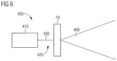
- FIG. 6shows a highly schematic block diagram of a laser component 400 .
- the laser component 400comprises a laser light source 410 configured to emit a laser beam 430 along a light path 420 .
- the laser light source 410may comprise a semiconductor laser diode, for example.
- the laser component 400furthermore comprises the diffractive optical element 10 .
- the diffractive optical element 10is arranged in the light path 420 of the laser light source 410 such that the laser beam 430 emitted by the laser light source 410 penetrates through the diffractive optical element 10 .
- the laser beam 430impinges on the diffractive optical element 10 in a direction substantially parallel to the rods 200 of the diffractive optical element 10 .
- the diffractive optical element 10expands the laser beam 430 such that the latter emerges as expanded beam 440 from the diffractive optical element 10 .
- the expanded beam 440may be attenuated, for example, such that the expanded beam 440 poses no danger to the eyes and skin of persons.
- the diffractive optical element 10 of the laser component 400might also be configured to shape the laser beam 430 in some other way.
- the diffractive optical element 10might be configured to split the laser beam 430 into a plurality of individual partial beams.
Landscapes
- Physics & Mathematics (AREA)
- General Physics & Mathematics (AREA)
- Optics & Photonics (AREA)
- Engineering & Computer Science (AREA)
- Manufacturing & Machinery (AREA)
- Diffracting Gratings Or Hologram Optical Elements (AREA)
- Crystals, And After-Treatments Of Crystals (AREA)
Abstract
Description
- 10 Diffractive optical element
- 100 Carrier
- 101 Top side
- 110 Buffer layer
- 120 Mask structure
- 130 Opening
- 131 Grid arrangement
- 200 Rods
- 201 Grid arrangement
- 210 Cross section
- 220 Diameter
- 230 Spacing
- 240 Length
- 250 First group
- 260 Second group
- 270 Second length
- 300 Protective layer
- 310 Protecting layer
- 400 Laser component
- 410 Laser light source
- 420 Light path
- 430 Laser beam
- 440 Expanded beam
Claims (18)
Applications Claiming Priority (3)
| Application Number | Priority Date | Filing Date | Title |
|---|---|---|---|
| DE102016105063.6 | 2016-03-18 | ||
| DE102016105063.6ADE102016105063A1 (en) | 2016-03-18 | 2016-03-18 | Diffractive optical element, method of making a diffractive optical element and laser device |
| PCT/EP2017/056235WO2017158091A1 (en) | 2016-03-18 | 2017-03-16 | Diffractive optical element, method for producing a diffractive optical element and laser component |
Publications (2)
| Publication Number | Publication Date |
|---|---|
| US20200201055A1 US20200201055A1 (en) | 2020-06-25 |
| US11061174B2true US11061174B2 (en) | 2021-07-13 |
Family
ID=58347368
Family Applications (1)
| Application Number | Title | Priority Date | Filing Date |
|---|---|---|---|
| US16/086,133Expired - Fee RelatedUS11061174B2 (en) | 2016-03-18 | 2017-03-16 | Diffractive optical element, method of producing a diffractive optical element and laser component |
Country Status (3)
| Country | Link |
|---|---|
| US (1) | US11061174B2 (en) |
| DE (1) | DE102016105063A1 (en) |
| WO (1) | WO2017158091A1 (en) |
Citations (22)
| Publication number | Priority date | Publication date | Assignee | Title |
|---|---|---|---|---|
| US20020022290A1 (en) | 1999-10-14 | 2002-02-21 | Hua-Shuang Kong | Single step pendeo-and lateral epitaxial overgrowth of group III-nitride epitaxial layers with group III-nitride buffer layer and resulting structures |
| US20030104678A1 (en) | 1996-10-01 | 2003-06-05 | Siemens Aktiengesellschaft | Method of separating two layers of material from one another |
| EP1727217A2 (en) | 2005-05-24 | 2006-11-29 | LG Electronics, Inc. | Light emitting device having nano structures for light extraction |
| EP1821378A1 (en) | 2004-12-08 | 2007-08-22 | Sumitomo Electric Industries, Ltd. | Semiconductor laser device and method for manufacturing same |
| US20130107367A1 (en) | 2011-10-28 | 2013-05-02 | Zhen-Dong Zhu | Grating |
| JP2014137853A (en) | 2013-01-15 | 2014-07-28 | Nippon Hoso Kyokai <Nhk> | Light-emitting element |
| US20140263982A1 (en) | 2013-03-15 | 2014-09-18 | Raytheon Company | Sensor including dielectric metamaterial microarray |
| US20150185378A1 (en) | 2013-12-27 | 2015-07-02 | Sunasic Technologies, Inc. | Silicon wafer having colored top side |
| US20150253470A1 (en) | 2014-03-06 | 2015-09-10 | University Of Southern California | Reflective color display based on tunable sub-wavelength high contrast gratings |
| US9598785B2 (en)* | 2008-09-11 | 2017-03-21 | Ramot At Tel-Aviv University Ltd. | Nanostructures and process of preparing same |
| US9650723B1 (en)* | 2013-04-11 | 2017-05-16 | Soraa, Inc. | Large area seed crystal for ammonothermal crystal growth and method of making |
| US9695055B2 (en)* | 2012-06-15 | 2017-07-04 | Intellectual Discovery Co., Ltd. | Synthetic gel for crystal growth inducing only secondary growth from surface of silicalite-1 or zeolite beta seed crystal |
| US9915603B1 (en)* | 2004-10-05 | 2018-03-13 | Photon Systems, Inc. | Spectroscopic chemical analysis methods and apparatus |
| US9954126B2 (en)* | 2013-03-14 | 2018-04-24 | Q1 Nanosystems Corporation | Three-dimensional photovoltaic devices including cavity-containing cores and methods of manufacture |
| US9961731B2 (en)* | 2015-12-08 | 2018-05-01 | Express Imaging Systems, Llc | Luminaire with transmissive filter and adjustable illumination pattern |
| US9963633B2 (en)* | 2008-09-11 | 2018-05-08 | Nexdot | Process for manufacturing colloidal materials, colloidal materials and their uses |
| US20180327669A1 (en)* | 2015-09-01 | 2018-11-15 | Dic Corporation | Powder mixture |
| US20190173128A1 (en)* | 2014-12-02 | 2019-06-06 | Polyplus Battery Company | Making and inspecting a web of vitreous lithium sulfide separator sheet and lithium electrode assemblies and battery cells |
| US20190204511A1 (en)* | 2015-04-21 | 2019-07-04 | Infineon Technologies Austria Ag | Plasmonic and photonic wavelength separation filters |
| US20200014063A1 (en)* | 2014-12-02 | 2020-01-09 | Polyplus Battery Company | Methods of making lithium ion conducting sulfide glass |
| US20200028209A1 (en)* | 2014-12-02 | 2020-01-23 | Polyplus Battery Company | Methods of making lithium ion conducting sulfide glass |
| US20200036003A1 (en)* | 2014-05-15 | 2020-01-30 | Msmh, Llc | Lithium intercalated nanocrystal anodes |
- 2016
- 2016-03-18DEDE102016105063.6Apatent/DE102016105063A1/enactivePending
- 2017
- 2017-03-16USUS16/086,133patent/US11061174B2/ennot_activeExpired - Fee Related
- 2017-03-16WOPCT/EP2017/056235patent/WO2017158091A1/ennot_activeCeased
Patent Citations (22)
| Publication number | Priority date | Publication date | Assignee | Title |
|---|---|---|---|---|
| US20030104678A1 (en) | 1996-10-01 | 2003-06-05 | Siemens Aktiengesellschaft | Method of separating two layers of material from one another |
| US20020022290A1 (en) | 1999-10-14 | 2002-02-21 | Hua-Shuang Kong | Single step pendeo-and lateral epitaxial overgrowth of group III-nitride epitaxial layers with group III-nitride buffer layer and resulting structures |
| US9915603B1 (en)* | 2004-10-05 | 2018-03-13 | Photon Systems, Inc. | Spectroscopic chemical analysis methods and apparatus |
| EP1821378A1 (en) | 2004-12-08 | 2007-08-22 | Sumitomo Electric Industries, Ltd. | Semiconductor laser device and method for manufacturing same |
| EP1727217A2 (en) | 2005-05-24 | 2006-11-29 | LG Electronics, Inc. | Light emitting device having nano structures for light extraction |
| US9598785B2 (en)* | 2008-09-11 | 2017-03-21 | Ramot At Tel-Aviv University Ltd. | Nanostructures and process of preparing same |
| US9963633B2 (en)* | 2008-09-11 | 2018-05-08 | Nexdot | Process for manufacturing colloidal materials, colloidal materials and their uses |
| US20130107367A1 (en) | 2011-10-28 | 2013-05-02 | Zhen-Dong Zhu | Grating |
| US9695055B2 (en)* | 2012-06-15 | 2017-07-04 | Intellectual Discovery Co., Ltd. | Synthetic gel for crystal growth inducing only secondary growth from surface of silicalite-1 or zeolite beta seed crystal |
| JP2014137853A (en) | 2013-01-15 | 2014-07-28 | Nippon Hoso Kyokai <Nhk> | Light-emitting element |
| US9954126B2 (en)* | 2013-03-14 | 2018-04-24 | Q1 Nanosystems Corporation | Three-dimensional photovoltaic devices including cavity-containing cores and methods of manufacture |
| US20140263982A1 (en) | 2013-03-15 | 2014-09-18 | Raytheon Company | Sensor including dielectric metamaterial microarray |
| US9650723B1 (en)* | 2013-04-11 | 2017-05-16 | Soraa, Inc. | Large area seed crystal for ammonothermal crystal growth and method of making |
| US20150185378A1 (en) | 2013-12-27 | 2015-07-02 | Sunasic Technologies, Inc. | Silicon wafer having colored top side |
| US20150253470A1 (en) | 2014-03-06 | 2015-09-10 | University Of Southern California | Reflective color display based on tunable sub-wavelength high contrast gratings |
| US20200036003A1 (en)* | 2014-05-15 | 2020-01-30 | Msmh, Llc | Lithium intercalated nanocrystal anodes |
| US20190173128A1 (en)* | 2014-12-02 | 2019-06-06 | Polyplus Battery Company | Making and inspecting a web of vitreous lithium sulfide separator sheet and lithium electrode assemblies and battery cells |
| US20200014063A1 (en)* | 2014-12-02 | 2020-01-09 | Polyplus Battery Company | Methods of making lithium ion conducting sulfide glass |
| US20200028209A1 (en)* | 2014-12-02 | 2020-01-23 | Polyplus Battery Company | Methods of making lithium ion conducting sulfide glass |
| US20190204511A1 (en)* | 2015-04-21 | 2019-07-04 | Infineon Technologies Austria Ag | Plasmonic and photonic wavelength separation filters |
| US20180327669A1 (en)* | 2015-09-01 | 2018-11-15 | Dic Corporation | Powder mixture |
| US9961731B2 (en)* | 2015-12-08 | 2018-05-01 | Express Imaging Systems, Llc | Luminaire with transmissive filter and adjustable illumination pattern |
Non-Patent Citations (2)
| Title |
|---|
| Ku, Jui-Tai & Yang,, Tsung-Hsi & Chang,, Jet-Rung & Wong, Yuen-Yee & Chou, Wu-Ching & Chang, Chun-Yen & Chen, Chiang-Yao. Epitaxial Overgrowth of Gallium Nitride Nano-Rods on Silicon (111) Substrates by RF-Plasma-Assisted Molecular Beam Epitaxy. 2010. Japanese Journal of Applied Physics. 49. 10.114 (Year: 2010).* |
| Wang, X. et al., "Fabrication of GaN nanowire arrays by confined epitaxy", 2006, Appl. Phys. Lett. 89, 233115. |
Also Published As
| Publication number | Publication date |
|---|---|
| DE102016105063A1 (en) | 2017-09-21 |
| WO2017158091A1 (en) | 2017-09-21 |
| US20200201055A1 (en) | 2020-06-25 |
Similar Documents
| Publication | Publication Date | Title |
|---|---|---|
| US11726308B2 (en) | Nanostructured meta-materials and meta-surfaces to collimate light emissions from LEDs | |
| KR20140022106A (en) | Light emitting element and method for manufacturing same | |
| DE60305832D1 (en) | Light curing device with selected spectrum | |
| US9105472B2 (en) | Single-crystal substrate,single-crystal substrate having crystalline film,crystalline film,method for producing single-crystal substrate having crystalline film,method for producing crystalline substrate,and method for producing element | |
| JP2005064492A (en) | Single crystal sapphire substrate, manufacturing method thereof, and semiconductor light emitting device | |
| TW201225277A (en) | Method for producing a plurality of optoelectronic semiconductor chips | |
| US9452495B1 (en) | Laser slicer of crystal ingots and a method of slicing gallium nitride ingots using a laser slicer | |
| US11061174B2 (en) | Diffractive optical element, method of producing a diffractive optical element and laser component | |
| CN106443985A (en) | Method for scaling structured light patterns and optical device applying same | |
| JP5057076B2 (en) | Light extraction structure from light emitting element | |
| JP2008515177A (en) | Optoelectronic thin film chip | |
| JP5357537B2 (en) | Lighting device | |
| TWI672828B (en) | Light emitting device and the manufacturing method thereof | |
| CN101409321B (en) | LED with coarsing interface and manufacturing method thereof | |
| US11688993B2 (en) | Method of producing a plurality of laser diodes and laser diode | |
| JP6147854B2 (en) | Group III nitride structure | |
| JP6991199B2 (en) | Optoelectronic element | |
| JP2003279762A (en) | Light beam deflection element | |
| KR20050037324A (en) | Gan-based semiconductor light emitting device with nano-structure layer | |
| US11289620B2 (en) | Method of producing optoelectronic semiconductor chips and optoelectronic semiconductor chip | |
| KR20170063713A (en) | Method for producing a plurality of semiconductor chips and semiconductor chip | |
| US20170012165A1 (en) | Method of producing a semiconductor layer sequence and an optoelectronic semiconductor component | |
| US10145529B2 (en) | Optical lens package for automotive lighting application | |
| US8581283B2 (en) | Photoelectric device having group III nitride semiconductor | |
| US20250047058A1 (en) | Optoelectronic semiconductor component and method for producing a plurality of optoelectronic semiconductor components |
Legal Events
| Date | Code | Title | Description |
|---|---|---|---|
| FEPP | Fee payment procedure | Free format text:ENTITY STATUS SET TO UNDISCOUNTED (ORIGINAL EVENT CODE: BIG.); ENTITY STATUS OF PATENT OWNER: LARGE ENTITY | |
| AS | Assignment | Owner name:OSRAM OPTO SEMICONDUCTORS GMBH, GERMANY Free format text:ASSIGNMENT OF ASSIGNORS INTEREST;ASSIGNORS:ENZMANN, ROLAND;HALBRITTER, HUBERT;AVRAMESCU, ADRIAN STEFAN;AND OTHERS;SIGNING DATES FROM 20180921 TO 20181015;REEL/FRAME:047191/0258 | |
| AS | Assignment | Owner name:OSRAM OLED GMBH, GERMANY Free format text:ASSIGNMENT OF ASSIGNORS INTEREST;ASSIGNOR:OSRAM OPTO SEMICONDUCTORS GMBH;REEL/FRAME:051464/0504 Effective date:20191218 | |
| STPP | Information on status: patent application and granting procedure in general | Free format text:RESPONSE TO NON-FINAL OFFICE ACTION ENTERED AND FORWARDED TO EXAMINER | |
| STPP | Information on status: patent application and granting procedure in general | Free format text:FINAL REJECTION MAILED | |
| STPP | Information on status: patent application and granting procedure in general | Free format text:RESPONSE AFTER FINAL ACTION FORWARDED TO EXAMINER | |
| STPP | Information on status: patent application and granting procedure in general | Free format text:ADVISORY ACTION MAILED | |
| STPP | Information on status: patent application and granting procedure in general | Free format text:NOTICE OF ALLOWANCE MAILED -- APPLICATION RECEIVED IN OFFICE OF PUBLICATIONS | |
| STPP | Information on status: patent application and granting procedure in general | Free format text:PUBLICATIONS -- ISSUE FEE PAYMENT RECEIVED | |
| STPP | Information on status: patent application and granting procedure in general | Free format text:PUBLICATIONS -- ISSUE FEE PAYMENT VERIFIED | |
| STCF | Information on status: patent grant | Free format text:PATENTED CASE | |
| FEPP | Fee payment procedure | Free format text:MAINTENANCE FEE REMINDER MAILED (ORIGINAL EVENT CODE: REM.); ENTITY STATUS OF PATENT OWNER: LARGE ENTITY | |
| LAPS | Lapse for failure to pay maintenance fees | Free format text:PATENT EXPIRED FOR FAILURE TO PAY MAINTENANCE FEES (ORIGINAL EVENT CODE: EXP.); ENTITY STATUS OF PATENT OWNER: LARGE ENTITY | |
| STCH | Information on status: patent discontinuation | Free format text:PATENT EXPIRED DUE TO NONPAYMENT OF MAINTENANCE FEES UNDER 37 CFR 1.362 | |
| FP | Lapsed due to failure to pay maintenance fee | Effective date:20250713 |