US11056792B2 - Antenna-in-package system and mobile terminal - Google Patents
Antenna-in-package system and mobile terminalDownload PDFInfo
- Publication number
- US11056792B2 US11056792B2US16/705,227US201916705227AUS11056792B2US 11056792 B2US11056792 B2US 11056792B2US 201916705227 AUS201916705227 AUS 201916705227AUS 11056792 B2US11056792 B2US 11056792B2
- Authority
- US
- United States
- Prior art keywords
- antenna
- package system
- mobile terminal
- metal
- substrate
- Prior art date
- Legal status (The legal status is an assumption and is not a legal conclusion. Google has not performed a legal analysis and makes no representation as to the accuracy of the status listed.)
- Expired - Fee Related
Links
Images


Classifications
- H—ELECTRICITY
- H01—ELECTRIC ELEMENTS
- H01Q—ANTENNAS, i.e. RADIO AERIALS
- H01Q9/00—Electrically-short antennas having dimensions not more than twice the operating wavelength and consisting of conductive active radiating elements
- H01Q9/04—Resonant antennas
- H01Q9/0407—Substantially flat resonant element parallel to ground plane, e.g. patch antenna
- H01Q9/0428—Substantially flat resonant element parallel to ground plane, e.g. patch antenna radiating a circular polarised wave
- H01Q9/0435—Substantially flat resonant element parallel to ground plane, e.g. patch antenna radiating a circular polarised wave using two feed points
- H—ELECTRICITY
- H01—ELECTRIC ELEMENTS
- H01Q—ANTENNAS, i.e. RADIO AERIALS
- H01Q1/00—Details of, or arrangements associated with, antennas
- H01Q1/12—Supports; Mounting means
- H01Q1/22—Supports; Mounting means by structural association with other equipment or articles
- H—ELECTRICITY
- H01—ELECTRIC ELEMENTS
- H01Q—ANTENNAS, i.e. RADIO AERIALS
- H01Q1/00—Details of, or arrangements associated with, antennas
- H01Q1/12—Supports; Mounting means
- H01Q1/22—Supports; Mounting means by structural association with other equipment or articles
- H01Q1/2258—Supports; Mounting means by structural association with other equipment or articles used with computer equipment
- H01Q1/2266—Supports; Mounting means by structural association with other equipment or articles used with computer equipment disposed inside the computer
- H—ELECTRICITY
- H01—ELECTRIC ELEMENTS
- H01Q—ANTENNAS, i.e. RADIO AERIALS
- H01Q1/00—Details of, or arrangements associated with, antennas
- H01Q1/12—Supports; Mounting means
- H01Q1/22—Supports; Mounting means by structural association with other equipment or articles
- H01Q1/2283—Supports; Mounting means by structural association with other equipment or articles mounted in or on the surface of a semiconductor substrate as a chip-type antenna or integrated with other components into an IC package
- H—ELECTRICITY
- H01—ELECTRIC ELEMENTS
- H01Q—ANTENNAS, i.e. RADIO AERIALS
- H01Q1/00—Details of, or arrangements associated with, antennas
- H01Q1/12—Supports; Mounting means
- H01Q1/22—Supports; Mounting means by structural association with other equipment or articles
- H01Q1/24—Supports; Mounting means by structural association with other equipment or articles with receiving set
- H01Q1/241—Supports; Mounting means by structural association with other equipment or articles with receiving set used in mobile communications, e.g. GSM
- H01Q1/242—Supports; Mounting means by structural association with other equipment or articles with receiving set used in mobile communications, e.g. GSM specially adapted for hand-held use
- H01Q1/243—Supports; Mounting means by structural association with other equipment or articles with receiving set used in mobile communications, e.g. GSM specially adapted for hand-held use with built-in antennas
- H—ELECTRICITY
- H01—ELECTRIC ELEMENTS
- H01Q—ANTENNAS, i.e. RADIO AERIALS
- H01Q1/00—Details of, or arrangements associated with, antennas
- H01Q1/36—Structural form of radiating elements, e.g. cone, spiral, umbrella; Particular materials used therewith
- H01Q1/38—Structural form of radiating elements, e.g. cone, spiral, umbrella; Particular materials used therewith formed by a conductive layer on an insulating support
- H—ELECTRICITY
- H01—ELECTRIC ELEMENTS
- H01Q—ANTENNAS, i.e. RADIO AERIALS
- H01Q1/00—Details of, or arrangements associated with, antennas
- H01Q1/50—Structural association of antennas with earthing switches, lead-in devices or lightning protectors
- H—ELECTRICITY
- H01—ELECTRIC ELEMENTS
- H01Q—ANTENNAS, i.e. RADIO AERIALS
- H01Q21/00—Antenna arrays or systems
- H01Q21/06—Arrays of individually energised antenna units similarly polarised and spaced apart
- H01Q21/061—Two dimensional planar arrays
- H01Q21/065—Patch antenna array
- H—ELECTRICITY
- H01—ELECTRIC ELEMENTS
- H01Q—ANTENNAS, i.e. RADIO AERIALS
- H01Q21/00—Antenna arrays or systems
- H01Q21/06—Arrays of individually energised antenna units similarly polarised and spaced apart
- H01Q21/08—Arrays of individually energised antenna units similarly polarised and spaced apart the units being spaced along or adjacent to a rectilinear path
- H—ELECTRICITY
- H01—ELECTRIC ELEMENTS
- H01Q—ANTENNAS, i.e. RADIO AERIALS
- H01Q5/00—Arrangements for simultaneous operation of antennas on two or more different wavebands, e.g. dual-band or multi-band arrangements
- H01Q5/20—Arrangements for simultaneous operation of antennas on two or more different wavebands, e.g. dual-band or multi-band arrangements characterised by the operating wavebands
- H—ELECTRICITY
- H01—ELECTRIC ELEMENTS
- H01Q—ANTENNAS, i.e. RADIO AERIALS
- H01Q5/00—Arrangements for simultaneous operation of antennas on two or more different wavebands, e.g. dual-band or multi-band arrangements
- H01Q5/30—Arrangements for providing operation on different wavebands
- H01Q5/307—Individual or coupled radiating elements, each element being fed in an unspecified way
- H01Q5/342—Individual or coupled radiating elements, each element being fed in an unspecified way for different propagation modes
- H01Q5/35—Individual or coupled radiating elements, each element being fed in an unspecified way for different propagation modes using two or more simultaneously fed points
Definitions
- the present disclosurerelates to the field of wireless communication technologies, and in particular, to an antenna-in-package system and a mobile terminal.
- the ITU-RWP5D 22nd conference held in June 2015 by International Telecommunication Union (ITU)identified three main application scenarios for 5G: enhance mobile broadband, large-scale machine communication, and highly reliable low-latency communication. These three application scenarios respectively correspond to different key indicators, and in the enhance mobile broadband scenario, the user peak speed is 20 Gbps and the minimum user experience rate is 100 Mbps.
- 3GPPis working on standardization of 5G technology.
- the first 5G Non-Stand Alone (NSA) international standardwas officially completed and frozen in December 2017, and the 5G Stand Alone standard was scheduled to be completed in June 2018.
- the rich bandwidth resources of the millimeter wave bandprovide a guarantee for high-speed transmission rates.
- wireless communication systems using the millimeter wave bandneed to adopt an architecture of a phased array. Phases of respective array units are caused to distribute according to certain rule by a phase shifter, so that a high gain beam is formed and the beam is scanned over a certain spatial range through a change in phase shift.
- the antenna-in-package (AiP) technologyintegrates, through package material and process, an antenna into a package carrying a chip, which fully balances antenna performance, cost and volume and is widely favored by broad chip and package manufacturers.
- companies including Qualcomm, Intel, IBM and the likehave adopted the antenna-in-package technology.
- the AiP technologywill also provide a good antenna solution for 5G millimeter wave mobile communication systems.
- the band of 28 GHz and 39 GHzbelong two independent channels, which require a large area in space of a mobile phone.
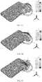
- FIG. 1is a perspective structural schematic diagram of a mobile terminal according to the present disclosure
- FIG. 2is a schematic diagram showing a connection structure of an antenna-in-package system and a main board shown in FIG. 1 ;
- FIG. 3is a schematic diagram showing a connection structure of a metal antenna unit and a feeding probe
- FIG. 4Aillustrates a radiation pattern of a metal antenna unit with a phase shift being 45° when an antenna-in-package system according to the present disclosure is in a band of 28 GHz;
- FIG. 4Billustrates a radiation pattern of a metal antenna unit with a phase shift being 0° when an antenna-in-package system according to the present disclosure is in a band of 28 GHz;
- FIG. 4Cillustrates a radiation pattern of a metal antenna unit with a phase shift being ⁇ 45° when an antenna-in-package system according to the present disclosure is in a band of 28 GHz;
- FIG. 5Aillustrates a radiation pattern of a metal antenna unit with a phase shift being 45° when an antenna-in-package system according to the present disclosure is in a band of 39 GHz;
- FIG. 5Billustrates a radiation pattern of a metal antenna unit with a phase shift being 0° when an antenna-in-package system according to the present disclosure is in a band of 39 GHz;
- FIG. 5Cillustrates a radiation pattern of a metal antenna unit with a phase shift being ⁇ 45° when an antenna-in-package system according to the present disclosure is in a band of 39 GHz;
- FIG. 6Aillustrates a reflection coefficient graph of an antenna-in-package system according to the present disclosure in a band of 28 GHz;
- FIG. 6Billustrates a reflection coefficient graph of an antenna-in-package system according to the present disclosure in a band of 39 GHz.
- FIG. 7Aillustrates a coverage efficiency graph of an antenna-in-package system according to the present disclosure in a band of 28 GHz.
- FIG. 7Billustrates a coverage efficiency graph of an antenna-in-package system according to the present disclosure in a band of 39 GHz.
- the present disclosureprovides a mobile terminal 100 , and the mobile terminal 100 may be a mobile phone, an ipad, a POS machine, etc., which is not limited by the present disclosure.
- the mobile terminal 100includes a screen 1 , a back cover 2 covering, connected to and fitting with the screen 1 to form a receiving space, a main board 3 interposed between the screen 1 and the back cover 2 , and an antenna-in-package system 4 connected to the main board 3 .
- the main board 3 and the antenna-in-package system 4are both received in the receiving space.
- the back cover 2is a 3D glass back cover that can provide better protection, aesthetics, thermal diffusion, color, and user experience.
- the back cover 2includes a bottom wall 21 opposite to and spaced apart from the screen 1 , and a side wall 22 being bent and extending from an outer periphery of the bottom wall 21 towards the screen 1 .
- the side wall 22is connected to the screen 1 , and the bottom wall 21 and the side wall 22 are formed into one piece.
- the antenna-in-package system 4is provided close to the side wall 22 and parallel to the bottom wall 21 .
- the antenna-in-package system 4is configured to receive and transmit electromagnetic wave signals, thereby implementing a communication function of the mobile terminal 100 .
- the antenna-in-package system 4can be connected to the main board 3 by adopting a Ball Grid array (BGA) technology.
- BGABall Grid array
- the antenna-in-package system 4includes a substrate 41 provided between the screen 1 and the back cover 2 , an integrated circuit chip 42 provided on a side of the substrate 41 close to the main board 3 , a metal antenna 43 provided on a side of the substrate 41 facing away from the main board 3 , and a circuit 44 provided in the substrate 41 and connecting the integrated circuit chip 42 with the metal antenna 43 .
- the substrate 41is configured to carry the metal antenna 43 and the circuit 44 .
- the substrate 41may be integrally formed or layered.
- the substrate 41is a multilayer high-frequency low-loss plate.
- the integrated circuit chip 42is fixedly connected to the substrate 41 by a bumping welding process.
- the metal antenna 43is a patch antenna and includes two feeding points 10 , and the patch antenna is simultaneously fed with power by the two feeding points 10 .
- the two feeding points 10are configured to excite electromagnetic waves of different bands.
- the feeding points 10include a first feeding point 101 and a second feeding point 102 , and the first feeding point 101 and the second feeding point 102 are spaced apart from each other.
- the first feeding point 101is configured to excite electromagnetic waves of 28 GHz
- the second feeding point 102is configured to excite electromagnetic waves of 39 GHz.
- the feeding point 10is connected to the circuit 44 via a feeding probe 20 , to feed power to the metal antenna 43 .
- the feeding probe 20includes a first feeding probe 201 and a second feeding probe 202 .
- the first feeding point 101is connected to the circuit 44 by the first feeding probe 201
- the second feeding point 102is connected to the circuit 44 by the second feeding probe 202 .
- the antenna-in-package system 4is a millimeter wave phased array system, and the space occupied in the mobile phone is narrowed; and only one perspective needs to be scanned, which simplifies design difficulty, test difficulty, and beam management complexity.
- the metal antenna 43is arranged in a one-dimensional linear array and includes a plurality of metal antenna units 431 , and the plurality of the metal antenna units 431 is sequentially arranged at intervals.
- the metal antenna 43is a linear array of 1 ⁇ 4, that is, the metal antenna 43 includes four metal antenna units 431 , and each of the metal antenna units 431 includes two feeding points 10 .
- the metal antenna 43is a microstrip patch antenna and it is selected from a group consisting of a square patch antenna, a ring patch antenna, a circular patch antenna, and a cross-shaped patch antenna.
- the metal antenna 43is a square patch antenna. It is appreciated that, in other embodiments, the metal antenna 43 may also use antennas of other forms.
- the metal antenna 43includes a first feeding point 101 and a second feeding point 102 , and the first feeding point 101 and the second feeding point 102 excite signals of different bands to achieve a dual-band coverage of the antenna-in-package system 4 .
- the antenna-in-package system 4is formed by being laminated by a PCB process or an LTCC process, such that the size is reduced to 18 ⁇ 5 mm and the occupied area is greatly reduced compared with the dual-band antenna system in the related art.
- FIG. 4A ?? FIG. 7Bin which:
- FIG. 4Aillustrates a radiation pattern of a metal antenna unit with a phase shift being 45° when an antenna-in-package system according to the present disclosure is in a band of 28 GHz;
- FIG. 4Billustrates a radiation pattern of a metal antenna unit with a phase shift being 0° when an antenna-in-package system according to the present disclosure is in a band of 28 GHz;
- FIG. 4Cillustrates a radiation pattern of a metal antenna unit with a phase shift being ⁇ 45° when an antenna-in-package system according to the present disclosure is in a band of 28 GHz;
- FIG. 5Aillustrates a radiation pattern of a metal antenna unit with a phase shift being 45° when an antenna-in-package system according to the present disclosure is in a band of 39 GHz;
- FIG. 5Billustrates a radiation pattern of a metal antenna unit with a phase shift being 0° when an antenna-in-package system according to the present disclosure is in a band of 39 GHz;
- FIG. 5Cillustrates a radiation pattern of a metal antenna unit with a phase shift being ⁇ 45° when an antenna-in-package system according to the present disclosure is in a band of 39 GHz;
- FIG. 6Aillustrates a reflection coefficient graph of an antenna-in-package system according to the present disclosure in a band of 28 GHz;
- FIG. 6Billustrates a reflection coefficient graph of an antenna-in-package system according to the present disclosure in a band of 39 GHz.
- FIG. 7Aillustrates a coverage efficiency graph of an antenna-in-package system according to the present disclosure in a band of 28 GHz.
- FIG. 7Billustrates a coverage efficiency graph of an antenna-in-package system according to the present disclosure in a band of 39 GHz.
- a gain threshold of the antenna-in-package system 4is 10 dBi, and the gain threshold of the antenna-in-package system 4 is reduced by 10 dBi for the case of 50% coverage efficiency, while the gain threshold is reduced by 12.98 dBi for the case of 50% coverage efficiency in the 3GPP discussion; in the band of 39 GHz, the gain threshold of the antenna-in-package system 4 is 13 dBi, and the gain threshold of the antenna-in-package system 4 is reduced by 10 dBi for the case of 50% coverage efficiency, while the gain threshold is reduced by 13.6-18.0 dBi for the case of 50% coverage efficiency in the 3GPP discussion, showing that the AiP antenna system 4 of the present disclosure has the better coverage efficiency.
- the antenna-in-package system 4 and the mobile terminal 100 provided by the present disclosurehave following beneficial effects: the metal antenna 43 includes a first feeding point 101 and a second feeding point 102 , and the first feeding point 101 and the second feeding point 102 excite signals of different bands to achieve the dual-band coverage of the antenna-in-package system 4 .
- the antenna-in-package system 4is formed by being laminated by a PCB process or an LTCC process, such that the size is reduced to 18 ⁇ 5 mm and the occupied area is greatly reduced compared with the dual-band antenna system in the related art.
- the millimeter wave phased array antenna systemadopts a linear array instead of a planar array, occupies a narrower space in the mobile phone, and only needs to be scanned in one perspective, which simplifies design difficulty, test difficulty, and beam management complexity.
Landscapes
- Engineering & Computer Science (AREA)
- Computer Networks & Wireless Communication (AREA)
- Computer Hardware Design (AREA)
- General Engineering & Computer Science (AREA)
- Microelectronics & Electronic Packaging (AREA)
- Support Of Aerials (AREA)
- Variable-Direction Aerials And Aerial Arrays (AREA)
Abstract
Description
Claims (12)
Applications Claiming Priority (2)
| Application Number | Priority Date | Filing Date | Title |
|---|---|---|---|
| CN201811645892.5 | 2018-12-29 | ||
| CN201811645892.5ACN109687166A (en) | 2018-12-29 | 2018-12-29 | Encapsulating antenna system and mobile terminal |
Publications (2)
| Publication Number | Publication Date |
|---|---|
| US20200212579A1 US20200212579A1 (en) | 2020-07-02 |
| US11056792B2true US11056792B2 (en) | 2021-07-06 |
Family
ID=66191593
Family Applications (1)
| Application Number | Title | Priority Date | Filing Date |
|---|---|---|---|
| US16/705,227Expired - Fee RelatedUS11056792B2 (en) | 2018-12-29 | 2019-12-06 | Antenna-in-package system and mobile terminal |
Country Status (3)
| Country | Link |
|---|---|
| US (1) | US11056792B2 (en) |
| CN (1) | CN109687166A (en) |
| WO (1) | WO2020134476A1 (en) |
Cited By (1)
| Publication number | Priority date | Publication date | Assignee | Title |
|---|---|---|---|---|
| US20220399907A1 (en)* | 2021-06-11 | 2022-12-15 | Wistron Neweb Corp. | Antenna structure |
Families Citing this family (10)
| Publication number | Priority date | Publication date | Assignee | Title |
|---|---|---|---|---|
| US11201119B2 (en) | 2018-06-06 | 2021-12-14 | At&S Austria Technologie & Systemtechnik Aktiengesellschaft | RF functionality and electromagnetic radiation shielding in a component carrier |
| CN109687166A (en)* | 2018-12-29 | 2019-04-26 | 瑞声科技(南京)有限公司 | Encapsulating antenna system and mobile terminal |
| CN109830799A (en)* | 2018-12-29 | 2019-05-31 | 瑞声科技(南京)有限公司 | Dielectric resonator encapsulating antenna system and mobile terminal |
| CN111864362A (en)* | 2019-04-30 | 2020-10-30 | Oppo广东移动通信有限公司 | Antenna modules and electronic equipment |
| CN111864343A (en)* | 2019-04-30 | 2020-10-30 | Oppo广东移动通信有限公司 | Electronic equipment |
| WO2020237559A1 (en) | 2019-05-30 | 2020-12-03 | 华为技术有限公司 | Packaging structure, network device, and terminal device |
| WO2021000146A1 (en)* | 2019-06-30 | 2021-01-07 | 瑞声声学科技(深圳)有限公司 | Antenna-in-package module and electronic apparatus |
| CN112290193B (en)* | 2019-07-26 | 2023-07-25 | Oppo广东移动通信有限公司 | Millimeter wave module, electronic equipment and adjusting method of millimeter wave module |
| CN113036461A (en)* | 2019-12-25 | 2021-06-25 | 中国移动通信集团终端有限公司 | System-in-package antenna module and terminal |
| CN111403901B (en)* | 2020-03-16 | 2021-06-15 | Oppo广东移动通信有限公司 | Antenna modules and electronic equipment |
Citations (2)
| Publication number | Priority date | Publication date | Assignee | Title |
|---|---|---|---|---|
| US20200052416A1 (en)* | 2018-08-12 | 2020-02-13 | AAC Technologies Pte. Ltd. | Antenna module and mobile terminal |
| US20200161749A1 (en)* | 2017-07-31 | 2020-05-21 | Murata Manufacturing Co., Ltd. | Antenna module and communication apparatus |
Family Cites Families (8)
| Publication number | Priority date | Publication date | Assignee | Title |
|---|---|---|---|---|
| EP1710861A1 (en)* | 2005-04-07 | 2006-10-11 | Sony Ericsson Mobile Communications AB | Antenna Arrangement |
| EP1786064A1 (en)* | 2005-11-09 | 2007-05-16 | Sony Deutschland GmbH | Planar antenna apparatus for ultra wide band applications |
| CN203039113U (en)* | 2013-01-11 | 2013-07-03 | 成都信息工程学院 | Eight-port microstrip antenna array |
| CN103682613A (en)* | 2013-12-27 | 2014-03-26 | 禾邦电子(苏州)有限公司 | Antenna assembly and dual-frequency and double-fed antenna thereof |
| CN104064867B (en)* | 2014-06-12 | 2016-10-05 | 京信通信技术(广州)有限公司 | Multiband radiating element and mobile communication antenna |
| CN108879114A (en)* | 2017-05-16 | 2018-11-23 | 华为技术有限公司 | Integrated antenna packages structure and terminal |
| CN109088180B (en)* | 2018-08-12 | 2020-11-20 | 瑞声科技(南京)有限公司 | AOG antenna system and mobile terminal |
| CN109687166A (en)* | 2018-12-29 | 2019-04-26 | 瑞声科技(南京)有限公司 | Encapsulating antenna system and mobile terminal |
- 2018
- 2018-12-29CNCN201811645892.5Apatent/CN109687166A/enactivePending
- 2019
- 2019-10-25WOPCT/CN2019/113380patent/WO2020134476A1/ennot_activeCeased
- 2019-12-06USUS16/705,227patent/US11056792B2/ennot_activeExpired - Fee Related
Patent Citations (2)
| Publication number | Priority date | Publication date | Assignee | Title |
|---|---|---|---|---|
| US20200161749A1 (en)* | 2017-07-31 | 2020-05-21 | Murata Manufacturing Co., Ltd. | Antenna module and communication apparatus |
| US20200052416A1 (en)* | 2018-08-12 | 2020-02-13 | AAC Technologies Pte. Ltd. | Antenna module and mobile terminal |
Cited By (2)
| Publication number | Priority date | Publication date | Assignee | Title |
|---|---|---|---|---|
| US20220399907A1 (en)* | 2021-06-11 | 2022-12-15 | Wistron Neweb Corp. | Antenna structure |
| US11824568B2 (en)* | 2021-06-11 | 2023-11-21 | Wistron Neweb Corp. | Antenna structure |
Also Published As
| Publication number | Publication date |
|---|---|
| CN109687166A (en) | 2019-04-26 |
| US20200212579A1 (en) | 2020-07-02 |
| WO2020134476A1 (en) | 2020-07-02 |
Similar Documents
| Publication | Publication Date | Title |
|---|---|---|
| US11056792B2 (en) | Antenna-in-package system and mobile terminal | |
| US11031696B2 (en) | Antenna-in-package system and mobile terminal | |
| US10992059B2 (en) | Millimeter wave array antenna module and mobile terminal | |
| US10819002B2 (en) | AOG antenna system and mobile terminal | |
| US11024942B2 (en) | Antenna-in-package system and mobile terminal | |
| US11075450B2 (en) | AOG antenna system and mobile terminal | |
| US11031671B2 (en) | AOG antenna system and mobile terminal | |
| US11108164B2 (en) | Antenna module and mobile terminal | |
| US20200212581A1 (en) | Dielectric resonator antenna-in-package system and mobile terminal | |
| US10978783B2 (en) | Antenna system and mobile terminal | |
| US11075440B2 (en) | Surface-mounted device and mobile terminal | |
| US20200212542A1 (en) | Antenna system and mobile terminal | |
| US10819016B2 (en) | Antenna system and mobile terminal | |
| CN111710961B (en) | Millimeter wave antenna module and electronic equipment | |
| CN108417996A (en) | Antenna components and mobile terminals | |
| US10930998B2 (en) | Antenna system and electronic device | |
| US11063341B2 (en) | Antenna assembly and mobile terminal using same | |
| CN205509020U (en) | Communication terminal | |
| US20120287015A1 (en) | Multi-layer antenna | |
| CN109786934B (en) | Packaged antenna system and mobile terminal | |
| US20120313819A1 (en) | Active Antenna and Electronic Device | |
| CN112701461B (en) | 5G millimeter wave super-surface antenna module and mobile device | |
| JP2013017008A (en) | Radio communication device |
Legal Events
| Date | Code | Title | Description |
|---|---|---|---|
| FEPP | Fee payment procedure | Free format text:ENTITY STATUS SET TO UNDISCOUNTED (ORIGINAL EVENT CODE: BIG.); ENTITY STATUS OF PATENT OWNER: LARGE ENTITY | |
| AS | Assignment | Owner name:AAC TECHNOLOGIES PTE. LTD., SINGAPORE Free format text:ASSIGNMENT OF ASSIGNORS INTEREST;ASSIGNORS:XIA, XIAOYUE;WANG, CHAO;SIGNING DATES FROM 20191130 TO 20191202;REEL/FRAME:051835/0440 | |
| STPP | Information on status: patent application and granting procedure in general | Free format text:DOCKETED NEW CASE - READY FOR EXAMINATION | |
| STPP | Information on status: patent application and granting procedure in general | Free format text:NON FINAL ACTION MAILED | |
| STPP | Information on status: patent application and granting procedure in general | Free format text:RESPONSE TO NON-FINAL OFFICE ACTION ENTERED AND FORWARDED TO EXAMINER | |
| STPP | Information on status: patent application and granting procedure in general | Free format text:NOTICE OF ALLOWANCE MAILED -- APPLICATION RECEIVED IN OFFICE OF PUBLICATIONS | |
| STPP | Information on status: patent application and granting procedure in general | Free format text:PUBLICATIONS -- ISSUE FEE PAYMENT RECEIVED | |
| STPP | Information on status: patent application and granting procedure in general | Free format text:PUBLICATIONS -- ISSUE FEE PAYMENT VERIFIED | |
| STCF | Information on status: patent grant | Free format text:PATENTED CASE | |
| FEPP | Fee payment procedure | Free format text:MAINTENANCE FEE REMINDER MAILED (ORIGINAL EVENT CODE: REM.); ENTITY STATUS OF PATENT OWNER: LARGE ENTITY | |
| LAPS | Lapse for failure to pay maintenance fees | Free format text:PATENT EXPIRED FOR FAILURE TO PAY MAINTENANCE FEES (ORIGINAL EVENT CODE: EXP.); ENTITY STATUS OF PATENT OWNER: LARGE ENTITY | |
| STCH | Information on status: patent discontinuation | Free format text:PATENT EXPIRED DUE TO NONPAYMENT OF MAINTENANCE FEES UNDER 37 CFR 1.362 | |
| FP | Lapsed due to failure to pay maintenance fee | Effective date:20250706 |