US11056483B2 - Heterolithic microwave integrated circuits including gallium-nitride devices on intrinsic semiconductor - Google Patents
Heterolithic microwave integrated circuits including gallium-nitride devices on intrinsic semiconductorDownload PDFInfo
- Publication number
- US11056483B2 US11056483B2US15/875,406US201815875406AUS11056483B2US 11056483 B2US11056483 B2US 11056483B2US 201815875406 AUS201815875406 AUS 201815875406AUS 11056483 B2US11056483 B2US 11056483B2
- Authority
- US
- United States
- Prior art keywords
- region
- substrate
- integrated circuit
- semiconductor
- semiconductor material
- Prior art date
- Legal status (The legal status is an assumption and is not a legal conclusion. Google has not performed a legal analysis and makes no representation as to the accuracy of the status listed.)
- Active
Links
- 239000004065semiconductorSubstances0.000titleclaimsabstractdescription212
- JMASRVWKEDWRBT-UHFFFAOYSA-NGallium nitrideChemical compound[Ga]#NJMASRVWKEDWRBT-UHFFFAOYSA-N0.000titleclaimsdescription56
- 229910002601GaNInorganic materials0.000titleclaimsdescription54
- 239000000758substrateSubstances0.000claimsabstractdescription84
- 238000000034methodMethods0.000claimsabstractdescription74
- 239000012777electrically insulating materialSubstances0.000claimsabstractdescription26
- 239000000463materialSubstances0.000claimsdescription172
- 239000010410layerSubstances0.000claimsdescription109
- 239000000203mixtureSubstances0.000claimsdescription28
- 239000011241protective layerSubstances0.000claimsdescription26
- 229910052710siliconInorganic materials0.000claimsdescription21
- 239000010703siliconSubstances0.000claimsdescription21
- 238000005530etchingMethods0.000claimsdescription20
- 239000003989dielectric materialSubstances0.000claimsdescription10
- 238000011049fillingMethods0.000claimsdescription8
- 238000002161passivationMethods0.000claimsdescription7
- 238000004519manufacturing processMethods0.000claimsdescription5
- 230000009477glass transitionEffects0.000claimsdescription3
- 101000615941Homo sapiens Mannosyl-oligosaccharide 1,2-alpha-mannosidase ICProteins0.000abstract3
- 102100021770Mannosyl-oligosaccharide 1,2-alpha-mannosidase ICHuman genes0.000abstract3
- UGVTYCQVZPDYRZ-ZHACJKMWSA-N4-[(E)-[hydroxymethyl(methyl)amino]diazenyl]-1H-imidazole-5-carboxamideChemical compoundCN(CO)\N=N\C1=C(N=CN1)C(N)=OUGVTYCQVZPDYRZ-ZHACJKMWSA-N0.000abstract2
- 230000008569processEffects0.000description42
- 239000010408filmSubstances0.000description28
- 239000011810insulating materialSubstances0.000description24
- XUIMIQQOPSSXEZ-UHFFFAOYSA-NSiliconChemical compound[Si]XUIMIQQOPSSXEZ-UHFFFAOYSA-N0.000description19
- 150000004767nitridesChemical class0.000description14
- 239000003990capacitorSubstances0.000description9
- 239000011521glassSubstances0.000description7
- 230000003071parasitic effectEffects0.000description6
- 229910052751metalInorganic materials0.000description5
- 239000002184metalSubstances0.000description5
- 238000001020plasma etchingMethods0.000description5
- 239000004033plasticSubstances0.000description5
- 238000000231atomic layer depositionMethods0.000description4
- 230000009286beneficial effectEffects0.000description4
- 230000008901benefitEffects0.000description4
- 230000015572biosynthetic processEffects0.000description4
- 238000005468ion implantationMethods0.000description4
- 238000002955isolationMethods0.000description4
- 229910000577Silicon-germaniumInorganic materials0.000description3
- LEVVHYCKPQWKOP-UHFFFAOYSA-N[Si].[Ge]Chemical compound[Si].[Ge]LEVVHYCKPQWKOP-UHFFFAOYSA-N0.000description3
- 229910052782aluminiumInorganic materials0.000description3
- XAGFODPZIPBFFR-UHFFFAOYSA-NaluminiumChemical compound[Al]XAGFODPZIPBFFR-UHFFFAOYSA-N0.000description3
- 238000004891communicationMethods0.000description3
- 238000005566electron beam evaporationMethods0.000description3
- 238000005516engineering processMethods0.000description3
- 238000004518low pressure chemical vapour depositionMethods0.000description3
- 229920002120photoresistant polymerPolymers0.000description3
- 238000000623plasma-assisted chemical vapour depositionMethods0.000description3
- XKRFYHLGVUSROY-UHFFFAOYSA-NArgonChemical compound[Ar]XKRFYHLGVUSROY-UHFFFAOYSA-N0.000description2
- JBRZTFJDHDCESZ-UHFFFAOYSA-NAsGaChemical compound[As]#[Ga]JBRZTFJDHDCESZ-UHFFFAOYSA-N0.000description2
- IJGRMHOSHXDMSA-UHFFFAOYSA-NAtomic nitrogenChemical compoundN#NIJGRMHOSHXDMSA-UHFFFAOYSA-N0.000description2
- RYGMFSIKBFXOCR-UHFFFAOYSA-NCopperChemical compound[Cu]RYGMFSIKBFXOCR-UHFFFAOYSA-N0.000description2
- GYHNNYVSQQEPJS-UHFFFAOYSA-NGalliumChemical compound[Ga]GYHNNYVSQQEPJS-UHFFFAOYSA-N0.000description2
- 229910001218Gallium arsenideInorganic materials0.000description2
- UFHFLCQGNIYNRP-UHFFFAOYSA-NHydrogenChemical compound[H][H]UFHFLCQGNIYNRP-UHFFFAOYSA-N0.000description2
- PXHVJJICTQNCMI-UHFFFAOYSA-NNickelChemical compound[Ni]PXHVJJICTQNCMI-UHFFFAOYSA-N0.000description2
- 229910052581Si3N4Inorganic materials0.000description2
- 230000004075alterationEffects0.000description2
- AJGDITRVXRPLBY-UHFFFAOYSA-Naluminum indiumChemical compound[Al].[In]AJGDITRVXRPLBY-UHFFFAOYSA-N0.000description2
- 230000015556catabolic processEffects0.000description2
- 239000000919ceramicSubstances0.000description2
- 239000004020conductorSubstances0.000description2
- 229910052802copperInorganic materials0.000description2
- 239000010949copperSubstances0.000description2
- 230000002939deleterious effectEffects0.000description2
- 238000000151depositionMethods0.000description2
- 230000008021depositionEffects0.000description2
- 238000009792diffusion processMethods0.000description2
- 230000005669field effectEffects0.000description2
- 229910052733galliumInorganic materials0.000description2
- 239000010931goldSubstances0.000description2
- 230000017525heat dissipationEffects0.000description2
- 238000010438heat treatmentMethods0.000description2
- 239000001257hydrogenSubstances0.000description2
- 229910052739hydrogenInorganic materials0.000description2
- 238000007654immersionMethods0.000description2
- 230000006872improvementEffects0.000description2
- 229910052738indiumInorganic materials0.000description2
- APFVFJFRJDLVQX-UHFFFAOYSA-Nindium atomChemical compound[In]APFVFJFRJDLVQX-UHFFFAOYSA-N0.000description2
- 238000012986modificationMethods0.000description2
- 230000004048modificationEffects0.000description2
- 230000003287optical effectEffects0.000description2
- 238000000059patterningMethods0.000description2
- 238000002360preparation methodMethods0.000description2
- 230000001681protective effectEffects0.000description2
- HBMJWWWQQXIZIP-UHFFFAOYSA-Nsilicon carbideChemical compound[Si+]#[C-]HBMJWWWQQXIZIP-UHFFFAOYSA-N0.000description2
- 229910010271silicon carbideInorganic materials0.000description2
- HQVNEWCFYHHQES-UHFFFAOYSA-Nsilicon nitrideChemical compoundN12[Si]34N5[Si]62N3[Si]51N64HQVNEWCFYHHQES-UHFFFAOYSA-N0.000description2
- 239000002210silicon-based materialSubstances0.000description2
- 239000000126substanceSubstances0.000description2
- 239000010409thin filmSubstances0.000description2
- 239000010936titaniumSubstances0.000description2
- 229910000838Al alloyInorganic materials0.000description1
- VYZAMTAEIAYCRO-UHFFFAOYSA-NChromiumChemical compound[Cr]VYZAMTAEIAYCRO-UHFFFAOYSA-N0.000description1
- 229910000881Cu alloyInorganic materials0.000description1
- 229910000530Gallium indium arsenideInorganic materials0.000description1
- 239000004642PolyimideSubstances0.000description1
- BQCADISMDOOEFD-UHFFFAOYSA-NSilverChemical compound[Ag]BQCADISMDOOEFD-UHFFFAOYSA-N0.000description1
- ATJFFYVFTNAWJD-UHFFFAOYSA-NTinChemical compound[Sn]ATJFFYVFTNAWJD-UHFFFAOYSA-N0.000description1
- RTAQQCXQSZGOHL-UHFFFAOYSA-NTitaniumChemical compound[Ti]RTAQQCXQSZGOHL-UHFFFAOYSA-N0.000description1
- 229910052770UraniumInorganic materials0.000description1
- 239000000853adhesiveSubstances0.000description1
- 230000001070adhesive effectEffects0.000description1
- 229910045601alloyInorganic materials0.000description1
- 239000000956alloySubstances0.000description1
- -1aluminumChemical class0.000description1
- RNQKDQAVIXDKAG-UHFFFAOYSA-Naluminum galliumChemical compound[Al].[Ga]RNQKDQAVIXDKAG-UHFFFAOYSA-N0.000description1
- 238000013459approachMethods0.000description1
- 229910052786argonInorganic materials0.000description1
- 229910052785arsenicInorganic materials0.000description1
- RQNWIZPPADIBDY-UHFFFAOYSA-Narsenic atomChemical compound[As]RQNWIZPPADIBDY-UHFFFAOYSA-N0.000description1
- 238000000277atomic layer chemical vapour depositionMethods0.000description1
- UMIVXZPTRXBADB-UHFFFAOYSA-NbenzocyclobuteneChemical compoundC1=CC=C2CCC2=C1UMIVXZPTRXBADB-UHFFFAOYSA-N0.000description1
- 230000005540biological transmissionEffects0.000description1
- 239000005388borosilicate glassSubstances0.000description1
- 238000006243chemical reactionMethods0.000description1
- 229910017052cobaltInorganic materials0.000description1
- 239000010941cobaltSubstances0.000description1
- GUTLYIVDDKVIGB-UHFFFAOYSA-Ncobalt atomChemical compound[Co]GUTLYIVDDKVIGB-UHFFFAOYSA-N0.000description1
- 238000001816coolingMethods0.000description1
- PMHQVHHXPFUNSP-UHFFFAOYSA-Mcopper(1+);methylsulfanylmethane;bromideChemical compoundBr[Cu].CSCPMHQVHHXPFUNSP-UHFFFAOYSA-M0.000description1
- 239000013078crystalSubstances0.000description1
- 230000007547defectEffects0.000description1
- 239000002019doping agentSubstances0.000description1
- 238000000407epitaxyMethods0.000description1
- 230000002349favourable effectEffects0.000description1
- 239000007789gasSubstances0.000description1
- 229910052732germaniumInorganic materials0.000description1
- GNPVGFCGXDBREM-UHFFFAOYSA-Ngermanium atomChemical compound[Ge]GNPVGFCGXDBREM-UHFFFAOYSA-N0.000description1
- PCHJSUWPFVWCPO-UHFFFAOYSA-NgoldChemical compound[Au]PCHJSUWPFVWCPO-UHFFFAOYSA-N0.000description1
- 229910052737goldInorganic materials0.000description1
- BHEPBYXIRTUNPN-UHFFFAOYSA-Nhydridophosphorus(.) (triplet)Chemical compound[PH]BHEPBYXIRTUNPN-UHFFFAOYSA-N0.000description1
- 238000002513implantationMethods0.000description1
- 238000009616inductively coupled plasmaMethods0.000description1
- 238000003780insertionMethods0.000description1
- 230000037431insertionEffects0.000description1
- 230000008018meltingEffects0.000description1
- 238000002844meltingMethods0.000description1
- 150000002739metalsChemical class0.000description1
- 230000000116mitigating effectEffects0.000description1
- 238000010295mobile communicationMethods0.000description1
- 229910052759nickelInorganic materials0.000description1
- 229910052757nitrogenInorganic materials0.000description1
- TWNQGVIAIRXVLR-UHFFFAOYSA-Noxo(oxoalumanyloxy)alumaneChemical compoundO=[Al]O[Al]=OTWNQGVIAIRXVLR-UHFFFAOYSA-N0.000description1
- 230000000149penetrating effectEffects0.000description1
- 229920001721polyimidePolymers0.000description1
- 229920000642polymerPolymers0.000description1
- 229910021332silicideInorganic materials0.000description1
- FVBUAEGBCNSCDD-UHFFFAOYSA-Nsilicide(4-)Chemical compound[Si-4]FVBUAEGBCNSCDD-UHFFFAOYSA-N0.000description1
- 229910052709silverInorganic materials0.000description1
- 239000004332silverSubstances0.000description1
- 229910000679solderInorganic materials0.000description1
- 238000004544sputter depositionMethods0.000description1
- 229910052718tinInorganic materials0.000description1
- 239000011135tinSubstances0.000description1
- 229910052719titaniumInorganic materials0.000description1
- 230000007704transitionEffects0.000description1
- WFKWXMTUELFFGS-UHFFFAOYSA-NtungstenChemical compound[W]WFKWXMTUELFFGS-UHFFFAOYSA-N0.000description1
- 229910052721tungstenInorganic materials0.000description1
- 239000010937tungstenSubstances0.000description1
- 238000001429visible spectrumMethods0.000description1
- 238000003631wet chemical etchingMethods0.000description1
- 229910052984zinc sulfideInorganic materials0.000description1
Images


Classifications
- H01L27/0605—
- H—ELECTRICITY
- H01—ELECTRIC ELEMENTS
- H01L—SEMICONDUCTOR DEVICES NOT COVERED BY CLASS H10
- H01L23/00—Details of semiconductor or other solid state devices
- H01L23/58—Structural electrical arrangements for semiconductor devices not otherwise provided for, e.g. in combination with batteries
- H01L23/64—Impedance arrangements
- H01L23/66—High-frequency adaptations
- H—ELECTRICITY
- H01—ELECTRIC ELEMENTS
- H01L—SEMICONDUCTOR DEVICES NOT COVERED BY CLASS H10
- H01L21/00—Processes or apparatus adapted for the manufacture or treatment of semiconductor or solid state devices or of parts thereof
- H01L21/02—Manufacture or treatment of semiconductor devices or of parts thereof
- H01L21/02104—Forming layers
- H01L21/02365—Forming inorganic semiconducting materials on a substrate
- H01L21/02367—Substrates
- H01L21/0237—Materials
- H01L21/02387—Group 13/15 materials
- H01L21/02389—Nitrides
- H—ELECTRICITY
- H01—ELECTRIC ELEMENTS
- H01L—SEMICONDUCTOR DEVICES NOT COVERED BY CLASS H10
- H01L21/00—Processes or apparatus adapted for the manufacture or treatment of semiconductor or solid state devices or of parts thereof
- H01L21/70—Manufacture or treatment of devices consisting of a plurality of solid state components formed in or on a common substrate or of parts thereof; Manufacture of integrated circuit devices or of parts thereof
- H01L21/71—Manufacture of specific parts of devices defined in group H01L21/70
- H01L21/76—Making of isolation regions between components
- H01L21/762—Dielectric regions, e.g. EPIC dielectric isolation, LOCOS; Trench refilling techniques, SOI technology, use of channel stoppers
- H01L21/7624—Dielectric regions, e.g. EPIC dielectric isolation, LOCOS; Trench refilling techniques, SOI technology, use of channel stoppers using semiconductor on insulator [SOI] technology
- H01L21/76264—SOI together with lateral isolation, e.g. using local oxidation of silicon, or dielectric or polycristalline material refilled trench or air gap isolation regions, e.g. completely isolated semiconductor islands
- H01L27/0629—
- H01L27/1207—
- H—ELECTRICITY
- H10—SEMICONDUCTOR DEVICES; ELECTRIC SOLID-STATE DEVICES NOT OTHERWISE PROVIDED FOR
- H10D—INORGANIC ELECTRIC SEMICONDUCTOR DEVICES
- H10D84/00—Integrated devices formed in or on semiconductor substrates that comprise only semiconducting layers, e.g. on Si wafers or on GaAs-on-Si wafers
- H10D84/01—Manufacture or treatment
- H10D84/02—Manufacture or treatment characterised by using material-based technologies
- H10D84/08—Manufacture or treatment characterised by using material-based technologies using combinations of technologies, e.g. using both Si and SiC technologies or using both Si and Group III-V technologies
- H—ELECTRICITY
- H10—SEMICONDUCTOR DEVICES; ELECTRIC SOLID-STATE DEVICES NOT OTHERWISE PROVIDED FOR
- H10D—INORGANIC ELECTRIC SEMICONDUCTOR DEVICES
- H10D84/00—Integrated devices formed in or on semiconductor substrates that comprise only semiconducting layers, e.g. on Si wafers or on GaAs-on-Si wafers
- H10D84/80—Integrated devices formed in or on semiconductor substrates that comprise only semiconducting layers, e.g. on Si wafers or on GaAs-on-Si wafers characterised by the integration of at least one component covered by groups H10D12/00 or H10D30/00, e.g. integration of IGFETs
- H10D84/811—Combinations of field-effect devices and one or more diodes, capacitors or resistors
- H—ELECTRICITY
- H10—SEMICONDUCTOR DEVICES; ELECTRIC SOLID-STATE DEVICES NOT OTHERWISE PROVIDED FOR
- H10D—INORGANIC ELECTRIC SEMICONDUCTOR DEVICES
- H10D87/00—Integrated devices comprising both bulk components and either SOI or SOS components on the same substrate
- H—ELECTRICITY
- H01—ELECTRIC ELEMENTS
- H01L—SEMICONDUCTOR DEVICES NOT COVERED BY CLASS H10
- H01L21/00—Processes or apparatus adapted for the manufacture or treatment of semiconductor or solid state devices or of parts thereof
- H01L21/70—Manufacture or treatment of devices consisting of a plurality of solid state components formed in or on a common substrate or of parts thereof; Manufacture of integrated circuit devices or of parts thereof
- H01L21/71—Manufacture of specific parts of devices defined in group H01L21/70
- H01L21/76—Making of isolation regions between components
- H01L21/762—Dielectric regions, e.g. EPIC dielectric isolation, LOCOS; Trench refilling techniques, SOI technology, use of channel stoppers
- H—ELECTRICITY
- H01—ELECTRIC ELEMENTS
- H01L—SEMICONDUCTOR DEVICES NOT COVERED BY CLASS H10
- H01L2223/00—Details relating to semiconductor or other solid state devices covered by the group H01L23/00
- H01L2223/58—Structural electrical arrangements for semiconductor devices not otherwise provided for
- H01L2223/64—Impedance arrangements
- H01L2223/66—High-frequency adaptations
- H01L2223/6644—Packaging aspects of high-frequency amplifiers
- H01L2223/6655—Matching arrangements, e.g. arrangement of inductive and capacitive components
- H—ELECTRICITY
- H01—ELECTRIC ELEMENTS
- H01L—SEMICONDUCTOR DEVICES NOT COVERED BY CLASS H10
- H01L2224/00—Indexing scheme for arrangements for connecting or disconnecting semiconductor or solid-state bodies and methods related thereto as covered by H01L24/00
- H01L2224/01—Means for bonding being attached to, or being formed on, the surface to be connected, e.g. chip-to-package, die-attach, "first-level" interconnects; Manufacturing methods related thereto
- H01L2224/42—Wire connectors; Manufacturing methods related thereto
- H01L2224/47—Structure, shape, material or disposition of the wire connectors after the connecting process
- H01L2224/48—Structure, shape, material or disposition of the wire connectors after the connecting process of an individual wire connector
- H01L2224/481—Disposition
- H01L2224/48151—Connecting between a semiconductor or solid-state body and an item not being a semiconductor or solid-state body, e.g. chip-to-substrate, chip-to-passive
- H01L2224/48221—Connecting between a semiconductor or solid-state body and an item not being a semiconductor or solid-state body, e.g. chip-to-substrate, chip-to-passive the body and the item being stacked
- H01L2224/48225—Connecting between a semiconductor or solid-state body and an item not being a semiconductor or solid-state body, e.g. chip-to-substrate, chip-to-passive the body and the item being stacked the item being non-metallic, e.g. insulating substrate with or without metallisation
- H01L2224/4824—Connecting between the body and an opposite side of the item with respect to the body
- H—ELECTRICITY
- H01—ELECTRIC ELEMENTS
- H01L—SEMICONDUCTOR DEVICES NOT COVERED BY CLASS H10
- H01L2224/00—Indexing scheme for arrangements for connecting or disconnecting semiconductor or solid-state bodies and methods related thereto as covered by H01L24/00
- H01L2224/01—Means for bonding being attached to, or being formed on, the surface to be connected, e.g. chip-to-package, die-attach, "first-level" interconnects; Manufacturing methods related thereto
- H01L2224/42—Wire connectors; Manufacturing methods related thereto
- H01L2224/47—Structure, shape, material or disposition of the wire connectors after the connecting process
- H01L2224/48—Structure, shape, material or disposition of the wire connectors after the connecting process of an individual wire connector
- H01L2224/484—Connecting portions
- H01L2224/4847—Connecting portions the connecting portion on the bonding area of the semiconductor or solid-state body being a wedge bond
- H01L2224/48472—Connecting portions the connecting portion on the bonding area of the semiconductor or solid-state body being a wedge bond the other connecting portion not on the bonding area also being a wedge bond, i.e. wedge-to-wedge
- H—ELECTRICITY
- H10—SEMICONDUCTOR DEVICES; ELECTRIC SOLID-STATE DEVICES NOT OTHERWISE PROVIDED FOR
- H10D—INORGANIC ELECTRIC SEMICONDUCTOR DEVICES
- H10D84/00—Integrated devices formed in or on semiconductor substrates that comprise only semiconducting layers, e.g. on Si wafers or on GaAs-on-Si wafers
- H10D84/01—Manufacture or treatment
Definitions
- the technologyrelates to high-speed, heterolithic microwave integrated circuits that include integrated devices formed from silicon, integrated devices formed from gallium nitride, integrated circuit elements, and regions of bulk electrically-insulating material.
- High-speed and power amplifier circuitshave a variety of useful applications, such as radio-frequency (RF) communications, radar, RF power, and microwave applications.
- Such circuitsmay include diodes and power transistors formed from semiconductor materials and a number of other circuit components, such as capacitors, inductors, resistors, microstrip lines, and interconnects.
- Gallium nitride semiconductor materialhas received appreciable attention in recent years because of its desirable electronic and electro-optical properties.
- GaNhas a wide, direct bandgap of about 3.4 eV that corresponds to the blue wavelength region of the visible spectrum. Because of its wide bandgap, GaN is more resistant to avalanche breakdown and can maintain electrical performance at higher temperatures than other semiconductors, such as silicon.
- GaNalso has a higher carrier saturation velocity compared to silicon. Additionally, GaN has a Wurtzite crystal structure, is a very stable and hard material, has a high thermal conductivity, and has a much higher melting point than other conventional semiconductors such as silicon, germanium, and gallium arsenide. Accordingly, GaN can be used to make transistors and diodes for high-speed, high-voltage, and high-power applications.
- AN HMIC of the present embodimentscan comprise a substrate having regions of different semiconductor materials and regions of electrically-insulating dielectric material that extend through the substrate.
- the regions of different semiconductor materialscan include different integrated devices formed from the different semiconductor materials having different base elemental compositions (e.g., silicon and III-nitride).
- Conductive interconnects and passive devicese.g., capacitors and inductors
- Inclusion of the electrically-insulating dielectric material in an HMICcan improve electrical performance (e.g., higher Q values for resonators) of the microwave integrated circuits.
- Some embodimentsrelate to an integrated circuit comprising a first region of a substrate containing a first integrated device formed from a first semiconductor material; a second region of the substrate containing a second integrated device formed from a second semiconductor material of a different base elemental composition than the first semiconductor material; and a third region of the substrate containing an electrically-insulating dielectric material that extends through the substrate, wherein the third region of the substrate is located between the first region and the second region.
- Some embodimentsrelate to a method of making a heterolithic microwave integrated circuit, the method comprising forming a first semiconductor device from a first semiconductor material in a first region of a wafer; forming a second semiconductor material on the first semiconductor material in a second region of the wafer, the second semiconductor material having a different base elemental composition than the first semiconductor material; forming a second semiconductor device from the second semiconductor material; etching a cavity in a third region of the wafer; filling the cavity with an electrically-insulating material; planarizing the electrically-insulating material; and removing a portion of a backside of the wafer to form a substrate, wherein the electrically-insulating material extends through the substrate.
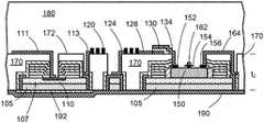
- FIG. 1depicts an example portion of a heterolithic microwave integrated circuit (HMIC) according to a first embodiment
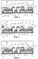
- FIG. 2depicts an example portion of an HMIC according to a second embodiment
- FIG. 3depicts an example portion of an HMIC according to a third embodiment
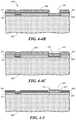
- FIG. 4-1illustrates example structure associated with a method for making an HMIC
- FIG. 4-2Aillustrates example structure that includes a patterned resist as part of a process for making a first device in a first region of an HMIC
- FIG. 4-2B and FIG. 4-2Cillustrates example structure associated with semiconductor doping in a first region for a first device of an HMIC
- FIG. 4-3illustrates structure associated with forming a second device in a second region of an HMIC
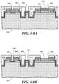
- FIG. 4-4Aillustrates formation of an epitaxial layer of one or more layers of a different semiconductor material on an intrinsic semiconductor layer in a second region of an HMIC
- FIG. 4-4Billustrates formation of one or more epitaxial layers of a different semiconductor material directly on a highly doped semiconductor layer in a second region of an HMIC
- FIG. 4-4Cillustrates formation of one or more epitaxial layers of a different semiconductor material on a highly doped region of an intrinsic semiconductor layer in a second region of an HMIC
- FIG. 4-5illustrates removal of the different semiconductor material except for a portion in the second region of the HMIC
- FIG. 4-6Aillustrates protective layers formed over the different semiconductor material in the second region of the HMIC
- FIG. 4-6Billustrates patterned protective layers that expose underlying semiconductor material
- FIG. 4-6Cillustrates etched cavities in the underlying semiconductor materials
- FIG. 4-7Aillustrates an electrically conductive film formed in the etched cavities
- FIG. 4-7Billustrates a protective layer formed over the HMIC structure and application of an electrically-insulating dielectric material (glass, for example) that will fill the etched cavities;
- FIG. 4-7Cillustrates flow of the electrically-insulating dielectric material into the etched cavities and residual air bubbles at the bottom of the etched cavities
- FIG. 4-7Dillustrates planarization of the electrically-insulating material
- FIG. 4-8Aillustrates etched openings in the electrically-insulating material
- FIG. 4-8Billustrates a deepening of the etched openings
- FIG. 5illustrates circuitry formed for an HMIC
- FIG. 6illustrates passivation of HMIC circuitry
- FIG. 7illustrates an example portion of an HMIC substrate in which a portion of the wafer's backside has been removed and a conductive ground plane has been deposited;
- FIG. 8Adepicts a plan view of an example package that can contain an HMIC die
- FIG. 8Bdepicts an elevation view of an example package that can contain an HMIC die.
- Radio-frequency (RF) circuitryoften includes other elements in addition to transistors, such as capacitors, inductors, diodes, interconnects, antennas, signal couplers, power splitters, and microstrip transmission lines. It can be desirable to integrate some or all of these components onto a monolithic microwave integrated circuit for some RF applications.
- diode switches formed from silicon semiconductor materialscan have more desirable properties in terms of insertion loss, isolation, distortion, linearity and power handling than switches formed from gallium nitride materials. Accordingly, in some circuits it would be desirable to integrate onto a same substrate diodes having active areas formed from silicon semiconductor materials and transistors formed from gallium nitride materials.
- Embodiments hereindescribe structures and processes for integrating at least two different semiconductor devices formed from different semiconductor material systems having different base elemental compositions onto a single heterolithic microwave integrated circuit (HMIC).
- HMICheterolithic microwave integrated circuit
- FIG. 1illustrates a portion of an HMIC that includes two different semiconductor devices formed from different semiconductor material systems having different base elemental compositions, according to a first aspect of the disclosed technology.
- An HMICcan include a first semiconductor device 110 formed from a first semiconductor material system and a second semiconductor device 150 formed from a second semiconductor material system.
- the first semiconductor device 110can comprise a silicon material system, though the invention is not limited to only silicon material systems.
- the first semiconductor device 110can comprise a silicon-carbide or silicon-germanium material system.
- the active layers of the first semiconductor device 110can comprise doped silicon layers.
- the first semiconductor device 110can be a diode (e.g., a p-i-n diode or n-i-p diode), though the invention is not limited to only these diodes.
- diodese.g., p-n, n-p, Schottky diodes, etc.
- semiconductor devicese.g., transistors
- a p-i-n diodecan be formed from a highly doped region 108 (p-type conductivity) formed in an intrinsic layer 107 disposed on an n-doped substrate 105 .
- the second semiconductor device 150can be a transistor of any type formed from a gallium-nitride material system.
- the illustrated exampledepicts a high-electron-mobility transistor (HEMT) that is formed from one or more epitaxial layers 151 of gallium nitride material, though other types of transistors (e.g., field-effect transistors, junction field-effect transistors, bipolar junction transistors, insulated-gate bipolar transistors, etc.) can be formed in an HMIC in some embodiments.
- the one or more epitaxial layers 151 of gallium nitride materialcan be grown directly on a highly doped substrate 105 , as depicted in FIG. 1 , and used to form a HEMT semiconductor device 150 .
- the HEMTcan have a drain contact 152 , a gate contact 154 and a source contact 156 .
- the one or more epitaxial layers 151 of gallium nitride materialcan be formed using processes described in U.S. Pat. No. 9,627,473, issued Apr. 18, 2017, and titled “Parasitic Channel Mitigation in III-nitride Material Semiconductor Structures,” which is incorporated herein by reference. Additional examples of epitaxial layers 151 can be found in, U.S. Pat. No. 7,135,720, issued Nov. 14, 2006, titled “Gallium Nitride Material Transistors and Methods Associated with the Same,” and in U.S. Pat. No. 9,064,775, issued Jun.
- a HEMTcan be formed on an HMIC using processes described in U.S. patent application Ser. No. 15/223,734, filed Jul. 29, 2016, and titled “High-Voltage GaN High Electron Mobility Transistors with Reduced Leakage Current,” which is incorporated herein by reference.
- the inventorshave recognized and appreciated that forming a gallium-nitride device on highly doped silicon (e.g., a doping density of at least 5 ⁇ 10 18 cm ⁇ 3 ) can mitigate deleterious effects associated with parasitic currents in an underlying lightly doped and more resistive semiconductor material.
- the resistivity of the semiconductor (e.g., silicon) on which the one or more epitaxial layers 151 of gallium nitride material are formedcan be between 0.0001 ohm-cm and 0.010 ohm-cm. In some cases, the resistivity of the semiconductor on which the one or more epitaxial layers 151 of gallium nitride material are formed is between 0.0001 ohm-cm and 0.005 ohm-cm.
- the one or more epitaxial layers 151 of gallium nitride materialare formed directly on a highly doped substrate 105 .
- a portion of an intrinsic semiconductor layer 107has been removed by etching, for example.
- one or more epitaxial layers 151 of gallium nitride materialcan be formed on a highly doped region 158 of an intrinsic semiconductor layer 107 .
- the highly doped regioncan be formed by ion implantation and diffusion, for example, though other doping techniques may be used.
- a thin, highly doped layercomprising the same semiconductor material (e.g., silicon) as the intrinsic layer 107 can be epitaxially grown on the intrinsic layer 107 to form a highly doped region 158 on which the one or more epitaxial layers 151 can be deposited.
- the highly doped region 158can have a doping density of at least 5 ⁇ 10 18 cm ⁇ 3 .
- the resistivity of the highly doped region 158can be between 0.0001 ohm-cm and 0.010 ohm-cm, in some cases, or between 0.0001 ohm-cm and 0.005 ohm-cm in other embodiments.
- the one or more epitaxial layers 151 of gallium nitride materialcan be formed directly on intrinsic semiconductor material 107 , such as intrinsic silicon.
- intrinsic semiconductor material 107such as intrinsic silicon.
- highly resistive semiconductor material underlying a device formed from the gallium nitride materialcan also mitigate deleterious effects associated with parasitic conductance in the underlying semiconductor material.
- intrinsic siliconcan behave like insulating material so that little or no parasitic currents flow in the underlying semiconductor material.
- the resistivity of the underlying semiconductor materialcan be between 100 ohm-cm and 10,000 ohm-cm. In some cases, the resistivity of the underlying semiconductor material can be between 2000 ohm-cm and 10,000 ohm-cm.
- the intrinsic semiconductor layer 107can have a thickness of any value in a range from 10 microns to 50 microns. In some cases, the thickness of the intrinsic semiconductor layer 107 can be less than 10 microns. In other cases, the thickness of the intrinsic semiconductor layer 107 can be more than 50 microns.
- a total thickness of the one or more epitaxial layers 151 of gallium nitride materialcan be any value in a range from 1.5 microns to 6 microns. In some cases, a GaN buffer layer having a thickness between 1.5 microns and 4 microns can be formed within the one or more epitaxial layers 151 to obtain semiconductor devices with very high reverse-bias breakdown voltages.
- Schottky diodes and HEMTs formed with such thick buffer layers and other features described in U.S. patent application Ser. No. 15/223,734, referenced abovecan sustain reverse bias voltages as much as 2000 volts, exhibit low leakage currents (e.g., not more than 40 microamps per millimeter of transistor gate width), and handle large forward currents (as much as 1 amp per millimeter of gate width).
- an HMICcan include additional RF circuitry formed on a same wafer and die.
- an HMICcan include an electrically-insulating material 170 that extends through the monolithic substrate 102 and upon which some RF circuit elements can be formed.
- the insulating material 170can comprise a glass or other dielectric material that is electrically insulating and exhibits low loss for RF fields that penetrate into the insulating material 170 .
- a loss tangent of the insulating material 170can be as low as 0.002 at 10 GHz.
- the loss tangent of the insulating material 170can be between 0.0001 and 0.0004 in a frequency range between 500 MHz and 10 GHz.
- a benefit of an HMICis that RF circuit elements can be formed over regions of the insulating material 170 and thereby exhibit lower loss than they would if formed over semiconductor material.
- Other benefits of the insulating material 170include improved electrical isolation between semiconductor devices, lower permittivity compared to semiconductor material, and structural support for RF circuitry.
- a transparent insulating material 170can also provide optical visibility through the wafer on which HMICs are fabricated. Through-wafer optical visibility can facilitate backside alignment for patterning structures on a backside of the HMIC, such as patterned islands of electrically-insulating film 192 for device isolation.
- an insulating film 192can be formed and patterned on a backside of the HMIC in a correct location to allow for electrical isolation and/or biasing of a device (e.g., biasing a cathode of a p-i-n diode).
- FIG. 1illustrates RF circuitry that includes a p-i-n diode as a first semiconductor device 110 and a HEMT as a second semiconductor device 150 .
- the first semiconductor device 110is formed from a first semiconductor material system (e.g., silicon) that is different from a second semiconductor material system (e.g., gallium-nitride) that is used to form the second semiconductor device 150 .
- first semiconductor material systeme.g., silicon
- second semiconductor material systeme.g., gallium-nitride
- the illustrated RF circuitryalso includes passive elements such as capacitors 130 (e.g., metal-insulator-metal capacitors and/or metal-insulator-semiconductor capacitors) and inductors 120 (e.g., patterned spiral inductors or meandering interconnects), though other integrated circuit elements can be formed on an HMIC. Passive elements can be located over regions of the insulating material 170 to reduce electrical losses associated with fields penetrating into the underlying material, as described above.
- RF circuitry of an HMICcan further include patterned conductive interconnects 111 , 113 , 124 , 126 , 134 , 162 , 164 , as depicted in FIG. 1 , and/or wire bonds 115 , depicted in FIG. 2 .
- an HMICcan be covered with a passivation layer 180 .
- a backside of an HMICcan be covered with a conductive film 190 .
- the conductive film 190can provide an electrical ground plane or reference potential plane for the RF circuitry.
- the conductive film 190can comprise one or more metal layers, and may also be used for mounting the HMIC on a receiving substrate.
- the HMICcan be adhered to a receiving substrate using a solder bond, which can provide a low-loss electrical connection to the conductive film 190 .
- the HMICcan be adhered to a receiving substrate using a thermally-conductive adhesive or electrically and thermally-conductive bond.
- regions or islands of conductive semiconductor material on which semiconductor devices are formed within an HMICcan provide improved thermal conductivity of heat from the semiconductor devices to a backside of the HMIC where heat can be further dissipated into air or into a receiving substrate to which the HMIC is bonded.
- an example fabrication processcan begin with a semiconductor wafer 400 , of which a portion is depicted in FIG. 4-1 .
- the wafer 400can comprise a doped substrate 105 (e.g., doped for n-type or p-type conductivity), an undoped or intrinsic layer 107 , and a hard mask 402 .
- an entire wafercan be doped when grown.
- an upper region of the substrate 105can be doped (e.g., by ion implantation or epitaxial growth) to obtain a doping density desired for a semiconductor device.
- a doping density of the substrate 105 near the process surface of the wafer 400can be between 10 15 cm ⁇ 3 and 10 21 cm ⁇ 3 .
- the substrate 105 near the process surfacecan have n + or p + doping.
- an intrinsic layer 107can be formed by epitaxial growth over the doped substrate 105 .
- the intrinsic layercan be formed from a same semiconductor material as the substrate 105 , though in some cases a different material may be used for the intrinsic layer.
- the intrinsic layer 107can have a thickness t 1 of any value in a range from 10 microns to 50 microns, though other thicknesses may be used in some cases.
- the intrinsic layer 107can be covered with a hard mask 402 , which can be electrically insulating.
- An example hard mask 402is thermal oxide, which can be grown on the intrinsic layer 107 .
- an oxide or nitride layercan be deposited by electron-beam evaporation, plasma deposition, atomic layer deposition, or chemical vapor deposition.
- a thickness of the hard maskcan be between 200 nanometers (nm) and 2 microns.
- FIG. 4-2A through FIG. 4-2Cillustrate steps by which semiconductor layers for a first semiconductor device can be formed in a first region of the substrate 105 .
- a resist 420can be patterned over the hard mask 402 as depicted in FIG. 4-2A .
- the resistcan comprise a photoresist (e.g., a polymeric photoresist), though other types of resists can be used alternatively or additionally.
- a multilayer resistcan be used, where one layer of the multilayer resist is used to pattern other layers of the multilayer resist, which in turn are used to pattern one or more underlying materials.
- a multilayer resistcan comprise organic and inorganic layers.
- One example of a multilayer resistis a photoresist formed on an oxide or nitride layer.
- the resist 420may be lithographically patterned to from one or more openings 422 in the resist 420 across the wafer 400 .
- the one or more openings 422can be formed by photolithographic exposure and subsequent immersion of the wafer in a developer.
- the one or more openings 422can then be transferred to the underlying hard mask 402 by etching, for example, as depicted in FIG. 4-2B .
- reactive ion etchingcan be used to obtain anisotropic etching of the underlying hard mask 402 when forming openings 423 .
- immersion in a chemical etchantcan be used to form one or more openings 423 in the hard mask 402 .
- the resist 420can be stripped from the wafer 400 leaving the structure shown in FIG. 4-2B .
- the one or more openings 423expose one or more first regions 425 of the underlying semiconductor material in which one or more first semiconductor devices can be formed, as depicted in FIG. 4-2C .
- the first semiconductor devicescan be formed from a first semiconductor material system that has a base elemental composition that is common with the substrate 105 .
- the substrate 105 near the process surfacecan be doped silicon, and the first semiconductor devices can be silicon-based semiconductor devices.
- the substrate 105 near the process surfacecan be doped silicon-germanium, and the first semiconductor devices can be silicon-germanium semiconductor devices.
- Another semiconductor system for the first semiconductor devicescould be silicon-carbide.
- semiconductor layers for a first semiconductor devicecan be formed in the first region 425 by doping a portion of the intrinsic layer 107 .
- the dopingcan be performed by ion implantation and heating to diffuse and activate the dopants.
- the doped region 108can have an opposite conductivity type from the substrate 105 .
- the doped region 108can comprise heavily doped p-type semiconductor material and the substrate can comprise highly doped n-type semiconductor material to form p-i-n diode layers.
- the doped region 108can comprise heavily doped n-type semiconductor material and the substrate can comprise highly doped p-type semiconductor material to form n-i-p diode layers.
- an oxide layer 431can be formed over at least the first region 425 , as depicted in FIG. 4-3 .
- the oxide layer 431comprises a thermal oxide, though other oxides described above may be used.
- a thickness of the oxide layer 431can be between 50 nm and 300 nm.
- a nitride protective layer 432can be formed over the oxide layer 431 .
- the nitride layercan be formed using low pressure chemical vapor deposition (LPCVD), according to some embodiments.
- a thickness of the nitride layer 432can be between 50 nm and 300 nm. In some embodiments, the nitride layer 432 can be used to compensate for in-plane stress introduced by the oxide layer 431 to help prevent bowing of the wafer 400 .
- a resist and etching process, as described in connection with FIG. 4-2A and FIG. 4-2B ,can be used to pattern a second opening 434 in the oxide and nitride layers for forming a second semiconductor device.
- Epitaxial growthcan then be used to form one or more layers comprising a second semiconductor material 440 in a second device region 445 , as depicted in FIG. 4-4A .
- the second semiconductor material 440can comprise gallium-nitride material, for example.
- the one or more layersmay be buffer layers formed from other III-nitride material (e.g., aluminum nitride).
- the one or more layers comprising the second semiconductor material 440can include layered structures described in the U.S. applications and patents referenced above, for example. Because epitaxial growth of gallium-nitride material can require high temperatures (e.g., GaN epitaxy can require temperatures up to 1000° C. or higher), it can be advantageous to form the second semiconductor material 440 for the HMIC prior to forming the insulating material 170 , which can reflow at significantly lower temperatures.
- gallium-nitride materialrefers to gallium nitride (GaN) and any of its alloys, such as aluminum gallium nitride (AlxGa (1-x)N), indium gallium nitride (InyGa(1-y)N), aluminum indium gallium nitride (AlxInyGa(1-x-y)N), gallium arsenide phosporide nitride (GaAsxPy N(1-x-y)), aluminum indium gallium arsenide phosporide nitride (AlxInyGa(1-x-y)AsaPb N(1-a-b)), amongst others.
- AlxGa (1-x)Naluminum gallium nitride
- InyGa(1-y)Nindium gallium nitride
- AlxInyGa(1-x-y)Naluminum indium gallium nitride
- the gallium-nitride materialhas a high concentration of gallium and includes little or no amounts of aluminum and/or indium.
- the sum of (x+y)may be less than 0.4 in some implementations, less than 0.2 in some implementations, less than 0.1 in some implementations, or even less in other implementations.
- an active layer in which a majority of current conduction occursmay have a composition of GaN.
- Gallium-nitride materials in a multi-layer stackmay be doped n-type or p-type, or may be undoped. Suitable gallium-nitride materials are described in U.S. Pat. No. 6,649,287, which is incorporated herein by reference in its entirety.
- FIG. 4-4Adepicts one embodiment in which one or more layers comprising a second semiconductor material 440 are formed in a second device region 445 .
- the one or more layers comprising a second semiconductor material 440are formed directly on an intrinsic semiconductor layer 107 , corresponding to structure depicted in FIG. 3 .
- FIG. 4-4BAnother embodiment is depicted in FIG. 4-4B , in which the one or more layers comprising a second semiconductor material 440 are formed directly on an underlying highly doped substrate 105 in a second device region 446 .
- This embodimentcorresponds to structure depicted in FIG. 1 .
- the intrinsic layer 107can be etched away in the second device region 446 before epitaxial growth of the one or more layers comprising a second semiconductor material 440 .
- a timed reactive ion etching processcan be used to remove the intrinsic layer 107 in the second opening 434 .
- the nitride layer 432can serve as an etch mask for removing the intrinsic layer 107 , for example.
- itcan be beneficial to form a second semiconductor device on a highly conductive semiconductor to reduce losses associated with parasitic conductance in an underlying more resistive and lossy semiconductor material.
- FIG. 4-4CA third embodiment is depicted in FIG. 4-4C , in which the one or more layers comprising a second semiconductor material 440 are formed on a highly doped region 158 of the intrinsic layer 107 in a second device region 447 .
- This embodimentcorresponds to structure depicted in FIG. 2 .
- ion implantation and diffusioncan be performed in the second opening 434 , where the nitride layer 432 and oxide layers 431 , 402 can serve as implantation masks. This process may avoid a lengthy etching step to remove the intrinsic layer 107 , and yet provide a highly conductive region directly below the second semiconductor device.
- a resist and etching processcan be used to remove the one or more layers comprising a second semiconductor material 440 in areas outside the second device region 445 , as illustrated in FIG. 4-5 .
- the etching processcan comprise a reactive ion etching process that removes a majority of the material 440 .
- the etchingcan also remove some of the material 440 within the second opening 434 , leaving gaps 452 near an edge of the second opening where a defect density of the epitaxially grown second semiconductor can be higher than near the center of the second opening 434 .
- the etching processcan leave an island of one or more epitaxial layers 151 of the second semiconductor material within the second opening 434 comprising a second device region 445 , as depicted in FIG. 4-5 .
- the layers 151can be covered with one or more protective layers in preparation for forming intervening regions of electrically-insulating material.
- a second protective layer 461 and third protective layer 462can be formed over at least the one or more epitaxial layers 151 of the second semiconductor material in the second device region 445 , as depicted in FIG. 4-6A .
- the second protective layer 461can comprise a nitride or aluminum oxide or multilayer combination thereof, which can be deposited by any one of a variety of low-temperature processes.
- a low-temperature processcan comprise a process in which the substrate temperature does not exceed 400° C.
- Example low-temperature processesinclude electron-beam evaporation, sputtering, plasma-enhanced chemical vapor deposition (PECVD), and atomic layer deposition (ALD).
- the second protective layer 461is needed to protect the one or more epitaxial layers 151 of second semiconductor material (e.g., layers comprising gallium nitride) during deposition of the third protective layer 462 .
- a thickness of the second protective layer 461can be between 50 nm and 300 nm.
- the third protective layer 462can comprise a high quality silicon nitride that is deposited by LPCVD, according to some embodiments.
- the silicon nitride for the third protective layer 462can be deposited at temperatures as high as 800° C. and pressures between 150 millitorr and 250 millitorr.
- the hydrogen content of the second protective layer 461 and/or third protective layer 462is controlled to be not more than 15%. In some cases, the hydrogen content of the second protective layer 461 and/or third protective layer 462 is controlled to be not more than 10%.
- the third protective layercan be beneficial in additionally protecting the one or more epitaxial layers 151 of second semiconductor material during formation of the insulating material 170 , which can require temperatures as high as 900° C.
- a thickness of the third protective layer 462can be between 50 nm and 300 nm.
- a subsequent resist and etching processcan be used to remove protective layers and oxide layers in areas around the first device region and second device region, as depicted in FIG. 4-6B .
- a resistcan be patterned to cover the first device region and second device region and protect them from subsequent etching steps.
- reactive ion etching stepscan be used to etch through the protective layers and oxide layers to expose the underlying intrinsic layer 107 and/or semiconductor substrate 105 .
- the resistcan then be stripped from the wafer 400 leaving the structure depicted in FIG. 4-6B .
- An additional resist and etching processcan be used to form cavities 464 into the underlying semiconductor substrate 105 , as illustrated in FIG. 4-6C .
- an inductively coupled plasma (ICP) etching processcan be used to etch deep cavities 464 into the substrate 105 .
- the resistcan be patterned to protect a region of the substrate from being etched to form a backside via 465 .
- the backside via 465can be used to provide a conductive path from a process side of the wafer 400 and resulting HMIC substrate to a backside of the HMIC substrate.
- the etch depth of the cavities 464 into the substrate 105can be between 120 microns and 200 microns.
- the cavities 464can provide receptacles into which electrically-insulating material is formed.
- a resist(not shown) can be applied and patterned to mask the first and second semiconductor device regions, and a conductive film 471 can be deposited over exposed regions of the wafer 400 .
- the resist and part of the conductive film deposited on the resistcan be removed using a lift-off process, leaving the structure shown in FIG. 4-7A .
- the conductive film 471can be deposited over the entire area that includes the cavities 464 as well as the first and second semiconductor device regions.
- a resistcan be patterned with openings over the first and second device regions, so that the conductive film 471 in these regions can be etched away leaving the structure shown in FIG. 4-7A .
- the conductive filmcomprises cobalt silicide, though other conductive materials can be used alternatively or additionally.
- a dielectric film 472can be formed over the entire area, as depicted in FIG. 4-7B .
- an oxide or nitride filmcan be deposited conformally over the structure by PECVD or ALD, for example.
- the dielectric film 472can help protect the conductive film 471 during a subsequent step in which an insulating material 170 is applied to the wafer as well as provide an etch stop for subsequent etching of the insulating material 170 .
- the insulating material 170can comprise a glass substrate that is slumped onto the wafer at high temperature and low pressure, so that the glass reflows filling cavities 464 , as depicted in FIG. 4-7C .
- An example glass substrate that can be usedis a Corning 7070 borosilicate glass, which can have a coefficient of thermal expansion that approximately matches the coefficient of thermal expansion for silicon. Other glasses can be used for other substrate materials.
- a thickness of the glass substratecan be between 250 microns and 750 microns.
- a process of slumping the insulating material 170 onto the wafer 400can comprise placing the material 170 and wafer 400 in contact and under vacuum between 10 millitorr and 50 millitorr, heating the insulating material 170 and wafer to a temperature between 700° C. and 900° C., allowing the insulating material 170 to reflow into cavities 464 for a period of time, placing the material 170 and wafer 400 under pressure between 1 atmosphere and 3 atmosphere, and cooling the material 170 and wafer 400 to a temperature below the glass transition temperature of the material 170 .
- a dry gase.g., nitrogen or argon
- the insulating material 170can fill most of the cavities' volumes, air pockets 475 can become trapped at the bottom of the cavities, as depicted in FIG. 4-7C .
- a planarization step(e.g., grind and polish, or chemical mechanical polish) can be performed to form a planar surface 478 on the insulating material 170 , as depicted in FIG. 4-7D .
- the planar surface 478can allow subsequent quality lithographic and microfabrication processes to be carried out on the wafer 400 to form RF circuitry.
- Forming RF circuitry for an HMICcan comprise etching the insulating material 170 and underlying protective and oxide layers to expose underlying conductors and semiconductors.
- a resist and etching processcan be used to form openings 481 , 482 , 483 , 484 in the insulating material 170 , as depicted in FIG. 4-8A .
- the dielectric film 472can provide a beneficial etch stop that permits significantly different etch depths of the openings 481 , 482 , 483 , 484 without affecting material underlying the dielectric film 472 .
- etch depths of the openings 481 , 482 , 483 , 484can vary by a factor of 2 or more.
- Plasma etching and/or wet chemical etchingcan be used to form openings 481 , 482 , 483 , 484 .
- a weak anisotropic etchcan be used so that sidewalls in the openings of the insulating material 170 are sloped outward to permit patterning of conductive interconnects along the sidewalls.
- the patterned insulating material 170can serve as an etch mask for the underlying protective layers and oxide layers. Additionally or alternatively, a resist used to pattern the insulating material 170 can provide an etch mask for the underlying protective layers and oxide layers. One or more etching steps can be carried out to extend the openings 481 , 482 , 483 , 484 through the protective and oxide layers to the underlying semiconductors 108 , 151 and conductive film 471 , as depicted in FIG. 4-8B .
- FIG. 5illustrates several examples of circuit elements that can be formed on the wafer 400 .
- Example elementsinclude, but are not limited to, conductive interconnects 111 , 113 , 124 , 126 , 134 , 162 , 164 , a spiral inductor 120 , a metal-insulator-metal (MIM) capacitor 130 , thin-film resistor 140 , and transistor contacts 152 , 154 , 156 .
- a first interconnect 111connects a thin-film resistor 140 to an anode of a p-i-n diode 110 .
- a second interconnect 113connects an inductor 120 to a cathode of the p-i-n diode 110 .
- a third interconnect 124connects a center of the inductor 120 to the conductive film 471 and backside via 465 .
- a fourth interconnect 126connects the inductor 120 to a MIM capacitor 130 .
- a fifth interconnect 134connects the MIM capacitor to a drain contact 152 of a HEMT 150 .
- a sixth interconnect 162connects to a gate contact 154 of the HEMT, and a seventh interconnect 164 connects a source contact 156 of the HEMT 150 to the conductive film 471 and underlying substrate 105 .
- the RF circuitry illustrated in FIG. 5is only an example of some circuit elements and their arrangement and does not limit the invention to only the illustrated embodiments. A wide variety of different circuit elements and arrangements can be formed on an HMIC as will be appreciated by those skilled in the art of microfabrication of RF circuitry
- a passivation layer 180comprises a polymer, such as but not limited to polyimide or benzocyclobutene.
- an inorganic passivation layercan be used, such as but not limited to an oxide or nitride.
- a backside of the wafer 400can be ground down and polished to remove a significant portion of the wafer's bulk substrate 105 when forming a final HMIC substrate.
- a thickness t 2 of the HMIC substratecan be between 50 microns and 200 microns.
- the amount of substrate 105 removedextends beyond the lowest layer 610 of conductive film 471 in the cavities, so that different regions having remaining substrate 105 can be electrically isolated from each other, as can be seen in FIG. 7 .
- the amount of substrate 105 removedextends additionally beyond the air pockets 475 .
- FIG. 7illustrates an example HMIC substrate in which the backside of the wafer 400 has been removed to an extent that the air pockets 475 have been removed.
- islands of an insulating film 192can be patterned on the backside of the wafer 400 to electrically isolate semiconductor devices (e.g., semiconductor device 110 in the illustrated example) from a backside conductive film 190 .
- the backside conductive film 190can provide a ground plane as described above in connection with FIG. 1 .
- An example conductive film 190can comprise a titanium adhesion layer and gold film deposited by any suitable means (e.g., electron-beam evaporation). Compositions other than Ti/Au can be used for the conductive film in other embodiments, for example compositions that include additionally or alternatively one or more of the following materials: nickel, tin, tungsten, chrome, aluminum, copper, silver.
- FIG. 8A and FIG. 8Bdepict one example of a package 800 that can be used to enclose an HMIC die containing one or more transistors, such as one or more high power HEMTs.
- the package shown in FIG. 8A and FIG. 8Bcan be suitable for an amplifier device.
- Other package shapes and form factorscan be used for amplifiers and other devices.
- the HEMTscan be arranged with RF circuitry on the HMIC as an amplifier circuit for amplifying RF signals.
- the HEMTscan be arranged on the HMIC as a Doherty amplifier.
- a packaged HMIC amplifiercan amplify input signals up to 100 Watts and even up to 300 Watts of output power. In some cases, a packaged HMIC amplifier can amplify input signals up to 500 Watts of output power.
- An example package for an HMICcan comprise an enclosure 804 that surrounds the HMIC.
- the enclosure 804can be metal-ceramic or metal-plastic, according to some embodiments.
- the enclosure 804can comprise plastic or comprise a plastic overmold enclosure.
- a package 800can include a ceramic air-cavity or a plastic air-cavity, within which the HMIC is located.
- a plastic over-mold packagemay have no air cavity around the HMIC.
- a package 800 for an HMIC that includes one or more transistorscan include a gate terminal 811 , a drain terminal 813 , and an electrically and thermally conductive mount 812 .
- the gate terminal 811 and drain terminal 813can be shaped as fins.
- the conductive mount 812can be formed from one or more metals, such as aluminum, an aluminum alloy, copper, a copper alloy, though other metal compositions may be used. In addition to heat dissipation, the conductive mount 812 can provide electrical connection to a reference potential, e.g., ground.
- a reference potentiale.g., ground.
- Example configurationsinclude combinations of configurations (1) through (16) as described below.
- An integrated circuitcomprising a first region of a substrate containing a first integrated device formed from a first semiconductor material; a second region of the substrate containing a second integrated device formed from a second semiconductor material of a different base elemental composition than the first semiconductor material; and a third region of the substrate containing an electrically-insulating dielectric material that extends through the substrate, wherein the third region of the substrate is located between the first region and the second region.
- Methods for making an integrated circuitcan include various processes.
- Example methodsinclude combinations of processes (17) through (27) as described below. These processes may be used, at least in part, to make an integrated circuit of the configurations listed above.
- a method of making a heterolithic microwave integrated circuitcomprising forming a first semiconductor device from a first semiconductor material in a first region of a wafer; forming a second semiconductor material on the first semiconductor material in a second region of the wafer, the second semiconductor material having a different base elemental composition than the first semiconductor material; forming a second semiconductor device from the second semiconductor material; etching a cavity in a third region of the wafer; filling the cavity with an electrically-insulating material; planarizing the electrically-insulating material; and removing a portion of a backside of the wafer to form a substrate, wherein the electrically-insulating material extends through the substrate.
- filling the cavitycomprises forcing into the cavity under pressure the electrically-insulating material that is heated above its glass transition temperature.
- the terms “approximately” and “about”are used to mean within ⁇ 20% of a target dimension in some embodiments, within ⁇ 10% of a target dimension in some embodiments, within ⁇ 5% of a target dimension in some embodiments, and yet within ⁇ 2% of a target dimension in some embodiments.
- the terms “approximately” and “about”can include the target dimension.
- the term “essentially”is used to mean within ⁇ 3% of a target dimension.
- the technology described hereinmay be embodied as a method, of which at least some acts have been described.
- the acts performed as part of the methodmay be ordered in any suitable way. Accordingly, embodiments may be implemented in which acts are performed in an order different than described, which may include performing some acts simultaneously, even though described as sequential acts in illustrative embodiments. Additionally, a method may include more acts than those described, in some embodiments, and fewer acts than those described in other embodiments.
Landscapes
- Engineering & Computer Science (AREA)
- Power Engineering (AREA)
- Physics & Mathematics (AREA)
- Condensed Matter Physics & Semiconductors (AREA)
- General Physics & Mathematics (AREA)
- Computer Hardware Design (AREA)
- Microelectronics & Electronic Packaging (AREA)
- Manufacturing & Machinery (AREA)
- Materials Engineering (AREA)
- Chemical & Material Sciences (AREA)
- Junction Field-Effect Transistors (AREA)
- Internal Circuitry In Semiconductor Integrated Circuit Devices (AREA)
- Electrodes Of Semiconductors (AREA)
- Semiconductor Integrated Circuits (AREA)
Abstract
Description
Claims (22)
Priority Applications (2)
| Application Number | Priority Date | Filing Date | Title |
|---|---|---|---|
| US15/875,406US11056483B2 (en) | 2018-01-19 | 2018-01-19 | Heterolithic microwave integrated circuits including gallium-nitride devices on intrinsic semiconductor |
| US17/344,057US11640960B2 (en) | 2018-01-19 | 2021-06-10 | Heterolithic microwave integrated circuits including gallium-nitride devices on intrinsic semiconductor |
Applications Claiming Priority (1)
| Application Number | Priority Date | Filing Date | Title |
|---|---|---|---|
| US15/875,406US11056483B2 (en) | 2018-01-19 | 2018-01-19 | Heterolithic microwave integrated circuits including gallium-nitride devices on intrinsic semiconductor |
Related Child Applications (1)
| Application Number | Title | Priority Date | Filing Date |
|---|---|---|---|
| US17/344,057ContinuationUS11640960B2 (en) | 2018-01-19 | 2021-06-10 | Heterolithic microwave integrated circuits including gallium-nitride devices on intrinsic semiconductor |
Publications (2)
| Publication Number | Publication Date |
|---|---|
| US20190229114A1 US20190229114A1 (en) | 2019-07-25 |
| US11056483B2true US11056483B2 (en) | 2021-07-06 |
Family
ID=67300072
Family Applications (2)
| Application Number | Title | Priority Date | Filing Date |
|---|---|---|---|
| US15/875,406ActiveUS11056483B2 (en) | 2018-01-19 | 2018-01-19 | Heterolithic microwave integrated circuits including gallium-nitride devices on intrinsic semiconductor |
| US17/344,057Active2038-03-03US11640960B2 (en) | 2018-01-19 | 2021-06-10 | Heterolithic microwave integrated circuits including gallium-nitride devices on intrinsic semiconductor |
Family Applications After (1)
| Application Number | Title | Priority Date | Filing Date |
|---|---|---|---|
| US17/344,057Active2038-03-03US11640960B2 (en) | 2018-01-19 | 2021-06-10 | Heterolithic microwave integrated circuits including gallium-nitride devices on intrinsic semiconductor |
Country Status (1)
| Country | Link |
|---|---|
| US (2) | US11056483B2 (en) |
Cited By (3)
| Publication number | Priority date | Publication date | Assignee | Title |
|---|---|---|---|---|
| US20210305237A1 (en)* | 2018-01-19 | 2021-09-30 | Macom Technology Solutions Holdings, Inc. | Heterolithic microwave integrated circuits including gallium-nitride devices on intrinsic semiconductor |
| US11600614B2 (en) | 2020-03-26 | 2023-03-07 | Macom Technology Solutions Holdings, Inc. | Microwave integrated circuits including gallium-nitride devices on silicon |
| US11817450B2 (en) | 2018-01-19 | 2023-11-14 | Macom Technology Solutions Holdings, Inc. | Heterolithic integrated circuits including integrated devices formed on semiconductor materials of different elemental composition |
Families Citing this family (6)
| Publication number | Priority date | Publication date | Assignee | Title |
|---|---|---|---|---|
| US20170301780A1 (en) | 2016-04-15 | 2017-10-19 | Macom Technology Solutions Holdings, Inc. | High-voltage gan high electron mobility transistors with reduced leakage current |
| US10651317B2 (en) | 2016-04-15 | 2020-05-12 | Macom Technology Solutions Holdings, Inc. | High-voltage lateral GaN-on-silicon Schottky diode |
| US11233047B2 (en) | 2018-01-19 | 2022-01-25 | Macom Technology Solutions Holdings, Inc. | Heterolithic microwave integrated circuits including gallium-nitride devices on highly doped regions of intrinsic silicon |
| EP4169077A4 (en)* | 2020-06-19 | 2024-10-09 | MACOM Technology Solutions Holdings, Inc. | SUPPRESSION OF PARASITIC ACOUSTIC WAVES IN INTEGRATED CIRCUIT DEVICES |
| US11469225B2 (en)* | 2020-10-16 | 2022-10-11 | Globalfoundries U.S. Inc. | Device integration schemes leveraging a bulk semiconductor substrate having a <111 > crystal orientation |
| US12206031B2 (en)* | 2022-06-09 | 2025-01-21 | Macom Technology Solutions Holdings, Inc. | Monolithic pin and Schottky diode integrated circuits |
Citations (81)
| Publication number | Priority date | Publication date | Assignee | Title |
|---|---|---|---|---|
| US4692998A (en) | 1985-01-12 | 1987-09-15 | M/A-Com, Inc. | Process for fabricating semiconductor components |
| US4737236A (en) | 1986-09-08 | 1988-04-12 | M/A-Com, Inc. | Method of making microwave integrated circuits |
| US5268310A (en) | 1992-11-25 | 1993-12-07 | M/A-Com, Inc. | Method for making a mesa type PIN diode |
| US5696466A (en) | 1995-12-08 | 1997-12-09 | The Whitaker Corporation | Heterolithic microwave integrated impedance matching circuitry and method of manufacture |
| US5877530A (en) | 1996-07-31 | 1999-03-02 | Lsi Logic Corporation | Formation of gradient doped profile region between channel region and heavily doped source/drain contact region of MOS device in integrated circuit structure using a re-entrant gate electrode and a higher dose drain implantation |
| US5889314A (en) | 1996-06-03 | 1999-03-30 | Nec Corporation | Mixed-mode IC having an isolator for minimizing cross-talk through substrate and method of fabricating same |
| US5976941A (en) | 1997-06-06 | 1999-11-02 | The Whitaker Corporation | Ultrahigh vacuum deposition of silicon (Si-Ge) on HMIC substrates |
| US6014064A (en) | 1996-07-28 | 2000-01-11 | The Whitaker Corporation | Heterolithic voltage controlled oscillator |
| US6114716A (en) | 1996-03-22 | 2000-09-05 | The Whitaker Corporation | Heterolithic microwave integrated circuits |
| US6150197A (en) | 1997-04-25 | 2000-11-21 | The Whitaker Corp. | Method of fabricating heterolithic microwave integrated circuits |
| US6197645B1 (en) | 1997-04-21 | 2001-03-06 | Advanced Micro Devices, Inc. | Method of making an IGFET with elevated source/drain regions in close proximity to gate with sloped sidewalls |
| US6329702B1 (en) | 2000-07-06 | 2001-12-11 | Tyco Electronics Corporation | High frequency carrier |
| US6379785B1 (en) | 1997-12-31 | 2002-04-30 | Tyco Electronic Corp | Glass-coated substrates for high frequency applications |
| US20020139971A1 (en) | 2001-03-29 | 2002-10-03 | Nec Corporation | Semiconductor device and method for fabricating same |
| US6465289B1 (en) | 1994-11-02 | 2002-10-15 | Trw Inc. | Method of fabricating monolithic multifunction integrated circuit devices |
| US6600199B2 (en)* | 2000-12-29 | 2003-07-29 | International Business Machines Corporation | Deep trench-buried layer array and integrated device structures for noise isolation and latch up immunity |
| US20030141518A1 (en)* | 2000-11-21 | 2003-07-31 | Toshiya Yokogawa | Semiconductor device and equipment for communication system |
| US20050145851A1 (en) | 2003-12-17 | 2005-07-07 | Nitronex Corporation | Gallium nitride material structures including isolation regions and methods |
| US7026223B2 (en) | 2002-03-28 | 2006-04-11 | M/A-Com, Inc | Hermetic electric component package |
| US7071498B2 (en) | 2003-12-17 | 2006-07-04 | Nitronex Corporation | Gallium nitride material devices including an electrode-defining layer and methods of forming the same |
| US20070018199A1 (en) | 2005-07-20 | 2007-01-25 | Cree, Inc. | Nitride-based transistors and fabrication methods with an etch stop layer |
| US7223441B2 (en) | 2004-03-10 | 2007-05-29 | Pilkington North America, Inc. | Method for depositing gallium oxide coatings on flat glass |
| US20070126067A1 (en) | 2005-12-01 | 2007-06-07 | Intel Corporation | Angled implantation for removal of thin film layers |
| US7402842B2 (en) | 2004-08-09 | 2008-07-22 | M/A-Com, Inc. | Light emitting diode package |
| US7419892B2 (en) | 2005-12-13 | 2008-09-02 | Cree, Inc. | Semiconductor devices including implanted regions and protective layers and methods of forming the same |
| US20080265379A1 (en) | 2005-07-11 | 2008-10-30 | Cree, Inc. | Laser Diode Orientation on Mis-Cut Substrates |
| US20080308813A1 (en) | 2006-08-18 | 2008-12-18 | Chang Soo Suh | High breakdown enhancement mode gallium nitride based high electron mobility transistors with integrated slant field plate |
| US20090026498A1 (en) | 2007-07-25 | 2009-01-29 | Eudyna Devices Inc. | Field effect transistor and method for fabricating the same |
| US20090267078A1 (en) | 2008-04-23 | 2009-10-29 | Transphorm Inc. | Enhancement Mode III-N HEMTs |
| US20100019279A1 (en) | 2008-04-02 | 2010-01-28 | The Hong Kong University Of Science And Technology | Integrated HEMT and Lateral Field-Effect Rectifier Combinations, Methods, and Systems |
| US7692263B2 (en) | 2006-11-21 | 2010-04-06 | Cree, Inc. | High voltage GaN transistors |
| US7709859B2 (en) | 2004-11-23 | 2010-05-04 | Cree, Inc. | Cap layers including aluminum nitride for nitride-based transistors |
| US20100117146A1 (en) | 2008-11-13 | 2010-05-13 | Furukawa Electric Co., Ltd. | Semiconductor device and method for fabricating the same |
| US7719091B2 (en) | 2002-06-28 | 2010-05-18 | M/A-Com Technology Solutions Holdings, Inc. | Diode with improved switching speed |
| US7745848B1 (en) | 2007-08-15 | 2010-06-29 | Nitronex Corporation | Gallium nitride material devices and thermal designs thereof |
| US20100164062A1 (en) | 2008-12-31 | 2010-07-01 | Industrial Technology Research Institute | Method of manufacturing through-silicon-via and through-silicon-via structure |
| US7755173B2 (en) | 2007-06-26 | 2010-07-13 | M/A-Com Technology Solutions Holdings, Inc. | Series-shunt switch with thermal terminal |
| US7858456B2 (en)* | 2004-01-27 | 2010-12-28 | Siliconix Technology C. V. | Merged P-i-N Schottky structure |
| US7868428B2 (en) | 2008-03-14 | 2011-01-11 | M/A-Com Technology Solutions Holdings, Inc. | PIN diode with improved power limiting |
| US20110049526A1 (en) | 2009-08-28 | 2011-03-03 | Transphorm Inc. | Semiconductor Devices with Field Plates |
| US8237198B2 (en) | 2008-12-10 | 2012-08-07 | Transphorm Inc. | Semiconductor heterostructure diodes |
| US20120223320A1 (en) | 2011-03-04 | 2012-09-06 | Transphorm Inc. | Electrode configurations for semiconductor devices |
| US20130043517A1 (en) | 2011-08-19 | 2013-02-21 | Haizhou Yin | Semiconductor Structure And Method For Manufacturing The Same |
| US8390091B2 (en) | 2009-02-03 | 2013-03-05 | Freescale Semiconductor, Inc. | Semiconductor structure, an integrated circuit including a semiconductor structure and a method for manufacturing a semiconductor structure |
| US20140103357A1 (en) | 2012-10-17 | 2014-04-17 | Imec | Schottky diode structure and method of fabrication |
| US20140159116A1 (en) | 2012-12-07 | 2014-06-12 | International Rectifier Corporation | III-Nitride Device Having an Enhanced Field Plate |
| US20140231823A1 (en) | 2013-02-15 | 2014-08-21 | Transphorm Inc. | Electrodes for semiconductor devices and methods of forming the same |
| US20140306235A1 (en) | 2013-04-16 | 2014-10-16 | Imec | Method for Producing a Semiconductor Device Comprising a Schottky Diode and a High Electron Mobility Transistor |
| US8912610B2 (en) | 2011-11-11 | 2014-12-16 | Taiwan Semiconductor Manufacturing Company, Ltd. | Structure and method for MOSFETS with high-K and metal gate structure |
| US8946724B1 (en) | 2010-06-02 | 2015-02-03 | Hrl Laboratories, Llc | Monolithically integrated self-aligned GaN-HEMTs and Schottky diodes and method of fabricating the same |
| US20150034958A1 (en) | 2013-08-01 | 2015-02-05 | Taiwan Semiconductor Manufacturing Co., Ltd. | Hemt-compatible lateral rectifier structure |
| US20150060876A1 (en) | 2013-08-27 | 2015-03-05 | University Of Notre Dame Du Lac | Polarization induced doped transistor |
| US20150294984A1 (en) | 2014-04-11 | 2015-10-15 | International Business Machines Corporation | High voltage metal oxide semiconductor field effect transistor integrated into extremely thin semiconductor on insulator process |
| US20150295074A1 (en) | 2014-04-14 | 2015-10-15 | Fujitsu Limited | Compound semiconductor device and method of manufacturing the same |
| US20150303291A1 (en) | 2014-04-17 | 2015-10-22 | Fujitsu Limited | Semiconductor device and method of manufacturing semiconductor device |
| US9281417B1 (en) | 2015-02-20 | 2016-03-08 | Vishay General Semiconductor Llc | GaN-based schottky diode having large bond pads and reduced contact resistance |
| US20160086938A1 (en) | 2014-09-19 | 2016-03-24 | Navitas Semiconductor Inc. | GaN STRUCTURES |
| US20160155674A1 (en)* | 2012-10-18 | 2016-06-02 | Infineon Technologies Americas Corp. | Fabricating a Semiconductor Package with Conductive Carrier |
| US20160190298A1 (en) | 2014-07-21 | 2016-06-30 | Transphorm Inc. | Forming enhancement mode iii-nitride devices |
| US20160233235A1 (en) | 2015-02-06 | 2016-08-11 | Semiconductor Energy Laboratory Co., Ltd. | Device, manufacturing method thereof, and electronic device |
| US9431551B2 (en) | 2014-09-15 | 2016-08-30 | Infineon Technologies Ag | Circuit arrangement and method of forming a circuit arrangement |
| US20160351092A1 (en)* | 2015-06-01 | 2016-12-01 | Au Optronics Corp | Display panel and repairing method thereof |
| US9559012B1 (en) | 2013-09-30 | 2017-01-31 | Hrl Laboratories, Llc | Gallium nitride complementary transistors |
| US20170133500A1 (en) | 2014-07-29 | 2017-05-11 | Panasonic Intellectual Property Management Co., Ltd. | Nitride semiconductor device |
| US20170301780A1 (en) | 2016-04-15 | 2017-10-19 | Macom Technology Solutions Holdings, Inc. | High-voltage gan high electron mobility transistors with reduced leakage current |
| US20170301798A1 (en) | 2016-04-15 | 2017-10-19 | Macom Technology Solutions Holdings, Inc. | High-voltage lateral gan-on-silicon schottky diode |
| US9799760B2 (en) | 2012-06-26 | 2017-10-24 | Nxp Usa, Inc. | Semiconductor device with selectively etched surface passivation |
| US20170317202A1 (en) | 2012-06-26 | 2017-11-02 | Nxp Usa, Inc. | Semiconductor device with selectively etched surface passivation |
| US9818856B2 (en) | 2011-10-31 | 2017-11-14 | Denso Corporation | Semiconductor device with high electron mobility transistor |
| US20170338171A1 (en)* | 2016-05-20 | 2017-11-23 | Infineon Technologies Americas Corp. | Semiconductor Package Including Flip Chip Mounted IC and Vertically Integrated Inductor |
| US20170345812A1 (en) | 2016-05-27 | 2017-11-30 | Taiwan Semiconductor Manufacturing Co., Ltd. | Through via extending through a group iii-v layer |
| US9837524B2 (en) | 2014-12-10 | 2017-12-05 | Renesas Electronics Corporation | Semiconductor device and method of manufacturing semiconductor device |
| US9837521B2 (en) | 2012-10-11 | 2017-12-05 | Rohm Co., Ltd. | Nitride semiconductor device and fabrication method therefor |
| US9853108B2 (en) | 2014-08-25 | 2017-12-26 | Renesas Electronics Corporation | Nitride semiconductor device using insulating films having different bandgaps to enhance performance |
| US9893174B2 (en) | 2014-05-21 | 2018-02-13 | Arizona Board Of Regents On Behalf Of Arizona State University | III-nitride based N polar vertical tunnel transistor |
| US9911817B2 (en) | 2015-07-17 | 2018-03-06 | Cambridge Electronics, Inc. | Field-plate structures for semiconductor devices |
| US20180175268A1 (en)* | 2016-12-20 | 2018-06-21 | Lg Display Co., Ltd. | Light emitting diode chip and light emitting diode dsiplay apparatus comprising the same |
| US20180248009A1 (en) | 2013-08-01 | 2018-08-30 | Taiwan Semiconductor Manufacturing Co., Ltd. | Hemt-compatible lateral rectifier structure |
| US20180295683A1 (en) | 2017-04-05 | 2018-10-11 | Epistar Corporation | Led driver and illumination system related to the same |
| US20190229115A1 (en) | 2018-01-19 | 2019-07-25 | Macom Technology Solutions Holdings, Inc. | Heterolithic microwave integrated circuits including gallium-nitride devices formed on highly doped semiconductor |
| US20190229114A1 (en) | 2018-01-19 | 2019-07-25 | Macom Technology Solutions Holdings, Inc. | Heterolithic microwave integrated circuits including gallium-nitride devices on intrinsic semiconductor |
Family Cites Families (6)
| Publication number | Priority date | Publication date | Assignee | Title |
|---|---|---|---|---|
| FR2784800B1 (en) | 1998-10-20 | 2000-12-01 | Commissariat Energie Atomique | PROCESS FOR PRODUCING PASSIVE AND ACTIVE COMPONENTS ON THE SAME INSULATING SUBSTRATE |
| US7898047B2 (en) | 2003-03-03 | 2011-03-01 | Samsung Electronics Co., Ltd. | Integrated nitride and silicon carbide-based devices and methods of fabricating integrated nitride-based devices |
| JP2006036845A (en) | 2004-07-23 | 2006-02-09 | Toshiba Corp | Phosphor, method for manufacturing the same, and light emitting device |
| US10416504B2 (en)* | 2013-05-21 | 2019-09-17 | Semiconductor Energy Laboratory Co., Ltd. | Liquid crystal display device |
| US9111750B2 (en) | 2013-06-28 | 2015-08-18 | General Electric Company | Over-voltage protection of gallium nitride semiconductor devices |
| US11444090B2 (en) | 2020-04-20 | 2022-09-13 | Semiconductor Components Industries, Llc | Semiconductor device having a programming element |
- 2018
- 2018-01-19USUS15/875,406patent/US11056483B2/enactiveActive
- 2021
- 2021-06-10USUS17/344,057patent/US11640960B2/enactiveActive
Patent Citations (87)
| Publication number | Priority date | Publication date | Assignee | Title |
|---|---|---|---|---|
| US4692998A (en) | 1985-01-12 | 1987-09-15 | M/A-Com, Inc. | Process for fabricating semiconductor components |
| US4737236A (en) | 1986-09-08 | 1988-04-12 | M/A-Com, Inc. | Method of making microwave integrated circuits |
| US5268310A (en) | 1992-11-25 | 1993-12-07 | M/A-Com, Inc. | Method for making a mesa type PIN diode |
| US5343070A (en) | 1992-11-25 | 1994-08-30 | M/A-Com, Inc. | Mesa type PIN diode |
| US6465289B1 (en) | 1994-11-02 | 2002-10-15 | Trw Inc. | Method of fabricating monolithic multifunction integrated circuit devices |
| US5696466A (en) | 1995-12-08 | 1997-12-09 | The Whitaker Corporation | Heterolithic microwave integrated impedance matching circuitry and method of manufacture |
| US6114716A (en) | 1996-03-22 | 2000-09-05 | The Whitaker Corporation | Heterolithic microwave integrated circuits |
| US5889314A (en) | 1996-06-03 | 1999-03-30 | Nec Corporation | Mixed-mode IC having an isolator for minimizing cross-talk through substrate and method of fabricating same |
| US6014064A (en) | 1996-07-28 | 2000-01-11 | The Whitaker Corporation | Heterolithic voltage controlled oscillator |
| US5877530A (en) | 1996-07-31 | 1999-03-02 | Lsi Logic Corporation | Formation of gradient doped profile region between channel region and heavily doped source/drain contact region of MOS device in integrated circuit structure using a re-entrant gate electrode and a higher dose drain implantation |
| US6197645B1 (en) | 1997-04-21 | 2001-03-06 | Advanced Micro Devices, Inc. | Method of making an IGFET with elevated source/drain regions in close proximity to gate with sloped sidewalls |
| US6150197A (en) | 1997-04-25 | 2000-11-21 | The Whitaker Corp. | Method of fabricating heterolithic microwave integrated circuits |
| US5976941A (en) | 1997-06-06 | 1999-11-02 | The Whitaker Corporation | Ultrahigh vacuum deposition of silicon (Si-Ge) on HMIC substrates |
| US6379785B1 (en) | 1997-12-31 | 2002-04-30 | Tyco Electronic Corp | Glass-coated substrates for high frequency applications |
| US6329702B1 (en) | 2000-07-06 | 2001-12-11 | Tyco Electronics Corporation | High frequency carrier |
| US20030141518A1 (en)* | 2000-11-21 | 2003-07-31 | Toshiya Yokogawa | Semiconductor device and equipment for communication system |
| US6600199B2 (en)* | 2000-12-29 | 2003-07-29 | International Business Machines Corporation | Deep trench-buried layer array and integrated device structures for noise isolation and latch up immunity |
| US20020139971A1 (en) | 2001-03-29 | 2002-10-03 | Nec Corporation | Semiconductor device and method for fabricating same |
| US7026223B2 (en) | 2002-03-28 | 2006-04-11 | M/A-Com, Inc | Hermetic electric component package |
| US7719091B2 (en) | 2002-06-28 | 2010-05-18 | M/A-Com Technology Solutions Holdings, Inc. | Diode with improved switching speed |
| US20050145851A1 (en) | 2003-12-17 | 2005-07-07 | Nitronex Corporation | Gallium nitride material structures including isolation regions and methods |
| US7071498B2 (en) | 2003-12-17 | 2006-07-04 | Nitronex Corporation | Gallium nitride material devices including an electrode-defining layer and methods of forming the same |
| US7858456B2 (en)* | 2004-01-27 | 2010-12-28 | Siliconix Technology C. V. | Merged P-i-N Schottky structure |
| US7223441B2 (en) | 2004-03-10 | 2007-05-29 | Pilkington North America, Inc. | Method for depositing gallium oxide coatings on flat glass |
| US7402842B2 (en) | 2004-08-09 | 2008-07-22 | M/A-Com, Inc. | Light emitting diode package |
| US7709859B2 (en) | 2004-11-23 | 2010-05-04 | Cree, Inc. | Cap layers including aluminum nitride for nitride-based transistors |
| US20080265379A1 (en) | 2005-07-11 | 2008-10-30 | Cree, Inc. | Laser Diode Orientation on Mis-Cut Substrates |
| US20070018199A1 (en) | 2005-07-20 | 2007-01-25 | Cree, Inc. | Nitride-based transistors and fabrication methods with an etch stop layer |
| US20070126067A1 (en) | 2005-12-01 | 2007-06-07 | Intel Corporation | Angled implantation for removal of thin film layers |
| US7419892B2 (en) | 2005-12-13 | 2008-09-02 | Cree, Inc. | Semiconductor devices including implanted regions and protective layers and methods of forming the same |
| US20080308813A1 (en) | 2006-08-18 | 2008-12-18 | Chang Soo Suh | High breakdown enhancement mode gallium nitride based high electron mobility transistors with integrated slant field plate |
| US7692263B2 (en) | 2006-11-21 | 2010-04-06 | Cree, Inc. | High voltage GaN transistors |
| US7755173B2 (en) | 2007-06-26 | 2010-07-13 | M/A-Com Technology Solutions Holdings, Inc. | Series-shunt switch with thermal terminal |
| US20090026498A1 (en) | 2007-07-25 | 2009-01-29 | Eudyna Devices Inc. | Field effect transistor and method for fabricating the same |
| US7745848B1 (en) | 2007-08-15 | 2010-06-29 | Nitronex Corporation | Gallium nitride material devices and thermal designs thereof |
| US7868428B2 (en) | 2008-03-14 | 2011-01-11 | M/A-Com Technology Solutions Holdings, Inc. | PIN diode with improved power limiting |
| US20100019279A1 (en) | 2008-04-02 | 2010-01-28 | The Hong Kong University Of Science And Technology | Integrated HEMT and Lateral Field-Effect Rectifier Combinations, Methods, and Systems |
| US20090267078A1 (en) | 2008-04-23 | 2009-10-29 | Transphorm Inc. | Enhancement Mode III-N HEMTs |
| US20100117146A1 (en) | 2008-11-13 | 2010-05-13 | Furukawa Electric Co., Ltd. | Semiconductor device and method for fabricating the same |
| US8237198B2 (en) | 2008-12-10 | 2012-08-07 | Transphorm Inc. | Semiconductor heterostructure diodes |
| US20100164062A1 (en) | 2008-12-31 | 2010-07-01 | Industrial Technology Research Institute | Method of manufacturing through-silicon-via and through-silicon-via structure |
| US8390091B2 (en) | 2009-02-03 | 2013-03-05 | Freescale Semiconductor, Inc. | Semiconductor structure, an integrated circuit including a semiconductor structure and a method for manufacturing a semiconductor structure |
| US20110049526A1 (en) | 2009-08-28 | 2011-03-03 | Transphorm Inc. | Semiconductor Devices with Field Plates |
| US8946724B1 (en) | 2010-06-02 | 2015-02-03 | Hrl Laboratories, Llc | Monolithically integrated self-aligned GaN-HEMTs and Schottky diodes and method of fabricating the same |
| US20120223320A1 (en) | 2011-03-04 | 2012-09-06 | Transphorm Inc. | Electrode configurations for semiconductor devices |
| US9142659B2 (en) | 2011-03-04 | 2015-09-22 | Transphorm Inc. | Electrode configurations for semiconductor devices |
| US20130043517A1 (en) | 2011-08-19 | 2013-02-21 | Haizhou Yin | Semiconductor Structure And Method For Manufacturing The Same |
| US9818856B2 (en) | 2011-10-31 | 2017-11-14 | Denso Corporation | Semiconductor device with high electron mobility transistor |
| US8912610B2 (en) | 2011-11-11 | 2014-12-16 | Taiwan Semiconductor Manufacturing Company, Ltd. | Structure and method for MOSFETS with high-K and metal gate structure |
| US9799760B2 (en) | 2012-06-26 | 2017-10-24 | Nxp Usa, Inc. | Semiconductor device with selectively etched surface passivation |
| US20170317202A1 (en) | 2012-06-26 | 2017-11-02 | Nxp Usa, Inc. | Semiconductor device with selectively etched surface passivation |
| US9837521B2 (en) | 2012-10-11 | 2017-12-05 | Rohm Co., Ltd. | Nitride semiconductor device and fabrication method therefor |
| US20140103357A1 (en) | 2012-10-17 | 2014-04-17 | Imec | Schottky diode structure and method of fabrication |
| US20160155674A1 (en)* | 2012-10-18 | 2016-06-02 | Infineon Technologies Americas Corp. | Fabricating a Semiconductor Package with Conductive Carrier |
| US20140159116A1 (en) | 2012-12-07 | 2014-06-12 | International Rectifier Corporation | III-Nitride Device Having an Enhanced Field Plate |
| US20140231823A1 (en) | 2013-02-15 | 2014-08-21 | Transphorm Inc. | Electrodes for semiconductor devices and methods of forming the same |
| US20140306235A1 (en) | 2013-04-16 | 2014-10-16 | Imec | Method for Producing a Semiconductor Device Comprising a Schottky Diode and a High Electron Mobility Transistor |
| US20150034958A1 (en) | 2013-08-01 | 2015-02-05 | Taiwan Semiconductor Manufacturing Co., Ltd. | Hemt-compatible lateral rectifier structure |
| US20180248009A1 (en) | 2013-08-01 | 2018-08-30 | Taiwan Semiconductor Manufacturing Co., Ltd. | Hemt-compatible lateral rectifier structure |
| US20150060876A1 (en) | 2013-08-27 | 2015-03-05 | University Of Notre Dame Du Lac | Polarization induced doped transistor |
| US9559012B1 (en) | 2013-09-30 | 2017-01-31 | Hrl Laboratories, Llc | Gallium nitride complementary transistors |
| US20150294984A1 (en) | 2014-04-11 | 2015-10-15 | International Business Machines Corporation | High voltage metal oxide semiconductor field effect transistor integrated into extremely thin semiconductor on insulator process |
| US20150295074A1 (en) | 2014-04-14 | 2015-10-15 | Fujitsu Limited | Compound semiconductor device and method of manufacturing the same |
| US20150303291A1 (en) | 2014-04-17 | 2015-10-22 | Fujitsu Limited | Semiconductor device and method of manufacturing semiconductor device |
| US9893174B2 (en) | 2014-05-21 | 2018-02-13 | Arizona Board Of Regents On Behalf Of Arizona State University | III-nitride based N polar vertical tunnel transistor |
| US20160190298A1 (en) | 2014-07-21 | 2016-06-30 | Transphorm Inc. | Forming enhancement mode iii-nitride devices |
| US9935190B2 (en) | 2014-07-21 | 2018-04-03 | Transphorm Inc. | Forming enhancement mode III-nitride devices |
| US20170133500A1 (en) | 2014-07-29 | 2017-05-11 | Panasonic Intellectual Property Management Co., Ltd. | Nitride semiconductor device |
| US9853108B2 (en) | 2014-08-25 | 2017-12-26 | Renesas Electronics Corporation | Nitride semiconductor device using insulating films having different bandgaps to enhance performance |
| US9431551B2 (en) | 2014-09-15 | 2016-08-30 | Infineon Technologies Ag | Circuit arrangement and method of forming a circuit arrangement |
| US20160086938A1 (en) | 2014-09-19 | 2016-03-24 | Navitas Semiconductor Inc. | GaN STRUCTURES |
| US9837524B2 (en) | 2014-12-10 | 2017-12-05 | Renesas Electronics Corporation | Semiconductor device and method of manufacturing semiconductor device |
| US20160233235A1 (en) | 2015-02-06 | 2016-08-11 | Semiconductor Energy Laboratory Co., Ltd. | Device, manufacturing method thereof, and electronic device |
| US9281417B1 (en) | 2015-02-20 | 2016-03-08 | Vishay General Semiconductor Llc | GaN-based schottky diode having large bond pads and reduced contact resistance |
| US20160351092A1 (en)* | 2015-06-01 | 2016-12-01 | Au Optronics Corp | Display panel and repairing method thereof |
| US9911817B2 (en) | 2015-07-17 | 2018-03-06 | Cambridge Electronics, Inc. | Field-plate structures for semiconductor devices |
| US20170301781A1 (en) | 2016-04-15 | 2017-10-19 | Macom Technology Solutions Holdings, Inc. | High-voltage gan high electron mobility transistors |
| US20170301799A1 (en) | 2016-04-15 | 2017-10-19 | Macom Technology Solutions Holdings, Inc. | High-voltage lateral gan-on-silicon schottky diode with reduced junction leakage current |
| US20170301780A1 (en) | 2016-04-15 | 2017-10-19 | Macom Technology Solutions Holdings, Inc. | High-voltage gan high electron mobility transistors with reduced leakage current |
| US20170301798A1 (en) | 2016-04-15 | 2017-10-19 | Macom Technology Solutions Holdings, Inc. | High-voltage lateral gan-on-silicon schottky diode |
| US20190341480A1 (en) | 2016-04-15 | 2019-11-07 | Macom Technology Solutions Holdings, Inc. | High-voltage gan high electron mobility transistors with reduced leakage current |
| US20170338171A1 (en)* | 2016-05-20 | 2017-11-23 | Infineon Technologies Americas Corp. | Semiconductor Package Including Flip Chip Mounted IC and Vertically Integrated Inductor |
| US20170345812A1 (en) | 2016-05-27 | 2017-11-30 | Taiwan Semiconductor Manufacturing Co., Ltd. | Through via extending through a group iii-v layer |
| US20180175268A1 (en)* | 2016-12-20 | 2018-06-21 | Lg Display Co., Ltd. | Light emitting diode chip and light emitting diode dsiplay apparatus comprising the same |
| US20180295683A1 (en) | 2017-04-05 | 2018-10-11 | Epistar Corporation | Led driver and illumination system related to the same |
| US20190229115A1 (en) | 2018-01-19 | 2019-07-25 | Macom Technology Solutions Holdings, Inc. | Heterolithic microwave integrated circuits including gallium-nitride devices formed on highly doped semiconductor |
| US20190229114A1 (en) | 2018-01-19 | 2019-07-25 | Macom Technology Solutions Holdings, Inc. | Heterolithic microwave integrated circuits including gallium-nitride devices on intrinsic semiconductor |
Non-Patent Citations (27)
| Title |
|---|
| Ch. II International Preliminary Report on Patentability for International Application No. PCT/US2017/027779, dated Aug. 9, 2018. |
| Ch. II International Preliminary Report on Patentability for International Application No. PCT/US2017/027780, dated Jul. 24, 2018. |
| International Search Report and Written Opinion dated Dec. 21, 2017 for Application No. PCT/US2017/027780. |
| International Search Report and Written Opinion for Application No. PCT/US2017/027779 dated Nov. 29, 2017. |
| Invitation to Pay Additional Fees for Application No. PCT/US2017/027779 dated Oct. 5, 2017. |
| Invitation to Pay Additional Fees for Application No. PCT/US2017/027780 dated Sep. 25, 2017. |
| PCT/US2017/027779, dated Aug. 9, 2018, Ch. II International Preliminary Report on Patentability. |
| PCT/US2017/027779, dated May 8, 2018, Written Opinion of the IPEA. |
| PCT/US2017/027779, dated Nov. 29, 2017, International Search Report and Written Opinion. |
| PCT/US2017/027779, dated Oct. 5, 2017, Invitation to Pay Additional Fees. |
| PCT/US2017/027780, dated Dec. 21, 2017, International Search Report and Written Opinion. |
| PCT/US2017/027780, dated Jul. 24, 2018, Ch. II International Preliminary Report on Patentability. |
| PCT/US2017/027780, dated May 30, 2018, Written Opinion of the IPEA. |
| PCT/US2017/027780, dated Sep. 25, 2017, Invitation to Pay Additional Fees. |
| Tangsheng et al., AlGaN/GaN MIS HEMT with AIN Dielectric. GaAs Mantech Conf Proc. 2006: 227-30. |
| Tsou et al., 2.07-kV AlGaN/GaN Schottky Barrier Diodes on Silicon With High Baliga's Figure-of-Merit. IEEE Electron Device Letters. Jan. 2016;37(1):70-3. |
| U.S. Appl. No. 15/223,455, filed Jul. 29, 2016, Kaleta et al. |
| U.S. Appl. No. 15/223,455, Kaleta et al., dated Jul. 29, 2016. |
| U.S. Appl. No. 15/223,677, Boles et al., dated Jul. 29, 2016. |
| U.S. Appl. No. 15/223,677, filed Jul. 29, 2016, Boles et al. |
| U.S. Appl. No. 15/875,441, Boles et al., dated Jan. 19, 2018. |
| U.S. Appl. No. 15/875,441, filed Jan. 19, 2018, Boles et al. |
| U.S. Appl. No. 15/875,459, filed Jan. 19, 2018, Boles et al. |
| U.S. Appl. No. 16/431,480, Boles et al., dated Jun. 4, 2019. |
| U.S. Appl. No. 16/431,480, filed Jun. 4, 2019, Boles et al. |
| Written Opinion of the IPEA for Application No. PCT/US2017/027779 dated May 8, 2018. |
| Written Opinion of the IPEA for Application No. PCT/US2017/027780 dated May 30, 2018. |
Cited By (4)
| Publication number | Priority date | Publication date | Assignee | Title |
|---|---|---|---|---|
| US20210305237A1 (en)* | 2018-01-19 | 2021-09-30 | Macom Technology Solutions Holdings, Inc. | Heterolithic microwave integrated circuits including gallium-nitride devices on intrinsic semiconductor |
| US11640960B2 (en)* | 2018-01-19 | 2023-05-02 | Macom Technology Solutions Holdings, Inc. | Heterolithic microwave integrated circuits including gallium-nitride devices on intrinsic semiconductor |
| US11817450B2 (en) | 2018-01-19 | 2023-11-14 | Macom Technology Solutions Holdings, Inc. | Heterolithic integrated circuits including integrated devices formed on semiconductor materials of different elemental composition |
| US11600614B2 (en) | 2020-03-26 | 2023-03-07 | Macom Technology Solutions Holdings, Inc. | Microwave integrated circuits including gallium-nitride devices on silicon |
Also Published As
| Publication number | Publication date |
|---|---|
| US20210305237A1 (en) | 2021-09-30 |
| US11640960B2 (en) | 2023-05-02 |
| US20190229114A1 (en) | 2019-07-25 |
Similar Documents
| Publication | Publication Date | Title |
|---|---|---|
| US11640960B2 (en) | Heterolithic microwave integrated circuits including gallium-nitride devices on intrinsic semiconductor | |
| US11817450B2 (en) | Heterolithic integrated circuits including integrated devices formed on semiconductor materials of different elemental composition | |
| US11233047B2 (en) | Heterolithic microwave integrated circuits including gallium-nitride devices on highly doped regions of intrinsic silicon | |
| EP3327774B1 (en) | Device with a conductive feature formed over a cavity and method therefor | |
| US12183676B2 (en) | Semiconductor device for RF integrated circuit | |
| US10204992B2 (en) | Tuned semiconductor amplifier | |
| US20230207558A1 (en) | Microwave integrated circuits including gallium-nitride devices on silicon | |
| US11791389B2 (en) | Radio frequency transistor amplifiers having widened and/or asymmetric source/drain regions for improved on-resistance performance | |
| JP2008516441A (en) | Semiconductor device and use thereof | |
| Brückner et al. | Development of 100 nm gate AlGaN/GaN HEMT and MMIC technology suitable for mm‐wave applications | |
| CN115148734B (en) | Gallium arsenide low noise amplifier and gallium nitride power amplifier monolithic integrated circuit and preparation thereof | |
| US20230170273A1 (en) | Flexible transistors with near-junction heat dissipation | |
| US20240105692A1 (en) | Packaged flip chip radio frequency transistor amplifier circuits | |
| US12324179B2 (en) | Group III-nitride high-electron mobility transistors with a buried metallic conductive material layer and process for making the same | |
| US12402346B2 (en) | Circuits and group III-nitride transistors with buried p-layers and controlled gate voltages and methods thereof | |
| Kim et al. | GaN MIS-HEMT PA MMICs for 5G mobile devices | |
| US20250210409A1 (en) | Device with electrical component formed over a cavity and method therefor | |
| WO2025188481A1 (en) | Rf amplifier with integrated harmonic termination circuit | |
| KR20230137469A (en) | Group III-nitride high-electron mobility transistor and method of manufacturing the same | |
| HK1236690B (en) | Tuned semiconductor amplifier | |
| HK1236690A1 (en) | Tuned semiconductor amplifier |
Legal Events
| Date | Code | Title | Description |
|---|---|---|---|
| FEPP | Fee payment procedure | Free format text:ENTITY STATUS SET TO UNDISCOUNTED (ORIGINAL EVENT CODE: BIG.); ENTITY STATUS OF PATENT OWNER: LARGE ENTITY | |
| AS | Assignment | Owner name:MACOM TECHNOLOGY SOLUTIONS HOLDINGS, INC., MASSACH Free format text:ASSIGNMENT OF ASSIGNORS INTEREST;ASSIGNORS:BOLES, TIMOTHY E.;STRUBLE, WAYNE MACK;REEL/FRAME:045991/0444 Effective date:20180518 Owner name:MACOM TECHNOLOGY SOLUTIONS HOLDINGS, INC., MASSACHUSETTS Free format text:ASSIGNMENT OF ASSIGNORS INTEREST;ASSIGNORS:BOLES, TIMOTHY E.;STRUBLE, WAYNE MACK;REEL/FRAME:045991/0444 Effective date:20180518 | |
| STPP | Information on status: patent application and granting procedure in general | Free format text:FINAL REJECTION MAILED | |
| STPP | Information on status: patent application and granting procedure in general | Free format text:RESPONSE AFTER FINAL ACTION FORWARDED TO EXAMINER | |
| STPP | Information on status: patent application and granting procedure in general | Free format text:NON FINAL ACTION MAILED | |
| STPP | Information on status: patent application and granting procedure in general | Free format text:FINAL REJECTION MAILED | |
| STPP | Information on status: patent application and granting procedure in general | Free format text:RESPONSE AFTER FINAL ACTION FORWARDED TO EXAMINER | |
| STPP | Information on status: patent application and granting procedure in general | Free format text:ADVISORY ACTION MAILED | |
| STPP | Information on status: patent application and granting procedure in general | Free format text:NOTICE OF ALLOWANCE MAILED -- APPLICATION RECEIVED IN OFFICE OF PUBLICATIONS | |
| STPP | Information on status: patent application and granting procedure in general | Free format text:PUBLICATIONS -- ISSUE FEE PAYMENT RECEIVED | |
| STPP | Information on status: patent application and granting procedure in general | Free format text:PUBLICATIONS -- ISSUE FEE PAYMENT VERIFIED | |
| STCF | Information on status: patent grant | Free format text:PATENTED CASE | |
| MAFP | Maintenance fee payment | Free format text:PAYMENT OF MAINTENANCE FEE, 4TH YEAR, LARGE ENTITY (ORIGINAL EVENT CODE: M1551); ENTITY STATUS OF PATENT OWNER: LARGE ENTITY Year of fee payment:4 |