US11054932B2 - Electronic device having a touch sensor, force sensor, and haptic actuator in an integrated module - Google Patents
Electronic device having a touch sensor, force sensor, and haptic actuator in an integrated moduleDownload PDFInfo
- Publication number
- US11054932B2 US11054932B2US16/102,557US201816102557AUS11054932B2US 11054932 B2US11054932 B2US 11054932B2US 201816102557 AUS201816102557 AUS 201816102557AUS 11054932 B2US11054932 B2US 11054932B2
- Authority
- US
- United States
- Prior art keywords
- input
- electrode
- touch
- cover
- input electrode
- Prior art date
- Legal status (The legal status is an assumption and is not a legal conclusion. Google has not performed a legal analysis and makes no representation as to the accuracy of the status listed.)
- Active
Links
Images


Classifications
- G—PHYSICS
- G06—COMPUTING OR CALCULATING; COUNTING
- G06F—ELECTRIC DIGITAL DATA PROCESSING
- G06F3/00—Input arrangements for transferring data to be processed into a form capable of being handled by the computer; Output arrangements for transferring data from processing unit to output unit, e.g. interface arrangements
- G06F3/01—Input arrangements or combined input and output arrangements for interaction between user and computer
- G06F3/03—Arrangements for converting the position or the displacement of a member into a coded form
- G06F3/041—Digitisers, e.g. for touch screens or touch pads, characterised by the transducing means
- G06F3/0416—Control or interface arrangements specially adapted for digitisers
- G—PHYSICS
- G06—COMPUTING OR CALCULATING; COUNTING
- G06F—ELECTRIC DIGITAL DATA PROCESSING
- G06F3/00—Input arrangements for transferring data to be processed into a form capable of being handled by the computer; Output arrangements for transferring data from processing unit to output unit, e.g. interface arrangements
- G06F3/01—Input arrangements or combined input and output arrangements for interaction between user and computer
- G06F3/016—Input arrangements with force or tactile feedback as computer generated output to the user
- G—PHYSICS
- G06—COMPUTING OR CALCULATING; COUNTING
- G06F—ELECTRIC DIGITAL DATA PROCESSING
- G06F3/00—Input arrangements for transferring data to be processed into a form capable of being handled by the computer; Output arrangements for transferring data from processing unit to output unit, e.g. interface arrangements
- G06F3/01—Input arrangements or combined input and output arrangements for interaction between user and computer
- G06F3/03—Arrangements for converting the position or the displacement of a member into a coded form
- G06F3/033—Pointing devices displaced or positioned by the user, e.g. mice, trackballs, pens or joysticks; Accessories therefor
- G06F3/0354—Pointing devices displaced or positioned by the user, e.g. mice, trackballs, pens or joysticks; Accessories therefor with detection of 2D relative movements between the device, or an operating part thereof, and a plane or surface, e.g. 2D mice, trackballs, pens or pucks
- G06F3/03547—Touch pads, in which fingers can move on a surface
- G—PHYSICS
- G06—COMPUTING OR CALCULATING; COUNTING
- G06F—ELECTRIC DIGITAL DATA PROCESSING
- G06F3/00—Input arrangements for transferring data to be processed into a form capable of being handled by the computer; Output arrangements for transferring data from processing unit to output unit, e.g. interface arrangements
- G06F3/01—Input arrangements or combined input and output arrangements for interaction between user and computer
- G06F3/03—Arrangements for converting the position or the displacement of a member into a coded form
- G06F3/041—Digitisers, e.g. for touch screens or touch pads, characterised by the transducing means
- G06F3/0412—Digitisers structurally integrated in a display
- G—PHYSICS
- G06—COMPUTING OR CALCULATING; COUNTING
- G06F—ELECTRIC DIGITAL DATA PROCESSING
- G06F3/00—Input arrangements for transferring data to be processed into a form capable of being handled by the computer; Output arrangements for transferring data from processing unit to output unit, e.g. interface arrangements
- G06F3/01—Input arrangements or combined input and output arrangements for interaction between user and computer
- G06F3/03—Arrangements for converting the position or the displacement of a member into a coded form
- G06F3/041—Digitisers, e.g. for touch screens or touch pads, characterised by the transducing means
- G06F3/044—Digitisers, e.g. for touch screens or touch pads, characterised by the transducing means by capacitive means
- G06F3/0443—Digitisers, e.g. for touch screens or touch pads, characterised by the transducing means by capacitive means using a single layer of sensing electrodes
- G—PHYSICS
- G06—COMPUTING OR CALCULATING; COUNTING
- G06F—ELECTRIC DIGITAL DATA PROCESSING
- G06F3/00—Input arrangements for transferring data to be processed into a form capable of being handled by the computer; Output arrangements for transferring data from processing unit to output unit, e.g. interface arrangements
- G06F3/01—Input arrangements or combined input and output arrangements for interaction between user and computer
- G06F3/03—Arrangements for converting the position or the displacement of a member into a coded form
- G06F3/041—Digitisers, e.g. for touch screens or touch pads, characterised by the transducing means
- G06F3/045—Digitisers, e.g. for touch screens or touch pads, characterised by the transducing means using resistive elements, e.g. a single continuous surface or two parallel surfaces put in contact
- G—PHYSICS
- G06—COMPUTING OR CALCULATING; COUNTING
- G06F—ELECTRIC DIGITAL DATA PROCESSING
- G06F2203/00—Indexing scheme relating to G06F3/00 - G06F3/048
- G06F2203/041—Indexing scheme relating to G06F3/041 - G06F3/045
- G06F2203/04105—Pressure sensors for measuring the pressure or force exerted on the touch surface without providing the touch position
- G—PHYSICS
- G06—COMPUTING OR CALCULATING; COUNTING
- G06F—ELECTRIC DIGITAL DATA PROCESSING
- G06F3/00—Input arrangements for transferring data to be processed into a form capable of being handled by the computer; Output arrangements for transferring data from processing unit to output unit, e.g. interface arrangements
- G06F3/01—Input arrangements or combined input and output arrangements for interaction between user and computer
- G06F3/03—Arrangements for converting the position or the displacement of a member into a coded form
- G06F3/041—Digitisers, e.g. for touch screens or touch pads, characterised by the transducing means
- G06F3/044—Digitisers, e.g. for touch screens or touch pads, characterised by the transducing means by capacitive means
- G06F3/0448—Details of the electrode shape, e.g. for enhancing the detection of touches, for generating specific electric field shapes, for enhancing display quality
Definitions
- the described embodimentsrelate generally to input devices in electronic devices. More particularly, the present embodiments relate to an input/output module that receives touch and/or force inputs and provides localized deflection along an input surface of an electronic device.
- Electronic devicesare commonplace in today's society and typically include an input device used to control or provide commands to the electronic device.
- the input devicemay include a button, knob, key or other similar device that can be actuated by the user to provide the input.
- a button, knob, key or other similar devicethat can be actuated by the user to provide the input.
- itmay be difficult to integrate traditional input devices without increasing the size or form factor of the electronic device.
- many traditional input devicesare not configurable, which may limit the adaptability of the electronic device.
- Systems and techniques described hereinare directed to an electronic device having an integrated module that includes a touch sensor, a force sensor, and a haptic actuator that may form an input device or input surface for an electronic device.
- Embodiments described hereinrelate to an electronic device that includes an input/output module for receiving touch and/or force inputs, and to provide localized haptic feedback.
- the electronic deviceincludes an input surface and the input/output module receives input on the input surface and provides haptic feedback to the same input surface.
- an electronic devicein an example embodiment, includes a cover defining an input surface and an input/output module below the cover.
- the input/output moduleincludes a substrate.
- a drive input electrodeis coupled to the substrate, and a sense input electrode is coupled to the substrate adjacent the drive input sensor.
- a piezoelectric elementis coupled to the substrate and configured to cause a deflection of the cover in response to an actuation signal.
- the electronic devicealso includes a processing circuit operably coupled to the drive input electrode and the sense input electrode.
- the processing circuitis configured to detect a touch on the input surface based on a change in capacitance between the drive input electrode and the sense input electrode.
- the processing circuitis further configured to detect an amount of force of the touch based on a change in resistance of the drive input electrode or the sense input electrode.
- the processing circuitis also configured to cause the actuation signal in response to at least one of the detected touch or the detected amount of force.
- the piezoelectric elementcontracts along a first direction.
- the contraction along the first directioncauses the deflection in the cover along a second direction that is transverse to the first direction.
- the drive input electrode and the sense input electrodemay be formed from a piezoresistive material deposited on the substrate in a spiral pattern.
- the touchmay form a touch capacitance between a touching object and the sense and drive input electrodes, and the touch capacitance may cause the change in capacitance between the drive input electrode and the sense input electrode.
- Another example embodimentmay include a method of determining a location and an amount of force corresponding to a touch on an input surface of an electronic device.
- the methodincludes the operations of driving a first set of input electrodes, disposed on a surface of a substrate, with a drive signal and monitoring a second set of input electrodes, distinct from the first set of input sensors and disposed on the surface of the substrate, for a capacitive response to the drive signal and the touch.
- the methodfurther includes determining the location corresponding to the touch based on the capacitive response, monitoring the first set of input electrodes for a resistive response to the drive signal and the touch, and determining the amount of force corresponding to the touch based on the resistive response.
- the monitoring the second set of input sensors for the capacitive response and the monitoring the first set of input sensors for the resistive responseoccur during time periods which at least partially overlap. In other cases, the monitoring the second set of input sensors for the capacitive response occurs during a first period of time and the monitoring the first set of input sensors for the resistive response occurs during a second, non-overlapping period of time.
- an input devicein still another example embodiment, includes a cover defining an input surface external to the input device and a substrate coupled to the cover.
- the substrateincludes a top surface facing the cover and a bottom surface.
- a drive input electrodeis coupled to the top surface, and a sense input electrode is coupled to the top surface adjacent the drive input electrode.
- the input devicealso includes a piezoelectric element coupled to the bottom surface and configured to cause a deflection of the cover in response to an actuation signal.
- a processing circuitis operably coupled to the drive input electrode and the sense input electrode and configured to detect a location of a touch on the input surface and an amount of force corresponding to the touch.
- a conductive layeris deposited on the bottom surface and the piezoelectric element is coupled to a bottom of the conductive layer.
- the conductive layermay include an array of conductive pads, and the piezoelectric element may be electrically coupled to two conductive pads.
- the piezoelectric elementmay be coupled to the array of conductive pads by an anisotropic conductive film.
- FIG. 1depicts an electronic device with an input device having an integrated input/output module according to the present disclosure.
- FIG. 2Adepicts an example cross-sectional view of the electronic device depicted in FIG. 1 , taken along section A-A, illustrating detection of a touch.
- FIG. 2Bdepicts an example cross-sectional view of the electronic device depicted in FIG. 1 , taken along section A-A, illustrating detection of a force.
- FIG. 2Cdepicts an example cross-sectional view of the electronic device depicted in FIG. 1 , taken along section A-A, illustrating a haptic output.
- FIG. 3Adepicts a top view of an input device illustrating an example touch and/or force-sensing input electrode.
- FIG. 3Bdepicts a cross-sectional view of the input device depicted in FIG. 3A , illustrating detection of a touch location by self-capacitance.
- FIG. 3Cdepicts a cross-sectional view of the input device depicted in FIG. 3A , illustrating detection of an amount of force.
- FIG. 4Adepicts a top view of an input device illustrating an example pair of touch and/or force-sensing input electrodes.
- FIG. 4Bdepicts a cross-sectional view of the input device depicted in FIG. 4A , illustrating detection of a touch location by mutual capacitance.
- FIG. 4Cdepicts a cross-sectional view of the input device depicted in FIG. 4A , illustrating detection of an amount of force.
- FIG. 5Adepicts an example cross-sectional view of the electronic device depicted in FIG. 1 , taken along section A-A, illustrating a first example input/output module.
- FIG. 5Bdepicts another example cross-sectional view of the electronic device depicted in FIG. 1 , taken along section A-A, illustrating a second example input/output module.
- FIG. 5Cdepicts another example cross-sectional view of the electronic device depicted in FIG. 1 , taken along section A-A, illustrating a third example input/output module.
- FIG. 5Ddepicts another example cross-sectional view of the electronic device depicted in FIG. 1 , taken along section A-A, illustrating a fourth example input/output module.
- FIG. 5Edepicts another example cross-sectional view of the electronic device depicted in FIG. 1 , taken along section A-A, illustrating a fifth example input/output module.
- FIG. 5Fdepicts another example cross-sectional view of the electronic device depicted in FIG. 1 , taken along section A-A, illustrating a sixth example input/output module.
- FIG. 6Adepicts an example cross-sectional view of an input/output module illustrating the deposition of input electrodes on a top surface of a substrate and haptic actuators on a bottom surface of the substrate.
- FIG. 6Bdepicts an example top view of input electrodes deposited on the top surface of the substrate.
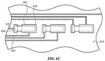
- FIG. 6Cdepicts an example bottom view of a conducting layer for haptic actuators, deposited on the bottom surface of the substrate.
- FIG. 7Adepicts an example perspective view of a pair of input electrodes disposed adjacent one another over a substrate.
- FIG. 7Bdepicts another example perspective view of a pair of input electrodes disposed above and below one another.
- FIG. 8Adepicts another electronic device with an input region having an integrated input/output module according to the present disclosure.
- FIG. 8Bdepicts an example cross-sectional view of the electronic device depicted in FIG. 8A , taken along section B-B, illustrating a first example input/output module.
- FIG. 8Cdepicts another example cross-sectional view of the electronic device depicted in FIG. 8A , taken along section B-B, illustrating a second example input/output module.
- FIG. 9depicts an enclosure for an electronic device having an input/output module disposed at least partially within a portion of the enclosure.
- FIG. 10Adepicts an example partial cross-sectional view of the electronic device depicted in FIG. 9 , taken along section C-C.
- FIG. 10Bdepicts an example view of input electrodes deposited on an interior surface of a wall, taken through section D-D of FIG. 10A .
- FIG. 10Cdepicts another example partial cross-sectional view of the electronic device depicted in FIG. 9 , taken along section C-C.
- FIG. 10Ddepicts an example partial cross-sectional view showing example patterns of input electrodes.
- FIG. 11depicts an example wearable electronic device that may incorporate an input/output module as described herein.
- FIG. 12depicts an example input device that may incorporate an input/output module as described herein.
- FIG. 13depicts an example method for detecting a location of a touch and an amount of force corresponding to the touch with a single module.
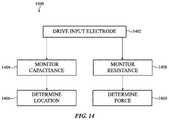
- FIG. 14depicts another example method for detecting a location of a touch and an amount of force corresponding to the touch with a single module.
- FIG. 15depicts example components of an electronic device in accordance with the embodiments described herein.
- cross-hatching or shading in the accompanying figuresis generally provided to clarify the boundaries between adjacent elements and also to facilitate legibility of the figures. Accordingly, neither the presence nor the absence of cross-hatching or shading conveys or indicates any preference or requirement for particular materials, material properties, element proportions, element dimensions, commonalities of similarly illustrated elements, or any other characteristic, attribute, or property for any element illustrated in the accompanying figures.
- An electronic devicemay include an enclosure component defining an input surface for receiving user inputs and outputting feedback to the user.
- Example enclosure componentsinclude a cover (e.g., a cover sheet, a trackpad cover, and the like), a wall of an enclosure (e.g., a sidewall or other wall), and the like.
- Example input surfacesinclude a trackpad, a touch screen, a surface of a wall of a device enclosure, or another exterior surface of an enclosure of an electronic device.
- Example electronic devicesinclude a personal computer, a notebook or laptop computer, a tablet, a smart phone, a watch, a case for an electronic device, a home automation device, and so on.
- Sensorsmay be placed on, within, or below the enclosure component to receive various types of inputs.
- a touch sensormay detect an object approaching or in contact with the input surface.
- the electronic devicemay determine the location of the object, and in some cases of multiple objects, relative to the input surface.
- a force sensormay detect a force applied to the enclosure component. Based on the output of the force sensor, the electronic device may approximate, measure, or otherwise determine an amount of the force applied to the cover. With an array of force sensors, the electronic device may determine the locations and amounts of multiple forces applied to the cover.
- the electronic devicemay also provide haptic output to a user through the enclosure component.
- Haptic outputis generated through the production of mechanical movement, vibrations, and/or force.
- the haptic outputcan be created based on an input command (e.g., one or more touch and/or force inputs), a simulation, an application, or a system state.
- an input commande.g., one or more touch and/or force inputs
- a simulatione.g., one or more touch and/or force inputs
- an applicatione.g., one or more touch and/or force inputs
- the electronic devicemay include one or more haptic devices configured to provide haptic feedback.
- an integrated touch input, force input, and haptic feedback moduleis provided on, within, or below the enclosure component of an electronic device.
- one or more components of the input/output moduleare integrally formed with the enclosure component.
- integrated withmay be used to refer to defining or forming a unitary structure.
- one or more input electrodes and/or haptic devicesmay be integrally formed with an enclosure component, such as a ceramic enclosure of an electronic device.
- Integrally forming a haptic actuator with an enclosure componentallows for localized haptic feedback (e.g., localized deflection of the wall) to be produced at select locations along an exterior surface of the enclosure.
- integrally forming an input electrode within an enclosure componentallows for localized touch input and force input detection at select locations along the exterior surface of the enclosure.
- localized haptic feedbackis produced in response to detecting touch and/or force input along the exterior surface of the enclosure.
- one or more components of the input/output module and/or other components of the electronic devicemay be integrally formed with an enclosure component by co-firing or co-sintering.
- co-firingmay be used to refer to any process by which one or more components or materials are fired in a kiln or otherwise heated to fuse or sinter the materials at the same time.
- co-firingmay be used to refer to a process in which two materials, which are in a green, partially sintered, pre-sintered state are heated or sintered together for some period of time.
- This input/output modulemay include one or more input electrodes, which are responsive to both touch and force inputs. That is, an array of input electrodes may be used to determine a location of a touch on the input surface and an amount (and location) of force applied to the cover.
- an input electrodemay be a strain gauge, having a series of parallel conductive traces, for example over a substrate, on a surface of the cover, or within the cover. The conductive traces may be formed in a variety of patterns, including a spiral pattern. As a strain gauge, the input electrode may exhibit a change in resistance in response to force or strain. In addition, the conductive material may exhibit a change in capacitance in response to the approach of a finger or other object.
- an array of input electrodesmay function as both touch and force sensors in a single layer, detecting a location of a touch on the input surface and an amount of force applied to the cover.
- the input electrodesmay be deposited on or otherwise attached to a top surface of a substrate, such as a glass or polyimide substrate. In some embodiments, the input electrodes may be deposited on or within, or otherwise attached to the cover.
- the input/output modulemay also include one or more haptic actuators deposited on, within, or otherwise attached to a bottom surface of the substrate or the cover.
- a haptic actuatormay provide localized haptic feedback to the cover.
- a haptic actuatormay be a piezoelectric haptic actuator, having a piezoelectric element which contracts and/or expands in response to application of a voltage across the piezoelectric element.
- an actuating signalmay cause the piezoelectric element to contract along the axis of elongation and/or contraction (e.g., a first direction parallel to the bottom surface).
- the piezoelectric elementmay bend and deflect along a second direction transverse to the axis of elongation and/or contraction, which may cause a deflection (e.g., a vertical deflection) of the substrate.
- the deflection of the substratemay be transferred to the cover.
- the deflection in the covermay be perceived as haptic feedback by a user through a finger or other body part in contact with the input surface.
- the input/output moduleis disposed below an opaque cover (e.g., a cover including an opaque layer, such as an ink layer) defining an input surface, such as a trackpad of a laptop.
- the materials of the input/output modulemay be optically opaque materials.
- the input/output moduleis disposed below a transparent cover defining an input surface, such as a cover of a cellular telephone or tablet device.
- the input/output modulemay be placed between the cover and a display, and the input/output module may be formed from optically transparent materials.
- the input/output modulemay be placed below the display and formed from opaque materials.
- FIG. 1depicts an electronic device with an input device having an integrated input/output module according to the present disclosure.
- the electronic device 100is a portable electronic device, specifically a laptop computer.
- Other embodimentsmay incorporate the input/output module into another type of portable electronic device, such as a mobile electronic device (see FIGS. 8A-8C ).
- an electronic devicemay include a smart phone, a wearable computing device, a digital music player, an automotive device, a kiosk, a stand-alone touch screen display, a mouse, a keyboard, and other types of electronic devices that are configured to receive touch and/or force inputs as well as provide haptic feedback to a user.
- the electronic device 100may include an enclosure 101 housing a keyboard 104 and a display 102 .
- the electronic device 100may also include an input device 108 , such as a trackpad.
- the input device 108may be positioned along a side of the keyboard 104 .
- the keyboard 104may be positioned between the input device 108 and a connection interface between the enclosure 101 and the display 102 .
- the input device 108may include a cover defining an input surface, and an input/output module may be incorporated below the cover.
- the input/output modulemay detect touch inputs and force inputs on the input surface, and additionally may provide haptic feedback to the cover. Examples of the input device 108 and the features of the input/output module are further depicted below with respect to FIGS. 2A-7B, 9, and 10 .
- the display 102may function as both an input device and an output device. For example, the display 102 may output images, graphics, text, and the like to a user.
- the display 102may also act as a touch input device that detects and measures a location of a touch input on the display 102 , via touch-sensing circuitry.
- the electronic device 100may also include one or more force sensors that detect and/or measure an amount of force exerted on the display 102 .
- the keyboard 104 of the electronic device 100includes an array of keys or buttons (e.g., movable input components). Each of the keys may correspond to a particular input.
- the keyboard 104may also include a frame or key web.
- the framemay define an aperture through which each key protrudes, such that each of the array of keys is at least partially positioned within the frame and at least partially without the frame.
- the framealso separates one key from an adjacent key and/or an enclosure of the electronic device 100 .
- the electronic device 100can also include a processor, memory, power supply and/or battery, network connections, sensors, input/output ports, acoustic components, haptic components, digital and/or analog circuits for performing and/or coordinating tasks of the electronic device 100 , and so on.
- a processormemory
- power supply and/or batterynetwork connections
- sensorsinput/output ports
- acoustic componentshaptic components
- digital and/or analog circuitsfor performing and/or coordinating tasks of the electronic device 100 , and so on.
- the electronic device 100is depicted in FIG. 1 without many of these components, each of which may be included, partially and/or entirely, within the enclosure 101 . Examples of such components are described below with respect to FIG. 11 .
- An integrated input/output modulemay be incorporated in other regions of a device to provide different functionality.
- the input/output modulemay extend over a keyboard region of the electronic device 100 (e.g., in place of all or a portion of the keyboard 104 ) and may be used to define a virtual or soft keyboard.
- the input/output modulemay allow for an adaptable key arrangement and may include configurable or adaptable glyphs and markings to designate the location of an array of virtual or configurable key regions.
- the input/output moduleforms an input surface over the display. This may enable a touch- and force-sensitive touch screen providing localized haptic output.
- the input/output modulemay be incorporated in a similar manner as described below with respect to FIGS. 8A-8C .
- the input/output modulemay form a portion of a key region, such as a function row above a physical keyboard.
- the input/output modulemay define a set of dynamically adjustable input regions.
- a display or other meansmay provide a visual representation (e.g., through adaptable glyphs and markings) to designate the location of virtual keys or input regions defined by the input/output module.
- the input/output modulemay be located on or within a portion of a device enclosure, such as a wall of a device enclosure, as discussed below with respect to FIGS. 9-11 .
- an input/output modulemay be attached to a cover of an electronic device.
- the input/output moduledetects touch and/or force inputs on the cover, and outputs localized haptic feedback to the cover.
- covermay refer to a cover for a trackpad, it should be understood that the term “cover” may also refer to a portion of an enclosure (such as the enclosure 101 depicted in FIG. 1 ).
- FIG. 2Adepicts an example cross-sectional view of the electronic device depicted in FIG. 1 , taken along section A-A, illustrating detection of a touch location.
- an input device 208includes a cover 210 defining an input surface, and an input/output module 205 is attached or otherwise coupled to the cover 210 .
- the input/output module 205may be attached to the cover 210 through an appropriate means, such as depicted in FIGS. 5A-5F, 8B, and 8C .
- the input/output module 205may detect the touch.
- the input/output module 205may include an input electrode which detects the touch as a change in capacitance.
- the input electrodemay operate through self-capacitance (as depicted in FIGS. 3A-3C ) or through mutual capacitance (as depicted in FIGS. 4A-4C ).
- the input electrodemay be coupled to processing circuitry to determine the presence and location of the finger 212 on the input surface of the cover 210 .
- the finger 212 or other objectmay exert force or pressure on the cover 210 .
- This forcemay deflect the cover 210 , which may in turn deflect the input/output module 205 .
- an input electrodemay have a non-binary response to the deflection, which response corresponds to and indicates the amount of force applied to the cover 210 .
- the input electrodemay be a strain gauge which undergoes a change in resistance in response to deflection of the input/output module 205 .
- the input electrodemay be coupled to processing circuitry to estimate or otherwise determine the amount of force applied to the cover 210 based on the resistive response.
- an input electrodemay be otherwise responsive to strain.
- the input electrodemay be formed from a piezoresistive, piezoelectric, or similar material having an electrical property that changes in response to stress, strain, and/or deflection.
- the input/output module 205may also provide localized haptic feedback to the cover 210 .
- the input/output module 205may include a haptic actuator which is coupled to processing circuitry and/or a signal generator.
- the processing circuitry and/or signal generatormay actuate the haptic actuator by applying an electrical signal to the haptic actuator.
- the haptic actuatormay cause the input/output module 205 to deflect upward.
- the haptic actuatormay include a piezoelectric element with a pair of electrodes coupled to opposing sides of the piezoelectric element (e.g., a top and bottom, which may be parallel to the cover 210 ).
- the piezoelectric elementmay contract along a first direction parallel to the electrodes. With the piezoelectric element coupled to a substrate, the contraction may cause the piezoelectric element to bend along a second direction transverse to the first direction. This bending of the piezoelectric element may cause the input/output module 205 to which the piezoelectric element is coupled to deflect upward toward the cover 210 .
- the input/output module 205may cause one or more sections of the cover 210 to deflect or move to provide localized haptic feedback to the user.
- the cover 210bends or deflects at a location that substantially corresponds to the location of the haptic actuator. This deflection of the cover 210 may be felt or otherwise perceived by a user through a finger 212 in contact with the cover 210 .
- the haptic actuatormay be actuated in response to a variety of stimuli, such as a touch input, a force input, the operation of software executed by the processing circuitry, and so on.
- the input/output module 205may cause haptic feedback at the cover 210 in response to an amount of force exerted on the cover 210 exceeding a threshold (e.g., similar to a button press).
- software executed by the processing circuitrymay cause the input/output module 205 to provide haptic feedback in response to events which occur during execution of the software.
- FIGS. 2A-2Cpresent cross-sectional views which may omit certain components for clarity.
- the input/output module 205may include multiple layers and components.
- One or more additional layers, such as an adhesive layer,may also be included between the cover 210 and the input/output module 205 .
- the input device and/or the electronic devicemay also include additional components and structures, such as the components depicted in FIG. 11 , support structures, and the like.
- an input electrode of the input/output modulemay include a strain gauge which operates to detect touch through self-capacitance, and force may be detected through a resistive strain response of the input electrode.
- FIG. 3Ais a top view of an input device, while FIGS. 3B and 3C are cross-sectional views of the input device.
- FIG. 3Adepicts a top view of an input device illustrating an example touch and/or force-sensing input electrode.
- the input device 308may be any input device configured to detect touch and/or force inputs, such as the trackpad depicted in FIG. 1 .
- the input device 308includes a cover 310 defining an input surface, and an input electrode 306 positioned below the cover 310 .
- a finger 312 or other objectmay approach or contact the input surface of the cover 310 .
- the input electrode 306may be a strain gauge formed from a conductive material patterned into a spiral pattern, which includes a set of parallel lines.
- the input electrode 306may be any type of sensor which responds to touch inputs and strain inputs, in which touch and strain may be distinguished.
- the input electrode 306may be formed from a piezoresistive, piezoelectric, or similar material having an electrical property (e.g., a resistance or resistivity) that changes in response to stress, strain, and/or deflection.
- the input electrode 306may operate to detect touch through self-capacitance.
- the conductive material of the input electrode 306may be energized (e.g., driven) with an alternating current or direct current signal (e.g., from a signal generator).
- an alternating current or direct current signale.g., from a signal generator.
- a touch capacitance Cmay be formed between the finger 312 and the input electrode 306 .
- the touch capacitance C formed between the finger 412 and the input electrode 306(or change in capacitance) may be detected by processing circuitry coupled to the input electrode 306 , which may indicate a touch input to the input surface of the cover 310 .
- a force F applied to the cover 310may be detected through the same input electrode 306 .
- the input electrode 306may be energized (e.g., driven) with an alternating current or direct current signal (e.g., from a signal generator).
- an alternating current or direct current signale.g., from a signal generator.
- the cover 310may deflect and cause a strain on the input electrode 306 .
- the geometry of the conductive traces of the input electrode 306may change in response to the cover 310 deflection (e.g., the traces may be stretched and/or compressed).
- This change in geometrymay result in a change in resistance through the input electrode 306 , which may be detected by processing circuitry coupled to the input electrode 306 .
- the processing circuitrymay further estimate or otherwise determine a non-binary amount of force applied to the cover 310 based on the change in resistance.
- non-binaryamount of force or force input signal is one that may be registered as more than two possible values.
- non-binary force input signalsmay have intermediate values, outputs, or states other than zero and a maximum (or off and on).
- Such non-binary signalsmay have a series of values, which may be discrete or continuous, each corresponding to a variety of input forces beyond binary options.
- the force signalmay vary in magnitude in accordance with a force that is applied to the cover.
- the input electrode 306may be energized with an electrical signal (e.g., driven with a drive signal), and touch inputs may be detected or measured as a capacitive response to the signal while force inputs may be detected or measured as a resistive response to the signal.
- touch and/or force sensingmay be time multiplexed.
- the input electrode 306may be driven with a first signal (e.g., a signal having a first waveform, which may include A/C and/or D/C components, and may have a given amplitude, shape, and/or frequency) for a first period of time, and a touch input may be measured as a capacitive response to the first signal.
- a first signale.g., a signal having a first waveform, which may include A/C and/or D/C components, and may have a given amplitude, shape, and/or frequency
- the input electrode 306may be driven with a second signal (e.g., a signal having a second waveform, which may include A/C and/or D/C components, and may have a given amplitude, shape, and/or frequency) for a second period of time, and a force input may be measured as a resistive response to the second signal.
- a second signale.g., a signal having a second waveform, which may include A/C and/or D/C components, and may have a given amplitude, shape, and/or frequency
- a force inputmay be measured as a resistive response to the second signal.
- a same signalmay be used to drive the input electrode 306 , but the touch response may be measured during a first period of time and the force response may be measured during a second period of time.
- two or more input electrodes of the input/output modulemay include strain gauges.
- the input electrodesmay operate to detect touch through mutual capacitance between the input electrodes, and force may be detected through a resistive strain response of the input electrodes.
- FIG. 4Adepicts a top view of an input device illustrating an example pair of touch and/or force-sensing input electrodes.
- the input device 408may be any input device configured to detect touch and/or force inputs, such as the trackpad depicted in FIG. 1 .
- the input device 408includes a cover 410 defining an input surface, and input electrodes 406 a , 406 b positioned below the cover 410 .
- a finger 412 or other objectmay approach or contact the input surface of the cover 410 .
- the input electrodemay operate to detect touch through mutual capacitance.
- a first input electrodedesignated a drive input electrode 406 a
- a cross-capacitance C 1may be formed between the drive input electrode 406 a and a second input electrode adjacent the drive input electrode 406 a , designated a sense input electrode 406 b , in response to the drive signal.
- a touch capacitance C 2may be formed between the finger 412 and the drive input electrode 406 a and/or the sense input electrode 406 b .
- the touch capacitance C 2may in turn alter the cross-capacitance C 1 .
- Processing circuitrymay be coupled to the drive input electrode 406 a and/or sense input electrode 406 b to detect the change in the cross-capacitance C 1 .
- processing circuitrymay monitor the sense input electrode 406 b for a change in capacitance which may indicate a touch input to the input surface of the cover 410 .
- processing circuitrymay monitor a capacitance across the drive input electrode 406 a and the sense input electrode 406 b , or by a similar technique.
- a force F applied to the cover 410may be detected through one or both of the drive input electrode 406 a and the sense input electrode 406 b .
- the drive input electrode 406 a and the sense input electrode 406 bmay each be driven with an alternating current or direct current signal (e.g., from a signal generator).
- the cover 410may deflect and cause a strain on the input electrodes 406 a , 406 b .
- Processing circuitrymay monitor the drive input electrode 406 a and the sense input electrode 406 b for a change in resistance, corresponding to a non-binary force applied to the cover 410 .
- the only one of the drive input electrode 406 a and the sense input electrode 406 bmay be driven and monitored for a change in resistance.
- FIGS. 5A-5Fexample cross-sections of an input device according to the present disclosure are illustrated. Each example includes in input/output module which operates as described above with respect to FIGS. 1-4C .
- FIG. 5Adepicts an example cross-sectional view of the electronic device depicted in FIG. 1 , taken along section A-A, illustrating a first example input/output module.
- An input device 508includes a cover 510 and an input/output module 505 a coupled to the cover 510 .
- the cover 510is formed from a dielectric material, such as glass, plastic, acrylic, and other non-conductive materials.
- the covermay be formed from an opaque material and/or include an opaque layer, such as an ink layer.
- the cover 510may be transparent or partially transparent. While in these examples the term “cover” may refer to a cover for a trackpad, it should be understood that the term “cover” may also refer to a portion of an enclosure (such as the enclosure 101 depicted in FIG. 1 ).
- the cover 510may enclose a virtual keyboard having dynamically adjustable input regions defined by the input/output module 505 a , a sidewall of an electronic device, or the like.
- the cover 510may be coupled to the input/output module 505 a by an adhesive layer 540 .
- the adhesive layer 540may include a pressure-sensitive adhesive, or another adhesive which couples the cover 510 to the input/output module 505 a such that a deflection in the cover 510 is transferred through the adhesive layer 540 to the input/output module 505 a , and a deflection of the input/output module 505 a is transferred to the cover 510 .
- the input/output module 505 aincludes a substrate 516 on which input electrodes 506 and haptic actuators 521 a are disposed.
- the substrate 516may include materials such as, but not limited to: plastic, ceramic, glass, polyimide, polyethylene terephthalate, silicone, fiber composite, or any combination thereof.
- the substrate 516may provide structural rigidity for the input electrodes 506 and/or a stiffener to improve performance of the haptic actuators 521 a.
- One or more input electrodes 506may be deposited on a top surface (e.g., the surface facing the cover 510 ) of the substrate 516 .
- Each input electrode 506may be formed from a conductive material which is also responsive to strain, formed with a set of conductive traces arranged in a doubled-back spiral shape, such as depicted below with respect to FIGS. 6B, 7A , and 7 B.
- the shape or geometry of an input electrode 506may vary.
- an input electrode 506may be formed from a set of traces arranged in a forked or comb-shaped configuration, a linear serpentine shape, a radial serpentine shape, a spiral shape, and so on.
- the conductive material of the input electrodes 506may include materials such as, but not limited to: gold, copper, copper-nickel alloy, copper-nickel-iron alloy, copper-nickel-manganese-iron alloy, copper-nickel-manganese alloy, nickel-chrome alloy, chromium nitride, a composite nanowire structure, a composite carbon structure, graphene, nanotube, constantan, karma, silicon, polysilicon, gallium alloy, isoelastic alloy, and so on.
- the conductive material of the input electrodes 506may be formed or deposited on a surface using a suitable disposition technique such as, but not limited to: vapor deposition, sputtering, printing, roll-to-roll processing, gravure, pick and place, adhesive, mask-and-etch, and so on.
- a haptic actuator 521 amay include a piezoelectric element 522 a , a top electrode 518 a , and a bottom electrode 524 a .
- the top electrode 518 ae.g., a conductive pad
- a conductive pad 520 amay be formed from a conductive material deposited on the bottom surface of the substrate 516 .
- the bottom electrode 524 amay wrap around a portion of the piezoelectric element and couple to the conductive pad 520 a.
- the top electrode 518 a and the conductive pad 520 amay be disposed on a common layer, which may additionally include signal lines to transmit actuation signals to each haptic actuator 521 a (e.g., such as depicted below with respect to FIG. 6C ). Accordingly, a potential may be applied across the piezoelectric element 522 a —a reference voltage may be provided to the bottom electrode 524 a through the conductive pad 520 a ; and an actuation signal may be provided to the top electrode 518 a . In some embodiments, the top electrode 518 a may be coupled to a reference voltage and the bottom electrode 524 a may be coupled to an actuation signal.
- Each haptic actuator 521 acan be selectively activated in the embodiment shown in FIG. 5A .
- the bottom electrode 524 acan provide a reference voltage to a haptic actuator 521 a
- the top electrode 518 acan apply an electrical signal across each individual piezoelectric element 522 a independently of the other piezoelectric elements 522 a.
- the voltagemay induce the piezoelectric element 522 a to expand or contract in a direction or plane substantially parallel to the substrate 516 .
- the properties of the piezoelectric element 522 amay cause the piezoelectric element 522 a to expand or contract along a plane substantially parallel to the substrate when electrodes applying the voltage are placed on a top surface and bottom surface of the piezoelectric element 522 a parallel to the substrate.
- the piezoelectric element 522 amay bow and deflect in a direction orthogonal to the substrate 516 , that is upward toward the cover 510 , such as depicted above with respect to FIG. 2C .
- the haptic feedbackmay be localized to a portion of the cover 510 above the haptic actuator 521 a.
- the piezoelectric element 522 amay be formed from an appropriate piezoelectric material, such as potassium-based ceramics (e.g., potassium-sodium niobate, potassium niobate), lead-based ceramics (e.g., PZT, lead titanate), quartz, bismuth ferrite, and other suitable piezoelectric materials.
- the top electrode 518 a , the bottom electrode 524 a , and the conductive pad 520 aare typically formed from metal or a metal alloy such as silver, silver ink, copper, copper-nickel alloy, and so on. In other embodiments, other conductive materials can be used.
- the top electrode 518 a and the conductive pad 520 aare formed or deposited directly on the substrate 516 using a suitable disposition technique such as, but not limited to: vapor deposition, sputtering, printing, roll-to-roll processing, gravure, pick and place, adhesive, mask-and-etch, and so on.
- the piezoelectric element 522 amay be similarly formed directly on the top electrode 518 a and the conductive pad 520 a
- the bottom electrode 524 amay be formed directly on the piezoelectric element 522 a and the conductive pad 520 a.
- haptic actuator 521 ahas been described with respect to a piezoelectric actuator, different types of haptic actuators 521 a can be used in other embodiments.
- one or more electromagnetic actuatorscan be disposed below the substrate 516 and used to produce localized deflection of the cover 510 .
- one or more piston actuatorsmay be disposed below the cover 510 , and so on.
- the relative position of the various layers described abovemay change depending on the embodiment. Some layers, such as the adhesive layer 540 , may be omitted in other embodiments. Other layers, such as the cover 510 and the substrate 516 , may not be uniform layers of single materials, but may include additional layers, coatings, and/or be formed from composite materials.
- the input device 508 and/or electronic devicemay include additional layers and components, such as processing circuitry, a signal generator, a battery, etc., which have been omitted from FIGS. 5A-5F for clarity.
- FIG. 5Bdepicts another example cross-sectional view of the electronic device depicted in FIG. 1 , taken along section A-A, illustrating a second example input/output module.
- a haptic actuator 521 b in the input/output module 505 bmay be selectively actuated through signals transmitted on two layers.
- the top electrode 518 bmay be deposited on the bottom surface of the substrate 516 .
- Signal linesmay also be deposited on the bottom surface of the substrate 516 to transmit actuation signals to each top electrode 518 b of a haptic actuator 521 b .
- a piezoelectric element 522 bbe formed directly on the top electrode 518 b
- the bottom electrode 524 bmay be formed on the piezoelectric element 522 b.
- the input device 508may also include a circuit layer 526 b which includes signal lines to provide a common reference voltage to each bottom electrode 524 b of a haptic actuator 521 b .
- the circuit layer 526 bmay be a flexible printed circuit or a flexible printed circuit board.
- the circuit layer 526 bcan be made from any number of suitable materials, such as polyimide or polyethylene terephthalate, with conductive traces for signal lines formed from materials such as copper, silver, aluminum, and so on.
- the circuit layer 526 bmay be coupled to each haptic actuator 521 b in a manner that electrically couples a signal line or common reference voltage plate on the circuit layer 526 b to each bottom electrode 524 b .
- the circuit layer 526 bmay be coupled to each haptic actuator 521 b by an adhesive layer, such as an isotropic or anisotropic conductive film, by soldering, and other appropriate techniques.
- a potentialmay be applied across the piezoelectric element 522 b , with a common reference voltage provided to each bottom electrode 524 b and a signal line provided to each top electrode 518 b .
- a top electrode 518 bmay receive an actuation signal, and the voltage across the piezoelectric element 522 b may cause the haptic actuator 521 b to deflect, which in turn provides localized haptic feedback at the cover 510 .
- the top electrodes 518 bmay form a common reference layer, and actuation signals may be transmitted to the bottom electrodes 524 b .
- the top electrodes 518 bmay be formed as an interconnected conductive layer (partially or entirely formed of conductive material), while the circuit layer 526 b may include separate signal lines to provide actuation signals to each bottom electrode 524 b.
- FIG. 5Cdepicts another example cross-sectional view of the electronic device depicted in FIG. 1 , taken along section A-A, illustrating a third example input/output module.
- a haptic actuator 521 c in the input/output module 505 cmay be formed with a dielectric 530 separating the conductive pad 520 c from the top electrode 518 c.
- a top electrode 518 c and a conductive pad 520 cmay be disposed on a common layer, which may additionally include signal lines to transmit actuation signals to each haptic actuator 521 c (e.g., such as depicted below with respect to FIG. 6C ).
- a dielectric 530may be deposited between the conductive pad 520 c and the top electrode 518 c to electrically isolate the conductive pad 520 c from the top electrode 518 c . The dielectric 530 further isolates the top electrode 518 c and the bottom electrode 524 c.
- the dielectric 530may be formed from silicon dioxide, hafnium oxide, tantalum oxide, nanopourous silica, hydrogensilsesquioxanes, polytetrafluoethylene, silicon oxyflouride, or another suitable dielectric material.
- the dielectric 530may be formed or deposited using a suitable disposition technique such as, but not limited to: vapor deposition, sputtering, printing, roll-to-roll processing, gravure, pick and place, adhesive, mask-and-etch, and so on.
- a connecting line 528 cmay be deposited over the dielectric 530 , electrically coupling the conductive pad 520 c to the bottom electrode 524 c .
- the connecting line 528 cmay be formed from a similar material and using a similar technique as described above with respect to the conductive pad 520 c and the top electrode 518 c .
- a potentialmay be applied across the piezoelectric element 522 c —a reference voltage may be provided to the bottom electrode 524 c through the conductive pad 520 c and the connecting line 528 c ; and an actuation signal may be provided to the top electrode 518 c .
- the top electrode 518 cmay be coupled to a reference voltage and the bottom electrode 524 c may be coupled to an actuation signal.
- FIG. 5Ddepicts another example cross-sectional view of the electronic device depicted in FIG. 1 , taken along section A-A, illustrating a fourth example input/output module.
- a haptic actuator 521 d in the input/output module 505 dmay be formed by interleaving electrodes 525 d , 519 d in the piezoelectric element 522 d.
- the piezoelectric element 522 dmay operate effectively as two stacked piezoelectric elements 522 d , which may improve the performance of the haptic actuator 521 d when actuated.
- the top electrode 518 dmay be formed on the substrate 516 , less than the entire width of the piezoelectric element 522 d , and may be connected to signal lines disposed on the substrate 516 .
- the material of the piezoelectric element 522 dmay be deposited over the top electrode 518 d , and an intermediate bottom electrode 525 d may be formed on the piezoelectric material, spanning less than the entire width of the piezoelectric element 522 d . Additional material of the piezoelectric element 522 d may be deposited on the intermediate bottom electrode 525 d , and an intermediate top electrode 519 d may be deposited on the piezoelectric material, spanning less than the entire width of the piezoelectric element 522 d.
- Additional material of the piezoelectric element 522 dmay be deposited on the intermediate top electrode 519 d .
- the bottom electrode 524 dmay be deposited over the piezoelectric element 522 d .
- a bottom connecting line 528 dmay electrically connect the intermediate bottom electrode 525 d and the bottom electrode 524 d to signal lines disposed on the substrate 516 .
- a top connecting line 532 dmay electrically connect the intermediate top electrode 519 d to the top electrode 518 d.
- the haptic actuator 521 dmay be effectively two actuators, with the top electrode 518 d and the intermediate bottom electrode 525 d forming a first actuator.
- the intermediate top electrode 519 d and the bottom electrode 524 dform a second electrode.
- a potentialmay be applied across the portions of the piezoelectric element 522 d between the electrodes.
- a reference voltagemay be provided to the intermediate bottom electrode 525 d and the bottom electrode 524 d through the bottom connecting line 528 d ; and an actuation signal may be provided to the top electrode 518 d and the intermediate top electrode 519 d through the top connecting line 532 d .
- the top electrode 518 d and intermediate top electrode 519 dmay be coupled to a reference voltage and the intermediate bottom electrode 525 d and the bottom electrode 524 d may be coupled to an actuation signal.
- FIG. 5Edepicts another example cross-sectional view of the electronic device depicted in FIG. 1 , taken along section A-A, illustrating a fifth example input/output module.
- a haptic actuator 521 emay be separately formed and coupled to the input/output module 505 e.
- the haptic actuator 521 emay be formed by a separate process rather than being deposited onto the substrate 516 .
- a voltagemay be applied across the piezoelectric element 522 e via electrodes 518 e , 524 e formed on opposing surfaces of the piezoelectric element 522 e .
- a top electrode 518 eis formed on a top surface of the piezoelectric element 522 e
- a bottom electrode 524 eis formed on a bottom surface of the piezoelectric element 522 e .
- the bottom electrode 524 ewraps around the piezoelectric element 522 e such that a portion of the second electrode is disposed on the top surface of the piezoelectric element 522 e . In this manner, a reference voltage and actuation signal may be provided at a same interface.
- the electrodes 518 e , 524 emay be formed from a suitable conductive material, such as metal (e.g., silver, nickel, copper, aluminum, gold), polyethyleneioxythiophene, indium tin oxide, graphene, piezoresistive semiconductor materials, piezoresistive metal materials, and the like.
- the top electrode 518 emay be formed from the same material as the bottom electrode 524 e , while in other embodiments the electrodes 518 e , 524 e may be formed from different materials.
- the electrodes 518 e , 524 emay be formed or deposited using a suitable disposition technique such as, but not limited to: vapor deposition, sputtering, plating, printing, roll-to-roll processing, gravure, pick and place, adhesive, mask-and-etch, and so on.
- a mask or similar techniquemay be applied to form a patterned top surface of the piezoelectric element 522 e and/or a wraparound bottom electrode 524 e.
- a first conductive pad 520 e and a second conductive pad 534 emay be formed from a conductive material deposited on the bottom surface of the substrate 516 .
- the first conductive pad 520 e and the second conductive pad 534 emay be disposed on a common layer, which may additionally include signal lines to transmit actuation signals to each haptic actuator 521 e (e.g., such as depicted below with respect to FIG. 6C ).
- the piezoelectric element 522 emay be coupled to the first conductive pad 520 e and the second conductive pad 534 e by an adhesive layer 536 e , which may be an anisotropic conductive film.
- the anisotropic conductive film of the adhesive layer 536 emay facilitate conduction from the first conductive pad 520 e to the bottom electrode 524 e and from the second conductive pad 534 e to the top electrode 518 e .
- the anisotropic conductive filmmay further isolate these conduction paths to prevent an undesired short between the conductive pads 520 e , 534 e or electrodes 518 e , 524 e.
- the piezoelectric element 522 emay be coupled and electrically connected to the first conductive pad 520 e and the second conductive pad 534 e by isolated segments of isotropic conductive film, an anisotropic or isotropic conductive paste, or another appropriate method.
- FIG. 5Fdepicts another example cross-sectional view of the electronic device depicted in FIG. 1 , taken along section A-A, illustrating a sixth example input/output module.
- a haptic actuator 521 fmay be separately formed and coupled to the input/output module 505 f and a circuit layer 526 f.
- the haptic actuator 521 fmay be formed by a separate process rather than being deposited onto the substrate 516 .
- a top electrode 518 fis formed on a top surface of the piezoelectric element 522 f
- a bottom electrode 524 fis formed on a bottom surface of the piezoelectric element 522 f in a manner similar to that described above with respect to FIG. 5E .
- the input device 508may also include a circuit layer 526 f which includes signals lines to provide a common reference voltage to each bottom electrode 524 f of a haptic actuator 521 f .
- the circuit layer 526 fmay be a flexible printed circuit or a flexible printed circuit board, similar to that described above with respect to FIG. 5B .
- the circuit layer 526 fmay include a first conductive pad 520 f for each haptic actuator 521 f.
- a second conductive pad 534 fmay be formed from a conductive material deposited on the bottom surface of the substrate 516 .
- the second conductive pad 534 fmay be disposed on a layer which additionally includes signal lines to transmit actuation signals to each haptic actuator 521 f.
- the piezoelectric element 522 fmay be coupled to the second conductive pad 534 f by a first adhesive layer 536 f and the first conductive pad 520 f by a second adhesive layer 538 .
- the first adhesive layer 536 fmay be an anisotropic conductive film, which may facilitate conduction from the second conductive pad 534 f to the top electrode 518 f .
- the anisotropic conductive filmmay further isolate the conductive pad 534 f and top electrode 518 f of separate haptic actuators 521 f to prevent an undesired short between haptic actuators 521 f.
- the top electrode 518 fmay be coupled and electrically connected to the second conductive pad 534 f by isolated segments of isotropic conductive film, an anisotropic or isotropic conductive paste, or another appropriate method.
- the circuit layer 526 fmay couple a reference voltage to each bottom electrode 524 f .
- the second adhesive layer 538may be an isotropic conductive film, anisotropic conductive film, a conductive paste, or other conductive adhesion material.
- a potentialmay be applied across the piezoelectric element 522 f , with a common reference voltage provided to each bottom electrode 524 f and a signal line provided to each top electrode 518 f .
- a top electrode 518 fmay receive an actuation signal, and the voltage across the piezoelectric element 522 f may cause the haptic actuator 521 f to deflect, which in turn provides localized haptic feedback at the cover 510 .
- the top electrodes 518 fmay form a common reference layer, and actuation signals may be transmitted to the bottom electrodes 524 f .
- the top electrodes 518 fmay be formed as an interconnected conductive layer (partially or entirely formed of conductive material), while the circuit layer 526 f may include separate signal lines to provide actuation signals to each bottom electrode 524 f .
- the second adhesive layer 538may be an anisotropic conductive film or other adhesion material that isolates the first conductive pads 520 f from each other.
- FIG. 6Adepicts an example cross-sectional view of an input/output module illustrating the deposition of input electrodes on a top surface of a substrate and haptic actuators on a bottom surface of the substrate.
- the input/output module 605may be similar to those depicted above with respect to FIGS. 5A-5F .
- the input/output module 605includes a substrate 616 on which input electrodes 606 and haptic actuators 621 are disposed.
- a set or array of input electrodes 606are disposed on a top surface of the substrate 616 , near a cover of an input device.
- a set or array of haptic actuators 621is disposed on a bottom surface of the substrate 616 .
- Each haptic actuator 621may include a piezoelectric element 622 between a conductive pad 620 and a top electrode 618 above, and a bottom electrode 624 below.
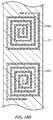
- FIG. 6Bdepicts an example top view of input electrodes deposited on the top surface of the substrate.
- each input electrode 606may be a touch- and strain-sensitive element, which may be a conductive trace deposited or otherwise formed on the substrate 616 as a strain gauge.
- Each input electrode 606may be formed in a double-backed spiral shape. In other embodiments, the shape or geometry of an input electrode 606 may vary.
- an input electrode 606may be formed from a set of traces arranged in a forked or comb-shaped configuration, a linear serpentine shape, a radial serpentine shape, a spiral shape, and so on.
- the input electrode 606may include conductive traces set in one or more sets of parallel lines.
- Each input electrode 606includes or is electrically coupled to a first signal line 607 and a second signal line 609 , which lead across the substrate 616 to connect to processing circuitry and/or a signal generator, such as described below with respect to FIG. 11 .
- a signal generatormay provide electrical signals to each input electrode 606 through the first signal line 607 or the second signal line 609 .
- Processing circuitrymay be coupled to one or both signal lines 607 , 609 to detect a capacitive touch response and a resistive force response. That is, a presence and location of a touch may be detected through a change in capacitance of an input electrode 606 , or across multiple input electrodes 606 (see FIGS. 3B and 4B , described above).
- a non-binary amount of forcemay be detected through a change in resistance through an input electrode 606 (see FIGS. 3C and 4C , described above).
- the signal lines 607 , 609may be formed of a similar material and in a similar process as the input electrodes 606 .
- the input electrodes 606 and the signal lines 607 , 609are formed in a same processing step.
- the input electrodes 606are formed in one processing step and one or both signal lines 607 , 609 are formed in a separate processing step.
- the input electrodes 606 and the signal lines 607 , 609may be arranged in any suitable pattern, such as a grid pattern, a circular pattern, or any other geometric pattern (including a non-regular pattern).
- FIG. 6Cdepicts an example bottom view of a conducting layer for haptic actuators, deposited on the bottom surface of the substrate.
- FIG. 6Cis depicted with other elements of each haptic actuator 621 shown as ghosted lines in order to clarify an example layout of a conducting layer.
- a conductive pad 620 and a top electrode 618may be provided for each haptic actuator 621 .
- Signal lines 619 , 623connect to each top electrode 618 and conductive pad 620 in order to electrically couple the haptic actuator 621 to a signal generator and/or processing circuitry and provide actuation signals.
- each conductive pad 620may connect to a first signal line 619 , which may provide a reference voltage to a bottom electrode of the haptic actuator 621 .
- Each top electrode 618may connect to a second signal line 623 , which may provide an actuation signal to the haptic actuator 621 .
- the top electrodes 618may be coupled to a reference voltage and the conductive pads 620 may receive an actuation signal.
- the signal lines 619 , 623may be formed of a similar material and in a similar process as the conductive pads 620 and top electrodes 618 , described above with respect to FIG. 5A .
- the conductive pads 620 , top electrodes 618 , and signal lines 619 , 623are formed in a same processing step.
- the conductive pads 620 and/or top electrodes 618are formed in one processing step and one or more signal lines 619 , 623 are formed in a separate processing step.
- the input electrodes 606 and the signal lines 607 , 609may be arranged in any suitable pattern, such as a grid pattern, a circular pattern, or any other geometric pattern (including a non-regular pattern).
- the input electrodes 606 and signal lines 607 , 609are formed on the top surface of the substrate 616 in one processing step, and the conductive pads 620 , top electrodes 618 , and signal lines 619 , 623 are formed on the bottom surface of the substrate 616 in another processing step.
- conducting materialis formed on both sides of the substrate 616 in a same processing step.
- FIGS. 7A and 7Bdepict example input electrodes which may compensate for adverse environmental effects, such as changes in temperature.
- the performance of an input electrode 706 a , 706 b , 706 cis dependent, in part, on the precision, accuracy, and resolution with which the strain experienced by the input electrode 706 a , 706 b , 706 c may be estimated.
- processing circuitrymay be configured to measure a change in the resistance of an input electrode 706 a , 706 b , 706 c due to applied force.
- an actual measurement of the resistance of an input electrode 706 a , 706 b , 706 cmay also be sensitive to variations in temperature, both across the device and localized over a portion of the device.
- Some embodiments of the input electrode 706 a , 706 b , 706 cmay be used to reduce or eliminate effects due to temperature or other environmental conditions.
- FIG. 7Adepicts an example perspective view of a pair of input electrodes disposed adjacent one another over a substrate.
- a first input electrode 706 a and a second input electrode 706 bmay be arranged in sufficient proximity that the two input electrodes 706 a , 706 b experience approximately the same environmental effects.
- the output of the first input electrode 706 a and the second input electrode 706 bmay be compared by processing circuitry to mitigate or eliminate variations in force measurements as a result of changing environmental conditions, such as changes in temperature.
- the first input electrode 706 amay be more responsive to strain along a particular direction than the second input electrode 706 b .
- the resistive response to of the first input electrode 706 amay then be compared to the resistive response of the second input electrode 706 b (e.g., by subtracting the response of the second input electrode 706 b from the first input electrode 706 a ) to account for temperature variation.
- FIG. 7Bdepicts another example perspective view of a pair of strain-sensitive element disposed above and below one another to form an input electrode.
- An input electrode 706 amay include a first strain-sensitive element 770 disposed on the substrate 716 .
- a second strain-sensitive element 766is disposed above the first strain-sensitive element 770 , with a film 768 or other dielectric material disposed between.
- the output of the first strain-sensitive element 770may similarly be compared to the second strain-sensitive element 766 by processing circuitry to mitigate or eliminate variations in force measurements as a result of changes in temperature or other conditions.
- first strain-sensitive element 770may be placed under compression while the second strain-sensitive element 766 may be placed under tension in response to a force on the cover.
- the distinct resistive responses of the first strain-sensitive element 770 and the second strain-sensitive element 766may be compared to account for temperature variation.
- FIG. 8Adepicts another electronic device with an input region having an integrated input/output module according to the present disclosure.
- the electronic device 800is implemented as a tablet computing device.
- the electronic device 800includes an enclosure 801 at least partially surrounding a display 802 and one or more input devices 842 .
- the enclosure 801can form an outer surface or partial outer surface for the internal components of the electronic device 800 .
- the enclosure 801can be formed of one or more components operably connected together, such as a front piece and a back piece. Alternatively, the enclosure 801 can be formed of a single piece operably connected to the display 802 .
- the display 802can provide a visual output to the user.
- the display 802can be implemented with any suitable technology, including, but not limited to, a liquid crystal display element, a light emitting diode element, an organic light-emitting display element, an organic electroluminescence element, an electrophoretic ink display, and the like.
- the input device 842can take the form of a home button, which may be a mechanical button, a soft button (e.g., a button that does not physically move but still accepts inputs), an icon or image on a display, and so on. Further, in some embodiments, the input device 842 can be integrated as part of a cover 810 and/or the enclosure 801 of the electronic device 800 . Although not shown in FIG. 1 , the electronic device 800 can include other types of input and/or output devices, such as a microphone, a speaker, a camera, a biometric electrode, and one or more ports, such as a network communication port and/or a power cord port.
- a home buttonwhich may be a mechanical button, a soft button (e.g., a button that does not physically move but still accepts inputs), an icon or image on a display, and so on.
- the input device 842can be integrated as part of a cover 810 and/or the enclosure 801 of the electronic device 800 .
- a cover 810may be positioned over the front surface (or a portion of the front surface) of the electronic device 800 . While the cover 810 is depicted in reference to a cover over a display of a tablet computer, an input/output module may be positioned below other transparent or partially transparent covers, such as an enclosure of a device forming a virtual keyboard. The input/output module and the display 802 may define user input regions, such as dynamically configurable keys, which may receive force and touch inputs and provide haptic outputs to the cover 810 .
- At least a portion of the cover 810can function as an input surface that receives touch and/or force inputs.
- the cover 810can be formed with any suitable material, such as glass, plastic, sapphire, or combinations thereof.
- the cover 810encloses the display 802 and the input device 842 . Touch and/or force inputs can be received by the portion of the cover 810 that encloses the display 802 and by the portion of the cover 810 that encloses the input device 842 .
- the cover 810encloses the display 802 but not the input device 842 .
- Touch and/or force inputscan be received by the portion of the cover 810 that encloses the display 802 .
- touch and/or force inputscan be received on other portions of the cover 810 , or on the entire cover 810 .
- the input device 842may be disposed in an opening or aperture formed in the cover 810 .
- the apertureextends through the enclosure 801 and one or more components of the input device 842 are positioned in the enclosure.
- An input/output modulemay be incorporated below all or a portion of the cover 810 .
- the input/output modulemay detect touch inputs and force inputs on all or a portion of the cover 810 , and additionally may provide haptic feedback to the cover 810 .
- Examples of the electronic device 800 and the features of the input/output moduleare further depicted below with respect to FIGS. 8B, 8C, 9, and 10 .
- Example components of the electronic device 800are described below with respect to FIG. 11 .
- FIG. 8Bdepicts an example cross-sectional view of the electronic device depicted in FIG. 8A , taken along section B-B, illustrating a first example input/output module.
- An input device 808includes a cover 810 defining an input surface, a display 802 below the cover 810 , and an input/output module 805 between the cover 810 and the display 802 .
- the cover 810is typically formed from a transparent dielectric material, such as glass, sapphire, plastic, acrylic, and other transparent, non-conductive materials.
- the cover 810may be coupled to the input/output module 805 by an adhesive layer 840 .
- the adhesive layer 840may include an optically clear adhesive, or another transparent adhesive which couples the cover 810 to the input/output module 805 such that a deflection in the cover 810 is transferred through the adhesive layer 840 to the input/output module 805 , and a deflection of the input/output module 805 is transferred to the cover 810 .
- the input/output module 805includes a substrate 816 on which input electrodes 806 and haptic actuators are disposed, in a manner similar to the input/output modules 505 a - 505 f described above with respect to FIGS. 5A-5F .
- the materials of the substrate 816 , the input electrodes 806 , and the piezoelectric elements 822may be optically transparent.
- the piezoelectric elements 822 of the haptic actuatorsmay be coupled to the substrate 816 through a conductive layer 818 , which may provide actuation signals to the piezoelectric elements 822 .
- Conductive materials of the input/output module 805may be formed from optically transparent materials, such as, but not limited to: indium-tin oxide, carbon nanotubes, metal nanowires, or any combination thereof.
- the piezoelectric element 822may be formed from a transparent piezoelectric material, such as lithium niobate, quartz, and other suitable piezoelectric materials.
- the display 802may include a display element, and may include additional layers such as one or more polarizers, one or more conductive layers, and one or more adhesive layers.
- a backlight assembly(not shown) is positioned below the display 802 .
- the display 802along with the backlight assembly, is used to output images on the display. In other embodiments, the backlight assembly may be omitted.
- FIG. 8Cdepicts another example cross-sectional view of the electronic device depicted in FIG. 8A , taken along section B-B, illustrating a second example input/output module.
- the display 802may be positioned adjacent the cover 810 , and the input/output module 805 may be placed below the display 802 .
- the input/output module 805may be coupled to the display 802 by an adhesive layer 846 .
- the input/output module 805may include a substrate 816 on which input electrodes 806 , and haptic actuators are disposed.
- the haptic actuatorsmay include a conductive layer 818 and a piezoelectric element 822 . Each of these components may be similar to those described above with respect to FIGS. 5A-5F and 8C , and may be optically transparent or opaque.
- the input/output modules shown and described with respect to FIGS. 5A-8Cinclude haptic actuators and input electrodes disposed beneath a cover as part of a separate layer from the cover, such as a substrate. These are example arrangements of the haptic actuators with respect to the cover, and other arrangements are possible.
- one or more haptic actuators or input electrodesmay be integrally formed with (e.g., on or within) a wall of an enclosure of a portable electronic device.
- FIGS. 9-10Ddepict example embodiments in which haptic actuators and input electrodes are integrally formed with (e.g., on or within) a wall of an enclosure.
- FIG. 9depicts an enclosure 900 for an electronic device 990 (e.g., a portable electronic device) having one or more components of an input/output module integrally formed with a wall of the enclosure.
- the electronic device 990is an electronic watch or smartwatch.
- the enclosure 900may include an enclosure component 901 and a cover 902 .
- the enclosure component 901 and the cover 902may be attached or otherwise coupled and may cooperate to form the enclosure 900 and define one or more exterior surfaces of the electronic device 990 .
- one or more input/output modulesmay be at least partially integrally formed with a wall 931 of the enclosure 900 .
- integrally formed withmay be used to refer to defining or forming a unitary structure.
- one or more haptic actuators, input electrodes, and/or other components of an input/output modulemay be integrally formed on or within the wall 931 to form a unitary structure by co-firing or co-sintering the one or more haptic actuators, input electrodes, and/or other components with at least a portion of the enclosure 900 .
- the wall 931(e.g., a sidewall of the electronic device 990 ) defines at least a portion of an exterior surface of the enclosure 900 that is configured to receive a contact from a user. Integrally forming a haptic actuator within a wall of the enclosure allows for localized haptic feedback (e.g., localized deflection of the wall 931 ) to be produced at select locations along an exterior surface of the enclosure, for example in response to a touch input detected along the exterior surface. Similarly, integrally forming an input electrode within a wall of the enclosure allows for localized touch input and force input detection at select locations along the exterior surface of the enclosure.
- localized haptic feedbacke.g., localized deflection of the wall 931
- the enclosure 900may be formed from a variety of materials including polymers (e.g., polycarbonate, acrylic), glass, ceramics, composites, metal or metal alloys, (e.g., stainless steel, aluminum), precious metals (e.g., gold, silver), or other suitable materials, or a combination of these materials.
- the enclosure component 901is at least partially formed from a ceramic material such as aluminum oxide (alumina) or other similar type of material.
- the enclosure component 901may be co-fired with one or more components of the input/output module and/or other components of the electronic device 990 .
- co-firingmay be used to refer to any process by which one or more components or materials are fired in a kiln or otherwise heated to fuse or sinter the materials at the same time.
- co-firingmay be used to refer to a process in which two materials, which are in a green, partially sintered, pre-sintered state are heated or sintered together for some period of time.
- a co-firing processmay include low temperature (LTCC) applications (e.g., sintering temperatures below 1000 degrees Celsius) and/or high temperature (HTCC) applications (e.g., high temperatures between 1000 and 1800 degrees Celsius).
- co-firing components of the electronic device 990may improve the electronic device by reducing device dimensions (e.g., thickness of a wall or other component), reducing or eliminating the need for adhesives to join components together, simplifying manufacturing, and the like.
- one or more components of the input/output moduleare at least partially formed of a ceramic material.
- the input/output modulemay include one or more piezoelectric ceramic actuators, ceramic buffers, or the like, as discussed below. More specifically, as described in more detail below, the input/output module may include a piezoelectric element that is configured to produce a localized deflection along the exterior surface of the enclosure component 901 . If the enclosure component 901 and the piezoelectric element are both formed from ceramic materials, the two components may be integrally formed using a co-firing or co-sintering process.
- the cover 902may include a sheet or cover sheet that is positioned over a display of the electronic device 990 .
- the displaymay include one or more input devices or touch sensors and be configured as a touch-sensitive or touchscreen display.
- the touch sensorsmay include input electrodes or electrodes in accordance with embodiments described herein. Specifically, the touch sensors may include an array of input electrodes that are configured to detect a location of a touch input along the cover 902 . In some instances, an array of electrodes that are configured to detect a force of a touch input are positioned along or below the cover 902 .
- the cover 902may be formed from an optically transmissive material to allow images or light to be visible therethrough.
- optically transmissiveor “light-transmissive” may be used to refer to something that is transparent or translucent, or otherwise allows light or other electromagnetic radiation to propagate therethrough.
- transparent materials or componentsmay introduce some diffusion, lensing effects, distortions, or the like (e.g., due to surface textures) while still allowing objects or images to be seen through the materials or components, and such deviations are understood to be within the scope of the meaning of transparent.
- materials that are transparentmay be coated, painted, or otherwise treated to produce a non-transparent (e.g., opaque) component; in such cases the material may still be referred to as transparent, even though the material may be part of an opaque component.
- Translucent componentsmay be formed by producing a textured or frosted surface on an otherwise transparent material (e.g., clear glass). Translucent materials may also be used, such as translucent polymers, translucent ceramics, or the like.
- an electronic device 990may be coupled to and/or positioned within the enclosure 900 .
- processing circuitry of the electronic devicemay be housed or positioned within an internal volume 921 of the enclosure 900 . Additional components of the electronic device are discussed in more detail below with respect to FIG. 15 .
- the enclosure 900is pictured as having a rectangular shape, this is one example and is not meant to be limiting.
- the electronic devicemay be and/or take the form of a personal computer, a notebook or laptop computer, a tablet, a smart phone, a watch, a case for an electronic device, a home automation device, and so on.
- the enclosure component 901defines a wall 931 (e.g., sidewall or enclosure wall) that defines at least a portion of an exterior surface 911 of the enclosure 900 .
- FIG. 10Adepicts an example partial cross-sectional view of the electronic device 990 depicted in FIG. 9 , taken along section C-C.
- the electronic device 990includes an input/output module 1050 a .
- the input/output module 1050 aincludes one or more haptic actuators 1051 , and one or more input electrodes 1060 , 1070 .
- the input/output module 1050 amay be at least partially integrated or integrally formed with the wall 931 . For example, as shown in FIG.
- one or more haptic actuators 1051may be formed within the structure of the wall 931 .
- the haptic actuator 1051is formed form a ceramic (e.g., ceramic piezoelectric) material, the haptic actuator 1051 may be integrally formed with a structure of the enclosure by being co-fired or co-sintered with the wall 931 of the enclosure 900 .
- one or more input electrodes 1060 a , 1060 bmay be deposited on or within the wall 931 .
- the input electrodes 1060 a , 1060 bmay be deposited on an interior surface 1004 of the wall 931 .
- Each input electrode 1060 a , 1060 bmay be formed from a conductive material arranged in a pattern suitable to detect touch inputs, for example along a portion of the exterior surface located along the wall 931 .
- the input electrodes 1060 a , 1060 bmay be arranged in square or rectangular shapes, such as described with respect to FIG. 10B .
- the input electrodes 1060 a , 1060 b alone or in combination with other electrodesmay define an array of input electrodes. In some instances, at least a portion of the array of electrodes defines a touch sensor or a portion of the touch screen that is positioned below the cover (e.g., cover 902 of FIG. 9 ).
- FIG. 10Bdepicts an example view of input electrodes deposited on the interior surface 1004 of the wall 931 , taken through section D-D of FIG. 10A .
- each input electrode 1060 a , 1060 bmay be a touch- and/or strain-sensitive element, which may be a conductive trace deposited or otherwise formed on or within the wall 931 .
- one or more input electrodesare responsive to strain and may be configured to produce an electrical signal or have an electrical characteristic (e.g., resistance) that is responsive to a force applied to the wall 931 .
- one or more input electrodesare may be configured to produce an electrical signal or have an electrical characteristic (e.g., capacitance) that is responsive to a touch input applied along the wall 931 .
- input electrode 1060 ais a touch-sensing input electrode and input electrode 1060 b is a force-sensing input electrode.
- the input electrodes 1060 a , 1060 bare touch-sensing and force-sensing electrodes.
- shape or geometry of an input electrode 1060may vary.
- an input electrodemay be formed from a set of conductive traces arranged in a doubled-back spiral shape, a forked or comb-shaped configuration, a linear serpentine shape, a radial serpentine shape, a spiral shape, and so on.
- the input electrode 1060 a , 1060 bmay include conductive traces set in one or more sets of parallel lines.
- Each input electrode 1060 a , 1060 bincludes or is electrically coupled to one or more signal lines (e.g., one or more signal lines of a signal trace 1080 ).
- a signal generatormay provide electrical signals to each input electrode 1060 a , 1060 b through the signal line(s).
- Processing circuitrymay be coupled to the signal line(s) to detect a capacitive touch response and a resistive force response. For example, a presence and/or location of a touch input may be detected through a change in capacitance of an input electrode 1060 a , 1060 b , or across multiple input electrodes 1060 a , 1060 b (see FIGS. 3B and 4B , described above). Further, an amount of force may be detected using a change in resistance through an input electrode 1060 a , 1060 b to produce a non-binary force signal or output (see FIGS. 3C and 4C , described above).
- the conductive material of the input electrodes 1060 a , 1060 bmay include materials such as, but not limited to: gold, copper, copper-nickel alloy, copper-nickel-iron alloy, copper-nickel-manganese-iron alloy, copper-nickel-manganese alloy, nickel-chrome alloy, chromium nitride, a composite nanowire structure, a composite carbon structure, graphene, nanotube, constantan, karma, silicon, polysilicon, gallium alloy, isoelastic alloy, and so on.
- the conductive material of the input electrodes 1060 a,bmay be formed or deposited on a surface using a suitable disposition technique such as, but not limited to: vapor deposition, sputtering, printing, roll-to-roll processing, gravure, pick and place, adhesive, mask-and-etch, and so on.
- the input electrodesmay be co-fired with one or more components of the input/output module and/or the enclosure component 901 , such as described below with respect to FIGS. 10C and 10D .
- one or more signal linesmay be included in a signal trace 1080 .
- the signal linesmay be formed of a similar material and in a similar process as the input electrodes 1060 a , 1060 b .
- the input electrodes 1060 a , 1060 b and the signal linesare formed in a same processing step.
- the input electrodes 1060 a , 1060 bare formed in one processing step and one or both signal lines are formed in a separate processing step.
- the input electrodes 1060 a , 1060 b and the signal linesmay be arranged in any suitable pattern, such as a grid pattern, a circular pattern, or any other geometric pattern (including a non-regular pattern).
- localized haptic feedbackmay be provided by means of the one or more haptic actuators 1051 that are integrally formed with the wall 931 .
- a haptic actuator 1051may include a piezoelectric element 1052 , a first electrode 1053 , and a second electrode 1054 .
- the second electrode 1054(e.g., a conductive pad) may be formed from a conductive material deposited on the internal surface 1004 of the enclosure component 901 .
- the second electrode 1054is integrally formed with the wall 931 and may define a conductive portion of the internal surface 1004 .
- the first electrode 1053may extend beyond and/or wrap around a portion of the piezoelectric element and couple to a conductive pad 1055 and/or a trace 1080 .
- the conductive pad 1055may be formed from a conductive material deposited on the internal surface 1004 and/or integrally formed with the wall 931 .
- the second electrode 1054is integrally formed with the wall 931 and may define a conductive portion of the interior surface 1004 .
- One or more signal linesmay be conductively coupled with the conductive pad 1055 , the first electrode 1053 and/or the second electrode 1054 to transmit actuation signals to each haptic actuator 1051 . Accordingly, a potential may be applied across the piezoelectric element 1052 —a reference voltage may be provided to the second electrode 1054 ; and an actuation signal may be provided to the first electrode 1053 .
- the first electrode 1053may be coupled to a reference voltage and the second electrode 1054 may be coupled to an actuation signal.
- the reference voltagemay be ground.
- the signal trace 1080may couple the input electrodes 1060 a , 1060 b , the haptic actuators 1051 , and/or other components of the electronic device 990 to one or more additional components of the electronic device 990 .
- the signal trace 1080is coupled to processing circuitry disposed in the interior volume of the electronic device 990 .
- Each haptic actuator 1051can be selectively activated in the embodiment shown in FIG. 10A .
- the second electrode 1054can provide a reference voltage to a haptic actuator 1051
- each first electrode 1053can apply an electrical signal across each individual piezoelectric element 1052 independently of the other piezoelectric elements 1052 .
- the haptic actuator 1051(including piezoelectric element 1052 ) may produce a localized deflection or haptic output along the wall 931 .
- the localized deflection or haptic outputmay be tactically perceptible through a touch of the user's finger or other part of the user's body.
- the localized deflection or haptic outputmay be provided in response to detecting a touch input along the exterior surface of the electronic device.
- the voltagewhen a voltage is applied across the piezoelectric element 1052 (or other type of haptic actuator), the voltage may induce the piezoelectric element 1052 to expand or contract in a direction or plane substantially parallel to the interior surface 1004 and/or the exterior surface 911 .
- the properties of the piezoelectric element 1052may cause the piezoelectric element 1052 to expand or contract along a plane substantially parallel to the interior surface 1004 and/or the exterior surface 911 when electrodes applying the voltage are placed on a top surface and bottom surface of the piezoelectric element 1052 parallel to the interior surface 1004 and/or the exterior surface 911 .
- the piezoelectric element 1052may bow and deflect in a direction orthogonal to the interior surface 1004 and/or the exterior surface 911 (e.g., rightward toward the exterior surface 911 with respect to FIG. 10A ), thereby causing the wall 931 to bow and/or deflect to provide a haptic output.
- the haptic outputmay be localized to a portion of the exterior surface 911 close to the haptic actuator 1051 (e.g., a portion of the exterior surface 911 rightward of the haptic actuator 1051 with respect to FIG. 10A ).
- haptic actuator 1051may be a piezoelectric actuator
- different types of haptic actuators 1051can be used in other embodiments.
- one or more piston actuatorsmay be disposed within the wall 931 , and so on.
- the haptic actuatorwhen an actuation signal is applied to the haptic actuator 1051 , the haptic actuator may actuate to cause the wall 931 to bow and/or deflect to produce a haptic output.
- a piston of the actuatormay move in a direction that is substantially perpendicular to the exterior surface 911 to create a deflection in the wall 931 .
- the haptic outputmay be localized to a portion of the exterior surface 911 close to the haptic actuator 1051 .
- a piezoelectric actuatormay change thickness in a direction that is substantially perpendicular to the exterior surface 911 , which may in turn cause the wall 931 to bow and/or deflect to produce a haptic output.
- the piezoelectric element 1052may be formed from an appropriate piezoelectric material, such as potassium-based ceramics (e.g., potassium-sodium niobate. potassium niobate), lead-based ceramics (e.g., PZT, lead titanate), quartz, bismuth ferrite, and other suitable piezoelectric materials.
- the first electrode 1053 , the second electrode 1054 , and the conductive pad 1055are typically formed from metal or a metal alloy such as silver, silver ink, copper, copper-nickel alloy, and so on. In other embodiments, other conductive materials can be used.
- the second electrode 1054 and the conductive pad 1055are formed or deposited directly on the interior surface 1004 using a suitable disposition technique such as, but not limited to: vapor deposition, sputtering, printing, roll-to-roll processing, gravure, pick and place, adhesive, mask-and-etch, and so on.
- one or more components of the haptic actuator 1051 , the conductive pad 1055 , the trace 1080 , and/or one or more input electrodes 1060may be co-fired with the enclosure component 901 and/or other components of the electronic device 990 .
- the haptic actuator 1051may be formed from a first ceramic material and the enclosure component 901 may be formed from a second housing material, and the haptic actuator 1051 and the enclosure component 901 may be heated at the same time to form a co-sintered or co-fired enclosure component.
- the haptic actuator 1051 and enclosure component 901may be heated to at least partially sinter or fuse the respective ceramic materials of each element.
- the one or more components of the haptic actuator 1051 , the conductive pad 1055 , the trace 1080 , and/or one or more input electrodes 1060may be in a green, partially sintered, pre-sintered state prior to being heated together in a co-sintering or co-firing process.
- FIG. 10Cillustrates an example partial cross-sectional view of the electronic device 990 depicted in FIG. 9 , taken along section C-C.
- the electronic device 990includes an input/output module 1050 b .
- the input/output module 1050 bincludes one or more haptic actuators 1091 , and one or more input electrodes 1092 , 1094 .
- one or more components of the input/output module 1050 bmay be integrally formed with the wall 931 .
- one or more input electrodes 1092 , 1094may be integrally formed within the wall 931 by co-firing or co-sintering the one or more input electrodes with the enclosure component 901 .
- one or more components of the input/output module 1050 bmay be integrally formed with the wall 931 , even if not within the wall.
- one or more haptic actuators 1091may be integrally formed with the wall 931 (e.g., on the wall 931 ) by co-firing or co-sintering the one or more input electrodes with the enclosure component 901 .
- the wall 931defines at least a portion of an exterior surface of the enclosure 900 that is configured to receive a contact from a user. Integrally forming an input electrode within a wall of the enclosure allows for localized touch input and force input detection at select locations along the exterior surface of the enclosure. Integrally forming a haptic actuator within a wall of the enclosure allows for localized haptic output (e.g., localized deflection of the wall 931 ) at select locations along the exterior surface of the enclosure.
- localized haptic feedbackmay be provided by means of the one or more haptic actuators 1091 .
- a haptic actuator 1091may be similar to the haptic actuator 1051 discussed above with respect to FIG. 10A .
- the haptic actuator 1091may include a piezoelectric element 1062 , a first electrode 1063 , and a second electrode 1064 .
- the haptic actuator 1091may include one or more buffer elements (e.g., a first buffer element 1096 and a second buffer element 1098 ).
- the haptic actuator 1051may be integrally formed with a structure of the enclosure by being co-fired or co-sintered with the wall 931 of the enclosure 900 .
- the haptic actuators 1091are positioned on the interior surface 1004 of the wall 931 .
- One or more signal linesmay be conductively coupled with the first electrode 1063 and/or the second electrode 1064 to transmit actuation signals to each haptic actuator 1091 . Accordingly, a potential may be applied across the piezoelectric element 1062 —a reference voltage may be provided to the second electrode 1064 ; and an actuation signal may be provided to the first electrode 1063 . In some embodiments, the first electrode 1063 may be coupled to a reference voltage and the second electrode 1064 may be coupled to an actuation signal. In various embodiments the reference voltage may be ground. In response to a drive voltage or signal, the haptic actuator 1091 may produce a localized deflection or haptic output along the wall 931 . The localized deflection or haptic output may be tactically perceptible through a touch of the user's finger or other part of the user's body.
- the haptic actuator 1091may be fixed with respect to the wall 931 . Because the piezoelectric element 1062 is fixed with respect to the wall 931 , as the piezoelectric element 1062 contracts along the plane parallel to the interior surface 1004 and/or the exterior surface 911 , the piezoelectric element 1062 may bow and deflect in a direction orthogonal to the interior surface 1004 and/or the exterior surface 911 (e.g., rightward toward the exterior surface 911 with respect to FIG. 10C ), thereby causing the wall 931 to bow and/or deflect.
- the haptic feedbackmay be localized to a portion of the exterior surface 911 close to the haptic actuator 1091 (e.g., a portion of the exterior surface 911 rightward of the haptic actuator 1091 with respect to FIG. 10C ).
- the input electrodes 1092 , 1094 , 1099may be similar to the input electrodes discussed herein (e.g., input electrodes 1060 a , 1060 b ). In some embodiments, the input electrodes 1092 , 1094 may be integrally formed with the wall 931 , for example by co-firing the input electrodes with the enclosure component 901 . The input electrodes 1099 may be deposited on a buffer element, such as buffer element 1098 .
- Each input electrode 1092 , 1094 , 1099may be formed from a conductive material arranged in a pattern suitable to detect inputs.
- the input electrodes 1092 , 1094 , 1099may be arranged in spiral shapes, such as described with respect to FIG. 10D .
- the input electrodes 1092 , 1094 , 1099 alone or in combination with other electrodesmay define an array of input electrodes. In some instances, at least a portion of the array of electrodes defines a touch sensor or a portion of the touch screen that is positioned below the cover (e.g., cover 902 of FIG. 9 ).
- FIG. 10Ddepicts an example partial cross-sectional view showing example patterns of the input electrodes 1092 taken along section E-E.
- FIG. 10Dalso depicts an example partial cross-sectional view showing example patterns of the input electrodes 1094 taken along section F-F.
- each input electrode 1092 , 1094 , 1099may be a touch- and/or strain-sensitive element 1090 a , 1090 b , which may be a conductive trace deposited or otherwise formed on or within the wall 931 .
- one or more input electrodesare responsive to strain and may be configured to produce an electrical signal or have an electrical characteristic (e.g., resistance) that is responsive to a force applied to the wall 931 .
- one or more input electrodesare may be configured to produce an electrical signal or have an electrical characteristic (e.g., capacitance) that is responsive to a touch input applied along the wall 931 .
- input electrode 1092is a touch-sensing input electrode and input electrodes 1094 and 1099 are force-sensing input electrodes.
- the input electrodes 1092 , 1094are touch-sensing and force-sensing electrodes.
- the input/output module 1050 bincludes a subset of the input electrodes 1092 , 1094 , and 1099 .
- the input/output module 1050 bmay include a touch-sensing input electrode 1092 and a force-sensing input electrode 1094 .
- the input/output module 1050 bmay include a touch-sensing input electrode 1092 and a force-sensing input electrode 1099 .
- the input electrodesare arranged in spiral shapes, such as elements 1090 a , 1090 b shown in FIG. 10D .
- shape or geometry of an input electrode 1092 , 1094may vary.
- an input electrodemay be formed from a set of conductive traces arranged in a doubled-back spiral shape, a forked or comb-shaped configuration, a linear serpentine shape, a radial serpentine shape, a spiral shape, and so on.
- the input electrode 1092 , 1094may include conductive traces set in one or more sets of parallel lines.
- Each input electrode 1092 , 1094includes or is electrically coupled to one or more signal lines (e.g., one or more signal lines of a signal trace). For example, returning to FIG. 10C , the input electrodes 1092 , 1094 may be coupled to one or more conductive pads 1095 a,b and 1093 a , 1060 b , respectively.
- a signal generatormay provide electrical signals to each input electrode 1092 , 1094 through the signal line(s), for example via the conductive pads 1093 , 1095 .
- the conductive pads 1093 , 1095may be formed from a conductive material deposited on the internal surface 1004 and/or integrally formed with the wall 931 .
- Processing circuitrymay be coupled to the signal line(s) to detect a capacitive touch response and a resistive force response. That is, a presence and location of a touch input may be detected through a change in capacitance of an input electrode 1092 , 1094 , or across multiple input electrodes 1092 , 1094 (see FIGS. 3B and 4B , described above). Further, an amount of force may be detected using a change in resistance through an input electrode 1092 , 1094 to produce a non-binary force signal or output (see FIGS. 3C and 4C , described above).
- the conductive material of the input electrodes 1092 , 1094may include materials such as, but not limited to: gold, copper, copper-nickel alloy, copper-nickel-iron alloy, copper-nickel-manganese-iron alloy, copper-nickel-manganese alloy, nickel-chrome alloy, chromium nitride, a composite nanowire structure, a composite carbon structure, graphene, nanotube, constantan, karma, silicon, polysilicon, gallium alloy, isoelastic alloy, and so on.
- the conductive material of the input electrodes 1092 , 1094may be formed or deposited on a surface using a suitable disposition technique such as, but not limited to: vapor deposition, sputtering, printing, roll-to-roll processing, gravure, pick and place, adhesive, mask-and-etch, and so on.
- the input electrodesmay be co-fired with one or more components of the input/output module and/or the enclosure component 901 .
- the signal tracemay couple the input electrodes 1092 , 1094 , the haptic actuators 1091 , and/or other components of the electronic device 990 to one or more additional components of the electronic device 990 .
- the signal traceis coupled to processing circuitry disposed in the interior volume of the electronic device 990 .
- one or more components of the haptic actuator 1091 and/or one or more input electrodes 1092 , 1094may be co-fired with the enclosure component 901 and/or other components of the electronic device 990 .
- the haptic actuator 1091may be formed from a first ceramic material and the enclosure component 901 may be formed from a second housing material, and the haptic actuator 1091 and the enclosure component 901 may be heated at the same time to form a co-sintered or co-fired enclosure component.
- the haptic actuator 1091 and enclosure component 901may be heated to at least partially sinter or fuse the respective ceramic materials of each element.
- the one or more components of the haptic actuator 1091 , the contact pad 1093 , 1095 , and/or one or more input electrodes 1092 , 1094may be in a green, partially sintered, pre-sintered state prior to being heated together in a co-sintering or co-firing process.
- the input/output module 1050 aincludes three haptic actuators and four input electrodes.
- the input/output module 1050 bincludes two haptic actuators and two input electrodes. These are example configurations, and in various embodiments, the input/output module (s) may include more or fewer haptic actuators and/or more or fewer input electrodes.
- the input/output modules 1050 a , 1050 bare shown in FIGS. 10A-10D as being at least partially disposed in the wall 931 of the electronic device 990 . These are examples of placement of the input/output module.
- the input/output module(s)may be positioned at any suitable location in an electronic device.
- the input/output modulemay be positioned on or within and/or integrally formed with one or more covers of the electronic device or any other suitable components.
- the electronic device 990may include a layer 1003 between the cover 902 and the enclosure component 901 .
- the layer 1003is an adhesive and/or compliant layer.
- the layer 1003is a gasket that forms a seal (e.g., a watertight and/or airtight seal) around a perimeter of the cover 902 .
- the electronic devicemay include additional layers and components, such as processing circuitry, a signal generator, a battery, etc., which have been omitted from FIGS. 10A-10D for clarity.
- an input/output modulemay be disposed in any electronic device.
- the input/output moduleis disposed in a wearable electronic device such as a watch.
- FIG. 11depicts an example wearable electronic device 1100 that may incorporate an input/output module as described herein.
- the electronic device 1100is implemented as a wearable computing device (e.g., an electronic watch).
- a wearable computing devicee.g., an electronic watch
- Other embodimentscan implement the electronic device differently.
- the electronic devicecan be a smart telephone, a gaming device, a digital music player, a device that provides time, a health assistant, and other types of electronic devices that include, or can be connected to a sensor(s).
- the wearable electronic device 1100includes an enclosure 1150 at least partially surrounding a display 1108 , a watch crown 1110 , and one or more buttons 1112 .
- the wearable electronic device 1100may also include a band 1104 that may be used to attach the wearable electronic device to a user.
- the display 1108may be positioned at least partially within an opening defined in the enclosure 1150 .
- a covermay be disposed over the display 1108 .
- the wearable electronic device 1100can also include one or more internal components (not shown) typical of a computing or electronic device, such as, for example, processing circuitry, memory components, network interfaces, and so on.
- FIG. 15depicts an example computing device, the components of which may be included in the wearable electronic device 1100 .
- the wearable electronic device 1100may include an input/output module such as those described herein.
- the input/output modulemay be positioned on or within a wall 1131 , the display 1108 and/or a cover disposed over the display, the band 1104 , the watch crown 1110 , the button 1112 , or substantially any other surface of the wearable electronic device 1100 .
- the wearable electronic device 1100may display graphical outputs.
- processing circuitry of the wearable electronic devicemay direct the display 1108 to provide a graphical output.
- the display 1108is configured to receive inputs as a touch screen style display.
- the input/output modulemay provide outputs and/or detect inputs in relation to graphical outputs provided at the display, inputs received at the wearable electronic device 1100 , and so on.
- FIG. 12depicts an example input device 1204 that may incorporate an input/output module as described herein.
- the input device 1204may be used to provide input to an additional electronic device, for example, through interaction with a touch-sensitive surface.
- the input device 1204may be a stylus keyboard, trackpad, touch screen, three-dimensional input systems (e.g., virtual or augmented reality input systems), or other corresponding input structure.
- a usermay manipulate an orientation and position of the electronic device 1204 relative to the touch-sensitive surface to convey information to the additional electronic device such as, but not limited to, writing, sketching, scrolling, gaming, selecting user interface elements, moving user interface elements, and so on.
- the touch-sensitive surfacemay be a multi-touch display screen or a non-display input surface (e.g., such as a trackpad or drawing tablet) as may be appropriate for a given application.
- FIG. 12generally shows the input device 1204 having a long, narrow, or elongated body or enclosure 1208 coupled to the tip 1206 (although the exact shape of the stylus may widely vary).
- the enclosure 1208may extend along a longitudinal axis of a stylus body or other structure having an exterior surface that is configured for manipulation by a user as a writing implement.
- the exterior surface of the enclosure 1208may be a hoop, shell, or other substantially cylindrical structure that may be gripped by a user in order to use the input device 1204 as a writing instrument.
- the tip 1206may be configured to move relative to the enclosure 1208 in response to a force input.
- the input device 1204may include one or more input/output modules as described herein.
- an input/output modulemay be positioned on or in the enclosure 1208 , for example on or in a wall of the enclosure 1208 .
- the input/output modulemay detect inputs and/or provide haptic outputs at a surface of the input device 1204 .
- FIG. 13depicts an example method for detecting a location of a touch input and an amount of force corresponding to the touch input with a single module.
- touch input and force inputmay be detected through input electrodes disposed on a single layer of an input/output module of an input device, though this is not required.
- the methodbegins at operation 1302 , in which an input electrode is driven by a drive signal.
- the input electrodemay be driven by an alternating current drive signal or a direct current drive signal.
- the input electrodemay be driven by a first drive signal (e.g., a drive signal having a first waveform, which may include A/C and/or D/C components, and may have a given amplitude, shape, and/or frequency) during a first period of time, and a different second drive signal (e.g., a drive signal having a second waveform, which may include A/C and/or D/C components, and may have a given amplitude, shape, and/or frequency) during a second period of time.
- a first drive signale.g., a drive signal having a first waveform, which may include A/C and/or D/C components, and may have a given amplitude, shape, and/or frequency
- a different second drive signale.g., a drive signal having a second
- the input devicemay include a set or array of input electrodes. Each input electrode may be driven by the drive signal, or some input electrodes may be driven while others are not. The input electrodes may be driven by a same drive signal, or by distinct drive signals (e.g., drive signals having different waveforms).
- the input electrodeis monitored (e.g., by processing circuitry). Generally, the input electrode is monitored for a change in an electrical parameter, such as capacitance. Where the input device includes multiple input electrodes, all input electrodes may be monitored concurrently, or the input electrodes may be monitored during distinct time periods.
- a touch locationis determined.
- a change in capacitancemay be detected, indicating a finger or other object has approached or come in contact with an input surface (e.g., defined by a cover) of the input device.
- the location of the touchmay be determined based on a location corresponding to the input electrode(s) which detected the change in capacitance.
- the input electrodeis monitored for a change in another electrical parameter, such as resistance.
- the input deviceincludes multiple input electrodes, all input electrodes may be monitored concurrently, or the input electrodes may be monitored during distinct time periods.
- an amount of forceis determined.
- a non-binary change in resistancemay be detected, indicating a force has been applied to the cover.
- a non-binary amount of the forcemay be estimated or determined based on the change in resistance detected.
- a location of the forcemay be determined based on a location corresponding to the input electrode(s) which detected the change in resistance.
- FIG. 14depicts another example method for detecting a location of a touch and an amount of force corresponding to the touch with a single module.
- the methodbegins at operation 1402 , in which an input electrode is driven by a drive signal.
- the input electrodemay be driven by an alternating current drive signal or a direct current drive signal.
- the input devicemay include a set or array of input electrodes. Each input electrode may be driven by the drive signal, or some input electrodes may be driven while others are not.
- the input electrodesmay be driven by a same drive signal, or by distinct drive signals (e.g., drive signals having different waveforms).
- the input electrodeis monitored (e.g., by processing circuitry). Generally, the input electrode is monitored for a change in capacitance.
- a touch locationis determined. As the input electrodes are monitored, a change in capacitance may be detected, and a touch location may be determined based on a location corresponding to the input electrode(s) which detected the change in capacitance.
- the input electrodeis monitored for a change in resistance.
- an amount of forceis determined. As the input electrodes are monitored, a non-binary change in resistance may be detected, indicating a force has been applied to the cover. A non-binary amount of the force, may be estimated or determined based on the change in resistance detected.
- FIG. 15depicts example components of an electronic device in accordance with the embodiments described herein.
- the schematic representation depicted in FIG. 15may correspond to components of the devices depicted in FIGS. 1-10 , described above.
- FIG. 15may also more generally represent other types of electronic devices with an integrated input/output module that receives touch and/or force inputs and provides localized deflection at a surface.
- a device 1500includes an input electrode 1506 which detects touch and/or force inputs.
- the input electrode 1506may receive signals from a signal generator 1556 , and output response signals to processing circuitry 1548 .
- the response signalsmay indicate touch inputs through changes in capacitance, and may further indicate force inputs through changes in resistance.
- the device 1500also includes processing circuitry 1548 .
- the processing circuitry 1548is operatively connected to components of the device 1500 , such as an input electrode 1506 .
- the processing circuitry 1548is configured to determine a location of a finger or touch over an input surface (e.g., defined by a cover) of the device 1500 , based on signals received from the input electrode 1506 .
- the processing circuitry 1548may also be configured to receive force input from the input electrode 1506 and determine a non-binary amount of force based on signals received from the input electrode 1506 . In accordance with the embodiments described herein, the processing circuitry 1548 may be configured to operate using a dynamic or adjustable force threshold.
- processing circuitry 1548may be operatively connected to computer memory 1550 .
- the processing circuitry 1548may be operatively connected to the memory 1550 component via an electronic bus or bridge.
- the processing circuitry 1548may include one or more computer processors or microcontrollers that are configured to perform operations in response to computer-readable instructions.
- the processing circuitry 1548may include a central processing unit (CPU) of the device 1500 . Additionally or alternatively, the processing circuitry 1548 may include other processors within the device 1500 including application specific integrated chips (ASIC) and other microcontroller devices.
- ASICapplication specific integrated chips
- the processing circuitry 1548may be configured to perform functionality described in the examples above.
- the memory 1550may include a variety of types of non-transitory computer-readable storage media, including, for example, read access memory (RAM), read-only memory (ROM), erasable programmable memory (e.g., EPROM and EEPROM), or flash memory.
- RAMread access memory
- ROMread-only memory
- EPROMerasable programmable memory
- flash memoryany type of non-transitory computer-readable storage media, including, for example, read access memory (RAM), read-only memory (ROM), erasable programmable memory (e.g., EPROM and EEPROM), or flash memory.
- the memory 1550is configured to store computer-readable instructions, sensor values, and other persistent software elements.
- the processing circuitry 1548is operable to read computer-readable instructions stored on the memory 1550 .
- the computer-readable instructionsmay adapt the processing circuitry 1548 to perform the operations or functions described above with respect to FIGS. 1-10 .
- the computer-readable instructionsmay be provided as a computer-program product, software application, or the like.
- the device 1500may also include a battery 1558 that is configured to provide electrical power to the components of the device 1500 .
- the battery 1558may include one or more power storage cells that are linked together to provide an internal supply of electrical power.
- the battery 1558may be operatively coupled to power management circuitry that is configured to provide appropriate voltage and power levels for individual components or groups of components within the device 1500 .
- the battery 1558via power management circuitry, may be configured to receive power from an external source, such as an alternating current power outlet.
- the battery 1558may store received power so that the device 1500 may operate without connection to an external power source for an extended period of time, which may range from several hours to several days.
- the device 1500also includes a display 1502 that renders visual information generated by the processing circuitry 1548 .
- the display 1502may include a liquid-crystal display, light-emitting diode, organic light emitting diode display, organic electroluminescent display, electrophoretic ink display, or the like. If the display 1502 is a liquid-crystal display or an electrophoretic ink display, the display may also include a backlight component that can be controlled to provide variable levels of display brightness. If the display 1502 is an organic light-emitting diode or organic electroluminescent type display, the brightness of the display 1502 may be controlled by modifying the electrical signals that are provided to display elements.
- the device 1500includes one or more input devices 1560 .
- the input device 1560is a device that is configured to receive user input.
- the input device 1560may include, for example, a push button, a touch-activated button, or the like.
- the input devices 1560may provide a dedicated or primary function, including, for example, a power button, volume buttons, home buttons, scroll wheels, and camera buttons.
- an input electrodemay also be classified as an input component. However, for purposes of this illustrative example, the input electrode 1506 is depicted as a distinct component within the device 1500 .
- the device 1500may also include a haptic actuator 1521 .
- the haptic actuator 1521may be implemented as described above, and may be a ceramic piezoelectric transducer.
- the haptic actuator 1521may be controlled by the processing circuitry 1548 , and may be configured to provide haptic feedback to a user interacting with the device 1500 .
- the device 1500may also include a communication port 1552 that is configured to transmit and/or receive signals or electrical communication from an external or separate device.
- the communication port 1552may be configured to couple to an external device via a cable, adaptor, or other type of electrical connector. In some embodiments, the communication port 1552 may be used to couple the device 1500 to a host computer.
- the device 1500may also include a signal generator 1556 .
- the signal generator 1556may be operatively connected to the input electrode 1506 and the haptic actuator 1521 .
- the signal generator 1556may transmit electrical signals to the haptic actuator 1521 and the input electrode 1506 .
- the signal generator 1556is also operatively connected to the processing circuitry 1548 .
- the processing circuitry 1548is configured to control the generation of the electrical signals for the haptic actuator 1521 and the input electrode 1506 .
- distinct signal generators 1556may be connected to the input electrode 1506 and the haptic actuator 1521 .
- the memory 1550can store electronic data that can be used by the signal generator 1556 .
- the memory 1550can store electrical data or content, such as timing signals, algorithms, and one or more different electrical signal characteristics that the signal generator 1556 can use to produce one or more electrical signals.
- the electrical signal characteristicsinclude, but are not limited to, an amplitude, a phase, a frequency, and/or a timing of an electrical signal.
- the processing circuitry 1548can cause the one or more electrical signal characteristics to be transmitted to the signal generator 1556 .
- the signal generator 1556can produce an electrical signal that corresponds to the received electrical signal characteristic(s).
- features implementing functionsmay also be physically located at various positions, including being distributed such that portions of functions are implemented at different physical locations.
- “or” as used in a list of items prefaced by “at least one of”indicates a disjunctive list such that, for example, a list of “at least one of A, B, or C” means A or B or C or AB or AC or BC or ABC (i.e., A and B and C).
- the term “exemplary”does not mean that the described example is preferred or better than other examples.
Landscapes
- Engineering & Computer Science (AREA)
- General Engineering & Computer Science (AREA)
- Theoretical Computer Science (AREA)
- Human Computer Interaction (AREA)
- Physics & Mathematics (AREA)
- General Physics & Mathematics (AREA)
- User Interface Of Digital Computer (AREA)
Abstract
Description
Claims (18)
Priority Applications (3)
| Application Number | Priority Date | Filing Date | Title |
|---|---|---|---|
| US16/102,557US11054932B2 (en) | 2017-09-06 | 2018-08-13 | Electronic device having a touch sensor, force sensor, and haptic actuator in an integrated module |
| CN201811018223.5ACN109460142B (en) | 2017-09-06 | 2018-08-31 | Method for determining position and force magnitude corresponding to touch and related device |
| US17/360,970US11460946B2 (en) | 2017-09-06 | 2021-06-28 | Electronic device having a touch sensor, force sensor, and haptic actuator in an integrated module |
Applications Claiming Priority (2)
| Application Number | Priority Date | Filing Date | Title |
|---|---|---|---|
| US201762555019P | 2017-09-06 | 2017-09-06 | |
| US16/102,557US11054932B2 (en) | 2017-09-06 | 2018-08-13 | Electronic device having a touch sensor, force sensor, and haptic actuator in an integrated module |
Related Child Applications (1)
| Application Number | Title | Priority Date | Filing Date |
|---|---|---|---|
| US17/360,970ContinuationUS11460946B2 (en) | 2017-09-06 | 2021-06-28 | Electronic device having a touch sensor, force sensor, and haptic actuator in an integrated module |
Publications (2)
| Publication Number | Publication Date |
|---|---|
| US20190073079A1 US20190073079A1 (en) | 2019-03-07 |
| US11054932B2true US11054932B2 (en) | 2021-07-06 |
Family
ID=65518685
Family Applications (2)
| Application Number | Title | Priority Date | Filing Date |
|---|---|---|---|
| US16/102,557ActiveUS11054932B2 (en) | 2017-09-06 | 2018-08-13 | Electronic device having a touch sensor, force sensor, and haptic actuator in an integrated module |
| US17/360,970ActiveUS11460946B2 (en) | 2017-09-06 | 2021-06-28 | Electronic device having a touch sensor, force sensor, and haptic actuator in an integrated module |
Family Applications After (1)
| Application Number | Title | Priority Date | Filing Date |
|---|---|---|---|
| US17/360,970ActiveUS11460946B2 (en) | 2017-09-06 | 2021-06-28 | Electronic device having a touch sensor, force sensor, and haptic actuator in an integrated module |
Country Status (2)
| Country | Link |
|---|---|
| US (2) | US11054932B2 (en) |
| CN (1) | CN109460142B (en) |
Cited By (9)
| Publication number | Priority date | Publication date | Assignee | Title |
|---|---|---|---|---|
| US20210255726A1 (en)* | 2006-03-24 | 2021-08-19 | Northwestern University | Haptic Device With Indirect Haptic Feedback |
| US20220187145A1 (en)* | 2019-09-20 | 2022-06-16 | Japan Display Inc. | Force sensor |
| US11756392B2 (en) | 2020-06-17 | 2023-09-12 | Apple Inc. | Portable electronic device having a haptic button assembly |
| US11762470B2 (en) | 2016-05-10 | 2023-09-19 | Apple Inc. | Electronic device with an input device having a haptic engine |
| US11805345B2 (en) | 2018-09-25 | 2023-10-31 | Apple Inc. | Haptic output system |
| US11845347B2 (en) | 2021-05-12 | 2023-12-19 | David Alan Copeland | Precision charging control of an untethered vehicle with a modular vehicle charging roadway |
| US12169597B1 (en)* | 2023-10-19 | 2024-12-17 | Microsoft Technology Licensing, Llc | Keyboard with haptic trackpad |
| US12379814B1 (en)* | 2024-08-02 | 2025-08-05 | Cirque Corporation | Continuous opening in a shield layer |
| US12445759B2 (en) | 2023-10-27 | 2025-10-14 | Apple Inc. | Haptic output system |
Families Citing this family (21)
| Publication number | Priority date | Publication date | Assignee | Title |
|---|---|---|---|---|
| US20170019731A1 (en)* | 2015-07-14 | 2017-01-19 | Lockheed Martin Corporation | Monolithic ceramic transducers with embedded electrodes |
| US10768747B2 (en) | 2017-08-31 | 2020-09-08 | Apple Inc. | Haptic realignment cues for touch-input displays |
| US11054932B2 (en) | 2017-09-06 | 2021-07-06 | Apple Inc. | Electronic device having a touch sensor, force sensor, and haptic actuator in an integrated module |
| US10768738B1 (en) | 2017-09-27 | 2020-09-08 | Apple Inc. | Electronic device having a haptic actuator with magnetic augmentation |
| US10996755B2 (en)* | 2018-02-28 | 2021-05-04 | Google Llc | Piezoelectric haptic feedback module |
| US10942571B2 (en) | 2018-06-29 | 2021-03-09 | Apple Inc. | Laptop computing device with discrete haptic regions |
| US10936071B2 (en) | 2018-08-30 | 2021-03-02 | Apple Inc. | Wearable electronic device with haptic rotatable input |
| CN110244546A (en)* | 2019-05-29 | 2019-09-17 | 华为技术有限公司 | Integrated structure for smart watch and smart watch |
| CN211604072U (en)* | 2020-04-09 | 2020-09-29 | 南昌欧菲生物识别技术有限公司 | Vibration module and electronic device |
| US11907463B2 (en)* | 2020-05-08 | 2024-02-20 | Accenture Global Solutions Limited | Pressure-sensitive machine interface device |
| CN112234969B (en)* | 2020-10-29 | 2024-09-24 | 维沃移动通信有限公司 | Key structure and electronics |
| WO2022261767A1 (en)* | 2021-06-16 | 2022-12-22 | UNIVERSITé LAVAL | Electrode structure for fresnel lens device |
| US11681399B2 (en)* | 2021-06-30 | 2023-06-20 | UltraSense Systems, Inc. | User-input systems and methods of detecting a user input at a cover member of a user-input system |
| WO2023113763A2 (en)* | 2021-12-19 | 2023-06-22 | Hacettepe Universitesi Rektorluk | Flexible force measuring tactile sensor system |
| EP4446857A4 (en)* | 2022-04-28 | 2025-02-26 | Boe Technology Group Co., Ltd. | TOUCH SCREEN AND HUMAN-COMPUTER INTERACTION METHODS BASED ON THE TOUCH SCREEN |
| US20240367197A1 (en)* | 2022-04-29 | 2024-11-07 | Beijing Boe Technology Development Co., Ltd. | Piezoelectric actuator and haptics apparatus |
| TWI812297B (en)* | 2022-06-22 | 2023-08-11 | 大陸商宸美(廈門)光電有限公司 | Touchpad assembly |
| US12242676B2 (en)* | 2023-06-23 | 2025-03-04 | Apple Inc. | Input device |
| WO2025019925A1 (en)* | 2023-07-26 | 2025-01-30 | Innovobot Labs Inc. | Methods and device for actuating haptic effects |
| FR3151658A1 (en)* | 2023-07-26 | 2025-01-31 | Nanomadelab | Method and device for assembling a sensor on a substrate |
| CN119374761A (en)* | 2023-07-26 | 2025-01-28 | 纳米制作实验室 | Method for manufacturing a combined touch and force sensor, especially a backlit sensor |
Citations (353)
| Publication number | Priority date | Publication date | Assignee | Title |
|---|---|---|---|---|
| DE214030C (en) | 1908-01-07 | 1909-10-08 | ||
| US5196745A (en) | 1991-08-16 | 1993-03-23 | Massachusetts Institute Of Technology | Magnetic positioning device |
| US5293161A (en) | 1990-06-18 | 1994-03-08 | Motorola, Inc. | Selective call receiver having a variable frequency vibrator |
| US5424756A (en) | 1993-05-14 | 1995-06-13 | Ho; Yung-Lung | Track pad cursor positioning device and method |
| US5434549A (en) | 1992-07-20 | 1995-07-18 | Tdk Corporation | Moving magnet-type actuator |
| US5436622A (en) | 1993-07-06 | 1995-07-25 | Motorola, Inc. | Variable frequency vibratory alert method and structure |
| US5668423A (en) | 1996-03-21 | 1997-09-16 | You; Dong-Ok | Exciter for generating vibration in a pager |
| US5739759A (en) | 1993-02-04 | 1998-04-14 | Toshiba Corporation | Melody paging apparatus |
| US5842967A (en) | 1996-08-07 | 1998-12-01 | St. Croix Medical, Inc. | Contactless transducer stimulation and sensing of ossicular chain |
| US6084319A (en) | 1996-10-16 | 2000-07-04 | Canon Kabushiki Kaisha | Linear motor, and stage device and exposure apparatus provided with the same |
| US6342880B2 (en) | 1995-09-27 | 2002-01-29 | Immersion Corporation | Force feedback system including multiple force processors |
| US6373465B2 (en) | 1998-11-10 | 2002-04-16 | Lord Corporation | Magnetically-controllable, semi-active haptic interface system and apparatus |
| US6388789B1 (en) | 2000-09-19 | 2002-05-14 | The Charles Stark Draper Laboratory, Inc. | Multi-axis magnetically actuated device |
| US6438393B1 (en) | 1998-06-25 | 2002-08-20 | Nokia Mobile Phones Limited | Integrated motion detector in a mobile communications device |
| US6445093B1 (en) | 2000-06-26 | 2002-09-03 | Nikon Corporation | Planar motor with linear coil arrays |
| WO2002073587A1 (en) | 2001-03-09 | 2002-09-19 | Immersion Corporation | Haptic interface for laptop computers and other portable devices |
| US6493612B1 (en) | 1998-12-18 | 2002-12-10 | Dyson Limited | Sensors arrangement |
| US6554191B2 (en) | 2000-04-28 | 2003-04-29 | Akihiko Yoneya | Data entry method for portable communications device |
| US20030117132A1 (en) | 2001-12-21 | 2003-06-26 | Gunnar Klinghult | Contactless sensing input device |
| US6693622B1 (en) | 1999-07-01 | 2004-02-17 | Immersion Corporation | Vibrotactile haptic feedback devices |
| JP2004129120A (en) | 2002-10-07 | 2004-04-22 | Nec Corp | Wireless telephone terminal having vibrator control function and vibrator control method therefor |
| US6777895B2 (en) | 2001-11-22 | 2004-08-17 | Matsushita Electric Industrial Co., Ltd. | Vibrating linear actuator |
| JP2004236202A (en) | 2003-01-31 | 2004-08-19 | Nec Commun Syst Ltd | Mobile phone, incoming call notification control method used for the mobile phone, and incoming call notification control program |
| US20050036603A1 (en) | 2003-06-16 | 2005-02-17 | Hughes David A. | User-defined ring tone file |
| US6864877B2 (en) | 2000-09-28 | 2005-03-08 | Immersion Corporation | Directional tactile feedback for haptic feedback interface devices |
| KR20050033909A (en) | 2003-10-07 | 2005-04-14 | 조영준 | Key switch using magnetic force |
| US20050168109A1 (en)* | 1999-10-01 | 2005-08-04 | Ngk Insulators, Ltd. | Piezoelectric/electrostrictive device |
| US20050191604A1 (en) | 2004-02-27 | 2005-09-01 | Allen William H. | Apparatus and method for teaching dyslexic individuals |
| US6952203B2 (en) | 2002-01-08 | 2005-10-04 | International Business Machines Corporation | Touchscreen user interface: Bluetooth™ stylus for performing right mouse clicks |
| US20050230594A1 (en) | 2004-04-15 | 2005-10-20 | Alps Electric Co., Ltd. | Haptic feedback input device |
| US6988414B2 (en) | 2003-04-29 | 2006-01-24 | Stiftung Caesar Center Of Advanced European Studies And Research | Sensor device having a magnetostrictive force sensor |
| US20060017691A1 (en) | 2004-07-23 | 2006-01-26 | Juan Manuel Cruz-Hernandez | System and method for controlling audio output associated with haptic effects |
| US7068168B2 (en) | 2004-11-12 | 2006-06-27 | Simon Girshovich | Wireless anti-theft system for computer and other electronic and electrical equipment |
| US7080271B2 (en) | 2003-02-14 | 2006-07-18 | Intel Corporation | Non main CPU/OS based operational environment |
| EP1686776A1 (en) | 2005-01-31 | 2006-08-02 | Research In Motion Limited | User hand detection for wireless devices |
| WO2006091494A1 (en) | 2005-02-22 | 2006-08-31 | Mako Surgical Corp. | Haptic guidance system and method |
| US20060202170A1 (en)* | 2005-03-08 | 2006-09-14 | Ngk Insulators, Ltd. | Piezoelectric/electrostrictive porcelain composition and method of manufacturing the same |
| US20060209037A1 (en) | 2004-03-15 | 2006-09-21 | David Wang | Method and system for providing haptic effects |
| US20060223547A1 (en) | 2005-03-31 | 2006-10-05 | Microsoft Corporation | Environment sensitive notifications for mobile devices |
| US7126254B2 (en) | 2003-07-22 | 2006-10-24 | Ngk Insulators, Ltd. | Actuator element and device including the actuator element |
| US7130664B1 (en) | 2003-06-12 | 2006-10-31 | Williams Daniel P | User-based signal indicator for telecommunications device and method of remotely notifying a user of an incoming communications signal incorporating the same |
| US20060252463A1 (en) | 2005-05-06 | 2006-11-09 | Benq Corporation | Mobile phones |
| US7196688B2 (en) | 2000-05-24 | 2007-03-27 | Immersion Corporation | Haptic devices using electroactive polymers |
| US7202851B2 (en) | 2001-05-04 | 2007-04-10 | Immersion Medical Inc. | Haptic interface for palpation simulation |
| WO2007049253A2 (en) | 2005-10-28 | 2007-05-03 | Koninklijke Philips Electronics N.V. | Display system with a haptic feedback via interaction with physical objects |
| US20070106457A1 (en) | 2005-11-09 | 2007-05-10 | Outland Research | Portable computing with geospatial haptic compass |
| US7234379B2 (en) | 2005-06-28 | 2007-06-26 | Ingvar Claesson | Device and a method for preventing or reducing vibrations in a cutting tool |
| US20070152974A1 (en) | 2006-01-03 | 2007-07-05 | Samsung Electronics Co., Ltd. | Haptic button and haptic device using the same |
| US7253350B2 (en) | 1999-10-22 | 2007-08-07 | Yamaha Corporation | Vibration source driving device |
| CN101036105A (en) | 2004-10-01 | 2007-09-12 | 3M创新有限公司 | Vibration sensing touch input device |
| US7276907B2 (en) | 2003-03-07 | 2007-10-02 | Ge Medical Systems Global Technology Company, Llc | Magnetic resonance imaging system |
| WO2007114631A2 (en) | 2006-04-03 | 2007-10-11 | Young-Jun Cho | Key switch using magnetic force |
| US7323959B2 (en) | 2005-03-17 | 2008-01-29 | Matsushita Electric Industrial Co., Ltd. | Trackball device |
| US7336006B2 (en) | 2002-09-19 | 2008-02-26 | Fuji Xerox Co., Ltd. | Magnetic actuator with reduced magnetic flux leakage and haptic sense presenting device |
| US20080062624A1 (en) | 2006-09-13 | 2008-03-13 | Paul Regen | Transformable Mobile Computing Device |
| CN201044066Y (en) | 2007-04-06 | 2008-04-02 | 深圳市顶星数码网络技术有限公司 | Notebook computer with touch panel dividing strip |
| US7355305B2 (en) | 2003-12-08 | 2008-04-08 | Shen-Etsu Chemical Co., Ltd. | Small-size direct-acting actuator |
| US20080084384A1 (en) | 2006-10-05 | 2008-04-10 | Immersion Corporation | Multiple Mode Haptic Feedback System |
| US7360446B2 (en) | 2006-05-31 | 2008-04-22 | Motorola, Inc. | Ceramic oscillation flow meter having cofired piezoresistive sensors |
| US7370289B1 (en) | 2001-03-07 | 2008-05-06 | Palmsource, Inc. | Method and apparatus for notification on an electronic handheld device using an attention manager |
| US20080111791A1 (en) | 2006-11-15 | 2008-05-15 | Alex Sasha Nikittin | Self-propelled haptic mouse system |
| US7392066B2 (en) | 2004-06-17 | 2008-06-24 | Ixi Mobile (R&D), Ltd. | Volume control system and method for a mobile communication device |
| US7423631B2 (en) | 1998-06-23 | 2008-09-09 | Immersion Corporation | Low-cost haptic mouse implementations |
| US7508382B2 (en) | 2004-04-28 | 2009-03-24 | Fuji Xerox Co., Ltd. | Force-feedback stylus and applications to freeform ink |
| WO2009038862A1 (en) | 2007-09-17 | 2009-03-26 | Sony Ericsson Mobile Communications Ab | Mobile device comprising a vibrator and an accelerometer to control the performance of said vibrator |
| US20090085879A1 (en) | 2007-09-28 | 2009-04-02 | Motorola, Inc. | Electronic device having rigid input surface with piezoelectric haptics and corresponding method |
| CN101409164A (en) | 2007-10-10 | 2009-04-15 | 唐艺华 | Key-press and keyboard using the same |
| US20090115734A1 (en) | 2007-11-02 | 2009-05-07 | Sony Ericsson Mobile Communications Ab | Perceivable feedback |
| CN101436099A (en) | 2007-11-16 | 2009-05-20 | 捷讯研究有限公司 | Tactile touch screen for electronic device |
| US20090160763A1 (en)* | 2007-12-21 | 2009-06-25 | Patrick Cauwels | Haptic Response Apparatus for an Electronic Device |
| US20090166098A1 (en) | 2007-12-31 | 2009-07-02 | Apple Inc. | Non-visual control of multi-touch device |
| US20090167702A1 (en) | 2008-01-02 | 2009-07-02 | Nokia Corporation | Pointing device detection |
| US20090174672A1 (en) | 2008-01-03 | 2009-07-09 | Schmidt Robert M | Haptic actuator assembly and method of manufacturing a haptic actuator assembly |
| US7570254B2 (en) | 2004-11-09 | 2009-08-04 | Takahiko Suzuki | Haptic feedback controller, method of controlling the same, and method of transmitting messages that uses a haptic feedback controller |
| US20090207129A1 (en) | 2008-02-15 | 2009-08-20 | Immersion Corporation | Providing Haptic Feedback To User-Operated Switch |
| US20090225046A1 (en) | 2008-03-10 | 2009-09-10 | Korea Research Institute Of Standards And Science | Tactile transmission method and system using tactile feedback apparatus |
| US20090243404A1 (en) | 2008-03-28 | 2009-10-01 | Samsung Electro-Mechanics Co., Ltd. | Vibrator, controlling method thereof and portable terminal provided with the same |
| US20090267892A1 (en) | 2008-04-24 | 2009-10-29 | Research In Motion Limited | System and method for generating energy from activation of an input device in an electronic device |
| WO2009156145A1 (en) | 2008-06-26 | 2009-12-30 | Fraunhofer-Gesellschaft zur Förderung der angewandten Forschung e.V. | Hearing aid apparatus, and hearing aid method |
| US7656388B2 (en) | 1999-07-01 | 2010-02-02 | Immersion Corporation | Controlling vibrotactile sensations for haptic feedback devices |
| US7667371B2 (en) | 2007-09-17 | 2010-02-23 | Motorola, Inc. | Electronic device and circuit for providing tactile feedback |
| US7667691B2 (en) | 2006-01-19 | 2010-02-23 | International Business Machines Corporation | System, computer program product and method of preventing recordation of true keyboard acoustic emanations |
| CN101663104A (en) | 2007-04-10 | 2010-03-03 | 英默森公司 | Vibration actuator with a unidirectional drive |
| US7675414B2 (en) | 2006-08-10 | 2010-03-09 | Qualcomm Incorporated | Methods and apparatus for an environmental and behavioral adaptive wireless communication device |
| US7710397B2 (en) | 2005-06-03 | 2010-05-04 | Apple Inc. | Mouse with improved input mechanisms using touch sensors |
| US7710399B2 (en) | 1998-06-23 | 2010-05-04 | Immersion Corporation | Haptic trackball device |
| US20100116629A1 (en) | 2008-11-12 | 2010-05-13 | Milo Borissov | Dual action push-type button |
| US7741938B2 (en) | 2005-06-02 | 2010-06-22 | Preh Gmbh | Rotary actuator with programmable tactile feedback |
| US20100156818A1 (en)* | 2008-12-23 | 2010-06-24 | Apple Inc. | Multi touch with multi haptics |
| US7755605B2 (en) | 2004-05-18 | 2010-07-13 | Simon Daniel | Spherical display and control device |
| US20100225600A1 (en) | 2009-03-09 | 2010-09-09 | Motorola Inc. | Display Structure with Direct Piezoelectric Actuation |
| US20100231508A1 (en) | 2009-03-12 | 2010-09-16 | Immersion Corporation | Systems and Methods for Using Multiple Actuators to Realize Textures |
| US7798982B2 (en) | 2002-11-08 | 2010-09-21 | Engineering Acoustics, Inc. | Method and apparatus for generating a vibrational stimulus |
| TW201035805A (en) | 2008-12-23 | 2010-10-01 | Research In Motion Ltd | Portable electronic device including touch-sensitive display and method of controlling same to provide tactile feedback |
| US20100253651A1 (en)* | 2009-04-06 | 2010-10-07 | Synaptics Incorporated | Input device with deflectable electrode |
| CN101872257A (en) | 2009-04-22 | 2010-10-27 | 船井电机株式会社 | Rotary input device and electronic equipment |
| US7825903B2 (en) | 2005-05-12 | 2010-11-02 | Immersion Corporation | Method and apparatus for providing haptic effects to a touch panel |
| WO2010129892A2 (en) | 2009-05-07 | 2010-11-11 | Immersion Corporation | Method and apparatus for providing a haptic feedback shape-changing display |
| JP2010537279A (en) | 2007-08-16 | 2010-12-02 | イマージョン コーポレーション | Resistive actuator that dynamically changes frictional force |
| US20100313425A1 (en) | 2009-06-11 | 2010-12-16 | Christopher Martin Hawes | Variable amplitude vibrating personal care device |
| US7855657B2 (en) | 2005-01-13 | 2010-12-21 | Siemens Aktiengesellschaft | Device for communicating environmental information to a visually impaired person |
| JP2010540320A (en) | 2008-05-26 | 2010-12-24 | デースン エレクトリック シーオー エルティーディー | Haptic steering wheel switch unit and haptic steering wheel switch system including the same |
| US20100328229A1 (en) | 2009-06-30 | 2010-12-30 | Research In Motion Limited | Method and apparatus for providing tactile feedback |
| US7890863B2 (en) | 2006-10-04 | 2011-02-15 | Immersion Corporation | Haptic effects with proximity sensing |
| US7893922B2 (en) | 2007-01-15 | 2011-02-22 | Sony Ericsson Mobile Communications Ab | Touch sensor with tactile feedback |
| KR101016208B1 (en) | 2009-09-11 | 2011-02-25 | 한국과학기술원 | Mixed actuator using vibration generating means and electromagnetic force generating means, vibration haptic providing device using same, display device using same and control method thereof |
| US7904210B2 (en) | 2008-03-18 | 2011-03-08 | Visteon Global Technologies, Inc. | Vibration control system |
| US7911328B2 (en) | 2007-11-21 | 2011-03-22 | The Guitammer Company | Capture and remote reproduction of haptic events in synchronous association with the video and audio capture and reproduction of those events |
| US7919945B2 (en) | 2005-06-27 | 2011-04-05 | Coactive Drive Corporation | Synchronized vibration device for haptic feedback |
| US20110115754A1 (en) | 2009-11-17 | 2011-05-19 | Immersion Corporation | Systems and Methods For A Friction Rotary Device For Haptic Feedback |
| US7952566B2 (en) | 2006-07-31 | 2011-05-31 | Sony Corporation | Apparatus and method for touch screen interaction based on tactile feedback and pressure measurement |
| US7952261B2 (en) | 2007-06-29 | 2011-05-31 | Bayer Materialscience Ag | Electroactive polymer transducers for sensory feedback applications |
| US20110128239A1 (en) | 2007-11-21 | 2011-06-02 | Bayer Materialscience Ag | Electroactive polymer transducers for tactile feedback devices |
| US7956770B2 (en) | 2007-06-28 | 2011-06-07 | Sony Ericsson Mobile Communications Ab | Data input device and portable electronic device |
| US20110132114A1 (en) | 2009-12-03 | 2011-06-09 | Sony Ericsson Mobile Communications Ab | Vibration apparatus for a hand-held mobile device, hand-held mobile device comprising the vibration apparatus and method for operating the vibration apparatus |
| US7976230B2 (en) | 2006-04-13 | 2011-07-12 | Nokia Corporation | Actuator mechanism and a shutter mechanism |
| CN201897778U (en) | 2010-11-23 | 2011-07-13 | 英业达股份有限公司 | Touch panel and electronic display device using the touch panel |
| US20110169347A1 (en) | 2008-09-05 | 2011-07-14 | Hideaki Miyamoto | Linear motor and portable device provided with linear motor |
| US8002089B2 (en) | 2004-09-10 | 2011-08-23 | Immersion Corporation | Systems and methods for providing a haptic device |
| CN201945951U (en) | 2011-01-22 | 2011-08-24 | 苏州达方电子有限公司 | Soft protecting cover and keyboard |
| US20110205038A1 (en) | 2008-07-21 | 2011-08-25 | Dav | Device for haptic feedback control |
| US20110210926A1 (en)* | 2010-03-01 | 2011-09-01 | Research In Motion Limited | Method of providing tactile feedback and apparatus |
| US8020266B2 (en) | 2006-10-02 | 2011-09-20 | Robert Bosch Gmbh | Method of producing a device |
| US8040224B2 (en) | 2007-08-22 | 2011-10-18 | Samsung Electronics Co., Ltd. | Apparatus and method for controlling vibration in mobile terminal |
| US20110261021A1 (en) | 2010-04-23 | 2011-10-27 | Immersion Corporation | Transparent composite piezoelectric combined touch sensor and haptic actuator |
| US8053688B2 (en) | 2006-06-07 | 2011-11-08 | International Business Machines Corporation | Method and apparatus for masking keystroke sounds from computer keyboards |
| US8072418B2 (en) | 2007-05-31 | 2011-12-06 | Disney Enterprises, Inc. | Tactile feedback mechanism using magnets to provide trigger or release sensations |
| US20110298871A1 (en)* | 2010-06-07 | 2011-12-08 | Xerox Corporation | Electrical interconnect using embossed contacts on a flex circuit |
| US8081156B2 (en) | 2003-11-20 | 2011-12-20 | Preh Gmbh | Control element with programmable haptics |
| CN102349039A (en) | 2009-03-12 | 2012-02-08 | 伊梅森公司 | Systems and methods for providing features in tribological displays |
| US20120038471A1 (en) | 2010-08-13 | 2012-02-16 | Samsung Electro-Mechanics Co., Ltd. | Haptic feedback actuator, haptic feedback device and electronic device |
| US20120038469A1 (en)* | 2010-08-11 | 2012-02-16 | Research In Motion Limited | Actuator assembly and electronic device including same |
| US8125453B2 (en) | 2002-10-20 | 2012-02-28 | Immersion Corporation | System and method for providing rotational haptic feedback |
| US20120056825A1 (en) | 2010-03-16 | 2012-03-08 | Immersion Corporation | Systems And Methods For Pre-Touch And True Touch |
| US20120062491A1 (en) | 2010-09-14 | 2012-03-15 | Thales | Haptic interaction device and method for generating haptic and sound effects |
| US8169402B2 (en) | 1999-07-01 | 2012-05-01 | Immersion Corporation | Vibrotactile haptic feedback devices |
| US8174512B2 (en) | 2006-06-02 | 2012-05-08 | Immersion Corporation | Hybrid haptic device utilizing mechanical and programmable haptic effects |
| US8174495B2 (en) | 2005-10-28 | 2012-05-08 | Sony Corporation | Electronic apparatus |
| US20120113008A1 (en) | 2010-11-08 | 2012-05-10 | Ville Makinen | On-screen keyboard with haptic effects |
| US20120127071A1 (en) | 2010-11-18 | 2012-05-24 | Google Inc. | Haptic Feedback to Abnormal Computing Events |
| US20120127088A1 (en) | 2010-11-19 | 2012-05-24 | Apple Inc. | Haptic input device |
| US8188989B2 (en) | 1996-11-26 | 2012-05-29 | Immersion Corporation | Control knob with multiple degrees of freedom and force feedback |
| US8217892B2 (en) | 2008-05-06 | 2012-07-10 | Dell Products L.P. | Tactile feedback input device |
| US8217910B2 (en) | 2008-12-19 | 2012-07-10 | Verizon Patent And Licensing Inc. | Morphing touch screen layout |
| US8232494B2 (en) | 2005-12-16 | 2012-07-31 | Purcocks Dale Mcphee | Keyboard |
| US8248386B2 (en) | 2008-01-21 | 2012-08-21 | Sony Computer Entertainment America Llc | Hand-held device with touchscreen and digital tactile pixels |
| US8253686B2 (en) | 2007-11-26 | 2012-08-28 | Electronics And Telecommunications Research Institute | Pointing apparatus capable of providing haptic feedback, and haptic interaction system and method using the same |
| US8265292B2 (en) | 2010-06-30 | 2012-09-11 | Google Inc. | Removing noise from audio |
| US8265308B2 (en) | 2007-12-07 | 2012-09-11 | Motorola Mobility Llc | Apparatus including two housings and a piezoelectric transducer |
| US8264465B2 (en) | 2004-10-08 | 2012-09-11 | Immersion Corporation | Haptic feedback for button and scrolling action simulation in touch input devices |
| US8262480B2 (en) | 2009-11-12 | 2012-09-11 | Igt | Touch screen displays with physical buttons for gaming devices |
| US20120249474A1 (en) | 2011-04-01 | 2012-10-04 | Analog Devices, Inc. | Proximity and force detection for haptic effect generation |
| US20120327006A1 (en) | 2010-05-21 | 2012-12-27 | Disney Enterprises, Inc. | Using tactile feedback to provide spatial awareness |
| US8345025B2 (en) | 2008-06-05 | 2013-01-01 | Dell Products, Lp | Computation device incorporating motion detection and method thereof |
| US8344834B2 (en) | 2010-01-15 | 2013-01-01 | Hosiden Corporation | Input apparatus |
| US8351104B2 (en) | 2008-03-06 | 2013-01-08 | Zaifrani Silvio | Controllably coupled piezoelectric motors |
| US20130009905A1 (en)* | 2011-07-06 | 2013-01-10 | Sharp Kabushiki Kaisha | Dual-function transducer for a touch panel |
| US20130016042A1 (en) | 2011-07-12 | 2013-01-17 | Ville Makinen | Haptic device with touch gesture interface |
| US20130021296A1 (en)* | 2010-03-30 | 2013-01-24 | Dong Jin Min | Touch-sensing panel and touch-sensing apparatus |
| US8378797B2 (en) | 2009-07-17 | 2013-02-19 | Apple Inc. | Method and apparatus for localization of haptic feedback |
| US20130044049A1 (en) | 2009-03-10 | 2013-02-21 | Bayer Materialscience Ag | Electroactive polymer transducers for tactile feedback devices |
| US20130043670A1 (en) | 2010-02-24 | 2013-02-21 | De La Rue International Limited | Security device |
| US8390594B2 (en) | 2009-08-18 | 2013-03-05 | Immersion Corporation | Haptic feedback using composite piezoelectric actuator |
| US8390572B2 (en) | 2007-09-19 | 2013-03-05 | Cleankeys Inc. | Dynamically located onscreen keyboard |
| US8400027B2 (en) | 2009-10-19 | 2013-03-19 | AAC Acoustic Technologies (Shenzhen) Co. Ltd. | Flat linear vibrating motor |
| US8405618B2 (en) | 2006-03-24 | 2013-03-26 | Northwestern University | Haptic device with indirect haptic feedback |
| US20130076635A1 (en) | 2011-09-26 | 2013-03-28 | Ko Ja (Cayman) Co., Ltd. | Membrane touch keyboard structure for notebook computers |
| US20130082970A1 (en) | 2010-06-11 | 2013-04-04 | 3M Innovative Properties Company | Positional touch sensor with force measurement |
| US8421609B2 (en) | 2010-08-13 | 2013-04-16 | Samsung Electro-Mechanics Co., Ltd. | Haptic feedback device and electronic device having the same |
| US8432365B2 (en) | 2007-08-30 | 2013-04-30 | Lg Electronics Inc. | Apparatus and method for providing feedback for three-dimensional touchscreen |
| US20130154996A1 (en)* | 2011-12-16 | 2013-06-20 | Matthew Trend | Touch Sensor Including Mutual Capacitance Electrodes and Self-Capacitance Electrodes |
| US8469806B2 (en) | 2009-07-22 | 2013-06-25 | Immersion Corporation | System and method for providing complex haptic stimulation during input of control gestures, and relating to control of virtual equipment |
| US8471690B2 (en) | 2009-04-02 | 2013-06-25 | Pi Ceramic Gmbh | Device for producing a haptic feedback from a keyless input unit |
| US8493177B2 (en) | 2010-01-29 | 2013-07-23 | Immersion Corporation | System and method of haptically communicating vehicle information from a vehicle to a keyless entry device |
| US8493189B2 (en) | 2006-12-25 | 2013-07-23 | Fukoku Co., Ltd. | Haptic feedback controller |
| US20130199915A1 (en)* | 2012-02-07 | 2013-08-08 | David Brent GUARD | Connecting Conductive Layers Using In-Mould Lamination And Decoration |
| US20130207793A1 (en) | 2009-01-21 | 2013-08-15 | Bayer Materialscience Ag | Electroactive polymer transducers for tactile feedback devices |
| US20130215080A1 (en)* | 2010-10-21 | 2013-08-22 | Kyocera Corporation | Touch panel apparatus |
| US8576171B2 (en) | 2010-08-13 | 2013-11-05 | Immersion Corporation | Systems and methods for providing haptic feedback to touch-sensitive input devices |
| WO2013169303A1 (en) | 2012-05-09 | 2013-11-14 | Yknots Industries Llc | Adaptive haptic feedback for electronic devices |
| US8598750B2 (en) | 2010-04-16 | 2013-12-03 | Lg Innotek Co., Ltd. | Broadband linear vibrator and mobile terminal |
| US8598972B2 (en) | 2008-08-22 | 2013-12-03 | Korea Advanced Institute Of Science And Technology | Electromagnetic multi-axis actuator |
| US8605141B2 (en) | 2010-02-24 | 2013-12-10 | Nant Holdings Ip, Llc | Augmented reality panorama supporting visually impaired individuals |
| US8604670B2 (en) | 2008-05-30 | 2013-12-10 | The Trustees Of The University Of Pennsylvania | Piezoelectric ALN RF MEM switches monolithically integrated with ALN contour-mode resonators |
| KR20130137124A (en) | 2010-07-09 | 2013-12-16 | 디지맥 코포레이션 | Mobile devices and methods employing haptics |
| US8614431B2 (en) | 2005-09-30 | 2013-12-24 | Apple Inc. | Automated response to and sensing of user activity in portable devices |
| US8619031B2 (en) | 2003-05-30 | 2013-12-31 | Immersion Corporation | System and method for low power haptic feedback |
| US8624448B2 (en) | 2008-11-18 | 2014-01-07 | Institute fuer Luft- und Kaeltetechnik gemeinnutzige GmbH | Electrodynamic linear oscillating motor |
| US20140009441A1 (en)* | 2009-12-10 | 2014-01-09 | Apple Inc. | Touch pad with force sensors and actuator feedback |
| CN203405773U (en) | 2012-03-02 | 2014-01-22 | 微软公司 | Pressure sensitive key, keyboard, and calculating system |
| US8639485B2 (en) | 2005-11-14 | 2014-01-28 | Immersion Medical, Inc. | Systems and methods for editing a model of a physical system for a simulation |
| US8654524B2 (en) | 2009-08-17 | 2014-02-18 | Apple Inc. | Housing as an I/O device |
| US8653785B2 (en) | 2009-03-27 | 2014-02-18 | Qualcomm Incorporated | System and method of managing power at a portable computing device and a portable computing device docking station |
| US20140055407A1 (en)* | 2012-08-24 | 2014-02-27 | Samsung Display Co., Ltd. | Touch display apparatus sensing touch force |
| US20140062948A1 (en) | 2012-08-29 | 2014-03-06 | Samsung Electronics Co., Ltd | Touch screen device |
| US8681130B2 (en) | 2011-05-20 | 2014-03-25 | Sony Corporation | Stylus based haptic peripheral for touch screen and tablet devices |
| WO2014066516A1 (en) | 2012-10-23 | 2014-05-01 | New York University | Somatosensory feedback wearable object |
| US8717151B2 (en) | 2011-05-13 | 2014-05-06 | Qualcomm Incorporated | Devices and methods for presenting information to a user on a tactile output surface of a mobile device |
| US20140125470A1 (en) | 2001-10-23 | 2014-05-08 | Immersion Corporation | Devices Using Tactile Feedback To Deliver Silent Status Information |
| US8730182B2 (en) | 2009-07-30 | 2014-05-20 | Immersion Corporation | Systems and methods for piezo-based haptic feedback |
| CN203630729U (en) | 2013-11-21 | 2014-06-04 | 联想(北京)有限公司 | Glass keyboard |
| US20140152618A1 (en)* | 2011-08-11 | 2014-06-05 | Murata Manufacturing Co., Ltd. | Touch panel |
| US8749495B2 (en) | 2008-09-24 | 2014-06-10 | Immersion Corporation | Multiple actuation handheld device |
| US8754759B2 (en) | 2007-12-31 | 2014-06-17 | Apple Inc. | Tactile feedback in an electronic device |
| EP2743798A1 (en) | 2012-12-13 | 2014-06-18 | BlackBerry Limited | Magnetically coupling stylus and host electronic device |
| US20140168175A1 (en) | 2012-12-13 | 2014-06-19 | Research In Motion Limited | Magnetically coupling stylus and host electronic device |
| US8760037B2 (en) | 2006-12-02 | 2014-06-24 | Gal ESHED | Controllable coupling force |
| US8773247B2 (en) | 2009-12-15 | 2014-07-08 | Immersion Corporation | Haptic feedback device using standing waves |
| TW201430623A (en) | 2013-01-30 | 2014-08-01 | Hon Hai Prec Ind Co Ltd | Electronic device and human-computer interaction method |
| US8797153B2 (en) | 2009-09-16 | 2014-08-05 | Dav | Rotary control device with haptic feedback |
| US8803670B2 (en) | 2008-09-05 | 2014-08-12 | Lisa Dräxlmaier GmbH | Operating control having specific feedback |
| US20140240289A1 (en)* | 2011-09-27 | 2014-08-28 | Apple Inc. | Electronic Devices With Sidewall Displays |
| US8836643B2 (en) | 2010-06-10 | 2014-09-16 | Qualcomm Incorporated | Auto-morphing adaptive user interface device and methods |
| US8834390B2 (en) | 2002-06-21 | 2014-09-16 | Boston Scientific Scimed, Inc. | Electronically activated capture device |
| US8836502B2 (en) | 2007-12-28 | 2014-09-16 | Apple Inc. | Personal media device input and output control based on associated conditions |
| US8867757B1 (en) | 2013-06-28 | 2014-10-21 | Google Inc. | Microphone under keyboard to assist in noise cancellation |
| US8872448B2 (en) | 2012-02-24 | 2014-10-28 | Nokia Corporation | Apparatus and method for reorientation during sensed drop |
| US8878401B2 (en) | 2010-11-10 | 2014-11-04 | Lg Innotek Co., Ltd. | Linear vibrator having a trembler with a magnet and a weight |
| US8907661B2 (en) | 2010-03-22 | 2014-12-09 | Fm Marketing Gmbh | Input apparatus with haptic feedback |
| WO2014200766A1 (en) | 2013-06-11 | 2014-12-18 | Bodhi Technology Ventures Llc | Rotary input mechanism for an electronic device |
| US20150035789A1 (en)* | 2013-07-31 | 2015-02-05 | Samuel Brunet | Dynamic Configuration Of Touch Sensor Electrode Clusters |
| US8977376B1 (en) | 2014-01-06 | 2015-03-10 | Alpine Electronics of Silicon Valley, Inc. | Reproducing audio signals with a haptic apparatus on acoustic headphones and their calibration and measurement |
| US8976139B2 (en) | 2012-01-20 | 2015-03-10 | Panasonic Intellectual Property Management Co., Ltd. | Electronic device |
| US8981682B2 (en) | 2005-06-27 | 2015-03-17 | Coactive Drive Corporation | Asymmetric and general vibration waveforms from multiple synchronized vibration actuators |
| US8987951B2 (en) | 2010-10-27 | 2015-03-24 | EM-Tech Co., Ltd | Linear vibrator |
| US20150084909A1 (en)* | 2013-09-20 | 2015-03-26 | Synaptics Incorporated | Device and method for resistive force sensing and proximity sensing |
| US9008730B2 (en) | 2009-04-21 | 2015-04-14 | Lg Electronics Inc. | Mobile terminal capable of providing multi-haptic effect and method of controlling the mobile terminal |
| US9024738B2 (en) | 2013-02-01 | 2015-05-05 | Blackberry Limited | Apparatus, systems and methods for mitigating vibration of an electronic device |
| US20150126070A1 (en) | 2013-11-05 | 2015-05-07 | Sony Corporation | Apparatus for powering an electronic device in a secure manner |
| US20150130730A1 (en) | 2012-05-09 | 2015-05-14 | Jonah A. Harley | Feedback systems for input devices |
| US9049339B2 (en) | 2012-01-18 | 2015-06-02 | Harman Becker Automotive Systems Gmbh | Method for operating a conference system and device for a conference system |
| CN104679233A (en) | 2013-11-26 | 2015-06-03 | 意美森公司 | Systems and methods for generating friction and vibrotactile effects |
| US9054605B2 (en) | 2010-11-19 | 2015-06-09 | Hysonic. Co., Ltd. | Haptic module using piezoelectric element |
| US9052785B2 (en) | 2011-06-06 | 2015-06-09 | Wacom Co., Ltd. | Position detecting device, display apparatus, and portable apparatus |
| US9058077B2 (en) | 2007-11-16 | 2015-06-16 | Blackberry Limited | Tactile touch screen for electronic device |
| US9086727B2 (en) | 2010-06-22 | 2015-07-21 | Microsoft Technology Licensing, Llc | Free space directional force feedback apparatus |
| US9092056B2 (en) | 2010-02-22 | 2015-07-28 | Panasonic Corporation Of North America | Keyboard having selectively viewable glyphs |
| US9122330B2 (en) | 2012-11-19 | 2015-09-01 | Disney Enterprises, Inc. | Controlling a user's tactile perception in a dynamic physical environment |
| US9134796B2 (en) | 2009-04-15 | 2015-09-15 | Koninklijke Philips N.V. | Foldable tactile display |
| US20150293592A1 (en) | 2014-04-15 | 2015-10-15 | Samsung Electronics Co., Ltd. | Haptic information management method and electronic device supporting the same |
| US9172669B2 (en) | 2009-10-14 | 2015-10-27 | At&T Mobility Ii Llc | Apparatus, methods and computer-readable storage media for security provisioning at a communication device |
| US9182837B2 (en) | 2005-11-28 | 2015-11-10 | Synaptics Incorporated | Methods and systems for implementing modal changes in a device in response to proximity and force indications |
| US20150338919A1 (en) | 2014-05-21 | 2015-11-26 | Apple Inc. | Providing haptic output based on a determined orientation of an electronic device |
| US20150349619A1 (en) | 2014-06-03 | 2015-12-03 | Apple Inc. | Linear Actuator |
| CN105144052A (en) | 2013-04-26 | 2015-12-09 | 意美森公司 | Passive stiffness and active deformation haptic output devices for flexible displays |
| US9218727B2 (en) | 2011-05-12 | 2015-12-22 | Apple Inc. | Vibration in portable devices |
| US9245704B2 (en) | 2013-10-08 | 2016-01-26 | 19th Space Electronics | Piezoelectric multiplexer |
| US9256287B2 (en) | 2011-08-30 | 2016-02-09 | Kyocera Corporation | Tactile sensation providing apparatus |
| US9274601B2 (en) | 2008-04-24 | 2016-03-01 | Blackberry Limited | System and method for generating a feedback signal in response to an input signal provided to an electronic device |
| US9280205B2 (en) | 1999-12-17 | 2016-03-08 | Immersion Corporation | Haptic feedback for touchpads and other touch controls |
| US9286907B2 (en) | 2011-11-23 | 2016-03-15 | Creative Technology Ltd | Smart rejecter for keyboard click noise |
| US9304587B2 (en) | 2013-02-13 | 2016-04-05 | Apple Inc. | Force sensing mouse |
| US20160098107A1 (en) | 2014-09-30 | 2016-04-07 | Apple Inc. | Configurable force-sensitive input structure for electronic devices |
| US20160103545A1 (en)* | 2014-01-13 | 2016-04-14 | Apple Inc. | Temperature Compensating Transparent Force Sensor Having a Complliant Layer |
| US9319150B2 (en) | 2012-10-29 | 2016-04-19 | Dell Products, Lp | Reduction of haptic noise feedback in system |
| WO2016091944A1 (en) | 2014-12-09 | 2016-06-16 | Agfa Healthcare | System to deliver alert messages from at least one critical service running on a monitored target system to a wearable device |
| US20160171767A1 (en) | 2014-12-11 | 2016-06-16 | Intel Corporation | Facilitating dynamic non-visual markers for augmented reality on computing devices |
| US9396629B1 (en) | 2014-02-21 | 2016-07-19 | Apple Inc. | Haptic modules with independently controllable vertical and horizontal mass movements |
| US20160209979A1 (en) | 2013-09-26 | 2016-07-21 | Fujitsu Limited | Drive control apparatus, electronic device and drive controlling method |
| US20160216833A1 (en)* | 2013-09-30 | 2016-07-28 | Apple Inc. | Operating Multiple Functions in a Display of an Electronic Device |
| US20160225568A1 (en)* | 2015-02-02 | 2016-08-04 | Uneo Inc. | Embedded button for an electronic device |
| US9430042B2 (en) | 2006-12-27 | 2016-08-30 | Immersion Corporation | Virtual detents through vibrotactile feedback |
| US9436280B2 (en) | 2010-01-07 | 2016-09-06 | Qualcomm Incorporated | Simulation of three-dimensional touch sensation using haptics |
| US9442570B2 (en) | 2013-03-13 | 2016-09-13 | Google Technology Holdings LLC | Method and system for gesture recognition |
| WO2016144563A1 (en) | 2015-03-08 | 2016-09-15 | Apple Inc. | User interface using a rotatable input mechanism |
| US9448713B2 (en) | 2011-04-22 | 2016-09-20 | Immersion Corporation | Electro-vibrotactile display |
| US9449476B2 (en) | 2011-11-18 | 2016-09-20 | Sentons Inc. | Localized haptic feedback |
| US20160293829A1 (en) | 2015-04-01 | 2016-10-06 | 19th Space Electronics | Piezoelectric switch with lateral moving beams |
| US9466783B2 (en) | 2012-07-26 | 2016-10-11 | Immersion Corporation | Suspension element having integrated piezo material for providing haptic effects to a touch screen |
| US20160306481A1 (en)* | 2013-10-28 | 2016-10-20 | Apple Inc. | Piezo Based Force Sensing |
| US9489049B2 (en) | 2014-08-26 | 2016-11-08 | Samsung Electronics Co., Ltd. | Force simulation finger sleeve using orthogonal uniform magnetic field |
| US20160327911A1 (en) | 2015-05-06 | 2016-11-10 | Lg Electronics Inc. | Watch type terminal |
| US9496777B2 (en) | 2012-07-19 | 2016-11-15 | M2Sys. Co., Ltd. | Haptic actuator |
| CN106133650A (en) | 2014-03-31 | 2016-11-16 | 索尼公司 | Haptic reproduction device, signal generating device, tactile reproduction system and tactile reproduction method |
| US9501149B2 (en) | 2012-08-29 | 2016-11-22 | Immersion Corporation | System for haptically representing sensor input |
| US9513704B2 (en) | 2008-03-12 | 2016-12-06 | Immersion Corporation | Haptically enabled user interface |
| US20160357331A1 (en)* | 2014-04-07 | 2016-12-08 | Murata Manufacturing Co., Ltd. | Touch panel and electronic device |
| US9519346B2 (en) | 2013-05-17 | 2016-12-13 | Immersion Corporation | Low-frequency effects haptic conversion system |
| US20160379776A1 (en) | 2015-06-27 | 2016-12-29 | Intel Corporation | Keyboard for an electronic device |
| US9535500B2 (en) | 2010-03-01 | 2017-01-03 | Blackberry Limited | Method of providing tactile feedback and apparatus |
| US20170003744A1 (en) | 2014-03-27 | 2017-01-05 | Apple Inc. | Adjusting the level of acoustic and haptic output in haptic devices |
| US9539164B2 (en) | 2012-03-20 | 2017-01-10 | Xerox Corporation | System for indoor guidance with mobility assistance |
| US20170024010A1 (en) | 2015-07-21 | 2017-01-26 | Apple Inc. | Guidance device for the sensory impaired |
| US9557857B2 (en) | 2011-04-26 | 2017-01-31 | Synaptics Incorporated | Input device with force sensing and haptic response |
| US9557830B2 (en) | 2013-03-15 | 2017-01-31 | Immersion Corporation | Programmable haptic peripheral |
| US9563274B2 (en) | 2011-06-10 | 2017-02-07 | Sri International | Adaptable input/output device |
| US9564029B2 (en) | 2014-09-02 | 2017-02-07 | Apple Inc. | Haptic notifications |
| US9600071B2 (en) | 2011-03-04 | 2017-03-21 | Apple Inc. | Linear vibrator providing localized haptic feedback |
| US9607491B1 (en) | 2013-09-18 | 2017-03-28 | Bruce J. P. Mortimer | Apparatus for generating a vibrational stimulus using a planar reciprocating actuator |
| US20170090655A1 (en)* | 2015-09-29 | 2017-03-30 | Apple Inc. | Location-Independent Force Sensing Using Differential Strain Measurement |
| US20170111734A1 (en) | 2015-10-16 | 2017-04-20 | Nxp B.V. | Controller for a haptic feedback element |
| US9632583B2 (en) | 2014-01-21 | 2017-04-25 | Senseg Ltd. | Controlling output current for electrosensory vibration |
| US9710061B2 (en) | 2011-06-17 | 2017-07-18 | Apple Inc. | Haptic feedback device |
| US9707593B2 (en) | 2013-03-15 | 2017-07-18 | uBeam Inc. | Ultrasonic transducer |
| CN206339935U (en) | 2016-11-16 | 2017-07-18 | 甘肃工业职业技术学院 | A kind of keyboard with touch pad |
| US9727238B2 (en) | 2012-06-04 | 2017-08-08 | Home Control Singapore Pte. Ltd. | User-interface for entering alphanumerical characters |
| US9733704B2 (en) | 2008-06-12 | 2017-08-15 | Immersion Corporation | User interface impact actuator |
| US20170249024A1 (en) | 2016-02-27 | 2017-08-31 | Apple Inc. | Haptic mouse |
| US20170285843A1 (en) | 2016-04-05 | 2017-10-05 | Google Inc. | Computing devices having swiping interfaces and methods of operating the same |
| US20170285799A1 (en)* | 2016-03-29 | 2017-10-05 | Japan Display Inc. | Detecting apparatus and display apparatus |
| US20170336273A1 (en) | 2014-12-10 | 2017-11-23 | Hci Viocare Technologies Ltd. | Force sensing device |
| US20170337025A1 (en) | 2016-05-17 | 2017-11-23 | Google Inc. | Dual screen haptic enabled convertible laptop |
| US9829981B1 (en) | 2016-05-26 | 2017-11-28 | Apple Inc. | Haptic output device |
| US20170357325A1 (en) | 2016-06-14 | 2017-12-14 | Apple Inc. | Localized Deflection Using a Bending Haptic Actuator |
| US9857872B2 (en) | 2007-12-31 | 2018-01-02 | Apple Inc. | Multi-touch display screen with localized tactile feedback |
| US20180005496A1 (en) | 2016-07-01 | 2018-01-04 | Intel Corporation | Distributed haptics for wearable electronic devices |
| US20180014096A1 (en) | 2015-03-27 | 2018-01-11 | Fujifilm Corporation | Electroacoustic transducer |
| US9870053B2 (en) | 2010-02-08 | 2018-01-16 | Immersion Corporation | Systems and methods for haptic feedback using laterally driven piezoelectric actuators |
| US9875625B2 (en) | 2015-12-18 | 2018-01-23 | Immersion Corporation | Systems and methods for multifunction haptic output devices |
| US9878239B2 (en) | 2013-09-10 | 2018-01-30 | Immersion Corporation | Systems and methods for performing haptic conversion |
| US20180029078A1 (en) | 2016-07-27 | 2018-02-01 | Moda-Innochips Co., Ltd. | Piezoelectric vibrating module and electronic device having the same |
| US9886090B2 (en) | 2014-07-08 | 2018-02-06 | Apple Inc. | Haptic notifications utilizing haptic input devices |
| US20180046275A1 (en)* | 2016-08-11 | 2018-02-15 | Microsoft Technology Licensing, Llc | Touch and force sensing |
| US9902186B2 (en) | 2012-07-06 | 2018-02-27 | De La Rue International Limited | Security devices |
| US20180059839A1 (en)* | 2016-08-26 | 2018-03-01 | Hideep Inc. | Touch input device including display panel formed with strain gauge and display panel formed with strain gauge forming method |
| CN207115337U (en) | 2017-07-04 | 2018-03-16 | 惠州Tcl移动通信有限公司 | Keyboard and electronic equipment with contact type panel |
| US9921649B2 (en) | 2013-10-07 | 2018-03-20 | Immersion Corporation | Electrostatic haptic based user input elements |
| US20180081438A1 (en) | 2016-09-21 | 2018-03-22 | Apple Inc. | Haptic structure for providing localized haptic output |
| US9928950B2 (en) | 2013-09-27 | 2018-03-27 | Apple Inc. | Polarized magnetic actuators for haptic response |
| US9927902B2 (en) | 2013-01-06 | 2018-03-27 | Intel Corporation | Method, apparatus, and system for distributed pre-processing of touch data and display region control |
| US9927887B2 (en) | 2015-12-31 | 2018-03-27 | Synaptics Incorporated | Localized haptics for two fingers |
| US20180095582A1 (en)* | 2016-09-30 | 2018-04-05 | Lg Display Co., Ltd. | Organic Light Emitting Display Device |
| US9940013B2 (en) | 2012-12-06 | 2018-04-10 | Samsung Electronics Co., Ltd. | Display device for controlling displaying of a window and method of controlling the same |
| US9971407B2 (en) | 2015-09-30 | 2018-05-15 | Apple Inc. | Haptic feedback for rotary inputs |
| US9990040B2 (en) | 2015-09-25 | 2018-06-05 | Immersion Corporation | Haptic CAPTCHA |
| US9996199B2 (en) | 2012-07-10 | 2018-06-12 | Electronics And Telecommunications Research Institute | Film haptic system having multiple operation points |
| US20180194229A1 (en) | 2015-07-02 | 2018-07-12 | Audi Ag | Motor vehicle operating device with haptic feedback |
| US10025399B2 (en) | 2016-03-16 | 2018-07-17 | Lg Electronics Inc. | Watch type mobile terminal and method for controlling the same |
| US10037660B2 (en) | 2016-12-30 | 2018-07-31 | Immersion Corporation | Flexible haptic actuator |
| US10061385B2 (en) | 2016-01-22 | 2018-08-28 | Microsoft Technology Licensing, Llc | Haptic feedback for a touch input device |
| US10082873B2 (en) | 2015-12-11 | 2018-09-25 | Xiaomi Inc. | Method and apparatus for inputting contents based on virtual keyboard, and touch device |
| US10110986B1 (en) | 2017-03-28 | 2018-10-23 | Motorola Mobility Llc | Haptic feedback for head-wearable speaker mount such as headphones or earbuds to indicate ambient sound |
| US10122184B2 (en) | 2016-09-15 | 2018-11-06 | Blackberry Limited | Application of modulated vibrations in docking scenarios |
| US20180321841A1 (en) | 2011-11-09 | 2018-11-08 | Joseph T. LAPP | Calibrated finger-mapped gesture systems |
| US20180335883A1 (en)* | 2017-05-22 | 2018-11-22 | Hideep Inc. | Touch input device including light shielding layer and method for manufacturing the same |
| US10152131B2 (en) | 2011-11-07 | 2018-12-11 | Immersion Corporation | Systems and methods for multi-pressure interaction on touch-sensitive surfaces |
| US20190064997A1 (en) | 2017-08-31 | 2019-02-28 | Apple Inc. | Haptic realignment cues for touch-input displays |
| US10235849B1 (en) | 2017-12-22 | 2019-03-19 | Immersion Corporation | Haptic delivery cluster for providing a haptic effect |
| US10289199B2 (en) | 2008-09-29 | 2019-05-14 | Apple Inc. | Haptic feedback system |
| US10346117B2 (en) | 2016-11-09 | 2019-07-09 | Microsoft Technology Licensing, Llc | Device having a screen region on a hinge coupled between other screen regions |
| US10372214B1 (en) | 2016-09-07 | 2019-08-06 | Apple Inc. | Adaptable user-selectable input area in an electronic device |
| US10390139B2 (en) | 2015-09-16 | 2019-08-20 | Taction Technology, Inc. | Apparatus and methods for audio-tactile spatialization of sound and perception of bass |
| US10397686B2 (en) | 2016-08-15 | 2019-08-27 | Bragi GmbH | Detection of movement adjacent an earpiece device |
| US20190278232A1 (en) | 2013-06-11 | 2019-09-12 | Apple Inc. | Rotary input mechanism for an electronic device |
| US10430077B2 (en) | 2016-04-20 | 2019-10-01 | Samsung Electronics Co., Ltd. | Cover device and electronic device including cover device |
| US10437359B1 (en) | 2017-02-28 | 2019-10-08 | Apple Inc. | Stylus with external magnetic influence |
| US20190310724A1 (en) | 2018-04-10 | 2019-10-10 | Apple Inc. | Electronic Device Display for Through-Display Imaging |
| US20200004337A1 (en) | 2018-06-29 | 2020-01-02 | Apple Inc. | Laptop computing device with discrete haptic regions |
| US10556252B2 (en) | 2017-09-20 | 2020-02-11 | Apple Inc. | Electronic device having a tuned resonance haptic actuation system |
| US20200073477A1 (en) | 2018-08-30 | 2020-03-05 | Apple Inc. | Wearable electronic device with haptic rotatable input |
| US10585480B1 (en) | 2016-05-10 | 2020-03-10 | Apple Inc. | Electronic device with an input device having a haptic engine |
| US10649529B1 (en) | 2016-06-28 | 2020-05-12 | Apple Inc. | Modification of user-perceived feedback of an input device using acoustic or haptic output |
| US10768738B1 (en) | 2017-09-27 | 2020-09-08 | Apple Inc. | Electronic device having a haptic actuator with magnetic augmentation |
Family Cites Families (23)
| Publication number | Priority date | Publication date | Assignee | Title |
|---|---|---|---|---|
| EP1513032A1 (en) | 2003-09-02 | 2005-03-09 | The Swatch Group Management Services AG | Object with a metallic case comprising an electronic module suitable for the memorization of information, and electronic module compatible with such an object |
| JP5685582B2 (en) | 2009-04-26 | 2015-03-18 | ナイキ イノベイト セー. フェー. | Exercise clock |
| FR2989829B1 (en)* | 2012-04-20 | 2014-04-11 | Commissariat Energie Atomique | PHOTOSENSITIVE TOUCH SENSOR |
| TW201416726A (en)* | 2012-10-26 | 2014-05-01 | Dongguan Masstop Liquid Crystal Display Co Ltd | Color filter substrate having touch-sensing function |
| US9285905B1 (en)* | 2013-03-14 | 2016-03-15 | Amazon Technologies, Inc. | Actuator coupled device chassis |
| US20150182163A1 (en) | 2013-12-31 | 2015-07-02 | Aliphcom | Wearable device to detect inflamation |
| EP3014400B1 (en) | 2013-08-09 | 2020-06-03 | Apple Inc. | Tactile switch for an electronic device |
| CN110795005A (en) | 2013-09-03 | 2020-02-14 | 苹果公司 | User interface for manipulating user interface objects using magnetic properties |
| US9001082B1 (en)* | 2013-09-27 | 2015-04-07 | Sensel, Inc. | Touch sensor detector system and method |
| CN105765504A (en)* | 2013-11-21 | 2016-07-13 | 3M创新有限公司 | Touch system and method employing force direction determination |
| WO2015123322A1 (en)* | 2014-02-12 | 2015-08-20 | Apple Inc. | Force determination employing sheet sensor and capacitive array |
| US9542037B2 (en)* | 2015-03-08 | 2017-01-10 | Apple Inc. | Device, method, and user interface for processing intensity of touch contacts |
| KR102373491B1 (en) | 2015-07-15 | 2022-03-11 | 삼성전자주식회사 | Method for sensing a rotation of rotation member and an electronic device thereof |
| US9886057B2 (en)* | 2015-09-22 | 2018-02-06 | Apple Inc. | Electronic device with enhanced pressure resistant features |
| KR102625859B1 (en) | 2016-04-19 | 2024-01-17 | 삼성디스플레이 주식회사 | Display, electronic watch having the same and electronic device having the same |
| CN109311489B (en) | 2016-06-10 | 2021-08-10 | 三菱电机株式会社 | Air conditioner for vehicle and jam detection system for air conditioner for vehicle |
| US10845878B1 (en) | 2016-07-25 | 2020-11-24 | Apple Inc. | Input device with tactile feedback |
| CN106843592A (en)* | 2017-02-17 | 2017-06-13 | 北京小米移动软件有限公司 | Touch control method and device and mobile terminal |
| US10775889B1 (en) | 2017-07-21 | 2020-09-15 | Apple Inc. | Enclosure with locally-flexible regions |
| US11054932B2 (en) | 2017-09-06 | 2021-07-06 | Apple Inc. | Electronic device having a touch sensor, force sensor, and haptic actuator in an integrated module |
| US10966007B1 (en) | 2018-09-25 | 2021-03-30 | Apple Inc. | Haptic output system |
| US11188151B2 (en)* | 2018-09-25 | 2021-11-30 | Apple Inc. | Vibration driven housing component for audio reproduction, haptic feedback, and force sensing |
| US11024135B1 (en) | 2020-06-17 | 2021-06-01 | Apple Inc. | Portable electronic device having a haptic button assembly |
- 2018
- 2018-08-13USUS16/102,557patent/US11054932B2/enactiveActive
- 2018-08-31CNCN201811018223.5Apatent/CN109460142B/enactiveActive
- 2021
- 2021-06-28USUS17/360,970patent/US11460946B2/enactiveActive
Patent Citations (381)
| Publication number | Priority date | Publication date | Assignee | Title |
|---|---|---|---|---|
| DE214030C (en) | 1908-01-07 | 1909-10-08 | ||
| US5293161A (en) | 1990-06-18 | 1994-03-08 | Motorola, Inc. | Selective call receiver having a variable frequency vibrator |
| US5196745A (en) | 1991-08-16 | 1993-03-23 | Massachusetts Institute Of Technology | Magnetic positioning device |
| US5434549A (en) | 1992-07-20 | 1995-07-18 | Tdk Corporation | Moving magnet-type actuator |
| US5739759A (en) | 1993-02-04 | 1998-04-14 | Toshiba Corporation | Melody paging apparatus |
| US5424756A (en) | 1993-05-14 | 1995-06-13 | Ho; Yung-Lung | Track pad cursor positioning device and method |
| US5436622A (en) | 1993-07-06 | 1995-07-25 | Motorola, Inc. | Variable frequency vibratory alert method and structure |
| US6342880B2 (en) | 1995-09-27 | 2002-01-29 | Immersion Corporation | Force feedback system including multiple force processors |
| US5668423A (en) | 1996-03-21 | 1997-09-16 | You; Dong-Ok | Exciter for generating vibration in a pager |
| US5842967A (en) | 1996-08-07 | 1998-12-01 | St. Croix Medical, Inc. | Contactless transducer stimulation and sensing of ossicular chain |
| US6084319A (en) | 1996-10-16 | 2000-07-04 | Canon Kabushiki Kaisha | Linear motor, and stage device and exposure apparatus provided with the same |
| US8188989B2 (en) | 1996-11-26 | 2012-05-29 | Immersion Corporation | Control knob with multiple degrees of freedom and force feedback |
| US7423631B2 (en) | 1998-06-23 | 2008-09-09 | Immersion Corporation | Low-cost haptic mouse implementations |
| US7710399B2 (en) | 1998-06-23 | 2010-05-04 | Immersion Corporation | Haptic trackball device |
| US6438393B1 (en) | 1998-06-25 | 2002-08-20 | Nokia Mobile Phones Limited | Integrated motion detector in a mobile communications device |
| US6373465B2 (en) | 1998-11-10 | 2002-04-16 | Lord Corporation | Magnetically-controllable, semi-active haptic interface system and apparatus |
| US6493612B1 (en) | 1998-12-18 | 2002-12-10 | Dyson Limited | Sensors arrangement |
| US7656388B2 (en) | 1999-07-01 | 2010-02-02 | Immersion Corporation | Controlling vibrotactile sensations for haptic feedback devices |
| US6693622B1 (en) | 1999-07-01 | 2004-02-17 | Immersion Corporation | Vibrotactile haptic feedback devices |
| US8169402B2 (en) | 1999-07-01 | 2012-05-01 | Immersion Corporation | Vibrotactile haptic feedback devices |
| US20050168109A1 (en)* | 1999-10-01 | 2005-08-04 | Ngk Insulators, Ltd. | Piezoelectric/electrostrictive device |
| US7253350B2 (en) | 1999-10-22 | 2007-08-07 | Yamaha Corporation | Vibration source driving device |
| US9280205B2 (en) | 1999-12-17 | 2016-03-08 | Immersion Corporation | Haptic feedback for touchpads and other touch controls |
| US20080062145A1 (en) | 2000-01-19 | 2008-03-13 | Immersion Corporation | Haptic interface for touch screen embodiments |
| US20120235942A1 (en) | 2000-01-19 | 2012-09-20 | Immersion Corporation | Haptic interface for touch screen embodiments |
| US8063892B2 (en) | 2000-01-19 | 2011-11-22 | Immersion Corporation | Haptic interface for touch screen embodiments |
| US6822635B2 (en) | 2000-01-19 | 2004-11-23 | Immersion Corporation | Haptic interface for laptop computers and other portable devices |
| US6554191B2 (en) | 2000-04-28 | 2003-04-29 | Akihiko Yoneya | Data entry method for portable communications device |
| US7196688B2 (en) | 2000-05-24 | 2007-03-27 | Immersion Corporation | Haptic devices using electroactive polymers |
| US7339572B2 (en) | 2000-05-24 | 2008-03-04 | Immersion Corporation | Haptic devices using electroactive polymers |
| US6445093B1 (en) | 2000-06-26 | 2002-09-03 | Nikon Corporation | Planar motor with linear coil arrays |
| US6388789B1 (en) | 2000-09-19 | 2002-05-14 | The Charles Stark Draper Laboratory, Inc. | Multi-axis magnetically actuated device |
| US6864877B2 (en) | 2000-09-28 | 2005-03-08 | Immersion Corporation | Directional tactile feedback for haptic feedback interface devices |
| US7370289B1 (en) | 2001-03-07 | 2008-05-06 | Palmsource, Inc. | Method and apparatus for notification on an electronic handheld device using an attention manager |
| WO2002073587A1 (en) | 2001-03-09 | 2002-09-19 | Immersion Corporation | Haptic interface for laptop computers and other portable devices |
| US7202851B2 (en) | 2001-05-04 | 2007-04-10 | Immersion Medical Inc. | Haptic interface for palpation simulation |
| US20140125470A1 (en) | 2001-10-23 | 2014-05-08 | Immersion Corporation | Devices Using Tactile Feedback To Deliver Silent Status Information |
| US6777895B2 (en) | 2001-11-22 | 2004-08-17 | Matsushita Electric Industrial Co., Ltd. | Vibrating linear actuator |
| US20030117132A1 (en) | 2001-12-21 | 2003-06-26 | Gunnar Klinghult | Contactless sensing input device |
| US6952203B2 (en) | 2002-01-08 | 2005-10-04 | International Business Machines Corporation | Touchscreen user interface: Bluetooth™ stylus for performing right mouse clicks |
| US8834390B2 (en) | 2002-06-21 | 2014-09-16 | Boston Scientific Scimed, Inc. | Electronically activated capture device |
| US7336006B2 (en) | 2002-09-19 | 2008-02-26 | Fuji Xerox Co., Ltd. | Magnetic actuator with reduced magnetic flux leakage and haptic sense presenting device |
| JP2004129120A (en) | 2002-10-07 | 2004-04-22 | Nec Corp | Wireless telephone terminal having vibrator control function and vibrator control method therefor |
| US8648829B2 (en) | 2002-10-20 | 2014-02-11 | Immersion Corporation | System and method for providing rotational haptic feedback |
| US8125453B2 (en) | 2002-10-20 | 2012-02-28 | Immersion Corporation | System and method for providing rotational haptic feedback |
| US7798982B2 (en) | 2002-11-08 | 2010-09-21 | Engineering Acoustics, Inc. | Method and apparatus for generating a vibrational stimulus |
| JP2004236202A (en) | 2003-01-31 | 2004-08-19 | Nec Commun Syst Ltd | Mobile phone, incoming call notification control method used for the mobile phone, and incoming call notification control program |
| US7080271B2 (en) | 2003-02-14 | 2006-07-18 | Intel Corporation | Non main CPU/OS based operational environment |
| US7276907B2 (en) | 2003-03-07 | 2007-10-02 | Ge Medical Systems Global Technology Company, Llc | Magnetic resonance imaging system |
| US6988414B2 (en) | 2003-04-29 | 2006-01-24 | Stiftung Caesar Center Of Advanced European Studies And Research | Sensor device having a magnetostrictive force sensor |
| US8619031B2 (en) | 2003-05-30 | 2013-12-31 | Immersion Corporation | System and method for low power haptic feedback |
| US7130664B1 (en) | 2003-06-12 | 2006-10-31 | Williams Daniel P | User-based signal indicator for telecommunications device and method of remotely notifying a user of an incoming communications signal incorporating the same |
| US20050036603A1 (en) | 2003-06-16 | 2005-02-17 | Hughes David A. | User-defined ring tone file |
| US7126254B2 (en) | 2003-07-22 | 2006-10-24 | Ngk Insulators, Ltd. | Actuator element and device including the actuator element |
| KR20050033909A (en) | 2003-10-07 | 2005-04-14 | 조영준 | Key switch using magnetic force |
| US8081156B2 (en) | 2003-11-20 | 2011-12-20 | Preh Gmbh | Control element with programmable haptics |
| US7355305B2 (en) | 2003-12-08 | 2008-04-08 | Shen-Etsu Chemical Co., Ltd. | Small-size direct-acting actuator |
| US20050191604A1 (en) | 2004-02-27 | 2005-09-01 | Allen William H. | Apparatus and method for teaching dyslexic individuals |
| US20060209037A1 (en) | 2004-03-15 | 2006-09-21 | David Wang | Method and system for providing haptic effects |
| US20050230594A1 (en) | 2004-04-15 | 2005-10-20 | Alps Electric Co., Ltd. | Haptic feedback input device |
| US7508382B2 (en) | 2004-04-28 | 2009-03-24 | Fuji Xerox Co., Ltd. | Force-feedback stylus and applications to freeform ink |
| US7755605B2 (en) | 2004-05-18 | 2010-07-13 | Simon Daniel | Spherical display and control device |
| US7392066B2 (en) | 2004-06-17 | 2008-06-24 | Ixi Mobile (R&D), Ltd. | Volume control system and method for a mobile communication device |
| US20060017691A1 (en) | 2004-07-23 | 2006-01-26 | Juan Manuel Cruz-Hernandez | System and method for controlling audio output associated with haptic effects |
| US8002089B2 (en) | 2004-09-10 | 2011-08-23 | Immersion Corporation | Systems and methods for providing a haptic device |
| CN101036105A (en) | 2004-10-01 | 2007-09-12 | 3M创新有限公司 | Vibration sensing touch input device |
| US8264465B2 (en) | 2004-10-08 | 2012-09-11 | Immersion Corporation | Haptic feedback for button and scrolling action simulation in touch input devices |
| US7570254B2 (en) | 2004-11-09 | 2009-08-04 | Takahiko Suzuki | Haptic feedback controller, method of controlling the same, and method of transmitting messages that uses a haptic feedback controller |
| US7068168B2 (en) | 2004-11-12 | 2006-06-27 | Simon Girshovich | Wireless anti-theft system for computer and other electronic and electrical equipment |
| US7855657B2 (en) | 2005-01-13 | 2010-12-21 | Siemens Aktiengesellschaft | Device for communicating environmental information to a visually impaired person |
| EP1686776A1 (en) | 2005-01-31 | 2006-08-02 | Research In Motion Limited | User hand detection for wireless devices |
| WO2006091494A1 (en) | 2005-02-22 | 2006-08-31 | Mako Surgical Corp. | Haptic guidance system and method |
| US20060202170A1 (en)* | 2005-03-08 | 2006-09-14 | Ngk Insulators, Ltd. | Piezoelectric/electrostrictive porcelain composition and method of manufacturing the same |
| US7323959B2 (en) | 2005-03-17 | 2008-01-29 | Matsushita Electric Industrial Co., Ltd. | Trackball device |
| US20060223547A1 (en) | 2005-03-31 | 2006-10-05 | Microsoft Corporation | Environment sensitive notifications for mobile devices |
| US20060252463A1 (en) | 2005-05-06 | 2006-11-09 | Benq Corporation | Mobile phones |
| US7825903B2 (en) | 2005-05-12 | 2010-11-02 | Immersion Corporation | Method and apparatus for providing haptic effects to a touch panel |
| US7741938B2 (en) | 2005-06-02 | 2010-06-22 | Preh Gmbh | Rotary actuator with programmable tactile feedback |
| US7710397B2 (en) | 2005-06-03 | 2010-05-04 | Apple Inc. | Mouse with improved input mechanisms using touch sensors |
| US7919945B2 (en) | 2005-06-27 | 2011-04-05 | Coactive Drive Corporation | Synchronized vibration device for haptic feedback |
| US8981682B2 (en) | 2005-06-27 | 2015-03-17 | Coactive Drive Corporation | Asymmetric and general vibration waveforms from multiple synchronized vibration actuators |
| US8390218B2 (en) | 2005-06-27 | 2013-03-05 | Coactive Drive Corporation | Synchronized vibration device for haptic feedback |
| US8384316B2 (en) | 2005-06-27 | 2013-02-26 | Coactive Drive Corporation | Synchronized vibration device for haptic feedback |
| US7234379B2 (en) | 2005-06-28 | 2007-06-26 | Ingvar Claesson | Device and a method for preventing or reducing vibrations in a cutting tool |
| US8614431B2 (en) | 2005-09-30 | 2013-12-24 | Apple Inc. | Automated response to and sensing of user activity in portable devices |
| WO2007049253A2 (en) | 2005-10-28 | 2007-05-03 | Koninklijke Philips Electronics N.V. | Display system with a haptic feedback via interaction with physical objects |
| US8174495B2 (en) | 2005-10-28 | 2012-05-08 | Sony Corporation | Electronic apparatus |
| US20070106457A1 (en) | 2005-11-09 | 2007-05-10 | Outland Research | Portable computing with geospatial haptic compass |
| US8639485B2 (en) | 2005-11-14 | 2014-01-28 | Immersion Medical, Inc. | Systems and methods for editing a model of a physical system for a simulation |
| US9182837B2 (en) | 2005-11-28 | 2015-11-10 | Synaptics Incorporated | Methods and systems for implementing modal changes in a device in response to proximity and force indications |
| US8232494B2 (en) | 2005-12-16 | 2012-07-31 | Purcocks Dale Mcphee | Keyboard |
| US20070152974A1 (en) | 2006-01-03 | 2007-07-05 | Samsung Electronics Co., Ltd. | Haptic button and haptic device using the same |
| US7667691B2 (en) | 2006-01-19 | 2010-02-23 | International Business Machines Corporation | System, computer program product and method of preventing recordation of true keyboard acoustic emanations |
| US8405618B2 (en) | 2006-03-24 | 2013-03-26 | Northwestern University | Haptic device with indirect haptic feedback |
| US9104285B2 (en) | 2006-03-24 | 2015-08-11 | Northwestern University | Haptic device with indirect haptic feedback |
| WO2007114631A2 (en) | 2006-04-03 | 2007-10-11 | Young-Jun Cho | Key switch using magnetic force |
| US7976230B2 (en) | 2006-04-13 | 2011-07-12 | Nokia Corporation | Actuator mechanism and a shutter mechanism |
| US7360446B2 (en) | 2006-05-31 | 2008-04-22 | Motorola, Inc. | Ceramic oscillation flow meter having cofired piezoresistive sensors |
| US8174512B2 (en) | 2006-06-02 | 2012-05-08 | Immersion Corporation | Hybrid haptic device utilizing mechanical and programmable haptic effects |
| US8053688B2 (en) | 2006-06-07 | 2011-11-08 | International Business Machines Corporation | Method and apparatus for masking keystroke sounds from computer keyboards |
| US7952566B2 (en) | 2006-07-31 | 2011-05-31 | Sony Corporation | Apparatus and method for touch screen interaction based on tactile feedback and pressure measurement |
| US7675414B2 (en) | 2006-08-10 | 2010-03-09 | Qualcomm Incorporated | Methods and apparatus for an environmental and behavioral adaptive wireless communication device |
| US20080062624A1 (en) | 2006-09-13 | 2008-03-13 | Paul Regen | Transformable Mobile Computing Device |
| US8020266B2 (en) | 2006-10-02 | 2011-09-20 | Robert Bosch Gmbh | Method of producing a device |
| US7890863B2 (en) | 2006-10-04 | 2011-02-15 | Immersion Corporation | Haptic effects with proximity sensing |
| US20080084384A1 (en) | 2006-10-05 | 2008-04-10 | Immersion Corporation | Multiple Mode Haptic Feedback System |
| US20080111791A1 (en) | 2006-11-15 | 2008-05-15 | Alex Sasha Nikittin | Self-propelled haptic mouse system |
| US8760037B2 (en) | 2006-12-02 | 2014-06-24 | Gal ESHED | Controllable coupling force |
| US8493189B2 (en) | 2006-12-25 | 2013-07-23 | Fukoku Co., Ltd. | Haptic feedback controller |
| US9430042B2 (en) | 2006-12-27 | 2016-08-30 | Immersion Corporation | Virtual detents through vibrotactile feedback |
| US7893922B2 (en) | 2007-01-15 | 2011-02-22 | Sony Ericsson Mobile Communications Ab | Touch sensor with tactile feedback |
| CN201044066Y (en) | 2007-04-06 | 2008-04-02 | 深圳市顶星数码网络技术有限公司 | Notebook computer with touch panel dividing strip |
| CN101663104A (en) | 2007-04-10 | 2010-03-03 | 英默森公司 | Vibration actuator with a unidirectional drive |
| US8378965B2 (en) | 2007-04-10 | 2013-02-19 | Immersion Corporation | Vibration actuator with a unidirectional drive |
| US8072418B2 (en) | 2007-05-31 | 2011-12-06 | Disney Enterprises, Inc. | Tactile feedback mechanism using magnets to provide trigger or release sensations |
| US7956770B2 (en) | 2007-06-28 | 2011-06-07 | Sony Ericsson Mobile Communications Ab | Data input device and portable electronic device |
| US7952261B2 (en) | 2007-06-29 | 2011-05-31 | Bayer Materialscience Ag | Electroactive polymer transducers for sensory feedback applications |
| JP2010537279A (en) | 2007-08-16 | 2010-12-02 | イマージョン コーポレーション | Resistive actuator that dynamically changes frictional force |
| US8154537B2 (en) | 2007-08-16 | 2012-04-10 | Immersion Corporation | Resistive actuator with dynamic variations of frictional forces |
| US8040224B2 (en) | 2007-08-22 | 2011-10-18 | Samsung Electronics Co., Ltd. | Apparatus and method for controlling vibration in mobile terminal |
| US8432365B2 (en) | 2007-08-30 | 2013-04-30 | Lg Electronics Inc. | Apparatus and method for providing feedback for three-dimensional touchscreen |
| US7667371B2 (en) | 2007-09-17 | 2010-02-23 | Motorola, Inc. | Electronic device and circuit for providing tactile feedback |
| WO2009038862A1 (en) | 2007-09-17 | 2009-03-26 | Sony Ericsson Mobile Communications Ab | Mobile device comprising a vibrator and an accelerometer to control the performance of said vibrator |
| US8390572B2 (en) | 2007-09-19 | 2013-03-05 | Cleankeys Inc. | Dynamically located onscreen keyboard |
| US20090085879A1 (en) | 2007-09-28 | 2009-04-02 | Motorola, Inc. | Electronic device having rigid input surface with piezoelectric haptics and corresponding method |
| CN101409164A (en) | 2007-10-10 | 2009-04-15 | 唐艺华 | Key-press and keyboard using the same |
| US20090115734A1 (en) | 2007-11-02 | 2009-05-07 | Sony Ericsson Mobile Communications Ab | Perceivable feedback |
| US9058077B2 (en) | 2007-11-16 | 2015-06-16 | Blackberry Limited | Tactile touch screen for electronic device |
| CN101436099A (en) | 2007-11-16 | 2009-05-20 | 捷讯研究有限公司 | Tactile touch screen for electronic device |
| US7911328B2 (en) | 2007-11-21 | 2011-03-22 | The Guitammer Company | Capture and remote reproduction of haptic events in synchronous association with the video and audio capture and reproduction of those events |
| US20110128239A1 (en) | 2007-11-21 | 2011-06-02 | Bayer Materialscience Ag | Electroactive polymer transducers for tactile feedback devices |
| US8253686B2 (en) | 2007-11-26 | 2012-08-28 | Electronics And Telecommunications Research Institute | Pointing apparatus capable of providing haptic feedback, and haptic interaction system and method using the same |
| US8265308B2 (en) | 2007-12-07 | 2012-09-11 | Motorola Mobility Llc | Apparatus including two housings and a piezoelectric transducer |
| US20090160763A1 (en)* | 2007-12-21 | 2009-06-25 | Patrick Cauwels | Haptic Response Apparatus for an Electronic Device |
| US8836502B2 (en) | 2007-12-28 | 2014-09-16 | Apple Inc. | Personal media device input and output control based on associated conditions |
| US20090166098A1 (en) | 2007-12-31 | 2009-07-02 | Apple Inc. | Non-visual control of multi-touch device |
| US8754759B2 (en) | 2007-12-31 | 2014-06-17 | Apple Inc. | Tactile feedback in an electronic device |
| US9857872B2 (en) | 2007-12-31 | 2018-01-02 | Apple Inc. | Multi-touch display screen with localized tactile feedback |
| US20090167702A1 (en) | 2008-01-02 | 2009-07-02 | Nokia Corporation | Pointing device detection |
| US20090174672A1 (en) | 2008-01-03 | 2009-07-09 | Schmidt Robert M | Haptic actuator assembly and method of manufacturing a haptic actuator assembly |
| US8248386B2 (en) | 2008-01-21 | 2012-08-21 | Sony Computer Entertainment America Llc | Hand-held device with touchscreen and digital tactile pixels |
| US20090207129A1 (en) | 2008-02-15 | 2009-08-20 | Immersion Corporation | Providing Haptic Feedback To User-Operated Switch |
| US8351104B2 (en) | 2008-03-06 | 2013-01-08 | Zaifrani Silvio | Controllably coupled piezoelectric motors |
| US20090225046A1 (en) | 2008-03-10 | 2009-09-10 | Korea Research Institute Of Standards And Science | Tactile transmission method and system using tactile feedback apparatus |
| US9513704B2 (en) | 2008-03-12 | 2016-12-06 | Immersion Corporation | Haptically enabled user interface |
| US7904210B2 (en) | 2008-03-18 | 2011-03-08 | Visteon Global Technologies, Inc. | Vibration control system |
| US20090243404A1 (en) | 2008-03-28 | 2009-10-01 | Samsung Electro-Mechanics Co., Ltd. | Vibrator, controlling method thereof and portable terminal provided with the same |
| US9274601B2 (en) | 2008-04-24 | 2016-03-01 | Blackberry Limited | System and method for generating a feedback signal in response to an input signal provided to an electronic device |
| US20090267892A1 (en) | 2008-04-24 | 2009-10-29 | Research In Motion Limited | System and method for generating energy from activation of an input device in an electronic device |
| US8217892B2 (en) | 2008-05-06 | 2012-07-10 | Dell Products L.P. | Tactile feedback input device |
| JP2010540320A (en) | 2008-05-26 | 2010-12-24 | デースン エレクトリック シーオー エルティーディー | Haptic steering wheel switch unit and haptic steering wheel switch system including the same |
| US8604670B2 (en) | 2008-05-30 | 2013-12-10 | The Trustees Of The University Of Pennsylvania | Piezoelectric ALN RF MEM switches monolithically integrated with ALN contour-mode resonators |
| US8345025B2 (en) | 2008-06-05 | 2013-01-01 | Dell Products, Lp | Computation device incorporating motion detection and method thereof |
| US9733704B2 (en) | 2008-06-12 | 2017-08-15 | Immersion Corporation | User interface impact actuator |
| WO2009156145A1 (en) | 2008-06-26 | 2009-12-30 | Fraunhofer-Gesellschaft zur Förderung der angewandten Forschung e.V. | Hearing aid apparatus, and hearing aid method |
| US20110205038A1 (en) | 2008-07-21 | 2011-08-25 | Dav | Device for haptic feedback control |
| US8598972B2 (en) | 2008-08-22 | 2013-12-03 | Korea Advanced Institute Of Science And Technology | Electromagnetic multi-axis actuator |
| US8803670B2 (en) | 2008-09-05 | 2014-08-12 | Lisa Dräxlmaier GmbH | Operating control having specific feedback |
| US20110169347A1 (en) | 2008-09-05 | 2011-07-14 | Hideaki Miyamoto | Linear motor and portable device provided with linear motor |
| US8749495B2 (en) | 2008-09-24 | 2014-06-10 | Immersion Corporation | Multiple actuation handheld device |
| US10289199B2 (en) | 2008-09-29 | 2019-05-14 | Apple Inc. | Haptic feedback system |
| US20100116629A1 (en) | 2008-11-12 | 2010-05-13 | Milo Borissov | Dual action push-type button |
| US8624448B2 (en) | 2008-11-18 | 2014-01-07 | Institute fuer Luft- und Kaeltetechnik gemeinnutzige GmbH | Electrodynamic linear oscillating motor |
| US8217910B2 (en) | 2008-12-19 | 2012-07-10 | Verizon Patent And Licensing Inc. | Morphing touch screen layout |
| US8686952B2 (en) | 2008-12-23 | 2014-04-01 | Apple Inc. | Multi touch with multi haptics |
| TW201035805A (en) | 2008-12-23 | 2010-10-01 | Research In Motion Ltd | Portable electronic device including touch-sensitive display and method of controlling same to provide tactile feedback |
| US20100156818A1 (en)* | 2008-12-23 | 2010-06-24 | Apple Inc. | Multi touch with multi haptics |
| US20130207793A1 (en) | 2009-01-21 | 2013-08-15 | Bayer Materialscience Ag | Electroactive polymer transducers for tactile feedback devices |
| US20100225600A1 (en) | 2009-03-09 | 2010-09-09 | Motorola Inc. | Display Structure with Direct Piezoelectric Actuation |
| US20130044049A1 (en) | 2009-03-10 | 2013-02-21 | Bayer Materialscience Ag | Electroactive polymer transducers for tactile feedback devices |
| US20100231508A1 (en) | 2009-03-12 | 2010-09-16 | Immersion Corporation | Systems and Methods for Using Multiple Actuators to Realize Textures |
| CN102349039A (en) | 2009-03-12 | 2012-02-08 | 伊梅森公司 | Systems and methods for providing features in tribological displays |
| US8653785B2 (en) | 2009-03-27 | 2014-02-18 | Qualcomm Incorporated | System and method of managing power at a portable computing device and a portable computing device docking station |
| US8471690B2 (en) | 2009-04-02 | 2013-06-25 | Pi Ceramic Gmbh | Device for producing a haptic feedback from a keyless input unit |
| US20100253651A1 (en)* | 2009-04-06 | 2010-10-07 | Synaptics Incorporated | Input device with deflectable electrode |
| US9134796B2 (en) | 2009-04-15 | 2015-09-15 | Koninklijke Philips N.V. | Foldable tactile display |
| US9008730B2 (en) | 2009-04-21 | 2015-04-14 | Lg Electronics Inc. | Mobile terminal capable of providing multi-haptic effect and method of controlling the mobile terminal |
| CN101872257A (en) | 2009-04-22 | 2010-10-27 | 船井电机株式会社 | Rotary input device and electronic equipment |
| WO2010129892A2 (en) | 2009-05-07 | 2010-11-11 | Immersion Corporation | Method and apparatus for providing a haptic feedback shape-changing display |
| US20100313425A1 (en) | 2009-06-11 | 2010-12-16 | Christopher Martin Hawes | Variable amplitude vibrating personal care device |
| US20100328229A1 (en) | 2009-06-30 | 2010-12-30 | Research In Motion Limited | Method and apparatus for providing tactile feedback |
| US8378797B2 (en) | 2009-07-17 | 2013-02-19 | Apple Inc. | Method and apparatus for localization of haptic feedback |
| US8469806B2 (en) | 2009-07-22 | 2013-06-25 | Immersion Corporation | System and method for providing complex haptic stimulation during input of control gestures, and relating to control of virtual equipment |
| US8730182B2 (en) | 2009-07-30 | 2014-05-20 | Immersion Corporation | Systems and methods for piezo-based haptic feedback |
| US9600037B2 (en) | 2009-08-17 | 2017-03-21 | Apple Inc. | Housing as an I/O device |
| US8654524B2 (en) | 2009-08-17 | 2014-02-18 | Apple Inc. | Housing as an I/O device |
| US8390594B2 (en) | 2009-08-18 | 2013-03-05 | Immersion Corporation | Haptic feedback using composite piezoelectric actuator |
| KR101016208B1 (en) | 2009-09-11 | 2011-02-25 | 한국과학기술원 | Mixed actuator using vibration generating means and electromagnetic force generating means, vibration haptic providing device using same, display device using same and control method thereof |
| US8797153B2 (en) | 2009-09-16 | 2014-08-05 | Dav | Rotary control device with haptic feedback |
| US9172669B2 (en) | 2009-10-14 | 2015-10-27 | At&T Mobility Ii Llc | Apparatus, methods and computer-readable storage media for security provisioning at a communication device |
| US8400027B2 (en) | 2009-10-19 | 2013-03-19 | AAC Acoustic Technologies (Shenzhen) Co. Ltd. | Flat linear vibrating motor |
| US8262480B2 (en) | 2009-11-12 | 2012-09-11 | Igt | Touch screen displays with physical buttons for gaming devices |
| US20110115754A1 (en) | 2009-11-17 | 2011-05-19 | Immersion Corporation | Systems and Methods For A Friction Rotary Device For Haptic Feedback |
| US20110132114A1 (en) | 2009-12-03 | 2011-06-09 | Sony Ericsson Mobile Communications Ab | Vibration apparatus for a hand-held mobile device, hand-held mobile device comprising the vibration apparatus and method for operating the vibration apparatus |
| US8633916B2 (en) | 2009-12-10 | 2014-01-21 | Apple, Inc. | Touch pad with force sensors and actuator feedback |
| US20140009441A1 (en)* | 2009-12-10 | 2014-01-09 | Apple Inc. | Touch pad with force sensors and actuator feedback |
| US8773247B2 (en) | 2009-12-15 | 2014-07-08 | Immersion Corporation | Haptic feedback device using standing waves |
| US9436280B2 (en) | 2010-01-07 | 2016-09-06 | Qualcomm Incorporated | Simulation of three-dimensional touch sensation using haptics |
| US8344834B2 (en) | 2010-01-15 | 2013-01-01 | Hosiden Corporation | Input apparatus |
| US9666040B2 (en) | 2010-01-29 | 2017-05-30 | Immersion Corporation | Keyless entry device for haptic communications |
| US8493177B2 (en) | 2010-01-29 | 2013-07-23 | Immersion Corporation | System and method of haptically communicating vehicle information from a vehicle to a keyless entry device |
| US9870053B2 (en) | 2010-02-08 | 2018-01-16 | Immersion Corporation | Systems and methods for haptic feedback using laterally driven piezoelectric actuators |
| US9092056B2 (en) | 2010-02-22 | 2015-07-28 | Panasonic Corporation Of North America | Keyboard having selectively viewable glyphs |
| US8605141B2 (en) | 2010-02-24 | 2013-12-10 | Nant Holdings Ip, Llc | Augmented reality panorama supporting visually impaired individuals |
| US20130043670A1 (en) | 2010-02-24 | 2013-02-21 | De La Rue International Limited | Security device |
| US9361018B2 (en) | 2010-03-01 | 2016-06-07 | Blackberry Limited | Method of providing tactile feedback and apparatus |
| US20110210926A1 (en)* | 2010-03-01 | 2011-09-01 | Research In Motion Limited | Method of providing tactile feedback and apparatus |
| US9535500B2 (en) | 2010-03-01 | 2017-01-03 | Blackberry Limited | Method of providing tactile feedback and apparatus |
| US20120056825A1 (en) | 2010-03-16 | 2012-03-08 | Immersion Corporation | Systems And Methods For Pre-Touch And True Touch |
| US8907661B2 (en) | 2010-03-22 | 2014-12-09 | Fm Marketing Gmbh | Input apparatus with haptic feedback |
| US20130021296A1 (en)* | 2010-03-30 | 2013-01-24 | Dong Jin Min | Touch-sensing panel and touch-sensing apparatus |
| US8598750B2 (en) | 2010-04-16 | 2013-12-03 | Lg Innotek Co., Ltd. | Broadband linear vibrator and mobile terminal |
| US20110261021A1 (en) | 2010-04-23 | 2011-10-27 | Immersion Corporation | Transparent composite piezoelectric combined touch sensor and haptic actuator |
| US20120327006A1 (en) | 2010-05-21 | 2012-12-27 | Disney Enterprises, Inc. | Using tactile feedback to provide spatial awareness |
| US20110298871A1 (en)* | 2010-06-07 | 2011-12-08 | Xerox Corporation | Electrical interconnect using embossed contacts on a flex circuit |
| US8836643B2 (en) | 2010-06-10 | 2014-09-16 | Qualcomm Incorporated | Auto-morphing adaptive user interface device and methods |
| US20130082970A1 (en) | 2010-06-11 | 2013-04-04 | 3M Innovative Properties Company | Positional touch sensor with force measurement |
| US9086727B2 (en) | 2010-06-22 | 2015-07-21 | Microsoft Technology Licensing, Llc | Free space directional force feedback apparatus |
| US8265292B2 (en) | 2010-06-30 | 2012-09-11 | Google Inc. | Removing noise from audio |
| KR20130137124A (en) | 2010-07-09 | 2013-12-16 | 디지맥 코포레이션 | Mobile devices and methods employing haptics |
| US20120038469A1 (en)* | 2010-08-11 | 2012-02-16 | Research In Motion Limited | Actuator assembly and electronic device including same |
| US20120038471A1 (en) | 2010-08-13 | 2012-02-16 | Samsung Electro-Mechanics Co., Ltd. | Haptic feedback actuator, haptic feedback device and electronic device |
| US8421609B2 (en) | 2010-08-13 | 2013-04-16 | Samsung Electro-Mechanics Co., Ltd. | Haptic feedback device and electronic device having the same |
| US8576171B2 (en) | 2010-08-13 | 2013-11-05 | Immersion Corporation | Systems and methods for providing haptic feedback to touch-sensitive input devices |
| US20120062491A1 (en) | 2010-09-14 | 2012-03-15 | Thales | Haptic interaction device and method for generating haptic and sound effects |
| US20130215080A1 (en)* | 2010-10-21 | 2013-08-22 | Kyocera Corporation | Touch panel apparatus |
| US8987951B2 (en) | 2010-10-27 | 2015-03-24 | EM-Tech Co., Ltd | Linear vibrator |
| US20120113008A1 (en) | 2010-11-08 | 2012-05-10 | Ville Makinen | On-screen keyboard with haptic effects |
| US8878401B2 (en) | 2010-11-10 | 2014-11-04 | Lg Innotek Co., Ltd. | Linear vibrator having a trembler with a magnet and a weight |
| US20120127071A1 (en) | 2010-11-18 | 2012-05-24 | Google Inc. | Haptic Feedback to Abnormal Computing Events |
| US20120127088A1 (en) | 2010-11-19 | 2012-05-24 | Apple Inc. | Haptic input device |
| US9054605B2 (en) | 2010-11-19 | 2015-06-09 | Hysonic. Co., Ltd. | Haptic module using piezoelectric element |
| CN201897778U (en) | 2010-11-23 | 2011-07-13 | 英业达股份有限公司 | Touch panel and electronic display device using the touch panel |
| CN201945951U (en) | 2011-01-22 | 2011-08-24 | 苏州达方电子有限公司 | Soft protecting cover and keyboard |
| US9600071B2 (en) | 2011-03-04 | 2017-03-21 | Apple Inc. | Linear vibrator providing localized haptic feedback |
| US20120249474A1 (en) | 2011-04-01 | 2012-10-04 | Analog Devices, Inc. | Proximity and force detection for haptic effect generation |
| US9448713B2 (en) | 2011-04-22 | 2016-09-20 | Immersion Corporation | Electro-vibrotactile display |
| US9557857B2 (en) | 2011-04-26 | 2017-01-31 | Synaptics Incorporated | Input device with force sensing and haptic response |
| US9218727B2 (en) | 2011-05-12 | 2015-12-22 | Apple Inc. | Vibration in portable devices |
| US8717151B2 (en) | 2011-05-13 | 2014-05-06 | Qualcomm Incorporated | Devices and methods for presenting information to a user on a tactile output surface of a mobile device |
| US8681130B2 (en) | 2011-05-20 | 2014-03-25 | Sony Corporation | Stylus based haptic peripheral for touch screen and tablet devices |
| US9052785B2 (en) | 2011-06-06 | 2015-06-09 | Wacom Co., Ltd. | Position detecting device, display apparatus, and portable apparatus |
| US9563274B2 (en) | 2011-06-10 | 2017-02-07 | Sri International | Adaptable input/output device |
| US9710061B2 (en) | 2011-06-17 | 2017-07-18 | Apple Inc. | Haptic feedback device |
| US8780074B2 (en) | 2011-07-06 | 2014-07-15 | Sharp Kabushiki Kaisha | Dual-function transducer for a touch panel |
| US20130009905A1 (en)* | 2011-07-06 | 2013-01-10 | Sharp Kabushiki Kaisha | Dual-function transducer for a touch panel |
| US20130016042A1 (en) | 2011-07-12 | 2013-01-17 | Ville Makinen | Haptic device with touch gesture interface |
| US20140152618A1 (en)* | 2011-08-11 | 2014-06-05 | Murata Manufacturing Co., Ltd. | Touch panel |
| US9256287B2 (en) | 2011-08-30 | 2016-02-09 | Kyocera Corporation | Tactile sensation providing apparatus |
| US20130076635A1 (en) | 2011-09-26 | 2013-03-28 | Ko Ja (Cayman) Co., Ltd. | Membrane touch keyboard structure for notebook computers |
| US20140240289A1 (en)* | 2011-09-27 | 2014-08-28 | Apple Inc. | Electronic Devices With Sidewall Displays |
| US10152131B2 (en) | 2011-11-07 | 2018-12-11 | Immersion Corporation | Systems and methods for multi-pressure interaction on touch-sensitive surfaces |
| US20180321841A1 (en) | 2011-11-09 | 2018-11-08 | Joseph T. LAPP | Calibrated finger-mapped gesture systems |
| US9449476B2 (en) | 2011-11-18 | 2016-09-20 | Sentons Inc. | Localized haptic feedback |
| US9286907B2 (en) | 2011-11-23 | 2016-03-15 | Creative Technology Ltd | Smart rejecter for keyboard click noise |
| US20130154996A1 (en)* | 2011-12-16 | 2013-06-20 | Matthew Trend | Touch Sensor Including Mutual Capacitance Electrodes and Self-Capacitance Electrodes |
| US9049339B2 (en) | 2012-01-18 | 2015-06-02 | Harman Becker Automotive Systems Gmbh | Method for operating a conference system and device for a conference system |
| US8976139B2 (en) | 2012-01-20 | 2015-03-10 | Panasonic Intellectual Property Management Co., Ltd. | Electronic device |
| US20130199915A1 (en)* | 2012-02-07 | 2013-08-08 | David Brent GUARD | Connecting Conductive Layers Using In-Mould Lamination And Decoration |
| US8872448B2 (en) | 2012-02-24 | 2014-10-28 | Nokia Corporation | Apparatus and method for reorientation during sensed drop |
| CN203405773U (en) | 2012-03-02 | 2014-01-22 | 微软公司 | Pressure sensitive key, keyboard, and calculating system |
| US9539164B2 (en) | 2012-03-20 | 2017-01-10 | Xerox Corporation | System for indoor guidance with mobility assistance |
| US20150234493A1 (en) | 2012-05-09 | 2015-08-20 | Nima Parivar | Varying output for a computing device based on tracking windows |
| WO2013169303A1 (en) | 2012-05-09 | 2013-11-14 | Yknots Industries Llc | Adaptive haptic feedback for electronic devices |
| US9977499B2 (en) | 2012-05-09 | 2018-05-22 | Apple Inc. | Thresholds for determining feedback in computing devices |
| US20150130730A1 (en) | 2012-05-09 | 2015-05-14 | Jonah A. Harley | Feedback systems for input devices |
| US9727238B2 (en) | 2012-06-04 | 2017-08-08 | Home Control Singapore Pte. Ltd. | User-interface for entering alphanumerical characters |
| US9902186B2 (en) | 2012-07-06 | 2018-02-27 | De La Rue International Limited | Security devices |
| US9996199B2 (en) | 2012-07-10 | 2018-06-12 | Electronics And Telecommunications Research Institute | Film haptic system having multiple operation points |
| US9496777B2 (en) | 2012-07-19 | 2016-11-15 | M2Sys. Co., Ltd. | Haptic actuator |
| US9466783B2 (en) | 2012-07-26 | 2016-10-11 | Immersion Corporation | Suspension element having integrated piezo material for providing haptic effects to a touch screen |
| US20140055407A1 (en)* | 2012-08-24 | 2014-02-27 | Samsung Display Co., Ltd. | Touch display apparatus sensing touch force |
| US9501149B2 (en) | 2012-08-29 | 2016-11-22 | Immersion Corporation | System for haptically representing sensor input |
| US20140062948A1 (en) | 2012-08-29 | 2014-03-06 | Samsung Electronics Co., Ltd | Touch screen device |
| WO2014066516A1 (en) | 2012-10-23 | 2014-05-01 | New York University | Somatosensory feedback wearable object |
| US9319150B2 (en) | 2012-10-29 | 2016-04-19 | Dell Products, Lp | Reduction of haptic noise feedback in system |
| US9122330B2 (en) | 2012-11-19 | 2015-09-01 | Disney Enterprises, Inc. | Controlling a user's tactile perception in a dynamic physical environment |
| US9940013B2 (en) | 2012-12-06 | 2018-04-10 | Samsung Electronics Co., Ltd. | Display device for controlling displaying of a window and method of controlling the same |
| US20140168175A1 (en) | 2012-12-13 | 2014-06-19 | Research In Motion Limited | Magnetically coupling stylus and host electronic device |
| EP2743798A1 (en) | 2012-12-13 | 2014-06-18 | BlackBerry Limited | Magnetically coupling stylus and host electronic device |
| US9927902B2 (en) | 2013-01-06 | 2018-03-27 | Intel Corporation | Method, apparatus, and system for distributed pre-processing of touch data and display region control |
| TW201430623A (en) | 2013-01-30 | 2014-08-01 | Hon Hai Prec Ind Co Ltd | Electronic device and human-computer interaction method |
| US9024738B2 (en) | 2013-02-01 | 2015-05-05 | Blackberry Limited | Apparatus, systems and methods for mitigating vibration of an electronic device |
| US9304587B2 (en) | 2013-02-13 | 2016-04-05 | Apple Inc. | Force sensing mouse |
| US9442570B2 (en) | 2013-03-13 | 2016-09-13 | Google Technology Holdings LLC | Method and system for gesture recognition |
| US9707593B2 (en) | 2013-03-15 | 2017-07-18 | uBeam Inc. | Ultrasonic transducer |
| US9557830B2 (en) | 2013-03-15 | 2017-01-31 | Immersion Corporation | Programmable haptic peripheral |
| CN105144052A (en) | 2013-04-26 | 2015-12-09 | 意美森公司 | Passive stiffness and active deformation haptic output devices for flexible displays |
| US9519346B2 (en) | 2013-05-17 | 2016-12-13 | Immersion Corporation | Low-frequency effects haptic conversion system |
| WO2014200766A1 (en) | 2013-06-11 | 2014-12-18 | Bodhi Technology Ventures Llc | Rotary input mechanism for an electronic device |
| US20190278232A1 (en) | 2013-06-11 | 2019-09-12 | Apple Inc. | Rotary input mechanism for an electronic device |
| US8867757B1 (en) | 2013-06-28 | 2014-10-21 | Google Inc. | Microphone under keyboard to assist in noise cancellation |
| US20150035789A1 (en)* | 2013-07-31 | 2015-02-05 | Samuel Brunet | Dynamic Configuration Of Touch Sensor Electrode Clusters |
| US9878239B2 (en) | 2013-09-10 | 2018-01-30 | Immersion Corporation | Systems and methods for performing haptic conversion |
| US9607491B1 (en) | 2013-09-18 | 2017-03-28 | Bruce J. P. Mortimer | Apparatus for generating a vibrational stimulus using a planar reciprocating actuator |
| US20150084909A1 (en)* | 2013-09-20 | 2015-03-26 | Synaptics Incorporated | Device and method for resistive force sensing and proximity sensing |
| US20160209979A1 (en) | 2013-09-26 | 2016-07-21 | Fujitsu Limited | Drive control apparatus, electronic device and drive controlling method |
| US9928950B2 (en) | 2013-09-27 | 2018-03-27 | Apple Inc. | Polarized magnetic actuators for haptic response |
| US20160216833A1 (en)* | 2013-09-30 | 2016-07-28 | Apple Inc. | Operating Multiple Functions in a Display of an Electronic Device |
| US9921649B2 (en) | 2013-10-07 | 2018-03-20 | Immersion Corporation | Electrostatic haptic based user input elements |
| US9245704B2 (en) | 2013-10-08 | 2016-01-26 | 19th Space Electronics | Piezoelectric multiplexer |
| US20160306481A1 (en)* | 2013-10-28 | 2016-10-20 | Apple Inc. | Piezo Based Force Sensing |
| US20150126070A1 (en) | 2013-11-05 | 2015-05-07 | Sony Corporation | Apparatus for powering an electronic device in a secure manner |
| CN203630729U (en) | 2013-11-21 | 2014-06-04 | 联想(北京)有限公司 | Glass keyboard |
| US9639158B2 (en) | 2013-11-26 | 2017-05-02 | Immersion Corporation | Systems and methods for generating friction and vibrotactile effects |
| CN104679233A (en) | 2013-11-26 | 2015-06-03 | 意美森公司 | Systems and methods for generating friction and vibrotactile effects |
| US8977376B1 (en) | 2014-01-06 | 2015-03-10 | Alpine Electronics of Silicon Valley, Inc. | Reproducing audio signals with a haptic apparatus on acoustic headphones and their calibration and measurement |
| US20160103545A1 (en)* | 2014-01-13 | 2016-04-14 | Apple Inc. | Temperature Compensating Transparent Force Sensor Having a Complliant Layer |
| US9632583B2 (en) | 2014-01-21 | 2017-04-25 | Senseg Ltd. | Controlling output current for electrosensory vibration |
| US9396629B1 (en) | 2014-02-21 | 2016-07-19 | Apple Inc. | Haptic modules with independently controllable vertical and horizontal mass movements |
| US20160328930A1 (en) | 2014-02-21 | 2016-11-10 | Apple Inc. | Haptic modules with independently controllable vertical and horizontal mass movements |
| US20170003744A1 (en) | 2014-03-27 | 2017-01-05 | Apple Inc. | Adjusting the level of acoustic and haptic output in haptic devices |
| US9594429B2 (en) | 2014-03-27 | 2017-03-14 | Apple Inc. | Adjusting the level of acoustic and haptic output in haptic devices |
| US10394326B2 (en) | 2014-03-31 | 2019-08-27 | Sony Corporation | Tactile sense presentation apparatus, signal generation device, tactile sense presentation system, and tactile sense presentation method |
| CN106133650A (en) | 2014-03-31 | 2016-11-16 | 索尼公司 | Haptic reproduction device, signal generating device, tactile reproduction system and tactile reproduction method |
| US20160357331A1 (en)* | 2014-04-07 | 2016-12-08 | Murata Manufacturing Co., Ltd. | Touch panel and electronic device |
| US20150293592A1 (en) | 2014-04-15 | 2015-10-15 | Samsung Electronics Co., Ltd. | Haptic information management method and electronic device supporting the same |
| US20150338919A1 (en) | 2014-05-21 | 2015-11-26 | Apple Inc. | Providing haptic output based on a determined orientation of an electronic device |
| US20150349619A1 (en) | 2014-06-03 | 2015-12-03 | Apple Inc. | Linear Actuator |
| US9886090B2 (en) | 2014-07-08 | 2018-02-06 | Apple Inc. | Haptic notifications utilizing haptic input devices |
| US9489049B2 (en) | 2014-08-26 | 2016-11-08 | Samsung Electronics Co., Ltd. | Force simulation finger sleeve using orthogonal uniform magnetic field |
| US9830782B2 (en) | 2014-09-02 | 2017-11-28 | Apple Inc. | Haptic notifications |
| US9564029B2 (en) | 2014-09-02 | 2017-02-07 | Apple Inc. | Haptic notifications |
| US20160098107A1 (en) | 2014-09-30 | 2016-04-07 | Apple Inc. | Configurable force-sensitive input structure for electronic devices |
| WO2016091944A1 (en) | 2014-12-09 | 2016-06-16 | Agfa Healthcare | System to deliver alert messages from at least one critical service running on a monitored target system to a wearable device |
| US20170336273A1 (en) | 2014-12-10 | 2017-11-23 | Hci Viocare Technologies Ltd. | Force sensing device |
| US20160171767A1 (en) | 2014-12-11 | 2016-06-16 | Intel Corporation | Facilitating dynamic non-visual markers for augmented reality on computing devices |
| US20160225568A1 (en)* | 2015-02-02 | 2016-08-04 | Uneo Inc. | Embedded button for an electronic device |
| WO2016144563A1 (en) | 2015-03-08 | 2016-09-15 | Apple Inc. | User interface using a rotatable input mechanism |
| US20180014096A1 (en) | 2015-03-27 | 2018-01-11 | Fujifilm Corporation | Electroacoustic transducer |
| US20160293829A1 (en) | 2015-04-01 | 2016-10-06 | 19th Space Electronics | Piezoelectric switch with lateral moving beams |
| US20160327911A1 (en) | 2015-05-06 | 2016-11-10 | Lg Electronics Inc. | Watch type terminal |
| US20160379776A1 (en) | 2015-06-27 | 2016-12-29 | Intel Corporation | Keyboard for an electronic device |
| US20180194229A1 (en) | 2015-07-02 | 2018-07-12 | Audi Ag | Motor vehicle operating device with haptic feedback |
| US20180181204A1 (en) | 2015-07-21 | 2018-06-28 | Apple Inc. | Guidance device for the sensory impaired |
| US20170024010A1 (en) | 2015-07-21 | 2017-01-26 | Apple Inc. | Guidance device for the sensory impaired |
| US10390139B2 (en) | 2015-09-16 | 2019-08-20 | Taction Technology, Inc. | Apparatus and methods for audio-tactile spatialization of sound and perception of bass |
| US9990040B2 (en) | 2015-09-25 | 2018-06-05 | Immersion Corporation | Haptic CAPTCHA |
| US20170090655A1 (en)* | 2015-09-29 | 2017-03-30 | Apple Inc. | Location-Independent Force Sensing Using Differential Strain Measurement |
| US9971407B2 (en) | 2015-09-30 | 2018-05-15 | Apple Inc. | Haptic feedback for rotary inputs |
| US20170111734A1 (en) | 2015-10-16 | 2017-04-20 | Nxp B.V. | Controller for a haptic feedback element |
| US10082873B2 (en) | 2015-12-11 | 2018-09-25 | Xiaomi Inc. | Method and apparatus for inputting contents based on virtual keyboard, and touch device |
| US9875625B2 (en) | 2015-12-18 | 2018-01-23 | Immersion Corporation | Systems and methods for multifunction haptic output devices |
| US9927887B2 (en) | 2015-12-31 | 2018-03-27 | Synaptics Incorporated | Localized haptics for two fingers |
| US10061385B2 (en) | 2016-01-22 | 2018-08-28 | Microsoft Technology Licensing, Llc | Haptic feedback for a touch input device |
| US20170249024A1 (en) | 2016-02-27 | 2017-08-31 | Apple Inc. | Haptic mouse |
| US10025399B2 (en) | 2016-03-16 | 2018-07-17 | Lg Electronics Inc. | Watch type mobile terminal and method for controlling the same |
| US20170285799A1 (en)* | 2016-03-29 | 2017-10-05 | Japan Display Inc. | Detecting apparatus and display apparatus |
| US20170285843A1 (en) | 2016-04-05 | 2017-10-05 | Google Inc. | Computing devices having swiping interfaces and methods of operating the same |
| US10430077B2 (en) | 2016-04-20 | 2019-10-01 | Samsung Electronics Co., Ltd. | Cover device and electronic device including cover device |
| US20200233495A1 (en) | 2016-05-10 | 2020-07-23 | Apple Inc. | Electronic Device with an Input Device Having a Haptic Engine |
| US10585480B1 (en) | 2016-05-10 | 2020-03-10 | Apple Inc. | Electronic device with an input device having a haptic engine |
| US20170337025A1 (en) | 2016-05-17 | 2017-11-23 | Google Inc. | Dual screen haptic enabled convertible laptop |
| US9829981B1 (en) | 2016-05-26 | 2017-11-28 | Apple Inc. | Haptic output device |
| US20170357325A1 (en) | 2016-06-14 | 2017-12-14 | Apple Inc. | Localized Deflection Using a Bending Haptic Actuator |
| US10649529B1 (en) | 2016-06-28 | 2020-05-12 | Apple Inc. | Modification of user-perceived feedback of an input device using acoustic or haptic output |
| US20180005496A1 (en) | 2016-07-01 | 2018-01-04 | Intel Corporation | Distributed haptics for wearable electronic devices |
| US20180029078A1 (en) | 2016-07-27 | 2018-02-01 | Moda-Innochips Co., Ltd. | Piezoelectric vibrating module and electronic device having the same |
| US20180046275A1 (en)* | 2016-08-11 | 2018-02-15 | Microsoft Technology Licensing, Llc | Touch and force sensing |
| US10397686B2 (en) | 2016-08-15 | 2019-08-27 | Bragi GmbH | Detection of movement adjacent an earpiece device |
| US20180059839A1 (en)* | 2016-08-26 | 2018-03-01 | Hideep Inc. | Touch input device including display panel formed with strain gauge and display panel formed with strain gauge forming method |
| US10372214B1 (en) | 2016-09-07 | 2019-08-06 | Apple Inc. | Adaptable user-selectable input area in an electronic device |
| US10122184B2 (en) | 2016-09-15 | 2018-11-06 | Blackberry Limited | Application of modulated vibrations in docking scenarios |
| US20180081438A1 (en) | 2016-09-21 | 2018-03-22 | Apple Inc. | Haptic structure for providing localized haptic output |
| US10275075B2 (en) | 2016-09-30 | 2019-04-30 | Lg Display Co., Ltd. | Organic light emitting display device |
| US20180095582A1 (en)* | 2016-09-30 | 2018-04-05 | Lg Display Co., Ltd. | Organic Light Emitting Display Device |
| US10346117B2 (en) | 2016-11-09 | 2019-07-09 | Microsoft Technology Licensing, Llc | Device having a screen region on a hinge coupled between other screen regions |
| CN206339935U (en) | 2016-11-16 | 2017-07-18 | 甘肃工业职业技术学院 | A kind of keyboard with touch pad |
| US10037660B2 (en) | 2016-12-30 | 2018-07-31 | Immersion Corporation | Flexible haptic actuator |
| US10437359B1 (en) | 2017-02-28 | 2019-10-08 | Apple Inc. | Stylus with external magnetic influence |
| US10110986B1 (en) | 2017-03-28 | 2018-10-23 | Motorola Mobility Llc | Haptic feedback for head-wearable speaker mount such as headphones or earbuds to indicate ambient sound |
| US10382866B2 (en) | 2017-03-28 | 2019-08-13 | Motorola Mobility Llc | Haptic feedback for head-wearable speaker mount such as headphones or earbuds to indicate ambient sound |
| US20180335883A1 (en)* | 2017-05-22 | 2018-11-22 | Hideep Inc. | Touch input device including light shielding layer and method for manufacturing the same |
| CN207115337U (en) | 2017-07-04 | 2018-03-16 | 惠州Tcl移动通信有限公司 | Keyboard and electronic equipment with contact type panel |
| US20190064997A1 (en) | 2017-08-31 | 2019-02-28 | Apple Inc. | Haptic realignment cues for touch-input displays |
| US10556252B2 (en) | 2017-09-20 | 2020-02-11 | Apple Inc. | Electronic device having a tuned resonance haptic actuation system |
| US10768738B1 (en) | 2017-09-27 | 2020-09-08 | Apple Inc. | Electronic device having a haptic actuator with magnetic augmentation |
| US10235849B1 (en) | 2017-12-22 | 2019-03-19 | Immersion Corporation | Haptic delivery cluster for providing a haptic effect |
| US20190310724A1 (en) | 2018-04-10 | 2019-10-10 | Apple Inc. | Electronic Device Display for Through-Display Imaging |
| US20200004337A1 (en) | 2018-06-29 | 2020-01-02 | Apple Inc. | Laptop computing device with discrete haptic regions |
| US20200073477A1 (en) | 2018-08-30 | 2020-03-05 | Apple Inc. | Wearable electronic device with haptic rotatable input |
Non-Patent Citations (12)
| Title |
|---|
| "Auto Haptic Widget for Android," Retrieved from Internet Nov. 13, 2019, https://apkpure.com/auto-haptic-widget/com.immersion.android.autohaptic, 3 pages. |
| "Feel what you hear: haptic feedback as an accompaniment to mobile music playback," Retrieved from Internet Nov. 13, 2019: https://dl.acm.org/citation.cfm?id=2019336, 2 pages. |
| "Lofelt at Smart Haptics 2017," Auto-generated transcript from YouTube video clip, uploaded on Jun. 12, 2018 by user "Lofelt," Retrieved from Internet: <https://www.youtube.com/watch?v=3w7LTQkS430>, 3 pages. |
| "Tutorial: Haptic Feedback Using Music and Audio—Precision Microdrives," Retrieved from Internet Nov. 13, 2019: https://www.precisionmicrodrives.com/haptic-feedback/tutorial-haptic-feedback-using-music-and-audio/, 9 pages. |
| Author Unknown, "3D Printed Mini Haptic Actuator," Autodesk, Inc., 16 pages, 2016. |
| D-BOX Home, Retrieved from Internet Nov. 12, 2019: https://web.archive.org/web/20180922193345/https://www.d-box.com/en, 4 pages. |
| Hasser et al., "Preliminary Evaluation of a Shape-Memory Alloy Tactile Feedback Display," Advances in Robotics, Mechantronics, and Haptic Interfaces, ASME, DSC—vol. 49, pp. 73-80, 1993. |
| Hill et al., "Real-time Estimation of Human Impedance for Haptic Interfaces," Stanford Telerobotics Laboratory, Department of Mechanical Engineering, Standford University, 6 pages, at least as early as Sep. 30, 2009. |
| Lee et al, "Haptic Pen: Tactile Feedback Stylus for Touch Screens," Mitsubishi Electric Research Laboratories, http://wwwlmerl.com, 6 pages, Oct. 2004. |
| Stein et al., "A process chain for integrating piezoelectric transducers into aluminum die castings to generate smart lightweight structures," Results in Physics 7, pp. 2534-2539, 2017. |
| U.S. Appl. No. 16/377,197, filed Apr. 6, 2019, Pandya et al. |
| U.S. Appl. No. 16/904,409, filed Jun. 17, 2020, Ostdiek et al. |
Cited By (13)
| Publication number | Priority date | Publication date | Assignee | Title |
|---|---|---|---|---|
| US11500487B2 (en)* | 2006-03-24 | 2022-11-15 | Northwestern University | Haptic device with indirect haptic feedback |
| US20210255726A1 (en)* | 2006-03-24 | 2021-08-19 | Northwestern University | Haptic Device With Indirect Haptic Feedback |
| US11762470B2 (en) | 2016-05-10 | 2023-09-19 | Apple Inc. | Electronic device with an input device having a haptic engine |
| US11805345B2 (en) | 2018-09-25 | 2023-10-31 | Apple Inc. | Haptic output system |
| US12135252B2 (en)* | 2019-09-20 | 2024-11-05 | Japan Display Inc. | Force sensor with conductive films |
| US20220187145A1 (en)* | 2019-09-20 | 2022-06-16 | Japan Display Inc. | Force sensor |
| US11756392B2 (en) | 2020-06-17 | 2023-09-12 | Apple Inc. | Portable electronic device having a haptic button assembly |
| US12073710B2 (en) | 2020-06-17 | 2024-08-27 | Apple Inc. | Portable electronic device having a haptic button assembly |
| US11845347B2 (en) | 2021-05-12 | 2023-12-19 | David Alan Copeland | Precision charging control of an untethered vehicle with a modular vehicle charging roadway |
| US12377738B2 (en) | 2021-05-12 | 2025-08-05 | David Alan Copeland | Precision charging control of an untethered vehicle with a modular vehicle charging surface |
| US12169597B1 (en)* | 2023-10-19 | 2024-12-17 | Microsoft Technology Licensing, Llc | Keyboard with haptic trackpad |
| US12445759B2 (en) | 2023-10-27 | 2025-10-14 | Apple Inc. | Haptic output system |
| US12379814B1 (en)* | 2024-08-02 | 2025-08-05 | Cirque Corporation | Continuous opening in a shield layer |
Also Published As
| Publication number | Publication date |
|---|---|
| CN109460142A (en) | 2019-03-12 |
| US20190073079A1 (en) | 2019-03-07 |
| CN109460142B (en) | 2022-04-22 |
| US20210325993A1 (en) | 2021-10-21 |
| US11460946B2 (en) | 2022-10-04 |
Similar Documents
| Publication | Publication Date | Title |
|---|---|---|
| US11460946B2 (en) | Electronic device having a touch sensor, force sensor, and haptic actuator in an integrated module | |
| US20180081441A1 (en) | Integrated Haptic Output and Touch Input System | |
| US10409391B2 (en) | Keyboard with adaptive input row | |
| US10739899B2 (en) | Force determination employing sheet sensor | |
| US10591368B2 (en) | Force sensor with strain relief | |
| US20170357325A1 (en) | Localized Deflection Using a Bending Haptic Actuator | |
| KR102636735B1 (en) | Display Device | |
| US10289210B1 (en) | Enabling touch on a tactile keyboard | |
| CN102754053B (en) | Multi-driver touch panel | |
| CN105929577B (en) | Display panel, display device and manufacturing method of display panel | |
| KR102057566B1 (en) | Touch input method for providing uer interface and apparatus | |
| CN105549790A (en) | A pressure sensing touch module | |
| US20180196569A1 (en) | Touch input device for providing user interface and the method for the same | |
| US11360616B1 (en) | Stylus with touch input and compressive force sensors | |
| US20210072862A1 (en) | Touch input device comprising strain gauge | |
| US20230142264A1 (en) | Haptic Structure for Providing Haptic Outputs at an Electronic Device | |
| HK1212486B (en) | Force determination employing sheet sensor and capacitive array |
Legal Events
| Date | Code | Title | Description |
|---|---|---|---|
| FEPP | Fee payment procedure | Free format text:ENTITY STATUS SET TO UNDISCOUNTED (ORIGINAL EVENT CODE: BIG.); ENTITY STATUS OF PATENT OWNER: LARGE ENTITY | |
| STPP | Information on status: patent application and granting procedure in general | Free format text:DOCKETED NEW CASE - READY FOR EXAMINATION | |
| AS | Assignment | Owner name:APPLE INC., CALIFORNIA Free format text:ASSIGNMENT OF ASSIGNORS INTEREST;ASSIGNORS:XU, QILIANG;LEHMANN, ALEX J.;YU, MING;AND OTHERS;SIGNING DATES FROM 20180718 TO 20181011;REEL/FRAME:047145/0083 | |
| STPP | Information on status: patent application and granting procedure in general | Free format text:NON FINAL ACTION MAILED | |
| STPP | Information on status: patent application and granting procedure in general | Free format text:RESPONSE TO NON-FINAL OFFICE ACTION ENTERED AND FORWARDED TO EXAMINER | |
| STPP | Information on status: patent application and granting procedure in general | Free format text:FINAL REJECTION MAILED | |
| STPP | Information on status: patent application and granting procedure in general | Free format text:DOCKETED NEW CASE - READY FOR EXAMINATION | |
| STPP | Information on status: patent application and granting procedure in general | Free format text:NON FINAL ACTION MAILED | |
| STPP | Information on status: patent application and granting procedure in general | Free format text:RESPONSE TO NON-FINAL OFFICE ACTION ENTERED AND FORWARDED TO EXAMINER | |
| STPP | Information on status: patent application and granting procedure in general | Free format text:FINAL REJECTION MAILED | |
| STPP | Information on status: patent application and granting procedure in general | Free format text:NOTICE OF ALLOWANCE MAILED -- APPLICATION RECEIVED IN OFFICE OF PUBLICATIONS | |
| STPP | Information on status: patent application and granting procedure in general | Free format text:PUBLICATIONS -- ISSUE FEE PAYMENT RECEIVED | |
| STPP | Information on status: patent application and granting procedure in general | Free format text:PUBLICATIONS -- ISSUE FEE PAYMENT VERIFIED | |
| STCF | Information on status: patent grant | Free format text:PATENTED CASE | |
| CC | Certificate of correction | ||
| MAFP | Maintenance fee payment | Free format text:PAYMENT OF MAINTENANCE FEE, 4TH YEAR, LARGE ENTITY (ORIGINAL EVENT CODE: M1551); ENTITY STATUS OF PATENT OWNER: LARGE ENTITY Year of fee payment:4 |