US11049716B2 - Gap fill using carbon-based films - Google Patents
Gap fill using carbon-based filmsDownload PDFInfo
- Publication number
- US11049716B2 US11049716B2US16/194,102US201816194102AUS11049716B2US 11049716 B2US11049716 B2US 11049716B2US 201816194102 AUS201816194102 AUS 201816194102AUS 11049716 B2US11049716 B2US 11049716B2
- Authority
- US
- United States
- Prior art keywords
- gap
- deposition
- etch
- hdp cvd
- chamber
- Prior art date
- Legal status (The legal status is an assumption and is not a legal conclusion. Google has not performed a legal analysis and makes no representation as to the accuracy of the status listed.)
- Active
Links
Images


Classifications
- H—ELECTRICITY
- H01—ELECTRIC ELEMENTS
- H01L—SEMICONDUCTOR DEVICES NOT COVERED BY CLASS H10
- H01L21/00—Processes or apparatus adapted for the manufacture or treatment of semiconductor or solid state devices or of parts thereof
- H01L21/70—Manufacture or treatment of devices consisting of a plurality of solid state components formed in or on a common substrate or of parts thereof; Manufacture of integrated circuit devices or of parts thereof
- H01L21/71—Manufacture of specific parts of devices defined in group H01L21/70
- H01L21/768—Applying interconnections to be used for carrying current between separate components within a device comprising conductors and dielectrics
- H01L21/76801—Applying interconnections to be used for carrying current between separate components within a device comprising conductors and dielectrics characterised by the formation and the after-treatment of the dielectrics, e.g. smoothing
- H01L21/76837—Filling up the space between adjacent conductive structures; Gap-filling properties of dielectrics
- H—ELECTRICITY
- H01—ELECTRIC ELEMENTS
- H01L—SEMICONDUCTOR DEVICES NOT COVERED BY CLASS H10
- H01L21/00—Processes or apparatus adapted for the manufacture or treatment of semiconductor or solid state devices or of parts thereof
- H01L21/02—Manufacture or treatment of semiconductor devices or of parts thereof
- H01L21/02104—Forming layers
- H01L21/02107—Forming insulating materials on a substrate
- H01L21/02225—Forming insulating materials on a substrate characterised by the process for the formation of the insulating layer
- H01L21/0226—Forming insulating materials on a substrate characterised by the process for the formation of the insulating layer formation by a deposition process
- H01L21/02263—Forming insulating materials on a substrate characterised by the process for the formation of the insulating layer formation by a deposition process deposition from the gas or vapour phase
- H01L21/02271—Forming insulating materials on a substrate characterised by the process for the formation of the insulating layer formation by a deposition process deposition from the gas or vapour phase deposition by decomposition or reaction of gaseous or vapour phase compounds, i.e. chemical vapour deposition
- H01L21/02274—Forming insulating materials on a substrate characterised by the process for the formation of the insulating layer formation by a deposition process deposition from the gas or vapour phase deposition by decomposition or reaction of gaseous or vapour phase compounds, i.e. chemical vapour deposition in the presence of a plasma [PECVD]
- H—ELECTRICITY
- H01—ELECTRIC ELEMENTS
- H01L—SEMICONDUCTOR DEVICES NOT COVERED BY CLASS H10
- H01L21/00—Processes or apparatus adapted for the manufacture or treatment of semiconductor or solid state devices or of parts thereof
- H01L21/70—Manufacture or treatment of devices consisting of a plurality of solid state components formed in or on a common substrate or of parts thereof; Manufacture of integrated circuit devices or of parts thereof
- H01L21/71—Manufacture of specific parts of devices defined in group H01L21/70
- H01L21/76—Making of isolation regions between components
- H01L21/762—Dielectric regions, e.g. EPIC dielectric isolation, LOCOS; Trench refilling techniques, SOI technology, use of channel stoppers
- H01L21/76224—Dielectric regions, e.g. EPIC dielectric isolation, LOCOS; Trench refilling techniques, SOI technology, use of channel stoppers using trench refilling with dielectric materials
- C—CHEMISTRY; METALLURGY
- C23—COATING METALLIC MATERIAL; COATING MATERIAL WITH METALLIC MATERIAL; CHEMICAL SURFACE TREATMENT; DIFFUSION TREATMENT OF METALLIC MATERIAL; COATING BY VACUUM EVAPORATION, BY SPUTTERING, BY ION IMPLANTATION OR BY CHEMICAL VAPOUR DEPOSITION, IN GENERAL; INHIBITING CORROSION OF METALLIC MATERIAL OR INCRUSTATION IN GENERAL
- C23C—COATING METALLIC MATERIAL; COATING MATERIAL WITH METALLIC MATERIAL; SURFACE TREATMENT OF METALLIC MATERIAL BY DIFFUSION INTO THE SURFACE, BY CHEMICAL CONVERSION OR SUBSTITUTION; COATING BY VACUUM EVAPORATION, BY SPUTTERING, BY ION IMPLANTATION OR BY CHEMICAL VAPOUR DEPOSITION, IN GENERAL
- C23C16/00—Chemical coating by decomposition of gaseous compounds, without leaving reaction products of surface material in the coating, i.e. chemical vapour deposition [CVD] processes
- C23C16/04—Coating on selected surface areas, e.g. using masks
- C23C16/045—Coating cavities or hollow spaces, e.g. interior of tubes; Infiltration of porous substrates
- C—CHEMISTRY; METALLURGY
- C23—COATING METALLIC MATERIAL; COATING MATERIAL WITH METALLIC MATERIAL; CHEMICAL SURFACE TREATMENT; DIFFUSION TREATMENT OF METALLIC MATERIAL; COATING BY VACUUM EVAPORATION, BY SPUTTERING, BY ION IMPLANTATION OR BY CHEMICAL VAPOUR DEPOSITION, IN GENERAL; INHIBITING CORROSION OF METALLIC MATERIAL OR INCRUSTATION IN GENERAL
- C23C—COATING METALLIC MATERIAL; COATING MATERIAL WITH METALLIC MATERIAL; SURFACE TREATMENT OF METALLIC MATERIAL BY DIFFUSION INTO THE SURFACE, BY CHEMICAL CONVERSION OR SUBSTITUTION; COATING BY VACUUM EVAPORATION, BY SPUTTERING, BY ION IMPLANTATION OR BY CHEMICAL VAPOUR DEPOSITION, IN GENERAL
- C23C16/00—Chemical coating by decomposition of gaseous compounds, without leaving reaction products of surface material in the coating, i.e. chemical vapour deposition [CVD] processes
- C23C16/22—Chemical coating by decomposition of gaseous compounds, without leaving reaction products of surface material in the coating, i.e. chemical vapour deposition [CVD] processes characterised by the deposition of inorganic material, other than metallic material
- C23C16/26—Deposition of carbon only
- C—CHEMISTRY; METALLURGY
- C23—COATING METALLIC MATERIAL; COATING MATERIAL WITH METALLIC MATERIAL; CHEMICAL SURFACE TREATMENT; DIFFUSION TREATMENT OF METALLIC MATERIAL; COATING BY VACUUM EVAPORATION, BY SPUTTERING, BY ION IMPLANTATION OR BY CHEMICAL VAPOUR DEPOSITION, IN GENERAL; INHIBITING CORROSION OF METALLIC MATERIAL OR INCRUSTATION IN GENERAL
- C23C—COATING METALLIC MATERIAL; COATING MATERIAL WITH METALLIC MATERIAL; SURFACE TREATMENT OF METALLIC MATERIAL BY DIFFUSION INTO THE SURFACE, BY CHEMICAL CONVERSION OR SUBSTITUTION; COATING BY VACUUM EVAPORATION, BY SPUTTERING, BY ION IMPLANTATION OR BY CHEMICAL VAPOUR DEPOSITION, IN GENERAL
- C23C16/00—Chemical coating by decomposition of gaseous compounds, without leaving reaction products of surface material in the coating, i.e. chemical vapour deposition [CVD] processes
- C23C16/22—Chemical coating by decomposition of gaseous compounds, without leaving reaction products of surface material in the coating, i.e. chemical vapour deposition [CVD] processes characterised by the deposition of inorganic material, other than metallic material
- C23C16/30—Deposition of compounds, mixtures or solid solutions, e.g. borides, carbides, nitrides
- C23C16/32—Carbides
- C23C16/325—Silicon carbide
- H—ELECTRICITY
- H01—ELECTRIC ELEMENTS
- H01L—SEMICONDUCTOR DEVICES NOT COVERED BY CLASS H10
- H01L21/00—Processes or apparatus adapted for the manufacture or treatment of semiconductor or solid state devices or of parts thereof
- H01L21/02—Manufacture or treatment of semiconductor devices or of parts thereof
- H01L21/02104—Forming layers
- H01L21/02107—Forming insulating materials on a substrate
- H01L21/02109—Forming insulating materials on a substrate characterised by the type of layer, e.g. type of material, porous/non-porous, pre-cursors, mixtures or laminates
- H01L21/02112—Forming insulating materials on a substrate characterised by the type of layer, e.g. type of material, porous/non-porous, pre-cursors, mixtures or laminates characterised by the material of the layer
- H01L21/02115—Forming insulating materials on a substrate characterised by the type of layer, e.g. type of material, porous/non-porous, pre-cursors, mixtures or laminates characterised by the material of the layer the material being carbon, e.g. alpha-C, diamond or hydrogen doped carbon
- H—ELECTRICITY
- H01—ELECTRIC ELEMENTS
- H01L—SEMICONDUCTOR DEVICES NOT COVERED BY CLASS H10
- H01L21/00—Processes or apparatus adapted for the manufacture or treatment of semiconductor or solid state devices or of parts thereof
- H01L21/02—Manufacture or treatment of semiconductor devices or of parts thereof
- H01L21/02104—Forming layers
- H01L21/02107—Forming insulating materials on a substrate
- H01L21/02109—Forming insulating materials on a substrate characterised by the type of layer, e.g. type of material, porous/non-porous, pre-cursors, mixtures or laminates
- H01L21/02112—Forming insulating materials on a substrate characterised by the type of layer, e.g. type of material, porous/non-porous, pre-cursors, mixtures or laminates characterised by the material of the layer
- H01L21/02123—Forming insulating materials on a substrate characterised by the type of layer, e.g. type of material, porous/non-porous, pre-cursors, mixtures or laminates characterised by the material of the layer the material containing silicon
- H01L21/02167—Forming insulating materials on a substrate characterised by the type of layer, e.g. type of material, porous/non-porous, pre-cursors, mixtures or laminates characterised by the material of the layer the material containing silicon the material being a silicon carbide not containing oxygen, e.g. SiC, SiC:H or silicon carbonitrides
- H—ELECTRICITY
- H01—ELECTRIC ELEMENTS
- H01L—SEMICONDUCTOR DEVICES NOT COVERED BY CLASS H10
- H01L21/00—Processes or apparatus adapted for the manufacture or treatment of semiconductor or solid state devices or of parts thereof
- H01L21/02—Manufacture or treatment of semiconductor devices or of parts thereof
- H01L21/02104—Forming layers
- H01L21/02107—Forming insulating materials on a substrate
- H01L21/02109—Forming insulating materials on a substrate characterised by the type of layer, e.g. type of material, porous/non-porous, pre-cursors, mixtures or laminates
- H01L21/02205—Forming insulating materials on a substrate characterised by the type of layer, e.g. type of material, porous/non-porous, pre-cursors, mixtures or laminates the layer being characterised by the precursor material for deposition
- H01L21/02208—Forming insulating materials on a substrate characterised by the type of layer, e.g. type of material, porous/non-porous, pre-cursors, mixtures or laminates the layer being characterised by the precursor material for deposition the precursor containing a compound comprising Si
- H01L21/02211—Forming insulating materials on a substrate characterised by the type of layer, e.g. type of material, porous/non-porous, pre-cursors, mixtures or laminates the layer being characterised by the precursor material for deposition the precursor containing a compound comprising Si the compound being a silane, e.g. disilane, methylsilane or chlorosilane
- H—ELECTRICITY
- H01—ELECTRIC ELEMENTS
- H01L—SEMICONDUCTOR DEVICES NOT COVERED BY CLASS H10
- H01L21/00—Processes or apparatus adapted for the manufacture or treatment of semiconductor or solid state devices or of parts thereof
- H01L21/02—Manufacture or treatment of semiconductor devices or of parts thereof
- H01L21/02104—Forming layers
- H01L21/02107—Forming insulating materials on a substrate
- H01L21/02225—Forming insulating materials on a substrate characterised by the process for the formation of the insulating layer
- H01L21/0226—Forming insulating materials on a substrate characterised by the process for the formation of the insulating layer formation by a deposition process
- H01L21/02263—Forming insulating materials on a substrate characterised by the process for the formation of the insulating layer formation by a deposition process deposition from the gas or vapour phase
- H01L21/02271—Forming insulating materials on a substrate characterised by the process for the formation of the insulating layer formation by a deposition process deposition from the gas or vapour phase deposition by decomposition or reaction of gaseous or vapour phase compounds, i.e. chemical vapour deposition
- H01L21/0228—Forming insulating materials on a substrate characterised by the process for the formation of the insulating layer formation by a deposition process deposition from the gas or vapour phase deposition by decomposition or reaction of gaseous or vapour phase compounds, i.e. chemical vapour deposition deposition by cyclic CVD, e.g. ALD, ALE, pulsed CVD
- H—ELECTRICITY
- H01—ELECTRIC ELEMENTS
- H01L—SEMICONDUCTOR DEVICES NOT COVERED BY CLASS H10
- H01L21/00—Processes or apparatus adapted for the manufacture or treatment of semiconductor or solid state devices or of parts thereof
- H01L21/02—Manufacture or treatment of semiconductor devices or of parts thereof
- H01L21/02104—Forming layers
- H01L21/02365—Forming inorganic semiconducting materials on a substrate
- H01L21/02518—Deposited layers
- H01L21/02587—Structure
- H01L21/0259—Microstructure
- H01L21/02592—Microstructure amorphous
Definitions
- Semiconductor integration operationsmay involve filling high aspect ratio gaps with insulating material. This is the case for shallow trench isolation, inter-metal dielectric layers, passivation layers, and the like. As device geometries shrink and thermal budgets are reduced, void-free filling of high aspect ratio (AR) gaps becomes increasingly difficult due to limitations of existing deposition processes.
- ARaspect ratio
- a reentrant featureis a feature that narrows from the bottom of the gap.
- One such problematic reentrant featureis a narrowing at the top of the gap, with the gap sidewalls sloping inward near the top of the gap.
- thisincreases the ratio of gap volume to gap access area seen by the reactor species during deposition. Voids and seams formation is more likely under these conditions. If the top of the gap prematurely closes off, the gap is re-opened before more film can be deposited in the gap.
- the methodsinvolve introducing a process gas to a high density plasma chemical vapor deposition (HDP CVD) chamber that houses a substrate having a gap, where the process gas includes a hydrocarbon reactant and has a H:C ratio of at least 4:1, and filling the gap with a carbon-based film by an HDP CVD reaction of the process gas.
- HDP CVDhigh density plasma chemical vapor deposition
- the gapis filled in a single deposition operation without intervening etch operations. In some embodiments, the gap is filled using two or more deposition operations and one or more intervening etch operations.
- An intervening etch operationmay be performed in the HDP CVD chamber or in a separate etch chamber. In some embodiments, an intervening etch operation is a hydrogen-based etch.
- the carbon-based filmis an amorphous carbon film.
- the process gasmay include the hydrocarbon reactant and an optional carrier gas.
- the process gasmay consist essentially of the hydrocarbon reactant and an optional carrier gas.
- the process gasmay consist essentially of the hydrocarbon reactant, molecular hydrogen or other hydrogen source, and an optional carrier gas.
- One or more dopantsmay also be present in the process gas.
- the carbon-based filmis an amorphous carbide film.
- examplesinclude oxygen doped SiC, also known as silicon oxycarbide (SiOC), nitrogen doped SiC, also known as silicon nitricarbide (SiNC), oxygen and nitrogen doped SiC, also known as silicon oxynitricarbide (SiONC), boron doped carbide (SiBC), and undoped silicon carbide (SiC).
- the process gasincludes a silicon-containing reactant.
- the silicon-containing reactantmay have an H:Si ration of at least 4.
- the process gasmay include the hydrocarbon reactant, a silicon-containing reactant and an optional carrier gas.
- the process gasmay consist essentially of the hydrocarbon reactant, the silicon-containing reactant and an optional carrier gas.
- the process gasmay consist essentially of the hydrocarbon reactant, the silicon-containing reactant, molecular hydrogen or other hydrogen source, and an optional carrier gas.
- One or more dopantsmay also be present in the process gas.
- the hydrocarbon reactanthas an H:C ratio of at least 3:1 or at least 4:1.
- examplesinclude methane (CH 4 ).
- the process gasincludes molecular hydrogen (H 2 ).
- the methodmay include generating hydrogen radicals.
- filling the gapincludes a hydrogen radical etch during the HDP CVD reaction. Hydrogen radicals may etch deposited carbon-based material at the top of the gap preferentially.
- an apparatusinclude a plasma generator, a chamber having a pedestal, one or more inlets to the chamber, and a controller including machine-readable instructions for inletting a process gas including a process gas comprising a hydrocarbon reactant, wherein the process gas has a H:C ratio of at least 4:1 and generating a high density plasma in the chamber to thereby fill a gap on a substrate in the chamber.
- FIG. 1provides a process flow diagram illustrating operations in an example of a method of filling a gap according to various embodiments.
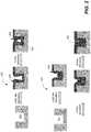
- FIG. 2depicts schematic cross-sectional diagrams of feature filled with SiC in a single deposition stage using acetylene as a carbon source (process gas He/SiH 4 /C 2 H 2 ) as compared to single stage feature fill using methane as a carbon source (process gas He/SiH 4 /CH 4 ).
- FIG. 3shows SEM images of 3:1 AR, 25 nm wide trenches filled with SiC using acetylene and methane, respectively, as a carbon source in HDP CVD processes similar to those depicted schematically in FIG. 2 .
- FIG. 4shows a cross-sectional schematic diagram and counterpart SEM images of 3:1 AR, 25 nm features filled with amorphous carbon using a He/CH 4 process gas in a HDP CVD process at various stages during the deposition.
- FIG. 5provides a process flow diagram illustrating operations in an example of a method of filling a gap according to various embodiments.
- FIG. 6provides a simple block diagram depicting various reactor components arranged as may be arranged in a reactor.
- FIG. 7is a block diagram of a system suitable for conducting a deposition process in accordance with disclosed embodiments.
- FIG. 8provides an example of operations including carbon-based gap fill in a self-aligned contact integration process.
- Semiconductor integration operationsmay involve filling high aspect ratio gaps with various materials. This is the case for shallow trench isolation, inter-metal dielectric layers, passivation layers, and the like. As device geometries shrink and thermal budgets are reduced, void-free filling of high aspect ratio (AR) gaps becomes increasingly difficult due to limitations of existing deposition processes.
- ARaspect ratio
- HDP CVDhigh density plasma chemical vapor deposition
- carbon-containing filmssuch as amorphous carbon and amorphous carbide films are deposited by HDP CVD into gaps on substrates to fill the gaps.
- the methodsmay involve using high hydrogen-content process gasses during HDP CVD deposition to provide bottom-up fill. Also provided are related apparatus.
- a reentrant featureis a feature that narrows from the bottom of the gap.
- One such problematic reentrant featureis a narrowing at the top of the gap, with the gap sidewalls sloping inward near the top of the gap.
- thisincreases the ratio of gap volume to gap access area seen by the precursor species during deposition. Voids and seams formation is more likely under these conditions. If the top of the gap prematurely closes off, the gap is re-opened before more film can be deposited in the gap.
- HDP CVDis a directional CVD process that involves directing charged dielectric precursor species toward a substrate.
- HDP CVDis not purely an isotropic, diffusion-based process, some overhang or top-hat formation may still result at the entry region of the gap to be filled. This may result from the non-directional deposition reactions of neutral species in the plasma reactor and from sputtering and redeposition processes.
- the directional aspect of the deposition processproduces some high momentum charged species that sputter away bottom fill. The sputtered material tends to redeposit on the sidewalls. Limitations due to overhang formation become ever more severe as the width of the gap to be filled decreases and the aspect ratio increases.
- the methods provided hereinprovide gap fill by suppressing re-entrant feature formation using a hydrogen-rich process gas.
- a gapis filled with an amorphous carbon-containing material such as amorphous carbon (a-C) and amorphous carbides including amorphous silicon carbides (a-SiC).
- Classes of SiCinclude oxygen doped SiC, also known as silicon oxycarbide (SiOC), nitrogen doped SiC, also known as silicon nitricarbide (SiNC), oxygen and nitrogen doped SiC, also known as silicon oxynitricarbide (SiONC), boron doped carbide (SiBC), and undoped silicon carbide (SiC).
- a trench on a topological substratemay be filled with an a-C film that acts as a sacrificial hardmask in a pattern transfer scheme.
- a-SiC and other amorphous carbide layersmay be used, for example, as barrier layers in VLSI backend processes.
- void-free gap fill of SiC or other carbide filmsis useful.
- FIG. 8provides an example of operations including carbon-based gap fill in a self-aligned contact integration process.
- a metal gate 801 and spacers 802are depicted in FIG. 8 .
- the metal gate 801is recessed, forming a gap 804 between the spacers.
- a gate cap 803which may be for example a SiC film, is deposited in the gap 804 prior to definition of the contact holes.
- the presence of the gate cap 803relaxes the alignment precision for contact hole definition; in FIG. 8 , contact hole 805 is within the increased tolerance provided by the gate cap 803 .
- FIG. 1provides a process flow diagram illustrating operations in an example of a method of filling a gap according to various embodiments.
- the process 100involves providing a substrate including a gap to a HDP CVD chamber. Block 101 .
- HDP CVD chambersare discussed further below with respect to FIG. 6 .
- the substratemay be a wafer suitable for semiconductor processing, such as a 200 mm, 300 mm or 450 mm silicon wafer. Wafers of different compositions and/or sizes may be used. Further, the methods are not limited to semiconductor substrates, but may be implemented with any appropriate substrate that includes a gap to be filled, including glass and plastic panels and the like.
- a hydrogen (H)-rich process gasis introduced to the HDP CVD chamber.
- Block 103can involve one or both of using H-rich reactants and introducing hydrogen (H 2 ) to the chamber in addition to reactants.
- the term process gasis used to denote multiple component gases or a mixture thereof that is introduced to the chamber.
- a process gascan include a liquid reactant entrained in a carrier gas or otherwise provided to the chamber.
- the process gasincludes one or more carbon reactants to supply carbon to the carbon-based gap fill material, and as appropriate one or more co-reactants such as silicon-containing compounds, nitrogen-containing compounds, boron-containing compounds, and the like.
- an H-rich process gasmay be characterized by one or more of the following: an H:C ratio of at least 3:1, an H:C ratio of more than 3:1, or at H:C ratio of at least 4:1.
- a carbon precursor having an H:C ratio of at least 3:1, an H:C ratio of more than 3:1, or at H:C ratio of at least 4:1is used. Examples include ethane (C 2 H 6 ) and methane (CH 4 ). Carbon precursors that have lower H:C ratios may be used with the addition of H 2 or hydrogen from another source.
- a process gasmay include acetylene (C 2 H 2 ) and H 2 .
- a process gasmay include an inert carrier gas, with examples including helium (He), argon (Ar), and the like.
- a process gasmay include one or more additional reactants depending on the type of film being deposited.
- a silicon-containing reactantsuch as one or more silanes may be used as a silicon source.
- the silicon-containing reactantdoes not include carbon.
- silanesinclude silane, disilane, trisilane, and higher silanes.
- silicon-containing reactantsmay be used as appropriate, including siloxanes, alkyl silanes, alkoxy silanes, and amino silanes, among others.
- alkyl silanesinclude dimethylsilane, trimethylsilane, tetramethylsilane, triethylsilane, and pentamethyldisilamethane.
- Silicon-carbon-containing filmsalso including oxygen atoms (e.g., silicon-carbon-oxides and silicon-carbon-oxynitrides) may be formed using an organosilicon reactant that includes oxygen, such as siloxanes and alkoxy silanes.
- Non-limiting examples of siloxanesinclude cyclotetrasiloxanes (e.g., 2,4,6,8-tetramethylcyclotetrasiloxane; octamethylcyclotetrasiloxane; and heptamethylcyclotetrasiloxane); other cyclic siloxanes; siloxanes having three-dimensional or caged structures (i.e., where silicon atoms are bridged with one another via oxygen atoms, forming a three-dimensional structure or a polyhedron) such as silsequioxane; and linear siloxanes, such as disiloxanes (e.g., pentamethyldisiloxane, tetramethyldisiloxane, and hexamethyl trisiloxane).
- cyclotetrasiloxanese.g., 2,4,6,8-tetramethylcyclotetrasiloxane; octamethylcyclotetrasilox
- Non-limiting examples of alkoxy silanesinclude methoxysilane, dimethoxysilane, trimethoxysilane, methyldimethoxysilane, diethoxymethylsilane, dimethylethoxysilane, and dimethylmethoxysilane.
- Silicon-carbon-containing filmsalso including nitrogen atoms (e.g., silicon-carbon-nitrides and silicon-carbon-oxynitrides) may be formed using an organosilicon reactant that includes nitrogen, such as amino silanes and silazanes.
- Non-limiting examples of amino silanesinclude 2,2-bis(dimethylamino)-4,4-dimethyl-2,4-disilapentane, 2,2,4-trimethyl-4-dimethylamino-3,4-disilapentane, dimethylaminodimethylsilane, bis(dimethylamino)methylsilane, and tris(dimethylamino)silane.
- 1,1,3,3-tetramethyldisilazaneis a non-limiting example of a silazane.
- a silicon-containing reactant and a hydrocarbonmay be provided to the chamber in an approximately 1:1 ratio to fill the gap. This includes ratios between 1:1.5 and 1.5:1. In some cases, the ratio is between 1:1.25 and 1.25:1, or between 1:1.1 and 1.1:1. In some embodiments, the silicon-containing reactant is hydrogen rich, having a H:Si ratio of at least 3:1 or at least 4:1.
- Non-limiting examples of hydrogen-rich process gases for depositing a-C filmsinclude He/CH 4 , He/C 2 H 2 /H 2 , He/CH 4 /H 2 , and He/C 2 H 6 /H 2 .
- Non-limiting examples of hydrogen-rich process gases for depositing a-SiC filmsinclude He/SiH 4 /CH 4 , He/SiH 4 /C 2 H 2 /H 2 , He/SiH 4 /CH 4 /H 2 , and He/SiH4/C2H6/H 2 .
- Any appropriate carrier gasmay be used in addition to or instead of He in these examples.
- any appropriate silicon-containing reactantmay be used instead or in addition to SiH 4 in these examples.
- a carbon-based filmis then deposited to fill the gap.
- Block 105A carbon-based film is then deposited to fill the gap.
- filling the gapmay be performed in a single deposition or in multiple depositions separated by intervening an etch operation. An example of the latter technique is described below with respect to FIG. 5 .
- FIG. 2depicts cross-sectional diagrams of a feature filled with SiC in a single deposition stage using acetylene as a carbon source (process gas He/SiH 4 /C 2 H 2 ) as compared to single stage feature fill using methane as a carbon source (He/SiH 4 /CH 4 ).
- Process 210depicts trench 201 during SiC deposition from He/SiH 4 /C 2 H 2 . As the deposition proceeds, a cusp 204 forms.
- FIG. 3shows SEM images of 3:1 AR, 25 nm wide trenches filled with SiC using acetylene (image 310 ) and methane (image 320 ), respectively, as carbon sources in HDP CVD processes similar to those depicted schematically in FIG. 2 .
- Voids 303can be seen in image 310 .
- the trenches filled using methaneare void-free.
- FIG. 4shows a cross-sectional schematic diagram and counterpart SEM images of 3:1 AR, 25 nm trenches 401 filled using a He/CH 4 process gas in a HDP CVD process at various stages during the deposition.
- the depositionmay be characterized as largely bottom-up, resulting in trenches filled with void-free a-C.
- a He/C 2 H 2 process gasresults in void formation due to sidewall cusp development and premature gap closure (not shown).
- cusp suppressionis due to etch by H species such as hydrogen radicals (i.e., atomic H) at the top of the gap during deposition.
- H speciessuch as hydrogen radicals (i.e., atomic H) at the top of the gap during deposition.
- Neutral and low mass species in the plasmapreferentially etch at the top of the gap, allowing fill in the bottom part of the feature and etch at the top. This effect can counteract the above-described factors that lead to cusp deposition.
- Gap fill of carbon-based films using non-hydrogen enriched process gases, other hydrocarbon precursors, or other techniques such as plasma-enhanced chemical vapor deposition (PECVD)does not exhibit the same cusp suppression that is exhibited by the hydrogen-enriched HDP CVD processes. As such, they cannot be used for high quality, void free, single stage gap fill.
- PECVDplasma-enhanced chemical vapor deposition
- the methodsmay include one or more deposition-etch-deposition cycles. Such a process may be used, for example, to fill particularly challenging structures.
- FIG. 5provides a process flow diagram illustrating operations in an example of a method of filling a gap according to various embodiments.
- a deposition process 500begins at block 101 in which a substrate containing a gap is provided to a HDP CVD reaction chamber. This operation may be performed as described above with respect to FIG. 1 . A H-rich process gas is then introduced to the HDP CVD chamber. Block 103 . This may also be performed as described above with respect to FIG. 1 .
- a carbon-based filmis then deposited to partially fill the gap. Block 505 .
- Depositionis stopped prior to closure of the gap.
- the deposited filmmay exhibit nascent cusp formation, a re-entrant profile, or otherwise present a challenging-to-fill structure. While any cusp formation will be less than in the absence of a hydrogen-rich process gas, it may be useful to halt the deposition and employ a dedicated etch operation to appropriately tailor the profile of the film partially filling the gap.
- reactant flowis turned off and the carbon-based film is etched. Because the reactant flow is turned off, the deposition is halted.
- hydrogen radicals or other hydrogen speciesare the primary etchant.
- transitioning from block 505 to block 507may involve turning off one or more reactant flows while allowing H 2 to continue to flow.
- the substratemay also be transferred to an etch chamber to be etched. Any appropriate etchant may be used, including a fluorine-based etch, etc.
- One or more additional etchant gasesmay be added to hydrogen in hydrogen-based etches.
- hydrogen speciesmay be the sole etchants, with no halogen etchants.
- Block 507may involve preferentially etching material at the top of the gap to appropriately shape the profile of the material in the gap. This may be referred to as a non-conformal etch or low-step coverage etch. Step coverage of the carbon-based film may be proportional to (etchant concentration)/etch rate. For example, for hydrogen radical etching, at higher temperatures, hydrogen radicals readily react and etch at the feature entrance, resulting in a more non-conformal etch; at lower temperature, the hydrogen radicals may be able to diffuse and etch further into the feature, resulting in a more conformal etch.
- Block 509carbon-based film is deposited in the gap, this time on the etched carbon-based film that partially fills the gap.
- Block 509typically involves HDP CVD deposition using a hydrogen-rich process gas as described above.
- the gapmay be filled after one dep-etch-dep sequence.
- blocks 507 and 509can be repeated one or more times to fill the gap. Block 511 .
- carbon-based gap fillmay be performed by using a nitrogen-rich process gas.
- a hydrogen-rich or carbon-rich hydrocarbon precursor as described abovemay be mixed with nitrogen (N 2 ).
- the present inventionmay be implemented in a HDP CVD reactor.
- a reactormay take many different forms.
- the apparatuswill include one or more chambers or “reactors” (sometimes including multiple stations) that house one or more wafers and are suitable for wafer processing.
- Each chambermay house one or more wafers for processing.
- the one or more chambersmaintain the wafer in a defined position or positions (with or without motion within that position, e.g. rotation, vibration, or other agitation).
- each waferis held in place by a pedestal, wafer chuck and/or other wafer holding apparatus.
- the apparatusmay include a heater such as a heating plate.
- An examples of a suitable reactoris the SpeedTM reactor, available from Lam Research of Fremont, Calif.
- FIG. 6provides a simple block diagram depicting various reactor components arranged as may be arranged in a reactor.
- a reactor 601includes a process chamber 603 which encloses other components of the reactor and serves to contain the plasma.
- the process chamber wallsare made from aluminum, aluminum oxide, and/or other suitable material.
- the embodiment shown in FIG. 6has two plasma sources: top RF coil 605 and side RF coil 607 .
- Top RF coil 605is a medium frequency (MFRF) coil and side RF coil 607 is a low frequency (LFRF) coil.
- MFRF frequencymay be from 430-470 kHz and LFRF frequency from 340-370 kHz.
- the methods and apparatusare not limited to operation in reaction chambers with dual sources, these frequencies, or RF plasma sources. Any suitable plasma source or sources may be used.
- a wafer pedestal 609supports a substrate 611 .
- the pedestaltypically includes a chuck (sometimes referred to as a clamp) to hold the substrate in place during the deposition reaction.
- the chuckmay be an electrostatic chuck, a mechanical chuck or various other types of chuck as are available for use.
- a heat transfer subsystemincluding a line 613 for supplying heat transfer fluid controls the temperature of substrate 611 .
- the wafer chuck and heat transfer fluid systemcan facilitate maintaining the appropriate wafer temperatures.
- a high frequency RF of HFRF source 615serves to electrically bias substrate 611 and draw charged reactant species onto the substrate for the deposition reaction. Electrical energy from source 615 is coupled to substrate 611 via an electrode or capacitive coupling, for example. Note that the bias applied to the substrate need not be an RF bias. Other frequencies and DC bias may be used as well.
- the hydrogen-rich process gasis introduced via one or more inlets 617 .
- the component gases of the process gasmay be premixed or not.
- the process gasis introduced through a gas supply inlet mechanism including orifices.
- at least some of the orificesorient the process gas along an axis of injection intersecting an exposed surface of the substrate at an acute angle.
- the gas or gas mixturesmay be introduced from a primary gas ring 621 , which may or may not direct the gases toward the pedestal.
- gasesmay be introduced from one or more gas rings (not shown) in addition to the primary gas ring 621 .
- Injectorsmay be connected to the primary gas ring 621 to direct at least some of the gases or gas mixtures into the chamber and toward the pedestal. Note that injectors, gas rings or other mechanisms for directing process gas toward the wafer may not be used in some embodiments; any appropriate process gas delivery system may be employed.
- the sonic front caused by a process gas entering the chamberwill itself cause the gas to rapidly disperse in all directions—including toward the substrate.
- Process gasesexit chamber 603 via an outlet 622 .
- a vacuum pumpe.g., a turbomolecular pump
- the reactor 601may be controlled using a controller 690 .
- the controller 690may include machine-readable instructions for performing various operations disclosed herein. Further description regarding the controller 690 is provided below.
- an HDP CVD reactorsuch as the reactor 601 shown in FIG. 6 is part of a tool for processing one or more wafers.
- An example of a tool including one or more reactorsis provided in FIG. 7 .
- FIG. 7is a block diagram of a system suitable for conducting a deposition process in accordance with disclosed embodiments.
- the system 700includes a transfer module 703 , such as the wafer transfer system (WTS) used on the SPEEDTM platform available from Lam Research Corporation of Fremont, Calif.
- WTSwafer transfer system
- the transfer module 703provides a clean, pressurized environment to minimize the risk of contamination of workpieces, such as wafers, being processed as they are moved between the various processing stages.
- HDP CVD modules or process chambers 705such as Lam SPEEDTM reactors, available from Lam Research Corporation of Fremont, Calif.
- etch chambers 707are mounted on the transfer module 703 .
- etch chambersinclude a Lam atomic layer removal (ALR) reactor or KiyoTM reactor. These etch chambers may be mounted on the same or separate platforms as the one or more deposition reactors.
- the system 700also includes one or more (in this case two) wafer source modules 701 where wafers are stored before and after processing.
- a device(generally a robot arm unit) in the transfer module 703 moves the wafers among the modules mounted on the transfer module 703 .
- Wafersare transferred by the robot arm between the HDP CVD reactor 705 and/or the etch chamber 707 for deposition and etch back processing, respectively.
- a single etch reactorcan support two SPEED deposition modules 705 with a high throughput of about 15-16 wafers per hour (wph).
- two etch reactors 707may support one or more SPEED deposition modules 705 .
- a single chambermay be configured for both HDP CVD deposition and etch.
- the Lam SPEED HDP-CVD reactorsare capable of deposition and etch with a throughput similar to that of using separate reactors.
- a single chambermay be configured, for example, a plasma reactor, with equipment, for example the various plasma sources described herein, for deposition (HDP CVD) and a reactive plasma etch (e.g., in-situ or downstream plasma source).
- FIG. 7also depicts an embodiment of a system controller 750 employed to control process conditions and hardware states of process tool 700 .
- the system controller 750may provide program instructions for implementing the above-described processes.
- the program instructionsmay control a variety of process parameters, such as DC power level, RF bias power level, pressure, temperature, etc.
- the instructionsmay control the parameters to perform deposition operations according to various embodiments described herein.
- a controller 750is part of a system, which may be part of the above-described examples.
- Such systemscan comprise semiconductor processing equipment, including a processing tool or tools, chamber or chambers, a platform or platforms for processing, and/or specific processing components (a wafer pedestal, a gas flow system, etc.).
- These systemsmay be integrated with electronics for controlling their operation before, during, and after processing of a semiconductor wafer or substrate.
- the electronicsmay be referred to as the “controller,” which may control various components or subparts of the system or systems.
- the controller 750may be programmed to control any of the processes disclosed herein, including the delivery of processing gases, temperature settings (e.g., heating and/or cooling), pressure settings, vacuum settings, power settings, radio frequency (RF) generator settings, RF matching circuit settings, frequency settings, flow rate settings, fluid delivery settings, positional and operation settings, wafer transfers into and out of a tool and other transfer tools and/or load locks connected to or interfaced with a specific system.
- temperature settingse.g., heating and/or cooling
- pressure settingse.g., vacuum settings, power settings, radio frequency (RF) generator settings, RF matching circuit settings, frequency settings, flow rate settings, fluid delivery settings, positional and operation settings
- RFradio frequency
- the controller 750may be defined as electronics having various integrated circuits, logic, memory, and/or software that receive instructions, issue instructions, control operation, enable cleaning operations, enable endpoint measurements, and the like.
- the integrated circuitsmay include chips in the form of firmware that store program instructions, digital signal processors (DSPs), chips defined as application specific integrated circuits (ASICs), and/or one or more microprocessors, or microcontrollers that execute program instructions (e.g., software).
- Program instructionsmay be instructions communicated to the controller in the form of various individual settings (or program files), defining operational parameters for carrying out a particular process on or for a semiconductor wafer or to a system.
- the operational parametersmay, in some embodiments, be part of a recipe defined by process engineers to accomplish one or more processing steps during the fabrication of one or more layers, materials, metals, oxides, silicon, silicon dioxide, surfaces, circuits, and/or dies of a wafer.
- the system controller 750controls all of the activities of process tool 700 .
- the system controller 750may include one or more memory devices 756 , one or more mass storage devices 754 , and one or more processors 752 .
- a processor 752may include a CPU or computer, analog and/or digital input/output connections, stepper motor controller boards, etc.
- the system controller 750executes system control software 758 stored in a mass storage device 754 , loaded into memory device 756 , and executed on processor 752 .
- the control logicmay be hard coded in the controller 750 .
- Applications Specific Integrated Circuits, Programmable Logic Devicese.g., field-programmable gate arrays, or FPGAs
- FPGAsfield-programmable gate arrays
- System control software 758may include instructions for controlling the transfer of wafers into and out of a process chamber, timing of gases, mixture of gases, amount of gas flow, chamber and/or station pressure, chamber and/or reactor temperature, wafer temperature, bias power, target power levels, RF power levels, pedestal, chuck and/or susceptor position, and other parameters of a particular process performed by process tool 700 .
- the system control software 758may be configured in any suitable way. For example, various process tool component subroutines or control objects may be written to control operation of the process tool components necessary to carry out various process tool processes.
- System control software 758may be coded in any suitable computer readable programming language.
- the controller 750may be a part of or coupled to a computer that is integrated with, coupled to the system, otherwise networked to the system, or a combination thereof.
- the controller 750may be in the “cloud” or all or a part of a fab host computer system, which can allow for remote access of the wafer processing.
- the computermay enable remote access to the system to monitor current progress of fabrication operations, examine a history of past fabrication operations, examine trends or performance metrics from a plurality of fabrication operations, to change parameters of current processing, to set processing steps to follow a current processing, or to start a new process.
- a remote computere.g.
- a servercan provide process recipes to a system over a network, which may include a local network or the Internet.
- the remote computermay include a user interface that enables entry or programming of parameters and/or settings, which are then communicated to the system from the remote computer.
- the controller 750receives instructions in the form of data, which specify parameters for each of the processing steps to be performed during one or more operations. It should be understood that the parameters may be specific to the type of process to be performed and the type of tool that the controller is configured to interface with or control.
- the controller 750may be distributed, such as by including one or more discrete controllers that are networked together and working towards a common purpose, such as the processes and controls described herein.
- An example of a distributed controller for such purposeswould be one or more integrated circuits on a chamber in communication with one or more integrated circuits located remotely (such as at the platform level or as part of a remote computer) that combine to control a process on the chamber.
- system control software 758may include input/output control (IOC) sequencing instructions for controlling the various parameters described above.
- IOCinput/output control
- Other computer software and/or programs stored on mass storage device 754 and/or memory device 756 associated with system controller 750may be employed in some embodiments. Examples of programs or sections of programs for this purpose include a wafer positioning program, a process gas control program, a pressure control program, a heater control program, and a plasma control program.
- a wafer positioning programmay include program code for process tool components that are used to load a wafer onto pedestal 718 .
- a process gas control programmay include code for controlling gas composition (e.g., process gases, helium gas or carrier gases, etc., as described herein) and flow rates and optionally for flowing gas into one or more process chambers or stations prior to deposition in order to stabilize the pressure therein.
- a pressure control programmay include code for controlling the pressure in the process chamber by regulating, for example, a throttle valve in the exhaust system of the process chamber, a gas flow into the process chamber, etc.
- a heater control programmay include code for controlling the current to a heating unit that is used to heat the wafer or other workpiece. Alternatively, the heater control program may control delivery of a heat transfer gas (such as helium) to the wafer.
- a plasma control programmay include code for setting RF power levels applied to the process electrodes and the bias in one or more process chambers or stations in accordance with the embodiments herein.
- a pressure control programmay include code for maintaining the pressure in the reaction chamber in accordance with the embodiments herein.
- the user interfacemay include a display screen, graphical software displays of the apparatus and/or process conditions, and user input devices such as pointing devices, keyboards, touch screens, microphones, etc.
- parameters adjusted by system controller 750may relate to process conditions.
- process conditionsinclude process gas composition and flow rates, temperature, pressure, plasma conditions (such as RF bias power levels), pressure, temperature, etc. These parameters may be provided to the user in the form of a recipe, which may be entered utilizing the user interface.
- Signals for monitoring the processmay be provided by analog and/or digital input connections of system controller 750 from various process tool sensors.
- the signals for controlling the processmay be output on the analog and digital output connections of process tool 700 .
- process tool sensorsthat may be monitored include mass flow controllers, pressure sensors (such as manometers), thermocouples, etc. Appropriately programmed feedback and control algorithms may be used with data from these sensors to maintain process conditions.
- example systemsmay include a plasma etch chamber or module, a deposition chamber or module, a spin-rinse chamber or module, a metal plating chamber or module, a clean chamber or module, a bevel edge etch chamber or module, a physical vapor deposition (PVD) chamber or module, a chemical vapor deposition (CVD) chamber or module, an atomic layer deposition (ALD) chamber or module, an atomic layer etch (ALE) chamber or module, an ion implantation chamber or module, a track chamber or module, and any other semiconductor processing systems that may be associated or used in the fabrication and/or manufacturing of semiconductor wafers.
- PVDphysical vapor deposition
- CVDchemical vapor deposition
- ALDatomic layer deposition
- ALEatomic layer etch
- the controllermight communicate with one or more of other tool circuits or modules, other tool components, cluster tools, other tool interfaces, adjacent tools, neighboring tools, tools located throughout a factory, a main computer, another controller, or tools used in material transport that bring containers of wafers to and from tool locations and/or load ports in a semiconductor manufacturing factory.
- HDP CVDas used herein is distinct from plasma-enhanced chemical vapor deposition techniques, also known as PECVD.
- HDP CVD reactorstypically employ inductively-coupled plasmas, while PECVD reactors typically employ capacitively-coupled plasmas.
- HDP CVD process conditions and resulting filmsare different PECVD processes.
- various HDP reactors as described hereinoperate at a pressure less than about 100 mTorr with a plasma density greater than 10 17 ions/m 3 , e.g., 10 17 ions/m 3 to 10 19 ions/m 3 .
- PECVD processesoperate at much higher pressures with much lower plasma densities, e.g., 10 14 ions/m 3 to 10 16 ions/m 3 .
- HDP reactorsmay ignite plasma at a plasma frequency of 400 kHz for coils and a frequency of 13.56 MHz for the pedestal where the wafer is placed.
- an a capacitively-coupled plasma reactora plasma frequency of 13.56 MHz is used to generate plasma as applied to either a showerhead or the pedestal, and 400 kHz is applied to either the showerhead or the pedestal.
- Ion energies in HDP reactorsmay be greater than in PECVD reactors.
- film composition and characteristics of films deposited in HDP CVD reactorsare different than those deposited in PECVD reactors.
- the lower plasma densities in PECVDtypically cannot generate hydrogen radicals in an amount effective to suppress cusp formation even using hydrogen-rich process gases.
- the plasma source poweris high enough to sustain a plasma and low enough so that the effect of the H + ions does not overwhelm that of the hydrogen radicals.
- the RF powerwill depend on the substrate size (e.g., 200 mm, 300 mm, or 450 mm diameter wafer) and the requirements of the specific process being used. An example range is between about 3000 W and 6000 W for a 300 mm wafer, with plasma power scaling with substrate surface area.
- Substrate temperature and chamber pressure duringmay be generally with the ranges commonly used during HDP CVD processes. Temperature values may range from about 200° C. and 1000° C., with typical ranges between about 300° C. and 550° C., e.g., 400° C. Pressure is typically maintained at a value below 500 mTorr, and can be significantly lower, e.g., below 100 mTorr or 10 mTorr. In one example, pressure is 6 mTorr.
- Example aspect ratiosmay range from 3:1 to 30:1, or 3:1 to 10:1.
- Example trench widthsmay range from 10 nm to 100 nm, for example 50 nm or less, or 25 nm or less.
- a HFRF power source or other sourcemay be used to bias the substrate.
- Substratesare typically biased during deposition operations to direct charged species downward, to the bottom of the gap.
- the hydrogen-rich process gasimproves gap fill by a chemical etch at the top of the gap.
- the substratemay or may not be biased.
- Example HF bias powers during HDP CVDare between 0 to 9500 W about for a 300 mm system, with bias power scaling with substrate surface area.
Landscapes
- Engineering & Computer Science (AREA)
- Chemical & Material Sciences (AREA)
- Physics & Mathematics (AREA)
- Condensed Matter Physics & Semiconductors (AREA)
- General Physics & Mathematics (AREA)
- Manufacturing & Machinery (AREA)
- Computer Hardware Design (AREA)
- Microelectronics & Electronic Packaging (AREA)
- Power Engineering (AREA)
- Chemical Kinetics & Catalysis (AREA)
- General Chemical & Material Sciences (AREA)
- Materials Engineering (AREA)
- Mechanical Engineering (AREA)
- Metallurgy (AREA)
- Organic Chemistry (AREA)
- Inorganic Chemistry (AREA)
- Plasma & Fusion (AREA)
- Crystallography & Structural Chemistry (AREA)
- Chemical Vapour Deposition (AREA)
- Formation Of Insulating Films (AREA)
Abstract
Description
Claims (13)
Priority Applications (1)
| Application Number | Priority Date | Filing Date | Title |
|---|---|---|---|
| US16/194,102US11049716B2 (en) | 2015-04-21 | 2018-11-16 | Gap fill using carbon-based films |
Applications Claiming Priority (2)
| Application Number | Priority Date | Filing Date | Title |
|---|---|---|---|
| US14/692,627US20160314964A1 (en) | 2015-04-21 | 2015-04-21 | Gap fill using carbon-based films |
| US16/194,102US11049716B2 (en) | 2015-04-21 | 2018-11-16 | Gap fill using carbon-based films |
Related Parent Applications (1)
| Application Number | Title | Priority Date | Filing Date |
|---|---|---|---|
| US14/692,627ContinuationUS20160314964A1 (en) | 2015-04-21 | 2015-04-21 | Gap fill using carbon-based films |
Publications (2)
| Publication Number | Publication Date |
|---|---|
| US20190181004A1 US20190181004A1 (en) | 2019-06-13 |
| US11049716B2true US11049716B2 (en) | 2021-06-29 |
Family
ID=57147973
Family Applications (2)
| Application Number | Title | Priority Date | Filing Date |
|---|---|---|---|
| US14/692,627AbandonedUS20160314964A1 (en) | 2015-04-21 | 2015-04-21 | Gap fill using carbon-based films |
| US16/194,102ActiveUS11049716B2 (en) | 2015-04-21 | 2018-11-16 | Gap fill using carbon-based films |
Family Applications Before (1)
| Application Number | Title | Priority Date | Filing Date |
|---|---|---|---|
| US14/692,627AbandonedUS20160314964A1 (en) | 2015-04-21 | 2015-04-21 | Gap fill using carbon-based films |
Country Status (4)
| Country | Link |
|---|---|
| US (2) | US20160314964A1 (en) |
| KR (1) | KR102648712B1 (en) |
| CN (1) | CN106067440A (en) |
| TW (1) | TW201708597A (en) |
Cited By (5)
| Publication number | Priority date | Publication date | Assignee | Title |
|---|---|---|---|---|
| US11264234B2 (en) | 2012-06-12 | 2022-03-01 | Novellus Systems, Inc. | Conformal deposition of silicon carbide films |
| US11680315B2 (en) | 2013-05-31 | 2023-06-20 | Novellus Systems, Inc. | Films of desired composition and film properties |
| US11848199B2 (en) | 2018-10-19 | 2023-12-19 | Lam Research Corporation | Doped or undoped silicon carbide deposition and remote hydrogen plasma exposure for gapfill |
| US12334332B2 (en) | 2012-06-12 | 2025-06-17 | Lam Research Corporation | Remote plasma based deposition of silicon carbide films using silicon-containing and carbon-containing precursors |
| US12359311B2 (en) | 2012-06-12 | 2025-07-15 | Lam Research Corporation | Conformal deposition of silicon carbide films using heterogeneous precursor interaction |
Families Citing this family (409)
| Publication number | Priority date | Publication date | Assignee | Title |
|---|---|---|---|---|
| US10378106B2 (en) | 2008-11-14 | 2019-08-13 | Asm Ip Holding B.V. | Method of forming insulation film by modified PEALD |
| US9394608B2 (en) | 2009-04-06 | 2016-07-19 | Asm America, Inc. | Semiconductor processing reactor and components thereof |
| US8802201B2 (en) | 2009-08-14 | 2014-08-12 | Asm America, Inc. | Systems and methods for thin-film deposition of metal oxides using excited nitrogen-oxygen species |
| US9312155B2 (en) | 2011-06-06 | 2016-04-12 | Asm Japan K.K. | High-throughput semiconductor-processing apparatus equipped with multiple dual-chamber modules |
| US10364496B2 (en) | 2011-06-27 | 2019-07-30 | Asm Ip Holding B.V. | Dual section module having shared and unshared mass flow controllers |
| US10854498B2 (en) | 2011-07-15 | 2020-12-01 | Asm Ip Holding B.V. | Wafer-supporting device and method for producing same |
| US20130023129A1 (en) | 2011-07-20 | 2013-01-24 | Asm America, Inc. | Pressure transmitter for a semiconductor processing environment |
| US9017481B1 (en) | 2011-10-28 | 2015-04-28 | Asm America, Inc. | Process feed management for semiconductor substrate processing |
| US10832904B2 (en) | 2012-06-12 | 2020-11-10 | Lam Research Corporation | Remote plasma based deposition of oxygen doped silicon carbide films |
| US10211310B2 (en) | 2012-06-12 | 2019-02-19 | Novellus Systems, Inc. | Remote plasma based deposition of SiOC class of films |
| US9659799B2 (en) | 2012-08-28 | 2017-05-23 | Asm Ip Holding B.V. | Systems and methods for dynamic semiconductor process scheduling |
| US10714315B2 (en) | 2012-10-12 | 2020-07-14 | Asm Ip Holdings B.V. | Semiconductor reaction chamber showerhead |
| US9362133B2 (en) | 2012-12-14 | 2016-06-07 | Lam Research Corporation | Method for forming a mask by etching conformal film on patterned ashable hardmask |
| US20160376700A1 (en) | 2013-02-01 | 2016-12-29 | Asm Ip Holding B.V. | System for treatment of deposition reactor |
| US9589770B2 (en) | 2013-03-08 | 2017-03-07 | Asm Ip Holding B.V. | Method and systems for in-situ formation of intermediate reactive species |
| US9484191B2 (en) | 2013-03-08 | 2016-11-01 | Asm Ip Holding B.V. | Pulsed remote plasma method and system |
| US10297442B2 (en) | 2013-05-31 | 2019-05-21 | Lam Research Corporation | Remote plasma based deposition of graded or multi-layered silicon carbide film |
| US9240412B2 (en) | 2013-09-27 | 2016-01-19 | Asm Ip Holding B.V. | Semiconductor structure and device and methods of forming same using selective epitaxial process |
| TWI639179B (en) | 2014-01-31 | 2018-10-21 | 美商蘭姆研究公司 | Vacuum integrated hard mask process and equipment |
| US10683571B2 (en) | 2014-02-25 | 2020-06-16 | Asm Ip Holding B.V. | Gas supply manifold and method of supplying gases to chamber using same |
| US10167557B2 (en) | 2014-03-18 | 2019-01-01 | Asm Ip Holding B.V. | Gas distribution system, reactor including the system, and methods of using the same |
| US11015245B2 (en) | 2014-03-19 | 2021-05-25 | Asm Ip Holding B.V. | Gas-phase reactor and system having exhaust plenum and components thereof |
| US10858737B2 (en) | 2014-07-28 | 2020-12-08 | Asm Ip Holding B.V. | Showerhead assembly and components thereof |
| US9890456B2 (en) | 2014-08-21 | 2018-02-13 | Asm Ip Holding B.V. | Method and system for in situ formation of gas-phase compounds |
| US9657845B2 (en) | 2014-10-07 | 2017-05-23 | Asm Ip Holding B.V. | Variable conductance gas distribution apparatus and method |
| US10941490B2 (en) | 2014-10-07 | 2021-03-09 | Asm Ip Holding B.V. | Multiple temperature range susceptor, assembly, reactor and system including the susceptor, and methods of using the same |
| KR102263121B1 (en) | 2014-12-22 | 2021-06-09 | 에이에스엠 아이피 홀딩 비.브이. | Semiconductor device and manufacuring method thereof |
| US10529542B2 (en) | 2015-03-11 | 2020-01-07 | Asm Ip Holdings B.V. | Cross-flow reactor and method |
| US10276355B2 (en) | 2015-03-12 | 2019-04-30 | Asm Ip Holding B.V. | Multi-zone reactor, system including the reactor, and method of using the same |
| US20160314964A1 (en) | 2015-04-21 | 2016-10-27 | Lam Research Corporation | Gap fill using carbon-based films |
| US10458018B2 (en) | 2015-06-26 | 2019-10-29 | Asm Ip Holding B.V. | Structures including metal carbide material, devices including the structures, and methods of forming same |
| US10600673B2 (en) | 2015-07-07 | 2020-03-24 | Asm Ip Holding B.V. | Magnetic susceptor to baseplate seal |
| US10428421B2 (en) | 2015-08-03 | 2019-10-01 | Asm Ip Holding B.V. | Selective deposition on metal or metallic surfaces relative to dielectric surfaces |
| US9960072B2 (en) | 2015-09-29 | 2018-05-01 | Asm Ip Holding B.V. | Variable adjustment for precise matching of multiple chamber cavity housings |
| US10211308B2 (en) | 2015-10-21 | 2019-02-19 | Asm Ip Holding B.V. | NbMC layers |
| US10322384B2 (en) | 2015-11-09 | 2019-06-18 | Asm Ip Holding B.V. | Counter flow mixer for process chamber |
| US9996004B2 (en) | 2015-11-20 | 2018-06-12 | Lam Research Corporation | EUV photopatterning of vapor-deposited metal oxide-containing hardmasks |
| US11139308B2 (en) | 2015-12-29 | 2021-10-05 | Asm Ip Holding B.V. | Atomic layer deposition of III-V compounds to form V-NAND devices |
| US10529554B2 (en) | 2016-02-19 | 2020-01-07 | Asm Ip Holding B.V. | Method for forming silicon nitride film selectively on sidewalls or flat surfaces of trenches |
| US10468251B2 (en) | 2016-02-19 | 2019-11-05 | Asm Ip Holding B.V. | Method for forming spacers using silicon nitride film for spacer-defined multiple patterning |
| US10501866B2 (en) | 2016-03-09 | 2019-12-10 | Asm Ip Holding B.V. | Gas distribution apparatus for improved film uniformity in an epitaxial system |
| US10343920B2 (en) | 2016-03-18 | 2019-07-09 | Asm Ip Holding B.V. | Aligned carbon nanotubes |
| US9892913B2 (en) | 2016-03-24 | 2018-02-13 | Asm Ip Holding B.V. | Radial and thickness control via biased multi-port injection settings |
| US10190213B2 (en) | 2016-04-21 | 2019-01-29 | Asm Ip Holding B.V. | Deposition of metal borides |
| US10865475B2 (en) | 2016-04-21 | 2020-12-15 | Asm Ip Holding B.V. | Deposition of metal borides and silicides |
| US10367080B2 (en) | 2016-05-02 | 2019-07-30 | Asm Ip Holding B.V. | Method of forming a germanium oxynitride film |
| US10032628B2 (en) | 2016-05-02 | 2018-07-24 | Asm Ip Holding B.V. | Source/drain performance through conformal solid state doping |
| US11081342B2 (en) | 2016-05-05 | 2021-08-03 | Asm Ip Holding B.V. | Selective deposition using hydrophobic precursors |
| KR102592471B1 (en) | 2016-05-17 | 2023-10-20 | 에이에스엠 아이피 홀딩 비.브이. | Method of forming metal interconnection and method of fabricating semiconductor device using the same |
| US11453943B2 (en) | 2016-05-25 | 2022-09-27 | Asm Ip Holding B.V. | Method for forming carbon-containing silicon/metal oxide or nitride film by ALD using silicon precursor and hydrocarbon precursor |
| US20170372919A1 (en)* | 2016-06-25 | 2017-12-28 | Applied Materials, Inc. | Flowable Amorphous Silicon Films For Gapfill Applications |
| US10388509B2 (en) | 2016-06-28 | 2019-08-20 | Asm Ip Holding B.V. | Formation of epitaxial layers via dislocation filtering |
| US9859151B1 (en) | 2016-07-08 | 2018-01-02 | Asm Ip Holding B.V. | Selective film deposition method to form air gaps |
| US10612137B2 (en) | 2016-07-08 | 2020-04-07 | Asm Ip Holdings B.V. | Organic reactants for atomic layer deposition |
| US10714385B2 (en) | 2016-07-19 | 2020-07-14 | Asm Ip Holding B.V. | Selective deposition of tungsten |
| KR102354490B1 (en) | 2016-07-27 | 2022-01-21 | 에이에스엠 아이피 홀딩 비.브이. | Method of processing a substrate |
| US9812320B1 (en) | 2016-07-28 | 2017-11-07 | Asm Ip Holding B.V. | Method and apparatus for filling a gap |
| US10395919B2 (en) | 2016-07-28 | 2019-08-27 | Asm Ip Holding B.V. | Method and apparatus for filling a gap |
| US9887082B1 (en) | 2016-07-28 | 2018-02-06 | Asm Ip Holding B.V. | Method and apparatus for filling a gap |
| KR102532607B1 (en) | 2016-07-28 | 2023-05-15 | 에이에스엠 아이피 홀딩 비.브이. | Substrate processing apparatus and method of operating the same |
| KR102613349B1 (en) | 2016-08-25 | 2023-12-14 | 에이에스엠 아이피 홀딩 비.브이. | Exhaust apparatus and substrate processing apparatus and thin film fabricating method using the same |
| US10410943B2 (en) | 2016-10-13 | 2019-09-10 | Asm Ip Holding B.V. | Method for passivating a surface of a semiconductor and related systems |
| US10643826B2 (en) | 2016-10-26 | 2020-05-05 | Asm Ip Holdings B.V. | Methods for thermally calibrating reaction chambers |
| US11532757B2 (en) | 2016-10-27 | 2022-12-20 | Asm Ip Holding B.V. | Deposition of charge trapping layers |
| US10714350B2 (en) | 2016-11-01 | 2020-07-14 | ASM IP Holdings, B.V. | Methods for forming a transition metal niobium nitride film on a substrate by atomic layer deposition and related semiconductor device structures |
| US10435790B2 (en) | 2016-11-01 | 2019-10-08 | Asm Ip Holding B.V. | Method of subatmospheric plasma-enhanced ALD using capacitively coupled electrodes with narrow gap |
| US10643904B2 (en) | 2016-11-01 | 2020-05-05 | Asm Ip Holdings B.V. | Methods for forming a semiconductor device and related semiconductor device structures |
| US10229833B2 (en) | 2016-11-01 | 2019-03-12 | Asm Ip Holding B.V. | Methods for forming a transition metal nitride film on a substrate by atomic layer deposition and related semiconductor device structures |
| US10134757B2 (en) | 2016-11-07 | 2018-11-20 | Asm Ip Holding B.V. | Method of processing a substrate and a device manufactured by using the method |
| KR102546317B1 (en) | 2016-11-15 | 2023-06-21 | 에이에스엠 아이피 홀딩 비.브이. | Gas supply unit and substrate processing apparatus including the same |
| US10002787B2 (en) | 2016-11-23 | 2018-06-19 | Lam Research Corporation | Staircase encapsulation in 3D NAND fabrication |
| US10340135B2 (en) | 2016-11-28 | 2019-07-02 | Asm Ip Holding B.V. | Method of topologically restricted plasma-enhanced cyclic deposition of silicon or metal nitride |
| KR102762543B1 (en) | 2016-12-14 | 2025-02-05 | 에이에스엠 아이피 홀딩 비.브이. | Substrate processing apparatus |
| US11447861B2 (en) | 2016-12-15 | 2022-09-20 | Asm Ip Holding B.V. | Sequential infiltration synthesis apparatus and a method of forming a patterned structure |
| US11581186B2 (en) | 2016-12-15 | 2023-02-14 | Asm Ip Holding B.V. | Sequential infiltration synthesis apparatus |
| US9837270B1 (en) | 2016-12-16 | 2017-12-05 | Lam Research Corporation | Densification of silicon carbide film using remote plasma treatment |
| KR102700194B1 (en) | 2016-12-19 | 2024-08-28 | 에이에스엠 아이피 홀딩 비.브이. | Substrate processing apparatus |
| US10269558B2 (en) | 2016-12-22 | 2019-04-23 | Asm Ip Holding B.V. | Method of forming a structure on a substrate |
| US10867788B2 (en) | 2016-12-28 | 2020-12-15 | Asm Ip Holding B.V. | Method of forming a structure on a substrate |
| US11390950B2 (en) | 2017-01-10 | 2022-07-19 | Asm Ip Holding B.V. | Reactor system and method to reduce residue buildup during a film deposition process |
| US10655221B2 (en) | 2017-02-09 | 2020-05-19 | Asm Ip Holding B.V. | Method for depositing oxide film by thermal ALD and PEALD |
| US10468261B2 (en) | 2017-02-15 | 2019-11-05 | Asm Ip Holding B.V. | Methods for forming a metallic film on a substrate by cyclical deposition and related semiconductor device structures |
| DE102017103620B4 (en) | 2017-02-22 | 2022-01-05 | Infineon Technologies Ag | Semiconductor device, microphone, and method of forming a semiconductor device |
| JP6807775B2 (en) | 2017-02-28 | 2021-01-06 | 東京エレクトロン株式会社 | Film formation method and plasma processing equipment |
| US10224224B2 (en) | 2017-03-10 | 2019-03-05 | Micromaterials, LLC | High pressure wafer processing systems and related methods |
| US10283353B2 (en) | 2017-03-29 | 2019-05-07 | Asm Ip Holding B.V. | Method of reforming insulating film deposited on substrate with recess pattern |
| US10529563B2 (en) | 2017-03-29 | 2020-01-07 | Asm Ip Holdings B.V. | Method for forming doped metal oxide films on a substrate by cyclical deposition and related semiconductor device structures |
| WO2018187546A1 (en) | 2017-04-07 | 2018-10-11 | Applied Materials, Inc. | Gapfill using reactive anneal |
| KR102457289B1 (en) | 2017-04-25 | 2022-10-21 | 에이에스엠 아이피 홀딩 비.브이. | Method for depositing a thin film and manufacturing a semiconductor device |
| US11501965B2 (en) | 2017-05-05 | 2022-11-15 | Asm Ip Holding B.V. | Plasma enhanced deposition processes for controlled formation of metal oxide thin films |
| US10770286B2 (en) | 2017-05-08 | 2020-09-08 | Asm Ip Holdings B.V. | Methods for selectively forming a silicon nitride film on a substrate and related semiconductor device structures |
| US10446393B2 (en) | 2017-05-08 | 2019-10-15 | Asm Ip Holding B.V. | Methods for forming silicon-containing epitaxial layers and related semiconductor device structures |
| US10892156B2 (en) | 2017-05-08 | 2021-01-12 | Asm Ip Holding B.V. | Methods for forming a silicon nitride film on a substrate and related semiconductor device structures |
| KR102684628B1 (en)* | 2017-05-16 | 2024-07-15 | 에이에스엠 아이피 홀딩 비.브이. | Selective PEALD of oxides on dielectrics |
| US10796912B2 (en) | 2017-05-16 | 2020-10-06 | Lam Research Corporation | Eliminating yield impact of stochastics in lithography |
| US10622214B2 (en) | 2017-05-25 | 2020-04-14 | Applied Materials, Inc. | Tungsten defluorination by high pressure treatment |
| US10504742B2 (en) | 2017-05-31 | 2019-12-10 | Asm Ip Holding B.V. | Method of atomic layer etching using hydrogen plasma |
| US10886123B2 (en) | 2017-06-02 | 2021-01-05 | Asm Ip Holding B.V. | Methods for forming low temperature semiconductor layers and related semiconductor device structures |
| US12040200B2 (en) | 2017-06-20 | 2024-07-16 | Asm Ip Holding B.V. | Semiconductor processing apparatus and methods for calibrating a semiconductor processing apparatus |
| US11306395B2 (en) | 2017-06-28 | 2022-04-19 | Asm Ip Holding B.V. | Methods for depositing a transition metal nitride film on a substrate by atomic layer deposition and related deposition apparatus |
| US10685834B2 (en) | 2017-07-05 | 2020-06-16 | Asm Ip Holdings B.V. | Methods for forming a silicon germanium tin layer and related semiconductor device structures |
| KR20190009245A (en) | 2017-07-18 | 2019-01-28 | 에이에스엠 아이피 홀딩 비.브이. | Methods for forming a semiconductor device structure and related semiconductor device structures |
| US11374112B2 (en) | 2017-07-19 | 2022-06-28 | Asm Ip Holding B.V. | Method for depositing a group IV semiconductor and related semiconductor device structures |
| US10541333B2 (en) | 2017-07-19 | 2020-01-21 | Asm Ip Holding B.V. | Method for depositing a group IV semiconductor and related semiconductor device structures |
| US11018002B2 (en) | 2017-07-19 | 2021-05-25 | Asm Ip Holding B.V. | Method for selectively depositing a Group IV semiconductor and related semiconductor device structures |
| US10605530B2 (en) | 2017-07-26 | 2020-03-31 | Asm Ip Holding B.V. | Assembly of a liner and a flange for a vertical furnace as well as the liner and the vertical furnace |
| US10590535B2 (en) | 2017-07-26 | 2020-03-17 | Asm Ip Holdings B.V. | Chemical treatment, deposition and/or infiltration apparatus and method for using the same |
| US10312055B2 (en) | 2017-07-26 | 2019-06-04 | Asm Ip Holding B.V. | Method of depositing film by PEALD using negative bias |
| TWI815813B (en) | 2017-08-04 | 2023-09-21 | 荷蘭商Asm智慧財產控股公司 | Showerhead assembly for distributing a gas within a reaction chamber |
| US10770336B2 (en) | 2017-08-08 | 2020-09-08 | Asm Ip Holding B.V. | Substrate lift mechanism and reactor including same |
| US10692741B2 (en) | 2017-08-08 | 2020-06-23 | Asm Ip Holdings B.V. | Radiation shield |
| US11139191B2 (en) | 2017-08-09 | 2021-10-05 | Asm Ip Holding B.V. | Storage apparatus for storing cassettes for substrates and processing apparatus equipped therewith |
| US10249524B2 (en) | 2017-08-09 | 2019-04-02 | Asm Ip Holding B.V. | Cassette holder assembly for a substrate cassette and holding member for use in such assembly |
| US11769682B2 (en) | 2017-08-09 | 2023-09-26 | Asm Ip Holding B.V. | Storage apparatus for storing cassettes for substrates and processing apparatus equipped therewith |
| WO2019036157A1 (en) | 2017-08-18 | 2019-02-21 | Applied Materials, Inc. | High pressure and high temperature anneal chamber |
| US10276411B2 (en) | 2017-08-18 | 2019-04-30 | Applied Materials, Inc. | High pressure and high temperature anneal chamber |
| USD900036S1 (en) | 2017-08-24 | 2020-10-27 | Asm Ip Holding B.V. | Heater electrical connector and adapter |
| US11830730B2 (en) | 2017-08-29 | 2023-11-28 | Asm Ip Holding B.V. | Layer forming method and apparatus |
| US11056344B2 (en) | 2017-08-30 | 2021-07-06 | Asm Ip Holding B.V. | Layer forming method |
| US11295980B2 (en) | 2017-08-30 | 2022-04-05 | Asm Ip Holding B.V. | Methods for depositing a molybdenum metal film over a dielectric surface of a substrate by a cyclical deposition process and related semiconductor device structures |
| KR102491945B1 (en) | 2017-08-30 | 2023-01-26 | 에이에스엠 아이피 홀딩 비.브이. | Substrate processing apparatus |
| KR102401446B1 (en) | 2017-08-31 | 2022-05-24 | 에이에스엠 아이피 홀딩 비.브이. | Substrate processing apparatus |
| JP7274461B2 (en) | 2017-09-12 | 2023-05-16 | アプライド マテリアルズ インコーポレイテッド | Apparatus and method for manufacturing semiconductor structures using protective barrier layers |
| US10607895B2 (en) | 2017-09-18 | 2020-03-31 | Asm Ip Holdings B.V. | Method for forming a semiconductor device structure comprising a gate fill metal |
| KR102630301B1 (en) | 2017-09-21 | 2024-01-29 | 에이에스엠 아이피 홀딩 비.브이. | Method of sequential infiltration synthesis treatment of infiltrateable material and structures and devices formed using same |
| US10844484B2 (en) | 2017-09-22 | 2020-11-24 | Asm Ip Holding B.V. | Apparatus for dispensing a vapor phase reactant to a reaction chamber and related methods |
| US10658205B2 (en) | 2017-09-28 | 2020-05-19 | Asm Ip Holdings B.V. | Chemical dispensing apparatus and methods for dispensing a chemical to a reaction chamber |
| US10403504B2 (en) | 2017-10-05 | 2019-09-03 | Asm Ip Holding B.V. | Method for selectively depositing a metallic film on a substrate |
| US10319588B2 (en) | 2017-10-10 | 2019-06-11 | Asm Ip Holding B.V. | Method for depositing a metal chalcogenide on a substrate by cyclical deposition |
| US10923344B2 (en) | 2017-10-30 | 2021-02-16 | Asm Ip Holding B.V. | Methods for forming a semiconductor structure and related semiconductor structures |
| CN117936420A (en) | 2017-11-11 | 2024-04-26 | 微材料有限责任公司 | Gas delivery system for high pressure processing chamber |
| KR102443047B1 (en) | 2017-11-16 | 2022-09-14 | 에이에스엠 아이피 홀딩 비.브이. | Method of processing a substrate and a device manufactured by the same |
| JP7330181B2 (en) | 2017-11-16 | 2023-08-21 | アプライド マテリアルズ インコーポレイテッド | High-pressure steam annealing treatment equipment |
| US10910262B2 (en) | 2017-11-16 | 2021-02-02 | Asm Ip Holding B.V. | Method of selectively depositing a capping layer structure on a semiconductor device structure |
| KR20200075892A (en) | 2017-11-17 | 2020-06-26 | 어플라이드 머티어리얼스, 인코포레이티드 | Condenser system for high pressure treatment systems |
| US11022879B2 (en) | 2017-11-24 | 2021-06-01 | Asm Ip Holding B.V. | Method of forming an enhanced unexposed photoresist layer |
| WO2019103613A1 (en) | 2017-11-27 | 2019-05-31 | Asm Ip Holding B.V. | A storage device for storing wafer cassettes for use with a batch furnace |
| CN111344522B (en) | 2017-11-27 | 2022-04-12 | 阿斯莫Ip控股公司 | Including clean mini-environment device |
| US10290508B1 (en) | 2017-12-05 | 2019-05-14 | Asm Ip Holding B.V. | Method for forming vertical spacers for spacer-defined patterning |
| US10872771B2 (en) | 2018-01-16 | 2020-12-22 | Asm Ip Holding B. V. | Method for depositing a material film on a substrate within a reaction chamber by a cyclical deposition process and related device structures |
| KR102695659B1 (en) | 2018-01-19 | 2024-08-14 | 에이에스엠 아이피 홀딩 비.브이. | Method for depositing a gap filling layer by plasma assisted deposition |
| TWI799494B (en) | 2018-01-19 | 2023-04-21 | 荷蘭商Asm 智慧財產控股公司 | Deposition method |
| USD903477S1 (en) | 2018-01-24 | 2020-12-01 | Asm Ip Holdings B.V. | Metal clamp |
| US11018047B2 (en) | 2018-01-25 | 2021-05-25 | Asm Ip Holding B.V. | Hybrid lift pin |
| USD880437S1 (en) | 2018-02-01 | 2020-04-07 | Asm Ip Holding B.V. | Gas supply plate for semiconductor manufacturing apparatus |
| US10535516B2 (en) | 2018-02-01 | 2020-01-14 | Asm Ip Holdings B.V. | Method for depositing a semiconductor structure on a surface of a substrate and related semiconductor structures |
| US11081345B2 (en) | 2018-02-06 | 2021-08-03 | Asm Ip Holding B.V. | Method of post-deposition treatment for silicon oxide film |
| US10896820B2 (en) | 2018-02-14 | 2021-01-19 | Asm Ip Holding B.V. | Method for depositing a ruthenium-containing film on a substrate by a cyclical deposition process |
| WO2019158960A1 (en) | 2018-02-14 | 2019-08-22 | Asm Ip Holding B.V. | A method for depositing a ruthenium-containing film on a substrate by a cyclical deposition process |
| US10731249B2 (en) | 2018-02-15 | 2020-08-04 | Asm Ip Holding B.V. | Method of forming a transition metal containing film on a substrate by a cyclical deposition process, a method for supplying a transition metal halide compound to a reaction chamber, and related vapor deposition apparatus |
| US10658181B2 (en) | 2018-02-20 | 2020-05-19 | Asm Ip Holding B.V. | Method of spacer-defined direct patterning in semiconductor fabrication |
| KR102636427B1 (en) | 2018-02-20 | 2024-02-13 | 에이에스엠 아이피 홀딩 비.브이. | Substrate processing method and apparatus |
| US10975470B2 (en) | 2018-02-23 | 2021-04-13 | Asm Ip Holding B.V. | Apparatus for detecting or monitoring for a chemical precursor in a high temperature environment |
| US11473195B2 (en) | 2018-03-01 | 2022-10-18 | Asm Ip Holding B.V. | Semiconductor processing apparatus and a method for processing a substrate |
| SG11202008256WA (en) | 2018-03-09 | 2020-09-29 | Applied Materials Inc | High pressure annealing process for metal containing materials |
| US11629406B2 (en) | 2018-03-09 | 2023-04-18 | Asm Ip Holding B.V. | Semiconductor processing apparatus comprising one or more pyrometers for measuring a temperature of a substrate during transfer of the substrate |
| US11114283B2 (en) | 2018-03-16 | 2021-09-07 | Asm Ip Holding B.V. | Reactor, system including the reactor, and methods of manufacturing and using same |
| KR102646467B1 (en) | 2018-03-27 | 2024-03-11 | 에이에스엠 아이피 홀딩 비.브이. | Method of forming an electrode on a substrate and a semiconductor device structure including an electrode |
| US11088002B2 (en) | 2018-03-29 | 2021-08-10 | Asm Ip Holding B.V. | Substrate rack and a substrate processing system and method |
| US10510536B2 (en) | 2018-03-29 | 2019-12-17 | Asm Ip Holding B.V. | Method of depositing a co-doped polysilicon film on a surface of a substrate within a reaction chamber |
| US11230766B2 (en) | 2018-03-29 | 2022-01-25 | Asm Ip Holding B.V. | Substrate processing apparatus and method |
| KR102501472B1 (en) | 2018-03-30 | 2023-02-20 | 에이에스엠 아이피 홀딩 비.브이. | Substrate processing method |
| US10714331B2 (en) | 2018-04-04 | 2020-07-14 | Applied Materials, Inc. | Method to fabricate thermally stable low K-FinFET spacer |
| KR102600229B1 (en) | 2018-04-09 | 2023-11-10 | 에이에스엠 아이피 홀딩 비.브이. | Substrate supporting device, substrate processing apparatus including the same and substrate processing method |
| US12025484B2 (en) | 2018-05-08 | 2024-07-02 | Asm Ip Holding B.V. | Thin film forming method |
| US10950429B2 (en) | 2018-05-08 | 2021-03-16 | Applied Materials, Inc. | Methods of forming amorphous carbon hard mask layers and hard mask layers formed therefrom |
| TWI811348B (en) | 2018-05-08 | 2023-08-11 | 荷蘭商Asm 智慧財產控股公司 | Methods for depositing an oxide film on a substrate by a cyclical deposition process and related device structures |
| US12272527B2 (en) | 2018-05-09 | 2025-04-08 | Asm Ip Holding B.V. | Apparatus for use with hydrogen radicals and method of using same |
| KR20190129718A (en) | 2018-05-11 | 2019-11-20 | 에이에스엠 아이피 홀딩 비.브이. | Methods for forming a doped metal carbide film on a substrate and related semiconductor device structures |
| KR102596988B1 (en) | 2018-05-28 | 2023-10-31 | 에이에스엠 아이피 홀딩 비.브이. | Method of processing a substrate and a device manufactured by the same |
| US11718913B2 (en) | 2018-06-04 | 2023-08-08 | Asm Ip Holding B.V. | Gas distribution system and reactor system including same |
| TWI840362B (en) | 2018-06-04 | 2024-05-01 | 荷蘭商Asm Ip私人控股有限公司 | Wafer handling chamber with moisture reduction |
| US11286562B2 (en) | 2018-06-08 | 2022-03-29 | Asm Ip Holding B.V. | Gas-phase chemical reactor and method of using same |
| TW202403083A (en)* | 2018-06-19 | 2024-01-16 | 美商應用材料股份有限公司 | Gapfill deposition method and diamond-like carbon gapfill material |
| KR102568797B1 (en) | 2018-06-21 | 2023-08-21 | 에이에스엠 아이피 홀딩 비.브이. | Substrate processing system |
| US10797133B2 (en) | 2018-06-21 | 2020-10-06 | Asm Ip Holding B.V. | Method for depositing a phosphorus doped silicon arsenide film and related semiconductor device structures |
| TWI873894B (en) | 2018-06-27 | 2025-02-21 | 荷蘭商Asm Ip私人控股有限公司 | Cyclic deposition methods for forming metal-containing material and films and structures including the metal-containing material |
| KR102854019B1 (en) | 2018-06-27 | 2025-09-02 | 에이에스엠 아이피 홀딩 비.브이. | Periodic deposition method for forming a metal-containing material and films and structures comprising the metal-containing material |
| US10643846B2 (en) | 2018-06-28 | 2020-05-05 | Lam Research Corporation | Selective growth of metal-containing hardmask thin films |
| KR102686758B1 (en) | 2018-06-29 | 2024-07-18 | 에이에스엠 아이피 홀딩 비.브이. | Method for depositing a thin film and manufacturing a semiconductor device |
| US10612136B2 (en) | 2018-06-29 | 2020-04-07 | ASM IP Holding, B.V. | Temperature-controlled flange and reactor system including same |
| US10755922B2 (en) | 2018-07-03 | 2020-08-25 | Asm Ip Holding B.V. | Method for depositing silicon-free carbon-containing film as gap-fill layer by pulse plasma-assisted deposition |
| US10388513B1 (en) | 2018-07-03 | 2019-08-20 | Asm Ip Holding B.V. | Method for depositing silicon-free carbon-containing film as gap-fill layer by pulse plasma-assisted deposition |
| US10767789B2 (en) | 2018-07-16 | 2020-09-08 | Asm Ip Holding B.V. | Diaphragm valves, valve components, and methods for forming valve components |
| US10840087B2 (en) | 2018-07-20 | 2020-11-17 | Lam Research Corporation | Remote plasma based deposition of boron nitride, boron carbide, and boron carbonitride films |
| US10748783B2 (en) | 2018-07-25 | 2020-08-18 | Applied Materials, Inc. | Gas delivery module |
| US10483099B1 (en) | 2018-07-26 | 2019-11-19 | Asm Ip Holding B.V. | Method for forming thermally stable organosilicon polymer film |
| US10675581B2 (en) | 2018-08-06 | 2020-06-09 | Applied Materials, Inc. | Gas abatement apparatus |
| US11053591B2 (en) | 2018-08-06 | 2021-07-06 | Asm Ip Holding B.V. | Multi-port gas injection system and reactor system including same |
| US10883175B2 (en) | 2018-08-09 | 2021-01-05 | Asm Ip Holding B.V. | Vertical furnace for processing substrates and a liner for use therein |
| US10829852B2 (en) | 2018-08-16 | 2020-11-10 | Asm Ip Holding B.V. | Gas distribution device for a wafer processing apparatus |
| US11430674B2 (en) | 2018-08-22 | 2022-08-30 | Asm Ip Holding B.V. | Sensor array, apparatus for dispensing a vapor phase reactant to a reaction chamber and related methods |
| US11024523B2 (en) | 2018-09-11 | 2021-06-01 | Asm Ip Holding B.V. | Substrate processing apparatus and method |
| KR102707956B1 (en) | 2018-09-11 | 2024-09-19 | 에이에스엠 아이피 홀딩 비.브이. | Method for deposition of a thin film |
| US11049751B2 (en) | 2018-09-14 | 2021-06-29 | Asm Ip Holding B.V. | Cassette supply system to store and handle cassettes and processing apparatus equipped therewith |
| US11393754B2 (en) | 2018-09-28 | 2022-07-19 | Intel Corporation | Contact over active gate structures with etch stop layers for advanced integrated circuit structure fabrication |
| CN110970344B (en) | 2018-10-01 | 2024-10-25 | Asmip控股有限公司 | Substrate holding apparatus, system comprising the same and method of using the same |
| JP2020056104A (en) | 2018-10-02 | 2020-04-09 | エーエスエム アイピー ホールディング ビー.ブイ. | Selective passivation and selective deposition |
| US11232963B2 (en) | 2018-10-03 | 2022-01-25 | Asm Ip Holding B.V. | Substrate processing apparatus and method |
| KR102592699B1 (en) | 2018-10-08 | 2023-10-23 | 에이에스엠 아이피 홀딩 비.브이. | Substrate support unit and apparatuses for depositing thin film and processing the substrate including the same |
| US10847365B2 (en) | 2018-10-11 | 2020-11-24 | Asm Ip Holding B.V. | Method of forming conformal silicon carbide film by cyclic CVD |
| US10811256B2 (en) | 2018-10-16 | 2020-10-20 | Asm Ip Holding B.V. | Method for etching a carbon-containing feature |
| KR102546322B1 (en) | 2018-10-19 | 2023-06-21 | 에이에스엠 아이피 홀딩 비.브이. | Substrate processing apparatus and substrate processing method |
| KR102605121B1 (en) | 2018-10-19 | 2023-11-23 | 에이에스엠 아이피 홀딩 비.브이. | Substrate processing apparatus and substrate processing method |
| USD948463S1 (en) | 2018-10-24 | 2022-04-12 | Asm Ip Holding B.V. | Susceptor for semiconductor substrate supporting apparatus |
| US10381219B1 (en) | 2018-10-25 | 2019-08-13 | Asm Ip Holding B.V. | Methods for forming a silicon nitride film |
| US12378665B2 (en) | 2018-10-26 | 2025-08-05 | Asm Ip Holding B.V. | High temperature coatings for a preclean and etch apparatus and related methods |
| CN112640065B (en) | 2018-10-30 | 2024-10-01 | 应用材料公司 | Method for etching structures for semiconductor applications |
| US11087997B2 (en) | 2018-10-31 | 2021-08-10 | Asm Ip Holding B.V. | Substrate processing apparatus for processing substrates |
| KR102748291B1 (en) | 2018-11-02 | 2024-12-31 | 에이에스엠 아이피 홀딩 비.브이. | Substrate support unit and substrate processing apparatus including the same |
| US11572620B2 (en) | 2018-11-06 | 2023-02-07 | Asm Ip Holding B.V. | Methods for selectively depositing an amorphous silicon film on a substrate |
| US11031242B2 (en) | 2018-11-07 | 2021-06-08 | Asm Ip Holding B.V. | Methods for depositing a boron doped silicon germanium film |
| KR20240104192A (en) | 2018-11-14 | 2024-07-04 | 램 리써치 코포레이션 | Methods for Making hard masks useful in next-generation lithography |
| US10847366B2 (en) | 2018-11-16 | 2020-11-24 | Asm Ip Holding B.V. | Methods for depositing a transition metal chalcogenide film on a substrate by a cyclical deposition process |
| WO2020101935A1 (en)* | 2018-11-16 | 2020-05-22 | Applied Materials, Inc. | Film deposition using enhanced diffusion process |
| US10818758B2 (en) | 2018-11-16 | 2020-10-27 | Asm Ip Holding B.V. | Methods for forming a metal silicate film on a substrate in a reaction chamber and related semiconductor device structures |
| US10559458B1 (en) | 2018-11-26 | 2020-02-11 | Asm Ip Holding B.V. | Method of forming oxynitride film |
| US12040199B2 (en) | 2018-11-28 | 2024-07-16 | Asm Ip Holding B.V. | Substrate processing apparatus for processing substrates |
| US11217444B2 (en) | 2018-11-30 | 2022-01-04 | Asm Ip Holding B.V. | Method for forming an ultraviolet radiation responsive metal oxide-containing film |
| KR102636428B1 (en) | 2018-12-04 | 2024-02-13 | 에이에스엠 아이피 홀딩 비.브이. | A method for cleaning a substrate processing apparatus |
| WO2020117462A1 (en) | 2018-12-07 | 2020-06-11 | Applied Materials, Inc. | Semiconductor processing system |
| US11158513B2 (en) | 2018-12-13 | 2021-10-26 | Asm Ip Holding B.V. | Methods for forming a rhenium-containing film on a substrate by a cyclical deposition process and related semiconductor device structures |
| TWI874340B (en) | 2018-12-14 | 2025-03-01 | 荷蘭商Asm Ip私人控股有限公司 | Method of forming device structure, structure formed by the method and system for performing the method |
| US12211691B2 (en) | 2018-12-20 | 2025-01-28 | Lam Research Corporation | Dry development of resists |
| TWI866480B (en) | 2019-01-17 | 2024-12-11 | 荷蘭商Asm Ip 私人控股有限公司 | Methods of forming a transition metal containing film on a substrate by a cyclical deposition process |
| KR102727227B1 (en) | 2019-01-22 | 2024-11-07 | 에이에스엠 아이피 홀딩 비.브이. | Semiconductor processing device |
| CN111524788B (en) | 2019-02-01 | 2023-11-24 | Asm Ip私人控股有限公司 | Method for forming topologically selective films of silicon oxide |
| TWI845607B (en) | 2019-02-20 | 2024-06-21 | 荷蘭商Asm Ip私人控股有限公司 | Cyclical deposition method and apparatus for filling a recess formed within a substrate surface |
| TWI873122B (en) | 2019-02-20 | 2025-02-21 | 荷蘭商Asm Ip私人控股有限公司 | Method of filling a recess formed within a surface of a substrate, semiconductor structure formed according to the method, and semiconductor processing apparatus |
| TWI838458B (en) | 2019-02-20 | 2024-04-11 | 荷蘭商Asm Ip私人控股有限公司 | Apparatus and methods for plug fill deposition in 3-d nand applications |
| KR102626263B1 (en) | 2019-02-20 | 2024-01-16 | 에이에스엠 아이피 홀딩 비.브이. | Cyclical deposition method including treatment step and apparatus for same |
| TWI842826B (en) | 2019-02-22 | 2024-05-21 | 荷蘭商Asm Ip私人控股有限公司 | Substrate processing apparatus and method for processing substrate |
| KR102858005B1 (en) | 2019-03-08 | 2025-09-09 | 에이에스엠 아이피 홀딩 비.브이. | Method for Selective Deposition of Silicon Nitride Layer and Structure Including Selectively-Deposited Silicon Nitride Layer |
| US11742198B2 (en) | 2019-03-08 | 2023-08-29 | Asm Ip Holding B.V. | Structure including SiOCN layer and method of forming same |
| KR102782593B1 (en) | 2019-03-08 | 2025-03-14 | 에이에스엠 아이피 홀딩 비.브이. | Structure Including SiOC Layer and Method of Forming Same |
| US12125711B2 (en) | 2019-03-18 | 2024-10-22 | Lam Research Corporation | Reducing roughness of extreme ultraviolet lithography resists |
| JP2020167398A (en) | 2019-03-28 | 2020-10-08 | エーエスエム・アイピー・ホールディング・ベー・フェー | Door openers and substrate processing equipment provided with door openers |
| KR102809999B1 (en) | 2019-04-01 | 2025-05-19 | 에이에스엠 아이피 홀딩 비.브이. | Method of manufacturing semiconductor device |
| KR20200123380A (en) | 2019-04-19 | 2020-10-29 | 에이에스엠 아이피 홀딩 비.브이. | Layer forming method and apparatus |
| KR20200125453A (en) | 2019-04-24 | 2020-11-04 | 에이에스엠 아이피 홀딩 비.브이. | Gas-phase reactor system and method of using same |
| WO2020223011A1 (en) | 2019-04-30 | 2020-11-05 | Lam Research Corporation | Atomic layer etch and selective deposition process for extreme ultraviolet lithography resist improvement |
| KR20200130121A (en) | 2019-05-07 | 2020-11-18 | 에이에스엠 아이피 홀딩 비.브이. | Chemical source vessel with dip tube |
| US11289326B2 (en) | 2019-05-07 | 2022-03-29 | Asm Ip Holding B.V. | Method for reforming amorphous carbon polymer film |
| KR20200130652A (en) | 2019-05-10 | 2020-11-19 | 에이에스엠 아이피 홀딩 비.브이. | Method of depositing material onto a surface and structure formed according to the method |
| JP7612342B2 (en) | 2019-05-16 | 2025-01-14 | エーエスエム・アイピー・ホールディング・ベー・フェー | Wafer boat handling apparatus, vertical batch furnace and method |
| JP7598201B2 (en) | 2019-05-16 | 2024-12-11 | エーエスエム・アイピー・ホールディング・ベー・フェー | Wafer boat handling apparatus, vertical batch furnace and method |
| USD975665S1 (en) | 2019-05-17 | 2023-01-17 | Asm Ip Holding B.V. | Susceptor shaft |
| USD947913S1 (en) | 2019-05-17 | 2022-04-05 | Asm Ip Holding B.V. | Susceptor shaft |
| USD935572S1 (en) | 2019-05-24 | 2021-11-09 | Asm Ip Holding B.V. | Gas channel plate |
| USD922229S1 (en) | 2019-06-05 | 2021-06-15 | Asm Ip Holding B.V. | Device for controlling a temperature of a gas supply unit |
| KR20200141002A (en) | 2019-06-06 | 2020-12-17 | 에이에스엠 아이피 홀딩 비.브이. | Method of using a gas-phase reactor system including analyzing exhausted gas |
| KR20200141931A (en) | 2019-06-10 | 2020-12-21 | 에이에스엠 아이피 홀딩 비.브이. | Method for cleaning quartz epitaxial chambers |
| KR20200143254A (en) | 2019-06-11 | 2020-12-23 | 에이에스엠 아이피 홀딩 비.브이. | Method of forming an electronic structure using an reforming gas, system for performing the method, and structure formed using the method |
| USD944946S1 (en) | 2019-06-14 | 2022-03-01 | Asm Ip Holding B.V. | Shower plate |
| TW202514284A (en) | 2019-06-26 | 2025-04-01 | 美商蘭姆研究公司 | Photoresist development with halide chemistries |
| USD931978S1 (en) | 2019-06-27 | 2021-09-28 | Asm Ip Holding B.V. | Showerhead vacuum transport |
| KR20210005515A (en) | 2019-07-03 | 2021-01-14 | 에이에스엠 아이피 홀딩 비.브이. | Temperature control assembly for substrate processing apparatus and method of using same |
| JP7499079B2 (en) | 2019-07-09 | 2024-06-13 | エーエスエム・アイピー・ホールディング・ベー・フェー | Plasma device using coaxial waveguide and substrate processing method |
| CN112216646A (en) | 2019-07-10 | 2021-01-12 | Asm Ip私人控股有限公司 | Substrate supporting assembly and substrate processing device comprising same |
| KR20210010307A (en) | 2019-07-16 | 2021-01-27 | 에이에스엠 아이피 홀딩 비.브이. | Substrate processing apparatus |
| KR102860110B1 (en) | 2019-07-17 | 2025-09-16 | 에이에스엠 아이피 홀딩 비.브이. | Methods of forming silicon germanium structures |
| KR20210010816A (en) | 2019-07-17 | 2021-01-28 | 에이에스엠 아이피 홀딩 비.브이. | Radical assist ignition plasma system and method |
| US11643724B2 (en) | 2019-07-18 | 2023-05-09 | Asm Ip Holding B.V. | Method of forming structures using a neutral beam |
| KR20210010817A (en) | 2019-07-19 | 2021-01-28 | 에이에스엠 아이피 홀딩 비.브이. | Method of Forming Topology-Controlled Amorphous Carbon Polymer Film |
| TWI839544B (en) | 2019-07-19 | 2024-04-21 | 荷蘭商Asm Ip私人控股有限公司 | Method of forming topology-controlled amorphous carbon polymer film |
| TWI851767B (en) | 2019-07-29 | 2024-08-11 | 荷蘭商Asm Ip私人控股有限公司 | Methods for selective deposition utilizing n-type dopants and/or alternative dopants to achieve high dopant incorporation |
| US12169361B2 (en) | 2019-07-30 | 2024-12-17 | Asm Ip Holding B.V. | Substrate processing apparatus and method |
| CN112309899A (en) | 2019-07-30 | 2021-02-02 | Asm Ip私人控股有限公司 | Substrate processing apparatus |
| CN112309900A (en) | 2019-07-30 | 2021-02-02 | Asm Ip私人控股有限公司 | Substrate processing apparatus |
| US11587815B2 (en) | 2019-07-31 | 2023-02-21 | Asm Ip Holding B.V. | Vertical batch furnace assembly |
| US11227782B2 (en) | 2019-07-31 | 2022-01-18 | Asm Ip Holding B.V. | Vertical batch furnace assembly |
| US11587814B2 (en) | 2019-07-31 | 2023-02-21 | Asm Ip Holding B.V. | Vertical batch furnace assembly |
| CN112323048B (en) | 2019-08-05 | 2024-02-09 | Asm Ip私人控股有限公司 | Liquid level sensor for chemical source container |
| CN112342526A (en) | 2019-08-09 | 2021-02-09 | Asm Ip私人控股有限公司 | Heater assembly including cooling device and method of using same |
| USD965524S1 (en) | 2019-08-19 | 2022-10-04 | Asm Ip Holding B.V. | Susceptor support |
| USD965044S1 (en) | 2019-08-19 | 2022-09-27 | Asm Ip Holding B.V. | Susceptor shaft |
| JP2021031769A (en) | 2019-08-21 | 2021-03-01 | エーエスエム アイピー ホールディング ビー.ブイ. | Production apparatus of mixed gas of film deposition raw material and film deposition apparatus |
| KR20210024423A (en) | 2019-08-22 | 2021-03-05 | 에이에스엠 아이피 홀딩 비.브이. | Method for forming a structure with a hole |
| USD940837S1 (en) | 2019-08-22 | 2022-01-11 | Asm Ip Holding B.V. | Electrode |
| USD930782S1 (en) | 2019-08-22 | 2021-09-14 | Asm Ip Holding B.V. | Gas distributor |
| USD949319S1 (en) | 2019-08-22 | 2022-04-19 | Asm Ip Holding B.V. | Exhaust duct |
| USD979506S1 (en) | 2019-08-22 | 2023-02-28 | Asm Ip Holding B.V. | Insulator |
| KR20210024420A (en) | 2019-08-23 | 2021-03-05 | 에이에스엠 아이피 홀딩 비.브이. | Method for depositing silicon oxide film having improved quality by peald using bis(diethylamino)silane |
| US11286558B2 (en) | 2019-08-23 | 2022-03-29 | Asm Ip Holding B.V. | Methods for depositing a molybdenum nitride film on a surface of a substrate by a cyclical deposition process and related semiconductor device structures including a molybdenum nitride film |
| KR20220051009A (en) | 2019-08-30 | 2022-04-25 | 램 리써치 코포레이션 | High Density, High Modulus, and High Hardness Amorphous Carbon Films at Low Pressure |
| KR102806450B1 (en) | 2019-09-04 | 2025-05-12 | 에이에스엠 아이피 홀딩 비.브이. | Methods for selective deposition using a sacrificial capping layer |
| KR102733104B1 (en) | 2019-09-05 | 2024-11-22 | 에이에스엠 아이피 홀딩 비.브이. | Substrate processing apparatus |
| US11562901B2 (en) | 2019-09-25 | 2023-01-24 | Asm Ip Holding B.V. | Substrate processing method |
| CN112593212B (en) | 2019-10-02 | 2023-12-22 | Asm Ip私人控股有限公司 | Method for forming topologically selective silicon oxide film by cyclic plasma enhanced deposition process |
| TWI846953B (en) | 2019-10-08 | 2024-07-01 | 荷蘭商Asm Ip私人控股有限公司 | Substrate processing device |
| TW202128273A (en) | 2019-10-08 | 2021-08-01 | 荷蘭商Asm Ip私人控股有限公司 | Gas injection system, reactor system, and method of depositing material on surface of substratewithin reaction chamber |
| KR20210042810A (en) | 2019-10-08 | 2021-04-20 | 에이에스엠 아이피 홀딩 비.브이. | Reactor system including a gas distribution assembly for use with activated species and method of using same |
| TWI846966B (en) | 2019-10-10 | 2024-07-01 | 荷蘭商Asm Ip私人控股有限公司 | Method of forming a photoresist underlayer and structure including same |
| US12009241B2 (en) | 2019-10-14 | 2024-06-11 | Asm Ip Holding B.V. | Vertical batch furnace assembly with detector to detect cassette |
| TWI834919B (en) | 2019-10-16 | 2024-03-11 | 荷蘭商Asm Ip私人控股有限公司 | Method of topology-selective film formation of silicon oxide |
| US11637014B2 (en) | 2019-10-17 | 2023-04-25 | Asm Ip Holding B.V. | Methods for selective deposition of doped semiconductor material |
| KR102845724B1 (en) | 2019-10-21 | 2025-08-13 | 에이에스엠 아이피 홀딩 비.브이. | Apparatus and methods for selectively etching films |
| KR20210050453A (en) | 2019-10-25 | 2021-05-07 | 에이에스엠 아이피 홀딩 비.브이. | Methods for filling a gap feature on a substrate surface and related semiconductor structures |
| US11646205B2 (en) | 2019-10-29 | 2023-05-09 | Asm Ip Holding B.V. | Methods of selectively forming n-type doped material on a surface, systems for selectively forming n-type doped material, and structures formed using same |
| WO2021087132A1 (en)* | 2019-10-29 | 2021-05-06 | Lam Research Corporation | Methods to enable seamless high quality gapfill |
| KR20210054983A (en) | 2019-11-05 | 2021-05-14 | 에이에스엠 아이피 홀딩 비.브이. | Structures with doped semiconductor layers and methods and systems for forming same |
| US11501968B2 (en) | 2019-11-15 | 2022-11-15 | Asm Ip Holding B.V. | Method for providing a semiconductor device with silicon filled gaps |
| KR102861314B1 (en) | 2019-11-20 | 2025-09-17 | 에이에스엠 아이피 홀딩 비.브이. | Method of depositing carbon-containing material on a surface of a substrate, structure formed using the method, and system for forming the structure |
| CN112951697B (en) | 2019-11-26 | 2025-07-29 | Asmip私人控股有限公司 | Substrate processing apparatus |
| US11450529B2 (en) | 2019-11-26 | 2022-09-20 | Asm Ip Holding B.V. | Methods for selectively forming a target film on a substrate comprising a first dielectric surface and a second metallic surface |
| CN112885692B (en) | 2019-11-29 | 2025-08-15 | Asmip私人控股有限公司 | Substrate processing apparatus |
| CN120432376A (en) | 2019-11-29 | 2025-08-05 | Asm Ip私人控股有限公司 | Substrate processing apparatus |
| JP7527928B2 (en) | 2019-12-02 | 2024-08-05 | エーエスエム・アイピー・ホールディング・ベー・フェー | Substrate processing apparatus and substrate processing method |
| KR20210070898A (en) | 2019-12-04 | 2021-06-15 | 에이에스엠 아이피 홀딩 비.브이. | Substrate processing apparatus |
| KR20210078405A (en) | 2019-12-17 | 2021-06-28 | 에이에스엠 아이피 홀딩 비.브이. | Method of forming vanadium nitride layer and structure including the vanadium nitride layer |
| KR20210080214A (en) | 2019-12-19 | 2021-06-30 | 에이에스엠 아이피 홀딩 비.브이. | Methods for filling a gap feature on a substrate and related semiconductor structures |
| JP7636892B2 (en) | 2020-01-06 | 2025-02-27 | エーエスエム・アイピー・ホールディング・ベー・フェー | Channeled Lift Pins |
| JP7730637B2 (en) | 2020-01-06 | 2025-08-28 | エーエスエム・アイピー・ホールディング・ベー・フェー | Gas delivery assembly, components thereof, and reactor system including same |
| US11993847B2 (en) | 2020-01-08 | 2024-05-28 | Asm Ip Holding B.V. | Injector |
| WO2021146138A1 (en) | 2020-01-15 | 2021-07-22 | Lam Research Corporation | Underlayer for photoresist adhesion and dose reduction |
| KR20210093163A (en)* | 2020-01-16 | 2021-07-27 | 에이에스엠 아이피 홀딩 비.브이. | Method of forming high aspect ratio features |
| KR102675856B1 (en) | 2020-01-20 | 2024-06-17 | 에이에스엠 아이피 홀딩 비.브이. | Method of forming thin film and method of modifying surface of thin film |
| TWI889744B (en) | 2020-01-29 | 2025-07-11 | 荷蘭商Asm Ip私人控股有限公司 | Contaminant trap system, and baffle plate stack |
| TW202513845A (en) | 2020-02-03 | 2025-04-01 | 荷蘭商Asm Ip私人控股有限公司 | Semiconductor structures and methods for forming the same |
| KR20210100010A (en) | 2020-02-04 | 2021-08-13 | 에이에스엠 아이피 홀딩 비.브이. | Method and apparatus for transmittance measurements of large articles |
| US11776846B2 (en)* | 2020-02-07 | 2023-10-03 | Asm Ip Holding B.V. | Methods for depositing gap filling fluids and related systems and devices |
| KR20210103956A (en) | 2020-02-13 | 2021-08-24 | 에이에스엠 아이피 홀딩 비.브이. | Substrate processing apparatus including light receiving device and calibration method of light receiving device |
| TW202146691A (en) | 2020-02-13 | 2021-12-16 | 荷蘭商Asm Ip私人控股有限公司 | Gas distribution assembly, shower plate assembly, and method of adjusting conductance of gas to reaction chamber |
| TWI855223B (en) | 2020-02-17 | 2024-09-11 | 荷蘭商Asm Ip私人控股有限公司 | Method for growing phosphorous-doped silicon layer |
| US11901222B2 (en) | 2020-02-17 | 2024-02-13 | Applied Materials, Inc. | Multi-step process for flowable gap-fill film |
| JP7702419B2 (en) | 2020-02-28 | 2025-07-03 | ラム リサーチ コーポレーション | Multilayer hardmasks for defect reduction in EUV patterning - Patents.com |
| CN113410160A (en) | 2020-02-28 | 2021-09-17 | Asm Ip私人控股有限公司 | System specially used for cleaning parts |
| KR20210113043A (en) | 2020-03-04 | 2021-09-15 | 에이에스엠 아이피 홀딩 비.브이. | Alignment fixture for a reactor system |
| US11876356B2 (en) | 2020-03-11 | 2024-01-16 | Asm Ip Holding B.V. | Lockout tagout assembly and system and method of using same |
| KR20210116240A (en) | 2020-03-11 | 2021-09-27 | 에이에스엠 아이피 홀딩 비.브이. | Substrate handling device with adjustable joints |
| KR102775390B1 (en) | 2020-03-12 | 2025-02-28 | 에이에스엠 아이피 홀딩 비.브이. | Method for Fabricating Layer Structure Having Target Topological Profile |
| US12173404B2 (en) | 2020-03-17 | 2024-12-24 | Asm Ip Holding B.V. | Method of depositing epitaxial material, structure formed using the method, and system for performing the method |
| KR102755229B1 (en) | 2020-04-02 | 2025-01-14 | 에이에스엠 아이피 홀딩 비.브이. | Thin film forming method |
| TWI887376B (en) | 2020-04-03 | 2025-06-21 | 荷蘭商Asm Ip私人控股有限公司 | Method for manufacturing semiconductor device |
| US12436464B2 (en) | 2020-04-03 | 2025-10-07 | Lam Research Corporation | Pre-exposure photoresist curing to enhance EUV lithographic performance |
| TWI888525B (en) | 2020-04-08 | 2025-07-01 | 荷蘭商Asm Ip私人控股有限公司 | Apparatus and methods for selectively etching silcon oxide films |
| US11821078B2 (en) | 2020-04-15 | 2023-11-21 | Asm Ip Holding B.V. | Method for forming precoat film and method for forming silicon-containing film |
| KR20210128343A (en) | 2020-04-15 | 2021-10-26 | 에이에스엠 아이피 홀딩 비.브이. | Method of forming chromium nitride layer and structure including the chromium nitride layer |
| US11996289B2 (en) | 2020-04-16 | 2024-05-28 | Asm Ip Holding B.V. | Methods of forming structures including silicon germanium and silicon layers, devices formed using the methods, and systems for performing the methods |
| CN111554590B (en)* | 2020-04-16 | 2021-04-13 | 上海陛通半导体能源科技股份有限公司 | Semiconductor hole filling vacuum system and hole filling method |
| KR20210130646A (en) | 2020-04-21 | 2021-11-01 | 에이에스엠 아이피 홀딩 비.브이. | Method for processing a substrate |
| CN113555279A (en) | 2020-04-24 | 2021-10-26 | Asm Ip私人控股有限公司 | Methods of forming vanadium nitride-containing layers and structures comprising the same |
| KR20210132612A (en) | 2020-04-24 | 2021-11-04 | 에이에스엠 아이피 홀딩 비.브이. | Methods and apparatus for stabilizing vanadium compounds |
| KR102866804B1 (en) | 2020-04-24 | 2025-09-30 | 에이에스엠 아이피 홀딩 비.브이. | Vertical batch furnace assembly comprising a cooling gas supply |
| KR20210132600A (en) | 2020-04-24 | 2021-11-04 | 에이에스엠 아이피 홀딩 비.브이. | Methods and systems for depositing a layer comprising vanadium, nitrogen, and a further element |
| TW202208671A (en) | 2020-04-24 | 2022-03-01 | 荷蘭商Asm Ip私人控股有限公司 | Methods of forming structures including vanadium boride and vanadium phosphide layers |
| KR102783898B1 (en) | 2020-04-29 | 2025-03-18 | 에이에스엠 아이피 홀딩 비.브이. | Solid source precursor vessel |
| KR20210134869A (en) | 2020-05-01 | 2021-11-11 | 에이에스엠 아이피 홀딩 비.브이. | Fast FOUP swapping with a FOUP handler |
| JP7726664B2 (en) | 2020-05-04 | 2025-08-20 | エーエスエム・アイピー・ホールディング・ベー・フェー | Substrate processing system for processing a substrate |
| KR102788543B1 (en) | 2020-05-13 | 2025-03-27 | 에이에스엠 아이피 홀딩 비.브이. | Laser alignment fixture for a reactor system |
| TW202146699A (en) | 2020-05-15 | 2021-12-16 | 荷蘭商Asm Ip私人控股有限公司 | Method of forming a silicon germanium layer, semiconductor structure, semiconductor device, method of forming a deposition layer, and deposition system |
| KR20210143653A (en) | 2020-05-19 | 2021-11-29 | 에이에스엠 아이피 홀딩 비.브이. | Substrate processing apparatus |
| KR20210145079A (en) | 2020-05-21 | 2021-12-01 | 에이에스엠 아이피 홀딩 비.브이. | Flange and apparatus for processing substrates |
| KR102795476B1 (en) | 2020-05-21 | 2025-04-11 | 에이에스엠 아이피 홀딩 비.브이. | Structures including multiple carbon layers and methods of forming and using same |
| TWI873343B (en) | 2020-05-22 | 2025-02-21 | 荷蘭商Asm Ip私人控股有限公司 | Reaction system for forming thin film on substrate |
| KR20210146802A (en) | 2020-05-26 | 2021-12-06 | 에이에스엠 아이피 홀딩 비.브이. | Method for depositing boron and gallium containing silicon germanium layers |
| TWI876048B (en) | 2020-05-29 | 2025-03-11 | 荷蘭商Asm Ip私人控股有限公司 | Substrate processing device |
| TW202212620A (en) | 2020-06-02 | 2022-04-01 | 荷蘭商Asm Ip私人控股有限公司 | Apparatus for processing substrate, method of forming film, and method of controlling apparatus for processing substrate |
| TW202208659A (en) | 2020-06-16 | 2022-03-01 | 荷蘭商Asm Ip私人控股有限公司 | Method for depositing boron containing silicon germanium layers |
| TW202218133A (en) | 2020-06-24 | 2022-05-01 | 荷蘭商Asm Ip私人控股有限公司 | Method for forming a layer provided with silicon |
| TWI873359B (en) | 2020-06-30 | 2025-02-21 | 荷蘭商Asm Ip私人控股有限公司 | Substrate processing method |
| US12431354B2 (en) | 2020-07-01 | 2025-09-30 | Asm Ip Holding B.V. | Silicon nitride and silicon oxide deposition methods using fluorine inhibitor |
| JP7382512B2 (en) | 2020-07-07 | 2023-11-16 | ラム リサーチ コーポレーション | Integrated dry process for irradiated photoresist patterning |
| TW202202649A (en) | 2020-07-08 | 2022-01-16 | 荷蘭商Asm Ip私人控股有限公司 | Substrate processing method |
| KR20220010438A (en) | 2020-07-17 | 2022-01-25 | 에이에스엠 아이피 홀딩 비.브이. | Structures and methods for use in photolithography |
| TWI878570B (en) | 2020-07-20 | 2025-04-01 | 荷蘭商Asm Ip私人控股有限公司 | Method and system for depositing molybdenum layers |
| KR20220011092A (en) | 2020-07-20 | 2022-01-27 | 에이에스엠 아이피 홀딩 비.브이. | Method and system for forming structures including transition metal layers |
| US12322591B2 (en) | 2020-07-27 | 2025-06-03 | Asm Ip Holding B.V. | Thin film deposition process |
| KR20220021863A (en) | 2020-08-14 | 2022-02-22 | 에이에스엠 아이피 홀딩 비.브이. | Method for processing a substrate |
| US12040177B2 (en) | 2020-08-18 | 2024-07-16 | Asm Ip Holding B.V. | Methods for forming a laminate film by cyclical plasma-enhanced deposition processes |
| TW202228863A (en) | 2020-08-25 | 2022-08-01 | 荷蘭商Asm Ip私人控股有限公司 | Method for cleaning a substrate, method for selectively depositing, and reaction system |
| US11725280B2 (en) | 2020-08-26 | 2023-08-15 | Asm Ip Holding B.V. | Method for forming metal silicon oxide and metal silicon oxynitride layers |
| TW202229601A (en) | 2020-08-27 | 2022-08-01 | 荷蘭商Asm Ip私人控股有限公司 | Method of forming patterned structures, method of manipulating mechanical property, device structure, and substrate processing system |
| US12062536B2 (en)* | 2020-09-08 | 2024-08-13 | Applied Materials, Inc. | Amorphous carbon for gap fill |
| TW202217045A (en) | 2020-09-10 | 2022-05-01 | 荷蘭商Asm Ip私人控股有限公司 | Methods for depositing gap filing fluids and related systems and devices |
| USD990534S1 (en) | 2020-09-11 | 2023-06-27 | Asm Ip Holding B.V. | Weighted lift pin |
| KR20220036866A (en) | 2020-09-16 | 2022-03-23 | 에이에스엠 아이피 홀딩 비.브이. | Silicon oxide deposition method |
| USD1012873S1 (en) | 2020-09-24 | 2024-01-30 | Asm Ip Holding B.V. | Electrode for semiconductor processing apparatus |
| TWI889903B (en) | 2020-09-25 | 2025-07-11 | 荷蘭商Asm Ip私人控股有限公司 | Semiconductor processing method |
| US12009224B2 (en) | 2020-09-29 | 2024-06-11 | Asm Ip Holding B.V. | Apparatus and method for etching metal nitrides |
| KR20220045900A (en) | 2020-10-06 | 2022-04-13 | 에이에스엠 아이피 홀딩 비.브이. | Deposition method and an apparatus for depositing a silicon-containing material |
| CN114293174A (en) | 2020-10-07 | 2022-04-08 | Asm Ip私人控股有限公司 | Gas supply unit and substrate processing apparatus including the same |
| TW202229613A (en) | 2020-10-14 | 2022-08-01 | 荷蘭商Asm Ip私人控股有限公司 | Method of depositing material on stepped structure |
| TW202232565A (en) | 2020-10-15 | 2022-08-16 | 荷蘭商Asm Ip私人控股有限公司 | Method of manufacturing semiconductor device, and substrate treatment apparatus using ether-cat |
| TW202217037A (en) | 2020-10-22 | 2022-05-01 | 荷蘭商Asm Ip私人控股有限公司 | Method of depositing vanadium metal, structure, device and a deposition assembly |
| US11655537B2 (en) | 2020-10-26 | 2023-05-23 | Applied Materials, Inc. | HDP sacrificial carbon gapfill |
| TW202223136A (en) | 2020-10-28 | 2022-06-16 | 荷蘭商Asm Ip私人控股有限公司 | Method for forming layer on substrate, and semiconductor processing system |
| TW202229620A (en) | 2020-11-12 | 2022-08-01 | 特文特大學 | Deposition system, method for controlling reaction condition, method for depositing |
| US20230107357A1 (en) | 2020-11-13 | 2023-04-06 | Lam Research Corporation | Process tool for dry removal of photoresist |
| TW202229795A (en) | 2020-11-23 | 2022-08-01 | 荷蘭商Asm Ip私人控股有限公司 | A substrate processing apparatus with an injector |
| TW202235649A (en) | 2020-11-24 | 2022-09-16 | 荷蘭商Asm Ip私人控股有限公司 | Methods for filling a gap and related systems and devices |
| TW202235675A (en) | 2020-11-30 | 2022-09-16 | 荷蘭商Asm Ip私人控股有限公司 | Injector, and substrate processing apparatus |
| US12255053B2 (en) | 2020-12-10 | 2025-03-18 | Asm Ip Holding B.V. | Methods and systems for depositing a layer |
| TW202233884A (en) | 2020-12-14 | 2022-09-01 | 荷蘭商Asm Ip私人控股有限公司 | Method of forming structures for threshold voltage control |
| US11946137B2 (en) | 2020-12-16 | 2024-04-02 | Asm Ip Holding B.V. | Runout and wobble measurement fixtures |
| TW202232639A (en) | 2020-12-18 | 2022-08-16 | 荷蘭商Asm Ip私人控股有限公司 | Wafer processing apparatus with a rotatable table |
| TW202226899A (en) | 2020-12-22 | 2022-07-01 | 荷蘭商Asm Ip私人控股有限公司 | Plasma treatment device having matching box |
| TW202231903A (en) | 2020-12-22 | 2022-08-16 | 荷蘭商Asm Ip私人控股有限公司 | Transition metal deposition method, transition metal layer, and deposition assembly for depositing transition metal on substrate |
| TW202242184A (en) | 2020-12-22 | 2022-11-01 | 荷蘭商Asm Ip私人控股有限公司 | Precursor capsule, precursor vessel, vapor deposition assembly, and method of loading solid precursor into precursor vessel |
| USD1023959S1 (en) | 2021-05-11 | 2024-04-23 | Asm Ip Holding B.V. | Electrode for substrate processing apparatus |
| USD981973S1 (en) | 2021-05-11 | 2023-03-28 | Asm Ip Holding B.V. | Reactor wall for substrate processing apparatus |
| USD980814S1 (en) | 2021-05-11 | 2023-03-14 | Asm Ip Holding B.V. | Gas distributor for substrate processing apparatus |
| USD980813S1 (en) | 2021-05-11 | 2023-03-14 | Asm Ip Holding B.V. | Gas flow control plate for substrate processing apparatus |
| US20230051200A1 (en)* | 2021-08-11 | 2023-02-16 | Applied Materials, Inc. | Seam-free gapfill deposition |
| WO2023027305A1 (en)* | 2021-08-27 | 2023-03-02 | 삼성전자주식회사 | Exterior material for cooking device and preparation method therefor |
| USD990441S1 (en) | 2021-09-07 | 2023-06-27 | Asm Ip Holding B.V. | Gas flow control plate |
| USD1060598S1 (en) | 2021-12-03 | 2025-02-04 | Asm Ip Holding B.V. | Split showerhead cover |
| US20250112039A1 (en)* | 2023-10-03 | 2025-04-03 | Applied Materials, Inc. | Seam-free single operation amorphous silicon gap fill |
| US20250253144A1 (en)* | 2024-02-01 | 2025-08-07 | Applied Materials, Inc. | Coetaneous deposition-etching for bottom-up carbon gapfill |
Citations (300)
| Publication number | Priority date | Publication date | Assignee | Title |
|---|---|---|---|---|
| CA868641A (en) | 1971-04-13 | L. Cuomo Jerome | Method for etching silicon nitride films with sharp edge definition | |
| US4177474A (en) | 1977-05-18 | 1979-12-04 | Energy Conversion Devices, Inc. | High temperature amorphous semiconductor member and method of making the same |
| US4532150A (en) | 1982-12-29 | 1985-07-30 | Shin-Etsu Chemical Co., Ltd. | Method for providing a coating layer of silicon carbide on the surface of a substrate |
| US4656110A (en) | 1984-10-24 | 1987-04-07 | Kabushiki Kaisha Toshiba | Electrophotographic photosensitive member having a photoconductive layer of an amorphous material |
| US4783368A (en) | 1985-11-06 | 1988-11-08 | Kanegafuchi Kagaku Kogyo Kabushiki Kaisha | High heat conductive insulated substrate and method of manufacturing the same |
| US4895789A (en) | 1988-03-29 | 1990-01-23 | Seiko Instruments Inc. | Method of manufacturing non-linear resistive element array |
| US4952658A (en) | 1988-04-07 | 1990-08-28 | Wacker-Chemie Gmbh | Process for preparing organopolysilanes |
| US5034355A (en) | 1987-10-28 | 1991-07-23 | Kabushiki Kaisha Toyota Chuo Kenkyusho | Tough silicon carbide composite material containing fibrous boride |
| US5108965A (en) | 1987-08-11 | 1992-04-28 | Kabushiki Kaisha Toyota Chuo Kenkyusho | Method of manufacturing a silicon carbide-based material |
| US5122431A (en) | 1988-09-14 | 1992-06-16 | Fujitsu Limited | Thin film formation apparatus |
| US5324690A (en) | 1993-02-01 | 1994-06-28 | Motorola Inc. | Semiconductor device having a ternary boron nitride film and a method for forming the same |
| TW261689B (en) | 1994-06-03 | 1995-11-01 | Materials Research Corp | Method and apparatus for producing thin films by low temperature plasma-enhanced chemical vapor deposition using a rotating susceptor reactor |
| US5464699A (en) | 1988-04-18 | 1995-11-07 | Alloy Surfaces Co. Inc. | Pyrophoric materials and methods for making the same |
| US5518572A (en) | 1991-06-10 | 1996-05-21 | Kawasaki Steel Corporation | Plasma processing system and method |
| US5654208A (en) | 1995-04-10 | 1997-08-05 | Abb Research Ltd. | Method for producing a semiconductor device having a semiconductor layer of SiC comprising a masking step |
| JPH1092742A (en) | 1996-08-21 | 1998-04-10 | Samsung Electron Co Ltd | Antireflective composition containing germanium and pattern forming method using the same |
| US5739579A (en) | 1992-06-29 | 1998-04-14 | Intel Corporation | Method for forming interconnections for semiconductor fabrication and semiconductor device having such interconnections |
| US5807615A (en) | 1993-12-15 | 1998-09-15 | L'air Liquide, Societe Anonyme Pour L'etude Et L'exploitation Des Procedes Georges Claude | Method and device for forming an excited gaseous treatment atmosphere lacking electrically charged species used for treating metallic substrates |
| US5958324A (en) | 1998-02-06 | 1999-09-28 | Dow Corning Corporation | Method for formation of crystalline boron-doped silicon carbide and amorphous boron silicon oxycarbide fibers from polymer blends containing siloxane and boron |
| US5981398A (en) | 1998-04-10 | 1999-11-09 | Taiwan Semiconductor Manufacturing Company, Ltd. | Hard mask method for forming chlorine containing plasma etched layer |
| US6030881A (en) | 1998-05-05 | 2000-02-29 | Novellus Systems, Inc. | High throughput chemical vapor deposition process capable of filling high aspect ratio structures |
| US6045877A (en) | 1997-07-28 | 2000-04-04 | Massachusetts Institute Of Technology | Pyrolytic chemical vapor deposition of silicone films |
| US6100587A (en) | 1999-08-26 | 2000-08-08 | Lucent Technologies Inc. | Silicon carbide barrier layers for porous low dielectric constant materials |
| US6150719A (en) | 1997-07-28 | 2000-11-21 | General Electric Company | Amorphous hydrogenated carbon hermetic structure and fabrication method |
| US6159871A (en) | 1998-05-29 | 2000-12-12 | Dow Corning Corporation | Method for producing hydrogenated silicon oxycarbide films having low dielectric constant |
| US6197688B1 (en) | 1998-02-12 | 2001-03-06 | Motorola Inc. | Interconnect structure in a semiconductor device and method of formation |
| US6215087B1 (en) | 1996-11-14 | 2001-04-10 | Tokyo Electron Limited | Plasma film forming method and plasma film forming apparatus |
| US6242686B1 (en) | 1998-06-12 | 2001-06-05 | Sharp Kabushiki Kaisha | Photovoltaic device and process for producing the same |
| JP2001160547A (en) | 1999-12-01 | 2001-06-12 | Nec Corp | Etching mask, method for forming contact hole which uses the etching mask and semiconductor device formed by the method |
| US6262445B1 (en) | 1998-03-30 | 2001-07-17 | Texas Instruments Incorporated | SiC sidewall process |
| US20010021491A1 (en) | 1999-11-24 | 2001-09-13 | Nexpress Solutiions Llc | Fusing belt for applying a protective overcoat to a photographic element |
| US6316167B1 (en) | 2000-01-10 | 2001-11-13 | International Business Machines Corporation | Tunabale vapor deposited materials as antireflective coatings, hardmasks and as combined antireflective coating/hardmasks and methods of fabrication thereof and application thereof |
| US20020000202A1 (en) | 2000-06-29 | 2002-01-03 | Katsuhisa Yuda | Remote plasma apparatus for processing sustrate with two types of gases |
| EP1172845A2 (en) | 2000-07-14 | 2002-01-16 | Applied Materials, Inc. | Method for treating dielectric layers with low dielectric constant to reduce oxygen diffusion |
| US20020019148A1 (en) | 2000-06-12 | 2002-02-14 | Ultratech Stepper, Inc. | Thermally induced reflectivity switch for laser thermal processing |
| TW476807B (en) | 1998-02-26 | 2002-02-21 | Anelva Corp | CVD film formation apparatus |
| US20020024117A1 (en) | 2000-08-29 | 2002-02-28 | Russell Steven W. | Dielectric layer liner for an integrated circuit structure |
| US6352945B1 (en) | 1998-02-05 | 2002-03-05 | Asm Japan K.K. | Silicone polymer insulation film on semiconductor substrate and method for forming the film |
| EP1186685A2 (en) | 2000-09-08 | 2002-03-13 | Applied Materials, Inc. | Method for forming silicon carbide films |
| US6365527B1 (en) | 2000-10-06 | 2002-04-02 | United Microelectronics Corp. | Method for depositing silicon carbide in semiconductor devices |
| US20020039625A1 (en) | 1999-09-30 | 2002-04-04 | Novellus Systems, Inc. | Apparatus and method for injecting and modifying gas concentration of a meta-stable or atomic species in a downstream plasma reactor |
| US6383898B1 (en) | 1999-05-28 | 2002-05-07 | Sharp Kabushiki Kaisha | Method for manufacturing photoelectric conversion device |
| US6383299B1 (en) | 1997-05-21 | 2002-05-07 | Nec Corporation | Silicon oxide film, method of forming the silicon oxide film, and apparatus for depositing the silicon oxide film |
| US6383955B1 (en) | 1998-02-05 | 2002-05-07 | Asm Japan K.K. | Silicone polymer insulation film on semiconductor substrate and method for forming the film |
| US6395150B1 (en) | 1998-04-01 | 2002-05-28 | Novellus Systems, Inc. | Very high aspect ratio gapfill using HDP |
| US6399484B1 (en) | 1998-10-26 | 2002-06-04 | Tokyo Electron Limited | Semiconductor device fabricating method and system for carrying out the same |
| US6417092B1 (en) | 2000-04-05 | 2002-07-09 | Novellus Systems, Inc. | Low dielectric constant etch stop films |
| US6424044B1 (en) | 2000-07-19 | 2002-07-23 | Chartered Semiconductor Manufacturing Ltd. | Use of boron carbide as an etch-stop and barrier layer for copper dual damascene metallization |
| US20020106891A1 (en) | 2000-12-08 | 2002-08-08 | Samsung Electronics Co., Ltd. | Method of fabricating semiconductor devices having low dielectric interlayer insulation layer |
| US6432846B1 (en) | 1999-02-02 | 2002-08-13 | Asm Japan K.K. | Silicone polymer insulation film on semiconductor substrate and method for forming the film |
| US6448186B1 (en)* | 2000-10-06 | 2002-09-10 | Novellus Systems, Inc. | Method and apparatus for use of hydrogen and silanes in plasma |
| US6448666B1 (en) | 1995-02-17 | 2002-09-10 | Fujitsu Limited | Semiconductor device and method for forming insulating film |
| US20020132101A1 (en)* | 1999-06-03 | 2002-09-19 | The Penn State Research Foundation | Deposited thin film void-column network materials |
| US6455409B1 (en) | 2001-02-28 | 2002-09-24 | Advanced Micro Devices, Inc. | Damascene processing using a silicon carbide hard mask |
| US6465372B1 (en) | 1999-08-17 | 2002-10-15 | Applied Materials, Inc. | Surface treatment of C-doped SiO2 film to enhance film stability during O2 ashing |
| US6465366B1 (en) | 2000-09-12 | 2002-10-15 | Applied Materials, Inc. | Dual frequency plasma enhanced chemical vapor deposition of silicon carbide layers |
| US20030001275A1 (en) | 2001-06-14 | 2003-01-02 | Sambucetti Carlos Juan | Chip to wiring interface with single metal alloy layer applied to surface of copper interconnect |
| US6506692B2 (en) | 2001-05-30 | 2003-01-14 | Intel Corporation | Method of making a semiconductor device using a silicon carbide hard mask |
| US20030036215A1 (en) | 2001-07-20 | 2003-02-20 | Reflectivity, Inc., A Delaware Corporation | MEMS device made of transition metal-dielectric oxide materials |
| US20030049460A1 (en) | 2001-05-23 | 2003-03-13 | O'neill Mark Leonard | Low dielectric constant material and method of processing by CVD |
| US20030057553A1 (en) | 2000-04-03 | 2003-03-27 | Delarosa Mark J. | Fluorine diffusion barriers for fluorinated dielectrics in integrated circuits |
| US20030064154A1 (en) | 2001-08-06 | 2003-04-03 | Laxman Ravi K. | Low-K dielectric thin films and chemical vapor deposition method of making same |
| US20030068881A1 (en) | 2001-10-09 | 2003-04-10 | Applied Materials, Inc. | Method of depositing low k barrier layers |
| US20030082296A1 (en) | 2001-09-14 | 2003-05-01 | Kai Elers | Metal nitride deposition by ALD with reduction pulse |
| US20030089992A1 (en) | 1998-10-01 | 2003-05-15 | Sudha Rathi | Silicon carbide deposition for use as a barrier layer and an etch stop |
| US6576345B1 (en) | 2000-11-30 | 2003-06-10 | Novellus Systems Inc | Dielectric films with low dielectric constants |
| US20030139035A1 (en) | 2001-12-14 | 2003-07-24 | Applied Materials, Inc. | Low dielectric (low k) barrier films with oxygen doping by plasma-enhanced chemical vapor deposition (pecvd) |
| US20030154141A1 (en) | 2001-09-18 | 2003-08-14 | Pro Corp Holdings International Ltd. | Image recognition inventory management system |
| US20030162033A1 (en) | 2002-02-22 | 2003-08-28 | Afg Industries, Inc. | Method of making self-cleaning substrates |
| US20030176030A1 (en) | 2002-03-04 | 2003-09-18 | Naoto Tsuji | Method of forming silicon-containing insulation film having low dielectric constant and high mechanical strength |
| US6624064B1 (en)* | 1997-10-10 | 2003-09-23 | Applied Materials, Inc. | Chamber seasoning method to improve adhesion of F-containing dielectric film to metal for VLSI application |
| US20030194496A1 (en) | 2002-04-11 | 2003-10-16 | Applied Materials, Inc. | Methods for depositing dielectric material |
| US20030232150A1 (en) | 2002-05-24 | 2003-12-18 | Gregor Arnold | CVD coating device |
| US20030232504A1 (en)* | 2002-06-14 | 2003-12-18 | Aaron Eppler | Process for etching dielectric films with improved resist and/or etch profile characteristics |
| US20030232514A1 (en) | 2002-03-05 | 2003-12-18 | Young-Seok Kim | Method for forming a thin film using an atomic layer deposition (ALD) process |
| US6670715B2 (en) | 2001-12-05 | 2003-12-30 | United Microelectronics Corp. | Bilayer silicon carbide based barrier |
| US20040025791A1 (en) | 2002-08-09 | 2004-02-12 | Applied Materials, Inc. | Etch chamber with dual frequency biasing sources and a single frequency plasma generating source |
| US6713390B2 (en)* | 1999-11-01 | 2004-03-30 | Applied Materials Inc. | Barrier layer deposition using HDP-CVD |
| TW200405437A (en) | 2002-09-27 | 2004-04-01 | Advanced Micro Devices Inc | Hardmask employing multiple layers of silicon oxynitride |
| US20040067308A1 (en) | 2002-10-07 | 2004-04-08 | Applied Materials, Inc. | Two-layer film for next generation damascene barrier application with good oxidation resistance |
| US20040084680A1 (en) | 2002-10-31 | 2004-05-06 | Hartmut Ruelke | Barrier layer for a copper metallization layer including a low k dielectric |
| US20040084774A1 (en) | 2002-11-02 | 2004-05-06 | Bo Li | Gas layer formation materials |
| US20040089924A1 (en) | 2002-10-25 | 2004-05-13 | Matsushita Electric Industrial Co., Ltd. | Electronic device and method for fabricating the same |
| US20040113279A1 (en) | 2002-12-16 | 2004-06-17 | International Business Machines Corporation | Copper recess process with application to selective capping and electroless plating |
| US20040115876A1 (en) | 2002-10-10 | 2004-06-17 | Asm Japan K.K. | Method of manufacturing silicon carbide film |
| US20040115954A1 (en) | 2002-12-12 | 2004-06-17 | Todd Michael A. | Cvd of porous dielectric materials |
| US20040121085A1 (en) | 2002-12-20 | 2004-06-24 | Shulin Wang | Method and apparatus for forming a high quality low temperature silicon nitride film |
| US20040124531A1 (en) | 2001-01-22 | 2004-07-01 | Chandra Venkatraman | Copper diffusion barriers |
| US6764958B1 (en) | 2000-07-28 | 2004-07-20 | Applied Materials Inc. | Method of depositing dielectric films |
| US6767836B2 (en) | 2002-09-04 | 2004-07-27 | Asm Japan K.K. | Method of cleaning a CVD reaction chamber using an active oxygen species |
| US20040161535A1 (en) | 2003-02-13 | 2004-08-19 | Goundar Kamal Kishore | Method of forming silicon carbide films |
| US6790767B2 (en) | 2001-11-28 | 2004-09-14 | Dongbu Electronics Co., Ltd. | Method for formation of copper diffusion barrier film using aluminum |
| US6790788B2 (en) | 2003-01-13 | 2004-09-14 | Applied Materials Inc. | Method of improving stability in low k barrier layers |
| US20040178169A1 (en) | 2003-03-12 | 2004-09-16 | International Business Machines Corporation | Hard mask integrated etch process for patterning of silicon oxide and other dielectric materials |
| US20040194706A1 (en) | 2002-12-20 | 2004-10-07 | Shulin Wang | Method and apparatus for forming a high quality low temperature silicon nitride layer |
| US20040207084A1 (en) | 2003-04-17 | 2004-10-21 | International Business Machines Corporation | Multilayered cap barrier in microelectronic interconnect structures |
| JP2004320005A (en) | 2003-04-01 | 2004-11-11 | Air Products & Chemicals Inc | Chemical vapor deposition method for production of organosilica porous membrane |
| US20040232552A1 (en) | 2002-12-09 | 2004-11-25 | Advanced Micro Devices, Inc. | Air gap dual damascene process and structure |
| US20040253777A1 (en) | 2001-08-30 | 2004-12-16 | Hidenori Miyoshi | Method and apparatus for forming film |
| US20050014361A1 (en) | 2003-05-19 | 2005-01-20 | Nguyen Son Van | Dielectric materials to prevent photoresist poisoning |
| US6846391B1 (en) | 1998-04-01 | 2005-01-25 | Novellus Systems | Process for depositing F-doped silica glass in high aspect ratio structures |
| US6849561B1 (en) | 2003-08-18 | 2005-02-01 | Asm Japan K.K. | Method of forming low-k films |
| US6855645B2 (en) | 2002-12-30 | 2005-02-15 | Novellus Systems, Inc. | Silicon carbide having low dielectric constant |
| JP2005051096A (en) | 2003-07-30 | 2005-02-24 | Nissan Motor Co Ltd | Semiconductor device and manufacturing method of semiconductor device |
| US20050042889A1 (en) | 2001-12-14 | 2005-02-24 | Albert Lee | Bi-layer approach for a hermetic low dielectric constant layer for barrier applications |
| US6875687B1 (en) | 1999-10-18 | 2005-04-05 | Applied Materials, Inc. | Capping layer for extreme low dielectric constant films |
| US6881683B2 (en) | 1998-02-05 | 2005-04-19 | Asm Japan K.K. | Insulation film on semiconductor substrate and method for forming same |
| US6890850B2 (en) | 2001-12-14 | 2005-05-10 | Applied Materials, Inc. | Method of depositing dielectric materials in damascene applications |
| US20050100682A1 (en) | 2003-11-06 | 2005-05-12 | Tokyo Electron Limited | Method for depositing materials on a substrate |
| US6919270B2 (en) | 2002-10-10 | 2005-07-19 | Asm Japan K.K. | Method of manufacturing silicon carbide film |
| US6930013B2 (en) | 2001-05-29 | 2005-08-16 | Samsung Electronics Co., Ltd. | Method of forming a capacitor of an integrated circuit device |
| US6935553B2 (en) | 2002-04-16 | 2005-08-30 | Senju Metal Industry Co., Ltd. | Reflow soldering method |
| US20050202685A1 (en) | 2004-03-15 | 2005-09-15 | Applied Materials, Inc. | Adhesion improvement for low k dielectrics |
| US6949450B2 (en) | 2000-12-06 | 2005-09-27 | Novellus Systems, Inc. | Method for integrated in-situ cleaning and subsequent atomic layer deposition within a single processing chamber |
| US20050233555A1 (en) | 2004-04-19 | 2005-10-20 | Nagarajan Rajagopalan | Adhesion improvement for low k dielectrics to conductive materials |
| US20050230831A1 (en) | 2004-04-19 | 2005-10-20 | International Business Machines Corporation | Structure to improve adhesion between top CVD low-k dielectiric and dielectric capping layer |
| US20050236711A1 (en) | 2004-04-27 | 2005-10-27 | Pei-I Wang | Siloxane epoxy polymers as metal diffusion barriers to reduce electromigration |
| US20050245071A1 (en) | 2004-04-28 | 2005-11-03 | Taiwan Semiconductor Manufacturing Co., Ltd. | Copper damascene integration scheme for improved barrier layers |
| US20050255714A1 (en) | 2002-12-20 | 2005-11-17 | Applied Materials, Inc. | Method for silicon nitride chemical vapor deposition |
| US6967405B1 (en) | 2003-09-24 | 2005-11-22 | Yongsik Yu | Film for copper diffusion barrier |
| US20050277302A1 (en) | 2004-05-28 | 2005-12-15 | Nguyen Son V | Advanced low dielectric constant barrier layers |
| US20050287811A1 (en) | 2004-06-28 | 2005-12-29 | Semiconductor Leading Edge Technologies, Inc. | Semiconductor device fabrication method |
| US20050287790A1 (en) | 2002-10-30 | 2005-12-29 | Fujitsu Limited | Silicon oxycarbide, growth method of silicon oxycarbide layer, semiconductor device and manufacture method for semiconductor device |
| US20060014399A1 (en) | 2004-07-14 | 2006-01-19 | Tokyo Electron Limited | Low-temperature plasma-enhanced chemical vapor deposition of silicon-nitrogen-containing films |
| US20060014384A1 (en) | 2002-06-05 | 2006-01-19 | Jong-Cheol Lee | Method of forming a layer and forming a capacitor of a semiconductor device having the same layer |
| US20060040507A1 (en) | 2004-08-17 | 2006-02-23 | Mak Cecilia Y | Method for depositing porous films |
| US20060046520A1 (en) | 2004-09-01 | 2006-03-02 | Applied Materials, Inc. | Method to deposit functionally graded dielectric films via chemical vapor deposition using viscous precursors |
| KR20060029762A (en) | 2004-10-04 | 2006-04-07 | 삼성전자주식회사 | Thin Film Formation Method of Semiconductor Device |
| US20060091559A1 (en) | 2004-11-04 | 2006-05-04 | International Business Machines Corporation | Hardmask for improved reliability of silicon based dielectrics |
| US20060110931A1 (en) | 1998-02-05 | 2006-05-25 | Asm Japan K.K. | Method for forming insulation film |
| US7064088B2 (en) | 1998-02-05 | 2006-06-20 | Asm Japan K.K. | Method for forming low-k hard film |
| US20060160376A1 (en) | 2005-01-19 | 2006-07-20 | Deenesh Padhi | Interface engineering to improve adhesion between low k stacks |
| US20060216916A1 (en) | 2004-05-10 | 2006-09-28 | Taiwan Semiconductor Manufacturing Company, Ltd. | Plasma Treatment at Film Layer to Reduce Sheet Resistance and to Improve Via Contact Resistance |
| US20060252273A1 (en) | 2005-05-04 | 2006-11-09 | Applied Materials, Inc. | Strengthening the interface between dielectric layers and barrier layers with an oxide layer of varying composition profile |
| US20060273319A1 (en) | 2005-06-03 | 2006-12-07 | Semiconductor Energy Laboratory Co., Ltd. | Integrated circuit device and manufacturing method thereof |
| KR20060134964A (en) | 2003-12-26 | 2006-12-28 | 닛산 가가쿠 고교 가부시키 가이샤 | Coating type nitride film forming composition for hard mask |
| US20070004204A1 (en) | 1998-02-05 | 2007-01-04 | Asm Japan K.K. | Method for forming insulation film |
| US7163896B1 (en) | 2003-12-10 | 2007-01-16 | Novellus Systems, Inc. | Biased H2 etch process in deposition-etch-deposition gap fill |
| US20070032095A1 (en) | 2005-08-08 | 2007-02-08 | Applied Materials, Inc. | Copper conductor annealing process employing high speed optical annealing with a low temperature-deposited optical absorber layer |
| US20070032054A1 (en) | 2005-08-08 | 2007-02-08 | Applied Materials, Inc. | Semiconductor substrate process using a low temperature deposited carbon-containing hard mask |
| US7200460B2 (en) | 2001-02-23 | 2007-04-03 | Applied Materials, Inc. | Method of depositing low dielectric constant silicon carbide layers |
| US20070141812A1 (en) | 2005-12-16 | 2007-06-21 | Zagwijn Peter M | Low temperature doped silicon layer formation |
| JP2007158000A (en) | 2005-12-05 | 2007-06-21 | Tokyo Electron Ltd | Film forming method, multilayer wiring structure, semiconductor device, computer-readable recording medium |
| US20070166546A1 (en) | 2004-04-23 | 2007-07-19 | Shigeru Ichikawa | Carbon composite materials comprising particles of metal carbides dispersed therein and method for producing the same |
| US20070173071A1 (en) | 2006-01-20 | 2007-07-26 | International Business Machines Corporation | SiCOH dielectric |
| US7253125B1 (en) | 2004-04-16 | 2007-08-07 | Novellus Systems, Inc. | Method to improve mechanical strength of low-k dielectric film using modulated UV exposure |
| US7256139B2 (en)* | 2002-05-08 | 2007-08-14 | Applied Materials, Inc. | Methods and apparatus for e-beam treatment used to fabricate integrated circuit devices |
| CN101017834A (en) | 2007-03-02 | 2007-08-15 | 上海集成电路研发中心有限公司 | SOI integrated circuit structure and its making method |
| US20070190266A1 (en) | 2006-02-10 | 2007-08-16 | Applied Materials, Inc. | Water vapor passivation of a wall facing a plasma |
| US20070225823A1 (en) | 2006-03-24 | 2007-09-27 | Zimmer, Inc. | Methods of preparing hydrogel coatings |
| US20070232071A1 (en) | 2006-03-31 | 2007-10-04 | Applied Materials, Inc. | Method to improve the step coverage and pattern loading for dielectric films |
| US7282438B1 (en) | 2004-06-15 | 2007-10-16 | Novellus Systems, Inc. | Low-k SiC copper diffusion barrier films |
| WO2007116492A1 (en) | 2006-03-31 | 2007-10-18 | Fujitsu Microelectronics Limited | Method for manufacturing semiconductor device |
| KR20070102960A (en) | 2006-04-17 | 2007-10-22 | 어플라이드 머티어리얼스, 인코포레이티드 | New Solution to Gap Fill Using HDP-CHD, Integrated Process Modulation (IPPM) |
| CN101065834A (en) | 2004-08-24 | 2007-10-31 | 应用材料股份有限公司 | Low temperature process to produce low-k dielectrics with low stress by plasma-enhanced chemical vapor deposition(pecvd) |
| US20070264839A1 (en) | 2006-05-12 | 2007-11-15 | Freescale Semiconductor, Inc. | Process of forming electronic device including a densified nitride layer adjacent to an opening within a semiconductor layer |
| US20070281497A1 (en) | 2006-06-01 | 2007-12-06 | Applied Materials, Inc. | Method to mitigate impact of uv and e-beam exposure on semiconductor device film properties by use of a bilayer film |
| US20070281496A1 (en) | 2006-05-30 | 2007-12-06 | Applied Materials, Inc. | Chemical vapor deposition of high quality flow-like silicon dioxide using a silicon containing precursor and atomic oxygen |
| TW200803988A (en) | 2006-03-31 | 2008-01-16 | Exxonmobil Res & Eng Co | Improved FCC catalyst stripper configuration |
| CN101111930A (en) | 2005-01-27 | 2008-01-23 | 皇家飞利浦电子股份有限公司 | Method for manufacturing semiconductor device |
| US20080050933A1 (en) | 2006-08-21 | 2008-02-28 | Fujitsu Limited | Insulator film, manufacturing method of multilayer wiring device and multilayer wiring device |
| US20080057666A1 (en) | 2006-09-06 | 2008-03-06 | Hynix Semiconductor Inc. | Method of manufacturing a semiconductor device |
| US20080064173A1 (en) | 2006-09-08 | 2008-03-13 | United Microelectronics Corp. | Semiconductor device, cmos device and fabricating methods of the same |
| US20080063809A1 (en) | 2006-09-08 | 2008-03-13 | Tokyo Electron Limited | Thermal processing system for curing dielectric films |
| US20080070396A1 (en) | 2006-09-15 | 2008-03-20 | Budrevich Aaron A | Group II element alloys for protecting metal interconnects |
| US20080099754A1 (en) | 2006-10-31 | 2008-05-01 | Atmel Corporation | Method for providing a nanoscale, high electron mobility transistor (hemt) on insulator |
| US20080122103A1 (en) | 2006-11-29 | 2008-05-29 | International Business Machines Corporation | Embedded nano uv blocking barrier for improved reliability of copper/ultra low k interlevel dielectric electronic devices |
| US7381662B1 (en) | 2004-03-11 | 2008-06-03 | Novellus Systems, Inc. | Methods for improving the cracking resistance of low-k dielectric materials |
| US20080128907A1 (en) | 2006-12-01 | 2008-06-05 | International Business Machines Corporation | Semiconductor structure with liner |
| US20080156264A1 (en) | 2006-12-27 | 2008-07-03 | Novellus Systems, Inc. | Plasma Generator Apparatus |
| US20080173984A1 (en) | 2007-01-24 | 2008-07-24 | International Business Machines Corporation | MECHANICALLY ROBUST METAL/LOW-k INTERCONNECTS |
| US20080178805A1 (en) | 2006-12-05 | 2008-07-31 | Applied Materials, Inc. | Mid-chamber gas distribution plate, tuned plasma flow control grid and electrode |
| US7420275B1 (en) | 2003-09-24 | 2008-09-02 | Novellus Systems, Inc. | Boron-doped SIC copper diffusion barrier films |
| US20080217746A1 (en) | 2007-03-02 | 2008-09-11 | Fujifilm Corporation | Insulating film |
| US20080233366A1 (en) | 2007-03-23 | 2008-09-25 | International Business Machines Corporation | STRUCTURE AND METHOD FOR SiCOH INTERFACES WITH INCREASED MECHANICAL STRENGTH |
| TW200839884A (en) | 2007-03-22 | 2008-10-01 | United Microelectronics Corp | Method for manufacturing MOS transistor utilizing hybrid a hard mask |
| US20080254641A1 (en) | 2004-01-13 | 2008-10-16 | Tokyo Electron Limited | Manufacturing Method Of Semiconductor Device And Film Deposition System |
| US20080277765A1 (en) | 2007-05-10 | 2008-11-13 | International Business Machines Corporation | Inhibiting damage from dicing and chip packaging interaction failures in back end of line structures |
| US7468290B2 (en) | 2003-03-04 | 2008-12-23 | Air Products And Chemicals, Inc. | Mechanical enhancement of dense and porous organosilicate materials by UV exposure |
| US20090017640A1 (en) | 2007-07-13 | 2009-01-15 | Applied Materials, Inc. | Boron derived materials deposition method |
| US20090017227A1 (en) | 2007-07-11 | 2009-01-15 | Applied Materials, Inc. | Remote Plasma Source for Pre-Treatment of Substrates Prior to Deposition |
| TW200908138A (en) | 2007-05-03 | 2009-02-16 | Lam Res Corp | Hardmask open and etch profile control with hardmask open |
| US20090082240A1 (en) | 2007-09-20 | 2009-03-26 | Fujifilm Corporation | Stripping liquid for semiconductor device, and stripping method |
| US7524735B1 (en) | 2004-03-25 | 2009-04-28 | Novellus Systems, Inc | Flowable film dielectric gap fill process |
| US20090183984A1 (en) | 2006-01-31 | 2009-07-23 | Takashi Sakuma | Seed Film Forming Method, Plasma-Assisted Film Forming System and Storage Medium |
| US20090215282A1 (en) | 2008-02-26 | 2009-08-27 | Axcelis Technologies, Inc. | Processes for curing silicon based low-k dielectric materials |
| US20090218699A1 (en) | 2006-02-28 | 2009-09-03 | Joaquin Torres | Metal interconnects in a dielectric material |
| US20090258487A1 (en) | 2008-04-14 | 2009-10-15 | Keng-Chu Lin | Method for Improving the Reliability of Low-k Dielectric Materials |
| US20090264277A1 (en) | 2007-04-17 | 2009-10-22 | Dr. Rishi Raj | Picoscale catalysts for hydrogen catalysis |
| US7622400B1 (en) | 2004-05-18 | 2009-11-24 | Novellus Systems, Inc. | Method for improving mechanical properties of low dielectric constant materials |
| KR20090121361A (en) | 2007-02-27 | 2009-11-25 | 식스트론 어드밴스드 머티리얼즈 인코포레이티드 | How to Form a Film on a Substrate |
| US20090325364A1 (en) | 2008-06-26 | 2009-12-31 | Semiconductor Energy Laboratory Co., Ltd. | Method for manufacturing soi substrate |
| US7662355B2 (en) | 2004-11-29 | 2010-02-16 | National University Corporation Tokyo University Of Agriculture And Technology | Silicon nanosized linear body and a method for producing a silicon nanosized linear body |
| WO2010020578A1 (en) | 2008-08-18 | 2010-02-25 | International Business Machines Corporation | Self-aligned borderless contacts for high density electronic and memory device integration |
| KR20100028050A (en) | 2007-05-24 | 2010-03-11 | 램 리써치 코포레이션 | In-situ photoresist strip during plasma etching of active hard mask |
| US20100075077A1 (en) | 2006-12-12 | 2010-03-25 | Matthias Bicker | Container having improved ease of discharge product residue, and method for the production thereof |
| US20100081293A1 (en) | 2008-10-01 | 2010-04-01 | Applied Materials, Inc. | Methods for forming silicon nitride based film or silicon carbon based film |
| US20100144150A1 (en) | 2008-12-04 | 2010-06-10 | Micron Technology, Inc. | Methods of Fabricating Substrates |
| US7736728B2 (en) | 2004-08-18 | 2010-06-15 | Dow Corning Corporation | Coated substrates and methods for their preparation |
| US20100181654A1 (en) | 2007-06-18 | 2010-07-22 | Mitsubishi Heavy Industries, Ltd. | Manufacturing method of semiconductor device, insulating film for semiconductor device, and manufacturing apparatus of the same |
| US20100207274A1 (en) | 2005-08-15 | 2010-08-19 | Kabushiki Kaisha Toshiba | Semiconductor device and its manufacturing method |
| US20100255667A1 (en) | 2007-11-02 | 2010-10-07 | Canon Anelva Corporation | Substrate cleaning method for removing oxide film |
| US20100308463A1 (en) | 2009-06-03 | 2010-12-09 | Jengyi Yu | Interfacial capping layers for interconnects |
| US20100311251A1 (en) | 2009-06-04 | 2010-12-09 | Tokyo Electron Limited | Batch processing method for forming structure including amorphous carbon film |
| US20100317198A1 (en) | 2009-06-12 | 2010-12-16 | Novellus Systems, Inc. | Remote plasma processing of interface surfaces |
| US20110027957A1 (en) | 2009-07-29 | 2011-02-03 | Axcelis Technologies, Inc. | Method of doping semiconductors |
| US20110045676A1 (en) | 2009-08-18 | 2011-02-24 | Applied Materials, Inc. | Remote plasma source seasoning |
| US7915166B1 (en) | 2007-02-22 | 2011-03-29 | Novellus Systems, Inc. | Diffusion barrier and etch stop films |
| US20110074044A1 (en) | 2009-09-29 | 2011-03-31 | International Business Machines Corporation | Patternable low-k dielectric interconnect structure with a graded cap layer and method of fabrication |
| US7923385B2 (en) | 2003-03-31 | 2011-04-12 | Novellus Systems, Inc. | Methods for producing low stress porous and CDO low-K dielectric materials using precursors with organic functional groups |
| US20110111533A1 (en) | 2009-11-12 | 2011-05-12 | Bhadri Varadarajan | Uv and reducing treatment for k recovery and surface clean in semiconductor processing |
| US20110111590A1 (en) | 2004-01-30 | 2011-05-12 | International Business Machines Corporation | Device and methodology for reducing effective dielectric constant in semiconductor devices |
| US20110109148A1 (en) | 2008-05-19 | 2011-05-12 | Sandvik Intellectual Property Ab | Road grading pick with washer |
| US20110117678A1 (en) | 2006-10-30 | 2011-05-19 | Varadarajan Bhadri N | Carbon containing low-k dielectric constant recovery using uv treatment |
| US20110114994A1 (en) | 2008-05-07 | 2011-05-19 | Prashant Mandlik | Hybrid layers for use in coatings on electronic devices or other articles |
| US20110135557A1 (en) | 2009-12-04 | 2011-06-09 | Vishwanathan Rangarajan | Hardmask materials |
| KR20110063386A (en) | 2009-12-04 | 2011-06-10 | 노벨러스 시스템즈, 인코포레이티드 | Hardmask material |
| US20110146568A1 (en) | 2007-12-21 | 2011-06-23 | Asm International N.V. | Modification of nanoimprint lithography templates by atomic layer deposition |
| US20110151678A1 (en) | 2009-12-09 | 2011-06-23 | Kaihan Ashtiani | Novel gap fill integration |
| TW201123294A (en) | 2006-08-01 | 2011-07-01 | Taiwan Semiconductor Mfg | Method for fabricating semiconductor device |
| KR20110074904A (en) | 2008-10-14 | 2011-07-04 | 어플라이드 머티어리얼스, 인코포레이티드 | Method for depositing conformal amorphous carbon film by plasma-enhanced chemical vapor deposition (PECD) |
| TW201124553A (en) | 2009-12-02 | 2011-07-16 | Applied Materials Inc | Oxygen-doping for non-carbon radical-component CVD films |
| US20110180866A1 (en) | 2010-01-25 | 2011-07-28 | Kabushiki Kaisha Toshiba | Nonvolatile semiconductor memory device and method for manufacturing same |
| US20110193230A1 (en) | 2010-02-05 | 2011-08-11 | International Business Machines Corporation | Formation of air gap with protection of metal lines |
| US20110204492A1 (en) | 2010-02-23 | 2011-08-25 | Applied Materials, Inc. | Microelectronic structure including a low K dielectric and a method of controlling carbon distribution in the structure |
| WO2011109148A2 (en) | 2010-03-05 | 2011-09-09 | Applied Materials, Inc. | Conformal layers by radical-component cvd |
| CN102187450A (en) | 2008-10-16 | 2011-09-14 | 应用材料股份有限公司 | Gapfill improvement with low etch rate dielectric liners |
| US8021992B2 (en) | 2005-09-01 | 2011-09-20 | Taiwan Semiconductor Manufacturing Co., Ltd. | High aspect ratio gap fill application using high density plasma chemical vapor deposition |
| US20110236594A1 (en) | 2010-03-25 | 2011-09-29 | Jason Haverkamp | In-Situ Deposition of Film Stacks |
| US20110244142A1 (en) | 2010-03-30 | 2011-10-06 | Applied Materials, Inc. | Nitrogen doped amorphous carbon hardmask |
| US8053372B1 (en) | 2006-09-12 | 2011-11-08 | Novellus Systems, Inc. | Method of reducing plasma stabilization time in a cyclic deposition process |
| US8084339B2 (en) | 2009-06-12 | 2011-12-27 | Novellus Systems, Inc. | Remote plasma processing of interface surfaces |
| US20120009802A1 (en) | 2010-04-15 | 2012-01-12 | Adrien Lavoie | Plasma activated conformal dielectric film deposition |
| US8110493B1 (en) | 2005-12-23 | 2012-02-07 | Novellus Systems, Inc. | Pulsed PECVD method for modulating hydrogen content in hard mask |
| US8124522B1 (en) | 2008-04-11 | 2012-02-28 | Novellus Systems, Inc. | Reducing UV and dielectric diffusion barrier interaction through the modulation of optical properties |
| US20120077349A1 (en) | 2010-09-23 | 2012-03-29 | Ming Li | Plasma-activated deposition of conformal films |
| TW201214512A (en) | 2010-04-19 | 2012-04-01 | Hoya Corp | Method of manufacturing a multi-tone photomask and etching device |
| US8168268B2 (en) | 2008-12-12 | 2012-05-01 | Ovishinsky Innovation, LLC | Thin film deposition via a spatially-coordinated and time-synchronized process |
| US8173537B1 (en) | 2007-03-29 | 2012-05-08 | Novellus Systems, Inc. | Methods for reducing UV and dielectric diffusion barrier interaction |
| US8178443B2 (en) | 2009-12-04 | 2012-05-15 | Novellus Systems, Inc. | Hardmask materials |
| US8178168B2 (en) | 2004-10-26 | 2012-05-15 | Dow Corning Ireland Limited | Method for coating a substrate using plasma |
| US20120122302A1 (en) | 2010-11-03 | 2012-05-17 | Applied Materials, Inc. | Apparatus And Methods For Deposition Of Silicon Carbide And Silicon Carbonitride Films |
| CN102468434A (en) | 2010-11-17 | 2012-05-23 | 中芯国际集成电路制造(北京)有限公司 | Manufacturing method of phase change memory |
| US20120142172A1 (en) | 2010-03-25 | 2012-06-07 | Keith Fox | Pecvd deposition of smooth polysilicon films |
| US8227352B2 (en) | 2010-04-30 | 2012-07-24 | Applied Materials, Inc. | Amorphous carbon deposition method for improved stack defectivity |
| US20120202301A1 (en) | 2011-02-08 | 2012-08-09 | Tokyo Electron Limited | Method of forming mask pattern |
| US20120241089A1 (en) | 2011-03-25 | 2012-09-27 | Applied Materials, Inc. | Method and apparatus for thermocouple installation or replacement in a substrate support |
| US20120329268A1 (en) | 2011-03-28 | 2012-12-27 | Ibm Corporation | Method of making a semiconductor device |
| US20120329287A1 (en) | 2007-08-28 | 2012-12-27 | International Business Machines Corporation | LOW k POROUS SiCOH DIELECTRIC AND INTEGRATION WITH POST FILM FORMATION TREATMENT |
| US20130008378A1 (en) | 2010-03-30 | 2013-01-10 | George Andrew Antonelli | Depositing conformal boron nitride films |
| CN102892922A (en) | 2010-03-17 | 2013-01-23 | 应用材料公司 | Method and apparatus for remote plasma source assisted silicon-containing film deposition |
| US20130043514A1 (en) | 2011-08-19 | 2013-02-21 | International Business Machines Corporation | Multiphase ultra low k dielectric material |
| US20130056818A1 (en) | 2011-09-01 | 2013-03-07 | Kabushiki Kaisha Toshiba | Nonvolatile semiconductor storage device and method for manufacturing same |
| US20130075455A1 (en) | 2011-09-28 | 2013-03-28 | Renesas Electronics Corporation | Reflow pretreatment apparatus and reflow pretreatment method |
| US20130084711A1 (en) | 2011-10-04 | 2013-04-04 | Applied Materials, Inc. | Remote plasma burn-in |
| US20130122686A1 (en) | 2011-11-16 | 2013-05-16 | Taiwan Semiconductor Manufacturing Company, Ltd. | Reverse Tone STI Formation |
| US20130119406A1 (en)* | 2011-11-14 | 2013-05-16 | Sumitomo Electric Industries, Ltd. | Silicon carbide substrate, semiconductor device, and methods for manufacturing them |
| US20130129940A1 (en) | 2011-05-24 | 2013-05-23 | Air Products And Chemicals, Inc. | Organoaminosilane precursors and methods for making and using same |
| US20130157466A1 (en) | 2010-03-25 | 2013-06-20 | Keith Fox | Silicon nitride films for semiconductor device applications |
| US20130242493A1 (en) | 2012-03-13 | 2013-09-19 | Qualcomm Mems Technologies, Inc. | Low cost interposer fabricated with additive processes |
| US20130298942A1 (en) | 2012-05-14 | 2013-11-14 | Applied Materials, Inc. | Etch remnant removal |
| KR101334640B1 (en) | 2011-08-22 | 2013-11-29 | 서울시립대학교 산학협력단 | Composition for high strength siliconoxycarbide bonded silicon carbide ceramics and the producing method of the silicon carbide ceramics |
| US20130319290A1 (en) | 2012-06-01 | 2013-12-05 | Air Products And Chemicals, Inc. | Organoaminodisilane precursors and methods for depositing films comprising same |
| US20130330935A1 (en) | 2012-06-12 | 2013-12-12 | Bhadri Varadarajan | REMOTE PLASMA BASED DEPOSITION OF SiOC CLASS OF FILMS |
| US20140054534A1 (en) | 2012-08-23 | 2014-02-27 | Micron Technology, Inc. | Self-aligned interconnection for integrated circuits |
| US20140094035A1 (en) | 2012-05-18 | 2014-04-03 | Novellus Systems, Inc. | Carbon deposition-etch-ash gap fill process |
| US20140132466A1 (en) | 2012-11-12 | 2014-05-15 | Osaka University | Antenna module |
| US20140170853A1 (en) | 2012-12-14 | 2014-06-19 | Lam Research Corporation | Image reversal with ahm gap fill for multiple patterning |
| US20140175617A1 (en) | 2012-12-18 | 2014-06-26 | Lam Research Corporation | Oxygen-containing ceramic hard masks and associated wet-cleans |
| US20140191365A1 (en) | 2013-01-10 | 2014-07-10 | Intermolecular, Inc. | Device design for partially oriented rutile dielectrics |
| US20140197470A1 (en) | 2010-11-17 | 2014-07-17 | Jaegoo Lee | Methods for forming etch stop layers, semiconductor devices having the same, and methods for fabricating semiconductor devices |
| US20140264780A1 (en) | 2013-03-14 | 2014-09-18 | Applied Materials, Inc. | Adhesion layer to minimize dielectric constant increase with good adhesion strength in a pecvd process |
| US20140264925A1 (en) | 2013-03-12 | 2014-09-18 | Macronix International Co., Ltd. | Interlayer conductor and method for forming |
| US20140302690A1 (en) | 2013-04-04 | 2014-10-09 | Applied Materials, Inc. | Chemical linkers to impart improved mechanical strength to flowable films |
| US20140356549A1 (en) | 2013-05-31 | 2014-12-04 | Novellus Systems, Inc. | METHOD TO OBTAIN SiC CLASS OF FILMS OF DESIRED COMPOSITION AND FILM PROPERTIES |
| US8916022B1 (en) | 2008-09-12 | 2014-12-23 | Novellus Systems, Inc. | Plasma generator systems and methods of forming plasma |
| US8927442B1 (en) | 2013-07-25 | 2015-01-06 | International Business Machines Corporation | SiCOH hardmask with graded transition layers |
| US20150016085A1 (en) | 2012-01-07 | 2015-01-15 | Nec Corporation | Optical device, optical element, and image display device |
| US20150118394A1 (en) | 2013-10-24 | 2015-04-30 | Lam Research Corporation | Ground state hydrogen radical sources for chemical vapor deposition of silicon-carbon-containing films |
| US20150179466A1 (en) | 2013-12-19 | 2015-06-25 | Tokyo Electron Limited | Method of manufacturing semiconductor device |
| US20150214015A1 (en) | 2012-08-23 | 2015-07-30 | Tohoku University | FILM FORMING APPARATUS, METHOD OF FORMING LOW-PERMITTIVITY FILM, SiCO FILM, AND DAMASCENE INTERCONNECT STRUCTURE |
| US20150303056A1 (en) | 2012-06-12 | 2015-10-22 | Novellus Systems, Inc. | Conformal deposition of silicon carbide films |
| US20160020089A1 (en) | 2014-07-16 | 2016-01-21 | Applied Materials, Inc. | Low-k dielectric gapfill by flowable deposition |
| US9391086B1 (en) | 2015-02-23 | 2016-07-12 | Kabushiki Kaisha Toshiba | Nonvolatile semiconductor memory device and method of manufacturing nonvolatile semiconductor memory device |
| US20160268286A1 (en) | 2015-03-11 | 2016-09-15 | Kabushiki Kaisha Toshiba | Method of manufacturing semiconductor device and semiconductor device |
| US20160284615A1 (en) | 2014-07-16 | 2016-09-29 | Applied Materials, Inc. | Polishing with measurement prior to deposition of outer layer |
| US20160314964A1 (en) | 2015-04-21 | 2016-10-27 | Lam Research Corporation | Gap fill using carbon-based films |
| US20160358804A1 (en) | 2015-06-05 | 2016-12-08 | Applied Materials, Inc. | Graded in-situ charge trapping layers to enable electrostatic chucking and excellent particle performance for boron-doped carbon films |
| US9591738B2 (en) | 2008-04-03 | 2017-03-07 | Novellus Systems, Inc. | Plasma generator systems and methods of forming plasma |
| US20170140924A1 (en) | 2015-11-12 | 2017-05-18 | Asm Ip Holding B.V. | FORMATION OF SiOCN THIN FILMS |
| US9837270B1 (en) | 2016-12-16 | 2017-12-05 | Lam Research Corporation | Densification of silicon carbide film using remote plasma treatment |
| US20170365462A1 (en) | 2012-06-12 | 2017-12-21 | Novellus Systems, Inc. | Remote plasma based deposition of oxygen doped silicon carbide films |
| US20180033614A1 (en) | 2016-07-27 | 2018-02-01 | Versum Materials Us, Llc | Compositions and Methods Using Same for Carbon Doped Silicon Containing Films |
| US20180096842A1 (en) | 2013-05-31 | 2018-04-05 | Lam Research Corporation | Remote plasma based deposition of graded or multi-layered silicon carbide film |
| US20180144977A1 (en) | 2016-11-23 | 2018-05-24 | Lam Research Corporation | Staircase encapsulation in 3d nand fabrication |
| US20180202042A1 (en) | 2015-07-09 | 2018-07-19 | L'air Liquide, Societe Anonyme Pour L'etude Et L'exploitation Des Procedes Georges Claude | Alkylamino-substituted halocarbosilane precursors |
| US20180330945A1 (en) | 2012-06-12 | 2018-11-15 | Lam Research Corporation | Remote plasma based deposition of silicon carbide films using silicon-containing and carbon-containing precursors |
| US20180330939A1 (en) | 2013-10-16 | 2018-11-15 | Asm Ip Holding B.V. | Deposition of boron and carbon containing materials |
| US20180347035A1 (en) | 2012-06-12 | 2018-12-06 | Lam Research Corporation | Conformal deposition of silicon carbide films using heterogeneous precursor interaction |
| US20200027725A1 (en) | 2018-07-20 | 2020-01-23 | Lam Research Corporation | Remote plasma based deposition of boron nitride, boron carbide, and boron carbonitride films |
- 2015
- 2015-04-21USUS14/692,627patent/US20160314964A1/ennot_activeAbandoned
- 2016
- 2016-04-20TWTW105112209Apatent/TW201708597A/enunknown
- 2016-04-20KRKR1020160048396Apatent/KR102648712B1/enactiveActive
- 2016-04-21CNCN201610251266.2Apatent/CN106067440A/enactivePending
- 2018
- 2018-11-16USUS16/194,102patent/US11049716B2/enactiveActive
Patent Citations (362)
| Publication number | Priority date | Publication date | Assignee | Title |
|---|---|---|---|---|
| CA868641A (en) | 1971-04-13 | L. Cuomo Jerome | Method for etching silicon nitride films with sharp edge definition | |
| US4177474A (en) | 1977-05-18 | 1979-12-04 | Energy Conversion Devices, Inc. | High temperature amorphous semiconductor member and method of making the same |
| US4532150A (en) | 1982-12-29 | 1985-07-30 | Shin-Etsu Chemical Co., Ltd. | Method for providing a coating layer of silicon carbide on the surface of a substrate |
| US4656110A (en) | 1984-10-24 | 1987-04-07 | Kabushiki Kaisha Toshiba | Electrophotographic photosensitive member having a photoconductive layer of an amorphous material |
| US4783368A (en) | 1985-11-06 | 1988-11-08 | Kanegafuchi Kagaku Kogyo Kabushiki Kaisha | High heat conductive insulated substrate and method of manufacturing the same |
| US5108965A (en) | 1987-08-11 | 1992-04-28 | Kabushiki Kaisha Toyota Chuo Kenkyusho | Method of manufacturing a silicon carbide-based material |
| US5034355A (en) | 1987-10-28 | 1991-07-23 | Kabushiki Kaisha Toyota Chuo Kenkyusho | Tough silicon carbide composite material containing fibrous boride |
| US4895789A (en) | 1988-03-29 | 1990-01-23 | Seiko Instruments Inc. | Method of manufacturing non-linear resistive element array |
| US4952658A (en) | 1988-04-07 | 1990-08-28 | Wacker-Chemie Gmbh | Process for preparing organopolysilanes |
| US5464699A (en) | 1988-04-18 | 1995-11-07 | Alloy Surfaces Co. Inc. | Pyrophoric materials and methods for making the same |
| US5122431A (en) | 1988-09-14 | 1992-06-16 | Fujitsu Limited | Thin film formation apparatus |
| US5447816A (en) | 1988-09-14 | 1995-09-05 | Fujitsu Limited | Method for forming a thin protection film |
| US5518572A (en) | 1991-06-10 | 1996-05-21 | Kawasaki Steel Corporation | Plasma processing system and method |
| US5739579A (en) | 1992-06-29 | 1998-04-14 | Intel Corporation | Method for forming interconnections for semiconductor fabrication and semiconductor device having such interconnections |
| US5324690A (en) | 1993-02-01 | 1994-06-28 | Motorola Inc. | Semiconductor device having a ternary boron nitride film and a method for forming the same |
| US5807615A (en) | 1993-12-15 | 1998-09-15 | L'air Liquide, Societe Anonyme Pour L'etude Et L'exploitation Des Procedes Georges Claude | Method and device for forming an excited gaseous treatment atmosphere lacking electrically charged species used for treating metallic substrates |
| TW261689B (en) | 1994-06-03 | 1995-11-01 | Materials Research Corp | Method and apparatus for producing thin films by low temperature plasma-enhanced chemical vapor deposition using a rotating susceptor reactor |
| US5567243A (en) | 1994-06-03 | 1996-10-22 | Sony Corporation | Apparatus for producing thin films by low temperature plasma-enhanced chemical vapor deposition using a rotating susceptor reactor |
| US6448666B1 (en) | 1995-02-17 | 2002-09-10 | Fujitsu Limited | Semiconductor device and method for forming insulating film |
| US5654208A (en) | 1995-04-10 | 1997-08-05 | Abb Research Ltd. | Method for producing a semiconductor device having a semiconductor layer of SiC comprising a masking step |
| JPH1092742A (en) | 1996-08-21 | 1998-04-10 | Samsung Electron Co Ltd | Antireflective composition containing germanium and pattern forming method using the same |
| US6215087B1 (en) | 1996-11-14 | 2001-04-10 | Tokyo Electron Limited | Plasma film forming method and plasma film forming apparatus |
| US6383299B1 (en) | 1997-05-21 | 2002-05-07 | Nec Corporation | Silicon oxide film, method of forming the silicon oxide film, and apparatus for depositing the silicon oxide film |
| US6045877A (en) | 1997-07-28 | 2000-04-04 | Massachusetts Institute Of Technology | Pyrolytic chemical vapor deposition of silicone films |
| US6150719A (en) | 1997-07-28 | 2000-11-21 | General Electric Company | Amorphous hydrogenated carbon hermetic structure and fabrication method |
| US6624064B1 (en)* | 1997-10-10 | 2003-09-23 | Applied Materials, Inc. | Chamber seasoning method to improve adhesion of F-containing dielectric film to metal for VLSI application |
| US7064088B2 (en) | 1998-02-05 | 2006-06-20 | Asm Japan K.K. | Method for forming low-k hard film |
| US20070004204A1 (en) | 1998-02-05 | 2007-01-04 | Asm Japan K.K. | Method for forming insulation film |
| US20060110931A1 (en) | 1998-02-05 | 2006-05-25 | Asm Japan K.K. | Method for forming insulation film |
| US6352945B1 (en) | 1998-02-05 | 2002-03-05 | Asm Japan K.K. | Silicone polymer insulation film on semiconductor substrate and method for forming the film |
| US6383955B1 (en) | 1998-02-05 | 2002-05-07 | Asm Japan K.K. | Silicone polymer insulation film on semiconductor substrate and method for forming the film |
| US6881683B2 (en) | 1998-02-05 | 2005-04-19 | Asm Japan K.K. | Insulation film on semiconductor substrate and method for forming same |
| US5958324A (en) | 1998-02-06 | 1999-09-28 | Dow Corning Corporation | Method for formation of crystalline boron-doped silicon carbide and amorphous boron silicon oxycarbide fibers from polymer blends containing siloxane and boron |
| US6197688B1 (en) | 1998-02-12 | 2001-03-06 | Motorola Inc. | Interconnect structure in a semiconductor device and method of formation |
| TW476807B (en) | 1998-02-26 | 2002-02-21 | Anelva Corp | CVD film formation apparatus |
| US6262445B1 (en) | 1998-03-30 | 2001-07-17 | Texas Instruments Incorporated | SiC sidewall process |
| US6395150B1 (en) | 1998-04-01 | 2002-05-28 | Novellus Systems, Inc. | Very high aspect ratio gapfill using HDP |
| US6846391B1 (en) | 1998-04-01 | 2005-01-25 | Novellus Systems | Process for depositing F-doped silica glass in high aspect ratio structures |
| US5981398A (en) | 1998-04-10 | 1999-11-09 | Taiwan Semiconductor Manufacturing Company, Ltd. | Hard mask method for forming chlorine containing plasma etched layer |
| US6030881A (en) | 1998-05-05 | 2000-02-29 | Novellus Systems, Inc. | High throughput chemical vapor deposition process capable of filling high aspect ratio structures |
| US6159871A (en) | 1998-05-29 | 2000-12-12 | Dow Corning Corporation | Method for producing hydrogenated silicon oxycarbide films having low dielectric constant |
| US6242686B1 (en) | 1998-06-12 | 2001-06-05 | Sharp Kabushiki Kaisha | Photovoltaic device and process for producing the same |
| US20020012876A1 (en) | 1998-06-29 | 2002-01-31 | Marie Angelopoulos | Tunable vapor deposited materials as antireflective coatings, hardmasks and as combined antireflective coating/hardmasks and methods of fabrication thereof and applications thereof |
| US20030089992A1 (en) | 1998-10-01 | 2003-05-15 | Sudha Rathi | Silicon carbide deposition for use as a barrier layer and an etch stop |
| US6399484B1 (en) | 1998-10-26 | 2002-06-04 | Tokyo Electron Limited | Semiconductor device fabricating method and system for carrying out the same |
| US6432846B1 (en) | 1999-02-02 | 2002-08-13 | Asm Japan K.K. | Silicone polymer insulation film on semiconductor substrate and method for forming the film |
| US6383898B1 (en) | 1999-05-28 | 2002-05-07 | Sharp Kabushiki Kaisha | Method for manufacturing photoelectric conversion device |
| US20020132101A1 (en)* | 1999-06-03 | 2002-09-19 | The Penn State Research Foundation | Deposited thin film void-column network materials |
| US20030008528A1 (en) | 1999-08-17 | 2003-01-09 | Applied Materials, Inc. | Surface treatment of c-doped SiO2 film to enhance film stability during 02 ashing |
| US6465372B1 (en) | 1999-08-17 | 2002-10-15 | Applied Materials, Inc. | Surface treatment of C-doped SiO2 film to enhance film stability during O2 ashing |
| US6100587A (en) | 1999-08-26 | 2000-08-08 | Lucent Technologies Inc. | Silicon carbide barrier layers for porous low dielectric constant materials |
| US6410419B1 (en) | 1999-08-26 | 2002-06-25 | Agere Systems Guardian Corp. | Silicon carbide barrier layers for porous low dielectric constant materials |
| US20020039625A1 (en) | 1999-09-30 | 2002-04-04 | Novellus Systems, Inc. | Apparatus and method for injecting and modifying gas concentration of a meta-stable or atomic species in a downstream plasma reactor |
| US6875687B1 (en) | 1999-10-18 | 2005-04-05 | Applied Materials, Inc. | Capping layer for extreme low dielectric constant films |
| US6713390B2 (en)* | 1999-11-01 | 2004-03-30 | Applied Materials Inc. | Barrier layer deposition using HDP-CVD |
| US20010021491A1 (en) | 1999-11-24 | 2001-09-13 | Nexpress Solutiions Llc | Fusing belt for applying a protective overcoat to a photographic element |
| JP2001160547A (en) | 1999-12-01 | 2001-06-12 | Nec Corp | Etching mask, method for forming contact hole which uses the etching mask and semiconductor device formed by the method |
| US6316167B1 (en) | 2000-01-10 | 2001-11-13 | International Business Machines Corporation | Tunabale vapor deposited materials as antireflective coatings, hardmasks and as combined antireflective coating/hardmasks and methods of fabrication thereof and application thereof |
| US20030057553A1 (en) | 2000-04-03 | 2003-03-27 | Delarosa Mark J. | Fluorine diffusion barriers for fluorinated dielectrics in integrated circuits |
| US6417092B1 (en) | 2000-04-05 | 2002-07-09 | Novellus Systems, Inc. | Low dielectric constant etch stop films |
| US20020019148A1 (en) | 2000-06-12 | 2002-02-14 | Ultratech Stepper, Inc. | Thermally induced reflectivity switch for laser thermal processing |
| US20020000202A1 (en) | 2000-06-29 | 2002-01-03 | Katsuhisa Yuda | Remote plasma apparatus for processing sustrate with two types of gases |
| US7709063B2 (en) | 2000-06-29 | 2010-05-04 | Nec Corporation | Remote plasma apparatus for processing substrate with two types of gases |
| US6851384B2 (en) | 2000-06-29 | 2005-02-08 | Nec Corporation | Remote plasma apparatus for processing substrate with two types of gases |
| US20020016085A1 (en) | 2000-07-14 | 2002-02-07 | Kegang Huang | Method and apparatus for treating low k dielectric layers to reduce diffusion |
| JP2002176100A (en) | 2000-07-14 | 2002-06-21 | Applied Materials Inc | Method and apparatus for treating low K dielectric layers to reduce diffusion |
| EP1172845A2 (en) | 2000-07-14 | 2002-01-16 | Applied Materials, Inc. | Method for treating dielectric layers with low dielectric constant to reduce oxygen diffusion |
| US6424044B1 (en) | 2000-07-19 | 2002-07-23 | Chartered Semiconductor Manufacturing Ltd. | Use of boron carbide as an etch-stop and barrier layer for copper dual damascene metallization |
| US6764958B1 (en) | 2000-07-28 | 2004-07-20 | Applied Materials Inc. | Method of depositing dielectric films |
| US6774489B2 (en) | 2000-08-29 | 2004-08-10 | Texas Instruments Incorporated | Dielectric layer liner for an integrated circuit structure |
| US20020024117A1 (en) | 2000-08-29 | 2002-02-28 | Russell Steven W. | Dielectric layer liner for an integrated circuit structure |
| JP2002217189A (en) | 2000-09-08 | 2002-08-02 | Applied Materials Inc | Dual plasma treatment of silicon carbide film |
| EP1186685A2 (en) | 2000-09-08 | 2002-03-13 | Applied Materials, Inc. | Method for forming silicon carbide films |
| TW535253B (en) | 2000-09-08 | 2003-06-01 | Applied Materials Inc | Plasma treatment of silicon carbide films |
| US6465366B1 (en) | 2000-09-12 | 2002-10-15 | Applied Materials, Inc. | Dual frequency plasma enhanced chemical vapor deposition of silicon carbide layers |
| US6448186B1 (en)* | 2000-10-06 | 2002-09-10 | Novellus Systems, Inc. | Method and apparatus for use of hydrogen and silanes in plasma |
| US6365527B1 (en) | 2000-10-06 | 2002-04-02 | United Microelectronics Corp. | Method for depositing silicon carbide in semiconductor devices |
| US6576345B1 (en) | 2000-11-30 | 2003-06-10 | Novellus Systems Inc | Dielectric films with low dielectric constants |
| US6949450B2 (en) | 2000-12-06 | 2005-09-27 | Novellus Systems, Inc. | Method for integrated in-situ cleaning and subsequent atomic layer deposition within a single processing chamber |
| US20020106891A1 (en) | 2000-12-08 | 2002-08-08 | Samsung Electronics Co., Ltd. | Method of fabricating semiconductor devices having low dielectric interlayer insulation layer |
| US20040124531A1 (en) | 2001-01-22 | 2004-07-01 | Chandra Venkatraman | Copper diffusion barriers |
| US7200460B2 (en) | 2001-02-23 | 2007-04-03 | Applied Materials, Inc. | Method of depositing low dielectric constant silicon carbide layers |
| US6455409B1 (en) | 2001-02-28 | 2002-09-24 | Advanced Micro Devices, Inc. | Damascene processing using a silicon carbide hard mask |
| US20030049460A1 (en) | 2001-05-23 | 2003-03-13 | O'neill Mark Leonard | Low dielectric constant material and method of processing by CVD |
| US6930013B2 (en) | 2001-05-29 | 2005-08-16 | Samsung Electronics Co., Ltd. | Method of forming a capacitor of an integrated circuit device |
| US6506692B2 (en) | 2001-05-30 | 2003-01-14 | Intel Corporation | Method of making a semiconductor device using a silicon carbide hard mask |
| US20030001275A1 (en) | 2001-06-14 | 2003-01-02 | Sambucetti Carlos Juan | Chip to wiring interface with single metal alloy layer applied to surface of copper interconnect |
| US20030036215A1 (en) | 2001-07-20 | 2003-02-20 | Reflectivity, Inc., A Delaware Corporation | MEMS device made of transition metal-dielectric oxide materials |
| US20030064154A1 (en) | 2001-08-06 | 2003-04-03 | Laxman Ravi K. | Low-K dielectric thin films and chemical vapor deposition method of making same |
| US20040253777A1 (en) | 2001-08-30 | 2004-12-16 | Hidenori Miyoshi | Method and apparatus for forming film |
| US20030082296A1 (en) | 2001-09-14 | 2003-05-01 | Kai Elers | Metal nitride deposition by ALD with reduction pulse |
| US20030154141A1 (en) | 2001-09-18 | 2003-08-14 | Pro Corp Holdings International Ltd. | Image recognition inventory management system |
| US20030068881A1 (en) | 2001-10-09 | 2003-04-10 | Applied Materials, Inc. | Method of depositing low k barrier layers |
| US6790767B2 (en) | 2001-11-28 | 2004-09-14 | Dongbu Electronics Co., Ltd. | Method for formation of copper diffusion barrier film using aluminum |
| US6670715B2 (en) | 2001-12-05 | 2003-12-30 | United Microelectronics Corp. | Bilayer silicon carbide based barrier |
| US7091137B2 (en) | 2001-12-14 | 2006-08-15 | Applied Materials | Bi-layer approach for a hermetic low dielectric constant layer for barrier applications |
| US20050042889A1 (en) | 2001-12-14 | 2005-02-24 | Albert Lee | Bi-layer approach for a hermetic low dielectric constant layer for barrier applications |
| US20030139035A1 (en) | 2001-12-14 | 2003-07-24 | Applied Materials, Inc. | Low dielectric (low k) barrier films with oxygen doping by plasma-enhanced chemical vapor deposition (pecvd) |
| US6890850B2 (en) | 2001-12-14 | 2005-05-10 | Applied Materials, Inc. | Method of depositing dielectric materials in damascene applications |
| US20030162033A1 (en) | 2002-02-22 | 2003-08-28 | Afg Industries, Inc. | Method of making self-cleaning substrates |
| US20030176030A1 (en) | 2002-03-04 | 2003-09-18 | Naoto Tsuji | Method of forming silicon-containing insulation film having low dielectric constant and high mechanical strength |
| US20030232514A1 (en) | 2002-03-05 | 2003-12-18 | Young-Seok Kim | Method for forming a thin film using an atomic layer deposition (ALD) process |
| US20030194496A1 (en) | 2002-04-11 | 2003-10-16 | Applied Materials, Inc. | Methods for depositing dielectric material |
| US6935553B2 (en) | 2002-04-16 | 2005-08-30 | Senju Metal Industry Co., Ltd. | Reflow soldering method |
| US7256139B2 (en)* | 2002-05-08 | 2007-08-14 | Applied Materials, Inc. | Methods and apparatus for e-beam treatment used to fabricate integrated circuit devices |
| US20030232150A1 (en) | 2002-05-24 | 2003-12-18 | Gregor Arnold | CVD coating device |
| US20060014384A1 (en) | 2002-06-05 | 2006-01-19 | Jong-Cheol Lee | Method of forming a layer and forming a capacitor of a semiconductor device having the same layer |
| US20030232504A1 (en)* | 2002-06-14 | 2003-12-18 | Aaron Eppler | Process for etching dielectric films with improved resist and/or etch profile characteristics |
| US20040025791A1 (en) | 2002-08-09 | 2004-02-12 | Applied Materials, Inc. | Etch chamber with dual frequency biasing sources and a single frequency plasma generating source |
| US6767836B2 (en) | 2002-09-04 | 2004-07-27 | Asm Japan K.K. | Method of cleaning a CVD reaction chamber using an active oxygen species |
| TW200405437A (en) | 2002-09-27 | 2004-04-01 | Advanced Micro Devices Inc | Hardmask employing multiple layers of silicon oxynitride |
| CN1714168A (en) | 2002-10-07 | 2005-12-28 | 应用材料公司 | Bilayer films with good oxidation resistance for next-generation mosaic barrier applications |
| US20040067308A1 (en) | 2002-10-07 | 2004-04-08 | Applied Materials, Inc. | Two-layer film for next generation damascene barrier application with good oxidation resistance |
| US6991959B2 (en) | 2002-10-10 | 2006-01-31 | Asm Japan K.K. | Method of manufacturing silicon carbide film |
| US20040115876A1 (en) | 2002-10-10 | 2004-06-17 | Asm Japan K.K. | Method of manufacturing silicon carbide film |
| US6919270B2 (en) | 2002-10-10 | 2005-07-19 | Asm Japan K.K. | Method of manufacturing silicon carbide film |
| US20040089924A1 (en) | 2002-10-25 | 2004-05-13 | Matsushita Electric Industrial Co., Ltd. | Electronic device and method for fabricating the same |
| US20050287790A1 (en) | 2002-10-30 | 2005-12-29 | Fujitsu Limited | Silicon oxycarbide, growth method of silicon oxycarbide layer, semiconductor device and manufacture method for semiconductor device |
| US20040084680A1 (en) | 2002-10-31 | 2004-05-06 | Hartmut Ruelke | Barrier layer for a copper metallization layer including a low k dielectric |
| US20040084774A1 (en) | 2002-11-02 | 2004-05-06 | Bo Li | Gas layer formation materials |
| CN1735945A (en) | 2002-11-02 | 2006-02-15 | 霍尼韦尔国际公司 | gas layer forming material |
| US20040232552A1 (en) | 2002-12-09 | 2004-11-25 | Advanced Micro Devices, Inc. | Air gap dual damascene process and structure |
| US20040115954A1 (en) | 2002-12-12 | 2004-06-17 | Todd Michael A. | Cvd of porous dielectric materials |
| US20040113279A1 (en) | 2002-12-16 | 2004-06-17 | International Business Machines Corporation | Copper recess process with application to selective capping and electroless plating |
| US20040121085A1 (en) | 2002-12-20 | 2004-06-24 | Shulin Wang | Method and apparatus for forming a high quality low temperature silicon nitride film |
| US20050255714A1 (en) | 2002-12-20 | 2005-11-17 | Applied Materials, Inc. | Method for silicon nitride chemical vapor deposition |
| US20040194706A1 (en) | 2002-12-20 | 2004-10-07 | Shulin Wang | Method and apparatus for forming a high quality low temperature silicon nitride layer |
| US6855645B2 (en) | 2002-12-30 | 2005-02-15 | Novellus Systems, Inc. | Silicon carbide having low dielectric constant |
| US6790788B2 (en) | 2003-01-13 | 2004-09-14 | Applied Materials Inc. | Method of improving stability in low k barrier layers |
| US20040161535A1 (en) | 2003-02-13 | 2004-08-19 | Goundar Kamal Kishore | Method of forming silicon carbide films |
| JP2004247725A (en) | 2003-02-13 | 2004-09-02 | Asm Japan Kk | Method of forming silicon carbide film |
| US7468290B2 (en) | 2003-03-04 | 2008-12-23 | Air Products And Chemicals, Inc. | Mechanical enhancement of dense and porous organosilicate materials by UV exposure |
| US20040178169A1 (en) | 2003-03-12 | 2004-09-16 | International Business Machines Corporation | Hard mask integrated etch process for patterning of silicon oxide and other dielectric materials |
| US7923385B2 (en) | 2003-03-31 | 2011-04-12 | Novellus Systems, Inc. | Methods for producing low stress porous and CDO low-K dielectric materials using precursors with organic functional groups |
| JP2004320005A (en) | 2003-04-01 | 2004-11-11 | Air Products & Chemicals Inc | Chemical vapor deposition method for production of organosilica porous membrane |
| US20040207084A1 (en) | 2003-04-17 | 2004-10-21 | International Business Machines Corporation | Multilayered cap barrier in microelectronic interconnect structures |
| US7115534B2 (en) | 2003-05-19 | 2006-10-03 | Applied Materials, Inc. | Dielectric materials to prevent photoresist poisoning |
| US20050014361A1 (en) | 2003-05-19 | 2005-01-20 | Nguyen Son Van | Dielectric materials to prevent photoresist poisoning |
| JP2005051096A (en) | 2003-07-30 | 2005-02-24 | Nissan Motor Co Ltd | Semiconductor device and manufacturing method of semiconductor device |
| US6849561B1 (en) | 2003-08-18 | 2005-02-01 | Asm Japan K.K. | Method of forming low-k films |
| US6967405B1 (en) | 2003-09-24 | 2005-11-22 | Yongsik Yu | Film for copper diffusion barrier |
| US7239017B1 (en) | 2003-09-24 | 2007-07-03 | Novellus Systems, Inc. | Low-k B-doped SiC copper diffusion barrier films |
| US7842604B1 (en) | 2003-09-24 | 2010-11-30 | Novellus Systems, Inc. | Low-k b-doped SiC copper diffusion barrier films |
| US20060019486A1 (en) | 2003-09-24 | 2006-01-26 | Novellus Systems, Inc. | Novel film for copper diffusion barrier |
| US7163889B2 (en) | 2003-09-24 | 2007-01-16 | Novellus Systems, Inc. | Film for copper diffusion barrier |
| US7420275B1 (en) | 2003-09-24 | 2008-09-02 | Novellus Systems, Inc. | Boron-doped SIC copper diffusion barrier films |
| US20050100682A1 (en) | 2003-11-06 | 2005-05-12 | Tokyo Electron Limited | Method for depositing materials on a substrate |
| US7163896B1 (en) | 2003-12-10 | 2007-01-16 | Novellus Systems, Inc. | Biased H2 etch process in deposition-etch-deposition gap fill |
| KR20060134964A (en) | 2003-12-26 | 2006-12-28 | 닛산 가가쿠 고교 가부시키 가이샤 | Coating type nitride film forming composition for hard mask |
| US20080254641A1 (en) | 2004-01-13 | 2008-10-16 | Tokyo Electron Limited | Manufacturing Method Of Semiconductor Device And Film Deposition System |
| US20110111590A1 (en) | 2004-01-30 | 2011-05-12 | International Business Machines Corporation | Device and methodology for reducing effective dielectric constant in semiconductor devices |
| US7381662B1 (en) | 2004-03-11 | 2008-06-03 | Novellus Systems, Inc. | Methods for improving the cracking resistance of low-k dielectric materials |
| US20050202685A1 (en) | 2004-03-15 | 2005-09-15 | Applied Materials, Inc. | Adhesion improvement for low k dielectrics |
| US7524735B1 (en) | 2004-03-25 | 2009-04-28 | Novellus Systems, Inc | Flowable film dielectric gap fill process |
| US7253125B1 (en) | 2004-04-16 | 2007-08-07 | Novellus Systems, Inc. | Method to improve mechanical strength of low-k dielectric film using modulated UV exposure |
| US20050233555A1 (en) | 2004-04-19 | 2005-10-20 | Nagarajan Rajagopalan | Adhesion improvement for low k dielectrics to conductive materials |
| US20050230831A1 (en) | 2004-04-19 | 2005-10-20 | International Business Machines Corporation | Structure to improve adhesion between top CVD low-k dielectiric and dielectric capping layer |
| US20070166546A1 (en) | 2004-04-23 | 2007-07-19 | Shigeru Ichikawa | Carbon composite materials comprising particles of metal carbides dispersed therein and method for producing the same |
| US20050236711A1 (en) | 2004-04-27 | 2005-10-27 | Pei-I Wang | Siloxane epoxy polymers as metal diffusion barriers to reduce electromigration |
| US20050245071A1 (en) | 2004-04-28 | 2005-11-03 | Taiwan Semiconductor Manufacturing Co., Ltd. | Copper damascene integration scheme for improved barrier layers |
| US20060216916A1 (en) | 2004-05-10 | 2006-09-28 | Taiwan Semiconductor Manufacturing Company, Ltd. | Plasma Treatment at Film Layer to Reduce Sheet Resistance and to Improve Via Contact Resistance |
| US7622400B1 (en) | 2004-05-18 | 2009-11-24 | Novellus Systems, Inc. | Method for improving mechanical properties of low dielectric constant materials |
| US20050277302A1 (en) | 2004-05-28 | 2005-12-15 | Nguyen Son V | Advanced low dielectric constant barrier layers |
| US7573061B1 (en) | 2004-06-15 | 2009-08-11 | Novellus Systems, Inc. | Low-k SiC copper diffusion barrier films |
| US7968436B1 (en) | 2004-06-15 | 2011-06-28 | Novellus Systems, Inc. | Low-K SiC copper diffusion barrier films |
| US7282438B1 (en) | 2004-06-15 | 2007-10-16 | Novellus Systems, Inc. | Low-k SiC copper diffusion barrier films |
| US20050287811A1 (en) | 2004-06-28 | 2005-12-29 | Semiconductor Leading Edge Technologies, Inc. | Semiconductor device fabrication method |
| TW200600984A (en) | 2004-06-28 | 2006-01-01 | Rohm Co Ltd | Semiconductor device fabrication method |
| US20060014399A1 (en) | 2004-07-14 | 2006-01-19 | Tokyo Electron Limited | Low-temperature plasma-enhanced chemical vapor deposition of silicon-nitrogen-containing films |
| US20060040507A1 (en) | 2004-08-17 | 2006-02-23 | Mak Cecilia Y | Method for depositing porous films |
| US7736728B2 (en) | 2004-08-18 | 2010-06-15 | Dow Corning Corporation | Coated substrates and methods for their preparation |
| CN101065834A (en) | 2004-08-24 | 2007-10-31 | 应用材料股份有限公司 | Low temperature process to produce low-k dielectrics with low stress by plasma-enhanced chemical vapor deposition(pecvd) |
| US20060046520A1 (en) | 2004-09-01 | 2006-03-02 | Applied Materials, Inc. | Method to deposit functionally graded dielectric films via chemical vapor deposition using viscous precursors |
| KR20060029762A (en) | 2004-10-04 | 2006-04-07 | 삼성전자주식회사 | Thin Film Formation Method of Semiconductor Device |
| US8178168B2 (en) | 2004-10-26 | 2012-05-15 | Dow Corning Ireland Limited | Method for coating a substrate using plasma |
| US20060091559A1 (en) | 2004-11-04 | 2006-05-04 | International Business Machines Corporation | Hardmask for improved reliability of silicon based dielectrics |
| US7662355B2 (en) | 2004-11-29 | 2010-02-16 | National University Corporation Tokyo University Of Agriculture And Technology | Silicon nanosized linear body and a method for producing a silicon nanosized linear body |
| US20060160376A1 (en) | 2005-01-19 | 2006-07-20 | Deenesh Padhi | Interface engineering to improve adhesion between low k stacks |
| CN101111930A (en) | 2005-01-27 | 2008-01-23 | 皇家飞利浦电子股份有限公司 | Method for manufacturing semiconductor device |
| JP2008529296A (en) | 2005-01-27 | 2008-07-31 | コーニンクレッカ フィリップス エレクトロニクス エヌ ヴィ | Manufacturing method of semiconductor device |
| US20060252273A1 (en) | 2005-05-04 | 2006-11-09 | Applied Materials, Inc. | Strengthening the interface between dielectric layers and barrier layers with an oxide layer of varying composition profile |
| US20060273319A1 (en) | 2005-06-03 | 2006-12-07 | Semiconductor Energy Laboratory Co., Ltd. | Integrated circuit device and manufacturing method thereof |
| US20070032054A1 (en) | 2005-08-08 | 2007-02-08 | Applied Materials, Inc. | Semiconductor substrate process using a low temperature deposited carbon-containing hard mask |
| US20070032095A1 (en) | 2005-08-08 | 2007-02-08 | Applied Materials, Inc. | Copper conductor annealing process employing high speed optical annealing with a low temperature-deposited optical absorber layer |
| US20100207274A1 (en) | 2005-08-15 | 2010-08-19 | Kabushiki Kaisha Toshiba | Semiconductor device and its manufacturing method |
| US8021992B2 (en) | 2005-09-01 | 2011-09-20 | Taiwan Semiconductor Manufacturing Co., Ltd. | High aspect ratio gap fill application using high density plasma chemical vapor deposition |
| JP2007158000A (en) | 2005-12-05 | 2007-06-21 | Tokyo Electron Ltd | Film forming method, multilayer wiring structure, semiconductor device, computer-readable recording medium |
| US20070141812A1 (en) | 2005-12-16 | 2007-06-21 | Zagwijn Peter M | Low temperature doped silicon layer formation |
| US8110493B1 (en) | 2005-12-23 | 2012-02-07 | Novellus Systems, Inc. | Pulsed PECVD method for modulating hydrogen content in hard mask |
| US20070173071A1 (en) | 2006-01-20 | 2007-07-26 | International Business Machines Corporation | SiCOH dielectric |
| US20090183984A1 (en) | 2006-01-31 | 2009-07-23 | Takashi Sakuma | Seed Film Forming Method, Plasma-Assisted Film Forming System and Storage Medium |
| US20070190266A1 (en) | 2006-02-10 | 2007-08-16 | Applied Materials, Inc. | Water vapor passivation of a wall facing a plasma |
| US20090218699A1 (en) | 2006-02-28 | 2009-09-03 | Joaquin Torres | Metal interconnects in a dielectric material |
| US20070225823A1 (en) | 2006-03-24 | 2007-09-27 | Zimmer, Inc. | Methods of preparing hydrogel coatings |
| TW200803988A (en) | 2006-03-31 | 2008-01-16 | Exxonmobil Res & Eng Co | Improved FCC catalyst stripper configuration |
| WO2007116492A1 (en) | 2006-03-31 | 2007-10-18 | Fujitsu Microelectronics Limited | Method for manufacturing semiconductor device |
| US20070232071A1 (en) | 2006-03-31 | 2007-10-04 | Applied Materials, Inc. | Method to improve the step coverage and pattern loading for dielectric films |
| US20090042402A1 (en) | 2006-03-31 | 2009-02-12 | Fujitsu Microelectronics Limited | Method for fabricating semiconductor device |
| KR20070102960A (en) | 2006-04-17 | 2007-10-22 | 어플라이드 머티어리얼스, 인코포레이티드 | New Solution to Gap Fill Using HDP-CHD, Integrated Process Modulation (IPPM) |
| US20070264839A1 (en) | 2006-05-12 | 2007-11-15 | Freescale Semiconductor, Inc. | Process of forming electronic device including a densified nitride layer adjacent to an opening within a semiconductor layer |
| US20070281496A1 (en) | 2006-05-30 | 2007-12-06 | Applied Materials, Inc. | Chemical vapor deposition of high quality flow-like silicon dioxide using a silicon containing precursor and atomic oxygen |
| US20070281497A1 (en) | 2006-06-01 | 2007-12-06 | Applied Materials, Inc. | Method to mitigate impact of uv and e-beam exposure on semiconductor device film properties by use of a bilayer film |
| TW201123294A (en) | 2006-08-01 | 2011-07-01 | Taiwan Semiconductor Mfg | Method for fabricating semiconductor device |
| US20080050933A1 (en) | 2006-08-21 | 2008-02-28 | Fujitsu Limited | Insulator film, manufacturing method of multilayer wiring device and multilayer wiring device |
| US20080057666A1 (en) | 2006-09-06 | 2008-03-06 | Hynix Semiconductor Inc. | Method of manufacturing a semiconductor device |
| US20080063809A1 (en) | 2006-09-08 | 2008-03-13 | Tokyo Electron Limited | Thermal processing system for curing dielectric films |
| US20080064173A1 (en) | 2006-09-08 | 2008-03-13 | United Microelectronics Corp. | Semiconductor device, cmos device and fabricating methods of the same |
| US8053372B1 (en) | 2006-09-12 | 2011-11-08 | Novellus Systems, Inc. | Method of reducing plasma stabilization time in a cyclic deposition process |
| US20080070396A1 (en) | 2006-09-15 | 2008-03-20 | Budrevich Aaron A | Group II element alloys for protecting metal interconnects |
| US20110117678A1 (en) | 2006-10-30 | 2011-05-19 | Varadarajan Bhadri N | Carbon containing low-k dielectric constant recovery using uv treatment |
| CN101536191A (en) | 2006-10-31 | 2009-09-16 | 爱特梅尔公司 | Method for providing a nanoscale, High Electron Mobility Transistor (HEMT) on insulator |
| US20080099754A1 (en) | 2006-10-31 | 2008-05-01 | Atmel Corporation | Method for providing a nanoscale, high electron mobility transistor (hemt) on insulator |
| US20080122103A1 (en) | 2006-11-29 | 2008-05-29 | International Business Machines Corporation | Embedded nano uv blocking barrier for improved reliability of copper/ultra low k interlevel dielectric electronic devices |
| US20080128907A1 (en) | 2006-12-01 | 2008-06-05 | International Business Machines Corporation | Semiconductor structure with liner |
| US20080178805A1 (en) | 2006-12-05 | 2008-07-31 | Applied Materials, Inc. | Mid-chamber gas distribution plate, tuned plasma flow control grid and electrode |
| US20100075077A1 (en) | 2006-12-12 | 2010-03-25 | Matthias Bicker | Container having improved ease of discharge product residue, and method for the production thereof |
| US20080156264A1 (en) | 2006-12-27 | 2008-07-03 | Novellus Systems, Inc. | Plasma Generator Apparatus |
| US8864935B2 (en) | 2006-12-27 | 2014-10-21 | Novellus Systems, Inc. | Plasma generator apparatus |
| US20080173984A1 (en) | 2007-01-24 | 2008-07-24 | International Business Machines Corporation | MECHANICALLY ROBUST METAL/LOW-k INTERCONNECTS |
| US20090294925A1 (en) | 2007-01-24 | 2009-12-03 | International Business Machines Corporation | MECHANICALLY ROBUST METAL/LOW-k INTERCONNECTS |
| US7915166B1 (en) | 2007-02-22 | 2011-03-29 | Novellus Systems, Inc. | Diffusion barrier and etch stop films |
| US8669181B1 (en) | 2007-02-22 | 2014-03-11 | Novellus Systems, Inc. | Diffusion barrier and etch stop films |
| KR20090121361A (en) | 2007-02-27 | 2009-11-25 | 식스트론 어드밴스드 머티리얼즈 인코포레이티드 | How to Form a Film on a Substrate |
| US20080217746A1 (en) | 2007-03-02 | 2008-09-11 | Fujifilm Corporation | Insulating film |
| CN101017834A (en) | 2007-03-02 | 2007-08-15 | 上海集成电路研发中心有限公司 | SOI integrated circuit structure and its making method |
| TW200903635A (en) | 2007-03-02 | 2009-01-16 | Fujifilm Corp | Insulating film |
| TW200839884A (en) | 2007-03-22 | 2008-10-01 | United Microelectronics Corp | Method for manufacturing MOS transistor utilizing hybrid a hard mask |
| US20080233366A1 (en) | 2007-03-23 | 2008-09-25 | International Business Machines Corporation | STRUCTURE AND METHOD FOR SiCOH INTERFACES WITH INCREASED MECHANICAL STRENGTH |
| US8173537B1 (en) | 2007-03-29 | 2012-05-08 | Novellus Systems, Inc. | Methods for reducing UV and dielectric diffusion barrier interaction |
| US20090264277A1 (en) | 2007-04-17 | 2009-10-22 | Dr. Rishi Raj | Picoscale catalysts for hydrogen catalysis |
| TW200908138A (en) | 2007-05-03 | 2009-02-16 | Lam Res Corp | Hardmask open and etch profile control with hardmask open |
| US20080277765A1 (en) | 2007-05-10 | 2008-11-13 | International Business Machines Corporation | Inhibiting damage from dicing and chip packaging interaction failures in back end of line structures |
| KR20100028050A (en) | 2007-05-24 | 2010-03-11 | 램 리써치 코포레이션 | In-situ photoresist strip during plasma etching of active hard mask |
| US20100181654A1 (en) | 2007-06-18 | 2010-07-22 | Mitsubishi Heavy Industries, Ltd. | Manufacturing method of semiconductor device, insulating film for semiconductor device, and manufacturing apparatus of the same |
| US20090017227A1 (en) | 2007-07-11 | 2009-01-15 | Applied Materials, Inc. | Remote Plasma Source for Pre-Treatment of Substrates Prior to Deposition |
| US20090017640A1 (en) | 2007-07-13 | 2009-01-15 | Applied Materials, Inc. | Boron derived materials deposition method |
| US20120329287A1 (en) | 2007-08-28 | 2012-12-27 | International Business Machines Corporation | LOW k POROUS SiCOH DIELECTRIC AND INTEGRATION WITH POST FILM FORMATION TREATMENT |
| US20090082240A1 (en) | 2007-09-20 | 2009-03-26 | Fujifilm Corporation | Stripping liquid for semiconductor device, and stripping method |
| US20100255667A1 (en) | 2007-11-02 | 2010-10-07 | Canon Anelva Corporation | Substrate cleaning method for removing oxide film |
| US20110146568A1 (en) | 2007-12-21 | 2011-06-23 | Asm International N.V. | Modification of nanoimprint lithography templates by atomic layer deposition |
| US20090215282A1 (en) | 2008-02-26 | 2009-08-27 | Axcelis Technologies, Inc. | Processes for curing silicon based low-k dielectric materials |
| US9591738B2 (en) | 2008-04-03 | 2017-03-07 | Novellus Systems, Inc. | Plasma generator systems and methods of forming plasma |
| US8124522B1 (en) | 2008-04-11 | 2012-02-28 | Novellus Systems, Inc. | Reducing UV and dielectric diffusion barrier interaction through the modulation of optical properties |
| US20090258487A1 (en) | 2008-04-14 | 2009-10-15 | Keng-Chu Lin | Method for Improving the Reliability of Low-k Dielectric Materials |
| US20110114994A1 (en) | 2008-05-07 | 2011-05-19 | Prashant Mandlik | Hybrid layers for use in coatings on electronic devices or other articles |
| US20110109148A1 (en) | 2008-05-19 | 2011-05-12 | Sandvik Intellectual Property Ab | Road grading pick with washer |
| US20090325364A1 (en) | 2008-06-26 | 2009-12-31 | Semiconductor Energy Laboratory Co., Ltd. | Method for manufacturing soi substrate |
| WO2010020578A1 (en) | 2008-08-18 | 2010-02-25 | International Business Machines Corporation | Self-aligned borderless contacts for high density electronic and memory device integration |
| US8916022B1 (en) | 2008-09-12 | 2014-12-23 | Novellus Systems, Inc. | Plasma generator systems and methods of forming plasma |
| CN102171796A (en) | 2008-10-01 | 2011-08-31 | 应用材料股份有限公司 | Methods for forming silicon nitride based film or silicon carbon based film |
| US20100081293A1 (en) | 2008-10-01 | 2010-04-01 | Applied Materials, Inc. | Methods for forming silicon nitride based film or silicon carbon based film |
| KR20110074904A (en) | 2008-10-14 | 2011-07-04 | 어플라이드 머티어리얼스, 인코포레이티드 | Method for depositing conformal amorphous carbon film by plasma-enhanced chemical vapor deposition (PECD) |
| CN102187450A (en) | 2008-10-16 | 2011-09-14 | 应用材料股份有限公司 | Gapfill improvement with low etch rate dielectric liners |
| US20100144150A1 (en) | 2008-12-04 | 2010-06-10 | Micron Technology, Inc. | Methods of Fabricating Substrates |
| KR20110099286A (en) | 2008-12-04 | 2011-09-07 | 마이크론 테크놀로지, 인크. | PCB manufacturing method |
| US8168268B2 (en) | 2008-12-12 | 2012-05-01 | Ovishinsky Innovation, LLC | Thin film deposition via a spatially-coordinated and time-synchronized process |
| US20100308463A1 (en) | 2009-06-03 | 2010-12-09 | Jengyi Yu | Interfacial capping layers for interconnects |
| US20100311251A1 (en) | 2009-06-04 | 2010-12-09 | Tokyo Electron Limited | Batch processing method for forming structure including amorphous carbon film |
| US8217513B2 (en) | 2009-06-12 | 2012-07-10 | Novellus Systems, Inc. | Remote plasma processing of interface surfaces |
| US20100317198A1 (en) | 2009-06-12 | 2010-12-16 | Novellus Systems, Inc. | Remote plasma processing of interface surfaces |
| US8084339B2 (en) | 2009-06-12 | 2011-12-27 | Novellus Systems, Inc. | Remote plasma processing of interface surfaces |
| US20110027957A1 (en) | 2009-07-29 | 2011-02-03 | Axcelis Technologies, Inc. | Method of doping semiconductors |
| US20110045676A1 (en) | 2009-08-18 | 2011-02-24 | Applied Materials, Inc. | Remote plasma source seasoning |
| US20110074044A1 (en) | 2009-09-29 | 2011-03-31 | International Business Machines Corporation | Patternable low-k dielectric interconnect structure with a graded cap layer and method of fabrication |
| US20110111533A1 (en) | 2009-11-12 | 2011-05-12 | Bhadri Varadarajan | Uv and reducing treatment for k recovery and surface clean in semiconductor processing |
| TW201124553A (en) | 2009-12-02 | 2011-07-16 | Applied Materials Inc | Oxygen-doping for non-carbon radical-component CVD films |
| US20110135557A1 (en) | 2009-12-04 | 2011-06-09 | Vishwanathan Rangarajan | Hardmask materials |
| US8846525B2 (en) | 2009-12-04 | 2014-09-30 | Novellus Systems, Inc. | Hardmask materials |
| US20130330932A1 (en) | 2009-12-04 | 2013-12-12 | Novellus Systems, Inc. | Hardmask materials |
| KR20110063386A (en) | 2009-12-04 | 2011-06-10 | 노벨러스 시스템즈, 인코포레이티드 | Hardmask material |
| US8178443B2 (en) | 2009-12-04 | 2012-05-15 | Novellus Systems, Inc. | Hardmask materials |
| US8247332B2 (en) | 2009-12-04 | 2012-08-21 | Novellus Systems, Inc. | Hardmask materials |
| US20110151678A1 (en) | 2009-12-09 | 2011-06-23 | Kaihan Ashtiani | Novel gap fill integration |
| CN102652353A (en) | 2009-12-09 | 2012-08-29 | 诺发系统有限公司 | Novel gap fill integration |
| US20110180866A1 (en) | 2010-01-25 | 2011-07-28 | Kabushiki Kaisha Toshiba | Nonvolatile semiconductor memory device and method for manufacturing same |
| US20110193230A1 (en) | 2010-02-05 | 2011-08-11 | International Business Machines Corporation | Formation of air gap with protection of metal lines |
| US20110204492A1 (en) | 2010-02-23 | 2011-08-25 | Applied Materials, Inc. | Microelectronic structure including a low K dielectric and a method of controlling carbon distribution in the structure |
| WO2011109148A2 (en) | 2010-03-05 | 2011-09-09 | Applied Materials, Inc. | Conformal layers by radical-component cvd |
| CN102892922A (en) | 2010-03-17 | 2013-01-23 | 应用材料公司 | Method and apparatus for remote plasma source assisted silicon-containing film deposition |
| US20120142172A1 (en) | 2010-03-25 | 2012-06-07 | Keith Fox | Pecvd deposition of smooth polysilicon films |
| US20130157466A1 (en) | 2010-03-25 | 2013-06-20 | Keith Fox | Silicon nitride films for semiconductor device applications |
| US20110236594A1 (en) | 2010-03-25 | 2011-09-29 | Jason Haverkamp | In-Situ Deposition of Film Stacks |
| US20110244142A1 (en) | 2010-03-30 | 2011-10-06 | Applied Materials, Inc. | Nitrogen doped amorphous carbon hardmask |
| US20130008378A1 (en) | 2010-03-30 | 2013-01-10 | George Andrew Antonelli | Depositing conformal boron nitride films |
| US20120009802A1 (en) | 2010-04-15 | 2012-01-12 | Adrien Lavoie | Plasma activated conformal dielectric film deposition |
| TW201214512A (en) | 2010-04-19 | 2012-04-01 | Hoya Corp | Method of manufacturing a multi-tone photomask and etching device |
| US8227352B2 (en) | 2010-04-30 | 2012-07-24 | Applied Materials, Inc. | Amorphous carbon deposition method for improved stack defectivity |
| US20120077349A1 (en) | 2010-09-23 | 2012-03-29 | Ming Li | Plasma-activated deposition of conformal films |
| TW201214563A (en) | 2010-09-23 | 2012-04-01 | Novellus Systems Inc | Plasma-activated deposition of conformal films |
| US20120122302A1 (en) | 2010-11-03 | 2012-05-17 | Applied Materials, Inc. | Apparatus And Methods For Deposition Of Silicon Carbide And Silicon Carbonitride Films |
| CN102468434A (en) | 2010-11-17 | 2012-05-23 | 中芯国际集成电路制造(北京)有限公司 | Manufacturing method of phase change memory |
| US20140197470A1 (en) | 2010-11-17 | 2014-07-17 | Jaegoo Lee | Methods for forming etch stop layers, semiconductor devices having the same, and methods for fabricating semiconductor devices |
| US20120202301A1 (en) | 2011-02-08 | 2012-08-09 | Tokyo Electron Limited | Method of forming mask pattern |
| US20120241089A1 (en) | 2011-03-25 | 2012-09-27 | Applied Materials, Inc. | Method and apparatus for thermocouple installation or replacement in a substrate support |
| TW201240012A (en) | 2011-03-25 | 2012-10-01 | Applied Materials Inc | Method and apparatus for thermocouple installation or replacement in a substrate support |
| US20120329268A1 (en) | 2011-03-28 | 2012-12-27 | Ibm Corporation | Method of making a semiconductor device |
| US20130129940A1 (en) | 2011-05-24 | 2013-05-23 | Air Products And Chemicals, Inc. | Organoaminosilane precursors and methods for making and using same |
| US20130043514A1 (en) | 2011-08-19 | 2013-02-21 | International Business Machines Corporation | Multiphase ultra low k dielectric material |
| KR101334640B1 (en) | 2011-08-22 | 2013-11-29 | 서울시립대학교 산학협력단 | Composition for high strength siliconoxycarbide bonded silicon carbide ceramics and the producing method of the silicon carbide ceramics |
| US20130056818A1 (en) | 2011-09-01 | 2013-03-07 | Kabushiki Kaisha Toshiba | Nonvolatile semiconductor storage device and method for manufacturing same |
| US20130075455A1 (en) | 2011-09-28 | 2013-03-28 | Renesas Electronics Corporation | Reflow pretreatment apparatus and reflow pretreatment method |
| US20130084711A1 (en) | 2011-10-04 | 2013-04-04 | Applied Materials, Inc. | Remote plasma burn-in |
| US20130119406A1 (en)* | 2011-11-14 | 2013-05-16 | Sumitomo Electric Industries, Ltd. | Silicon carbide substrate, semiconductor device, and methods for manufacturing them |
| US20130122686A1 (en) | 2011-11-16 | 2013-05-16 | Taiwan Semiconductor Manufacturing Company, Ltd. | Reverse Tone STI Formation |
| US20150016085A1 (en) | 2012-01-07 | 2015-01-15 | Nec Corporation | Optical device, optical element, and image display device |
| US20130242493A1 (en) | 2012-03-13 | 2013-09-19 | Qualcomm Mems Technologies, Inc. | Low cost interposer fabricated with additive processes |
| US20130298942A1 (en) | 2012-05-14 | 2013-11-14 | Applied Materials, Inc. | Etch remnant removal |
| US9023731B2 (en) | 2012-05-18 | 2015-05-05 | Novellus Systems, Inc. | Carbon deposition-etch-ash gap fill process |
| US20140094035A1 (en) | 2012-05-18 | 2014-04-03 | Novellus Systems, Inc. | Carbon deposition-etch-ash gap fill process |
| US20130319290A1 (en) | 2012-06-01 | 2013-12-05 | Air Products And Chemicals, Inc. | Organoaminodisilane precursors and methods for depositing films comprising same |
| TW201405659A (en) | 2012-06-12 | 2014-02-01 | Novellus Systems Inc | Remote plasma based deposition using SiOC films |
| US20130330935A1 (en) | 2012-06-12 | 2013-12-12 | Bhadri Varadarajan | REMOTE PLASMA BASED DEPOSITION OF SiOC CLASS OF FILMS |
| US20180330945A1 (en) | 2012-06-12 | 2018-11-15 | Lam Research Corporation | Remote plasma based deposition of silicon carbide films using silicon-containing and carbon-containing precursors |
| US20180347035A1 (en) | 2012-06-12 | 2018-12-06 | Lam Research Corporation | Conformal deposition of silicon carbide films using heterogeneous precursor interaction |
| US10211310B2 (en) | 2012-06-12 | 2019-02-19 | Novellus Systems, Inc. | Remote plasma based deposition of SiOC class of films |
| US10325773B2 (en) | 2012-06-12 | 2019-06-18 | Novellus Systems, Inc. | Conformal deposition of silicon carbide films |
| US20190259604A1 (en) | 2012-06-12 | 2019-08-22 | Novellus Systems, Inc. | Conformal deposition of silicon carbide films |
| US20170365462A1 (en) | 2012-06-12 | 2017-12-21 | Novellus Systems, Inc. | Remote plasma based deposition of oxygen doped silicon carbide films |
| US20150303056A1 (en) | 2012-06-12 | 2015-10-22 | Novellus Systems, Inc. | Conformal deposition of silicon carbide films |
| US20140054534A1 (en) | 2012-08-23 | 2014-02-27 | Micron Technology, Inc. | Self-aligned interconnection for integrated circuits |
| US20150214015A1 (en) | 2012-08-23 | 2015-07-30 | Tohoku University | FILM FORMING APPARATUS, METHOD OF FORMING LOW-PERMITTIVITY FILM, SiCO FILM, AND DAMASCENE INTERCONNECT STRUCTURE |
| US20140132466A1 (en) | 2012-11-12 | 2014-05-15 | Osaka University | Antenna module |
| US10192759B2 (en) | 2012-12-14 | 2019-01-29 | Lam Research Corporation | Image reversal with AHM gap fill for multiple patterning |
| US9362133B2 (en) | 2012-12-14 | 2016-06-07 | Lam Research Corporation | Method for forming a mask by etching conformal film on patterned ashable hardmask |
| US20140170853A1 (en) | 2012-12-14 | 2014-06-19 | Lam Research Corporation | Image reversal with ahm gap fill for multiple patterning |
| US20160254171A1 (en) | 2012-12-14 | 2016-09-01 | Lam Research Corporation | Image reversal with ahm gap fill for multiple patterning |
| US20140175617A1 (en) | 2012-12-18 | 2014-06-26 | Lam Research Corporation | Oxygen-containing ceramic hard masks and associated wet-cleans |
| US9337068B2 (en) | 2012-12-18 | 2016-05-10 | Lam Research Corporation | Oxygen-containing ceramic hard masks and associated wet-cleans |
| US20140191365A1 (en) | 2013-01-10 | 2014-07-10 | Intermolecular, Inc. | Device design for partially oriented rutile dielectrics |
| US20140264925A1 (en) | 2013-03-12 | 2014-09-18 | Macronix International Co., Ltd. | Interlayer conductor and method for forming |
| US20140264780A1 (en) | 2013-03-14 | 2014-09-18 | Applied Materials, Inc. | Adhesion layer to minimize dielectric constant increase with good adhesion strength in a pecvd process |
| US20140302690A1 (en) | 2013-04-04 | 2014-10-09 | Applied Materials, Inc. | Chemical linkers to impart improved mechanical strength to flowable films |
| US9234276B2 (en) | 2013-05-31 | 2016-01-12 | Novellus Systems, Inc. | Method to obtain SiC class of films of desired composition and film properties |
| US20160090649A1 (en) | 2013-05-31 | 2016-03-31 | Novellus Systems, Inc. | METHOD TO OBTAIN SiC CLASS OF FILMS OF DESIRED COMPOSITION AND FILM PROPERTIES |
| US10472714B2 (en) | 2013-05-31 | 2019-11-12 | Novellus Systems, Inc. | Method to obtain SiC class of films of desired composition and film properties |
| US10297442B2 (en) | 2013-05-31 | 2019-05-21 | Lam Research Corporation | Remote plasma based deposition of graded or multi-layered silicon carbide film |
| US20190382885A1 (en) | 2013-05-31 | 2019-12-19 | Novellus Systems, Inc. | METHOD TO OBTAIN SiC CLASS OF FILMS OF DESIRED COMPOSITION AND FILM PROPERTIES |
| US20140356549A1 (en) | 2013-05-31 | 2014-12-04 | Novellus Systems, Inc. | METHOD TO OBTAIN SiC CLASS OF FILMS OF DESIRED COMPOSITION AND FILM PROPERTIES |
| US20180240664A9 (en) | 2013-05-31 | 2018-08-23 | Lam Research Corporation | Remote plasma based deposition of graded or multi-layered silicon carbide film |
| US20180096842A1 (en) | 2013-05-31 | 2018-04-05 | Lam Research Corporation | Remote plasma based deposition of graded or multi-layered silicon carbide film |
| US8927442B1 (en) | 2013-07-25 | 2015-01-06 | International Business Machines Corporation | SiCOH hardmask with graded transition layers |
| US20180330939A1 (en) | 2013-10-16 | 2018-11-15 | Asm Ip Holding B.V. | Deposition of boron and carbon containing materials |
| US20160276140A1 (en) | 2013-10-24 | 2016-09-22 | Lam Research Corporation | Ground state hydrogen radical sources for chemical vapor deposition of silicon-carbon-containing films |
| US20150118394A1 (en) | 2013-10-24 | 2015-04-30 | Lam Research Corporation | Ground state hydrogen radical sources for chemical vapor deposition of silicon-carbon-containing films |
| US9371579B2 (en) | 2013-10-24 | 2016-06-21 | Lam Research Corporation | Ground state hydrogen radical sources for chemical vapor deposition of silicon-carbon-containing films |
| US20150179466A1 (en) | 2013-12-19 | 2015-06-25 | Tokyo Electron Limited | Method of manufacturing semiconductor device |
| US20160020089A1 (en) | 2014-07-16 | 2016-01-21 | Applied Materials, Inc. | Low-k dielectric gapfill by flowable deposition |
| US20160284615A1 (en) | 2014-07-16 | 2016-09-29 | Applied Materials, Inc. | Polishing with measurement prior to deposition of outer layer |
| US9391086B1 (en) | 2015-02-23 | 2016-07-12 | Kabushiki Kaisha Toshiba | Nonvolatile semiconductor memory device and method of manufacturing nonvolatile semiconductor memory device |
| US20160268286A1 (en) | 2015-03-11 | 2016-09-15 | Kabushiki Kaisha Toshiba | Method of manufacturing semiconductor device and semiconductor device |
| US20160314964A1 (en) | 2015-04-21 | 2016-10-27 | Lam Research Corporation | Gap fill using carbon-based films |
| US20190181004A1 (en) | 2015-04-21 | 2019-06-13 | Lam Research Corporation | Gap fill using carbon-based films |
| US20160358804A1 (en) | 2015-06-05 | 2016-12-08 | Applied Materials, Inc. | Graded in-situ charge trapping layers to enable electrostatic chucking and excellent particle performance for boron-doped carbon films |
| US20180202042A1 (en) | 2015-07-09 | 2018-07-19 | L'air Liquide, Societe Anonyme Pour L'etude Et L'exploitation Des Procedes Georges Claude | Alkylamino-substituted halocarbosilane precursors |
| US20170140924A1 (en) | 2015-11-12 | 2017-05-18 | Asm Ip Holding B.V. | FORMATION OF SiOCN THIN FILMS |
| US20180033614A1 (en) | 2016-07-27 | 2018-02-01 | Versum Materials Us, Llc | Compositions and Methods Using Same for Carbon Doped Silicon Containing Films |
| US20180330985A1 (en) | 2016-11-23 | 2018-11-15 | Lam Research Corporation | Staircase encapsulation in 3d nand fabrication |
| US10002787B2 (en) | 2016-11-23 | 2018-06-19 | Lam Research Corporation | Staircase encapsulation in 3D NAND fabrication |
| US20180144977A1 (en) | 2016-11-23 | 2018-05-24 | Lam Research Corporation | Staircase encapsulation in 3d nand fabrication |
| US10580690B2 (en) | 2016-11-23 | 2020-03-03 | Lam Research Corporation | Staircase encapsulation in 3D NAND fabrication |
| US9837270B1 (en) | 2016-12-16 | 2017-12-05 | Lam Research Corporation | Densification of silicon carbide film using remote plasma treatment |
| US20200027725A1 (en) | 2018-07-20 | 2020-01-23 | Lam Research Corporation | Remote plasma based deposition of boron nitride, boron carbide, and boron carbonitride films |
Non-Patent Citations (174)
| Title |
|---|
| "Development of Current Atomic Theory," Emission Spectrum of Hydrogen, [downloaded at http://chemed.chem.purdue.edu/genchem/topicreview/bp/ch6/bohr.html on Sep. 23, 2015], 7pp. |
| "Dummies' Guide to Hydrogen," Molecular Hydrogen Foundation, MHF, [downloaded at http://www.molecularhydrogenfoundation.org/core-information/dummies-guide-to-hydrogen on Sep. 23, 2015], 2 pp. |
| "Radical (chemistry)" From Wikipedia, the free encyclopedia, [downloaded at http://en.wikipedia.org/wiki/Radical_(chemistry) on Sep. 23, 2015), 11 pages. |
| Benilan et al., (Oct. 4, 2011) "Optimization of microwave Hydrogen plasma discharges to mimic Lyman α(121.6 nm) solar irradiations," EPSC-DPS2011-131 7, EPSC-DPJ Joint Meeting 2011, EPSC Abstracts, 6:2pp. |
| Blaszczyk-Lezak et al., (2005) "Silicon Carbonitride Films Produced by Remote Hydrogen Microwave Plasma CVD Using a (Dimethylamino)dimethylsilane Precursor," Chemical Vapor Deposition, 11(1):44-52. |
| Boo et al., (1999) "Growth of boron nitride thin films on silicon substrates using new organoboron precursors" Phys. Stat. sol. (a), vol. 176. Nov. 1999, pp. 705-710. |
| Chinese Examination Decision dated Apr. 8, 2020 issued in Application No. 201610251266.2. |
| Chinese First Office Action dated Dec. 20, 2018 issued in Application No. CN 201710307116.3. |
| Chinese First Office Action dated Jan. 24, 2014 issued in Application No. CN 201010569747.0. |
| Chinese First Office Action dated Jan. 3, 2018 issued in Application No. CN 201610084166.5. |
| Chinese First Office Action dated Jul. 3, 2017 issued in Application No. CN 201510566292.X. |
| Chinese First Office Action dated Jun. 25, 2018 issued in Application No. CN 201610251266.2. |
| Chinese First Office Action dated Sep. 5, 2016 issued in Application No. CN 201410576747.1. |
| Chinese Second Office Action [Decision of Final Rejection] dated Jan. 25, 2019 issued in Application No. CN 201610251266.2. |
| Chinese Second Office Action dated Aug. 14, 2014 issued in Application No. CN 201010569747.0. |
| Chinese Second Office Action dated Jun. 3, 2019 issued in Application No. CN 201710307116.3. |
| Chinese Second Office Action dated Oct. 12, 2018 issued in Application No. CN 201610084166.5. |
| Chinese Third Office Action dated Apr. 22, 2019 issued in Application No. CN 201610084166.5. |
| Chinese Third Office Action dated Dec. 9, 2019 issued in Application No. CN 201710307116.3. |
| Chinese Third Office Action dated Jan. 13, 2015 issued in Application No. CN 201010569747.0. |
| Fozza et al., (Jan./Feb. 1998) "Vacuum ultraviolet to visible emission of some pure gases and their mixtures used for plasma processing," J. Vac. Sci. Technol. A, American Vacuum Society, 16(1):72-77. |
| Fozza et al., (Jul. 2000) "Vacuum ultraviolet to visible emission from hydrogen plasma: Effect of excitation frequency," Journal of Applied Physics, 88(1):20-33. |
| G.E. Coates et al., "Chapter Four: Organometallic compounds of elements of main groups IV and V," Principles of Organometallic Chemistry, (1968) pp. 121-122. |
| Grubbs et al. (May/Jun. 2006) "Attenuation of hydrogen radicals traveling under flowing gas conditions through tubes of different materials," J. Vac. Sci. Technol. A, 24(3):486-496. |
| Hatanaka et al., (2000) "Experiments and analyses of SiC thin film deposition from organo-silicon by a remote plasma method," Thin Solid Films, 368:287-291. |
| Holländer et al., (May 1994) "Vacuum ultraviolet emission from microwave plasmas of hydrogen and its mixtures with helium and oxygen," J. Vac. Sci. Technol. A, 12(3):879 -882. |
| Huran, J., et al., (2004) "RBS study of amorphous silicon carbide films deposited by PECVD," Czechoslovak Journal of Physics, 54(Suppl. C):C1006-C1010. |
| International Search Report and Written Opinion dated Nov. 20, 2019 (ISA/KR) issued in PCT/US2019/042812. |
| International Search Report and Written Opinion dated Oct. 25, 2019 issued in Application No. PCT/US2019/042413. |
| Japanese Office Action dated Jul. 29, 2014 issued in Application No. JP 2010-256165. |
| Jones et al., (Nov. 30, 2001) "Silicon Containing Polymers: The Science and Technology of Their Synthesis and Applications," Springer, p. 705. |
| Korean Decision for Grant of Patent dated Dec. 27, 2019 issued in Application No. KR 10-2013-0066728. |
| Korean First Office Action dated Aug. 9, 2019 issued in Application No. KR 10-2013-0066728. |
| Korean First Office Action dated Feb. 1, 2018 issued in Application No. KR 10-2017-0147917. |
| Korean First Office Action dated Jan. 30, 2020 issued in Application No. KR 2013-0158829. |
| Korean First Office Action dated Sep. 25, 2019 issued in Application No. KR 10-2013-0056017. |
| Korean Office Action dated Feb. 20, 2017 issued in Application No. KR 10-2010-0123145. |
| Korean Second Office Action dated Feb. 24, 2020 issued in Application No. KR 10-2013-0056017. |
| Lemaire, P.J., Walker, K.L., Kranz, K.S., Huff, R.G. and DiMarcello, F.V., (1990) "Diffusion of Hydrogen Through Hermetic Carbon Films on Silica Fibers," AT&T Bell Laboratories, 600 Mountain Avenue, Murray Hill, NJ 07974, Mat. Res. Soc. Symp. Proc. vol. 172, 12 pages, © 1990 Materials Research Society. |
| Maeda et al. (Sep. 1989), "A Low-Permittivity Interconnection Using an SiBN Interlayer," IEEE Transactions on Electron Devices 36(9). |
| PCT International Preliminary Report on Patentability (ISA/KR) dated Jun. 27, 2019 issued in PCT/US2017/064024. |
| PCT International Preliminary Report on Patentability (ISA/KR) dated Jun. 6, 2019 issued in PCT/US2017/062882. |
| PCT International Preliminary Report on Patentability dated Apr. 11, 2019 (ISA/KR) dated Apr. 11, 2019 issued in PCT/US2017/051794. |
| PCT International Search Report and Written Opinion (ISA/KR) dated Dec. 26, 2017 issued in PCT/US2017/051794. |
| PCT International Search Report and Written Opinion (ISA/KR) dated Mar. 15, 2018 issued in PCT/US2017/062882. |
| PCT International Search Report and Written Opinion (ISA/KR) dated Mar. 19, 2018 issued in PCT/US2017/064024. |
| PCT International Search Report and Written Opinion (ISA/KR) dated Nov. 8, 2019 issued in Application No. PCT/US2019/042821. |
| Singapore Notice of Allowance & Supplemental Exam Report dated Nov. 30, 2017 issued in Application No. SG 10201402381U. |
| Sota et al., (2010) "Influence of atomic bonds on electrical property of boron carbon nitride films synthesized by remote plasma-assisted chemical vapor deposition. Diamond & Related Materials" vol. 19, No. 12, Jun. 23, 2010, pp. 1441-1445. |
| Sugino, Takashi et al. (2001), "Synthesis of boron nitride film with low dielectric constant for its application to silicon ultralarge scale integrated semiconductors," Diamond and Related Materials, pp. 1275-1379, Elsevier Science B.V. |
| Taiwan Examination Report dated Aug. 8, 2017 issued in Application No. TW 102146997. |
| Taiwan Examination Report dated Feb. 9, 2017 issued in Application No. TW 102146185. |
| Taiwan Examination Report dated Mar. 14, 2017 issued in Application No. TW 102146997. |
| Taiwan First Office Action dated Dec. 24, 2018 issued in Application No. TW 107123391. |
| Taiwan Notice of Allowance and Search Report dated Jul. 13, 2017 issued in Application No. TW 102117769. |
| Taiwan Notice of Allowance and Search Report dated Jul. 8, 2015 issued in Application No. TW 099140866. |
| Taiwan Notice of Allowance and Search Report dated Jun. 14, 2018 issued in Application No. TW 103136697. |
| Taiwan Notice of Allowance dated Jan. 8, 2019 issued in Application No. TW 107126975. |
| Taiwan Office Action dated Dec. 22, 2015 issued in Application No. TW 102120742. |
| Taiwan Office Action dated Jan. 14, 2016 issued in Application No. TW 104126278. |
| Taiwan Office Action dated Nov. 6, 2017 issued in Application No. TW 103119100. |
| Taiwanese First Office Action dated Jul. 31, 2019 issued in Application No. TW 105103396. |
| Taiwanese Second Office Action dated Apr. 18, 2019 issued in Application No. TW 107123391. |
| Taiwanese Third Office Action dated Aug. 21, 2019 issued in Application No. TW 107123391. |
| U.S. Advisory Action and Examiner Initiated Interview Summary dated Aug. 12, 2015 issued in U.S. Appl. No. 13/907,699. |
| U.S. Appl. No. 11/693,661, filed Mar. 29, 2007, Wu et al. |
| U.S. Appl. No. 16/041,153, filed Jul. 20, 2018, Weimer et al. |
| U.S. Appl. No. 16/240,133, filed Jan. 4, 2019, Varadarajan. |
| U.S. Appl. No. 16/556,145, filed Aug. 29, 2019, Varadarajan. |
| U.S. Examiner's Answer to the Appeal brief [filed Apr. 28, 2017] before the Patent Trial and Appeal Board dated Sep. 25, 2017 issued in U.S. Appl. No. 13/494,836. |
| U.S. Examiner's Answer to the Appeal brief [filed May 19, 2017] before the Patent Trial and Appeal Board dated Sep. 22, 2017 issued in U.S. Appl. No. 14/616,435. |
| U.S. Final Office Action dated Apr. 10, 2020 issued in U.S. Appl. No. 15/169,530. |
| U.S. Final Office Action dated Apr. 15, 2010 issued in U.S. Appl. No. 11/710,652. |
| U.S. Final Office Action dated Aug. 21, 2014 issued in U.S. Appl. No. 13/494,836. |
| U.S. Final Office Action dated Aug. 28, 2018 issued in U.S. Appl. No. 14/961,637. |
| U.S. Final Office Action dated Aug. 4, 2011 issued in U.S. Appl. No. 12/082,496. |
| U.S. Final Office Action dated Aug. 6, 2019 issued in U.S. Appl. No. 15/969,045. |
| U.S. Final Office Action dated Dec. 12, 2019 issued in U.S. Appl. No. 16/041,153. |
| U.S. Final Office Action dated Feb. 22, 2017 issued in U.S. Appl. No. 14/616,435. |
| U.S. Final Office Action dated Jan. 20, 2011 issued in U.S. Appl. No. 11/693,617. |
| U.S. Final Office Action dated Jul. 11, 2016 issued in U.S. Appl. No. 13/494,836. |
| U.S. Final Office Action dated Jun. 28, 2007 issued in U.S. Appl. No. 10/869,474. |
| U.S. Final Office Action dated Mar. 10, 2016 issued in U.S. Appl. No. 14/616,435. |
| U.S. Final Office Action dated Mar. 5, 2019 issued in U.S. Appl. No. 15/169,530. |
| U.S. Final Office Action dated May 14, 2015 issued in U.S. Appl. No. 13/907,699. |
| U.S. Final Office Action dated May 16, 2018 issued in U.S. Appl. No. 14/692,627. |
| U.S. Final Office Action dated Nov. 16, 2015 issued in U.S. Appl. No. 13/494,836. |
| U.S. Final Office Action dated Nov. 5, 2010 issued in U.S. Appl. No. 11/693,661. |
| U.S. Final Office Action dated Oct. 13, 2009 issued in U.S. Appl. No. 11/805,356. |
| U.S. Final Office Action dated Sep. 7, 2006 issued in U.S. Appl. No. 10/915,117. |
| U.S. Final Office Action, dated May 19, 2017, issued in U.S. Appl. No. 14/692,627. |
| U.S. Final Office Action, dated Nov. 25, 2015, issued in U.S. Appl. No. 14/101,901. |
| U.S. Notice of Allowance (Corrected Notice of Allowability), dated Apr. 24, 2015, issued in U.S. Appl. No. 13/896,729. |
| U.S. Notice of Allowance and Allowed Claims dated Jul. 1, 2008 issued in U.S. Appl. No. 11/373,847. |
| U.S. Notice of Allowance and Allowed Claims dated Jul. 26, 2010 issued in U.S. Appl. No. 11/805,356. |
| U.S. Notice of Allowance and Allowed Claims dated Mar. 11, 2011 issued in U.S. Appl. No. 12/497,322. |
| U.S. Notice of Allowance and Allowed Claims dated Nov. 24, 2010 issued in U.S. Appl. No. 11/710,652. |
| U.S. Notice of Allowance dated Apr. 10, 2012 issued in U.S. Appl. No. 12/631,691. |
| U.S. Notice of Allowance dated Feb. 19, 2016 issued in U.S. Appl. No. 14/062,648. |
| U.S. Notice of Allowance dated Feb. 26, 2007 issued in U.S. Appl. No. 10/915,117. |
| U.S. Notice of Allowance dated Feb. 4, 2019 issued in U.S. Appl. No. 14/616,435. |
| U.S. Notice of Allowance dated Feb. 7, 2018 issued in U.S. Appl. No. 15/408,291. |
| U.S. Notice of Allowance dated Jan. 29, 2016 issued in U.S. Appl. No. 14/105,026. |
| U.S. Notice of Allowance dated Jan. 7, 2019 issued in U.S. Appl. No. 15/283,159. |
| U.S. Notice of Allowance dated Jan. 9, 2012 issued in U.S. Appl. No. 11/693,617. |
| U.S. Notice of Allowance dated Jul. 26, 2007 issued in U.S. Appl. No. 10/869,474. |
| U.S. Notice of Allowance dated Jun. 18, 2019 issued in U.S. Appl. No. 14/961,637. |
| U.S. Notice of Allowance dated Mar. 25, 2020 issued in U.S. Appl. No. 16/041,153. |
| U.S. Notice of Allowance dated May 30, 2014 issued in U.S. Appl. No. 13/967,832. |
| U.S. Notice of Allowance dated May 4, 2009 issued in U.S. Appl. No. 11/893,490. |
| U.S. Notice of Allowance dated Oct. 2, 2018 issued in U.S. Appl. No. 13/494,836. |
| U.S. Notice of Allowance dated Oct. 22, 2019 issued in U.S. Appl. No. 15/972,554. |
| U.S. Notice of Allowance dated Oct. 25, 2013 issued in U.S. Appl. No. 11/710,652. |
| U.S. Notice of Allowance dated Oct. 26, 2011 issued in U.S. Appl. No. 12/082,496. |
| U.S. Notice of Allowance dated Sep. 10, 2015 issued in U.S. Appl. No. 13/907,699. |
| U.S. Notice of Allowance dated Sep. 11, 2006 issued in U.S. Appl. No. 11/234,808. |
| U.S. Notice of Allowance dated Sep. 22, 2017 issued in U.S. Appl. No. 15/382,137. |
| U.S. Notice of Allowance dated Sep. 5, 2014 issued in U.S. Appl. No. 13/967,832. |
| U.S. Notice of Allowance, dated Feb. 10, 2016, issued in U.S. Appl. No. 14/101,901. |
| U.S. Notice of Allowance, dated Jan. 9, 2015, issued in U.S. Appl. No. 13/896,729. |
| U.S. Notice of Allowance, dated Nov. 26, 2018, issued in U.S. Appl. No. 15/150,239. |
| U.S. Office Action (Ex Parte Quayle) dated Jan. 27, 2009 issued in U.S. Appl. No. 11/893,490. |
| U.S. Office Action dated Apr. 10, 2009 issued in U.S. Appl. No. 11/805,356. |
| U.S. Office Action dated Apr. 18, 2019 issued in U.S. Appl. No. 15/972,554. |
| U.S. Office Action dated Apr. 8, 2010 issued in U.S. Appl. No. 11/805,356. |
| U.S. Office Action dated Aug. 28, 2009 issued in U.S. Appl. No. 11/693,661. |
| U.S. Office Action dated Aug. 29, 2018 issued in U.S. Appl. No. 15/283,159. |
| U.S. Office Action dated Aug. 5, 2010 issued in U.S. Appl. No. 11/710,652. |
| U.S. Office Action dated Aug. 8, 2008 issued in U.S. Appl. No. 11/893,490. |
| U.S. Office Action dated Dec. 11, 2006 issued in U.S. Appl. No. 10/915,117. |
| U.S. Office Action dated Dec. 19, 2014 issued in U.S. Appl. No. 13/907,699. |
| U.S. Office Action dated Dec. 2, 2019 issued in U.S. Appl. No. 15/169,530. |
| U.S. Office Action dated Dec. 29, 2017 issued in U.S. Appl. No. 15/283,159. |
| U.S. Office Action dated Dec. 31, 2008 issued in U.S. Appl. No. 11/693,617. |
| U.S. Office Action dated Feb. 24, 2005 issued in U.S. Appl. No. 10/670,660. |
| U.S. Office Action dated Feb. 24, 2010 issued in U.S. Appl. No. 11/693,661. |
| U.S. Office Action dated Feb. 5, 2018 issued in U.S. Appl. No. 14/961,637. |
| U.S. Office Action dated Feb. 7, 2014 issued in U.S. Appl. No. 13/494,836. |
| U.S. Office Action dated Feb. 7, 2014 issued in U.S. Appl. No. 13/967,832. |
| U.S. Office Action dated Feb. 9, 2007 issued in U.S. Appl. No. 10/869,474. |
| U.S. Office Action dated Jan. 12, 2011 issued in U.S. Appl. No. 12/082,496. |
| U.S. Office Action dated Jan. 28, 2019 issued in U.S. Appl. No. 15/969,045. |
| U.S. Office Action dated Jan. 29, 2019 issued in U.S. Appl. No. 14/961,637. |
| U.S. Office Action dated Jan. 9, 2017 issued in U.S. Appl. No. 13/494,836. |
| U.S. Office Action dated Jul. 28, 2017 issued in U.S. Appl. No. 15/408,291. |
| U.S. Office Action dated Jul. 7, 2017 issued in U.S. Appl. No. 15/382,137. |
| U.S. Office Action dated Jul. 8, 2016 issued in U.S. Appl. No. 14/616,435. |
| U.S. Office Action dated Jul. 9, 2013 issued in U.S. Appl. No. 11/710,652. |
| U.S. Office Action dated Jul. 9, 2019 issued in U.S. Appl. No. 16/041,153. |
| U.S. Office Action dated Jun. 10, 2010 issued in U.S. Appl. No. 11/693,617. |
| U.S. Office Action dated Mar. 10, 2016 issued in U.S. Appl. No. 13/494,836. |
| U.S. Office Action dated Mar. 17, 2008 issued in U.S. Appl. No. 11/893,490. |
| U.S. Office Action dated Mar. 19, 2020 issued in U.S. Appl. No. 16/194,102. |
| U.S. Office Action dated Mar. 6, 2020 issued in U.S. Appl. No. 15/696,045. |
| U.S. Office Action dated May 1, 2008 issued in U.S. Appl. No. 11/373,847. |
| U.S. Office Action dated May 3, 2006 issued in U.S. Appl. No. 10/915,117. |
| U.S. Office Action dated May 5, 2015 issued in U.S. Appl. No. 13/494,836. |
| U.S. Office Action dated Nov. 16, 2018 issued in U.S. Appl. No. 15/169,530. |
| U.S. Office Action dated Nov. 2, 2015 issued in U.S. Appl. No. 14/616,435. |
| U.S. Office Action dated Nov. 20, 2009 issued in U.S. Appl. No. 11/710,652. |
| U.S. Office Action dated Nov. 8, 2017 issued in U.S. Appl. No. 14/692,627. |
| U.S. Office Action dated Oct. 15, 2010 issued in U.S. Appl. No. 12/497,322. |
| U.S. Office Action dated Oct. 7, 2009 issued in U.S. Appl. No. 11/693,617. |
| U.S. Office Action dated Sep. 12, 2016 issued in U.S. Appl. No. 14/692,627. |
| U.S. Office Action dated Sep. 15, 2015 issued in U.S. Appl. No. 14/062,648. |
| U.S. Office Action dated Sep. 16, 2011 issued in U.S. Appl. No. 11/693,617. |
| U.S. Office Action dated Sep. 29, 2015 issued in U.S. Appl. No. 14/105,026. |
| U.S. Office Action dated Sep. 6, 2006 issued in U.S. Appl. No. 10/869,474. |
| U.S. Office Action, dated Aug. 10, 2018, issued in U.S. Appl. No. 15/150,239. |
| U.S. Office Action, dated Aug. 4, 2015, issued in U.S. Appl. No. 14/101,901. |
| Wrobel et al. (2001) "Oligomerization and Polymerization Steps in Remote Plasma Chemical Vapor Deposition of Silicon-Carbon and Silica Films from Organosilicon Sources," Chem. Mater, 13(5): 1884-1895. |
| Wróbel et al., (2010) "Reactivity of Organosilicon Precursors in Remote Hydrogen Microwave Plasma Chemical Vapor Deposition of Silicon Carbide and Silicon Carbonitride Thin-Film Coatings," Appl. Organometal. Chem., 24:201-207. |
| Wu et al. (Oct. 17-19, 2006), "Ultra Low k Dielectrics Prepared by PECVD Using a Single-Precursor and Treated by UV Assisted Thermal Processing," Advanced Metallization Conference (AMC) 2006, pp. 1-6, San Diego, CA. |
| Xu, Ying-Yu, et al., (1999) "Preparation of SiC Thin Film Using Organosilicon by Remote Plasma Cvd Method," Mat. Res. Soc. Symp. Proc., 544:185-189. |
Cited By (11)
| Publication number | Priority date | Publication date | Assignee | Title |
|---|---|---|---|---|
| US11264234B2 (en) | 2012-06-12 | 2022-03-01 | Novellus Systems, Inc. | Conformal deposition of silicon carbide films |
| US11894227B2 (en) | 2012-06-12 | 2024-02-06 | Novellus Systems, Inc. | Conformal deposition of silicon carbide films |
| US12272547B2 (en) | 2012-06-12 | 2025-04-08 | Novellus Systems, Inc. | Conformal deposition of silicon carbide films |
| US12334332B2 (en) | 2012-06-12 | 2025-06-17 | Lam Research Corporation | Remote plasma based deposition of silicon carbide films using silicon-containing and carbon-containing precursors |
| US12359311B2 (en) | 2012-06-12 | 2025-07-15 | Lam Research Corporation | Conformal deposition of silicon carbide films using heterogeneous precursor interaction |
| US11680315B2 (en) | 2013-05-31 | 2023-06-20 | Novellus Systems, Inc. | Films of desired composition and film properties |
| US11680314B2 (en) | 2013-05-31 | 2023-06-20 | Novellus Systems, Inc. | Films of desired composition and film properties |
| US11708634B2 (en) | 2013-05-31 | 2023-07-25 | Novellus Systems, Inc. | Films of desired composition and film properties |
| US11732350B2 (en) | 2013-05-31 | 2023-08-22 | Novellus Systems, Inc. | Films of desired composition and film properties |
| US11848199B2 (en) | 2018-10-19 | 2023-12-19 | Lam Research Corporation | Doped or undoped silicon carbide deposition and remote hydrogen plasma exposure for gapfill |
| US12300488B2 (en) | 2018-10-19 | 2025-05-13 | Lam Research Corporation | Doped or undoped silicon carbide deposition and remote hydrogen plasma exposure for gapfill |
Also Published As
| Publication number | Publication date |
|---|---|
| US20160314964A1 (en) | 2016-10-27 |
| KR102648712B1 (en) | 2024-03-19 |
| US20190181004A1 (en) | 2019-06-13 |
| KR20160125310A (en) | 2016-10-31 |
| CN106067440A (en) | 2016-11-02 |
| TW201708597A (en) | 2017-03-01 |
Similar Documents
| Publication | Publication Date | Title |
|---|---|---|
| US11049716B2 (en) | Gap fill using carbon-based films | |
| KR102510157B1 (en) | Doped ald films for semiconductor patterning applications | |
| US10658172B2 (en) | Dielectric gapfill of high aspect ratio features utilizing a sacrificial etch cap layer | |
| KR102711787B1 (en) | Geometrically selective deposition of dielectric films | |
| US10037884B2 (en) | Selective atomic layer deposition for gapfill using sacrificial underlayer | |
| US10832908B2 (en) | Self-aligned multi-patterning process flow with ALD gapfill spacer mask | |
| US10074543B2 (en) | High dry etch rate materials for semiconductor patterning applications | |
| US9745658B2 (en) | Chamber undercoat preparation method for low temperature ALD films | |
| KR102815400B1 (en) | Method of densifying films in semiconductor device | |
| US20250014893A1 (en) | Atomic layer deposition seam reduction | |
| US12417943B2 (en) | Reducing intralevel capacitance in semiconductor devices | |
| US12252782B2 (en) | In-situ PECVD cap layer | |
| US20250207246A1 (en) | Reducing capacitance in semiconductor devices | |
| US20250250666A1 (en) | Lateral gap fill | |
| KR20250006087A (en) | Deposition of metal-containing films and chamber cleaning | |
| KR20250012645A (en) | Single wafer reactor, low temperature, thermal silicon nitride deposition |
Legal Events
| Date | Code | Title | Description |
|---|---|---|---|
| FEPP | Fee payment procedure | Free format text:ENTITY STATUS SET TO UNDISCOUNTED (ORIGINAL EVENT CODE: BIG.); ENTITY STATUS OF PATENT OWNER: LARGE ENTITY | |
| STPP | Information on status: patent application and granting procedure in general | Free format text:DOCKETED NEW CASE - READY FOR EXAMINATION | |
| STPP | Information on status: patent application and granting procedure in general | Free format text:NON FINAL ACTION MAILED | |
| STPP | Information on status: patent application and granting procedure in general | Free format text:RESPONSE TO NON-FINAL OFFICE ACTION ENTERED AND FORWARDED TO EXAMINER | |
| STPP | Information on status: patent application and granting procedure in general | Free format text:RESPONSE AFTER FINAL ACTION FORWARDED TO EXAMINER | |
| STPP | Information on status: patent application and granting procedure in general | Free format text:RESPONSE AFTER FINAL ACTION FORWARDED TO EXAMINER | |
| STPP | Information on status: patent application and granting procedure in general | Free format text:NOTICE OF ALLOWANCE MAILED -- APPLICATION RECEIVED IN OFFICE OF PUBLICATIONS | |
| STPP | Information on status: patent application and granting procedure in general | Free format text:AWAITING TC RESP., ISSUE FEE NOT PAID | |
| STPP | Information on status: patent application and granting procedure in general | Free format text:NOTICE OF ALLOWANCE MAILED -- APPLICATION RECEIVED IN OFFICE OF PUBLICATIONS | |
| STPP | Information on status: patent application and granting procedure in general | Free format text:PUBLICATIONS -- ISSUE FEE PAYMENT RECEIVED | |
| STPP | Information on status: patent application and granting procedure in general | Free format text:PUBLICATIONS -- ISSUE FEE PAYMENT VERIFIED Free format text:AWAITING TC RESP, ISSUE FEE PAYMENT VERIFIED | |
| STPP | Information on status: patent application and granting procedure in general | Free format text:PUBLICATIONS -- ISSUE FEE PAYMENT VERIFIED | |
| STCF | Information on status: patent grant | Free format text:PATENTED CASE | |
| MAFP | Maintenance fee payment | Free format text:PAYMENT OF MAINTENANCE FEE, 4TH YEAR, LARGE ENTITY (ORIGINAL EVENT CODE: M1551); ENTITY STATUS OF PATENT OWNER: LARGE ENTITY Year of fee payment:4 |