US11043254B2 - Semiconductor device having cam that stores address signals - Google Patents
Semiconductor device having cam that stores address signalsDownload PDFInfo
- Publication number
- US11043254B2 US11043254B2US16/358,587US201916358587AUS11043254B2US 11043254 B2US11043254 B2US 11043254B2US 201916358587 AUS201916358587 AUS 201916358587AUS 11043254 B2US11043254 B2US 11043254B2
- Authority
- US
- United States
- Prior art keywords
- address
- circuit
- address registers
- signal
- refresh
- Prior art date
- Legal status (The legal status is an assumption and is not a legal conclusion. Google has not performed a legal analysis and makes no representation as to the accuracy of the status listed.)
- Active
Links
Images


Classifications
- G—PHYSICS
- G11—INFORMATION STORAGE
- G11C—STATIC STORES
- G11C11/00—Digital stores characterised by the use of particular electric or magnetic storage elements; Storage elements therefor
- G11C11/21—Digital stores characterised by the use of particular electric or magnetic storage elements; Storage elements therefor using electric elements
- G11C11/34—Digital stores characterised by the use of particular electric or magnetic storage elements; Storage elements therefor using electric elements using semiconductor devices
- G11C11/40—Digital stores characterised by the use of particular electric or magnetic storage elements; Storage elements therefor using electric elements using semiconductor devices using transistors
- G11C11/401—Digital stores characterised by the use of particular electric or magnetic storage elements; Storage elements therefor using electric elements using semiconductor devices using transistors forming cells needing refreshing or charge regeneration, i.e. dynamic cells
- G11C11/406—Management or control of the refreshing or charge-regeneration cycles
- G11C11/40603—Arbitration, priority and concurrent access to memory cells for read/write or refresh operations
- G—PHYSICS
- G11—INFORMATION STORAGE
- G11C—STATIC STORES
- G11C11/00—Digital stores characterised by the use of particular electric or magnetic storage elements; Storage elements therefor
- G11C11/21—Digital stores characterised by the use of particular electric or magnetic storage elements; Storage elements therefor using electric elements
- G11C11/34—Digital stores characterised by the use of particular electric or magnetic storage elements; Storage elements therefor using electric elements using semiconductor devices
- G11C11/40—Digital stores characterised by the use of particular electric or magnetic storage elements; Storage elements therefor using electric elements using semiconductor devices using transistors
- G11C11/401—Digital stores characterised by the use of particular electric or magnetic storage elements; Storage elements therefor using electric elements using semiconductor devices using transistors forming cells needing refreshing or charge regeneration, i.e. dynamic cells
- G11C11/406—Management or control of the refreshing or charge-regeneration cycles
- G11C11/40611—External triggering or timing of internal or partially internal refresh operations, e.g. auto-refresh or CAS-before-RAS triggered refresh
- G—PHYSICS
- G06—COMPUTING OR CALCULATING; COUNTING
- G06F—ELECTRIC DIGITAL DATA PROCESSING
- G06F7/00—Methods or arrangements for processing data by operating upon the order or content of the data handled
- G06F7/58—Random or pseudo-random number generators
- G06F7/582—Pseudo-random number generators
- G06F7/584—Pseudo-random number generators using finite field arithmetic, e.g. using a linear feedback shift register
- G—PHYSICS
- G11—INFORMATION STORAGE
- G11C—STATIC STORES
- G11C11/00—Digital stores characterised by the use of particular electric or magnetic storage elements; Storage elements therefor
- G11C11/21—Digital stores characterised by the use of particular electric or magnetic storage elements; Storage elements therefor using electric elements
- G11C11/34—Digital stores characterised by the use of particular electric or magnetic storage elements; Storage elements therefor using electric elements using semiconductor devices
- G11C11/40—Digital stores characterised by the use of particular electric or magnetic storage elements; Storage elements therefor using electric elements using semiconductor devices using transistors
- G11C11/401—Digital stores characterised by the use of particular electric or magnetic storage elements; Storage elements therefor using electric elements using semiconductor devices using transistors forming cells needing refreshing or charge regeneration, i.e. dynamic cells
- G11C11/4063—Auxiliary circuits, e.g. for addressing, decoding, driving, writing, sensing or timing
- G11C11/407—Auxiliary circuits, e.g. for addressing, decoding, driving, writing, sensing or timing for memory cells of the field-effect type
- G11C11/408—Address circuits
- G11C11/4082—Address Buffers; level conversion circuits
- G—PHYSICS
- G11—INFORMATION STORAGE
- G11C—STATIC STORES
- G11C11/00—Digital stores characterised by the use of particular electric or magnetic storage elements; Storage elements therefor
- G11C11/21—Digital stores characterised by the use of particular electric or magnetic storage elements; Storage elements therefor using electric elements
- G11C11/34—Digital stores characterised by the use of particular electric or magnetic storage elements; Storage elements therefor using electric elements using semiconductor devices
- G11C11/40—Digital stores characterised by the use of particular electric or magnetic storage elements; Storage elements therefor using electric elements using semiconductor devices using transistors
- G11C11/401—Digital stores characterised by the use of particular electric or magnetic storage elements; Storage elements therefor using electric elements using semiconductor devices using transistors forming cells needing refreshing or charge regeneration, i.e. dynamic cells
- G11C11/4063—Auxiliary circuits, e.g. for addressing, decoding, driving, writing, sensing or timing
- G11C11/407—Auxiliary circuits, e.g. for addressing, decoding, driving, writing, sensing or timing for memory cells of the field-effect type
- G11C11/408—Address circuits
- G11C11/4085—Word line control circuits, e.g. word line drivers, - boosters, - pull-up, - pull-down, - precharge
- G—PHYSICS
- G11—INFORMATION STORAGE
- G11C—STATIC STORES
- G11C2211/00—Indexing scheme relating to digital stores characterized by the use of particular electric or magnetic storage elements; Storage elements therefor
- G11C2211/401—Indexing scheme relating to cells needing refreshing or charge regeneration, i.e. dynamic cells
- G11C2211/406—Refreshing of dynamic cells
- G11C2211/4065—Low level details of refresh operations
Definitions
- a refresh operation of the memory cellsis performed in addition to a normal refresh operation to prevent information of the memory cells connected to the adjacent word line from being lost. This additional refresh operation is called “row hammer refreshing operation”.
- the row hammer refresh operationis performed on word lines adjacent to word lines at which accesses are concentrated.
- addresses of a plurality of word lines at which accesses are concentratedare stored in an address storing circuit and one of the addresses is read from the address storing circuit at a time of the row hammer refresh operation.
- the row hammer refresh operationis to be performed, which one of the addresses stored in the address storing circuit is to be read is the issue to be handled.
- FIG. 2is a block diagram for explaining a configuration of a refresh control circuit.
- FIG. 3is a schematic diagram for explaining a relation between an address of a word line at which accesses are concentrated and addresses of word lines on which a row hammer refresh operation is to be performed.
- FIG. 4is a block diagram for explaining a configuration of a row hammer address storing circuit.
- FIG. 5is a block diagram for explaining a configuration of a control circuit.
- FIGS. 7A and 7Bare timing charts respectively showing an example where a plurality of refresh operations are performed in response to one refresh command.
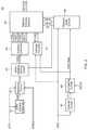
- FIG. 1is a block diagram of a semiconductor device 10 according to an embodiment of the present disclosure.
- the semiconductor device 10may be a DDR4 SDRAM incorporated in a single semiconductor chip, for example.
- the semiconductor device 10may be mounted on an external substrate, for example, a memory module substrate or a mother board.
- the semiconductor deviceto includes a memory cell array 11 .
- the memory cell array 11includes a plurality of word lines WL, a plurality of bit lines BL, and a plurality of memory cells MC arranged at intersections of the word lines WL and the bit lines BL. Selection of a word line WL is performed by a row address control circuit 12 , and selection of a bit line BL is performed by a column decoder 13 .
- a sense amplifier 14is connected to a corresponding bit line BL and a pair of local I/O lines LIOT/B.
- the pair of local I/O lines LIOT/Bis connected to a pair of main I/O lines MIOT/B via a transfer gate 15 functioning as a switch.
- the memory cell array 11is divided into (m+1) memory banks including memory banks BANK 0 to BANKm.
- a command address signal CAis supplied to the command address terminals 21 .
- One of the command address signals CA supplied to the command address terminals 21which relates to an address, is transferred to an address decoder 32 via a command address input circuit 31 .
- Another one that relates to a commandis transferred to a command control circuit 33 via the command address input circuit 31 .
- the address decoder 32decodes an address signal and generates a row address XADD and a column address YADD.
- the mw address XADDis supplied to the row address control circuit 12
- the column address YADDis supplied to the column decoder 13 .
- a command address signal CA that functions as a clock enable signal CKEis supplied to an internal clock generator 35 .
- Complementary external clock signals CK and /CKare supplied to the clock terminals 22 .
- the complementary external clock signals CK and /CKare input to a clock input circuit 34 .
- the clock input circuit 34generates an internal clock signal ICLK based on the complementary external clock signals CK and /CK.
- the internal clock signal ICLKis supplied to at least the command control circuit 33 and the internal clock generator 35 .
- the internal clock generator 35is activated by the clock enable signal CKE, for example, and generates an internal clock signal LCLK based on the internal clock signal ICLK.
- the internal clock signal LCLKis supplied to the I/O circuit 16 .
- the internal clock signal LCLKis used as a timing signal that defines a timing at which read data DQ is output from the data terminal 23 at the time of a read operation.
- write datais input to the data terminal 23 from outside.
- a data mask signal DMmay be input to the data terminal 23 from outside.
- Power-supply potentials VDD and VSSare supplied to the power-supply terminals 24 . These power-supply potentials VDD and VSS are supplied to a voltage generator 36 .
- the voltage generator 36generates various internal potentials VPP, VOD, VARY, and VPERI, for example, based on the power-supply potentials VDD and VSS.
- the internal potential VPPis used mainly in the row address control circuit 12 .
- the internal potentials VOD and VARYare used mainly in the sense amplifier 14 included in the memory cell array 11 .
- the internal potential VPERIis used in many other circuit blocks.
- Power-supply potentials VDDQ and VSSQare supplied to the I/O circuit 16 from the power-supply terminals 25 .
- the power-supply potentials VDDQ and VSSQmay be the same potentials as the power-supply potentials VDD and VSS supplied to the power supply terminals 24 , respectively, the dedicated power-supply potentials VDDQ and VSSQ are assigned to the I/O circuit 16 in order to prevent propagation of power-supply noise generated in the I/O circuit 16 to another circuit block.
- the command control circuit 33activates an active signal ACT when an active command is issued, and activates a refresh signal AREF when a refresh command is issued.
- the active signal ACT and the refresh signal AREFare both supplied to the row address control circuit 12 .
- the row address control circuit 12includes a refresh control circuit 40 .
- the refresh control circuit 40controls a refresh operation for the memory cell array 11 based on the row address XADD, the active signal ACT, and the refresh signal AREF.
- the refresh control circuit 40will be described in detail later.
- FIG. 2is a block diagram for explaining a configuration of the refresh control circuit 40 .
- the refresh control circuit 40includes a refresh counter 41 , an ARM sample generator 42 , a sampling circuit 43 , a row hammer address storing circuit 44 , an address convertor 45 , and a refresh address selector 46 .
- the refresh counter 41generates a normal refresh address NRADD.
- the normal refresh address NRADDis incremented or decremented in response to an internal refresh signal IREF.
- the internal refresh signal IREFcan be a signal activated plural times on the basis of the refresh signal AREF.
- the sampling circuit 43samples the row address XADD at a timing when a sampling signal SMP generated by the ARM sample generator 42 is activated, and supplies the sampled row address XADD to the row hammer address storing circuit 44 .
- the ARM sample generator 42may activate the sampling signal SMP at a timing when the active signal ACT is activated for a predetermined number of times. Accordingly, an address VADD of a word line WL at which accesses are concentrated is supplied to the row hammer address storing circuit 44 . As described later, the row hammer address storing circuit 44 stores a plurality of row addresses VADD. The row addresses VADD stored in the row hammer address storing circuit 44 are supplied to the address convertor 45 . The address convertor 45 converts the row addresses VADD to generate row hammer refresh addresses +1ADD, ⁇ 1ADD, +2ADD, and ⁇ 2ADD.
- the row hammer refresh addresses +1ADD and ⁇ 1ADDare addresses of word lines WL adjacent to the word line WL having the row address VADD assigned thereto on the both sides.
- the row hammer refresh addresses +2ADD and ⁇ 2ADDare addresses of word lines WL two lines away from the word line WL having the row address VADD assigned thereto on the both sides. For example, when word lines WL 1 to WL 5 are arranged in this order as shown in FIG.
- the row address VADDcorresponds to the word line WL 3
- the row hammer refresh addresses ⁇ 1ADD and +1ADDcorrespond to the word lines WL 2 and WL 4 , respectively
- the row hammer refresh addresses ⁇ 2ADD and +2ADDcorrespond to the word lines WL 1 and WL 5 , respectively.
- the word lines WL 4 , WL 2 , WL 5 , and WL 1 to which the row hammer refresh addresses +1ADD, ⁇ 1ADD, +2ADD, and ⁇ 2ADD are respectively assignedthere is a possibility that the information storing performance of associated memory cells MC is decreased because accesses are concentrated at the word line WL 3 adjacent thereto or two lines away therefrom.
- the normal refresh address NRADD and the row hammer refresh addresses +1ADD, ⁇ 1ADD, +2ADD, and ⁇ 2ADDare supplied to the refresh address selector 46 .
- the refresh control circuit 40further includes a counter circuit 47 , a comparing circuit 48 , and a refresh state circuit 49 .
- the counter circuit 47increments or decrements a count value CV in response to the internal refresh signal IREF.
- the comparing circuit 48receives the count value CV and activates a refresh state signal RHR State each time the count value CV reaches a predetermined value.
- the predetermined valuecan be changed with a mode signal MODE. Therefore, it suffices to set the predetermined value to a small value with the mode signal MODE when the frequency of the row hammer refresh operations is to be increased, and set the predetermined value to a large value with the mode signal MODE when the frequency of the row hammer refresh operations is to be decreased.
- the refresh counter 41may temporarily stop an update operation of the normal refresh address NRADD when the refresh state signal RHR State is activated.
- the refresh state signal RHR Stateis supplied to the refresh state circuit 49 .
- the refresh state circuit 49generates refresh selection signals NR, RHR 1 , and RHR 2 on the basis of the internal refresh signal IREF and the refresh state signal RHR State.
- the refresh state circuit 49activates the refresh selection signal NR when the refresh state signal RHR State is in an inactive state.
- the refresh selection signal NRis a signal activated when the normal refresh operation is to be performed.
- the refresh address selector 46selects the normal refresh address NRADD output from the refresh counter 41 and outputs the normal refresh address NRADD as a refresh address REFADD.
- the refresh state circuit 49activates the refresh selection signal RHR 1 or RHR 2 .
- the refresh selection signal RHR 1is a signal activated when the row hammer refresh operation is to be performed on the word lines WL 2 and WL 4 adjacent to the word line WL 3 at which accesses are concentrated.
- the refresh address selector 46selects the row hammer refresh addresses +1ADD and ⁇ 1ADD output from the address convertor 45 and outputs the row hammer refresh addresses +1ADD and ⁇ 1ADD as the refresh addresses REFADD.
- the refresh selection signal RHR 1is supplied also to the row hammer address storing circuit 44 .
- the refresh selection signal RHR 2is a signal activated when the row hammer refresh operation is to be performed on the word lines WL 1 and WL 5 two lines away from the word lines WL 3 at which accesses are concentrated.
- the refresh address selector 46selects the row hammer refresh addresses +2ADD and ⁇ 2ADD output from the address convertor 45 and outputs the row hammer refresh addresses +2ADD and ⁇ 2ADD as the refresh addresses REFADD.
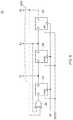
- FIG. 4is a block diagram for explaining a configuration of the row hammer address storing circuit 44 .
- the row hammer address storing circuit 44includes a plurality of address registers 50 to 57 , a plurality of counter circuits 60 to 67 , a comparing circuit 70 , and a control circuit 80 . While eight address registers 50 to 57 are illustrated in an example shown in FIG. 4 , the number of address registers included in the row hammer address storing circuit 44 is not limited thereto.
- the row addresses XADD sampled by the sampling circuit 43are stored in the address registers 50 to 57 , respectively.
- the counter circuits 60 to 67correspond to the address registers 50 to 57 , respectively.
- the comparing circuit 70compares the input row address XADD with each of the row addresses XADD stored in the address registers 50 to 57 .
- the comparing circuit 70activates a corresponding one of hit signals HIT 0 to HIT 7 .
- the control circuit 80increments the count value of a corresponding one of the counter circuits 60 to 67 . Therefore, the count values of the counter circuits 60 to 67 indicate the numbers of times when the row addresses XADD stored in the address registers 50 to 57 are sampled by the sampling circuit 43 , respectively.
- the control circuit 80includes a minimum pointer 81 that indicates one of the counter circuits 60 to 67 having a smallest count value, and a maximum pointer 82 that indicates one of the counter circuits 60 to 67 having a greatest count value.
- the control circuit 80resets one of the counter circuits 60 to 67 indicated by the minimum pointer 81 to an initial value and supplies a point number MIN to the address registers 50 to 57 . Accordingly, the input row address XADD is overwritten in one of the address registers 50 to 57 indicated by the point value MIN.
- the control circuit 80further includes a sequential counter 83 .
- a point value MAX indicated by the maximum pointer 82 or a point value SEQ indicated by the sequential counter 83is selected.
- One of the address registers 50 to 57is selected by a selected point value SEL and the row address XADD stored in the selected one of the address registers 50 to 57 is output as the row address VADD.
- the value of one of the counter circuits 60 to 67 corresponding to the selected point value SELis reset to an initial value.
- the control circuit 80further includes a selection signal generator 84 , a multiplexer 85 , and a comparing circuit 86 .
- the selection signal generator 84generates a selection signal M/S having a value inverted each time the refresh selection signal RHR 1 is activated twice.
- the selection signal M/Sis supplied to the multiplexer 85 .
- the multiplexer 85selects the point value MAX output from the maximum pointer 82 when the selection signal M/S has one logical level (a low level, for example), and selects the point value SEQ output from the sequential counter 83 when the selection signal M/S has the other logical level (a high level, for example).
- the point value MAX or SEQ selected by the multiplexer 85is output as the point value SEL.
- the point value SELis used to select one of the address registers 50 to 57 .
- the point value MAX and the point value SEQare compared with each other by the comparing circuit 86 .
- the comparing circuit 86activates a skip signal SKIP
- the sequential counter 83performs a count-up operation in response to the skip signal SKIP and the selection signal M/S.
- FIG. 6is a timing chart for explaining an operation of the control circuit 80 .
- the refresh selection signal RHR 1is activated twice at each of times t 1 to t 17 .
- the selection signal M/Sis inverted. Therefore, the multiplexer 85 alternately selects the point value MAX and the point value SEQ.
- the point value MAXis selected when the selection signal M/S is at a low level and the point value SEQ is selected when the selection signal M/S is at a high level.
- the point value SEQis selected at the times t 1 , t 3 , t 5 , t 7 , t 9 , t 11 , t 13 , t 15 , and t 17
- the point value MAXis selected at the times t 2 , t 4 , t 6 , t 8 , t 10 , t 12 , t 14 , and t 16 .
- the point value SEQis incremented in response to a falling edge of the selection signal M/S.
- the point value SEQis, for example, a 3-bit signal and is incremented from 0 to 7 and then returns to 0.
- the point value MAXis also, for example, a 3-bit signal and indicates the address of one of the counter circuits 60 to 67 currently having a greatest count value.
- the comparing circuit 86activates the skip signal SKIP.
- the point value MAX and the point value SEQboth indicate a value “4” at the time t 6 .
- the point value SEQ indicated by the sequential counter 83is immediately incremented to “5”.
- the point value SEL generated when the refresh selection signal RHR 1 is activated next timeindicates a value “5” and “4”, which is the value of the point value SEL generated in response to the previous point value MAX, is not repeatedly output.
- the point value MAX and the point value SEQboth indicate a value “0” at the time t 12 .
- the count signal UPis activated in response thereto and accordingly the point value SEQ indicated by the sequential counter 83 is immediately incremented to “1”.
- the point value SEL generated when the refresh selection signal RHR 1 is activated next timeindicates a value “1” and “0”, which is the value of the point value SEL generated in response to the previous point value MAX, is not repeatedly output.
- the value of the point value SEL generated in response to the previous point value MAX and the value of the point value SEL generated in response to the current point value SEQdo not match with each other Therefore, any unnecessary row hammer refresh operation can be avoided.
- the point value SEQ of the sequential counter 83is not skipped if the point value MAX is selected next.
- the point value MAX and the point value SEQboth indicate a value “2” at the time t 15
- the count signal UPis not activated because the selection signal M/S is at a high level at this timing That is, the point value SEQ is kept at the value “2” and any unnecessary skip operation is not performed.
- the point value SEQis skipped when the point value MAX and the point value SEQ match with each other. Therefore, the value of the point value SEL generated in response to the previous point value MAX and the value of the point value SEL generated in response to the current point value SEQ do not match with each other and any unnecessary row hammer refresh operation can be avoided.
- the refresh operationmay be performed plural times in the semiconductor device 10 in response to one refresh command issued from outside.
- FIGS. 7A and 7Bexamples where the refresh operation is performed five times each time the refresh signal AREF is activated once are shown.
- the refresh signal AREFis activated at each of times t 20 to t 24 and the internal refresh signal IREF is activated five times in a row each time the refresh signal AREF is activated.
- the refresh state signal RHR Stateis in an inactive state at the time t 20
- the refresh selection signal NRis activated synchronously with the internal refresh signal IREF.
- the refresh operationis performed sequentially on five normal refresh addresses NRADD in response to the refresh signal AREF.
- the refresh state signal RHR Stateis an active state.
- the refresh selection signal RHR 1is also activated synchronously with the internal refresh signal IREF during a period when the refresh state signal RHR State is activated.
- the refresh operationis performed on 12 row hammer refresh addresses +1 ADD, ⁇ 1ADD in one row hammer refresh operation. In this case, the refresh operation cannot be performed on 12 addresses in response to one refresh signal AREF.
- the refresh state signal RHR Stateis kept in the active state until the row hammer refresh operation to the 12 addresses is completed. That is, five row hammer refresh operations are performed in response to each of the refresh signals AREF activated at the time 121 and the time t 22 , and two row hammer refresh operations are performed in response to the refresh signal AREF activated at the time t 23 .
- first and second row hammer refresh operationsare respectively performed on +1ADD and ⁇ 1ADD of the row address VADD indicated by the point value MAX.
- Third and fourth row hammer refresh operationsare respectively performed on +1ADD and ⁇ 1ADD of the row address VADD indicated by the point value SEQ.
- Fifth and sixth row hammer refresh operationsare respectively performed on +1ADD and ⁇ 1ADD of the row address VADD indicated by the point value MAX.
- Seventh and eighth row hammer refresh operationsare respectively performed on +1ADD and ⁇ 1ADD of the row address VADD indicated by the point value SEQ.
- Ninth and tenth row hammer refresh operationsare respectively performed on +1ADD and ⁇ 1ADD of the row address VADD indicated by the point value MAX.
- the refresh signal AREFis activated at each of times t 30 to t 34 .
- the refresh selection signal NRis activated.
- the refresh operationis performed sequentially on five normal refresh addresses NRADD synchronously with the internal refresh signal IREF.
- the refresh state signal RHR Stateswitches to an active state.
- the refresh selection signal RHR 1 or RHR 2is activated. In the example shown in FIG.
- the refresh operationis performed on 12 row hammer refresh addresses +1ADD, ⁇ 1ADD and the refresh operation is performed to four row hammer refresh addresses +2ADD, ⁇ 2ADD in one row hammer refresh operation.
- the refresh state signal RHR Stateis kept in the active state until the row hammer refresh operation to the 16 addresses is completed. That is, five row hammer refresh operations are performed in response to each of the refresh signals AREF activated at the time t 31 , the time 132 , and the time 133 and one row hammer refresh operation is performed in response to the refresh signal AREF activated at the time t 34 .
- the refresh operationis performed on two row hammer refresh addresses +1ADD, ⁇ 1ADD and the refresh operation is performed on three row hammer refresh addresses +2ADD, ⁇ 2ADD.
- the refresh operationis performed on four row hammer refresh addresses +1ADD, ⁇ 1ADD and the refresh operation is performed on one row hammer refresh address +2ADD, ⁇ 2ADD.
- first to fourth row hammer refresh operationsare respectively performed on +2ADD, ⁇ 2ADD, +1ADD, and ⁇ 1ADD of the row address VADD indicated by the point value MAX.
- Fifth to eighth row hammer refresh operationsare respectively performed on +2ADD, ⁇ 2ADD, +1ADD, and ⁇ 1ADD of the row address VADD indicated by the point value SEQ.
- Ninth and tenth row hammer refresh operationsare respectively performed on +1 ADD and ⁇ 1ADD of the row address VADD indicated by the point value MAX.
- Eleventh and twelfth row hammer refresh operationsare respectively performed on +1ADD and ⁇ 1ADD of the row address VADD indicated by the point value SEQ.
- the sequential counter 83does not need to be a counter circuit that simply increments the point value SEQ, and can be a linear feedback shift register (LFSR) circuit that generates a pseudorandom number.
- LFSRlinear feedback shift register
- FIG. 8is an example of a circuit diagram of an LFSR circuit 90 .
- the LFSR circuit 90includes a shift register constituted by three flip-flop circuits 91 to 93 , and an EXOR circuit 94 .
- the flip-flop circuits 91 to 93are cascade-connected and respective output bits B 1 to B 3 constitute the point value SEQ being a pseudorandom number.
- the bit B 2 and the bit B 3are input to the EXOR circuit 94 and an output thereof is fed back to the flip-flop circuit 91 at the first stage.
- the count signal UPis supplied in common to clock nodes of the flip-flop circuits 91 to 93 .
- a reset signal RESETis supplied in common to reset or set nodes of the flip-flop circuits 91 to 93 . Accordingly, when the reset signal RESET is activated, the value of the point value SEQ is initialized to 4. When the count value UP is activated, the value of the point value SEQ is sequentially updated.
Landscapes
- Engineering & Computer Science (AREA)
- Microelectronics & Electronic Packaging (AREA)
- Computer Hardware Design (AREA)
- Physics & Mathematics (AREA)
- General Physics & Mathematics (AREA)
- Theoretical Computer Science (AREA)
- Computational Mathematics (AREA)
- Mathematical Analysis (AREA)
- Mathematical Optimization (AREA)
- Pure & Applied Mathematics (AREA)
- General Engineering & Computer Science (AREA)
- Dram (AREA)
Abstract
Description
Claims (19)
Priority Applications (4)
| Application Number | Priority Date | Filing Date | Title |
|---|---|---|---|
| US16/358,587US11043254B2 (en) | 2019-03-19 | 2019-03-19 | Semiconductor device having cam that stores address signals |
| CN202080019880.0ACN113557570B (en) | 2019-03-19 | 2020-03-19 | Semiconductor device having CAM storing address signals |
| PCT/US2020/023689WO2020191222A1 (en) | 2019-03-19 | 2020-03-19 | Semiconductor device having cam that stores address signals |
| US17/301,533US11521669B2 (en) | 2019-03-19 | 2021-04-06 | Semiconductor device having cam that stores address signals |
Applications Claiming Priority (1)
| Application Number | Priority Date | Filing Date | Title |
|---|---|---|---|
| US16/358,587US11043254B2 (en) | 2019-03-19 | 2019-03-19 | Semiconductor device having cam that stores address signals |
Related Child Applications (1)
| Application Number | Title | Priority Date | Filing Date |
|---|---|---|---|
| US17/301,533DivisionUS11521669B2 (en) | 2019-03-19 | 2021-04-06 | Semiconductor device having cam that stores address signals |
Publications (2)
| Publication Number | Publication Date |
|---|---|
| US20200302994A1 US20200302994A1 (en) | 2020-09-24 |
| US11043254B2true US11043254B2 (en) | 2021-06-22 |
Family
ID=72516066
Family Applications (2)
| Application Number | Title | Priority Date | Filing Date |
|---|---|---|---|
| US16/358,587ActiveUS11043254B2 (en) | 2019-03-19 | 2019-03-19 | Semiconductor device having cam that stores address signals |
| US17/301,533ActiveUS11521669B2 (en) | 2019-03-19 | 2021-04-06 | Semiconductor device having cam that stores address signals |
Family Applications After (1)
| Application Number | Title | Priority Date | Filing Date |
|---|---|---|---|
| US17/301,533ActiveUS11521669B2 (en) | 2019-03-19 | 2021-04-06 | Semiconductor device having cam that stores address signals |
Country Status (3)
| Country | Link |
|---|---|
| US (2) | US11043254B2 (en) |
| CN (1) | CN113557570B (en) |
| WO (1) | WO2020191222A1 (en) |
Cited By (23)
| Publication number | Priority date | Publication date | Assignee | Title |
|---|---|---|---|---|
| US11222682B1 (en) | 2020-08-31 | 2022-01-11 | Micron Technology, Inc. | Apparatuses and methods for providing refresh addresses |
| US11257535B2 (en) | 2019-02-06 | 2022-02-22 | Micron Technology, Inc. | Apparatuses and methods for managing row access counts |
| US11264096B2 (en) | 2019-05-14 | 2022-03-01 | Micron Technology, Inc. | Apparatuses, systems, and methods for a content addressable memory cell with latch and comparator circuits |
| US11322192B2 (en) | 2018-01-22 | 2022-05-03 | Micron Technology, Inc. | Apparatuses and methods for calculating row hammer refresh addresses in a semiconductor device |
| US11361808B2 (en) | 2013-08-26 | 2022-06-14 | Micron Technology, Inc. | Apparatuses and methods for selective row refreshes |
| US20220189538A1 (en)* | 2020-12-10 | 2022-06-16 | SK Hynix Inc. | Memory system |
| US20220199148A1 (en)* | 2020-12-23 | 2022-06-23 | Samsung Electronics Co., Ltd. | Semiconductor memory device and memory system having the same |
| US11386946B2 (en) | 2019-07-16 | 2022-07-12 | Micron Technology, Inc. | Apparatuses and methods for tracking row accesses |
| US11398265B2 (en) | 2019-08-20 | 2022-07-26 | Micron Technology, Inc. | Apparatuses and methods for analog row access tracking |
| US11424005B2 (en) | 2019-07-01 | 2022-08-23 | Micron Technology, Inc. | Apparatuses and methods for adjusting victim data |
| US11462291B2 (en) | 2020-11-23 | 2022-10-04 | Micron Technology, Inc. | Apparatuses and methods for tracking word line accesses |
| US11482275B2 (en) | 2021-01-20 | 2022-10-25 | Micron Technology, Inc. | Apparatuses and methods for dynamically allocated aggressor detection |
| US11521669B2 (en) | 2019-03-19 | 2022-12-06 | Micron Technology, Inc. | Semiconductor device having cam that stores address signals |
| US11568918B2 (en) | 2019-08-22 | 2023-01-31 | Micron Technology, Inc. | Apparatuses, systems, and methods for analog accumulator for determining row access rate and target row address used for refresh operation |
| US11600314B2 (en) | 2021-03-15 | 2023-03-07 | Micron Technology, Inc. | Apparatuses and methods for sketch circuits for refresh binning |
| US11664063B2 (en) | 2021-08-12 | 2023-05-30 | Micron Technology, Inc. | Apparatuses and methods for countering memory attacks |
| US11688451B2 (en) | 2021-11-29 | 2023-06-27 | Micron Technology, Inc. | Apparatuses, systems, and methods for main sketch and slim sketch circuit for row address tracking |
| US20230205872A1 (en)* | 2021-12-23 | 2023-06-29 | Advanced Micro Devices, Inc. | Method and apparatus to address row hammer attacks at a host processor |
| US11694738B2 (en) | 2018-06-19 | 2023-07-04 | Micron Technology, Inc. | Apparatuses and methods for multiple row hammer refresh address sequences |
| US11699476B2 (en) | 2019-07-01 | 2023-07-11 | Micron Technology, Inc. | Apparatuses and methods for monitoring word line accesses |
| US11854618B2 (en) | 2019-06-11 | 2023-12-26 | Micron Technology, Inc. | Apparatuses, systems, and methods for determining extremum numerical values |
| US11984148B2 (en) | 2019-05-31 | 2024-05-14 | Micron Technology, Inc. | Apparatuses and methods for tracking victim rows |
| US12165687B2 (en) | 2021-12-29 | 2024-12-10 | Micron Technology, Inc. | Apparatuses and methods for row hammer counter mat |
Families Citing this family (12)
| Publication number | Priority date | Publication date | Assignee | Title |
|---|---|---|---|---|
| US9324398B2 (en) | 2013-02-04 | 2016-04-26 | Micron Technology, Inc. | Apparatuses and methods for targeted refreshing of memory |
| KR102782820B1 (en)* | 2019-08-06 | 2025-03-14 | 에스케이하이닉스 주식회사 | Row hammer prevention circuit, memory module including the row hammer prevention circuit and memory system including the memory module |
| US11200942B2 (en) | 2019-08-23 | 2021-12-14 | Micron Technology, Inc. | Apparatuses and methods for lossy row access counting |
| KR102851135B1 (en)* | 2020-06-24 | 2025-08-28 | 에스케이하이닉스 주식회사 | Semiconductor memory device and operating method thereof |
| US11264079B1 (en) | 2020-12-18 | 2022-03-01 | Micron Technology, Inc. | Apparatuses and methods for row hammer based cache lockdown |
| CN112767983B (en)* | 2021-03-15 | 2022-04-26 | 长鑫存储技术有限公司 | Refresh control circuit and memory |
| CN112786087B (en)* | 2021-03-15 | 2022-04-26 | 长鑫存储技术有限公司 | Refresh circuit and memory |
| US11682444B2 (en)* | 2021-09-29 | 2023-06-20 | Lenovo Golbal Technology (United States) Inc. | Dynamic random-access memory array including sensor cells |
| US12182416B2 (en) | 2021-11-09 | 2024-12-31 | Samsung Electronics Co., Ltd. | Memory device and memory system including the same |
| US12080334B2 (en)* | 2022-04-11 | 2024-09-03 | Samsung Electronics Co., Ltd. | Semiconductor memory device and memory system including the same |
| CN119229928B (en)* | 2023-06-21 | 2025-09-26 | 长鑫存储技术有限公司 | Content-addressable storage device and content-addressable storage controller |
| CN120236621A (en)* | 2023-12-29 | 2025-07-01 | 长鑫科技集团股份有限公司 | Address translation circuit |
Citations (290)
| Publication number | Priority date | Publication date | Assignee | Title |
|---|---|---|---|---|
| US5299159A (en) | 1992-06-29 | 1994-03-29 | Texas Instruments Incorporated | Serial register stage arranged for connection with a single bitline |
| JPH0773682A (en) | 1993-06-12 | 1995-03-17 | Hitachi Ltd | Semiconductor memory device |
| US5422850A (en) | 1993-07-12 | 1995-06-06 | Texas Instruments Incorporated | Semiconductor memory device and defective memory cell repair circuit |
| US5699297A (en) | 1995-05-30 | 1997-12-16 | Kabushiki Kaisha Toshiba | Method of rewriting data in a microprocessor additionally provided with a flash memory |
| US5768196A (en) | 1996-03-01 | 1998-06-16 | Cypress Semiconductor Corp. | Shift-register based row select circuit with redundancy for a FIFO memory |
| CN1195173A (en) | 1997-03-28 | 1998-10-07 | 西门子公司 | Flexible fuse placement in redundant semiconductor memory |
| US5933377A (en) | 1997-03-25 | 1999-08-03 | Mitsubishi Denki Kabushiki Kaisha | Semiconductor memory device and defect repair method for semiconductor memory device |
| US5943283A (en) | 1997-12-05 | 1999-08-24 | Invox Technology | Address scrambling in a semiconductor memory |
| US5970507A (en) | 1995-12-12 | 1999-10-19 | Mitsubishi Denki Kabushiki Kaisha | Semiconductor memory device having a refresh-cycle program circuit |
| US5999471A (en) | 1997-01-30 | 1999-12-07 | Samsung Electronics, Co., Ltd. | Semiconductor memory device having a refresh function and a method for refreshing the same |
| US6002629A (en) | 1997-12-06 | 1999-12-14 | Samsung Electronics Co., Ltd. | Integrated circuit memory devices having improved refresh mode addressing and methods of operating same |
| US6011734A (en) | 1998-03-12 | 2000-01-04 | Motorola, Inc. | Fuseless memory repair system and method of operation |
| US6061290A (en) | 1997-06-30 | 2000-05-09 | Micron Technology, Inc. | Method and apparatus for simultaneous memory subarray testing |
| US6212118B1 (en) | 1997-12-12 | 2001-04-03 | Nec Corporation | Semiconductor memory |
| US20010008498A1 (en) | 1995-07-03 | 2001-07-19 | Mitsubishi Denki Kabushiki Kaisha | Fast accessible dynamic type semiconductor memory device |
| US6310806B1 (en) | 1999-11-26 | 2001-10-30 | Kabushiki Kaisha Toshiba | Semiconductor memory device with redundant circuit |
| US6317381B1 (en) | 1999-12-07 | 2001-11-13 | Micron Technology, Inc. | Method and system for adaptively adjusting control signal timing in a memory device |
| US6373738B1 (en) | 2000-11-20 | 2002-04-16 | International Business Machines Corporation | Low power CAM match line circuit |
| US6392952B1 (en) | 2001-05-15 | 2002-05-21 | United Microelectronics Corp. | Memory refresh circuit and memory refresh method |
| US6424582B1 (en) | 1998-05-27 | 2002-07-23 | Mitsubishi Denki Kasbushiki Kaisha | Semiconductor memory device having redundancy |
| US6434064B2 (en) | 2000-06-27 | 2002-08-13 | Kabushiki Kaisha Toshiba | Semiconductor memory device having redundancy circuit for saving faulty memory cells |
| US6452868B1 (en) | 1998-05-22 | 2002-09-17 | Micron Technology, Inc. | Method for generating memory addresses for accessing memory-cell arrays in memory devices |
| US6480931B1 (en) | 1999-11-05 | 2002-11-12 | International Business Machines Corporation | Content addressable storage apparatus and register mapper architecture |
| US20020181301A1 (en) | 1999-12-03 | 2002-12-05 | Hiroyuki Takahashi | Semiconductor storage and method for testing the same |
| US6515928B2 (en) | 2000-11-30 | 2003-02-04 | Fujitsu Limited | Semiconductor memory device having a plurality of low power consumption modes |
| US20030063512A1 (en) | 2000-04-11 | 2003-04-03 | Hiroyuki Takahashi | Semiconductor storage device |
| US20030067825A1 (en) | 2001-10-05 | 2003-04-10 | Hiroki Shimano | Semiconductor memory device |
| US20030090400A1 (en) | 2001-11-09 | 2003-05-15 | Texas Instruments Incorporated. | Multi-output dac and method using single dac and multiple s/h circuits |
| US6567340B1 (en) | 1999-09-23 | 2003-05-20 | Netlogic Microsystems, Inc. | Memory storage cell based array of counters |
| US20030123301A1 (en) | 2001-12-28 | 2003-07-03 | Samsung Electronics Co., Ltd. | Semiconductor memory device post-repair circuit and method |
| US20030193829A1 (en) | 2002-04-11 | 2003-10-16 | Morgan Donald M. | Method and system for low power refresh of dynamic random access memories |
| US20030231540A1 (en) | 2002-06-18 | 2003-12-18 | Nanoamp Solutions, Inc. | DRAM with total self refresh and control circuit |
| US20040008544A1 (en) | 2002-07-15 | 2004-01-15 | Fujitsu Limited | Semiconductor memory |
| US20040022093A1 (en) | 2002-08-02 | 2004-02-05 | Lee Hi-Choon | Semiconductor memory device having improved replacement efficiency of defective word lines by redundancy word lines |
| US20040114446A1 (en) | 2000-03-08 | 2004-06-17 | Hiroyuki Takahashi | Semiconductor memory |
| US20040130959A1 (en) | 2002-12-20 | 2004-07-08 | Nec Electronics Corporation | Semiconductor memory device having a DRAM cell structure and handled as a SRAM |
| US20040174757A1 (en) | 2001-01-26 | 2004-09-09 | Garverick Steven L. | Content addressable control system |
| US20040184323A1 (en) | 2003-03-17 | 2004-09-23 | Fujitsu Limited | Semiconductor memory device with shift register-based refresh address generation circuit |
| US20040218431A1 (en) | 2003-04-30 | 2004-11-04 | Hynix Semiconductor Inc. | Semiconductor memory device and method of operating the same |
| US20050105315A1 (en) | 2003-11-03 | 2005-05-19 | Samsung Electronics Co., Ltd. | Content addressable memory (CAM) capable of finding errors in a CAM cell array and a method thereof |
| JP2005216429A (en) | 2004-01-30 | 2005-08-11 | Elpida Memory Inc | Semiconductor storage device and its refresh control method |
| US6950364B2 (en) | 2003-02-10 | 2005-09-27 | Hynix Semiconductor Inc. | Self-refresh apparatus and method |
| US20050243629A1 (en) | 2004-04-28 | 2005-11-03 | Lee Jong W | Apparatus for controlling self-refresh period in memory device |
| US20050265104A1 (en) | 2004-05-27 | 2005-12-01 | Remaklus Perry W Jr | Method and system for providing independent bank refresh for volatile memories |
| US7027343B2 (en) | 2003-09-22 | 2006-04-11 | Micron Technology | Method and apparatus for controlling refresh operations in a dynamic memory device |
| US20060083099A1 (en) | 2004-10-14 | 2006-04-20 | Bae Myung H | System and method for redundancy memory decoding |
| US20060087903A1 (en) | 2004-10-21 | 2006-04-27 | Elpida Memory Inc. | Refresh control method of a semiconductor memory device and semiconductor memory device |
| US7057960B1 (en) | 2002-03-04 | 2006-06-06 | Cypress Semiconductor Corp. | Method and architecture for reducing the power consumption for memory devices in refresh operations |
| US7082070B2 (en) | 2003-07-23 | 2006-07-25 | Samsung Electronics Co., Ltd. | Temperature detection circuit and temperature detection method |
| US20060176744A1 (en) | 2005-02-10 | 2006-08-10 | Micron Technology, Inc. | Low power chip select (CS) latency option |
| US20060262616A1 (en) | 2005-05-18 | 2006-11-23 | Macronix International Co., Ltd. | Method and apparatus for implementing high speed memory |
| US20070008799A1 (en) | 2005-06-01 | 2007-01-11 | Elpida Memory, Inc | Semiconductor device |
| US20070014174A1 (en) | 2005-06-30 | 2007-01-18 | Kabushiki Kaisha Toshiba | Semiconductor memory device |
| US20070028068A1 (en) | 2005-07-29 | 2007-02-01 | International Business Machines Corporation | System and method for managing resources in a distributed storage system |
| US20070030746A1 (en) | 2005-08-04 | 2007-02-08 | Best Scott C | Memory device testing to support address-differentiated refresh rates |
| US20070033339A1 (en) | 2005-08-04 | 2007-02-08 | Best Scott C | Memory with refresh cycle donation to accommodate low-retention storage rows |
| US7187607B2 (en) | 2003-10-09 | 2007-03-06 | Elpida Memory, Inc. | Semiconductor memory device and method for manufacturing same |
| US7203115B2 (en) | 2003-08-18 | 2007-04-10 | Fujitsu Limited | Semiconductor memory and method for operating the same |
| US7203113B2 (en) | 2004-03-30 | 2007-04-10 | Nec Electronics Corporation | Semiconductor storage device |
| US20070133330A1 (en) | 2005-12-08 | 2007-06-14 | Kabushiki Kaisha Toshiba | Semiconductor memory device |
| CN101038785A (en) | 2000-07-07 | 2007-09-19 | 睦塞德技术公司 | A high speed dram architecture with uniform access latency |
| CN101067972A (en) | 2007-04-23 | 2007-11-07 | 北京芯技佳易微电子科技有限公司 | Memory error-detecting and error-correcting coding circuit and method for reading and writing data utilizing the same |
| US20070297252A1 (en) | 2006-06-26 | 2007-12-27 | Anant Pratap Singh | Integrated circuit having memory array including ECC and/or column redundancy, and method of programming, controlling and/or operating same |
| US20080028260A1 (en) | 2006-07-26 | 2008-01-31 | Mutsumi Oyagi | Memory system |
| US20080031068A1 (en) | 2006-07-26 | 2008-02-07 | Zmos Technology, Inc. | Dynamic memory refresh configurations and leakage control methods |
| US20080126893A1 (en) | 2006-07-03 | 2008-05-29 | Stmicroelectronics Sa | Method of refreshing a dynamic random access memory and corresponding dynamic random access memory device, in particular incorporated into a cellular mobile telephone |
| US20080130394A1 (en) | 2006-12-05 | 2008-06-05 | Elpida Memory, Inc. | Semiconductor memory device |
| US20080181048A1 (en) | 2007-01-25 | 2008-07-31 | Yong-Joo Han | Semiconductor memory device and memory cell accessing method thereof |
| US20080224742A1 (en) | 2007-03-16 | 2008-09-18 | Pomichter Gerald P | Small scale clock multiplier circuit for fixed speed testing |
| US20080253212A1 (en) | 2007-04-10 | 2008-10-16 | Masahisa Iida | Semiconductor memory device |
| US20080266990A1 (en) | 2007-04-30 | 2008-10-30 | Infineon Technologies North America Corp. | Flexible redundancy replacement scheme for semiconductor device |
| US20080288720A1 (en) | 2007-05-18 | 2008-11-20 | International Business Machines Corporation | Multi-wafer 3d cam cell |
| CN101331554A (en) | 2005-11-08 | 2008-12-24 | 桑迪士克股份有限公司 | Memory with retargetable memory cell redundancy |
| US20080316845A1 (en) | 2007-06-20 | 2008-12-25 | Shih-Hsing Wang | Memory row architecture having memory row redundancy repair function |
| US20090021999A1 (en) | 2007-07-20 | 2009-01-22 | Elpida Memory, Inc. | Semiconductor device |
| US20090059641A1 (en) | 2007-08-29 | 2009-03-05 | Jeddeloh Joe M | Memory device interface methods, apparatus, and systems |
| US20090077571A1 (en) | 2006-08-21 | 2009-03-19 | International Business Machines Corporation | Method and apparatus for efficient performance monitoring of a large number of simultaneous events |
| CN101458658A (en) | 2007-12-13 | 2009-06-17 | 中芯国际集成电路制造(上海)有限公司 | Data storage method and apparatus for flash memory |
| US7551502B2 (en) | 2005-05-18 | 2009-06-23 | Elpida Memory, Inc. | Semiconductor device |
| US20090161457A1 (en) | 2007-12-25 | 2009-06-25 | Elpida Memory, Inc. | Semiconductor storage device having redundancy area |
| US20090168571A1 (en) | 2005-11-29 | 2009-07-02 | Samsung Electronics Co., Ltd. | Dynamic random access memory device and method of determining refresh cycle thereof |
| US20090185440A1 (en) | 2006-02-10 | 2009-07-23 | Hynix Semiconductor Inc. | Active cycyle control circuit for semiconductor memory apparatus |
| US20090201752A1 (en) | 2008-02-08 | 2009-08-13 | Elpida Memory, Inc. | Semiconductor memory device |
| US20090296510A1 (en) | 2008-05-30 | 2009-12-03 | Samsung Electronics Co., Ltd. | Semiconductor memory device having refresh circuit and word line activating method therefor |
| CN101622607A (en) | 2008-02-29 | 2010-01-06 | 株式会社东芝 | Semiconductor memory device with a plurality of memory cells |
| US20100005376A1 (en) | 2008-07-02 | 2010-01-07 | Micron Technology, Inc. | Method and apparatus for repairing high capacity/high bandwidth memory devices |
| US20100005217A1 (en) | 2008-07-02 | 2010-01-07 | Micron Technology, Inc | Multi-mode memory device and method |
| US20100054011A1 (en) | 2008-08-30 | 2010-03-04 | Juhan Kim | High speed SRAM |
| US20100074042A1 (en) | 2008-09-24 | 2010-03-25 | Kabushiki Kaisha Toshiba | Semiconductor memory device |
| US20100080074A1 (en) | 2008-09-30 | 2010-04-01 | Semiconductor Energy Laboratory Co., Ltd. | Semiconductor memory device |
| US20100110809A1 (en) | 2007-07-11 | 2010-05-06 | Fujitsu Microelectronics Limited | Semiconductor memory device and system with redundant element |
| US20100110810A1 (en) | 2007-07-11 | 2010-05-06 | Fujitsu Microelectronics Limited | Semiconductor memory device and system |
| US20100131812A1 (en) | 2008-11-26 | 2010-05-27 | Qualcomm Incorporated | Resizable Cache Memory |
| US20100157693A1 (en) | 2008-12-24 | 2010-06-24 | Kabushiki Kaisha Toshiba | Semiconductor memory device |
| US20100182663A1 (en) | 2009-01-16 | 2010-07-22 | Sony Corporation | Light illuminating apparatus and light illuminating method |
| US20100329069A1 (en) | 2009-06-26 | 2010-12-30 | Fujitsu Limited | Semiconductor memory device |
| US20110026290A1 (en) | 2009-08-03 | 2011-02-03 | Elpida Memory, Inc. | Semiconductor device having memory cell array divided into plural memory mats |
| US20110055495A1 (en) | 2009-08-28 | 2011-03-03 | Qualcomm Incorporated | Memory Controller Page Management Devices, Systems, and Methods |
| US20110051530A1 (en) | 2009-08-26 | 2011-03-03 | Kabushiki Kaisha Toshiba | Semiconductor memory device and method of updating data stored in the semiconductor memory device |
| US20110069572A1 (en) | 2009-09-18 | 2011-03-24 | Samsung Electronics Co., Ltd. | Row address code selection based on locations of substandard memory cells |
| CN102113058A (en) | 2008-04-09 | 2011-06-29 | 拉姆伯斯公司 | Programmable Memory Repair Solution |
| US20110216614A1 (en) | 2010-03-05 | 2011-09-08 | Elpida Memory, Inc. | Semiconductor device enabling refreshing of redundant memory cell instead of defective memory cell |
| US20110225355A1 (en) | 2010-03-12 | 2011-09-15 | Elpida Memory Inc. | Semiconductor device, refresh control method thereof and computer system |
| US20110286271A1 (en) | 2010-05-21 | 2011-11-24 | Mediatek Inc. | Memory systems and methods for reading data stored in a memory cell of a memory device |
| US20110310648A1 (en) | 2010-06-21 | 2011-12-22 | Renesas Technology Corporation | Semiconductor storage device |
| JP2011258259A (en) | 2010-06-07 | 2011-12-22 | Elpida Memory Inc | Semiconductor device |
| US20120014199A1 (en) | 2010-07-15 | 2012-01-19 | Elpida Memory, Inc. | Semiconductor device that performs refresh operation |
| US20120059984A1 (en) | 2010-09-03 | 2012-03-08 | Kang Uk-Song | Semiconductor memory device |
| JP4911510B2 (en) | 2007-04-16 | 2012-04-04 | エルピーダメモリ株式会社 | Semiconductor memory device |
| US8174921B2 (en) | 2008-12-19 | 2012-05-08 | Samsung Electronics Co., Ltd. | Semiconductor memory device having shared temperature control circuit |
| CN102483952A (en) | 2009-11-06 | 2012-05-30 | 株式会社东芝 | Memory system |
| US20120151131A1 (en) | 2010-12-09 | 2012-06-14 | International Business Machines Corporation | Memory system with a programmable refresh cycle |
| US20120213021A1 (en) | 2011-02-18 | 2012-08-23 | Elpida Memory, Inc. | Semiconductor device having redundant bit line provided to replace defective bit line |
| US20120254472A1 (en) | 2010-03-15 | 2012-10-04 | Ware Frederick A | Chip selection in a symmetric interconnection topology |
| US20130003467A1 (en) | 2004-07-15 | 2013-01-03 | Micron Technology, Inc. | Digit line comparison circuits |
| US20130003477A1 (en) | 2011-06-30 | 2013-01-03 | Ju-Seop Park | Semiconductor memory device including spare antifuse array and antifuse repair method of the semiconductor memory device |
| JP2013004158A (en) | 2011-06-21 | 2013-01-07 | Elpida Memory Inc | Semiconductor storage device and refresh control method thereof |
| US8400805B2 (en) | 2011-01-28 | 2013-03-19 | Elpida Memory, Inc. | Semiconductor device |
| US8451677B2 (en) | 2008-11-27 | 2013-05-28 | Elpida Memory, Inc. | Semiconductor device and method of refreshing the same |
| US20130173971A1 (en) | 2011-12-29 | 2013-07-04 | David J. Zimmerman | Boundary scan chain for stacked memory |
| US20130254475A1 (en) | 2010-12-03 | 2013-09-26 | Rambus Inc. | Memory refresh method and devices |
| US20130304982A1 (en) | 2012-05-14 | 2013-11-14 | Bu Il JUNG | Memory device, memory system, and operating methods thereof |
| US20140006704A1 (en) | 2012-06-30 | 2014-01-02 | Zvika Greenfield | Row hammer condition monitoring |
| US20140006703A1 (en) | 2012-06-30 | 2014-01-02 | Kuljit S. Bains | Row hammer refresh command |
| US20140013169A1 (en) | 2012-03-30 | 2014-01-09 | Darshan Kobla | Generic address scrambler for memory circuit test engine |
| US20140013185A1 (en) | 2012-03-30 | 2014-01-09 | Darshan Kobla | On chip redundancy repair for memory devices |
| US20140050004A1 (en) | 2012-08-14 | 2014-02-20 | Elpida Memory, Inc. | Semiconductor device having hierarchically structured bit lines |
| US20140078842A1 (en) | 2012-09-18 | 2014-03-20 | Samsung Electronics Co., Ltd. | Post package repairing method, method of preventing multiple activation of spare word lines, and semiconductor memory device including fuse programming circuit |
| US20140078841A1 (en) | 2012-09-18 | 2014-03-20 | Mosys, Inc. | Programmable memory built in self repair circuit |
| US20140089576A1 (en) | 2012-09-24 | 2014-03-27 | Kuljit S. Bains | Method, apparatus and system for providing a memory refresh |
| US20140095786A1 (en) | 2012-09-28 | 2014-04-03 | SK Hynix Inc. | Semiconductor device and operating method thereof |
| US20140095780A1 (en) | 2012-09-28 | 2014-04-03 | Kuljit S. Bains | Distributed row hammer tracking |
| US20140119091A1 (en) | 2012-10-25 | 2014-05-01 | Samsung Electronics Co., Ltd. | Bit-line sense amplifier, semiconductor memory device and memory system including the same |
| US20140136763A1 (en) | 2012-11-09 | 2014-05-15 | Sandisk Technologies Inc. | CAM NAND with OR Function and Full Chip Search Capability |
| US20140143473A1 (en) | 2012-11-19 | 2014-05-22 | Spansion Llc | Data refresh in non-volatile memory |
| US20140177370A1 (en) | 2012-12-21 | 2014-06-26 | Intel Corporation | Method, apparatus and system for responding to a row hammer event |
| US20140189228A1 (en) | 2012-12-28 | 2014-07-03 | Zaika Greenfield | Throttling support for row-hammer counters |
| US20140219043A1 (en) | 2013-02-04 | 2014-08-07 | Micron Technology, Inc. | Apparatuses and methods for targeted refreshing of memory |
| US8811100B2 (en) | 2012-06-28 | 2014-08-19 | SK Hynix Inc. | Cell array and memory device including the same |
| US20140237307A1 (en) | 2011-12-28 | 2014-08-21 | Darshan Kobla | Generic address scrambler for memory circuit test engine |
| US20140241099A1 (en) | 2013-02-26 | 2014-08-28 | Samsung Electronics Co., Ltd. | Semiconductor memory and memory system including the semiconductor memory |
| US20140254298A1 (en) | 2013-03-11 | 2014-09-11 | Nvidia Corporation | Variable dynamic memory refresh |
| US20140281206A1 (en) | 2013-03-15 | 2014-09-18 | John H. Crawford | Techniques for Probabilistic Dynamic Random Access Memory Row Repair |
| US20140281207A1 (en) | 2013-03-12 | 2014-09-18 | Sreenivas Mandava | Techniques for Determining Victim Row Addresses in a Volatile Memory |
| US20140269021A1 (en) | 2013-03-15 | 2014-09-18 | Taiwan Semiconductor Manufacturing Company Limited | Timing logic for memory array |
| US20140292375A1 (en) | 2013-03-29 | 2014-10-02 | Stmicroelectronics Asia Pacific Pte. Ltd. | Analog accumulator |
| US8862973B2 (en) | 2009-12-09 | 2014-10-14 | Intel Corporation | Method and system for error management in a memory device |
| US20140355332A1 (en) | 2013-05-30 | 2014-12-04 | Samsung Electronics Co., Ltd. | Volatile memory device and refresh method thereof |
| US20150049567A1 (en) | 2013-08-14 | 2015-02-19 | SK Hynix Inc. | Memory and memory system including the same |
| US20150055420A1 (en) | 2013-08-26 | 2015-02-26 | Micron Technology, Inc. | Apparatuses and methods for selective row refreshes |
| US20150078112A1 (en) | 2013-09-19 | 2015-03-19 | Elite Semiconductor Memory Technology Inc. | Method for auto-refreshing memory cells in semiconductor memory device and semiconductor memory device using the method |
| US20150089326A1 (en) | 2013-09-25 | 2015-03-26 | SK Hynix Inc. | Address detection circuit and memory including the same |
| US9032141B2 (en) | 2012-11-30 | 2015-05-12 | Intel Corporation | Row hammer monitoring based on stored row hammer threshold value |
| US20150155027A1 (en) | 2013-12-04 | 2015-06-04 | Fujitsu Limited | Semiconductor memory apparatus |
| US20150162067A1 (en) | 2013-12-11 | 2015-06-11 | SK Hynix Inc. | Memory and memory system including the same |
| US9058900B2 (en) | 2011-09-26 | 2015-06-16 | SK Hynix Inc. | System, semiconductor memory device and operating method thereof |
| US20150170728A1 (en) | 2013-12-18 | 2015-06-18 | SK Hynix Inc. | Memory and memory system including the same |
| US20150199126A1 (en) | 2014-01-10 | 2015-07-16 | Advanced Micro Devices, Inc. | Page migration in a 3d stacked hybrid memory |
| US20150206572A1 (en) | 2014-01-21 | 2015-07-23 | SK Hynix Inc. | Memory and memory system including the same |
| US20150213872A1 (en) | 2014-01-30 | 2015-07-30 | Micron Technology, Inc. | Apparatuses and methods for address detection |
| US20150213877A1 (en) | 2012-10-22 | 2015-07-30 | Hewlett-Packard Development Company, L.P. | Refreshing a group of memory cells in response to potential disturbance |
| US20150228341A1 (en) | 2006-04-25 | 2015-08-13 | Renesas Electronics Corporation | Content addressable memory |
| US9117544B2 (en) | 2012-06-30 | 2015-08-25 | Intel Corporation | Row hammer refresh command |
| US9123447B2 (en) | 2013-08-09 | 2015-09-01 | SK Hynix Inc. | Memory, memory system including the same and method for operating memory |
| US20150255140A1 (en) | 2014-03-07 | 2015-09-10 | SK Hynix Inc. | Semiconductor memory device and refresh control system |
| US20150262652A1 (en)* | 2014-03-17 | 2015-09-17 | Nec Corporation | Access count device, memory system, and access count method |
| US20150279442A1 (en) | 2014-03-26 | 2015-10-01 | SK Hynix Inc. | Semiconductor memory device and semiconductor memory system including the same |
| US20150279441A1 (en) | 2014-03-28 | 2015-10-01 | Synopsys, Inc. | Most activated memory portion handling |
| US9153294B2 (en) | 2012-09-24 | 2015-10-06 | Samsung Electronics Co., Ltd. | Semiconductor memory device having adjustable refresh period, memory system comprising same, and method of operating same |
| US20150294711A1 (en) | 2012-10-22 | 2015-10-15 | Hewlett-Packard Development Company, L.P. | Performing refresh of a memory device in response to access of data |
| US20150340077A1 (en) | 2014-05-21 | 2015-11-26 | Micron Technology, Inc. | Apparatuses and methods for controlling refresh operations |
| US20150356048A1 (en) | 2014-06-09 | 2015-12-10 | Micron Technology, Inc. | Method and apparatus for controlling access to a common bus by multiple components |
| US20160019940A1 (en) | 2014-07-21 | 2016-01-21 | SK Hynix Inc. | Memory device |
| US20160027532A1 (en) | 2014-07-22 | 2016-01-28 | SK Hynix Inc. | Memory device |
| US20160027498A1 (en) | 2014-07-24 | 2016-01-28 | Rambus Inc. | Reduced refresh power |
| US20160042782A1 (en) | 2013-03-15 | 2016-02-11 | Ps4 Luxco S.A.R.L. | Semiconductor storage device and system provided with same |
| US20160078911A1 (en)* | 2013-11-08 | 2016-03-17 | Micron Technology, Inc. | Semiconductor memory device having count value control circuit |
| US20160086649A1 (en) | 2014-09-23 | 2016-03-24 | SK Hynix Inc. | Smart refresh device |
| US9299457B2 (en) | 2014-02-23 | 2016-03-29 | Qualcomm Incorporated | Kernel masking of DRAM defects |
| US20160093402A1 (en) | 2014-09-30 | 2016-03-31 | Sony Corporation | Memory with distributed replacement word lines |
| US9311985B2 (en) | 2013-12-18 | 2016-04-12 | SK Hynix Inc. | Memory and memory system for periodic targeted refresh |
| US20160125931A1 (en) | 2014-11-03 | 2016-05-05 | Samsung Electronics Co., Ltd. | Semiconductor memory device that performs a refresh operation |
| US20160133314A1 (en) | 2014-11-11 | 2016-05-12 | Samsung Electronics Co., Ltd. | Semiconductor memory devices, memory systems including the same, and methods of operating memory systems |
| US20160140243A1 (en) | 2014-11-18 | 2016-05-19 | International Business Machines Corporation | Scoped search engine |
| US20160172056A1 (en) | 2014-12-12 | 2016-06-16 | SK Hynix Inc. | Semiconductor device |
| US20160180921A1 (en) | 2012-05-17 | 2016-06-23 | Samsung Electronics Co., Ltd. | Semiconductor memory device controlling refresh cycle, memory system, and method of operating the semiconductor memory device |
| US20160180917A1 (en) | 2014-12-23 | 2016-06-23 | Zeshan A. Chishti | Techniques to Reduce Memory Cell Refreshes for a Memory Device |
| US9384821B2 (en) | 2012-11-30 | 2016-07-05 | Intel Corporation | Row hammer monitoring based on stored row hammer threshold value |
| US20160196863A1 (en) | 2015-01-07 | 2016-07-07 | Samsung Electronics Co., Ltd. | Method of operating memory device and method of operating memory system including the same |
| US20160202926A1 (en) | 2013-09-27 | 2016-07-14 | Hewlett Packard Enterprise Development Lp | Refresh row address |
| US20160225461A1 (en) | 2015-01-30 | 2016-08-04 | Sandisk Technologies Inc. | Memory System and Method for Reducing Read Disturb Errors |
| US9424907B2 (en) | 2013-06-26 | 2016-08-23 | Micron Technology, Inc. | Semiconductor device suppressing BTI deterioration |
| US9484079B2 (en) | 2015-02-02 | 2016-11-01 | SK Hynix Inc. | Memory device and memory system including the same |
| US20160336060A1 (en) | 2015-05-13 | 2016-11-17 | Samsung Electronics Co., Ltd. | Semiconductor memory device for deconcentrating refresh commands and system including the same |
| US20160343423A1 (en) | 2015-05-18 | 2016-11-24 | Micron Technology, Inc. | Apparatus having dice to perorm refresh operations |
| US9570143B2 (en) | 2015-05-08 | 2017-02-14 | SK Hynix Inc. | Semiconductor memory device for performing refresh operation |
| US20170117030A1 (en) | 2015-10-21 | 2017-04-27 | Invensas Corporation | DRAM Adjacent Row Disturb Mitigation |
| US9646672B1 (en) | 2016-04-25 | 2017-05-09 | SK Hynix Inc. | Memory device and method of refreshing the same |
| US20170133085A1 (en) | 2015-11-06 | 2017-05-11 | Samsung Electronics Co., Ltd. | Memory device and memory system performing request-based refresh, and operating method of the memory device |
| US20170140807A1 (en) | 2014-07-03 | 2017-05-18 | Yale University | Circuitry for Ferroelectric FET-Based Dynamic Random Access Memory and Non-Violatile Memory |
| US20170140811A1 (en) | 2015-11-18 | 2017-05-18 | SK Hynix Inc. | Refresh control circuit and memory device including same |
| US20170148504A1 (en) | 2015-11-24 | 2017-05-25 | Qualcomm Incorporated | Controlling a refresh mode of a dynamic random access memory (dram) die |
| US9672889B2 (en) | 2014-12-08 | 2017-06-06 | SK Hynix Inc. | Semiconductor memory device and refresh control method thereof |
| US9685240B1 (en) | 2016-03-17 | 2017-06-20 | SK Hynix Inc. | Memory device to alleviate the effects of row hammer condition and memory system including the same |
| US20170177246A1 (en) | 2015-12-21 | 2017-06-22 | Intel Corporation | Predictive memory maintenance |
| US9691466B1 (en) | 2016-06-03 | 2017-06-27 | SK Hynix Inc. | Memory device including refresh controller |
| US20170186481A1 (en) | 2015-12-28 | 2017-06-29 | Samsung Electronics Co., Ltd. | Refresh controller and memory device including the same |
| US9697913B1 (en) | 2016-06-10 | 2017-07-04 | Micron Technology, Inc. | Ferroelectric memory cell recovery |
| US20170213586A1 (en) | 2016-01-25 | 2017-07-27 | Samsung Electronics Co., Ltd. | Memory device performing hammer refresh operation and memory system including the same |
| US20170221546A1 (en) | 2016-02-03 | 2017-08-03 | Samsung Electronics Co., Ltd. | Volatile memory device and electronic device comprising refresh information generator, information providing method thereof, and refresh control method thereof |
| US9734887B1 (en) | 2016-03-21 | 2017-08-15 | International Business Machines Corporation | Per-die based memory refresh control based on a master controller |
| US9741447B2 (en) | 2014-04-23 | 2017-08-22 | Micron Technology, Inc. | Semiconductor device including fuse circuit |
| US9761297B1 (en) | 2016-12-30 | 2017-09-12 | Intel Corporation | Hidden refresh control in dynamic random access memory |
| US20170263305A1 (en) | 2014-11-25 | 2017-09-14 | Samg Yeun CHO | Method of detecting most frequently accessed address of semiconductor memory based on probability information |
| US20170287547A1 (en) | 2016-03-31 | 2017-10-05 | Micron Technology, Inc. | Semiconductor device |
| US9786351B2 (en) | 2015-12-29 | 2017-10-10 | SK Hynix Inc. | Semiconductor memory device for performing refresh operation and operating method therof |
| US9799391B1 (en) | 2016-11-21 | 2017-10-24 | Nanya Technology Corporation | Dram circuit, redundant refresh circuit and refresh method |
| US9805782B1 (en) | 2017-02-02 | 2017-10-31 | Elite Semiconductor Memory Technology Inc. | Memory device capable of determining candidate wordline for refresh and control method thereof |
| US9818469B1 (en) | 2016-09-05 | 2017-11-14 | SK Hynix Inc. | Refresh control device and semiconductor device including the same |
| US20170352399A1 (en) | 2016-06-06 | 2017-12-07 | Renesas Electronics Corporation | Memory macro and semiconductor integrated circuit device |
| US20170371742A1 (en) | 2016-06-27 | 2017-12-28 | Young-Seop Shim | Storage device |
| US20170372767A1 (en) | 2016-06-27 | 2017-12-28 | SK Hynix Inc. | Semiconductor memory device and operating method thereof |
| US20180005690A1 (en) | 2016-06-29 | 2018-01-04 | Micron Technology, Inc. | Oscillator controlled random sampling method and circuit |
| US9865328B1 (en) | 2015-12-04 | 2018-01-09 | Integrated Device Technology, Inc. | Nullifying incorrect sampled data contribution in decision feedback equalizer at restart of forwarded clock in memory system |
| US20180025772A1 (en) | 2016-07-25 | 2018-01-25 | SK Hynix Inc. | Semiconductor devices having a refresh operation |
| US20180061483A1 (en) | 2016-08-23 | 2018-03-01 | Micron Technology, Inc. | A temperature-dependent refresh circuit configured to increase or decrease a count value of a refresh timer according to a self-refresh signal |
| US20180060194A1 (en) | 2016-09-01 | 2018-03-01 | Samsung Electronics Co., Ltd. | Semiconductor Memory Devices with Error Correction and Methods of Operating the Same |
| US20180082737A1 (en) | 2016-09-20 | 2018-03-22 | SK Hynix Inc. | Address decoder and active control circuit and semiconductor memory including the same |
| US20180090199A1 (en) | 2016-09-26 | 2018-03-29 | SK Hynix Inc. | Refresh control device |
| US9934143B2 (en) | 2013-09-26 | 2018-04-03 | Intel Corporation | Mapping a physical address differently to different memory devices in a group |
| US20180096719A1 (en) | 2016-09-30 | 2018-04-05 | Intel Corporation | Staggering initiation of refresh in a group of memory devices |
| US20180102776A1 (en) | 2016-10-07 | 2018-04-12 | Altera Corporation | Methods and apparatus for managing application-specific power gating on multichip packages |
| US20180107417A1 (en) | 2016-02-19 | 2018-04-19 | Sandisk Technologies Llc | Systems and methods for efficient power state transitions |
| US9953696B2 (en) | 2016-08-23 | 2018-04-24 | SK Hynix Inc. | Refresh control circuit for target refresh operation of semiconductor memory device, and operating method thereof |
| US20180114565A1 (en) | 2016-10-20 | 2018-04-26 | SK Hynix Inc. | Refresh timing generation circuit, refresh control circuit and semiconductor apparatus including the same |
| KR20180064940A (en) | 2016-12-06 | 2018-06-15 | 삼성전자주식회사 | Memory system performing hammer refresh operation |
| US20180182445A1 (en) | 2016-12-26 | 2018-06-28 | SK Hynix Inc. | Memory device, memory system including the same, and operation method thereof |
| US20180203621A1 (en) | 2017-01-18 | 2018-07-19 | SK Hynix Inc. | Semiconductor apparatus, memory module and operation method thereof |
| US20180218767A1 (en) | 2017-01-30 | 2018-08-02 | Micron Technology, Inc. | Apparatuses and methods for distributing row hammer refresh events across a memory device |
| US20180261268A1 (en) | 2017-03-07 | 2018-09-13 | SK Hynix Inc. | Semiconductor device and semiconductor system |
| US20180294028A1 (en) | 2017-04-11 | 2018-10-11 | SK Hynix Inc. | Semiconductor memory device |
| US20180341553A1 (en) | 2017-05-25 | 2018-11-29 | Micron Technology, Inc. | Memory device with dynamic target calibration |
| US10170174B1 (en) | 2017-10-27 | 2019-01-01 | Micron Technology, Inc. | Apparatus and methods for refreshing memory |
| US10176860B1 (en) | 2017-08-29 | 2019-01-08 | Micron Technology, Inc. | Refresh in non-volatile memory |
| US20190043558A1 (en) | 2017-08-02 | 2019-02-07 | Qualcomm Incorporated | Partial refresh technique to save memory refresh power |
| US20190066759A1 (en) | 2018-11-01 | 2019-02-28 | Intel Corporation | Row hammer mitigation with randomization of target row selection |
| US20190066762A1 (en) | 2017-08-29 | 2019-02-28 | Yoshihito Koya | Volatile memory device including stacked memory cells |
| US20190088315A1 (en) | 2017-09-20 | 2019-03-21 | Sandisk Technologies Llc | Identifying non-volatile memory cells for data refresh |
| US20190088316A1 (en) | 2017-09-19 | 2019-03-21 | Toshiba Memory Corporation | Resistance change type memory |
| US20190147941A1 (en) | 2017-11-13 | 2019-05-16 | Western Digital Technologies, Inc. | Managing refresh operations for a memory device |
| US10297305B1 (en) | 2017-10-30 | 2019-05-21 | SK Hynix Inc. | Memory device having twin cell mode and refresh method thereof |
| US20190161341A1 (en) | 2017-11-28 | 2019-05-30 | Micron Technology, Inc. | Systems and methods for temperature sensor access in die stacks |
| US20190196730A1 (en) | 2017-12-21 | 2019-06-27 | Qualcomm Incorporated | Partial area self refresh mode |
| US20190198099A1 (en) | 2017-12-22 | 2019-06-27 | Micron Technology, Inc. | Auto-referenced memory cell read techniques |
| US20190198090A1 (en) | 2017-12-27 | 2019-06-27 | Micron Technology, Inc. | Systems and methods for performing row hammer refresh operations in redundant memory |
| US20190207736A1 (en) | 2016-01-18 | 2019-07-04 | Sckipio Technologies S.I Ltd | Dynamic resource allocation (dra) for communication systems |
| US20190205253A1 (en) | 2017-12-29 | 2019-07-04 | Advanced Micro Devices, Inc. | Method and apparatus for controlling cache line storage in cache memory |
| US20190228813A1 (en) | 2019-03-29 | 2019-07-25 | Intel Corporation | Refresh command control for host assist of row hammer mitigation |
| US20190228815A1 (en) | 2018-01-22 | 2019-07-25 | Micron Technology, Inc. | Apparatuses and methods for calculating row hammer refresh addresses in a semiconductor device |
| US20190237132A1 (en) | 2018-01-30 | 2019-08-01 | Micron Technology, Inc. | Semiconductor device performing row hammer refresh operation |
| US20190243708A1 (en) | 2018-02-05 | 2019-08-08 | Samsung Electronics Co., Ltd. | Semiconductor memory devices, memory systems, and methods of operating the semiconductor memory devices |
| US10381327B2 (en) | 2016-10-06 | 2019-08-13 | Sandisk Technologies Llc | Non-volatile memory system with wide I/O memory die |
| US20190252020A1 (en) | 2016-09-30 | 2019-08-15 | Intel Corporation | Two transistor, one resistor non-volatile gain cell memory and storage element |
| US20190279706A1 (en) | 2018-03-07 | 2019-09-12 | SK Hynix Inc. | Refresh control circuit, semiconductor memory device, and refresh method thereof |
| US20190333573A1 (en) | 2018-04-25 | 2019-10-31 | Samsung Electronics Co., Ltd. | Semiconductor memory device and memory system having the same |
| US20190348107A1 (en) | 2018-05-14 | 2019-11-14 | Hoon Shin | Refresh control circuit, memory device including the same and method of operating the same for hammer refresh operation |
| US20190348100A1 (en) | 2018-05-08 | 2019-11-14 | Micron Technology, Inc. | Memory with internal refresh rate control |
| US20190349545A1 (en) | 2014-12-05 | 2019-11-14 | Samsung Electronics Co., Ltd. | Image sensor for improving nonlinearity of row code region, and device including the same |
| WO2019222960A1 (en) | 2018-05-24 | 2019-11-28 | Micron Technology, Inc. | Apparatuses and methods for pure-time, self adopt sampling for row hammer refresh sampling |
| US20190362774A1 (en) | 2017-08-02 | 2019-11-28 | Zentel Japan Corporation | Semiconductor memory device for preventing occurance of row hammer issue |
| US20190371391A1 (en) | 2018-06-01 | 2019-12-05 | Samsung Electronics Co., Ltd. | Semiconductor memory devices, memory systems and methods of operating semiconductor memory devices |
| US20190385667A1 (en) | 2018-06-19 | 2019-12-19 | Micron Technology, Inc. | Apparatuses and methods for multiple row hammer refresh address sequences |
| US20190385661A1 (en) | 2018-06-19 | 2019-12-19 | SK Hynix Inc. | Semiconductor device |
| US20200005857A1 (en) | 2018-07-02 | 2020-01-02 | Micron Technology, Inc. | Apparatus and methods for triggering row hammer address sampling |
| US20200075106A1 (en) | 2018-08-30 | 2020-03-05 | Toshiba Memory Corporation | Memory system |
| US20200090760A1 (en) | 2018-09-18 | 2020-03-19 | Western Digital Technologies, Inc. | Data storage systems and methods for improved recovery after a write abort event |
| US10600491B2 (en) | 2016-05-13 | 2020-03-24 | Silicon Motion, Inc. | Method for managing data blocks and method of data management for data storage device |
| US10600462B2 (en) | 2015-04-24 | 2020-03-24 | Intel Corporation | Bitcell state retention |
| US10629286B2 (en) | 2017-11-23 | 2020-04-21 | Samsung Electronics Co., Ltd. | Memory devices, memory systems and methods of operating memory devices |
| US20200135263A1 (en) | 2018-10-31 | 2020-04-30 | Micron Technology, Inc. | Apparatuses and methods for access based refresh timing |
| US10679710B2 (en) | 2018-03-22 | 2020-06-09 | Toshiba Memory Corporation | Semiconductor device |
| US20200194056A1 (en) | 2018-12-12 | 2020-06-18 | Micron Technology, Inc. | Apparatuses and methods for multi-bank and multi-pump refresh operations |
| US20200201380A1 (en) | 2017-12-17 | 2020-06-25 | Redpine Signals, Inc. | Fine-Grained Clock Resolution using Low and High Frequency Clock Sources in a Low-Power System |
| US20200211633A1 (en) | 2018-12-27 | 2020-07-02 | Micron Technology, Inc. | Apparatus with a row-hammer address latch mechanism |
| US20200211636A1 (en) | 2018-12-31 | 2020-07-02 | Micron Technology, Inc. | Memory with partial array refresh |
| US20200211626A1 (en) | 2018-12-31 | 2020-07-02 | Micron Technology, Inc. | Memory with on-die data transfer |
| US20200251158A1 (en) | 2019-02-06 | 2020-08-06 | Micron Technology, Inc. | Apparatuses and methods for managing row access counts |
| US20210026732A1 (en) | 2019-07-24 | 2021-01-28 | Samsung Electronics Co., Ltd. | Memory systems for performing failover |
| US20210065755A1 (en) | 2019-09-02 | 2021-03-04 | SK Hynix Inc. | Memory controller and operating method thereof |
| US20210065764A1 (en) | 2019-09-04 | 2021-03-04 | Winbond Electronics Corp. | Memory storage device and operation method thereof |
Family Cites Families (74)
| Publication number | Priority date | Publication date | Assignee | Title |
|---|---|---|---|---|
| US3633175A (en) | 1969-05-15 | 1972-01-04 | Honeywell Inc | Defect-tolerant digital memory system |
| JP3361825B2 (en) | 1990-08-22 | 2003-01-07 | テキサス インスツルメンツ インコーポレイテツド | Memory array architecture |
| GB9205727D0 (en) | 1992-03-16 | 1992-04-29 | Sarnoff David Res Center | Averaging,flash analog to digital converter |
| JP3184129B2 (en) | 1997-09-29 | 2001-07-09 | 甲府日本電気株式会社 | Storage device |
| US6888776B2 (en) | 2000-09-06 | 2005-05-03 | Renesas Technology Corp. | Semiconductor memory device |
| EP1808861B1 (en) | 2000-12-20 | 2010-08-04 | Fujitsu Semiconductor Limited | Multi-port memory based on a plurality of memory cores |
| US7283380B1 (en) | 2001-08-03 | 2007-10-16 | Netlogic Microsystems, Inc. | Content addressable memory with selective error logging |
| JP3821066B2 (en) | 2002-07-04 | 2006-09-13 | 日本電気株式会社 | Magnetic random access memory |
| JP2004111643A (en) | 2002-09-18 | 2004-04-08 | Toshiba Corp | Semiconductor memory device and control method thereof |
| FR2851074B1 (en) | 2003-02-10 | 2005-04-22 | St Microelectronics Sa | SECTORIZED FLASH MEMORY COMPRISING MEANS FOR CONTROLLING AND REFRESHING MEMORY CELLS |
| DE10337855B4 (en) | 2003-08-18 | 2005-09-29 | Infineon Technologies Ag | Circuit and method for evaluating and controlling a refresh rate of memory cells of a dynamic memory |
| US7304875B1 (en) | 2003-12-17 | 2007-12-04 | Integrated Device Technology. Inc. | Content addressable memory (CAM) devices that support background BIST and BISR operations and methods of operating same |
| KR100859252B1 (en) | 2004-06-23 | 2008-09-18 | 산요덴키가부시키가이샤 | Memory |
| US7319602B1 (en) | 2004-07-01 | 2008-01-15 | Netlogic Microsystems, Inc | Content addressable memory with twisted data lines |
| DE102004062150A1 (en) | 2004-12-23 | 2006-07-13 | Braun Gmbh | Interchangeable accessory for a small electrical appliance and method for determining the service life of the accessory |
| JP4912718B2 (en) | 2006-03-30 | 2012-04-11 | 富士通セミコンダクター株式会社 | Dynamic semiconductor memory |
| US7586771B2 (en) | 2006-09-11 | 2009-09-08 | Jinn-Shyan Wang | Tree-style and-type match circuit device applied to content addressable memory |
| US7760530B2 (en) | 2007-06-04 | 2010-07-20 | Hewlett-Packard Development Company, L.P. | Content addressable memory address resolver |
| US7975170B2 (en) | 2007-06-15 | 2011-07-05 | Qimonda Ag | Memory refresh system and method |
| JP2009205724A (en) | 2008-02-27 | 2009-09-10 | Toshiba Corp | Semiconductor memory device |
| JP2009252278A (en) | 2008-04-04 | 2009-10-29 | Toshiba Corp | Nonvolatile semiconductor storage device and memory system |
| JP2010170596A (en) | 2009-01-20 | 2010-08-05 | Elpida Memory Inc | Semiconductor memory device |
| US8676725B1 (en) | 2009-06-05 | 2014-03-18 | Google Inc. | Method and system for entropy-based semantic hashing |
| US8031503B1 (en) | 2010-06-23 | 2011-10-04 | Netlogic Microsystems, Inc. | System for dynamically managing power consumption in a search engine |
| CN102364991B (en) | 2011-02-01 | 2012-10-24 | 杭州士兰微电子股份有限公司 | Switching power supply controller for constant current driving of LED by primary side control and method for constant current driving of LED |
| US8891297B2 (en) | 2011-11-01 | 2014-11-18 | Micron Technology, Inc. | Memory cell sensing |
| KR101325038B1 (en) | 2011-12-09 | 2013-11-04 | 조재영 | Fitting insole |
| KR20130117198A (en) | 2012-04-18 | 2013-10-25 | 삼성전자주식회사 | A method refreshing memory cells and a semiconductor memory device using thereof |
| KR102003894B1 (en) | 2012-09-20 | 2019-07-25 | 에스케이하이닉스 주식회사 | Cell array, memory and memory system icluding the same |
| US9190131B2 (en) | 2012-12-20 | 2015-11-17 | SK Hynix Inc. | Memory and memory system including the same |
| US9183917B1 (en) | 2012-12-21 | 2015-11-10 | Samsung Electronics Co., Ltd. | Memory device, operating method thereof, and system having the memory device |
| KR102089665B1 (en) | 2012-12-28 | 2020-04-14 | 삼성전자주식회사 | Memory modules and memory systems |
| KR101976452B1 (en) | 2013-04-22 | 2019-05-10 | 에스케이하이닉스 주식회사 | Semiconductor device |
| KR102075665B1 (en) | 2013-06-17 | 2020-02-10 | 에스케이하이닉스 주식회사 | Semiconductor memory device and operating method for the same and semiconductor system comprising semiconductor memory device |
| US20140379978A1 (en) | 2013-06-24 | 2014-12-25 | Qualcomm Incorporated | Refresh scheme for memory cells with weak retention time |
| KR102103873B1 (en) | 2013-06-28 | 2020-04-24 | 에스케이하이닉스 주식회사 | Memory and memory system including the same |
| EP3039683A1 (en) | 2013-08-28 | 2016-07-06 | Hewlett Packard Enterprise Development LP | Refresh rate adjust |
| KR102204240B1 (en) | 2014-09-11 | 2021-01-19 | 에스케이하이닉스 주식회사 | Memory device and memory including the same |
| TWI529695B (en) | 2014-09-15 | 2016-04-11 | 友達光電股份有限公司 | Display panel and method of transmitting signal therein |
| KR102194768B1 (en) | 2014-09-24 | 2020-12-23 | 에스케이하이닉스 주식회사 | Semiconductor memory device and semiconductor memory system |
| US9431086B2 (en) | 2014-10-06 | 2016-08-30 | Winbond Electronics Corp. | Memory circuit and refresh method thereof |
| KR20160045461A (en) | 2014-10-17 | 2016-04-27 | 에스케이하이닉스 주식회사 | Semiconductor device and method of driving the same |
| US10091563B2 (en) | 2015-03-02 | 2018-10-02 | Semiconductor Energy Laboratory Co., Ltd. | Environmental sensor or semiconductor device |
| US10147500B2 (en) | 2015-05-22 | 2018-12-04 | SK Hynix Inc. | Hybrid read disturb count management |
| KR20170024307A (en) | 2015-08-25 | 2017-03-07 | 삼성전자주식회사 | Embedded refresh controller and memory device including the same |
| KR102434053B1 (en) | 2015-11-16 | 2022-08-19 | 삼성전자주식회사 | Semiconductor memory device, memory system including the same and method of operating the same |
| KR102553181B1 (en) | 2016-07-12 | 2023-07-10 | 에스케이하이닉스 주식회사 | Memory device and method for operating memory device |
| KR20180136611A (en) | 2017-06-14 | 2018-12-26 | 에스케이하이닉스 주식회사 | Semiconductor device |
| KR102341261B1 (en) | 2017-11-13 | 2021-12-20 | 삼성전자주식회사 | A memory device including massbit counter and operating method thereof |
| US10497424B2 (en) | 2017-12-06 | 2019-12-03 | Micron Technology, Inc. | Systems and methods for plate voltage regulation during memory array access |
| US10679685B2 (en) | 2017-12-27 | 2020-06-09 | Spin Memory, Inc. | Shared bit line array architecture for magnetoresistive memory |
| US10705900B2 (en) | 2018-02-02 | 2020-07-07 | Western Digital Technologies, Inc. | Program verify adaptation for flash memory |
| US10585767B2 (en) | 2018-02-07 | 2020-03-10 | International Business Machines Corporation | Automatic data healing using a storage controller |
| KR102534631B1 (en) | 2018-05-11 | 2023-05-19 | 에스케이하이닉스 주식회사 | Semiconductor System Including Counting Circuit Block |
| US11309431B2 (en) | 2018-05-17 | 2022-04-19 | Semiconductor Energy Laboratory Co., Ltd. | Memory device, semiconductor device, and electronic device |
| US10536069B2 (en) | 2018-06-15 | 2020-01-14 | Ford Global Technologies, Llc | Virtual resistance gate driver |
| US11043254B2 (en) | 2019-03-19 | 2021-06-22 | Micron Technology, Inc. | Semiconductor device having cam that stores address signals |
| US11227649B2 (en) | 2019-04-04 | 2022-01-18 | Micron Technology, Inc. | Apparatuses and methods for staggered timing of targeted refresh operations |
| US11264096B2 (en) | 2019-05-14 | 2022-03-01 | Micron Technology, Inc. | Apparatuses, systems, and methods for a content addressable memory cell with latch and comparator circuits |
| US11158364B2 (en) | 2019-05-31 | 2021-10-26 | Micron Technology, Inc. | Apparatuses and methods for tracking victim rows |
| US11158373B2 (en) | 2019-06-11 | 2021-10-26 | Micron Technology, Inc. | Apparatuses, systems, and methods for determining extremum numerical values |
| US11139015B2 (en) | 2019-07-01 | 2021-10-05 | Micron Technology, Inc. | Apparatuses and methods for monitoring word line accesses |
| US10832792B1 (en) | 2019-07-01 | 2020-11-10 | Micron Technology, Inc. | Apparatuses and methods for adjusting victim data |
| US10937468B2 (en) | 2019-07-03 | 2021-03-02 | Micron Technology, Inc. | Memory with configurable die powerup delay |
| US11386946B2 (en) | 2019-07-16 | 2022-07-12 | Micron Technology, Inc. | Apparatuses and methods for tracking row accesses |
| US10943636B1 (en) | 2019-08-20 | 2021-03-09 | Micron Technology, Inc. | Apparatuses and methods for analog row access tracking |
| US10964378B2 (en) | 2019-08-22 | 2021-03-30 | Micron Technology, Inc. | Apparatus and method including analog accumulator for determining row access rate and target row address used for refresh operation |
| US11200942B2 (en) | 2019-08-23 | 2021-12-14 | Micron Technology, Inc. | Apparatuses and methods for lossy row access counting |
| KR102729243B1 (en) | 2019-11-25 | 2024-11-12 | 삼성전자주식회사 | Semiconductor memory devices and methods of operating the same |
| US11011215B1 (en) | 2019-12-19 | 2021-05-18 | Micron Technology, Inc. | Apparatus with an internal-operation management mechanism |
| US11094370B2 (en) | 2019-12-27 | 2021-08-17 | Intel Corporation | Enhanced auto-precharge memory scheduling policy |
| US11568913B2 (en) | 2020-02-05 | 2023-01-31 | Micron Technology, Inc. | Voltage adjustment based on pending refresh operations |
| US11222682B1 (en) | 2020-08-31 | 2022-01-11 | Micron Technology, Inc. | Apparatuses and methods for providing refresh addresses |
| US11462291B2 (en) | 2020-11-23 | 2022-10-04 | Micron Technology, Inc. | Apparatuses and methods for tracking word line accesses |
- 2019
- 2019-03-19USUS16/358,587patent/US11043254B2/enactiveActive
- 2020
- 2020-03-19CNCN202080019880.0Apatent/CN113557570B/enactiveActive
- 2020-03-19WOPCT/US2020/023689patent/WO2020191222A1/ennot_activeCeased
- 2021
- 2021-04-06USUS17/301,533patent/US11521669B2/enactiveActive
Patent Citations (354)
| Publication number | Priority date | Publication date | Assignee | Title |
|---|---|---|---|---|
| US5299159A (en) | 1992-06-29 | 1994-03-29 | Texas Instruments Incorporated | Serial register stage arranged for connection with a single bitline |
| JPH0773682A (en) | 1993-06-12 | 1995-03-17 | Hitachi Ltd | Semiconductor memory device |
| US5422850A (en) | 1993-07-12 | 1995-06-06 | Texas Instruments Incorporated | Semiconductor memory device and defective memory cell repair circuit |
| US5699297A (en) | 1995-05-30 | 1997-12-16 | Kabushiki Kaisha Toshiba | Method of rewriting data in a microprocessor additionally provided with a flash memory |
| US20010008498A1 (en) | 1995-07-03 | 2001-07-19 | Mitsubishi Denki Kabushiki Kaisha | Fast accessible dynamic type semiconductor memory device |
| US5970507A (en) | 1995-12-12 | 1999-10-19 | Mitsubishi Denki Kabushiki Kaisha | Semiconductor memory device having a refresh-cycle program circuit |
| US5768196A (en) | 1996-03-01 | 1998-06-16 | Cypress Semiconductor Corp. | Shift-register based row select circuit with redundancy for a FIFO memory |
| US5999471A (en) | 1997-01-30 | 1999-12-07 | Samsung Electronics, Co., Ltd. | Semiconductor memory device having a refresh function and a method for refreshing the same |
| US5933377A (en) | 1997-03-25 | 1999-08-03 | Mitsubishi Denki Kabushiki Kaisha | Semiconductor memory device and defect repair method for semiconductor memory device |
| CN1195173A (en) | 1997-03-28 | 1998-10-07 | 西门子公司 | Flexible fuse placement in redundant semiconductor memory |
| US6061290A (en) | 1997-06-30 | 2000-05-09 | Micron Technology, Inc. | Method and apparatus for simultaneous memory subarray testing |
| US5943283A (en) | 1997-12-05 | 1999-08-24 | Invox Technology | Address scrambling in a semiconductor memory |
| US6002629A (en) | 1997-12-06 | 1999-12-14 | Samsung Electronics Co., Ltd. | Integrated circuit memory devices having improved refresh mode addressing and methods of operating same |
| US6212118B1 (en) | 1997-12-12 | 2001-04-03 | Nec Corporation | Semiconductor memory |
| US6011734A (en) | 1998-03-12 | 2000-01-04 | Motorola, Inc. | Fuseless memory repair system and method of operation |
| US6452868B1 (en) | 1998-05-22 | 2002-09-17 | Micron Technology, Inc. | Method for generating memory addresses for accessing memory-cell arrays in memory devices |
| US6424582B1 (en) | 1998-05-27 | 2002-07-23 | Mitsubishi Denki Kasbushiki Kaisha | Semiconductor memory device having redundancy |
| US6567340B1 (en) | 1999-09-23 | 2003-05-20 | Netlogic Microsystems, Inc. | Memory storage cell based array of counters |
| US6480931B1 (en) | 1999-11-05 | 2002-11-12 | International Business Machines Corporation | Content addressable storage apparatus and register mapper architecture |
| US6310806B1 (en) | 1999-11-26 | 2001-10-30 | Kabushiki Kaisha Toshiba | Semiconductor memory device with redundant circuit |
| US20020181301A1 (en) | 1999-12-03 | 2002-12-05 | Hiroyuki Takahashi | Semiconductor storage and method for testing the same |
| US6317381B1 (en) | 1999-12-07 | 2001-11-13 | Micron Technology, Inc. | Method and system for adaptively adjusting control signal timing in a memory device |
| US20040114446A1 (en) | 2000-03-08 | 2004-06-17 | Hiroyuki Takahashi | Semiconductor memory |
| US20030063512A1 (en) | 2000-04-11 | 2003-04-03 | Hiroyuki Takahashi | Semiconductor storage device |
| US6434064B2 (en) | 2000-06-27 | 2002-08-13 | Kabushiki Kaisha Toshiba | Semiconductor memory device having redundancy circuit for saving faulty memory cells |
| CN101038785A (en) | 2000-07-07 | 2007-09-19 | 睦塞德技术公司 | A high speed dram architecture with uniform access latency |
| US6373738B1 (en) | 2000-11-20 | 2002-04-16 | International Business Machines Corporation | Low power CAM match line circuit |
| US6515928B2 (en) | 2000-11-30 | 2003-02-04 | Fujitsu Limited | Semiconductor memory device having a plurality of low power consumption modes |
| US20040174757A1 (en) | 2001-01-26 | 2004-09-09 | Garverick Steven L. | Content addressable control system |
| US6392952B1 (en) | 2001-05-15 | 2002-05-21 | United Microelectronics Corp. | Memory refresh circuit and memory refresh method |
| US20030067825A1 (en) | 2001-10-05 | 2003-04-10 | Hiroki Shimano | Semiconductor memory device |
| US20030090400A1 (en) | 2001-11-09 | 2003-05-15 | Texas Instruments Incorporated. | Multi-output dac and method using single dac and multiple s/h circuits |
| US20030123301A1 (en) | 2001-12-28 | 2003-07-03 | Samsung Electronics Co., Ltd. | Semiconductor memory device post-repair circuit and method |
| US7057960B1 (en) | 2002-03-04 | 2006-06-06 | Cypress Semiconductor Corp. | Method and architecture for reducing the power consumption for memory devices in refresh operations |
| US20030193829A1 (en) | 2002-04-11 | 2003-10-16 | Morgan Donald M. | Method and system for low power refresh of dynamic random access memories |
| US20030231540A1 (en) | 2002-06-18 | 2003-12-18 | Nanoamp Solutions, Inc. | DRAM with total self refresh and control circuit |
| US20040008544A1 (en) | 2002-07-15 | 2004-01-15 | Fujitsu Limited | Semiconductor memory |
| US7209402B2 (en) | 2002-07-15 | 2007-04-24 | Fujitsu Limited | Semiconductor memory |
| US20040022093A1 (en) | 2002-08-02 | 2004-02-05 | Lee Hi-Choon | Semiconductor memory device having improved replacement efficiency of defective word lines by redundancy word lines |
| US20040130959A1 (en) | 2002-12-20 | 2004-07-08 | Nec Electronics Corporation | Semiconductor memory device having a DRAM cell structure and handled as a SRAM |
| US6950364B2 (en) | 2003-02-10 | 2005-09-27 | Hynix Semiconductor Inc. | Self-refresh apparatus and method |
| US20040184323A1 (en) | 2003-03-17 | 2004-09-23 | Fujitsu Limited | Semiconductor memory device with shift register-based refresh address generation circuit |
| US20040218431A1 (en) | 2003-04-30 | 2004-11-04 | Hynix Semiconductor Inc. | Semiconductor memory device and method of operating the same |
| US7082070B2 (en) | 2003-07-23 | 2006-07-25 | Samsung Electronics Co., Ltd. | Temperature detection circuit and temperature detection method |
| US7203115B2 (en) | 2003-08-18 | 2007-04-10 | Fujitsu Limited | Semiconductor memory and method for operating the same |
| US7027343B2 (en) | 2003-09-22 | 2006-04-11 | Micron Technology | Method and apparatus for controlling refresh operations in a dynamic memory device |
| US7187607B2 (en) | 2003-10-09 | 2007-03-06 | Elpida Memory, Inc. | Semiconductor memory device and method for manufacturing same |
| US20050105315A1 (en) | 2003-11-03 | 2005-05-19 | Samsung Electronics Co., Ltd. | Content addressable memory (CAM) capable of finding errors in a CAM cell array and a method thereof |
| JP2005216429A (en) | 2004-01-30 | 2005-08-11 | Elpida Memory Inc | Semiconductor storage device and its refresh control method |
| US7203113B2 (en) | 2004-03-30 | 2007-04-10 | Nec Electronics Corporation | Semiconductor storage device |
| US20050243629A1 (en) | 2004-04-28 | 2005-11-03 | Lee Jong W | Apparatus for controlling self-refresh period in memory device |
| US7215588B2 (en) | 2004-04-28 | 2007-05-08 | Hynix Semiconductor Inc. | Apparatus for controlling self-refresh period in memory device |
| US20050265104A1 (en) | 2004-05-27 | 2005-12-01 | Remaklus Perry W Jr | Method and system for providing independent bank refresh for volatile memories |
| US20130003467A1 (en) | 2004-07-15 | 2013-01-03 | Micron Technology, Inc. | Digit line comparison circuits |
| US20060083099A1 (en) | 2004-10-14 | 2006-04-20 | Bae Myung H | System and method for redundancy memory decoding |
| US20060087903A1 (en) | 2004-10-21 | 2006-04-27 | Elpida Memory Inc. | Refresh control method of a semiconductor memory device and semiconductor memory device |
| US20060176744A1 (en) | 2005-02-10 | 2006-08-10 | Micron Technology, Inc. | Low power chip select (CS) latency option |
| US20060262616A1 (en) | 2005-05-18 | 2006-11-23 | Macronix International Co., Ltd. | Method and apparatus for implementing high speed memory |
| US7551502B2 (en) | 2005-05-18 | 2009-06-23 | Elpida Memory, Inc. | Semiconductor device |
| US20070008799A1 (en) | 2005-06-01 | 2007-01-11 | Elpida Memory, Inc | Semiconductor device |
| US20070014174A1 (en) | 2005-06-30 | 2007-01-18 | Kabushiki Kaisha Toshiba | Semiconductor memory device |
| US20070028068A1 (en) | 2005-07-29 | 2007-02-01 | International Business Machines Corporation | System and method for managing resources in a distributed storage system |
| US7444577B2 (en) | 2005-08-04 | 2008-10-28 | Rambus Inc. | Memory device testing to support address-differentiated refresh rates |
| US20070033339A1 (en) | 2005-08-04 | 2007-02-08 | Best Scott C | Memory with refresh cycle donation to accommodate low-retention storage rows |
| US20070030746A1 (en) | 2005-08-04 | 2007-02-08 | Best Scott C | Memory device testing to support address-differentiated refresh rates |
| US8756368B2 (en) | 2005-08-04 | 2014-06-17 | Rambus Inc. | Memory controller with refresh logic to accommodate low-retention storage rows in a memory device |
| US9390782B2 (en) | 2005-08-04 | 2016-07-12 | Rambus Inc. | Memory with refresh logic to accommodate low-retention storage rows |
| US7565479B2 (en) | 2005-08-04 | 2009-07-21 | Rambus Inc. | Memory with refresh cycle donation to accommodate low-retention-storage rows |
| US20140293725A1 (en) | 2005-08-04 | 2014-10-02 | Rambus Inc. | Memory with refresh logic to accomodate low-retention storage rows |
| CN101331554A (en) | 2005-11-08 | 2008-12-24 | 桑迪士克股份有限公司 | Memory with retargetable memory cell redundancy |
| US20090168571A1 (en) | 2005-11-29 | 2009-07-02 | Samsung Electronics Co., Ltd. | Dynamic random access memory device and method of determining refresh cycle thereof |
| US20070133330A1 (en) | 2005-12-08 | 2007-06-14 | Kabushiki Kaisha Toshiba | Semiconductor memory device |
| US20090185440A1 (en) | 2006-02-10 | 2009-07-23 | Hynix Semiconductor Inc. | Active cycyle control circuit for semiconductor memory apparatus |
| US20150228341A1 (en) | 2006-04-25 | 2015-08-13 | Renesas Electronics Corporation | Content addressable memory |
| US20070297252A1 (en) | 2006-06-26 | 2007-12-27 | Anant Pratap Singh | Integrated circuit having memory array including ECC and/or column redundancy, and method of programming, controlling and/or operating same |
| US20080126893A1 (en) | 2006-07-03 | 2008-05-29 | Stmicroelectronics Sa | Method of refreshing a dynamic random access memory and corresponding dynamic random access memory device, in particular incorporated into a cellular mobile telephone |
| US20080028260A1 (en) | 2006-07-26 | 2008-01-31 | Mutsumi Oyagi | Memory system |
| US20080031068A1 (en) | 2006-07-26 | 2008-02-07 | Zmos Technology, Inc. | Dynamic memory refresh configurations and leakage control methods |
| US20090077571A1 (en) | 2006-08-21 | 2009-03-19 | International Business Machines Corporation | Method and apparatus for efficient performance monitoring of a large number of simultaneous events |
| US20080130394A1 (en) | 2006-12-05 | 2008-06-05 | Elpida Memory, Inc. | Semiconductor memory device |
| US7830742B2 (en) | 2007-01-25 | 2010-11-09 | Samsung Electronics Co., Ltd. | Semiconductor memory device and memory cell accessing method thereof |
| US20080181048A1 (en) | 2007-01-25 | 2008-07-31 | Yong-Joo Han | Semiconductor memory device and memory cell accessing method thereof |
| US20080224742A1 (en) | 2007-03-16 | 2008-09-18 | Pomichter Gerald P | Small scale clock multiplier circuit for fixed speed testing |
| US20080253212A1 (en) | 2007-04-10 | 2008-10-16 | Masahisa Iida | Semiconductor memory device |
| JP4911510B2 (en) | 2007-04-16 | 2012-04-04 | エルピーダメモリ株式会社 | Semiconductor memory device |
| CN101067972A (en) | 2007-04-23 | 2007-11-07 | 北京芯技佳易微电子科技有限公司 | Memory error-detecting and error-correcting coding circuit and method for reading and writing data utilizing the same |
| US20080266990A1 (en) | 2007-04-30 | 2008-10-30 | Infineon Technologies North America Corp. | Flexible redundancy replacement scheme for semiconductor device |
| US20080288720A1 (en) | 2007-05-18 | 2008-11-20 | International Business Machines Corporation | Multi-wafer 3d cam cell |
| US20080316845A1 (en) | 2007-06-20 | 2008-12-25 | Shih-Hsing Wang | Memory row architecture having memory row redundancy repair function |
| US20100110810A1 (en) | 2007-07-11 | 2010-05-06 | Fujitsu Microelectronics Limited | Semiconductor memory device and system |
| US20100110809A1 (en) | 2007-07-11 | 2010-05-06 | Fujitsu Microelectronics Limited | Semiconductor memory device and system with redundant element |
| US20090021999A1 (en) | 2007-07-20 | 2009-01-22 | Elpida Memory, Inc. | Semiconductor device |
| US20090059641A1 (en) | 2007-08-29 | 2009-03-05 | Jeddeloh Joe M | Memory device interface methods, apparatus, and systems |
| CN101458658A (en) | 2007-12-13 | 2009-06-17 | 中芯国际集成电路制造(上海)有限公司 | Data storage method and apparatus for flash memory |
| US20090161457A1 (en) | 2007-12-25 | 2009-06-25 | Elpida Memory, Inc. | Semiconductor storage device having redundancy area |
| US20090201752A1 (en) | 2008-02-08 | 2009-08-13 | Elpida Memory, Inc. | Semiconductor memory device |
| CN101622607A (en) | 2008-02-29 | 2010-01-06 | 株式会社东芝 | Semiconductor memory device with a plurality of memory cells |
| CN102113058A (en) | 2008-04-09 | 2011-06-29 | 拉姆伯斯公司 | Programmable Memory Repair Solution |
| US20090296510A1 (en) | 2008-05-30 | 2009-12-03 | Samsung Electronics Co., Ltd. | Semiconductor memory device having refresh circuit and word line activating method therefor |
| US20100005376A1 (en) | 2008-07-02 | 2010-01-07 | Micron Technology, Inc. | Method and apparatus for repairing high capacity/high bandwidth memory devices |
| US20100005217A1 (en) | 2008-07-02 | 2010-01-07 | Micron Technology, Inc | Multi-mode memory device and method |
| US20100054011A1 (en) | 2008-08-30 | 2010-03-04 | Juhan Kim | High speed SRAM |
| US20100074042A1 (en) | 2008-09-24 | 2010-03-25 | Kabushiki Kaisha Toshiba | Semiconductor memory device |
| US20100080074A1 (en) | 2008-09-30 | 2010-04-01 | Semiconductor Energy Laboratory Co., Ltd. | Semiconductor memory device |
| US20100131812A1 (en) | 2008-11-26 | 2010-05-27 | Qualcomm Incorporated | Resizable Cache Memory |
| US8451677B2 (en) | 2008-11-27 | 2013-05-28 | Elpida Memory, Inc. | Semiconductor device and method of refreshing the same |
| US8174921B2 (en) | 2008-12-19 | 2012-05-08 | Samsung Electronics Co., Ltd. | Semiconductor memory device having shared temperature control circuit |
| US20100157693A1 (en) | 2008-12-24 | 2010-06-24 | Kabushiki Kaisha Toshiba | Semiconductor memory device |
| US20100182663A1 (en) | 2009-01-16 | 2010-07-22 | Sony Corporation | Light illuminating apparatus and light illuminating method |
| US20100329069A1 (en) | 2009-06-26 | 2010-12-30 | Fujitsu Limited | Semiconductor memory device |
| US20110026290A1 (en) | 2009-08-03 | 2011-02-03 | Elpida Memory, Inc. | Semiconductor device having memory cell array divided into plural memory mats |
| US20110051530A1 (en) | 2009-08-26 | 2011-03-03 | Kabushiki Kaisha Toshiba | Semiconductor memory device and method of updating data stored in the semiconductor memory device |
| US20110055495A1 (en) | 2009-08-28 | 2011-03-03 | Qualcomm Incorporated | Memory Controller Page Management Devices, Systems, and Methods |
| US20110069572A1 (en) | 2009-09-18 | 2011-03-24 | Samsung Electronics Co., Ltd. | Row address code selection based on locations of substandard memory cells |
| CN102483952A (en) | 2009-11-06 | 2012-05-30 | 株式会社东芝 | Memory system |
| US8862973B2 (en) | 2009-12-09 | 2014-10-14 | Intel Corporation | Method and system for error management in a memory device |
| US20110216614A1 (en) | 2010-03-05 | 2011-09-08 | Elpida Memory, Inc. | Semiconductor device enabling refreshing of redundant memory cell instead of defective memory cell |
| US20110225355A1 (en) | 2010-03-12 | 2011-09-15 | Elpida Memory Inc. | Semiconductor device, refresh control method thereof and computer system |
| US20120254472A1 (en) | 2010-03-15 | 2012-10-04 | Ware Frederick A | Chip selection in a symmetric interconnection topology |
| US20110286271A1 (en) | 2010-05-21 | 2011-11-24 | Mediatek Inc. | Memory systems and methods for reading data stored in a memory cell of a memory device |
| JP2011258259A (en) | 2010-06-07 | 2011-12-22 | Elpida Memory Inc | Semiconductor device |
| US8625360B2 (en) | 2010-06-21 | 2014-01-07 | Renesas Electronics Corporation | Semiconductor storage device operative to search for data |
| US20110310648A1 (en) | 2010-06-21 | 2011-12-22 | Renesas Technology Corporation | Semiconductor storage device |
| US8681578B2 (en) | 2010-07-15 | 2014-03-25 | Elpida Memory, Inc. | Semiconductor device that performs refresh operation |
| US20120014199A1 (en) | 2010-07-15 | 2012-01-19 | Elpida Memory, Inc. | Semiconductor device that performs refresh operation |
| US20120059984A1 (en) | 2010-09-03 | 2012-03-08 | Kang Uk-Song | Semiconductor memory device |
| US20130254475A1 (en) | 2010-12-03 | 2013-09-26 | Rambus Inc. | Memory refresh method and devices |
| US20120151131A1 (en) | 2010-12-09 | 2012-06-14 | International Business Machines Corporation | Memory system with a programmable refresh cycle |
| US8400805B2 (en) | 2011-01-28 | 2013-03-19 | Elpida Memory, Inc. | Semiconductor device |
| US20120213021A1 (en) | 2011-02-18 | 2012-08-23 | Elpida Memory, Inc. | Semiconductor device having redundant bit line provided to replace defective bit line |
| JP2013004158A (en) | 2011-06-21 | 2013-01-07 | Elpida Memory Inc | Semiconductor storage device and refresh control method thereof |
| US20130003477A1 (en) | 2011-06-30 | 2013-01-03 | Ju-Seop Park | Semiconductor memory device including spare antifuse array and antifuse repair method of the semiconductor memory device |
| US9058900B2 (en) | 2011-09-26 | 2015-06-16 | SK Hynix Inc. | System, semiconductor memory device and operating method thereof |
| US20140237307A1 (en) | 2011-12-28 | 2014-08-21 | Darshan Kobla | Generic address scrambler for memory circuit test engine |
| US20130173971A1 (en) | 2011-12-29 | 2013-07-04 | David J. Zimmerman | Boundary scan chain for stacked memory |
| US20140013185A1 (en) | 2012-03-30 | 2014-01-09 | Darshan Kobla | On chip redundancy repair for memory devices |
| US20140013169A1 (en) | 2012-03-30 | 2014-01-09 | Darshan Kobla | Generic address scrambler for memory circuit test engine |
| US20130304982A1 (en) | 2012-05-14 | 2013-11-14 | Bu Il JUNG | Memory device, memory system, and operating methods thereof |
| US20160180921A1 (en) | 2012-05-17 | 2016-06-23 | Samsung Electronics Co., Ltd. | Semiconductor memory device controlling refresh cycle, memory system, and method of operating the semiconductor memory device |
| US8811100B2 (en) | 2012-06-28 | 2014-08-19 | SK Hynix Inc. | Cell array and memory device including the same |
| US20140006703A1 (en) | 2012-06-30 | 2014-01-02 | Kuljit S. Bains | Row hammer refresh command |
| US9865326B2 (en) | 2012-06-30 | 2018-01-09 | Intel Corporation | Row hammer refresh command |
| US20160225433A1 (en) | 2012-06-30 | 2016-08-04 | Intel Corporation | Row hammer refresh command |
| US9117544B2 (en) | 2012-06-30 | 2015-08-25 | Intel Corporation | Row hammer refresh command |
| US8938573B2 (en) | 2012-06-30 | 2015-01-20 | Intel Corporation | Row hammer condition monitoring |
| US20170076779A1 (en) | 2012-06-30 | 2017-03-16 | Intel Corporation | Row hammer refresh command |
| CN104350546A (en) | 2012-06-30 | 2015-02-11 | 英特尔公司 | Row hammer refresh command |
| US20140006704A1 (en) | 2012-06-30 | 2014-01-02 | Zvika Greenfield | Row hammer condition monitoring |
| US9747971B2 (en) | 2012-06-30 | 2017-08-29 | Intel Corporation | Row hammer refresh command |
| US10210925B2 (en) | 2012-06-30 | 2019-02-19 | Intel Corporation | Row hammer refresh command |
| US20140050004A1 (en) | 2012-08-14 | 2014-02-20 | Elpida Memory, Inc. | Semiconductor device having hierarchically structured bit lines |
| US20140078841A1 (en) | 2012-09-18 | 2014-03-20 | Mosys, Inc. | Programmable memory built in self repair circuit |
| US20140078842A1 (en) | 2012-09-18 | 2014-03-20 | Samsung Electronics Co., Ltd. | Post package repairing method, method of preventing multiple activation of spare word lines, and semiconductor memory device including fuse programming circuit |
| US20140089576A1 (en) | 2012-09-24 | 2014-03-27 | Kuljit S. Bains | Method, apparatus and system for providing a memory refresh |
| US9153294B2 (en) | 2012-09-24 | 2015-10-06 | Samsung Electronics Co., Ltd. | Semiconductor memory device having adjustable refresh period, memory system comprising same, and method of operating same |
| US20140095780A1 (en) | 2012-09-28 | 2014-04-03 | Kuljit S. Bains | Distributed row hammer tracking |
| US20140095786A1 (en) | 2012-09-28 | 2014-04-03 | SK Hynix Inc. | Semiconductor device and operating method thereof |
| US20150213877A1 (en) | 2012-10-22 | 2015-07-30 | Hewlett-Packard Development Company, L.P. | Refreshing a group of memory cells in response to potential disturbance |
| US20150294711A1 (en) | 2012-10-22 | 2015-10-15 | Hewlett-Packard Development Company, L.P. | Performing refresh of a memory device in response to access of data |
| US20140119091A1 (en) | 2012-10-25 | 2014-05-01 | Samsung Electronics Co., Ltd. | Bit-line sense amplifier, semiconductor memory device and memory system including the same |
| US20140136763A1 (en) | 2012-11-09 | 2014-05-15 | Sandisk Technologies Inc. | CAM NAND with OR Function and Full Chip Search Capability |
| US20140143473A1 (en) | 2012-11-19 | 2014-05-22 | Spansion Llc | Data refresh in non-volatile memory |
| US10083737B2 (en) | 2012-11-30 | 2018-09-25 | Intel Corporation | Row hammer monitoring based on stored row hammer threshold value |
| US9032141B2 (en) | 2012-11-30 | 2015-05-12 | Intel Corporation | Row hammer monitoring based on stored row hammer threshold value |
| US9384821B2 (en) | 2012-11-30 | 2016-07-05 | Intel Corporation | Row hammer monitoring based on stored row hammer threshold value |
| US20140177370A1 (en) | 2012-12-21 | 2014-06-26 | Intel Corporation | Method, apparatus and system for responding to a row hammer event |
| US20170092350A1 (en) | 2012-12-21 | 2017-03-30 | Intel Corporation | Method, apparatus and system for responding to a row hammer event |
| US9286964B2 (en) | 2012-12-21 | 2016-03-15 | Intel Corporation | Method, apparatus and system for responding to a row hammer event |
| US9251885B2 (en) | 2012-12-28 | 2016-02-02 | Intel Corporation | Throttling support for row-hammer counters |
| US20140189228A1 (en) | 2012-12-28 | 2014-07-03 | Zaika Greenfield | Throttling support for row-hammer counters |
| US20140219043A1 (en) | 2013-02-04 | 2014-08-07 | Micron Technology, Inc. | Apparatuses and methods for targeted refreshing of memory |
| US9741409B2 (en) | 2013-02-04 | 2017-08-22 | Micron Technology, Inc. | Apparatuses and methods for targeted refreshing of memory |
| US20190228810A1 (en) | 2013-02-04 | 2019-07-25 | Micron Technology, Inc. | Apparatuses and methods for targeted refreshing of memory |
| US10147472B2 (en) | 2013-02-04 | 2018-12-04 | Micron Technology, Inc. | Apparatuses and methods for targeted refreshing of memory |
| US20170323675A1 (en) | 2013-02-04 | 2017-11-09 | Micron Technology, Inc. | Apparatuses and methods for targeted refreshing of memory |
| US9324398B2 (en) | 2013-02-04 | 2016-04-26 | Micron Technology, Inc. | Apparatuses and methods for targeted refreshing of memory |
| US20160027531A1 (en) | 2013-02-04 | 2016-01-28 | Micron Technology, Inc. | Apparatuses and methods for targeted refreshing of memory |
| US20190103147A1 (en) | 2013-02-04 | 2019-04-04 | Micron Technology, Inc. | Apparatuses and methods for targeted refreshing of memory |
| US20140241099A1 (en) | 2013-02-26 | 2014-08-28 | Samsung Electronics Co., Ltd. | Semiconductor memory and memory system including the semiconductor memory |
| US20140254298A1 (en) | 2013-03-11 | 2014-09-11 | Nvidia Corporation | Variable dynamic memory refresh |
| US20140281207A1 (en) | 2013-03-12 | 2014-09-18 | Sreenivas Mandava | Techniques for Determining Victim Row Addresses in a Volatile Memory |
| US20140281206A1 (en) | 2013-03-15 | 2014-09-18 | John H. Crawford | Techniques for Probabilistic Dynamic Random Access Memory Row Repair |
| US20140269021A1 (en) | 2013-03-15 | 2014-09-18 | Taiwan Semiconductor Manufacturing Company Limited | Timing logic for memory array |
| US9412432B2 (en) | 2013-03-15 | 2016-08-09 | Ps4 Luxco S.A.R.L. | Semiconductor storage device and system provided with same |
| US20160042782A1 (en) | 2013-03-15 | 2016-02-11 | Ps4 Luxco S.A.R.L. | Semiconductor storage device and system provided with same |
| US20140292375A1 (en) | 2013-03-29 | 2014-10-02 | Stmicroelectronics Asia Pacific Pte. Ltd. | Analog accumulator |
| US20140355332A1 (en) | 2013-05-30 | 2014-12-04 | Samsung Electronics Co., Ltd. | Volatile memory device and refresh method thereof |
| US9087602B2 (en) | 2013-05-30 | 2015-07-21 | Samsung Electronics Co., Ltd. | Volatile memory device capable of relieving disturbances of adjacent memory cells and refresh method thereof |
| US9424907B2 (en) | 2013-06-26 | 2016-08-23 | Micron Technology, Inc. | Semiconductor device suppressing BTI deterioration |
| US9123447B2 (en) | 2013-08-09 | 2015-09-01 | SK Hynix Inc. | Memory, memory system including the same and method for operating memory |
| US20150049567A1 (en) | 2013-08-14 | 2015-02-19 | SK Hynix Inc. | Memory and memory system including the same |
| US20150243339A1 (en) | 2013-08-26 | 2015-08-27 | Micron Technology, Inc. | Apparatuses and methods for selective row refreshes |
| US9047978B2 (en) | 2013-08-26 | 2015-06-02 | Micron Technology, Inc. | Apparatuses and methods for selective row refreshes |
| US10134461B2 (en) | 2013-08-26 | 2018-11-20 | Micron Technology, Inc. | Apparatuses and methods for selective row refreshes |
| US20190051344A1 (en) | 2013-08-26 | 2019-02-14 | Micron Technology, Inc. | Apparatuses and methods for selective row refreshes |
| US20190130961A1 (en) | 2013-08-26 | 2019-05-02 | Micron Technology, Inc. | Apparatuses and methods for selective row refreshes |
| US20150055420A1 (en) | 2013-08-26 | 2015-02-26 | Micron Technology, Inc. | Apparatuses and methods for selective row refreshes |
| US20150078112A1 (en) | 2013-09-19 | 2015-03-19 | Elite Semiconductor Memory Technology Inc. | Method for auto-refreshing memory cells in semiconductor memory device and semiconductor memory device using the method |
| US20150089326A1 (en) | 2013-09-25 | 2015-03-26 | SK Hynix Inc. | Address detection circuit and memory including the same |
| US9934143B2 (en) | 2013-09-26 | 2018-04-03 | Intel Corporation | Mapping a physical address differently to different memory devices in a group |
| US20160202926A1 (en) | 2013-09-27 | 2016-07-14 | Hewlett Packard Enterprise Development Lp | Refresh row address |
| US20160078911A1 (en)* | 2013-11-08 | 2016-03-17 | Micron Technology, Inc. | Semiconductor memory device having count value control circuit |
| US20150155027A1 (en) | 2013-12-04 | 2015-06-04 | Fujitsu Limited | Semiconductor memory apparatus |
| US9190137B2 (en) | 2013-12-11 | 2015-11-17 | SK Hynix Inc. | Memory performing target refresh operation and memory system including the same |
| US20150162067A1 (en) | 2013-12-11 | 2015-06-11 | SK Hynix Inc. | Memory and memory system including the same |
| US20150170728A1 (en) | 2013-12-18 | 2015-06-18 | SK Hynix Inc. | Memory and memory system including the same |
| US9190139B2 (en) | 2013-12-18 | 2015-11-17 | SK Hynix Inc. | Memory and memory system including the same |
| US9311985B2 (en) | 2013-12-18 | 2016-04-12 | SK Hynix Inc. | Memory and memory system for periodic targeted refresh |
| US20150199126A1 (en) | 2014-01-10 | 2015-07-16 | Advanced Micro Devices, Inc. | Page migration in a 3d stacked hybrid memory |
| US20150206572A1 (en) | 2014-01-21 | 2015-07-23 | SK Hynix Inc. | Memory and memory system including the same |
| US20150213872A1 (en) | 2014-01-30 | 2015-07-30 | Micron Technology, Inc. | Apparatuses and methods for address detection |
| US9299457B2 (en) | 2014-02-23 | 2016-03-29 | Qualcomm Incorporated | Kernel masking of DRAM defects |
| US20150255140A1 (en) | 2014-03-07 | 2015-09-10 | SK Hynix Inc. | Semiconductor memory device and refresh control system |
| US20150262652A1 (en)* | 2014-03-17 | 2015-09-17 | Nec Corporation | Access count device, memory system, and access count method |
| US20150279442A1 (en) | 2014-03-26 | 2015-10-01 | SK Hynix Inc. | Semiconductor memory device and semiconductor memory system including the same |
| US20150279441A1 (en) | 2014-03-28 | 2015-10-01 | Synopsys, Inc. | Most activated memory portion handling |
| US9741447B2 (en) | 2014-04-23 | 2017-08-22 | Micron Technology, Inc. | Semiconductor device including fuse circuit |
| US9922694B2 (en) | 2014-05-21 | 2018-03-20 | Micron Technology, Inc. | Apparatuses and methods for controlling refresh operations |
| US20180158504A1 (en) | 2014-05-21 | 2018-06-07 | Micron Technology, Inc. | Apparatuses and methods for controlling refresh operations |
| US20200194050A1 (en) | 2014-05-21 | 2020-06-18 | Micron Technology, Inc. | 3apparatuses and methods for controlling refresh operations |
| US10607686B2 (en) | 2014-05-21 | 2020-03-31 | Micron Technology, Inc. | Apparatuses and methods for controlling refresh operations |
| US10153031B2 (en) | 2014-05-21 | 2018-12-11 | Micron Technology, Inc. | Apparatuses and methods for controlling refresh operations |
| US20150340077A1 (en) | 2014-05-21 | 2015-11-26 | Micron Technology, Inc. | Apparatuses and methods for controlling refresh operations |
| US20190013059A1 (en) | 2014-05-21 | 2019-01-10 | Micron Technology, Inc. | Apparatuses and methods for controlling refresh operations |
| US20150356048A1 (en) | 2014-06-09 | 2015-12-10 | Micron Technology, Inc. | Method and apparatus for controlling access to a common bus by multiple components |
| US20170140807A1 (en) | 2014-07-03 | 2017-05-18 | Yale University | Circuitry for Ferroelectric FET-Based Dynamic Random Access Memory and Non-Violatile Memory |
| US20160019940A1 (en) | 2014-07-21 | 2016-01-21 | SK Hynix Inc. | Memory device |
| US9514850B2 (en) | 2014-07-22 | 2016-12-06 | SK Hynix Inc. | Memory device with improved refresh scheme for redundancy word line |
| US20160027532A1 (en) | 2014-07-22 | 2016-01-28 | SK Hynix Inc. | Memory device |
| US20160027498A1 (en) | 2014-07-24 | 2016-01-28 | Rambus Inc. | Reduced refresh power |
| US20160086649A1 (en) | 2014-09-23 | 2016-03-24 | SK Hynix Inc. | Smart refresh device |
| US20160093402A1 (en) | 2014-09-30 | 2016-03-31 | Sony Corporation | Memory with distributed replacement word lines |
| US20160125931A1 (en) | 2014-11-03 | 2016-05-05 | Samsung Electronics Co., Ltd. | Semiconductor memory device that performs a refresh operation |
| US20160133314A1 (en) | 2014-11-11 | 2016-05-12 | Samsung Electronics Co., Ltd. | Semiconductor memory devices, memory systems including the same, and methods of operating memory systems |
| US20160140243A1 (en) | 2014-11-18 | 2016-05-19 | International Business Machines Corporation | Scoped search engine |
| US20170263305A1 (en) | 2014-11-25 | 2017-09-14 | Samg Yeun CHO | Method of detecting most frequently accessed address of semiconductor memory based on probability information |
| US20190349545A1 (en) | 2014-12-05 | 2019-11-14 | Samsung Electronics Co., Ltd. | Image sensor for improving nonlinearity of row code region, and device including the same |
| US9672889B2 (en) | 2014-12-08 | 2017-06-06 | SK Hynix Inc. | Semiconductor memory device and refresh control method thereof |
| US20160172056A1 (en) | 2014-12-12 | 2016-06-16 | SK Hynix Inc. | Semiconductor device |
| US20160180917A1 (en) | 2014-12-23 | 2016-06-23 | Zeshan A. Chishti | Techniques to Reduce Memory Cell Refreshes for a Memory Device |
| US20160196863A1 (en) | 2015-01-07 | 2016-07-07 | Samsung Electronics Co., Ltd. | Method of operating memory device and method of operating memory system including the same |
| US20160225461A1 (en) | 2015-01-30 | 2016-08-04 | Sandisk Technologies Inc. | Memory System and Method for Reducing Read Disturb Errors |
| US9484079B2 (en) | 2015-02-02 | 2016-11-01 | SK Hynix Inc. | Memory device and memory system including the same |
| US10600462B2 (en) | 2015-04-24 | 2020-03-24 | Intel Corporation | Bitcell state retention |
| US9570143B2 (en) | 2015-05-08 | 2017-02-14 | SK Hynix Inc. | Semiconductor memory device for performing refresh operation |
| US20160336060A1 (en) | 2015-05-13 | 2016-11-17 | Samsung Electronics Co., Ltd. | Semiconductor memory device for deconcentrating refresh commands and system including the same |
| US10090038B2 (en) | 2015-05-13 | 2018-10-02 | Samsung Electronics Co., Ltd. | Semiconductor memory device for deconcentrating refresh commands and system including the same |
| US20160343423A1 (en) | 2015-05-18 | 2016-11-24 | Micron Technology, Inc. | Apparatus having dice to perorm refresh operations |
| US20180114561A1 (en) | 2015-10-21 | 2018-04-26 | Invensas Corporation | DRAM Adjacent Row Disturb Mitigation |
| US20170117030A1 (en) | 2015-10-21 | 2017-04-27 | Invensas Corporation | DRAM Adjacent Row Disturb Mitigation |
| US20170133085A1 (en) | 2015-11-06 | 2017-05-11 | Samsung Electronics Co., Ltd. | Memory device and memory system performing request-based refresh, and operating method of the memory device |
| CN106710621A (en) | 2015-11-18 | 2017-05-24 | 爱思开海力士有限公司 | Refresh control circuit and memory device including same |
| US20170140811A1 (en) | 2015-11-18 | 2017-05-18 | SK Hynix Inc. | Refresh control circuit and memory device including same |
| US20170148504A1 (en) | 2015-11-24 | 2017-05-25 | Qualcomm Incorporated | Controlling a refresh mode of a dynamic random access memory (dram) die |
| US9865328B1 (en) | 2015-12-04 | 2018-01-09 | Integrated Device Technology, Inc. | Nullifying incorrect sampled data contribution in decision feedback equalizer at restart of forwarded clock in memory system |
| US20170177246A1 (en) | 2015-12-21 | 2017-06-22 | Intel Corporation | Predictive memory maintenance |
| US20170186481A1 (en) | 2015-12-28 | 2017-06-29 | Samsung Electronics Co., Ltd. | Refresh controller and memory device including the same |
| US9786351B2 (en) | 2015-12-29 | 2017-10-10 | SK Hynix Inc. | Semiconductor memory device for performing refresh operation and operating method therof |
| US20190207736A1 (en) | 2016-01-18 | 2019-07-04 | Sckipio Technologies S.I Ltd | Dynamic resource allocation (dra) for communication systems |
| US20170213586A1 (en) | 2016-01-25 | 2017-07-27 | Samsung Electronics Co., Ltd. | Memory device performing hammer refresh operation and memory system including the same |
| US20170221546A1 (en) | 2016-02-03 | 2017-08-03 | Samsung Electronics Co., Ltd. | Volatile memory device and electronic device comprising refresh information generator, information providing method thereof, and refresh control method thereof |
| US20180107417A1 (en) | 2016-02-19 | 2018-04-19 | Sandisk Technologies Llc | Systems and methods for efficient power state transitions |
| US9685240B1 (en) | 2016-03-17 | 2017-06-20 | SK Hynix Inc. | Memory device to alleviate the effects of row hammer condition and memory system including the same |
| US9734887B1 (en) | 2016-03-21 | 2017-08-15 | International Business Machines Corporation | Per-die based memory refresh control based on a master controller |
| US20180308539A1 (en) | 2016-03-31 | 2018-10-25 | Micron Technology, Inc. | Semiconductor device |
| US20170287547A1 (en) | 2016-03-31 | 2017-10-05 | Micron Technology, Inc. | Semiconductor device |
| US9805783B2 (en) | 2016-03-31 | 2017-10-31 | Micron Technology, Inc. | Semiconductor device |
| US10339994B2 (en) | 2016-03-31 | 2019-07-02 | Micron Technology, Inc. | Semiconductor device |
| US20190267077A1 (en) | 2016-03-31 | 2019-08-29 | Micron Technology, Inc. | Semiconductor device |
| US10032501B2 (en) | 2016-03-31 | 2018-07-24 | Micron Technology, Inc. | Semiconductor device |
| US20180025770A1 (en) | 2016-03-31 | 2018-01-25 | Micron Technology, Inc. | Semiconductor device |
| US9646672B1 (en) | 2016-04-25 | 2017-05-09 | SK Hynix Inc. | Memory device and method of refreshing the same |
| US10600491B2 (en) | 2016-05-13 | 2020-03-24 | Silicon Motion, Inc. | Method for managing data blocks and method of data management for data storage device |
| US9691466B1 (en) | 2016-06-03 | 2017-06-27 | SK Hynix Inc. | Memory device including refresh controller |
| US20170352399A1 (en) | 2016-06-06 | 2017-12-07 | Renesas Electronics Corporation | Memory macro and semiconductor integrated circuit device |
| US9697913B1 (en) | 2016-06-10 | 2017-07-04 | Micron Technology, Inc. | Ferroelectric memory cell recovery |
| US20170372767A1 (en) | 2016-06-27 | 2017-12-28 | SK Hynix Inc. | Semiconductor memory device and operating method thereof |
| US20170371742A1 (en) | 2016-06-27 | 2017-12-28 | Young-Seop Shim | Storage device |
| US20180005690A1 (en) | 2016-06-29 | 2018-01-04 | Micron Technology, Inc. | Oscillator controlled random sampling method and circuit |
| US20180025772A1 (en) | 2016-07-25 | 2018-01-25 | SK Hynix Inc. | Semiconductor devices having a refresh operation |
| US9953696B2 (en) | 2016-08-23 | 2018-04-24 | SK Hynix Inc. | Refresh control circuit for target refresh operation of semiconductor memory device, and operating method thereof |
| US20180061483A1 (en) | 2016-08-23 | 2018-03-01 | Micron Technology, Inc. | A temperature-dependent refresh circuit configured to increase or decrease a count value of a refresh timer according to a self-refresh signal |
| US10387276B2 (en) | 2016-09-01 | 2019-08-20 | Samsung Electronics Co., Ltd. | Semiconductor memory devices with error correction and methods of operating the same |
| US20180060194A1 (en) | 2016-09-01 | 2018-03-01 | Samsung Electronics Co., Ltd. | Semiconductor Memory Devices with Error Correction and Methods of Operating the Same |
| US9818469B1 (en) | 2016-09-05 | 2017-11-14 | SK Hynix Inc. | Refresh control device and semiconductor device including the same |
| US20180082737A1 (en) | 2016-09-20 | 2018-03-22 | SK Hynix Inc. | Address decoder and active control circuit and semiconductor memory including the same |
| US20180090199A1 (en) | 2016-09-26 | 2018-03-29 | SK Hynix Inc. | Refresh control device |
| CN107871516A (en) | 2016-09-26 | 2018-04-03 | 爱思开海力士有限公司 | Refresh Control Device |
| US20180096719A1 (en) | 2016-09-30 | 2018-04-05 | Intel Corporation | Staggering initiation of refresh in a group of memory devices |
| US20190252020A1 (en) | 2016-09-30 | 2019-08-15 | Intel Corporation | Two transistor, one resistor non-volatile gain cell memory and storage element |
| US10381327B2 (en) | 2016-10-06 | 2019-08-13 | Sandisk Technologies Llc | Non-volatile memory system with wide I/O memory die |
| US20180102776A1 (en) | 2016-10-07 | 2018-04-12 | Altera Corporation | Methods and apparatus for managing application-specific power gating on multichip packages |
| US20180114565A1 (en) | 2016-10-20 | 2018-04-26 | SK Hynix Inc. | Refresh timing generation circuit, refresh control circuit and semiconductor apparatus including the same |
| US9799391B1 (en) | 2016-11-21 | 2017-10-24 | Nanya Technology Corporation | Dram circuit, redundant refresh circuit and refresh method |
| KR20180064940A (en) | 2016-12-06 | 2018-06-15 | 삼성전자주식회사 | Memory system performing hammer refresh operation |
| US20180182445A1 (en) | 2016-12-26 | 2018-06-28 | SK Hynix Inc. | Memory device, memory system including the same, and operation method thereof |
| US9761297B1 (en) | 2016-12-30 | 2017-09-12 | Intel Corporation | Hidden refresh control in dynamic random access memory |
| KR20180085184A (en) | 2017-01-18 | 2018-07-26 | 에스케이하이닉스 주식회사 | Memory module capable of improving row hammering and operation method thereof |
| US20180203621A1 (en) | 2017-01-18 | 2018-07-19 | SK Hynix Inc. | Semiconductor apparatus, memory module and operation method thereof |
| US10490251B2 (en) | 2017-01-30 | 2019-11-26 | Micron Technology, Inc. | Apparatuses and methods for distributing row hammer refresh events across a memory device |
| US20180218767A1 (en) | 2017-01-30 | 2018-08-02 | Micron Technology, Inc. | Apparatuses and methods for distributing row hammer refresh events across a memory device |
| US20200082873A1 (en) | 2017-01-30 | 2020-03-12 | Micron Technology, Inc. | Apparatuses and methods for distributing row hammer refresh events across a memory device |
| US9805782B1 (en) | 2017-02-02 | 2017-10-31 | Elite Semiconductor Memory Technology Inc. | Memory device capable of determining candidate wordline for refresh and control method thereof |
| US20180261268A1 (en) | 2017-03-07 | 2018-09-13 | SK Hynix Inc. | Semiconductor device and semiconductor system |
| US20180294028A1 (en) | 2017-04-11 | 2018-10-11 | SK Hynix Inc. | Semiconductor memory device |
| US20180341553A1 (en) | 2017-05-25 | 2018-11-29 | Micron Technology, Inc. | Memory device with dynamic target calibration |
| US20190043558A1 (en) | 2017-08-02 | 2019-02-07 | Qualcomm Incorporated | Partial refresh technique to save memory refresh power |
| US20190362774A1 (en) | 2017-08-02 | 2019-11-28 | Zentel Japan Corporation | Semiconductor memory device for preventing occurance of row hammer issue |
| US20190066762A1 (en) | 2017-08-29 | 2019-02-28 | Yoshihito Koya | Volatile memory device including stacked memory cells |
| US10176860B1 (en) | 2017-08-29 | 2019-01-08 | Micron Technology, Inc. | Refresh in non-volatile memory |
| US20190088316A1 (en) | 2017-09-19 | 2019-03-21 | Toshiba Memory Corporation | Resistance change type memory |
| US20190088315A1 (en) | 2017-09-20 | 2019-03-21 | Sandisk Technologies Llc | Identifying non-volatile memory cells for data refresh |
| US10170174B1 (en) | 2017-10-27 | 2019-01-01 | Micron Technology, Inc. | Apparatus and methods for refreshing memory |
| US20190139599A1 (en) | 2017-10-27 | 2019-05-09 | Micron Technology, Inc. | Apparatus and methods for refreshing memory |
| US10297305B1 (en) | 2017-10-30 | 2019-05-21 | SK Hynix Inc. | Memory device having twin cell mode and refresh method thereof |
| US20190147941A1 (en) | 2017-11-13 | 2019-05-16 | Western Digital Technologies, Inc. | Managing refresh operations for a memory device |
| US10629286B2 (en) | 2017-11-23 | 2020-04-21 | Samsung Electronics Co., Ltd. | Memory devices, memory systems and methods of operating memory devices |
| US20190161341A1 (en) | 2017-11-28 | 2019-05-30 | Micron Technology, Inc. | Systems and methods for temperature sensor access in die stacks |
| US20200201380A1 (en) | 2017-12-17 | 2020-06-25 | Redpine Signals, Inc. | Fine-Grained Clock Resolution using Low and High Frequency Clock Sources in a Low-Power System |
| US20190196730A1 (en) | 2017-12-21 | 2019-06-27 | Qualcomm Incorporated | Partial area self refresh mode |
| US20190198099A1 (en) | 2017-12-22 | 2019-06-27 | Micron Technology, Inc. | Auto-referenced memory cell read techniques |
| US20190198090A1 (en) | 2017-12-27 | 2019-06-27 | Micron Technology, Inc. | Systems and methods for performing row hammer refresh operations in redundant memory |
| US20190205253A1 (en) | 2017-12-29 | 2019-07-04 | Advanced Micro Devices, Inc. | Method and apparatus for controlling cache line storage in cache memory |
| US20200202921A1 (en) | 2018-01-22 | 2020-06-25 | Micron Technology, Inc. | Apparatuses and methods for calculating row hammer refresh addresses in a semiconductor device |
| US20190228815A1 (en) | 2018-01-22 | 2019-07-25 | Micron Technology, Inc. | Apparatuses and methods for calculating row hammer refresh addresses in a semiconductor device |
| US20190237132A1 (en) | 2018-01-30 | 2019-08-01 | Micron Technology, Inc. | Semiconductor device performing row hammer refresh operation |
| US20190243708A1 (en) | 2018-02-05 | 2019-08-08 | Samsung Electronics Co., Ltd. | Semiconductor memory devices, memory systems, and methods of operating the semiconductor memory devices |
| US20190279706A1 (en) | 2018-03-07 | 2019-09-12 | SK Hynix Inc. | Refresh control circuit, semiconductor memory device, and refresh method thereof |
| US10679710B2 (en) | 2018-03-22 | 2020-06-09 | Toshiba Memory Corporation | Semiconductor device |
| US20190333573A1 (en) | 2018-04-25 | 2019-10-31 | Samsung Electronics Co., Ltd. | Semiconductor memory device and memory system having the same |
| US20190348100A1 (en) | 2018-05-08 | 2019-11-14 | Micron Technology, Inc. | Memory with internal refresh rate control |
| US20190348107A1 (en) | 2018-05-14 | 2019-11-14 | Hoon Shin | Refresh control circuit, memory device including the same and method of operating the same for hammer refresh operation |
| WO2019222960A1 (en) | 2018-05-24 | 2019-11-28 | Micron Technology, Inc. | Apparatuses and methods for pure-time, self adopt sampling for row hammer refresh sampling |
| US20190371391A1 (en) | 2018-06-01 | 2019-12-05 | Samsung Electronics Co., Ltd. | Semiconductor memory devices, memory systems and methods of operating semiconductor memory devices |
| US20190385667A1 (en) | 2018-06-19 | 2019-12-19 | Micron Technology, Inc. | Apparatuses and methods for multiple row hammer refresh address sequences |
| US20190385661A1 (en) | 2018-06-19 | 2019-12-19 | SK Hynix Inc. | Semiconductor device |
| WO2020010010A1 (en) | 2018-07-02 | 2020-01-09 | Micron Technology, Inc. | Apparatus and methods for triggering row hammer address sampling |
| US20200005857A1 (en) | 2018-07-02 | 2020-01-02 | Micron Technology, Inc. | Apparatus and methods for triggering row hammer address sampling |
| US20200075106A1 (en) | 2018-08-30 | 2020-03-05 | Toshiba Memory Corporation | Memory system |
| US20200090760A1 (en) | 2018-09-18 | 2020-03-19 | Western Digital Technologies, Inc. | Data storage systems and methods for improved recovery after a write abort event |
| US20200294576A1 (en) | 2018-10-31 | 2020-09-17 | Micron Technology, Inc. | Apparatuses and methods for access based refresh timing |
| US20200135263A1 (en) | 2018-10-31 | 2020-04-30 | Micron Technology, Inc. | Apparatuses and methods for access based refresh timing |
| US20190066759A1 (en) | 2018-11-01 | 2019-02-28 | Intel Corporation | Row hammer mitigation with randomization of target row selection |
| US20200194056A1 (en) | 2018-12-12 | 2020-06-18 | Micron Technology, Inc. | Apparatuses and methods for multi-bank and multi-pump refresh operations |
| US20200211633A1 (en) | 2018-12-27 | 2020-07-02 | Micron Technology, Inc. | Apparatus with a row-hammer address latch mechanism |
| US20200211636A1 (en) | 2018-12-31 | 2020-07-02 | Micron Technology, Inc. | Memory with partial array refresh |
| US20200211626A1 (en) | 2018-12-31 | 2020-07-02 | Micron Technology, Inc. | Memory with on-die data transfer |
| US20200251158A1 (en) | 2019-02-06 | 2020-08-06 | Micron Technology, Inc. | Apparatuses and methods for managing row access counts |
| US10770127B2 (en) | 2019-02-06 | 2020-09-08 | Micron Technology, Inc. | Apparatuses and methods for managing row access counts |
| US20200349995A1 (en) | 2019-02-06 | 2020-11-05 | Micron Technology, Inc. | Apparatuses and methods for managing row access counts |
| US20190228813A1 (en) | 2019-03-29 | 2019-07-25 | Intel Corporation | Refresh command control for host assist of row hammer mitigation |
| US20210026732A1 (en) | 2019-07-24 | 2021-01-28 | Samsung Electronics Co., Ltd. | Memory systems for performing failover |
| US20210065755A1 (en) | 2019-09-02 | 2021-03-04 | SK Hynix Inc. | Memory controller and operating method thereof |
| US20210065764A1 (en) | 2019-09-04 | 2021-03-04 | Winbond Electronics Corp. | Memory storage device and operation method thereof |
Non-Patent Citations (54)
| Title |
|---|
| Application No. PCT/US20/23689, titled "Semiconductor Device Having Cam That Stores Address Signals", dated Mar. 19, 2020. |
| International Search Report/Written Opinion dated Jul. 8, 2020 for PCT Application No. PCT/US2020/023689, 12 pgs. |
| Kim, et al., "Flipping Bits in Memory Without Accessing Them: An Experimental Study of DRAM Disturbance Errors", IEEE, Jun. 2014, 12 pgs. |
| Thomas, et al., "Voltage Source Based Voltage-to-Time Converter", IEEE, 2020, p. All. |
| U.S. Appl. No. 15/789,897, entitled "Apparatus and Methods for Refreshing Memory", filed Oct. 20, 2017; pp. all. |
| U.S. Appl. No. 15/796,340, entitled: "Apparatus and Methods for Refreshing Memory" filed Oct. 27, 2017; pp. all. |
| U.S. Appl. No. 15/881,256 entitled ‘Apparatuses and Methods for Detecting a Row Hammer Attack With a Bandpass Filter’ filed Jan. 26, 2018, pp. all. |
| U.S. Appl. No. 15/884,192 entitled ‘Semiconductor Device Performing Row Hammer Refresh Operation’ filed Jan. 30, 2018, pp. all. |
| U.S. Appl. No. 16/012,679, titled "Apparatuses and Methods for Multiple Row Hammer Refresh Address Sequences", filed Jun. 19, 2018. |
| U.S. Appl. No. 16/025,844, titled "Apparatus and Methods for Triggering Row Hammer Address Sampling", filed Jul. 2, 2018, pp. all. |
| U.S. Appl. No. 16/084,119, titled "Apparatuses and Methods for Pure-Time, Self Adopt Sampling for Row Hammer Refresh Sampling", filed Sep. 11, 2018; pp. all. |
| U.S. Appl. No. 16/176,932, titled "Apparatuses and Methods for Access Based Refresh Timing", filed Oct. 31, 2018, pp. all. |
| U.S. Appl. No. 16/208,217, titled "Semiconductor Device Performing Row Hammer Refresh Operation", filed Dec. 3, 2018, pp. all. |
| U.S. Appl. No. 16/230,300, titled "Apparatuses and Methods for Staggered Timing of Targeted Refresh Operations" filed Dec. 21, 2018, pp. all. |
| U.S. Appl. No. 16/232,837, titled "Apparatuses and Methods for Distributed Targeted Refresh Operations", filed Dec. 26, 2018; pp. all. |
| U.S. Appl. No. 16/237,291, titled "Apparatus and Methods for Refreshing Memory", filed Dec. 31, 2018, pp. all. |
| U.S. Appl. No. 16/268,818, titled "Apparatuses and Methods for Managing Row Access Counts", filed Feb. 6, 2019. |
| U.S. Appl. No. 16/286,187 titled "Apparatuses and Methods for Memory Mat Refresh Sequencing" filed Feb. 26, 2019; pp. all. |
| U.S. Appl. No. 16/290,730, titled "Semiconductor Device Performing Row Hammer Refresh Operation", filed Mar. 1, 2019, pp. all. |
| U.S. Appl. No. 16/374,623, titled "Semiconductor Device Performing Row Hammer Refresh Operation", filed Apr. 3, 2019, pp. all. |
| U.S. Appl. No. 16/375,716 titled "Apparatuses and Methods for Staggered Timing of Targeted Refresh Operations" filed Apr. 4, 2019; pp. all. |
| U.S. Appl. No. 16/411,573 titled "Apparatuses, Systems, and Methods for a Content Addressable Memory Cell" filed May 14, 2019. |
| U.S. Appl. No. 16/425,525 titled "Apparatuses and Methods for Tracking All Row Accesses" filed May 29, 2019. |
| U.S. Appl. No. 16/427,105 titled "Apparatuses and Methods for Priority Targeted Refresh Operations" filed May 30, 2019. |
| U.S. Appl. No. 16/427,140 titled "Apparatuses and Methods for Tracking Row Access Counts Between Multiple Register Stacks" filed May 30, 2019. |
| U.S. Appl. No. 16/427,330 titled "Apparatuses and Methods for Storing Victim Row Data" filed May 30, 2019. |
| U.S. Appl. No. 16/428,625 titled "Apparatuses and Methods for Tracking Victim Rows" filed May 31, 2019. |
| U.S. Appl. No. 16/431,641 titled "Apparatuses and Methods for Controlling Steal Rates" filed Jun. 4, 2019, pp. all. |
| U.S. Appl. No. 16/437,811 titled "Apparatuses, Systems, and Methods for Determining Extremum Numerical Values" filed Jun. 11, 2019. |
| U.S. Appl. No. 16/459,520 titled "Apparatuses and Methods for Monitoring Word Line Accesses", filed Jul. 1, 2019, pp. all. |
| U.S. Appl. No. 16/513,400 titled "Apparatuses and Methods for Tracking Row Accesses" filed Jul. 16, 2019. |
| U.S. Appl. No. 16/537,981 titled "Apparatuses and Methods for Controlling Targeted Refresh Rates" filed Aug. 12, 2019, pp. all. |
| U.S. Appl. No. 16/546,152 titled "Apparatuses and Methods for Analog Row Access Tracking" filed Aug. 20, 2019. |
| U.S. Appl. No. 16/548,027 titled "Apparatuses, Systems, and Methods for Analog Row Access Rate Determination" filed Aug. 22, 2019. |
| U.S. Appl. No. 16/549,411 titled "Apparatuses and Methods for Dynamic Refresh Allocation" filed Aug. 23, 2019, pp. all. |
| U.S. Appl. No. 16/549,942 titled "Apparatuses and Methods for Lossy Row Access Counting" filed Aug. 23, 2019. |
| U.S. Appl. No. 16/655,110 titled "Apparatuses and Methods for Dynamic Targeted Refresh Steals" filed Oct. 16, 2019, pp. all. |
| U.S. Appl. No. 16/682,606, titled "Apparatuses and Methods for Distributing Row Hammer Refresh Events Across a Memory Device", filed Nov. 13, 2019, pp. all. |
| U.S. Appl. No. 16/783,063, titled "Apparatus and Methods for Triggering Row Hammer Address Sampling", dated Feb. 5, 2020, pp. all. |
| U.S. Appl. No. 16/788,657, titled "Semiconductor Device Performing Row Hammer Refresh Operation", dated Feb. 12, 2020, pp. all. |
| U.S. Appl. No. 16/797,658, titles "Apparatuses and Methods for Controlling Refresh Operations", filed Feb. 21, 2020. |
| U.S. Appl. No. 16/805,197, titled "Apparatuses and Methods for Calculating Row Hammer Refresh Addresses in a Semiconductor Device", dated Feb. 28, 2020. |
| U.S. Appl. No. 16/818,981 titled "Apparatuses and Methods for Staggered Timing of Targeted Refresh Operations" filed Mar. 13, 2020, pp. all. |
| U.S. Appl. No. 16/818,989, titled "Semiconductor Device Performing Row Hammer Refresh Operation", dated Mar. 13, 2020, pp. all. |
| U.S. Appl. No. 16/824,460, titled "Semiconductor Device Performing Row Hammer Refresh Operation", dated Mar. 19, 2020, pp. all. |
| U.S. Appl. No. 16/886,284 titled "Apparatuses and Methods for Access Based Refresh Timing" filed May 28, 2020, pp. all. |
| U.S. Appl. No. 16/886,284, titled "Apparatuses and Methods for Access Based Refresh Timing", dated May 28, 2020, pp. all. |
| U.S. Appl. No. 16/936,297 titled "Apparatuses and Methods for Managing Row Access Counts" filed Jul. 22, 2020, pp. all. |
| U.S. Appl. No. 17/102,266, titled "Apparatuses and Methods for Tracking Word Line Accesses", dated Nov. 23, 2020, pp. all. |
| U.S. Appl. No. 17/154,945 titled "Apparatuses, Systems, and Methods for a Content Addressable Memory Cell" filed Jan. 21, 2021, pp. all. |
| U.S. Appl. No. 17/168,036 titled "Apparatuses and Methods for Analog Row Access Tracking" filed Feb. 4, 2021, pp. all. |
| U.S. Appl. No. 17/201,941 titled "Apparatuses and Methods for Sketch Circuits for Refresh Binning" filed Mar. 15, 2021, pp. all. |
| U.S. Appl. No. 17/301,533 titled "Semiconductor Device Having CAM that Stores Address Signals" filed Apr. 6, 2021, pp. all. |
| Unpublished Application for Application No. PCT/US20/32684, titled "Apparatuses, Systems, and Methods for a Content Addressable Memory Cell", dated May 13, 2020. |
Cited By (31)
| Publication number | Priority date | Publication date | Assignee | Title |
|---|---|---|---|---|
| US11361808B2 (en) | 2013-08-26 | 2022-06-14 | Micron Technology, Inc. | Apparatuses and methods for selective row refreshes |
| US11322192B2 (en) | 2018-01-22 | 2022-05-03 | Micron Technology, Inc. | Apparatuses and methods for calculating row hammer refresh addresses in a semiconductor device |
| US11694738B2 (en) | 2018-06-19 | 2023-07-04 | Micron Technology, Inc. | Apparatuses and methods for multiple row hammer refresh address sequences |
| US11257535B2 (en) | 2019-02-06 | 2022-02-22 | Micron Technology, Inc. | Apparatuses and methods for managing row access counts |
| US11521669B2 (en) | 2019-03-19 | 2022-12-06 | Micron Technology, Inc. | Semiconductor device having cam that stores address signals |
| US11264096B2 (en) | 2019-05-14 | 2022-03-01 | Micron Technology, Inc. | Apparatuses, systems, and methods for a content addressable memory cell with latch and comparator circuits |
| US11600326B2 (en) | 2019-05-14 | 2023-03-07 | Micron Technology, Inc. | Apparatuses, systems, and methods for a content addressable memory cell and associated comparison operation |
| US11984148B2 (en) | 2019-05-31 | 2024-05-14 | Micron Technology, Inc. | Apparatuses and methods for tracking victim rows |
| US11854618B2 (en) | 2019-06-11 | 2023-12-26 | Micron Technology, Inc. | Apparatuses, systems, and methods for determining extremum numerical values |
| US11699476B2 (en) | 2019-07-01 | 2023-07-11 | Micron Technology, Inc. | Apparatuses and methods for monitoring word line accesses |
| US11424005B2 (en) | 2019-07-01 | 2022-08-23 | Micron Technology, Inc. | Apparatuses and methods for adjusting victim data |
| US11386946B2 (en) | 2019-07-16 | 2022-07-12 | Micron Technology, Inc. | Apparatuses and methods for tracking row accesses |
| US11398265B2 (en) | 2019-08-20 | 2022-07-26 | Micron Technology, Inc. | Apparatuses and methods for analog row access tracking |
| US11568918B2 (en) | 2019-08-22 | 2023-01-31 | Micron Technology, Inc. | Apparatuses, systems, and methods for analog accumulator for determining row access rate and target row address used for refresh operation |
| US11222682B1 (en) | 2020-08-31 | 2022-01-11 | Micron Technology, Inc. | Apparatuses and methods for providing refresh addresses |
| US11462291B2 (en) | 2020-11-23 | 2022-10-04 | Micron Technology, Inc. | Apparatuses and methods for tracking word line accesses |
| US12217813B2 (en) | 2020-11-23 | 2025-02-04 | Lodestar Licensing Group Llc | Apparatuses and methods for tracking word line accesses |
| US12431184B2 (en)* | 2020-12-10 | 2025-09-30 | SK Hynix Inc. | Memory system |
| US20220189538A1 (en)* | 2020-12-10 | 2022-06-16 | SK Hynix Inc. | Memory system |
| US20230402086A1 (en)* | 2020-12-10 | 2023-12-14 | SK Hynix Inc. | Memory system |
| US11749333B2 (en)* | 2020-12-10 | 2023-09-05 | SK Hynix Inc. | Memory system |
| US20220199148A1 (en)* | 2020-12-23 | 2022-06-23 | Samsung Electronics Co., Ltd. | Semiconductor memory device and memory system having the same |
| US12027194B2 (en) | 2020-12-23 | 2024-07-02 | Samsung Electronics Co., Ltd. | Semiconductor memory device and memory system having the same |
| US11568914B2 (en)* | 2020-12-23 | 2023-01-31 | Samsung Electronics Co., Ltd. | Semiconductor memory device and memory system having the same |
| US11482275B2 (en) | 2021-01-20 | 2022-10-25 | Micron Technology, Inc. | Apparatuses and methods for dynamically allocated aggressor detection |
| US12406717B2 (en) | 2021-01-20 | 2025-09-02 | Micron Technology, Inc. | Apparatuses and methods for dynamically allocated aggressor detection |
| US11600314B2 (en) | 2021-03-15 | 2023-03-07 | Micron Technology, Inc. | Apparatuses and methods for sketch circuits for refresh binning |
| US11664063B2 (en) | 2021-08-12 | 2023-05-30 | Micron Technology, Inc. | Apparatuses and methods for countering memory attacks |
| US11688451B2 (en) | 2021-11-29 | 2023-06-27 | Micron Technology, Inc. | Apparatuses, systems, and methods for main sketch and slim sketch circuit for row address tracking |
| US20230205872A1 (en)* | 2021-12-23 | 2023-06-29 | Advanced Micro Devices, Inc. | Method and apparatus to address row hammer attacks at a host processor |
| US12165687B2 (en) | 2021-12-29 | 2024-12-10 | Micron Technology, Inc. | Apparatuses and methods for row hammer counter mat |
Also Published As
| Publication number | Publication date |
|---|---|
| CN113557570A (en) | 2021-10-26 |
| US20210225432A1 (en) | 2021-07-22 |
| CN113557570B (en) | 2024-03-26 |
| US11521669B2 (en) | 2022-12-06 |
| US20200302994A1 (en) | 2020-09-24 |
| WO2020191222A1 (en) | 2020-09-24 |
Similar Documents
| Publication | Publication Date | Title |
|---|---|---|
| US11043254B2 (en) | Semiconductor device having cam that stores address signals | |
| US11935576B2 (en) | Semiconductor device performing row hammer refresh operation | |
| US20200211632A1 (en) | Apparatuses and methods for distributed targeted refresh operations | |
| US10553272B2 (en) | Method of operating a semiconductor device having CAL latency function | |
| CN114121077A (en) | Apparatus and method for providing refresh address | |
| US11031066B2 (en) | Methods for adjusting memory device refresh operations based on memory device temperature, and related memory devices and systems | |
| US7180808B2 (en) | Semiconductor memory device for performing refresh operation | |
| US10930338B2 (en) | Semiconductor device having PDA function | |
| US11356081B2 (en) | Average interval generator | |
| US12236997B2 (en) | Semiconductor memory device and memory system including the same | |
| US20250028456A1 (en) | Semiconductor memory device and memory system including the same | |
| US11309047B2 (en) | Test circuit using clock signals having mutually different frequency | |
| CN112489706B (en) | Method for regulating memory device refresh operations based on memory device temperature and related memory device and system | |
| US20250124964A1 (en) | Apparatuses and methods for per row activation counter testing | |
| KR100529036B1 (en) | Semiconductor memory device with decreased self refresh current | |
| US11348660B1 (en) | Semiconductor device performing loop-back test operation | |
| US20060044912A1 (en) | Method and apparatus for refreshing memory device | |
| US20250278276A1 (en) | Apparatuses, systems, and methods for mode register page access modes | |
| US20250140299A1 (en) | Semiconductor device and memory device including sampling circuit |
Legal Events
| Date | Code | Title | Description |
|---|---|---|---|
| AS | Assignment | Owner name:MICRON TECHNOLOGY, INC., IDAHO Free format text:ASSIGNMENT OF ASSIGNORS INTEREST;ASSIGNORS:ENOMOTO, HONOKA;MOROHASHI, MASARU;REEL/FRAME:048641/0947 Effective date:20190315 | |
| FEPP | Fee payment procedure | Free format text:ENTITY STATUS SET TO UNDISCOUNTED (ORIGINAL EVENT CODE: BIG.); ENTITY STATUS OF PATENT OWNER: LARGE ENTITY | |
| AS | Assignment | Owner name:MORGAN STANLEY SENIOR FUNDING, INC., AS COLLATERAL AGENT, MARYLAND Free format text:SUPPLEMENT NO. 12 TO PATENT SECURITY AGREEMENT;ASSIGNOR:MICRON TECHNOLOGY, INC.;REEL/FRAME:048948/0677 Effective date:20190416 Owner name:JPMORGAN CHASE BANK, N.A., AS COLLATERAL AGENT, ILLINOIS Free format text:SUPPLEMENT NO. 3 TO PATENT SECURITY AGREEMENT;ASSIGNOR:MICRON TECHNOLOGY, INC.;REEL/FRAME:048951/0902 Effective date:20190416 | |
| AS | Assignment | Owner name:MICRON TECHNOLOGY, INC., IDAHO Free format text:RELEASE BY SECURED PARTY;ASSIGNOR:MORGAN STANLEY SENIOR FUNDING, INC., AS COLLATERAL AGENT;REEL/FRAME:050724/0392 Effective date:20190731 | |
| AS | Assignment | Owner name:MICRON TECHNOLOGY, INC., IDAHO Free format text:RELEASE BY SECURED PARTY;ASSIGNOR:JPMORGAN CHASE BANK, N.A., AS COLLATERAL AGENT;REEL/FRAME:051041/0317 Effective date:20190731 | |
| STPP | Information on status: patent application and granting procedure in general | Free format text:NOTICE OF ALLOWANCE MAILED -- APPLICATION RECEIVED IN OFFICE OF PUBLICATIONS | |
| STPP | Information on status: patent application and granting procedure in general | Free format text:AWAITING TC RESP., ISSUE FEE NOT PAID | |
| STPP | Information on status: patent application and granting procedure in general | Free format text:NOTICE OF ALLOWANCE MAILED -- APPLICATION RECEIVED IN OFFICE OF PUBLICATIONS | |
| STPP | Information on status: patent application and granting procedure in general | Free format text:PUBLICATIONS -- ISSUE FEE PAYMENT RECEIVED | |
| STPP | Information on status: patent application and granting procedure in general | Free format text:AWAITING TC RESP, ISSUE FEE PAYMENT VERIFIED | |
| STCF | Information on status: patent grant | Free format text:PATENTED CASE | |
| STPP | Information on status: patent application and granting procedure in general | Free format text:WITHDRAW FROM ISSUE AWAITING ACTION | |
| STPP | Information on status: patent application and granting procedure in general | Free format text:AWAITING TC RESP., ISSUE FEE NOT PAID | |
| STPP | Information on status: patent application and granting procedure in general | Free format text:NOTICE OF ALLOWANCE MAILED -- APPLICATION RECEIVED IN OFFICE OF PUBLICATIONS | |
| STPP | Information on status: patent application and granting procedure in general | Free format text:PUBLICATIONS -- ISSUE FEE PAYMENT VERIFIED | |
| STCF | Information on status: patent grant | Free format text:PATENTED CASE | |
| FEPP | Fee payment procedure | Free format text:MAINTENANCE FEE REMINDER MAILED (ORIGINAL EVENT CODE: REM.); ENTITY STATUS OF PATENT OWNER: LARGE ENTITY | |
| FEPP | Fee payment procedure | Free format text:SURCHARGE FOR LATE PAYMENT, LARGE ENTITY (ORIGINAL EVENT CODE: M1554); ENTITY STATUS OF PATENT OWNER: LARGE ENTITY | |
| MAFP | Maintenance fee payment | Free format text:PAYMENT OF MAINTENANCE FEE, 4TH YEAR, LARGE ENTITY (ORIGINAL EVENT CODE: M1551); ENTITY STATUS OF PATENT OWNER: LARGE ENTITY Year of fee payment:4 |