US11038080B2 - Thin-film semiconductor optoelectronic device with textured front and/or back surface prepared from etching - Google Patents
Thin-film semiconductor optoelectronic device with textured front and/or back surface prepared from etchingDownload PDFInfo
- Publication number
- US11038080B2 US11038080B2US15/422,218US201715422218AUS11038080B2US 11038080 B2US11038080 B2US 11038080B2US 201715422218 AUS201715422218 AUS 201715422218AUS 11038080 B2US11038080 B2US 11038080B2
- Authority
- US
- United States
- Prior art keywords
- layer
- semiconductor layer
- semiconductor
- optoelectronic device
- textured
- Prior art date
- Legal status (The legal status is an assumption and is not a legal conclusion. Google has not performed a legal analysis and makes no representation as to the accuracy of the status listed.)
- Expired - Fee Related
Links
Images


Classifications
- H—ELECTRICITY
- H10—SEMICONDUCTOR DEVICES; ELECTRIC SOLID-STATE DEVICES NOT OTHERWISE PROVIDED FOR
- H10H—INORGANIC LIGHT-EMITTING SEMICONDUCTOR DEVICES HAVING POTENTIAL BARRIERS
- H10H20/00—Individual inorganic light-emitting semiconductor devices having potential barriers, e.g. light-emitting diodes [LED]
- H10H20/01—Manufacture or treatment
- H10H20/011—Manufacture or treatment of bodies, e.g. forming semiconductor layers
- H10H20/018—Bonding of wafers
- H01L33/0093—
- H01L31/02168—
- H01L31/02366—
- H01L31/056—
- H01L31/1892—
- H01L33/0062—
- H01L33/22—
- H01L33/30—
- H01L33/42—
- H01L33/44—
- H01L33/46—
- H—ELECTRICITY
- H10—SEMICONDUCTOR DEVICES; ELECTRIC SOLID-STATE DEVICES NOT OTHERWISE PROVIDED FOR
- H10F—INORGANIC SEMICONDUCTOR DEVICES SENSITIVE TO INFRARED RADIATION, LIGHT, ELECTROMAGNETIC RADIATION OF SHORTER WAVELENGTH OR CORPUSCULAR RADIATION
- H10F71/00—Manufacture or treatment of devices covered by this subclass
- H10F71/139—Manufacture or treatment of devices covered by this subclass using temporary substrates
- H—ELECTRICITY
- H10—SEMICONDUCTOR DEVICES; ELECTRIC SOLID-STATE DEVICES NOT OTHERWISE PROVIDED FOR
- H10F—INORGANIC SEMICONDUCTOR DEVICES SENSITIVE TO INFRARED RADIATION, LIGHT, ELECTROMAGNETIC RADIATION OF SHORTER WAVELENGTH OR CORPUSCULAR RADIATION
- H10F77/00—Constructional details of devices covered by this subclass
- H10F77/30—Coatings
- H10F77/306—Coatings for devices having potential barriers
- H10F77/311—Coatings for devices having potential barriers for photovoltaic cells
- H10F77/315—Coatings for devices having potential barriers for photovoltaic cells the coatings being antireflective or having enhancing optical properties
- H—ELECTRICITY
- H10—SEMICONDUCTOR DEVICES; ELECTRIC SOLID-STATE DEVICES NOT OTHERWISE PROVIDED FOR
- H10F—INORGANIC SEMICONDUCTOR DEVICES SENSITIVE TO INFRARED RADIATION, LIGHT, ELECTROMAGNETIC RADIATION OF SHORTER WAVELENGTH OR CORPUSCULAR RADIATION
- H10F77/00—Constructional details of devices covered by this subclass
- H10F77/40—Optical elements or arrangements
- H10F77/42—Optical elements or arrangements directly associated or integrated with photovoltaic cells, e.g. light-reflecting means or light-concentrating means
- H10F77/48—Back surface reflectors [BSR]
- H—ELECTRICITY
- H10—SEMICONDUCTOR DEVICES; ELECTRIC SOLID-STATE DEVICES NOT OTHERWISE PROVIDED FOR
- H10F—INORGANIC SEMICONDUCTOR DEVICES SENSITIVE TO INFRARED RADIATION, LIGHT, ELECTROMAGNETIC RADIATION OF SHORTER WAVELENGTH OR CORPUSCULAR RADIATION
- H10F77/00—Constructional details of devices covered by this subclass
- H10F77/70—Surface textures, e.g. pyramid structures
- H10F77/707—Surface textures, e.g. pyramid structures of the substrates or of layers on substrates, e.g. textured ITO layer on a glass substrate
- H—ELECTRICITY
- H10—SEMICONDUCTOR DEVICES; ELECTRIC SOLID-STATE DEVICES NOT OTHERWISE PROVIDED FOR
- H10H—INORGANIC LIGHT-EMITTING SEMICONDUCTOR DEVICES HAVING POTENTIAL BARRIERS
- H10H20/00—Individual inorganic light-emitting semiconductor devices having potential barriers, e.g. light-emitting diodes [LED]
- H10H20/01—Manufacture or treatment
- H10H20/011—Manufacture or treatment of bodies, e.g. forming semiconductor layers
- H10H20/013—Manufacture or treatment of bodies, e.g. forming semiconductor layers having light-emitting regions comprising only Group III-V materials
- H—ELECTRICITY
- H10—SEMICONDUCTOR DEVICES; ELECTRIC SOLID-STATE DEVICES NOT OTHERWISE PROVIDED FOR
- H10H—INORGANIC LIGHT-EMITTING SEMICONDUCTOR DEVICES HAVING POTENTIAL BARRIERS
- H10H20/00—Individual inorganic light-emitting semiconductor devices having potential barriers, e.g. light-emitting diodes [LED]
- H10H20/80—Constructional details
- H10H20/81—Bodies
- H10H20/819—Bodies characterised by their shape, e.g. curved or truncated substrates
- H10H20/82—Roughened surfaces, e.g. at the interface between epitaxial layers
- H—ELECTRICITY
- H10—SEMICONDUCTOR DEVICES; ELECTRIC SOLID-STATE DEVICES NOT OTHERWISE PROVIDED FOR
- H10H—INORGANIC LIGHT-EMITTING SEMICONDUCTOR DEVICES HAVING POTENTIAL BARRIERS
- H10H20/00—Individual inorganic light-emitting semiconductor devices having potential barriers, e.g. light-emitting diodes [LED]
- H10H20/80—Constructional details
- H10H20/81—Bodies
- H10H20/822—Materials of the light-emitting regions
- H10H20/824—Materials of the light-emitting regions comprising only Group III-V materials, e.g. GaP
- H—ELECTRICITY
- H10—SEMICONDUCTOR DEVICES; ELECTRIC SOLID-STATE DEVICES NOT OTHERWISE PROVIDED FOR
- H10H—INORGANIC LIGHT-EMITTING SEMICONDUCTOR DEVICES HAVING POTENTIAL BARRIERS
- H10H20/00—Individual inorganic light-emitting semiconductor devices having potential barriers, e.g. light-emitting diodes [LED]
- H10H20/80—Constructional details
- H10H20/83—Electrodes
- H10H20/832—Electrodes characterised by their material
- H10H20/833—Transparent materials
- H—ELECTRICITY
- H10—SEMICONDUCTOR DEVICES; ELECTRIC SOLID-STATE DEVICES NOT OTHERWISE PROVIDED FOR
- H10H—INORGANIC LIGHT-EMITTING SEMICONDUCTOR DEVICES HAVING POTENTIAL BARRIERS
- H10H20/00—Individual inorganic light-emitting semiconductor devices having potential barriers, e.g. light-emitting diodes [LED]
- H10H20/80—Constructional details
- H10H20/84—Coatings, e.g. passivation layers or antireflective coatings
- H10H20/841—Reflective coatings, e.g. dielectric Bragg reflectors
- H01L2933/0016—
- H01L2933/0025—
- H01L2933/0091—
- H—ELECTRICITY
- H10—SEMICONDUCTOR DEVICES; ELECTRIC SOLID-STATE DEVICES NOT OTHERWISE PROVIDED FOR
- H10H—INORGANIC LIGHT-EMITTING SEMICONDUCTOR DEVICES HAVING POTENTIAL BARRIERS
- H10H20/00—Individual inorganic light-emitting semiconductor devices having potential barriers, e.g. light-emitting diodes [LED]
- H10H20/01—Manufacture or treatment
- H10H20/032—Manufacture or treatment of electrodes
- H—ELECTRICITY
- H10—SEMICONDUCTOR DEVICES; ELECTRIC SOLID-STATE DEVICES NOT OTHERWISE PROVIDED FOR
- H10H—INORGANIC LIGHT-EMITTING SEMICONDUCTOR DEVICES HAVING POTENTIAL BARRIERS
- H10H20/00—Individual inorganic light-emitting semiconductor devices having potential barriers, e.g. light-emitting diodes [LED]
- H10H20/01—Manufacture or treatment
- H10H20/034—Manufacture or treatment of coatings
- H—ELECTRICITY
- H10—SEMICONDUCTOR DEVICES; ELECTRIC SOLID-STATE DEVICES NOT OTHERWISE PROVIDED FOR
- H10H—INORGANIC LIGHT-EMITTING SEMICONDUCTOR DEVICES HAVING POTENTIAL BARRIERS
- H10H20/00—Individual inorganic light-emitting semiconductor devices having potential barriers, e.g. light-emitting diodes [LED]
- H10H20/80—Constructional details
- H10H20/882—Scattering means
- Y—GENERAL TAGGING OF NEW TECHNOLOGICAL DEVELOPMENTS; GENERAL TAGGING OF CROSS-SECTIONAL TECHNOLOGIES SPANNING OVER SEVERAL SECTIONS OF THE IPC; TECHNICAL SUBJECTS COVERED BY FORMER USPC CROSS-REFERENCE ART COLLECTIONS [XRACs] AND DIGESTS
- Y02—TECHNOLOGIES OR APPLICATIONS FOR MITIGATION OR ADAPTATION AGAINST CLIMATE CHANGE
- Y02E—REDUCTION OF GREENHOUSE GAS [GHG] EMISSIONS, RELATED TO ENERGY GENERATION, TRANSMISSION OR DISTRIBUTION
- Y02E10/00—Energy generation through renewable energy sources
- Y02E10/50—Photovoltaic [PV] energy
- Y02E10/52—PV systems with concentrators
Definitions
- Implementations of the disclosuregenerally relate to optoelectronic semiconductor devices, sometimes simply referred to as optoelectronic devices, such as photovoltaic (PV) devices including solar cells, or light emitting diodes (LEDs), and methods for fabricating such devices.
- optoelectronic devicessuch as photovoltaic (PV) devices including solar cells, or light emitting diodes (LEDs)
- PVphotovoltaic
- LEDslight emitting diodes
- PV devices and LEDsare becoming more widespread as energy efficiency increases in importance.
- a PV devicesuch as a solar cell
- lightis received by the PV device and the region around the junction of a solar cell absorbs photons from the light to produce electron-hole pairs, which are separated by the internal electric field of the junction to generate a voltage, thereby converting light energy to electric energy.
- the electric energycan be used directly to power electronic components and/or can be stored for use at a later time.
- the absorber layersometimes referred to as a base layer, of an ideal PV device can absorb the photons impinging on the PV device's front side facing the source of the light since the open circuit voltage (V oc ) or short circuit current (I oc ) is proportional to the light intensity.
- V ocopen circuit voltage
- I ocshort circuit current
- Several loss mechanismscan typically interfere with the PV device's ability to have the absorber layer absorb the light reaching the front side of the PV device. For example, some photons can pass through the absorber layer without affecting any electron-hole pairs and thus never contributing to the generation of electrical energy by the PV device.
- the semiconductor layers of the PV devicecan reflect a substantial portion of the impinging photons, preventing these photons from ever reaching the absorber layer. Texturing of one or more surface in the PV device or solar cell can improve light absorption and/or decrease reflection losses.
- the efficiency of the conversion of electrical energy into light energycan be reduced by internal reflection (also referred to as total internal reflection or TIR), which can trap the light inside the LED instead of having the light emitted from the device. Texturing of one or more surfaces in the LED can improve efficiency by making it easier for light to escape from the LED into its surrounding environment.
- internal reflectionalso referred to as total internal reflection or TIR
- a method for providing at least one textured layer in an optoelectronic deviceincludes epitaxially growing a semiconductor layer of the optoelectronic device on a growth substrate.
- the semiconductor layercan be made of, for example, one or more Group III-V semiconductor materials.
- the methodcan also include exposing the semiconductor layer to an etching process to create or alter the at least one textured surface on the semiconductor layer.
- the at least one textured surfaceis configured to cause scattering of light.
- the at least one textured surfaceis configured to cause photons to scatter at randomized angles.
- the semiconductor layer with the at least one textured surfacecan be referred to as a textured semiconductor layer or simply as a textured layer.
- the methodcan also include lifting the optoelectronic device from the growth substrate (e.g., by using an epitaxial lift-off (ELO) process).
- the at least one textured surfaceincludes microscopically non-uniform features.
- a method for providing an optoelectronic deviceincludes depositing a base layer and depositing an emitter layer on a substrate to form a p-n layer.
- the methodcan also include depositing a semiconductor layer of the optoelectronic device over the p-n layer.
- the semiconductor layercan be made of, for example, one or more Group III-V semiconductor materials.
- the methodcan further include exposing the semiconductor layer to an etching process to create or alter at least one textured surface on the semiconductor layer.
- the at least one textured surfaceis configured to cause scattering of light.
- the at least one textured surfaceis configured to cause photons to scatter at randomized angles.
- the p-n layer and the semiconductor layermay then be lifted from the substrate (e.g., by using an ELO process).
- the at least one textured surfaceincludes microscopically non-uniform features.
- an optoelectronic device having at least one textured surfaceis described.
- the optoelectronic devicecan be made by performing a method that includes epitaxially growing a semiconductor layer of the optoelectronic device on a growth substrate, and exposing the semiconductor layer to an etching process to create the at least one textured surface on the semiconductor layer.
- the semiconductor layercan be made of, for example, one or more Group III-V semiconductor materials.
- the optoelectronic devicemay then be lifted off from the substrate (e.g., by using an ELO process).
- the at least one textured surfaceincludes microscopically non-uniform features.
- the etching process described hereinis performed without the use of a template layer, or similar layer, configured as a mask to generate texturing.
- the etching processcan be done by one or more of a liquid or solution-based chemical etchant, gas etching, laser etching, plasma etching, or ion etching.
- the at least one textured surface produced by the etching processincludes microscopically non-uniform features resulting from inhomogeneous etching by the etching process.
- the resulting optoelectronic device described hereinmay belong, but need not be limited, to one of the following categories of optoelectronic devices: a photovoltaic device, a photodetector, a diode, a photodiode, a light emitting diode, a laser, a laser diode, a quantum cascade laser, a transistor, a phototransistor, a photomultiplier, a resistor, a photoresistor, an optoisolator, or a charge-coupled device.
- a photovoltaic devicea photodetector, a diode, a photodiode, a light emitting diode, a laser, a laser diode, a quantum cascade laser, a transistor, a phototransistor, a photomultiplier, a resistor, a photoresistor, an optoisolator, or a charge-coupled device.
- FIG. 1Aillustrates a cross-sectional view of a photovoltaic device in accordance with aspects described in this disclosure.
- FIG. 1Billustrates a cross-sectional view of a photovoltaic device in accordance with aspects described in this disclosure
- FIG. 2illustrates a cross-sectional view of a photovoltaic device in which a semiconductor contact layer and dielectric layer have been deposited over a textured semiconductor layer in accordance with aspects described in this disclosure.
- FIG. 3illustrates a cross-sectional view of a photovoltaic device in which apertures have been formed in a dielectric layer in accordance with aspects described in this disclosure.
- FIG. 4illustrates a top plan view of an example of a mask which can be used to form apertures in a dielectric layer in accordance with aspects described in this disclosure.
- FIG. 5illustrates a top plan view of another example of a mask which can be used to form apertures in a dielectric layer in accordance with aspects described in this disclosure.
- FIG. 6illustrates a cross-sectional view of a photovoltaic device in which a metal layer has been deposited on a dielectric layer in accordance with aspects described in this disclosure.
- FIG. 7illustrates a cross-sectional view of an example of a photovoltaic cell resulting after a lift-off process in accordance with aspects described in this disclosure.
- FIG. 8illustrates a cross-sectional view of a photovoltaic cell illustrating scattering of light by a textured layer on a back side of a device in accordance with aspects described in this disclosure.
- FIG. 9illustrates a cross-sectional view of a photovoltaic device providing a front side light trapping textured layer in accordance with aspects described in this disclosure.
- FIG. 10illustrates a cross-sectional view of the photovoltaic device of FIG. 9 with a textured surface in accordance with aspects described in this disclosure.
- FIG. 11illustrates a cross-sectional view of the photovoltaic device of FIG. 10 in which layers have been deposited over the textured surface in accordance with aspects described in this disclosure.
- FIGS. 12A-12Cillustrate surface images at different etching times for a temporally non-uniform etching process in accordance with aspects described in this disclosure.
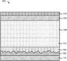
- FIG. 13Aillustrates a cross-sectional view of a photovoltaic device with a textured semiconductor layer etched using an etching period in accordance with aspects described in this disclosure.
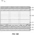
- FIG. 13Billustrates a cross-sectional view of a photovoltaic device with a textured semiconductor layer etched using another etching period in accordance with aspects described in this disclosure.
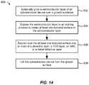
- FIG. 14illustrates a flowchart of a method for texturing a semiconductor layer using an etching process in accordance with aspects described in this disclosure.
- FIG. 15illustrates a flowchart of another method for texturing a semiconductor layer using an etching process in accordance with aspects described in this disclosure.
- Textured layers in this disclosuremay refer to, for example, a semiconductor layer having at least one textured surface, where the semiconductor layer is part of an optoelectronic device.
- a layercan be described as being deposited “on” or “over” one or more other layers. These terms indicate that the layer can be deposited directly on top of the other layer(s), or can indicate that one or more additional layers can be deposited between the layer and the other layer(s) in some implementations. Also, the other layer(s) can be arranged in any order.
- PV devicesrelate to light trapping using textured layer(s) for greater device efficiency.
- the various implementations and aspects described hereinmay also apply to LEDs to can improve efficiency by making it easier for light to escape (e.g., by scattering) from the LED into its surrounding environment.
- a lift-off processe.g., ELO process
- a photovoltaic device sunny side downgives the opportunity to place light scattering texture on the back of the photovoltaic device (e.g., solar cell).
- the issue that may arise, particularly when the layer in the photovoltaic structure that is to be layered is grown (e.g., epitaxially grown),is how to produce such light scattering texturing in a way that is compatible with the fabrication techniques and costs for generating the photovoltaic device.
- etchantse.g., etching solutions
- An epitaxially grown materialmay refer to a material grown as a layer or film, typically using precursors (e.g., gas and/or liquid precursors), over a substrate or other layer/film that acts as a seed crystal. Accordingly, it is preferable that the process of texturing is applied to a semiconductor layer grown with a minimal amount of epitaxial material (e.g., small thickness) to reduce the costs associated with generating the texturing.
- precursorse.g., gas and/or liquid precursors
- a templatee.g., a template layer
- a template layerfor explicit patterning using techniques such as photolithography, stamping, e-beam lithography, to name a few.
- spinning on microscopic or nanoscopic spheres that could provide an etching mask for plasma etchingmay be considered.
- texturingcan be produced by using mismatch layers where there is a lattice mismatch between a contact layer and the template layer, for example.
- layer mismatchallows for a random but controllable template layer.
- the template layercreates islands or regions with gaps between the islands and that provides a natural template where a selective etchant can etch between the islands to produce texturing.
- a spatially non-uniform texturingmay be generated on the surface of a semiconductor material that is suitable for light scattering without the need for a thick semiconductor layer, mismatch layers, and/or explicit patterning.
- Such etching processcan create a spatially non-uniform texturing on semiconductor layers that may not be possible by straight acids.
- a semiconductor layerwhen nitric acid is used as an etchant, a semiconductor layer may need to be about 4-5 microns thick to allow for the etching process to produce an appropriate texturing suitable for light scattering.
- an etching processthat results in an inhomogeneous etching (e.g., that produces microscopically non-uniform features) of the semiconductor layer it is then possible to produce an appropriate level of texturing but with a much thinner semiconductor layer.
- using such an etching processmay require semiconductor layers having a 1-1.5 micron thickness, and it may be possible with sub-micron layers.
- the use of an initial semiconductor layer that is 1-1.5 micron thicknessprovides sufficient sacrificial material (e.g., material to be wasted through the etching process) to produce the appropriate level of texturing.
- photovoltaic cells based on crystalline siliconcan use etching techniques to create light scattering surfaces, such techniques apply to silicon wafers that are very thick in comparison to epitaxially grown III-V semiconductor materials, and consequently, can have various microns of material wasted in the etching process.
- any photovoltaic device based (or LED) on III-V semiconductor materials that are epitaxially grownit would be cost prohibitive to provide texturing by removing one or more microns of sacrificial material.
- the semiconductor layer to be texturedmay need to be thinner than the absorber layer to keep costs down. Therefore, for a photovoltaic device having an absorber layer that is 2 microns thick, or thinner, the semiconductor layer to be textured for light scattering can be in the range of 1-1.5 microns thick, or thinner. Using a semiconductor layer thicker than that, as used for crystalline silicon, would otherwise be too costly.
- FIG. 1Aillustrates a cross-sectional view of an implementation of a photovoltaic device 100 suitable for use with the various aspects for texturing described herein. That is, one or more layers of FIG. 1A may be textured using the texturing techniques described below.
- examples hereinrelate to photovoltaic devices, described features can also be applied to other optoelectronic semiconductor devices, such as light emitting diodes (LEDs), for example, to scatter light in the device to provide increased or more efficient light generation.
- LEDslight emitting diodes
- the optoelectronic device 100includes a p-n layer 120 coupled with a growth wafer 101 by an epitaxial lift-off (ELO) release layer or sacrificial layer 104 disposed therebetween. Multiple layers of epitaxial materials containing varying compositions are deposited within the optoelectronic device 100 . The various layers of epitaxial materials can be grown or otherwise formed by a suitable method for semiconductor growth, including epitaxial growth.
- the p-n layer 120can be, for example, a gallium arsenide based optoelectronic device with layers made of Group III-V semiconductor materials. The Group III-V semiconductor materials are thin films of epitaxially grown layers.
- the epitaxially grown layerscan be formed by growing Group III-V semiconductor materials during, for example, a high growth rate vapor deposition process.
- a high growth rate deposition processallows for growth rates of greater than 5 microns/hour ( ⁇ m/hr), such as about 10 ⁇ m/hr or greater, or as high as about 100 ⁇ m/hr or greater.
- the term “about”may indicate a value that is within 1%, 2%, 5%, 10%, or 20% of a nominal value.
- the high growth rate processincludes heating a wafer to a deposition temperature of about 550° C.
- a deposition gas containing a chemical precursorsuch as gallium precursor gas and arsine for a gallium arsenide deposition process, and depositing a layer containing gallium arsenide on the wafer.
- the deposition gascan contain a Group V precursor, such as arsine, phosphine, or ammonia.
- the deposition processes for depositing or forming Group III-V semiconductor materialscan be conducted in various types of deposition chambers.
- one continuous feed deposition chamberthat can be utilized for growing, depositing, or otherwise forming Group III-V semiconductor materials is described in the commonly assigned U.S. patent application Ser. Nos. 12/475,131 and 12/475,169, both filed on May 29, 2009, which are herein incorporated by reference in their entireties.
- one or more buffer layers 102can be formed on the growth wafer 101 in order to start forming the optoelectronic device 100 .
- the growth wafer 101can include, for example, a p-type, an n-type, or semi-insulating material, and can include the same or similar material as the one or more subsequently deposited buffer layers.
- the growth wafer 101may be referred to as a substrate layer, growth substrate, or substrate.
- a sacrificial layer (ELO release layer) 104can be deposited on the growth wafer 101 or buffer layer 102 (if present).
- the sacrificial layer 104can contain a suitable material, such as aluminum arsenide (AlAs), aluminum gallium arsenide (AlGaAs), indium aluminum arsenide (InAlAs), or another aluminum arsenide alloy, and is utilized to form a lattice structure for the layers contained within the p-n layer 120 , and then etched and removed during the ELO process.
- the p-n layer 120can comprise multiple layers deposited over the sacrificial layer 104 , which in some implementations can include one or more of a first contact layer, a first window layer, base layer, an emitter layer, and a second window layer.
- a second contact layer 112can be deposited over the p-n layer 120 .
- FIG. 1Bshows an example of the photovoltaic device 100 in which the p-n layer 120 includes a first contact layer 105 , a first window layer 106 , a base layer 108 , and an emitter layer 110 .
- the first contact layer 105may be referred to as a front contact layer
- the first window layer 106may be referred to as a front window layer.
- a second window layermay be disposed opposite of the placement of the first window layer in the photovoltaic device 100 .
- Any references in this disclosure to a p-n layer 120may refer to the p-n layer 120 as described in the examples shown in FIGS. 1A and 1B , but need not be limited to the examples shown in FIGS. 1A and 1B .
- the p-n layer 120or portions of the p-n layer 120 (e.g., a subset of the layers), as described in FIG. 1B in certain embodiments or implementations in the figures, the p-n layer 120 , or portions of the p-n layer 120 as described in FIG. 1A may be similarly applicable in those same embodiments or implementations.
- the contact of the base layer with the emitter layercreates a p-n junction.
- Other implementationscan include one or more intermediate layers between the base layer and the emitter layer.
- the p-n junctionis a homojunction, in other embodiments it is a heterojunction.
- the at least one intermediate layer, if present,has graded doping and/or composition.
- the base layeris n-type while the emitter layer is p-type, while in other embodiments the base layer is p-type while the emitter layer is n-type.
- the p-n junctionis closer to the first window layer than to the second window layer, while in other embodiments the p-n junction is closer to the second window layer than to the first window layer, while in yet other embodiments the p-n junction is equidistant from the first window layer and the second window layer.
- a second contact layer 112 for texturingcan optionally be deposited over the emitter layer 110 as in FIG. 1B , or over the p-n layer 120 as in FIG. 1A .
- the second contact layer 112can provide a first layer on which a semiconductor layer (or multiple layers forming the semiconductor layer) is deposited for texturing purposes.
- the second contact layer 112can be the semiconductor layer to be textured and no additional layer is provided for texturing.
- the semiconductor layer, when textured,may be referred to as a textured semiconductor layer.
- the second contact layer 112can be monocrystalline, and n-doped or p-doped, and have a doping concentration in a range of about 5 ⁇ 10 17 cm ⁇ 3 to about 5 ⁇ 10 20 cm ⁇ 3 .
- the second contact layer 112is described in greater detail below.
- the second contact layer 112is not included in the optoelectronic device 100 .
- a semiconductor layer(described below) can be deposited on the p-n layer 120 without the need of the second contact layer 112 .
- a semiconductor layer to be texturedcan, but need not be, substantially etched away in the process of forming a textured surface, altering the textured surface, or both. That is, the semiconductor layer can be partially present after the etching process.
- the textured semiconductor layermay be used to form or produce another textured layer and the textured semiconductor layer could be partially or wholly removed in subsequent processing steps prior to completion of fabrication of the optoelectronic device.
- the semiconductor layercan include a semiconductor material, and can be a different material than the material of the second contact layer 112 upon which the semiconductor layer is deposited (or different from the p-n layer 120 when a second contact layer 112 is not used).
- the semiconductor layercan be a material having a different band gap from the material of the second contact layer 112 .
- the semiconductor layercan comprise phosphorus, gallium, aluminum, indium, arsenic, antimony, nitrogen, derivatives thereof, and/or combinations thereof.
- the second contact layer 112can comprise gallium arsenide (GaAs) or aluminum gallium arsenide (AlGaAs), and the semiconductor layer can comprise gallium arsenide (GaAs), aluminum gallium arsenide (AlGaAs), indium gallium arsenide (InGaAs) or gallium arsenide antimonide (GaAsSb).
- the second contact layer 112can comprise aluminum gallium arsenide (AlGaAs) and the semiconductor layer can comprise gallium arsenide (GaAs), aluminum gallium arsenide (AlGaAs), or gallium phosphide (GaP).
- the second contact layer 112can comprise indium arsenide (InAs) and the semiconductor layer can comprise gallium arsenide (GaAs), aluminum gallium arsenide (AlGaAs), or indium arsenide antimonide (InAsSb).
- the second contact layer 112can comprise gallium indium phosphide (GaInP) and the semiconductor layer can comprise gallium arsenide (GaAs), aluminum gallium arsenide (AlGaAs), gallium phosphide (GaP) or aluminum phosphide (AlP).
- the second contact layer 112can comprise indium phosphide (InP) and the semiconductor layer can comprise gallium arsenide (GaAs), aluminum gallium arsenide (AlGaAs), or indium phosphide antimonide (InPSb).
- the semiconductor layercan comprise gallium indium nitride arsenide (GaInNAs), gallium nitride arsenide (GaNAs), gallium arsenide phosphide (GaAsP), aluminum gallium arsenide phosphide (AlGaAsP), or aluminum gallium phosphide (AlGaP).
- the semiconductor layer materialcan be n-doped or p-doped, and can have a doping concentration in a range of about 1 ⁇ 10 17 cm ⁇ 3 to about 5 ⁇ 10 20 cm ⁇ 3 .
- the semiconductor layerincludes a material that has an index of refraction (n) and an absorption (k) that increases or maximizes the ability to scatter or reflect light.
- semiconductor layercan comprise a transparent material to allow light to pass through the semiconductor layer.
- transparentrefers to a negligible amount of absorption in the wavelength range of operation of the optoelectronic device.
- the semiconductor layercan have an index of refraction in a range of about 1 to about 6.
- the material of the semiconductor layercan have an absorption (k) in a range of about 0 to about 5, such as about 1 ⁇ 10 ⁇ 3 or about 1 ⁇ 10 ⁇ 4 .
- the semiconductor layercan comprise multiple transparent layers.
- the semiconductor layercan include a layer of graded composition, for example, any of the Group III-V semiconductor materials where composition can be varied.
- the semiconductor layercomprises a graded layer which grades from aluminum gallium arsenide of one composition (Al x Ga 1-x As) to aluminum gallium arsenide of a different composition (Al y Ga 1-y As, where x ⁇ y).
- the semiconductor layercan include a layer of graded doping.
- the semiconductor layercomprises a layer of graded doping which grades from a lower dopant concentration nearer the p-n layer to a higher dopant concentration farther from the p-n layer.
- various parameters of the deposition processcan be changed or tuned for the deposition of the semiconductor layer, as compared to the deposition parameters used during deposition of previous layers such as the second contact layer 112 .
- the temperature, pressure, deposition gas, and/or growth rate of the deposition processcan be changed, as described in greater detail below.
- a textured surface of the semiconductor layeris formed as a non-active scattering layer having features (e.g., non-uniform microscopic features) not provided within a base layer or an emitter layer, and since a greater degree of variation, irregularity or randomness is preferred in the textured formation, a high-quality semiconductor is not necessary as the material of the semiconductor layer in some implementations. This can allow some reduction in cost of materials and/or processing compared to previous techniques in which precisely-dimensioned and precisely-spaced islands were grown in absorber layers of a device (e.g., for tuning wavelength emissions in semiconductor lasers). In addition, the use of lesser-quality semiconductors for the semiconductor layer to be textured can allow higher growth rates of the semiconductor layer in some implementations. However, it is important that defect states in the semiconductor layer do not contribute significantly to parasitic absorption of light.
- etchingcan be performed on a semiconductor layer.
- the parameters of the etchingcan be controlled over the morphology and dimensions of the texture, thereby maximizing the benefit of the texture to the device performance.
- the etchingcan be one or more of chemical etching, laser etching, plasma etching, ion etching, or the like. Additional details regarding the spatially and microscopically non-uniform etching process of the present disclosure are provided below.
- the etching processis done by chemical etching. In some implementations that chemical etching creates a non-uniform surface. In some implementations the chemical etching has a spatially and/or temporally non-uniform etch rate (e.g., etch rate varies with position and/or time) that allows for the creation of a non-uniform surface (e.g., spatially non-uniform surface). In some implementations the chemical etching involves a mixture that can include one or more of inorganic acids, organic acids, bases, oxidizers, and/or solvents.
- a semiconductor layer and the second contact layer 112can be partially etched to create the appropriate texturing.
- the etching process to create the texturingmay not be restricted to the second contact layer 112 and those layers above layer 112 , but rather extends also to the p-n layer 120 .
- the photovoltaic device 100 of FIG. 1A or FIG. 1Bhas been further developed by depositing a semiconductor layer 140 over the second contact layer 112 , an optional semiconductor contact layer 160 over the semiconductor layer 140 , followed by the deposition of a layer 162 over the semiconductor contact layer 160 (if present) or over the semiconductor layer 140 (if the semiconductor contact layer 160 is not present).
- the layer 162may be a dielectric layer, a transparent conductive oxide (TCO) layer, a high-resistivity transparent (HRT) layer, or some other similar layer.
- TCOtransparent conductive oxide
- HRThigh-resistivity transparent
- the semiconductor layer 140is shown in the example Figures described below.
- the semiconductor layer 140may be textured using the techniques and/or processes described herein to produce light scattering.
- the semiconductor contact layer 160can be deposited in some implementations to, for example, provide a cap on the semiconductor layer 140 and to allow other layers to be more easily deposited over the semiconductor layer 140 , and/or to provide a better ohmic contact for charge carrier movement in the photovoltaic device 100 .
- the semiconductor contact layer 160can be comprised of a semiconductor such as gallium arsenide (GaAs) (e.g., with lower thicknesses since it can be less transparent), aluminum gallium arsenide (AlGaAs) (e.g., with higher thicknesses since it can be more transparent), or other materials, and can be p-doped in some implementations, having a thickness in a range of about 5 nm to about 2500 nm.
- GaAsgallium arsenide
- AlGaAsaluminum gallium arsenide
- the microscopic features (e.g., cavities, holes, trenches, etc.) of the textured surface of the semiconductor layer 140can form recesses in the layer(s) deposited above the semiconductor layer 140 , such that in a back reflector implementation, light traveling through the material of the semiconductor layer 140 impinges on and reflects off (e.g., is scattered by) the surfaces of the recesses.
- Some examplesare shown in greater detail with respect to FIG. 9 .
- scattering particlesmay be introduced into the layer 162 as a mechanism to provide additional increases in scattering efficiency.
- a different materialcan be deposited instead of layer 162 over the semiconductor contact layer 160 or over the semiconductor layer 140 (if the semiconductor contact layer 160 is not present).
- a transparent conducting oxide (TCO) layercan be deposited to provide boosted reflection abilities similar to a dielectric layer, and also provide a conductive path for charge carriers between the semiconductor layers and a conductive metal layer provided over the TCO layer.
- aperturessuch as those described for the layer 162 in FIG. 3 need not be formed in the TCO layer.
- a high-resistivity transparent (HRT) layercan also be provided between the TCO layer and a semiconductor layer (such as semiconductor layer 140 , emitter layer 110 , or absorber layer 108 ).
- the HRT layercan reduce shunting of charge carriers through pin holes in the semiconductor material.
- the HRT layercan be deposited using various processes including but not limited to, for example, screen printing, inkjet printing, evaporation techniques, spin coating, digital printing, screen print masking, and/or shadow masking.
- FIG. 3illustrates the photovoltaic device 100 of FIG. 2 after apertures 164 have been formed in the layer 162 to allow a conductive contact through the layer 162 .
- the apertures 164are formed through the layer 162 from the surface of the layer 162 to the semiconductor contact layer 160 .
- the apertures 164can be formed from the surface of the layer 162 to the semiconductor layer 140 .
- the apertures 164are formed by etching using an etching process.
- the etching processcan be performed using any of available suitable techniques.
- a particular pattern of apertures 164 in the layer 162can be provided with a mask such as a photoresist/etching mask.
- FIG. 4shows one example of a top view of a mask pattern 165 providing the apertures 164 in the layer 162 , in which the apertures are circular holes 166 having an approximately circular cross section (approximately circular in the top view of FIG. 4 ).
- the holesmay have other geometric shapes.
- the holesmay be square holes rather than circular holes, with an approximately square cross-section.
- the apertures 164may have a periodic or irregular/random spacing.
- FIG. 5shows another example of a top of view of a mask pattern 167 providing the apertures 164 in the layer 162 , in which the apertures are linear grooves.
- One or more grooves 168can intersect one or more other grooves 169 as shown.
- the groovescan be positioned approximately parallel and/or perpendicular to each other as shown, or can be positioned at various other angles in other implementations.
- the groovesneed not be uniformly spaced. Non-linear or irregular grooves can be used in other implementations.
- a direct or maskless patterning processmay be used.
- Layer 162 layercan be deposited using various processes including but not limited to, for example, screen printing, inkjet printing, evaporation techniques, spin coating, digital printing, screen print masking, and/or shadow masking.
- the photovoltaic device 100has been further developed by depositing a reflective back metal layer 170 over the layer 162 , providing one example of a textured layer 180 .
- the textured layer 180may include the textured semiconductor layer 140 .
- a reference to a textured layermay be a reference to the textured layer 180 or the textured semiconductor layer 140 , for example.
- the metal layer 170comprises a metal that reflects light efficiently.
- the metal layer 170can be comprised of gold, silver, copper, platinum, aluminum, or other reflective metals, derivatives thereof, and/or combinations thereof.
- the metal layer 170may be deposited using different techniques including, but not limited to, sputtering, evaporation, and/or plating.
- the deposition of the metal layer 170provides an approximately flat surface opposite to the semiconductor layer 140 .
- the semiconductor layer 140has received etching (e.g., temporally non-uniform etching) prior to subsequent processing steps.
- the metal layer 170can have an average thickness in a range of about 50 nm to about 10 ⁇ m.
- the material of the metal layer 170also is deposited into the apertures 164 so that a conductive contact is made between the metal layer 170 and the semiconductor contact layer 160 , or between the metal layer 170 and the semiconductor layer 140 if the semiconductor contact layer 160 is not present.
- the metal layer 170can be deposited over the semiconductor layer 140 without having a layer 162 and/or a semiconductor contact layer 160 deposited between the metal layer 170 and the semiconductor layer 140 .
- the optoelectronic device 185is shown flipped over in orientation after a lift-off process has removed some of the layers shown in previous Figures.
- some layers of the photovoltaic device 100such as the p-n layer 120 , and the textured layer 180 (including the semiconductor layer 140 ) can be separated from the growth wafer 101 and any buffer layer(s) 102 during an ELO process.
- the optoelectronic device 100can be exposed to an etchant solution in order to etch the sacrificial layer 104 and to separate the p-n layer 120 from the growth wafer 101 during an epitaxial lift off (ELO) process.
- FIG. 7shows aspects of an example of the p-n layer 120 in its resulting orientation, with the front of the p-n layer 120 oriented at the top of the cell, where light impinges on and enters the p-n layer 120 .
- the textured layer 180thus acts as a back reflector at a position further from the front of the p-n layer 120 than the p-n junction formed by the absorber (or base) and emitter layers.
- the p-n layer 120can be further processed to form a variety of optoelectronic devices, including photovoltaic cells and modules, and other devices described above.
- metal contacts 190can be deposited on the front contact layer 105 .
- the photovoltaic cell or moduleis physically flexible after the ELO process.
- the first contact layeris a front contact layer
- the first window layeris a front window layer
- the second window layeris a back window layer
- the second contact layer 112is a back contact layer.
- the first contact layeris a back contact layer
- the first window layeris a back window layer
- the second window layeris a front window layer
- the second contact layer 112is a front contact layer
- FIG. 8shows a diagram illustrating a portion 200 of the p-n layer 120 of FIG. 7 , and in which light is received by the textured layer 180 acting as a back reflector layer.
- An active layer or region 202is provided over a textured layer 180 , also referred to as a textured reflective layer.
- the active layer 202can be a solar cell active region such as an emitter layer 110 and/or absorber layer 108 .
- One or more other layers 204can also be positioned between the active layer 202 and the textured layer 180 in some implementations.
- light 206has traveled into the cell 120 and has not been absorbed by the upper layers. This light 206 emerges from the active layer 202 and impinges on the front surface 210 of the textured layer 180 . The light 206 passes through the transparent material of the semiconductor layer 140 . In some implementations, the semiconductor layer 140 has received etching (e.g., temporally non-uniform etching process) prior to subsequent processing steps. Some of the photons of the light 206 can hit a surface of the layer 162 and are reflected from that layer. Other photons of the light 206 can pass through the layer 162 and can hit a surface of the back metal layer 170 and are reflected from that layer.
- etchinge.g., temporally non-uniform etching process
- the reflected photonsare directed back through the semiconductor layer 140 and then into the active layer 202 as indicated by arrows 212 , where they can “bounce around” and can be captured by the absorber layer 108 and emitter layer 110 and further generate current in the cell 120 .
- the features of the texturing of the semiconductor layer 140create recesses 172 in the layer 162 and the back metal layer 170 . This creates a randomized, roughened, and angled front surface of the layer 162 and the back metal layer 170 .
- the textured layer 180diffuses or scatters photons that pass through the active layer 202 without being absorbed.
- the texturing of the textured layer 180e.g., the microscopic, non-uniform surface features
- the different angles on the surfaces of the textured layer 180 and its recesses 172thus effectively cause the photons of the light 206 to reflect at random angles back into the active layer 202 to allow a greater amount of them to be recaptured by the active layer and converted into electrical energy, thereby increasing the light trapping properties of the cell 120 and increasing efficiency.
- FIG. 9is a cross-sectional view of an implementation of a photovoltaic device 300 suitable for providing a textured layer at a front side of the device.
- a textured layercan be provided for light trapping at the front side of a photovoltaic cell instead of, or in addition to, the back-side light trapping described above. This allows light impinging on the front side of the photovoltaic device to become scattered in the device by a textured surface created by the textured layer, increasing light trapping in the device.
- the photovoltaic device 300includes a p-n layer or cell 320 coupled with a growth wafer 301 by an ELO release layer or sacrificial layer 304 disposed therebetween.
- one or more buffer layers 302can be formed on the growth wafer 301 in order to start forming the photovoltaic device 300 .
- Layers of the photovoltaic cell 320can be deposited over the sacrificial layer 304 , which in some implementations can include a back semiconductor contact layer 312 , an emitter layer 310 over the back semiconductor contact layer 312 , a base layer 308 over the emitter layer 310 (or emitter layer 310 over the base layer 308 ), a front window or passivation layer 306 over the absorber layer 308 , and a layer 305 for texturing, provided over the window layer 306 .
- the layer 305 for texturingis similar to the second contact layer 112 described above with reference to FIGS. 1A and 1B .
- the p-n layer 320can include different layers, a non-limiting example of a combination of layers being shown in FIG. 9 .
- the back contact layer 312can be comprised of a non-metal Group III-V semiconductor material, such as gallium arsenide.
- the photovoltaic device 300is not grown on a sacrificial or ELO release layer structure as shown.
- the photovoltaic device 300is not included an ELO lift-off procedure and is grown on a substrate without the sacrificial layer 104 or buffer layers 302 .
- FIG. 10is a cross-sectional view of the photovoltaic device 300 including a deposition of a semiconductor layer 340 on the layer 305 according to one implementation of a textured layer for use as a front side light trapping layer.
- the semiconductor layer 340can provide a textured surface formed using the etching processes described herein to cause light reflection and scattering in the device, increasing light trapping.
- the semiconductor layer 340has received etching (e.g., inhomogeneous etching process) prior to subsequent processing steps.
- the photovoltaic device 300has been further developed by depositing layers over the semiconductor layer 340 .
- an optional semiconductor contact layer 360is deposited over the semiconductor layer 340 .
- An anti-reflective coating (ARC) 362can be deposited over the semiconductor contact layer 360 (if present) or over the semiconductor layer 340 (if the semiconductor contact layer 360 is not present).
- the ARC layer 362includes a dielectric material that allows light to pass through while preventing light reflection from the surface of the ARC layer 362 .
- the ARC layer 362can comprise multiple layers.
- the p-n layer 320 along with layers 340 , 360 , 362 , and 312can be removed from the ELO layers 301 , 302 , and 304 shown in FIG. 9 using an ELO process. After removal, the p-n layer 320 retains its orientation shown in FIGS. 9-11 and is not flipped over in orientation as for the back side reflector implementation described above. In other implementations, no ELO process is used for the p-n layer 320 .
- the layers 340 , 360 , and 362provide a front side light-trapping textured layer 380 .
- the front side location of the textured layer 380allows it to receive light impinging on the device 300 and scatter the light at different angles into the lower layers of the device 300 due to the textured, randomized features in the semiconductor layer 340 . This promotes light trapping as the photons bounce within the lower layers, allowing more of them to be absorbed to generate current.
- the photovoltaic devices 100 and 300can be used in other implementations of the photovoltaic devices 100 and 300 .
- the emitter layercan be deposited over the absorber layer in some implementations.
- the implementations of the photovoltaic devices 100 and 300can be combined to produce photovoltaic devices that have both front-side and back-side textured surfaces form based on the etching techniques described herein.
- the etching process for generating textured surfaces described abovemay be performed between 4° C. to 70° C. with or without stirring.
- the surface preparationmay include a surface pre-clean, although the surface pre-clean may not be necessary.
- the surfacemay be cleaned to remove organic contamination and native oxide layer before etching.
- the surfacemay be cleaned using one or more acids, bases, and solvents that are capable of removing oxides, including sulfuric acid and ammonium hydroxide.
- the feature sizes or scale of the textured surfaces produced from the etchingare between 10 nm and 1000 nm, and more generally between 300 nm and 600 nm, and in some cases between 300 nm and 400 nm. These feature sizes can refer to both lateral and vertical (depth) feature sizes. In some instances, the upper range of the lateral features sizes can extend significantly, up to 5 microns.
- the etch rate used in the non-uniform etching processis in the range of 10 nm/min and 1000 nm/min, and more generally averaging about 300 nm/min. In some instances, however, the lower end of the etch rate can be 5 nm/min.
- the etching processhas different etching rates at the start of the process and at subsequent times.
- the spatial non-uniformity of the textured surfaces or textured materials described abovemay result in part from the use of the non-uniform etching process described herein. Aspects other than the change in etching rate may also influence the spatial non-uniformity of the textured surfaces or textured materials
- the thickness of the etched layer(e.g., the semiconductor layer to be etched) can be greater than 1000 nm. As described above, the layer to be etched can have a thickness of about 0.3-10 microns. In a non-limiting example, the material of the etched layer can be AlxGa1-xAs, 0 ⁇ x ⁇ 0.8.
- the chemistry of the etching solution used for the non-uniform etching processmay include the use of oxidizing agents to form an oxide on the surface of the Group III-V semiconductor materials and another chemical component that etches or removes the oxide that is formed.
- the etching solutionmay include an acid and hydrogen peroxide as the chemical components.
- the chemical ratiosare typically in the range of 1:1-1:100 for one chemical component relative to the other, with varying dilution with water to control etch rate.
- the surface preparationcan involve the use of organic solvents for removal of organic residue including acetone and isopropanol, and the use of uniform oxide growth promoters such as hydrogen peroxide.
- Oxide etchantsincluding hydrochloric acid, sulfuric acid, ammonium hydroxide, and nitric acid, and mixtures of these can be used.
- Other chemistries that can be useinclude organic solvents such as toluene, benzene, chlorobenzene, xylene, PGMEA, and chloroform, and oxide etchants such as KOH, HF, citric acid, Iodic acid, and phosphoric acid.
- etch chemistriesthat can be used include combinations of organic acids, sulfuric acid, hydrochloric acid, nitric acid, ammonium hydroxide, and hydrogen peroxide, as well as Iodic acid, phosphoric acid, HF, and citric acid.
- FIGS. 12A-12Cillustrate surface images at different etching times for an inhomogeneous etching process in accordance with aspects described in this disclosure.
- the etching times in FIGS. 12A-12Ccan range from about 30 seconds to 1 hour.
- FIG. 12Ashows a characterization of a scanning electrode microscope (SEM) image 400 after a first etching time
- FIG. 12Bshows a characterization of an SEM image 402 after a second etching time subsequent to the first etching time
- FIG. 12Cshows a characterization of an SEM image 404 after a third etching time subsequent to the second etching time.
- SEMscanning electrode microscope
- the etching process described hereinit is possible to characterize the etching process described herein to include a first portion associated with a first time period of the etching process that provides a particle aggregation effect, and a second portion associated with a second time period of the etching process that provides a surface roughening effect.
- FIG. 13Aillustrates a cross-sectional view of a photovoltaic device 500 with a textured semiconductor layer etched using an etching period in accordance with aspects described in this disclosure.
- the photovoltaic device 500can include a front contact layer 105 , a front window 106 , an absorber layer 108 , an emitter layer 110 , a semiconductor layer 140 , a layer 162 , and a metal layer 170 .
- the semiconductor layer 140 in FIG. 13Ais shown having a first textured surface.
- FIG. 13Billustrates a cross-sectional view of a photovoltaic device 602 with a textured semiconductor layer etched using another etching period in accordance with aspects described in this disclosure.
- the photovoltaic device 602like the photovoltaic device 600 in FIG. 16B , can include a front contact layer 105 , a front window 106 , an absorber layer 108 , an emitter layer 110 , a semiconductor layer 140 , a layer 162 , and a metal layer 170 .
- the semiconductor layer 140 in FIG. 13Bis shown having a second textured surface different from the first textured surface on the semiconductor layer 140 in FIG. 13A because of the different etching period.
- FIG. 14illustrates a flowchart of a method 600 for texturing a semiconductor layer in an optoelectronic device (e.g., a photovoltaic device) using an etching process in accordance with aspects described in this disclosure.
- an optoelectronic devicee.g., a photovoltaic device
- the method 600includes epitaxially growing a semiconductor layer of the optoelectronic device on a growth substrate.
- the semiconductor layerincludes at least one or more of gallium, aluminum, indium, phosphorus, nitrogen, or arsenic.
- the method 600includes exposing the semiconductor layer to an etching process (e.g., an inhomogeneous etching process that produces microscopically non-uniform features) to create at least one textured surface in the semiconductor layer.
- an etching processe.g., an inhomogeneous etching process that produces microscopically non-uniform features
- one or more of a dielectric layer, a TCO layer, an ARC, a high-resistivity transparent (HRT) layer, or a metal reflective layerare deposited over the at least one textured surface.
- the optoelectronic deviceis lifted from the growth surface to separate the device from the growth surface.
- the liftingmay be performed based on an ELO process, for example.
- the etching processcan be performed without the use of a template layer, lattice mismatching of layers, or both.
- the etching processcan be a spatially non-uniform etching process, and the at least one textured surface includes spatially non-uniform features.
- the etching processcan be done or performed by a liquid or solution-based chemical etchant, or by one or more of gas etching, laser etching, plasma etching, or ion etching.
- the at least one textured surfaceis configured to cause scattering of light.
- the at least one textured surfaceis configured to cause photons to scatter at randomized angles.
- FIG. 15illustrates a flowchart of another method 700 for texturing a semiconductor layer in an optoelectronic device (e.g., a photovoltaic device) using an etching process in accordance with aspects described in this disclosure.
- an optoelectronic devicee.g., a photovoltaic device
- the method 700includes depositing an emitter layer and a base layer over a growth substrate.
- the method 700includes epitaxially growing a semiconductor layer of the optoelectronic device over the emitter layer and the base layer.
- the semiconductor layerincludes at least one or more of gallium, aluminum, indium, phosphorus, nitrogen, or arsenic.
- the method 700includes exposing the semiconductor layer to an etching process (e.g., an inhomogeneous etching process that produces microscopically non-uniform features) to create at least one textured surface in the semiconductor layer.
- an etching processe.g., an inhomogeneous etching process that produces microscopically non-uniform features
- one or more of a dielectric layer, a TCO layer, an ARC, a high-resistivity transparent (HRT) layer, or a metal reflective layerare deposited over the at least one textured surface.
- the optoelectronic deviceis lifted from the growth surface to separate the device from the growth surface.
- the liftingmay be performed based on an ELO process, for example.
- Implementations of optoelectronic devices and methods to provide such devices described hereincan provide a textured layer (e.g., textured semiconductor layer) created for a textured surface allowing increased light trapping.
- Disclosed implementations and aspectsalso can provide advantages over previous light trapping layer formation techniques, including greater flexibility, reduced cost, and increased layer growth rate, saving time and expense in the manufacture of devices.
Landscapes
- Life Sciences & Earth Sciences (AREA)
- Sustainable Development (AREA)
- Photovoltaic Devices (AREA)
Abstract
Description
Claims (7)
Priority Applications (2)
| Application Number | Priority Date | Filing Date | Title |
|---|---|---|---|
| US15/422,218US11038080B2 (en) | 2012-01-19 | 2017-02-01 | Thin-film semiconductor optoelectronic device with textured front and/or back surface prepared from etching |
| US17/347,314US11942566B2 (en) | 2012-01-19 | 2021-06-14 | Thin-film semiconductor optoelectronic device with textured front and/or back surface prepared from etching |
Applications Claiming Priority (4)
| Application Number | Priority Date | Filing Date | Title |
|---|---|---|---|
| US13/354,175US9136422B1 (en) | 2012-01-19 | 2012-01-19 | Texturing a layer in an optoelectronic device for improved angle randomization of light |
| US14/452,393US9502594B2 (en) | 2012-01-19 | 2014-08-05 | Thin-film semiconductor optoelectronic device with textured front and/or back surface prepared from template layer and etching |
| US15/340,560US10008628B2 (en) | 2012-01-19 | 2016-11-01 | Thin-film semiconductor optoelectronic device with textured front and/or back surface prepared from template layer and etching |
| US15/422,218US11038080B2 (en) | 2012-01-19 | 2017-02-01 | Thin-film semiconductor optoelectronic device with textured front and/or back surface prepared from etching |
Related Parent Applications (1)
| Application Number | Title | Priority Date | Filing Date |
|---|---|---|---|
| US15/340,560Continuation-In-PartUS10008628B2 (en) | 2012-01-19 | 2016-11-01 | Thin-film semiconductor optoelectronic device with textured front and/or back surface prepared from template layer and etching |
Related Child Applications (1)
| Application Number | Title | Priority Date | Filing Date |
|---|---|---|---|
| US17/347,314DivisionUS11942566B2 (en) | 2012-01-19 | 2021-06-14 | Thin-film semiconductor optoelectronic device with textured front and/or back surface prepared from etching |
Publications (2)
| Publication Number | Publication Date |
|---|---|
| US20170148930A1 US20170148930A1 (en) | 2017-05-25 |
| US11038080B2true US11038080B2 (en) | 2021-06-15 |
Family
ID=58721105
Family Applications (2)
| Application Number | Title | Priority Date | Filing Date |
|---|---|---|---|
| US15/422,218Expired - Fee RelatedUS11038080B2 (en) | 2012-01-19 | 2017-02-01 | Thin-film semiconductor optoelectronic device with textured front and/or back surface prepared from etching |
| US17/347,314Active2032-05-16US11942566B2 (en) | 2012-01-19 | 2021-06-14 | Thin-film semiconductor optoelectronic device with textured front and/or back surface prepared from etching |
Family Applications After (1)
| Application Number | Title | Priority Date | Filing Date |
|---|---|---|---|
| US17/347,314Active2032-05-16US11942566B2 (en) | 2012-01-19 | 2021-06-14 | Thin-film semiconductor optoelectronic device with textured front and/or back surface prepared from etching |
Country Status (1)
| Country | Link |
|---|---|
| US (2) | US11038080B2 (en) |
Families Citing this family (18)
| Publication number | Priority date | Publication date | Assignee | Title |
|---|---|---|---|---|
| US11271128B2 (en) | 2009-10-23 | 2022-03-08 | Utica Leaseco, Llc | Multi-junction optoelectronic device |
| US9502594B2 (en) | 2012-01-19 | 2016-11-22 | Alta Devices, Inc. | Thin-film semiconductor optoelectronic device with textured front and/or back surface prepared from template layer and etching |
| US20150380576A1 (en) | 2010-10-13 | 2015-12-31 | Alta Devices, Inc. | Optoelectronic device with dielectric layer and method of manufacture |
| US20170141256A1 (en) | 2009-10-23 | 2017-05-18 | Alta Devices, Inc. | Multi-junction optoelectronic device with group iv semiconductor as a bottom junction |
| US11038080B2 (en) | 2012-01-19 | 2021-06-15 | Utica Leaseco, Llc | Thin-film semiconductor optoelectronic device with textured front and/or back surface prepared from etching |
| TWI629720B (en)* | 2015-09-30 | 2018-07-11 | 東京威力科創股份有限公司 | Method and apparatus for dynamic control of the temperature of a wet etch process |
| US10707379B2 (en) | 2015-10-01 | 2020-07-07 | Sensor Electronic Technology, Inc. | Configuration for optoelectronic device |
| US10854785B2 (en)* | 2015-10-01 | 2020-12-01 | Sensor Electronic Technology, Inc. | Contact configuration for optoelectronic device |
| CN109004042A (en)* | 2017-06-07 | 2018-12-14 | 中国科学院物理研究所 | Vertical-type opto-electronic device and its manufacturing method |
| DE102018107615B4 (en)* | 2017-09-06 | 2024-08-22 | OSRAM Opto Semiconductors Gesellschaft mit beschränkter Haftung | Method for producing an optoelectronic semiconductor chip and optoelectronic semiconductor chip |
| US10916672B2 (en)* | 2018-03-30 | 2021-02-09 | Lucintech Inc. | Method of making a photovoltaic cell, the photovoltaic cell made therewith, and an assembly including the same |
| US11393938B2 (en) | 2019-04-02 | 2022-07-19 | Utica Leaseco, Llc | Laser-textured thin-film semiconductors by melting and ablation |
| CN112310230A (en)* | 2019-07-31 | 2021-02-02 | 东泰高科装备科技有限公司 | Solar cell |
| TWM587826U (en)* | 2019-08-15 | 2019-12-11 | 凌巨科技股份有限公司 | Thin film solar cell |
| WO2022047098A1 (en)* | 2020-08-27 | 2022-03-03 | Utica Leaseco, Llc | Bifacial optoelectronic device with transparent conductive layer |
| US20220238747A1 (en) | 2021-01-28 | 2022-07-28 | Solaero Technologies Corp. | Inverted metamorphic multijunction solar cell |
| US11329181B1 (en) | 2021-03-03 | 2022-05-10 | Solaero Technologies Corp. | Multijunction solar cells |
| US20240258169A1 (en)* | 2023-01-31 | 2024-08-01 | Tokyo Electron Limited | Methods for fabricating semiconductor devices with backside power delivery network using laser liftoff layer |
Citations (164)
| Publication number | Priority date | Publication date | Assignee | Title |
|---|---|---|---|---|
| US3615853A (en) | 1970-01-28 | 1971-10-26 | Nasa | Solar cell panels with light-transmitting plate |
| US3838359A (en) | 1973-11-23 | 1974-09-24 | Bell Telephone Labor Inc | Gain asymmetry in heterostructure junction lasers operating in a fundamental transverse mode |
| US3990101A (en) | 1975-10-20 | 1976-11-02 | Rca Corporation | Solar cell device having two heterojunctions |
| US4015280A (en) | 1974-10-19 | 1977-03-29 | Sony Corporation | Multi-layer semiconductor photovoltaic device |
| US4017332A (en) | 1975-02-27 | 1977-04-12 | Varian Associates | Solar cells employing stacked opposite conductivity layers |
| US4094704A (en) | 1977-05-11 | 1978-06-13 | Milnes Arthur G | Dual electrically insulated solar cells |
| US4107723A (en) | 1977-05-02 | 1978-08-15 | Hughes Aircraft Company | High bandgap window layer for GaAs solar cells and fabrication process therefor |
| US4191593A (en) | 1977-09-27 | 1980-03-04 | Centre National D'etudes Spatiales | Double heterojunction solar cells |
| US4197141A (en) | 1978-01-31 | 1980-04-08 | Massachusetts Institute Of Technology | Method for passivating imperfections in semiconductor materials |
| US4295002A (en) | 1980-06-23 | 1981-10-13 | International Business Machines Corporation | Heterojunction V-groove multijunction solar cell |
| US4338480A (en) | 1980-12-29 | 1982-07-06 | Varian Associates, Inc. | Stacked multijunction photovoltaic converters |
| US4385198A (en) | 1981-07-08 | 1983-05-24 | The United States Of America As Represented By The Secretary Of The Air Force | Gallium arsenide-germanium heteroface junction device |
| US4400221A (en) | 1981-07-08 | 1983-08-23 | The United States Of America As Represented By The Secretary Of The Air Force | Fabrication of gallium arsenide-germanium heteroface junction device |
| US4410758A (en) | 1979-03-29 | 1983-10-18 | Solar Voltaic, Inc. | Photovoltaic products and processes |
| US4419533A (en) | 1982-03-03 | 1983-12-06 | Energy Conversion Devices, Inc. | Photovoltaic device having incident radiation directing means for total internal reflection |
| US4444992A (en) | 1980-11-12 | 1984-04-24 | Massachusetts Institute Of Technology | Photovoltaic-thermal collectors |
| US4479027A (en) | 1982-09-24 | 1984-10-23 | Todorof William J | Multi-layer thin-film, flexible silicon alloy photovoltaic cell |
| US4497974A (en) | 1982-11-22 | 1985-02-05 | Exxon Research & Engineering Co. | Realization of a thin film solar cell with a detached reflector |
| US4543441A (en) | 1983-02-14 | 1985-09-24 | Hitachi, Ltd. | Solar battery using amorphous silicon |
| US4571448A (en) | 1981-11-16 | 1986-02-18 | University Of Delaware | Thin film photovoltaic solar cell and method of making the same |
| US4582952A (en) | 1984-04-30 | 1986-04-15 | Astrosystems, Inc. | Gallium arsenide phosphide top solar cell |
| US4633030A (en) | 1985-08-05 | 1986-12-30 | Holobeam, Inc. | Photovoltaic cells on lattice-mismatched crystal substrates |
| US4667059A (en) | 1985-10-22 | 1987-05-19 | The United States Of America As Represented By The United States Department Of Energy | Current and lattice matched tandem solar cell |
| JPS63211775A (en) | 1987-02-27 | 1988-09-02 | Mitsubishi Electric Corp | compound semiconductor solar cell |
| US4773945A (en) | 1987-09-14 | 1988-09-27 | Ga Technologies, Inc. | Solar cell with low infra-red absorption and method of manufacture |
| US4775639A (en) | 1986-12-24 | 1988-10-04 | Mitsubishi Denki Kabushiki Kaisha | Method of manufacturing Group III-V compound semiconductor solar battery |
| US4889656A (en) | 1987-10-30 | 1989-12-26 | Minnesota Mining And Manufacturing Company | Perfluoro(cycloaliphatic methyleneoxyalkylene) carbonyl fluorides and derivatives thereof |
| US4916503A (en) | 1987-07-08 | 1990-04-10 | Hitachi, Ltd. | Photo-electric converting device |
| US4989059A (en) | 1988-05-13 | 1991-01-29 | Mobil Solar Energy Corporation | Solar cell with trench through pn junction |
| US4997491A (en) | 1988-11-16 | 1991-03-05 | Mitsubishi Denki Kabushiki Kaisha | Solar cell and a production method therefor |
| JPH03285368A (en) | 1990-04-02 | 1991-12-16 | Hitachi Cable Ltd | Gaas solar cell |
| US5101260A (en) | 1989-05-01 | 1992-03-31 | Energy Conversion Devices, Inc. | Multilayer light scattering photovoltaic back reflector and method of making same |
| US5103268A (en) | 1989-03-30 | 1992-04-07 | Siemens Solar Industries, L.P. | Semiconductor device with interfacial electrode layer |
| US5116427A (en) | 1987-08-20 | 1992-05-26 | Kopin Corporation | High temperature photovoltaic cell |
| US5136351A (en) | 1990-03-30 | 1992-08-04 | Sharp Kabushiki Kaisha | Photovoltaic device with porous metal layer |
| US5217539A (en) | 1991-09-05 | 1993-06-08 | The Boeing Company | III-V solar cells and doping processes |
| US5223043A (en) | 1991-02-11 | 1993-06-29 | The United States Of America As Represented By The United States Department Of Energy | Current-matched high-efficiency, multijunction monolithic solar cells |
| US5230746A (en) | 1992-03-03 | 1993-07-27 | Amoco Corporation | Photovoltaic device having enhanced rear reflecting contact |
| US5231931A (en) | 1992-01-23 | 1993-08-03 | J. Muller International | Rapid transit viaduct system |
| EP0595634A1 (en) | 1992-10-30 | 1994-05-04 | Spectrolab, Inc. | Gallium arsenide/aluminum gallium arsenide photocell including environmentally sealed ohmic contact grid interface and method of fabricating the cell |
| US5316593A (en) | 1992-11-16 | 1994-05-31 | Midwest Research Institute | Heterojunction solar cell with passivated emitter surface |
| US5342453A (en) | 1992-11-13 | 1994-08-30 | Midwest Research Institute | Heterojunction solar cell |
| US5356488A (en) | 1991-12-27 | 1994-10-18 | Rudolf Hezel | Solar cell and method for its manufacture |
| US5376185A (en) | 1993-05-12 | 1994-12-27 | Midwest Research Institute | Single-junction solar cells with the optimum band gap for terrestrial concentrator applications |
| JPH077148A (en) | 1993-03-19 | 1995-01-10 | Akzo Nobel Nv | Method for integrating semiconductor device with polymeric optical waveguide device and electro-optical device having integrated structure thus obtained |
| US5385960A (en) | 1991-12-03 | 1995-01-31 | Rohm And Haas Company | Process for controlling adsorption of polymeric latex on titanium dioxide |
| US5465009A (en) | 1992-04-08 | 1995-11-07 | Georgia Tech Research Corporation | Processes and apparatus for lift-off and bonding of materials and devices |
| US5468652A (en) | 1993-07-14 | 1995-11-21 | Sandia Corporation | Method of making a back contacted solar cell |
| JPH08130321A (en) | 1994-11-01 | 1996-05-21 | Matsushita Electric Ind Co Ltd | Solar cell |
| JPH09213206A (en) | 1996-02-06 | 1997-08-15 | Hamamatsu Photonics Kk | Transmission type photoelectric surface, manufacture thereof and photoelectric transfer tube using the transmission type photoelectric surface |
| US6107563A (en) | 1997-10-27 | 2000-08-22 | Sharp Kabushiki Kaisha | Photoelectric converter having light diffusion layer |
| US6166218A (en) | 1996-11-07 | 2000-12-26 | Ciba Specialty Chemicals Corporation | Benzotriazole UV absorbers having enhanced durability |
| US6166318A (en) | 1998-03-03 | 2000-12-26 | Interface Studies, Inc. | Single absorber layer radiated energy conversion device |
| US6229084B1 (en) | 1998-09-28 | 2001-05-08 | Sharp Kabushiki Kaisha | Space solar cell |
| US6231931B1 (en) | 1998-03-02 | 2001-05-15 | John S. Blazey | Method of coating a substrate with a structural polymer overlay |
| US6255580B1 (en) | 1999-04-23 | 2001-07-03 | The Boeing Company | Bilayer passivation structure for photovoltaic cells |
| US20010027805A1 (en) | 1998-05-28 | 2001-10-11 | Frank Ho | Solar cell having an integral monolithically grown bypass diode |
| US20020000244A1 (en) | 2000-04-11 | 2002-01-03 | Zaidi Saleem H. | Enhanced light absorption of solar cells and photodetectors by diffraction |
| US6372981B1 (en) | 1999-08-13 | 2002-04-16 | Oki Electric Industry Co., Ltd. | Semiconductor substrate, solar cell using same, and fabrication methods thereof |
| US20020053683A1 (en) | 2000-08-17 | 2002-05-09 | Hill Darrell G. | Method of manufacturing a semiconductor component and semiconductor component thereof |
| WO2002065553A1 (en) | 2001-02-09 | 2002-08-22 | Midwest Research Institute | Isoelectronic co-doping |
| US6452091B1 (en) | 1999-07-14 | 2002-09-17 | Canon Kabushiki Kaisha | Method of producing thin-film single-crystal device, solar cell module and method of producing the same |
| US20020144724A1 (en) | 1998-08-20 | 2002-10-10 | Kilmer Louis C. | Solar cell having a front-mounted bypass diode |
| US6534336B1 (en) | 1999-05-21 | 2003-03-18 | Canon Kabushiki Kaisha | Production method of photoelectric conversion device, and photoelectric conversion device produced by the method |
| US20030070707A1 (en) | 2001-10-12 | 2003-04-17 | King Richard Roland | Wide-bandgap, lattice-mismatched window layer for a solar energy conversion device |
| US20030140962A1 (en) | 2001-10-24 | 2003-07-31 | Sharps Paul R. | Apparatus and method for integral bypass diode in solar cells |
| US20030222278A1 (en) | 2002-06-04 | 2003-12-04 | National Cheng Kung University | Heterojunction bipolar transistor with zero conduction band discontinuity |
| US20040112426A1 (en) | 2002-12-11 | 2004-06-17 | Sharp Kabushiki Kaisha | Solar cell and method of manufacturing the same |
| US20040166681A1 (en) | 2002-12-05 | 2004-08-26 | Iles Peter A. | High efficiency, monolithic multijunction solar cells containing lattice-mismatched materials and methods of forming same |
| US20040200523A1 (en) | 2003-04-14 | 2004-10-14 | The Boeing Company | Multijunction photovoltaic cell grown on high-miscut-angle substrate |
| US20050001233A1 (en) | 2003-05-28 | 2005-01-06 | Kabushiki Kaisha Toshiba | Semiconductor device |
| US20050022863A1 (en) | 2003-06-20 | 2005-02-03 | Guido Agostinelli | Method for backside surface passivation of solar cells and solar cells with such passivation |
| US20060081963A1 (en) | 2004-10-20 | 2006-04-20 | Kopin Corporation | Bipolar transistor with enhanced base transport |
| US20060090790A1 (en) | 2004-10-29 | 2006-05-04 | Mitsubishi Heavy Industries, Ltd. | Photoelectric conversion device |
| US20060144435A1 (en) | 2002-05-21 | 2006-07-06 | Wanlass Mark W | High-efficiency, monolithic, multi-bandgap, tandem photovoltaic energy converters |
| US20060162767A1 (en) | 2002-08-16 | 2006-07-27 | Angelo Mascarenhas | Multi-junction, monolithic solar cell with active silicon substrate |
| US20060207651A1 (en) | 2003-05-07 | 2006-09-21 | Niels Posthuma | Germanium solar cell and method for the production thereof |
| US20060255340A1 (en) | 2005-05-12 | 2006-11-16 | Venkatesan Manivannan | Surface passivated photovoltaic devices |
| US20070040233A1 (en)* | 2005-08-22 | 2007-02-22 | Canon Kabushiki Kaisha | Photovoltaic device |
| US20070131275A1 (en) | 2005-12-13 | 2007-06-14 | The Boeing Company | Multijunction solar cell with bonded transparent conductive interlayer |
| US20070137698A1 (en) | 2002-02-27 | 2007-06-21 | Wanlass Mark W | Monolithic photovoltaic energy conversion device |
| US20070137695A1 (en) | 2005-12-19 | 2007-06-21 | The Boeing Company | Reduced band gap absorber for solar cells |
| US20070151596A1 (en) | 2004-02-20 | 2007-07-05 | Sharp Kabushiki Kaisha | Substrate for photoelectric conversion device, photoelectric conversion device, and stacked photoelectric conversion device |
| US20070166862A1 (en) | 2005-12-15 | 2007-07-19 | Lg Electronics Inc. | Method for fabricating substrate with nano structures, light emitting device and manufacturing method thereof |
| US20070199591A1 (en) | 2004-07-07 | 2007-08-30 | Saint-Gobain Glass France | Photovoltaic Solar Cell and Solar Module |
| KR100762772B1 (en) | 2003-09-09 | 2007-10-02 | 아사히 가세이 일렉트로닉스 가부시끼가이샤 | Infrared sensor ic, infrared sensor and method for producing same |
| US20070235074A1 (en) | 2006-03-17 | 2007-10-11 | Silicon Genesis Corporation | Method and structure for fabricating solar cells using a layer transfer process |
| US20070277874A1 (en) | 2006-05-31 | 2007-12-06 | David Francis Dawson-Elli | Thin film photovoltaic structure |
| US20080128020A1 (en) | 2006-11-30 | 2008-06-05 | First Solar, Inc. | Photovoltaic devices including a metal stack |
| WO2008100603A1 (en) | 2007-02-15 | 2008-08-21 | Massachusetts Institute Of Technology | Solar cells with textured surfaces |
| US20080245409A1 (en) | 2006-12-27 | 2008-10-09 | Emcore Corporation | Inverted Metamorphic Solar Cell Mounted on Flexible Film |
| US20090151784A1 (en) | 2007-12-14 | 2009-06-18 | Hsin-Chiao Luan | Anti-Reflective Coating With High Optical Absorption Layer For Backside Contact Solar Cells |
| US20090283802A1 (en) | 2008-05-15 | 2009-11-19 | Triquint Semiconductor, Inc. | Heterojunction bipolar transistor device with electrostatic discharge ruggedness |
| US20090288703A1 (en) | 2008-05-20 | 2009-11-26 | Emcore Corporation | Wide Band Gap Window Layers In Inverted Metamorphic Multijunction Solar Cells |
| US20100006143A1 (en) | 2007-04-26 | 2010-01-14 | Welser Roger E | Solar Cell Devices |
| US20100015751A1 (en) | 2008-07-16 | 2010-01-21 | Applied Materials, Inc. | Hybrid heterojunction solar cell fabrication using a metal layer mask |
| US20100047959A1 (en) | 2006-08-07 | 2010-02-25 | Emcore Solar Power, Inc. | Epitaxial Lift Off on Film Mounted Inverted Metamorphic Multijunction Solar Cells |
| US20100055397A1 (en) | 2006-11-15 | 2010-03-04 | National Institute Of Advanced Industrial Science And Technology | Mold for optical device with anti-reflection structure, method for producing the same, and optical device |
| US20100065117A1 (en) | 2008-09-16 | 2010-03-18 | Jinsung Kim | Solar cell and texturing method thereof |
| US20100089443A1 (en) | 2008-09-24 | 2010-04-15 | Massachusetts Institute Of Technology | Photon processing with nanopatterned materials |
| US20100096010A1 (en) | 2008-10-17 | 2010-04-22 | Kopin Corporation | Ingap heterojunction barrier solar cells |
| US20100126572A1 (en) | 2008-10-23 | 2010-05-27 | Kizilyalli Isik C | Photovoltaic device with back side contacts |
| US20100126570A1 (en) | 2008-10-23 | 2010-05-27 | Kizilyalli Isik C | Thin absorber layer of a photovoltaic device |
| US20100126552A1 (en) | 2008-10-23 | 2010-05-27 | Kizilyalli Isik C | Integration of a photovoltaic device |
| US20100126571A1 (en) | 2008-10-23 | 2010-05-27 | Kizilyalli Isik C | Photovoltaic device with increased light trapping |
| US20100132774A1 (en) | 2008-12-11 | 2010-06-03 | Applied Materials, Inc. | Thin Film Silicon Solar Cell Device With Amorphous Window Layer |
| US20100132780A1 (en) | 2008-10-23 | 2010-06-03 | Kizilyalli Isik C | Photovoltaic device |
| US20100193002A1 (en) | 2007-05-14 | 2010-08-05 | Fraunhofer-Gesellschaft Zur Foerderung Der Angewandten Forschung E.V. | Semiconductor component, method for the production thereof, and use thereof |
| US20100218819A1 (en) | 2007-10-05 | 2010-09-02 | The University Court Of The University Of Glasgow | Semiconductor optoelectronic devices and methods for making semiconductor optoelectronic devices |
| US20100270653A1 (en) | 2009-04-24 | 2010-10-28 | Christopher Leitz | Crystalline thin-film photovoltaic structures and methods for forming the same |
| US20100294349A1 (en) | 2009-05-20 | 2010-11-25 | Uma Srinivasan | Back contact solar cells with effective and efficient designs and corresponding patterning processes |
| US20100294356A1 (en) | 2009-04-24 | 2010-11-25 | Solexel, Inc. | Integrated 3-dimensional and planar metallization structure for thin film solar cells |
| US20100300506A1 (en)* | 2009-06-02 | 2010-12-02 | Sierra Solar Power, Inc. | Low-cost high-efficiency solar module using epitaxial si thin-film absorber and double-sided heterojunction solar cell with integrated module fabrication |
| US7875945B2 (en) | 2007-06-12 | 2011-01-25 | Guardian Industries Corp. | Rear electrode structure for use in photovoltaic device such as CIGS/CIS photovoltaic device and method of making same |
| CN102007582A (en) | 2008-04-17 | 2011-04-06 | 三菱电机株式会社 | Method for roughening substrate surface and method for manufacturing photovoltaic device |
| US20110083722A1 (en) | 2009-10-14 | 2011-04-14 | Alta Devices, Inc. | Textured metallic back reflector |
| US20110088771A1 (en) | 2009-10-19 | 2011-04-21 | Du Pont Apollo Ltd. | Process of manufacturing tco substrate with light trapping feature and the device thereof |
| US20110108098A1 (en) | 2006-10-09 | 2011-05-12 | Pawan Kapur | Structures and methods for high-efficiency pyramidal three-dimensional solar cells |
| US20110156000A1 (en) | 2009-12-30 | 2011-06-30 | Imec | Method of manufacturing a semiconductor device and semiconductor device |
| US20110189817A1 (en) | 2008-10-17 | 2011-08-04 | Ulvac, Inc. | Manufacturing method for solar cell |
| US20110214728A1 (en) | 2010-03-04 | 2011-09-08 | Guardian Industries Corp. | Electronic devices including transparent conductive coatings including carbon nanotubes and nanowire composites, and methods of making the same |
| US20110244692A1 (en) | 2010-04-02 | 2011-10-06 | The Board Of Trustees Of The Leland Stanford Junior University | Method for Forming a Nano-textured Substrate |
| US20110290322A1 (en) | 2009-02-03 | 2011-12-01 | Kaneka Corporation | Substrate with transparent conductive film and thin film photoelectric conversion device |
| US20120024336A1 (en) | 2010-07-27 | 2012-02-02 | Jeong-Mo Hwang | Charge control of solar cell passivation layers |
| US20120031478A1 (en) | 2010-08-09 | 2012-02-09 | The Boeing Company | Heterojunction Solar Cell |
| US20120055541A1 (en) | 2009-03-02 | 2012-03-08 | Fraunhofer-Gesellschaft Zur Forderung Der Angewandten Forschung E.V. | Front-and-back contact solar cells, and method for the production thereof |
| US20120067423A1 (en) | 2010-09-21 | 2012-03-22 | Amberwave, Inc. | Flexible Monocrystalline Thin Silicon Cell |
| US20120104411A1 (en) | 2010-10-29 | 2012-05-03 | The Regents Of The University Of California | Textured iii-v semiconductor |
| CN102473743A (en) | 2010-01-27 | 2012-05-23 | 因特潘开发咨询有限责任公司 | Method for producing a coated item by means of texture etching |
| US20120125256A1 (en) | 2007-10-06 | 2012-05-24 | Solexel, Inc. | Apparatus and method for repeatedly fabricating thin film semiconductor substrates using a template |
| US20120132930A1 (en) | 2010-08-07 | 2012-05-31 | Michael Eugene Young | Device components with surface-embedded additives and related manufacturing methods |
| US20120160296A1 (en) | 2011-09-30 | 2012-06-28 | Olivier Laparra | Textured photovoltaic cells and methods |
| US20120164796A1 (en) | 2007-05-31 | 2012-06-28 | Nthdegree Technologies Worldwide Inc. | Method of Manufacturing a Printable Composition of a Liquid or Gel Suspension of Diodes |
| US8258596B2 (en) | 2007-01-23 | 2012-09-04 | Sharp Kabushiki Kaisha | Stacked photoelectric conversion device and method for producing the same |
| US20120227805A1 (en) | 2009-09-21 | 2012-09-13 | Fraunhofer-Gesellschaft zur Förderung der angewandten Forschung e.V. | Solar cell |
| US20120247555A1 (en) | 2011-03-24 | 2012-10-04 | Panasonic Corporation | Solar cell |
| US20120305059A1 (en) | 2011-06-06 | 2012-12-06 | Alta Devices, Inc. | Photon recycling in an optoelectronic device |
| US20130025654A1 (en) | 2011-07-29 | 2013-01-31 | International Business Machines Corporation | Multi-junction photovoltaic device and fabrication method |
| US20130026481A1 (en) | 2011-07-26 | 2013-01-31 | Micron Technology, Inc. | Textured optoelectronic devices and associated methods of manufacture |
| US20130112258A1 (en) | 2011-11-03 | 2013-05-09 | Joong-hyun Park | Solar cell |
| US20130220396A1 (en) | 2010-08-24 | 2013-08-29 | Energy Research Centre Of The Netherlands | Photovoltaic Device and Module with Improved Passivation and a Method of Manufacturing |
| US20130270589A1 (en) | 2012-04-13 | 2013-10-17 | Alta Devices, Inc. | Optoelectronic device with non-continuous back contacts |
| GB2501432A (en) | 2009-02-19 | 2013-10-23 | Iqe Silicon Compounds Ltd | Germanium Based Photovoltaic Cell With GaAs Substrate Removed |
| US20130288418A1 (en) | 2008-11-13 | 2013-10-31 | Solexel, Inc. | Method for fabricating a three-dimensional thin-film semiconductor substrate from a template |
| US20130337601A1 (en) | 2012-02-29 | 2013-12-19 | Solexel, Inc. | Structures and methods for high efficiency compound semiconductor solar cells |
| US8664515B2 (en) | 2009-03-16 | 2014-03-04 | National Cheng Kung University | Solar concentrator |
| US20140076386A1 (en) | 2012-09-14 | 2014-03-20 | The Boeing Company | GROUP-IV SOLAR CELL STRUCTURE USING GROUP-IV or III-V HETEROSTRUCTURES |
| US8697553B2 (en) | 2008-06-11 | 2014-04-15 | Intevac, Inc | Solar cell fabrication with faceting and ion implantation |
| CN103952768A (en) | 2014-05-09 | 2014-07-30 | 中国科学院宁波材料技术与工程研究所 | A kind of monocrystalline silicon inverted pyramid array structure suede and its preparation method and application |
| US20140261611A1 (en) | 2013-03-14 | 2014-09-18 | The Boeing Company | Solar cell structures for improved current generation and collection |
| US20140312373A1 (en) | 2013-04-23 | 2014-10-23 | Cree, Inc. | Light emitting diodes having group iii nitride surface features defined by a mask and crystal planes |
| US8993873B2 (en) | 2008-11-26 | 2015-03-31 | Microlink Devices, Inc. | Solar cell with a backside via to contact the emitter layer |
| US20150171261A1 (en) | 2013-12-17 | 2015-06-18 | Tel Solar Ag | Transparent conductive oxide (tco) layer, and systems, apparatuses and methods for fabricating a transparent conductive oxide (tco) layer |
| US9099595B2 (en) | 2012-09-14 | 2015-08-04 | The Boeing Company | Group-IV solar cell structure using group-IV or III-V heterostructures |
| US20150228835A1 (en) | 2008-10-23 | 2015-08-13 | Alta Devices, Inc. | Optoelectronic devices including heterojunction and intermediate layer |
| US9136422B1 (en) | 2012-01-19 | 2015-09-15 | Alta Devices, Inc. | Texturing a layer in an optoelectronic device for improved angle randomization of light |
| EP2927968A1 (en) | 2014-04-01 | 2015-10-07 | Sharp Kabushiki Kaisha | Highly efficient photovoltaic energy harvesting device |
| US20150368833A1 (en) | 2014-06-19 | 2015-12-24 | John Farah | Laser epitaxial lift-off of high efficiency solar cell |
| US20150380576A1 (en) | 2010-10-13 | 2015-12-31 | Alta Devices, Inc. | Optoelectronic device with dielectric layer and method of manufacture |
| US20160155881A1 (en) | 2009-10-23 | 2016-06-02 | Alta Devices, Inc. | Thin film iii-v optoelectronic device optimized for non-solar illumination sources |
| WO2016123074A1 (en) | 2015-01-27 | 2016-08-04 | Alta Devices, Inc. | Thin film iii-v optoelectronic device optimized for non-solar illumination sources |
| US9502594B2 (en) | 2012-01-19 | 2016-11-22 | Alta Devices, Inc. | Thin-film semiconductor optoelectronic device with textured front and/or back surface prepared from template layer and etching |
| US20170141256A1 (en) | 2009-10-23 | 2017-05-18 | Alta Devices, Inc. | Multi-junction optoelectronic device with group iv semiconductor as a bottom junction |
| US9768329B1 (en) | 2009-10-23 | 2017-09-19 | Alta Devices, Inc. | Multi-junction optoelectronic device |
Family Cites Families (11)
| Publication number | Priority date | Publication date | Assignee | Title |
|---|---|---|---|---|
| US6262359B1 (en)* | 1999-03-17 | 2001-07-17 | Ebara Solar, Inc. | Aluminum alloy back junction solar cell and a process for fabrication thereof |
| DE102008013446A1 (en)* | 2008-02-15 | 2009-08-27 | Ersol Solar Energy Ag | Process for producing monocrystalline n-silicon solar cells and solar cell, produced by such a process |
| US9496308B2 (en)* | 2011-06-09 | 2016-11-15 | Sionyx, Llc | Process module for increasing the response of backside illuminated photosensitive imagers and associated methods |
| US20130043214A1 (en)* | 2011-06-29 | 2013-02-21 | The Regents Of The University Of Michigan | Sacrificial etch protection layers for reuse of wafers after epitaxial lift off |
| JP6082237B2 (en)* | 2011-12-09 | 2017-02-15 | 株式会社トクヤマ | Manufacturing method of silicon substrate having texture structure |
| US9257284B2 (en)* | 2012-01-13 | 2016-02-09 | Crystal Solar, Incorporated | Silicon heterojunction solar cells |
| US11038080B2 (en) | 2012-01-19 | 2021-06-15 | Utica Leaseco, Llc | Thin-film semiconductor optoelectronic device with textured front and/or back surface prepared from etching |
| JP5777798B2 (en)* | 2012-03-12 | 2015-09-09 | 三菱電機株式会社 | Method for manufacturing solar battery cell |
| WO2014175564A1 (en)* | 2013-04-22 | 2014-10-30 | 한국산업기술대학교산학협력단 | Method for manufacturing vertical type light emitting diode, vertical type light emitting diode, method for manufacturing ultraviolet ray light emitting diode, and ultraviolet ray light emitting diode |
| CN104143496B (en)* | 2013-05-08 | 2016-12-28 | 中国科学院上海高等研究院 | A kind of preparation method of polycrystal silicon film based on layer transfer |
| JP2022502895A (en) | 2018-09-28 | 2022-01-11 | テレフオンアクチーボラゲット エルエム エリクソン(パブル) | Coexistence of reference signals in wireless communication networks |
- 2017
- 2017-02-01USUS15/422,218patent/US11038080B2/ennot_activeExpired - Fee Related
- 2021
- 2021-06-14USUS17/347,314patent/US11942566B2/enactiveActive
Patent Citations (181)
| Publication number | Priority date | Publication date | Assignee | Title |
|---|---|---|---|---|
| US3615853A (en) | 1970-01-28 | 1971-10-26 | Nasa | Solar cell panels with light-transmitting plate |
| US3838359A (en) | 1973-11-23 | 1974-09-24 | Bell Telephone Labor Inc | Gain asymmetry in heterostructure junction lasers operating in a fundamental transverse mode |
| US4015280A (en) | 1974-10-19 | 1977-03-29 | Sony Corporation | Multi-layer semiconductor photovoltaic device |
| US4017332A (en) | 1975-02-27 | 1977-04-12 | Varian Associates | Solar cells employing stacked opposite conductivity layers |
| US3990101A (en) | 1975-10-20 | 1976-11-02 | Rca Corporation | Solar cell device having two heterojunctions |
| US4107723A (en) | 1977-05-02 | 1978-08-15 | Hughes Aircraft Company | High bandgap window layer for GaAs solar cells and fabrication process therefor |
| US4094704A (en) | 1977-05-11 | 1978-06-13 | Milnes Arthur G | Dual electrically insulated solar cells |
| US4191593A (en) | 1977-09-27 | 1980-03-04 | Centre National D'etudes Spatiales | Double heterojunction solar cells |
| US4197141A (en) | 1978-01-31 | 1980-04-08 | Massachusetts Institute Of Technology | Method for passivating imperfections in semiconductor materials |
| US4410758A (en) | 1979-03-29 | 1983-10-18 | Solar Voltaic, Inc. | Photovoltaic products and processes |
| US4295002A (en) | 1980-06-23 | 1981-10-13 | International Business Machines Corporation | Heterojunction V-groove multijunction solar cell |
| US4444992A (en) | 1980-11-12 | 1984-04-24 | Massachusetts Institute Of Technology | Photovoltaic-thermal collectors |
| US4338480A (en) | 1980-12-29 | 1982-07-06 | Varian Associates, Inc. | Stacked multijunction photovoltaic converters |
| US4400221A (en) | 1981-07-08 | 1983-08-23 | The United States Of America As Represented By The Secretary Of The Air Force | Fabrication of gallium arsenide-germanium heteroface junction device |
| US4385198A (en) | 1981-07-08 | 1983-05-24 | The United States Of America As Represented By The Secretary Of The Air Force | Gallium arsenide-germanium heteroface junction device |
| US4571448A (en) | 1981-11-16 | 1986-02-18 | University Of Delaware | Thin film photovoltaic solar cell and method of making the same |
| US4419533A (en) | 1982-03-03 | 1983-12-06 | Energy Conversion Devices, Inc. | Photovoltaic device having incident radiation directing means for total internal reflection |
| US4479027A (en) | 1982-09-24 | 1984-10-23 | Todorof William J | Multi-layer thin-film, flexible silicon alloy photovoltaic cell |
| US4497974A (en) | 1982-11-22 | 1985-02-05 | Exxon Research & Engineering Co. | Realization of a thin film solar cell with a detached reflector |
| US4543441A (en) | 1983-02-14 | 1985-09-24 | Hitachi, Ltd. | Solar battery using amorphous silicon |
| US4582952A (en) | 1984-04-30 | 1986-04-15 | Astrosystems, Inc. | Gallium arsenide phosphide top solar cell |
| US4633030A (en) | 1985-08-05 | 1986-12-30 | Holobeam, Inc. | Photovoltaic cells on lattice-mismatched crystal substrates |
| US4667059A (en) | 1985-10-22 | 1987-05-19 | The United States Of America As Represented By The United States Department Of Energy | Current and lattice matched tandem solar cell |
| US4775639A (en) | 1986-12-24 | 1988-10-04 | Mitsubishi Denki Kabushiki Kaisha | Method of manufacturing Group III-V compound semiconductor solar battery |
| JPS63211775A (en) | 1987-02-27 | 1988-09-02 | Mitsubishi Electric Corp | compound semiconductor solar cell |
| US4916503A (en) | 1987-07-08 | 1990-04-10 | Hitachi, Ltd. | Photo-electric converting device |
| US5116427A (en) | 1987-08-20 | 1992-05-26 | Kopin Corporation | High temperature photovoltaic cell |
| US4773945A (en) | 1987-09-14 | 1988-09-27 | Ga Technologies, Inc. | Solar cell with low infra-red absorption and method of manufacture |
| US4889656A (en) | 1987-10-30 | 1989-12-26 | Minnesota Mining And Manufacturing Company | Perfluoro(cycloaliphatic methyleneoxyalkylene) carbonyl fluorides and derivatives thereof |
| US4989059A (en) | 1988-05-13 | 1991-01-29 | Mobil Solar Energy Corporation | Solar cell with trench through pn junction |
| US4997491A (en) | 1988-11-16 | 1991-03-05 | Mitsubishi Denki Kabushiki Kaisha | Solar cell and a production method therefor |
| US5103268A (en) | 1989-03-30 | 1992-04-07 | Siemens Solar Industries, L.P. | Semiconductor device with interfacial electrode layer |
| US5101260A (en) | 1989-05-01 | 1992-03-31 | Energy Conversion Devices, Inc. | Multilayer light scattering photovoltaic back reflector and method of making same |
| US5136351A (en) | 1990-03-30 | 1992-08-04 | Sharp Kabushiki Kaisha | Photovoltaic device with porous metal layer |
| JPH03285368A (en) | 1990-04-02 | 1991-12-16 | Hitachi Cable Ltd | Gaas solar cell |
| US5223043A (en) | 1991-02-11 | 1993-06-29 | The United States Of America As Represented By The United States Department Of Energy | Current-matched high-efficiency, multijunction monolithic solar cells |
| US5217539A (en) | 1991-09-05 | 1993-06-08 | The Boeing Company | III-V solar cells and doping processes |
| US5385960A (en) | 1991-12-03 | 1995-01-31 | Rohm And Haas Company | Process for controlling adsorption of polymeric latex on titanium dioxide |
| US5356488A (en) | 1991-12-27 | 1994-10-18 | Rudolf Hezel | Solar cell and method for its manufacture |
| US5231931A (en) | 1992-01-23 | 1993-08-03 | J. Muller International | Rapid transit viaduct system |
| US5230746A (en) | 1992-03-03 | 1993-07-27 | Amoco Corporation | Photovoltaic device having enhanced rear reflecting contact |
| US5465009A (en) | 1992-04-08 | 1995-11-07 | Georgia Tech Research Corporation | Processes and apparatus for lift-off and bonding of materials and devices |
| JPH06244443A (en) | 1992-10-30 | 1994-09-02 | Spectrolab Inc | Gallium arsenide and aluminum gallium arsenide photocell provided with ohmic contact grid sealed against environment and manufacture thereof |
| EP0595634A1 (en) | 1992-10-30 | 1994-05-04 | Spectrolab, Inc. | Gallium arsenide/aluminum gallium arsenide photocell including environmentally sealed ohmic contact grid interface and method of fabricating the cell |
| US5330585A (en) | 1992-10-30 | 1994-07-19 | Spectrolab, Inc. | Gallium arsenide/aluminum gallium arsenide photocell including environmentally sealed ohmic contact grid interface and method of fabricating the cell |
| US5342453A (en) | 1992-11-13 | 1994-08-30 | Midwest Research Institute | Heterojunction solar cell |
| US5316593A (en) | 1992-11-16 | 1994-05-31 | Midwest Research Institute | Heterojunction solar cell with passivated emitter surface |
| JPH077148A (en) | 1993-03-19 | 1995-01-10 | Akzo Nobel Nv | Method for integrating semiconductor device with polymeric optical waveguide device and electro-optical device having integrated structure thus obtained |
| US5376185A (en) | 1993-05-12 | 1994-12-27 | Midwest Research Institute | Single-junction solar cells with the optimum band gap for terrestrial concentrator applications |
| US5468652A (en) | 1993-07-14 | 1995-11-21 | Sandia Corporation | Method of making a back contacted solar cell |
| JPH08130321A (en) | 1994-11-01 | 1996-05-21 | Matsushita Electric Ind Co Ltd | Solar cell |
| JPH09213206A (en) | 1996-02-06 | 1997-08-15 | Hamamatsu Photonics Kk | Transmission type photoelectric surface, manufacture thereof and photoelectric transfer tube using the transmission type photoelectric surface |
| US6166218A (en) | 1996-11-07 | 2000-12-26 | Ciba Specialty Chemicals Corporation | Benzotriazole UV absorbers having enhanced durability |
| US6107563A (en) | 1997-10-27 | 2000-08-22 | Sharp Kabushiki Kaisha | Photoelectric converter having light diffusion layer |
| US6231931B1 (en) | 1998-03-02 | 2001-05-15 | John S. Blazey | Method of coating a substrate with a structural polymer overlay |
| US6166318A (en) | 1998-03-03 | 2000-12-26 | Interface Studies, Inc. | Single absorber layer radiated energy conversion device |
| US20010027805A1 (en) | 1998-05-28 | 2001-10-11 | Frank Ho | Solar cell having an integral monolithically grown bypass diode |
| US20020179141A1 (en) | 1998-05-28 | 2002-12-05 | Frank Ho | Solar cell having an integral monolithically grown bypass |
| US20020144724A1 (en) | 1998-08-20 | 2002-10-10 | Kilmer Louis C. | Solar cell having a front-mounted bypass diode |
| US6617508B2 (en) | 1998-08-20 | 2003-09-09 | Emcore Corporation | Solar cell having a front-mounted bypass diode |
| US6229084B1 (en) | 1998-09-28 | 2001-05-08 | Sharp Kabushiki Kaisha | Space solar cell |
| US6255580B1 (en) | 1999-04-23 | 2001-07-03 | The Boeing Company | Bilayer passivation structure for photovoltaic cells |
| US6534336B1 (en) | 1999-05-21 | 2003-03-18 | Canon Kabushiki Kaisha | Production method of photoelectric conversion device, and photoelectric conversion device produced by the method |
| US6452091B1 (en) | 1999-07-14 | 2002-09-17 | Canon Kabushiki Kaisha | Method of producing thin-film single-crystal device, solar cell module and method of producing the same |
| US6372981B1 (en) | 1999-08-13 | 2002-04-16 | Oki Electric Industry Co., Ltd. | Semiconductor substrate, solar cell using same, and fabrication methods thereof |
| US20020000244A1 (en) | 2000-04-11 | 2002-01-03 | Zaidi Saleem H. | Enhanced light absorption of solar cells and photodetectors by diffraction |
| US20020053683A1 (en) | 2000-08-17 | 2002-05-09 | Hill Darrell G. | Method of manufacturing a semiconductor component and semiconductor component thereof |
| WO2002065553A1 (en) | 2001-02-09 | 2002-08-22 | Midwest Research Institute | Isoelectronic co-doping |
| US20030070707A1 (en) | 2001-10-12 | 2003-04-17 | King Richard Roland | Wide-bandgap, lattice-mismatched window layer for a solar energy conversion device |
| US20030140962A1 (en) | 2001-10-24 | 2003-07-31 | Sharps Paul R. | Apparatus and method for integral bypass diode in solar cells |
| US20070137698A1 (en) | 2002-02-27 | 2007-06-21 | Wanlass Mark W | Monolithic photovoltaic energy conversion device |
| US20060144435A1 (en) | 2002-05-21 | 2006-07-06 | Wanlass Mark W | High-efficiency, monolithic, multi-bandgap, tandem photovoltaic energy converters |
| US20030222278A1 (en) | 2002-06-04 | 2003-12-04 | National Cheng Kung University | Heterojunction bipolar transistor with zero conduction band discontinuity |
| US20060162767A1 (en) | 2002-08-16 | 2006-07-27 | Angelo Mascarenhas | Multi-junction, monolithic solar cell with active silicon substrate |
| US20040166681A1 (en) | 2002-12-05 | 2004-08-26 | Iles Peter A. | High efficiency, monolithic multijunction solar cells containing lattice-mismatched materials and methods of forming same |
| US20040112426A1 (en) | 2002-12-11 | 2004-06-17 | Sharp Kabushiki Kaisha | Solar cell and method of manufacturing the same |
| US20040200523A1 (en) | 2003-04-14 | 2004-10-14 | The Boeing Company | Multijunction photovoltaic cell grown on high-miscut-angle substrate |
| US20060207651A1 (en) | 2003-05-07 | 2006-09-21 | Niels Posthuma | Germanium solar cell and method for the production thereof |
| CN1574388A (en) | 2003-05-28 | 2005-02-02 | 株式会社东芝 | Semiconductor device |
| US7038250B2 (en) | 2003-05-28 | 2006-05-02 | Kabushiki Kaisha Toshiba | Semiconductor device suited for a high frequency amplifier |
| US20050001233A1 (en) | 2003-05-28 | 2005-01-06 | Kabushiki Kaisha Toshiba | Semiconductor device |
| US20050022863A1 (en) | 2003-06-20 | 2005-02-03 | Guido Agostinelli | Method for backside surface passivation of solar cells and solar cells with such passivation |
| KR100762772B1 (en) | 2003-09-09 | 2007-10-02 | 아사히 가세이 일렉트로닉스 가부시끼가이샤 | Infrared sensor ic, infrared sensor and method for producing same |
| US20070151596A1 (en) | 2004-02-20 | 2007-07-05 | Sharp Kabushiki Kaisha | Substrate for photoelectric conversion device, photoelectric conversion device, and stacked photoelectric conversion device |
| US20070199591A1 (en) | 2004-07-07 | 2007-08-30 | Saint-Gobain Glass France | Photovoltaic Solar Cell and Solar Module |
| US20060081963A1 (en) | 2004-10-20 | 2006-04-20 | Kopin Corporation | Bipolar transistor with enhanced base transport |
| US20060090790A1 (en) | 2004-10-29 | 2006-05-04 | Mitsubishi Heavy Industries, Ltd. | Photoelectric conversion device |
| US20060255340A1 (en) | 2005-05-12 | 2006-11-16 | Venkatesan Manivannan | Surface passivated photovoltaic devices |
| US20070040233A1 (en)* | 2005-08-22 | 2007-02-22 | Canon Kabushiki Kaisha | Photovoltaic device |
| US20070131275A1 (en) | 2005-12-13 | 2007-06-14 | The Boeing Company | Multijunction solar cell with bonded transparent conductive interlayer |
| US20070166862A1 (en) | 2005-12-15 | 2007-07-19 | Lg Electronics Inc. | Method for fabricating substrate with nano structures, light emitting device and manufacturing method thereof |
| US20070137695A1 (en) | 2005-12-19 | 2007-06-21 | The Boeing Company | Reduced band gap absorber for solar cells |
| US20070235074A1 (en) | 2006-03-17 | 2007-10-11 | Silicon Genesis Corporation | Method and structure for fabricating solar cells using a layer transfer process |
| US20070277874A1 (en) | 2006-05-31 | 2007-12-06 | David Francis Dawson-Elli | Thin film photovoltaic structure |
| US20100047959A1 (en) | 2006-08-07 | 2010-02-25 | Emcore Solar Power, Inc. | Epitaxial Lift Off on Film Mounted Inverted Metamorphic Multijunction Solar Cells |
| US20110108098A1 (en) | 2006-10-09 | 2011-05-12 | Pawan Kapur | Structures and methods for high-efficiency pyramidal three-dimensional solar cells |
| US20100055397A1 (en) | 2006-11-15 | 2010-03-04 | National Institute Of Advanced Industrial Science And Technology | Mold for optical device with anti-reflection structure, method for producing the same, and optical device |
| US20080128020A1 (en) | 2006-11-30 | 2008-06-05 | First Solar, Inc. | Photovoltaic devices including a metal stack |
| US20080245409A1 (en) | 2006-12-27 | 2008-10-09 | Emcore Corporation | Inverted Metamorphic Solar Cell Mounted on Flexible Film |
| US8258596B2 (en) | 2007-01-23 | 2012-09-04 | Sharp Kabushiki Kaisha | Stacked photoelectric conversion device and method for producing the same |
| WO2008100603A1 (en) | 2007-02-15 | 2008-08-21 | Massachusetts Institute Of Technology | Solar cells with textured surfaces |
| US20100006143A1 (en) | 2007-04-26 | 2010-01-14 | Welser Roger E | Solar Cell Devices |
| US20100193002A1 (en) | 2007-05-14 | 2010-08-05 | Fraunhofer-Gesellschaft Zur Foerderung Der Angewandten Forschung E.V. | Semiconductor component, method for the production thereof, and use thereof |
| US20120164796A1 (en) | 2007-05-31 | 2012-06-28 | Nthdegree Technologies Worldwide Inc. | Method of Manufacturing a Printable Composition of a Liquid or Gel Suspension of Diodes |
| US7875945B2 (en) | 2007-06-12 | 2011-01-25 | Guardian Industries Corp. | Rear electrode structure for use in photovoltaic device such as CIGS/CIS photovoltaic device and method of making same |
| US20100218819A1 (en) | 2007-10-05 | 2010-09-02 | The University Court Of The University Of Glasgow | Semiconductor optoelectronic devices and methods for making semiconductor optoelectronic devices |
| US20120125256A1 (en) | 2007-10-06 | 2012-05-24 | Solexel, Inc. | Apparatus and method for repeatedly fabricating thin film semiconductor substrates using a template |
| US20090151784A1 (en) | 2007-12-14 | 2009-06-18 | Hsin-Chiao Luan | Anti-Reflective Coating With High Optical Absorption Layer For Backside Contact Solar Cells |
| CN102007582A (en) | 2008-04-17 | 2011-04-06 | 三菱电机株式会社 | Method for roughening substrate surface and method for manufacturing photovoltaic device |
| US20090283802A1 (en) | 2008-05-15 | 2009-11-19 | Triquint Semiconductor, Inc. | Heterojunction bipolar transistor device with electrostatic discharge ruggedness |
| US20090288703A1 (en) | 2008-05-20 | 2009-11-26 | Emcore Corporation | Wide Band Gap Window Layers In Inverted Metamorphic Multijunction Solar Cells |
| US8697553B2 (en) | 2008-06-11 | 2014-04-15 | Intevac, Inc | Solar cell fabrication with faceting and ion implantation |
| US8183081B2 (en) | 2008-07-16 | 2012-05-22 | Applied Materials, Inc. | Hybrid heterojunction solar cell fabrication using a metal layer mask |
| US20100015751A1 (en) | 2008-07-16 | 2010-01-21 | Applied Materials, Inc. | Hybrid heterojunction solar cell fabrication using a metal layer mask |
| US20100065117A1 (en) | 2008-09-16 | 2010-03-18 | Jinsung Kim | Solar cell and texturing method thereof |
| US20100089443A1 (en) | 2008-09-24 | 2010-04-15 | Massachusetts Institute Of Technology | Photon processing with nanopatterned materials |
| US20110189817A1 (en) | 2008-10-17 | 2011-08-04 | Ulvac, Inc. | Manufacturing method for solar cell |
| US20100096010A1 (en) | 2008-10-17 | 2010-04-22 | Kopin Corporation | Ingap heterojunction barrier solar cells |
| US20150228835A1 (en) | 2008-10-23 | 2015-08-13 | Alta Devices, Inc. | Optoelectronic devices including heterojunction and intermediate layer |
| US8937244B2 (en) | 2008-10-23 | 2015-01-20 | Alta Devices, Inc. | Photovoltaic device |
| US9136418B2 (en) | 2008-10-23 | 2015-09-15 | Alta Devices, Inc. | Optoelectronic devices including heterojunction and intermediate layer |
| US8895846B2 (en) | 2008-10-23 | 2014-11-25 | Alta Devices, Inc. | Photovoltaic device |
| US20130153013A1 (en) | 2008-10-23 | 2013-06-20 | Alta Devices, Inc. | Photovoltaic device |
| US20100132780A1 (en) | 2008-10-23 | 2010-06-03 | Kizilyalli Isik C | Photovoltaic device |
| US9178099B2 (en) | 2008-10-23 | 2015-11-03 | Alta Devices, Inc. | Methods for forming optoelectronic devices including heterojunction |
| US20100126552A1 (en) | 2008-10-23 | 2010-05-27 | Kizilyalli Isik C | Integration of a photovoltaic device |
| US20100126571A1 (en) | 2008-10-23 | 2010-05-27 | Kizilyalli Isik C | Photovoltaic device with increased light trapping |
| US20100126572A1 (en) | 2008-10-23 | 2010-05-27 | Kizilyalli Isik C | Photovoltaic device with back side contacts |
| CN102257637A (en) | 2008-10-23 | 2011-11-23 | 奥塔装置公司 | Photovoltaic device |
| US20100126570A1 (en) | 2008-10-23 | 2010-05-27 | Kizilyalli Isik C | Thin absorber layer of a photovoltaic device |
| US8895845B2 (en) | 2008-10-23 | 2014-11-25 | Alta Devices, Inc. | Photovoltaic device |
| US20130288418A1 (en) | 2008-11-13 | 2013-10-31 | Solexel, Inc. | Method for fabricating a three-dimensional thin-film semiconductor substrate from a template |
| US8993873B2 (en) | 2008-11-26 | 2015-03-31 | Microlink Devices, Inc. | Solar cell with a backside via to contact the emitter layer |
| US20100132774A1 (en) | 2008-12-11 | 2010-06-03 | Applied Materials, Inc. | Thin Film Silicon Solar Cell Device With Amorphous Window Layer |
| US20110290322A1 (en) | 2009-02-03 | 2011-12-01 | Kaneka Corporation | Substrate with transparent conductive film and thin film photoelectric conversion device |
| GB2501432A (en) | 2009-02-19 | 2013-10-23 | Iqe Silicon Compounds Ltd | Germanium Based Photovoltaic Cell With GaAs Substrate Removed |
| US20120055541A1 (en) | 2009-03-02 | 2012-03-08 | Fraunhofer-Gesellschaft Zur Forderung Der Angewandten Forschung E.V. | Front-and-back contact solar cells, and method for the production thereof |
| US8664515B2 (en) | 2009-03-16 | 2014-03-04 | National Cheng Kung University | Solar concentrator |
| US20100294356A1 (en) | 2009-04-24 | 2010-11-25 | Solexel, Inc. | Integrated 3-dimensional and planar metallization structure for thin film solar cells |
| US20100270653A1 (en) | 2009-04-24 | 2010-10-28 | Christopher Leitz | Crystalline thin-film photovoltaic structures and methods for forming the same |
| US20100294349A1 (en) | 2009-05-20 | 2010-11-25 | Uma Srinivasan | Back contact solar cells with effective and efficient designs and corresponding patterning processes |
| US20100300506A1 (en)* | 2009-06-02 | 2010-12-02 | Sierra Solar Power, Inc. | Low-cost high-efficiency solar module using epitaxial si thin-film absorber and double-sided heterojunction solar cell with integrated module fabrication |
| US20120227805A1 (en) | 2009-09-21 | 2012-09-13 | Fraunhofer-Gesellschaft zur Förderung der angewandten Forschung e.V. | Solar cell |
| US20110083722A1 (en) | 2009-10-14 | 2011-04-14 | Alta Devices, Inc. | Textured metallic back reflector |
| US9691921B2 (en) | 2009-10-14 | 2017-06-27 | Alta Devices, Inc. | Textured metallic back reflector |
| US20110088771A1 (en) | 2009-10-19 | 2011-04-21 | Du Pont Apollo Ltd. | Process of manufacturing tco substrate with light trapping feature and the device thereof |
| US20160155881A1 (en) | 2009-10-23 | 2016-06-02 | Alta Devices, Inc. | Thin film iii-v optoelectronic device optimized for non-solar illumination sources |
| US20170141256A1 (en) | 2009-10-23 | 2017-05-18 | Alta Devices, Inc. | Multi-junction optoelectronic device with group iv semiconductor as a bottom junction |
| US9768329B1 (en) | 2009-10-23 | 2017-09-19 | Alta Devices, Inc. | Multi-junction optoelectronic device |
| US20110156000A1 (en) | 2009-12-30 | 2011-06-30 | Imec | Method of manufacturing a semiconductor device and semiconductor device |
| CN102473743A (en) | 2010-01-27 | 2012-05-23 | 因特潘开发咨询有限责任公司 | Method for producing a coated item by means of texture etching |
| US20110214728A1 (en) | 2010-03-04 | 2011-09-08 | Guardian Industries Corp. | Electronic devices including transparent conductive coatings including carbon nanotubes and nanowire composites, and methods of making the same |
| US20110244692A1 (en) | 2010-04-02 | 2011-10-06 | The Board Of Trustees Of The Leland Stanford Junior University | Method for Forming a Nano-textured Substrate |
| US20120024336A1 (en) | 2010-07-27 | 2012-02-02 | Jeong-Mo Hwang | Charge control of solar cell passivation layers |
| US20120132930A1 (en) | 2010-08-07 | 2012-05-31 | Michael Eugene Young | Device components with surface-embedded additives and related manufacturing methods |
| US20120031478A1 (en) | 2010-08-09 | 2012-02-09 | The Boeing Company | Heterojunction Solar Cell |
| US20130220396A1 (en) | 2010-08-24 | 2013-08-29 | Energy Research Centre Of The Netherlands | Photovoltaic Device and Module with Improved Passivation and a Method of Manufacturing |
| US20120067423A1 (en) | 2010-09-21 | 2012-03-22 | Amberwave, Inc. | Flexible Monocrystalline Thin Silicon Cell |
| US20150380576A1 (en) | 2010-10-13 | 2015-12-31 | Alta Devices, Inc. | Optoelectronic device with dielectric layer and method of manufacture |
| US20120104411A1 (en) | 2010-10-29 | 2012-05-03 | The Regents Of The University Of California | Textured iii-v semiconductor |
| US20120247555A1 (en) | 2011-03-24 | 2012-10-04 | Panasonic Corporation | Solar cell |
| US20120305059A1 (en) | 2011-06-06 | 2012-12-06 | Alta Devices, Inc. | Photon recycling in an optoelectronic device |
| US20130026481A1 (en) | 2011-07-26 | 2013-01-31 | Micron Technology, Inc. | Textured optoelectronic devices and associated methods of manufacture |
| US20130025654A1 (en) | 2011-07-29 | 2013-01-31 | International Business Machines Corporation | Multi-junction photovoltaic device and fabrication method |
| US20120160296A1 (en) | 2011-09-30 | 2012-06-28 | Olivier Laparra | Textured photovoltaic cells and methods |
| US20130112258A1 (en) | 2011-11-03 | 2013-05-09 | Joong-hyun Park | Solar cell |
| US9136422B1 (en) | 2012-01-19 | 2015-09-15 | Alta Devices, Inc. | Texturing a layer in an optoelectronic device for improved angle randomization of light |
| US9502594B2 (en) | 2012-01-19 | 2016-11-22 | Alta Devices, Inc. | Thin-film semiconductor optoelectronic device with textured front and/or back surface prepared from template layer and etching |
| US20170047471A1 (en) | 2012-01-19 | 2017-02-16 | Alta Devices, Inc. | Thin-film semiconductor optoelectronic device with textured front and/or back surface prepared from template layer and etching |
| US9537025B1 (en) | 2012-01-19 | 2017-01-03 | Alta Devices, Inc. | Texturing a layer in an optoelectronic device for improved angle randomization of light |
| US20130337601A1 (en) | 2012-02-29 | 2013-12-19 | Solexel, Inc. | Structures and methods for high efficiency compound semiconductor solar cells |
| US20130270589A1 (en) | 2012-04-13 | 2013-10-17 | Alta Devices, Inc. | Optoelectronic device with non-continuous back contacts |
| US9099595B2 (en) | 2012-09-14 | 2015-08-04 | The Boeing Company | Group-IV solar cell structure using group-IV or III-V heterostructures |
| US20140076386A1 (en) | 2012-09-14 | 2014-03-20 | The Boeing Company | GROUP-IV SOLAR CELL STRUCTURE USING GROUP-IV or III-V HETEROSTRUCTURES |
| US20140261611A1 (en) | 2013-03-14 | 2014-09-18 | The Boeing Company | Solar cell structures for improved current generation and collection |
| US20140312373A1 (en) | 2013-04-23 | 2014-10-23 | Cree, Inc. | Light emitting diodes having group iii nitride surface features defined by a mask and crystal planes |
| US20150171261A1 (en) | 2013-12-17 | 2015-06-18 | Tel Solar Ag | Transparent conductive oxide (tco) layer, and systems, apparatuses and methods for fabricating a transparent conductive oxide (tco) layer |
| EP2927968A1 (en) | 2014-04-01 | 2015-10-07 | Sharp Kabushiki Kaisha | Highly efficient photovoltaic energy harvesting device |
| CN103952768A (en) | 2014-05-09 | 2014-07-30 | 中国科学院宁波材料技术与工程研究所 | A kind of monocrystalline silicon inverted pyramid array structure suede and its preparation method and application |
| US20150368833A1 (en) | 2014-06-19 | 2015-12-24 | John Farah | Laser epitaxial lift-off of high efficiency solar cell |
| WO2016123074A1 (en) | 2015-01-27 | 2016-08-04 | Alta Devices, Inc. | Thin film iii-v optoelectronic device optimized for non-solar illumination sources |
Non-Patent Citations (121)
| Title |
|---|
| "Wide bandgap Cu(ln,Ga)Se2 solar cells with improved energy conversion efficiency" by Contreras et al. Apr. 2012.* |
| Advisory Action dated Apr. 13, 2016 for U.S. Appl. No. 13/446,876 of Kayes, B.M. et al. filed Apr. 13, 2012. |
| Advisory Action dated Jul. 22, 2011, for U.S. Appl. No. 12/605,108 of Kizilyalli, I.C. et al. on Nov. 23, 2009. |
| Aisaka et al. "Enhancement of upconversion Luminescence of Er Doped Al2O3 Films by Ag Islands Films" (Apr. 1, 2008) Applied Physics Letters 92, 132105, pp. 1-3. |
| B. H. Floyd, et al., "An N—AlGaAs P—GaAs Graded Heterojunction for High Concentration Ratios," pp. 81-86, IEEE, 1987. |
| Biteen et al. "Spectral Tuning of Plasmon-enhanced Silicon Quantum Dot Luminescence" (Mar. 31, 2006) Applied Physics Letters 88, 131109, pp. 1-3. |
| Chinese Office Action issued in Chinese Patent Application No. 201510475349.5 dated Nov. 30, 2016. |
| Corrected Notice of Allowability dated Apr. 20, 2015 for U.S. Appl. No. 13/451,455 of Nie, H. et al. filed Jul. 19, 2012. |
| Corrected Notice of Allowability dated Aug. 17, 2015 for U.S. Appl. No. 13/451,455 of Nie, H. et al. filed Jul. 19, 2012. |
| Corrected Notice of Allowability dated Dec. 9, 2015 for U.S. Appl. No. 14/452,393 of Ding, I.-K. et al. filed Aug. 5, 2014. |
| Corrected Notice of Allowability dated Jun. 26, 2017 for U.S. Appl. No. 13/705,064 of Kayes, B.M. et al. filed Dec. 4, 2012. |
| Corrected Notice of Allowability dated Jun. 29, 2015 for U.S. Appl. No. 13/451,455 of Nie, H. et al. filed Jul. 19, 2012. |
| Corrected Notice of Allowability dated May 26, 2017, for U.S. Appl. No. 12/904,047 of Atwater, H. et al. filed Oct. 13, 2010. |
| Dionne et al. "Highly Confined Photon Transport in Subwavelength Metallic Slot Waveguides" (Jun. 20, 2006) Nano Lett., vol. 6, No. 9, pp. 1928-1932. |
| European Search Report dated Sep. 19, 2017 for European Patent Application No. 11187659.5, 11 pages. |
| Ex Parte Quayle Action mailed Nov. 18, 2016 for U.S. Appl. No. 13/705,064 of Kayes, B.M. et al. filed Dec. 4, 2012. |
| Final Office Action dated Apr. 10, 2014 for U.S. Appl. No. 13/772,043 of Archer, M.J. et al. filed Feb. 20, 2013. |
| Final Office Action dated Apr. 20, 2017 for U.S. Appl. No. 13/446,876 of Kayes, B.M. et al. filed Apr. 13, 2012. |
| Final Office Action dated Apr. 26, 2012 for U.S. Appl. No. 12/605,108 of Kizilyalli, I.C. et al. dated Nov. 23, 2009. |
| Final Office Action dated Apr. 28, 2011 for U.S. Patent Application No. 12/605,108 of Kizilyalli, I.C. et al. dated Nov. 23, 2009. |
| Final Office Action dated Aug. 14, 2014 for U.S. Appl. No. 13/354,175 of Higashi, G. et al. filed Jan. 19, 2012. |
| Final Office Action dated Aug. 6, 2012 for U.S. Appl. No. 12/939,077 of Nie, H. et al. filed Nov. 3, 2010. |
| Final Office Action dated Feb. 1, 2016 for U.S. Appl. No. 12/904,047 of Atwater, H. et al. filed Oct. 13, 2010. |
| Final Office Action dated Feb. 8, 2016 for U.S. Appl. No. 13/772,043 of Archer, M.J. et al. filed Feb. 20, 2013. |
| Final Office Action dated Jan. 26, 2017, for Korean Patent Application No. KR-20127012346, 4 pages. |
| Final Office Action dated Jan. 29, 2016 for U.S. Appl. No. 13/446,876 of Kayes, B.M. et al. filed Apr. 13, 2012. |
| Final Office Action dated Mar. 4, 2016 for U.S. Appl. No. 14/696,106 of Kayes, Brendan M. filed Apr. 24, 2015. |
| Final Office Action dated Mar. 8, 2017 for U.S. Appl. No. 15/006,003 of Kayes, B.M. et al. filed Jan. 25, 2016. |
| Final Office Action dated Nov. 6, 2015 for U.S. Appl. No. 13/705,064 of Kayes, B.M. et al. filed Dec. 4, 2012. |
| Final Office Action dated Oct. 18, 2011, for U.S. Appl. No. 12/940,876 of Kizilyalli, I.C. et al. filed Nov. 10, 2010. |
| Final Office Action dated Oct. 28, 2016 for U.S. Appl. No. 14/846,675 of Kayes, B.M. et al. filed Sep. 4, 2015. |
| Final Office Action dated Sep. 11, 2017 for U.S. Appl. No. 12/904,047 of Atwater, H. et al. filed Oct. 13, 2010. |
| Final Office Action dated Sep. 16, 2011 for U.S. Appl. No. 12/940,861 of Kizilyalli, I.C. et al. filed Nov. 5, 2010. |
| Final Office Action dated Sep. 22, 2017 for U.S. Appl. No. 13/772,043 of Archer, M.J. et al. filed Feb. 20, 2013. |
| First Office Action dated Jun. 5, 2014, for Chinese Patent Application No. 201080046469 filed Oct. 14, 2010, 23 pages., dated Jun. 5, 2014. |
| First Office Action dated Jun. 7, 2016 for Korean Patent Application No. KR-20127012346, 6 pages. |
| Heckelmann, Stefan et al., "Investigations on A1xGa1—xAs Solar Cells Grown by MOVPE", IEEE Journal of Photovoltaics, IEEE, US, vol. 5, No. 1, Dec. 18, 2014, pp. 446-453. |
| Hiroshi Yamaguchi, et al., "Development Status of "Space Solar Sheet"", IEEE PVSC Proceedings, 2008. |
| Hobner, A. et al., "Novel cost-effective bifacial silicon solar cells with 19.4% front and 18.1% rear efficiency", Applied physics letters 70(8), 1997, pp. 1008-1010. |
| International Search Report and Written Opinion dated Dec. 2, 2016 for International Patent Application No. PCT/US2016/052939, 12 pages. |
| International Search Report and Written Opinion dated Jun. 1, 2010 for International Application No. PCT/US2009/061898. |
| International Search Report and Written Opinion dated Jun. 1, 2010 for International Application No. PCT/US2009/061906. |
| International Search Report and Written Opinion dated Jun. 1, 2010 for International Application No. PCT/US2009/061911. |
| International Search Report and Written Opinion dated Jun. 1, 2010 for International Application No. PCT/US2009/061914. |
| International Search Report and Written Opinion dated Jun. 1, 2010 for International Application No. PCT/US2009/061920. |
| International Search Report and Written Opinion dated May 23, 2016 for International Patent Application No. PCT/US2016/014866, 12 pages. |
| International Search Report and Written Opinion dated May 8, 2017 for International Patent Application No. PCT/US2017/015387, 10 pages. |
| Kang, et al., "Ultra-thin Film Nano-structured Gallium Arsenide Solar Cells", Proc. of SPJE, vol. 9277, No. 927718pp. 1-7. |
| Lenkeit, B. et al., "Excellent thermal stability of remote plasma-enhanced chemical vapour deposited silicon nitride films for the rear of screen-printed bifacial silicon solar cells", Solar energy materials and solar cells 65(1), 2001, pp. 317-323. |
| Lezec et al. "Negative Refraction at Visible Frequencies" (Apr. 20, 2007) Science, vol. 316, pp. 430-432. |
| M. M. Sanfacon et al, "Analysis of AlGaAs/GaAs Solar Cell Structures by Optical Reflectance Spectroscopy" IEEE Transactions on Electron Devices, vol. 37, No. 2, Feb. 1990, pp. 450-454. |
| Mathews, Ian et al., "GaAs solar cells for Indoor Light Harvesting", 2014 IEEE 40th Photovoltaic Specialist Conference (PVSC), IEEE, Jun. 8, 2014, pp. 510-513. |
| McClelland, R.W. et al., "High-Efficiency Thin-Film GAAS Bifacial Solar Cells", Proceedings of IEEE Photovoltaic Specialists Conference, 1990, May 21, 1990-May 25, 1990, pp. 145-147. |
| Mcpheeters, et al., "Computational analysis of thin film JnGaAs/GaAs quantum well solar cells with backside light trapping structures", Optics Express, Vcol. 20, No. S6, Nov. 5, 2012, pp. A864-A878. |
| Mellor, et al., "A numerical study of Bi-periodic binary diffraction gratings for solar cell applications", Solar Energy Materials & Solar Cells 95, 2011, pp. 3527-3535. |
| Non-Final Office Action dated Apr. 16, 2012 for U.S. Appl. No. 12/939,077 of Nie, H. et al. filed Nov. 3, 2010. |
| Non-Final Office Action dated Apr. 25, 2015 for U.S. Appl. No. 13/705,064 of Kayes, B.M. et al. filed Dec. 4, 2012. |
| Non-Final Office Action dated Apr. 7, 2016 for U.S. Appl. No. 13/705,064 of Kayes, B.M. et al. filed Dec. 4, 2012. |
| Non-Final Office Action dated Apr. 7, 2016 for U.S. Appl. No. 14/846,675 of Kayes, B.M. et al. filed Sep. 4, 2015. |
| Non-Final Office Action dated Apr. 7, 2017 for U.S. Appl. No. 13/772,043 of Archer, M.J. et al. filed Feb. 20, 2013. |
| Non-Final Office Action dated Aug. 16, 2017 for U.S. Appl. No. 14/846,675 of Kayes, B.M. et al. filed Sep. 4, 2015. |
| Non-Final Office Action dated Aug. 19, 2011 for U.S. Appl. No. 12/605,108 of Kizilyalli, I.C. et al. dated Nov. 23, 2009. |
| Non-Final Office Action dated Jan. 16, 2014 for U.S. Appl. No. 12/904,047 of Atwater, H. et al. filed Oct. 13, 2010. |
| Non-Final Office Action dated Jan. 30, 2014 for U.S. Appl. No. 13/354,175 of Higashi, G. et al. filed Jan. 19, 2012. |
| Non-Final Office Action dated Jul. 16, 2015 for U.S. Appl. No. 13/446,876 of Kayes, B.M. et al. filed Apr. 13, 2012. |
| Non-Final Office Action dated Jul. 16, 2015 for U.S. Appl. No. 13/772,043 of Archer, M.J. et al. filed Feb. 20, 2013. |
| Non-Final Office Action dated Jul. 30, 2015 for U.S. Appl. No. 12/904,047 of Atwater, H. et al. filed Oct. 13, 2010. |
| Non-Final Office Action dated Jun. 28, 2016 for U.S. Appl. No. 13/446,876 of Kayes, B.M. et al. filed Apr. 13, 2012. |
| Non-Final Office Action dated Mar. 17, 2011, for U.S. Appl. No. 12/940,876 of Kizilyalli, I.C. et al. filed Nov. 10, 2010. |
| Non-Final Office Action dated May 11, 2017 for U.S. Appl. No. 14/692,647 of Kayes, Brendan M. et al. filed Apr. 21, 2015. |
| Non-Final Office Action dated May 31, 2016 for U.S. Appl. No. 12/904,047 of Atwater, H. et al. filed Oct. 13, 2010. |
| Non-Final Office Action dated Nov. 17, 2010 for U.S. Appl. No. 12/605,108 of Kizilyalli, I.C. et al. dated Nov. 23, 2009. |
| Non-Final Office Action dated Nov. 17, 2015 for U.S. Appl. No. 14/696,106 of Kayes, Brendan M. filed Apr. 24, 2015. |
| Non-Final Office Action dated Nov. 2, 2017 for U.S. Appl. No. 15/340,560 of Ding, I.-K. et al. filed Nov. 1, 2016. |
| Non-Final Office Action dated Sep. 22, 2016 for U.S. Appl. No. 15/006,003 of Kayes, B.M. et al. filed Jan. 25, 2016. |
| Non-Final Office Action dated Sep. 26, 2013 for U.S. Appl. No. 13/772,043 of Archer, M.J. et al. filed Feb. 20, 2013. |
| Notice of Allowance dated Aug. 12, 2014, for U.S. Appl. No. 12/940,876 of Kizilyalli, I.C. et al. filed Nov. 10, 2010. |
| Notice of Allowance dated Aug. 17, 2015 for U.S. Appl. No. 14/452,393 of Ding, I.-K. et al. filed Aug. 5, 2014. |
| Notice of Allowance dated Aug. 26, 2016 for U.S. Appl. No. 14/696,106 of Kayes, Brendan M. filed Apr. 24, 2015. |
| Notice of Allowance dated Dec. 20, 2017 for U.S. Appl. No. 14/692,647 of Kayes, Brendan M. et al. filed Apr. 21, 2015. |
| Notice of Allowance dated Feb. 27, 2015 for U.S. Appl. No. 13/451,455 of Nie, H. et al. filed Jul. 19, 2012. |
| Notice of Allowance dated Jan. 26, 2015 for U.S. Appl. No. 13/451,455 of Nie, H. et al. filed Jul. 19, 2012. |
| Notice of Allowance dated Janury 2, 2015 for U.S. Appl. No. 13/354,175 of Higashi, G. et al. filed Jan. 19, 2012. |
| Notice of Allowance dated Jul. 25, 2016 for U.S. Appl. No. 14/452,393 of Ding, I.-K. et al. filed Aug. 5, 2014. |
| Notice of Allowance dated Jul. 31, 2014 for U.S. Appl. No. 12/940,861 of Kizilyalli, I.C. et al. filed Nov. 5, 2010. |
| Notice of Allowance dated Jun. 19, 2014 for U.S. Appl. No. 12/605,108 of Kizilyalli, I.C. et al. dated Nov. 23, 2009. |
| Notice of Allowance dated Jun. 2, 2015 for U.S. Appl. No. 13/354,175 of Higashi, G. et al. filed Jan. 19, 2012. |
| Notice of Allowance dated Mar. 4, 2016 for U.S. Appl. No. 14/452,393 of Ding, I.-K. et al. filed Aug. 5, 2014. |
| Notice of Allowance dated May 5, 2017 for U.S. Appl. No. 13/705,064 of Kayes, B.M. et al. filed Dec. 4, 2012. |
| Notice of Allowance dated Oct. 20, 2016 for U.S. Appl. No. 12/904,047 of Atwater, H. et al. filed Oct. 13, 2010. |
| Notice of Allowance with Corrected Notice of Allowability dated Feb. 28, 2017 for U.S. Appl. No. 12/904,047 of Atwater, H. et al. filed Oct. 13, 2010. |
| Office Action dated Jun. 23, 2016, for Chinese Patent Application No. 201110329046.4. |
| Ohtsuka, H. et al., "Effect of light degradation on bifacial Si solar cells", Solar energy materials and solar cells 66(1), 2001, pp. 51-59. |
| Pacifici et al. "Quantitative Determination of Optical Transmission through Subwavelength Slit Arrays in Ag films: The Essential role of Surface Wave Interference and Local Coupling between Adjacent Slits" (Oct. 22, 2007) Thomas J. Watson Lab. of Appl. Phys., pp. 1-4. |
| Park et al. "Surface Plasmon Enhanced Photoluminescence of Conjugated Polymers" (Apr. 17, 2007) Appl. Phys. Letters 90, 161107, pp. 1-3. |
| Peter A. Lewis, "Pigment Handbook vol. I: Properties and Economics, 2nd Edition", John Wiley & Sons, New York, pp. 790-791 (1988). |
| Pillai et al. "Enhanced emission from Si-based Light-emitting Diodes using Surface Plasmons" (Apr. 17, 2006) Applied Physics Letters, 88, 161102, pp. 1-3. |
| Q. M. Zhang et al., "Effects of Displaced p-n Junction of Heterojunction Bipolar Transistors", IEEE Transactions on Electron Devices, vol. 39, No. 11, Nov. 1992, pp. 2430-2437. |
| Restriction Requirement dated Dec. 26, 2014 for U.S. Appl. No. 13/446,876 of Kayes, B.M. et al. filed Apr. 13, 2012. |
| Restriction Requirement dated Feb. 24, 2012 for U.S. Appl. No. 12/939,077 of Nie, H. et al. filed Nov. 3, 2010. |
| Restriction Requirement dated Jan. 22, 2013 for U.S. Appl. No. 12/904,047 of Atwater, H. et al. filed Oct. 13, 2010. |
| Restriction Requirement dated Jun. 22, 2016 for U.S. Appl. No. 15/006,003 of Kayes, B.M. et al. filed Jan. 25, 2016. |
| Restriction Requirement dated Nov. 18, 2016, for U.S. Appl. No. 14/692,647 of Kayes, Brendan M. et al. filed Apr. 21, 2015. |
| Restriction Requirement dated Oct. 24, 2014 for U.S. Appl. No. 13/705,064 of Kayes, B.M. et al. filed Dec. 4, 2012. |
| Search Report dated Jun. 5, 2014, for Chinese Patent Application No. 201080046469 filed Oct. 14, 2010, 2 pages., dated Jun. 5, 2014. |
| Supplementary Search Report dated Sep. 18, 2017 for Chinese Patent Application No. 201510475349.5, 1 page. |
| Tanabe et al. "Direct-bonded GaAs/InGaAs Tandem Solar Cell" (Sep. 6, 2006) Appl. Phys. Lett. 89, 102106, pp. 1-3 |
| Tatsuya Takamoto, et al., "Paper-Thin InGaP/GaAs Solar Cells", IEEE PVSC Proceedings, pp. 1769-1772, 2006 |
| The Stranski—Krastanov Three Dimensional Island Growth Prediction on Finite Size Model to Othaman et al., 2008 |
| U.S. Appl. No. 13/705,064 of Kayes, B.M. et al. filed Dec. 4, 2012. |
| U.S. Appl. No. 13/772,043 of Archer, M.J. et al. filed Feb. 20, 2013. |
| U.S. Appl. No. 14/846,675 of Kayes, B.M. et al. filed Sep. 4, 2015. |
| U.S. Appl. No. 15/417,105 of Kayes, B.M. et al. filed Jan. 26, 2017. |
| U.S. Appl. No. 15/706,090 of Kayes, B.M. et al. filed Sep. 15, 2017. |
| U.S. Appl. No. 15/837,533 of Kayes, B.M. et al. filed Dec. 11, 2017. |
| Van Geelen, A. et al., "Epitaxial lift-off GaAs solar cell from a reusable GaAs substrate", Materials Science and Engineering: B, vol. 45, No. 1-3, Mar. 1997, pp. 162-171. |
| Van Wijngaarden et al. "Direct Imaging of Propagation and Damping of Near-Resonance Surface Plasmon Polaritons using Cathodoluminescence Spectroscopy" (Jun. 1, 2006) Appl. Phys. Lett. 88, 221111, pp. 1-3. |
| Volmer-Weber and Stranski-Krastanov InAs..As quantum dots emitting at 1.3um by Tsatsul'nikov et al., Journal of Applied Physics, vol. 88, No. 11, Dec. 1, 2000. |
| Yamaguchi, Hiroshi et al., "Development Status of "Space Solar Sheer"", IEEE PVSC Proceedings, 2008. |
| Yang, et al., "Ultra-Thin GaAs Single-Junction Solar Cells Integrated with an AlInP Layer for Reflective Back Scattering", (4 total pages). |
| Yazawa, Y. et al., "GalnP single-junction and GaInP/GaAs two-junction thin-film solar cell structures by epitaxial lift-off", Solar Energy Materials and Solar Cells, vol. 50, No. 1-4, 1998, pp. 229-235. |
Also Published As
| Publication number | Publication date |
|---|---|
| US20170148930A1 (en) | 2017-05-25 |
| US11942566B2 (en) | 2024-03-26 |
| US20210305452A1 (en) | 2021-09-30 |
Similar Documents
| Publication | Publication Date | Title |
|---|---|---|
| US11942566B2 (en) | Thin-film semiconductor optoelectronic device with textured front and/or back surface prepared from etching | |
| US10008628B2 (en) | Thin-film semiconductor optoelectronic device with textured front and/or back surface prepared from template layer and etching | |
| US10050166B2 (en) | Silicon heterojunction photovoltaic device with wide band gap emitter | |
| US9680040B2 (en) | Semiconductor device and method for manufacturing the same | |
| KR100847741B1 (en) | A point contact heterojunction silicon solar cell having a passivation layer at a VII-n junction interface and a method of manufacturing the same | |
| US9537025B1 (en) | Texturing a layer in an optoelectronic device for improved angle randomization of light | |
| US9231132B2 (en) | Process for manufacturing solar cell equipped with electrode having mesh structure | |
| JP2020513167A (en) | Nano structure | |
| JP2005310830A (en) | Solar cell and method for manufacturing solar cell | |
| WO2010062644A2 (en) | Vertical group iii-v nanowires on si, heterostructures, flexible arrays and fabrication | |
| US11335822B2 (en) | Multijunction solar cell having patterned emitter and method of making the solar cell | |
| US10957808B2 (en) | Flexible double-junction solar cell | |
| CN113169244A (en) | Optoelectronic devices with diluted nitride layers | |
| US12433066B2 (en) | Semiconductor optical device and method of producing the same | |
| CN105336797B (en) | Thin-film semiconductor optoelectronic devices with textured front and/or back surfaces | |
| US10749052B2 (en) | Methods of forming interdigitated back contact solar cells | |
| CN119050210A (en) | Nanoscale visible light emitting diode and preparation method thereof | |
| JPH08274358A (en) | III-V group compound semiconductor solar cell | |
| Cui | High-efficiency nanowire solar cells | |
| KR20120040462A (en) | Method for fabricating nanostructure and method for fabricating electronic devices using the same | |
| US9705055B2 (en) | Light emitting diodes | |
| Bochicchio | Light management in InP nanowire solar cells | |
| Kjellman et al. | Monolithic InGaAs-on-Si micro-disk ensemble LED with peak luminescence at 1.58 μm |
Legal Events
| Date | Code | Title | Description |
|---|---|---|---|
| AS | Assignment | Owner name:ALTA DEVICES, INC., CALIFORNIA Free format text:ASSIGNMENT OF ASSIGNORS INTEREST;ASSIGNORS:ZHU, YAN;SWEETNAM, SEAN;KAYES, BRENDAN M.;AND OTHERS;REEL/FRAME:041223/0722 Effective date:20170206 | |
| STPP | Information on status: patent application and granting procedure in general | Free format text:FINAL REJECTION MAILED | |
| AS | Assignment | Owner name:UTICA LEASECO, LLC, MICHIGAN Free format text:SECURITY INTEREST;ASSIGNOR:ALTA DEVICES, INC.;REEL/FRAME:049027/0944 Effective date:20190425 | |
| STPP | Information on status: patent application and granting procedure in general | Free format text:DOCKETED NEW CASE - READY FOR EXAMINATION | |
| STPP | Information on status: patent application and granting procedure in general | Free format text:NON FINAL ACTION MAILED | |
| STPP | Information on status: patent application and granting procedure in general | Free format text:RESPONSE TO NON-FINAL OFFICE ACTION ENTERED AND FORWARDED TO EXAMINER | |
| STPP | Information on status: patent application and granting procedure in general | Free format text:FINAL REJECTION MAILED | |
| STPP | Information on status: patent application and granting procedure in general | Free format text:DOCKETED NEW CASE - READY FOR EXAMINATION | |
| STPP | Information on status: patent application and granting procedure in general | Free format text:NON FINAL ACTION MAILED | |
| STPP | Information on status: patent application and granting procedure in general | Free format text:RESPONSE TO NON-FINAL OFFICE ACTION ENTERED AND FORWARDED TO EXAMINER | |
| STPP | Information on status: patent application and granting procedure in general | Free format text:RESPONSE AFTER FINAL ACTION FORWARDED TO EXAMINER | |
| FEPP | Fee payment procedure | Free format text:ENTITY STATUS SET TO SMALL (ORIGINAL EVENT CODE: SMAL); ENTITY STATUS OF PATENT OWNER: SMALL ENTITY | |
| STPP | Information on status: patent application and granting procedure in general | Free format text:NOTICE OF ALLOWANCE MAILED -- APPLICATION RECEIVED IN OFFICE OF PUBLICATIONS | |
| STPP | Information on status: patent application and granting procedure in general | Free format text:AWAITING TC RESP., ISSUE FEE NOT PAID | |
| STPP | Information on status: patent application and granting procedure in general | Free format text:NOTICE OF ALLOWANCE MAILED -- APPLICATION RECEIVED IN OFFICE OF PUBLICATIONS | |
| AS | Assignment | Owner name:UTICA LEASECO, LLC ASSIGNEE, MICHIGAN Free format text:CONFIRMATION OF FORECLOSURE TRANSFER OF PATENT RIGHTS;ASSIGNOR:UTICA LEASECO, LLC SECURED PARTY;REEL/FRAME:056123/0141 Effective date:20210225 | |
| STPP | Information on status: patent application and granting procedure in general | Free format text:PUBLICATIONS -- ISSUE FEE PAYMENT RECEIVED | |
| STPP | Information on status: patent application and granting procedure in general | Free format text:PUBLICATIONS -- ISSUE FEE PAYMENT VERIFIED | |
| STCF | Information on status: patent grant | Free format text:PATENTED CASE | |
| AS | Assignment | Owner name:TIGER FINANCE, LLC, MASSACHUSETTS Free format text:SECURITY INTEREST;ASSIGNOR:UTICA LEASECO, LLC;REEL/FRAME:064731/0814 Effective date:20230828 | |
| FEPP | Fee payment procedure | Free format text:MAINTENANCE FEE REMINDER MAILED (ORIGINAL EVENT CODE: REM.); ENTITY STATUS OF PATENT OWNER: SMALL ENTITY | |
| LAPS | Lapse for failure to pay maintenance fees | Free format text:PATENT EXPIRED FOR FAILURE TO PAY MAINTENANCE FEES (ORIGINAL EVENT CODE: EXP.); ENTITY STATUS OF PATENT OWNER: SMALL ENTITY | |
| STCH | Information on status: patent discontinuation | Free format text:PATENT EXPIRED DUE TO NONPAYMENT OF MAINTENANCE FEES UNDER 37 CFR 1.362 | |
| FP | Lapsed due to failure to pay maintenance fee | Effective date:20250615 |