US11024785B2 - Light-emitting diode packages - Google Patents
Light-emitting diode packagesDownload PDFInfo
- Publication number
- US11024785B2 US11024785B2US16/118,747US201816118747AUS11024785B2US 11024785 B2US11024785 B2US 11024785B2US 201816118747 AUS201816118747 AUS 201816118747AUS 11024785 B2US11024785 B2US 11024785B2
- Authority
- US
- United States
- Prior art keywords
- led
- metal
- light
- chip
- metal trace
- Prior art date
- Legal status (The legal status is an assumption and is not a legal conclusion. Google has not performed a legal analysis and makes no representation as to the accuracy of the status listed.)
- Active
Links
Images


Classifications
- H—ELECTRICITY
- H10—SEMICONDUCTOR DEVICES; ELECTRIC SOLID-STATE DEVICES NOT OTHERWISE PROVIDED FOR
- H10H—INORGANIC LIGHT-EMITTING SEMICONDUCTOR DEVICES HAVING POTENTIAL BARRIERS
- H10H29/00—Integrated devices, or assemblies of multiple devices, comprising at least one light-emitting semiconductor element covered by group H10H20/00
- H10H29/80—Constructional details
- H10H29/85—Packages
- H10H29/857—Interconnections
- H01L33/62—
- G—PHYSICS
- G02—OPTICS
- G02B—OPTICAL ELEMENTS, SYSTEMS OR APPARATUS
- G02B19/00—Condensers, e.g. light collectors or similar non-imaging optics
- G02B19/0004—Condensers, e.g. light collectors or similar non-imaging optics characterised by the optical means employed
- G02B19/0009—Condensers, e.g. light collectors or similar non-imaging optics characterised by the optical means employed having refractive surfaces only
- G02B19/0014—Condensers, e.g. light collectors or similar non-imaging optics characterised by the optical means employed having refractive surfaces only at least one surface having optical power
- G—PHYSICS
- G02—OPTICS
- G02B—OPTICAL ELEMENTS, SYSTEMS OR APPARATUS
- G02B19/00—Condensers, e.g. light collectors or similar non-imaging optics
- G02B19/0033—Condensers, e.g. light collectors or similar non-imaging optics characterised by the use
- G02B19/0047—Condensers, e.g. light collectors or similar non-imaging optics characterised by the use for use with a light source
- G02B19/0061—Condensers, e.g. light collectors or similar non-imaging optics characterised by the use for use with a light source the light source comprising a LED
- G02B19/0066—Condensers, e.g. light collectors or similar non-imaging optics characterised by the use for use with a light source the light source comprising a LED in the form of an LED array
- G—PHYSICS
- G02—OPTICS
- G02B—OPTICAL ELEMENTS, SYSTEMS OR APPARATUS
- G02B27/00—Optical systems or apparatus not provided for by any of the groups G02B1/00 - G02B26/00, G02B30/00
- G02B27/09—Beam shaping, e.g. changing the cross-sectional area, not otherwise provided for
- G02B27/0938—Using specific optical elements
- G02B27/095—Refractive optical elements
- G02B27/0955—Lenses
- G—PHYSICS
- G02—OPTICS
- G02B—OPTICAL ELEMENTS, SYSTEMS OR APPARATUS
- G02B5/00—Optical elements other than lenses
- G02B5/02—Diffusing elements; Afocal elements
- G02B5/0205—Diffusing elements; Afocal elements characterised by the diffusing properties
- H—ELECTRICITY
- H01—ELECTRIC ELEMENTS
- H01L—SEMICONDUCTOR DEVICES NOT COVERED BY CLASS H10
- H01L23/00—Details of semiconductor or other solid state devices
- H01L23/48—Arrangements for conducting electric current to or from the solid state body in operation, e.g. leads, terminal arrangements ; Selection of materials therefor
- H01L23/488—Arrangements for conducting electric current to or from the solid state body in operation, e.g. leads, terminal arrangements ; Selection of materials therefor consisting of soldered or bonded constructions
- H01L23/498—Leads, i.e. metallisations or lead-frames on insulating substrates, e.g. chip carriers
- H01L23/49811—Additional leads joined to the metallisation on the insulating substrate, e.g. pins, bumps, wires, flat leads
- H—ELECTRICITY
- H01—ELECTRIC ELEMENTS
- H01L—SEMICONDUCTOR DEVICES NOT COVERED BY CLASS H10
- H01L24/00—Arrangements for connecting or disconnecting semiconductor or solid-state bodies; Methods or apparatus related thereto
- H01L24/01—Means for bonding being attached to, or being formed on, the surface to be connected, e.g. chip-to-package, die-attach, "first-level" interconnects; Manufacturing methods related thereto
- H01L24/02—Bonding areas ; Manufacturing methods related thereto
- H01L24/04—Structure, shape, material or disposition of the bonding areas prior to the connecting process
- H—ELECTRICITY
- H01—ELECTRIC ELEMENTS
- H01L—SEMICONDUCTOR DEVICES NOT COVERED BY CLASS H10
- H01L25/00—Assemblies consisting of a plurality of semiconductor or other solid state devices
- H01L25/03—Assemblies consisting of a plurality of semiconductor or other solid state devices all the devices being of a type provided for in a single subclass of subclasses H10B, H10D, H10F, H10H, H10K or H10N, e.g. assemblies of rectifier diodes
- H01L25/04—Assemblies consisting of a plurality of semiconductor or other solid state devices all the devices being of a type provided for in a single subclass of subclasses H10B, H10D, H10F, H10H, H10K or H10N, e.g. assemblies of rectifier diodes the devices not having separate containers
- H01L25/075—Assemblies consisting of a plurality of semiconductor or other solid state devices all the devices being of a type provided for in a single subclass of subclasses H10B, H10D, H10F, H10H, H10K or H10N, e.g. assemblies of rectifier diodes the devices not having separate containers the devices being of a type provided for in group H10H20/00
- H01L25/0753—Assemblies consisting of a plurality of semiconductor or other solid state devices all the devices being of a type provided for in a single subclass of subclasses H10B, H10D, H10F, H10H, H10K or H10N, e.g. assemblies of rectifier diodes the devices not having separate containers the devices being of a type provided for in group H10H20/00 the devices being arranged next to each other
- H—ELECTRICITY
- H01—ELECTRIC ELEMENTS
- H01L—SEMICONDUCTOR DEVICES NOT COVERED BY CLASS H10
- H01L25/00—Assemblies consisting of a plurality of semiconductor or other solid state devices
- H01L25/16—Assemblies consisting of a plurality of semiconductor or other solid state devices the devices being of types provided for in two or more different subclasses of H10B, H10D, H10F, H10H, H10K or H10N, e.g. forming hybrid circuits
- H01L25/167—Assemblies consisting of a plurality of semiconductor or other solid state devices the devices being of types provided for in two or more different subclasses of H10B, H10D, H10F, H10H, H10K or H10N, e.g. forming hybrid circuits comprising optoelectronic devices, e.g. LED, photodiodes
- H01L27/0248—
- H01L33/10—
- H01L33/502—
- H01L33/60—
- H01L33/647—
- H—ELECTRICITY
- H10—SEMICONDUCTOR DEVICES; ELECTRIC SOLID-STATE DEVICES NOT OTHERWISE PROVIDED FOR
- H10D—INORGANIC ELECTRIC SEMICONDUCTOR DEVICES
- H10D89/00—Aspects of integrated devices not covered by groups H10D84/00 - H10D88/00
- H10D89/60—Integrated devices comprising arrangements for electrical or thermal protection, e.g. protection circuits against electrostatic discharge [ESD]
- H—ELECTRICITY
- H10—SEMICONDUCTOR DEVICES; ELECTRIC SOLID-STATE DEVICES NOT OTHERWISE PROVIDED FOR
- H10H—INORGANIC LIGHT-EMITTING SEMICONDUCTOR DEVICES HAVING POTENTIAL BARRIERS
- H10H20/00—Individual inorganic light-emitting semiconductor devices having potential barriers, e.g. light-emitting diodes [LED]
- H10H20/80—Constructional details
- H10H20/81—Bodies
- H10H20/814—Bodies having reflecting means, e.g. semiconductor Bragg reflectors
- H—ELECTRICITY
- H10—SEMICONDUCTOR DEVICES; ELECTRIC SOLID-STATE DEVICES NOT OTHERWISE PROVIDED FOR
- H10H—INORGANIC LIGHT-EMITTING SEMICONDUCTOR DEVICES HAVING POTENTIAL BARRIERS
- H10H20/00—Individual inorganic light-emitting semiconductor devices having potential barriers, e.g. light-emitting diodes [LED]
- H10H20/80—Constructional details
- H10H20/85—Packages
- H10H20/851—Wavelength conversion means
- H10H20/8511—Wavelength conversion means characterised by their material, e.g. binder
- H10H20/8512—Wavelength conversion materials
- H—ELECTRICITY
- H10—SEMICONDUCTOR DEVICES; ELECTRIC SOLID-STATE DEVICES NOT OTHERWISE PROVIDED FOR
- H10H—INORGANIC LIGHT-EMITTING SEMICONDUCTOR DEVICES HAVING POTENTIAL BARRIERS
- H10H20/00—Individual inorganic light-emitting semiconductor devices having potential barriers, e.g. light-emitting diodes [LED]
- H10H20/80—Constructional details
- H10H20/85—Packages
- H10H20/852—Encapsulations
- H10H20/854—Encapsulations characterised by their material, e.g. epoxy or silicone resins
- H—ELECTRICITY
- H10—SEMICONDUCTOR DEVICES; ELECTRIC SOLID-STATE DEVICES NOT OTHERWISE PROVIDED FOR
- H10H—INORGANIC LIGHT-EMITTING SEMICONDUCTOR DEVICES HAVING POTENTIAL BARRIERS
- H10H20/00—Individual inorganic light-emitting semiconductor devices having potential barriers, e.g. light-emitting diodes [LED]
- H10H20/80—Constructional details
- H10H20/85—Packages
- H10H20/855—Optical field-shaping means, e.g. lenses
- H10H20/856—Reflecting means
- H—ELECTRICITY
- H10—SEMICONDUCTOR DEVICES; ELECTRIC SOLID-STATE DEVICES NOT OTHERWISE PROVIDED FOR
- H10H—INORGANIC LIGHT-EMITTING SEMICONDUCTOR DEVICES HAVING POTENTIAL BARRIERS
- H10H20/00—Individual inorganic light-emitting semiconductor devices having potential barriers, e.g. light-emitting diodes [LED]
- H10H20/80—Constructional details
- H10H20/85—Packages
- H10H20/858—Means for heat extraction or cooling
- H10H20/8585—Means for heat extraction or cooling being an interconnection
- H—ELECTRICITY
- H10—SEMICONDUCTOR DEVICES; ELECTRIC SOLID-STATE DEVICES NOT OTHERWISE PROVIDED FOR
- H10H—INORGANIC LIGHT-EMITTING SEMICONDUCTOR DEVICES HAVING POTENTIAL BARRIERS
- H10H29/00—Integrated devices, or assemblies of multiple devices, comprising at least one light-emitting semiconductor element covered by group H10H20/00
- H10H29/20—Assemblies of multiple devices comprising at least one light-emitting semiconductor device covered by group H10H20/00
- H10H29/24—Assemblies of multiple devices comprising at least one light-emitting semiconductor device covered by group H10H20/00 comprising multiple light-emitting semiconductor devices
- H—ELECTRICITY
- H10—SEMICONDUCTOR DEVICES; ELECTRIC SOLID-STATE DEVICES NOT OTHERWISE PROVIDED FOR
- H10H—INORGANIC LIGHT-EMITTING SEMICONDUCTOR DEVICES HAVING POTENTIAL BARRIERS
- H10H29/00—Integrated devices, or assemblies of multiple devices, comprising at least one light-emitting semiconductor element covered by group H10H20/00
- H10H29/80—Constructional details
- H10H29/85—Packages
- H10H29/8508—Package substrates, e.g. submounts
- H—ELECTRICITY
- H10—SEMICONDUCTOR DEVICES; ELECTRIC SOLID-STATE DEVICES NOT OTHERWISE PROVIDED FOR
- H10H—INORGANIC LIGHT-EMITTING SEMICONDUCTOR DEVICES HAVING POTENTIAL BARRIERS
- H10H29/00—Integrated devices, or assemblies of multiple devices, comprising at least one light-emitting semiconductor element covered by group H10H20/00
- H10H29/80—Constructional details
- H10H29/85—Packages
- H10H29/851—Wavelength conversion means
- H10H29/8511—Wavelength conversion means characterised by their material, e.g. binder
- H10H29/8512—Wavelength conversion materials
- H—ELECTRICITY
- H10—SEMICONDUCTOR DEVICES; ELECTRIC SOLID-STATE DEVICES NOT OTHERWISE PROVIDED FOR
- H10H—INORGANIC LIGHT-EMITTING SEMICONDUCTOR DEVICES HAVING POTENTIAL BARRIERS
- H10H29/00—Integrated devices, or assemblies of multiple devices, comprising at least one light-emitting semiconductor element covered by group H10H20/00
- H10H29/80—Constructional details
- H10H29/85—Packages
- H10H29/855—Optical field-shaping means, e.g. lenses
- H10H29/856—Reflecting means
- H—ELECTRICITY
- H10—SEMICONDUCTOR DEVICES; ELECTRIC SOLID-STATE DEVICES NOT OTHERWISE PROVIDED FOR
- H10H—INORGANIC LIGHT-EMITTING SEMICONDUCTOR DEVICES HAVING POTENTIAL BARRIERS
- H10H29/00—Integrated devices, or assemblies of multiple devices, comprising at least one light-emitting semiconductor element covered by group H10H20/00
- H10H29/80—Constructional details
- H10H29/85—Packages
- H10H29/858—Means for heat extraction or cooling
- H10H29/8585—Means for heat extraction or cooling being an interconnection
- H—ELECTRICITY
- H01—ELECTRIC ELEMENTS
- H01L—SEMICONDUCTOR DEVICES NOT COVERED BY CLASS H10
- H01L22/00—Testing or measuring during manufacture or treatment; Reliability measurements, i.e. testing of parts without further processing to modify the parts as such; Structural arrangements therefor
- H01L22/30—Structural arrangements specially adapted for testing or measuring during manufacture or treatment, or specially adapted for reliability measurements
- H01L22/32—Additional lead-in metallisation on a device or substrate, e.g. additional pads or pad portions, lines in the scribe line, sacrificed conductors
- H—ELECTRICITY
- H10—SEMICONDUCTOR DEVICES; ELECTRIC SOLID-STATE DEVICES NOT OTHERWISE PROVIDED FOR
- H10H—INORGANIC LIGHT-EMITTING SEMICONDUCTOR DEVICES HAVING POTENTIAL BARRIERS
- H10H20/00—Individual inorganic light-emitting semiconductor devices having potential barriers, e.g. light-emitting diodes [LED]
- H10H20/80—Constructional details
- H10H20/85—Packages
- H10H20/857—Interconnections, e.g. lead-frames, bond wires or solder balls
Definitions
- the present disclosurerelates to solid-state lighting devices including light-emitting diodes, and more particularly to packaged light-emitting diodes.
- Solid-state lighting devicessuch as light-emitting diodes (LEDs) are increasingly used in both consumer and commercial applications. Advancements in LED technology have resulted in highly efficient and mechanically robust light sources with a long service life. Accordingly, modern LEDs have enabled a variety of new display applications and are being increasingly utilized for general illumination applications, often replacing incandescent and fluorescent light sources.
- LEDslight-emitting diodes
- LEDsare solid-state devices that convert electrical energy to light and generally include one or more active layers of semiconductor material (or an active region) arranged between oppositely doped n-type and p-type layers. When a bias is applied across the doped layers, holes and electrons are injected into the one or more active layers where they recombine to generate emissions such as visible light or ultraviolet emissions.
- An LED chiptypically includes an active region that may be fabricated, for example, from silicon carbide, gallium nitride, gallium phosphide, aluminum nitride, gallium arsenide-based materials, and/or from organic semiconductor materials. Photons generated by the active region are initiated in all directions.
- LEDstypically operate LEDs at the highest light emission efficiency possible, which can be measured by the emission intensity in relation to the output power (e.g., in lumens per watt).
- a practical goal to enhance emission efficiencyis to maximize extraction of light emitted by the active region in the direction of the desired transmission of light.
- Light extraction and external quantum efficiency of an LEDcan be limited by a number of factors, including internal reflection. According to the well-understood implications of Snell's law, photons reaching the surface (interface) between an LED surface and the surrounding environment are either refracted or internally reflected. If photons are internally reflected in a repeated manner, then such photons eventually are absorbed and never provide visible light that exits an LED.
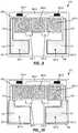
- FIG. 1illustrates a typical LED package 10 including a single LED chip 12 that is mounted on a reflective cup 14 by means of a solder bond or conductive epoxy.
- One or more wire bonds 16can connect ohmic contacts of the LED chip 12 to leads 18 A and/or 18 B, which may be attached to or integral with the reflective cup 14 .
- the reflective cup 14may be filled with an encapsulant material 20 , which may contain a wavelength conversion material such as a phosphor. At least some light emitted by the LED chip 12 at a first wavelength may be absorbed by the phosphor, which may responsively emit light at a second wavelength.
- a clear protective resin 22which may be molded in the shape of a lens to collimate the light emitted from the LED chip 12 .
- the reflective cup 14may direct light in an upward direction, optical losses may occur when the light is reflected. Some light may be absorbed by the reflective cup 14 due to the less than 100% reflectivity of practical reflector surfaces. Some metals can have less than 95% reflectivity in the wavelength range of interest.
- FIG. 2shows another conventional LED package 24 in which one or more LED chips 26 can be mounted onto a carrier such as a printed circuit board (PCB) carrier, substrate, or submount 28 .
- a metal reflector 30is mounted on the submount 28 and surrounds the LED chips 26 to reflect light emitted by the LED chips 26 away from the LED package 24 .
- the metal reflector 30also provides mechanical protection to the LED chips 26 .
- One or more wire bond connections 32are made between ohmic contacts on the LED chips 26 and electrical traces 34 A, 34 B on the submount 28 .
- the mounted LED chips 26are then covered with an encapsulant 36 , which may provide environmental and mechanical protection to the LED chips 26 while also acting as a lens.
- the metal reflector 30is typically attached to the submount 28 by means of a solder or epoxy bond. The metal reflector 30 may also experience optical losses when the light is reflected because it also has less than 100% reflectivity.
- FIG. 3shows another conventional LED package 38 in which an LED chip 40 can be mounted on a submount 42 with a hemispheric lens 44 formed over it.
- the LED chip 40can be coated by a conversion material that can convert all or most of the light from the LED chip 40 .
- the hemispheric lens 44is arranged to reduce total internal reflection of light.
- the lens 44is made relatively large compared to the LED chip 40 so that the LED chip 40 approximates a point light source under the lens 44 . As a result, an increased amount of LED light that reaches the surface of the lens 44 emits from the lens 44 on a first pass. Additionally, the lens 44 can be useful for directing light emission from the LED chip 40 in a desired emission pattern for the LED package 38 .
- the artcontinues to seek improved light-emitting diodes and solid-state lighting devices having reduced optical losses and providing desirable illumination characteristics capable of overcoming challenges associated with conventional lighting devices.
- an LED packageincludes electrical connections that are configured to reduce corrosion of metals within the package; or decrease the overall forward voltage of the LED package; or provide an electrical path for serially-connected electrostatic discharge (ESD) chips.
- ESDelectrostatic discharge
- an LED packageincludes at least two LED chips and a material between the two LED chips that promotes homogeneity of composite emissions from the two LED chips. In this manner, LED packages according to the present disclosure may be beneficial for various applications, including those where a high luminous intensity is desired in a variety of environmental conditions. Such applications include automotive lighting, aerospace lighting, and general illumination.
- an LED packagecomprises: a submount; a metal pattern on the submount, wherein the metal pattern comprises: at least one die attach pad; and at least one bond pad.
- the LED packageadditionally comprises at least one LED chip mounted on the at least one die attach pad; and a bond metal on the at least one bond pad and on a surface of the submount that is adjacent the at least one bond pad.
- the LED packagefurther comprises a light-altering material arranged around a perimeter of the at least one LED chip on the surface of the submount.
- the light-altering materialcovers a portion of the bond metal on the surface of the submount.
- the light-altering materialcomprises a light-reflective material.
- the light-reflective materialcomprises fused silica, fumed silica, or titanium dioxide (TiO 2 ) particles suspended in silicone.
- the LED packagefurther comprises a wavelength conversion element on the at least one LED chip.
- an LED packagecomprises: a submount; a metal pattern on the submount, wherein the metal pattern comprises: a die attach pad; a bond pad; and the LED package additionally comprise a metal trace that is continuous with at least a portion of the die attach pad and the bond pad; an LED chip mounted on the die attach pad; and a bond metal on the bond pad, wherein the bond metal comprises a conductive finger that extends on the metal trace adjacent the LED chip.
- the bond metalis on a surface of the submount that is adjacent the bond pad.
- the LED packagefurther comprises a light-altering material arranged around a perimeter of the LED chip on the surface of the submount.
- the light-altering materialcovers at least a portion of the conductive finger. In some embodiments, the light-altering material comprises a light-reflective material. In some embodiments, the light-reflective material comprises fused silica, fumed silica, or titanium dioxide (TiO2) particles suspended in silicone. In some embodiments, the LED package further comprises a wavelength conversion element on the LED chip.
- an LED packagecomprises: a submount; a metal pattern on the submount, wherein the metal pattern comprises: at least one die attach pad; and at least one bond pad; and the LED package additionally comprises at least one LED chip mounted on the at least one die attach pad; a bond metal on a top surface of the at least one bond pad; and a corrosion-reducing layer on a sidewall of the at least one bond pad and a surface of the submount that is adjacent the at least one bond pad.
- an LED packagecomprises: a submount; a plurality of LED chips on the submount; a clear material at least partially between each LED chip of the plurality of LED chips; and a wavelength conversion element on the plurality of LED chips.
- the clear materialis also arranged between the wavelength conversion element and the plurality of LED chips.
- the wavelength conversion elementcomprises a lumiphoric material on a superstrate. In some embodiments, the lumiphoric material is between the superstrate and the clear material.
- a LED packagecomprises: a submount; a first metal trace on a surface of the submount; a second metal trace on the surface of the submount; a first LED chip electrically connected to the first metal trace and the second metal trace; a first ESD chip electrically connected to the first metal trace; a second ESD chip electrically connected to the second metal trace; and a third metal trace serially connected between the first ESD chip and the second ESD chip.
- the LED packagefurther comprises a second LED chip serially connected with the first LED chip between the first metal trace and the second metal trace.
- the first ESD chip and the second ESD chipare arranged in parallel with the first LED chip and the second LED chip between the first metal trace and the second metal trace.
- the LED packagefurther comprises a light-altering material arranged around a perimeter of the first LED chip on the surface of the submount.
- the light-altering materialcovers the first ESD chip and the second ESD chip on the surface of the submount.
- the light-altering materialcomprises a light-reflective material.
- the light-reflective materialcomprises fused silica, fumed silica, or titanium dioxide (TiO 2 ) particles suspended in silicone.
- an anode of the first LED chipis flip-chip mounted to the first metal trace and a cathode of the second LED chip is flip-chip mounted to the second metal trace.
- a cathode of the first LED chipis flip-chip mounted to a fourth metal trace and an anode of the second LED chip is flip-chip mounted to a fifth metal trace.
- the LED packagefurther comprises a third LED chip wherein an anode of the third LED chip is flip-chip mounted to the fourth metal trace and a cathode of the third LED chip is flip-chip mounted to the fifth metal trace.
- FIG. 1illustrates a cross-sectional representation of a conventional light-emitting diode (LED) package.
- LEDlight-emitting diode
- FIG. 2illustrates a cross-sectional representation of a conventional LED package.
- FIG. 3illustrates a cross-sectional representation of a conventional LED package.
- FIG. 4is a perspective view of an LED package according to some embodiments.
- FIG. 5Aillustrates a top view of an LED package according to some embodiments.
- FIG. 5Billustrates a top view of an LED package according to some embodiments.
- FIG. 5Cillustrates a top view of an LED package according to some embodiments.
- FIG. 5Dillustrates a bottom view of the LED package of FIG. 5C according to some embodiments.
- FIG. 6Aillustrates a top view of an LED package according to some embodiments.
- FIG. 6Billustrates a top view of an LED package according to some embodiments.
- FIG. 6Cis a side view illustration representing a cross-section taken along section line II-II of the LED package of FIG. 6B .
- FIG. 6Dillustrates a cross-sectional view of the LED package of FIG. 6C with the addition of a light-altering material and a wavelength conversion element.
- FIG. 7Aillustrates a cross-sectional view of an LED package similar to the LED package of FIG. 6C .
- FIG. 7Billustrates a cross-sectional view of an LED package similar to the LED package of FIG. 7A .
- FIG. 7Cillustrates a cross-sectional view of an LED package similar to the LED package of FIG. 7A .
- FIG. 7Dillustrates a cross-sectional view of an LED package similar to the LED package of FIG. 6C .
- FIG. 8Ais a photograph of a portion of a conventional LED package after exposure to corrosion testing.
- FIG. 8Bis a photograph of a portion of an LED package according to some embodiments after exposure to corrosion testing.
- FIG. 9illustrates a top view of an LED package according to some embodiments.
- FIG. 10illustrates a top view of an LED package according to some embodiments.
- FIG. 11Ais a plot comparing electrical performance of LED packages with and without conductive fingers of a bond metal according to some embodiments.
- FIG. 11Bis a plot comparing electrical performance of LED packages after die attach for LED packages with and without conductive fingers of a bond metal according to some embodiments.
- FIG. 12Aillustrates a cross-sectional view of an LED package according to some embodiments.
- FIG. 12Billustrates a cross-sectional view of the LED package of FIG. 12A with a lens according to some embodiments.
- FIG. 12Cillustrates a cross-sectional view of the LED package of FIG. 12A with a plurality of lenses according to some embodiments.
- FIG. 13Aillustrates a top view of an LED package according to some embodiments.
- FIG. 13Billustrates a bottom view of an LED package according to some embodiments.
- FIG. 13Cillustrates a bottom view of an LED package according to some embodiments.
- FIG. 13Dis a side view illustration representing a cross-section of the LED package taken along section line III-III of FIG. 13A .
- FIG. 14illustrates a top view of a panel from an intermediate step of manufacturing according to some embodiments.
- an LED packageincludes electrical connections that are configured to reduce corrosion of metals within the package; or decrease the overall forward voltage of the LED package; or provide an electrical path for serially-connected electrostatic discharge (ESD) chips.
- ESDelectrostatic discharge
- an LED packageincludes at least two LED chips and a material between the two LED chips that promotes homogeneity of composite emissions from the two LED chips. In this manner, LED packages according to the present disclosure may be beneficial for various applications, including those where a high luminous intensity is desired in a variety of environmental conditions. Such applications include automotive lighting, aerospace lighting, and general illumination.
- An LED chiptypically comprises an active LED structure or region that can have many different semiconductor layers arranged in different ways.
- the fabrication and operation of LEDs and their active structureare generally known in the art and are only briefly discussed herein.
- the layers of the active LED structurecan be fabricated using known processes with a suitable process being fabrication using metal organic chemical vapor deposition.
- the layers of the active LED structurecan comprise many different layers and generally comprise an active layer sandwiched between n-type and p-type oppositely doped epitaxial layers, all of which are formed successively on a growth substrate.
- additional layers and elementscan also be included in the active LED structure, including but not limited to: buffer layers, nucleation layers, super lattice structures, un-doped layers, cladding layers, contact layers, current-spreading layers, and light extraction layers and elements.
- the active layercan comprise a single quantum well, a multiple quantum well, a double heterostructure, or super lattice structures.
- the active LED structurecan be fabricated from different material systems, with some material systems being Group III nitride-based material systems.
- Group III nitridesrefer to those semiconductor compounds formed between nitrogen and the elements in Group III of the periodic table, usually aluminum (Al), gallium (Ga), and indium (In).
- Gallium nitride (GaN)is a common binary compound.
- Group III nitridesalso refer to ternary and quaternary compounds such as aluminum gallium nitride (AlGaN), indium gallium nitride (InGaN), and aluminum indium gallium nitride (AlInGaN).
- the active layer, n-type layer, and p-type layermay include one or more layers of GaN, AlGaN, InGaN, and AlInGaN that are either undoped or doped with Si or Mg for a material system based on Group III nitrides.
- Other material systemsinclude silicon carbide (SiC), organic semiconductor materials, and other Group III-V systems such as gallium phosphide (GaP), gallium arsenide (GaAs), and related compounds.
- the active LED structuremay be grown on a growth substrate that can include many materials, such as sapphire, SiC, aluminum nitride (AlN), GaN, with a suitable substrate being a 4H polytype of SiC, although other SiC polytypes can also be used including 3C, 6H, and 15R polytypes.
- SiChas certain advantages, such as a closer crystal lattice match to Group III nitrides than other substrates and results in Group III nitride films of high quality.
- SiCalso has a very high thermal conductivity so that the total output power of Group III nitride devices on SiC is not limited by the thermal dissipation of the substrate.
- Sapphireis another common substrate for Group III nitrides and also has certain advantages, including being lower cost, having established manufacturing processes, and having good light transmissive optical properties.
- the active LED structurecan emit different wavelengths of light depending on the composition of the active layer and n-type and p-type layers.
- the active LED structureemits a blue light in a peak wavelength range of approximately 430 nanometers (nm) to 480 nm.
- the active LED structureemits green light in a peak wavelength range of 500 nm to 570 nm.
- the active LED structureemits red light in a peak wavelength range of 600 nm to 650 nm.
- the LED chipcan also be covered with one or more lumiphors or other conversion materials, such as phosphors, such that at least some of the light from the LED passes through the one or more phosphors and is converted to one or more different wavelengths of light.
- the LED chipemits a generally white light combination of light from the active LED structure and light from the one or more phosphors.
- the one or more phosphorsmay include yellow (e.g., YAG:Ce), green (LuAg:Ce), and red (Ca i ⁇ x ⁇ y Sr x Eu y AlSiN 3 ) emitting phosphors, and combinations thereof.
- the present disclosurecan include LED chips having a variety of geometries, such as vertical geometry or lateral geometry.
- a vertical geometry LED chiptypically includes an anode and cathode on opposing sides of the active LED structure.
- a lateral geometry LED chiptypically includes an anode and a cathode on the same side of the active LED structure that is opposite a substrate, such as a growth substrate or a carrier substrate.
- a lateral geometry LED chipmay be mounted on a submount of an LED package such that the anode and cathode are on a face of the active LED structure that is opposite the submount. In this configuration, wire bonds may be used to provide electrical connections with the anode and cathode.
- a lateral geometry LED chipmay be flip-chip mounted on a submount of an LED package such that the anode and cathode are on a face of the active LED structure that is adjacent to the submount.
- electrical traces or patternsmay be provided on the submount for providing electrical connections to the anode and cathode of the LED chip.
- the active LED structureis configured between the substrate of the LED chip and the submount for the LED package. Accordingly, light emitted from the active LED structure may pass through the substrate in a desired emission direction.
- the flip-chip LED chipmay be configured as described in commonly-assigned U.S. Patent Application Publication No. 2017/0098746, which is hereby incorporated by reference herein.
- Embodiments of the disclosureare described herein with reference to cross-sectional view illustrations that are schematic illustrations of embodiments of the disclosure. As such, the actual thickness of the layers can be different, and variations from the shapes of the illustrations as a result, for example, of manufacturing techniques and/or tolerances, are expected. For example, a region illustrated or described as square or rectangular can have rounded or curved features, and regions shown as straight lines may have some irregularity. Thus, the regions illustrated in the figures are schematic and their shapes are not intended to illustrate the precise shape of a region of a device and are not intended to limit the scope of the disclosure.
- FIG. 4is a perspective view of an LED package 46 according to some embodiments.
- the LED package 46includes a submount 48 that can be formed of many different materials with a preferred material being electrically insulating. Suitable materials include, but are not limited to ceramic materials such as aluminum oxide or alumina, AlN, or organic insulators like polyimide (PI) and polyphthalamide (PPA).
- the submount 48can comprise a printed circuit board (PCB), sapphire, Si or any other suitable material.
- PCBprinted circuit board
- different PCB typescan be used such as standard FR-4 PCB, metal core PCB, or any other type of PCB. At least a portion of a metal pattern 50 is visible on the submount 48 .
- Package contacts 52 - 1 , 52 - 2comprise at least a portion of the metal pattern 50 and include an anode contact and a cathode contact configured to receive an electrical connection from a power source external to the LED package 46 .
- a portion 51 of the submount 48includes identification or other information about the LED package 46 , including a quick response (QR) code, a bar code, or alphanumeric information.
- QRquick response
- the portion 51is illustrated between the package contacts 52 - 1 , 52 - 2 .
- the portion 51 that includes identification or other informationmay be located on other areas of the submount 48 .
- a plurality of LED chips 54 - 1 to 54 - 3are visible on the submount 48 , and a light-altering material 56 is arranged around a perimeter of the LED chips 54 - 1 to 54 - 3 on a surface of the submount 48 .
- the LED package 46is designed with three LED chips 54 - 1 to 54 - 3 , any number of LED chips are possible.
- LED packages according to embodiments disclosed hereinmay include a single LED chip, or two LED chips, or three LED chips, or more.
- the light-altering material 56is configured to redirect or reflect laterally-emitting light from the LED chips 54 - 1 to 54 - 3 toward a desired emission direction.
- the light-altering material 56may block or absorb at least of portion of any laterally-emitting light from the LED chips 54 - 1 to 54 - 3 that would otherwise escape the LED package 46 with high or wide emission angles.
- the light-altering material 56may partially cover the submount 48 outside of where the LED chips 54 - 1 to 54 - 3 are located. In that regard, the light-altering material 56 may cover portions of the metal pattern 50 that extend from the package contacts 52 - 1 , 52 - 2 to the LED chips 54 - 1 to 54 - 3 .
- the light-altering material 56may be adapted for dispensing, or placing, and may include many different materials including light-reflective materials that reflect or redirect light, light-absorbing materials that absorb light, and materials that act as a thixotropic agent.
- the light-altering material 56may include at least one of fused silica, fumed silica, and titanium dioxide (TiO 2 ) particles suspended in a binder, such as silicone or epoxy.
- the light-altering material 56may comprise a white color to reflect and redirect light.
- the light-altering material 56may comprise an opaque or black color for absorbing light and increasing contrast of the LED package 46 .
- the light-altering material 56can be dispensed or deposited in place using an automated dispensing machine where any suitable size and/or shape can be formed.
- the light-altering material 56may include a cross-sectional profile comprising a planar top surface with vertical side surfaces or a curved top surface with vertical side surfaces. In other embodiments, the light-altering material 56 may comprise other shapes, including a planar or curved top surface with non-planar or non-vertical side surfaces. In some embodiments, at least a portion of the light-altering material 56 may extend to one or more edges of the submount 48 . In FIG. 4 , the light-altering material 56 extends to three edges of the submount 48 , but does not extend to a fourth edge of the submount 48 , thereby leaving the package contacts 52 - 1 , 52 - 2 uncovered.
- a wavelength conversion element 58is arranged over the plurality of LED chips 54 - 1 to 54 - 3 on the submount 48 .
- the light-altering material 56is also arranged around a perimeter of the wavelength conversion element 58 .
- the wavelength conversion element 58includes one or more lumiphoric materials. Lumiphoric materials as described herein may be or include one or more of a phosphor, a scintillator, a lumiphoric ink, a quantum dot material, a day glow tape, and the like.
- Lumiphoric materialsmay be provided by any suitable means, for example, direct coating on one or more surfaces of an LED, dispersal in an encapsulant material configured to cover one or more LEDs, and/or coating on one or more optical or support elements (e.g., by powder coating, spray coating, inkjet printing, or the like).
- lumiphoric materialsmay be deposited utilizing one or more applications of a spray coating after the LED chip is mounted on the submount 48 , as described in commonly-assigned U.S. Patent Application Publication No. 2017/0098746.
- lumiphoric materialsmay be downconverting or upconverting, and combinations of both downconverting and upconverting materials may be provided.
- multiple different (e.g., compositionally different) lumiphoric materials arranged to produce different peak wavelengthsmay be arranged to receive emissions from one or more LED chips.
- one or more phosphorsmay include yellow phosphors (e.g., YAG:Ce), green phosphors (LuAg:Ce), and red phosphors (Cai ⁇ x ⁇ ySrxEuyAlSiN3) and combinations thereof.
- the wavelength conversion element 58includes embodiments as described in commonly-assigned U.S. Patent Application Publication No. 2018/0033924, which is hereby incorporated by reference herein.
- FIG. 5Aillustrates a top view of a partially-assembled LED package 60 according to some embodiments.
- the LED package 60is similar to the LED package 46 of FIG. 4 , except only the submount 48 and the metal pattern 50 are present.
- the metal pattern 50includes a plurality of metal traces 50 - 1 to 50 - 5 .
- Each metal trace 50 - 1 to 50 - 5includes a continuous metal formed on a surface of the submount 48 , and each metal trace 50 - 1 to 50 - 5 is discontinuous with each other.
- the metal pattern 50forms a plurality of die attach pads 61 - 1 to 61 - 3 that are indicated by dashed-line boxes in FIG. 5A .
- the die attach pads 61 - 1 to 61 - 3are configured to receive a plurality of LED chips.
- the die attach pad 61 - 1includes a portion of the metal trace 50 - 1 and a portion of the metal trace 50 - 4 .
- an anode of an LED chipmay be mounted or attached to the metal trace 50 - 1 while a cathode of the LED chip may be mounted or attached to the metal trace 50 - 4 .
- the die attach pad 61 - 2includes a portion of the metal trace 50 - 4 and a portion of the metal trace 50 - 5
- the die attach pad 61 - 3includes a portion of the metal trace 50 - 2 and a portion of the metal trace 50 - 5 .
- a portion of the metal trace 50 - 1 and a portion of the metal trace 50 - 2form bond pads 62 - 1 and 62 - 2 , respectively.
- the bond pads 62 - 1 , 62 - 2form a portion of the package contacts 52 - 1 , 52 - 2 of FIG. 4 .
- the metal trace 50 - 1is continuous with at least a portion of the die attach pad 61 - 1 and the bond pad 62 - 1 ; and the metal trace 50 - 2 is continuous with at least a portion of the die attach pad 61 - 3 and the bond pad 62 - 2 .
- the metal pattern 50includes one or more test tabs 63 - 1 , 63 - 2 that allow for individual testing of LED chips that are mounted to the die attach pads 61 - 1 to 61 - 3 .
- the metal trace 50 - 4includes the test tab 63 - 1
- the metal trace 50 - 5includes the test tab 63 - 2 .
- the one or more test tabs 63 - 1 , 63 - 2are outside an area of the die attach pads 61 - 1 to 61 - 3 . In that regard, the one or more test tabs 63 - 1 , 63 - 2 are accessible after LED chips are mounted in the LED package 60 .
- the metal pattern 50may include any number of electrically conductive materials.
- the metal pattern 50includes at least one of the following; copper (Cu) or alloys thereof, nickel (Ni) or alloys thereof, nickel chromium (NiCr), gold (Au) or alloys thereof, electroless Au, electroless silver (Ag), NiAg, Al or alloys thereof, titanium tungsten (TiW), titanium tungsten nitride (TiWN), electroless nickel electroless palladium immersion gold (ENEPIG), electroless nickel immersion gold (ENIG), hot air solder leveling (HASL), and organic solderability preservative (OSP).
- the metal pattern 50includes a first layer of Cu or Ni followed by a layer of ENEPIG or ENIG that conformally covers a top and sidewalls of the first layer of Cu or Ni.
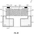
- FIG. 5Billustrates a top view of a partially-assembled LED package 64 according to some embodiments.
- the LED package 64is similar to the LED package 60 of FIG. 5A , except a plurality of LED chips 66 - 1 to 66 - 3 and a plurality of ESD chips 68 - 1 , 68 - 2 are mounted on the metal pattern 50 .
- an anode of the first LED chip 66 - 1is mounted or attached to the first metal trace 50 - 1 while a cathode of the first LED chip 66 - 1 is mounted or attached to the fourth metal trace 50 - 4 .
- An anode of the second LED chip 66 - 2is mounted or attached to the fourth metal trace 50 - 4 while a cathode of the second LED chip 66 - 2 is mounted or attached to the fifth metal trace 50 - 5 .
- An anode of the third LED chip 66 - 3is mounted or attached to the fifth metal trace 50 - 5 while a cathode of the third LED chip 66 - 3 is mounted or attached to the second metal trace 50 - 2 .
- each of the plurality of LED chips 66 - 1 to 66 - 3are electrically connected in series with each other between the first metal trace 50 - 1 and the second metal trace 50 - 2 .
- the LED chips 66 - 1 to 66 - 3may be flip-chip mounted to the metal traces 50 - 1 , 50 - 2 , 50 - 4 , 50 - 5 .
- the LED chips 66 - 1 to 66 - 3may be configured as described in commonly-assigned U.S. Patent Application Publication No. 2017/0098746, which is hereby incorporated by reference herein.
- the first ESD chip 68 - 1is attached or mounted to the first metal trace 50 - 1 and the third metal trace 50 - 3
- the second ESD chip 68 - 2is attached or mounted to the third metal trace 50 - 3 and the second metal trace 50 - 2 .
- each of the plurality of ESD chips 68 - 1 , 68 - 2are electrically connected in series between the first metal trace 50 - 1 and the second metal trace 50 - 2 .
- the first ESD chip 68 - 1is electrically connected to the first metal trace 50 - 1
- the second ESD chip 68 - 2is electrically connected to the second metal trace 50 - 2
- the third metal trace 50 - 3is serially connected between the first ESD chip 68 - 1 and the second ESD chip 68 - 2 .
- the first ESD chip 68 - 1 and the second ESD chip 68 - 2are arranged in parallel with the LED chips 66 - 1 to 66 - 3 between the first metal trace 50 - 1 and the second metal trace 50 - 2 .
- the one or more test tabs 63 - 1 , 63 - 2are configured to allow for individual testing of the LED chips 66 - 1 to 66 - 3 after the LED chips 66 - 1 to 66 - 3 and the ESD chips 68 - 1 , 68 - 2 are mounted to the LED package 64 .
- the LED chip 66 - 1may be individually tested via electrical contacts to the first metal trace 50 - 1 and the test tab 63 - 1 ; the LED chip 66 - 2 may be individually tested via electrical contacts to the one or more test tabs 63 - 1 , 63 - 2 ; and finally, the LED chip 66 - 3 may be individually tested via electrical contacts to the test tab 63 - 2 and the metal trace 50 - 2 . Furthermore, subgroups of the LED chips 66 - 1 to 66 - 3 may be tested together. For example, the LED chips 66 - 1 and 66 - 2 may be tested as a pair via electrical contacts to the metal trace 50 - 1 and the test tab 63 - 2 .
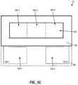
- FIG. 5Cillustrates a top view of an LED package 70 according to some embodiments.
- the LED package 70is similar to the LED package 64 of FIG. 5B , except the LED package 70 includes the light-altering material 56 and the wavelength conversion element 58 as previously-described.
- the LED chips 66 - 1 to 66 - 3are laterally spaced from the bond pads 62 - 1 , 62 - 2 on the submount 48 .
- the light-altering material 56is arranged around a perimeter of the LED chips 66 - 1 to 66 - 3 on a surface of the submount 48 .
- the light-altering material 56covers the first ESD chip 68 - 1 and the second ESD chip 68 - 2 of FIG.
- ESD chipsare typically dark in color and may therefore absorb light.
- the light-altering material 56may include light reflective particles as previously described, and accordingly, the amount of light from the LED chips 66 - 1 to 66 - 3 that may reach the ESD chips ( 68 - 1 , 68 - 2 of FIG. 5B ) is reduced.
- the light-altering material 56does not cover the entire surface of the submount 48 . In particular, a portion of the first metal trace 50 - 1 and a portion of the second metal trace 50 - 2 are not covered by the light-altering material 56 .
- the bond pads 62 - 1 , 62 - 2 of the metal traces 50 - 1 , 50 - 2form at least a portion of the package contacts (see, for example 52 - 1 , 52 - 2 of FIG. 4 ).
- the portions of the metal traces 50 - 1 , 50 - 2 that are not covered by the light-altering material 56may experience corrosion that adversely impacts the performance of the LED package 70 .
- Cuis known to be susceptible to oxidation with exposure to air.
- portions of the metal traces 50 - 1 , 50 - 2may form Cu oxide that is black in color.
- the metal traces 50 - 1 , 50 - 2may further include a surface finish such as ENEPIG; however, corrosion and oxidation of the metal traces 50 - 1 , 50 - 2 may still occur under some operation conditions.
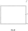
- FIG. 5Dillustrates a bottom view of the LED package 70 of FIG. 5C according to some embodiments.
- the bottom side of the submount 48may include a mount pad 71 that is configured for mounting the LED package 70 to another surface, such as a PCB or a housing for a lighting fixture.
- the bottom sideis a face of the submount 48 that is opposite a face where the LED chips 66 - 1 to 66 - 3 of FIG. 5C are mounted.
- the mount pad 71may include a metal, such as Cu or alloys thereof, Ni or alloys thereof, NiCr, Au or alloys thereof, electroless Au, electroless Ag, NiAg, Al or alloys thereof, TiW, TiWN, ENEPIG, ENIG, HASL, and OSP.
- the mount pad 71includes a thickness that is similar to a thickness of the metal pattern 50 ( FIG. 5B ). In some embodiments where the mount pad 71 includes a metal, the mount pad 71 may be configured to provide a metal-to-metal bond with a corresponding metal pad that is located on another surface. In operation, the mount pad 71 may also provide a thermal path, or a heat sink, that assists in dissipating heat generated by the LED package 70 . Additionally, the mount pad 71 may provide structural integrity for the LED package 70 during various manufacturing steps. For example, before singulation, the LED package 70 may be part of a larger panel of LED packages, each of which includes a corresponding mount pad.
- Each of the corresponding mount padsmay assist in keeping the panel flat during subsequent processing steps.
- the LED package 70may be glued directly to another surface without a mount pad 71 .
- FIG. 6Aillustrates a top view of an LED package 72 according to some embodiments.
- the LED package 72is similar to the LED package 70 of FIG. 5C , except the LED package 72 includes a bond metal 74 that covers the bond pads 62 - 1 , 62 - 2 of the exposed portions of the metal traces 50 - 1 , 50 - 2 .
- the one or more test tabs 63 - 1 , 63 - 2 of FIG. 5A and FIG. 5Bare not shown in FIG. 6A , but it is understood the one or more test tabs 63 - 1 , 63 - 2 are applicable to all embodiments disclosed herein, including FIG. 6A .
- the bond metal 74may include one or more layers of a conductive metal that is configured to receive and bond with an external electrical connection.
- the bond metal 74may comprise a different metal than the metal traces 50 - 1 , 50 - 2 .
- the bond metal 74includes Al or alloys thereof and is arranged to be bonded with one or more wire bonds that are electrically connected to an external power source.
- the bond metal 74 and the metal traces 50 - 1 , 50 - 2may include different metals selected from the following: Cu or alloys thereof, Ni or alloys thereof, NiCr, Au or alloys thereof, electroless Au, electroless Ag, NiAg, Al or alloys thereof, TiW, TiWN, ENEPIG, ENIG, HASL, and OSP.
- the bond metal 74 and the bond pads 62 - 1 , 62 - 2collectively form package contacts as previously described (see, for example 52 - 1 , 52 - 2 of FIG. 4 ).
- the bond metal 74may be formed by various deposition techniques including sputtering, evaporation, plating, and patterning.
- Patterningmay include various techniques that include masking and/or etching back of deposited material.
- the bond metal 74is on the bond pads 62 - 1 , 62 - 2 and on a surface of the submount 48 that is adjacent the bond pads 62 - 1 , 62 - 2 . Stated differently, the bond metal 74 covers the portions of the metal traces 50 - 1 , 50 - 2 that are uncovered by the light-altering material 56 and the wavelength conversion element 58 . In this manner, the bond metal 74 serves as a barrier between the metal traces 50 - 1 , 50 - 2 and the surrounding atmosphere, thereby reducing potential corrosion of the metal traces 50 - 1 , 50 - 2 .
- the bond metal 74serves as a corrosion-reducing layer.
- a portion of the bond metal 74extends underneath the light-altering material 56 such that the portion of the bond metal 74 is between the light-altering material 56 and the submount 48 .
- FIG. 6Billustrates a top view of a partially-assembled LED package 76 according to some embodiments.
- the LED package 76is similar to the LED package 72 of FIG. 6A , except the light-altering material 56 and the wavelength conversion element 58 of FIG. 6A are not present.
- the LED package 76includes the LED chips 66 - 1 to 66 - 3 and the ESD chips 68 - 1 , 68 - 2 serially connected by the metal trace 50 - 3 as previously described.
- the bond metal 74covers portions of the metal traces 50 - 1 , 50 - 2 and includes bond metal portions 74 ′ that are covered after the light-altering material of previous embodiments is formed.
- FIG. 6Cis a side view illustration representing a cross-section taken along section line II-II of the LED package 76 of FIG. 6B .
- a portion of the first metal trace 50 - 1is covered by the bond metal 74 .
- the bond metal 74is on a top surface and sidewalls of the portion of the first metal trace 50 - 1 as well as on a surface of the submount 48 that is adjacent the portion of the first metal trace 50 - 1 .
- the LED chip 66 - 1is on a different portion of the first metal trace 50 - 1
- the ESD chip 68 - 1is on the third trace 50 - 3 .
- FIG. 6Dillustrates the cross-sectional view of the LED package 76 of FIG.
- the light-altering material 56is arranged around a perimeter of the LED chip 66 - 1 and covers the ESD chip 68 - 1 on the submount 48 .
- FIG. 7Aillustrates a cross-sectional view of an LED package 80 similar to the LED package 76 of FIG. 6C .
- the LED package 80includes the metal traces 50 - 1 , 50 - 3 on the submount 48 , the LED chip 66 - 1 , and the ESD chip 68 - 1 as previously described.
- the LED package 80further includes an alternative configuration of the bond metal 74 .
- the bond metal 74is on a top surface of a portion of the first metal trace 50 - 1 , but not on sidewalls of the first metal trace 50 - 1 or on the surface of the submount 48 that is adjacent the portion of the first metal trace 50 - 1 .
- the bond metal 74is arranged to receive an electrical connection, such as a wire bond, from an external power source.
- a corrosion-reducing layer 82 that is distinct from the bond metal 74is arranged on a sidewall 50 - 1 ′ of the metal trace 50 - 1 as well as on the surface of the submount 48 that is adjacent the first metal trace 50 - 1 .
- the corrosion-reducing layer 82may include one or more layers that include at least one of a polymer, a dielectric, or a metal that is different from the bond metal 74 .
- the corrosion-reducing layer 82includes at least one layer of Au, platinum (Pt), Ni, Ti, TiW, TiWN, or other alloys thereof in embodiments where the bond metal 74 includes Al.
- FIG. 7Billustrates a cross sectional view of an LED package 84 similar to the LED package 80 of FIG. 7A .
- the LED package 84includes the metal traces 50 - 1 , 50 - 3 on the submount 48 , the LED chip 66 - 1 , and the ESD chip 68 - 1 as previously described.
- the LED package 84further includes an alternative configuration of the bond metal 74 .
- a corrosion-reducing layer 86 that is distinct from the bond metal 74is arranged to cover the metal trace 50 - 1 , and the bond metal 74 is arranged on the corrosion-reducing layer 86 .
- the corrosion-reducing layer 86is on the top surface and on the sidewall 50 - 1 ′ of the metal trace 50 - 1 as well as on the surface of the submount 48 that is adjacent the first metal trace 50 - 1 .
- the corrosion-reducing layer 86may include one or more electrically conductive layers that include a metal that is different from the bond metal 74 .
- the bond metal 74includes Al and the corrosion-reducing layer 86 includes one or more layers of Pt, Ni, Ti, TiW, or TiWN, or other alloys thereof.
- FIG. 7Cillustrates a cross sectional view of an LED package 88 similar to the LED package 80 of FIG. 7A .
- the LED package 88includes the metal traces 50 - 1 , 50 - 3 on the submount 48 , the LED chip 66 - 1 , and the ESD chip 68 - 1 as previously described.
- the LED package 88further includes an alternative configuration of the bond metal 74 .
- a first corrosion-reducing layer 90 and a second corrosion-reducing layer 91 that are distinct from the bond metal 74are arranged to cover the metal trace 50 - 1 .
- the first corrosion-reducing layer 90is arranged on the top surface and on the sidewall 50 - 1 ′ of the metal trace 50 - 1 as well as on the surface of the submount 48 that is adjacent the first metal trace 50 - 1 .
- the second corrosion-reducing layer 91is arranged to cover the first corrosion-reducing layer 90 and is also on the surface of the submount 48 that is adjacent the first corrosion-reducing layer 90 .
- the bond metal 74is arranged on the second corrosion-reducing layer 91 .
- the first corrosion-reducing layer 90 and the second corrosion-reducing layer 91may include one or more electrically conductive layers that include a metal that is different from the bond metal 74 .
- the bond metal 74includes Al
- the first corrosion-reducing layer 90includes one or more layers of Pt, Ni, Ti, TiW, or TiWN, or other alloys thereof
- the second corrosion-reducing layer 92includes at least one of ENEPIG or ENIG.
- FIG. 7Dillustrates a cross sectional view of an LED package 92 similar to the LED package 76 of FIG. 6C .
- the LED package 92includes the metal traces 50 - 1 , 50 - 3 on the submount 48 , the bond metal 74 , the LED chip 66 - 1 , and the ESD chip 68 - 1 as previously described.
- the metal traces 50 - 1 , 50 - 3may include additional layers. For example, in FIG.
- an additional metal trace layer 93is formed or coated on the original metal traces 50 - 1 , 50 - 3 to form metal traces that include the metal trace 50 - 1 , the additional metal trace layer 93 and the metal trace 50 - 3 , and the additional metal trace layer 93 .
- the additional metal trace layer 93includes a layer of metal, such as an electroless metal including Au plating that covers the top surfaces and sidewalls of the metal traces 50 - 1 , 50 - 3 all the way to the submount 48 .
- the additional metal trace layer 93encapsulate the metal traces 50 - 1 , 50 - 3 and may provide improved corrosion resistance while still enabling good die attach with the LED chip 66 - 1 or the ESD chip 68 - 1 .
- Conventional metal tracesmay include coatings of ENIG, which can have pin holes in the top layer of Au that are susceptible to corrosion, or ENEPIG, which is more corrosion resistant, but provides a poor die attach for the LED chip 66 - 1 or the ESD chip 68 - 1 .
- the additional metal trace layer 93may replace coatings or treatments of ENIG or ENEPIG, while in other embodiments, the additional metal trace layer 93 may be provided on a top surface and sidewalls to encapsulate coatings or treatments of ENIG or ENEPIG. In some embodiments, the additional metal trace layer 93 include multiple layers.
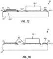
- FIG. 8Ais a photograph of a portion of a conventional LED package 94 .
- a package contact 96is visible and includes a first layer of Cu, followed by a layer of ENEPIG, and followed by a bond metal of Al that is only on a top surface of the package contact 96 .
- a wire bond 98is electrically connected to the package contact 96 .
- a corrosion 100is clearly visible as black material around the perimeter of the package contact 96 .
- FIG. 8Bis a photograph of a portion of an LED package 102 according to embodiments of the present disclosure.
- a package contact 104is visible and is configured similar to the embodiments described for FIG. 6A .
- the package contact 104includes a first layer of Cu, followed by a layer of ENEPIG, and followed by a bond metal of Al that covers the layer of Cu and the layer of ENEPIG and is additionally on a surface 106 of the submount 48 that is adjacent the package contact 104 . After corrosion testing, corrosion is noticeably reduced around the perimeter of the package contact 104 as compared to the package contact 96 of FIG. 8A .
- FIG. 9illustrates a top view of a partially-assembled LED package 110 according to some embodiments.
- the LED package 110includes the submount 48 ; the metal traces 50 - 1 to 50 - 3 ; the bond pads 62 - 1 and 62 - 2 for the LED package 110 ; the one or more test tabs 63 - 1 , 63 - 2 ; the LED chips 66 - 1 to 66 - 3 ; the ESD chips 68 - 1 , 68 - 2 ; and the bond metal 74 as previously described.
- the bond metal 74includes bond metal portions 74 ′′ that are covered after the light-altering material of previous embodiments is formed.
- the bond metal portions 74 ′′which may also be referred to as conductive fingers, extend on a top surface of each of the metal traces 50 - 1 and 50 - 2 away from the bond pads 62 - 1 , 62 - 2 and in a direction toward the LED chips 66 - 1 to 66 - 3 .
- the bond metal portions 74 ′′extend on the top surface of the metal traces 50 - 1 , 50 - 2 in a manner that at least a portion of the bond metal portions 74 ′′ are in close proximity with, or immediately adjacent the LED chips 66 - 1 to 66 - 3 .
- the bond metal portions 74 ′′extend at least to an edge of the LED chips 66 - 1 , 66 - 3 that is opposite the edge of the LED chips 66 - 1 , 66 - 3 that is closest to the bond pads 62 - 1 , 62 - 2 .
- the bond metal 74is configured to receive an electrical connection at the bond pads 62 - 1 , 62 - 2 and current may travel within the bond metal 74 to or from a position that is in close proximity or immediately adjacent the LED chips 66 - 1 and 66 - 3 .
- the bond metal 74includes a highly conductive metal such as Al or alloys thereof, the forward voltage of the LED package 110 may be reduced.
- the amount of Aumay be reduced, thereby saving costs without compromising current carrying capabilities of the LED package 110 .
- the bond metal 74(inclusive of the bond metal portions 74 ′′, or fingers) and the metal traces 50 - 1 , 50 - 2 may include different metals selected from the following: Cu or alloys thereof, Ni or alloys thereof, NiCr, Au or alloys thereof, electroless Au, electroless Ag, NiAg, Al or alloys thereof, TiW, TiWN, ENEPIG, ENIG, HASL, and OSP.
- FIG. 10illustrates a top view of a partially-assembled LED package 112 according to some embodiments.
- the LED package 112includes the submount 48 ; the metal traces 50 - 1 to 50 - 3 ; the bond pads 62 - 1 and 62 - 2 for the LED package 112 ; the one or more test tabs 63 - 1 , 63 - 2 ; the LED chips 66 - 1 to 66 - 3 ; the ESD chips 68 - 1 , 68 - 2 ; the bond metal 74 and the bond metal portions 74 ′′ as previously described.
- the LED package 112is similar to the LED package 110 of FIG.
- the bond metal 74covers at least a portion of the metal traces 50 - 1 and 50 - 2 . Accordingly, the bond metal 74 is also on a surface of the submount 48 that is adjacent portions of the metal traces 50 - 1 and 50 - 2 . In that regard, after the light-altering material and the wavelength conversion element of previous embodiments is formed, all portions of the metal traces 50 - 1 and 50 - 2 that are uncovered by the light-altering material and the wavelength conversion element are covered by the bond metal 74 . Accordingly, the bond pads 62 - 1 and 62 - 2 for the LED package 112 are more resistant to corrosion.
- FIG. 11Ais a plot comparing electrical performance of LED packages with and without conductive fingers of the bond metal as described for FIG. 9 and FIG. 10 .
- the bottom of the plotdetails various LED packages built for the comparisons.
- the various LED packageswere built with and without conductive fingers of the bond metal (Al in this case) and as indicated by the “Al finger extension” row with labels Yes (with Al conductive fingers) or No (without Al conductive fingers).
- the metal traces underneath the bond metal as well as the portions of the metal traces that form the die attach pads as previously describedincluded Au with variable thicknesses as measured in a direction perpendicular to the submount.
- the Au thicknesswas varied from 1 to 3 ⁇ m for various LED packages as indicated by the “Au Thickness” row.
- a width of the metal trace that extends between and connects the package bond pads and the die attach padswas varied between 450 and 550 ⁇ m, as indicated by the label “Side Au metal trace” row.
- the number of LED chips, or LED diewas also varied between 2 and 3 chips as indicated by the “Die number” row.
- the y-axis of the plotis the electrical resistance of the metal traces for a fixed current in milliohms.
- the LED packages with Al finger extensionshave a substantially decreased electrical resistance.
- the resistance of the metal tracesalso decreases when the Au thickness or width is increased.
- extra Aucan add additional costs to the LED package.
- LED packages with metal traces having an Au thickness of 2 ⁇ m and including Al finger extensionsmeasured a lower electrical resistance than LED packages with metal traces having an Au thickness of 3 ⁇ m and without Al finger extensions. Additionally, for packages with an Au thickness reduced to 1 ⁇ m and with Al finger extensions, the electrical resistance was measured close or similar to LED packages having an Au thickness of 2 ⁇ m and without Al finger extensions. Accordingly, some embodiments of the present invention include metal traces having an Au thickness of less than 2 ⁇ m, or in a range from 1 ⁇ m to 2 ⁇ m, or in a range from 1 ⁇ m to less than 2 ⁇ m.
- FIG. 11Bincludes a plot comparing electrical performance of LED packages after die attach for LED packages with and without conductive fingers of the bond metal as described for FIG. 9 and FIG. 10 .
- the bottom of the plotdetails various LED packages built for the comparisons.
- the various LED packageswere built with and without conductive fingers of the bond metal (Al in this case) and as indicated by the “Al finger extension” row with labels Yes (with Al conductive fingers); No (without Al conductive fingers); or POR (e.g. process of record and without Al conductive fingers).
- the metal traces underneath the bond metal as well as the portions of the metal traces that form the die attach pads as previously describedincluded Au with variable thicknesses as measured in a direction perpendicular to the submount.
- the Au thicknesswas varied from 1 to 3 ⁇ m for various LED packages as indicated by the “Au Thickness” row. Additionally, a width of the metal trace that extends between and connects the LED package bond pads and the die attach pads was varied between 450 and 550 ⁇ m, as indicated by the label “Side Au metal trace” row. The “Au Thickness” row and the “Side Au metal trace” row also include the label POR, which does not include Al. The number of LED chips, or LED die, was also varied between 2 and 3 chips as indicated by the “Die number” row.
- the y-axis of the top portion of the plotis the change in forward voltage (V f ), or V f Delta, in volts
- the y-axis at the bottom portion of the plotis the percentage change in V f , or V f Delta %, in volts.
- the table at the bottom of FIG. 11Bsummarizes the mean values for V f Delta and V f Delta % for the number N of LED packages tested.
- Deltarefers to the difference between the POR cells without the Al finger and the other cells with the Al finger.
- the presence of an Al finger extensiongenerally improves (lowers) V f , although as the Au thickness increases, the improvement becomes less pronounced.
- the Al fingerprovides a mean V f improvement of about 0.044 volts, or 44 millivolts (mV); for LED packages with 2 ⁇ m of Au, the Al finger provides a mean V f improvement of about 21 mV; and for LED packages with 3 ⁇ m of Au, the Al finger provides a mean V f improvement of about 12 mV. Accordingly, the presence of an Al finger extension and metal traces with Au as previously described can each lower the V f values closer to the POR while also providing the corrosion resistance as previously described.
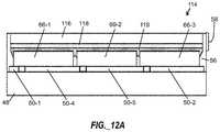
- FIG. 12Ais a cross-sectional view of an LED package 114 according to some embodiments.
- the cross-sectional viewmay be similar to a cross-section taken along section line I-I of the LED package 72 of FIG. 6A .
- the LED package 114includes the submount 48 ; the metal traces 50 - 1 , 50 - 2 , 50 - 4 , 50 - 5 ; the LED chips 66 - 1 to 66 - 3 ; the light-altering material 56 ; and the wavelength conversion element 58 as previously described.
- the wavelength conversion element 58includes a superstrate 116 that includes a lumiphoric material 118 disposed thereon.
- the term “superstrate” as used hereinrefers to an element placed on an LED chip with a lumiphoric material between the superstrate and the LED chip.
- the term “superstrate”is used herein, in part, to avoid confusion with other substrates that may be part of the semiconductor light emitting device, such as a growth or carrier substrate of the LED chip or a submount of the LED package.
- the term “superstrate”is not intended to limit the orientation, location, and/or composition of the structure it describes.
- the superstrate 116may be composed of, for example, sapphire, silicon carbide, silicone, and/or glass (e.g., borosilicate and/or fused quartz).
- the superstrate 116may be patterned to enhance light extraction from the LED chips 66 - 1 to 66 - 3 as described in commonly-assigned U.S. Provisional Application No. 62/661,359 entitled “Semiconductor Light Emitting Devices Including Superstrates With Patterned Surfaces” which is hereby incorporated by reference herein.
- the superstrate 116may also be configured as described in previously-referenced U.S. Patent Application Publication No. 2018/0033924, also incorporated by reference herein.
- the superstrate 116may be formed from a bulk substrate which is optionally patterned and then singulated.
- the patterning of the superstrate 116may be performed by an etching process (e.g., wet or dry etching). In some embodiments, the patterning of the superstrate 116 may be performed by otherwise altering the surface, such as by a laser or saw. In some embodiments, the superstrate 116 may be thinned before or after the patterning process is performed. The lumiphoric material 118 may then be placed on the superstrate 116 by, for example, spraying and/or otherwise coating the superstrate 116 with the lumiphoric material 118 .
- an etching processe.g., wet or dry etching
- the patterning of the superstrate 116may be performed by otherwise altering the surface, such as by a laser or saw.
- the superstrate 116may be thinned before or after the patterning process is performed.
- the lumiphoric material 118may then be placed on the superstrate 116 by, for example, spraying and/or otherwise
- the superstrate 116 and the lumiphoric material 118may be attached to the LED chips 66 - 1 to 66 - 3 using, for example, a layer of transparent adhesive 119 .
- a portion of the transparent adhesive 119is positioned at least partially between lateral edges of the LED chips 66 - 1 to 66 - 3 .
- the layer of the transparent adhesive 119may include silicone with a refractive index in a range of about 1.3 to about 1.6 that is less than a refractive index of the LED chips 66 - 1 to 66 - 3 .
- At least a portion of light emitted laterally from the LED chips 66 - 1 to 66 - 3may have improved light extraction between the lateral edges of the LED chips 66 - 1 to 66 - 3 , thereby providing improved overall package brightness as well as improved homogeneity of composite emissions from the LED chips 66 - 1 to 66 - 3 .
- the appearance of dark spots due to illumination gaps between the LED chips 66 - 1 to 66 - 3may be reduced.
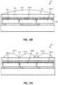
- FIG. 12Billustrates a cross-sectional view of the LED package 114 of FIG. 12A with a lens 120 .
- the lens 120may be added to the LED package 114 to improve color angle uniformity.
- the lens 120may be configured to reduce the appearance of blue emissions around a lateral perimeter of the LED package 114 .
- the lens 120may also provide a different light distribution pattern for the LED package 114 .
- the lens 120may include a curved upper surface, such as a partial hemisphere, a partial dome, or a partial ellipsoid.
- the lens 120may include a curved upper surface with one or more planar sidewalls.
- the lens 120may have a planar upper surface with planar sidewalls.
- Many different materialscan be used for the lens 120 , including silicones, plastics, epoxies, or glass, with a suitable material being compatible with dispensing or molding processes. Silicone is suitable for dispensing or molding and provides good optical transmission properties for light emitted from the LED chips 66 - 1 to 66 - 3 .
- the lens 120may be dispensed on a surface of the LED package 114 . The viscosity of the material used for the lens 120 may be such that the curved upper surface is formed by surface tension. In other embodiments, the lens 120 may be molded over the LED package 114 .
- the lens 120may be dispensed or molded onto the superstrate 116 before it is placed in the LED package 114 .
- the lens 120may be dispensed or molded onto the LED package 114 after the superstrate 116 has been added. In this manner, the lens 120 may extend over both the superstrate 116 and the light-altering material 56 .
- the LED package 114may further include an additional light-altering material 121 .
- the additional light-altering material 121may include at least one of a second lumiphoric material or a light-diffusing material.
- the additional light-altering material 121includes a second lumiphoric material that is either the same as or different than the lumiphoric material 118 (or a first lumiphoric material).
- the additional light-altering material 121includes a light-diffusing material
- the light-diffusing materialmay scatter light emitted from the LED chips 66 - 1 to 66 - 3 for improvements in color uniformity and color mixing.
- the additional light-altering material 121may be formed by deposition or other suitable techniques on the LED package 114 before the lens 120 is formed.
- the additional light-altering material 121may be formed at the same time the lens 120 is formed.
- the additional light-altering material 121may include at least one of lumiphoric particles or light-diffusing particles that are suspended in a silicone material.
- the silicone materialmay then be dispensed or molded to form the lens 120 .
- the silicone materialmay be cured after the additional light-altering material 121 is allowed to settle closer to the LED chips 66 - 1 to 66 - 3 .
- the silicone materialmay be cured while the additional light-altering material 121 is distributed throughout the lens 120 .
- FIG. 12Cillustrates a cross-sectional view of the LED package 114 of FIG. 12A with a plurality of lenses 120 - 1 to 120 - 3 according to some embodiments.
- Each of the plurality of lenses 120 - 1 to 120 - 3may be registered with corresponding ones of the plurality of LED chips 66 - 1 to 66 - 3 .
- each of the plurality of lenses 120 - 1 to 120 - 3may comprise a portion of the additional light-altering material 121 .
- the additional light-altering material 121may not be present in all of the plurality of lenses 120 - 1 to 120 - 3 .
- the superstrate 116may be continuous between the plurality of LED chips 66 - 1 to 66 - 3 and the plurality of lenses 120 - 1 to 120 - 3 . In other embodiments, the superstrate 116 may be divided into a plurality of individual pieces that are each registered with a corresponding lens 120 - 1 to 120 - 3 and a corresponding LED chip 66 - 1 to 66 - 3 .
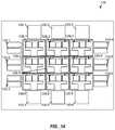
- FIG. 13A , FIG. 13B , FIG. 13C , and FIG. 13Dillustrate top, bottom, and cross-sectional views respectively of a partially-assembled LED package 122 according to some embodiments.
- the LED package 122is similar to previous embodiments, except the package contacts 52 - 1 , 52 - 2 are on a backside of the submount 48 , rather than a frontside of the submount 48 as previously described.
- the LED package 122additionally includes the metal traces 50 - 1 to 50 - 5 ; the one or more test tabs 63 - 1 , 63 - 2 ; the LED chips 66 - 1 to 66 - 3 ; and the ESD chips 68 - 1 , 68 - 2 as previously described.
- One or more conductive vias 124 - 1 to 124 - 4extend through the submount 48 to electrically connect the first metal trace 50 - 1 and the second metal trace 50 - 2 to the package contacts 52 - 1 , 52 - 2 , respectively.
- the LED package 122may further include a thermal pad 125 on the backside of the submount 48 .
- the thermal pad 125includes the same materials as the package contacts 52 - 1 , 52 - 2 . In other embodiments, the thermal pad 125 includes different materials. The thermal pad 125 may be electrically isolated from the package contacts 52 - 1 , 52 - 2 and may be configured to spread heat away from the LED chips 66 - 1 to 66 - 3 through the submount 48 .
- FIG. 13Cillustrates an alternative configuration for the backside of the submount 48 . In FIG. 13C , the package contacts 52 - 1 , 52 - 2 are larger and take up more surface area on the backside of the submount 48 .
- FIG. 13Dis a side view illustration representing a cross-section of the LED package 122 taken along section line III-III of FIG. 13A .
- the first metal trace 50 - 1 and the package contact 52 - 1are shown on opposite faces of the submount 48 .
- the conductive vias 124 - 1 , 124 - 2extend through the submount 48 to electrically connect the first metal trace 50 - 1 to the package contact 52 - 1 .
- the first metal trace 50 - 1 and the package contact 52 - 1are illustrated as having multiple layers 50 - 1 ′, 50 - 1 ′′ and 52 - 1 ′, 52 - 1 ′′ respectively.
- the multiple layers 50 - 1 ′, 50 - 1 ′′ and 52 - 1 ′, 52 - 1 ′′may include any number of electrically conductive materials as described above.
- the layers 50 - 1 ′ and 52 - 1 ′include Au, ENIG, or ENEPIG and the layers 50 - 1 ′′ and 52 - 1 ′′ include an electroless Au plating.
- the layer 52 - 1 ′′is illustrated as covering sidewalls of the layer 50 - 1 ′. In other embodiments, the layer 52 - 1 ′′ may only cover a surface of the layer 50 - 1 ′ without covering the sidewalls.
- methods of manufacturing LED packages as disclosed hereininclude forming multiple LED packages at the same time on a panel and then singulating individual LED packages.
- FIG. 14illustrates a top view of a panel 126 from an intermediate step of manufacturing according to some embodiments disclosed herein. As illustrated, the panel 126 includes a plurality of partially-formed LED packages 128 - 1 to 128 - 9 . While nine LED packages are illustrated, embodiments of the present disclosure are applicable to any number of LED packages, including more than one hundred LED packages in some embodiments.
- a plurality of first metal patterns 130 - 1 to 130 - 6 and a plurality of second metal patterns 132 - 1 to 132 - 6are arranged on the panel 126 around a perimeter of the partially-formed LED packages 128 - 1 to 128 - 9 .
- the plurality of first metal patterns 130 - 1 to 130 - 6 and the plurality of second metal patterns 132 - 1 to 132 - 6are formed at the same time as metal patterns of the partially-formed LED packages 128 - 1 to 128 - 9 are formed.
- the plurality of first metal patterns 130 - 1 to 130 - 6include the same metal layer or layers as package contacts (e.g. 52 - 1 , 52 - 2 of FIG.
- the first metal patterns 130 - 1 to 130 - 6 and the second metal patterns 132 - 1 to 132 - 6may be tested and characterized after deposition without damaging or impacting metal layers of the partially-formed LED packages 128 - 1 to 128 - 9 .
- LED chips and ESD chipsmay be mounted to each of the partially-formed LED packages 128 - 1 to 128 - 9 as previously described.
- the light-altering material and the wavelength conversion element as previously describedmay be added to complete formation of the LED packages 128 - 1 to 128 - 9 .
Landscapes
- Engineering & Computer Science (AREA)
- Physics & Mathematics (AREA)
- Microelectronics & Electronic Packaging (AREA)
- General Physics & Mathematics (AREA)
- Power Engineering (AREA)
- Computer Hardware Design (AREA)
- Condensed Matter Physics & Semiconductors (AREA)
- Optics & Photonics (AREA)
- Manufacturing & Machinery (AREA)
- Led Device Packages (AREA)
Abstract
Description
Claims (34)
Priority Applications (8)
| Application Number | Priority Date | Filing Date | Title |
|---|---|---|---|
| US16/118,747US11024785B2 (en) | 2018-05-25 | 2018-08-31 | Light-emitting diode packages |
| JP2021516523AJP7315665B2 (en) | 2018-05-25 | 2019-04-23 | light emitting diode package |
| CN202410416521.9ACN118281141A (en) | 2018-05-25 | 2019-04-23 | Light emitting diode package |
| EP19727151.3AEP3803967B1 (en) | 2018-05-25 | 2019-04-23 | Light emitting diode packages |
| KR1020207037027AKR102511883B1 (en) | 2018-05-25 | 2019-04-23 | light emitting diode packages |
| CN201980035147.5ACN112714951B (en) | 2018-05-25 | 2019-04-23 | Light emitting diode package |
| PCT/US2019/028704WO2019226262A1 (en) | 2018-05-25 | 2019-04-23 | Light-emitting diode packages |
| US17/238,934US12176472B2 (en) | 2018-05-25 | 2021-04-23 | Light-emitting diode packages |
Applications Claiming Priority (2)
| Application Number | Priority Date | Filing Date | Title |
|---|---|---|---|
| US201862676697P | 2018-05-25 | 2018-05-25 | |
| US16/118,747US11024785B2 (en) | 2018-05-25 | 2018-08-31 | Light-emitting diode packages |
Related Child Applications (1)
| Application Number | Title | Priority Date | Filing Date |
|---|---|---|---|
| US17/238,934DivisionUS12176472B2 (en) | 2018-05-25 | 2021-04-23 | Light-emitting diode packages |
Publications (2)
| Publication Number | Publication Date |
|---|---|
| US20190363223A1 US20190363223A1 (en) | 2019-11-28 |
| US11024785B2true US11024785B2 (en) | 2021-06-01 |
Family
ID=68613854
Family Applications (3)
| Application Number | Title | Priority Date | Filing Date |
|---|---|---|---|
| US16/118,762ActiveUS11121298B2 (en) | 2018-05-25 | 2018-08-31 | Light-emitting diode packages with individually controllable light-emitting diode chips |
| US16/118,747ActiveUS11024785B2 (en) | 2018-05-25 | 2018-08-31 | Light-emitting diode packages |
| US17/238,934Active2039-08-11US12176472B2 (en) | 2018-05-25 | 2021-04-23 | Light-emitting diode packages |
Family Applications Before (1)
| Application Number | Title | Priority Date | Filing Date |
|---|---|---|---|
| US16/118,762ActiveUS11121298B2 (en) | 2018-05-25 | 2018-08-31 | Light-emitting diode packages with individually controllable light-emitting diode chips |
Family Applications After (1)
| Application Number | Title | Priority Date | Filing Date |
|---|---|---|---|
| US17/238,934Active2039-08-11US12176472B2 (en) | 2018-05-25 | 2021-04-23 | Light-emitting diode packages |
Country Status (6)
| Country | Link |
|---|---|
| US (3) | US11121298B2 (en) |
| EP (2) | EP3803968B1 (en) |
| JP (1) | JP7315665B2 (en) |
| KR (1) | KR102511883B1 (en) |
| CN (4) | CN112189256B (en) |
| WO (2) | WO2019226263A1 (en) |
Cited By (1)
| Publication number | Priority date | Publication date | Assignee | Title |
|---|---|---|---|---|
| US11295680B2 (en)* | 2019-04-11 | 2022-04-05 | PixelDisplay, Inc. | Method and apparatus of a multi-modal illumination and display for improved color rendering, power efficiency, health and eye-safety |
Families Citing this family (11)
| Publication number | Priority date | Publication date | Assignee | Title |
|---|---|---|---|---|
| EP3491679B1 (en) | 2016-07-26 | 2023-02-22 | CreeLED, Inc. | Light emitting diodes, components and related methods |
| US11121298B2 (en) | 2018-05-25 | 2021-09-14 | Creeled, Inc. | Light-emitting diode packages with individually controllable light-emitting diode chips |
| TWI676851B (en)* | 2018-08-22 | 2019-11-11 | 隆達電子股份有限公司 | Pixel array package structure and display panel |
| USD902448S1 (en) | 2018-08-31 | 2020-11-17 | Cree, Inc. | Light emitting diode package |
| US11101411B2 (en) | 2019-06-26 | 2021-08-24 | Creeled, Inc. | Solid-state light emitting devices including light emitting diodes in package structures |
| US11837684B2 (en) | 2019-11-21 | 2023-12-05 | Creeled, Inc. | Submount structures for light emitting diode packages |
| EP4002459A1 (en)* | 2020-11-23 | 2022-05-25 | Infineon Technologies AG | Method for manufacturing an electrostatic discharge protection circuit and electrostatic discharge protection circuit |
| US11791441B2 (en) | 2020-12-16 | 2023-10-17 | Creeled, Inc. | Support structures for light emitting diode packages |
| TWI744139B (en) | 2020-12-16 | 2021-10-21 | 隆達電子股份有限公司 | Diode package structure and manugacturing thereof |
| EP4125126A1 (en)* | 2021-07-28 | 2023-02-01 | Excellence Opto. Inc. | Led package with multiple test pads and parallel circuit elements |
| TWI769932B (en)* | 2021-10-03 | 2022-07-01 | 郭明騰 | Light source module |
Citations (192)
| Publication number | Priority date | Publication date | Assignee | Title |
|---|---|---|---|---|
| US2857541A (en) | 1954-03-29 | 1958-10-21 | Westinghouse Electric Corp | Thin sheet of phosphor embedded glass and method of preparing |
| US4918497A (en) | 1988-12-14 | 1990-04-17 | Cree Research, Inc. | Blue light emitting diode formed in silicon carbide |
| US4966862A (en) | 1989-08-28 | 1990-10-30 | Cree Research, Inc. | Method of production of light emitting diodes |
| US5027168A (en) | 1988-12-14 | 1991-06-25 | Cree Research, Inc. | Blue light emitting diode formed in silicon carbide |
| US5177500A (en) | 1991-09-11 | 1993-01-05 | Eastman Kodak Company | LED array printhead with thermally coupled arrays |
| US5210051A (en) | 1990-03-27 | 1993-05-11 | Cree Research, Inc. | High efficiency light emitting diodes from bipolar gallium nitride |
| US5338944A (en) | 1993-09-22 | 1994-08-16 | Cree Research, Inc. | Blue light-emitting diode with degenerate junction structure |
| US5359345A (en) | 1992-08-05 | 1994-10-25 | Cree Research, Inc. | Shuttered and cycled light emitting diode display and method of producing the same |
| US5393993A (en) | 1993-12-13 | 1995-02-28 | Cree Research, Inc. | Buffer structure between silicon carbide and gallium nitride and resulting semiconductor devices |
| US5416342A (en) | 1993-06-23 | 1995-05-16 | Cree Research, Inc. | Blue light-emitting diode with high external quantum efficiency |
| US5523589A (en) | 1994-09-20 | 1996-06-04 | Cree Research, Inc. | Vertical geometry light emitting diode with group III nitride active layer and extended lifetime |
| US5604135A (en) | 1994-08-12 | 1997-02-18 | Cree Research, Inc. | Method of forming green light emitting diode in silicon carbide |
| US5631190A (en) | 1994-10-07 | 1997-05-20 | Cree Research, Inc. | Method for producing high efficiency light-emitting diodes and resulting diode structures |
| US5739554A (en) | 1995-05-08 | 1998-04-14 | Cree Research, Inc. | Double heterojunction light emitting diode with gallium nitride active layer |
| US6034422A (en)* | 1995-09-29 | 2000-03-07 | Dai Nippon Printing Co., Ltd. | Lead frame, method for partial noble plating of said lead frame and semiconductor device having said lead frame |
| US6187606B1 (en) | 1997-10-07 | 2001-02-13 | Cree, Inc. | Group III nitride photonic devices on silicon carbide substrates with conductive buffer interlayer structure |
| US6274399B1 (en)* | 1998-06-05 | 2001-08-14 | Lumileds Lighting, U.S. Llc | Method of strain engineering and impurity control in III-V nitride semiconductor films and optoelectronic devices |
| US20020123164A1 (en)* | 2001-02-01 | 2002-09-05 | Slater David B. | Light emitting diodes including modifications for light extraction and manufacturing methods therefor |
| US20030006418A1 (en)* | 2001-05-30 | 2003-01-09 | Emerson David Todd | Group III nitride based light emitting diode structures with a quantum well and superlattice, group III nitride based quantum well structures and group III nitride based superlattice structures |
| US6600175B1 (en) | 1996-03-26 | 2003-07-29 | Advanced Technology Materials, Inc. | Solid state white light emitter and display using same |
| US6646330B2 (en)* | 2000-09-21 | 2003-11-11 | Matsushita Electric Industrial Co., Ltd. | Lead frame for semiconductor device, process for producing the same and semiconductor device using the same |
| US6649440B1 (en)* | 1999-06-08 | 2003-11-18 | Lumileds Lighting U.S., Llc | Aluminum indium gallium nitride-based LED having thick epitaxial layer for improved light extraction |
| JP2004031989A (en)* | 1996-06-26 | 2004-01-29 | Siemens Ag | Coating device, semiconductor light emitting device, and method of manufacturing semiconductor light emitting device |
| US20040048219A1 (en)* | 2002-09-11 | 2004-03-11 | Chang-Ju Yun | Baking apparatus for manufacturing a semiconductor device |
| US20040056260A1 (en)* | 2002-09-19 | 2004-03-25 | Slater David B. | Phosphor-coated light emitting diodes including tapered sidewalls, and fabrication methods therefor |
| US20050127381A1 (en)* | 2003-12-10 | 2005-06-16 | Pranciskus Vitta | White light emitting device and method |
| US20050269582A1 (en)* | 2004-06-03 | 2005-12-08 | Lumileds Lighting, U.S., Llc | Luminescent ceramic for a light emitting device |
| US20050269587A1 (en)* | 2004-06-04 | 2005-12-08 | Loh Ban P | Power light emitting die package with reflecting lens and the method of making the same |
| US20060105485A1 (en)* | 2004-11-15 | 2006-05-18 | Lumileds Lighting U.S., Llc | Overmolded lens over LED die |
| US20060152140A1 (en)* | 2005-01-10 | 2006-07-13 | Brandes George R | Light emission device |
| US20060221272A1 (en) | 2005-04-04 | 2006-10-05 | Negley Gerald H | Light emitting diode backlighting systems and methods that use more colors than display picture elements |
| EP1710846A1 (en) | 2005-04-08 | 2006-10-11 | Sharp Kabushiki Kaisha | Light-emitting diode |
| US20060281203A1 (en)* | 2005-06-09 | 2006-12-14 | Lumileds Lighting U.S, Llc | Method of removing the growth substrate of a semiconductor light emitting device |
| WO2007034367A1 (en) | 2005-09-19 | 2007-03-29 | Koninklijke Philips Electronics N.V. | Variable color light emitting device and method for controlling the same |
| US7213940B1 (en) | 2005-12-21 | 2007-05-08 | Led Lighting Fixtures, Inc. | Lighting device and lighting method |
| US20070104828A1 (en) | 2005-11-04 | 2007-05-10 | Fornaguera Joan F | Center-filled confectionery product and method |
| US20070139923A1 (en)* | 2005-12-21 | 2007-06-21 | Led Lighting Fixtures, Inc. | Lighting device |
| US20070158668A1 (en)* | 2005-08-25 | 2007-07-12 | Cree, Inc. | Close loop electrophoretic deposition of semiconductor devices |
| US20070170447A1 (en)* | 2006-01-20 | 2007-07-26 | Led Lighting Fixtures, Inc. | Shifting spectral content in solid state light emitters by spatially separating lumiphor films |
| US20070223219A1 (en)* | 2005-01-10 | 2007-09-27 | Cree, Inc. | Multi-chip light emitting device lamps for providing high-cri warm white light and light fixtures including the same |
| US20070241666A1 (en)* | 2006-04-17 | 2007-10-18 | Ho-Seong Jang | Yellow light emitting Ce3+-activated silicate phosphor with new composition, manufacturing method thereof and white LEDs including phosphor |
| US20070241661A1 (en) | 2006-04-12 | 2007-10-18 | Yin Chua B | High light output lamps having a phosphor embedded glass/ceramic layer |
| US20070253209A1 (en)* | 2006-04-27 | 2007-11-01 | Cree, Inc. | Submounts for semiconductor light emitting device packages and semiconductor light emitting device packages including the same |
| US20080012036A1 (en)* | 2006-07-13 | 2008-01-17 | Loh Ban P | Leadframe-based packages for solid state light emitting devices and methods of forming leadframe-based packages for solid state light emitting devices |
| US20080054279A1 (en)* | 2006-09-01 | 2008-03-06 | Hussell Christopher P | Phosphor Position in Light Emitting Diodes |
| US20080121921A1 (en)* | 2006-07-13 | 2008-05-29 | Cree, Inc. | Leadframe-based packages for solid state light emitting devices and methods of forming leadframe-based packages for solid state light emitting devices |
| USD572387S1 (en) | 2006-06-20 | 2008-07-01 | Matsushita Electric Industrial Co., Ltd. | Lighting apparatus |
| USD573731S1 (en) | 2006-06-20 | 2008-07-22 | Matsushita Electric Industrial Co., Ltd. | Lighting apparatus |
| US20080173884A1 (en)* | 2007-01-22 | 2008-07-24 | Cree, Inc. | Wafer level phosphor coating method and devices fabricated utilizing method |
| US20080179611A1 (en)* | 2007-01-22 | 2008-07-31 | Cree, Inc. | Wafer level phosphor coating method and devices fabricated utilizing method |
| US20080198112A1 (en)* | 2007-02-15 | 2008-08-21 | Cree, Inc. | Partially filterless liquid crystal display devices and methods of operating the same |
| US20080258130A1 (en)* | 2007-04-23 | 2008-10-23 | Bergmann Michael J | Beveled LED Chip with Transparent Substrate |
| US20080308825A1 (en)* | 2007-06-14 | 2008-12-18 | Cree, Inc. | Encapsulant with scatterer to tailor spatial emission pattern and color uniformity in light emitting diodes |
| US20090001490A1 (en)* | 2004-07-26 | 2009-01-01 | Georg Bogner | Optoelectronic Component that Emits Electromagnetic Radiation and Illumination Module |
| US20090021841A1 (en)* | 2007-07-17 | 2009-01-22 | Cree Led Lighting Solutions, Inc. | Optical elements with internal optical features and methods of fabricating same |
| US20090039375A1 (en) | 2007-08-07 | 2009-02-12 | Cree, Inc. | Semiconductor light emitting devices with separated wavelength conversion materials and methods of forming the same |
| US7495387B2 (en) | 2001-02-05 | 2009-02-24 | Samsung Sdi Co., Ltd. | Organic electroluminescent element and organic electroluminescent device including the same |
| US20090051022A1 (en)* | 2007-08-24 | 2009-02-26 | Denso Corporation | Lead frame structure |
| US20090050908A1 (en) | 2005-01-10 | 2009-02-26 | Cree, Inc. | Solid state lighting component |
| US20090050907A1 (en)* | 2005-01-10 | 2009-02-26 | Cree, Inc. | Solid state lighting component |
| US20090057690A1 (en)* | 2007-01-22 | 2009-03-05 | Cree, Inc. | Wafer level phosphor coating technique for warm light emitting diodes |
| US20090080185A1 (en)* | 2007-09-25 | 2009-03-26 | Cree, Inc. | LED multi-chip lighting units and related methods |
| US20090160363A1 (en)* | 2007-11-28 | 2009-06-25 | Cree Led Lighting Solutions, Inc. | Solid state lighting devices and methods of manufacturing the same |
| US20090166665A1 (en)* | 2007-12-31 | 2009-07-02 | Lumination Llc | Encapsulated optoelectronic device |
| US20090179213A1 (en)* | 2008-01-15 | 2009-07-16 | Cree, Inc. | Phosphor coating systems and methods for light emitting structures and packaged light emitting diodes including phosphor coating |
| US20090184616A1 (en)* | 2007-10-10 | 2009-07-23 | Cree Led Lighting Solutions, Inc. | Lighting device and method of making |
| USD597502S1 (en) | 2007-06-14 | 2009-08-04 | Panasonic Corporation | Light source of light emitting diode |
| US20090261708A1 (en) | 2008-04-21 | 2009-10-22 | Motorola, Inc. | Glass-phosphor capping structure for leds |
| US20090316409A1 (en)* | 2008-06-24 | 2009-12-24 | Yu-Sik Kim | Sub-mount, light emitting device including sub-mount and methods of manufacturing such sub-mount and/or light emitting device |
| USD611628S1 (en) | 2006-06-20 | 2010-03-09 | Panasonic Corporation | Lighting apparatus |
| US20100079059A1 (en)* | 2006-04-18 | 2010-04-01 | John Roberts | Solid State Lighting Devices Including Light Mixtures |
| US20100090233A1 (en)* | 2006-04-24 | 2010-04-15 | Cree, Inc. | Side-view surface mount white led |
| US20100091499A1 (en)* | 2008-10-14 | 2010-04-15 | Ledengin, Inc. | Total Internal Reflection Lens and Mechanical Retention and Locating Device |
| US20100154035A1 (en) | 2007-03-06 | 2010-06-17 | Ayodele Damola | Personalized Interaction Using Codes |
| US20100155763A1 (en)* | 2008-01-15 | 2010-06-24 | Cree, Inc. | Systems and methods for application of optical materials to optical elements |
| EP2216834A1 (en)* | 2007-11-29 | 2010-08-11 | Nichia Corporation | Light-emitting device and its manufacturing method |
| US7791061B2 (en)* | 2004-05-18 | 2010-09-07 | Cree, Inc. | External extraction light emitting diode based upon crystallographic faceted surfaces |
| US20100244060A1 (en) | 2004-12-14 | 2010-09-30 | Seoul Opto Device Co., Ltd. | Light emitting device having a plurality of light emitting cells and package mounting the same |
| US20100259930A1 (en)* | 2009-04-08 | 2010-10-14 | Ledengin, Inc. | Package for multiple light emitting diodes |
| US7847303B2 (en)* | 2008-07-29 | 2010-12-07 | Seoul Semiconductor Co., Ltd. | Warm white light emitting apparatus and back light module comprising the same |
| US20100320928A1 (en) | 2008-02-13 | 2010-12-23 | Canon Components, Inc. | White light emitting apparatus and line illuminator using the same in image reading apparatus |
| WO2011007275A1 (en)* | 2009-07-16 | 2011-01-20 | Philips Lumileds Lighting Company, Llc | Reflective substrate for leds |
| US20110018017A1 (en) | 2009-07-23 | 2011-01-27 | Koninklijke Philips Electronics N.V. | Led with molded reflective sidewall coating |
| US20110031516A1 (en)* | 2009-08-07 | 2011-02-10 | Koninklijke Philips Electronics N.V. | Led with silicone layer and laminated remote phosphor layer |
| US20110049545A1 (en) | 2009-09-02 | 2011-03-03 | Koninklijke Philips Electronics N.V. | Led package with phosphor plate and reflective substrate |
| US20110068702A1 (en) | 2009-09-24 | 2011-03-24 | Cree Led Lighting Solutions, Inc. | Solid state lighting apparatus with controllable bypass circuits and methods of operation thereof |
| US20110169033A1 (en) | 2008-12-25 | 2011-07-14 | Takahiro Fukunaga | Lead, wiring member, package part, metal part provided with resin and resin-sealed semiconductor device, and methods for producing same |
| US20110180822A1 (en)* | 2002-06-28 | 2011-07-28 | Osram Opto Semiconductors Gmbh | Optoelectronic Component |
| CN102214651A (en) | 2011-05-25 | 2011-10-12 | 映瑞光电科技(上海)有限公司 | LED (light emitting diode) pixel unit device structure and preparation method thereof |
| US20110254022A1 (en)* | 2010-04-16 | 2011-10-20 | Haruaki Sasano | Light emitting device |
| US20110309388A1 (en) | 2010-06-16 | 2011-12-22 | Ito Kosaburo | Semiconductor light-emitting device and manufacturing method |
| US20120061692A1 (en)* | 2010-09-10 | 2012-03-15 | Advanced Optoelectronic Technology, Inc. | Light emitting diode package having interconnection structures |
| US20120068594A1 (en)* | 2010-09-21 | 2012-03-22 | James Ibbetson | Semiconductor Light Emitting Devices with Densely Packed Phosphor Layer at Light Emitting Surface |
| US20120086023A1 (en) | 2010-10-08 | 2012-04-12 | Guardian Industries Corp. | Insulating glass (IG) or vacuum insulating glass (VIG) unit including light source, and/or methods of making the same |
| US20120104452A1 (en) | 2010-10-29 | 2012-05-03 | Nichia Corporation | Light emitting apparatus and production method thereof |
| WO2012058040A1 (en) | 2010-10-28 | 2012-05-03 | Corning Incorporated | Phosphor containing glass frit materials for led lighting applications |
| US20120193651A1 (en)* | 2010-11-22 | 2012-08-02 | Edmond John A | Light emitting devices, systems, and methods |
| US20120286669A1 (en)* | 2011-05-12 | 2012-11-15 | Ledengin, Inc. | Tuning of emitter with multiple leds to a single color bin |
| US20120306355A1 (en)* | 2011-06-03 | 2012-12-06 | Seibel Ii Harry A | Methods of determining and making red nitride compositions |
| US20120305949A1 (en) | 2011-01-31 | 2012-12-06 | Matthew Donofrio | Light Emitting Diode (LED) Arrays Including Direct Die Attach And Related Assemblies |
| US20130033169A1 (en)* | 2011-08-05 | 2013-02-07 | Ito Kosaburo | Light emitting device and method for manufacturing the same |
| US20130057593A1 (en)* | 2011-09-05 | 2013-03-07 | Canon Kabushiki Kaisha | Lighting apparatus |
| US20130069781A1 (en) | 2011-09-15 | 2013-03-21 | Kevin Terwilliger | Multidimensional Barcodes For Information Handling System Manufacture, Assembly And Service |
| US20130069535A1 (en)* | 2011-09-16 | 2013-03-21 | Cree, Inc. | Solid-state lighting apparatus and methods using energy storage |
| US20130069536A1 (en)* | 2011-09-16 | 2013-03-21 | Cree, Inc. | Solid-state lighting apparatus and methods using current diversion controlled by lighting device bias states |
| US20130077299A1 (en)* | 2011-02-16 | 2013-03-28 | Cree, Inc. | High voltage array light emitting diode (led) devices, fixtures and methods |
| US20130092960A1 (en) | 2007-10-31 | 2013-04-18 | Ruud Lighting, Inc. | Multi-Die LED Package |
| US20130221509A1 (en)* | 2010-11-02 | 2013-08-29 | Dai Nippon Printing Co., Ltd. | Lead frame for mounting led elements, lead frame with resin, method for manufacturing semiconductor devices, and lead frame for mounting semiconductor elements |
| US20130256711A1 (en) | 2012-03-30 | 2013-10-03 | Cree, Inc. | Substrate based light emitter devices, components, and related methods |
| US20130256710A1 (en) | 2007-10-31 | 2013-10-03 | Cree, Inc. | Multi-chip light emitter packages and related methods |
| US20130264589A1 (en) | 2012-04-09 | 2013-10-10 | Cree, Inc. | Wafer level packaging of light emitting diodes (leds) |
| US20130271991A1 (en)* | 2012-04-13 | 2013-10-17 | Cree, Inc. | Led lamp |
| WO2013154818A1 (en) | 2012-04-09 | 2013-10-17 | Cree, Inc. | Wafer level packaging of multiple light emitting diodes (leds) on a single carrier die |
| US20130301257A1 (en) | 2012-05-14 | 2013-11-14 | Cree, Inc. | Light emitting devices including multiple anodes and cathodes |
| WO2014024108A1 (en) | 2012-08-07 | 2014-02-13 | Koninklijke Philips N.V. | Led package and manufacturing method |
| USD703841S1 (en) | 2012-04-11 | 2014-04-29 | Osram Gmbh | LED lighting module |
| US20140138725A1 (en) | 2012-11-12 | 2014-05-22 | Citizen Electronics Co., Ltd. | Semiconductor light-emitting device and producing method thereof |
| CN103864302A (en) | 2014-04-02 | 2014-06-18 | 福建鸿博光电科技有限公司 | Glass phosphor and preparation method thereof |
| US20140217443A1 (en) | 2013-02-05 | 2014-08-07 | Cree, Inc. | Chip with integrated phosphor |
| US20140217325A1 (en) | 2011-09-05 | 2014-08-07 | Merck Patent Gmbh | Liquid-crystalline medium and high-frequency components comprising same |
| US20140217436A1 (en) | 2013-02-05 | 2014-08-07 | Cree, Inc. | Submount-free light emitting diode (led) components and methods of fabricating same |
| US20140217435A1 (en)* | 2011-01-21 | 2014-08-07 | Cree, Inc. | Light Emitting Diodes with Low Junction Temperature and Solid State Backlight Components Including Light Emitting Diodes with Low Junction Temperature |
| EP2768037A1 (en) | 2011-10-11 | 2014-08-20 | Panasonic Corporation | Light-emission device, and illumination device using same |
| US20140232288A1 (en)* | 2013-02-15 | 2014-08-21 | Cree, Inc. | Solid state lighting apparatuses and related methods |
| US20140232289A1 (en)* | 2013-02-15 | 2014-08-21 | Cree, Inc. | Solid state lighting apparatuses and related methods |
| WO2014133294A1 (en) | 2013-02-26 | 2014-09-04 | 포항공과대학교 산학협력단 | Glass-phosphor composite containing rare-earth ion and light-emitting diode including same |
| WO2014159894A1 (en) | 2013-03-14 | 2014-10-02 | Corning Incorporated | Led lighting devices |
| EP2804225A1 (en) | 2013-05-13 | 2014-11-19 | Nichia Corporation | Light emitting device and method for manufacturing same |
| US20140367713A1 (en) | 2011-02-16 | 2014-12-18 | Cree, Inc. | Multi-layer conversion material for down conversion in solid state lighting |
| EP2819191A1 (en) | 2012-02-20 | 2014-12-31 | Sharp Kabushiki Kaisha | Light emission device and illumination device |
| CN204088306U (en) | 2014-01-15 | 2015-01-07 | 四川新力光源股份有限公司 | A kind of white light LEDs module |
| US20150028372A1 (en) | 2013-07-26 | 2015-01-29 | Shinko Electric Industries Co., Ltd. | Light emitting device package and package for mounting light emitting device |
| WO2015026033A1 (en) | 2013-08-20 | 2015-02-26 | Lg Electronics Inc. | Display device using semiconductor light emitting device |
| US20150062915A1 (en) | 2013-09-05 | 2015-03-05 | Cree, Inc. | Light emitting diode devices and methods with reflective material for increased light output |
| US20150155447A1 (en) | 2013-11-29 | 2015-06-04 | Nichia Corporation | Method of manufacturing light emitting device, and light emitting device |
| US20150204525A1 (en)* | 2013-03-11 | 2015-07-23 | Yi Shen | High-Definition LED Display Screen and Surface-Mounted LED Composite Lamp with Ultra-Small Point Distance Thereof |
| US20150207045A1 (en) | 2014-01-21 | 2015-07-23 | Toyoda Gosei Co., Ltd. | Light-Emitting Device and Method of Manufacturing the Same |
| US20150249196A1 (en) | 2011-06-24 | 2015-09-03 | Cree, Inc. | High voltage monolithic led chip with improved reliability |
| US20150257211A1 (en) | 2014-03-05 | 2015-09-10 | Cree, Inc. | Solid state lighting apparatuses and related methods |
| US20150262987A1 (en)* | 2014-03-12 | 2015-09-17 | Toyoda Gosei Co., Ltd. | Light Emitting Device And Method For Manufacturing The Same |
| US20150263247A1 (en)* | 2014-03-17 | 2015-09-17 | Toyoda Gosei Co., Ltd. | Light Emitting Device |
| EP2927970A1 (en) | 2012-12-03 | 2015-10-07 | Citizen Holdings Co., Ltd. | Led module |
| US9192013B1 (en)* | 2014-06-06 | 2015-11-17 | Cree, Inc. | Lighting devices with variable gamut |
| US20150349218A1 (en) | 2014-05-30 | 2015-12-03 | Cree, Inc. | Submount based light emitter components and methods |
| US20150364660A1 (en) | 2014-06-12 | 2015-12-17 | Genesis Photonics Inc. | Light emitting component |
| US20160064623A1 (en) | 2014-09-03 | 2016-03-03 | Cree, Inc. | Light emitting diode (led) component comprising a phosphor with improved excitation properties |
| US20160074833A1 (en) | 2014-09-12 | 2016-03-17 | Paul Gregory O'BRIEN | Nanostructured solar selective catalytic supports |
| US20160079486A1 (en) | 2013-04-17 | 2016-03-17 | Nichia Corporation | Light emitting device |
| US20160093777A1 (en)* | 2014-09-30 | 2016-03-31 | Nichia Corporation | Light emitting device and method of manufacturing the same |
| US9310026B2 (en)* | 2006-12-04 | 2016-04-12 | Cree, Inc. | Lighting assembly and lighting method |
| US20160111600A1 (en) | 2013-07-29 | 2016-04-21 | Seoul Viosys Co., Ltd. | Light emitting diode, method of fabricating the same and led module having the same |
| US20160126434A1 (en)* | 2014-10-31 | 2016-05-05 | Nichia Corporation | Light emitting device and adaptive driving beam headlamp system |
| US20160126010A1 (en) | 2011-06-15 | 2016-05-05 | James Jen-Ho Wang | Flexible circuit assembly and method therof |
| USD756547S1 (en) | 2014-06-05 | 2016-05-17 | Osram Gmbh | Lighting device |
| US20160161098A1 (en) | 2010-11-22 | 2016-06-09 | Cree, Inc. | Solid state lighting apparatuses, systems, and related methods for improved heat distribution |
| US9461222B1 (en)* | 2015-06-30 | 2016-10-04 | Epistar Corporation | Light-emitting element and the light-emitting module thereof |
| US20160293811A1 (en) | 2015-03-31 | 2016-10-06 | Cree, Inc. | Light emitting diodes and methods with encapsulation |
| US20160341402A1 (en)* | 2011-05-12 | 2016-11-24 | Ledengin, Inc. | Method and system for forming led light emitters |
| US20160351846A1 (en) | 2015-05-28 | 2016-12-01 | Lg Display Co., Ltd. | Organic light emitting display apparatus and method of manufacturing the same |
| US20170018687A1 (en)* | 2010-11-08 | 2017-01-19 | Bridgelux, Inc. | LED-Based Light Source Utilizing Asymmetric Conductors |
| US20170040183A1 (en)* | 2015-08-07 | 2017-02-09 | Shinko Electric Industries Co., Ltd. | Lead frame and semiconductor device |
| US20170092820A1 (en) | 2015-09-30 | 2017-03-30 | Samsung Electronics Co., Ltd. | Light emitting device package |
| US20170098746A1 (en) | 2015-10-01 | 2017-04-06 | Cree, Inc. | Low optical loss flip chip solid state lighting device |
| US20170154880A1 (en) | 2015-11-30 | 2017-06-01 | Nichia Corporation | Method of manufacturing light emitting device |
| US20170207202A1 (en)* | 2014-07-18 | 2017-07-20 | Koninklijke Philips N.V. | Light emitting diodes and reflector |
| USD797321S1 (en) | 2016-02-19 | 2017-09-12 | Epistar Corporation | Light emitting unit |
| US20170263828A1 (en) | 2016-03-14 | 2017-09-14 | Innolux Corporation | Display device |
| US20170294417A1 (en) | 2016-04-12 | 2017-10-12 | Cree, Inc. | High density pixelated led and devices and methods thereof |
| US20170301832A1 (en)* | 2014-01-07 | 2017-10-19 | Koninklijke Philips N.V. | Glueless light emitting device with phosphor converter |
| US20170299798A1 (en) | 2016-04-15 | 2017-10-19 | Lg Innotek Co., Ltd. | Light-Emitting Apparatus and Illumination Apparatus Including the Same |
| US20170373225A1 (en)* | 2015-07-23 | 2017-12-28 | Nichia Corporation | Method of manufacturing light emitting device |
| US20180012949A1 (en) | 2016-07-06 | 2018-01-11 | Seoul Semiconductor Co., Ltd. | Display apparatus |
| WO2018022456A1 (en) | 2016-07-26 | 2018-02-01 | Cree, Inc. | Light emitting diodes, components and related methods |
| US20180043178A1 (en) | 2015-02-26 | 2018-02-15 | Sharp Kabushiki Kaisha | Light irradiation substrate |
| US20180076368A1 (en)* | 2015-03-31 | 2018-03-15 | Cree, Inc. | Light emitting diodes and methods |
| US20180103513A1 (en) | 2016-10-12 | 2018-04-12 | Everlight Electronics Co., Ltd. | Light emitting device and led package structure |
| US20180102348A1 (en)* | 2016-10-06 | 2018-04-12 | Osram Opto Semiconductors Gmbh | Optoelectronic component and method of producing an optoelectronic component |
| US20180102449A1 (en) | 2016-10-12 | 2018-04-12 | Kateeva, Inc. | Display Devices Utilizing Quantum Dots and Inkjet Printing Techniques Thereof |
| US20180130776A1 (en) | 2016-11-09 | 2018-05-10 | Nichia Corporation | Light emitting device |
| US20180190881A1 (en)* | 2016-12-30 | 2018-07-05 | Lite-On Opto Technology (Changzhou) Co., Ltd. | Phosphor plate assembly, led package structure, and method for manufacturing led package structure |
| US20180190880A1 (en) | 2016-12-30 | 2018-07-05 | Lumileds Llc | Phosphor deposition system for leds |
| US20180190885A1 (en) | 2016-12-30 | 2018-07-05 | Lite-On Technology Corporation | Led package structure and chip-scale light emitting unit |
| US10057983B1 (en) | 2014-06-13 | 2018-08-21 | Verily Life Sciences Llc | Fabrication methods for bio-compatible devices using an etch stop and/or a coating |
| US20190148346A1 (en) | 2016-05-06 | 2019-05-16 | Epcos Ag | Multi-led system |
| US20190165231A1 (en) | 2017-11-08 | 2019-05-30 | SemiLEDs Optoelectronics Co., Ltd. | Method For Making Light Emitting Device LED Arrays |
| USD851790S1 (en) | 2017-09-08 | 2019-06-18 | Cree, Inc. | Light emitting device |
| US20190312187A1 (en)* | 2018-04-04 | 2019-10-10 | Stanley Electric Co., Ltd. | Semiconductor light-emitting apparatus having light reflection adjusting member of gray resin and its manufacturing method |
| US20190363232A1 (en)* | 2018-05-25 | 2019-11-28 | Cree, Inc. | Light-emitting diode packages with individually controllable light-emitting diode chips |
| US20200075813A1 (en)* | 2018-08-31 | 2020-03-05 | Cree, Inc. | Light-emitting diodes, light-emitting diode arrays and related devices |
| US20200075822A1 (en)* | 2018-08-31 | 2020-03-05 | Cree, Inc. | Light-emitting diodes, light-emitting diode arrays and related devices |
| US10651351B1 (en)* | 2018-11-13 | 2020-05-12 | Cree, Inc. | Light emitting diode packages |
| US10651353B2 (en)* | 2015-07-22 | 2020-05-12 | Panasonic Intellectual Property Management Co., Ltd. | Light-emitting device including a reflective element |
Family Cites Families (25)
| Publication number | Priority date | Publication date | Assignee | Title |
|---|---|---|---|---|
| JPS54105772A (en)* | 1978-02-08 | 1979-08-20 | Hitachi Ltd | Method of forming electrode of thin film circuit |
| JPH0294524A (en)* | 1988-09-30 | 1990-04-05 | Toshiba Corp | Manufacture of semiconductor device |
| US7365371B2 (en)* | 2005-08-04 | 2008-04-29 | Cree, Inc. | Packages for semiconductor light emitting devices utilizing dispensed encapsulants |
| KR20080013592A (en) | 2006-08-09 | 2008-02-13 | 삼성전자주식회사 | Backlight unit and display device including same |
| EP2237331B1 (en) | 2007-12-26 | 2017-01-25 | Kyocera Corporation | Light-emitting device and illuminating device |
| CN101567366A (en) | 2008-04-25 | 2009-10-28 | 展晶科技(深圳)有限公司 | Light emitting diode |
| JP2010267857A (en) | 2009-05-15 | 2010-11-25 | Panasonic Electric Works Co Ltd | LED light source device and illumination device |
| JP5398513B2 (en)* | 2009-12-18 | 2014-01-29 | 株式会社フジクラ | Printed wiring board |
| CN102782089B (en) | 2010-02-04 | 2015-07-22 | 日东电工株式会社 | Luminescent ceramic laminate and manufacturing method thereof |
| CN107477471A (en) | 2010-03-11 | 2017-12-15 | 伦斯莱尔工艺研究院 | Light fixture based on scattered photon extraction |
| CN102804428B (en)* | 2010-03-30 | 2016-09-21 | 大日本印刷株式会社 | Lead frame or substrate for LED, semiconductor device, and method for manufacturing lead frame or substrate for LED |
| US10546846B2 (en) | 2010-07-23 | 2020-01-28 | Cree, Inc. | Light transmission control for masking appearance of solid state light sources |
| JP5765981B2 (en)* | 2011-03-22 | 2015-08-19 | スタンレー電気株式会社 | Light emitting device |
| US20130003346A1 (en) | 2011-06-28 | 2013-01-03 | Cree, Inc. | Compact high efficiency remote led module |
| JP6079223B2 (en) | 2011-12-28 | 2017-02-15 | 日亜化学工業株式会社 | Package molded body for light emitting device |
| US9818919B2 (en) | 2012-06-11 | 2017-11-14 | Cree, Inc. | LED package with multiple element light source and encapsulant having planar surfaces |
| US10234119B2 (en) | 2014-03-24 | 2019-03-19 | Cree, Inc. | Multiple voltage light emitter packages, systems, and related methods |
| JP6194514B2 (en) | 2014-06-26 | 2017-09-13 | 豊田合成株式会社 | Method for manufacturing light emitting device |
| EP3174110B1 (en) | 2015-11-30 | 2020-12-23 | Nichia Corporation | Light emitting device |
| JP6332294B2 (en)* | 2015-11-30 | 2018-05-30 | 日亜化学工業株式会社 | Light emitting device |
| JP6414141B2 (en)* | 2016-05-31 | 2018-10-31 | 日亜化学工業株式会社 | Light emitting device |
| WO2017217703A1 (en) | 2016-06-13 | 2017-12-21 | Seoul Semiconductor Co., Ltd | Display apparatus and manufacturing method thereof |
| JP6729025B2 (en)* | 2016-06-14 | 2020-07-22 | 日亜化学工業株式会社 | Light emitting device |
| US11263933B2 (en) | 2017-10-25 | 2022-03-01 | Samsung Electronics Co., Ltd. | LED panel and display apparatus having the same |
| EP3785307A1 (en) | 2018-04-23 | 2021-03-03 | Cree, Inc. | Semiconductor light emitting devices including superstrates with patterned surfaces |
- 2018
- 2018-08-31USUS16/118,762patent/US11121298B2/enactiveActive
- 2018-08-31USUS16/118,747patent/US11024785B2/enactiveActive
- 2019
- 2019-04-23WOPCT/US2019/028708patent/WO2019226263A1/ennot_activeCeased
- 2019-04-23CNCN201980035067.XApatent/CN112189256B/enactiveActive
- 2019-04-23CNCN202410368680.6Apatent/CN118198239A/enactivePending
- 2019-04-23EPEP19727152.1Apatent/EP3803968B1/enactiveActive
- 2019-04-23JPJP2021516523Apatent/JP7315665B2/enactiveActive
- 2019-04-23KRKR1020207037027Apatent/KR102511883B1/enactiveActive
- 2019-04-23CNCN201980035147.5Apatent/CN112714951B/enactiveActive
- 2019-04-23EPEP19727151.3Apatent/EP3803967B1/enactiveActive
- 2019-04-23WOPCT/US2019/028704patent/WO2019226262A1/ennot_activeCeased
- 2019-04-23CNCN202410416521.9Apatent/CN118281141A/enactivePending
- 2021
- 2021-04-23USUS17/238,934patent/US12176472B2/enactiveActive
Patent Citations (285)
| Publication number | Priority date | Publication date | Assignee | Title |
|---|---|---|---|---|
| US2857541A (en) | 1954-03-29 | 1958-10-21 | Westinghouse Electric Corp | Thin sheet of phosphor embedded glass and method of preparing |
| US4918497A (en) | 1988-12-14 | 1990-04-17 | Cree Research, Inc. | Blue light emitting diode formed in silicon carbide |
| US5027168A (en) | 1988-12-14 | 1991-06-25 | Cree Research, Inc. | Blue light emitting diode formed in silicon carbide |
| US4966862A (en) | 1989-08-28 | 1990-10-30 | Cree Research, Inc. | Method of production of light emitting diodes |
| US5210051A (en) | 1990-03-27 | 1993-05-11 | Cree Research, Inc. | High efficiency light emitting diodes from bipolar gallium nitride |
| US5177500A (en) | 1991-09-11 | 1993-01-05 | Eastman Kodak Company | LED array printhead with thermally coupled arrays |
| US5359345A (en) | 1992-08-05 | 1994-10-25 | Cree Research, Inc. | Shuttered and cycled light emitting diode display and method of producing the same |
| US5416342A (en) | 1993-06-23 | 1995-05-16 | Cree Research, Inc. | Blue light-emitting diode with high external quantum efficiency |
| US5338944A (en) | 1993-09-22 | 1994-08-16 | Cree Research, Inc. | Blue light-emitting diode with degenerate junction structure |
| US5393993A (en) | 1993-12-13 | 1995-02-28 | Cree Research, Inc. | Buffer structure between silicon carbide and gallium nitride and resulting semiconductor devices |
| US5604135A (en) | 1994-08-12 | 1997-02-18 | Cree Research, Inc. | Method of forming green light emitting diode in silicon carbide |
| US5523589A (en) | 1994-09-20 | 1996-06-04 | Cree Research, Inc. | Vertical geometry light emitting diode with group III nitride active layer and extended lifetime |
| US5912477A (en) | 1994-10-07 | 1999-06-15 | Cree Research, Inc. | High efficiency light emitting diodes |
| US5631190A (en) | 1994-10-07 | 1997-05-20 | Cree Research, Inc. | Method for producing high efficiency light-emitting diodes and resulting diode structures |
| US6120600A (en) | 1995-05-08 | 2000-09-19 | Cree, Inc. | Double heterojunction light emitting diode with gallium nitride active layer |
| US5739554A (en) | 1995-05-08 | 1998-04-14 | Cree Research, Inc. | Double heterojunction light emitting diode with gallium nitride active layer |
| US6034422A (en)* | 1995-09-29 | 2000-03-07 | Dai Nippon Printing Co., Ltd. | Lead frame, method for partial noble plating of said lead frame and semiconductor device having said lead frame |
| US6600175B1 (en) | 1996-03-26 | 2003-07-29 | Advanced Technology Materials, Inc. | Solid state white light emitter and display using same |
| JP2004031989A (en)* | 1996-06-26 | 2004-01-29 | Siemens Ag | Coating device, semiconductor light emitting device, and method of manufacturing semiconductor light emitting device |
| US6187606B1 (en) | 1997-10-07 | 2001-02-13 | Cree, Inc. | Group III nitride photonic devices on silicon carbide substrates with conductive buffer interlayer structure |
| US6201262B1 (en) | 1997-10-07 | 2001-03-13 | Cree, Inc. | Group III nitride photonic devices on silicon carbide substrates with conductive buffer interlay structure |
| US6274399B1 (en)* | 1998-06-05 | 2001-08-14 | Lumileds Lighting, U.S. Llc | Method of strain engineering and impurity control in III-V nitride semiconductor films and optoelectronic devices |
| US6649440B1 (en)* | 1999-06-08 | 2003-11-18 | Lumileds Lighting U.S., Llc | Aluminum indium gallium nitride-based LED having thick epitaxial layer for improved light extraction |
| US6646330B2 (en)* | 2000-09-21 | 2003-11-11 | Matsushita Electric Industrial Co., Ltd. | Lead frame for semiconductor device, process for producing the same and semiconductor device using the same |
| US20020123164A1 (en)* | 2001-02-01 | 2002-09-05 | Slater David B. | Light emitting diodes including modifications for light extraction and manufacturing methods therefor |
| US6791119B2 (en) | 2001-02-01 | 2004-09-14 | Cree, Inc. | Light emitting diodes including modifications for light extraction |
| US7495387B2 (en) | 2001-02-05 | 2009-02-24 | Samsung Sdi Co., Ltd. | Organic electroluminescent element and organic electroluminescent device including the same |
| US20030006418A1 (en)* | 2001-05-30 | 2003-01-09 | Emerson David Todd | Group III nitride based light emitting diode structures with a quantum well and superlattice, group III nitride based quantum well structures and group III nitride based superlattice structures |
| US6958497B2 (en) | 2001-05-30 | 2005-10-25 | Cree, Inc. | Group III nitride based light emitting diode structures with a quantum well and superlattice, group III nitride based quantum well structures and group III nitride based superlattice structures |
| US20110180822A1 (en)* | 2002-06-28 | 2011-07-28 | Osram Opto Semiconductors Gmbh | Optoelectronic Component |
| US20040048219A1 (en)* | 2002-09-11 | 2004-03-11 | Chang-Ju Yun | Baking apparatus for manufacturing a semiconductor device |
| US6808391B2 (en)* | 2002-09-11 | 2004-10-26 | Samsung Electronics Co., Ltd. | Baking apparatus for manufacturing a semiconductor device |
| US6853010B2 (en) | 2002-09-19 | 2005-02-08 | Cree, Inc. | Phosphor-coated light emitting diodes including tapered sidewalls, and fabrication methods therefor |
| US20040056260A1 (en)* | 2002-09-19 | 2004-03-25 | Slater David B. | Phosphor-coated light emitting diodes including tapered sidewalls, and fabrication methods therefor |
| US20050127381A1 (en)* | 2003-12-10 | 2005-06-16 | Pranciskus Vitta | White light emitting device and method |
| US7095056B2 (en) | 2003-12-10 | 2006-08-22 | Sensor Electronic Technology, Inc. | White light emitting device and method |
| US7791061B2 (en)* | 2004-05-18 | 2010-09-07 | Cree, Inc. | External extraction light emitting diode based upon crystallographic faceted surfaces |
| US7361938B2 (en)* | 2004-06-03 | 2008-04-22 | Philips Lumileds Lighting Company Llc | Luminescent ceramic for a light emitting device |
| US20050269582A1 (en)* | 2004-06-03 | 2005-12-08 | Lumileds Lighting, U.S., Llc | Luminescent ceramic for a light emitting device |
| US20050269587A1 (en)* | 2004-06-04 | 2005-12-08 | Loh Ban P | Power light emitting die package with reflecting lens and the method of making the same |
| US7456499B2 (en) | 2004-06-04 | 2008-11-25 | Cree, Inc. | Power light emitting die package with reflecting lens and the method of making the same |
| US20090001490A1 (en)* | 2004-07-26 | 2009-01-01 | Georg Bogner | Optoelectronic Component that Emits Electromagnetic Radiation and Illumination Module |
| US20060105485A1 (en)* | 2004-11-15 | 2006-05-18 | Lumileds Lighting U.S., Llc | Overmolded lens over LED die |
| US7344902B2 (en)* | 2004-11-15 | 2008-03-18 | Philips Lumileds Lighting Company, Llc | Overmolded lens over LED die |
| US20100244060A1 (en) | 2004-12-14 | 2010-09-30 | Seoul Opto Device Co., Ltd. | Light emitting device having a plurality of light emitting cells and package mounting the same |
| US20070223219A1 (en)* | 2005-01-10 | 2007-09-27 | Cree, Inc. | Multi-chip light emitting device lamps for providing high-cri warm white light and light fixtures including the same |
| US20090050908A1 (en) | 2005-01-10 | 2009-02-26 | Cree, Inc. | Solid state lighting component |
| US8125137B2 (en) | 2005-01-10 | 2012-02-28 | Cree, Inc. | Multi-chip light emitting device lamps for providing high-CRI warm white light and light fixtures including the same |
| US20060152140A1 (en)* | 2005-01-10 | 2006-07-13 | Brandes George R | Light emission device |
| US7821023B2 (en) | 2005-01-10 | 2010-10-26 | Cree, Inc. | Solid state lighting component |
| US9793247B2 (en)* | 2005-01-10 | 2017-10-17 | Cree, Inc. | Solid state lighting component |
| US20090050907A1 (en)* | 2005-01-10 | 2009-02-26 | Cree, Inc. | Solid state lighting component |
| US7564180B2 (en) | 2005-01-10 | 2009-07-21 | Cree, Inc. | Light emission device and method utilizing multiple emitters and multiple phosphors |
| US20060221272A1 (en) | 2005-04-04 | 2006-10-05 | Negley Gerald H | Light emitting diode backlighting systems and methods that use more colors than display picture elements |
| EP1710846A1 (en) | 2005-04-08 | 2006-10-11 | Sharp Kabushiki Kaisha | Light-emitting diode |
| US7754507B2 (en)* | 2005-06-09 | 2010-07-13 | Philips Lumileds Lighting Company, Llc | Method of removing the growth substrate of a semiconductor light emitting device |
| US20060281203A1 (en)* | 2005-06-09 | 2006-12-14 | Lumileds Lighting U.S, Llc | Method of removing the growth substrate of a semiconductor light emitting device |
| US20070158668A1 (en)* | 2005-08-25 | 2007-07-12 | Cree, Inc. | Close loop electrophoretic deposition of semiconductor devices |
| US8563339B2 (en) | 2005-08-25 | 2013-10-22 | Cree, Inc. | System for and method for closed loop electrophoretic deposition of phosphor materials on semiconductor devices |
| WO2007034367A1 (en) | 2005-09-19 | 2007-03-29 | Koninklijke Philips Electronics N.V. | Variable color light emitting device and method for controlling the same |
| US20070104828A1 (en) | 2005-11-04 | 2007-05-10 | Fornaguera Joan F | Center-filled confectionery product and method |
| US20070139923A1 (en)* | 2005-12-21 | 2007-06-21 | Led Lighting Fixtures, Inc. | Lighting device |
| US8337071B2 (en) | 2005-12-21 | 2012-12-25 | Cree, Inc. | Lighting device |
| US7213940B1 (en) | 2005-12-21 | 2007-05-08 | Led Lighting Fixtures, Inc. | Lighting device and lighting method |
| US20070170447A1 (en)* | 2006-01-20 | 2007-07-26 | Led Lighting Fixtures, Inc. | Shifting spectral content in solid state light emitters by spatially separating lumiphor films |
| US8264138B2 (en) | 2006-01-20 | 2012-09-11 | Cree, Inc. | Shifting spectral content in solid state light emitters by spatially separating lumiphor films |
| US20070241661A1 (en) | 2006-04-12 | 2007-10-18 | Yin Chua B | High light output lamps having a phosphor embedded glass/ceramic layer |
| US7928648B2 (en) | 2006-04-17 | 2011-04-19 | Korea Advanced Institute Of Science And Technology | Yellow light emitting Ce3+-activated silicate phosphor with new composition, manufacturing method thereof and white LEDs including phosphor |
| US20070241666A1 (en)* | 2006-04-17 | 2007-10-18 | Ho-Seong Jang | Yellow light emitting Ce3+-activated silicate phosphor with new composition, manufacturing method thereof and white LEDs including phosphor |
| US8998444B2 (en) | 2006-04-18 | 2015-04-07 | Cree, Inc. | Solid state lighting devices including light mixtures |
| US20100079059A1 (en)* | 2006-04-18 | 2010-04-01 | John Roberts | Solid State Lighting Devices Including Light Mixtures |
| US20120104428A1 (en)* | 2006-04-24 | 2012-05-03 | Cree Inc. | Side view surface mount led |
| US8362512B2 (en) | 2006-04-24 | 2013-01-29 | Cree, Inc. | Side-view surface mount white LED |
| US8390022B2 (en) | 2006-04-24 | 2013-03-05 | Cree, Inc. | Side view surface mount LED |
| US20100090233A1 (en)* | 2006-04-24 | 2010-04-15 | Cree, Inc. | Side-view surface mount white led |
| US7655957B2 (en) | 2006-04-27 | 2010-02-02 | Cree, Inc. | Submounts for semiconductor light emitting device packages and semiconductor light emitting device packages including the same |
| US20070253209A1 (en)* | 2006-04-27 | 2007-11-01 | Cree, Inc. | Submounts for semiconductor light emitting device packages and semiconductor light emitting device packages including the same |
| USD572387S1 (en) | 2006-06-20 | 2008-07-01 | Matsushita Electric Industrial Co., Ltd. | Lighting apparatus |
| USD573731S1 (en) | 2006-06-20 | 2008-07-22 | Matsushita Electric Industrial Co., Ltd. | Lighting apparatus |
| USD611628S1 (en) | 2006-06-20 | 2010-03-09 | Panasonic Corporation | Lighting apparatus |
| USD612958S1 (en) | 2006-06-20 | 2010-03-30 | Panasonic Corporation | Lighting apparatus |
| US7960819B2 (en) | 2006-07-13 | 2011-06-14 | Cree, Inc. | Leadframe-based packages for solid state emitting devices |
| US8044418B2 (en) | 2006-07-13 | 2011-10-25 | Cree, Inc. | Leadframe-based packages for solid state light emitting devices |
| US20080012036A1 (en)* | 2006-07-13 | 2008-01-17 | Loh Ban P | Leadframe-based packages for solid state light emitting devices and methods of forming leadframe-based packages for solid state light emitting devices |
| US20080121921A1 (en)* | 2006-07-13 | 2008-05-29 | Cree, Inc. | Leadframe-based packages for solid state light emitting devices and methods of forming leadframe-based packages for solid state light emitting devices |
| US20080054279A1 (en)* | 2006-09-01 | 2008-03-06 | Hussell Christopher P | Phosphor Position in Light Emitting Diodes |
| US8425271B2 (en) | 2006-09-01 | 2013-04-23 | Cree, Inc. | Phosphor position in light emitting diodes |
| US9310026B2 (en)* | 2006-12-04 | 2016-04-12 | Cree, Inc. | Lighting assembly and lighting method |
| US9159888B2 (en) | 2007-01-22 | 2015-10-13 | Cree, Inc. | Wafer level phosphor coating method and devices fabricated utilizing method |
| US9024349B2 (en) | 2007-01-22 | 2015-05-05 | Cree, Inc. | Wafer level phosphor coating method and devices fabricated utilizing method |
| US20080179611A1 (en)* | 2007-01-22 | 2008-07-31 | Cree, Inc. | Wafer level phosphor coating method and devices fabricated utilizing method |
| US20080173884A1 (en)* | 2007-01-22 | 2008-07-24 | Cree, Inc. | Wafer level phosphor coating method and devices fabricated utilizing method |
| US8232564B2 (en) | 2007-01-22 | 2012-07-31 | Cree, Inc. | Wafer level phosphor coating technique for warm light emitting diodes |
| US20090057690A1 (en)* | 2007-01-22 | 2009-03-05 | Cree, Inc. | Wafer level phosphor coating technique for warm light emitting diodes |
| US7952544B2 (en) | 2007-02-15 | 2011-05-31 | Cree, Inc. | Partially filterless liquid crystal display devices and methods of operating the same |
| US20080198112A1 (en)* | 2007-02-15 | 2008-08-21 | Cree, Inc. | Partially filterless liquid crystal display devices and methods of operating the same |
| US20100154035A1 (en) | 2007-03-06 | 2010-06-17 | Ayodele Damola | Personalized Interaction Using Codes |
| US8671440B2 (en)* | 2007-03-06 | 2014-03-11 | Telefonaktiebolaget L M Ericsson (Publ) | Personalized interaction using codes |
| US20080258130A1 (en)* | 2007-04-23 | 2008-10-23 | Bergmann Michael J | Beveled LED Chip with Transparent Substrate |
| US20080308825A1 (en)* | 2007-06-14 | 2008-12-18 | Cree, Inc. | Encapsulant with scatterer to tailor spatial emission pattern and color uniformity in light emitting diodes |
| US7999283B2 (en) | 2007-06-14 | 2011-08-16 | Cree, Inc. | Encapsulant with scatterer to tailor spatial emission pattern and color uniformity in light emitting diodes |
| USD597502S1 (en) | 2007-06-14 | 2009-08-04 | Panasonic Corporation | Light source of light emitting diode |
| US8123384B2 (en)* | 2007-07-17 | 2012-02-28 | Cree, Inc. | Optical elements with internal optical features and methods of fabricating same |
| US20120111471A1 (en)* | 2007-07-17 | 2012-05-10 | Cree, Inc. | Optical elements with internal optical features and methods of fabricating same |
| US20090021841A1 (en)* | 2007-07-17 | 2009-01-22 | Cree Led Lighting Solutions, Inc. | Optical elements with internal optical features and methods of fabricating same |
| US20090039375A1 (en) | 2007-08-07 | 2009-02-12 | Cree, Inc. | Semiconductor light emitting devices with separated wavelength conversion materials and methods of forming the same |
| US20090051022A1 (en)* | 2007-08-24 | 2009-02-26 | Denso Corporation | Lead frame structure |
| US20090080185A1 (en)* | 2007-09-25 | 2009-03-26 | Cree, Inc. | LED multi-chip lighting units and related methods |
| US7802901B2 (en) | 2007-09-25 | 2010-09-28 | Cree, Inc. | LED multi-chip lighting units and related methods |
| US20090184616A1 (en)* | 2007-10-10 | 2009-07-23 | Cree Led Lighting Solutions, Inc. | Lighting device and method of making |
| US8018135B2 (en) | 2007-10-10 | 2011-09-13 | Cree, Inc. | Lighting device and method of making |
| US20130092960A1 (en) | 2007-10-31 | 2013-04-18 | Ruud Lighting, Inc. | Multi-Die LED Package |
| US9082921B2 (en)* | 2007-10-31 | 2015-07-14 | Cree, Inc. | Multi-die LED package |
| US9172012B2 (en)* | 2007-10-31 | 2015-10-27 | Cree, Inc. | Multi-chip light emitter packages and related methods |
| US20130256710A1 (en) | 2007-10-31 | 2013-10-03 | Cree, Inc. | Multi-chip light emitter packages and related methods |
| US20090160363A1 (en)* | 2007-11-28 | 2009-06-25 | Cree Led Lighting Solutions, Inc. | Solid state lighting devices and methods of manufacturing the same |
| US8866410B2 (en) | 2007-11-28 | 2014-10-21 | Cree, Inc. | Solid state lighting devices and methods of manufacturing the same |
| US20180069164A1 (en) | 2007-11-29 | 2018-03-08 | Nichia Corporation | Light emitting apparatus and method for producing the same |
| US9024340B2 (en)* | 2007-11-29 | 2015-05-05 | Nichia Corporation | Light emitting apparatus and method for producing the same |
| US10522727B2 (en)* | 2007-11-29 | 2019-12-31 | Nichia Corporation | Light emitting apparatus and method for producing the same |
| EP2216834A1 (en)* | 2007-11-29 | 2010-08-11 | Nichia Corporation | Light-emitting device and its manufacturing method |
| US20100320479A1 (en)* | 2007-11-29 | 2010-12-23 | Nichia Corporation | Light emitting apparatus and method for producing the same |
| US20090166665A1 (en)* | 2007-12-31 | 2009-07-02 | Lumination Llc | Encapsulated optoelectronic device |
| US20090179213A1 (en)* | 2008-01-15 | 2009-07-16 | Cree, Inc. | Phosphor coating systems and methods for light emitting structures and packaged light emitting diodes including phosphor coating |
| US8940561B2 (en) | 2008-01-15 | 2015-01-27 | Cree, Inc. | Systems and methods for application of optical materials to optical elements |
| US8058088B2 (en) | 2008-01-15 | 2011-11-15 | Cree, Inc. | Phosphor coating systems and methods for light emitting structures and packaged light emitting diodes including phosphor coating |
| US20100155763A1 (en)* | 2008-01-15 | 2010-06-24 | Cree, Inc. | Systems and methods for application of optical materials to optical elements |
| US20100320928A1 (en) | 2008-02-13 | 2010-12-23 | Canon Components, Inc. | White light emitting apparatus and line illuminator using the same in image reading apparatus |
| US20090261708A1 (en) | 2008-04-21 | 2009-10-22 | Motorola, Inc. | Glass-phosphor capping structure for leds |
| US20090316409A1 (en)* | 2008-06-24 | 2009-12-24 | Yu-Sik Kim | Sub-mount, light emitting device including sub-mount and methods of manufacturing such sub-mount and/or light emitting device |
| US7847303B2 (en)* | 2008-07-29 | 2010-12-07 | Seoul Semiconductor Co., Ltd. | Warm white light emitting apparatus and back light module comprising the same |
| US8075165B2 (en)* | 2008-10-14 | 2011-12-13 | Ledengin, Inc. | Total internal reflection lens and mechanical retention and locating device |
| US20100091499A1 (en)* | 2008-10-14 | 2010-04-15 | Ledengin, Inc. | Total Internal Reflection Lens and Mechanical Retention and Locating Device |
| US20110169033A1 (en) | 2008-12-25 | 2011-07-14 | Takahiro Fukunaga | Lead, wiring member, package part, metal part provided with resin and resin-sealed semiconductor device, and methods for producing same |
| US8384097B2 (en)* | 2009-04-08 | 2013-02-26 | Ledengin, Inc. | Package for multiple light emitting diodes |
| US20100259930A1 (en)* | 2009-04-08 | 2010-10-14 | Ledengin, Inc. | Package for multiple light emitting diodes |
| WO2011007275A1 (en)* | 2009-07-16 | 2011-01-20 | Philips Lumileds Lighting Company, Llc | Reflective substrate for leds |
| US20110018017A1 (en) | 2009-07-23 | 2011-01-27 | Koninklijke Philips Electronics N.V. | Led with molded reflective sidewall coating |
| US8097894B2 (en)* | 2009-07-23 | 2012-01-17 | Koninklijke Philips Electronics N.V. | LED with molded reflective sidewall coating |
| US20110031516A1 (en)* | 2009-08-07 | 2011-02-10 | Koninklijke Philips Electronics N.V. | Led with silicone layer and laminated remote phosphor layer |
| US20110049545A1 (en) | 2009-09-02 | 2011-03-03 | Koninklijke Philips Electronics N.V. | Led package with phosphor plate and reflective substrate |
| US9713211B2 (en) | 2009-09-24 | 2017-07-18 | Cree, Inc. | Solid state lighting apparatus with controllable bypass circuits and methods of operation thereof |
| US20110068702A1 (en) | 2009-09-24 | 2011-03-24 | Cree Led Lighting Solutions, Inc. | Solid state lighting apparatus with controllable bypass circuits and methods of operation thereof |
| US20110254022A1 (en)* | 2010-04-16 | 2011-10-20 | Haruaki Sasano | Light emitting device |
| US8461610B2 (en)* | 2010-06-16 | 2013-06-11 | Stanley Electric Co., Ltd. | Semiconductor light emitting device having a reflective material with a side slant surface and method of manufacturing |
| US20110309388A1 (en) | 2010-06-16 | 2011-12-22 | Ito Kosaburo | Semiconductor light-emitting device and manufacturing method |
| US20120061692A1 (en)* | 2010-09-10 | 2012-03-15 | Advanced Optoelectronic Technology, Inc. | Light emitting diode package having interconnection structures |
| US8410679B2 (en) | 2010-09-21 | 2013-04-02 | Cree, Inc. | Semiconductor light emitting devices with densely packed phosphor layer at light emitting surface |
| US20120068594A1 (en)* | 2010-09-21 | 2012-03-22 | James Ibbetson | Semiconductor Light Emitting Devices with Densely Packed Phosphor Layer at Light Emitting Surface |
| US20120086023A1 (en) | 2010-10-08 | 2012-04-12 | Guardian Industries Corp. | Insulating glass (IG) or vacuum insulating glass (VIG) unit including light source, and/or methods of making the same |
| US8492788B2 (en)* | 2010-10-08 | 2013-07-23 | Guardian Industries Corp. | Insulating glass (IG) or vacuum insulating glass (VIG) unit including light source, and/or methods of making the same |
| US20120107622A1 (en)* | 2010-10-28 | 2012-05-03 | Nicholas Francis Borrelli | Phosphor containing glass frit materials for led lighting applications |
| WO2012058040A1 (en) | 2010-10-28 | 2012-05-03 | Corning Incorporated | Phosphor containing glass frit materials for led lighting applications |
| US8822032B2 (en) | 2010-10-28 | 2014-09-02 | Corning Incorporated | Phosphor containing glass frit materials for LED lighting applications |
| US20120104452A1 (en) | 2010-10-29 | 2012-05-03 | Nichia Corporation | Light emitting apparatus and production method thereof |
| US8759124B2 (en)* | 2010-10-29 | 2014-06-24 | Nichia Corporation | Light emitting apparatus and production method thereof |
| US20140239320A1 (en)* | 2010-10-29 | 2014-08-28 | Nichia Corporation | Light emitting apparatus and production method thereof |
| US20130221509A1 (en)* | 2010-11-02 | 2013-08-29 | Dai Nippon Printing Co., Ltd. | Lead frame for mounting led elements, lead frame with resin, method for manufacturing semiconductor devices, and lead frame for mounting semiconductor elements |
| US9893243B2 (en)* | 2010-11-08 | 2018-02-13 | Bridgelux, Inc. | LED-based light source utilizing asymmetric conductors |
| US20170018687A1 (en)* | 2010-11-08 | 2017-01-19 | Bridgelux, Inc. | LED-Based Light Source Utilizing Asymmetric Conductors |
| US20120193651A1 (en)* | 2010-11-22 | 2012-08-02 | Edmond John A | Light emitting devices, systems, and methods |
| US10267506B2 (en)* | 2010-11-22 | 2019-04-23 | Cree, Inc. | Solid state lighting apparatuses with non-uniformly spaced emitters for improved heat distribution, system having the same, and methods having the same |
| US20160161098A1 (en) | 2010-11-22 | 2016-06-09 | Cree, Inc. | Solid state lighting apparatuses, systems, and related methods for improved heat distribution |
| US20140217435A1 (en)* | 2011-01-21 | 2014-08-07 | Cree, Inc. | Light Emitting Diodes with Low Junction Temperature and Solid State Backlight Components Including Light Emitting Diodes with Low Junction Temperature |
| US9053958B2 (en) | 2011-01-31 | 2015-06-09 | Cree, Inc. | Light emitting diode (LED) arrays including direct die attach and related assemblies |
| US20120305949A1 (en) | 2011-01-31 | 2012-12-06 | Matthew Donofrio | Light Emitting Diode (LED) Arrays Including Direct Die Attach And Related Assemblies |
| US8729589B2 (en) | 2011-02-16 | 2014-05-20 | Cree, Inc. | High voltage array light emitting diode (LED) devices and fixtures |
| US20130077299A1 (en)* | 2011-02-16 | 2013-03-28 | Cree, Inc. | High voltage array light emitting diode (led) devices, fixtures and methods |
| US20140367713A1 (en) | 2011-02-16 | 2014-12-18 | Cree, Inc. | Multi-layer conversion material for down conversion in solid state lighting |
| US9816691B2 (en)* | 2011-05-12 | 2017-11-14 | Ledengin, Inc. | Method and system for forming LED light emitters |
| US20160341402A1 (en)* | 2011-05-12 | 2016-11-24 | Ledengin, Inc. | Method and system for forming led light emitters |
| US20120286669A1 (en)* | 2011-05-12 | 2012-11-15 | Ledengin, Inc. | Tuning of emitter with multiple leds to a single color bin |
| US8598793B2 (en)* | 2011-05-12 | 2013-12-03 | Ledengin, Inc. | Tuning of emitter with multiple LEDs to a single color bin |
| CN102214651A (en) | 2011-05-25 | 2011-10-12 | 映瑞光电科技(上海)有限公司 | LED (light emitting diode) pixel unit device structure and preparation method thereof |
| US20120306355A1 (en)* | 2011-06-03 | 2012-12-06 | Seibel Ii Harry A | Methods of determining and making red nitride compositions |
| US20160126010A1 (en) | 2011-06-15 | 2016-05-05 | James Jen-Ho Wang | Flexible circuit assembly and method therof |
| US20150249196A1 (en) | 2011-06-24 | 2015-09-03 | Cree, Inc. | High voltage monolithic led chip with improved reliability |
| US20130033169A1 (en)* | 2011-08-05 | 2013-02-07 | Ito Kosaburo | Light emitting device and method for manufacturing the same |
| US20130057593A1 (en)* | 2011-09-05 | 2013-03-07 | Canon Kabushiki Kaisha | Lighting apparatus |
| US20140217325A1 (en) | 2011-09-05 | 2014-08-07 | Merck Patent Gmbh | Liquid-crystalline medium and high-frequency components comprising same |
| US8833661B2 (en)* | 2011-09-15 | 2014-09-16 | Dell Products L.P. | Multidimensional barcodes for information handling system manufacture, assembly and service |
| US20130069781A1 (en) | 2011-09-15 | 2013-03-21 | Kevin Terwilliger | Multidimensional Barcodes For Information Handling System Manufacture, Assembly And Service |
| US20130069535A1 (en)* | 2011-09-16 | 2013-03-21 | Cree, Inc. | Solid-state lighting apparatus and methods using energy storage |
| US9277605B2 (en) | 2011-09-16 | 2016-03-01 | Cree, Inc. | Solid-state lighting apparatus and methods using current diversion controlled by lighting device bias states |
| US9131561B2 (en) | 2011-09-16 | 2015-09-08 | Cree, Inc. | Solid-state lighting apparatus and methods using energy storage |
| US20130069536A1 (en)* | 2011-09-16 | 2013-03-21 | Cree, Inc. | Solid-state lighting apparatus and methods using current diversion controlled by lighting device bias states |
| EP2768037A1 (en) | 2011-10-11 | 2014-08-20 | Panasonic Corporation | Light-emission device, and illumination device using same |
| EP2819191A1 (en) | 2012-02-20 | 2014-12-31 | Sharp Kabushiki Kaisha | Light emission device and illumination device |
| US20130256711A1 (en) | 2012-03-30 | 2013-10-03 | Cree, Inc. | Substrate based light emitter devices, components, and related methods |
| US9735198B2 (en)* | 2012-03-30 | 2017-08-15 | Cree, Inc. | Substrate based light emitter devices, components, and related methods |
| US9653643B2 (en)* | 2012-04-09 | 2017-05-16 | Cree, Inc. | Wafer level packaging of light emitting diodes (LEDs) |
| WO2013154818A1 (en) | 2012-04-09 | 2013-10-17 | Cree, Inc. | Wafer level packaging of multiple light emitting diodes (leds) on a single carrier die |
| US20130264589A1 (en) | 2012-04-09 | 2013-10-10 | Cree, Inc. | Wafer level packaging of light emitting diodes (leds) |
| USD703841S1 (en) | 2012-04-11 | 2014-04-29 | Osram Gmbh | LED lighting module |
| US20130271991A1 (en)* | 2012-04-13 | 2013-10-17 | Cree, Inc. | Led lamp |
| US20130301257A1 (en) | 2012-05-14 | 2013-11-14 | Cree, Inc. | Light emitting devices including multiple anodes and cathodes |
| WO2014024108A1 (en) | 2012-08-07 | 2014-02-13 | Koninklijke Philips N.V. | Led package and manufacturing method |
| US20140138725A1 (en) | 2012-11-12 | 2014-05-22 | Citizen Electronics Co., Ltd. | Semiconductor light-emitting device and producing method thereof |
| EP2927970A1 (en) | 2012-12-03 | 2015-10-07 | Citizen Holdings Co., Ltd. | Led module |
| US9318674B2 (en)* | 2013-02-05 | 2016-04-19 | Cree, Inc. | Submount-free light emitting diode (LED) components and methods of fabricating same |
| US20140217443A1 (en) | 2013-02-05 | 2014-08-07 | Cree, Inc. | Chip with integrated phosphor |
| US20140217436A1 (en) | 2013-02-05 | 2014-08-07 | Cree, Inc. | Submount-free light emitting diode (led) components and methods of fabricating same |
| US10439107B2 (en)* | 2013-02-05 | 2019-10-08 | Cree, Inc. | Chip with integrated phosphor |
| US20140232288A1 (en)* | 2013-02-15 | 2014-08-21 | Cree, Inc. | Solid state lighting apparatuses and related methods |
| US9414454B2 (en) | 2013-02-15 | 2016-08-09 | Cree, Inc. | Solid state lighting apparatuses and related methods |
| US8970131B2 (en) | 2013-02-15 | 2015-03-03 | Cree, Inc. | Solid state lighting apparatuses and related methods |
| US20140232289A1 (en)* | 2013-02-15 | 2014-08-21 | Cree, Inc. | Solid state lighting apparatuses and related methods |
| WO2014133294A1 (en) | 2013-02-26 | 2014-09-04 | 포항공과대학교 산학협력단 | Glass-phosphor composite containing rare-earth ion and light-emitting diode including same |
| US20150204525A1 (en)* | 2013-03-11 | 2015-07-23 | Yi Shen | High-Definition LED Display Screen and Surface-Mounted LED Composite Lamp with Ultra-Small Point Distance Thereof |
| WO2014159894A1 (en) | 2013-03-14 | 2014-10-02 | Corning Incorporated | Led lighting devices |
| US20160079486A1 (en) | 2013-04-17 | 2016-03-17 | Nichia Corporation | Light emitting device |
| US9496465B2 (en)* | 2013-04-17 | 2016-11-15 | Nichia Corporation | Light emitting device |
| EP2804225A1 (en) | 2013-05-13 | 2014-11-19 | Nichia Corporation | Light emitting device and method for manufacturing same |
| US20150028372A1 (en) | 2013-07-26 | 2015-01-29 | Shinko Electric Industries Co., Ltd. | Light emitting device package and package for mounting light emitting device |
| US20160111600A1 (en) | 2013-07-29 | 2016-04-21 | Seoul Viosys Co., Ltd. | Light emitting diode, method of fabricating the same and led module having the same |
| WO2015026033A1 (en) | 2013-08-20 | 2015-02-26 | Lg Electronics Inc. | Display device using semiconductor light emitting device |
| US20150062915A1 (en) | 2013-09-05 | 2015-03-05 | Cree, Inc. | Light emitting diode devices and methods with reflective material for increased light output |
| US9461214B2 (en)* | 2013-11-29 | 2016-10-04 | Nichia Corporation | Light emitting device with phosphor layer |
| US20150155447A1 (en) | 2013-11-29 | 2015-06-04 | Nichia Corporation | Method of manufacturing light emitting device, and light emitting device |
| US20170301832A1 (en)* | 2014-01-07 | 2017-10-19 | Koninklijke Philips N.V. | Glueless light emitting device with phosphor converter |
| CN204088306U (en) | 2014-01-15 | 2015-01-07 | 四川新力光源股份有限公司 | A kind of white light LEDs module |
| US9583682B2 (en)* | 2014-01-21 | 2017-02-28 | Toyoda Gosei Co., Ltd. | Light-emitting device and method of manufacturing the same |
| US20150207045A1 (en) | 2014-01-21 | 2015-07-23 | Toyoda Gosei Co., Ltd. | Light-Emitting Device and Method of Manufacturing the Same |
| US20150257211A1 (en) | 2014-03-05 | 2015-09-10 | Cree, Inc. | Solid state lighting apparatuses and related methods |
| US20150262987A1 (en)* | 2014-03-12 | 2015-09-17 | Toyoda Gosei Co., Ltd. | Light Emitting Device And Method For Manufacturing The Same |
| US9379094B2 (en)* | 2014-03-12 | 2016-06-28 | Toyoda Gosei Co., Ltd. | Light emitting device and method for manufacturing the same including a light-reflective resin |
| US20150263247A1 (en)* | 2014-03-17 | 2015-09-17 | Toyoda Gosei Co., Ltd. | Light Emitting Device |
| US9941449B2 (en)* | 2014-03-17 | 2018-04-10 | Toyoda Gosei Co., Ltd. | Light emitting device |
| CN103864302A (en) | 2014-04-02 | 2014-06-18 | 福建鸿博光电科技有限公司 | Glass phosphor and preparation method thereof |
| US20150349218A1 (en) | 2014-05-30 | 2015-12-03 | Cree, Inc. | Submount based light emitter components and methods |
| USD756547S1 (en) | 2014-06-05 | 2016-05-17 | Osram Gmbh | Lighting device |
| US20150359050A1 (en)* | 2014-06-06 | 2015-12-10 | Cree, Inc. | Lighting devices with variable gamut |
| US9192013B1 (en)* | 2014-06-06 | 2015-11-17 | Cree, Inc. | Lighting devices with variable gamut |
| US20150364660A1 (en) | 2014-06-12 | 2015-12-17 | Genesis Photonics Inc. | Light emitting component |
| US10057983B1 (en) | 2014-06-13 | 2018-08-21 | Verily Life Sciences Llc | Fabrication methods for bio-compatible devices using an etch stop and/or a coating |
| US10211187B2 (en)* | 2014-07-18 | 2019-02-19 | Koninklijke Philips N.V. | Light emitting diodes and reflector |
| US20170207202A1 (en)* | 2014-07-18 | 2017-07-20 | Koninklijke Philips N.V. | Light emitting diodes and reflector |
| US9331253B2 (en)* | 2014-09-03 | 2016-05-03 | Cree, Inc. | Light emitting diode (LED) component comprising a phosphor with improved excitation properties |
| US20160064623A1 (en) | 2014-09-03 | 2016-03-03 | Cree, Inc. | Light emitting diode (led) component comprising a phosphor with improved excitation properties |
| US20160074833A1 (en) | 2014-09-12 | 2016-03-17 | Paul Gregory O'BRIEN | Nanostructured solar selective catalytic supports |
| US20160093777A1 (en)* | 2014-09-30 | 2016-03-31 | Nichia Corporation | Light emitting device and method of manufacturing the same |
| US20160126434A1 (en)* | 2014-10-31 | 2016-05-05 | Nichia Corporation | Light emitting device and adaptive driving beam headlamp system |
| US20180043178A1 (en) | 2015-02-26 | 2018-02-15 | Sharp Kabushiki Kaisha | Light irradiation substrate |
| US20180076368A1 (en)* | 2015-03-31 | 2018-03-15 | Cree, Inc. | Light emitting diodes and methods |
| US20160293811A1 (en) | 2015-03-31 | 2016-10-06 | Cree, Inc. | Light emitting diodes and methods with encapsulation |
| US9620733B2 (en)* | 2015-05-28 | 2017-04-11 | Lg Display Co., Ltd. | Organic light emitting display apparatus and method of manufacturing the same |
| US20160351846A1 (en) | 2015-05-28 | 2016-12-01 | Lg Display Co., Ltd. | Organic light emitting display apparatus and method of manufacturing the same |
| US9461222B1 (en)* | 2015-06-30 | 2016-10-04 | Epistar Corporation | Light-emitting element and the light-emitting module thereof |
| US10651353B2 (en)* | 2015-07-22 | 2020-05-12 | Panasonic Intellectual Property Management Co., Ltd. | Light-emitting device including a reflective element |
| US20170373225A1 (en)* | 2015-07-23 | 2017-12-28 | Nichia Corporation | Method of manufacturing light emitting device |
| US10186633B2 (en)* | 2015-07-23 | 2019-01-22 | Nichia Corporation | Method of manufacturing light emitting device |
| US20170040183A1 (en)* | 2015-08-07 | 2017-02-09 | Shinko Electric Industries Co., Ltd. | Lead frame and semiconductor device |
| US9779966B2 (en)* | 2015-08-07 | 2017-10-03 | Shinko Electric Industries Co., Ltd. | Lead frame and semiconductor device |
| US20170092820A1 (en) | 2015-09-30 | 2017-03-30 | Samsung Electronics Co., Ltd. | Light emitting device package |
| US20170098746A1 (en) | 2015-10-01 | 2017-04-06 | Cree, Inc. | Low optical loss flip chip solid state lighting device |
| US20170154880A1 (en) | 2015-11-30 | 2017-06-01 | Nichia Corporation | Method of manufacturing light emitting device |
| USD797321S1 (en) | 2016-02-19 | 2017-09-12 | Epistar Corporation | Light emitting unit |
| US20170263828A1 (en) | 2016-03-14 | 2017-09-14 | Innolux Corporation | Display device |
| US10529696B2 (en)* | 2016-04-12 | 2020-01-07 | Cree, Inc. | High density pixelated LED and devices and methods thereof |
| US20170294417A1 (en) | 2016-04-12 | 2017-10-12 | Cree, Inc. | High density pixelated led and devices and methods thereof |
| US20170299798A1 (en) | 2016-04-15 | 2017-10-19 | Lg Innotek Co., Ltd. | Light-Emitting Apparatus and Illumination Apparatus Including the Same |
| US20190148346A1 (en) | 2016-05-06 | 2019-05-16 | Epcos Ag | Multi-led system |
| US20180012949A1 (en) | 2016-07-06 | 2018-01-11 | Seoul Semiconductor Co., Ltd. | Display apparatus |
| WO2018022456A1 (en) | 2016-07-26 | 2018-02-01 | Cree, Inc. | Light emitting diodes, components and related methods |
| US20180033924A1 (en) | 2016-07-26 | 2018-02-01 | Cree, Inc. | Light emitting diodes, components and related methods |
| US10290777B2 (en)* | 2016-07-26 | 2019-05-14 | Cree, Inc. | Light emitting diodes, components and related methods |
| US20180102348A1 (en)* | 2016-10-06 | 2018-04-12 | Osram Opto Semiconductors Gmbh | Optoelectronic component and method of producing an optoelectronic component |
| US20180103513A1 (en) | 2016-10-12 | 2018-04-12 | Everlight Electronics Co., Ltd. | Light emitting device and led package structure |
| US10588184B2 (en)* | 2016-10-12 | 2020-03-10 | Everlight Electronics Co., Ltd. | Light emitting device and LED package structure |
| US20180102449A1 (en) | 2016-10-12 | 2018-04-12 | Kateeva, Inc. | Display Devices Utilizing Quantum Dots and Inkjet Printing Techniques Thereof |
| US20180130776A1 (en) | 2016-11-09 | 2018-05-10 | Nichia Corporation | Light emitting device |
| US10109615B2 (en)* | 2016-11-09 | 2018-10-23 | Nichia Corporation | Light emitting device |
| US10128420B2 (en)* | 2016-12-30 | 2018-11-13 | Lite-On Technology Corporation | LED package structure and chip-scale light emitting unit |
| US20180190885A1 (en) | 2016-12-30 | 2018-07-05 | Lite-On Technology Corporation | Led package structure and chip-scale light emitting unit |
| US20180190880A1 (en) | 2016-12-30 | 2018-07-05 | Lumileds Llc | Phosphor deposition system for leds |
| US20180190881A1 (en)* | 2016-12-30 | 2018-07-05 | Lite-On Opto Technology (Changzhou) Co., Ltd. | Phosphor plate assembly, led package structure, and method for manufacturing led package structure |
| USD851790S1 (en) | 2017-09-08 | 2019-06-18 | Cree, Inc. | Light emitting device |
| US20190165231A1 (en) | 2017-11-08 | 2019-05-30 | SemiLEDs Optoelectronics Co., Ltd. | Method For Making Light Emitting Device LED Arrays |
| US20190312187A1 (en)* | 2018-04-04 | 2019-10-10 | Stanley Electric Co., Ltd. | Semiconductor light-emitting apparatus having light reflection adjusting member of gray resin and its manufacturing method |
| US20190363223A1 (en)* | 2018-05-25 | 2019-11-28 | Cree, Inc. | Light-emitting diode packages |
| US20190363232A1 (en)* | 2018-05-25 | 2019-11-28 | Cree, Inc. | Light-emitting diode packages with individually controllable light-emitting diode chips |
| US20200075813A1 (en)* | 2018-08-31 | 2020-03-05 | Cree, Inc. | Light-emitting diodes, light-emitting diode arrays and related devices |
| US20200075822A1 (en)* | 2018-08-31 | 2020-03-05 | Cree, Inc. | Light-emitting diodes, light-emitting diode arrays and related devices |
| US10651351B1 (en)* | 2018-11-13 | 2020-05-12 | Cree, Inc. | Light emitting diode packages |
| US20200152840A1 (en)* | 2018-11-13 | 2020-05-14 | Cree, Inc. | Light emitting diode packages |
Non-Patent Citations (46)
| Title |
|---|
| Advisory Action and Applicant-Initiated Interview Summary for U.S. Appl. No. 16/118,762, dated Mar. 22, 2021, 5 pages. |
| Advisory Action and Applicant-Initiated Interview Summary for U.S. Appl. No. 16/118,779, dated Nov. 20, 2020, 5 pages. |
| Advisory Action and Applicant-Initiated Interview Summary for U.S. Appl. No. 16/545,357, dated Mar. 3, 2021, 4 pages. |
| Advisory Action, Applicant-Initiated Interview Summary, and AFCP 2.0 Decision for U.S. Appl. No. 16/118,762, dated Apr. 24, 2020, 9 pages. |
| Author Unknown, "Black Silicon," Wikipedia [online], <https://web.archive.org/web/20150401161824/http://en.wikipedia.org/wiki/Black_Silicon> Apr. 1, 2015, 1 page. |
| DuPont, "DuPont™ Ti-Pure® titanium dioxide: Titanium Dioxide for Coatings," Product Brochure H-65969-2, Jun. 2007, 28 pages. |
| Examination Report for European Patent Application No. 17748998.6, dated Feb. 4, 2021, 6 pages. |
| Examination Report for European Patent Application No. 17748998.6, dated Jan. 3, 2020, 7 pages. |
| Examination Report for European Patent Application No. 17748998.6, dated Jun. 25, 2020, 7 pages. |
| Final Office Action for U.S. Appl. No. 15/657,027, dated Oct. 19, 2018, 17 pages. |
| Final Office Action for U.S. Appl. No. 16/118,762, dated Feb. 14, 2020, 44 pages. |
| Final Office Action for U.S. Appl. No. 16/118,762, dated Jan. 4, 2021, 20 pages. |
| Final Office Action for U.S. Appl. No. 16/118,779, dated Jul. 16, 2020, 35 pages. |
| Final Office Action for U.S. Appl. No. 16/545,357, dated Dec. 7, 2020, 41 pages. |
| First Office Action for Chinese Patent Application No. 2017800585182, dated Jan. 27, 2021, 15 pages. |
| International Preliminary Report on Patentability for International Patent Application No. PCT/US2017/043316, dated Feb. 7, 2019, 9 pages. |
| International Preliminary Report on Patentability for International Patent Application No. PCT/US2019/028704, dated Dec. 10, 2020, 11 pages. |
| International Preliminary Report on Patentability for International Patent Application No. PCT/US2019/028708, dated Dec. 10, 2020, 12 pages. |
| International Search Report and Written Opinion for International Patent Application No. PCT/US2017/043316, dated Sep. 1, 2017, 13 pages. |
| International Search Report and Written Opinion for International Patent Application No. PCT/US2019/028704, dated Sep. 9, 2019, 18 pages. |
| International Search Report and Written Opinion for International Patent Application No. PCT/US2019/028708, dated Sep. 9, 2019, 20 pages. |
| International Search Report and Written Opinion for International Patent Application No. PCT/US2020/038960, dated Aug. 11, 2020, 17 pages. |
| Invitation to Pay Additional Fees and Partial International Search for International Patent Application No. PCT/US2019/028704, dated Jul. 17, 2019, 14 pages. |
| Invitation to Pay Additional Fees and Partial International Search for International Patent Application No. PCT/US2019/028708, dated Jul. 17, 2019, 17 pages. |
| Nichia Corporation, "NC2W321AT: Specifications for White LED," Nichia STS-DA1-4323A <Cat.No. 160711>, [online], [retrieved on May 21, 2018] Retrieved from Nichia Corporation using Internet <URL: http://www.nichia.co.jp/en/product/led.html>, 16 pages. |
| Nichia Corporation, "NC3W321AT: Specifications for White LED," Nichia STS-DA1-4281A <Cat.No. 160603>, [online], [retrieved on May 21, 2018] Retrieved from Nichia Corporation using Internet <URL: http://www.nichia.co.jp/en/product/led.html>, 16 pages. |
| Nichia Corporation, "NC4W321AT: Specifications for White LED," Nichia STS-DA1-4325A <Cat.No. 160711>, [online], [retrieved on May 21, 2018] Retrieved from Nichia Corporation using Internet <URL: http://www.nichia.co.jp/en/product/led.html>, 16 pages. |
| Non-Final Office Action for U.S. Appl. No. 15/657,027, dated Apr. 10, 2018, 11 pages. |
| Non-Final Office Action for U.S. Appl. No. 16/118,762, dated May 26, 2020, 25 pages. |
| Non-Final Office Action for U.S. Appl. No. 16/118,762, dated Oct. 1, 2019, 36 pages. |
| Non-Final Office Action for U.S. Appl. No. 16/118,779, dated Jan. 10, 2020, 27 pages. |
| Non-Final Office Action for U.S. Appl. No. 16/118,779, dated Jan. 22, 2021, 27 pages. |
| Non-Final Office Action for U.S. Appl. No. 16/380,400, dated Jul. 27, 2020, 12 pages. |
| Non-Final Office Action for U.S. Appl. No. 16/380,400, dated Sep. 9, 2019, 13 pages. |
| Non-Final Office Action for U.S. Appl. No. 16/453,447, dated Dec. 22, 2020, 19 pages. |
| Non-Final Office Action for U.S. Appl. No. 16/545,357, dated Jun. 24, 2020, 33 pages. |
| Non-Final Office Action for U.S. Appl. No. 16/545,357, dated Mar. 15, 2021, 28 pages. |
| Notice of Allowance for U.S. Appl. No. 15/657,027, dated Dec. 28, 2018, 9 pages. |
| Notice of Allowance for U.S. Appl. No. 16/118,762, dated Apr. 16, 2021, 8 page. |
| Notice of Allowance for U.S. Appl. No. 16/380,400, dated Mar. 17, 2020, 8 pages. |
| Notice of Allowance for U.S. Appl. No. 16/380,400, dated Nov. 27, 2019, 8 pages. |
| Notice of Allowance for U.S. Appl. No. 16/380,400, dated Oct. 28, 2020, 9 pages. |
| Notice of Allowance for U.S. Appl. No. 16/797,173, dated Aug. 24, 2020, 9 pages. |
| Notice of Allowance for U.S. Appl. No. 16/797,173, dated Jun. 22, 2020, 10 pages. |
| Notice of Allowance for U.S. Appl. No. 29/661,900, dated Apr. 29, 2020, 6 pages. |
| Restriction Requirement for U.S. Appl. No. 29/661,900, dated Nov. 25, 2019, 6 pages. |
Cited By (1)
| Publication number | Priority date | Publication date | Assignee | Title |
|---|---|---|---|---|
| US11295680B2 (en)* | 2019-04-11 | 2022-04-05 | PixelDisplay, Inc. | Method and apparatus of a multi-modal illumination and display for improved color rendering, power efficiency, health and eye-safety |
Also Published As
| Publication number | Publication date |
|---|---|
| US20190363223A1 (en) | 2019-11-28 |
| EP3803968B1 (en) | 2023-10-18 |
| US12176472B2 (en) | 2024-12-24 |
| WO2019226262A1 (en) | 2019-11-28 |
| EP3803967B1 (en) | 2025-06-04 |
| CN112714951B (en) | 2024-04-05 |
| JP7315665B2 (en) | 2023-07-26 |
| CN118198239A (en) | 2024-06-14 |
| CN112714951A (en) | 2021-04-27 |
| KR102511883B1 (en) | 2023-03-21 |
| WO2019226263A1 (en) | 2019-11-28 |
| CN118281141A (en) | 2024-07-02 |
| EP3803967A1 (en) | 2021-04-14 |
| EP3803968A1 (en) | 2021-04-14 |
| KR20210013615A (en) | 2021-02-04 |
| CN112189256A (en) | 2021-01-05 |
| US20210265544A1 (en) | 2021-08-26 |
| US20190363232A1 (en) | 2019-11-28 |
| US11121298B2 (en) | 2021-09-14 |
| JP2021526317A (en) | 2021-09-30 |
| CN112189256B (en) | 2024-04-05 |
Similar Documents
| Publication | Publication Date | Title |
|---|---|---|
| US12176472B2 (en) | Light-emitting diode packages | |
| US11411148B2 (en) | Light-emitting diode package with light-altering material | |
| US10217918B2 (en) | Light-emitting element package | |
| US11791441B2 (en) | Support structures for light emitting diode packages | |
| US9105824B2 (en) | High reflective board or substrate for LEDs | |
| US10651351B1 (en) | Light emitting diode packages | |
| US11233183B2 (en) | Light-emitting diodes, light-emitting diode arrays and related devices | |
| US11101411B2 (en) | Solid-state light emitting devices including light emitting diodes in package structures | |
| US11024613B2 (en) | Lumiphoric material region arrangements for light emitting diode packages | |
| US11837684B2 (en) | Submount structures for light emitting diode packages | |
| US20240072212A1 (en) | Sealing structures for light-emitting diode packages | |
| US20240355979A1 (en) | Light-emitting diode packages with materials for reducing effects of environmental ingress |
Legal Events
| Date | Code | Title | Description |
|---|---|---|---|
| FEPP | Fee payment procedure | Free format text:ENTITY STATUS SET TO UNDISCOUNTED (ORIGINAL EVENT CODE: BIG.); ENTITY STATUS OF PATENT OWNER: LARGE ENTITY | |
| AS | Assignment | Owner name:CREE, INC., NORTH CAROLINA Free format text:ASSIGNMENT OF ASSIGNORS INTEREST;ASSIGNORS:MURTHY, ROSHAN;DAVIS, KENNETH M.;PARK, JAE-HYUNG;AND OTHERS;SIGNING DATES FROM 20180905 TO 20181101;REEL/FRAME:047664/0311 | |
| STPP | Information on status: patent application and granting procedure in general | Free format text:RESPONSE TO NON-FINAL OFFICE ACTION ENTERED AND FORWARDED TO EXAMINER | |
| STPP | Information on status: patent application and granting procedure in general | Free format text:NON FINAL ACTION MAILED | |
| STPP | Information on status: patent application and granting procedure in general | Free format text:RESPONSE TO NON-FINAL OFFICE ACTION ENTERED AND FORWARDED TO EXAMINER | |
| STPP | Information on status: patent application and granting procedure in general | Free format text:FINAL REJECTION MAILED | |
| STPP | Information on status: patent application and granting procedure in general | Free format text:ADVISORY ACTION MAILED | |
| STPP | Information on status: patent application and granting procedure in general | Free format text:NON FINAL ACTION MAILED | |
| STPP | Information on status: patent application and granting procedure in general | Free format text:NOTICE OF ALLOWANCE MAILED -- APPLICATION RECEIVED IN OFFICE OF PUBLICATIONS | |
| STPP | Information on status: patent application and granting procedure in general | Free format text:AWAITING TC RESP., ISSUE FEE NOT PAID | |
| STPP | Information on status: patent application and granting procedure in general | Free format text:NOTICE OF ALLOWANCE MAILED -- APPLICATION RECEIVED IN OFFICE OF PUBLICATIONS | |
| AS | Assignment | Owner name:CREELED, INC., CALIFORNIA Free format text:ASSIGNMENT OF ASSIGNORS INTEREST;ASSIGNOR:CREE, INC.;REEL/FRAME:055819/0446 Effective date:20210301 | |
| STPP | Information on status: patent application and granting procedure in general | Free format text:PUBLICATIONS -- ISSUE FEE PAYMENT VERIFIED Free format text:AWAITING TC RESP, ISSUE FEE PAYMENT VERIFIED | |
| STPP | Information on status: patent application and granting procedure in general | Free format text:PUBLICATIONS -- ISSUE FEE PAYMENT VERIFIED | |
| STCF | Information on status: patent grant | Free format text:PATENTED CASE | |
| STPP | Information on status: patent application and granting procedure in general | Free format text:WITHDRAW FROM ISSUE AWAITING ACTION | |
| STPP | Information on status: patent application and granting procedure in general | Free format text:NOTICE OF ALLOWANCE MAILED -- APPLICATION RECEIVED IN OFFICE OF PUBLICATIONS | |
| STPP | Information on status: patent application and granting procedure in general | Free format text:PUBLICATIONS -- ISSUE FEE PAYMENT VERIFIED | |
| STCF | Information on status: patent grant | Free format text:PATENTED CASE | |
| AS | Assignment | Owner name:CITIZENS BANK, N.A., MASSACHUSETTS Free format text:SECURITY INTEREST;ASSIGNORS:SMART MODULAR TECHNOLOGIES, INC.;SMART HIGH RELIABILITY SOLUTIONS, LLC;SMART EMBEDDED COMPUTING, INC.;AND OTHERS;REEL/FRAME:058983/0001 Effective date:20220207 | |
| MAFP | Maintenance fee payment | Free format text:PAYMENT OF MAINTENANCE FEE, 4TH YEAR, LARGE ENTITY (ORIGINAL EVENT CODE: M1551); ENTITY STATUS OF PATENT OWNER: LARGE ENTITY Year of fee payment:4 | |
| AS | Assignment | Owner name:SMART MODULAR TECHNOLOGIES, INC., CALIFORNIA Free format text:RELEASE OF PATENT SECURITY INTEREST RECORDED AT R/F 058983/0001;ASSIGNOR:CITIZENS BANK, N.A.;REEL/FRAME:071725/0207 Effective date:20250624 Owner name:SMART EMBEDDED COMPUTING, INC., ARIZONA Free format text:RELEASE OF PATENT SECURITY INTEREST RECORDED AT R/F 058983/0001;ASSIGNOR:CITIZENS BANK, N.A.;REEL/FRAME:071725/0207 Effective date:20250624 Owner name:SMART HIGH RELIABILITY SOLUTIONS LLC, CALIFORNIA Free format text:RELEASE OF PATENT SECURITY INTEREST RECORDED AT R/F 058983/0001;ASSIGNOR:CITIZENS BANK, N.A.;REEL/FRAME:071725/0207 Effective date:20250624 Owner name:CREELED, INC., CALIFORNIA Free format text:RELEASE OF PATENT SECURITY INTEREST RECORDED AT R/F 058983/0001;ASSIGNOR:CITIZENS BANK, N.A.;REEL/FRAME:071725/0207 Effective date:20250624 | |
| AS | Assignment | Owner name:JPMORGAN CHASE BANK, N.A., ILLINOIS Free format text:PATENT SECURITY AGREEMENT;ASSIGNORS:CREELED, INC.;PENGUIN SOLUTIONS CORPORATION (DE);SMART EMBEDDED COMPUTING, INC.;AND OTHERS;REEL/FRAME:071755/0001 Effective date:20250624 |