US11018662B2 - AC coupling modules for bias ladders - Google Patents
AC coupling modules for bias laddersDownload PDFInfo
- Publication number
- US11018662B2 US11018662B2US16/852,804US202016852804AUS11018662B2US 11018662 B2US11018662 B2US 11018662B2US 202016852804 AUS202016852804 AUS 202016852804AUS 11018662 B2US11018662 B2US 11018662B2
- Authority
- US
- United States
- Prior art keywords
- coupled
- series
- fet
- fets
- resistor ladder
- Prior art date
- Legal status (The legal status is an assumption and is not a legal conclusion. Google has not performed a legal analysis and makes no representation as to the accuracy of the status listed.)
- Active
Links
Images


Classifications
- H—ELECTRICITY
- H03—ELECTRONIC CIRCUITRY
- H03K—PULSE TECHNIQUE
- H03K17/00—Electronic switching or gating, i.e. not by contact-making and –breaking
- H03K17/04—Modifications for accelerating switching
- H03K17/041—Modifications for accelerating switching without feedback from the output circuit to the control circuit
- H03K17/0412—Modifications for accelerating switching without feedback from the output circuit to the control circuit by measures taken in the control circuit
- H—ELECTRICITY
- H03—ELECTRONIC CIRCUITRY
- H03K—PULSE TECHNIQUE
- H03K17/00—Electronic switching or gating, i.e. not by contact-making and –breaking
- H03K17/10—Modifications for increasing the maximum permissible switched voltage
- H03K17/102—Modifications for increasing the maximum permissible switched voltage in field-effect transistor switches
- H—ELECTRICITY
- H01—ELECTRIC ELEMENTS
- H01L—SEMICONDUCTOR DEVICES NOT COVERED BY CLASS H10
- H01L25/00—Assemblies consisting of a plurality of semiconductor or other solid state devices
- H01L25/03—Assemblies consisting of a plurality of semiconductor or other solid state devices all the devices being of a type provided for in a single subclass of subclasses H10B, H10D, H10F, H10H, H10K or H10N, e.g. assemblies of rectifier diodes
- H01L25/04—Assemblies consisting of a plurality of semiconductor or other solid state devices all the devices being of a type provided for in a single subclass of subclasses H10B, H10D, H10F, H10H, H10K or H10N, e.g. assemblies of rectifier diodes the devices not having separate containers
- H01L25/065—Assemblies consisting of a plurality of semiconductor or other solid state devices all the devices being of a type provided for in a single subclass of subclasses H10B, H10D, H10F, H10H, H10K or H10N, e.g. assemblies of rectifier diodes the devices not having separate containers the devices being of a type provided for in group H10D89/00
- H01L25/0657—Stacked arrangements of devices
- H01L27/0727—
- H01L27/1203—
- H—ELECTRICITY
- H03—ELECTRONIC CIRCUITRY
- H03K—PULSE TECHNIQUE
- H03K17/00—Electronic switching or gating, i.e. not by contact-making and –breaking
- H03K17/06—Modifications for ensuring a fully conducting state
- H03K17/063—Modifications for ensuring a fully conducting state in field-effect transistor switches
- H—ELECTRICITY
- H03—ELECTRONIC CIRCUITRY
- H03K—PULSE TECHNIQUE
- H03K17/00—Electronic switching or gating, i.e. not by contact-making and –breaking
- H03K17/16—Modifications for eliminating interference voltages or currents
- H03K17/161—Modifications for eliminating interference voltages or currents in field-effect transistor switches
- H03K17/162—Modifications for eliminating interference voltages or currents in field-effect transistor switches without feedback from the output circuit to the control circuit
- H—ELECTRICITY
- H03—ELECTRONIC CIRCUITRY
- H03K—PULSE TECHNIQUE
- H03K17/00—Electronic switching or gating, i.e. not by contact-making and –breaking
- H03K17/51—Electronic switching or gating, i.e. not by contact-making and –breaking characterised by the components used
- H03K17/56—Electronic switching or gating, i.e. not by contact-making and –breaking characterised by the components used by the use, as active elements, of semiconductor devices
- H03K17/687—Electronic switching or gating, i.e. not by contact-making and –breaking characterised by the components used by the use, as active elements, of semiconductor devices the devices being field-effect transistors
- H03K17/6871—Electronic switching or gating, i.e. not by contact-making and –breaking characterised by the components used by the use, as active elements, of semiconductor devices the devices being field-effect transistors the output circuit comprising more than one controlled field-effect transistor
- H03K17/6872—Electronic switching or gating, i.e. not by contact-making and –breaking characterised by the components used by the use, as active elements, of semiconductor devices the devices being field-effect transistors the output circuit comprising more than one controlled field-effect transistor using complementary field-effect transistors
- H—ELECTRICITY
- H03—ELECTRONIC CIRCUITRY
- H03K—PULSE TECHNIQUE
- H03K17/00—Electronic switching or gating, i.e. not by contact-making and –breaking
- H03K17/51—Electronic switching or gating, i.e. not by contact-making and –breaking characterised by the components used
- H03K17/56—Electronic switching or gating, i.e. not by contact-making and –breaking characterised by the components used by the use, as active elements, of semiconductor devices
- H03K17/687—Electronic switching or gating, i.e. not by contact-making and –breaking characterised by the components used by the use, as active elements, of semiconductor devices the devices being field-effect transistors
- H03K17/6871—Electronic switching or gating, i.e. not by contact-making and –breaking characterised by the components used by the use, as active elements, of semiconductor devices the devices being field-effect transistors the output circuit comprising more than one controlled field-effect transistor
- H03K17/6874—Electronic switching or gating, i.e. not by contact-making and –breaking characterised by the components used by the use, as active elements, of semiconductor devices the devices being field-effect transistors the output circuit comprising more than one controlled field-effect transistor in a symmetrical configuration
- H—ELECTRICITY
- H03—ELECTRONIC CIRCUITRY
- H03K—PULSE TECHNIQUE
- H03K17/00—Electronic switching or gating, i.e. not by contact-making and –breaking
- H03K17/51—Electronic switching or gating, i.e. not by contact-making and –breaking characterised by the components used
- H03K17/56—Electronic switching or gating, i.e. not by contact-making and –breaking characterised by the components used by the use, as active elements, of semiconductor devices
- H03K17/687—Electronic switching or gating, i.e. not by contact-making and –breaking characterised by the components used by the use, as active elements, of semiconductor devices the devices being field-effect transistors
- H03K17/693—Switching arrangements with several input- or output-terminals, e.g. multiplexers, distributors
- H—ELECTRICITY
- H10—SEMICONDUCTOR DEVICES; ELECTRIC SOLID-STATE DEVICES NOT OTHERWISE PROVIDED FOR
- H10D—INORGANIC ELECTRIC SEMICONDUCTOR DEVICES
- H10D84/00—Integrated devices formed in or on semiconductor substrates that comprise only semiconducting layers, e.g. on Si wafers or on GaAs-on-Si wafers
- H10D84/80—Integrated devices formed in or on semiconductor substrates that comprise only semiconducting layers, e.g. on Si wafers or on GaAs-on-Si wafers characterised by the integration of at least one component covered by groups H10D12/00 or H10D30/00, e.g. integration of IGFETs
- H10D84/811—Combinations of field-effect devices and one or more diodes, capacitors or resistors
- H—ELECTRICITY
- H10—SEMICONDUCTOR DEVICES; ELECTRIC SOLID-STATE DEVICES NOT OTHERWISE PROVIDED FOR
- H10D—INORGANIC ELECTRIC SEMICONDUCTOR DEVICES
- H10D86/00—Integrated devices formed in or on insulating or conducting substrates, e.g. formed in silicon-on-insulator [SOI] substrates or on stainless steel or glass substrates
- H10D86/201—Integrated devices formed in or on insulating or conducting substrates, e.g. formed in silicon-on-insulator [SOI] substrates or on stainless steel or glass substrates the substrates comprising an insulating layer on a semiconductor body, e.g. SOI
- H—ELECTRICITY
- H03—ELECTRONIC CIRCUITRY
- H03K—PULSE TECHNIQUE
- H03K17/00—Electronic switching or gating, i.e. not by contact-making and –breaking
- H03K17/06—Modifications for ensuring a fully conducting state
- H03K2017/066—Maximizing the OFF-resistance instead of minimizing the ON-resistance
- H—ELECTRICITY
- H03—ELECTRONIC CIRCUITRY
- H03K—PULSE TECHNIQUE
- H03K2217/00—Indexing scheme related to electronic switching or gating, i.e. not by contact-making or -breaking covered by H03K17/00
- H03K2217/0009—AC switches, i.e. delivering AC power to a load
- H—ELECTRICITY
- H03—ELECTRONIC CIRCUITRY
- H03K—PULSE TECHNIQUE
- H03K2217/00—Indexing scheme related to electronic switching or gating, i.e. not by contact-making or -breaking covered by H03K17/00
- H03K2217/0054—Gating switches, e.g. pass gates
Definitions
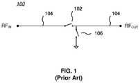
- the inventionrelates to electronic circuits, and more particularly to radio frequency electronic switch circuits and related methods.
- FIG. 1is a simplified schematic circuit of a common prior art series-shunt switch circuit configuration 100 .
- a series switch circuit 102is coupled in series with an RF signal line 104 between an RF IN port and an RF OUT port, and a shunt switch circuit 106 is coupled to the RF signal line 104 between the RF OUT port and circuit ground.
- the series switch circuit 102 and shunt switch circuit 104are modeled as single-pole, single-throw (SPST) switches.
- SPSTsingle-pole, single-throw
- the series switch circuit 102 and shunt switch circuit 106are generally operated in a complementary manner: if series switch circuit 102 is open, then shunt switch circuit 106 is closed, and if series switch circuit 102 is closed, then shunt switch circuit 106 is open.
- switch circuitssuch as those shown in FIG. 1 should not appreciably alter or affect an RF signal.
- RF switching circuitsare generally implemented with transistors, particularly field-effect transistors (FETs), and more particularly MOSFETs.
- FETsfield-effect transistors
- FET-based switch circuitsgenerally behave less than ideally in an RF circuit.
- a further issue with FETsis that the voltage that a single FET can withstand between drain and source without breaking down is generally limited to a few volts. In an electronic system, there may be parts of the system where the voltage that must be withstood far exceeds the voltage handling capability of a single FET.
- a common solutionis to series stack FETs so that the drain-source voltage across any one FET is less than its drain-source breakdown voltage.
- FIG. 2is a schematic circuit of a prior art series-shunt RF switch circuit 200 using FET stacks.
- an RF signal from an antenna ANTis coupled from RF IN through a series stack 202 to RF OUT .
- a shunt stack 204is coupled between RF OUT and circuit ground.
- Each of the stacks 202 , 204comprises a plurality of series-coupled FETs M 1 -Mn (although “n” may differ for the two stacks 202 , 204 ).
- each FETincludes a dedicated gate resistor Rg.
- a standard biasing schemeis usually used in this type of circuit 200 when configured with FET switches having a common threshold voltage and channel structure.
- a positive voltageis applied to the gate of each FET M 1 -Mn of a stack 202 , 204 to turn the stack ON (conducting), and a negative voltage is applied to the gate of each FET M 1 -Mn of a stack 202 , 204 to turn the stack OFF (blocking).
- a positive DC voltage of +3 voltsmay be applied (through the resistors Rg) to the gates of each FET M 1 -Mn of a stack 202 , 204 to turn the stack ON, and a negative DC voltage of ⁇ 3 volts may be applied (again through the resistors Rg) to the gates of each M 1 -Mn of a stack 202 , 204 to turn the stack OFF.
- a large enough negative voltageto fully turn each FET switch M 1 -Mn OFF. Turning the FET switches into a full OFF state results in improved RF linearity in terms of harmonics and inter-modulation distortion (IMD), better RF power handling, higher isolation, and lower leakage current, among other advantages.
- IMDinter-modulation distortion
- a positive supply voltageis readily available from an external source.
- a negative supply voltageis usually generated on-chip using a bias generator 206 , shown in FIG. 2 as coupled to the gate resistors Rg.
- the bias generator 206may conventionally use one or more negative voltage charge pumps and voltage regulators that convert an externally supplied positive supply voltage to a negative voltage.
- FIG. 2works reasonably well for many applications. However, there are applications where generating a negative supply voltage is either not desired or not practical due to design constraints; in some applications, use of a negative charge pump is not even possible. These are generally applications with stringent requirements such as extremely low current and power consumption, extremely low noise sensitivity, and/or very small IC die areas. Moreover, in biasing schemes wherein charge pumps are used to generate negative supply power, switching speed is limited by the current sourcing capability of the charge pumps. Further, the voltage swing on the FET gates from full ON to full OFF is significant—from +3V to ⁇ 3V in the example above, or a 6V swing, which further limits switching speed. In addition, the charge swing has to go through the series gate resistors of the FETs, which dampens and slows the switching process.
- FIG. 3is a schematic circuit of a series-shunt RF switch circuit 300 using “positive logic” FET stacks.
- an RF signal from an antenna ANTis coupled from RF IN through a series stack 302 to RF OUT .
- a shunt stack 304is coupled between RF OUT and circuit ground.
- Each of the stacks 302 , 304comprise a plurality of series-coupled FETs M 1 -Mn (although “n” may differ for the two stacks 302 , 304 ) which have the characteristic that each FET turns OFF sufficiently when Vgs ⁇ 0V.
- each FETincludes a dedicated gate resistor Rg.
- Each stack 302 , 304also includes two bracketing DC blocking capacitors C connected in series with the FETs M 1 -Mn; the blocking capacitors C may each have different values for particular applications.
- Each of the stacks 302 , 304is configured to be coupled to two non-negative supply voltages, Vgate and Vdrain, which are used to control the switch state, ON or OFF, of associated FETs M 1 -Mn.
- the Vgate supply voltageis coupled to the gates of the FETs M 1 -Mn of each stack 302 , 304 through corresponding parallel gate resistors Rg.
- the Vdrain supply voltageis coupled to a network of parallel resistors Rds that are coupled as shown to respective drains or sources of each of the FETs M 1 -Mn, including shared drains-source nodes between the FETs M 1 -Mn.
- the FETs M 1 -Mnare turned ON by applying a positive Vgate voltage (e.g., +3V) to the FET gates through their respective gate resistors Rg, while applying a Vdrain voltage of 0V to the FET drains and sources through respective Rds resistors.
- V GSpositive DC gate-source voltage
- the FET stacksare turned OFF by applying a Vgate voltage of 0V to the FET gates through their respective gate resistors Rg, while applying a positive Vdrain voltage (e.g., +3V) to the FET drains and sources through respective Rds resistors.
- a positive Vdrain voltagee.g., +3V
- Circuits of the type shown in FIG. 3avoid use of a negative voltage and thus require no negative voltage charge pump. Switching speed is increased because discharge of the FET gates does not have to go through a charge pump. Accordingly, operation without a charge-pump enables a zero current standby mode, with very fast switching and settling times and a valid RF state in standby mode, as well as other advantages as disclosed in the U.S. patent application Ser. No. 15/256,453. However, there is room for improvement.
- the DC blocking capacitors Chave to be large for high isolation and for low insertion loss and low mismatch loss (i.e., their impedance at a desired operating frequency needs to be low), thus consuming IC die area and increasing cost.
- the constant presence of the DC blocking capacitors C in both ON and OFF states for a series stack 302affects a conveyed RF signal, while their constant presence and size impacts isolation.
- the constantly present DC blocking capacitors Chave to be charged through the Rds resistor network, which impacts switching and settling times (this is in addition to the usual Rg*Cgs time constant on the gate terminal side).
- the DC blocking capacitors Care generally formed as metal-insulator-metal (MIM) capacitor structures, which are sensitive to electro-static discharge (ESD) and thus require ESD protection on RF ports (e.g.,RF IN ).
- MIMmetal-insulator-metal
- a series stack 302generally requires an integrated shunt tuning inductor L coupled near each DC blocking capacitor C to perform both impedance matching (i.e., resonating out the capacitance of the DC blocking capacitors C) and ESD protection for port connections (by providing a DC path to a reference potential).
- impedance matchingi.e., resonating out the capacitance of the DC blocking capacitors C
- ESD protectionfor port connections (by providing a DC path to a reference potential).
- Such added shunt tuning inductors Lin combination with the adjacent blocking capacitors C, cause the series stack 302 to have a high-pass filter response, affecting the RF performance of the switch.
- the shunt tuning inductors Lalso consume IC area, thus increasing cost.
- Embodiments of the type shown in FIG. 3may breakdown when subjected to a high voltage RF signal due to RF voltages being coupled through to gate resistors, causing breakdown.
- the inventionencompasses an improved positive-logic FET switch stack that does not require a negative bias voltage, exhibits high isolation and low insertion loss and mismatch loss characteristics, requires less integrated circuit (IC) area, and in some embodiments, can withstand application of a high voltage RF signal.
- ICintegrated circuit
- Embodimentsinclude a FET stack comprising one or more series-coupled positive-logic FETs M 1 -Mn (i.e., zero-Vt, low-Vt, or high-Vt FETs of a type that require a negative V GS to turn OFF but configured so as to not require a negative power supply), series-coupled on at least one end to an “end-cap” FET M 0 , where “M 0 ” designates a FET of a high-Vt type that turns OFF when the V GS of such FET is essentially zero volts.
- the end-cap M 0 FETsselectably provide either a capacitive DC blocking function or a resistive signal path.
- Some embodimentsmay comprise a stack of only M 0 FETs, or a mix of positive-logic FETs and M 0 FETs, so long as at least one end-cap FET is an M 0 FET.
- Optional end-cap capacitorsmay be included to prevent early breakdown of corresponding end-cap M 0 FETs.
- Some embodimentsare configured to withstand high applied RF voltages by including a series-connected bias resistor ladder for the gates of the FETs in the stack (i.e., M 1 -Mn, M 0 ), a series-connected Rds drain-source resistor ladder, and either a series-connected or a parallel-connected Rb body charge control resistor ladder.
- Some embodimentsmay use series-connected Rb body charge control resistor ladder in conjunction with a parallel-connected bias resistor ladder for the gates.
- Some embodimentsmay use a series-connected bias resistor ladder (in a “rail” configuration) in conjunction with a parallel-connected bias resistor ladder (in a “rung” configuration) for the gates.
- Some embodimentsare configured with one or more AC coupling modules each coupled to at least one end of a corresponding gate bias resistor ladder and/or body charge control resistor ladder, and configured to be coupled to a radio frequency voltage source.
- FIG. 1is a simplified schematic circuit of a common prior art series-shunt switch circuit configuration.
- FIG. 2is a schematic circuit of a prior art series-shunt RF switch circuit using FET stacks.
- FIG. 3is a schematic circuit of a series-shunt RF switch circuit using “positive logic” FET stacks.
- FIG. 4is a schematic circuit of an improved positive logic FET stack.
- FIG. 5Ais a table showing example voltages for Vgate and Vdrain corresponding to ON and OFF states for the FET stack of FIG. 4 .
- FIG. 5Bis a simplified schematic circuit of the FET stack of FIG. 4 showing example drain and source voltages for the interior FETs Mn and end-cap FETs M 0 when in an ON state.
- FIG. 5Cis a simplified schematic circuit of the FET stack of FIG. 4 showing example drain and source voltages for the interior FETs Mn and end-cap FETs M 0 when in an OFF state.
- FIG. 6is a schematic diagram of a series-shunt RF switch circuit using the improved positive logic FET stacks of FIG. 4 .
- FIG. 7depicts a schematic equivalent circuit of a portion of a prior art FET stack, showing parasitic capacitances.
- FIG. 8Ais a schematic equivalent circuit of a FET stack with a series-connected resistor ladder gate bias scheme in accordance with one aspect of the present invention, showing parasitic capacitances.
- FIG. 8Bis a schematic diagram of a positive logic FET stack with a series-connected gate bias resistor ladder and a series-connected drain-source resistor ladder in accordance with the present invention.
- FIG. 8Cis a schematic diagram of a positive logic FET stack with an added series-connected resistor ladder for controlling body charge.
- FIG. 8Dis a schematic diagram of a conventional FET stack with a series-connected gate bias resistor ladder, a series-connected drain-source resistor ladder, and a series-connected body charge control resistor ladder.
- FIG. 8Eis a schematic diagram of a conventional FET stack with a series-connected gate bias resistor ladder, a series-connected drain-source resistor ladder, and a parallel-connected body charge control resistor ladder.
- FIG. 8Fis a schematic diagram of a conventional FET stack with a series-connected gate bias resistor ladder and an AC Coupling Gate Module.
- FIG. 8Gis a schematic diagram of a conventional FET stack with a series-connected gate bias resistor ladder and dual AC Coupling Gate Modules.
- FIG. 8His a simplified schematic diagram of an SOI MOSFET that includes an ACS structure along with conventional drain D, source S, and gate G terminals and a gate resistor Rg.
- FIG. 9is a process flow diagram showing one method for providing a FET switch stack.
- FIG. 10is a process flow diagram showing one method for providing a series-shunt switch circuit.
- FIG. 11is a process flow diagram showing one method for biasing a FET switch stack.
- FIG. 12is a process flow diagram showing a method for providing a FET switch stack.
- FIG. 13is a process flow diagram showing another method for biasing a FET switch stack.
- the inventionencompasses an improved positive-logic FET switch stack that does not require a negative bias voltage, exhibits high isolation and low insertion loss and mismatch loss characteristics, requires less integrated circuit (IC) area, and in some embodiments, can withstand application of a high voltage RF signal.
- ICintegrated circuit
- Embodimentsinclude a FET stack comprising one or more series-coupled positive-logic FETs M 1 -Mn (i.e., zero-Vt, low-Vt, or high-Vt FETs of a type that require a negative V GS to turn OFF but configured so as to not require a negative power supply), series-coupled on at least one end to an “end-cap” FET M 0 , where “M 0 ” designates a FET of a high-Vt type that turns OFF when the V GS of such FET is essentially zero volts.
- the end-cap M 0 FETsselectably provide either a capacitive DC blocking function or a resistive signal path.
- Some embodimentsmay comprise a stack of only M 0 FETs, or a mix of positive-logic FETs and M 0 FETs, so long as at least one end-cap FET is an M 0 FET.
- Optional end-cap capacitorsmay be included to prevent early breakdown of corresponding end-cap M 0 FETs.
- Some embodimentsare configured to withstand high applied RF voltages by including a series-connected bias resistor ladder for the gates of the FETs in the stack (i.e., M 1 -Mn, M 0 ), a series-connected Rds drain-source resistor ladder, and either a series-connected or a parallel-connected Rb body charge control resistor ladder.
- Some embodimentsmay use series-connected Rb body charge control resistor ladder in conjunction with a parallel-connected bias resistor ladder for the gates.
- Some embodimentsmay use a series-connected bias resistor ladder (in a “rail” configuration) in conjunction with a parallel-connected bias resistor ladder (in a “rung” configuration) for the gates.
- Some embodimentsare configured with one or more AC coupling modules each coupled to at least one end of a corresponding gate bias resistor ladder and/or body charge control resistor ladder, and configured to be coupled to a radio frequency voltage source.
- Embodiments of the inventionmay be used in any circuit configuration in which a FET stack may be necessary or useful, such as RF switch circuits and digitally tuned capacitors (for example, of the type taught in U.S. patent application Ser. No. 15/256,453).
- FIG. 4is a schematic circuit of an improved positive logic FET stack 400 .
- the stack 400comprises one or more series-coupled FETs M 1 -Mn.
- Each of the FETs M 1 -Mnare of a type that require a negative V GS to turn OFF (e.g., ⁇ 3V) but which are configured to not require a negative power supply, as taught in co-pending U.S. patent application Ser. No. 15/256,453.
- Examples of such FETs M 1 -Mnmay have a V T ⁇ 0V and a low R ON (e.g., much less than Z 0 ohms, where Z 0 is the system characteristic impedance).
- the FETs M 1 -Mn in the “interior” of the stack 400which may be zero-Vt, low-Vt, or high-Vt FETs, are bracketed by “end-cap” M 0 high-Vt FETs.
- only one end of one or more series-coupled positive-logic FETs M 1 -Mnis series coupled to an M 0 FET; thus, for example, the end-cap M 0 FET in dashed box 402 or the end-cap M 0 FET in dashed box 404 may be omitted in some applications.
- Zero-Vt, low-Vt and high-Vt FETsare available from a number of different IC commercial foundries. Examples of such end-cap M 0 FETs may have a V T ⁇ 0.7V, and may have a higher R ON than the FETs M 1 -Mn.
- Each FET M 1 -Mn, M 0includes an associated gate resistor Rg; in the illustrated example, the gate resistors Rg are dedicated to each FET and parallel to each other (for other configurations, see below).
- Vgate and VdrainTwo non-negative supply voltages, Vgate and Vdrain, are used to control the switch state, ON or OFF, of associated FETs M 1 -Mn, M 0 .
- the Vgate supply voltageis coupled to the gates of the FETs of the stack 400 through corresponding dedicated parallel gate resistors Rg.
- the Vdrain supply voltageis coupled to a network of parallel resistors Rds that are coupled as shown to respective sources or drains of each of the FETs M 1 -Mn, including shared drains-source nodes between the FETs M 1 -Mn.
- the gate resistors Rg and the network resistors Rdsmay be of equal size, but a person skilled in the art will understand that other embodiments may include resistors of different sizes.
- each end-cap M 0 FETis coupled in parallel with a capacitor Cd.
- the Vds across each end-cap M 0 FETis lowered (e.g., to 2V) by their respective capacitor Cd.
- FIG. 5Ais a table showing example voltages for Vgate and Vdrain corresponding to ON and OFF states for the FET stack of FIG. 4 .
- FIG. 5Bis a simplified schematic circuit of the FET stack of FIG. 4 showing example drain and source voltages for the interior FETs Mn and end-cap M 0 FETs when in an ON state.
- FIG. 5Cis a simplified schematic circuit of the FET stack of FIG. 4 showing example drain and source voltages for the interior FETs Mn and end-cap M 0 FETs when in an OFF state.
- the FETs FET M 1 -Mn, M 0are turned ON by applying a positive Vgate voltage (e.g., +3V) to the FET gates through their respective gate resistors Rg, while applying a Vdrain voltage of 0V to the drains and sources of FETs M 1 -Mn through respective Rds resistors.
- a positive Vgate voltagee.g., +3V
- the source for the “top” M 0 FETwould be, for example, a coupled antenna or other RF signal source, and thus its drain is at the “bottom” end of that FET.
- the source for the “bottom” M 0 FETwould be, for example, circuit ground, and thus its drain is at the “top” end of that FET. Accordingly, the Vdrain voltage is coupled to the respective drains of both the “top” M 0 FET and the “bottom” M 0 FET.
- “top” and “bottom”are with respect to the illustrated orientation of the FET stack in FIG. 4 and are for convenience only).
- the end-cap M 0 FETsIn the ON state, the end-cap M 0 FETs each present a series resistance of R ON . Since the ON-state end-cap M 0 FETs essentially present no series capacitance, shunt tuning inductors L for impedance matching may be omitted, thus improving broadband performance and reducing consumption of IC area.
- the FETs FET M 1 -Mn, M 0are turned OFF by applying a Vgate voltage of 0V to the FET gates through their respective gate resistors Rg, while applying a positive Vdrain voltage (e.g., +3V) to the drains and sources of FETs M 1 -Mn (and thus to the source of the “top” M 0 FET, and to the drain of the “bottom” M 0 FET) through respective Rds resistors.
- a positive Vdrain voltagee.g., +3V
- the end-cap M 0 FETshave either a V GS of ⁇ 3V (for the “top” M 0 FET) or 0V (for the “bottom” M 0 FET), either of which is sufficient to turn the end-cap M 0 FETs OFF in light of their V GS characteristics (although the current blocking capability of the end-cap M 0 FETs increases as V GS becomes more negative).
- the end-cap M 0 FETsIn the OFF state, each present a series capacitance of C OFF , and thus perform a DC blocking function.
- the terminal labeled Vdrain in FIG. 4can be left as an open circuit, since all of the FETs coupled to the Rds resistor network would be coupled to circuit ground through the “bottom” M 0 FET.
- the terminal labeled Vdrain in FIG. 4would be coupled to a suitable voltage (e.g., +3V).
- Vdrainis varied between 0V to 3V as a function of the ON or OFF state of the FET stack 400 .
- Vdrainmay be set as a fixed voltage, such as a constant mid-rail voltage (e.g., +1.5V).
- a constant mid-rail voltagee.g., +1.5V.
- Vgatewhen Vgate is low (e.g., 0V), a negative voltage of ⁇ 1.5V will appear across the gate-source of each interior FET M 1 -Mn and turn those FETs OFF; similarly, V GS for the “top” end-cap M 0 FET will be ⁇ 1.5V, while the V GS for the “bottom” end-cap M 0 FET will be 0V, and thus both of the end-cap M 0 FETs will be OFF.
- lower or higher voltagese.g., +0.5V
- the fixed mid-rail voltagemay be chosen based on the threshold voltage, V T , of the FETs to provide a beneficial (potentially optimal) level of gate overdrive (V GS -V T ) to balance performance parameters in both ON and OFF states. More generally, the voltages for Vgate and Vdrain can be selected (and potentially optimized) to provide a balanced amount of gate overdrive. If Vdrain is biased to a non-zero DC voltage, a correctly sized shunt capacitor (or RC filter) may need to be added to sufficiently filter out RF voltage swings.
- the circuit configuration of the FET stack 400 of FIG. 4is thus similar to the circuit configurations of the stacks 302 , 304 of FIG. 3 , except that the end-cap M 0 FETs are used for DC blocking instead of explicit DC blocking capacitors C.
- the end-cap M 0 FETscan be turned to an OFF state in which they function as DC blocking capacitors having a capacitance of C OFF .
- the end-cap M 0 FETsalso can be turned to an ON state that forms an actual resistive DC path rather than a capacitance, resulting in little or no insertion loss, mismatch loss, or frequency dependence penalty compared to constantly present DC blocking capacitors C, and also decreasing switching and settling times.
- the R ON for the end-cap M 0 FETsgenerally may be greater than the R ON for the interior FETs M 1 -Mn, with larger numbers of interior FETs M 1 -Mn (i.e., higher stack heights), the R ON of the interior FETs M 1 -Mn will dominate the series resistance.
- a further benefit of using one or more end-cap M 0 FETs as DC blocking capacitancesis that they provide automatic ESD protection, because the FET stack is self-protected by drain-to-source breakdown and there are no additional series components between the FET drain-source terminals and the external ports (ESD pulses are applied across external ports). Accordingly, shunt tuning inductors L for ESD protection of MIM capacitors in FET stacks coupled to ports may be omitted, thus reducing consumption of IC area.
- using one or more end-cap M 0 FETsprovides a reasonable “un-powered OFF” state for applications that benefit from some isolation when the system voltage supply, Vcc, equals 0V.
- all of the FETs in a stack 400may be of the M 0 type.
- some (but not all) of the interior FETs in a stack 400may be of the M 0 type, so long as at least one end-cap M 0 FET is provided.
- the stack 400may comprise a mix of FETs in a sequence such as M 0 -M 1 -M 0 -M 2 -M 0 , where M 1 and M 2 are positive-logic FETS.
- Such mixed configurationsmay have a higher series resistance than the embodiment shown in FIG. 4 , due to higher R ON for the M 0 FETs, but would have a lower R ON than a stack comprising all M 0 -type FETs.
- Mixed configurations of FET types and sequencescan be used to help optimize the total stack performance parameters of R ON , OFF isolation, peak voltage (Vpk) handling, DC operation, and un-powered circuit behavior.
- optional capacitors Cdmay be coupled in parallel with the end-cap M 0 FETs, from drain to source, as indicated by the dotted connector lines.
- the optional capacitors CdWhen the end-cap M 0 FETs are in an ON state, the optional capacitors Cd are effectively bypassed and thus functionally out of the RF signal path.
- the optional capacitors CdWhen the end-cap M 0 FETs are in an OFF state, the optional capacitors Cd are coupled to the RF signal path in parallel with the end-cap M 0 FETs (which each present as a capacitance of C OFF ).
- the optional capacitors Cdreduce RF voltage swing across the end-cap M 0 FETs (e.g., to 2V instead of a full 3V) and thus help prevent early breakdown of those FETs. It may be desirable for the optional capacitors Cd to have a capacitance that is about 5-10 times the C OFF of the end-cap M 0 FETs. In some embodiments, only the “bottom” M 0 FET (i.e., nearest circuit ground in FIG. 4 ) includes the capacitor Cd.
- the person skilled in the artwill appreciate that, regardless of the switching state of the FET stack 400 , and except for leakage currents, the FET stack 400 and generation of the bias voltages Vgate and Vdrain does not consume any significant DC power, unlike the case of FET stacks that require a charge pump. This is very beneficial for integrated circuits with stringent power or current consumption requirements.
- Embodimentsmay use the existing system voltage supply rail to provide Vgate and Vdrain; however, a person skilled in the art will understand that other design choices to provide Vgate and Vdrain may be envisaged.
- the gates of one or both of the end-cap M 0 FETsmay be biased separately from the interior FETs M 1 -Mn.
- biasing the gates of both end-cap M 0 FETs with a negative gate voltage (and thus a negative VUs)would more completely turn both FETs OFF and improve the linearity and harmonics performance of those FETs, but would not require a significant current draw since such FETs inherently draw low body current and are only two in number.
- Negative biasingwould also allow the optional capacitors Cd to be much smaller than otherwise, or to be omitted entirely. Accordingly, a simple negative voltage generator could be used to generate a negative gate voltage bias for just the end-cap M 0 FETs.
- FIG. 6is a schematic diagram of a series-shunt RF switch circuit 600 using the improved positive logic FET stacks of FIG. 4 .
- an RF signal from an antenna ANTis coupled from RF IN through a series stack 602 to RF OUT .
- a shunt stack 604is coupled between RF OUT and a reference potential (circuit ground in this case).
- Each of the stacks 602 , 604are similar to the FET stack 400 of FIG. 4 , although “n” may differ for the two stacks 602 , 604 .
- each of the stacks 602 , 604is configured to be coupled to two non-negative supply voltages, Vgate and Vdrain.
- Optional capacitors Cdare shown as coupled in parallel with the end-cap M 0 FETs. Notably absent are constantly connected DC blocking capacitors or shunt tuning and ESD protection inductors L, as in FIG. 3 .
- only one end of the series stack 602 and/or the shunt stack 604includes an end-cap M 0 FET.
- Vgateis applied to each FET M 1 -Mn, M 0 through an associated gate resistor Rg in a conventional biasing scheme, which provides excellent performance in many applications, including low power RF switch circuits and many series and/or shunt circuit configurations.
- a conventional biasing schemeprovides excellent performance in many applications, including low power RF switch circuits and many series and/or shunt circuit configurations.
- an innovative biasing schemeprovides for an enhanced ability to withstand such voltages.
- FIG. 7depicts a schematic equivalent circuit of a portion of a prior art FET stack 700 , showing parasitic capacitances.
- the “top” FET, Mtop, of the FET stack 700is coupled to an RF input voltage V RF , and to a next sequential FET, Mnext.
- Mnexta next sequential FET
- additional FETsmay be similarly sequentially coupled to Mnext.
- a conventional parallel gate bias resistor ladder 702is shown in which a variable DC gate bias voltage Vgate is coupled to the gate of each FET Mtop, Mnext through a corresponding gate resistor Rg.
- Vgatevariable DC gate bias voltage
- each gate resistor Rghas a parallel parasitic capacitance Cp R
- each FETincludes parasitic capacitances Cp M between its gate and drain and between its gate and source. Accordingly, the gates of each FET are imperfectly isolated from the gate and source with respect to RF signals.
- V RFis an RF voltage of 100V and the stack 700 is in the OFF state (i.e., all FETs are biased to block drain-source current flow)
- each FET Mtop, Mnext, etc.can safely withstand 3V from drain to source (further assuming that there sufficient other FETs to drop the applied RF voltage such that no one FET is subjected to more than 3V)
- the source voltage for Mtopand thus the drain voltage for Mnext
- the source voltage for Mnextwould be 94V; additional FETs in the sequence would similarly drop 3V from drain to source.
- the parasitic capacitances Cp Mwill cause imposition of an RF voltage on the gate of Mtop of about 98.5V (i.e., about one-half the difference between 100V-97V); for Mnext, the imposed gate voltage would be about 95.5V. More specifically, the gate resistor Rg for Mtop will essentially have AC ground (0V) on its Vgate side, and very high RF voltage ( ⁇ 98.5V) on its other side. This causes excessive power dissipation in the gate resistor Rg for Mtop. The parallel parasitic capacitor Cp R across that gate resistor Rg makes the effective resistance even smaller, thereby increasing the RF power dissipation in the gate resistor Rg, which may cause device failure. A similar problem, but at increasingly lower RF voltages, occurs for each of the successive FETs Mnext in the stack 700 .
- FIG. 8Ais a schematic equivalent circuit of a FET stack 800 with a series-connected resistor ladder gate bias scheme in accordance with one aspect of the present invention, showing parasitic capacitances.
- the “top” FET, Mtop, of the FET stack 800is coupled to an RF input voltage V RF , and to a next sequential FET, Mnext; additional FETs may be similarly sequentially coupled to Mnext.
- a variable DC gate bias voltage Vgatemay be coupled to the gate of each FET Mtop, Mnext at nodes A, B situated after a corresponding one of a plurality of series-coupled gate resistors Rg, which thus form a series-connected gate bias resistor ladder 802 .
- each gate resistor Rgis coupled to the gates of two adjacent FETs, and the series-connected gate bias resistor ladder 802 is configured to be connected to a gate bias voltage Vgate. Accordingly, in the illustrated example, for n FETs, there are n ⁇ 1 gate resistors Rg (see also FIG. 8B ); however, if desired, an additional gate resistor Rg can be coupled between Vgate and the gate of the “bottom” FET in the FET stack 800 (see, for example, resistor RBF in FIG. 8B ). Each FET gate will see an applied DC bias voltage of Vgate through the series connection of the gate resistors Rg of the resistor ladder 802 ; that is, Vgate essentially just charges or discharges each FET gate through corresponding gate resistors Rg.
- V RFis an RF voltage of 100V and each FET Mtop, Mnext, etc. can safely withstand 3V from drain to source
- the source voltage for Mtop(and thus the drain voltage for Mnext) would be 97V
- the source voltage for Mnextwould be 94V.
- the parasitic capacitances Cp Mwill enable imposition of an RF voltage on the gate of Mtop of about 98.5V; for Mnext, the imposed gate voltage would be about 95.5V.
- each gate resistor Rg and its corresponding parasitic capacitance Cp Rwill be subjected to an RF voltage of only 3V, representing the difference between the RF voltages imposed on the gates of adjacent FETs (e.g., 98.5V for the gate of Mtop, and 95.5 for the gate of Mnext).
- RF voltage of only 3Vrepresenting the difference between the RF voltages imposed on the gates of adjacent FETs (e.g., 98.5V for the gate of Mtop, and 95.5 for the gate of Mnext).
- all gate resistors of the FET stack 800 of FIG. 8are subjected to an RF voltage of only 3V, and thus are protected from breakdown due to excessive RF voltages capacitively coupled through to the gates of associated FETs.
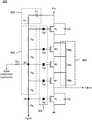
- FIG. 8Bis a schematic diagram of a positive logic FET stack 820 with a series-connected gate bias resistor ladder 802 and a series-connected drain-source resistor ladder in accordance with the present invention.
- the illustrated exampleis similar to the FET stack 400 of FIG. 4 (with optional capacitors Cd), but the gate resistors Rg are arrayed in a series-connected resistor ladder configuration 802 as in FIG. 8A , and, in addition, the resistors Rds of the drain-source resistor network are also arrayed as a series-connected resistor ladder 804 configured to be connected to a drain-source bias voltage Vdrain.
- each resistor Rdsis connected across the drain and source of a corresponding interior FET M 1 -Mn (but not across the end-cap M 0 FETs, which would defeat the DC blocking state of the end-cap M 0 FETs).
- the series-connected gate bias resistor ladder 802the series-connected drain-source resistor ladder 804 prevents any of the Rds resistors and FET devices from being subjected to high RF voltages V RF .
- DC blocking capacitorsmay be coupled to Vgate and/or Vdrain as described below with respect to FIG. 8C .
- the bias voltage Vgateis shown coupled to the “bottom” FET in the FET stack 820 at a “bottom feed” node BF through a “bottom feed” resistor RBF at one end of the series of resistors comprising the gate bias resistor ladder 802 .
- Vgatemay be coupled to the series-connected gate bias resistor ladder 802 at a “middle feed” node MF, optionally through a “middle feed” resistor R MF .
- the “middle feed” node MFneed not be in the exact middle of the gate bias resistor ladder 802 , but may be anywhere between the ends of the series of resistors comprising the gate bias resistor ladder 802 .
- a “middle feed” configurationmay be useful when the FET stack 820 could experience an applied RF voltage to FET at the “top” or “bottom” (in relation to FIG. 8B ) of the stack 820 , as may be the case if the FET stack 820 is designed for a dual-polarity series application (i.e., an RF signal can be applied to either end of the stack) rather than a shunt configuration (see also FIG. 8F below).
- a “middle feed” configurationcan provide a reduction in power dissipation in the gate resistors Rg regardless of whether an RF voltage amplitude is applied at either end of the transistor stack. Further benefits of a “middle feed” configuration are described in U.S. patent application Ser. No. 15/289,768 referenced above.
- an additional parallel-connected gate resistor ladder 805may be included.
- the parallel-connected gate resistor ladder 805comprises respective resistors Rg′ (indicated by a block symbol) coupled to the gates of the FETs in the FET stack 820 .
- Rg′indicated by a block symbol
- a combination of a series-connected gate bias resistor ladder 802 and a parallel-connected gate resistor ladder 805can provide reduced RF power dissipation while maintaining a low switching time constant (and therefore a high switching speed). Further benefits of a “series plus parallel” gate bias ladder configuration are described in U.S. patent application Ser. No. 15/289,768 referenced above.
- FIG. 8Cis a schematic diagram of a positive logic FET stack 830 with an added series-connected resistor ladder for controlling body charge, and thus “back gate” characteristics in the FETs.
- each FET(of any type M 1 -Mn, M 0 ) is treated as an explicit four-terminal transistor, and the body of each of the stacked four terminal FETs is configured to be connected to a body bias voltage Vbody directly or through a corresponding resistor Rb of a body charge control resistor ladder 806 .
- the series-connected body charge control resistor ladder 806prevents any of the resistors Rb from being subjected to high RF voltages V RF .
- a series-connected body charge control resistor ladder 806is also useful for FET stacks that draw a lot of body current, to mitigate or eliminate interference with gate voltages when high peak RF voltages are applied across the FET stack.
- an additional parallel-connected gate resistor ladder(not shown, but essentially the same as the parallel gate resistor ladder 805 of FIG. 8C ) may be included.
- VbodyIn the circuit configuration of FIG. 8C , a separate Vbody terminal is shown in the schematic diagram for flexibility, but in many applications Vbody can be tied directly to circuit ground.
- a negative power supplyis usually provided by a negative charge pump, the output of which, Vss, will slump when high peak RF voltages are applied across the FET stack and induce significant body current.
- capacitors Cgate, Cdrain, and/or Cbodymay be coupled as shown to the Vgate, Vdrain, and Vbody terminals, respectively, and to a reference potential, such as circuit ground.
- the Cgate, Cdrain, and/or Cbody capacitorswhen present, serve to filter out RF voltage from DC bias voltages applied to those terminals (i.e., making Vgate, Vdrain, and/or Vbody AC grounds).
- the series-connected gate bias resistor ladder 802 configuration of FIG. 8A , the series-connected drain-source resistor ladder 804 of FIG. 8B , and the series-connected body charge control resistor ladder 806 of FIG. 8Care applicable to conventional FET stacks (e.g., of the types shown in FIG. 2 or 3 ), as well as to FET switch stacks having one or more end-cap M 0 FETs (i.e., FETs that turn OFF when their V GS is essentially zero volts).
- FIG. 8Dis a schematic diagram of a conventional FET stack 840 with a series-connected gate bias resistor ladder 802 , a series-connected drain-source resistor ladder 804 , and a series-connected body charge control resistor ladder 806 .
- the “end-cap” FETs M 1 and Mnare conventional FETS
- additional drain-source resistors Rds′have been added to the drain-source resistor ladder 804 in order to span the drain and source of each of M 1 and Mn
- the optional capacitors Cd from FIG. 8Chave been removed, and there is no Vdrain bias voltage.
- This configurationhas the advantages for each series-connected resistor ladder 802 , 804 , 806 noted above for the series-connected gate bias resistor ladder 802 , especially protection from breakdown due to excessive capacitively coupled RF voltages.
- the series-connected body charge control resistor ladder 806may be replaced by a parallel-connected body charge control resistor ladder, either in a conventional FET stack or in a FET stack having one or more end-cap M 0 FETs.
- FIG. 8Eis a schematic diagram of a conventional FET stack 850 with a series-connected gate bias resistor ladder 802 , a series-connected drain-source resistor ladder 804 , and a parallel-connected body charge control resistor ladder 808 .
- This parallel-connected approachmay prove to be advantageous if the body current for a series-connected resistor ladder configuration (as in FIG.
- the parallel-connected body charge control resistor ladder 808 configurationcreates a consistent voltage drop across the body resistors Rb such that there is no additive voltage increase.
- an additional parallel-connected gate resistor ladder(not shown, but essentially the same as the parallel-connected gate resistor ladder 805 of FIG. 8C ) may be included.
- the configuration of the body charge control resistor laddermay be series-connected (as in FIG. 8D ) and the configuration of the gate bias resistor ladder may be parallel-connected (as in FIG. 4 ) or a combination of series-connected and parallel-connected (as in FIG. 8B , with the added parallel-connected gate resistor ladder 805 ), with benefits similar to those described above for FIG. 8E .
- any combination of series-connected resistor ladders 802 , 804 , 806may be used in conjunction with a FET stack, with or without adding a parallel-connected gate resistor ladder 805 or substituting a parallel-connected body charge control resistor ladder 808 for a series-connected resistor ladder 806 .
- Examplesinclude: a gate bias resistor ladder plus a body charge control resistor ladder; a gate bias resistor ladder plus a drain-source resistor ladder; a body charge control resistor ladder plus a drain-source resistor ladder; and a gate bias resistor ladder plus a body charge control resistor ladder plus a drain-source resistor ladder.
- Vdraine.g., from 3V to 0V
- Vgatee.g., from 3V to 0V
- Vdraine.g., from 0V to 3V
- the series-connected or series/parallel connected gate resistor ladders described aboveallow the gate of each FET in a switch stack to track the common mode voltage of its associated FET.
- such gate resistor laddersmust provide a high impedance relative to the impedance (capacitance) between the gate and the source/drain of the FETs in the switch stack.
- a series-connected gate bias resistor ladder 802e.g., as shown in FIG. 8A
- a combination of series-connected gate bias resistor ladder 802 and a parallel-connected gate bias resistor ladder 805e.g., as shown in FIG.
- the FET nearest an applied RF signale.g., the “top” FET in FIGS. 8B-8E coupled to V RF
- the FET nearest an applied RF signalstill has an effective RF load that can cause the gate of that FET to not fully track the transistor common mode voltage during RF operation.
- the RF load on the gate of the “top” FETacts as parasitic capacitance in producing non-ideal voltage division, and if not compensated, can reduce the peak breakdown voltage (BV) withstand capability of that FET by several percent.
- BVpeak breakdown voltage
- an AC Coupling Gate Module 822is coupled between the terminal receiving a V RF signal and the gate of the “top” FET (Mn or M 0 , as the case may be)—thus, the AC Coupling Gate Module 822 is also coupled to the “top” of the series-connected gate bias resistor ladder 802 .
- FIG. 8Fis a schematic diagram of a conventional FET stack 860 with a series-connected gate bias resistor ladder 802 and an AC Coupling Gate Module 822 .
- the FET stack 860is configured to be coupled in a shunt configuration or in a series configuration.
- the RF ⁇ terminalis usually circuit ground
- an RF input signalis applied at the RF+ terminal
- Vgateis applied at the “bottom” of the FET stack 860 through resistor RBF.
- either or both of the RF+ and RF ⁇ terminalsmay be the source of an RF signal (e.g., RF+ may be coupled between an RF antenna and an amplifier), and Vgate would generally be applied at the “middle” of the FET stack 860 through resistor R MF .
- a “middle feed” configurationcan provide a reduction in power dissipation in the gate resistors Rg regardless of whether an RF voltage amplitude is applied at either end of the FET stack 860 .
- the FETs M 1 -Mn of the conventional FET stack 860 of FIG. 8Fcan be replaced by a positive logic stack of the type shown in FIG. 8B .
- the AC Coupling Gate Module 822may comprise a DC blocking capacitor C 1 , while in other embodiments the AC Coupling Gate Module 822 may comprise a DC blocking capacitor C 1 connected in series with a resistor R 1 (the order of connection of C 1 and R 1 does not matter, whereas the order of connection does matter for Cgate and RBF at the “bottom” of the stack for a shunt stack configuration).
- the AC Coupling Gate Module 822improves voltage division along the gate bias resistor ladder 802 and allows the gate of the “top” FET to more fully track the transistor common mode voltage during RF operation. Another benefit of the AC Coupling Gate Module 822 in a series configuration is that it lets a coupled antenna be loaded directly, rather than through the FETs of the stack.
- FIG. 8Gis a schematic diagram of a conventional FET stack 870 with a series-connected gate bias resistor ladder 802 and dual AC Coupling Gate Modules.
- the FET stack 870 of FIG. 8Gis similar to the FET stack 860 of FIG.
- the second AC Coupling Gate Module 822 ′may comprise a DC blocking capacitor C 2
- the second AC Coupling Gate Module 822 ′may comprise a DC blocking capacitor C 2 connected in series with a resistor R 2 .
- a similar AC Coupling Body Module 823will provide the same benefits for the body (or “back gate”) of the “top” FET (in this example, FET Mn, nearest the RF+ terminal).
- the AC Coupling Body Module 823is coupled between the RF+ terminal and the series-connected body charge control resistor ladder 806 connected to the “top” FET Mn nearest the RF+ terminal.
- the AC Coupling Body Module 823may comprise a DC blocking capacitor C 2 in some embodiments, while in other embodiments the AC Coupling Body Module 823 may comprise a DC blocking capacitor C 2 connected in series with a resistor R 2 (again, the order of connection does not matter). Further, in a series configuration, a second AC Coupling Body Module (not shown) may be coupled between the RF ⁇ terminal and the series-connected body charge control resistor ladder 806 connected to the “bottom” FET M 1 nearest the RF ⁇ terminal to provide similar benefits.
- An AC Coupling Gate Module and an AC Coupling Body Modulemay be used independently of each other, or may be used together.
- a series-connected gate bias resistor ladder 802 and/or a series-connected body charge control resistor ladder 806there are significant benefits to using an AC Coupling Gate and/or Body Module between the respective ladders 802 , 806 and any RF terminal presenting an RF load, in order to mitigate or even totally eliminate an RF load across the FET coupled to that RF terminal.
- a parallel-connected gate bias ladder 805may be included with the values of the resistors Rg′ being selected to isolate for a different voltage division in the gate bias resistor ladders versus the component FETs M 1 -Mn of the FET stack 860 . More particularly, if the voltage division across the FET stack 860 is uniform, then constant Rg values for a series-connected gate bias resistor ladder 802 (i.e., a “rail” only configuration) in conjunction with an AC Coupling Gate Module 822 completely eliminates the RF load on the FETs since the voltage division across the gate bias resistor ladder is uniform.
- variable rail resistor valuesmay be adjusted to achieve a desired relationship of (1) the RF load on the FET gates to (2) the peak BV for the top-most transistor. However, there is a tradeoff with the switching time constant.
- the inclusion of the AC Coupling Gate Module 822 and/or the AC Coupling Body Module 823has essentially no adverse effect on the performance characteristics of the FET stack 860 (e.g., in terms of switching time constant, resistor power dissipation, resistive voltage drop through body resistors due to body current, etc.).
- the inclusion of one or more of such modules 822 , 823substantially eliminates the reduction in the peak breakdown voltage (BV) withstand capability of the “top” FET of the FET stack that would otherwise occur.
- BVpeak breakdown voltage
- the former configurationshowed a decrease in BV withstand capability of the “top” FET of about 0.714, while the latter configuration showed a decrease in BV withstand capability of the “top” FET of about 0.001—a factor of over 700 in improvement due to the AC Coupling Gate Module 822 .
- an AC Coupling Gate Module 822may be coupled between a terminal RF+, RF ⁇ and a respective end of the series-connected gate bias resistor ladder 802 for the FET stack 860 .
- Vgatewould normally be applied to the FET stack 860 using a “middle feed” configuration.
- an AC Coupling Body Module 823may be coupled to each end of the body charge control resistor ladder 806 for the FET stack 860 .
- Embodiments of the inventionmay benefit by adding an accumulated charge sink (ACS) structure to one or more constituent FETs (i.e., M 1 -Mn and/or M 0 ).
- SOIsilicon-on-insulator
- SOSsilicon-on-sapphire
- ACSaccumulated charge sink
- the linearity of an SOI MOSFETcan be improved by providing a means for sweeping out accumulated charge trapped below the gate oxide of the MOSFET, such as by use of the “HaRP”TM accumulated charge sink (ACS) technology taught in U.S. Pat. No. 7,910,993, issued Mar.
- an SOI MOSFETmay include an ACS structure that allows discharge of accumulated charge when the MOSFET is in a non-conducting (OFF) mode while allowing normal operation when the MOSFET is in a conducting (ON) mode.
- FIG. 8His a simplified schematic diagram of an SOI MOSFET 810 that includes an ACS structure along with conventional drain D, source S, and gate G terminals and a gate resistor Rg.
- the ACS structurecomprises a diode 812 coupled from the body of the MOSFET 810 to the gate G of the MOSFET 810 .
- the diode 812discharges accumulated charge from the body of the MOSFET 810 through the gate G when the MOSFET 810 is in a non-conducting (OFF) mode, while allowing normal operation when the MOSFET 810 is in a conducting (ON) mode.
- OFFnon-conducting
- ONconducting
- the MOSFET 810along with an ACS structure (e.g., a body-to-gate diode 812 ) may also be referred to as an “ACS FET”.
- an ACS FETe.g., a body-to-gate diode 812
- an SOI MOSFET stackcomprising one or more series-coupled positive-logic MOSFETs M 1 -Mn (i.e., FETs not requiring a negative voltage supply to turn OFF), coupled to one or more series-coupled “end-cap” M 0 MOSFETs
- one or more of the MOSFETsmay be ACS FETs.
- the principal of “superposition”may be used as a method for optimizing DC biasing and best AC voltage handling configuration independently, and then combining the results. That is, one can first define an optimum circuit configuration independently for AC behavior and DC behavior, and then overlay and merge the two solutions.
- FIG. 9is a process flow diagram 900 showing one method for providing a FET switch stack.
- the methodincludes: providing one or more series-coupled positive-logic FETs (STEP 902 ); and providing a first end-cap FET of a type that turns OFF when the V GS of such end-cap FET is essentially zero volts, series-coupled to a first end of the one or more series-coupled positive-logic FETs (STEP 904 ).
- Additional aspects of the method of FIG. 9may include one or more of the following: providing a second end-cap FET of a type that turns OFF when the VGS of such end-cap FET is essentially zero volts, series-coupled to a second end of the one or more series-coupled positive-logic FETs; further including series coupling, to the FET switch stack, at least one additional FET of the type that turns OFF when the VGS of such FET is essentially zero volts; wherein each end-cap FET functions as a DC blocking capacitor when in an OFF state, and as a resistive signal path when in an ON state; further including coupling at least one capacitor between the source and the drain of a corresponding end-cap FET; further including providing a gate bias resistor ladder including a plurality of series-coupled resistors configured to be coupled to a gate bias voltage, wherein each resistor is coupled to the respective gates of corresponding adjacent FETs; further including a capacitor coupled between the gate bias resistor ladder and a reference potential;
- FIG. 10is a process flow diagram 1000 showing one method for providing a series-shunt switch circuit.
- the methodincludes: providing a series FET switch stack having an input port configured to be coupled in series with an RF signal line, and an output port (STEP 1002 ); coupling a shunt FET switch stack to the output port of the series FET switch stack (STEP 1004 ); configuring the shunt FET switch stack to be coupled to a reference potential (STEP 1006 ); wherein the series FET switch stack and the shunt FET switch stack have at least one end-cap FET that turns OFF when the V GS of such end-cap FET is essentially zero volts (STEP 1008 ), or wherein the series FET switch stack and the shunt FET switch stack include at least one series-coupled positive-logic FET, series-coupled to at least one end-cap FET of a type that turns OFF when the V GS of such end-cap FET is essentially zero volts (STEP 10
- FIG. 11is a process flow diagram 1100 showing one method for biasing a FET switch stack.
- the methodincludes: providing a plurality of series-coupled FETs (STEP 1102 ); providing a gate bias resistor ladder including a plurality of resistors configured to be coupled to a gate bias voltage and to the gates of at least one corresponding FET (STEP 1104 ); providing a body charge control resistor ladder including a plurality of resistors configured to be coupled to a body bias voltage and to the body of at least one corresponding FET (STEP 1106 ); and providing a drain-source resistor ladder including a plurality of series-coupled resistors configured to be coupled to a drain-source bias voltage, wherein each resistor is coupled to the respective drains and sources of at least one corresponding adjacent FET (STEP 1108 ); and wherein the resistors of the gate bias resistor ladder are series-connected and the resistors of the body charge control resistor ladder are parallel-connected (STEP 1110 ),
- Additional aspects of the method of FIG. 11may include one or more of the following: wherein the plurality of series-coupled FETs includes one or more series-coupled positive-logic FET, series-coupled on at least one end to an end-cap FET of a type that turns OFF when the V GS of such end-cap FET is essentially zero volts; further including a second end-cap FET of a type that turns OFF when the V GS of such end-cap FET is essentially zero volts, series-coupled to a second end of the one or more series-coupled positive-logic FETs; coupling a capacitor between the gate bias resistor ladder and a reference potential; coupling an AC coupling gate module to at least one end of the gate bias resistor ladder and configuring the AC coupling gate module to be coupled to a radio frequency voltage source; wherein the AC coupling gate module includes one of a capacitor or a capacitor series coupled to a resistor; further including coupling an AC coupling body module coupled to at least one end of the
- FIG. 12is a process flow diagram 1200 showing a method for providing a FET switch stack.
- the methodincludes: providing a plurality of series-coupled FETs (STEP 1202 ); coupling a gate bias resistor ladder to the gates of the series-coupled FETs (STEP 1204 ); coupling an AC coupling gate module to at least one end of the gate bias resistor ladder and configuring the AC coupling gate module to be coupled to a corresponding radio frequency voltage source (STEP 1206 ); optionally, coupling a body charge control resistor ladder to the bodies of the series-coupled FETs (STEP 1208 ); and, optionally, coupling an AC coupling body module to at least one end of the body charge control resistor ladder and configured to be coupled to the corresponding radio frequency voltage source (STEP 1210 ).
- Additional aspects of the method of FIG. 12may include one or more of the following: wherein the plurality of series-coupled FETs includes one or more series-coupled positive-logic FET, series-coupled on at least one end to an end-cap FET of a type that turns OFF when the V GS of such end-cap FET is essentially zero volts; further including providing a second end-cap FET of a type that turns OFF when the VGS of such end-cap FET is essentially zero volts, series-coupled to a second end of the one or more series-coupled positive-logic FETs; further including providing a drain-source resistor ladder including a plurality of series-coupled resistors configured to be coupled to a drain-source bias voltage, wherein each resistor is coupled to the respective drains and sources of corresponding adjacent positive-logic FETs; wherein the gate bias resistor ladder includes a plurality of series-connected resistors; wherein the body charge control resistor ladder includes a plurality of series-connected resist
- FIG. 13is a process flow diagram 1300 showing another method for biasing a FET switch stack.
- the methodincludes: providing a plurality of series-coupled FETs (STEP 1302 ); providing a first gate resistor ladder including a plurality of parallel-connected constant-valued (or, optionally, variable-valued) resistors each coupled to the gate of one corresponding FET (STEP 1304 ); and providing a second gate bias resistor ladder including a plurality of series-connected variable-valued resistors each coupled to one corresponding constant-valued resistor of the first gate resistor ladder (STEP 1306 ).
- MOSFETmeans any field effect transistor (FET) with an insulated gate and comprising a metal or metal-like, insulator, and semiconductor structure.
- metalor metal-like include at least one electrically conductive material (such as aluminum, copper, or other metal, or highly doped polysilicon, graphene, or other electrical conductor), “insulator” includes at least one insulating material (such as silicon oxide or other dielectric material), and “semiconductor” includes at least one semiconductor material.
- various embodiments of the inventioncan be implemented to meet a wide variety of specifications. Unless otherwise noted above, selection of suitable component values is a matter of design choice and various embodiments of the invention may be implemented in any suitable IC technology (including but not limited to MOSFET structures), or in hybrid or discrete circuit forms. Integrated circuit embodiments may be fabricated using any suitable substrates and processes, including but not limited to standard bulk silicon, silicon-on-insulator (SOI), and silicon-on-sapphire (SOS). Unless otherwise noted above, the invention may be implemented in other transistor technologies such as bipolar, GaAs HBT, GaN HEMT, GaAs pHEMT, and MESFET technologies.
- inventive concepts described aboveare particularly useful with an SOI-based fabrication process (including SOS), and with fabrication processes having similar characteristics. Fabrication in CMOS on SOI or SOS processes enables circuits with low power consumption, the ability to withstand high power signals during operation due to FET stacking, good linearity, and high frequency operation (i.e., radio frequencies up to and exceeding 50 GHz). Monolithic IC implementation is particularly useful since parasitic capacitances generally can be kept low (or at a minimum, kept uniform across all units, permitting them to be compensated) by careful design.
- Voltage levelsmay be adjusted, or voltage and/or logic signal polarities reversed, depending on a particular specification and/or implementing technology (e.g., NMOS, PMOS, or CMOS, and enhancement mode or depletion mode transistor devices).
- Component voltage, current, and power handling capabilitiesmay be adapted as needed, for example, by adjusting device sizes, serially “stacking” components to withstand greater voltages as described above, and/or using multiple components in parallel to handle greater currents.
- Additional circuit componentsmay be added to enhance the capabilities of the disclosed circuits and/or to provide additional functional without significantly altering the functionality of the disclosed circuits.
Landscapes
- Engineering & Computer Science (AREA)
- Power Engineering (AREA)
- Microelectronics & Electronic Packaging (AREA)
- Physics & Mathematics (AREA)
- Condensed Matter Physics & Semiconductors (AREA)
- General Physics & Mathematics (AREA)
- Computer Hardware Design (AREA)
- Electronic Switches (AREA)
Abstract
Description
- U.S. Pat. No. 8,669,804, issued on Mar. 11, 2014 and entitled “Device and Methods for Improving Voltage Handling and/or Bi-directionality of Stacks of Elements when Connected Between Terminals”;
- U.S. patent application Ser. No. 15/256,453, filed Sep. 2, 2016 and entitled “Positive Logic Digitally Tunable Capacitor”, now U.S. Pat. No. 9,948,281 issued Apr. 17, 2018;
- U.S. patent application Ser. No. 15/289,768, filed Oct. 10, 2016, entitled “Reduced Dissipation Switch FET Gate Biasing”, which claims priority to U.S. Provisional Application No. 62/241,498, filed Oct. 14, 2015;
- U.S. patent application Ser. No. 15/939,128, filed on Mar. 28, 2018, entitled “Positive Logic Switch with Selectable DC Blocking Circuit”;
- U.S. patent application Ser. No. 15/939,132, filed on Mar. 28, 2018, entitled “Stacked FET Switch Bias Ladders”.
Claims (21)
Priority Applications (5)
| Application Number | Priority Date | Filing Date | Title |
|---|---|---|---|
| US16/852,804US11018662B2 (en) | 2018-03-28 | 2020-04-20 | AC coupling modules for bias ladders |
| US17/325,867US11418183B2 (en) | 2018-03-28 | 2021-05-20 | AC coupling modules for bias ladders |
| US17/884,252US11870431B2 (en) | 2018-03-28 | 2022-08-09 | AC coupling modules for bias ladders |
| US18/466,601US20240063785A1 (en) | 2018-03-28 | 2023-09-13 | AC Coupling Modules for Bias Ladders |
| US19/017,326US20250150073A1 (en) | 2018-03-28 | 2025-01-10 | AC Coupling Modules for Bias Ladders |
Applications Claiming Priority (3)
| Application Number | Priority Date | Filing Date | Title |
|---|---|---|---|
| US15/939,144US10236872B1 (en) | 2018-03-28 | 2018-03-28 | AC coupling modules for bias ladders |
| US16/261,167US10630280B2 (en) | 2018-03-28 | 2019-01-29 | AC coupling modules for bias ladders |
| US16/852,804US11018662B2 (en) | 2018-03-28 | 2020-04-20 | AC coupling modules for bias ladders |
Related Parent Applications (1)
| Application Number | Title | Priority Date | Filing Date |
|---|---|---|---|
| US16/261,167ContinuationUS10630280B2 (en) | 2018-03-28 | 2019-01-29 | AC coupling modules for bias ladders |
Related Child Applications (1)
| Application Number | Title | Priority Date | Filing Date |
|---|---|---|---|
| US17/325,867ContinuationUS11418183B2 (en) | 2018-03-28 | 2021-05-20 | AC coupling modules for bias ladders |
Publications (2)
| Publication Number | Publication Date |
|---|---|
| US20200321955A1 US20200321955A1 (en) | 2020-10-08 |
| US11018662B2true US11018662B2 (en) | 2021-05-25 |
Family
ID=65721857
Family Applications (7)
| Application Number | Title | Priority Date | Filing Date |
|---|---|---|---|
| US15/939,144ActiveUS10236872B1 (en) | 2018-03-28 | 2018-03-28 | AC coupling modules for bias ladders |
| US16/261,167ActiveUS10630280B2 (en) | 2018-03-28 | 2019-01-29 | AC coupling modules for bias ladders |
| US16/852,804ActiveUS11018662B2 (en) | 2018-03-28 | 2020-04-20 | AC coupling modules for bias ladders |
| US17/325,867ActiveUS11418183B2 (en) | 2018-03-28 | 2021-05-20 | AC coupling modules for bias ladders |
| US17/884,252Active2038-05-05US11870431B2 (en) | 2018-03-28 | 2022-08-09 | AC coupling modules for bias ladders |
| US18/466,601PendingUS20240063785A1 (en) | 2018-03-28 | 2023-09-13 | AC Coupling Modules for Bias Ladders |
| US19/017,326PendingUS20250150073A1 (en) | 2018-03-28 | 2025-01-10 | AC Coupling Modules for Bias Ladders |
Family Applications Before (2)
| Application Number | Title | Priority Date | Filing Date |
|---|---|---|---|
| US15/939,144ActiveUS10236872B1 (en) | 2018-03-28 | 2018-03-28 | AC coupling modules for bias ladders |
| US16/261,167ActiveUS10630280B2 (en) | 2018-03-28 | 2019-01-29 | AC coupling modules for bias ladders |
Family Applications After (4)
| Application Number | Title | Priority Date | Filing Date |
|---|---|---|---|
| US17/325,867ActiveUS11418183B2 (en) | 2018-03-28 | 2021-05-20 | AC coupling modules for bias ladders |
| US17/884,252Active2038-05-05US11870431B2 (en) | 2018-03-28 | 2022-08-09 | AC coupling modules for bias ladders |
| US18/466,601PendingUS20240063785A1 (en) | 2018-03-28 | 2023-09-13 | AC Coupling Modules for Bias Ladders |
| US19/017,326PendingUS20250150073A1 (en) | 2018-03-28 | 2025-01-10 | AC Coupling Modules for Bias Ladders |
Country Status (1)
| Country | Link |
|---|---|
| US (7) | US10236872B1 (en) |
Cited By (2)
| Publication number | Priority date | Publication date | Assignee | Title |
|---|---|---|---|---|
| US11290087B2 (en) | 2016-09-02 | 2022-03-29 | Psemi Corporation | Positive logic digitally tunable capacitor |
| US11418183B2 (en)* | 2018-03-28 | 2022-08-16 | Psemi Corporation | AC coupling modules for bias ladders |
Families Citing this family (27)
| Publication number | Priority date | Publication date | Assignee | Title |
|---|---|---|---|---|
| US7719343B2 (en) | 2003-09-08 | 2010-05-18 | Peregrine Semiconductor Corporation | Low noise charge pump method and apparatus |
| EP3570374B1 (en)* | 2004-06-23 | 2022-04-20 | pSemi Corporation | Integrated rf front end |
| US10756613B2 (en)* | 2018-02-01 | 2020-08-25 | Marvell Asia Pte, Ltd. | Controlling current flow between nodes with adjustable back-gate voltage |
| US10886911B2 (en) | 2018-03-28 | 2021-01-05 | Psemi Corporation | Stacked FET switch bias ladders |
| US10505530B2 (en) | 2018-03-28 | 2019-12-10 | Psemi Corporation | Positive logic switch with selectable DC blocking circuit |
| KR102583788B1 (en)* | 2018-07-09 | 2023-09-26 | 삼성전기주식회사 | Radio frequency switch device of leakage current reduction type |
| US10523195B1 (en) | 2018-08-02 | 2019-12-31 | Psemi Corporation | Mixed style bias network for RF switch FET stacks |
| US10742116B2 (en)* | 2018-11-29 | 2020-08-11 | Nxp Usa, Inc. | High voltage regulator using low voltage devices |
| CN111864411B (en)* | 2019-04-30 | 2022-08-05 | 北京小米移动软件有限公司 | Antenna module, terminal, control method, control device and storage medium |
| US11476849B2 (en) | 2020-01-06 | 2022-10-18 | Psemi Corporation | High power positive logic switch |
| TWI727673B (en)* | 2020-02-25 | 2021-05-11 | 瑞昱半導體股份有限公司 | Bias current generation circuit |
| US11569812B2 (en)* | 2020-06-15 | 2023-01-31 | Psemi Corporation | RF switch stack with charge control elements |
| US11855641B2 (en)* | 2020-07-07 | 2023-12-26 | Infineon Technologies LLC | Integrated resistor network and method for fabricating the same |
| US11463087B2 (en) | 2020-07-31 | 2022-10-04 | Psemi Corporation | Methods and devices to generate gate induced drain leakage current sink or source path for switch FETs |
| KR20230043983A (en)* | 2020-07-31 | 2023-03-31 | 피세미 코포레이션 | Switch FET body current management device and method |
| US11671090B2 (en)* | 2020-07-31 | 2023-06-06 | Psemi Corporation | Switch FET body current management devices and methods |
| US20220038097A1 (en)* | 2020-07-31 | 2022-02-03 | Psemi Corporation | Switch fet body current management devices and methods |
| US11601126B2 (en) | 2020-12-11 | 2023-03-07 | Psemi Corporation | RF switch stack with charge redistribution |
| US11290105B1 (en)* | 2020-12-21 | 2022-03-29 | Psemi Corporation | High power RF switch with controlled well voltage for improved linearity |
| US11329642B1 (en) | 2021-03-15 | 2022-05-10 | Psemi Corporation | Bypass circuitry to improve switching speed |
| US11405034B1 (en) | 2021-05-14 | 2022-08-02 | Psemi Corporation | Body resistor bypass for RF FET switch stack |
| US11405035B1 (en) | 2021-07-13 | 2022-08-02 | Psemi Corporation | Gate resistor bypass for RF FET switch stack |
| US11405031B1 (en) | 2021-08-16 | 2022-08-02 | Psemi Corporation | Gate resistor bypass for RF FET switch stack |
| US11632107B1 (en) | 2021-10-01 | 2023-04-18 | Psemi Corporation | Gate resistive ladder bypass for RF FET switch stack |
| US11671135B2 (en) | 2021-10-01 | 2023-06-06 | Psemi Corporation | Methods and apparatus for reducing switching time of RF FET switching devices |
| US11923838B2 (en) | 2022-06-17 | 2024-03-05 | Psemi Corporation | Inductive drain and/or body ladders in RF switch stacks |
| CN116112386A (en)* | 2022-11-25 | 2023-05-12 | 浙江华章科技有限公司 | A status diagnosis and management system for high-value equipment in a papermaking line |
Citations (490)
| Publication number | Priority date | Publication date | Assignee | Title |
|---|---|---|---|---|
| US3646361A (en) | 1970-10-16 | 1972-02-29 | Hughes Aircraft Co | High-speed sample and hold signal level comparator |
| US3699359A (en) | 1971-04-20 | 1972-10-17 | Philco Ford Corp | Electronic latching device |
| US3975671A (en) | 1975-02-24 | 1976-08-17 | Intel Corporation | Capacitive voltage converter employing CMOS switches |
| US3983414A (en) | 1975-02-10 | 1976-09-28 | Fairchild Camera And Instrument Corporation | Charge cancelling structure and method for integrated circuits |
| US3988727A (en) | 1974-06-24 | 1976-10-26 | P. R. Mallory & Co., Inc. | Timed switching circuit |
| JPS5215850B2 (en) | 1971-08-10 | 1977-05-04 | ||
| US4053916A (en) | 1975-09-04 | 1977-10-11 | Westinghouse Electric Corporation | Silicon on sapphire MOS transistor |
| US4139826A (en) | 1977-12-27 | 1979-02-13 | Rca Corporation | Crystal overtone oscillator using cascade connected transistors |
| US4145719A (en) | 1977-09-28 | 1979-03-20 | Gte Sylvania Incorporated | Multi-channel video switch using dual-gate MOS-FETS |
| JPS5575348A (en) | 1978-11-30 | 1980-06-06 | Licentia Gmbh | Circuit for controlling and transmitting ac voltage |
| US4244000A (en) | 1978-11-28 | 1981-01-06 | Nippon Telegraph And Telephone Public Corporation | PNPN Semiconductor switches |
| US4256977A (en) | 1978-12-26 | 1981-03-17 | Honeywell Inc. | Alternating polarity power supply control apparatus |
| US4317055A (en) | 1978-05-24 | 1982-02-23 | Hitachi, Ltd. | High-voltage circuit for insulated gate field-effect transistor |
| US4367421A (en) | 1980-04-21 | 1983-01-04 | Reliance Electric Company | Biasing methods and circuits for series connected transistor switches |
| US4390798A (en) | 1979-11-22 | 1983-06-28 | Fujitsu Limited | Bias-voltage generator |
| USRE31749E (en) | 1975-09-03 | 1984-11-27 | Hitachi, Ltd. | Class B FET amplifier circuit |
| JPS606219B2 (en) | 1979-05-15 | 1985-02-16 | 株式会社名機製作所 | Injection molding machine |
| JPS6026654B2 (en) | 1981-01-30 | 1985-06-25 | 本田技研工業株式会社 | Work clamp operation control device in jig table device |
| WO1986001037A1 (en) | 1984-08-01 | 1986-02-13 | American Telephone & Telegraph Company | Semiconductor-on-insulator (soi) devices and soi ic fabrication method |
| JPS6112795B2 (en) | 1976-07-02 | 1986-04-10 | Toppan Printing Co Ltd | |
| US4638184A (en) | 1983-09-22 | 1987-01-20 | Oki Electric Industry Co., Ltd. | CMOS bias voltage generating circuit |
| US4736169A (en) | 1986-09-29 | 1988-04-05 | Hughes Aircraft Company | Voltage controlled oscillator with frequency sensitivity control |
| US4739191A (en) | 1981-04-27 | 1988-04-19 | Signetics Corporation | Depletion-mode FET for the regulation of the on-chip generated substrate bias voltage |
| US4746960A (en) | 1987-07-27 | 1988-05-24 | General Motors Corporation | Vertical depletion-mode j-MOSFET |
| US4748485A (en) | 1985-03-21 | 1988-05-31 | Hughes Aircraft Company | Opposed dual-gate hybrid structure for three-dimensional integrated circuits |
| JPS63164352A (en) | 1986-12-26 | 1988-07-07 | Nec Corp | Semiconductor integrated circuit |
| JPS6434980A (en) | 1987-07-16 | 1989-02-06 | Ciba Geigy Ag | Piperidine-triazine compound and use as stabilizer |
| US4809056A (en) | 1985-10-31 | 1989-02-28 | Fujitsu Limited | Semiconductor device having a silicon on insulator structure |
| US4810911A (en) | 1986-11-14 | 1989-03-07 | Nec Corp | FET switch circuit having small insertion loss and exhibiting stable operation |
| US4825145A (en) | 1987-01-14 | 1989-04-25 | Hitachi, Ltd. | Constant current circuit |
| US4849651A (en) | 1988-02-24 | 1989-07-18 | Hughes Aircraft Company | Two-state, bilateral, single-pole, double-throw, half-bridge power-switching apparatus and power supply means for such electronic power switching apparatus |
| JPH01254014A (en) | 1988-04-04 | 1989-10-11 | Toshiba Corp | power amplifier |
| JPH0134980Y2 (en) | 1984-10-31 | 1989-10-25 | ||
| US4883976A (en) | 1987-12-02 | 1989-11-28 | Xicor, Inc. | Low power dual-mode CMOS bias voltage generator |
| US4890077A (en) | 1989-03-28 | 1989-12-26 | Teledyne Mec | FET monolithic microwave integrated circuit variable attenuator |
| US4891609A (en) | 1987-12-22 | 1990-01-02 | U.S. Philips Corporation | Ring oscillator |
| US4906587A (en) | 1988-07-29 | 1990-03-06 | Texas Instruments Incorporated | Making a silicon-on-insulator transistor with selectable body node to source node connection |
| US4929855A (en) | 1988-12-09 | 1990-05-29 | Grumman Corporation | High frequency switching device |
| JPH02161769A (en) | 1988-12-15 | 1990-06-21 | Toshiba Corp | transmission gate |
| US4939485A (en) | 1988-12-09 | 1990-07-03 | Varian Associates, Inc. | Microwave field effect switch |
| EP0385641A2 (en) | 1989-02-28 | 1990-09-05 | AT&T Corp. | A high efficiency UHF linear power amplifier |
| US4984040A (en) | 1989-06-15 | 1991-01-08 | Xerox Corporation | High voltage thin film transistor with second gate |
| US4985647A (en) | 1988-06-21 | 1991-01-15 | Nec Corporation | CMOS transfer switch free from malfunction on noise signal |
| US4999585A (en) | 1989-11-06 | 1991-03-12 | Burr-Brown Corporation | Circuit technique for cancelling non-linear capacitor-induced harmonic distortion |
| US5001528A (en) | 1989-01-31 | 1991-03-19 | The United States Of America As Represented By The Secretary Of The Air Force | Radiation hardened CMOS on SOI or SOS devices |
| US5012123A (en) | 1989-03-29 | 1991-04-30 | Hittite Microwave, Inc. | High-power rf switching system |
| US5023494A (en) | 1989-10-20 | 1991-06-11 | Raytheon Company | High isolation passive switch |
| US5061907A (en) | 1991-01-17 | 1991-10-29 | National Semiconductor Corporation | High frequency CMOS VCO with gain constant and duty cycle compensation |
| US5061911A (en) | 1990-04-03 | 1991-10-29 | Motorola, Inc. | Single fault/tolerant MMIC switches |
| US5081706A (en) | 1987-07-30 | 1992-01-14 | Texas Instruments Incorporated | Broadband merged switch |
| US5095348A (en) | 1989-10-02 | 1992-03-10 | Texas Instruments Incorporated | Semiconductor on insulator transistor |
| US5107152A (en) | 1989-09-08 | 1992-04-21 | Mia-Com, Inc. | Control component for a three-electrode device |
| US5124762A (en) | 1990-12-31 | 1992-06-23 | Honeywell Inc. | Gaas heterostructure metal-insulator-semiconductor integrated circuit technology |
| US5125007A (en) | 1988-11-25 | 1992-06-23 | Mitsubishi Denki Kabushiki Kaisha | Thin-film soi-mosfet with a body region |
| JPH04183008A (en) | 1990-11-16 | 1992-06-30 | Nippon Telegr & Teleph Corp <Ntt> | High frequency amplifier |
| US5148393A (en) | 1988-07-07 | 1992-09-15 | Kabushiki Kaisha Toshiba | Mos dynamic semiconductor memory cell |
| US5157279A (en) | 1991-05-28 | 1992-10-20 | Samsung Electronics Co., Ltd. | Data output driver with substrate biasing producing high output gain |
| US5182529A (en) | 1992-03-06 | 1993-01-26 | Micron Technology, Inc. | Zero crossing-current ring oscillator for substrate charge pump |
| US5208557A (en) | 1992-02-18 | 1993-05-04 | Texas Instruments Incorporated | Multiple frequency ring oscillator |
| JPH05299995A (en) | 1992-04-24 | 1993-11-12 | Nippon Telegr & Teleph Corp <Ntt> | Microwave semiconductor switch |
| US5272457A (en) | 1992-03-10 | 1993-12-21 | Harris Corporation | High isolation integrated switch circuit |
| US5274343A (en) | 1991-08-06 | 1993-12-28 | Raytheon Company | Plural switch circuits having RF propagation networks and RF terminations |
| US5283457A (en) | 1989-10-02 | 1994-02-01 | Texas Instruments Incorporated | Semiconductor on insulator transistor |
| US5285367A (en) | 1992-02-07 | 1994-02-08 | Power Integrations, Inc. | Linear load circuit to control switching power supplies under minimum load conditions |
| US5306954A (en) | 1992-06-04 | 1994-04-26 | Sipex Corporation | Charge pump with symmetrical +V and -V outputs |
| US5313083A (en) | 1988-12-16 | 1994-05-17 | Raytheon Company | R.F. switching circuits |
| US5317181A (en) | 1992-09-10 | 1994-05-31 | United Technologies Corporation | Alternative body contact for fully-depleted silicon-on-insulator transistors |
| US5319604A (en) | 1990-05-08 | 1994-06-07 | Texas Instruments Incorporated | Circuitry and method for selectively switching negative voltages in CMOS integrated circuits |
| US5345422A (en) | 1990-07-31 | 1994-09-06 | Texas Instruments Incorporated | Power up detection circuit |
| US5350957A (en) | 1989-10-20 | 1994-09-27 | Texas Instrument Incorporated | Electronic switch controlled by plural inputs |
| EP0622901A2 (en) | 1993-04-28 | 1994-11-02 | Nec Corporation | Signal processing circuit for switch capable of reducing insertion loss |
| EP0625831A2 (en) | 1993-05-21 | 1994-11-23 | Sony Corporation | Radio receiver-transmitter apparatus |
| US5375257A (en) | 1993-12-06 | 1994-12-20 | Raytheon Company | Microwave switch |
| JPH077245A (en) | 1993-06-18 | 1995-01-10 | Hitachi Chem Co Ltd | Water-soluble resist |
| US5382826A (en) | 1993-12-21 | 1995-01-17 | Xerox Corporation | Stacked high voltage transistor unit |
| US5405795A (en) | 1994-06-29 | 1995-04-11 | International Business Machines Corporation | Method of forming a SOI transistor having a self-aligned body contact |
| JPH07106937A (en) | 1993-09-30 | 1995-04-21 | Sony Corp | Semiconductor switch |
| US5416043A (en) | 1993-07-12 | 1995-05-16 | Peregrine Semiconductor Corporation | Minimum charge FET fabricated on an ultrathin silicon on sapphire wafer |
| US5422590A (en) | 1993-01-05 | 1995-06-06 | Texas Instruments Incorporated | High voltage negative charge pump with low voltage CMOS transistors |
| US5442327A (en) | 1994-06-21 | 1995-08-15 | Motorola, Inc. | MMIC tunable biphase modulator |
| US5446418A (en) | 1992-11-06 | 1995-08-29 | Mitsubishi Denki Kabushiki Kaisha | Ring oscillator and constant voltage generation circuit |
| WO1995023460A1 (en) | 1994-02-28 | 1995-08-31 | Qualcomm Incorporated | Method and apparatus for correction and limitation of transmitter power on the reverse link of a mobile radio telephone system |
| US5448207A (en) | 1993-09-30 | 1995-09-05 | Sony Corporation | Attenuator circuit apparatus |
| JPH0746109Y2 (en) | 1991-08-01 | 1995-10-25 | 株式会社共栄社 | Mower |
| US5477184A (en) | 1992-04-15 | 1995-12-19 | Sanyo Electric Co., Ltd. | Fet switching circuit for switching between a high power transmitting signal and a lower power receiving signal |
| JPH0823270A (en) | 1994-07-08 | 1996-01-23 | Nippon Telegr & Teleph Corp <Ntt> | High frequency switch |
| US5488243A (en) | 1992-12-04 | 1996-01-30 | Nippondenso Co., Ltd. | SOI MOSFET with floating gate |
| US5493249A (en) | 1993-12-06 | 1996-02-20 | Micron Technology, Inc. | System powered with inter-coupled charge pumps |
| US5492857A (en) | 1993-07-12 | 1996-02-20 | Peregrine Semiconductor Corporation | High-frequency wireless communication system on a single ultrathin silicon on sapphire chip |
| JPH0870245A (en) | 1994-08-29 | 1996-03-12 | Hitachi Ltd | Low distortion switch |
| JPH08148949A (en) | 1994-11-18 | 1996-06-07 | Fujitsu Ltd | High frequency amplifier |
| US5553295A (en) | 1994-03-23 | 1996-09-03 | Intel Corporation | Method and apparatus for regulating the output voltage of negative charge pumps |
| US5559368A (en) | 1994-08-30 | 1996-09-24 | The Regents Of The University Of California | Dynamic threshold voltage mosfet having gate to body connection for ultra-low voltage operation |
| JPH08251012A (en) | 1995-03-15 | 1996-09-27 | Mitsubishi Electric Corp | CMOS logic circuit |
| US5576647A (en) | 1995-06-22 | 1996-11-19 | Marvell Technology Group, Ltd. | Charge pump for phase lock loop |
| JPH08307305A (en) | 1994-08-30 | 1996-11-22 | Matsushita Electric Ind Co Ltd | Transmission / reception circuit of communication radio, semiconductor integrated circuit device, and communication radio |
| US5578853A (en) | 1992-12-10 | 1996-11-26 | Sony Corporation | Semiconductor memory cell having information storage transistor and switching transistor |
| JPH08330930A (en) | 1995-06-05 | 1996-12-13 | Matsushita Electron Corp | Semiconductor device |
| JPH098621A (en) | 1995-06-16 | 1997-01-10 | Nec Corp | Fet switch circuit |
| JPH098627A (en) | 1995-06-20 | 1997-01-10 | Matsushita Electric Ind Co Ltd | 2 terminal pair multiple common terminal matrix switch |
| US5594371A (en) | 1994-06-28 | 1997-01-14 | Nippon Telegraph And Telephone Corporation | Low voltage SOI (Silicon On Insulator) logic circuit |
| US5597739A (en) | 1994-01-19 | 1997-01-28 | Sony Corporation | MOS transistor and method for making the same |
| US5600588A (en) | 1994-01-24 | 1997-02-04 | Fujitsu Limited | Data retention circuit and semiconductor memory device using the same |
| JPH0941275A (en) | 1995-05-25 | 1997-02-10 | Seikoh Chem Co Ltd | Production of coated fabric |
| JPH0955682A (en) | 1995-08-10 | 1997-02-25 | Sony Corp | Switch semiconductor integrated circuit and communication terminal equipment |
| US5610533A (en) | 1993-11-29 | 1997-03-11 | Mitsubishi Denki Kabushiki Kaisha | Switched substrate bias for logic circuits |
| JPH0992785A (en) | 1995-09-27 | 1997-04-04 | Mitsubishi Electric Corp | GaAs integrated circuit, its circuit system, and semiconductor integrated circuit |
| US5629655A (en) | 1992-10-27 | 1997-05-13 | Ericsson Inc. | Integrated distributed RC low-pass filters |
| JPH09148587A (en) | 1995-11-28 | 1997-06-06 | Sony Corp | Semiconductor device |
| JPH09163721A (en) | 1995-12-08 | 1997-06-20 | Mitsubishi Electric Corp | Negative voltage generating circuit |
| EP0782267A2 (en) | 1995-12-27 | 1997-07-02 | Nec Corporation | Semiconductor switch |
| JPH09181641A (en) | 1995-12-22 | 1997-07-11 | Sharp Corp | High frequency switch |
| JPH09186501A (en) | 1995-12-28 | 1997-07-15 | Nec Corp | Semiconductor device |
| JPH09200074A (en) | 1996-01-11 | 1997-07-31 | Hitachi Ltd | Antenna switch |
| JPH09200021A (en) | 1996-01-22 | 1997-07-31 | Mitsubishi Electric Corp | Integrated circuit |
| EP0788185A1 (en) | 1996-01-31 | 1997-08-06 | Matsushita Electric Industrial Co., Ltd. | Switch attenuator |
| JPH09238059A (en) | 1996-02-29 | 1997-09-09 | Sanyo Electric Co Ltd | Switch circuit device |
| JPH09243738A (en) | 1996-03-12 | 1997-09-19 | Fujitsu Ltd | Radar equipment |
| US5670907A (en) | 1995-03-14 | 1997-09-23 | Lattice Semiconductor Corporation | VBB reference for pumped substrates |
| JPH09270659A (en) | 1996-01-31 | 1997-10-14 | Matsushita Electric Ind Co Ltd | Switch attenuator |
| US5681761A (en) | 1995-12-28 | 1997-10-28 | Philips Electronics North America Corporation | Microwave power SOI-MOSFET with high conductivity metal gate |
| JPH09284114A (en) | 1996-04-19 | 1997-10-31 | Toshiba Microelectron Corp | Analog input circuit |
| JPH09284170A (en) | 1996-04-12 | 1997-10-31 | Matsushita Electric Ind Co Ltd | Antenna switch and switch / power amplifier integrated semiconductor device |
| US5689144A (en) | 1996-05-15 | 1997-11-18 | Siliconix Incorporated | Four-terminal power MOSFET switch having reduced threshold voltage and on-resistance |
| JPH09298493A (en) | 1996-04-26 | 1997-11-18 | Toyo Commun Equip Co Ltd | Transmitter, receiver and communication system |
| US5694308A (en) | 1995-07-03 | 1997-12-02 | Motorola, Inc. | Method and apparatus for regulated low voltage charge pump |
| JPH09326642A (en) | 1996-06-06 | 1997-12-16 | Mitsubishi Electric Corp | Integrated circuit device |
| US5717356A (en) | 1995-01-23 | 1998-02-10 | Sony Corporation | Low insertion loss switch |
| WO1998006174A1 (en) | 1996-08-05 | 1998-02-12 | Mitsubishi Denki Kabushiki Kaisha | High-frequency integrated circuit for high-frequency radio transmitter-receiver suppressed in influence of high-frequency power leakage |
| JPH1079467A (en) | 1996-09-04 | 1998-03-24 | Mitsubishi Electric Corp | Semiconductor device |
| US5731607A (en) | 1995-04-24 | 1998-03-24 | Sony Corporation | Semiconductor integrated circuit device |
| US5734291A (en) | 1996-03-11 | 1998-03-31 | Telcom Semiconductor, Inc. | Power saving technique for battery powered devices |
| JPH1093471A (en) | 1996-09-11 | 1998-04-10 | Murata Mfg Co Ltd | Signal changeover switch |
| US5748016A (en) | 1995-03-22 | 1998-05-05 | Nec Corporation | Driver circuit |
| US5748053A (en) | 1995-09-28 | 1998-05-05 | Kabushiki Kaisha Toshiba | Switching circuit |
| US5753955A (en) | 1996-12-19 | 1998-05-19 | Honeywell Inc. | MOS device having a gate to body connection with a body injection current limiting feature for use on silicon on insulator substrates |
| US5767549A (en) | 1996-07-03 | 1998-06-16 | International Business Machines Corporation | SOI CMOS structure |
| US5774411A (en) | 1996-09-12 | 1998-06-30 | International Business Machines Corporation | Methods to enhance SOI SRAM cell stability |
| EP0851561A2 (en) | 1996-12-23 | 1998-07-01 | Texas Instruments Incorporated | Negative voltage charge pump, particularly for flash EEPROM memories. |
| US5784687A (en) | 1994-08-30 | 1998-07-21 | Matsushita Electric Industrial Co., Ltd. | Transmitting-receiving circuit for radiocommunication apparatus, semiconductor integrated circuit device including the circuit, and radiocommunication apparatus including the same |
| US5784311A (en) | 1997-06-13 | 1998-07-21 | International Business Machines Corporation | Two-device memory cell on SOI for merged logic and memory applications |
| US5793246A (en) | 1995-11-08 | 1998-08-11 | Altera Corporation | High voltage pump scheme incorporating an overlapping clock |
| US5801577A (en) | 1995-12-26 | 1998-09-01 | Sgs-Thomson Microelectronics S.A. | High voltage generator |
| US5804858A (en) | 1995-06-08 | 1998-09-08 | Taiwan Semiconductor Manufacturing, Ltd. | Body contacted SOI MOSFET |
| JPH10242477A (en) | 1996-12-26 | 1998-09-11 | Hitachi Ltd | Semiconductor device and manufacturing method thereof |
| JPH10242829A (en) | 1997-02-24 | 1998-09-11 | Sanyo Electric Co Ltd | Switch circuit device |
| JPH10242826A (en) | 1997-02-26 | 1998-09-11 | Nec Corp | High frequency switch circuit |
| JPH10244247A (en) | 1997-03-06 | 1998-09-14 | Toshiba Corp | Fermentation method and fermentation apparatus for organic waste |
| US5807772A (en) | 1992-06-09 | 1998-09-15 | Semiconductor Energy Laboratory Co., Ltd. | Method for forming semiconductor device with bottom gate connected to source or drain |
| US5808505A (en) | 1993-05-25 | 1998-09-15 | Nec Corporation | Substrate biasing circuit having controllable ring oscillator |
| US5814899A (en) | 1995-01-27 | 1998-09-29 | Nec Corporation | SOI-type semiconductor device with variable threshold voltages |
| US5818283A (en) | 1995-07-13 | 1998-10-06 | Japan Radio Co., Ltd. | High power FET switch |
| US5818278A (en) | 1996-09-06 | 1998-10-06 | Mitsubishi Denki Kabushiki Kaisha | Level shift circuit |
| US5818099A (en) | 1996-10-03 | 1998-10-06 | International Business Machines Corporation | MOS high frequency switch circuit using a variable well bias |
| US5818289A (en) | 1996-07-18 | 1998-10-06 | Micron Technology, Inc. | Clocking scheme and charge transfer switch for increasing the efficiency of a charge pump or other circuit |
| US5818766A (en) | 1997-03-05 | 1998-10-06 | Integrated Silicon Solution Inc. | Drain voltage pump circuit for nonvolatile memory device |
| US5821800A (en) | 1997-02-11 | 1998-10-13 | Advanced Micro Devices, Inc. | High-voltage CMOS level shifter |
| US5821769A (en) | 1995-04-21 | 1998-10-13 | Nippon Telegraph And Telephone Corporation | Low voltage CMOS logic circuit with threshold voltage control |
| US5825227A (en) | 1995-01-23 | 1998-10-20 | Sony Corporation | Switching circuit at high frequency with low insertion loss |
| JPH10335901A (en) | 1997-06-04 | 1998-12-18 | Nippon Telegr & Teleph Corp <Ntt> | Semiconductor switch |
| US5864328A (en) | 1995-09-01 | 1999-01-26 | Sharp Kabushiki Kaisha | Driving method for a liquid crystal display apparatus |
| US5863823A (en) | 1993-07-12 | 1999-01-26 | Peregrine Semiconductor Corporation | Self-aligned edge control in silicon on insulator |
| JPH1126776A (en) | 1997-07-02 | 1999-01-29 | Mitsubishi Electric Corp | Dual gate FET and high frequency circuit using dual gate FET |
| US5874836A (en) | 1996-09-06 | 1999-02-23 | International Business Machines Corporation | High reliability I/O stacked fets |
| US5874849A (en) | 1996-07-19 | 1999-02-23 | Texas Instruments Incorporated | Low voltage, high current pump for flash memory |
| US5877978A (en) | 1996-03-04 | 1999-03-02 | Mitsubishi Denki Kabushiki Kaisha | Semiconductor memory device |
| US5880620A (en) | 1997-04-22 | 1999-03-09 | Xilinx, Inc. | Pass gate circuit with body bias control |
| US5883541A (en) | 1997-03-05 | 1999-03-16 | Nec Corporation | High frequency switching circuit |
| US5892382A (en) | 1997-03-25 | 1999-04-06 | Mitsubishi Denki Kabushiki Kaisha | Current mode logic circuit, source follower circuit and flip flop circuit |
| US5892400A (en) | 1995-12-15 | 1999-04-06 | Anadigics, Inc. | Amplifier using a single polarity power supply and including depletion mode FET and negative voltage generator |
| JPH11112316A (en) | 1997-09-18 | 1999-04-23 | Samsung Electron Co Ltd | Switch circuit using MESFET |
| EP0913939A2 (en) | 1997-10-30 | 1999-05-06 | Sony Corporation | High-frequency circuit |
| US5903178A (en) | 1994-12-16 | 1999-05-11 | Matsushita Electronics Corporation | Semiconductor integrated circuit |
| US5912560A (en) | 1997-02-25 | 1999-06-15 | Waferscale Integration Inc. | Charge pump circuit for voltage boosting in integrated semiconductor circuits |
| JPH11163642A (en) | 1997-12-01 | 1999-06-18 | Nippon Telegr & Teleph Corp <Ntt> | Semiconductor device and high-frequency circuit using the same |
| JPH11163704A (en) | 1997-11-25 | 1999-06-18 | Sharp Corp | High frequency switch circuit |
| US5917362A (en) | 1996-01-29 | 1999-06-29 | Sony Corporation | Switching circuit |
| US5920233A (en) | 1996-11-18 | 1999-07-06 | Peregrine Semiconductor Corp. | Phase locked loop including a sampling circuit for reducing spurious side bands |
| US5920093A (en) | 1997-04-07 | 1999-07-06 | Motorola, Inc. | SOI FET having gate sub-regions conforming to t-shape |
| WO1999035695A1 (en) | 1998-01-09 | 1999-07-15 | Infineon Technologies Ag | Silicon on insulator high-voltage switch |
| US5926466A (en) | 1995-05-16 | 1999-07-20 | Matsushita Electric Industrial Co., Ltd. | Time division multiple access FDD wireless unit and time division multiple access FDD/TDD dual mode wireless unit |
| US5930638A (en) | 1993-07-12 | 1999-07-27 | Peregrine Semiconductor Corp. | Method of making a low parasitic resistor on ultrathin silicon on insulator |
| US5930605A (en) | 1996-05-20 | 1999-07-27 | Digital Equipment Corporation | Compact self-aligned body contact silicon-on-insulator transistors |
| JPH11205188A (en) | 1998-01-16 | 1999-07-30 | Mitsubishi Electric Corp | Transmission / reception switching circuit |
| US5953557A (en) | 1997-11-28 | 1999-09-14 | Nec Corporation | Image forming apparatus with controlled toner charging voltage |
| US5959335A (en) | 1998-09-23 | 1999-09-28 | International Business Machines Corporation | Device design for enhanced avalanche SOI CMOS |
| WO1999049565A1 (en) | 1998-03-24 | 1999-09-30 | Microchip Technology Incorporated | Adjustable frequency stabilizing internal chip capacitor system |
| JPH11274804A (en) | 1998-03-19 | 1999-10-08 | Sharp Corp | High frequency switch |
| US5973363A (en) | 1993-07-12 | 1999-10-26 | Peregrine Semiconductor Corp. | CMOS circuitry with shortened P-channel length on ultrathin silicon on insulator |
| US5973382A (en) | 1993-07-12 | 1999-10-26 | Peregrine Semiconductor Corporation | Capacitor on ultrathin semiconductor on insulator |
| US5973364A (en) | 1997-09-19 | 1999-10-26 | Kabushiki Kaisha Toshiba | MIS semiconductor device having body-contact region |
| US5986518A (en) | 1998-06-30 | 1999-11-16 | Motorola, Inc. | Distributed MMIC active quadrature hybrid and method for providing in-phase and quadrature-phase signals |
| US5990580A (en) | 1998-03-05 | 1999-11-23 | The Whitaker Corporation | Single pole double throw switch |
| JP2000031167A (en) | 1998-05-01 | 2000-01-28 | Oki Electric Ind Co Ltd | Semiconductor device and method of manufacturing the same |
| US6020778A (en) | 1997-04-24 | 2000-02-01 | Kabushiki Kaisha Toshiba | Transmission gate including body effect compensation circuit |
| US6020781A (en) | 1996-12-27 | 2000-02-01 | Fujitsu Limited | Step-up circuit using two frequencies |
| US6049110A (en) | 1996-06-26 | 2000-04-11 | Nec Corporation | Body driven SOI-MOS field effect transistor |
| US6057723A (en) | 1997-01-13 | 2000-05-02 | Kabushiki Kaisha Toshiba | Phase shifter |
| US6061267A (en) | 1998-09-28 | 2000-05-09 | Texas Instruments Incorporated | Memory circuits, systems, and methods with cells using back bias to control the threshold voltage of one or more corresponding cell transistors |
| US6063686A (en) | 1993-11-05 | 2000-05-16 | Masuda; Hiroo | Method of manufacturing an improved SOI (silicon-on-insulator) semiconductor integrated circuit device |
| US6064275A (en) | 1996-04-22 | 2000-05-16 | Mitsubishi Denki Kabushiki Kaisha | Internal voltage generation circuit having ring oscillator whose frequency changes inversely with power supply voltage |
| US6064872A (en) | 1991-03-12 | 2000-05-16 | Watkins-Johnson Company | Totem pole mixer having grounded serially connected stacked FET pair |
| EP1006584A2 (en) | 1998-12-03 | 2000-06-07 | Sharp Kabushiki Kaisha | Semiconductor device having SOI structure and manufacturing method thereof |
| US6081165A (en) | 1997-07-25 | 2000-06-27 | Texas Instruments Incorporated | Ring oscillator |
| US6081694A (en) | 1997-10-21 | 2000-06-27 | Matsushita Electric Industrial Co., Ltd. | Mobile telephone transmitter with internal auxiliary matching circuit |
| JP2000183353A (en) | 1998-12-14 | 2000-06-30 | Mitsubishi Electric Corp | Semiconductor integrated circuit |
| US6084255A (en) | 1998-01-29 | 2000-07-04 | Mitsubishi Denki Kabushiki Kaisha | Gate array semiconductor device |
| JP2000188501A (en) | 1998-12-22 | 2000-07-04 | Mitsubishi Electric Corp | Semiconductor switch |
| US6087893A (en) | 1996-10-24 | 2000-07-11 | Toshiba Corporation | Semiconductor integrated circuit having suppressed leakage currents |
| JP2000208614A (en) | 1999-01-14 | 2000-07-28 | Mitsubishi Electric Corp | Semiconductor device manufacturing method and semiconductor device |
| US6100564A (en) | 1998-09-30 | 2000-08-08 | International Business Machines Corporation | SOI pass-gate disturb solution |
| JP2000223713A (en) | 1999-02-02 | 2000-08-11 | Oki Electric Ind Co Ltd | Semiconductor element and its manufacture |
| US6104061A (en) | 1997-07-08 | 2000-08-15 | Micron Technology, Inc. | Memory cell with vertical transistor and buried word and body lines |
| US6111778A (en) | 1999-05-10 | 2000-08-29 | International Business Machines Corporation | Body contacted dynamic memory |
| US6114923A (en) | 1997-09-01 | 2000-09-05 | Nec Corporation | Switching circuit and semiconductor device |
| JP2000243973A (en) | 1998-12-24 | 2000-09-08 | Mitsubishi Electric Corp | Semiconductor device, method of manufacturing the same, and method of designing semiconductor device |
| US6118343A (en) | 1999-05-10 | 2000-09-12 | Tyco Electronics Logistics Ag | Power Amplifier incorporating single drain switch and single negative voltage generator |
| US6122185A (en) | 1997-07-22 | 2000-09-19 | Seiko Instruments R&D Center Inc. | Electronic apparatus |
| JP2000277703A (en) | 1999-03-25 | 2000-10-06 | Sanyo Electric Co Ltd | Switch circuit device |
| US6133752A (en) | 1997-09-25 | 2000-10-17 | Oki Electric Industry Co., Ltd. | Semiconductor integrated circuit having tri-state logic gate circuit |
| JP2000294786A (en) | 1999-04-05 | 2000-10-20 | Nippon Telegr & Teleph Corp <Ntt> | High frequency switch |
| US6137367A (en) | 1998-03-24 | 2000-10-24 | Amcom Communications, Inc. | High power high impedance microwave devices for power applications |
| JP2000311986A (en) | 1999-04-27 | 2000-11-07 | Mitsubishi Electric Corp | Digital / high frequency analog mixed IC chip, IC package and digital / high frequency analog mixed IC |
| US6160292A (en) | 1997-04-23 | 2000-12-12 | International Business Machines Corporation | Circuit and methods to improve the operation of SOI devices |
| US6169444B1 (en) | 1999-07-15 | 2001-01-02 | Maxim Integrated Products, Inc. | Pulse frequency operation of regulated charge pumps |
| US6172378B1 (en) | 1999-05-03 | 2001-01-09 | Silicon Wave, Inc. | Integrated circuit varactor having a wide capacitance range |
| US6173235B1 (en) | 1996-04-11 | 2001-01-09 | Mitsubishi Denki Kabushiki Kaisha | Method of estimating lifetime of floating SOI-MOSFET |
| JP2001007332A (en) | 1999-06-21 | 2001-01-12 | Seiko Epson Corp | SOI structure MOS field effect transistor and method of manufacturing the same |
| US6177826B1 (en) | 1997-12-01 | 2001-01-23 | Mitsubishi Denki Kabushiki Kaisha | Silicon-on-insulator circuit having series connected PMOS transistors each having connected body and gate |
| US6188590B1 (en) | 1996-12-18 | 2001-02-13 | Macronix International Co., Ltd. | Regulator system for charge pump circuits |
| US6188247B1 (en) | 1999-01-29 | 2001-02-13 | International Business Machines Corporation | Method and apparatus for elimination of parasitic bipolar action in logic circuits for history removal under stack contention including complementary oxide semiconductor (CMOS) silicon on insulator (SOI) elements |
| US6191449B1 (en) | 1996-09-19 | 2001-02-20 | Kabushiki Kaisha Toshiba | SOI based transistor having an independent substrate potential control |
| US6195307B1 (en) | 1997-02-26 | 2001-02-27 | Kabushiki Kaisha Toshiba | Booster circuit and semiconductor memory device having the same |
| US6201761B1 (en) | 2000-01-26 | 2001-03-13 | Advanced Micro Devices, Inc. | Field effect transistor with controlled body bias |
| JP2001089448A (en) | 1999-09-24 | 2001-04-03 | Yamanouchi Pharmaceut Co Ltd | Amide derivative |
| USRE37124E1 (en) | 1993-04-30 | 2001-04-03 | Stmicroelectronics Limited | Ring oscillator using current mirror inverter stages |
| US6215360B1 (en) | 1998-02-23 | 2001-04-10 | Motorola, Inc. | Semiconductor chip for RF transceiver and power output circuit therefor |
| US6218890B1 (en) | 1998-07-14 | 2001-04-17 | Sanyo Electric Co., Ltd. | Switching circuit device and semiconductor device |
| US6218248B1 (en) | 1998-04-02 | 2001-04-17 | Hyundai Electronics Industries Co., Ltd. | Semiconductor device and method for fabricating the same |
| US6218892B1 (en) | 1997-06-20 | 2001-04-17 | Intel Corporation | Differential circuits employing forward body bias |
| US6222394B1 (en) | 2000-02-03 | 2001-04-24 | International Business Machines Corporation | SOI CMOS sense amplifier with enhanced matching characteristics and sense point tolerance |
| JP2001119281A (en) | 1999-10-19 | 2001-04-27 | Nippon Telegr & Teleph Corp <Ntt> | Selection circuit and logic circuit using the same |
| US6239649B1 (en) | 1999-04-20 | 2001-05-29 | International Business Machines Corporation | Switched body SOI (silicon on insulator) circuits and fabrication method therefor |
| WO2001041306A1 (en) | 1999-11-30 | 2001-06-07 | Koninklijke Philips Electronics N.V. | Method and circuit for automatically tuning filter circuits over process, voltage, and temperature |
| JP2001156182A (en) | 1999-11-30 | 2001-06-08 | Nec Corp | Semiconductor device and method of manufacturing the same |
| JP2001157487A (en) | 1999-11-26 | 2001-06-08 | Nissan Motor Co Ltd | Control device for rotating electric machine |
| US6249446B1 (en) | 2000-08-23 | 2001-06-19 | Intersil Americas Inc. | Cascadable, high efficiency charge pump circuit and related methods |
| US6249027B1 (en) | 1998-06-08 | 2001-06-19 | Sun Microsystems, Inc. | Partially depleted SOI device having a dedicated single body bias means |
| US20010015461A1 (en) | 1999-12-08 | 2001-08-23 | Akihiko Ebina | SOI-structure MIS field-effect transistor and method of manufacturing the same |
| US6281737B1 (en) | 1998-11-20 | 2001-08-28 | International Business Machines Corporation | Method and apparatus for reducing parasitic bipolar current in a silicon-on-insulator transistor |
| US6288458B1 (en) | 1999-09-30 | 2001-09-11 | Honeywell International Inc. | Power stealing solid state switch |
| US6297687B1 (en) | 1998-08-11 | 2001-10-02 | Oki Electric Industry Co., Ltd. | Drive control circuit of charged pump circuit |
| JP2001274265A (en) | 2000-03-28 | 2001-10-05 | Mitsubishi Electric Corp | Semiconductor device |
| US6300796B1 (en) | 1999-02-19 | 2001-10-09 | Zilog, Inc. | High voltage PMOS level shifter |
| US6304110B1 (en) | 1998-06-11 | 2001-10-16 | Mitsubishi Denki Kabushiki Kaisha | Buffer using dynamic threshold-voltage MOS transistor |
| US20010031518A1 (en) | 1999-10-25 | 2001-10-18 | Samsung Electronics,Co. Ltd | Soi semiconductor integrated circuit for eliminating floating body effects in soi mosfets and method of fabricating the same |
| US6310508B1 (en) | 2000-08-24 | 2001-10-30 | Agilent Technologies, Inc. | High frequency switch |
| US6316983B1 (en) | 2000-07-26 | 2001-11-13 | Yrp Advanced Mobile Communication Systems Research Laboratories Co., Ltd. | Predistortion circuit |
| US20010040479A1 (en) | 2000-03-03 | 2001-11-15 | Shuyun Zhang | Electronic switch |
| US6320225B1 (en) | 1999-07-13 | 2001-11-20 | International Business Machines Corporation | SOI CMOS body contact through gate, self-aligned to source- drain diffusions |
| US20010045602A1 (en) | 1998-08-07 | 2001-11-29 | Shigenobu Maeda | A partially depleted soi based tft |
| US6337594B1 (en) | 1998-06-17 | 2002-01-08 | Hynix Semiconductor, Inc. | Charge pump circuit |
| JP2002033660A (en) | 2000-04-20 | 2002-01-31 | Texas Instr Inc <Ti> | System and method for applying time-dithering to tuning input of digital controlled oscillator |
| US6355957B1 (en) | 2000-01-05 | 2002-03-12 | Mitsubishi Denki Kabushiki Kaisha | Semiconductor device having body potential fixing portion and closed-loop gate structure |
| US6356536B1 (en) | 1998-09-30 | 2002-03-12 | Ericsson Inc. | Protective and decoupling shunt switch at LNA input for TDMA/TDD transceivers |
| US20020029971A1 (en) | 1996-07-09 | 2002-03-14 | Nanogen, Inc. | Multiplexed active biologic array |
| US6365488B1 (en) | 1998-03-05 | 2002-04-02 | Industrial Technology Research Institute | Method of manufacturing SOI wafer with buried layer |
| WO2002027920A1 (en) | 2000-09-28 | 2002-04-04 | Koninklijke Philips Electronics N.V. | Cascode bootstrapped analog power amplifier circuit |
| JP2002098712A (en) | 2000-09-21 | 2002-04-05 | Denso Corp | Capacitive type physical quantity detection device |
| US6380796B2 (en) | 1999-11-05 | 2002-04-30 | Hitachi, Ltd. | Semiconductor power converting apparatus |
| US6380793B1 (en) | 1999-10-28 | 2002-04-30 | Pixtech S.A. | Very high voltage switch |
| US6387739B1 (en) | 1998-08-07 | 2002-05-14 | International Business Machines Corporation | Method and improved SOI body contact structure for transistors |
| US6392440B2 (en) | 1998-06-04 | 2002-05-21 | Infineon Technologies Ag | 5V compliant transmission gate and the drive logic using 3.3V technology |
| US6396325B2 (en) | 1999-12-03 | 2002-05-28 | Fairchild Semiconductor Corporation | High frequency MOSFET switch |
| JP2002156602A (en) | 2000-08-10 | 2002-05-31 | Lg Electronics Inc | Total reflection prism system for digital micro mirror device and projector utilizing the same |
| US6400211B1 (en) | 2000-09-19 | 2002-06-04 | Rohm Co., Ltd. | DC/DC converter |
| US6407427B1 (en) | 1999-11-05 | 2002-06-18 | Hyundai Electronics Industries Co., Ltd. | SOI wafer device and a method of fabricating the same |
| US6407614B1 (en) | 2000-12-07 | 2002-06-18 | New Japan Radio Co., Ltd. | Semiconductor integrated switching circuit |
| US6411156B1 (en) | 1997-06-20 | 2002-06-25 | Intel Corporation | Employing transistor body bias in controlling chip parameters |
| US6414863B1 (en) | 2001-08-30 | 2002-07-02 | Texas Instruments Incorporated | Frequency control circuit for unregulated inductorless DC/DC converters |
| US6429487B1 (en) | 2000-07-18 | 2002-08-06 | Mitsubishi Denki Kabushiki Kaisha | Semiconductor device having gate to body connection |
| US6429632B1 (en) | 2000-02-11 | 2002-08-06 | Micron Technology, Inc. | Efficient CMOS DC-DC converters based on switched capacitor power supplies with inductive current limiters |
| US6429723B1 (en) | 1999-11-18 | 2002-08-06 | Texas Instruments Incorporated | Integrated circuit with charge pump and method |
| US6433587B1 (en) | 2000-03-17 | 2002-08-13 | International Business Machines Corporation | SOI CMOS dynamic circuits having threshold voltage control |
| US6433589B1 (en) | 2001-04-12 | 2002-08-13 | International Business Machines Corporation | Sense amplifier and method for sensing signals in a silicon-on-insulator integrated circuit |
| US20020115244A1 (en) | 2000-08-11 | 2002-08-22 | Sung-Bae Park | SOI MOSFET having body contact for preventing floating body effect and method of fabricating the same |
| US20020126767A1 (en) | 2001-01-25 | 2002-09-12 | Regents Of The University Of Minnesota | High linearity circuits and methods regarding same |
| US6461902B1 (en) | 2000-07-18 | 2002-10-08 | Institute Of Microelectronics | RF LDMOS on partial SOI substrate |
| US6466082B1 (en) | 2000-05-17 | 2002-10-15 | Advanced Micro Devices, Inc. | Circuit technique to deal with floating body effects |
| US6469568B2 (en) | 1999-12-24 | 2002-10-22 | Sharp Kabushiki Kaisha | Metal oxide semiconductor transistor circuit and semiconductor integrated circuit using the same |
| US6486511B1 (en) | 2001-08-30 | 2002-11-26 | Northrop Grumman Corporation | Solid state RF switch with high cutoff frequency |
| US6486729B2 (en) | 2000-05-24 | 2002-11-26 | Kabushiki Kaisha Toshiba | Potential detector and semiconductor integrated circuit |
| US6498370B1 (en) | 1999-10-25 | 2002-12-24 | Samsung Electronics Co., Ltd. | SOI semiconductor integrated circuit for eliminating floating body effects in SOI MOSFETs and method of fabricating the same |
| US20020195623A1 (en) | 1998-07-06 | 2002-12-26 | Masatada Horiuchi | Semiconductor integrated circuit and method for manufacturing the same |
| US20030002452A1 (en) | 2001-06-26 | 2003-01-02 | Sahota Gurkanwal Singh | System and method for power control calibration and a wireless communication device |
| US6504212B1 (en) | 2000-02-03 | 2003-01-07 | International Business Machines Corporation | Method and apparatus for enhanced SOI passgate operations |
| US6504213B1 (en) | 1999-07-27 | 2003-01-07 | Seiko Epson Corporation | SOI-structure field-effect transistor and method of manufacturing the same |
| US6512269B1 (en) | 2000-09-07 | 2003-01-28 | International Business Machines Corporation | High-voltage high-speed SOI MOSFET |
| US6518645B2 (en) | 2001-03-30 | 2003-02-11 | Samsung Electronics Co., Ltd. | SOI-type semiconductor device and method of forming the same |
| JP2003060451A (en) | 2001-08-17 | 2003-02-28 | Mitsubishi Electric Corp | Complementary push-pull amplifier |
| US6531356B1 (en) | 1999-01-27 | 2003-03-11 | Seiko Epson Corporation | Semiconductor devices and methods of manufacturing the same |
| US6537861B1 (en) | 1998-08-29 | 2003-03-25 | International Business Machines Corporation | SOI transistor with body contact and method of forming same |
| JP2003101407A (en) | 2001-09-21 | 2003-04-04 | Sharp Corp | Semiconductor integrated circuit |
| US6559689B1 (en) | 2000-10-02 | 2003-05-06 | Allegro Microsystems, Inc. | Circuit providing a control voltage to a switch and including a capacitor |
| JP2003143004A (en) | 2001-11-06 | 2003-05-16 | Matsushita Electric Ind Co Ltd | Level shifter circuit |
| US6573533B1 (en) | 1999-07-16 | 2003-06-03 | Seiko Epson Corporation | Semiconductor device, semiconductor gate array, electro-optical device, and electronic equipment |
| JP2003167615A (en) | 2001-11-30 | 2003-06-13 | Toyota Motor Corp | Production planning apparatus and method |
| JP2003189248A (en) | 2002-10-25 | 2003-07-04 | Toshiba Corp | Digital information management system including video information |
| US20030141543A1 (en) | 2002-01-31 | 2003-07-31 | International Business Machines Corporation | Body contact mosfet |
| US6608789B2 (en) | 2001-12-21 | 2003-08-19 | Motorola, Inc. | Hysteresis reduced sense amplifier and method of operation |
| US6608785B2 (en) | 2002-01-07 | 2003-08-19 | International Business Machines Corporation | Method and apparatus to ensure functionality and timing robustness in SOI circuits |
| US20030160515A1 (en) | 2002-01-15 | 2003-08-28 | Luke Yu | Controllable broad-spectrum harmonic filter (cbf) for electrical power systems |
| US6617933B2 (en) | 2000-09-29 | 2003-09-09 | Mitsubishi Denki Kabushiki Kaisha | VCO circuit with wide output frequency range and PLL circuit with the VCO circuit |
| US20030181167A1 (en) | 2001-02-19 | 2003-09-25 | Sachio Iida | Switch device and portable communication terminal |
| US6631505B2 (en) | 2000-11-29 | 2003-10-07 | Nec Electronics Corporation | Simulation circuit for MOS transistor, simulation testing method, netlist of simulation circuit and storage medium storing same |
| US6632724B2 (en) | 1997-05-12 | 2003-10-14 | Silicon Genesis Corporation | Controlled cleaving process |
| US20030201494A1 (en) | 2002-04-25 | 2003-10-30 | Mitsubishi Denki Kabushiki Kaisha | Semiconductor device and method of manufacturing the same |
| US6642578B1 (en) | 2002-07-22 | 2003-11-04 | Anadigics, Inc. | Linearity radio frequency switch with low control voltage |
| US20030205760A1 (en) | 1997-02-28 | 2003-11-06 | Kabushiki Kaisha Toshiba | Method of manufacturing SOI element having body contact |
| US6646305B2 (en) | 2001-07-25 | 2003-11-11 | International Business Machines Corporation | Grounded body SOI SRAM cell |
| JP2003332583A (en) | 2002-05-15 | 2003-11-21 | Sony Corp | Semiconductor device and its manufacturing method |
| US6653697B2 (en) | 2001-03-27 | 2003-11-25 | Matsushita Electric Industrial Co., Ltd. | High frequency switch circuit and communications terminal using the same |
| US20030222313A1 (en) | 2002-05-30 | 2003-12-04 | Honeywell International Inc. | Self-aligned body tie for a partially depleted SOI device structure |
| JP2003347553A (en) | 2002-05-30 | 2003-12-05 | Nec Compound Semiconductor Devices Ltd | High frequency circuit element |
| US20030227056A1 (en) | 2002-06-05 | 2003-12-11 | Hongmei Wang | Fully-depleted (FD) (SOI) MOSFET access transistor and method of fabrication |
| US6670655B2 (en) | 2001-04-18 | 2003-12-30 | International Business Machines Corporation | SOI CMOS device with body to gate connection |
| US6677803B1 (en) | 2002-08-21 | 2004-01-13 | Oki Electric Industry Co., Ltd. | Semiconductor integrated circuit device |
| US6677641B2 (en) | 2001-10-17 | 2004-01-13 | Fairchild Semiconductor Corporation | Semiconductor structure with improved smaller forward voltage loss and higher blocking capability |
| US6684065B2 (en) | 1999-12-20 | 2004-01-27 | Broadcom Corporation | Variable gain amplifier for low voltage applications |
| US20040021137A1 (en) | 2001-06-18 | 2004-02-05 | Pierre Fazan | Semiconductor device |
| US6693498B1 (en) | 2000-02-22 | 2004-02-17 | Murata Manufacturing Co. Ltd | SPDT switch and communication unit using the same |
| US6693326B2 (en) | 2000-04-04 | 2004-02-17 | Sharp Kabushiki Kaisha | Semiconductor device of SOI structure |
| US6698082B2 (en) | 2001-08-28 | 2004-03-02 | Texas Instruments Incorporated | Micro-electromechanical switch fabricated by simultaneous formation of a resistor and bottom electrode |
| US6698498B1 (en) | 1999-04-08 | 2004-03-02 | Castrip, Llc | Casting strip |
| US6703863B2 (en) | 2002-01-15 | 2004-03-09 | Matsushita Electric Industrial Co., Ltd. | Level shift circuit |
| US6704550B1 (en) | 1999-09-14 | 2004-03-09 | Sony Corporation | Antenna switching circuit and communication system using the same |
| US20040051114A1 (en) | 2002-09-13 | 2004-03-18 | M/A Com, Inc. | Apparatus, methods and articles of manufacture for a low control voltage switch |
| US6711397B1 (en) | 2000-11-20 | 2004-03-23 | Ami Semiconductor, Inc. | Structures and methods for direct conversion from radio frequency modulated signals to baseband signals |
| US6714065B2 (en) | 2001-10-26 | 2004-03-30 | Renesas Technology Corp. | Semiconductor device including power supply circuit conducting charge pumping operation |
| US20040061130A1 (en) | 2000-03-30 | 2004-04-01 | Mayumi Morizuka | High electron mobility transistor and method of manufacturing the same |
| US6717458B1 (en) | 2001-12-03 | 2004-04-06 | National Semiconductor Corporation | Method and apparatus for a DC-DC charge pump voltage converter-regulator circuit |
| US20040080364A1 (en) | 2000-08-10 | 2004-04-29 | Sander Wendell B. | High-efficiency modulating RF amplifier |
| JP2004147175A (en) | 2002-10-25 | 2004-05-20 | Renesas Technology Corp | Semiconductor device |
| JP2004166470A (en) | 2002-11-13 | 2004-06-10 | Hitachi Lighting Ltd | Inverter system |
| US20040129975A1 (en) | 2002-12-06 | 2004-07-08 | Nec Corporation | Semiconductor device and method for manufacturing the same |
| US6762477B2 (en) | 2000-03-24 | 2004-07-13 | Renesas Technology Corp. | Semiconductor device |
| JP2004199950A (en) | 2002-12-17 | 2004-07-15 | Shin Kobe Electric Mach Co Ltd | Method for manufacturing positive electrode plate for lead-acid battery |
| US6774701B1 (en) | 2003-02-19 | 2004-08-10 | Raytheon Company | Method and apparatus for electronic switching with low insertion loss and high isolation |
| US6781805B1 (en) | 1999-09-22 | 2004-08-24 | Kabushiki Kaisha Toshiba | Stacked MOSFET protection circuit |
| US6788130B2 (en) | 2002-09-25 | 2004-09-07 | Texas Instruments Incorporated | Efficient charge pump capable of high voltage operation |
| US6790747B2 (en) | 1997-05-12 | 2004-09-14 | Silicon Genesis Corporation | Method and device for controlled cleaving process |
| US6801076B1 (en) | 2000-04-28 | 2004-10-05 | Micron Technology, Inc. | High output high efficiency low voltage charge pump |
| US6803680B2 (en) | 2002-09-13 | 2004-10-12 | Mia-Com, Inc. | Apparatus, methods, and articles of manufacture for a switch having sharpened control voltage |
| US6804502B2 (en) | 2001-10-10 | 2004-10-12 | Peregrine Semiconductor Corporation | Switch circuit and method of switching radio frequency signals |
| JP2004288978A (en) | 2003-03-24 | 2004-10-14 | Seiko Epson Corp | Semiconductor integrated device |
| US20040204013A1 (en) | 2002-12-23 | 2004-10-14 | Qing Ma | Communication unit and switch unit |
| US20040218442A1 (en) | 2002-08-29 | 2004-11-04 | Micron Technology, Inc. | Word line driver for negative voltage |
| US20040227565A1 (en) | 2003-05-13 | 2004-11-18 | Feng Chen | Method and structure for improving the linearity of MOS switches |
| US20040242182A1 (en) | 2002-05-31 | 2004-12-02 | Kenichi Hidaka | High-frequency switch circuit and mobile telecommunications terminal device using the same |
| US6830963B1 (en) | 2003-10-09 | 2004-12-14 | Micron Technology, Inc. | Fully depleted silicon-on-insulator CMOS logic |
| US6870241B2 (en) | 2000-11-27 | 2005-03-22 | Matsushita Electric Industrial Co., Ltd. | High frequency switch circuit device |
| US6871059B1 (en) | 1999-06-16 | 2005-03-22 | Skyworks Solutions, Inc. | Passive balun FET mixer |
| US6879502B2 (en) | 2002-06-13 | 2005-04-12 | Seiko Instruments Inc. | Power source inverter circuit |
| US20050079829A1 (en) | 2003-10-08 | 2005-04-14 | Takashi Ogawa | Antenna switch |
| US6882210B2 (en) | 2001-04-19 | 2005-04-19 | Sanyo Electric Co. Ltd. | Semiconductor switching device |
| US6891234B1 (en) | 2004-01-07 | 2005-05-10 | Acorn Technologies, Inc. | Transistor with workfunction-induced charge layer |
| US6898778B2 (en) | 2000-07-13 | 2005-05-24 | Kabushiki Kaisha Toshiba | Semiconductor integrated circuit and method of manufacturing the same |
| US6903596B2 (en) | 2003-03-17 | 2005-06-07 | Mitsubishi Electric & Electronics U.S.A., Inc. | Method and system for impedance matched switching |
| US20050121699A1 (en) | 2003-12-08 | 2005-06-09 | Xiangdong Chen | Dynamic threshold voltage MOSFET on SOI |
| US20050127442A1 (en) | 2003-12-12 | 2005-06-16 | Surya Veeraraghavan | Method and apparatus for forming an SOI body-contacted transistor |
| US6908832B2 (en) | 1997-08-29 | 2005-06-21 | Silicon Genesis Corporation | In situ plasma wafer bonding method |
| US6917258B2 (en) | 2002-10-24 | 2005-07-12 | Matsushita Electric Industrial Co., Ltd. | High frequency switch |
| JP2005203643A (en) | 2004-01-16 | 2005-07-28 | Eudyna Devices Inc | High-frequency switch |
| US20050167751A1 (en) | 2004-02-02 | 2005-08-04 | Kabushiki Kaisha Toshiba | Semiconductor memory device for storing data as state of majority carriers accumulated in channel body and method of manufacturing the same |
| US20050179506A1 (en) | 2002-05-17 | 2005-08-18 | Yuji Takahashi | High frequency switch circuit |
| US6933744B2 (en) | 2002-06-11 | 2005-08-23 | The Regents Of The University Of Michigan | Low-leakage integrated circuits and dynamic logic circuits |
| JP2005251931A (en) | 2004-03-03 | 2005-09-15 | Seiko Epson Corp | Termination circuit |
| US6947720B2 (en) | 2000-10-17 | 2005-09-20 | Rf Micro Devices, Inc. | Low noise mixer circuit with improved gain |
| US20050212595A1 (en) | 2004-02-09 | 2005-09-29 | Sony Ericsson Mobile Communications Japan, Inc. | Distortion compensating device and power amplifying device with distortion compensating function |
| US6969668B1 (en) | 1999-04-21 | 2005-11-29 | Silicon Genesis Corporation | Treatment method of film quality for the manufacture of substrates |
| US20050264341A1 (en) | 2004-05-31 | 2005-12-01 | Matsushita Electric Industrial Co., Ltd. | Semiconductor switch |
| US6975271B2 (en) | 2003-02-26 | 2005-12-13 | Matsushita Electric Industrial Co., Ltd. | Antenna switch module, all-in-one communication module, communication apparatus and method for manufacturing antenna switch module |
| US6978437B1 (en) | 2000-10-10 | 2005-12-20 | Toppan Photomasks, Inc. | Photomask for eliminating antenna effects in an integrated circuit and integrated circuit manufacture with same |
| US6978122B2 (en) | 2001-05-25 | 2005-12-20 | Kabushiki Kaisha Toshiba | High-frequency switching device incorporating an inverter circuit |
| US20060009164A1 (en) | 2004-07-07 | 2006-01-12 | Matsushita Electric Industrial Co., Ltd. | Radio frequency switching circuit |
| US20060022526A1 (en) | 2004-07-27 | 2006-02-02 | David Cartalade | Asymmetric radio-frequency switch |
| US7023260B2 (en) | 2003-06-30 | 2006-04-04 | Matrix Semiconductor, Inc. | Charge pump circuit incorporating corresponding parallel charge pump stages and method therefor |
| US20060077082A1 (en) | 2001-02-12 | 2006-04-13 | Symbol Technologies, Inc. | Method, system, and apparatus for remote data calibration of a RFID tag population |
| WO2006038190A1 (en) | 2004-10-08 | 2006-04-13 | Koninklijke Philips Electronics N.V. | Array of capacitors switched by mos transistors |
| US7056808B2 (en) | 1999-08-10 | 2006-06-06 | Silicon Genesis Corporation | Cleaving process to fabricate multilayered substrates using low implantation doses |
| US7057472B2 (en) | 2001-08-10 | 2006-06-06 | Hitachi Metals, Ltd. | Bypass filter, multi-band antenna switch circuit, and layered module composite part and communication device using them |
| US20060118884A1 (en) | 2004-11-05 | 2006-06-08 | Infineon Technologies Ag | High-frequency switching transistor and high-frequency circuit |
| US7082293B1 (en) | 1999-10-21 | 2006-07-25 | Broadcom Corporation | Adaptive radio transceiver with CMOS offset PLL |
| US7092677B1 (en) | 2002-09-05 | 2006-08-15 | Analog Devices, Inc. | 2V SPDT switch for high power RF wireless applications |
| US7098755B2 (en) | 2003-07-16 | 2006-08-29 | Analog Devices, Inc. | High power, high linearity and low insertion loss single pole double throw transmitter/receiver switch |
| US20060194567A1 (en) | 2001-10-10 | 2006-08-31 | Kelly Dylan J | Symmetrically and asymmetrically stacked transistor grouping RF switch |
| US20060194558A1 (en) | 2005-02-03 | 2006-08-31 | Kelly Dylan J | Canceling harmonics in semiconductor RF switches |
| US20060199563A1 (en) | 2005-02-09 | 2006-09-07 | Kelly Dylan J | Unpowered switch and bleeder circuit |
| US7109532B1 (en) | 2003-12-23 | 2006-09-19 | Lee Zachary K | High Ion/Ioff SOI MOSFET using body voltage control |
| US7129545B2 (en) | 2005-02-24 | 2006-10-31 | International Business Machines Corporation | Charge modulation network for multiple power domains for silicon-on-insulator technology |
| US7132873B2 (en) | 2003-01-08 | 2006-11-07 | Emosyn America, Inc. | Method and apparatus for avoiding gated diode breakdown in transistor circuits |
| US7138846B2 (en) | 2001-12-20 | 2006-11-21 | Matsushita Electric Industrial Co., Ltd. | Field effect transistor switch circuit |
| US20060267093A1 (en) | 2004-06-30 | 2006-11-30 | Tang Stephen H | Floating-body dynamic random access memory and method of fabrication in tri-gate technology |
| US7161197B2 (en) | 2004-05-31 | 2007-01-09 | Matsushita Electric Industrial Co., Ltd. | RF switching circuit for use in mobile communication systems |
| WO2007008934A1 (en) | 2005-07-11 | 2007-01-18 | Peregrine Semiconductor Corporation | Method and apparatus for use in improving linearity of mosfets using an accumulated charge sink |
| US20070023833A1 (en) | 2005-07-28 | 2007-02-01 | Serguei Okhonin | Method for reading a memory cell having an electrically floating body transistor, and memory cell and array implementing same |
| US7173471B2 (en) | 2003-06-13 | 2007-02-06 | Matsushita Electric Industrial Co., Ltd. | High frequency switching circuit and semiconductor device |
| US20070045697A1 (en) | 2005-08-31 | 2007-03-01 | International Business Machines Corporation | Body-contacted semiconductor structures and methods of fabricating such body-contacted semiconductor structures |
| WO2007033045A2 (en) | 2005-09-12 | 2007-03-22 | Idaho Research Foundation, Inc. | Stacked mosfets |
| WO2007035610A2 (en) | 2005-09-15 | 2007-03-29 | Peregrine Semiconductor Corporation | Method and apparatus improving gate oxide reliability by controlling accumulated charge |
| US7199635B2 (en) | 2003-06-12 | 2007-04-03 | Matsushita Electric Industrial Co., Ltd. | High-frequency switching device and semiconductor |
| US7212788B2 (en) | 2002-08-13 | 2007-05-01 | Atheros Communications, Inc. | Method and apparatus for signal power loss reduction in RF communication systems |
| US7266014B2 (en) | 2005-08-01 | 2007-09-04 | Macronix International Co., Ltd | Method of operating non-volatile memory device |
| US7269392B2 (en) | 2003-08-27 | 2007-09-11 | Renesas Technology Corp. | Electric component for communication device and semiconductor device for switching transmission and reception |
| US20070279120A1 (en) | 2003-12-15 | 2007-12-06 | Infineon Technologies Ag | Noise-Reducing Transistor Arrangement, Integrated Circuit, and Method for Reducing the Noise of Field Effect Transistors |
| US7307490B2 (en) | 2003-10-09 | 2007-12-11 | Mitsubishi Denki Kabushiki Kaisha | High frequency switch device |
| US20070290744A1 (en) | 2006-05-31 | 2007-12-20 | Masakazu Adachi | Radio frequency switching circuit, radio frequency switching device, and transmitter module device |
| US20080034335A1 (en) | 2006-04-21 | 2008-02-07 | International Business Machines Corporation | Design Structures Incorporating Semiconductor Device Structures with Reduced Junction Capacitance and Drain Induced Barrier Lowering |
| US7345342B2 (en) | 2001-01-30 | 2008-03-18 | Fairchild Semiconductor Corporation | Power semiconductor devices and methods of manufacture |
| US20080076371A1 (en) | 2005-07-11 | 2008-03-27 | Alexander Dribinsky | Circuit and method for controlling charge injection in radio frequency switches |
| US7391282B2 (en) | 2004-11-17 | 2008-06-24 | Matsushita Electric Industrial Co., Ltd. | Radio-frequency switch circuit and semiconductor device |
| US7404157B2 (en) | 2002-12-25 | 2008-07-22 | Nec Corporation | Evaluation device and circuit design method used for the same |
| US20080191788A1 (en) | 2007-02-08 | 2008-08-14 | International Business Machines Corporation | Soi mosfet device with adjustable threshold voltage |
| US7432552B2 (en) | 2005-06-11 | 2008-10-07 | Seoul National University Industry Foundation | Body biasing structure of SOI |
| US20080265978A1 (en) | 2007-04-26 | 2008-10-30 | Robert Mark Englekirk | Tuning capacitance to enhance FET stack voltage withstand |
| JP4183008B2 (en) | 2007-02-28 | 2008-11-19 | 松下電工株式会社 | Micro relay |
| US7459988B1 (en) | 2006-09-18 | 2008-12-02 | Rf Micro Devices, Inc. | High linearity wide dynamic range radio frequency antenna switch |
| US20080303080A1 (en) | 2005-06-21 | 2008-12-11 | Micron Technology, Inc. | Back-sided trapped non-volatile memory device |
| US20090007036A1 (en) | 2007-06-29 | 2009-01-01 | International Business Machines Corporation | Integrated Fin-Local Interconnect Structure |
| US20090029511A1 (en) | 2004-02-18 | 2009-01-29 | Koucheng Wu | NOR-type channel-program channel-erase contactless flash memory on SOI |
| US7492209B2 (en) | 2006-04-17 | 2009-02-17 | Skyworks Solutions, Inc. | High-frequency switching device with reduced harmonics |
| US7492238B2 (en) | 2005-11-04 | 2009-02-17 | Panasonic Corporation | Radio-frequency switching circuit and semiconductor device |
| US7515882B2 (en) | 2002-12-17 | 2009-04-07 | Kelcourse Mark F | Apparatus, methods and articles of manufacture for a multi-band switch |
| US7518458B2 (en) | 2005-11-09 | 2009-04-14 | Renesas Technology Corp. | Oscillator and data processing equipment using the same and voltage control oscillator and data processing equipment using voltage control oscillator |
| US7535320B2 (en) | 2005-07-12 | 2009-05-19 | U.S. Monolithics, L.L.C. | Phase shifter with flexible control voltage |
| US7546089B2 (en) | 2004-12-23 | 2009-06-09 | Triquint Semiconductor, Inc. | Switchable directional coupler for use with RF devices |
| US7554789B2 (en) | 2006-06-29 | 2009-06-30 | Mediatek Inc. | Capacitor array management |
| US20090181630A1 (en) | 2008-01-15 | 2009-07-16 | Kabushiki Kaisha Toshiba | Radio frequency switch circuit |
| WO2009108391A1 (en) | 2008-02-28 | 2009-09-03 | Peregrine Semiconductor Corporation | Method and apparatus for use in digitally tuning a capacitor in an integrated circuit device |
| US7616482B2 (en) | 2004-02-24 | 2009-11-10 | Micron Technology, Inc. | Multi-state memory cell with asymmetric charge trapping |
| US7659152B2 (en) | 2002-08-29 | 2010-02-09 | Micron Technology, Inc. | Localized biasing for silicon on insulator structures |
| US20100060377A1 (en) | 2007-08-16 | 2010-03-11 | Yuji Takahashi | Switch circuit and semiconductor device |
| US7710189B2 (en) | 2005-05-27 | 2010-05-04 | Nec Electronics Corporation | Semiconductor device for RF switching |
| US7733156B2 (en) | 2003-09-04 | 2010-06-08 | Infineon Technologies Ag | Transistor arrangement, integrated circuit and method for operating field effect transistors |
| US20100308932A1 (en) | 2009-06-09 | 2010-12-09 | Qualcomm Incorporated | Capacitor switching circuit |
| US20100327948A1 (en) | 2009-06-29 | 2010-12-30 | Sige Semiconductor Inc. | Switching Circuit |
| US20110127849A1 (en) | 2009-11-27 | 2011-06-02 | Samsung Electro-Mechanics Company | high-power tunable capacitor |
| US7982265B2 (en) | 2003-05-20 | 2011-07-19 | Fairchild Semiconductor Corporation | Trenched shield gate power semiconductor devices and methods of manufacture |
| US20110227666A1 (en) | 2010-03-22 | 2011-09-22 | Paratek Microwave, Inc. | Method and apparatus for adapting a variable impedance network |
| US20110260774A1 (en) | 2010-04-27 | 2011-10-27 | Rf Micro Devices, Inc. | High power fet switch |
| WO2012054642A1 (en) | 2010-10-20 | 2012-04-26 | Peregrine Semiconductor Corporation | Method and apparatus for use in improving linearity of mosfets using an accumulated charge sink - harmonic wrinkle reduction |
| US20120267719A1 (en) | 2005-07-11 | 2012-10-25 | Brindle Christopher N | Method and Apparatus for use in Improving Linearity of MOSFETS using an Accumulated Charge Sink-Harmonic Wrinkle Reduction |
| US8330519B2 (en) | 2010-07-09 | 2012-12-11 | Sige Semiconductor Inc. | System and method of transistor switch biasing in a high power semiconductor switch |
| US8334718B2 (en) | 2009-12-23 | 2012-12-18 | Rf Micro Devices, Inc. | Variable attenuator having stacked transistors |
| US20130015717A1 (en) | 2011-07-13 | 2013-01-17 | Dykstra Jeffrey A | Method and Apparatus for Transistor Switch Isolation |
| US8373490B2 (en) | 2010-10-27 | 2013-02-12 | Peregrine Semiconductor Corporation | Method, system, and apparatus for RF and DC switching |
| US8461903B1 (en) | 2009-09-11 | 2013-06-11 | Rf Micro Devices, Inc. | SOI switch enhancement |
| US8481372B2 (en) | 2008-12-11 | 2013-07-09 | Micron Technology, Inc. | JFET device structures and methods for fabricating the same |
| US8487706B2 (en) | 2010-01-25 | 2013-07-16 | Peregrine Semiconductor Corporation | Stacked linear power amplifier with capacitor feedback and resistor isolation |
| US8527949B1 (en) | 2001-11-19 | 2013-09-03 | Cypress Semiconductor Corporation | Graphical user interface for dynamically reconfiguring a programmable device |
| JP5299995B2 (en) | 2008-08-26 | 2013-09-25 | アルパイン株式会社 | Map display device |
| US20140009214A1 (en) | 2012-07-07 | 2014-01-09 | Skyworks Solutions, Inc. | Circuits, devices, methods and applications related to silicon-on-insulator based radio-frequency switches |
| US20140009211A1 (en) | 2012-07-07 | 2014-01-09 | Skyworks Solutions, Inc. | Radio-frequency switch having gate node voltage compensation network |
| US20140055191A1 (en) | 2012-08-23 | 2014-02-27 | Hideep Inc | Low power rf switch |
| US20140118053A1 (en) | 2012-11-01 | 2014-05-01 | Renesas Electronics Corporation | High frequency switch circuit |
| US20140368257A1 (en) | 2013-06-17 | 2014-12-18 | Realtek Semiconductor Operation | Semiconductor switch |
| EP2908435A1 (en) | 2014-02-18 | 2015-08-19 | Acco | Switch controls |
| US20150270806A1 (en) | 2012-12-28 | 2015-09-24 | Peregrine Semiconductor Corporation | Bias Control for Stacked Transistor Configuration |
| US20150364928A1 (en) | 2014-01-08 | 2015-12-17 | Mediatek Singapore Pte. Ltd. | Wireless Power Receiver with Programmable Power Path |
| US20150381171A1 (en) | 2012-07-07 | 2015-12-31 | Skyworks Solutions, Inc. | Radio-frequency switch having dynamic body coupling |
| US20160064561A1 (en) | 2005-07-11 | 2016-03-03 | Peregrine Semiconductor Corporation | Method and Apparatus for use in Improving Linearity of MOSFETs Using an Accumulated Charge Sink-Harmonic Wrinkle Reduction |
| EP3032431A2 (en) | 2014-11-26 | 2016-06-15 | Naver Corp. | Apparatus and method for providing translations editor |
| US9438223B2 (en) | 2014-05-20 | 2016-09-06 | Qualcomm Incorporated | Transistor based switch stack having filters for preserving AC equipotential nodes |
| US20160329891A1 (en) | 2015-05-06 | 2016-11-10 | Infineon Technologies Ag | System and Method for a Driving a Radio Frequency Switch |
| JP6026654B2 (en) | 2012-07-07 | 2016-11-16 | スカイワークス ソリューションズ, インコーポレイテッドSkyworks Solutions, Inc. | Circuits, devices, methods and combinations for silicon-on-insulator based high frequency switches |
| JP6112795B2 (en) | 2012-07-13 | 2017-04-12 | スリーエム イノベイティブ プロパティズ カンパニー | Wire connector |
| WO2017066352A1 (en) | 2015-10-14 | 2017-04-20 | Peregrine Semiconductor Corporation | Reduced dissipation switch fet gate biasing |
| US9667244B1 (en) | 2015-11-16 | 2017-05-30 | Analog Devices Global | Method of and apparatus for biasing switches |
| US20170201248A1 (en) | 2016-01-08 | 2017-07-13 | Qorvo Us, Inc. | Rf switch having reduced signal distortion |
| US20170272066A1 (en) | 2016-01-08 | 2017-09-21 | Qorvo Us, Inc. | Radio frequency (rf) switch with on and off switching acceleration |
| US20170338321A1 (en) | 2016-05-18 | 2017-11-23 | Newport Fab, LLC dba Jazz Semiconductor, Inc. | Nickel silicide implementation for silicon-on-insulator (soi) radio frequency (rf) switch technology |
| US20180069530A1 (en) | 2016-09-02 | 2018-03-08 | Peregrine Semiconductor Corporation | Positive Logic Digitally Tunable Capacitor |
| US20180114801A1 (en) | 2016-10-21 | 2018-04-26 | Qorvo Us, Inc. | Radio frequency (rf) switch |
| US20180175851A1 (en) | 2016-12-21 | 2018-06-21 | Qorvo Us, Inc. | Transistor-based radio frequency (rf) switch |
| US10158285B2 (en) | 2016-06-16 | 2018-12-18 | Infineon Technologies Ag | Circuit and method for operating the circuit |
| US10236872B1 (en) | 2018-03-28 | 2019-03-19 | Psemi Corporation | AC coupling modules for bias ladders |
| US20190305767A1 (en) | 2018-03-28 | 2019-10-03 | Psemi Corporation | Positive Logic Switch with Selectable DC Blocking Circuit |
| WO2019191140A2 (en) | 2018-03-28 | 2019-10-03 | Psemi Corporation | Positive logic switch with selectable dc blocking circuit |
| US20190305768A1 (en) | 2018-03-28 | 2019-10-03 | Psemi Corporation | Stacked FET Switch Bias Ladders |
| US10523195B1 (en) | 2018-08-02 | 2019-12-31 | Psemi Corporation | Mixed style bias network for RF switch FET stacks |
Family Cites Families (15)
| Publication number | Priority date | Publication date | Assignee | Title |
|---|---|---|---|---|
| JPH0434980A (en) | 1990-05-30 | 1992-02-05 | Mitsubishi Electric Corp | Semiconductor device |
| JPH06112795A (en) | 1992-07-31 | 1994-04-22 | Hewlett Packard Co <Hp> | Signal changeover circuit and signal generation circuit |
| JP3068985B2 (en) | 1993-07-29 | 2000-07-24 | 株式会社東芝 | Semiconductor relay |
| JPH0770245A (en) | 1993-08-30 | 1995-03-14 | Nippon Synthetic Chem Ind Co Ltd:The | Super absorbent resin manufacturing method |
| KR960007722Y1 (en) | 1994-10-22 | 1996-09-16 | Kia Motors Corp | Mounting tongue of safety belt |
| JPH10324247A (en) | 1997-05-23 | 1998-12-08 | Eiwa:Kk | Tire wheel transport trolley |
| JP2002358775A (en) | 2001-05-31 | 2002-12-13 | Sony Corp | Magnetic memory device |
| JP5571596B2 (en)* | 2010-07-02 | 2014-08-13 | ルネサスエレクトロニクス株式会社 | Switch circuit device |
| CN103297405B (en) | 2012-03-02 | 2017-01-18 | 阿里巴巴集团控股有限公司 | User identification and information delivery method and device |
| KR101952857B1 (en)* | 2013-12-20 | 2019-02-27 | 삼성전기주식회사 | Switching circuit and high frequency switch including the same |
| US20160085256A1 (en)* | 2014-02-18 | 2016-03-24 | Acco | Body Biasing for RF Switch Optimization |
| US9503074B2 (en)* | 2015-03-06 | 2016-11-22 | Qualcomm Incorporated | RF circuit with switch transistor with body connection |
| US9843293B1 (en)* | 2016-09-16 | 2017-12-12 | Peregrine Semiconductor Corporation | Gate drivers for stacked transistor amplifiers |
| US11476849B2 (en) | 2020-01-06 | 2022-10-18 | Psemi Corporation | High power positive logic switch |
| JP7046109B2 (en) | 2020-01-24 | 2022-04-01 | 日立ジョンソンコントロールズ空調株式会社 | Refrigeration equipment |
- 2018
- 2018-03-28USUS15/939,144patent/US10236872B1/enactiveActive
- 2019
- 2019-01-29USUS16/261,167patent/US10630280B2/enactiveActive
- 2020
- 2020-04-20USUS16/852,804patent/US11018662B2/enactiveActive
- 2021
- 2021-05-20USUS17/325,867patent/US11418183B2/enactiveActive
- 2022
- 2022-08-09USUS17/884,252patent/US11870431B2/enactiveActive
- 2023
- 2023-09-13USUS18/466,601patent/US20240063785A1/enactivePending
- 2025
- 2025-01-10USUS19/017,326patent/US20250150073A1/enactivePending
Patent Citations (655)
| Publication number | Priority date | Publication date | Assignee | Title |
|---|---|---|---|---|
| US3646361A (en) | 1970-10-16 | 1972-02-29 | Hughes Aircraft Co | High-speed sample and hold signal level comparator |
| US3699359A (en) | 1971-04-20 | 1972-10-17 | Philco Ford Corp | Electronic latching device |
| JPS5215850B2 (en) | 1971-08-10 | 1977-05-04 | ||
| US3988727A (en) | 1974-06-24 | 1976-10-26 | P. R. Mallory & Co., Inc. | Timed switching circuit |
| US3983414A (en) | 1975-02-10 | 1976-09-28 | Fairchild Camera And Instrument Corporation | Charge cancelling structure and method for integrated circuits |
| US3975671A (en) | 1975-02-24 | 1976-08-17 | Intel Corporation | Capacitive voltage converter employing CMOS switches |
| USRE31749E (en) | 1975-09-03 | 1984-11-27 | Hitachi, Ltd. | Class B FET amplifier circuit |
| US4053916A (en) | 1975-09-04 | 1977-10-11 | Westinghouse Electric Corporation | Silicon on sapphire MOS transistor |
| US4053916B1 (en) | 1975-09-04 | 1983-03-08 | ||
| JPS6112795B2 (en) | 1976-07-02 | 1986-04-10 | Toppan Printing Co Ltd | |
| US4145719A (en) | 1977-09-28 | 1979-03-20 | Gte Sylvania Incorporated | Multi-channel video switch using dual-gate MOS-FETS |
| US4139826A (en) | 1977-12-27 | 1979-02-13 | Rca Corporation | Crystal overtone oscillator using cascade connected transistors |
| US4317055A (en) | 1978-05-24 | 1982-02-23 | Hitachi, Ltd. | High-voltage circuit for insulated gate field-effect transistor |
| US4244000A (en) | 1978-11-28 | 1981-01-06 | Nippon Telegraph And Telephone Public Corporation | PNPN Semiconductor switches |
| US4316101A (en) | 1978-11-30 | 1982-02-16 | Licentia-Patent-Verwaltungs-G.M.B.H. | Circuit for switching and transmitting alternating voltages |
| JPS5575348A (en) | 1978-11-30 | 1980-06-06 | Licentia Gmbh | Circuit for controlling and transmitting ac voltage |
| US4256977A (en) | 1978-12-26 | 1981-03-17 | Honeywell Inc. | Alternating polarity power supply control apparatus |
| JPS606219B2 (en) | 1979-05-15 | 1985-02-16 | 株式会社名機製作所 | Injection molding machine |
| US4390798A (en) | 1979-11-22 | 1983-06-28 | Fujitsu Limited | Bias-voltage generator |
| US4367421A (en) | 1980-04-21 | 1983-01-04 | Reliance Electric Company | Biasing methods and circuits for series connected transistor switches |
| JPS6026654B2 (en) | 1981-01-30 | 1985-06-25 | 本田技研工業株式会社 | Work clamp operation control device in jig table device |
| US4739191A (en) | 1981-04-27 | 1988-04-19 | Signetics Corporation | Depletion-mode FET for the regulation of the on-chip generated substrate bias voltage |
| US4638184A (en) | 1983-09-22 | 1987-01-20 | Oki Electric Industry Co., Ltd. | CMOS bias voltage generating circuit |
| WO1986001037A1 (en) | 1984-08-01 | 1986-02-13 | American Telephone & Telegraph Company | Semiconductor-on-insulator (soi) devices and soi ic fabrication method |
| JPH0134980Y2 (en) | 1984-10-31 | 1989-10-25 | ||
| US4748485A (en) | 1985-03-21 | 1988-05-31 | Hughes Aircraft Company | Opposed dual-gate hybrid structure for three-dimensional integrated circuits |
| US4809056A (en) | 1985-10-31 | 1989-02-28 | Fujitsu Limited | Semiconductor device having a silicon on insulator structure |
| US4736169A (en) | 1986-09-29 | 1988-04-05 | Hughes Aircraft Company | Voltage controlled oscillator with frequency sensitivity control |
| US4810911A (en) | 1986-11-14 | 1989-03-07 | Nec Corp | FET switch circuit having small insertion loss and exhibiting stable operation |
| JPS63164352A (en) | 1986-12-26 | 1988-07-07 | Nec Corp | Semiconductor integrated circuit |
| US4825145A (en) | 1987-01-14 | 1989-04-25 | Hitachi, Ltd. | Constant current circuit |
| JPS6434980A (en) | 1987-07-16 | 1989-02-06 | Ciba Geigy Ag | Piperidine-triazine compound and use as stabilizer |
| US4746960A (en) | 1987-07-27 | 1988-05-24 | General Motors Corporation | Vertical depletion-mode j-MOSFET |
| US5081706A (en) | 1987-07-30 | 1992-01-14 | Texas Instruments Incorporated | Broadband merged switch |
| US4883976A (en) | 1987-12-02 | 1989-11-28 | Xicor, Inc. | Low power dual-mode CMOS bias voltage generator |
| US4891609A (en) | 1987-12-22 | 1990-01-02 | U.S. Philips Corporation | Ring oscillator |
| US4849651A (en) | 1988-02-24 | 1989-07-18 | Hughes Aircraft Company | Two-state, bilateral, single-pole, double-throw, half-bridge power-switching apparatus and power supply means for such electronic power switching apparatus |
| JPH01254014A (en) | 1988-04-04 | 1989-10-11 | Toshiba Corp | power amplifier |
| US4985647A (en) | 1988-06-21 | 1991-01-15 | Nec Corporation | CMOS transfer switch free from malfunction on noise signal |
| US5148393A (en) | 1988-07-07 | 1992-09-15 | Kabushiki Kaisha Toshiba | Mos dynamic semiconductor memory cell |
| US4906587A (en) | 1988-07-29 | 1990-03-06 | Texas Instruments Incorporated | Making a silicon-on-insulator transistor with selectable body node to source node connection |
| US5125007A (en) | 1988-11-25 | 1992-06-23 | Mitsubishi Denki Kabushiki Kaisha | Thin-film soi-mosfet with a body region |
| US4939485A (en) | 1988-12-09 | 1990-07-03 | Varian Associates, Inc. | Microwave field effect switch |
| US4929855A (en) | 1988-12-09 | 1990-05-29 | Grumman Corporation | High frequency switching device |
| JPH02161769A (en) | 1988-12-15 | 1990-06-21 | Toshiba Corp | transmission gate |
| US5313083A (en) | 1988-12-16 | 1994-05-17 | Raytheon Company | R.F. switching circuits |
| US5001528A (en) | 1989-01-31 | 1991-03-19 | The United States Of America As Represented By The Secretary Of The Air Force | Radiation hardened CMOS on SOI or SOS devices |
| EP0385641A2 (en) | 1989-02-28 | 1990-09-05 | AT&T Corp. | A high efficiency UHF linear power amplifier |
| US4890077A (en) | 1989-03-28 | 1989-12-26 | Teledyne Mec | FET monolithic microwave integrated circuit variable attenuator |
| US5012123A (en) | 1989-03-29 | 1991-04-30 | Hittite Microwave, Inc. | High-power rf switching system |
| US4984040A (en) | 1989-06-15 | 1991-01-08 | Xerox Corporation | High voltage thin film transistor with second gate |
| US5107152A (en) | 1989-09-08 | 1992-04-21 | Mia-Com, Inc. | Control component for a three-electrode device |
| US5095348A (en) | 1989-10-02 | 1992-03-10 | Texas Instruments Incorporated | Semiconductor on insulator transistor |
| US5283457A (en) | 1989-10-02 | 1994-02-01 | Texas Instruments Incorporated | Semiconductor on insulator transistor |
| US5350957A (en) | 1989-10-20 | 1994-09-27 | Texas Instrument Incorporated | Electronic switch controlled by plural inputs |
| US5023494A (en) | 1989-10-20 | 1991-06-11 | Raytheon Company | High isolation passive switch |
| US5023494B1 (en) | 1989-10-20 | 1992-10-27 | Raytheon Co | |
| US4999585A (en) | 1989-11-06 | 1991-03-12 | Burr-Brown Corporation | Circuit technique for cancelling non-linear capacitor-induced harmonic distortion |
| US5061911A (en) | 1990-04-03 | 1991-10-29 | Motorola, Inc. | Single fault/tolerant MMIC switches |
| US5319604A (en) | 1990-05-08 | 1994-06-07 | Texas Instruments Incorporated | Circuitry and method for selectively switching negative voltages in CMOS integrated circuits |
| US5345422A (en) | 1990-07-31 | 1994-09-06 | Texas Instruments Incorporated | Power up detection circuit |
| US5146178A (en) | 1990-11-16 | 1992-09-08 | Nippon Telegraph And Telephone Company | Impedance-matched, class F high-frequency amplifier |
| JPH04183008A (en) | 1990-11-16 | 1992-06-30 | Nippon Telegr & Teleph Corp <Ntt> | High frequency amplifier |
| US5124762A (en) | 1990-12-31 | 1992-06-23 | Honeywell Inc. | Gaas heterostructure metal-insulator-semiconductor integrated circuit technology |
| US5061907A (en) | 1991-01-17 | 1991-10-29 | National Semiconductor Corporation | High frequency CMOS VCO with gain constant and duty cycle compensation |
| US6064872A (en) | 1991-03-12 | 2000-05-16 | Watkins-Johnson Company | Totem pole mixer having grounded serially connected stacked FET pair |
| US5157279A (en) | 1991-05-28 | 1992-10-20 | Samsung Electronics Co., Ltd. | Data output driver with substrate biasing producing high output gain |
| JPH0746109Y2 (en) | 1991-08-01 | 1995-10-25 | 株式会社共栄社 | Mower |
| US5274343A (en) | 1991-08-06 | 1993-12-28 | Raytheon Company | Plural switch circuits having RF propagation networks and RF terminations |
| US5285367A (en) | 1992-02-07 | 1994-02-08 | Power Integrations, Inc. | Linear load circuit to control switching power supplies under minimum load conditions |
| US5208557A (en) | 1992-02-18 | 1993-05-04 | Texas Instruments Incorporated | Multiple frequency ring oscillator |
| US5182529A (en) | 1992-03-06 | 1993-01-26 | Micron Technology, Inc. | Zero crossing-current ring oscillator for substrate charge pump |
| US5272457A (en) | 1992-03-10 | 1993-12-21 | Harris Corporation | High isolation integrated switch circuit |
| US5477184A (en) | 1992-04-15 | 1995-12-19 | Sanyo Electric Co., Ltd. | Fet switching circuit for switching between a high power transmitting signal and a lower power receiving signal |
| JPH05299995A (en) | 1992-04-24 | 1993-11-12 | Nippon Telegr & Teleph Corp <Ntt> | Microwave semiconductor switch |
| US5306954A (en) | 1992-06-04 | 1994-04-26 | Sipex Corporation | Charge pump with symmetrical +V and -V outputs |
| US5807772A (en) | 1992-06-09 | 1998-09-15 | Semiconductor Energy Laboratory Co., Ltd. | Method for forming semiconductor device with bottom gate connected to source or drain |
| US5317181A (en) | 1992-09-10 | 1994-05-31 | United Technologies Corporation | Alternative body contact for fully-depleted silicon-on-insulator transistors |
| US5629655A (en) | 1992-10-27 | 1997-05-13 | Ericsson Inc. | Integrated distributed RC low-pass filters |
| US5446418A (en) | 1992-11-06 | 1995-08-29 | Mitsubishi Denki Kabushiki Kaisha | Ring oscillator and constant voltage generation circuit |
| US5488243A (en) | 1992-12-04 | 1996-01-30 | Nippondenso Co., Ltd. | SOI MOSFET with floating gate |
| US5578853A (en) | 1992-12-10 | 1996-11-26 | Sony Corporation | Semiconductor memory cell having information storage transistor and switching transistor |
| US5581106A (en) | 1992-12-10 | 1996-12-03 | Sony Corporation | Semiconductor memory cell having information storage transistor and switching transistor |
| US5422590A (en) | 1993-01-05 | 1995-06-06 | Texas Instruments Incorporated | High voltage negative charge pump with low voltage CMOS transistors |
| JPH06314985A (en) | 1993-04-28 | 1994-11-08 | Nec Corp | Portable radio device |
| US5554892A (en) | 1993-04-28 | 1996-09-10 | Nec Corproation | Signal processing circuit for switch capable of reducing insertion loss |
| EP0622901A2 (en) | 1993-04-28 | 1994-11-02 | Nec Corporation | Signal processing circuit for switch capable of reducing insertion loss |
| USRE37124E1 (en) | 1993-04-30 | 2001-04-03 | Stmicroelectronics Limited | Ring oscillator using current mirror inverter stages |
| KR940027615A (en) | 1993-05-21 | 1994-12-10 | 오오가 노리오 | Signal changeover switch |
| US5548239A (en) | 1993-05-21 | 1996-08-20 | Sony Corporation | Radio receiver-transmitter apparatus and signal changeover switch |
| JPH06334506A (en) | 1993-05-21 | 1994-12-02 | Sony Corp | Switch for signal switching |
| EP0625831A2 (en) | 1993-05-21 | 1994-11-23 | Sony Corporation | Radio receiver-transmitter apparatus |
| US5808505A (en) | 1993-05-25 | 1998-09-15 | Nec Corporation | Substrate biasing circuit having controllable ring oscillator |
| JPH077245A (en) | 1993-06-18 | 1995-01-10 | Hitachi Chem Co Ltd | Water-soluble resist |
| US5930638A (en) | 1993-07-12 | 1999-07-27 | Peregrine Semiconductor Corp. | Method of making a low parasitic resistor on ultrathin silicon on insulator |
| US5861336A (en) | 1993-07-12 | 1999-01-19 | Peregrine Semiconductor Corporation | High-frequency wireless communication system on a single ultrathin silicon on sapphire chip |
| US5663570A (en) | 1993-07-12 | 1997-09-02 | Peregrine Semiconductor Corporation | High-frequency wireless communication system on a single ultrathin silicon on sapphire chip |
| US5492857A (en) | 1993-07-12 | 1996-02-20 | Peregrine Semiconductor Corporation | High-frequency wireless communication system on a single ultrathin silicon on sapphire chip |
| US5863823A (en) | 1993-07-12 | 1999-01-26 | Peregrine Semiconductor Corporation | Self-aligned edge control in silicon on insulator |
| US5883396A (en) | 1993-07-12 | 1999-03-16 | Peregrine Semiconductor Corporation | High-frequency wireless communication system on a single ultrathin silicon on sapphire chip |
| US5895957A (en) | 1993-07-12 | 1999-04-20 | Peregrine Semiconductor Corporation | Minimum charge FET fabricated on an ultrathin silicon on sapphire wafer |
| US5973363A (en) | 1993-07-12 | 1999-10-26 | Peregrine Semiconductor Corp. | CMOS circuitry with shortened P-channel length on ultrathin silicon on insulator |
| US5973382A (en) | 1993-07-12 | 1999-10-26 | Peregrine Semiconductor Corporation | Capacitor on ultrathin semiconductor on insulator |
| US5572040A (en) | 1993-07-12 | 1996-11-05 | Peregrine Semiconductor Corporation | High-frequency wireless communication system on a single ultrathin silicon on sapphire chip |
| US6057555A (en) | 1993-07-12 | 2000-05-02 | Peregrine Semiconductor Corporation | High-frequency wireless communication system on a single ultrathin silicon on sapphire chip |
| US5600169A (en) | 1993-07-12 | 1997-02-04 | Peregrine Semiconductor Corporation | Minimum charge FET fabricated on an ultrathin silicon on sapphire wafer |
| US5596205A (en) | 1993-07-12 | 1997-01-21 | Peregrine Semiconductor Corporation | High-frequency wireless communication system on a single ultrathin silicon on sapphire chip |
| US5416043A (en) | 1993-07-12 | 1995-05-16 | Peregrine Semiconductor Corporation | Minimum charge FET fabricated on an ultrathin silicon on sapphire wafer |
| US5448207A (en) | 1993-09-30 | 1995-09-05 | Sony Corporation | Attenuator circuit apparatus |
| JPH07106937A (en) | 1993-09-30 | 1995-04-21 | Sony Corp | Semiconductor switch |
| US6063686A (en) | 1993-11-05 | 2000-05-16 | Masuda; Hiroo | Method of manufacturing an improved SOI (silicon-on-insulator) semiconductor integrated circuit device |
| US5610533A (en) | 1993-11-29 | 1997-03-11 | Mitsubishi Denki Kabushiki Kaisha | Switched substrate bias for logic circuits |
| US5375257A (en) | 1993-12-06 | 1994-12-20 | Raytheon Company | Microwave switch |
| US5493249A (en) | 1993-12-06 | 1996-02-20 | Micron Technology, Inc. | System powered with inter-coupled charge pumps |
| US5382826A (en) | 1993-12-21 | 1995-01-17 | Xerox Corporation | Stacked high voltage transistor unit |
| US5597739A (en) | 1994-01-19 | 1997-01-28 | Sony Corporation | MOS transistor and method for making the same |
| US5600588A (en) | 1994-01-24 | 1997-02-04 | Fujitsu Limited | Data retention circuit and semiconductor memory device using the same |
| WO1995023460A1 (en) | 1994-02-28 | 1995-08-31 | Qualcomm Incorporated | Method and apparatus for correction and limitation of transmitter power on the reverse link of a mobile radio telephone system |
| US5553295A (en) | 1994-03-23 | 1996-09-03 | Intel Corporation | Method and apparatus for regulating the output voltage of negative charge pumps |
| US5442327A (en) | 1994-06-21 | 1995-08-15 | Motorola, Inc. | MMIC tunable biphase modulator |
| US5594371A (en) | 1994-06-28 | 1997-01-14 | Nippon Telegraph And Telephone Corporation | Low voltage SOI (Silicon On Insulator) logic circuit |
| US5729039A (en) | 1994-06-29 | 1998-03-17 | International Business Machines Corporation | SOI transistor having a self-aligned body contact |
| US5405795A (en) | 1994-06-29 | 1995-04-11 | International Business Machines Corporation | Method of forming a SOI transistor having a self-aligned body contact |
| JPH0823270A (en) | 1994-07-08 | 1996-01-23 | Nippon Telegr & Teleph Corp <Ntt> | High frequency switch |
| US5774792A (en) | 1994-08-29 | 1998-06-30 | Hitachi, Ltd. | Low distortion switch |
| JPH0870245A (en) | 1994-08-29 | 1996-03-12 | Hitachi Ltd | Low distortion switch |
| JPH08307305A (en) | 1994-08-30 | 1996-11-22 | Matsushita Electric Ind Co Ltd | Transmission / reception circuit of communication radio, semiconductor integrated circuit device, and communication radio |
| US5784687A (en) | 1994-08-30 | 1998-07-21 | Matsushita Electric Industrial Co., Ltd. | Transmitting-receiving circuit for radiocommunication apparatus, semiconductor integrated circuit device including the circuit, and radiocommunication apparatus including the same |
| US5559368A (en) | 1994-08-30 | 1996-09-24 | The Regents Of The University Of California | Dynamic threshold voltage mosfet having gate to body connection for ultra-low voltage operation |
| JPH08148949A (en) | 1994-11-18 | 1996-06-07 | Fujitsu Ltd | High frequency amplifier |
| US5903178A (en) | 1994-12-16 | 1999-05-11 | Matsushita Electronics Corporation | Semiconductor integrated circuit |
| US5825227A (en) | 1995-01-23 | 1998-10-20 | Sony Corporation | Switching circuit at high frequency with low insertion loss |
| US5717356A (en) | 1995-01-23 | 1998-02-10 | Sony Corporation | Low insertion loss switch |
| US5969560A (en) | 1995-01-23 | 1999-10-19 | Sony Corporation | Switching circuit at high frequency with low insertion loss |
| US5892260A (en) | 1995-01-27 | 1999-04-06 | Nec Corporation | SOI-type semiconductor device with variable threshold voltages |
| US5814899A (en) | 1995-01-27 | 1998-09-29 | Nec Corporation | SOI-type semiconductor device with variable threshold voltages |
| US5670907A (en) | 1995-03-14 | 1997-09-23 | Lattice Semiconductor Corporation | VBB reference for pumped substrates |
| JPH08251012A (en) | 1995-03-15 | 1996-09-27 | Mitsubishi Electric Corp | CMOS logic circuit |
| US5748016A (en) | 1995-03-22 | 1998-05-05 | Nec Corporation | Driver circuit |
| US5821769A (en) | 1995-04-21 | 1998-10-13 | Nippon Telegraph And Telephone Corporation | Low voltage CMOS logic circuit with threshold voltage control |
| US5731607A (en) | 1995-04-24 | 1998-03-24 | Sony Corporation | Semiconductor integrated circuit device |
| US5926466A (en) | 1995-05-16 | 1999-07-20 | Matsushita Electric Industrial Co., Ltd. | Time division multiple access FDD wireless unit and time division multiple access FDD/TDD dual mode wireless unit |
| JPH0941275A (en) | 1995-05-25 | 1997-02-10 | Seikoh Chem Co Ltd | Production of coated fabric |
| JPH08330930A (en) | 1995-06-05 | 1996-12-13 | Matsushita Electron Corp | Semiconductor device |
| US5804858A (en) | 1995-06-08 | 1998-09-08 | Taiwan Semiconductor Manufacturing, Ltd. | Body contacted SOI MOSFET |
| JPH098621A (en) | 1995-06-16 | 1997-01-10 | Nec Corp | Fet switch circuit |
| JPH098627A (en) | 1995-06-20 | 1997-01-10 | Matsushita Electric Ind Co Ltd | 2 terminal pair multiple common terminal matrix switch |
| US5576647A (en) | 1995-06-22 | 1996-11-19 | Marvell Technology Group, Ltd. | Charge pump for phase lock loop |
| US5694308A (en) | 1995-07-03 | 1997-12-02 | Motorola, Inc. | Method and apparatus for regulated low voltage charge pump |
| US5818283A (en) | 1995-07-13 | 1998-10-06 | Japan Radio Co., Ltd. | High power FET switch |
| US5812939A (en) | 1995-08-10 | 1998-09-22 | Sony Corporation | Switch semiconductor integrated circuit and communication terminal device |
| JPH0955682A (en) | 1995-08-10 | 1997-02-25 | Sony Corp | Switch semiconductor integrated circuit and communication terminal equipment |
| US5864328A (en) | 1995-09-01 | 1999-01-26 | Sharp Kabushiki Kaisha | Driving method for a liquid crystal display apparatus |
| JPH0992785A (en) | 1995-09-27 | 1997-04-04 | Mitsubishi Electric Corp | GaAs integrated circuit, its circuit system, and semiconductor integrated circuit |
| US5748053A (en) | 1995-09-28 | 1998-05-05 | Kabushiki Kaisha Toshiba | Switching circuit |
| US5793246A (en) | 1995-11-08 | 1998-08-11 | Altera Corporation | High voltage pump scheme incorporating an overlapping clock |
| JPH09148587A (en) | 1995-11-28 | 1997-06-06 | Sony Corp | Semiconductor device |
| US5699018A (en) | 1995-12-08 | 1997-12-16 | Mitsubishi Denki Kabushiki Kaisha | Negative voltage generator |
| JPH09163721A (en) | 1995-12-08 | 1997-06-20 | Mitsubishi Electric Corp | Negative voltage generating circuit |
| US5892400A (en) | 1995-12-15 | 1999-04-06 | Anadigics, Inc. | Amplifier using a single polarity power supply and including depletion mode FET and negative voltage generator |
| JPH09181641A (en) | 1995-12-22 | 1997-07-11 | Sharp Corp | High frequency switch |
| US5801577A (en) | 1995-12-26 | 1998-09-01 | Sgs-Thomson Microelectronics S.A. | High voltage generator |
| EP0782267A2 (en) | 1995-12-27 | 1997-07-02 | Nec Corporation | Semiconductor switch |
| JPH09186501A (en) | 1995-12-28 | 1997-07-15 | Nec Corp | Semiconductor device |
| US5681761A (en) | 1995-12-28 | 1997-10-28 | Philips Electronics North America Corporation | Microwave power SOI-MOSFET with high conductivity metal gate |
| JPH09200074A (en) | 1996-01-11 | 1997-07-31 | Hitachi Ltd | Antenna switch |
| US5878331A (en) | 1996-01-22 | 1999-03-02 | Mitsubishi Denki Kabushiki Kaisha | Integrated circuit |
| JPH09200021A (en) | 1996-01-22 | 1997-07-31 | Mitsubishi Electric Corp | Integrated circuit |
| US5917362A (en) | 1996-01-29 | 1999-06-29 | Sony Corporation | Switching circuit |
| JPH09270659A (en) | 1996-01-31 | 1997-10-14 | Matsushita Electric Ind Co Ltd | Switch attenuator |
| EP0788185A1 (en) | 1996-01-31 | 1997-08-06 | Matsushita Electric Industrial Co., Ltd. | Switch attenuator |
| US5777530A (en) | 1996-01-31 | 1998-07-07 | Matsushita Electric Industrial Co., Ltd. | Switch attenuator |
| JPH09238059A (en) | 1996-02-29 | 1997-09-09 | Sanyo Electric Co Ltd | Switch circuit device |
| US5877978A (en) | 1996-03-04 | 1999-03-02 | Mitsubishi Denki Kabushiki Kaisha | Semiconductor memory device |
| US6081443A (en) | 1996-03-04 | 2000-06-27 | Mitsubishi Denki Kabushiki Kaisha | Semiconductor memory device |
| US5734291A (en) | 1996-03-11 | 1998-03-31 | Telcom Semiconductor, Inc. | Power saving technique for battery powered devices |
| JPH09243738A (en) | 1996-03-12 | 1997-09-19 | Fujitsu Ltd | Radar equipment |
| US5973636A (en) | 1996-03-12 | 1999-10-26 | Fujitsu Ltd. | Radar apparatus with a simplified construction |
| US6173235B1 (en) | 1996-04-11 | 2001-01-09 | Mitsubishi Denki Kabushiki Kaisha | Method of estimating lifetime of floating SOI-MOSFET |
| JPH09284170A (en) | 1996-04-12 | 1997-10-31 | Matsushita Electric Ind Co Ltd | Antenna switch and switch / power amplifier integrated semiconductor device |
| JPH09284114A (en) | 1996-04-19 | 1997-10-31 | Toshiba Microelectron Corp | Analog input circuit |
| US6064275A (en) | 1996-04-22 | 2000-05-16 | Mitsubishi Denki Kabushiki Kaisha | Internal voltage generation circuit having ring oscillator whose frequency changes inversely with power supply voltage |
| JPH09298493A (en) | 1996-04-26 | 1997-11-18 | Toyo Commun Equip Co Ltd | Transmitter, receiver and communication system |
| US5689144A (en) | 1996-05-15 | 1997-11-18 | Siliconix Incorporated | Four-terminal power MOSFET switch having reduced threshold voltage and on-resistance |
| US5930605A (en) | 1996-05-20 | 1999-07-27 | Digital Equipment Corporation | Compact self-aligned body contact silicon-on-insulator transistors |
| JPH09326642A (en) | 1996-06-06 | 1997-12-16 | Mitsubishi Electric Corp | Integrated circuit device |
| US5760652A (en) | 1996-06-06 | 1998-06-02 | Mitsubishi Denki Kabushiki Kaisha | Integrated circuit device |
| US6049110A (en) | 1996-06-26 | 2000-04-11 | Nec Corporation | Body driven SOI-MOS field effect transistor |
| US5767549A (en) | 1996-07-03 | 1998-06-16 | International Business Machines Corporation | SOI CMOS structure |
| US20020029971A1 (en) | 1996-07-09 | 2002-03-14 | Nanogen, Inc. | Multiplexed active biologic array |
| US5818289A (en) | 1996-07-18 | 1998-10-06 | Micron Technology, Inc. | Clocking scheme and charge transfer switch for increasing the efficiency of a charge pump or other circuit |
| US5874849A (en) | 1996-07-19 | 1999-02-23 | Texas Instruments Incorporated | Low voltage, high current pump for flash memory |
| WO1998006174A1 (en) | 1996-08-05 | 1998-02-12 | Mitsubishi Denki Kabushiki Kaisha | High-frequency integrated circuit for high-frequency radio transmitter-receiver suppressed in influence of high-frequency power leakage |
| US6308047B1 (en) | 1996-08-05 | 2001-10-23 | Mitsubishi Denki Kabushiki Kaisha | Radio-frequency integrated circuit for a radio-frequency wireless transmitter-receiver with reduced influence by radio-frequency power leakage |
| JPH1079467A (en) | 1996-09-04 | 1998-03-24 | Mitsubishi Electric Corp | Semiconductor device |
| US5874836A (en) | 1996-09-06 | 1999-02-23 | International Business Machines Corporation | High reliability I/O stacked fets |
| US5818278A (en) | 1996-09-06 | 1998-10-06 | Mitsubishi Denki Kabushiki Kaisha | Level shift circuit |
| JPH1093471A (en) | 1996-09-11 | 1998-04-10 | Murata Mfg Co Ltd | Signal changeover switch |
| US5774411A (en) | 1996-09-12 | 1998-06-30 | International Business Machines Corporation | Methods to enhance SOI SRAM cell stability |
| US6191449B1 (en) | 1996-09-19 | 2001-02-20 | Kabushiki Kaisha Toshiba | SOI based transistor having an independent substrate potential control |
| US5818099A (en) | 1996-10-03 | 1998-10-06 | International Business Machines Corporation | MOS high frequency switch circuit using a variable well bias |
| US6087893A (en) | 1996-10-24 | 2000-07-11 | Toshiba Corporation | Semiconductor integrated circuit having suppressed leakage currents |
| US6392467B1 (en) | 1996-10-24 | 2002-05-21 | Toshiba Corporation | Semiconductor integrated circuit |
| US5920233A (en) | 1996-11-18 | 1999-07-06 | Peregrine Semiconductor Corp. | Phase locked loop including a sampling circuit for reducing spurious side bands |
| US6188590B1 (en) | 1996-12-18 | 2001-02-13 | Macronix International Co., Ltd. | Regulator system for charge pump circuits |
| US5753955A (en) | 1996-12-19 | 1998-05-19 | Honeywell Inc. | MOS device having a gate to body connection with a body injection current limiting feature for use on silicon on insulator substrates |
| EP0851561A2 (en) | 1996-12-23 | 1998-07-01 | Texas Instruments Incorporated | Negative voltage charge pump, particularly for flash EEPROM memories. |
| JPH10242477A (en) | 1996-12-26 | 1998-09-11 | Hitachi Ltd | Semiconductor device and manufacturing method thereof |
| US6020781A (en) | 1996-12-27 | 2000-02-01 | Fujitsu Limited | Step-up circuit using two frequencies |
| US6057723A (en) | 1997-01-13 | 2000-05-02 | Kabushiki Kaisha Toshiba | Phase shifter |
| US5821800A (en) | 1997-02-11 | 1998-10-13 | Advanced Micro Devices, Inc. | High-voltage CMOS level shifter |
| JPH10242829A (en) | 1997-02-24 | 1998-09-11 | Sanyo Electric Co Ltd | Switch circuit device |
| US5945867A (en) | 1997-02-24 | 1999-08-31 | Sanyo Electric Co., Ltd. | Switch circuit device |
| US5912560A (en) | 1997-02-25 | 1999-06-15 | Waferscale Integration Inc. | Charge pump circuit for voltage boosting in integrated semiconductor circuits |
| JPH10242826A (en) | 1997-02-26 | 1998-09-11 | Nec Corp | High frequency switch circuit |
| US6094088A (en) | 1997-02-26 | 2000-07-25 | Nec Corporation | Radio frequency switch circuit having resistors connected to back gates of transistors |
| US6195307B1 (en) | 1997-02-26 | 2001-02-27 | Kabushiki Kaisha Toshiba | Booster circuit and semiconductor memory device having the same |
| US20030205760A1 (en) | 1997-02-28 | 2003-11-06 | Kabushiki Kaisha Toshiba | Method of manufacturing SOI element having body contact |
| US5818766A (en) | 1997-03-05 | 1998-10-06 | Integrated Silicon Solution Inc. | Drain voltage pump circuit for nonvolatile memory device |
| US5883541A (en) | 1997-03-05 | 1999-03-16 | Nec Corporation | High frequency switching circuit |
| JPH10244247A (en) | 1997-03-06 | 1998-09-14 | Toshiba Corp | Fermentation method and fermentation apparatus for organic waste |
| US5892382A (en) | 1997-03-25 | 1999-04-06 | Mitsubishi Denki Kabushiki Kaisha | Current mode logic circuit, source follower circuit and flip flop circuit |
| US5920093A (en) | 1997-04-07 | 1999-07-06 | Motorola, Inc. | SOI FET having gate sub-regions conforming to t-shape |
| US5880620A (en) | 1997-04-22 | 1999-03-09 | Xilinx, Inc. | Pass gate circuit with body bias control |
| US7405982B1 (en) | 1997-04-23 | 2008-07-29 | International Business Machines Corporation | Methods to improve the operation of SOI devices |
| US6160292A (en) | 1997-04-23 | 2000-12-12 | International Business Machines Corporation | Circuit and methods to improve the operation of SOI devices |
| US6020778A (en) | 1997-04-24 | 2000-02-01 | Kabushiki Kaisha Toshiba | Transmission gate including body effect compensation circuit |
| US6632724B2 (en) | 1997-05-12 | 2003-10-14 | Silicon Genesis Corporation | Controlled cleaving process |
| US6790747B2 (en) | 1997-05-12 | 2004-09-14 | Silicon Genesis Corporation | Method and device for controlled cleaving process |
| JPH10335901A (en) | 1997-06-04 | 1998-12-18 | Nippon Telegr & Teleph Corp <Ntt> | Semiconductor switch |
| US5784311A (en) | 1997-06-13 | 1998-07-21 | International Business Machines Corporation | Two-device memory cell on SOI for merged logic and memory applications |
| US6411156B1 (en) | 1997-06-20 | 2002-06-25 | Intel Corporation | Employing transistor body bias in controlling chip parameters |
| US6218892B1 (en) | 1997-06-20 | 2001-04-17 | Intel Corporation | Differential circuits employing forward body bias |
| JPH1126776A (en) | 1997-07-02 | 1999-01-29 | Mitsubishi Electric Corp | Dual gate FET and high frequency circuit using dual gate FET |
| US6104061A (en) | 1997-07-08 | 2000-08-15 | Micron Technology, Inc. | Memory cell with vertical transistor and buried word and body lines |
| US6122185A (en) | 1997-07-22 | 2000-09-19 | Seiko Instruments R&D Center Inc. | Electronic apparatus |
| US6081165A (en) | 1997-07-25 | 2000-06-27 | Texas Instruments Incorporated | Ring oscillator |
| US6908832B2 (en) | 1997-08-29 | 2005-06-21 | Silicon Genesis Corporation | In situ plasma wafer bonding method |
| US6114923A (en) | 1997-09-01 | 2000-09-05 | Nec Corporation | Switching circuit and semiconductor device |
| JPH11112316A (en) | 1997-09-18 | 1999-04-23 | Samsung Electron Co Ltd | Switch circuit using MESFET |
| US6130570A (en) | 1997-09-18 | 2000-10-10 | Samsung Electronics Co., Ltd. | MESFET circuit utilizing only positive power supplies |
| US5973364A (en) | 1997-09-19 | 1999-10-26 | Kabushiki Kaisha Toshiba | MIS semiconductor device having body-contact region |
| US6133752A (en) | 1997-09-25 | 2000-10-17 | Oki Electric Industry Co., Ltd. | Semiconductor integrated circuit having tri-state logic gate circuit |
| US6081694A (en) | 1997-10-21 | 2000-06-27 | Matsushita Electric Industrial Co., Ltd. | Mobile telephone transmitter with internal auxiliary matching circuit |
| EP0913939A2 (en) | 1997-10-30 | 1999-05-06 | Sony Corporation | High-frequency circuit |
| JPH11136111A (en) | 1997-10-30 | 1999-05-21 | Sony Corp | High frequency circuit |
| US6563366B1 (en) | 1997-10-30 | 2003-05-13 | Sony Corporation | High-frequency Circuit |
| JPH11163704A (en) | 1997-11-25 | 1999-06-18 | Sharp Corp | High frequency switch circuit |
| US5953557A (en) | 1997-11-28 | 1999-09-14 | Nec Corporation | Image forming apparatus with controlled toner charging voltage |
| US6177826B1 (en) | 1997-12-01 | 2001-01-23 | Mitsubishi Denki Kabushiki Kaisha | Silicon-on-insulator circuit having series connected PMOS transistors each having connected body and gate |
| JPH11163642A (en) | 1997-12-01 | 1999-06-18 | Nippon Telegr & Teleph Corp <Ntt> | Semiconductor device and high-frequency circuit using the same |
| WO1999035695A1 (en) | 1998-01-09 | 1999-07-15 | Infineon Technologies Ag | Silicon on insulator high-voltage switch |
| US6066993A (en) | 1998-01-16 | 2000-05-23 | Mitsubishi Denki Kabushiki Kaisha | Duplexer circuit apparatus provided with amplifier and impedance matching inductor |
| DE19832565A1 (en) | 1998-01-16 | 1999-08-05 | Mitsubishi Electric Corp | Transmitter-receiver selection switching module used in portable telephone |
| JPH11205188A (en) | 1998-01-16 | 1999-07-30 | Mitsubishi Electric Corp | Transmission / reception switching circuit |
| US6084255A (en) | 1998-01-29 | 2000-07-04 | Mitsubishi Denki Kabushiki Kaisha | Gate array semiconductor device |
| US6215360B1 (en) | 1998-02-23 | 2001-04-10 | Motorola, Inc. | Semiconductor chip for RF transceiver and power output circuit therefor |
| US6365488B1 (en) | 1998-03-05 | 2002-04-02 | Industrial Technology Research Institute | Method of manufacturing SOI wafer with buried layer |
| US5990580A (en) | 1998-03-05 | 1999-11-23 | The Whitaker Corporation | Single pole double throw switch |
| JPH11274804A (en) | 1998-03-19 | 1999-10-08 | Sharp Corp | High frequency switch |
| WO1999049565A1 (en) | 1998-03-24 | 1999-09-30 | Microchip Technology Incorporated | Adjustable frequency stabilizing internal chip capacitor system |
| JP2001510006A (en) | 1998-03-24 | 2001-07-24 | マイクロチップ テクノロジー インコーポレイテッド | Adjustable frequency-stabilized internal chip capacitor system |
| US6137367A (en) | 1998-03-24 | 2000-10-24 | Amcom Communications, Inc. | High power high impedance microwave devices for power applications |
| US6218248B1 (en) | 1998-04-02 | 2001-04-17 | Hyundai Electronics Industries Co., Ltd. | Semiconductor device and method for fabricating the same |
| JP2000031167A (en) | 1998-05-01 | 2000-01-28 | Oki Electric Ind Co Ltd | Semiconductor device and method of manufacturing the same |
| US6392440B2 (en) | 1998-06-04 | 2002-05-21 | Infineon Technologies Ag | 5V compliant transmission gate and the drive logic using 3.3V technology |
| US6249027B1 (en) | 1998-06-08 | 2001-06-19 | Sun Microsystems, Inc. | Partially depleted SOI device having a dedicated single body bias means |
| US6304110B1 (en) | 1998-06-11 | 2001-10-16 | Mitsubishi Denki Kabushiki Kaisha | Buffer using dynamic threshold-voltage MOS transistor |
| US6337594B1 (en) | 1998-06-17 | 2002-01-08 | Hynix Semiconductor, Inc. | Charge pump circuit |
| US5986518A (en) | 1998-06-30 | 1999-11-16 | Motorola, Inc. | Distributed MMIC active quadrature hybrid and method for providing in-phase and quadrature-phase signals |
| US20020195623A1 (en) | 1998-07-06 | 2002-12-26 | Masatada Horiuchi | Semiconductor integrated circuit and method for manufacturing the same |
| US6218890B1 (en) | 1998-07-14 | 2001-04-17 | Sanyo Electric Co., Ltd. | Switching circuit device and semiconductor device |
| US20010045602A1 (en) | 1998-08-07 | 2001-11-29 | Shigenobu Maeda | A partially depleted soi based tft |
| US6414353B1 (en) | 1998-08-07 | 2002-07-02 | Mitsubishi Denki Kabushiki Kaisha | TFT with partially depleted body |
| US6387739B1 (en) | 1998-08-07 | 2002-05-14 | International Business Machines Corporation | Method and improved SOI body contact structure for transistors |
| US6297687B1 (en) | 1998-08-11 | 2001-10-02 | Oki Electric Industry Co., Ltd. | Drive control circuit of charged pump circuit |
| US6537861B1 (en) | 1998-08-29 | 2003-03-25 | International Business Machines Corporation | SOI transistor with body contact and method of forming same |
| US5959335A (en) | 1998-09-23 | 1999-09-28 | International Business Machines Corporation | Device design for enhanced avalanche SOI CMOS |
| US6249029B1 (en) | 1998-09-23 | 2001-06-19 | International Business Machines Corporation | Device method for enhanced avalanche SOI CMOS |
| US6061267A (en) | 1998-09-28 | 2000-05-09 | Texas Instruments Incorporated | Memory circuits, systems, and methods with cells using back bias to control the threshold voltage of one or more corresponding cell transistors |
| US6356536B1 (en) | 1998-09-30 | 2002-03-12 | Ericsson Inc. | Protective and decoupling shunt switch at LNA input for TDMA/TDD transceivers |
| US6100564A (en) | 1998-09-30 | 2000-08-08 | International Business Machines Corporation | SOI pass-gate disturb solution |
| US6498058B1 (en) | 1998-09-30 | 2002-12-24 | International Business Machines Corporation | SOI pass-gate disturb solution |
| US6281737B1 (en) | 1998-11-20 | 2001-08-28 | International Business Machines Corporation | Method and apparatus for reducing parasitic bipolar current in a silicon-on-insulator transistor |
| US6452232B1 (en) | 1998-12-03 | 2002-09-17 | Sharp Kabushiki Kaisha | Semiconductor device having SOI structure and manufacturing method thereof |
| EP1006584A2 (en) | 1998-12-03 | 2000-06-07 | Sharp Kabushiki Kaisha | Semiconductor device having SOI structure and manufacturing method thereof |
| CN1256521A (en) | 1998-12-03 | 2000-06-14 | 夏普公司 | Semiconductor device of SOI structure |
| JP2000183353A (en) | 1998-12-14 | 2000-06-30 | Mitsubishi Electric Corp | Semiconductor integrated circuit |
| JP2000188501A (en) | 1998-12-22 | 2000-07-04 | Mitsubishi Electric Corp | Semiconductor switch |
| JP2000243973A (en) | 1998-12-24 | 2000-09-08 | Mitsubishi Electric Corp | Semiconductor device, method of manufacturing the same, and method of designing semiconductor device |
| JP2000208614A (en) | 1999-01-14 | 2000-07-28 | Mitsubishi Electric Corp | Semiconductor device manufacturing method and semiconductor device |
| US6531356B1 (en) | 1999-01-27 | 2003-03-11 | Seiko Epson Corporation | Semiconductor devices and methods of manufacturing the same |
| US6188247B1 (en) | 1999-01-29 | 2001-02-13 | International Business Machines Corporation | Method and apparatus for elimination of parasitic bipolar action in logic circuits for history removal under stack contention including complementary oxide semiconductor (CMOS) silicon on insulator (SOI) elements |
| JP2000223713A (en) | 1999-02-02 | 2000-08-11 | Oki Electric Ind Co Ltd | Semiconductor element and its manufacture |
| US6300796B1 (en) | 1999-02-19 | 2001-10-09 | Zilog, Inc. | High voltage PMOS level shifter |
| JP2000277703A (en) | 1999-03-25 | 2000-10-06 | Sanyo Electric Co Ltd | Switch circuit device |
| JP2000294786A (en) | 1999-04-05 | 2000-10-20 | Nippon Telegr & Teleph Corp <Ntt> | High frequency switch |
| US6698498B1 (en) | 1999-04-08 | 2004-03-02 | Castrip, Llc | Casting strip |
| US6239649B1 (en) | 1999-04-20 | 2001-05-29 | International Business Machines Corporation | Switched body SOI (silicon on insulator) circuits and fabrication method therefor |
| US6969668B1 (en) | 1999-04-21 | 2005-11-29 | Silicon Genesis Corporation | Treatment method of film quality for the manufacture of substrates |
| JP2000311986A (en) | 1999-04-27 | 2000-11-07 | Mitsubishi Electric Corp | Digital / high frequency analog mixed IC chip, IC package and digital / high frequency analog mixed IC |
| US6172378B1 (en) | 1999-05-03 | 2001-01-09 | Silicon Wave, Inc. | Integrated circuit varactor having a wide capacitance range |
| US6118343A (en) | 1999-05-10 | 2000-09-12 | Tyco Electronics Logistics Ag | Power Amplifier incorporating single drain switch and single negative voltage generator |
| US6111778A (en) | 1999-05-10 | 2000-08-29 | International Business Machines Corporation | Body contacted dynamic memory |
| US6871059B1 (en) | 1999-06-16 | 2005-03-22 | Skyworks Solutions, Inc. | Passive balun FET mixer |
| JP2001007332A (en) | 1999-06-21 | 2001-01-12 | Seiko Epson Corp | SOI structure MOS field effect transistor and method of manufacturing the same |
| US6320225B1 (en) | 1999-07-13 | 2001-11-20 | International Business Machines Corporation | SOI CMOS body contact through gate, self-aligned to source- drain diffusions |
| US6169444B1 (en) | 1999-07-15 | 2001-01-02 | Maxim Integrated Products, Inc. | Pulse frequency operation of regulated charge pumps |
| US6573533B1 (en) | 1999-07-16 | 2003-06-03 | Seiko Epson Corporation | Semiconductor device, semiconductor gate array, electro-optical device, and electronic equipment |
| US6504213B1 (en) | 1999-07-27 | 2003-01-07 | Seiko Epson Corporation | SOI-structure field-effect transistor and method of manufacturing the same |
| US7056808B2 (en) | 1999-08-10 | 2006-06-06 | Silicon Genesis Corporation | Cleaving process to fabricate multilayered substrates using low implantation doses |
| US6704550B1 (en) | 1999-09-14 | 2004-03-09 | Sony Corporation | Antenna switching circuit and communication system using the same |
| US6781805B1 (en) | 1999-09-22 | 2004-08-24 | Kabushiki Kaisha Toshiba | Stacked MOSFET protection circuit |
| JP2001089448A (en) | 1999-09-24 | 2001-04-03 | Yamanouchi Pharmaceut Co Ltd | Amide derivative |
| US6288458B1 (en) | 1999-09-30 | 2001-09-11 | Honeywell International Inc. | Power stealing solid state switch |
| JP2001119281A (en) | 1999-10-19 | 2001-04-27 | Nippon Telegr & Teleph Corp <Ntt> | Selection circuit and logic circuit using the same |
| US7082293B1 (en) | 1999-10-21 | 2006-07-25 | Broadcom Corporation | Adaptive radio transceiver with CMOS offset PLL |
| US6521959B2 (en) | 1999-10-25 | 2003-02-18 | Samsung Electronics Co., Ltd. | SOI semiconductor integrated circuit for eliminating floating body effects in SOI MOSFETs and method of fabricating the same |
| US20010031518A1 (en) | 1999-10-25 | 2001-10-18 | Samsung Electronics,Co. Ltd | Soi semiconductor integrated circuit for eliminating floating body effects in soi mosfets and method of fabricating the same |
| US6498370B1 (en) | 1999-10-25 | 2002-12-24 | Samsung Electronics Co., Ltd. | SOI semiconductor integrated circuit for eliminating floating body effects in SOI MOSFETs and method of fabricating the same |
| US6380793B1 (en) | 1999-10-28 | 2002-04-30 | Pixtech S.A. | Very high voltage switch |
| US6380796B2 (en) | 1999-11-05 | 2002-04-30 | Hitachi, Ltd. | Semiconductor power converting apparatus |
| US6407427B1 (en) | 1999-11-05 | 2002-06-18 | Hyundai Electronics Industries Co., Ltd. | SOI wafer device and a method of fabricating the same |
| US6429723B1 (en) | 1999-11-18 | 2002-08-06 | Texas Instruments Incorporated | Integrated circuit with charge pump and method |
| JP2001157487A (en) | 1999-11-26 | 2001-06-08 | Nissan Motor Co Ltd | Control device for rotating electric machine |
| JP2003516083A (en) | 1999-11-30 | 2003-05-07 | コーニンクレッカ フィリップス エレクトロニクス エヌ ヴィ | Method and circuit for automatically tuning a filter circuit for process, voltage, and temperature |
| WO2001041306A1 (en) | 1999-11-30 | 2001-06-07 | Koninklijke Philips Electronics N.V. | Method and circuit for automatically tuning filter circuits over process, voltage, and temperature |
| JP2001156182A (en) | 1999-11-30 | 2001-06-08 | Nec Corp | Semiconductor device and method of manufacturing the same |
| US6396325B2 (en) | 1999-12-03 | 2002-05-28 | Fairchild Semiconductor Corporation | High frequency MOSFET switch |
| US20010015461A1 (en) | 1999-12-08 | 2001-08-23 | Akihiko Ebina | SOI-structure MIS field-effect transistor and method of manufacturing the same |
| US6684065B2 (en) | 1999-12-20 | 2004-01-27 | Broadcom Corporation | Variable gain amplifier for low voltage applications |
| US6469568B2 (en) | 1999-12-24 | 2002-10-22 | Sharp Kabushiki Kaisha | Metal oxide semiconductor transistor circuit and semiconductor integrated circuit using the same |
| US6355957B1 (en) | 2000-01-05 | 2002-03-12 | Mitsubishi Denki Kabushiki Kaisha | Semiconductor device having body potential fixing portion and closed-loop gate structure |
| US6201761B1 (en) | 2000-01-26 | 2001-03-13 | Advanced Micro Devices, Inc. | Field effect transistor with controlled body bias |
| US6222394B1 (en) | 2000-02-03 | 2001-04-24 | International Business Machines Corporation | SOI CMOS sense amplifier with enhanced matching characteristics and sense point tolerance |
| US6504212B1 (en) | 2000-02-03 | 2003-01-07 | International Business Machines Corporation | Method and apparatus for enhanced SOI passgate operations |
| US6429632B1 (en) | 2000-02-11 | 2002-08-06 | Micron Technology, Inc. | Efficient CMOS DC-DC converters based on switched capacitor power supplies with inductive current limiters |
| US6693498B1 (en) | 2000-02-22 | 2004-02-17 | Murata Manufacturing Co. Ltd | SPDT switch and communication unit using the same |
| US20010040479A1 (en) | 2000-03-03 | 2001-11-15 | Shuyun Zhang | Electronic switch |
| US6433587B1 (en) | 2000-03-17 | 2002-08-13 | International Business Machines Corporation | SOI CMOS dynamic circuits having threshold voltage control |
| US6762477B2 (en) | 2000-03-24 | 2004-07-13 | Renesas Technology Corp. | Semiconductor device |
| US6341087B1 (en) | 2000-03-28 | 2002-01-22 | Mitsubishi Denki Kabushiki Kaisha | Semiconductor device |
| JP2001274265A (en) | 2000-03-28 | 2001-10-05 | Mitsubishi Electric Corp | Semiconductor device |
| US20040061130A1 (en) | 2000-03-30 | 2004-04-01 | Mayumi Morizuka | High electron mobility transistor and method of manufacturing the same |
| US6693326B2 (en) | 2000-04-04 | 2004-02-17 | Sharp Kabushiki Kaisha | Semiconductor device of SOI structure |
| JP2002033660A (en) | 2000-04-20 | 2002-01-31 | Texas Instr Inc <Ti> | System and method for applying time-dithering to tuning input of digital controlled oscillator |
| US6801076B1 (en) | 2000-04-28 | 2004-10-05 | Micron Technology, Inc. | High output high efficiency low voltage charge pump |
| US6466082B1 (en) | 2000-05-17 | 2002-10-15 | Advanced Micro Devices, Inc. | Circuit technique to deal with floating body effects |
| US6486729B2 (en) | 2000-05-24 | 2002-11-26 | Kabushiki Kaisha Toshiba | Potential detector and semiconductor integrated circuit |
| US6898778B2 (en) | 2000-07-13 | 2005-05-24 | Kabushiki Kaisha Toshiba | Semiconductor integrated circuit and method of manufacturing the same |
| US7058922B2 (en) | 2000-07-13 | 2006-06-06 | Kabushiki Kaisha Toshiba | Semiconductor integrated circuit and method of manufacturing the same |
| US6429487B1 (en) | 2000-07-18 | 2002-08-06 | Mitsubishi Denki Kabushiki Kaisha | Semiconductor device having gate to body connection |
| US6461902B1 (en) | 2000-07-18 | 2002-10-08 | Institute Of Microelectronics | RF LDMOS on partial SOI substrate |
| US6316983B1 (en) | 2000-07-26 | 2001-11-13 | Yrp Advanced Mobile Communication Systems Research Laboratories Co., Ltd. | Predistortion circuit |
| US6816016B2 (en) | 2000-08-10 | 2004-11-09 | Tropian, Inc. | High-efficiency modulating RF amplifier |
| JP2002156602A (en) | 2000-08-10 | 2002-05-31 | Lg Electronics Inc | Total reflection prism system for digital micro mirror device and projector utilizing the same |
| US20040080364A1 (en) | 2000-08-10 | 2004-04-29 | Sander Wendell B. | High-efficiency modulating RF amplifier |
| US20020115244A1 (en) | 2000-08-11 | 2002-08-22 | Sung-Bae Park | SOI MOSFET having body contact for preventing floating body effect and method of fabricating the same |
| US6249446B1 (en) | 2000-08-23 | 2001-06-19 | Intersil Americas Inc. | Cascadable, high efficiency charge pump circuit and related methods |
| US6310508B1 (en) | 2000-08-24 | 2001-10-30 | Agilent Technologies, Inc. | High frequency switch |
| US6512269B1 (en) | 2000-09-07 | 2003-01-28 | International Business Machines Corporation | High-voltage high-speed SOI MOSFET |
| US6400211B1 (en) | 2000-09-19 | 2002-06-04 | Rohm Co., Ltd. | DC/DC converter |
| JP2002098712A (en) | 2000-09-21 | 2002-04-05 | Denso Corp | Capacitive type physical quantity detection device |
| WO2002027920A1 (en) | 2000-09-28 | 2002-04-04 | Koninklijke Philips Electronics N.V. | Cascode bootstrapped analog power amplifier circuit |
| JP2004515937A (en) | 2000-09-28 | 2004-05-27 | コーニンクレッカ フィリップス エレクトロニクス エヌ ヴィ | Cascode bootstrap analog power amplifier circuit |
| US6617933B2 (en) | 2000-09-29 | 2003-09-09 | Mitsubishi Denki Kabushiki Kaisha | VCO circuit with wide output frequency range and PLL circuit with the VCO circuit |
| US6559689B1 (en) | 2000-10-02 | 2003-05-06 | Allegro Microsystems, Inc. | Circuit providing a control voltage to a switch and including a capacitor |
| US6978437B1 (en) | 2000-10-10 | 2005-12-20 | Toppan Photomasks, Inc. | Photomask for eliminating antenna effects in an integrated circuit and integrated circuit manufacture with same |
| US6947720B2 (en) | 2000-10-17 | 2005-09-20 | Rf Micro Devices, Inc. | Low noise mixer circuit with improved gain |
| US6711397B1 (en) | 2000-11-20 | 2004-03-23 | Ami Semiconductor, Inc. | Structures and methods for direct conversion from radio frequency modulated signals to baseband signals |
| US6870241B2 (en) | 2000-11-27 | 2005-03-22 | Matsushita Electric Industrial Co., Ltd. | High frequency switch circuit device |
| US6631505B2 (en) | 2000-11-29 | 2003-10-07 | Nec Electronics Corporation | Simulation circuit for MOS transistor, simulation testing method, netlist of simulation circuit and storage medium storing same |
| US6407614B1 (en) | 2000-12-07 | 2002-06-18 | New Japan Radio Co., Ltd. | Semiconductor integrated switching circuit |
| US20020126767A1 (en) | 2001-01-25 | 2002-09-12 | Regents Of The University Of Minnesota | High linearity circuits and methods regarding same |
| US7345342B2 (en) | 2001-01-30 | 2008-03-18 | Fairchild Semiconductor Corporation | Power semiconductor devices and methods of manufacture |
| US20060077082A1 (en) | 2001-02-12 | 2006-04-13 | Symbol Technologies, Inc. | Method, system, and apparatus for remote data calibration of a RFID tag population |
| US20030181167A1 (en) | 2001-02-19 | 2003-09-25 | Sachio Iida | Switch device and portable communication terminal |
| US6653697B2 (en) | 2001-03-27 | 2003-11-25 | Matsushita Electric Industrial Co., Ltd. | High frequency switch circuit and communications terminal using the same |
| US6518645B2 (en) | 2001-03-30 | 2003-02-11 | Samsung Electronics Co., Ltd. | SOI-type semiconductor device and method of forming the same |
| US6433589B1 (en) | 2001-04-12 | 2002-08-13 | International Business Machines Corporation | Sense amplifier and method for sensing signals in a silicon-on-insulator integrated circuit |
| US6670655B2 (en) | 2001-04-18 | 2003-12-30 | International Business Machines Corporation | SOI CMOS device with body to gate connection |
| US6882210B2 (en) | 2001-04-19 | 2005-04-19 | Sanyo Electric Co. Ltd. | Semiconductor switching device |
| US6978122B2 (en) | 2001-05-25 | 2005-12-20 | Kabushiki Kaisha Toshiba | High-frequency switching device incorporating an inverter circuit |
| US20040021137A1 (en) | 2001-06-18 | 2004-02-05 | Pierre Fazan | Semiconductor device |
| US20080073719A1 (en) | 2001-06-18 | 2008-03-27 | Pierre Fazan | Semiconductor device |
| US6819938B2 (en) | 2001-06-26 | 2004-11-16 | Qualcomm Incorporated | System and method for power control calibration and a wireless communication device |
| US20030002452A1 (en) | 2001-06-26 | 2003-01-02 | Sahota Gurkanwal Singh | System and method for power control calibration and a wireless communication device |
| US6646305B2 (en) | 2001-07-25 | 2003-11-11 | International Business Machines Corporation | Grounded body SOI SRAM cell |
| US7057472B2 (en) | 2001-08-10 | 2006-06-06 | Hitachi Metals, Ltd. | Bypass filter, multi-band antenna switch circuit, and layered module composite part and communication device using them |
| JP2003060451A (en) | 2001-08-17 | 2003-02-28 | Mitsubishi Electric Corp | Complementary push-pull amplifier |
| US6698082B2 (en) | 2001-08-28 | 2004-03-02 | Texas Instruments Incorporated | Micro-electromechanical switch fabricated by simultaneous formation of a resistor and bottom electrode |
| US6486511B1 (en) | 2001-08-30 | 2002-11-26 | Northrop Grumman Corporation | Solid state RF switch with high cutoff frequency |
| US6414863B1 (en) | 2001-08-30 | 2002-07-02 | Texas Instruments Incorporated | Frequency control circuit for unregulated inductorless DC/DC converters |
| JP2003101407A (en) | 2001-09-21 | 2003-04-04 | Sharp Corp | Semiconductor integrated circuit |
| US20140179374A1 (en) | 2001-10-10 | 2014-06-26 | Peregrine Semiconductor Corporation | Switch Circuit and Method of Switching Radio Frequency Signals |
| US9780778B2 (en) | 2001-10-10 | 2017-10-03 | Peregrine Semiconductor Corporation | Switch circuit and method of switching radio frequency signals |
| US20060194567A1 (en) | 2001-10-10 | 2006-08-31 | Kelly Dylan J | Symmetrically and asymmetrically stacked transistor grouping RF switch |
| US10153767B2 (en) | 2001-10-10 | 2018-12-11 | Psemi Corporation | Switch circuit and method of switching radio frequency signals |
| US9225378B2 (en) | 2001-10-10 | 2015-12-29 | Peregrine Semiconductor Corpopration | Switch circuit and method of switching radio frequency signals |
| US7460852B2 (en) | 2001-10-10 | 2008-12-02 | Peregrine Semiconductor Corporation | Switch circuit and method of switching radio frequency signals |
| US20090117871A1 (en) | 2001-10-10 | 2009-05-07 | Burgener Mark L | Switch circuit and method of switching radio frequency signals |
| US6804502B2 (en) | 2001-10-10 | 2004-10-12 | Peregrine Semiconductor Corporation | Switch circuit and method of switching radio frequency signals |
| EP2387094A1 (en) | 2001-10-10 | 2011-11-16 | Peregrine Semiconductor Corporation | Switch circuit and method of switching radio frequency signals |
| US20110092179A1 (en) | 2001-10-10 | 2011-04-21 | Burgener Mark L | Switch Circuit and Method of Switching Radio Frequency Signals |
| US7860499B2 (en) | 2001-10-10 | 2010-12-28 | Peregrine Semiconductor Corporation | Switch circuit and method of switching radio frequency signals |
| US20050017789A1 (en) | 2001-10-10 | 2005-01-27 | Burgener Mark L. | Switch circuit and method of switching radio frequency signals |
| US7123898B2 (en) | 2001-10-10 | 2006-10-17 | Peregrine Semiconductor Corporation | Switch circuit and method of switching radio frequency signals |
| US20070120103A1 (en) | 2001-10-10 | 2007-05-31 | Burgener Mark L | Switch circuit and method of switching radio frequency signals |
| US7796969B2 (en) | 2001-10-10 | 2010-09-14 | Peregrine Semiconductor Corporation | Symmetrically and asymmetrically stacked transistor group RF switch |
| US8583111B2 (en) | 2001-10-10 | 2013-11-12 | Peregrine Semiconductor Corporation | Switch circuit and method of switching radio frequency signals |
| EP3113280A1 (en) | 2001-10-10 | 2017-01-04 | Peregrine Semiconductor Corporation | Switch circuit and method of switching radio frequency signals |
| US6677641B2 (en) | 2001-10-17 | 2004-01-13 | Fairchild Semiconductor Corporation | Semiconductor structure with improved smaller forward voltage loss and higher blocking capability |
| US6714065B2 (en) | 2001-10-26 | 2004-03-30 | Renesas Technology Corp. | Semiconductor device including power supply circuit conducting charge pumping operation |
| JP2003143004A (en) | 2001-11-06 | 2003-05-16 | Matsushita Electric Ind Co Ltd | Level shifter circuit |
| US8527949B1 (en) | 2001-11-19 | 2013-09-03 | Cypress Semiconductor Corporation | Graphical user interface for dynamically reconfiguring a programmable device |
| JP2003167615A (en) | 2001-11-30 | 2003-06-13 | Toyota Motor Corp | Production planning apparatus and method |
| US6717458B1 (en) | 2001-12-03 | 2004-04-06 | National Semiconductor Corporation | Method and apparatus for a DC-DC charge pump voltage converter-regulator circuit |
| US7138846B2 (en) | 2001-12-20 | 2006-11-21 | Matsushita Electric Industrial Co., Ltd. | Field effect transistor switch circuit |
| US6608789B2 (en) | 2001-12-21 | 2003-08-19 | Motorola, Inc. | Hysteresis reduced sense amplifier and method of operation |
| US6608785B2 (en) | 2002-01-07 | 2003-08-19 | International Business Machines Corporation | Method and apparatus to ensure functionality and timing robustness in SOI circuits |
| US6703863B2 (en) | 2002-01-15 | 2004-03-09 | Matsushita Electric Industrial Co., Ltd. | Level shift circuit |
| US20030160515A1 (en) | 2002-01-15 | 2003-08-28 | Luke Yu | Controllable broad-spectrum harmonic filter (cbf) for electrical power systems |
| US20030141543A1 (en) | 2002-01-31 | 2003-07-31 | International Business Machines Corporation | Body contact mosfet |
| US20030201494A1 (en) | 2002-04-25 | 2003-10-30 | Mitsubishi Denki Kabushiki Kaisha | Semiconductor device and method of manufacturing the same |
| JP2003332583A (en) | 2002-05-15 | 2003-11-21 | Sony Corp | Semiconductor device and its manufacturing method |
| US7345521B2 (en) | 2002-05-17 | 2008-03-18 | Nec Corporation | High frequency switch circuit |
| US20050179506A1 (en) | 2002-05-17 | 2005-08-18 | Yuji Takahashi | High frequency switch circuit |
| US6836172B2 (en) | 2002-05-30 | 2004-12-28 | Nec Compound Semiconductor Devices, Ltd. | Semiconductor switch apparatus including isolated MOS transistors |
| US20030222313A1 (en) | 2002-05-30 | 2003-12-04 | Honeywell International Inc. | Self-aligned body tie for a partially depleted SOI device structure |
| JP2003347553A (en) | 2002-05-30 | 2003-12-05 | Nec Compound Semiconductor Devices Ltd | High frequency circuit element |
| US20040242182A1 (en) | 2002-05-31 | 2004-12-02 | Kenichi Hidaka | High-frequency switch circuit and mobile telecommunications terminal device using the same |
| US20030227056A1 (en) | 2002-06-05 | 2003-12-11 | Hongmei Wang | Fully-depleted (FD) (SOI) MOSFET access transistor and method of fabrication |
| US6933744B2 (en) | 2002-06-11 | 2005-08-23 | The Regents Of The University Of Michigan | Low-leakage integrated circuits and dynamic logic circuits |
| US6879502B2 (en) | 2002-06-13 | 2005-04-12 | Seiko Instruments Inc. | Power source inverter circuit |
| US6642578B1 (en) | 2002-07-22 | 2003-11-04 | Anadigics, Inc. | Linearity radio frequency switch with low control voltage |
| US7212788B2 (en) | 2002-08-13 | 2007-05-01 | Atheros Communications, Inc. | Method and apparatus for signal power loss reduction in RF communication systems |
| US6677803B1 (en) | 2002-08-21 | 2004-01-13 | Oki Electric Industry Co., Ltd. | Semiconductor integrated circuit device |
| US6901023B2 (en) | 2002-08-29 | 2005-05-31 | Micron Technology, Inc. | Word line driver for negative voltage |
| US7659152B2 (en) | 2002-08-29 | 2010-02-09 | Micron Technology, Inc. | Localized biasing for silicon on insulator structures |
| US20040218442A1 (en) | 2002-08-29 | 2004-11-04 | Micron Technology, Inc. | Word line driver for negative voltage |
| US7092677B1 (en) | 2002-09-05 | 2006-08-15 | Analog Devices, Inc. | 2V SPDT switch for high power RF wireless applications |
| US20040051114A1 (en) | 2002-09-13 | 2004-03-18 | M/A Com, Inc. | Apparatus, methods and articles of manufacture for a low control voltage switch |
| US6803680B2 (en) | 2002-09-13 | 2004-10-12 | Mia-Com, Inc. | Apparatus, methods, and articles of manufacture for a switch having sharpened control voltage |
| US6788130B2 (en) | 2002-09-25 | 2004-09-07 | Texas Instruments Incorporated | Efficient charge pump capable of high voltage operation |
| US6917258B2 (en) | 2002-10-24 | 2005-07-12 | Matsushita Electric Industrial Co., Ltd. | High frequency switch |
| US7928759B2 (en) | 2002-10-25 | 2011-04-19 | Renesas Electronics Corporation | Low power consumption MIS semiconductor device |
| JP2003189248A (en) | 2002-10-25 | 2003-07-04 | Toshiba Corp | Digital information management system including video information |
| US7042245B2 (en) | 2002-10-25 | 2006-05-09 | Renesas Technology Corp. | Low power consumption MIS semiconductor device |
| JP2004147175A (en) | 2002-10-25 | 2004-05-20 | Renesas Technology Corp | Semiconductor device |
| US7355455B2 (en) | 2002-10-25 | 2008-04-08 | Renesas Technology Corp. | Low power consumption MIS semiconductor device |
| US7741869B2 (en) | 2002-10-25 | 2010-06-22 | Renesas Technology Corp. | Low power consumption MIS semiconductor device |
| US20110163779A1 (en) | 2002-10-25 | 2011-07-07 | Renesas Electronics Corporation | Low power consumption mis semiconductor device |
| JP2004166470A (en) | 2002-11-13 | 2004-06-10 | Hitachi Lighting Ltd | Inverter system |
| US20040129975A1 (en) | 2002-12-06 | 2004-07-08 | Nec Corporation | Semiconductor device and method for manufacturing the same |
| US7515882B2 (en) | 2002-12-17 | 2009-04-07 | Kelcourse Mark F | Apparatus, methods and articles of manufacture for a multi-band switch |
| JP2004199950A (en) | 2002-12-17 | 2004-07-15 | Shin Kobe Electric Mach Co Ltd | Method for manufacturing positive electrode plate for lead-acid battery |
| US20040204013A1 (en) | 2002-12-23 | 2004-10-14 | Qing Ma | Communication unit and switch unit |
| US7404157B2 (en) | 2002-12-25 | 2008-07-22 | Nec Corporation | Evaluation device and circuit design method used for the same |
| US7132873B2 (en) | 2003-01-08 | 2006-11-07 | Emosyn America, Inc. | Method and apparatus for avoiding gated diode breakdown in transistor circuits |
| US6774701B1 (en) | 2003-02-19 | 2004-08-10 | Raytheon Company | Method and apparatus for electronic switching with low insertion loss and high isolation |
| US6975271B2 (en) | 2003-02-26 | 2005-12-13 | Matsushita Electric Industrial Co., Ltd. | Antenna switch module, all-in-one communication module, communication apparatus and method for manufacturing antenna switch module |
| US6903596B2 (en) | 2003-03-17 | 2005-06-07 | Mitsubishi Electric & Electronics U.S.A., Inc. | Method and system for impedance matched switching |
| JP2004288978A (en) | 2003-03-24 | 2004-10-14 | Seiko Epson Corp | Semiconductor integrated device |
| US6897701B2 (en) | 2003-05-13 | 2005-05-24 | Texas Instruments Incorporated | Method and structure for improving the linearity of MOS switches |
| US20040227565A1 (en) | 2003-05-13 | 2004-11-18 | Feng Chen | Method and structure for improving the linearity of MOS switches |
| US7982265B2 (en) | 2003-05-20 | 2011-07-19 | Fairchild Semiconductor Corporation | Trenched shield gate power semiconductor devices and methods of manufacture |
| US7199635B2 (en) | 2003-06-12 | 2007-04-03 | Matsushita Electric Industrial Co., Ltd. | High-frequency switching device and semiconductor |
| US7173471B2 (en) | 2003-06-13 | 2007-02-06 | Matsushita Electric Industrial Co., Ltd. | High frequency switching circuit and semiconductor device |
| US7023260B2 (en) | 2003-06-30 | 2006-04-04 | Matrix Semiconductor, Inc. | Charge pump circuit incorporating corresponding parallel charge pump stages and method therefor |
| US7098755B2 (en) | 2003-07-16 | 2006-08-29 | Analog Devices, Inc. | High power, high linearity and low insertion loss single pole double throw transmitter/receiver switch |
| US7269392B2 (en) | 2003-08-27 | 2007-09-11 | Renesas Technology Corp. | Electric component for communication device and semiconductor device for switching transmission and reception |
| US7733156B2 (en) | 2003-09-04 | 2010-06-08 | Infineon Technologies Ag | Transistor arrangement, integrated circuit and method for operating field effect transistors |
| US20050079829A1 (en) | 2003-10-08 | 2005-04-14 | Takashi Ogawa | Antenna switch |
| US20050077564A1 (en) | 2003-10-09 | 2005-04-14 | Micron Technology, Inc. | Fully depleted silicon-on-insulator CMOS logic |
| US7307490B2 (en) | 2003-10-09 | 2007-12-11 | Mitsubishi Denki Kabushiki Kaisha | High frequency switch device |
| US6830963B1 (en) | 2003-10-09 | 2004-12-14 | Micron Technology, Inc. | Fully depleted silicon-on-insulator CMOS logic |
| US7045873B2 (en) | 2003-12-08 | 2006-05-16 | International Business Machines Corporation | Dynamic threshold voltage MOSFET on SOI |
| US20050121699A1 (en) | 2003-12-08 | 2005-06-09 | Xiangdong Chen | Dynamic threshold voltage MOSFET on SOI |
| US20050127442A1 (en) | 2003-12-12 | 2005-06-16 | Surya Veeraraghavan | Method and apparatus for forming an SOI body-contacted transistor |
| US20070279120A1 (en) | 2003-12-15 | 2007-12-06 | Infineon Technologies Ag | Noise-Reducing Transistor Arrangement, Integrated Circuit, and Method for Reducing the Noise of Field Effect Transistors |
| US7733157B2 (en) | 2003-12-15 | 2010-06-08 | Infineon Technologies Ag | Noise-reducing transistor arrangement |
| US7109532B1 (en) | 2003-12-23 | 2006-09-19 | Lee Zachary K | High Ion/Ioff SOI MOSFET using body voltage control |
| US6891234B1 (en) | 2004-01-07 | 2005-05-10 | Acorn Technologies, Inc. | Transistor with workfunction-induced charge layer |
| US20060160520A1 (en) | 2004-01-16 | 2006-07-20 | Naoyuki Miyazawa | Radio frequency switch |
| US7561853B2 (en) | 2004-01-16 | 2009-07-14 | Eudyna Devices Inc. | Radio frequency switch |
| JP2005203643A (en) | 2004-01-16 | 2005-07-28 | Eudyna Devices Inc | High-frequency switch |
| US20050167751A1 (en) | 2004-02-02 | 2005-08-04 | Kabushiki Kaisha Toshiba | Semiconductor memory device for storing data as state of majority carriers accumulated in channel body and method of manufacturing the same |
| US20050212595A1 (en) | 2004-02-09 | 2005-09-29 | Sony Ericsson Mobile Communications Japan, Inc. | Distortion compensating device and power amplifying device with distortion compensating function |
| US20090029511A1 (en) | 2004-02-18 | 2009-01-29 | Koucheng Wu | NOR-type channel-program channel-erase contactless flash memory on SOI |
| US7616482B2 (en) | 2004-02-24 | 2009-11-10 | Micron Technology, Inc. | Multi-state memory cell with asymmetric charge trapping |
| JP2005251931A (en) | 2004-03-03 | 2005-09-15 | Seiko Epson Corp | Termination circuit |
| US20050264341A1 (en) | 2004-05-31 | 2005-12-01 | Matsushita Electric Industrial Co., Ltd. | Semiconductor switch |
| US7161197B2 (en) | 2004-05-31 | 2007-01-09 | Matsushita Electric Industrial Co., Ltd. | RF switching circuit for use in mobile communication systems |
| US20060267093A1 (en) | 2004-06-30 | 2006-11-30 | Tang Stephen H | Floating-body dynamic random access memory and method of fabrication in tri-gate technology |
| US20060009164A1 (en) | 2004-07-07 | 2006-01-12 | Matsushita Electric Industrial Co., Ltd. | Radio frequency switching circuit |
| US20060022526A1 (en) | 2004-07-27 | 2006-02-02 | David Cartalade | Asymmetric radio-frequency switch |
| WO2006038190A1 (en) | 2004-10-08 | 2006-04-13 | Koninklijke Philips Electronics N.V. | Array of capacitors switched by mos transistors |
| US20140001550A1 (en) | 2004-11-05 | 2014-01-02 | Infineon Technologies Ag | High-Frequency Switching Transistor and High-Frequency Circuit |
| US9129836B2 (en) | 2004-11-05 | 2015-09-08 | Infineon Technologies, Ag | High-frequency switching transistor and high-frequency circuit |
| US7564103B2 (en) | 2004-11-05 | 2009-07-21 | Infineon Technologies Ag | High-frequency switching transistor and high-frequency circuit |
| US8525272B2 (en) | 2004-11-05 | 2013-09-03 | Infineon Technologies Ag | High-frequency switching transistor and high-frequency circuit |
| US20060118884A1 (en) | 2004-11-05 | 2006-06-08 | Infineon Technologies Ag | High-frequency switching transistor and high-frequency circuit |
| US20090278206A1 (en) | 2004-11-05 | 2009-11-12 | Infineon Technologies Ag | High-Frequency Switching Transistor and High-Frequency Circuit |
| US7391282B2 (en) | 2004-11-17 | 2008-06-24 | Matsushita Electric Industrial Co., Ltd. | Radio-frequency switch circuit and semiconductor device |
| US7546089B2 (en) | 2004-12-23 | 2009-06-09 | Triquint Semiconductor, Inc. | Switchable directional coupler for use with RF devices |
| US8081928B2 (en) | 2005-02-03 | 2011-12-20 | Peregrine Semiconductor Corporation | Canceling harmonics in semiconductor RF switches |
| US20060194558A1 (en) | 2005-02-03 | 2006-08-31 | Kelly Dylan J | Canceling harmonics in semiconductor RF switches |
| US7619462B2 (en) | 2005-02-09 | 2009-11-17 | Peregrine Semiconductor Corporation | Unpowered switch and bleeder circuit |
| US20060199563A1 (en) | 2005-02-09 | 2006-09-07 | Kelly Dylan J | Unpowered switch and bleeder circuit |
| US7129545B2 (en) | 2005-02-24 | 2006-10-31 | International Business Machines Corporation | Charge modulation network for multiple power domains for silicon-on-insulator technology |
| US7710189B2 (en) | 2005-05-27 | 2010-05-04 | Nec Electronics Corporation | Semiconductor device for RF switching |
| US7432552B2 (en) | 2005-06-11 | 2008-10-07 | Seoul National University Industry Foundation | Body biasing structure of SOI |
| US20080303080A1 (en) | 2005-06-21 | 2008-12-11 | Micron Technology, Inc. | Back-sided trapped non-volatile memory device |
| US20150015321A1 (en) | 2005-07-11 | 2015-01-15 | Peregrine Semiconductor Corporation | Circuit and Method for Controlling Charge Injection in Radio Frequency Switches |
| JP5678106B2 (en) | 2005-07-11 | 2015-02-25 | ペレグリン セミコンダクター コーポレイション | Method and apparatus used to improve the linearity of a MOSFET using a stored charge sink |
| WO2007008934A1 (en) | 2005-07-11 | 2007-01-18 | Peregrine Semiconductor Corporation | Method and apparatus for use in improving linearity of mosfets using an accumulated charge sink |
| US10153763B2 (en) | 2005-07-11 | 2018-12-11 | Psemi Corporation | Method and apparatus for use in improving linearity of MOSFETs using an accumulated charge sink |
| US10074746B2 (en) | 2005-07-11 | 2018-09-11 | Psemi Corporation | Method and apparatus for use in improving linearity of MOSFETs using an accumulated charge sink—harmonic wrinkle reduction |
| US20180212599A1 (en) | 2005-07-11 | 2018-07-26 | Psemi Corporation | Circuit and Method for Controlling Charge Injection in Radio Frequency Switches |
| US20180083614A1 (en) | 2005-07-11 | 2018-03-22 | Peregrine Semiconductor Corporatoin | Method and Apparatus for use in Improving Linearity of MOSFETs Using an Accumulated Charge Sink |
| US20180061985A1 (en) | 2005-07-11 | 2018-03-01 | Peregrine Semiconductor Corporation | Method and Apparatus for use in Improving Linearity of MOSFETs using an Accumulated Charge Sink - Harmonic Wrinkle Reduction |
| US9887695B2 (en) | 2005-07-11 | 2018-02-06 | Peregrine Semiconductor Corporation | Circuit and method for controlling charge injection in radio frequency switches |
| US9786781B2 (en) | 2005-07-11 | 2017-10-10 | Peregrine Semiconductor Corporation | Method and apparatus for use in improving linearity of MOSFETs using an accumulated charge sink-harmonic wrinkle reduction |
| US9780775B2 (en) | 2005-07-11 | 2017-10-03 | Peregrine Semiconductor Corporation | Method and apparatus for use in improving linearity of MOSFETs using an accumulated charge sink |
| US20070018247A1 (en) | 2005-07-11 | 2007-01-25 | Brindle Christopher N | Method and apparatus for use in improving linearity of MOSFET's using an accumulated charge sink |
| US20170236946A1 (en) | 2005-07-11 | 2017-08-17 | Peregrine Semiconductor Corporation | Method and Apparatus Improving Gate Oxide Reliability by Controlling Accumulated Charge |
| US7890891B2 (en) | 2005-07-11 | 2011-02-15 | Peregrine Semiconductor Corporation | Method and apparatus improving gate oxide reliability by controlling accumulated charge |
| US7910993B2 (en) | 2005-07-11 | 2011-03-22 | Peregrine Semiconductor Corporation | Method and apparatus for use in improving linearity of MOSFET's using an accumulated charge sink |
| US20170162692A1 (en) | 2005-07-11 | 2017-06-08 | Peregrine Semiconductor Corporation | Method and Apparatus for Use in Improving Linearity of MOSFETs Using an Accumulated Charge Sink-Harmonic Wrinkle Reduction |
| US9653601B2 (en) | 2005-07-11 | 2017-05-16 | Peregrine Semiconductor Corporation | Method and apparatus for use in improving linearity of MOSFETs using an accumulated charge sink-harmonic wrinkle reduction |
| US9608619B2 (en) | 2005-07-11 | 2017-03-28 | Peregrine Semiconductor Corporation | Method and apparatus improving gate oxide reliability by controlling accumulated charge |
| US20160226478A1 (en) | 2005-07-11 | 2016-08-04 | Peregrine Semiconductor Corporation | Circuit and Method for Controlling Charge Injection in Radio Frequency Switches |
| US9397656B2 (en) | 2005-07-11 | 2016-07-19 | Peregrine Semiconductor Corporation | Circuit and method for controlling charge injection in radio frequency switches |
| US20110169550A1 (en) | 2005-07-11 | 2011-07-14 | Brindle Christopher N | Method and Apparatus for Use in Improving Linearity of MOSFETs Using an Accumulated Charge Sink |
| US20160191040A1 (en) | 2005-07-11 | 2016-06-30 | Peregrine Semiconductor Corporation | Method and Apparatus for use in Improving Linearity of MOSFETs using an Accumulated Charge Sink |
| US20160064561A1 (en) | 2005-07-11 | 2016-03-03 | Peregrine Semiconductor Corporation | Method and Apparatus for use in Improving Linearity of MOSFETs Using an Accumulated Charge Sink-Harmonic Wrinkle Reduction |
| EP2348532A2 (en) | 2005-07-11 | 2011-07-27 | Peregrine Semiconductor Corporation | Apparatus for use in improving linearity of Mosfets using an accumulated charge sink |
| EP2348533A2 (en) | 2005-07-11 | 2011-07-27 | Peregrine Semiconductor Corporation | Apparatus for use in improving linearity of MOSFETs using an accumulated charge sink |
| EP2348535A2 (en) | 2005-07-11 | 2011-07-27 | Peregrine Semiconductor Corporation | Method and Apparatus for Use in Improving Linearity of MOSFETS Using an Accumulated Charge Sink |
| EP2348536A2 (en) | 2005-07-11 | 2011-07-27 | Peregrine Semiconductor Corporation | Method and apparatus for use in approving linearity of MOSFETs using an accumulated charge sink |
| EP2348534A2 (en) | 2005-07-11 | 2011-07-27 | Peregrine Semiconductor Corporation | Apparatus for use in improving linearity of MOSFETs using an accumulated charge sink |
| US20110227637A1 (en) | 2005-07-11 | 2011-09-22 | Stuber Michael A | Method and Apparatus Improving Gate Oxide Reliability by Controlling Accumulated Charge |
| US9130564B2 (en) | 2005-07-11 | 2015-09-08 | Peregrine Semiconductor Corporation | Method and apparatus for use in improving linearity of MOSFETs using an accumulated charge sink |
| US9087899B2 (en) | 2005-07-11 | 2015-07-21 | Peregrine Semiconductor Corporation | Method and apparatus for use in improving linearity of MOSFETs using an accumulated charge sink-harmonic wrinkle reduction |
| US8954902B2 (en) | 2005-07-11 | 2015-02-10 | Peregrine Semiconductor Corporation | Method and apparatus improving gate oxide reliability by controlling accumulated charge |
| US20080076371A1 (en) | 2005-07-11 | 2008-03-27 | Alexander Dribinsky | Circuit and method for controlling charge injection in radio frequency switches |
| US8129787B2 (en) | 2005-07-11 | 2012-03-06 | Peregrine Semiconductor Corporation | Method and apparatus for use in improving linearity of MOSFETs using an accumulated charge sink |
| US20140312422A1 (en) | 2005-07-11 | 2014-10-23 | Peregrine Semiconductor Corporation | Method and Apparatus for use in Improving Linearity of MOSFETs using an Accumulated Charge Sink-Harmonic Wrinkle Reduction |
| US20120169398A1 (en) | 2005-07-11 | 2012-07-05 | Brindle Christopher N | Method and Apparatus for Use in Improving Linearity of MOSFETs Using an Accumulated Charge Sink |
| US20120267719A1 (en) | 2005-07-11 | 2012-10-25 | Brindle Christopher N | Method and Apparatus for use in Improving Linearity of MOSFETS using an Accumulated Charge Sink-Harmonic Wrinkle Reduction |
| US20070069291A1 (en) | 2005-07-11 | 2007-03-29 | Stuber Michael A | Method and apparatus improving gate oxide reliability by controlling accumulated charge |
| US20140167834A1 (en) | 2005-07-11 | 2014-06-19 | Peregrine Semiconductor Corporation | Method and Apparatus Improving Gate Oxide Reliability by Controlling Accumulated Charge |
| US8742502B2 (en) | 2005-07-11 | 2014-06-03 | Peregrine Semiconductor Corporation | Method and apparatus for use in improving linearity of MOSFETs using an accumulated charge sink-harmonic wrinkle reduction |
| US20130293280A1 (en) | 2005-07-11 | 2013-11-07 | Peregrine Semiconductor Corporation | Method and Apparatus for use in Improving Linearity of MOSFETs using an Accumulated Charge Sink |
| US8405147B2 (en) | 2005-07-11 | 2013-03-26 | Peregrine Semiconductor Corporation | Method and apparatus for use in improving linearity of MOSFETs using an accumulated charge sink |
| EP1902474A1 (en) | 2005-07-11 | 2008-03-26 | Peregrine Semiconductor Corporation | Method and apparatus for use in improving linearity of mosfets using an accumulated charge sink |
| JP5215850B2 (en) | 2005-07-11 | 2013-06-19 | ペレグリン セミコンダクター コーポレイション | Method and apparatus used to improve the linearity of a MOSFET using a stored charge sink |
| US7535320B2 (en) | 2005-07-12 | 2009-05-19 | U.S. Monolithics, L.L.C. | Phase shifter with flexible control voltage |
| US20070023833A1 (en) | 2005-07-28 | 2007-02-01 | Serguei Okhonin | Method for reading a memory cell having an electrically floating body transistor, and memory cell and array implementing same |
| US7266014B2 (en) | 2005-08-01 | 2007-09-04 | Macronix International Co., Ltd | Method of operating non-volatile memory device |
| US20070045697A1 (en) | 2005-08-31 | 2007-03-01 | International Business Machines Corporation | Body-contacted semiconductor structures and methods of fabricating such body-contacted semiconductor structures |
| WO2007033045A2 (en) | 2005-09-12 | 2007-03-22 | Idaho Research Foundation, Inc. | Stacked mosfets |
| WO2007035610A2 (en) | 2005-09-15 | 2007-03-29 | Peregrine Semiconductor Corporation | Method and apparatus improving gate oxide reliability by controlling accumulated charge |
| EP1925030A2 (en) | 2005-09-15 | 2008-05-28 | Peregrine Semiconductor Corporation | Method and apparatus improving gate oxide reliability by controlling accumulated charge |
| US7492238B2 (en) | 2005-11-04 | 2009-02-17 | Panasonic Corporation | Radio-frequency switching circuit and semiconductor device |
| US7518458B2 (en) | 2005-11-09 | 2009-04-14 | Renesas Technology Corp. | Oscillator and data processing equipment using the same and voltage control oscillator and data processing equipment using voltage control oscillator |
| US7492209B2 (en) | 2006-04-17 | 2009-02-17 | Skyworks Solutions, Inc. | High-frequency switching device with reduced harmonics |
| US7984408B2 (en) | 2006-04-21 | 2011-07-19 | International Business Machines Corporation | Structures incorporating semiconductor device structures with reduced junction capacitance and drain induced barrier lowering |
| US20080034335A1 (en) | 2006-04-21 | 2008-02-07 | International Business Machines Corporation | Design Structures Incorporating Semiconductor Device Structures with Reduced Junction Capacitance and Drain Induced Barrier Lowering |
| US20070290744A1 (en) | 2006-05-31 | 2007-12-20 | Masakazu Adachi | Radio frequency switching circuit, radio frequency switching device, and transmitter module device |
| US7554789B2 (en) | 2006-06-29 | 2009-06-30 | Mediatek Inc. | Capacitor array management |
| US7459988B1 (en) | 2006-09-18 | 2008-12-02 | Rf Micro Devices, Inc. | High linearity wide dynamic range radio frequency antenna switch |
| US20080191788A1 (en) | 2007-02-08 | 2008-08-14 | International Business Machines Corporation | Soi mosfet device with adjustable threshold voltage |
| JP4183008B2 (en) | 2007-02-28 | 2008-11-19 | 松下電工株式会社 | Micro relay |
| US20080265978A1 (en) | 2007-04-26 | 2008-10-30 | Robert Mark Englekirk | Tuning capacitance to enhance FET stack voltage withstand |
| US7960772B2 (en) | 2007-04-26 | 2011-06-14 | Peregrine Semiconductor Corporation | Tuning capacitance to enhance FET stack voltage withstand |
| US20090007036A1 (en) | 2007-06-29 | 2009-01-01 | International Business Machines Corporation | Integrated Fin-Local Interconnect Structure |
| US20100060377A1 (en) | 2007-08-16 | 2010-03-11 | Yuji Takahashi | Switch circuit and semiconductor device |
| US20090181630A1 (en) | 2008-01-15 | 2009-07-16 | Kabushiki Kaisha Toshiba | Radio frequency switch circuit |
| US9806694B2 (en) | 2008-02-28 | 2017-10-31 | Peregrine Semiconductor Corporation | Methods and apparatuses for use in tuning reactance in a circuit device |
| US9106227B2 (en) | 2008-02-28 | 2015-08-11 | Peregrine Semiconductor Corporation | Devices and methods for improving voltage handling and/or bi-directionality of stacks of elements when connected between terminals |
| US20110001542A1 (en) | 2008-02-28 | 2011-01-06 | Tero Tapio Ranta | Devices and methods for improving voltage handling and/or bi-directionality of stacks of elements when connected between terminals |
| US9755615B2 (en) | 2008-02-28 | 2017-09-05 | Peregrine Semiconductor Corporation | Devices and methods for improving voltage handling and/or bi-directionality of stacks of elements when connected between terminals |
| US9197194B2 (en) | 2008-02-28 | 2015-11-24 | Peregrine Semiconductor Corporation | Methods and apparatuses for use in tuning reactance in a circuit device |
| WO2009108391A1 (en) | 2008-02-28 | 2009-09-03 | Peregrine Semiconductor Corporation | Method and apparatus for use in digitally tuning a capacitor in an integrated circuit device |
| US9496849B2 (en) | 2008-02-28 | 2016-11-15 | Peregrine Semiconductor Corporation | Devices and methods for improving voltage handling and/or bi-directionality of stacks of elements when connected between terminals |
| US9024700B2 (en) | 2008-02-28 | 2015-05-05 | Peregrine Semiconductor Corporation | Method and apparatus for use in digitally tuning a capacitor in an integrated circuit device |
| US9293262B2 (en) | 2008-02-28 | 2016-03-22 | Peregrine Semiconductor Corporation | Digitally tuned capacitors with tapered and reconfigurable quality factors |
| US8638159B2 (en) | 2008-02-28 | 2014-01-28 | Peregrine Semiconductor Corporation | Devices and methods for improving voltage handling and/or bi-directionality of stacks of elements when connected between terminals |
| US8604864B2 (en) | 2008-02-28 | 2013-12-10 | Peregrine Semiconductor Corporation | Devices and methods for improving voltage handling and/or bi-directionality of stacks of elements when connected between terminals |
| US8669804B2 (en) | 2008-02-28 | 2014-03-11 | Peregrine Semiconductor Corporation | Devices and methods for improving voltage handling and/or bi-directionality of stacks of elements when connected between terminals |
| US9667227B2 (en) | 2008-02-28 | 2017-05-30 | Peregrine Semiconductor Corporation | Method and apparatus for use in digitally tuning a capacitor in an integrated circuit device |
| US10050616B2 (en) | 2008-02-28 | 2018-08-14 | Psemi Corporation | Devices and methods for improving voltage handling and/or bi-directionality of stacks of elements when connected between terminals |
| JP5299995B2 (en) | 2008-08-26 | 2013-09-25 | アルパイン株式会社 | Map display device |
| US8481372B2 (en) | 2008-12-11 | 2013-07-09 | Micron Technology, Inc. | JFET device structures and methods for fabricating the same |
| US20100308932A1 (en) | 2009-06-09 | 2010-12-09 | Qualcomm Incorporated | Capacitor switching circuit |
| US20130260698A1 (en) | 2009-06-29 | 2013-10-03 | Sige Semiconductor, Inc. | Switching circuit |
| US20100327948A1 (en) | 2009-06-29 | 2010-12-30 | Sige Semiconductor Inc. | Switching Circuit |
| US8729949B2 (en) | 2009-06-29 | 2014-05-20 | Sige Semiconductor, Inc. | Switching circuit |
| US8451044B2 (en) | 2009-06-29 | 2013-05-28 | Sige Semiconductor, Inc. | Switching circuit |
| US8461903B1 (en) | 2009-09-11 | 2013-06-11 | Rf Micro Devices, Inc. | SOI switch enhancement |
| US20110127849A1 (en) | 2009-11-27 | 2011-06-02 | Samsung Electro-Mechanics Company | high-power tunable capacitor |
| US8334718B2 (en) | 2009-12-23 | 2012-12-18 | Rf Micro Devices, Inc. | Variable attenuator having stacked transistors |
| US8487706B2 (en) | 2010-01-25 | 2013-07-16 | Peregrine Semiconductor Corporation | Stacked linear power amplifier with capacitor feedback and resistor isolation |
| US20110227666A1 (en) | 2010-03-22 | 2011-09-22 | Paratek Microwave, Inc. | Method and apparatus for adapting a variable impedance network |
| US20110260774A1 (en) | 2010-04-27 | 2011-10-27 | Rf Micro Devices, Inc. | High power fet switch |
| US8970278B2 (en) | 2010-04-27 | 2015-03-03 | Rf Micro Devices, Inc. | High power FET switch |
| US8330519B2 (en) | 2010-07-09 | 2012-12-11 | Sige Semiconductor Inc. | System and method of transistor switch biasing in a high power semiconductor switch |
| JP6006219B2 (en) | 2010-10-20 | 2016-10-12 | ペレグリン セミコンダクター コーポレイション | Method and apparatus used to improve MOSFET linearity using stored charge sinks-Suppression of harmonic wrinkles |
| DE112011103554T5 (en) | 2010-10-20 | 2013-09-05 | Peregrine Semiconductor Corp. | Method and apparatus for use in improving a linearity of MOSFETs using a charge accumulation sink - reduction of harmonic wrinkles |
| WO2012054642A1 (en) | 2010-10-20 | 2012-04-26 | Peregrine Semiconductor Corporation | Method and apparatus for use in improving linearity of mosfets using an accumulated charge sink - harmonic wrinkle reduction |
| US8373490B2 (en) | 2010-10-27 | 2013-02-12 | Peregrine Semiconductor Corporation | Method, system, and apparatus for RF and DC switching |
| US20130015717A1 (en) | 2011-07-13 | 2013-01-17 | Dykstra Jeffrey A | Method and Apparatus for Transistor Switch Isolation |
| US9276570B2 (en) | 2012-07-07 | 2016-03-01 | Skyworks Solutions, Inc. | Radio-frequency switch having gate node voltage compensation network |
| US20150022256A1 (en) | 2012-07-07 | 2015-01-22 | Skyworks Solutions, Inc. | Radio-frequency switches having gate bias and frequency-tuned body bias |
| US20140009214A1 (en) | 2012-07-07 | 2014-01-09 | Skyworks Solutions, Inc. | Circuits, devices, methods and applications related to silicon-on-insulator based radio-frequency switches |
| US20140009211A1 (en) | 2012-07-07 | 2014-01-09 | Skyworks Solutions, Inc. | Radio-frequency switch having gate node voltage compensation network |
| US20150381171A1 (en) | 2012-07-07 | 2015-12-31 | Skyworks Solutions, Inc. | Radio-frequency switch having dynamic body coupling |
| JP6026654B2 (en) | 2012-07-07 | 2016-11-16 | スカイワークス ソリューションズ, インコーポレイテッドSkyworks Solutions, Inc. | Circuits, devices, methods and combinations for silicon-on-insulator based high frequency switches |
| JP6112795B2 (en) | 2012-07-13 | 2017-04-12 | スリーエム イノベイティブ プロパティズ カンパニー | Wire connector |
| US20140055191A1 (en) | 2012-08-23 | 2014-02-27 | Hideep Inc | Low power rf switch |
| US20140118053A1 (en) | 2012-11-01 | 2014-05-01 | Renesas Electronics Corporation | High frequency switch circuit |
| US9209801B2 (en) | 2012-11-01 | 2015-12-08 | Renesas Electronics Corporation | High frequency switch circuit including gate bias resistances |
| US20150270806A1 (en) | 2012-12-28 | 2015-09-24 | Peregrine Semiconductor Corporation | Bias Control for Stacked Transistor Configuration |
| US20140368257A1 (en) | 2013-06-17 | 2014-12-18 | Realtek Semiconductor Operation | Semiconductor switch |
| US20150364928A1 (en) | 2014-01-08 | 2015-12-17 | Mediatek Singapore Pte. Ltd. | Wireless Power Receiver with Programmable Power Path |
| EP2908435A1 (en) | 2014-02-18 | 2015-08-19 | Acco | Switch controls |
| US9438223B2 (en) | 2014-05-20 | 2016-09-06 | Qualcomm Incorporated | Transistor based switch stack having filters for preserving AC equipotential nodes |
| EP3032431A2 (en) | 2014-11-26 | 2016-06-15 | Naver Corp. | Apparatus and method for providing translations editor |
| US9742400B2 (en) | 2015-05-06 | 2017-08-22 | Infineon Technologies Ag | System and method for driving radio frequency switch |
| US20160329891A1 (en) | 2015-05-06 | 2016-11-10 | Infineon Technologies Ag | System and Method for a Driving a Radio Frequency Switch |
| US20170134016A1 (en) | 2015-10-14 | 2017-05-11 | Peregrine Semiconductor Corporation | Reduced Dissipation Switch FET Gate Biasing |
| WO2017066352A1 (en) | 2015-10-14 | 2017-04-20 | Peregrine Semiconductor Corporation | Reduced dissipation switch fet gate biasing |
| US9667244B1 (en) | 2015-11-16 | 2017-05-30 | Analog Devices Global | Method of and apparatus for biasing switches |
| US20170201248A1 (en) | 2016-01-08 | 2017-07-13 | Qorvo Us, Inc. | Rf switch having reduced signal distortion |
| US10270437B2 (en) | 2016-01-08 | 2019-04-23 | Qorvo Us, Inc. | RF switch having reduced signal distortion |
| US20170272066A1 (en) | 2016-01-08 | 2017-09-21 | Qorvo Us, Inc. | Radio frequency (rf) switch with on and off switching acceleration |
| US20170338321A1 (en) | 2016-05-18 | 2017-11-23 | Newport Fab, LLC dba Jazz Semiconductor, Inc. | Nickel silicide implementation for silicon-on-insulator (soi) radio frequency (rf) switch technology |
| US10158285B2 (en) | 2016-06-16 | 2018-12-18 | Infineon Technologies Ag | Circuit and method for operating the circuit |
| US20180069530A1 (en) | 2016-09-02 | 2018-03-08 | Peregrine Semiconductor Corporation | Positive Logic Digitally Tunable Capacitor |
| US20200119719A1 (en) | 2016-09-02 | 2020-04-16 | Psemi Corporation | Positive Logic Digitally Tunable Capacitor |
| US9948281B2 (en) | 2016-09-02 | 2018-04-17 | Peregrine Semiconductor Corporation | Positive logic digitally tunable capacitor |
| US20180114801A1 (en) | 2016-10-21 | 2018-04-26 | Qorvo Us, Inc. | Radio frequency (rf) switch |
| US20180175851A1 (en) | 2016-12-21 | 2018-06-21 | Qorvo Us, Inc. | Transistor-based radio frequency (rf) switch |
| US10320379B2 (en) | 2016-12-21 | 2019-06-11 | Qorvo Us, Inc. | Transistor-based radio frequency (RF) switch |
| WO2019191140A2 (en) | 2018-03-28 | 2019-10-03 | Psemi Corporation | Positive logic switch with selectable dc blocking circuit |
| US20190305767A1 (en) | 2018-03-28 | 2019-10-03 | Psemi Corporation | Positive Logic Switch with Selectable DC Blocking Circuit |
| US20190305768A1 (en) | 2018-03-28 | 2019-10-03 | Psemi Corporation | Stacked FET Switch Bias Ladders |
| US20190305769A1 (en) | 2018-03-28 | 2019-10-03 | Psemi Corporation | AC Coupling Modules for Bias Ladders |
| US10505530B2 (en) | 2018-03-28 | 2019-12-10 | Psemi Corporation | Positive logic switch with selectable DC blocking circuit |
| US10236872B1 (en) | 2018-03-28 | 2019-03-19 | Psemi Corporation | AC coupling modules for bias ladders |
| US10630280B2 (en)* | 2018-03-28 | 2020-04-21 | Psemi Corporation | AC coupling modules for bias ladders |
| US20200153425A1 (en) | 2018-03-28 | 2020-05-14 | Psemi Corporation | Positive Logic Switch with Selectable DC Blocking Circuit |
| US10886911B2 (en) | 2018-03-28 | 2021-01-05 | Psemi Corporation | Stacked FET switch bias ladders |
| US10523195B1 (en) | 2018-08-02 | 2019-12-31 | Psemi Corporation | Mixed style bias network for RF switch FET stacks |
Non-Patent Citations (696)
| Title |
|---|
| "A Voltage Regulator for GaAs FETs", Microwave Journal, 1995. |
| "An Ultra-Thin Silicon Technology that Provides Integration Solutions on Standard CMOS", Peregrine Semiconductor, 1998. |
| "CMOS Analog Switches", Harris, 1999, pp. 1-9. |
| "CMOS SOI RF Switch Family", Honeywell, 2002, pp. 1-4. |
| "CMOS SOI Technology", Honeywell, 2001, pp. 1-7. |
| "Miniature Dual Control SP4T Switches for Low Cost Multiplexing", Hittite Microwave, 1995. |
| "Positive Bias GaAs Multi-Throw Switches with Integrated TTL Decoders", Hittite Microwave, 2000. |
| "Radiation Hardened Cmos Dual DPST Analog Switch", Intersil, 1999, pp. 1-2. |
| "RF & Microwave Device Overview 2003—Silicon and GaAs Semiconductors", NEC, 2003. |
| "RF Amplifier Design Using HFA3046, HFA3096, HFA3127, HFA3128 Transistor Arrays", Intersil Corporation, 1996, pp. 1-4. |
| "SA630 Single Pole Double Throw (SPDT) Switch", Philips Semiconductors, 1997. |
| "Silicon Wave SiW1502 Radio Modem IC", Silicon Wave, 2000, pp. 1-21. |
| "UPG13xG Series L-Band SPDT Switch GaAs MMIC", NEC, 1996, pp. 1-30. |
| Abidi, "Low Power Radio Frequency IC's for Portable Communications", IEEE, 1995, pp. 544-569. |
| Adan, et al., "Linearity and Low Noise Performance of SOIMOSFETs for RF Applications", IEEE International SOI Conference, 2000, pp. 30-31. |
| Adan, et al., "Linearity and Low-Noise Performance of SOI MOSFETs for RF Applications", IEEE Transactions on Electron Devices, vol. 49, No. 5, May 2002, pp. 881-888. |
| Adan, et al., "Off-State Leakage Current Mechanisms in BulkSi and SOI MOSFETs and Their Impact on CMOS ULSIs Standby Current", IEEE Transactions on Electron Devices, vol. 48, No. 9, Sep. 2001, pp. 2050-2057. |
| Adriaensen, et al., "Analysis and Potential of the Bipolar- and Hybrid-Mode Thin-Film SOI MOSFETs for High-Temperature Applications", Laboratoire de Microelectronique, Universite catholique de Louvain, May 2001, 5 pgs. |
| Ajjkuttira, et al., "A Fully Integrated CMOS RFIC for Bluetooth Applications", IEEE International Solid-State Circuits Conference, 2001, pp. 1-3. |
| Akarvardar, et al., "Multi-Bias Dependence of Threshold Voltage, Subthreshold Swing, and Mobility in G4-FETs", Institute of Microelectronics, Electromagnetism, and Photonics, IEEE 2003, pp. 127-130. |
| Akarvardar, et al., "Threshold Voltage Model of the SOI 4-Gate Transistor", 2004 IEEE International SOI Conference, Oct. 2004, pp. 89-90. |
| Allen, Thomas P., "Characterization and Modeling of Silicon-on-Insulator Field Effect Transistors", Department of Electrical Engineering and Computer Science, MIT, May 20, 1999, 80 pgs. |
| Analog Devices, "CMOS, Low Voltage RF/Video, SPST Switch", Analog Devices, inc., 1999, pp. 1-10. |
| Analog Devices, "LC2MOS High Speed, Quad SPST Switch", Rev. B, 8 pgs. |
| Analog Devices, "LC2MOS Quad SPST Switches", Rev. B, 6 pgs. |
| Apel, et al., "A GaAs MMIC Transceiver for 2.45 GHz Wireless Commercial Products", Microwave and Millimeter-Wave Monolithic Circuits Symposium, 1994, pp. 15-18. |
| Aquilani, Communication and supplementary European Search Report dated Nov. 2009 relating to appln. No. 05763216. |
| Aquilani, Communications pursuant to Article 94(3) EPC received from the EPO dated Mar. 2010 relating to appln. No. 05763216.8. |
| Armijos, "High Speed DMOS FET Analog Switches and Switch Arrays", Temic Semiconductors 1994, pp. 1-10. |
| Assaderaghi, "DTMOS: Its Derivatives and Variations, and Their Potential Applications", The 12th Int'l Conference on Microelectronics, Nov. 2000, pp. 9-10. |
| Assaderaghi, et al, "Transient Pass-Transistor Leakage Current in SOI MOSFETs", IEEE Electron Device Letters, vol. 18, No. 6, Jun. 1997, pp. 241-243. |
| Assaderaghi, et al., "A Dynamic Threshold Voltage Mosfet (DTMOS) for Ultra-Low Voltage Operation", Int'l Electron Devices Meeting, Dec. 1994, pp. 809-812. |
| Assaderaghi, et al., "History Dependence of Non-Fully Depleted (NFD) Digital SOI Circuits", 1996 Symposium on VLSI Technology Digest of Technical Papers 13.1, 1996, pp. 122-123. |
| Ayasli, "Microwave Switching with GaAs FETs", Microwave Journal, 1982, pp. 719-723. |
| Ayasli, et al., "A Monolithic Single-Chip X-Band Four-Bit Phase Shifter", IEEE Transactions on Microwave Theory and Techniques, vol. MTT-30, No. 12, Dec. 1982, pp. 2201-2222. |
| Ayasli, et al., "An X-Band 10 W Monolithic Transmit-Receive GaAs FET Switch", Raytheon Research Division, 1982 IEEE, pp. 42-46. |
| Bahl, "Lumped Elements for RF and Microwave Circuits", Artech House, 2003, pp. 353-394. |
| Baker, et al., "Designing Nanosecond High Voltage Pulse Generators Using Power MOSFET's", Electronic Letters, 1994, pp. 1634-1635. |
| Baker, et al., "Series Operation of Power MOSFETs for High Speed Voltage Switching Applications", American Institute of Physics, 1993, pp. 1655-1656. |
| Baker, et al., "Stacking Power MOSFETs for Use in High Speed Instrumentation", American Institute of Physics, 1992, pp. 5799-5801. |
| Barker, Communications Electronics-Systems, Circuits, and Devices, 1987, Prentice-Hall. |
| Bawedin, et al., "Unusual Floating Body Effect in Fully Depleted MOSFETs", IMEP, Enserg, France and Microelectronics Laboratory, UCL, Belgium, Oct. 2004, 22 pgs. |
| Bernkopf, et al., "A High Power K/Ka-Band Monolithic T/R Switch", 1991 IEEE, IEEE 1991 Microwave and Millimeter-Wave Monolithic Circuits Symposium, pp. 15-18. |
| Bernstein, et al., "Design and CAD Challenges in sub-90nm CMOS Technologies", IBM Thomas J. Watson Research Center, NY, Nov. 11-13, 2003, pp. 129-136. |
| Bernstein, et al., "SOI Circuit Design Concepts", Springer Science + Business Media, 2000. |
| Bolam, et al., "Reliability Issues for Silicon-on-Insulator", 2000 IEEE, IBM Microelectronics Division, pp. 6.4.1-6.4.4, 4 pgs. |
| Bonkowski, et al., "Integraton of Triple Band GSM Antenna Switch Module Using SOI CMOS", IEEE Radio Frequency Integrated Circuits Symposium, 2004, pp. 511-514. |
| Botto, et al., "Series Connected Soft Switched IGBTs for High Power, High Voltage Drives Applications: Experimental Results", IEEE, 1997, pp. 3-7. |
| Brindle, Chris, et al., Translation of a Response filed in the Chinese Patent Office for appln No. 200680025128.7 dated Nov. 30, 2009, 3 pages. |
| Brindle, et al., Amendment After Final filed in the USPTO dated Dec. 27, 2013 for related U.S. Appl. No. 13/277,108, 8 pgs. |
| Brindle, et al., Amendment and Terminal Disclaimers filed in the USPTO dated Dec. 19, 2012 for U.S. Appl. No. 13/412,529, 17 pgs. |
| Brindle, et al., Amendment filed in the USPTO dated Dec. 26, 2013 for U.S. Appl. No. 13/850,251, 22 pgs. |
| Brindle, et al., Amendment filed in the USPTO dated Jul. 18, 2013 for related U.S. Appl. No. 13/277,108, 33 pgs. |
| Brindle, et al., Amendment filed in the USPTO dated Jul. 6, 2010 for U.S. Appl. No. 11/484,370, 23 pgs. |
| Brindle, et al., Amendment filed in the USPTO dated Mar. 23, 2015 for U.S. Appl. No. 13/850,251, 14 pgs. |
| Brindle, et al., Amendment filed in the USPTO dated Oct. 11, 2012 for U.S. Appl. No. 13/412,529, 15 pgs. |
| Brindle, et al., Amendment filed in the USPTO dated Oct. 2, 2014 for U.S. Appl. No. 13/850,251, 13 pgs. |
| Brindle, et al., Comments on Examiner's Statement of Reasons for Allowance filed in the USPTO dated Feb. 8, 2013 for U.S. Appl. No. 13/412,529, 4 pgs. |
| Brindle, et al., Comments on Examiner's Statement of Reasons for Allowance filed in the USPTO dated Jul. 22, 2015 for U.S. Appl. No. 13/850,251, 3 pgs. |
| Brindle, et al., Notice of Allowance received from the USPTO dated Feb. 3, 2015 for U.S. Appl. No. 14/198,315, 10 pgs. |
| Brindle, et al., Preliminary Amendment filed in the USPTO dated Dec. 7, 2017 for U.S. Appl. No. 15/707,970, 9 pgs. |
| Brindle, et al., Preliminary Amendment filed in the USPTO dated Feb. 23, 2017 for U.S. Appl. No. 15/354,723, 7 pgs. |
| Brindle, et al., Preliminary Amendment filed in the USPTO dated Jul. 19, 2013 for U.S. Appl. No. 13/850,251, 21 pgs. |
| Brindle, et al., Response and Terminal Disclaimer filed in the USPTO dated Dec. 26, 2012 for related U.S. Appl. No. 13/277,108, 17 pgs. |
| Brindle, et al., Response and Terminal Disclaimer filed in the USPTO dated Dec. 26, 2012 for related U.S. Appl. No. 13/277,108, 18 pgs. |
| Brindle, et al., Response filed in the EPO for application No. 06 814 836.0-1235 dated Oct. 12, 2010, 24 pages. |
| Brindle, et al., Response filed in the USPTO dated Apr. 17, 2017 for U.S. App.l. No. 15/354,723, 9 pgs. |
| Brindle, et al., Response filed in the USPTO dated Aug. 24, 2009 for U.S. Appl. No. 11/484,370, 5 pgs. |
| Brindle, et al., Response filed in the USPTO dated Jan. 20, 2009 for U.S. Appl. No. 11/484,370, 5 pgs. |
| Brindle, et al., Response filed in the USPTO dated Jun. 2, 2016 for U.S. Appl. No. 14/804,198, 9 pgs. |
| Brindle, et al., Response filed in the USPTO dated Oct. 28, 2016 for U.S. Appl. No. 14/845,154, 9 pgs. |
| Brindle, et al., Response to Final Office Action filed in the USPTO dated Mar. 24, 2017 for U.S. Appl. No. 14/845,154, 3 pgs. |
| Brinkman, et al., Respondents' Notice of Prior Art, Investigation No. 337-TA-848, dated Aug. 31, 2012, 59 pgs. |
| Bullock, "Transceiver and System Design for Digital Communication", Noble, 2000. |
| Burgener, CMOS SOS Switched Offer Useful Features, High Integration, CMOS SOS Switches, Microwaves & RF, Aug. 2001, p. 107-118. |
| Burgener, et al., Amendment filed in the USPTO dated Apr. 2010 relating to U.S. Appl. No. 11/501,125. |
| Burgener, et al., Amendment filed in the USPTO dated Dec. 5, 2005 for related U.S. Appl. No. 10/922,135, 7 pgs. |
| Burgener, et al., Amendment filed in the USPTO dated May 15, 2008 for related U.S. Appl. No. 11/582,206, 14 pgs. |
| Burgener, et al., Comments on Examiner's Statement of Reasons for Allowance dated Aug. 12, 2004 for related U.S. Appl. No. 10/267,531, 2 pgs. |
| Burgener, et al., First Preliminary Amendment filed in the USPTO dated Apr. 27, 2012 for related U.S. Appl. No. 12/980,161, 21 pgs. |
| Burgener, et al., Preliminary Amendment filed in the USPTO dated Nov. 17, 2017 for U.S. Appl. No. 15/656,953, 7 pgs. |
| Burgener, et al., Response filed in the USPTO dated May 26, 2017 for U.S. Appl. No. 14/883,499, 3 pgs. |
| Burgener, et al., Response filed in the USPTO dated Nov. 24, 2014 for U.S. Appl. No. 14/062,791, 10 pgs. |
| Burgener, et al., Response to Non-Final Office Action filed in the USPTO dated Feb. 3, 2017 for U.S. Appl. No. 14/883,499, 8 pgs. |
| Burgener, Response filed in the UPSTO including Terminal Disclaimer dated May 16, 2006 for U.S. Appl. No. 10/922,135, 3 pgs. |
| Burghartz, "Integrated RF and Microwave Components in BiCMOS Technology", IEEE Transactions on Electron Devices, 1996, pp. 1559-1570. |
| C. F. Edwards, et al., The Effect of Body Contact Series Resistance on SOI CMOS Amplifier Stages, IEEE Transactions on Electron Devices, vol. 44, No. 12, Dec. 1997 pp. 2290-2294. |
| C. Tinella et al., "A High-Performance CMOS-SOI Antenna Switch for the 2.55-GHz Band," IEEE Journal of Solid-State Circuits, vol. 38, No. 7, Jul. 2003. |
| Carr, "Secrets of RF Circuit Design", McGraw-Hill, 1997. |
| Casu, et al., "Comparative Analysis of PD-SOI Active Body-Biasing Circuits", IEEE Int'l SOI Conference, Oct. 2000, pp. 94-95. |
| Casu, et al., "Synthesis of Low-Leakage PD-SOI Circuits with Body Biasing", Int'l Symposium on Low Power Electronics and Design, Aug. 2001, pp. 287-290. |
| Casu, Mario Roberto, "High Performance Digital CMOS Circuits in PD-SOI Technology: Modeling and Design", Tesi di Dottorato di Recerca, Gennaio 2002, Politecnico di Torino, Corso di Dottorato di Ricerca in Ingegneria Elettronica e delle Communicazioni, 200 pgs. |
| Cathelin, et al., "Antenna Switch Devices in RF Modules for Mobile Applications", ST Microelectronics, Front-End Technology and Manufacturing, Crolles, France, Mar. 2005, 42 pgs. |
| Caverly, "A Project Oriented Undergraduate Cmos Analog Microelectronic System Design Course", IEEE, 1997, pp. 87-88. |
| Caverly, "Development of a CMOS Cell Library for RF Wireless and Telecommunications Applications", VLSI Symposium, 1998. |
| Caverly, "Distortion in GaAs MESFET Switch Circuits", 1994. |
| Caverly, "Distortion in Microwave Control Devices", 1997. |
| Caverly, "Distortion Properties of Gallium Arsenide and Silicon RF and Microwave Switches", IEEE, 1997, pp. 153-156. |
| Caverly, "High Power Gallium Nitride Devices for Microwave and RF Control Applications", 1999, pp. 1-30. |
| Caverly, "High Power Gallium Nitride Devices for Microwave and RF Control Applications", 2000, pp. 1-33. |
| Caverly, "Linear and Nonlinear Characteristics of the Silicon CMOS Monolithic 50-Omega Microwave and RF Control Element", IEEE Journal of Solid-State Circuits, 1999, pp. 124-126. |
| Caverly, "Nonlinear Properties of Gallium Arsenide and Silicon FET-Based RF and Microwave Switches", IEEE, 1998, pp. 1-4. |
| Caverly, et al., "A Silicon CMOS Monolithic RF and Microwave Switching Element", 27th European Microwave Conference, 1997, pp. 1046-1051. |
| Caverly, et al., "CMOS RF Circuits for Integrated Wireless Systems", IEEE, 1998, pp. 1-4. |
| Caverly, et al., "Gallium Nitride-Based Microwave and RF Control Devices", 2001. |
| Caverly, et al., "On-State Distortion in High Electron Mobility Transistor Microwave and RF Switch Control Circuits", IEEE Transactions on Microwave Theory and Techniques, 2000, pp. 98-103. |
| Caverly, et al., "SPICE Modeling of Microwave and RF Control Diodes", IEEE, 2000, pp. 28-31. |
| Caverly, Robert H., "A Silicon CMOS Monolithic RF and Microwave Switching Element", 1997 European Microwave Conference, Jerusalem, Sep. 1987, 4 pgs. |
| Chan, et al., "A Novel SOI CBiCMOS Compatible Device Structure for Analog and Mixed-Mode Circuits", Dept. of EECS, University of California at Berkeley, IEEE 1995, pp. 40-43. |
| Chan, et al., "Comparative Study of Fully Depleted and Body-Grounded Non Fully Depleted SOI MOSFET's for High Performance Analog and Mixed Signal Circuits", IEEE Transactions on Electron Devices, vol. 42, No. 11, Nov. 1995, pp. 1975-1981. |
| Chang, et al., "Investigations of Bulk Dynamic Threshold-Voltage MOSFET with 65 GHz "Normal-Mode" Ft and 220GHz "Over-Drive Mode" Ft for RF Applications", Institute of Electronics, National Chiao-Tung Universtiy, Taiwan, 2001 Symposium on VLSI Technology Digest of Technical Papers, pp. 89-90. |
| Chen, et al., "Dual-Gate GaAs FET: A Versatile Circuit Component for MMICs", Microwave Journal, Jun. 1989, pp. 125-135. |
| Chen, et al., "Low Power, Multi-Gigabit DRAM Cell Design Issues Using SOI Technologies", http://bwrc.eecs.berkeley.edu/people/grad_students/chenff/reports, May 1999. |
| Chen, Patrick C., Final Office Action received from the USPTO dated Dec. 13, 2018 for U.S. Appl. No. 15/871,643, 24 pgs. |
| Chen, Patrick C., Final Office Action received from the USPTO dated Oct. 21, 2020 for U.S. Appl. No. 16/653,728, 26 pgs. |
| Chen, Patrick C., Office Action received from the USPTO dated Apr. 4, 2017 for U.S. Appl. No. 15/256,453, 6 pgs. |
| Chen, Patrick C., Office Action received from the USPTO dated Jan. 28, 2020 for U.S. Appl. No. 16/653,728, 9 pgs. |
| Chen, Patrick C., Office Action received from the USPTO dated May 25, 2017 for U.S. Appl. No. 15/256,453, 11 pgs. |
| Chen, Patrick, Office Action received from the USPTO dated Apr. 2, 2020 for U.S. Appl. No. 16/653,728, 39 pgs. |
| Chen, Suheng, "G4-FET Based Voltage Reference", Masters Theses, University of Tennessee, Knoxville, Trace: Tennessee Research and Creative Exchange, May 2004, 57 pgs. |
| Cheng, et al., "Gate-Channel Capacitance Characteristics in the Fully-Depleted SOI MOSFET", IEEE Transactions on Electron Devices, vol. 48, No. 2, Feb. 2001, pp. 388-391. |
| Cherne, et al., U.S. Statutory Invention Registration No. H1435, published May 2, 1995. |
| Chinese Patent Office, a translation of a Chinese Office Action dated Nov. 2, 2011 for related appln. No. 200680025128.7, 12 pgs. |
| Chiquero, S. Sanchez, Datasheet for the Decision of Sep. 29, 2016 received from the EPO for appln. No. 06786943.8, 15 pgs. |
| Chiquero, S. Sanchez, Minutes of the Oral Proceedings received from the EPO dated Oct. 10, 2016 for appln. No. 06786943.8, 25 pgs. |
| Cho, et al., "Comparative Assessment of Adaptive Body-Bias SOI Pass-Transistor Logic", Fourth Int'l Symposium on Quality Electronic Design, Mar. 2003, pp. 55-60. |
| Choumei, et al., "A High Efficiency, 2V Single Supply Voltage Operation RF Front End MMIC for 1.9GHz Personal Handy Phone Systems", IEEE, 1998, pp. 73-76. |
| Chow, Charles Chiang, Advisory Action received from the USPTO dated May 12, 2011 for related U.S. Appl. No. 11/347,671, 3 pgs. |
| Chow, Charles Chiang, Notice of Allowance dated Aug. 16, 2011 for related U.S. Appl. No. 11/347,671, 12 pgs. |
| Chow, Charles Chiang, Notice of Panel Decision from Pre-Appeal Brief Review dated Jul. 11, 2011 for related U.S. Appl. No. 11/347,671, 2 pgs. |
| Chow, Charles Chiang, Office Action received from the USPTO dated Apr. 28, 2010 for related U.S. Appl. No. 11/347,671, 20 pgs. |
| Chow, Charles Chiang, Office Action received from the USPTO dated Aug. 16, 2009 for related U.S. Appl. No. 11/347,671, 16 pgs. |
| Chow, Charles Chiang, Office Action received from the USPTO dated Aug. 19, 2008 for related U.S. Appl. No. 11/347,671, 14 pgs. |
| Chow, Charles Chiang, Office Action received from the USPTO dated Aug. 20, 2010 for related U.S. Appl. No. 11/347,671, 18 pgs. |
| Chow, Charles Chiang, Office Action received from the USPTO dated Jul. 20, 2009 for related U.S. Appl. No. 11/347,671, 17 pgs. |
| Chow, Charles Chiang, Office Action received from the USPTO dated Mar. 2, 2011 for related U.S. Appl. No. 11/347,671, 15 pgs. |
| Chow, Office Action from the USPTO dated Aug. 2010 relating to U.S. Appl. No. 11/347,671. |
| Chuang, et al., "SOI for Digital CMOS VLSI Design: Design Consideration and Advances", Proceedings of the IEEE, vol. 86, No. 4, Apr. 1998, pp. 689-720. |
| Chung, et al., "A New SOI Inverter for Low Power Applications", IEEE SOI Conference, Oct. 1996, pp. 20-21. |
| Chung, et al., "A New SOI Inverter Using Dynamic Threshold for Low-Power Applications", IEEE Electron Device Letters, vol. 18, No. 6, Jun. 1997, pp. 248-250. |
| Chung, et al., "A New SOI MOSFET Structure with Junction Type Body Contact", Int'l Electron Device Meeting (IEDM) Technical Digest, 1999, pp. 59-62. |
| Chung, et al., "SOI MOSFET Structure with a Junction-Type Body Contact for Suppression of Pass Gate Leakage", IEEE Transactions on Electron Devices, vol. 48, No. 7, Jul. 2001. |
| Colinge, "Fully Depleted SOI CMOS for Analog Applications", IEEE Transactions on Electron Devices, 1998, pp. 1010-1016. |
| Colinge, et al., "A Low Voltage Low Power Microwave SOI MOSFET", IEEE International SOI Conference, 1996, pp. 128-129. |
| Colinge, Jean-Pierre, "An SOI Voltage-Controlled Bipolar-MOS Device", IEEE Transactions on Electron Devices, vol. ED-34, No. 4, Apr. 1987, pp. 845-849. |
| Corneglio, Bernard, International Preliminary Report on Patentability received from the EPO dated Feb. 6, 2013 for related appln. No. PCT/US2011/056942, 27 pgs. |
| Couch, "Digital and Analog Communication Systems", 2001, Prentice-Hall. |
| Couch, "Modern Communication Systems", Prentice-Hall, 1995. |
| Cristoloveanu, et al., "The Four-Gate Transistor", Institute of Microelectronics, Electromagnetism and Photonics, ESSDERC 2001, pp. 323-326. |
| Cristoloveanu, Sorin, "State-of-the-art and Future of Silicon on Insulator Technologies, Materials, and Devices", Microelectronics Reliability 40 (2000), pp. 771-777. |
| Crols, "CMOS Wireless Transceiver Design", Kluwer Academic, 1997. |
| Damiano, et al., "Integrated Dynamic Body Contact for H Gate PD SOI MOSFETs for High Performance/Low Power", IEEE SOI Conference, Oct. 2004, pp. 115-116. |
| Dang, Hung J., Office Action received from the USPTO dated Feb. 26, 2014 for related U.S. Appl. No. 12/735,954, 34 pgs. |
| Darabi, et al., "A 2.4GHz CMOS Transceiver for Bluetooth", IEEE, 2001, pp. 89-92. |
| Das, et al., "A Novel Sub-1 V High Speed Circuit Design Technique in Partially Depleted SOI-CMOS Technology with Ultra Low Leakage Power", Proceedings of the 28th European Solid-State Circuits Conference, Sep. 2002, pp. 24-26. |
| Das, et al., "A Novel Sub-1 V High Speed Circuit Design Technique in Partially Depleted SOI-CMOS Technology with Ultra Low Leakage Power", Proceedings of the 28th European Solid-State Circuits Conference, Sep. 2002, pp. 267-270. |
| Das, et al., "Ultra-Low-Leakage Power Strategies for Sub-1 V VLSI: Novel Circuit Styles and Design Methodologies for Partially Depleted Silicon-on-Insulator (PD-SOI) CMOS Technology", Proceedings of the 16th Int'l Conference on VLSI Design, 2003. |
| De Boer, et al., "Highly Integrated X-Band Multi-Function MMIC with Integrated LNA and Driver Amplifier", TNO Physics and Electronics Laboratory, 2002, pp. 1-4. |
| De La Houssaye, et al., "Microwave Performance of Optically Fabricated T-Gate Thin Film Silicon on Sapphire Based MOSFET's", IEEE Electron Device Letters, 1995, pp. 289-292. |
| Dehan, et al., "Alternative Architectures of SOI MOSFET for Improving DC and Microwave Characteristrics", Microwave Laboratory, Universite catholique de Louvain, Sep. 2001, 4 pgs. |
| Dehan, et al., "Dynamic Threshold Voltage MOS in Partially Depleted SOI Technology: A Wide Frequency Band Analysis", Solid-State Electronics 49 (2005), pp. 67-72. |
| Dehan, et al., "Partially Depleted SOI Dynamic Threshold MOSFET for low-voltage and microwave applications", 1 pg. |
| DeRossi, et al., "A Routing Switch Based on a Silicon-on-Insulator Mode Mixer", IEEE Photonics Technology Letters, 1999, pp. 194-196. |
| Devlin, "The Design of Integrated Switches and Phase Shifters", 1999. |
| Devlin, et al., "A 2.4 GHz Single Chip Transceiver", Microwave and Millimeter-Wave Monolithic Circuits Symposium, 1993, pp. 23-26. |
| Dinh, Le T., International Search Report received from the USRO dated Mar. 28, 2003 for related appln No. PCT/US02/32266, 2 pgs. |
| Douseki, et al., "A 0.5-V MTCOMS/SIMOX Logic Gate", IEEE Journal of Solid-State Circuits, vol. 32, No. 10, Oct. 1997. |
| Douseki, et al., "A 0.5v SIMOX-MTMCOS Circuit with 200ps Logic Gate", IEEE Int'l Solid-State Circuits Conference, 1996, pp. 84-85, 423. |
| Doyama, "Class E Power Amplifier for Wireless Transceivers", University of Toronto, 1999, pp. 1-9. |
| Drake, et al., "Analysis of the Impact of Gate-Body Signal Phase on DTMOS Inverters in 0.13um PD-SOI", Department of EECS, University of Michican, Ann Arbor, MI, Sep./Oct. 2003,16 pgs. |
| Drake, et al., "Analysis of the Impact of Gate-Body Signal Phase on DTMOS Inverters in 0.13um PD-SOI", Department of EECS, University of Michigan, Ann Arbor, MI, Sep./Oct. 2003, 4 pgs. |
| Drake, et al., "Dynamic-Threshold Logic for Low Power VLSI Design", www.research.ibm.com/acas, 2001. |
| Drake, et al., "Evaluation of Dynamic-Threshold Logic for Low-Power VLSI Design in 0.13um PD-SOI", IFIP VLSI-SoC 2003, IFIP WG 10.5 International Conference on Very Large Scale Integration of System-on-Chip, Darmstadt, Germany, Dec. 1-3, 2003. |
| Drake, et al., Evaluation of Dynamic-Threshold Logic for Low-Power VLSI Design in 0.13um PD-SOI, University of Michigan, Ann Arbor, MI, Dec. 2003, 29 pgs. |
| Dribinsky, et al, Response filed in USPTO dated Aug. 28, 2009 for U.S. Appl. No. 11/881,816, 5 pgs. |
| Dribinsky, et al., Amendment filed in the USPTO dated Oct. 13, 2015 for U.S. Appl. No. 14/257,808, 19 pgs. |
| Dribinsky, et al., Notice of Appeal and Pre-Appeal Brief Request for Review filed in the USPTO dated Feb. 20, 2014 for related U.S. Appl. No. 11/881,816, 7 pgs. |
| Dribinsky, et al., Response filed in the USPTO dated Feb. 4, 2014 for related U.S. Appl. No. 11/881,816, 20 pgs. |
| Dribinsky, et al., Response filed in the USPTO dated Jan. 14, 2011 for related U.S. Appl. No. 11/881,816, 19 pgs. |
| Dribinsky, et al., Response filed in the USPTO dated Jan. 7, 2009 for related U.S. Appl. No. 11/881,816, 7 pgs. |
| Dribinsky, et al., Response filed in the USPTO for related U.S. Appl. No. 11/881,816, dated Jul. 19, 2010, 22 pgs. |
| Drozdovsky, et al., "Large Signal Modeling of Microwave Gallium Nitride Based HFETs", Asia Pacific Microwave Conference, 2001, pp. 248-251. |
| Dufrene, et al., "Investigation of the Four-Gate Action in G4-FETs", IEEE Transactions on Electron Devices, vol. 51, No. 11, Nov. 2004, pp. 1931-1935. |
| Dufrene, et al., "The G4-FET: Low Voltage to High Voltage Operation and Performance", Dept. of Electrical and Computer Engineering, The University of Tennessee, IEEE 2003, pp. 55-56. |
| Dunga, "Analysis of Floating Body Effects in Thin Film SOI MOSFET's Using the GIDL Current Technique", Proceedings of the 8th Int'l Symposium on Physical and Failure Analysis of Integrated Circuits, 2001, pp. 254-257. |
| Duyet, et al., "Effects of Body Reverse Pulse Bias on Geometric Component of Charge Pumping Current in FD SOI MOSFETs", Proceedings IEEE Int'l SOI Conference, Oct. 1998, pp. 79-80. |
| Duyet, et al., "Suppression of Geometric Component of Charge Pumping Current in Thin Film Silicon on Insulator Metal-Oxide-Semiconductor Field-Effect Transistors", Japanese Journal of Applied Physics, vol. 37, Jul. 1998, pp. L855-L858. |
| Eggert, et al., "CMOS/SIMOX-RF-Frontend for 1.7GHz", Solid State Circuits Conference, 1996. |
| Eggert, et al., A SOI-RF-CMOS Technology on High Resistivity SIMOX Substrates for Microwave Applications to 5 GHz, IEEE Transactions on Electron Devices, 1997, pp. 1981-1989. |
| Eisenberg, et al., "High Isolation 1-20GHz MMIC Switches with On-Chip Drivers", IEEE Microwave and Millimeter-Wave Monolithic Circuits Symposium, 1989, pp. 41-45. |
| Ernst, et al., "Detailed Analysis of Short-Channel SOI DT-MOSFET", Laboratoire de Physique des Composants a Semiconducteurs, Enserg, France, Sep. 1999, pp. 380-383. |
| Eron, "Small and Large Signal Analysis of MESETs as Switches" Microwave Journal, 1992. |
| Eschenbach, Communication from the EPO dated Feb. 4, 2009 for related appln. No. 06786943.8, 101 pgs. |
| European Patent Office, Brief Communication dated Jan. 16, 2014 regarding Oral Proceedings to be held Feb. 12, 2014, letter from opponent dated Jan. 10, 2014, for related appln. No. 02800982.7, 7 pgs. |
| European Patent Office, Brief Communication received from the EPO dated May 8, 2014 for related appln. No. 02800982.7, 2 pgs. |
| European Patent Office, Communication received from the EPO dated Aug. 14, 2014 for related appln. No. 02800982.7, 2 pgs. |
| F. Assaderaghi, et al., "Dynamic Threshold-voltage MOSFET (DTMOS) for Ultra-low Voltage VLSI," IEEE Transactions on Electron Devices, vol. 44, No. 3, Mar. 1997, pp. 414-422. |
| F. Hameau and O. Rozeau, "Radio-Frequency Circuits Integration Using CMOS SOI 0.25μm Technology", 2002 RF IC Design Workshop Europe, Mar. 19-22, 2002, Grenoble, France. |
| Ferlet-Cavrois, et al., "High Frequency Characterization of SOI Dynamic Threshold Voltage MOS (DTMOS) Transistors", 1999 IEEE International SOI Conference, Oct. 1999, pp. 24-25. |
| Fermentel, Thomas, International Search Report and Written Opinion received from the EPO dated Jan. 8, 2020 for appln. No. PCT?US2019/024143, 19 pgs. |
| Fiorenza, et al., "RF Power Performance of LDMOSFETs on SOI: An Experimental Comparison with Bulk Si MOSFETs", IEEE Radio Frequency Integrated Circuits Symposium, 2001, pp. 43-46. |
| Flandre, et al., "Design of EEPROM Memory Cells in Fully Depleted ‘CMOS SOI Technology’", Catholic University of Louvain Faculty of Applied Science, Laboratory of Electronics and Microelectronics, Academic Year 2003-2004, 94 pgs. |
| Flandre, et al., "Fully Depleted SOI CMOS Technology for Low Voltage Low Power Mixed Digital/Analog/Microwave Circuits", Analog Integrated Circuits and Signal Processing, 1999, pp. 213-228. |
| Freeman, "Radio System Design for Telecommunications", Wiley, 1997. |
| Fukuda, et al., "SOI CMOS Device Technology", Special Edition on 21st Century Solutions, 2001, pp. 54-57. |
| Fung, et al., "Frequency Dispersion in Partially Depleted SOI MOSFET Output Resistance", Proceedings 1996 IEEE International SOI Conference, Oct. 1996, pp. 146-147. |
| Fung, et al., "Present Status and Future Direction of BSMI SOIL Model for High-Performance/Low-Power/RF Application", IBM Microelectronics, Semiconductor Research and Development Center, Apr. 2002, 4 pgs. |
| Fuse, et al., "0.5V SOI CMOS Pass-Gate Logic", 1996 IEEE Int'l Solid-State Circuits Conference, Feb. 1996, pp. 88-89,424. |
| Fuse, et al., "A 0.5V 200MHz 1-Stage 32b ALU Using a Body Bias Controlled SOI Pass-Gate Logic", IEEE Int'l Solid-State Circuits Conference, Feb. 1997. |
| G. O. Workman and J. G. Fossum, "A Comparative Analysis of the Dynamic Behavior of BTG/SOI MOSFETs and Circuits with Distributed Body Resistance," IEEE Transactions on Electron Devices, vol. 45, No. 10, Oct. 1998 pp. 2138-2145. |
| Gautier, et al., "Body Charge Related Transient Effects in Floating Body SOI NMOSFETs", IEDM Tech. Digest, 1995, pp. 623-626. |
| Geier, Adolf, International Preliminary Report on Patentability received from the EPo dated Jun. 21, 2007 for related appin. No. PCT/US2006/026965, 12 pgs. |
| Gentinne, et al., "Measurement and Two-Dimensional Simulation of Thin-Film Soi MOSETs: Intrinsic Gate Capacitances at Elevated Temperatures", Solid-State Electronics, vol. 39, No. 11, pp. 1613-1619, 1996. |
| Gibson, "The Communications Handbook", CRC Press, 1997. |
| Giffard, et al., "Dynamic Effects in SOI MOSFET's", IEEE 1991, pp. 160-161. |
| Gil, et al., "A High Speed and Low Power SOI Inverter Using Active Body-Bias", Proceedings Int'l Symposium on Low Power Electronics and Design, Aug. 1998, pp. 59-63. |
| Gil, et al., "A High Speed and Low Power SOI Inverter Using Active Body-Bias", Solid-State Electronics, vol. 43, 1999, pp. 791-799. |
| Giugni, "A Novel Multi-Port Microwave/Millimeter-Wave Switching Circuit", Microwave Conference, 2000. |
| Goldman, et al., "0.15um SOI DRAM Technology Incorporating Sub-Volt Dynamic Threshold Devices for Embedded Mixed-Signal & RF Circuits", 2001 IEEE SOI Conference, Oct. 2001, pp. 97-98. |
| Goo, et al., "History-Effect-Conscious Spice Model Extraction for PD-SOI Technology", 2004 IEEE International SOI Conference, Oct. 2004, pp. 156-158. |
| Gopinath, et al., "GaAs FET RF Switches", IEEE Transactions on Electron Devices, 1985, pp. 1272-1278. |
| Gould, et al., "NMOS SPDT Switch MMIC with >48dB Isolation and 30dBm IIP3 for Applications within GSM and UMTS Bands", Bell Labs, 2001, pp. 1-4. |
| Gritsch, et al., "Influence of Generation/Recombination Effects in Simulations of Partially Depleted SOI MOSFETs", Solid-State Electronics 45 (2001), accepted Fev. 14, 2001, pp. 621-627. |
| Gu, et al., "A 2.3V PHEMT Power SP3T Antenna Switch IC for GSM Handsets", IEEE GaAs Digest, 2003, pp. 48-51. |
| Gu, et al., "A High Performance GaAs SP3T Switch for Digital Cellular Systems", IEEE MTT-S Digest, 2001, pp. 241-244. |
| Gu, et al., "A High Power DPDT MMIC Switch for Broadband Wireless Applications", IEEE MTT-S Digest, 2003, pp. 173-176. |
| Gu, et al., "Low Insertion Loss and High Linearity Phemt SPDT and SP3T Switch Ics for WLAN 802.11a/b/g Application", 2004 IEEE Radio Frequency Integrated Circuits Symposium, 2004, pp. 505-508. |
| Gundlach, Susanne, Invitation to Pay Additional Fees and, Where Applicable, Protest Fee received from the EPO dated Jul. 5, 2019 for appln. No. PCT/US2019/024143, 13 pgs. |
| H. Lee et al., "Analysis of body bias effect with PD-SOI for analog and RF applications," Solid State Electron., vol. 46, pp. 1169-1176, 2002. |
| Hagen, "Radio Frequency Electronics", Cambridge University Press, 1996. |
| Han, et al., "A Simple and Accurate Method for Extracting Substrate Resistance of RF MOSFETs", IEEE Electron Device Letters, vol. 23, No. 7, Jul. 2002, pp. 434-436. |
| Hanzo, "Adaptive Wireless Transceivers", Wiley, 2002. |
| Harjani, et al., "A Prototype Framework for Knowledge Based Analog Circuit Synthesis", IEEE Design Automation Conference, 1987, pp. 42-49. |
| Heller, et al., "Cascode Voltage Switch Logic: A Different CMOS Logic Family", IEEE International Solid-State Circuits Conference, 1984, pp. 16-17. |
| Henshaw, "Design of an RF Transceiver", IEEE Colloquium on Analog Signal Processing, 1998. |
| Hess, et al., "Transformerless Capacitive Coupling of Gate Signals for Series Operation of Power MOS Devices", IEEE, 1999, pp. 673-675. |
| Hickman, "Practical RF Handbook", Newnes, 1997. |
| Hieda, et al., Floating-Body Effect Free Concave SOI-MOSFETs (COSMOS), ULSI Research Center, Toshiba Corporation, IEEE 1991, pp. 26.2.1-26.2.4. |
| Hiramoto, Toshiro, et al., "Low Power and Low Voltage MOSFETs with Variable Threshold Voltage Controlled by Back-Bias", IEICE Trans. Electron, vol. E83-C, No. 2, Feb. 2000, pp. 161-169. |
| Hirano, et al., "Impact of Actively Body-bias Controlled (ABC) SOI SRAM by using Direct Body Contact Technology for Low-Voltage Application" IEEE, 2003, pp. 2.4.1-2.4.4. |
| Hirano, et al., "Impact of Actively Body-Bias Controlled (ABC) SOI SRAM by Using Direct Body Contact Technology for Low-Voltage Applications", IEEE, 2003, pp. 2.4.1-2.4.4. |
| Hirota, et a., "0.5V 320MHz 8b Multiplexer/Demultiplexer Chips Based on a Gate Array with Regular-Structured DTMOS/SOI", ISSCC, Feb. 1998, pp. 12.2-1-12.2.11. |
| Hittite Microwave, "Wireless Symposium 2000 is Stage for New Product Introductions", Hittite Microwave, 2000, pp. 1-8. |
| Hittite Microwave, Floating Ground SPNT MMIC Switch Driver Techniques, 2001. |
| Hoffman, et al., Communication under Rule 71(3) received from the EPO dated Dec. 1, 2016 for appln. No. 06786943.8, 4 pgs. |
| Hoffman, Niels, Extended Search Report received from the EPO dated May 4, 2012 for related appln. No. 11153227.1, 4 pgs. |
| Hoffman, Niels, Extended Search Report received from the EPO dated May 7, 2012 for related appln. No. 111153247.9, 4 pgs. |
| Hoffman, Niels, Extended Search Report received from the EPO dated May 7, 2012 for related appln. No. 11153241.2, 4 pgs. |
| Hoffman, Niels, Extended Search Report received from the EPO dated May 8, 2012 for related appln. No. 11153281.8, 4 pgs. |
| Hoffman, Niels, Extended Search Report received from the EPO dated May 8, 2012 for related appln. No. 11153313.9, 4 pgs. |
| Hoffmann, N., Summons to Attend Oral Proceedings pursuant to Rule 115(1) EPC received from the EPO dated Jul. 22, 2011 for related appln. No. 06786943.8, 8 pgs. |
| Hoffmann, Niels, Communication from the EPO dated Feb. 4, 2009 for appln No. 06786943.8, 7 pgs. |
| Hoffmann, Niels, Communication pursuant to Article 94(3) EPC received from the EPO dated May 13, 2016 for appln. No. 11153313.9, 4 pgs. |
| Hoffmann, Niels, Communication pursuant to Article 94(3) EPC received from the EPO dated Oct. 17, 2018 for appln. No. 11153227.1. |
| Hoffmann, Niels, Communication pursuant to Article 94(3) EPC received from the EPO dated Oct. 17, 2018 for appln. No. 11153247.9. |
| Hoffmann, Niels, International Search Report received from the EPO dated Feb. 27, 2012, 12 pgs. |
| Honeywell, "Honeywell SPDT Absorptive RF Switch", Honeywell, 2002, pp. 1-6. |
| Honeywell, "Honeywell SPDT Reflective RF Switch", Honeywell Advance Information, 2001, pp. 1-3. |
| Horiuchi, Masatada, "A Dynamic-Threshold SOI Device with a J-FET Embedded Source Structure and a Merged Body-Bias-Control Transistor—Part I: A J-FET Embedded Source Structure Properties", IEEE Transactions on Electron Devices, vol. 47, No. 8, Aug. 2000, pp. 1587-1592. |
| Horiuchi, Masatada, "A Dynamic-Threshold SOI Device with a J-FET Embedded Source Structure and a Merged Body-Bias-Control Transistor—Part II: Circuit Simulation", IEEE Transactions on Electron Devices, vol. 47, No. 8, Aug. 2000, pp. 1593-1598. |
| Houng, et al., "60-70 dB Isolation 2-19 GHz Switches", Raytheon Electromagnetic Systems Division, 1989 IEEE, GaAs IC Symposium, pp. 173-176. |
| Hu, et al., "A Unified Gate Oxide Reliability Model", IEEE 99CH36296, 37th Annual International Reliability Physics Symposium, San Diego, CA 1999, pp. 47-51. |
| Huang, "A 05 um CMOS T/R Switch for 900-MHz Wireless Applications"; IEEE Journal of Solid-State Circuits, vol. 36, No. 3, Mar. 2001, pp. 486-492. |
| Huang, "Schottky Clamped MOS Transistors for Wireless Cmos Radio Frequency Switch Application", University of Florida, 2001, pp. 1-167. |
| Huang, et al., "A 2.4-GHz Single-Pole Double Throw T/R Switch with 0.8-dB Insertion Loss Implemented in a CMOS Process (slides)", Silicon Microwave Integrated Circuits and Systems Research, 2001, pp. 1-16. |
| Huang, et al., "A 2.4-GHz Single-Pole Double Throw T/R Switch with 0.8-dB Insertion Loss Implemented in a CMOS Process", Silicon Microwave Integrated Circuits and Systems Research, 2001, pp. 1-4. |
| Huang, et al., "A 900-MHz T/R Switch with a 0.8-dB Insertion Loss Implemented in a 0.5-um CMOS Process", IEEE Custom Integrated Circuits Conference, 2000, pp. 341-344. |
| Huang, et al., "Device Physics, Performance Simulations and Measured Results of SOI MOS and DTMOS Transistors and Integrated Circuits", Beijing Microelectronics Technology Institute, 1998 IEEE, pp. 712-715. |
| Huang, et al., "Hot Carrier Degradation Behavior in SOI Dynamic-Threshold-Voltage nMOSFET's (n-DTMOSFET) Measured by Gated-Diode Configuration", Microelectronics Reliability 43 (2003), pp. 707-711. |
| Huang, et al., "TFSOI Can It Meet the Challenge of Single Chip Portable Wireless Systems", IEEE International SOI Conference, 1997, pp. 1-3. |
| Huber & Schussler, Report on Decision in EPO Opposition Division for related appln. No. 02800982.7-2220 dated Feb. 25, 2014, 13 pgs. |
| Ijima, M, et al., "Boosted Voltage Scheme with Active Body-Biasing Control on PD-SOI for Ultra Low Voltage Operation", IEICE Transactions on Electronics, Institute of Electronics, vol. E90C, No. 4, Apr. 1, 2007, pp. 666-674. |
| Imai, et al., "Novel High Isolation FET Switches", IEEE Transactions on Microwave Theory and Techniques, 1996, pp. 685-691. |
| Imam, et al., "A Simple Method to Determine the Floating-Body Voltage of SOI CMOS Devices", IEEE Electron Device Letters, vol. 21, No. 1, Jan. 2000, pp. 21-23. |
| Ionescu, et al., "A Physical Analysis of Drain Current Transients at Low Drain Voltage in Thin Film SOI MOSFETs", Microelectronic Engineering 28 (1995), pp. 431-434. |
| Iperione, Analia, International Search Report and Written Opinion received from the EPO dated Nov. 7, 2006 for related appin. No. PCT/US2006/026965, 19 pgs. |
| Ippoushi, "SOI Structure Avoids Increases in Chip Area and Parasitic Capacitance Enables Operational Control of Transistor Threshold Voltage", Renesas Edge, vol. 2004.5, Jul. 2004, pp. 15. |
| Ishida, et al., "A Low Power GaAs Front End IC with Current Reuse Configuration Using 0.15um Gate GaAs MODFETs", IEEE, 1997, pp. 669-672. |
| Itoh, "RF Technologies for Low Power Wireless Communications", Wiley, 2001. |
| Itoh, et al., English Translation of Decision to Refuse received from the JPO dated Oct. 30, 2018, 20 pgs. |
| Itoh, et al., English translation of Office Action received from the JPO dated Feb. 27, 2018 for appln. No. 2016-175339, 4 pgs. |
| Itoh, et al., Office Action and English translation received from the JPO dated Jun. 27, 2017 for appln. No. 2016-175339, 14 pgs. |
| Itoh, Tadashige, et al, English translation of Office Action received from the JPO dated Dec. 1, 2015 for appln. No. 2013-535054, 3 pgs. |
| Iwata, et al., "Gate Over Driving CMOS Architecture for 0.5V Single Power Supply Operated Devices", IEEE, 1997, pp. 290-291, 473. |
| Iyama, et al., "L-Band SPDT Switch Using Si-MOSFET", IEICE Trans. Electron, vol. E79-C, No. 5, May 1996, pp. 636-643. |
| J.-H. Lee, et al., "Effect of Body Structure on Analog Performance of SOI NMOSFETs," Proceedings, 1998 IEEE International SOI Conference, Oct. 5-8, 1998, pp. 61-62. |
| Johnson, "Advanced High-Frequency Radio Communication", Artech House, 1997. |
| Johnson, "Silicon-on-Sapphire Technology for Microwave Circuit Applications", Dissertation, UCSD, 1997, pp. 1-184. |
| Johnson, et al., "A Model for Leakage Control by MOS Transistor Stacking", ECE Technical Papers, 1997, pp. 1-28. |
| Johnson, et al., "Advanced Thin-Film Silicon-on-Sapphire Technology: Microwave Circuit Applications", IEEE Transactions on Electron Devices, vol. 45, No. 5, May 1998, pp. 1047-1054. |
| Johnson, et al., "Silicon-On-Sapphire MOSFET Transmit/Receive Switch for L and S Band Transceiver Applications", Electronic Letters, 1997, pp. 1324-1326. |
| Juhl, Andreas, Decision to refuse a European patent application received from the EPO dated Nov. 18, 2011 for related appln. No. 06786943.8-1528, 4 pgs. |
| Kai, An English translation of an Office Action received from the Japanese Patent Office dated Jul. 2010 relating to appln. No. 2007-518298. |
| Kanda, et al., "A Si RF Switch MMIC for the Cellular Frequency Band Using SOI-CMOS Technology", Institute of Electronics, Information and Communication Engineers Technical Report, vol. 100, No. 152, Jun. 2000, pp. 79-83. |
| Kanda, et al., "High Performance 19GHz Band GaAs FET Switches Using LOXI (Layerd Oxide Isolation)—MESFETs", IEEE, 1997, pp. 62-65. |
| Karandikar, et al., "Technology Mapping for SOI Domino Logic Incorporating Solutions for the Parasitic Bipolar Effect", ACM, 2001, pp. 1-14. |
| Katzin, et al., "High Speed 100+ W RF Switches Using GaAs MMICs", IEEE Transactions on Microwave Theory and Techniques, 1992, pp. 1989-1996. |
| Kawakyu, et al., "A 2-V Operation Resonant Type T/R Switch with Low Distortion Characteristics for 1.9GHz PHS", IEICE Trans Electron, vol. E81-C, No. 6, Jun. 1998, pp. 862-867. |
| Kelly, "Integrated Ultra CMIS Designs in GSM Front End", Wireless Design Magazine, 2004, pp. 18-22. |
| Kelly, Dylan, Amendment filed in the USPTO dated Dec. 19, 2008 for related U.S. Appl. No. 11/347,671, 12 pgs. |
| Kelly, Dylan, Amendment filed in the USPTO dated Dec. 20, 2010 for related U.S. Appl. No. 11/347,671, 12 pgs. |
| Kelly, Dylan, Amendment filed in the USPTO dated Dec. 20, 2012 for related U.S. Appl. No. 11/347,671, 10 pgs. |
| Kelly, Dylan, Amendment filed in the USPTO dated Jan. 20, 2010 for related U.S. Appl. No. 11/347,671, 18 pgs. |
| Kelly, Dylan, Amendment filed in the USPTO dated Jul. 28, 2010 for related U.S. Appl. No. 11/347,671, 6 pgs. |
| Kelly, Dylan, Amendment filed in the USPTO dated May 2, 2011 for related U.S. Appl. No. 11/347,671, 6 pgs. |
| Kelly, Dylan, Comments on Examiner's Statement of Reasons for Allowance filed in the USPTO dated Nov. 16, 2011 for related U.S. Appl. No. 11/347,671, 4 pgs. |
| Kelly, Dylan, et al., Response and Terminal Disclaimers filed in the USPTO for related U.S. Appl. No. 11/347,014, dated Mar. 16, 2010, 10 pgs. |
| Kelly, Dylan, Notice of Appeal filed in the USPTO dated Jun. 2, 2011 for related U.S. Appl. No. 11/347,671, 6 pgs. |
| Kelly, Dylan, Response filed in the USPTO dated Jun. 16, 2009 for related U.S. Appl. No. 11/347,671, 14 pgs. |
| Kelly, Dylan, Supplemental Amendment filed in the USPTO dated Aug. 9, 2011 for related U.S. Appl. No. 11/347,671, 3 pgs. |
| Kelly, et al., Comments on Examiner's Statement of Reasons for Allowance filed in the USPTO dated Jul. 29, 2010 for related U.S. Appl. No. 11/347,014, 2 pgs. |
| Kelly, Proposed Amendment After Final from the USPTO dated Jun. 2009 relating to U.S. Appl. No. 11/351,342. |
| Kelly, Response to Office Action mailed to USPTO relating to U.S. Appl. No. 11/351,342 dated Jan. 30, 2009. |
| Keys, "Low Distortion Mixers or RF Communications", Ph.D. Thesis, University of California-Berkeley, 1995. |
| Koh, et al., "Body-Contacted SOI MOSFET Structure with Fully Bulk CMOS Compatible Layout and Process", IEEE Electron Device Letters, vol. 18, No. 3, Mar. 1997, pp. 102-104. |
| Koh, et al., "Body-Contracted SOI MOSFET Structure and its Application to DRAM", IEEE Transactions on Electron Devices, vol. 45, No. 5, May 1998, pp. 1063-1070. |
| Kohama, et al., "High Power DPDT Antenna Switch MMIC for Digital Cellular Systems", GaAs IC Symposium, 1995, pp. 75-78. |
| Kohama, et al., "High Power DPDT Antenna Switch MMIC for Digital Cellular Systems", IEEE Journal of Solid-State Circuits, 1996, pp. 1406-1411. |
| Koo, Raymond, "RF Switches", Univ. Toronto, Elec. And Computer Engineering Dept. 2001, 12 pgs. |
| Koudymov, et al., "Low Loss High Power RF Switching Using Multifinger AlGaN/GaN MOSHFETs", University of South Carolina Scholar Commons, 2002, pp. 449-451. |
| Krishnan, "Efficacy of Body Ties Under Dynamic Switching Conditions in Partially Depleted SOI CMOS Technology", Proceedings IEEE Int'l SOI Conference, Oct. 1997, pp. 140-141. |
| Kuang, et al., "A Dynamic Body Discharge Technique for SOI Circuit Applications", IEEE Int'l SOI Conference, Oct. 1999, pp. 77-78. |
| Kuang, et al., "A High-Performance Body-Charge-Modulated SOI Sense Amplifier", IEEE Int'l SOI Conference, Oct. 2000, pp. 100-101. |
| Kuang, et al., "SRAM Bitline Circuits on PD SOI: Advantages and Concerns", IEEE Journal of Solid-State Circuits, vol. 32, No. 6, Jun. 1997. |
| Kuang, J.B., et al., "A Floating-Body Charge Monitoring Technique for Partially Depleted SOI Technology", Int. J. of Electronics, vol. 91, No. 11, Nov. 11, 2004, pp. 625-637. |
| Kuge, et al., "SOI-DRAM Circuit Technologies for Low Power High Speed Multigiga Scale Memories", IEEE Journal of Solid-State Circuits, vol. 31, No. 4, Apr. 1996, pp. 586-591. |
| Kumar, et al., "A Simple High Performance Complementary TFSOI BiCMOS Technology with Excellent Cross-Talk Isolation", 2000 IEEE International SOI Conference, 2000, pp. 142-143. |
| KUO J B, LIN S-C: "LOW-VOLTAGE SOI CMOS VLSI DEVICES AND CIRCUITS, PASSAGE", LOW-VOLTAGE SOI CMOS VLSI DEVICES AND CIRCUITS, WILEY, NEW YORK, NY, US, 1 January 2001 (2001-01-01), US, pages 57 - 60+349, XP001090589 |
| Kuo, et al., "Low-Voltage SOI CMOS VLSI Devices and Circuits", 2001, Wiley Interscience, New York, XP001090589, pp. 57-60 and 349-354. |
| Kuo, et al., "Low-Voltage SOI CMOS VLSI Devices and Circuits", Wiley Interscience, XP001090589, New York, 2001, 215 pgs. |
| Kuroda, et al., "A 0.9-V, 150-MHz, 10-mW, 4 mm2, 2-D Discrete Cosine Transform Core Processor with Variable Threshold-Voltage (VT) Scheme", IEEE Journal of Solid-State Circuits, vol. 31, No. 11, Nov. 1996, pp. 1770-1779. |
| Kuroda, et al., "A 0.9-V, 150-MHz, 10-mW, 4 mm2, 2-D Discrete Cosine Transform Core Processor with Variable-Threshold-Voltage Scheme", Technical Paper, 1996 IEEE International Solid-State Circuits Conference, 1996 Digest of Technical Papers, pp. 166-167. |
| Kusunoki, et al., "SPDT Switch MMIC Using E/D Mode GaAs JFETs for Personal Communications", IEEE GaAs IC Symposium, 1992, pp. 135-138. |
| Kwok, "An X-Band SOS Resistive Gate Insulator Semiconductor (RIS) Switch", IEEE Transactions on Electron Device, 1980, pp. 442-448. |
| Larson, "Integrated Circuit Technology Options for RFIC's—Present Status and Future Directions", IEEE Journal of Solid-State Circuits, 1998, pp. 387-399. |
| Larson, "RF and Microwave Circuit Design for Wireless Communications", Artech House, 1996. |
| Lauterbach, et al. "Charge Sharing Concept and New Clocking Scheme for Power Efficiency and Electromagnetic Emission Improvement of Boosted Charge Pumps", IEEE Journal of Solid-State Circuits, vol. 35, No. 5, May 2000, pp. 719-723. |
| Le TMOS en technologie SOI, 3.7.2.2 Pompage de charges, pp. 110-111. |
| Lederer, et al., "Frequency degradation of SOI MOS device output conductance", Microwave Laboratory of UCL, Belgium, IEEE 2003, pp. 76-77. |
| Lederer, et al., "Frequency degradation of SOI MOS device output conductance", Microwave Laboratory of Universite catholique de Louvain, Belgium, Sep./Oct. 2003, 1 pg. |
| Lee, "CMOS RF: (Still) No Longer an Oxymoron (Invited)", IEEE Radio Frequency Integrated Circuits Symposium, 1999, pp. 3-6. |
| Lee, et al., "Analysis of Body Bias Effect with PD-SOI for Analog and RF Application", Solid State Electron, vol. 46, 2002, pp. 1169-1176. |
| Lee, et al., "Analysis of Body Bias Effect with PD-SOI or Analog and RF Applications", Solid State Electron, vol. 46, 2002, pp. 1169-1176. |
| Lee, et al., "Effects of Gate Structures on the RF Performance in PD SOI MOSFETs", IEEE Microwave and Wireless Components Letters, vol. 15, No. 4, Apr. 2005. |
| Lee, et al., "Harmonic Distortion Due to Narrow Width Effects in Deep sub-micron SOI-CMOS Device for analog-RF Applications", 2002 IEEE International SOI Conference, Oct. 2002. |
| Leenaerts, "Circuits Design for RF Transceivers" Kluwer Academic, 2001. |
| Lim, et al., "Partial SOI LDMOSFETs for High-Side Switching", Dept. of Engineering, University of Cambridge, 1999 IEEE, pp. 149-152. |
| Lindert, et al. "Dynamic Threshold Pass-Transistor Logic for Improved Delay at Lower Power Supply Voltages", IEEE Journal of Solid-State Circuits, vol. 34, No. 1, Jan. 1999, pp. 85-89. |
| Linear Systems, "High-Speed DMOS FET Analog Switches and Switch Arrays", 11 pgs. |
| Lossee, "RF Systems, Components, and Circuits Handbook", Artech House, 1997. |
| Lovelace, et al., "Silicon MOSFET Technology for RF ICs", IEEE, 1995, pp. 1238-1241. |
| Lu, et al., "Floating Body Effects in Partially Depleted SOI CMOS Circuits", ISPLED, Aug. 1996, pp. 1-6. |
| Luu, Final Office Action received from the USPTO dated Apr. 2009 relating to U.S. Appl. No. 11/351,342. |
| Luu, Notice of Allowance and Fee(s) Due from the USPTO dated Jul. 2009 relating to U.S. Appl. No. 11/351,342. |
| Luu, Office Action from the USPTO dated Oct. 2008 relating to U.S. Appl. No. 11/351,342. |
| Maas, "The RF and Microwave Circuit Design Cookbook", Artech House, 1998. |
| Madihian, et al., "A 2-V, 1-10GHz BiCMOS Transceiver Chip for Multimode Wireless Communications Networks", IEEE, 1997, pp. 521-525. |
| Madihian, et al., "A High Speed Resonance Type FET Transceiver Switch for Millimeter Wave Band Wireless Networks", 26th EuMC, 1996, pp. 941-944. |
| Madihian, et al., "CMOS RF ICs for 900MHz-2.4GHz Band Wireless Communication Networks", IEEE Radio Frequency Integrated Circuits Symposium, 1999, pp. 13-16. |
| Makioka, et al., "Super Self-Aligned GaAs RF Switch IC with 0.25 dB Extremely Low Insertion Loss for Mobile Communication Systems", IEEE Transactions on Electron Devices, vol. 48, No. 8, Aug. 2001, pp. 1510-1514. |
| Marenk, et al., "Layout Optimization of Cascode RF SOI Transistors", IEEE International SOI Conference, 2001, pp. 105-106. |
| Marks, Jeffery Earl, "SOI for Frequency Synthesis in RF Integrated Circuits", Thesis submitted to North Carolina State University, 2003, 155 pgs. |
| Marshall, et al., "SOI Design: Analog, Memory, and Digital Techniques", Kluwer Academic Publishers, 2002. |
| Mashiko, et al., "Ultra-Low Power Operation of Partially-Depleted SOI/CMOS Integrated Circuits", IEICS Transactions on Electronic Voltage, No. 11, Nov. 2000, pp. 1697-1704. |
| Masuda, et al., "High Power Heterojunction GaAs Switch IC with P-1dB of more than 38dBm for GSM Application", IEEE, 1998, pp. 229-232. |
| Masuda, et al., "RF Current Evaluation of ICs by MP-10L", NEC Research & Development, vol. 40-41, 1999, pp. 253-258. |
| Matloubian, "Smart Body Contact for SOI MOSFETs", 1989 IEEE SOS/SOI Technology Conference, Oct. 1999, pp. 128-129. |
| Matsumoto, et al., "A Novel High Frequency Quasi-SOI Power MOSFET for Multi-Gigahertz Application", IEEE, 1998, pp. 945-948. |
| Matsumoto, et al., "Fully Depleted 30-V-Class Thin Film SOI Power MOSFET", IEDM 95-979, 1995, pp. 38.6.1-38.6.4. |
| Mattison, David, Office Action received from the USPTO dated Sep. 28, 2017 for U.S. Appl. No. 15/289,768, 44 pgs. |
| McGrath, et al., "A 1.9-GHz GaAs Chip Set for the Personal Handyphone System", IEEE Transaction on Microwave Theory and Techniques, 1995, pp. 1733-1744. |
| McGrath, et al., "Multi Gate FET Power Switches", Applied Microwave, 1991, pp. 77-88. |
| McGrath, et al., "Novel High Performance SPDT Power Switches using Multi-Gate FETs", 1991 IEEE, 1991 IEEE MTT-S Digest, pp. 839-842. |
| McGrath, et al., "Novel High Performance SPDT Power Switches Using Multi-Gate FET's", IEEE, 1991, pp. 839-842. |
| McRory, et al., "Transformer Coupled Stacked FET Power Amplifier", IEEE Journal of Solid State Circuits, vol. 34, No. 2, Feb. 1999, pp. 157-161. |
| Megahed, et al., "Low Cost UTSI Technology for RF Wireless Applications", Peregrine Semiconductor Corporation, 1998 IEEE MTT-S Digest p. 981-984. |
| Miller, "Moderin Electronic Communications", Prentice-Hall, 1999. |
| Ming, et al., "A New Structure of Silicon-on-Insulator Metal-Oxide-Semiconductor Field Effect Transistor to Suppress the Floating Body Effect", Chin. Phys. Leff, vol. 20, No. 5 (2003), pp. 767-769. |
| Minoli, "Telecommunications Technology Handbook", Artech House, 2003. |
| Misra, "Radio Frequency and Microwave Communication Circuits", Wiley, 2001. |
| Miyajima, Ikumi, Notice of Reasons for Refusal received from the JPO dated Oct. 5, 2006 for related appln. No. 2003-535287, 4 pgs. |
| Miyajima, Notice of Reasons for Refusal received from the Japanese Patent Office for appln. No. 2003-535287 dated Feb. 13, 2006, 3 pgs. |
| Miyatsuji, et al., "A GaAs High Power RF Single Pole Double Throw Switch IC for Digital Mobile Communication System", IEEE International Solid-State Circuits Conference, 1994, pp. 34-35. |
| Miyatsuji, et al., "A GaAs High Power RF Single Pole Dual Throw Switch IC for Digital Mobile Communication System", IEEE Journal of Solid-State Circuits, 1995, pp. 979-983. |
| Mizutani, et al., "Compact DC-60-GHz HJFET MMIC Switches using Ohmic Electrode-Sharing Technology", IEEE Transactions on Microwave Theory and Techniques, vol. 46, No. 11, Nov. 1998, pp. 1597-1603. |
| Montoriol, et al., "3.6V and 4.8V GSM/DCS1800 Dual Band PA Application with DECT Capability Using Standard Motorola RFICs", 2000, pp. 1-20. |
| Morena, Enrico, Communication pursuant to Article 94(3) EPC received from the EPO dated Dec. 18, 2013 for related appln. No. 06814836.0, 5 pgs. |
| Morena, Enrico, Supplementary European Search Report for appln. No. 06814836.0, dated Feb. 17, 2010, 8 pages. |
| Morishita, et al., "Leakage Mechanism Due to Floating Body and Countermeasure on Dynamic Retention Mode of SOI-Dram", 1995 Symposium on VLSI Technology Digest of Technical Papers, Apr. 1995, pp. 141-142. |
| Morreale, "The CRC Handbook of Modern Telecommunications", CRC Press, 2001. |
| Moye, et al., "A Compact Broadband, Six-Bit MMIC Phasor with Integrated Digital Drivers+", IEEE 1990 Microwave and Millimeter-Wave Monolithic Circuits Symposium, 1988 IEEE, pp. 123-126. |
| Nagayama, et al., "Low Insertion Los DP3T MMIC Switch for Dual Band Cellular Phones", IEEE Jounral of Solid State Circuits, 1999, pp. 1051-1055. |
| Nakatani, "A Wide Dynamic Range Switched-LNA in SiGe BICMOS", IEEE Radio Frequency Integrated Circuits Symposium, 2001, pp. 223-226. |
| Nakayama, et al., "A 1.9 GHz Single-Chip RF Front-End GaAs MMIC with Low-Distortion Cascade FET Mixer for Personal Handy-Phone System Terminals", IEEE, 1998, pp. 101-104. |
| Nakayama, et al., "A 1.9GHz Single-Chip RF Front End GaAs MMIC for Personal Communications", Microwave and Millimeter-Wave Monolithic Circuits Symposium, 1996, pp. 69-72. |
| Nakayama, et al., "A 1.9GHz Single-Chip RF Front End GaAs MMIC with Low-Distortion Cascade FET Mixer for Personal Handy-Phone System Terminals", Radio Frequency Integrated Circuits Symposium, 1998, pp. 205-208. |
| Narendra, et al., "Scaling of Stack Effects and its Application for Leakage Reduction", ISLPED 2001, 2001, pp. 195-200. |
| Newman, "Radiation Hardened Power Electronics", Intersil Corporation, 1999, pp. 1-4. |
| Nguyen, Hai L., Notice of Allowance received from the USPTO dated Oct. 4, 2019 for U.S. Appl. No. 16/053,710, 27 pgs. |
| Nguyen, Niki Hoang, Final Office Action received from the USPTO dated Mar. 8, 2017 for U.S. Appl. No. 14/845,154, 28 pgs. |
| Nguyen, Niki Hoang, Final Office Action received from the USPTO dated Sep. 27, 2013 for related U.S. Appl. No. 13/277,108, 9 pgs. |
| Nguyen, Niki Hoang, Notice of Allowance received from the USPTO dated Apr. 10, 2017 for U.S. Appl. No. 14/845,154, 8 pgs. |
| Nguyen, Niki Hoang, Notice of Allowance received from the USPTO dated Apr. 2, 2018 for U.S. Appl. No. 15/707,970, 14 pgs. |
| Nguyen, Niki Hoang, Notice of Allowance received from the USPTO dated Aug. 11, 2017 for U.S. Appl. No. 15/354,723, 18 pgs. |
| Nguyen, Niki Hoang, Notice of Allowance received from the USPTO dated Aug. 20, 2014 for related U.S. Appl. No. 14/198,315, 11 pgs. |
| Nguyen, Niki Hoang, Notice of Allowance received from the USPTO dated Aug. 9, 2017 for U.S. Appl. No. 14/845,154, 12 pgs. |
| Nguyen, Niki Hoang, Notice of Allowance received from the USPTO dated Dec. 7, 2016 for U.S. Appl. No. 14/804,198, 12 pgs. |
| Nguyen, Niki Hoang, Notice of Allowance received from the USPTO dated Feb. 8, 2013 for U.S. Appl. No. 13/412,529, 19 pgs. |
| Nguyen, Niki Hoang, Notice of Allowance received from the USPTO dated Jan. 10, 2014 for related U.S. Appl. No. 13/277,108, 24 pgs. |
| Nguyen, Niki Hoang, Notice of Allowance received from the USPTO dated Jan. 17, 2013 for U.S. Appl. No. 13/412,529, 13 pgs. |
| Nguyen, Niki Hoang, Notice of Allowance received from the USPTO dated Jul. 2, 2018 for U.S. Appl. No. 15/707,970, 19 pgs. |
| Nguyen, Niki Hoang, Notice of Allowance received from the USPTO dated Jun. 21, 2017 for U.S. Appl. No. 15/354,723, 23 pgs. |
| Nguyen, Niki Hoang, Notice of Allowance received from the USPTO dated Jun. 21, 2018 for U.S. Appl. No. 15/693,182, 22 pgs. |
| Nguyen, Niki Hoang, Notice of Allowance received from the USPTO dated May 29, 2019 for U.S. Appl. No. 16/377,026, 8 pgs. |
| Nguyen, Niki Hoang, Notice of Allowance received from the USPTO dated Sep. 23, 2016 for U.S. Appl. No. 14/804,198, 21 pgs. |
| Nguyen, Niki Hoang, Notice of Allowance received from the USPTO dated Sep. 28, 2018 for U.S. Appl. No. 15/707,970, 28 pgs. |
| Nguyen, Niki Hoang, Office Action received from the USPTO dated Apr. 10, 2013 for related U.S. Appl. No. 13/277,108, 184 pgs. |
| Nguyen, Niki Hoang, Office Action received from the USPTO dated Jan. 12, 2018 for U.S. Appl. No. 15/707,970, 11 pgs. |
| Nguyen, Niki Hoang, Office Action received from the USPTO dated Jun. 1, 2016 for U.S. Appl. No. 14/845,154, 6 pgs. |
| Nguyen, Niki Hoang, Office Action received from the USPTO dated Mar. 2, 2016 for U.S. Appl. No. 14/804,198, 5 pgs. |
| Nguyen, Niki Hoang, Office Action received from the USPTO dated Mar. 24, 2017 for U.S. Appl. No. 15/354,723, 15 pgs. |
| Nguyen, Niki Hoang, Office Action received from the USPTO dated Mar. 9, 2018 for U.S. Appl. No. 15/693,182, 10 ppgs. |
| Nguyen, Niki Hoang, Office Action received from the USPTO dated Sep. 26, 2012 for related U.S. Appl. No. 13/277,108, 47 pgs. |
| Nguyen, Niki, Final Office Action received from the USPTO dated Jan. 22, 2015 for U.S. Appl. No. 13/850,251, 245 pgs. |
| Nguyen, Niki, Notice of Allowance received from the USPTO dated Apr. 22, 2015 for U.S. Appl. No. 13/850,251, 22 pgs. |
| Nguyen, Niki, Office Action received from the USPTO dated Apr. 2, 2014 for U.S. Appl. No. 13/850,251, 9 pgs. |
| Nguyen, Niki, Office Action received from the USPTO dated Oct. 2, 2013 for U.S. Appl. No. 13/850,251, 22 pgs. |
| Nguyen, Tram Hoang, Examiner Amendment received from the USPTO dated Nov. 1, 2010 for related U.S. Appl. No. 11/484,370, 7 pgs. |
| Nguyen, Tram Hoang, Notice of Allowance received from the USPTO dated Nov. 12, 2010 for U.S. Appl. No. 11/484,370, 21 pgs. |
| Nguyen, Tram Hoang, Notice of Allowance received from the USPTO dated Nov. 17, 2011, 41 pgs. |
| Nguyen, Tram Hoang, Office Action received from the USPTO dated Apr. 11, 2012 for U.S. Appl. No. 13/412,529, 6 pgs. |
| Nguyen, Tram Hoang, Office Action received from the USPTO dated Apr. 23, 2009 for U.S. Appl. No. 11/484,370, 11 pgs. |
| Nguyen, Tram Hoang, Office Action received from the USPTO dated Jan. 6, 2010 for U.S. Appl. No. 11/484,370, 46 pgs. |
| Nguyen, Tram Hoang, Office Action received from the USPTO dated Sep. 19, 2008 for U.S. Appl. No. 11/484,370, 7 pgs. |
| Niishijima, et al., "A High Performance Transceiver Hybrid IC for PHS Hand Set Operating with Single Positive Voltage Supply", Microwave Symposium Digest, 1997, pp. 1155-1158. |
| Nishide, Ryuji, Office Action received from the Japanese Patent Office dated Jul. 17, 2012 for related appln. No. 2008-521544, 4 pgs. |
| Numata, et al., "A +2.4/0 V Controlled High Power GaAs SPDT Antenna Switch IC for GSM Application", IEEE Radio Frequency Integrated Circuits Symposium, 2002, pp. 141-144. |
| Numata, et al., "A High Power Handling GSM Switch IC with New Adaptive Control Voltage Generator Circuit Scheme", IEEE Radio Frequency Integrated Circuits Symposium, 2003, pp. 233-236. |
| O, et al., "CMOS Components for 802.11b Wireless LAN Applications", IEEE Radio Frequency Integrated Circuits Symposium, 2002, pp. 103-106. |
| O. Rozeau et al., "SOI Technologies Overview for Low-Power Low-Voltage Radio-Frequency Applications," Analog Integrated Circuits and Signal Processing, 25, pp. 93-114, Boston, MA, Kluwer Academic Publishers, Nov. 2000. |
| Ohnakado, et al., "A 1.4dB Insertion Loss, 5GHz Transmit/Receive Switch Utilizing Novel Depletion-Layer Extended Transistors (DETs) in 0.18um CMOS Process", Symposium on VLSI Circuits Digest of Technical Papers, 2002, pp. 162-163. |
| Orndorff, et al., "CMOS/SOS/LSI Switching Regulator Control Device", ISSCC 78, Feb. 17, 1978, IEEE International Solid-State Circuits Conference, pp. 234-235 and 282. |
| Ota, et al., "High Isolation and Low Insertion Loss Switch IC Using GaAs MESFETs", IEEE Transactions on Microwave Theory and Techniques, vol. 43, No. 9, Sep. 1995, pp. 2175-2177. |
| Park, "A Regulated, Charge Pump CMOS DC/DC Converter for Low Power Application", 1998, pp. 1-62. |
| Peczalski, "RF/Analog/Digital SOI Technology GPS Receivers and Other Systems on a Chip", IEEE Aerospace Conference Proceedings, 2002, pp. 2013-2017. |
| Pelella, et al., "Analysis and Control of Hysteresis in PD/SOI CMOS", University of Florida, Gainesville, FF., 1999 IEEE, pp. 34.5.1 through 34.5.4. |
| Pelella, et al., "Control of Off-State Current in Scaled PD/SOI CMOS Digital Circuits", Proceedings IEEE Int'l SOI Conference, Oct. 1998, pp. 147-148. |
| Pelella, et al., "Low-Voltage Transient Bipolar Effect Induced by Dynamic Floating-Body Charging in Scaled PD/SOI MOSFET's", IEEE Electron Device Letters, vol. 17, No. 5, May 1996. |
| Pelloie, et al., "WP 25.2: SOI Technology Performance and Modeling", 1999 IEEE Int'l Solid-State Circuits Conference, Feb. 1999. |
| Peregrine Semiconductor Corporation communication received from the EPO dated Dec. 3, 2015 for appln. No. 11153227.1, 2 pgs. |
| Peregrine Semiconductor Corporation communication received from the EPO dated Dec. 3, 2015 for appln. No. 11153241.2, 3 pgs. |
| Peregrine Semiconductor Corporation communication received from the EPO dated Dec. 3, 2015 for appln. No. 11153247.9, 2 pgs. |
| Peregrine Semiconductor Corporation communication received from the EPO dated Dec. 4, 2015 for appln. No. 11153281.8, 3 pgs. |
| Peregrine Semiconductor Corporation, Appeal to the Decision for Refusal filed in the EPO dated Mar. 20, 2012 for related appln No. 06786943.1, 27 pgs. |
| Peregrine Semiconductor Corporation, Demand filed in the EPO dated Aug. 17, 2012 for related appln. No. PCT/US2011/056942, 41 pgs. |
| Peregrine Semiconductor Corporation, English translation of Response filed in the JPO dated Jul. 3, 2014 for related appln. No. 2013-003388, 14 pgs. |
| Peregrine Semiconductor Corporation, English translation of Response filed in the JPO dated Mar. 31, 2016 for appln. No. 2013-535054, 7 pgs. |
| Peregrine Semiconductor Corporation, Reply filed in the EPO dated May 8, 2014 for related appln. No. 02800982.7, 79 pgs. |
| Peregrine Semiconductor Corporation, Reply filed in the EPO dated Oct. 24, 2011 for related appln. No. 06786943.8, 1 pg. |
| Peregrine Semiconductor Corporation, Reply to Summons to Attend Oral Proceedings filed in the EPO dated Apr. 15, 2016 for appln. No. 0678943.8, 26 pgs. |
| Peregrine Semiconductor Corporation, Response filed in EPO dated May 15, 2012 for related appln. No. 10011669.8, 19 pgs. |
| Peregrine Semiconductor Corporation, Response filed in the EPO dated Jan. 17, 2012 for related appln. No. 06786943.8, 1 pg. |
| Peregrine Semiconductor Corporation, Response filed in the EPO dated Jan. 9, 2014 for related appln. No. 02800982.7, 21 pgs. |
| Peregrine Semiconductor Corporation, Response filed in the EPO dated Mar. 30, 2016 for appln. No. 11153227.1, 13 pgs. |
| Peregrine Semiconductor Corporation, Response filed in the EPO dated Mar. 30, 2016 for appln. No. 11153241.2, 15 pgs. |
| Peregrine Semiconductor Corporation, Response filed in the EPO dated Mar. 30, 2016 for appln. No. 11153247.9, 13 pgs. |
| Peregrine Semiconductor Corporation, Response filed in the EPO dated Mar. 30, 2016 for appln. No. 11153281.8, 13 pgs. |
| Peregrine Semiconductor Corporation, Response filed in the EPO dated May 16, 2011 for related appln No. 11153227.1, 5 pgs. |
| Peregrine Semiconductor Corporation, Response filed in the EPO dated May 16, 2011 for related appln No. 11153241.2, 5 pgs. |
| Peregrine Semiconductor Corporation, Response filed in the EPO dated May 16, 2011 for related appln No. 11153247.9, 6 pgs. |
| Peregrine Semiconductor Corporation, Response filed in the EPO dated May 16, 2011 for related appln No. 11153281.8, 7 pgs. |
| Peregrine Semiconductor Corporation, Response filed in the EPO dated May 16, 2011 for related appln No. 11153313.9, 8 pgs. |
| Peregrine Semiconductor Corporation, Response filed in the EPO dated Oct. 14, 2014 for appln. No. 10011669.8, 30 pgs. |
| Peregrine Semiconductor Corporation, Response filed in the EPO dated Sep. 6, 2016 for appln. No. 16020116.6, 2 pgs. |
| Peregrine Semiconductor Corporation, Response to Communication filed in the EPO dated Aug. 12, 2009 for related application No. 06786943,8, 31 pgs. |
| Peregrine Semiconductor Corporation, Translation of Response filed in the Chinese Patent Office on Feb. 29, 2012 for related appln. No. 200680025128.7, 1 pg. |
| Peregrine Semiconductor Corporation, Translation of Response filed in the Chinese Patent Office on Jun. 20, 2012 for related appln. No. 200680025128.7, 12 pgs. |
| Photocopy of a translation of an Office Action dated Jul. 31, 2009 for Chinese appln. No. 200680025128.7, 3 pages. |
| Pozar, "Microwave and RF Design of Wireless Systems", Wiley, 2001. |
| PSemi Corporation, Preliminary Amendment filed in the USPTO dated Jun. 26, 2018 for U.S. Appl. No. 15/939,144, 4 pgs. |
| PSemi Corporation, Response filed in the USPTO dated Dec. 13, 2018 for U.S. Appl. No. 15/939,144, 10 pgs. |
| Pucel, et al., "A Multi-Chip GaAs Monolithic Transmit/Receive Module for X-Band", Research Division, Raytheon Company, 1982 IEEE MTT-S Digest, pp. 489-492. |
| Puechberty, et al., "A GaAs Power Chip Set for 3V Cellular Communications", 1994. |
| Pylarinos, "Charge Pumps: An Overview", Proceedings of the IEEE International Symposium on Circuits and Systems, 2003, pp. 1-7. |
| Ranta, et al., "Positive Logic Switch with Selectable DC Blocking Circuit", patent application filed in the USPTO on Mar. 28, 2018 for U.S. Appl. No. 15/939,128, 62 pgs. |
| Ranta, et al., Response filed in the USPTO dated May 20, 2013 for U.S. Appl. No. 12/803,139, 8 pgs. |
| Ranta, et al., Response filed in the USPTO dated Sep. 17, 2013 for U.S. Appl. No. 12/803,139, 14 pgs. |
| Ranta, Tero Tapio, Response filed in the USPTO dated Apr. 14, 2017 for U.S. Appl. No. 15/256,453, 3 pgs. |
| Ranta, Tero Tapio, Response filed in the USPTO dated Aug. 24, 2017 for U.S. Appl. No. 15/256,453, 11 pgs. |
| Rauly, et al., Investigation of Single and Double Gate SOI MOSFETs in Accumulation Mode for Enhanced Performances and Reduced Technological Drawbacks, Proceedings 30th European Solid-State Device Research Conference, Sep. 2000, pp. 540-543. |
| Razavi, "Next Generation RF Circuits and Systems", IEEE, 1997, pp. 270-282. |
| Razavi, "RF Microelectronics", Prentice-Hall, 1998. |
| Reedy, et al., "Single Chip Wireless Systems Using SOI", IEEE International SOI Conference, 1999, pp. 8-11. |
| Reedy, et al., "UTSi CMOS: A Complete RF SOI Solution", Peregrine Semiconductor, 2001, pp. 1-6. |
| Rodgers, et al., "Silicon UTSi COMS RFIC for CDMA Wireless Communications Systems", Peregrine Semiconductor Corporation, 1999 IEEE MTT-S Digest, p. 485-488. |
| Rojas, Daniel E., Notice of Allowance received from the USPTO dated Oct. 22, 2013 for U.S. Appl. No. 12/803,139, 142 pgs. |
| Rojas, Daniel E., Office Action received from the USPTO dated Feb. 21, 2013 for U.S. Appl. No. 12/803,139, 7 pgs. |
| Rojas, Daniel E., Office Action received from the USPTO dated Jun. 17, 2013 for U.S. Appl. No. 12/803,139, 36 pgs. |
| Rossek, Sacha, "Direct Optical Control of a Microwave Phase Shifter Using GaAs Field-Effect Transistors", Communications Research Group, School of Electronic Engineering, Faculty of Technology, Middlesex University, Sep. 1998, 224 pgs. |
| S. Maeda, et al., Substrate-bias Effect and Source-drain Breakdown Characteristics in Body-tied Short-channel SOI MOSFET's, IEEE Transactions on Electron Devices, vol. 46, No. 1, Jan. 1999 pp. 151-158. |
| Saccamango, et al., "An SOI Floating Body Charge Monitor Technique", IEEE Int'l SOI Conference, Oct. 2000, pp. 88-89. |
| Sanders, "Statistical Modeling of SOI Devices for the Low Power Electronics Program", AET, Inc., 1995, pp. 1-109. |
| Savla, "Design and Simulation of a Low Power Bluetooth Transceiver", The University of Wisconsin, 2001, pp. 1-90. |
| Sayre, "Complete Wireless Design", McGraw-Hill, 2001. |
| Schaper, "Communications, Computations, Control, and Signal Processing", Kluwer Academic, 1997. |
| Scheinberg, et al., "A Computer Simulation Model for Simulating Distortion in FET Resistors", IEEE Transactions on Computer-Aided Design of Integrated Circuits and Systems, vol. 19, No. 9, Sep. 2000, pp. 981-989. |
| Schindler, et al., "A 2-18 GHz Non-Blocking Active 2×2 Switch", Raytheon Company, 1989 IEEE, GaAs Ic Symposium, pp. 181-183. |
| Schindler, et al., "A High Power 2-18 GHz T/R Switch", IEEE Microwave and Millimeter-Wave Monolithic Circuits Symposium, 1990, pp. 119-122. |
| Schindler, et al., "A Single Chip 2-20 GHz T/R Module" 1988 IEEE, IEEE 1990 Microwave and Millimeter-Wave Monolithic Circuits Symposium, pp. 99-102. |
| Schindler, et al., "DC-20 GHz N X M Passive Switches", IEEE Transactions on Microwave Theory and Techniques, vol. 36, No. 12, Dec. 1988, pp. 1604-1613. |
| Schindler, et al., "DC-20 Ghz N X M Passive Switches", Raytheon Co., 1998 IEEE MTT-S Digest, pp. 1001-1005. |
| Schindler, et al., "DC-40 GHz and 20-40 GHz MMIC SPDT Switches", IEEE Transactions of Electron Devices, vol. ED-34, No. 12, Dec. 1987, pp. 2595-2602. |
| Sedra, Adel A., et al., "Microelectronic Circuits", Fourth Edition, University of Toronto, Oxford University Press, 1982, 1987, 1991 and 1998, pp. 374-375. |
| Shafi, "Wireless Communications in the 21st Century", Wiley, 2002. |
| Shahidi, et al., "Partially Depleted SOI Technology for Digital Logic", IEEE Int'l Solid-State Circuits Conference, 1999, pp. 426-427. |
| Shanjani, Payman, "High Power Positive Logic Switch", provisional application filed in the USPTO on Jan. 6, 2020, U.S. Appl. No. 162/957,705, 25 pgs. |
| Shifrin et al., "High Power Control Components Using a New Monolithic FET Structure", IEEE Microwave and Millimeter-Wave Monolithic Circuits Symposium, 1988, pp. 51-56. |
| Shifrin, et al., "A New Power Amplifier Topology with Series Biasing and Power Combining of Transistors", IEEE 1992 Microwave and Millimeter-Wave Monolithic Circuits Symposium, 1992, pp. 39-41. |
| Shifrin, et al., "Monolithic FET Structure for HighPower Control Component Applications", IEEE Transactions on Microwave Theory and Techniques, 1989, pp. 2134-2142. |
| Shifrin, Mitchell B., "Monolithic FET Structures for High-Power Control Component Applications", IEEE Transactions on Microwave Theory and Techniques, vol. 37, No. 12, Dec. 1989, pp. 2134-2141. |
| Shimomura, et al., "A 1-V 46-ns 16-mb SOI-DRAM with Body Control Technique", IEEE Journal of Solid-State circuits, vol. 32, No. 11, Nov. 1997, pp. 1712-1720. |
| Shimomura, et al., "TP 4.3: A 1V 46ns 16Mb SOI-DRAM with Body Control Technique", 1997 IEEE Int'l Solid-State Circuits Conference, Feb. 1997. |
| Shimura, et al., "High Isolation V-Band SPDT Switch MMIC for High Power Use", IEEE MTT-S International Microwave Symposium Digest, 2001, pp. 245-248. |
| Shingleton, Michael B, Notice of Allowance received from the USPTO for related U.S. Appl. No. 11/881,816, dated Oct. 12, 2011, 5 pgs. |
| Shingleton, Michael B., Advisory Action received from the USPTO dated Mar. 18, 2011 for related U.S. Appl. No. 11/881,816, 3 pgs. |
| Shingleton, Michael B., Communication received from USPTO dated Apr. 28, 2009 for U.S. Appl. No. 11/881,816, 3 pgs. |
| Shingleton, Michael B., Interview Summary received from the USPTO dated Apr. 18, 2011 for related U.S. Appl. No. 11/881,816, 3 pgs. |
| Shingleton, Michael B., Notice of Allowance received from the USPTO dated Aug. 10, 2017 for U.S. Appl. No. 14/987,360, 49 pgs. |
| Shingleton, Michael B., Notice of Allowance received from the USPTO dated Dec. 10, 2015 for U.S. Appl. No. 14/257,808, 176 pgs. |
| Shingleton, Michael B., Notice of Allowance received from the USPTO dated Jun. 4, 2012 for related U.S. Appl. No. 11/881,816, 13 pgs. |
| Shingleton, Michael B., Office Action dated Oct. 7, 2008 received from the USPTO for U.S. Appl. No. 11/881,816, 4 pgs. |
| Shingleton, Michael B., Office Action received from the USPTO dated Jan. 19, 2010 for U.S. Appl. No. 11/881,816, 16 pgs. |
| Shingleton, Michael B., Office Action received from the USPTO dated Oct. 14, 2010 for related U.S. Appl. No. 11/881,816, 15 pgs. |
| Shingleton, Michael, Advisory Action received from the USPTO dated Feb. 19, 2014 or related U.S. Appl. No. 11/881,816, 3 pgs. |
| Shingleton, Michael, Final Office Action received from the USPTO dated Oct. 23, 2013 for related U.S. Appl. No. 11/881,816, 25 pgs. |
| Shingleton, Michael, Office Action received from the USPTO dated Apr. 10, 2015 for U.S. Appl. No. 14/257,808, 8 pgs. |
| Shoucair, "Modeling, Decoupling and Supression of MOSFET Distortion Components", IEEE Proceeding Circuit Devices Systems, vol. 146, No. 1, Feb. 1999. |
| Sivaram, et al., "Silicon Film Thickness Considerations in SOI-DTMOS", IEEE Device Letters, vol. 23, No. 5, May 2002, pp. 276-278. |
| Sleight, et al., "Transient Measurements of SOI Body Contact Effectiveness", IEEE Electron Device Letters, vol. 19, No. 12, Dec. 1998. |
| Slobodnik, et al., "Millimeter Wave GaAs Switch FET Modeling", Microwave Journal, 1989. |
| Smith, "Modern Communication Systems", McGraw-Hill, 1998. |
| Smuk, et al. "Monolithic GaAs Multi-Throw Switches with Integrated Low-Power Decoder-Driver Logic", Hittite Microwave Corporation, Jun. 1997, 4 pgs. |
| Smuk, et al., "Multi-Throw Plastic MMIC Switches up to 6GHz with Integrated Positive Control Logic", IEEE, 1999, pp. 259-262. |
| Soyuer, et al., "RF and Microwave Building Blocks in a Standard BiCMOS Technology", IBM T.J. Watson Research enter, 1996 IEEE, pp. 89-92. |
| Street, A.M., "RF Switch Design", The Institution of Electrical Engineers, 2000, pp. 4/1-4/7. |
| Streetman, et al., "Solid State Electronic Devices", Microelectronics Research Center, Dept. of Electrical and Computer Engineering, The University of Texas at Austin, Chapter 6, 2004 by Pearson Education Inc., 4 pgs. |
| Stuber, et al., "Comments on Examiner's Statement of Reasons for Allowance" filed in the USPTO dated Sep. 27, 2013 for related U.S. Appl. No. 13/028,144, 4 pgs. |
| Stuber, et al., "Method and Apparatus Improving Gate Oxide Reliability by Controlling Accumulated Charge", patent application filed in the USPTO dated Jul. 22, 2013 for related U.S. Appl. No. 13/948,094, 132 pgs. |
| Stuber, et al., "SOI CMOS with High Performance Passive Components for Analog, RF and Mixed Signal Designs", IEEE International SOI Conference, 1998, pp. 99-100. |
| Stuber, et al., Amendment filed in the USPTO dated Dec. 20, 2013 for related U.S. Appl. No. 13/028,144, 25 pgs. |
| Stuber, et al., Amendment filed in the USPTO for U.S. Appl. No. 11/520,912, dated Jun. 10, 2010, 25 pages. |
| Stuber, et al., Comments on Examiners Statement of Reasons for Allowance filed in the USPTO dated Dec. 15, 2010 for related U.S. Appl. No. 11/520,912, 5 pgs. |
| Stuber, et al., Comments on Examiner's Statement of Reasons for Allowance filed in the USPTO dated Dec. 8, 2014 for U.S. Appl. No. 13/028,144, 4 pgs. |
| Stuber, et al., Preliminary Amendment filed in the USPTO dated Jul. 21, 2017 for U.S. Appl. No. 15/419,898, 10 pgs. |
| Stuber, et al., Proposed Amended Claims for Examiner's Consideration filed in the USPTO dated Aug. 27, 2010 for related U.S. Appl. No. 11/520,912, 11 pgs. |
| Stuber, et al., Response filed in the USPTO dated Aug. 3, 2012 for related U.S. Appl. No. 13/028,144, 6 pgs. |
| Stuber, et al., Response filed in the USPTO dated Feb. 21, 2012 for related U.S. Appl. No. 13/028,144, 3 pgs. |
| Stuber, et al., Response/Amendment and Terminal Disclaimers filed in the USPTO dated Jul. 27, 2015 for U.S. Appl. No. 13/948,094, 26 pgs. |
| Stuber, et al., Response/Amendment filed in the USPTO dated Jul. 15, 2013 for related U.S. Appl. No. 13/028,144, 20 pgs. |
| Stuber, et al., Response/Amendment filed in the USPTO dated Mar. 2, 2015 for U.S. Appl. No. 13/948,094, 11 pgs. |
| Stuber, et al., Response/Amendment filed in the USPTO dated Oct. 23, 2014 for U.S. Appl. No. 13/948,094, 28 pgs. |
| Stuber, et al., Supplemental Amendment filed in the USPTO dated Nov. 8, 2012 for related U.S. Appl. No. 13/028,144, 17 pgs. |
| Stuber, Michael, et al., Photocopy of a Response that was filed in the UPSTO for U.S. Appl. No. 11/520,912, dated Sep. 8, 2009, 3 pgs. |
| Stuber, Michael, et al., photocopy of an Amendment dated Mar. 16, 2009 filed in the USPTO for U.S. Appl. No. 11/520,912, 21 pages. |
| Su, et al., "On the Prediction of Geometry-Dependent Floating-Body Effect in SOI MOSFETs", IEEE Transactions on Electron Devices, vol. 52, No. 7, Jul. 2005, pp. 1662-1664. |
| Su, Pin, et al., "On the Body-Source Built-In Potential Lowering of SOI MOSFETs", IEEE Electron Device Letters, vol. 24, No. 2, Feb. 2003, pp. 90-92. |
| Sudhama, et al., "Compact Modeling and Circuit Impact of a Novel Frequency Dependence of Capacitance in RF MOSFETs", Nano Science and Technology Institute, Technical Proceedings of the 2001 Int'l Conference of Modeling and Simulation of Microsystems. 2001. |
| Suehle, et al., "Low Electric Field Breakdown of Thin Si02 Films Under Static and Dynamic Stress", IEEE Transactions on Electron Devices, vol. 44, No. 5, May 1997. |
| Suematsu, "On-Chip Matching SI-MMIC for Mobile Communication Terminal Application", IEEE, 1997, pp. 9-12. |
| Suematsu, et al., "L-Band Internally Matched Si-MMIC Front End", IEEE, 1996, pp. 2375-2378. |
| Suh, et al., "A Physical Charge-Based Model for Non-Fully Depleted SOI MOSFET's and Its Use in Assessing Floating-Body Effects in SOI CMOS Circuits", IEEE Transactions on Electron Devices, vol. 42, No. 4, Apr. 1995, pp. 728-737. |
| Sukman-Pranhofer, Sibina, English translation of Office Action received from the German Patent Office for appln. No. 112011103554.3, 7 pgs. |
| Szedon, et al., "Advanced Silicon Technology for Microwave Circuits", Naval Research Laboratory, 1994, pp. 1-110. |
| T.-S. Chao, et al. "High-voltage and High-temperature Applications of DTMOS with Reverse Schottky Barrier on Substrate Contacts," IEEE Electron Device Letters, vol. 25, No. 2, Feb. 2004, pp. 86-88. |
| Takamiya, et al., "High-Performance Accumulated Back-Interface Dynamic Threshold SOI MOSFET (AB-DTMOS) with Large Body Effect at Low Supply Voltage", Japanese Journal of Applied Physics, vol. 38 (1999), Part 1, No. 4B, Apr. 1999, pp. 2483-2486. |
| Tat, Binh C., Final Office Action received from the USPTO dated Dec. 3, 2018 for U.S. Appl. No. 15/419,898, 24 pgs. |
| Tat, Binh C., International Search Report and Written Opinion received from USRO dated Jul. 3, 2008 for application No. PCT/US06/36240, 10 pgs. |
| Tat, Binh C., Notice of Allowance received from the USPTO dated Dec. 5, 2014 for U.S. Appl. No. 13/028,144, 13 pgs. |
| Tat, Binh C., Notice of Allowance received from the USPTO dated Jul. 18, 2014 for related U.S. Appl. No. 13/028,144, 29 pgs. |
| Tat, Binh C., Notice of Allowance received from the USPTO dated Oct. 1, 2014 for related U.S. Appl. No. 13/028,144, 15 pgs. |
| Tat, Binh C., Notice of Allowance received from the USPTO for U.S. Appl. No. 11/520,912, dated Sep. 16, 2010, 13 pages. |
| Tat, Binh C., Office Action received from the USPTO dated Apr. 12, 2012 for related U.S. Appl. No. 13/028,144, 19 pgs. |
| Tat, Binh C., Office Action received from the USPTO dated Dec. 10, 2009 for U.S. Appl. No. 11/520,912, 19 pages. |
| Tat, Binh C., Office Action received from the USPTO dated Jan. 18, 2012 for related U.S. Appl. No. 13/028,144, 33 pgs. |
| Tat, Binh C., Office Action received from the USPTO dated Jan. 2, 2015 for U.S. Appl. No. 13/948,094, 187 pgs. |
| Tat, Binh C., Office Action received from the USPTO dated Mar. 27, 2015 for U.S. Appl. No. 13/948,094, 23 pgs. |
| Tat, Binh C., Office Action received from the USPTO dated May 23, 2014 for related U.S. Appl. No. 13/948,094, 7 pgs. |
| Tat, Binh C., Office Action received from USPTO dated Jul. 8, 2009 for U.S. Appl. No. 11/520,912, 6 pgs. |
| Tat, Binh C., Office Action received from USPTO dated Sep. 15, 2008 for U.S. Appl. No. 11/520,912, 18 pgs. |
| Tat, Binh, Final Office Action received from the USPTO dated Nov. 19, 2015 for U.S. Appl. No. 13/948,094, 34 pgs. |
| Tat, Binh, Office Action received from the USPTO dated Jun. 4, 2018 for U.S. Appl. No. 15/419,898, 39 pgs. |
| Terauchi, et al., "A ‘Self-Body-Bias’ SOI MOSFET: A Novel Body-Voltage-Controlled SOI MOSFET for Low Voltage Applications", The Japan Sociey of Applied Physics, vol. 42 (2003), pp. 2014-2019, Part 1, No. 4B, Apr. 2003. |
| Terauchi, et al., "A Novel 4T SRAM Cell Using "Self-Body-Biased" SOI MOSFET Structure Operating at 0.5 Volt", IEEE Int'l SOI Conference, Oct. 2000, pp. 108-109. |
| Tieu, Binh Kien, Final Office Action received from the USPTO dated May 16, 2018 for U.S. Appl. No. 15/656,953, 12 pgs. |
| Tieu, Binh Kien, Final Office Action received from the USPTO dated May 18, 2017 for U.S. Appl. No. 14/883,499, 19 pgs. |
| Tieu, Binh Kien, Notice of Allowance received from the USPTO dated Aug. 11, 2010 for related U.S. Appl. No. 12/315,395, 26 pgs. |
| Tieu, Binh Kien, Notice of Allowance received from the USPTO dated Jan. 23, 2015 for U.S. Appl. No. 14/062,791, 8 pgs. |
| Tieu, Binh Kien, Notice of Allowance received from the USPTO dated Jun. 8, 2017 for U.S. Appl. No. 14/883,499, 14 pgs. |
| Tieu, Binh Kien, Notice of Allowance received from the USPTO dated May 14, 2015 for U.S. Appl. No. 14/062,791, 211 pgs. |
| Tieu, Binh Kien, Notice of Allowance received from the USPTO dated Sep. 30, 2013 for related U.S. Appl. No. 12/980,161, 8 pgs. |
| Tieu, Binh Kien, Notice of Allowance received from the USPTO dated Sep. 4, 2015 for U.S. Appl. No. 14/062,791, 12 pgs. |
| Tieu, Binh Kien, Notice of Allowance received from the USPTO for related U.S. Appl. No. 11/347,014, dated Apr. 29, 2010, 12 pgs. |
| Tieu, Binh Kien, Notice of Allowance received in the USPTO dated Jul. 15, 2008 for related U.S. Appl. No. 11/582,206, 7 pgs. |
| Tieu, Binh Kien, Office Action received from the USPTO dated Feb. 19, 2013 for related U.S. Appl. No. 12/980,161, 97 pgs. |
| Tieu, Binh Kien, Office Action received from the USPTO dated Jun. 24, 2014 for related U.S. Appl. No. 14/062,791, 7 pgs. |
| Tieu, Binh Kien, Office Action received from the USPTO dated Mar. 7, 2018 for U.S. Appl. No. 15/656,953, 14 pgs. |
| Tieu, Binh Kien, Office Action received from the USPTO dated Nov. 15, 2007 for related U.S. Appl. No. 11/582,206, 9 pgs. |
| Tieu, Binh Kien, Office Action received from the USPTO dated Oct. 4, 2016 for U.S. Appl. No. 14/883,499, 23 pgs. |
| Tieu, Binh Kien, Office Action received from the USPTO dated Sep. 16, 2009 for related U.S. Appl. No. 11/347,014, 26 pgs. |
| Tieu, Binh, Notice of Allowance received from the USPTO dated Jun. 2, 2006 for related U.S. Appl. No. 10/922,135, 5 pgs. |
| Tieu, Binh, Notice of Allowance received from the USPTO dated May 12, 2004 for related U.S. Appl. No. 10/267,531, 7 pgs. |
| Tieu, Binh, Office Action received from the USPTO dated Jun. 3, 2005 for related U.S. Appl. No. 10/922,135, 8 pgs. |
| Tieu, Binh, Office Action received from USPTO dated Jan. 17, 2006 for related U.S. Appl. No. 10/922,135, 8 pgs. |
| Tieu, Notice of Allowance and Fee(s) Due from the USPTO dated Dec. 2008 relating to U.S. Appl. No. 11/127,520. |
| Tinella, Carlo, "Study of the potential of CMOS-SOI technologies partially abandoned for radiofrequency applications", Thesis for obtaining the standard of Doctor of INPG, National Polytechnic of Grenoble, Sep. 25, 2003, 187 pgs. |
| Tinella, et al., "A 0.7dB Insertion Loss CMOS—SOI Antenna Switch with More than 50dB Isolation over the 2.5 to 5GHz Band", Proceeding of the 28th European Solid-State Circuits Conference, 2002, pp. 483-486. |
| Titus, et al., "A Silicon BICMOS Transceiver Front-End MMIC Covering 900 and 1900 Mhz Applications", Hittite Microwave Corporation, IEEE 1996 Microwave and Millimeter-Wave Monolithic Circuits Symposium, pp. 73-75. |
| Toeu. Binh Kien, Notice of Allowance received from the USPTO dated Aug. 1, 2018 for U.S. Appl. No. 15/656,953, 13 pgs. |
| Tokumitsu, et al, "A Low-Voltage, High-Power T/R-Switch MMIC Using LC Resonators", IEEE Transactions on Microwave Theory and Techniques, vol. 43, No. 5, May 1995, pp. 997-1003. |
| Tokumitsu, et al., "A Low Voltage High Power T/R Switch MMIC Using LC Resonators", IEEE Transactions on Microwave Theory and Techniques, 1995, pp. 997-1003. |
| Tra, Anh Quan, Advisory Action received from the USPTO dated Sep. 11, 2020 for U.S. Appl. No. 15/939,132, 3 pgs. |
| Tra, Anh Quan, Final Office Action received from the USPTO dated Jul. 2, 2020 for U.S. Appl. No. 15/939,132, 15 pgs. |
| Tra, Anh Quan, Notice of Allowance received from the USPTO dated Aug. 13, 2019 for U.S. Appl. No. 15/939,132, 18 pgs. |
| Tra, Anh Quan, Notice of Allowance received from the USPTO dated Nov. 4, 2019 for U.S. Appl. No. 15/939,132, 11 pgs. |
| Tra, Anh Quan, Office Action received from the USPTO dated May 8, 2019 for U.S. Appl. No. 15/939,132, 143 pgs. |
| Tran, Notice of Allowance and Fee(s) Due from the USPTO dated Jun. 2010 relating to U.S. Appl. No. 11/501,125. |
| Tseng, et al. "Comprehensive Study on AC Characteristics in SOI MOSFETs for Analog Applications", 1998 Symposium on VLSI Technology Digest of Technical Papers, Jun. 1998. |
| Tseng, et al., "AC Floating-Body Effects and the Resultant Analog Circuit Issues in Submicron Floating body and Body-Grounded SOI MOSFET's", IEEE Transactions on Electron Devices, vol. 46, No. 8, Aug. 1999, pp. All. |
| Tseng, et al., "AC Floating-Body Effects in Submicron Fully Depleted (FD) SOI nMOSFET's and the Impact on Analog Applications", IEEE Electron Devices, vol. 19, No. 9, Sep. 1998, pp. 351-353. |
| Tseng, et al., "Characterization of Floating Body and Body-Grounded Thin Film Silicon-on-Insulator MOSFETs for Analog Circuit Applications", PhD. Thesis, UCLA, 1999, pp. All. |
| Tsutsumi, et al., "A Single Chip PHS Front End MMIC with a True Single +3 Voltage Supply", IEEE Radio Frequency Integrated Circuits Symposium, 1998, pp. 105-108. |
| Uda, "Miniturization and High Isolation of a GaAs SPDT Switch IC Mounted in Plastic Package", 1996. |
| Uda, et al., "A High Performance and Miniturized Dual Use (antenna/local) GaAs SPDT Switch IC Operating at +3V/0V", Microwave Symposium Digest, 1996, pp. 141-144. |
| Uda, et al., "High Performance GaAs Switch IC's Fabricated Using MESFETs with Two Kinds of Pinch Off Voltages", IEEE GaAs IC Symposium, 1993, pp. 247-250. |
| Uda, et al., "High-Performance GaAs Switch IC's Fabricated Using MESFET's with Two Kinds of Pinch-Off Voltages and a Symmetrical Pattern Configuration", IEEE Journal of Solid-State Circuits, vol. 29, No. 10, Oct. 1994, pp. 1262-1269. |
| Ueda, et al., "A CAD Compatible SOI/CMOS Gate Array Having Body Fixed Partially Depleted Transistors", IEEE Int'l Solid-State Circuits Conference, Feb. 8, 1997, pp. 288-289. |
| Ueda, et al., "Floating Body Effects on Propagation Delay in SOI/CMOS LSIs", IEEE SOI Conference, Oct. 1996, pp. 142-143. |
| Unterberger, M., Summons to attend oral proceedings pursuant to Rule 115(1) EPC received from EPO dated Oct. 17, 2013 for related appln. No. 02800982.7, 15 pgs. |
| Unterberger, Michael, Communication pursuant to Article 101(1) and Rule 81(2) to (3) received from the EPO dated Mar. 3, 2014 for related appln. No. 02800982.7, 3 pgs. |
| Unterberger, Michael, Communication pursuant to Article 94(3) EPO received from the EPO dated Apr. 9, 2014 for related appln. No. 10011669.8, 5 pgs. |
| Unterberger, Michael, Communication under Rule 71(3) EPC dated Dec. 1, 2015 for appln. No. 10011669.8, 64 pgs. |
| Unterberger, Michael, extended European Search Report received from the EPO dated Sep. 30, 2011 for related appln. No. 10011669.8-2220, 9 pgs. |
| Unterberger, Michael, Extended Search Report received from the EPO dated Dec. 6, 2016 for appln. No. 16020116.6, 10 pgs. |
| Utagawa, Tsutomu, English translation of Notification of Reasons for Refusal received from the JPO dated Jun. 4, 2013 for related appln. No. 2010-548750, 3 pgs. |
| Valeri, et al., "A Composite High Voltage Device Using Low Voltage SOI MOSFET's", IEEE, 1990, pp. 169-170. |
| Valeri, et al., "A Silicon-on-Insulator Circuit for High Temperature, High-Voltage Applications", IEEE, 1991, pp. 60-61. |
| Van Der Peet, Communications pursuant to Article 94(3) EPC dated Aug. 2009 relating to appln. No. 02800982.7-2220. |
| Van Der Peet, H., Communication pursuant to Article 94(3) EPC for related application No. 02800982.7-2220 dated Aug. 6, 2009, 2 pgs. |
| Van der Peet, H., Communication Pursuant to Article 94(3) EPC received from the EPO in related appln. No. 02800982.7-2220, dated Jun. 19, 2008, 3 pgs. |
| Van Der Pujie, "Telecommunication Circuit Design", Wiley, 1992. |
| Van Der Pujie, "Telecommunication Circuit Design", Wiley, 2002. |
| Vergoosen, Joannes, International Search Report and Written Opinion received from the EPO dated Dec. 22, 2016 for appln. No. PCT/US2016/056684, 14 pgs. |
| Wada, et al., "Active Body-Bias SOI-CMOS Driver Circuits", Symposium on VLSI Circuits Digest of Technical Papers, 1997, pp. 29-30. |
| Wambacq, et al., "A Single Package Solution for Wireless Transceivers", IEEE, 1999, pp. 1-5. |
| Wang, et al., "A Robust Large Signal Non-Quasi-Static MOSFET Model for Circuit Simulation", IEEE 2004 Custom Integrated Circuits Conference, pgs. 2-1-1 through 2-1-4. |
| Wang, et al., "Efficiency Improvement in Charge Pump Circuits", IEEE Journal of Solid-State Circuits, vol. 32, No. 6, Jun. 1997, pp. 852-860. |
| Wang, et al., "Threshold Voltage Instability at Low Temperatures in Partially Depleted Thin Film SOI MOSFET's", 1990 IEEE SOS/SOI Technology Conference, Oct. 1990, pp. 91-92. |
| Wang, et all., "A Novel Low-Voltage Silicon-On-Insulator (SOI) CMOS Complementary Pass-Transistor Logic (CPL) Circuit Using Asymmetrical Dynamic Threshold Pass-Transistor (ADTPT) Technique", Proceedings of the 43rd IEEE Midwest Symposium on Circuits and Systems, Aug. 2000, pp. 694-697. |
| Wei, "Measurement and Modeling of Transient Effects in Partially Depleted SOI MOSFETs", M.S. Thesis, MIT, Jul. 1996. |
| Wei, et al., "Effect of Floating-Body Charge on SOI MOSFET Design", IEEE Transaction on Electron Devices, vol. 45, No. 2, Feb. 1998. |
| Wei, et al., "Large-Signal Model of Triple-Gate MESFET/PHEMT for Switch Applications", Alpha Industries, Inc., 1999 IEEE, pp. 745-748. |
| Wei, et al., "Measurement of Transient Effects in SOI DRAM/SRAM Access Transistors", IEEE Electron Device Letters, vol. 17, No. 5, May 1996. |
| Weigand, Christopher, "An ASIC Driver for GaAs FET Control Components", Technical Feature, Applied Microwave & Wireless, 2000, pp. 42-48. |
| Weisman, "The Essential Guide to RF and Wireless", Prentice-Hall, 2000. |
| Wells, Kenneth B., Final Office Action received from the USPTO dated Jan. 28, 2020 for U.S. Appl. No. 16/261,167, 25 pgs. |
| Wells, Kenneth B., Final Office Action received from the USPTO dated Jul. 29, 2020 for U.S. Appl. No. 16/682,920, 20 pgs. |
| Wells, Kenneth B., Notice of Allowance received from the USPTO dated Feb. 28, 2020 for U.S. Appl. No. 16/261,167, 11 pgs. |
| Wells, Kenneth B., Notice of Allowance received from the USPTO dated Jan. 14, 2019 for U.S. Appl. No. 15/939,144, 205 pgs. |
| Wells, Kenneth B., Notice of Allowance received from the USPTO dated Jul. 17, 2019 for U.S. Appl. No. 15/939,128, 19 pgs. |
| Wells, Kenneth B., Notice of Allowance received from the USPTO dated Oct. 17, 2019 for U.S. Appl. No. 15/939,128, 10 pgs. |
| Wells, Kenneth B., Notice of Allowance received from the USPTO dated Sep. 10, 2020 for U.S. Appl. No. 16/682,920, 7 pgs. |
| Wells, Kenneth B., Office Action received from the USPTO dated Apr. 22, 2020 for U.S. Appl. No. 16/682,920, 154 pgs. |
| Wells, Kenneth B., Office Action received from the USPTO dated Dec. 12, 2018 for U.S. Appl. No. 15/939,128, 18 pgs. |
| Wells, Kenneth B., Office Action received from the USPTO dated Nov. 2, 2018 for U.S. Appl. No. 15/939,144, 11 pgs. |
| Wells, Kenneth B., Office Action received from the USPTO dated Oct. 29, 2018 for U.S. Appl. No. 15/939,128, 210 pgs. |
| Wells, Kenneth B., Office Action received from the USPTO dated Sep. 4, 2019 for U.S. Appl. No. 16/261,167, 31 pgs. |
| Weman, Communication under Rule 71(3) EPC and Annex Form 2004 received from the EPO dated Nov. 2009 relating to appln. No. 020800982.7. |
| Weman, Eva, Communication of a Notice of Opposition received from the EPO dated Nov. 8, 2011 for related appln. No. 028000982.7, 33 pgs. |
| Weman, Eva, Communication under Rule 71(3) EPC and Annex Form 2004 received from the European Patent Office for related appln. No. 02800982.7 dated Nov. 27, 2009, 68 pgs. |
| Weman, Eva, Provision of the minutes in accordance with Rule 124(4) EPC received from the EPO dated Jan. 10, 2014 for related appln. No. 02800982.7, 9 pgs. |
| Wetzel, "Silicon-on-Sapphire Technology for Microwave Power Application", University of California, San Diego, 2001. |
| Wiatr, et al., "Impact of Floating Silicon Film on Small-Signal Parameters of Fully Depleted SOI-MOSFETs Biased Into Accumulation", Solid-State Electronics 49 (2005), revised on Nov. 9, 2004, pp. 779-789. |
| Willard, et al., "Stacked FET Switch Bias Ladders", patent application filed in the USPTO on Mar. 28, 2018 for U.S. Appl. No. 15/939,132, 62 pgs. |
| Willert-Porada, "Advanced in Microwave and Radio Frequency Processing", Spring, 2001. |
| Workman, et al., "Dynamic Effects in BTG/SOI MOSFETs and Circuits Due to Distributed Body Resistance", Proceedings 1997 IEEE International SOI Conference, Oct. 1997, pp. 28-29. |
| Yamamoto, et al., "A 2.4GHz Band 1.8V Operation Single Chip SI-CMOS T/R MMIC Front End with a Low Insertion Loss Switch", IEEE Journal of Solid-State Circuits, vol. 36, No. 8, Aug. 2001, pp. 1186-1197. |
| Yamamoto, et al., "A GaAs RF Transceiver IC for 1.9GHz Digital Mobile Communication Systems", ISSCC96, 1996, pp. 340-341, 469. |
| Yamamoto, et al., "A Single-Chip GaAs RF Transceiver for 1.9GHz Digital Mobile Communication Systems", IEEE Journal of Solid-State Circuits, 1996. |
| Yamamoto, et al., "Design and Experimental Results of a 2V-Operation Single-Chip GaAs T/R MMIC Front-End for 1.9GHz Personal Communications", IEEE, 1998, pp. 7-12. |
| Yamamoto, Kazuya, et al., "A 2.2-V Operation, 2.4-GHz Single-Chip GaAs MMIC Transceiver for Wireless Applications", IEEE Journal of Solid-State Circuits, vol. 34, No. 4, Apr. 1999. |
| Yamao, "GaAs Broadband Monolithic Switches", 1986, pp. 63-71. |
| Yang, Min, "Sub-100nm Vertical MOSFET's with Si1-x-y GexCy Source/Drains", a dissertation presented to the faculty of Princeton University, Jun. 2000, 272 pgs. |
| Yeh, et al., "High Performance 0.1um Partially Depleted SOI CMOSFET", 2000 IEEE International SOI Conference, Oct. 2000, pp. 68-69. |
| Ytterdal, T., et al., "MOSFET Device Physics and Operation", Device Modeling for Analog and RF CMOS Circuit Design, 2003 John Wiley & Sons, Ltd., 46 pgs. |
| Yun, et al., "High Power-GaAs MMIC Switches wtih Planar Semi-Insulated Gate FETs (SIGFETs)", International Symposium on Power Semiconductor Devices & ICs, 1990, pp. 55-58. |
| Zhu et al. "Simulation of Suppression of Floating-Body Effect in Partially Depleted SOI MOSFET Using a Sil-xGex Dual Source Structure", Materials Science and Engineering B 114-115 (2004), pp. 264-268. |
Cited By (3)
| Publication number | Priority date | Publication date | Assignee | Title |
|---|---|---|---|---|
| US11290087B2 (en) | 2016-09-02 | 2022-03-29 | Psemi Corporation | Positive logic digitally tunable capacitor |
| US11418183B2 (en)* | 2018-03-28 | 2022-08-16 | Psemi Corporation | AC coupling modules for bias ladders |
| US11870431B2 (en) | 2018-03-28 | 2024-01-09 | Psemi Corporation | AC coupling modules for bias ladders |
Also Published As
| Publication number | Publication date |
|---|---|
| US11870431B2 (en) | 2024-01-09 |
| US10236872B1 (en) | 2019-03-19 |
| US20200321955A1 (en) | 2020-10-08 |
| US20210344338A1 (en) | 2021-11-04 |
| US11418183B2 (en) | 2022-08-16 |
| US20190305769A1 (en) | 2019-10-03 |
| US20240063785A1 (en) | 2024-02-22 |
| US20230032891A1 (en) | 2023-02-02 |
| US20250150073A1 (en) | 2025-05-08 |
| US10630280B2 (en) | 2020-04-21 |
Similar Documents
| Publication | Publication Date | Title |
|---|---|---|
| US11870431B2 (en) | AC coupling modules for bias ladders | |
| US10862473B2 (en) | Positive logic switch with selectable DC blocking circuit | |
| US10886911B2 (en) | Stacked FET switch bias ladders | |
| CN111971899B (en) | Positive logic switch with optional DC blocking circuit | |
| US11290087B2 (en) | Positive logic digitally tunable capacitor | |
| US10498332B2 (en) | System and method for a driving a radio frequency switch | |
| US8970278B2 (en) | High power FET switch | |
| US9742400B2 (en) | System and method for driving radio frequency switch | |
| US10523195B1 (en) | Mixed style bias network for RF switch FET stacks | |
| US20240340004A1 (en) | Rf switch stack with charge control elements | |
| US11264984B2 (en) | Single supply RF switch driver | |
| US12081211B2 (en) | High power positive logic switch | |
| US12199594B2 (en) | Switching time reduction of an RF switch | |
| US12160229B2 (en) | Switching time reduction of an RF switch |
Legal Events
| Date | Code | Title | Description |
|---|---|---|---|
| FEPP | Fee payment procedure | Free format text:ENTITY STATUS SET TO UNDISCOUNTED (ORIGINAL EVENT CODE: BIG.); ENTITY STATUS OF PATENT OWNER: LARGE ENTITY | |
| STPP | Information on status: patent application and granting procedure in general | Free format text:NOTICE OF ALLOWANCE MAILED -- APPLICATION RECEIVED IN OFFICE OF PUBLICATIONS | |
| STPP | Information on status: patent application and granting procedure in general | Free format text:NOTICE OF ALLOWANCE MAILED -- APPLICATION RECEIVED IN OFFICE OF PUBLICATIONS | |
| STPP | Information on status: patent application and granting procedure in general | Free format text:PUBLICATIONS -- ISSUE FEE PAYMENT RECEIVED | |
| STPP | Information on status: patent application and granting procedure in general | Free format text:PUBLICATIONS -- ISSUE FEE PAYMENT VERIFIED | |
| STCF | Information on status: patent grant | Free format text:PATENTED CASE | |
| MAFP | Maintenance fee payment | Free format text:PAYMENT OF MAINTENANCE FEE, 4TH YEAR, LARGE ENTITY (ORIGINAL EVENT CODE: M1551); ENTITY STATUS OF PATENT OWNER: LARGE ENTITY Year of fee payment:4 | |
| AS | Assignment | Owner name:PSEMI CORPORATION, CALIFORNIA Free format text:ASSIGNMENT OF ASSIGNORS INTEREST;ASSIGNORS:WILLARD, SIMON EDWARD;RANTA, TERO TAPIO;SIGNING DATES FROM 20180419 TO 20180424;REEL/FRAME:072449/0985 |