US11016378B2 - Laser light source - Google Patents
Laser light sourceDownload PDFInfo
- Publication number
- US11016378B2 US11016378B2US16/140,357US201816140357AUS11016378B2US 11016378 B2US11016378 B2US 11016378B2US 201816140357 AUS201816140357 AUS 201816140357AUS 11016378 B2US11016378 B2US 11016378B2
- Authority
- US
- United States
- Prior art keywords
- laser diode
- blue
- laser
- green
- emitting laser
- Prior art date
- Legal status (The legal status is an assumption and is not a legal conclusion. Google has not performed a legal analysis and makes no representation as to the accuracy of the status listed.)
- Active
Links
- OAICVXFJPJFONN-UHFFFAOYSA-NPhosphorusChemical compound[P]OAICVXFJPJFONN-UHFFFAOYSA-N0.000claimsdescription58
- 230000003287optical effectEffects0.000claimsdescription53
- 239000000463materialSubstances0.000claimsdescription52
- 229910052733galliumInorganic materials0.000claimsdescription13
- GYHNNYVSQQEPJS-UHFFFAOYSA-NGalliumChemical compound[Ga]GYHNNYVSQQEPJS-UHFFFAOYSA-N0.000claimsdescription12
- 238000005253claddingMethods0.000claimsdescription12
- QJGQUHMNIGDVPM-UHFFFAOYSA-Nnitrogen groupChemical group[N]QJGQUHMNIGDVPM-UHFFFAOYSA-N0.000claimsdescription11
- 229910002601GaNInorganic materials0.000description62
- 239000000758substrateSubstances0.000description46
- 238000010586diagramMethods0.000description45
- JMASRVWKEDWRBT-UHFFFAOYSA-NGallium nitrideChemical compound[Ga]#NJMASRVWKEDWRBT-UHFFFAOYSA-N0.000description27
- 238000012986modificationMethods0.000description27
- 230000004048modificationEffects0.000description27
- 238000000034methodMethods0.000description21
- 230000010287polarizationEffects0.000description17
- 238000012545processingMethods0.000description16
- 238000005516engineering processMethods0.000description15
- 230000008569processEffects0.000description13
- 239000003086colorantSubstances0.000description9
- VYPSYNLAJGMNEJ-UHFFFAOYSA-NSilicium dioxideChemical compoundO=[Si]=OVYPSYNLAJGMNEJ-UHFFFAOYSA-N0.000description8
- 230000008901benefitEffects0.000description7
- 239000011521glassSubstances0.000description7
- 230000000903blocking effectEffects0.000description6
- 239000004973liquid crystal related substanceSubstances0.000description6
- 230000004888barrier functionEffects0.000description5
- 238000013461designMethods0.000description5
- 238000005530etchingMethods0.000description5
- 239000010931goldSubstances0.000description5
- 229910052738indiumInorganic materials0.000description5
- APFVFJFRJDLVQX-UHFFFAOYSA-Nindium atomChemical compound[In]APFVFJFRJDLVQX-UHFFFAOYSA-N0.000description5
- 229910052751metalInorganic materials0.000description5
- 239000002184metalSubstances0.000description5
- 229910052710siliconInorganic materials0.000description5
- 238000001228spectrumMethods0.000description5
- 229910002704AlGaNInorganic materials0.000description4
- QGZKDVFQNNGYKY-UHFFFAOYSA-NAmmoniaChemical compoundNQGZKDVFQNNGYKY-UHFFFAOYSA-N0.000description4
- IJGRMHOSHXDMSA-UHFFFAOYSA-NAtomic nitrogenChemical compoundN#NIJGRMHOSHXDMSA-UHFFFAOYSA-N0.000description4
- XUIMIQQOPSSXEZ-UHFFFAOYSA-NSiliconChemical compound[Si]XUIMIQQOPSSXEZ-UHFFFAOYSA-N0.000description4
- GWEVSGVZZGPLCZ-UHFFFAOYSA-NTitan oxideChemical compoundO=[Ti]=OGWEVSGVZZGPLCZ-UHFFFAOYSA-N0.000description4
- MCMNRKCIXSYSNV-UHFFFAOYSA-NZirconium dioxideChemical compoundO=[Zr]=OMCMNRKCIXSYSNV-UHFFFAOYSA-N0.000description4
- 239000013078crystalSubstances0.000description4
- 239000010703siliconSubstances0.000description4
- 235000012239silicon dioxideNutrition0.000description4
- 239000000377silicon dioxideSubstances0.000description4
- 230000003595spectral effectEffects0.000description4
- KDLHZDBZIXYQEI-UHFFFAOYSA-NPalladiumChemical compound[Pd]KDLHZDBZIXYQEI-UHFFFAOYSA-N0.000description3
- 239000012159carrier gasSubstances0.000description3
- 230000008859changeEffects0.000description3
- 238000006243chemical reactionMethods0.000description3
- 239000011248coating agentSubstances0.000description3
- 238000000576coating methodMethods0.000description3
- 238000000151depositionMethods0.000description3
- 238000001312dry etchingMethods0.000description3
- 230000005684electric fieldEffects0.000description3
- BASFCYQUMIYNBI-UHFFFAOYSA-NplatinumChemical compound[Pt]BASFCYQUMIYNBI-UHFFFAOYSA-N0.000description3
- 239000002243precursorSubstances0.000description3
- 230000006798recombinationEffects0.000description3
- 238000005215recombinationMethods0.000description3
- RGGPNXQUMRMPRA-UHFFFAOYSA-NtriethylgalliumChemical compoundCC[Ga](CC)CCRGGPNXQUMRMPRA-UHFFFAOYSA-N0.000description3
- XCZXGTMEAKBVPV-UHFFFAOYSA-NtrimethylgalliumChemical compoundC[Ga](C)CXCZXGTMEAKBVPV-UHFFFAOYSA-N0.000description3
- XKRFYHLGVUSROY-UHFFFAOYSA-NArgonChemical compound[Ar]XKRFYHLGVUSROY-UHFFFAOYSA-N0.000description2
- 241000588731HafniaSpecies0.000description2
- 229910052581Si3N4Inorganic materials0.000description2
- 229910021529ammoniaInorganic materials0.000description2
- 239000006117anti-reflective coatingSubstances0.000description2
- 239000000460chlorineSubstances0.000description2
- 229910052801chlorineInorganic materials0.000description2
- 125000001309chloro groupChemical groupCl*0.000description2
- 238000001816coolingMethods0.000description2
- 230000008878couplingEffects0.000description2
- 238000010168coupling processMethods0.000description2
- 238000005859coupling reactionMethods0.000description2
- 230000001419dependent effectEffects0.000description2
- 230000008021depositionEffects0.000description2
- 229910003460diamondInorganic materials0.000description2
- 239000010432diamondSubstances0.000description2
- 230000006870functionEffects0.000description2
- 239000007789gasSubstances0.000description2
- PCHJSUWPFVWCPO-UHFFFAOYSA-NgoldChemical compound[Au]PCHJSUWPFVWCPO-UHFFFAOYSA-N0.000description2
- 229910052737goldInorganic materials0.000description2
- CJNBYAVZURUTKZ-UHFFFAOYSA-Nhafnium(IV) oxideInorganic materialsO=[Hf]=OCJNBYAVZURUTKZ-UHFFFAOYSA-N0.000description2
- GQYHUHYESMUTHG-UHFFFAOYSA-Nlithium niobateChemical compound[Li+].[O-][Nb](=O)=OGQYHUHYESMUTHG-UHFFFAOYSA-N0.000description2
- 238000001451molecular beam epitaxyMethods0.000description2
- -1nitride GaN substrateChemical class0.000description2
- 150000004767nitridesChemical class0.000description2
- 229910052757nitrogenInorganic materials0.000description2
- BPUBBGLMJRNUCC-UHFFFAOYSA-Noxygen(2-);tantalum(5+)Chemical compound[O-2].[O-2].[O-2].[O-2].[O-2].[Ta+5].[Ta+5]BPUBBGLMJRNUCC-UHFFFAOYSA-N0.000description2
- 230000005701quantum confined stark effectEffects0.000description2
- HQVNEWCFYHHQES-UHFFFAOYSA-Nsilicon nitrideChemical compoundN12[Si]34N5[Si]62N3[Si]51N64HQVNEWCFYHHQES-UHFFFAOYSA-N0.000description2
- 241000894007speciesSpecies0.000description2
- PBCFLUZVCVVTBY-UHFFFAOYSA-Ntantalum pentoxideInorganic materialsO=[Ta](=O)O[Ta](=O)=OPBCFLUZVCVVTBY-UHFFFAOYSA-N0.000description2
- 238000001039wet etchingMethods0.000description2
- KZBUYRJDOAKODT-UHFFFAOYSA-NChlorineChemical compoundClClKZBUYRJDOAKODT-UHFFFAOYSA-N0.000description1
- 229910052782aluminiumInorganic materials0.000description1
- XAGFODPZIPBFFR-UHFFFAOYSA-NaluminiumChemical compound[Al]XAGFODPZIPBFFR-UHFFFAOYSA-N0.000description1
- 238000013459approachMethods0.000description1
- 229910052786argonInorganic materials0.000description1
- 230000009286beneficial effectEffects0.000description1
- 230000005540biological transmissionEffects0.000description1
- 230000001413cellular effectEffects0.000description1
- 238000005229chemical vapour depositionMethods0.000description1
- 238000004891communicationMethods0.000description1
- 238000010276constructionMethods0.000description1
- 230000007123defenseEffects0.000description1
- PZPGRFITIJYNEJ-UHFFFAOYSA-NdisilaneChemical compound[SiH3][SiH3]PZPGRFITIJYNEJ-UHFFFAOYSA-N0.000description1
- 239000002019doping agentSubstances0.000description1
- 239000003814drugSubstances0.000description1
- 230000000694effectsEffects0.000description1
- 230000002349favourable effectEffects0.000description1
- 239000005262ferroelectric liquid crystals (FLCs)Substances0.000description1
- MSNOMDLPLDYDME-UHFFFAOYSA-Ngold nickelChemical compound[Ni].[Au]MSNOMDLPLDYDME-UHFFFAOYSA-N0.000description1
- 239000001307heliumSubstances0.000description1
- 229910052734heliumInorganic materials0.000description1
- SWQJXJOGLNCZEY-UHFFFAOYSA-Nhelium atomChemical compound[He]SWQJXJOGLNCZEY-UHFFFAOYSA-N0.000description1
- 239000001257hydrogenSubstances0.000description1
- 229910052739hydrogenInorganic materials0.000description1
- 125000004435hydrogen atomChemical class[H]*0.000description1
- 238000005286illuminationMethods0.000description1
- 238000003384imaging methodMethods0.000description1
- 230000010354integrationEffects0.000description1
- 238000004519manufacturing processMethods0.000description1
- 230000000873masking effectEffects0.000description1
- 239000000203mixtureSubstances0.000description1
- PXHVJJICTQNCMI-UHFFFAOYSA-NnickelSubstances[Ni]PXHVJJICTQNCMI-UHFFFAOYSA-N0.000description1
- 229910052763palladiumInorganic materials0.000description1
- 238000001020plasma etchingMethods0.000description1
- 229910052697platinumInorganic materials0.000description1
- 238000004064recyclingMethods0.000description1
- 238000005204segregationMethods0.000description1
- 239000004065semiconductorSubstances0.000description1
- 238000000926separation methodMethods0.000description1
- 238000007493shaping processMethods0.000description1
- 239000007787solidSubstances0.000description1
- 230000002269spontaneous effectEffects0.000description1
- JLTRXTDYQLMHGR-UHFFFAOYSA-NtrimethylaluminiumChemical compoundC[Al](C)CJLTRXTDYQLMHGR-UHFFFAOYSA-N0.000description1
- IBEFSUTVZWZJEL-UHFFFAOYSA-NtrimethylindiumChemical compoundC[In](C)CIBEFSUTVZWZJEL-UHFFFAOYSA-N0.000description1
- 230000005428wave functionEffects0.000description1
Images


Classifications
- G—PHYSICS
- G03—PHOTOGRAPHY; CINEMATOGRAPHY; ANALOGOUS TECHNIQUES USING WAVES OTHER THAN OPTICAL WAVES; ELECTROGRAPHY; HOLOGRAPHY
- G03B—APPARATUS OR ARRANGEMENTS FOR TAKING PHOTOGRAPHS OR FOR PROJECTING OR VIEWING THEM; APPARATUS OR ARRANGEMENTS EMPLOYING ANALOGOUS TECHNIQUES USING WAVES OTHER THAN OPTICAL WAVES; ACCESSORIES THEREFOR
- G03B21/00—Projectors or projection-type viewers; Accessories therefor
- G03B21/14—Details
- G03B21/20—Lamp housings
- G03B21/2066—Reflectors in illumination beam
- F—MECHANICAL ENGINEERING; LIGHTING; HEATING; WEAPONS; BLASTING
- F21—LIGHTING
- F21K—NON-ELECTRIC LIGHT SOURCES USING LUMINESCENCE; LIGHT SOURCES USING ELECTROCHEMILUMINESCENCE; LIGHT SOURCES USING CHARGES OF COMBUSTIBLE MATERIAL; LIGHT SOURCES USING SEMICONDUCTOR DEVICES AS LIGHT-GENERATING ELEMENTS; LIGHT SOURCES NOT OTHERWISE PROVIDED FOR
- F21K9/00—Light sources using semiconductor devices as light-generating elements, e.g. using light-emitting diodes [LED] or lasers
- F21K9/60—Optical arrangements integrated in the light source, e.g. for improving the colour rendering index or the light extraction
- F21K9/64—Optical arrangements integrated in the light source, e.g. for improving the colour rendering index or the light extraction using wavelength conversion means distinct or spaced from the light-generating element, e.g. a remote phosphor layer
- F—MECHANICAL ENGINEERING; LIGHTING; HEATING; WEAPONS; BLASTING
- F21—LIGHTING
- F21S—NON-PORTABLE LIGHTING DEVICES; SYSTEMS THEREOF; VEHICLE LIGHTING DEVICES SPECIALLY ADAPTED FOR VEHICLE EXTERIORS
- F21S41/00—Illuminating devices specially adapted for vehicle exteriors, e.g. headlamps
- F21S41/10—Illuminating devices specially adapted for vehicle exteriors, e.g. headlamps characterised by the light source
- F21S41/14—Illuminating devices specially adapted for vehicle exteriors, e.g. headlamps characterised by the light source characterised by the type of light source
- F21S41/16—Laser light sources
- G—PHYSICS
- G03—PHOTOGRAPHY; CINEMATOGRAPHY; ANALOGOUS TECHNIQUES USING WAVES OTHER THAN OPTICAL WAVES; ELECTROGRAPHY; HOLOGRAPHY
- G03B—APPARATUS OR ARRANGEMENTS FOR TAKING PHOTOGRAPHS OR FOR PROJECTING OR VIEWING THEM; APPARATUS OR ARRANGEMENTS EMPLOYING ANALOGOUS TECHNIQUES USING WAVES OTHER THAN OPTICAL WAVES; ACCESSORIES THEREFOR
- G03B21/00—Projectors or projection-type viewers; Accessories therefor
- G03B21/14—Details
- G03B21/20—Lamp housings
- G03B21/2006—Lamp housings characterised by the light source
- G03B21/2033—LED or laser light sources
- H—ELECTRICITY
- H01—ELECTRIC ELEMENTS
- H01S—DEVICES USING THE PROCESS OF LIGHT AMPLIFICATION BY STIMULATED EMISSION OF RADIATION [LASER] TO AMPLIFY OR GENERATE LIGHT; DEVICES USING STIMULATED EMISSION OF ELECTROMAGNETIC RADIATION IN WAVE RANGES OTHER THAN OPTICAL
- H01S5/00—Semiconductor lasers
- H01S5/005—Optical components external to the laser cavity, specially adapted therefor, e.g. for homogenisation or merging of the beams or for manipulating laser pulses, e.g. pulse shaping
- H01S5/0071—Optical components external to the laser cavity, specially adapted therefor, e.g. for homogenisation or merging of the beams or for manipulating laser pulses, e.g. pulse shaping for beam steering, e.g. using a mirror outside the cavity to change the beam direction
- H—ELECTRICITY
- H01—ELECTRIC ELEMENTS
- H01S—DEVICES USING THE PROCESS OF LIGHT AMPLIFICATION BY STIMULATED EMISSION OF RADIATION [LASER] TO AMPLIFY OR GENERATE LIGHT; DEVICES USING STIMULATED EMISSION OF ELECTROMAGNETIC RADIATION IN WAVE RANGES OTHER THAN OPTICAL
- H01S5/00—Semiconductor lasers
- H01S5/005—Optical components external to the laser cavity, specially adapted therefor, e.g. for homogenisation or merging of the beams or for manipulating laser pulses, e.g. pulse shaping
- H01S5/0087—Optical components external to the laser cavity, specially adapted therefor, e.g. for homogenisation or merging of the beams or for manipulating laser pulses, e.g. pulse shaping for illuminating phosphorescent or fluorescent materials, e.g. using optical arrangements specifically adapted for guiding or shaping laser beams illuminating these materials
- H—ELECTRICITY
- H01—ELECTRIC ELEMENTS
- H01S—DEVICES USING THE PROCESS OF LIGHT AMPLIFICATION BY STIMULATED EMISSION OF RADIATION [LASER] TO AMPLIFY OR GENERATE LIGHT; DEVICES USING STIMULATED EMISSION OF ELECTROMAGNETIC RADIATION IN WAVE RANGES OTHER THAN OPTICAL
- H01S5/00—Semiconductor lasers
- H01S5/30—Structure or shape of the active region; Materials used for the active region
- H01S5/34—Structure or shape of the active region; Materials used for the active region comprising quantum well or superlattice structures, e.g. single quantum well [SQW] lasers, multiple quantum well [MQW] lasers or graded index separate confinement heterostructure [GRINSCH] lasers
- H01S5/343—Structure or shape of the active region; Materials used for the active region comprising quantum well or superlattice structures, e.g. single quantum well [SQW] lasers, multiple quantum well [MQW] lasers or graded index separate confinement heterostructure [GRINSCH] lasers in AIIIBV compounds, e.g. AlGaAs-laser, InP-based laser
- H01S5/34333—Structure or shape of the active region; Materials used for the active region comprising quantum well or superlattice structures, e.g. single quantum well [SQW] lasers, multiple quantum well [MQW] lasers or graded index separate confinement heterostructure [GRINSCH] lasers in AIIIBV compounds, e.g. AlGaAs-laser, InP-based laser with a well layer based on Ga(In)N or Ga(In)P, e.g. blue laser
- H—ELECTRICITY
- H01—ELECTRIC ELEMENTS
- H01S—DEVICES USING THE PROCESS OF LIGHT AMPLIFICATION BY STIMULATED EMISSION OF RADIATION [LASER] TO AMPLIFY OR GENERATE LIGHT; DEVICES USING STIMULATED EMISSION OF ELECTROMAGNETIC RADIATION IN WAVE RANGES OTHER THAN OPTICAL
- H01S5/00—Semiconductor lasers
- H01S5/40—Arrangement of two or more semiconductor lasers, not provided for in groups H01S5/02 - H01S5/30
- H01S5/4025—Array arrangements, e.g. constituted by discrete laser diodes or laser bar
- H01S5/4087—Array arrangements, e.g. constituted by discrete laser diodes or laser bar emitting more than one wavelength
- H01S5/4093—Red, green and blue [RGB] generated directly by laser action or by a combination of laser action with nonlinear frequency conversion
- H—ELECTRICITY
- H04—ELECTRIC COMMUNICATION TECHNIQUE
- H04N—PICTORIAL COMMUNICATION, e.g. TELEVISION
- H04N13/00—Stereoscopic video systems; Multi-view video systems; Details thereof
- H04N13/30—Image reproducers
- H04N13/332—Displays for viewing with the aid of special glasses or head-mounted displays [HMD]
- H04N13/334—Displays for viewing with the aid of special glasses or head-mounted displays [HMD] using spectral multiplexing
- H—ELECTRICITY
- H04—ELECTRIC COMMUNICATION TECHNIQUE
- H04N—PICTORIAL COMMUNICATION, e.g. TELEVISION
- H04N13/00—Stereoscopic video systems; Multi-view video systems; Details thereof
- H04N13/30—Image reproducers
- H04N13/332—Displays for viewing with the aid of special glasses or head-mounted displays [HMD]
- H04N13/337—Displays for viewing with the aid of special glasses or head-mounted displays [HMD] using polarisation multiplexing
- H—ELECTRICITY
- H04—ELECTRIC COMMUNICATION TECHNIQUE
- H04N—PICTORIAL COMMUNICATION, e.g. TELEVISION
- H04N13/00—Stereoscopic video systems; Multi-view video systems; Details thereof
- H04N13/30—Image reproducers
- H04N13/363—Image reproducers using image projection screens
- H—ELECTRICITY
- H04—ELECTRIC COMMUNICATION TECHNIQUE
- H04N—PICTORIAL COMMUNICATION, e.g. TELEVISION
- H04N9/00—Details of colour television systems
- H04N9/12—Picture reproducers
- H04N9/31—Projection devices for colour picture display, e.g. using electronic spatial light modulators [ESLM]
- H04N9/3129—Projection devices for colour picture display, e.g. using electronic spatial light modulators [ESLM] scanning a light beam on the display screen
- H—ELECTRICITY
- H04—ELECTRIC COMMUNICATION TECHNIQUE
- H04N—PICTORIAL COMMUNICATION, e.g. TELEVISION
- H04N9/00—Details of colour television systems
- H04N9/12—Picture reproducers
- H04N9/31—Projection devices for colour picture display, e.g. using electronic spatial light modulators [ESLM]
- H04N9/3141—Constructional details thereof
- H04N9/315—Modulator illumination systems
- H04N9/3161—Modulator illumination systems using laser light sources
- G—PHYSICS
- G03—PHOTOGRAPHY; CINEMATOGRAPHY; ANALOGOUS TECHNIQUES USING WAVES OTHER THAN OPTICAL WAVES; ELECTROGRAPHY; HOLOGRAPHY
- G03B—APPARATUS OR ARRANGEMENTS FOR TAKING PHOTOGRAPHS OR FOR PROJECTING OR VIEWING THEM; APPARATUS OR ARRANGEMENTS EMPLOYING ANALOGOUS TECHNIQUES USING WAVES OTHER THAN OPTICAL WAVES; ACCESSORIES THEREFOR
- G03B21/00—Projectors or projection-type viewers; Accessories therefor
- G03B21/14—Details
- G03B21/20—Lamp housings
- G03B21/2006—Lamp housings characterised by the light source
- G03B21/2033—LED or laser light sources
- G03B21/204—LED or laser light sources using secondary light emission, e.g. luminescence or fluorescence
- H—ELECTRICITY
- H01—ELECTRIC ELEMENTS
- H01S—DEVICES USING THE PROCESS OF LIGHT AMPLIFICATION BY STIMULATED EMISSION OF RADIATION [LASER] TO AMPLIFY OR GENERATE LIGHT; DEVICES USING STIMULATED EMISSION OF ELECTROMAGNETIC RADIATION IN WAVE RANGES OTHER THAN OPTICAL
- H01S5/00—Semiconductor lasers
- H01S5/20—Structure or shape of the semiconductor body to guide the optical wave ; Confining structures perpendicular to the optical axis, e.g. index or gain guiding, stripe geometry, broad area lasers, gain tailoring, transverse or lateral reflectors, special cladding structures, MQW barrier reflection layers
- H01S5/22—Structure or shape of the semiconductor body to guide the optical wave ; Confining structures perpendicular to the optical axis, e.g. index or gain guiding, stripe geometry, broad area lasers, gain tailoring, transverse or lateral reflectors, special cladding structures, MQW barrier reflection layers having a ridge or stripe structure
- H—ELECTRICITY
- H01—ELECTRIC ELEMENTS
- H01S—DEVICES USING THE PROCESS OF LIGHT AMPLIFICATION BY STIMULATED EMISSION OF RADIATION [LASER] TO AMPLIFY OR GENERATE LIGHT; DEVICES USING STIMULATED EMISSION OF ELECTROMAGNETIC RADIATION IN WAVE RANGES OTHER THAN OPTICAL
- H01S5/00—Semiconductor lasers
- H01S5/40—Arrangement of two or more semiconductor lasers, not provided for in groups H01S5/02 - H01S5/30
- H01S5/4012—Beam combining, e.g. by the use of fibres, gratings, polarisers, prisms
Definitions
- the present inventionis directed to a laser light source.
- such light sourcecan be used for display technologies or a vehicle.
- various embodiments of the present inventionprovide projection display systems where one or more laser diodes and/or LEDs are used as light source for illustrating images.
- the present inventionprovides projector systems that utilize blue and/or green laser fabricated using gallium nitride containing material.
- the present inventionprovides projection systems having digital lighting processing engines illuminated by blue and/or green laser devices.
- the present inventionprovides a 3D display system. There are other embodiments as well.
- the present inventionis directed to a laser light source.
- such light sourcecan be used in display technologies or a vehicle.
- various embodiments of the present inventionprovide projection display systems where one or more laser diodes are used as light source for illustrating images.
- the present inventionprovides projector systems that utilize blue and/or green laser fabricated using gallium nitride containing material.
- the present inventionprovides projection systems having digital lighting processing engines illuminated by blue and/or green laser devices. There are other embodiments as well.
- the present inventionprovides a projection system.
- the projection systemincludes an interface for receiving video.
- the systemalso includes an image processor for processing the video.
- the systemincludes a light source including a plurality of laser diodes.
- the plurality of laser diodesincludes a blue laser diode.
- the blue laser diodeis fabricated on non-polar oriented gallium nitride material.
- the systemincludes a power source electrically coupled to the light source.
- the present inventionprovides a projection system.
- the systemincludes an interface for receiving video.
- the systemalso includes an image processor for processing the video.
- the systemincludes a light source including a plurality of laser diodes.
- the plurality of laser diodesincludes a blue laser diode.
- the blue laser diodeis fabricated on semi-polar oriented gallium nitride material.
- the systemalso includes a power source electrically coupled to the light source.
- the present inventionprovides a projection apparatus.
- the projection apparatusincludes a housing having an aperture.
- the apparatusalso includes an input interface for receiving one or more frames of images.
- the apparatusincludes a video processing module.
- the apparatusincludes a laser source.
- the laser sourceincludes a blue laser diode, a green laser diode, and a red laser diode.
- the blue laser diodeis fabricated on a nonpolar or semipolar oriented Ga-containing substrate and has a peak operation wavelength of about 430 to 480 nm.
- the green laser diodeis fabricated on a nonpolar or semipolar oriented Ga-containing substrate and has a peak operation wavelength of about 490 nm to 540 nm.
- the red lasercould be fabricated from AlInGaP.
- the laser sourceis configured produce a laser beam by combining outputs from the blue, green, and red laser diodes.
- the apparatusalso includes a laser driver module coupled to the laser source.
- the laser driver modulegenerates three drive currents based on a pixel from the one or more frames of images. Each of the three drive currents is adapted to drive a laser diode.
- the apparatusalso includes a microelectromechanical system (MEMS) scanning mirror, or “flying mirror”, configured to project the laser beam to a specific location through the aperture resulting in a single picture. By rastering the pixel in two dimensions a complete image is formed.
- the apparatusincludes an optical member provided within proximity of the laser source, the optical member being adapted to direct the laser beam to the MEMS scanning mirror.
- the apparatusincludes a power source electrically coupled to the laser source and the MEMS scanning mirror.
- the present inventionprovides a projection apparatus.
- the projection apparatusincludes a housing having an aperture.
- the apparatusalso includes an input interface for receiving one or more frames of images.
- the apparatusincludes a video processing module.
- the apparatusincludes a laser source.
- the laser sourceincludes a blue laser diode, a green laser diode, and a red laser diode.
- the blue laser diodeis fabricated on a nonpolar or semipolar oriented Ga-containing substrate and has a peak operation wavelength of about 430 to 480 nm.
- the green laser diodeis fabricated on a nonpolar or semipolar oriented Ga-containing substrate and has a peak operation wavelength of about 490 nm to 540 nm.
- the blue and the green laser diodewould share the same substrate.
- the red lasercould be fabricated from AlInGaP.
- the laser sourceis configured produce a laser beam by combining outputs from the blue, green, and red laser diodes.
- the apparatusalso includes a laser driver module coupled to the laser source.
- the laser driver modulegenerates three drive currents based on a pixel from the one or more frames of images. Each of the three drive currents is adapted to drive a laser diode.
- the apparatusalso includes a MEMS scanning mirror, or “flying mirror”, configured to project the laser beam to a specific location through the aperture resulting in a single picture. By rastering the pixel in two dimensions a complete image is formed.
- the apparatusincludes an optical member provided within proximity of the laser source, the optical member being adapted to direct the laser beam to the MEMS scanning mirror.
- the apparatusincludes a power source electrically coupled to the laser source and the MEMS scanning mirror.
- the present inventionprovides a projection apparatus.
- the projection apparatusincludes a housing having an aperture.
- the apparatusalso includes an input interface for receiving one or more frames of images.
- the apparatusincludes a video processing module.
- the apparatusincludes a laser source.
- the laser sourceincludes a blue laser diode, a green laser diode, and a red laser diode.
- the blue laser diodeis fabricated on a nonpolar or semipolar oriented Ga-containing substrate and has a peak operation wavelength of about 430 to 480 nm.
- the green laser diodeis fabricated on a nonpolar or semipolar oriented Ga-containing substrate and has a peak operation wavelength of about 490 nm to 540 nm.
- the red lasercould be fabricated from AlInGaP.
- the apparatusalso includes a laser driver module coupled to the laser source.
- the laser driver modulegenerates three drive currents based on a pixel from the one or more frames of images. Each of the three drive currents is adapted to drive a laser diode.
- the apparatusalso includes a microelectromechanical system (MEMS) scanning mirror, or “flying mirror”, configured to project the laser beam to a specific location through the aperture resulting in a single picture. By rastering the pixel in two dimensions a complete image is formed.
- the apparatusincludes an optical member provided within proximity of the laser source, the optical member being adapted to direct the laser beam to the MEMS scanning mirror.
- the apparatusincludes a power source electrically coupled to the laser source and the MEMS scanning mirror.
- the present inventionprovides a projection apparatus.
- the apparatusincludes a housing having an aperture.
- the apparatusincludes an input interface for receiving one or more frames of images.
- the apparatusincludes a laser source.
- the laser sourceincludes a blue laser diode, a green laser diode, and a red laser diode.
- the blue laser diodeis fabricated on a nonpolar or semipolar oriented Ga-containing substrate and has a peak operation wavelength of about 430 to 480 nm.
- the green laser diodeis fabricated on a nonpolar or semipolar oriented Ga-containing substrate and has a peak operation wavelength of about 490 nm to 540 nm.
- the red lasercould be fabricated from AlInGaP.
- the laser sourceis configured produce a laser beam by combining outputs from the blue, green, and red laser diodes.
- the apparatusincludes a digital light processing (DLP) chip comprising a digital mirror device.
- the digital mirror deviceincluding a plurality of mirrors, each of the mirrors corresponding to one or more pixels of the one or more frames of images.
- the apparatusincludes a power source electrically coupled to the laser source and the digital light processing chip.
- the present inventionprovides a projection apparatus.
- the apparatusincludes a housing having an aperture.
- the apparatusincludes an input interface for receiving one or more frames of images.
- the apparatusincludes a laser source.
- the laser sourceincludes a blue laser diode, a green laser diode, and a red laser diode.
- the blue laser diodeis fabricated on a nonpolar or semipolar oriented Ga-containing substrate and has a peak operation wavelength of about 430 to 480 nm.
- the green laser diodeis fabricated on a nonpolar or semipolar oriented Ga-containing substrate and has a peak operation wavelength of about 490 nm to 540 nm.
- the red lasercould be fabricated from AlInGaP.
- the apparatusincludes a digital light processing chip (DLP) comprising three digital mirror devices. Each of the digital mirror devices includes a plurality of mirrors. Each of the mirrors corresponds to one or more pixels of the one or more frames of images. The color beams are respectively projected onto the digital mirror devices.
- the apparatusincludes a power source electrically coupled to the laser sources and the digital light processing chip. Many variations of this embodiment could exist, such as an embodiment where the green and blue laser diode share the same substrate or two or more of the different color lasers could be housed in the same package. In this copackaging embodiment, the outputs from the blue, green, and red laser diodes would be combined into a single beam.
- the color wheelmay include phosphor material that modifies the color of light emitted from the light source.
- the color wheelincludes multiple regions, each of the regions corresponding to a specific color (e.g., red, green, blue, etc.).
- a projectorincludes a light source that includes blue and red light sources.
- the color wheelincludes a slot for the blue color light and a phosphor containing region for converting blue light to green light.
- the blue light sourcee.g., blue laser diode or blue LED
- the red light sourceprovides red light separately.
- the green light from the phosphormay be transmitted through the color wheel, or reflected back from it. In either case the green light is collected by optics and redirected to the microdisplay.
- the blue light passed through the slotis also directed to the microdisplay.
- the blue light sourcemay be a laser diode or LED fabricated on non-polar or semi-polar oriented GaN.
- a green laser diodemay be used, instead of a blue laser diode with phosphor, to emit green light. It is to be appreciated that can be other combinations of colored light sources and color wheels thereof.
- the color wheelmay include multiple phosphor materials.
- the color wheelmay include both green and red phosphors in combination with a blue light source.
- the color wheelincludes multiple regions, each of the regions corresponding to a specific color (e.g., red, green, blue, etc.).
- a projectorincludes a light source that includes a blue light source.
- the color wheelincludes a slot for the blue laser light and two phosphor containing regions for converting blue light to green light, and blue light and to red light, respectively.
- the blue light sourcee.g., blue laser diode or blue LED
- the green and red light from the phosphormay be transmitted through the color wheel, or reflected back from it. In either case the green and red light is collected by optics and redirected to the microdisplay.
- the blue light sourcemay be a laser diode or LED fabricated on non-polar or semi-polar oriented GaN. It is to be appreciated that can be other combinations of colored light sources and color wheels thereof.
- the color wheelmay include blue, green, and red phosphor materials.
- the color wheelmay include blue, green and red phosphors in combination with a ultra-violet (UV) light source.
- color wheelincludes multiple regions, each of the regions corresponding to a specific color (e.g., red, green, blue, etc.).
- a projectorincludes a light source that includes a UV light source.
- the color wheelincludes three phosphor containing regions for converting UV light to blue light, UV light to green light, and UV light and to red light, respectively. In operation, the color wheel emits blue, green, and red light from the phosphor containing regions in sequence.
- the blue, green and red light from the phosphormay be transmitted through the color wheel, or reflected back from it. In either case the blue, green, and red light is collected by optics and redirected to the microdisplay.
- the UV light sourcemay be a laser diode or LED fabricated on non-polar or semi-polar oriented GaN. It is to be appreciated that can be other combinations of colored light sources and color wheels thereof.
- the present inventionprovides a projection apparatus.
- the apparatusincludes a housing having an aperture.
- the apparatusincludes an input interface for receiving one or more frames of images.
- the apparatusincludes a laser source.
- the laser sourceincludes a blue laser diode, a green laser diode, and a red laser diode.
- the blue laser diodeis fabricated on a nonpolar or semipolar oriented Ga-containing substrate and has a peak operation wavelength of about 430 to 480 nm.
- the green laser diodeis fabricated on a nonpolar or semipolar oriented Ga-containing substrate and has a peak operation wavelength of about 490 nm to 540 nm.
- the red lasercould be fabricated from AlInGaP.
- he green laser diodehas a wavelength of about 490 nm to 540 nm.
- the laser sourceis configured produce a laser beam by coming outputs from the blue, green, and red laser diodes.
- the apparatusincludes a digital light processing chip comprising three digital mirror devices. Each of the digital mirror devices includes a plurality of mirrors. Each of the mirrors corresponds to one or more pixels of the one or more frames of images. The color beams are respectively projected onto the digital mirror devices.
- the apparatusincludes a power source electrically coupled to the laser sources and the digital light processing chip. Many variations of this embodiment could exist, such as an embodiment where the green and blue laser diode share the same substrate or two or more of the different color lasers could be housed in the same package. In this copackaging embodiment, the outputs from the blue, green, and red laser diodes would be combined into a single beam.
- the color wheelmay include phosphor material that modifies the color of light emitted from the light source.
- the color wheelincludes multiple regions, each of the regions corresponding to a specific color (e.g., red, green, blue, etc.).
- a projectorincludes a light source that includes blue and red light sources.
- the color wheelincludes a slot for the blue color light and a phosphor containing region for converting blue light to green light.
- the blue light sourcee.g., blue laser diode or blue LED
- the red light sourceprovides red light separately.
- the green light from the phosphormay be transmitted through the color wheel, or reflected back from it. In either case the green light is collected by optics and redirected to the microdisplay.
- the blue light passed through the slotis also directed to the microdisplay.
- the blue light sourcemay be a laser diode or LED fabricated on non-polar or semi-polar oriented GaN.
- a green laser diodemay be used, instead of a blue laser diode with phosphor, to emit green light. It is to be appreciated that can be other combinations of colored light sources and color wheels thereof.
- the color wheelmay include multiple phosphor materials.
- the color wheelmay include both green and red phosphors in combination with a blue light source.
- the color wheelincludes multiple regions, each of the regions corresponding to a specific color (e.g., red, green, blue, etc.).
- a projectorincludes a light source that includes a blue light source.
- the color wheelincludes a slot for the blue laser light and two phosphor containing regions for converting blue light to green light, and blue light and to red light, respectively.
- the blue light sourcee.g., blue laser diode or blue LED
- the green and red light from the phosphormay be transmitted through the color wheel, or reflected back from it. In either case the green and red light is collected by optics and redirected to the microdisplay.
- the blue light sourcemay be a laser diode or LED fabricated on non-polar or semi-polar oriented GaN. It is to be appreciated that can be other combinations of colored light sources and color wheels thereof.
- the color wheelmay include blue, green, and red phosphor materials.
- the color wheelmay include blue, green and red phosphors in combination with a ultra-violet (UV) light source.
- color wheelincludes multiple regions, each of the regions corresponding to a specific color (e.g., red, green, blue, etc.).
- a projectorincludes a light source that includes a UV light source.
- the color wheelincludes three phosphor containing regions for converting UV light to blue light, UV light to green light, and UV light and to red light, respectively. In operation, the color wheel emits blue, green, and red light from the phosphor containing regions in sequence.
- the blue, green and red light from the phosphormay be transmitted through the color wheel, or reflected back from it. In either case the blue, green, and red light is collected by optics and redirected to the microdisplay.
- the UV light sourcemay be a laser diode or LED fabricated on non-polar or semi-polar oriented GaN. It is to be appreciated that can be other combinations of colored light sources and color wheels thereof.
- the present inventionenables a cost-effective projection systems that utilizes efficient light sources.
- the light sourcecan be manufactured in a relatively simple and cost effective manner.
- the present apparatus and methodcan be manufactured using conventional materials and/or methods according to one of ordinary skill in the art.
- the laser deviceis capable of multiple wavelengths.
- one or more of these benefitsmay be achieved.
- FIG. 1is a diagram illustrating a conventional projection system.
- FIG. 2is a simplified diagram illustrating a projection device according to an embodiment of the present invention.
- FIG. 2Ais a detailed cross-sectional view of a laser device 200 fabricated on a ⁇ 20-21 ⁇ substrate according to an embodiment of the present invention.
- FIG. 2Bis a simplified diagram illustrating a projector having LED light sources.
- FIG. 3is an alternative illustration of a projection device according to an embodiment of the present invention.
- FIG. 3Ais a simplified diagram illustrating a laser diodes packaged together according to an embodiment of the present invention.
- FIG. 3Bis a diagram illustrating a cross section of active region with graded emission wavelength according to an embodiment of the present invention.
- FIG. 3Cis a simplified diagram illustrating a cross section of multiple active regions according to an embodiment of the present invention.
- FIG. 3Dis a simplified diagram illustrating a projector having LED light sources.
- FIG. 4is a simplified diagram illustrating a projection device according to an embodiment of the present invention.
- FIG. 4Ais a simplified diagram illustrating laser diodes integrated into single package according to an embodiment of the present invention.
- FIG. 5is a simplified diagram of a DLP projection device according to an embodiment of the present invention.
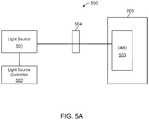
- FIG. 5Ais a simplified diagram illustrating a DLP projector according to an embodiment of the present invention.
- FIG. 6is simplified diagram illustrating a 3-chip DLP projection system according to an embodiment of the present invention.
- FIG. 7is a simplified diagram illustrating 3D display involving polarized images filtered by polarized glasses.
- FIG. 8is a simplified diagram illustrating a 3D projection system according to an embodiment of the present invention.
- FIG. 9is a simplified diagram illustrating a LCOS projection system 900 according to an embodiment of the present invention.
- the present inventionis directed to a laser light source.
- such light sourceis directed to display technologies.
- various embodiments of the present inventionprovide projection display systems where one or more laser diodes are used as light source for illustrating images.
- the present inventionprovides projector systems that utilize blue and/or green laser fabricated using gallium nitride containing material.
- the present inventionprovides projection systems having digital lighting processing engines illuminated by blue and/or green laser devices. There are other embodiments as well.
- Miniature projectorsaddress this problem by projecting large images (up to 60 inch and above) from the hand held device, allowing movies, interne surfing and other images to be shared in a size format consistent with the displays customers are accustomed to.
- pocket projectors, standalone companion pico projectors, and embedded pico projectors in mobile devices such as phonesare becoming increasingly available.
- InGaN-based lasers and LEDsare grown on the polar c-plane of the GaN crystal. It is well known that InGaN light emitting layers deposited on this conventional GaN orientation suffer from internal polarization-related electric fields. In these structures, spontaneous polarization results from charge asymmetry in the GaN bonding, while piezoelectric polarization is the product of strain. In quantum well structures, these polarization fields spatially separate the electron and hole wave functions, reducing their radiative recombination efficiency. Due to the strain dependence of piezoelectric polarization, these internal fields grow stronger for with increased-indium-content in the emitting layers required for blue and especially for green lasers and LEDs.
- the internal electric fieldsinduce the quantum confined Stark effect (QCSE) within the light emitting quantum well layers.
- QCSEquantum confined Stark effect
- This effectresults in a blue-shift of the peak emission wavelength with increased carrier density in the quantum well layers. Since the carrier density is increased with increased current, a blue or green LED will undergo a shift in peak wavelength as a function of current. Such wavelength dependence on drive current would not be ideal for display applications where the LED is subjected to a current modulation scheme since the color will change with current.
- the carrier densityis increased with increasing current up until the onset of laser threshold where the gain overcomes the loss in the cavity.
- Typical projectors based on solid-state emittersinclude:
- projection systemscan utilize polarized or unpolarized lights.
- single scanner based projection systemse.g., pico projectors
- DLP based systemstypically use unpolarized light source.
- polarized light sourceis desirable.
- blue and green (maybe red) LEDs used in conventional projectorsare unpolarized (or demonstrate low polarization ratio), thereby resulting in excessive optical losses from polarization dependent optical components and exhibit a poor spatial mode quality, which require large LCOS or LCD chips, and are not viable for compact designs because the light is not focusable into a small area.
- FIG. 1is a diagram illustrating a conventional projection system. As shown, blue, green, and red laser lights are combined into a laser beam, which is then projected to an MEMS scanning mirror.
- a green second-harmonic generation (SHG) laseris used to provide green laser light.
- SHGgreen second-harmonic generation
- PPLNperiodically-pulsed lithium niobate
- optical lossesIn order to manufacturer highly efficient display that maximize battery life and minimize cost, size, and weight, optical losses must be minimized from the system.
- Sources of optical losses in systemsinclude, but are not limited to, losses from optical elements whose transmission is polarization dependent.
- a micro-display technologyIn many compact projector such as pico projectors, a micro-display technology is used which is highly polarization sensitive, such as LCOS or LCD.
- LCOSliquid crystal display technology.
- the present inventionprovides blue and green direct diode GaN based lasers that offers offer highly polarized output, single spatial mode, moderate to large spectral width, high efficiency, and high modulation rates ideal for various types of projection and displays, such as pico projectors, DLP projectors, liquid crystal based displays (e.g., liquid crystal on silicon or “LCOS”), and others.
- pico projectorse.g., DLP projectors
- liquid crystal based displayse.g., liquid crystal on silicon or “LCOS”
- the optical efficiencycan be maximized with minimal costs and maximum flexibility in the selection on optical components.
- Conventional illumination sourcessuch as unpolarized LEDs and systems thereof, where complicated optics are required for polarization recycling to increase the efficiency from the non-polarized light source.
- blue and green laser and/or LEDson nonpolar or semipolar GaN the light output will be highly polarized eliminating the need for additional optics to deal with polarization.
- direct diode lasers having GaN based laserare used for blue and green sources.
- Conventional c-plane GaN lasersemits unpolarized or near-unpolarized light when laser is below threshold. After the laser reaches threshold the output light will become polarized with increased current.
- lasers fabricated on nonpolar or semipolar GaN according to embodiments of the present inventionemit polarized light below threshold and will also have an increased polarization ratio with increased current.
- Embodiments of the present inventionalso provides the benefit of reduced speckling.
- frequency doubled 1060 nm diode lasers used in conventional systemsproduces a narrow spectrum which causes speckle in the image.
- Direct diode visible lasers (e.g., green laser) used in embodiments of the present inventionoffer as much as >100 ⁇ increase in the spectrum, substantially reducing speckle in the image and reducing the need for additional expensive and bulky components.
- frequency doubled 1060 nm diode lasers used in conventional systemare inefficient because of the second harmonic generation.
- Direct diode visible lasers used in the present inventionoffer the potential for substantially higher efficiency with the benefit of reduced optical components and size and weight of the system.
- a typical miniature projectorse.g., pico projector
- the blue and green direct diode GaN based lasers according to embodiments of the present inventionoffers highly polarized output, single spatial mode, moderate to large spectral width, high efficiency, and high modulation rates ideal for liquid crystal based displays.
- Nonpolar and/or semipolar based GaN lasershold great promise for enabling the direct diode green solution, and therefore, digital scanning micro mirror projectors.
- FIG. 2is a simplified diagram illustrating a projection device according to an embodiment of the present invention. This diagram is merely an example, which should not unduly limit the scope of the claims. One of ordinary skill in the art would recognize many variations, alternatives, and modifications.
- a projection system 250includes a MEMS scanning mirror 251 , a mirror 252 , an optical member 254 , green laser diode 253 , red laser diode 256 , and blue laser diode 255 .
- the projection system 250is a pico projector.
- the projection system 250also includes a housing having an aperture and an input interface for receiving one or more frames of images.
- the projection system 250also includes a video processing module.
- the video processing moduleis electrically coupled to an ASIC for driving the laser diodes and the MEMS scanning mirrorscanning mirror 251 .
- the laser diodes together with the optical member 254form a laser source.
- the green laser diode 253is characterized by a wavelength of about 490 nm to 540 nm.
- the laser sourceis configured produce a laser beam by combining outputs from the blue, green, and red laser diodes.
- various types of optical componentsmay be used to combine the light outputs from the laser diodes.
- optical componentscan be dichroic lenses, prisms, converging lenses, etc.
- the combined laser beamis polarized.
- a laser driver moduleis provided.
- the laser driver moduleis adapted to adjust the amount of power to be provided to the laser diodes.
- the laser driver modulegenerates three drive currents based one or more pixels from the one or more frames of images, each of the three drive currents being adapted to drive a laser diode.
- the laser driver moduleis configured to generate pulse-modulated signal at a frequency range of about 50 to 300 MHz.
- the MEMS scanning mirror 251is configured to project the laser beam to a specific location through the aperture. For example, the MEMS scanning mirror 251 process one pixel at a specific time onto a specific location corresponding to an pixel of an image. At a high frequency, pixels projected by the MEMS scanning mirror 251 form images.
- the MEMS scanning mirror 251receives light from the laser source though mirror 252 . As shown, the mirror 252 is provided within proximity of the laser source. Among other things, the optical member is adapted to direct the laser beam to the MEMS scanning mirror 251 .
- the projection system 250include other components as well, such as a power source electrically coupled to the laser source and the MEMS scanning mirror 251 .
- Other componentscan include buffer memory, communication interface, network interface, etc.
- a key component of the projection system 250is the laser light source.
- embodiments of the present inventionuse highly efficient laser diodes.
- the blue laser diodeoperates in a single lateral mode.
- the blue laser diodeis characterized by a spectral width of about 0.5 nm to 2 nm.
- the blue laser diodeis designed for integration into portable applications such as embedded and companion pico projectors and features 60 mW of 445 nm single mode output power in a compact TO-38 package.
- blue lasersoperate with high efficiency and require minimal power consumption over a broad temperature range, meeting the demanding requirements of consumer projection displays, defense pointers and illuminators, biomedical instrumentation and therapeutics, and industrial imaging applications.
- blue lasersare based on the Indium Gallium Nitride (InGaN) semiconductor technology and are fabricated on GaN substrates.
- InGaNIndium Gallium Nitride
- the blue and green laser diodesare fabricated using GaN material.
- the blue laser diodemay be semi-polar or non-polar.
- the green laser diodecan be semi-polar or non-polar.
- the red laser diodecan be fabricated using GaAlInP material.
- following combinations of laser diodesare provided, but there could be others:
- blue and green laser diodescan be manufactured on m-plane.
- a blue or green laser diodeincludes a gallium nitride substrate member having the off-cut m-plane crystalline surface region. In a specific embodiment this offcut angle is between ⁇ 2.0 and ⁇ 0.5 degrees toward the c-plane.
- the gallium nitride substrate memberis a bulk GaN substrate characterized by having a semipolar or non-polar crystalline surface region, but can be others.
- the bulk nitride GaN substratecomprises nitrogen and has a surface dislocation density below 10 5 cm ⁇ 2 .
- the nitride crystal or wafermay comprise Al x In y Ga 1-x-y N, where 0 ⁇ x, y, x+y ⁇ 1.
- the nitride crystalcomprises GaN, but can be others.
- the GaN substratehas threading dislocations, at a concentration between about 10 5 cm ⁇ 2 and about 10 8 cm ⁇ 2 , in a direction that is substantially orthogonal or oblique with respect to the surface. As a consequence of the orthogonal or oblique orientation of the dislocations, the surface dislocation density is below about 10 5 cm ⁇ 2 .
- the devicecan be fabricated on a slightly off-cut semipolar substrate as described in U.S. patent application Ser. No. 12/749,466, file Mar. 29, 2010, which is commonly assigned and incorporated by reference herein.
- the devicehas a laser stripe region formed overlying a portion of the off-cut crystalline orientation surface region.
- the laser stripe regionis characterized by a cavity orientation substantially in a projection of a c-direction, which is substantially normal to the a-direction.
- the laser strip regionhas a first end and a second end.
- the laser cavityis oriented formed in a projection of the c-direction on a ⁇ 20-21 ⁇ gallium and nitrogen containing substrate having a pair of cleaved mirror structures, at the end of cavity.
- the devicehas a laser stripe region formed overlying a portion of the off-cut crystalline orientation surface region.
- the laser stripe regionis characterized by a cavity orientation substantially in the c-direction, which is substantially normal to the a-direction.
- the laser strip regionhas a first end and a second end.
- the laser cavityis oriented formed in the c-direction on an m-plane gallium and nitrogen containing substrate having a pair of cleaved mirror structures, at the end of cavity.
- the devicehas a first cleaved facet provided on the first end of the laser stripe region and a second cleaved facet provided on the second end of the laser stripe region.
- the first cleavedis substantially parallel with the second cleaved facet.
- Mirror surfacesare formed on each of the cleaved surfaces.
- the first cleaved facetcomprises a first mirror surface.
- the first mirror surfaceis provided by a top-side skip-scribe scribing and breaking process. The scribing process can use any suitable techniques, such as a diamond scribe or laser scribe or combinations.
- the first mirror surfacecomprises a reflective coating.
- the reflective coatingis selected from silicon dioxide, hafnia, and titania, tantalum pentoxide, zirconia, including combinations, and the like.
- the first mirror surfacecan also comprise an anti-reflective coating.
- the second cleaved facetcomprises a second mirror surface.
- the second mirror surfaceis provided by a top side skip-scribe scribing and breaking process according to a specific embodiment.
- the scribingis diamond scribed or laser scribed or the like.
- the second mirror surfacecomprises a reflective coating, such as silicon dioxide, hafnia, and titania, tantalum pentoxide, zirconia, combinations, and the like.
- the second mirror surfacecomprises an anti-reflective coating.
- the laser stripehas a length and width.
- the lengthranges from about 50 microns to about 3000 microns.
- the stripalso has a width ranging from about 0.5 microns to about 50 microns, but can be other dimensions.
- the widthis substantially constant in dimension, although there may be slight variations.
- the width and lengthare often formed using a masking and etching process, which are commonly used in the art.
- the present inventionprovides an alternative device structure capable of emitting 501 nm and greater light in a ridge laser embodiment.
- the deviceis provided with one or more of the following epitaxially grown elements, but is not limiting:
- the laser deviceis fabricated on a ⁇ 20-21 ⁇ semipolar Ga-containing substrate. But it is to be understood that the laser device can be fabricated on other types of substrates such as nonpolar oriented Ga-containing substrate as well.
- the light source used in a projection systemcombines a yellow light source with the red, green, and blue light sources.
- the addition of yellow light sourcesimproves the color characteristics (e.g., allowing for wider color gamut) of RBG based projection and display systems.
- an RGYB light sourcesis used for a projection system.
- the yellow light sourcecan be a yellow laser diode manufactured from gallium nitride material or AlInGaP material.
- the yellow light sourcecan have a polar, non-polar, or semi-polar orientation.
- projection systems according to the present inventionmay use light sources in other colors as well.
- other colorsinclude cyan, magenta, and others.
- the laser diodes of the different colorsare separately packaged.
- the laser diodes of two or more of the different colorsare copackaged.
- the laser diodes of two or more of the different colorsare fabricated on the same substrate.
- FIG. 2Ais a detailed cross-sectional view of a laser device 200 fabricated on a ⁇ 20-21 ⁇ substrate according to an embodiment of the present invention.
- the laser deviceincludes gallium nitride substrate 203 , which has an underlying n-type metal back contact region 201 .
- the metal back contact regionis made of a suitable material such as those noted below and others. Further details of the contact region can be found throughout the present specification and more particularly below.
- the devicealso has an overlying n-type gallium nitride layer 205 , an active region 207 , and an overlying p-type gallium nitride layer structured as a laser stripe region 209 .
- each of these regionsis formed using at least an epitaxial deposition technique of metal organic chemical vapor deposition (MOCVD), molecular beam epitaxy (MBE), or other epitaxial growth techniques suitable for GaN growth.
- the epitaxial layeris a high quality epitaxial layer overlying the n-type gallium nitride layer.
- the high quality layeris doped, for example, with Si or O to form n-type material, with a dopant concentration between about 10 16 cm ⁇ 3 and 10 20 cm ⁇ 3 .
- an n-type Al u In v Ga 1-u-v N layerwhere 0 ⁇ u, v, u+v ⁇ 1, is deposited on the substrate.
- the carrier concentrationmay lie in the range between about 10 16 cm ⁇ 3 and 10 20 cm ⁇ 3 .
- the depositionmay be performed using MOCVD or MBE. Of course, there can be other variations, modifications, and alternatives.
- the bulk GaN substrateis placed on a susceptor in an MOCVD reactor.
- the susceptoris heated to a temperature between about 900 and about 1200 degrees Celsius in the presence of a nitrogen-containing gas.
- the susceptoris heated to approximately 1100 degrees Celsius under flowing ammonia.
- a flow of a gallium-containing metalorganic precursor, such as trimethylgallium (TMG) or triethylgallium (TEG)is initiated, in a carrier gas, at a total rate between approximately 1 and 50 standard cubic centimeters per minute (sccm).
- the carrier gasmay comprise hydrogen, helium, nitrogen, or argon.
- the ratio of the flow rate of the group V precursor (ammonia) to that of the group III precursor (trimethylgallium, triethylgallium, trimethylindium, trimethylaluminum) during growthis between about 2000 and about 12000.
- the laser stripe regionis made of the p-type gallium nitride layer 209 .
- the laser stripeis provided by an etching process selected from dry etching or wet etching.
- the etching processis dry, but can be others.
- the dry etching processis an inductively coupled process using chlorine bearing species or a reactive ion etching process using similar chemistries.
- the chlorine bearing speciesare commonly derived from chlorine gas or the like.
- the devicealso has an overlying dielectric region, which exposes 213 contact region.
- the dielectric regionis an oxide such as silicon dioxide or silicon nitride, but can be others.
- the contact regionis coupled to an overlying metal layer 215 .
- the overlying metal layeris a multilayered structure containing palladium and gold (Pd/Au), platinum and gold (Pt/Au), nickel gold (Ni/Au), but can be others. Of course, there can be other variations, modifications, and alternatives.
- the laser devicehas active region 207 .
- the active regioncan include one to twenty quantum well regions according to one or more embodiments.
- an active layeris deposited.
- the active layermay be comprised of multiple quantum wells, with 2-10 quantum wells.
- the quantum wellsmay be comprised of InGaN with GaN barrier layers separating them.
- the well layers and barrier layerscomprise Al w In x Ga 1-w-x N and Al y In z Ga 1-y-z N, respectively, where 0 ⁇ w, x, y, z, w+x, y+z ⁇ 1, where w ⁇ u, y and/or x>v, z so that the bandgap of the well layer(s) is less than that of the barrier layer(s) and the n-type layer.
- the well layers and barrier layersmay each have a thickness between about 1 nm and about 20 nm.
- the composition and structure of the active layerare chosen to provide light emission at a preselected wavelength.
- the active layermay be left undoped (or unintentionally doped) or may be doped n-type or p-type.
- the active regioncan also include an electron blocking region, and a separate confinement heterostructure.
- an electron blocking layeris preferably deposited.
- the electron-blocking layermay comprise Al s In t Ga 1-s-t N, where 0 ⁇ s, t, s+t ⁇ 1, with a higher bandgap than the active layer, and may be doped p-type.
- the electron blocking layercomprises AlGaN.
- the electron blocking layercomprises an AlGaN/GaN super-lattice structure, comprising alternating layers of AlGaN and GaN, each with a thickness between about 0.2 nm and about 5 nm.
- the p-type gallium nitride structureis deposited above the electron blocking layer and active layer(s).
- the p-type layermay be doped with Mg, to a level between about 10 16 cm ⁇ 3 and 10 22 cm ⁇ 3 , and may have a thickness between about 5 nm and about 1000 nm.
- the outermost 1-50 nm of the p-type layermay be doped more heavily than the rest of the layer, so as to enable an improved electrical contact.
- the laser stripeis provided by an etching process selected from dry etching or wet etching. In a preferred embodiment, the etching process is dry, but can be others.
- the devicealso has an overlying dielectric region, which exposes 213 contact region.
- the dielectric regionis an oxide such as silicon dioxide, but can be others such as silicon nitride.
- the dielectric regionis an oxide such as silicon dioxide, but can be others such as silicon nitride.
- FIG. 2Bis a simplified diagram illustrating a projector having LED light sources. This diagram is merely an example, which should not unduly limit the scope of the claims.
- the blue and green LEDsare manufactured from gallium nitride containing material.
- the blue LEDis characterized by a non-polar orientation.
- the blue LEDis characterized by a semi-polar orientation.
- FIG. 3is an alternative illustration of a projection device according to an embodiment of the present invention.
- a projection deviceincludes an MEMS scanning mirror, a mirror, a light conversion member, a red laser diode, a blue diode, and green laser diode.
- the blue and green laser diodes as shownare integrated as a single package.
- the blue and green lasershared the same substrate and surface.
- Output from the blue and green laser diodesare emitted from a common plane of surface. It is to be appreciated that that by having blue and green laser diodes co-packaged, it is possible to substantially reduce the size and cost (e.g., fewer parts) of the projector device.
- the green and blue laser diodesare characterized by a high efficiency.
- the blue on the green laser diodeare manufactured from bulk gallium nitride material.
- the blue laser diodecan be non-polar or semi-polar oriented.
- the green laser diodessimilarly can be non-polar polar or semipolar. For example, following combinations of laser diodes are provided, but there could be others:
- the green laser diodeis characterized by wavelength of between 480 nm to 540 nm, which is different from conventional production devices that use an infrared laser diode (i.e., emission wavelength of about 1060 nm) and use SHG to double the frequency.
- FIG. 3Ais a simplified diagram illustrating a laser diodes packaged together according to an embodiment of the present invention. This diagram is merely an example, which should not unduly limit the scope of the claims. One of ordinary skill in the art would recognize many variations, alternatives, and modifications. As shown in FIG. 3A , two laser diodes are provided on a single package. For example, laser 1 as shown in a blue laser diode and laser 2 is a green laser diode. Optics may be used to combine the outputs of lasers.
- optical componentssuch as dichroic lens, waveguide, can be used to combine the outputs of the laser 1 and laser 2 as shown.
- FIG. 3Bis a diagram illustrating a cross section of active region with graded emission wavelength according to an embodiment of the present invention. This diagram is merely an example, which should not unduly limit the scope of the claims. One of ordinary skill in the art would recognize many variations, alternatives, and modifications. As illustrating FIG. 3B , for example, active regions having different emission gradient are used. Ridged waveguides at different portion of the active region are adapted to emit different wavelength. FIG.
- FIG. 3Bshows a cross-section of an active region with graded emission wavelength including ridge waveguide of laser 301 operating at a first peak wavelength determined by the cavity position relative to the emission wavelength of the graded active region 302 ; ridge waveguide of laser 303 operating at a second peak wavelength determined by the cavity position relative to the emission wavelength of the graded active region 302 ; active region 302 with a peak emission gradient; n-type cladding region 304 ; and substrate 305 .
- FIG. 3Bshows an example of a graded emission wavelength active region configuration where adjacent lasers are operating at different wavelengths as a result of lasing off being positioned in areas where the active region possesses different peak emission wavelengths.
- FIG. 3Cis a simplified diagram illustrating a cross section of multiple active regions according to an embodiment of the present invention. This diagram is merely an example, which should not unduly limit the scope of the claims. One of ordinary skill in the art would recognize many variations, alternatives, and modifications. Among other things, each active region is associated with a specific wavelength.
- FIG. 3Cshows a cross-section of multiple active regions including a ridge waveguide of laser 311 operating at a first peak wavelength from active region 312 , which overlies active region 312 with a first peak wavelength; ridge waveguide of laser 313 operating at a second peak wavelength from active region 314 , which overlies active region 304 with a second peak wavelength; n-type cladding region 315 ; and substrate 316 .
- FIG. 3Cshows an example of a multiple active region configuration where adjacent lasers are operating at different wavelengths as a result of lasing off of two different active regions with different peak wavelengths.
- the light source of the projector 300may include one or more LED as well.
- FIG. 3Dis a simplified diagram illustrating a projector having LED light sources. This diagram is merely an example, which should not unduly limit the scope of the claims.
- the blue and green LEDsare manufactured from gallium nitride containing material.
- the blue LEDis characterized by a non-polar orientation.
- the blue LEDis characterized by a semi-polar orientation.
- FIG. 4is a simplified diagram illustrating a projection device according to an embodiment of the present invention. This diagram is merely an example, which should not unduly limit the scope of the claims. One of ordinary skill in the art would recognize many variations, alternatives, and modifications.
- blue, green, and red laser diodesare integrated into a light source 401 .
- the light source 401is combines outputs of each of the laser diodes.
- the combined lightis projected onto the mirror, which reflects the combined light onto the MEMS scanning mirror. It is to be appreciated that, by providing laser diodes in the same package, both the size and cost of the light source 401 can be reduced. For example, following combinations of laser diodes are provided, but there could be others:
- FIG. 4Ais a simplified diagram illustrating laser diodes integrated into single package according to an embodiment of the present invention.
- laser 1can be a green laser diode
- laser 2can be a red laser diode
- laser 3can be a blue laser diode.
- the green laser diodecan be fabricated on a semi-polar, non-polar, or polar gallium containing substrates.
- the blue laser diodecan be formed on semi-polar, non-polar, or polar gallium containing substrates.
- projections systemsaccording to the present invention have wide range of applications.
- the projections systems described aboveare integrated on cellular telephone, camera, personal computer, portable computer, and other electronic devices.
- FIG. 5is a simplified diagram of a DLP projection device according to an embodiment of the present invention. This diagram is merely an example, which should not unduly limit the scope of the claims. One of ordinary skill in the art would recognize many variations, alternatives, and modifications.
- a projection apparatusincludes, among other things, a light source, a condensing lens, a color wheel, a shaping lens, and a digital lighting processor (DLP) board, and a projection lens.
- the DLP boardincludes a processor, a memory, and a digital micromirror device (DMD).
- DMDdigital micromirror device
- the color wheelmay include phosphor material that modifies the color of light emitted from the light source.
- the color wheelincludes multiple regions, each of the regions corresponding to a specific color (e.g., red, green, blue, etc.).
- a projectorincludes a light source that includes blue and red light sources.
- the color wheelincludes a slot for the blue color light and a phosphor containing region for converting blue light to green light.
- the blue light sourcee.g., blue laser diode or blue LED
- the red light sourceprovides red light separately.
- the green light from the phosphormay be transmitted through the color wheel, or reflected back from it. In either case the green light is collected by optics and redirected to the microdisplay.
- the blue light passed through the slotis also directed to the microdisplay.
- the blue light sourcemay be a laser diode and/or LED fabricated on non-polar or semi-polar oriented GaN. In some cases, by combining both blue lasers and blue LEDs, the color characteristics could be improved. Alternate sources for the green light could include green laser diodes and/or green LEDs, which could be fabricated from nonpolar or semipolar Ga-containing substrates. In some embodiments, it could be beneficial to include some combination of LEDs, lasers, and or phosphor converted green light. It is to be appreciated that can be other combinations of colored light sources and color wheels thereof.
- the color wheelmay include multiple phosphor materials.
- the color wheelmay include both green and red phosphors in combination with a blue light source.
- the color wheelincludes multiple regions, each of the regions corresponding to a specific color (e.g., red, green, blue, etc.).
- a projectorincludes a light source that includes a blue light source.
- the color wheelincludes a slot for the blue laser light and two phosphor containing regions for converting blue light to green light, and blue light and to red light, respectively.
- the blue light sourcee.g., blue laser diode or blue LED
- the green and red light from the phosphormay be transmitted through the color wheel, or reflected back from it. In either case the green and red light is collected by optics and redirected to the microdisplay.
- the blue light sourcemay be a laser diode or LED fabricated on non-polar or semi-polar oriented GaN. It is to be appreciated that can be other combinations of colored light sources and color wheels thereof.
- the color wheelmay include blue, green, and red phosphor materials.
- the color wheelmay include blue, green and red phosphors in combination with a ultra-violet (UV) light source.
- color wheelincludes multiple regions, each of the regions corresponding to a specific color (e.g., red, green, blue, etc.).
- a projectorincludes a light source that includes a UV light source.
- the color wheelincludes three phosphor containing regions for converting UV light to blue light, UV light to green light, and UV light and to red light, respectively. In operation, the color wheel emits blue, green, and red light from the phosphor containing regions in sequence.
- the blue, green and red light from the phosphormay be transmitted through the color wheel, or reflected back from it. In either case the blue, green, and red light is collected by optics and redirected to the microdisplay.
- the UV light sourcemay be a laser diode or LED fabricated on non-polar or semi-polar oriented GaN. It is to be appreciated that can be other combinations of colored light sources and color wheels thereof.
- the light source as showncould be made laser-based.
- the output from the light sourceis laser beam characterized by a substantially white color.
- the light sourcecombines light output from blue, green, and red laser diodes.
- the blue, green, and red laser diodecan be integrated into a single package as described above. Other combinations are possible as well.
- blue and green laser diodesshare a single package while the red laser diode is packaged by itself.
- the laserscan be individually modulated so that color is time-sequenced, and thus there is no need for the color wheel.
- the blue laser diodecan be polar, semipolar, and non-polar.
- green laser diodecan be polar, semipolar, and non-polar.
- blue and/or green diodesare manufactured from bulk substrate containing gallium nitride material. For example, following combinations of laser diodes are provided, but there could be others:
- the DLP projection systemutilizes a color wheel to project one color (e.g., red, green, or blue) of light at a time to the DMD.
- the color wheelis needed because the light source continuously provide white light. It is to be appreciated that because solid state devices are used as light source in the embodiments of the present invention, a DLP projector according to the present invention does not require the color wheel shown in FIG. 5 .
- FIG. 5Ais a simplified diagram illustrating a DLP projector according to an embodiment of the present invention. This diagram is merely an example, which should not unduly limit the scope of the claims. One of ordinary skill in the art would recognize many variations, alternatives, and modifications.
- the light sourcecomprises a single laser diode.
- the light sourcecomprises a blue laser diode that outputs blue laser beams.
- the light sourcealso includes one or more optical members that changes the blue color of the laser beam.
- the one or more optical membersincludes phosphor material. The laser beam excites the phosphor material to form a substantially white emission source which becomes the light source for the projection display. In this embodiment, a color wheel is needed in order to sequence the blue, green, and red frames to the DLP.
- a projection system 500includes a light source 501 , a light source controller 502 , an optical member 504 , and a DLP chip 505 .
- the light source 501is configured to emit a color light to the DMD 503 through the optical member 504 . More specifically, the light source 501 includes colored laser diodes.
- the laser diodesinclude red laser diode, blue laser diode, and green laser diode. At a predetermined time interval, a single laser diode is turn on while the other laser diodes are off, thereby emitting a single colored laser beam onto the DMD 503 .
- the light source controller 502provides control signal to the light source 501 to switch laser diodes on and off based on predetermined frequency and sequence. For example, the switching of laser diodes is similar to the function of the color wheel shown in FIG. 5 .
- FIG. 6is a simplified diagram illustrating a 3-chip DLP projection system according to an embodiment of the present invention. This diagram is merely an example, which should not unduly limit the scope of the claims. One of ordinary skill in the art would recognize many variations, alternatives, and modifications. As shown in FIG. 5 , the 3-chip DLP projection system includes a light source, optics, and multiple DMDs, and a color wheel system. As shown, each of the DMDs is associated with a specific color.
- the white light beamcomprises a substantially white laser beam provided by the light source.
- the output from the light sourceis laser beam characterized by a substantially white color.
- the light sourcecombines light output from blue, green, and red laser diodes.
- the blue, green, and red laser diodecan be integrated into a single package as described above. Other combinations are possible as well.
- blue and green laser diodesshare a single package while the red laser diode is packaged by itself.
- the blue laser diodecan be polar, semipolar, and non-polar.
- green laser diodecan be polar, semipolar, and non-polar.
- blue and/or green diodesare manufactured from bulk substrate containing gallium nitride material. For example, following combinations of laser diodes are provided, but there could be others:
- the light sourcecomprises a single laser diode.
- the light sourcecomprises a blue laser diode that outputs blue laser beams.
- the light sourcealso includes one or more optical members that change the blue color of the laser beam.
- the one or more optical membersinclude phosphor material.
- the light sourcemay include laser diodes and/or LEDs.
- the light sourceincludes laser diodes in different colors.
- the light sourcemay additionally include phosphor material for changing the light color emitted from the laser diodes.
- the light sourceincludes one or more colored LEDs.
- light sourceincludes both laser diodes and LEDs.
- the light sourcemay include phosphor material to change the light color for laser diodes and/or LEDs.
- laser diodesare utilized in 3D display applications.
- 3D display systemsrely on the stereopsis principle, where stereoscopic technology uses a separate device for each person viewing the scene which provides a different image to the person's left and right eyes. Examples of this technology include anaglyph images and polarized glasses.
- FIG. 7is a simplified diagram illustrating 3D display involving polarized images filtered by polarized glasses. As shown, the left eye and the right eye perceive different images through the polarizing glasses.
- the conventional polarizing glasseswhich typically include circular polarization glasses used by RealD CinemaTM, have been widely accepted in many theaters.
- Another type of image separationis provided by interference filter technology.
- special interference filters in the glasses and in the projectorform the main item of technology and have given it this name.
- the filtersdivide the visible color spectrum into six narrow bands—two in the red region, two in the green region, and two in the blue region (called R1, R2, G1, G2, B1 and B2 for the purposes of this description).
- the R1, G1 and B1 bandsare used for one eye image, and R2, G2, B2 for the other eye.
- the human eyeis largely insensitive to such fine spectral differences so this technique is able to generate full-color 3D images with only slight colour differences between the two eyes.
- this techniqueis described as a “super-anaglyph” because it is an advanced form of spectral-multiplexing which is at the heart of the conventional anaglyph technique.
- the following set of wavelengthsare used:
- FIG. 8is a simplified diagram illustrating a 3D projection system according to an embodiment of the present invention. This diagram is merely an example, which should not unduly limit the scope of the claims. One of ordinary skill in the art would recognize many variations, alternatives, and modifications.
- a projection systemincludes a projector 801 .
- the projector 801is configured to project images associated for one eye (e.g., left eye).
- the projector 801includes a first light source.
- the first light sourceincluding a first set of laser diodes: a red laser diode, a green laser diode, and a blue laser diode.
- Each of the laser diodeis associated with a specific wavelength.
- red laser diodeis configured to emit a laser beam characterized by a wavelength of 629 nm
- green laser diodeis configured to emit a laser beam characterized by a wavelength of 532 nm
- blue laser diodeis configured to emit a laser beam characterized by a wavelength of 446 nm. It is to be appreciated that other wavelengths are possible as well.
- the blue laser diodeis characterized by a non-polar or semi-polar orientation.
- the blue laser diodeis fabricated from gallium nitride containing substrate.
- the blue laser diodeis manufactured from bulk substrate material.
- the green laser diodecan manufactured from gallium nitride containing substrate as well.
- the green laser diodeis characterized by a non-polar or semi-polar orientation.
- color LEDsmay also be used to provide colored light for the projection elements.
- a red LEDcan be used instead of a red laser diode in providing the red light.
- LED and/or laser diodes in various colorscan be interchangeably used as light sources.
- Phosphor materialmay be used to alter light color for light emitted from LED and/or laser diodes.
- the projector 802is configured to project images associated for the other eye (e.g., right eye).
- the second light sourceincluding a second set of laser diodes: a red laser diode, a green laser diode, and a blue laser diode.
- Each of the laser diodeis associated with a specific wavelength, and each of the wavelengths is different from that of the corresponding laser diodes of the first light source.
- the red laser diodeis configured to emit a laser beam characterized by a wavelength of 615 nm
- the green laser diodeis configured to emit a laser beam characterized by a wavelength of 518 nm
- the blue laser diodeis configured to emit a laser beam characterized by a wavelength of 432 nm. It is to be appreciated that other wavelengths are possible as well.
- Projectors 801 and 802 shown in FIG. 8are positioned far apart, but it is to be appreciated that the two projectors may be integrally positioned within one housing unit.
- the projectorsinclude optics for focusing images from the two projectors onto the same screen.
- bandpass filtersare used.
- a bandpass filteronly allows one set of RGB color wavelength to pass to an eye.
- notch filtersare used, where the notch filters would allow substantially all wavelength except a specific set of RGB color wavelength to pass to an eye. There can be other embodiments as well.
- the present inventionprovides a liquid crystal on silicon (LCOS) projection system.
- FIG. 9is a simplified diagram illustrating a LCOS projection system 900 according to an embodiment of the present invention. This diagram is merely an example, which should not unduly limit the scope of the claims. One of ordinary skill in the art would recognize many variations, alternatives, and modifications.
- a green laser diodeprovides green laser light to the green LCOS through splitter 901 ;
- a blue laser diodeprovides blue laser light to the blue LCOS through splitter 903 ;
- a red laser diodeprovides red laser light to the red LCOS through splitter 904 .
- Each of the LCOSis used to form images in a predetermined single color as provided by its corresponding laser diode, and the single-colored image is combined by the x-cube component 902 . The combined color image is projected onto the lens 906 .
- one or more laser diodes used in the projection system 900are characterized by semi-polar or non-polar orientation.
- the laser diodesare manufactured from bulk substrate.
- the blue and green laser diodesare manufactured from gallium nitride containing substrate.
- color LEDsmay also be used to provide colored light for the projection elements. For example, a red LED can be used instead of a red laser diode in providing the red light.
- LED and/or laser diodes in various colorscan be interchangeably used as light sources.
- Phosphor materialmay be used to alter light color for light emitted from LED and/or laser diodes.
- the LCOS projection system 900comprises three panels.
- the present inventionprovides a projection system with a single LCOS panel. Red, green, and blue laser diodes are aligned where red, green, and blue laser beams are collimated onto a single LCOS. The laser diodes are pulse-modulated so that only one laser diode is power at a given time and the LCOS is lit by a single color. It is to be appreciated that since colored laser diodes are used, LCOS projection systems according to the present invention do not need beam splitter that split a single white light source into color beams as used in conventional LCOS projection systems.
- one or more laser diodes used in the single LCOS projection systemare characterized by semi-polar or non-polar orientation.
- the laser diodesare manufactured from bulk substrate.
- the blue and green laser diodesare manufactured from gallium nitride containing substrate.
- the configuration illustrated in FIG. 9is also used in ferroelectric liquid crystal on silicon (FLCOS) systems.
- the panels illustrated FIG. 9can be FLCOS panels.
- the housing memberprovides an enclosure for the components of the laser device.
- the housing membermay be in various types of shapes.
- the housing membercan be attached to vehicle mount and/or include tripod. There can be other variations, modifications, and alternatives.
- the present inventionprovides a light apparatus for a vehicle.
- the apparatushas a housing to be configured to the vehicle and a laser diode device coupled to the housing, the laser diode device comprising a gallium and nitrogen containing material.
- the laser diode devicecomprises an n-cladding layer with a thickness from 100 nm to 5000 nm with Si doping level of 1E17 to 3E18 cm ⁇ 3, an n-side SCH layer comprised of InGaN, multiple quantum well active region layers, a p-cladding layer and a p++-GaN contact layer.
- the devicehas a non-polar, semipolar, or polar configuration characterizing the gallium and nitrogen containing material.
- the apparatushas an optical component coupled to an output laser beam of the laser device and a phosphor material coupled to the laser device to be excited by a laser beam from the laser device.
- the apparatushas a substantially white light output from the laser device coupled to the phosphor material.
- the inventionprovides a light source apparatus for a vehicle.
- the apparatushas a housing to be configured to the vehicle and a laser diode device comprising a gallium and nitrogen containing material coupled to the housing.
- the apparatushas an output provided on the laser diode device to output a laser beam; and one or more optical members coupled to an output of the optical device and configured to output a substantially white emission by exciting a phosphor material coupled to the one or more optical members.
- the present inventionprovides a light apparatus.
- the apparatuscomprises a housing to be configured to a vehicle, and a laser diode device coupled to the housing.
- the laser diode devicecomprises a gallium and nitrogen containing material and an optical component coupled to an output laser beam of the laser device.
- the apparatushas a phosphor material coupled to the laser device to be excited by a laser beam from the laser device and a substantially white light output from the laser device coupled to the phosphor material.
- the apparatushas a reflector coupled to an output of the laser device, and a controller coupled to the light apparatus.
- the optical componentcomprises a waveguide coupled to the laser diode device.
Landscapes
- Physics & Mathematics (AREA)
- Engineering & Computer Science (AREA)
- Optics & Photonics (AREA)
- General Physics & Mathematics (AREA)
- Multimedia (AREA)
- Signal Processing (AREA)
- Electromagnetism (AREA)
- Condensed Matter Physics & Semiconductors (AREA)
- General Engineering & Computer Science (AREA)
- Spectroscopy & Molecular Physics (AREA)
- Microelectronics & Electronic Packaging (AREA)
- Projection Apparatus (AREA)
- Semiconductor Lasers (AREA)
Abstract
Description
- a light source (laser or LED),
- optics,
- micro-display such as a liquid crystal on silicon (LCOS) or a digital micro-mirror device (DMD),
- driver boards, and
- power source (i.e., battery or power adapter).
- a light source (laser or LED),
- optics,
- micro-display such as a LCOS or a DMD display;
- driver boards
- power source, i.e., battery or power adapter
- Blue polar+Green nonpolar+Red*AlInGaP
- Blue polar+Green semipolar+Red*AlInGaP
- Blue polar+Green polar+Red*AlInGaP
- Blue semipolar+Green nonpolar+Red*AlInGaP
- Blue semipolar+Green semipolar+Red*AlInGaP
- Blue semipolar+Green polar+Red*AlInGaP
- Blue nonpolar+Green nonpolar+Red*AlInGaP
- Blue nonpolar+Green semipolar+Red*AlInGaP
- Blue nonpolar+Green polar+Red*AlInGaP
- an n-GaN cladding layer with a thickness from 100 nm to 5000 nm with Si doping level of 5E17 to 3E18 cm−3
- an n-side SCH layer comprised of InGaN with molar fraction of indium of between 3% and 10% and thickness from 20 to 100 nm
- multiple quantum well active region layers comprised of at least two 2.0-8.5 nm InGaN quantum wells separated by thin 2.5 nm and greater, and optionally up to about 8 nm, GaN barriers
- a p-side SCH layer comprised of InGaN with molar a fraction of indium of between 1% and 10% and a thickness from 15 nm to 100 nm
- an electron blocking layer comprised of AlGaN with molar fraction of aluminum of between 12% and 22% and thickness from 5 nm to 20 nm and doped with Mg.
- a p-GaN cladding layer with a thickness from 400 nm to 1000 nm with Mg doping level of 2E17 cm−3 to 2E19 cm−3
- a p++-GaN contact layer with a thickness from 20 nm to 40 nm with Mg doping level of 1E19 cm−3 to 1E21 cm−3
- Blue polar+Green nonpolar+Red*AlInGaP
- Blue polar+Green semipolar+Red*AlInGaP
- Blue polar+Green polar+Red*AlInGaP
- Blue semipolar+Green nonpolar+Red*AlInGaP
- Blue semipolar+Green semipolar+Red*AlInGaP
- Blue semipolar+Green polar+Red*AlInGaP
- Blue nonpolar+Green nonpolar+Red*AlInGaP
- Blue nonpolar+Green semipolar+Red*AlInGaP
- Blue nonpolar+Green polar+Red*AlInGaP
Claims (16)
Priority Applications (3)
| Application Number | Priority Date | Filing Date | Title |
|---|---|---|---|
| US16/140,357US11016378B2 (en) | 2009-05-29 | 2018-09-24 | Laser light source |
| US16/835,897US11796903B2 (en) | 2009-05-29 | 2020-03-31 | Laser based display system |
| US17/009,599US11619871B2 (en) | 2009-05-29 | 2020-09-01 | Laser based display system |
Applications Claiming Priority (14)
| Application Number | Priority Date | Filing Date | Title |
|---|---|---|---|
| US18210609P | 2009-05-29 | 2009-05-29 | |
| US18210509P | 2009-05-29 | 2009-05-29 | |
| US18210409P | 2009-05-29 | 2009-05-29 | |
| US34556110P | 2010-05-17 | 2010-05-17 | |
| US34780010P | 2010-05-24 | 2010-05-24 | |
| US12/787,343US8509275B1 (en) | 2009-05-29 | 2010-05-25 | Gallium nitride based laser dazzling device and method |
| US12/789,303US8427590B2 (en) | 2009-05-29 | 2010-05-27 | Laser based display method and system |
| US13/678,101US8749719B2 (en) | 2009-05-29 | 2012-11-15 | Laser based display method and system |
| US13/938,048US9250044B1 (en) | 2009-05-29 | 2013-07-09 | Gallium and nitrogen containing laser diode dazzling devices and methods of use |
| US14/262,208US9100590B2 (en) | 2009-05-29 | 2014-04-25 | Laser based display method and system |
| US14/743,971US9829778B2 (en) | 2009-05-29 | 2015-06-18 | Laser light source |
| US14/802,960US9829780B2 (en) | 2009-05-29 | 2015-07-17 | Laser light source for a vehicle |
| US15/796,568US10108079B2 (en) | 2009-05-29 | 2017-10-27 | Laser light source for a vehicle |
| US16/140,357US11016378B2 (en) | 2009-05-29 | 2018-09-24 | Laser light source |
Related Parent Applications (1)
| Application Number | Title | Priority Date | Filing Date |
|---|---|---|---|
| US15/796,568ContinuationUS10108079B2 (en) | 2009-05-29 | 2017-10-27 | Laser light source for a vehicle |
Related Child Applications (1)
| Application Number | Title | Priority Date | Filing Date |
|---|---|---|---|
| US16/835,897ContinuationUS11796903B2 (en) | 2009-05-29 | 2020-03-31 | Laser based display system |
Publications (2)
| Publication Number | Publication Date |
|---|---|
| US20190025687A1 US20190025687A1 (en) | 2019-01-24 |
| US11016378B2true US11016378B2 (en) | 2021-05-25 |
Family
ID=65018889
Family Applications (4)
| Application Number | Title | Priority Date | Filing Date |
|---|---|---|---|
| US15/796,568ActiveUS10108079B2 (en) | 2009-05-29 | 2017-10-27 | Laser light source for a vehicle |
| US16/140,357ActiveUS11016378B2 (en) | 2009-05-29 | 2018-09-24 | Laser light source |
| US16/835,897Active2031-01-05US11796903B2 (en) | 2009-05-29 | 2020-03-31 | Laser based display system |
| US17/009,599Active2030-07-18US11619871B2 (en) | 2009-05-29 | 2020-09-01 | Laser based display system |
Family Applications Before (1)
| Application Number | Title | Priority Date | Filing Date |
|---|---|---|---|
| US15/796,568ActiveUS10108079B2 (en) | 2009-05-29 | 2017-10-27 | Laser light source for a vehicle |
Family Applications After (2)
| Application Number | Title | Priority Date | Filing Date |
|---|---|---|---|
| US16/835,897Active2031-01-05US11796903B2 (en) | 2009-05-29 | 2020-03-31 | Laser based display system |
| US17/009,599Active2030-07-18US11619871B2 (en) | 2009-05-29 | 2020-09-01 | Laser based display system |
Country Status (1)
| Country | Link |
|---|---|
| US (4) | US10108079B2 (en) |
Cited By (5)
| Publication number | Priority date | Publication date | Assignee | Title |
|---|---|---|---|---|
| US11594862B2 (en) | 2018-12-21 | 2023-02-28 | Kyocera Sld Laser, Inc. | Fiber delivered laser induced white light system |
| US11788699B2 (en) | 2018-12-21 | 2023-10-17 | Kyocera Sld Laser, Inc. | Fiber-delivered laser-induced dynamic light system |
| US12000552B2 (en) | 2019-01-18 | 2024-06-04 | Kyocera Sld Laser, Inc. | Laser-based fiber-coupled white light system for a vehicle |
| US12152742B2 (en) | 2019-01-18 | 2024-11-26 | Kyocera Sld Laser, Inc. | Laser-based light guide-coupled wide-spectrum light system |
| US12218477B2 (en) | 2015-08-19 | 2025-02-04 | Kyocera Sld Laser, Inc. | High-luminous flux laser-based white light source |
Families Citing this family (6)
| Publication number | Priority date | Publication date | Assignee | Title |
|---|---|---|---|---|
| US10108079B2 (en) | 2009-05-29 | 2018-10-23 | Soraa Laser Diode, Inc. | Laser light source for a vehicle |
| US10495421B2 (en) | 2017-08-25 | 2019-12-03 | Aurora Flight Sciences Corporation | Aerial vehicle interception system |
| US11064184B2 (en) | 2017-08-25 | 2021-07-13 | Aurora Flight Sciences Corporation | Aerial vehicle imaging and targeting system |
| WO2019202082A1 (en)* | 2018-04-19 | 2019-10-24 | Lumileds Holding B.V. | Laser lighting module with safety function |
| US11884202B2 (en) | 2019-01-18 | 2024-01-30 | Kyocera Sld Laser, Inc. | Laser-based fiber-coupled white light system |
| US11175447B1 (en)* | 2019-08-13 | 2021-11-16 | Facebook Technologies, Llc | Waveguide in-coupling using polarized light emitting diodes |
Citations (294)
| Publication number | Priority date | Publication date | Assignee | Title |
|---|---|---|---|---|
| US4318058A (en) | 1979-04-24 | 1982-03-02 | Nippon Electric Co., Ltd. | Semiconductor diode laser array |
| US4341592A (en) | 1975-08-04 | 1982-07-27 | Texas Instruments Incorporated | Method for removing photoresist layer from substrate by ozone treatment |
| US4860687A (en) | 1986-03-21 | 1989-08-29 | U.S. Philips Corporation | Device comprising a flat susceptor rotating parallel to a reference surface about a shift perpendicular to this surface |
| US4911102A (en) | 1987-01-31 | 1990-03-27 | Toyoda Gosei Co., Ltd. | Process of vapor growth of gallium nitride and its apparatus |
| JPH03287770A (en) | 1990-04-05 | 1991-12-18 | Hitachi Electron Eng Co Ltd | Single wafer processing atmospheric cvd device |
| US5208307A (en) | 1990-08-24 | 1993-05-04 | Tosoh Corporation | Optical material |
| US5331654A (en) | 1993-03-05 | 1994-07-19 | Photonics Research Incorporated | Polarized surface-emitting laser |
| US5334277A (en) | 1990-10-25 | 1994-08-02 | Nichia Kagaky Kogyo K.K. | Method of vapor-growing semiconductor crystal and apparatus for vapor-growing the same |
| US5366953A (en) | 1991-03-19 | 1994-11-22 | Conductus, Inc. | Method of forming grain boundary junctions in high temperature superconductor films |
| JPH07162081A (en) | 1993-12-08 | 1995-06-23 | Nec Corp | Optical element |
| US5527417A (en) | 1992-07-06 | 1996-06-18 | Kabushiki Kaisha Toshiba | Photo-assisted CVD apparatus |
| US5607899A (en) | 1994-02-25 | 1997-03-04 | Sumitomo Electric Industries, Ltd. | Method of forming single-crystalline thin film |
| US5632812A (en) | 1993-03-10 | 1997-05-27 | Canon Kabushiki Kaisha | Diamond electronic device and process for producing the same |
| US5647945A (en) | 1993-08-25 | 1997-07-15 | Tokyo Electron Limited | Vacuum processing apparatus |
| US5696389A (en) | 1994-03-15 | 1997-12-09 | Kabushiki Kaisha Toshiba | Light-emitting semiconductor device |
| US5821555A (en) | 1995-03-27 | 1998-10-13 | Kabushiki Kaisha Toshiba | Semicoductor device having a hetero interface with a lowered barrier |
| US5888907A (en) | 1996-04-26 | 1999-03-30 | Tokyo Electron Limited | Plasma processing method |
| US5926493A (en) | 1997-05-20 | 1999-07-20 | Sdl, Inc. | Optical semiconductor device with diffraction grating structure |
| US5951923A (en) | 1996-05-23 | 1999-09-14 | Ebara Corporation | Vaporizer apparatus and film deposition apparatus therewith |
| US5982969A (en) | 1997-04-24 | 1999-11-09 | Bridgestone Corporation | Optical transmission tube, making method, and linear illuminant system |
| US6069394A (en) | 1997-04-09 | 2000-05-30 | Matsushita Electronics Corporation | Semiconductor substrate, semiconductor device and method of manufacturing the same |
| US6072197A (en) | 1996-02-23 | 2000-06-06 | Fujitsu Limited | Semiconductor light emitting device with an active layer made of semiconductor having uniaxial anisotropy |
| US6147953A (en) | 1998-03-25 | 2000-11-14 | Duncan Technologies, Inc. | Optical signal transmission apparatus |
| US6150943A (en) | 1999-07-14 | 2000-11-21 | American Xtal Technology, Inc. | Laser director for fire evacuation path |
| US6153010A (en) | 1997-04-11 | 2000-11-28 | Nichia Chemical Industries Ltd. | Method of growing nitride semiconductors, nitride semiconductor substrate and nitride semiconductor device |
| US6188495B1 (en) | 1996-11-25 | 2001-02-13 | Sony Corporation | Optical transmission-reception apparatus |
| US6195381B1 (en) | 1998-04-27 | 2001-02-27 | Wisconsin Alumni Research Foundation | Narrow spectral width high-power distributed feedback semiconductor lasers |
| US6239454B1 (en) | 1999-05-10 | 2001-05-29 | Lucent Technologies Inc. | Net strain reduction in integrated laser-modulator |
| JP2001230497A (en) | 1999-12-06 | 2001-08-24 | Matsushita Electric Ind Co Ltd | Nitride semiconductor device |
| US6283597B1 (en) | 1997-04-30 | 2001-09-04 | Daimlerchrysler Ag | Method and facility for light-beam projection of images on a screen |
| US20010048114A1 (en) | 1997-06-03 | 2001-12-06 | Etsuo Morita | Semiconductor substrate and semiconductor device |
| JP2002009402A (en) | 2000-06-20 | 2002-01-11 | Fuji Photo Film Co Ltd | Light emitting device |
| US20020027933A1 (en) | 2000-07-18 | 2002-03-07 | Rohm Co., Ltd. | Semiconductor light emitting device and semiconductor laser |
| US6379985B1 (en) | 2001-08-01 | 2002-04-30 | Xerox Corporation | Methods for cleaving facets in III-V nitrides grown on c-face sapphire substrates |
| JP2002185082A (en) | 2000-12-15 | 2002-06-28 | Nichia Chem Ind Ltd | Nitride semiconductor laser array |
| US20020105986A1 (en) | 2000-12-20 | 2002-08-08 | Yukio Yamasaki | Semiconductor laser device and method of manufacturing the same |
| US6451157B1 (en) | 1999-09-23 | 2002-09-17 | Lam Research Corporation | Gas distribution apparatus for semiconductor processing |
| US20020159741A1 (en) | 2001-02-26 | 2002-10-31 | Graves Stephen M. | Optical transmission tube and applications thereof |
| US20020171092A1 (en) | 2001-03-29 | 2002-11-21 | Goetz Werner K. | Indium gallium nitride smoothing structures for III-nitride devices |
| US6489636B1 (en) | 2001-03-29 | 2002-12-03 | Lumileds Lighting U.S., Llc | Indium gallium nitride smoothing structures for III-nitride devices |
| US20030000453A1 (en) | 2001-06-27 | 2003-01-02 | Yasuyuki Unno | Optical element and manufacturing method thereof |
| US20030001238A1 (en) | 2001-06-06 | 2003-01-02 | Matsushita Electric Industrial Co., Ltd. | GaN-based compound semiconductor EPI-wafer and semiconductor element using the same |
| US20030012243A1 (en) | 1998-01-26 | 2003-01-16 | Toshiyuki Okumura | Gallium nitride type semiconductor laser device |
| US20030020087A1 (en) | 2001-04-24 | 2003-01-30 | Osamu Goto | Nitride semiconductor, semiconductor device, and method of manufacturing the same |
| US20030063476A1 (en) | 2001-09-28 | 2003-04-03 | English George J. | Replaceable LED lamp capsule |
| US6586762B2 (en) | 2000-07-07 | 2003-07-01 | Nichia Corporation | Nitride semiconductor device with improved lifetime and high output power |
| US20030129810A1 (en) | 2000-05-30 | 2003-07-10 | Barth Kurt L. | Apparatus and processes for the mass production of photovoltaic modules |
| US20030140846A1 (en) | 2002-01-17 | 2003-07-31 | Goshi Biwa | Selective growth method, and semiconductor light emitting device and fabrication method thereof |
| US20030178617A1 (en) | 2002-03-20 | 2003-09-25 | International Business Machines Corporation | Self-aligned nanotube field effect transistor and method of fabricating same |
| US6639925B2 (en) | 1996-10-30 | 2003-10-28 | Hitachi, Inc. | Optical information processing equipment and semiconductor light emitting device suitable therefor |
| CN1452254A (en) | 2002-04-17 | 2003-10-29 | 泰谷光电科技股份有限公司 | Semiconductor light-emitting device based on gallium nitride |
| US20030200931A1 (en) | 2000-04-17 | 2003-10-30 | Goodwin Dennis L. | Rotating semiconductor processing apparatus |
| US20030216011A1 (en) | 1992-11-20 | 2003-11-20 | Nichia Chemical Industries Ltd. | Light-emitting gallium nitride-based compound semiconductor device |
| US20040012027A1 (en) | 2002-06-13 | 2004-01-22 | Cree Lighting Company | Saturated phosphor solid state emitter |
| JP2004503923A (en) | 2000-07-10 | 2004-02-05 | コーポレーション フォー レーザー オプティックス リサーチ | System and method for speckle reduction by bandwidth enhancement |
| US20040025787A1 (en) | 2002-04-19 | 2004-02-12 | Selbrede Steven C. | System for depositing a film onto a substrate using a low pressure gas precursor |
| US20040031978A1 (en) | 2000-10-23 | 2004-02-19 | General Electric Company | Homoepitaxial gallium-nitride-based light emitting device and method for producing |
| JP2004071885A (en) | 2002-08-07 | 2004-03-04 | Sanyo Electric Co Ltd | Semiconductor light emitting element |
| US20040060518A1 (en) | 2001-09-29 | 2004-04-01 | Cree Lighting Company | Apparatus for inverted multi-wafer MOCVD fabrication |
| US6734461B1 (en) | 1999-09-07 | 2004-05-11 | Sixon Inc. | SiC wafer, SiC semiconductor device, and production method of SiC wafer |
| US20040099213A1 (en) | 2000-07-24 | 2004-05-27 | Adomaitis Raymond A | Spatially programmable microelectronics process equipment using segmented gas injection showerhead with exhaust gas recirculation |
| JP2004152841A (en) | 2002-10-29 | 2004-05-27 | Matsushita Electric Ind Co Ltd | Nitride semiconductor laser device |
| US20040104391A1 (en) | 2001-09-03 | 2004-06-03 | Toshihide Maeda | Semiconductor light emitting device, light emitting apparatus and production method for semiconductor light emitting device |
| US6755932B2 (en) | 2000-02-21 | 2004-06-29 | Hitachi, Ltd. | Plasma processing system and apparatus and a sample processing method |
| JP2004186527A (en) | 2002-12-05 | 2004-07-02 | Tecnisco Ltd | Laser diode cooling apparatus |
| US20040146264A1 (en) | 2000-06-16 | 2004-07-29 | Auner Gregory W. | Wide bandgap semiconductor waveguide structures |
| US20040151222A1 (en) | 2003-02-05 | 2004-08-05 | Fujitsu Limited | Distributed feedback semiconductor laser |
| US20040196877A1 (en) | 2003-04-01 | 2004-10-07 | Sharp Kabushiki Kaisha | Multi-wavelength laser device |
| US6809781B2 (en) | 2002-09-24 | 2004-10-26 | General Electric Company | Phosphor blends and backlight sources for liquid crystal displays |
| US6814811B2 (en) | 1998-10-29 | 2004-11-09 | Shin-Etsu Handotai Co., Ltd. | Semiconductor wafer and vapor phase growth apparatus |
| US20040222357A1 (en) | 2002-05-22 | 2004-11-11 | King David Andrew | Optical excitation/detection device and method for making same using fluidic self-assembly techniques |
| US20040233950A1 (en)* | 2001-06-15 | 2004-11-25 | Yoshihiko Furukawa | Semicondutor laser device and its manufacturing method |
| US20040247275A1 (en) | 2003-03-12 | 2004-12-09 | Daryoosh Vakhshoori | Extended optical bandwidth semiconductor source |
| US6833564B2 (en) | 2001-11-02 | 2004-12-21 | Lumileds Lighting U.S., Llc | Indium gallium nitride separate confinement heterostructure light emitting devices |
| US20040262624A1 (en) | 2003-06-26 | 2004-12-30 | Katsushi Akita | GaN substrate and method of fabricating the same, nitride semiconductor device and method of fabricating the same |
| US6858882B2 (en) | 2000-09-08 | 2005-02-22 | Sharp Kabushiki Kaisha | Nitride semiconductor light-emitting device and optical device including the same |
| US20050040384A1 (en) | 2003-08-20 | 2005-02-24 | Kabushiki Kaisha Toshiba | Semiconductor light-emitting element and method of manufacturing the same |
| US20050072986A1 (en) | 2001-09-03 | 2005-04-07 | Nec Corporation | Group-III nitride semiconductor device |
| US6920166B2 (en) | 2002-03-19 | 2005-07-19 | Nippon Telegraph & Telephone Corporation | Thin film deposition method of nitride semiconductor and nitride semiconductor light emitting device |
| US20050168564A1 (en) | 2004-01-30 | 2005-08-04 | Yoshinobu Kawaguchi | Method and device for driving LED element, illumination apparatus, and display apparatus |
| CN1655371A (en) | 2005-02-18 | 2005-08-17 | 乐清市亿昊科技发展有限公司 | Substrate structure for light-emitting diode tube core and method for making same |
| CN1668947A (en) | 2002-07-12 | 2005-09-14 | X3D科技有限责任公司 | Automatic stereo projection device |
| US20050214992A1 (en) | 2002-12-16 | 2005-09-29 | The Regents Of The University Of California | Fabrication of nonpolar indium gallium nitride thin films, heterostructures and devices by metalorganic chemical vapor deposition |
| US20050218413A1 (en) | 2001-12-27 | 2005-10-06 | Fuji Photo Film Co., Ltd. | Image exposure device and laser exposure device applied thereto |
| US20050224826A1 (en) | 2004-03-19 | 2005-10-13 | Lumileds Lighting, U.S., Llc | Optical system for light emitting diodes |
| US20050230701A1 (en) | 2004-04-16 | 2005-10-20 | Wen-Chieh Huang | High brightness gallium nitride-based light emitting diode with transparent conducting oxide spreading layer |
| US20050229855A1 (en) | 1998-09-10 | 2005-10-20 | Ivo Raaijmakers | Apparatus for thermal treatment of substrates |
| US20050231973A1 (en) | 2004-04-16 | 2005-10-20 | Cassarly William J | Efficient luminaire with directional side-light extraction |
| US20050286591A1 (en) | 2004-06-25 | 2005-12-29 | Samsung Electro-Mechanics Co., Ltd. | Method of producing multi-wavelength semiconductor laser device |
| US20060030738A1 (en) | 2004-08-06 | 2006-02-09 | Luc Vanmaele | Device provided with a dedicated dye compound |
| WO2006015133A2 (en) | 2004-07-30 | 2006-02-09 | Novalux, Inc. | Projection display apparatus, system, and method |
| US20060033009A1 (en)* | 2004-08-16 | 2006-02-16 | Shuichi Kobayashi | Displaying optical system and image projection apparatus |
| US20060038193A1 (en) | 2004-08-18 | 2006-02-23 | Liang-Wen Wu | Gallium-nitride based light emitting diode structure with enhanced light illuminance |
| US20060037529A1 (en) | 2002-03-27 | 2006-02-23 | General Electric Company | Single crystal and quasi-single crystal, composition, apparatus, and associated method |
| US7009199B2 (en) | 2002-10-22 | 2006-03-07 | Cree, Inc. | Electronic devices having a header and antiparallel connected light emitting diodes for producing light from AC current |
| US20060060131A1 (en) | 2003-12-29 | 2006-03-23 | Translucent, Inc. | Method of forming a rare-earth dielectric layer |
| US7019325B2 (en) | 2004-06-16 | 2006-03-28 | Exalos Ag | Broadband light emitting device |
| US20060066319A1 (en) | 2004-09-29 | 2006-03-30 | Loadstar Sensors.Inc. | Area-change sensing through capacitive techniques |
| JP2006091285A (en) | 2004-09-22 | 2006-04-06 | Sumitomo Electric Ind Ltd | Light emitting device |
| US20060078022A1 (en) | 1999-03-04 | 2006-04-13 | Tokuya Kozaki | Nitride semiconductor laser device |
| US20060079082A1 (en) | 2002-07-19 | 2006-04-13 | Cree, Inc. | Trench cut light emitting diodes and methods of fabricating same |
| US20060077795A1 (en) | 2004-09-01 | 2006-04-13 | Fujinon Corporation | Objective optical system for optical recording media and optical pickup device using it |
| US7033858B2 (en) | 2003-03-18 | 2006-04-25 | Crystal Photonics, Incorporated | Method for making Group III nitride devices and devices produced thereby |
| US20060087864A1 (en) | 2004-10-26 | 2006-04-27 | Chi-Tsung Peng | Illuminating textile device |
| US20060086319A1 (en) | 2003-06-10 | 2006-04-27 | Tokyo Electron Limited | Processing gas supply mechanism, film forming apparatus and method, and computer storage medium storing program for controlling same |
| JP2006120923A (en) | 2004-10-22 | 2006-05-11 | Fuji Photo Film Co Ltd | Semiconductor laser device |
| US7053413B2 (en) | 2000-10-23 | 2006-05-30 | General Electric Company | Homoepitaxial gallium-nitride-based light emitting device and method for producing |
| US20060118799A1 (en) | 2003-10-24 | 2006-06-08 | General Electric Company | Resonant cavity light emitting devices and associated method |
| US20060126688A1 (en) | 2004-12-14 | 2006-06-15 | Palo Alto Research Center Incorporated | Blue and green laser diodes with gallium nitride or indium gallium nitride cladding laser structure |
| US20060144334A1 (en) | 2002-05-06 | 2006-07-06 | Applied Materials, Inc. | Method and apparatus for deposition of low dielectric constant materials |
| US20060175624A1 (en) | 2005-02-09 | 2006-08-10 | The Regents Of The University Of California | Semiconductor light-emitting device |
| US20060189098A1 (en) | 2005-02-23 | 2006-08-24 | Cree, Inc. | Substrate removal process for high light extraction LEDs |
| US20060193359A1 (en) | 2005-02-25 | 2006-08-31 | Mitsubishi Denki Kabushiki Kaisha | Semiconductor light-emitting device |
| US20060205199A1 (en) | 2005-03-10 | 2006-09-14 | The Regents Of The University Of California | Technique for the growth of planar semi-polar gallium nitride |
| US20060215127A1 (en)* | 2005-03-23 | 2006-09-28 | Infocus Corporation | Projection systems and processes for generating images with increased brightness uniformity |
| US20060216416A1 (en) | 2003-04-16 | 2006-09-28 | Sumakeris Joseph J | Methods for controlling formation of deposits in a deposition system and deposition methods including the same |
| US20060213429A1 (en) | 2001-10-09 | 2006-09-28 | Sumitomo Electric Industries, Ltd. | Single crystal GaN substrate, method of growing single crystal GaN and method of producing single crystal GaN substrate |
| US7128849B2 (en) | 2003-10-31 | 2006-10-31 | General Electric Company | Phosphors containing boron and metals of Group IIIA and IIIB |
| US20060256482A1 (en) | 2005-05-10 | 2006-11-16 | Hitachi Global Storage Technologies Netherlands, B.V. | Method to fabricate side shields for a magnetic sensor |
| US20060262243A1 (en)* | 2005-05-19 | 2006-11-23 | Lester Steven D | Display system and method using a solid state laser |
| US20060279662A1 (en) | 2003-03-16 | 2006-12-14 | Explay Ltd. | Projection system and method |
| US20060288928A1 (en) | 2005-06-10 | 2006-12-28 | Chang-Beom Eom | Perovskite-based thin film structures on miscut semiconductor substrates |
| WO2007009035A2 (en) | 2005-07-13 | 2007-01-18 | The Regents Of The University Of California | Lateral growth method for defect reduction of semipolar nitride films |
| US20070019408A1 (en) | 2005-06-07 | 2007-01-25 | Mcguire James P Jr | Phosphor wheel illuminator |
| JP2007068398A (en) | 1999-01-13 | 2007-03-15 | Shinko Electric Co Ltd | Automatic guided vehicle system |
| US20070081857A1 (en) | 2005-10-07 | 2007-04-12 | Yoon Jung H | Four parts manhole enabling an easy install and height adjustment |
| US20070086916A1 (en) | 2005-10-14 | 2007-04-19 | General Electric Company | Faceted structure, article, sensor device, and method |
| CN1953197A (en) | 2005-10-17 | 2007-04-25 | 鸿富锦精密工业(深圳)有限公司 | Luminous element, plane illuminant and direct lighting backlight system |
| US20070091634A1 (en) | 2005-10-24 | 2007-04-26 | Sumitomo Electric Industries, Ltd. | Light supply unit, illumination unit, and illumination system |
| US20070093073A1 (en) | 2005-06-01 | 2007-04-26 | Farrell Robert M Jr | Technique for the growth and fabrication of semipolar (Ga,A1,In,B)N thin films, heterostructures, and devices |
| US20070101932A1 (en) | 2001-12-24 | 2007-05-10 | Crystal Is, Inc. | Method and apparatus for producing large, single-crystals of aluminum nitride |
| US20070109504A1 (en) | 2005-11-16 | 2007-05-17 | Seiko Epson Corporation | Projection system, projector, and information processing device |
| US20070110112A1 (en) | 2005-11-16 | 2007-05-17 | Katsumi Sugiura | Group III nitride semiconductor light emitting device |
| US20070120141A1 (en) | 2004-04-15 | 2007-05-31 | Moustakas Theodore D | Optical devices featuring textured semiconductor layers |
| JP2007173467A (en) | 2005-12-21 | 2007-07-05 | Toyota Motor Corp | Semiconductor thin film manufacturing equipment |
| US20070153866A1 (en)* | 2004-07-30 | 2007-07-05 | Shchegrov Andrei V | Manufacturable vertical extended cavity surface emitting laser arrays |
| US20070163490A1 (en) | 2005-12-22 | 2007-07-19 | Freiberger Compound Materials Gmbh | Process for selective masking of iii-n layers and for the preparation of free-standing iii-n layers or of devices, and products obtained thereby |
| US20070166853A1 (en) | 2004-04-30 | 2007-07-19 | Guenther Ewald K M | LED Arrangement |
| US20070184637A1 (en) | 2004-06-03 | 2007-08-09 | The Regents Of The University Of California | Growth of planar reduced dislocation density m-plane gallium nitride by hydride vapor phase epitaxy |
| US20070190758A1 (en) | 2006-02-10 | 2007-08-16 | The Regents Of The University Of California | METHOD FOR CONDUCTIVITY CONTROL OF (Al,In,Ga,B)N |
| US20070217462A1 (en) | 2006-03-14 | 2007-09-20 | Sharp Kabushiki Kaisha | Nitride semiconductor laser device and method of producing the same |
| US20070242716A1 (en) | 2004-03-19 | 2007-10-18 | Arizona Board Of Regents, A Body Corporation Acting On Behalf Of Arizona State University | High Power Vcsels With Transverse Mode Control |
| WO2007119723A1 (en) | 2006-04-12 | 2007-10-25 | Panasonic Corporation | Image display device |
| US20070252164A1 (en) | 2006-02-17 | 2007-11-01 | Hong Zhong | METHOD FOR GROWTH OF SEMIPOLAR (Al,In,Ga,B)N OPTOELECTRONIC DEVICES |
| US20070259464A1 (en) | 2006-05-05 | 2007-11-08 | Applied Materials, Inc. | Dislocation-specific dielectric mask deposition and lateral epitaxial overgrowth to reduce dislocation density of nitride films |
| US7303630B2 (en) | 2003-11-05 | 2007-12-04 | Sumitomo Electric Industries, Ltd. | Method of growing GaN crystal, method of producing single crystal GaN substrate, and single crystal GaN substrate |
| US20070280320A1 (en)* | 2006-05-15 | 2007-12-06 | Feezell Daniel F | Electrically-pumped (Ga,In,Al)N vertical-cavity surface-emitting laser |
| US7312156B2 (en) | 1996-07-08 | 2007-12-25 | Asm International N.V. | Method and apparatus for supporting a semiconductor wafer during processing |
| US20080006831A1 (en) | 2006-07-10 | 2008-01-10 | Lucent Technologies Inc. | Light-emitting crystal structures |
| JP2008003125A (en) | 2006-06-20 | 2008-01-10 | Seiko Epson Corp | Lighting device and projector |
| US7323723B2 (en) | 2001-12-28 | 2008-01-29 | Sanken Electric Co., Ltd. | Semiconductor light-emitting device using phosphors for performing wavelength conversion |
| US20080029152A1 (en) | 2006-08-04 | 2008-02-07 | Erel Milshtein | Laser scribing apparatus, systems, and methods |
| US7338828B2 (en) | 2005-05-31 | 2008-03-04 | The Regents Of The University Of California | Growth of planar non-polar {1 -1 0 0} m-plane gallium nitride with metalorganic chemical vapor deposition (MOCVD) |
| JP2008508559A (en) | 2004-07-30 | 2008-03-21 | ノバラックス,インコーポレイティド | Projection display apparatus, system and method |
| WO2008041521A1 (en) | 2006-09-29 | 2008-04-10 | Rohm Co., Ltd. | Light-emitting device |
| US7358542B2 (en) | 2005-02-02 | 2008-04-15 | Lumination Llc | Red emitting phosphor materials for use in LED and LCD applications |
| US7358543B2 (en) | 2005-05-27 | 2008-04-15 | Avago Technologies Ecbu Ip (Singapore) Pte. Ltd. | Light emitting device having a layer of photonic crystals and a region of diffusing material and method for fabricating the device |
| US20080087919A1 (en) | 2006-10-08 | 2008-04-17 | Tysoe Steven A | Method for forming nitride crystals |
| US20080092812A1 (en) | 2004-06-10 | 2008-04-24 | Mcdiarmid James | Methods and Apparatuses for Depositing Uniform Layers |
| US20080095492A1 (en) | 2006-10-18 | 2008-04-24 | Samsung Electronics Co., Ltd. | Semiconductor optoelectronic device and method of fabricating the same |
| US20080124817A1 (en) | 2006-08-23 | 2008-05-29 | Applied Materials, Inc. | Stress measurement and stress balance in films |
| US20080121916A1 (en) | 2006-11-24 | 2008-05-29 | Agency For Science, Technology And Research | Method of forming a metal contact and passivation of a semiconductor feature |
| US20080143970A1 (en) | 2006-12-13 | 2008-06-19 | Philips Lumileds Lighting Company, Llc | Multi-Color Primary Light Generation in a Projection System Using LEDs |
| US7390359B2 (en) | 2004-10-06 | 2008-06-24 | Sumitomo Electric Industries, Ltd. | Nitride semiconductor wafer |
| US20080149949A1 (en) | 2006-12-11 | 2008-06-26 | The Regents Of The University Of California | Lead frame for transparent and mirrorless light emitting diodes |
| US20080149959A1 (en) | 2006-12-11 | 2008-06-26 | The Regents Of The University Of California | Transparent light emitting diodes |
| JP2008153286A (en) | 2006-12-14 | 2008-07-03 | Rohm Co Ltd | Nitride semiconductor laminate structure, nitride semiconductor apparatus and manufacturing method for the nitride semiconductor laminate structure |
| US20080164578A1 (en) | 2006-12-28 | 2008-07-10 | Saint-Gobain Ceramics & Plastics, Inc. | Sapphire substrates and methods of making same |
| US20080173735A1 (en) | 2007-01-12 | 2008-07-24 | Veeco Instruments Inc. | Gas treatment systems |
| US20080191192A1 (en) | 2007-02-12 | 2008-08-14 | The Regents Of The University Of California | Al(x)Ga(1-x)N-CLADDING-FREE NONPOLAR III-NITRIDE BASED LASER DIODES AND LIGHT EMITTING DIODES |
| US20080191223A1 (en) | 2007-02-12 | 2008-08-14 | The Regents Of The University Of California | CLEAVED FACET (Ga,Al,In)N EDGE-EMITTING LASER DIODES GROWN ON SEMIPOLAR BULK GALLIUM NITRIDE SUBSTRATES |
| JP2008193057A (en) | 2007-01-09 | 2008-08-21 | Matsushita Electric Ind Co Ltd | Wavelength conversion device and two-dimensional image display device |
| US20080198881A1 (en) | 2007-02-12 | 2008-08-21 | The Regents Of The University Of California | OPTIMIZATION OF LASER BAR ORIENTATION FOR NONPOLAR AND SEMIPOLAR (Ga,Al,In,B)N DIODE LASERS |
| US20080210958A1 (en) | 2006-12-05 | 2008-09-04 | Rohm Co., Ltd. | Semiconductor white light emitting device and method for manufacturing the same |
| US20080217745A1 (en) | 2006-12-19 | 2008-09-11 | Sumitomo Electric Industries, Ltd. | Nitride Semiconductor Wafer |
| WO2008109296A1 (en) | 2007-03-08 | 2008-09-12 | 3M Innovative Properties Company | Array of luminescent elements |
| US20080232416A1 (en) | 2007-03-23 | 2008-09-25 | Rohm Co., Ltd. | Light emitting device |
| US20080251020A1 (en) | 2005-11-19 | 2008-10-16 | Walter Franken | Cvd-Reactor with Slidingly Mounted Susceptor Holder |
| US20080252778A1 (en)* | 2007-04-13 | 2008-10-16 | Ethicon Endo-Surgery, Inc. | Combined SBI and conventional image processor |
| US20080259431A1 (en) | 2005-10-04 | 2008-10-23 | Koninklijke Philips Electronics, N.V. | Laser Projection System Based on a Luminescent Screen |
| US20080285609A1 (en) | 2007-05-16 | 2008-11-20 | Rohm Co., Ltd. | Semiconductor laser diode |
| US20080283851A1 (en) | 2007-05-17 | 2008-11-20 | Sumitomo Electric Industries, Ltd. | GaN Substrate, and Epitaxial Substrate and Semiconductor Light-Emitting Device Employing the Substrate |
| WO2008143276A1 (en) | 2007-05-21 | 2008-11-27 | Rohm Co., Ltd. | Laser light emitting device |
| US20080291961A1 (en) | 2005-12-16 | 2008-11-27 | Takeshi Kamikawa | Nitride semiconductor light emitting device and method of fabricating nitride semiconductor laser device |
| US20080298409A1 (en) | 2007-05-31 | 2008-12-04 | Sharp Kabushiki Kaisha | Nitride semiconductor laser chip and fabrication method thereof |
| US20080303033A1 (en) | 2007-06-05 | 2008-12-11 | Cree, Inc. | Formation of nitride-based optoelectronic and electronic device structures on lattice-matched substrates |
| US20080308815A1 (en) | 2007-06-14 | 2008-12-18 | Sumitomo Electric Industries, Ltd. | GaN Substrate, Substrate with an Epitaxial Layer, Semiconductor Device, and GaN Substrate Manufacturing Method |
| US20080315179A1 (en) | 2007-06-22 | 2008-12-25 | Tae Yun Kim | Semiconductor light emitting device |
| US7470555B2 (en) | 2000-06-08 | 2008-12-30 | Nichia Corporation | Semiconductor laser device, and method of manufacturing the same |
| US20090021723A1 (en)* | 2007-07-19 | 2009-01-22 | Zygo Corporation | Generating model signals for interferometry |
| US7483466B2 (en) | 2005-04-28 | 2009-01-27 | Canon Kabushiki Kaisha | Vertical cavity surface emitting laser device |
| US7483468B2 (en) | 2006-01-27 | 2009-01-27 | Kabushiki Kaisha Toshiba | Multiple wavelengths semiconductor laser device |
| JP2009021506A (en) | 2007-07-13 | 2009-01-29 | Sharp Corp | Semiconductor laser array, light emitting device, method for manufacturing semiconductor laser array, and method for manufacturing light emitting device |
| US7489441B2 (en) | 2004-05-17 | 2009-02-10 | Carl Zeiss Smt Ag | Monocrystalline optical component with curved surface and multilayer coating |
| US7491984B2 (en) | 2000-03-31 | 2009-02-17 | Toyoda Gosei Co., Ltd. | Method for fabricating group III nitride compound semiconductors and group III nitride compound semiconductor devices |
| US20090058532A1 (en) | 2007-08-31 | 2009-03-05 | Fujitsu Limited | Nitride semiconductor device, doherty amplifier and drain voltage controlled amplifier |
| US20090066241A1 (en)* | 2006-09-12 | 2009-03-12 | Konica Minolta Holdings ,Inc. | Organic electroluminescence element, and illuminating device and display device therewith |
| US20090080857A1 (en) | 2007-09-21 | 2009-03-26 | Echostar Technologies Corporation | Systems and methods for selectively recording at least part of a program based on an occurrence of a video or audio characteristic in the program |
| US20090081867A1 (en) | 2007-09-21 | 2009-03-26 | Shinko Electric Industries Co., Ltd. | Method of manufacturing substrate |
| US20090081857A1 (en) | 2007-09-14 | 2009-03-26 | Kyma Technologies, Inc. | Non-polar and semi-polar GaN substrates, devices, and methods for making them |
| US20090078944A1 (en) | 2007-09-07 | 2009-03-26 | Rohm Co., Ltd. | Light emitting device and method of manufacturing the same |
| US20090086170A1 (en)* | 2007-09-27 | 2009-04-02 | Ostendo Technologies, Inc. | Quantum Photonic Imagers and Methods of Fabrication Thereof |
| JP2009070893A (en) | 2007-09-11 | 2009-04-02 | Rohm Co Ltd | Light-emitting device and manufacturing method therefor |
| US20090141242A1 (en) | 2007-11-30 | 2009-06-04 | Silverstein Barry D | Stereo projection apparatus using polarized solid state light sources |
| US20090141765A1 (en) | 2007-11-12 | 2009-06-04 | Rohm Co., Ltd. | Nitride semiconductor laser device |
| US20090153752A1 (en)* | 2007-12-14 | 2009-06-18 | Silverstein Barry D | Projector using independent multiple wavelength light sources |
| US20090157229A1 (en)* | 2007-12-12 | 2009-06-18 | Lam Research Corporation | Method and apparatus for plating solution analysis and control |
| US20090159869A1 (en) | 2005-03-11 | 2009-06-25 | Ponce Fernando A | Solid State Light Emitting Device |
| US7555025B2 (en) | 2007-03-07 | 2009-06-30 | Mitsubishi Electric Corporation | Semiconductor laser device |
| JP2009158893A (en) | 2007-12-28 | 2009-07-16 | Nec Corp | Semiconductor light-emitting element and manufacturing method therefor |
| US20090250686A1 (en) | 2008-04-04 | 2009-10-08 | The Regents Of The University Of California | METHOD FOR FABRICATION OF SEMIPOLAR (Al, In, Ga, B)N BASED LIGHT EMITTING DIODES |
| US20090267100A1 (en) | 2008-04-25 | 2009-10-29 | Sanyo Electric Co., Ltd. | Nitride-based semiconductor device and method of manufacturing the same |
| US20090273005A1 (en) | 2006-07-24 | 2009-11-05 | Hung-Yi Lin | Opto-electronic package structure having silicon-substrate and method of forming the same |
| US20090301387A1 (en) | 2008-06-05 | 2009-12-10 | Soraa Inc. | High pressure apparatus and method for nitride crystal growth |
| US20090301388A1 (en) | 2008-06-05 | 2009-12-10 | Soraa Inc. | Capsule for high pressure processing and method of use for supercritical fluids |
| US20090309127A1 (en) | 2008-06-13 | 2009-12-17 | Soraa, Inc. | Selective area epitaxy growth method and structure |
| US20090309110A1 (en) | 2008-06-16 | 2009-12-17 | Soraa, Inc. | Selective area epitaxy growth method and structure for multi-colored devices |
| US20090316116A1 (en)* | 2008-05-19 | 2009-12-24 | University Of Washington Uw Techtransfer - Invention Licensing | Scanning laser projection display for small handheld devices |
| US20090320744A1 (en) | 2008-06-18 | 2009-12-31 | Soraa, Inc. | High pressure apparatus and method for nitride crystal growth |
| US20090321778A1 (en) | 2008-06-30 | 2009-12-31 | Advanced Optoelectronic Technology, Inc. | Flip-chip light emitting diode and method for fabricating the same |
| US20100003492A1 (en) | 2008-07-07 | 2010-01-07 | Soraa, Inc. | High quality large area bulk non-polar or semipolar gallium based substrates and methods |
| US20100001300A1 (en) | 2008-06-25 | 2010-01-07 | Soraa, Inc. | COPACKING CONFIGURATIONS FOR NONPOLAR GaN AND/OR SEMIPOLAR GaN LEDs |
| US20100006546A1 (en)* | 2008-07-08 | 2010-01-14 | Acme Services Company, Llp | Laser Engraving of Ceramic Articles |
| US20100025656A1 (en) | 2008-08-04 | 2010-02-04 | Soraa, Inc. | White light devices using non-polar or semipolar gallium containing materials and phosphors |
| US20100031875A1 (en) | 2008-08-07 | 2010-02-11 | Soraa, Inc. | Process for large-scale ammonothermal manufacturing of gallium nitride boules |
| US20100046234A1 (en)* | 2008-01-16 | 2010-02-25 | Abu-Ageel Nayef M | Illumination Systems Utilizing Wavelength Conversion Materials |
| US20100044718A1 (en) | 2005-12-12 | 2010-02-25 | Hanser Andrew D | Group III Nitride Articles and Methods for Making Same |
| US7691658B2 (en) | 2006-01-20 | 2010-04-06 | The Regents Of The University Of California | Method for improved growth of semipolar (Al,In,Ga,B)N |
| US20100104495A1 (en) | 2006-10-16 | 2010-04-29 | Mitsubishi Chemical Corporation | Method for producing nitride semiconductor, crystal growth rate increasing agent, single crystal nitride, wafer and device |
| US7709284B2 (en) | 2006-08-16 | 2010-05-04 | The Regents Of The University Of California | Method for deposition of magnesium doped (Al, In, Ga, B)N layers |
| US7733571B1 (en) | 2007-07-24 | 2010-06-08 | Rockwell Collins, Inc. | Phosphor screen and displays systems |
| US20100140745A1 (en) | 2006-12-15 | 2010-06-10 | Khan M Asif | Pulsed selective area lateral epitaxy for growth of iii-nitride materials over non-polar and semi-polar substrates |
| US20100151194A1 (en) | 2008-12-12 | 2010-06-17 | Soraa, Inc. | Polycrystalline group iii metal nitride with getter and method of making |
| US20100150193A1 (en)* | 2008-12-16 | 2010-06-17 | Rajaram Bhat | MQW Laser Structure Comprising Plural MQW Regions |
| US7749326B2 (en) | 2008-05-22 | 2010-07-06 | Samsung Led Co., Ltd. | Chemical vapor deposition apparatus |
| US20100187550A1 (en)* | 2008-05-07 | 2010-07-29 | U.S. Government As Represented By The Secretary Of The Army | Light emitting diode |
| US20100195687A1 (en) | 2009-02-02 | 2010-08-05 | Rohm Co., Ltd. | Semiconductor laser device |
| US20100220262A1 (en) | 2008-08-05 | 2010-09-02 | The Regents Of The University Of California | Linearly polarized backlight source in conjunction with polarized phosphor emission screens for use in liquid crystal displays |
| US7806078B2 (en) | 2002-08-09 | 2010-10-05 | Mitsubishi Heavy Industries, Ltd. | Plasma treatment apparatus |
| WO2010120819A1 (en) | 2009-04-13 | 2010-10-21 | Kaai, Inc. | Optical device structure using gan substrates for laser applications |
| US20100276663A1 (en) | 2008-08-04 | 2010-11-04 | Sumitomo Electric Industries, Ltd. | Gan semiconductor optical element, method for manufacturing gan semiconductor optical element, epitaxial wafer and method for growing gan semiconductor film |
| US20100295054A1 (en) | 2007-06-08 | 2010-11-25 | Rohm Co., Ltd. | Semiconductor light-emitting element and method for fabricating the same |
| US20100302464A1 (en) | 2009-05-29 | 2010-12-02 | Soraa, Inc. | Laser Based Display Method and System |
| US20100309943A1 (en) | 2009-06-05 | 2010-12-09 | The Regents Of The University Of California | LONG WAVELENGTH NONPOLAR AND SEMIPOLAR (Al,Ga,In)N BASED LASER DIODES |
| US7858408B2 (en) | 2004-11-15 | 2010-12-28 | Koninklijke Philips Electronics N.V. | LED with phosphor tile and overmolded phosphor in lens |
| US7862761B2 (en) | 2006-05-31 | 2011-01-04 | Canon Kabushiki Kaisha | Pattern forming method and pattern forming apparatus |
| US20110001431A1 (en) | 2009-07-02 | 2011-01-06 | Brukilacchio Thomas J | Light emitting diode light engine |
| US20110031508A1 (en) | 2009-05-01 | 2011-02-10 | Bridgelux, Inc. | Method and Apparatus for Manufacturing LED Devices using Laser Scribing |
| US20110057167A1 (en) | 2008-09-11 | 2011-03-10 | Sumitomo Electric Industries, Ltd. | Nitride based semiconductor optical device, epitaxial wafer for nitride based semiconductor optical device, and method of fabricating semiconductor light-emitting device |
| US20110064101A1 (en) | 2009-09-17 | 2011-03-17 | Kaai, Inc. | Low Voltage Laser Diodes on Gallium and Nitrogen Containing Substrates |
| US20110073888A1 (en) | 2009-09-30 | 2011-03-31 | Sumitomo Electric Industries, Ltd. | Group iii nitride semiconductor optical device, epitaxial substrate, and method of making group iii nitride semiconductor light-emitting device |
| US20110075694A1 (en) | 2009-09-30 | 2011-03-31 | Sumitomo Electric Industries, Ltd. | III-Nitride semiconductor laser device, and method of fabricating the III-Nitride semiconductor laser device |
| US7923741B1 (en) | 2009-01-05 | 2011-04-12 | Lednovation, Inc. | Semiconductor lighting device with reflective remote wavelength conversion |
| US20110103418A1 (en) | 2009-11-03 | 2011-05-05 | The Regents Of The University Of California | Superluminescent diodes by crystallographic etching |
| US7939354B2 (en) | 2008-03-07 | 2011-05-10 | Sumitomo Electric Industries, Ltd. | Method of fabricating nitride semiconductor laser |
| US20110122646A1 (en) | 2009-11-20 | 2011-05-26 | Scott Robertson Bickham | Optical Fiber Illumination Systems and Methods |
| US20110129669A1 (en)* | 2008-03-03 | 2011-06-02 | Mitsubishi Chemical Corporation | Nitride semiconductor crystal and its production method |
| US20110150020A1 (en) | 2008-09-04 | 2011-06-23 | 3M Innovative Properties Company | Ii-vi mqw vscel on a heat sink optically pumped by a gan ld |
| US20110148280A1 (en) | 2009-12-17 | 2011-06-23 | Sharp Kabushiki Kaisha | Vehicle headlamp and illuminating device |
| US7968864B2 (en) | 2008-02-22 | 2011-06-28 | Sumitomo Electric Industries, Ltd. | Group-III nitride light-emitting device |
| US20110186887A1 (en) | 2009-09-21 | 2011-08-04 | Soraa, Inc. | Reflection Mode Wavelength Conversion Material for Optical Devices Using Non-Polar or Semipolar Gallium Containing Materials |
| US20110186874A1 (en) | 2010-02-03 | 2011-08-04 | Soraa, Inc. | White Light Apparatus and Method |
| US20110188530A1 (en) | 2007-12-21 | 2011-08-04 | Osram Opto Semiconductors Gmbh | Laser Light Source and Method for Producing a Laser Light Source |
| US20110216795A1 (en) | 2007-02-12 | 2011-09-08 | The Regents Of The University Of California | Semi-polar iii-nitride optoelectronic devices on m-plane substrates with miscuts less than +/-15 degrees in the c-direction |
| US20110247556A1 (en) | 2010-03-31 | 2011-10-13 | Soraa, Inc. | Tapered Horizontal Growth Chamber |
| US8044412B2 (en) | 2006-01-20 | 2011-10-25 | Taiwan Semiconductor Manufacturing Company, Ltd | Package for a light emitting element |
| US20110280032A1 (en) | 2010-05-17 | 2011-11-17 | Sharp Kabushiki Kaisha | Light-emitting device, illumination device, and vehicle headlight |
| WO2012016033A1 (en) | 2010-07-28 | 2012-02-02 | Momentive Performance Materials Inc. | Apparatus for processing materials at high temperatures and pressures |
| US8126024B1 (en) | 2009-04-17 | 2012-02-28 | Soraa, Inc. | Optical device structure using GaN substrates and growth structures for laser applications of emissions of 500 nm and greater |
| US8143148B1 (en) | 2008-07-14 | 2012-03-27 | Soraa, Inc. | Self-aligned multi-dielectric-layer lift off process for laser diode stripes |
| US8148801B2 (en) | 2008-08-25 | 2012-04-03 | Soraa, Inc. | Nitride crystal with removable surface layer and methods of manufacture |
| US20120104359A1 (en) | 2010-11-09 | 2012-05-03 | Soraa, Inc. | Method of Fabricating Optical Devices Using Laser Treatment of Contact Regions of Gallium and Nitrogen Containing Material |
| US8242522B1 (en) | 2009-05-12 | 2012-08-14 | Soraa, Inc. | Optical device structure using non-polar GaN substrates and growth structures for laser applications in 481 nm |
| US8247887B1 (en) | 2009-05-29 | 2012-08-21 | Soraa, Inc. | Method and surface morphology of non-polar gallium nitride containing substrates |
| US8254425B1 (en) | 2009-04-17 | 2012-08-28 | Soraa, Inc. | Optical device structure using GaN substrates and growth structures for laser applications |
| US8252662B1 (en) | 2009-03-28 | 2012-08-28 | Soraa, Inc. | Method and structure for manufacture of light emitting diode devices using bulk GaN |
| US8259769B1 (en) | 2008-07-14 | 2012-09-04 | Soraa, Inc. | Integrated total internal reflectors for high-gain laser diodes with high quality cleaved facets on nonpolar/semipolar GaN substrates |
| US8284810B1 (en) | 2008-08-04 | 2012-10-09 | Soraa, Inc. | Solid state laser device using a selected crystal orientation in non-polar or semi-polar GaN containing materials and methods |
| US8294179B1 (en) | 2009-04-17 | 2012-10-23 | Soraa, Inc. | Optical device structure using GaN substrates and growth structures for laser applications |
| US8314429B1 (en) | 2009-09-14 | 2012-11-20 | Soraa, Inc. | Multi color active regions for white light emitting diode |
| US20120314398A1 (en) | 2011-04-04 | 2012-12-13 | Soraa, Inc. | Laser package having multiple emitters with color wheel |
| US20130022064A1 (en) | 2011-01-24 | 2013-01-24 | Soraa, Inc. | Laser Package Having Multiple Emitters Configured on a Substrate Member |
| US8416825B1 (en) | 2009-04-17 | 2013-04-09 | Soraa, Inc. | Optical device structure using GaN substrates and growth structure for laser applications |
| US20130088888A1 (en) | 2011-10-07 | 2013-04-11 | Edward John Fewkes | Optical Fiber Illumination Systems and Methods |
| US8422525B1 (en) | 2009-03-28 | 2013-04-16 | Soraa, Inc. | Optical device structure using miscut GaN substrates for laser applications |
| US8451876B1 (en) | 2010-05-17 | 2013-05-28 | Soraa, Inc. | Method and system for providing bidirectional light sources with broad spectrum |
| US8509275B1 (en) | 2009-05-29 | 2013-08-13 | Soraa, Inc. | Gallium nitride based laser dazzling device and method |
| US20130229820A1 (en) | 2012-03-01 | 2013-09-05 | GM Global Technology Operations LLC | Vehicle body side lighting |
| US20140268815A1 (en) | 2013-03-13 | 2014-09-18 | Corning Incorporated | Light-diffusing elements |
| US20160131334A1 (en) | 2014-11-11 | 2016-05-12 | Optomak, Inc. | Laser-pumped high-radiance incoherent light source |
| US20160236613A1 (en) | 2013-09-19 | 2016-08-18 | Kunststoff-Technik Scherer & Trier Gmbh & Co Kg | Covering device, system, body component, body component system, and vehicle |
| US20170072841A1 (en) | 2015-09-10 | 2017-03-16 | Schott Ag | Linear illumination device |
| US9714749B1 (en) | 2016-05-10 | 2017-07-25 | Ford Global Technologies, Llc | Illuminated vehicle grille assembly |
| US10108079B2 (en) | 2009-05-29 | 2018-10-23 | Soraa Laser Diode, Inc. | Laser light source for a vehicle |
Family Cites Families (17)
| Publication number | Priority date | Publication date | Assignee | Title |
|---|---|---|---|---|
| WO2002101894A1 (en) | 2001-05-31 | 2002-12-19 | Nichia Corporation | Semiconductor laser element |
| US6819701B2 (en) | 2002-03-26 | 2004-11-16 | Joseph Reid Henrichs | Super-luminescent folded cavity light emitting diode |
| JP2005129686A (en) | 2003-10-23 | 2005-05-19 | Sanyo Electric Co Ltd | Semiconductor light emitting element |
| US7827726B2 (en) | 2005-04-26 | 2010-11-09 | Tactical Devices, Inc. | Target illumination and sighting device with integrated non-lethal weaponry |
| JP4979299B2 (en) | 2006-08-03 | 2012-07-18 | 豊田合成株式会社 | Optical device and manufacturing method thereof |
| US7769066B2 (en) | 2006-11-15 | 2010-08-03 | Cree, Inc. | Laser diode and method for fabricating same |
| JP2008198952A (en) | 2007-02-15 | 2008-08-28 | Rohm Co Ltd | Group iii nitride semiconductor light emitting device |
| US8363376B2 (en) | 2008-02-07 | 2013-01-29 | Abatemarco Michael R | Multifunction security device |
| US7926951B2 (en)* | 2008-07-11 | 2011-04-19 | Eastman Kodak Company | Laser illuminated micro-mirror projector |
| US9250044B1 (en) | 2009-05-29 | 2016-02-02 | Soraa Laser Diode, Inc. | Gallium and nitrogen containing laser diode dazzling devices and methods of use |
| US9829780B2 (en) | 2009-05-29 | 2017-11-28 | Soraa Laser Diode, Inc. | Laser light source for a vehicle |
| US8510979B1 (en) | 2010-01-18 | 2013-08-20 | Timothy Scott Mortimer | Light-emitting and less-than-lethal-agent-emitting apparatus |
| US20110286484A1 (en) | 2010-05-24 | 2011-11-24 | Sorra, Inc. | System and Method of Multi-Wavelength Laser Apparatus |
| DE102014202090B4 (en) | 2014-02-05 | 2024-02-22 | Coretronic Corporation | Illumination device with a wavelength conversion arrangement |
| EP3212463B1 (en) | 2014-10-27 | 2020-12-09 | SMR Patents S.à.r.l. | A lamp assembly for a vehicle |
| US11437775B2 (en) | 2015-08-19 | 2022-09-06 | Kyocera Sld Laser, Inc. | Integrated light source using a laser diode |
| DE102016113470A1 (en) | 2016-07-21 | 2018-01-25 | Osram Opto Semiconductors Gmbh | LASER COMPONENT |
- 2017
- 2017-10-27USUS15/796,568patent/US10108079B2/enactiveActive
- 2018
- 2018-09-24USUS16/140,357patent/US11016378B2/enactiveActive
- 2020
- 2020-03-31USUS16/835,897patent/US11796903B2/enactiveActive
- 2020-09-01USUS17/009,599patent/US11619871B2/enactiveActive
Patent Citations (335)
| Publication number | Priority date | Publication date | Assignee | Title |
|---|---|---|---|---|
| US4341592A (en) | 1975-08-04 | 1982-07-27 | Texas Instruments Incorporated | Method for removing photoresist layer from substrate by ozone treatment |
| US4318058A (en) | 1979-04-24 | 1982-03-02 | Nippon Electric Co., Ltd. | Semiconductor diode laser array |
| US4860687A (en) | 1986-03-21 | 1989-08-29 | U.S. Philips Corporation | Device comprising a flat susceptor rotating parallel to a reference surface about a shift perpendicular to this surface |
| US4911102A (en) | 1987-01-31 | 1990-03-27 | Toyoda Gosei Co., Ltd. | Process of vapor growth of gallium nitride and its apparatus |
| JPH03287770A (en) | 1990-04-05 | 1991-12-18 | Hitachi Electron Eng Co Ltd | Single wafer processing atmospheric cvd device |
| US5208307A (en) | 1990-08-24 | 1993-05-04 | Tosoh Corporation | Optical material |
| US5334277A (en) | 1990-10-25 | 1994-08-02 | Nichia Kagaky Kogyo K.K. | Method of vapor-growing semiconductor crystal and apparatus for vapor-growing the same |
| US5366953A (en) | 1991-03-19 | 1994-11-22 | Conductus, Inc. | Method of forming grain boundary junctions in high temperature superconductor films |
| US5527417A (en) | 1992-07-06 | 1996-06-18 | Kabushiki Kaisha Toshiba | Photo-assisted CVD apparatus |
| US20030216011A1 (en) | 1992-11-20 | 2003-11-20 | Nichia Chemical Industries Ltd. | Light-emitting gallium nitride-based compound semiconductor device |
| US5331654A (en) | 1993-03-05 | 1994-07-19 | Photonics Research Incorporated | Polarized surface-emitting laser |
| US5632812A (en) | 1993-03-10 | 1997-05-27 | Canon Kabushiki Kaisha | Diamond electronic device and process for producing the same |
| US5647945A (en) | 1993-08-25 | 1997-07-15 | Tokyo Electron Limited | Vacuum processing apparatus |
| JPH07162081A (en) | 1993-12-08 | 1995-06-23 | Nec Corp | Optical element |
| US5607899A (en) | 1994-02-25 | 1997-03-04 | Sumitomo Electric Industries, Ltd. | Method of forming single-crystalline thin film |
| US5696389A (en) | 1994-03-15 | 1997-12-09 | Kabushiki Kaisha Toshiba | Light-emitting semiconductor device |
| US5821555A (en) | 1995-03-27 | 1998-10-13 | Kabushiki Kaisha Toshiba | Semicoductor device having a hetero interface with a lowered barrier |
| US6072197A (en) | 1996-02-23 | 2000-06-06 | Fujitsu Limited | Semiconductor light emitting device with an active layer made of semiconductor having uniaxial anisotropy |
| US5888907A (en) | 1996-04-26 | 1999-03-30 | Tokyo Electron Limited | Plasma processing method |
| US5951923A (en) | 1996-05-23 | 1999-09-14 | Ebara Corporation | Vaporizer apparatus and film deposition apparatus therewith |
| US7312156B2 (en) | 1996-07-08 | 2007-12-25 | Asm International N.V. | Method and apparatus for supporting a semiconductor wafer during processing |
| US6639925B2 (en) | 1996-10-30 | 2003-10-28 | Hitachi, Inc. | Optical information processing equipment and semiconductor light emitting device suitable therefor |
| US6188495B1 (en) | 1996-11-25 | 2001-02-13 | Sony Corporation | Optical transmission-reception apparatus |
| US6069394A (en) | 1997-04-09 | 2000-05-30 | Matsushita Electronics Corporation | Semiconductor substrate, semiconductor device and method of manufacturing the same |
| US6153010A (en) | 1997-04-11 | 2000-11-28 | Nichia Chemical Industries Ltd. | Method of growing nitride semiconductors, nitride semiconductor substrate and nitride semiconductor device |
| US5982969A (en) | 1997-04-24 | 1999-11-09 | Bridgestone Corporation | Optical transmission tube, making method, and linear illuminant system |
| US6283597B1 (en) | 1997-04-30 | 2001-09-04 | Daimlerchrysler Ag | Method and facility for light-beam projection of images on a screen |
| US5926493A (en) | 1997-05-20 | 1999-07-20 | Sdl, Inc. | Optical semiconductor device with diffraction grating structure |
| US20010048114A1 (en) | 1997-06-03 | 2001-12-06 | Etsuo Morita | Semiconductor substrate and semiconductor device |
| US20030012243A1 (en) | 1998-01-26 | 2003-01-16 | Toshiyuki Okumura | Gallium nitride type semiconductor laser device |
| US6147953A (en) | 1998-03-25 | 2000-11-14 | Duncan Technologies, Inc. | Optical signal transmission apparatus |
| US6195381B1 (en) | 1998-04-27 | 2001-02-27 | Wisconsin Alumni Research Foundation | Narrow spectral width high-power distributed feedback semiconductor lasers |
| US20050229855A1 (en) | 1998-09-10 | 2005-10-20 | Ivo Raaijmakers | Apparatus for thermal treatment of substrates |
| US6814811B2 (en) | 1998-10-29 | 2004-11-09 | Shin-Etsu Handotai Co., Ltd. | Semiconductor wafer and vapor phase growth apparatus |
| JP2007068398A (en) | 1999-01-13 | 2007-03-15 | Shinko Electric Co Ltd | Automatic guided vehicle system |
| US20060078022A1 (en) | 1999-03-04 | 2006-04-13 | Tokuya Kozaki | Nitride semiconductor laser device |
| US6239454B1 (en) | 1999-05-10 | 2001-05-29 | Lucent Technologies Inc. | Net strain reduction in integrated laser-modulator |
| US6150943A (en) | 1999-07-14 | 2000-11-21 | American Xtal Technology, Inc. | Laser director for fire evacuation path |
| US6734461B1 (en) | 1999-09-07 | 2004-05-11 | Sixon Inc. | SiC wafer, SiC semiconductor device, and production method of SiC wafer |
| US6451157B1 (en) | 1999-09-23 | 2002-09-17 | Lam Research Corporation | Gas distribution apparatus for semiconductor processing |
| JP2001230497A (en) | 1999-12-06 | 2001-08-24 | Matsushita Electric Ind Co Ltd | Nitride semiconductor device |
| US6755932B2 (en) | 2000-02-21 | 2004-06-29 | Hitachi, Ltd. | Plasma processing system and apparatus and a sample processing method |
| US7491984B2 (en) | 2000-03-31 | 2009-02-17 | Toyoda Gosei Co., Ltd. | Method for fabricating group III nitride compound semiconductors and group III nitride compound semiconductor devices |
| US20030200931A1 (en) | 2000-04-17 | 2003-10-30 | Goodwin Dennis L. | Rotating semiconductor processing apparatus |
| US20030129810A1 (en) | 2000-05-30 | 2003-07-10 | Barth Kurt L. | Apparatus and processes for the mass production of photovoltaic modules |
| US7470555B2 (en) | 2000-06-08 | 2008-12-30 | Nichia Corporation | Semiconductor laser device, and method of manufacturing the same |
| US20040146264A1 (en) | 2000-06-16 | 2004-07-29 | Auner Gregory W. | Wide bandgap semiconductor waveguide structures |
| JP2002009402A (en) | 2000-06-20 | 2002-01-11 | Fuji Photo Film Co Ltd | Light emitting device |
| US6586762B2 (en) | 2000-07-07 | 2003-07-01 | Nichia Corporation | Nitride semiconductor device with improved lifetime and high output power |
| JP2004503923A (en) | 2000-07-10 | 2004-02-05 | コーポレーション フォー レーザー オプティックス リサーチ | System and method for speckle reduction by bandwidth enhancement |
| US6680959B2 (en) | 2000-07-18 | 2004-01-20 | Rohm Co., Ltd. | Semiconductor light emitting device and semiconductor laser |
| US20020027933A1 (en) | 2000-07-18 | 2002-03-07 | Rohm Co., Ltd. | Semiconductor light emitting device and semiconductor laser |
| US20040099213A1 (en) | 2000-07-24 | 2004-05-27 | Adomaitis Raymond A | Spatially programmable microelectronics process equipment using segmented gas injection showerhead with exhaust gas recirculation |
| US6858882B2 (en) | 2000-09-08 | 2005-02-22 | Sharp Kabushiki Kaisha | Nitride semiconductor light-emitting device and optical device including the same |
| US7053413B2 (en) | 2000-10-23 | 2006-05-30 | General Electric Company | Homoepitaxial gallium-nitride-based light emitting device and method for producing |
| US20040031978A1 (en) | 2000-10-23 | 2004-02-19 | General Electric Company | Homoepitaxial gallium-nitride-based light emitting device and method for producing |
| JP2002185082A (en) | 2000-12-15 | 2002-06-28 | Nichia Chem Ind Ltd | Nitride semiconductor laser array |
| US20020105986A1 (en) | 2000-12-20 | 2002-08-08 | Yukio Yamasaki | Semiconductor laser device and method of manufacturing the same |
| US20020159741A1 (en) | 2001-02-26 | 2002-10-31 | Graves Stephen M. | Optical transmission tube and applications thereof |
| US20020171092A1 (en) | 2001-03-29 | 2002-11-21 | Goetz Werner K. | Indium gallium nitride smoothing structures for III-nitride devices |
| US6635904B2 (en) | 2001-03-29 | 2003-10-21 | Lumileds Lighting U.S., Llc | Indium gallium nitride smoothing structures for III-nitride devices |
| US6489636B1 (en) | 2001-03-29 | 2002-12-03 | Lumileds Lighting U.S., Llc | Indium gallium nitride smoothing structures for III-nitride devices |
| US20030020087A1 (en) | 2001-04-24 | 2003-01-30 | Osamu Goto | Nitride semiconductor, semiconductor device, and method of manufacturing the same |
| US20030001238A1 (en) | 2001-06-06 | 2003-01-02 | Matsushita Electric Industrial Co., Ltd. | GaN-based compound semiconductor EPI-wafer and semiconductor element using the same |
| US20040233950A1 (en)* | 2001-06-15 | 2004-11-25 | Yoshihiko Furukawa | Semicondutor laser device and its manufacturing method |
| US20030000453A1 (en) | 2001-06-27 | 2003-01-02 | Yasuyuki Unno | Optical element and manufacturing method thereof |
| US6379985B1 (en) | 2001-08-01 | 2002-04-30 | Xerox Corporation | Methods for cleaving facets in III-V nitrides grown on c-face sapphire substrates |
| US20040104391A1 (en) | 2001-09-03 | 2004-06-03 | Toshihide Maeda | Semiconductor light emitting device, light emitting apparatus and production method for semiconductor light emitting device |
| US20050072986A1 (en) | 2001-09-03 | 2005-04-07 | Nec Corporation | Group-III nitride semiconductor device |
| US20030063476A1 (en) | 2001-09-28 | 2003-04-03 | English George J. | Replaceable LED lamp capsule |
| US20040060518A1 (en) | 2001-09-29 | 2004-04-01 | Cree Lighting Company | Apparatus for inverted multi-wafer MOCVD fabrication |
| US20060213429A1 (en) | 2001-10-09 | 2006-09-28 | Sumitomo Electric Industries, Ltd. | Single crystal GaN substrate, method of growing single crystal GaN and method of producing single crystal GaN substrate |
| US6833564B2 (en) | 2001-11-02 | 2004-12-21 | Lumileds Lighting U.S., Llc | Indium gallium nitride separate confinement heterostructure light emitting devices |
| US20070101932A1 (en) | 2001-12-24 | 2007-05-10 | Crystal Is, Inc. | Method and apparatus for producing large, single-crystals of aluminum nitride |
| US20050218413A1 (en) | 2001-12-27 | 2005-10-06 | Fuji Photo Film Co., Ltd. | Image exposure device and laser exposure device applied thereto |
| US7323723B2 (en) | 2001-12-28 | 2008-01-29 | Sanken Electric Co., Ltd. | Semiconductor light-emitting device using phosphors for performing wavelength conversion |
| US6858081B2 (en) | 2002-01-17 | 2005-02-22 | Sony Corporation | Selective growth method, and semiconductor light emitting device and fabrication method thereof |
| US20030140846A1 (en) | 2002-01-17 | 2003-07-31 | Goshi Biwa | Selective growth method, and semiconductor light emitting device and fabrication method thereof |
| US6920166B2 (en) | 2002-03-19 | 2005-07-19 | Nippon Telegraph & Telephone Corporation | Thin film deposition method of nitride semiconductor and nitride semiconductor light emitting device |
| US20030178617A1 (en) | 2002-03-20 | 2003-09-25 | International Business Machines Corporation | Self-aligned nanotube field effect transistor and method of fabricating same |
| US7063741B2 (en) | 2002-03-27 | 2006-06-20 | General Electric Company | High pressure high temperature growth of crystalline group III metal nitrides |
| US20060037529A1 (en) | 2002-03-27 | 2006-02-23 | General Electric Company | Single crystal and quasi-single crystal, composition, apparatus, and associated method |
| CN1452254A (en) | 2002-04-17 | 2003-10-29 | 泰谷光电科技股份有限公司 | Semiconductor light-emitting device based on gallium nitride |
| US20040025787A1 (en) | 2002-04-19 | 2004-02-12 | Selbrede Steven C. | System for depositing a film onto a substrate using a low pressure gas precursor |
| US20060144334A1 (en) | 2002-05-06 | 2006-07-06 | Applied Materials, Inc. | Method and apparatus for deposition of low dielectric constant materials |
| US20040222357A1 (en) | 2002-05-22 | 2004-11-11 | King David Andrew | Optical excitation/detection device and method for making same using fluidic self-assembly techniques |
| US20040012027A1 (en) | 2002-06-13 | 2004-01-22 | Cree Lighting Company | Saturated phosphor solid state emitter |
| CN1668947A (en) | 2002-07-12 | 2005-09-14 | X3D科技有限责任公司 | Automatic stereo projection device |
| US20060079082A1 (en) | 2002-07-19 | 2006-04-13 | Cree, Inc. | Trench cut light emitting diodes and methods of fabricating same |
| JP2004071885A (en) | 2002-08-07 | 2004-03-04 | Sanyo Electric Co Ltd | Semiconductor light emitting element |
| US7806078B2 (en) | 2002-08-09 | 2010-10-05 | Mitsubishi Heavy Industries, Ltd. | Plasma treatment apparatus |
| US6809781B2 (en) | 2002-09-24 | 2004-10-26 | General Electric Company | Phosphor blends and backlight sources for liquid crystal displays |
| US7009199B2 (en) | 2002-10-22 | 2006-03-07 | Cree, Inc. | Electronic devices having a header and antiparallel connected light emitting diodes for producing light from AC current |
| JP2004152841A (en) | 2002-10-29 | 2004-05-27 | Matsushita Electric Ind Co Ltd | Nitride semiconductor laser device |
| JP2004186527A (en) | 2002-12-05 | 2004-07-02 | Tecnisco Ltd | Laser diode cooling apparatus |
| US20050214992A1 (en) | 2002-12-16 | 2005-09-29 | The Regents Of The University Of California | Fabrication of nonpolar indium gallium nitride thin films, heterostructures and devices by metalorganic chemical vapor deposition |
| US20040151222A1 (en) | 2003-02-05 | 2004-08-05 | Fujitsu Limited | Distributed feedback semiconductor laser |
| US20040247275A1 (en) | 2003-03-12 | 2004-12-09 | Daryoosh Vakhshoori | Extended optical bandwidth semiconductor source |
| US20060279662A1 (en) | 2003-03-16 | 2006-12-14 | Explay Ltd. | Projection system and method |
| US7033858B2 (en) | 2003-03-18 | 2006-04-25 | Crystal Photonics, Incorporated | Method for making Group III nitride devices and devices produced thereby |
| US20040196877A1 (en) | 2003-04-01 | 2004-10-07 | Sharp Kabushiki Kaisha | Multi-wavelength laser device |
| JP2004304111A (en) | 2003-04-01 | 2004-10-28 | Sharp Corp | Multi-wavelength laser device |
| US20060216416A1 (en) | 2003-04-16 | 2006-09-28 | Sumakeris Joseph J | Methods for controlling formation of deposits in a deposition system and deposition methods including the same |
| US20060086319A1 (en) | 2003-06-10 | 2006-04-27 | Tokyo Electron Limited | Processing gas supply mechanism, film forming apparatus and method, and computer storage medium storing program for controlling same |
| US20040262624A1 (en) | 2003-06-26 | 2004-12-30 | Katsushi Akita | GaN substrate and method of fabricating the same, nitride semiconductor device and method of fabricating the same |
| US20050040384A1 (en) | 2003-08-20 | 2005-02-24 | Kabushiki Kaisha Toshiba | Semiconductor light-emitting element and method of manufacturing the same |
| US20060118799A1 (en) | 2003-10-24 | 2006-06-08 | General Electric Company | Resonant cavity light emitting devices and associated method |
| US7128849B2 (en) | 2003-10-31 | 2006-10-31 | General Electric Company | Phosphors containing boron and metals of Group IIIA and IIIB |
| US7303630B2 (en) | 2003-11-05 | 2007-12-04 | Sumitomo Electric Industries, Ltd. | Method of growing GaN crystal, method of producing single crystal GaN substrate, and single crystal GaN substrate |
| US20060060131A1 (en) | 2003-12-29 | 2006-03-23 | Translucent, Inc. | Method of forming a rare-earth dielectric layer |
| US20050168564A1 (en) | 2004-01-30 | 2005-08-04 | Yoshinobu Kawaguchi | Method and device for driving LED element, illumination apparatus, and display apparatus |
| US20070242716A1 (en) | 2004-03-19 | 2007-10-18 | Arizona Board Of Regents, A Body Corporation Acting On Behalf Of Arizona State University | High Power Vcsels With Transverse Mode Control |
| US20050224826A1 (en) | 2004-03-19 | 2005-10-13 | Lumileds Lighting, U.S., Llc | Optical system for light emitting diodes |
| JP2007529910A (en) | 2004-03-19 | 2007-10-25 | アリゾナ ボード オブ リージェンツ | High output VCSEL with lateral mode control |
| US20070120141A1 (en) | 2004-04-15 | 2007-05-31 | Moustakas Theodore D | Optical devices featuring textured semiconductor layers |
| US20050231973A1 (en) | 2004-04-16 | 2005-10-20 | Cassarly William J | Efficient luminaire with directional side-light extraction |
| US20050230701A1 (en) | 2004-04-16 | 2005-10-20 | Wen-Chieh Huang | High brightness gallium nitride-based light emitting diode with transparent conducting oxide spreading layer |
| US20070166853A1 (en) | 2004-04-30 | 2007-07-19 | Guenther Ewald K M | LED Arrangement |
| US7489441B2 (en) | 2004-05-17 | 2009-02-10 | Carl Zeiss Smt Ag | Monocrystalline optical component with curved surface and multilayer coating |
| US20070184637A1 (en) | 2004-06-03 | 2007-08-09 | The Regents Of The University Of California | Growth of planar reduced dislocation density m-plane gallium nitride by hydride vapor phase epitaxy |
| US20080092812A1 (en) | 2004-06-10 | 2008-04-24 | Mcdiarmid James | Methods and Apparatuses for Depositing Uniform Layers |
| US7019325B2 (en) | 2004-06-16 | 2006-03-28 | Exalos Ag | Broadband light emitting device |
| US20050286591A1 (en) | 2004-06-25 | 2005-12-29 | Samsung Electro-Mechanics Co., Ltd. | Method of producing multi-wavelength semiconductor laser device |
| WO2006015133A2 (en) | 2004-07-30 | 2006-02-09 | Novalux, Inc. | Projection display apparatus, system, and method |
| US20070153866A1 (en)* | 2004-07-30 | 2007-07-05 | Shchegrov Andrei V | Manufacturable vertical extended cavity surface emitting laser arrays |
| JP2008508559A (en) | 2004-07-30 | 2008-03-21 | ノバラックス,インコーポレイティド | Projection display apparatus, system and method |
| US20060030738A1 (en) | 2004-08-06 | 2006-02-09 | Luc Vanmaele | Device provided with a dedicated dye compound |
| US20060033009A1 (en)* | 2004-08-16 | 2006-02-16 | Shuichi Kobayashi | Displaying optical system and image projection apparatus |
| US20060038193A1 (en) | 2004-08-18 | 2006-02-23 | Liang-Wen Wu | Gallium-nitride based light emitting diode structure with enhanced light illuminance |
| US20060077795A1 (en) | 2004-09-01 | 2006-04-13 | Fujinon Corporation | Objective optical system for optical recording media and optical pickup device using it |
| JP2006091285A (en) | 2004-09-22 | 2006-04-06 | Sumitomo Electric Ind Ltd | Light emitting device |
| US20060066319A1 (en) | 2004-09-29 | 2006-03-30 | Loadstar Sensors.Inc. | Area-change sensing through capacitive techniques |
| US7390359B2 (en) | 2004-10-06 | 2008-06-24 | Sumitomo Electric Industries, Ltd. | Nitride semiconductor wafer |
| JP2006120923A (en) | 2004-10-22 | 2006-05-11 | Fuji Photo Film Co Ltd | Semiconductor laser device |
| US20060087864A1 (en) | 2004-10-26 | 2006-04-27 | Chi-Tsung Peng | Illuminating textile device |
| US7858408B2 (en) | 2004-11-15 | 2010-12-28 | Koninklijke Philips Electronics N.V. | LED with phosphor tile and overmolded phosphor in lens |
| US20060126688A1 (en) | 2004-12-14 | 2006-06-15 | Palo Alto Research Center Incorporated | Blue and green laser diodes with gallium nitride or indium gallium nitride cladding laser structure |
| US7358542B2 (en) | 2005-02-02 | 2008-04-15 | Lumination Llc | Red emitting phosphor materials for use in LED and LCD applications |
| US20060175624A1 (en) | 2005-02-09 | 2006-08-10 | The Regents Of The University Of California | Semiconductor light-emitting device |
| CN1655371A (en) | 2005-02-18 | 2005-08-17 | 乐清市亿昊科技发展有限公司 | Substrate structure for light-emitting diode tube core and method for making same |
| US20060189098A1 (en) | 2005-02-23 | 2006-08-24 | Cree, Inc. | Substrate removal process for high light extraction LEDs |
| US20060193359A1 (en) | 2005-02-25 | 2006-08-31 | Mitsubishi Denki Kabushiki Kaisha | Semiconductor light-emitting device |
| US20060205199A1 (en) | 2005-03-10 | 2006-09-14 | The Regents Of The University Of California | Technique for the growth of planar semi-polar gallium nitride |
| US7220324B2 (en) | 2005-03-10 | 2007-05-22 | The Regents Of The University Of California | Technique for the growth of planar semi-polar gallium nitride |
| JP2008533723A (en) | 2005-03-10 | 2008-08-21 | ザ リージェンツ オブ ザ ユニバーシティ オブ カリフォルニア | Flat semipolar gallium nitride growth technology |
| WO2006099138A2 (en) | 2005-03-10 | 2006-09-21 | The Regents Of The University Of California | Technique for the growth of planar semi-polar gallium nitride |
| US20090159869A1 (en) | 2005-03-11 | 2009-06-25 | Ponce Fernando A | Solid State Light Emitting Device |
| US20060215127A1 (en)* | 2005-03-23 | 2006-09-28 | Infocus Corporation | Projection systems and processes for generating images with increased brightness uniformity |
| US7483466B2 (en) | 2005-04-28 | 2009-01-27 | Canon Kabushiki Kaisha | Vertical cavity surface emitting laser device |
| US20060256482A1 (en) | 2005-05-10 | 2006-11-16 | Hitachi Global Storage Technologies Netherlands, B.V. | Method to fabricate side shields for a magnetic sensor |
| US20060262243A1 (en)* | 2005-05-19 | 2006-11-23 | Lester Steven D | Display system and method using a solid state laser |
| US7358543B2 (en) | 2005-05-27 | 2008-04-15 | Avago Technologies Ecbu Ip (Singapore) Pte. Ltd. | Light emitting device having a layer of photonic crystals and a region of diffusing material and method for fabricating the device |
| US7338828B2 (en) | 2005-05-31 | 2008-03-04 | The Regents Of The University Of California | Growth of planar non-polar {1 -1 0 0} m-plane gallium nitride with metalorganic chemical vapor deposition (MOCVD) |
| JP2008543089A (en) | 2005-06-01 | 2008-11-27 | ザ リージェンツ オブ ザ ユニバーシティ オブ カリフォルニア | Method and apparatus for growth and fabrication of semipolar (Ga, Al, In, B) N thin films, heterostructures and devices |
| US20070093073A1 (en) | 2005-06-01 | 2007-04-26 | Farrell Robert M Jr | Technique for the growth and fabrication of semipolar (Ga,A1,In,B)N thin films, heterostructures, and devices |
| US20070019408A1 (en) | 2005-06-07 | 2007-01-25 | Mcguire James P Jr | Phosphor wheel illuminator |
| US20060288928A1 (en) | 2005-06-10 | 2006-12-28 | Chang-Beom Eom | Perovskite-based thin film structures on miscut semiconductor substrates |
| JP2009501843A (en) | 2005-07-13 | 2009-01-22 | ザ リージェンツ オブ ザ ユニバーシティ オブ カリフォルニア | Lateral growth method for defect reduction in semipolar nitride thin films |
| WO2007009035A2 (en) | 2005-07-13 | 2007-01-18 | The Regents Of The University Of California | Lateral growth method for defect reduction of semipolar nitride films |
| US20080259431A1 (en) | 2005-10-04 | 2008-10-23 | Koninklijke Philips Electronics, N.V. | Laser Projection System Based on a Luminescent Screen |
| US20070081857A1 (en) | 2005-10-07 | 2007-04-12 | Yoon Jung H | Four parts manhole enabling an easy install and height adjustment |
| US20070086916A1 (en) | 2005-10-14 | 2007-04-19 | General Electric Company | Faceted structure, article, sensor device, and method |
| CN1953197A (en) | 2005-10-17 | 2007-04-25 | 鸿富锦精密工业(深圳)有限公司 | Luminous element, plane illuminant and direct lighting backlight system |
| US20070091634A1 (en) | 2005-10-24 | 2007-04-26 | Sumitomo Electric Industries, Ltd. | Light supply unit, illumination unit, and illumination system |
| US20070109504A1 (en) | 2005-11-16 | 2007-05-17 | Seiko Epson Corporation | Projection system, projector, and information processing device |
| US20070110112A1 (en) | 2005-11-16 | 2007-05-17 | Katsumi Sugiura | Group III nitride semiconductor light emitting device |
| US20080251020A1 (en) | 2005-11-19 | 2008-10-16 | Walter Franken | Cvd-Reactor with Slidingly Mounted Susceptor Holder |
| US20100327291A1 (en) | 2005-12-12 | 2010-12-30 | Kyma Technologies, Inc. | Single crystal group III nitride articles and method of producing same by HVPE method incorporating a polycrystalline layer for yield enhancement |
| US20100044718A1 (en) | 2005-12-12 | 2010-02-25 | Hanser Andrew D | Group III Nitride Articles and Methods for Making Same |
| US20080291961A1 (en) | 2005-12-16 | 2008-11-27 | Takeshi Kamikawa | Nitride semiconductor light emitting device and method of fabricating nitride semiconductor laser device |
| JP2007173467A (en) | 2005-12-21 | 2007-07-05 | Toyota Motor Corp | Semiconductor thin film manufacturing equipment |
| US20090229519A1 (en) | 2005-12-21 | 2009-09-17 | Hiroaki Saitoh | Apparatus for manufacturing semiconductor thin film |
| US20070163490A1 (en) | 2005-12-22 | 2007-07-19 | Freiberger Compound Materials Gmbh | Process for selective masking of iii-n layers and for the preparation of free-standing iii-n layers or of devices, and products obtained thereby |
| US7727332B2 (en) | 2005-12-22 | 2010-06-01 | Freiberger Compound Materials Gmbh | Process for selective masking of III-N layers and for the preparation of free-standing III-N layers or of devices, and products obtained thereby |
| US8044412B2 (en) | 2006-01-20 | 2011-10-25 | Taiwan Semiconductor Manufacturing Company, Ltd | Package for a light emitting element |
| US7691658B2 (en) | 2006-01-20 | 2010-04-06 | The Regents Of The University Of California | Method for improved growth of semipolar (Al,In,Ga,B)N |
| US7483468B2 (en) | 2006-01-27 | 2009-01-27 | Kabushiki Kaisha Toshiba | Multiple wavelengths semiconductor laser device |
| US20070190758A1 (en) | 2006-02-10 | 2007-08-16 | The Regents Of The University Of California | METHOD FOR CONDUCTIVITY CONTROL OF (Al,In,Ga,B)N |
| US20070252164A1 (en) | 2006-02-17 | 2007-11-01 | Hong Zhong | METHOD FOR GROWTH OF SEMIPOLAR (Al,In,Ga,B)N OPTOELECTRONIC DEVICES |
| US20070217462A1 (en) | 2006-03-14 | 2007-09-20 | Sharp Kabushiki Kaisha | Nitride semiconductor laser device and method of producing the same |
| WO2007119723A1 (en) | 2006-04-12 | 2007-10-25 | Panasonic Corporation | Image display device |
| US20070252918A1 (en) | 2006-04-12 | 2007-11-01 | Hiroyuki Furuya | Image display apparatus |
| US20070259464A1 (en) | 2006-05-05 | 2007-11-08 | Applied Materials, Inc. | Dislocation-specific dielectric mask deposition and lateral epitaxial overgrowth to reduce dislocation density of nitride films |
| US20070280320A1 (en)* | 2006-05-15 | 2007-12-06 | Feezell Daniel F | Electrically-pumped (Ga,In,Al)N vertical-cavity surface-emitting laser |
| US7862761B2 (en) | 2006-05-31 | 2011-01-04 | Canon Kabushiki Kaisha | Pattern forming method and pattern forming apparatus |
| JP2008003125A (en) | 2006-06-20 | 2008-01-10 | Seiko Epson Corp | Lighting device and projector |
| US20080006831A1 (en) | 2006-07-10 | 2008-01-10 | Lucent Technologies Inc. | Light-emitting crystal structures |
| US20090273005A1 (en) | 2006-07-24 | 2009-11-05 | Hung-Yi Lin | Opto-electronic package structure having silicon-substrate and method of forming the same |
| US20080029152A1 (en) | 2006-08-04 | 2008-02-07 | Erel Milshtein | Laser scribing apparatus, systems, and methods |
| US7709284B2 (en) | 2006-08-16 | 2010-05-04 | The Regents Of The University Of California | Method for deposition of magnesium doped (Al, In, Ga, B)N layers |
| US20080124817A1 (en) | 2006-08-23 | 2008-05-29 | Applied Materials, Inc. | Stress measurement and stress balance in films |
| US20090066241A1 (en)* | 2006-09-12 | 2009-03-12 | Konica Minolta Holdings ,Inc. | Organic electroluminescence element, and illuminating device and display device therewith |
| WO2008041521A1 (en) | 2006-09-29 | 2008-04-10 | Rohm Co., Ltd. | Light-emitting device |
| US20100096615A1 (en) | 2006-09-29 | 2010-04-22 | Rohm Co., Ltd. | Light-emitting device |
| US8017932B2 (en) | 2006-09-29 | 2011-09-13 | Rohm Co., Ltd. | Light-emitting device |
| US20080087919A1 (en) | 2006-10-08 | 2008-04-17 | Tysoe Steven A | Method for forming nitride crystals |
| US20100104495A1 (en) | 2006-10-16 | 2010-04-29 | Mitsubishi Chemical Corporation | Method for producing nitride semiconductor, crystal growth rate increasing agent, single crystal nitride, wafer and device |
| US20080095492A1 (en) | 2006-10-18 | 2008-04-24 | Samsung Electronics Co., Ltd. | Semiconductor optoelectronic device and method of fabricating the same |
| US7598104B2 (en) | 2006-11-24 | 2009-10-06 | Agency For Science, Technology And Research | Method of forming a metal contact and passivation of a semiconductor feature |
| US20080121916A1 (en) | 2006-11-24 | 2008-05-29 | Agency For Science, Technology And Research | Method of forming a metal contact and passivation of a semiconductor feature |
| US20080210958A1 (en) | 2006-12-05 | 2008-09-04 | Rohm Co., Ltd. | Semiconductor white light emitting device and method for manufacturing the same |
| US20080149959A1 (en) | 2006-12-11 | 2008-06-26 | The Regents Of The University Of California | Transparent light emitting diodes |
| US20080149949A1 (en) | 2006-12-11 | 2008-06-26 | The Regents Of The University Of California | Lead frame for transparent and mirrorless light emitting diodes |
| US20080143970A1 (en) | 2006-12-13 | 2008-06-19 | Philips Lumileds Lighting Company, Llc | Multi-Color Primary Light Generation in a Projection System Using LEDs |
| JP2008153286A (en) | 2006-12-14 | 2008-07-03 | Rohm Co Ltd | Nitride semiconductor laminate structure, nitride semiconductor apparatus and manufacturing method for the nitride semiconductor laminate structure |
| US20100140745A1 (en) | 2006-12-15 | 2010-06-10 | Khan M Asif | Pulsed selective area lateral epitaxy for growth of iii-nitride materials over non-polar and semi-polar substrates |
| US20080217745A1 (en) | 2006-12-19 | 2008-09-11 | Sumitomo Electric Industries, Ltd. | Nitride Semiconductor Wafer |
| US20080164578A1 (en) | 2006-12-28 | 2008-07-10 | Saint-Gobain Ceramics & Plastics, Inc. | Sapphire substrates and methods of making same |
| JP2008193057A (en) | 2007-01-09 | 2008-08-21 | Matsushita Electric Ind Co Ltd | Wavelength conversion device and two-dimensional image display device |
| US20080173735A1 (en) | 2007-01-12 | 2008-07-24 | Veeco Instruments Inc. | Gas treatment systems |
| US20080191223A1 (en) | 2007-02-12 | 2008-08-14 | The Regents Of The University Of California | CLEAVED FACET (Ga,Al,In)N EDGE-EMITTING LASER DIODES GROWN ON SEMIPOLAR BULK GALLIUM NITRIDE SUBSTRATES |
| US20080198881A1 (en) | 2007-02-12 | 2008-08-21 | The Regents Of The University Of California | OPTIMIZATION OF LASER BAR ORIENTATION FOR NONPOLAR AND SEMIPOLAR (Ga,Al,In,B)N DIODE LASERS |
| US20080191192A1 (en) | 2007-02-12 | 2008-08-14 | The Regents Of The University Of California | Al(x)Ga(1-x)N-CLADDING-FREE NONPOLAR III-NITRIDE BASED LASER DIODES AND LIGHT EMITTING DIODES |
| US20110216795A1 (en) | 2007-02-12 | 2011-09-08 | The Regents Of The University Of California | Semi-polar iii-nitride optoelectronic devices on m-plane substrates with miscuts less than +/-15 degrees in the c-direction |
| US7555025B2 (en) | 2007-03-07 | 2009-06-30 | Mitsubishi Electric Corporation | Semiconductor laser device |
| WO2008109296A1 (en) | 2007-03-08 | 2008-09-12 | 3M Innovative Properties Company | Array of luminescent elements |
| US20080232416A1 (en) | 2007-03-23 | 2008-09-25 | Rohm Co., Ltd. | Light emitting device |
| US20080252778A1 (en)* | 2007-04-13 | 2008-10-16 | Ethicon Endo-Surgery, Inc. | Combined SBI and conventional image processor |
| JP2008311640A (en) | 2007-05-16 | 2008-12-25 | Rohm Co Ltd | Semiconductor laser diode |
| US20080285609A1 (en) | 2007-05-16 | 2008-11-20 | Rohm Co., Ltd. | Semiconductor laser diode |
| US20080283851A1 (en) | 2007-05-17 | 2008-11-20 | Sumitomo Electric Industries, Ltd. | GaN Substrate, and Epitaxial Substrate and Semiconductor Light-Emitting Device Employing the Substrate |
| US20100189155A1 (en) | 2007-05-21 | 2010-07-29 | Tanaka Taketoshi | Laser light emitting device |
| WO2008143276A1 (en) | 2007-05-21 | 2008-11-27 | Rohm Co., Ltd. | Laser light emitting device |
| JP2008288527A (en) | 2007-05-21 | 2008-11-27 | Rohm Co Ltd | Laser light-emitting device |
| US20080298409A1 (en) | 2007-05-31 | 2008-12-04 | Sharp Kabushiki Kaisha | Nitride semiconductor laser chip and fabrication method thereof |
| US20080303033A1 (en) | 2007-06-05 | 2008-12-11 | Cree, Inc. | Formation of nitride-based optoelectronic and electronic device structures on lattice-matched substrates |
| US20100295054A1 (en) | 2007-06-08 | 2010-11-25 | Rohm Co., Ltd. | Semiconductor light-emitting element and method for fabricating the same |
| US20080308815A1 (en) | 2007-06-14 | 2008-12-18 | Sumitomo Electric Industries, Ltd. | GaN Substrate, Substrate with an Epitaxial Layer, Semiconductor Device, and GaN Substrate Manufacturing Method |
| US20080315179A1 (en) | 2007-06-22 | 2008-12-25 | Tae Yun Kim | Semiconductor light emitting device |
| JP2009021506A (en) | 2007-07-13 | 2009-01-29 | Sharp Corp | Semiconductor laser array, light emitting device, method for manufacturing semiconductor laser array, and method for manufacturing light emitting device |
| US20090021723A1 (en)* | 2007-07-19 | 2009-01-22 | Zygo Corporation | Generating model signals for interferometry |
| US7733571B1 (en) | 2007-07-24 | 2010-06-08 | Rockwell Collins, Inc. | Phosphor screen and displays systems |
| US20090058532A1 (en) | 2007-08-31 | 2009-03-05 | Fujitsu Limited | Nitride semiconductor device, doherty amplifier and drain voltage controlled amplifier |
| US20090078944A1 (en) | 2007-09-07 | 2009-03-26 | Rohm Co., Ltd. | Light emitting device and method of manufacturing the same |
| JP2009070893A (en) | 2007-09-11 | 2009-04-02 | Rohm Co Ltd | Light-emitting device and manufacturing method therefor |
| US20090081857A1 (en) | 2007-09-14 | 2009-03-26 | Kyma Technologies, Inc. | Non-polar and semi-polar GaN substrates, devices, and methods for making them |
| US20090081867A1 (en) | 2007-09-21 | 2009-03-26 | Shinko Electric Industries Co., Ltd. | Method of manufacturing substrate |
| US20090080857A1 (en) | 2007-09-21 | 2009-03-26 | Echostar Technologies Corporation | Systems and methods for selectively recording at least part of a program based on an occurrence of a video or audio characteristic in the program |
| US20090086170A1 (en)* | 2007-09-27 | 2009-04-02 | Ostendo Technologies, Inc. | Quantum Photonic Imagers and Methods of Fabrication Thereof |
| US20090141765A1 (en) | 2007-11-12 | 2009-06-04 | Rohm Co., Ltd. | Nitride semiconductor laser device |
| US20090141242A1 (en) | 2007-11-30 | 2009-06-04 | Silverstein Barry D | Stereo projection apparatus using polarized solid state light sources |
| US20090157229A1 (en)* | 2007-12-12 | 2009-06-18 | Lam Research Corporation | Method and apparatus for plating solution analysis and control |
| US20090153752A1 (en)* | 2007-12-14 | 2009-06-18 | Silverstein Barry D | Projector using independent multiple wavelength light sources |
| US20110188530A1 (en) | 2007-12-21 | 2011-08-04 | Osram Opto Semiconductors Gmbh | Laser Light Source and Method for Producing a Laser Light Source |
| JP2009158893A (en) | 2007-12-28 | 2009-07-16 | Nec Corp | Semiconductor light-emitting element and manufacturing method therefor |
| US20100046234A1 (en)* | 2008-01-16 | 2010-02-25 | Abu-Ageel Nayef M | Illumination Systems Utilizing Wavelength Conversion Materials |
| US7968864B2 (en) | 2008-02-22 | 2011-06-28 | Sumitomo Electric Industries, Ltd. | Group-III nitride light-emitting device |
| US20110129669A1 (en)* | 2008-03-03 | 2011-06-02 | Mitsubishi Chemical Corporation | Nitride semiconductor crystal and its production method |
| US7939354B2 (en) | 2008-03-07 | 2011-05-10 | Sumitomo Electric Industries, Ltd. | Method of fabricating nitride semiconductor laser |
| US20090250686A1 (en) | 2008-04-04 | 2009-10-08 | The Regents Of The University Of California | METHOD FOR FABRICATION OF SEMIPOLAR (Al, In, Ga, B)N BASED LIGHT EMITTING DIODES |
| US20090267100A1 (en) | 2008-04-25 | 2009-10-29 | Sanyo Electric Co., Ltd. | Nitride-based semiconductor device and method of manufacturing the same |
| US20100187550A1 (en)* | 2008-05-07 | 2010-07-29 | U.S. Government As Represented By The Secretary Of The Army | Light emitting diode |
| US20090316116A1 (en)* | 2008-05-19 | 2009-12-24 | University Of Washington Uw Techtransfer - Invention Licensing | Scanning laser projection display for small handheld devices |
| US7749326B2 (en) | 2008-05-22 | 2010-07-06 | Samsung Led Co., Ltd. | Chemical vapor deposition apparatus |
| US20090301388A1 (en) | 2008-06-05 | 2009-12-10 | Soraa Inc. | Capsule for high pressure processing and method of use for supercritical fluids |
| US20090301387A1 (en) | 2008-06-05 | 2009-12-10 | Soraa Inc. | High pressure apparatus and method for nitride crystal growth |
| US20090309127A1 (en) | 2008-06-13 | 2009-12-17 | Soraa, Inc. | Selective area epitaxy growth method and structure |
| US20090309110A1 (en) | 2008-06-16 | 2009-12-17 | Soraa, Inc. | Selective area epitaxy growth method and structure for multi-colored devices |
| US20090320744A1 (en) | 2008-06-18 | 2009-12-31 | Soraa, Inc. | High pressure apparatus and method for nitride crystal growth |
| US20100006873A1 (en) | 2008-06-25 | 2010-01-14 | Soraa, Inc. | HIGHLY POLARIZED WHITE LIGHT SOURCE BY COMBINING BLUE LED ON SEMIPOLAR OR NONPOLAR GaN WITH YELLOW LED ON SEMIPOLAR OR NONPOLAR GaN |
| US20100001300A1 (en) | 2008-06-25 | 2010-01-07 | Soraa, Inc. | COPACKING CONFIGURATIONS FOR NONPOLAR GaN AND/OR SEMIPOLAR GaN LEDs |
| US20090321778A1 (en) | 2008-06-30 | 2009-12-31 | Advanced Optoelectronic Technology, Inc. | Flip-chip light emitting diode and method for fabricating the same |
| US20100003492A1 (en) | 2008-07-07 | 2010-01-07 | Soraa, Inc. | High quality large area bulk non-polar or semipolar gallium based substrates and methods |
| US20100006546A1 (en)* | 2008-07-08 | 2010-01-14 | Acme Services Company, Llp | Laser Engraving of Ceramic Articles |
| US8143148B1 (en) | 2008-07-14 | 2012-03-27 | Soraa, Inc. | Self-aligned multi-dielectric-layer lift off process for laser diode stripes |
| US20120178198A1 (en) | 2008-07-14 | 2012-07-12 | Soraa, Inc. | Self-Aligned Multi-Dielectric-Layer Lift Off Process for Laser Diode Stripes |
| US8259769B1 (en) | 2008-07-14 | 2012-09-04 | Soraa, Inc. | Integrated total internal reflectors for high-gain laser diodes with high quality cleaved facets on nonpolar/semipolar GaN substrates |
| US8124996B2 (en) | 2008-08-04 | 2012-02-28 | Soraa, Inc. | White light devices using non-polar or semipolar gallium containing materials and phosphors |
| US20100276663A1 (en) | 2008-08-04 | 2010-11-04 | Sumitomo Electric Industries, Ltd. | Gan semiconductor optical element, method for manufacturing gan semiconductor optical element, epitaxial wafer and method for growing gan semiconductor film |
| US20120187371A1 (en) | 2008-08-04 | 2012-07-26 | Soraa, Inc. | White Light Devices Using Non-polar or Semipolar Gallium Containing Materials and Phosphors |
| US8284810B1 (en) | 2008-08-04 | 2012-10-09 | Soraa, Inc. | Solid state laser device using a selected crystal orientation in non-polar or semi-polar GaN containing materials and methods |
| US20100025656A1 (en) | 2008-08-04 | 2010-02-04 | Soraa, Inc. | White light devices using non-polar or semipolar gallium containing materials and phosphors |
| US20100220262A1 (en) | 2008-08-05 | 2010-09-02 | The Regents Of The University Of California | Linearly polarized backlight source in conjunction with polarized phosphor emission screens for use in liquid crystal displays |
| US20100031875A1 (en) | 2008-08-07 | 2010-02-11 | Soraa, Inc. | Process for large-scale ammonothermal manufacturing of gallium nitride boules |
| US8148801B2 (en) | 2008-08-25 | 2012-04-03 | Soraa, Inc. | Nitride crystal with removable surface layer and methods of manufacture |
| US20110150020A1 (en) | 2008-09-04 | 2011-06-23 | 3M Innovative Properties Company | Ii-vi mqw vscel on a heat sink optically pumped by a gan ld |
| US20110057167A1 (en) | 2008-09-11 | 2011-03-10 | Sumitomo Electric Industries, Ltd. | Nitride based semiconductor optical device, epitaxial wafer for nitride based semiconductor optical device, and method of fabricating semiconductor light-emitting device |
| US20100151194A1 (en) | 2008-12-12 | 2010-06-17 | Soraa, Inc. | Polycrystalline group iii metal nitride with getter and method of making |
| US20100150193A1 (en)* | 2008-12-16 | 2010-06-17 | Rajaram Bhat | MQW Laser Structure Comprising Plural MQW Regions |
| US7923741B1 (en) | 2009-01-05 | 2011-04-12 | Lednovation, Inc. | Semiconductor lighting device with reflective remote wavelength conversion |
| US20100195687A1 (en) | 2009-02-02 | 2010-08-05 | Rohm Co., Ltd. | Semiconductor laser device |
| US8422525B1 (en) | 2009-03-28 | 2013-04-16 | Soraa, Inc. | Optical device structure using miscut GaN substrates for laser applications |
| US8252662B1 (en) | 2009-03-28 | 2012-08-28 | Soraa, Inc. | Method and structure for manufacture of light emitting diode devices using bulk GaN |
| US20100316075A1 (en) | 2009-04-13 | 2010-12-16 | Kaai, Inc. | Optical Device Structure Using GaN Substrates for Laser Applications |
| WO2010120819A1 (en) | 2009-04-13 | 2010-10-21 | Kaai, Inc. | Optical device structure using gan substrates for laser applications |
| US8416825B1 (en) | 2009-04-17 | 2013-04-09 | Soraa, Inc. | Optical device structure using GaN substrates and growth structure for laser applications |
| US8254425B1 (en) | 2009-04-17 | 2012-08-28 | Soraa, Inc. | Optical device structure using GaN substrates and growth structures for laser applications |
| US8294179B1 (en) | 2009-04-17 | 2012-10-23 | Soraa, Inc. | Optical device structure using GaN substrates and growth structures for laser applications |
| US8126024B1 (en) | 2009-04-17 | 2012-02-28 | Soraa, Inc. | Optical device structure using GaN substrates and growth structures for laser applications of emissions of 500 nm and greater |
| US20110031508A1 (en) | 2009-05-01 | 2011-02-10 | Bridgelux, Inc. | Method and Apparatus for Manufacturing LED Devices using Laser Scribing |
| US8242522B1 (en) | 2009-05-12 | 2012-08-14 | Soraa, Inc. | Optical device structure using non-polar GaN substrates and growth structures for laser applications in 481 nm |
| US8582038B1 (en) | 2009-05-29 | 2013-11-12 | Soraa, Inc. | Laser based display method and system |
| US9013638B2 (en) | 2009-05-29 | 2015-04-21 | Soraa Laser Diode, Inc. | Laser based display method and system |
| US10108079B2 (en) | 2009-05-29 | 2018-10-23 | Soraa Laser Diode, Inc. | Laser light source for a vehicle |
| US8509275B1 (en) | 2009-05-29 | 2013-08-13 | Soraa, Inc. | Gallium nitride based laser dazzling device and method |
| US8717505B1 (en) | 2009-05-29 | 2014-05-06 | Soraa Laser Diode, Inc. | Laser based display method and system |
| US20100302464A1 (en) | 2009-05-29 | 2010-12-02 | Soraa, Inc. | Laser Based Display Method and System |
| US9100590B2 (en) | 2009-05-29 | 2015-08-04 | Soraa Laser Diode, Inc. | Laser based display method and system |
| US9071772B2 (en) | 2009-05-29 | 2015-06-30 | Soraa Laser Diode, Inc. | Laser based display method and system |
| US8730410B1 (en) | 2009-05-29 | 2014-05-20 | Soraa Laser Diode, Inc. | Laser based display method and system |
| US9019437B2 (en) | 2009-05-29 | 2015-04-28 | Soraa Laser Diode, Inc. | Laser based display method and system |
| US8247887B1 (en) | 2009-05-29 | 2012-08-21 | Soraa, Inc. | Method and surface morphology of non-polar gallium nitride containing substrates |
| US8427590B2 (en) | 2009-05-29 | 2013-04-23 | Soraa, Inc. | Laser based display method and system |
| US8749719B2 (en) | 2009-05-29 | 2014-06-10 | Soraa Laser Diode, Inc. | Laser based display method and system |
| US20140253697A1 (en) | 2009-05-29 | 2014-09-11 | Soraa Laser Diode, Inc. | Laser based display method and system |
| US8773598B2 (en) | 2009-05-29 | 2014-07-08 | Soraa Laser Diode, Inc. | Laser based display method and system |
| US20100309943A1 (en) | 2009-06-05 | 2010-12-09 | The Regents Of The University Of California | LONG WAVELENGTH NONPOLAR AND SEMIPOLAR (Al,Ga,In)N BASED LASER DIODES |
| US20110001431A1 (en) | 2009-07-02 | 2011-01-06 | Brukilacchio Thomas J | Light emitting diode light engine |
| US8314429B1 (en) | 2009-09-14 | 2012-11-20 | Soraa, Inc. | Multi color active regions for white light emitting diode |
| US20110064102A1 (en) | 2009-09-17 | 2011-03-17 | Kaai, Inc. | Growth Structures and Method for Forming Laser Diodes on or Off Cut Gallium and Nitrogen Containing Substrates |
| US20110064100A1 (en) | 2009-09-17 | 2011-03-17 | Kaai, Inc. | Growth Structures and Method for Forming Laser Diodes on or Off Cut Gallium and Nitrogen Containing Substrates |
| US8351478B2 (en) | 2009-09-17 | 2013-01-08 | Soraa, Inc. | Growth structures and method for forming laser diodes on {30-31} or off cut gallium and nitrogen containing substrates |
| US8355418B2 (en) | 2009-09-17 | 2013-01-15 | Soraa, Inc. | Growth structures and method for forming laser diodes on {20-21} or off cut gallium and nitrogen containing substrates |
| US20110064101A1 (en) | 2009-09-17 | 2011-03-17 | Kaai, Inc. | Low Voltage Laser Diodes on Gallium and Nitrogen Containing Substrates |
| US20110186887A1 (en) | 2009-09-21 | 2011-08-04 | Soraa, Inc. | Reflection Mode Wavelength Conversion Material for Optical Devices Using Non-Polar or Semipolar Gallium Containing Materials |
| US20110073888A1 (en) | 2009-09-30 | 2011-03-31 | Sumitomo Electric Industries, Ltd. | Group iii nitride semiconductor optical device, epitaxial substrate, and method of making group iii nitride semiconductor light-emitting device |
| US20110075694A1 (en) | 2009-09-30 | 2011-03-31 | Sumitomo Electric Industries, Ltd. | III-Nitride semiconductor laser device, and method of fabricating the III-Nitride semiconductor laser device |
| US20110103418A1 (en) | 2009-11-03 | 2011-05-05 | The Regents Of The University Of California | Superluminescent diodes by crystallographic etching |
| US20110122646A1 (en) | 2009-11-20 | 2011-05-26 | Scott Robertson Bickham | Optical Fiber Illumination Systems and Methods |
| US20110148280A1 (en) | 2009-12-17 | 2011-06-23 | Sharp Kabushiki Kaisha | Vehicle headlamp and illuminating device |
| US20110186874A1 (en) | 2010-02-03 | 2011-08-04 | Soraa, Inc. | White Light Apparatus and Method |
| US20110247556A1 (en) | 2010-03-31 | 2011-10-13 | Soraa, Inc. | Tapered Horizontal Growth Chamber |
| US8451876B1 (en) | 2010-05-17 | 2013-05-28 | Soraa, Inc. | Method and system for providing bidirectional light sources with broad spectrum |
| US20110280032A1 (en) | 2010-05-17 | 2011-11-17 | Sharp Kabushiki Kaisha | Light-emitting device, illumination device, and vehicle headlight |
| WO2012016033A1 (en) | 2010-07-28 | 2012-02-02 | Momentive Performance Materials Inc. | Apparatus for processing materials at high temperatures and pressures |
| US20120104359A1 (en) | 2010-11-09 | 2012-05-03 | Soraa, Inc. | Method of Fabricating Optical Devices Using Laser Treatment of Contact Regions of Gallium and Nitrogen Containing Material |
| US20130022064A1 (en) | 2011-01-24 | 2013-01-24 | Soraa, Inc. | Laser Package Having Multiple Emitters Configured on a Substrate Member |
| US20120314398A1 (en) | 2011-04-04 | 2012-12-13 | Soraa, Inc. | Laser package having multiple emitters with color wheel |
| US20130088888A1 (en) | 2011-10-07 | 2013-04-11 | Edward John Fewkes | Optical Fiber Illumination Systems and Methods |
| US20130229820A1 (en) | 2012-03-01 | 2013-09-05 | GM Global Technology Operations LLC | Vehicle body side lighting |
| US20140268815A1 (en) | 2013-03-13 | 2014-09-18 | Corning Incorporated | Light-diffusing elements |
| US20160236613A1 (en) | 2013-09-19 | 2016-08-18 | Kunststoff-Technik Scherer & Trier Gmbh & Co Kg | Covering device, system, body component, body component system, and vehicle |
| US20160131334A1 (en) | 2014-11-11 | 2016-05-12 | Optomak, Inc. | Laser-pumped high-radiance incoherent light source |
| US20170072841A1 (en) | 2015-09-10 | 2017-03-16 | Schott Ag | Linear illumination device |
| US9714749B1 (en) | 2016-05-10 | 2017-07-25 | Ford Global Technologies, Llc | Illuminated vehicle grille assembly |
Non-Patent Citations (86)
| Title |
|---|
| Abare et al., Cleaved and Etched Facet Nitride Laser Diodes, IEEE Journal of Selected Topics in Quantum Electronics, vol. 4, No. 3, May-Jun. 1998, pp. 505-509. |
| Adesida et al., Characteristics of Chemically Assisted Ion Beam Etching of Gallium Nitride, Applied Physics Letters, vol. 65, No. 7, Aug. 15, 1994, pp. 889-891. |
| Aoki et al., InGaAs/InGaAsP MQW Electroabsorption Modulator Integrated with a DFB Laser Fabricated by Band-Gap Energy Control Selective Area MOCVD, IEEE Journal of Quantum Electronics, vol. 29, No. 6, Jun. 1993, pp. 2088-2096. |
| Asano et al., 100-mW Kink-Free Blue-Violet Laser Diodes with Low Aspect Ratio, IEEE Journal of Quantum Electronics, vol. 39, No. 1, Jan. 2003, pp. 135-140. |
| Bernardini et al., Spontaneous Polarization and Piezoelectric Constants of III-V Nitrides, Physical Review B, vol. 56, No. 16, Oct. 15, 1997, pp. 10024-10027. |
| Caneau et al., Studies on the Selective OMVPE of (Ga,In)/(As,P), Journal of Crystal Growth, vol. 124, Nov. 1, 1992, pp. 243-248. |
| Chen et al., Growth and Optical Properties of Highly Uniform and Periodic InGaN Nanostructures, Advanced Materials, vol. 19, 2007, pp. 1707-1710. |
| D'Evelyn et al., Bulk GaN Crystal Growth by the High-Pressure Ammonothermal Method, Journal of Crystal Growth, vol. 300, No. 1, Mar. 1, 2007, pp. 11-16. |
| Founta et al., Anisotropic Morphology of Nonpolar a-Plane GaN Quantum Dots and Quantum Wells, Journal of Applied Physics, vol. 102, No. 7, 2007, pp. 074304-1-074304-6. |
| Franssila, Tools for CVD and Epitaxy, Introduction to Microfabrication, 2004, pp. 329-336. |
| Fujii et al., Increase in the Extraction Efficiency of GaN-Based Light-Emitting Diodes via Surface Roughening, Applied Physics Letters, vol. 84, No. 6, 2004, pp. 855-857. |
| Funato et al., Blue, Green, and Amber InGaN/GaN Light-Emitting Diodes on Semipolar {1122} GaN Bulk Substrates, Journal of Japanese Applied Physics, vol. 45, No. 26, 2006, pp. L659-L662. |
| Funato et al., Monolithic Polychromatic Light-Emitting Diodes Based on InGaN Microfacet Quantum Wells toward Tailor-Made Solid-State Lighting, Applied Physics Express, vol. 1, No. 1, 2008, pp. 011106-1-011106-3. |
| Gardner et al., Blue-Emitting InGaN—GaN Double-Heterostructure Light-Emitting Diodes Reaching Maximum Quantum Efficiency Above 200A/cm2, Applied Physics Letters, vol. 91, 2007, pp. 243506-1-243506-3. |
| Hiramatsu et al., Selective Area Growth and Epitaxial Lateral Overgrowth of GaN by Metalorganic Vapor Phase Epitaxy and Hydride Vapor Phase Epitaxy, Materials Science and Engineering: B, vol. 59, Issue 1-3, May 6, 1999, pp. 104-111. |
| International Application No. PCT/US2009/046786, International Search Report and Written Opinion dated May 13, 2010, 8 pages. |
| International Application No. PCT/US2009/047107, International Search Report and Written Opinion dated Sep. 29, 2009, 10 pages. |
| International Application No. PCT/US2009/052611, International Search Report and Written Opinion dated Sep. 29, 2009, 11 pages. |
| International Application No. PCT/US2010/030939, International Search Report and Written Opinion dated Jun. 16, 2010, 9 pages. |
| International Application No. PCT/US2010/036739, International Search Report and Written Opinion dated Nov. 8, 2010, 10 pages. |
| International Application No. PCT/US2010/049172, International Search Report and Written Opinion dated Nov. 17, 2010, 7 pages. |
| International Application No. PCT/US2011/037792, International Search Report and Written Opinion dated Sep. 8, 2011, 9 pages. |
| International Application No. PCT/US2011/060030, International Search Report and Written Opinion dated Mar. 21, 2012, 8 pages. |
| Iso, High Brightness Blue InGaN/GaN Light Emitting Diode on Nonpolar m-plane Bulk GaN Substrate, Japanese Journal of Applied Physics, vol. 46, 2007, L960-L962. |
| Kendall et al., Energy Savings Potential of Solid State Lighting in General Lighting Applications, Report for the Department of Energy, 2001, 35 pages. |
| Khan et al., Cleaved Cavity Optically Pumped InGaN—GaN Laser Grown on Spinel Substrates, Applied Physics Letters, vol. 69, No. 16, Oct. 14, 1996, pp. 2418-2420. |
| Kim et al., Improved Electroluminescence on Nonpolar m-Plane InGaN/GaN Qantum Well LEDs, Physica Status Solidi (RRL), vol. 1, No. 3, 2007, pp. 125-127. |
| Kuramoto et al., Novel Ridge-Type InGaN Multiple-Quantum-Well Laser Diodes Fabricated by Selective Area Re-Growth on n-GaN Substrates, Journal of Japanese Applied Physics, vol. 40, 2001, pp. L925-L927. |
| Lin et al., Influence of Separate Confinement Heterostructure Layer on Carrier Distribution in InGaAsP Laser Diodes with Nonidentical Multiple Quantum Wells, Japanese Journal of Applied Physics, vol. 43, No. 10, 2004, pp. 7032-7035. |
| Masui et al., Electrical Characteristics of Nonpolar InGaN-Based Light-Emitting Diodes Evaluated at Low Temperature, Japanese Journal of Applied Physics, vol. 46, No. 11, 2007, pp. 7309-7310. |
| Merriam Webster, "Collimate", retrieved from https://www.merriam-webster.com/dictionary/collimate on Feb. 10, 2021, 1 page. |
| Michiue et al., Recent Development of Nitride LEDs and LDs, Proceedings of SPIE, vol. 7216, 2009, pp. 721612-1-721612-6. |
| Nakamura et al., InGaN/GaN/AlGaN-Based Laser Diodes with Modulation-Doped Strained-Layer Superlattices Grown on an Epitaxially Laterally Overgrown GaN Substrate, Applied Physics Letters, vol. 72, No. 2, 1998, pp. 211-213. |
| Nam et al., Lateral Epitaxial Overgrowth of GaN Films on SiO2 Areas via Metalorganic Vapor Phase Epitaxy, Journal of Electronic Materials, vol. 27, No. 4, Apr. 1998, pp. 233-237. |
| Okamoto et al., Continuous-Wave Operation of m-Plane InGaN Multiple Quantum Well Laser Diodes, the Japan Society of Applied Physics, JJAP Express Letter, vol. 46, No. 9, 2007, pp. L187-L189. |
| Okamoto et al., High-Efficiency Continuous-Wave Operation of Blue-Green Laser Diodes Based on Nonpolar mPlane Gallium Nitride, the Japan Society of Applied Physics, Applied Physics Express, vol. 1, Jun. 20, 2008, pp. 072201-1-072201-3. |
| Okamoto et al., Pure Blue Laser Diodes Based on Nonpolar m-Piane Gallium Nitride with InGaN Waveguiding Layers, Journal of Japanese Applied Physics, vol. 46, No. 35, 2007, pp. L820-L822. |
| Okubo et al., Nichia Develops Blue-green Semiconductor Laser w/ 488nm Wavelength, Nikkei Technology Online, http://techon.nikkeibp.co.jp/english/NEWS_EN/20080122/146009/, Jan. 22, 2008, 3 pages. |
| Park, Crystal Orientation Effects on Electronic Properties of Wurtzite InGaN/GaN Quantum Wells, Journal of Applied Physics, vol. 91, No. 12, Jun. 15, 2002, pp. 9904-9908. |
| Purvis, Changing the Crystal Face of Gallium Nitride, the Advance Semiconductor Magazine, III-Vs Review, vol. 18, No. 8, Nov. 8, 2005, 3 pages. |
| Romanov et al., Strain-Induced Polarization in Wurtzite III-Nitride Semipolar Layers, J. Appl. Phys., vol. 100, 2006, pp. 023522-1-023522-10. |
| Sato et al., High Power and High Efficiency Green Light Emitting Diode on Free-Standing Semipolar (1122) Bulk GaN Substrate, Physica Status Sol. (RRL), vol. 1, No. 4, Jun. 15, 2007, pp. 162-164. |
| Sato et al., Optical Properties of Yellow Light-Emitting-Diodes Grown on Semipolar (1122) Bulk GaN Substrate, Applied Physics Letter, vol. 92, No. 22, 2008, pp. 221110-1-221110-3. |
| Schmidt et al., Demonstration of Nonpolar m-Plane InGaN/GaN Laser Diodes, Japanese Journal of Applied Physics, vol. 46, No. 9, 2007, pp. L190-L191. |
| Schmidt et al., High Power and High External Efficiency m-Plane InGaN Light Emitting Diodes, Japanese Journal of Applied Physics, vol. 46, No. 7, Feb. 9, 2007, pp. L126-L128. |
| Schoedl et al., Facet Degradation of GaN Heterostructure Laser Diodes, Journal of Applied Physics, vol. 97, No. 12, 2005, pp. 123102-1-123102-8. |
| Schremer et al., Progress in Etched Facet Technology for GaN and Blue Lasers, Proc. of SPIE 6473, vol. 6473, 2007, pp. 6473F-1-6473F-8. |
| Shchekin et al., High Performance Thin-Film Flip-Chip InGaN—GaN Light-Emitting Diodes, Applied Physics Letters, vol. 89, Aug. 16, 2006, pp. 071109-1-071109-3. |
| Shen et al., Auger Recombination in InGaN Measured by Photoluminescence, Applied Physics Letters, vol. 91, Oct. 1, 2007, pp. 141101-1-141101-3. |
| Sizov et al., 500-nm Optical Gain Anisotropy of Semipolar (1122) InGaN Quantum Wells, Applied Physics Express, vol. 2, Jun. 19, 2009, pp. 071001-1-071001-3. |
| Tomiya et al., Dislocation Related Issues in the Degradation of GaN-Based Laser Diodes, IEEE Journal of Selected Topics in Quantum Electronics, vol. 10, No. 6, Nov.-Dec. 2004, pp. 1277-1286. |
| Tyagi et al., High Brightness Violet InGan/Gan Light EMitting Diodes on Semipolar (1011) Bulk Gan Substrates, Japanese Journal of Applied Physics, vol. 46, No. 7, Feb. 9, 2007, pp. L129-L131. |
| Tyagi et al., Semipolar (1011) InGaN/GaN Laser Diodes on Bulk GaN Substrates, Japanese Journal of Applied Physics, vol. 46, No. 19, May 11, 2007, pp. L444-L445. |
| U.S. Appl. No. 12/789,303, Non-Final Office Action dated Sep. 24, 2012, 20 pages. |
| U.S. Appl. No. 12/789,303, Notice of Allowance dated Dec. 21, 2012, 5 pages. |
| U.S. Appl. No. 13/678,101, Notice of Allowance dated Jan. 24, 2014, 10 pages. |
| U.S. Appl. No. 13/678,122, Notice of Allowance dated Mar. 4, 2014, 18 pages. |
| U.S. Appl. No. 13/739,961, Notice of Allowance dated Dec. 10, 2013, 13 pages. |
| U.S. Appl. No. 13/853,694, Notice of Allowance dated Sep. 3, 2013, 8 pages. |
| U.S. Appl. No. 14/035,045, Notice of Allowance dated Jan. 13, 2014, 9 pages. |
| U.S. Appl. No. 14/199,672, Non-Final Office Action dated Oct. 8, 2014, 7 pages. |
| U.S. Appl. No. 14/199,672, Notice of Allowance dated Feb. 2, 2015, 5 pages. |
| U.S. Appl. No. 14/262,208, Non-Final Office Action dated Dec. 22, 2014, 10 pages. |
| U.S. Appl. No. 14/262,208, Notice of Allowance dated Apr. 23, 2015, 5 pages. |
| U.S. Appl. No. 14/307,214, Notice of Allowance dated Feb. 27, 2015, 10 pages. |
| U.S. Appl. No. 14/743,971, Final Office Action dated Nov. 30, 2016, 23 pages. |
| U.S. Appl. No. 14/743,971, Non-Final Office Action dated Apr. 21, 2016, 23 pages. |
| U.S. Appl. No. 14/743,971, Non-Final Office Action dated May 12, 2017, 20 pages. |
| U.S. Appl. No. 14/743,971, Notice of Allowance dated Jul. 28, 2017, 5 pages. |
| U.S. Appl. No. 14/802,960, Final Office Action dated Nov. 30, 2016, 23 pages. |
| U.S. Appl. No. 14/802,960, Non-Final Office Action dated Apr. 15, 2016, 23 pages. |
| U.S. Appl. No. 14/802,960, Non-Final Office Action dated May 8, 2017, 19 pages. |
| U.S. Appl. No. 14/802,960, Notice of Allowance dated Jul. 31, 2017, 5 pages. |
| U.S. Appl. No. 15/796,568, First Action Interview Pilot Program Pre-Interview Communication dated Apr. 17, 2018, 5 pages. |
| U.S. Appl. No. 15/796,568, Notice of Allowance dated Jun. 22, 2018, 6 pages. |
| U.S. Appl. No. 16/380,217 Final Office Action dated Aug. 27, 2020, 58 pages. |
| U.S. Appl. No. 16/380,217 Non-Final Office Action dated Feb. 17, 2021, 66 pages. |
| U.S. Appl. No. 16/380,217 Non-Final Office Action dated May 13, 2020, 56 pages. |
| U.S. Appl. No. 16/835,897 Non-Final Office Action dated Jan. 1, 2021, 32 pages. |
| Uchida et al., Recent Progress in High-Power Blue-Violet Lasers, IEEE Journal of Selected Topics in Quantum Electronics, vol. 9, No. 5, 2003, pp. 1252-1259. |
| Waltereit et al., Nitride Semiconductors Free of Electrostatic Fields for Efficient White Light-Emitting Diodes, Nature, vol. 406, Aug. 24, 2000, pp. 865-868. |
| Yamaguchi, Anisotropic Optical Matrix Elements in Strained GaN-Quantum Wells with Various Substrate Orientations, Physica Status Solidi (PSS), vol. 5, No. 6, May 2008, pp. 2329-2332. |
| Yoshizumi et al., Continuous-Wave Operation of 520 nm Green InGaN-Based Laser Diodes on Semi-Polar {2021} GaN Substrates, Applied Physics Express, vol. 2, No. 9, Aug. 2009, pp. 1-3. |
| Yu et al., Multiple Wavelength Emission from Semipolar InGaN/GaN Quantum Wells Selectively Grown by MOCVD, Conference on Lasers and Electro-Optics/Quantum Electronics and Laser Science Conference and Photonic Applications Systems Technologies, OSA Technical Digest (CD), 2007, 2 pages. |
| Zhong et al., Demonstration of High Power Blue-Green Light Emitting Diode on Semipolar (1122) Bulk GaN Substrate, Electronics Letters, vol. 43, No. 15, Jul. 19, 2007, 2 pages. |
| Zhong et al., High Power and High Efficiency Blue Light Emitting Diode on Freestanding Semipolar (1011) Bulk GaN Substrate, Applied Physics Letter, vol. 90, No. 23, 2007, pp. 233504-1-233504-3. |
Cited By (5)
| Publication number | Priority date | Publication date | Assignee | Title |
|---|---|---|---|---|
| US12218477B2 (en) | 2015-08-19 | 2025-02-04 | Kyocera Sld Laser, Inc. | High-luminous flux laser-based white light source |
| US11594862B2 (en) | 2018-12-21 | 2023-02-28 | Kyocera Sld Laser, Inc. | Fiber delivered laser induced white light system |
| US11788699B2 (en) | 2018-12-21 | 2023-10-17 | Kyocera Sld Laser, Inc. | Fiber-delivered laser-induced dynamic light system |
| US12000552B2 (en) | 2019-01-18 | 2024-06-04 | Kyocera Sld Laser, Inc. | Laser-based fiber-coupled white light system for a vehicle |
| US12152742B2 (en) | 2019-01-18 | 2024-11-26 | Kyocera Sld Laser, Inc. | Laser-based light guide-coupled wide-spectrum light system |
Also Published As
| Publication number | Publication date |
|---|---|
| US10108079B2 (en) | 2018-10-23 |
| US11619871B2 (en) | 2023-04-04 |
| US20200225566A1 (en) | 2020-07-16 |
| US11796903B2 (en) | 2023-10-24 |
| US20180059525A1 (en) | 2018-03-01 |
| US20190025687A1 (en) | 2019-01-24 |
| US20200393748A1 (en) | 2020-12-17 |
Similar Documents
| Publication | Publication Date | Title |
|---|---|---|
| JP7242574B2 (en) | Display method and system using laser | |
| US9829778B2 (en) | Laser light source | |
| US9829780B2 (en) | Laser light source for a vehicle | |
| US11619871B2 (en) | Laser based display system | |
| US20200333605A1 (en) | Wearable laser based display method and system | |
| US20240027766A1 (en) | Wearable laser based display method and system | |
| US20100080001A1 (en) | Semiconductor laser device and display | |
| US20100079359A1 (en) | Semiconductor laser device and display |
Legal Events
| Date | Code | Title | Description |
|---|---|---|---|
| FEPP | Fee payment procedure | Free format text:ENTITY STATUS SET TO UNDISCOUNTED (ORIGINAL EVENT CODE: BIG.); ENTITY STATUS OF PATENT OWNER: LARGE ENTITY | |
| FEPP | Fee payment procedure | Free format text:ENTITY STATUS SET TO SMALL (ORIGINAL EVENT CODE: SMAL); ENTITY STATUS OF PATENT OWNER: LARGE ENTITY | |
| STPP | Information on status: patent application and granting procedure in general | Free format text:DOCKETED NEW CASE - READY FOR EXAMINATION | |
| STPP | Information on status: patent application and granting procedure in general | Free format text:PRE-INTERVIEW COMMUNICATION MAILED | |
| STPP | Information on status: patent application and granting procedure in general | Free format text:RESPONSE TO NON-FINAL OFFICE ACTION ENTERED AND FORWARDED TO EXAMINER | |
| STPP | Information on status: patent application and granting procedure in general | Free format text:FINAL REJECTION MAILED | |
| STPP | Information on status: patent application and granting procedure in general | Free format text:ADVISORY ACTION MAILED | |
| STCV | Information on status: appeal procedure | Free format text:NOTICE OF APPEAL FILED | |
| STPP | Information on status: patent application and granting procedure in general | Free format text:DOCKETED NEW CASE - READY FOR EXAMINATION | |
| STPP | Information on status: patent application and granting procedure in general | Free format text:NOTICE OF ALLOWANCE MAILED -- APPLICATION RECEIVED IN OFFICE OF PUBLICATIONS | |
| AS | Assignment | Owner name:SORAA LASER DIODE, INC., CALIFORNIA Free format text:ASSIGNMENT OF ASSIGNORS INTEREST;ASSIGNORS:RARING, JAMES W.;RUDY, PAUL;SIGNING DATES FROM 20150715 TO 20150717;REEL/FRAME:055418/0504 | |
| AS | Assignment | Owner name:KYOCERA SLD LASER, INC., CALIFORNIA Free format text:CHANGE OF NAME;ASSIGNOR:SORAA LASER DIODE, INC.;REEL/FRAME:056001/0313 Effective date:20210108 | |
| STPP | Information on status: patent application and granting procedure in general | Free format text:AWAITING TC RESP., ISSUE FEE NOT PAID | |
| AS | Assignment | Owner name:KYOCERA SLD LASER, INC., CALIFORNIA Free format text:CHANGE OF NAME;ASSIGNOR:SORAA LASER DIODE, INC.;REEL/FRAME:055972/0369 Effective date:20210108 | |
| STPP | Information on status: patent application and granting procedure in general | Free format text:AWAITING TC RESP., ISSUE FEE NOT PAID | |
| FEPP | Fee payment procedure | Free format text:ENTITY STATUS SET TO UNDISCOUNTED (ORIGINAL EVENT CODE: BIG.); ENTITY STATUS OF PATENT OWNER: LARGE ENTITY | |
| STPP | Information on status: patent application and granting procedure in general | Free format text:PUBLICATIONS -- ISSUE FEE PAYMENT RECEIVED | |
| STPP | Information on status: patent application and granting procedure in general | Free format text:PUBLICATIONS -- ISSUE FEE PAYMENT VERIFIED | |
| STCF | Information on status: patent grant | Free format text:PATENTED CASE | |
| MAFP | Maintenance fee payment | Free format text:PAYMENT OF MAINTENANCE FEE, 4TH YEAR, LARGE ENTITY (ORIGINAL EVENT CODE: M1551); ENTITY STATUS OF PATENT OWNER: LARGE ENTITY Year of fee payment:4 |