US11005418B2 - Device for testing a concentrated photovoltaic module - Google Patents
Device for testing a concentrated photovoltaic moduleDownload PDFInfo
- Publication number
- US11005418B2 US11005418B2US15/036,036US201415036036AUS11005418B2US 11005418 B2US11005418 B2US 11005418B2US 201415036036 AUS201415036036 AUS 201415036036AUS 11005418 B2US11005418 B2US 11005418B2
- Authority
- US
- United States
- Prior art keywords
- module
- light beam
- intensity
- absorbent regions
- partially absorbent
- Prior art date
- Legal status (The legal status is an assumption and is not a legal conclusion. Google has not performed a legal analysis and makes no representation as to the accuracy of the status listed.)
- Expired - Fee Related, expires
Links
Images


Classifications
- H—ELECTRICITY
- H02—GENERATION; CONVERSION OR DISTRIBUTION OF ELECTRIC POWER
- H02S—GENERATION OF ELECTRIC POWER BY CONVERSION OF INFRARED RADIATION, VISIBLE LIGHT OR ULTRAVIOLET LIGHT, e.g. USING PHOTOVOLTAIC [PV] MODULES
- H02S50/00—Monitoring or testing of PV systems, e.g. load balancing or fault identification
- H02S50/10—Testing of PV devices, e.g. of PV modules or single PV cells
- H02S50/15—Testing of PV devices, e.g. of PV modules or single PV cells using optical means, e.g. using electroluminescence
- H01L31/0547—
- H—ELECTRICITY
- H02—GENERATION; CONVERSION OR DISTRIBUTION OF ELECTRIC POWER
- H02S—GENERATION OF ELECTRIC POWER BY CONVERSION OF INFRARED RADIATION, VISIBLE LIGHT OR ULTRAVIOLET LIGHT, e.g. USING PHOTOVOLTAIC [PV] MODULES
- H02S40/00—Components or accessories in combination with PV modules, not provided for in groups H02S10/00 - H02S30/00
- H02S40/20—Optical components
- H02S40/22—Light-reflecting or light-concentrating means
- H—ELECTRICITY
- H02—GENERATION; CONVERSION OR DISTRIBUTION OF ELECTRIC POWER
- H02S—GENERATION OF ELECTRIC POWER BY CONVERSION OF INFRARED RADIATION, VISIBLE LIGHT OR ULTRAVIOLET LIGHT, e.g. USING PHOTOVOLTAIC [PV] MODULES
- H02S50/00—Monitoring or testing of PV systems, e.g. load balancing or fault identification
- H02S50/10—Testing of PV devices, e.g. of PV modules or single PV cells
- H—ELECTRICITY
- H10—SEMICONDUCTOR DEVICES; ELECTRIC SOLID-STATE DEVICES NOT OTHERWISE PROVIDED FOR
- H10F—INORGANIC SEMICONDUCTOR DEVICES SENSITIVE TO INFRARED RADIATION, LIGHT, ELECTROMAGNETIC RADIATION OF SHORTER WAVELENGTH OR CORPUSCULAR RADIATION
- H10F77/00—Constructional details of devices covered by this subclass
- H10F77/40—Optical elements or arrangements
- H10F77/42—Optical elements or arrangements directly associated or integrated with photovoltaic cells, e.g. light-reflecting means or light-concentrating means
- H10F77/488—Reflecting light-concentrating means, e.g. parabolic mirrors or concentrators using total internal reflection
- Y—GENERAL TAGGING OF NEW TECHNOLOGICAL DEVELOPMENTS; GENERAL TAGGING OF CROSS-SECTIONAL TECHNOLOGIES SPANNING OVER SEVERAL SECTIONS OF THE IPC; TECHNICAL SUBJECTS COVERED BY FORMER USPC CROSS-REFERENCE ART COLLECTIONS [XRACs] AND DIGESTS
- Y02—TECHNOLOGIES OR APPLICATIONS FOR MITIGATION OR ADAPTATION AGAINST CLIMATE CHANGE
- Y02E—REDUCTION OF GREENHOUSE GAS [GHG] EMISSIONS, RELATED TO ENERGY GENERATION, TRANSMISSION OR DISTRIBUTION
- Y02E10/00—Energy generation through renewable energy sources
- Y02E10/50—Photovoltaic [PV] energy
- Y02E10/52—PV systems with concentrators
Definitions
- This disclosurerelates to a device and a method for testing a concentration photovoltaic module.
- a concentration photovoltaic moduleessentially comprises a photovoltaic cell (for example multi-junction) and a concentrator designed to concentrate solar radiation toward the cell.
- the different junctionsare arranged in series, each of the junctions being adapted to a specific spectral band of the sunlight.
- Multi-junction cellswhich are a smaller size than conventional solar cells made of silicon, have the advantage of offering better efficiency, but to function need a higher light intensity.
- a CPV modulethe cells are associated with a concentrator, for example a Fresnel lens, which concentrates solar radiation toward the cell.
- a concentratorfor example a Fresnel lens
- photovoltaic modulesare designed to be mounted on a sun-follower system (also called “tracker”) so as to optimally orient the module as a function of the trajectory of the sun so that the concentrators focus the rays of the sun onto the cells.
- a sun-follower systemalso called “tracker”
- the modulesare frequently combined by being mounted totally or partially in series. In this case, performance of the overall system will be limited by the weakest element. It can therefore prove useful to select the modules before they are combined so that they are homogeneous in response. In this respect, it is important to be able to measure the performance of this module.
- a lighting deviceFor this purpose, it is known to simulate the lighting of the sun by means of a lighting device generally called a “flasher,” which generates a light beam having irradiance, spectral power distribution and angular divergence close to those of the sun. These characteristics are to be conformed over the entire surface of the module to be tested.
- CPV modules currently commercially availablehave relatively small dimensions (of the order of 0.5 to 1.5 m 2 ).
- lighting deviceswhich simulate solar lighting on a module of this type.
- the Soitec companyhas marketed large-size solar modules, having a surface of several m 2 , comprising several CPV sub-modules connected by a single chassis.
- a module of 8 m 2can be formed by two rows of six sub-modules, which can optionally be connected in series.
- these devicesoffer either a more reduced field or characteristics (especially angular divergence) too far removed from those of the sun.
- Retaining the compactness of the test devicerequires the use of a plurality of mirrors.
- An aim of the present disclosureis to provide a device for testing a concentration photovoltaic module of large size, which respects the abovementioned restrictions and which offers especially very good homogeneity of light intensity and which has a cost less than that of existing devices.
- a device for testing a concentration photovoltaic modulecomprising at least one assembly of a photovoltaic cell and a concentrator arranged relative to the cell to concentrate radiation arriving at normal incidence to the cell, the device being characterized in that it comprises:
- Almost collimated beam in the present textmeans a beam wherein the divergence is low, typically less than 1°.
- the almost collimated beammay have a divergence of +/ ⁇ 0.25°.
- each almost collimated beamis obtained by placing the orifice of each light source at the focal point or in the vicinity of the focal point of the parabolic mirror to which it is coupled, the skilled person being capable of defining the dimensional characteristics of the orifice and of the source-mirror couple to obtain such an almost collimated beam.
- the device described hereinabovealso has a notable advantage for testing a unitary module of reduced dimensions, to the extent where the intensity filter is a cheaper solution than the very high-quality mirrors known to ensure uniform distribution of the intensity of the light beam.
- the intensity filtercomprises a support transparent to the almost collimated beam and a film adhered on the support, the film comprising at least partially absorbent regions with neutral spectral density relative to the almost collimated beam, the at least partially absorbent regions corresponding to the areas of greatest intensity of the beam.
- the intensity filtercomprises a support transparent to the almost collimated beam, the support comprising a printing layer comprising at least partially absorbent regions with neutral spectral density relative to the almost collimated beam, the at least partially absorbent regions corresponding to the areas of greatest intensity of the beam.
- the at least partially absorbent regions of the filteradvantageously consist of elementary patterns, the patterns comprising patterns transparent and patterns opaque to the light beam.
- the elementary patternshave a square or rectangular shape.
- the parabolic mirrorcan advantageously comprise a glass plate covered with a reflecting film or a stack of thin reflecting layers.
- the test deviceis adapted to test a concentration photovoltaic module comprising a plurality of photovoltaic sub-modules each comprising at least one assembly of a photovoltaic cell and a concentrator.
- the devicecomprises a plurality of light sources and a plurality of parabolic mirrors coupled to the sources so as to send almost collimated beams to the module to be tested and an intensity filter is interposed on the trajectory of each almost collimated beam upstream of the module to be tested, each intensity filter comprising at least partially absorbent regions with neutral spectral density relative to the light beam, the at least partially absorbent regions being arranged facing the areas of greatest intensity of the beam so as to attenuate the differences in intensity of each beam.
- the devicecan further comprise a support for the module to be tested, the light sources being arranged according to two rows extending on both sides of the placement of the module on the support.
- the parabolic mirrorsare preferably arranged so as to form two horizontal rows facing the support of the module to be tested.
- Another aimrelates to a method for testing a concentration photovoltaic module, the module comprising at least one assembly of a photovoltaic cell and a concentrator arranged relative to the cell to concentrate to the cell radiation arriving at normal incidence, the method being characterized in that at least one almost collimated light beam is sent to the module by means of at least one light source coupled to a parabolic mirror, and in that, an intensity filter comprising at least partially absorbent regions with neutral spectral density relative to the light beam is interposed on the trajectory of the almost collimated light beam upstream of the module to be tested, the at least partially absorbent regions being arranged facing the areas of greatest intensity of the beam, so as to attenuate the differences in intensity of the beam.
- the intensity filteris formed by adhering, on a support transparent to the almost collimated beam, a film comprising at least partially absorbent regions relative to the almost collimated beam, the at least partially absorbent regions corresponding to the areas of greatest intensity of the beam.
- the intensity filteris formed by printing, on a support transparent to the almost collimated beam, at least partially absorbent regions with neutral spectral density relative to the almost collimated beam, the at least partially absorbent regions corresponding to the areas of greatest intensity of the beam.
- the parabolic mirroris advantageously formed by thermoforming a glass or plastic plate then covering it with a reflecting film or a stack of reflecting thin layers.
- the photovoltaic module to be testedcomprises a plurality of photovoltaic sub-modules and a plurality of almost collimated light beams is sent to the module by means of a plurality of light sources coupled to a plurality of parabolic mirrors; an intensity filter comprising at least partially absorbent regions with zero spectral density relative to the light beam is interposed on the trajectory of each almost collimated light beam upstream of the module to be tested, the at least partially absorbent regions being arranged facing the areas of greatest intensity of the beam so as to attenuate the differences in intensity of each beam.
- parabolic mirrors and intensity filters as sub-modules of the photovoltaic module to be testedcan be used, each light source and each parabolic mirror being coupled so as to send an almost collimated light beam to a corresponding sub-module.
- the surface of the module to be testedis greater than or equal to 8 m 2 .
- the at least partially absorbent regions of the intensity filterare defined by implementing the following steps:
- FIG. 1Ais a schematic diagram of a concentration photovoltaic module comprising several sub-modules connected in series;
- FIG. 1Bis a schematic diagram of a photovoltaic cell—concentrator assembly belonging to a sub-module of such a module
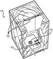
- FIG. 2is an overview of a test device according to an embodiment the present disclosure
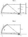
- FIG. 3is a schematic diagram of a light source, mirror and intensity filter assembly belonging to a test device according to the present disclosure
- FIG. 4is a schematic diagram of a device for defining the intensity filter to be interposed on the trajectory of the light beam
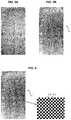
- FIGS. 5A and 5Bare images respectively of the light intensity produced by a light source—parabolic mirror assembly and the negative filter for compensating the effects of the surface defects of the mirror on the intensity of the light beam,
- FIG. 6shows an example of an at least partially absorbent region of the filter, comprising a set of transparent and opaque patterns.
- FIG. 1Ais a schematic diagram of a photovoltaic module that may be tested using embodiments of the present disclosure.
- the module 1 to be testedcomprises a plurality of concentration sub-photovoltaic modules 10 .
- Each sub-photovoltaic module 10comprises a plurality of cell—concentrator assemblies.
- each assembly 100essentially comprises a photovoltaic cell 101 (for example multi-junction) and a concentrator 102 designed to concentrate the solar radiation arriving in normal incidence toward the photovoltaic cell 101 .
- the photovoltaic cell 101is placed on a heat dissipator 103 to limit its rise in temperature.
- the concentrator 102comprises for example a Fresnel lens.
- the surface of the module to be testedis the surface of the concentrators.
- the sub-photovoltaic modules 10 forming the module 1can optionally be electrically connected in series or in parallel.
- each sub-module 10has a generally rectangular shape, whereof the width and height are respectively in the following ranges: between 30 and 80 cm in width, for example 60 cm, and between 60 and 150 cm in height, for example 120 cm.
- the sub-photovoltaic modules 10are typically arranged in the shape of rows and/or columns to form the module.
- a module of 8 m 2can be formed from two rows of six sub-modules, each sub-module having a surface of around 0.7 m 2 .
- FIG. 2is an overview of a test device according to the present disclosure.
- the devicecomprises a support 3 for the module 1 to be tested.
- the support 3is arranged such that the surface of the module to be tested is vertical.
- “Vertical” in the present textmeans a direction perpendicular to the floor of the building in which the test device is installed.
- the test devicecomprises a plurality of light sources 2 and a plurality of parabolic mirrors 4 coupled to the light sources so as to reflect the light originating from each source in an almost collimated light beam in a direction perpendicular to the surface of the module.
- each sourceis arranged at the focal point of the corresponding parabolic mirror.
- the test devicetherefore comprises as many sources as mirrors.
- Thisutilises a plurality of identical mirrors, whereof the position and orientation are adjusted so as to send back towards the module to be tested an almost collimated beam perpendicular to the surface of the module.
- each light sourcecan be coupled to several mirrors, to the extent where these mirrors are arranged such that their focal points coincide, the source being arranged at the placement of these focal points.
- the test devicecomprises twelve light sources 2 placed according to two horizontal rows on either side of the module 1 , and twelve parabolic mirrors 4 placed according to two horizontal rows facing the module 1 .
- Each source and the corresponding parabolic mirrorare oriented relative to each other such that the light beam sent back by the mirror is perpendicular to the surface of the corresponding sub-module.
- the distance between the sources and the parabolic mirrorsis defined such that the almost collimated light beam sent back by each mirror illuminates with the preferred characteristics the entire surface of the corresponding sub-module.
- This distanceas well as the surface of the mirrors, therefore depends on the surface of the sub-modules of the module to be tested.
- each sub-moduleis sufficiently low, it can eventuate that a light source—parabolic mirror couple illuminates several sub-modules and retains a ground space acceptable to the test device and a mirror size which does not impair its manufacturing cost.
- the light sources and the parabolic mirrorsare advantageously arranged so that areas not illuminated by the almost collimated beams sent by the mirrors coincide with the areas separating the sub-modules from the module to be tested, which are not functional in terms of photovoltaic conversion.
- test deviceis designed such that adjustment of the position and orientation of each mirror is possible.
- an intensity filter 11is interposed on the trajectory of the beam, upstream of the module 1 .
- the intensity filter 11comprises at least partially absorbent regions with neutral spectral density relative to the light beam.
- “Absorbent with neutral spectral density”means that the region concerned of the filter blocks in intensity in an equivalent manner all the wavelengths of the light beam. In this case this is not selective absorption of a determined range of wavelengths.
- the intensity filter 11is specifically adapted to the mirror 4 , i.e. the at least partially absorbent regions of the filter are arranged facing the areas of greatest intensity of the beam.
- the intensity filter 11can be specifically adapted to a mirror—light source couple, which compensates any defects in uniformity of the source apart from those of the mirror.
- the at least partially absorbent regionsdiminish the intensity of the beam passing through them.
- regions of the filterare transparent or less absorbent so as to transmit the entire light beam or a majority of the intensity of the latter in the areas of the beam exhibiting lower intensity.
- distribution of the at least partially absorbent regions on the filter and the degree of absorption of the regionscorrespond substantially to the negative of distribution of the intensity of the light beam.
- the filterattenuates the differences in intensity of the beam and produces improved uniformity of the intensity arriving at the module.
- parabolic mirrors made by low-cost methodscan be used, for example by thermoforming of a glass plate or plastic material followed by coating with a reflecting film or a stack of thin reflecting layers.
- the intensity filter 11comprises a support 110 transparent to the almost collimated beam and a film 111 adhered on the support 110 , the film 111 comprising the absorbent regions mentioned above.
- the intensity filtercomprises a support transparent to the almost collimated beam and a printing layer applied to the support to form the absorbent regions.
- the supportis planar so as not to deform the almost collimated beam and is positioned perpendicular to the beam.
- the supportis a glass plate.
- FIG. 4illustrates the arrangement of a device for defining an intensity filter adapted to a determined mirror.
- the light source 2is arranged at the focal point F of the mirror 4 so that the mirror 4 sends back the light emitted by the source in an almost collimated beam.
- a screen 12 of uniform tintis placed on the trajectory of the beam, perpendicular to the latter.
- An image sensoris placed at a placement C facing the screen 12 , and an image of the beam projected onto the screen 12 is recorded.
- the resultis mapping of the intensity of the beam, such as illustrated in FIG. 5A .
- the intensity of the beamis shown by levels of grey (the lightest areas having the strongest intensity) and is not uniform.
- a negative of this imageis created, illustrated in FIG. 5B , having more absorbent dark regions facing the light areas of the image of the light beam, and transparent or less absorbent light regions facing the dark areas of the image of the light beam.
- this negative imageis printed on a film in turn applied to a support transparent to the light beam.
- the filmis a transparent self-adhesive film intended to be adhered on the support after printing.
- the negative imageis directly formed on a transparent support by a printing method.
- the negative imageis transformed in to a binary set of elementary patterns comprising patterns 11 a transparent and patterns 11 b opaque to the light beam.
- thisshows in an enlarged manner a region of the filter in the shape of a checkerboard consisting of transparent squares 11 a and absorbent black squares 11 b.
- any other form of elementary patternscould be selected without as such departing from the scope of the present disclosure, the shape and dimension of the patterns further able to vary from one region to the other of the filter.
- the degree of absorption of the filter relative to the light beamcan in fact be modulated by the shape and dimension of the different patterns.
- the length of the sideis between 0.5 and 10 mm.
- This binarization of the negative imageproduces the filter simply by using black ink printing to form the elementary absorbent patterns.
- a corresponding intensity filteris made for each parabolic mirror of the test device, and each filter is installed on the trajectory of the light beam sent back by the corresponding mirror.
Landscapes
- Photovoltaic Devices (AREA)
Abstract
Description
- irradiance comparable to that produced by the sun at ground level, that is, of the order of 1 kW/m2.
- reproduction of the complete solar spectrum, from ultraviolet to infrared, by respecting spectral densities,
- angular divergence close to that of solar light, that is, 0.5° (±0.25°),
- considerable spatial uniformity of the irradiance (the aim being inhomogeneity of irradiance less than or equal to 5%).
- at least one light source,
- at least one parabolic mirror coupled to the source so as to send back the light coming from the source in an almost collimated light beam to the module to be tested, in a direction perpendicular to the surface of the module, and
- an intensity filter interposed on the trajectory of the almost collimated beam upstream of the module to be tested, the filter comprising at least partially absorbent regions with neutral spectral density relative to the light beam, the at least partially absorbent regions being arranged facing areas of greatest intensity of the beam so as to attenuate the differences in intensity of the beam.
- acquisition of an image of the almost collimated beam originating from the parabolic mirror,
- determination, on the image, of the areas of the beam of greatest intensity,
- decomposition of the areas of the image into elementary patterns,
- attribution to each elementary pattern of a transparent or opaque character relative to the light flow so as to faun, facing the areas of greatest intensity of the light beam, at least partially absorbent regions consisting of the patterns.
Claims (17)
Applications Claiming Priority (4)
| Application Number | Priority Date | Filing Date | Title |
|---|---|---|---|
| FR1361142 | 2013-11-14 | ||
| FR1361142AFR3013174B1 (en) | 2013-11-14 | 2013-11-14 | DEVICE FOR TESTING A CONCENTRATION PHOTOVOLTAIC MODULE |
| PCT/EP2014/074635WO2015071425A1 (en) | 2013-11-14 | 2014-11-14 | Device for testing a concentrated photovoltaic module |
| US201615036030A | 2016-05-11 | 2016-05-11 |
Publications (2)
| Publication Number | Publication Date |
|---|---|
| US20160365834A1 US20160365834A1 (en) | 2016-12-15 |
| US11005418B2true US11005418B2 (en) | 2021-05-11 |
Family
ID=50023782
Family Applications (1)
| Application Number | Title | Priority Date | Filing Date |
|---|---|---|---|
| US15/036,036Expired - Fee RelatedUS11005418B2 (en) | 2013-11-14 | 2014-11-14 | Device for testing a concentrated photovoltaic module |
Country Status (6)
| Country | Link |
|---|---|
| US (1) | US11005418B2 (en) |
| EP (1) | EP3069157B1 (en) |
| CN (1) | CN106461736B (en) |
| ES (1) | ES2657069T3 (en) |
| FR (1) | FR3013174B1 (en) |
| WO (1) | WO2015071425A1 (en) |
Families Citing this family (4)
| Publication number | Priority date | Publication date | Assignee | Title |
|---|---|---|---|---|
| CN105048963B (en)* | 2015-07-27 | 2017-04-12 | 连云港神舟新能源有限公司 | Indoor testing system for low-power condensing assembly |
| US11614406B2 (en)* | 2018-04-30 | 2023-03-28 | The Southern Company | Systems and methods for inspecting solar modules using high-power light sources |
| CN108616259B (en)* | 2018-07-10 | 2024-11-22 | 苏州腾晖光伏技术有限公司 | Photovoltaic module test stand |
| KR102445394B1 (en)* | 2020-05-27 | 2022-09-19 | 재단법인 한국조명아이씨티연구원 | Angle-adjustable simulation light source test device for calculating the light collecting efficiency of solar light concentrators |
Citations (29)
| Publication number | Priority date | Publication date | Assignee | Title |
|---|---|---|---|---|
| US3877814A (en) | 1973-02-07 | 1975-04-15 | Ppg Industries Inc | Method of and apparatus for detecting concave and convex portions in a specular surface |
| US6076942A (en)* | 1998-06-30 | 2000-06-20 | Hughes Electronics Corporation | Uniformity filter |
| CN1316613A (en) | 2001-05-31 | 2001-10-10 | 上海交通大学 | Sunlight simulator with pulsive xenon lamp and three-freedom paraboloid for scattered reflection |
| US20080048102A1 (en)* | 2006-08-22 | 2008-02-28 | Eastman Kodak Company | Optically enhanced multi-spectral detector structure |
| CN101290340A (en) | 2008-04-29 | 2008-10-22 | 李果华 | LED solar simulator |
| CN101351715A (en) | 2005-12-30 | 2009-01-21 | 太阳能技术股份公司 | Test apparatus and test method for a pv concentrator module |
| US20090194098A1 (en) | 2008-01-31 | 2009-08-06 | Bp Corporation North America Inc. | Solar Module with a Frame for Mounting a Solar Panel |
| WO2010003115A1 (en) | 2008-07-03 | 2010-01-07 | Greenfield Solar Corp. | Solar collector assembly |
| US20100006139A1 (en)* | 2008-07-03 | 2010-01-14 | Greenfield Solar Corp. | Light beam pattern and photovoltaic elements layout |
| US20100046229A1 (en)* | 2008-08-21 | 2010-02-25 | All Real Technology Co., Ltd. | Artificial light source generator |
| CN101681948A (en) | 2007-04-12 | 2010-03-24 | 安吉尔安东尼工业股份公司 | Concentrating photovoltaic system and its concentrating method |
| US20100073011A1 (en)* | 2008-09-23 | 2010-03-25 | Applied Materials, Inc. | Light soaking system and test method for solar cells |
| JP2010186890A (en) | 2009-02-12 | 2010-08-26 | Nisshinbo Holdings Inc | Parallel light solar simulator |
| US20110017269A1 (en)* | 2009-07-24 | 2011-01-27 | John Stewart Fangman | Solar Concentrator Configuration With Improved Manufacturability And Efficiency |
| CN102160189A (en) | 2008-07-18 | 2011-08-17 | 日清纺控股株式会社 | Solar simulator and method of measuring multijunction solar cell |
| US20110246109A1 (en)* | 2011-05-30 | 2011-10-06 | Cyrium Technologies Incorporated | Apparatus and method to characterize multijunction photovoltaic solar cells |
| US20110259396A1 (en)* | 2008-12-03 | 2011-10-27 | Hoffman James T | Solar energy collection system |
| US20110273020A1 (en) | 2010-04-01 | 2011-11-10 | Morgan Solar Inc. | Integrated Photovoltaic Module |
| CN102252826A (en) | 2011-04-15 | 2011-11-23 | 中国科学院长春光学精密机械与物理研究所 | Device and method for testing light concentration efficiency of high-parallelism and large-aperture light concentration system |
| US20120097546A1 (en)* | 2010-10-25 | 2012-04-26 | Ppg Industries Ohio, Inc. | Electrocurtain coating process for coating solar mirrors |
| US20120223733A1 (en)* | 2011-03-03 | 2012-09-06 | International Business Machines Corporation | Solar Cell Characterization System with an Automated Continuous Neutral Density Filter |
| CN102721841A (en) | 2012-06-15 | 2012-10-10 | 深圳市创益科技发展有限公司 | Solar simulator for testing solar cells |
| US20120273041A1 (en)* | 2011-04-28 | 2012-11-01 | Angus Wu | Light concentrator with tapered dichroic materials |
| US20130021054A1 (en)* | 2011-07-19 | 2013-01-24 | Applied Materials Italia S.R.L. | Method and apparatus for testing photovoltaic devices |
| CN103064030A (en) | 2012-12-21 | 2013-04-24 | 杨军 | System and method for battery light converging testing and sample platform for battery light converging testing |
| US8471142B1 (en)* | 2012-08-16 | 2013-06-25 | Pu Ni Tai Yang Neng (Hangzhou) Co., Limited | Solar energy systems using external reflectors |
| US8860424B1 (en)* | 2011-03-10 | 2014-10-14 | Solar Junction Corporation | Apparatus and method for highly accelerated life testing of solar cells |
| US20150015297A1 (en)* | 2013-07-10 | 2015-01-15 | Dainippon Screen Mfg. Co., Ltd. | Photo device inspection apparatus and photo device inspection method |
| US20160344340A1 (en) | 2013-11-14 | 2016-11-24 | Soitec Solar Gmbh | Method for testing a concentrated photovoltaic module |
- 2013
- 2013-11-14FRFR1361142Apatent/FR3013174B1/ennot_activeExpired - Fee Related
- 2014
- 2014-11-14WOPCT/EP2014/074635patent/WO2015071425A1/enactiveApplication Filing
- 2014-11-14EPEP14799416.4Apatent/EP3069157B1/enactiveActive
- 2014-11-14CNCN201480072563.XApatent/CN106461736B/enactiveActive
- 2014-11-14ESES14799416.4Tpatent/ES2657069T3/enactiveActive
- 2014-11-14USUS15/036,036patent/US11005418B2/ennot_activeExpired - Fee Related
Patent Citations (33)
| Publication number | Priority date | Publication date | Assignee | Title |
|---|---|---|---|---|
| US3877814A (en) | 1973-02-07 | 1975-04-15 | Ppg Industries Inc | Method of and apparatus for detecting concave and convex portions in a specular surface |
| US6076942A (en)* | 1998-06-30 | 2000-06-20 | Hughes Electronics Corporation | Uniformity filter |
| CN1316613A (en) | 2001-05-31 | 2001-10-10 | 上海交通大学 | Sunlight simulator with pulsive xenon lamp and three-freedom paraboloid for scattered reflection |
| CN101351715A (en) | 2005-12-30 | 2009-01-21 | 太阳能技术股份公司 | Test apparatus and test method for a pv concentrator module |
| US20080048102A1 (en)* | 2006-08-22 | 2008-02-28 | Eastman Kodak Company | Optically enhanced multi-spectral detector structure |
| CN101681948A (en) | 2007-04-12 | 2010-03-24 | 安吉尔安东尼工业股份公司 | Concentrating photovoltaic system and its concentrating method |
| US20090194098A1 (en) | 2008-01-31 | 2009-08-06 | Bp Corporation North America Inc. | Solar Module with a Frame for Mounting a Solar Panel |
| CN101290340A (en) | 2008-04-29 | 2008-10-22 | 李果华 | LED solar simulator |
| WO2010003115A1 (en) | 2008-07-03 | 2010-01-07 | Greenfield Solar Corp. | Solar collector assembly |
| US20100006139A1 (en)* | 2008-07-03 | 2010-01-14 | Greenfield Solar Corp. | Light beam pattern and photovoltaic elements layout |
| CN102160189A (en) | 2008-07-18 | 2011-08-17 | 日清纺控股株式会社 | Solar simulator and method of measuring multijunction solar cell |
| CN102160189B (en) | 2008-07-18 | 2014-03-26 | 日清纺控股株式会社 | Solar simulator and method for measuring multi-junction solar cells |
| US20100046229A1 (en)* | 2008-08-21 | 2010-02-25 | All Real Technology Co., Ltd. | Artificial light source generator |
| US20100073011A1 (en)* | 2008-09-23 | 2010-03-25 | Applied Materials, Inc. | Light soaking system and test method for solar cells |
| US20110259396A1 (en)* | 2008-12-03 | 2011-10-27 | Hoffman James T | Solar energy collection system |
| JP2010186890A (en) | 2009-02-12 | 2010-08-26 | Nisshinbo Holdings Inc | Parallel light solar simulator |
| TW201100693A (en) | 2009-02-12 | 2011-01-01 | Nisshinbo Holdings Inc | Parallel light solar simulator |
| US20110017269A1 (en)* | 2009-07-24 | 2011-01-27 | John Stewart Fangman | Solar Concentrator Configuration With Improved Manufacturability And Efficiency |
| US20110273020A1 (en) | 2010-04-01 | 2011-11-10 | Morgan Solar Inc. | Integrated Photovoltaic Module |
| US20120097546A1 (en)* | 2010-10-25 | 2012-04-26 | Ppg Industries Ohio, Inc. | Electrocurtain coating process for coating solar mirrors |
| US20120223733A1 (en)* | 2011-03-03 | 2012-09-06 | International Business Machines Corporation | Solar Cell Characterization System with an Automated Continuous Neutral Density Filter |
| US8860424B1 (en)* | 2011-03-10 | 2014-10-14 | Solar Junction Corporation | Apparatus and method for highly accelerated life testing of solar cells |
| CN102252826A (en) | 2011-04-15 | 2011-11-23 | 中国科学院长春光学精密机械与物理研究所 | Device and method for testing light concentration efficiency of high-parallelism and large-aperture light concentration system |
| US20120273041A1 (en)* | 2011-04-28 | 2012-11-01 | Angus Wu | Light concentrator with tapered dichroic materials |
| US20110246109A1 (en)* | 2011-05-30 | 2011-10-06 | Cyrium Technologies Incorporated | Apparatus and method to characterize multijunction photovoltaic solar cells |
| US20130021054A1 (en)* | 2011-07-19 | 2013-01-24 | Applied Materials Italia S.R.L. | Method and apparatus for testing photovoltaic devices |
| CN102721841B (en) | 2012-06-15 | 2014-10-01 | 深圳市创益科技发展有限公司 | A solar simulator for testing solar cells |
| CN102721841A (en) | 2012-06-15 | 2012-10-10 | 深圳市创益科技发展有限公司 | Solar simulator for testing solar cells |
| US8471142B1 (en)* | 2012-08-16 | 2013-06-25 | Pu Ni Tai Yang Neng (Hangzhou) Co., Limited | Solar energy systems using external reflectors |
| CN103064030A (en) | 2012-12-21 | 2013-04-24 | 杨军 | System and method for battery light converging testing and sample platform for battery light converging testing |
| US20150015297A1 (en)* | 2013-07-10 | 2015-01-15 | Dainippon Screen Mfg. Co., Ltd. | Photo device inspection apparatus and photo device inspection method |
| US20160344340A1 (en) | 2013-11-14 | 2016-11-24 | Soitec Solar Gmbh | Method for testing a concentrated photovoltaic module |
| CN106471388A (en) | 2013-11-14 | 2017-03-01 | 圣奥古斯丁加拿大电气有限公司 | Method for testing light concentrating photovoltaic module |
Non-Patent Citations (7)
| Title |
|---|
| Chinese First Office Action for Chinese Application No. 201480072325, dated Jul. 27, 2018, 9 pages with English Translation. |
| Chinese First Office Action for Chinese Application No. 201480072563, dated Aug. 28, 2018, 22 pages with English Translation. |
| Chinese First Search for Chinese Application No. 201480072325, dated Jul. 18, 2018, 2 pages. |
| Chinese First Search Report for Chinese Application No. 201480072563, dated Aug. 7, 2018, 2 pages. |
| Chinese Supplementary Search Report for Chinese Application No. 201480072563, dated Mar. 6, 2019, 1 page. |
| International Search Report for International Application No. PCT/EP2014/07463 dated Jan. 14, 2015, 2 pages. |
| International Written Opinion for International Application No. PCT/EP2014/07463 dated Jan. 14, 2015, 5 pages. |
Also Published As
| Publication number | Publication date |
|---|---|
| CN106461736B (en) | 2019-06-07 |
| WO2015071425A1 (en) | 2015-05-21 |
| EP3069157A1 (en) | 2016-09-21 |
| EP3069157B1 (en) | 2017-11-08 |
| ES2657069T3 (en) | 2018-03-01 |
| US20160365834A1 (en) | 2016-12-15 |
| FR3013174A1 (en) | 2015-05-15 |
| FR3013174B1 (en) | 2015-11-20 |
| CN106461736A (en) | 2017-02-22 |
Similar Documents
| Publication | Publication Date | Title |
|---|---|---|
| US11005418B2 (en) | Device for testing a concentrated photovoltaic module | |
| US20130063174A1 (en) | Solar simulator and solar cell inspection device | |
| Yew et al. | Performance study of crossed compound parabolic concentrator as secondary optics in non-imaging dish concentrator for the application of dense-array concentrator photovoltaic system | |
| Sato et al. | Design of low‐concentration static III‐V/Si partial CPV module with 27.3% annual efficiency for car‐roof application | |
| MX2011011979A (en) | SOLAR PHOTOVOLTAIC CONCENTRATOR PANEL. | |
| Hayashi et al. | Nonuniformity sunlight-irradiation effect on photovoltaic performance of concentrating photovoltaic using microsolar cells without secondary optics | |
| US8669508B2 (en) | Sun-tracking system | |
| Huang et al. | Ball lens as secondary optical element for CPV system | |
| EP2157359B1 (en) | Artificial light source generator | |
| US9859842B2 (en) | Device and method for testing a concentrated photovoltaic module | |
| KR101412533B1 (en) | Concentrating Photovoltaics Apparatus Having Non-Powered Solar Light Tracking Function | |
| KR102037733B1 (en) | Apparatus for measuring amount of incident light and apparatus for measuring angle of incident light using photodiode | |
| US20150236639A1 (en) | Solar receiver module for a concentrated photovoltaic (cpv) power plant | |
| US20120125403A1 (en) | Photovoltaic Flat Panel With Enhanced Acceptance Angle Comprising Micro-Lens Array In Laminating Film | |
| US10432140B2 (en) | Method for testing a concentrated photovoltaic module | |
| CN102263146A (en) | solar cell device | |
| KR101783532B1 (en) | Device and method for optimally adjusting the lens plate in a cpv module | |
| US20120180847A1 (en) | Method for improving solar energy condensation efficiency in solar energy condensation electric power facility | |
| CN105337570A (en) | Photoelectric conversion module and conversion method for converting optical energy into electric energy | |
| KR102848482B1 (en) | Performance measuring apparatus for bifacial solar cell | |
| CN105242389A (en) | Optical energy output apparatus | |
| CN205103445U (en) | Photovoltaic conversion module | |
| JP2015207570A (en) | Light collection type photovoltaic power generation device | |
| Vivar et al. | Radial CPV receiver | |
| Lin et al. | Diffuse Solar Micro‐Concentrators Using Dielectric Total Internal Reflection with Tunable Side and Top Profiles |
Legal Events
| Date | Code | Title | Description |
|---|---|---|---|
| AS | Assignment | Owner name:SOITEC SOLAR GMBH, GERMANY Free format text:ASSIGNMENT OF ASSIGNORS INTEREST;ASSIGNOR:GASTALDO, PHILIPPE;REEL/FRAME:038553/0146 Effective date:20140512 | |
| STPP | Information on status: patent application and granting procedure in general | Free format text:DOCKETED NEW CASE - READY FOR EXAMINATION | |
| AS | Assignment | Owner name:SAINT-AUGUSTIN CANADA ELECTRIC INC., CANADA Free format text:ASSIGNMENT OF ASSIGNORS INTEREST;ASSIGNOR:SOITEC SOLAR GMBH;REEL/FRAME:042268/0083 Effective date:20170215 | |
| AS | Assignment | Owner name:SAINT-AUGUSTIN CANADA ELECTRIC INC., CANADA Free format text:CORRECTIVE ASSIGNMENT TO CORRECT THE ASSIGNEE'S ADDRESS PREVIOUSLY RECORDED ON REEL 042268 FRAME 0083. ASSIGNOR(S) HEREBY CONFIRMS THE ASSIGNMENT;ASSIGNOR:SOITEC SOLAR GMBH;REEL/FRAME:047571/0084 Effective date:20170215 | |
| STPP | Information on status: patent application and granting procedure in general | Free format text:NON FINAL ACTION MAILED | |
| STPP | Information on status: patent application and granting procedure in general | Free format text:RESPONSE TO NON-FINAL OFFICE ACTION ENTERED AND FORWARDED TO EXAMINER | |
| STPP | Information on status: patent application and granting procedure in general | Free format text:FINAL REJECTION MAILED | |
| STPP | Information on status: patent application and granting procedure in general | Free format text:DOCKETED NEW CASE - READY FOR EXAMINATION | |
| STPP | Information on status: patent application and granting procedure in general | Free format text:RESPONSE TO NON-FINAL OFFICE ACTION ENTERED AND FORWARDED TO EXAMINER | |
| STPP | Information on status: patent application and granting procedure in general | Free format text:NOTICE OF ALLOWANCE MAILED -- APPLICATION RECEIVED IN OFFICE OF PUBLICATIONS | |
| STPP | Information on status: patent application and granting procedure in general | Free format text:PUBLICATIONS -- ISSUE FEE PAYMENT VERIFIED | |
| STCF | Information on status: patent grant | Free format text:PATENTED CASE | |
| CC | Certificate of correction | ||
| FEPP | Fee payment procedure | Free format text:MAINTENANCE FEE REMINDER MAILED (ORIGINAL EVENT CODE: REM.); ENTITY STATUS OF PATENT OWNER: LARGE ENTITY | |
| LAPS | Lapse for failure to pay maintenance fees | Free format text:PATENT EXPIRED FOR FAILURE TO PAY MAINTENANCE FEES (ORIGINAL EVENT CODE: EXP.); ENTITY STATUS OF PATENT OWNER: LARGE ENTITY | |
| STCH | Information on status: patent discontinuation | Free format text:PATENT EXPIRED DUE TO NONPAYMENT OF MAINTENANCE FEES UNDER 37 CFR 1.362 | |
| FP | Lapsed due to failure to pay maintenance fee | Effective date:20250511 |