US10998248B2 - Semiconductor device and method of forming sacrificial adhesive over contact pads of semiconductor die - Google Patents
Semiconductor device and method of forming sacrificial adhesive over contact pads of semiconductor dieDownload PDFInfo
- Publication number
- US10998248B2 US10998248B2US15/068,290US201615068290AUS10998248B2US 10998248 B2US10998248 B2US 10998248B2US 201615068290 AUS201615068290 AUS 201615068290AUS 10998248 B2US10998248 B2US 10998248B2
- Authority
- US
- United States
- Prior art keywords
- semiconductor die
- semiconductor
- sacrificial adhesive
- carrier
- contact pads
- Prior art date
- Legal status (The legal status is an assumption and is not a legal conclusion. Google has not performed a legal analysis and makes no representation as to the accuracy of the status listed.)
- Active, expires
Links
Images


Classifications
- H—ELECTRICITY
- H01—ELECTRIC ELEMENTS
- H01L—SEMICONDUCTOR DEVICES NOT COVERED BY CLASS H10
- H01L23/00—Details of semiconductor or other solid state devices
- H01L23/28—Encapsulations, e.g. encapsulating layers, coatings, e.g. for protection
- H01L23/31—Encapsulations, e.g. encapsulating layers, coatings, e.g. for protection characterised by the arrangement or shape
- H01L23/3107—Encapsulations, e.g. encapsulating layers, coatings, e.g. for protection characterised by the arrangement or shape the device being completely enclosed
- H01L23/3121—Encapsulations, e.g. encapsulating layers, coatings, e.g. for protection characterised by the arrangement or shape the device being completely enclosed a substrate forming part of the encapsulation
- H01L23/3128—Encapsulations, e.g. encapsulating layers, coatings, e.g. for protection characterised by the arrangement or shape the device being completely enclosed a substrate forming part of the encapsulation the substrate having spherical bumps for external connection
- H—ELECTRICITY
- H01—ELECTRIC ELEMENTS
- H01L—SEMICONDUCTOR DEVICES NOT COVERED BY CLASS H10
- H01L21/00—Processes or apparatus adapted for the manufacture or treatment of semiconductor or solid state devices or of parts thereof
- H01L21/02—Manufacture or treatment of semiconductor devices or of parts thereof
- H01L21/04—Manufacture or treatment of semiconductor devices or of parts thereof the devices having potential barriers, e.g. a PN junction, depletion layer or carrier concentration layer
- H01L21/50—Assembly of semiconductor devices using processes or apparatus not provided for in a single one of the groups H01L21/18 - H01L21/326 or H10D48/04 - H10D48/07 e.g. sealing of a cap to a base of a container
- H01L21/56—Encapsulations, e.g. encapsulation layers, coatings
- H01L21/561—Batch processing
- H—ELECTRICITY
- H01—ELECTRIC ELEMENTS
- H01L—SEMICONDUCTOR DEVICES NOT COVERED BY CLASS H10
- H01L21/00—Processes or apparatus adapted for the manufacture or treatment of semiconductor or solid state devices or of parts thereof
- H01L21/02—Manufacture or treatment of semiconductor devices or of parts thereof
- H01L21/04—Manufacture or treatment of semiconductor devices or of parts thereof the devices having potential barriers, e.g. a PN junction, depletion layer or carrier concentration layer
- H01L21/50—Assembly of semiconductor devices using processes or apparatus not provided for in a single one of the groups H01L21/18 - H01L21/326 or H10D48/04 - H10D48/07 e.g. sealing of a cap to a base of a container
- H01L21/56—Encapsulations, e.g. encapsulation layers, coatings
- H01L21/563—Encapsulation of active face of flip-chip device, e.g. underfilling or underencapsulation of flip-chip, encapsulation preform on chip or mounting substrate
- H—ELECTRICITY
- H01—ELECTRIC ELEMENTS
- H01L—SEMICONDUCTOR DEVICES NOT COVERED BY CLASS H10
- H01L21/00—Processes or apparatus adapted for the manufacture or treatment of semiconductor or solid state devices or of parts thereof
- H01L21/02—Manufacture or treatment of semiconductor devices or of parts thereof
- H01L21/04—Manufacture or treatment of semiconductor devices or of parts thereof the devices having potential barriers, e.g. a PN junction, depletion layer or carrier concentration layer
- H01L21/50—Assembly of semiconductor devices using processes or apparatus not provided for in a single one of the groups H01L21/18 - H01L21/326 or H10D48/04 - H10D48/07 e.g. sealing of a cap to a base of a container
- H01L21/56—Encapsulations, e.g. encapsulation layers, coatings
- H01L21/568—Temporary substrate used as encapsulation process aid
- H—ELECTRICITY
- H01—ELECTRIC ELEMENTS
- H01L—SEMICONDUCTOR DEVICES NOT COVERED BY CLASS H10
- H01L23/00—Details of semiconductor or other solid state devices
- H01L23/48—Arrangements for conducting electric current to or from the solid state body in operation, e.g. leads, terminal arrangements ; Selection of materials therefor
- H01L23/488—Arrangements for conducting electric current to or from the solid state body in operation, e.g. leads, terminal arrangements ; Selection of materials therefor consisting of soldered or bonded constructions
- H01L23/498—Leads, i.e. metallisations or lead-frames on insulating substrates, e.g. chip carriers
- H01L23/49811—Additional leads joined to the metallisation on the insulating substrate, e.g. pins, bumps, wires, flat leads
- H01L23/49816—Spherical bumps on the substrate for external connection, e.g. ball grid arrays [BGA]
- H—ELECTRICITY
- H01—ELECTRIC ELEMENTS
- H01L—SEMICONDUCTOR DEVICES NOT COVERED BY CLASS H10
- H01L23/00—Details of semiconductor or other solid state devices
- H01L23/52—Arrangements for conducting electric current within the device in operation from one component to another, i.e. interconnections, e.g. wires, lead frames
- H01L23/538—Arrangements for conducting electric current within the device in operation from one component to another, i.e. interconnections, e.g. wires, lead frames the interconnection structure between a plurality of semiconductor chips being formed on, or in, insulating substrates
- H01L23/5389—Arrangements for conducting electric current within the device in operation from one component to another, i.e. interconnections, e.g. wires, lead frames the interconnection structure between a plurality of semiconductor chips being formed on, or in, insulating substrates the chips being integrally enclosed by the interconnect and support structures
- H—ELECTRICITY
- H01—ELECTRIC ELEMENTS
- H01L—SEMICONDUCTOR DEVICES NOT COVERED BY CLASS H10
- H01L24/00—Arrangements for connecting or disconnecting semiconductor or solid-state bodies; Methods or apparatus related thereto
- H01L24/01—Means for bonding being attached to, or being formed on, the surface to be connected, e.g. chip-to-package, die-attach, "first-level" interconnects; Manufacturing methods related thereto
- H01L24/02—Bonding areas ; Manufacturing methods related thereto
- H01L24/04—Structure, shape, material or disposition of the bonding areas prior to the connecting process
- H01L24/06—Structure, shape, material or disposition of the bonding areas prior to the connecting process of a plurality of bonding areas
- H—ELECTRICITY
- H01—ELECTRIC ELEMENTS
- H01L—SEMICONDUCTOR DEVICES NOT COVERED BY CLASS H10
- H01L24/00—Arrangements for connecting or disconnecting semiconductor or solid-state bodies; Methods or apparatus related thereto
- H01L24/01—Means for bonding being attached to, or being formed on, the surface to be connected, e.g. chip-to-package, die-attach, "first-level" interconnects; Manufacturing methods related thereto
- H01L24/18—High density interconnect [HDI] connectors; Manufacturing methods related thereto
- H01L24/19—Manufacturing methods of high density interconnect preforms
- H—ELECTRICITY
- H01—ELECTRIC ELEMENTS
- H01L—SEMICONDUCTOR DEVICES NOT COVERED BY CLASS H10
- H01L24/00—Arrangements for connecting or disconnecting semiconductor or solid-state bodies; Methods or apparatus related thereto
- H01L24/01—Means for bonding being attached to, or being formed on, the surface to be connected, e.g. chip-to-package, die-attach, "first-level" interconnects; Manufacturing methods related thereto
- H01L24/18—High density interconnect [HDI] connectors; Manufacturing methods related thereto
- H01L24/20—Structure, shape, material or disposition of high density interconnect preforms
- H—ELECTRICITY
- H01—ELECTRIC ELEMENTS
- H01L—SEMICONDUCTOR DEVICES NOT COVERED BY CLASS H10
- H01L24/00—Arrangements for connecting or disconnecting semiconductor or solid-state bodies; Methods or apparatus related thereto
- H01L24/93—Batch processes
- H01L24/95—Batch processes at chip-level, i.e. with connecting carried out on a plurality of singulated devices, i.e. on diced chips
- H01L24/96—Batch processes at chip-level, i.e. with connecting carried out on a plurality of singulated devices, i.e. on diced chips the devices being encapsulated in a common layer, e.g. neo-wafer or pseudo-wafer, said common layer being separable into individual assemblies after connecting
- H—ELECTRICITY
- H01—ELECTRIC ELEMENTS
- H01L—SEMICONDUCTOR DEVICES NOT COVERED BY CLASS H10
- H01L24/00—Arrangements for connecting or disconnecting semiconductor or solid-state bodies; Methods or apparatus related thereto
- H01L24/93—Batch processes
- H01L24/95—Batch processes at chip-level, i.e. with connecting carried out on a plurality of singulated devices, i.e. on diced chips
- H01L24/97—Batch processes at chip-level, i.e. with connecting carried out on a plurality of singulated devices, i.e. on diced chips the devices being connected to a common substrate, e.g. interposer, said common substrate being separable into individual assemblies after connecting
- H—ELECTRICITY
- H01—ELECTRIC ELEMENTS
- H01L—SEMICONDUCTOR DEVICES NOT COVERED BY CLASS H10
- H01L2221/00—Processes or apparatus adapted for the manufacture or treatment of semiconductor or solid state devices or of parts thereof covered by H01L21/00
- H01L2221/67—Apparatus for handling semiconductor or electric solid state devices during manufacture or treatment thereof; Apparatus for handling wafers during manufacture or treatment of semiconductor or electric solid state devices or components; Apparatus not specifically provided for elsewhere
- H01L2221/683—Apparatus for handling semiconductor or electric solid state devices during manufacture or treatment thereof; Apparatus for handling wafers during manufacture or treatment of semiconductor or electric solid state devices or components; Apparatus not specifically provided for elsewhere for supporting or gripping
- H01L2221/68304—Apparatus for handling semiconductor or electric solid state devices during manufacture or treatment thereof; Apparatus for handling wafers during manufacture or treatment of semiconductor or electric solid state devices or components; Apparatus not specifically provided for elsewhere for supporting or gripping using temporarily an auxiliary support
- H01L2221/68359—Apparatus for handling semiconductor or electric solid state devices during manufacture or treatment thereof; Apparatus for handling wafers during manufacture or treatment of semiconductor or electric solid state devices or components; Apparatus not specifically provided for elsewhere for supporting or gripping using temporarily an auxiliary support used as a support during manufacture of interconnect decals or build up layers
- H—ELECTRICITY
- H01—ELECTRIC ELEMENTS
- H01L—SEMICONDUCTOR DEVICES NOT COVERED BY CLASS H10
- H01L2224/00—Indexing scheme for arrangements for connecting or disconnecting semiconductor or solid-state bodies and methods related thereto as covered by H01L24/00
- H01L2224/01—Means for bonding being attached to, or being formed on, the surface to be connected, e.g. chip-to-package, die-attach, "first-level" interconnects; Manufacturing methods related thereto
- H01L2224/02—Bonding areas; Manufacturing methods related thereto
- H01L2224/04—Structure, shape, material or disposition of the bonding areas prior to the connecting process
- H01L2224/0401—Bonding areas specifically adapted for bump connectors, e.g. under bump metallisation [UBM]
- H—ELECTRICITY
- H01—ELECTRIC ELEMENTS
- H01L—SEMICONDUCTOR DEVICES NOT COVERED BY CLASS H10
- H01L2224/00—Indexing scheme for arrangements for connecting or disconnecting semiconductor or solid-state bodies and methods related thereto as covered by H01L24/00
- H01L2224/01—Means for bonding being attached to, or being formed on, the surface to be connected, e.g. chip-to-package, die-attach, "first-level" interconnects; Manufacturing methods related thereto
- H01L2224/02—Bonding areas; Manufacturing methods related thereto
- H01L2224/04—Structure, shape, material or disposition of the bonding areas prior to the connecting process
- H01L2224/04105—Bonding areas formed on an encapsulation of the semiconductor or solid-state body, e.g. bonding areas on chip-scale packages
- H—ELECTRICITY
- H01—ELECTRIC ELEMENTS
- H01L—SEMICONDUCTOR DEVICES NOT COVERED BY CLASS H10
- H01L2224/00—Indexing scheme for arrangements for connecting or disconnecting semiconductor or solid-state bodies and methods related thereto as covered by H01L24/00
- H01L2224/01—Means for bonding being attached to, or being formed on, the surface to be connected, e.g. chip-to-package, die-attach, "first-level" interconnects; Manufacturing methods related thereto
- H01L2224/10—Bump connectors; Manufacturing methods related thereto
- H01L2224/11—Manufacturing methods
- H01L2224/118—Post-treatment of the bump connector
- H01L2224/11848—Thermal treatments, e.g. annealing, controlled cooling
- H01L2224/11849—Reflowing
- H—ELECTRICITY
- H01—ELECTRIC ELEMENTS
- H01L—SEMICONDUCTOR DEVICES NOT COVERED BY CLASS H10
- H01L2224/00—Indexing scheme for arrangements for connecting or disconnecting semiconductor or solid-state bodies and methods related thereto as covered by H01L24/00
- H01L2224/01—Means for bonding being attached to, or being formed on, the surface to be connected, e.g. chip-to-package, die-attach, "first-level" interconnects; Manufacturing methods related thereto
- H01L2224/10—Bump connectors; Manufacturing methods related thereto
- H01L2224/12—Structure, shape, material or disposition of the bump connectors prior to the connecting process
- H01L2224/12105—Bump connectors formed on an encapsulation of the semiconductor or solid-state body, e.g. bumps on chip-scale packages
- H—ELECTRICITY
- H01—ELECTRIC ELEMENTS
- H01L—SEMICONDUCTOR DEVICES NOT COVERED BY CLASS H10
- H01L2224/00—Indexing scheme for arrangements for connecting or disconnecting semiconductor or solid-state bodies and methods related thereto as covered by H01L24/00
- H01L2224/01—Means for bonding being attached to, or being formed on, the surface to be connected, e.g. chip-to-package, die-attach, "first-level" interconnects; Manufacturing methods related thereto
- H01L2224/10—Bump connectors; Manufacturing methods related thereto
- H01L2224/12—Structure, shape, material or disposition of the bump connectors prior to the connecting process
- H01L2224/13—Structure, shape, material or disposition of the bump connectors prior to the connecting process of an individual bump connector
- H01L2224/13001—Core members of the bump connector
- H01L2224/1302—Disposition
- H01L2224/13022—Disposition the bump connector being at least partially embedded in the surface
- H—ELECTRICITY
- H01—ELECTRIC ELEMENTS
- H01L—SEMICONDUCTOR DEVICES NOT COVERED BY CLASS H10
- H01L2224/00—Indexing scheme for arrangements for connecting or disconnecting semiconductor or solid-state bodies and methods related thereto as covered by H01L24/00
- H01L2224/01—Means for bonding being attached to, or being formed on, the surface to be connected, e.g. chip-to-package, die-attach, "first-level" interconnects; Manufacturing methods related thereto
- H01L2224/10—Bump connectors; Manufacturing methods related thereto
- H01L2224/12—Structure, shape, material or disposition of the bump connectors prior to the connecting process
- H01L2224/13—Structure, shape, material or disposition of the bump connectors prior to the connecting process of an individual bump connector
- H01L2224/13001—Core members of the bump connector
- H01L2224/13099—Material
- H01L2224/131—Material with a principal constituent of the material being a metal or a metalloid, e.g. boron [B], silicon [Si], germanium [Ge], arsenic [As], antimony [Sb], tellurium [Te] and polonium [Po], and alloys thereof
- H01L2224/13101—Material with a principal constituent of the material being a metal or a metalloid, e.g. boron [B], silicon [Si], germanium [Ge], arsenic [As], antimony [Sb], tellurium [Te] and polonium [Po], and alloys thereof the principal constituent melting at a temperature of less than 400°C
- H01L2224/13111—Tin [Sn] as principal constituent
- H—ELECTRICITY
- H01—ELECTRIC ELEMENTS
- H01L—SEMICONDUCTOR DEVICES NOT COVERED BY CLASS H10
- H01L2224/00—Indexing scheme for arrangements for connecting or disconnecting semiconductor or solid-state bodies and methods related thereto as covered by H01L24/00
- H01L2224/01—Means for bonding being attached to, or being formed on, the surface to be connected, e.g. chip-to-package, die-attach, "first-level" interconnects; Manufacturing methods related thereto
- H01L2224/10—Bump connectors; Manufacturing methods related thereto
- H01L2224/12—Structure, shape, material or disposition of the bump connectors prior to the connecting process
- H01L2224/13—Structure, shape, material or disposition of the bump connectors prior to the connecting process of an individual bump connector
- H01L2224/13001—Core members of the bump connector
- H01L2224/13099—Material
- H01L2224/131—Material with a principal constituent of the material being a metal or a metalloid, e.g. boron [B], silicon [Si], germanium [Ge], arsenic [As], antimony [Sb], tellurium [Te] and polonium [Po], and alloys thereof
- H01L2224/13101—Material with a principal constituent of the material being a metal or a metalloid, e.g. boron [B], silicon [Si], germanium [Ge], arsenic [As], antimony [Sb], tellurium [Te] and polonium [Po], and alloys thereof the principal constituent melting at a temperature of less than 400°C
- H01L2224/13113—Bismuth [Bi] as principal constituent
- H—ELECTRICITY
- H01—ELECTRIC ELEMENTS
- H01L—SEMICONDUCTOR DEVICES NOT COVERED BY CLASS H10
- H01L2224/00—Indexing scheme for arrangements for connecting or disconnecting semiconductor or solid-state bodies and methods related thereto as covered by H01L24/00
- H01L2224/01—Means for bonding being attached to, or being formed on, the surface to be connected, e.g. chip-to-package, die-attach, "first-level" interconnects; Manufacturing methods related thereto
- H01L2224/10—Bump connectors; Manufacturing methods related thereto
- H01L2224/12—Structure, shape, material or disposition of the bump connectors prior to the connecting process
- H01L2224/13—Structure, shape, material or disposition of the bump connectors prior to the connecting process of an individual bump connector
- H01L2224/13001—Core members of the bump connector
- H01L2224/13099—Material
- H01L2224/131—Material with a principal constituent of the material being a metal or a metalloid, e.g. boron [B], silicon [Si], germanium [Ge], arsenic [As], antimony [Sb], tellurium [Te] and polonium [Po], and alloys thereof
- H01L2224/13101—Material with a principal constituent of the material being a metal or a metalloid, e.g. boron [B], silicon [Si], germanium [Ge], arsenic [As], antimony [Sb], tellurium [Te] and polonium [Po], and alloys thereof the principal constituent melting at a temperature of less than 400°C
- H01L2224/13116—Lead [Pb] as principal constituent
- H—ELECTRICITY
- H01—ELECTRIC ELEMENTS
- H01L—SEMICONDUCTOR DEVICES NOT COVERED BY CLASS H10
- H01L2224/00—Indexing scheme for arrangements for connecting or disconnecting semiconductor or solid-state bodies and methods related thereto as covered by H01L24/00
- H01L2224/01—Means for bonding being attached to, or being formed on, the surface to be connected, e.g. chip-to-package, die-attach, "first-level" interconnects; Manufacturing methods related thereto
- H01L2224/10—Bump connectors; Manufacturing methods related thereto
- H01L2224/12—Structure, shape, material or disposition of the bump connectors prior to the connecting process
- H01L2224/13—Structure, shape, material or disposition of the bump connectors prior to the connecting process of an individual bump connector
- H01L2224/13001—Core members of the bump connector
- H01L2224/13099—Material
- H01L2224/131—Material with a principal constituent of the material being a metal or a metalloid, e.g. boron [B], silicon [Si], germanium [Ge], arsenic [As], antimony [Sb], tellurium [Te] and polonium [Po], and alloys thereof
- H01L2224/13117—Material with a principal constituent of the material being a metal or a metalloid, e.g. boron [B], silicon [Si], germanium [Ge], arsenic [As], antimony [Sb], tellurium [Te] and polonium [Po], and alloys thereof the principal constituent melting at a temperature of greater than or equal to 400°C and less than 950°C
- H01L2224/13124—Aluminium [Al] as principal constituent
- H—ELECTRICITY
- H01—ELECTRIC ELEMENTS
- H01L—SEMICONDUCTOR DEVICES NOT COVERED BY CLASS H10
- H01L2224/00—Indexing scheme for arrangements for connecting or disconnecting semiconductor or solid-state bodies and methods related thereto as covered by H01L24/00
- H01L2224/01—Means for bonding being attached to, or being formed on, the surface to be connected, e.g. chip-to-package, die-attach, "first-level" interconnects; Manufacturing methods related thereto
- H01L2224/10—Bump connectors; Manufacturing methods related thereto
- H01L2224/12—Structure, shape, material or disposition of the bump connectors prior to the connecting process
- H01L2224/13—Structure, shape, material or disposition of the bump connectors prior to the connecting process of an individual bump connector
- H01L2224/13001—Core members of the bump connector
- H01L2224/13099—Material
- H01L2224/131—Material with a principal constituent of the material being a metal or a metalloid, e.g. boron [B], silicon [Si], germanium [Ge], arsenic [As], antimony [Sb], tellurium [Te] and polonium [Po], and alloys thereof
- H01L2224/13138—Material with a principal constituent of the material being a metal or a metalloid, e.g. boron [B], silicon [Si], germanium [Ge], arsenic [As], antimony [Sb], tellurium [Te] and polonium [Po], and alloys thereof the principal constituent melting at a temperature of greater than or equal to 950°C and less than 1550°C
- H01L2224/13139—Silver [Ag] as principal constituent
- H—ELECTRICITY
- H01—ELECTRIC ELEMENTS
- H01L—SEMICONDUCTOR DEVICES NOT COVERED BY CLASS H10
- H01L2224/00—Indexing scheme for arrangements for connecting or disconnecting semiconductor or solid-state bodies and methods related thereto as covered by H01L24/00
- H01L2224/01—Means for bonding being attached to, or being formed on, the surface to be connected, e.g. chip-to-package, die-attach, "first-level" interconnects; Manufacturing methods related thereto
- H01L2224/10—Bump connectors; Manufacturing methods related thereto
- H01L2224/12—Structure, shape, material or disposition of the bump connectors prior to the connecting process
- H01L2224/13—Structure, shape, material or disposition of the bump connectors prior to the connecting process of an individual bump connector
- H01L2224/13001—Core members of the bump connector
- H01L2224/13099—Material
- H01L2224/131—Material with a principal constituent of the material being a metal or a metalloid, e.g. boron [B], silicon [Si], germanium [Ge], arsenic [As], antimony [Sb], tellurium [Te] and polonium [Po], and alloys thereof
- H01L2224/13138—Material with a principal constituent of the material being a metal or a metalloid, e.g. boron [B], silicon [Si], germanium [Ge], arsenic [As], antimony [Sb], tellurium [Te] and polonium [Po], and alloys thereof the principal constituent melting at a temperature of greater than or equal to 950°C and less than 1550°C
- H01L2224/13144—Gold [Au] as principal constituent
- H—ELECTRICITY
- H01—ELECTRIC ELEMENTS
- H01L—SEMICONDUCTOR DEVICES NOT COVERED BY CLASS H10
- H01L2224/00—Indexing scheme for arrangements for connecting or disconnecting semiconductor or solid-state bodies and methods related thereto as covered by H01L24/00
- H01L2224/01—Means for bonding being attached to, or being formed on, the surface to be connected, e.g. chip-to-package, die-attach, "first-level" interconnects; Manufacturing methods related thereto
- H01L2224/10—Bump connectors; Manufacturing methods related thereto
- H01L2224/12—Structure, shape, material or disposition of the bump connectors prior to the connecting process
- H01L2224/13—Structure, shape, material or disposition of the bump connectors prior to the connecting process of an individual bump connector
- H01L2224/13001—Core members of the bump connector
- H01L2224/13099—Material
- H01L2224/131—Material with a principal constituent of the material being a metal or a metalloid, e.g. boron [B], silicon [Si], germanium [Ge], arsenic [As], antimony [Sb], tellurium [Te] and polonium [Po], and alloys thereof
- H01L2224/13138—Material with a principal constituent of the material being a metal or a metalloid, e.g. boron [B], silicon [Si], germanium [Ge], arsenic [As], antimony [Sb], tellurium [Te] and polonium [Po], and alloys thereof the principal constituent melting at a temperature of greater than or equal to 950°C and less than 1550°C
- H01L2224/13147—Copper [Cu] as principal constituent
- H—ELECTRICITY
- H01—ELECTRIC ELEMENTS
- H01L—SEMICONDUCTOR DEVICES NOT COVERED BY CLASS H10
- H01L2224/00—Indexing scheme for arrangements for connecting or disconnecting semiconductor or solid-state bodies and methods related thereto as covered by H01L24/00
- H01L2224/01—Means for bonding being attached to, or being formed on, the surface to be connected, e.g. chip-to-package, die-attach, "first-level" interconnects; Manufacturing methods related thereto
- H01L2224/10—Bump connectors; Manufacturing methods related thereto
- H01L2224/12—Structure, shape, material or disposition of the bump connectors prior to the connecting process
- H01L2224/13—Structure, shape, material or disposition of the bump connectors prior to the connecting process of an individual bump connector
- H01L2224/13001—Core members of the bump connector
- H01L2224/13099—Material
- H01L2224/131—Material with a principal constituent of the material being a metal or a metalloid, e.g. boron [B], silicon [Si], germanium [Ge], arsenic [As], antimony [Sb], tellurium [Te] and polonium [Po], and alloys thereof
- H01L2224/13138—Material with a principal constituent of the material being a metal or a metalloid, e.g. boron [B], silicon [Si], germanium [Ge], arsenic [As], antimony [Sb], tellurium [Te] and polonium [Po], and alloys thereof the principal constituent melting at a temperature of greater than or equal to 950°C and less than 1550°C
- H01L2224/13155—Nickel [Ni] as principal constituent
- H—ELECTRICITY
- H01—ELECTRIC ELEMENTS
- H01L—SEMICONDUCTOR DEVICES NOT COVERED BY CLASS H10
- H01L2224/00—Indexing scheme for arrangements for connecting or disconnecting semiconductor or solid-state bodies and methods related thereto as covered by H01L24/00
- H01L2224/01—Means for bonding being attached to, or being formed on, the surface to be connected, e.g. chip-to-package, die-attach, "first-level" interconnects; Manufacturing methods related thereto
- H01L2224/10—Bump connectors; Manufacturing methods related thereto
- H01L2224/15—Structure, shape, material or disposition of the bump connectors after the connecting process
- H01L2224/16—Structure, shape, material or disposition of the bump connectors after the connecting process of an individual bump connector
- H01L2224/161—Disposition
- H01L2224/16151—Disposition the bump connector connecting between a semiconductor or solid-state body and an item not being a semiconductor or solid-state body, e.g. chip-to-substrate, chip-to-passive
- H01L2224/16221—Disposition the bump connector connecting between a semiconductor or solid-state body and an item not being a semiconductor or solid-state body, e.g. chip-to-substrate, chip-to-passive the body and the item being stacked
- H01L2224/16225—Disposition the bump connector connecting between a semiconductor or solid-state body and an item not being a semiconductor or solid-state body, e.g. chip-to-substrate, chip-to-passive the body and the item being stacked the item being non-metallic, e.g. insulating substrate with or without metallisation
- H—ELECTRICITY
- H01—ELECTRIC ELEMENTS
- H01L—SEMICONDUCTOR DEVICES NOT COVERED BY CLASS H10
- H01L2224/00—Indexing scheme for arrangements for connecting or disconnecting semiconductor or solid-state bodies and methods related thereto as covered by H01L24/00
- H01L2224/01—Means for bonding being attached to, or being formed on, the surface to be connected, e.g. chip-to-package, die-attach, "first-level" interconnects; Manufacturing methods related thereto
- H01L2224/18—High density interconnect [HDI] connectors; Manufacturing methods related thereto
- H01L2224/19—Manufacturing methods of high density interconnect preforms
- H—ELECTRICITY
- H01—ELECTRIC ELEMENTS
- H01L—SEMICONDUCTOR DEVICES NOT COVERED BY CLASS H10
- H01L2224/00—Indexing scheme for arrangements for connecting or disconnecting semiconductor or solid-state bodies and methods related thereto as covered by H01L24/00
- H01L2224/01—Means for bonding being attached to, or being formed on, the surface to be connected, e.g. chip-to-package, die-attach, "first-level" interconnects; Manufacturing methods related thereto
- H01L2224/18—High density interconnect [HDI] connectors; Manufacturing methods related thereto
- H01L2224/20—Structure, shape, material or disposition of high density interconnect preforms
- H01L2224/21—Structure, shape, material or disposition of high density interconnect preforms of an individual HDI interconnect
- H01L2224/214—Connecting portions
- H—ELECTRICITY
- H01—ELECTRIC ELEMENTS
- H01L—SEMICONDUCTOR DEVICES NOT COVERED BY CLASS H10
- H01L2224/00—Indexing scheme for arrangements for connecting or disconnecting semiconductor or solid-state bodies and methods related thereto as covered by H01L24/00
- H01L2224/01—Means for bonding being attached to, or being formed on, the surface to be connected, e.g. chip-to-package, die-attach, "first-level" interconnects; Manufacturing methods related thereto
- H01L2224/18—High density interconnect [HDI] connectors; Manufacturing methods related thereto
- H01L2224/20—Structure, shape, material or disposition of high density interconnect preforms
- H01L2224/22—Structure, shape, material or disposition of high density interconnect preforms of a plurality of HDI interconnects
- H01L2224/221—Disposition
- H—ELECTRICITY
- H01—ELECTRIC ELEMENTS
- H01L—SEMICONDUCTOR DEVICES NOT COVERED BY CLASS H10
- H01L2224/00—Indexing scheme for arrangements for connecting or disconnecting semiconductor or solid-state bodies and methods related thereto as covered by H01L24/00
- H01L2224/01—Means for bonding being attached to, or being formed on, the surface to be connected, e.g. chip-to-package, die-attach, "first-level" interconnects; Manufacturing methods related thereto
- H01L2224/42—Wire connectors; Manufacturing methods related thereto
- H01L2224/44—Structure, shape, material or disposition of the wire connectors prior to the connecting process
- H01L2224/45—Structure, shape, material or disposition of the wire connectors prior to the connecting process of an individual wire connector
- H01L2224/45001—Core members of the connector
- H01L2224/4501—Shape
- H01L2224/45012—Cross-sectional shape
- H01L2224/45015—Cross-sectional shape being circular
- H—ELECTRICITY
- H01—ELECTRIC ELEMENTS
- H01L—SEMICONDUCTOR DEVICES NOT COVERED BY CLASS H10
- H01L2224/00—Indexing scheme for arrangements for connecting or disconnecting semiconductor or solid-state bodies and methods related thereto as covered by H01L24/00
- H01L2224/01—Means for bonding being attached to, or being formed on, the surface to be connected, e.g. chip-to-package, die-attach, "first-level" interconnects; Manufacturing methods related thereto
- H01L2224/42—Wire connectors; Manufacturing methods related thereto
- H01L2224/44—Structure, shape, material or disposition of the wire connectors prior to the connecting process
- H01L2224/45—Structure, shape, material or disposition of the wire connectors prior to the connecting process of an individual wire connector
- H01L2224/45001—Core members of the connector
- H01L2224/45099—Material
- H—ELECTRICITY
- H01—ELECTRIC ELEMENTS
- H01L—SEMICONDUCTOR DEVICES NOT COVERED BY CLASS H10
- H01L2224/00—Indexing scheme for arrangements for connecting or disconnecting semiconductor or solid-state bodies and methods related thereto as covered by H01L24/00
- H01L2224/01—Means for bonding being attached to, or being formed on, the surface to be connected, e.g. chip-to-package, die-attach, "first-level" interconnects; Manufacturing methods related thereto
- H01L2224/42—Wire connectors; Manufacturing methods related thereto
- H01L2224/47—Structure, shape, material or disposition of the wire connectors after the connecting process
- H01L2224/48—Structure, shape, material or disposition of the wire connectors after the connecting process of an individual wire connector
- H01L2224/4805—Shape
- H01L2224/4809—Loop shape
- H01L2224/48091—Arched
- H—ELECTRICITY
- H01—ELECTRIC ELEMENTS
- H01L—SEMICONDUCTOR DEVICES NOT COVERED BY CLASS H10
- H01L2224/00—Indexing scheme for arrangements for connecting or disconnecting semiconductor or solid-state bodies and methods related thereto as covered by H01L24/00
- H01L2224/73—Means for bonding being of different types provided for in two or more of groups H01L2224/10, H01L2224/18, H01L2224/26, H01L2224/34, H01L2224/42, H01L2224/50, H01L2224/63, H01L2224/71
- H01L2224/732—Location after the connecting process
- H01L2224/73201—Location after the connecting process on the same surface
- H01L2224/73203—Bump and layer connectors
- H—ELECTRICITY
- H01—ELECTRIC ELEMENTS
- H01L—SEMICONDUCTOR DEVICES NOT COVERED BY CLASS H10
- H01L2224/00—Indexing scheme for arrangements for connecting or disconnecting semiconductor or solid-state bodies and methods related thereto as covered by H01L24/00
- H01L2224/73—Means for bonding being of different types provided for in two or more of groups H01L2224/10, H01L2224/18, H01L2224/26, H01L2224/34, H01L2224/42, H01L2224/50, H01L2224/63, H01L2224/71
- H01L2224/732—Location after the connecting process
- H01L2224/73251—Location after the connecting process on different surfaces
- H01L2224/73265—Layer and wire connectors
- H—ELECTRICITY
- H01—ELECTRIC ELEMENTS
- H01L—SEMICONDUCTOR DEVICES NOT COVERED BY CLASS H10
- H01L2224/00—Indexing scheme for arrangements for connecting or disconnecting semiconductor or solid-state bodies and methods related thereto as covered by H01L24/00
- H01L2224/80—Methods for connecting semiconductor or other solid state bodies using means for bonding being attached to, or being formed on, the surface to be connected
- H01L2224/82—Methods for connecting semiconductor or other solid state bodies using means for bonding being attached to, or being formed on, the surface to be connected by forming build-up interconnects at chip-level, e.g. for high density interconnects [HDI]
- H—ELECTRICITY
- H01—ELECTRIC ELEMENTS
- H01L—SEMICONDUCTOR DEVICES NOT COVERED BY CLASS H10
- H01L2224/00—Indexing scheme for arrangements for connecting or disconnecting semiconductor or solid-state bodies and methods related thereto as covered by H01L24/00
- H01L2224/93—Batch processes
- H01L2224/95—Batch processes at chip-level, i.e. with connecting carried out on a plurality of singulated devices, i.e. on diced chips
- H01L2224/96—Batch processes at chip-level, i.e. with connecting carried out on a plurality of singulated devices, i.e. on diced chips the devices being encapsulated in a common layer, e.g. neo-wafer or pseudo-wafer, said common layer being separable into individual assemblies after connecting
- H—ELECTRICITY
- H01—ELECTRIC ELEMENTS
- H01L—SEMICONDUCTOR DEVICES NOT COVERED BY CLASS H10
- H01L2224/00—Indexing scheme for arrangements for connecting or disconnecting semiconductor or solid-state bodies and methods related thereto as covered by H01L24/00
- H01L2224/93—Batch processes
- H01L2224/95—Batch processes at chip-level, i.e. with connecting carried out on a plurality of singulated devices, i.e. on diced chips
- H01L2224/97—Batch processes at chip-level, i.e. with connecting carried out on a plurality of singulated devices, i.e. on diced chips the devices being connected to a common substrate, e.g. interposer, said common substrate being separable into individual assemblies after connecting
- H—ELECTRICITY
- H01—ELECTRIC ELEMENTS
- H01L—SEMICONDUCTOR DEVICES NOT COVERED BY CLASS H10
- H01L24/00—Arrangements for connecting or disconnecting semiconductor or solid-state bodies; Methods or apparatus related thereto
- H01L24/01—Means for bonding being attached to, or being formed on, the surface to be connected, e.g. chip-to-package, die-attach, "first-level" interconnects; Manufacturing methods related thereto
- H01L24/42—Wire connectors; Manufacturing methods related thereto
- H01L24/47—Structure, shape, material or disposition of the wire connectors after the connecting process
- H01L24/48—Structure, shape, material or disposition of the wire connectors after the connecting process of an individual wire connector
- H—ELECTRICITY
- H01—ELECTRIC ELEMENTS
- H01L—SEMICONDUCTOR DEVICES NOT COVERED BY CLASS H10
- H01L2924/00—Indexing scheme for arrangements or methods for connecting or disconnecting semiconductor or solid-state bodies as covered by H01L24/00
- H—ELECTRICITY
- H01—ELECTRIC ELEMENTS
- H01L—SEMICONDUCTOR DEVICES NOT COVERED BY CLASS H10
- H01L2924/00—Indexing scheme for arrangements or methods for connecting or disconnecting semiconductor or solid-state bodies as covered by H01L24/00
- H01L2924/0001—Technical content checked by a classifier
- H01L2924/00012—Relevant to the scope of the group, the symbol of which is combined with the symbol of this group
- H—ELECTRICITY
- H01—ELECTRIC ELEMENTS
- H01L—SEMICONDUCTOR DEVICES NOT COVERED BY CLASS H10
- H01L2924/00—Indexing scheme for arrangements or methods for connecting or disconnecting semiconductor or solid-state bodies as covered by H01L24/00
- H01L2924/0001—Technical content checked by a classifier
- H01L2924/00014—Technical content checked by a classifier the subject-matter covered by the group, the symbol of which is combined with the symbol of this group, being disclosed without further technical details
- H—ELECTRICITY
- H01—ELECTRIC ELEMENTS
- H01L—SEMICONDUCTOR DEVICES NOT COVERED BY CLASS H10
- H01L2924/00—Indexing scheme for arrangements or methods for connecting or disconnecting semiconductor or solid-state bodies as covered by H01L24/00
- H01L2924/01—Chemical elements
- H01L2924/01004—Beryllium [Be]
- H—ELECTRICITY
- H01—ELECTRIC ELEMENTS
- H01L—SEMICONDUCTOR DEVICES NOT COVERED BY CLASS H10
- H01L2924/00—Indexing scheme for arrangements or methods for connecting or disconnecting semiconductor or solid-state bodies as covered by H01L24/00
- H01L2924/01—Chemical elements
- H01L2924/01013—Aluminum [Al]
- H—ELECTRICITY
- H01—ELECTRIC ELEMENTS
- H01L—SEMICONDUCTOR DEVICES NOT COVERED BY CLASS H10
- H01L2924/00—Indexing scheme for arrangements or methods for connecting or disconnecting semiconductor or solid-state bodies as covered by H01L24/00
- H01L2924/01—Chemical elements
- H01L2924/01029—Copper [Cu]
- H—ELECTRICITY
- H01—ELECTRIC ELEMENTS
- H01L—SEMICONDUCTOR DEVICES NOT COVERED BY CLASS H10
- H01L2924/00—Indexing scheme for arrangements or methods for connecting or disconnecting semiconductor or solid-state bodies as covered by H01L24/00
- H01L2924/01—Chemical elements
- H01L2924/01047—Silver [Ag]
- H—ELECTRICITY
- H01—ELECTRIC ELEMENTS
- H01L—SEMICONDUCTOR DEVICES NOT COVERED BY CLASS H10
- H01L2924/00—Indexing scheme for arrangements or methods for connecting or disconnecting semiconductor or solid-state bodies as covered by H01L24/00
- H01L2924/01—Chemical elements
- H01L2924/01049—Indium [In]
- H—ELECTRICITY
- H01—ELECTRIC ELEMENTS
- H01L—SEMICONDUCTOR DEVICES NOT COVERED BY CLASS H10
- H01L2924/00—Indexing scheme for arrangements or methods for connecting or disconnecting semiconductor or solid-state bodies as covered by H01L24/00
- H01L2924/01—Chemical elements
- H01L2924/01061—Promethium [Pm]
- H—ELECTRICITY
- H01—ELECTRIC ELEMENTS
- H01L—SEMICONDUCTOR DEVICES NOT COVERED BY CLASS H10
- H01L2924/00—Indexing scheme for arrangements or methods for connecting or disconnecting semiconductor or solid-state bodies as covered by H01L24/00
- H01L2924/01—Chemical elements
- H01L2924/01073—Tantalum [Ta]
- H—ELECTRICITY
- H01—ELECTRIC ELEMENTS
- H01L—SEMICONDUCTOR DEVICES NOT COVERED BY CLASS H10
- H01L2924/00—Indexing scheme for arrangements or methods for connecting or disconnecting semiconductor or solid-state bodies as covered by H01L24/00
- H01L2924/01—Chemical elements
- H01L2924/01078—Platinum [Pt]
- H—ELECTRICITY
- H01—ELECTRIC ELEMENTS
- H01L—SEMICONDUCTOR DEVICES NOT COVERED BY CLASS H10
- H01L2924/00—Indexing scheme for arrangements or methods for connecting or disconnecting semiconductor or solid-state bodies as covered by H01L24/00
- H01L2924/01—Chemical elements
- H01L2924/01079—Gold [Au]
- H—ELECTRICITY
- H01—ELECTRIC ELEMENTS
- H01L—SEMICONDUCTOR DEVICES NOT COVERED BY CLASS H10
- H01L2924/00—Indexing scheme for arrangements or methods for connecting or disconnecting semiconductor or solid-state bodies as covered by H01L24/00
- H01L2924/01—Chemical elements
- H01L2924/01082—Lead [Pb]
- H—ELECTRICITY
- H01—ELECTRIC ELEMENTS
- H01L—SEMICONDUCTOR DEVICES NOT COVERED BY CLASS H10
- H01L2924/00—Indexing scheme for arrangements or methods for connecting or disconnecting semiconductor or solid-state bodies as covered by H01L24/00
- H01L2924/013—Alloys
- H01L2924/0132—Binary Alloys
- H01L2924/01322—Eutectic Alloys, i.e. obtained by a liquid transforming into two solid phases
- H—ELECTRICITY
- H01—ELECTRIC ELEMENTS
- H01L—SEMICONDUCTOR DEVICES NOT COVERED BY CLASS H10
- H01L2924/00—Indexing scheme for arrangements or methods for connecting or disconnecting semiconductor or solid-state bodies as covered by H01L24/00
- H01L2924/013—Alloys
- H01L2924/014—Solder alloys
- H—ELECTRICITY
- H01—ELECTRIC ELEMENTS
- H01L—SEMICONDUCTOR DEVICES NOT COVERED BY CLASS H10
- H01L2924/00—Indexing scheme for arrangements or methods for connecting or disconnecting semiconductor or solid-state bodies as covered by H01L24/00
- H01L2924/095—Indexing scheme for arrangements or methods for connecting or disconnecting semiconductor or solid-state bodies as covered by H01L24/00 with a principal constituent of the material being a combination of two or more materials provided in the groups H01L2924/013 - H01L2924/0715
- H01L2924/097—Glass-ceramics, e.g. devitrified glass
- H01L2924/09701—Low temperature co-fired ceramic [LTCC]
- H—ELECTRICITY
- H01—ELECTRIC ELEMENTS
- H01L—SEMICONDUCTOR DEVICES NOT COVERED BY CLASS H10
- H01L2924/00—Indexing scheme for arrangements or methods for connecting or disconnecting semiconductor or solid-state bodies as covered by H01L24/00
- H01L2924/10—Details of semiconductor or other solid state devices to be connected
- H01L2924/11—Device type
- H01L2924/12—Passive devices, e.g. 2 terminal devices
- H01L2924/1204—Optical Diode
- H01L2924/12041—LED
- H—ELECTRICITY
- H01—ELECTRIC ELEMENTS
- H01L—SEMICONDUCTOR DEVICES NOT COVERED BY CLASS H10
- H01L2924/00—Indexing scheme for arrangements or methods for connecting or disconnecting semiconductor or solid-state bodies as covered by H01L24/00
- H01L2924/10—Details of semiconductor or other solid state devices to be connected
- H01L2924/11—Device type
- H01L2924/13—Discrete devices, e.g. 3 terminal devices
- H01L2924/1304—Transistor
- H01L2924/1306—Field-effect transistor [FET]
- H01L2924/13091—Metal-Oxide-Semiconductor Field-Effect Transistor [MOSFET]
- H—ELECTRICITY
- H01—ELECTRIC ELEMENTS
- H01L—SEMICONDUCTOR DEVICES NOT COVERED BY CLASS H10
- H01L2924/00—Indexing scheme for arrangements or methods for connecting or disconnecting semiconductor or solid-state bodies as covered by H01L24/00
- H01L2924/10—Details of semiconductor or other solid state devices to be connected
- H01L2924/11—Device type
- H01L2924/14—Integrated circuits
- H—ELECTRICITY
- H01—ELECTRIC ELEMENTS
- H01L—SEMICONDUCTOR DEVICES NOT COVERED BY CLASS H10
- H01L2924/00—Indexing scheme for arrangements or methods for connecting or disconnecting semiconductor or solid-state bodies as covered by H01L24/00
- H01L2924/15—Details of package parts other than the semiconductor or other solid state devices to be connected
- H01L2924/181—Encapsulation
- H—ELECTRICITY
- H01—ELECTRIC ELEMENTS
- H01L—SEMICONDUCTOR DEVICES NOT COVERED BY CLASS H10
- H01L2924/00—Indexing scheme for arrangements or methods for connecting or disconnecting semiconductor or solid-state bodies as covered by H01L24/00
- H01L2924/20—Parameters
- H01L2924/207—Diameter ranges
Definitions
- the present inventionrelates in general to semiconductor devices and, more particularly, to a semiconductor device and method of forming sacrificial adhesive over contact pads of a semiconductor die. After the sacrificial adhesive is removed, a conductive layer within the interconnect structure extends into the via for electrical connection to the contact pads.
- Semiconductor devicesare commonly found in modern electronic products. Semiconductor devices vary in the number and density of electrical components. Discrete semiconductor devices generally contain one type of electrical component, e.g., light emitting diode (LED), small signal transistor, resistor, capacitor, inductor, and power metal oxide semiconductor field effect transistor (MOSFET). Integrated semiconductor devices typically contain hundreds to millions of electrical components. Examples of integrated semiconductor devices include microcontrollers, microprocessors, charged-coupled devices (CCDs), solar cells, and digital micro-mirror devices (DMDs).
- LEDlight emitting diode
- MOSFETpower metal oxide semiconductor field effect transistor
- Semiconductor devicesperform a wide range of functions such as high-speed calculations, transmitting and receiving electromagnetic signals, controlling electronic devices, transforming sunlight to electricity, and creating visual projections for television displays.
- Semiconductor devicesare found in the fields of entertainment, communications, power conversion, networks, computers, and consumer products. Semiconductor devices are also found in military applications, aviation, automotive, industrial controllers, and office equipment.
- Semiconductor devicesexploit the electrical properties of semiconductor materials.
- the atomic structure of semiconductor materialallows its electrical conductivity to be manipulated by the application of an electric field or base current or through the process of doping. Doping introduces impurities into the semiconductor material to manipulate and control the conductivity of the semiconductor device.
- a semiconductor devicecontains active and passive electrical structures.
- Active structuresincluding bipolar and field effect transistors, control the flow of electrical current. By varying levels of doping and application of an electric field or base current, the transistor either promotes or restricts the flow of electrical current.
- Passive structuresincluding resistors, capacitors, and inductors, create a relationship between voltage and current necessary to perform a variety of electrical functions.
- the passive and active structuresare electrically connected to form circuits, which enable the semiconductor device to perform high-speed calculations and other useful functions.
- Front-end manufacturinginvolves the formation of a plurality of die on the surface of a semiconductor wafer. Each die is typically identical and contains circuits formed by electrically connecting active and passive components.
- Back-end manufacturinginvolves singulating individual die from the finished wafer and packaging the die to provide structural support and environmental isolation.
- One goal of semiconductor manufacturingis to produce smaller semiconductor devices. Smaller devices typically consume less power, have higher performance, and can be produced more efficiently. In addition, smaller semiconductor devices have a smaller footprint, which is desirable for smaller end products.
- a smaller die sizemay be achieved by improvements in the front-end process resulting in die with smaller, higher density active and passive components. Back-end processes may result in semiconductor device packages with a smaller footprint by improvements in electrical interconnection and packaging materials.
- a semiconductor wafertypically contains a plurality of semiconductor die.
- the semiconductor dieis singulated from the wafer and mounted to a temporary support carrier.
- An encapsulant or molding compoundis deposited over the semiconductor die for environmental protection from external elements and contaminants. The encapsulation process imposes forces on the semiconductor die as the encapsulant is deposited around the die. The forces can cause vertical or lateral shifting or movement of the semiconductor die.
- bumpscan be formed over the die while in wafer form and wettable contact pads can be formed over the carrier.
- the die bumpsare bonded to the wettable contact pads on the carrier to hold the die in place during encapsulation.
- wafer bumping and patterning solder-wettable padsinvolves time consuming and costly manufacturing processes, such as photolithography and plating.
- non-uniform bumps on wafermust be reworked.
- the temporary carrier and adhesive layerare removed and a build-up interconnect structure is formed over the semiconductor die and encapsulant. Bump cracking often occurs due to CTE mismatch between the semiconductor die, bumps, and interconnect structure formed over the encapsulant.
- the present inventionis a semiconductor device comprising a semiconductor die including a contact pad formed on an active surface of the semiconductor die.
- a sacrificial adhesiveis disposed only over the contact pad.
- An underfill materialis deposited over the active surface of the semiconductor die. The sacrificial adhesive blocks the underfill material from the contact pad.
- An encapsulantis deposited over the semiconductor die.
- the present inventionis a semiconductor device comprising a semiconductor die including a conductive layer formed on a first surface of the semiconductor die.
- a sacrificial adhesiveis disposed over the conductive layer to completely cover the conductive layer.
- An underfill materialis deposited over the first surface of the semiconductor die. The sacrificial adhesive blocks the underfill material from the conductive layer.
- An encapsulantis deposited over the semiconductor die.
- the present inventionis a semiconductor device comprising a semiconductor die including a conductive layer formed on a first surface of the semiconductor die.
- a sacrificial adhesiveis disposed over the conductive layer to completely cover the conductive layer.
- An encapsulantis deposited over and around the semiconductor die including the first surface of the semiconductor die. The sacrificial adhesive blocks the encapsulant from the conductive layer.
- the present inventionis a semiconductor device comprising a semiconductor die including a contact pad formed on an active surface of the semiconductor die.
- a sacrificial adhesiveis disposed only over the contact pad.
- An encapsulantis deposited over and around the semiconductor die including the active surface of the semiconductor die. The sacrificial adhesive blocks the encapsulant from the contact pad.
- FIG. 1illustrates a PCB with different types of packages mounted to its surface
- FIGS. 2 a -2 cillustrate further detail of the representative semiconductor packages mounted to the PCB
- FIGS. 3 a -3 fillustrate a process of forming sacrificial adhesive over contact pads of a semiconductor die
- FIGS. 4 a -4 dillustrate another process of forming the sacrificial adhesive over contact pads of a semiconductor die
- FIGS. 5 a -5 gillustrate forming the conductive layer of the interconnect structure to extend to the contact pads of the semiconductor die upon removal of the sacrificial adhesive
- FIG. 6illustrates a WLCSP with the conductive layer of the interconnect structure extending to the contact pads of the semiconductor die
- FIGS. 7 a -7 eillustrate the conductive layer extending to the contact pads with an encapsulant deposited under the semiconductor die
- FIG. 8illustrates another WLCSP with the conductive layer extending to the contact pads and an encapsulant deposited under the semiconductor die
- FIGS. 9 a -9 iillustrate forming the sacrificial adhesive and underfill material over the carrier and forming the conductive layer to extend to the contact pads;
- FIGS. 10 a -10 gillustrate forming the sacrificial adhesive over the carrier and forming the conductive layer to extend to the contact pads with an encapsulant under the die.
- Front-end manufacturinginvolves the formation of a plurality of die on the surface of a semiconductor wafer.
- Each die on the wafercontains active and passive electrical components, which are electrically connected to form functional electrical circuits.
- Active electrical componentssuch as transistors and diodes, have the ability to control the flow of electrical current.
- Passive electrical componentssuch as capacitors, inductors, resistors, and transformers, create a relationship between voltage and current necessary to perform electrical circuit functions.
- Passive and active componentsare formed over the surface of the semiconductor wafer by a series of process steps including doping, deposition, photolithography, etching, and planarization.
- Dopingintroduces impurities into the semiconductor material by techniques such as ion implantation or thermal diffusion.
- the doping processmodifies the electrical conductivity of semiconductor material in active devices, transforming the semiconductor material into an insulator, conductor, or dynamically changing the semiconductor material conductivity in response to an electric field or base current.
- Transistorscontain regions of varying types and degrees of doping arranged as necessary to enable the transistor to promote or restrict the flow of electrical current upon the application of the electric field or base current.
- Active and passive componentsare formed by layers of materials with different electrical properties.
- the layerscan be formed by a variety of deposition techniques determined in part by the type of material being deposited. For example, thin film deposition may involve chemical vapor deposition (CVD), physical vapor deposition (PVD), electrolytic plating, and electroless plating processes.
- CVDchemical vapor deposition
- PVDphysical vapor deposition
- electrolytic platingelectroless plating processes.
- Each layeris generally patterned to form portions of active components, passive components, or electrical connections between components.
- the layerscan be patterned using photolithography, which involves the deposition of light sensitive material, e.g., photoresist, over the layer to be patterned.
- a patternis transferred from a photomask to the photoresist using light.
- the portion of the photoresist pattern subjected to lightis removed using a solvent, exposing portions of the underlying layer to be patterned.
- the remainder of the photoresistis removed, leaving behind a patterned layer.
- some types of materialsare patterned by directly depositing the material into the areas or voids formed by a previous deposition/etch process using techniques such as electroless and electrolytic plating.
- Planarizationcan be used to remove material from the surface of the wafer and produce a uniformly flat surface. Planarization involves polishing the surface of the wafer with a polishing pad. An abrasive material and corrosive chemical are added to the surface of the wafer during polishing. The combined mechanical action of the abrasive and corrosive action of the chemical removes any irregular topography, resulting in a uniformly flat surface.
- Back-end manufacturingrefers to cutting or singulating the finished wafer into the individual die and then packaging the die for structural support and environmental isolation.
- the waferis scored and broken along non-functional regions of the wafer called saw streets or scribes.
- the waferis singulated using a laser cutting tool or saw blade.
- the individual dieare mounted to a package substrate that includes pins or contact pads for interconnection with other system components.
- Contact pads formed over the semiconductor dieare then connected to contact pads within the package.
- the electrical connectionscan be made with solder bumps, stud bumps, conductive paste, or wirebonds.
- An encapsulant or other molding materialis deposited over the package to provide physical support and electrical isolation.
- the finished packageis then inserted into an electrical system and the functionality of the semiconductor device is made available to the other system components.
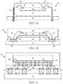
- FIG. 1illustrates electronic device 50 having a chip carrier substrate or printed circuit board (PCB) 52 with a plurality of semiconductor packages mounted on its surface.
- Electronic device 50may have one type of semiconductor package, or multiple types of semiconductor packages, depending on the application. The different types of semiconductor packages are shown in FIG. 1 for purposes of illustration.
- Electronic device 50may be a stand-alone system that uses the semiconductor packages to perform one or more electrical functions.
- electronic device 50may be a subcomponent of a larger system.
- electronic device 50may be part of a cellular phone, personal digital assistant (PDA), digital video camera (DVC), or other electronic communication device.
- PDApersonal digital assistant
- DVCdigital video camera
- electronic device 50can be a graphics card, network interface card, or other signal processing card that can be inserted into a computer.
- the semiconductor packagecan include microprocessors, memories, application specific integrated circuits (ASIC), logic circuits, analog circuits, RF circuits, discrete devices, or other semiconductor die or electrical components.
- ASICapplication specific integrated circuits
- the miniaturization and the weight reductionare essential for these products to be accepted by the market.
- the distance between semiconductor devicesmust be decreased to achieve higher density.
- PCB 52provides a general substrate for structural support and electrical interconnect of the semiconductor packages mounted on the PCB.
- Conductive signal traces 54are formed over a surface or within layers of PCB 52 using evaporation, electrolytic plating, electroless plating, screen printing, or other suitable metal deposition process. Signal traces 54 provide for electrical communication between each of the semiconductor packages, mounted components, and other external system components. Traces 54 also provide power and ground connections to each of the semiconductor packages.
- a semiconductor devicehas two packaging levels.
- First level packagingis a technique for mechanically and electrically attaching the semiconductor die to an intermediate carrier.
- Second level packaginginvolves mechanically and electrically attaching the intermediate carrier to the PCB.
- a semiconductor devicemay only have the first level packaging where the die is mechanically and electrically mounted directly to the PCB.
- first level packagingincluding wire bond package 56 and flip chip 58
- second level packagingincluding ball grid array (BGA) 60 , bump chip carrier (BCC) 62 , dual in-line package (DIP) 64 , land grid array (LGA) 66 , multi-chip module (MCM) 68 , quad flat non-leaded package (QFN) 70 , and quad flat package 72 .
- BGAball grid array
- BCCbump chip carrier
- DIPdual in-line package
- LGAland grid array
- MCMmulti-chip module
- QFNquad flat non-leaded package
- quad flat package 72quad flat package
- electronic device 50includes a single attached semiconductor package, while other embodiments call for multiple interconnected packages.
- manufacturerscan incorporate pre-made components into electronic devices and systems. Because the semiconductor packages include sophisticated functionality, electronic devices can be manufactured using cheaper components and a streamlined manufacturing process. The resulting devices are less likely to fail and less expensive to manufacture resulting in a lower cost for consumers.
- FIGS. 2 a -2 cshow exemplary semiconductor packages.
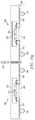
- FIG. 2 aillustrates further detail of DIP 64 mounted on PCB 52 .
- Semiconductor die 74includes an active region containing analog or digital circuits implemented as active devices, passive devices, conductive layers, and dielectric layers formed within the die and are electrically interconnected according to the electrical design of the die.
- the circuitmay include one or more transistors, diodes, inductors, capacitors, resistors, and other circuit elements formed within the active region of semiconductor die 74 .
- Contact pads 76are one or more layers of conductive material, such as aluminum (Al), copper (Cu), tin (Sn), nickel (Ni), gold (Au), or silver (Ag), and are electrically connected to the circuit elements formed within semiconductor die 74 .
- semiconductor die 74is mounted to an intermediate carrier 78 using a gold-silicon eutectic layer or adhesive material such as thermal epoxy or epoxy resin.
- the package bodyincludes an insulative packaging material such as polymer or ceramic.
- Conductor leads 80 and wire bonds 82provide electrical interconnect between semiconductor die 74 and PCB 52 .
- Encapsulant 84is deposited over the package for environmental protection by preventing moisture and particles from entering the package and contaminating die 74 or wire bonds 82 .
- FIG. 2 billustrates further detail of BCC 62 mounted on PCB 52 .
- Semiconductor die 88is mounted over carrier 90 using an underfill or epoxy-resin adhesive material 92 .
- Wire bonds 94provide first level packaging interconnect between contact pads 96 and 98 .
- Molding compound or encapsulant 100is deposited over semiconductor die 88 and wire bonds 94 to provide physical support and electrical isolation for the device.
- Contact pads 102are formed over a surface of PCB 52 using a suitable metal deposition process such as electrolytic plating or electroless plating to prevent oxidation.
- Contact pads 102are electrically connected to one or more conductive signal traces 54 in PCB 52 .
- Bumps 104are formed between contact pads 98 of BCC 62 and contact pads 102 of PCB 52 .
- semiconductor die 58is mounted face down to intermediate carrier 106 with a flip chip style first level packaging.
- Active region 108 of semiconductor die 58contains analog or digital circuits implemented as active devices, passive devices, conductive layers, and dielectric layers formed according to the electrical design of the die.
- the circuitmay include one or more transistors, diodes, inductors, capacitors, resistors, and other circuit elements within active region 108 .
- Semiconductor die 58is electrically and mechanically connected to carrier 106 through bumps 110 .
- BGA 60is electrically and mechanically connected to PCB 52 with a BGA style second level packaging using bumps 112 .
- Semiconductor die 58is electrically connected to conductive signal traces 54 in PCB 52 through bumps 110 , signal lines 114 , and bumps 112 .
- a molding compound or encapsulant 116is deposited over semiconductor die 58 and carrier 106 to provide physical support and electrical isolation for the device.
- the flip chip semiconductor deviceprovides a short electrical conduction path from the active devices on semiconductor die 58 to conduction tracks on PCB 52 in order to reduce signal propagation distance, lower capacitance, and improve overall circuit performance.
- the semiconductor die 58can be mechanically and electrically connected directly to PCB 52 using flip chip style first level packaging without intermediate carrier 106 .
- FIGS. 3 a -3 fillustrate a process of forming sacrificial adhesive over contact pads of a semiconductor die.
- FIG. 3 ashows a semiconductor wafer 120 with a base substrate material 122 , such as silicon, germanium, gallium arsenide, indium phosphide, or silicon carbide, for structural support.
- a plurality of semiconductor die or components 124is formed on wafer 120 separated by saw streets 126 as described above.
- FIG. 3 bshows a cross-sectional view of a portion of semiconductor wafer 120 .
- Each semiconductor die 124has an active surface 130 containing analog or digital circuits implemented as active devices, passive devices, conductive layers, and dielectric layers formed within the die and electrically interconnected according to the electrical design and function of the die.
- the circuitmay include one or more transistors, diodes, and other circuit elements formed within active surface 130 to implement analog circuits or digital circuits, such as digital signal processor (DSP), ASIC, memory, or other signal processing circuit.
- DSPdigital signal processor
- Semiconductor die 124may also contain IPDs, such as inductors, capacitors, and resistors, for RF signal processing.
- An electrically conductive layer 132is formed over active surface 130 using PVD, CVD, electrolytic plating, electroless plating process, or other suitable metal deposition process.
- Conductive layer 132can be one or more layers of Al, Cu, Sn, Ni, Au, Ag, or other suitable electrically conductive material.
- Conductive layer 132operates as contact pads electrically connected to the circuits on active surface 130 .
- a sacrificial adhesive 134such as ultraviolet (UV) or heat releasable polymer adhesive, is deposited over contact pads 132 on semiconductor wafer 120 by screen printing or other suitable application process.
- UVultraviolet
- heat releasable polymer adhesiveheat releasable polymer adhesive
- semiconductor wafer 120is singulated through saw street 126 using saw blade or laser cutting tool 135 into individual semiconductor die 124 .
- Each semiconductor die 124has sacrificial adhesive 134 over contacts pads 132 .
- an underfill material 136such as epoxy resin, is deposited over active surface 130 between sacrificial adhesive 134 , as shown in FIG. 3 e .
- the top surface of underfill material 136 and sacrificial adhesive 134is planarized.
- semiconductor wafer 120is singulated through saw street 126 using saw blade or laser cutting tool 138 into individual semiconductor die 124 .
- Each semiconductor die 124has sacrificial adhesive 134 over contacts pads 132 and underfill material 136 over active surface 130 .
- an underfill material 140such as epoxy resin, is deposited over active surface 130 of semiconductor wafer 120 , as shown in FIG. 4 a .
- a plurality of vias 142is formed through underfill material 140 over contact pads 132 using an etching process, as shown in FIG. 4 b .
- vias 142are filled with sacrificial adhesive 144 , such as UV or heat releasable polymer adhesive, by screen printing, needle dispensing, or other suitable application process.
- the top surface of underfill material 136 and sacrificial adhesive 144is planarized.
- semiconductor wafer 120is singulated through saw street 126 using saw blade or laser cutting tool 146 into individual semiconductor die 124 .
- Each semiconductor die 124has sacrificial adhesive 144 over contacts pads 132 and underfill material 140 over active surface 130 , similar to FIG. 3 f.
- FIGS. 5 a -5 gillustrate, in relation to FIGS. 1 and 2 a - 2 c , a process of forming the conductive layer of the interconnect structure to extend to the contact pads of the semiconductor die after removal of the sacrificial adhesive.
- a temporary substrate or carrier 150contains sacrificial base material such as silicon, polymer, polymer composite, metal, ceramic, glass, glass epoxy, beryllium oxide, or other suitable low-cost, rigid material for structural support.
- An interface layer or tape 152is applied over carrier 150 as a temporary adhesive bonding film releasable by heat or ultraviolet (UV) light.
- semiconductor die 124 with the sacrificial adhesive over contact pads 132 and underfill material over active surface 130are mounted to interface layer 152 using a pick and place operation.
- the sacrificial adhesive and underfill materialare oriented toward carrier 150 .
- FIG. 5 cshows all semiconductor die 124 mounted to carrier 150 with sacrificial adhesive 134 and underfill material 136 contacting interface layer 152 .
- Active surface 130is offset from carrier 150 by a height of sacrificial adhesive 134 .
- sacrificial adhesive 134has a height of 5-75 micrometers ( ⁇ m).
- an encapsulant or molding compound 154is deposited over semiconductor die 124 and carrier 150 using a paste printing, compressive molding, transfer molding, liquid encapsulant molding, vacuum lamination, spin coating, or other suitable applicator.
- Encapsulant 154can be polymer composite material, such as epoxy resin with filler, epoxy acrylate with filler, or polymer with proper filler.
- Encapsulant 154is non-conductive and environmentally protects the semiconductor device from external elements and contaminants. Sacrificial adhesive 134 holds semiconductor die 124 securely in place, reducing lateral or vertical shifting of the die, while encapsulant 154 is deposited and cured.
- carrier 150 and interface layer 152are removed by UV light, thermal bake, chemical etching, mechanical peel-off, CMP, mechanical grinding, laser scanning, or wet stripping.
- Sacrificial adhesive 134is also removed, leaving vias 156 which extend to contact pads 132 .
- a build-up interconnect structure 160is formed over encapsulant 154 and underfill material 136 .
- the build-up interconnect structure 160includes an electrically conductive layer or redistribution layer (RDL) 162 formed using a patterning and metal deposition process such as sputtering, electrolytic plating, and electroless plating.
- Conductive layer 162can be one or more layers of Al, Cu, Sn, Ni, Au, Ag, or other suitable electrically conductive material.
- One portion of conductive layer 162extends into vias 156 for electrical connection to contact pads 132 .
- Conductive layer 162may partially or completely fill vias 156 .
- Other portions of conductive layer 162can be electrically common or electrically isolated depending on the design and function of semiconductor die 124 .
- the build-up interconnect structure 160further includes an insulating or passivation layer 164 formed between conductive layers 162 for electrical isolation.
- the insulating layer 164contains one or more layers of silicon dioxide (SiO2), silicon nitride (Si3N4), silicon oxynitride (SiON), tantalum pentoxide (Ta2O5), aluminum oxide (Al2O3), or other material having similar insulating and structural properties.
- the insulating layer 164is formed using PVD, CVD, printing, spin coating, spray coating, sintering or thermal oxidation. A portion of insulating layer 164 is removed by an etching process to expose conductive layer 162 for bump formation or additional package interconnect.
- an electrically conductive bump materialis deposited over build-up interconnect structure 160 and electrically connected to conductive layer 162 using an evaporation, electrolytic plating, electroless plating, ball drop, or screen printing process.
- the bump materialcan be Al, Sn, Ni, Au, Ag, Pb, Bi, Cu, solder, and combinations thereof, with an optional flux solution.
- the bump materialcan be eutectic Sn/Pb, high-lead solder, or lead-free solder.
- the bump materialis bonded to conductive layer 162 using a suitable attachment or bonding process. In one embodiment, the bump material is reflowed by heating the material above its melting point to form spherical balls or bumps 166 .
- bumps 166are reflowed a second time to improve electrical contact to conductive layer 162 .
- An under bump metallization (UBM)can be formed under bumps 166 .
- the bumpscan also be compression bonded to conductive layer 162 .
- Bumps 166represent one type of interconnect structure that can be formed over conductive layer 162 .
- the interconnect structurecan also use bond wires, stud bump, micro bump, or other electrical interconnect.
- the encapsulant 154 and interconnect structure 160are singulated using saw blade or laser cutting tool 167 into individual FO-WLCSP 168 .
- FIG. 6shows FO-WLCSP 168 after singulation.
- Semiconductor die 124is electrically connected to conductive layer 162 of interconnect structures 160 and bumps 166 .
- Sacrificial adhesive 134is formed over contact pads 132 prior to mounting semiconductor die 124 to carrier 150 for encapsulation and formation of interconnect structure 160 .
- Sacrificial adhesive 134holds semiconductor die 124 securely in place, reducing lateral or vertical shifting of the die, while encapsulant 154 is deposited and cured.
- Active surface 130is offset from interconnect structure 160 by a height of sacrificial adhesive 134 .
- Sacrificial adhesive 134is removed with carrier 150 but leaves behind via 156 as an opening through underfill material 136 extending to contact pad 132 .
- Conductive layer 162is formed in via 156 to electrically connect semiconductor die 124 to interconnect structure 160 and bumps 166 , without forming bumps over contact pads 132 . Since conductive layer 162 is formed to extend to contact pads 132 , no separate via formation is needed to make the electrical connection to the contact pads. The interconnect resistance is reduced by directly connecting conductive layer 162 to contact pads 132 . By avoiding wafer-level bump formation over contact pads 132 , wafer-level bump rework can be omitted. In addition, no solder-wettable contact pads are needed over the carrier to hold the semiconductor die in place during encapsulation, which saves manufacturing costs and reduces risk of bump cracking.
- FIGS. 7 a -7 eshow another embodiment with a temporary substrate or carrier 170 containing sacrificial base material such as silicon, polymer, polymer composite, metal, ceramic, glass, glass epoxy, beryllium oxide, or other suitable low-cost, rigid material for structural support.
- An interface layer or tape 172is applied over carrier 170 as a temporary adhesive bonding film releasable by heat or UV light.
- Semiconductor die 124 with sacrificial adhesive 134 formed over contact pads 132 , from the wafer processing option of FIGS. 3 a -3 d ,are mounted to interface layer 172 using a pick and place operation, as shown in FIG. 7 a .
- Sacrificial adhesive 134is oriented toward carrier 160 .
- Active surface 130is offset from carrier 170 by a height of sacrificial adhesive 134 .
- an encapsulant or molding compound 174is deposited over semiconductor die 124 and carrier 170 using a paste printing, compressive molding, transfer molding, liquid encapsulant molding, vacuum lamination, spin coating, or other suitable applicator.
- Encapsulant 174can be polymer composite material, such as epoxy resin with filler, epoxy acrylate with filler, or polymer with proper filler.
- Encapsulant 174is non-conductive and environmentally protects the semiconductor device from external elements and contaminants.
- Encapsulant 174underfills semiconductor die 124 . Sacrificial adhesive 134 holds semiconductor die 124 securely in place, reducing lateral or vertical shifting of the die, while encapsulant 174 is deposited and cured.
- carrier 170 and interface layer 172are removed by UV light, thermal bake, chemical etching, mechanical peel-off, CMP, mechanical grinding, laser scanning, or wet stripping.
- Sacrificial adhesive 134is also removed, leaving vias 176 which extend to contact pads 132 .
- a build-up interconnect structure 180is formed over encapsulant 174 .
- the build-up interconnect structure 180includes an electrically conductive layer or RDL 182 formed using a patterning and metal deposition process such as sputtering, electrolytic plating, and electroless plating.
- Conductive layer 182can be one or more layers of Al, Cu, Sn, Ni, Au, Ag, or other suitable electrically conductive material.
- One portion of conductive layer 182extends into vias 176 for electrical connection to contact pads 132 .
- Conductive layer 182may partially or completely fill vias 176 .
- Other portions of conductive layer 182can be electrically common or electrically isolated depending on the design and function of semiconductor die 124 .
- the build-up interconnect structure 180further includes an insulating or passivation layer 184 formed between conductive layers 182 for electrical isolation.
- the insulating layer 184contains one or more layers of SiO2, Si3N4, SiON, Ta2O5, Al2O3, or other material having similar insulating and structural properties.
- the insulating layer 184is formed using PVD, CVD, printing, spin coating, spray coating, sintering or thermal oxidation. A portion of insulating layer 184 is removed by an etching process to expose conductive layer 182 for bump formation or additional package interconnect.
- an electrically conductive bump materialis deposited over build-up interconnect structure 180 and electrically connected to conductive layer 182 using an evaporation, electrolytic plating, electroless plating, ball drop, or screen printing process.
- the bump materialcan be Al, Sn, Ni, Au, Ag, Pb, Bi, Cu, solder, and combinations thereof, with an optional flux solution.
- the bump materialcan be eutectic Sn/Pb, high-lead solder, or lead-free solder.
- the bump materialis bonded to conductive layer 182 using a suitable attachment or bonding process. In one embodiment, the bump material is reflowed by heating the material above its melting point to form spherical balls or bumps 186 .
- bumps 186are reflowed a second time to improve electrical contact to conductive layer 182 .
- a UBMcan be formed under bumps 186 .
- the bumpscan also be compression bonded to conductive layer 182 .
- Bumps 186represent one type of interconnect structure that can be formed over conductive layer 182 .
- the interconnect structurecan also use bond wires, stud bump, micro bump, or other electrical interconnect.
- FIG. 8shows FO-WLCSP 188 after singulation.
- Semiconductor die 124is electrically connected to conductive layer 182 of interconnect structures 180 and bumps 186 .
- Sacrificial adhesive 134is formed over contact pads 132 prior to mounting semiconductor die 124 to carrier 170 for encapsulation and formation of interconnect structure 180 .
- Sacrificial adhesive 134holds semiconductor die 124 securely in place, reducing lateral or vertical shifting of the die, while encapsulant 174 is deposited and cured.
- Active surface 130is offset from interconnect structure 160 by a height of sacrificial adhesive 134 .
- Sacrificial adhesive 134is removed with carrier 180 but leaves behind via 176 as an opening through encapsulant 174 extending to contact pad 132 .
- Conductive layer 182is formed in via 176 to electrically connect semiconductor die 124 to interconnect structure 180 and bumps 186 , without forming bumps over contact pads 132 . Since conductive layer 182 is formed to extend to contact pads 132 , no separate via formation is needed to make the electrical connection to the contact pads. The interconnect resistance is reduced by directly connecting conductive layer 182 to contact pads 132 . By avoiding wafer-level bump formation over contact pads 132 , wafer-level bump rework can be omitted. In addition, no solder-wettable contact pads are needed over the carrier to hold the semiconductor die in place during encapsulation, which saves manufacturing costs and reduces risk of bump cracking.
- FIGS. 9 a -9 ishow another embodiment with a temporary substrate or carrier 190 containing sacrificial base material such as silicon, polymer, polymer composite, metal, ceramic, glass, glass epoxy, beryllium oxide, or other suitable low-cost, rigid material for structural support.
- An interface layer or tape 192is applied over carrier 190 as a temporary adhesive bonding film releasable by heat or UV light, as shown in FIG. 9 a.
- a sacrificial adhesive 194such as UV or heat releasable polymer adhesive, is deposited over interface layer 192 by screen printing or other suitable application process. Sacrificial adhesive 194 is disposed in an area 196 designed for mounting semiconductor die, more specifically in the area aligned with the contact pads of the semiconductor die.
- an underfill material 198such as epoxy resin, is deposited over area 196 .
- the top surface of underfill material 198 and sacrificial adhesive 194is planarized.
- a plurality of semiconductor die 200each have an active surface 202 containing analog or digital circuits implemented as active devices, passive devices, conductive layers, and dielectric layers formed within the die and electrically interconnected according to the electrical design and function of the die.
- the circuitmay include one or more transistors, diodes, and other circuit elements formed within active surface 202 to implement analog circuits or digital circuits, such as DSP, ASIC, memory, or other signal processing circuit.
- Semiconductor die 200may also contain IPDs, such as inductors, capacitors, and resistors, for RF signal processing.
- IPDssuch as inductors, capacitors, and resistors
- An electrically conductive layer 204is formed over active surface 202 using PVD, CVD, electrolytic plating, electroless plating process, or other suitable metal deposition process.
- Conductive layer 204can be one or more layers of Al, Cu, Sn, Ni, Au, Ag, or other suitable electrically conductive material.
- Conductive layer 204operates as contact pads electrically connected to the circuits on active surface 202 .
- Each semiconductor die 200is mounted over carrier 190 with active surface 202 oriented toward carrier 190 and contact pads 204 aligned with sacrificial adhesive 194 .
- FIG. 9 eshows all semiconductor die 200 mounted to carrier 190 with contact pads 204 aligned with sacrificial adhesive 194 and active surface 202 aligned to underfill material 198 .
- Active surface 202is offset from carrier 190 by a height of sacrificial adhesive 194 .
- sacrificial adhesive 194has a height of 5-75 ⁇ m.
- an encapsulant or molding compound 206is deposited over semiconductor die 200 and carrier 190 using a paste printing, compressive molding, transfer molding, liquid encapsulant molding, vacuum lamination, spin coating, or other suitable applicator.
- Encapsulant 206can be polymer composite material, such as epoxy resin with filler, epoxy acrylate with filler, or polymer with proper filler.
- Encapsulant 206is non-conductive and environmentally protects the semiconductor device from external elements and contaminants.
- Sacrificial adhesive 194holds semiconductor die 200 securely in place, reducing lateral or vertical shifting of the die, while encapsulant 206 is deposited and cured.
- carrier 190 and interface layer 192are removed by UV light, thermal bake, chemical etching, mechanical peel-off, CMP, mechanical grinding, laser scanning, or wet stripping.
- Sacrificial adhesive 194is also removed, leaving vias 208 which extend to contact pads 204 .
- a build-up interconnect structure 210is formed over encapsulant 206 and underfill material 198 .
- the build-up interconnect structure 210includes an electrically conductive layer or RDL 212 formed using a patterning and metal deposition process such as sputtering, electrolytic plating, and electroless plating.
- Conductive layer 212can be one or more layers of Al, Cu, Sn, Ni, Au, Ag, or other suitable electrically conductive material.
- One portion of conductive layer 212extends into vias 208 for electrical connection to contact pads 204 .
- Conductive layer 212may partially or completely fill vias 208 .
- Other portions of conductive layer 212can be electrically common or electrically isolated depending on the design and function of semiconductor die 200 .
- the build-up interconnect structure 210further includes an insulating or passivation layer 214 formed between conductive layers 212 for electrical isolation.
- the insulating layer 214contains one or more layers of SiO2, Si3N4, SiON, Ta2O5, Al2O3, or other material having similar insulating and structural properties.
- the insulating layer 214is formed using PVD, CVD, printing, spin coating, spray coating, sintering or thermal oxidation. A portion of insulating layer 214 is removed by an etching process to expose conductive layer 212 for bump formation or additional package interconnect.
- an electrically conductive bump materialis deposited over build-up interconnect structure 210 and electrically connected to conductive layer 212 using an evaporation, electrolytic plating, electroless plating, ball drop, or screen printing process.
- the bump materialcan be Al, Sn, Ni, Au, Ag, Pb, Bi, Cu, solder, and combinations thereof, with an optional flux solution.
- the bump materialcan be eutectic Sn/Pb, high-lead solder, or lead-free solder.
- the bump materialis bonded to conductive layer 212 using a suitable attachment or bonding process. In one embodiment, the bump material is reflowed by heating the material above its melting point to form spherical balls or bumps 216 .
- bumps 216are reflowed a second time to improve electrical contact to conductive layer 212 .
- a UBMcan be formed under bumps 216 .
- the bumpscan also be compression bonded to conductive layer 212 .
- Bumps 216represent one type of interconnect structure that can be formed over conductive layer 212 .
- the interconnect structurecan also use bond wires, stud bump, micro bump, or other electrical interconnect.
- the encapsulant 206 and interconnect structure 210are singulated using saw blade or laser cutting tool 217 into individual FO-WLCSP 218 , similar to FIG. 6 .
- FIGS. 10 a -10 gshow another embodiment with a temporary substrate or carrier 220 containing sacrificial base material such as silicon, polymer, polymer composite, metal, ceramic, glass, glass epoxy, beryllium oxide, or other suitable low-cost, rigid material for structural support.
- An interface layer or tape 222is applied over carrier 220 as a temporary adhesive bonding film releasable by heat or UV light, as shown in FIG. 10 a.
- a sacrificial adhesive 224such as UV or heat releasable polymer adhesive, is deposited over interface layer 222 by screen printing or other suitable application process. Sacrificial adhesive 224 is disposed in an area 226 designed for mounting semiconductor die, more specifically in the area aligned with the contact pads of the semiconductor die.
- a plurality of semiconductor die 230each have an active surface 232 containing analog or digital circuits implemented as active devices, passive devices, conductive layers, and dielectric layers formed within the die and electrically interconnected according to the electrical design and function of the die.
- the circuitmay include one or more transistors, diodes, and other circuit elements formed within active surface 232 to implement analog circuits or digital circuits, such as DSP, ASIC, memory, or other signal processing circuit.
- semiconductor die 230may also contain IPDs, such as inductors, capacitors, and resistors, for RF signal processing.
- An electrically conductive layer 234is formed over active surface 232 using PVD, CVD, electrolytic plating, electroless plating process, or other suitable metal deposition process.
- Conductive layer 234can be one or more layers of Al, Cu, Sn, Ni, Au, Ag, or other suitable electrically conductive material.
- Conductive layer 234operates as contact pads electrically connected to the circuits on active surface 232 .
- Semiconductor die 234are formed on and singulated from a semiconductor wafer, similar to FIG. 3 a.
- Each semiconductor die 230is mounted over carrier 220 with active surface 232 oriented toward carrier 220 and contact pads 234 aligned with sacrificial adhesive 224 .
- FIG. 10 cshows all semiconductor die 220 mounted to carrier 220 with contact pads 234 aligned with sacrificial adhesive 224 .
- Active surface 232is offset from carrier 220 by a height of sacrificial adhesive 224 .
- sacrificial adhesive 224has a height of 5-75 ⁇ m.
- an encapsulant or molding compound 236is deposited over semiconductor die 230 and carrier 220 using a paste printing, compressive molding, transfer molding, liquid encapsulant molding, vacuum lamination, spin coating, or other suitable applicator.
- Encapsulant 236can be polymer composite material, such as epoxy resin with filler, epoxy acrylate with filler, or polymer with proper filler.
- Encapsulant 236is non-conductive and environmentally protects the semiconductor device from external elements and contaminants. Sacrificial adhesive 224 holds semiconductor die 230 securely in place, reducing lateral or vertical shifting of the die, while encapsulant 236 is deposited and cured.
- carrier 220 and interface layer 222are removed by UV light, thermal bake, chemical etching, mechanical peel-off, CMP, mechanical grinding, laser scanning, or wet stripping.
- Sacrificial adhesive 224is also removed, leaving vias 238 which extend to contact pads 234 .
- a build-up interconnect structure 240is formed over encapsulant 236 .
- the build-up interconnect structure 240includes an electrically conductive layer or RDL 242 formed using a patterning and metal deposition process such as sputtering, electrolytic plating, and electroless plating.
- Conductive layer 242can be one or more layers of Al, Cu, Sn, Ni, Au, Ag, or other suitable electrically conductive material.
- One portion of conductive layer 242extends into vias 238 for electrical connection to contact pads 204 .
- Conductive layer 242may partially or completely fill vias 238 .
- Other portions of conductive layer 242can be electrically common or electrically isolated depending on the design and function of semiconductor die 230 .
- the build-up interconnect structure 240further includes an insulating or passivation layer 244 formed between conductive layers 242 for electrical isolation.
- the insulating layer 244contains one or more layers of SiO2, Si3N4, SiON, Ta2O5, Al2O3, or other material having similar insulating and structural properties.
- the insulating layer 244is formed using PVD, CVD, printing, spin coating, spray coating, sintering or thermal oxidation. A portion of insulating layer 244 is removed by an etching process to expose conductive layer 242 for bump formation or additional package interconnect.
- an electrically conductive bump materialis deposited over build-up interconnect structure 240 and electrically connected to conductive layer 242 using an evaporation, electrolytic plating, electroless plating, ball drop, or screen printing process.
- the bump materialcan be Al, Sn, Ni, Au, Ag, Pb, Bi, Cu, solder, and combinations thereof, with an optional flux solution.
- the bump materialcan be eutectic Sn/Pb, high-lead solder, or lead-free solder.
- the bump materialis bonded to conductive layer 242 using a suitable attachment or bonding process. In one embodiment, the bump material is reflowed by heating the material above its melting point to form spherical balls or bumps 246 .
- bumps 246are reflowed a second time to improve electrical contact to conductive layer 242 .
- a UBMcan be formed under bumps 246 .
- the bumpscan also be compression bonded to conductive layer 242 .
- Bumps 246represent one type of interconnect structure that can be formed over conductive layer 242 .
- the interconnect structurecan also use bond wires, stud bump, micro bump, or other electrical interconnect.
- the encapsulant 236 and interconnect structure 240are singulated using saw blade or laser cutting tool 247 into individual FO-WLCSP 248 , similar to FIG. 8 .
Landscapes
- Engineering & Computer Science (AREA)
- Microelectronics & Electronic Packaging (AREA)
- Computer Hardware Design (AREA)
- Power Engineering (AREA)
- Physics & Mathematics (AREA)
- Condensed Matter Physics & Semiconductors (AREA)
- General Physics & Mathematics (AREA)
- Manufacturing & Machinery (AREA)
- Structures Or Materials For Encapsulating Or Coating Semiconductor Devices Or Solid State Devices (AREA)
- Encapsulation Of And Coatings For Semiconductor Or Solid State Devices (AREA)
Abstract
Description
Claims (10)
Priority Applications (1)
| Application Number | Priority Date | Filing Date | Title |
|---|---|---|---|
| US15/068,290US10998248B2 (en) | 2007-12-14 | 2016-03-11 | Semiconductor device and method of forming sacrificial adhesive over contact pads of semiconductor die |
Applications Claiming Priority (3)
| Application Number | Priority Date | Filing Date | Title |
|---|---|---|---|
| US11/957,101US7767496B2 (en) | 2007-12-14 | 2007-12-14 | Semiconductor device and method of forming interconnect structure for encapsulated die having pre-applied protective layer |
| US12/794,598US9318441B2 (en) | 2007-12-14 | 2010-06-04 | Semiconductor device and method of forming sacrificial adhesive over contact pads of semiconductor die |
| US15/068,290US10998248B2 (en) | 2007-12-14 | 2016-03-11 | Semiconductor device and method of forming sacrificial adhesive over contact pads of semiconductor die |
Related Parent Applications (1)
| Application Number | Title | Priority Date | Filing Date |
|---|---|---|---|
| US12/794,598DivisionUS9318441B2 (en) | 2007-12-14 | 2010-06-04 | Semiconductor device and method of forming sacrificial adhesive over contact pads of semiconductor die |
Publications (2)
| Publication Number | Publication Date |
|---|---|
| US20160197022A1 US20160197022A1 (en) | 2016-07-07 |
| US10998248B2true US10998248B2 (en) | 2021-05-04 |
Family
ID=45063848
Family Applications (2)
| Application Number | Title | Priority Date | Filing Date |
|---|---|---|---|
| US12/794,598Active2029-01-07US9318441B2 (en) | 2007-12-14 | 2010-06-04 | Semiconductor device and method of forming sacrificial adhesive over contact pads of semiconductor die |
| US15/068,290Active2028-05-12US10998248B2 (en) | 2007-12-14 | 2016-03-11 | Semiconductor device and method of forming sacrificial adhesive over contact pads of semiconductor die |
Family Applications Before (1)
| Application Number | Title | Priority Date | Filing Date |
|---|---|---|---|
| US12/794,598Active2029-01-07US9318441B2 (en) | 2007-12-14 | 2010-06-04 | Semiconductor device and method of forming sacrificial adhesive over contact pads of semiconductor die |
Country Status (1)
| Country | Link |
|---|---|
| US (2) | US9318441B2 (en) |
Families Citing this family (34)
| Publication number | Priority date | Publication date | Assignee | Title |
|---|---|---|---|---|
| TWI405279B (en)* | 2010-07-23 | 2013-08-11 | Global Unichip Corp | Packaging of semiconductor components |
| US8860079B2 (en)* | 2010-11-15 | 2014-10-14 | United Test And Assembly Center Ltd. | Semiconductor packages and methods of packaging semiconductor devices |
| US8963310B2 (en)* | 2011-08-24 | 2015-02-24 | Tessera, Inc. | Low cost hybrid high density package |
| US20130049214A1 (en)* | 2011-08-29 | 2013-02-28 | Infineon Technologies Ag | Method of processing at least one die and die arrangement |
| US10177054B2 (en) | 2011-10-27 | 2019-01-08 | Global Circuit Innovations, Inc. | Method for remapping a packaged extracted die |
| US10128161B2 (en) | 2011-10-27 | 2018-11-13 | Global Circuit Innovations, Inc. | 3D printed hermetic package assembly and method |
| US10147660B2 (en) | 2011-10-27 | 2018-12-04 | Global Circuits Innovations, Inc. | Remapped packaged extracted die with 3D printed bond connections |
| US9966319B1 (en)* | 2011-10-27 | 2018-05-08 | Global Circuit Innovations Incorporated | Environmental hardening integrated circuit method and apparatus |
| US10109606B2 (en) | 2011-10-27 | 2018-10-23 | Global Circuit Innovations, Inc. | Remapped packaged extracted die |
| US9935028B2 (en) | 2013-03-05 | 2018-04-03 | Global Circuit Innovations Incorporated | Method and apparatus for printing integrated circuit bond connections |
| US9870968B2 (en) | 2011-10-27 | 2018-01-16 | Global Circuit Innovations Incorporated | Repackaged integrated circuit and assembly method |
| US10002846B2 (en) | 2011-10-27 | 2018-06-19 | Global Circuit Innovations Incorporated | Method for remapping a packaged extracted die with 3D printed bond connections |
| US8569886B2 (en) | 2011-11-22 | 2013-10-29 | Taiwan Semiconductor Manufacturing Company, Ltd. | Methods and apparatus of under bump metallization in packaging semiconductor devices |
| US8697542B2 (en)* | 2012-04-12 | 2014-04-15 | The Research Foundation Of State University Of New York | Method for thin die-to-wafer bonding |
| TWI467714B (en)* | 2012-06-18 | 2015-01-01 | 矽品精密工業股份有限公司 | Semiconductor package and method of forming the same |
| TWI503933B (en)* | 2013-01-03 | 2015-10-11 | 矽品精密工業股份有限公司 | Semiconductor package and fabrication method thereof |
| CN104051411B (en) | 2013-03-15 | 2018-08-28 | 台湾积体电路制造股份有限公司 | Laminated packaging structure |
| US9768048B2 (en)* | 2013-03-15 | 2017-09-19 | Taiwan Semiconductor Manufacturing Company, Ltd. | Package on-package structure |
| US9379041B2 (en)* | 2013-12-11 | 2016-06-28 | Taiwan Semiconductor Manufacturing Company, Ltd. | Fan out package structure |
| US9497570B2 (en) | 2014-02-06 | 2016-11-15 | Nimbelink Corp. | Embedded wireless modem |
| USD731491S1 (en)* | 2014-02-07 | 2015-06-09 | NimbeLink L.L.C. | Embedded cellular modem |
| US9252135B2 (en)* | 2014-02-13 | 2016-02-02 | Taiwan Semiconductor Manufacturing Company, Ltd. | Packaged semiconductor devices and methods of packaging semiconductor devices |
| US9595482B2 (en) | 2015-03-16 | 2017-03-14 | Taiwan Semiconductor Manufacturing Company, Ltd. | Structure for die probing |
| US10242927B2 (en)* | 2015-12-31 | 2019-03-26 | Mediatek Inc. | Semiconductor package, semiconductor device using the same and manufacturing method thereof |
| US9824901B2 (en)* | 2016-03-30 | 2017-11-21 | Intel Corporation | Complex cavity formation in molded packaging structures |
| US10504827B2 (en)* | 2016-06-03 | 2019-12-10 | Amkor Technology, Inc. | Semiconductor device and manufacturing method thereof |
| US10777478B2 (en)* | 2016-07-15 | 2020-09-15 | Advanced Semiconductor Engineering, Inc. | Semiconductor package device for power device |
| CN108242405A (en)* | 2016-12-27 | 2018-07-03 | 冠宝科技股份有限公司 | Substrate-free semiconductor package manufacturing method |
| US20190013283A1 (en)* | 2017-07-10 | 2019-01-10 | Powertech Technology Inc. | Semiconductor package and manufacturing method thereof |
| US10115645B1 (en) | 2018-01-09 | 2018-10-30 | Global Circuit Innovations, Inc. | Repackaged reconditioned die method and assembly |
| CN108321113A (en)* | 2018-01-29 | 2018-07-24 | 合肥矽迈微电子科技有限公司 | Fan-out package method |
| US11121101B2 (en) | 2020-01-30 | 2021-09-14 | International Business Machines Corporation | Flip chip packaging rework |
| US11508680B2 (en) | 2020-11-13 | 2022-11-22 | Global Circuit Innovations Inc. | Solder ball application for singular die |
| CN115995453A (en)* | 2021-10-19 | 2023-04-21 | 群创光电股份有限公司 | Electronic device and method for manufacturing electronic device |
Citations (102)
| Publication number | Priority date | Publication date | Assignee | Title |
|---|---|---|---|---|
| US4894115A (en) | 1989-02-14 | 1990-01-16 | General Electric Company | Laser beam scanning method for forming via holes in polymer materials |
| US5157001A (en) | 1989-09-18 | 1992-10-20 | Matsushita Electric Industrial Co., Ltd. | Method of dicing semiconductor wafer along protective film formed on scribe lines |
| US5161093A (en) | 1990-07-02 | 1992-11-03 | General Electric Company | Multiple lamination high density interconnect process and structure employing a variable crosslinking adhesive |
| US5250843A (en) | 1991-03-27 | 1993-10-05 | Integrated System Assemblies Corp. | Multichip integrated circuit modules |
| US5309026A (en) | 1991-11-19 | 1994-05-03 | Nippon Precision Circuits Ltd. | Integrated circuit package having stress reducing recesses |
| US5353498A (en) | 1993-02-08 | 1994-10-11 | General Electric Company | Method for fabricating an integrated circuit module |
| US5524339A (en) | 1994-09-19 | 1996-06-11 | Martin Marietta Corporation | Method for protecting gallium arsenide mmic air bridge structures |
| US5527741A (en) | 1994-10-11 | 1996-06-18 | Martin Marietta Corporation | Fabrication and structures of circuit modules with flexible interconnect layers |
| US5614765A (en) | 1995-06-07 | 1997-03-25 | Advanced Micro Devices, Inc. | Self aligned via dual damascene |
| US5703400A (en) | 1995-12-04 | 1997-12-30 | General Electric Company | Fabrication and structures of two-sided molded circuit modules with flexible interconnect layers |
| US5814193A (en) | 1995-08-17 | 1998-09-29 | Bp Chemicals Limited | Process for the purification of a C2 to C4 carboxylic acid and/or anhydride having halide impurities |
| US5834340A (en) | 1993-06-01 | 1998-11-10 | Mitsubishi Denki Kabushiki Kaisha | Plastic molded semiconductor package and method of manufacturing the same |
| US5841193A (en) | 1996-05-20 | 1998-11-24 | Epic Technologies, Inc. | Single chip modules, repairable multichip modules, and methods of fabrication thereof |
| US5866952A (en)* | 1995-11-30 | 1999-02-02 | Lockheed Martin Corporation | High density interconnected circuit module with a compliant layer as part of a stress-reducing molded substrate |
| US6025995A (en) | 1997-11-05 | 2000-02-15 | Ericsson Inc. | Integrated circuit module and method |
| US6028364A (en) | 1994-09-20 | 2000-02-22 | Hitachi, Ltd. | Semiconductor device having a stress relieving mechanism |
| CN1246731A (en) | 1998-08-28 | 2000-03-08 | 三星电子株式会社 | Chip dimention packaging and method for preparing wafer-class chip dimention packing |
| US6052995A (en) | 1996-09-12 | 2000-04-25 | Robert Bosch Gmbh | Valve for an internal combustion engine, and an internal combustion engine including the valve |
| US6110773A (en) | 1994-12-31 | 2000-08-29 | Samsung Electronics Co., Ltd. | Static random access memory device manufacturing method |
| US6168966B1 (en) | 1999-02-18 | 2001-01-02 | Taiwan Semiconductor Manufacturing Company | Fabrication of uniform areal sensitivity image array |
| US6197613B1 (en) | 1999-03-23 | 2001-03-06 | Industrial Technology Research Institute | Wafer level packaging method and devices formed |
| US6271469B1 (en) | 1999-11-12 | 2001-08-07 | Intel Corporation | Direct build-up layer on an encapsulated die package |
| US6274486B1 (en) | 1998-09-02 | 2001-08-14 | Micron Technology, Inc. | Metal contact and process |
| US6351031B1 (en) | 1999-10-12 | 2002-02-26 | Fujitsu Limited | Semiconductor device and method for manufacturing substrate of the same |
| US6423571B2 (en) | 1994-09-20 | 2002-07-23 | Hitachi, Ltd. | Method of making a semiconductor device having a stress relieving mechanism |
| US6501164B1 (en) | 2001-06-26 | 2002-12-31 | Siliconware Precision Industries Co., Ltd. | Multi-chip semiconductor package with heat dissipating structure |
| US20030013232A1 (en) | 2001-07-11 | 2003-01-16 | Intel Corporation | Method for fabricating a microelectronic device using wafer-level adhesion layer deposition |
| TW522499B (en) | 2002-04-11 | 2003-03-01 | Ru Yi Invest Co Ltd | Semiconductor apparatus and fabrication method of reducing the influence of package induced stress on IC parameter offset |
| US20030141105A1 (en) | 1999-12-20 | 2003-07-31 | Matsushita Electric Industrial Co., Ltd. | Circuit component built-in module, radio device having the same, and method for producing the same |
| US20030226254A1 (en)* | 2002-06-07 | 2003-12-11 | Paul Koning | Wafer-level underfill process and device for cpu and non-cpu applications |
| US20040056344A1 (en) | 2001-11-22 | 2004-03-25 | Tsuyoshi Ogawa | Multi-chip circuit module and method for producing the same |
| JP2004128286A (en) | 2002-10-04 | 2004-04-22 | Sony Corp | Chip-like electronic component and manufacturing method thereof, pseudo wafer used for the manufacturing and manufacturing method thereof, and mounting structure |
| US20040110316A1 (en) | 2002-11-20 | 2004-06-10 | Mitsuhiko Ogihara | Semiconductor device and method of manufacturing the same |
| US20040219717A1 (en) | 2000-03-09 | 2004-11-04 | Yoshikazu Takahashi | Method of manufacturing chip size package semiconductor device without intermediate substrate |
| US20050073029A1 (en) | 2002-08-27 | 2005-04-07 | Chua Swee Kwang | Multichip wafer level packages and computing systems incorporating same |
| US20050121771A1 (en) | 2001-12-31 | 2005-06-09 | Mou-Shiung Lin | Integrated chip package structure using metal substrate and method of manufacturing the same |
| US6905914B1 (en)* | 2002-11-08 | 2005-06-14 | Amkor Technology, Inc. | Wafer level package and fabrication method |
| US20050186704A1 (en) | 2002-05-30 | 2005-08-25 | Micron Technology, Inc. | Intrinsic thermal enhancement for FBGA package |
| JP2006019433A (en) | 2004-06-30 | 2006-01-19 | Nec Electronics Corp | Semiconductor device and manufacturing method thereof |
| US20060046347A1 (en)* | 2004-09-02 | 2006-03-02 | Wood Alan G | Die package, conductive element, semiconductor device including same, microlens, system including same, and methods of manufacture |
| US7008822B2 (en) | 2003-05-12 | 2006-03-07 | Micron Technology, Inc. | Method for fabricating semiconductor component having stacked, encapsulated dice |
| US20060084240A1 (en) | 2001-10-08 | 2006-04-20 | Micron Technology, Inc. | Apparatus and method for packaging circuits |
| US20060125072A1 (en) | 2004-12-14 | 2006-06-15 | Casio Computer Co., Ltd. | Semiconductor device having laminated semiconductor constructions and a manufacturing method thereof |
| US20060263003A1 (en)* | 2003-11-27 | 2006-11-23 | Ibiden Co., Ltd. | Substrate for mounting IC chip, substrate for motherboard, device for optical communication, manufacturing method of substrate for mounting IC chip, and manufacturing method of substrate for motherboard |
| US7165316B2 (en) | 1996-04-18 | 2007-01-23 | Tessera, Inc. | Methods for manufacturing resistors using a sacrificial layer |
| US20070035033A1 (en) | 2005-05-26 | 2007-02-15 | Volkan Ozguz | Stackable tier structure comprising high density feedthrough |
| US20070035015A1 (en) | 2005-08-15 | 2007-02-15 | Shih-Ping Hsu | Stack structure with semiconductor chip embedded in carrier |
| US20070040258A1 (en) | 2005-08-18 | 2007-02-22 | Intelleflex Corporation | Method of packaging and interconnection of integrated circuits |
| US7189596B1 (en) | 2000-03-01 | 2007-03-13 | Intel Corporation | Process for forming a direct build-up layer on an encapsulated die packages utilizing intermediate structures |
| US20070085188A1 (en) | 2005-10-18 | 2007-04-19 | Phoenix Precision Technology Corporation | Stack Structure of Carrier Board Embedded with Semiconductor Components and Method for Fabricating the same |
| US20070141759A1 (en) | 2005-12-19 | 2007-06-21 | Tdk Corporation | Method for manufacturing ic-embedded substrate |
| JP2007184636A (en) | 2003-12-25 | 2007-07-19 | Casio Comput Co Ltd | Semiconductor device |
| US20070178622A1 (en) | 2006-01-30 | 2007-08-02 | Marvell International Ltd. | Thermal enhanced package |
| US20070249153A1 (en) | 2006-04-20 | 2007-10-25 | Wen-Chang Dong | Chip structure with half-tunneling electrical contact to have one electrical contact formed on inactive side thereof and method for producing the same |
| US20080006900A1 (en) | 2004-10-21 | 2008-01-10 | Infineon Technologies Ag | Semiconductor Package and Method for Producing the Same |
| US20080012144A1 (en) | 2006-07-12 | 2008-01-17 | Infineon Technologies Ag | Method for producing chip packages, and chip package produced in this way |
| CN101138084A (en) | 2004-10-29 | 2008-03-05 | 弗利普芯片国际有限公司 | Semiconductor device package with bump overlying a polymer layer |
| US20080054426A1 (en) | 2006-08-31 | 2008-03-06 | Oki Electric Industry Co., Ltd. | Semiconductor device and manufacturing method thereof |
| US7348277B2 (en) | 2005-02-14 | 2008-03-25 | Samsung Electronics Co., Ltd. | Methods of fabricating semiconductor device using sacrificial layer |
| US20080090335A1 (en) | 2003-07-22 | 2008-04-17 | Matsushita Electric Industrial Co., Ltd. | Circuit module and manufacturing method thereof |
| CN101192550A (en) | 2006-12-01 | 2008-06-04 | 矽品精密工业股份有限公司 | Semiconductor package and fabrication method thereof |
| US20080128838A1 (en)* | 2006-08-25 | 2008-06-05 | Horst Theuss | Sensor module and method of manufacturing same |
| US20080136004A1 (en) | 2006-12-08 | 2008-06-12 | Advanced Chip Engineering Technology Inc. | Multi-chip package structure and method of forming the same |
| US20080188037A1 (en) | 2007-02-05 | 2008-08-07 | Bridge Semiconductor Corporation | Method of manufacturing semiconductor chip assembly with sacrificial metal-based core carrier |
| CN101261984A (en) | 2007-03-08 | 2008-09-10 | 育霈科技股份有限公司 | Semiconductor assembly packaging structure and method thereof |
| US20080246126A1 (en) | 2007-04-04 | 2008-10-09 | Freescale Semiconductor, Inc. | Stacked and shielded die packages with interconnects |
| US20080265383A1 (en) | 2007-04-30 | 2008-10-30 | Infineon Technologies Ag | Workpiece with Semiconductor Chips, Semiconductor Device and Method for Producing a Workpiece with Semiconductor Chips |
| US20080313894A1 (en)* | 2007-06-21 | 2008-12-25 | General Electric Company | Method for making an interconnect structure and low-temperature interconnect component recovery process |
| US20080315385A1 (en) | 2007-06-22 | 2008-12-25 | Texas Instruments Incorporated | Array molded package-on-package having redistribution lines |
| US20090008793A1 (en) | 2007-07-02 | 2009-01-08 | Infineon Technologies Ag | Semiconductor device |
| US20090042366A1 (en) | 2007-08-07 | 2009-02-12 | Grivna Gordon M | Semiconductor die singulation method |
| US7514767B2 (en) | 2003-12-03 | 2009-04-07 | Advanced Chip Engineering Technology Inc. | Fan out type wafer level package structure and method of the same |
| US20090130840A1 (en) | 2007-11-16 | 2009-05-21 | Chung Yu Wang | Protected Solder Ball Joints in Wafer Level Chip-Scale Packaging |
| US20090140442A1 (en) | 2007-12-03 | 2009-06-04 | Stats Chippac, Ltd. | Wafer Level Package Integration and Method |
| US20090146282A1 (en)* | 2007-12-07 | 2009-06-11 | Stats Chippac, Ltd. | Semiconductor Package and Method of Forming Similar Structure for Top and Bottom Bonding Pads |
| US20090152715A1 (en) | 2007-12-14 | 2009-06-18 | Stats Chippac, Ltd. | Semiconductor Device and Method of Forming Interconnect Structure for Encapsulated Die Having Pre-applied Protective Layer |
| US7569427B2 (en) | 2005-11-09 | 2009-08-04 | Infineon Technologies Ag | Semiconductor component with connecting elements and method for producing the same |
| US7598117B2 (en) | 2005-10-18 | 2009-10-06 | Nec Electronics Corporation | Method for manufacturing semiconductor module using interconnection structure |
| US7619901B2 (en) | 2007-06-25 | 2009-11-17 | Epic Technologies, Inc. | Integrated structures and fabrication methods thereof implementing a cell phone or other electronic system |
| US20090309212A1 (en) | 2008-06-11 | 2009-12-17 | Stats Chippac, Ltd. | Semiconductor Device and Method of Forming Stress Relief Layer Between Die and Interconnect Structure |
| US7642128B1 (en) | 2008-12-12 | 2010-01-05 | Stats Chippac, Ltd. | Semiconductor device and method of forming a vertical interconnect structure for 3-D FO-WLCSP |
| US7657157B2 (en) | 2004-01-15 | 2010-02-02 | Panasonic Corporation | Still image producing apparatus |
| US7666709B1 (en)* | 2008-12-10 | 2010-02-23 | Stats Chippac, Ltd. | Semiconductor device and method of placing semiconductor die on a temporary carrier using fiducial patterns |
| US7675131B2 (en) | 2007-04-05 | 2010-03-09 | Micron Technology, Inc. | Flip-chip image sensor packages and methods of fabricating the same |
| US7741194B2 (en) | 2008-01-04 | 2010-06-22 | Freescale Semiconductor, Inc. | Removable layer manufacturing method |
| CN101752273A (en) | 2008-12-10 | 2010-06-23 | 卡西欧计算机株式会社 | Method of manufacturing semiconductor device |
| US7830004B2 (en) | 2006-10-27 | 2010-11-09 | Taiwan Semiconductor Manufacturing Company, Ltd. | Packaging with base layers comprising alloy 42 |
| US7888238B2 (en) | 2007-12-12 | 2011-02-15 | Casio Computer Co., Ltd. | Method of manufacturing semiconductor device having semiconductor formation regions of different planar sizes |
| US7915690B2 (en) | 2007-12-20 | 2011-03-29 | Chipmos Technologies Inc | Die rearrangement package structure using layout process to form a compliant configuration |
| US20110095404A1 (en) | 2009-10-23 | 2011-04-28 | Shinko Electric Industries Co., Ltd. | Semiconductor device and method of manufacturing the same |
| US20110114950A1 (en) | 2009-11-13 | 2011-05-19 | Yao-Sheng Huang | Integrated Circuit Wafer and Integrated Circuit Die |
| US20110198762A1 (en) | 2010-02-16 | 2011-08-18 | Deca Technologies Inc. | Panelized packaging with transferred dielectric |
| US20110221055A1 (en) | 2010-03-15 | 2011-09-15 | Stats Chippac, Ltd. | Semiconductor Device and Method of Forming Repassivation Layer with Reduced Opening to Contact Pad of Semiconductor Die |
| US20110221057A1 (en) | 2010-03-12 | 2011-09-15 | Stats Chippac, Ltd. | Semiconductor Device and Method of Forming Sacrificial Protective Layer to Protect Semiconductor Die Edge During Singulation |
| US20110244657A1 (en) | 2007-08-07 | 2011-10-06 | Grivna Gordon M | Semiconductor die singulation method |
| US8035231B2 (en) | 2005-04-06 | 2011-10-11 | Renesas Electronics Corporation | Semiconductor device and method of manufacturing the same |
| US20110254156A1 (en) | 2007-12-03 | 2011-10-20 | Stats Chippac, Ltd. | Semiconductor Device and Method of Wafer Level Package Integration |
| US20110256690A1 (en) | 2010-04-20 | 2011-10-20 | Yao-Sheng Huang | Integrated circuit wafer dicing method |
| US8097489B2 (en) | 2009-03-23 | 2012-01-17 | Stats Chippac, Ltd. | Semiconductor device and method of mounting pre-fabricated shielding frame over semiconductor die |
| US8188584B1 (en) | 2002-11-08 | 2012-05-29 | Amkor Technology, Inc. | Direct-write wafer level chip scale package |
| US8193647B2 (en) | 2009-07-21 | 2012-06-05 | Advanced Semiconductor Engineering, Inc. | Semiconductor device package with an alignment mark |
| US8258633B2 (en) | 2010-03-31 | 2012-09-04 | Infineon Technologies Ag | Semiconductor package and multichip arrangement having a polymer layer and an encapsulant |
- 2010
- 2010-06-04USUS12/794,598patent/US9318441B2/enactiveActive
- 2016
- 2016-03-11USUS15/068,290patent/US10998248B2/enactiveActive
Patent Citations (116)
| Publication number | Priority date | Publication date | Assignee | Title |
|---|---|---|---|---|
| US4894115A (en) | 1989-02-14 | 1990-01-16 | General Electric Company | Laser beam scanning method for forming via holes in polymer materials |
| US5157001A (en) | 1989-09-18 | 1992-10-20 | Matsushita Electric Industrial Co., Ltd. | Method of dicing semiconductor wafer along protective film formed on scribe lines |
| US5161093A (en) | 1990-07-02 | 1992-11-03 | General Electric Company | Multiple lamination high density interconnect process and structure employing a variable crosslinking adhesive |
| US5250843A (en) | 1991-03-27 | 1993-10-05 | Integrated System Assemblies Corp. | Multichip integrated circuit modules |
| US5309026A (en) | 1991-11-19 | 1994-05-03 | Nippon Precision Circuits Ltd. | Integrated circuit package having stress reducing recesses |
| US5353498A (en) | 1993-02-08 | 1994-10-11 | General Electric Company | Method for fabricating an integrated circuit module |
| US5834340A (en) | 1993-06-01 | 1998-11-10 | Mitsubishi Denki Kabushiki Kaisha | Plastic molded semiconductor package and method of manufacturing the same |
| US5524339A (en) | 1994-09-19 | 1996-06-11 | Martin Marietta Corporation | Method for protecting gallium arsenide mmic air bridge structures |
| US6423571B2 (en) | 1994-09-20 | 2002-07-23 | Hitachi, Ltd. | Method of making a semiconductor device having a stress relieving mechanism |
| US6028364A (en) | 1994-09-20 | 2000-02-22 | Hitachi, Ltd. | Semiconductor device having a stress relieving mechanism |
| US5527741A (en) | 1994-10-11 | 1996-06-18 | Martin Marietta Corporation | Fabrication and structures of circuit modules with flexible interconnect layers |
| US6110773A (en) | 1994-12-31 | 2000-08-29 | Samsung Electronics Co., Ltd. | Static random access memory device manufacturing method |
| US5614765A (en) | 1995-06-07 | 1997-03-25 | Advanced Micro Devices, Inc. | Self aligned via dual damascene |
| US5814193A (en) | 1995-08-17 | 1998-09-29 | Bp Chemicals Limited | Process for the purification of a C2 to C4 carboxylic acid and/or anhydride having halide impurities |
| US5866952A (en)* | 1995-11-30 | 1999-02-02 | Lockheed Martin Corporation | High density interconnected circuit module with a compliant layer as part of a stress-reducing molded substrate |
| US5703400A (en) | 1995-12-04 | 1997-12-30 | General Electric Company | Fabrication and structures of two-sided molded circuit modules with flexible interconnect layers |
| US7165316B2 (en) | 1996-04-18 | 2007-01-23 | Tessera, Inc. | Methods for manufacturing resistors using a sacrificial layer |
| US5841193A (en) | 1996-05-20 | 1998-11-24 | Epic Technologies, Inc. | Single chip modules, repairable multichip modules, and methods of fabrication thereof |
| US6052995A (en) | 1996-09-12 | 2000-04-25 | Robert Bosch Gmbh | Valve for an internal combustion engine, and an internal combustion engine including the valve |
| US6025995A (en) | 1997-11-05 | 2000-02-15 | Ericsson Inc. | Integrated circuit module and method |
| CN1246731A (en) | 1998-08-28 | 2000-03-08 | 三星电子株式会社 | Chip dimention packaging and method for preparing wafer-class chip dimention packing |
| TW411536B (en) | 1998-08-28 | 2000-11-11 | Samsung Electronics Co Ltd | Chip scale packages and methods for manufacturing the chip scale packages at wafer level |
| US6187615B1 (en) | 1998-08-28 | 2001-02-13 | Samsung Electronics Co., Ltd. | Chip scale packages and methods for manufacturing the chip scale packages at wafer level |
| US6274486B1 (en) | 1998-09-02 | 2001-08-14 | Micron Technology, Inc. | Metal contact and process |
| US6168966B1 (en) | 1999-02-18 | 2001-01-02 | Taiwan Semiconductor Manufacturing Company | Fabrication of uniform areal sensitivity image array |
| US6197613B1 (en) | 1999-03-23 | 2001-03-06 | Industrial Technology Research Institute | Wafer level packaging method and devices formed |
| US6351031B1 (en) | 1999-10-12 | 2002-02-26 | Fujitsu Limited | Semiconductor device and method for manufacturing substrate of the same |
| US6271469B1 (en) | 1999-11-12 | 2001-08-07 | Intel Corporation | Direct build-up layer on an encapsulated die package |
| US20030141105A1 (en) | 1999-12-20 | 2003-07-31 | Matsushita Electric Industrial Co., Ltd. | Circuit component built-in module, radio device having the same, and method for producing the same |
| US7189596B1 (en) | 2000-03-01 | 2007-03-13 | Intel Corporation | Process for forming a direct build-up layer on an encapsulated die packages utilizing intermediate structures |
| US20040219717A1 (en) | 2000-03-09 | 2004-11-04 | Yoshikazu Takahashi | Method of manufacturing chip size package semiconductor device without intermediate substrate |
| US6501164B1 (en) | 2001-06-26 | 2002-12-31 | Siliconware Precision Industries Co., Ltd. | Multi-chip semiconductor package with heat dissipating structure |
| US20030013232A1 (en) | 2001-07-11 | 2003-01-16 | Intel Corporation | Method for fabricating a microelectronic device using wafer-level adhesion layer deposition |
| US20060084240A1 (en) | 2001-10-08 | 2006-04-20 | Micron Technology, Inc. | Apparatus and method for packaging circuits |
| US20040056344A1 (en) | 2001-11-22 | 2004-03-25 | Tsuyoshi Ogawa | Multi-chip circuit module and method for producing the same |
| US20050121771A1 (en) | 2001-12-31 | 2005-06-09 | Mou-Shiung Lin | Integrated chip package structure using metal substrate and method of manufacturing the same |
| TW522499B (en) | 2002-04-11 | 2003-03-01 | Ru Yi Invest Co Ltd | Semiconductor apparatus and fabrication method of reducing the influence of package induced stress on IC parameter offset |
| US20050186704A1 (en) | 2002-05-30 | 2005-08-25 | Micron Technology, Inc. | Intrinsic thermal enhancement for FBGA package |
| US20030226254A1 (en)* | 2002-06-07 | 2003-12-11 | Paul Koning | Wafer-level underfill process and device for cpu and non-cpu applications |
| US20050073029A1 (en) | 2002-08-27 | 2005-04-07 | Chua Swee Kwang | Multichip wafer level packages and computing systems incorporating same |
| JP2004128286A (en) | 2002-10-04 | 2004-04-22 | Sony Corp | Chip-like electronic component and manufacturing method thereof, pseudo wafer used for the manufacturing and manufacturing method thereof, and mounting structure |
| US8188584B1 (en) | 2002-11-08 | 2012-05-29 | Amkor Technology, Inc. | Direct-write wafer level chip scale package |
| US6905914B1 (en)* | 2002-11-08 | 2005-06-14 | Amkor Technology, Inc. | Wafer level package and fabrication method |
| US7192807B1 (en) | 2002-11-08 | 2007-03-20 | Amkor Technology, Inc. | Wafer level package and fabrication method |
| US20040110316A1 (en) | 2002-11-20 | 2004-06-10 | Mitsuhiko Ogihara | Semiconductor device and method of manufacturing the same |
| US7008822B2 (en) | 2003-05-12 | 2006-03-07 | Micron Technology, Inc. | Method for fabricating semiconductor component having stacked, encapsulated dice |
| US20080090335A1 (en) | 2003-07-22 | 2008-04-17 | Matsushita Electric Industrial Co., Ltd. | Circuit module and manufacturing method thereof |
| US20060263003A1 (en)* | 2003-11-27 | 2006-11-23 | Ibiden Co., Ltd. | Substrate for mounting IC chip, substrate for motherboard, device for optical communication, manufacturing method of substrate for mounting IC chip, and manufacturing method of substrate for motherboard |
| US7514767B2 (en) | 2003-12-03 | 2009-04-07 | Advanced Chip Engineering Technology Inc. | Fan out type wafer level package structure and method of the same |
| JP2007184636A (en) | 2003-12-25 | 2007-07-19 | Casio Comput Co Ltd | Semiconductor device |
| US7657157B2 (en) | 2004-01-15 | 2010-02-02 | Panasonic Corporation | Still image producing apparatus |
| US20060063312A1 (en) | 2004-06-30 | 2006-03-23 | Nec Electronics Corporation | Semiconductor device and method for manufacturing the same |
| JP2006019433A (en) | 2004-06-30 | 2006-01-19 | Nec Electronics Corp | Semiconductor device and manufacturing method thereof |
| US20060046347A1 (en)* | 2004-09-02 | 2006-03-02 | Wood Alan G | Die package, conductive element, semiconductor device including same, microlens, system including same, and methods of manufacture |
| US20080006900A1 (en) | 2004-10-21 | 2008-01-10 | Infineon Technologies Ag | Semiconductor Package and Method for Producing the Same |
| CN101138084A (en) | 2004-10-29 | 2008-03-05 | 弗利普芯片国际有限公司 | Semiconductor device package with bump overlying a polymer layer |
| US20090014869A1 (en) | 2004-10-29 | 2009-01-15 | Vrtis Joan K | Semiconductor device package with bump overlying a polymer layer |
| US20060125072A1 (en) | 2004-12-14 | 2006-06-15 | Casio Computer Co., Ltd. | Semiconductor device having laminated semiconductor constructions and a manufacturing method thereof |
| US7348277B2 (en) | 2005-02-14 | 2008-03-25 | Samsung Electronics Co., Ltd. | Methods of fabricating semiconductor device using sacrificial layer |
| US8035231B2 (en) | 2005-04-06 | 2011-10-11 | Renesas Electronics Corporation | Semiconductor device and method of manufacturing the same |
| US20070035033A1 (en) | 2005-05-26 | 2007-02-15 | Volkan Ozguz | Stackable tier structure comprising high density feedthrough |
| US20070035015A1 (en) | 2005-08-15 | 2007-02-15 | Shih-Ping Hsu | Stack structure with semiconductor chip embedded in carrier |
| US20070040258A1 (en) | 2005-08-18 | 2007-02-22 | Intelleflex Corporation | Method of packaging and interconnection of integrated circuits |
| US20070085188A1 (en) | 2005-10-18 | 2007-04-19 | Phoenix Precision Technology Corporation | Stack Structure of Carrier Board Embedded with Semiconductor Components and Method for Fabricating the same |
| US7598117B2 (en) | 2005-10-18 | 2009-10-06 | Nec Electronics Corporation | Method for manufacturing semiconductor module using interconnection structure |
| US7569427B2 (en) | 2005-11-09 | 2009-08-04 | Infineon Technologies Ag | Semiconductor component with connecting elements and method for producing the same |
| US20070141759A1 (en) | 2005-12-19 | 2007-06-21 | Tdk Corporation | Method for manufacturing ic-embedded substrate |
| US20070178622A1 (en) | 2006-01-30 | 2007-08-02 | Marvell International Ltd. | Thermal enhanced package |
| US7675157B2 (en) | 2006-01-30 | 2010-03-09 | Marvell World Trade Ltd. | Thermal enhanced package |
| US20070249153A1 (en) | 2006-04-20 | 2007-10-25 | Wen-Chang Dong | Chip structure with half-tunneling electrical contact to have one electrical contact formed on inactive side thereof and method for producing the same |
| US20080012144A1 (en) | 2006-07-12 | 2008-01-17 | Infineon Technologies Ag | Method for producing chip packages, and chip package produced in this way |
| US8012807B2 (en) | 2006-07-12 | 2011-09-06 | Infineon Technologies Ag | Method for producing chip packages, and chip package produced in this way |
| US20080128838A1 (en)* | 2006-08-25 | 2008-06-05 | Horst Theuss | Sensor module and method of manufacturing same |
| US20080054426A1 (en) | 2006-08-31 | 2008-03-06 | Oki Electric Industry Co., Ltd. | Semiconductor device and manufacturing method thereof |
| US7830004B2 (en) | 2006-10-27 | 2010-11-09 | Taiwan Semiconductor Manufacturing Company, Ltd. | Packaging with base layers comprising alloy 42 |
| CN101192550A (en) | 2006-12-01 | 2008-06-04 | 矽品精密工业股份有限公司 | Semiconductor package and fabrication method thereof |
| US20080136004A1 (en) | 2006-12-08 | 2008-06-12 | Advanced Chip Engineering Technology Inc. | Multi-chip package structure and method of forming the same |
| US20080188037A1 (en) | 2007-02-05 | 2008-08-07 | Bridge Semiconductor Corporation | Method of manufacturing semiconductor chip assembly with sacrificial metal-based core carrier |
| CN101261984A (en) | 2007-03-08 | 2008-09-10 | 育霈科技股份有限公司 | Semiconductor assembly packaging structure and method thereof |
| US20080217761A1 (en) | 2007-03-08 | 2008-09-11 | Advanced Chip Engineering Technology Inc. | Structure of semiconductor device package and method of the same |
| US20080246126A1 (en) | 2007-04-04 | 2008-10-09 | Freescale Semiconductor, Inc. | Stacked and shielded die packages with interconnects |
| US7675131B2 (en) | 2007-04-05 | 2010-03-09 | Micron Technology, Inc. | Flip-chip image sensor packages and methods of fabricating the same |
| US20080265383A1 (en) | 2007-04-30 | 2008-10-30 | Infineon Technologies Ag | Workpiece with Semiconductor Chips, Semiconductor Device and Method for Producing a Workpiece with Semiconductor Chips |
| US20080313894A1 (en)* | 2007-06-21 | 2008-12-25 | General Electric Company | Method for making an interconnect structure and low-temperature interconnect component recovery process |
| US20080315385A1 (en) | 2007-06-22 | 2008-12-25 | Texas Instruments Incorporated | Array molded package-on-package having redistribution lines |
| US7619901B2 (en) | 2007-06-25 | 2009-11-17 | Epic Technologies, Inc. | Integrated structures and fabrication methods thereof implementing a cell phone or other electronic system |
| US20090008793A1 (en) | 2007-07-02 | 2009-01-08 | Infineon Technologies Ag | Semiconductor device |
| US20090042366A1 (en) | 2007-08-07 | 2009-02-12 | Grivna Gordon M | Semiconductor die singulation method |
| US20110244657A1 (en) | 2007-08-07 | 2011-10-06 | Grivna Gordon M | Semiconductor die singulation method |
| TW200924090A (en) | 2007-11-16 | 2009-06-01 | Taiwan Semiconductor Mfg | Protected solder ball joints in wafer level chip-scale packaging |
| US20090130840A1 (en) | 2007-11-16 | 2009-05-21 | Chung Yu Wang | Protected Solder Ball Joints in Wafer Level Chip-Scale Packaging |
| US20110254156A1 (en) | 2007-12-03 | 2011-10-20 | Stats Chippac, Ltd. | Semiconductor Device and Method of Wafer Level Package Integration |
| US20090140442A1 (en) | 2007-12-03 | 2009-06-04 | Stats Chippac, Ltd. | Wafer Level Package Integration and Method |
| US20090146282A1 (en)* | 2007-12-07 | 2009-06-11 | Stats Chippac, Ltd. | Semiconductor Package and Method of Forming Similar Structure for Top and Bottom Bonding Pads |
| US7888238B2 (en) | 2007-12-12 | 2011-02-15 | Casio Computer Co., Ltd. | Method of manufacturing semiconductor device having semiconductor formation regions of different planar sizes |
| US20090152715A1 (en) | 2007-12-14 | 2009-06-18 | Stats Chippac, Ltd. | Semiconductor Device and Method of Forming Interconnect Structure for Encapsulated Die Having Pre-applied Protective Layer |
| US7767496B2 (en) | 2007-12-14 | 2010-08-03 | Stats Chippac, Ltd. | Semiconductor device and method of forming interconnect structure for encapsulated die having pre-applied protective layer |
| US20100258937A1 (en) | 2007-12-14 | 2010-10-14 | Stats Chippac, Ltd. | Semiconductor Device and Method of Forming Interconnect Structure for Encapsulated Die Having Pre-Applied Protective Layer |
| US7915690B2 (en) | 2007-12-20 | 2011-03-29 | Chipmos Technologies Inc | Die rearrangement package structure using layout process to form a compliant configuration |
| US7741194B2 (en) | 2008-01-04 | 2010-06-22 | Freescale Semiconductor, Inc. | Removable layer manufacturing method |
| US20090309212A1 (en) | 2008-06-11 | 2009-12-17 | Stats Chippac, Ltd. | Semiconductor Device and Method of Forming Stress Relief Layer Between Die and Interconnect Structure |
| US8039303B2 (en) | 2008-06-11 | 2011-10-18 | Stats Chippac, Ltd. | Method of forming stress relief layer between die and interconnect structure |
| US7666709B1 (en)* | 2008-12-10 | 2010-02-23 | Stats Chippac, Ltd. | Semiconductor device and method of placing semiconductor die on a temporary carrier using fiducial patterns |
| CN101752273A (en) | 2008-12-10 | 2010-06-23 | 卡西欧计算机株式会社 | Method of manufacturing semiconductor device |
| US7642128B1 (en) | 2008-12-12 | 2010-01-05 | Stats Chippac, Ltd. | Semiconductor device and method of forming a vertical interconnect structure for 3-D FO-WLCSP |
| US8097489B2 (en) | 2009-03-23 | 2012-01-17 | Stats Chippac, Ltd. | Semiconductor device and method of mounting pre-fabricated shielding frame over semiconductor die |
| US8193647B2 (en) | 2009-07-21 | 2012-06-05 | Advanced Semiconductor Engineering, Inc. | Semiconductor device package with an alignment mark |
| US20110095404A1 (en) | 2009-10-23 | 2011-04-28 | Shinko Electric Industries Co., Ltd. | Semiconductor device and method of manufacturing the same |
| US20110114950A1 (en) | 2009-11-13 | 2011-05-19 | Yao-Sheng Huang | Integrated Circuit Wafer and Integrated Circuit Die |
| US20110198762A1 (en) | 2010-02-16 | 2011-08-18 | Deca Technologies Inc. | Panelized packaging with transferred dielectric |
| US20110221057A1 (en) | 2010-03-12 | 2011-09-15 | Stats Chippac, Ltd. | Semiconductor Device and Method of Forming Sacrificial Protective Layer to Protect Semiconductor Die Edge During Singulation |
| US20110221055A1 (en) | 2010-03-15 | 2011-09-15 | Stats Chippac, Ltd. | Semiconductor Device and Method of Forming Repassivation Layer with Reduced Opening to Contact Pad of Semiconductor Die |
| US8343809B2 (en) | 2010-03-15 | 2013-01-01 | Stats Chippac, Ltd. | Semiconductor device and method of forming repassivation layer with reduced opening to contact pad of semiconductor die |
| US8786100B2 (en) | 2010-03-15 | 2014-07-22 | Stats Chippac, Ltd. | Semiconductor device and method of forming repassivation layer with reduced opening to contact pad of semiconductor die |
| US8258633B2 (en) | 2010-03-31 | 2012-09-04 | Infineon Technologies Ag | Semiconductor package and multichip arrangement having a polymer layer and an encapsulant |
| US20110256690A1 (en) | 2010-04-20 | 2011-10-20 | Yao-Sheng Huang | Integrated circuit wafer dicing method |
Also Published As
| Publication number | Publication date |
|---|---|
| US9318441B2 (en) | 2016-04-19 |
| US20110298137A1 (en) | 2011-12-08 |
| US20140252631A9 (en) | 2014-09-11 |
| US20160197022A1 (en) | 2016-07-07 |
Similar Documents
| Publication | Publication Date | Title |
|---|---|---|
| US10998248B2 (en) | Semiconductor device and method of forming sacrificial adhesive over contact pads of semiconductor die | |
| US9679824B2 (en) | Semiconductor device and method of forming bond-on-lead interconnection for mounting semiconductor die in Fo-WLCSP | |
| US9431331B2 (en) | Semiconductor device and method of forming penetrable film encapsulant around semiconductor die and interconnect structure | |
| US9966335B2 (en) | Semiconductor device and method of forming interposer frame electrically connected to embedded semiconductor die | |
| US9472452B2 (en) | Semiconductor device and method of forming repassivation layer with reduced opening to contact pad of semiconductor die | |
| US8994184B2 (en) | Semiconductor device and method of forming interposer and opposing build-up interconnect structure with connecting conductive TMV for electrical interconnect of FO-WLCSP | |
| US8896109B2 (en) | Semiconductor device and method of forming different height conductive pillars to electrically interconnect stacked laterally offset semiconductor die | |
| US9460951B2 (en) | Semiconductor device and method of wafer level package integration | |
| US8895440B2 (en) | Semiconductor die and method of forming Fo-WLCSP vertical interconnect using TSV and TMV | |
| US8383457B2 (en) | Semiconductor device and method of forming interposer frame over semiconductor die to provide vertical interconnect | |
| US8409926B2 (en) | Semiconductor device and method of forming insulating layer around semiconductor die | |
| US8097490B1 (en) | Semiconductor device and method of forming stepped interconnect layer for stacked semiconductor die | |
| US8193610B2 (en) | Semiconductor device and method of forming B-stage conductive polymer over contact pads of semiconductor die in Fo-WLCSP | |
| US11127666B2 (en) | Semiconductor device and method of forming openings through insulating layer over encapsulant for enhanced adhesion of interconnect structure |
Legal Events
| Date | Code | Title | Description |
|---|---|---|---|
| STPP | Information on status: patent application and granting procedure in general | Free format text:FINAL REJECTION MAILED | |
| STPP | Information on status: patent application and granting procedure in general | Free format text:DOCKETED NEW CASE - READY FOR EXAMINATION | |
| STPP | Information on status: patent application and granting procedure in general | Free format text:NON FINAL ACTION MAILED | |
| STPP | Information on status: patent application and granting procedure in general | Free format text:RESPONSE TO NON-FINAL OFFICE ACTION ENTERED AND FORWARDED TO EXAMINER | |
| AS | Assignment | Owner name:JCET SEMICONDUCTOR (SHAOXING) CO., LTD., CHINA Free format text:ASSIGNMENT OF ASSIGNORS INTEREST;ASSIGNOR:STATS CHIPPAC PTE. LTD.;REEL/FRAME:051365/0680 Effective date:20191128 | |
| STPP | Information on status: patent application and granting procedure in general | Free format text:FINAL REJECTION MAILED | |
| STCV | Information on status: appeal procedure | Free format text:NOTICE OF APPEAL FILED | |
| STCV | Information on status: appeal procedure | Free format text:APPEAL BRIEF (OR SUPPLEMENTAL BRIEF) ENTERED AND FORWARDED TO EXAMINER | |
| STPP | Information on status: patent application and granting procedure in general | Free format text:NOTICE OF ALLOWANCE MAILED -- APPLICATION RECEIVED IN OFFICE OF PUBLICATIONS | |
| STPP | Information on status: patent application and granting procedure in general | Free format text:PUBLICATIONS -- ISSUE FEE PAYMENT VERIFIED | |
| STCF | Information on status: patent grant | Free format text:PATENTED CASE | |
| MAFP | Maintenance fee payment | Free format text:PAYMENT OF MAINTENANCE FEE, 4TH YEAR, LARGE ENTITY (ORIGINAL EVENT CODE: M1551); ENTITY STATUS OF PATENT OWNER: LARGE ENTITY Year of fee payment:4 |