US10997901B2 - Display system - Google Patents
Display systemDownload PDFInfo
- Publication number
- US10997901B2 US10997901B2US14/630,906US201514630906AUS10997901B2US 10997901 B2US10997901 B2US 10997901B2US 201514630906 AUS201514630906 AUS 201514630906AUS 10997901 B2US10997901 B2US 10997901B2
- Authority
- US
- United States
- Prior art keywords
- pixel
- driving transistor
- voltage
- recovery
- driving
- Prior art date
- Legal status (The legal status is an assumption and is not a legal conclusion. Google has not performed a legal analysis and makes no representation as to the accuracy of the status listed.)
- Expired - Fee Related, expires
Links
Images


Classifications
- G—PHYSICS
- G09—EDUCATION; CRYPTOGRAPHY; DISPLAY; ADVERTISING; SEALS
- G09G—ARRANGEMENTS OR CIRCUITS FOR CONTROL OF INDICATING DEVICES USING STATIC MEANS TO PRESENT VARIABLE INFORMATION
- G09G3/00—Control arrangements or circuits, of interest only in connection with visual indicators other than cathode-ray tubes
- G09G3/20—Control arrangements or circuits, of interest only in connection with visual indicators other than cathode-ray tubes for presentation of an assembly of a number of characters, e.g. a page, by composing the assembly by combination of individual elements arranged in a matrix no fixed position being assigned to or needed to be assigned to the individual characters or partial characters
- G09G3/22—Control arrangements or circuits, of interest only in connection with visual indicators other than cathode-ray tubes for presentation of an assembly of a number of characters, e.g. a page, by composing the assembly by combination of individual elements arranged in a matrix no fixed position being assigned to or needed to be assigned to the individual characters or partial characters using controlled light sources
- G09G3/30—Control arrangements or circuits, of interest only in connection with visual indicators other than cathode-ray tubes for presentation of an assembly of a number of characters, e.g. a page, by composing the assembly by combination of individual elements arranged in a matrix no fixed position being assigned to or needed to be assigned to the individual characters or partial characters using controlled light sources using electroluminescent panels
- G09G3/32—Control arrangements or circuits, of interest only in connection with visual indicators other than cathode-ray tubes for presentation of an assembly of a number of characters, e.g. a page, by composing the assembly by combination of individual elements arranged in a matrix no fixed position being assigned to or needed to be assigned to the individual characters or partial characters using controlled light sources using electroluminescent panels semiconductive, e.g. using light-emitting diodes [LED]
- G09G3/3208—Control arrangements or circuits, of interest only in connection with visual indicators other than cathode-ray tubes for presentation of an assembly of a number of characters, e.g. a page, by composing the assembly by combination of individual elements arranged in a matrix no fixed position being assigned to or needed to be assigned to the individual characters or partial characters using controlled light sources using electroluminescent panels semiconductive, e.g. using light-emitting diodes [LED] organic, e.g. using organic light-emitting diodes [OLED]
- G09G3/3225—Control arrangements or circuits, of interest only in connection with visual indicators other than cathode-ray tubes for presentation of an assembly of a number of characters, e.g. a page, by composing the assembly by combination of individual elements arranged in a matrix no fixed position being assigned to or needed to be assigned to the individual characters or partial characters using controlled light sources using electroluminescent panels semiconductive, e.g. using light-emitting diodes [LED] organic, e.g. using organic light-emitting diodes [OLED] using an active matrix
- G09G3/3233—Control arrangements or circuits, of interest only in connection with visual indicators other than cathode-ray tubes for presentation of an assembly of a number of characters, e.g. a page, by composing the assembly by combination of individual elements arranged in a matrix no fixed position being assigned to or needed to be assigned to the individual characters or partial characters using controlled light sources using electroluminescent panels semiconductive, e.g. using light-emitting diodes [LED] organic, e.g. using organic light-emitting diodes [OLED] using an active matrix with pixel circuitry controlling the current through the light-emitting element
- G—PHYSICS
- G09—EDUCATION; CRYPTOGRAPHY; DISPLAY; ADVERTISING; SEALS
- G09G—ARRANGEMENTS OR CIRCUITS FOR CONTROL OF INDICATING DEVICES USING STATIC MEANS TO PRESENT VARIABLE INFORMATION
- G09G3/00—Control arrangements or circuits, of interest only in connection with visual indicators other than cathode-ray tubes
- G09G3/20—Control arrangements or circuits, of interest only in connection with visual indicators other than cathode-ray tubes for presentation of an assembly of a number of characters, e.g. a page, by composing the assembly by combination of individual elements arranged in a matrix no fixed position being assigned to or needed to be assigned to the individual characters or partial characters
- G09G3/22—Control arrangements or circuits, of interest only in connection with visual indicators other than cathode-ray tubes for presentation of an assembly of a number of characters, e.g. a page, by composing the assembly by combination of individual elements arranged in a matrix no fixed position being assigned to or needed to be assigned to the individual characters or partial characters using controlled light sources
- G09G3/30—Control arrangements or circuits, of interest only in connection with visual indicators other than cathode-ray tubes for presentation of an assembly of a number of characters, e.g. a page, by composing the assembly by combination of individual elements arranged in a matrix no fixed position being assigned to or needed to be assigned to the individual characters or partial characters using controlled light sources using electroluminescent panels
- G09G3/32—Control arrangements or circuits, of interest only in connection with visual indicators other than cathode-ray tubes for presentation of an assembly of a number of characters, e.g. a page, by composing the assembly by combination of individual elements arranged in a matrix no fixed position being assigned to or needed to be assigned to the individual characters or partial characters using controlled light sources using electroluminescent panels semiconductive, e.g. using light-emitting diodes [LED]
- G09G3/3208—Control arrangements or circuits, of interest only in connection with visual indicators other than cathode-ray tubes for presentation of an assembly of a number of characters, e.g. a page, by composing the assembly by combination of individual elements arranged in a matrix no fixed position being assigned to or needed to be assigned to the individual characters or partial characters using controlled light sources using electroluminescent panels semiconductive, e.g. using light-emitting diodes [LED] organic, e.g. using organic light-emitting diodes [OLED]
- G09G3/3225—Control arrangements or circuits, of interest only in connection with visual indicators other than cathode-ray tubes for presentation of an assembly of a number of characters, e.g. a page, by composing the assembly by combination of individual elements arranged in a matrix no fixed position being assigned to or needed to be assigned to the individual characters or partial characters using controlled light sources using electroluminescent panels semiconductive, e.g. using light-emitting diodes [LED] organic, e.g. using organic light-emitting diodes [OLED] using an active matrix
- G09G3/3258—Control arrangements or circuits, of interest only in connection with visual indicators other than cathode-ray tubes for presentation of an assembly of a number of characters, e.g. a page, by composing the assembly by combination of individual elements arranged in a matrix no fixed position being assigned to or needed to be assigned to the individual characters or partial characters using controlled light sources using electroluminescent panels semiconductive, e.g. using light-emitting diodes [LED] organic, e.g. using organic light-emitting diodes [OLED] using an active matrix with pixel circuitry controlling the voltage across the light-emitting element
- G—PHYSICS
- G09—EDUCATION; CRYPTOGRAPHY; DISPLAY; ADVERTISING; SEALS
- G09G—ARRANGEMENTS OR CIRCUITS FOR CONTROL OF INDICATING DEVICES USING STATIC MEANS TO PRESENT VARIABLE INFORMATION
- G09G2300/00—Aspects of the constitution of display devices
- G09G2300/08—Active matrix structure, i.e. with use of active elements, inclusive of non-linear two terminal elements, in the pixels together with light emitting or modulating elements
- G09G2300/0809—Several active elements per pixel in active matrix panels
- G09G2300/0819—Several active elements per pixel in active matrix panels used for counteracting undesired variations, e.g. feedback or autozeroing
- G—PHYSICS
- G09—EDUCATION; CRYPTOGRAPHY; DISPLAY; ADVERTISING; SEALS
- G09G—ARRANGEMENTS OR CIRCUITS FOR CONTROL OF INDICATING DEVICES USING STATIC MEANS TO PRESENT VARIABLE INFORMATION
- G09G2300/00—Aspects of the constitution of display devices
- G09G2300/08—Active matrix structure, i.e. with use of active elements, inclusive of non-linear two terminal elements, in the pixels together with light emitting or modulating elements
- G09G2300/0809—Several active elements per pixel in active matrix panels
- G09G2300/0842—Several active elements per pixel in active matrix panels forming a memory circuit, e.g. a dynamic memory with one capacitor
- G09G2300/0852—Several active elements per pixel in active matrix panels forming a memory circuit, e.g. a dynamic memory with one capacitor being a dynamic memory with more than one capacitor
- G—PHYSICS
- G09—EDUCATION; CRYPTOGRAPHY; DISPLAY; ADVERTISING; SEALS
- G09G—ARRANGEMENTS OR CIRCUITS FOR CONTROL OF INDICATING DEVICES USING STATIC MEANS TO PRESENT VARIABLE INFORMATION
- G09G2300/00—Aspects of the constitution of display devices
- G09G2300/08—Active matrix structure, i.e. with use of active elements, inclusive of non-linear two terminal elements, in the pixels together with light emitting or modulating elements
- G09G2300/0809—Several active elements per pixel in active matrix panels
- G09G2300/0842—Several active elements per pixel in active matrix panels forming a memory circuit, e.g. a dynamic memory with one capacitor
- G09G2300/0861—Several active elements per pixel in active matrix panels forming a memory circuit, e.g. a dynamic memory with one capacitor with additional control of the display period without amending the charge stored in a pixel memory, e.g. by means of additional select electrodes
- G—PHYSICS
- G09—EDUCATION; CRYPTOGRAPHY; DISPLAY; ADVERTISING; SEALS
- G09G—ARRANGEMENTS OR CIRCUITS FOR CONTROL OF INDICATING DEVICES USING STATIC MEANS TO PRESENT VARIABLE INFORMATION
- G09G2310/00—Command of the display device
- G09G2310/02—Addressing, scanning or driving the display screen or processing steps related thereto
- G09G2310/0243—Details of the generation of driving signals
- G09G2310/0251—Precharge or discharge of pixel before applying new pixel voltage
- G—PHYSICS
- G09—EDUCATION; CRYPTOGRAPHY; DISPLAY; ADVERTISING; SEALS
- G09G—ARRANGEMENTS OR CIRCUITS FOR CONTROL OF INDICATING DEVICES USING STATIC MEANS TO PRESENT VARIABLE INFORMATION
- G09G2310/00—Command of the display device
- G09G2310/02—Addressing, scanning or driving the display screen or processing steps related thereto
- G09G2310/0243—Details of the generation of driving signals
- G09G2310/0254—Control of polarity reversal in general, other than for liquid crystal displays
- G09G2310/0256—Control of polarity reversal in general, other than for liquid crystal displays with the purpose of reversing the voltage across a light emitting or modulating element within a pixel
- G—PHYSICS
- G09—EDUCATION; CRYPTOGRAPHY; DISPLAY; ADVERTISING; SEALS
- G09G—ARRANGEMENTS OR CIRCUITS FOR CONTROL OF INDICATING DEVICES USING STATIC MEANS TO PRESENT VARIABLE INFORMATION
- G09G2320/00—Control of display operating conditions
- G09G2320/04—Maintaining the quality of display appearance
- G09G2320/043—Preventing or counteracting the effects of ageing
- G09G2320/045—Compensation of drifts in the characteristics of light emitting or modulating elements
- G—PHYSICS
- G09—EDUCATION; CRYPTOGRAPHY; DISPLAY; ADVERTISING; SEALS
- G09G—ARRANGEMENTS OR CIRCUITS FOR CONTROL OF INDICATING DEVICES USING STATIC MEANS TO PRESENT VARIABLE INFORMATION
- G09G2320/00—Control of display operating conditions
- G09G2320/04—Maintaining the quality of display appearance
- G09G2320/043—Preventing or counteracting the effects of ageing
- G09G2320/048—Preventing or counteracting the effects of ageing using evaluation of the usage time
- G—PHYSICS
- G09—EDUCATION; CRYPTOGRAPHY; DISPLAY; ADVERTISING; SEALS
- G09G—ARRANGEMENTS OR CIRCUITS FOR CONTROL OF INDICATING DEVICES USING STATIC MEANS TO PRESENT VARIABLE INFORMATION
- G09G2330/00—Aspects of power supply; Aspects of display protection and defect management
- G09G2330/02—Details of power systems and of start or stop of display operation
- G09G2330/027—Arrangements or methods related to powering off a display
- G—PHYSICS
- G09—EDUCATION; CRYPTOGRAPHY; DISPLAY; ADVERTISING; SEALS
- G09G—ARRANGEMENTS OR CIRCUITS FOR CONTROL OF INDICATING DEVICES USING STATIC MEANS TO PRESENT VARIABLE INFORMATION
- G09G3/00—Control arrangements or circuits, of interest only in connection with visual indicators other than cathode-ray tubes
- G09G3/20—Control arrangements or circuits, of interest only in connection with visual indicators other than cathode-ray tubes for presentation of an assembly of a number of characters, e.g. a page, by composing the assembly by combination of individual elements arranged in a matrix no fixed position being assigned to or needed to be assigned to the individual characters or partial characters
- G09G3/22—Control arrangements or circuits, of interest only in connection with visual indicators other than cathode-ray tubes for presentation of an assembly of a number of characters, e.g. a page, by composing the assembly by combination of individual elements arranged in a matrix no fixed position being assigned to or needed to be assigned to the individual characters or partial characters using controlled light sources
- G09G3/30—Control arrangements or circuits, of interest only in connection with visual indicators other than cathode-ray tubes for presentation of an assembly of a number of characters, e.g. a page, by composing the assembly by combination of individual elements arranged in a matrix no fixed position being assigned to or needed to be assigned to the individual characters or partial characters using controlled light sources using electroluminescent panels
- G09G3/32—Control arrangements or circuits, of interest only in connection with visual indicators other than cathode-ray tubes for presentation of an assembly of a number of characters, e.g. a page, by composing the assembly by combination of individual elements arranged in a matrix no fixed position being assigned to or needed to be assigned to the individual characters or partial characters using controlled light sources using electroluminescent panels semiconductive, e.g. using light-emitting diodes [LED]
- G09G3/3208—Control arrangements or circuits, of interest only in connection with visual indicators other than cathode-ray tubes for presentation of an assembly of a number of characters, e.g. a page, by composing the assembly by combination of individual elements arranged in a matrix no fixed position being assigned to or needed to be assigned to the individual characters or partial characters using controlled light sources using electroluminescent panels semiconductive, e.g. using light-emitting diodes [LED] organic, e.g. using organic light-emitting diodes [OLED]
- G09G3/3275—Details of drivers for data electrodes
- G09G3/3291—Details of drivers for data electrodes in which the data driver supplies a variable data voltage for setting the current through, or the voltage across, the light-emitting elements
Definitions
- the present inventionrelates to display devices, and more specifically to a pixel circuit, a light emitting device display and an operation technique for the light emitting device display.
- Electro-luminance displayshave been developed for a wide variety of devices, such as, personal digital assistants (PDAs) and cell phones.
- PDAspersonal digital assistants
- AMOLEDactive-matrix organic light emitting diode
- a-Siamorphous silicon
- poly-siliconpoly-silicon
- organic, or other driving backplanehave become more attractive due to advantages, such as feasible flexible displays, its low cost fabrication, high resolution, and a wide viewing angle.
- An AMOLED displayincludes an array of rows and columns of pixels, each having an organic light emitting diode (OLED) and backplane electronics arranged in the array of rows and columns. Since the OLED is a current driven device, there is a need to provide an accurate and constant drive current.
- OLEDorganic light emitting diode
- the AMOLED displaysexhibit non-uniformities in luminance on a pixel-to-pixel basis, as a result of pixel degradation.
- Such degradationincludes, for example, aging caused by operational usage over time (e.g., threshold shift, OLED aging).
- OLED aginge.g., threshold shift, OLED aging
- different pixelsmay have different amounts of the degradation.
- Theremay be an ever-increasing error between the required brightness of some pixels as specified by luminance data and the actual brightness of the pixels. The result is that the desired image will not show properly on the display.
- a method of recovering a display having a plurality of pixelseach having a light emitting device and a driving transistor for driving the light emitting device.
- the driving transistor and the light emitting deviceare coupled in series between a first power supply and a second power supply.
- the methodilluminates the semiconductor device while negatively biasing the pixel circuit with a recovery voltage different from an image programming voltage.
- the illuminatingmay follow a first cycle implementing an image display operation that includes programming the pixel circuit for a valid image and driving the pixel circuit to emit light according to the programming.
- the illuminationis with light in the blue or ultraviolet range. In another implementation, the illumination is generated by said semiconductor device itself.
- the recovery voltageis based on the performance or aging history of the pixel circuit, and the illumination and the recovery voltage may be either constant or pulsed.
- Illuminating the semiconductor device while negatively biasing the pixel circuit with a recovery voltagepreferably produces a negative induced VT voltage shift in the semiconductor device.
- the negative induced VT shiftmay be followed by a positive induced VT shift to minimize the gap between the performances of different pixel circuits, and the negative induced VT shift and the positive induced VT shift may be repeated multiple times.
- FIG. 1is a diagram showing an example of a pixel circuit in accordance with an embodiment of the present invention
- FIG. 2is a timing diagram showing exemplary waveforms applied to the pixel circuit of FIG. 1 ;
- FIG. 3is a diagram showing an example of a display system having a mechanism for a relaxation driving scheme, in accordance with an embodiment of the present invention
- FIG. 4is a timing diagram showing exemplary waveforms applied to the display system of FIG. 3 ;
- FIG. 5is a timing diagram showing exemplary frame operations for a recovery driving scheme in accordance with an embodiment of the present invention
- FIG. 6is a diagram showing an example of pixel components to which the recovery driving scheme of FIG. 5 is applied;
- FIG. 7is a timing diagram showing one example of recovery frames for the recovery driving scheme of FIG. 5 ;
- FIG. 8is a timing diagram showing another example of recovery frames for the recovery driving scheme of FIG. 5 ;
- FIG. 9is a timing diagram showing an example of a driving scheme in accordance with an embodiment of the present invention.
- Embodiments of the present inventionare described using an active matrix light emitting display and a pixel that has an organic light emitting diode (OLED) and one or more thin film transistors (TFTs).
- the pixelmay include a light emitting device other than OLED, and the pixel may include transistors other than TFTs.
- the transistors of the pixel and display elementsmay be fabricated using poly silicon, nano/micro crystalline silicon, amorphous silicon, organic semiconductors technologies (e.g., organic TFTs), NMOS technology, CMOS technology (e.g., MOSFET), metal oxide technologies, or combinations thereof.
- pixel circuitand “pixel” are used interchangeably.
- signaland “line” may be used interchangeably.
- couple (or coupled)may be used interchangeably, and may be used to indicate that two or more elements are directly or indirectly in physical or electrical contact with each other.
- each transistorhas a gate terminal, a first terminal and a second terminal where the first terminal (the second terminal) may be, but not limited to, a drain terminal or a source terminal (source terminal or drain terminal).
- FIG. 1illustrates an example of a pixel circuit in accordance with an embodiment of the present invention.
- the pixel circuit 100 of FIG. 1employs a relaxation driving scheme for recovering the aging of the pixel elements.
- the pixel circuit 100includes an OLED 10 , a storage capacitor 12 , a driving transistor 14 , a switch transistor 16 , and a relaxation circuit 18 .
- the storage capacitor 12 and the transistors 14 and 16form a pixel driver for driving the OLED 10 .
- the relaxation circuit 18is implemented by a transistor 18 , hereinafter referred to as transistor 18 or relaxation (switch) transistor 18 .
- the transistors 14 , 16 , and 18are n-type TFTs.
- An address (select) line SEL, a data line Vdata for providing a programming data (voltage) Vdata to the pixel circuit, power supply lines Vdd and Vss, and a relaxation select line RLX for the relaxationare coupled to the pixel circuit 100 .
- Vdd and Vssmay be controllable (changeable).
- the first terminal of the driving transistor 14is coupled to the voltage supply line Vdd.
- the second terminal of the driving transistor 14is coupled to the anode electrode of the OLED 10 at node B 1 .
- the first terminal of the switch transistor 16is coupled to the data line Vdata.
- the second terminal of the switch transistor 16is coupled to the gate terminal of the driving transistor at node A 1 .
- the gate terminal of the switch transistor 16is coupled to the select line SEL.
- the storage capacitoris coupled to node A 1 and node B 1 .
- the relaxation switch transistor 18is coupled to node A 1 and node B 1 .
- the gate terminal of the relaxation switch transistor 18is coupled to RLX.
- the pixel circuit 100In a normal operation mode (active mode), the pixel circuit 100 is programmed with the programming data (programming state), and then a current is supplied to the OLED 10 (light emission/driving state). In the normal operation mode, the relaxation switch transistor 18 is off. In a relaxation mode, the relaxation switch transistor 18 is on so that the gate-source voltage of the driving transistor 16 is reduced.
- FIG. 2illustrates a driving scheme for the pixel circuit 100 of FIG. 1 .
- the operation for the pixel circuit 100 of FIG. 1includes four operation cycles X 11 , X 12 , X 13 and X 14 .
- X 11 , X 12 , X 13 and X 14may form a frame.
- SEL signalis high and the pixel circuit 100 is programmed for a wanted brightness with Vdata.
- the driving transistor 12provides current to the OLED 10 .
- RLX signalis high and the gate-source voltage of the driving transistor 14 becomes zero.
- the driving transistor 14is not under stress during the fourth operating cycle X 14 .
- the aging of the driving transistor 14is suppressed.
- FIG. 3illustrates an example of a display system having a mechanism for a relaxation driving scheme, in accordance with an embodiment of the present invention.
- the display system 120includes a display array 30 .
- the display array 30is an AMOLED display where a plurality of pixel circuits 32 are arranged in rows and columns.
- the pixel circuit 32may be the pixel circuit 100 of FIG. 1 .
- four pixel circuits 32are arranged with 2 rows and 2 columns.
- the number of the pixel circuits 32is not limited to four and may vary.
- RLX[i]represents a relaxation (select) line for the ith row, which is shared among the pixels in the ith row.
- SEL[i]corresponds to SEL of FIG. 1 .
- RLX[i]corresponds to RLX of FIG. 1 .
- Data[j]corresponds to Vdata of FIG. 1 .
- Data[j]is driven by a source driver 34 .
- SEL[i] and RLX[i]are driven by a gate driver 36 .
- the gate driver 36provides a gate (select) signal Gate[i] for the ith row.
- SEL[i] and RLX[i]share the select signal Gate[i] output from the gate driver 36 via a switch circuit SW[i] for the ith row.
- the switch circuit SW[i]is provided to control a voltage level of each SEL[i] and RLX[i].
- the switch circuit SW[i]includes switch transistors T 1 , T 2 , T 3 , and T 4 .
- Enable lines SEL_EN and RLX_EN and a bias voltage line VGLare coupled to the switch circuit SW[i].
- “enable signal SEL_EN” and “enable line SEL_EN”are used interchangeably.
- “enable signal RLX_EN” and “enable line RLX_EN”are used interchangeably.
- a controller 38controls the operations of the source driver 34 , the gate driver 36 , SEL_EN, RLX_EN and VGL.
- the switch transistor T 1is coupled to a gate driver's output (e.g., Gate[ 1 ], Gate [ 2 ]) and the select line (e.g., SEL[ 1 ], SEL[ 2 ]).
- the switch transistor T 2is coupled to the gate driver's output (e.g., Gate[ 1 ], Gate [ 2 ]) and the relaxation select line (e.g., RLX[ 1 ], RLX[ 2 ]).
- the switch transistor T 3is coupled to the select line (e.g., SEL[ 1 ], SEL[ 2 ]) and VGL.
- the switch transistor T 4is coupled to the relaxation select line (e.g., RLX[ 1 ], RLX[ 2 ]) and VGL.
- VGL lineprovides the off voltage of the gate driver 36 . VGL is selected so that the switches are Off.
- the gate terminal of the switch transistor T 1is coupled to the enable line SEL_EN.
- the gate terminal of the switch transistor T 2is coupled to the enable line RLX_EN.
- the gate terminal of the switch transistor T 3is coupled to the enable line RLX_EN.
- the gate terminal of the switch transistor T 4is coupled to the enable line SEL_EN.
- the display systememploys a recovery operation including the relaxation operation for recovering the display after being under stress and thus reducing the temporal non-uniformity of the pixel circuits.
- FIG. 4illustrates a driving scheme for the display system 120 of FIG. 3 .
- each frame time operationincludes a normal operation cycle 50 and a relaxation cycle 52 .
- the normal operation cycle 50includes a programming cycle and a driving cycle as well understood by one of ordinary skill in the art.
- SEL_ENis high so that the switch transistors T 1 and T 4 are on
- RLX_ENis low so that the switch transistors T 2 and T 3 are off.
- the gate driver 36is coupled to the gate driver 36 (Gate[i]) via the switch transistor T 1 , and RLX[i] is coupled to VGL (the off voltage of the gate driver) via the transistor T 4 .
- the gate driver 36sequentially outputs a select signal for each row (Gate[ 1 ], Gate [ 2 ]). Based on the select signal and a programming data (e.g., Data [ 1 ], Data [ 2 ]), the display system 120 programs a selected pixel circuit and drives the OLED in the selected pixel circuit.
- SEL_ENis low, and RLX_EN is high.
- the switch transistors T 2 and T 3are on, and the switch transistors T 1 and T 4 are off.
- SEL[i]is coupled to VGL via the switch transistor T 3
- RLX[i]is coupled to the gate driver 36 (Gate [i]) via the switch transistor T 2 .
- the relaxation switch transistore.g., 18 of FIG. 1
- the switch transistor coupled to the data linee.g., 16 of FIG. 1
- the gate-source voltage of the driving transistor (e.g., 14 of FIG. 1 ) in the pixel circuit 32becomes, for example, zero.
- the normal operation and the relaxation operationare implemented in one frame.
- the relaxation operationmay be implemented in a different frame.
- the relaxation operationmay be implemented after an active time on which the display system displays a valid image.
- the recovery driving schemeuses a recovery operation to improve the display lifetime, including recovering the degradation of pixel components and reducing temporal non-uniformity of pixels.
- the recovery driving schememay include the relaxation operation ( FIGS. 1-4 ).
- the recovery operationmay be implemented after a active time or in an active time.
- FIG. 5illustrates a recovery driving scheme for a display system in accordance with an embodiment of the present invention.
- the recovery driving scheme 150 of FIG. 5includes an active time 152 and a recovery time 154 after the active time 152 .
- the active frames f( 1 ), f( 2 ), . . . , f(n)are applied to a display.
- the recovery frames fr( 1 ), fr( 2 ), . . . , fr(m)are applied to the display.
- the recovery driving scheme 150is applicable to any displays and pixel circuits.
- the active time 152is a normal operation time on which the display system displays a valid image.
- Each active frameincludes a programming cycle for programming a pixel associated with the valid image and a driving cycle for driving a light emitting device.
- the recovery time 154is a time for recovering the display and not for showing the valid image.
- the recovery frames fr( 1 ), . . . , fr(m)are applied to the display to turn over the pixel's components aging.
- the aging of the pixel elementsincludes, for example, threshold voltage shift of transistors and OLED luminance and/or electrical degradation.
- the recovery frame fr( 1 )one can operate the display in the relaxation mode (described above) and/or a mode of reducing OLED luminance and electrical degradation.
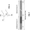
- FIG. 6illustrates one example of pixel components to which the recovery driving scheme of FIG. 5 is applied.
- a pixel circuitincludes a driving transistor 2 and OLED 4 , being coupled in series between a power supply VDD and a power supply VSS.
- the driving transistor 2is coupled to the power supply VDD.
- the OLED 4is coupled to the driving transistor at node B 0 and the power supply line VSS.
- the gate terminal of the driving transistor 2i.e., node A 0 , is charged by a programming voltage.
- the driving transistor 2provides a current to the OLED 4 .
- VSS lineis a controllable voltage line so that the voltage on VSS is changeable.
- VDD linemay be a controllable voltage line so that the voltage on VDD is changeable.
- VSS and VDD linesmay be shared by other pixel circuits.
- the pixel circuitmay include components other than the driving transistor 2 and the OLED 4 , such as a switch transistor for selecting the pixel circuit and providing a programming data on a data line to the pixel circuit, and a storage capacitor in which the programming data is stored.
- FIG. 7illustrates one example of recovery frames associated with the recovery deriving scheme of FIG. 5 .
- the recovery time 154 A of FIG. 7corresponds to the recovery time 154 of FIG. 5 , and includes initialization frames Y 1 and stand by frames Y 2 .
- the initialization frames Y 1include frames C 1 and C 2 .
- the stand by frames Y 2include frames C 3 , . . . , CK.
- the stand by frames Y 2are normal stand by frames.
- the displayis programmed with a high voltage (VP_R) while VSS is high voltage (VSS_R) and VDD is at VDD_R.
- VSShigh voltage
- VDDhigh voltage
- node A 0is charged to VP_R
- node B 0is charged to VDD_R.
- the voltage at OLED 4will be—(VSS_R-VDD_R).
- VSS_Ris larger than VDD_R, the OLED 4 will be under negative bias which will help the OLED 4 to recover.
- VSS_Ris higher than VSS at a normal image programming and driving operation.
- VP-Rmay be higher than that of a general programming voltage VP.
- the displayis programmed with gray zero while VDD and VSS preserve their previous value.
- the gate-source voltage (VGS) of the driving transistor 2will be—VDD_R.
- VGSgate-source voltage
- the driving transistor 2will recover from the aging.
- this conditionwill help to reduce the differential aging among the pixels, by balancing the aging effect. If the state of each pixel is known, one can use different voltages instead of zero for each pixel at this stage. As a result, the negative voltage apply to each pixel will be different so that the recovery will be faster and more efficient.
- Each pixelmay be programmed with different negative recovery voltage, for example, based on the ageing profile (history of the pixel's aging) or a look up table.
- the frame C 2is located after the frame C 1 .
- the frame C 2may be implemented before the frame C 1 .
- the same techniquecan be applied to a pixel in which the OLED 4 is coupled to the drain of the driving transistor 2 as well.
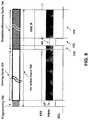
- FIG. 8illustrates another example of recovery frames associated with the recovery deriving scheme of FIG. 5 .
- the recovery time 154 B of FIG. 8corresponds to the recovery time 154 of FIG. 5 , and includes balancing frames Y 3 and the stand by frames Y 4 .
- the stand by frames Y 4include frames DJ, . . . , Dk.
- the stand by frames Y 4correspond to the stand by frames Y 3 of FIG. 7 .
- the balancing frames Y 3include frames D 1 , . . . , DJ ⁇ 1.
- the displayruns on uncompensated mode for a number of frames D 1 ⁇ DJ ⁇ 1 that can be selected based on the ON time of the display. In this mode, the part that aged more start recovering and the part that aged less will age. This will balance the display uniformity over time.
- FIG. 9illustrates a further example of a driving scheme for a display in accordance with an embodiment of the present invention.
- the active frame 160 of FIG. 9includes a programming cycle 162 , a driving cycle 164 , and a relaxation/recovery cycle 166 .
- the driving scheme of FIG. 9is applied to a pixel having the driving transistor 2 and the OLED 4 of FIG. 6 .
- the pixelis programmed with a required programming voltage VP.
- the driving transistor 2provides current to the OLED 4 based on the programming voltage VP.
- the relaxation/recovery cycle 166starts.
- the degradation of pixel componentsis recovered.
- the display systemimplements a recovery operation formed by a first operation cycle 170 , a second operation cycle 172 and a third operation cycle 174 .
- VSSgoes to VSS_R, and so node B 0 is charged to VP-VT (VT: threshold voltage of the driving transistor 4 ).
- VTthreshold voltage of the driving transistor 4
- node A 0is charged to VP_R and so the gate voltage of the driving transistor 2 will be—(VP-VT-VP_R).
- the pixel with larger programming voltage during the driving cycle 164will have a larger negative voltage across its gate-source voltage. This will results in faster recovery for the pixels at higher stress condition.
- the display systemmay be in the relaxation mode during the relaxation/recovery cycle 166 .
- the history of pixels' agingmay be used. If the history of the pixel's aging is known, each pixel can be programmed with different negative recovery voltage according to its aging profile. This will result in faster and more effective recovery.
- the negative recovery voltageis calculated or fetch from a look up table, based on the aging of the each pixel.
- the pixel circuits and display systemsare described using n-type transistors. However, one of ordinary skill in the art would appreciate that the n-type transistor in the circuits can be replaced with a p-type transistor with complementary circuit concept. One of ordinary skill in the art would appreciate that the programming, driving and relaxation techniques in the embodiments are also applicable to a complementary pixel circuit having p-type transistors.
- Some semiconductor devicesexperience stress annealing or recovery under certain bias, temperature and illumination.
- oxide semiconductor deviceshave negative threshold voltage shift under negative bias and illumination condition
- a semiconductor deviceis negatively biased while it is under illumination to induce negative threshold voltage shift in the device.
- a semiconductor devicecan generate the light by itself to be used for recovery process.
- the semiconductor devicecan be an array of the pixel and each pixel can be negatively biased and left under illumination.
- the pixelcan be biased with different biased levels based on a signal representing the performance of the pixel or aging history of the pixel.
- the signalcan be the stress history, a current level for a given voltage, a voltage for a given current, or any other type of signal representing the pixel performance.
- constant illumination and/or bias conditionsare used for recovery.
- pulse illumination and/or bias conditionsare used for recovery.
- the negative induced VT shift operationcan be followed by stress condition with positive induced VT shift to minimize the gap between the performances of different pixels.
- the negative induced VT shift and positive induced VT shift operationscan be repeated multiple times.
- Another aspect of this inventionwill be to use the bias illumination condition to improve non-uniformities associated with the solid state devices, including both initial non-uniformities and those due to aging.
Landscapes
- Engineering & Computer Science (AREA)
- Physics & Mathematics (AREA)
- Computer Hardware Design (AREA)
- General Physics & Mathematics (AREA)
- Theoretical Computer Science (AREA)
- Control Of Indicators Other Than Cathode Ray Tubes (AREA)
- Control Of El Displays (AREA)
- Electroluminescent Light Sources (AREA)
Abstract
Description
Claims (16)
Priority Applications (2)
| Application Number | Priority Date | Filing Date | Title |
|---|---|---|---|
| US14/630,906US10997901B2 (en) | 2014-02-28 | 2015-02-25 | Display system |
| US17/222,032US20210225273A1 (en) | 2014-02-28 | 2021-04-05 | Display system |
Applications Claiming Priority (2)
| Application Number | Priority Date | Filing Date | Title |
|---|---|---|---|
| US201461946427P | 2014-02-28 | 2014-02-28 | |
| US14/630,906US10997901B2 (en) | 2014-02-28 | 2015-02-25 | Display system |
Related Child Applications (1)
| Application Number | Title | Priority Date | Filing Date |
|---|---|---|---|
| US17/222,032ContinuationUS20210225273A1 (en) | 2014-02-28 | 2021-04-05 | Display system |
Publications (2)
| Publication Number | Publication Date |
|---|---|
| US20150248860A1 US20150248860A1 (en) | 2015-09-03 |
| US10997901B2true US10997901B2 (en) | 2021-05-04 |
Family
ID=53801530
Family Applications (2)
| Application Number | Title | Priority Date | Filing Date |
|---|---|---|---|
| US14/630,906Expired - Fee RelatedUS10997901B2 (en) | 2014-02-28 | 2015-02-25 | Display system |
| US17/222,032AbandonedUS20210225273A1 (en) | 2014-02-28 | 2021-04-05 | Display system |
Family Applications After (1)
| Application Number | Title | Priority Date | Filing Date |
|---|---|---|---|
| US17/222,032AbandonedUS20210225273A1 (en) | 2014-02-28 | 2021-04-05 | Display system |
Country Status (2)
| Country | Link |
|---|---|
| US (2) | US10997901B2 (en) |
| DE (1) | DE102015203408A1 (en) |
Families Citing this family (1)
| Publication number | Priority date | Publication date | Assignee | Title |
|---|---|---|---|---|
| US11715416B1 (en)* | 2022-10-31 | 2023-08-01 | Innolux Corporation | Method for driving an active-matrix pixel array |
Citations (379)
| Publication number | Priority date | Publication date | Assignee | Title |
|---|---|---|---|---|
| US4354162A (en) | 1981-02-09 | 1982-10-12 | National Semiconductor Corporation | Wide dynamic range control amplifier with offset correction |
| US4758831A (en) | 1984-11-05 | 1988-07-19 | Kabushiki Kaisha Toshiba | Matrix-addressed display device |
| GB2205431A (en) | 1986-09-27 | 1988-12-07 | Junichi Nishizawa | Color display device |
| US4963860A (en) | 1988-02-01 | 1990-10-16 | General Electric Company | Integrated matrix display circuitry |
| US4975691A (en) | 1987-06-16 | 1990-12-04 | Interstate Electronics Corporation | Scan inversion symmetric drive |
| US4996523A (en) | 1988-10-20 | 1991-02-26 | Eastman Kodak Company | Electroluminescent storage display with improved intensity driver circuits |
| US5051739A (en) | 1986-05-13 | 1991-09-24 | Sanyo Electric Co., Ltd. | Driving circuit for an image display apparatus with improved yield and performance |
| CA1294034C (en) | 1985-01-09 | 1992-01-07 | Hiromu Hosokawa | Color uniformity compensation apparatus for cathode ray tubes |
| CA2109951A1 (en) | 1991-05-24 | 1992-11-26 | Robert Hotto | Dc integrating display driver employing pixel status memories |
| US5222082A (en) | 1991-02-28 | 1993-06-22 | Thomson Consumer Electronics, S.A. | Shift register useful as a select line scanner for liquid crystal display |
| US5266515A (en) | 1992-03-02 | 1993-11-30 | Motorola, Inc. | Fabricating dual gate thin film transistors |
| WO1994025954A1 (en) | 1993-04-30 | 1994-11-10 | Prime View Hk Limited | Apparatus for recovery of threshold voltage shift in amorphous silicon thin-film transistor device |
| US5498880A (en) | 1995-01-12 | 1996-03-12 | E. I. Du Pont De Nemours And Company | Image capture panel using a solid state device |
| US5589847A (en) | 1991-09-23 | 1996-12-31 | Xerox Corporation | Switched capacitor analog circuits using polysilicon thin film technology |
| JPH0990405A (en) | 1995-09-21 | 1997-04-04 | Sharp Corp | Thin film transistor |
| US5619033A (en) | 1995-06-07 | 1997-04-08 | Xerox Corporation | Layered solid state photodiode sensor array |
| US5648276A (en) | 1993-05-27 | 1997-07-15 | Sony Corporation | Method and apparatus for fabricating a thin film semiconductor device |
| US5670973A (en) | 1993-04-05 | 1997-09-23 | Cirrus Logic, Inc. | Method and apparatus for compensating crosstalk in liquid crystal displays |
| US5684365A (en) | 1994-12-14 | 1997-11-04 | Eastman Kodak Company | TFT-el display panel using organic electroluminescent media |
| US5686935A (en) | 1995-03-06 | 1997-11-11 | Thomson Consumer Electronics, S.A. | Data line drivers with column initialization transistor |
| US5712653A (en) | 1993-12-27 | 1998-01-27 | Sharp Kabushiki Kaisha | Image display scanning circuit with outputs from sequentially switched pulse signals |
| US5714968A (en) | 1994-08-09 | 1998-02-03 | Nec Corporation | Current-dependent light-emitting element drive circuit for use in active matrix display device |
| US5747928A (en) | 1994-10-07 | 1998-05-05 | Iowa State University Research Foundation, Inc. | Flexible panel display having thin film transistors driving polymer light-emitting diodes |
| US5748160A (en) | 1995-08-21 | 1998-05-05 | Mororola, Inc. | Active driven LED matrices |
| JPH10153759A (en) | 1996-11-26 | 1998-06-09 | Matsushita Electric Ind Co Ltd | Liquid crystal display |
| US5784042A (en) | 1991-03-19 | 1998-07-21 | Hitachi, Ltd. | Liquid crystal display device and method for driving the same |
| CA2249592A1 (en) | 1997-01-28 | 1998-07-30 | Casio Computer Co., Ltd. | Active matrix electroluminescent display device and a driving method thereof |
| US5790234A (en) | 1995-12-27 | 1998-08-04 | Canon Kabushiki Kaisha | Eyeball detection apparatus |
| JPH10254410A (en) | 1997-03-12 | 1998-09-25 | Pioneer Electron Corp | Organic electroluminescent display device, and driving method therefor |
| US5815303A (en) | 1997-06-26 | 1998-09-29 | Xerox Corporation | Fault tolerant projective display having redundant light modulators |
| US5870071A (en) | 1995-09-07 | 1999-02-09 | Frontec Incorporated | LCD gate line drive circuit |
| US5874803A (en) | 1997-09-09 | 1999-02-23 | The Trustees Of Princeton University | Light emitting device with stack of OLEDS and phosphor downconverter |
| US5880582A (en) | 1996-09-04 | 1999-03-09 | Sumitomo Electric Industries, Ltd. | Current mirror circuit and reference voltage generating and light emitting element driving circuits using the same |
| US5903248A (en) | 1997-04-11 | 1999-05-11 | Spatialight, Inc. | Active matrix display having pixel driving circuits with integrated charge pumps |
| US5917280A (en) | 1997-02-03 | 1999-06-29 | The Trustees Of Princeton University | Stacked organic light emitting devices |
| US5923794A (en) | 1996-02-06 | 1999-07-13 | Polaroid Corporation | Current-mediated active-pixel image sensing device with current reset |
| JPH11231805A (en) | 1998-02-10 | 1999-08-27 | Sanyo Electric Co Ltd | Display device |
| EP0940796A1 (en) | 1997-08-21 | 1999-09-08 | Seiko Epson Corporation | Active matrix display |
| US5952789A (en) | 1997-04-14 | 1999-09-14 | Sarnoff Corporation | Active matrix organic light emitting diode (amoled) display pixel structure and data load/illuminate circuit therefor |
| WO1999048079A1 (en) | 1998-03-19 | 1999-09-23 | Holloman Charles J | Analog driver for led or similar display element |
| JPH11282419A (en) | 1998-03-31 | 1999-10-15 | Nec Corp | Element driving device and method and image display device |
| US6023259A (en) | 1997-07-11 | 2000-02-08 | Fed Corporation | OLED active matrix using a single transistor current mode pixel design |
| JP2000056847A (en) | 1998-08-14 | 2000-02-25 | Nec Corp | Constant current driving circuit |
| JP2000077192A (en) | 1998-09-01 | 2000-03-14 | Pioneer Electronic Corp | Organic electroluminescent panel and manufacture thereof |
| JP2000089198A (en) | 1998-09-11 | 2000-03-31 | Seiko Epson Corp | Compensation method for liquid crystal applied voltage of liquid crystal display device, liquid crystal display device, electronic device, and voltage detection method for liquid crystal layer |
| CA2242720C (en) | 1998-07-09 | 2000-05-16 | Ibm Canada Limited-Ibm Canada Limitee | Programmable led driver |
| US6069365A (en) | 1997-11-25 | 2000-05-30 | Alan Y. Chow | Optical processor based imaging system |
| CA2354018A1 (en) | 1998-12-14 | 2000-06-22 | Alan Richard | Portable microdisplay system |
| US6081131A (en) | 1997-11-12 | 2000-06-27 | Seiko Epson Corporation | Logical amplitude level conversion circuit, liquid crystal device and electronic apparatus |
| EP1028471A2 (en) | 1999-02-09 | 2000-08-16 | SANYO ELECTRIC Co., Ltd. | Electroluminescence display device |
| US6157583A (en) | 1999-03-02 | 2000-12-05 | Motorola, Inc. | Integrated circuit memory having a fuse detect circuit and method therefor |
| JP2000352941A (en) | 1999-06-14 | 2000-12-19 | Sony Corp | Display device |
| US6166489A (en) | 1998-09-15 | 2000-12-26 | The Trustees Of Princeton University | Light emitting device using dual light emitting stacks to achieve full-color emission |
| US6177915B1 (en) | 1990-06-11 | 2001-01-23 | International Business Machines Corporation | Display system having section brightness control and method of operating system |
| WO2001027910A1 (en) | 1999-10-12 | 2001-04-19 | Koninklijke Philips Electronics N.V. | Led display device |
| US6225846B1 (en) | 1997-01-23 | 2001-05-01 | Mitsubishi Denki Kabushiki Kaisha | Body voltage controlled semiconductor integrated circuit |
| US6229508B1 (en) | 1997-09-29 | 2001-05-08 | Sarnoff Corporation | Active matrix light emitting diode pixel structure and concomitant method |
| US6232939B1 (en) | 1997-11-10 | 2001-05-15 | Hitachi, Ltd. | Liquid crystal display apparatus including scanning circuit having bidirectional shift register stages |
| EP1103947A2 (en) | 1999-11-29 | 2001-05-30 | Sel Semiconductor Energy Laboratory Co., Ltd. | EL display device and electronic apparatus |
| US20010002703A1 (en) | 1999-11-30 | 2001-06-07 | Jun Koyama | Electric device |
| US6246180B1 (en) | 1999-01-29 | 2001-06-12 | Nec Corporation | Organic el display device having an improved image quality |
| US20010004190A1 (en) | 1999-12-15 | 2001-06-21 | Semiconductor Energy Laboratory Co., Ltd. | EL disply device |
| US6252248B1 (en) | 1998-06-08 | 2001-06-26 | Sanyo Electric Co., Ltd. | Thin film transistor and display |
| US6259424B1 (en) | 1998-03-04 | 2001-07-10 | Victor Company Of Japan, Ltd. | Display matrix substrate, production method of the same and display matrix circuit |
| US6274887B1 (en) | 1998-11-02 | 2001-08-14 | Semiconductor Energy Laboratory Co., Ltd. | Semiconductor device and manufacturing method therefor |
| US20010013806A1 (en) | 2000-02-15 | 2001-08-16 | Hiromi Notani | Semiconductor integrated circuit |
| US20010015653A1 (en) | 2000-02-23 | 2001-08-23 | U.S. Philips Corporation. | Integrated circuit with test interface |
| EP1130565A1 (en) | 1999-07-14 | 2001-09-05 | Sony Corporation | Current drive circuit and display comprising the same, pixel circuit, and drive method |
| US20010020926A1 (en) | 2000-02-15 | 2001-09-13 | Kuijk Karel Elbert | Display device |
| US20010026127A1 (en) | 1998-02-27 | 2001-10-04 | Kiyoshi Yoneda | Color display apparatus having electroluminescence elements |
| US20010026257A1 (en) | 2000-03-27 | 2001-10-04 | Hajime Kimura | Electro-optical device |
| US20010026179A1 (en) | 2000-03-24 | 2001-10-04 | Takanori Saeki | Clock control circuit and clock control method |
| US6300928B1 (en) | 1997-08-09 | 2001-10-09 | Lg Electronics Inc. | Scanning circuit for driving liquid crystal display |
| US6303963B1 (en) | 1998-12-03 | 2001-10-16 | Semiconductor Energy Laboratory Co., Ltd. | Electro-optical device and semiconductor circuit |
| US20010030323A1 (en) | 2000-03-29 | 2001-10-18 | Sony Corporation | Thin film semiconductor apparatus and method for driving the same |
| US6306694B1 (en) | 1999-03-12 | 2001-10-23 | Semiconductor Energy Laboratory Co., Ltd. | Process of fabricating a semiconductor device |
| US6307322B1 (en) | 1999-12-28 | 2001-10-23 | Sarnoff Corporation | Thin-film transistor circuitry with reduced sensitivity to variance in transistor threshold voltage |
| US20010033199A1 (en) | 2000-02-07 | 2001-10-25 | Yuuichi Aoki | Variable-gain circuit |
| US20010038098A1 (en) | 2000-02-29 | 2001-11-08 | Shunpei Yamazaki | Light-emitting device |
| US6316786B1 (en) | 1998-08-29 | 2001-11-13 | International Business Machines Corporation | Organic opto-electronic devices |
| US6320325B1 (en) | 2000-11-06 | 2001-11-20 | Eastman Kodak Company | Emissive display with luminance feedback from a representative pixel |
| US20010043173A1 (en) | 1997-09-04 | 2001-11-22 | Ronald Roy Troutman | Field sequential gray in active matrix led display using complementary transistor pixel circuits |
| US6323832B1 (en) | 1986-09-27 | 2001-11-27 | Junichi Nishizawa | Color display device |
| US6323631B1 (en) | 2001-01-18 | 2001-11-27 | Sunplus Technology Co., Ltd. | Constant current driver with auto-clamped pre-charge function |
| US20010045929A1 (en) | 2000-01-21 | 2001-11-29 | Prache Olivier F. | Gray scale pixel driver for electronic display and method of operation therefor |
| US20010052898A1 (en) | 2000-02-01 | 2001-12-20 | Semiconductor Energy Laboratory Co., Ltd. | Semiconductor display device and method of driving the same |
| US20010052606A1 (en) | 2000-05-22 | 2001-12-20 | Koninklijke Philips Electronics N.V. | Display device |
| US20020000576A1 (en) | 2000-06-22 | 2002-01-03 | Kazutaka Inukai | Display device |
| US20020011799A1 (en) | 2000-04-06 | 2002-01-31 | Semiconductor Energy Laboratory Co., Ltd. | Electronic device and driving method |
| US20020011796A1 (en) | 2000-05-08 | 2002-01-31 | Semiconductor Energy Laboratory Co., Ltd. | Light-emitting device, and electric device using the same |
| US20020011981A1 (en) | 2000-07-20 | 2002-01-31 | Koninklijke Philips Electronics N.V. | Display device |
| US6345085B1 (en) | 1999-11-05 | 2002-02-05 | Lg. Philips Lcd Co., Ltd. | Shift register |
| US20020015032A1 (en) | 2000-07-25 | 2002-02-07 | Jun Koyama | Driver circuit of a display device |
| US20020015031A1 (en) | 2000-07-24 | 2002-02-07 | Seiko Epson Corporation | Electro-optical panel, method for driving the same, electrooptical device, and electronic equipment |
| US6348835B1 (en) | 1999-05-27 | 2002-02-19 | Nec Corporation | Semiconductor device with constant current source circuit not influenced by noise |
| EP1184833A2 (en) | 2000-09-04 | 2002-03-06 | Sel Semiconductor Energy Laboratory Co., Ltd. | Method of driving EL display device |
| US20020030528A1 (en) | 2000-06-14 | 2002-03-14 | Shoichiro Matsumoto | Level shifter for use in active matrix display apparatus |
| US20020030647A1 (en) | 2000-06-06 | 2002-03-14 | Michael Hack | Uniform active matrix oled displays |
| JP2002091376A (en) | 2000-06-27 | 2002-03-27 | Hitachi Ltd | Image display device and driving method thereof |
| US6365917B1 (en) | 1998-11-25 | 2002-04-02 | Semiconductor Energy Laboratory Co., Ltd. | Semiconductor device |
| EP1194013A1 (en) | 2000-09-29 | 2002-04-03 | Eastman Kodak Company | A flat-panel display with luminance feedback |
| US20020048829A1 (en) | 2000-04-19 | 2002-04-25 | Shunpei Yamazaki | Light emitting device and fabricating method thereof |
| US20020050795A1 (en) | 2000-10-27 | 2002-05-02 | Nec Corporation | Active matrix organic el display device and method of forming the same |
| US6384427B1 (en) | 1999-10-29 | 2002-05-07 | Semiconductor Energy Laboratory Co., Ltd. | Electronic device |
| US20020053401A1 (en) | 2000-10-31 | 2002-05-09 | Nobuyuki Ishikawa | Organic luminescence display device and process for production thereof |
| US6392617B1 (en) | 1999-10-27 | 2002-05-21 | Agilent Technologies, Inc. | Active matrix light emitting diode display |
| US6399988B1 (en) | 1999-03-26 | 2002-06-04 | Semiconductor Energy Laboratory Co., Ltd. | Thin film transistor having lightly doped regions |
| US20020070909A1 (en) | 2000-11-22 | 2002-06-13 | Mitsuru Asano | Active matrix type display apparatus |
| US20020080108A1 (en) | 2000-12-26 | 2002-06-27 | Hannstar Display Corp. | Gate lines driving circuit and driving method |
| US6414661B1 (en) | 2000-02-22 | 2002-07-02 | Sarnoff Corporation | Method and apparatus for calibrating display devices and automatically compensating for loss in their efficiency over time |
| US20020084463A1 (en) | 2001-01-04 | 2002-07-04 | International Business Machines Corporation | Low-power organic light emitting diode pixel circuit |
| US6420758B1 (en) | 1998-11-17 | 2002-07-16 | Semiconductor Energy Laboratory Co., Ltd. | Semiconductor device having an impurity region overlapping a gate electrode |
| US6420834B2 (en) | 2000-03-27 | 2002-07-16 | Semiconductor Energy Laboratory Co., Ltd. | Light emitting device and a method of manufacturing the same |
| US6420988B1 (en) | 1998-12-03 | 2002-07-16 | Semiconductor Energy Laboratory Co., Ltd. | Digital analog converter and electronic device using the same |
| US20020101433A1 (en) | 1996-12-19 | 2002-08-01 | Mcknight Douglas | Display system having electrode modulation to alter a state of an electro-optic layer |
| US20020101172A1 (en) | 2001-01-02 | 2002-08-01 | Bu Lin-Kai | Oled active driving system with current feedback |
| CA2436451A1 (en) | 2001-02-05 | 2002-08-15 | International Business Machines Corporation | Liquid crystal display device |
| US20020113248A1 (en) | 2001-02-19 | 2002-08-22 | Semiconductor Energy Laboratory Co., Ltd. | Light emitting device and method of manufacturing the same |
| CA2438577A1 (en) | 2001-02-16 | 2002-08-29 | Ignis Innovation Inc. | Pixel current driver for organic light emitting diode displays |
| WO2002067327A2 (en) | 2001-02-16 | 2002-08-29 | Ignis Innovation Inc. | Pixel current driver for organic light emitting diode displays |
| US6445376B2 (en) | 1997-09-12 | 2002-09-03 | Sean T. Parrish | Alternative power for a portable computer via solar cells |
| US20020122308A1 (en) | 2001-03-05 | 2002-09-05 | Fuji Xerox Co., Ltd. | Apparatus for driving light emitting element and system for driving light emitting element |
| TW502233B (en) | 1999-06-17 | 2002-09-11 | Sony Corp | Image display apparatus |
| US20020130686A1 (en) | 2001-03-14 | 2002-09-19 | Micron Technology, Inc. | CMOS gate array with vertical transistors |
| JP2002268576A (en) | 2000-12-05 | 2002-09-20 | Matsushita Electric Ind Co Ltd | Image display device, method of manufacturing image display device, and image display driver IC |
| JP2002278513A (en) | 2001-03-19 | 2002-09-27 | Sharp Corp | Electro-optical device |
| US6468638B2 (en) | 1999-03-16 | 2002-10-22 | Alien Technology Corporation | Web process interconnect in electronic assemblies |
| US20020154084A1 (en) | 2000-06-16 | 2002-10-24 | Yukio Tanaka | Active matrix display device, its driving method, and display element |
| US20020158823A1 (en) | 1997-10-31 | 2002-10-31 | Matthew Zavracky | Portable microdisplay system |
| US20020167471A1 (en) | 2001-05-09 | 2002-11-14 | Everitt James W. | System for providing pulse amplitude modulation for oled display drivers |
| JP2002333862A (en) | 2001-02-21 | 2002-11-22 | Semiconductor Energy Lab Co Ltd | Light emission device and electronic equipment |
| US6489952B1 (en) | 1998-11-17 | 2002-12-03 | Semiconductor Energy Laboratory Co., Ltd. | Active matrix type semiconductor display device |
| US20020180721A1 (en) | 1997-03-12 | 2002-12-05 | Mutsumi Kimura | Pixel circuit display apparatus and electronic apparatus equipped with current driving type light-emitting device |
| US20020180369A1 (en) | 2001-02-21 | 2002-12-05 | Jun Koyama | Light emitting device and electronic appliance |
| US20020186214A1 (en) | 2001-06-05 | 2002-12-12 | Eastman Kodak Company | Method for saving power in an organic electroluminescent display using white light emitting elements |
| US20020190971A1 (en) | 2001-04-27 | 2002-12-19 | Kabushiki Kaisha Toshiba | Display apparatus, digital-to-analog conversion circuit and digital-to-analog conversion method |
| US20020190924A1 (en) | 2001-01-19 | 2002-12-19 | Mitsuru Asano | Active matrix display |
| US20020190332A1 (en) | 2001-06-15 | 2002-12-19 | Lg Electronics Inc. | Thin film transistor, and organic EL display thereof and method for fabricating the same |
| US20020195967A1 (en) | 2001-06-22 | 2002-12-26 | Kim Sung Ki | Electro-luminescence panel |
| US20020195968A1 (en) | 2001-06-22 | 2002-12-26 | International Business Machines Corporation | Oled current drive pixel circuit |
| US6501466B1 (en) | 1999-11-18 | 2002-12-31 | Sony Corporation | Active matrix type display apparatus and drive circuit thereof |
| US6501098B2 (en) | 1998-11-25 | 2002-12-31 | Semiconductor Energy Laboratory Co, Ltd. | Semiconductor device |
| JP2003022035A (en) | 2001-07-10 | 2003-01-24 | Sharp Corp | Organic EL panel and manufacturing method thereof |
| US6512271B1 (en) | 1998-11-16 | 2003-01-28 | Semiconductor Energy Laboratory Co., Ltd. | Semiconductor device |
| US20030020413A1 (en) | 2001-07-27 | 2003-01-30 | Masanobu Oomura | Active matrix display |
| US6518594B1 (en) | 1998-11-16 | 2003-02-11 | Semiconductor Energy Laboratory Co., Ltd. | Semiconductor devices |
| US20030030603A1 (en) | 2001-08-09 | 2003-02-13 | Nec Corporation | Drive circuit for display device |
| US6524895B2 (en) | 1998-12-25 | 2003-02-25 | Semiconductor Energy Laboratory Co., Ltd. | Semiconductor device and method of fabricating the same |
| US6531713B1 (en) | 1999-03-19 | 2003-03-11 | Semiconductor Energy Laboratory Co., Ltd. | Electro-optical device and manufacturing method thereof |
| JP2003076331A (en) | 2001-08-31 | 2003-03-14 | Seiko Epson Corp | Display device and electronic equipment |
| US20030062524A1 (en) | 2001-08-29 | 2003-04-03 | Hajime Kimura | Light emitting device, method of driving a light emitting device, element substrate, and electronic equipment |
| US20030071804A1 (en) | 2001-09-28 | 2003-04-17 | Semiconductor Energy Laboratory Co., Ltd. | Light emitting device and electronic apparatus using the same |
| US20030076048A1 (en) | 2001-10-23 | 2003-04-24 | Rutherford James C. | Organic electroluminescent display device driving method and apparatus |
| WO2003034389A2 (en) | 2001-10-19 | 2003-04-24 | Clare Micronix Integrated Systems, Inc. | System and method for providing pulse amplitude modulation for oled display drivers |
| US6559594B2 (en) | 2000-02-03 | 2003-05-06 | Semiconductor Energy Laboratory Co., Ltd. | Light-emitting device |
| EP1310939A2 (en) | 2001-09-28 | 2003-05-14 | Sel Semiconductor Energy Laboratory Co., Ltd. | A light emitting device and electronic apparatus using the same |
| US20030090445A1 (en) | 2001-11-14 | 2003-05-15 | Industrial Technology Research Institute | Current driver for active matrix organic light emitting diode |
| US20030090481A1 (en) | 2001-11-13 | 2003-05-15 | Hajime Kimura | Display device and method for driving the same |
| US20030090447A1 (en) | 2001-09-21 | 2003-05-15 | Hajime Kimura | Display device and driving method thereof |
| JP2003150082A (en) | 2001-11-15 | 2003-05-21 | Matsushita Electric Ind Co Ltd | EL display device driving method, EL display device, manufacturing method thereof, and information display device |
| US20030095087A1 (en) | 2001-11-20 | 2003-05-22 | International Business Machines Corporation | Data voltage current drive amoled pixel circuit |
| US6573584B1 (en) | 1999-10-29 | 2003-06-03 | Kyocera Corporation | Thin film electronic device and circuit board mounting the same |
| US6573195B1 (en) | 1999-01-26 | 2003-06-03 | Semiconductor Energy Laboratory Co., Ltd. | Method for manufacturing a semiconductor device by performing a heat-treatment in a hydrogen atmosphere |
| US6576926B1 (en) | 1999-02-23 | 2003-06-10 | Semiconductor Energy Laboratory Co., Ltd. | Semiconductor device and fabrication method thereof |
| US20030107560A1 (en) | 2001-01-15 | 2003-06-12 | Akira Yumoto | Active-matrix display, active-matrix organic electroluminescent display, and methods of driving them |
| US6580408B1 (en) | 1999-06-03 | 2003-06-17 | Lg. Philips Lcd Co., Ltd. | Electro-luminescent display including a current mirror |
| US20030111966A1 (en) | 2001-12-19 | 2003-06-19 | Yoshiro Mikami | Image display apparatus |
| TW538650B (en) | 2000-09-29 | 2003-06-21 | Seiko Epson Corp | Driving method for electro-optical device, electro-optical device, and electronic apparatus |
| JP2003177709A (en) | 2001-12-13 | 2003-06-27 | Seiko Epson Corp | Pixel circuit for light emitting element |
| US6587086B1 (en) | 1999-10-26 | 2003-07-01 | Semiconductor Energy Laboratory Co., Ltd. | Electro-optical device |
| US6594606B2 (en) | 2001-05-09 | 2003-07-15 | Clare Micronix Integrated Systems, Inc. | Matrix element voltage sensing for precharge |
| US20030140958A1 (en) | 2002-01-28 | 2003-07-31 | Cheng-Chieh Yang | Solar photoelectric module |
| WO2003063124A1 (en) | 2002-01-17 | 2003-07-31 | Nec Corporation | Semiconductor device incorporating matrix type current load driving circuits, and driving method thereof |
| EP1335430A1 (en) | 2002-02-12 | 2003-08-13 | Eastman Kodak Company | A flat-panel light emitting pixel with luminance feedback |
| US6611108B2 (en) | 2000-04-26 | 2003-08-26 | Semiconductor Energy Laboratory Co., Ltd. | Electronic device and driving method thereof |
| US6617644B1 (en) | 1998-11-09 | 2003-09-09 | Semiconductor Energy Laboratory Co., Ltd. | Semiconductor device and method of manufacturing the same |
| US20030169219A1 (en) | 2001-10-19 | 2003-09-11 | Lechevalier Robert | System and method for exposure timing compensation for row resistance |
| US20030174152A1 (en) | 2002-02-04 | 2003-09-18 | Yukihiro Noguchi | Display apparatus with function which makes gradiation control easier |
| WO2003077231A2 (en) | 2002-03-13 | 2003-09-18 | Koninklijke Philips Electronics N.V. | Two sided display device |
| JP2003271095A (en) | 2002-03-14 | 2003-09-25 | Nec Corp | Driving circuit for current control element and image display device |
| CN1448908A (en) | 2002-03-29 | 2003-10-15 | 精工爱普生株式会社 | Electronic device, method for driving electronic device, electrooptical device and electronic apparatus |
| US20030197663A1 (en) | 2001-12-27 | 2003-10-23 | Lee Han Sang | Electroluminescent display panel and method for operating the same |
| JP2003308046A (en) | 2002-02-18 | 2003-10-31 | Sanyo Electric Co Ltd | Display device |
| US6641933B1 (en) | 1999-09-24 | 2003-11-04 | Semiconductor Energy Laboratory Co., Ltd. | Light-emitting EL display device |
| US20030206060A1 (en) | 2000-05-16 | 2003-11-06 | Fujitsu Limited | Operational amplifier circuit |
| US6661180B2 (en) | 2001-03-22 | 2003-12-09 | Semiconductor Energy Laboratory Co., Ltd. | Light emitting device, driving method for the same and electronic apparatus |
| US6661397B2 (en) | 2001-03-30 | 2003-12-09 | Hitachi, Ltd. | Emissive display using organic electroluminescent devices |
| EP1372136A1 (en) | 2002-06-12 | 2003-12-17 | Seiko Epson Corporation | Scan driver and a column driver for active matrix display device and corresponding method |
| WO2003105117A2 (en) | 2002-06-07 | 2003-12-18 | Casio Computer Co., Ltd. | Display device and its driving method |
| US20030230980A1 (en) | 2002-06-18 | 2003-12-18 | Forrest Stephen R | Very low voltage, high efficiency phosphorescent oled in a p-i-n structure |
| CA2483645A1 (en) | 2002-06-21 | 2003-12-31 | Josuke Nakata | Light-receiving or light-emitting device and its production method |
| TW569173B (en) | 2002-08-05 | 2004-01-01 | Etoms Electronics Corp | Driver for controlling display cycle of OLED and its method |
| WO2004003877A2 (en) | 2002-06-27 | 2004-01-08 | Casio Computer Co., Ltd. | Current drive apparatus and drive method thereof, and electroluminescent display apparatus using the circuit |
| US6677713B1 (en) | 2002-08-28 | 2004-01-13 | Au Optronics Corporation | Driving circuit and method for light emitting device |
| EP1381019A1 (en) | 2002-07-10 | 2004-01-14 | Pioneer Corporation | Automatic luminance adjustment device and method |
| CA2463653A1 (en) | 2002-07-09 | 2004-01-15 | Casio Computer Co., Ltd. | Driving device, display apparatus using the same, and driving method therefor |
| US6687266B1 (en) | 2002-11-08 | 2004-02-03 | Universal Display Corporation | Organic light emitting materials and devices |
| US6690344B1 (en) | 1999-05-14 | 2004-02-10 | Ngk Insulators, Ltd. | Method and apparatus for driving device and display |
| US20040027063A1 (en) | 2002-03-13 | 2004-02-12 | Ryuji Nishikawa | Organic EL panel and manufacturing method thereof |
| US6693610B2 (en) | 1999-09-11 | 2004-02-17 | Koninklijke Philips Electronics N.V. | Active matrix electroluminescent display device |
| US6697057B2 (en) | 2000-10-27 | 2004-02-24 | Semiconductor Energy Laboratory Co., Ltd. | Display device and method of driving the same |
| CA2498136A1 (en) | 2002-09-09 | 2004-03-18 | Matthew Stevenson | Organic electronic device having improved homogeneity |
| US20040056604A1 (en) | 2002-09-19 | 2004-03-25 | Jun-Ren Shih | Pixel structure for an active matrix OLED |
| US20040066357A1 (en) | 2002-09-02 | 2004-04-08 | Canon Kabushiki Kaisha | Drive circuit, display apparatus, and information display apparatus |
| US20040070557A1 (en) | 2002-10-11 | 2004-04-15 | Mitsuru Asano | Active-matrix display device and method of driving the same |
| WO2004034364A1 (en) | 2002-10-08 | 2004-04-22 | Koninklijke Philips Electronics N.V. | Electroluminescent display devices |
| US20040080262A1 (en) | 2002-10-29 | 2004-04-29 | Lg.Philips Lcd Co., Ltd. | Dual panel type organic electro luminescent display device and manufacturing method for the same |
| EP1418566A2 (en) | 2002-11-08 | 2004-05-12 | Tohoku Pioneer Corporation | Drive methods and drive devices for active type light emitting display panel |
| US20040090400A1 (en) | 2002-11-05 | 2004-05-13 | Yoo Juhn Suk | Data driving apparatus and method of driving organic electro luminescence display panel |
| US6738035B1 (en) | 1997-09-22 | 2004-05-18 | Nongqiang Fan | Active matrix LCD based on diode switches and methods of improving display uniformity of same |
| US6738034B2 (en) | 2000-06-27 | 2004-05-18 | Hitachi, Ltd. | Picture image display device and method of driving the same |
| US20040108518A1 (en) | 2002-03-29 | 2004-06-10 | Seiko Epson Corporation | Electronic device, method for driving the electronic device, electro-optical device, and electronic equipment |
| EP1429312A2 (en) | 2002-12-12 | 2004-06-16 | Seiko Epson Corporation | Electro-optical device, method of driving electro optical device, and electronic apparatus |
| US20040113903A1 (en) | 2002-12-11 | 2004-06-17 | Yoshiro Mikami | Low-power driven display device |
| US20040130516A1 (en) | 2001-02-16 | 2004-07-08 | Arokia Nathan | Organic light emitting diode display having shield electrodes |
| US20040135749A1 (en) | 2003-01-14 | 2004-07-15 | Eastman Kodak Company | Compensating for aging in OLED devices |
| EP1439520A2 (en) | 2003-01-20 | 2004-07-21 | SANYO ELECTRIC Co., Ltd. | Display device of active matrix drive type |
| US20040145547A1 (en) | 2003-01-21 | 2004-07-29 | Oh Choon-Yul | Luminescent display, and driving method and pixel circuit thereof, and display device |
| US6771028B1 (en) | 2003-04-30 | 2004-08-03 | Eastman Kodak Company | Drive circuitry for four-color organic light-emitting device |
| US20040150594A1 (en) | 2002-07-25 | 2004-08-05 | Semiconductor Energy Laboratory Co., Ltd. | Display device and drive method therefor |
| US20040150592A1 (en) | 2003-01-10 | 2004-08-05 | Eastman Kodak Company | Correction of pixels in an organic EL display device |
| US20040155841A1 (en) | 2002-11-27 | 2004-08-12 | Seiko Epson Corporation | Electro-optical device, method of driving electro-optical device, and electronic apparatus |
| US6780687B2 (en) | 2000-01-28 | 2004-08-24 | Semiconductor Energy Laboratory Co., Ltd. | Method of manufacturing a semiconductor device having a heat absorbing layer |
| US20040174349A1 (en) | 2003-03-04 | 2004-09-09 | Libsch Frank Robert | Driving circuits for displays |
| US20040174347A1 (en) | 2003-03-07 | 2004-09-09 | Wein-Town Sun | Data driver and related method used in a display device for saving space |
| US20040179005A1 (en)* | 2003-02-19 | 2004-09-16 | Seiko Epson Corporation | Electro-optical device, method of driving electro-optical device, and electronic apparatus |
| US20040189627A1 (en) | 2003-03-05 | 2004-09-30 | Casio Computer Co., Ltd. | Display device and method for driving display device |
| EP1465143A2 (en) | 2003-04-01 | 2004-10-06 | Samsung SDI Co., Ltd. | Light emitting display, display panel, and driving method thereof |
| EP1467408A2 (en) | 2003-04-09 | 2004-10-13 | Eastman Kodak Company | An oled display with integrated photosensor |
| US20040201554A1 (en) | 2003-04-10 | 2004-10-14 | Shinichi Satoh | Method of driving display panel and drive for carrying out same |
| US6806638B2 (en) | 2002-12-27 | 2004-10-19 | Au Optronics Corporation | Display of active matrix organic light emitting diode and fabricating method |
| US20040207615A1 (en) | 1999-07-14 | 2004-10-21 | Akira Yumoto | Current drive circuit and display device using same pixel circuit, and drive method |
| CA2522396A1 (en) | 2003-04-25 | 2004-11-11 | Visioneered Image Systems, Inc. | Led illumination source/display with individual led brightness monitoring capability and calibration method |
| US20040233125A1 (en) | 2003-05-23 | 2004-11-25 | Gino Tanghe | Method for displaying images on a large-screen organic light-emitting diode display, and display used therefore |
| US20040239596A1 (en) | 2003-02-19 | 2004-12-02 | Shinya Ono | Image display apparatus using current-controlled light emitting element |
| US20040252089A1 (en) | 2003-05-16 | 2004-12-16 | Shinya Ono | Image display apparatus controlling brightness of current-controlled light emitting element |
| US20040257355A1 (en) | 2003-06-18 | 2004-12-23 | Nuelight Corporation | Method and apparatus for controlling an active matrix display |
| US20050007357A1 (en) | 2003-05-19 | 2005-01-13 | Sony Corporation | Pixel circuit, display device, and driving method of pixel circuit |
| US20050030267A1 (en) | 2003-08-07 | 2005-02-10 | Gino Tanghe | Method and system for measuring and controlling an OLED display element for improved lifetime and light output |
| US20050035709A1 (en) | 2003-08-11 | 2005-02-17 | Hitachi Displays, Ltd. | Organic electroluminescent display device |
| US6861670B1 (en) | 1999-04-01 | 2005-03-01 | Semiconductor Energy Laboratory Co., Ltd. | Semiconductor device having multi-layer wiring |
| JP2005057217A (en) | 2003-08-07 | 2005-03-03 | Renesas Technology Corp | Semiconductor integrated circuit device |
| WO2005022498A2 (en) | 2003-09-02 | 2005-03-10 | Koninklijke Philips Electronics N.V. | Active matrix display devices |
| US20050057459A1 (en)* | 2003-08-29 | 2005-03-17 | Seiko Epson Corporation | Electro-optical device, method of driving the same, and electronic apparatus |
| CA2443206A1 (en) | 2003-09-23 | 2005-03-23 | Ignis Innovation Inc. | Amoled display backplanes - pixel driver circuits, array architecture, and external compensation |
| EP1517290A2 (en) | 2003-08-29 | 2005-03-23 | Seiko Epson Corporation | Driving circuit for electroluminescent display device and its related method of operation |
| US6873320B2 (en) | 2000-09-05 | 2005-03-29 | Kabushiki Kaisha Toshiba | Display device and driving method thereof |
| US6873117B2 (en) | 2002-09-30 | 2005-03-29 | Pioneer Corporation | Display panel and display device |
| US20050068270A1 (en) | 2003-09-17 | 2005-03-31 | Hiroki Awakura | Display apparatus and display control method |
| US20050067971A1 (en) | 2003-09-29 | 2005-03-31 | Michael Gillis Kane | Pixel circuit for an active matrix organic light-emitting diode display |
| US20050067970A1 (en) | 2003-09-26 | 2005-03-31 | International Business Machines Corporation | Active-matrix light emitting display and method for obtaining threshold voltage compensation for same |
| EP1521203A2 (en) | 2003-10-02 | 2005-04-06 | Alps Electric Co., Ltd. | Capacitance detector circuit, capacitance detector method and fingerprint sensor using the same |
| US6878968B1 (en) | 1999-05-10 | 2005-04-12 | Semiconductor Energy Laboratory Co., Ltd. | Semiconductor device |
| US20050088103A1 (en) | 2003-10-28 | 2005-04-28 | Hitachi., Ltd. | Image display device |
| US20050088085A1 (en) | 2003-09-30 | 2005-04-28 | Ryuji Nishikawa | Organic EL panel |
| US20050110420A1 (en) | 2003-11-25 | 2005-05-26 | Eastman Kodak Company | OLED display with aging compensation |
| US20050117096A1 (en) | 2003-12-02 | 2005-06-02 | Motorola, Inc. | Color Display and Solar Cell Device |
| WO2005055185A1 (en) | 2003-11-25 | 2005-06-16 | Eastman Kodak Company | Aceing compensation in an oled display |
| US6909114B1 (en) | 1998-11-17 | 2005-06-21 | Semiconductor Energy Laboratory Co., Ltd. | Semiconductor device having LDD regions |
| US20050140610A1 (en) | 2002-03-14 | 2005-06-30 | Smith Euan C. | Display driver circuits |
| US20050140598A1 (en) | 2003-12-30 | 2005-06-30 | Kim Chang Y. | Electro-luminescence display device and driving method thereof |
| US20050156831A1 (en) | 2002-04-23 | 2005-07-21 | Semiconductor Energy Laboratory Co., Ltd. | Light emitting device and production system of the same |
| US20050168416A1 (en) | 2004-01-30 | 2005-08-04 | Nec Electronics Corporation | Display apparatus, and driving circuit for the same |
| US6937215B2 (en) | 2003-11-03 | 2005-08-30 | Wintek Corporation | Pixel driving circuit of an organic light emitting diode display panel |
| US6943500B2 (en) | 2001-10-19 | 2005-09-13 | Clare Micronix Integrated Systems, Inc. | Matrix element precharge voltage adjusting apparatus and method |
| US20050206590A1 (en) | 2002-03-05 | 2005-09-22 | Nec Corporation | Image display and Its control method |
| US6954194B2 (en) | 2002-04-04 | 2005-10-11 | Sanyo Electric Co., Ltd. | Semiconductor device and display apparatus |
| US20050225686A1 (en) | 2002-05-14 | 2005-10-13 | Hanna Brummack | Device comprising a solar cell arrangement and a liquid crystal display |
| US6956547B2 (en) | 2001-06-30 | 2005-10-18 | Lg.Philips Lcd Co., Ltd. | Driving circuit and method of driving an organic electroluminescence device |
| US20050260777A1 (en) | 2001-08-21 | 2005-11-24 | Brabec Christoph J | Organic luminous diode, method for the production thefeof and uses thereof |
| US20050269960A1 (en) | 2004-06-07 | 2005-12-08 | Kyocera Corporation | Display with current controlled light-emitting device |
| US20050269959A1 (en) | 2004-06-02 | 2005-12-08 | Sony Corporation | Pixel circuit, active matrix apparatus and display apparatus |
| US20050285822A1 (en) | 2004-06-29 | 2005-12-29 | Damoder Reddy | High-performance emissive display device for computers, information appliances, and entertainment systems |
| CA2472671A1 (en) | 2004-06-29 | 2005-12-29 | Ignis Innovation Inc. | Voltage-programming scheme for current-driven amoled displays |
| US20050285825A1 (en) | 2004-06-29 | 2005-12-29 | Ki-Myeong Eom | Light emitting display and driving method thereof |
| CA2567076A1 (en) | 2004-06-29 | 2006-01-05 | Ignis Innovation Inc. | Voltage-programming scheme for current-driven amoled displays |
| US20060007072A1 (en) | 2004-06-02 | 2006-01-12 | Samsung Electronics Co., Ltd. | Display device and driving method thereof |
| US20060012310A1 (en) | 2004-07-16 | 2006-01-19 | Zhining Chen | Circuit for driving an electronic component and method of operating an electronic device having the circuit |
| US6995510B2 (en) | 2001-12-07 | 2006-02-07 | Hitachi Cable, Ltd. | Light-emitting unit and method for producing same as well as lead frame used for producing light-emitting unit |
| US20060030084A1 (en) | 2002-08-24 | 2006-02-09 | Koninklijke Philips Electronics, N.V. | Manufacture of electronic devices comprising thin-film circuit elements |
| US20060038758A1 (en) | 2002-06-18 | 2006-02-23 | Routley Paul R | Display driver circuits |
| US20060044227A1 (en) | 2004-06-18 | 2006-03-02 | Eastman Kodak Company | Selecting adjustment for OLED drive voltage |
| JP2006065148A (en) | 2004-08-30 | 2006-03-09 | Sony Corp | Display device, and its driving method |
| US20060066527A1 (en) | 2004-09-24 | 2006-03-30 | Chen-Jean Chou | Active matrix light emitting device display pixel circuit and drive method |
| US7022556B1 (en) | 1998-11-11 | 2006-04-04 | Semiconductor Energy Laboratory Co., Ltd. | Exposure device, exposure method and method of manufacturing semiconductor device |
| US7023408B2 (en) | 2003-03-21 | 2006-04-04 | Industrial Technology Research Institute | Pixel circuit for active matrix OLED and driving method |
| US7027015B2 (en) | 2001-08-31 | 2006-04-11 | Intel Corporation | Compensating organic light emitting device displays for color variations |
| CA2526782A1 (en) | 2004-12-15 | 2006-04-20 | Ignis Innovation Inc. | Method and system for programming, calibrating and driving a light emitting device display |
| US7034793B2 (en) | 2001-05-23 | 2006-04-25 | Au Optronics Corporation | Liquid crystal display device |
| US20060092185A1 (en) | 2004-10-19 | 2006-05-04 | Seiko Epson Corporation | Electro-optical device, method of driving the same, and electronic apparatus |
| US20060097965A1 (en)* | 2003-01-24 | 2006-05-11 | Koninklijke Philips Electronics N.V. | Active matrix electroluminescent display devices |
| WO2006053424A1 (en) | 2004-11-16 | 2006-05-26 | Ignis Innovation Inc. | System and driving method for active matrix light emitting device display |
| DE202006005427U1 (en) | 2006-04-04 | 2006-06-08 | Emde, Thomas | lighting device |
| WO2006063448A1 (en) | 2004-12-15 | 2006-06-22 | Ignis Innovation Inc. | Method and system for programming, calibrating and driving a light emitting device display |
| US7088051B1 (en) | 2005-04-08 | 2006-08-08 | Eastman Kodak Company | OLED display with control |
| US20060187154A1 (en)* | 2005-01-31 | 2006-08-24 | Pioneer Corporation | Display apparatus and method of driving same |
| US7116058B2 (en) | 2004-11-30 | 2006-10-03 | Wintek Corporation | Method of improving the stability of active matrix OLED displays driven by amorphous silicon thin-film transistors |
| US20060232522A1 (en) | 2005-04-14 | 2006-10-19 | Roy Philippe L | Active-matrix display, the emitters of which are supplied by voltage-controlled current generators |
| US7129914B2 (en) | 2001-12-20 | 2006-10-31 | Koninklijke Philips Electronics N. V. | Active matrix electroluminescent display device |
| US20060261841A1 (en) | 2004-08-20 | 2006-11-23 | Koninklijke Philips Electronics N.V. | Data signal driver for light emitting display |
| US20060264143A1 (en) | 2003-12-08 | 2006-11-23 | Ritdisplay Corporation | Fabricating method of an organic electroluminescent device having solar cells |
| US7141821B1 (en) | 1998-11-10 | 2006-11-28 | Semiconductor Energy Laboratory Co., Ltd. | Semiconductor device having an impurity gradient in the impurity regions and method of manufacture |
| US20060273997A1 (en)* | 2005-04-12 | 2006-12-07 | Ignis Innovation, Inc. | Method and system for compensation of non-uniformities in light emitting device displays |
| US20060284801A1 (en) | 2005-06-20 | 2006-12-21 | Lg Philips Lcd Co., Ltd. | Driving circuit for organic light emitting diode, display device using the same and driving method of organic light emitting diode display device |
| WO2006137337A1 (en) | 2005-06-23 | 2006-12-28 | Tpo Hong Kong Holding Limited | Liquid crystal display having photoelectric converting function |
| US20070001937A1 (en) | 2005-06-30 | 2007-01-04 | Lg. Philips Lcd Co., Ltd. | Organic light emitting diode display |
| US7161566B2 (en) | 2003-01-31 | 2007-01-09 | Eastman Kodak Company | OLED display with aging compensation |
| US20070008268A1 (en) | 2005-06-25 | 2007-01-11 | Lg. Philips Lcd Co., Ltd. | Organic light emitting diode display |
| WO2007003877A2 (en) | 2005-06-30 | 2007-01-11 | Dry Ice Limited | Cooling receptacle |
| US20070008297A1 (en) | 2005-04-20 | 2007-01-11 | Bassetti Chester F | Method and apparatus for image based power control of drive circuitry of a display pixel |
| US20070046195A1 (en) | 2005-08-31 | 2007-03-01 | Univision Technology Inc. | Organic light-emitting display and fabricating method thereof |
| US7199516B2 (en) | 2002-01-25 | 2007-04-03 | Semiconductor Energy Laboratory Co., Ltd. | Display device and method for manufacturing thereof |
| US20070080906A1 (en) | 2003-10-02 | 2007-04-12 | Pioneer Corporation | Display apparatus with active matrix display panel, and method for driving same |
| US20070080905A1 (en) | 2003-05-07 | 2007-04-12 | Toshiba Matsushita Display Technology Co., Ltd. | El display and its driving method |
| US20070080918A1 (en) | 2001-11-29 | 2007-04-12 | Genshiro Kawachi | Display device |
| US20070120785A1 (en)* | 2005-11-30 | 2007-05-31 | Semiconductor Energy Laboratory Co., Ltd. | Display device |
| US7235810B1 (en) | 1998-12-03 | 2007-06-26 | Semiconductor Energy Laboratory Co., Ltd. | Semiconductor device and method of fabricating the same |
| WO2007079572A1 (en) | 2006-01-09 | 2007-07-19 | Ignis Innovation Inc. | Method and system for driving an active matrix display circuit |
| US7274363B2 (en) | 2001-12-28 | 2007-09-25 | Pioneer Corporation | Panel display driving device and driving method |
| US7274345B2 (en) | 2003-05-19 | 2007-09-25 | Seiko Epson Corporation | Electro-optical device and driving device thereof |
| US20070273294A1 (en) | 2006-05-23 | 2007-11-29 | Canon Kabushiki Kaisha | Organic elecroluminescence display apparatus, method of producing the same, and method of repairing a defect |
| US7304621B2 (en) | 2003-04-09 | 2007-12-04 | Matsushita Electric Industrial Co., Ltd. | Display apparatus, source driver and display panel |
| US20070285359A1 (en) | 2006-05-16 | 2007-12-13 | Shinya Ono | Display apparatus |
| US7310092B2 (en) | 2002-04-24 | 2007-12-18 | Seiko Epson Corporation | Electronic apparatus, electronic system, and driving method for electronic apparatus |
| US20070296672A1 (en) | 2006-06-22 | 2007-12-27 | Lg.Philips Lcd Co., Ltd. | Organic light-emitting diode display device and driving method thereof |
| US7315295B2 (en) | 2000-09-29 | 2008-01-01 | Seiko Epson Corporation | Driving method for electro-optical device, electro-optical device, and electronic apparatus |
| US7317429B2 (en) | 2001-12-28 | 2008-01-08 | Casio Computer Co., Ltd. | Display panel and display panel driving method |
| US7321348B2 (en) | 2000-05-24 | 2008-01-22 | Eastman Kodak Company | OLED display with aging compensation |
| US20080042948A1 (en)* | 2006-08-17 | 2008-02-21 | Sony Corporation | Display device and electronic equipment |
| US20080055209A1 (en) | 2006-08-30 | 2008-03-06 | Eastman Kodak Company | Method and apparatus for uniformity and brightness correction in an amoled display |
| US20080074413A1 (en)* | 2006-09-26 | 2008-03-27 | Casio Computer Co., Ltd. | Display apparatus, display driving apparatus and method for driving same |
| US7355574B1 (en) | 2007-01-24 | 2008-04-08 | Eastman Kodak Company | OLED display with aging and efficiency compensation |
| US20080122803A1 (en) | 2006-11-27 | 2008-05-29 | Microsoft Corporation | Touch Sensing Using Shadow and Reflective Modes |
| US7402467B1 (en) | 1999-03-26 | 2008-07-22 | Semiconductor Energy Laboratory Co., Ltd. | Method of manufacturing a semiconductor device |
| US20080230118A1 (en) | 2005-11-28 | 2008-09-25 | Mitsubishi Electric Coporation | Printing Mask and Solar Cell |
| US7474285B2 (en) | 2002-05-17 | 2009-01-06 | Semiconductor Energy Laboratory Co., Ltd. | Display apparatus and driving method thereof |
| US20090032807A1 (en) | 2005-04-18 | 2009-02-05 | Seiko Epson Corporation | Method of Manufacturing Semiconductor Element, Semiconductor Element, Electronic Device, and Electronic Equipment |
| US20090051283A1 (en) | 2007-08-21 | 2009-02-26 | Cok Ronald S | Led device having improved contrast |
| US7502000B2 (en) | 2004-02-12 | 2009-03-10 | Canon Kabushiki Kaisha | Drive circuit and image forming apparatus using the same |
| US20090096722A1 (en)* | 2007-10-16 | 2009-04-16 | Seiko Epson Corporation | Electrophoretic display device, electronic apparatus, and method of driving electrophoretic display device |
| US7535449B2 (en) | 2003-02-12 | 2009-05-19 | Seiko Epson Corporation | Method of driving electro-optical device and electronic apparatus |
| US20090162961A1 (en) | 2003-12-15 | 2009-06-25 | Koninklijke Philips Electronics, N.V. | Active matrix device with photo sensor |
| US20090160743A1 (en) | 2007-12-21 | 2009-06-25 | Sony Corporation | Self-luminous display device and driving method of the same |
| US20090167644A1 (en)* | 2007-12-28 | 2009-07-02 | White Christopher J | Resetting drive transistors in electronic displays |
| US20090174628A1 (en) | 2008-01-04 | 2009-07-09 | Tpo Display Corp. | OLED display, information device, and method for displaying an image in OLED display |
| US20090184898A1 (en)* | 2008-01-21 | 2009-07-23 | Sony Corporation | Electroluminescent display panel and electronic apparatus |
| US7569849B2 (en) | 2001-02-16 | 2009-08-04 | Ignis Innovation Inc. | Pixel driver circuit and pixel circuit having the pixel driver circuit |
| US20090213046A1 (en) | 2008-02-22 | 2009-08-27 | Lg Display Co., Ltd. | Organic light emitting diode display and method of driving the same |
| US20090262101A1 (en)* | 2008-04-16 | 2009-10-22 | Ignis Innovation Inc. | Pixel circuit, display system and driving method thereof |
| US7619594B2 (en) | 2005-05-23 | 2009-11-17 | Au Optronics Corp. | Display unit, array display and display panel utilizing the same and control method thereof |
| US20090284451A1 (en)* | 2008-05-13 | 2009-11-19 | Sony Corporation | Display device |
| JP2009282158A (en) | 2008-05-20 | 2009-12-03 | Samsung Electronics Co Ltd | Display device |
| US20100013746A1 (en)* | 2008-07-15 | 2010-01-21 | Fujifilm Corporation | Display apparatus |
| WO2010023270A1 (en) | 2008-09-01 | 2010-03-04 | Barco N.V. | Method and system for compensating ageing effects in light emitting diode display devices |
| US20100052524A1 (en) | 2008-08-29 | 2010-03-04 | Fujifilm Corporation | Color display device and method for manufacturing the same |
| US20100078230A1 (en) | 2008-09-30 | 2010-04-01 | Michael Nathaniel Rosenblatt | Integrated touch sensor and solar assembly |
| US7697052B1 (en) | 1999-02-17 | 2010-04-13 | Semiconductor Energy Laboratory Co., Ltd. | Electronic view finder utilizing an organic electroluminescence display |
| US20100097335A1 (en)* | 2008-10-20 | 2010-04-22 | Samsung Electronics Co. Ltd. | Apparatus and method for determining input in computing equipment with touch screen |
| US20100134456A1 (en) | 2007-03-22 | 2010-06-03 | Pioneer Corporation | Organic electroluminescent element, display incorporating electroluminescent element,and electrical generator |
| US20100133994A1 (en) | 2008-12-02 | 2010-06-03 | Song Jung-Bae | Organic light emitting diode display and method for manufacturing the same |
| US20100156279A1 (en) | 2008-12-19 | 2010-06-24 | Shinichiro Tamura | Organic emitting device |
| US20100225634A1 (en)* | 2009-03-04 | 2010-09-09 | Levey Charles I | Electroluminescent display compensated drive signal |
| US20100237374A1 (en) | 2009-03-20 | 2010-09-23 | Electronics And Telecommunications Research Institute | Transparent Organic Light Emitting Diode Lighting Device |
| US7859492B2 (en) | 2005-06-15 | 2010-12-28 | Global Oled Technology Llc | Assuring uniformity in the output of an OLED |
| US20110069059A1 (en)* | 2009-09-18 | 2011-03-24 | Hyunjae Lee | Regulator and organic light emitting diode display using the same |
| EP2317499A2 (en) | 2009-10-09 | 2011-05-04 | Samsung Mobile Display Co., Ltd. | Organic light emitting display and method of driving the same |
| WO2011052472A1 (en)* | 2009-10-29 | 2011-05-05 | シャープ株式会社 | Pixel circuit and display apparatus |
| US7948170B2 (en) | 2003-02-24 | 2011-05-24 | Ignis Innovation Inc. | Pixel having an organic light emitting diode and method of fabricating the pixel |
| US20110133636A1 (en) | 2008-08-08 | 2011-06-09 | Sony Corporation | Display device and method of manufacturing same |
| US20110134157A1 (en)* | 2009-12-06 | 2011-06-09 | Ignis Innovation Inc. | System and methods for power conservation for amoled pixel drivers |
| US7969390B2 (en) | 2005-09-15 | 2011-06-28 | Semiconductor Energy Laboratory Co., Ltd. | Display device and driving method thereof |
| US20110180825A1 (en) | 2010-01-27 | 2011-07-28 | Sang-Pil Lee | Organic light emitting device display and method of manufacturing the same |
| US8044893B2 (en) | 2005-01-28 | 2011-10-25 | Ignis Innovation Inc. | Voltage programmed pixel circuit, display system and driving method thereof |
| US20120212468A1 (en)* | 2008-02-11 | 2012-08-23 | Qualcomm Mems Technologies, Inc. | Method and apparatus for sensing, measurement or characterization of display elements integrated with the display drive scheme, and system and applications using the same |
| US20130009930A1 (en)* | 2011-07-08 | 2013-01-10 | Se Hyoung Cho | Display device and driving method thereof |
| US20130032831A1 (en) | 2011-08-03 | 2013-02-07 | Ignis Innovation Inc. | Organic light emitting diode and method of manufacturing |
| US8378362B2 (en) | 2009-08-05 | 2013-02-19 | Lg Display Co., Ltd. | Organic light emitting diode display and method of manufacturing the same |
| US20130113785A1 (en) | 2011-11-08 | 2013-05-09 | Chimei Innolux Corporation | Stereophonic display devices |
| TWM485337U (en) | 2014-05-29 | 2014-09-01 | Jin-Yu Guo | Bellows coupling device |
Family Cites Families (3)
| Publication number | Priority date | Publication date | Assignee | Title |
|---|---|---|---|---|
| GB0318613D0 (en)* | 2003-08-08 | 2003-09-10 | Koninkl Philips Electronics Nv | Electroluminescent display devices |
| CN101933072B (en)* | 2008-06-30 | 2013-04-24 | 松下电器产业株式会社 | Display device and control method thereof |
| WO2015033496A1 (en)* | 2013-09-04 | 2015-03-12 | パナソニック株式会社 | Display device and driving method |
- 2015
- 2015-02-25USUS14/630,906patent/US10997901B2/ennot_activeExpired - Fee Related
- 2015-02-26DEDE102015203408.9Apatent/DE102015203408A1/enactivePending
- 2021
- 2021-04-05USUS17/222,032patent/US20210225273A1/ennot_activeAbandoned
Patent Citations (457)
| Publication number | Priority date | Publication date | Assignee | Title |
|---|---|---|---|---|
| US4354162A (en) | 1981-02-09 | 1982-10-12 | National Semiconductor Corporation | Wide dynamic range control amplifier with offset correction |
| US4758831A (en) | 1984-11-05 | 1988-07-19 | Kabushiki Kaisha Toshiba | Matrix-addressed display device |
| CA1294034C (en) | 1985-01-09 | 1992-01-07 | Hiromu Hosokawa | Color uniformity compensation apparatus for cathode ray tubes |
| US5051739A (en) | 1986-05-13 | 1991-09-24 | Sanyo Electric Co., Ltd. | Driving circuit for an image display apparatus with improved yield and performance |
| US6323832B1 (en) | 1986-09-27 | 2001-11-27 | Junichi Nishizawa | Color display device |
| GB2205431A (en) | 1986-09-27 | 1988-12-07 | Junichi Nishizawa | Color display device |
| US4975691A (en) | 1987-06-16 | 1990-12-04 | Interstate Electronics Corporation | Scan inversion symmetric drive |
| US4963860A (en) | 1988-02-01 | 1990-10-16 | General Electric Company | Integrated matrix display circuitry |
| US4996523A (en) | 1988-10-20 | 1991-02-26 | Eastman Kodak Company | Electroluminescent storage display with improved intensity driver circuits |
| US6177915B1 (en) | 1990-06-11 | 2001-01-23 | International Business Machines Corporation | Display system having section brightness control and method of operating system |
| US5222082A (en) | 1991-02-28 | 1993-06-22 | Thomson Consumer Electronics, S.A. | Shift register useful as a select line scanner for liquid crystal display |
| US5784042A (en) | 1991-03-19 | 1998-07-21 | Hitachi, Ltd. | Liquid crystal display device and method for driving the same |
| CA2109951A1 (en) | 1991-05-24 | 1992-11-26 | Robert Hotto | Dc integrating display driver employing pixel status memories |
| US5589847A (en) | 1991-09-23 | 1996-12-31 | Xerox Corporation | Switched capacitor analog circuits using polysilicon thin film technology |
| US5266515A (en) | 1992-03-02 | 1993-11-30 | Motorola, Inc. | Fabricating dual gate thin film transistors |
| US5670973A (en) | 1993-04-05 | 1997-09-23 | Cirrus Logic, Inc. | Method and apparatus for compensating crosstalk in liquid crystal displays |
| WO1994025954A1 (en) | 1993-04-30 | 1994-11-10 | Prime View Hk Limited | Apparatus for recovery of threshold voltage shift in amorphous silicon thin-film transistor device |
| US5648276A (en) | 1993-05-27 | 1997-07-15 | Sony Corporation | Method and apparatus for fabricating a thin film semiconductor device |
| US5712653A (en) | 1993-12-27 | 1998-01-27 | Sharp Kabushiki Kaisha | Image display scanning circuit with outputs from sequentially switched pulse signals |
| US5714968A (en) | 1994-08-09 | 1998-02-03 | Nec Corporation | Current-dependent light-emitting element drive circuit for use in active matrix display device |
| US5747928A (en) | 1994-10-07 | 1998-05-05 | Iowa State University Research Foundation, Inc. | Flexible panel display having thin film transistors driving polymer light-emitting diodes |
| US5684365A (en) | 1994-12-14 | 1997-11-04 | Eastman Kodak Company | TFT-el display panel using organic electroluminescent media |
| US5498880A (en) | 1995-01-12 | 1996-03-12 | E. I. Du Pont De Nemours And Company | Image capture panel using a solid state device |
| US5686935A (en) | 1995-03-06 | 1997-11-11 | Thomson Consumer Electronics, S.A. | Data line drivers with column initialization transistor |
| US5619033A (en) | 1995-06-07 | 1997-04-08 | Xerox Corporation | Layered solid state photodiode sensor array |
| US5748160A (en) | 1995-08-21 | 1998-05-05 | Mororola, Inc. | Active driven LED matrices |
| US5870071A (en) | 1995-09-07 | 1999-02-09 | Frontec Incorporated | LCD gate line drive circuit |
| JPH0990405A (en) | 1995-09-21 | 1997-04-04 | Sharp Corp | Thin film transistor |
| US5790234A (en) | 1995-12-27 | 1998-08-04 | Canon Kabushiki Kaisha | Eyeball detection apparatus |
| US5923794A (en) | 1996-02-06 | 1999-07-13 | Polaroid Corporation | Current-mediated active-pixel image sensing device with current reset |
| US5880582A (en) | 1996-09-04 | 1999-03-09 | Sumitomo Electric Industries, Ltd. | Current mirror circuit and reference voltage generating and light emitting element driving circuits using the same |
| JPH10153759A (en) | 1996-11-26 | 1998-06-09 | Matsushita Electric Ind Co Ltd | Liquid crystal display |
| US20020101433A1 (en) | 1996-12-19 | 2002-08-01 | Mcknight Douglas | Display system having electrode modulation to alter a state of an electro-optic layer |
| US6225846B1 (en) | 1997-01-23 | 2001-05-01 | Mitsubishi Denki Kabushiki Kaisha | Body voltage controlled semiconductor integrated circuit |
| CA2249592A1 (en) | 1997-01-28 | 1998-07-30 | Casio Computer Co., Ltd. | Active matrix electroluminescent display device and a driving method thereof |
| US5990629A (en) | 1997-01-28 | 1999-11-23 | Casio Computer Co., Ltd. | Electroluminescent display device and a driving method thereof |
| US5917280A (en) | 1997-02-03 | 1999-06-29 | The Trustees Of Princeton University | Stacked organic light emitting devices |
| US20030063081A1 (en) | 1997-03-12 | 2003-04-03 | Seiko Epson Corporation | Pixel circuit, display apparatus and electronic apparatus equipped with current driving type light-emitting device |
| JPH10254410A (en) | 1997-03-12 | 1998-09-25 | Pioneer Electron Corp | Organic electroluminescent display device, and driving method therefor |
| US20020180721A1 (en) | 1997-03-12 | 2002-12-05 | Mutsumi Kimura | Pixel circuit display apparatus and electronic apparatus equipped with current driving type light-emitting device |
| US5903248A (en) | 1997-04-11 | 1999-05-11 | Spatialight, Inc. | Active matrix display having pixel driving circuits with integrated charge pumps |
| US5952789A (en) | 1997-04-14 | 1999-09-14 | Sarnoff Corporation | Active matrix organic light emitting diode (amoled) display pixel structure and data load/illuminate circuit therefor |
| US5815303A (en) | 1997-06-26 | 1998-09-29 | Xerox Corporation | Fault tolerant projective display having redundant light modulators |
| US6023259A (en) | 1997-07-11 | 2000-02-08 | Fed Corporation | OLED active matrix using a single transistor current mode pixel design |
| US6300928B1 (en) | 1997-08-09 | 2001-10-09 | Lg Electronics Inc. | Scanning circuit for driving liquid crystal display |
| EP0940796A1 (en) | 1997-08-21 | 1999-09-08 | Seiko Epson Corporation | Active matrix display |
| US6373453B1 (en) | 1997-08-21 | 2002-04-16 | Seiko Epson Corporation | Active matrix display |
| US20010043173A1 (en) | 1997-09-04 | 2001-11-22 | Ronald Roy Troutman | Field sequential gray in active matrix led display using complementary transistor pixel circuits |
| US5874803A (en) | 1997-09-09 | 1999-02-23 | The Trustees Of Princeton University | Light emitting device with stack of OLEDS and phosphor downconverter |
| US6445376B2 (en) | 1997-09-12 | 2002-09-03 | Sean T. Parrish | Alternative power for a portable computer via solar cells |
| US6738035B1 (en) | 1997-09-22 | 2004-05-18 | Nongqiang Fan | Active matrix LCD based on diode switches and methods of improving display uniformity of same |
| US6229508B1 (en) | 1997-09-29 | 2001-05-08 | Sarnoff Corporation | Active matrix light emitting diode pixel structure and concomitant method |
| US6618030B2 (en) | 1997-09-29 | 2003-09-09 | Sarnoff Corporation | Active matrix light emitting diode pixel structure and concomitant method |
| US6909419B2 (en) | 1997-10-31 | 2005-06-21 | Kopin Corporation | Portable microdisplay system |
| US20020158823A1 (en) | 1997-10-31 | 2002-10-31 | Matthew Zavracky | Portable microdisplay system |
| US6232939B1 (en) | 1997-11-10 | 2001-05-15 | Hitachi, Ltd. | Liquid crystal display apparatus including scanning circuit having bidirectional shift register stages |
| US6081131A (en) | 1997-11-12 | 2000-06-27 | Seiko Epson Corporation | Logical amplitude level conversion circuit, liquid crystal device and electronic apparatus |
| US6069365A (en) | 1997-11-25 | 2000-05-30 | Alan Y. Chow | Optical processor based imaging system |
| JPH11231805A (en) | 1998-02-10 | 1999-08-27 | Sanyo Electric Co Ltd | Display device |
| US20010026127A1 (en) | 1998-02-27 | 2001-10-04 | Kiyoshi Yoneda | Color display apparatus having electroluminescence elements |
| US20020036463A1 (en) | 1998-02-27 | 2002-03-28 | Kiyoshi Yoneda | Color display apparatus having electroluminescence elements |
| US6259424B1 (en) | 1998-03-04 | 2001-07-10 | Victor Company Of Japan, Ltd. | Display matrix substrate, production method of the same and display matrix circuit |
| US6097360A (en) | 1998-03-19 | 2000-08-01 | Holloman; Charles J | Analog driver for LED or similar display element |
| WO1999048079A1 (en) | 1998-03-19 | 1999-09-23 | Holloman Charles J | Analog driver for led or similar display element |
| CA2368386A1 (en) | 1998-03-19 | 1999-09-23 | Charles J. Holloman | Analog driver for led or similar display element |
| US6288696B1 (en) | 1998-03-19 | 2001-09-11 | Charles J Holloman | Analog driver for led or similar display element |
| JPH11282419A (en) | 1998-03-31 | 1999-10-15 | Nec Corp | Element driving device and method and image display device |
| US6091203A (en) | 1998-03-31 | 2000-07-18 | Nec Corporation | Image display device with element driving device for matrix drive of multiple active elements |
| US6252248B1 (en) | 1998-06-08 | 2001-06-26 | Sanyo Electric Co., Ltd. | Thin film transistor and display |
| US6144222A (en) | 1998-07-09 | 2000-11-07 | International Business Machines Corporation | Programmable LED driver |
| CA2242720C (en) | 1998-07-09 | 2000-05-16 | Ibm Canada Limited-Ibm Canada Limitee | Programmable led driver |
| JP2000056847A (en) | 1998-08-14 | 2000-02-25 | Nec Corp | Constant current driving circuit |
| US6316786B1 (en) | 1998-08-29 | 2001-11-13 | International Business Machines Corporation | Organic opto-electronic devices |
| JP2000077192A (en) | 1998-09-01 | 2000-03-14 | Pioneer Electronic Corp | Organic electroluminescent panel and manufacture thereof |
| JP2000089198A (en) | 1998-09-11 | 2000-03-31 | Seiko Epson Corp | Compensation method for liquid crystal applied voltage of liquid crystal display device, liquid crystal display device, electronic device, and voltage detection method for liquid crystal layer |
| US6166489A (en) | 1998-09-15 | 2000-12-26 | The Trustees Of Princeton University | Light emitting device using dual light emitting stacks to achieve full-color emission |
| US6274887B1 (en) | 1998-11-02 | 2001-08-14 | Semiconductor Energy Laboratory Co., Ltd. | Semiconductor device and manufacturing method therefor |
| US6617644B1 (en) | 1998-11-09 | 2003-09-09 | Semiconductor Energy Laboratory Co., Ltd. | Semiconductor device and method of manufacturing the same |
| US7279711B1 (en) | 1998-11-09 | 2007-10-09 | Semiconductor Energy Laboratory Co., Ltd. | Ferroelectric liquid crystal and goggle type display devices |
| US7141821B1 (en) | 1998-11-10 | 2006-11-28 | Semiconductor Energy Laboratory Co., Ltd. | Semiconductor device having an impurity gradient in the impurity regions and method of manufacture |
| US7022556B1 (en) | 1998-11-11 | 2006-04-04 | Semiconductor Energy Laboratory Co., Ltd. | Exposure device, exposure method and method of manufacturing semiconductor device |
| US6512271B1 (en) | 1998-11-16 | 2003-01-28 | Semiconductor Energy Laboratory Co., Ltd. | Semiconductor device |
| US6518594B1 (en) | 1998-11-16 | 2003-02-11 | Semiconductor Energy Laboratory Co., Ltd. | Semiconductor devices |
| US6909114B1 (en) | 1998-11-17 | 2005-06-21 | Semiconductor Energy Laboratory Co., Ltd. | Semiconductor device having LDD regions |
| US6489952B1 (en) | 1998-11-17 | 2002-12-03 | Semiconductor Energy Laboratory Co., Ltd. | Active matrix type semiconductor display device |
| US6420758B1 (en) | 1998-11-17 | 2002-07-16 | Semiconductor Energy Laboratory Co., Ltd. | Semiconductor device having an impurity region overlapping a gate electrode |
| US6365917B1 (en) | 1998-11-25 | 2002-04-02 | Semiconductor Energy Laboratory Co., Ltd. | Semiconductor device |
| US6501098B2 (en) | 1998-11-25 | 2002-12-31 | Semiconductor Energy Laboratory Co, Ltd. | Semiconductor device |
| US6420988B1 (en) | 1998-12-03 | 2002-07-16 | Semiconductor Energy Laboratory Co., Ltd. | Digital analog converter and electronic device using the same |
| US6303963B1 (en) | 1998-12-03 | 2001-10-16 | Semiconductor Energy Laboratory Co., Ltd. | Electro-optical device and semiconductor circuit |
| US7235810B1 (en) | 1998-12-03 | 2007-06-26 | Semiconductor Energy Laboratory Co., Ltd. | Semiconductor device and method of fabricating the same |
| CA2354018A1 (en) | 1998-12-14 | 2000-06-22 | Alan Richard | Portable microdisplay system |
| US6524895B2 (en) | 1998-12-25 | 2003-02-25 | Semiconductor Energy Laboratory Co., Ltd. | Semiconductor device and method of fabricating the same |
| US6573195B1 (en) | 1999-01-26 | 2003-06-03 | Semiconductor Energy Laboratory Co., Ltd. | Method for manufacturing a semiconductor device by performing a heat-treatment in a hydrogen atmosphere |
| US6246180B1 (en) | 1999-01-29 | 2001-06-12 | Nec Corporation | Organic el display device having an improved image quality |
| EP1028471A2 (en) | 1999-02-09 | 2000-08-16 | SANYO ELECTRIC Co., Ltd. | Electroluminescence display device |
| US6940214B1 (en) | 1999-02-09 | 2005-09-06 | Sanyo Electric Co., Ltd. | Electroluminescence display device |
| US7697052B1 (en) | 1999-02-17 | 2010-04-13 | Semiconductor Energy Laboratory Co., Ltd. | Electronic view finder utilizing an organic electroluminescence display |
| US6576926B1 (en) | 1999-02-23 | 2003-06-10 | Semiconductor Energy Laboratory Co., Ltd. | Semiconductor device and fabrication method thereof |
| US6157583A (en) | 1999-03-02 | 2000-12-05 | Motorola, Inc. | Integrated circuit memory having a fuse detect circuit and method therefor |
| US6306694B1 (en) | 1999-03-12 | 2001-10-23 | Semiconductor Energy Laboratory Co., Ltd. | Process of fabricating a semiconductor device |
| US6468638B2 (en) | 1999-03-16 | 2002-10-22 | Alien Technology Corporation | Web process interconnect in electronic assemblies |
| US6531713B1 (en) | 1999-03-19 | 2003-03-11 | Semiconductor Energy Laboratory Co., Ltd. | Electro-optical device and manufacturing method thereof |
| US6399988B1 (en) | 1999-03-26 | 2002-06-04 | Semiconductor Energy Laboratory Co., Ltd. | Thin film transistor having lightly doped regions |
| US7402467B1 (en) | 1999-03-26 | 2008-07-22 | Semiconductor Energy Laboratory Co., Ltd. | Method of manufacturing a semiconductor device |
| US6861670B1 (en) | 1999-04-01 | 2005-03-01 | Semiconductor Energy Laboratory Co., Ltd. | Semiconductor device having multi-layer wiring |
| US6878968B1 (en) | 1999-05-10 | 2005-04-12 | Semiconductor Energy Laboratory Co., Ltd. | Semiconductor device |
| US6690344B1 (en) | 1999-05-14 | 2004-02-10 | Ngk Insulators, Ltd. | Method and apparatus for driving device and display |
| US6348835B1 (en) | 1999-05-27 | 2002-02-19 | Nec Corporation | Semiconductor device with constant current source circuit not influenced by noise |
| US6580408B1 (en) | 1999-06-03 | 2003-06-17 | Lg. Philips Lcd Co., Ltd. | Electro-luminescent display including a current mirror |
| JP2000352941A (en) | 1999-06-14 | 2000-12-19 | Sony Corp | Display device |
| TW502233B (en) | 1999-06-17 | 2002-09-11 | Sony Corp | Image display apparatus |
| US6583775B1 (en) | 1999-06-17 | 2003-06-24 | Sony Corporation | Image display apparatus |
| US20040207615A1 (en) | 1999-07-14 | 2004-10-21 | Akira Yumoto | Current drive circuit and display device using same pixel circuit, and drive method |
| US6859193B1 (en) | 1999-07-14 | 2005-02-22 | Sony Corporation | Current drive circuit and display device using the same, pixel circuit, and drive method |
| EP1130565A1 (en) | 1999-07-14 | 2001-09-05 | Sony Corporation | Current drive circuit and display comprising the same, pixel circuit, and drive method |
| US6693610B2 (en) | 1999-09-11 | 2004-02-17 | Koninklijke Philips Electronics N.V. | Active matrix electroluminescent display device |
| US6641933B1 (en) | 1999-09-24 | 2003-11-04 | Semiconductor Energy Laboratory Co., Ltd. | Light-emitting EL display device |
| WO2001027910A1 (en) | 1999-10-12 | 2001-04-19 | Koninklijke Philips Electronics N.V. | Led display device |
| US6587086B1 (en) | 1999-10-26 | 2003-07-01 | Semiconductor Energy Laboratory Co., Ltd. | Electro-optical device |
| US6392617B1 (en) | 1999-10-27 | 2002-05-21 | Agilent Technologies, Inc. | Active matrix light emitting diode display |
| US6384427B1 (en) | 1999-10-29 | 2002-05-07 | Semiconductor Energy Laboratory Co., Ltd. | Electronic device |
| US6573584B1 (en) | 1999-10-29 | 2003-06-03 | Kyocera Corporation | Thin film electronic device and circuit board mounting the same |
| US6670637B2 (en) | 1999-10-29 | 2003-12-30 | Semiconductor Energy Laboratory Co., Ltd. | Electronic device |
| US6345085B1 (en) | 1999-11-05 | 2002-02-05 | Lg. Philips Lcd Co., Ltd. | Shift register |
| US6501466B1 (en) | 1999-11-18 | 2002-12-31 | Sony Corporation | Active matrix type display apparatus and drive circuit thereof |
| EP1103947A2 (en) | 1999-11-29 | 2001-05-30 | Sel Semiconductor Energy Laboratory Co., Ltd. | EL display device and electronic apparatus |
| US6680577B1 (en) | 1999-11-29 | 2004-01-20 | Semiconductor Energy Laboratory Co., Ltd. | EL display device and electronic apparatus |
| US20010002703A1 (en) | 1999-11-30 | 2001-06-07 | Jun Koyama | Electric device |
| US6593691B2 (en) | 1999-12-15 | 2003-07-15 | Semiconductor Energy Laboratory Co., Ltd. | EL display device |
| US20010004190A1 (en) | 1999-12-15 | 2001-06-21 | Semiconductor Energy Laboratory Co., Ltd. | EL disply device |
| US6307322B1 (en) | 1999-12-28 | 2001-10-23 | Sarnoff Corporation | Thin-film transistor circuitry with reduced sensitivity to variance in transistor threshold voltage |
| US20010045929A1 (en) | 2000-01-21 | 2001-11-29 | Prache Olivier F. | Gray scale pixel driver for electronic display and method of operation therefor |
| US6780687B2 (en) | 2000-01-28 | 2004-08-24 | Semiconductor Energy Laboratory Co., Ltd. | Method of manufacturing a semiconductor device having a heat absorbing layer |
| US20010052898A1 (en) | 2000-02-01 | 2001-12-20 | Semiconductor Energy Laboratory Co., Ltd. | Semiconductor display device and method of driving the same |
| US6559594B2 (en) | 2000-02-03 | 2003-05-06 | Semiconductor Energy Laboratory Co., Ltd. | Light-emitting device |
| US20010033199A1 (en) | 2000-02-07 | 2001-10-25 | Yuuichi Aoki | Variable-gain circuit |
| US20010013806A1 (en) | 2000-02-15 | 2001-08-16 | Hiromi Notani | Semiconductor integrated circuit |
| US20010020926A1 (en) | 2000-02-15 | 2001-09-13 | Kuijk Karel Elbert | Display device |
| US6414661B1 (en) | 2000-02-22 | 2002-07-02 | Sarnoff Corporation | Method and apparatus for calibrating display devices and automatically compensating for loss in their efficiency over time |
| US20010015653A1 (en) | 2000-02-23 | 2001-08-23 | U.S. Philips Corporation. | Integrated circuit with test interface |
| US20040080470A1 (en) | 2000-02-29 | 2004-04-29 | Semiconductor Energy Laboratory Co., Ltd., A Japan Corporation | Light-emitting device |
| US7995010B2 (en) | 2000-02-29 | 2011-08-09 | Semiconductor Energy Laboratory Co., Ltd. | Light-emitting device |
| US20010038098A1 (en) | 2000-02-29 | 2001-11-08 | Shunpei Yamazaki | Light-emitting device |
| JP2001318627A (en) | 2000-02-29 | 2001-11-16 | Semiconductor Energy Lab Co Ltd | Light emitting device |
| US6583776B2 (en) | 2000-02-29 | 2003-06-24 | Semiconductor Energy Laboratory Co., Ltd. | Light-emitting device |
| US8493295B2 (en) | 2000-02-29 | 2013-07-23 | Semiconductor Energy Laboratory Co., Ltd. | Light-emitting device |
| US7129917B2 (en) | 2000-02-29 | 2006-10-31 | Semiconductor Energy Laboratory Co., Ltd. | Light-emitting device |
| US20010026179A1 (en) | 2000-03-24 | 2001-10-04 | Takanori Saeki | Clock control circuit and clock control method |
| US20020163314A1 (en) | 2000-03-27 | 2002-11-07 | Semiconductor Energy Laboratory Co., Ltd., A Japan Corporation | Light emitting device and a method of manufacturing the same |
| US20010026257A1 (en) | 2000-03-27 | 2001-10-04 | Hajime Kimura | Electro-optical device |
| US6420834B2 (en) | 2000-03-27 | 2002-07-16 | Semiconductor Energy Laboratory Co., Ltd. | Light emitting device and a method of manufacturing the same |
| US20010030323A1 (en) | 2000-03-29 | 2001-10-18 | Sony Corporation | Thin film semiconductor apparatus and method for driving the same |
| US20020011799A1 (en) | 2000-04-06 | 2002-01-31 | Semiconductor Energy Laboratory Co., Ltd. | Electronic device and driving method |
| US20020048829A1 (en) | 2000-04-19 | 2002-04-25 | Shunpei Yamazaki | Light emitting device and fabricating method thereof |
| US6611108B2 (en) | 2000-04-26 | 2003-08-26 | Semiconductor Energy Laboratory Co., Ltd. | Electronic device and driving method thereof |
| US20020011796A1 (en) | 2000-05-08 | 2002-01-31 | Semiconductor Energy Laboratory Co., Ltd. | Light-emitting device, and electric device using the same |
| US20030206060A1 (en) | 2000-05-16 | 2003-11-06 | Fujitsu Limited | Operational amplifier circuit |
| CN1381032A (en) | 2000-05-22 | 2002-11-20 | 皇家菲利浦电子有限公司 | Active matrix electroluminescent display device |
| US20010052606A1 (en) | 2000-05-22 | 2001-12-20 | Koninklijke Philips Electronics N.V. | Display device |
| US6806857B2 (en) | 2000-05-22 | 2004-10-19 | Koninklijke Philips Electronics N.V. | Display device |
| US7321348B2 (en) | 2000-05-24 | 2008-01-22 | Eastman Kodak Company | OLED display with aging compensation |
| US20020030647A1 (en) | 2000-06-06 | 2002-03-14 | Michael Hack | Uniform active matrix oled displays |
| US20020030528A1 (en) | 2000-06-14 | 2002-03-14 | Shoichiro Matsumoto | Level shifter for use in active matrix display apparatus |
| US20020154084A1 (en) | 2000-06-16 | 2002-10-24 | Yukio Tanaka | Active matrix display device, its driving method, and display element |
| US20020000576A1 (en) | 2000-06-22 | 2002-01-03 | Kazutaka Inukai | Display device |
| US6738034B2 (en) | 2000-06-27 | 2004-05-18 | Hitachi, Ltd. | Picture image display device and method of driving the same |
| JP2002091376A (en) | 2000-06-27 | 2002-03-27 | Hitachi Ltd | Image display device and driving method thereof |
| US20020011981A1 (en) | 2000-07-20 | 2002-01-31 | Koninklijke Philips Electronics N.V. | Display device |
| US20020015031A1 (en) | 2000-07-24 | 2002-02-07 | Seiko Epson Corporation | Electro-optical panel, method for driving the same, electrooptical device, and electronic equipment |
| US20020015032A1 (en) | 2000-07-25 | 2002-02-07 | Jun Koyama | Driver circuit of a display device |
| EP1184833A2 (en) | 2000-09-04 | 2002-03-06 | Sel Semiconductor Energy Laboratory Co., Ltd. | Method of driving EL display device |
| US20020047852A1 (en) | 2000-09-04 | 2002-04-25 | Kazutaka Inukai | Method of driving EL display device |
| US6873320B2 (en) | 2000-09-05 | 2005-03-29 | Kabushiki Kaisha Toshiba | Display device and driving method thereof |
| TW538650B (en) | 2000-09-29 | 2003-06-21 | Seiko Epson Corp | Driving method for electro-optical device, electro-optical device, and electronic apparatus |
| EP1194013A1 (en) | 2000-09-29 | 2002-04-03 | Eastman Kodak Company | A flat-panel display with luminance feedback |
| US7315295B2 (en) | 2000-09-29 | 2008-01-01 | Seiko Epson Corporation | Driving method for electro-optical device, electro-optical device, and electronic apparatus |
| US6697057B2 (en) | 2000-10-27 | 2004-02-24 | Semiconductor Energy Laboratory Co., Ltd. | Display device and method of driving the same |
| US20020050795A1 (en) | 2000-10-27 | 2002-05-02 | Nec Corporation | Active matrix organic el display device and method of forming the same |
| US20020053401A1 (en) | 2000-10-31 | 2002-05-09 | Nobuyuki Ishikawa | Organic luminescence display device and process for production thereof |
| US6320325B1 (en) | 2000-11-06 | 2001-11-20 | Eastman Kodak Company | Emissive display with luminance feedback from a representative pixel |
| US20020070909A1 (en) | 2000-11-22 | 2002-06-13 | Mitsuru Asano | Active matrix type display apparatus |
| JP2002268576A (en) | 2000-12-05 | 2002-09-20 | Matsushita Electric Ind Co Ltd | Image display device, method of manufacturing image display device, and image display driver IC |
| US20020080108A1 (en) | 2000-12-26 | 2002-06-27 | Hannstar Display Corp. | Gate lines driving circuit and driving method |
| US6433488B1 (en) | 2001-01-02 | 2002-08-13 | Chi Mei Optoelectronics Corp. | OLED active driving system with current feedback |
| US20020101172A1 (en) | 2001-01-02 | 2002-08-01 | Bu Lin-Kai | Oled active driving system with current feedback |
| US6580657B2 (en) | 2001-01-04 | 2003-06-17 | International Business Machines Corporation | Low-power organic light emitting diode pixel circuit |
| US6777712B2 (en) | 2001-01-04 | 2004-08-17 | International Business Machines Corporation | Low-power organic light emitting diode pixel circuit |
| US20020084463A1 (en) | 2001-01-04 | 2002-07-04 | International Business Machines Corporation | Low-power organic light emitting diode pixel circuit |
| US20030179626A1 (en) | 2001-01-04 | 2003-09-25 | International Business Machines Corporation | Low-power organic light emitting diode pixel circuit |
| US20030107560A1 (en) | 2001-01-15 | 2003-06-12 | Akira Yumoto | Active-matrix display, active-matrix organic electroluminescent display, and methods of driving them |
| US6323631B1 (en) | 2001-01-18 | 2001-11-27 | Sunplus Technology Co., Ltd. | Constant current driver with auto-clamped pre-charge function |
| US7432885B2 (en) | 2001-01-19 | 2008-10-07 | Sony Corporation | Active matrix display |
| US20020190924A1 (en) | 2001-01-19 | 2002-12-19 | Mitsuru Asano | Active matrix display |
| CA2436451A1 (en) | 2001-02-05 | 2002-08-15 | International Business Machines Corporation | Liquid crystal display device |
| US7569849B2 (en) | 2001-02-16 | 2009-08-04 | Ignis Innovation Inc. | Pixel driver circuit and pixel circuit having the pixel driver circuit |
| CA2438577A1 (en) | 2001-02-16 | 2002-08-29 | Ignis Innovation Inc. | Pixel current driver for organic light emitting diode displays |
| WO2002067327A2 (en) | 2001-02-16 | 2002-08-29 | Ignis Innovation Inc. | Pixel current driver for organic light emitting diode displays |
| US20060027807A1 (en) | 2001-02-16 | 2006-02-09 | Arokia Nathan | Pixel current driver for organic light emitting diode displays |
| US7248236B2 (en) | 2001-02-16 | 2007-07-24 | Ignis Innovation Inc. | Organic light emitting diode display having shield electrodes |
| US7414600B2 (en) | 2001-02-16 | 2008-08-19 | Ignis Innovation Inc. | Pixel current driver for organic light emitting diode displays |
| US20040130516A1 (en) | 2001-02-16 | 2004-07-08 | Arokia Nathan | Organic light emitting diode display having shield electrodes |
| US20040129933A1 (en) | 2001-02-16 | 2004-07-08 | Arokia Nathan | Pixel current driver for organic light emitting diode displays |
| US8497525B2 (en) | 2001-02-19 | 2013-07-30 | Semiconductor Energy Laboratory Co., Ltd. | Light emitting device and method of manufacturing the same |
| US20020113248A1 (en) | 2001-02-19 | 2002-08-22 | Semiconductor Energy Laboratory Co., Ltd. | Light emitting device and method of manufacturing the same |
| US7264979B2 (en) | 2001-02-19 | 2007-09-04 | Semiconductor Energy Laboratory Co., Ltd. | Method of manufacturing light emitting device |
| US7485478B2 (en) | 2001-02-19 | 2009-02-03 | Semiconductor Energy Laboratory Co., Ltd. | Light emitting device and method of manufacturing the same |
| US7825419B2 (en) | 2001-02-19 | 2010-11-02 | Semiconductor Energy Laboratory Co., Ltd. | Light emitting device and method of manufacturing the same |
| JP2002333862A (en) | 2001-02-21 | 2002-11-22 | Semiconductor Energy Lab Co Ltd | Light emission device and electronic equipment |
| US20020180369A1 (en) | 2001-02-21 | 2002-12-05 | Jun Koyama | Light emitting device and electronic appliance |
| US20020122308A1 (en) | 2001-03-05 | 2002-09-05 | Fuji Xerox Co., Ltd. | Apparatus for driving light emitting element and system for driving light emitting element |
| US20020130686A1 (en) | 2001-03-14 | 2002-09-19 | Micron Technology, Inc. | CMOS gate array with vertical transistors |
| US6597203B2 (en) | 2001-03-14 | 2003-07-22 | Micron Technology, Inc. | CMOS gate array with vertical transistors |
| JP2002278513A (en) | 2001-03-19 | 2002-09-27 | Sharp Corp | Electro-optical device |
| US6661180B2 (en) | 2001-03-22 | 2003-12-09 | Semiconductor Energy Laboratory Co., Ltd. | Light emitting device, driving method for the same and electronic apparatus |
| US6661397B2 (en) | 2001-03-30 | 2003-12-09 | Hitachi, Ltd. | Emissive display using organic electroluminescent devices |
| US20020190971A1 (en) | 2001-04-27 | 2002-12-19 | Kabushiki Kaisha Toshiba | Display apparatus, digital-to-analog conversion circuit and digital-to-analog conversion method |
| US20020167471A1 (en) | 2001-05-09 | 2002-11-14 | Everitt James W. | System for providing pulse amplitude modulation for oled display drivers |
| US6594606B2 (en) | 2001-05-09 | 2003-07-15 | Clare Micronix Integrated Systems, Inc. | Matrix element voltage sensing for precharge |
| US7034793B2 (en) | 2001-05-23 | 2006-04-25 | Au Optronics Corporation | Liquid crystal display device |
| US20020186214A1 (en) | 2001-06-05 | 2002-12-12 | Eastman Kodak Company | Method for saving power in an organic electroluminescent display using white light emitting elements |
| US20020190332A1 (en) | 2001-06-15 | 2002-12-19 | Lg Electronics Inc. | Thin film transistor, and organic EL display thereof and method for fabricating the same |
| US20020195967A1 (en) | 2001-06-22 | 2002-12-26 | Kim Sung Ki | Electro-luminescence panel |
| US20020195968A1 (en) | 2001-06-22 | 2002-12-26 | International Business Machines Corporation | Oled current drive pixel circuit |
| US6734636B2 (en) | 2001-06-22 | 2004-05-11 | International Business Machines Corporation | OLED current drive pixel circuit |
| US6956547B2 (en) | 2001-06-30 | 2005-10-18 | Lg.Philips Lcd Co., Ltd. | Driving circuit and method of driving an organic electroluminescence device |
| JP2003022035A (en) | 2001-07-10 | 2003-01-24 | Sharp Corp | Organic EL panel and manufacturing method thereof |
| US6693388B2 (en) | 2001-07-27 | 2004-02-17 | Canon Kabushiki Kaisha | Active matrix display |
| US20030020413A1 (en) | 2001-07-27 | 2003-01-30 | Masanobu Oomura | Active matrix display |
| US20030030603A1 (en) | 2001-08-09 | 2003-02-13 | Nec Corporation | Drive circuit for display device |
| US6809706B2 (en) | 2001-08-09 | 2004-10-26 | Nec Corporation | Drive circuit for display device |
| US20050260777A1 (en) | 2001-08-21 | 2005-11-24 | Brabec Christoph J | Organic luminous diode, method for the production thefeof and uses thereof |
| US20030062524A1 (en) | 2001-08-29 | 2003-04-03 | Hajime Kimura | Light emitting device, method of driving a light emitting device, element substrate, and electronic equipment |
| JP2003076331A (en) | 2001-08-31 | 2003-03-14 | Seiko Epson Corp | Display device and electronic equipment |
| US7027015B2 (en) | 2001-08-31 | 2006-04-11 | Intel Corporation | Compensating organic light emitting device displays for color variations |
| US20030090447A1 (en) | 2001-09-21 | 2003-05-15 | Hajime Kimura | Display device and driving method thereof |
| US20030071804A1 (en) | 2001-09-28 | 2003-04-17 | Semiconductor Energy Laboratory Co., Ltd. | Light emitting device and electronic apparatus using the same |
| EP1310939A2 (en) | 2001-09-28 | 2003-05-14 | Sel Semiconductor Energy Laboratory Co., Ltd. | A light emitting device and electronic apparatus using the same |
| US20030169219A1 (en) | 2001-10-19 | 2003-09-11 | Lechevalier Robert | System and method for exposure timing compensation for row resistance |
| WO2003034389A2 (en) | 2001-10-19 | 2003-04-24 | Clare Micronix Integrated Systems, Inc. | System and method for providing pulse amplitude modulation for oled display drivers |
| US6943500B2 (en) | 2001-10-19 | 2005-09-13 | Clare Micronix Integrated Systems, Inc. | Matrix element precharge voltage adjusting apparatus and method |
| US20030076048A1 (en) | 2001-10-23 | 2003-04-24 | Rutherford James C. | Organic electroluminescent display device driving method and apparatus |
| US20030090481A1 (en) | 2001-11-13 | 2003-05-15 | Hajime Kimura | Display device and method for driving the same |
| US20030090445A1 (en) | 2001-11-14 | 2003-05-15 | Industrial Technology Research Institute | Current driver for active matrix organic light emitting diode |
| JP2003150082A (en) | 2001-11-15 | 2003-05-21 | Matsushita Electric Ind Co Ltd | EL display device driving method, EL display device, manufacturing method thereof, and information display device |
| US20030095087A1 (en) | 2001-11-20 | 2003-05-22 | International Business Machines Corporation | Data voltage current drive amoled pixel circuit |
| US20070080918A1 (en) | 2001-11-29 | 2007-04-12 | Genshiro Kawachi | Display device |
| US6995510B2 (en) | 2001-12-07 | 2006-02-07 | Hitachi Cable, Ltd. | Light-emitting unit and method for producing same as well as lead frame used for producing light-emitting unit |
| US20030122745A1 (en) | 2001-12-13 | 2003-07-03 | Seiko Epson Corporation | Pixel circuit for light emitting element |
| JP2003177709A (en) | 2001-12-13 | 2003-06-27 | Seiko Epson Corp | Pixel circuit for light emitting element |
| US20030111966A1 (en) | 2001-12-19 | 2003-06-19 | Yoshiro Mikami | Image display apparatus |
| US7129914B2 (en) | 2001-12-20 | 2006-10-31 | Koninklijke Philips Electronics N. V. | Active matrix electroluminescent display device |
| US20030197663A1 (en) | 2001-12-27 | 2003-10-23 | Lee Han Sang | Electroluminescent display panel and method for operating the same |
| US7317429B2 (en) | 2001-12-28 | 2008-01-08 | Casio Computer Co., Ltd. | Display panel and display panel driving method |
| US7274363B2 (en) | 2001-12-28 | 2007-09-25 | Pioneer Corporation | Panel display driving device and driving method |
| WO2003063124A1 (en) | 2002-01-17 | 2003-07-31 | Nec Corporation | Semiconductor device incorporating matrix type current load driving circuits, and driving method thereof |
| US20050145891A1 (en) | 2002-01-17 | 2005-07-07 | Nec Corporation | Semiconductor device provided with matrix type current load driving circuits, and driving method thereof |
| US7199516B2 (en) | 2002-01-25 | 2007-04-03 | Semiconductor Energy Laboratory Co., Ltd. | Display device and method for manufacturing thereof |
| US20030140958A1 (en) | 2002-01-28 | 2003-07-31 | Cheng-Chieh Yang | Solar photoelectric module |
| US20030174152A1 (en) | 2002-02-04 | 2003-09-18 | Yukihiro Noguchi | Display apparatus with function which makes gradiation control easier |
| US20030151569A1 (en) | 2002-02-12 | 2003-08-14 | Eastman Kodak Company | Flat-panel light emitting pixel with luminance feedback |
| US6720942B2 (en) | 2002-02-12 | 2004-04-13 | Eastman Kodak Company | Flat-panel light emitting pixel with luminance feedback |
| EP1335430A1 (en) | 2002-02-12 | 2003-08-13 | Eastman Kodak Company | A flat-panel light emitting pixel with luminance feedback |
| JP2003308046A (en) | 2002-02-18 | 2003-10-31 | Sanyo Electric Co Ltd | Display device |
| US7876294B2 (en) | 2002-03-05 | 2011-01-25 | Nec Corporation | Image display and its control method |
| US20110090210A1 (en) | 2002-03-05 | 2011-04-21 | Isao Sasaki | Image display apparatus and control method therefor |
| US20100328294A1 (en) | 2002-03-05 | 2010-12-30 | Isao Sasaki | Image display apparatus and control method therefor |
| US20050206590A1 (en) | 2002-03-05 | 2005-09-22 | Nec Corporation | Image display and Its control method |
| WO2003077231A2 (en) | 2002-03-13 | 2003-09-18 | Koninklijke Philips Electronics N.V. | Two sided display device |
| US20040027063A1 (en) | 2002-03-13 | 2004-02-12 | Ryuji Nishikawa | Organic EL panel and manufacturing method thereof |
| US20050140610A1 (en) | 2002-03-14 | 2005-06-30 | Smith Euan C. | Display driver circuits |
| JP2003271095A (en) | 2002-03-14 | 2003-09-25 | Nec Corp | Driving circuit for current control element and image display device |
| US20040108518A1 (en) | 2002-03-29 | 2004-06-10 | Seiko Epson Corporation | Electronic device, method for driving the electronic device, electro-optical device, and electronic equipment |
| CN1448908A (en) | 2002-03-29 | 2003-10-15 | 精工爱普生株式会社 | Electronic device, method for driving electronic device, electrooptical device and electronic apparatus |
| US6954194B2 (en) | 2002-04-04 | 2005-10-11 | Sanyo Electric Co., Ltd. | Semiconductor device and display apparatus |
| US20050156831A1 (en) | 2002-04-23 | 2005-07-21 | Semiconductor Energy Laboratory Co., Ltd. | Light emitting device and production system of the same |
| US7310092B2 (en) | 2002-04-24 | 2007-12-18 | Seiko Epson Corporation | Electronic apparatus, electronic system, and driving method for electronic apparatus |
| US20050225686A1 (en) | 2002-05-14 | 2005-10-13 | Hanna Brummack | Device comprising a solar cell arrangement and a liquid crystal display |
| US7474285B2 (en) | 2002-05-17 | 2009-01-06 | Semiconductor Energy Laboratory Co., Ltd. | Display apparatus and driving method thereof |
| WO2003105117A2 (en) | 2002-06-07 | 2003-12-18 | Casio Computer Co., Ltd. | Display device and its driving method |
| EP1372136A1 (en) | 2002-06-12 | 2003-12-17 | Seiko Epson Corporation | Scan driver and a column driver for active matrix display device and corresponding method |
| US20060038758A1 (en) | 2002-06-18 | 2006-02-23 | Routley Paul R | Display driver circuits |
| US20030230980A1 (en) | 2002-06-18 | 2003-12-18 | Forrest Stephen R | Very low voltage, high efficiency phosphorescent oled in a p-i-n structure |
| CA2483645A1 (en) | 2002-06-21 | 2003-12-31 | Josuke Nakata | Light-receiving or light-emitting device and its production method |
| US7220997B2 (en) | 2002-06-21 | 2007-05-22 | Josuke Nakata | Light receiving or light emitting device and itsd production method |
| US20040263437A1 (en) | 2002-06-27 | 2004-12-30 | Casio Computer Co., Ltd. | Current drive circuit and drive method thereof, and electroluminescent display apparatus using the circuit |
| WO2004003877A2 (en) | 2002-06-27 | 2004-01-08 | Casio Computer Co., Ltd. | Current drive apparatus and drive method thereof, and electroluminescent display apparatus using the circuit |
| CA2463653A1 (en) | 2002-07-09 | 2004-01-15 | Casio Computer Co., Ltd. | Driving device, display apparatus using the same, and driving method therefor |
| US20040196275A1 (en) | 2002-07-09 | 2004-10-07 | Casio Computer Co., Ltd. | Driving device, display apparatus using the same, and driving method therefor |
| EP1381019A1 (en) | 2002-07-10 | 2004-01-14 | Pioneer Corporation | Automatic luminance adjustment device and method |
| US7245277B2 (en) | 2002-07-10 | 2007-07-17 | Pioneer Corporation | Display panel and display device |
| US20040150594A1 (en) | 2002-07-25 | 2004-08-05 | Semiconductor Energy Laboratory Co., Ltd. | Display device and drive method therefor |
| TW569173B (en) | 2002-08-05 | 2004-01-01 | Etoms Electronics Corp | Driver for controlling display cycle of OLED and its method |
| US20060030084A1 (en) | 2002-08-24 | 2006-02-09 | Koninklijke Philips Electronics, N.V. | Manufacture of electronic devices comprising thin-film circuit elements |
| US6677713B1 (en) | 2002-08-28 | 2004-01-13 | Au Optronics Corporation | Driving circuit and method for light emitting device |
| US20040066357A1 (en) | 2002-09-02 | 2004-04-08 | Canon Kabushiki Kaisha | Drive circuit, display apparatus, and information display apparatus |
| CA2498136A1 (en) | 2002-09-09 | 2004-03-18 | Matthew Stevenson | Organic electronic device having improved homogeneity |
| US20040183759A1 (en) | 2002-09-09 | 2004-09-23 | Matthew Stevenson | Organic electronic device having improved homogeneity |
| US20040056604A1 (en) | 2002-09-19 | 2004-03-25 | Jun-Ren Shih | Pixel structure for an active matrix OLED |
| US6873117B2 (en) | 2002-09-30 | 2005-03-29 | Pioneer Corporation | Display panel and display device |
| US7554512B2 (en) | 2002-10-08 | 2009-06-30 | Tpo Displays Corp. | Electroluminescent display devices |
| WO2004034364A1 (en) | 2002-10-08 | 2004-04-22 | Koninklijke Philips Electronics N.V. | Electroluminescent display devices |
| US20040070557A1 (en) | 2002-10-11 | 2004-04-15 | Mitsuru Asano | Active-matrix display device and method of driving the same |
| US20040080262A1 (en) | 2002-10-29 | 2004-04-29 | Lg.Philips Lcd Co., Ltd. | Dual panel type organic electro luminescent display device and manufacturing method for the same |
| US20040090400A1 (en) | 2002-11-05 | 2004-05-13 | Yoo Juhn Suk | Data driving apparatus and method of driving organic electro luminescence display panel |
| US6687266B1 (en) | 2002-11-08 | 2004-02-03 | Universal Display Corporation | Organic light emitting materials and devices |
| EP1418566A2 (en) | 2002-11-08 | 2004-05-12 | Tohoku Pioneer Corporation | Drive methods and drive devices for active type light emitting display panel |
| US7193589B2 (en) | 2002-11-08 | 2007-03-20 | Tohoku Pioneer Corporation | Drive methods and drive devices for active type light emitting display panel |
| US20040155841A1 (en) | 2002-11-27 | 2004-08-12 | Seiko Epson Corporation | Electro-optical device, method of driving electro-optical device, and electronic apparatus |
| US7319465B2 (en) | 2002-12-11 | 2008-01-15 | Hitachi, Ltd. | Low-power driven display device |
| US20040113903A1 (en) | 2002-12-11 | 2004-06-17 | Yoshiro Mikami | Low-power driven display device |
| EP1429312A2 (en) | 2002-12-12 | 2004-06-16 | Seiko Epson Corporation | Electro-optical device, method of driving electro optical device, and electronic apparatus |
| US20040150595A1 (en) | 2002-12-12 | 2004-08-05 | Seiko Epson Corporation | Electro-optical device, method of driving electro-optical device, and electronic apparatus |
| US6806638B2 (en) | 2002-12-27 | 2004-10-19 | Au Optronics Corporation | Display of active matrix organic light emitting diode and fabricating method |
| US20040150592A1 (en) | 2003-01-10 | 2004-08-05 | Eastman Kodak Company | Correction of pixels in an organic EL display device |
| US20040135749A1 (en) | 2003-01-14 | 2004-07-15 | Eastman Kodak Company | Compensating for aging in OLED devices |
| EP1439520A2 (en) | 2003-01-20 | 2004-07-21 | SANYO ELECTRIC Co., Ltd. | Display device of active matrix drive type |
| US20040145547A1 (en) | 2003-01-21 | 2004-07-29 | Oh Choon-Yul | Luminescent display, and driving method and pixel circuit thereof, and display device |
| US20060097965A1 (en)* | 2003-01-24 | 2006-05-11 | Koninklijke Philips Electronics N.V. | Active matrix electroluminescent display devices |
| US7161566B2 (en) | 2003-01-31 | 2007-01-09 | Eastman Kodak Company | OLED display with aging compensation |
| US7535449B2 (en) | 2003-02-12 | 2009-05-19 | Seiko Epson Corporation | Method of driving electro-optical device and electronic apparatus |
| US20040239596A1 (en) | 2003-02-19 | 2004-12-02 | Shinya Ono | Image display apparatus using current-controlled light emitting element |
| US20040179005A1 (en)* | 2003-02-19 | 2004-09-16 | Seiko Epson Corporation | Electro-optical device, method of driving electro-optical device, and electronic apparatus |
| US7358941B2 (en) | 2003-02-19 | 2008-04-15 | Kyocera Corporation | Image display apparatus using current-controlled light emitting element |
| US7948170B2 (en) | 2003-02-24 | 2011-05-24 | Ignis Innovation Inc. | Pixel having an organic light emitting diode and method of fabricating the pixel |
| US20040174349A1 (en) | 2003-03-04 | 2004-09-09 | Libsch Frank Robert | Driving circuits for displays |
| US20040189627A1 (en) | 2003-03-05 | 2004-09-30 | Casio Computer Co., Ltd. | Display device and method for driving display device |
| US20040174347A1 (en) | 2003-03-07 | 2004-09-09 | Wein-Town Sun | Data driver and related method used in a display device for saving space |
| US7023408B2 (en) | 2003-03-21 | 2006-04-04 | Industrial Technology Research Institute | Pixel circuit for active matrix OLED and driving method |
| EP1465143A2 (en) | 2003-04-01 | 2004-10-06 | Samsung SDI Co., Ltd. | Light emitting display, display panel, and driving method thereof |
| US6919871B2 (en) | 2003-04-01 | 2005-07-19 | Samsung Sdi Co., Ltd. | Light emitting display, display panel, and driving method thereof |
| EP1467408A2 (en) | 2003-04-09 | 2004-10-13 | Eastman Kodak Company | An oled display with integrated photosensor |
| US7304621B2 (en) | 2003-04-09 | 2007-12-04 | Matsushita Electric Industrial Co., Ltd. | Display apparatus, source driver and display panel |
| US20040201554A1 (en) | 2003-04-10 | 2004-10-14 | Shinichi Satoh | Method of driving display panel and drive for carrying out same |
| CA2522396A1 (en) | 2003-04-25 | 2004-11-11 | Visioneered Image Systems, Inc. | Led illumination source/display with individual led brightness monitoring capability and calibration method |
| US6771028B1 (en) | 2003-04-30 | 2004-08-03 | Eastman Kodak Company | Drive circuitry for four-color organic light-emitting device |
| US20070080905A1 (en) | 2003-05-07 | 2007-04-12 | Toshiba Matsushita Display Technology Co., Ltd. | El display and its driving method |
| US20040252089A1 (en) | 2003-05-16 | 2004-12-16 | Shinya Ono | Image display apparatus controlling brightness of current-controlled light emitting element |
| US20050007357A1 (en) | 2003-05-19 | 2005-01-13 | Sony Corporation | Pixel circuit, display device, and driving method of pixel circuit |
| US7274345B2 (en) | 2003-05-19 | 2007-09-25 | Seiko Epson Corporation | Electro-optical device and driving device thereof |
| US20040233125A1 (en) | 2003-05-23 | 2004-11-25 | Gino Tanghe | Method for displaying images on a large-screen organic light-emitting diode display, and display used therefore |
| US20040257355A1 (en) | 2003-06-18 | 2004-12-23 | Nuelight Corporation | Method and apparatus for controlling an active matrix display |
| US7106285B2 (en) | 2003-06-18 | 2006-09-12 | Nuelight Corporation | Method and apparatus for controlling an active matrix display |
| US20070069998A1 (en) | 2003-06-18 | 2007-03-29 | Naugler W Edward Jr | Method and apparatus for controlling pixel emission |
| JP2005057217A (en) | 2003-08-07 | 2005-03-03 | Renesas Technology Corp | Semiconductor integrated circuit device |
| US20050030267A1 (en) | 2003-08-07 | 2005-02-10 | Gino Tanghe | Method and system for measuring and controlling an OLED display element for improved lifetime and light output |
| US20050035709A1 (en) | 2003-08-11 | 2005-02-17 | Hitachi Displays, Ltd. | Organic electroluminescent display device |
| EP1517290A2 (en) | 2003-08-29 | 2005-03-23 | Seiko Epson Corporation | Driving circuit for electroluminescent display device and its related method of operation |
| US20050057459A1 (en)* | 2003-08-29 | 2005-03-17 | Seiko Epson Corporation | Electro-optical device, method of driving the same, and electronic apparatus |
| WO2005022498A2 (en) | 2003-09-02 | 2005-03-10 | Koninklijke Philips Electronics N.V. | Active matrix display devices |
| US20050068270A1 (en) | 2003-09-17 | 2005-03-31 | Hiroki Awakura | Display apparatus and display control method |
| CA2443206A1 (en) | 2003-09-23 | 2005-03-23 | Ignis Innovation Inc. | Amoled display backplanes - pixel driver circuits, array architecture, and external compensation |
| WO2005029455A1 (en) | 2003-09-23 | 2005-03-31 | Ignis Innovation Inc. | Pixel driver circuit |
| US20070080908A1 (en) | 2003-09-23 | 2007-04-12 | Arokia Nathan | Circuit and method for driving an array of light emitting pixels |
| US20070182671A1 (en) | 2003-09-23 | 2007-08-09 | Arokia Nathan | Pixel driver circuit |
| US20050067970A1 (en) | 2003-09-26 | 2005-03-31 | International Business Machines Corporation | Active-matrix light emitting display and method for obtaining threshold voltage compensation for same |
| US20050067971A1 (en) | 2003-09-29 | 2005-03-31 | Michael Gillis Kane | Pixel circuit for an active matrix organic light-emitting diode display |
| US20050088085A1 (en) | 2003-09-30 | 2005-04-28 | Ryuji Nishikawa | Organic EL panel |
| US20070080906A1 (en) | 2003-10-02 | 2007-04-12 | Pioneer Corporation | Display apparatus with active matrix display panel, and method for driving same |
| EP1521203A2 (en) | 2003-10-02 | 2005-04-06 | Alps Electric Co., Ltd. | Capacitance detector circuit, capacitance detector method and fingerprint sensor using the same |
| US20050088103A1 (en) | 2003-10-28 | 2005-04-28 | Hitachi., Ltd. | Image display device |
| US6937215B2 (en) | 2003-11-03 | 2005-08-30 | Wintek Corporation | Pixel driving circuit of an organic light emitting diode display panel |
| US20050110420A1 (en) | 2003-11-25 | 2005-05-26 | Eastman Kodak Company | OLED display with aging compensation |
| US6995519B2 (en) | 2003-11-25 | 2006-02-07 | Eastman Kodak Company | OLED display with aging compensation |
| WO2005055185A1 (en) | 2003-11-25 | 2005-06-16 | Eastman Kodak Company | Aceing compensation in an oled display |
| US7339636B2 (en) | 2003-12-02 | 2008-03-04 | Motorola, Inc. | Color display and solar cell device |
| US20050117096A1 (en) | 2003-12-02 | 2005-06-02 | Motorola, Inc. | Color Display and Solar Cell Device |
| US20060264143A1 (en) | 2003-12-08 | 2006-11-23 | Ritdisplay Corporation | Fabricating method of an organic electroluminescent device having solar cells |
| US20090162961A1 (en) | 2003-12-15 | 2009-06-25 | Koninklijke Philips Electronics, N.V. | Active matrix device with photo sensor |
| US20050140598A1 (en) | 2003-12-30 | 2005-06-30 | Kim Chang Y. | Electro-luminescence display device and driving method thereof |
| US20050168416A1 (en) | 2004-01-30 | 2005-08-04 | Nec Electronics Corporation | Display apparatus, and driving circuit for the same |
| US20070001939A1 (en) | 2004-01-30 | 2007-01-04 | Nec Electronics Corporation | Display apparatus, and driving circuit for the same |
| US7502000B2 (en) | 2004-02-12 | 2009-03-10 | Canon Kabushiki Kaisha | Drive circuit and image forming apparatus using the same |
| US20070103419A1 (en) | 2004-06-02 | 2007-05-10 | Sony Corporation | Pixel circuit, active matrix apparatus and display apparatus |
| US20060007072A1 (en) | 2004-06-02 | 2006-01-12 | Samsung Electronics Co., Ltd. | Display device and driving method thereof |
| US20050269959A1 (en) | 2004-06-02 | 2005-12-08 | Sony Corporation | Pixel circuit, active matrix apparatus and display apparatus |
| US20050269960A1 (en) | 2004-06-07 | 2005-12-08 | Kyocera Corporation | Display with current controlled light-emitting device |
| US20060044227A1 (en) | 2004-06-18 | 2006-03-02 | Eastman Kodak Company | Selecting adjustment for OLED drive voltage |
| US20050285822A1 (en) | 2004-06-29 | 2005-12-29 | Damoder Reddy | High-performance emissive display device for computers, information appliances, and entertainment systems |
| CA2472671A1 (en) | 2004-06-29 | 2005-12-29 | Ignis Innovation Inc. | Voltage-programming scheme for current-driven amoled displays |
| US20050285825A1 (en) | 2004-06-29 | 2005-12-29 | Ki-Myeong Eom | Light emitting display and driving method thereof |
| CA2567076A1 (en) | 2004-06-29 | 2006-01-05 | Ignis Innovation Inc. | Voltage-programming scheme for current-driven amoled displays |
| US8115707B2 (en) | 2004-06-29 | 2012-02-14 | Ignis Innovation Inc. | Voltage-programming scheme for current-driven AMOLED displays |
| US20060012310A1 (en) | 2004-07-16 | 2006-01-19 | Zhining Chen | Circuit for driving an electronic component and method of operating an electronic device having the circuit |
| US20060261841A1 (en) | 2004-08-20 | 2006-11-23 | Koninklijke Philips Electronics N.V. | Data signal driver for light emitting display |
| JP2006065148A (en) | 2004-08-30 | 2006-03-09 | Sony Corp | Display device, and its driving method |
| US20060066527A1 (en) | 2004-09-24 | 2006-03-30 | Chen-Jean Chou | Active matrix light emitting device display pixel circuit and drive method |
| US20060092185A1 (en) | 2004-10-19 | 2006-05-04 | Seiko Epson Corporation | Electro-optical device, method of driving the same, and electronic apparatus |
| WO2006053424A1 (en) | 2004-11-16 | 2006-05-26 | Ignis Innovation Inc. | System and driving method for active matrix light emitting device display |
| US7116058B2 (en) | 2004-11-30 | 2006-10-03 | Wintek Corporation | Method of improving the stability of active matrix OLED displays driven by amorphous silicon thin-film transistors |
| WO2006063448A1 (en) | 2004-12-15 | 2006-06-22 | Ignis Innovation Inc. | Method and system for programming, calibrating and driving a light emitting device display |
| US7619597B2 (en) | 2004-12-15 | 2009-11-17 | Ignis Innovation Inc. | Method and system for programming, calibrating and driving a light emitting device display |
| CA2526782A1 (en) | 2004-12-15 | 2006-04-20 | Ignis Innovation Inc. | Method and system for programming, calibrating and driving a light emitting device display |
| US8044893B2 (en) | 2005-01-28 | 2011-10-25 | Ignis Innovation Inc. | Voltage programmed pixel circuit, display system and driving method thereof |
| US20060187154A1 (en)* | 2005-01-31 | 2006-08-24 | Pioneer Corporation | Display apparatus and method of driving same |
| US7088051B1 (en) | 2005-04-08 | 2006-08-08 | Eastman Kodak Company | OLED display with control |
| US20060273997A1 (en)* | 2005-04-12 | 2006-12-07 | Ignis Innovation, Inc. | Method and system for compensation of non-uniformities in light emitting device displays |
| US20060232522A1 (en) | 2005-04-14 | 2006-10-19 | Roy Philippe L | Active-matrix display, the emitters of which are supplied by voltage-controlled current generators |
| US20090032807A1 (en) | 2005-04-18 | 2009-02-05 | Seiko Epson Corporation | Method of Manufacturing Semiconductor Element, Semiconductor Element, Electronic Device, and Electronic Equipment |
| US20070008297A1 (en) | 2005-04-20 | 2007-01-11 | Bassetti Chester F | Method and apparatus for image based power control of drive circuitry of a display pixel |
| US7619594B2 (en) | 2005-05-23 | 2009-11-17 | Au Optronics Corp. | Display unit, array display and display panel utilizing the same and control method thereof |
| US7859492B2 (en) | 2005-06-15 | 2010-12-28 | Global Oled Technology Llc | Assuring uniformity in the output of an OLED |
| US20060284801A1 (en) | 2005-06-20 | 2006-12-21 | Lg Philips Lcd Co., Ltd. | Driving circuit for organic light emitting diode, display device using the same and driving method of organic light emitting diode display device |
| WO2006137337A1 (en) | 2005-06-23 | 2006-12-28 | Tpo Hong Kong Holding Limited | Liquid crystal display having photoelectric converting function |
| US20100079711A1 (en) | 2005-06-23 | 2010-04-01 | TPO Hong Holding Limited | Liquid crystal display device equipped with a photovoltaic conversion function |
| US20070008268A1 (en) | 2005-06-25 | 2007-01-11 | Lg. Philips Lcd Co., Ltd. | Organic light emitting diode display |
| US20070001937A1 (en) | 2005-06-30 | 2007-01-04 | Lg. Philips Lcd Co., Ltd. | Organic light emitting diode display |
| WO2007003877A2 (en) | 2005-06-30 | 2007-01-11 | Dry Ice Limited | Cooling receptacle |
| US20070046195A1 (en) | 2005-08-31 | 2007-03-01 | Univision Technology Inc. | Organic light-emitting display and fabricating method thereof |
| US7969390B2 (en) | 2005-09-15 | 2011-06-28 | Semiconductor Energy Laboratory Co., Ltd. | Display device and driving method thereof |
| US20080230118A1 (en) | 2005-11-28 | 2008-09-25 | Mitsubishi Electric Coporation | Printing Mask and Solar Cell |
| US20070120785A1 (en)* | 2005-11-30 | 2007-05-31 | Semiconductor Energy Laboratory Co., Ltd. | Display device |
| WO2007079572A1 (en) | 2006-01-09 | 2007-07-19 | Ignis Innovation Inc. | Method and system for driving an active matrix display circuit |
| US20080088549A1 (en) | 2006-01-09 | 2008-04-17 | Arokia Nathan | Method and system for driving an active matrix display circuit |
| DE202006005427U1 (en) | 2006-04-04 | 2006-06-08 | Emde, Thomas | lighting device |
| US20070285359A1 (en) | 2006-05-16 | 2007-12-13 | Shinya Ono | Display apparatus |
| US20070273294A1 (en) | 2006-05-23 | 2007-11-29 | Canon Kabushiki Kaisha | Organic elecroluminescence display apparatus, method of producing the same, and method of repairing a defect |
| US20070296672A1 (en) | 2006-06-22 | 2007-12-27 | Lg.Philips Lcd Co., Ltd. | Organic light-emitting diode display device and driving method thereof |
| US20080042948A1 (en)* | 2006-08-17 | 2008-02-21 | Sony Corporation | Display device and electronic equipment |
| US20080055209A1 (en) | 2006-08-30 | 2008-03-06 | Eastman Kodak Company | Method and apparatus for uniformity and brightness correction in an amoled display |
| US20080074413A1 (en)* | 2006-09-26 | 2008-03-27 | Casio Computer Co., Ltd. | Display apparatus, display driving apparatus and method for driving same |
| US20080122803A1 (en) | 2006-11-27 | 2008-05-29 | Microsoft Corporation | Touch Sensing Using Shadow and Reflective Modes |
| US7355574B1 (en) | 2007-01-24 | 2008-04-08 | Eastman Kodak Company | OLED display with aging and efficiency compensation |
| US20100134456A1 (en) | 2007-03-22 | 2010-06-03 | Pioneer Corporation | Organic electroluminescent element, display incorporating electroluminescent element,and electrical generator |
| US20090051283A1 (en) | 2007-08-21 | 2009-02-26 | Cok Ronald S | Led device having improved contrast |
| US20090096722A1 (en)* | 2007-10-16 | 2009-04-16 | Seiko Epson Corporation | Electrophoretic display device, electronic apparatus, and method of driving electrophoretic display device |
| US20090160743A1 (en) | 2007-12-21 | 2009-06-25 | Sony Corporation | Self-luminous display device and driving method of the same |
| US7868859B2 (en) | 2007-12-21 | 2011-01-11 | Sony Corporation | Self-luminous display device and driving method of the same |
| US20090167644A1 (en)* | 2007-12-28 | 2009-07-02 | White Christopher J | Resetting drive transistors in electronic displays |
| US20090174628A1 (en) | 2008-01-04 | 2009-07-09 | Tpo Display Corp. | OLED display, information device, and method for displaying an image in OLED display |
| US20090184898A1 (en)* | 2008-01-21 | 2009-07-23 | Sony Corporation | Electroluminescent display panel and electronic apparatus |
| US20120212468A1 (en)* | 2008-02-11 | 2012-08-23 | Qualcomm Mems Technologies, Inc. | Method and apparatus for sensing, measurement or characterization of display elements integrated with the display drive scheme, and system and applications using the same |
| US20090213046A1 (en) | 2008-02-22 | 2009-08-27 | Lg Display Co., Ltd. | Organic light emitting diode display and method of driving the same |
| US8299984B2 (en)* | 2008-04-16 | 2012-10-30 | Ignis Innovation Inc. | Pixel circuit, display system and driving method thereof |
| US20090262101A1 (en)* | 2008-04-16 | 2009-10-22 | Ignis Innovation Inc. | Pixel circuit, display system and driving method thereof |
| US20090284451A1 (en)* | 2008-05-13 | 2009-11-19 | Sony Corporation | Display device |
| JP2009282158A (en) | 2008-05-20 | 2009-12-03 | Samsung Electronics Co Ltd | Display device |
| US20100013746A1 (en)* | 2008-07-15 | 2010-01-21 | Fujifilm Corporation | Display apparatus |
| US20110133636A1 (en) | 2008-08-08 | 2011-06-09 | Sony Corporation | Display device and method of manufacturing same |
| US20100052524A1 (en) | 2008-08-29 | 2010-03-04 | Fujifilm Corporation | Color display device and method for manufacturing the same |
| WO2010023270A1 (en) | 2008-09-01 | 2010-03-04 | Barco N.V. | Method and system for compensating ageing effects in light emitting diode display devices |
| US20100078230A1 (en) | 2008-09-30 | 2010-04-01 | Michael Nathaniel Rosenblatt | Integrated touch sensor and solar assembly |
| US20100097335A1 (en)* | 2008-10-20 | 2010-04-22 | Samsung Electronics Co. Ltd. | Apparatus and method for determining input in computing equipment with touch screen |
| US20100133994A1 (en) | 2008-12-02 | 2010-06-03 | Song Jung-Bae | Organic light emitting diode display and method for manufacturing the same |
| US20100156279A1 (en) | 2008-12-19 | 2010-06-24 | Shinichiro Tamura | Organic emitting device |
| US20100225634A1 (en)* | 2009-03-04 | 2010-09-09 | Levey Charles I | Electroluminescent display compensated drive signal |
| US20100237374A1 (en) | 2009-03-20 | 2010-09-23 | Electronics And Telecommunications Research Institute | Transparent Organic Light Emitting Diode Lighting Device |
| US8378362B2 (en) | 2009-08-05 | 2013-02-19 | Lg Display Co., Ltd. | Organic light emitting diode display and method of manufacturing the same |
| US20110069059A1 (en)* | 2009-09-18 | 2011-03-24 | Hyunjae Lee | Regulator and organic light emitting diode display using the same |
| EP2317499A2 (en) | 2009-10-09 | 2011-05-04 | Samsung Mobile Display Co., Ltd. | Organic light emitting display and method of driving the same |
| WO2011052472A1 (en)* | 2009-10-29 | 2011-05-05 | シャープ株式会社 | Pixel circuit and display apparatus |
| US20110134157A1 (en)* | 2009-12-06 | 2011-06-09 | Ignis Innovation Inc. | System and methods for power conservation for amoled pixel drivers |
| US20110180825A1 (en) | 2010-01-27 | 2011-07-28 | Sang-Pil Lee | Organic light emitting device display and method of manufacturing the same |
| US20130009930A1 (en)* | 2011-07-08 | 2013-01-10 | Se Hyoung Cho | Display device and driving method thereof |
| US20130032831A1 (en) | 2011-08-03 | 2013-02-07 | Ignis Innovation Inc. | Organic light emitting diode and method of manufacturing |
| US20130113785A1 (en) | 2011-11-08 | 2013-05-09 | Chimei Innolux Corporation | Stereophonic display devices |
| TWM485337U (en) | 2014-05-29 | 2014-09-01 | Jin-Yu Guo | Bellows coupling device |
Non-Patent Citations (81)
| Title |
|---|
| Ahnood et al.: "Effect of threshold voltage instability on field effect mobility in thin film transistors deduced from constant current measurements"; dated Aug. 2009 (3 pages). |
| Alexander et al.: "Pixel circuits and drive schemes for glass and elastic AMOLED displays"; dated Jul. 2005 (9 pages). |
| Alexander et al.: "Unique Electrical Measurement Technology for Compensation, Inspection, and Process Diagnostics of AMOLED HDTV"; dated May 2010 (4 pages). |
| Ashtiani et al.: "AMOLED Pixel Circuit With Electronic Compensation of Luminance Degradation"; dated Mar. 2007 (4 pages). |
| Chaji et al.: "A Current-Mode Comparator for Digital Calibration of Amorphous Silicon AMOLED Displays"; dated Jul. 2008 (5 pages). |
| Chaji et al.: "A fast settling current driver based on the CCII for AMOLED displays"; dated Dec. 2009 (6 pages). |
| Chaji et al.: "A Low-Cost Stable Amorphous Silicon AMOLED Display with Full V˜T- and V˜O˜L˜E˜D Shift Compensation"; dated May 2007 (4 pages). |
| Chaji et al.: "A low-power driving scheme for a-Si:H active-matrix organic light-emitting diode displays"; dated Jun. 2005 (4 pages). |
| Chaji et al.: "A low-power high-performance digital circuit for deep submicron technologies"; dated Jun. 2005 (4 pages). |
| Chaji et al.: "A novel a-Si:H AMOLED pixel circuit based on short-term stress stability of a-Si:H TFTs"; dated Oct. 2005 (3 pages). |
| Chaji et al.: "A Novel Driving Scheme and Pixel Circuit for AMOLED Displays"; dated Jun. 2006 (4 pages). |
| Chaji et al.: "A novel driving scheme for high-resolution large-area a-Si:H AMOLED displays"; dated Aug. 2005 (4 pages). |
| Chaji et al.: "A Stable Voltage-Programmed Pixel Circuit for a-Si:H AMOLED Displays"; dated Dec. 2006 (12 pages). |
| Chaji et al.: "A Sub-μA fast-settling current-programmed pixel circuit for AMOLED displays"; dated Sep. 2007. |
| Chaji et al.: "An Enhanced and Simplified Optical Feedback Pixel Circuit for AMOLED Displays"; dated Oct. 2006. |
| Chaji et al.: "Compensation technique for DC and transient instability of thin film transistor circuits for large-area devices"; dated Aug. 2008. |
| Chaji et al.: "Driving scheme for stable operation of 2-TFT a-Si AMOLED pixel"; dated Apr. 2005 (2 pages). |
| Chaji et al.: "Dynamic-effect compensating technique for stable a-Si:H AMOLED displays"; dated Aug. 2005 (4 pages). |
| Chaji et al.: "Electrical Compensation of OLED Luminance Degradation"; dated Dec. 2007 (3 pages). |
| Chaji et al.: "eUTDSP: a design study of a new VLIW-based DSP architecture"; dated My 2003 (4 pages). |
| Chaji et al.: "Fast and Offset-Leakage Insensitive Current-Mode Line Driver for Active Matrix Displays and Sensors"; dated Feb. 2009 (8 pages). |
| Chaji et al.: "High Speed Low Power Adder Design With a New Logic Style: Pseudo Dynamic Logic (SDL)"; dated Oct. 2001 (4 pages). |
| Chaji et al.: "High-precision, fast current source for large-area current-programmed a-Si flat panels"; dated Sep. 2006 (4 pages). |
| Chaji et al.: "Low-Cost AMOLED Television with IGNIS Compensating Technology"; dated May 2008 (4 pages). |
| Chaji et al.: "Low-Cost Stable a-Si:H AMOLED Display for Portable Applications"; dated Jun. 2006 (4 pages). |
| Chaji et al.: "Low-Power Low-Cost Voltage-Programmed a-Si:H AMOLED Display"; dated Jun. 2008 (5 pages). |
| Chaji et al.: "Merged phototransistor pixel with enhanced near infrared response and flicker noise reduction for biomolecular imaging"; dated Nov. 2008 (3 pages). |
| Chaji et al.: "Parallel Addressing Scheme for Voltage-Programmed Active-Matrix OLED Displays"; dated May 2007 (6 pages). |
| Chaji et al.: "Pseudo dynamic logic (SDL): a high-speed and low-power dynamic logic family"; dated 2002 (4 pages). |
| Chaji et al.: "Stable a-Si:H circuits based on short-term stress stability of amorphous silicon thin film transistors"; dated May 2006 (4 pages). |
| Chaji et al.: "Stable Pixel Circuit for Small-Area High-Resolution a-Si:H AMOLED Displays"; dated Oct. 2008 (6 pages). |
| Chaji et al.: "Stable RGBW AMOLED display with OLED degradation compensation using electrical feedback"; dated Feb. 2010 (2 pages). |
| Chaji et al.: "Thin-Film Transistor Integration for Biomedical Imaging and AMOLED Displays"; dated 2008 (177 pages). |
| European Search Report and Written Opinion for Application No. 08 86 5338 dated Nov. 2, 2011 (7 pages). |
| European Search Report dated Mar. 26, 2012 in corresponding European Patent Application No. 10000421.7 (6 pages). |
| European Search Report for European Application No. EP 04 78 6661 dated Mar. 9, 2009. |
| European Search Report for European Application No. EP 05 75 9141 dated Oct. 30, 2009. |
| European Search Report for European Application No. EP 05 82 1114 dated Mar. 27, 2009 (2 pages). |
| European Search Report for European Application No. EP 07 71 9579 dated May 20, 2009. |
| Extended European Search Report dated Apr. 27, 2011 issued during prosecution of European patent application No. 09733076.5 (13 pages). |
| Extended European Search Report for Application No. EP 14181848.4, dated Mar. 5, 2015, (9 pages). |
| Goh et al., "A New a-Si:H Thin Film Transistor Pixel Circul for Active-Matrix Organic Light-Emitting Diodes", IEEE Electron Device Letters, vol. 24, No. 9, Sep. 2003, 4 pages. |
| International Search Report dated Jul. 30, 2009 for International Application No. PCT/CA2009/000501 (4 pages). |
| International Search Report for Application No. PCT/IB2014/059409, Canadian Intellectual Property Office, dated Jun. 12, 2014 (4 pages). |
| International Search Report for International Application No. PCT/CA02/00180 dated Jul. 31, 2002 (3 pages). |
| International Search Report for International Application No. PCT/CA2004/001741 dated Feb. 21, 2005. |
| International Search Report for International Application No. PCT/CA2005/001007 dated Oct. 18, 2005. |
| International Search Report for International Application No. PCT/CA2005/001844 dated Mar. 28, 2006 (2 pages). |
| International Search Report for International Application No. PCT/CA2007/000652 dated Jul. 25, 2007. |
| International Search Report for International Application No. PCT/CA2008/002307, dated Apr. 28, 2009 (3 pages). |
| International Search Report for International Application No. PCT/IB2011/055135, Canadian Patent Office, dated Apr. 16, 2012 (5 pages). |
| Jafarabadiashtiani et al.: "A New Driving Method for a-Si AMOLED Displays Based on Voltage Feedback"; dated 2005 (4 pages). |
| Lee et al.: "Ambipolar Thin-Film Transistors Fabricated by PECVD Nanocrystalline Silicon"; dated 2006 (6 pages). |
| Ma e y et al: "Organic Light-Emitting Diode/Thin Film Transistor Integration for foldable Displays" Conference record of the 1997 International display research conference and international workshops on LCD technology and emissive technology. Toronto, Sep. 15-19, 1997 (6 pages). |
| Matsueda y et al.: "35.1: 2.5-in. AMOLED with Integrated 6-bit Gamma Compensated Digital Data Driver"; dated May 2004. |
| Nathan et al.: "Backplane Requirements for Active Matrix Organic Light Emitting Diode Displays"; dated 2006 (16 pages). |
| Nathan et al.: "Call for papers second international workshop on compact thin-film transistor (TFT) modeling for circuit simulation"; dated Sep. 2009 (1 page). |
| Nathan et al.: "Driving schemes for a-Si and LTPS AMOLED displays"; dated Dec. 2005 (11 pages). |
| Nathan et al.: "Invited Paper: a-Si for AMOLED—Meeting the Performance and Cost Demands of Display Applications (Cell Phone to HDTV)", dated 2006 (4 pages). |
| Nathan et al.: "Thin film imaging technology on glass and plastic" ICM 2000, Proceedings of the 12th International Conference on Microelectronics, (IEEE Cat. No. 00EX453), Tehran Iran; dated Oct. 31-Nov. 2, 2000, pp. 11-14, ISBN: 964-360-057-2, p. 13, col. 1, line 11-48; (4 pages). |
| Nathan, et al., "Amorphous Silicon Thin Film Transistor Circuit Integration for Organic LED Displays on Glass and Plastic", IEEE Journal of Solid-State Circuits, vol. 39, No. 9, Sep. 2004, pp. 1477-1486. |
| Office Action issued in Chinese Patent Application 200910246264.4 Dated Jul. 5, 2013; 8 pages. |
| Patent Abstracts of Japan, vol. 2000, No. 09, Oct. 13, 2000—JP 2000 172199 A, Jun. 3, 2000, abstract. |
| Patent Abstracts of Japan, vol. 2002, No. 03, Apr. 3, 2002 (Apr. 4, 2004 & JP 2001 318627 A (Semiconductor EnergyLab DO LTD), Nov. 16, 2001, abstract, paragraphs '01331-01801, paragraph '01691, paragraph '01701, paragraph'01721 and figure 10. |
| Philipp: "Charge transfer sensing" Sensor Review, vol. 19, No. 2, Dec. 31, 1999 (Dec. 31, 1999), 10 pages. |
| Rafati et al.: "Comparison of a 17 b multiplier in Dual-rail domino and in Dual-rail D L (D L) logic styles"; dated 2002 (4 pages). |
| Safavaian et al.: "Three-TFT image sensor for real-time digital X-ray imaging"; dated Feb. 2, 2006 (2 pages). |
| Safavian et al.: "3-TFT active pixel sensor with correlated double sampling readout circuit for real-time medical x-ray imaging"; dated Jun. 2006 (4 pages). |
| Safavian et al.: "A novel current scaling active pixel sensor with correlated double sampling readout circuit for real time medical x-ray imaging"; dated May 2007 (7 pages). |
| Safavian et al.: "A novel hybrid active-passive pixel with correlated double sampling CMOS readout circuit for medical x-ray imaging"; dated May 2008 (4 pages). |
| Safavian et al.: "Self-compensated a-Si:H detector with current-mode readout circuit for digital X-ray fluoroscopy"; dated Aug. 2005 (4 pages). |
| Safavian et al.: "TFT active image sensor with current-mode readout circuit for digital x-ray fluoroscopy [5969D-82]"; dated Sep. 2005 (9 pages). |
| Sanford, James L., et al., "4.2 TFT AMOLED Pixel Circuits and Driving Methods", SID 03 Digest, ISSN/0003, 2003, pp. 10-13. |
| Stewart M. et al., "Polysilicon TFT technology for active matrix OLED displays" IEEE transactions on electron devices, vol. 48, No. 5; Dated May, 2001 (7 pages). |
| Tatsuya Sasaoka et al., 24.4L; Late-News Paper: A 13.0-inch AM-Oled Display with Top Emitting Structure and Adaptive Current Mode Programmed Pixel Circuit (TAC), SID 01 Digest, (2001), pp. 384-387. |
| Vygranenko et al.: "Stability of indium-oxide thin-film transistors by reactive ion beam assisted deposition"; dated 2009. |
| Wang et al.: "Indium oxides by reactive ion beam assisted evaporation: From material study to device application"; dated Mar. 2009 (6 pages). |
| Written Opinion dated Jul. 30, 2009 for International Application No. PCT/CA2009/000501 (6 pages). |
| Written Opinion for Application No. PCT/IB2014/059409, Canadian Intellectual Property Office, dated Jun. 12, 2014 (5 pages). |
| Yi He et al., "Current-Source a-Si:H Thin Film Transistor Circuit for Active-Matrix Organic Light-Emitting Displays", IEEE Electron Device Letters, vol. 21, No. 12, Dec. 2000, pp. 590-592. |
| Zhiguo Meng et al; "24.3: Active-Matrix Organic Light-Emitting Diode Display implemented Using Metal-Induced Unilaterally Crystallized Polycrystalline Silicon Thin-Film Transistors", SID 01Digest, (2001), pp. 380-383. |
Also Published As
| Publication number | Publication date |
|---|---|
| US20210225273A1 (en) | 2021-07-22 |
| DE102015203408A1 (en) | 2015-09-03 |
| US20150248860A1 (en) | 2015-09-03 |
Similar Documents
| Publication | Publication Date | Title |
|---|---|---|
| US8299984B2 (en) | Pixel circuit, display system and driving method thereof | |
| US10650754B2 (en) | Stable driving scheme for active matrix displays | |
| EP1932135B1 (en) | Compensation technique for luminance degradation in electro-luminance devices | |
| KR100702094B1 (en) | Active Matrix Display and Driving Method | |
| US9324258B2 (en) | Display apparatus | |
| JPWO2010146707A1 (en) | Active matrix organic EL display device and driving method thereof | |
| JP5685700B2 (en) | Driving method of image display device | |
| US20210225273A1 (en) | Display system | |
| JP5938742B2 (en) | EL display device | |
| JP2011022364A (en) | Display device and drive control method thereof | |
| CA2583708C (en) | Stable driving scheme for active matrix displays | |
| JP2012073367A (en) | Light emission driving circuit, light emitting device and driving control method thereof, and electronic equipment |
Legal Events
| Date | Code | Title | Description |
|---|---|---|---|
| AS | Assignment | Owner name:IGNIS INNOVATION INC., CANADA Free format text:ASSIGNMENT OF ASSIGNORS INTEREST;ASSIGNORS:CHAJI, GHOLAMREZA;NATHAN, AROKIA;DIONNE, MARCEL;SIGNING DATES FROM 20140311 TO 20140312;REEL/FRAME:035025/0933 | |
| STPP | Information on status: patent application and granting procedure in general | Free format text:NON FINAL ACTION MAILED | |
| STPP | Information on status: patent application and granting procedure in general | Free format text:RESPONSE TO NON-FINAL OFFICE ACTION ENTERED AND FORWARDED TO EXAMINER | |
| STPP | Information on status: patent application and granting procedure in general | Free format text:FINAL REJECTION MAILED | |
| STPP | Information on status: patent application and granting procedure in general | Free format text:ADVISORY ACTION MAILED | |
| STPP | Information on status: patent application and granting procedure in general | Free format text:DOCKETED NEW CASE - READY FOR EXAMINATION | |
| STPP | Information on status: patent application and granting procedure in general | Free format text:NON FINAL ACTION MAILED | |
| STPP | Information on status: patent application and granting procedure in general | Free format text:RESPONSE TO NON-FINAL OFFICE ACTION ENTERED AND FORWARDED TO EXAMINER | |
| STPP | Information on status: patent application and granting procedure in general | Free format text:ADVISORY ACTION MAILED | |
| STPP | Information on status: patent application and granting procedure in general | Free format text:DOCKETED NEW CASE - READY FOR EXAMINATION | |
| STPP | Information on status: patent application and granting procedure in general | Free format text:NOTICE OF ALLOWANCE MAILED -- APPLICATION RECEIVED IN OFFICE OF PUBLICATIONS | |
| FEPP | Fee payment procedure | Free format text:ENTITY STATUS SET TO UNDISCOUNTED (ORIGINAL EVENT CODE: BIG.); ENTITY STATUS OF PATENT OWNER: LARGE ENTITY | |
| STPP | Information on status: patent application and granting procedure in general | Free format text:PUBLICATIONS -- ISSUE FEE PAYMENT RECEIVED | |
| STPP | Information on status: patent application and granting procedure in general | Free format text:PUBLICATIONS -- ISSUE FEE PAYMENT VERIFIED | |
| STCF | Information on status: patent grant | Free format text:PATENTED CASE | |
| AS | Assignment | Owner name:IGNIS INNOVATION INC., VIRGIN ISLANDS, BRITISH Free format text:ASSIGNMENT OF ASSIGNORS INTEREST;ASSIGNOR:IGNIS INNOVATION INC.;REEL/FRAME:063706/0406 Effective date:20230331 | |
| FEPP | Fee payment procedure | Free format text:MAINTENANCE FEE REMINDER MAILED (ORIGINAL EVENT CODE: REM.); ENTITY STATUS OF PATENT OWNER: LARGE ENTITY | |
| LAPS | Lapse for failure to pay maintenance fees | Free format text:PATENT EXPIRED FOR FAILURE TO PAY MAINTENANCE FEES (ORIGINAL EVENT CODE: EXP.); ENTITY STATUS OF PATENT OWNER: LARGE ENTITY | |
| STCH | Information on status: patent discontinuation | Free format text:PATENT EXPIRED DUE TO NONPAYMENT OF MAINTENANCE FEES UNDER 37 CFR 1.362 | |
| FP | Lapsed due to failure to pay maintenance fee | Effective date:20250504 |