US10991573B2 - Uniform deposition of SiOC on dielectric and metal surfaces - Google Patents
Uniform deposition of SiOC on dielectric and metal surfacesDownload PDFInfo
- Publication number
- US10991573B2 US10991573B2US16/208,350US201816208350AUS10991573B2US 10991573 B2US10991573 B2US 10991573B2US 201816208350 AUS201816208350 AUS 201816208350AUS 10991573 B2US10991573 B2US 10991573B2
- Authority
- US
- United States
- Prior art keywords
- substrate
- plasma
- reactant
- sioc
- deposition
- Prior art date
- Legal status (The legal status is an assumption and is not a legal conclusion. Google has not performed a legal analysis and makes no representation as to the accuracy of the status listed.)
- Active, expires
Links
Images


Classifications
- H—ELECTRICITY
- H01—ELECTRIC ELEMENTS
- H01L—SEMICONDUCTOR DEVICES NOT COVERED BY CLASS H10
- H01L21/00—Processes or apparatus adapted for the manufacture or treatment of semiconductor or solid state devices or of parts thereof
- H01L21/02—Manufacture or treatment of semiconductor devices or of parts thereof
- H01L21/02104—Forming layers
- H01L21/02107—Forming insulating materials on a substrate
- H01L21/02225—Forming insulating materials on a substrate characterised by the process for the formation of the insulating layer
- H01L21/0226—Forming insulating materials on a substrate characterised by the process for the formation of the insulating layer formation by a deposition process
- H01L21/02263—Forming insulating materials on a substrate characterised by the process for the formation of the insulating layer formation by a deposition process deposition from the gas or vapour phase
- H01L21/02271—Forming insulating materials on a substrate characterised by the process for the formation of the insulating layer formation by a deposition process deposition from the gas or vapour phase deposition by decomposition or reaction of gaseous or vapour phase compounds, i.e. chemical vapour deposition
- H01L21/0228—Forming insulating materials on a substrate characterised by the process for the formation of the insulating layer formation by a deposition process deposition from the gas or vapour phase deposition by decomposition or reaction of gaseous or vapour phase compounds, i.e. chemical vapour deposition deposition by cyclic CVD, e.g. ALD, ALE, pulsed CVD
- C—CHEMISTRY; METALLURGY
- C23—COATING METALLIC MATERIAL; COATING MATERIAL WITH METALLIC MATERIAL; CHEMICAL SURFACE TREATMENT; DIFFUSION TREATMENT OF METALLIC MATERIAL; COATING BY VACUUM EVAPORATION, BY SPUTTERING, BY ION IMPLANTATION OR BY CHEMICAL VAPOUR DEPOSITION, IN GENERAL; INHIBITING CORROSION OF METALLIC MATERIAL OR INCRUSTATION IN GENERAL
- C23C—COATING METALLIC MATERIAL; COATING MATERIAL WITH METALLIC MATERIAL; SURFACE TREATMENT OF METALLIC MATERIAL BY DIFFUSION INTO THE SURFACE, BY CHEMICAL CONVERSION OR SUBSTITUTION; COATING BY VACUUM EVAPORATION, BY SPUTTERING, BY ION IMPLANTATION OR BY CHEMICAL VAPOUR DEPOSITION, IN GENERAL
- C23C16/00—Chemical coating by decomposition of gaseous compounds, without leaving reaction products of surface material in the coating, i.e. chemical vapour deposition [CVD] processes
- C23C16/22—Chemical coating by decomposition of gaseous compounds, without leaving reaction products of surface material in the coating, i.e. chemical vapour deposition [CVD] processes characterised by the deposition of inorganic material, other than metallic material
- C23C16/30—Deposition of compounds, mixtures or solid solutions, e.g. borides, carbides, nitrides
- C23C16/32—Carbides
- C—CHEMISTRY; METALLURGY
- C23—COATING METALLIC MATERIAL; COATING MATERIAL WITH METALLIC MATERIAL; CHEMICAL SURFACE TREATMENT; DIFFUSION TREATMENT OF METALLIC MATERIAL; COATING BY VACUUM EVAPORATION, BY SPUTTERING, BY ION IMPLANTATION OR BY CHEMICAL VAPOUR DEPOSITION, IN GENERAL; INHIBITING CORROSION OF METALLIC MATERIAL OR INCRUSTATION IN GENERAL
- C23C—COATING METALLIC MATERIAL; COATING MATERIAL WITH METALLIC MATERIAL; SURFACE TREATMENT OF METALLIC MATERIAL BY DIFFUSION INTO THE SURFACE, BY CHEMICAL CONVERSION OR SUBSTITUTION; COATING BY VACUUM EVAPORATION, BY SPUTTERING, BY ION IMPLANTATION OR BY CHEMICAL VAPOUR DEPOSITION, IN GENERAL
- C23C16/00—Chemical coating by decomposition of gaseous compounds, without leaving reaction products of surface material in the coating, i.e. chemical vapour deposition [CVD] processes
- C23C16/22—Chemical coating by decomposition of gaseous compounds, without leaving reaction products of surface material in the coating, i.e. chemical vapour deposition [CVD] processes characterised by the deposition of inorganic material, other than metallic material
- C23C16/30—Deposition of compounds, mixtures or solid solutions, e.g. borides, carbides, nitrides
- C23C16/40—Oxides
- C23C16/401—Oxides containing silicon
- C—CHEMISTRY; METALLURGY
- C23—COATING METALLIC MATERIAL; COATING MATERIAL WITH METALLIC MATERIAL; CHEMICAL SURFACE TREATMENT; DIFFUSION TREATMENT OF METALLIC MATERIAL; COATING BY VACUUM EVAPORATION, BY SPUTTERING, BY ION IMPLANTATION OR BY CHEMICAL VAPOUR DEPOSITION, IN GENERAL; INHIBITING CORROSION OF METALLIC MATERIAL OR INCRUSTATION IN GENERAL
- C23C—COATING METALLIC MATERIAL; COATING MATERIAL WITH METALLIC MATERIAL; SURFACE TREATMENT OF METALLIC MATERIAL BY DIFFUSION INTO THE SURFACE, BY CHEMICAL CONVERSION OR SUBSTITUTION; COATING BY VACUUM EVAPORATION, BY SPUTTERING, BY ION IMPLANTATION OR BY CHEMICAL VAPOUR DEPOSITION, IN GENERAL
- C23C16/00—Chemical coating by decomposition of gaseous compounds, without leaving reaction products of surface material in the coating, i.e. chemical vapour deposition [CVD] processes
- C23C16/44—Chemical coating by decomposition of gaseous compounds, without leaving reaction products of surface material in the coating, i.e. chemical vapour deposition [CVD] processes characterised by the method of coating
- C23C16/455—Chemical coating by decomposition of gaseous compounds, without leaving reaction products of surface material in the coating, i.e. chemical vapour deposition [CVD] processes characterised by the method of coating characterised by the method used for introducing gases into reaction chamber or for modifying gas flows in reaction chamber
- C23C16/45523—Pulsed gas flow or change of composition over time
- C23C16/45525—Atomic layer deposition [ALD]
- C23C16/45527—Atomic layer deposition [ALD] characterized by the ALD cycle, e.g. different flows or temperatures during half-reactions, unusual pulsing sequence, use of precursor mixtures or auxiliary reactants or activations
- C23C16/45536—Use of plasma, radiation or electromagnetic fields
- C23C16/45542—Plasma being used non-continuously during the ALD reactions
- C—CHEMISTRY; METALLURGY
- C23—COATING METALLIC MATERIAL; COATING MATERIAL WITH METALLIC MATERIAL; CHEMICAL SURFACE TREATMENT; DIFFUSION TREATMENT OF METALLIC MATERIAL; COATING BY VACUUM EVAPORATION, BY SPUTTERING, BY ION IMPLANTATION OR BY CHEMICAL VAPOUR DEPOSITION, IN GENERAL; INHIBITING CORROSION OF METALLIC MATERIAL OR INCRUSTATION IN GENERAL
- C23C—COATING METALLIC MATERIAL; COATING MATERIAL WITH METALLIC MATERIAL; SURFACE TREATMENT OF METALLIC MATERIAL BY DIFFUSION INTO THE SURFACE, BY CHEMICAL CONVERSION OR SUBSTITUTION; COATING BY VACUUM EVAPORATION, BY SPUTTERING, BY ION IMPLANTATION OR BY CHEMICAL VAPOUR DEPOSITION, IN GENERAL
- C23C16/00—Chemical coating by decomposition of gaseous compounds, without leaving reaction products of surface material in the coating, i.e. chemical vapour deposition [CVD] processes
- C23C16/44—Chemical coating by decomposition of gaseous compounds, without leaving reaction products of surface material in the coating, i.e. chemical vapour deposition [CVD] processes characterised by the method of coating
- C23C16/455—Chemical coating by decomposition of gaseous compounds, without leaving reaction products of surface material in the coating, i.e. chemical vapour deposition [CVD] processes characterised by the method of coating characterised by the method used for introducing gases into reaction chamber or for modifying gas flows in reaction chamber
- C23C16/45523—Pulsed gas flow or change of composition over time
- C23C16/45525—Atomic layer deposition [ALD]
- C23C16/45553—Atomic layer deposition [ALD] characterized by the use of precursors specially adapted for ALD
- H—ELECTRICITY
- H01—ELECTRIC ELEMENTS
- H01L—SEMICONDUCTOR DEVICES NOT COVERED BY CLASS H10
- H01L21/00—Processes or apparatus adapted for the manufacture or treatment of semiconductor or solid state devices or of parts thereof
- H01L21/02—Manufacture or treatment of semiconductor devices or of parts thereof
- H01L21/02104—Forming layers
- H01L21/02107—Forming insulating materials on a substrate
- H01L21/02109—Forming insulating materials on a substrate characterised by the type of layer, e.g. type of material, porous/non-porous, pre-cursors, mixtures or laminates
- H01L21/02112—Forming insulating materials on a substrate characterised by the type of layer, e.g. type of material, porous/non-porous, pre-cursors, mixtures or laminates characterised by the material of the layer
- H01L21/02123—Forming insulating materials on a substrate characterised by the type of layer, e.g. type of material, porous/non-porous, pre-cursors, mixtures or laminates characterised by the material of the layer the material containing silicon
- H01L21/02126—Forming insulating materials on a substrate characterised by the type of layer, e.g. type of material, porous/non-porous, pre-cursors, mixtures or laminates characterised by the material of the layer the material containing silicon the material containing Si, O, and at least one of H, N, C, F, or other non-metal elements, e.g. SiOC, SiOC:H or SiONC
- H—ELECTRICITY
- H01—ELECTRIC ELEMENTS
- H01L—SEMICONDUCTOR DEVICES NOT COVERED BY CLASS H10
- H01L21/00—Processes or apparatus adapted for the manufacture or treatment of semiconductor or solid state devices or of parts thereof
- H01L21/02—Manufacture or treatment of semiconductor devices or of parts thereof
- H01L21/02104—Forming layers
- H01L21/02107—Forming insulating materials on a substrate
- H01L21/02109—Forming insulating materials on a substrate characterised by the type of layer, e.g. type of material, porous/non-porous, pre-cursors, mixtures or laminates
- H01L21/02205—Forming insulating materials on a substrate characterised by the type of layer, e.g. type of material, porous/non-porous, pre-cursors, mixtures or laminates the layer being characterised by the precursor material for deposition
- H01L21/02208—Forming insulating materials on a substrate characterised by the type of layer, e.g. type of material, porous/non-porous, pre-cursors, mixtures or laminates the layer being characterised by the precursor material for deposition the precursor containing a compound comprising Si
- H01L21/02214—Forming insulating materials on a substrate characterised by the type of layer, e.g. type of material, porous/non-porous, pre-cursors, mixtures or laminates the layer being characterised by the precursor material for deposition the precursor containing a compound comprising Si the compound comprising silicon and oxygen
- H01L21/02216—Forming insulating materials on a substrate characterised by the type of layer, e.g. type of material, porous/non-porous, pre-cursors, mixtures or laminates the layer being characterised by the precursor material for deposition the precursor containing a compound comprising Si the compound comprising silicon and oxygen the compound being a molecule comprising at least one silicon-oxygen bond and the compound having hydrogen or an organic group attached to the silicon or oxygen, e.g. a siloxane
- H—ELECTRICITY
- H01—ELECTRIC ELEMENTS
- H01L—SEMICONDUCTOR DEVICES NOT COVERED BY CLASS H10
- H01L21/00—Processes or apparatus adapted for the manufacture or treatment of semiconductor or solid state devices or of parts thereof
- H01L21/02—Manufacture or treatment of semiconductor devices or of parts thereof
- H01L21/02104—Forming layers
- H01L21/02107—Forming insulating materials on a substrate
- H01L21/02225—Forming insulating materials on a substrate characterised by the process for the formation of the insulating layer
- H01L21/0226—Forming insulating materials on a substrate characterised by the process for the formation of the insulating layer formation by a deposition process
- H01L21/02263—Forming insulating materials on a substrate characterised by the process for the formation of the insulating layer formation by a deposition process deposition from the gas or vapour phase
- H01L21/02271—Forming insulating materials on a substrate characterised by the process for the formation of the insulating layer formation by a deposition process deposition from the gas or vapour phase deposition by decomposition or reaction of gaseous or vapour phase compounds, i.e. chemical vapour deposition
- H01L21/02274—Forming insulating materials on a substrate characterised by the process for the formation of the insulating layer formation by a deposition process deposition from the gas or vapour phase deposition by decomposition or reaction of gaseous or vapour phase compounds, i.e. chemical vapour deposition in the presence of a plasma [PECVD]
Definitions
- the present applicationrelates generally to plasma enhanced atomic layer deposition (PEALD) of silicon oxide carbide (SiOC).
- PEALDplasma enhanced atomic layer deposition
- LLSlow-K spacers
- These different surfacescan constitute different materials, for example a metal and a dielectric. Uniform deposition of one material on two or more different substrate surfaces could be beneficial, for example by reducing the number of steps in device fabrication.
- dielectric materials with low dielectric constant (k) values and low etch ratesfor example in acid-based etching solutions such as HF.
- PEALDplasma enhanced atomic layer deposition
- the PEALD processescan comprise providing a substrate comprising a first surface and a second surface, where the first surface comprises a different material from the second surface, and conducting two or more deposition cycles for forming SiOC on the two surfaces.
- the deposition cyclesmay comprise alternately and sequentially contacting the substrate with a first precursor comprising silicon and a second plasma reactant.
- a PEALD processfurther comprises contacting the substrate with a plasma reactant prior to beginning the deposition cycle.
- the deposition cycleis repeated more than 500 times.
- the SiOC filmis deposited uniformly on the first surface and second surface.
- the SiOC filmhas a k value of less than 4.
- the first surfaceis a metal surface and the second surface is a dielectric surface.
- the dielectric surfacecomprises SiO 2 .
- the metal surfacecomprises W.
- the first precursoris a silicon precursor.
- R IIhas alkenyl, alkynyl, phenyl, carbonyl, aldehyde, ester, ether, carboxyl, peroxy or hydroperoxy functionalities and all R I and R II groups can be chosen independently from each other.
- the first precursoris MPTMS.
- the plasma reactantcomprises Ar/H 2 plasma. In some embodiments, the plasma reactant does not comprise oxygen species.
- the first precursoris MPTMS and the second reactant comprises Ar/H 2 plasma.
- methods of depositing a SiOC thin film on both a first dielectric surface of a substrate and a second metal surface of the same substratecomprise two or more deposition cycles in which the substrate is alternately and sequentially contacted with a first reactant comprising silicon and a second plasma reactant that does not comprise oxygen species.
- the first reactantis MPTMS and the second reactant is plasma generated in Ar/H 2 gas.
- the dielectric surfacecomprises SiO 2 and the metal surface comprises W.
- PEALD processes for depositing SiOC on a first surface of a substrate comprising SiO 2 and a second surface of the substrate comprising Ware described.
- the PEALD processmay comprise two or more deposition cycles comprising, in sequence: contacting the substrate with a first reactant comprising MPTMS; contacting the substrate with a purge gas; contacting the substrate with Ar/H 2 plasma; and again contacting the substrate with a purge gas.
- the processadditionally comprises contacting the substrate with a plasma reactant prior to the first deposition cycle.
- the SiOCis deposited uniformly on the first and second surfaces.
- FIG. 1is a schematic drawing of a uniform SiOC layer deposited on both dielectric and metal surfaces.
- FIG. 2is an STEM of SiOC film deposited on W and SiO 2 pattern at 200° C. and 200 W.
- the left panelshows the film after 1000 deposition cycles.
- the right panelshows the film after 500 deposition cycles.
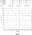
- FIG. 3shows XRR spectra of MPTMS related SiOC deposited on a 12 nm PVD TiN metallic surface after 500 deposition cycles.
- SiOC filmshave a wide variety of applications, as will be apparent to the skilled artisan, for example in integrated circuit fabrication.
- SiOC filmsare deposited on two or more different surfaces, for example on a metal surface and a dielectric surface as illustrated in FIG. 1 .
- the SiOC filmsare deposited on two or more different surfaces by a single deposition process.
- a SiOC filmcan be deposited on two different surfaces of a substrate by a plasma-enhanced atomic layer deposition (PEALD) process.
- PEALDplasma-enhanced atomic layer deposition
- SiOC films having low etch ratesare deposited by oxygen-free PEALD processes on a first surface comprising a first material and a second surface comprising a second, different material.
- the processesuse a Si-alkoxy-based precursor and plasma, such as Ar/H 2 plasma. The processes can be controlled to achieve uniform film deposition on a variety of different substrate surfaces.
- a SiOC filmis deposited using a PEALD process comprising alternately contacting the substrate with a first silicon alkoxy precursor and a plasma reactant, such as Ar/H 2 plasma.
- the first precursormay contain both oxygen and silicon.
- the filmgrows on a first surface, such as a dielectric surface, and on a second different surface, such as a metal or metallic surface. Excess reactant and/or reaction byproducts may be removed from the substrate surfaces between contacting steps, such as by exposing the substrate to a purge gas.
- a substratecomprising a first surface, such as a dielectric surface, and second different surface, such as a metal surface.
- the substrateis alternately and sequentially contacted with a silicon precursor, such as a silicon alkoxy precursor, and a plasma reactant, such as Ar/H 2 plasma.
- a silicon precursorsuch as a silicon alkoxy precursor
- a plasma reactantsuch as Ar/H 2 plasma.
- the plasma and silicon precursormay be provided in pulses separated by a purge in which excess reactant and reaction byproducts, if any, are removed from the substrate surface.
- the first and second surfaceare contacted with a purge gas between pulses of the silicon reactant and the plasma.
- a deposition processbegins with a silicon reactant pulse, and the reaction sequence, or deposition cycle, may be repeated a desired number of times (A): A ⁇ (silicon precursor pulse/purge/plasma pulse/purge)
- the deposition cyclebegins with a plasma pulse, which is followed by a silicon precursor pulse.
- the deposition cycleis repeated until a uniform SiOC film is deposited on two or more different surfaces. In some embodiments the deposition cycle is repeated at least 100 times, at least 200 times, at least 300 times, at least 400 times, or at least 500 times. In some embodiments the deposition cycle is repeated at least 1000 times. The deposition cycle may be repeated until a film of a desired thickness has been formed on the two or more different surfaces.
- deposition on two or more different surfacescan be achieved with a desired level of uniformity.
- the process conditions, such as plasma powercan be tuned such that growth proceeds uniformly on two or more different surfaces.
- a filmis considered to be uniformly deposited when it has a thickness that varies by less than 75%, less than 50%, less than 40%, less than 30%, less than 20%, less than 15%, less than 10%, less than 9%, less than 8%, less than 7%, less than 6%, less than 5%, less than 4%, less than 3%, less than 2% or even less than 1% between at least a first surface and a second different surface.
- thicknessis measured as the average thickness of the film deposited on a particular surface.
- uniformityis measured as the actual thickness variation measured between two different surfaces.
- the plasma reactantis hydrogen based.
- the plasmamay be generated in H 2 gas or a mixture of H 2 and a noble gas, such as Ar.
- the plasmais generated in a mixture of H 2 and Ar gas (referred to as Ar/H 2 plasma).
- the plasmais oxygen gas-free. That is, the plasma is generated in a gas or gas mixture that does not comprise oxygen.
- plasmafor example hydrogen containing plasma
- plasmamay be generated by applying RF power of from about 5 W to about 5000 W, 10 W to about 2000 W, from about 50 W to about 1000 W, or from about 100 W to about 500 W to a reactant gas or gas mixture.
- the RF power densitymay be from about 0.02 W/cm 2 to about 2.0 W/cm 2 , or from about 0.05 W/cm 2 to about 1.5 W/cm 2 .
- the RF powermay be applied to a gas that flows during the plasma contacting time, that flows continuously through the reaction chamber, and/or that flows through a remote plasma generator.
- the plasmais generated in situ, while in other embodiments the plasma is generated remotely.
- a showerhead reactoris utilized and plasma is generated between a susceptor (on top of which the substrate is located) and a showerhead plate.
- the deposition rateis similar on both surfaces. In some embodiments the deposition rate differs between the two or more different surfaces. For example, in some embodiments there may be a longer incubation time on one of the surfaces relative to the other. In some embodiments the growth rate on one surface may be different than on the other surface. In some embodiments the deposition rate on one or more surfaces may change over time. For example, the deposition rate on one surface may increase while the deposition rate on a second surface remains constant.
- deposition timecan be selected to achieve deposition of a SiOC film of similar, relatively uniform thickness on two or more different surfaces, such as on both dielectric and metal surfaces of the same substrate.
- the number of deposition cyclesis selected to achieve deposition of a SiOC film of a similar, relatively uniform thickness on two or more different surfaces of a substrate.
- the deposition processis carried out at a low processing temperature.
- the deposition temperatureis less than about 500° C., less than about 400° C., less than about 300° C., less than about 200° C. or less than about 100° C.
- a SiOC filmis deposited at a temperature of about 100° C. to about 300° C.
- a SiOC filmis deposited at a temperature of about 150° C. to 250° C.
- a SiOC filmis deposited at a temperature of about 200° C.
- a SiOC filmis deposited on two or more different surfaces comprising different materials in the same deposition process. In some embodiments a SiOC film is deposited uniformly on two or more different surfaces comprising two or more different materials, for example three or more different surfaces each comprising a different material, four or more different surfaces each comprising a different material etc. In some embodiments the two or more different surfaces are on the same substrate. In some embodiments the two or more surfaces are adjacent.
- a SiOC filmis deposited on all surfaces of a substrate.
- a SiOC filmis deposited on two or more different surfaces, where the two or more different surfaces comprise, for example, metal, oxide, oxidized metal, native metal oxide, native SiO 2 , Si, dielectric, SiO 2 , and/or Si 3 N 4 .
- a SiOC filmis deposited on two different surfaces, where one of the surfaces is a dielectric material and the other surface comprises a metal or metallic material.
- a dielectric surfacemay be, for example, a SiO 2 surface or a low-k surface.
- a dielectric materialcomprises one or more of SiO 2 , SiN and poly Si.
- a dielectric materialis SiO 2 .
- a dielectric materialis SiN.
- a dielectric materialis poly-Si.
- a SiOC filmis deposited on both a first surface and a second, surface that comprises a different material from the first surface.
- a SiOC filmmay be deposited on a first metal or metallic surface and a second dielectric surface.
- a SiOC filmis deposited on a SiO 2 surface and a metal surface.
- a SiOC filmis deposited on a SiO 2 surface and a W surface.
- a SiOC filmis deposited on a SiO 2 surface and a TiN surface.
- a SiOC filmis deposited on a W surface and a SiN surface.
- a SiOC filmis deposited on a TiN surface and a SiN surface.
- a SiOC filmis deposited on a W surface and a poly-Si surface.
- a SiOC filmis deposited on a TiN surface and a poly-Si surface.
- a SiOC filmis deposited on a TiN surface and a poly-Si surface.
- a SiOC filmis deposited with good uniformity on both a first surface and a second surface that comprises a different material from the first surface.
- a SiOC filmmay be deposited simultaneously and uniformly on a first metal or metallic surface and a second dielectric surface.
- a SiOC filmis deposited uniformly on a SiO 2 surface and a metal surface.
- a SiOC filmis deposited uniformly on a SiO 2 surface and a W surface.
- a SiOC filmis deposited uniformly on a SiO 2 surface and a TiN surface.
- a SiOC filmis deposited uniformly on a W surface and a SiN surface.
- a SiOC filmis deposited uniformly on a TiN surface and a SiN surface. In some embodiments a SiOC film is deposited uniformly on a W surface and a poly-Si surface. In some embodiment a SiOC film is deposited uniformly on a TiN surface and a poly-Si surface.
- a surfacemay be a metal surface or a metallic surface.
- the metal or metallic surfacemay comprise metal, metal oxides, and/or mixtures thereof.
- the metal or metallic surfacemay comprise surface oxidation.
- the metal or metallic material of a metal or metallic surfaceis electrically conductive with or without surface oxidation.
- a metal or a metallic surfacecomprises one or more transition metals.
- the metal or metallic surfacecomprises one or more of Al, Cu, Co, Ni, W, Nb, and Fe.
- a metal or metallic surfacecomprises W.
- a metal or metallic surfacecomprises one or more noble metals, such as Ru.
- a metal or metallic surfacecomprises a conductive metal oxide, nitride, carbide, boride, or combination thereof.
- the substratemay comprise a metal nitride, including, but not limited to TiN and/or TaN.
- the metal surfacemay comprise a metal carbide.
- the metal surfacemay comprise a metal chalcogenide.
- SiOCsilicon oxycarbide films
- SiOCis not intended to limit, restrict, or define the bonding or chemical state, for example the oxidation state of any of Si, O, C and/or any other element in the film.
- SiOC thin filmsmay comprise one or more elements in addition to Si, O and C.
- the SiOCmay comprise from about 0% to about 30% carbon on an atomic basis. In some embodiments the SiOC films may comprise from about 0% to about 60% oxygen on an atomic basis. In some embodiments the SiOC films may comprise about 0% to about 50% silicon on an atomic basis.
- the SiOC filmhas a low-k value. In some embodiments the SiOC film has a k value of less than 4.
- the substrate on which deposition is desiredis loaded into a reaction space or reactor.
- the reactormay be part of a cluster tool in which a variety of different processes in the formation of an integrated circuit are carried out.
- a flow-type reactoris utilized.
- a shower head type of reactoris utilized.
- a space divided reactoris utilized.
- a high-volume manufacturing-capable single wafer ALD reactoris used.
- a batch reactorcomprising multiple substrates is used.
- the number of substratesis in the range of 10 to 200, in the range of 50 to 150, or in the range of 100 to 130.
- suitable reactorsinclude commercially available equipment such as the F-120® reactor, F-450® reactor, Pulsar® reactors—such as the Pulsar® 2000 and the Pulsar® 3000—EmerALD® reactor and Advance® 400 Series reactors, available from ASM America, Inc of Phoenix, Ariz. and ASM Europe B.V., Almere, Netherlands.
- Other commercially available reactorsinclude those from ASM Japan K.K (Tokyo, Japan) under the tradename Eagle® XP and XP8.
- one or more exposed surfaces of the substratecan be pre-treated to provide reactive sites to react with the first phase of the PEALD process. In some embodiments a separate pre-treatment step is not required. In some embodiments the substrate is pre-treated to provide a desired surface termination. In some embodiments one or more surfaces of the substrate is pre-treated with plasma. In some embodiments the two or more surfaces on which SiOC is to be deposited are pre-treated with plasma, for example with H plasma.
- a metal or metallic surfaceis subject to a surface treatment prior to deposition.
- a metal or metallic surfacemay be treated by exposure to a plasma.
- the metal or metallic surfacemay be treated with H plasma prior to deposition.
- a W surfaceis treated with H plasma prior to deposition.
- the substrateis contacted with a first silicon precursor and a second plasma reactant.
- the deposition processis halogen free. In some embodiments the deposition process is oxygen free.
- the silicon precursorhas the formula (1.): Si(OR I ) 4-x R II x
- R Iis alkyl with 1-5 carbons and R II is any ligand containing carbon and/or hydrogen and/or oxygen.
- R IIcan have, for example, alkenyl, alkynyl, phenyl, carbonyl, aldehyde, ester, ether, carboxyl, peroxy or hydroperoxy functionalities. All R I and R II groups can be chosen independently from each other.
- the silicon precursoris MPTMS.
- R Iis methyl
- R IIis 3-methoxypropyl
- xis 1.
- the PEALD processesdo not comprise oxygen plasma or plasma comprising oxygen species.
- each PEALD cyclecomprises at least two distinct phases.
- the contacting and removal of a reactant from the substratemay be considered a phase.
- a vapor phase first reactantcomprising silicon contacts the substrate and forms no more than about one monolayer on the surface on which deposition is desired.
- This reactantis also referred to herein as “the silicon precursor,” “silicon-containing precursor,” or “silicon reactant” and may be, for example, 3-methoxypropyltrimethoxysilane (MPTMS).
- the first reactantcomprises both silicon and oxygen.
- a second reactantcomprising a reactive species contacts the substrate surfaces and may convert adsorbed silicon to SiOC on the dielectric surface.
- the second reactantcomprises a hydrogen plasma, such as a H 2 /Ar plasma.
- a gas that is used to form a plasmamay flow constantly throughout the deposition process but only be activated intermittently.
- a gas that is used to form a plasmadoes not comprise oxygen.
- the adsorbed silicon precursoris not contacted with a reactive species generated by a plasma from oxygen.
- a second reactant comprising reactive speciesis generated in a gas that does not comprise oxygen.
- a second reactantmay comprise a plasma generated in a gas that does not comprise oxygen.
- the second reactantmay be generated in a gas comprising less than about 1 atomic % (at %) oxygen, less than about 0.1 at % oxygen, less than about 0.01 at % oxygen, or less than about 0.001 at % oxygen.
- Additional phasesmay be added and phases may be removed as desired to adjust the composition of the final film.
- one or more deposition cyclesbegin by contacting the substrate with the silicon precursor, followed by the second plasma reactant. In other embodiments deposition may begin by contacting the substrate with the second plasma reactant, followed by the silicon precursor.
- Excess reactant and reaction byproducts, if any,are removed from the vicinity of the substrate, and in particular from the substrate surface, between reactant contacting phases.
- excess reactant and reaction byproducts, if any,are removed from the substrate surface by, for example, purging the reaction chamber between reactant contacting phases, such as by purging with an inert gas.
- the flow rate and contacting time of each reactantis tunable, as is the removal step, allowing for control of the quality and various properties of the films.
- the deposition cycleis repeated until a SiOC film of the desired thickness is obtained on the desired surfaces.
- the deposition parameterssuch as the precursor flow rate, contacting time, removal time, and/or reactants themselves, may be varied in one or more deposition cycles during the PEALD process in order to obtain a film with the desired characteristics on two or more different surfaces.
- the second plasma reactantis provided in two or more distinct pulses, without introducing another reactant in between any of the two or more pulses.
- a plasmais provided in two or more sequential pulses, without introducing a Si-precursor in between the sequential plasma pulses.
- two or more sequential plasma pulsesare generated by providing a plasma discharge for a first period of time, extinguishing the plasma discharge for a second period of time, for example from about 0.1 seconds to about 10 seconds, from about 0.5 seconds to about 5 seconds or about 1.0 seconds to about 4.0 seconds, and exciting it again for a third period of time before introduction of another precursor or a removal step, such as before the Si-precursor or a purge step. Additional pulses of plasma can be introduced in the same way.
- a plasmais ignited for an equivalent period of time in each of the pulses.
- removing excess reactant and reaction byproducts, if any,may comprise purging the reaction chamber.
- the reaction chambermay be purged by stopping the flow of the second reactant while continuing to flow a carrier gas or purge gas for a sufficient time to diffuse or purge excess reactants and reactant by-products, if any, from the reaction space.
- the excess second precursoris purged with the aid of inert gas, such as nitrogen or argon, which is flowing throughout the PEALD cycle.
- the substratemay be moved from the reaction space containing the second reactant to a different reaction space.
- the removalmay, in some embodiments, be from about 0.1 seconds to about 10 seconds, about 0.1 seconds to about 4 seconds or about 0.1 seconds to about 0.5 seconds.
- the reactive species contacting and removalrepresent a second, reactive species phase in a SiOC atomic layer deposition cycle.
- the pressure of the reaction chamber during processingis maintained at from about 0.01 Torr to about 50 Torr, or from about 0.1 Torr to about 10 Torr. In some embodiments the pressure of the reaction chamber is greater than about 6 Torr, or about 20 Torr.
- a direct plasma PEALD reactorwas used to deposit SiOC films by PEALD using 3-Methoxypropyl(trimethoxysilane) (MPTMS) as the silicon precursor. No heating of the precursor to produce vapor-phase reactant was required due to high enough vapor pressure of the compound. Experiments were carried out at a deposition temperature of 200° C. The growth rate per cycle (GPC) of the process was typically ⁇ 0.2 ⁇ /c.
- FIG. 2shows SEM images of SiOC films deposited at 200° C. on a substrate comprising adjacent horizontal surfaces of W and SiO2.
- FIG. 3shows that around 6.2 nm of SiOC film was deposited on a TiN surface using MPTMS as the silicon precursor after 500 cycles, which indicates a slightly lower growth per cycle than that observed on native oxide surfaces.
Landscapes
- Chemical & Material Sciences (AREA)
- Engineering & Computer Science (AREA)
- Physics & Mathematics (AREA)
- Chemical Kinetics & Catalysis (AREA)
- Computer Hardware Design (AREA)
- Condensed Matter Physics & Semiconductors (AREA)
- Microelectronics & Electronic Packaging (AREA)
- Power Engineering (AREA)
- General Physics & Mathematics (AREA)
- Manufacturing & Machinery (AREA)
- Metallurgy (AREA)
- Materials Engineering (AREA)
- Mechanical Engineering (AREA)
- General Chemical & Material Sciences (AREA)
- Organic Chemistry (AREA)
- Plasma & Fusion (AREA)
- Inorganic Chemistry (AREA)
- Electromagnetism (AREA)
- Spectroscopy & Molecular Physics (AREA)
- Chemical Vapour Deposition (AREA)
- Formation Of Insulating Films (AREA)
Abstract
Description
A×(silicon precursor pulse/purge/plasma pulse/purge)
Si(ORI)4-xRIIx
Claims (20)
Priority Applications (1)
| Application Number | Priority Date | Filing Date | Title |
|---|---|---|---|
| US16/208,350US10991573B2 (en) | 2017-12-04 | 2018-12-03 | Uniform deposition of SiOC on dielectric and metal surfaces |
Applications Claiming Priority (2)
| Application Number | Priority Date | Filing Date | Title |
|---|---|---|---|
| US201762594474P | 2017-12-04 | 2017-12-04 | |
| US16/208,350US10991573B2 (en) | 2017-12-04 | 2018-12-03 | Uniform deposition of SiOC on dielectric and metal surfaces |
Publications (2)
| Publication Number | Publication Date |
|---|---|
| US20190172701A1 US20190172701A1 (en) | 2019-06-06 |
| US10991573B2true US10991573B2 (en) | 2021-04-27 |
Family
ID=66659457
Family Applications (1)
| Application Number | Title | Priority Date | Filing Date |
|---|---|---|---|
| US16/208,350Active2039-03-14US10991573B2 (en) | 2017-12-04 | 2018-12-03 | Uniform deposition of SiOC on dielectric and metal surfaces |
Country Status (3)
| Country | Link |
|---|---|
| US (1) | US10991573B2 (en) |
| KR (1) | KR20190065962A (en) |
| TW (1) | TWI761636B (en) |
Cited By (8)
| Publication number | Priority date | Publication date | Assignee | Title |
|---|---|---|---|---|
| US20210301392A1 (en)* | 2020-03-30 | 2021-09-30 | Asm Ip Holding B.V. | Selective deposition of silicon oxide on dielectric surfaces relative to metal surfaces |
| US11195845B2 (en) | 2017-04-13 | 2021-12-07 | Asm Ip Holding B.V. | Substrate processing method and device manufactured by the same |
| US11501965B2 (en) | 2017-05-05 | 2022-11-15 | Asm Ip Holding B.V. | Plasma enhanced deposition processes for controlled formation of metal oxide thin films |
| US11562900B2 (en) | 2016-05-06 | 2023-01-24 | Asm Ip Holding B.V. | Formation of SiOC thin films |
| US11664219B2 (en) | 2019-10-31 | 2023-05-30 | Asm Ip Holding B.V. | Selective deposition of SiOC thin films |
| US11776807B2 (en) | 2017-05-05 | 2023-10-03 | ASM IP Holding, B.V. | Plasma enhanced deposition processes for controlled formation of oxygen containing thin films |
| US11996284B2 (en) | 2015-11-12 | 2024-05-28 | Asm Ip Holding B.V. | Formation of SiOCN thin films |
| US12227835B2 (en) | 2021-10-29 | 2025-02-18 | Asm Ip Holding B.V. | Selective deposition of material comprising silicon and oxygen using plasma |
Families Citing this family (230)
| Publication number | Priority date | Publication date | Assignee | Title |
|---|---|---|---|---|
| US20130023129A1 (en) | 2011-07-20 | 2013-01-24 | Asm America, Inc. | Pressure transmitter for a semiconductor processing environment |
| US20160376700A1 (en) | 2013-02-01 | 2016-12-29 | Asm Ip Holding B.V. | System for treatment of deposition reactor |
| US10941490B2 (en) | 2014-10-07 | 2021-03-09 | Asm Ip Holding B.V. | Multiple temperature range susceptor, assembly, reactor and system including the susceptor, and methods of using the same |
| US10276355B2 (en) | 2015-03-12 | 2019-04-30 | Asm Ip Holding B.V. | Multi-zone reactor, system including the reactor, and method of using the same |
| US11139308B2 (en) | 2015-12-29 | 2021-10-05 | Asm Ip Holding B.V. | Atomic layer deposition of III-V compounds to form V-NAND devices |
| US10529554B2 (en) | 2016-02-19 | 2020-01-07 | Asm Ip Holding B.V. | Method for forming silicon nitride film selectively on sidewalls or flat surfaces of trenches |
| US10343920B2 (en) | 2016-03-18 | 2019-07-09 | Asm Ip Holding B.V. | Aligned carbon nanotubes |
| US11453943B2 (en) | 2016-05-25 | 2022-09-27 | Asm Ip Holding B.V. | Method for forming carbon-containing silicon/metal oxide or nitride film by ALD using silicon precursor and hydrocarbon precursor |
| US10612137B2 (en) | 2016-07-08 | 2020-04-07 | Asm Ip Holdings B.V. | Organic reactants for atomic layer deposition |
| US9859151B1 (en) | 2016-07-08 | 2018-01-02 | Asm Ip Holding B.V. | Selective film deposition method to form air gaps |
| US9812320B1 (en) | 2016-07-28 | 2017-11-07 | Asm Ip Holding B.V. | Method and apparatus for filling a gap |
| US9887082B1 (en) | 2016-07-28 | 2018-02-06 | Asm Ip Holding B.V. | Method and apparatus for filling a gap |
| US11532757B2 (en) | 2016-10-27 | 2022-12-20 | Asm Ip Holding B.V. | Deposition of charge trapping layers |
| US10714350B2 (en) | 2016-11-01 | 2020-07-14 | ASM IP Holdings, B.V. | Methods for forming a transition metal niobium nitride film on a substrate by atomic layer deposition and related semiconductor device structures |
| KR102546317B1 (en) | 2016-11-15 | 2023-06-21 | 에이에스엠 아이피 홀딩 비.브이. | Gas supply unit and substrate processing apparatus including the same |
| US11581186B2 (en) | 2016-12-15 | 2023-02-14 | Asm Ip Holding B.V. | Sequential infiltration synthesis apparatus |
| US11447861B2 (en) | 2016-12-15 | 2022-09-20 | Asm Ip Holding B.V. | Sequential infiltration synthesis apparatus and a method of forming a patterned structure |
| US11390950B2 (en) | 2017-01-10 | 2022-07-19 | Asm Ip Holding B.V. | Reactor system and method to reduce residue buildup during a film deposition process |
| US10468261B2 (en) | 2017-02-15 | 2019-11-05 | Asm Ip Holding B.V. | Methods for forming a metallic film on a substrate by cyclical deposition and related semiconductor device structures |
| US10770286B2 (en) | 2017-05-08 | 2020-09-08 | Asm Ip Holdings B.V. | Methods for selectively forming a silicon nitride film on a substrate and related semiconductor device structures |
| US12040200B2 (en) | 2017-06-20 | 2024-07-16 | Asm Ip Holding B.V. | Semiconductor processing apparatus and methods for calibrating a semiconductor processing apparatus |
| US11306395B2 (en) | 2017-06-28 | 2022-04-19 | Asm Ip Holding B.V. | Methods for depositing a transition metal nitride film on a substrate by atomic layer deposition and related deposition apparatus |
| KR20190009245A (en) | 2017-07-18 | 2019-01-28 | 에이에스엠 아이피 홀딩 비.브이. | Methods for forming a semiconductor device structure and related semiconductor device structures |
| US11374112B2 (en) | 2017-07-19 | 2022-06-28 | Asm Ip Holding B.V. | Method for depositing a group IV semiconductor and related semiconductor device structures |
| US10590535B2 (en) | 2017-07-26 | 2020-03-17 | Asm Ip Holdings B.V. | Chemical treatment, deposition and/or infiltration apparatus and method for using the same |
| TWI815813B (en) | 2017-08-04 | 2023-09-21 | 荷蘭商Asm智慧財產控股公司 | Showerhead assembly for distributing a gas within a reaction chamber |
| US10770336B2 (en) | 2017-08-08 | 2020-09-08 | Asm Ip Holding B.V. | Substrate lift mechanism and reactor including same |
| US10692741B2 (en) | 2017-08-08 | 2020-06-23 | Asm Ip Holdings B.V. | Radiation shield |
| US11769682B2 (en) | 2017-08-09 | 2023-09-26 | Asm Ip Holding B.V. | Storage apparatus for storing cassettes for substrates and processing apparatus equipped therewith |
| US11830730B2 (en) | 2017-08-29 | 2023-11-28 | Asm Ip Holding B.V. | Layer forming method and apparatus |
| US11295980B2 (en) | 2017-08-30 | 2022-04-05 | Asm Ip Holding B.V. | Methods for depositing a molybdenum metal film over a dielectric surface of a substrate by a cyclical deposition process and related semiconductor device structures |
| US10658205B2 (en) | 2017-09-28 | 2020-05-19 | Asm Ip Holdings B.V. | Chemical dispensing apparatus and methods for dispensing a chemical to a reaction chamber |
| US10403504B2 (en) | 2017-10-05 | 2019-09-03 | Asm Ip Holding B.V. | Method for selectively depositing a metallic film on a substrate |
| US10923344B2 (en) | 2017-10-30 | 2021-02-16 | Asm Ip Holding B.V. | Methods for forming a semiconductor structure and related semiconductor structures |
| CN111344522B (en) | 2017-11-27 | 2022-04-12 | 阿斯莫Ip控股公司 | Including clean mini-environment device |
| WO2019103613A1 (en) | 2017-11-27 | 2019-05-31 | Asm Ip Holding B.V. | A storage device for storing wafer cassettes for use with a batch furnace |
| US10872771B2 (en) | 2018-01-16 | 2020-12-22 | Asm Ip Holding B. V. | Method for depositing a material film on a substrate within a reaction chamber by a cyclical deposition process and related device structures |
| TWI799494B (en) | 2018-01-19 | 2023-04-21 | 荷蘭商Asm 智慧財產控股公司 | Deposition method |
| KR102695659B1 (en) | 2018-01-19 | 2024-08-14 | 에이에스엠 아이피 홀딩 비.브이. | Method for depositing a gap filling layer by plasma assisted deposition |
| US11081345B2 (en) | 2018-02-06 | 2021-08-03 | Asm Ip Holding B.V. | Method of post-deposition treatment for silicon oxide film |
| WO2019158960A1 (en) | 2018-02-14 | 2019-08-22 | Asm Ip Holding B.V. | A method for depositing a ruthenium-containing film on a substrate by a cyclical deposition process |
| US10896820B2 (en) | 2018-02-14 | 2021-01-19 | Asm Ip Holding B.V. | Method for depositing a ruthenium-containing film on a substrate by a cyclical deposition process |
| US10731249B2 (en) | 2018-02-15 | 2020-08-04 | Asm Ip Holding B.V. | Method of forming a transition metal containing film on a substrate by a cyclical deposition process, a method for supplying a transition metal halide compound to a reaction chamber, and related vapor deposition apparatus |
| KR102636427B1 (en) | 2018-02-20 | 2024-02-13 | 에이에스엠 아이피 홀딩 비.브이. | Substrate processing method and apparatus |
| US10975470B2 (en) | 2018-02-23 | 2021-04-13 | Asm Ip Holding B.V. | Apparatus for detecting or monitoring for a chemical precursor in a high temperature environment |
| US11473195B2 (en) | 2018-03-01 | 2022-10-18 | Asm Ip Holding B.V. | Semiconductor processing apparatus and a method for processing a substrate |
| KR102646467B1 (en) | 2018-03-27 | 2024-03-11 | 에이에스엠 아이피 홀딩 비.브이. | Method of forming an electrode on a substrate and a semiconductor device structure including an electrode |
| KR102600229B1 (en) | 2018-04-09 | 2023-11-10 | 에이에스엠 아이피 홀딩 비.브이. | Substrate supporting device, substrate processing apparatus including the same and substrate processing method |
| US12025484B2 (en) | 2018-05-08 | 2024-07-02 | Asm Ip Holding B.V. | Thin film forming method |
| US12272527B2 (en) | 2018-05-09 | 2025-04-08 | Asm Ip Holding B.V. | Apparatus for use with hydrogen radicals and method of using same |
| KR102596988B1 (en) | 2018-05-28 | 2023-10-31 | 에이에스엠 아이피 홀딩 비.브이. | Method of processing a substrate and a device manufactured by the same |
| US11718913B2 (en) | 2018-06-04 | 2023-08-08 | Asm Ip Holding B.V. | Gas distribution system and reactor system including same |
| KR102568797B1 (en) | 2018-06-21 | 2023-08-21 | 에이에스엠 아이피 홀딩 비.브이. | Substrate processing system |
| US10797133B2 (en) | 2018-06-21 | 2020-10-06 | Asm Ip Holding B.V. | Method for depositing a phosphorus doped silicon arsenide film and related semiconductor device structures |
| KR102854019B1 (en) | 2018-06-27 | 2025-09-02 | 에이에스엠 아이피 홀딩 비.브이. | Periodic deposition method for forming a metal-containing material and films and structures comprising the metal-containing material |
| TWI873894B (en) | 2018-06-27 | 2025-02-21 | 荷蘭商Asm Ip私人控股有限公司 | Cyclic deposition methods for forming metal-containing material and films and structures including the metal-containing material |
| US10388513B1 (en) | 2018-07-03 | 2019-08-20 | Asm Ip Holding B.V. | Method for depositing silicon-free carbon-containing film as gap-fill layer by pulse plasma-assisted deposition |
| US10755922B2 (en) | 2018-07-03 | 2020-08-25 | Asm Ip Holding B.V. | Method for depositing silicon-free carbon-containing film as gap-fill layer by pulse plasma-assisted deposition |
| US11430674B2 (en) | 2018-08-22 | 2022-08-30 | Asm Ip Holding B.V. | Sensor array, apparatus for dispensing a vapor phase reactant to a reaction chamber and related methods |
| US11024523B2 (en) | 2018-09-11 | 2021-06-01 | Asm Ip Holding B.V. | Substrate processing apparatus and method |
| KR102707956B1 (en) | 2018-09-11 | 2024-09-19 | 에이에스엠 아이피 홀딩 비.브이. | Method for deposition of a thin film |
| CN110970344B (en) | 2018-10-01 | 2024-10-25 | Asmip控股有限公司 | Substrate holding apparatus, system comprising the same and method of using the same |
| KR102592699B1 (en) | 2018-10-08 | 2023-10-23 | 에이에스엠 아이피 홀딩 비.브이. | Substrate support unit and apparatuses for depositing thin film and processing the substrate including the same |
| KR102546322B1 (en) | 2018-10-19 | 2023-06-21 | 에이에스엠 아이피 홀딩 비.브이. | Substrate processing apparatus and substrate processing method |
| US12378665B2 (en) | 2018-10-26 | 2025-08-05 | Asm Ip Holding B.V. | High temperature coatings for a preclean and etch apparatus and related methods |
| US11087997B2 (en) | 2018-10-31 | 2021-08-10 | Asm Ip Holding B.V. | Substrate processing apparatus for processing substrates |
| KR102748291B1 (en) | 2018-11-02 | 2024-12-31 | 에이에스엠 아이피 홀딩 비.브이. | Substrate support unit and substrate processing apparatus including the same |
| US11572620B2 (en) | 2018-11-06 | 2023-02-07 | Asm Ip Holding B.V. | Methods for selectively depositing an amorphous silicon film on a substrate |
| US10818758B2 (en) | 2018-11-16 | 2020-10-27 | Asm Ip Holding B.V. | Methods for forming a metal silicate film on a substrate in a reaction chamber and related semiconductor device structures |
| US12040199B2 (en) | 2018-11-28 | 2024-07-16 | Asm Ip Holding B.V. | Substrate processing apparatus for processing substrates |
| KR102636428B1 (en) | 2018-12-04 | 2024-02-13 | 에이에스엠 아이피 홀딩 비.브이. | A method for cleaning a substrate processing apparatus |
| US11158513B2 (en) | 2018-12-13 | 2021-10-26 | Asm Ip Holding B.V. | Methods for forming a rhenium-containing film on a substrate by a cyclical deposition process and related semiconductor device structures |
| TWI874340B (en) | 2018-12-14 | 2025-03-01 | 荷蘭商Asm Ip私人控股有限公司 | Method of forming device structure, structure formed by the method and system for performing the method |
| TWI866480B (en) | 2019-01-17 | 2024-12-11 | 荷蘭商Asm Ip 私人控股有限公司 | Methods of forming a transition metal containing film on a substrate by a cyclical deposition process |
| TWI845607B (en) | 2019-02-20 | 2024-06-21 | 荷蘭商Asm Ip私人控股有限公司 | Cyclical deposition method and apparatus for filling a recess formed within a substrate surface |
| TWI873122B (en) | 2019-02-20 | 2025-02-21 | 荷蘭商Asm Ip私人控股有限公司 | Method of filling a recess formed within a surface of a substrate, semiconductor structure formed according to the method, and semiconductor processing apparatus |
| TWI838458B (en) | 2019-02-20 | 2024-04-11 | 荷蘭商Asm Ip私人控股有限公司 | Apparatus and methods for plug fill deposition in 3-d nand applications |
| TWI842826B (en) | 2019-02-22 | 2024-05-21 | 荷蘭商Asm Ip私人控股有限公司 | Substrate processing apparatus and method for processing substrate |
| US11742198B2 (en) | 2019-03-08 | 2023-08-29 | Asm Ip Holding B.V. | Structure including SiOCN layer and method of forming same |
| KR102858005B1 (en) | 2019-03-08 | 2025-09-09 | 에이에스엠 아이피 홀딩 비.브이. | Method for Selective Deposition of Silicon Nitride Layer and Structure Including Selectively-Deposited Silicon Nitride Layer |
| JP2020167398A (en) | 2019-03-28 | 2020-10-08 | エーエスエム・アイピー・ホールディング・ベー・フェー | Door openers and substrate processing equipment provided with door openers |
| KR102809999B1 (en) | 2019-04-01 | 2025-05-19 | 에이에스엠 아이피 홀딩 비.브이. | Method of manufacturing semiconductor device |
| KR20200123380A (en) | 2019-04-19 | 2020-10-29 | 에이에스엠 아이피 홀딩 비.브이. | Layer forming method and apparatus |
| KR20200125453A (en) | 2019-04-24 | 2020-11-04 | 에이에스엠 아이피 홀딩 비.브이. | Gas-phase reactor system and method of using same |
| KR20200130121A (en) | 2019-05-07 | 2020-11-18 | 에이에스엠 아이피 홀딩 비.브이. | Chemical source vessel with dip tube |
| KR20200130652A (en) | 2019-05-10 | 2020-11-19 | 에이에스엠 아이피 홀딩 비.브이. | Method of depositing material onto a surface and structure formed according to the method |
| JP7612342B2 (en) | 2019-05-16 | 2025-01-14 | エーエスエム・アイピー・ホールディング・ベー・フェー | Wafer boat handling apparatus, vertical batch furnace and method |
| JP7598201B2 (en) | 2019-05-16 | 2024-12-11 | エーエスエム・アイピー・ホールディング・ベー・フェー | Wafer boat handling apparatus, vertical batch furnace and method |
| USD975665S1 (en) | 2019-05-17 | 2023-01-17 | Asm Ip Holding B.V. | Susceptor shaft |
| USD947913S1 (en) | 2019-05-17 | 2022-04-05 | Asm Ip Holding B.V. | Susceptor shaft |
| KR20200141002A (en) | 2019-06-06 | 2020-12-17 | 에이에스엠 아이피 홀딩 비.브이. | Method of using a gas-phase reactor system including analyzing exhausted gas |
| KR20200141931A (en) | 2019-06-10 | 2020-12-21 | 에이에스엠 아이피 홀딩 비.브이. | Method for cleaning quartz epitaxial chambers |
| KR20200143254A (en) | 2019-06-11 | 2020-12-23 | 에이에스엠 아이피 홀딩 비.브이. | Method of forming an electronic structure using an reforming gas, system for performing the method, and structure formed using the method |
| KR20210005515A (en) | 2019-07-03 | 2021-01-14 | 에이에스엠 아이피 홀딩 비.브이. | Temperature control assembly for substrate processing apparatus and method of using same |
| JP7499079B2 (en) | 2019-07-09 | 2024-06-13 | エーエスエム・アイピー・ホールディング・ベー・フェー | Plasma device using coaxial waveguide and substrate processing method |
| CN112216646A (en) | 2019-07-10 | 2021-01-12 | Asm Ip私人控股有限公司 | Substrate supporting assembly and substrate processing device comprising same |
| KR20210010307A (en) | 2019-07-16 | 2021-01-27 | 에이에스엠 아이피 홀딩 비.브이. | Substrate processing apparatus |
| KR102860110B1 (en) | 2019-07-17 | 2025-09-16 | 에이에스엠 아이피 홀딩 비.브이. | Methods of forming silicon germanium structures |
| KR20210010816A (en) | 2019-07-17 | 2021-01-28 | 에이에스엠 아이피 홀딩 비.브이. | Radical assist ignition plasma system and method |
| US11643724B2 (en) | 2019-07-18 | 2023-05-09 | Asm Ip Holding B.V. | Method of forming structures using a neutral beam |
| KR20210010817A (en) | 2019-07-19 | 2021-01-28 | 에이에스엠 아이피 홀딩 비.브이. | Method of Forming Topology-Controlled Amorphous Carbon Polymer Film |
| TWI851767B (en) | 2019-07-29 | 2024-08-11 | 荷蘭商Asm Ip私人控股有限公司 | Methods for selective deposition utilizing n-type dopants and/or alternative dopants to achieve high dopant incorporation |
| CN112309900A (en) | 2019-07-30 | 2021-02-02 | Asm Ip私人控股有限公司 | Substrate processing apparatus |
| CN112309899A (en) | 2019-07-30 | 2021-02-02 | Asm Ip私人控股有限公司 | Substrate processing apparatus |
| US12169361B2 (en) | 2019-07-30 | 2024-12-17 | Asm Ip Holding B.V. | Substrate processing apparatus and method |
| US11587814B2 (en) | 2019-07-31 | 2023-02-21 | Asm Ip Holding B.V. | Vertical batch furnace assembly |
| US11587815B2 (en) | 2019-07-31 | 2023-02-21 | Asm Ip Holding B.V. | Vertical batch furnace assembly |
| US11227782B2 (en) | 2019-07-31 | 2022-01-18 | Asm Ip Holding B.V. | Vertical batch furnace assembly |
| CN112323048B (en) | 2019-08-05 | 2024-02-09 | Asm Ip私人控股有限公司 | Liquid level sensor for chemical source container |
| CN112342526A (en) | 2019-08-09 | 2021-02-09 | Asm Ip私人控股有限公司 | Heater assembly including cooling device and method of using same |
| USD965524S1 (en) | 2019-08-19 | 2022-10-04 | Asm Ip Holding B.V. | Susceptor support |
| JP7243521B2 (en)* | 2019-08-19 | 2023-03-22 | 東京エレクトロン株式会社 | Film forming method and film forming apparatus |
| USD965044S1 (en) | 2019-08-19 | 2022-09-27 | Asm Ip Holding B.V. | Susceptor shaft |
| JP2021031769A (en) | 2019-08-21 | 2021-03-01 | エーエスエム アイピー ホールディング ビー.ブイ. | Production apparatus of mixed gas of film deposition raw material and film deposition apparatus |
| KR20210024423A (en) | 2019-08-22 | 2021-03-05 | 에이에스엠 아이피 홀딩 비.브이. | Method for forming a structure with a hole |
| USD979506S1 (en) | 2019-08-22 | 2023-02-28 | Asm Ip Holding B.V. | Insulator |
| KR20210024420A (en) | 2019-08-23 | 2021-03-05 | 에이에스엠 아이피 홀딩 비.브이. | Method for depositing silicon oxide film having improved quality by peald using bis(diethylamino)silane |
| US11286558B2 (en) | 2019-08-23 | 2022-03-29 | Asm Ip Holding B.V. | Methods for depositing a molybdenum nitride film on a surface of a substrate by a cyclical deposition process and related semiconductor device structures including a molybdenum nitride film |
| US11186909B2 (en)* | 2019-08-26 | 2021-11-30 | Applied Materials, Inc. | Methods of depositing low-K films |
| KR102806450B1 (en) | 2019-09-04 | 2025-05-12 | 에이에스엠 아이피 홀딩 비.브이. | Methods for selective deposition using a sacrificial capping layer |
| KR102733104B1 (en) | 2019-09-05 | 2024-11-22 | 에이에스엠 아이피 홀딩 비.브이. | Substrate processing apparatus |
| US11562901B2 (en) | 2019-09-25 | 2023-01-24 | Asm Ip Holding B.V. | Substrate processing method |
| CN112593212B (en) | 2019-10-02 | 2023-12-22 | Asm Ip私人控股有限公司 | Method for forming topologically selective silicon oxide film by cyclic plasma enhanced deposition process |
| TWI846953B (en) | 2019-10-08 | 2024-07-01 | 荷蘭商Asm Ip私人控股有限公司 | Substrate processing device |
| KR20210042810A (en) | 2019-10-08 | 2021-04-20 | 에이에스엠 아이피 홀딩 비.브이. | Reactor system including a gas distribution assembly for use with activated species and method of using same |
| TW202128273A (en) | 2019-10-08 | 2021-08-01 | 荷蘭商Asm Ip私人控股有限公司 | Gas injection system, reactor system, and method of depositing material on surface of substratewithin reaction chamber |
| TWI846966B (en) | 2019-10-10 | 2024-07-01 | 荷蘭商Asm Ip私人控股有限公司 | Method of forming a photoresist underlayer and structure including same |
| US12009241B2 (en) | 2019-10-14 | 2024-06-11 | Asm Ip Holding B.V. | Vertical batch furnace assembly with detector to detect cassette |
| TWI834919B (en) | 2019-10-16 | 2024-03-11 | 荷蘭商Asm Ip私人控股有限公司 | Method of topology-selective film formation of silicon oxide |
| US11637014B2 (en) | 2019-10-17 | 2023-04-25 | Asm Ip Holding B.V. | Methods for selective deposition of doped semiconductor material |
| KR102845724B1 (en) | 2019-10-21 | 2025-08-13 | 에이에스엠 아이피 홀딩 비.브이. | Apparatus and methods for selectively etching films |
| KR20210050453A (en) | 2019-10-25 | 2021-05-07 | 에이에스엠 아이피 홀딩 비.브이. | Methods for filling a gap feature on a substrate surface and related semiconductor structures |
| US11646205B2 (en) | 2019-10-29 | 2023-05-09 | Asm Ip Holding B.V. | Methods of selectively forming n-type doped material on a surface, systems for selectively forming n-type doped material, and structures formed using same |
| KR20210054983A (en) | 2019-11-05 | 2021-05-14 | 에이에스엠 아이피 홀딩 비.브이. | Structures with doped semiconductor layers and methods and systems for forming same |
| US11501968B2 (en) | 2019-11-15 | 2022-11-15 | Asm Ip Holding B.V. | Method for providing a semiconductor device with silicon filled gaps |
| KR102861314B1 (en) | 2019-11-20 | 2025-09-17 | 에이에스엠 아이피 홀딩 비.브이. | Method of depositing carbon-containing material on a surface of a substrate, structure formed using the method, and system for forming the structure |
| US11450529B2 (en) | 2019-11-26 | 2022-09-20 | Asm Ip Holding B.V. | Methods for selectively forming a target film on a substrate comprising a first dielectric surface and a second metallic surface |
| CN112951697B (en) | 2019-11-26 | 2025-07-29 | Asmip私人控股有限公司 | Substrate processing apparatus |
| CN112885692B (en) | 2019-11-29 | 2025-08-15 | Asmip私人控股有限公司 | Substrate processing apparatus |
| CN120432376A (en) | 2019-11-29 | 2025-08-05 | Asm Ip私人控股有限公司 | Substrate processing apparatus |
| JP7527928B2 (en) | 2019-12-02 | 2024-08-05 | エーエスエム・アイピー・ホールディング・ベー・フェー | Substrate processing apparatus and substrate processing method |
| KR20210070898A (en) | 2019-12-04 | 2021-06-15 | 에이에스엠 아이피 홀딩 비.브이. | Substrate processing apparatus |
| KR20210078405A (en) | 2019-12-17 | 2021-06-28 | 에이에스엠 아이피 홀딩 비.브이. | Method of forming vanadium nitride layer and structure including the vanadium nitride layer |
| KR20210080214A (en) | 2019-12-19 | 2021-06-30 | 에이에스엠 아이피 홀딩 비.브이. | Methods for filling a gap feature on a substrate and related semiconductor structures |
| JP7730637B2 (en) | 2020-01-06 | 2025-08-28 | エーエスエム・アイピー・ホールディング・ベー・フェー | Gas delivery assembly, components thereof, and reactor system including same |
| JP7636892B2 (en) | 2020-01-06 | 2025-02-27 | エーエスエム・アイピー・ホールディング・ベー・フェー | Channeled Lift Pins |
| US11993847B2 (en) | 2020-01-08 | 2024-05-28 | Asm Ip Holding B.V. | Injector |
| KR20210093163A (en) | 2020-01-16 | 2021-07-27 | 에이에스엠 아이피 홀딩 비.브이. | Method of forming high aspect ratio features |
| KR102675856B1 (en) | 2020-01-20 | 2024-06-17 | 에이에스엠 아이피 홀딩 비.브이. | Method of forming thin film and method of modifying surface of thin film |
| TWI889744B (en) | 2020-01-29 | 2025-07-11 | 荷蘭商Asm Ip私人控股有限公司 | Contaminant trap system, and baffle plate stack |
| TW202513845A (en) | 2020-02-03 | 2025-04-01 | 荷蘭商Asm Ip私人控股有限公司 | Semiconductor structures and methods for forming the same |
| KR20210100010A (en) | 2020-02-04 | 2021-08-13 | 에이에스엠 아이피 홀딩 비.브이. | Method and apparatus for transmittance measurements of large articles |
| US11776846B2 (en) | 2020-02-07 | 2023-10-03 | Asm Ip Holding B.V. | Methods for depositing gap filling fluids and related systems and devices |
| KR20210103956A (en) | 2020-02-13 | 2021-08-24 | 에이에스엠 아이피 홀딩 비.브이. | Substrate processing apparatus including light receiving device and calibration method of light receiving device |
| TW202146691A (en) | 2020-02-13 | 2021-12-16 | 荷蘭商Asm Ip私人控股有限公司 | Gas distribution assembly, shower plate assembly, and method of adjusting conductance of gas to reaction chamber |
| TWI855223B (en) | 2020-02-17 | 2024-09-11 | 荷蘭商Asm Ip私人控股有限公司 | Method for growing phosphorous-doped silicon layer |
| CN113410160A (en) | 2020-02-28 | 2021-09-17 | Asm Ip私人控股有限公司 | System specially used for cleaning parts |
| KR20210113043A (en) | 2020-03-04 | 2021-09-15 | 에이에스엠 아이피 홀딩 비.브이. | Alignment fixture for a reactor system |
| US11876356B2 (en) | 2020-03-11 | 2024-01-16 | Asm Ip Holding B.V. | Lockout tagout assembly and system and method of using same |
| KR20210116240A (en) | 2020-03-11 | 2021-09-27 | 에이에스엠 아이피 홀딩 비.브이. | Substrate handling device with adjustable joints |
| KR102775390B1 (en) | 2020-03-12 | 2025-02-28 | 에이에스엠 아이피 홀딩 비.브이. | Method for Fabricating Layer Structure Having Target Topological Profile |
| US12173404B2 (en) | 2020-03-17 | 2024-12-24 | Asm Ip Holding B.V. | Method of depositing epitaxial material, structure formed using the method, and system for performing the method |
| KR102755229B1 (en) | 2020-04-02 | 2025-01-14 | 에이에스엠 아이피 홀딩 비.브이. | Thin film forming method |
| TWI887376B (en) | 2020-04-03 | 2025-06-21 | 荷蘭商Asm Ip私人控股有限公司 | Method for manufacturing semiconductor device |
| TWI888525B (en) | 2020-04-08 | 2025-07-01 | 荷蘭商Asm Ip私人控股有限公司 | Apparatus and methods for selectively etching silcon oxide films |
| KR20210127620A (en) | 2020-04-13 | 2021-10-22 | 에이에스엠 아이피 홀딩 비.브이. | method of forming a nitrogen-containing carbon film and system for performing the method |
| KR20210128343A (en) | 2020-04-15 | 2021-10-26 | 에이에스엠 아이피 홀딩 비.브이. | Method of forming chromium nitride layer and structure including the chromium nitride layer |
| US11821078B2 (en) | 2020-04-15 | 2023-11-21 | Asm Ip Holding B.V. | Method for forming precoat film and method for forming silicon-containing film |
| US11996289B2 (en) | 2020-04-16 | 2024-05-28 | Asm Ip Holding B.V. | Methods of forming structures including silicon germanium and silicon layers, devices formed using the methods, and systems for performing the methods |
| KR20210130646A (en) | 2020-04-21 | 2021-11-01 | 에이에스엠 아이피 홀딩 비.브이. | Method for processing a substrate |
| KR102866804B1 (en) | 2020-04-24 | 2025-09-30 | 에이에스엠 아이피 홀딩 비.브이. | Vertical batch furnace assembly comprising a cooling gas supply |
| TW202208671A (en) | 2020-04-24 | 2022-03-01 | 荷蘭商Asm Ip私人控股有限公司 | Methods of forming structures including vanadium boride and vanadium phosphide layers |
| KR20210132600A (en) | 2020-04-24 | 2021-11-04 | 에이에스엠 아이피 홀딩 비.브이. | Methods and systems for depositing a layer comprising vanadium, nitrogen, and a further element |
| CN113555279A (en) | 2020-04-24 | 2021-10-26 | Asm Ip私人控股有限公司 | Methods of forming vanadium nitride-containing layers and structures comprising the same |
| KR20210132612A (en) | 2020-04-24 | 2021-11-04 | 에이에스엠 아이피 홀딩 비.브이. | Methods and apparatus for stabilizing vanadium compounds |
| KR102783898B1 (en) | 2020-04-29 | 2025-03-18 | 에이에스엠 아이피 홀딩 비.브이. | Solid source precursor vessel |
| KR20210134869A (en) | 2020-05-01 | 2021-11-11 | 에이에스엠 아이피 홀딩 비.브이. | Fast FOUP swapping with a FOUP handler |
| JP7726664B2 (en) | 2020-05-04 | 2025-08-20 | エーエスエム・アイピー・ホールディング・ベー・フェー | Substrate processing system for processing a substrate |
| KR20210137395A (en) | 2020-05-07 | 2021-11-17 | 에이에스엠 아이피 홀딩 비.브이. | Apparatus and methods for performing an in-situ etch of reaction chambers with fluorine-based radicals |
| KR102788543B1 (en) | 2020-05-13 | 2025-03-27 | 에이에스엠 아이피 홀딩 비.브이. | Laser alignment fixture for a reactor system |
| TW202146699A (en) | 2020-05-15 | 2021-12-16 | 荷蘭商Asm Ip私人控股有限公司 | Method of forming a silicon germanium layer, semiconductor structure, semiconductor device, method of forming a deposition layer, and deposition system |
| KR20210143653A (en) | 2020-05-19 | 2021-11-29 | 에이에스엠 아이피 홀딩 비.브이. | Substrate processing apparatus |
| KR20210145079A (en) | 2020-05-21 | 2021-12-01 | 에이에스엠 아이피 홀딩 비.브이. | Flange and apparatus for processing substrates |
| KR102795476B1 (en) | 2020-05-21 | 2025-04-11 | 에이에스엠 아이피 홀딩 비.브이. | Structures including multiple carbon layers and methods of forming and using same |
| TWI873343B (en) | 2020-05-22 | 2025-02-21 | 荷蘭商Asm Ip私人控股有限公司 | Reaction system for forming thin film on substrate |
| KR20210146802A (en) | 2020-05-26 | 2021-12-06 | 에이에스엠 아이피 홀딩 비.브이. | Method for depositing boron and gallium containing silicon germanium layers |
| TWI876048B (en) | 2020-05-29 | 2025-03-11 | 荷蘭商Asm Ip私人控股有限公司 | Substrate processing device |
| TW202212620A (en) | 2020-06-02 | 2022-04-01 | 荷蘭商Asm Ip私人控股有限公司 | Apparatus for processing substrate, method of forming film, and method of controlling apparatus for processing substrate |
| TW202208659A (en) | 2020-06-16 | 2022-03-01 | 荷蘭商Asm Ip私人控股有限公司 | Method for depositing boron containing silicon germanium layers |
| TW202218133A (en) | 2020-06-24 | 2022-05-01 | 荷蘭商Asm Ip私人控股有限公司 | Method for forming a layer provided with silicon |
| TWI873359B (en) | 2020-06-30 | 2025-02-21 | 荷蘭商Asm Ip私人控股有限公司 | Substrate processing method |
| TW202202649A (en) | 2020-07-08 | 2022-01-16 | 荷蘭商Asm Ip私人控股有限公司 | Substrate processing method |
| KR20220010438A (en) | 2020-07-17 | 2022-01-25 | 에이에스엠 아이피 홀딩 비.브이. | Structures and methods for use in photolithography |
| TWI878570B (en) | 2020-07-20 | 2025-04-01 | 荷蘭商Asm Ip私人控股有限公司 | Method and system for depositing molybdenum layers |
| KR20220011092A (en) | 2020-07-20 | 2022-01-27 | 에이에스엠 아이피 홀딩 비.브이. | Method and system for forming structures including transition metal layers |
| US12322591B2 (en) | 2020-07-27 | 2025-06-03 | Asm Ip Holding B.V. | Thin film deposition process |
| KR20220021863A (en) | 2020-08-14 | 2022-02-22 | 에이에스엠 아이피 홀딩 비.브이. | Method for processing a substrate |
| US12040177B2 (en) | 2020-08-18 | 2024-07-16 | Asm Ip Holding B.V. | Methods for forming a laminate film by cyclical plasma-enhanced deposition processes |
| TW202228863A (en) | 2020-08-25 | 2022-08-01 | 荷蘭商Asm Ip私人控股有限公司 | Method for cleaning a substrate, method for selectively depositing, and reaction system |
| US11725280B2 (en) | 2020-08-26 | 2023-08-15 | Asm Ip Holding B.V. | Method for forming metal silicon oxide and metal silicon oxynitride layers |
| TW202229601A (en) | 2020-08-27 | 2022-08-01 | 荷蘭商Asm Ip私人控股有限公司 | Method of forming patterned structures, method of manipulating mechanical property, device structure, and substrate processing system |
| USD990534S1 (en) | 2020-09-11 | 2023-06-27 | Asm Ip Holding B.V. | Weighted lift pin |
| KR20220036866A (en) | 2020-09-16 | 2022-03-23 | 에이에스엠 아이피 홀딩 비.브이. | Silicon oxide deposition method |
| USD1012873S1 (en) | 2020-09-24 | 2024-01-30 | Asm Ip Holding B.V. | Electrode for semiconductor processing apparatus |
| TWI889903B (en) | 2020-09-25 | 2025-07-11 | 荷蘭商Asm Ip私人控股有限公司 | Semiconductor processing method |
| US12009224B2 (en) | 2020-09-29 | 2024-06-11 | Asm Ip Holding B.V. | Apparatus and method for etching metal nitrides |
| KR20220045900A (en) | 2020-10-06 | 2022-04-13 | 에이에스엠 아이피 홀딩 비.브이. | Deposition method and an apparatus for depositing a silicon-containing material |
| CN114293174A (en) | 2020-10-07 | 2022-04-08 | Asm Ip私人控股有限公司 | Gas supply unit and substrate processing apparatus including the same |
| TW202229613A (en) | 2020-10-14 | 2022-08-01 | 荷蘭商Asm Ip私人控股有限公司 | Method of depositing material on stepped structure |
| TW202232565A (en) | 2020-10-15 | 2022-08-16 | 荷蘭商Asm Ip私人控股有限公司 | Method of manufacturing semiconductor device, and substrate treatment apparatus using ether-cat |
| TW202217037A (en) | 2020-10-22 | 2022-05-01 | 荷蘭商Asm Ip私人控股有限公司 | Method of depositing vanadium metal, structure, device and a deposition assembly |
| TW202223136A (en) | 2020-10-28 | 2022-06-16 | 荷蘭商Asm Ip私人控股有限公司 | Method for forming layer on substrate, and semiconductor processing system |
| TW202229620A (en) | 2020-11-12 | 2022-08-01 | 特文特大學 | Deposition system, method for controlling reaction condition, method for depositing |
| TW202229795A (en) | 2020-11-23 | 2022-08-01 | 荷蘭商Asm Ip私人控股有限公司 | A substrate processing apparatus with an injector |
| TW202235649A (en) | 2020-11-24 | 2022-09-16 | 荷蘭商Asm Ip私人控股有限公司 | Methods for filling a gap and related systems and devices |
| TW202235675A (en) | 2020-11-30 | 2022-09-16 | 荷蘭商Asm Ip私人控股有限公司 | Injector, and substrate processing apparatus |
| US12255053B2 (en) | 2020-12-10 | 2025-03-18 | Asm Ip Holding B.V. | Methods and systems for depositing a layer |
| TW202233884A (en) | 2020-12-14 | 2022-09-01 | 荷蘭商Asm Ip私人控股有限公司 | Method of forming structures for threshold voltage control |
| US11946137B2 (en) | 2020-12-16 | 2024-04-02 | Asm Ip Holding B.V. | Runout and wobble measurement fixtures |
| TW202232639A (en) | 2020-12-18 | 2022-08-16 | 荷蘭商Asm Ip私人控股有限公司 | Wafer processing apparatus with a rotatable table |
| TW202226899A (en) | 2020-12-22 | 2022-07-01 | 荷蘭商Asm Ip私人控股有限公司 | Plasma treatment device having matching box |
| TW202242184A (en) | 2020-12-22 | 2022-11-01 | 荷蘭商Asm Ip私人控股有限公司 | Precursor capsule, precursor vessel, vapor deposition assembly, and method of loading solid precursor into precursor vessel |
| TW202231903A (en) | 2020-12-22 | 2022-08-16 | 荷蘭商Asm Ip私人控股有限公司 | Transition metal deposition method, transition metal layer, and deposition assembly for depositing transition metal on substrate |
| USD980813S1 (en) | 2021-05-11 | 2023-03-14 | Asm Ip Holding B.V. | Gas flow control plate for substrate processing apparatus |
| USD980814S1 (en) | 2021-05-11 | 2023-03-14 | Asm Ip Holding B.V. | Gas distributor for substrate processing apparatus |
| USD981973S1 (en) | 2021-05-11 | 2023-03-28 | Asm Ip Holding B.V. | Reactor wall for substrate processing apparatus |
| USD1023959S1 (en) | 2021-05-11 | 2024-04-23 | Asm Ip Holding B.V. | Electrode for substrate processing apparatus |
| TWI809454B (en)* | 2021-07-19 | 2023-07-21 | 南亞科技股份有限公司 | Method of manufacturing semiconductor structure |
| USD990441S1 (en) | 2021-09-07 | 2023-06-27 | Asm Ip Holding B.V. | Gas flow control plate |
| USD1060598S1 (en) | 2021-12-03 | 2025-02-04 | Asm Ip Holding B.V. | Split showerhead cover |
Citations (264)
| Publication number | Priority date | Publication date | Assignee | Title |
|---|---|---|---|---|
| US3708728A (en) | 1971-06-10 | 1973-01-02 | Int Standard Electric Corp | Electrolytic capacitor electrode comprising semiconductor core with film-forming metal coating |
| US3925337A (en) | 1969-07-31 | 1975-12-09 | Air Prod & Chem | Post chlorinated vinyl chloride copolymers |
| US4058430A (en) | 1974-11-29 | 1977-11-15 | Tuomo Suntola | Method for producing compound thin films |
| US4282267A (en) | 1979-09-20 | 1981-08-04 | Western Electric Co., Inc. | Methods and apparatus for generating plasmas |
| JPS5833841A (en) | 1981-08-24 | 1983-02-28 | Hitachi Ltd | Semiconductor device |
| US4389973A (en) | 1980-03-18 | 1983-06-28 | Oy Lohja Ab | Apparatus for performing growth of compound thin films |
| US4565747A (en) | 1983-11-11 | 1986-01-21 | Research Development Corporation | Boron nitride containing titanium nitride, method of producing the same and composite ceramics produced therefrom |
| US4747367A (en) | 1986-06-12 | 1988-05-31 | Crystal Specialties, Inc. | Method and apparatus for producing a constant flow, constant pressure chemical vapor deposition |
| US4761269A (en) | 1986-06-12 | 1988-08-02 | Crystal Specialties, Inc. | Apparatus for depositing material on a substrate |
| US4767494A (en) | 1986-07-04 | 1988-08-30 | Nippon Telegraph & Telephone Corporation | Preparation process of compound semiconductor |
| US4851095A (en) | 1988-02-08 | 1989-07-25 | Optical Coating Laboratory, Inc. | Magnetron sputtering apparatus and process |
| US4935661A (en) | 1985-06-29 | 1990-06-19 | Stc Plc | Pulsed plasma apparatus and process |
| EP0387403A1 (en) | 1988-10-27 | 1990-09-19 | Air Products And Chemicals, Inc. | Deposition of silicon oxide films using alkylsilane liquid sources |
| EP0394054A1 (en) | 1989-04-21 | 1990-10-24 | Nec Corporation | Method of manufacturing siliconboron nitride film having excellent step coverage characteristic |
| EP0442490A1 (en) | 1990-02-14 | 1991-08-21 | Sumitomo Electric Industries, Ltd. | Method for producing single crystal boron nitride film |
| US5071670A (en) | 1990-06-11 | 1991-12-10 | Kelly Michael A | Method for chemical vapor deposition under a single reactor vessel divided into separate reaction chambers each with its own depositing and exhausting means |
| US5166092A (en) | 1988-01-28 | 1992-11-24 | Fujitsu Limited | Method of growing compound semiconductor epitaxial layer by atomic layer epitaxy |
| EP0526779A1 (en) | 1991-08-05 | 1993-02-10 | International Business Machines Corporation | Pulsed gas plasma-enhanced chemical vapor deposition of silicon |
| EP0528779A1 (en) | 1991-08-21 | 1993-02-24 | Daifuku Co., Ltd. | Apparatus for storing articles |
| US5221556A (en) | 1987-06-24 | 1993-06-22 | Epsilon Technology, Inc. | Gas injectors for reaction chambers in CVD systems |
| EP0573033A1 (en) | 1992-06-03 | 1993-12-08 | Showa Shell Sekiyu Kabushiki Kaisha | Method of forming p-type silicon carbide |
| US5270247A (en) | 1991-07-12 | 1993-12-14 | Fujitsu Limited | Atomic layer epitaxy of compound semiconductor |
| US5281274A (en) | 1990-06-22 | 1994-01-25 | The United States Of America As Represented By The Secretary Of The Navy | Atomic layer epitaxy (ALE) apparatus for growing thin films of elemental semiconductors |
| JPH0637041A (en) | 1992-07-15 | 1994-02-10 | Hitachi Ltd | Wiring member forming method |
| JPH0669157A (en) | 1992-08-21 | 1994-03-11 | Sony Corp | Method for forming titanium film |
| US5306666A (en) | 1992-07-24 | 1994-04-26 | Nippon Steel Corporation | Process for forming a thin metal film by chemical vapor deposition |
| US5316793A (en) | 1992-07-27 | 1994-05-31 | Texas Instruments Incorporated | Directed effusive beam atomic layer epitaxy system and method |
| US5342652A (en) | 1992-06-15 | 1994-08-30 | Materials Research Corporation | Method of nucleating tungsten on titanium nitride by CVD without silane |
| JPH07230957A (en) | 1994-02-15 | 1995-08-29 | Nippon Steel Corp | Method for forming boron-containing polysilicon film |
| US5482262A (en) | 1991-12-20 | 1996-01-09 | Ntn Corporation | Hydraulic autotensioner |
| WO1996017107A1 (en) | 1994-11-28 | 1996-06-06 | Mikrokemia Oy | Method and apparatus for growing thin films |
| WO1996018756A1 (en) | 1994-12-16 | 1996-06-20 | Nkt Research Center A/S | A PA-CVD PROCESS FOR DEPOSITION OF A SOLID METAL-CONTAINING FILM ONTO A SUBSTRATE CONTAINING AT LEAST 50 % of Fe or WC |
| JPH08264530A (en) | 1995-03-20 | 1996-10-11 | Fujitsu Ltd | Semiconductor device manufacturing method and semiconductor device manufacturing apparatus |
| US5595784A (en) | 1995-08-01 | 1997-01-21 | Kaim; Robert | Titanium nitride and multilayers formed by chemical vapor deposition of titanium halides |
| US5603771A (en) | 1992-09-24 | 1997-02-18 | Office National D'etudes Et De Recherches Aerospatiales | Chemical vapor deposition apparatus activated by a microwave plasma |
| JPH0955365A (en) | 1995-08-10 | 1997-02-25 | Hewlett Packard Co <Hp> | Surface cleaning method of semiconductor substrate |
| JPH0987857A (en) | 1995-09-27 | 1997-03-31 | Res Dev Corp Of Japan | Carbide coating method by plasma CVD |
| US5618395A (en) | 1989-10-11 | 1997-04-08 | U.S. Philips Corporation | Method of plasma-activated reactive deposition of electrically conducting multicomponent material from a gas phase |
| EP0774533A1 (en) | 1995-10-30 | 1997-05-21 | Dow Corning Corporation | Method for depositing Si-O containing coatings |
| US5691235A (en) | 1994-11-30 | 1997-11-25 | Micron Technology, Inc. | Method of depositing tungsten nitride using a source gas comprising silicon |
| US5693139A (en) | 1984-07-26 | 1997-12-02 | Research Development Corporation Of Japan | Growth of doped semiconductor monolayers |
| US5711811A (en) | 1994-11-28 | 1998-01-27 | Mikrokemia Oy | Method and equipment for growing thin films |
| US5723384A (en) | 1995-11-03 | 1998-03-03 | Samsung Electronics Co., Ltd. | Method for manufacturing a capacitor in a semiconductor device using selective tungsten nitride thin film |
| US5744254A (en) | 1995-05-24 | 1998-04-28 | Virginia Tech Intellectual Properties, Inc. | Composite materials including metallic matrix composite reinforcements |
| US5769950A (en) | 1985-07-23 | 1998-06-23 | Canon Kabushiki Kaisha | Device for forming deposited film |
| US5789024A (en) | 1996-05-15 | 1998-08-04 | New Jersey Institute Of Technology | Subnanoscale composite, N2-permselective membrane for the separation of volatile organic compounds |
| WO1998051838A1 (en) | 1997-05-16 | 1998-11-19 | Applied Materials, Inc. | Low resistivity w using b2h¿6? |
| US5855680A (en) | 1994-11-28 | 1999-01-05 | Neste Oy | Apparatus for growing thin films |
| EP0899779A2 (en) | 1997-08-28 | 1999-03-03 | Texas Instruments Incorporated | Method for fabricating thermally stable contacts |
| US5916365A (en) | 1996-08-16 | 1999-06-29 | Sherman; Arthur | Sequential chemical vapor deposition |
| WO1999037655A1 (en) | 1998-01-23 | 1999-07-29 | Advanced Technology Materials, Inc. | Tantalum amide precursors for deposition of tantalum nitride on a substrate |
| US5946598A (en) | 1996-11-18 | 1999-08-31 | United Microelectronics Corporation | Process of fabricating metal gate electrode |
| US5947710A (en) | 1995-12-07 | 1999-09-07 | Carrier Corporation | Rotary compressor with reduced lubrication sensitivity |
| US5964943A (en) | 1994-12-27 | 1999-10-12 | Siemens Aktiengesellschaft | Method of producing boron-doped monocrystalline silicon carbide |
| US5965004A (en) | 1996-03-13 | 1999-10-12 | Sterling Pulp Chemicals, Ltd. | Chlorine dioxide generation for water treatment |
| US5973400A (en) | 1996-09-24 | 1999-10-26 | Sharp Kabushiki Kaisha | Semiconductor device having a copper wiring layer formed on a base via a barrier layer of amorphous tantalum carbide |
| US5972430A (en) | 1997-11-26 | 1999-10-26 | Advanced Technology Materials, Inc. | Digital chemical vapor deposition (CVD) method for forming a multi-component oxide layer |
| US6006763A (en) | 1995-01-11 | 1999-12-28 | Seiko Epson Corporation | Surface treatment method |
| WO2000001006A1 (en) | 1998-06-26 | 2000-01-06 | The Regents Of The University Of California | Low resistance barrier layer for isolating, adhering, and passivating copper metal in semiconductor fabrication |
| WO2000004704A1 (en) | 1998-07-17 | 2000-01-27 | Heidelberger Druckmaschinen Ag | Method for controlling devices in the field of reproduction techniques |
| US6087257A (en) | 1996-11-12 | 2000-07-11 | Samsung Electronics Co., Ltd. | Methods of fabricating a selectively deposited tungsten nitride layer and metal wiring using a tungsten nitride layer |
| WO2000040772A1 (en) | 1999-01-04 | 2000-07-13 | Genus, Inc. | Processing chamber for atomic layer deposition processes |
| US6099904A (en) | 1997-12-02 | 2000-08-08 | Applied Materials, Inc. | Low resistivity W using B2 H6 nucleation step |
| US6104074A (en) | 1997-12-11 | 2000-08-15 | Apa Optics, Inc. | Schottky barrier detectors for visible-blind ultraviolet detection |
| WO2000047796A1 (en) | 1999-02-11 | 2000-08-17 | Hardide Limited | Tungsten carbide coatings and method for producing the same |
| WO2000047404A1 (en) | 1999-02-12 | 2000-08-17 | Gelest, Inc. | Chemical vapor deposition of tungsten nitride |
| US6113977A (en) | 1996-09-11 | 2000-09-05 | Planar International Oy Ltd. | Method of growing a ZnS:Mn phosphor layer for use in thin-film electroluminescent components |
| WO2000054320A1 (en) | 1999-03-11 | 2000-09-14 | Genus, Inc. | Radical-assisted sequential cvd |
| WO2000055895A1 (en) | 1999-03-16 | 2000-09-21 | Genitech, Inc. | Method of forming an aluminum oxide film |
| US6124158A (en) | 1999-06-08 | 2000-09-26 | Lucent Technologies Inc. | Method of reducing carbon contamination of a thin dielectric film by using gaseous organic precursors, inert gas, and ozone to react with carbon contaminants |
| WO2000063957A1 (en) | 1999-04-06 | 2000-10-26 | Genitech, Inc. | Method of forming a thin film |
| US6139700A (en) | 1997-10-01 | 2000-10-31 | Samsung Electronics Co., Ltd. | Method of and apparatus for forming a metal interconnection in the contact hole of a semiconductor device |
| US6139624A (en) | 1995-04-13 | 2000-10-31 | Siemens Aktiengesellschaft | Process for producing an electrical contact on a SIC surface |
| US6144060A (en) | 1997-07-31 | 2000-11-07 | Samsung Electronics Co., Ltd. | Integrated circuit devices having buffer layers therein which contain metal oxide stabilized by heat treatment under low temperature |
| US6159871A (en) | 1998-05-29 | 2000-12-12 | Dow Corning Corporation | Method for producing hydrogenated silicon oxycarbide films having low dielectric constant |
| US6162501A (en) | 1998-03-17 | 2000-12-19 | Samsung Electronics Co., Ltd. | Method for manufacturing thin films of multi-element group oxide or nitride |
| US6174809B1 (en) | 1997-12-31 | 2001-01-16 | Samsung Electronics, Co., Ltd. | Method for forming metal layer using atomic layer deposition |
| US6188134B1 (en) | 1998-08-20 | 2001-02-13 | The United States Of America As Represented By The Secretary Of The Navy | Electronic devices with rubidium barrier film and process for making same |
| US6194310B1 (en) | 2000-06-01 | 2001-02-27 | Sharp Laboratories Of America, Inc. | Method of forming amorphous conducting diffusion barriers |
| US6200389B1 (en) | 1994-07-18 | 2001-03-13 | Silicon Valley Group Thermal Systems Llc | Single body injector and deposition chamber |
| US6203613B1 (en) | 1999-10-19 | 2001-03-20 | International Business Machines Corporation | Atomic layer deposition with nitrate containing precursors |
| WO2001027347A1 (en) | 1999-10-15 | 2001-04-19 | Asm Microchemistry Oy | Method of depositing transition metal nitride thin films |
| WO2001029891A1 (en) | 1999-10-15 | 2001-04-26 | Asm America, Inc. | Conformal lining layers for damascene metallization |
| WO2001029280A1 (en) | 1999-10-15 | 2001-04-26 | Asm America, Inc. | Deposition of transition metal carbides |
| WO2001029893A1 (en) | 1999-10-15 | 2001-04-26 | Asm America, Inc. | Method for depositing nanolaminate thin films on sensitive surfaces |
| US6234646B1 (en) | 1998-07-24 | 2001-05-22 | Stanley Electric Co., Ltd. | Vehicular signal lamp having a plurality of light-emitting diodes |
| US20010004479A1 (en) | 1998-02-11 | 2001-06-21 | David Cheung | Plasma processes for depositing low dielectric constant films |
| WO2001053565A1 (en) | 2000-01-21 | 2001-07-26 | Korea Advanced Institute Of Science And Technology | Process for preparing metal nitride thin film employing amine-adduct single-source precursor |
| US6270572B1 (en) | 1998-08-07 | 2001-08-07 | Samsung Electronics Co., Ltd. | Method for manufacturing thin film using atomic layer deposition |
| US6284646B1 (en) | 1997-08-19 | 2001-09-04 | Samsung Electronics Co., Ltd | Methods of forming smooth conductive layers for integrated circuit devices |
| US6287965B1 (en) | 1997-07-28 | 2001-09-11 | Samsung Electronics Co, Ltd. | Method of forming metal layer using atomic layer deposition and semiconductor device having the metal layer as barrier metal layer or upper or lower electrode of capacitor |
| WO2001066832A2 (en) | 2000-03-07 | 2001-09-13 | Asm America, Inc. | Graded thin films |
| US20010024387A1 (en) | 1999-12-03 | 2001-09-27 | Ivo Raaijmakers | Conformal thin films over textured capacitor electrodes |
| WO2001078213A1 (en) | 2000-04-12 | 2001-10-18 | Robert Bosch Gmbh | Electromotor |
| US20010034097A1 (en) | 1997-09-29 | 2001-10-25 | Hyun-Seok Lim | Method of forming metal nitride film by chemical vapor deposition and method of forming metal contact and capacitor of semiconductor device using the same |
| WO2001088972A1 (en) | 2000-05-15 | 2001-11-22 | Asm Microchemistry Oy | Process for producing integrated circuits |
| EP1167567A1 (en) | 2000-06-28 | 2002-01-02 | Applied Materials, Inc. | Method and apparatus for depositing refractory metal layers employing sequential deposition techniques to form a nucleation layer |
| US6342277B1 (en) | 1996-08-16 | 2002-01-29 | Licensee For Microelectronics: Asm America, Inc. | Sequential chemical vapor deposition |
| US6355561B1 (en) | 2000-11-21 | 2002-03-12 | Micron Technology, Inc. | ALD method to improve surface coverage |
| US6391785B1 (en) | 1999-08-24 | 2002-05-21 | Interuniversitair Microelektronica Centrum (Imec) | Method for bottomless deposition of barrier layers in integrated circuit metallization schemes |
| US6410462B1 (en) | 2000-05-12 | 2002-06-25 | Sharp Laboratories Of America, Inc. | Method of making low-K carbon doped silicon oxide |
| US6416577B1 (en) | 1997-12-09 | 2002-07-09 | Asm Microchemistry Ltd. | Method for coating inner surfaces of equipment |
| US20020104481A1 (en) | 2000-12-06 | 2002-08-08 | Chiang Tony P. | System and method for modulated ion-induced atomic layer deposition (MII-ALD) |
| US6464779B1 (en) | 2001-01-19 | 2002-10-15 | Novellus Systems, Inc. | Copper atomic layer chemical vapor desposition |
| US6475276B1 (en) | 1999-10-15 | 2002-11-05 | Asm Microchemistry Oy | Production of elemental thin films using a boron-containing reducing agent |
| US6482733B2 (en) | 2000-05-15 | 2002-11-19 | Asm Microchemistry Oy | Protective layers prior to alternating layer deposition |
| US20020182320A1 (en) | 2001-03-16 | 2002-12-05 | Markku Leskela | Method for preparing metal nitride thin films |
| US20030015764A1 (en) | 2001-06-21 | 2003-01-23 | Ivo Raaijmakers | Trench isolation for integrated circuit |
| US6511539B1 (en) | 1999-09-08 | 2003-01-28 | Asm America, Inc. | Apparatus and method for growth of a thin film |
| US20030026989A1 (en) | 2000-06-21 | 2003-02-06 | George Steven M. | Insulating and functionalizing fine metal-containing particles with conformal ultra-thin films |
| US20030031793A1 (en) | 2001-03-20 | 2003-02-13 | Mattson Technology, Inc. | Method for depositing a coating having a relatively high dielectric constant onto a substrate |
| KR20030016346A (en) | 2003-01-29 | 2003-02-26 | 윤태식 | Automatic menagement system for car running |
| US20030049931A1 (en) | 2001-09-19 | 2003-03-13 | Applied Materials, Inc. | Formation of refractory metal nitrides using chemisorption techniques |
| US20030072975A1 (en) | 2001-10-02 | 2003-04-17 | Shero Eric J. | Incorporation of nitrogen into high k dielectric film |
| US20030082296A1 (en) | 2001-09-14 | 2003-05-01 | Kai Elers | Metal nitride deposition by ALD with reduction pulse |
| US20030104126A1 (en) | 2001-10-10 | 2003-06-05 | Hongbin Fang | Method for depositing refractory metal layers employing sequential deposition techniques |
| US6576053B1 (en) | 1999-10-06 | 2003-06-10 | Samsung Electronics Co., Ltd. | Method of forming thin film using atomic layer deposition method |
| US6583048B2 (en) | 2001-01-17 | 2003-06-24 | Air Products And Chemicals, Inc. | Organosilicon precursors for interlayer dielectric films with low dielectric constants |
| US20030119305A1 (en) | 2001-12-21 | 2003-06-26 | Huang Robert Y. S. | Mask layer and dual damascene interconnect structure in a semiconductor device |
| US20030123216A1 (en) | 2001-12-27 | 2003-07-03 | Yoon Hyungsuk A. | Deposition of tungsten for the formation of conformal tungsten silicide |
| KR20030057938A (en) | 2001-12-29 | 2003-07-07 | 주식회사 하이닉스반도체 | Method for manufacturing silicon nitride layer of semiconductor device |
| US20030127043A1 (en) | 2001-07-13 | 2003-07-10 | Applied Materials, Inc. | Pulsed nucleation deposition of tungsten layers |
| US6599572B2 (en) | 2000-01-18 | 2003-07-29 | Asm Microchemistry Oy | Process for growing metalloid thin films utilizing boron-containing reducing agents |
| US20030153181A1 (en) | 2002-02-11 | 2003-08-14 | Applied Materials, Inc. | Deposition of tungsten films |
| US20030157760A1 (en) | 2002-02-20 | 2003-08-21 | Applied Materials, Inc. | Deposition of tungsten films for dynamic random access memory (DRAM) applications |
| US20030161952A1 (en) | 2002-02-26 | 2003-08-28 | Applied Materials, Inc. | Cyclical deposition of tungsten nitride for metal oxide gate electrode |
| US6613383B1 (en) | 1999-06-21 | 2003-09-02 | Regents Of The University Of Colorado | Atomic layer controlled deposition on particle surfaces |
| US6616982B2 (en) | 1995-11-17 | 2003-09-09 | Massachusetts Institute Of Technology | Poly(ethylene oxide) coated surfaces |
| US20030181035A1 (en) | 2001-12-21 | 2003-09-25 | Applied Materials, Inc. | Selective deposition of abarrier layer on a metal film |
| US6632595B2 (en) | 2001-03-13 | 2003-10-14 | Fuji Photo Film Co., Ltd. | Silver halide photographic emulsion |
| US20030194825A1 (en) | 2002-04-10 | 2003-10-16 | Kam Law | Deposition of gate metallization for active matrix liquid crystal display (AMLCD) applications |
| US20030203616A1 (en) | 2002-04-24 | 2003-10-30 | Applied Materials, Inc. | Atomic layer deposition of tungsten barrier layers using tungsten carbonyls and boranes for copper metallization |
| JP2003342731A (en) | 2002-05-24 | 2003-12-03 | Dainippon Printing Co Ltd | Laminated body and method for manufacturing the same |
| KR20030093575A (en) | 2002-06-03 | 2003-12-11 | 주식회사 하이닉스반도체 | Method for fabricating capacitor using high selectivity nitride |
| US6727169B1 (en) | 1999-10-15 | 2004-04-27 | Asm International, N.V. | Method of making conformal lining layers for damascene metallization |
| KR20040060402A (en) | 2002-12-30 | 2004-07-06 | 주식회사 하이닉스반도체 | A method for forming a contact of a semiconductor device |
| WO2004077515A2 (en) | 2003-02-21 | 2004-09-10 | Gadgil, Prasad, N. | Apparatus and method for delivery of reactive chemical precursors to the surface to be treated |
| KR20040079175A (en) | 2003-03-06 | 2004-09-14 | 주식회사 하이닉스반도체 | The method for forming electrode in semiconductor device |
| KR20040079173A (en) | 2003-03-06 | 2004-09-14 | 주식회사 하이닉스반도체 | The method for forming bitline in semiconductor device |
| US20040185183A1 (en) | 1998-09-03 | 2004-09-23 | Anand Srinivasan | Methods of forming fluorine doped insulating materials |
| JP2004288979A (en) | 2003-03-24 | 2004-10-14 | L'air Liquide Sa Pour L'etude & L'exploitation Des Procede S Georges Claude | Method for forming insulating film |
| US20040206008A1 (en) | 2001-07-16 | 2004-10-21 | Chien-Min Sung | SiCN compositions and methods |
| US20040208994A1 (en) | 2003-02-06 | 2004-10-21 | Planar Systems, Inc. | Deposition of carbon-and transition metal-containing thin films |
| US20040224504A1 (en) | 2000-06-23 | 2004-11-11 | Gadgil Prasad N. | Apparatus and method for plasma enhanced monolayer processing |
| US20040231799A1 (en) | 2001-08-06 | 2004-11-25 | Lee Chun Soo | Plasma enhanced atomic layer deposition (peald) equipment and method of forming a conducting thin film using the same thereof |
| US20040238876A1 (en) | 2003-05-29 | 2004-12-02 | Sunpil Youn | Semiconductor structure having low resistance and method of manufacturing same |
| KR20040100767A (en) | 2003-05-24 | 2004-12-02 | 주식회사 하이닉스반도체 | method for forming low pressure-silicon nitride layer |
| US20040240820A1 (en) | 2001-07-12 | 2004-12-02 | Johnson Frederick G. | Silicon-oxycarbide high index contrast, low-loss optical waveguides and integrated thermo-optic devices |
| KR20050000168A (en) | 2003-06-23 | 2005-01-03 | 주식회사 포스코 | Telemeter system of water process apparatus |
| US20050037557A1 (en) | 2003-08-15 | 2005-02-17 | Mark Doczy | Transition metal alloys for use as a gate electrode and devices incorporating these alloys |
| US20050106877A1 (en) | 1999-10-15 | 2005-05-19 | Kai-Erik Elers | Method for depositing nanolaminate thin films on sensitive surfaces |
| US20050215008A1 (en) | 2004-03-26 | 2005-09-29 | Orlowski Marius K | Method for forming a semiconductor device having a notched control electrode and structure thereof |
| US20050236694A1 (en) | 2004-04-27 | 2005-10-27 | Zhen-Cheng Wu | Silicon oxycarbide and silicon carbonitride based materials for MOS devices |
| US20050271813A1 (en) | 2004-05-12 | 2005-12-08 | Shreyas Kher | Apparatuses and methods for atomic layer deposition of hafnium-containing high-k dielectric materials |
| US20060019494A1 (en) | 2002-03-04 | 2006-01-26 | Wei Cao | Sequential deposition of tantalum nitride using a tantalum-containing precursor and a nitrogen-containing precursor |
| JP2006040936A (en) | 2004-07-22 | 2006-02-09 | L'air Liquide Sa Pour L'etude & L'exploitation Des Procede S Georges Claude | Method and apparatus of depositing insulating film |
| US7015153B1 (en) | 2004-10-20 | 2006-03-21 | Freescale Semiconductor, Inc. | Method for forming a layer using a purging gas in a semiconductor process |
| US20060079099A1 (en) | 2004-10-13 | 2006-04-13 | International Business Machines Corporation | Ultra low k plasma enhanced chemical vapor deposition processes using a single bifunctional precursor containing both a SiCOH matrix functionality and organic porogen functionality |
| US7045406B2 (en) | 2002-12-03 | 2006-05-16 | Asm International, N.V. | Method of forming an electrode with adjusted work function |
| US7074690B1 (en) | 2004-03-25 | 2006-07-11 | Novellus Systems, Inc. | Selective gap-fill process |
| US20060165892A1 (en) | 2005-01-27 | 2006-07-27 | Applied Materials, Inc. | Ruthenium containing layer deposition method |
| WO2006080782A1 (en) | 2005-01-26 | 2006-08-03 | Ips Ltd. | Method of depositing thin layer using atomic layer deposition |
| WO2006097525A2 (en) | 2005-03-17 | 2006-09-21 | L'air Liquide, Societe Anonyme Pour L'etude Et L'exploitation Des Procedes Georges Claude | Method of forming silicon oxide containing films |
| US20060211224A1 (en) | 2005-03-21 | 2006-09-21 | Tokyo Electron Limited | Plasma enhanced atomic layer deposition system and method |
| US7115534B2 (en) | 2003-05-19 | 2006-10-03 | Applied Materials, Inc. | Dielectric materials to prevent photoresist poisoning |
| US20060223300A1 (en) | 2005-03-31 | 2006-10-05 | Harsono Simka | Organometallic precursors for the chemical phase deposition of metal films in interconnect applications |
| US20060240187A1 (en) | 2005-01-27 | 2006-10-26 | Applied Materials, Inc. | Deposition of an intermediate catalytic layer on a barrier layer for copper metallization |
| US20070054046A1 (en) | 2005-09-06 | 2007-03-08 | Tokyo Electron Limited | Method of forming a tantalum-containing layer from a metalorganic precursor |
| US20070072427A1 (en)* | 2005-09-29 | 2007-03-29 | Dai Fukushima | Method for fabricating semiconductor device and polishing method |
| WO2007041089A2 (en) | 2005-09-29 | 2007-04-12 | Praxair Technology, Inc. | Organometallic compounds and methods of use thereof |
| US7211508B2 (en) | 2003-06-18 | 2007-05-01 | Applied Materials, Inc. | Atomic layer deposition of tantalum based barrier materials |
| US20070148350A1 (en) | 2005-10-27 | 2007-06-28 | Antti Rahtu | Enhanced thin film deposition |
| US7268078B2 (en) | 1996-01-02 | 2007-09-11 | Micron Technology, Inc. | Chemical vapor deposition of titanium from titanium tetrachloride and hydrocarbon reactants |
| US20070218670A1 (en) | 2006-03-20 | 2007-09-20 | Tokyo Electron Limited | Method of plasma enhanced atomic layer deposition of TaC and TaCN films having good adhesion to copper |
| US20070232082A1 (en) | 2006-03-31 | 2007-10-04 | Mihaela Balseanu | Method to improve the step coverage and pattern loading for dielectric films |
| US20070251444A1 (en) | 2006-04-25 | 2007-11-01 | Stmicroelectronics S.A. | PEALD Deposition of a Silicon-Based Material |
| US20080081470A1 (en) | 2006-09-29 | 2008-04-03 | Tokyo Electron Limited | Method for forming strained silicon nitride films and a device containing such films |
| US20080102613A1 (en) | 2006-11-01 | 2008-05-01 | Kai-Erik Elers | Controlled composition using plasma-enhanced atomic layer deposition |
| US20080102204A1 (en) | 2006-11-01 | 2008-05-01 | Kai-Erik Elers | Vapor deposition of metal carbide films |
| WO2008051851A1 (en) | 2006-10-25 | 2008-05-02 | Asm America, Inc. | Plasma-enhanced deposition of metal carbide films |
| US7405158B2 (en) | 2000-06-28 | 2008-07-29 | Applied Materials, Inc. | Methods for depositing tungsten layers employing atomic layer deposition techniques |
| US20080182411A1 (en) | 2007-01-26 | 2008-07-31 | Asm America, Inc. | Plasma-enhanced ald of tantalum nitride films |
| US7416981B2 (en) | 2004-10-14 | 2008-08-26 | Samsung Electronics Co., Ltd. | Method of forming metal layer used in the fabrication of semiconductor device |
| WO2008121478A2 (en) | 2007-03-28 | 2008-10-09 | Dow Corning Corporation | Roll-to-roll plasma enhanced chemical vapor deposition method of barrier layers comprising silicon and carbon |
| US20080274617A1 (en) | 2007-05-02 | 2008-11-06 | Asm America, Inc. | Periodic plasma annealing in an ald-type process |
| US20090081868A1 (en) | 2007-09-25 | 2009-03-26 | Applied Materials, Inc. | Vapor deposition processes for tantalum carbide nitride materials |
| US20090104791A1 (en) | 2007-10-22 | 2009-04-23 | Applied Materials, Inc. A Delaware Corporation | Methods for Forming a Silicon Oxide Layer Over a Substrate |
| JP2009083511A (en) | 2008-12-25 | 2009-04-23 | Toyo Seikan Kaisha Ltd | Plastic mold having deposition film |
| US20090211526A1 (en) | 2003-05-13 | 2009-08-27 | Tokyo Electron Limited | Processing apparatus using source gas and reactive gas |
| US20090315093A1 (en) | 2008-04-16 | 2009-12-24 | Asm America, Inc. | Atomic layer deposition of metal carbide films using aluminum hydrocarbon compounds |
| TW201021202A (en) | 2008-11-10 | 2010-06-01 | Toshiba Kk | Nonvolatile semiconductor memory device and method of manufacturing the same |
| US20100148903A1 (en) | 2008-12-12 | 2010-06-17 | General Electric Company | Electrical energy transformation apparatus |
| US7776396B2 (en) | 2004-06-04 | 2010-08-17 | Applied Microstructures, Inc. | Controlled vapor deposition of multilayered coatings adhered by an oxide layer |
| US7794798B2 (en) | 2007-09-29 | 2010-09-14 | Tel Epion Inc. | Method for depositing films using gas cluster ion beam processing |
| US20100239742A1 (en) | 2009-03-23 | 2010-09-23 | The Boeing Company | Durable transparent intelligent coatings for polymeric transparencies |
| JP2010219533A (en) | 2009-03-13 | 2010-09-30 | Air Products & Chemicals Inc | Methods for making dielectric film |
| US7824492B2 (en) | 1999-12-03 | 2010-11-02 | Asm International N.V. | Method of growing oxide thin films |
| US20100297545A1 (en) | 2009-05-25 | 2010-11-25 | Sukgyung AT Co., Ltd. | Preparation Method of Composite Silica Nanoparticles with Monodispersity |
| US20110159202A1 (en) | 2009-12-29 | 2011-06-30 | Asm Japan K.K. | Method for Sealing Pores at Surface of Dielectric Layer by UV Light-Assisted CVD |
| US20110262642A1 (en) | 2006-05-23 | 2011-10-27 | Air Products And Chemicals, Inc. | Process for Producing Silicon and Oxide Films from Organoaminosilane Precursors |
| US20110278533A1 (en) | 2007-04-05 | 2011-11-17 | Purdue Research Foundation | Double gyroid structure nanoporous films and nanowire networks |
| US20120003831A1 (en) | 2010-07-05 | 2012-01-05 | Daehyuk Kang | Methods of Forming Nonvolatile Memory Devices Using Nonselective and Selective Etching Techniques to Define Vertically Stacked Word Lines |
| US20120119283A1 (en) | 2010-11-17 | 2012-05-17 | Samsung Electronics Co., Ltd. | Methods for forming etch stop layers, semiconductor devices having the same, and methods for fabricating semiconductor devices |
| US20120141770A1 (en) | 2009-08-13 | 2012-06-07 | Mamonjy Cadet | Method for Manufacturing a Substrate Coated with Mesoporous Antistatic Film, and Use Thereof in Ophthalmic Optics |
| US20120208347A1 (en) | 2011-02-11 | 2012-08-16 | Samsung Electronics Co., Ltd. | Three-dimensional semiconductor memory devices and methods of fabricating the same |
| US20120269962A1 (en) | 2009-10-20 | 2012-10-25 | Asm International N.V. | Process for passivating dielectric films |
| US20130078454A1 (en) | 2011-09-23 | 2013-03-28 | Applied Materials, Inc. | Metal-Aluminum Alloy Films From Metal Amidinate Precursors And Aluminum Precursors |
| US20130084714A1 (en)* | 2011-09-30 | 2013-04-04 | Asm Japan K.K. | Method for Forming Single-Phase Multi-Element Film by PEALD |
| US20130112605A1 (en) | 2010-07-26 | 2013-05-09 | Waters Technologies Corporation | Superficially porous materials comprising a substantially nonporous core having narrow particle size distribution; process for the preparation thereof; and use thereof for chromatographic separations |
| US20130115763A1 (en) | 2011-11-04 | 2013-05-09 | ASM International. N.V. | Methods for forming doped silicon oxide thin films |
| US20130134372A1 (en) | 2011-11-29 | 2013-05-30 | Kiwamu Sakuma | Semiconductor device and method of manufacturing the same |
| EP2620440A1 (en) | 2012-01-27 | 2013-07-31 | Air Products And Chemicals, Inc. | Volatile monoamino-dialkoxysilanes and their use for creating silicon-containing films |
| US20130330935A1 (en) | 2012-06-12 | 2013-12-12 | Bhadri Varadarajan | REMOTE PLASMA BASED DEPOSITION OF SiOC CLASS OF FILMS |
| TW201403759A (en) | 2012-07-13 | 2014-01-16 | Macronix Int Co Ltd | Damascene word line |
| US20140030432A1 (en) | 2012-07-25 | 2014-01-30 | National Chiao Tung University | Method for Making Porous Materials |
| US20140048131A1 (en) | 2011-04-28 | 2014-02-20 | Fujifilm Corporation | Conductive member, production method of the same, touch panel, and solar cell |
| JP2014135475A (en) | 2012-12-13 | 2014-07-24 | Hitachi Kokusai Electric Inc | Semiconductor device manufacturing method, substrate processing device and program |
| US20140272194A1 (en) | 2011-05-24 | 2014-09-18 | Air Products And Chemicals, Inc. | Organoaminosilane precursors and methods for making and using same |
| US20140273477A1 (en) | 2013-03-14 | 2014-09-18 | Asm Ip Holding B.V. | Si PRECURSORS FOR DEPOSITION OF SiN AT LOW TEMPERATURES |
| US20140295109A1 (en) | 2006-07-14 | 2014-10-02 | Dai Nippon Printing Co., Ltd. | Film with transparent electroconductive membrane and its use |
| US20140302267A1 (en) | 2011-07-26 | 2014-10-09 | Virginia Commonwealth University | Abhesive coatings |
| US20140349107A1 (en) | 2011-11-16 | 2014-11-27 | Saint-Gobain Glass France | Barrier layer to sioc alkali metals |
| JP2014229834A (en) | 2013-05-24 | 2014-12-08 | 株式会社日立国際電気 | Method for manufacturing semiconductor device, substrate processing device, and program |
| US20140367764A1 (en) | 2010-08-30 | 2014-12-18 | Samsung Electronics Co., Ltd. | Semiconductor devices and methods of fabricating the same |
| US20150087156A1 (en) | 2012-07-20 | 2015-03-26 | Fujifilm Corporation | Etching method, and method of producing semiconductor substrate product and semiconductor device using the same, as well as kit for preparation of etching liquid |
| US20150118865A1 (en) | 2013-10-29 | 2015-04-30 | Tokyo Electron Limited | Method and apparatus for forming silicon oxycarbonitride film, silicon oxycarbide film and silicon oxynitride film |
| US20150214103A1 (en) | 2014-01-24 | 2015-07-30 | Kabushiki Kaisha Toshiba | Semiconductor device and method of manufacturing the same |
| US20150217240A1 (en) | 2012-08-09 | 2015-08-06 | Stichting Energieonderzoek Centrum Nederland | Membranes for dewatering acid mixtures |
| US20150217330A1 (en) | 2014-02-04 | 2015-08-06 | Asm Ip Holding B.V. | Selective deposition of metals, metal oxides, and dielectrics |
| US9111746B2 (en) | 2012-03-22 | 2015-08-18 | Tokyo Electron Limited | Method for reducing damage to low-k gate spacer during etching |
| JP2015523917A (en) | 2012-04-30 | 2015-08-20 | ザ・ボーイング・カンパニーTheBoeing Company | Composite material comprising a silicon oxycarbide layer and method for forming a composite material |
| CN104900513A (en) | 2014-03-06 | 2015-09-09 | 应用材料公司 | In-situ carbon and oxide doping of atomic layer deposition silicon nitride films |
| US20150275355A1 (en) | 2014-03-26 | 2015-10-01 | Air Products And Chemicals, Inc. | Compositions and methods for the deposition of silicon oxide films |
| US20150303056A1 (en) | 2012-06-12 | 2015-10-22 | Novellus Systems, Inc. | Conformal deposition of silicon carbide films |
| US20150303101A1 (en) | 2014-04-17 | 2015-10-22 | Asm Ip Holding B.V. | Fluorine-containing conductive films |
| US9171736B2 (en) | 2014-03-03 | 2015-10-27 | Tokyo Electron Limited | Spacer material modification to improve K-value and etch properties |
| US20150380302A1 (en) | 2014-06-30 | 2015-12-31 | Lam Research Corporation | Selective formation of dielectric barriers for metal interconnects in semiconductor devices |
| US20150376211A1 (en) | 2015-03-30 | 2015-12-31 | L'Air Liquide, Société Anonyme pour l'Etude et l'Exploitation des Procédés Georges Claude | Si-CONTAINING FILM FORMING PRECURSORS AND METHODS OF USING THE SAME |
| US9243324B2 (en) | 2012-07-30 | 2016-01-26 | Air Products And Chemicals, Inc. | Methods of forming non-oxygen containing silicon-based films |
| US20160064281A1 (en) | 2014-08-26 | 2016-03-03 | Sandisk Technologies Inc. | Multiheight contact via structures for a multilevel interconnect structure |
| US20160093485A1 (en) | 2014-09-26 | 2016-03-31 | Asm Ip Holding B.V. | Method for Hydrophobization of Surface of Silicon-Containing Film by ALD |
| US20160225616A1 (en) | 2015-01-29 | 2016-08-04 | Air Products And Chemicals, Inc. | Method and precursors for manufacturing 3d devices |
| US9425097B1 (en)* | 2015-04-29 | 2016-08-23 | Globalfoundries Inc. | Cut first alternative for 2D self-aligned via |
| US9455138B1 (en) | 2015-11-10 | 2016-09-27 | Asm Ip Holding B.V. | Method for forming dielectric film in trenches by PEALD using H-containing gas |
| US20160336338A1 (en) | 2015-05-13 | 2016-11-17 | Ju Hak Song | Semiconductor Apparatus |
| US20170140924A1 (en) | 2015-11-12 | 2017-05-18 | Asm Ip Holding B.V. | FORMATION OF SiOCN THIN FILMS |
| EP3196336A1 (en) | 2016-01-20 | 2017-07-26 | Versum Materials US, LLC | High temperature atomic layer deposition of silicon-containing films |
| US20170213726A1 (en) | 2016-01-24 | 2017-07-27 | Applied Materials, Inc. | Acetylide-Based Silicon Precursors And Their Use As ALD/CVD Precursors |
| US9786492B2 (en) | 2015-11-12 | 2017-10-10 | Asm Ip Holding B.V. | Formation of SiOCN thin films |
| US9784695B2 (en) | 2011-11-08 | 2017-10-10 | Technische Hochschule Koeln | Test body and method for checking the transmission properties of volume tomographs |
| US20170309476A1 (en) | 2016-04-21 | 2017-10-26 | Applied Materials, Inc. | Doped And Undoped Vanadium Oxides For Low-K Spacer Applications |
| US20170323782A1 (en) | 2016-05-06 | 2017-11-09 | Asm Ip Holding B.V. | FORMATION OF SiOC THIN FILMS |
| US20170352680A1 (en) | 2016-06-02 | 2017-12-07 | Yoo Cheol Shin | Memory device |
| US20170365462A1 (en) | 2012-06-12 | 2017-12-21 | Novellus Systems, Inc. | Remote plasma based deposition of oxygen doped silicon carbide films |
| US20180005814A1 (en) | 2016-07-01 | 2018-01-04 | Lam Research Corporation | Selective atomic layer deposition with post-dose treatment |
| US20180013078A1 (en) | 2016-07-05 | 2018-01-11 | Samsung Electronics Co., Ltd. | Organometallic compound, organic light-emitting device including the same, and diagnostic composition including the organometallic compound |
| US20180122742A1 (en) | 2016-10-28 | 2018-05-03 | Jooyeon Ha | Semiconductor memory devices |
| US20180151355A1 (en) | 2016-11-29 | 2018-05-31 | Asm Ip Holding B.V. | Formation of silicon-containing thin films |
| US20180182618A1 (en) | 2016-12-22 | 2018-06-28 | Asm Ip Holding B.V. | Method of forming a structure on a substrate |
| WO2018204709A1 (en) | 2017-05-05 | 2018-11-08 | Asm Ip Holding B.V. | Plasma enhanced deposition processes for controlled formation of oxygen containing thin films |
| WO2018213018A1 (en) | 2017-05-16 | 2018-11-22 | Asm Ip Holding B.V. | Selective peald of oxide on dielectric |
| US20180350587A1 (en) | 2017-05-05 | 2018-12-06 | Asm Ip Holding B.V. | Plasma enhanced deposition processes for controlled formation of metal oxide thin films |
| US10424477B2 (en) | 2013-03-14 | 2019-09-24 | Asm Ip Holding B.V. | Si precursors for deposition of SiN at low temperatures |
| US10453675B2 (en) | 2013-09-20 | 2019-10-22 | Versum Materials Us, Llc | Organoaminosilane precursors and methods for depositing films comprising same |
Family Cites Families (1)
| Publication number | Priority date | Publication date | Assignee | Title |
|---|---|---|---|---|
| US7422776B2 (en)* | 2004-08-24 | 2008-09-09 | Applied Materials, Inc. | Low temperature process to produce low-K dielectrics with low stress by plasma-enhanced chemical vapor deposition (PECVD) |
- 2018
- 2018-12-03TWTW107143225Apatent/TWI761636B/enactive
- 2018-12-03KRKR1020180153601Apatent/KR20190065962A/ennot_activeCeased
- 2018-12-03USUS16/208,350patent/US10991573B2/enactiveActive
Patent Citations (314)
| Publication number | Priority date | Publication date | Assignee | Title |
|---|---|---|---|---|
| US6482262B1 (en) | 1959-10-10 | 2002-11-19 | Asm Microchemistry Oy | Deposition of transition metal carbides |
| US3925337A (en) | 1969-07-31 | 1975-12-09 | Air Prod & Chem | Post chlorinated vinyl chloride copolymers |
| US3708728A (en) | 1971-06-10 | 1973-01-02 | Int Standard Electric Corp | Electrolytic capacitor electrode comprising semiconductor core with film-forming metal coating |
| US4058430A (en) | 1974-11-29 | 1977-11-15 | Tuomo Suntola | Method for producing compound thin films |
| US4282267A (en) | 1979-09-20 | 1981-08-04 | Western Electric Co., Inc. | Methods and apparatus for generating plasmas |
| US4389973A (en) | 1980-03-18 | 1983-06-28 | Oy Lohja Ab | Apparatus for performing growth of compound thin films |
| JPS5833841A (en) | 1981-08-24 | 1983-02-28 | Hitachi Ltd | Semiconductor device |
| US4565747A (en) | 1983-11-11 | 1986-01-21 | Research Development Corporation | Boron nitride containing titanium nitride, method of producing the same and composite ceramics produced therefrom |
| US5693139A (en) | 1984-07-26 | 1997-12-02 | Research Development Corporation Of Japan | Growth of doped semiconductor monolayers |
| US4935661A (en) | 1985-06-29 | 1990-06-19 | Stc Plc | Pulsed plasma apparatus and process |
| US5769950A (en) | 1985-07-23 | 1998-06-23 | Canon Kabushiki Kaisha | Device for forming deposited film |
| US4747367A (en) | 1986-06-12 | 1988-05-31 | Crystal Specialties, Inc. | Method and apparatus for producing a constant flow, constant pressure chemical vapor deposition |
| US4761269A (en) | 1986-06-12 | 1988-08-02 | Crystal Specialties, Inc. | Apparatus for depositing material on a substrate |
| US4767494A (en) | 1986-07-04 | 1988-08-30 | Nippon Telegraph & Telephone Corporation | Preparation process of compound semiconductor |
| US5221556A (en) | 1987-06-24 | 1993-06-22 | Epsilon Technology, Inc. | Gas injectors for reaction chambers in CVD systems |
| US5166092A (en) | 1988-01-28 | 1992-11-24 | Fujitsu Limited | Method of growing compound semiconductor epitaxial layer by atomic layer epitaxy |
| US4851095A (en) | 1988-02-08 | 1989-07-25 | Optical Coating Laboratory, Inc. | Magnetron sputtering apparatus and process |
| EP0387403A1 (en) | 1988-10-27 | 1990-09-19 | Air Products And Chemicals, Inc. | Deposition of silicon oxide films using alkylsilane liquid sources |
| EP0394054A1 (en) | 1989-04-21 | 1990-10-24 | Nec Corporation | Method of manufacturing siliconboron nitride film having excellent step coverage characteristic |
| US5618395A (en) | 1989-10-11 | 1997-04-08 | U.S. Philips Corporation | Method of plasma-activated reactive deposition of electrically conducting multicomponent material from a gas phase |
| EP0442490A1 (en) | 1990-02-14 | 1991-08-21 | Sumitomo Electric Industries, Ltd. | Method for producing single crystal boron nitride film |
| US5071670A (en) | 1990-06-11 | 1991-12-10 | Kelly Michael A | Method for chemical vapor deposition under a single reactor vessel divided into separate reaction chambers each with its own depositing and exhausting means |
| US5281274A (en) | 1990-06-22 | 1994-01-25 | The United States Of America As Represented By The Secretary Of The Navy | Atomic layer epitaxy (ALE) apparatus for growing thin films of elemental semiconductors |
| US5270247A (en) | 1991-07-12 | 1993-12-14 | Fujitsu Limited | Atomic layer epitaxy of compound semiconductor |
| EP0526779A1 (en) | 1991-08-05 | 1993-02-10 | International Business Machines Corporation | Pulsed gas plasma-enhanced chemical vapor deposition of silicon |
| EP0528779A1 (en) | 1991-08-21 | 1993-02-24 | Daifuku Co., Ltd. | Apparatus for storing articles |
| US5482262A (en) | 1991-12-20 | 1996-01-09 | Ntn Corporation | Hydraulic autotensioner |
| EP0573033A1 (en) | 1992-06-03 | 1993-12-08 | Showa Shell Sekiyu Kabushiki Kaisha | Method of forming p-type silicon carbide |
| US5342652A (en) | 1992-06-15 | 1994-08-30 | Materials Research Corporation | Method of nucleating tungsten on titanium nitride by CVD without silane |
| JPH0637041A (en) | 1992-07-15 | 1994-02-10 | Hitachi Ltd | Wiring member forming method |
| US5306666A (en) | 1992-07-24 | 1994-04-26 | Nippon Steel Corporation | Process for forming a thin metal film by chemical vapor deposition |
| US5316793A (en) | 1992-07-27 | 1994-05-31 | Texas Instruments Incorporated | Directed effusive beam atomic layer epitaxy system and method |
| JPH0669157A (en) | 1992-08-21 | 1994-03-11 | Sony Corp | Method for forming titanium film |
| US5603771A (en) | 1992-09-24 | 1997-02-18 | Office National D'etudes Et De Recherches Aerospatiales | Chemical vapor deposition apparatus activated by a microwave plasma |
| JPH07230957A (en) | 1994-02-15 | 1995-08-29 | Nippon Steel Corp | Method for forming boron-containing polysilicon film |
| US6200389B1 (en) | 1994-07-18 | 2001-03-13 | Silicon Valley Group Thermal Systems Llc | Single body injector and deposition chamber |
| US5855680A (en) | 1994-11-28 | 1999-01-05 | Neste Oy | Apparatus for growing thin films |
| US6015590A (en) | 1994-11-28 | 2000-01-18 | Neste Oy | Method for growing thin films |
| US5711811A (en) | 1994-11-28 | 1998-01-27 | Mikrokemia Oy | Method and equipment for growing thin films |
| WO1996017107A1 (en) | 1994-11-28 | 1996-06-06 | Mikrokemia Oy | Method and apparatus for growing thin films |
| US5691235A (en) | 1994-11-30 | 1997-11-25 | Micron Technology, Inc. | Method of depositing tungsten nitride using a source gas comprising silicon |
| WO1996018756A1 (en) | 1994-12-16 | 1996-06-20 | Nkt Research Center A/S | A PA-CVD PROCESS FOR DEPOSITION OF A SOLID METAL-CONTAINING FILM ONTO A SUBSTRATE CONTAINING AT LEAST 50 % of Fe or WC |
| US5964943A (en) | 1994-12-27 | 1999-10-12 | Siemens Aktiengesellschaft | Method of producing boron-doped monocrystalline silicon carbide |
| US6006763A (en) | 1995-01-11 | 1999-12-28 | Seiko Epson Corporation | Surface treatment method |
| JPH08264530A (en) | 1995-03-20 | 1996-10-11 | Fujitsu Ltd | Semiconductor device manufacturing method and semiconductor device manufacturing apparatus |
| US6139624A (en) | 1995-04-13 | 2000-10-31 | Siemens Aktiengesellschaft | Process for producing an electrical contact on a SIC surface |
| US5744254A (en) | 1995-05-24 | 1998-04-28 | Virginia Tech Intellectual Properties, Inc. | Composite materials including metallic matrix composite reinforcements |
| US5595784A (en) | 1995-08-01 | 1997-01-21 | Kaim; Robert | Titanium nitride and multilayers formed by chemical vapor deposition of titanium halides |
| JPH0955365A (en) | 1995-08-10 | 1997-02-25 | Hewlett Packard Co <Hp> | Surface cleaning method of semiconductor substrate |
| JPH0987857A (en) | 1995-09-27 | 1997-03-31 | Res Dev Corp Of Japan | Carbide coating method by plasma CVD |
| EP0774533A1 (en) | 1995-10-30 | 1997-05-21 | Dow Corning Corporation | Method for depositing Si-O containing coatings |
| US5723384A (en) | 1995-11-03 | 1998-03-03 | Samsung Electronics Co., Ltd. | Method for manufacturing a capacitor in a semiconductor device using selective tungsten nitride thin film |
| US6616982B2 (en) | 1995-11-17 | 2003-09-09 | Massachusetts Institute Of Technology | Poly(ethylene oxide) coated surfaces |
| US5947710A (en) | 1995-12-07 | 1999-09-07 | Carrier Corporation | Rotary compressor with reduced lubrication sensitivity |
| US7268078B2 (en) | 1996-01-02 | 2007-09-11 | Micron Technology, Inc. | Chemical vapor deposition of titanium from titanium tetrachloride and hydrocarbon reactants |
| US5965004A (en) | 1996-03-13 | 1999-10-12 | Sterling Pulp Chemicals, Ltd. | Chlorine dioxide generation for water treatment |
| US5789024A (en) | 1996-05-15 | 1998-08-04 | New Jersey Institute Of Technology | Subnanoscale composite, N2-permselective membrane for the separation of volatile organic compounds |
| US5916365A (en) | 1996-08-16 | 1999-06-29 | Sherman; Arthur | Sequential chemical vapor deposition |
| US6342277B1 (en) | 1996-08-16 | 2002-01-29 | Licensee For Microelectronics: Asm America, Inc. | Sequential chemical vapor deposition |
| US6652924B2 (en) | 1996-08-16 | 2003-11-25 | Licensee For Microelectronics: Asm America, Inc. | Sequential chemical vapor deposition |
| US6113977A (en) | 1996-09-11 | 2000-09-05 | Planar International Oy Ltd. | Method of growing a ZnS:Mn phosphor layer for use in thin-film electroluminescent components |
| US5973400A (en) | 1996-09-24 | 1999-10-26 | Sharp Kabushiki Kaisha | Semiconductor device having a copper wiring layer formed on a base via a barrier layer of amorphous tantalum carbide |
| US6087257A (en) | 1996-11-12 | 2000-07-11 | Samsung Electronics Co., Ltd. | Methods of fabricating a selectively deposited tungsten nitride layer and metal wiring using a tungsten nitride layer |
| US5946598A (en) | 1996-11-18 | 1999-08-31 | United Microelectronics Corporation | Process of fabricating metal gate electrode |
| WO1998051838A1 (en) | 1997-05-16 | 1998-11-19 | Applied Materials, Inc. | Low resistivity w using b2h¿6? |
| US6156382A (en) | 1997-05-16 | 2000-12-05 | Applied Materials, Inc. | Chemical vapor deposition process for depositing tungsten |
| US6287965B1 (en) | 1997-07-28 | 2001-09-11 | Samsung Electronics Co, Ltd. | Method of forming metal layer using atomic layer deposition and semiconductor device having the metal layer as barrier metal layer or upper or lower electrode of capacitor |
| US6144060A (en) | 1997-07-31 | 2000-11-07 | Samsung Electronics Co., Ltd. | Integrated circuit devices having buffer layers therein which contain metal oxide stabilized by heat treatment under low temperature |
| US6284646B1 (en) | 1997-08-19 | 2001-09-04 | Samsung Electronics Co., Ltd | Methods of forming smooth conductive layers for integrated circuit devices |
| EP0899779A2 (en) | 1997-08-28 | 1999-03-03 | Texas Instruments Incorporated | Method for fabricating thermally stable contacts |
| US20010034097A1 (en) | 1997-09-29 | 2001-10-25 | Hyun-Seok Lim | Method of forming metal nitride film by chemical vapor deposition and method of forming metal contact and capacitor of semiconductor device using the same |
| US6139700A (en) | 1997-10-01 | 2000-10-31 | Samsung Electronics Co., Ltd. | Method of and apparatus for forming a metal interconnection in the contact hole of a semiconductor device |
| US5972430A (en) | 1997-11-26 | 1999-10-26 | Advanced Technology Materials, Inc. | Digital chemical vapor deposition (CVD) method for forming a multi-component oxide layer |
| US6206967B1 (en) | 1997-12-02 | 2001-03-27 | Applied Materials, Inc. | Low resistivity W using B2H6 nucleation step |
| US6099904A (en) | 1997-12-02 | 2000-08-08 | Applied Materials, Inc. | Low resistivity W using B2 H6 nucleation step |
| US6416577B1 (en) | 1997-12-09 | 2002-07-09 | Asm Microchemistry Ltd. | Method for coating inner surfaces of equipment |
| US6104074A (en) | 1997-12-11 | 2000-08-15 | Apa Optics, Inc. | Schottky barrier detectors for visible-blind ultraviolet detection |
| US6174809B1 (en) | 1997-12-31 | 2001-01-16 | Samsung Electronics, Co., Ltd. | Method for forming metal layer using atomic layer deposition |
| WO1999037655A1 (en) | 1998-01-23 | 1999-07-29 | Advanced Technology Materials, Inc. | Tantalum amide precursors for deposition of tantalum nitride on a substrate |
| US20010005546A1 (en) | 1998-02-11 | 2001-06-28 | Applied Materials, Inc. | Plasma processes for depositing low dielectric constant films |
| US20010004479A1 (en) | 1998-02-11 | 2001-06-21 | David Cheung | Plasma processes for depositing low dielectric constant films |
| US6162501A (en) | 1998-03-17 | 2000-12-19 | Samsung Electronics Co., Ltd. | Method for manufacturing thin films of multi-element group oxide or nitride |
| US6159871A (en) | 1998-05-29 | 2000-12-12 | Dow Corning Corporation | Method for producing hydrogenated silicon oxycarbide films having low dielectric constant |
| WO2000001006A1 (en) | 1998-06-26 | 2000-01-06 | The Regents Of The University Of California | Low resistance barrier layer for isolating, adhering, and passivating copper metal in semiconductor fabrication |
| US6380627B1 (en) | 1998-06-26 | 2002-04-30 | The Regents Of The University Of California | Low resistance barrier layer for isolating, adhering, and passivating copper metal in semiconductor fabrication |
| WO2000004704A1 (en) | 1998-07-17 | 2000-01-27 | Heidelberger Druckmaschinen Ag | Method for controlling devices in the field of reproduction techniques |
| US6234646B1 (en) | 1998-07-24 | 2001-05-22 | Stanley Electric Co., Ltd. | Vehicular signal lamp having a plurality of light-emitting diodes |
| US6270572B1 (en) | 1998-08-07 | 2001-08-07 | Samsung Electronics Co., Ltd. | Method for manufacturing thin film using atomic layer deposition |
| US6188134B1 (en) | 1998-08-20 | 2001-02-13 | The United States Of America As Represented By The Secretary Of The Navy | Electronic devices with rubidium barrier film and process for making same |
| US20040185183A1 (en) | 1998-09-03 | 2004-09-23 | Anand Srinivasan | Methods of forming fluorine doped insulating materials |
| WO2000040772A1 (en) | 1999-01-04 | 2000-07-13 | Genus, Inc. | Processing chamber for atomic layer deposition processes |
| US6800383B1 (en) | 1999-02-11 | 2004-10-05 | Hardide Limited | Tungsten carbide coating and method for producing the same |
| EP1158070A1 (en) | 1999-02-11 | 2001-11-28 | Hardide Limited | Tungsten carbide coatings and method for producing the same |
| WO2000047796A1 (en) | 1999-02-11 | 2000-08-17 | Hardide Limited | Tungsten carbide coatings and method for producing the same |
| WO2000047404A1 (en) | 1999-02-12 | 2000-08-17 | Gelest, Inc. | Chemical vapor deposition of tungsten nitride |
| WO2000054320A1 (en) | 1999-03-11 | 2000-09-14 | Genus, Inc. | Radical-assisted sequential cvd |
| WO2000055895A1 (en) | 1999-03-16 | 2000-09-21 | Genitech, Inc. | Method of forming an aluminum oxide film |
| WO2000063957A1 (en) | 1999-04-06 | 2000-10-26 | Genitech, Inc. | Method of forming a thin film |
| US6124158A (en) | 1999-06-08 | 2000-09-26 | Lucent Technologies Inc. | Method of reducing carbon contamination of a thin dielectric film by using gaseous organic precursors, inert gas, and ozone to react with carbon contaminants |
| US6613383B1 (en) | 1999-06-21 | 2003-09-02 | Regents Of The University Of Colorado | Atomic layer controlled deposition on particle surfaces |
| US6391785B1 (en) | 1999-08-24 | 2002-05-21 | Interuniversitair Microelektronica Centrum (Imec) | Method for bottomless deposition of barrier layers in integrated circuit metallization schemes |
| US6511539B1 (en) | 1999-09-08 | 2003-01-28 | Asm America, Inc. | Apparatus and method for growth of a thin film |
| US6576053B1 (en) | 1999-10-06 | 2003-06-10 | Samsung Electronics Co., Ltd. | Method of forming thin film using atomic layer deposition method |
| US6800552B2 (en) | 1999-10-15 | 2004-10-05 | Asm International, N.V. | Deposition of transition metal carbides |
| WO2001029280A1 (en) | 1999-10-15 | 2001-04-26 | Asm America, Inc. | Deposition of transition metal carbides |
| WO2001027347A1 (en) | 1999-10-15 | 2001-04-19 | Asm Microchemistry Oy | Method of depositing transition metal nitride thin films |
| WO2001029891A1 (en) | 1999-10-15 | 2001-04-26 | Asm America, Inc. | Conformal lining layers for damascene metallization |
| US7749871B2 (en) | 1999-10-15 | 2010-07-06 | Asm International N.V. | Method for depositing nanolaminate thin films on sensitive surfaces |
| US20040130029A1 (en) | 1999-10-15 | 2004-07-08 | Ivo Raaijmakers | Conformal lining layers for damascene metallization |
| US6727169B1 (en) | 1999-10-15 | 2004-04-27 | Asm International, N.V. | Method of making conformal lining layers for damascene metallization |
| US6821889B2 (en) | 1999-10-15 | 2004-11-23 | Asm International N.V. | Production of elemental thin films using a boron-containing reducing agent |
| US7329590B2 (en) | 1999-10-15 | 2008-02-12 | Asm International N.V. | Method for depositing nanolaminate thin films on sensitive surfaces |
| US6475276B1 (en) | 1999-10-15 | 2002-11-05 | Asm Microchemistry Oy | Production of elemental thin films using a boron-containing reducing agent |
| WO2001029893A1 (en) | 1999-10-15 | 2001-04-26 | Asm America, Inc. | Method for depositing nanolaminate thin films on sensitive surfaces |
| US6863727B1 (en) | 1999-10-15 | 2005-03-08 | Asm International N.V. | Method of depositing transition metal nitride thin films |
| US20050106877A1 (en) | 1999-10-15 | 2005-05-19 | Kai-Erik Elers | Method for depositing nanolaminate thin films on sensitive surfaces |
| US6902763B1 (en) | 1999-10-15 | 2005-06-07 | Asm International N.V. | Method for depositing nanolaminate thin films on sensitive surfaces |
| US20060079090A1 (en) | 1999-10-15 | 2006-04-13 | Kai-Erik Elers | Method for depositing nanolaminate thin films on sensitive surfaces |
| US6203613B1 (en) | 1999-10-19 | 2001-03-20 | International Business Machines Corporation | Atomic layer deposition with nitrate containing precursors |
| US20010024387A1 (en) | 1999-12-03 | 2001-09-27 | Ivo Raaijmakers | Conformal thin films over textured capacitor electrodes |
| US6780704B1 (en) | 1999-12-03 | 2004-08-24 | Asm International Nv | Conformal thin films over textured capacitor electrodes |
| US7824492B2 (en) | 1999-12-03 | 2010-11-02 | Asm International N.V. | Method of growing oxide thin films |
| US6599572B2 (en) | 2000-01-18 | 2003-07-29 | Asm Microchemistry Oy | Process for growing metalloid thin films utilizing boron-containing reducing agents |
| US6794287B2 (en) | 2000-01-18 | 2004-09-21 | Asm International Nv | Process for growing metal or metal carbide thin films utilizing boron-containing reducing agents |
| WO2001053565A1 (en) | 2000-01-21 | 2001-07-26 | Korea Advanced Institute Of Science And Technology | Process for preparing metal nitride thin film employing amine-adduct single-source precursor |
| WO2001066832A2 (en) | 2000-03-07 | 2001-09-13 | Asm America, Inc. | Graded thin films |
| US6534395B2 (en) | 2000-03-07 | 2003-03-18 | Asm Microchemistry Oy | Method of forming graded thin films using alternating pulses of vapor phase reactants |
| US20010041250A1 (en) | 2000-03-07 | 2001-11-15 | Werkhoven Christian J. | Graded thin films |
| WO2001078213A1 (en) | 2000-04-12 | 2001-10-18 | Robert Bosch Gmbh | Electromotor |
| US6410462B1 (en) | 2000-05-12 | 2002-06-25 | Sharp Laboratories Of America, Inc. | Method of making low-K carbon doped silicon oxide |
| US20020004293A1 (en) | 2000-05-15 | 2002-01-10 | Soininen Pekka J. | Method of growing electrical conductors |
| US6482740B2 (en) | 2000-05-15 | 2002-11-19 | Asm Microchemistry Oy | Method of growing electrical conductors by reducing metal oxide film with organic compound containing -OH, -CHO, or -COOH |
| US6482733B2 (en) | 2000-05-15 | 2002-11-19 | Asm Microchemistry Oy | Protective layers prior to alternating layer deposition |
| WO2001088972A1 (en) | 2000-05-15 | 2001-11-22 | Asm Microchemistry Oy | Process for producing integrated circuits |
| US6194310B1 (en) | 2000-06-01 | 2001-02-27 | Sharp Laboratories Of America, Inc. | Method of forming amorphous conducting diffusion barriers |
| US20030026989A1 (en) | 2000-06-21 | 2003-02-06 | George Steven M. | Insulating and functionalizing fine metal-containing particles with conformal ultra-thin films |
| US20040224504A1 (en) | 2000-06-23 | 2004-11-11 | Gadgil Prasad N. | Apparatus and method for plasma enhanced monolayer processing |
| EP1167567A1 (en) | 2000-06-28 | 2002-01-02 | Applied Materials, Inc. | Method and apparatus for depositing refractory metal layers employing sequential deposition techniques to form a nucleation layer |
| US7405158B2 (en) | 2000-06-28 | 2008-07-29 | Applied Materials, Inc. | Methods for depositing tungsten layers employing atomic layer deposition techniques |
| US6355561B1 (en) | 2000-11-21 | 2002-03-12 | Micron Technology, Inc. | ALD method to improve surface coverage |
| US20020104481A1 (en) | 2000-12-06 | 2002-08-08 | Chiang Tony P. | System and method for modulated ion-induced atomic layer deposition (MII-ALD) |
| US6583048B2 (en) | 2001-01-17 | 2003-06-24 | Air Products And Chemicals, Inc. | Organosilicon precursors for interlayer dielectric films with low dielectric constants |
| US6464779B1 (en) | 2001-01-19 | 2002-10-15 | Novellus Systems, Inc. | Copper atomic layer chemical vapor desposition |
| US6632595B2 (en) | 2001-03-13 | 2003-10-14 | Fuji Photo Film Co., Ltd. | Silver halide photographic emulsion |
| US20020182320A1 (en) | 2001-03-16 | 2002-12-05 | Markku Leskela | Method for preparing metal nitride thin films |
| US6706115B2 (en) | 2001-03-16 | 2004-03-16 | Asm International N.V. | Method for preparing metal nitride thin films |
| US20030031793A1 (en) | 2001-03-20 | 2003-02-13 | Mattson Technology, Inc. | Method for depositing a coating having a relatively high dielectric constant onto a substrate |
| US20030015764A1 (en) | 2001-06-21 | 2003-01-23 | Ivo Raaijmakers | Trench isolation for integrated circuit |
| US20040240820A1 (en) | 2001-07-12 | 2004-12-02 | Johnson Frederick G. | Silicon-oxycarbide high index contrast, low-loss optical waveguides and integrated thermo-optic devices |
| US20030127043A1 (en) | 2001-07-13 | 2003-07-10 | Applied Materials, Inc. | Pulsed nucleation deposition of tungsten layers |
| US7211144B2 (en) | 2001-07-13 | 2007-05-01 | Applied Materials, Inc. | Pulsed nucleation deposition of tungsten layers |
| US20040206008A1 (en) | 2001-07-16 | 2004-10-21 | Chien-Min Sung | SiCN compositions and methods |
| US7138336B2 (en) | 2001-08-06 | 2006-11-21 | Asm Genitech Korea Ltd. | Plasma enhanced atomic layer deposition (PEALD) equipment and method of forming a conducting thin film using the same thereof |
| US20040231799A1 (en) | 2001-08-06 | 2004-11-25 | Lee Chun Soo | Plasma enhanced atomic layer deposition (peald) equipment and method of forming a conducting thin film using the same thereof |
| US7410666B2 (en) | 2001-09-14 | 2008-08-12 | Asm International N.V. | Metal nitride carbide deposition by ALD |
| US20030082296A1 (en) | 2001-09-14 | 2003-05-01 | Kai Elers | Metal nitride deposition by ALD with reduction pulse |
| US20060078679A1 (en) | 2001-09-14 | 2006-04-13 | Kai Elers | Metal nitride carbide deposition by ALD |
| US6986914B2 (en) | 2001-09-14 | 2006-01-17 | Asm International N.V. | Metal nitride deposition by ALD with reduction pulse |
| US20030049931A1 (en) | 2001-09-19 | 2003-03-13 | Applied Materials, Inc. | Formation of refractory metal nitrides using chemisorption techniques |
| US20030072975A1 (en) | 2001-10-02 | 2003-04-17 | Shero Eric J. | Incorporation of nitrogen into high k dielectric film |
| US6797340B2 (en) | 2001-10-10 | 2004-09-28 | Applied Materials, Inc. | Method for depositing refractory metal layers employing sequential deposition techniques |
| US20030104126A1 (en) | 2001-10-10 | 2003-06-05 | Hongbin Fang | Method for depositing refractory metal layers employing sequential deposition techniques |
| US6809026B2 (en) | 2001-12-21 | 2004-10-26 | Applied Materials, Inc. | Selective deposition of a barrier layer on a metal film |
| US20030119305A1 (en) | 2001-12-21 | 2003-06-26 | Huang Robert Y. S. | Mask layer and dual damascene interconnect structure in a semiconductor device |
| US20030181035A1 (en) | 2001-12-21 | 2003-09-25 | Applied Materials, Inc. | Selective deposition of abarrier layer on a metal film |
| US20030123216A1 (en) | 2001-12-27 | 2003-07-03 | Yoon Hyungsuk A. | Deposition of tungsten for the formation of conformal tungsten silicide |
| KR20030057938A (en) | 2001-12-29 | 2003-07-07 | 주식회사 하이닉스반도체 | Method for manufacturing silicon nitride layer of semiconductor device |
| US6827978B2 (en) | 2002-02-11 | 2004-12-07 | Applied Materials, Inc. | Deposition of tungsten films |
| US20030153181A1 (en) | 2002-02-11 | 2003-08-14 | Applied Materials, Inc. | Deposition of tungsten films |
| US20030157760A1 (en) | 2002-02-20 | 2003-08-21 | Applied Materials, Inc. | Deposition of tungsten films for dynamic random access memory (DRAM) applications |
| US20030161952A1 (en) | 2002-02-26 | 2003-08-28 | Applied Materials, Inc. | Cyclical deposition of tungsten nitride for metal oxide gate electrode |
| US6833161B2 (en) | 2002-02-26 | 2004-12-21 | Applied Materials, Inc. | Cyclical deposition of tungsten nitride for metal oxide gate electrode |
| US20060019494A1 (en) | 2002-03-04 | 2006-01-26 | Wei Cao | Sequential deposition of tantalum nitride using a tantalum-containing precursor and a nitrogen-containing precursor |
| US20030194825A1 (en) | 2002-04-10 | 2003-10-16 | Kam Law | Deposition of gate metallization for active matrix liquid crystal display (AMLCD) applications |
| US20030203616A1 (en) | 2002-04-24 | 2003-10-30 | Applied Materials, Inc. | Atomic layer deposition of tungsten barrier layers using tungsten carbonyls and boranes for copper metallization |
| JP2003342731A (en) | 2002-05-24 | 2003-12-03 | Dainippon Printing Co Ltd | Laminated body and method for manufacturing the same |
| KR20030093575A (en) | 2002-06-03 | 2003-12-11 | 주식회사 하이닉스반도체 | Method for fabricating capacitor using high selectivity nitride |
| US7045406B2 (en) | 2002-12-03 | 2006-05-16 | Asm International, N.V. | Method of forming an electrode with adjusted work function |
| KR20040060402A (en) | 2002-12-30 | 2004-07-06 | 주식회사 하이닉스반도체 | A method for forming a contact of a semiconductor device |
| KR20030016346A (en) | 2003-01-29 | 2003-02-26 | 윤태식 | Automatic menagement system for car running |
| US20040208994A1 (en) | 2003-02-06 | 2004-10-21 | Planar Systems, Inc. | Deposition of carbon-and transition metal-containing thin films |
| WO2004077515A2 (en) | 2003-02-21 | 2004-09-10 | Gadgil, Prasad, N. | Apparatus and method for delivery of reactive chemical precursors to the surface to be treated |
| KR20040079173A (en) | 2003-03-06 | 2004-09-14 | 주식회사 하이닉스반도체 | The method for forming bitline in semiconductor device |
| KR20040079175A (en) | 2003-03-06 | 2004-09-14 | 주식회사 하이닉스반도체 | The method for forming electrode in semiconductor device |
| JP2004288979A (en) | 2003-03-24 | 2004-10-14 | L'air Liquide Sa Pour L'etude & L'exploitation Des Procede S Georges Claude | Method for forming insulating film |
| US20090211526A1 (en) | 2003-05-13 | 2009-08-27 | Tokyo Electron Limited | Processing apparatus using source gas and reactive gas |
| US7115534B2 (en) | 2003-05-19 | 2006-10-03 | Applied Materials, Inc. | Dielectric materials to prevent photoresist poisoning |
| KR20040100767A (en) | 2003-05-24 | 2004-12-02 | 주식회사 하이닉스반도체 | method for forming low pressure-silicon nitride layer |
| US20040238876A1 (en) | 2003-05-29 | 2004-12-02 | Sunpil Youn | Semiconductor structure having low resistance and method of manufacturing same |
| US7211508B2 (en) | 2003-06-18 | 2007-05-01 | Applied Materials, Inc. | Atomic layer deposition of tantalum based barrier materials |
| KR20050000168A (en) | 2003-06-23 | 2005-01-03 | 주식회사 포스코 | Telemeter system of water process apparatus |
| US20050037557A1 (en) | 2003-08-15 | 2005-02-17 | Mark Doczy | Transition metal alloys for use as a gate electrode and devices incorporating these alloys |
| US7074690B1 (en) | 2004-03-25 | 2006-07-11 | Novellus Systems, Inc. | Selective gap-fill process |
| US20050215008A1 (en) | 2004-03-26 | 2005-09-29 | Orlowski Marius K | Method for forming a semiconductor device having a notched control electrode and structure thereof |
| US7115974B2 (en) | 2004-04-27 | 2006-10-03 | Taiwan Semiconductor Manfacturing Company, Ltd. | Silicon oxycarbide and silicon carbonitride based materials for MOS devices |
| US20050236694A1 (en) | 2004-04-27 | 2005-10-27 | Zhen-Cheng Wu | Silicon oxycarbide and silicon carbonitride based materials for MOS devices |
| US20050271813A1 (en) | 2004-05-12 | 2005-12-08 | Shreyas Kher | Apparatuses and methods for atomic layer deposition of hafnium-containing high-k dielectric materials |
| US7776396B2 (en) | 2004-06-04 | 2010-08-17 | Applied Microstructures, Inc. | Controlled vapor deposition of multilayered coatings adhered by an oxide layer |
| JP2006040936A (en) | 2004-07-22 | 2006-02-09 | L'air Liquide Sa Pour L'etude & L'exploitation Des Procede S Georges Claude | Method and apparatus of depositing insulating film |
| US20060079099A1 (en) | 2004-10-13 | 2006-04-13 | International Business Machines Corporation | Ultra low k plasma enhanced chemical vapor deposition processes using a single bifunctional precursor containing both a SiCOH matrix functionality and organic porogen functionality |
| US7416981B2 (en) | 2004-10-14 | 2008-08-26 | Samsung Electronics Co., Ltd. | Method of forming metal layer used in the fabrication of semiconductor device |
| US7015153B1 (en) | 2004-10-20 | 2006-03-21 | Freescale Semiconductor, Inc. | Method for forming a layer using a purging gas in a semiconductor process |
| WO2006080782A1 (en) | 2005-01-26 | 2006-08-03 | Ips Ltd. | Method of depositing thin layer using atomic layer deposition |
| US20060240187A1 (en) | 2005-01-27 | 2006-10-26 | Applied Materials, Inc. | Deposition of an intermediate catalytic layer on a barrier layer for copper metallization |
| US20060165892A1 (en) | 2005-01-27 | 2006-07-27 | Applied Materials, Inc. | Ruthenium containing layer deposition method |
| WO2006097525A2 (en) | 2005-03-17 | 2006-09-21 | L'air Liquide, Societe Anonyme Pour L'etude Et L'exploitation Des Procedes Georges Claude | Method of forming silicon oxide containing films |
| US20060211224A1 (en) | 2005-03-21 | 2006-09-21 | Tokyo Electron Limited | Plasma enhanced atomic layer deposition system and method |
| US20060223300A1 (en) | 2005-03-31 | 2006-10-05 | Harsono Simka | Organometallic precursors for the chemical phase deposition of metal films in interconnect applications |
| US20070054046A1 (en) | 2005-09-06 | 2007-03-08 | Tokyo Electron Limited | Method of forming a tantalum-containing layer from a metalorganic precursor |
| WO2007041089A2 (en) | 2005-09-29 | 2007-04-12 | Praxair Technology, Inc. | Organometallic compounds and methods of use thereof |
| US20070072427A1 (en)* | 2005-09-29 | 2007-03-29 | Dai Fukushima | Method for fabricating semiconductor device and polishing method |
| US20070148350A1 (en) | 2005-10-27 | 2007-06-28 | Antti Rahtu | Enhanced thin film deposition |
| US20070218670A1 (en) | 2006-03-20 | 2007-09-20 | Tokyo Electron Limited | Method of plasma enhanced atomic layer deposition of TaC and TaCN films having good adhesion to copper |
| US20070232082A1 (en) | 2006-03-31 | 2007-10-04 | Mihaela Balseanu | Method to improve the step coverage and pattern loading for dielectric films |
| US20070251444A1 (en) | 2006-04-25 | 2007-11-01 | Stmicroelectronics S.A. | PEALD Deposition of a Silicon-Based Material |
| US20110262642A1 (en) | 2006-05-23 | 2011-10-27 | Air Products And Chemicals, Inc. | Process for Producing Silicon and Oxide Films from Organoaminosilane Precursors |
| US20140295109A1 (en) | 2006-07-14 | 2014-10-02 | Dai Nippon Printing Co., Ltd. | Film with transparent electroconductive membrane and its use |
| US20080081470A1 (en) | 2006-09-29 | 2008-04-03 | Tokyo Electron Limited | Method for forming strained silicon nitride films and a device containing such films |
| US20080113110A1 (en) | 2006-10-25 | 2008-05-15 | Asm America, Inc. | Plasma-enhanced deposition of metal carbide films |
| WO2008051851A1 (en) | 2006-10-25 | 2008-05-02 | Asm America, Inc. | Plasma-enhanced deposition of metal carbide films |
| US7611751B2 (en) | 2006-11-01 | 2009-11-03 | Asm America, Inc. | Vapor deposition of metal carbide films |
| US20080102613A1 (en) | 2006-11-01 | 2008-05-01 | Kai-Erik Elers | Controlled composition using plasma-enhanced atomic layer deposition |
| US20080102204A1 (en) | 2006-11-01 | 2008-05-01 | Kai-Erik Elers | Vapor deposition of metal carbide films |
| US20080182411A1 (en) | 2007-01-26 | 2008-07-31 | Asm America, Inc. | Plasma-enhanced ald of tantalum nitride films |
| WO2008121478A2 (en) | 2007-03-28 | 2008-10-09 | Dow Corning Corporation | Roll-to-roll plasma enhanced chemical vapor deposition method of barrier layers comprising silicon and carbon |
| US20100092781A1 (en) | 2007-03-28 | 2010-04-15 | Dow Corning Corporation | Roll-To-Roll Plasma Enhanced Chemical Vapor Deposition Method of Barrier Layers Comprising Silicon And Carbon |
| US20110278533A1 (en) | 2007-04-05 | 2011-11-17 | Purdue Research Foundation | Double gyroid structure nanoporous films and nanowire networks |
| US20080274617A1 (en) | 2007-05-02 | 2008-11-06 | Asm America, Inc. | Periodic plasma annealing in an ald-type process |
| WO2008137399A1 (en) | 2007-05-02 | 2008-11-13 | Asm America, Inc. | Periodic plasma annealing in an ald-type process |
| US20090081868A1 (en) | 2007-09-25 | 2009-03-26 | Applied Materials, Inc. | Vapor deposition processes for tantalum carbide nitride materials |
| US7794798B2 (en) | 2007-09-29 | 2010-09-14 | Tel Epion Inc. | Method for depositing films using gas cluster ion beam processing |
| US20090104791A1 (en) | 2007-10-22 | 2009-04-23 | Applied Materials, Inc. A Delaware Corporation | Methods for Forming a Silicon Oxide Layer Over a Substrate |
| US20090315093A1 (en) | 2008-04-16 | 2009-12-24 | Asm America, Inc. | Atomic layer deposition of metal carbide films using aluminum hydrocarbon compounds |
| TW201021202A (en) | 2008-11-10 | 2010-06-01 | Toshiba Kk | Nonvolatile semiconductor memory device and method of manufacturing the same |
| US8217446B2 (en) | 2008-11-10 | 2012-07-10 | Kabushiki Kaisha Toshiba | Nonvolatile semiconductor memory device and method of manufacturing the same |
| US20100148903A1 (en) | 2008-12-12 | 2010-06-17 | General Electric Company | Electrical energy transformation apparatus |
| JP2009083511A (en) | 2008-12-25 | 2009-04-23 | Toyo Seikan Kaisha Ltd | Plastic mold having deposition film |
| US8703624B2 (en) | 2009-03-13 | 2014-04-22 | Air Products And Chemicals, Inc. | Dielectric films comprising silicon and methods for making same |
| JP2010219533A (en) | 2009-03-13 | 2010-09-30 | Air Products & Chemicals Inc | Methods for making dielectric film |
| US20100239742A1 (en) | 2009-03-23 | 2010-09-23 | The Boeing Company | Durable transparent intelligent coatings for polymeric transparencies |
| US20100297545A1 (en) | 2009-05-25 | 2010-11-25 | Sukgyung AT Co., Ltd. | Preparation Method of Composite Silica Nanoparticles with Monodispersity |
| US20120141770A1 (en) | 2009-08-13 | 2012-06-07 | Mamonjy Cadet | Method for Manufacturing a Substrate Coated with Mesoporous Antistatic Film, and Use Thereof in Ophthalmic Optics |
| US20120269962A1 (en) | 2009-10-20 | 2012-10-25 | Asm International N.V. | Process for passivating dielectric films |
| US20110159202A1 (en) | 2009-12-29 | 2011-06-30 | Asm Japan K.K. | Method for Sealing Pores at Surface of Dielectric Layer by UV Light-Assisted CVD |
| US20120003831A1 (en) | 2010-07-05 | 2012-01-05 | Daehyuk Kang | Methods of Forming Nonvolatile Memory Devices Using Nonselective and Selective Etching Techniques to Define Vertically Stacked Word Lines |
| US20130112605A1 (en) | 2010-07-26 | 2013-05-09 | Waters Technologies Corporation | Superficially porous materials comprising a substantially nonporous core having narrow particle size distribution; process for the preparation thereof; and use thereof for chromatographic separations |
| US20140367764A1 (en) | 2010-08-30 | 2014-12-18 | Samsung Electronics Co., Ltd. | Semiconductor devices and methods of fabricating the same |
| US20120119283A1 (en) | 2010-11-17 | 2012-05-17 | Samsung Electronics Co., Ltd. | Methods for forming etch stop layers, semiconductor devices having the same, and methods for fabricating semiconductor devices |
| US20120208347A1 (en) | 2011-02-11 | 2012-08-16 | Samsung Electronics Co., Ltd. | Three-dimensional semiconductor memory devices and methods of fabricating the same |
| US20140048131A1 (en) | 2011-04-28 | 2014-02-20 | Fujifilm Corporation | Conductive member, production method of the same, touch panel, and solar cell |
| US20140272194A1 (en) | 2011-05-24 | 2014-09-18 | Air Products And Chemicals, Inc. | Organoaminosilane precursors and methods for making and using same |
| US20140302267A1 (en) | 2011-07-26 | 2014-10-09 | Virginia Commonwealth University | Abhesive coatings |
| US20130078454A1 (en) | 2011-09-23 | 2013-03-28 | Applied Materials, Inc. | Metal-Aluminum Alloy Films From Metal Amidinate Precursors And Aluminum Precursors |
| US20130084714A1 (en)* | 2011-09-30 | 2013-04-04 | Asm Japan K.K. | Method for Forming Single-Phase Multi-Element Film by PEALD |
| US20130115763A1 (en) | 2011-11-04 | 2013-05-09 | ASM International. N.V. | Methods for forming doped silicon oxide thin films |
| US9784695B2 (en) | 2011-11-08 | 2017-10-10 | Technische Hochschule Koeln | Test body and method for checking the transmission properties of volume tomographs |
| US20140349107A1 (en) | 2011-11-16 | 2014-11-27 | Saint-Gobain Glass France | Barrier layer to sioc alkali metals |
| US20130134372A1 (en) | 2011-11-29 | 2013-05-30 | Kiwamu Sakuma | Semiconductor device and method of manufacturing the same |
| US20130196082A1 (en) | 2012-01-27 | 2013-08-01 | Air Products And Chemicals, Inc. | Alkoxyaminosilane compounds and applications thereof |
| EP2620440A1 (en) | 2012-01-27 | 2013-07-31 | Air Products And Chemicals, Inc. | Volatile monoamino-dialkoxysilanes and their use for creating silicon-containing films |
| US9111746B2 (en) | 2012-03-22 | 2015-08-18 | Tokyo Electron Limited | Method for reducing damage to low-k gate spacer during etching |
| US10787591B2 (en) | 2012-04-30 | 2020-09-29 | The Boeing Company | Composites including silicon-oxy-carbide layers and methods of making the same |
| JP2015523917A (en) | 2012-04-30 | 2015-08-20 | ザ・ボーイング・カンパニーTheBoeing Company | Composite material comprising a silicon oxycarbide layer and method for forming a composite material |
| US20130330935A1 (en) | 2012-06-12 | 2013-12-12 | Bhadri Varadarajan | REMOTE PLASMA BASED DEPOSITION OF SiOC CLASS OF FILMS |
| US20150303056A1 (en) | 2012-06-12 | 2015-10-22 | Novellus Systems, Inc. | Conformal deposition of silicon carbide films |
| US20170365462A1 (en) | 2012-06-12 | 2017-12-21 | Novellus Systems, Inc. | Remote plasma based deposition of oxygen doped silicon carbide films |
| TW201403759A (en) | 2012-07-13 | 2014-01-16 | Macronix Int Co Ltd | Damascene word line |
| US20150087156A1 (en) | 2012-07-20 | 2015-03-26 | Fujifilm Corporation | Etching method, and method of producing semiconductor substrate product and semiconductor device using the same, as well as kit for preparation of etching liquid |
| US20140030432A1 (en) | 2012-07-25 | 2014-01-30 | National Chiao Tung University | Method for Making Porous Materials |
| US9243324B2 (en) | 2012-07-30 | 2016-01-26 | Air Products And Chemicals, Inc. | Methods of forming non-oxygen containing silicon-based films |
| US20150217240A1 (en) | 2012-08-09 | 2015-08-06 | Stichting Energieonderzoek Centrum Nederland | Membranes for dewatering acid mixtures |
| JP2014135475A (en) | 2012-12-13 | 2014-07-24 | Hitachi Kokusai Electric Inc | Semiconductor device manufacturing method, substrate processing device and program |
| US9443718B2 (en) | 2012-12-13 | 2016-09-13 | Hitachi Kokusai Electric Inc. | Method of manufacturing semiconductor device, substrate processing apparatus, and non-transitory computer-readable recording medium |
| US10424477B2 (en) | 2013-03-14 | 2019-09-24 | Asm Ip Holding B.V. | Si precursors for deposition of SiN at low temperatures |
| US20140273477A1 (en) | 2013-03-14 | 2014-09-18 | Asm Ip Holding B.V. | Si PRECURSORS FOR DEPOSITION OF SiN AT LOW TEMPERATURES |
| JP2014229834A (en) | 2013-05-24 | 2014-12-08 | 株式会社日立国際電気 | Method for manufacturing semiconductor device, substrate processing device, and program |
| US9472391B2 (en) | 2013-05-24 | 2016-10-18 | Hitachi Kokusai Electric Inc. | Semiconductor device manufacturing method |
| US10453675B2 (en) | 2013-09-20 | 2019-10-22 | Versum Materials Us, Llc | Organoaminosilane precursors and methods for depositing films comprising same |
| US20150118865A1 (en) | 2013-10-29 | 2015-04-30 | Tokyo Electron Limited | Method and apparatus for forming silicon oxycarbonitride film, silicon oxycarbide film and silicon oxynitride film |
| US9425038B2 (en) | 2013-10-29 | 2016-08-23 | Tokyo Electron Limited | Method and apparatus for forming silicon oxycarbonitride film, silicon oxycarbide film and silicon oxynitride film |
| US20150214103A1 (en) | 2014-01-24 | 2015-07-30 | Kabushiki Kaisha Toshiba | Semiconductor device and method of manufacturing the same |
| US20150217330A1 (en) | 2014-02-04 | 2015-08-06 | Asm Ip Holding B.V. | Selective deposition of metals, metal oxides, and dielectrics |
| US9171736B2 (en) | 2014-03-03 | 2015-10-27 | Tokyo Electron Limited | Spacer material modification to improve K-value and etch properties |
| US20150252477A1 (en) | 2014-03-06 | 2015-09-10 | Applied Materials, Inc. | In-situ carbon and oxide doping of atomic layer deposition silicon nitride films |
| CN104900513A (en) | 2014-03-06 | 2015-09-09 | 应用材料公司 | In-situ carbon and oxide doping of atomic layer deposition silicon nitride films |
| US20150275355A1 (en) | 2014-03-26 | 2015-10-01 | Air Products And Chemicals, Inc. | Compositions and methods for the deposition of silicon oxide films |
| US20150303101A1 (en) | 2014-04-17 | 2015-10-22 | Asm Ip Holding B.V. | Fluorine-containing conductive films |
| US20150380302A1 (en) | 2014-06-30 | 2015-12-31 | Lam Research Corporation | Selective formation of dielectric barriers for metal interconnects in semiconductor devices |
| US20160064281A1 (en) | 2014-08-26 | 2016-03-03 | Sandisk Technologies Inc. | Multiheight contact via structures for a multilevel interconnect structure |
| US20160093485A1 (en) | 2014-09-26 | 2016-03-31 | Asm Ip Holding B.V. | Method for Hydrophobization of Surface of Silicon-Containing Film by ALD |
| US20160225616A1 (en) | 2015-01-29 | 2016-08-04 | Air Products And Chemicals, Inc. | Method and precursors for manufacturing 3d devices |
| US20150376211A1 (en) | 2015-03-30 | 2015-12-31 | L'Air Liquide, Société Anonyme pour l'Etude et l'Exploitation des Procédés Georges Claude | Si-CONTAINING FILM FORMING PRECURSORS AND METHODS OF USING THE SAME |
| US9425097B1 (en)* | 2015-04-29 | 2016-08-23 | Globalfoundries Inc. | Cut first alternative for 2D self-aligned via |
| US20160336338A1 (en) | 2015-05-13 | 2016-11-17 | Ju Hak Song | Semiconductor Apparatus |
| US9455138B1 (en) | 2015-11-10 | 2016-09-27 | Asm Ip Holding B.V. | Method for forming dielectric film in trenches by PEALD using H-containing gas |
| US9786491B2 (en) | 2015-11-12 | 2017-10-10 | Asm Ip Holding B.V. | Formation of SiOCN thin films |
| US20170140924A1 (en) | 2015-11-12 | 2017-05-18 | Asm Ip Holding B.V. | FORMATION OF SiOCN THIN FILMS |
| US10424476B2 (en) | 2015-11-12 | 2019-09-24 | Asm Ip Holding B.V. | Formation of SiOCN thin films |
| US9786492B2 (en) | 2015-11-12 | 2017-10-10 | Asm Ip Holding B.V. | Formation of SiOCN thin films |
| EP3196336A1 (en) | 2016-01-20 | 2017-07-26 | Versum Materials US, LLC | High temperature atomic layer deposition of silicon-containing films |
| US20170213726A1 (en) | 2016-01-24 | 2017-07-27 | Applied Materials, Inc. | Acetylide-Based Silicon Precursors And Their Use As ALD/CVD Precursors |
| US20170309476A1 (en) | 2016-04-21 | 2017-10-26 | Applied Materials, Inc. | Doped And Undoped Vanadium Oxides For Low-K Spacer Applications |
| US10600637B2 (en) | 2016-05-06 | 2020-03-24 | Asm Ip Holding B.V. | Formation of SiOC thin films |
| US20170323782A1 (en) | 2016-05-06 | 2017-11-09 | Asm Ip Holding B.V. | FORMATION OF SiOC THIN FILMS |
| US20170352680A1 (en) | 2016-06-02 | 2017-12-07 | Yoo Cheol Shin | Memory device |
| US20180005814A1 (en) | 2016-07-01 | 2018-01-04 | Lam Research Corporation | Selective atomic layer deposition with post-dose treatment |
| US20180013078A1 (en) | 2016-07-05 | 2018-01-11 | Samsung Electronics Co., Ltd. | Organometallic compound, organic light-emitting device including the same, and diagnostic composition including the organometallic compound |
| KR20180005128A (en) | 2016-07-05 | 2018-01-15 | 삼성전자주식회사 | Organometallic compound, organic light emitting device including the same and a composition for diagnosing including the same |
| US20180122742A1 (en) | 2016-10-28 | 2018-05-03 | Jooyeon Ha | Semiconductor memory devices |
| US20180151355A1 (en) | 2016-11-29 | 2018-05-31 | Asm Ip Holding B.V. | Formation of silicon-containing thin films |
| US20180182618A1 (en) | 2016-12-22 | 2018-06-28 | Asm Ip Holding B.V. | Method of forming a structure on a substrate |
| US20180350587A1 (en) | 2017-05-05 | 2018-12-06 | Asm Ip Holding B.V. | Plasma enhanced deposition processes for controlled formation of metal oxide thin films |
| WO2018204709A1 (en) | 2017-05-05 | 2018-11-08 | Asm Ip Holding B.V. | Plasma enhanced deposition processes for controlled formation of oxygen containing thin films |
| WO2018213018A1 (en) | 2017-05-16 | 2018-11-22 | Asm Ip Holding B.V. | Selective peald of oxide on dielectric |
Non-Patent Citations (89)
| Title |
|---|
| 1988RD-0296076 (Nov. 20, 1998), Field effect transistor structure with improved transconductant—contg. spacer-less conducting gate oxide, and tungsten deposited on source and drain, East Version 2.0.1.4 Patent-Assignee: Anonymous[Anon], Sep. 19, 2005. |
| Aarik et al., "Influence of substrate temperature on atomic layer growth and properties of HfO2 thin films", Thin Solid Films, vol. 340, 1999, pp. 110-116. |
| Alen et al., "Atomic Layer Deposition of Ta(Al)N(C) Thin Films Using Trimethylaluminum as a Reducing Agent", Journal of the Electrochemical Society, vol. 148, No. 10, pp. G566-G571, 2001. |
| Amano et al., "Improved brushing durability of titanium dioxide coating on polymethyl methacrylate substrate by prior treatment with acryloxypropyl trimethoxysilane-based agent for denture application", Dental Materials Journal 2010, 29(1): pp. 97-103. |
| Andricacos et al., Damascene copper electroplating for chip, IBM Jour. Research and Dev., 1998, vol. 42, Issue 5, pp. 567-574. |
| Bain et al., Deposition of tungsten by plasma enhanced chemical vapour deposition, J. Phys. IV France, 1999, vol. 9, pp. 827-833. |
| Chang et al, "Chemical Vapor Deposition of Tantalum Carbide and Carbonitride Thin Films from Me3CE=Ta(CH2CMe3)3 (E = CH, N)," J. Mater. Chem. 13:365-369 (2003). |
| Chookarjorn et al, "Design of Stable Nanocrystalline Alloys," Science Magazine, vol. 337, pp. 951-954, Aug. 24, 2012. |
| Closser et al., "Molecular Layer Deposition of a Highly Stable Oxycarbide Thin Film Using an Organic Chlorosilane and Water", ACS Appl. Mater. Interfaces 2018, 10, pp. 24266-24274. |
| Diaz-Benito et al., "Hydrolysis study of bis-1,2-(triethoxylsilyl)ethane silane by NMR", Colloids and Surfaces A; Physicochemical and Engineering Aspects, 369 (2010), pp. 53-56. |
| Elers et al., NbC15 as a precursor in atomic layer epitaxy, Applied Surface Science, Jul. 9, 1994, vol. 82/83, pp. 468-474. |
| Favis et al., Atomic layer epitaxy of silicon, silicon/germanium and silicon carbide via extraction/exchange processes, Avail. NTIS. Report, 1991, pp. 33. |
| File History of U.S. Appl. No. 14/939,984, filed Nov. 12, 2015. |
| File History of U.S. Appl. No. 15/588,026, filed May 5, 2017. |
| File History of U.S. Appl. No. 15/707,749, filed Sep. 18, 2017. |
| File History of U.S. Appl. No. 15/707,878, filed Sep. 18, 2017. |
| File History of U.S. Appl. No. 15/787,342, filed Oct. 18, 2017. |
| File History of U.S. Appl. No. 15/951,626, filed Apr. 12, 2018. |
| File History of U.S. Appl. No. 15/951,644, filed Apr. 12, 2018. |
| File History of U.S. Appl. No. 16/576,328, filed Sep. 19, 2019. |
| File History of U.S. Appl. No. 16/603,555, filed Oct. 7, 2019. |
| File History of U.S. Appl. No. 16/811,258, filed Mar. 6, 2020. |
| File History of U.S. Appl. No. 17/072,480, filed Oct. 16, 2020. |
| Fuyuki et al., Atomic layer epitaxy controlled by surface superstructures in silicon carbide, Thin Solid Films, 1993, vol. 225, Issue 1-2, pp. 225-229. |
| Fuyuki et al., Atomic layer epitaxy of cubic silicon carbide by gas source MBE using surface superstructure, J. Cryst. Growth, 1989, vol. 95, Issue 1-4, pp. 461-463. |
| Gallis et al., "White light emission from amorphous silicon oxycarbide (a-SiCxOy) thin films: Role of composition and postdeposition annealing", Applied Physics Letters 97, 2010, pp. 0810905-1-0810905-3. |
| Girolami et al., Tailored Organometallics as Low-Temperature CVD Precursors to Thin Films, Materials Research Society Symposium Proceedings, 1988, vol. 121, pp. 429-438. |
| Gordon et al., "A Kinetic Model for Step Coverage by Atomic Layer Deposition in Narrow Holes or Trenches", Chemical Vapor Deposition, 2003, vol. 9, No. 2, pp. 73-78. |
| Hara et al., Atomic layer control of .beta.-silicon carbide (001) surface, Springer Proc. Phys., 1992, pp. 90-95. |
| Hiltunen et al., Nitrides of titanium, niobium, tantalum and molybdenum grown as thin films by the atomic layer epitaxy method, Thin Solid Films, 1988, vol. 166, pp. 149-154. |
| Hultman et al., "Review of the Thermal and Mechanical Stability of TiN-based Thin Films" Zeitscrift Fur Metallkunde 90 (10): 803-813 (1999). |
| Ibrahim et al., "Organosilica bis(triethoxysilypethane (BTESE) membranes for gas permeation (GS) and reverse osmosis (RO): The effect of preparation conditions on structure, and the correlation between gas and liquid permeation properties", Journal of Membrane Science, 526 (2017), pp. 242-251. |
| Ihanus et al., "ALE growth of ZnS1-xSex thin films by substituting surface sulfur with elemental selenium," Appl. Surface Sci., 112:154-158 (1997). |
| International Search Report and Written Opinion dated Apr. 7, 2008, Application No. PCT/US2007/082131. |
| International Search Report and Written Opinion dated Jun. 25, 2015 in Application No. PCT/US2015/023492. |
| Jehn et al., Gmelin Handbook of Inorganic and Organometallic Chemistry, 8th Edition, 1993, vol. A 5b, Issue 54, pp. 131-154. |
| Jeon et al., A Study on the Characteristics of TiN Thin Film Deposited by Atomic Layer Chemical Vapor Deposition Method, J. Vac. Sci. Technol. A, 2000, vol. 18, Issue 4, pp. 1595-1598. |
| Juppo et al., Deposition of copper films by an alternate supply of CuCl and Zn, J. Vac. Sci. Technol A, Jul./Aug. 1997, vol. 15, Issue 4, pp. 2330-2333. |
| Kattelus et al., "Electrical Properties of Tantalum Based Composite Oxide Films," Mat. Res. Soc. Symp. Proc. vol. 284, pp. 511-516 (1993). |
| Kattelus et al., "Layered tantalum-aluminum oxide films deposited by atomic layer epitaxy," Thin Solid Films, Vo. 225, pp. 296-298 (1993). |
| Kim et al., "Novel capacitor technology for high density stand-alone and embedded DRAMs," IEEE International Electron Devices Meeting, IEDM (2000). |
| Kim et al., Atomic-layer-deposited WNxCy thin films as diffusion barrier for copper metallization, Applied Physics Letters, Jun. 23, 2003, vol. 82, Issue 25, pp. 4486-4488. |
| Kirk-Othmer, Encyclopedia of Chemical Technology, John Wiley & Sons, Inc., 1992, vol. 4, pp. 841-878. |
| Klaus et al., Atomic layer deposition of tungsten and tungsten nitride using sequential surface reactions, AVS 46th International Symposium, 1999, Seattle, WA, US. |
| Klaus et al., Atomic Layer Deposition of Tungsten Nitride Films Using Sequential Surface Reactions, Journal of the Electrochemical Society, 2000, vol. 147, Issue 3, pp. 1175-1181. |
| Klaus et al., Atomic layer deposition of tungsten using sequential surface chemistry with a sacrificial stripping reaction, Thin Solid Films, 2000, vol. 360, pp. 145-153. |
| Klaus et al., Atomically controlled growth of tungsten and tungsten nitride using sequential surface reactions, Applied Surface Science, 2000, vol. 162-163, pp. 479-491. |
| Kukli et al., Properties of (Nb1-xTax)2O5 Solid Solutions and (Nb1-xTax)2O5-ZrO2 Nanolaminates Growth by Atomic Layer Epitaxy, NanoStructured Materials, 1997, vol. 8, pp. 785-793. |
| Lai et al., Precursors for Organometallic Chemical Vapor Deposition of Tungsten Carbide Films, Chem. Mater., 1995, vol. 7, pp. 2284-2292. |
| Lakomaa et al., "Surface reactions in AI203 growth from trimethylaluminum and water by atomic layer epitaxy," Applied Surface Science, vol. 107, pp. 107-115 (1996). |
| Lee et al., "Characteristics of low-k SiOC films deposited via atomic layer deposition", Thin Solid Films 645 (2018), pp. 334-339. |
| Leskelä et al., ALD precursor chemistry: Evolution and future challenges, Jour. Phys. IV France 9, 1999, pp. 837-852. |
| Ludviksson et al., Low-Temperature Thermal CVD of Ti-Al Metal Films Using a Strong Reducing Agent, Chem. Vap. Deposition, 1998, vol. 4, Issue 4, pp. 129-132. |
| Martensson et al., Atomic Layer Epitaxy of Copper and Tantalum, Chemical Vapor Deposition, 1997, vol. 3, Issue 1, pp. 45-50. |
| Martensson et al., CU(THD)2 As Copper Source in Atomic Layer Epitaxy, Electrochemical Society Proceedings, vol. 97-25, (1997) pp. 1529-1536. |
| Martensson, Use of atomic layer epitaxy for fabrication of Si/TiN/Cu structures, J. Vac. Sci. Technol. B, Sep./Oct. 1999, vol. 17, Issue 5, pp. 2122-2128. |
| Matsunami et al., Hetero-interface control and atomic layer epitaxy of SiC, Applied Surface Science, 1997, vol. 112, pp. 171-175. |
| Min et al., Atomic Layer Deposition of TiN Films by Alternate Supply of Tetrakis (ethylmethylamino)- Titanium and Ammonia, Jpn. J. Appl. Phys., 1998, vol. 37, pp. 4999-5004. |
| Min et al., Atomic Layer Deposition of TiN Thin Films by Sequential Introduction of Ti Precursor and HN3, Mat. Res. Soc. Symp. Proc., 1998, vol. 514, pp. 337-342. |
| Nakajima et al., Chemical Vapor Deposition of Tungsten Carbide, Molybdenum Carbide Nitride, and Molybdenum Nitride Films, J. Electrochem. Soc., Jun. 1997, vol. 144, Issue 6, pp. 2096-2100. |
| Polyakov et al., Growth of GaBN Ternary Solutions by Organometallic Vapor Phase Epitaxy, Journal of Electronic Materials, 1997, vol. 26, Issue 3, pp. 237-242. |
| Ritala et al., "Controlled Growth of TaN, Ta3N5, and TaOxNy Thin Films by Atomic Layer Deposition", Chem. Mater., 1999, vol. 11, pp. 1712-1718. |
| Ritala et al., Atomic Layer Epitaxy Growth of TiN Thin Films from Til4 and NH3, J. Electrochem. Soc., Aug. 1998, vol. 145, Issue 8, pp. 2914-2920. |
| Ritala et al., Atomic layer epitaxy growth of TiN thin films, J. Electrochem. Soc., 1995, vol. 142, Issue 8, pp. 2731-2737. |
| Ritala et al., Effects of intermediate zinc pulses on properties of TiN and NbN films deposited by atomic layer epitaxy, Appl. Surf. Sci., 1997, vol. 120, pp. 199-212. |
| Ritala et al., Perfectly conformal TiN and Al2O3 films deposited by atomic layer deposition, Chem. Vapor Deposition, 1999, vol. 5, pp. 7-9. |
| Ritala et al., Surface roughness reduction in atomic layer epitaxy grown of titanium dioxide thin films, Thin Solid Films, vol. 249, pp. 155-162 (1994). |
| Sadayuki et al., Sub-atomic layer growth of SiC at low temperatures, Japanese Journal of Applied Physics, 1995, vol. 34, Issue 11, pp. 6166-6170. |
| Sherman et al., Plasma enhanced atomic layer deposition of Ta for diffusion barrier applications, AVS 46th International Symposium, Oct. 26, 1999, Seattle, WA, US. |
| Song et al., "Formation of Tantalum Carbide and Nitride Phases in Atomic Layer Deposition Using Hydrogen Plasm and tert-Butylimido-tris(diethylamido)-tantalum (TBTDET), and its Effect on Material Properties", Chemical Vapor Deposition, 2008, vol. 14, pp. 334-338. |
| Suntola, "Atomic Layer Epitaxy," Handbook of Crystal Growth 3, Ch. 14, pp. 601-663 (1994). |
| Teo et al., "Pre-treatments applied to oxidized aluminum surfaces to modify the interfacial bonding with bis-1, 2-(triethoxysilyl) ethane (BTSE)—Part I. High-purity Al with native oxide", Applied Surface Science 252(5), 2005, pp. 1293-1304. |
| Teo et al., "Pre-treatments applied to oxidized aluminum surfaces to modify the interfacial bonding with bis-1,2-(triethoxysilyl) ethane (BTSE)—Part II. Anodized 7075-T6 Al alloy", Applied Surface Science 252(5), 2005, pp. 1305-1312. |
| Tulhoff et al., Ullmann's Encyclopedia of Industrial Chemistry, 5th, Completely Revised Edition, 1986, vol. A5, pp. 61-77. |
| U.S. Appl. No. 10/049,125, filed Aug. 20, 2002 including prosecution history, including but not limited to, Office Action dated Apr. 8, 2004, Office Action dated Jun. 18, 2003, and Office Action dated Oct. 27, 2003. |
| U.S. Appl. No. 10/242,368, filed Sep. 12, 2002 including prosecution history, including but not limited to, Office Action dated Oct. 20, 2004, Office Action dated Apr. 27, 2004, and Notice of Allowance dated Jul. 19, 2005. |
| U.S. Appl. No. 10/969,297, filed Oct. 19, 2004 including prosecution history, including but not limited to, Office Action dated Oct. 11, 2006, Office Action dated Apr. 12, 2007, and Notice of Allowance dated Sep. 18, 2007. |
| U.S. Appl. No. 11/286,203, filed Nov. 22, 2005 including prosecution history, including but not limited to Office Action dated Sep. 28, 2007. |
| U.S. Appl. No. 11/288,872, filed Nov. 28, 2005 including prosecution history, including but not limited to, Office Action dated Jul. 2, 2007, Office Action dated Jan. 30, 2008, Office Action dated Sep. 9, 2008, Office Action dated Dec. 4, 2008, and Office Action dated Aug. 20, 2009. |
| U.S. Appl. No. 11/591,845, filed Nov. 1, 2006 including prosecution history, including but not limited to, Office Action dated Sep. 4, 2008, Office Action dated May 28, 2009, and Notice of Allowance dated Sep. 4, 2009. |
| U.S. Appl. No. 14/255,799, filed Apr. 17, 2014 including prosecution history, including but not limited to, Office Action dated Dec. 1, 2016, Final Office Action dated Aug. 29, 2017, and Advisory Action dated Dec. 21, 2017. |
| U.S. Appl. No. 14/939,984, filed Nov. 12, 2015 including prosecution history, including but not limited to, Office Action dated Feb. 3, 2017, and Notice of Allowance dated Jun. 7, 2017. |
| U.S. Appl. No. 15/342,943, filed Nov. 3, 2016 including prosecution history, including but not limited to Notice of Allowance dated Jun. 13, 2017. |
| Utriainen et al., "Controlled Electrical Conductivity in SnO2 Thin Films by Oxygen or Hydrocarbon Assisted Atomic Layer Epitaxy," J. Electrochem. Soc. 146(1):189-193 (1999). |
| Wahab et al., "Hybrid periodic mesoporous organosilica materials prepared from 1,2-bis(triethoxysilyl)ethane and (3-cyanopropyl)triethoxysilane", Microporous and Mesoporous Materials 69 (2004), pp. 19-27. |
| Wong et al., Barriers for copper interconnections, Solid State Technology, 1999, pp. 1-7. |
| Wrobel et al., "Silicon Oxycarbide Films Produced by Remote Microwave Hydrogen Plasma CVD using a Tetramethyldisiloxane Precursor: Growth Kinetics, Structure, Surface Morphology, and Properties", Chem. Vap. Deposition 2015, 21, pp. 307-318. |
| Yang et al., Atomic Layer Deposition of Tungsten Film from WF6/B2H6: Nucleation Layer for Advanced Semiconductor Devices, Advanced Metallization Conference 2001 (AMC 2001), Conference Proceedings ULSI XVII@2002 Materials Research Society, 2001, pp. 655-660. |
| Zhang et al., "High permittivity thin film nanolaminates," Journal of Applied Physics, vol. 87, No. 4, pp. 1921-1924 (2000). |
Cited By (11)
| Publication number | Priority date | Publication date | Assignee | Title |
|---|---|---|---|---|
| US11996284B2 (en) | 2015-11-12 | 2024-05-28 | Asm Ip Holding B.V. | Formation of SiOCN thin films |
| US11562900B2 (en) | 2016-05-06 | 2023-01-24 | Asm Ip Holding B.V. | Formation of SiOC thin films |
| US12272546B2 (en) | 2016-05-06 | 2025-04-08 | Asm Ip Holding B.V. | Formation of SiOC thin films |
| US11195845B2 (en) | 2017-04-13 | 2021-12-07 | Asm Ip Holding B.V. | Substrate processing method and device manufactured by the same |
| US11501965B2 (en) | 2017-05-05 | 2022-11-15 | Asm Ip Holding B.V. | Plasma enhanced deposition processes for controlled formation of metal oxide thin films |
| US11776807B2 (en) | 2017-05-05 | 2023-10-03 | ASM IP Holding, B.V. | Plasma enhanced deposition processes for controlled formation of oxygen containing thin films |
| US11664219B2 (en) | 2019-10-31 | 2023-05-30 | Asm Ip Holding B.V. | Selective deposition of SiOC thin films |
| US12068156B2 (en) | 2019-10-31 | 2024-08-20 | Asm Ip Holding B.V. | Selective deposition of SiOC thin films |
| US20210301392A1 (en)* | 2020-03-30 | 2021-09-30 | Asm Ip Holding B.V. | Selective deposition of silicon oxide on dielectric surfaces relative to metal surfaces |
| US11898240B2 (en)* | 2020-03-30 | 2024-02-13 | Asm Ip Holding B.V. | Selective deposition of silicon oxide on dielectric surfaces relative to metal surfaces |
| US12227835B2 (en) | 2021-10-29 | 2025-02-18 | Asm Ip Holding B.V. | Selective deposition of material comprising silicon and oxygen using plasma |
Also Published As
| Publication number | Publication date |
|---|---|
| US20190172701A1 (en) | 2019-06-06 |
| TWI761636B (en) | 2022-04-21 |
| KR20190065962A (en) | 2019-06-12 |
| TW201925526A (en) | 2019-07-01 |
Similar Documents
| Publication | Publication Date | Title |
|---|---|---|
| US10991573B2 (en) | Uniform deposition of SiOC on dielectric and metal surfaces | |
| US10847361B2 (en) | Selective deposition of aluminum and nitrogen containing material | |
| US11728164B2 (en) | Selective PEALD of oxide on dielectric | |
| US11996284B2 (en) | Formation of SiOCN thin films | |
| CN110408906B (en) | Plasma-Enhanced Atomic Layer Deposition (PEALD) of SiN Using Silicon Hydrohalide Precursors | |
| US12068156B2 (en) | Selective deposition of SiOC thin films | |
| CN110622283B (en) | Method for reducing or eliminating defects in tungsten films | |
| US11894233B2 (en) | Electronic device having an oxygen free platinum group metal film | |
| KR20170104936A (en) | Selective formation of metal silicides | |
| US12148609B2 (en) | Silicon oxide deposition method | |
| US10366879B2 (en) | Dry and wet etch resistance for atomic layer deposited TiO2 for SIT spacer application | |
| KR102597990B1 (en) | Method for selective deposition of aluminum and nitrogen containing material | |
| US12227835B2 (en) | Selective deposition of material comprising silicon and oxygen using plasma | |
| US20240387174A1 (en) | Formation of silicon-and-metal-containing materials for hardmask applications | |
| US20240387190A1 (en) | Formation of silicon-and-metal-containing materials for hardmask applications | |
| KR20230047002A (en) | Selective deposition of organic material |
Legal Events
| Date | Code | Title | Description |
|---|---|---|---|
| FEPP | Fee payment procedure | Free format text:ENTITY STATUS SET TO UNDISCOUNTED (ORIGINAL EVENT CODE: BIG.); ENTITY STATUS OF PATENT OWNER: LARGE ENTITY | |
| STPP | Information on status: patent application and granting procedure in general | Free format text:DOCKETED NEW CASE - READY FOR EXAMINATION | |
| AS | Assignment | Owner name:ASM IP HOLDING B.V., NETHERLANDS Free format text:ASSIGNMENT OF ASSIGNORS INTEREST;ASSIGNORS:JIA, LINGYUN;PORE, VILJAMI;TOIS, EVA;AND OTHERS;REEL/FRAME:049306/0754 Effective date:20181114 | |
| STPP | Information on status: patent application and granting procedure in general | Free format text:RESPONSE TO NON-FINAL OFFICE ACTION ENTERED AND FORWARDED TO EXAMINER | |
| STPP | Information on status: patent application and granting procedure in general | Free format text:NOTICE OF ALLOWANCE MAILED -- APPLICATION RECEIVED IN OFFICE OF PUBLICATIONS | |
| STPP | Information on status: patent application and granting procedure in general | Free format text:PUBLICATIONS -- ISSUE FEE PAYMENT RECEIVED | |
| STPP | Information on status: patent application and granting procedure in general | Free format text:PUBLICATIONS -- ISSUE FEE PAYMENT VERIFIED | |
| STCF | Information on status: patent grant | Free format text:PATENTED CASE | |
| CC | Certificate of correction | ||
| MAFP | Maintenance fee payment | Free format text:PAYMENT OF MAINTENANCE FEE, 4TH YEAR, LARGE ENTITY (ORIGINAL EVENT CODE: M1551); ENTITY STATUS OF PATENT OWNER: LARGE ENTITY Year of fee payment:4 |