US10989863B2 - Slim waveguide coupling apparatus and method - Google Patents
Slim waveguide coupling apparatus and methodDownload PDFInfo
- Publication number
- US10989863B2 US10989863B2US15/963,685US201815963685AUS10989863B2US 10989863 B2US10989863 B2US 10989863B2US 201815963685 AUS201815963685 AUS 201815963685AUS 10989863 B2US10989863 B2US 10989863B2
- Authority
- US
- United States
- Prior art keywords
- waveguide
- mirror
- light sources
- discrete light
- illumination structure
- Prior art date
- Legal status (The legal status is an assumption and is not a legal conclusion. Google has not performed a legal analysis and makes no representation as to the accuracy of the status listed.)
- Expired - Fee Related
Links
Images


Classifications
- G—PHYSICS
- G02—OPTICS
- G02B—OPTICAL ELEMENTS, SYSTEMS OR APPARATUS
- G02B6/00—Light guides; Structural details of arrangements comprising light guides and other optical elements, e.g. couplings
- G02B6/0001—Light guides; Structural details of arrangements comprising light guides and other optical elements, e.g. couplings specially adapted for lighting devices or systems
- G02B6/0011—Light guides; Structural details of arrangements comprising light guides and other optical elements, e.g. couplings specially adapted for lighting devices or systems the light guides being planar or of plate-like form
- G02B6/0081—Mechanical or electrical aspects of the light guide and light source in the lighting device peculiar to the adaptation to planar light guides, e.g. concerning packaging
- G02B6/0086—Positioning aspects
- G02B6/009—Positioning aspects of the light source in the package
- G—PHYSICS
- G02—OPTICS
- G02B—OPTICAL ELEMENTS, SYSTEMS OR APPARATUS
- G02B5/00—Optical elements other than lenses
- G02B5/02—Diffusing elements; Afocal elements
- G02B5/0205—Diffusing elements; Afocal elements characterised by the diffusing properties
- G02B5/021—Diffusing elements; Afocal elements characterised by the diffusing properties the diffusion taking place at the element's surface, e.g. by means of surface roughening or microprismatic structures
- G—PHYSICS
- G02—OPTICS
- G02B—OPTICAL ELEMENTS, SYSTEMS OR APPARATUS
- G02B19/00—Condensers, e.g. light collectors or similar non-imaging optics
- G02B19/0004—Condensers, e.g. light collectors or similar non-imaging optics characterised by the optical means employed
- G02B19/0028—Condensers, e.g. light collectors or similar non-imaging optics characterised by the optical means employed refractive and reflective surfaces, e.g. non-imaging catadioptric systems
- G—PHYSICS
- G02—OPTICS
- G02B—OPTICAL ELEMENTS, SYSTEMS OR APPARATUS
- G02B19/00—Condensers, e.g. light collectors or similar non-imaging optics
- G02B19/0033—Condensers, e.g. light collectors or similar non-imaging optics characterised by the use
- G02B19/0047—Condensers, e.g. light collectors or similar non-imaging optics characterised by the use for use with a light source
- G02B19/0061—Condensers, e.g. light collectors or similar non-imaging optics characterised by the use for use with a light source the light source comprising a LED
- G02B19/0066—Condensers, e.g. light collectors or similar non-imaging optics characterised by the use for use with a light source the light source comprising a LED in the form of an LED array
- G—PHYSICS
- G02—OPTICS
- G02B—OPTICAL ELEMENTS, SYSTEMS OR APPARATUS
- G02B6/00—Light guides; Structural details of arrangements comprising light guides and other optical elements, e.g. couplings
- G02B6/0001—Light guides; Structural details of arrangements comprising light guides and other optical elements, e.g. couplings specially adapted for lighting devices or systems
- G02B6/0011—Light guides; Structural details of arrangements comprising light guides and other optical elements, e.g. couplings specially adapted for lighting devices or systems the light guides being planar or of plate-like form
- G02B6/0013—Means for improving the coupling-in of light from the light source into the light guide
- G02B6/0015—Means for improving the coupling-in of light from the light source into the light guide provided on the surface of the light guide or in the bulk of it
- G02B6/0018—Redirecting means on the surface of the light guide
- G—PHYSICS
- G02—OPTICS
- G02B—OPTICAL ELEMENTS, SYSTEMS OR APPARATUS
- G02B6/00—Light guides; Structural details of arrangements comprising light guides and other optical elements, e.g. couplings
- G02B6/0001—Light guides; Structural details of arrangements comprising light guides and other optical elements, e.g. couplings specially adapted for lighting devices or systems
- G02B6/0011—Light guides; Structural details of arrangements comprising light guides and other optical elements, e.g. couplings specially adapted for lighting devices or systems the light guides being planar or of plate-like form
- G02B6/0013—Means for improving the coupling-in of light from the light source into the light guide
- G02B6/0015—Means for improving the coupling-in of light from the light source into the light guide provided on the surface of the light guide or in the bulk of it
- G02B6/002—Means for improving the coupling-in of light from the light source into the light guide provided on the surface of the light guide or in the bulk of it by shaping at least a portion of the light guide, e.g. with collimating, focussing or diverging surfaces
- G—PHYSICS
- G02—OPTICS
- G02B—OPTICAL ELEMENTS, SYSTEMS OR APPARATUS
- G02B6/00—Light guides; Structural details of arrangements comprising light guides and other optical elements, e.g. couplings
- G02B6/0001—Light guides; Structural details of arrangements comprising light guides and other optical elements, e.g. couplings specially adapted for lighting devices or systems
- G02B6/0011—Light guides; Structural details of arrangements comprising light guides and other optical elements, e.g. couplings specially adapted for lighting devices or systems the light guides being planar or of plate-like form
- G02B6/0013—Means for improving the coupling-in of light from the light source into the light guide
- G02B6/0023—Means for improving the coupling-in of light from the light source into the light guide provided by one optical element, or plurality thereof, placed between the light guide and the light source, or around the light source
- G02B6/0025—Diffusing sheet or layer; Prismatic sheet or layer
- G—PHYSICS
- G02—OPTICS
- G02B—OPTICAL ELEMENTS, SYSTEMS OR APPARATUS
- G02B6/00—Light guides; Structural details of arrangements comprising light guides and other optical elements, e.g. couplings
- G02B6/0001—Light guides; Structural details of arrangements comprising light guides and other optical elements, e.g. couplings specially adapted for lighting devices or systems
- G02B6/0011—Light guides; Structural details of arrangements comprising light guides and other optical elements, e.g. couplings specially adapted for lighting devices or systems the light guides being planar or of plate-like form
- G02B6/0013—Means for improving the coupling-in of light from the light source into the light guide
- G02B6/0023—Means for improving the coupling-in of light from the light source into the light guide provided by one optical element, or plurality thereof, placed between the light guide and the light source, or around the light source
- G02B6/0026—Wavelength selective element, sheet or layer, e.g. filter or grating
- G—PHYSICS
- G02—OPTICS
- G02B—OPTICAL ELEMENTS, SYSTEMS OR APPARATUS
- G02B6/00—Light guides; Structural details of arrangements comprising light guides and other optical elements, e.g. couplings
- G02B6/0001—Light guides; Structural details of arrangements comprising light guides and other optical elements, e.g. couplings specially adapted for lighting devices or systems
- G02B6/0011—Light guides; Structural details of arrangements comprising light guides and other optical elements, e.g. couplings specially adapted for lighting devices or systems the light guides being planar or of plate-like form
- G02B6/0013—Means for improving the coupling-in of light from the light source into the light guide
- G02B6/0023—Means for improving the coupling-in of light from the light source into the light guide provided by one optical element, or plurality thereof, placed between the light guide and the light source, or around the light source
- G02B6/0031—Reflecting element, sheet or layer
- G—PHYSICS
- G02—OPTICS
- G02B—OPTICAL ELEMENTS, SYSTEMS OR APPARATUS
- G02B6/00—Light guides; Structural details of arrangements comprising light guides and other optical elements, e.g. couplings
- G02B6/0001—Light guides; Structural details of arrangements comprising light guides and other optical elements, e.g. couplings specially adapted for lighting devices or systems
- G02B6/0011—Light guides; Structural details of arrangements comprising light guides and other optical elements, e.g. couplings specially adapted for lighting devices or systems the light guides being planar or of plate-like form
- G02B6/0033—Means for improving the coupling-out of light from the light guide
- G02B6/0035—Means for improving the coupling-out of light from the light guide provided on the surface of the light guide or in the bulk of it
- G02B6/0036—2-D arrangement of prisms, protrusions, indentations or roughened surfaces
- G—PHYSICS
- G02—OPTICS
- G02B—OPTICAL ELEMENTS, SYSTEMS OR APPARATUS
- G02B6/00—Light guides; Structural details of arrangements comprising light guides and other optical elements, e.g. couplings
- G02B6/0001—Light guides; Structural details of arrangements comprising light guides and other optical elements, e.g. couplings specially adapted for lighting devices or systems
- G02B6/0011—Light guides; Structural details of arrangements comprising light guides and other optical elements, e.g. couplings specially adapted for lighting devices or systems the light guides being planar or of plate-like form
- G02B6/0033—Means for improving the coupling-out of light from the light guide
- G02B6/0035—Means for improving the coupling-out of light from the light guide provided on the surface of the light guide or in the bulk of it
- G02B6/0045—Means for improving the coupling-out of light from the light guide provided on the surface of the light guide or in the bulk of it by shaping at least a portion of the light guide
- G—PHYSICS
- G02—OPTICS
- G02B—OPTICAL ELEMENTS, SYSTEMS OR APPARATUS
- G02B6/00—Light guides; Structural details of arrangements comprising light guides and other optical elements, e.g. couplings
- G02B6/0001—Light guides; Structural details of arrangements comprising light guides and other optical elements, e.g. couplings specially adapted for lighting devices or systems
- G02B6/0011—Light guides; Structural details of arrangements comprising light guides and other optical elements, e.g. couplings specially adapted for lighting devices or systems the light guides being planar or of plate-like form
- G02B6/0033—Means for improving the coupling-out of light from the light guide
- G02B6/005—Means for improving the coupling-out of light from the light guide provided by one optical element, or plurality thereof, placed on the light output side of the light guide
- G02B6/0051—Diffusing sheet or layer
- G—PHYSICS
- G02—OPTICS
- G02B—OPTICAL ELEMENTS, SYSTEMS OR APPARATUS
- G02B6/00—Light guides; Structural details of arrangements comprising light guides and other optical elements, e.g. couplings
- G02B6/0001—Light guides; Structural details of arrangements comprising light guides and other optical elements, e.g. couplings specially adapted for lighting devices or systems
- G02B6/0011—Light guides; Structural details of arrangements comprising light guides and other optical elements, e.g. couplings specially adapted for lighting devices or systems the light guides being planar or of plate-like form
- G02B6/0033—Means for improving the coupling-out of light from the light guide
- G02B6/005—Means for improving the coupling-out of light from the light guide provided by one optical element, or plurality thereof, placed on the light output side of the light guide
- G02B6/0055—Reflecting element, sheet or layer
- G—PHYSICS
- G02—OPTICS
- G02B—OPTICAL ELEMENTS, SYSTEMS OR APPARATUS
- G02B6/00—Light guides; Structural details of arrangements comprising light guides and other optical elements, e.g. couplings
- G02B6/0001—Light guides; Structural details of arrangements comprising light guides and other optical elements, e.g. couplings specially adapted for lighting devices or systems
- G02B6/0011—Light guides; Structural details of arrangements comprising light guides and other optical elements, e.g. couplings specially adapted for lighting devices or systems the light guides being planar or of plate-like form
- G02B6/0033—Means for improving the coupling-out of light from the light guide
- G02B6/0058—Means for improving the coupling-out of light from the light guide varying in density, size, shape or depth along the light guide
- G02B6/0061—Means for improving the coupling-out of light from the light guide varying in density, size, shape or depth along the light guide to provide homogeneous light output intensity
- G—PHYSICS
- G02—OPTICS
- G02B—OPTICAL ELEMENTS, SYSTEMS OR APPARATUS
- G02B6/00—Light guides; Structural details of arrangements comprising light guides and other optical elements, e.g. couplings
- G02B6/0001—Light guides; Structural details of arrangements comprising light guides and other optical elements, e.g. couplings specially adapted for lighting devices or systems
- G02B6/0011—Light guides; Structural details of arrangements comprising light guides and other optical elements, e.g. couplings specially adapted for lighting devices or systems the light guides being planar or of plate-like form
- G02B6/0066—Light guides; Structural details of arrangements comprising light guides and other optical elements, e.g. couplings specially adapted for lighting devices or systems the light guides being planar or of plate-like form characterised by the light source being coupled to the light guide
- G02B6/0068—Arrangements of plural sources, e.g. multi-colour light sources
- G—PHYSICS
- G02—OPTICS
- G02B—OPTICAL ELEMENTS, SYSTEMS OR APPARATUS
- G02B6/00—Light guides; Structural details of arrangements comprising light guides and other optical elements, e.g. couplings
- G02B6/0001—Light guides; Structural details of arrangements comprising light guides and other optical elements, e.g. couplings specially adapted for lighting devices or systems
- G02B6/0011—Light guides; Structural details of arrangements comprising light guides and other optical elements, e.g. couplings specially adapted for lighting devices or systems the light guides being planar or of plate-like form
- G02B6/0013—Means for improving the coupling-in of light from the light source into the light guide
- G02B6/0015—Means for improving the coupling-in of light from the light source into the light guide provided on the surface of the light guide or in the bulk of it
- G02B6/002—Means for improving the coupling-in of light from the light source into the light guide provided on the surface of the light guide or in the bulk of it by shaping at least a portion of the light guide, e.g. with collimating, focussing or diverging surfaces
- G02B6/0021—Means for improving the coupling-in of light from the light source into the light guide provided on the surface of the light guide or in the bulk of it by shaping at least a portion of the light guide, e.g. with collimating, focussing or diverging surfaces for housing at least a part of the light source, e.g. by forming holes or recesses
- G—PHYSICS
- G02—OPTICS
- G02B—OPTICAL ELEMENTS, SYSTEMS OR APPARATUS
- G02B6/00—Light guides; Structural details of arrangements comprising light guides and other optical elements, e.g. couplings
- G02B6/0001—Light guides; Structural details of arrangements comprising light guides and other optical elements, e.g. couplings specially adapted for lighting devices or systems
- G02B6/0011—Light guides; Structural details of arrangements comprising light guides and other optical elements, e.g. couplings specially adapted for lighting devices or systems the light guides being planar or of plate-like form
- G02B6/0033—Means for improving the coupling-out of light from the light guide
- G02B6/0035—Means for improving the coupling-out of light from the light guide provided on the surface of the light guide or in the bulk of it
- G—PHYSICS
- G02—OPTICS
- G02B—OPTICAL ELEMENTS, SYSTEMS OR APPARATUS
- G02B6/00—Light guides; Structural details of arrangements comprising light guides and other optical elements, e.g. couplings
- G02B6/0001—Light guides; Structural details of arrangements comprising light guides and other optical elements, e.g. couplings specially adapted for lighting devices or systems
- G02B6/0011—Light guides; Structural details of arrangements comprising light guides and other optical elements, e.g. couplings specially adapted for lighting devices or systems the light guides being planar or of plate-like form
- G02B6/0075—Arrangements of multiple light guides
- G02B6/0076—Stacked arrangements of multiple light guides of the same or different cross-sectional area
Definitions
- Embodiments of the inventiongenerally relate to illumination panels, and, more specifically, to coupling of light sources to waveguides.
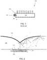
- FIG. 1illustrates such an illumination system 100 fabricated by coupling a discrete light source, e.g., a light-emitting diode (“LED”) 102 to a narrow face 104 of a waveguide 106 .
- a discrete light sourcee.g., a light-emitting diode (“LED”) 102
- LEDlight-emitting diode
- a waveguide 106 having a refractive index of N1.5
- an LED 102 having Lambertian output characteristicscombined as in the illumination system 100 , have a theoretical maximum coupling efficiency limit of 85%. That is, at most 85% of the light emitted by the LED 102 will be trapped within the waveguide 106 , and the remaining portion of the emitted light will be lost.
- This coupling inefficiencymay be attributed to the constraints inherent in the side-emitting LED design of the illumination system 100 . While thinner waveguides are desirable, the thickness t of the waveguide must be larger than the width d of the LED in order to achieve coupling efficiencies approaching 85%. Relatively high coupling efficiencies (e.g., greater than approximately 70%) are difficult to obtain for cases where the thickness t of the waveguide is smaller than the width d of the LED. Thus, as waveguides become thinner, the coupling efficiency of the waveguide decreases and more light is lost. The coupling inefficiency may even set a practical lower bound on the thickness of the waveguide 106 . In addition, many side-emitting illumination systems utilize specially engineered LED and waveguide structures in order to increase the coupling efficiency. These structures not only add to the complexity and cost of the illumination system 100 but also increase its thickness.
- the present inventionenables superior coupling efficiencies between light sources such as LEDs and thin waveguides by utilizing an LED that is embedded inside a waveguide and emits all its light inside the waveguide.
- a first portion of the emitted lightpropagates through the waveguide because its emission angle (with respect to the waveguide's upper surface) results in total internal reflection (“TIR”) of the first portion.
- TIRtotal internal reflection
- a second portion of the lightis not emitted at an angle to the waveguide's upper (and/or lower) surface resulting in total internal reflection; this second portion may be reflected by a specular mirror positioned above the LED. The light thus reflected also undergoes total internal reflection, improving the coupling efficiency to the waveguide.
- Embodiments of the inventionenable the waveguide to have a small thickness, e.g., less than approximately 1 mm, with an LED having a width of approximately 1 mm. Moreover, embodiments of the invention also utilize standard waveguide shapes and standard LED light sources not engineered to re-reflect emitted light, thereby reducing the cost and complexity of the system. Finally, embodiments of the invention do not require specially designed reflectors or selectively coated waveguide surfaces, further decreasing manufacturing cost and complexity.
- top-emittinge.g., Lambertian
- side-emitting LEDse.g., side-emitting LEDs
- Such chipsmay be placed below the waveguide instead of attached to a narrow side of the waveguide.
- a mirrormay be used that exhibits specular reflection instead of a mirror exhibiting total internal reflection or a diffuser (i.e., a surface exhibiting diffuse reflection).
- the mirrormay be positioned and designed such that most of the light emitted from the LED, e.g., more than approximately 85%, is coupled to the waveguide.
- the light reflected by the mirrormay be within the propagation angle of the waveguide after reflection. Back-reflection of light toward the LED may be prevented, thereby obviating the need for specially engineered increased reflectivity of the LED surface (or the surface of the LED electrode) to decrease light absorption by the LED.
- the waveguide and LEDmay be included in a full illumination device featuring in-coupling, concentration, propagation, and out-coupling regions. Light propagating inside the waveguide in a direction away from the out-coupling region may be redirected toward the out-coupling region by a specially engineered shape of the waveguide's back edge.
- a top mirrormay be included to reduce or prevent reflection of light back toward the LED in the vertical direction; a concentrating mirror may also be included (on, e.g., the back surface of the waveguide) to reduce or prevent reflection of light back toward the LED in the horizontal direction.
- the full illumination devicemay provide efficient (e.g., greater than approximately 70% or even 85% or more) light in-coupling to a thin waveguide, even when the thickness of the waveguide is approximately equal to (or even less than) the LED width.
- embodiments of the inventionfeature an illumination structure including or consisting essentially of a waveguide, a discrete light source, and a top mirror.
- the waveguidehas a depression in its top surface
- the discrete light sourceis disposed proximate the bottom surface of the waveguide and below the depression
- the top mirroris disposed above the discrete light source.
- the top mirrormay include or consist essentially of a conical mirror disposed over and at lest substantially filling the depression.
- An air gapmay be disposed between the conical mirror and the depression.
- the top mirrormay include or consist essentially of a substantially flat mirror disposed over substantially all of the depression.
- the substantially flat mirrormay be a specular mirror, a diffusive reflector, a Fresnel reflector, and/or a diffractive optical element. At least a portion of light emitted from the discrete light source may be reflected from a side surface of the waveguide through the depression in a confined mode of the waveguide. At least a portion of light emitted from the discrete light source may be reflected from a side surface of the waveguide through the depression and reflected back into the waveguide in a confined mode of the waveguide by the substantially flat mirror.
- embodiments of the inventionfeature an illumination structure including or consisting essentially of a waveguide having a cavity through a thickness thereof, a discrete light source disposed in the cavity, and a top mirror disposed in the cavity above the discrete light source.
- the top mirrormay include or consist essentially of a conical mirror and/or a substantially flat mirror.
- the portion of the cavity not occupied by the top mirror and the dicrete light sourcemay be filled with an index-matching material.
- the index-matching materialmay have an index of refraction substantially matching that of the waveguide.
- the cross-sectional area of the cavity proximate the top mirrormay be larger than the cross-sectional area of the cavity proximate the discrete light source.
- embodiments of the inventionfeature a method for coupling light emitted from a discrete light source to a waveguide.
- Lightis emitted from a discrete light source disposed within a waveguide.
- a portion of the emitted lightis reflected from a top mirror disposed above a depression in the top surface of the waveguide (the depression being disposed above the discrete light source), so as to confine the reflected portion of the emitted light within the waveguide.
- the top mirrormay include or consist essentially of a conical mirror substantially filling the depression, and the portion of the emitted light may traverse an air gap between the depression and the top mirror before being reflected.
- a second portion of the emitted lightmay be reflected from a side surface of the waveguide through the depression so as to confine the reflected second portion of the emitted light within the waveguide.
- the reflected second portion of the emitted lightmay not strike the top mirror after being reflected through the depression.
- the reflected second portion of the emitted lightmay strike the top mirror after being reflected through the depression, and the reflection from the top mirror may confine the reflected second portion of the emitted light within the waveguide.
- embodiments of the inventionfeature a method for coupling light emitted from a discrete light source to a waveguide.
- Lightis emitted from a discrete light source disposed within a cavity extending through the thickness of a waveguide.
- a portion of the emitted lightis reflected from a top mirror disposed above at least a portion of the cavity so as to confine the reflected portion of the emitted light within the waveguide.
- the top mirrormay include or consist essentially of a conical mirror and/or a substantially flat mirror.
- the portion of the cavity not occupied by the top mirror and the discrete light sourcemay be filled with an index-matching material.
- the index-matching materialmay have an index of refraction substantially matching that of the waveguide.
- embodiments of the inventionfeature a method of forming an illumination structure.
- a substantially planar waveguide having input and output regionsis formed.
- a depression in the top surface of the waveguide in the input region and a notch in the bottom surface of the waveguide in the input regionare formed.
- a top mirroris disposed over the depression, and a discrete light source is disposed within the notch.
- the top mirrormay include or consist essentially of a conical mirror, and disposing the top mirror over the depression may include substantially filling the depression with the top mirror.
- An air gapmay be left between the top mirror and the depression.
- the top mirrormay include or consist essentially of a substantially flat mirror, and disposing the top mirror over the depression may include substantially covering the depression with the top mirror.
- At least a portion of the notchmay be filled with an index-matching material.
- the index-matching materialmay have an index of refraction substantially matching that of the waveguide.
- FIG. 1is a cross-sectional view of a prior-art side-mounted illumination system
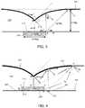
- FIG. 2is a cross-sectional view of an illumination system featuring a parabolic mirror
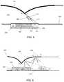
- FIG. 3is a cross-sectional view of an illumination system showing relative dimensions
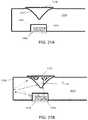
- FIG. 4is a cross-sectional view of an illumination system with an embedded LED
- FIG. 5is a cross-sectional view of an illumination system featuring an LED sub-assembly
- FIG. 6is a cross-sectional view of an illumination system featuring a bottom diffusive mirror
- FIG. 7is a cross-sectional view of an illumination system featuring an alternative mirror design
- FIG. 8is a plan view of an illumination panel for use in a tiled configuration of panels
- FIG. 9is a plan view of an in-coupling region featuring elliptical mirror sections
- FIG. 10is a plan view of an illumination panel featuring multiple LEDs
- FIG. 11is a plan view of an illumination panel featuring multiple LEDs in an alternate configuration
- FIG. 12is a cross-sectional view of an illumination panel
- FIG. 13is a plan view of an illumination panel featuring scattering structures
- FIG. 14is a cross-sectional view of an illumination panel featuring two layers
- FIGS. 15A and 15Bare a perspective view and a plan view, respectively, of an illumination panel featuring multiple LEDs;
- FIG. 16is a cross-sectional view of an illumination panel featuring an asymmetrically placed LED
- FIG. 17is a cross-sectional view of an illumination panel featuring a phosphor layer
- FIGS. 18A and 18Bare a cross-sectional view and top view, respectively, of an illumination panel
- FIG. 19is a cross-sectional view of an illumination system having a cavity and a curved mirror inserted therein;
- FIG. 20is a cross-sectional view of an illumination system having a waveguide with a depression in a surface thereof and a curved mirror disposed over the depression;
- FIGS. 21A and 21Bare cross-sectional views of an illumination system having a waveguide with a depression in a surface thereof and a substantially flat mirror disposed over the depression.
- Embodiments of the inventionapply to two different cases: (1) when a thickness, t, of the waveguide is approximately equal to or larger than the width, d, of the light source and (2) when t is less than d.
- a curved, semi-curved, broken-line, or single-line top mirrorredirects light that strikes it into confined modes (i.e., propagation paths confined by the waveguide).
- curvedrefers to a mirror with a curved shape
- si-curvedrefers to a mirror with a curved segment and straight segments
- broken-linerefers to a mirror having several discrete straight segments that approximate a curved segment
- single-linerefers to a mirror consisting of a straight segment.
- the mirroris positioned such that light propagating at an angle less than necessary for TIR (and which therefore will not be confined within the waveguide) strikes the mirror.
- the mirror shape and positionmay enable the redirection of light from unconfined modes into confined modes. Any light already in a confined mode that does strike the mirror may remain in a confined mode after reflection.
- FIG. 2illustrates one example of a parabolic mirror 202 that is set around a point A (the top-right corner 204 of an LED 206 ), such that the light rays emitted from the point A toward the region of the mirror bounded by points M and D (“region M-D”) are reflected back into the waveguide 208 at an angle equal to (or larger than) the critical angle ⁇ T for total internal reflection.
- region A-Ball of the light rays from the portion of the top surface 210 of the LED 206 bounded by points A and B
- region A-Bmay be reflected at angles larger than ⁇ T so as to be confined.
- the light rays from the region bounded by points B and C (“region B-C”)may undergo one or multiple reflections at the mirror such that their final propagating angle is also greater than ⁇ T .
- Light rays that do not strike the mirrorare, by definition, already confined (i.e., propagating at an angle greater than ⁇ T ) because the light ray from point A to point M and the light ray from point A to point D propagate at an angle ⁇ T .
- the light ray from point A to point Mpropagates perpendicularly to the surface of the mirror 202 at point M such that the light is reflected back toward point A.
- the mirror 202is substantially parallel to the plane of the waveguide 208 , and the light ray propagating from point A at an angle ⁇ T is reflected into the waveguide 208 at an angle ⁇ T (pursuant to Snell's Law).
- the light raysmay act similarly if one or more cladding layers (not shown) are added to the waveguide 208 .
- FIG. 3depicts an exemplary embodiment of the invention that includes relative dimensions.
- the waveguide 208 thickness t(as measured from the top surface 210 of the LED 206 to the top surface 302 of the waveguide 208 ) may be approximately equal to the LED 206 width d.
- the mirror configurationtakes alignment tolerances into account.
- the width d of the LED 206 and the thickness t of the waveguide 208may thus be defined as ⁇ square root over (2) ⁇ y 0
- the shortest distance between the mirror 304 and the surface 210 (at point M of the mirror 304 )is y 0 / ⁇ square root over (2) ⁇ .
- point M of the mirror 304is defined with reference to point A (the right edge of the LED 206 )
- slight misalignment of the LED 206may lead to less efficient light coupling.
- the sensitivity to such misalignmentmay be reduced by positioning point M with respect to a point A′ offset from point A by a typical misalignment tolerance, e.g., approximately 0.1 mm.
- light emitted by or through side faces 412 of the LED 206may be coupled into the waveguide 208 .
- the LED 206may be embedded within the waveguide 208 , as shown, which then may have a thickness of approximately t+h (i.e., slightly larger than the LED width d).
- the light from an LED 206 having a width d of approximately 1 mmmay be coupled to a waveguide 208 having a thickness of approximately 1 mm (or slightly greater than approximately 1 mm) while achieving a coupling efficiency greater than approximately 85%, or even greater than approximately 95%.
- Light emitted from a side surface 412 of the LED 206may propagate at angles less than the angle required for total internal reflection.
- a reflecting layer 402may therefore be placed at the bottom facet 404 of the waveguide 208 , at least spanning and desirably extending beyond the perimeter of the LED 206 , to capture the unconfined light.
- the reflecting layer 402may reflect unconfined light toward the top mirror 304 .
- the position of point Dmay be determined by the ray 416 from point S′ that strikes the waveguide 208 top surface at an incident angle equal to the critical angle ⁇ T .
- the distance between points S and S′may be approximately equal to the thickness h of the LED 206 .
- the non-zero thickness h of the LED 206is considered when designing the shape and placement of the mirror 202 . This consideration is important for LEDs that not only emit light from their top surfaces 210 (as in the case described above), but also from their side surfaces 412 . The light emitted from or through the side surfaces 412 of the LED 206 may also be confined in the waveguide 208 .
- the critical angle ⁇ Tis determined by the ray from point S (the bottom-right corner 414 of the LED 206 ) to point D.
- ⁇ Twill be slightly larger than the ⁇ T described above (which may apply to an LED that emits light only from its top surface). This selection of the proper ⁇ T enables the coupling of substantially all light emitted from the LED 206 .
- the critical angle ⁇ T(measured from point A) is approximately 45 degrees.
- FIG. 5illustrates an LED light source 206 assembled on a top surface of an LED sub-assembly module 502 , such as a printed-circuit board (“PCB”) or a carrier plate, which provides a mechanical interface to hold the LED light source 206 in position and/or an electrical interface to operate the LED light source 206 .
- an LED sub-assembly module 502such as a printed-circuit board (“PCB”) or a carrier plate, which provides a mechanical interface to hold the LED light source 206 in position and/or an electrical interface to operate the LED light source 206 .
- PCBprinted-circuit board
- an index-matching material 504may be used to fill the space between the LED 206 and the top mirror 304 (and/or bottom facet 404 ), thereby providing an optical connection not only between the LED 206 and the top mirror 304 (and/or bottom facet 404 ) but also between the top mirror 304 (and/or bottom facet 404 ) and the top surface 506 of the LED sub-assembly 502 .
- the top surface 506 of the LED sub-assembly 502may extend beyond the dimensions of the LED light source 206 , thus allowing guided light rays to reach the top surface 506 of the LED sub-assembly 502 .
- the reflectivity quality of the LED sub-assembly surface 506may not be controllable and is less than the TIR reflectivity. Therefore, the top mirror 304 positioned over the LED light source 206 is preferably designed to reflect light away from the LED sub-assembly 502 . In one embodiment, as shown in FIG. 5 , the top mirror 304 has a parabolic contour.
- a light ray 508is coupled from a point S at the right edge 510 of the LED light source 206 , reflected from a point M on the top mirror 304 , and radiates back along a path 510 to a point S′′ at the end of the index-matching region 504 of the LED sub-assembly 502 .
- Other rays emitted from the LED light sourcemay be reflected past the LED sub-assembly 502 to the region beyond point S′′.
- Point S′which is approximately halfway between points S and S′′, may be used as a reference point for forming the parabolic shape of the top mirror 504 .
- a light ray 512 emitted from point S′ that strikes the top mirror at point Mmay be reflected back toward point S′.
- the shape of the top mirror 304 at point Mmay a sharp edge or a curve.
- the width of the top mirror 304is 2 mm
- the shape of the top mirror 304 at point Mmay be a curve having a radius of 0.1 mm. Such a shape may decrease the manufacturing cost and/or complexity of the top mirror 304 relative to the cost and complexity of manufacturing a sharp edge at point M without significantly affecting the performance of the top mirror 304 .
- all the unconfined light raysstrike a curved, semi-curved, or broken-line top mirror that redirects the light back into the waveguide.
- the mirrorpreferably does not reflect the light back into the LED. While most of these reflected rays are redirected to confined modes (i.e., propagation paths confined by the waveguide), some remain propagating at angles below the critical angle (i.e., they remain unconfined modes). These unconfined modes may be redirected toward a bottom diffusive reflector which redirects at least a significant portion (for example, greater than 55%) of this remaining light into confined modes.
- FIG. 6depicts a top specular mirror 602 including a curved section 604 between points M and D and a flat section 606 between points D and E.
- the flat section 606may be substantially parallel to a top surface 608 of the LED 206 .
- a bottom diffusive mirror 610extends from approximately the LED 206 edge A to a point G and may be designed so that most or all of the reflected light already corresponding to confined modes does not strike the bottom diffusive mirror 610 .
- a similar bottom diffusive mirrormay be disposed on the other side of the LED 206 .
- Light emitted from the LED 206 that does not strike the curved section 604may instead strike the flat section 606 and be reflected toward the bottom diffusive mirror 610 . This light, initially in an unconfined mode, strikes the diffusive mirror 610 and is reflected into confined modes. Coupling efficiencies greater than approximately 80% may be obtained with this configuration.
- FIG. 7depicts an embodiment in which the curved section 604 of the mirror 602 has a radius approximately equal to half the width of the LED 206 (i.e., d/2), and point M of the mirror approximately coincides with point B (the center of the top surface 608 of the LED 206 ).
- Light rays from point A that propagate toward the curved section 604are reflected back toward point A.
- Light rays from point B propagating at approximately 45 degreesstrike the top mirror 602 at point D and are reflected to point G of the diffusive mirror 610 .
- most or all of the unconfined modes emitted from the LED 206 between points A and Bstrike the diffusive mirror 610 and are reflected into confined modes.
- large illumination structuresare formed by arranging (or “tiling”) panels that include the above-described waveguide structures.
- each panelmay include or consist essentially of an input region and an output region, and the output region of one panel may cover the input region of an adjoining panel.
- a large illumination structureis formed by placing panels adjoining each other (i.e., in a non-tiled configuration with no overlap between panels) such that light is coupled out from the entire panel surface.
- FIG. 8illustrates a panel 802 for use in a tiled configuration of one or more panels.
- the output region 804 of each panel 802may include scattering structures (such as hemispheres, wedges, particles, and/or other similar structures).
- Light from an LED 806 disposed in an input region 808is preferably directed toward the output region 804 such that the light does not pass through the LED 806 and/or a top mirror.
- Light rays 810 emitted by the LED 806 away from the output region 804may be reflected back toward the output region 804 by a back horizontal mirror 812 .
- the back horizontal mirror 812is not perfectly linear, but rather includes or consists essentially of one or two elliptical mirror sections.
- FIG. 9shows, in one embodiment, elliptical mirror sections 906 , 908 each define a portion of the back horizontal mirror 812 .
- the LED 806may be positioned approximately at a position corresponding to the poles common to each ellipse 906 , 906 (which also have poles 902 , 904 ). Thus, substantially all of the light rays emitted from the LED 806 may be redirected (and distributed) to the output coupling region 804 while not passing through the LED 806 .
- emission of white lighte.g., formed by the combination of red, green, and blue (“RGB”) light
- RGBred, green, and blue
- each single LED of the above-described embodimentsmay be replaced by a set of at least three LEDs: at least one emitting red light, at least one emitting green light, and at least one emitting blue light.
- FIG. 10illustrates an embodiment in which a plurality of LEDs 1002 are “crowded” (i.e., arranged close together, but not necessarily collinearly), such that color mixing is optimized and the loss due to light propagating from one LED directly to the other LEDs is minimal.
- the LEDsmay include a red LED 1004 , a green LED 1006 , and a blue LED 1008 .
- separate horizontal back mirrors 1102 , 1104 , 1106are provided for each LED 1004 , 1006 , 1008 , respectively, and the colors are mixed to white light while propagating in the input region (i.e., before the light reaches the output region 804 ).
- FIG. 12illustrates a side view of a panel 1202 including an LED 1204 disposed on a substrate 1206 .
- lightis preferably emitted from the entire top surface 1208 of the panel 1202 , including the region 1210 above the top curved mirror 1212 .
- the intensity of the light emitted through the top curved mirror 1212is equal to the intensity of the light coupled out from the rest of the top surface 1208 of the panel 1202 .
- a suitable absorber 1214may be placed above the top curved mirror 1212 to emit light of a desired intensity therefrom.
- Some lightmay penetrate through the top curved mirror 1212 .
- the absorber 1214should absorb ⁇ 98% of the light intensity.
- the absorber 1214is diffusive.
- scattering structures 1216may be placed across some or all of a top surface 1208 of the panel 1202 to aid in the out-coupling of light.
- a mirror 1218may placed at the bottom surface 1220 of the panel 1202 .
- the LEDsmay be crowded (i.e., positioned closely together) to permit the use of a single out-coupling structure for all of the LEDs.
- the density of scattering structurespreferably increases as a function of distance away from the LEDs.
- scattering structures with increasing scattering coefficientsmay be utilized.
- the region above the top curved mirror of one LEDmay be transparent to light emitted by the other LEDs in order to facilitate out-coupling of light of all colors.
- FIGS. 13 and 14depict a suitable configuration.
- FIG. 13depicts a top view of an isolated illumination panel 1302 that includes four crowded LEDs 1304 (e.g., one red, two green, and one blue—“RGGB”). Out-coupling scattering structures 1306 are provided between and/or around the LEDs 1304 .
- a cross-sectional view of two of the LEDs 1304 , including a red LED 1402 and a blue LED 1404 , and their corresponding upper curved mirrors 1406 , 1408is shown in FIG. 14 .
- a top layer 1410 of the waveguide disposed above the upper curved mirrors 1406 , 1408includes scattering structures 1412 for facilitating the out-coupling of light in the regions above the upper curved mirrors 1406 , 1408 .
- the top layer 1410is preferably optically connected with the bottom layer 1414 (the layer containing the curved mirrors 1406 , 1408 and the LEDs 1402 , 1404 ) such that light freely propagates from one layer to the other.
- the scattering structures 1412may be disposed at the top surface 1416 of the top layer 1410 . In other embodiments, the scattering structures 1412 are incorporated in other portions of the top layer 1410 , or even in the bottom layer 1414 .
- FIG. 14also depicts several different light rays, each traveling a different path from an LED 1402 , 1404 to emission from the waveguide 1418 .
- Ray (a)is emitted from the blue LED 1404 and scattered from the blue top curved mirror 1408 into the waveguide 1418 .
- Ray (b)is the part of ray (a) that penetrates through the mirror 1408 and is emitted from the waveguide 1418 by the scattering structures 1412 .
- Ray (c)is emitted from the red LED 1402 and then from the waveguide 1418 through the scattering structures 1412 .
- Ray (d)is the part of ray (c) that is reflected back to the waveguide 1418 and, after reflection therefrom, is emitted from the waveguide 1418 in the region above the blue top curved mirror 1408 .
- each LEDhas its own, separate top mirror.
- each top mirroris shaped like a cone, pyramid, or any other non-flat shape suitable to retaining light within the waveguide that would otherwise escape.
- more than one of the LEDsshare a single top mirror.
- the LEDsmay be arranged in a line, and the shared top mirror may be shaped like a prism with curved side facets.
- the shared top mirror 1502is a triangular prism having triangular side facets and the array of LEDs 1504 includes RRGGB LEDs.
- the top curved mirror 1502is not limited to symmetric structures; it may be designed asymmetrically if, for example, the LEDs 1504 are configured asymmetrically, such as an LED not located at the center of the LED sub-assembly 1506 . In such a case, in order to avoid rays striking the LED sub-assembly (as illustrated in FIG. 5 ), the top curved mirror 1502 may be designed asymmetrically and/or located asymmetrically (relative to the center of the LEDs 1504 ). An example is shown in FIG.
- the LED sub-assembly 1602is asymmetric (relative to the center of the LED 1604 ) and, accordingly, the top curved mirror 1606 is asymmetrically located (relative to the center of the LED 1604 ).
- the curved mirror 1606is located such that rays from point A are reflected back from point M toward point A and rays from point C are reflected from point M toward point C′.
- a virtual point C′′is located approximately at the center between point C and point C′; i.e., virtual rays from point C′′ striking point M will be back reflected to point C′′.
- point Mis located at the center between points A and C′′.
- FIG. 17illustrates a side view of a waveguide 1702 that features a phosphor layer 1704 .
- the phosphor layer 1704may produce white light from a single-color LED light source 1706 .
- the phosphor layer 1704preferably converts some of the light from the LED 1706 to another wavelength. The original light adds to the converted light, creating white light. For example, a blue LED may be combined with a yellow phosphor layer, and the blue light from the LED may combine with the yellow light from the phosphor layer to produce white light.
- phosphorsare utilized to facilitate the emission of white light (or light of another preferred wavelength).
- the configuration depicted in FIG. 17includes a patterned waveguide 1702 and an LED chip 1716 with matching indices of refraction.
- the waveguidemay be an optical polymer, e.g., a polymethyl methacrylate (PMMA), and may include a bottom notch 1720 (for embedding the LED 1716 therein) and a top curved mirror 1708 .
- PMMApolymethyl methacrylate
- the waveguide 1702may be formed by molding or by another suitable process known in the art.
- the waveguide 1702may also include a bottom mirror 1712 .
- the LED chip 1716may be mounted into the waveguide notch 1720 such that it substantially seals the notch 1720 along the bottom surface 1722 of the waveguide 1702 .
- any remaining space in the notch 1720may be filled with an index-matching material 1718 having an index of refraction matching that of the waveguide 1702 .
- the phosphor layer 1704may be formed above or around the LED chip 1716 , or it may be deposited directly in the waveguide notch 1720 prior to introduction of the LED chip 1716 .
- An absorber layer 1710 and a substrate 1714may also be included.
- FIGS. 18A and 18Bdepict a side and top view, respectively, of an isolated panel configuration 1800 , including a phosphor layer, that adds scattering structures 1802 .
- the illumination system 1800may be utilized in cases where the waveguide 1702 thickness is either approximately equal to (or even larger than) the width of the LED 1716 , as well as in cases where the waveguide thickness is less than the LED width.
- the phosphor-containing systemmay also be utilized in tiled or isolated configurations, as described above.
- FIG. 19depicts a side view of a waveguide 1910 having, through at least a substantial portion of its thickness, a cavity 1920 formed therein.
- An LED 1930(or other light source) may abut a bottom portion of cavity 1920 or be embedded therein, as shown in FIG. 19 .
- LED 1930may be supported by a sub-assembly 1940 (as described above).
- a conical mirror 1950is positioned (e.g., inserted or deposited) within the top portion of cavity 1920 (i.e., opposing LED 1930 ).
- Conical mirror 1950may be coated on its “front,” i.e., curved, surface.
- the remaining volume of cavity 1920is preferably filled with an index-matching material 1960 that has an index of refraction substantially the same as that of waveguide 1910 .
- Conical mirror 1950is preferably three-dimensional (rather than, e.g., a shaped two-dimensional sheet) and substantially conical, parabolic, pyramidal, and/or prismatic in shape.
- Conical mirror 1950may include or consist essentially of a reflective metal, e.g., aluminum, and may even have a reflective coating on at least the surface positioned within the cavity.
- conical mirror 1950includes or consists essentially of topaz or a polymer such as PMMA and is coated with a coating of a reflective metal, e.g., aluminum and/or silver.
- a reflective metale.g., aluminum and/or silver.
- conical mirror 1950In embodiments in which conical mirror 1950 is coated, generally the surface of conical mirror 1950 facing the incident light is coated and thus reflects the light.
- a substantially flat mirror(as described below with reference to FIGS. 21A and 21B ), rather than or in addition to conical mirror 1950 , may be formed over or within cavity 1920 .
- a waveguide 2010has an LED 1930 embedded in a cavity (or notch) therewithin and a top depression 2015 similar in shape to conical mirror 1950 .
- Depression 2015is an angled interior feature that reflects impinging light, preferably into confined modes of waveguide 2010 .
- depression 2015is approximately conical, parabolic, pyramidal, or prismatic in shape.
- an index-matching material 1960may surround LED 1930 in the cavity.
- Air gap 2020may have a thickness ranging from approximately 100 ⁇ m to approximately 200 ⁇ m, or even smaller (e.g., ranging from approximately 10 ⁇ m to approximately 50 ⁇ m, or may even be less than approximately 10 ⁇ m). Air gap 2020 effectively acts as a “cladding layer” for depression 2015 of waveguide 2010 , increasing the amount of light from LED 1930 that undergoes total internal reflection into waveguide 2010 .
- air gap 2020is at least partially filled with a filler material that may have a lower refractive index than the refractive index of the waveguide material and/or adhesive properties for adhering conical mirror 1950 into depression 2015 of waveguide 2010 .
- the difference in refractive indices between the filler material and the waveguide materialmay be less than approximately 0.2.
- the waveguide materialmay be PMMA having a refractive index of approximately 1.5 and the filler material may be silicone having a refractive index of approximately 1.3.
- a portion of the light emitted by LED 1930strikes depression 2015 at an angle such that it “escapes” the waveguide (i.e., transmits through the surface of the waveguide at depression 2015 ).
- the escape anglemay be defined by Snell's Law, and depends upon the indices of refraction of the waveguide and of air gap 2020 (or a cladding material therewithin). Any light that escapes depression 2015 of waveguide 2010 is substantially reflected, by conical mirror 1950 , into waveguide 2010 where it may undergo total internal reflection.
- the optical coupling efficiency of the waveguideis enhanced without the need for a cavity through the entire waveguide thickness.
- FIGS. 19 and 20The high optical coupling efficiencies of the embodiments depicted in FIGS. 19 and 20 are demonstrated by the following examples. Assuming that the sides of the waveguide are coated and exhibit 98% reflectivity, and that the conical mirror also exhibits 98% reflectivity, the embodiments depicted in FIGS. 19 and 20 exhibit approximately 94.5% and 92% optical coupling efficiency, respectively. If the conical mirror has a reflectivity of only 91%, then the embodiments exhibit respective optical coupling efficiencies of approximately 89% and 91%. Thus, for a less reflective conical mirror, the addition of an air gap results in greater light confinement in the waveguide.
- a light sourcee.g., any of the above-described LEDs
- a light sourcee.g., any of the above-described LEDs
- an edge of the waveguide opposite this output regionwill generally be reflective in order to guide light travelling in the “wrong” direction back toward the output region.
- some embodiments of the above-described conical mirrorsmay prevent such propagation.
- the conical mirrormay be replaced by a substantially flat mirror (i.e., one that is sheet-like with minimal thickness) that covers (or “seals”) the opening to the depression in the waveguide.
- a substantially flat mirrori.e., one that is sheet-like with minimal thickness
- coversor “seals”
- FIG. 21Adepicts such a variant, in which waveguide 2110 has above depression 2015 a substantially flat mirror 2120 ; the region between depression 2015 and flat mirror 2120 is “empty,” e.g., filled with only air.
- Flat mirror 2120may be a specular mirror, a diffusive reflector, a Fresnel reflector, a diffractive optical element, or other means of reflecting light back into the waveguide.
- Flat mirror 2120may be a substantially planar sheet of reflective material, e.g., a foil such as VIKUITI Enhanced Specular Reflector Film, available from 3M of St. Paul, Minn.
- FIG. 21BAn advantage of this embodiment is depicted in FIG. 21B , which illustrates three exemplary light rays emanating from LED 1930 .
- the light ray labeled (a)is emitted from LED 1930 toward the side facet 2130 of waveguide 2110 and reflected back toward depression 2015 at a confined angle.
- Light ray (a)passes through the surfaces of depression 2015 , with a slight change in propagation angle, and proceeds through the waveguide in a confined mode. Such light would not be as efficiently coupled in the waveguide had a conical mirror been in place in depression 2015 .
- the light rays labeled (b) and (c)are, respectively, emitted directly toward depression 2015 or reflected back toward depression 2015 in an unconfined mode.
- These light raysstrike flat mirror 2120 (depicted as a diffusive mirror in FIG. 21B ) and are largely reflected back into the waveguide in confined modes (much as in the embodiments having a curved mirror described above).
- the region of waveguide 2110 covered by flat mirror 2120receives a portion of the light from one or more light sources disposed thereunder (e.g., LED 1930 ) and distributes it into the waveguide in confined modes.
- Flat mirror 2110may have a reflectivity of greater than approximately 80%, greater than approximately 90%, or even greater than approximately 95%.
- flat mirror 2120is a diffusive mirror having a Lambertian distribution and 98% reflectivity (and the waveguide edges also have 98% reflectivity, as in the above examples).
- an optical coupling efficiency of approximately 88%is obtained, very close to the values obtained with the conical mirrors.
- nearly the same optical coupling efficienciesmay be obtained in a much more manufacturable fashion.
- the above-described depression(s)may simply be embossed or “punched” into the waveguide material during a single-step process. The depressions may then simply be covered with flat mirrors, obviating the need for conical mirrors, prisms, or the like.
- FIGS. 19-21may be utilized with other elements described above, e.g., phosphor layers, absorbers, scattering structures, and/or various panel configurations, and may be utilized with multiple light sources.
- the waveguides described hereinmay have thicknesses of approximately 1 mm, or even less.
Landscapes
- Physics & Mathematics (AREA)
- General Physics & Mathematics (AREA)
- Optics & Photonics (AREA)
- Planar Illumination Modules (AREA)
Abstract
Description
Claims (20)
Priority Applications (2)
| Application Number | Priority Date | Filing Date | Title |
|---|---|---|---|
| US15/963,685US10989863B2 (en) | 2008-07-10 | 2018-04-26 | Slim waveguide coupling apparatus and method |
| US17/215,107US11231547B2 (en) | 2008-07-10 | 2021-03-29 | Slim waveguide coupling apparatus and method |
Applications Claiming Priority (11)
| Application Number | Priority Date | Filing Date | Title |
|---|---|---|---|
| US7958208P | 2008-07-10 | 2008-07-10 | |
| US20608009P | 2009-01-27 | 2009-01-27 | |
| US12/500,889US8301002B2 (en) | 2008-07-10 | 2009-07-10 | Slim waveguide coupling apparatus and method |
| US12/715,880US8297786B2 (en) | 2008-07-10 | 2010-03-02 | Slim waveguide coupling apparatus and method |
| US13/606,202US8851712B2 (en) | 2008-07-10 | 2012-09-07 | Slim waveguide coupling apparatus and method |
| US14/478,444US9164218B2 (en) | 2008-07-10 | 2014-09-05 | Slim waveguide coupling apparatus and method |
| US14/849,933US9470837B2 (en) | 2008-07-10 | 2015-09-10 | Slim waveguide coupling apparatus and method |
| US15/269,231US9606288B2 (en) | 2008-07-10 | 2016-09-19 | Slim waveguide coupling apparatus and method |
| US15/432,490US9798077B2 (en) | 2008-07-10 | 2017-02-14 | Slim waveguide coupling apparatus and method |
| US15/710,940US9983351B2 (en) | 2008-07-10 | 2017-09-21 | Slim waveguide coupling apparatus and method |
| US15/963,685US10989863B2 (en) | 2008-07-10 | 2018-04-26 | Slim waveguide coupling apparatus and method |
Related Parent Applications (1)
| Application Number | Title | Priority Date | Filing Date |
|---|---|---|---|
| US15/710,940ContinuationUS9983351B2 (en) | 2008-07-10 | 2017-09-21 | Slim waveguide coupling apparatus and method |
Related Child Applications (1)
| Application Number | Title | Priority Date | Filing Date |
|---|---|---|---|
| US17/215,107ContinuationUS11231547B2 (en) | 2008-07-10 | 2021-03-29 | Slim waveguide coupling apparatus and method |
Publications (2)
| Publication Number | Publication Date |
|---|---|
| US20200088929A1 US20200088929A1 (en) | 2020-03-19 |
| US10989863B2true US10989863B2 (en) | 2021-04-27 |
Family
ID=42666988
Family Applications (9)
| Application Number | Title | Priority Date | Filing Date |
|---|---|---|---|
| US12/715,880Active2030-07-03US8297786B2 (en) | 2008-07-10 | 2010-03-02 | Slim waveguide coupling apparatus and method |
| US13/606,202Active2030-02-26US8851712B2 (en) | 2008-07-10 | 2012-09-07 | Slim waveguide coupling apparatus and method |
| US14/478,444Expired - Fee RelatedUS9164218B2 (en) | 2008-07-10 | 2014-09-05 | Slim waveguide coupling apparatus and method |
| US14/849,933ActiveUS9470837B2 (en) | 2008-07-10 | 2015-09-10 | Slim waveguide coupling apparatus and method |
| US15/269,231Expired - Fee RelatedUS9606288B2 (en) | 2008-07-10 | 2016-09-19 | Slim waveguide coupling apparatus and method |
| US15/432,490ActiveUS9798077B2 (en) | 2008-07-10 | 2017-02-14 | Slim waveguide coupling apparatus and method |
| US15/710,940ActiveUS9983351B2 (en) | 2008-07-10 | 2017-09-21 | Slim waveguide coupling apparatus and method |
| US15/963,685Expired - Fee RelatedUS10989863B2 (en) | 2008-07-10 | 2018-04-26 | Slim waveguide coupling apparatus and method |
| US17/215,107ActiveUS11231547B2 (en) | 2008-07-10 | 2021-03-29 | Slim waveguide coupling apparatus and method |
Family Applications Before (7)
| Application Number | Title | Priority Date | Filing Date |
|---|---|---|---|
| US12/715,880Active2030-07-03US8297786B2 (en) | 2008-07-10 | 2010-03-02 | Slim waveguide coupling apparatus and method |
| US13/606,202Active2030-02-26US8851712B2 (en) | 2008-07-10 | 2012-09-07 | Slim waveguide coupling apparatus and method |
| US14/478,444Expired - Fee RelatedUS9164218B2 (en) | 2008-07-10 | 2014-09-05 | Slim waveguide coupling apparatus and method |
| US14/849,933ActiveUS9470837B2 (en) | 2008-07-10 | 2015-09-10 | Slim waveguide coupling apparatus and method |
| US15/269,231Expired - Fee RelatedUS9606288B2 (en) | 2008-07-10 | 2016-09-19 | Slim waveguide coupling apparatus and method |
| US15/432,490ActiveUS9798077B2 (en) | 2008-07-10 | 2017-02-14 | Slim waveguide coupling apparatus and method |
| US15/710,940ActiveUS9983351B2 (en) | 2008-07-10 | 2017-09-21 | Slim waveguide coupling apparatus and method |
Family Applications After (1)
| Application Number | Title | Priority Date | Filing Date |
|---|---|---|---|
| US17/215,107ActiveUS11231547B2 (en) | 2008-07-10 | 2021-03-29 | Slim waveguide coupling apparatus and method |
Country Status (1)
| Country | Link |
|---|---|
| US (9) | US8297786B2 (en) |
Families Citing this family (75)
| Publication number | Priority date | Publication date | Assignee | Title |
|---|---|---|---|---|
| US8684584B2 (en)* | 2001-05-16 | 2014-04-01 | Benzion Inditsky | Ultra-thin backlight |
| US8272758B2 (en) | 2005-06-07 | 2012-09-25 | Oree, Inc. | Illumination apparatus and methods of forming the same |
| WO2006131924A2 (en) | 2005-06-07 | 2006-12-14 | Oree, Advanced Illumination Solutions Inc. | Illumination apparatus |
| US8215815B2 (en) | 2005-06-07 | 2012-07-10 | Oree, Inc. | Illumination apparatus and methods of forming the same |
| CN101836042B (en) | 2007-09-21 | 2014-11-05 | 库帕技术公司 | Light emitting diode recessed light fixture |
| US7907804B2 (en) | 2007-12-19 | 2011-03-15 | Oree, Inc. | Elimination of stitch artifacts in a planar illumination area |
| US8182128B2 (en)* | 2007-12-19 | 2012-05-22 | Oree, Inc. | Planar white illumination apparatus |
| US8297786B2 (en) | 2008-07-10 | 2012-10-30 | Oree, Inc. | Slim waveguide coupling apparatus and method |
| US8301002B2 (en) | 2008-07-10 | 2012-10-30 | Oree, Inc. | Slim waveguide coupling apparatus and method |
| US8624527B1 (en) | 2009-03-27 | 2014-01-07 | Oree, Inc. | Independently controllable illumination device |
| US20100320904A1 (en) | 2009-05-13 | 2010-12-23 | Oree Inc. | LED-Based Replacement Lamps for Incandescent Fixtures |
| WO2010150202A2 (en) | 2009-06-24 | 2010-12-29 | Oree, Advanced Illumination Solutions Inc. | Illumination apparatus with high conversion efficiency and methods of forming the same |
| CA2768777C (en) | 2009-07-21 | 2017-11-28 | Cooper Technologies Company | Interfacing a light emitting diode (led) module to a heat sink assembly, a light reflector and electrical circuits |
| US9075172B2 (en)* | 2010-09-20 | 2015-07-07 | Luxingtek, Ltd. | Light converting optical structure and lighting device utilizing the same |
| WO2012042460A1 (en)* | 2010-09-29 | 2012-04-05 | Koninklijke Philips Electronics N.V. | Tube luminescent retrofit using high power light emitting diodes |
| FR2973475B1 (en)* | 2011-03-30 | 2018-05-25 | Gb Developpement | LIGHTING MODULE, HOMOGENEITY OF IMPROVED LIGHTING. |
| WO2013062159A1 (en)* | 2011-10-27 | 2013-05-02 | Lg Electronics Inc. | Ultra slim collimator for light emitting diode |
| US8591072B2 (en) | 2011-11-16 | 2013-11-26 | Oree, Inc. | Illumination apparatus confining light by total internal reflection and methods of forming the same |
| WO2013180365A1 (en)* | 2012-05-31 | 2013-12-05 | Lg Innotek Co., Ltd. | Member for cotrolling luminous flux, method for fabricating the member, display device, and light emitting device |
| WO2014006501A1 (en) | 2012-07-03 | 2014-01-09 | Yosi Shani | Planar remote phosphor illumination apparatus |
| JP2014093229A (en)* | 2012-11-05 | 2014-05-19 | Toshiba Corp | Surface light source device |
| CN102937269A (en)* | 2012-11-15 | 2013-02-20 | 京东方科技集团股份有限公司 | Light guide plate, backlight module and display device |
| US10234616B2 (en) | 2013-01-30 | 2019-03-19 | Cree, Inc. | Simplified low profile module with light guide for pendant, surface mount, wall mount and stand alone luminaires |
| US9625638B2 (en) | 2013-03-15 | 2017-04-18 | Cree, Inc. | Optical waveguide body |
| US9519095B2 (en) | 2013-01-30 | 2016-12-13 | Cree, Inc. | Optical waveguides |
| US9291320B2 (en) | 2013-01-30 | 2016-03-22 | Cree, Inc. | Consolidated troffer |
| US9690029B2 (en) | 2013-01-30 | 2017-06-27 | Cree, Inc. | Optical waveguides and luminaires incorporating same |
| CN105164467B (en)* | 2013-01-30 | 2018-03-13 | 克利公司 | Optical waveguide and lamp comprising the optical waveguide |
| US9869432B2 (en) | 2013-01-30 | 2018-01-16 | Cree, Inc. | Luminaires using waveguide bodies and optical elements |
| US9442243B2 (en) | 2013-01-30 | 2016-09-13 | Cree, Inc. | Waveguide bodies including redirection features and methods of producing same |
| US9366396B2 (en) | 2013-01-30 | 2016-06-14 | Cree, Inc. | Optical waveguide and lamp including same |
| US10436970B2 (en) | 2013-03-15 | 2019-10-08 | Ideal Industries Lighting Llc | Shaped optical waveguide bodies |
| US9798072B2 (en) | 2013-03-15 | 2017-10-24 | Cree, Inc. | Optical element and method of forming an optical element |
| US10400984B2 (en) | 2013-03-15 | 2019-09-03 | Cree, Inc. | LED light fixture and unitary optic member therefor |
| US10502899B2 (en)* | 2013-03-15 | 2019-12-10 | Ideal Industries Lighting Llc | Outdoor and/or enclosed structure LED luminaire |
| US9920901B2 (en) | 2013-03-15 | 2018-03-20 | Cree, Inc. | LED lensing arrangement |
| US9366799B2 (en) | 2013-03-15 | 2016-06-14 | Cree, Inc. | Optical waveguide bodies and luminaires utilizing same |
| US10379278B2 (en)* | 2013-03-15 | 2019-08-13 | Ideal Industries Lighting Llc | Outdoor and/or enclosed structure LED luminaire outdoor and/or enclosed structure LED luminaire having outward illumination |
| US10209429B2 (en) | 2013-03-15 | 2019-02-19 | Cree, Inc. | Luminaire with selectable luminous intensity pattern |
| DE102013106689B4 (en)* | 2013-06-26 | 2022-02-03 | OSRAM Opto Semiconductors Gesellschaft mit beschränkter Haftung | Optoelectronic semiconductor component |
| CN104421832A (en)* | 2013-08-21 | 2015-03-18 | 展晶科技(深圳)有限公司 | Lens and light-emitting element comprising same |
| JP2015099336A (en)* | 2013-11-20 | 2015-05-28 | 株式会社東芝 | Optical element and optical device |
| US9228706B2 (en)* | 2014-04-23 | 2016-01-05 | Brent V. Andersen | Lighting array providing visually-captivating lighting effects |
| US12372219B2 (en)* | 2014-05-30 | 2025-07-29 | Cree Lighting Usa Llc | LED luminaire with a cavity, finned interior, and a curved outer wall extending from a surface on which the light source is mounted |
| TWI578068B (en)* | 2015-01-05 | 2017-04-11 | 穎台科技股份有限公司 | Direct back-lit light guide structure, light guide plate and back-light module |
| WO2016190937A1 (en)* | 2015-03-09 | 2016-12-01 | Massachusetts Institute Of Technology | Phosphor-loaded waveguide |
| WO2017039725A1 (en)* | 2015-09-05 | 2017-03-09 | Leia Inc. | Dual-direction collimator |
| US9903995B2 (en)* | 2016-03-03 | 2018-02-27 | Microsoft Technology Licensing, Llc | Flat panel illuminator with concentrator |
| US11719882B2 (en) | 2016-05-06 | 2023-08-08 | Ideal Industries Lighting Llc | Waveguide-based light sources with dynamic beam shaping |
| US10416377B2 (en) | 2016-05-06 | 2019-09-17 | Cree, Inc. | Luminaire with controllable light emission |
| US10464472B2 (en)* | 2016-11-18 | 2019-11-05 | Rebo Lighting & Electronics, Llc | Illumination assembly for a vehicle |
| CN108459433B (en)* | 2017-02-21 | 2021-08-13 | 中强光电股份有限公司 | Backlight module and surface light source assembly thereof |
| JP6801539B2 (en)* | 2017-03-17 | 2020-12-16 | 株式会社リコー | Information processing system, information processing device, information processing program and information processing method |
| US12436394B2 (en) | 2017-07-03 | 2025-10-07 | Holovisions | Augmented reality (or mixed reality) eyewear with see-through optical elements having individually-adjustable opacity/reflectivity levels |
| US11754843B2 (en) | 2017-07-03 | 2023-09-12 | Holovisions LLC | Augmented reality eyewear with “ghost buster” technology |
| US11307420B2 (en) | 2017-07-03 | 2022-04-19 | Holovisions LLC | Augmented reality eyewear with “ghost buster” technology |
| US11163163B2 (en) | 2017-07-03 | 2021-11-02 | Holovisions | Augmented reality (AR) eyewear with at least one quasi Fresnel reflector (QFR) |
| US12013538B2 (en) | 2017-07-03 | 2024-06-18 | Holovisions LLC | Augmented reality (AR) eyewear with a section of a fresnel reflector comprising individually-adjustable transmissive-reflective optical elements |
| US12205231B2 (en) | 2017-07-03 | 2025-01-21 | Holovisions | Holovisions™—adjustable and/or modular augmented reality (AR) eyewear with a movable transflective mirror and different viewing modes |
| JP6729646B2 (en) | 2018-08-21 | 2020-07-22 | 日亜化学工業株式会社 | Light emitting device |
| CN109031510B (en)* | 2018-08-24 | 2020-06-30 | 京东方科技集团股份有限公司 | A light guide plate and its manufacturing method, a backlight module and a display device |
| WO2020101517A1 (en)* | 2018-11-12 | 2020-05-22 | Corning Incorporated | Backlight including patterned reflectors and method for fabricating the backlight |
| TW202036060A (en) | 2018-11-12 | 2020-10-01 | 美商康寧公司 | Backlight including patterned reflectors, diffuser plate, and method for fabricating the backlight |
| JP6753452B2 (en)* | 2018-11-30 | 2020-09-09 | 日亜化学工業株式会社 | Luminous module |
| US11073654B2 (en)* | 2018-12-28 | 2021-07-27 | Nichia Corporation | Light emitting module with recesses in light guide plate |
| JP6866903B2 (en)* | 2019-03-05 | 2021-04-28 | 日亜化学工業株式会社 | Luminous module |
| CN111665663B (en) | 2019-03-05 | 2025-04-08 | 日亚化学工业株式会社 | Light-emitting module and surface light-emitting light source |
| KR102626377B1 (en)* | 2019-06-12 | 2024-01-19 | 삼성디스플레이 주식회사 | Backlight unit and display device having the same |
| US20230359036A1 (en)* | 2019-06-24 | 2023-11-09 | Magic Leap, Inc. | Waveguides having integral spacers and related systems and methods |
| KR20210001964A (en) | 2019-06-27 | 2021-01-06 | 니치아 카가쿠 고교 가부시키가이샤 | Light emitting module |
| US20230161127A1 (en)* | 2020-04-15 | 2023-05-25 | CommScope Connectivity Belgium BV | Device and method for sealing cables in telecommunications enclosures |
| WO2022072855A1 (en)* | 2020-10-01 | 2022-04-07 | Avicenatech Corp. | Multi-layer planar waveguide interconnects |
| CN114578614B (en)* | 2020-11-30 | 2025-01-03 | 华为技术有限公司 | Backlight module and display screen |
| TW202305480A (en)* | 2021-06-10 | 2023-02-01 | 加拿大商弗瑞爾公司 | Color optoelectronic solid state device |
| EP4400342A4 (en)* | 2021-10-15 | 2024-09-18 | Fuyao Glass Industry Group Co., Ltd. | VEHICLE WINDOW ASSEMBLY AND VEHICLE |
Citations (5)
| Publication number | Priority date | Publication date | Assignee | Title |
|---|---|---|---|---|
| US20060262538A1 (en) | 2005-05-18 | 2006-11-23 | Zhi-Feng Li | Light-emitting diode component having a light direction-changing unit and related light direction-changing unit and module |
| US7316495B2 (en) | 2003-12-05 | 2008-01-08 | Koito Manufacturing Co., Ltd. | Vehicle headlight including a plurality of led lighting device units |
| US20080137335A1 (en)* | 2006-12-06 | 2008-06-12 | Shen-Yin Tsai | Light mixer and backlight module having the same |
| US20100220484A1 (en) | 2008-07-10 | 2010-09-02 | Oree Inc. | Slim waveguide coupling apparatus and method |
| US8301002B2 (en) | 2008-07-10 | 2012-10-30 | Oree, Inc. | Slim waveguide coupling apparatus and method |
Family Cites Families (380)
| Publication number | Priority date | Publication date | Assignee | Title |
|---|---|---|---|---|
| GB512062A (en) | 1938-01-28 | 1939-08-29 | Ernst Hirsch | Improvements in reflectors |
| US3261356A (en) | 1963-10-21 | 1966-07-19 | American Cystoscope Makers Inc | Suction and illumination device |
| US3626471A (en) | 1969-10-13 | 1971-12-07 | Robert E Florin | Illuminated suction brain retractor |
| US3871747A (en)* | 1972-10-03 | 1975-03-18 | Us Navy | Optical waveguide display panel |
| DE2433219A1 (en) | 1973-10-19 | 1976-01-22 | Nath Guenther | FLEXIBLE LIGHT GUIDE |
| US4551129A (en) | 1983-04-08 | 1985-11-05 | Coleman D Jackson | Technique and apparatus for intraocular and microsurgery including lighter-irrigator hypodermic tube |
| US4672381A (en) | 1984-08-30 | 1987-06-09 | Paul Labbe | Doppler tracking processor and time of closest approach detector |
| US4669467A (en) | 1985-03-22 | 1987-06-02 | Massachusetts Institute Of Technology | Mode mixer for a laser catheter |
| CA1260741A (en) | 1985-03-30 | 1989-09-26 | Takafumi Uemiya | Elastomeric optical waveguide |
| EP0200876B1 (en) | 1985-04-30 | 1988-11-02 | Siemens Aktiengesellschaft | Arrangement for lighting a room with daylight |
| JPS6289914A (en) | 1985-05-31 | 1987-04-24 | Sumitomo Electric Ind Ltd | Optical waveguide with integrated optical element and its manufacturing method |
| US4714983A (en) | 1985-06-10 | 1987-12-22 | Motorola, Inc. | Uniform emission backlight |
| US4829192A (en) | 1986-03-27 | 1989-05-09 | Kabushiki Kaisha Tokai Rika Denki Seisakusho | Photo-coupler with delay function using a fluorescent substance as the delay means |
| DE3633203A1 (en) | 1986-09-30 | 1988-03-31 | Siemens Ag | LIGHT EMISSION DIODES (LED) - DISPLAY DEVICE |
| US5165187A (en) | 1987-01-30 | 1992-11-24 | Fiber Sense & Signals Inc. | Edge illuminated sign panel |
| FR2610511A1 (en) | 1987-02-06 | 1988-08-12 | Issalene Robert | DENTAL INSTRUMENT AND CANNULAS FOR ASPIRATION, CLEANING, DRYING AND LIGHTING IN THE MOUTH |
| DE3730591C1 (en)* | 1987-09-11 | 1988-07-07 | Inotec Gmbh Ges Fuer Innovativ | Illuminated display unit, in particular house number, traffic sign, advertising medium |
| NL8702166A (en) | 1987-09-11 | 1989-04-03 | Oce Nederland Bv | EXPOSURE DEVICE WITH AN AGING CORRECTION SYSTEM FOR AN LED PRINTER. |
| EP0365724A1 (en) | 1988-10-26 | 1990-05-02 | THE GENERAL ELECTRIC COMPANY, p.l.c. | Integrated optical waveguide band |
| US5009483A (en) | 1989-04-12 | 1991-04-23 | Rockwell Iii Marshall A | Optical waveguide display system |
| US5048913A (en) | 1989-12-26 | 1991-09-17 | United Technologies Corporation | Optical waveguide embedded transverse spatial mode discrimination filter |
| US5061032A (en) | 1989-12-26 | 1991-10-29 | United Technologies Corporation | Optical waveguide embedded light redirecting and focusing bragg grating arrangement |
| US5139420A (en) | 1990-09-04 | 1992-08-18 | Walker William S | Dental mirror system |
| US5152686A (en) | 1991-04-25 | 1992-10-06 | Calvin Duggan | Dental appliance |
| JPH05127158A (en) | 1991-07-25 | 1993-05-25 | Yoshimichi Hirashiro | Plane illuminating device |
| US5281134A (en) | 1991-11-19 | 1994-01-25 | Schultz Allen J | Fiber optic illumination system for dental instruments |
| US5211467A (en)* | 1992-01-07 | 1993-05-18 | Rockwell International Corporation | Fluorescent lighting system |
| US5816676A (en) | 1992-08-05 | 1998-10-06 | Koenen Myers; Howard P. | Work glove and illuminator assembly |
| US5283722A (en) | 1992-08-05 | 1994-02-01 | Koenen Howard P | Surgical-type glove and illuminator assembly |
| US5536105A (en) | 1992-09-04 | 1996-07-16 | Myotoku, Ltd. | Device for fixing rotary body |
| US5899552A (en) | 1993-11-11 | 1999-05-04 | Enplas Corporation | Surface light source device |
| US5559358A (en) | 1993-05-25 | 1996-09-24 | Honeywell Inc. | Opto-electro-mechanical device or filter, process for making, and sensors made therefrom |
| JPH07169311A (en) | 1993-12-17 | 1995-07-04 | Enplas Corp | Light scattering photoconductive light source and liquid crystal display |
| US5425730A (en) | 1994-02-16 | 1995-06-20 | Luloh; K. P. | Illumination cannula system for vitreous surgery |
| US5596671A (en) | 1994-04-28 | 1997-01-21 | Rockwell, Iii; Marshall A. | Optical waveguide display system |
| US5580154A (en) | 1994-08-24 | 1996-12-03 | Coulter; James D. | Glow-in-the-dark glove apparatus |
| TW281731B (en) | 1994-08-26 | 1996-07-21 | Akzo Nobel Nv | |
| US5544268A (en) | 1994-09-09 | 1996-08-06 | Deacon Research | Display panel with electrically-controlled waveguide-routing |
| US5626800A (en) | 1995-02-03 | 1997-05-06 | Minnesota Mining And Manufacturing Company | Prevention of groove tip deformation in brightness enhancement film |
| US5569254A (en) | 1995-04-12 | 1996-10-29 | Midas Rex Pneumatic Tools, Inc. | Surgical resection tool having an irrigation, lighting, suction and vision attachment |
| US5613751A (en) | 1995-06-27 | 1997-03-25 | Lumitex, Inc. | Light emitting panel assemblies |
| US5675678A (en) | 1995-10-10 | 1997-10-07 | Ceram Optec Industries Inc. | Flexible system for linearly distributed illumination |
| US5718666A (en) | 1996-02-29 | 1998-02-17 | Bioenterics Corporation | Transilluminating bougie |
| US5803579A (en)* | 1996-06-13 | 1998-09-08 | Gentex Corporation | Illuminator assembly incorporating light emitting diodes |
| KR100537349B1 (en)* | 1996-06-26 | 2006-02-28 | 오스람 게젤샤프트 미트 베쉬랭크터 하프퉁 | Light-emitting semiconductor component with luminescence conversion element |
| US6608332B2 (en) | 1996-07-29 | 2003-08-19 | Nichia Kagaku Kogyo Kabushiki Kaisha | Light emitting device and display |
| TW383508B (en) | 1996-07-29 | 2000-03-01 | Nichia Kagaku Kogyo Kk | Light emitting device and display |
| US6226440B1 (en) | 1996-09-16 | 2001-05-01 | Whelen Engineering Company, Inc. | Optical coupler and illumination system employing the same |
| JP3676524B2 (en) | 1996-10-25 | 2005-07-27 | ペンタックス株式会社 | prism |
| US6473554B1 (en) | 1996-12-12 | 2002-10-29 | Teledyne Lighting And Display Products, Inc. | Lighting apparatus having low profile |
| JPH10247412A (en) | 1997-03-03 | 1998-09-14 | Omron Corp | Surface light source device |
| US5813753A (en) | 1997-05-27 | 1998-09-29 | Philips Electronics North America Corporation | UV/blue led-phosphor device with efficient conversion of UV/blues light to visible light |
| US5813752A (en) | 1997-05-27 | 1998-09-29 | Philips Electronics North America Corporation | UV/blue LED-phosphor device with short wave pass, long wave pass band pass and peroit filters |
| US6031511A (en) | 1997-06-10 | 2000-02-29 | Deluca; Michael J. | Multiple wave guide phosphorous display |
| US5847507A (en) | 1997-07-14 | 1998-12-08 | Hewlett-Packard Company | Fluorescent dye added to epoxy of light emitting diode lens |
| JPH1144640A (en) | 1997-07-28 | 1999-02-16 | Tori Chem Kenkyusho:Kk | Detection element, detector and detection method |
| ATE209426T1 (en) | 1997-08-15 | 2001-12-15 | Suzo Int Nl Bv | INDICATOR SYSTEM WITH A NUMBER OF LIGHT SOURCES AND THEIR MOUNTS |
| US7014336B1 (en)* | 1999-11-18 | 2006-03-21 | Color Kinetics Incorporated | Systems and methods for generating and modulating illumination conditions |
| US6016038A (en)* | 1997-08-26 | 2000-01-18 | Color Kinetics, Inc. | Multicolored LED lighting method and apparatus |
| US5947588A (en) | 1997-10-06 | 1999-09-07 | Grand General Accessories Manufacturing Inc. | Light fixture with an LED light bulb having a conventional connection post |
| DE19746508A1 (en) | 1997-10-22 | 1999-04-29 | Daimler Chrysler Ag | Arrangement and method for producing waveguide structures with optical components |
| US6238074B1 (en) | 1997-12-09 | 2001-05-29 | Cooper Automotive Products, Inc. | Optical waveguide structures |
| GB2339318A (en) | 1998-07-06 | 2000-01-19 | Lite On Electronics Inc | Lateral type backlight using light emitting diodes |
| JP3326390B2 (en) | 1998-07-07 | 2002-09-24 | 日本電信電話株式会社 | Playback-only multiplex hologram card |
| US5959316A (en) | 1998-09-01 | 1999-09-28 | Hewlett-Packard Company | Multiple encapsulation of phosphor-LED devices |
| US6785447B2 (en) | 1998-10-09 | 2004-08-31 | Fujitsu Limited | Single and multilayer waveguides and fabrication process |
| US6329444B1 (en) | 1998-10-14 | 2001-12-11 | Apex Medical Technologies, Inc. | Dip-molded medical devices from cis-1,4-polyisoprene |
| GB2343361A (en) | 1998-11-05 | 2000-05-10 | Paul Spooner | A glove with illuminating light |
| US6252348B1 (en)* | 1998-11-20 | 2001-06-26 | Micron Technology, Inc. | Field emission display devices, and methods of forming field emission display devices |
| US6275512B1 (en) | 1998-11-25 | 2001-08-14 | Imra America, Inc. | Mode-locked multimode fiber laser pulse source |
| KR100323830B1 (en) | 1998-12-01 | 2002-06-20 | 김규섭.최승 | Optical waveguide display having embedded light source |
| US6351069B1 (en) | 1999-02-18 | 2002-02-26 | Lumileds Lighting, U.S., Llc | Red-deficiency-compensating phosphor LED |
| DE19910561A1 (en) | 1999-03-10 | 2000-09-14 | Schaffer Moshe | Use of porphyrin derivatives in aquariums |
| US6155699A (en) | 1999-03-15 | 2000-12-05 | Agilent Technologies, Inc. | Efficient phosphor-conversion led structure |
| JP3458823B2 (en) | 1999-05-11 | 2003-10-20 | 日亜化学工業株式会社 | Surface emitting device |
| US6850665B2 (en) | 1999-05-12 | 2005-02-01 | Sabeus Photonics | Wavelength-selective optical fiber components using cladding-mode assisted coupling |
| FI107085B (en)* | 1999-05-28 | 2001-05-31 | Ics Intelligent Control System | Lighting panel |
| US6205263B1 (en)* | 1999-06-16 | 2001-03-20 | Intelligent Optical Systems | Distributed optical fiber sensor with controlled response |
| US6504301B1 (en)* | 1999-09-03 | 2003-01-07 | Lumileds Lighting, U.S., Llc | Non-incandescent lightbulb package using light emitting diodes |
| US6687010B1 (en) | 1999-09-09 | 2004-02-03 | Olympus Corporation | Rapid depth scanning optical imaging device |
| KR100683364B1 (en) | 1999-09-27 | 2007-02-15 | 필립스 루미리즈 라이팅 캄파니 엘엘씨 | Light Emitting Diodes Generate White Light by Complete Fluorescence Conversion |
| EP1224843A1 (en) | 1999-09-29 | 2002-07-24 | Color Kinetics Incorporated | Systems and methods for calibrating light output by light-emitting diodes |
| DE19952430A1 (en) | 1999-10-22 | 2001-05-31 | Hans Stern | Illuminated glove for cyclists, comprises rows of light emitting diodes on fingers to allow signaling in dark and improve safety |
| JP4071407B2 (en) | 1999-11-08 | 2008-04-02 | 矢崎総業株式会社 | Optical connector sleeve and receptacle |
| JP3513448B2 (en) | 1999-11-11 | 2004-03-31 | キヤノン株式会社 | Optical probe |
| US20020176259A1 (en)* | 1999-11-18 | 2002-11-28 | Ducharme Alfred D. | Systems and methods for converting illumination |
| US6357889B1 (en) | 1999-12-01 | 2002-03-19 | General Electric Company | Color tunable light source |
| US6350041B1 (en)* | 1999-12-03 | 2002-02-26 | Cree Lighting Company | High output radial dispersing lamp using a solid state light source |
| US6333602B1 (en)* | 1999-12-14 | 2001-12-25 | Exfo Photonic Solutions Inc. | Smart light source with integrated operational parameters data storage capability |
| JP2001184929A (en) | 1999-12-24 | 2001-07-06 | Nec Corp | Plane light source apparatus and liquid crystal display provided with it |
| US6671235B1 (en) | 2000-03-27 | 2003-12-30 | Ultratech Stepper, Inc. | Method of and apparatus for defining disk tracks in magnetic recording media |
| US6522065B1 (en) | 2000-03-27 | 2003-02-18 | General Electric Company | Single phosphor for creating white light with high luminosity and high CRI in a UV led device |
| AU2001255284A1 (en)* | 2000-04-11 | 2001-10-23 | Branson Ultrasonics Corp. | Light guide for laser welding |
| PT1422975E (en) | 2000-04-24 | 2010-07-09 | Philips Solid State Lighting | Light-emitting diode based product |
| EP1281022A1 (en) | 2000-05-04 | 2003-02-05 | Koninklijke Philips Electronics N.V. | Illumination unit for a device having a multi-color reflective liquid crystal display |
| US6621211B1 (en) | 2000-05-15 | 2003-09-16 | General Electric Company | White light emitting phosphor blends for LED devices |
| US6501100B1 (en) | 2000-05-15 | 2002-12-31 | General Electric Company | White light emitting phosphor blend for LED devices |
| US6551346B2 (en) | 2000-05-17 | 2003-04-22 | Kent Crossley | Method and apparatus to prevent infections |
| US7627018B1 (en) | 2000-05-26 | 2009-12-01 | Opticomp Corporation | Polarization control using diffraction gratings in VCSEL waveguide grating couplers |
| TW574343B (en) | 2000-06-27 | 2004-02-01 | Sumitomo Chemical Co | Method of producing aluminate fluorescent substance, a fluorescent substance and a device containing a fluorescent substance |
| US6747406B1 (en) | 2000-08-07 | 2004-06-08 | General Electric Company | LED cross-linkable phospor coating |
| US6635363B1 (en) | 2000-08-21 | 2003-10-21 | General Electric Company | Phosphor coating with self-adjusting distance from LED chip |
| US6345903B1 (en)* | 2000-09-01 | 2002-02-12 | Citizen Electronics Co., Ltd. | Surface-mount type emitting diode and method of manufacturing same |
| US6635987B1 (en) | 2000-09-26 | 2003-10-21 | General Electric Company | High power white LED lamp structure using unique phosphor application for LED lighting products |
| US6435903B1 (en) | 2000-10-19 | 2002-08-20 | Eric L. Nelson | Electrical outlet fixture recessible in a housing |
| US6754408B2 (en)* | 2000-10-23 | 2004-06-22 | Sony Corporation | Optical switch and display unit |
| US6694069B2 (en) | 2000-10-30 | 2004-02-17 | Kyocera Corporation | Optical integrated circuit substrate and optical module |
| JP4368075B2 (en) | 2000-11-06 | 2009-11-18 | シャープ株式会社 | Surface lighting device |
| US6637924B2 (en) | 2000-11-15 | 2003-10-28 | Teledyne Lighting And Display Products, Inc. | Strip lighting apparatus and method |
| AT410266B (en) | 2000-12-28 | 2003-03-25 | Tridonic Optoelectronics Gmbh | LIGHT SOURCE WITH A LIGHT-EMITTING ELEMENT |
| US6930737B2 (en)* | 2001-01-16 | 2005-08-16 | Visteon Global Technologies, Inc. | LED backlighting system |
| DE10102587A1 (en) | 2001-01-20 | 2002-07-25 | Philips Corp Intellectual Pty | Luminair with linear light sources and light guide plate with several ducts for light sources |
| JP2002258081A (en)* | 2001-02-28 | 2002-09-11 | Fujitsu Ltd | Optical wiring board, method for manufacturing optical wiring board, and multilayer optical wiring |
| US6488704B1 (en) | 2001-05-07 | 2002-12-03 | Biomed Solutions, Llc | Implantable particle measuring apparatus |
| US7001058B2 (en) | 2001-05-16 | 2006-02-21 | Ben-Zion Inditsky | Ultra-thin backlight |
| DE10124370B4 (en) | 2001-05-18 | 2010-11-18 | Zumtobel Lighting Gmbh | Optical element with total reflection |
| AUPR518801A0 (en) | 2001-05-22 | 2001-06-14 | Poly Optics Australia Pty Ltd | Side scattering fibre-optic and method of manufacturing a side scattering fibre-optic |
| JP3940596B2 (en) | 2001-05-24 | 2007-07-04 | 松下電器産業株式会社 | Illumination light source |
| US7331700B2 (en)* | 2003-11-14 | 2008-02-19 | A L Lightech, Inc. | High intensity utility light |
| JP3552044B2 (en) | 2001-08-02 | 2004-08-11 | ミネベア株式会社 | Planar lighting device |
| US6965705B1 (en) | 2001-08-09 | 2005-11-15 | Ndsp, Inc. | Method and system for dynamic angle interpolation in image processing |
| TW567619B (en) | 2001-08-09 | 2003-12-21 | Matsushita Electric Industrial Co Ltd | LED lighting apparatus and card-type LED light source |
| JP4076329B2 (en)* | 2001-08-13 | 2008-04-16 | エイテックス株式会社 | LED bulb |
| GB2379317A (en) | 2001-08-30 | 2003-03-05 | Cambridge Display Tech Ltd | Optoelectronic display operating by photoluminescence quenching |
| US7358929B2 (en) | 2001-09-17 | 2008-04-15 | Philips Solid-State Lighting Solutions, Inc. | Tile lighting methods and systems |
| KR100863865B1 (en) | 2001-10-04 | 2008-10-15 | 미츠비시 레이온 가부시키가이샤 | Surface light source device and light guide used therein |
| US6527419B1 (en)* | 2001-10-12 | 2003-03-04 | Robert D. Galli | LED spotlight illumination system |
| US6599000B2 (en)* | 2001-10-15 | 2003-07-29 | Steven T. Nolan | Interior lamp for producing white light using bright white LEDs |
| KR20050044695A (en) | 2001-12-05 | 2005-05-12 | 솔리드 스테이트 옵토 리미티드 | Transreflectors, transreflector systems and displays and methods of making transreflectors |
| EP1461979B1 (en) | 2002-01-07 | 2008-12-31 | Patent-Treuhand-Gesellschaft für elektrische Glühlampen mbH | Lamp |
| GB0202426D0 (en) | 2002-02-01 | 2002-03-20 | Halse Nigel J | Display system |
| ITTO20020205A1 (en) | 2002-03-12 | 2003-09-12 | Skf Ind Spa | BEARING-HUB ASSEMBLY FOR WHEELS OF VEHICLES WITH SENSOR. |
| JP4348457B2 (en) | 2002-03-13 | 2009-10-21 | ドルビー ラボラトリーズ ライセンシング コーポレイション | High dynamic range display, display controller, and image display method |
| US6796698B2 (en) | 2002-04-01 | 2004-09-28 | Gelcore, Llc | Light emitting diode-based signal light |
| JP2003308714A (en) | 2002-04-17 | 2003-10-31 | Fuji Photo Film Co Ltd | Light guide film |
| US6679621B2 (en) | 2002-06-24 | 2004-01-20 | Lumileds Lighting U.S., Llc | Side emitting LED and lens |
| US20040012556A1 (en)* | 2002-07-17 | 2004-01-22 | Sea-Weng Yong | Method and related device for controlling illumination of a backlight of a liquid crystal display |
| JP4289027B2 (en)* | 2002-07-25 | 2009-07-01 | 豊田合成株式会社 | Light emitting device |
| US9682319B2 (en) | 2002-07-31 | 2017-06-20 | Sony Interactive Entertainment Inc. | Combiner method for altering game gearing |
| CA2398177A1 (en) | 2002-08-14 | 2004-02-14 | Gilles Trudeau | Illuminating structure |
| WO2004022637A2 (en) | 2002-09-05 | 2004-03-18 | Nanosys, Inc. | Nanocomposites |
| AU2002951256A0 (en) | 2002-09-06 | 2002-09-19 | Poly Optics Australia Pty Ltd | Improvements in side-scattering light guides |
| US7036946B1 (en) | 2002-09-13 | 2006-05-02 | Rockwell Collins, Inc. | LCD backlight with UV light-emitting diodes and planar reactive element |
| AU2002951465A0 (en) | 2002-09-18 | 2002-10-03 | Poly Optics Australia Pty Ltd | Light emitting device |
| US7262787B2 (en) | 2002-09-18 | 2007-08-28 | Samsung Electronics Co., Ltd. | Laser scanning unit assembly and laser printer having the same |
| CN1689059A (en) | 2002-10-04 | 2005-10-26 | 皇家飞利浦电子股份有限公司 | Multi-panel display device |
| JP3910517B2 (en) | 2002-10-07 | 2007-04-25 | シャープ株式会社 | LED device |
| FR2845812B1 (en) | 2002-10-10 | 2005-09-23 | Inanov | VISUALIZING SCREEN ADDRESSING SYSTEM |
| JP4190258B2 (en) | 2002-11-08 | 2008-12-03 | 星和電機株式会社 | Method for producing phosphor |
| WO2004053531A2 (en)* | 2002-12-09 | 2004-06-24 | Oree, Advanced Illumination Solutions Inc. | Flexible optical device |
| CN2593229Y (en) | 2002-12-17 | 2003-12-17 | 统宝光电股份有限公司 | Light source module of liquid crystal display |
| US6917057B2 (en) | 2002-12-31 | 2005-07-12 | Gelcore Llc | Layered phosphor coatings for LED devices |
| US6765237B1 (en) | 2003-01-15 | 2004-07-20 | Gelcore, Llc | White light emitting device based on UV LED and phosphor blend |
| US6941069B2 (en) | 2003-01-17 | 2005-09-06 | Pentax Corporation | Light-projecting device |
| US7425798B2 (en) | 2003-01-23 | 2008-09-16 | Lumination Llc | Intelligent light degradation sensing LED traffic signal |
| CN100421037C (en) | 2003-01-23 | 2008-09-24 | 株式会社理光 | Developing device and image forming device |
| JP4397394B2 (en) | 2003-01-24 | 2010-01-13 | ディジタル・オプティクス・インターナショナル・コーポレイション | High density lighting system |
| JP4325207B2 (en) | 2003-02-06 | 2009-09-02 | 日亜化学工業株式会社 | Surface emitting device |
| WO2004081140A1 (en)* | 2003-03-13 | 2004-09-23 | Nichia Corporation | Light emitting film, luminescent device, method for manufacturing light emitting film and method for manufacturing luminescent device |
| US7465961B2 (en) | 2003-03-25 | 2008-12-16 | Sharp Kabushiki Kaisha | Electronic equipment, backlight structure and keypad for electronic equipment |
| WO2004085570A1 (en) | 2003-03-28 | 2004-10-07 | Korea Research Institute Of Chemical Technology | Strontium silicate-based phosphor, fabrication method thereof, and led using the phosphor |
| DE10314525A1 (en) | 2003-03-31 | 2004-11-04 | Osram Opto Semiconductors Gmbh | Method of manufacturing a lighting device and lighting device |
| US7279832B2 (en) | 2003-04-01 | 2007-10-09 | Innovalight, Inc. | Phosphor materials and illumination devices made therefrom |
| AU2004235139A1 (en) | 2003-04-25 | 2004-11-11 | Visioneered Image Systems, Inc. | Led illumination source/display with individual led brightness monitoring capability and calibration method |
| US7005679B2 (en) | 2003-05-01 | 2006-02-28 | Cree, Inc. | Multiple component solid state white light |
| WO2004100624A2 (en)* | 2003-05-05 | 2004-11-18 | Color Kinetics, Inc. | Lighting methods and systems |
| WO2004100226A2 (en) | 2003-05-05 | 2004-11-18 | Gelcore Llc | Method and apparatus for led panel lamp systems |
| EP1627177A1 (en)* | 2003-05-09 | 2006-02-22 | Philips Intellectual Property & Standards GmbH | Uv light source coated with nano-particles of phosphor |
| US6965709B1 (en) | 2003-05-14 | 2005-11-15 | Sandia Corporation | Fluorescent optical position sensor |
| JP4703104B2 (en) | 2003-06-06 | 2011-06-15 | 株式会社東芝 | Communication terminal device |
| JP3954533B2 (en)* | 2003-06-17 | 2007-08-08 | 株式会社モリテックス | Skin observation device |
| US20040257352A1 (en) | 2003-06-18 | 2004-12-23 | Nuelight Corporation | Method and apparatus for controlling |
| KR101067738B1 (en) | 2003-07-02 | 2011-09-28 | 에스.씨. 존슨 앤드 선, 인코포레이티드 | Lamp and Bulb for Illumination and Ambiance Lighting |
| EP2520953A1 (en) | 2003-07-29 | 2012-11-07 | Light Engine Limited | Circumferentially emitting luminaires and lens elements formed by transverse-axis profile-sweeps |
| WO2005025933A2 (en) | 2003-09-08 | 2005-03-24 | Schefenacker Vision Systems Usa Inc. | Led light source |
| JP2005085718A (en) | 2003-09-11 | 2005-03-31 | Toyoda Gosei Co Ltd | Planar light emitting device |
| US7204607B2 (en)* | 2003-09-16 | 2007-04-17 | Matsushita Electric Industrial Co., Ltd. | LED lamp |
| GB0322823D0 (en) | 2003-09-30 | 2003-10-29 | Oxley Dev Co Ltd | Method and drive circuit for controlling leds |
| US7052152B2 (en)* | 2003-10-03 | 2006-05-30 | Philips Lumileds Lighting Company, Llc | LCD backlight using two-dimensional array LEDs |
| CN1321344C (en) | 2003-10-14 | 2007-06-13 | 统宝光电股份有限公司 | LCD device |
| JP3927163B2 (en) | 2003-10-21 | 2007-06-06 | 本田技研工業株式会社 | Deterioration detection system for internal combustion engine purifier using nonlinear filter |
| JP2005134422A (en) | 2003-10-28 | 2005-05-26 | Advanced Display Inc | Liquid crystal display device and electronic equipment |
| TWI230904B (en) | 2003-11-10 | 2005-04-11 | Sunplus Technology Co Ltd | Light guide module having an embedded LED |
| TWI303110B (en)* | 2003-11-25 | 2008-11-11 | Matsushita Electric Works Ltd | Light-emitting device using light-emitting diode chip |
| US7430355B2 (en)* | 2003-12-08 | 2008-09-30 | University Of Cincinnati | Light emissive signage devices based on lightwave coupling |
| US7123796B2 (en) | 2003-12-08 | 2006-10-17 | University Of Cincinnati | Light emissive display based on lightwave coupling |
| US7318651B2 (en) | 2003-12-18 | 2008-01-15 | Avago Technologies Ecbu Ip (Singapore) Pte. Ltd. | Flash module with quantum dot light conversion |
| US7066623B2 (en)* | 2003-12-19 | 2006-06-27 | Soo Ghee Lee | Method and apparatus for producing untainted white light using off-white light emitting diodes |
| EP1708284B1 (en) | 2004-01-20 | 2017-03-29 | Nichia Corporation | Semiconductor light-emitting device |
| US7720116B2 (en) | 2004-01-22 | 2010-05-18 | Vescent Photonics, Inc. | Tunable laser having liquid crystal waveguide |
| US6948829B2 (en) | 2004-01-28 | 2005-09-27 | Dialight Corporation | Light emitting diode (LED) light bulbs |
| WO2005096258A1 (en) | 2004-03-30 | 2005-10-13 | Koninklijke Philips Electronics N.V. | Method of calibrating an illumination system and an illumination system |
| GB0408347D0 (en) | 2004-04-15 | 2004-05-19 | Design Led Products Ltd | Light guide device |
| US7215086B2 (en)* | 2004-04-23 | 2007-05-08 | Lighting Science Group Corporation | Electronic light generating element light bulb |
| JP2005310611A (en) | 2004-04-23 | 2005-11-04 | Hitachi Displays Ltd | Backlight device and display device |
| KR101041311B1 (en)* | 2004-04-27 | 2011-06-14 | 파나소닉 주식회사 | Phosphor composition, its manufacturing method, and light-emitting device using the phosphor composition |
| US7367692B2 (en) | 2004-04-30 | 2008-05-06 | Lighting Science Group Corporation | Light bulb having surfaces for reflecting light produced by electronic light generating sources |
| KR20050108177A (en) | 2004-05-12 | 2005-11-16 | 삼성전기주식회사 | A method for increasing optical output of led device using pulsation current and a driving unit of led device using the method |
| US7086767B2 (en) | 2004-05-12 | 2006-08-08 | Osram Sylvania Inc. | Thermally efficient LED bulb |
| JP4590283B2 (en) | 2004-05-21 | 2010-12-01 | シャープ株式会社 | Backlight unit and liquid crystal display device including the same |
| TWI282017B (en)* | 2004-05-28 | 2007-06-01 | Epistar Corp | Planar light device |
| US7570846B2 (en) | 2004-06-21 | 2009-08-04 | Oree, Advanced Illumination Solutions Inc. | High efficacy waveguide coupler |
| US7204630B2 (en)* | 2004-06-30 | 2007-04-17 | 3M Innovative Properties Company | Phosphor based illumination system having a plurality of light guides and an interference reflector |
| US8482663B2 (en) | 2004-06-30 | 2013-07-09 | Osram Opto Semiconductors Gmbh | Light-emitting diode arrangement, optical recording device and method for the pulsed operation of at least one light-emitting diode |
| JP4535792B2 (en)* | 2004-07-01 | 2010-09-01 | Nec液晶テクノロジー株式会社 | Backlight and liquid crystal display device including the backlight |
| US8324640B2 (en)* | 2004-07-02 | 2012-12-04 | GE Lighting Solutions, LLC | LED-based edge lit illumination system |
| US7285903B2 (en)* | 2004-07-15 | 2007-10-23 | Honeywell International, Inc. | Display with bright backlight |
| GB2416251B (en) | 2004-07-15 | 2008-01-09 | Mood Concepts Ltd | Lighting system and controller |
| US7267787B2 (en) | 2004-08-04 | 2007-09-11 | Intematix Corporation | Phosphor systems for a white light emitting diode (LED) |
| KR20060012959A (en)* | 2004-08-05 | 2006-02-09 | 삼성전자주식회사 | Backlight for display device |
| JP4829230B2 (en)* | 2004-08-06 | 2011-12-07 | コーニンクレッカ フィリップス エレクトロニクス エヌ ヴィ | Light engine |
| KR101166664B1 (en) | 2004-08-06 | 2012-09-13 | 코닌클리즈케 필립스 일렉트로닉스 엔.브이. | High performance led lamp system |
| US7153008B2 (en) | 2004-08-18 | 2006-12-26 | Grote Industries, Inc. | Conversion cradle incandescent lamp to LED lamp |
| US8033706B1 (en) | 2004-09-09 | 2011-10-11 | Fusion Optix, Inc. | Lightguide comprising a low refractive index region |
| EP1640756A1 (en)* | 2004-09-27 | 2006-03-29 | Barco N.V. | Methods and systems for illuminating |
| CN100539246C (en) | 2004-09-27 | 2009-09-09 | 皇家飞利浦电子股份有限公司 | Lighting system |
| US7144131B2 (en) | 2004-09-29 | 2006-12-05 | Advanced Optical Technologies, Llc | Optical system using LED coupled with phosphor-doped reflective materials |
| TWI254821B (en) | 2004-10-01 | 2006-05-11 | Delta Electronics Inc | Backlight module |
| JP2006148036A (en)* | 2004-10-19 | 2006-06-08 | Omron Corp | Light emitting light source and light emitting light source array |
| KR101157233B1 (en) | 2004-10-30 | 2012-06-15 | 엘지디스플레이 주식회사 | Apparatus of light emitting diode backlight and liquid crystal display device using thereof |
| TWI248543B (en)* | 2004-11-10 | 2006-02-01 | Coretronic Corp | Bottom-lit backlight module |
| TWI390264B (en) | 2004-11-17 | 2013-03-21 | Hitachi Chemical Co Ltd | A photoelectric hybrid circuit mounting substrate and a transfer device using the same |
| US7481562B2 (en)* | 2004-11-18 | 2009-01-27 | Avago Technologies Ecbu Ip (Singapore) Pte. Ltd. | Device and method for providing illuminating light using quantum dots |
| DE102004055991B3 (en) | 2004-11-19 | 2006-02-02 | Cts Fahrzeug-Dachsysteme Gmbh | Adjustable vehicle roof with material cover has rear screen stowed between the rear leg of cover rod and main leg of cover rod in stowage position |
| US7168842B2 (en) | 2004-12-01 | 2007-01-30 | Au Optronics Corporation | Light emitting diode backlight package |
| US7773849B2 (en) | 2004-12-14 | 2010-08-10 | Oms Displays Ltd. | Device and method for optical resizing and backlighting |
| US7221110B2 (en)* | 2004-12-17 | 2007-05-22 | Bruce Industries, Inc. | Lighting control system and method |
| KR101189080B1 (en)* | 2005-01-24 | 2012-11-09 | 삼성디스플레이 주식회사 | Reflecting plate and liquid crystal display device having the same |
| US20060193133A1 (en)* | 2005-02-25 | 2006-08-31 | Erco Leuchten Gmbh | Lamp |
| WO2006089450A2 (en) | 2005-02-28 | 2006-08-31 | Lucea Ag Wey & Spiess Treuhand- Und Revisionsgesellschaft | Light source |
| US20060203502A1 (en) | 2005-03-10 | 2006-09-14 | Stevens Peter M | Total internal reflection license plate frame |
| US7327097B2 (en) | 2005-03-21 | 2008-02-05 | Hannstar Display Corporation | Light module with control of luminance and method for managing the luminance |
| TWI249867B (en)* | 2005-03-24 | 2006-02-21 | Lighthouse Technology Co Ltd | Light-emitting diode package, cold cathode fluorescence lamp and photoluminescence material thereof |
| WO2006104553A1 (en)* | 2005-03-25 | 2006-10-05 | Five Star Import Group L.L.C. | Led light bulb |
| US20060221610A1 (en) | 2005-04-01 | 2006-10-05 | Chew Tong F | Light-emitting apparatus having a plurality of overlapping panels forming recesses from which light is emitted |
| US7311431B2 (en) | 2005-04-01 | 2007-12-25 | Avago Technologies Ecbu Ip Pte Ltd | Light-emitting apparatus having a plurality of adjacent, overlapping light-guide plates |
| JP2006291064A (en) | 2005-04-12 | 2006-10-26 | Seiko Instruments Inc | Phosphor film, device of illumination and displaying device having the same |
| JP2006303016A (en)* | 2005-04-18 | 2006-11-02 | Rohm Co Ltd | LIGHTING DEVICE AND DISPLAY DEVICE USING THE SAME |
| GB2425874A (en) | 2005-05-06 | 2006-11-08 | Cambridge Consultants | Eye-wear incorporating a segmented display |
| US7347586B2 (en)* | 2005-05-09 | 2008-03-25 | Gamasonic Ltd. | LED light bulb |
| DE102005022832A1 (en) | 2005-05-11 | 2006-11-16 | Arnold & Richter Cine Technik Gmbh & Co. Betriebs Kg | Headlamp for film and video recordings |
| KR100774061B1 (en) | 2005-05-17 | 2007-11-06 | 엔이씨 엘씨디 테크놀로지스, 엘티디. | Backlight and liquid crystal display device |
| EP1882209A2 (en) | 2005-05-18 | 2008-01-30 | Douglas S. Hobbs | Microstructured optical device for polarization and wavelength filtering |
| US7293906B2 (en) | 2005-05-23 | 2007-11-13 | Avago Technologies Ecbu Ip (Singapore) Pte Ltd | Light source adapted for LCD back-lit displays |
| JP4791462B2 (en)* | 2005-05-30 | 2011-10-12 | 京セラ株式会社 | Liquid crystal display |
| US20060268537A1 (en) | 2005-05-31 | 2006-11-30 | Makoto Kurihara | Phosphor film, lighting device using the same, and display device |
| KR100691179B1 (en)* | 2005-06-01 | 2007-03-09 | 삼성전기주식회사 | Side emitting type LED package and manufacturing method thereof |
| US8215815B2 (en)* | 2005-06-07 | 2012-07-10 | Oree, Inc. | Illumination apparatus and methods of forming the same |
| WO2006131924A2 (en) | 2005-06-07 | 2006-12-14 | Oree, Advanced Illumination Solutions Inc. | Illumination apparatus |
| US8272758B2 (en)* | 2005-06-07 | 2012-09-25 | Oree, Inc. | Illumination apparatus and methods of forming the same |
| US20060290253A1 (en) | 2005-06-23 | 2006-12-28 | Fusion Optix, Inc. | Enhanced Diffusing Plates, Films and Backlights |
| US7322731B2 (en) | 2005-06-24 | 2008-01-29 | 3M Innovative Properties Company | Color mixing illumination light unit and system using same |
| TWI319504B (en)* | 2005-06-28 | 2010-01-11 | Chi Mei Optoelectronics Corp | Planar light source device and fabricating method thereof and liquid crystal display with the same |
| US20070019129A1 (en) | 2005-07-20 | 2007-01-25 | Cree, Inc. | Independent control of light emitting diodes for backlighting of color displays |
| TW200705033A (en)* | 2005-07-21 | 2007-02-01 | Jemitek Electronics Corp | Back light unit and method of adjusting spectral distribution thereof |
| US7382091B2 (en)* | 2005-07-27 | 2008-06-03 | Lung-Chien Chen | White light emitting diode using phosphor excitation |
| US7513669B2 (en) | 2005-08-01 | 2009-04-07 | Avago Technologies General Ip (Singapore) Pte. Ltd. | Light source for LCD back-lit displays |
| US7230222B2 (en)* | 2005-08-15 | 2007-06-12 | Avago Technologies Ecbu Ip (Singapore) Pte. Ltd. | Calibrated LED light module |
| US7434940B2 (en) | 2005-09-06 | 2008-10-14 | Hewlett-Packard Development Company, L.P. | Light coupling system and method |
| JP4898332B2 (en)* | 2005-09-15 | 2012-03-14 | セイコーインスツル株式会社 | Display device |
| EP1932032A1 (en) | 2005-09-19 | 2008-06-18 | Koninklijke Philips Electronics N.V. | Improved waveguide and lighting device |
| US20080212315A1 (en) | 2005-09-19 | 2008-09-04 | Koninklijke Philips Electronics, N.V. | Illumination System for Illumination Display Devices, and Display Device Provided with Such an Illumination System |
| US7251389B2 (en) | 2005-09-26 | 2007-07-31 | Intel Corporation | Embedded on-die laser source and optical interconnect |
| KR101333025B1 (en) | 2005-09-29 | 2013-11-26 | 코닌클리케 필립스 엔.브이. | A method of compensating an aging process of an illumination device |
| CA2624507C (en) | 2005-10-07 | 2014-04-29 | Osram Sylvania Inc. | Led with light transmissive heat sink |
| US7638754B2 (en) | 2005-10-07 | 2009-12-29 | Sharp Kabushiki Kaisha | Backlight device, display apparatus including backlight device, method for driving backlight device, and method for adjusting backlight device |
| US7891852B2 (en)* | 2005-10-17 | 2011-02-22 | Koninklijke Philips Electronics Nv | Illumination system using phosphor remote from light source |
| US7293908B2 (en) | 2005-10-18 | 2007-11-13 | Goldeneye, Inc. | Side emitting illumination systems incorporating light emitting diodes |
| US7378686B2 (en) | 2005-10-18 | 2008-05-27 | Goldeneye, Inc. | Light emitting diode and side emitting lens |
| US20070103914A1 (en)* | 2005-11-08 | 2007-05-10 | United Technologies Corporation | LED replacement bulb |
| KR20070049322A (en) | 2005-11-08 | 2007-05-11 | 엘지이노텍 주식회사 | Back light assembly and liquid crystal display device having same |
| ATE532000T1 (en)* | 2005-11-14 | 2011-11-15 | Trumpf Medizin Systeme Gmbh & Co Kg | OPERATIONAL LIGHT |
| CN101352101A (en) | 2005-12-01 | 2009-01-21 | 马田专业公司 | Method and apparatus for controlling a variable-colour light source |
| CA2570967C (en) | 2005-12-13 | 2010-10-26 | Lumincity Inc. | An illuminating device and assembly for illuminating enclosed spaces using the same |
| DE102005061204A1 (en) | 2005-12-21 | 2007-07-05 | Perkinelmer Elcos Gmbh | Lighting device, lighting control device and lighting system |
| TWI320123B (en) | 2005-12-23 | 2010-02-01 | Backlight module and liquid crystal display device using the same | |
| CN101346583B (en)* | 2005-12-27 | 2011-11-23 | 昭和电工株式会社 | Light guide member, flat light source device and display device |
| ITBO20060003A1 (en) | 2006-01-03 | 2007-07-04 | Marchesini Group Spa | DEVICE FOR BOTTLE SUPPORT |
| KR100718146B1 (en) | 2006-01-13 | 2007-05-14 | 삼성전자주식회사 | Thermally Assisted Magnetic Record Head |
| WO2007086657A1 (en) | 2006-01-24 | 2007-08-02 | Lg Innotek Co., Ltd | Backlight unit and lcd having the same |
| US8791645B2 (en) | 2006-02-10 | 2014-07-29 | Honeywell International Inc. | Systems and methods for controlling light sources |
| US8526096B2 (en) | 2006-02-23 | 2013-09-03 | Pixtronix, Inc. | Mechanical light modulators with stressed beams |
| US7950832B2 (en) | 2006-02-23 | 2011-05-31 | Panasonic Electric Works Co., Ltd. | LED luminaire |
| CA2645998C (en) | 2006-03-30 | 2012-05-15 | Japan Tobacco Inc. | Low ignition propensity cigarette paper |
| US7540628B2 (en)* | 2006-04-24 | 2009-06-02 | Novicomm, Inc. | Illuminated panels and methods therefor |
| US7740387B2 (en) | 2006-05-24 | 2010-06-22 | 3M Innovative Properties Company | Backlight wedge with side mounted light source |
| CN101078795B (en) | 2006-05-24 | 2010-05-12 | 清华大学 | Light guide plate and backlight module |
| US7736044B2 (en)* | 2006-05-26 | 2010-06-15 | Avago Technologies General Ip (Singapore) Pte. Ltd. | Indirect lighting device for light guide illumination |
| US7626210B2 (en) | 2006-06-09 | 2009-12-01 | Philips Lumileds Lighting Company, Llc | Low profile side emitting LED |
| DE102006029203B9 (en) | 2006-06-26 | 2023-06-22 | OSRAM Opto Semiconductors Gesellschaft mit beschränkter Haftung | Light Emitting Device |
| US7703945B2 (en) | 2006-06-27 | 2010-04-27 | Cree, Inc. | Efficient emitting LED package and method for efficiently emitting light |
| CN101479694A (en) | 2006-06-27 | 2009-07-08 | 皇家飞利浦电子股份有限公司 | Large area lighting |
| US20080007541A1 (en)* | 2006-07-06 | 2008-01-10 | O-Pen A/S | Optical touchpad system and waveguide for use therein |
| WO2008008994A2 (en) | 2006-07-14 | 2008-01-17 | Light Prescriptions Innovators, Llc | Brightness-enhancing film |
| US7736042B2 (en)* | 2006-07-20 | 2010-06-15 | Ls Tech Co., Ltd. | Back light unit |
| EP1882974A1 (en) | 2006-07-25 | 2008-01-30 | Jenn-Wei Mii | Brightness enhancement structure of side-type LCD backlight module |
| US8157400B2 (en) | 2006-07-25 | 2012-04-17 | Showa Denko K.K. | Light emitting apparatus, display apparatus and method for manufacturing light emitting apparatus |
| US20080029720A1 (en)* | 2006-08-03 | 2008-02-07 | Intematix Corporation | LED lighting arrangement including light emitting phosphor |
| JP4926762B2 (en) | 2006-08-03 | 2012-05-09 | シチズン電子株式会社 | Luminescent sheet module |
| JP4751269B2 (en) | 2006-08-09 | 2011-08-17 | セイコーインスツル株式会社 | Illumination device, display device including the same, and portable electronic device |
| TW200811536A (en)* | 2006-08-21 | 2008-03-01 | Onion Technology Corp | Back light module with direct type light guide plate and lighting device |
| US20080049445A1 (en) | 2006-08-25 | 2008-02-28 | Philips Lumileds Lighting Company, Llc | Backlight Using High-Powered Corner LED |
| US7703942B2 (en) | 2006-08-31 | 2010-04-27 | Rensselaer Polytechnic Institute | High-efficient light engines using light emitting diodes |
| WO2008029548A1 (en) | 2006-09-06 | 2008-03-13 | Sharp Kabushiki Kaisha | Illuminating device, backlight device, liquid crystal display device, method for controlling illuminating device and method for controlling liquid crystal display device |
| US20080062070A1 (en) | 2006-09-13 | 2008-03-13 | Honeywell International Inc. | Led brightness compensation system and method |
| ATE452528T1 (en) | 2006-09-22 | 2010-01-15 | Koninkl Philips Electronics Nv | LIGHTING SYSTEM |
| US7607798B2 (en) | 2006-09-25 | 2009-10-27 | Avago Technologies General Ip (Singapore) Pte. Ltd. | LED lighting unit |
| TWI335467B (en) | 2006-09-29 | 2011-01-01 | Chimei Innolux Corp | Liquid crystal display device |
| EP2069838A2 (en) | 2006-10-06 | 2009-06-17 | Qualcomm Mems Technologies, Inc. | Illumination device with built-in light coupler |
| JP5243439B2 (en) | 2006-10-06 | 2013-07-24 | スリーエム イノベイティブ プロパティズ カンパニー | Backlight module for autostereoscopic 3D display device and scanning backlight for LCD device |
| US8155489B2 (en) | 2006-11-02 | 2012-04-10 | Nokia Corporation | Method for coupling light into a thin planar waveguide |
| CN101606090B (en) | 2006-11-14 | 2012-09-05 | 莫迪里斯有限公司 | Lightguide arrangement and related applications |
| EP2084942A2 (en) | 2006-11-14 | 2009-08-05 | Koninklijke Philips Electronics N.V. | External microcontroller for led lighting fixture, led lighting fixture with internal controller, and led lighting system |
| DE102006055610A1 (en) | 2006-11-24 | 2008-05-29 | Hella Kgaa Hueck & Co. | Method for the pulsed energization of incandescent lamps in motor vehicles |
| US7607815B2 (en) | 2006-11-27 | 2009-10-27 | Avago Technologies Ecbu Ip (Singapore) Pte. Ltd. | Low profile and high efficiency lighting device for backlighting applications |
| TW200828622A (en)* | 2006-12-27 | 2008-07-01 | Fitipower Integrated Tech Inc | Method for manufacturing a white light source |
| US8128253B2 (en) | 2007-01-30 | 2012-03-06 | Koninklijke Philips Electronics N.V. | Light emitting floor surface |
| US20080192458A1 (en) | 2007-02-12 | 2008-08-14 | Intematix Corporation | Light emitting diode lighting system |
| JP4996941B2 (en) | 2007-02-21 | 2012-08-08 | 富士フイルム株式会社 | Liquid crystal display |
| US20080205078A1 (en) | 2007-02-23 | 2008-08-28 | Luminus Devices, Inc. | Illumination tiles and related methods |
| US7883226B2 (en) | 2007-03-05 | 2011-02-08 | Intematix Corporation | LED signal lamp |
| DE102007010755A1 (en) | 2007-03-06 | 2008-10-30 | Osram Opto Semiconductors Gmbh | Arrangement with a semiconductor chip and a light guide layer |
| JP2008226792A (en)* | 2007-03-15 | 2008-09-25 | Stanley Electric Co Ltd | Surface light source device |
| US20100053497A1 (en) | 2007-03-20 | 2010-03-04 | Takayuki Nagata | Surface illumination device and liquid crystal display using the same |
| US7806579B2 (en) | 2007-03-30 | 2010-10-05 | Honeywell International Inc. | Luminaire having a two-way waveguide |
| CN101657745B (en)* | 2007-04-12 | 2013-02-06 | 皇家飞利浦电子股份有限公司 | Improved light guide and light output device |
| DE102007018224A1 (en) | 2007-04-16 | 2008-10-23 | Schott Ag | LED luminaire with stabilized luminous flux and stabilized light color |
| US20090059553A1 (en) | 2007-05-08 | 2009-03-05 | Tai-Yen Lin | Light guiding structure and manufacturing of the same |
| US7991257B1 (en) | 2007-05-16 | 2011-08-02 | Fusion Optix, Inc. | Method of manufacturing an optical composite |
| WO2008146290A2 (en) | 2007-05-29 | 2008-12-04 | Oree, Advanced Illumination Solutions Inc. | Method and device for providing circumferential illumination |
| EP3667399A1 (en) | 2007-06-04 | 2020-06-17 | Magic Leap, Inc. | A diffractive beam expander |
| JP5018254B2 (en) | 2007-06-06 | 2012-09-05 | 日立電線株式会社 | Optical waveguide with mirror and manufacturing method thereof |
| EP2000837A1 (en) | 2007-06-07 | 2008-12-10 | Nitto Denko Corporation | Manufacturing method of optical waveguide |
| US8102506B2 (en)* | 2007-06-26 | 2012-01-24 | Carl Zeiss Smt Gmbh | Method and device for controlling a plurality of actuators and an illumination device for lithography |
| TW200906221A (en) | 2007-07-19 | 2009-02-01 | Aussmak Optoelectronic Corp | Light emitting device and its calibrating and controlling method |
| US7872705B2 (en) | 2007-07-29 | 2011-01-18 | Cree, Inc. | LED backlight system for LCD displays |
| JP2009046668A (en)* | 2007-08-21 | 2009-03-05 | Samsung Sdi Co Ltd | White phosphor, light emitting device using the same, and display device |
| TW200909857A (en) | 2007-08-23 | 2009-03-01 | Prodisc Technology Inc | Light source module of scanning device |
| DE102007041439A1 (en) | 2007-08-28 | 2009-03-05 | Carl Zeiss Surgical Gmbh | Secondary light source |
| US20090067194A1 (en)* | 2007-09-11 | 2009-03-12 | World Properties, Inc. | Light guide with imprinted phosphor |
| US7915627B2 (en) | 2007-10-17 | 2011-03-29 | Intematix Corporation | Light emitting device with phosphor wavelength conversion |
| US7845839B2 (en) | 2007-11-13 | 2010-12-07 | Intematix Corporation | Light emitting display |
| US7791683B2 (en)* | 2007-11-19 | 2010-09-07 | Honeywell International Inc. | Backlight systems for liquid crystal displays |
| GB2448564B (en) | 2007-11-26 | 2009-04-29 | Iti Scotland Ltd | Light guides |
| US20090151575A1 (en) | 2007-12-14 | 2009-06-18 | Benjamin Cardozo Eisendrath | Elevated rotisserie for grill assembly |
| US8182128B2 (en) | 2007-12-19 | 2012-05-22 | Oree, Inc. | Planar white illumination apparatus |
| US7907804B2 (en)* | 2007-12-19 | 2011-03-15 | Oree, Inc. | Elimination of stitch artifacts in a planar illumination area |
| CN101463966A (en)* | 2007-12-19 | 2009-06-24 | 富准精密工业(深圳)有限公司 | White light illumination device and desk lamp using the same |
| US8147081B2 (en)* | 2007-12-26 | 2012-04-03 | Lumination Llc | Directional linear light source |
| US8723073B2 (en) | 2008-02-07 | 2014-05-13 | Cymer, Llc | Illumination apparatus and method for controlling energy of a laser source |
| JP5075673B2 (en) | 2008-02-26 | 2012-11-21 | パナソニック株式会社 | Lighting control system |
| US20090225566A1 (en) | 2008-03-05 | 2009-09-10 | Micha Zimmermann | Illumination apparatus and methods of forming the same |
| US8408775B1 (en) | 2008-03-12 | 2013-04-02 | Fusion Optix, Inc. | Light recycling directional control element and light emitting device using the same |
| KR100986359B1 (en) | 2008-03-14 | 2010-10-08 | 엘지이노텍 주식회사 | Light emitting device and display device having same |
| JP2009252898A (en) | 2008-04-03 | 2009-10-29 | Toyoda Gosei Co Ltd | Light source device |
| KR101046079B1 (en) | 2008-04-03 | 2011-07-01 | 삼성엘이디 주식회사 | LED element and LED luminaire using the same |
| WO2009126836A1 (en) | 2008-04-09 | 2009-10-15 | Ventures, Khosla | Light-emitting devices and related methods |
| WO2009130637A1 (en) | 2008-04-23 | 2009-10-29 | Koninklijke Philips Electronics N.V. | Direction-dependent control of light guide |
| WO2009134433A2 (en) | 2008-05-02 | 2009-11-05 | Light Prescriptions Innovators, Llc | Remote-phosphor led downlight |
| US7719022B2 (en)* | 2008-05-06 | 2010-05-18 | Palo Alto Research Center Incorporated | Phosphor illumination optics for LED light sources |
| CN102047174B (en) | 2008-05-27 | 2016-01-27 | Lg电子株式会社 | LED backlight unit and use the liquid crystal indicator of this LED backlight unit |
| TW201008396A (en)* | 2008-08-06 | 2010-02-16 | Advanced Analog Technology Inc | Lighting system having control architecture |
| WO2010022104A2 (en)* | 2008-08-19 | 2010-02-25 | Plextronics, Inc. | Organic light emitting diode lighting systems |
| US7859190B2 (en)* | 2008-09-10 | 2010-12-28 | Bridgelux, Inc. | Phosphor layer arrangement for use with light emitting diodes |
| EP2331990A1 (en) | 2008-09-23 | 2011-06-15 | Koninklijke Philips Electronics N.V. | A light guide |
| US7885506B2 (en)* | 2008-09-26 | 2011-02-08 | Nokia Corporation | Device and a method for polarized illumination of a micro-display |
| US20110128450A1 (en) | 2008-09-30 | 2011-06-02 | Sharp Kabushiki Kaisha | Illumination device and liquid crystal display device |
| US20100098377A1 (en)* | 2008-10-16 | 2010-04-22 | Noam Meir | Light confinement using diffusers |
| TW201033961A (en) | 2008-12-23 | 2010-09-16 | Illumitex Inc | LED displays |
| US7600882B1 (en) | 2009-01-20 | 2009-10-13 | Lednovation, Inc. | High efficiency incandescent bulb replacement lamp |
| US20100195306A1 (en) | 2009-02-03 | 2010-08-05 | Rene Helbing | Light emitting diode lamp with phosphor coated reflector |
| US20100208469A1 (en) | 2009-02-10 | 2010-08-19 | Yosi Shani | Illumination surfaces with reduced linear artifacts |
| JP4681059B2 (en) | 2009-02-12 | 2011-05-11 | 鈴木 優一 | Fluorescent light-emitting diode |
| US8624527B1 (en) | 2009-03-27 | 2014-01-07 | Oree, Inc. | Independently controllable illumination device |
| US20100320904A1 (en) | 2009-05-13 | 2010-12-23 | Oree Inc. | LED-Based Replacement Lamps for Incandescent Fixtures |
| WO2010150202A2 (en) | 2009-06-24 | 2010-12-29 | Oree, Advanced Illumination Solutions Inc. | Illumination apparatus with high conversion efficiency and methods of forming the same |
| DE202010001155U1 (en) | 2010-01-20 | 2010-04-22 | Zumtobel Lighting Gmbh | Light guide plate with phosphorus-containing structural elements |
| WO2011141779A1 (en) | 2010-05-12 | 2011-11-17 | Oree, Advanced Illumination Solutions Inc. | Illumination apparatus with high conversion efficiency and methods of forming the same |
| US20130033164A1 (en) | 2011-08-03 | 2013-02-07 | Yosi Shani | Planar remote phosphor illumination apparatus |
| US8591072B2 (en) | 2011-11-16 | 2013-11-26 | Oree, Inc. | Illumination apparatus confining light by total internal reflection and methods of forming the same |
- 2010
- 2010-03-02USUS12/715,880patent/US8297786B2/enactiveActive
- 2012
- 2012-09-07USUS13/606,202patent/US8851712B2/enactiveActive
- 2014
- 2014-09-05USUS14/478,444patent/US9164218B2/ennot_activeExpired - Fee Related
- 2015
- 2015-09-10USUS14/849,933patent/US9470837B2/enactiveActive
- 2016
- 2016-09-19USUS15/269,231patent/US9606288B2/ennot_activeExpired - Fee Related
- 2017
- 2017-02-14USUS15/432,490patent/US9798077B2/enactiveActive
- 2017-09-21USUS15/710,940patent/US9983351B2/enactiveActive
- 2018
- 2018-04-26USUS15/963,685patent/US10989863B2/ennot_activeExpired - Fee Related
- 2021
- 2021-03-29USUS17/215,107patent/US11231547B2/enactiveActive
Patent Citations (12)
| Publication number | Priority date | Publication date | Assignee | Title |
|---|---|---|---|---|
| US7316495B2 (en) | 2003-12-05 | 2008-01-08 | Koito Manufacturing Co., Ltd. | Vehicle headlight including a plurality of led lighting device units |
| US20060262538A1 (en) | 2005-05-18 | 2006-11-23 | Zhi-Feng Li | Light-emitting diode component having a light direction-changing unit and related light direction-changing unit and module |
| US20080137335A1 (en)* | 2006-12-06 | 2008-06-12 | Shen-Yin Tsai | Light mixer and backlight module having the same |
| US7654687B2 (en) | 2006-12-06 | 2010-02-02 | Chi Lin Technology Co., Ltd. | Light mixer and backlight module having the same |
| US20100220484A1 (en) | 2008-07-10 | 2010-09-02 | Oree Inc. | Slim waveguide coupling apparatus and method |
| US8301002B2 (en) | 2008-07-10 | 2012-10-30 | Oree, Inc. | Slim waveguide coupling apparatus and method |
| US8297786B2 (en) | 2008-07-10 | 2012-10-30 | Oree, Inc. | Slim waveguide coupling apparatus and method |
| US8851712B2 (en) | 2008-07-10 | 2014-10-07 | Oree, Inc. | Slim waveguide coupling apparatus and method |
| US9164218B2 (en) | 2008-07-10 | 2015-10-20 | Oree, Inc. | Slim waveguide coupling apparatus and method |
| US9470837B2 (en) | 2008-07-10 | 2016-10-18 | Oree, Inc. | Slim waveguide coupling apparatus and method |
| US9606288B2 (en) | 2008-07-10 | 2017-03-28 | Oree Advanced Illumination Solutions Ltd. | Slim waveguide coupling apparatus and method |
| US20170160456A1 (en) | 2008-07-10 | 2017-06-08 | Yosi Shani | Slim waveguide coupling apparatus and method |
Also Published As
| Publication number | Publication date |
|---|---|
| US9470837B2 (en) | 2016-10-18 |
| US20170160456A1 (en) | 2017-06-08 |
| US9606288B2 (en) | 2017-03-28 |
| US9164218B2 (en) | 2015-10-20 |
| US20160004001A1 (en) | 2016-01-07 |
| US11231547B2 (en) | 2022-01-25 |
| US20150049507A1 (en) | 2015-02-19 |
| US20210286118A1 (en) | 2021-09-16 |
| US9798077B2 (en) | 2017-10-24 |
| US20200088929A1 (en) | 2020-03-19 |
| US20170003432A1 (en) | 2017-01-05 |
| US8851712B2 (en) | 2014-10-07 |
| US9983351B2 (en) | 2018-05-29 |
| US20100220484A1 (en) | 2010-09-02 |
| US20130058610A1 (en) | 2013-03-07 |
| US20180074248A1 (en) | 2018-03-15 |
| US8297786B2 (en) | 2012-10-30 |
Similar Documents
| Publication | Publication Date | Title |
|---|---|---|
| US11231547B2 (en) | Slim waveguide coupling apparatus and method | |
| US8301002B2 (en) | Slim waveguide coupling apparatus and method | |
| US7826698B1 (en) | Elimination of stitch artifacts in a planar illumination area | |
| JP4717494B2 (en) | LIGHTING DEVICE AND DISPLAY DEVICE USING THE SAME | |
| US12282186B2 (en) | Multi-waveguide illumination panel | |
| KR20080079314A (en) | Collimation arrangement and illumination system and display device using the same | |
| JP4739454B2 (en) | LIGHTING DEVICE AND DISPLAY DEVICE USING THE SAME | |
| GB2443215A (en) | An illumination system having a light source and a light guide | |
| JP2008027649A (en) | Light source device and backlight device | |
| KR102373025B1 (en) | Light source module and plane light source device |
Legal Events
| Date | Code | Title | Description |
|---|---|---|---|
| FEPP | Fee payment procedure | Free format text:ENTITY STATUS SET TO UNDISCOUNTED (ORIGINAL EVENT CODE: BIG.); ENTITY STATUS OF PATENT OWNER: SMALL ENTITY | |
| FEPP | Fee payment procedure | Free format text:ENTITY STATUS SET TO SMALL (ORIGINAL EVENT CODE: SMAL); ENTITY STATUS OF PATENT OWNER: SMALL ENTITY | |
| AS | Assignment | Owner name:MORGAN, LEWIS, & BOCKIUS LLP, MASSACHUSETTS Free format text:SECURITY INTEREST;ASSIGNOR:OREE ADVANCED ILLUMINATION SOLUTIONS LTD.;REEL/FRAME:046947/0252 Effective date:20180727 | |
| AS | Assignment | Owner name:MORGAN, LEWIS & BOCKIUS LLP ("MLB"), MASSACHUSETTS Free format text:SECURITY INTEREST;ASSIGNOR:OREE ADVANCED ILLUMINATION SYSTEMS LTD.;REEL/FRAME:047014/0866 Effective date:20180905 | |
| AS | Assignment | Owner name:OREE ADVANCED ILLUMINATION SOLUTIONS LTD., ISRAEL Free format text:RELEASE BY SECURED PARTY;ASSIGNOR:MORGAN, LEWIS & BOCKIUS LLP;REEL/FRAME:048727/0765 Effective date:20190328 | |
| STPP | Information on status: patent application and granting procedure in general | Free format text:NON FINAL ACTION MAILED | |
| STPP | Information on status: patent application and granting procedure in general | Free format text:NOTICE OF ALLOWANCE MAILED -- APPLICATION RECEIVED IN OFFICE OF PUBLICATIONS | |
| STPP | Information on status: patent application and granting procedure in general | Free format text:PUBLICATIONS -- ISSUE FEE PAYMENT RECEIVED | |
| STPP | Information on status: patent application and granting procedure in general | Free format text:PUBLICATIONS -- ISSUE FEE PAYMENT VERIFIED | |
| STCF | Information on status: patent grant | Free format text:PATENTED CASE | |
| FEPP | Fee payment procedure | Free format text:MAINTENANCE FEE REMINDER MAILED (ORIGINAL EVENT CODE: REM.); ENTITY STATUS OF PATENT OWNER: SMALL ENTITY | |
| LAPS | Lapse for failure to pay maintenance fees | Free format text:PATENT EXPIRED FOR FAILURE TO PAY MAINTENANCE FEES (ORIGINAL EVENT CODE: EXP.); ENTITY STATUS OF PATENT OWNER: SMALL ENTITY | |
| STCH | Information on status: patent discontinuation | Free format text:PATENT EXPIRED DUE TO NONPAYMENT OF MAINTENANCE FEES UNDER 37 CFR 1.362 | |
| FP | Lapsed due to failure to pay maintenance fee | Effective date:20250427 |