US10977122B2 - System and method for facilitating differentiated error correction in high-density flash devices - Google Patents
System and method for facilitating differentiated error correction in high-density flash devicesDownload PDFInfo
- Publication number
- US10977122B2 US10977122B2US16/237,340US201816237340AUS10977122B2US 10977122 B2US10977122 B2US 10977122B2US 201816237340 AUS201816237340 AUS 201816237340AUS 10977122 B2US10977122 B2US 10977122B2
- Authority
- US
- United States
- Prior art keywords
- bits
- cells
- ecc
- subset
- modulation
- Prior art date
- Legal status (The legal status is an assumption and is not a legal conclusion. Google has not performed a legal analysis and makes no representation as to the accuracy of the status listed.)
- Active, expires
Links
Images


Classifications
- G—PHYSICS
- G11—INFORMATION STORAGE
- G11C—STATIC STORES
- G11C7/00—Arrangements for writing information into, or reading information out from, a digital store
- G11C7/10—Input/output [I/O] data interface arrangements, e.g. I/O data control circuits, I/O data buffers
- G11C7/1006—Data managing, e.g. manipulating data before writing or reading out, data bus switches or control circuits therefor
- G11C7/1012—Data reordering during input/output, e.g. crossbars, layers of multiplexers, shifting or rotating
- G—PHYSICS
- G06—COMPUTING OR CALCULATING; COUNTING
- G06F—ELECTRIC DIGITAL DATA PROCESSING
- G06F11/00—Error detection; Error correction; Monitoring
- G06F11/07—Responding to the occurrence of a fault, e.g. fault tolerance
- G06F11/08—Error detection or correction by redundancy in data representation, e.g. by using checking codes
- G06F11/10—Adding special bits or symbols to the coded information, e.g. parity check, casting out 9's or 11's
- G06F11/1008—Adding special bits or symbols to the coded information, e.g. parity check, casting out 9's or 11's in individual solid state devices
- G06F11/1072—Adding special bits or symbols to the coded information, e.g. parity check, casting out 9's or 11's in individual solid state devices in multilevel memories
- G—PHYSICS
- G06—COMPUTING OR CALCULATING; COUNTING
- G06F—ELECTRIC DIGITAL DATA PROCESSING
- G06F11/00—Error detection; Error correction; Monitoring
- G06F11/07—Responding to the occurrence of a fault, e.g. fault tolerance
- G06F11/08—Error detection or correction by redundancy in data representation, e.g. by using checking codes
- G06F11/10—Adding special bits or symbols to the coded information, e.g. parity check, casting out 9's or 11's
- G06F11/1008—Adding special bits or symbols to the coded information, e.g. parity check, casting out 9's or 11's in individual solid state devices
- G06F11/1044—Adding special bits or symbols to the coded information, e.g. parity check, casting out 9's or 11's in individual solid state devices with specific ECC/EDC distribution
- G—PHYSICS
- G06—COMPUTING OR CALCULATING; COUNTING
- G06F—ELECTRIC DIGITAL DATA PROCESSING
- G06F11/00—Error detection; Error correction; Monitoring
- G06F11/07—Responding to the occurrence of a fault, e.g. fault tolerance
- G06F11/08—Error detection or correction by redundancy in data representation, e.g. by using checking codes
- G06F11/10—Adding special bits or symbols to the coded information, e.g. parity check, casting out 9's or 11's
- G06F11/1008—Adding special bits or symbols to the coded information, e.g. parity check, casting out 9's or 11's in individual solid state devices
- G06F11/1048—Adding special bits or symbols to the coded information, e.g. parity check, casting out 9's or 11's in individual solid state devices using arrangements adapted for a specific error detection or correction feature
- G—PHYSICS
- G06—COMPUTING OR CALCULATING; COUNTING
- G06F—ELECTRIC DIGITAL DATA PROCESSING
- G06F12/00—Accessing, addressing or allocating within memory systems or architectures
- G06F12/02—Addressing or allocation; Relocation
- G06F12/0223—User address space allocation, e.g. contiguous or non contiguous base addressing
- G06F12/023—Free address space management
- G06F12/0238—Memory management in non-volatile memory, e.g. resistive RAM or ferroelectric memory
- G06F12/0246—Memory management in non-volatile memory, e.g. resistive RAM or ferroelectric memory in block erasable memory, e.g. flash memory
- G—PHYSICS
- G11—INFORMATION STORAGE
- G11C—STATIC STORES
- G11C11/00—Digital stores characterised by the use of particular electric or magnetic storage elements; Storage elements therefor
- G11C11/56—Digital stores characterised by the use of particular electric or magnetic storage elements; Storage elements therefor using storage elements with more than two stable states represented by steps, e.g. of voltage, current, phase, frequency
- G11C11/5621—Digital stores characterised by the use of particular electric or magnetic storage elements; Storage elements therefor using storage elements with more than two stable states represented by steps, e.g. of voltage, current, phase, frequency using charge storage in a floating gate
- G11C11/5628—Programming or writing circuits; Data input circuits
- G—PHYSICS
- G11—INFORMATION STORAGE
- G11C—STATIC STORES
- G11C11/00—Digital stores characterised by the use of particular electric or magnetic storage elements; Storage elements therefor
- G11C11/56—Digital stores characterised by the use of particular electric or magnetic storage elements; Storage elements therefor using storage elements with more than two stable states represented by steps, e.g. of voltage, current, phase, frequency
- G11C11/5621—Digital stores characterised by the use of particular electric or magnetic storage elements; Storage elements therefor using storage elements with more than two stable states represented by steps, e.g. of voltage, current, phase, frequency using charge storage in a floating gate
- G11C11/5642—Sensing or reading circuits; Data output circuits
- G—PHYSICS
- G11—INFORMATION STORAGE
- G11C—STATIC STORES
- G11C16/00—Erasable programmable read-only memories
- G11C16/02—Erasable programmable read-only memories electrically programmable
- G11C16/04—Erasable programmable read-only memories electrically programmable using variable threshold transistors, e.g. FAMOS
- G11C16/0483—Erasable programmable read-only memories electrically programmable using variable threshold transistors, e.g. FAMOS comprising cells having several storage transistors connected in series
- G—PHYSICS
- G11—INFORMATION STORAGE
- G11C—STATIC STORES
- G11C16/00—Erasable programmable read-only memories
- G11C16/02—Erasable programmable read-only memories electrically programmable
- G11C16/06—Auxiliary circuits, e.g. for writing into memory
- G11C16/10—Programming or data input circuits
- G—PHYSICS
- G11—INFORMATION STORAGE
- G11C—STATIC STORES
- G11C16/00—Erasable programmable read-only memories
- G11C16/02—Erasable programmable read-only memories electrically programmable
- G11C16/06—Auxiliary circuits, e.g. for writing into memory
- G11C16/34—Determination of programming status, e.g. threshold voltage, overprogramming or underprogramming, retention
- G11C16/3404—Convergence or correction of memory cell threshold voltages; Repair or recovery of overerased or overprogrammed cells
- G—PHYSICS
- G11—INFORMATION STORAGE
- G11C—STATIC STORES
- G11C16/00—Erasable programmable read-only memories
- G11C16/02—Erasable programmable read-only memories electrically programmable
- G11C16/06—Auxiliary circuits, e.g. for writing into memory
- G11C16/34—Determination of programming status, e.g. threshold voltage, overprogramming or underprogramming, retention
- G11C16/349—Arrangements for evaluating degradation, retention or wearout, e.g. by counting erase cycles
- G—PHYSICS
- G11—INFORMATION STORAGE
- G11C—STATIC STORES
- G11C29/00—Checking stores for correct operation ; Subsequent repair; Testing stores during standby or offline operation
- G11C29/04—Detection or location of defective memory elements, e.g. cell constructio details, timing of test signals
- G11C29/08—Functional testing, e.g. testing during refresh, power-on self testing [POST] or distributed testing
- G11C29/12—Built-in arrangements for testing, e.g. built-in self testing [BIST] or interconnection details
- G11C29/38—Response verification devices
- G11C29/42—Response verification devices using error correcting codes [ECC] or parity check
- G—PHYSICS
- G11—INFORMATION STORAGE
- G11C—STATIC STORES
- G11C29/00—Checking stores for correct operation ; Subsequent repair; Testing stores during standby or offline operation
- G11C29/52—Protection of memory contents; Detection of errors in memory contents
- G—PHYSICS
- G11—INFORMATION STORAGE
- G11C—STATIC STORES
- G11C8/00—Arrangements for selecting an address in a digital store
- G11C8/12—Group selection circuits, e.g. for memory block selection, chip selection, array selection
- G—PHYSICS
- G06—COMPUTING OR CALCULATING; COUNTING
- G06F—ELECTRIC DIGITAL DATA PROCESSING
- G06F12/00—Accessing, addressing or allocating within memory systems or architectures
- G06F12/14—Protection against unauthorised use of memory or access to memory
- G06F12/1408—Protection against unauthorised use of memory or access to memory by using cryptography
- G—PHYSICS
- G06—COMPUTING OR CALCULATING; COUNTING
- G06F—ELECTRIC DIGITAL DATA PROCESSING
- G06F2212/00—Indexing scheme relating to accessing, addressing or allocation within memory systems or architectures
- G06F2212/10—Providing a specific technical effect
- G06F2212/1032—Reliability improvement, data loss prevention, degraded operation etc
- G—PHYSICS
- G06—COMPUTING OR CALCULATING; COUNTING
- G06F—ELECTRIC DIGITAL DATA PROCESSING
- G06F2212/00—Indexing scheme relating to accessing, addressing or allocation within memory systems or architectures
- G06F2212/10—Providing a specific technical effect
- G06F2212/1052—Security improvement
- G—PHYSICS
- G06—COMPUTING OR CALCULATING; COUNTING
- G06F—ELECTRIC DIGITAL DATA PROCESSING
- G06F2212/00—Indexing scheme relating to accessing, addressing or allocation within memory systems or architectures
- G06F2212/72—Details relating to flash memory management
- G06F2212/7202—Allocation control and policies
- G—PHYSICS
- G06—COMPUTING OR CALCULATING; COUNTING
- G06F—ELECTRIC DIGITAL DATA PROCESSING
- G06F2212/00—Indexing scheme relating to accessing, addressing or allocation within memory systems or architectures
- G06F2212/72—Details relating to flash memory management
- G06F2212/7207—Details relating to flash memory management management of metadata or control data
- G—PHYSICS
- G11—INFORMATION STORAGE
- G11C—STATIC STORES
- G11C29/00—Checking stores for correct operation ; Subsequent repair; Testing stores during standby or offline operation
- G11C29/04—Detection or location of defective memory elements, e.g. cell constructio details, timing of test signals
- G11C2029/0411—Online error correction
Definitions
- This disclosureis generally related to the field of storage management. More specifically, this disclosure is related to a system and method for facilitating efficient error correction in high-density flash memory devices.
- Such a computing devicetypically needs a storage technology that can provide large storage capacity as well as efficient storage/retrieval of data.
- One such storage technologycan be based on Not AND (NAND) flash memory devices (or flash devices).
- NAND flash devicescan provide high capacity storage at a low cost.
- HDDshard disk drives
- NAND flash deviceshave become the primary competitor of traditional hard disk drives (HDDs) as a persistent storage solution.
- HDDshard disk drives
- TLCtriple-level cell
- QLCquad-level cell
- a NAND flash deviceis typically designed in such a way that the programmed data on the device should meet a set of data retention requirements in a noisy environment for a threshold period of time.
- ECCerror-correction coding
- Embodiments described hereinprovide an apparatus supporting modulation-assisted error correction.
- the apparatuscan include a plurality of flash memory cells, an organization module, a mapping module, and a modulation module.
- the organization modulegroups bits of a cluster of cells in the plurality of flash memory cells into a first group and a second group.
- a respective of the first and second groupsincludes bits from a respective cell of the cluster of cells.
- the mapping modulegenerates a modulation map that maps a subset of bits indicated by the first group in such a way that the subset of bits is repeated in a respective domain of bits indicated by the second group.
- the modulation modulethen programs user data bits in the cluster of cells based on the modulation map.
- a number of dimensions of the modulation mapcorresponds to the number of cells in the cluster.
- a respective dimension of the modulation mapcorresponds to a voltage level of a cell of the cluster.
- programming the user data bitscan include determining a point corresponding to the user data bits in the modulation map and programming the voltage level of a respective cell in the cluster based on the point.
- the apparatusincludes an error-correction module that can apply a first error-correction coding (ECC) to a first subset of bits of the user data bits that are modulated for the first group and a second ECC to a second subset of bits of the user data bits that are modulated for the second group.
- ECCerror-correction coding
- the first ECCcan detect and correct a higher bit error rate than that of the second ECC.
- the modulation modulecan read the first subset of bits from the cluster of cells based on the first ECC even when the programmed voltage levels have become overlapping due to data retention over a period of time.
- the first ECCcan generate a first set of parity bits for the first subset of bits and the second ECC can generate a second set of parity bits for the second subset of bits.
- the number of bits in the second set of parity bitscan be lower than that of the first set of parity bits.
- the apparatusalso includes a plurality of out-of-band (OOB) flash memory cells distinct from the plurality of flash memory cells.
- the modulation modulecan program one or more cells of the plurality of the OOB flash memory cells to store the first and second sets of parity bits.
- the modulation modulecan switch from the first ECC to a third ECC in response to determining a bit error rate higher than the capability of the first ECC.
- the modulation modulethen applies the third ECC to the first subset of bits of the user data bits to generate a third set of parity bits for the first subset of bits and stores an overflow bit of the third set of parity bits in an empty bit in a cell of the OOB flash memory cells.
- a respective cell of the plurality of flash memory cellsis one of: a triple-level cell (TLC) and a quad-level cell (QLC).
- the cluster of cellscan include at least two cells.
- the modulation mapis a two-dimensional map.
- the voltage levels of the first cell of the cluster of cellsindicate an x axis of the modulation map and voltage levels of the second cell of the cluster of cells indicate a y axis of the modulation map.
- FIG. 1Aillustrates an exemplary infrastructure that facilitates modulation-assisted error correction, in accordance with an embodiment of the present application.
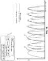
- FIG. 1Billustrates an exemplary voltage distribution of a high-density NAND cell with reduced noise margin.
- FIG. 2Aillustrates an exemplary domain denotation in storage cells for multi-dimensional modulation, in accordance with an embodiment of the present application.
- FIG. 2Billustrates an exemplary subset denotation in storage cells for multi-dimensional modulation, in accordance with an embodiment of the present application.
- FIG. 2Cillustrates an exemplary two-dimensional space for multi-dimensional modulation, in accordance with an embodiment of the present application.
- FIG. 3illustrates exemplary data storage based on modulation-assisted error correction, in accordance with an embodiment of the present application.
- FIG. 4illustrates exemplary data retrieval based on modulation-assisted error correction, in accordance with an embodiment of the present application.
- FIG. 5illustrates an exemplary architecture of a controller of a flash device supporting modulation-assisted error correction, in accordance with an embodiment of the present application.
- FIG. 6Aillustrates an exemplary reduced-dimension (RD) modulation that utilizes parity difference of modulation-assisted error-correction, in accordance with an embodiment of the present application.
- RDreduced-dimension
- FIG. 6Billustrates an exemplary parity-bit management using RD modulation, in accordance with an embodiment of the present application.
- FIG. 7Apresents a flowchart illustrating a method of the controller of a flash device storing data based on modulation-assisted error correction, in accordance with an embodiment of the present application.
- FIG. 7Bpresents a flowchart illustrating a method of the controller of a flash device retrieving data based on modulation-assisted error correction, in accordance with an embodiment of the present application.
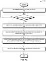
- FIG. 7Cpresents a flowchart illustrating a method of the controller of a flash device storing overflow parity bits based on RD modulation, in accordance with an embodiment of the present application.
- FIG. 8illustrates an exemplary computer system that facilitates modulation-assisted error correction, in accordance with an embodiment of the present application.
- FIG. 9illustrates an exemplary apparatus that facilitates modulation-assisted error correction, in accordance with an embodiment of the present application.
- the embodiments described hereinsolve the problem of providing efficient error correction for a high-density flash device by facilitating (i) a modulator-assisted error-correction coding that supports differentiated error correction for different types of bits in the flash device; and (ii) a reduced-dimension error-correction coding that can accommodate overflow parity bits based on parity difference of modulation-assisted error-correction.
- high-density flash devicessuch as high-density NAND flash devices, typically use triple-level cells (TLCs) and quad-level cells (QLCs) for representing data bits. These cells can be referred to as storage cells.
- a NAND flash memory devicecan also be referred to as a flash device and/or a flash. Since each cell in the flash stores a plurality of bits, each cell needs to distinguish among a large number of voltage levels to identify the corresponding bits. For a QLC, the cell represents 4 bits and needs to distinguish among 16 voltage levels to identify a corresponding bit pattern (e.g., 0101 versus 0100). In other words, the cell needs to uniquely identify 15 threshold voltage levels.
- This high-density nature of data storageleads to a limited gap between adjacent voltage levels and corresponding tightly distributed threshold voltage levels.
- the data retention capability of the storage cells in the flash devicegradually weakens over the lifespan of the storage cells.
- the threshold voltage distributioncan become distorted: the threshold voltage distribution tends to shift and becomes wider. Since the gap between adjacent levels is limited, the distorted threshold voltage distribution overlaps.
- the controller of the flash deviceretrieves data from the cell, the controller may not be able to sense the originally stored data from the overlapping voltage level. As a result, the corresponding data retrieval can become error-prone. In other words, high-density flash devices can suffer high data error rates, which continue to increase with the use of the flash device. Consequently, the ECC scheme of the flash device may not be sufficient after a period of time.
- the controller of the flash deviceneeds to change the ECC scheme on-the-fly (i.e., during runtime) to a higher-accuracy ECC (i.e., an ECC that can detect and correct a higher number of bit error rates) than the current one to decrease the overall error rate and bring it below a threshold.
- a higher-accuracy ECCi.e., an ECC that can detect and correct a higher number of bit error rates
- multiple ECC schemesneed to be designed and implemented in the flash device. This can lead to increased complexity and higher costs.
- the higher-accuracy ECCwhich can address a higher error rate, needs more parity bits to be stored. As a result, more storage space in the flash device needs to be dedicated for storing the parity bits. This reduces the effective storage space that can be used to accommodate the user data.
- PEprogram-erase
- an enhanced controller for a flash devicesuch as a NAND flash controller, that can support modulation-assisted error correction for the flash device.
- the modulation-assisted error correctionintegrates multi-dimensional modulations and error correction without introducing extra parity.
- the bits in each storage cell, such as a NAND cellare divided into different categories. Each category of bits is associated with its own modulation and error correction.
- modulationencodes a set of bits into a corresponding signal (e.g., a voltage level).
- the multi-dimensional modulationincreases the distance between the same repeated subset (i.e., the same bit pattern). This leads to lower overlapping in the threshold voltage distribution region and, hence, a reduced error rate.
- the storage cells in the flash deviceare TLCs.
- the number of bits stored in a respective cellis three.
- the 3 bits in a TLCcan be in an upper bit (u bit), middle bit (m bit), and lower bit (1 bit) format.
- the 3 bits of a TLCcan be u-m-1 bits.
- the multi-dimensional modulation schemecan use two such cells.
- the lower bits of the 2 cellsare used to represent the coordinate of modulation domains. These 2 domain bits can represent 4 such domains.
- the upper and middle bits from the 2 cellsare used to represent a modulation subset.
- These 4 subset bitscan represent 16 possible subsets, each with 4 points (i.e., 4 repetitions of the same subset) that are distributed evenly into 4 domains. In this way, the multi-dimensional modulation scheme divides the modulation into two dimensions.
- the controllercan consider the first cell's threshold voltage as a horizontal axis and the second cell's threshold voltage as a vertical axis.
- the resultant two-dimensional spacei.e., 8 levels by 8 levels
- the resultant two-dimensional spacecan be divided to map the 64 points represented by the 4 domains and the 16 subsets, each repeated once in each domain.
- the increased distance between two points (i.e., 2 repetitions) represented by the multi-dimensional modulation schemecan lower the error rate.
- the modulation schememaps the points in the same subset as far as possible.
- the controller of the flash devicecan deploy a modulation-assisted ECC (MECC) scheme.
- MECCmodulation-assisted ECC
- the multi-dimensional modulation schemeincreases the inter-subset distance (e.g., the distance between any 2 points of the same subset), hence lowering the corresponding raw error rate.
- the domain bitsbecome enhanced with a higher-degree of noise immunity after the modulation.
- MECCdeploys a high-accuracy ECC for the subset bits.
- MECCcan use a baseline ECC for the domain bits.
- the baseline ECCmay not be as “strong” as the high-accuracy ECC.
- the baseline ECCmay not be able to detect as many bit errors as the high-accuracy ECC.
- the high-accuracy ECCcan detect and correct up to x number of bit errors while the baseline ECC can detect and correct up to (x-y) number of bit errors (x and y are positive integers).
- the enhanced noise immunityallows the controller to use the baseline ECC and perform the necessary level of error correction. In this way, since each point is distributed into one of the domains for all points of a subset, MECC can facilitate enhanced error correction, thereby addressing the threshold voltage distribution issue with data retention without introducing extra parity.
- FIG. 1Aillustrates an exemplary infrastructure that facilitates modulation-assisted error correction, in accordance with an embodiment of the present application.
- an infrastructure 100can include a distributed storage system 110 .
- System 110can include: client servers (or client-serving machines) 102 , 104 , and 106 , and storage servers 112 , 114 , and 116 .
- Client servers 102 , 104 , and 106 , and storage servers 112 , 114 , and 116can communicate with each other via a network 130 (e.g., a local or a wide area network, such as the Internet).
- a storage servercan also include multiple storage devices.
- storage server 116can include components such as a central processing unit (CPU) 172 , a memory 174 (e.g., a dual in-line memory module), a network interface card (NIC) 176 , and a number of storage devices/disks 154 , 155 , and 156 .
- CPUcentral processing unit
- memory 174e.g., a dual in-line memory module
- NICnetwork interface card
- storage server 116can include components such as a central processing unit (CPU) 172 , a memory 174 (e.g., a dual in-line memory module), a network interface card (NIC) 176 , and a number of storage devices/disks 154 , 155 , and 156 .
- NICnetwork interface card
- Storage device 156can include one or more high-density flash devices, such as NAND flash device 120 .
- Flash 120can include a number of storage cells 122 , 124 , 126 , and 128 . These cells can be any level cells (e.g., a TLC or a QLC).
- a respective storage cell of flash 120is a TLC.
- the number of bits stored in a respective cell of flash 120can be three.
- the 3 bits in cell 122can include a u bit 132 , an m bit 134 , and an 1 bit 136 .
- the 3 bits in cell 124can include a u bit 142 , an m bit 144 , and an 1 bit 146 .
- Flash 120can include a NAND flash controller 150 , which manages data storage, retrieval, and retention operations of flash 120 . Such operations can include, but are not limited to, read, write, modulation, error correction, and scheme selection operations.
- FIG. 1Billustrates an exemplary voltage distribution of a high-density NAND cell with reduced noise margin.
- the originally programmed threshold voltage distribution 162e.g., a probability density function (PDF)
- PDFprobability density function
- Threshold voltage distribution 164tends to shift from distribution 162 and becomes wider compared to distribution 162 . Since the gap between adjacent levels is limited, threshold voltage distribution 164 can become significantly overlapping.
- controller 150retrieves data from cell 122 , controller 150 may not be able to sense the originally stored data from the overlapping voltage levels. As a result, the corresponding data retrieval can become error-prone. In other words, flash 120 can suffer a high data error rate, which continues to increase with more PE cycles. Consequently, the ECC scheme of flash 120 may not be sufficient after a period of time.
- controller 150may need to change the ECC scheme on-the-fly to a higher-accuracy ECC than the current one to decrease the overall error rate and bring it below a threshold.
- multiple ECC schemesneed to be designed and implemented in flash 120 . This can lead to increased complexity and higher costs.
- the higher-accuracy ECCwhich can address a higher error rate, needs more parity bits to be stored in flash 120 . As a result, more storage space in flash 120 may be dedicated for storing the parity bits. This reduces the effective storage space of flash 120 that can be used to accommodate the user data.
- the raw error ratevaries among blocks in flash 120 .
- controller 150switches to the higher-accuracy ECC calculation, that could be applicable to all blocks. This can cause inefficient usage of flash 120 .
- controller 150can facilitate modulation-assisted error correction for flash 120 .
- the modulation-assisted error correctionintegrates multi-dimensional modulations and error correction without introducing extra parity in flash 120 .
- the bits in each storage cell, cell 122are divided into different categories. Each category of bits is associated with its own modulation and error correction.
- the multi-dimensional modulationincreases the distance between the points of the same subset. This leads to lower overlapping in the threshold voltage distribution region and, hence, a reduced error rate.
- the multi-dimensional modulation schemecan be applied to a cell-pair, such as cells 122 and 124 .
- Lower bits 136 and 146can be used to represent the coordinate of modulation domains. These 2 domain bits can represent 4 such domains.
- Upper bits 132 and 142 , and middle bits 134 and 144are used to represent a modulation subset. These 4 subset bits can represent 16 possible subsets, each having 4 points that are distributed evenly into 4 domains. In this way, the multi-dimensional modulation scheme divides the modulation into two dimensions.
- controller 150can deploy a MECC scheme in flash 120 .
- the multi-dimensional modulation schemeincreases the inter-subset distance (e.g., the distance between any 2 points of the same subset), and hence, lowering the corresponding raw error rate.
- domain bits 136 and 146become enhanced with a higher-degree of noise immunity after the modulation.
- MECCdeploys a high-accuracy ECC (or a strong ECC) for subset bits 132 , 134 , 142 , and 144 .
- MECCcan use a baseline ECC for these bits. Because each point is distributed into one of the domains for all points of a subset, MECC can facilitate enhanced error correction, thereby addressing the threshold voltage distribution issue with data retention without introducing extra parity in flash 120 .
- FIG. 2Aillustrates an exemplary domain denotation in storage cells for multi-dimensional modulation, in accordance with an embodiment of the present application.
- Domain bits 136 and 146can represent 4 domains 200 that include I, II, III, and IV, which can be 00, 01, 10, and 11, respectively. Each of these 4 domains can include a point of each subset.
- Domain bits 136 and 146denote the coordinates of domains 200 . For example, bits “00” correspond to domain I and denote the coordinate of domain I in the 2-D space created by the voltage levels of cells 122 and 124 .
- FIG. 2Billustrates an exemplary subset denotation in storage cells for multi-dimensional modulation, in accordance with an embodiment of the present application.
- Subset bits 132 , 134 , 142 , and 144can represent 16 subsets 230 that include subsets A-P.
- Each subsetis a specific bit pattern.
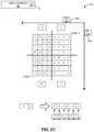
- FIG. 2Cillustrates an exemplary two-dimensional space for multi-dimensional modulation, in accordance with an embodiment of the present application.
- the resultant two-dimensional spacei.e., 8 levels by 8 levels
- can represent a modulation map 250which maps the 64 points represented by the 4 domains and the 16 subsets. This multi-dimensional modulation increases the distance between two points of a subset.
- the distance between the two points of subset Acan be ⁇ square root over (17) ⁇ . This increased distance between two points can lower the error rate.
- subset AAs described in conjunction with FIGS. 2A and 2B , the four points of subset A are evenly distributed in the 4 domains.
- controller 150intends to program bits “000001” in cells 122 and 124 .
- Subset Ais denoted by “0000” in bits 132 , 134 , 142 , and 144 , respectively, and domain IV is denoted by “11” in bits 136 and 146 , respectively.
- bits “001001”are programmed in cells 122 and 124 as subset A in domain IV.
- subset A in domain IVcan be indicated by level 2 of threshold voltage 252 and level 5 of threshold voltage 254 starting from 0.
- subset A in domain IIcan be indicated by level 7 of threshold voltage 252 and level 0 of threshold voltage 254 .
- FIG. 3illustrates exemplary data storage based on modulation-assisted error correction, in accordance with an embodiment of the present application.
- controller 150can include a modulator 300 that is capable of facilitating multi-dimensional modulation.
- Modulator 300can generate the corresponding voltage levels for cells 122 and 124 in such a way that the 6 bits programmed in cells 122 and 124 are one of the 64 possible combinations. For example, to program bits “001001” in cells 122 and 124 , modulator 300 programs “0000” in subset bits 132 , 134 , 142 , and 144 , respectively, and “11” in domain bits 136 and 146 , respectively.
- modulator 300can modulate cell 122 with a voltage level 2 of the 8 levels and cell 124 with a voltage level 5 of the 8 levels.
- modulator 300programs “0000” in subset bits 132 , 134 , 142 , and 144 , respectively, and “11” in domain bits 136 and 146 , respectively.
- modulator 300can modulate cell 122 with a voltage level 5 and cell 124 with a voltage level 2. This modulation increases the distance between the points of subset A (i.e., the subset of “0000,” as described in conjunction with FIG. 2B ). Therefore, the bits for domain denotation naturally get enhanced noise immunity after the modulation.
- controller 150can deploy the MECC scheme.
- controller 150can include at least two ECC encoders 322 and 324 .
- Encoder 322can encode bits with a high-accuracy ECC and encoder 324 can encode bits with a baseline ECC. Since domain bits 136 and 146 become enhanced with noise immunity, controller 150 can use ECC encoder 324 for bits 136 and 146 , and generate corresponding parity bits 334 .
- controller 150can use ECC encoder 324 for bits 132 , 134 , 142 , and 144 , and generate corresponding parity bits 334 . Because each point of the subset is distributed into one of the domains and the domains are enhanced with noise immunity, even with distorted threshold voltage levels, as described in conjunction with FIG. 1A , parity bits 332 and 334 are sufficient to recover the bits stored in cells 122 and 124 .
- FIG. 4illustrates exemplary data retrieval based on modulation-assisted error correction, in accordance with an embodiment of the present application.
- controller 150can also read from both cells 122 and 124 .
- controller 150divides the read result into 2 groups.
- the first groupcan include bits 132 , 134 , 142 , and 144
- the second groupcan include bits 136 and 146 .
- controller 150can include ECC decoders 422 and 424 .
- Decoder 422can decode bits with the high-accuracy ECC corresponding to encoder 322 and decoder 424 can decode bits with the baseline ECC corresponding to encoder 324 .
- Controller 150can use decoder 422 to decode the first group. This allows controller 150 to determine which subset the programmed data belongs to. For example, if the first group is “0000,” controller 150 can determine that the decoded data corresponds to subset A.
- sense level 412can indicate the threshold voltage level controller 150 is expected to sense
- programmed level 414can indicate the threshold voltage level of the cells in flash 120 for data retention over a period of time. In this way, controller 150 can still sense the correct points with a low error rate without needing to switch to a higher-strength ECC on-the-fly.
- Controller 150can use decoder 424 to decode the second group to determine the domain of the subset based on parity bits 334 . For example, if the second group is “11,” controller 150 can determine that the decoded subset A corresponds to domain IV.
- controller 150when controller 150 determines the point in the 2-D space generated by sense level 412 for cells 122 and 124 , controller 150 can check the corresponding modulation map (e.g., modulation map 250 in FIG. 2C ) to determine the 6 bits from cells 122 and 124 .
- modulation mape.g., modulation map 250 in FIG. 2C
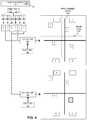
- FIG. 5illustrates an exemplary architecture of a controller of a flash device supporting modulation-assisted error correction, in accordance with an embodiment of the present application.
- Controller 150can include a host interface 502 for communicating with the host device and obtaining user data, and a media interface 504 for storing the modulated data in the storage cells.
- controller 150first performs a cyclic-redundancy check (CRC) on any incoming user data received via host interface 502 using a CRC checker 512 . This allows controller 150 to detect any error in the user data.
- Encryption module 514then encrypts the user data based on an on-chip encryption mechanism, such as a self-encrypting mechanism for flash memory.
- CRCcyclic-redundancy check
- a bit separator 516separates the bits from a cell into a first group and a second group for subset denotation and domain denotation, respectively.
- bits 132 and 134 of cell 122are grouped into the first group, and bit 136 of cell 122 is grouped into the second group.
- Controller 150then encodes the first group with encoder 322 and the second group with encoder 324 to generate the corresponding parity bits.
- Controller 150then programs the user bits and the parity bits into the cells using modulator 300 . This programming includes setting the respective voltage levels of the cells based on the modulation map (e.g., modulation map 250 in FIG. 2C ).
- controller 150obtains programmed data via media interface 504 .
- Decoders 422 and 424then perform ECC decoding on the subset bits and domain bits, respectively. Since the multi-dimensional modulation increases the distance between two points of a subset, decoder 422 can still decode the subset with shifted programmed level 414 due to data retention over a period of time. This allows controller 150 to avoid switching to a higher-accuracy ECC encoding mechanism.
- demodulator 522demodulates the decoded user data to generate the corresponding domain and subset bits.
- Bit aggregator 524aggregates the bits to generate corresponding user data bits.
- bit aggregator 524can aggregate subset bits “0000” with domain bits “11” to generate user data bits “001001” stored in a cell-pair.
- Decryption module 526can decrypt the on-chip encryption on the user data.
- CRC checker 528then performs a CRC check on the decrypted user data to ensure the data is error-free.
- Controller 150provides that user data to the user (i.e., the host machine) via host interface 502 .
- FIG. 6Aillustrates an exemplary RD modulation that utilizes parity difference of modulation-assisted error-correction, in accordance with an embodiment of the present application.
- encoder 322uses the higher-accuracy ECC encoding and encoder 324 uses the baseline ECC encoding.
- the number of parity bits generated by encoder 322can be higher than the same of encoder 324 .
- parity bits 332can be larger than parity bits 334 .
- Flash 120can store the parity bits in out-of-band (OOB) cells (i.e., the cells not used for storing user data). These OOB cells can also be TLCs and include an upper parity bit, a middle parity bit, and a lower parity bit.
- OOBout-of-band
- the resultant parity bitsmay match the number of upper and middle parity bits in the OOB cells.
- the parity bits for the lower bits of a respective storage cellare encoded by encoder 324 .
- the number of parity bits for the lower bitscan be fewer than the number of lower parity bits in the OOB cells.
- upper parity bits 602 and middle parity bits 604 of the OOB cellsmay match the number of parity bits generated by encoder 322 for the upper and middle bits in the storage cells used for storing user data.
- the number of parity bits generated by encoder 324 for the lower bits in the storage cellscan be fewer than the lower parity bits 606 of the OOB cells.
- a number of bits in parity bits 606may remain unused and can be referred to as unused bits 608 .
- a number of cells in the OOB cellsonly use 2 bits, and the other bit remains in unused bits 608 .
- These cellscan be referred to as RD modulation cells 600 .
- controller 150can use an RD modulation that modulates the 2 bits in upper parity bits 602 and middle parity bits 604 of cells 600 . Similar to the multi-dimensional modulation, RD modulation can modulate 2 OOB cells. Consequently, RD modulation can use 4 bits in upper parity bits 602 and middle parity bits 604 to denote 16 points A-P similar to 16 subsets 230 . The 2-D space corresponding to the 8-by-8 voltage levels of the 2 OOB cells can generate 64 possible combinations. Controller 150 generates an RD modulation map 610 by mapping the 16 points to 16 positions out of the 64 positions. In some embodiments, controller 150 can select the 16 positions in such a way that the average distance between two points is increased, which can lead to a reduced error rate. Because of unused bits 608 , controller 150 only needs to program 16 points instead of 64.
- FIG. 6Billustrates an exemplary parity-bit management using RD modulation, in accordance with an embodiment of the present application.
- Controller 150can then switch to a higher-accuracy ECC than the ECC provided by encoder 322 to maintain the advantage of MECC.
- controller 150can be equipped with an ECC encoder 640 capable of providing the higher-accuracy ECC. Controller 150 can then disable encoder 322 (denoted with dotted lines) and enable encoder 640 to switch to the higher-accuracy ECC. However, encoder 640 may generate a higher number of parity bits compared to that of encoder 322 . The additional parity bits 622 and 624 may exceed the memory space originally accommodated in OOB cells. As a result, parity bits 622 and 624 can overflow. To address the overflow issue, controller 150 can move parity bits 622 and 624 to unused bits 608 . In this way, controller 150 can still switch to a higher-priority ECC without allocating data cells that were previously allocated for user data for parity bits.
- the enhanced noisy immunity from the multi-dimensional modulationprovides a low error rate to the domain bits.
- the baseline ECC provided by encoder 324would still be sufficient to protect the domain bits.
- Controller 150adjusts RD modulation cells 600 in upper parity bits 602 and middle parity bits 604 to correspond to unused bits 620 .
- These adjusted RD modulation cells 650can still include OOB cell-pairs for which RD modulation mapping 610 can be used.
- FIG. 7Apresents a flowchart 700 illustrating a method of the controller of a flash device storing data based on modulation-assisted error correction, in accordance with an embodiment of the present application.
- the controllerreceives data bits from the host interface (operation 702 ), and performs a redundancy check and encryption on the data bits (operation 704 ).
- the controllerthen groups the data bits for subset denotation and domain denotation (operation 706 ).
- the controllercan encode the subset bits with a high-accuracy ECC encoding to generate subset parity bits (operation 708 ).
- the controllercan also encode the domain bits with baseline ECC encoding to generate domain parity bits (operation 710 ).
- the controllermodulates the subset and domain bits, and the parity bits for storing in cells (operation 712 ).
- the controllerthen programs a storage cell-pair via the media interface such that the resultant 2-D space corresponds to modulated bits (operation 714 ).
- the controlleralso programs OOB cells with the parity bits via the media interface (operation 716 ).
- FIG. 7Bpresents a flowchart 730 illustrating a method of the controller of a flash device retrieving data based on modulation-assisted error correction, in accordance with an embodiment of the present application.
- the controllerdetermines respective programmed voltage levels from a storage cell-pair (operation 732 ).
- the controllerapplies a high-accuracy ECC decoding to the programmed voltage levels based on the subset parity bits to determine the points of a subset (operation 734 ). For example, for 4 domains, this operation can provide the 4 points of the subset, as described in conjunction with FIG. 4 .
- the controllerthen applies a baseline ECC decoding to the programmed voltage levels based on the domain parity bits to determine the domain of the subset (operation 736 ).
- the controllerdemodulates the subset and domain bits based on the corresponding modulation map (operation 738 ), and aggregates the subset and domain bits to generate the data bits (operation 740 ).
- the controllerthen performs decryption and redundancy check on the data bits (operation 742 ), and provides the resultant data bits via the host interface (operation 744 ).
- FIG. 7Cpresents a flowchart 750 illustrating a method of the controller of a flash device storing overflow parity bits based on RD modulation, in accordance with an embodiment of the present application.
- the controllerdetermines the sensitivity levels of the cells (operation 752 ).
- the sensitivity levelscan indicate whether the controller can correctly sense the programmed data in the cells.
- the controllerchecks whether a switchover has been triggered (operation 754 ). A switchover can trigger if the controller can no longer correctly sense the subset bits from the programmed cells. If a switchover is not triggered, the controller continues to determine the sensitivity levels of the cells (operation 752 ).
- the controllercan switch to a higher-accuracy ECC encoding for the subset bits (operation 756 ).
- the controllercan perform the switchover by enabling an encoder capable of performing the higher-accuracy ECC encoding.
- the controllerthen encodes the subset bits with the higher-accuracy ECC encoding to generate the subset parity bits (operation 758 ).
- the controllercan store the overflow parity bits, if any, of the subset parity bits in the unused bits corresponding to the domain parity bits in the OOB cells (operation 760 ).
- the controllerthen adjusts the RD modulation based on the reduced unused bits (operation 762 ).
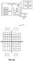
- FIG. 8illustrates an exemplary computer system that facilitates modulation-assisted error correction, in accordance with an embodiment of the present application.
- Computer system 800includes a processor 802 , a memory 804 , and a storage device 806 .
- Memory 804can include a volatile memory (e.g., a dual in-line memory module (DIMM)).
- DIMMdual in-line memory module
- computer system 800can be coupled to a display device 810 , a keyboard 812 , and a pointing device 814 .
- Storage device 808can store an operating system 816 , a storage control system 818 , and data 836 .
- Storage control system 818can facilitate the operations of controller 150 , as described in conjunction with FIG. 5 .
- Storage control system 818can include instructions, which when executed by computer system 800 can cause computer system 800 to perform methods and/or processes described in this disclosure. Specifically, storage control system 818 can include instructions for obtaining data from and providing data to a host machine (interface module 820 ). Storage control system 818 can also include instructions for programming data in and retrieving/sensing programmed data from storage cells (e.g., NAND cells) (interface module 820 ). Furthermore, storage control system 818 includes instructions for encrypting and/or decrypting data (encryption module 822 ) and performing CRC checks on the data (CRC module 824 ).
- encryption module 822encrypting and/or decrypting data
- CRC module 824performing CRC checks on the data
- storage control system 818includes instructions for organizing (e.g., grouping and/or aggregating) bits from storage cells into subset and domain bits (organization module 826 ).
- Storage control system 818further includes instructions for performing the MECC scheme, which can include using a high-accuracy ECC for the subset bits and a baseline ECC for the domain bits (ECC module 828 ).
- ECC module 828ECC module 828
- Storage control system 818can include instructions for mapping the subset and domain bits to the voltage levels of the corresponding storage cells and generating the corresponding modulation map (mapping module 830 ).
- Storage control system 818can also include instructions for mapping the upper and middle parity bits to the voltage levels of the corresponding RD modulations cells and generating the corresponding RD modulation map (mapping module 830 ).
- storage control system 818includes instructions for performing the multi-dimensional modulation and programming the one or more storage cells based on the corresponding modulation mapping (modulation module 832 ).
- Storage control system 818also includes instructions for performing the RD modulation and programming the one or more RD modulation cells based on the corresponding RD modulation mapping (modulation module 832 ).
- Storage control system 818also includes instructions for programming the OOB cells with parity bits generated by the MECC scheme (modulation module 832 ).
- Storage control system 818may further include instructions for sending and receiving messages (communication module 834 ).
- Data 836can include any data that can facilitate the operations of controller 150 , such as modulation mapping 250 and RD modulation mapping 610 .
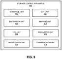
- FIG. 9illustrates an exemplary apparatus that facilitates modulation-assisted error correction, in accordance with an embodiment of the present application.
- Storage control apparatus 900can comprise a plurality of units or apparatuses which may communicate with one another via a wired, wireless, quantum light, or electrical communication channel.
- Apparatus 900may be realized using one or more integrated circuits, and may include fewer or more units or apparatuses than those shown in FIG. 9 . Further, apparatus 900 may be integrated in a computer system, or realized as a separate device that is capable of communicating with other computer systems and/or devices.
- apparatus 900can comprise units 902 - 916 , which perform functions or operations similar to modules 820 - 834 of computer system 800 of FIG.
- an interface unit 902including: an interface unit 902 ; an encryption unit 904 ; a CRC unit 906 ; an organization unit 908 ; an ECC unit 910 ; a mapping unit 912 ; a modulation unit 914 ; and a communication unit 916 .
- the data structures and code described in this detailed descriptionare typically stored on a computer-readable storage medium, which may be any device or medium that can store code and/or data for use by a computer system.
- the computer-readable storage mediumincludes, but is not limited to, volatile memory, non-volatile memory, magnetic and optical storage devices such as disks, magnetic tape, CDs (compact discs), DVDs (digital versatile discs or digital video discs), or other media capable of storing computer-readable media now known or later developed.
- the methods and processes described in the detailed description sectioncan be embodied as code and/or data, which can be stored in a computer-readable storage medium as described above.
- a computer systemreads and executes the code and/or data stored on the computer-readable storage medium, the computer system performs the methods and processes embodied as data structures and code and stored within the computer-readable storage medium.
- the methods and processes described abovecan be included in hardware modules.
- the hardware modulescan include, but are not limited to, application-specific integrated circuit (ASIC) chips, field-programmable gate arrays (FPGAs), and other programmable-logic devices now known or later developed.
- ASICapplication-specific integrated circuit
- FPGAfield-programmable gate arrays
- the hardware modulesWhen the hardware modules are activated, the hardware modules perform the methods and processes included within the hardware modules.
Landscapes
- Engineering & Computer Science (AREA)
- Theoretical Computer Science (AREA)
- Physics & Mathematics (AREA)
- General Engineering & Computer Science (AREA)
- General Physics & Mathematics (AREA)
- Quality & Reliability (AREA)
- Microelectronics & Electronic Packaging (AREA)
- Computer Hardware Design (AREA)
- Read Only Memory (AREA)
- Techniques For Improving Reliability Of Storages (AREA)
Abstract
Description
Claims (20)
Priority Applications (1)
| Application Number | Priority Date | Filing Date | Title |
|---|---|---|---|
| US16/237,340US10977122B2 (en) | 2018-12-31 | 2018-12-31 | System and method for facilitating differentiated error correction in high-density flash devices |
Applications Claiming Priority (1)
| Application Number | Priority Date | Filing Date | Title |
|---|---|---|---|
| US16/237,340US10977122B2 (en) | 2018-12-31 | 2018-12-31 | System and method for facilitating differentiated error correction in high-density flash devices |
Publications (2)
| Publication Number | Publication Date |
|---|---|
| US20200210288A1 US20200210288A1 (en) | 2020-07-02 |
| US10977122B2true US10977122B2 (en) | 2021-04-13 |
Family
ID=71124288
Family Applications (1)
| Application Number | Title | Priority Date | Filing Date |
|---|---|---|---|
| US16/237,340Active2039-05-30US10977122B2 (en) | 2018-12-31 | 2018-12-31 | System and method for facilitating differentiated error correction in high-density flash devices |
Country Status (1)
| Country | Link |
|---|---|
| US (1) | US10977122B2 (en) |
Families Citing this family (1)
| Publication number | Priority date | Publication date | Assignee | Title |
|---|---|---|---|---|
| US11487611B2 (en)* | 2020-10-02 | 2022-11-01 | Western Digital Technologies, Inc. | LDPC encoding for memory cells with arbitrary number of levels |
Citations (292)
| Publication number | Priority date | Publication date | Assignee | Title |
|---|---|---|---|---|
| US3893071A (en) | 1974-08-19 | 1975-07-01 | Ibm | Multi level error correction system for high density memory |
| US4562494A (en) | 1983-04-07 | 1985-12-31 | Verbatim Corporation | Disk drive alignment analyzer |
| US4718067A (en) | 1984-08-02 | 1988-01-05 | U.S. Philips Corporation | Device for correcting and concealing errors in a data stream, and video and/or audio reproduction apparatus comprising such a device |
| US4775932A (en) | 1984-07-31 | 1988-10-04 | Texas Instruments Incorporated | Computer memory system with parallel garbage collection independent from an associated user processor |
| US4858040A (en) | 1987-08-25 | 1989-08-15 | Ampex Corporation | Bimorph actuator for a disk drive |
| WO1994018634A1 (en) | 1993-02-01 | 1994-08-18 | Lsc, Inc. | Archiving file system for data servers in a distributed network environment |
| US5394382A (en) | 1993-02-11 | 1995-02-28 | International Business Machines Corporation | Method for the organization of data on a CD-ROM |
| US5602693A (en) | 1994-12-14 | 1997-02-11 | Micropolis (S) Pte Ltd. | Method and apparatus for sensing position in a disk drive |
| US5732093A (en) | 1996-02-08 | 1998-03-24 | United Microelectronics Corporation | Error correction method and apparatus on optical disc system |
| US5802551A (en) | 1993-10-01 | 1998-09-01 | Fujitsu Limited | Method and apparatus for controlling the writing and erasing of information in a memory device |
| US5930167A (en) | 1997-07-30 | 1999-07-27 | Sandisk Corporation | Multi-state non-volatile flash memory capable of being its own two state write cache |
| US6098185A (en) | 1997-10-31 | 2000-08-01 | Stmicroelectronics, N.V. | Header-formatted defective sector management system |
| US6148377A (en) | 1996-11-22 | 2000-11-14 | Mangosoft Corporation | Shared memory computer networks |
| US6226650B1 (en) | 1998-09-17 | 2001-05-01 | Synchrologic, Inc. | Database synchronization and organization system and method |
| US20010032324A1 (en) | 1998-05-12 | 2001-10-18 | Slaughter Gregory L. | Highly available cluster message passing facility |
| US20020010783A1 (en) | 1999-12-06 | 2002-01-24 | Leonard Primak | System and method for enhancing operation of a web server cluster |
| US20020039260A1 (en) | 1995-11-28 | 2002-04-04 | Kilmer Dan L. | Twin coil positioner |
| US20020073358A1 (en) | 2000-12-07 | 2002-06-13 | Atkinson Lee. W. | Method for redundant suspend to RAM |
| US20020095403A1 (en) | 1998-11-24 | 2002-07-18 | Sashikanth Chandrasekaran | Methods to perform disk writes in a distributed shared disk system needing consistency across failures |
| US6457104B1 (en) | 2000-03-20 | 2002-09-24 | International Business Machines Corporation | System and method for recycling stale memory content in compressed memory systems |
| US20020161890A1 (en) | 2000-12-22 | 2002-10-31 | Kailai Chen | System and method for intelligently distributing content over a communicatons network |
| JP2003022209A (en) | 2001-07-05 | 2003-01-24 | Nri & Ncc Co Ltd | Distributed server system |
| US20030145274A1 (en) | 2002-01-23 | 2003-07-31 | Samsung Electronics Co., Ltd. | Decoding method and apparatus therefor |
| US20030163633A1 (en) | 2002-02-27 | 2003-08-28 | Aasheim Jered Donald | System and method for achieving uniform wear levels in a flash memory device |
| US20030163594A1 (en) | 2002-02-27 | 2003-08-28 | Aasheim Jered Donald | Open-architecture file system |
| US20030217080A1 (en) | 2002-05-20 | 2003-11-20 | Ken White | System and method for intelligent write management of disk pages in cache checkpoint operations |
| US6658478B1 (en) | 2000-08-04 | 2003-12-02 | 3Pardata, Inc. | Data storage system |
| US20040010545A1 (en) | 2002-06-11 | 2004-01-15 | Pandya Ashish A. | Data processing system using internet protocols and RDMA |
| US20040066741A1 (en) | 2002-09-23 | 2004-04-08 | Darpan Dinker | System and method for performing a cluster topology self-healing process in a distributed data system cluster |
| US20040103238A1 (en) | 2002-11-26 | 2004-05-27 | M-Systems Flash Disk Pioneers Ltd. | Appliance, including a flash memory, that is robust under power failure |
| US6795894B1 (en) | 2000-08-08 | 2004-09-21 | Hewlett-Packard Development Company, L.P. | Fast disk cache writing system |
| US20040255171A1 (en) | 2003-06-13 | 2004-12-16 | Zimmer Vincent J. | Power management for clustered computing platforms |
| US20040268278A1 (en) | 2003-05-07 | 2004-12-30 | Hoberman Barry Alan | Managing power on integrated circuits using power islands |
| US20050038954A1 (en) | 2003-06-04 | 2005-02-17 | Quantum Corporation | Storage drive having universal format across media types |
| US20050097126A1 (en) | 2000-08-24 | 2005-05-05 | Microsoft Corporation | Partial migration of an object to another storage location in a computer system |
| US20050149827A1 (en) | 2002-01-24 | 2005-07-07 | Nicolaas Lambert | Data storage apparatus and method for handling a data storage apparatus |
| US20050174670A1 (en) | 2004-02-10 | 2005-08-11 | Hitachi Global Storage Technologies Netherlands Bv | Adaptive data format method integrating spare sectors |
| US20050177755A1 (en) | 2000-09-27 | 2005-08-11 | Amphus, Inc. | Multi-server and multi-CPU power management system and method |
| US20050177672A1 (en) | 2004-02-10 | 2005-08-11 | Sun Microsystems, Inc. | Storage system structure for storing relational cache metadata |
| US20050195635A1 (en) | 2004-03-08 | 2005-09-08 | Conley Kevin M. | Flash controller cache architecture |
| US20050235067A1 (en) | 2004-04-20 | 2005-10-20 | Intel Corporation | Write combining protocol between processors and chipsets |
| US20050235171A1 (en) | 2003-09-02 | 2005-10-20 | Kabushiki Kaisha Toshiba | Electronic device with serial ATA interface and power saving method for serial ATA buses |
| US20060031709A1 (en) | 2004-08-09 | 2006-02-09 | Yuri Hiraiwa | Failure monitoring for storage systems constituting multiple stages |
| US20060156012A1 (en) | 2005-01-07 | 2006-07-13 | Beeson Curtis L | Facilitating digital signature based on ephemeral private key |
| US20070033323A1 (en) | 2005-08-03 | 2007-02-08 | Gorobets Sergey A | Interfacing systems operating through a logical address space and on a direct data file basis |
| US20070061502A1 (en) | 2005-09-09 | 2007-03-15 | M-Systems Flash Disk Pioneers Ltd. | Flash memory storage system and method |
| US20070101096A1 (en) | 2005-10-27 | 2007-05-03 | Sandisk Corporation | Non-volatile memory with adaptive handling of data writes |
| US20070283081A1 (en) | 2006-06-06 | 2007-12-06 | Msystem Ltd. | Cache control in a non-volatile memory device |
| US20070285980A1 (en) | 2006-05-10 | 2007-12-13 | Takahiro Shimizu | Semiconductor memory device |
| US20080034154A1 (en) | 1999-08-04 | 2008-02-07 | Super Talent Electronics Inc. | Multi-Channel Flash Module with Plane-Interleaved Sequential ECC Writes and Background Recycling to Restricted-Write Flash Chips |
| US20080065805A1 (en) | 2006-09-11 | 2008-03-13 | Cameo Communications, Inc. | PCI-Express multimode expansion card and communication device having the same |
| US7351072B2 (en) | 2005-07-08 | 2008-04-01 | Qimonda Ag | Memory module, memory extension memory module, memory module system, and method for manufacturing a memory module |
| US20080082731A1 (en) | 2006-09-28 | 2008-04-03 | Vijay Karamcheti | Main memory in a system with a memory controller configured to control access to non-volatile memory, and related technologies |
| US20080112238A1 (en) | 2006-10-25 | 2008-05-15 | Seon-Taek Kim | Hybrid flash memory device and method for assigning reserved blocks thereof |
| US20080301532A1 (en)* | 2006-09-25 | 2008-12-04 | Kabushiki Kaisha Toshiba | Non-volatile semiconductor memory device |
| US20090006667A1 (en) | 2007-06-29 | 2009-01-01 | Sandisk Corporation, A Delaware Corporation | Secure digital host sector application flag compression |
| US20090089544A1 (en) | 2007-10-01 | 2009-04-02 | Accenture Global Services Gmbh | Infrastructure for parallel programming of clusters of machines |
| US20090113219A1 (en) | 2007-10-30 | 2009-04-30 | Sandisk Il Ltd. | Optimized hierarchical integrity protection for stored data |
| US20090183052A1 (en) | 2007-08-31 | 2009-07-16 | Shinichi Kanno | Semiconductor memory device and method of controlling the same |
| US7565454B2 (en) | 2003-07-18 | 2009-07-21 | Microsoft Corporation | State migration in multiple NIC RDMA enabled devices |
| US7599139B1 (en) | 2007-06-22 | 2009-10-06 | Western Digital Technologies, Inc. | Disk drive having a high performance access mode and a lower performance archive mode |
| US20090282275A1 (en) | 2006-06-27 | 2009-11-12 | Koninklijke Philips Electronics N.V. | Device and a method for managing power consumption of a plurality of data processing units |
| US20090287956A1 (en) | 2008-05-16 | 2009-11-19 | David Flynn | Apparatus, system, and method for detecting and replacing failed data storage |
| US20090307249A1 (en) | 2006-05-31 | 2009-12-10 | Storwize Ltd. | Method and system for transformation of logical data objects for storage |
| US20090310412A1 (en) | 2008-06-17 | 2009-12-17 | Jun-Ho Jang | Methods of data management in non-volatile memory devices and related non-volatile memory systems |
| US20100169470A1 (en) | 2008-12-25 | 2010-07-01 | Hitachi, Ltd. | System and method for operational management of computer system |
| US20100217952A1 (en) | 2009-02-26 | 2010-08-26 | Iyer Rahul N | Remapping of Data Addresses for a Large Capacity Victim Cache |
| US20100229224A1 (en) | 2009-02-10 | 2010-09-09 | Uniloc Usa, Inc. | Web Content Access Using a Client Device Identifier |
| US20100325367A1 (en) | 2009-06-19 | 2010-12-23 | International Business Machines Corporation | Write-Back Coherency Data Cache for Resolving Read/Write Conflicts |
| US20100332922A1 (en) | 2009-06-30 | 2010-12-30 | Mediatek Inc. | Method for managing device and solid state disk drive utilizing the same |
| US20110031546A1 (en) | 2009-08-06 | 2011-02-10 | Kabushiki Kaisha Toshiba | Method for manufacturing semiconductor device and apparatus for manufacturing same |
| US20110055471A1 (en) | 2009-08-28 | 2011-03-03 | Jonathan Thatcher | Apparatus, system, and method for improved data deduplication |
| US20110055458A1 (en) | 2009-09-03 | 2011-03-03 | 248 Solid State, Inc. | Page based management of flash storage |
| US20110099418A1 (en) | 2009-10-28 | 2011-04-28 | Jian Chen | Non-Volatile Memory And Method With Post-Write Read And Adaptive Re-Write To Manage Errors |
| US7953899B1 (en) | 2002-08-21 | 2011-05-31 | 3Par Inc. | Universal diagnostic hardware space access system for firmware |
| US7958433B1 (en) | 2006-11-30 | 2011-06-07 | Marvell International Ltd. | Methods and systems for storing data in memory using zoning |
| US20110153903A1 (en) | 2009-12-21 | 2011-06-23 | Sanmina-Sci Corporation | Method and apparatus for supporting storage modules in standard memory and/or hybrid memory bus architectures |
| US20110161784A1 (en) | 2009-12-30 | 2011-06-30 | Selinger Robert D | Method and Controller for Performing a Copy-Back Operation |
| US20110191525A1 (en) | 2010-02-04 | 2011-08-04 | Phison Electronics Corp. | Flash memory storage device, controller thereof, and data programming method thereof |
| JP2011175422A (en) | 2010-02-24 | 2011-09-08 | Fujitsu Ltd | Determination program, method and device |
| US20110218969A1 (en) | 2010-03-08 | 2011-09-08 | International Business Machines Corporation | Approach for optimizing restores of deduplicated data |
| US20110231598A1 (en) | 2010-03-19 | 2011-09-22 | Kabushiki Kaisha Toshiba | Memory system and controller |
| US20110239083A1 (en) | 2010-03-24 | 2011-09-29 | Kabushiki Kaisha Toshiba | Semiconductor memory device |
| US20110252188A1 (en)* | 2010-04-07 | 2011-10-13 | Hanan Weingarten | System and method for storing information in a multi-level cell memory |
| US20110258514A1 (en) | 2010-01-28 | 2011-10-20 | Sandisk Il Ltd. | Overlapping error correction operations |
| US20110296411A1 (en) | 2010-05-25 | 2011-12-01 | Transoft | Kernel Bus System to Build Virtual Machine Monitor and the Performance Service Framework and Method Therefor |
| US20110292538A1 (en) | 2010-05-31 | 2011-12-01 | Kabushiki Kaisha Toshiba | Recording medium controller and method thereof |
| US20110299317A1 (en) | 2006-11-29 | 2011-12-08 | Shaeffer Ian P | Integrated circuit heating to effect in-situ annealing |
| US20110302353A1 (en) | 2008-12-30 | 2011-12-08 | Emanuele Confalonieri | Non-volatile memory with extended operating temperature range |
| US8085569B2 (en) | 2006-12-28 | 2011-12-27 | Hynix Semiconductor Inc. | Semiconductor memory device, and multi-chip package and method of operating the same |
| US8144512B2 (en) | 2009-12-18 | 2012-03-27 | Sandisk Technologies Inc. | Data transfer flows for on-chip folding |
| US20120084523A1 (en) | 2010-09-30 | 2012-04-05 | Littlefield Duncan A | Data recovery operations, such as recovery from modified network data management protocol data |
| US20120089774A1 (en) | 2010-10-12 | 2012-04-12 | International Business Machines Corporation | Method and system for mitigating adjacent track erasure in hard disk drives |
| US20120096330A1 (en) | 2010-10-19 | 2012-04-19 | Mosaid Technologies Incorporated | Error detection and correction codes for channels and memories with incomplete error characteristics |
| US8166233B2 (en) | 2009-07-24 | 2012-04-24 | Lsi Corporation | Garbage collection for solid state disks |
| US20120117399A1 (en) | 2010-11-04 | 2012-05-10 | International Business Machines Corporation | Saving power by managing the state of inactive computing devices |
| US20120147021A1 (en) | 2010-12-13 | 2012-06-14 | Advanced Micro Devices, Inc. | Graphics compute process scheduling |
| US20120159099A1 (en) | 2010-12-17 | 2012-06-21 | Jack William Lindamood | Distributed Storage System |
| US20120159289A1 (en) | 2010-12-20 | 2012-06-21 | Piccirillo Gary J | Data signatures to determine sucessful completion of memory backup |
| US20120173792A1 (en) | 2010-12-30 | 2012-07-05 | Lassa Paul A | Controller and Method for Performing Background Operations |
| US20120203958A1 (en) | 2011-02-08 | 2012-08-09 | SMART Storage Systems, Inc. | Storage control system with change logging mechanism and method of operation thereof |
| US20120210095A1 (en) | 2011-02-11 | 2012-08-16 | Fusion-Io, Inc. | Apparatus, system, and method for application direct virtual memory management |
| US8260924B2 (en) | 2006-05-03 | 2012-09-04 | Bluetie, Inc. | User load balancing systems and methods thereof |
| US20120246392A1 (en) | 2011-03-23 | 2012-09-27 | Samsung Electronics Co., Ltd. | Storage device with buffer memory including non-volatile ram and volatile ram |
| US8281061B2 (en) | 2008-03-31 | 2012-10-02 | Micron Technology, Inc. | Data conditioning to improve flash memory reliability |
| US20120278579A1 (en) | 2011-04-29 | 2012-11-01 | Seagate Technology Llc | Self-Initiated Secure Erasure Responsive to an Unauthorized Power Down Event |
| US20120284587A1 (en) | 2008-06-18 | 2012-11-08 | Super Talent Electronics, Inc. | Super-Endurance Solid-State Drive with Endurance Translation Layer (ETL) and Diversion of Temp Files for Reduced Flash Wear |
| US20120331207A1 (en) | 2011-06-24 | 2012-12-27 | Lassa Paul A | Controller, Storage Device, and Method for Power Throttling Memory Operations |
| US20130024605A1 (en)* | 2011-07-22 | 2013-01-24 | Sandisk Technologies Inc. | Systems and methods of storing data |
| US20130054822A1 (en) | 2011-08-30 | 2013-02-28 | Rajiv P. Mordani | Failover Data Replication with Colocation of Session State Data |
| US20130061029A1 (en) | 2011-09-02 | 2013-03-07 | Lsi Corporation | Method and apparatus for consolidating boot drives and improving reliability/availability/serviceability in high density server environments |
| US20130073798A1 (en) | 2011-09-20 | 2013-03-21 | Samsung Electronics Co., Ltd. | Flash memory device and data management method |
| US20130080391A1 (en) | 2011-09-23 | 2013-03-28 | International Business Machines Corporation | Block level backup and restore |
| US8452819B1 (en) | 2011-03-22 | 2013-05-28 | Amazon Technologies, Inc. | Methods and apparatus for optimizing resource utilization in distributed storage systems |
| US20130145089A1 (en) | 2010-05-28 | 2013-06-06 | International Business Machines Corporation | Cache memory management in a flash cache architecture |
| US20130145085A1 (en) | 2008-06-18 | 2013-06-06 | Super Talent Technology Corp. | Virtual Memory Device (VMD) Application/Driver with Dual-Level Interception for Data-Type Splitting, Meta-Page Grouping, and Diversion of Temp Files to Ramdisks for Enhanced Flash Endurance |
| US20130151759A1 (en) | 2011-12-08 | 2013-06-13 | Samsung Electronics Co., Ltd. | Storage device and operating method eliminating duplicate data storage |
| US20130159251A1 (en) | 2009-06-19 | 2013-06-20 | Rich Skrenta | Dedicating Disks to Reading or Writing |
| US20130166820A1 (en) | 2011-12-22 | 2013-06-27 | Fusion-Io, Inc. | Methods and appratuses for atomic storage operations |
| US20130173845A1 (en) | 2011-12-29 | 2013-07-04 | Ameen Aslam | Command Aware Partial Page Programming |
| US20130191601A1 (en) | 2012-01-24 | 2013-07-25 | Fusion-Io, Inc. | Apparatus, system, and method for managing a cache |
| US20130219131A1 (en) | 2012-02-20 | 2013-08-22 | Nimrod Alexandron | Low access time indirect memory accesses |
| US8527544B1 (en) | 2011-08-11 | 2013-09-03 | Pure Storage Inc. | Garbage collection in a storage system |
| US20130238955A1 (en) | 2012-03-09 | 2013-09-12 | Sandisk Technologies Inc. | System and method to decode data subject to a disturb condition |
| US20130318283A1 (en) | 2012-05-22 | 2013-11-28 | Netapp, Inc. | Specializing i/0 access patterns for flash storage |
| US20140006688A1 (en) | 2012-07-02 | 2014-01-02 | Super Talent Technology, Corp. | Endurance and Retention Flash Controller with Programmable Binary-Levels-Per-Cell Bits Identifying Pages or Blocks as having Triple, Multi, or Single-Level Flash-Memory Cells |
| US20140019650A1 (en) | 2012-07-10 | 2014-01-16 | Zhi Bin Li | Multi-Write Bit-Fill FIFO |
| US20140025638A1 (en) | 2011-03-22 | 2014-01-23 | Zte Corporation | Method, system and serving node for data backup and restoration |
| US20140082273A1 (en) | 2012-09-20 | 2014-03-20 | XtremlO Ltd. | Content addressable storage in legacy systems |
| US20140095827A1 (en) | 2011-05-24 | 2014-04-03 | Agency For Science, Technology And Research | Memory storage device, and a related zone-based block management and mapping method |
| US20140108891A1 (en)* | 2010-01-27 | 2014-04-17 | Fusion-Io, Inc. | Managing non-volatile media |
| US20140108414A1 (en) | 2012-10-12 | 2014-04-17 | Architecture Technology Corporation | Scalable distributed processing of rdf data |
| US8751763B1 (en) | 2013-03-13 | 2014-06-10 | Nimbus Data Systems, Inc. | Low-overhead deduplication within a block-based data storage |
| US20140164879A1 (en)* | 2012-12-11 | 2014-06-12 | Sandisk Technologies Inc. | Data Recovery on Cluster Failures and ECC Enhancements with Code Word Interleaving |
| US20140181532A1 (en) | 2010-12-31 | 2014-06-26 | International Business Machines Corporation | Encrypted flash-based data storage system with confidentiality mode |
| US20140195564A1 (en) | 2010-12-13 | 2014-07-10 | Fusion-Io, Inc. | Persistent data structures |
| US20140233950A1 (en) | 2013-02-15 | 2014-08-21 | Futurewei Technologies, Inc. | Downstream Burst Transmission In Passive Optical Networks |
| US8825937B2 (en) | 2011-02-25 | 2014-09-02 | Fusion-Io, Inc. | Writing cached data forward on read |
| US20140250259A1 (en) | 2013-03-01 | 2014-09-04 | Silicon Motion, Inc. | Data storage device and flash memory control method |
| US20140279927A1 (en) | 2013-03-15 | 2014-09-18 | International Business Machines Corporation | Scalable graph modeling of metadata for deduplicated storage systems |
| US20140304452A1 (en) | 2013-04-03 | 2014-10-09 | Violin Memory Inc. | Method for increasing storage media performance |
| US20140310574A1 (en) | 2012-12-28 | 2014-10-16 | Super Talent Technology, Corp. | Green eMMC Device (GeD) Controller with DRAM Data Persistence, Data-Type Splitting, Meta-Page Grouping, and Diversion of Temp Files for Enhanced Flash Endurance |
| US8868825B1 (en) | 2014-07-02 | 2014-10-21 | Pure Storage, Inc. | Nonrepeating identifiers in an address space of a non-volatile solid-state storage |
| US8904061B1 (en) | 2011-12-30 | 2014-12-02 | Emc Corporation | Managing storage operations in a server cache |
| US20140359229A1 (en) | 2013-05-31 | 2014-12-04 | Vmware, Inc. | Lightweight Remote Replication of a Local Write-Back Cache |
| US20140365707A1 (en) | 2010-12-13 | 2014-12-11 | Fusion-Io, Inc. | Memory device with volatile and non-volatile media |
| US20150019798A1 (en) | 2013-07-15 | 2015-01-15 | CNEXLABS, Inc. | Method and Apparatus for Providing Dual Memory Access to Non-Volatile Memory |
| US20150082317A1 (en) | 2013-09-19 | 2015-03-19 | Liang You | Techniques for distributed processing task portion assignment |
| US20150106556A1 (en) | 2008-06-18 | 2015-04-16 | Super Talent Electronics, Inc. | Endurance Translation Layer (ETL) and Diversion of Temp Files for Reduced Flash Wear of a Super-Endurance Solid-State Drive |
| US20150106559A1 (en) | 2013-03-15 | 2015-04-16 | Samsung Electronics Co., Ltd. | Nonvolatile storage device and operating system (os) image program method thereof |
| US9015561B1 (en) | 2014-06-11 | 2015-04-21 | Sandisk Technologies Inc. | Adaptive redundancy in three dimensional memory |
| US20150121031A1 (en) | 2013-10-25 | 2015-04-30 | Seagate Technology Llc | Adaptive guard band for improved data storage capacity |
| US20150142752A1 (en) | 2013-11-15 | 2015-05-21 | International Business Machines Corporation | Priority based reliability mechanism for archived data |
| US9043545B2 (en) | 2012-01-06 | 2015-05-26 | Netapp, Inc. | Distributing capacity slices across storage system nodes |
| US20150199234A1 (en) | 2014-01-13 | 2015-07-16 | Samsung Electronics Co., Ltd. | Memory device, memory system, and method of operating memory device |
| US9088300B1 (en) | 2011-12-15 | 2015-07-21 | Marvell International Ltd. | Cyclic redundancy check for out-of-order codewords |
| US9092223B1 (en) | 2012-05-31 | 2015-07-28 | Google Inc. | Systems and methods to save power in data-center networks |
| US20150227316A1 (en) | 2014-02-07 | 2015-08-13 | Coho Data, Inc. | Methods, systems and devices relating to data storage interfaces for managing data address spaces in data storage devices |
| US20150234845A1 (en) | 2014-02-17 | 2015-08-20 | Netapp, Inc. | Subpartitioning of a namespace region |
| US9129628B1 (en) | 2014-10-23 | 2015-09-08 | Western Digital Technologies, Inc. | Data management for data storage device with different track density regions |
| US9141176B1 (en) | 2013-07-29 | 2015-09-22 | Western Digital Technologies, Inc. | Power management for data storage device |
| US20150269964A1 (en) | 2014-03-21 | 2015-09-24 | Western Digital Technologies, Inc. | Data management for a data storage device using a last resort zone |
| US20150277937A1 (en) | 2014-03-26 | 2015-10-01 | Robert C. Swanson | Boot image discovery and delivery |
| US20150294684A1 (en) | 2014-04-10 | 2015-10-15 | Seagate Technology Llc | Band rewrite optimization |
| US20150304108A1 (en) | 2010-09-15 | 2015-10-22 | Seagate Technology Llc | Encryption Key Destruction For Secure Data Erasure |
| US20150301964A1 (en) | 2014-02-18 | 2015-10-22 | Alistair Mark Brinicombe | Methods and systems of multi-memory, control and data plane architecture |
| US20150347025A1 (en) | 2014-05-27 | 2015-12-03 | Kabushiki Kaisha Toshiba | Host-controlled garbage collection |
| US9208817B1 (en) | 2015-03-10 | 2015-12-08 | Alibaba Group Holding Limited | System and method for determination and reallocation of pending sectors caused by media fatigue |
| US20150363328A1 (en) | 2013-01-18 | 2015-12-17 | Cisco Technology, Inc. | Methods and apparatus for data processing |
| US20150363271A1 (en) | 2014-06-16 | 2015-12-17 | International Business Machines Corporation | Restoring data in a hierarchical storage management system |
| US20150372597A1 (en) | 2014-06-19 | 2015-12-24 | Shiguo Luo | Methods and systems for improving light load efficiency for power stages of multi-phase voltage regulator circuits |
| US20160014039A1 (en) | 2014-07-11 | 2016-01-14 | Vmware, Inc. | Methods and apparatus to provision a workload in a virtual server rack deployment |
| US20160026575A1 (en) | 2014-07-22 | 2016-01-28 | Lsi Corporation | Selective mirroring in caches for logical volumes |
| US20160041760A1 (en) | 2014-08-08 | 2016-02-11 | International Business Machines Corporation | Multi-Level Cell Flash Memory Control Mechanisms |
| US20160048341A1 (en) | 2012-06-29 | 2016-02-18 | International Business Machines Corporation | Optimized data placement for individual file accesses on deduplication-enabled sequential storage systems |
| US9280472B1 (en) | 2013-03-13 | 2016-03-08 | Western Digital Technologies, Inc. | Caching data in a high performance zone of a data storage system |
| US20160077749A1 (en) | 2014-09-16 | 2016-03-17 | Sandisk Technologies Inc. | Adaptive Block Allocation in Nonvolatile Memory |
| US20160077968A1 (en) | 2014-09-16 | 2016-03-17 | Sandisk Technologies Inc. | System and method for configuring and controlling non-volatile cache |
| US20160098344A1 (en) | 2014-10-03 | 2016-04-07 | Sandisk Technologies Inc. | Hardware automation for memory management |
| US20160098350A1 (en) | 2014-10-06 | 2016-04-07 | Sk Hynix Memory Solutions Inc. | Sizing a cache while taking into account a total bytes written requirement |
| US9311939B1 (en) | 2014-12-23 | 2016-04-12 | Western Digital Technologies, Inc. | Write-through media caching |
| US20160103631A1 (en) | 2014-10-13 | 2016-04-14 | Silicon Motion, Inc. | Non-volatile memory devices and control methods therefor |
| US20160110254A1 (en) | 2014-10-15 | 2016-04-21 | Empire Technology Development Llc | Partial Cloud Data Storage |
| US9336340B1 (en) | 2012-03-30 | 2016-05-10 | Emc Corporation | Evaluating management operations |
| US20160154601A1 (en) | 2014-11-28 | 2016-06-02 | International Business Machines Corporation | Disk management in distributed storage system |
| US20160155750A1 (en) | 2014-11-28 | 2016-06-02 | Kabushiki Kaisha Toshiba | Semiconductor memory device and method for manufacturing the same |
| US20160162187A1 (en) | 2013-04-17 | 2016-06-09 | The-Aio Co., Ltd. | Storage System And Method For Processing Writing Data Of Storage System |
| US20160179399A1 (en) | 2014-12-23 | 2016-06-23 | Sandisk Technologies Inc. | System and Method for Selecting Blocks for Garbage Collection Based on Block Health |
| US20160203000A1 (en) | 2015-01-09 | 2016-07-14 | Avago Technologies General Ip (Singapore) Pte. Ltd | Operating system software install and boot up from a storage area network device |
| US20160234297A1 (en) | 2015-02-11 | 2016-08-11 | International Business Machines Corporation | Load-balancing input/output requests in clustered storage systems |
| US20160232103A1 (en) | 2013-09-26 | 2016-08-11 | Mark A. Schmisseur | Block storage apertures to persistent memory |
| US20160239380A1 (en) | 2015-02-16 | 2016-08-18 | Quantum Corporation | Garbage Collection And Defragmentation For Solid State Drives (SSD) and Shingled Magnetic Recording (SMR) Drives |
| US20160239074A1 (en) | 2015-02-13 | 2016-08-18 | Victor W. Lee | Performing power management in a multicore processor |
| US9436595B1 (en) | 2013-03-15 | 2016-09-06 | Google Inc. | Use of application data and garbage-collected data to improve write efficiency of a data storage device |
| US20160274636A1 (en) | 2015-03-16 | 2016-09-22 | Electronics And Telecommunications Research Institute | Gpu power measuring method of heterogeneous multi-core system |
| US20160306853A1 (en) | 2010-06-09 | 2016-10-20 | Brocade Communications Systems, Inc. | Inline Wire Speed Deduplication System |
| US20160321002A1 (en) | 2015-04-30 | 2016-11-03 | Bong-Kil Jung | Storage device and initializing method thereof |
| US20160343429A1 (en) | 2015-05-19 | 2016-11-24 | Emc Corporation | Method and system for storing and recovering data from flash memory |
| US20160342345A1 (en) | 2015-05-20 | 2016-11-24 | Sandisk Enterprise Ip Llc | Variable Bit Encoding Per NAND Flash Cell to Improve Device Endurance and Extend Life of Flash-Based Storage Devices |
| US20160350385A1 (en) | 2015-05-26 | 2016-12-01 | Gluent Inc. | System and method for transparent context aware filtering of data requests |
| US20160350002A1 (en) | 2015-05-29 | 2016-12-01 | Intel Corporation | Memory device specific self refresh entry and exit |
| US20160364146A1 (en) | 2015-06-12 | 2016-12-15 | International Business Machines Corporation | Region-based storage for volume data and metadata |
| US9529601B1 (en) | 2015-07-15 | 2016-12-27 | Dell Products L.P. | Multi-processor startup system |
| US20170010652A1 (en) | 2015-07-08 | 2017-01-12 | Quanta Computer Inc. | Dynamic power supply management |
| US9588977B1 (en) | 2014-09-30 | 2017-03-07 | EMC IP Holding Company LLC | Data and metadata structures for use in tiering data to cloud storage |
| US9588698B1 (en) | 2013-03-15 | 2017-03-07 | Virident Systems Inc. | Managing the write performance of an asymmetric memory system |
| US20170075583A1 (en) | 2015-09-14 | 2017-03-16 | Microsoft Technology Licensing, Llc. | Exposing and managing disparate read, write, and erase sizes in data storage devices |
| US9607631B2 (en) | 2014-11-24 | 2017-03-28 | Seagate Technology Llc | Enhanced capacity recording |
| US20170091110A1 (en) | 2015-09-29 | 2017-03-30 | International Business Machines Corporation | Considering a frequency of access to groups of tracks and density of the groups to select groups of tracks to destage |
| US20170109199A1 (en) | 2015-10-15 | 2017-04-20 | Red Hat, Inc. | Scheduling multi-phase computing jobs |
| US20170109232A1 (en) | 2015-10-20 | 2017-04-20 | Samsung Electronics Co., Ltd. | Methods operating semiconductor memory devices with selective write-back of data for error scrubbing and related devices |
| US20170147499A1 (en) | 2015-11-25 | 2017-05-25 | Sandisk Technologies Llc | Multi-Level Logical to Physical Address Mapping Using Distributed Processors in Non-Volatile Storage Device |
| US20170162235A1 (en) | 2015-12-02 | 2017-06-08 | Qualcomm Incorporated | System and method for memory management using dynamic partial channel interleaving |
| US20170161202A1 (en) | 2015-12-02 | 2017-06-08 | Samsung Electronics Co., Ltd. | Flash memory device including address mapping for deduplication, and related methods |
| US20170168986A1 (en) | 2015-12-10 | 2017-06-15 | Cisco Technology, Inc. | Adaptive coalescing of remote direct memory access acknowledgements based on i/o characteristics |
| US20170177217A1 (en) | 2015-12-22 | 2017-06-22 | Kabushiki Kaisha Toshiba | Memory system and method for controlling nonvolatile memory |
| US20170177259A1 (en) | 2015-12-18 | 2017-06-22 | Intel Corporation | Techniques to Use Open Bit Line Information for a Memory System |
| US20170199823A1 (en) | 2014-07-02 | 2017-07-13 | Pure Storage, Inc. | Nonrepeating identifiers in an address space of a non-volatile solid-state storage |
| US20170212708A1 (en) | 2016-01-25 | 2017-07-27 | Samsung Electronics Co., Ltd. | Dynamic garbage collection p/e policies for redundant storage blocks and distributed software stacks |
| US20170221519A1 (en) | 2016-02-03 | 2017-08-03 | Kabushiki Kaisha Toshiba | Rewriting of data stored in defective storage regions into other storage regions |
| US20170228157A1 (en) | 2015-07-13 | 2017-08-10 | Samsung Electronics Co., Ltd. | Automatic stream detection & assignment algorithm |
| US20170242722A1 (en) | 2016-02-24 | 2017-08-24 | Samsung Electronics Co., Ltd. | Vm-aware ftl design for sr-iov nvme ssd |
| US9747202B1 (en) | 2013-03-14 | 2017-08-29 | Sandisk Technologies Llc | Storage module and method for identifying hot and cold data |
| US20170249162A1 (en) | 2016-02-25 | 2017-08-31 | Red Hat Israel, Ltd. | Safe transmit packet processing for network function virtualization applications |
| US20170262217A1 (en) | 2016-03-09 | 2017-09-14 | Commvault Systems, Inc. | Data transfer to a distributed storage environment |
| US20170262178A1 (en) | 2016-03-09 | 2017-09-14 | Kabushiki Kaisha Toshiba | Storage system having a host that manages physical data locations of a storage device |
| US20170269998A1 (en) | 2016-03-17 | 2017-09-21 | Samsung Electronics Co., Ltd. | Non-volatile memory device and method of operating the same |
| US20170286311A1 (en) | 2016-04-01 | 2017-10-05 | Dale J. Juenemann | Repetitive address indirection in a memory |
| US20170285976A1 (en) | 2016-04-01 | 2017-10-05 | David M. Durham | Convolutional memory integrity |
| US20170322888A1 (en) | 2016-05-05 | 2017-11-09 | HGST Netherlands B.V. | Zoning of logical to physical dataaddress translation tables with parallelized log list replay |
| US20170344491A1 (en) | 2016-05-25 | 2017-11-30 | Samsung Electronics Co., Ltd. | Access parameter based multi-stream storage device access |
| US20170344470A1 (en) | 2016-05-25 | 2017-11-30 | Samsung Electronics Co., Ltd. | Range based stream detection for flash memory device |
| US20170353576A1 (en) | 2016-06-01 | 2017-12-07 | Intel Corporation | Method and apparatus for remote prefetches of variable size |
| US9852076B1 (en) | 2014-12-18 | 2017-12-26 | Violin Systems Llc | Caching of metadata for deduplicated LUNs |
| US9875053B2 (en) | 2015-06-05 | 2018-01-23 | Western Digital Technologies, Inc. | Scheduling scheme(s) for a multi-die storage device |
| US20180024779A1 (en) | 2016-07-25 | 2018-01-25 | Toshiba Memory Corporation | Storage device and storage control method |
| US20180024772A1 (en) | 2016-07-21 | 2018-01-25 | Micron Technology, Inc. | Memory device including concurrent suspend states for different operations |
| US20180033491A1 (en) | 2016-07-28 | 2018-02-01 | Ip Gem Group, Llc | Method and apparatus with background reference positioning and local reference positioning |
| US20180052797A1 (en) | 2015-03-09 | 2018-02-22 | International Business Machines Corporation | Preventing input/output (i/o) traffic overloading of an interconnect channel in a distributed data storage system |
| US20180067847A1 (en) | 2016-09-06 | 2018-03-08 | Samsung Electronics Co., Ltd. | Memory device including column redundancy |
| US20180074730A1 (en) | 2016-09-12 | 2018-03-15 | Toshiba Memory Corporation | Memory controller |
| US20180076828A1 (en) | 2016-09-09 | 2018-03-15 | Toshiba Memory Corporation | Storgae device that inverts bits of data written into a nonvolatile memory thereof |
| US20180088867A1 (en) | 2016-09-28 | 2018-03-29 | Winbond Electronics Corp. | Semiconductor memory device and continuous reading method for the same |
| US9946596B2 (en) | 2016-01-29 | 2018-04-17 | Toshiba Memory Corporation | Global error recovery system |
| US20180107591A1 (en) | 2011-04-06 | 2018-04-19 | P4tents1, LLC | System, method and computer program product for fetching data between an execution of a plurality of threads |
| US20180143780A1 (en) | 2016-11-23 | 2018-05-24 | Samsung Electronics Co., Ltd. | Storage system performing data deduplication, method of operating storage system, and method of operating data processing system |
| US20180165038A1 (en) | 2016-12-13 | 2018-06-14 | International Business Machines Corporation | Techniques for storage command processing |
| US20180167268A1 (en) | 2016-12-13 | 2018-06-14 | Amazon Technologies, Inc. | Reconfigurable server |
| US20180173620A1 (en) | 2015-09-23 | 2018-06-21 | Huawei Technologies Co., Ltd. | Data erasure method for solid state drive, and apparatus |
| US10013169B2 (en) | 2014-12-19 | 2018-07-03 | International Business Machines Corporation | Cooperative data deduplication in a solid state storage array |
| US20180189182A1 (en) | 2016-12-29 | 2018-07-05 | Intel Corporation | Aggregated write back in a direct mapped two level memory |
| US20180188970A1 (en) | 2016-12-30 | 2018-07-05 | Western Digital Technologies, Inc. | Scheduling access commands for data storage devices |
| US20180212951A1 (en) | 2015-09-04 | 2018-07-26 | Hewlett Packard Enterprise Development Lp | Secure login information |
| US20180226124A1 (en)* | 2015-10-01 | 2018-08-09 | Infineon Technologies Ag | Method of operating a memory unit sector |
| US20180270110A1 (en) | 2017-03-17 | 2018-09-20 | Verizon Patent And Licensing Inc. | Automatic bootstrapping and dynamic configuration of data center nodes |
| US20180293014A1 (en) | 2017-04-10 | 2018-10-11 | Sandisk Technologies Llc | Folding operations in memory systems with single address updates |
| US20180300203A1 (en) | 2017-04-18 | 2018-10-18 | Netapp, Inc. | Systems and methods for backup and restore of distributed master-slave database clusters |
| US20180329776A1 (en) | 2017-05-12 | 2018-11-15 | Via Technologies, Inc. | Non-volatile memory apparatus and reading method thereof |
| US20180336921A1 (en) | 2017-05-19 | 2018-11-22 | Seagate Technology Llc | Narrow band dwell monitoring |
| US20180356992A1 (en) | 2017-06-13 | 2018-12-13 | Western Digital Technologies, Inc. | Multi-Device Platform |
| US20180373664A1 (en) | 2017-06-23 | 2018-12-27 | Facebook, Inc. | Apparatus, system, and method for performing hardware acceleration via expansion cards |
| US20180373655A1 (en) | 2017-06-22 | 2018-12-27 | Macronix International Co., Ltd. | Controller for a memory system |
| US20180373428A1 (en) | 2017-06-23 | 2018-12-27 | Dell Products L.P. | Methods and systems for managing data migration in solid state non-volatile memory |
| US20190012111A1 (en) | 2017-07-06 | 2019-01-10 | Alibaba Group Holding Limited | Method and system for mitigating write amplification in a phase change memory-based storage device |
| US10199066B1 (en) | 2018-03-01 | 2019-02-05 | Seagate Technology Llc | Write management of physically coupled storage areas |
| US20190065085A1 (en) | 2017-08-31 | 2019-02-28 | Micron Technology, Inc. | Prioritized security |
| US20190073262A1 (en) | 2017-09-04 | 2019-03-07 | Via Technologies, Inc. | Error checking and correcting decoding method and apparatus |
| US10229735B1 (en) | 2017-12-22 | 2019-03-12 | Intel Corporation | Block management for dynamic single-level cell buffers in storage devices |
| US20190087328A1 (en) | 2017-09-21 | 2019-03-21 | Toshiba Memory Corporation | Memory system and method for controlling nonvolatile memory |
| US20190087115A1 (en) | 2017-09-15 | 2019-03-21 | Alibaba Group Holding Limited | Method and system for in-line deduplication in a storage drive based on a non-collision hash |
| US20190171532A1 (en) | 2017-12-04 | 2019-06-06 | International Business Machines Corporation | MANAGING BIG DATA ON DOCUMENT BASED NoSQL DATABASES |
| US20190205206A1 (en) | 2017-12-28 | 2019-07-04 | Micron Technology, Inc. | Memory controller implemented error correction code memory |
| US10361722B2 (en) | 2016-11-10 | 2019-07-23 | SK Hynix Inc. | Semiconductor memory device performing randomization operation |
| US20190227927A1 (en) | 2018-01-19 | 2019-07-25 | Shannon Systems Ltd. | Data storage device and data storage method for dynamically executing a garbage-collection process |
| US20190272242A1 (en) | 2018-03-05 | 2019-09-05 | Samsung Electronics Co., Ltd. | Novel ssd architecture for fpga based acceleration |
| US20190278654A1 (en)* | 2017-03-17 | 2019-09-12 | Micron Technology, Inc. | Tiered error correction code (ecc) operations in memory |
| US10437670B1 (en) | 2018-05-24 | 2019-10-08 | International Business Machines Corporation | Metadata hardening and parity accumulation for log-structured arrays |
| US20190339998A1 (en) | 2018-05-04 | 2019-11-07 | Citrix Systems, Inc. | Systems and methods for remote computing sessions with variable forward error correction (fec) |
| US20190377821A1 (en) | 2018-06-12 | 2019-12-12 | Open Text Corporation | System and method for persistence and replication of changes to a data store |
| US20190377632A1 (en) | 2018-06-07 | 2019-12-12 | Samsung Electronics Co., Ltd. | Method of equalizing bit error rates of memory device |
| US20190391748A1 (en) | 2018-06-25 | 2019-12-26 | Alibaba Group Holding Limited | Method and system for data placement in a hard disk drive based on access frequency for improved iops and utilization efficiency |
| US20200004456A1 (en) | 2018-06-28 | 2020-01-02 | Seagate Technology Llc | Deterministic Optimization via Performance Tracking in a Data Storage System |
| US20200004674A1 (en) | 2018-06-27 | 2020-01-02 | Seagate Technology Llc | Non-deterministic window scheduling for data storage systems |
| US20200013458A1 (en)* | 2018-07-03 | 2020-01-09 | Micron Technology, Inc. | Data storage based on data polarity |
| US20200042223A1 (en)* | 2018-08-02 | 2020-02-06 | Alibaba Group Holding Limited | System and method for facilitating a high-density storage device with improved performance and endurance |
| US20200097189A1 (en) | 2018-09-26 | 2020-03-26 | Western Digital Technologies, Inc. | Data storage systems and methods for improved data relocation based on read-level voltages associated with error recovery |
| US10649657B2 (en) | 2018-03-22 | 2020-05-12 | Western Digital Technologies, Inc. | Log-based storage for different data types in non-volatile memory |
| US20200159425A1 (en)* | 2006-12-06 | 2020-05-21 | Fio Semiconductor Technologies, Llc | Apparatus, System, and Method for Data Block Usage Information Synchronization for a Non-Volatile Storage Volume |
| US20200167091A1 (en) | 2018-11-27 | 2020-05-28 | Commvault Systems, Inc. | Using interoperability between components of a data storage management system and appliances for data storage and deduplication to generate secondary and tertiary copies |
| US10678432B1 (en) | 2016-10-04 | 2020-06-09 | Pure Storage, Inc. | User space and kernel space access to memory devices through private queues |
| US10756816B1 (en) | 2016-10-04 | 2020-08-25 | Pure Storage, Inc. | Optimized fibre channel and non-volatile memory express access |
| US20200348888A1 (en) | 2017-08-22 | 2020-11-05 | SK Hynix Inc. | Storage device and method of operating the same |
- 2018
- 2018-12-31USUS16/237,340patent/US10977122B2/enactiveActive
Patent Citations (302)
| Publication number | Priority date | Publication date | Assignee | Title |
|---|---|---|---|---|
| US3893071A (en) | 1974-08-19 | 1975-07-01 | Ibm | Multi level error correction system for high density memory |
| US4562494A (en) | 1983-04-07 | 1985-12-31 | Verbatim Corporation | Disk drive alignment analyzer |
| US4775932A (en) | 1984-07-31 | 1988-10-04 | Texas Instruments Incorporated | Computer memory system with parallel garbage collection independent from an associated user processor |
| US4718067A (en) | 1984-08-02 | 1988-01-05 | U.S. Philips Corporation | Device for correcting and concealing errors in a data stream, and video and/or audio reproduction apparatus comprising such a device |
| US4858040A (en) | 1987-08-25 | 1989-08-15 | Ampex Corporation | Bimorph actuator for a disk drive |
| WO1994018634A1 (en) | 1993-02-01 | 1994-08-18 | Lsc, Inc. | Archiving file system for data servers in a distributed network environment |
| US5394382A (en) | 1993-02-11 | 1995-02-28 | International Business Machines Corporation | Method for the organization of data on a CD-ROM |
| US5802551A (en) | 1993-10-01 | 1998-09-01 | Fujitsu Limited | Method and apparatus for controlling the writing and erasing of information in a memory device |
| US5602693A (en) | 1994-12-14 | 1997-02-11 | Micropolis (S) Pte Ltd. | Method and apparatus for sensing position in a disk drive |
| US20020039260A1 (en) | 1995-11-28 | 2002-04-04 | Kilmer Dan L. | Twin coil positioner |
| US5732093A (en) | 1996-02-08 | 1998-03-24 | United Microelectronics Corporation | Error correction method and apparatus on optical disc system |
| US6148377A (en) | 1996-11-22 | 2000-11-14 | Mangosoft Corporation | Shared memory computer networks |
| US5930167A (en) | 1997-07-30 | 1999-07-27 | Sandisk Corporation | Multi-state non-volatile flash memory capable of being its own two state write cache |
| US6098185A (en) | 1997-10-31 | 2000-08-01 | Stmicroelectronics, N.V. | Header-formatted defective sector management system |
| US20010032324A1 (en) | 1998-05-12 | 2001-10-18 | Slaughter Gregory L. | Highly available cluster message passing facility |
| US6226650B1 (en) | 1998-09-17 | 2001-05-01 | Synchrologic, Inc. | Database synchronization and organization system and method |
| US20020095403A1 (en) | 1998-11-24 | 2002-07-18 | Sashikanth Chandrasekaran | Methods to perform disk writes in a distributed shared disk system needing consistency across failures |
| US20080034154A1 (en) | 1999-08-04 | 2008-02-07 | Super Talent Electronics Inc. | Multi-Channel Flash Module with Plane-Interleaved Sequential ECC Writes and Background Recycling to Restricted-Write Flash Chips |
| US20020010783A1 (en) | 1999-12-06 | 2002-01-24 | Leonard Primak | System and method for enhancing operation of a web server cluster |
| US6457104B1 (en) | 2000-03-20 | 2002-09-24 | International Business Machines Corporation | System and method for recycling stale memory content in compressed memory systems |
| US6658478B1 (en) | 2000-08-04 | 2003-12-02 | 3Pardata, Inc. | Data storage system |
| US6795894B1 (en) | 2000-08-08 | 2004-09-21 | Hewlett-Packard Development Company, L.P. | Fast disk cache writing system |
| US20050097126A1 (en) | 2000-08-24 | 2005-05-05 | Microsoft Corporation | Partial migration of an object to another storage location in a computer system |
| US20050177755A1 (en) | 2000-09-27 | 2005-08-11 | Amphus, Inc. | Multi-server and multi-CPU power management system and method |
| US20020073358A1 (en) | 2000-12-07 | 2002-06-13 | Atkinson Lee. W. | Method for redundant suspend to RAM |
| US20020161890A1 (en) | 2000-12-22 | 2002-10-31 | Kailai Chen | System and method for intelligently distributing content over a communicatons network |
| JP2003022209A (en) | 2001-07-05 | 2003-01-24 | Nri & Ncc Co Ltd | Distributed server system |
| US20030145274A1 (en) | 2002-01-23 | 2003-07-31 | Samsung Electronics Co., Ltd. | Decoding method and apparatus therefor |
| US20050149827A1 (en) | 2002-01-24 | 2005-07-07 | Nicolaas Lambert | Data storage apparatus and method for handling a data storage apparatus |
| US20030163633A1 (en) | 2002-02-27 | 2003-08-28 | Aasheim Jered Donald | System and method for achieving uniform wear levels in a flash memory device |
| US20030163594A1 (en) | 2002-02-27 | 2003-08-28 | Aasheim Jered Donald | Open-architecture file system |
| US20030217080A1 (en) | 2002-05-20 | 2003-11-20 | Ken White | System and method for intelligent write management of disk pages in cache checkpoint operations |
| US20040010545A1 (en) | 2002-06-11 | 2004-01-15 | Pandya Ashish A. | Data processing system using internet protocols and RDMA |
| US7953899B1 (en) | 2002-08-21 | 2011-05-31 | 3Par Inc. | Universal diagnostic hardware space access system for firmware |
| US20040066741A1 (en) | 2002-09-23 | 2004-04-08 | Darpan Dinker | System and method for performing a cluster topology self-healing process in a distributed data system cluster |
| US20040103238A1 (en) | 2002-11-26 | 2004-05-27 | M-Systems Flash Disk Pioneers Ltd. | Appliance, including a flash memory, that is robust under power failure |
| US20040268278A1 (en) | 2003-05-07 | 2004-12-30 | Hoberman Barry Alan | Managing power on integrated circuits using power islands |
| US20050038954A1 (en) | 2003-06-04 | 2005-02-17 | Quantum Corporation | Storage drive having universal format across media types |
| US20040255171A1 (en) | 2003-06-13 | 2004-12-16 | Zimmer Vincent J. | Power management for clustered computing platforms |
| US7565454B2 (en) | 2003-07-18 | 2009-07-21 | Microsoft Corporation | State migration in multiple NIC RDMA enabled devices |
| US20050235171A1 (en) | 2003-09-02 | 2005-10-20 | Kabushiki Kaisha Toshiba | Electronic device with serial ATA interface and power saving method for serial ATA buses |
| US20050174670A1 (en) | 2004-02-10 | 2005-08-11 | Hitachi Global Storage Technologies Netherlands Bv | Adaptive data format method integrating spare sectors |
| US20050177672A1 (en) | 2004-02-10 | 2005-08-11 | Sun Microsystems, Inc. | Storage system structure for storing relational cache metadata |
| US20050195635A1 (en) | 2004-03-08 | 2005-09-08 | Conley Kevin M. | Flash controller cache architecture |
| US20050235067A1 (en) | 2004-04-20 | 2005-10-20 | Intel Corporation | Write combining protocol between processors and chipsets |
| US20060031709A1 (en) | 2004-08-09 | 2006-02-09 | Yuri Hiraiwa | Failure monitoring for storage systems constituting multiple stages |
| US20060156012A1 (en) | 2005-01-07 | 2006-07-13 | Beeson Curtis L | Facilitating digital signature based on ephemeral private key |
| US7351072B2 (en) | 2005-07-08 | 2008-04-01 | Qimonda Ag | Memory module, memory extension memory module, memory module system, and method for manufacturing a memory module |
| US20070033323A1 (en) | 2005-08-03 | 2007-02-08 | Gorobets Sergey A | Interfacing systems operating through a logical address space and on a direct data file basis |
| US20070061502A1 (en) | 2005-09-09 | 2007-03-15 | M-Systems Flash Disk Pioneers Ltd. | Flash memory storage system and method |
| US20070101096A1 (en) | 2005-10-27 | 2007-05-03 | Sandisk Corporation | Non-volatile memory with adaptive handling of data writes |
| US8260924B2 (en) | 2006-05-03 | 2012-09-04 | Bluetie, Inc. | User load balancing systems and methods thereof |
| US20070285980A1 (en) | 2006-05-10 | 2007-12-13 | Takahiro Shimizu | Semiconductor memory device |
| US20090307249A1 (en) | 2006-05-31 | 2009-12-10 | Storwize Ltd. | Method and system for transformation of logical data objects for storage |
| US20070283081A1 (en) | 2006-06-06 | 2007-12-06 | Msystem Ltd. | Cache control in a non-volatile memory device |
| US20090282275A1 (en) | 2006-06-27 | 2009-11-12 | Koninklijke Philips Electronics N.V. | Device and a method for managing power consumption of a plurality of data processing units |
| US20080065805A1 (en) | 2006-09-11 | 2008-03-13 | Cameo Communications, Inc. | PCI-Express multimode expansion card and communication device having the same |
| US20080301532A1 (en)* | 2006-09-25 | 2008-12-04 | Kabushiki Kaisha Toshiba | Non-volatile semiconductor memory device |
| US20080082731A1 (en) | 2006-09-28 | 2008-04-03 | Vijay Karamcheti | Main memory in a system with a memory controller configured to control access to non-volatile memory, and related technologies |
| US20080112238A1 (en) | 2006-10-25 | 2008-05-15 | Seon-Taek Kim | Hybrid flash memory device and method for assigning reserved blocks thereof |
| US20110299317A1 (en) | 2006-11-29 | 2011-12-08 | Shaeffer Ian P | Integrated circuit heating to effect in-situ annealing |
| US7958433B1 (en) | 2006-11-30 | 2011-06-07 | Marvell International Ltd. | Methods and systems for storing data in memory using zoning |
| US20200159425A1 (en)* | 2006-12-06 | 2020-05-21 | Fio Semiconductor Technologies, Llc | Apparatus, System, and Method for Data Block Usage Information Synchronization for a Non-Volatile Storage Volume |
| US8085569B2 (en) | 2006-12-28 | 2011-12-27 | Hynix Semiconductor Inc. | Semiconductor memory device, and multi-chip package and method of operating the same |
| US7599139B1 (en) | 2007-06-22 | 2009-10-06 | Western Digital Technologies, Inc. | Disk drive having a high performance access mode and a lower performance archive mode |
| US20090006667A1 (en) | 2007-06-29 | 2009-01-01 | Sandisk Corporation, A Delaware Corporation | Secure digital host sector application flag compression |
| US20090183052A1 (en) | 2007-08-31 | 2009-07-16 | Shinichi Kanno | Semiconductor memory device and method of controlling the same |
| US20090089544A1 (en) | 2007-10-01 | 2009-04-02 | Accenture Global Services Gmbh | Infrastructure for parallel programming of clusters of machines |
| US20090113219A1 (en) | 2007-10-30 | 2009-04-30 | Sandisk Il Ltd. | Optimized hierarchical integrity protection for stored data |
| US8281061B2 (en) | 2008-03-31 | 2012-10-02 | Micron Technology, Inc. | Data conditioning to improve flash memory reliability |
| US20090287956A1 (en) | 2008-05-16 | 2009-11-19 | David Flynn | Apparatus, system, and method for detecting and replacing failed data storage |
| US20090310412A1 (en) | 2008-06-17 | 2009-12-17 | Jun-Ho Jang | Methods of data management in non-volatile memory devices and related non-volatile memory systems |
| US20120284587A1 (en) | 2008-06-18 | 2012-11-08 | Super Talent Electronics, Inc. | Super-Endurance Solid-State Drive with Endurance Translation Layer (ETL) and Diversion of Temp Files for Reduced Flash Wear |
| US20150106556A1 (en) | 2008-06-18 | 2015-04-16 | Super Talent Electronics, Inc. | Endurance Translation Layer (ETL) and Diversion of Temp Files for Reduced Flash Wear of a Super-Endurance Solid-State Drive |
| US20130145085A1 (en) | 2008-06-18 | 2013-06-06 | Super Talent Technology Corp. | Virtual Memory Device (VMD) Application/Driver with Dual-Level Interception for Data-Type Splitting, Meta-Page Grouping, and Diversion of Temp Files to Ramdisks for Enhanced Flash Endurance |
| US20100169470A1 (en) | 2008-12-25 | 2010-07-01 | Hitachi, Ltd. | System and method for operational management of computer system |
| US20110302353A1 (en) | 2008-12-30 | 2011-12-08 | Emanuele Confalonieri | Non-volatile memory with extended operating temperature range |
| US20100229224A1 (en) | 2009-02-10 | 2010-09-09 | Uniloc Usa, Inc. | Web Content Access Using a Client Device Identifier |
| US20100217952A1 (en) | 2009-02-26 | 2010-08-26 | Iyer Rahul N | Remapping of Data Addresses for a Large Capacity Victim Cache |
| US20130159251A1 (en) | 2009-06-19 | 2013-06-20 | Rich Skrenta | Dedicating Disks to Reading or Writing |
| US20100325367A1 (en) | 2009-06-19 | 2010-12-23 | International Business Machines Corporation | Write-Back Coherency Data Cache for Resolving Read/Write Conflicts |
| US20100332922A1 (en) | 2009-06-30 | 2010-12-30 | Mediatek Inc. | Method for managing device and solid state disk drive utilizing the same |
| US8166233B2 (en) | 2009-07-24 | 2012-04-24 | Lsi Corporation | Garbage collection for solid state disks |
| US20110031546A1 (en) | 2009-08-06 | 2011-02-10 | Kabushiki Kaisha Toshiba | Method for manufacturing semiconductor device and apparatus for manufacturing same |
| US20110055471A1 (en) | 2009-08-28 | 2011-03-03 | Jonathan Thatcher | Apparatus, system, and method for improved data deduplication |
| US20110055458A1 (en) | 2009-09-03 | 2011-03-03 | 248 Solid State, Inc. | Page based management of flash storage |
| US20110099418A1 (en) | 2009-10-28 | 2011-04-28 | Jian Chen | Non-Volatile Memory And Method With Post-Write Read And Adaptive Re-Write To Manage Errors |
| US8144512B2 (en) | 2009-12-18 | 2012-03-27 | Sandisk Technologies Inc. | Data transfer flows for on-chip folding |
| US20110153903A1 (en) | 2009-12-21 | 2011-06-23 | Sanmina-Sci Corporation | Method and apparatus for supporting storage modules in standard memory and/or hybrid memory bus architectures |
| US20110161784A1 (en) | 2009-12-30 | 2011-06-30 | Selinger Robert D | Method and Controller for Performing a Copy-Back Operation |
| US20140108891A1 (en)* | 2010-01-27 | 2014-04-17 | Fusion-Io, Inc. | Managing non-volatile media |
| US20110258514A1 (en) | 2010-01-28 | 2011-10-20 | Sandisk Il Ltd. | Overlapping error correction operations |
| US20110191525A1 (en) | 2010-02-04 | 2011-08-04 | Phison Electronics Corp. | Flash memory storage device, controller thereof, and data programming method thereof |
| JP2011175422A (en) | 2010-02-24 | 2011-09-08 | Fujitsu Ltd | Determination program, method and device |
| US20110218969A1 (en) | 2010-03-08 | 2011-09-08 | International Business Machines Corporation | Approach for optimizing restores of deduplicated data |
| US20110231598A1 (en) | 2010-03-19 | 2011-09-22 | Kabushiki Kaisha Toshiba | Memory system and controller |
| US20110239083A1 (en) | 2010-03-24 | 2011-09-29 | Kabushiki Kaisha Toshiba | Semiconductor memory device |
| US20130254622A1 (en) | 2010-03-24 | 2013-09-26 | Kabushiki Kaisha Toshiba | Semiconductor memory device |
| US20110252188A1 (en)* | 2010-04-07 | 2011-10-13 | Hanan Weingarten | System and method for storing information in a multi-level cell memory |
| US8832688B2 (en) | 2010-05-25 | 2014-09-09 | Transoft | Kernel bus system with a hyberbus and method therefor |
| US20110296411A1 (en) | 2010-05-25 | 2011-12-01 | Transoft | Kernel Bus System to Build Virtual Machine Monitor and the Performance Service Framework and Method Therefor |
| US20130145089A1 (en) | 2010-05-28 | 2013-06-06 | International Business Machines Corporation | Cache memory management in a flash cache architecture |
| US20110292538A1 (en) | 2010-05-31 | 2011-12-01 | Kabushiki Kaisha Toshiba | Recording medium controller and method thereof |
| US20160306853A1 (en) | 2010-06-09 | 2016-10-20 | Brocade Communications Systems, Inc. | Inline Wire Speed Deduplication System |
| US20150304108A1 (en) | 2010-09-15 | 2015-10-22 | Seagate Technology Llc | Encryption Key Destruction For Secure Data Erasure |
| US20120084523A1 (en) | 2010-09-30 | 2012-04-05 | Littlefield Duncan A | Data recovery operations, such as recovery from modified network data management protocol data |
| US20120089774A1 (en) | 2010-10-12 | 2012-04-12 | International Business Machines Corporation | Method and system for mitigating adjacent track erasure in hard disk drives |
| US20120096330A1 (en) | 2010-10-19 | 2012-04-19 | Mosaid Technologies Incorporated | Error detection and correction codes for channels and memories with incomplete error characteristics |
| US20120117399A1 (en) | 2010-11-04 | 2012-05-10 | International Business Machines Corporation | Saving power by managing the state of inactive computing devices |
| US8516284B2 (en) | 2010-11-04 | 2013-08-20 | International Business Machines Corporation | Saving power by placing inactive computing devices in optimized configuration corresponding to a specific constraint |
| US20140365707A1 (en) | 2010-12-13 | 2014-12-11 | Fusion-Io, Inc. | Memory device with volatile and non-volatile media |
| US20120147021A1 (en) | 2010-12-13 | 2012-06-14 | Advanced Micro Devices, Inc. | Graphics compute process scheduling |
| US20140195564A1 (en) | 2010-12-13 | 2014-07-10 | Fusion-Io, Inc. | Persistent data structures |
| US20120159099A1 (en) | 2010-12-17 | 2012-06-21 | Jack William Lindamood | Distributed Storage System |
| US20120159289A1 (en) | 2010-12-20 | 2012-06-21 | Piccirillo Gary J | Data signatures to determine sucessful completion of memory backup |
| US20120173792A1 (en) | 2010-12-30 | 2012-07-05 | Lassa Paul A | Controller and Method for Performing Background Operations |
| US20140181532A1 (en) | 2010-12-31 | 2014-06-26 | International Business Machines Corporation | Encrypted flash-based data storage system with confidentiality mode |
| US20120203958A1 (en) | 2011-02-08 | 2012-08-09 | SMART Storage Systems, Inc. | Storage control system with change logging mechanism and method of operation thereof |
| US20120210095A1 (en) | 2011-02-11 | 2012-08-16 | Fusion-Io, Inc. | Apparatus, system, and method for application direct virtual memory management |
| US8825937B2 (en) | 2011-02-25 | 2014-09-02 | Fusion-Io, Inc. | Writing cached data forward on read |
| US20140025638A1 (en) | 2011-03-22 | 2014-01-23 | Zte Corporation | Method, system and serving node for data backup and restoration |
| US8452819B1 (en) | 2011-03-22 | 2013-05-28 | Amazon Technologies, Inc. | Methods and apparatus for optimizing resource utilization in distributed storage systems |
| US20120246392A1 (en) | 2011-03-23 | 2012-09-27 | Samsung Electronics Co., Ltd. | Storage device with buffer memory including non-volatile ram and volatile ram |
| US20180107591A1 (en) | 2011-04-06 | 2018-04-19 | P4tents1, LLC | System, method and computer program product for fetching data between an execution of a plurality of threads |
| US20120278579A1 (en) | 2011-04-29 | 2012-11-01 | Seagate Technology Llc | Self-Initiated Secure Erasure Responsive to an Unauthorized Power Down Event |
| US20140095827A1 (en) | 2011-05-24 | 2014-04-03 | Agency For Science, Technology And Research | Memory storage device, and a related zone-based block management and mapping method |
| US20120331207A1 (en) | 2011-06-24 | 2012-12-27 | Lassa Paul A | Controller, Storage Device, and Method for Power Throttling Memory Operations |
| US20130024605A1 (en)* | 2011-07-22 | 2013-01-24 | Sandisk Technologies Inc. | Systems and methods of storing data |
| US8527544B1 (en) | 2011-08-11 | 2013-09-03 | Pure Storage Inc. | Garbage collection in a storage system |
| US20130054822A1 (en) | 2011-08-30 | 2013-02-28 | Rajiv P. Mordani | Failover Data Replication with Colocation of Session State Data |
| US20130061029A1 (en) | 2011-09-02 | 2013-03-07 | Lsi Corporation | Method and apparatus for consolidating boot drives and improving reliability/availability/serviceability in high density server environments |
| US20130073798A1 (en) | 2011-09-20 | 2013-03-21 | Samsung Electronics Co., Ltd. | Flash memory device and data management method |
| US20130080391A1 (en) | 2011-09-23 | 2013-03-28 | International Business Machines Corporation | Block level backup and restore |
| US20130151759A1 (en) | 2011-12-08 | 2013-06-13 | Samsung Electronics Co., Ltd. | Storage device and operating method eliminating duplicate data storage |
| US9088300B1 (en) | 2011-12-15 | 2015-07-21 | Marvell International Ltd. | Cyclic redundancy check for out-of-order codewords |
| US20130166820A1 (en) | 2011-12-22 | 2013-06-27 | Fusion-Io, Inc. | Methods and appratuses for atomic storage operations |
| US20130173845A1 (en) | 2011-12-29 | 2013-07-04 | Ameen Aslam | Command Aware Partial Page Programming |
| US8904061B1 (en) | 2011-12-30 | 2014-12-02 | Emc Corporation | Managing storage operations in a server cache |
| US9043545B2 (en) | 2012-01-06 | 2015-05-26 | Netapp, Inc. | Distributing capacity slices across storage system nodes |
| US20130191601A1 (en) | 2012-01-24 | 2013-07-25 | Fusion-Io, Inc. | Apparatus, system, and method for managing a cache |
| US20130219131A1 (en) | 2012-02-20 | 2013-08-22 | Nimrod Alexandron | Low access time indirect memory accesses |
| US20130238955A1 (en) | 2012-03-09 | 2013-09-12 | Sandisk Technologies Inc. | System and method to decode data subject to a disturb condition |
| US9336340B1 (en) | 2012-03-30 | 2016-05-10 | Emc Corporation | Evaluating management operations |
| US20130318283A1 (en) | 2012-05-22 | 2013-11-28 | Netapp, Inc. | Specializing i/0 access patterns for flash storage |
| US9092223B1 (en) | 2012-05-31 | 2015-07-28 | Google Inc. | Systems and methods to save power in data-center networks |
| US20160048341A1 (en) | 2012-06-29 | 2016-02-18 | International Business Machines Corporation | Optimized data placement for individual file accesses on deduplication-enabled sequential storage systems |
| US20140006688A1 (en) | 2012-07-02 | 2014-01-02 | Super Talent Technology, Corp. | Endurance and Retention Flash Controller with Programmable Binary-Levels-Per-Cell Bits Identifying Pages or Blocks as having Triple, Multi, or Single-Level Flash-Memory Cells |
| US20140019650A1 (en) | 2012-07-10 | 2014-01-16 | Zhi Bin Li | Multi-Write Bit-Fill FIFO |
| US20140082273A1 (en) | 2012-09-20 | 2014-03-20 | XtremlO Ltd. | Content addressable storage in legacy systems |
| US20140108414A1 (en) | 2012-10-12 | 2014-04-17 | Architecture Technology Corporation | Scalable distributed processing of rdf data |
| US20140164879A1 (en)* | 2012-12-11 | 2014-06-12 | Sandisk Technologies Inc. | Data Recovery on Cluster Failures and ECC Enhancements with Code Word Interleaving |
| US20140310574A1 (en) | 2012-12-28 | 2014-10-16 | Super Talent Technology, Corp. | Green eMMC Device (GeD) Controller with DRAM Data Persistence, Data-Type Splitting, Meta-Page Grouping, and Diversion of Temp Files for Enhanced Flash Endurance |
| US20150363328A1 (en) | 2013-01-18 | 2015-12-17 | Cisco Technology, Inc. | Methods and apparatus for data processing |
| US9280487B2 (en) | 2013-01-18 | 2016-03-08 | Cisco Technology, Inc. | Methods and apparatus for data processing using data compression, linked lists and de-duplication techniques |
| US20140233950A1 (en) | 2013-02-15 | 2014-08-21 | Futurewei Technologies, Inc. | Downstream Burst Transmission In Passive Optical Networks |
| US20140250259A1 (en) | 2013-03-01 | 2014-09-04 | Silicon Motion, Inc. | Data storage device and flash memory control method |
| US9280472B1 (en) | 2013-03-13 | 2016-03-08 | Western Digital Technologies, Inc. | Caching data in a high performance zone of a data storage system |
| US8751763B1 (en) | 2013-03-13 | 2014-06-10 | Nimbus Data Systems, Inc. | Low-overhead deduplication within a block-based data storage |
| US9747202B1 (en) | 2013-03-14 | 2017-08-29 | Sandisk Technologies Llc | Storage module and method for identifying hot and cold data |
| US20140279927A1 (en) | 2013-03-15 | 2014-09-18 | International Business Machines Corporation | Scalable graph modeling of metadata for deduplicated storage systems |
| US9436595B1 (en) | 2013-03-15 | 2016-09-06 | Google Inc. | Use of application data and garbage-collected data to improve write efficiency of a data storage device |
| US9588698B1 (en) | 2013-03-15 | 2017-03-07 | Virident Systems Inc. | Managing the write performance of an asymmetric memory system |
| US20150106559A1 (en) | 2013-03-15 | 2015-04-16 | Samsung Electronics Co., Ltd. | Nonvolatile storage device and operating system (os) image program method thereof |
| US20140304452A1 (en) | 2013-04-03 | 2014-10-09 | Violin Memory Inc. | Method for increasing storage media performance |
| US20160162187A1 (en) | 2013-04-17 | 2016-06-09 | The-Aio Co., Ltd. | Storage System And Method For Processing Writing Data Of Storage System |
| US20140359229A1 (en) | 2013-05-31 | 2014-12-04 | Vmware, Inc. | Lightweight Remote Replication of a Local Write-Back Cache |
| US20150019798A1 (en) | 2013-07-15 | 2015-01-15 | CNEXLABS, Inc. | Method and Apparatus for Providing Dual Memory Access to Non-Volatile Memory |
| US9141176B1 (en) | 2013-07-29 | 2015-09-22 | Western Digital Technologies, Inc. | Power management for data storage device |
| US20150082317A1 (en) | 2013-09-19 | 2015-03-19 | Liang You | Techniques for distributed processing task portion assignment |
| US20160232103A1 (en) | 2013-09-26 | 2016-08-11 | Mark A. Schmisseur | Block storage apertures to persistent memory |
| US20150121031A1 (en) | 2013-10-25 | 2015-04-30 | Seagate Technology Llc | Adaptive guard band for improved data storage capacity |
| US20150142752A1 (en) | 2013-11-15 | 2015-05-21 | International Business Machines Corporation | Priority based reliability mechanism for archived data |
| US20150199234A1 (en) | 2014-01-13 | 2015-07-16 | Samsung Electronics Co., Ltd. | Memory device, memory system, and method of operating memory device |
| US20150227316A1 (en) | 2014-02-07 | 2015-08-13 | Coho Data, Inc. | Methods, systems and devices relating to data storage interfaces for managing data address spaces in data storage devices |
| US20170220254A1 (en) | 2014-02-07 | 2017-08-03 | Coho Data, Inc. | Methods, systems and devices relating to data storage interfaces for managing data address spaces in data storage devices |
| US20150234845A1 (en) | 2014-02-17 | 2015-08-20 | Netapp, Inc. | Subpartitioning of a namespace region |
| US20150301964A1 (en) | 2014-02-18 | 2015-10-22 | Alistair Mark Brinicombe | Methods and systems of multi-memory, control and data plane architecture |
| US20150269964A1 (en) | 2014-03-21 | 2015-09-24 | Western Digital Technologies, Inc. | Data management for a data storage device using a last resort zone |
| US20150277937A1 (en) | 2014-03-26 | 2015-10-01 | Robert C. Swanson | Boot image discovery and delivery |
| US20150294684A1 (en) | 2014-04-10 | 2015-10-15 | Seagate Technology Llc | Band rewrite optimization |
| US20150347025A1 (en) | 2014-05-27 | 2015-12-03 | Kabushiki Kaisha Toshiba | Host-controlled garbage collection |
| US9015561B1 (en) | 2014-06-11 | 2015-04-21 | Sandisk Technologies Inc. | Adaptive redundancy in three dimensional memory |
| US20150363271A1 (en) | 2014-06-16 | 2015-12-17 | International Business Machines Corporation | Restoring data in a hierarchical storage management system |
| US20150372597A1 (en) | 2014-06-19 | 2015-12-24 | Shiguo Luo | Methods and systems for improving light load efficiency for power stages of multi-phase voltage regulator circuits |
| US8868825B1 (en) | 2014-07-02 | 2014-10-21 | Pure Storage, Inc. | Nonrepeating identifiers in an address space of a non-volatile solid-state storage |
| US20170199823A1 (en) | 2014-07-02 | 2017-07-13 | Pure Storage, Inc. | Nonrepeating identifiers in an address space of a non-volatile solid-state storage |
| US20160014039A1 (en) | 2014-07-11 | 2016-01-14 | Vmware, Inc. | Methods and apparatus to provision a workload in a virtual server rack deployment |
| US20160026575A1 (en) | 2014-07-22 | 2016-01-28 | Lsi Corporation | Selective mirroring in caches for logical volumes |
| US20160041760A1 (en) | 2014-08-08 | 2016-02-11 | International Business Machines Corporation | Multi-Level Cell Flash Memory Control Mechanisms |
| US20160077749A1 (en) | 2014-09-16 | 2016-03-17 | Sandisk Technologies Inc. | Adaptive Block Allocation in Nonvolatile Memory |
| US20160077968A1 (en) | 2014-09-16 | 2016-03-17 | Sandisk Technologies Inc. | System and method for configuring and controlling non-volatile cache |
| US9588977B1 (en) | 2014-09-30 | 2017-03-07 | EMC IP Holding Company LLC | Data and metadata structures for use in tiering data to cloud storage |
| US20160098344A1 (en) | 2014-10-03 | 2016-04-07 | Sandisk Technologies Inc. | Hardware automation for memory management |
| US20160098350A1 (en) | 2014-10-06 | 2016-04-07 | Sk Hynix Memory Solutions Inc. | Sizing a cache while taking into account a total bytes written requirement |
| US20160103631A1 (en) | 2014-10-13 | 2016-04-14 | Silicon Motion, Inc. | Non-volatile memory devices and control methods therefor |
| US20160110254A1 (en) | 2014-10-15 | 2016-04-21 | Empire Technology Development Llc | Partial Cloud Data Storage |
| US9129628B1 (en) | 2014-10-23 | 2015-09-08 | Western Digital Technologies, Inc. | Data management for data storage device with different track density regions |
| US9607631B2 (en) | 2014-11-24 | 2017-03-28 | Seagate Technology Llc | Enhanced capacity recording |
| US20160155750A1 (en) | 2014-11-28 | 2016-06-02 | Kabushiki Kaisha Toshiba | Semiconductor memory device and method for manufacturing the same |
| US20160154601A1 (en) | 2014-11-28 | 2016-06-02 | International Business Machines Corporation | Disk management in distributed storage system |
| US9852076B1 (en) | 2014-12-18 | 2017-12-26 | Violin Systems Llc | Caching of metadata for deduplicated LUNs |
| US10013169B2 (en) | 2014-12-19 | 2018-07-03 | International Business Machines Corporation | Cooperative data deduplication in a solid state storage array |
| US9311939B1 (en) | 2014-12-23 | 2016-04-12 | Western Digital Technologies, Inc. | Write-through media caching |
| US20160179399A1 (en) | 2014-12-23 | 2016-06-23 | Sandisk Technologies Inc. | System and Method for Selecting Blocks for Garbage Collection Based on Block Health |
| US20160203000A1 (en) | 2015-01-09 | 2016-07-14 | Avago Technologies General Ip (Singapore) Pte. Ltd | Operating system software install and boot up from a storage area network device |
| US20160234297A1 (en) | 2015-02-11 | 2016-08-11 | International Business Machines Corporation | Load-balancing input/output requests in clustered storage systems |
| US20160239074A1 (en) | 2015-02-13 | 2016-08-18 | Victor W. Lee | Performing power management in a multicore processor |
| US20160239380A1 (en) | 2015-02-16 | 2016-08-18 | Quantum Corporation | Garbage Collection And Defragmentation For Solid State Drives (SSD) and Shingled Magnetic Recording (SMR) Drives |
| US20180052797A1 (en) | 2015-03-09 | 2018-02-22 | International Business Machines Corporation | Preventing input/output (i/o) traffic overloading of an interconnect channel in a distributed data storage system |
| US10318467B2 (en) | 2015-03-09 | 2019-06-11 | International Business Machines Corporation | Preventing input/output (I/O) traffic overloading of an interconnect channel in a distributed data storage system |
| US9208817B1 (en) | 2015-03-10 | 2015-12-08 | Alibaba Group Holding Limited | System and method for determination and reallocation of pending sectors caused by media fatigue |
| US20160274636A1 (en) | 2015-03-16 | 2016-09-22 | Electronics And Telecommunications Research Institute | Gpu power measuring method of heterogeneous multi-core system |
| US20160321002A1 (en) | 2015-04-30 | 2016-11-03 | Bong-Kil Jung | Storage device and initializing method thereof |
| US20160343429A1 (en) | 2015-05-19 | 2016-11-24 | Emc Corporation | Method and system for storing and recovering data from flash memory |
| US20160342345A1 (en) | 2015-05-20 | 2016-11-24 | Sandisk Enterprise Ip Llc | Variable Bit Encoding Per NAND Flash Cell to Improve Device Endurance and Extend Life of Flash-Based Storage Devices |
| US20160350385A1 (en) | 2015-05-26 | 2016-12-01 | Gluent Inc. | System and method for transparent context aware filtering of data requests |
| US20160350002A1 (en) | 2015-05-29 | 2016-12-01 | Intel Corporation | Memory device specific self refresh entry and exit |
| US9875053B2 (en) | 2015-06-05 | 2018-01-23 | Western Digital Technologies, Inc. | Scheduling scheme(s) for a multi-die storage device |
| US20160364146A1 (en) | 2015-06-12 | 2016-12-15 | International Business Machines Corporation | Region-based storage for volume data and metadata |
| US20170010652A1 (en) | 2015-07-08 | 2017-01-12 | Quanta Computer Inc. | Dynamic power supply management |
| US20170228157A1 (en) | 2015-07-13 | 2017-08-10 | Samsung Electronics Co., Ltd. | Automatic stream detection & assignment algorithm |
| US9529601B1 (en) | 2015-07-15 | 2016-12-27 | Dell Products L.P. | Multi-processor startup system |
| US20180212951A1 (en) | 2015-09-04 | 2018-07-26 | Hewlett Packard Enterprise Development Lp | Secure login information |
| US20170075594A1 (en) | 2015-09-14 | 2017-03-16 | Microsoft Technology Licensing, Llc. | Storage stack architecture for many-log structured media |
| US20170075583A1 (en) | 2015-09-14 | 2017-03-16 | Microsoft Technology Licensing, Llc. | Exposing and managing disparate read, write, and erase sizes in data storage devices |
| US20180232151A1 (en) | 2015-09-14 | 2018-08-16 | Microsoft Technology Licensing, Llc. | Data storage system with data storage devices operative to manage storage device functions specific to a particular data storage device |
| US20180173620A1 (en) | 2015-09-23 | 2018-06-21 | Huawei Technologies Co., Ltd. | Data erasure method for solid state drive, and apparatus |
| US20170091110A1 (en) | 2015-09-29 | 2017-03-30 | International Business Machines Corporation | Considering a frequency of access to groups of tracks and density of the groups to select groups of tracks to destage |
| US20180226124A1 (en)* | 2015-10-01 | 2018-08-09 | Infineon Technologies Ag | Method of operating a memory unit sector |
| US20170109199A1 (en) | 2015-10-15 | 2017-04-20 | Red Hat, Inc. | Scheduling multi-phase computing jobs |
| US20170109232A1 (en) | 2015-10-20 | 2017-04-20 | Samsung Electronics Co., Ltd. | Methods operating semiconductor memory devices with selective write-back of data for error scrubbing and related devices |
| US20170147499A1 (en) | 2015-11-25 | 2017-05-25 | Sandisk Technologies Llc | Multi-Level Logical to Physical Address Mapping Using Distributed Processors in Non-Volatile Storage Device |
| US20170162235A1 (en) | 2015-12-02 | 2017-06-08 | Qualcomm Incorporated | System and method for memory management using dynamic partial channel interleaving |
| US20170161202A1 (en) | 2015-12-02 | 2017-06-08 | Samsung Electronics Co., Ltd. | Flash memory device including address mapping for deduplication, and related methods |
| US20170168986A1 (en) | 2015-12-10 | 2017-06-15 | Cisco Technology, Inc. | Adaptive coalescing of remote direct memory access acknowledgements based on i/o characteristics |
| US20170177259A1 (en) | 2015-12-18 | 2017-06-22 | Intel Corporation | Techniques to Use Open Bit Line Information for a Memory System |
| US20170177217A1 (en) | 2015-12-22 | 2017-06-22 | Kabushiki Kaisha Toshiba | Memory system and method for controlling nonvolatile memory |
| US20170212708A1 (en) | 2016-01-25 | 2017-07-27 | Samsung Electronics Co., Ltd. | Dynamic garbage collection p/e policies for redundant storage blocks and distributed software stacks |
| US9946596B2 (en) | 2016-01-29 | 2018-04-17 | Toshiba Memory Corporation | Global error recovery system |
| US20170221519A1 (en) | 2016-02-03 | 2017-08-03 | Kabushiki Kaisha Toshiba | Rewriting of data stored in defective storage regions into other storage regions |
| US10235198B2 (en) | 2016-02-24 | 2019-03-19 | Samsung Electronics Co., Ltd. | VM-aware FTL design for SR-IOV NVME SSD |
| US20170242722A1 (en) | 2016-02-24 | 2017-08-24 | Samsung Electronics Co., Ltd. | Vm-aware ftl design for sr-iov nvme ssd |
| US20170249162A1 (en) | 2016-02-25 | 2017-08-31 | Red Hat Israel, Ltd. | Safe transmit packet processing for network function virtualization applications |
| US20170262217A1 (en) | 2016-03-09 | 2017-09-14 | Commvault Systems, Inc. | Data transfer to a distributed storage environment |
| US20170262178A1 (en) | 2016-03-09 | 2017-09-14 | Kabushiki Kaisha Toshiba | Storage system having a host that manages physical data locations of a storage device |
| US20170269998A1 (en) | 2016-03-17 | 2017-09-21 | Samsung Electronics Co., Ltd. | Non-volatile memory device and method of operating the same |
| US20170286311A1 (en) | 2016-04-01 | 2017-10-05 | Dale J. Juenemann | Repetitive address indirection in a memory |
| US20170285976A1 (en) | 2016-04-01 | 2017-10-05 | David M. Durham | Convolutional memory integrity |
| US20170322888A1 (en) | 2016-05-05 | 2017-11-09 | HGST Netherlands B.V. | Zoning of logical to physical dataaddress translation tables with parallelized log list replay |
| US20170344491A1 (en) | 2016-05-25 | 2017-11-30 | Samsung Electronics Co., Ltd. | Access parameter based multi-stream storage device access |
| US20170344470A1 (en) | 2016-05-25 | 2017-11-30 | Samsung Electronics Co., Ltd. | Range based stream detection for flash memory device |
| US20170353576A1 (en) | 2016-06-01 | 2017-12-07 | Intel Corporation | Method and apparatus for remote prefetches of variable size |
| US20180024772A1 (en) | 2016-07-21 | 2018-01-25 | Micron Technology, Inc. | Memory device including concurrent suspend states for different operations |
| US20180024779A1 (en) | 2016-07-25 | 2018-01-25 | Toshiba Memory Corporation | Storage device and storage control method |
| US20180033491A1 (en) | 2016-07-28 | 2018-02-01 | Ip Gem Group, Llc | Method and apparatus with background reference positioning and local reference positioning |
| US20180067847A1 (en) | 2016-09-06 | 2018-03-08 | Samsung Electronics Co., Ltd. | Memory device including column redundancy |
| US20180076828A1 (en) | 2016-09-09 | 2018-03-15 | Toshiba Memory Corporation | Storgae device that inverts bits of data written into a nonvolatile memory thereof |
| US20180074730A1 (en) | 2016-09-12 | 2018-03-15 | Toshiba Memory Corporation | Memory controller |
| US20180088867A1 (en) | 2016-09-28 | 2018-03-29 | Winbond Electronics Corp. | Semiconductor memory device and continuous reading method for the same |
| US10678432B1 (en) | 2016-10-04 | 2020-06-09 | Pure Storage, Inc. | User space and kernel space access to memory devices through private queues |
| US10756816B1 (en) | 2016-10-04 | 2020-08-25 | Pure Storage, Inc. | Optimized fibre channel and non-volatile memory express access |
| US10361722B2 (en) | 2016-11-10 | 2019-07-23 | SK Hynix Inc. | Semiconductor memory device performing randomization operation |
| US20180143780A1 (en) | 2016-11-23 | 2018-05-24 | Samsung Electronics Co., Ltd. | Storage system performing data deduplication, method of operating storage system, and method of operating data processing system |
| US20180167268A1 (en) | 2016-12-13 | 2018-06-14 | Amazon Technologies, Inc. | Reconfigurable server |
| US20180165038A1 (en) | 2016-12-13 | 2018-06-14 | International Business Machines Corporation | Techniques for storage command processing |
| US20180189182A1 (en) | 2016-12-29 | 2018-07-05 | Intel Corporation | Aggregated write back in a direct mapped two level memory |
| US20180188970A1 (en) | 2016-12-30 | 2018-07-05 | Western Digital Technologies, Inc. | Scheduling access commands for data storage devices |
| US20190278654A1 (en)* | 2017-03-17 | 2019-09-12 | Micron Technology, Inc. | Tiered error correction code (ecc) operations in memory |
| US20180270110A1 (en) | 2017-03-17 | 2018-09-20 | Verizon Patent And Licensing Inc. | Automatic bootstrapping and dynamic configuration of data center nodes |
| US20180293014A1 (en) | 2017-04-10 | 2018-10-11 | Sandisk Technologies Llc | Folding operations in memory systems with single address updates |
| US20180300203A1 (en) | 2017-04-18 | 2018-10-18 | Netapp, Inc. | Systems and methods for backup and restore of distributed master-slave database clusters |
| US20180329776A1 (en) | 2017-05-12 | 2018-11-15 | Via Technologies, Inc. | Non-volatile memory apparatus and reading method thereof |
| US20180336921A1 (en) | 2017-05-19 | 2018-11-22 | Seagate Technology Llc | Narrow band dwell monitoring |
| US20180356992A1 (en) | 2017-06-13 | 2018-12-13 | Western Digital Technologies, Inc. | Multi-Device Platform |
| US20180373655A1 (en) | 2017-06-22 | 2018-12-27 | Macronix International Co., Ltd. | Controller for a memory system |
| US20180373428A1 (en) | 2017-06-23 | 2018-12-27 | Dell Products L.P. | Methods and systems for managing data migration in solid state non-volatile memory |
| US20180373664A1 (en) | 2017-06-23 | 2018-12-27 | Facebook, Inc. | Apparatus, system, and method for performing hardware acceleration via expansion cards |
| US20190012111A1 (en) | 2017-07-06 | 2019-01-10 | Alibaba Group Holding Limited | Method and system for mitigating write amplification in a phase change memory-based storage device |
| US20200348888A1 (en) | 2017-08-22 | 2020-11-05 | SK Hynix Inc. | Storage device and method of operating the same |
| US20190065085A1 (en) | 2017-08-31 | 2019-02-28 | Micron Technology, Inc. | Prioritized security |
| US20190073262A1 (en) | 2017-09-04 | 2019-03-07 | Via Technologies, Inc. | Error checking and correcting decoding method and apparatus |
| US10642522B2 (en) | 2017-09-15 | 2020-05-05 | Alibaba Group Holding Limited | Method and system for in-line deduplication in a storage drive based on a non-collision hash |
| US20190087115A1 (en) | 2017-09-15 | 2019-03-21 | Alibaba Group Holding Limited | Method and system for in-line deduplication in a storage drive based on a non-collision hash |
| US20190087328A1 (en) | 2017-09-21 | 2019-03-21 | Toshiba Memory Corporation | Memory system and method for controlling nonvolatile memory |
| US20190171532A1 (en) | 2017-12-04 | 2019-06-06 | International Business Machines Corporation | MANAGING BIG DATA ON DOCUMENT BASED NoSQL DATABASES |
| US10229735B1 (en) | 2017-12-22 | 2019-03-12 | Intel Corporation | Block management for dynamic single-level cell buffers in storage devices |
| US20190205206A1 (en) | 2017-12-28 | 2019-07-04 | Micron Technology, Inc. | Memory controller implemented error correction code memory |
| US20190227927A1 (en) | 2018-01-19 | 2019-07-25 | Shannon Systems Ltd. | Data storage device and data storage method for dynamically executing a garbage-collection process |
| US10199066B1 (en) | 2018-03-01 | 2019-02-05 | Seagate Technology Llc | Write management of physically coupled storage areas |
| US20190272242A1 (en) | 2018-03-05 | 2019-09-05 | Samsung Electronics Co., Ltd. | Novel ssd architecture for fpga based acceleration |
| US10649657B2 (en) | 2018-03-22 | 2020-05-12 | Western Digital Technologies, Inc. | Log-based storage for different data types in non-volatile memory |
| US20190339998A1 (en) | 2018-05-04 | 2019-11-07 | Citrix Systems, Inc. | Systems and methods for remote computing sessions with variable forward error correction (fec) |
| US10437670B1 (en) | 2018-05-24 | 2019-10-08 | International Business Machines Corporation | Metadata hardening and parity accumulation for log-structured arrays |
| US20190377632A1 (en) | 2018-06-07 | 2019-12-12 | Samsung Electronics Co., Ltd. | Method of equalizing bit error rates of memory device |
| US20190377821A1 (en) | 2018-06-12 | 2019-12-12 | Open Text Corporation | System and method for persistence and replication of changes to a data store |
| US20190391748A1 (en) | 2018-06-25 | 2019-12-26 | Alibaba Group Holding Limited | Method and system for data placement in a hard disk drive based on access frequency for improved iops and utilization efficiency |
| US20200004674A1 (en) | 2018-06-27 | 2020-01-02 | Seagate Technology Llc | Non-deterministic window scheduling for data storage systems |
| US20200004456A1 (en) | 2018-06-28 | 2020-01-02 | Seagate Technology Llc | Deterministic Optimization via Performance Tracking in a Data Storage System |
| US20200013458A1 (en)* | 2018-07-03 | 2020-01-09 | Micron Technology, Inc. | Data storage based on data polarity |
| US20200042223A1 (en)* | 2018-08-02 | 2020-02-06 | Alibaba Group Holding Limited | System and method for facilitating a high-density storage device with improved performance and endurance |
| US20200097189A1 (en) | 2018-09-26 | 2020-03-26 | Western Digital Technologies, Inc. | Data storage systems and methods for improved data relocation based on read-level voltages associated with error recovery |
| US20200167091A1 (en) | 2018-11-27 | 2020-05-28 | Commvault Systems, Inc. | Using interoperability between components of a data storage management system and appliances for data storage and deduplication to generate secondary and tertiary copies |
Non-Patent Citations (19)
| Title |
|---|
| A. Zuck, O. Kishon and S. Toledo. "LSDM: Improving the Preformance of Mobile Storage with a Log-Structured Address Remapping Device Driver", 2014 Eighth International Conference on Next Generation Mobile Apps, Services and Technologies, Oxford, 2014, pp. 221-228. |
| Arpaci-Dusseau et al. "Operating Systems: Three Easy Pieces", Originally published 2015; Pertinent: Chapter 44; flash-based SSDs, available at http://pages.cs.wisc.edu/˜remzi/OSTEP/. |
| C. Wu, D. Wu, H. Chou and C. Cheng, "Rethink the Design of Flash Translation Layers in a Component-Based View", in IEEE Acess, vol. 5, pp. 12895-12912, 2017. |
| Chen Feng, et al. "CAFTL: A Content-Aware Flash Translation Layer Enhancing the Lifespan of Flash Memory based Solid State Devices"< FAST '11, San Jose, CA Feb. 15-17, 2011, pp. 1-14. |
| EMC Powerpath Load Balancing and Failover Comparison with native MPIO operating system solutions. Feb. 2011. |
| Helen H. W. Chan et al. "HashKV: Enabling Efficient Updated in KV Storage via Hashing", https://www.usenix.org/conference/atc18/presentation/chan, (Year: 2018). |
| https://web.archive.org/web/20071130235034/http://en.wikipedia.org:80/wiki/logical_block_addressing wikipedia screen shot retriefed on wayback Nov. 20, 2007 showing both physical and logical addressing used historically to access data on storage devices (Year: 2007). |
| Ivan Picoli, Carla Pasco, Bjorn Jonsson, Luc Bouganim, Philippe Bonnet. "uFLIP-OC: Understanding Flash I/O Patterns on Open-Channel Solid-State Drives." APSys'17, Sep. 2017, Mumbai, India. pp. 1-7, 2017, <10.1145/3124680.3124741>. <hal-01654985>. |
| J. Jung and Y. Won, "nvramdisk: A Transactional Block Device Driver for Non-Volatile RAM", in IEEE Transactions on Computers, vol. 65, No. 2, pp. 589-600, Feb. 1, 2016. |
| Jimenex, X., Novo, D. and P. Ienne, "Pheonix:Reviving MLC Blocks as SLC to Extend NAND Flash Devices Lifetime,"Design, Automation & Text in Europe Conference & Exhibition (Date), 2013. |
| Po-Liang Wu, Yuan-Hao Chang and T. Kuo, "A file-system-aware FTL design for flash-memory storage systems," 2009, pp. 393-398. |
| S. Choudhuri and T. Givargis, "Preformance improvement of block based NAND flash translation layer", 2007 5th IEEE/ACM/IFIP International Conference on Hardware/Software Codesign and Systems Synthesis (CODES+ISSS). Saizburg, 2007, pp. 257-262. |
| S. Hong and D. Shin, "NAND Flash-Based Disk Cache Using SLC/MLC Combined Flash Memory," 2010 International Workshop on Storage Network Architecture and Parallel I/Os, Incline Village, NV, 2010, pp. 21-30. |
| Seongcheol, Hong and Dongkun, Shin, NAND Flash-based Disk Cache Using SLC/MLC Combined Flash Memory, School of Information and Communication Engineering, Sungkyunkwan University, Suwon, Korea (Year: 2010).* |
| Tsuchiya, Yoshihiro et al. "DBLK: Deduplication for Primary Block Storage", MSST 2011, Denver, CO, May 23-27, 2011 pp. 1-5. |
| WOW: Wise Ordering for Writes-Combining Spatial and Temporal Locality in Non-Volatile Caches by Gill (Year: 2005). |
| WOW: Wise Ordering for Writes—Combining Spatial and Temporal Locality in Non-Volatile Caches by Gill (Year: 2005). |
| Wu, Huijun et al. "HPDedup: A Hybrid Prioritized Data Deduplication Mechanism for Primary Storage in the Cloud", Cornell Univ. arXiv: 1702.08153v2[cs.DC], Apr. 16, 2017, pp. 1-14. |
| Yang, T. Wu, H. and W. Sun, "GD-FTL: Improving the Performance and Lifetime of TLC SSD by Downgrading Worn-out Blocks," IEEE 37th International Performance Computing and Communications Conference (IPCCC), 2018. |
Also Published As
| Publication number | Publication date |
|---|---|
| US20200210288A1 (en) | 2020-07-02 |
Similar Documents
| Publication | Publication Date | Title |
|---|---|---|
| US20200042223A1 (en) | System and method for facilitating a high-density storage device with improved performance and endurance | |
| JP6606039B2 (en) | Memory system and control method | |
| US9455004B2 (en) | Multiple retry reads in a read channel of a memory | |
| US10007573B2 (en) | Preferred state encoding in non-volatile memories | |
| US8984373B2 (en) | Method for accessing flash memory and associated flash memory controller | |
| US9830084B2 (en) | Writing logical groups of data to physical locations in memory using headers | |
| US9768808B2 (en) | Method for modifying device-specific variable error correction settings | |
| US10891065B2 (en) | Method and system for online conversion of bad blocks for improvement of performance and longevity in a solid state drive | |
| CN107423228A (en) | The operating method of storage facilities and storage facilities | |
| US11340986B1 (en) | Host-assisted storage device error correction | |
| US20160299812A1 (en) | Device-Specific Variable Error Correction | |
| US10013179B2 (en) | Reading logical groups of data from physical locations in memory using headers | |
| US10860420B2 (en) | Method and system for mitigating read disturb impact on persistent memory | |
| US20120240006A1 (en) | Trellis-coded modulation in a multi-level cell flash memory device | |
| US20160299844A1 (en) | Mapping Logical Groups of Data to Physical Locations In Memory | |
| KR20090108586A (en) | Flash Memory Devices, Systems, and Methods Rendering for Error Suppression | |
| US9304851B2 (en) | Decoding with log likelihood ratios stored in a controller | |
| KR20230064279A (en) | Apparatus and method for recovering data in a memory system | |
| US20200356669A1 (en) | Storage system with separated rpmb sub-systems and method of operating the same | |
| US10083742B2 (en) | Method and apparatus for programming non-volatile memory using a multi-cell storage cell group to provide error location information for retention errors | |
| US9176896B2 (en) | Method of managing aligned and unaligned data bands in a self encrypting solid state drive | |
| KR20190038964A (en) | Error correction code unit and encoding and decoding methods thereof | |
| KR20150043127A (en) | Coding method and decoding method in memory system | |
| US10977122B2 (en) | System and method for facilitating differentiated error correction in high-density flash devices | |
| CN109710450A (en) | Data encoding method, memory control circuit unit, and memory storage device |
Legal Events
| Date | Code | Title | Description |
|---|---|---|---|
| FEPP | Fee payment procedure | Free format text:ENTITY STATUS SET TO UNDISCOUNTED (ORIGINAL EVENT CODE: BIG.); ENTITY STATUS OF PATENT OWNER: LARGE ENTITY | |
| AS | Assignment | Owner name:ALIBABA GROUP HOLDING LIMITED, CAYMAN ISLANDS Free format text:ASSIGNMENT OF ASSIGNORS INTEREST;ASSIGNOR:LI, SHU;REEL/FRAME:048010/0006 Effective date:20181207 | |
| STPP | Information on status: patent application and granting procedure in general | Free format text:DOCKETED NEW CASE - READY FOR EXAMINATION | |
| STPP | Information on status: patent application and granting procedure in general | Free format text:PRE-INTERVIEW COMMUNICATION MAILED | |
| STPP | Information on status: patent application and granting procedure in general | Free format text:NOTICE OF ALLOWANCE MAILED -- APPLICATION RECEIVED IN OFFICE OF PUBLICATIONS | |
| STPP | Information on status: patent application and granting procedure in general | Free format text:NOTICE OF ALLOWANCE MAILED -- APPLICATION RECEIVED IN OFFICE OF PUBLICATIONS | |
| STPP | Information on status: patent application and granting procedure in general | Free format text:PUBLICATIONS -- ISSUE FEE PAYMENT RECEIVED | |
| STPP | Information on status: patent application and granting procedure in general | Free format text:PUBLICATIONS -- ISSUE FEE PAYMENT VERIFIED | |
| STCF | Information on status: patent grant | Free format text:PATENTED CASE | |
| MAFP | Maintenance fee payment | Free format text:PAYMENT OF MAINTENANCE FEE, 4TH YEAR, LARGE ENTITY (ORIGINAL EVENT CODE: M1551); ENTITY STATUS OF PATENT OWNER: LARGE ENTITY Year of fee payment:4 |