US10976634B2 - Applications of electro-optic displays - Google Patents
Applications of electro-optic displaysDownload PDFInfo
- Publication number
- US10976634B2 US10976634B2US16/198,142US201816198142AUS10976634B2US 10976634 B2US10976634 B2US 10976634B2US 201816198142 AUS201816198142 AUS 201816198142AUS 10976634 B2US10976634 B2US 10976634B2
- Authority
- US
- United States
- Prior art keywords
- electro
- layer
- optic
- display
- color
- Prior art date
- Legal status (The legal status is an assumption and is not a legal conclusion. Google has not performed a legal analysis and makes no representation as to the accuracy of the status listed.)
- Active
Links
Images


Classifications
- G—PHYSICS
- G02—OPTICS
- G02F—OPTICAL DEVICES OR ARRANGEMENTS FOR THE CONTROL OF LIGHT BY MODIFICATION OF THE OPTICAL PROPERTIES OF THE MEDIA OF THE ELEMENTS INVOLVED THEREIN; NON-LINEAR OPTICS; FREQUENCY-CHANGING OF LIGHT; OPTICAL LOGIC ELEMENTS; OPTICAL ANALOGUE/DIGITAL CONVERTERS
- G02F1/00—Devices or arrangements for the control of the intensity, colour, phase, polarisation or direction of light arriving from an independent light source, e.g. switching, gating or modulating; Non-linear optics
- G02F1/01—Devices or arrangements for the control of the intensity, colour, phase, polarisation or direction of light arriving from an independent light source, e.g. switching, gating or modulating; Non-linear optics for the control of the intensity, phase, polarisation or colour
- G02F1/13—Devices or arrangements for the control of the intensity, colour, phase, polarisation or direction of light arriving from an independent light source, e.g. switching, gating or modulating; Non-linear optics for the control of the intensity, phase, polarisation or colour based on liquid crystals, e.g. single liquid crystal display cells
- G02F1/133—Constructional arrangements; Operation of liquid crystal cells; Circuit arrangements
- G02F1/1333—Constructional arrangements; Manufacturing methods
- G02F1/13336—Combining plural substrates to produce large-area displays, e.g. tiled displays
- G—PHYSICS
- G02—OPTICS
- G02F—OPTICAL DEVICES OR ARRANGEMENTS FOR THE CONTROL OF LIGHT BY MODIFICATION OF THE OPTICAL PROPERTIES OF THE MEDIA OF THE ELEMENTS INVOLVED THEREIN; NON-LINEAR OPTICS; FREQUENCY-CHANGING OF LIGHT; OPTICAL LOGIC ELEMENTS; OPTICAL ANALOGUE/DIGITAL CONVERTERS
- G02F1/00—Devices or arrangements for the control of the intensity, colour, phase, polarisation or direction of light arriving from an independent light source, e.g. switching, gating or modulating; Non-linear optics
- G02F1/01—Devices or arrangements for the control of the intensity, colour, phase, polarisation or direction of light arriving from an independent light source, e.g. switching, gating or modulating; Non-linear optics for the control of the intensity, phase, polarisation or colour
- G02F1/165—Devices or arrangements for the control of the intensity, colour, phase, polarisation or direction of light arriving from an independent light source, e.g. switching, gating or modulating; Non-linear optics for the control of the intensity, phase, polarisation or colour based on translational movement of particles in a fluid under the influence of an applied field
- G02F1/166—Devices or arrangements for the control of the intensity, colour, phase, polarisation or direction of light arriving from an independent light source, e.g. switching, gating or modulating; Non-linear optics for the control of the intensity, phase, polarisation or colour based on translational movement of particles in a fluid under the influence of an applied field characterised by the electro-optical or magneto-optical effect
- G02F1/167—Devices or arrangements for the control of the intensity, colour, phase, polarisation or direction of light arriving from an independent light source, e.g. switching, gating or modulating; Non-linear optics for the control of the intensity, phase, polarisation or colour based on translational movement of particles in a fluid under the influence of an applied field characterised by the electro-optical or magneto-optical effect by electrophoresis
- B—PERFORMING OPERATIONS; TRANSPORTING
- B43—WRITING OR DRAWING IMPLEMENTS; BUREAU ACCESSORIES
- B43L—ARTICLES FOR WRITING OR DRAWING UPON; WRITING OR DRAWING AIDS; ACCESSORIES FOR WRITING OR DRAWING
- B43L1/00—Repeatedly-usable boards or tablets for writing or drawing
- B43L1/12—Repeatedly-usable boards or tablets for writing or drawing having translucent writing surfaces producing visual impressions by co-operation with backing members
- E—FIXED CONSTRUCTIONS
- E04—BUILDING
- E04F—FINISHING WORK ON BUILDINGS, e.g. STAIRS, FLOORS
- E04F13/00—Coverings or linings, e.g. for walls or ceilings
- E04F13/07—Coverings or linings, e.g. for walls or ceilings composed of covering or lining elements; Sub-structures therefor; Fastening means therefor
- E04F13/08—Coverings or linings, e.g. for walls or ceilings composed of covering or lining elements; Sub-structures therefor; Fastening means therefor composed of a plurality of similar covering or lining elements
- E04F13/0871—Coverings or linings, e.g. for walls or ceilings composed of covering or lining elements; Sub-structures therefor; Fastening means therefor composed of a plurality of similar covering or lining elements having an ornamental or specially shaped visible surface
- E—FIXED CONSTRUCTIONS
- E04—BUILDING
- E04F—FINISHING WORK ON BUILDINGS, e.g. STAIRS, FLOORS
- E04F13/00—Coverings or linings, e.g. for walls or ceilings
- E04F13/07—Coverings or linings, e.g. for walls or ceilings composed of covering or lining elements; Sub-structures therefor; Fastening means therefor
- E04F13/08—Coverings or linings, e.g. for walls or ceilings composed of covering or lining elements; Sub-structures therefor; Fastening means therefor composed of a plurality of similar covering or lining elements
- E04F13/18—Coverings or linings, e.g. for walls or ceilings composed of covering or lining elements; Sub-structures therefor; Fastening means therefor composed of a plurality of similar covering or lining elements of organic plastics with or without reinforcements or filling materials or with an outer layer of organic plastics with or without reinforcements or filling materials; plastic tiles
- G—PHYSICS
- G02—OPTICS
- G02F—OPTICAL DEVICES OR ARRANGEMENTS FOR THE CONTROL OF LIGHT BY MODIFICATION OF THE OPTICAL PROPERTIES OF THE MEDIA OF THE ELEMENTS INVOLVED THEREIN; NON-LINEAR OPTICS; FREQUENCY-CHANGING OF LIGHT; OPTICAL LOGIC ELEMENTS; OPTICAL ANALOGUE/DIGITAL CONVERTERS
- G02F1/00—Devices or arrangements for the control of the intensity, colour, phase, polarisation or direction of light arriving from an independent light source, e.g. switching, gating or modulating; Non-linear optics
- G02F1/01—Devices or arrangements for the control of the intensity, colour, phase, polarisation or direction of light arriving from an independent light source, e.g. switching, gating or modulating; Non-linear optics for the control of the intensity, phase, polarisation or colour
- G02F1/13—Devices or arrangements for the control of the intensity, colour, phase, polarisation or direction of light arriving from an independent light source, e.g. switching, gating or modulating; Non-linear optics for the control of the intensity, phase, polarisation or colour based on liquid crystals, e.g. single liquid crystal display cells
- G02F1/133—Constructional arrangements; Operation of liquid crystal cells; Circuit arrangements
- G02F1/1333—Constructional arrangements; Manufacturing methods
- G02F1/1335—Structural association of cells with optical devices, e.g. polarisers or reflectors
- G—PHYSICS
- G02—OPTICS
- G02F—OPTICAL DEVICES OR ARRANGEMENTS FOR THE CONTROL OF LIGHT BY MODIFICATION OF THE OPTICAL PROPERTIES OF THE MEDIA OF THE ELEMENTS INVOLVED THEREIN; NON-LINEAR OPTICS; FREQUENCY-CHANGING OF LIGHT; OPTICAL LOGIC ELEMENTS; OPTICAL ANALOGUE/DIGITAL CONVERTERS
- G02F1/00—Devices or arrangements for the control of the intensity, colour, phase, polarisation or direction of light arriving from an independent light source, e.g. switching, gating or modulating; Non-linear optics
- G02F1/01—Devices or arrangements for the control of the intensity, colour, phase, polarisation or direction of light arriving from an independent light source, e.g. switching, gating or modulating; Non-linear optics for the control of the intensity, phase, polarisation or colour
- G02F1/13—Devices or arrangements for the control of the intensity, colour, phase, polarisation or direction of light arriving from an independent light source, e.g. switching, gating or modulating; Non-linear optics for the control of the intensity, phase, polarisation or colour based on liquid crystals, e.g. single liquid crystal display cells
- G02F1/133—Constructional arrangements; Operation of liquid crystal cells; Circuit arrangements
- G02F1/1333—Constructional arrangements; Manufacturing methods
- G02F1/1343—Electrodes
- G02F1/134309—Electrodes characterised by their geometrical arrangement
- G02F1/134336—Matrix
- G—PHYSICS
- G02—OPTICS
- G02F—OPTICAL DEVICES OR ARRANGEMENTS FOR THE CONTROL OF LIGHT BY MODIFICATION OF THE OPTICAL PROPERTIES OF THE MEDIA OF THE ELEMENTS INVOLVED THEREIN; NON-LINEAR OPTICS; FREQUENCY-CHANGING OF LIGHT; OPTICAL LOGIC ELEMENTS; OPTICAL ANALOGUE/DIGITAL CONVERTERS
- G02F1/00—Devices or arrangements for the control of the intensity, colour, phase, polarisation or direction of light arriving from an independent light source, e.g. switching, gating or modulating; Non-linear optics
- G02F1/01—Devices or arrangements for the control of the intensity, colour, phase, polarisation or direction of light arriving from an independent light source, e.g. switching, gating or modulating; Non-linear optics for the control of the intensity, phase, polarisation or colour
- G02F1/165—Devices or arrangements for the control of the intensity, colour, phase, polarisation or direction of light arriving from an independent light source, e.g. switching, gating or modulating; Non-linear optics for the control of the intensity, phase, polarisation or colour based on translational movement of particles in a fluid under the influence of an applied field
- G02F1/1675—Constructional details
- G02F1/1676—Electrodes
- G—PHYSICS
- G02—OPTICS
- G02F—OPTICAL DEVICES OR ARRANGEMENTS FOR THE CONTROL OF LIGHT BY MODIFICATION OF THE OPTICAL PROPERTIES OF THE MEDIA OF THE ELEMENTS INVOLVED THEREIN; NON-LINEAR OPTICS; FREQUENCY-CHANGING OF LIGHT; OPTICAL LOGIC ELEMENTS; OPTICAL ANALOGUE/DIGITAL CONVERTERS
- G02F1/00—Devices or arrangements for the control of the intensity, colour, phase, polarisation or direction of light arriving from an independent light source, e.g. switching, gating or modulating; Non-linear optics
- G02F1/01—Devices or arrangements for the control of the intensity, colour, phase, polarisation or direction of light arriving from an independent light source, e.g. switching, gating or modulating; Non-linear optics for the control of the intensity, phase, polarisation or colour
- G02F1/165—Devices or arrangements for the control of the intensity, colour, phase, polarisation or direction of light arriving from an independent light source, e.g. switching, gating or modulating; Non-linear optics for the control of the intensity, phase, polarisation or colour based on translational movement of particles in a fluid under the influence of an applied field
- G02F1/1675—Constructional details
- G02F1/1677—Structural association of cells with optical devices, e.g. reflectors or illuminating devices
- G—PHYSICS
- G02—OPTICS
- G02F—OPTICAL DEVICES OR ARRANGEMENTS FOR THE CONTROL OF LIGHT BY MODIFICATION OF THE OPTICAL PROPERTIES OF THE MEDIA OF THE ELEMENTS INVOLVED THEREIN; NON-LINEAR OPTICS; FREQUENCY-CHANGING OF LIGHT; OPTICAL LOGIC ELEMENTS; OPTICAL ANALOGUE/DIGITAL CONVERTERS
- G02F1/00—Devices or arrangements for the control of the intensity, colour, phase, polarisation or direction of light arriving from an independent light source, e.g. switching, gating or modulating; Non-linear optics
- G02F1/01—Devices or arrangements for the control of the intensity, colour, phase, polarisation or direction of light arriving from an independent light source, e.g. switching, gating or modulating; Non-linear optics for the control of the intensity, phase, polarisation or colour
- G02F1/13—Devices or arrangements for the control of the intensity, colour, phase, polarisation or direction of light arriving from an independent light source, e.g. switching, gating or modulating; Non-linear optics for the control of the intensity, phase, polarisation or colour based on liquid crystals, e.g. single liquid crystal display cells
- G02F1/133—Constructional arrangements; Operation of liquid crystal cells; Circuit arrangements
- G02F1/1333—Constructional arrangements; Manufacturing methods
- G02F1/1335—Structural association of cells with optical devices, e.g. polarisers or reflectors
- G02F1/13356—Structural association of cells with optical devices, e.g. polarisers or reflectors characterised by the placement of the optical elements
- G02F1/133562—Structural association of cells with optical devices, e.g. polarisers or reflectors characterised by the placement of the optical elements on the viewer side
Definitions
- This inventionrelates to applications of electro-optic displays. More specifically, this invention relates to uses of electro-optic displays, especially but not exclusively, particle-based electrophoretic displays, in architectural, furnishing and similar applications.
- optical propertyis typically color perceptible to the human eye, it may be another optical property, such as optical transmission, reflectance, luminescence or, in the case of displays intended for machine reading, pseudo-color in the sense of a change in reflectance of electromagnetic wavelengths outside the visible range.
- gray stateis used herein in its conventional meaning in the imaging art to refer to a state intermediate two extreme optical states of a pixel, and does not necessarily imply a black-white transition between these two extreme states.
- E Ink patents and published applications referred to belowdescribe electrophoretic displays in which the extreme states are white and deep blue, so that an intermediate “gray state” would actually be pale blue. Indeed, as already mentioned, the change in optical state may not be a color change at all.
- black and “white”may be used hereinafter to refer to the two extreme optical states of a display, and should be understood as normally including extreme optical states which are not strictly black and white, for example the aforementioned white and dark blue states.
- the term “monochrome”may be used hereinafter to denote a drive scheme which only drives pixels to their two extreme optical states with no intervening gray states.
- solid electro-optic displaysincludes rotating bichromal member displays, encapsulated electrophoretic displays, microcell electrophoretic displays and encapsulated liquid crystal displays.
- bistable and “bistability”are used herein in their conventional meaning in the art to refer to displays comprising display elements having first and second display states differing in at least one optical property, and such that after any given element has been driven, by means of an addressing pulse of finite duration, to assume either its first or second display state, after the addressing pulse has terminated, that state will persist for at least several times, for example at least four times, the minimum duration of the addressing pulse required to change the state of the display element.
- addressing pulseof finite duration
- some particle-based electrophoretic displays capable of gray scaleare stable not only in their extreme black and white states but also in their intermediate gray states, and the same is true of some other types of electro-optic displays.
- This type of displayis properly called “multi-stable” rather than bistable, although for convenience the term “bistable” may be used herein to cover both bistable and multi-stable displays.
- electro-optic displaysare known.
- One type of electro-optic displayis a rotating bichromal member type as described, for example, in U.S. Pat. Nos. 5,808,783; 5,777,782; 5,760,761; 6,054,071 6,055,091; 6,097,531; 6,128,124; 6,137,467; and 6,147,791 (although this type of display is often referred to as a “rotating bichromal ball” display, the term “rotating bichromal member” is preferred as more accurate since in some of the patents mentioned above the rotating members are not spherical).
- Such a displayuses a large number of small bodies (typically spherical or cylindrical) which have two or more sections with differing optical characteristics, and an internal dipole. These bodies are suspended within liquid-filled vacuoles within a matrix, the vacuoles being filled with liquid so that the bodies are free to rotate. The appearance of the display is changed by applying an electric field thereto, thus rotating the bodies to various positions and varying which of the sections of the bodies is seen through a viewing surface.
- This type of electro-optic mediumis typically bistable.
- electro-optic displayuses an electrochromic medium, for example an electrochromic medium in the form of a nanochromic film comprising an electrode formed at least in part from a semi-conducting metal oxide and a plurality of dye molecules capable of reversible color change attached to the electrode; see, for example O'Regan, B., et al., Nature 1991, 353, 737; and Wood, D., Information Display, 18(3), 24 (March 2002). See also Bach, U., et al., Adv. Mater., 2002, 14(11), 845. Nanochromic films of this type are also described, for example, in U.S. Pat. Nos. 6,301,038; 6,870,657; and 6,950,220. This type of medium is also typically bistable.
- electro-optic displayis an electro-wetting display developed by Philips and described in Hayes, R. A., et al., “Video-Speed Electronic Paper Based on Electrowetting”, Nature, 425, 383-385 (2003). It is shown in U.S. Pat. No. 7,420,549 that such electro-wetting displays can be made bistable.
- Electrophoretic displayscan have attributes of good brightness and contrast, wide viewing angles, state bistability, and low power consumption when compared with liquid crystal displays. Nevertheless, problems with the long-term image quality of these displays have prevented their widespread usage. For example, particles that make up electrophoretic displays tend to settle, resulting in inadequate service-life for these displays.
- electrophoretic mediarequire the presence of a fluid.
- this fluidis a liquid, but electrophoretic media can be produced using gaseous fluids; see, for example, Kitamura, T., et al., “Electrical toner movement for electronic paper-like display”, IDW Japan, 2001, Paper HCS1-1, and Yamaguchi, Y., et al., “Toner display using insulative particles charged triboelectrically”, IDW Japan, 2001, Paper AMD4-4). See also U.S. Pat. Nos. 7,321,459 and 7,236,291.
- Such gas-based electrophoretic mediaappear to be susceptible to the same types of problems due to particle settling as liquid-based electrophoretic media, when the media are used in an orientation which permits such settling, for example in a sign where the medium is disposed in a vertical plane. Indeed, particle settling appears to be a more serious problem in gas-based electrophoretic media than in liquid-based ones, since the lower viscosity of gaseous suspending fluids as compared with liquid ones allows more rapid settling of the electrophoretic particles.
- encapsulated electrophoretic and other electro-optic mediacomprise numerous small capsules, each of which itself comprises an internal phase containing electrophoretically-mobile particles in a fluid medium, and a capsule wall surrounding the internal phase.
- the capsulesare themselves held within a polymeric binder to form a coherent layer positioned between two electrodes.
- the technologies described in these patents and applicationsinclude:
- the walls surrounding the discrete microcapsules in an encapsulated electrophoretic mediumcould be replaced by a continuous phase, thus producing a so-called polymer-dispersed electrophoretic display, in which the electrophoretic medium comprises a plurality of discrete droplets of an electrophoretic fluid and a continuous phase of a polymeric material, and that the discrete droplets of electrophoretic fluid within such a polymer-dispersed electrophoretic display may be regarded as capsules or microcapsules even though no discrete capsule membrane is associated with each individual droplet; see for example, the aforementioned U.S. Pat. No. 6,866,760. Accordingly, for purposes of the present application, such polymer-dispersed electrophoretic media are regarded as sub-species of encapsulated electrophoretic media.
- microcell electrophoretic displayA related type of electrophoretic display is a so-called “microcell electrophoretic display”.
- the charged particles and the fluidare not encapsulated within microcapsules but instead are retained within a plurality of cavities formed within a carrier medium, typically a polymeric film. See, for example, U.S. Pat. Nos. 6,672,921 and 6,788,449, both assigned to Sipix Imaging, Inc.
- electrophoretic mediaare often opaque (since, for example, in many electrophoretic media, the particles substantially block transmission of visible light through the display) and operate in a reflective mode
- many electrophoretic displayscan be made to operate in a so-called “shutter mode” in which one display state is substantially opaque and one is light-transmissive. See, for example, U.S. Pat. Nos. 5,872,552; 6,130,774; 6,144,361; 6,172,798; 6,271,823; 6,225,971; and 6,184,856.
- Dielectrophoretic displayswhich are similar to electrophoretic displays but rely upon variations in electric field strength, can operate in a similar mode; see U.S. Pat. No. 4,418,346.
- Electro-optic media operating in shutter modemay be useful in multi-layer structures for full color displays; in such structures, at least one layer adjacent the viewing surface of the display operates in shutter mode to expose or conceal a second layer more distant from the viewing surface.
- An encapsulated electrophoretic displaytypically does not suffer from the clustering and settling failure mode of traditional electrophoretic devices and provides further advantages, such as the ability to print or coat the display on a wide variety of flexible and rigid substrates.
- printingis intended to include all forms of printing and coating, including, but without limitation: pre-metered coatings such as patch die coating, slot or extrusion coating, slide or cascade coating, curtain coating; roll coating such as knife over roll coating, forward and reverse roll coating; gravure coating; dip coating; spray coating; meniscus coating; spin coating; brush coating; air knife coating; silk screen printing processes; electrostatic printing processes; thermal printing processes; ink jet printing processes; electrophoretic deposition (See U.S. Pat. No. 7,339,715); and other similar techniques.)
- pre-metered coatingssuch as patch die coating, slot or extrusion coating, slide or cascade coating, curtain coating
- roll coatingsuch as knife over roll coating, forward and reverse roll coating
- gravure coatingdip coating
- spray coatingmeniscus coating
- spin coatingbrush
- electro-optic materialsmay also be used in the present invention.
- An electro-optic displaynormally comprises a layer of electro-optic material and at least two other layers disposed on opposed sides of the electro-optic material, one of these two layers being an electrode layer.
- both the layersare electrode layers, and one or both of the electrode layers are patterned to define the pixels of the display.
- one electrode layermay be patterned into elongate row electrodes and the other into elongate column electrodes running at right angles to the row electrodes, the pixels being defined by the intersections of the row and column electrodes.
- one electrode layerhas the form of a single continuous electrode and the other electrode layer is patterned into a matrix of pixel electrodes, each of which defines one pixel of the display.
- electro-optic displaywhich is intended for use with a stylus, print head or similar movable electrode separate from the display
- only one of the layers adjacent the electro-optic layercomprises an electrode, the layer on the opposed side of the electro-optic layer typically being a protective layer intended to prevent the movable electrode damaging the electro-optic layer.
- the manufacture of a three-layer electro-optic displaynormally involves at least one lamination operation.
- a process for manufacturing an encapsulated electrophoretic displayin which an encapsulated electrophoretic medium comprising capsules in a binder is coated on to a flexible substrate comprising indium-tin-oxide (ITO) or a similar conductive coating (which acts as one electrode of the final display) on a plastic film, the capsules/binder coating being dried to form a coherent layer of the electrophoretic medium firmly adhered to the substrate.
- ITOindium-tin-oxide
- a similar conductive coatingwhich acts as one electrode of the final display
- a backplanecontaining an array of pixel electrodes and an appropriate arrangement of conductors to connect the pixel electrodes to drive circuitry, is prepared.
- the substrate having the capsule/binder layer thereonis laminated to the backplane using a lamination adhesive.
- a lamination adhesiveA very similar process can be used to prepare an electrophoretic display usable with a stylus or similar movable electrode by replacing the backplane with a simple protective layer, such as a plastic film, over which the stylus or other movable electrode can slide.
- the backplaneis itself flexible and is prepared by printing the pixel electrodes and conductors on a plastic film or other flexible substrate.
- the obvious lamination technique for mass production of displays by this processis roll lamination using a lamination adhesive. Similar manufacturing techniques can be used with other types of electro-optic displays.
- a microcell electrophoretic medium or a rotating bichromal member mediummay be laminated to a backplane in substantially the same manner as an encapsulated electrophoretic medium.
- solid electro-optic displaysAs discussed in the aforementioned U.S. Pat. No. 6,982,178, (see column 3, lines 63 to column 5, line 46) many of the components used in solid electro-optic displays, and the methods used to manufacture such displays, are derived from technology used in liquid crystal displays (LCD's), which are of course also electro-optic displays, though using a liquid rather than a solid medium.
- solid electro-optic displaysmay make use of an active matrix backplane comprising an array of transistors or diodes and a corresponding array of pixel electrodes, and a “continuous” front electrode (in the sense of an electrode which extends over multiple pixels and typically the whole display) on a transparent substrate, these components being essentially the same as in LCD's.
- LCD'sare normally assembled by forming the backplane and front electrode on separate glass substrates, then adhesively securing these components together leaving a small aperture between them, placing the resultant assembly under vacuum, and immersing the assembly in a bath of the liquid crystal, so that the liquid crystal flows through the aperture between the backplane and the front electrode. Finally, with the liquid crystal in place, the aperture is sealed to provide the final display.
- This LCD assembly processcannot readily be transferred to solid electro-optic displays. Because the electro-optic material is solid, it must be present between the backplane and the front electrode before these two integers are secured to each other. Furthermore, in contrast to a liquid crystal material, which is simply placed between the front electrode and the backplane without being attached to either, a solid electro-optic medium normally needs to be secured to both; in most cases the solid electro-optic medium is formed on the front electrode, since this is generally easier than forming the medium on the circuitry-containing backplane, and the front electrode/electro-optic medium combination is then laminated to the backplane, typically by covering the entire surface of the electro-optic medium with an adhesive and laminating under heat, pressure and possibly vacuum.
- Electro-optic displaysare often costly; for example, the cost of the color LCD found in a portable computer is typically a substantial fraction of the entire cost of the computer.
- electro-optic displaysspreads to devices, such as cellular telephones and personal digital assistants (PDA's), much less costly than portable computers, there is great pressure to reduce the costs of such displays.
- PDA'spersonal digital assistants
- U.S. Pat. No. 6,982,178describes a method of assembling a solid electro-optic display (including an encapsulated electrophoretic display) which is well adapted for mass production.
- this patentdescribes a so-called “front plane laminate” (“FPL”) which comprises, in order, a light-transmissive electrically-conductive layer; a layer of a solid electro-optic medium in electrical contact with the electrically-conductive layer; an adhesive layer; and a release sheet.
- FPLfront plane laminate
- the light-transmissive electrically-conductive layerwill be carried on a light-transmissive substrate, which is preferably flexible, in the sense that the substrate can be manually wrapped around a drum (say) 10 inches (254 mm) in diameter without permanent deformation.
- the term “light-transmissive”is used in this patent and herein to mean that the layer thus designated transmits sufficient light to enable an observer, looking through that layer, to observe the change in display states of the electro-optic medium, which will normally be viewed through the electrically-conductive layer and adjacent substrate (if present); in cases where the electro-optic medium displays a change in reflectivity at non-visible wavelengths, the term “light-transmissive” should of course be interpreted to refer to transmission of the relevant non-visible wavelengths.
- the substratewill typically be a polymeric film, and will normally have a thickness in the range of about 1 to about 25 mil (25 to 634 ⁇ m), preferably about 2 to about 10 mil (51 to 254 ⁇ m).
- the electrically-conductive layeris conveniently a thin metal or metal oxide layer of, for example, aluminum or ITO, or may be a conductive polymer.
- PETpoly(ethylene terephthalate)
- PETpoly(ethylene terephthalate)
- Mylaris a Registered Trade Mark
- E.I. du Pont de Nemours & CompanyWilmington Del., and such commercial materials may be used with good results in the front plane laminate.
- the aforementioned U.S. Pat. No. 6,982,178also describes a method for testing the electro-optic medium in a front plane laminate prior to incorporation of the front plane laminate into a display.
- the release sheetis provided with an electrically conductive layer, and a voltage sufficient to change the optical state of the electro-optic medium is applied between this electrically conductive layer and the electrically conductive layer on the opposed side of the electro-optic medium.
- Observation of the electro-optic mediumwill then reveal any faults in the medium, thus avoiding laminating faulty electro-optic medium into a display, with the resultant cost of scrapping the entire display, not merely the faulty front plane laminate.
- Assembly of an electro-optic display using such a front plane laminatemay be effected by removing the release sheet from the front plane laminate and contacting the adhesive layer with the backplane under conditions effective to cause the adhesive layer to adhere to the backplane, thereby securing the adhesive layer, layer of electro-optic medium and electrically-conductive layer to the backplane.
- This processis well-adapted to mass production since the front plane laminate may be mass produced, typically using roll-to-roll coating techniques, and then cut into pieces of any size needed for use with specific backplanes.
- U.S. Pat. No. 7,561,324describes a so-called “double release sheet” which is essentially a simplified version of the front plane laminate of the aforementioned U.S. Pat. No. 6,982,178.
- One form of the double release sheetcomprises a layer of a solid electro-optic medium sandwiched between two adhesive layers, one or both of the adhesive layers being covered by a release sheet.
- Another form of the double release sheetcomprises a layer of a solid electro-optic medium sandwiched between two release sheets.
- Both forms of the double release filmare intended for use in a process generally similar to the process for assembling an electro-optic display from a front plane laminate already described, but involving two separate laminations; typically, in a first lamination the double release sheet is laminated to a front electrode to form a front sub-assembly, and then in a second lamination the front sub-assembly is laminated to a backplane to form the final display, although the order of these two laminations could be reversed if desired.
- U.S. Pat. No. 7,839,564describes a so-called “inverted front plane laminate”, which is a variant of the front plane laminate described in the aforementioned U.S. Pat. No. 6,982,178.
- This inverted front plane laminatecomprises, in order, at least one of a light-transmissive protective layer and a light-transmissive electrically-conductive layer; an adhesive layer; a layer of a solid electro-optic medium; and a release sheet.
- This inverted front plane laminateis used to form an electro-optic display having a layer of lamination adhesive between the electro-optic layer and the front electrode or front substrate; a second, typically thin layer of adhesive may or may not be present between the electro-optic layer and a backplane.
- Such electro-optic displayscan combine good resolution with good low temperature performance.
- Light modulatorsrepresent a potentially important market for electro-optic media.
- electro-optic mediacan be used as coatings on windows (including skylights and sunroofs) to enable the proportion of incident radiation transmitted through the windows to be electronically controlled by varying the optical state of the electro-optic media.
- Effective implementation of such “variable-transmissivity” (“VT”) technology in buildingsis expected to provide (1) reduction of unwanted heating effects during hot weather, thus reducing the amount of energy needed for cooling, the size of air conditioning plants, and peak electricity demand; (2) increased use of natural daylight, thus reducing energy used for lighting and peak electricity demand; and (3) increased occupant comfort by increasing both thermal and visual comfort.
- VTvariable-transmissivity
- VT technologyin automobiles is expected to provide not only the aforementioned benefits but also (1) increased motoring safety, (2) reduced glare, (3) enhanced mirror performance (by using an electro-optic coating on the mirror), and (4) increased ability to use heads-up displays.
- Other potential applications of VT technologyinclude privacy glass and glare-guards in electronic devices.
- Electrophoretic and similar bistable electro-optic display mediahave until now been primarily used in electronic document readers (E-book readers), with some use in electronic storage media such as flash drives, portable computers, tablet computers, cellular telephones, smart cards, signs, watches, shelf labels, and variable transmission windows.
- electronic storage mediasuch as flash drives, portable computers, tablet computers, cellular telephones, smart cards, signs, watches, shelf labels, and variable transmission windows.
- the low power requirements, flexibility and light weight of electrophoretic and similar bistable electro-optic display mediarender them useful in numerous other applications, especially architectural, furniture and related applications.
- this inventionprovides a tile comprising, in order, a light-transmissive front layer, at least one front electrode, an electro-optic layer capable of changing the color of the tile, and a plurality of rear electrodes, the exposed surface of the front layer being textured to provide a plurality of facets having a plurality of inclinations to the plane of the tile, and the plurality of rear electrodes providing at least one electrode located within each facet of the front layer.
- These tiles of the present inventionmay be used as wall, ceiling or other tiles, or may be used in screens, dividers or similar devices.
- the tilesmay be mounted on or within the surfaces of furniture and architectural fittings, including table tops, chairs, countertops, door and cabinets.
- At least some (i.e., one or more), and preferably a majority, of the facetsdo not lie parallel to the plane of the electro-optic layer and of the tile itself. “Inclining” some facets in this manner assists in the production of interesting visual effects, and also reduces the effects of any mis-alignment between the facets themselves and the rear electrodes.
- the individual facetsthemselves need not be strictly planar; they may be flat, or convex or concave outwards.
- the facetsdesirably vary in both size and shape, but desirably a majority of the facets are in the form of polygons, preferably irregular polygons, having from four to eight vertices. While the invention is primarily described below with reference to electro-optic media having only two colors, electro-optic media having more colors may be used; in particular, three and four color media capable of displaying black, white and one or two other colors (typically one or both of red and yellow) are known and may usefully be employed in the present tiles.
- the plurality of rear electrodesprovides at least one electrode located within each of the facets of the front layer.
- the rear electrodesmay be of substantially the same size and shape as the facets of the front layer.
- Such an arrangementmay be provided by having the backplane in the form of a printed circuit board having the electrodes mounted thereon; alternatively, a screen printed backplane could be used.
- an active matrix backplanemay be used, with the electrodes arranged in the usual matrix of rows and columns.
- Such an active matrix backplanemay be used to create interesting optical effects in combination with the faceted front layer.
- such an active matrix backplanemay be driven so that all the electrodes lying within a single facet of the front layer are maintained at the same potential so that all these electrodes essentially form a single “virtual electrode” having the shape of the single facet.
- use of such an active matrix backplane, together with a controller capable of defining any desired pattern of virtual electrodes corresponding to any desired pattern of facets on the front layermay be more economical than producing a plurality of types of backplanes each having a set of electrodes corresponding to the facet pattern on one type of front layer.
- more than one pixel electrodemight be provided behind a single facet.
- individual tilesare square or rectangular, it may be advantageous to arrange the facets so that a facet on the edge of one tile aligns with a facet on the adjacent edge of the next tile, so that the two facets on adjacent tiles in effect form a single “compound” facet.
- the arrangement of the facetsmay be such that, when the tile is surrounded by other tiles having the same facet pattern, at least some of the lines dividing adjacent facets continue unbroken across the joins between adjacent tiles.
- this compound facetwill be adjacent two separate pixel electrodes on the two separate tiles, it is advantageous to arrange the driving of the tiles so that these two pixel electrodes always remain at the same potential relative to their respective common electrodes, so that the two parts of the compound facet appear as a single facet, thus visually “breaking up” the straight line between the adjacent tiles and (when repeated over the edges between numerous adjacent tiles) giving the impression of a continuous sheet of color-changing paneling rather than an assembly of discrete tiles.
- the four facets in the corners of a rectangular tileto be arranged to as to form a single compound facet.
- the electro-optic mediummay be laminated directly on to the backplane.
- this inventionprovides a wall, ceiling, floor, piece of furniture or architectural surface (all of which will hereinafter for convenience be referred to as “architectural surfaces”) having fixed thereto or embedded therein an electro-optic layer capable of changing the color of the architectural surface.
- a variable color architectural surfacecomprises a tile (which may be a wall, ceiling or other tile) which may be used as a direct replacement for a conventional tile.
- Such a tilemay comprise a light-transmissive (preferably essentially transparent) front layer, a front electrode, an electro-optic layer and a backplane.
- the polymeric layeris textured to provide a plurality of facets
- the backplaneis of the direct drive type having segments (pixel electrodes) aligned with the facets on the polymeric layer.
- the backplanemay be in the form of a printed circuit board having the segments mounted thereon.
- the electro-optic mediummay be laminated directly on to the printed circuit board backplane.
- Tiles of the present invention intended for use as ceiling tilesmay display a starry sky or similar pattern, and may be luminescent or phosphorescent.
- tilesmay act as single pixels of a large display; such a display may provide paths leading persons to a specific area or destination, for example, the tiles may function as evacuation indicators in emergency situations, or the tiles may be used to form graffiti walls.
- this inventionprovides a variable color writable board having a writable surface capable of being written on with a marker, and an electro-optic layer viewable through the writable surface, the electro-optic layer being capable of displaying at least two different colors, thereby enabling the appearance of the writable board to be changed.
- a variable color writable boardwill be provided with manually operable switching means to enable a user to select the color displayed by the electro-optic layer.
- the boardmay be made white or black and/or any one of a selection of colors.
- Writable boardsare commercially available, for example, as whiteboards, blackboards, chalkboards, and marker boards. Prior commercial variants of such boards are static such that the user cannot actively change a background color electronically. The information written on the board can be erased using an eraser.
- the term “marker”refers to a device that enables the user to write on a writable board.
- a markerdispenses an additive colorant, that is a mixture of a subtractive colorant, which only absorbs light of certain colors, and a light-scattering medium which scatters all wavelengths of light. (A white marker for use on a blackboard may simply comprise a light-scattering medium without any colorant.)
- An “eraser”is a device that removes the layer of additive colorant deposited on to the writable board by the marker. This removal is accomplished by scraping or wiping or transferring the additive colorant material on to the material comprising the eraser.
- this inventionprovides a method of guiding a user to a selected one of a plurality of locations within an area, the method comprising:
- variable direction indicatorsmay be effected by direct physical contact, but the use of RFID or similar non-contact technology will generally be preferred.
- this inventionprovides a room divider comprising: a plurality of color changing modules arranged in a plurality of rows and a plurality of columns, each module being arranged to display at least two different colors, each module being pivotally connected to at least one module in a row above or below its own, and also pivotally connected to at least one module in the same row; support means arranged to support the modules above a floor or below a ceiling; and control means arranged to control the modules so that at least some modules change color at times differing from those of other modules.
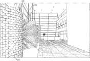
- FIG. 1is an exploded isometric view of tile of the present invention intended primarily for use as a wall tile.
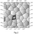
- FIG. 2is a front plan view of the polymeric layer of the tile shown in FIG. 1 .
- FIG. 3is an isometric view of the polymeric layer shown in FIG. 2 from in front and to one side.
- FIG. 4is a schematic exploded three-quarter view of a writable board of the present invention viewed from in front, above and to one side.
- FIG. 5is an elevation of a room divider of the present invention.
- FIG. 6is a front plan view of a plurality of the tiles shown in FIG. 1 in an installed condition.
- the present inventionprovides a variety of devices which make use of electro-optic displays. Although the various types of devices will mainly be described separately below, it will be appreciated that a single physical device may make use of more than one aspect of the present invention; for example, a variable color wall of the present invention could incorporate a variable color marker board of the present invention and/or variable directional signs of the present invention.
- this inventionprovides a tile comprising a light-transmissive (preferably essentially transparent) polymeric layer, a front electrode, an electro-optic layer and a backplane, the polymeric layer being textured to provide a plurality of facets, the tile further comprising a backplane of the direct drive type having segments (pixel electrodes) aligned with the facets on the polymeric layer.
- the backplanemay be in the form of a printed circuit board having the segments mounted thereon.
- the electro-optic mediummay be laminated directly on to the printed circuit board backplane.
- the tile of the present inventioncan take this mood shifting one step further by enabling the actual colors walls, room dividers and other surfaces to be changed when desired.
- the present tilecan provide effects not readily available from static paints or lighting; for example, the tiles can display ripples of color slowly moving across the wall, or an interesting “twinkling” effects as the various facets undergo color changes.
- the colors of the tilesmight be changed dynamically to match the mood of music being played.
- a rapid shifting of red and white bands across the wall, with no use of intermediate colorswould convey a harsh, “edgy” atmosphere appropriate perhaps when rap music is being played, whereas a much slower, more graduated flow of bands across the display, with numerous intermediate shades being applied to ease the transition of a particular pixel from white to red, would convey a much more relaxed atmosphere.
- FIG. 1is an exploded isometric view of a tile (intended primarily for use as a wall tile, and generally designated 100 ) of the present invention.
- the tile 100comprises a transparent molded front plate 102 , which is discussed in more detail below with reference to FIGS. 2 and 3 , and which has a flat rear surface in optical contact with the flat front surface of an electrophoretic display module 104 .
- Methods for establishing good optical contact between two planar surfacessuch as those on the front plate 102 and the display module 104 , including the use of optically clear adhesive, are well known to those skilled in optics and are described, for example in the aforementioned U.S. Pat. No. 6,982,178 (see especially FIG. 20 and related description).
- the display module 104may be substantially as described in the aforementioned U.S. Pat. No. 6,982,178 and comprise, in order from the front plate 102 :
- a printed circuit board 118which acts as a display controller for one or more tiles 100 , is mounted in the center of the mounting plate 112 and electrical connectors (not shown) extend from the board 118 through the aperture 110 to each of the pixel electrodes of the display module 104 (so that the voltage applied to each pixel electrode can be individually controlled), and to the edge connectors 108 .
- the board 118may act as the controller for multiple tiles 100 , or even an entire wall display, or may simply control one tile, with the edge connectors 108 being used to pass timing signals to synchronize the switching of the various tiles.
- the front plate 102 , display module 104 , chassis 106 and mounting plate 112are each 12 inches (305 mm) square.
- FIG. 2is a front plan view of the front plate 102 , with one facet 122 highlighted, and FIG. 3 is an isometric view of the front plate 102 from in front and to one side.
- the front plate 102is, as already noted, 12 inches (305 mm) square and approximately 3/16- 5/16 inch (approximately 5-8 mm) thick.
- the front plate 102is conveniently formed by injection molding of a transparent polymer, for example poly(methyl methacrylate).
- the front plate 102has a flat rear surface 124 , while as best seen in FIG. 2 , its front surface 126 ( FIG.
- the pixel electrodesare arranged to that there is a single pixel electrode lying behind each facet of the front plane 102 .
- the arrangement of the facets on the front plate 102is carefully chosen so that when the tile 100 is surrounded by other tiles of the same pattern and in the same orientation, the lines dividing adjacent facets continue unbroken across the joins between adjacent tiles, so that two facets, one on each adjacent edge, form in effect a compound facet, which is switched as a single unit, thus rendering the joins between tiles essentially invisible when the tiles are in operation undergoing color changes, and giving the impression of a single continuous display.
- pairs of facets 128 A/B, 130 A/B, 132 A/B, 134 A/B, 136 A/B, 138 A/B, 140 A/B, 142 A/B, 144 A/B, 146 A/B and 148 A/Ball form such compound facets, while the four corner facets 150 A/B/C/D together form a four-element compound facet, as illustrated in FIG. 6 .
- the tiles of the present inventionmay be driven in a variety of ways.
- a panel comprising a rectangular array of tilesmay start as a solid block of one color and then individual pixel electrodes are switched one at a time (except that pairs or larger numbers of pixel electrodes associated with a compound facet are switched simultaneously) to the second color such that a band of the second color progresses in an irregular manner across the display.
- the entire panelmay be in the second color.
- a band of the first colormay start to appear at the edge from which the second color “emerged” so that alternating bands of the two colors can follow each other across the panel.
- the visual effectcan be markedly altered by changing the speed at which the bands progress and whether or not intermediate levels of color are used to spread out the transitions between the two colors.
- Further possibilitiesinclude a “twinkling” effect by keeping most of the pixels at the same (background) color and randomly switching a small proportion of pixels to the other color, then back again, and a “firefly” effect, where again most of the pixels are kept at the background color but at various points first and second adjacent pixels are switched to the second color, then a third pixel, adjacent to the second, is switched to the second color while the first pixel is returned to the background color, so that the two-pixel “firefly” appears to execute a random dance around the panel.
- Other driving methodsmay of course be used, and additional complications in the driving method are possible if more than two colors are available.
- the present inventionprovides a writeable board with an electro-optic color-changing background.
- electro-optic materialsboth emissive and reflective, may be used in such a board but reflective media are generally preferred.
- organic light emitting diodesOLEDs
- encapsulated liquid crystalsfor example polymer-dispersed liquid crystals
- electrochromic mediamay all be used in the present invention, however, the preferred embodiment uses an encapsulated, polymer-dispersed or microcell electrophoretic imaging medium.
- variable color writeable board of the present inventionthe reflective or absorptive layer in a conventional whiteboard or blackboard is replaced by a layer of electro-optic medium, and a marking medium comprised of an additive colorant (a subtractive colorant and a highly scattering medium) is applied to the exposed surface of the display.
- a marking mediumcomprised of an additive colorant (a subtractive colorant and a highly scattering medium) is applied to the exposed surface of the display.
- a variable color writeable boardcan be used as a blackboard (chalkboard) when the higher contrast and haptic feedback function of a blackboard is desired, or used as a whiteboard where users want to display information via interactive projection (i.e., to use the board as a projection screen) or seek to increase the vividness of colored writing.
- a protective layer(a layer of light-transmissive and preferably transparent material) may be placed between the electro-optic layer and the viewing/writing surface to protect the electro-optic layer from mechanical or other damage.
- the protective layermay be the writable layer itself or may be a separate layer disposed between the electro-optic layer and the writable layer.
- the viewing/writing surface of the displaymay be surface treated (roughened) to allow the additive colorant to deposit easily from the marker.
- an electro-optic film similar to the front plane laminate described in the aforementioned U.S. Pat. No. 6,982,178may be used in the present invention in conjunction with a suitable backplane and with a protective layer placed between the electro-optic film and the writing surface to protect it from damage and/or scratching.
- An “optical coupling layer”(a layer of material chosen to reduce light losses) may be placed between an electro-optic layer and a protective layer, or, if an electro-optic film is employed, between the electro-optic film and a protective layer to reduce the light losses between the two surfaces.
- a mechanical support structure(“device frame”) may be used to hold the writable board assembly together and to anchor it to any architectural surface (wall, door, etc. . . . ) of the user's choice. Displays may also be attached to a structure via lamination, frame holders, screws (preferably electrically non-conductive screws) or other known means.
- FIG. 4is a schematic exploded of one writable board of the present invention showing the multiple layers of a variable color writeable board.
- a first layer ( 401 ), an electro-optic film,is placed adjacent the rear surface of the display.
- the electro-optic filmmay be driven via a common front electrode and a backplane that may be in form of a single rear electrode, a segmented (direct drive) backplane (in which each segment is provided with an individual conductor to control the voltage of the segment) or an active or passive matrix backplane. (Not all types of electro-optic medium are usable with all types of backplane.)
- the electro-optic layercontains an encapsulated electrophoretic medium capable of achieving electrically tunable optical states of varying color and reflectivity. The construction of the electro-optic layer and its lamination to the desired backplane may be accomplished via techniques known in the art.
- the layer ( 401 )also has a bus ( 409 ) whereby electrical connections to the circuitry needed
- the layer ( 402 )may be attached to the first layer ( 401 ) using techniques known in the art.
- the purpose of the second layeris to reduce the optical losses between the first and third layers.
- the purpose of the third layeris to mechanically shield the layers below it. Materials used in this layer are well known in the art. Materials like glass, acrylic, and polycarbonate are used extensively in the marker board/chalkboard industry.
- the surface of the third layeris treated so as to receive the additive colorant and enable its removal with an eraser.
- the third layermay also be patterned via a printing process or decal on the back to create decorative, aesthetic or functional accents.
- the purpose of the fourth layeris to provide a means of mechanically supporting the device and anchoring it to an architectural surface. Numerous ways of constructing such a frame are known in the art.
- the layermay also have specific shape and form to permit decorative, aesthetic or functional enhancements.
- This layeralso has a place to house the electrical circuitry ( 408 ) needed to drive the electro-optic layer; alternatively, instead of accommodating the drive circuitry itself, this layer may accommodate a wired electrical connector or a wireless connection device (for example, a Wifi or Bluetooth module) for relaying data to or from remote drive circuitry.
- a wired electrical connector or a wireless connection devicefor example, a Wifi or Bluetooth module
- the framemay house a digitization device (known in the art) needed to capture the marker position and an interactive projector for displaying information on the board.
- a marker( 405 ) is comprised of a dispenser of additive colorant which can transfer on to the third layer and produce writing of the user's choice.
- a number of commercially available technologiescan fulfil this role. For example, chalk manufactured by “Chalk Ink” etc. may be used for this purpose.
- the markermay also be part of an electronic digitization solution. Such solutions are known in the art.
- An eraser ( 406 )is comprised of a spongy material. This device can be used to remove the additive colorant dispensed by the marker from the third layer. Many means of achieving this are known in the art.
- the board shown in FIG. 4may be assembled by placing the desired aesthetic pattern or decorative decal on the back of the third layer ( 403 ), adhering the first ( 401 ), second ( 402 ) and third ( 403 ) layers together using any means known in the art, electrically connecting the first layer ( 401 ) to the drive electronics and housing the electronics in the fourth layer ( 404 ).
- a fifth layer ( 407 )may be added behind the first layer ( 401 ).
- the purpose of this layeris to add mechanical support or additional properties as desired.
- the fifth layer ( 407 )may be a steel layer placed behind the first layer to create a writable board that also has magnetic properties to magnetically attach accessories associated with magnetic boards known in the art.
- the choice of materials in the first ( 401 ), second ( 402 ), third ( 403 ), fourth ( 404 ) and fifth ( 407 ) layersmay be such that the entire device is flexible and/or can be molded on to a curved surface.
- the third layermay also be patterned via a printing process or decal on the back to create decorative, aesthetic or functional accents.
- a portion of the third layermay be used to display a glyph (such as name, abbreviation, trademark, logo, seal or heraldic achievement) of the institution in which the board is located).
- a portion of the electro-optic layeritself (for example, one corner of the display or a strip along one edge of the display) to display the desired glyph.
- Known overlay techniques familiar from television broadcastsmay be applied to the drive circuitry of the electro-optic layer such that a portion of the display is reserved for the glyph and does not change with the rest of the display.
- the drive circuitrymay be arranged so that the pixels comprising the glyph remain constant regardless of the colors changes applied to the surrounding pixels, or are always in a color state contrasting with the surrounding pixels regardless of the color changes applied to those surrounding pixels. Provision of an “electronic glyph” in any of these ways has the important advantage that the glyph can be changed to accommodate different users; for example, a board at a conference center could display a glyph associated with the specific conference or sponsor of the event taking place at any time.
- electro-optic mediamay usefully be employed to provide color varying permanent or temporary walls and similar structures (such as room dividers and screens), ceilings, floors and surfaces of furniture and other building fittings.
- Variable color writable boards of the present inventionoffer the possibility of providing a writable board which essentially vanishes when not in use. If the writable board is mounted essentially flush with the surrounding wall, screen or other surface (for example, the surface of a variable directional sign or of a file cabinet), and appropriate drive circuitry and switch are provided), the writable board, when not in use, can undergo the same color changes as the surrounding surface and will thus appear to be a part of that surface. When the writable board is required to function as such, the switch is thrown and the writable board then functions independently of the surrounding surface.
- the light weight and low power consumption of electrophoretic and similar electro-optic displaysrender them very suitable for use in room dividers, especially room dividers which are suspended from above.
- Such room dividersmay have the form of a plurality of tiles connected to each other by connectors which permit relative movement between the tiles.
- Such multi-tile room dividersallow for visually interesting configurations; for example, even though the room divider is suspended at intervals from a linear rail, the divider may assume a serpentine or similar curved configuration.
- Electro-optic displaysmay be especially useful in sculptures, including suspended sculptures and mobiles.
- the provision of color changing technologycan greatly enhance the esthetic experience of sculptures, especially when combined with the physical movement of mobile sculptures.
- Furniture surfaceswhich may be enhanced by the present invention include table tops, chairs, countertops, door and cabinets.
- An electro-optic mediummay be laminated or otherwise attached by known methods to an exposed surface of the furniture or may be embedded within the article, for example a door, table or cabinet, by known methods of placing the electro-optic medium and associated electrodes within a cavity, filling the cavity with a polymerizable medium and then subjecting the polymerizable medium to conditions, such as heat or exposure to radiation, which could the polymerizable medium to polymerize, thereby embedding the electro-optic medium and electrodes with a light-transmissive polymer.
- the electro-optic medium and electrodesmay be laminated between two sheets of glass or other light-transmissive material.
- architectural surfacesmay usefully incorporate an optical coupling layer to reduce light losses between the two surfaces.
- Incorporating electro-optic displays into furniture in accordance with the present inventioncan accomplish far more than providing improved esthetic appearances; the electro-optic displays can enhance the functions of the furniture.
- provision of an electro-optic display in a coffee tablenot only enables interesting effects using color changes in the table but can also enable the table to function as a games table; the upper surface of the table could display games board, for example chess/checkers, backgammon or cribbage.
- games boardfor example chess/checkers, backgammon or cribbage.
- Such a tableespecially if provided with touch sensing capability, could provide more than the board for a game; the table could also display the game pieces and permit them to be moved.
- a restaurant tablecould display the menu and wine list.
- An arm of a chaircould be provided with a display an infra-emitter to act as a remote controller for a television and/or other electronic device.
- Signs using electro-optic media in accordance with the present inventioncan meet many of the problems with conventional fixed directional and other signs.
- the signscan be rendered inconspicuous by being set (mostly) to a color which blends into the background, leaving just a small area, marked perhaps with a question mark, which a user presses to activate the sign.
- the signcould then display a menu, which could be multi-tiered, asking the user to indicate what information is desired.
- Some pages of displayed informationcould include prompts asking if further information is desired; for example, a list of that day's meetings and corresponding rooms could include an option for “Is campus map desired?”
- the menucould also ask the class of user (for example, senior student, upper classman or parent) and vary the displayed pages depending upon this class.
- the ability to customize the displayed page depending upon the usercan be enhanced if the display is provided with some sensor capable of receiving information from a portable token (for example, a boarding pass or hotel room “key”) carried by a user.
- a portable tokenfor example, a boarding pass or hotel room “key”
- Such information exchange between a sign and a portable tokencan readily be carried out by RFID, Bluetooth or other known technologies.
- a guest in a hotel or a patient in a hospitalcan be issued with a card customized to the room to be occupied or visited. As the guest/patient traverses the corridors of the hotel/hospital, he places the card adjacent a sign found at each corridor intersection, whereupon the sign changes to indicate the direction in which he should proceed.
- FIG. 5illustrates such a divider, generally designated 500 .
- the room divider 500is suspended from a linear rail (not shown) by a plurality of supports 502 , each of which can be in the form of a conduit housing data and power cables.
- the dividerconsists of a large number of flat, hexagonal modules 504 each of which is switchable between yellow and white (and is capable of displaying intermediate shades).
- each hexagonal module 504is supported from above by two vertical connectors passing through the midpoints of its two upper edges, these vertical connectors permitting the two modules which they join to rotate relative to one another. Two similar vertical connectors enable each module to support the module below.
- Each module 504is also pivotably connected via its side edges to the modules on either side. The vertical connectors permit data to pass between the modules which they link.
- Control of the various modules by a controllermay be by master/slave techniques or by cascading techniques. The controller may be preloaded with sequences that may be selected by a user, or may be actively updated to change/reload the programming.
- the flexible connections between the various modules 504permit the overall configuration of the room divider 500 to deviate from the vertical plane containing the rail.
- the divider 500may assume a serpentine configuration as shown in FIG. 5 , or a different curved configuration, with the change of configuration typically being effected manually.
Landscapes
- Physics & Mathematics (AREA)
- Nonlinear Science (AREA)
- General Physics & Mathematics (AREA)
- Optics & Photonics (AREA)
- Architecture (AREA)
- Engineering & Computer Science (AREA)
- Chemical & Material Sciences (AREA)
- Structural Engineering (AREA)
- Civil Engineering (AREA)
- Mathematical Physics (AREA)
- Crystallography & Structural Chemistry (AREA)
- Molecular Biology (AREA)
- Electrochemistry (AREA)
- Chemical Kinetics & Catalysis (AREA)
- Life Sciences & Earth Sciences (AREA)
- Health & Medical Sciences (AREA)
- Geometry (AREA)
- Electrochromic Elements, Electrophoresis, Or Variable Reflection Or Absorption Elements (AREA)
- Devices For Indicating Variable Information By Combining Individual Elements (AREA)
- Liquid Crystal (AREA)
- Illuminated Signs And Luminous Advertising (AREA)
- Control Of Indicators Other Than Cathode Ray Tubes (AREA)
- Navigation (AREA)
- Traffic Control Systems (AREA)
Abstract
Description
- (a) Electrophoretic particles, fluids and fluid additives; see for example U.S. Pat. Nos. 5,961,804; 6,017,584; 6,120,588; 6,120,839; 6,262,706; 6,262,833; 6,300,932; 6,323,989; 6,377,387; 6,515,649; 6,538,801; 6,580,545; 6,652,075; 6,693,620; 6,721,083; 6,727,881; 6,822,782; 6,870,661; 7,002,728; 7,038,655; 7,170,670; 7,180,649; 7,230,750; 7,230,751; 7,236,290; 7,247,379; 7,312,916; 7,375,875; 7,411,720; 7,532,388; 7,679,814; 7,746,544; 7,848,006; 7,903,319; 8,018,640; 8,115,729; 8,199,395; 8,270,064; 8,305,341; 8,390,918; 8,582,196; 8,593,718; and 8,654,436; and U.S. Patent Applications Publication Nos. 2005/0012980; 2009/0009852; 2009/0206499; 2009/0225398; 2010/0148385; 2014/0078857; 2014/0211296; 2014/0347718; 2015/0015932; 2015/0177589; and 2015/0218384;
- (b) Capsules, binders and encapsulation processes; see for example U.S. Pat. Nos. 5,930,026; 6,067,185; 6,130,774; 6,172,798; 6,249,271; 6,327,072; 6,392,785; 6,392,786; 6,459,418; 6,839,158; 6,866,760; 6,922,276; 6,958,848; 6,987,603; 7,061,663; 7,071,913; 7,079,305; 7,109,968; 7,110,164; 7,202,991; 7,242,513; 7,304,634; 7,339,715; 7,391,555; 7,411,719; 7,477,444; 7,561,324; 7,848,007; 7,910,175; 7,952,790; 8,035,886; 8,129,655; 8,446,664; and 9,005,494; and U.S. Patent Applications Publication Nos. 2005/0156340; 2007/0091417; 2008/0130092; 2009/0122389; and 2011/0286081;
- (c) Films and sub-assemblies containing electro-optic materials; see for example U.S. Pat. Nos. 6,825,829; 6,982,178; 7,236,292; 7,443,571; 7,513,813; 7,561,324; 7,636,191; 7,649,666; 7,728,811; 7,729,039; 7,791,782; 7,839,564; 7,843,621; 7,843,624; 8,034,209; 8,068,272; 8,077,381; 8,177,942; 8,390,301; 8,482,852; 8,786,929; 8,830,553; 8,854,721; and 9,075,280; and U.S. Patent Applications Publication Nos. 2009/0109519; 2009/0168067; 2011/0164301; 2014/0027044; 2014/0115884; and 2014/0340738;
- (d) Backplanes, adhesive layers and other auxiliary layers and methods used in displays; see for example U.S. Pat. Nos. D485,294; 6,124,851; 6,130,773; 6,177,921; 6,232,950; 6,252,564; 6,312,304; 6,312,971; 6,376,828; 6,392,786; 6,413,790; 6,422,687; 6,445,374; 6,480,182; 6,498,114; 6,506,438; 6,518,949; 6,521,489; 6,535,197; 6,545,291; 6,639,578; 6,657,772; 6,664,944; 6,680,725; 6,683,333; 6,724,519; 6,750,473; 6,816,147; 6,819,471; 6,825,068; 6,831,769; 6,842,167; 6,842,279; 6,842,657; 6,865,010; 6,967,640; 6,980,196; 7,012,735; 7,030,412; 7,075,703; 7,106,296; 7,110,163; 7,116,318; 7,148,128; 7,167,155; 7,173,752; 7,176,880; 7,190,008; 7,206,119; 7,223,672; 7,230,751; 7,256,766; 7,259,744; 7,280,094; 7,327,511; 7,349,148; 7,352,353; 7,365,394; 7,365,733; 7,382,363; 7,388,572; 7,442,587; 7,492,497; 7,535,624; 7,551,346; 7,554,712; 7,583,427; 7,598,173; 7,605,799; 7,636,191; 7,649,674; 7,667,886; 7,672,040; 7,688,497; 7,733,335; 7,785,988; 7,843,626; 7,859,637; 7,893,435; 7,898,717; 7,957,053; 7,986,450; 8,009,344; 8,027,081; 8,049,947; 8,077,141; 8,089,453; 8,208,193; 8,373,211; 8,389,381; 8,498,042; 8,610,988; 8,728,266; 8,754,859; 8,830,560; 8,891,155; 8,989,886; 9,152,003; and 9,152,004; and U.S. Patent Applications Publication Nos. 2002/0060321; 2004/0105036; 2005/0122306; 2005/0122563; 2007/0052757; 2007/0097489; 2007/0109219; 2009/0122389; 2009/0315044; 2011/0026101; 2011/0140744; 2011/0187683; 2011/0187689; 2011/0292319; 2013/0278900; 2014/0078024; 2014/0139501; 2014/0300837; 2015/0171112; 2015/0205178; 2015/0226986; 2015/0227018; 2015/0228666; and 2015/0261057; and International Application Publication No. WO 00/38000; European Patents Nos. 1,099,207 B1 and 1,145,072 B1;
- (e) Color formation and color adjustment; see for example U.S. Pat. Nos. 6,017,584; 6,664,944; 6,864,875; 7,075,502; 7,167,155; 7,667,684; 7,791,789; 7,839,564; 7,956,841; 8,040,594; 8,054,526; 8,098,418; 8,213,076; 8,363,299; 8,441,714; 8,441,716; 8,466,852; 8,576,470; 8,576,475; 8,593,721; 8,797,634; 8,830,559; 8,873,129; and 8,902,153; and U.S. Patent Applications Publication Nos. 2007/0223079; 2008/0023332; 2008/0043318; 2008/0048970; 2009/0004442; 2009/0225398; 2010/0103502; 2010/0156780; 2011/0164307; 2012/0182597; 2012/0326957; 2013/0141778; 2013/0242378; 2013/0258449; 2013/0278995; 2014/0055841; 2014/0226198; 2014/0240817; 2014/0340430; 2014/0362213; 2015/0118390; and 2015/0124345;
- (f) Methods for driving displays; see for example U.S. Pat. Nos. 5,930,026; 6,445,489; 6,504,524; 6,512,354; 6,531,997; 6,753,999; 6,825,970; 6,900,851; 6,995,550; 7,012,600; 7,023,420; 7,034,783; 7,116,466; 7,119,772; 7,193,625; 7,202,847; 7,259,744; 7,304,787; 7,312,794; 7,327,511; 7,453,445; 7,492,339; 7,528,822; 7,545,358; 7,583,251; 7,602,374; 7,612,760; 7,679,599; 7,688,297; 7,729,039; 7,733,311; 7,733,335; 7,787,169; 7,952,557; 7,956,841; 7,999,787; 8,077,141; 8,125,501; 8,139,050; 8,174,490; 8,289,250; 8,300,006; 8,305,341; 8,314,784; 8,373,649; 8,384,658; 8,558,783; 8,558,785; 8,593,396; and 8,928,562; and U.S. Patent Applications Publication Nos. 2003/0102858; 2005/0253777; 2007/0091418; 2007/0103427; 2008/0024429; 2008/0024482; 2008/0136774; 2008/0291129; 2009/0174651; 2009/0179923; 2009/0195568; 2009/0322721; 2010/0220121; 2010/0265561; 2011/0193840; 2011/0193841; 2011/0199671; 2011/0285754; 2013/0063333; 2013/0194250; 2013/0321278; 2014/0009817; 2014/0085350; 2014/0240373; 2014/0253425; 2014/0292830; 2014/0333685; 2015/0070744; 2015/0109283; 2015/0213765; 2015/0221257; and 2015/0262255;
- (g) Applications of displays; see for example U.S. Pat. Nos. 6,118,426; 6,473,072; 6,704,133; 6,710,540; 6,738,050; 6,825,829; 7,030,854; 7,119,759; 7,312,784; and 8,009,348; 7,705,824; 8,064,962; and 8,553,012; and U.S. Patent Applications Publication Nos. 2002/0090980; 2004/0119681; and 2007/0285385; and International Application Publication No. WO 00/36560; and
- (h) Non-electrophoretic displays, as described in U.S. Pat. Nos. 6,241,921; 6,950,220; 7,420,549 8,319,759; and 8,994,705 and U.S. Patent Application Publication No. 2012/0293858.
- providing, at a plurality of locations within the area, a variable direction sign capable of displaying at least two different direction indicators;
- providing the user with a portable token containing information identifying the selected location; and
- bringing the portable token adjacent one of the variable direction signs so that the one variable direction sign receives at least part of the information identifying the selected location, thereby causing the one variable direction to display a direction indicator appropriate to guide the user to the selected location.
- (a) a substantially transparent front (and typically polymeric—although glass and other similar material may be used) layer carrying a continuous substantially transparent front electrode which extends across the
entire display module 104; the front layer and front electrode may be formed from a commercially-available polyethylene terephthalate film; - (b) a layer of an encapsulated red/white electrophoretic medium;
- (c) a layer of lamination adhesive; and
- (d) a backplane bearing a plurality of discrete pixel electrodes (discussed in more detail below).
- (a) a substantially transparent front (and typically polymeric—although glass and other similar material may be used) layer carrying a continuous substantially transparent front electrode which extends across the
Claims (4)
Priority Applications (1)
| Application Number | Priority Date | Filing Date | Title |
|---|---|---|---|
| US16/198,142US10976634B2 (en) | 2014-11-07 | 2018-11-21 | Applications of electro-optic displays |
Applications Claiming Priority (4)
| Application Number | Priority Date | Filing Date | Title |
|---|---|---|---|
| US201462077154P | 2014-11-07 | 2014-11-07 | |
| US201562099732P | 2015-01-05 | 2015-01-05 | |
| US14/934,662US10175550B2 (en) | 2014-11-07 | 2015-11-06 | Applications of electro-optic displays |
| US16/198,142US10976634B2 (en) | 2014-11-07 | 2018-11-21 | Applications of electro-optic displays |
Related Parent Applications (1)
| Application Number | Title | Priority Date | Filing Date |
|---|---|---|---|
| US14/934,662ContinuationUS10175550B2 (en) | 2014-11-07 | 2015-11-06 | Applications of electro-optic displays |
Publications (2)
| Publication Number | Publication Date |
|---|---|
| US20190094646A1 US20190094646A1 (en) | 2019-03-28 |
| US10976634B2true US10976634B2 (en) | 2021-04-13 |
Family
ID=55909898
Family Applications (2)
| Application Number | Title | Priority Date | Filing Date |
|---|---|---|---|
| US14/934,662ActiveUS10175550B2 (en) | 2014-11-07 | 2015-11-06 | Applications of electro-optic displays |
| US16/198,142ActiveUS10976634B2 (en) | 2014-11-07 | 2018-11-21 | Applications of electro-optic displays |
Family Applications Before (1)
| Application Number | Title | Priority Date | Filing Date |
|---|---|---|---|
| US14/934,662ActiveUS10175550B2 (en) | 2014-11-07 | 2015-11-06 | Applications of electro-optic displays |
Country Status (8)
| Country | Link |
|---|---|
| US (2) | US10175550B2 (en) |
| EP (1) | EP3215893B1 (en) |
| JP (4) | JP6634080B2 (en) |
| CN (2) | CN107077040B (en) |
| CA (1) | CA2963561A1 (en) |
| ES (1) | ES2959493T3 (en) |
| TW (3) | TWI726474B (en) |
| WO (1) | WO2016073914A1 (en) |
Families Citing this family (16)
| Publication number | Priority date | Publication date | Assignee | Title |
|---|---|---|---|---|
| CN109923572A (en)* | 2016-10-18 | 2019-06-21 | 牛顿诺伊德技术有限公司 | Building products display system and method |
| EP3577300A4 (en) | 2017-01-25 | 2020-06-24 | Sage Electrochromics, Inc. | Apparatus including a control device and a method of using the same |
| CN107643856B (en)* | 2017-07-26 | 2020-06-09 | 海宁钟江智能科技有限公司 | Touch screen easy to switch imaging system |
| JP2021507293A (en) | 2017-12-19 | 2021-02-22 | イー インク コーポレイション | Application of electro-optical display |
| WO2019148165A1 (en)* | 2018-01-29 | 2019-08-01 | President And Fellows Of Harvard College | Tunable blinds for windows |
| CN108831295A (en)* | 2018-04-26 | 2018-11-16 | 努比亚技术有限公司 | A kind of screen assembly and terminal |
| EP3874317B1 (en) | 2018-10-30 | 2025-03-19 | E Ink Corporation | Electro-optic assembly |
| US11447957B2 (en)* | 2019-02-11 | 2022-09-20 | Francis Bruce Kulp, III | Three-dimensional foam surface covering system |
| DE102019108851B4 (en)* | 2019-04-04 | 2020-10-15 | Newel AG | One-piece, waterproof wall cladding device |
| KR102809744B1 (en) | 2019-04-29 | 2025-05-16 | 카디날 아이지 컴퍼니 | Leakage current detection and control for one or more electrically controllable privacy glass structures |
| US11175523B2 (en) | 2019-04-29 | 2021-11-16 | Cardinal Ig Company | Staggered driving electrical control of a plurality of electrically controllable privacy glazing structures |
| MX2021013259A (en)* | 2019-04-29 | 2022-01-06 | Cardinal Ig Co | SYSTEMS AND METHODS FOR OPERATING ONE OR MORE GLAZING STRUCTURES WITH ELECTRICALLY CONTROLLABLE PRIVACY. |
| CN113071247B (en)* | 2021-04-14 | 2023-01-24 | 宫雨乔 | Font self-dropping type electromagnetic writing board |
| TWI813247B (en)* | 2022-04-13 | 2023-08-21 | 江昱穎 | Automatic color matching device and method of using same |
| WO2024250023A2 (en)* | 2023-06-01 | 2024-12-05 | OptoGlo, Inc. | Solar powered signs with dynamic digital overlays |
| WO2025155879A1 (en)* | 2024-01-18 | 2025-07-24 | President And Fellows Of Harvard College | Spectrally selective tiling systems and methods for inducing or reducing non-visual responses to light |
Citations (300)
| Publication number | Priority date | Publication date | Assignee | Title |
|---|---|---|---|---|
| US3068754A (en) | 1958-07-30 | 1962-12-18 | Corning Giass Works | Prismatic light transmitting panel |
| US3819857A (en) | 1971-11-17 | 1974-06-25 | Tokyo Shibaura Electric Co | Electromagnetic induction type pattern input apparatus |
| US4418346A (en) | 1981-05-20 | 1983-11-29 | Batchelder J Samuel | Method and apparatus for providing a dielectrophoretic display of visual information |
| US4791417A (en) | 1983-03-01 | 1988-12-13 | Tadeusz Bobak | Display device |
| US4965488A (en) | 1989-03-27 | 1990-10-23 | Bachir Hihi | Light-source multiplication device |
| US5760761A (en) | 1995-12-15 | 1998-06-02 | Xerox Corporation | Highlight color twisting ball display |
| US5777782A (en) | 1996-12-24 | 1998-07-07 | Xerox Corporation | Auxiliary optics for a twisting ball display |
| US5808783A (en) | 1996-06-27 | 1998-09-15 | Xerox Corporation | High reflectance gyricon display |
| US5872552A (en) | 1994-12-28 | 1999-02-16 | International Business Machines Corporation | Electrophoretic display |
| US5930026A (en) | 1996-10-25 | 1999-07-27 | Massachusetts Institute Of Technology | Nonemissive displays and piezoelectric power supplies therefor |
| US5961804A (en) | 1997-03-18 | 1999-10-05 | Massachusetts Institute Of Technology | Microencapsulated electrophoretic display |
| WO1999067678A2 (en) | 1998-06-22 | 1999-12-29 | E-Ink Corporation | Means of addressing microencapsulated display media |
| US6017584A (en) | 1995-07-20 | 2000-01-25 | E Ink Corporation | Multi-color electrophoretic displays and materials for making the same |
| WO2000005704A1 (en) | 1998-07-22 | 2000-02-03 | E-Ink Corporation | Electronic display |
| US6050490A (en)* | 1997-10-31 | 2000-04-18 | Hewlett-Packard Company | Handheld writing device and related data entry system |
| US6055091A (en) | 1996-06-27 | 2000-04-25 | Xerox Corporation | Twisting-cylinder display |
| US6054071A (en) | 1998-01-28 | 2000-04-25 | Xerox Corporation | Poled electrets for gyricon-based electric-paper displays |
| US6067185A (en) | 1997-08-28 | 2000-05-23 | E Ink Corporation | Process for creating an encapsulated electrophoretic display |
| WO2000036560A1 (en) | 1998-12-18 | 2000-06-22 | E Ink Corporation | Electronic ink display media for security and authentication |
| WO2000038000A1 (en) | 1998-12-22 | 2000-06-29 | E Ink Corporation | Method of manufacturing of a discrete electronic device |
| US6097531A (en) | 1998-11-25 | 2000-08-01 | Xerox Corporation | Method of making uniformly magnetized elements for a gyricon display |
| US6118426A (en) | 1995-07-20 | 2000-09-12 | E Ink Corporation | Transducers and indicators having printed displays |
| US6120839A (en) | 1995-07-20 | 2000-09-19 | E Ink Corporation | Electro-osmotic displays and materials for making the same |
| US6120588A (en) | 1996-07-19 | 2000-09-19 | E Ink Corporation | Electronically addressable microencapsulated ink and display thereof |
| US6124851A (en) | 1995-07-20 | 2000-09-26 | E Ink Corporation | Electronic book with multiple page displays |
| US6128124A (en) | 1998-10-16 | 2000-10-03 | Xerox Corporation | Additive color electric paper without registration or alignment of individual elements |
| US6130774A (en) | 1998-04-27 | 2000-10-10 | E Ink Corporation | Shutter mode microencapsulated electrophoretic display |
| US6137467A (en) | 1995-01-03 | 2000-10-24 | Xerox Corporation | Optically sensitive electric paper |
| US6144361A (en) | 1998-09-16 | 2000-11-07 | International Business Machines Corporation | Transmissive electrophoretic display with vertical electrodes |
| US6147791A (en) | 1998-11-25 | 2000-11-14 | Xerox Corporation | Gyricon displays utilizing rotating elements and magnetic latching |
| US6177921B1 (en) | 1997-08-28 | 2001-01-23 | E Ink Corporation | Printable electrode structures for displays |
| US6184856B1 (en) | 1998-09-16 | 2001-02-06 | International Business Machines Corporation | Transmissive electrophoretic display with laterally adjacent color cells |
| US6225971B1 (en) | 1998-09-16 | 2001-05-01 | International Business Machines Corporation | Reflective electrophoretic display with laterally adjacent color cells using an absorbing panel |
| US6232950B1 (en) | 1997-08-28 | 2001-05-15 | E Ink Corporation | Rear electrode structures for displays |
| US6241921B1 (en) | 1998-05-15 | 2001-06-05 | Massachusetts Institute Of Technology | Heterogeneous display elements and methods for their fabrication |
| US6249271B1 (en) | 1995-07-20 | 2001-06-19 | E Ink Corporation | Retroreflective electrophoretic displays and materials for making the same |
| US6252564B1 (en) | 1997-08-28 | 2001-06-26 | E Ink Corporation | Tiled displays |
| US6262706B1 (en) | 1995-07-20 | 2001-07-17 | E Ink Corporation | Retroreflective electrophoretic displays and materials for making the same |
| US6262833B1 (en) | 1998-10-07 | 2001-07-17 | E Ink Corporation | Capsules for electrophoretic displays and methods for making the same |
| US6271823B1 (en) | 1998-09-16 | 2001-08-07 | International Business Machines Corporation | Reflective electrophoretic display with laterally adjacent color cells using a reflective panel |
| US6301038B1 (en) | 1997-02-06 | 2001-10-09 | University College Dublin | Electrochromic system |
| US6300932B1 (en) | 1997-08-28 | 2001-10-09 | E Ink Corporation | Electrophoretic displays with luminescent particles and materials for making the same |
| US6312971B1 (en) | 1999-08-31 | 2001-11-06 | E Ink Corporation | Solvent annealing process for forming a thin semiconductor film with advantageous properties |
| US6312304B1 (en) | 1998-12-15 | 2001-11-06 | E Ink Corporation | Assembly of microencapsulated electronic displays |
| US6323989B1 (en) | 1996-07-19 | 2001-11-27 | E Ink Corporation | Electrophoretic displays using nanoparticles |
| US6327072B1 (en) | 1999-04-06 | 2001-12-04 | E Ink Corporation | Microcell electrophoretic displays |
| US6376828B1 (en) | 1998-10-07 | 2002-04-23 | E Ink Corporation | Illumination system for nonemissive electronic displays |
| US6377387B1 (en) | 1999-04-06 | 2002-04-23 | E Ink Corporation | Methods for producing droplets for use in capsule-based electrophoretic displays |
| US6392786B1 (en) | 1999-07-01 | 2002-05-21 | E Ink Corporation | Electrophoretic medium provided with spacers |
| US20020060321A1 (en) | 2000-07-14 | 2002-05-23 | Kazlas Peter T. | Minimally- patterned, thin-film semiconductor devices for display applications |
| US6413790B1 (en) | 1999-07-21 | 2002-07-02 | E Ink Corporation | Preferred methods for producing electrical circuit elements used to control an electronic display |
| US20020090980A1 (en) | 2000-12-05 | 2002-07-11 | Wilcox Russell J. | Displays for portable electronic apparatus |
| US6445489B1 (en) | 1998-03-18 | 2002-09-03 | E Ink Corporation | Electrophoretic displays and systems for addressing such displays |
| US6459418B1 (en) | 1995-07-20 | 2002-10-01 | E Ink Corporation | Displays combining active and non-active inks |
| US6473072B1 (en) | 1998-05-12 | 2002-10-29 | E Ink Corporation | Microencapsulated electrophoretic electrostatically-addressed media for drawing device applications |
| US6480182B2 (en) | 1997-03-18 | 2002-11-12 | Massachusetts Institute Of Technology | Printable electronic display |
| US20020190965A1 (en)* | 2001-06-19 | 2002-12-19 | Lemon Michael J. | Digital annotator |
| US6498114B1 (en) | 1999-04-09 | 2002-12-24 | E Ink Corporation | Method for forming a patterned semiconductor film |
| US6504524B1 (en) | 2000-03-08 | 2003-01-07 | E Ink Corporation | Addressing methods for displays having zero time-average field |
| US6506438B2 (en) | 1998-12-15 | 2003-01-14 | E Ink Corporation | Method for printing of transistor arrays on plastic substrates |
| US6512354B2 (en) | 1998-07-08 | 2003-01-28 | E Ink Corporation | Method and apparatus for sensing the state of an electrophoretic display |
| US6515649B1 (en) | 1995-07-20 | 2003-02-04 | E Ink Corporation | Suspended particle displays and materials for making the same |
| US6518949B2 (en) | 1998-04-10 | 2003-02-11 | E Ink Corporation | Electronic displays using organic-based field effect transistors |
| US6531997B1 (en) | 1999-04-30 | 2003-03-11 | E Ink Corporation | Methods for addressing electrophoretic displays |
| US6538801B2 (en) | 1996-07-19 | 2003-03-25 | E Ink Corporation | Electrophoretic displays using nanoparticles |
| US6545291B1 (en) | 1999-08-31 | 2003-04-08 | E Ink Corporation | Transistor design for use in the construction of an electronically driven display |
| US20030102858A1 (en) | 1998-07-08 | 2003-06-05 | E Ink Corporation | Method and apparatus for determining properties of an electrophoretic display |
| US6580545B2 (en) | 2001-04-19 | 2003-06-17 | E Ink Corporation | Electrochromic-nanoparticle displays |
| US6639578B1 (en) | 1995-07-20 | 2003-10-28 | E Ink Corporation | Flexible displays |
| US6657772B2 (en) | 2001-07-09 | 2003-12-02 | E Ink Corporation | Electro-optic display and adhesive composition for use therein |
| US6664944B1 (en) | 1995-07-20 | 2003-12-16 | E-Ink Corporation | Rear electrode structures for electrophoretic displays |
| US6672921B1 (en) | 2000-03-03 | 2004-01-06 | Sipix Imaging, Inc. | Manufacturing process for electrophoretic display |
| USD485294S1 (en) | 1998-07-22 | 2004-01-13 | E Ink Corporation | Electrode structure for an electronic display |
| US6693620B1 (en) | 1999-05-03 | 2004-02-17 | E Ink Corporation | Threshold addressing of electrophoretic displays |
| US6704133B2 (en) | 1998-03-18 | 2004-03-09 | E-Ink Corporation | Electro-optic display overlays and systems for addressing such displays |
| US6710540B1 (en) | 1995-07-20 | 2004-03-23 | E Ink Corporation | Electrostatically-addressable electrophoretic display |
| US6721083B2 (en) | 1996-07-19 | 2004-04-13 | E Ink Corporation | Electrophoretic displays using nanoparticles |
| US6724519B1 (en) | 1998-12-21 | 2004-04-20 | E-Ink Corporation | Protective electrodes for electrophoretic displays |
| US6727881B1 (en) | 1995-07-20 | 2004-04-27 | E Ink Corporation | Encapsulated electrophoretic displays and methods and materials for making the same |
| US20040105036A1 (en) | 2002-08-06 | 2004-06-03 | E Ink Corporation | Protection of electro-optic displays against thermal effects |
| US6753999B2 (en) | 1998-03-18 | 2004-06-22 | E Ink Corporation | Electrophoretic displays in portable devices and systems for addressing such displays |
| US20040119681A1 (en) | 1998-11-02 | 2004-06-24 | E Ink Corporation | Broadcast system for electronic ink signs |
| US6788449B2 (en) | 2000-03-03 | 2004-09-07 | Sipix Imaging, Inc. | Electrophoretic display and novel process for its manufacture |
| JP2004255885A (en) | 2004-04-12 | 2004-09-16 | Kenji Sato | White board usable as projection screen device |
| US6816147B2 (en) | 2000-08-17 | 2004-11-09 | E Ink Corporation | Bistable electro-optic display, and method for addressing same |
| US6819471B2 (en) | 2001-08-16 | 2004-11-16 | E Ink Corporation | Light modulation by frustration of total internal reflection |
| US6822782B2 (en) | 2001-05-15 | 2004-11-23 | E Ink Corporation | Electrophoretic particles and processes for the production thereof |
| US6825829B1 (en) | 1997-08-28 | 2004-11-30 | E Ink Corporation | Adhesive backed displays |
| US6825068B2 (en) | 2000-04-18 | 2004-11-30 | E Ink Corporation | Process for fabricating thin film transistors |
| US6825970B2 (en) | 2001-09-14 | 2004-11-30 | E Ink Corporation | Methods for addressing electro-optic materials |
| US6831769B2 (en) | 2001-07-09 | 2004-12-14 | E Ink Corporation | Electro-optic display and lamination adhesive |
| US6839158B2 (en) | 1997-08-28 | 2005-01-04 | E Ink Corporation | Encapsulated electrophoretic displays having a monolayer of capsules and materials and methods for making the same |
| US6842657B1 (en) | 1999-04-09 | 2005-01-11 | E Ink Corporation | Reactive formation of dielectric layers and protection of organic layers in organic semiconductor device fabrication |
| US6842279B2 (en) | 2002-06-27 | 2005-01-11 | E Ink Corporation | Illumination system for nonemissive electronic displays |
| US20050012980A1 (en) | 2003-05-02 | 2005-01-20 | E Ink Corporation | Electrophoretic displays with controlled amounts of pigment |
| US6850297B2 (en) | 2001-07-27 | 2005-02-01 | Seiko Epson Corporation | Substrate assembly for electrooptical device, method for manufacturing substrate assembly for electrooptical device, electrooptical device, method for manufacturing electrooptical device, and electronic apparatus |
| US6865010B2 (en) | 2001-12-13 | 2005-03-08 | E Ink Corporation | Electrophoretic electronic displays with low-index films |
| US6864875B2 (en) | 1998-04-10 | 2005-03-08 | E Ink Corporation | Full color reflective display with multichromatic sub-pixels |
| US6866760B2 (en) | 1998-08-27 | 2005-03-15 | E Ink Corporation | Electrophoretic medium and process for the production thereof |
| US6870661B2 (en) | 2001-05-15 | 2005-03-22 | E Ink Corporation | Electrophoretic displays containing magnetic particles |
| US6870657B1 (en) | 1999-10-11 | 2005-03-22 | University College Dublin | Electrochromic device |
| US6898018B2 (en) | 2000-10-18 | 2005-05-24 | Sharp Kabushiki Kaisha | Luminous display element |
| US6900851B2 (en) | 2002-02-08 | 2005-05-31 | E Ink Corporation | Electro-optic displays and optical systems for addressing such displays |
| US20050122306A1 (en) | 2003-10-29 | 2005-06-09 | E Ink Corporation | Electro-optic displays with single edge addressing and removable driver circuitry |
| US20050122563A1 (en) | 2003-07-24 | 2005-06-09 | E Ink Corporation | Electro-optic displays |
| US20050156340A1 (en) | 2004-01-20 | 2005-07-21 | E Ink Corporation | Preparation of capsules |
| US6922276B2 (en) | 2002-12-23 | 2005-07-26 | E Ink Corporation | Flexible electro-optic displays |
| US6950220B2 (en) | 2002-03-18 | 2005-09-27 | E Ink Corporation | Electro-optic displays, and methods for driving same |
| US6958848B2 (en) | 2002-05-23 | 2005-10-25 | E Ink Corporation | Capsules, materials for use therein and electrophoretic media and displays containing such capsules |
| US20050253777A1 (en) | 2004-05-12 | 2005-11-17 | E Ink Corporation | Tiled displays and methods for driving same |
| US6967640B2 (en) | 2001-07-27 | 2005-11-22 | E Ink Corporation | Microencapsulated electrophoretic display with integrated driver |
| US6982178B2 (en) | 2002-06-10 | 2006-01-03 | E Ink Corporation | Components and methods for use in electro-optic displays |
| US6987603B2 (en) | 2003-01-31 | 2006-01-17 | E Ink Corporation | Construction of electrophoretic displays |
| US6992718B1 (en) | 1998-08-31 | 2006-01-31 | Matsushita Electric Industrial Co., Ltd. | Illuminating apparatus, display panel, view finder, video display apparatus, and video camera mounting the elements |
| US7002728B2 (en) | 1997-08-28 | 2006-02-21 | E Ink Corporation | Electrophoretic particles, and processes for the production thereof |
| US7012600B2 (en) | 1999-04-30 | 2006-03-14 | E Ink Corporation | Methods for driving bistable electro-optic displays, and apparatus for use therein |
| US7012735B2 (en) | 2003-03-27 | 2006-03-14 | E Ink Corporaiton | Electro-optic assemblies, and materials for use therein |
| US7023420B2 (en) | 2000-11-29 | 2006-04-04 | E Ink Corporation | Electronic display with photo-addressing means |
| US7030412B1 (en) | 1999-05-05 | 2006-04-18 | E Ink Corporation | Minimally-patterned semiconductor devices for display applications |
| US7030854B2 (en) | 2001-03-13 | 2006-04-18 | E Ink Corporation | Apparatus for displaying drawings |
| US7034783B2 (en) | 2003-08-19 | 2006-04-25 | E Ink Corporation | Method for controlling electro-optic display |
| US7038655B2 (en) | 1999-05-03 | 2006-05-02 | E Ink Corporation | Electrophoretic ink composed of particles with field dependent mobilities |
| US7071913B2 (en) | 1995-07-20 | 2006-07-04 | E Ink Corporation | Retroreflective electrophoretic displays and materials for making the same |
| US7075703B2 (en) | 2004-01-16 | 2006-07-11 | E Ink Corporation | Process for sealing electro-optic displays |
| US7079305B2 (en) | 2001-03-19 | 2006-07-18 | E Ink Corporation | Electrophoretic medium and process for the production thereof |
| US7109968B2 (en) | 1995-07-20 | 2006-09-19 | E Ink Corporation | Non-spherical cavity electrophoretic displays and methods and materials for making the same |
| US7110164B2 (en) | 2002-06-10 | 2006-09-19 | E Ink Corporation | Electro-optic displays, and processes for the production thereof |
| US7110163B2 (en) | 2001-07-09 | 2006-09-19 | E Ink Corporation | Electro-optic display and lamination adhesive for use therein |
| US7116466B2 (en) | 2004-07-27 | 2006-10-03 | E Ink Corporation | Electro-optic displays |
| US7116318B2 (en) | 2002-04-24 | 2006-10-03 | E Ink Corporation | Backplanes for display applications, and components for use therein |
| US7119772B2 (en) | 1999-04-30 | 2006-10-10 | E Ink Corporation | Methods for driving bistable electro-optic displays, and apparatus for use therein |
| US7119759B2 (en) | 1999-05-03 | 2006-10-10 | E Ink Corporation | Machine-readable displays |
| WO2006137686A1 (en) | 2005-06-21 | 2006-12-28 | Namotek Co., Ltd. | Led array type lens and backlight apparatus using the same |
| US7167155B1 (en) | 1995-07-20 | 2007-01-23 | E Ink Corporation | Color electrophoretic displays |
| US7170670B2 (en) | 2001-04-02 | 2007-01-30 | E Ink Corporation | Electrophoretic medium and display with improved image stability |
| US7173752B2 (en) | 2003-11-05 | 2007-02-06 | E Ink Corporation | Electro-optic displays, and materials for use therein |
| US7176880B2 (en) | 1999-07-21 | 2007-02-13 | E Ink Corporation | Use of a storage capacitor to enhance the performance of an active matrix driven electronic display |
| JP2007047262A (en) | 2005-08-08 | 2007-02-22 | Bridgestone Corp | Panel for information display |
| US20070052757A1 (en) | 1996-07-19 | 2007-03-08 | E Ink Corporation | Electronically addressable microencapsulated ink and display thereof |
| US7190008B2 (en) | 2002-04-24 | 2007-03-13 | E Ink Corporation | Electro-optic displays, and components for use therein |
| US7193625B2 (en) | 1999-04-30 | 2007-03-20 | E Ink Corporation | Methods for driving electro-optic displays, and apparatus for use therein |
| US7202847B2 (en) | 2002-06-28 | 2007-04-10 | E Ink Corporation | Voltage modulated driver circuits for electro-optic displays |
| JP2007096792A (en) | 2005-09-29 | 2007-04-12 | Toppan Printing Co Ltd | Whiteboard |
| US7206119B2 (en) | 2003-12-31 | 2007-04-17 | E Ink Corporation | Electro-optic displays, and method for driving same |
| US20070091417A1 (en) | 2005-10-25 | 2007-04-26 | E Ink Corporation | Electrophoretic media and displays with improved binder |
| US20070103427A1 (en) | 2003-11-25 | 2007-05-10 | Koninklijke Philips Electronice N.V. | Display apparatus with a display device and a cyclic rail-stabilized method of driving the display device |
| US7223672B2 (en) | 2002-04-24 | 2007-05-29 | E Ink Corporation | Processes for forming backplanes for electro-optic displays |
| US7230751B2 (en) | 2005-01-26 | 2007-06-12 | E Ink Corporation | Electrophoretic displays using gaseous fluids |
| US7230750B2 (en) | 2001-05-15 | 2007-06-12 | E Ink Corporation | Electrophoretic media and processes for the production thereof |
| US7236290B1 (en) | 2000-07-25 | 2007-06-26 | E Ink Corporation | Electrophoretic medium with improved stability |
| US7236291B2 (en) | 2003-04-02 | 2007-06-26 | Bridgestone Corporation | Particle use for image display media, image display panel using the particles, and image display device |
| US7242513B2 (en) | 1997-08-28 | 2007-07-10 | E Ink Corporation | Encapsulated electrophoretic displays having a monolayer of capsules and materials and methods for making the same |
| US7247379B2 (en) | 1997-08-28 | 2007-07-24 | E Ink Corporation | Electrophoretic particles, and processes for the production thereof |
| US7256766B2 (en) | 1998-08-27 | 2007-08-14 | E Ink Corporation | Electrophoretic display comprising optical biasing element |
| US7259744B2 (en) | 1995-07-20 | 2007-08-21 | E Ink Corporation | Dielectrophoretic displays |
| JP2007248498A (en) | 2006-03-13 | 2007-09-27 | Toppan Printing Co Ltd | Display device |
| US7304634B2 (en) | 1995-07-20 | 2007-12-04 | E Ink Corporation | Rear electrode structures for electrophoretic displays |
| US20070285385A1 (en) | 1998-11-02 | 2007-12-13 | E Ink Corporation | Broadcast system for electronic ink signs |
| US7312916B2 (en) | 2002-08-07 | 2007-12-25 | E Ink Corporation | Electrophoretic media containing specularly reflective particles |
| US7321459B2 (en) | 2002-03-06 | 2008-01-22 | Bridgestone Corporation | Image display device and method |
| US20080024429A1 (en) | 2006-07-25 | 2008-01-31 | E Ink Corporation | Electrophoretic displays using gaseous fluids |
| US20080024482A1 (en) | 2002-06-13 | 2008-01-31 | E Ink Corporation | Methods for driving electro-optic displays |
| US7327511B2 (en) | 2004-03-23 | 2008-02-05 | E Ink Corporation | Light modulators |
| US20080043318A1 (en) | 2005-10-18 | 2008-02-21 | E Ink Corporation | Color electro-optic displays, and processes for the production thereof |
| US7339715B2 (en) | 2003-03-25 | 2008-03-04 | E Ink Corporation | Processes for the production of electrophoretic displays |
| US7352353B2 (en) | 1995-07-20 | 2008-04-01 | E Ink Corporation | Electrostatically addressable electrophoretic display |
| US7365733B2 (en) | 2002-12-16 | 2008-04-29 | E Ink Corporation | Backplanes for electro-optic displays |
| US20080130092A1 (en) | 2004-03-23 | 2008-06-05 | E Ink Corporation | Light modulators |
| US20080136774A1 (en) | 2004-07-27 | 2008-06-12 | E Ink Corporation | Methods for driving electrophoretic displays using dielectrophoretic forces |
| US7388572B2 (en) | 2004-02-27 | 2008-06-17 | E Ink Corporation | Backplanes for electro-optic displays |
| US7411719B2 (en) | 1995-07-20 | 2008-08-12 | E Ink Corporation | Electrophoretic medium and process for the production thereof |
| US7420549B2 (en) | 2003-10-08 | 2008-09-02 | E Ink Corporation | Electro-wetting displays |
| US7453445B2 (en) | 2004-08-13 | 2008-11-18 | E Ink Corproation | Methods for driving electro-optic displays |
| US20080291129A1 (en) | 2007-05-21 | 2008-11-27 | E Ink Corporation | Methods for driving video electro-optic displays |
| US20090009852A1 (en) | 2001-05-15 | 2009-01-08 | E Ink Corporation | Electrophoretic particles and processes for the production thereof |
| US7477444B2 (en) | 2006-09-22 | 2009-01-13 | E Ink Corporation & Air Products And Chemical, Inc. | Electro-optic display and materials for use therein |
| US7492497B2 (en) | 2006-08-02 | 2009-02-17 | E Ink Corporation | Multi-layer light modulator |
| US7492339B2 (en) | 2004-03-26 | 2009-02-17 | E Ink Corporation | Methods for driving bistable electro-optic displays |
| US7528822B2 (en) | 2001-11-20 | 2009-05-05 | E Ink Corporation | Methods for driving electro-optic displays |
| US20090122389A1 (en) | 2007-11-14 | 2009-05-14 | E Ink Corporation | Electro-optic assemblies, and adhesives and binders for use therein |
| US7535624B2 (en) | 2001-07-09 | 2009-05-19 | E Ink Corporation | Electro-optic display and materials for use therein |
| US7551346B2 (en) | 2003-11-05 | 2009-06-23 | E Ink Corporation | Electro-optic displays, and materials for use therein |
| US7554712B2 (en) | 2005-06-23 | 2009-06-30 | E Ink Corporation | Edge seals for, and processes for assembly of, electro-optic displays |
| US20090174651A1 (en) | 1995-07-20 | 2009-07-09 | E Ink Corporation | Addressing schemes for electronic displays |
| US7561324B2 (en) | 2002-09-03 | 2009-07-14 | E Ink Corporation | Electro-optic displays |
| US7583251B2 (en) | 1995-07-20 | 2009-09-01 | E Ink Corporation | Dielectrophoretic displays |
| US7583427B2 (en) | 2002-06-10 | 2009-09-01 | E Ink Corporation | Components and methods for use in electro-optic displays |
| US20090237775A1 (en) | 2008-03-21 | 2009-09-24 | Seiko Epson Corporation | Electro-optical display, electrophoretic display, and electronic device |
| US7602374B2 (en) | 2003-09-19 | 2009-10-13 | E Ink Corporation | Methods for reducing edge effects in electro-optic displays |
| US7612760B2 (en) | 2005-02-17 | 2009-11-03 | Seiko Epson Corporation | Electrophoresis device, method of driving electrophoresis device, and electronic apparatus |
| US7649666B2 (en) | 2006-12-07 | 2010-01-19 | E Ink Corporation | Components and methods for use in electro-optic displays |
| US7649674B2 (en) | 2002-06-10 | 2010-01-19 | E Ink Corporation | Electro-optic display with edge seal |
| JP2010026070A (en) | 2008-07-16 | 2010-02-04 | Toppan Forms Co Ltd | Building material with display device |
| US7667684B2 (en) | 1998-07-08 | 2010-02-23 | E Ink Corporation | Methods for achieving improved color in microencapsulated electrophoretic devices |
| US7667886B2 (en) | 2007-01-22 | 2010-02-23 | E Ink Corporation | Multi-layer sheet for use in electro-optic displays |
| US7672040B2 (en) | 2003-11-05 | 2010-03-02 | E Ink Corporation | Electro-optic displays, and materials for use therein |
| US7679599B2 (en) | 2005-03-04 | 2010-03-16 | Seiko Epson Corporation | Electrophoretic device, method of driving electrophoretic device, and electronic apparatus |
| US7679814B2 (en) | 2001-04-02 | 2010-03-16 | E Ink Corporation | Materials for use in electrophoretic displays |
| US7688497B2 (en) | 2007-01-22 | 2010-03-30 | E Ink Corporation | Multi-layer sheet for use in electro-optic displays |
| TWM381867U (en) | 2009-12-01 | 2010-06-01 | Ming-Hong Song | Leaflets device with guiding function |
| US20100148385A1 (en) | 2001-05-15 | 2010-06-17 | E Ink Corporation | Electrophoretic media and processes for the production thereof |
| US7791789B2 (en) | 1995-07-20 | 2010-09-07 | E Ink Corporation | Multi-color electrophoretic displays and materials for making the same |
| US7826129B2 (en) | 2007-03-06 | 2010-11-02 | E Ink Corporation | Materials for use in electrophoretic displays |
| US7839564B2 (en) | 2002-09-03 | 2010-11-23 | E Ink Corporation | Components and methods for use in electro-optic displays |
| US7843624B2 (en) | 2006-03-08 | 2010-11-30 | E Ink Corporation | Electro-optic displays, and materials and methods for production thereof |
| US7843621B2 (en) | 2002-06-10 | 2010-11-30 | E Ink Corporation | Components and testing methods for use in the production of electro-optic displays |
| US7848006B2 (en) | 1995-07-20 | 2010-12-07 | E Ink Corporation | Electrophoretic displays with controlled amounts of pigment |
| US7893435B2 (en) | 2000-04-18 | 2011-02-22 | E Ink Corporation | Flexible electronic circuits and displays including a backplane comprising a patterned metal foil having a plurality of apertures extending therethrough |
| US7903319B2 (en) | 2006-07-11 | 2011-03-08 | E Ink Corporation | Electrophoretic medium and display with improved image stability |
| US7910175B2 (en) | 2003-03-25 | 2011-03-22 | E Ink Corporation | Processes for the production of electrophoretic displays |
| US7952557B2 (en) | 2001-11-20 | 2011-05-31 | E Ink Corporation | Methods and apparatus for driving electro-optic displays |
| US7952790B2 (en) | 2006-03-22 | 2011-05-31 | E Ink Corporation | Electro-optic media produced using ink jet printing |
| US7956841B2 (en) | 1995-07-20 | 2011-06-07 | E Ink Corporation | Stylus-based addressing structures for displays |
| US20110164301A1 (en) | 2003-11-05 | 2011-07-07 | E Ink Corporation | Electro-optic displays, and materials for use therein |
| US7986450B2 (en) | 2006-09-22 | 2011-07-26 | E Ink Corporation | Electro-optic display and materials for use therein |
| US20110187683A1 (en) | 2003-10-30 | 2011-08-04 | E Ink Corporation | Electro-optic displays with single edge addressing and removable driver circuitry |
| US20110193841A1 (en) | 2002-06-13 | 2011-08-11 | E Ink Corporation | Methods for driving electrophoretic displays using dielectrophoretic forces |
| US20110193840A1 (en) | 1995-07-20 | 2011-08-11 | E Ink Corporation | Methods for driving electrophoretic displays using dielectrophoretic forces |
| US8009348B2 (en) | 1999-05-03 | 2011-08-30 | E Ink Corporation | Machine-readable displays |
| US8018640B2 (en) | 2006-07-13 | 2011-09-13 | E Ink Corporation | Particles for use in electrophoretic displays |
| US20110222145A1 (en) | 2010-03-15 | 2011-09-15 | Sony Corporation | Optical laminated product and fitting |
| US8034209B2 (en) | 2007-06-29 | 2011-10-11 | E Ink Corporation | Electro-optic displays, and materials and methods for production thereof |
| US8040594B2 (en) | 1997-08-28 | 2011-10-18 | E Ink Corporation | Multi-color electrophoretic displays |
| TW201137806A (en) | 2010-04-27 | 2011-11-01 | Chih-Tai Huang | Parking space guidance system |
| US8049947B2 (en) | 2002-06-10 | 2011-11-01 | E Ink Corporation | Components and methods for use in electro-optic displays |
| US8054526B2 (en) | 2008-03-21 | 2011-11-08 | E Ink Corporation | Electro-optic displays, and color filters for use therein |
| US20110287402A1 (en)* | 2007-08-02 | 2011-11-24 | Michael Sanford | Method and apparatus for novel embodiments to repurpose eink ereaders as writing devices to enable children to write on digital workbook learning content |
| US20110292319A1 (en) | 2010-05-27 | 2011-12-01 | E Ink Corporation | Dual mode electro-optic displays |
| US20110317248A1 (en) | 2010-06-24 | 2011-12-29 | Samsung Electro-Mechanics Co., Ltd. | Electronic paper display device and manufacturing method thereof |
| US8098418B2 (en) | 2009-03-03 | 2012-01-17 | E. Ink Corporation | Electro-optic displays, and color filters for use therein |
| US8115729B2 (en) | 1999-05-03 | 2012-02-14 | E Ink Corporation | Electrophoretic display element with filler particles |
| US8125501B2 (en) | 2001-11-20 | 2012-02-28 | E Ink Corporation | Voltage modulated driver circuits for electro-optic displays |
| US8129655B2 (en) | 2002-09-03 | 2012-03-06 | E Ink Corporation | Electrophoretic medium with gaseous suspending fluid |
| US8159463B2 (en) | 2000-05-19 | 2012-04-17 | Technology Innovations, Llc | Apparatus for the display of embedded information |
| US8174490B2 (en) | 2003-06-30 | 2012-05-08 | E Ink Corporation | Methods for driving electrophoretic displays |
| US8177942B2 (en) | 2003-11-05 | 2012-05-15 | E Ink Corporation | Electro-optic displays, and materials for use therein |
| US8213076B2 (en) | 1997-08-28 | 2012-07-03 | E Ink Corporation | Multi-color electrophoretic displays and materials for making the same |
| US20120196269A1 (en)* | 2010-12-02 | 2012-08-02 | ID Signsystems, Inc. | Multiplanar display system |
| US8270064B2 (en) | 2009-02-09 | 2012-09-18 | E Ink Corporation | Electrophoretic particles, and processes for the production thereof |
| US8283850B2 (en) | 2004-05-17 | 2012-10-09 | Zeon Corporation | Electroluminescent element, lightening equipment, and display device |
| US8289250B2 (en) | 2004-03-31 | 2012-10-16 | E Ink Corporation | Methods for driving electro-optic displays |
| US8300006B2 (en) | 2003-10-03 | 2012-10-30 | E Ink Corporation | Electrophoretic display unit |
| US8314784B2 (en) | 2008-04-11 | 2012-11-20 | E Ink Corporation | Methods for driving electro-optic displays |
| US20120293858A1 (en) | 2011-05-21 | 2012-11-22 | E Ink Corporation | Electro-optic displays |
| US8319759B2 (en) | 2003-10-08 | 2012-11-27 | E Ink Corporation | Electrowetting displays |
| US8331016B2 (en) | 2010-06-15 | 2012-12-11 | Seiko Epson Corporation | Electrophoretic display device |
| US8363299B2 (en) | 2002-06-10 | 2013-01-29 | E Ink Corporation | Electro-optic displays, and processes for the production thereof |
| US8373649B2 (en) | 2008-04-11 | 2013-02-12 | Seiko Epson Corporation | Time-overlapping partial-panel updating of a bistable electro-optic display |
| US8390918B2 (en) | 2001-04-02 | 2013-03-05 | E Ink Corporation | Electrophoretic displays with controlled amounts of pigment |
| US8390301B2 (en) | 2006-03-08 | 2013-03-05 | E Ink Corporation | Electro-optic displays, and materials and methods for production thereof |
| US20130063333A1 (en) | 2002-10-16 | 2013-03-14 | E Ink Corporation | Electrophoretic displays |
| US20130096964A1 (en) | 2011-10-14 | 2013-04-18 | Claridy Solutions, Inc. | Seat management system |
| US20130107144A1 (en) | 2011-11-01 | 2013-05-02 | Kent Displays Incorporated | Writing tablet information recording device |
| KR20130048611A (en) | 2011-11-02 | 2013-05-10 | 삼성전기주식회사 | Touch panel |
| US8446664B2 (en) | 2010-04-02 | 2013-05-21 | E Ink Corporation | Electrophoretic media, and materials for use therein |
| US20130194250A1 (en) | 2012-02-01 | 2013-08-01 | E Ink Corporation | Methods for driving electro-optic displays |
| US20130222881A1 (en)* | 2010-06-10 | 2013-08-29 | President And Fellows Of Harvard College | Adaptive shading, display and color control |
| US8542428B2 (en) | 2011-02-28 | 2013-09-24 | Samsung Display Co., Ltd. | Electropheretic display device and method for manufacturing the same |
| US8558783B2 (en) | 2001-11-20 | 2013-10-15 | E Ink Corporation | Electro-optic displays with reduced remnant voltage |
| US20130278900A1 (en) | 2012-04-20 | 2013-10-24 | E Ink Corporation | Illumination systems for reflective displays |
| US8576476B2 (en) | 2010-05-21 | 2013-11-05 | E Ink Corporation | Multi-color electro-optic displays |
| US8576470B2 (en) | 2010-06-02 | 2013-11-05 | E Ink Corporation | Electro-optic displays, and color alters for use therein |
| US8582196B2 (en) | 2001-05-15 | 2013-11-12 | E Ink Corporation | Electrophoretic particles and processes for the production thereof |
| US8593396B2 (en) | 2001-11-20 | 2013-11-26 | E Ink Corporation | Methods and apparatus for driving electro-optic displays |
| US8603613B2 (en) | 2007-04-25 | 2013-12-10 | Tesserae Technologies | System and method for color-changing decorative construction materials |
| US8610988B2 (en) | 2006-03-09 | 2013-12-17 | E Ink Corporation | Electro-optic display with edge seal |
| TW201403198A (en) | 2012-07-06 | 2014-01-16 | Au Optronics Corp | Electrophoretic display |
| US8654436B1 (en) | 2009-10-30 | 2014-02-18 | E Ink Corporation | Particles for use in electrophoretic displays |
| US8693086B2 (en) | 2008-06-17 | 2014-04-08 | Koninklijke Philips N.V. | Appearance-modifying device, method for manufacturing such a device, and appliance covered by such a device |
| US20140139501A1 (en) | 2012-11-16 | 2014-05-22 | E Ink Corporation | Active matrix display with dual driving modes |
| US8754859B2 (en) | 2009-10-28 | 2014-06-17 | E Ink Corporation | Electro-optic displays with touch sensors and/or tactile feedback |
| US8770813B2 (en) | 2010-12-23 | 2014-07-08 | Microsoft Corporation | Transparent display backlight assembly |
| US8797634B2 (en) | 2010-11-30 | 2014-08-05 | E Ink Corporation | Multi-color electrophoretic displays |
| US20140253425A1 (en) | 2013-03-07 | 2014-09-11 | E Ink Corporation | Method and apparatus for driving electro-optic displays |
| JP2014170188A (en) | 2013-03-05 | 2014-09-18 | Dainippon Printing Co Ltd | Reflection type display apparatus and manufacturing method thereof |
| US8840747B2 (en) | 2009-11-25 | 2014-09-23 | Dai Nippon Printing Co., Ltd. | Method for manufacturing twist ball type electronic paper |
| US20140308477A1 (en) | 2011-09-20 | 2014-10-16 | 3M Innovative Properties Company | Textured film and process for manufacture |
| US8873129B2 (en) | 2011-04-07 | 2014-10-28 | E Ink Corporation | Tetrachromatic color filter array for reflective display |
| US8902153B2 (en) | 2007-08-03 | 2014-12-02 | E Ink Corporation | Electro-optic displays, and processes for their production |
| US8928562B2 (en) | 2003-11-25 | 2015-01-06 | E Ink Corporation | Electro-optic displays, and methods for driving same |
| US20150118390A1 (en) | 2010-07-26 | 2015-04-30 | E Ink Corporation | Electro-optic displays, and components for use therein |
| US20150261057A1 (en) | 2014-03-17 | 2015-09-17 | E Ink Corporation | Multi-layer expanding electrode structures for backplane assemblies |
| US9195111B2 (en) | 2013-02-11 | 2015-11-24 | E Ink Corporation | Patterned electro-optic displays and processes for the production thereof |
| US9199441B2 (en) | 2007-06-28 | 2015-12-01 | E Ink Corporation | Processes for the production of electro-optic displays, and color filters for use therein |
| US9230492B2 (en) | 2003-03-31 | 2016-01-05 | E Ink Corporation | Methods for driving electro-optic displays |
| US9238340B2 (en) | 2012-07-27 | 2016-01-19 | E Ink Corporation | Processes for the production of electro-optic displays |
| US9412314B2 (en) | 2001-11-20 | 2016-08-09 | E Ink Corporation | Methods for driving electro-optic displays |
| US9436056B2 (en) | 2013-02-06 | 2016-09-06 | E Ink Corporation | Color electro-optic displays |
| US9495918B2 (en) | 2013-03-01 | 2016-11-15 | E Ink Corporation | Methods for driving electro-optic displays |
| US9513743B2 (en) | 2012-06-01 | 2016-12-06 | E Ink Corporation | Methods for driving electro-optic displays |
| US9529240B2 (en) | 2014-01-17 | 2016-12-27 | E Ink Corporation | Controlled polymeric material conductivity for use in a two-phase electrode layer |
| US9620066B2 (en) | 2010-02-02 | 2017-04-11 | E Ink Corporation | Method for driving electro-optic displays |
| US9620048B2 (en) | 2013-07-30 | 2017-04-11 | E Ink Corporation | Methods for driving electro-optic displays |
| US9671635B2 (en) | 2014-02-07 | 2017-06-06 | E Ink Corporation | Electro-optic display backplane structures with drive components and pixel electrodes on opposed surfaces |
| US9672766B2 (en) | 2003-03-31 | 2017-06-06 | E Ink Corporation | Methods for driving electro-optic displays |
| US9688859B2 (en) | 2014-02-06 | 2017-06-27 | E Ink Corporation | Electrophoretic particles and processes for the production thereof |
| US9697778B2 (en) | 2013-05-14 | 2017-07-04 | E Ink Corporation | Reverse driving pulses in electrophoretic displays |
| US20170206828A1 (en) | 2014-07-30 | 2017-07-20 | Hewlett-Packard Development Company, L.P. | Transparent whiteboard display |
| US9721495B2 (en) | 2013-02-27 | 2017-08-01 | E Ink Corporation | Methods for driving electro-optic displays |
| US9726957B2 (en) | 2013-01-10 | 2017-08-08 | E Ink Corporation | Electro-optic display with controlled electrochemical reactions |
Family Cites Families (17)
| Publication number | Priority date | Publication date | Assignee | Title |
|---|---|---|---|---|
| JPH01319900A (en)* | 1988-06-20 | 1989-12-26 | Energy Support Corp | Parking area management system |
| EP1335211B1 (en)* | 1997-08-28 | 2015-06-03 | E Ink Corporation | Battery indicator comprising an encapsulated electrophoretic display |
| US6897855B1 (en)* | 1998-02-17 | 2005-05-24 | Sarnoff Corporation | Tiled electronic display structure |
| US6753830B2 (en)* | 1998-09-11 | 2004-06-22 | Visible Tech-Knowledgy, Inc. | Smart electronic label employing electronic ink |
| CN2361481Y (en) | 1998-10-17 | 2000-02-02 | 张玉华 | Background colour changeable chalk writing board |
| KR200214378Y1 (en)* | 2000-10-07 | 2001-02-15 | 엘지전자주식회사 | Display |
| US7167106B2 (en)* | 2004-04-15 | 2007-01-23 | 3M Innovative Properties Company | Methods and systems utilizing a programmable sign display located in proximity to a traffic light |
| WO2006085382A1 (en)* | 2005-02-10 | 2006-08-17 | Fujitsu Limited | Information providing device, and information providing system |
| JP2007199805A (en) | 2006-01-24 | 2007-08-09 | Tamura Gakuen | Road guidance display device |
| CN201725356U (en)* | 2010-05-27 | 2011-01-26 | 无锡市天业智能科技有限公司 | Personnel perception and guide system based on internet of things RFID |
| CN101859412A (en)* | 2010-05-27 | 2010-10-13 | 无锡市天业智能科技有限公司 | Personnel sensing and leading system based on RFID of Internet-of-things |
| CN103377385A (en)* | 2012-04-26 | 2013-10-30 | 上海宝信软件股份有限公司 | Hotel guest room intelligent guide system based on radio frequency identification device (RFID) |
| CN103578053A (en)* | 2012-07-27 | 2014-02-12 | 苏州市国贸电子系统工程有限公司 | Guest guiding system based on RFID |
| KR101365331B1 (en)* | 2012-10-05 | 2014-02-19 | 삼성전기주식회사 | Electronic paper panel and electronic shelf label system and method for driving thereof |
| GB2519300A (en)* | 2013-10-15 | 2015-04-22 | Neil Brian Clarkson | Arrangement of a mounted display screen |
| CN203720862U (en)* | 2013-12-23 | 2014-07-16 | 绿地控股集团有限公司 | Hotel rfid identification system |
| CN104083831B (en)* | 2014-07-26 | 2017-09-26 | 公安部沈阳消防研究所 | A kind of intelligent evacuation indication system and evacuation method with positioning function |
- 2015
- 2015-11-06WOPCT/US2015/059569patent/WO2016073914A1/enactiveApplication Filing
- 2015-11-06CACA2963561Apatent/CA2963561A1/ennot_activeAbandoned
- 2015-11-06ESES15856860Tpatent/ES2959493T3/enactiveActive
- 2015-11-06USUS14/934,662patent/US10175550B2/enactiveActive
- 2015-11-06CNCN201580057743.5Apatent/CN107077040B/enactiveActive
- 2015-11-06JPJP2017523971Apatent/JP6634080B2/enactiveActive
- 2015-11-06CNCN202110635479.6Apatent/CN113341627B/enactiveActive
- 2015-11-06EPEP15856860.0Apatent/EP3215893B1/enactiveActive
- 2015-11-09TWTW108139864Apatent/TWI726474B/enactive
- 2015-11-09TWTW106122862Apatent/TW201734620A/enunknown
- 2015-11-09TWTW104136841Apatent/TWI674469B/enactive
- 2018
- 2018-11-21USUS16/198,142patent/US10976634B2/enactiveActive
- 2019
- 2019-10-25JPJP2019194165Apatent/JP2020029100A/enactivePending
- 2020
- 2020-11-13JPJP2020189345Apatent/JP7053766B2/enactiveActive
- 2021
- 2021-12-15JPJP2021203138Apatent/JP2022027922A/ennot_activeWithdrawn
Patent Citations (436)
| Publication number | Priority date | Publication date | Assignee | Title |
|---|---|---|---|---|
| US3068754A (en) | 1958-07-30 | 1962-12-18 | Corning Giass Works | Prismatic light transmitting panel |
| US3819857A (en) | 1971-11-17 | 1974-06-25 | Tokyo Shibaura Electric Co | Electromagnetic induction type pattern input apparatus |
| US4418346A (en) | 1981-05-20 | 1983-11-29 | Batchelder J Samuel | Method and apparatus for providing a dielectrophoretic display of visual information |
| US4791417A (en) | 1983-03-01 | 1988-12-13 | Tadeusz Bobak | Display device |
| US4965488A (en) | 1989-03-27 | 1990-10-23 | Bachir Hihi | Light-source multiplication device |
| US5872552A (en) | 1994-12-28 | 1999-02-16 | International Business Machines Corporation | Electrophoretic display |
| US6137467A (en) | 1995-01-03 | 2000-10-24 | Xerox Corporation | Optically sensitive electric paper |
| US6120839A (en) | 1995-07-20 | 2000-09-19 | E Ink Corporation | Electro-osmotic displays and materials for making the same |
| US6680725B1 (en) | 1995-07-20 | 2004-01-20 | E Ink Corporation | Methods of manufacturing electronically addressable displays |
| US6459418B1 (en) | 1995-07-20 | 2002-10-01 | E Ink Corporation | Displays combining active and non-active inks |
| US7746544B2 (en) | 1995-07-20 | 2010-06-29 | E Ink Corporation | Electro-osmotic displays and materials for making the same |
| US7583251B2 (en) | 1995-07-20 | 2009-09-01 | E Ink Corporation | Dielectrophoretic displays |
| US6017584A (en) | 1995-07-20 | 2000-01-25 | E Ink Corporation | Multi-color electrophoretic displays and materials for making the same |
| US20090174651A1 (en) | 1995-07-20 | 2009-07-09 | E Ink Corporation | Addressing schemes for electronic displays |
| US7791789B2 (en) | 1995-07-20 | 2010-09-07 | E Ink Corporation | Multi-color electrophoretic displays and materials for making the same |
| US7071913B2 (en) | 1995-07-20 | 2006-07-04 | E Ink Corporation | Retroreflective electrophoretic displays and materials for making the same |
| US7848006B2 (en) | 1995-07-20 | 2010-12-07 | E Ink Corporation | Electrophoretic displays with controlled amounts of pigment |
| US7848007B2 (en) | 1995-07-20 | 2010-12-07 | E Ink Corporation | Electrophoretic medium and process for the production thereof |
| US7956841B2 (en) | 1995-07-20 | 2011-06-07 | E Ink Corporation | Stylus-based addressing structures for displays |
| US20110193840A1 (en) | 1995-07-20 | 2011-08-11 | E Ink Corporation | Methods for driving electrophoretic displays using dielectrophoretic forces |
| US7411719B2 (en) | 1995-07-20 | 2008-08-12 | E Ink Corporation | Electrophoretic medium and process for the production thereof |
| US6118426A (en) | 1995-07-20 | 2000-09-12 | E Ink Corporation | Transducers and indicators having printed displays |
| US7106296B1 (en) | 1995-07-20 | 2006-09-12 | E Ink Corporation | Electronic book with multiple page displays |
| US6664944B1 (en) | 1995-07-20 | 2003-12-16 | E-Ink Corporation | Rear electrode structures for electrophoretic displays |
| US6124851A (en) | 1995-07-20 | 2000-09-26 | E Ink Corporation | Electronic book with multiple page displays |
| US7391555B2 (en) | 1995-07-20 | 2008-06-24 | E Ink Corporation | Non-spherical cavity electrophoretic displays and materials for making the same |
| US7109968B2 (en) | 1995-07-20 | 2006-09-19 | E Ink Corporation | Non-spherical cavity electrophoretic displays and methods and materials for making the same |
| US7999787B2 (en) | 1995-07-20 | 2011-08-16 | E Ink Corporation | Methods for driving electrophoretic displays using dielectrophoretic forces |
| US6639578B1 (en) | 1995-07-20 | 2003-10-28 | E Ink Corporation | Flexible displays |
| US6515649B1 (en) | 1995-07-20 | 2003-02-04 | E Ink Corporation | Suspended particle displays and materials for making the same |
| US7352353B2 (en) | 1995-07-20 | 2008-04-01 | E Ink Corporation | Electrostatically addressable electrophoretic display |
| US6710540B1 (en) | 1995-07-20 | 2004-03-23 | E Ink Corporation | Electrostatically-addressable electrophoretic display |
| US8089453B2 (en) | 1995-07-20 | 2012-01-03 | E Ink Corporation | Stylus-based addressing structures for displays |
| US8139050B2 (en) | 1995-07-20 | 2012-03-20 | E Ink Corporation | Addressing schemes for electronic displays |
| US7304634B2 (en) | 1995-07-20 | 2007-12-04 | E Ink Corporation | Rear electrode structures for electrophoretic displays |
| US8305341B2 (en) | 1995-07-20 | 2012-11-06 | E Ink Corporation | Dielectrophoretic displays |
| US7259744B2 (en) | 1995-07-20 | 2007-08-21 | E Ink Corporation | Dielectrophoretic displays |
| US6249271B1 (en) | 1995-07-20 | 2001-06-19 | E Ink Corporation | Retroreflective electrophoretic displays and materials for making the same |
| US8593718B2 (en) | 1995-07-20 | 2013-11-26 | E Ink Corporation | Electro-osmotic displays and materials for making the same |
| US6262706B1 (en) | 1995-07-20 | 2001-07-17 | E Ink Corporation | Retroreflective electrophoretic displays and materials for making the same |
| US8384658B2 (en) | 1995-07-20 | 2013-02-26 | E Ink Corporation | Electrostatically addressable electrophoretic display |
| US6727881B1 (en) | 1995-07-20 | 2004-04-27 | E Ink Corporation | Encapsulated electrophoretic displays and methods and materials for making the same |
| US20140078573A1 (en) | 1995-07-20 | 2014-03-20 | E Ink Corporation | Electro-osmotic displays and materials for making the same |
| US7167155B1 (en) | 1995-07-20 | 2007-01-23 | E Ink Corporation | Color electrophoretic displays |
| US5760761A (en) | 1995-12-15 | 1998-06-02 | Xerox Corporation | Highlight color twisting ball display |
| US5808783A (en) | 1996-06-27 | 1998-09-15 | Xerox Corporation | High reflectance gyricon display |
| US6055091A (en) | 1996-06-27 | 2000-04-25 | Xerox Corporation | Twisting-cylinder display |
| US8035886B2 (en) | 1996-07-19 | 2011-10-11 | E Ink Corporation | Electronically addressable microencapsulated ink and display thereof |
| US6652075B2 (en) | 1996-07-19 | 2003-11-25 | E Ink Corporation | Electronically addressable microencapsulated ink and display thereof |
| US7148128B2 (en) | 1996-07-19 | 2006-12-12 | E Ink Corporation | Electronically addressable microencapsulated ink and display thereof |
| US6538801B2 (en) | 1996-07-19 | 2003-03-25 | E Ink Corporation | Electrophoretic displays using nanoparticles |
| US20070052757A1 (en) | 1996-07-19 | 2007-03-08 | E Ink Corporation | Electronically addressable microencapsulated ink and display thereof |
| US6721083B2 (en) | 1996-07-19 | 2004-04-13 | E Ink Corporation | Electrophoretic displays using nanoparticles |
| US20110286081A1 (en) | 1996-07-19 | 2011-11-24 | E Ink Corporation | Electronically addressable microencapsulated ink and display thereof |
| US6323989B1 (en) | 1996-07-19 | 2001-11-27 | E Ink Corporation | Electrophoretic displays using nanoparticles |
| US6422687B1 (en) | 1996-07-19 | 2002-07-23 | E Ink Corporation | Electronically addressable microencapsulated ink and display thereof |
| US6120588A (en) | 1996-07-19 | 2000-09-19 | E Ink Corporation | Electronically addressable microencapsulated ink and display thereof |
| US6130773A (en) | 1996-10-25 | 2000-10-10 | Massachusetts Institute Of Technology | Nonemissive displays and piezoelectric power supplies therefor |
| US5930026A (en) | 1996-10-25 | 1999-07-27 | Massachusetts Institute Of Technology | Nonemissive displays and piezoelectric power supplies therefor |
| US5777782A (en) | 1996-12-24 | 1998-07-07 | Xerox Corporation | Auxiliary optics for a twisting ball display |
| US6301038B1 (en) | 1997-02-06 | 2001-10-09 | University College Dublin | Electrochromic system |
| US6480182B2 (en) | 1997-03-18 | 2002-11-12 | Massachusetts Institute Of Technology | Printable electronic display |
| US6980196B1 (en) | 1997-03-18 | 2005-12-27 | Massachusetts Institute Of Technology | Printable electronic display |
| US5961804A (en) | 1997-03-18 | 1999-10-05 | Massachusetts Institute Of Technology | Microencapsulated electrophoretic display |
| US6232950B1 (en) | 1997-08-28 | 2001-05-15 | E Ink Corporation | Rear electrode structures for displays |
| US9268191B2 (en) | 1997-08-28 | 2016-02-23 | E Ink Corporation | Multi-color electrophoretic displays |
| US7728811B2 (en) | 1997-08-28 | 2010-06-01 | E Ink Corporation | Adhesive backed displays |
| US7002728B2 (en) | 1997-08-28 | 2006-02-21 | E Ink Corporation | Electrophoretic particles, and processes for the production thereof |
| US6300932B1 (en) | 1997-08-28 | 2001-10-09 | E Ink Corporation | Electrophoretic displays with luminescent particles and materials for making the same |
| US6252564B1 (en) | 1997-08-28 | 2001-06-26 | E Ink Corporation | Tiled displays |
| US6535197B1 (en) | 1997-08-28 | 2003-03-18 | E Ink Corporation | Printable electrode structures for displays |
| US7242513B2 (en) | 1997-08-28 | 2007-07-10 | E Ink Corporation | Encapsulated electrophoretic displays having a monolayer of capsules and materials and methods for making the same |
| US7247379B2 (en) | 1997-08-28 | 2007-07-24 | E Ink Corporation | Electrophoretic particles, and processes for the production thereof |
| US8593721B2 (en) | 1997-08-28 | 2013-11-26 | E Ink Corporation | Multi-color electrophoretic displays and materials for making the same |
| US6392785B1 (en) | 1997-08-28 | 2002-05-21 | E Ink Corporation | Non-spherical cavity electrophoretic displays and materials for making the same |
| US8213076B2 (en) | 1997-08-28 | 2012-07-03 | E Ink Corporation | Multi-color electrophoretic displays and materials for making the same |
| US8441714B2 (en) | 1997-08-28 | 2013-05-14 | E Ink Corporation | Multi-color electrophoretic displays |
| US8040594B2 (en) | 1997-08-28 | 2011-10-18 | E Ink Corporation | Multi-color electrophoretic displays |
| US6445374B2 (en) | 1997-08-28 | 2002-09-03 | E Ink Corporation | Rear electrode structures for displays |
| US6177921B1 (en) | 1997-08-28 | 2001-01-23 | E Ink Corporation | Printable electrode structures for displays |
| US6842167B2 (en) | 1997-08-28 | 2005-01-11 | E Ink Corporation | Rear electrode structures for displays |
| US6839158B2 (en) | 1997-08-28 | 2005-01-04 | E Ink Corporation | Encapsulated electrophoretic displays having a monolayer of capsules and materials and methods for making the same |
| US6825829B1 (en) | 1997-08-28 | 2004-11-30 | E Ink Corporation | Adhesive backed displays |
| US6067185A (en) | 1997-08-28 | 2000-05-23 | E Ink Corporation | Process for creating an encapsulated electrophoretic display |
| US6050490A (en)* | 1997-10-31 | 2000-04-18 | Hewlett-Packard Company | Handheld writing device and related data entry system |
| US6054071A (en) | 1998-01-28 | 2000-04-25 | Xerox Corporation | Poled electrets for gyricon-based electric-paper displays |
| US6704133B2 (en) | 1998-03-18 | 2004-03-09 | E-Ink Corporation | Electro-optic display overlays and systems for addressing such displays |
| US6445489B1 (en) | 1998-03-18 | 2002-09-03 | E Ink Corporation | Electrophoretic displays and systems for addressing such displays |
| US6753999B2 (en) | 1998-03-18 | 2004-06-22 | E Ink Corporation | Electrophoretic displays in portable devices and systems for addressing such displays |
| US20080048970A1 (en) | 1998-04-10 | 2008-02-28 | E Ink Corporation | Full color reflective display with multichromatic sub-pixels |
| US20130278995A1 (en) | 1998-04-10 | 2013-10-24 | E Ink Corporation | Full color reflective display with multichromatic sub-pixels |
| US7075502B1 (en) | 1998-04-10 | 2006-07-11 | E Ink Corporation | Full color reflective display with multichromatic sub-pixels |
| US8466852B2 (en) | 1998-04-10 | 2013-06-18 | E Ink Corporation | Full color reflective display with multichromatic sub-pixels |
| US6518949B2 (en) | 1998-04-10 | 2003-02-11 | E Ink Corporation | Electronic displays using organic-based field effect transistors |
| US20120326957A1 (en) | 1998-04-10 | 2012-12-27 | E Ink Corporation | Full color reflective display with multichromatic sub pixels |
| US6864875B2 (en) | 1998-04-10 | 2005-03-08 | E Ink Corporation | Full color reflective display with multichromatic sub-pixels |
| US6130774A (en) | 1998-04-27 | 2000-10-10 | E Ink Corporation | Shutter mode microencapsulated electrophoretic display |
| US6172798B1 (en) | 1998-04-27 | 2001-01-09 | E Ink Corporation | Shutter mode microencapsulated electrophoretic display |
| US6738050B2 (en) | 1998-05-12 | 2004-05-18 | E Ink Corporation | Microencapsulated electrophoretic electrostatically addressed media for drawing device applications |
| US6473072B1 (en) | 1998-05-12 | 2002-10-29 | E Ink Corporation | Microencapsulated electrophoretic electrostatically-addressed media for drawing device applications |
| US6241921B1 (en) | 1998-05-15 | 2001-06-05 | Massachusetts Institute Of Technology | Heterogeneous display elements and methods for their fabrication |
| WO1999067678A2 (en) | 1998-06-22 | 1999-12-29 | E-Ink Corporation | Means of addressing microencapsulated display media |
| US6995550B2 (en) | 1998-07-08 | 2006-02-07 | E Ink Corporation | Method and apparatus for determining properties of an electrophoretic display |
| US20100156780A1 (en) | 1998-07-08 | 2010-06-24 | E Ink Corporation | Methods for achieving improved color in microencapsulated electrophoretic devices |
| US20030102858A1 (en) | 1998-07-08 | 2003-06-05 | E Ink Corporation | Method and apparatus for determining properties of an electrophoretic display |
| US7667684B2 (en) | 1998-07-08 | 2010-02-23 | E Ink Corporation | Methods for achieving improved color in microencapsulated electrophoretic devices |
| US6512354B2 (en) | 1998-07-08 | 2003-01-28 | E Ink Corporation | Method and apparatus for sensing the state of an electrophoretic display |
| US9293511B2 (en) | 1998-07-08 | 2016-03-22 | E Ink Corporation | Methods for achieving improved color in microencapsulated electrophoretic devices |
| WO2000005704A1 (en) | 1998-07-22 | 2000-02-03 | E-Ink Corporation | Electronic display |
| USD485294S1 (en) | 1998-07-22 | 2004-01-13 | E Ink Corporation | Electrode structure for an electronic display |
| US6866760B2 (en) | 1998-08-27 | 2005-03-15 | E Ink Corporation | Electrophoretic medium and process for the production thereof |
| US7256766B2 (en) | 1998-08-27 | 2007-08-14 | E Ink Corporation | Electrophoretic display comprising optical biasing element |
| US6992718B1 (en) | 1998-08-31 | 2006-01-31 | Matsushita Electric Industrial Co., Ltd. | Illuminating apparatus, display panel, view finder, video display apparatus, and video camera mounting the elements |
| US6184856B1 (en) | 1998-09-16 | 2001-02-06 | International Business Machines Corporation | Transmissive electrophoretic display with laterally adjacent color cells |
| US6271823B1 (en) | 1998-09-16 | 2001-08-07 | International Business Machines Corporation | Reflective electrophoretic display with laterally adjacent color cells using a reflective panel |
| US6225971B1 (en) | 1998-09-16 | 2001-05-01 | International Business Machines Corporation | Reflective electrophoretic display with laterally adjacent color cells using an absorbing panel |
| US6144361A (en) | 1998-09-16 | 2000-11-07 | International Business Machines Corporation | Transmissive electrophoretic display with vertical electrodes |
| US6262833B1 (en) | 1998-10-07 | 2001-07-17 | E Ink Corporation | Capsules for electrophoretic displays and methods for making the same |
| US6376828B1 (en) | 1998-10-07 | 2002-04-23 | E Ink Corporation | Illumination system for nonemissive electronic displays |
| US6128124A (en) | 1998-10-16 | 2000-10-03 | Xerox Corporation | Additive color electric paper without registration or alignment of individual elements |
| US20040119681A1 (en) | 1998-11-02 | 2004-06-24 | E Ink Corporation | Broadcast system for electronic ink signs |
| US20070285385A1 (en) | 1998-11-02 | 2007-12-13 | E Ink Corporation | Broadcast system for electronic ink signs |
| US6147791A (en) | 1998-11-25 | 2000-11-14 | Xerox Corporation | Gyricon displays utilizing rotating elements and magnetic latching |
| US6097531A (en) | 1998-11-25 | 2000-08-01 | Xerox Corporation | Method of making uniformly magnetized elements for a gyricon display |
| US6312304B1 (en) | 1998-12-15 | 2001-11-06 | E Ink Corporation | Assembly of microencapsulated electronic displays |
| US6506438B2 (en) | 1998-12-15 | 2003-01-14 | E Ink Corporation | Method for printing of transistor arrays on plastic substrates |
| WO2000036560A1 (en) | 1998-12-18 | 2000-06-22 | E Ink Corporation | Electronic ink display media for security and authentication |
| US6724519B1 (en) | 1998-12-21 | 2004-04-20 | E-Ink Corporation | Protective electrodes for electrophoretic displays |
| WO2000038000A1 (en) | 1998-12-22 | 2000-06-29 | E Ink Corporation | Method of manufacturing of a discrete electronic device |
| US6327072B1 (en) | 1999-04-06 | 2001-12-04 | E Ink Corporation | Microcell electrophoretic displays |
| US6377387B1 (en) | 1999-04-06 | 2002-04-23 | E Ink Corporation | Methods for producing droplets for use in capsule-based electrophoretic displays |
| US6498114B1 (en) | 1999-04-09 | 2002-12-24 | E Ink Corporation | Method for forming a patterned semiconductor film |
| US6842657B1 (en) | 1999-04-09 | 2005-01-11 | E Ink Corporation | Reactive formation of dielectric layers and protection of organic layers in organic semiconductor device fabrication |
| US7312794B2 (en) | 1999-04-30 | 2007-12-25 | E Ink Corporation | Methods for driving electro-optic displays, and apparatus for use therein |
| US7193625B2 (en) | 1999-04-30 | 2007-03-20 | E Ink Corporation | Methods for driving electro-optic displays, and apparatus for use therein |
| US7733311B2 (en) | 1999-04-30 | 2010-06-08 | E Ink Corporation | Methods for driving bistable electro-optic displays, and apparatus for use therein |
| US20100220121A1 (en) | 1999-04-30 | 2010-09-02 | E Ink Corporation | Methods for driving bistable electro-optic displays, and apparatus for use therein |
| US8558785B2 (en) | 1999-04-30 | 2013-10-15 | E Ink Corporation | Methods for driving bistable electro-optic displays, and apparatus for use therein |
| US7012600B2 (en) | 1999-04-30 | 2006-03-14 | E Ink Corporation | Methods for driving bistable electro-optic displays, and apparatus for use therein |
| US7688297B2 (en) | 1999-04-30 | 2010-03-30 | E Ink Corporation | Methods for driving bistable electro-optic displays, and apparatus for use therein |
| US20070091418A1 (en) | 1999-04-30 | 2007-04-26 | E Ink Corporation | Methods for driving electro-optic displays, and apparatus for use therein |
| US7733335B2 (en) | 1999-04-30 | 2010-06-08 | E Ink Corporation | Methods for driving bistable electro-optic displays, and apparatus for use therein |
| US6531997B1 (en) | 1999-04-30 | 2003-03-11 | E Ink Corporation | Methods for addressing electrophoretic displays |
| US20150262551A1 (en) | 1999-04-30 | 2015-09-17 | E Ink Corporation | Methods for driving bistable electro-optic displays, and apparatus for use therein |
| US7119772B2 (en) | 1999-04-30 | 2006-10-10 | E Ink Corporation | Methods for driving bistable electro-optic displays, and apparatus for use therein |
| US7119759B2 (en) | 1999-05-03 | 2006-10-10 | E Ink Corporation | Machine-readable displays |
| US7038655B2 (en) | 1999-05-03 | 2006-05-02 | E Ink Corporation | Electrophoretic ink composed of particles with field dependent mobilities |
| US6693620B1 (en) | 1999-05-03 | 2004-02-17 | E Ink Corporation | Threshold addressing of electrophoretic displays |
| US8009348B2 (en) | 1999-05-03 | 2011-08-30 | E Ink Corporation | Machine-readable displays |
| US8115729B2 (en) | 1999-05-03 | 2012-02-14 | E Ink Corporation | Electrophoretic display element with filler particles |
| US7030412B1 (en) | 1999-05-05 | 2006-04-18 | E Ink Corporation | Minimally-patterned semiconductor devices for display applications |
| US6392786B1 (en) | 1999-07-01 | 2002-05-21 | E Ink Corporation | Electrophoretic medium provided with spacers |
| US7859637B2 (en) | 1999-07-21 | 2010-12-28 | E Ink Corporation | Use of a storage capacitor to enhance the performance of an active matrix driven electronic display |
| US6521489B2 (en) | 1999-07-21 | 2003-02-18 | E Ink Corporation | Preferred methods for producing electrical circuit elements used to control an electronic display |
| US6413790B1 (en) | 1999-07-21 | 2002-07-02 | E Ink Corporation | Preferred methods for producing electrical circuit elements used to control an electronic display |
| US7176880B2 (en) | 1999-07-21 | 2007-02-13 | E Ink Corporation | Use of a storage capacitor to enhance the performance of an active matrix driven electronic display |
| US6545291B1 (en) | 1999-08-31 | 2003-04-08 | E Ink Corporation | Transistor design for use in the construction of an electronically driven display |
| US6312971B1 (en) | 1999-08-31 | 2001-11-06 | E Ink Corporation | Solvent annealing process for forming a thin semiconductor film with advantageous properties |
| US6750473B2 (en) | 1999-08-31 | 2004-06-15 | E-Ink Corporation | Transistor design for use in the construction of an electronically driven display |
| US6870657B1 (en) | 1999-10-11 | 2005-03-22 | University College Dublin | Electrochromic device |
| US6672921B1 (en) | 2000-03-03 | 2004-01-06 | Sipix Imaging, Inc. | Manufacturing process for electrophoretic display |
| US6788449B2 (en) | 2000-03-03 | 2004-09-07 | Sipix Imaging, Inc. | Electrophoretic display and novel process for its manufacture |
| US6504524B1 (en) | 2000-03-08 | 2003-01-07 | E Ink Corporation | Addressing methods for displays having zero time-average field |
| US6825068B2 (en) | 2000-04-18 | 2004-11-30 | E Ink Corporation | Process for fabricating thin film transistors |
| US7893435B2 (en) | 2000-04-18 | 2011-02-22 | E Ink Corporation | Flexible electronic circuits and displays including a backplane comprising a patterned metal foil having a plurality of apertures extending therethrough |
| US7365394B2 (en) | 2000-04-18 | 2008-04-29 | E Ink Corporation | Process for fabricating thin film transistors |
| US20110140744A1 (en) | 2000-04-18 | 2011-06-16 | E Ink Corporation | Flexible electronic circuits and displays |
| US8159463B2 (en) | 2000-05-19 | 2012-04-17 | Technology Innovations, Llc | Apparatus for the display of embedded information |
| US20020060321A1 (en) | 2000-07-14 | 2002-05-23 | Kazlas Peter T. | Minimally- patterned, thin-film semiconductor devices for display applications |
| US6683333B2 (en) | 2000-07-14 | 2004-01-27 | E Ink Corporation | Fabrication of electronic circuit elements using unpatterned semiconductor layers |
| US7236290B1 (en) | 2000-07-25 | 2007-06-26 | E Ink Corporation | Electrophoretic medium with improved stability |
| US6816147B2 (en) | 2000-08-17 | 2004-11-09 | E Ink Corporation | Bistable electro-optic display, and method for addressing same |
| US7280094B2 (en) | 2000-08-17 | 2007-10-09 | E Ink Corporation | Bistable electro-optic display, and method for addressing same |
| US6898018B2 (en) | 2000-10-18 | 2005-05-24 | Sharp Kabushiki Kaisha | Luminous display element |
| US7023420B2 (en) | 2000-11-29 | 2006-04-04 | E Ink Corporation | Electronic display with photo-addressing means |
| US20020090980A1 (en) | 2000-12-05 | 2002-07-11 | Wilcox Russell J. | Displays for portable electronic apparatus |
| US8064962B2 (en) | 2000-12-05 | 2011-11-22 | E Ink Corporation | Displays for portable electronic apparatus |
| US7030854B2 (en) | 2001-03-13 | 2006-04-18 | E Ink Corporation | Apparatus for displaying drawings |
| US7705824B2 (en) | 2001-03-13 | 2010-04-27 | E Ink Corporation | Apparatus for displaying drawings |
| US8553012B2 (en) | 2001-03-13 | 2013-10-08 | E Ink Corporation | Apparatus for displaying drawings |
| US7312784B2 (en) | 2001-03-13 | 2007-12-25 | E Ink Corporation | Apparatus for displaying drawings |
| US7079305B2 (en) | 2001-03-19 | 2006-07-18 | E Ink Corporation | Electrophoretic medium and process for the production thereof |
| US8390918B2 (en) | 2001-04-02 | 2013-03-05 | E Ink Corporation | Electrophoretic displays with controlled amounts of pigment |
| US7679814B2 (en) | 2001-04-02 | 2010-03-16 | E Ink Corporation | Materials for use in electrophoretic displays |
| US7170670B2 (en) | 2001-04-02 | 2007-01-30 | E Ink Corporation | Electrophoretic medium and display with improved image stability |
| US7180649B2 (en) | 2001-04-19 | 2007-02-20 | E Ink Corporation | Electrochromic-nanoparticle displays |
| US6580545B2 (en) | 2001-04-19 | 2003-06-17 | E Ink Corporation | Electrochromic-nanoparticle displays |
| US20090009852A1 (en) | 2001-05-15 | 2009-01-08 | E Ink Corporation | Electrophoretic particles and processes for the production thereof |
| US6870661B2 (en) | 2001-05-15 | 2005-03-22 | E Ink Corporation | Electrophoretic displays containing magnetic particles |
| US9158174B2 (en) | 2001-05-15 | 2015-10-13 | E Ink Corporation | Electrophoretic particles and processes for the production thereof |
| US20100148385A1 (en) | 2001-05-15 | 2010-06-17 | E Ink Corporation | Electrophoretic media and processes for the production thereof |
| US7532388B2 (en) | 2001-05-15 | 2009-05-12 | E Ink Corporation | Electrophoretic media and processes for the production thereof |
| US7411720B2 (en) | 2001-05-15 | 2008-08-12 | E Ink Corporation | Electrophoretic particles and processes for the production thereof |
| US7230750B2 (en) | 2001-05-15 | 2007-06-12 | E Ink Corporation | Electrophoretic media and processes for the production thereof |
| US8582196B2 (en) | 2001-05-15 | 2013-11-12 | E Ink Corporation | Electrophoretic particles and processes for the production thereof |
| US6822782B2 (en) | 2001-05-15 | 2004-11-23 | E Ink Corporation | Electrophoretic particles and processes for the production thereof |
| US7375875B2 (en) | 2001-05-15 | 2008-05-20 | E Ink Corporation | Electrophoretic media and processes for the production thereof |
| US20090206499A1 (en) | 2001-05-15 | 2009-08-20 | E Ink Corporation | Electrophoretic media and processes for the production thereof |
| US20020190965A1 (en)* | 2001-06-19 | 2002-12-19 | Lemon Michael J. | Digital annotator |
| US6831769B2 (en) | 2001-07-09 | 2004-12-14 | E Ink Corporation | Electro-optic display and lamination adhesive |
| US6657772B2 (en) | 2001-07-09 | 2003-12-02 | E Ink Corporation | Electro-optic display and adhesive composition for use therein |
| US7535624B2 (en) | 2001-07-09 | 2009-05-19 | E Ink Corporation | Electro-optic display and materials for use therein |
| US7843626B2 (en) | 2001-07-09 | 2010-11-30 | E Ink Corporation | Electro-optic display and materials for use therein |
| US7110163B2 (en) | 2001-07-09 | 2006-09-19 | E Ink Corporation | Electro-optic display and lamination adhesive for use therein |
| US6850297B2 (en) | 2001-07-27 | 2005-02-01 | Seiko Epson Corporation | Substrate assembly for electrooptical device, method for manufacturing substrate assembly for electrooptical device, electrooptical device, method for manufacturing electrooptical device, and electronic apparatus |
| US6967640B2 (en) | 2001-07-27 | 2005-11-22 | E Ink Corporation | Microencapsulated electrophoretic display with integrated driver |
| US7382363B2 (en) | 2001-07-27 | 2008-06-03 | E Ink Corporation | Microencapsulated electrophoretic display with integrated driver |
| US6819471B2 (en) | 2001-08-16 | 2004-11-16 | E Ink Corporation | Light modulation by frustration of total internal reflection |
| US6825970B2 (en) | 2001-09-14 | 2004-11-30 | E Ink Corporation | Methods for addressing electro-optic materials |
| US8558783B2 (en) | 2001-11-20 | 2013-10-15 | E Ink Corporation | Electro-optic displays with reduced remnant voltage |
| US7952557B2 (en) | 2001-11-20 | 2011-05-31 | E Ink Corporation | Methods and apparatus for driving electro-optic displays |
| US8593396B2 (en) | 2001-11-20 | 2013-11-26 | E Ink Corporation | Methods and apparatus for driving electro-optic displays |
| US9564088B2 (en) | 2001-11-20 | 2017-02-07 | E Ink Corporation | Electro-optic displays with reduced remnant voltage |
| US20140009817A1 (en) | 2001-11-20 | 2014-01-09 | E Ink Corporation | Electro-optic displays with reduced remnant voltage |
| US9269311B2 (en) | 2001-11-20 | 2016-02-23 | E Ink Corporation | Methods and apparatus for driving electro-optic displays |
| US7528822B2 (en) | 2001-11-20 | 2009-05-05 | E Ink Corporation | Methods for driving electro-optic displays |
| US8125501B2 (en) | 2001-11-20 | 2012-02-28 | E Ink Corporation | Voltage modulated driver circuits for electro-optic displays |
| US9412314B2 (en) | 2001-11-20 | 2016-08-09 | E Ink Corporation | Methods for driving electro-optic displays |
| US6865010B2 (en) | 2001-12-13 | 2005-03-08 | E Ink Corporation | Electrophoretic electronic displays with low-index films |
| US6900851B2 (en) | 2002-02-08 | 2005-05-31 | E Ink Corporation | Electro-optic displays and optical systems for addressing such displays |
| US7321459B2 (en) | 2002-03-06 | 2008-01-22 | Bridgestone Corporation | Image display device and method |
| US20100265561A1 (en) | 2002-03-18 | 2010-10-21 | E Ink Corporation | Electro-optic displays, and methods for driving same |
| US7787169B2 (en) | 2002-03-18 | 2010-08-31 | E Ink Corporation | Electro-optic displays, and methods for driving same |
| US6950220B2 (en) | 2002-03-18 | 2005-09-27 | E Ink Corporation | Electro-optic displays, and methods for driving same |
| US7785988B2 (en) | 2002-04-24 | 2010-08-31 | E Ink Corporation | Processes for forming backplanes for electro-optic displays |
| US7442587B2 (en) | 2002-04-24 | 2008-10-28 | E Ink Corporation | Processes for forming backplanes for electro-optic displays |
| US7223672B2 (en) | 2002-04-24 | 2007-05-29 | E Ink Corporation | Processes for forming backplanes for electro-optic displays |
| US9419024B2 (en) | 2002-04-24 | 2016-08-16 | E Ink Corporation | Methods for forming patterned semiconductors |
| US8969886B2 (en) | 2002-04-24 | 2015-03-03 | E Ink Corporation | Electro-optic displays having backplanes comprising ring diodes |
| US8389381B2 (en) | 2002-04-24 | 2013-03-05 | E Ink Corporation | Processes for forming backplanes for electro-optic displays |
| US7598173B2 (en) | 2002-04-24 | 2009-10-06 | E Ink Corporation | Electro-optic displays, and components for use therein |
| US8373211B2 (en) | 2002-04-24 | 2013-02-12 | E Ink Corporation | Field effect transistor |
| US7605799B2 (en) | 2002-04-24 | 2009-10-20 | E Ink Corporation | Backplanes for display applications, and components for use therein |
| US7190008B2 (en) | 2002-04-24 | 2007-03-13 | E Ink Corporation | Electro-optic displays, and components for use therein |
| US7116318B2 (en) | 2002-04-24 | 2006-10-03 | E Ink Corporation | Backplanes for display applications, and components for use therein |
| US20090315044A1 (en) | 2002-04-24 | 2009-12-24 | E Ink Corporation | Electro-optic displays, and components for use therein |
| US7202991B2 (en) | 2002-05-23 | 2007-04-10 | E Ink Corporation | Capsules, materials for use therein and electrophoretic media and displays containing such capsules |
| US7061663B2 (en) | 2002-05-23 | 2006-06-13 | E Ink Corporation | Capsules, materials for use therein and electrophoretic media and displays containing such capsules |
| US6958848B2 (en) | 2002-05-23 | 2005-10-25 | E Ink Corporation | Capsules, materials for use therein and electrophoretic media and displays containing such capsules |
| US8363299B2 (en) | 2002-06-10 | 2013-01-29 | E Ink Corporation | Electro-optic displays, and processes for the production thereof |
| US8891155B2 (en) | 2002-06-10 | 2014-11-18 | E Ink Corporation | Electro-optic display with edge seal |
| US8482835B2 (en) | 2002-06-10 | 2013-07-09 | E Ink Corporation | Components and methods for use in electro-optic displays |
| US6982178B2 (en) | 2002-06-10 | 2006-01-03 | E Ink Corporation | Components and methods for use in electro-optic displays |
| US7513813B2 (en) | 2002-06-10 | 2009-04-07 | E Ink Corporation | Sub-assemblies and processes for the production of electro-optic displays |
| US7649674B2 (en) | 2002-06-10 | 2010-01-19 | E Ink Corporation | Electro-optic display with edge seal |
| US9733540B2 (en) | 2002-06-10 | 2017-08-15 | E Ink Corporation | Components and methods for use in electro-optic displays |
| US7110164B2 (en) | 2002-06-10 | 2006-09-19 | E Ink Corporation | Electro-optic displays, and processes for the production thereof |
| US8077381B2 (en) | 2002-06-10 | 2011-12-13 | E Ink Corporation | Components and methods for use in electro-optic displays |
| US8068272B2 (en) | 2002-06-10 | 2011-11-29 | E Ink Corporation | Components and methods for use in electro-optic displays |
| US8049947B2 (en) | 2002-06-10 | 2011-11-01 | E Ink Corporation | Components and methods for use in electro-optic displays |
| US7729039B2 (en) | 2002-06-10 | 2010-06-01 | E Ink Corporation | Components and methods for use in electro-optic displays |
| US7236292B2 (en) | 2002-06-10 | 2007-06-26 | E Ink Corporation | Components and methods for use in electro-optic displays |
| US8027081B2 (en) | 2002-06-10 | 2011-09-27 | E Ink Corporation | Electro-optic display with edge seal |
| US9612502B2 (en) | 2002-06-10 | 2017-04-04 | E Ink Corporation | Electro-optic display with edge seal |
| US9182646B2 (en) | 2002-06-10 | 2015-11-10 | E Ink Corporation | Electro-optic displays, and processes for the production thereof |
| US7583427B2 (en) | 2002-06-10 | 2009-09-01 | E Ink Corporation | Components and methods for use in electro-optic displays |
| US8786929B2 (en) | 2002-06-10 | 2014-07-22 | E Ink Corporation | Components and methods for use in electro-optic displays |
| US20090168067A1 (en) | 2002-06-10 | 2009-07-02 | E Ink Corporation | Components and methods for use in electro-optic displays |
| US7843621B2 (en) | 2002-06-10 | 2010-11-30 | E Ink Corporation | Components and testing methods for use in the production of electro-optic displays |
| US8830560B2 (en) | 2002-06-10 | 2014-09-09 | E Ink Corporation | Electro-optic display with edge seal |
| US7791782B2 (en) | 2002-06-10 | 2010-09-07 | E Ink Corporation | Electro-optics displays, and processes for the production thereof |
| US7443571B2 (en) | 2002-06-10 | 2008-10-28 | E Ink Corporation | Components and methods for use in electro-optic displays |
| US8854721B2 (en) | 2002-06-10 | 2014-10-07 | E Ink Corporation | Components and testing methods for use in the production of electro-optic displays |
| US20110193841A1 (en) | 2002-06-13 | 2011-08-11 | E Ink Corporation | Methods for driving electrophoretic displays using dielectrophoretic forces |
| US20110199671A1 (en) | 2002-06-13 | 2011-08-18 | E Ink Corporation | Methods for driving electrophoretic displays using dielectrophoretic forces |
| US20080024482A1 (en) | 2002-06-13 | 2008-01-31 | E Ink Corporation | Methods for driving electro-optic displays |
| US9966018B2 (en) | 2002-06-13 | 2018-05-08 | E Ink Corporation | Methods for driving electro-optic displays |
| US6842279B2 (en) | 2002-06-27 | 2005-01-11 | E Ink Corporation | Illumination system for nonemissive electronic displays |
| US7202847B2 (en) | 2002-06-28 | 2007-04-10 | E Ink Corporation | Voltage modulated driver circuits for electro-optic displays |
| US20040105036A1 (en) | 2002-08-06 | 2004-06-03 | E Ink Corporation | Protection of electro-optic displays against thermal effects |
| US20140078024A1 (en) | 2002-08-06 | 2014-03-20 | E Ink Corporation | Protection of electro-optic displays against thermal effects |
| US7312916B2 (en) | 2002-08-07 | 2007-12-25 | E Ink Corporation | Electrophoretic media containing specularly reflective particles |
| US20140347718A1 (en) | 2002-09-03 | 2014-11-27 | E Ink Corporation | Electro-optic displays |
| US7839564B2 (en) | 2002-09-03 | 2010-11-23 | E Ink Corporation | Components and methods for use in electro-optic displays |
| US9075280B2 (en) | 2002-09-03 | 2015-07-07 | E Ink Corporation | Components and methods for use in electro-optic displays |
| US8129655B2 (en) | 2002-09-03 | 2012-03-06 | E Ink Corporation | Electrophoretic medium with gaseous suspending fluid |
| US20090225398A1 (en) | 2002-09-03 | 2009-09-10 | E Ink Corporation | Electro-optic displays |
| US7561324B2 (en) | 2002-09-03 | 2009-07-14 | E Ink Corporation | Electro-optic displays |
| US20130063333A1 (en) | 2002-10-16 | 2013-03-14 | E Ink Corporation | Electrophoretic displays |
| US9664978B2 (en) | 2002-10-16 | 2017-05-30 | E Ink Corporation | Electrophoretic displays |
| US8077141B2 (en) | 2002-12-16 | 2011-12-13 | E Ink Corporation | Backplanes for electro-optic displays |
| US7365733B2 (en) | 2002-12-16 | 2008-04-29 | E Ink Corporation | Backplanes for electro-optic displays |
| US6922276B2 (en) | 2002-12-23 | 2005-07-26 | E Ink Corporation | Flexible electro-optic displays |
| US6987603B2 (en) | 2003-01-31 | 2006-01-17 | E Ink Corporation | Construction of electrophoretic displays |
| US7910175B2 (en) | 2003-03-25 | 2011-03-22 | E Ink Corporation | Processes for the production of electrophoretic displays |
| US7339715B2 (en) | 2003-03-25 | 2008-03-04 | E Ink Corporation | Processes for the production of electrophoretic displays |
| US7012735B2 (en) | 2003-03-27 | 2006-03-14 | E Ink Corporaiton | Electro-optic assemblies, and materials for use therein |
| US9230492B2 (en) | 2003-03-31 | 2016-01-05 | E Ink Corporation | Methods for driving electro-optic displays |
| US9672766B2 (en) | 2003-03-31 | 2017-06-06 | E Ink Corporation | Methods for driving electro-optic displays |
| US7236291B2 (en) | 2003-04-02 | 2007-06-26 | Bridgestone Corporation | Particle use for image display media, image display panel using the particles, and image display device |
| US20050012980A1 (en) | 2003-05-02 | 2005-01-20 | E Ink Corporation | Electrophoretic displays with controlled amounts of pigment |
| US9152003B2 (en) | 2003-05-12 | 2015-10-06 | E Ink Corporation | Electro-optic display with edge seal |
| US8174490B2 (en) | 2003-06-30 | 2012-05-08 | E Ink Corporation | Methods for driving electrophoretic displays |
| US20050122563A1 (en) | 2003-07-24 | 2005-06-09 | E Ink Corporation | Electro-optic displays |
| US7957053B2 (en) | 2003-07-24 | 2011-06-07 | E Ink Corporation | Electro-optic displays |
| US7636191B2 (en) | 2003-07-24 | 2009-12-22 | E Ink Corporation | Electro-optic display |
| US7034783B2 (en) | 2003-08-19 | 2006-04-25 | E Ink Corporation | Method for controlling electro-optic display |
| US7545358B2 (en) | 2003-08-19 | 2009-06-09 | E Ink Corporation | Methods for controlling electro-optic displays |
| US20090322721A1 (en) | 2003-09-19 | 2009-12-31 | E Ink Corporation | Methods for reducing edge effects in electro-optic displays |
| US7602374B2 (en) | 2003-09-19 | 2009-10-13 | E Ink Corporation | Methods for reducing edge effects in electro-optic displays |
| US8300006B2 (en) | 2003-10-03 | 2012-10-30 | E Ink Corporation | Electrophoretic display unit |
| US8319759B2 (en) | 2003-10-08 | 2012-11-27 | E Ink Corporation | Electrowetting displays |
| US8994705B2 (en) | 2003-10-08 | 2015-03-31 | E Ink Corporation | Electrowetting displays |
| US7420549B2 (en) | 2003-10-08 | 2008-09-02 | E Ink Corporation | Electro-wetting displays |
| US20050122306A1 (en) | 2003-10-29 | 2005-06-09 | E Ink Corporation | Electro-optic displays with single edge addressing and removable driver circuitry |
| US20110187683A1 (en) | 2003-10-30 | 2011-08-04 | E Ink Corporation | Electro-optic displays with single edge addressing and removable driver circuitry |
| US7173752B2 (en) | 2003-11-05 | 2007-02-06 | E Ink Corporation | Electro-optic displays, and materials for use therein |
| US20150226986A1 (en) | 2003-11-05 | 2015-08-13 | E Ink Corporation | Electro-optic displays, and materials for use therein |
| US7551346B2 (en) | 2003-11-05 | 2009-06-23 | E Ink Corporation | Electro-optic displays, and materials for use therein |
| US9152004B2 (en) | 2003-11-05 | 2015-10-06 | E Ink Corporation | Electro-optic displays, and materials for use therein |
| US20150227018A1 (en) | 2003-11-05 | 2015-08-13 | E Ink Corporation | Electro-optic displays, and materials for use therein |
| US7672040B2 (en) | 2003-11-05 | 2010-03-02 | E Ink Corporation | Electro-optic displays, and materials for use therein |
| US7349148B2 (en) | 2003-11-05 | 2008-03-25 | E Ink Corporation | Electro-optic displays, and materials for use therein |
| US8177942B2 (en) | 2003-11-05 | 2012-05-15 | E Ink Corporation | Electro-optic displays, and materials for use therein |
| US20110164301A1 (en) | 2003-11-05 | 2011-07-07 | E Ink Corporation | Electro-optic displays, and materials for use therein |
| US8928562B2 (en) | 2003-11-25 | 2015-01-06 | E Ink Corporation | Electro-optic displays, and methods for driving same |
| US9542895B2 (en) | 2003-11-25 | 2017-01-10 | E Ink Corporation | Electro-optic displays, and methods for driving same |
| US20070103427A1 (en) | 2003-11-25 | 2007-05-10 | Koninklijke Philips Electronice N.V. | Display apparatus with a display device and a cyclic rail-stabilized method of driving the display device |
| US7206119B2 (en) | 2003-12-31 | 2007-04-17 | E Ink Corporation | Electro-optic displays, and method for driving same |
| US7075703B2 (en) | 2004-01-16 | 2006-07-11 | E Ink Corporation | Process for sealing electro-optic displays |
| US9005494B2 (en) | 2004-01-20 | 2015-04-14 | E Ink Corporation | Preparation of capsules |
| US20050156340A1 (en) | 2004-01-20 | 2005-07-21 | E Ink Corporation | Preparation of capsules |
| US7388572B2 (en) | 2004-02-27 | 2008-06-17 | E Ink Corporation | Backplanes for electro-optic displays |
| US20080130092A1 (en) | 2004-03-23 | 2008-06-05 | E Ink Corporation | Light modulators |
| US7327511B2 (en) | 2004-03-23 | 2008-02-05 | E Ink Corporation | Light modulators |
| US7492339B2 (en) | 2004-03-26 | 2009-02-17 | E Ink Corporation | Methods for driving bistable electro-optic displays |
| US8289250B2 (en) | 2004-03-31 | 2012-10-16 | E Ink Corporation | Methods for driving electro-optic displays |
| JP2004255885A (en) | 2004-04-12 | 2004-09-16 | Kenji Sato | White board usable as projection screen device |
| US20050253777A1 (en) | 2004-05-12 | 2005-11-17 | E Ink Corporation | Tiled displays and methods for driving same |
| US8283850B2 (en) | 2004-05-17 | 2012-10-09 | Zeon Corporation | Electroluminescent element, lightening equipment, and display device |
| US7304787B2 (en) | 2004-07-27 | 2007-12-04 | E Ink Corporation | Electro-optic displays |
| US20080136774A1 (en) | 2004-07-27 | 2008-06-12 | E Ink Corporation | Methods for driving electrophoretic displays using dielectrophoretic forces |
| US7116466B2 (en) | 2004-07-27 | 2006-10-03 | E Ink Corporation | Electro-optic displays |
| US7453445B2 (en) | 2004-08-13 | 2008-11-18 | E Ink Corproation | Methods for driving electro-optic displays |
| US7230751B2 (en) | 2005-01-26 | 2007-06-12 | E Ink Corporation | Electrophoretic displays using gaseous fluids |
| US7612760B2 (en) | 2005-02-17 | 2009-11-03 | Seiko Epson Corporation | Electrophoresis device, method of driving electrophoresis device, and electronic apparatus |
| US7679599B2 (en) | 2005-03-04 | 2010-03-16 | Seiko Epson Corporation | Electrophoretic device, method of driving electrophoretic device, and electronic apparatus |
| WO2006137686A1 (en) | 2005-06-21 | 2006-12-28 | Namotek Co., Ltd. | Led array type lens and backlight apparatus using the same |
| US8830553B2 (en) | 2005-06-23 | 2014-09-09 | E Ink Corporation | Edge seals for, and processes for assembly of, electro-optic displays |
| US8208193B2 (en) | 2005-06-23 | 2012-06-26 | E Ink Corporation | Edge seals for, and processes for assembly of, electro-optic displays |
| US7898717B2 (en) | 2005-06-23 | 2011-03-01 | E Ink Corporation | Edge seals for, and processes for assembly of, electro-optic displays |
| US7554712B2 (en) | 2005-06-23 | 2009-06-30 | E Ink Corporation | Edge seals for, and processes for assembly of, electro-optic displays |
| JP2007047262A (en) | 2005-08-08 | 2007-02-22 | Bridgestone Corp | Panel for information display |
| JP2007096792A (en) | 2005-09-29 | 2007-04-12 | Toppan Printing Co Ltd | Whiteboard |
| US9170467B2 (en) | 2005-10-18 | 2015-10-27 | E Ink Corporation | Color electro-optic displays, and processes for the production thereof |
| US20080043318A1 (en) | 2005-10-18 | 2008-02-21 | E Ink Corporation | Color electro-optic displays, and processes for the production thereof |
| US20070091417A1 (en) | 2005-10-25 | 2007-04-26 | E Ink Corporation | Electrophoretic media and displays with improved binder |
| US7843624B2 (en) | 2006-03-08 | 2010-11-30 | E Ink Corporation | Electro-optic displays, and materials and methods for production thereof |
| US8390301B2 (en) | 2006-03-08 | 2013-03-05 | E Ink Corporation | Electro-optic displays, and materials and methods for production thereof |
| US8610988B2 (en) | 2006-03-09 | 2013-12-17 | E Ink Corporation | Electro-optic display with edge seal |
| JP2007248498A (en) | 2006-03-13 | 2007-09-27 | Toppan Printing Co Ltd | Display device |
| US8830559B2 (en) | 2006-03-22 | 2014-09-09 | E Ink Corporation | Electro-optic media produced using ink jet printing |
| US7952790B2 (en) | 2006-03-22 | 2011-05-31 | E Ink Corporation | Electro-optic media produced using ink jet printing |
| US9164207B2 (en) | 2006-03-22 | 2015-10-20 | E Ink Corporation | Electro-optic media produced using ink jet printing |
| US7903319B2 (en) | 2006-07-11 | 2011-03-08 | E Ink Corporation | Electrophoretic medium and display with improved image stability |
| US8018640B2 (en) | 2006-07-13 | 2011-09-13 | E Ink Corporation | Particles for use in electrophoretic displays |
| US8199395B2 (en) | 2006-07-13 | 2012-06-12 | E Ink Corporation | Particles for use in electrophoretic displays |
| US20080024429A1 (en) | 2006-07-25 | 2008-01-31 | E Ink Corporation | Electrophoretic displays using gaseous fluids |
| US7492497B2 (en) | 2006-08-02 | 2009-02-17 | E Ink Corporation | Multi-layer light modulator |
| US7986450B2 (en) | 2006-09-22 | 2011-07-26 | E Ink Corporation | Electro-optic display and materials for use therein |
| US7477444B2 (en) | 2006-09-22 | 2009-01-13 | E Ink Corporation & Air Products And Chemical, Inc. | Electro-optic display and materials for use therein |
| US7649666B2 (en) | 2006-12-07 | 2010-01-19 | E Ink Corporation | Components and methods for use in electro-optic displays |
| US8498042B2 (en) | 2007-01-22 | 2013-07-30 | E Ink Corporation | Multi-layer sheet for use in electro-optic displays |
| US7667886B2 (en) | 2007-01-22 | 2010-02-23 | E Ink Corporation | Multi-layer sheet for use in electro-optic displays |
| US7688497B2 (en) | 2007-01-22 | 2010-03-30 | E Ink Corporation | Multi-layer sheet for use in electro-optic displays |
| US8009344B2 (en) | 2007-01-22 | 2011-08-30 | E Ink Corporation | Multi-layer sheet for use in electro-optic displays |
| US7826129B2 (en) | 2007-03-06 | 2010-11-02 | E Ink Corporation | Materials for use in electrophoretic displays |
| US9310661B2 (en) | 2007-03-06 | 2016-04-12 | E Ink Corporation | Materials for use in electrophoretic displays |
| US8603613B2 (en) | 2007-04-25 | 2013-12-10 | Tesserae Technologies | System and method for color-changing decorative construction materials |
| US20080291129A1 (en) | 2007-05-21 | 2008-11-27 | E Ink Corporation | Methods for driving video electro-optic displays |
| US9199441B2 (en) | 2007-06-28 | 2015-12-01 | E Ink Corporation | Processes for the production of electro-optic displays, and color filters for use therein |
| US8728266B2 (en) | 2007-06-29 | 2014-05-20 | E Ink Corporation | Electro-optic displays, and materials and methods for production thereof |
| US8034209B2 (en) | 2007-06-29 | 2011-10-11 | E Ink Corporation | Electro-optic displays, and materials and methods for production thereof |
| US9554495B2 (en) | 2007-06-29 | 2017-01-24 | E Ink Corporation | Electro-optic displays, and materials and methods for production thereof |
| US20110287402A1 (en)* | 2007-08-02 | 2011-11-24 | Michael Sanford | Method and apparatus for novel embodiments to repurpose eink ereaders as writing devices to enable children to write on digital workbook learning content |
| US8902153B2 (en) | 2007-08-03 | 2014-12-02 | E Ink Corporation | Electro-optic displays, and processes for their production |
| US20090122389A1 (en) | 2007-11-14 | 2009-05-14 | E Ink Corporation | Electro-optic assemblies, and adhesives and binders for use therein |
| US20090237775A1 (en) | 2008-03-21 | 2009-09-24 | Seiko Epson Corporation | Electro-optical display, electrophoretic display, and electronic device |
| US8054526B2 (en) | 2008-03-21 | 2011-11-08 | E Ink Corporation | Electro-optic displays, and color filters for use therein |
| US8373649B2 (en) | 2008-04-11 | 2013-02-12 | Seiko Epson Corporation | Time-overlapping partial-panel updating of a bistable electro-optic display |
| US8314784B2 (en) | 2008-04-11 | 2012-11-20 | E Ink Corporation | Methods for driving electro-optic displays |
| US8693086B2 (en) | 2008-06-17 | 2014-04-08 | Koninklijke Philips N.V. | Appearance-modifying device, method for manufacturing such a device, and appliance covered by such a device |
| JP2010026070A (en) | 2008-07-16 | 2010-02-04 | Toppan Forms Co Ltd | Building material with display device |
| US8270064B2 (en) | 2009-02-09 | 2012-09-18 | E Ink Corporation | Electrophoretic particles, and processes for the production thereof |
| US20130242378A1 (en) | 2009-03-03 | 2013-09-19 | E Ink Corporation | Electro-optic displays, and color filters for use therein |
| US8441716B2 (en) | 2009-03-03 | 2013-05-14 | E Ink Corporation | Electro-optic displays, and color filters for use therein |
| US8098418B2 (en) | 2009-03-03 | 2012-01-17 | E. Ink Corporation | Electro-optic displays, and color filters for use therein |
| US8754859B2 (en) | 2009-10-28 | 2014-06-17 | E Ink Corporation | Electro-optic displays with touch sensors and/or tactile feedback |
| US9778500B2 (en) | 2009-10-28 | 2017-10-03 | E Ink Corporation | Electro-optic displays with touch sensors and/or tactile feedback |
| US8654436B1 (en) | 2009-10-30 | 2014-02-18 | E Ink Corporation | Particles for use in electrophoretic displays |
| US8840747B2 (en) | 2009-11-25 | 2014-09-23 | Dai Nippon Printing Co., Ltd. | Method for manufacturing twist ball type electronic paper |
| TWM381867U (en) | 2009-12-01 | 2010-06-01 | Ming-Hong Song | Leaflets device with guiding function |
| US9620066B2 (en) | 2010-02-02 | 2017-04-11 | E Ink Corporation | Method for driving electro-optic displays |
| US20110222145A1 (en) | 2010-03-15 | 2011-09-15 | Sony Corporation | Optical laminated product and fitting |
| US8446664B2 (en) | 2010-04-02 | 2013-05-21 | E Ink Corporation | Electrophoretic media, and materials for use therein |
| TW201137806A (en) | 2010-04-27 | 2011-11-01 | Chih-Tai Huang | Parking space guidance system |
| US9341916B2 (en) | 2010-05-21 | 2016-05-17 | E Ink Corporation | Multi-color electro-optic displays |
| US8576476B2 (en) | 2010-05-21 | 2013-11-05 | E Ink Corporation | Multi-color electro-optic displays |
| US20110292319A1 (en) | 2010-05-27 | 2011-12-01 | E Ink Corporation | Dual mode electro-optic displays |
| US8576470B2 (en) | 2010-06-02 | 2013-11-05 | E Ink Corporation | Electro-optic displays, and color alters for use therein |
| US20130222881A1 (en)* | 2010-06-10 | 2013-08-29 | President And Fellows Of Harvard College | Adaptive shading, display and color control |
| US8331016B2 (en) | 2010-06-15 | 2012-12-11 | Seiko Epson Corporation | Electrophoretic display device |
| US20110317248A1 (en) | 2010-06-24 | 2011-12-29 | Samsung Electro-Mechanics Co., Ltd. | Electronic paper display device and manufacturing method thereof |
| US20150124345A1 (en) | 2010-07-26 | 2015-05-07 | E Ink Corporation | Method, apparatus and system for forming filter elements on display substrates |
| US20150118390A1 (en) | 2010-07-26 | 2015-04-30 | E Ink Corporation | Electro-optic displays, and components for use therein |
| US8797634B2 (en) | 2010-11-30 | 2014-08-05 | E Ink Corporation | Multi-color electrophoretic displays |
| US20120196269A1 (en)* | 2010-12-02 | 2012-08-02 | ID Signsystems, Inc. | Multiplanar display system |
| US8770813B2 (en) | 2010-12-23 | 2014-07-08 | Microsoft Corporation | Transparent display backlight assembly |
| US8542428B2 (en) | 2011-02-28 | 2013-09-24 | Samsung Display Co., Ltd. | Electropheretic display device and method for manufacturing the same |
| US8873129B2 (en) | 2011-04-07 | 2014-10-28 | E Ink Corporation | Tetrachromatic color filter array for reflective display |
| US20120293858A1 (en) | 2011-05-21 | 2012-11-22 | E Ink Corporation | Electro-optic displays |
| US9895837B2 (en) | 2011-09-20 | 2018-02-20 | 3M Innovative Properties Company | Textured film and process for manufacture |
| US20140308477A1 (en) | 2011-09-20 | 2014-10-16 | 3M Innovative Properties Company | Textured film and process for manufacture |
| US20130096964A1 (en) | 2011-10-14 | 2013-04-18 | Claridy Solutions, Inc. | Seat management system |
| US20130107144A1 (en) | 2011-11-01 | 2013-05-02 | Kent Displays Incorporated | Writing tablet information recording device |
| KR20130048611A (en) | 2011-11-02 | 2013-05-10 | 삼성전기주식회사 | Touch panel |
| US20130194250A1 (en) | 2012-02-01 | 2013-08-01 | E Ink Corporation | Methods for driving electro-optic displays |
| US20130278900A1 (en) | 2012-04-20 | 2013-10-24 | E Ink Corporation | Illumination systems for reflective displays |
| US9513743B2 (en) | 2012-06-01 | 2016-12-06 | E Ink Corporation | Methods for driving electro-optic displays |
| TW201403198A (en) | 2012-07-06 | 2014-01-16 | Au Optronics Corp | Electrophoretic display |
| US9238340B2 (en) | 2012-07-27 | 2016-01-19 | E Ink Corporation | Processes for the production of electro-optic displays |
| US20140139501A1 (en) | 2012-11-16 | 2014-05-22 | E Ink Corporation | Active matrix display with dual driving modes |
| US9726957B2 (en) | 2013-01-10 | 2017-08-08 | E Ink Corporation | Electro-optic display with controlled electrochemical reactions |
| US9436056B2 (en) | 2013-02-06 | 2016-09-06 | E Ink Corporation | Color electro-optic displays |
| US9195111B2 (en) | 2013-02-11 | 2015-11-24 | E Ink Corporation | Patterned electro-optic displays and processes for the production thereof |
| US9721495B2 (en) | 2013-02-27 | 2017-08-01 | E Ink Corporation | Methods for driving electro-optic displays |
| US9495918B2 (en) | 2013-03-01 | 2016-11-15 | E Ink Corporation | Methods for driving electro-optic displays |
| JP2014170188A (en) | 2013-03-05 | 2014-09-18 | Dainippon Printing Co Ltd | Reflection type display apparatus and manufacturing method thereof |
| US20140253425A1 (en) | 2013-03-07 | 2014-09-11 | E Ink Corporation | Method and apparatus for driving electro-optic displays |
| US9697778B2 (en) | 2013-05-14 | 2017-07-04 | E Ink Corporation | Reverse driving pulses in electrophoretic displays |
| US9620048B2 (en) | 2013-07-30 | 2017-04-11 | E Ink Corporation | Methods for driving electro-optic displays |
| US9529240B2 (en) | 2014-01-17 | 2016-12-27 | E Ink Corporation | Controlled polymeric material conductivity for use in a two-phase electrode layer |
| US9688859B2 (en) | 2014-02-06 | 2017-06-27 | E Ink Corporation | Electrophoretic particles and processes for the production thereof |
| US9671635B2 (en) | 2014-02-07 | 2017-06-06 | E Ink Corporation | Electro-optic display backplane structures with drive components and pixel electrodes on opposed surfaces |
| US20150261057A1 (en) | 2014-03-17 | 2015-09-17 | E Ink Corporation | Multi-layer expanding electrode structures for backplane assemblies |
| US20170206828A1 (en) | 2014-07-30 | 2017-07-20 | Hewlett-Packard Development Company, L.P. | Transparent whiteboard display |
Non-Patent Citations (8)
| Title |
|---|
| Bach, U. et al., "Nanomaterials-Based Electrochromics for Paper-Quality Displays", Adv. Mater, vol. 14, No. 11, pp. 845-848 (Jun. 2002). Jun. 5, 2002. |
| European Patent Office, EP Appl. No. 15856860.0, Extended European Search Report, dated Sep. 25, 2018 Sep. 25, 2018. |
| Hayes, R.A. et al., "Video-Speed Electronic Paper Based on Electrowetting", Nature, vol. 425, No. 25, pp. 383-385 (Sep. 2003). Sep. 25, 2003. |
| Kitamura, T. et al., "Electrical toner movement for electronic paper-like display", Asia Display/IDW '01, pp. 1517-1520, Paper HCS1-1 (2001). Jan. 1, 2001. |
| Korean Intellectual Property Office, PCT/US2015/059569, International Search Report and Written Opinion, dated Mar. 21, 2016. Mar. 21, 2016. |
| O'Regan, B. et al., "A Low Cost, High-efficiency Solar Cell Based on Dye-sensitized colloidal TiO2 Films", Nature, vol. 353, pp. 737-740 (Oct. 24, 1991). Oct. 24, 1991. |
| Wood, D., "An Electrochromic Renaissance?" Information Display, 18(3), 24 (Mar. 2002) Mar. 1, 2002. |
| Yamaguchi, Y. et al., "Toner display using insulative particles charged triboelectrically", Asia Display/IDW '01, pp. 1729-1730, Paper AMD4-4 (2001). Jan. 1, 2001. |
Also Published As
| Publication number | Publication date |
|---|---|
| JP2021051311A (en) | 2021-04-01 |
| CN107077040B (en) | 2021-06-29 |
| EP3215893A4 (en) | 2018-10-24 |
| JP2020029100A (en) | 2020-02-27 |
| JP7053766B2 (en) | 2022-04-12 |
| US20190094646A1 (en) | 2019-03-28 |
| JP2017534921A (en) | 2017-11-24 |
| TW201734620A (en) | 2017-10-01 |
| EP3215893C0 (en) | 2023-07-12 |
| TW202001392A (en) | 2020-01-01 |
| US20160259225A1 (en) | 2016-09-08 |
| US10175550B2 (en) | 2019-01-08 |
| CA2963561A1 (en) | 2016-05-12 |
| CN113341627B (en) | 2024-08-20 |
| TW201626084A (en) | 2016-07-16 |
| ES2959493T3 (en) | 2024-02-26 |
| JP6634080B2 (en) | 2020-01-22 |
| TWI726474B (en) | 2021-05-01 |
| TWI674469B (en) | 2019-10-11 |
| CN113341627A (en) | 2021-09-03 |
| WO2016073914A1 (en) | 2016-05-12 |
| EP3215893A1 (en) | 2017-09-13 |
| CN107077040A (en) | 2017-08-18 |
| EP3215893B1 (en) | 2023-07-12 |
| JP2022027922A (en) | 2022-02-14 |
Similar Documents
| Publication | Publication Date | Title |
|---|---|---|
| US10976634B2 (en) | Applications of electro-optic displays | |
| US9881565B2 (en) | Method for driving electro-optic displays | |
| US9436056B2 (en) | Color electro-optic displays | |
| US20120105370A1 (en) | Electroded Sheet for a Multitude of Products | |
| US8049954B2 (en) | Color rotating element displays | |
| US12130530B2 (en) | Applications of electro-optic displays | |
| EP3752883B1 (en) | Electro-optic display backplane | |
| HK40049258A (en) | Applications of electro-optic displays | |
| JP2009031370A (en) | Panel for information display | |
| HK1235471A1 (en) | Applications of electro-optic displays | |
| HK1235471B (en) | Applications of electro-optic displays | |
| JP2008299202A (en) | Information display panel | |
| HK40085318A (en) | Applications of electro-optic displays | |
| HK40025043A (en) | Applications of electro-optic displays |
Legal Events
| Date | Code | Title | Description |
|---|---|---|---|
| FEPP | Fee payment procedure | Free format text:ENTITY STATUS SET TO UNDISCOUNTED (ORIGINAL EVENT CODE: BIG.); ENTITY STATUS OF PATENT OWNER: LARGE ENTITY | |
| AS | Assignment | Owner name:E INK CORPORATION, MASSACHUSETTS Free format text:ASSIGNMENT OF ASSIGNORS INTEREST;ASSIGNORS:PAOLINI, RICHARD J., JR.;MCCREARY, MICHAEL D.;TAUSSIG, CARL;AND OTHERS;SIGNING DATES FROM 20160503 TO 20160512;REEL/FRAME:047605/0934 | |
| STPP | Information on status: patent application and granting procedure in general | Free format text:APPLICATION DISPATCHED FROM PREEXAM, NOT YET DOCKETED | |
| STPP | Information on status: patent application and granting procedure in general | Free format text:DOCKETED NEW CASE - READY FOR EXAMINATION | |
| STPP | Information on status: patent application and granting procedure in general | Free format text:NON FINAL ACTION MAILED | |
| STPP | Information on status: patent application and granting procedure in general | Free format text:RESPONSE TO NON-FINAL OFFICE ACTION ENTERED AND FORWARDED TO EXAMINER | |
| STPP | Information on status: patent application and granting procedure in general | Free format text:FINAL REJECTION MAILED | |
| STPP | Information on status: patent application and granting procedure in general | Free format text:ADVISORY ACTION MAILED | |
| STPP | Information on status: patent application and granting procedure in general | Free format text:DOCKETED NEW CASE - READY FOR EXAMINATION | |
| STPP | Information on status: patent application and granting procedure in general | Free format text:NOTICE OF ALLOWANCE MAILED -- APPLICATION RECEIVED IN OFFICE OF PUBLICATIONS | |
| STPP | Information on status: patent application and granting procedure in general | Free format text:PUBLICATIONS -- ISSUE FEE PAYMENT VERIFIED | |
| STCF | Information on status: patent grant | Free format text:PATENTED CASE | |
| MAFP | Maintenance fee payment | Free format text:PAYMENT OF MAINTENANCE FEE, 4TH YEAR, LARGE ENTITY (ORIGINAL EVENT CODE: M1551); ENTITY STATUS OF PATENT OWNER: LARGE ENTITY Year of fee payment:4 |