US10976491B2 - Photonics interposer optoelectronics - Google Patents
Photonics interposer optoelectronicsDownload PDFInfo
- Publication number
- US10976491B2 US10976491B2US15/795,349US201715795349AUS10976491B2US 10976491 B2US10976491 B2US 10976491B2US 201715795349 AUS201715795349 AUS 201715795349AUS 10976491 B2US10976491 B2US 10976491B2
- Authority
- US
- United States
- Prior art keywords
- prefabricated
- chip
- interposer structure
- functional interposer
- functional
- Prior art date
- Legal status (The legal status is an assumption and is not a legal conclusion. Google has not performed a legal analysis and makes no representation as to the accuracy of the status listed.)
- Active, expires
Links
Images


Classifications
- H—ELECTRICITY
- H01—ELECTRIC ELEMENTS
- H01S—DEVICES USING THE PROCESS OF LIGHT AMPLIFICATION BY STIMULATED EMISSION OF RADIATION [LASER] TO AMPLIFY OR GENERATE LIGHT; DEVICES USING STIMULATED EMISSION OF ELECTROMAGNETIC RADIATION IN WAVE RANGES OTHER THAN OPTICAL
- H01S5/00—Semiconductor lasers
- H01S5/02—Structural details or components not essential to laser action
- H01S5/022—Mountings; Housings
- H01S5/023—Mount members, e.g. sub-mount members
- H01S5/02325—Mechanically integrated components on mount members or optical micro-benches
- H01S5/02326—Arrangements for relative positioning of laser diodes and optical components, e.g. grooves in the mount to fix optical fibres or lenses
- G—PHYSICS
- G02—OPTICS
- G02B—OPTICAL ELEMENTS, SYSTEMS OR APPARATUS
- G02B6/00—Light guides; Structural details of arrangements comprising light guides and other optical elements, e.g. couplings
- G02B6/10—Light guides; Structural details of arrangements comprising light guides and other optical elements, e.g. couplings of the optical waveguide type
- G02B6/12—Light guides; Structural details of arrangements comprising light guides and other optical elements, e.g. couplings of the optical waveguide type of the integrated circuit kind
- G02B6/122—Basic optical elements, e.g. light-guiding paths
- G—PHYSICS
- G02—OPTICS
- G02B—OPTICAL ELEMENTS, SYSTEMS OR APPARATUS
- G02B6/00—Light guides; Structural details of arrangements comprising light guides and other optical elements, e.g. couplings
- G02B6/10—Light guides; Structural details of arrangements comprising light guides and other optical elements, e.g. couplings of the optical waveguide type
- G02B6/12—Light guides; Structural details of arrangements comprising light guides and other optical elements, e.g. couplings of the optical waveguide type of the integrated circuit kind
- G02B6/13—Integrated optical circuits characterised by the manufacturing method
- G02B6/132—Integrated optical circuits characterised by the manufacturing method by deposition of thin films
- G—PHYSICS
- G02—OPTICS
- G02B—OPTICAL ELEMENTS, SYSTEMS OR APPARATUS
- G02B6/00—Light guides; Structural details of arrangements comprising light guides and other optical elements, e.g. couplings
- G02B6/10—Light guides; Structural details of arrangements comprising light guides and other optical elements, e.g. couplings of the optical waveguide type
- G02B6/12—Light guides; Structural details of arrangements comprising light guides and other optical elements, e.g. couplings of the optical waveguide type of the integrated circuit kind
- G02B6/13—Integrated optical circuits characterised by the manufacturing method
- G02B6/136—Integrated optical circuits characterised by the manufacturing method by etching
- H—ELECTRICITY
- H01—ELECTRIC ELEMENTS
- H01L—SEMICONDUCTOR DEVICES NOT COVERED BY CLASS H10
- H01L21/00—Processes or apparatus adapted for the manufacture or treatment of semiconductor or solid state devices or of parts thereof
- H01L21/02—Manufacture or treatment of semiconductor devices or of parts thereof
- H01L21/04—Manufacture or treatment of semiconductor devices or of parts thereof the devices having potential barriers, e.g. a PN junction, depletion layer or carrier concentration layer
- H01L21/48—Manufacture or treatment of parts, e.g. containers, prior to assembly of the devices, using processes not provided for in a single one of the groups H01L21/18 - H01L21/326 or H10D48/04 - H10D48/07
- H01L21/4814—Conductive parts
- H01L21/4846—Leads on or in insulating or insulated substrates, e.g. metallisation
- H01L21/4857—Multilayer substrates
- H—ELECTRICITY
- H01—ELECTRIC ELEMENTS
- H01L—SEMICONDUCTOR DEVICES NOT COVERED BY CLASS H10
- H01L21/00—Processes or apparatus adapted for the manufacture or treatment of semiconductor or solid state devices or of parts thereof
- H01L21/02—Manufacture or treatment of semiconductor devices or of parts thereof
- H01L21/04—Manufacture or treatment of semiconductor devices or of parts thereof the devices having potential barriers, e.g. a PN junction, depletion layer or carrier concentration layer
- H01L21/48—Manufacture or treatment of parts, e.g. containers, prior to assembly of the devices, using processes not provided for in a single one of the groups H01L21/18 - H01L21/326 or H10D48/04 - H10D48/07
- H01L21/4814—Conductive parts
- H01L21/4846—Leads on or in insulating or insulated substrates, e.g. metallisation
- H01L21/486—Via connections through the substrate with or without pins
- H—ELECTRICITY
- H01—ELECTRIC ELEMENTS
- H01L—SEMICONDUCTOR DEVICES NOT COVERED BY CLASS H10
- H01L23/00—Details of semiconductor or other solid state devices
- H01L23/12—Mountings, e.g. non-detachable insulating substrates
- H01L23/13—Mountings, e.g. non-detachable insulating substrates characterised by the shape
- H—ELECTRICITY
- H01—ELECTRIC ELEMENTS
- H01L—SEMICONDUCTOR DEVICES NOT COVERED BY CLASS H10
- H01L23/00—Details of semiconductor or other solid state devices
- H01L23/48—Arrangements for conducting electric current to or from the solid state body in operation, e.g. leads, terminal arrangements ; Selection of materials therefor
- H01L23/488—Arrangements for conducting electric current to or from the solid state body in operation, e.g. leads, terminal arrangements ; Selection of materials therefor consisting of soldered or bonded constructions
- H01L23/498—Leads, i.e. metallisations or lead-frames on insulating substrates, e.g. chip carriers
- H01L23/49822—Multilayer substrates
- H01S5/02248—
- H—ELECTRICITY
- H01—ELECTRIC ELEMENTS
- H01S—DEVICES USING THE PROCESS OF LIGHT AMPLIFICATION BY STIMULATED EMISSION OF RADIATION [LASER] TO AMPLIFY OR GENERATE LIGHT; DEVICES USING STIMULATED EMISSION OF ELECTROMAGNETIC RADIATION IN WAVE RANGES OTHER THAN OPTICAL
- H01S5/00—Semiconductor lasers
- H01S5/02—Structural details or components not essential to laser action
- H01S5/022—Mountings; Housings
- H01S5/0225—Out-coupling of light
- H01S5/02251—Out-coupling of light using optical fibres
- H01S5/02284—
- H—ELECTRICITY
- H01—ELECTRIC ELEMENTS
- H01S—DEVICES USING THE PROCESS OF LIGHT AMPLIFICATION BY STIMULATED EMISSION OF RADIATION [LASER] TO AMPLIFY OR GENERATE LIGHT; DEVICES USING STIMULATED EMISSION OF ELECTROMAGNETIC RADIATION IN WAVE RANGES OTHER THAN OPTICAL
- H01S5/00—Semiconductor lasers
- H01S5/02—Structural details or components not essential to laser action
- H01S5/022—Mountings; Housings
- H01S5/023—Mount members, e.g. sub-mount members
- H01S5/02325—Mechanically integrated components on mount members or optical micro-benches
- H—ELECTRICITY
- H01—ELECTRIC ELEMENTS
- H01S—DEVICES USING THE PROCESS OF LIGHT AMPLIFICATION BY STIMULATED EMISSION OF RADIATION [LASER] TO AMPLIFY OR GENERATE LIGHT; DEVICES USING STIMULATED EMISSION OF ELECTROMAGNETIC RADIATION IN WAVE RANGES OTHER THAN OPTICAL
- H01S5/00—Semiconductor lasers
- H01S5/02—Structural details or components not essential to laser action
- H01S5/022—Mountings; Housings
- H01S5/0233—Mounting configuration of laser chips
- G—PHYSICS
- G02—OPTICS
- G02B—OPTICAL ELEMENTS, SYSTEMS OR APPARATUS
- G02B6/00—Light guides; Structural details of arrangements comprising light guides and other optical elements, e.g. couplings
- G02B6/10—Light guides; Structural details of arrangements comprising light guides and other optical elements, e.g. couplings of the optical waveguide type
- G02B6/12—Light guides; Structural details of arrangements comprising light guides and other optical elements, e.g. couplings of the optical waveguide type of the integrated circuit kind
- G02B2006/12035—Materials
- G02B2006/12061—Silicon
- G—PHYSICS
- G02—OPTICS
- G02B—OPTICAL ELEMENTS, SYSTEMS OR APPARATUS
- G02B6/00—Light guides; Structural details of arrangements comprising light guides and other optical elements, e.g. couplings
- G02B6/24—Coupling light guides
- G02B6/26—Optical coupling means
- G02B6/30—Optical coupling means for use between fibre and thin-film device
- G—PHYSICS
- G02—OPTICS
- G02B—OPTICAL ELEMENTS, SYSTEMS OR APPARATUS
- G02B6/00—Light guides; Structural details of arrangements comprising light guides and other optical elements, e.g. couplings
- G02B6/24—Coupling light guides
- G02B6/42—Coupling light guides with opto-electronic elements
- G02B6/4201—Packages, e.g. shape, construction, internal or external details
- G02B6/4219—Mechanical fixtures for holding or positioning the elements relative to each other in the couplings; Alignment methods for the elements, e.g. measuring or observing methods especially used therefor
- G02B6/4236—Fixing or mounting methods of the aligned elements
- G02B6/4245—Mounting of the opto-electronic elements
- G—PHYSICS
- G02—OPTICS
- G02B—OPTICAL ELEMENTS, SYSTEMS OR APPARATUS
- G02B6/00—Light guides; Structural details of arrangements comprising light guides and other optical elements, e.g. couplings
- G02B6/24—Coupling light guides
- G02B6/42—Coupling light guides with opto-electronic elements
- G02B6/4201—Packages, e.g. shape, construction, internal or external details
- G02B6/4274—Electrical aspects
- G02B6/428—Electrical aspects containing printed circuit boards [PCB]
- G—PHYSICS
- G02—OPTICS
- G02B—OPTICAL ELEMENTS, SYSTEMS OR APPARATUS
- G02B6/00—Light guides; Structural details of arrangements comprising light guides and other optical elements, e.g. couplings
- G02B6/24—Coupling light guides
- G02B6/42—Coupling light guides with opto-electronic elements
- G02B6/43—Arrangements comprising a plurality of opto-electronic elements and associated optical interconnections
- H—ELECTRICITY
- H01—ELECTRIC ELEMENTS
- H01L—SEMICONDUCTOR DEVICES NOT COVERED BY CLASS H10
- H01L2224/00—Indexing scheme for arrangements for connecting or disconnecting semiconductor or solid-state bodies and methods related thereto as covered by H01L24/00
- H01L2224/01—Means for bonding being attached to, or being formed on, the surface to be connected, e.g. chip-to-package, die-attach, "first-level" interconnects; Manufacturing methods related thereto
- H01L2224/42—Wire connectors; Manufacturing methods related thereto
- H01L2224/47—Structure, shape, material or disposition of the wire connectors after the connecting process
- H01L2224/48—Structure, shape, material or disposition of the wire connectors after the connecting process of an individual wire connector
- H01L2224/4805—Shape
- H01L2224/4809—Loop shape
- H01L2224/48091—Arched
- H01S5/02236—
- H01S5/02276—
- H—ELECTRICITY
- H01—ELECTRIC ELEMENTS
- H01S—DEVICES USING THE PROCESS OF LIGHT AMPLIFICATION BY STIMULATED EMISSION OF RADIATION [LASER] TO AMPLIFY OR GENERATE LIGHT; DEVICES USING STIMULATED EMISSION OF ELECTROMAGNETIC RADIATION IN WAVE RANGES OTHER THAN OPTICAL
- H01S5/00—Semiconductor lasers
- H01S5/02—Structural details or components not essential to laser action
- H01S5/022—Mountings; Housings
- H01S5/023—Mount members, e.g. sub-mount members
- H—ELECTRICITY
- H01—ELECTRIC ELEMENTS
- H01S—DEVICES USING THE PROCESS OF LIGHT AMPLIFICATION BY STIMULATED EMISSION OF RADIATION [LASER] TO AMPLIFY OR GENERATE LIGHT; DEVICES USING STIMULATED EMISSION OF ELECTROMAGNETIC RADIATION IN WAVE RANGES OTHER THAN OPTICAL
- H01S5/00—Semiconductor lasers
- H01S5/02—Structural details or components not essential to laser action
- H01S5/022—Mountings; Housings
- H01S5/0233—Mounting configuration of laser chips
- H01S5/02345—Wire-bonding
- H—ELECTRICITY
- H01—ELECTRIC ELEMENTS
- H01S—DEVICES USING THE PROCESS OF LIGHT AMPLIFICATION BY STIMULATED EMISSION OF RADIATION [LASER] TO AMPLIFY OR GENERATE LIGHT; DEVICES USING STIMULATED EMISSION OF ELECTROMAGNETIC RADIATION IN WAVE RANGES OTHER THAN OPTICAL
- H01S5/00—Semiconductor lasers
- H01S5/02—Structural details or components not essential to laser action
- H01S5/022—Mountings; Housings
- H01S5/0235—Method for mounting laser chips
Definitions
- the present disclosurerelates to photonics generally and specifically to photonics structures and processes for fabrication.
- photonics integrated circuitsare fabricated on wafers, such as bulk silicon or silicon-on-insulator wafers.
- commercially available prefabricated photonics integrated circuit chipscan include waveguides for transmission of optical signals between different areas of a prefabricated photonics integrated circuit chip.
- Commercially available waveguidesare of rectangular or ridge geometry and are fabricated in silicon (single or polycrystalline) or silicon nitride.
- Commercially available photonics integrated circuit chipsare available on systems having a photonics integrated circuit chip disposed on a printed circuit board.
- an optoelectronic systemcan include a photonics interposer having a substrate and a functional interposer structure formed on the substrate, a plurality of through vias carrying electrical signals extending through the substrate and the functional interposer structure, and a plurality of wires carrying signals to different areas of the functional interposer structure.
- the systemcan further include one or more photonics device integrally formed in the functional interposer structure; and one or more prefabricated component attached to the functional interposer structure.
- FIG. 1is a cross sectional schematic view of an optoelectronic system having an interposer one or more attached prefabricated component and one or more integrated photonics device;
- FIG. 2is cross sectional schematic view of an optoelectronic system in an intermediary stage of fabrication
- FIG. 3is cross sectional schematic view of an optoelectronic system in an intermediary stage of fabrication after fabrication of a redistribution layer;
- FIG. 4is cross sectional schematic view of an optoelectronic system in an intermediary stage of fabrication after fabrication for accommodation of one or more prefabricated components;
- FIG. 5is cross sectional schematic view of an optoelectronic system in an intermediary stage of fabrication after attachment of one or more prefabricated components;
- FIG. 6is cross sectional schematic view of an optoelectronic system installed on a substructure
- FIGS. 7-10illustrate alternative embodiments of photonics devices that can be integrally formed in an interposer functional structure.
- An optoelectronic system 10can include a photonics interposer 100 having a substrate 110 and a functional interposer structure 120 formed on the substrate 110 , a plurality of through vias 130 extending through the substrate 110 .
- Optoelectronic system 10can include one or more prefabricated component 160 attached to the functional interposer structure 100 , and one or more photonics device 150 formed in the functional interposer structure 120 .
- One or more prefabricated component 160can include one or more prefabricated component selected from the group including a prefabricated laser die chip, a prefabricated photonics integrated circuit chip or a prefabricated semiconductor chip.
- a prefabricated semiconductor chipcan be a chip with active and/or passive electrical devices (CMOS, RF components, MEMs, discrete components).
- One or more photonics device formed integral with functional interposer structure 120can include e.g. one or more photonics device, e.g. one or more of a waveguide, a photodetector, a coupler, a modulator, a polarizer, a splitter or a resonator.
- one or more photonics devicee.g. one or more of a waveguide, a photodetector, a coupler, a modulator, a polarizer, a splitter or a resonator.
- a method for fabricating an optoelectronics system 10 in one embodimentis described with reference to FIGS. 2-6 .
- Optoelectronics system 10can include a substrate 110 and functional interposer structure 120 .
- Substrate 110can be formed of various alternative materials e.g. Si, SiO 2 , glass, or sapphire.
- Functional interposer structure 120can be fabricated by appropriate depositing and patterning using multiple interposer materials layers, which layers can define a major body of functional interposer structure 120 .
- Interposer material layers defining a major body 122 of functional interposer structure 120can include e.g. Si, SiO 2 or a combination of layers having such materials.
- Functional interposer structure 120can include one or more feature formation layers (e.g. one or more metallization layer, hard stop layer, or photonics device e.g. waveguiding material layer) for formation of functional features and interposer material layers in areas between functional features formed in functional interposer structure 120 .
- Interposer material intermediate of functional features defining major body 122 of functional interposer structure 120can provide e.g. one or more of electrical isolation, optical isolation, structural integrity, or structural spacing.
- Interposer material layers defining functional interposer structure 120 where formed of dielectric materialcan be referred to as “the dielectric stack” of interposer 100 .
- functional interposer structure 120can be a multilayer structure having layers in which there can be defined various features.
- Through vias 130 which extend through substrate 110 and functional interposer structure 120can be formed by appropriate patterning, for example masking after depositing of interposer material layer to elevation 202 , etching to define through vias trenches, filling the through vias trenches with conductive material and planarizing to elevation 202 prior to depositing of metalization layer 1404 .
- Vias 134 extending through functional interposer structure 120can be formed by appropriate patterning, for example masking after depositing of one or more interposer material layers to elevation 202 (for lower elevation vias) or elevation 204 (for upper elevation vias), etching to define vias trenches, filling the vias trenches with conductive material and planarizing to elevation 202 (for lower elevation vias) or 204 (for upper elevation vias) prior to depositing of metallization layer 1404 (for lower elevation vias) or metalization layer 1406 (for upper elevation vias).
- Metallization layer 1402 and metallization layer 1404 and metallization layer 1406define wires 140 .
- Wires 140 defined by metallization layers 1402 , 1404 , and 1406can be horizontally extending through areas of functional interposer structure 120 .
- Metallization layers 1402 , 1404 , and 1406can be formed generally by depositing one or more interposer material layer to at least top elevation of the respective metallization layer 1402 , 1404 , or 1406 , etching to define cavities for receiving conductive material, filling the cavities with conductive material, and then planarizing to the top elevation of the respective metallization layer 1402 , 1404 , or 1406 .
- Metallization layers 1402 , 1404 , and 1406can also be formed generally by depositing uniform thickness metallization layers, and then masking and etching to remove layer material from unwanted areas.
- Metallization layers 1402 , 1404 , and 1406can be formed from metal or other conductive material.
- Wires 140 defined by metallization layer 1402can be electrically connected to one or more vias 130 for distribution of one or more of control logic and/or power signals vertically and horizontally to different areas of functional interposer structure 120 .
- Wires 140 defined by metallization layer 1404can be electrically connected to one or more of vias 134 for distribution of one or more of electrical control, logic and/or power signals horizontally between different areas of functional interposer structure 120 .
- Wires 140 defined by metallization layer 1406can be electrically connected to one or more vias 134 for distribution of one or more of control, logic and/or power signals horizontally to different areas of functional interposer structure 120 .
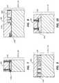
- Functional interposer structure 120can have formed therein an alignment feature 210 provided by a hard stop material layer for aligning of a prefabricated component.
- alignment feature 210can be provided by a layer of hard stop material deposited over an interposer material layer.
- Alignment feature 210 provided by a hard stop material layercan be deposited at a precise elevation of functional interposer structure 120 for providing precision vertical alignment of a prefabricated component as set forth herein for attachment of the prefabricated component to functional interposer structure 120 . Precision elevation control can permit reduced loss edge coupling between photonics devices.
- Alignment feature 210 provided by a hard stop material layercan be formed of a material having different etch selectivity relative to a material layer defining major body 122 of functional interposer structure 120 .
- Alignment feature 210 provided by a hard stop material layercan be deposited to a thickness from about 10 nm to about 200 nm and in one embodiment between about 20 nm and 80 nm.
- interposer materialcan be deposited over a hard stop material layer defining alignment feature 210 and then can be etched back for formation of cavity 402 to reveal alignment feature 210 .
- alignment feature 210can be formed of a material having etch selectivity differentiated from SiO 2 , e.g. titanium nitride, carbon silicon nitride, or amorphous silicon.
- Alignment features 220 provided by metal stacks shown in an intermediary stage of fabrication in FIG. 2can include metal pillars 221 , barrier layer 222 , and formations 420 (shown in the later stage view of FIG. 4 ).
- Alignment features 220 provided by metal stackscan provide vertical alignment along an axis running parallel to the z axis of reference coordinate system 15 to precisely vertically align a prefabricated component to be attached to functional interposer structure 120 so that elevation of the prefabricated component can be precisely established. Precision elevation control can permit reduced loss edge coupling between photonics devices.
- Alignment features 220 provided by metal stackscan be fabricated to have a predetermined total thickness within a small tolerance so that a distance between metallization layer 1404 and a top elevation of metal stacks defining alignment feature 220 can be precisely established.
- top elevation formations 420e.g. formed of metal bump formations or plating formations
- FIG. 4can be subject to heating and reflow for connection of a prefabricated component thereto.
- the distribution and volume of formations 420 as well as heating parameterscan be controlled so that an elevation of metal stacks defining alignment feature 220 is not unexpectedly impacted by reflow of formations 420 ( FIG. 4 ).
- one or more photonics device formed integral with functional interposer structure 120can include waveguide 150 A defined by waveguiding material layer 1502 .
- waveguide 150 Acan be fabricated by depositing waveguiding material layer 1502 , masking and etching to remove unwanted areas of waveguiding material layer 1502 and depositing an interposer material layer over the remaining portion of the waveguiding material layer.
- Waveguiding material layer 1502 defining waveguide 150 Acan include e.g. monocrystalline silicon, polycrystalline silicon, amorphous silicon, silicon nitride, or silicon oxynitride.
- Waveguides fabricated of different materials within functional interposer structure 120can be used for performance of different functions.
- waveguides formed of siliconmight be selected for fabrication of waveguides included in active devices such as photodetectors or modulators.
- Dielectric waveguidese.g. formed of silicon nitride
- Patterning of waveguide 150 Acan include patterning of material defining waveguide 150 as well as patterning of material surrounding the waveguide 150 A having an index of refraction differentiated from an index of refraction of a material of waveguide 150 A.
- Patterning of waveguide 150 Acan include patterning to define different alternative geometries.
- Functional interposer structure 120can include one or more integrally formed photonics device in addition to or in place of one or more waveguide such as waveguide 150 .
- functional interposer structure 120can include one or more integrated photonics region such as photonics region 240 which can be formed e.g. at location A formed on substrate 110 or location B formed in functional interposer structure 120 at an elevation above a substrate 110 of interposer 100 .
- integrated photonics region 240can include one or more layer defining functional interposer structure 120 patterned to define a photodetector 150 B. As shown in FIG.
- integrated photonics region 240can include one or more layer defining functional interposer structure 120 patterned to define waveguides 150 C, 150 D, 150 E of different dimensions, shapes, and materials. As shown in FIG. 9 , integrated photonics region 240 can include one or more layer defining functional interposer structure 120 patterned to define a grating coupler 150 F. As shown in FIG. 10 , integrated photonics region 240 can include one or more layer defining functional interposer structure 120 patterned to define a modulator 150 G.
- interposer 100can include photonics region 240 distributed throughout interposer 100 , and interposer 100 can include each of the integrated photonics devices 150 B- 150 G described with reference to FIGS. 7-10 .
- photonics regions 240represents a photonics region fabricated to define one or more of a polarizer, a splitter or a resonator.
- material forming photonics devicese.g. monocrystalline silicon, polycrystalline silicon, germanium
- material forming photonics devicescan be epitaxially grown.
- a structure having seed layer of silicon (a silicon template) on an insulatorcan be provided.
- a silicon on insulator (SOI) waferhaving a thin layer of oxide on a bulk silicon substrate and a thin layer of silicon on the oxide
- substrate 110is provided by a bulk silicon substrate of a SOI wafer.
- Epitaxially growingcan also be performed by epitaxially growing on a seed layer of silicon formed on glass. Accordingly, selection of a silicon on glass wafer (having a thin silicon layer formed on a bulk glass substitute) for fabrication of substrate 110 can accommodate epitaxial growth of epitaxial growth material and fabrication of photonics devices formed of epitaxially grown material such as monocrystalline silicon, polycrystalline silicon or germanium. In one embodiment where a silicon on glass wafer is used for fabrication of interposer 100 , substrate 110 is provided by a glass substrate of a silicon on glass wafer.
- functional interposer structure 120can be fabricated to include a silicon on insulator interface at an elevation above substrate 110 .
- a thick layer of silicon above a top elevation of substrate 110e.g. epitaxially grown on a substrate 110 where formed of silicon, can be subject to separation by local or non-local implanted oxygen (SIMOX) processing to define a thin silicon layer and buried oxide layer below the thin silicon layer.
- SIMOXlocal or non-local implanted oxygen
- photonic devices provided by or having waveguides of different waveguiding materialcan be fabricated at any elevation of functional interposer structure 120 .
- epitaxially grown photonic devicescan be fabricated at on substrate locations of functional interposer structure 120
- photonic devices formed of deposited materialse.g. formed of deposited silicon nitride or silicon oxynitride can be formed at an above substrate elevation of functional interposer structure 120 .
- Functional interposer structure 120can be fabricated to conduct light between elevations by evanescent coupling between waveguides at different elevations.
- a material layercan be formed of polycrystalline silicon (polysilicon).
- ion implantationcan be performed to modify the silicon crystal structure of a material layer.
- polysilicon materialcan be transformed into amorphous polysilicon material.
- Ion implant speciescan include one or more of silicon, argon (e.g., Ar or Ar+), xenon (e.g., Xe or Xe+) or germanium.
- an annealing processe.g., a recrystallization annealing process can be performed to further improve a grain structure of a material layer.
- a material layercan be subject to annealing for modification of a grain structure.
- interposer 100can include features for reducing coupling between integrally fabricated photonics devices and substrate 110 .
- substrate 110can be formed of glass for reduction of coupling.
- substrate 110can include deep trench isolation features in regions of interposer 100 in which photonics devices are integrally formed.
- FIG. 3illustrates the optoelectronics system 10 of FIG. 2 in a subsequent intermediary stage of fabrication.
- substrate 110can be grinded to reveal conductive material of through vias 130 and additional patterning can be performed for formation of redistribution layer wiring 170 .
- an interposer material layere.g. being of the material defining major body 122 can be deposited on substrate 110 after grinding of substrate planarized to a bottom elevation of through vias 130 in the stage shown in FIG.
- redistribution layer 1702followed by depositing of redistribution layer 1702 , masking and etching to remove unwanted material of redistribution layer 1702 to define redistribution layer wiring 170 and depositing of another one or more layer of interposer material, then recessing that one or more layer in areas for accommodated of under bump metallization formations.
- one or more interposer material layere.g. being of the material defining major body 122 can be deposited, etched to define cavities for receiving conductive material, and such cavities can be filled with conductive material to define redistribution layer 1702 followed by depositing an additional one or more interposer material layer and recessing in the areas depicted for accommodated of under bump metallization formations.
- a photoresist stencilcan be applied and filled with conductive material for formation of redistribution layer 1702 .
- Through vias 130 and vias 134can distribute control, logic and/or power signals between a backside of interposer 100 and interposer functional structure 120 .
- Through vias 130 and vias 134 , wires 140 , and wiring 170can facilitate fan out of electrical control and power signals.
- metallized layers 1402 1404 and 1406can have pitches on respective nanometer scales and redistribution layer 1702 can have a pitch on a micron scale.
- Materials for use in fabrication of redistribution layer 1702 and metallization layers 1402 1404 and 1406can include metals e.g. copper, silver, gold, tungsten, or other conductive material, or other conductive material, e.g. appropriately doped semiconductor material.
- a frontside handle wafer(not shown) having the general configuration of handle wafer 180 can be temporarily attached to a frontside of interposer 100 (the frontside of interposer 100 having functional interposer structure 120 ) using an adhesive layer having the general configuration of adhesive layer 182 .
- Such frontside handle waferpermits interposer 100 to be oriented in a backside up orientation for fabrication processing for formation of backside features including redistribution layer 1702 .
- a backside handle wafer 180e.g. with use of adhesive layer 182 , can be temporarily attached to interposer 100 as shown in FIG.
- Backside handle wafer 180permits interposer 100 to be oriented in a frontside up orientation as shown in FIG. 3 for fabrication processing of additional features, e.g. formation of features of area 302 , formation of cavities 402 and 404 , and attachment of prefabricated components 160 A, 160 B, and 160 B.
- Through vias 130 and vias 134can be vertically extending.
- through vias 130can extend through substrate 110 and can also extend though functional interposer structure 120 .
- through vias 130can extend through substrate 110 by extending entirely (completely) through substrate 110 and can extend though functional interposer structure 120 by extending partially through substrate 110 .
- vias 134can extend though functional interposer structure 120 by extending partially through functional interposer structure 120 .
- additional fabrication processing at area 302can be performed to accommodate attachment of a prefabricated component.
- the prefabricated componentis a prefabricated semiconductor chip having solder bumps processing at area 302 can include fabrication processing to fabricate under bump metallization (UBM) formations.
- UBMunder bump metallization
- FIG. 4illustrates the optoelectronics system 10 of FIG. 3 in a subsequent intermediary stage of fabrication.
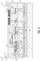
- cavity 402can be formed for accommodation of a prefabricated component provided by a prefabricated laser die chip 160 A ( FIG. 5 ) and cavity 404 can be formed for accommodation of a prefabricated component provided by a prefabricated photonics integrated circuit chip 160 B ( FIG. 5 ).
- Formations 410can be formed in cavity 402 for facilitating electrical and mechanical coupling of wires 140 to a prefabricated component and formations 420 can be formed in cavity 404 on barrier layer 222 for facilitating electrical and mechanical coupling of wire 140 to a prefabricated component.
- Formations 420can complete fabrication of alignment feature 220 provided by metals stacks shown in an intermediary stage of fabrication in FIG. 3 .
- Formations 410can be formed on barrier layer 212 which can be formed on metallization layer.
- Formation 420can be formed on barrier layer 222 .
- Barrier layer 222in turn can be formed in metal pillars 221 which can be formed on metallization layer 1404 .
- Barrier layers 212 and 222can form a barrier to inhibit reactions that may result from gold or tin of contacts 160 AC and 160 BC of respective prefabricated components such as prefabricated laser die chip 160 A and prefabricated photonics integrated circuit chip 160 B contacting metallization layer 1404 or pillars 211 .
- Formations 410 and/or formations 420 in one embodimentcan be formed of solder bumps. Formations 410 and/or formations 420 in one embodiment can be formed of thin coherent metal coatings (e.g. electroless plating formations or electroplating plating formations) yielded using an electroless plating process or an electroplating process.
- an electroless plating processcan be provided by a chemical or auto catalytic non-galvanic process that involves reactions in an aqueous solution without use of external power.
- hydrogencan be released by a reducing agent to produce a negative charge on a surface.
- Electroless platingcan include e.g.
- electroless nickel plating, electroless silver plating, electroless gold plating, or electroless copper platingcan be used to reduce dissolve metal cations so that they form a thin metal coating on an electrode.
- a plating processe.g. an electroless plating or electroplating process
- a plating processcan be used for precision control of an amount and distribution of material forming formation 410 and/or formation 420 , thus reducing thickness variations resulting from reflow of material forming formations 410 and/or formations 420 .
- prefabricated semiconductor chip 160 Ccan be attached at area 430 .
- Prefabricated semiconductor chip 160 Ccan be a semiconductor chip with active or passive electrical devices (CMOS, RF components, MEMs, discrete components).
- Processing at area 430can include processing to solder bumps of prefabricated semiconductor chip 160 C to under bump metallization formations (UBM).
- Prefabricated semiconducter chip 160 Ccan be a chip with active and/or passive electrical devices (CMOS, SRAM, Logic, ASIC, RF components, MEMs, discrete components).
- FIG. 5illustrates the optoelectronics system 10 of FIG. 4 in a subsequent intermediary stage of fabrication.
- prefabricated laser die chip 160 Acan be attached to functional interposer structure 120 within cavity 402
- prefabricated photonics integrated circuit chip 160 Bcan be attached to functional interposer structure 120 within cavity 404 .
- prefabricated laser die chip 160 AFor attachment of prefabricated laser die chip 160 A, prefabricated laser die chip 160 A can be lowered downward until a bottom elevation of prefabricated laser die chip 160 A at an area adjacent to contacts 160 AC of prefabricated laser die chip 160 A contacts alignment feature 210 .
- formations 410can be subject to localized laser heating using a laser heating tool to electrically and mechanically connect prefabricated laser die chip 160 A to functional interposer structure 120 . Localized laser heating can cause formations 410 to reflow and electrical and mechanical coupling between metallization layer 1404 and contacts 160 AC of prefabricated laser die chip 160 A can be established.
- Prefabricated laser die chip 160 Acan emit laser light of a predetermined or variable wavelength.
- Prefabricated laser die chip 160 Acan incorporate one or more laser light emission technologies, e.g. DFB, Fabry-Perot, WDM.
- prefabricated photonics integrated circuit chip 160 BFor attachment of prefabricated photonics integrated circuit chip 160 B to functional interposer structure 120 , prefabricated photonics integrated circuit chip 160 B can be pressed downward until contacts 160 BC of prefabricated photonics integrated circuit chip 160 B contact alignment feature 220 provided by metal stacks having metal pillars 221 , barrier layer 222 and formation 420 .
- the attachment assembly as shown for attaching chip 160 B at cavity 404can rely on controlled thickness of alignment feature 220 provided by metal stacks so that vertical alignment can be provided based on contacts of prefabricated photonics integrated circuit chip 160 B contacting formations 420 so that chip is at a certain elevation at which chip 160 B can essentially remain after reflow of formation 420 .
- contacts 160 BC of prefabricated photonics integrated circuit chip 160 B contact alignment feature 220formations 420 can be subject to localized laser heating using a laser heating tool.
- localized laser heatingcan cause formations 420 to reflow and electrical and mechanical coupling between metallization layer 1404 and contacts 160 BC of prefabricated laser die chip 160 B can be established.
- Prefabricated photonics integrated circuit chip 160 Bcan be a prefabricated photonics integrated circuit chip for various applications e.g. biomedical, WDM, datacom, analog RF, mobile, LIDAR, optical networking, and the like.
- Prefabricated photonics integrated circuit chip 160 Bcan include one or more photonics device e.g. waveguides 150 A and/or one or more photonics device 150 B- 150 G of photonics region 240 fabricated as set forth herein in reference to FIGS. 7-10 , e.g. one or more photonics device such as a waveguide, a photodetector, coupler, modulator, polarizer, splitter or a resonator.
- prefabricated laser die chip 160 A and prefabricated photonics integrated circuit chip 160 Bcan be located in their respective cavities 402 and 404 using a chip bonding tool having machine vision functionality.
- Alignment features 210 and 220can provide vertical alignment (in directions parallel to the z axis of the reference coordinate system 15 shown throughout the views associated to interposer 100 ) so that an elevation of prefabricated laser die chip 160 A and prefabricated photonics integrated circuit chip can be precisely established.
- Recognizable patternscan be included in interposer 100 to facilitate alignment of prefabricated laser die chip 160 A and prefabricated photonics integrated circuit chip 160 B both in directions along an axis that runs parallel to the y axis of reference coordinate system 15 in directions along an axis that runs parallel to the x axis of reference coordinate system 15 .
- Patterns recognizable by machine vision pattern recognitioncan be conveniently fabricated with patterns defined by metallization layer 1402 and/or metallization layer 1404 .
- Alignment feature 210which can operate to vertically align and establish a precision elevation of prefabricated laser die chip 160 A can be spaced apart from and independent of features for electrical connection of laser die chip 160 A and functional interposer structure 120 . As such requirements for locating and providing conductive material for purposes of electrical connectivity can be expected to have less of an effect on the vertical alignment of chip 160 A.
- the attachment assembly for attaching prefabricated photonics integrated circuit chip 160 B at cavity 404can operate independent of alignment feature 210 and can remove from a design configuration alignment feature 210 .
- attachment assembly for attaching a prefabricated laser die chip 160 A at cavity 402 and the attachment assembly for attaching prefabricated photonics integrated circuit chip 160 B at cavity 404are shown as different attachment assemblies in the specific embodiment of FIG. 4 , common attachment assemblies can alternatively be used.
- the attachment assembly for attaching prefabricated laser die chip 160 A at cavity 402could be used for attaching prefabricated laser die chip 160 A at cavity 402 and for attaching prefabricated photonics integrated circuit chip 160 B at cavity 404 .
- the attachment assembly shown for attaching prefabricated photonics integrated circuit chip 160 B at cavity 404can be used to attach prefabricated laser die chip 160 A at cavity 402 and to attach prefabricated photonics integrated circuit chip 160 B at cavity 404 .
- attachment assembly shown for attaching prefabricated laser die chip 160 A at cavity 402could be used for attaching prefabricated photonics integrated circuit chip 160 B at cavity 404 and the attachment assembly for attaching prefabricated photonics integrated circuit chip 160 B at cavity 404 can be used for attaching prefabricated laser die chip 160 A at cavity 402 .
- prefabricated laser die chip 160 AWith prefabricated laser die chip 160 A attached to functional interposer structure 120 as shown in FIG. 5 , prefabricated laser die chip 160 A can be vertically aligned (in a direction running parallel to the z axis of reference coordinate system 15 ) to waveguide 150 A integrally formed in functional interposer structure 120 so that a light emission layer 160 AL of chip 160 A is vertically aligned to waveguide 150 A.
- Prefabricated laser die chip 160 Acan be z axis aligned as well as x and y axis aligned to integrally formed waveguide 150 (in directions running parallel to the x axis and y axis of reference coordinate system 15 ).
- prefabricated laser die chip 160 A and waveguide 150 Acan be edge coupled to one another.
- an edge coupling between prefabricated laser die chip 160 A and waveguide 150 Acan include an optical coupling of reduced insertion loss, leading to enhanced system and signal integrity.
- Edge couplingcan include light receiving waveguide 150 A being tapered for further reduction of light losses.
- prefabricated photonics integrated circuit chip 160 BWith prefabricated photonics integrated circuit chip 160 B attached to functional interposer structure 120 as shown in FIG. 4 , prefabricated photonics integrated circuit chip 160 B can be vertically aligned (in a direction running parallel to the z axis of reference coordinate system 15 ) as well as x and y axis aligned (in directions running parallel to the x axis and y axis of reference coordinate system 15 ) to waveguide 150 A integrally formed in functional interposer structure 120 so that waveguide 160 BW of prefabricated photonics integrated circuit chip 160 B is aligned to waveguide 150 A and accordingly at a common elevation with waveguide 150 A.
- prefabricated photonics integrated circuit chip 160 B and waveguide 150can be edge coupled to one another.
- an edge coupling between prefabricated photonics integrated circuit chip 160 B and waveguide 150can include an optical coupling of reduced insertion loss, leading to enhanced system and signal integrity.
- Edge couplingcan include light receiving waveguide 160 BW being tapered for further reduction of light losses.
- prefabricated laser die chip 160 A and prefabricated photonics integrated circuit chip 160 Battached to functional interposer structure 120
- light emission layer 160 AL of prefabricated laser die chip 160 A, integrally formed waveguide 150 A integrally formed in functional interposer structure 120 , and waveguide 160 BW of prefabricated photonics integrated circuit chip 160 Bcan be aligned along a common horizontal axis 502 and can be disposed at a common elevation.
- Light emission layer 160 AL of prefabricated laser die chip 160 A, integrally formed waveguide 150 integrally formed in functional interposer structure 120 , and waveguide 160 BW in one embodimentcan each be provided by straight linear shaped structure having respective axes 504 , 506 , and 508 that run parallel to an x axis of reference coordinate system 15 . Aligning light emission layer 160 AL of prefabricated laser die chip 160 A, integrally formed waveguide 150 A integrally formed in functional interposer structure 120 , and waveguide 160 BW of prefabricated photonics integrated circuit chip 160 B as described can reduce light transmission losses which may result e.g. from diffraction or reflection from internal components of functional interposer structure 120 .
- interposer 100can be configured so that through vias 130 provide heat sinking functionality to remove heat generated by heat generating features of prefabricated laser die chip 160 A and prefabricated photonics integrated circuit chip 160 B.
- substrate 110is formed of thermally conductive material e.g. silicon
- interposer 100can be configured so that heat conducted by through vias 130 can be conducted by substrate and redistribution layer 1702 for removal of heat from interposer 100 .
- substrate 110is formed of thermally insulating material e.g. SiO 2 or glass
- interposer 100can be configured so that heat conducted by through vias 130 can be conducted primarily by redistribution layer 1702 for removal of heat from interposer 100 .
- under bump metallization (UBM) formations 176as shown in FIG. 6 can be formed on exposed areas of redistribution layer 1702 on a backside of interposer 100 (the exposed areas being where the interposer material surrounding redistribution layer 1702 is shown as being recessed). Such UBM formations 176 can be adapted to receive solder bumps of a substructure to which interposer 100 can be attached.
- a handle wafer(not shown) can be temporarily attached to functional interposer structure 120 via an adhesive to permit handling and installation of optoelectronics system 10 on a substructure such as a printed circuit board or interposer.
- FIG. 6illustrates system 10 mounted on a substructure 190 by way of connection of solder bumps 192 of interposer 100 to UBM formations 176 .
- Shown as being provided by a printed circuit board substructure 190can alternatively be provided e.g. by a ball grid array or an interposer.
- Interposer 100 in the fabrication stage as shown in FIG. 6can include a wire bond 188 for wire bonding of an electrode of prefabricated laser die chip 160 A to an exposed voltage terminal of functional interposer structure 120 .
- the area of formations 410 of functional interposer structure 120can be configured to define electrically isolated positive and negative voltage terminal and a prefabricated laser die chip 160 A having the bottom electrode shown configured as separated positive and negative terminal electrodes can be attached to the corresponding positive and negative voltage terminals in the area of formations 410 .
- External laser lightcan be coupled to functional interposer structure 120 .
- a fiber optic cable 196 carrying light from an external off-interposer source(not shown) can be coupled to integrated waveguide 150 H integrally formed in functional interposer structure 120 .
- Light receiving waveguide 150 Hcan be tapered for reduction of light losses.
- UBM formations 176 of interposer 100can be soldered to corresponding solder bumps 192 of substructure 190 , and sealed with a sealant 194 .
- a method or device that “comprises,” “has,” “includes,” or “contains” one or more steps or elementspossesses those one or more steps or elements, but is not limited to possessing only those one or more steps or elements.
- a step of a method or an element of a device that “comprises,” “has,” “includes,” or “contains” one or more featurespossesses those one or more features, but is not limited to possessing only those one or more features.
- Forms of the term “defined by”encompass relationships where an element is partially defined by as well relationships where an element is entirely defined by. Numerical identifiers herein, e.g.
- first and secondare arbitrary terms to designate different elements without designating an ordering of elements.
- a system method or apparatus that is configured in a certain wayis configured in at least that way, but may also be configured in ways that are not listed.
- a system method or apparatus set forth as having a certain number of elementscan be practiced with less than or greater than the certain number of elements.
Landscapes
- Physics & Mathematics (AREA)
- Engineering & Computer Science (AREA)
- General Physics & Mathematics (AREA)
- Microelectronics & Electronic Packaging (AREA)
- Condensed Matter Physics & Semiconductors (AREA)
- Optics & Photonics (AREA)
- Computer Hardware Design (AREA)
- Power Engineering (AREA)
- Electromagnetism (AREA)
- Ceramic Engineering (AREA)
- Manufacturing & Machinery (AREA)
- Optical Integrated Circuits (AREA)
Abstract
Description
Claims (20)
Priority Applications (1)
| Application Number | Priority Date | Filing Date | Title |
|---|---|---|---|
| US15/795,349US10976491B2 (en) | 2016-11-23 | 2017-10-27 | Photonics interposer optoelectronics |
Applications Claiming Priority (2)
| Application Number | Priority Date | Filing Date | Title |
|---|---|---|---|
| US201662426100P | 2016-11-23 | 2016-11-23 | |
| US15/795,349US10976491B2 (en) | 2016-11-23 | 2017-10-27 | Photonics interposer optoelectronics |
Publications (2)
| Publication Number | Publication Date |
|---|---|
| US20180143374A1 US20180143374A1 (en) | 2018-05-24 |
| US10976491B2true US10976491B2 (en) | 2021-04-13 |
Family
ID=62147510
Family Applications (1)
| Application Number | Title | Priority Date | Filing Date |
|---|---|---|---|
| US15/795,349Active2038-01-22US10976491B2 (en) | 2016-11-23 | 2017-10-27 | Photonics interposer optoelectronics |
Country Status (1)
| Country | Link |
|---|---|
| US (1) | US10976491B2 (en) |
Cited By (13)
| Publication number | Priority date | Publication date | Assignee | Title |
|---|---|---|---|---|
| US20230161120A1 (en)* | 2021-11-22 | 2023-05-25 | Taiwan Semiconductor Manufacturing Co., Ltd. | Package Structure Including Photonic Package and Interposer Having Waveguide |
| US20230244033A1 (en)* | 2022-01-31 | 2023-08-03 | Globalfoundries U.S. Inc. | Multiple-core heterogeneous waveguide structures including multiple slots |
| US11817903B2 (en) | 2020-08-06 | 2023-11-14 | Celestial Ai Inc. | Coherent photonic computing architectures |
| US11835777B2 (en) | 2022-03-18 | 2023-12-05 | Celestial Ai Inc. | Optical multi-die interconnect bridge (OMIB) |
| US12191257B2 (en) | 2022-07-26 | 2025-01-07 | Celestial Ai Inc. | Electrical bridge package with integrated off-bridge photonic channel interface |
| US12217056B2 (en) | 2023-01-27 | 2025-02-04 | Celestial Ai Inc. | Load/store unit for a tensor engine and methods for loading or storing a tensor |
| WO2024236040A3 (en)* | 2023-05-15 | 2025-03-06 | Ams-Osram International Gmbh | Integrated component package with a laser package arranged on a semiconductor chip |
| US12259575B2 (en) | 2021-06-18 | 2025-03-25 | Celestial Ai Inc. | Clock signal distribution using photonic fabric |
| US12271595B2 (en) | 2022-03-18 | 2025-04-08 | Celestial Ai Inc. | Photonic memory fabric for system memory interconnection |
| US12283584B2 (en) | 2022-07-26 | 2025-04-22 | Celestial Ai Inc. | Electrical bridge package with integrated off-bridge photonic channel interface |
| US12353988B2 (en) | 2020-07-09 | 2025-07-08 | Celestial Ai Inc. | Neuromorphic photonics with coherent linear neurons |
| US12436346B2 (en) | 2022-03-18 | 2025-10-07 | Celestial Ai Inc. | Optically bridged multicomponent package with extended temperature range |
| US12442999B2 (en) | 2025-04-04 | 2025-10-14 | Celestial Ai Inc. | Optically bridged multicomponent package with extended temperature range |
Families Citing this family (22)
| Publication number | Priority date | Publication date | Assignee | Title |
|---|---|---|---|---|
| US10976491B2 (en) | 2016-11-23 | 2021-04-13 | The Research Foundation For The State University Of New York | Photonics interposer optoelectronics |
| US10698156B2 (en) | 2017-04-27 | 2020-06-30 | The Research Foundation For The State University Of New York | Wafer scale bonded active photonics interposer |
| US10365446B2 (en)* | 2017-11-06 | 2019-07-30 | Panasonic Intellectual Property Management Co., Ltd. | Optical module structure |
| US10795079B2 (en) | 2018-01-25 | 2020-10-06 | Poet Technologies, Inc. | Methods for optical dielectric waveguide subassembly structure |
| WO2019195441A1 (en) | 2018-04-04 | 2019-10-10 | The Research Foundation For The State University Of New York | Heterogeneous structure on an integrated photonics platform |
| US10816724B2 (en) | 2018-04-05 | 2020-10-27 | The Research Foundation For The State University Of New York | Fabricating photonics structure light signal transmission regions |
| FR3082354B1 (en)* | 2018-06-08 | 2020-07-17 | Commissariat A L'energie Atomique Et Aux Energies Alternatives | PHOTONIC CHIP CROSSED BY A VIA |
| US11536805B2 (en) | 2018-06-25 | 2022-12-27 | Silc Technologies, Inc. | Optical switching for tuning direction of LIDAR output signals |
| TWI829761B (en)* | 2018-11-21 | 2024-01-21 | 紐約州立大學研究基金會 | Photonics structure with integrated laser |
| US11550099B2 (en) | 2018-11-21 | 2023-01-10 | The Research Foundation For The State University Of New York | Photonics optoelectrical system |
| WO2020123008A1 (en)* | 2018-11-21 | 2020-06-18 | The Research Foundation For The State University Of New York | Photonics structure with integrated laser |
| TWI851601B (en) | 2018-11-21 | 2024-08-11 | 紐約州立大學研究基金會 | Photonics optoelectrical system and method for fabricating same |
| US12429569B2 (en) | 2019-05-17 | 2025-09-30 | Silc Technologies, Inc. | Identification of materials illuminated by LIDAR systems |
| US11650317B2 (en) | 2019-06-28 | 2023-05-16 | Silc Technologies, Inc. | Use of frequency offsets in generation of LIDAR data |
| US11624826B2 (en)* | 2020-05-05 | 2023-04-11 | Silc Technologies, Inc. | Use of common chirp periods in generation of LIDAR data |
| TW202217377A (en) | 2020-07-06 | 2022-05-01 | 新加坡商光子智能私人有限公司 | Integrated circuit interposer, system, apparatus, method of fabricating integrated circuit interposer, and method and system for transmitting information from nodes to destination interposer |
| FR3120739B1 (en)* | 2021-03-11 | 2023-02-10 | Commissariat Energie Atomique | optoelectronic device comprising an active photonic interposer to which are connected a microelectronic chip and an electro-optical conversion chip |
| US12411213B2 (en) | 2021-10-11 | 2025-09-09 | Silc Technologies, Inc. | Separation of light signals in a LIDAR system |
| US12368109B2 (en)* | 2022-06-02 | 2025-07-22 | Taiwan Semiconductor Manufacturing Company Limited | Interposer structure for semiconductor package including peripheral metal pad around alignment mark and methods of fabricating same |
| US12422618B2 (en) | 2022-10-13 | 2025-09-23 | Silc Technologies, Inc. | Buried taper with reflecting surface |
| US20240302589A1 (en)* | 2023-03-10 | 2024-09-12 | Advanced Semiconductor Engineering, Inc. | Optoelectronic package structure |
| CN118732150A (en)* | 2023-03-28 | 2024-10-01 | 上海曦智科技有限公司 | Semiconductor structure and method for manufacturing the same |
Citations (139)
| Publication number | Priority date | Publication date | Assignee | Title |
|---|---|---|---|---|
| US5841931A (en) | 1996-11-26 | 1998-11-24 | Massachusetts Institute Of Technology | Methods of forming polycrystalline semiconductor waveguides for optoelectronic integrated circuits, and devices formed thereby |
| US6621972B2 (en) | 2000-10-13 | 2003-09-16 | Massachusetts Institute Of Technology | Optical waveguides with trench structures |
| US6631225B2 (en) | 2000-07-10 | 2003-10-07 | Massachusetts Institute Of Technology | Mode coupler between low index difference waveguide and high index difference waveguide |
| US6635110B1 (en) | 1999-06-25 | 2003-10-21 | Massachusetts Institute Of Technology | Cyclic thermal anneal for dislocation reduction |
| US20030215203A1 (en) | 2002-04-09 | 2003-11-20 | John Lock | Polysilane thin films for directly patternable waveguides |
| US6690871B2 (en) | 2000-07-10 | 2004-02-10 | Massachusetts Institute Of Technology | Graded index waveguide |
| US20040091719A1 (en)* | 2002-08-02 | 2004-05-13 | Canon Kabushiki Kaisha | Layered board, and apparatus incorporation such layered board |
| US6812495B2 (en) | 2002-06-19 | 2004-11-02 | Massachusetts Institute Of Technology | Ge photodetectors |
| US20050012040A1 (en) | 1997-03-28 | 2005-01-20 | Interuniversitair Micro-Elektronica Centrum (Imec,Vzw), A Belgium Company | Method of fabrication of an infrared radiation detector and infrared detector device |
| US6850683B2 (en) | 2000-07-10 | 2005-02-01 | Massachusetts Institute Of Technology | Low-loss waveguide and method of making same |
| US20050051705A1 (en) | 2003-09-05 | 2005-03-10 | John Yasaitis | Light conversion apparatus with topside electrode |
| US6879014B2 (en) | 2000-03-20 | 2005-04-12 | Aegis Semiconductor, Inc. | Semitransparent optical detector including a polycrystalline layer and method of making |
| US6887773B2 (en) | 2002-06-19 | 2005-05-03 | Luxtera, Inc. | Methods of incorporating germanium within CMOS process |
| US20050101084A1 (en) | 2002-04-10 | 2005-05-12 | Gilton Terry L. | Thin film diode integrated with chalcogenide memory cell |
| US6927392B2 (en) | 2000-07-25 | 2005-08-09 | Kevin Liddiard | Active or self-biasing micro-bolometer infrared detector |
| US20050205954A1 (en) | 2002-12-18 | 2005-09-22 | King Clifford A | Image sensor comprising isolated germanium photodetectors integrated with a silicon substrate and silicon circuitry |
| US7008813B1 (en) | 2005-02-28 | 2006-03-07 | Sharp Laboratories Of America, Inc.. | Epitaxial growth of germanium photodetector for CMOS imagers |
| US7043120B2 (en) | 2001-11-01 | 2006-05-09 | Massachusetts Institute Of Technology | Array waveguide grating |
| US20060110844A1 (en) | 2004-11-19 | 2006-05-25 | Sharp Laboratories Of America, Inc. | Fabrication of thin film germanium infrared sensor by bonding to silicon wafer |
| US7095010B2 (en) | 2002-12-04 | 2006-08-22 | California Institute Of Technology | Silicon on insulator resonator sensors and modulators and method of operating the same |
| US20060194357A1 (en) | 2005-02-28 | 2006-08-31 | Sharp Laboratories Of America, Inc. | High-density germanium-on-insulator photodiode array |
| US7103245B2 (en) | 2000-07-10 | 2006-09-05 | Massachusetts Institute Of Technology | High density integrated optical chip |
| US7123805B2 (en) | 2003-06-16 | 2006-10-17 | Massachusetts Institute Of Technology | Multiple oxidation smoothing method for reducing silicon waveguide roughness |
| US20060250836A1 (en) | 2005-05-09 | 2006-11-09 | Matrix Semiconductor, Inc. | Rewriteable memory cell comprising a diode and a resistance-switching material |
| US20060249753A1 (en) | 2005-05-09 | 2006-11-09 | Matrix Semiconductor, Inc. | High-density nonvolatile memory array fabricated at low temperature comprising semiconductor diodes |
| US20060250837A1 (en) | 2005-05-09 | 2006-11-09 | Sandisk 3D, Llc | Nonvolatile memory cell comprising a diode and a resistance-switching material |
| US20070034978A1 (en) | 2004-06-17 | 2007-02-15 | Pralle Martin U | Photonic crystal emitter, detector and sensor |
| US7194166B1 (en) | 2004-08-26 | 2007-03-20 | Luxtera, Inc. | Use of waveguide grating couplers in an optical mux/demux system |
| US20070090089A1 (en) | 2004-08-20 | 2007-04-26 | Chang Chang K | Method to trim and smooth high index contrast waveguide structures |
| US20070099329A1 (en) | 2005-10-27 | 2007-05-03 | Sharp Laboratories Of America, Inc. | Method of fabricating a germanium photo detector on a high quality germanium epitaxial overgrowth layer |
| US20070104410A1 (en) | 2005-11-08 | 2007-05-10 | Massachusetts Institute Of Technology | Integrated waveguide photodetector apparatus with matching propagation constants and related coupling methods |
| US20070141744A1 (en) | 2005-12-19 | 2007-06-21 | Sharp Laboratories Of America, Inc. | Method of fabricating a low, dark-current germanium-on-silicon pin photo detector |
| US7248757B2 (en)* | 2003-12-15 | 2007-07-24 | Canon Kabushiki Kaisha | Method, device and computer program for designing a circuit having electric wires and optical connections |
| US20070170536A1 (en) | 2006-01-25 | 2007-07-26 | Sharp Laboratories Of America, Inc. | Liquid phase epitaxial GOI photodiode with buried high resistivity germanium layer |
| US7251386B1 (en) | 2004-01-14 | 2007-07-31 | Luxtera, Inc | Integrated photonic-electronic circuits and systems |
| US20070190722A1 (en) | 2002-12-19 | 2007-08-16 | Herner S B | Method to form upward pointing p-i-n diodes having large and uniform current |
| US7262117B1 (en) | 2003-06-10 | 2007-08-28 | Luxtera, Inc. | Germanium integrated CMOS wafer and method for manufacturing the same |
| US20070228414A1 (en) | 2006-03-31 | 2007-10-04 | Sandisk 3D, Llc | Heterojunction device comprising a semiconductor and a resistivity-switching oxide or nitride |
| US7279682B2 (en) | 2002-07-03 | 2007-10-09 | Commissariat A L'energie Atomique | Device for maintaining an object under vacuum and methods for making same, use in non-cooled infrared sensors |
| US20070246764A1 (en) | 2006-03-31 | 2007-10-25 | Sandisk 3D, Llc | Low-temperature metal-induced crystallization of silicon-germanium films |
| US20070262296A1 (en) | 2006-05-11 | 2007-11-15 | Matthias Bauer | Photodetectors employing germanium layers |
| US7305157B2 (en) | 2005-11-08 | 2007-12-04 | Massachusetts Institute Of Technology | Vertically-integrated waveguide photodetector apparatus and related coupling methods |
| US7317242B2 (en) | 2003-02-25 | 2008-01-08 | Seiko Epson Corporation | Semiconductor device including p-type silicon layer including implanted germanium |
| US7321713B2 (en) | 2004-09-17 | 2008-01-22 | Massachusetts Institute Of Technology | Silicon based on-chip photonic band gap cladding waveguide |
| US7340709B1 (en) | 2004-07-08 | 2008-03-04 | Luxtera, Inc. | Method of generating a geometrical rule for germanium integration within CMOS |
| US7358527B1 (en) | 2005-02-03 | 2008-04-15 | Luxtera, Inc. | Systems and methods for testing germanium devices |
| US20080121805A1 (en) | 2006-11-04 | 2008-05-29 | Tweet Douglas J | Ge short wavelength infrared imager |
| US7389029B2 (en) | 2003-07-03 | 2008-06-17 | Applied Research And Photonics, Inc. | Photonic waveguide structures for chip-scale photonic integrated circuits |
| US20080157253A1 (en) | 2006-04-13 | 2008-07-03 | Integrated Micro Sensors Inc. | Single-Chip Monolithic Dual-Band Visible- or Solar-Blind Photodetector |
| US7397101B1 (en) | 2004-07-08 | 2008-07-08 | Luxtera, Inc. | Germanium silicon heterostructure photodetectors |
| US7424181B2 (en) | 2004-01-23 | 2008-09-09 | Massachusetts Institute Of Technology | Hitless switch for high-density integrated optics |
| US20080217651A1 (en) | 2007-03-05 | 2008-09-11 | National Taiwan University | Photodetector |
| US20080239787A1 (en) | 2007-03-27 | 2008-10-02 | Herner S Brad | Large array of upward pointing p-i-n diodes having large and uniform current |
| US7453132B1 (en) | 2002-06-19 | 2008-11-18 | Luxtera Inc. | Waveguide photodetector with integrated electronics |
| US7459686B2 (en) | 2006-01-26 | 2008-12-02 | L-3 Communications Corporation | Systems and methods for integrating focal plane arrays |
| US20080311696A1 (en) | 2007-06-12 | 2008-12-18 | National Taiwan University | Manufacturing prpcess for photodetector |
| US20080316795A1 (en) | 2007-06-25 | 2008-12-25 | Sandisk 3D Llc | Method of making nonvolatile memory device containing carbon or nitrogen doped diode |
| US20080318397A1 (en) | 2007-06-19 | 2008-12-25 | Herner S Brad | Junction Diode with Reduced Reverse Current |
| US7480430B2 (en) | 2006-02-08 | 2009-01-20 | Massachusetts Institute Of Technology | Partial confinement photonic crystal waveguides |
| US20090032814A1 (en) | 2007-08-02 | 2009-02-05 | Vladislav Vashchenko | SiGe DIAC ESD protection structure |
| US7508050B1 (en) | 2006-03-16 | 2009-03-24 | Advanced Micro Devices, Inc. | Negative differential resistance diode and SRAM utilizing such device |
| US7565046B2 (en) | 2006-12-13 | 2009-07-21 | Massachusetts Institute Of Technology | Mode transformers for low index high confinement waveguides |
| US20090196631A1 (en) | 2008-02-05 | 2009-08-06 | Finisar Corporation | Monolithic power monitor and wavelength detector |
| US7613369B2 (en) | 2006-04-13 | 2009-11-03 | Luxtera, Inc. | Design of CMOS integrated germanium photodiodes |
| US20100006961A1 (en) | 2008-07-09 | 2010-01-14 | Analog Devices, Inc. | Recessed Germanium (Ge) Diode |
| US7659627B2 (en) | 2007-12-05 | 2010-02-09 | Fujifilm Corporation | Photodiode |
| US20100031992A1 (en) | 2006-05-30 | 2010-02-11 | Ying Hsu | Large format thermoelectric infrared detector and method of fabrication |
| US7700975B2 (en) | 2006-03-31 | 2010-04-20 | Intel Corporation | Schottky barrier metal-germanium contact in metal-germanium-metal photodetectors |
| US20100102412A1 (en) | 2008-10-27 | 2010-04-29 | Electronics And Telecommunications Research Institute | Germanium photodetector and method of fabricating the same |
| US7723206B2 (en) | 2007-12-05 | 2010-05-25 | Fujifilm Corporation | Photodiode |
| US7723754B2 (en) | 2004-07-28 | 2010-05-25 | Massachusetts Institute Of Technology | Ge photodetectors |
| US20100133536A1 (en) | 2006-08-03 | 2010-06-03 | Syllaios Althanasios J | Microbolometer infrared detector elements and methods for forming same |
| US20100133585A1 (en) | 2008-12-03 | 2010-06-03 | Electronics And Telecomunications Research Institute | Growth of germanium epitaxial thin film with negative photoconductance characteristics and photodiode using the same |
| US7736734B2 (en) | 2005-12-30 | 2010-06-15 | Sandvik Intellectual Property Ab | Cutting tool insert |
| US7737534B2 (en) | 2008-06-10 | 2010-06-15 | Northrop Grumman Systems Corporation | Semiconductor devices that include germanium nanofilm layer disposed within openings of silicon dioxide layer |
| US7773836B2 (en) | 2005-12-14 | 2010-08-10 | Luxtera, Inc. | Integrated transceiver with lightpipe coupler |
| US20100213561A1 (en) | 2007-10-26 | 2010-08-26 | International Business Machines Corporation | Optoelectronic Device with Germanium Photodetector |
| US7801406B2 (en) | 2005-08-01 | 2010-09-21 | Massachusetts Institute Of Technology | Method of fabricating Ge or SiGe/Si waveguide or photonic crystal structures by selective growth |
| US20100276776A1 (en) | 2009-05-01 | 2010-11-04 | Jong-Jan Lee | Germanium Film Optical Device Fabricated on a Glass Substrate |
| US7831123B2 (en) | 2006-09-07 | 2010-11-09 | Massachusetts Institute Of Technology | Microphotonic waveguide including core/cladding interface layer |
| US20110012221A1 (en) | 2008-03-07 | 2011-01-20 | Junichi Fujikata | SiGe PHOTODIODE |
| US20110027950A1 (en) | 2009-07-28 | 2011-02-03 | Jones Robert E | Method for forming a semiconductor device having a photodetector |
| US7902620B2 (en) | 2008-08-14 | 2011-03-08 | International Business Machines Corporation | Suspended germanium photodetector for silicon waveguide |
| US7916377B2 (en) | 2008-11-03 | 2011-03-29 | Luxtera, Inc. | Integrated control system for laser and Mach-Zehnder interferometer |
| US7943471B1 (en) | 2006-05-15 | 2011-05-17 | Globalfoundries Inc. | Diode with asymmetric silicon germanium anode |
| US20110156183A1 (en) | 2009-12-31 | 2011-06-30 | Ansheng Liu | Integrated optical receiver architecture for high speed optical i/o applications |
| US7994066B1 (en) | 2007-10-13 | 2011-08-09 | Luxtera, Inc. | Si surface cleaning for semiconductor circuits |
| US20110227116A1 (en) | 2008-11-12 | 2011-09-22 | Hitachi, Ltd. | Light-emitting device, light-receiving device and method of manufacturing the same |
| US8030668B2 (en) | 2007-02-16 | 2011-10-04 | Hitachi, Ltd. | Semiconductor LED, opto-electronic integrated circuits (OEIC), and method of fabricating OEIC |
| US20120001283A1 (en) | 2010-07-02 | 2012-01-05 | International Business Machines Corporation | Germanium Photodetector |
| US20120025212A1 (en) | 2008-09-16 | 2012-02-02 | Arizona Board of Regents, a body corporate acting for and on behalf of Arizona State University | GeSn Infrared Photodetectors |
| US8168939B2 (en) | 2008-07-09 | 2012-05-01 | Luxtera, Inc. | Method and system for a light source assembly supporting direct coupling to an integrated circuit |
| US20120129302A1 (en) | 2010-11-22 | 2012-05-24 | International Business Machines Corporation | Fabricating photonics devices fully integrated into a cmos manufacturing process |
| US8213751B1 (en)* | 2008-11-26 | 2012-07-03 | Optonet Inc. | Electronic-integration compatible photonic integrated circuit and method for fabricating electronic-integration compatible photonic integrated circuit |
| US20120187280A1 (en) | 2011-01-26 | 2012-07-26 | Maxim Integrated Products, Inc. | Light sensor having ir suppression filter and transparent substrate |
| US20120193636A1 (en) | 2011-01-31 | 2012-08-02 | Alvin Gabriel Stern | Very high transmittance, back-illuminated, silicon-on-sapphire semiconductor wafer substrate for high quantum efficiency and high resolution, solid-state, imaging focal plane arrays |
| US8238014B2 (en) | 2008-09-08 | 2012-08-07 | Luxtera Inc. | Method and circuit for encoding multi-level pulse amplitude modulated signals using integrated optoelectronic devices |
| US8289067B2 (en) | 2009-09-14 | 2012-10-16 | Luxtera Inc. | Method and system for bandwidth enhancement using hybrid inductors |
| US20120280344A1 (en) | 2011-05-05 | 2012-11-08 | Lightwire LLC | Wafer Scale Packaging Platform For Transceivers |
| US20120288971A1 (en) | 2011-05-09 | 2012-11-15 | Universiteit Gent | Co-Integration of Photonic Devices on a Silicon Photonics Platform |
| US20120299143A1 (en) | 2011-05-23 | 2012-11-29 | Alvin Gabriel Stern | Thin, very high transmittance, back-illuminated, silicon-on-saphire semiconductor substrates bonded to fused silica |
| US20120301149A1 (en) | 2009-09-04 | 2012-11-29 | Thierry Pinguet | Method And System For Hybrid Integration Of Optical Communication Systems |
| US8343792B2 (en) | 2007-10-25 | 2013-01-01 | Bae Systems Information And Electronic Systems Integration Inc. | Method for manufacturing lateral germanium detectors |
| US8358940B2 (en) | 2009-07-10 | 2013-01-22 | Luxtera Inc. | Method and system for optoelectronic receivers for uncoded data |
| US20130065349A1 (en) | 2011-09-09 | 2013-03-14 | International Business Machines Corporation | Deposition of Germanium Film |
| US8399949B2 (en) | 2011-06-30 | 2013-03-19 | Micron Technology, Inc. | Photonic systems and methods of forming photonic systems |
| US20130156364A1 (en)* | 2011-12-15 | 2013-06-20 | Alcatel-Lucent Usa, Inc. | Electronic/photonic integrated circuit architecture and method of manufacture thereof |
| US8471639B2 (en) | 2010-07-06 | 2013-06-25 | Luxtera Inc. | Method and system for a feedback transimpedance amplifier with sub-40khz low-frequency cutoff |
| US20130202005A1 (en) | 2012-02-07 | 2013-08-08 | Apic Corporation | Laser using locally strained germanium on silicon for opto-electronic applications |
| US20130214160A1 (en) | 2010-11-03 | 2013-08-22 | Commissariat A L'energie Atomique Et Aux Energies Alternatives | Visible and near-infrared radiation detector |
| US20130228886A1 (en) | 2012-03-01 | 2013-09-05 | Taiwan Semiconductor Manufacturing Company, Ltd. | Method and Apparatus for Backside Illumination Sensor |
| US20130284889A1 (en) | 2010-11-03 | 2013-10-31 | Commissariat A L'energie Atomique Et Aux Energies Alternatives | Monolithic multispectral visible and infrared imager |
| US8592745B2 (en) | 2009-08-19 | 2013-11-26 | Luxtera Inc. | Method and system for optoelectronic receivers utilizing waveguide heterojunction phototransistors integrated in a CMOS SOI wafer |
| US20130313579A1 (en) | 2010-11-19 | 2013-11-28 | John Kouvetakis | Dilute sn-doped ge alloys |
| US8625935B2 (en) | 2010-06-15 | 2014-01-07 | Luxtera, Inc. | Method and system for integrated power combiners |
| US20140008750A1 (en) | 2012-03-29 | 2014-01-09 | Avi Feshali | Photonic device with a conductive shunt layer |
| US20140027826A1 (en) | 2012-07-30 | 2014-01-30 | International Business Machines Corporation | GERMANIUM PHOTODETECTOR SCHOTTKY CONTACT FOR INTEGRATION WITH CMOS AND Si NANOPHOTONICS |
| US20140029892A1 (en) | 2012-07-30 | 2014-01-30 | Bae Systems Information And Electronic Systems Integration Inc. | In-line germanium avalanche photodetector |
| US8649639B2 (en) | 2010-03-04 | 2014-02-11 | Luxtera, Inc. | Method and system for waveguide mode filters |
| US20140042463A1 (en) | 2012-08-13 | 2014-02-13 | Kabushiki Kaisha Toshiba | Optoelectronic integrated package module |
| US20140124669A1 (en) | 2012-11-06 | 2014-05-08 | Laxense Inc. | Waveguide end-coupled infrared detector |
| US8742398B2 (en) | 2009-09-29 | 2014-06-03 | Research Triangle Institute, Int'l. | Quantum dot-fullerene junction based photodetectors |
| US20140159129A1 (en) | 2012-12-10 | 2014-06-12 | Fudan University | Near-infrared-visible light adjustable image sensor |
| US8787774B2 (en) | 2007-10-10 | 2014-07-22 | Luxtera, Inc. | Method and system for a narrowband, non-linear optoelectronic receiver |
| US20140203325A1 (en) | 2013-01-22 | 2014-07-24 | Globalfoundries Singapore Pte. Ltd. | Integration of germanium photo detector in cmos processing |
| US8798476B2 (en) | 2009-02-18 | 2014-08-05 | Luxtera, Inc. | Method and system for single laser bidirectional links |
| US8877616B2 (en) | 2008-09-08 | 2014-11-04 | Luxtera, Inc. | Method and system for monolithic integration of photonics and electronics in CMOS processes |
| US8923664B2 (en) | 2010-06-15 | 2014-12-30 | Luxtera, Inc. | Method and system for multi-mode integrated receivers |
| US9046650B2 (en) | 2013-03-12 | 2015-06-02 | The Massachusetts Institute Of Technology | Methods and apparatus for mid-infrared sensing |
| US9091827B2 (en) | 2012-07-09 | 2015-07-28 | Luxtera, Inc. | Method and system for grating couplers incorporating perturbed waveguides |
| US9110221B2 (en) | 2012-02-10 | 2015-08-18 | Massachusetts Institute Of Technology | Athermal photonic waveguide with refractive index tuning |
| WO2016050243A1 (en) | 2014-09-30 | 2016-04-07 | Technische Universität Berlin | Optoelectronic component |
| US20160197111A1 (en) | 2015-01-05 | 2016-07-07 | The Research Foundation For The State University Of New York | Integrated photonics including germanium |
| US20160291265A1 (en)* | 2015-04-01 | 2016-10-06 | Coriant Advanced Technology, LLC | Optically Aligned Hybrid Semiconductor Device and Method |
| US20170047312A1 (en)* | 2015-08-13 | 2017-02-16 | International Business Machines Corporation | Packaging optoelectronic components and cmos circuitry using silicon-on-insulator substrates for photonics applications |
| US9851506B2 (en)* | 2015-06-04 | 2017-12-26 | Elenion Technologies, Llc | Back end of line process integrated optical device fabrication |
| US9874693B2 (en) | 2015-06-10 | 2018-01-23 | The Research Foundation For The State University Of New York | Method and structure for integrating photonics with CMOs |
| US20180143374A1 (en) | 2016-11-23 | 2018-05-24 | The Research Foundation For The State University Of New York | Photonics interposer optoelectronics |
| US20180314003A1 (en) | 2017-04-27 | 2018-11-01 | The Research Foundation For The State University Of New York | Wafer scale bonded active photonics interposer |
- 2017
- 2017-10-27USUS15/795,349patent/US10976491B2/enactiveActive
Patent Citations (205)
| Publication number | Priority date | Publication date | Assignee | Title |
|---|---|---|---|---|
| US5841931A (en) | 1996-11-26 | 1998-11-24 | Massachusetts Institute Of Technology | Methods of forming polycrystalline semiconductor waveguides for optoelectronic integrated circuits, and devices formed thereby |
| US6108464A (en) | 1996-11-26 | 2000-08-22 | Massachusetts Institute Of Technology | Optoelectronic integrated circuits formed of polycrystalline semiconductor waveguide |
| US20050012040A1 (en) | 1997-03-28 | 2005-01-20 | Interuniversitair Micro-Elektronica Centrum (Imec,Vzw), A Belgium Company | Method of fabrication of an infrared radiation detector and infrared detector device |
| US7320896B2 (en) | 1997-03-28 | 2008-01-22 | Interuniversitair Microelektronica Centrum (Imec) | Infrared radiation detector |
| US6884636B2 (en) | 1997-03-28 | 2005-04-26 | Interuniversitair Micro-Elektronica Centrum (Imec,Vzw) | Method of fabrication of an infrared radiation detector and infrared detector device |
| US7075081B2 (en) | 1997-03-28 | 2006-07-11 | Interuniversitair Microelektronica Centrum (Imec Vzw) | Method of fabrication of an infrared radiation detector and infrared detector device |
| US20060289764A1 (en) | 1997-03-28 | 2006-12-28 | Interuniversitair Micro-Elektronica Centrum (Imec, Vzw), A Belgium Company | Infrared radiation detector |
| US6635110B1 (en) | 1999-06-25 | 2003-10-21 | Massachusetts Institute Of Technology | Cyclic thermal anneal for dislocation reduction |
| US6879014B2 (en) | 2000-03-20 | 2005-04-12 | Aegis Semiconductor, Inc. | Semitransparent optical detector including a polycrystalline layer and method of making |
| US6850683B2 (en) | 2000-07-10 | 2005-02-01 | Massachusetts Institute Of Technology | Low-loss waveguide and method of making same |
| US6697551B2 (en) | 2000-07-10 | 2004-02-24 | Massachusetts Institute Of Technology | Mode transformer between low index difference waveguide and high index difference waveguide |
| US6690871B2 (en) | 2000-07-10 | 2004-02-10 | Massachusetts Institute Of Technology | Graded index waveguide |
| US7103245B2 (en) | 2000-07-10 | 2006-09-05 | Massachusetts Institute Of Technology | High density integrated optical chip |
| US6631225B2 (en) | 2000-07-10 | 2003-10-07 | Massachusetts Institute Of Technology | Mode coupler between low index difference waveguide and high index difference waveguide |
| US6927392B2 (en) | 2000-07-25 | 2005-08-09 | Kevin Liddiard | Active or self-biasing micro-bolometer infrared detector |
| US6621972B2 (en) | 2000-10-13 | 2003-09-16 | Massachusetts Institute Of Technology | Optical waveguides with trench structures |
| US7043120B2 (en) | 2001-11-01 | 2006-05-09 | Massachusetts Institute Of Technology | Array waveguide grating |
| US7190871B2 (en) | 2002-04-09 | 2007-03-13 | Massachusetts Institute Of Technology | Polysilane thin films for directly patternable waveguides |
| US20030215203A1 (en) | 2002-04-09 | 2003-11-20 | John Lock | Polysilane thin films for directly patternable waveguides |
| US20060243973A1 (en) | 2002-04-10 | 2006-11-02 | Micron Technology, Inc. | Thin film diode integrated with chalcogenide memory cell |
| US20050101084A1 (en) | 2002-04-10 | 2005-05-12 | Gilton Terry L. | Thin film diode integrated with chalcogenide memory cell |
| US7453132B1 (en) | 2002-06-19 | 2008-11-18 | Luxtera Inc. | Waveguide photodetector with integrated electronics |
| US6812495B2 (en) | 2002-06-19 | 2004-11-02 | Massachusetts Institute Of Technology | Ge photodetectors |
| US6946318B2 (en) | 2002-06-19 | 2005-09-20 | Massachusetts Institute Of Technology | Method of forming GE photodetectors |
| US7616904B1 (en) | 2002-06-19 | 2009-11-10 | Luxtera, Inc. | Waveguide photodetector with integrated electronics |
| US6887773B2 (en) | 2002-06-19 | 2005-05-03 | Luxtera, Inc. | Methods of incorporating germanium within CMOS process |
| US7279682B2 (en) | 2002-07-03 | 2007-10-09 | Commissariat A L'energie Atomique | Device for maintaining an object under vacuum and methods for making same, use in non-cooled infrared sensors |
| US20040091719A1 (en)* | 2002-08-02 | 2004-05-13 | Canon Kabushiki Kaisha | Layered board, and apparatus incorporation such layered board |
| US7095010B2 (en) | 2002-12-04 | 2006-08-22 | California Institute Of Technology | Silicon on insulator resonator sensors and modulators and method of operating the same |
| US20050205954A1 (en) | 2002-12-18 | 2005-09-22 | King Clifford A | Image sensor comprising isolated germanium photodetectors integrated with a silicon substrate and silicon circuitry |
| US7453129B2 (en) | 2002-12-18 | 2008-11-18 | Noble Peak Vision Corp. | Image sensor comprising isolated germanium photodetectors integrated with a silicon substrate and silicon circuitry |
| US8664739B2 (en) | 2002-12-18 | 2014-03-04 | Infrared Newco, Inc. | Image sensor comprising isolated germanium photodetectors integrated with a silicon substrate and silicon circuitry |
| US7973377B2 (en) | 2002-12-18 | 2011-07-05 | Infrared Newco, Inc. | Image sensor comprising isolated germanium photodetectors integrated with a silicon substrate and silicon circuitry |
| US7767499B2 (en) | 2002-12-19 | 2010-08-03 | Sandisk 3D Llc | Method to form upward pointing p-i-n diodes having large and uniform current |
| US20070190722A1 (en) | 2002-12-19 | 2007-08-16 | Herner S B | Method to form upward pointing p-i-n diodes having large and uniform current |
| US7317242B2 (en) | 2003-02-25 | 2008-01-08 | Seiko Epson Corporation | Semiconductor device including p-type silicon layer including implanted germanium |
| US7262117B1 (en) | 2003-06-10 | 2007-08-28 | Luxtera, Inc. | Germanium integrated CMOS wafer and method for manufacturing the same |
| US7123805B2 (en) | 2003-06-16 | 2006-10-17 | Massachusetts Institute Of Technology | Multiple oxidation smoothing method for reducing silicon waveguide roughness |
| US7389029B2 (en) | 2003-07-03 | 2008-06-17 | Applied Research And Photonics, Inc. | Photonic waveguide structures for chip-scale photonic integrated circuits |
| US20050051705A1 (en) | 2003-09-05 | 2005-03-10 | John Yasaitis | Light conversion apparatus with topside electrode |
| US7248757B2 (en)* | 2003-12-15 | 2007-07-24 | Canon Kabushiki Kaisha | Method, device and computer program for designing a circuit having electric wires and optical connections |
| US7259031B1 (en) | 2004-01-14 | 2007-08-21 | Luxtera, Inc. | Integrated photonic-electronic circuits and systems |
| USRE45214E1 (en) | 2004-01-14 | 2014-10-28 | Luxtera, Inc. | Integrated transceiver with lightpipe coupler |
| US7251386B1 (en) | 2004-01-14 | 2007-07-31 | Luxtera, Inc | Integrated photonic-electronic circuits and systems |
| USRE45390E1 (en) | 2004-01-14 | 2015-02-24 | Luxtera, Inc. | Integrated transceiver with lightpipe coupler |
| USRE45215E1 (en) | 2004-01-14 | 2014-10-28 | Luxtera, Inc. | Integrated transceiver with lightpipe coupler |
| US8577191B2 (en) | 2004-01-14 | 2013-11-05 | Luxtera Inc. | Low-cost transceiver approach |
| USRE44829E1 (en) | 2004-01-14 | 2014-04-08 | Luxtera, Inc. | Integrated transceiver with lightpipe coupler |
| US7424181B2 (en) | 2004-01-23 | 2008-09-09 | Massachusetts Institute Of Technology | Hitless switch for high-density integrated optics |
| US20070034978A1 (en) | 2004-06-17 | 2007-02-15 | Pralle Martin U | Photonic crystal emitter, detector and sensor |
| US7397101B1 (en) | 2004-07-08 | 2008-07-08 | Luxtera, Inc. | Germanium silicon heterostructure photodetectors |
| US7340709B1 (en) | 2004-07-08 | 2008-03-04 | Luxtera, Inc. | Method of generating a geometrical rule for germanium integration within CMOS |
| US7723754B2 (en) | 2004-07-28 | 2010-05-25 | Massachusetts Institute Of Technology | Ge photodetectors |
| US20070090089A1 (en) | 2004-08-20 | 2007-04-26 | Chang Chang K | Method to trim and smooth high index contrast waveguide structures |
| US7194166B1 (en) | 2004-08-26 | 2007-03-20 | Luxtera, Inc. | Use of waveguide grating couplers in an optical mux/demux system |
| US7321713B2 (en) | 2004-09-17 | 2008-01-22 | Massachusetts Institute Of Technology | Silicon based on-chip photonic band gap cladding waveguide |
| US20060110844A1 (en) | 2004-11-19 | 2006-05-25 | Sharp Laboratories Of America, Inc. | Fabrication of thin film germanium infrared sensor by bonding to silicon wafer |
| US7358527B1 (en) | 2005-02-03 | 2008-04-15 | Luxtera, Inc. | Systems and methods for testing germanium devices |
| US20060194357A1 (en) | 2005-02-28 | 2006-08-31 | Sharp Laboratories Of America, Inc. | High-density germanium-on-insulator photodiode array |
| US7008813B1 (en) | 2005-02-28 | 2006-03-07 | Sharp Laboratories Of America, Inc.. | Epitaxial growth of germanium photodetector for CMOS imagers |
| US7186611B2 (en) | 2005-02-28 | 2007-03-06 | Sharp Laboratories Of America, Inc. | High-density germanium-on-insulator photodiode array |
| US20060250836A1 (en) | 2005-05-09 | 2006-11-09 | Matrix Semiconductor, Inc. | Rewriteable memory cell comprising a diode and a resistance-switching material |
| US20100302836A1 (en) | 2005-05-09 | 2010-12-02 | Herner S Brad | Nonvolatile memory cell comprising a diode and a resistance-switching material |
| US7812404B2 (en) | 2005-05-09 | 2010-10-12 | Sandisk 3D Llc | Nonvolatile memory cell comprising a diode and a resistance-switching material |
| US20060250837A1 (en) | 2005-05-09 | 2006-11-09 | Sandisk 3D, Llc | Nonvolatile memory cell comprising a diode and a resistance-switching material |
| US20060249753A1 (en) | 2005-05-09 | 2006-11-09 | Matrix Semiconductor, Inc. | High-density nonvolatile memory array fabricated at low temperature comprising semiconductor diodes |
| US7801406B2 (en) | 2005-08-01 | 2010-09-21 | Massachusetts Institute Of Technology | Method of fabricating Ge or SiGe/Si waveguide or photonic crystal structures by selective growth |
| US20070099329A1 (en) | 2005-10-27 | 2007-05-03 | Sharp Laboratories Of America, Inc. | Method of fabricating a germanium photo detector on a high quality germanium epitaxial overgrowth layer |
| US20070104410A1 (en) | 2005-11-08 | 2007-05-10 | Massachusetts Institute Of Technology | Integrated waveguide photodetector apparatus with matching propagation constants and related coupling methods |
| US7266263B2 (en) | 2005-11-08 | 2007-09-04 | Massachusetts Institute Of Technology | Integrated waveguide photodetector apparatus with matching propagation constants and related coupling methods |
| US7305157B2 (en) | 2005-11-08 | 2007-12-04 | Massachusetts Institute Of Technology | Vertically-integrated waveguide photodetector apparatus and related coupling methods |
| US7961992B2 (en) | 2005-12-14 | 2011-06-14 | Luxtera, Inc. | Integrated transceiver with lightpipe coupler |
| US8121447B2 (en) | 2005-12-14 | 2012-02-21 | Luxtera, Inc. | Integrated transceiver with lightpipe coupler |
| US7773836B2 (en) | 2005-12-14 | 2010-08-10 | Luxtera, Inc. | Integrated transceiver with lightpipe coupler |
| US8165431B2 (en) | 2005-12-14 | 2012-04-24 | Luxtera, Inc. | Integrated transceiver with lightpipe coupler |
| US20070141744A1 (en) | 2005-12-19 | 2007-06-21 | Sharp Laboratories Of America, Inc. | Method of fabricating a low, dark-current germanium-on-silicon pin photo detector |
| US7736734B2 (en) | 2005-12-30 | 2010-06-15 | Sandvik Intellectual Property Ab | Cutting tool insert |
| US20070170536A1 (en) | 2006-01-25 | 2007-07-26 | Sharp Laboratories Of America, Inc. | Liquid phase epitaxial GOI photodiode with buried high resistivity germanium layer |
| US7459686B2 (en) | 2006-01-26 | 2008-12-02 | L-3 Communications Corporation | Systems and methods for integrating focal plane arrays |
| US7480430B2 (en) | 2006-02-08 | 2009-01-20 | Massachusetts Institute Of Technology | Partial confinement photonic crystal waveguides |
| US7816767B2 (en) | 2006-03-16 | 2010-10-19 | Advanced Micro Devices, Inc. | Negative differential resistance diode and SRAM utilizing such device |
| US7508050B1 (en) | 2006-03-16 | 2009-03-24 | Advanced Micro Devices, Inc. | Negative differential resistance diode and SRAM utilizing such device |
| US7700975B2 (en) | 2006-03-31 | 2010-04-20 | Intel Corporation | Schottky barrier metal-germanium contact in metal-germanium-metal photodetectors |
| US8227787B2 (en) | 2006-03-31 | 2012-07-24 | Sandisk 3D Llc | Heterojunction device comprising a semiconductor and a resistivity-switching oxide or nitride |
| US20070228414A1 (en) | 2006-03-31 | 2007-10-04 | Sandisk 3D, Llc | Heterojunction device comprising a semiconductor and a resistivity-switching oxide or nitride |
| US20070246764A1 (en) | 2006-03-31 | 2007-10-25 | Sandisk 3D, Llc | Low-temperature metal-induced crystallization of silicon-germanium films |
| US7613369B2 (en) | 2006-04-13 | 2009-11-03 | Luxtera, Inc. | Design of CMOS integrated germanium photodiodes |
| US20080157253A1 (en) | 2006-04-13 | 2008-07-03 | Integrated Micro Sensors Inc. | Single-Chip Monolithic Dual-Band Visible- or Solar-Blind Photodetector |
| US20070262296A1 (en) | 2006-05-11 | 2007-11-15 | Matthias Bauer | Photodetectors employing germanium layers |
| US7943471B1 (en) | 2006-05-15 | 2011-05-17 | Globalfoundries Inc. | Diode with asymmetric silicon germanium anode |
| US20100031992A1 (en) | 2006-05-30 | 2010-02-11 | Ying Hsu | Large format thermoelectric infrared detector and method of fabrication |
| US20100133536A1 (en) | 2006-08-03 | 2010-06-03 | Syllaios Althanasios J | Microbolometer infrared detector elements and methods for forming same |
| US7831123B2 (en) | 2006-09-07 | 2010-11-09 | Massachusetts Institute Of Technology | Microphotonic waveguide including core/cladding interface layer |
| US20100090110A1 (en) | 2006-11-04 | 2010-04-15 | Tweet Douglas J | Ge Imager for Short Wavelength Infrared |
| US20080121805A1 (en) | 2006-11-04 | 2008-05-29 | Tweet Douglas J | Ge short wavelength infrared imager |
| US7651880B2 (en) | 2006-11-04 | 2010-01-26 | Sharp Laboratories Of America, Inc. | Ge short wavelength infrared imager |
| US7906825B2 (en) | 2006-11-04 | 2011-03-15 | Sharp Laboratories Of America, Inc. | Ge imager for short wavelength infrared |
| US7565046B2 (en) | 2006-12-13 | 2009-07-21 | Massachusetts Institute Of Technology | Mode transformers for low index high confinement waveguides |
| US8030668B2 (en) | 2007-02-16 | 2011-10-04 | Hitachi, Ltd. | Semiconductor LED, opto-electronic integrated circuits (OEIC), and method of fabricating OEIC |
| US20080217651A1 (en) | 2007-03-05 | 2008-09-11 | National Taiwan University | Photodetector |
| US20080239787A1 (en) | 2007-03-27 | 2008-10-02 | Herner S Brad | Large array of upward pointing p-i-n diodes having large and uniform current |
| US20080311696A1 (en) | 2007-06-12 | 2008-12-18 | National Taiwan University | Manufacturing prpcess for photodetector |
| US20080318397A1 (en) | 2007-06-19 | 2008-12-25 | Herner S Brad | Junction Diode with Reduced Reverse Current |
| US20080316795A1 (en) | 2007-06-25 | 2008-12-25 | Sandisk 3D Llc | Method of making nonvolatile memory device containing carbon or nitrogen doped diode |
| US7754540B2 (en) | 2007-08-02 | 2010-07-13 | National Semiconductor Corporation | Method of forming a SiGe DIAC ESD protection structure |
| US20090032814A1 (en) | 2007-08-02 | 2009-02-05 | Vladislav Vashchenko | SiGe DIAC ESD protection structure |
| US8787774B2 (en) | 2007-10-10 | 2014-07-22 | Luxtera, Inc. | Method and system for a narrowband, non-linear optoelectronic receiver |
| US7994066B1 (en) | 2007-10-13 | 2011-08-09 | Luxtera, Inc. | Si surface cleaning for semiconductor circuits |
| US8343792B2 (en) | 2007-10-25 | 2013-01-01 | Bae Systems Information And Electronic Systems Integration Inc. | Method for manufacturing lateral germanium detectors |
| US7790495B2 (en) | 2007-10-26 | 2010-09-07 | International Business Machines Corporation | Optoelectronic device with germanium photodetector |
| US7999344B2 (en) | 2007-10-26 | 2011-08-16 | International Business Machines Corporation | Optoelectronic device with germanium photodetector |
| US20100213561A1 (en) | 2007-10-26 | 2010-08-26 | International Business Machines Corporation | Optoelectronic Device with Germanium Photodetector |
| US7659627B2 (en) | 2007-12-05 | 2010-02-09 | Fujifilm Corporation | Photodiode |
| US7723206B2 (en) | 2007-12-05 | 2010-05-25 | Fujifilm Corporation | Photodiode |
| US20090196631A1 (en) | 2008-02-05 | 2009-08-06 | Finisar Corporation | Monolithic power monitor and wavelength detector |
| US20110012221A1 (en) | 2008-03-07 | 2011-01-20 | Junichi Fujikata | SiGe PHOTODIODE |
| US7737534B2 (en) | 2008-06-10 | 2010-06-15 | Northrop Grumman Systems Corporation | Semiconductor devices that include germanium nanofilm layer disposed within openings of silicon dioxide layer |
| US8440989B2 (en) | 2008-07-09 | 2013-05-14 | Luxtera Inc. | Method and system for a light source assembly supporting direct coupling to an integrated circuit |
| US8772704B2 (en) | 2008-07-09 | 2014-07-08 | Luxtera, Inc. | Method and system for a light source assembly supporting direct coupling to an integrated circuit |
| US8168939B2 (en) | 2008-07-09 | 2012-05-01 | Luxtera, Inc. | Method and system for a light source assembly supporting direct coupling to an integrated circuit |
| US20100006961A1 (en) | 2008-07-09 | 2010-01-14 | Analog Devices, Inc. | Recessed Germanium (Ge) Diode |
| US20100151619A1 (en) | 2008-07-09 | 2010-06-17 | Analog Devices, Inc. | Recessed Germanium (Ge) Diode |
| US8178382B2 (en) | 2008-08-14 | 2012-05-15 | International Business Machines Corporation | Suspended germanium photodetector for silicon waveguide |
| US7902620B2 (en) | 2008-08-14 | 2011-03-08 | International Business Machines Corporation | Suspended germanium photodetector for silicon waveguide |
| US8238014B2 (en) | 2008-09-08 | 2012-08-07 | Luxtera Inc. | Method and circuit for encoding multi-level pulse amplitude modulated signals using integrated optoelectronic devices |
| US8665508B2 (en) | 2008-09-08 | 2014-03-04 | Luxtera, Inc. | Method and system for encoding multi-level pulse amplitude modulated signals using integrated optoelectronic devices |
| US9053980B2 (en) | 2008-09-08 | 2015-06-09 | Luxtera, Inc. | Monolithic integration of photonics and electronics in CMOS processes |
| US8877616B2 (en) | 2008-09-08 | 2014-11-04 | Luxtera, Inc. | Method and system for monolithic integration of photonics and electronics in CMOS processes |
| US8895413B2 (en) | 2008-09-08 | 2014-11-25 | Luxtera, Inc. | Monolithic integration of photonics and electronics in CMOS processes |
| US20120025212A1 (en) | 2008-09-16 | 2012-02-02 | Arizona Board of Regents, a body corporate acting for and on behalf of Arizona State University | GeSn Infrared Photodetectors |
| US8698271B2 (en) | 2008-10-27 | 2014-04-15 | Electronics And Telecommunications Research Institute | Germanium photodetector and method of fabricating the same |
| US20100102412A1 (en) | 2008-10-27 | 2010-04-29 | Electronics And Telecommunications Research Institute | Germanium photodetector and method of fabricating the same |
| US20140175510A1 (en) | 2008-10-27 | 2014-06-26 | Electronics And Telecommunications Research Institute | Germanium photodetector and method of fabricating the same |
| US7916377B2 (en) | 2008-11-03 | 2011-03-29 | Luxtera, Inc. | Integrated control system for laser and Mach-Zehnder interferometer |
| US20110227116A1 (en) | 2008-11-12 | 2011-09-22 | Hitachi, Ltd. | Light-emitting device, light-receiving device and method of manufacturing the same |
| US8213751B1 (en)* | 2008-11-26 | 2012-07-03 | Optonet Inc. | Electronic-integration compatible photonic integrated circuit and method for fabricating electronic-integration compatible photonic integrated circuit |
| US20100133585A1 (en) | 2008-12-03 | 2010-06-03 | Electronics And Telecomunications Research Institute | Growth of germanium epitaxial thin film with negative photoconductance characteristics and photodiode using the same |
| US8188512B2 (en) | 2008-12-03 | 2012-05-29 | Electronics And Telecommunications Research Institute | Growth of germanium epitaxial thin film with negative photoconductance characteristics and photodiode using the same |
| US8798476B2 (en) | 2009-02-18 | 2014-08-05 | Luxtera, Inc. | Method and system for single laser bidirectional links |
| US20100276776A1 (en) | 2009-05-01 | 2010-11-04 | Jong-Jan Lee | Germanium Film Optical Device Fabricated on a Glass Substrate |
| US20110163404A1 (en) | 2009-05-01 | 2011-07-07 | Jong-Jan Lee | Germanium Film Optical Device |
| US8358940B2 (en) | 2009-07-10 | 2013-01-22 | Luxtera Inc. | Method and system for optoelectronic receivers for uncoded data |
| US8626002B2 (en) | 2009-07-10 | 2014-01-07 | Luxtera, Inc. | Method and system for optoelectronic receivers for uncoded data |
| US20110027950A1 (en) | 2009-07-28 | 2011-02-03 | Jones Robert E | Method for forming a semiconductor device having a photodetector |
| US8592745B2 (en) | 2009-08-19 | 2013-11-26 | Luxtera Inc. | Method and system for optoelectronic receivers utilizing waveguide heterojunction phototransistors integrated in a CMOS SOI wafer |
| US20120301149A1 (en) | 2009-09-04 | 2012-11-29 | Thierry Pinguet | Method And System For Hybrid Integration Of Optical Communication Systems |
| US8604866B2 (en) | 2009-09-14 | 2013-12-10 | Luxtera, Inc. | Method and system for bandwidth enhancement using hybrid inductors |
| US8289067B2 (en) | 2009-09-14 | 2012-10-16 | Luxtera Inc. | Method and system for bandwidth enhancement using hybrid inductors |
| US8742398B2 (en) | 2009-09-29 | 2014-06-03 | Research Triangle Institute, Int'l. | Quantum dot-fullerene junction based photodetectors |
| US20130328145A1 (en) | 2009-12-31 | 2013-12-12 | Ansheng Liu | Integrated Optical Receiver Architecture For High Speed Optical I/O Applications |
| US20110156183A1 (en) | 2009-12-31 | 2011-06-30 | Ansheng Liu | Integrated optical receiver architecture for high speed optical i/o applications |
| US8649639B2 (en) | 2010-03-04 | 2014-02-11 | Luxtera, Inc. | Method and system for waveguide mode filters |
| US8923664B2 (en) | 2010-06-15 | 2014-12-30 | Luxtera, Inc. | Method and system for multi-mode integrated receivers |
| US8625935B2 (en) | 2010-06-15 | 2014-01-07 | Luxtera, Inc. | Method and system for integrated power combiners |
| US20140134789A1 (en) | 2010-07-02 | 2014-05-15 | International Business Machines Corporation | Germanium Photodetector |
| US20140134790A1 (en) | 2010-07-02 | 2014-05-15 | International Business Machines Corporation | Germanium Photodetector |
| US20120288992A1 (en) | 2010-07-02 | 2012-11-15 | International Business Machines Corporation | Germanium Photodetector |
| US8614116B2 (en) | 2010-07-02 | 2013-12-24 | International Business Machines Corporation | Germanium photodetector |
| US8304272B2 (en) | 2010-07-02 | 2012-11-06 | International Business Machines Corporation | Germanium photodetector |
| US20120001283A1 (en) | 2010-07-02 | 2012-01-05 | International Business Machines Corporation | Germanium Photodetector |
| US8754711B2 (en) | 2010-07-06 | 2014-06-17 | Luxtera, Inc. | Method and system for a feedback transimpedance amplifier with sub-40khz low-frequency cutoff |
| US8471639B2 (en) | 2010-07-06 | 2013-06-25 | Luxtera Inc. | Method and system for a feedback transimpedance amplifier with sub-40khz low-frequency cutoff |
| US20130284889A1 (en) | 2010-11-03 | 2013-10-31 | Commissariat A L'energie Atomique Et Aux Energies Alternatives | Monolithic multispectral visible and infrared imager |
| US20130214160A1 (en) | 2010-11-03 | 2013-08-22 | Commissariat A L'energie Atomique Et Aux Energies Alternatives | Visible and near-infrared radiation detector |
| US20130313579A1 (en) | 2010-11-19 | 2013-11-28 | John Kouvetakis | Dilute sn-doped ge alloys |
| US20120129302A1 (en) | 2010-11-22 | 2012-05-24 | International Business Machines Corporation | Fabricating photonics devices fully integrated into a cmos manufacturing process |
| US8633067B2 (en) | 2010-11-22 | 2014-01-21 | International Business Machines Corporation | Fabricating photonics devices fully integrated into a CMOS manufacturing process |
| US20140080269A1 (en) | 2010-11-22 | 2014-03-20 | International Business Machines Corporation | Fabricating photonics devices fully integrated into a cmos manufacturing process |
| US20120187280A1 (en) | 2011-01-26 | 2012-07-26 | Maxim Integrated Products, Inc. | Light sensor having ir suppression filter and transparent substrate |
| US20120193636A1 (en) | 2011-01-31 | 2012-08-02 | Alvin Gabriel Stern | Very high transmittance, back-illuminated, silicon-on-sapphire semiconductor wafer substrate for high quantum efficiency and high resolution, solid-state, imaging focal plane arrays |
| US8354282B2 (en) | 2011-01-31 | 2013-01-15 | Alvin Gabriel Stern | Very high transmittance, back-illuminated, silicon-on-sapphire semiconductor wafer substrate for high quantum efficiency and high resolution, solid-state, imaging focal plane arrays |
| US20120280344A1 (en) | 2011-05-05 | 2012-11-08 | Lightwire LLC | Wafer Scale Packaging Platform For Transceivers |
| CN103650140A (en) | 2011-05-05 | 2014-03-19 | 思科技术公司 | Wafer scale packaging platform for transceivers |
| US20120288971A1 (en) | 2011-05-09 | 2012-11-15 | Universiteit Gent | Co-Integration of Photonic Devices on a Silicon Photonics Platform |
| US20120299143A1 (en) | 2011-05-23 | 2012-11-29 | Alvin Gabriel Stern | Thin, very high transmittance, back-illuminated, silicon-on-saphire semiconductor substrates bonded to fused silica |
| US20140131733A1 (en) | 2011-06-30 | 2014-05-15 | Micron Technology, Inc. | Photonic Systems and Methods of Forming Photonic Systems |
| US20130154042A1 (en) | 2011-06-30 | 2013-06-20 | Micron Technology, Inc. | Photonic Systems and Methods of Forming Photonic Systems |
| US8399949B2 (en) | 2011-06-30 | 2013-03-19 | Micron Technology, Inc. | Photonic systems and methods of forming photonic systems |
| US20130065349A1 (en) | 2011-09-09 | 2013-03-14 | International Business Machines Corporation | Deposition of Germanium Film |
| US8455292B2 (en) | 2011-09-09 | 2013-06-04 | International Business Machines Corporation | Deposition of germanium film |
| US20130156364A1 (en)* | 2011-12-15 | 2013-06-20 | Alcatel-Lucent Usa, Inc. | Electronic/photonic integrated circuit architecture and method of manufacture thereof |
| US20130202005A1 (en) | 2012-02-07 | 2013-08-08 | Apic Corporation | Laser using locally strained germanium on silicon for opto-electronic applications |
| US9110221B2 (en) | 2012-02-10 | 2015-08-18 | Massachusetts Institute Of Technology | Athermal photonic waveguide with refractive index tuning |
| US20130228886A1 (en) | 2012-03-01 | 2013-09-05 | Taiwan Semiconductor Manufacturing Company, Ltd. | Method and Apparatus for Backside Illumination Sensor |
| US20140008750A1 (en) | 2012-03-29 | 2014-01-09 | Avi Feshali | Photonic device with a conductive shunt layer |
| US9091827B2 (en) | 2012-07-09 | 2015-07-28 | Luxtera, Inc. | Method and system for grating couplers incorporating perturbed waveguides |
| US20140029892A1 (en) | 2012-07-30 | 2014-01-30 | Bae Systems Information And Electronic Systems Integration Inc. | In-line germanium avalanche photodetector |
| US20140027826A1 (en) | 2012-07-30 | 2014-01-30 | International Business Machines Corporation | GERMANIUM PHOTODETECTOR SCHOTTKY CONTACT FOR INTEGRATION WITH CMOS AND Si NANOPHOTONICS |
| US20140209985A1 (en) | 2012-07-30 | 2014-07-31 | International Business Machines Corporation | GERMANIUM PHOTODETECTOR SCHOTTKY CONTACT FOR INTEGRATION WITH CMOS AND Si NANOPHOTONICS |
| US20140042463A1 (en) | 2012-08-13 | 2014-02-13 | Kabushiki Kaisha Toshiba | Optoelectronic integrated package module |
| US20140124669A1 (en) | 2012-11-06 | 2014-05-08 | Laxense Inc. | Waveguide end-coupled infrared detector |
| US20140159129A1 (en) | 2012-12-10 | 2014-06-12 | Fudan University | Near-infrared-visible light adjustable image sensor |
| US20140203325A1 (en) | 2013-01-22 | 2014-07-24 | Globalfoundries Singapore Pte. Ltd. | Integration of germanium photo detector in cmos processing |
| US9046650B2 (en) | 2013-03-12 | 2015-06-02 | The Massachusetts Institute Of Technology | Methods and apparatus for mid-infrared sensing |
| US20190146151A1 (en) | 2014-09-30 | 2019-05-16 | Technische Universität Berlin | Optoelectronic component |
| WO2016050243A1 (en) | 2014-09-30 | 2016-04-07 | Technische Universität Berlin | Optoelectronic component |
| US20160197111A1 (en) | 2015-01-05 | 2016-07-07 | The Research Foundation For The State University Of New York | Integrated photonics including germanium |
| US20190025513A1 (en) | 2015-01-05 | 2019-01-24 | The Research Foundation For The State University Of New York | Integrated photonics including germanium |
| US20160223749A1 (en) | 2015-01-05 | 2016-08-04 | The Research Foundation For The State University Of New York | Integrated photonics including waveguiding material |
| US20160291265A1 (en)* | 2015-04-01 | 2016-10-06 | Coriant Advanced Technology, LLC | Optically Aligned Hybrid Semiconductor Device and Method |
| US9851506B2 (en)* | 2015-06-04 | 2017-12-26 | Elenion Technologies, Llc | Back end of line process integrated optical device fabrication |
| US9874693B2 (en) | 2015-06-10 | 2018-01-23 | The Research Foundation For The State University Of New York | Method and structure for integrating photonics with CMOs |
| US20170047312A1 (en)* | 2015-08-13 | 2017-02-16 | International Business Machines Corporation | Packaging optoelectronic components and cmos circuitry using silicon-on-insulator substrates for photonics applications |
| US20180143374A1 (en) | 2016-11-23 | 2018-05-24 | The Research Foundation For The State University Of New York | Photonics interposer optoelectronics |
| US20180314003A1 (en) | 2017-04-27 | 2018-11-01 | The Research Foundation For The State University Of New York | Wafer scale bonded active photonics interposer |
Non-Patent Citations (12)
| Title |
|---|
| EPO Communication under Rule 161, EP Application No. 17812163.8, filed Nov. 21, 2017, dated Jul. 26, 2019. |
| International Search Report for International Application No. PCT/US2017/062773 filed Nov. 21, 2017, dated Mar. 21, 2018. |
| Office Action in Corresponding KR Application No. 10-2019-7014783, filed May 22, 2019, dated Jan. 22, 2021. |
| Office Action, Chinese Application No. 2017800723727, filed Nov. 21, 2017, dated Oct. 26, 2020. (Cited with the Original Document and Full Text Translation). |
| Office Action, Korean Application No. 10-2019-7014783, filed Nov. 21, 2017, dated Jul. 23, 2020. (Cited with the Original Document and Full Text Translation). |
| Office Action, TW Application No. 106140266, filed Nov. 21, 2017, dated Jul. 20, 2018. (Cited with the Original Document and a Full Text Translation). |
| Office Action, TW Application No. 106140266, filed Nov. 21, 2017, dated Jul. 9, 2019. (Cited with the Original Document and a Full Text Translation). |
| P. De Dobbelaere, et al. "Packaging of Silicon Photonics Systems," Optical Fiber Communication Conference, p. W31.2, Washington D.C., Jan. 1, 2014. |
| Search Report, TW Application No. 106140266, filed Nov. 21, 2017, dated Jul. 20, 2018. (Cited with the Original Document and a Full Text Translation). |
| Written Opinion and Search Report, SG Application No. 11201904517T, filed Nov. 21, 2017, dated Apr. 20, 2020. |
| Written Opinion of the International Searching Authority for International Application No. PCT/US2017/062773 filed Nov. 21, 2017, dated Mar. 21, 2018. |
| Y. Mingbin et al. "3D Electro-Optical Integration Based on High-Performance Si Photonics TSV Interposer" 2016 Optical Fiber Communications Conference and Exhibition (OFC), OSA, pp. 1-3, Mar. 20, 2016. |
Cited By (27)
| Publication number | Priority date | Publication date | Assignee | Title |
|---|---|---|---|---|
| US12353988B2 (en) | 2020-07-09 | 2025-07-08 | Celestial Ai Inc. | Neuromorphic photonics with coherent linear neurons |
| US11817903B2 (en) | 2020-08-06 | 2023-11-14 | Celestial Ai Inc. | Coherent photonic computing architectures |
| US12259575B2 (en) | 2021-06-18 | 2025-03-25 | Celestial Ai Inc. | Clock signal distribution using photonic fabric |
| US12353006B2 (en) | 2021-06-18 | 2025-07-08 | Celestial Ai Inc. | Electro-photonic network for machine learning |
| US12339490B2 (en) | 2021-06-18 | 2025-06-24 | Celestial Ai Inc. | Clock signal distribution using photonic fabric |
| US12044892B2 (en)* | 2021-11-22 | 2024-07-23 | Taiwan Semiconductor Manufacturing Co., Ltd. | Package structure including photonic package and interposer having waveguide |
| US20230161120A1 (en)* | 2021-11-22 | 2023-05-25 | Taiwan Semiconductor Manufacturing Co., Ltd. | Package Structure Including Photonic Package and Interposer Having Waveguide |
| US20230244033A1 (en)* | 2022-01-31 | 2023-08-03 | Globalfoundries U.S. Inc. | Multiple-core heterogeneous waveguide structures including multiple slots |
| US11835764B2 (en)* | 2022-01-31 | 2023-12-05 | Globalfoundries U.S. Inc. | Multiple-core heterogeneous waveguide structures including multiple slots |
| US12124095B2 (en) | 2022-03-18 | 2024-10-22 | Celestial Ai Inc. | Optical multi-die interconnect bridge with optical interface |
| US12436346B2 (en) | 2022-03-18 | 2025-10-07 | Celestial Ai Inc. | Optically bridged multicomponent package with extended temperature range |
| US12216318B2 (en) | 2022-03-18 | 2025-02-04 | Celestial Ai Inc. | Optical bridging element for separately stacked electrical ICs |
| US12242122B2 (en) | 2022-03-18 | 2025-03-04 | Celestial Ai Inc. | Multicomponent photonically intra-die bridged assembly |
| US12399333B2 (en) | 2022-03-18 | 2025-08-26 | Celestial AI, Inc. | Optical multi-die interconnect bridge with electrical and optical interfaces |
| US11835777B2 (en) | 2022-03-18 | 2023-12-05 | Celestial Ai Inc. | Optical multi-die interconnect bridge (OMIB) |
| US12271595B2 (en) | 2022-03-18 | 2025-04-08 | Celestial Ai Inc. | Photonic memory fabric for system memory interconnection |
| US12164162B2 (en) | 2022-03-18 | 2024-12-10 | Celestial Ai Inc. | Multicomponent photonically bridged assembly |
| US12298608B1 (en) | 2022-03-18 | 2025-05-13 | Celestial Ai Inc. | Optically bridged multicomponent package with extended temperature range |
| US12164161B1 (en) | 2022-03-18 | 2024-12-10 | Celestial Ai Inc. | Stacked-dies optically bridged multicomponent package |
| US12283584B2 (en) | 2022-07-26 | 2025-04-22 | Celestial Ai Inc. | Electrical bridge package with integrated off-bridge photonic channel interface |
| US12191257B2 (en) | 2022-07-26 | 2025-01-07 | Celestial Ai Inc. | Electrical bridge package with integrated off-bridge photonic channel interface |
| US12217056B2 (en) | 2023-01-27 | 2025-02-04 | Celestial Ai Inc. | Load/store unit for a tensor engine and methods for loading or storing a tensor |
| WO2024236040A3 (en)* | 2023-05-15 | 2025-03-06 | Ams-Osram International Gmbh | Integrated component package with a laser package arranged on a semiconductor chip |
| US12442999B2 (en) | 2025-04-04 | 2025-10-14 | Celestial Ai Inc. | Optically bridged multicomponent package with extended temperature range |
| US12442997B2 (en) | 2025-04-04 | 2025-10-14 | Celestial AI, Inc. | Optically bridged multicomponent package with extended temperature range |
| US12442998B2 (en) | 2025-04-04 | 2025-10-14 | Celestial AI, Inc. | Optically bridged multicomponent package with extended temperature range |
| US12443000B2 (en) | 2025-04-04 | 2025-10-14 | Celestial Ai Inc. | Optically bridged multicomponent package with extended temperature range |
Also Published As
| Publication number | Publication date |
|---|---|
| US20180143374A1 (en) | 2018-05-24 |
Similar Documents
| Publication | Publication Date | Title |
|---|---|---|
| US10976491B2 (en) | Photonics interposer optoelectronics | |
| EP3545349A1 (en) | Photonics interposer optoelectronics | |
| US11841531B2 (en) | Wafer scale bonded active photonics interposer | |
| KR102307165B1 (en) | Photonic semiconductor device and method | |
| WO2020106359A1 (en) | Photonics optoelectrical system | |
| US20230228953A1 (en) | Self-Aligned Fanout Waveguide Structure on Interposer with Linear Multicore Optical Fiber | |
| WO2024076466A1 (en) | A photonic glass layer substrate with embedded optical structures for communicating with an electro optical integrated circuit | |
| US20190006535A1 (en) | Semiconductor device and manufacturing method thereof | |
| EP3523685A1 (en) | Frontend integration of electronics and photonics | |
| TWI851601B (en) | Photonics optoelectrical system and method for fabricating same | |
| CN107037534B (en) | Integratable optoelectronic device, manufacturing method thereof, and integration method of multiple optoelectronic devices | |
| EP3923424A1 (en) | Method for processing a laser device | |
| US12345934B2 (en) | Methods for fabrication of optical structures on photonic glass layer substrates | |
| CN101996947B (en) | Method for integrating silicon-based photoelectric device | |
| US20200124794A1 (en) | Iii-v component with multi-layer silicon photonics waveguide platform | |
| US20250044532A1 (en) | Optical coupling structure for semiconductor device | |
| CN222979838U (en) | Optical device | |
| CN222354102U (en) | Optical device | |
| CN221746335U (en) | A multi-array heterogeneous integrated dense wavelength division multiplexing tunable optoelectronic device | |
| US20240369765A1 (en) | Semiconductor package structure and method of fabricating the same | |
| US20250258338A1 (en) | Optical device and method of manufacture | |
| CN119828297A (en) | Optical device and method of manufacturing optical device |
Legal Events
| Date | Code | Title | Description |
|---|---|---|---|
| AS | Assignment | Owner name:THE TRUSTEES OF COLUMBIA UNIVERSITY IN THE CITY OF NEW YORK, NEW YORK Free format text:ASSIGNMENT OF ASSIGNORS INTEREST;ASSIGNORS:LIPSON, MICHAL;BERGMAN, KEREN;COOLBAUGH, DOUGLAS;AND OTHERS;SIGNING DATES FROM 20170725 TO 20171024;REEL/FRAME:043965/0437 Owner name:THE RESEARCH FOUNDATION FOR THE STATE UNIVERSITY OF NEW YORK, NEW YORK Free format text:ASSIGNMENT OF ASSIGNORS INTEREST;ASSIGNORS:LIPSON, MICHAL;BERGMAN, KEREN;COOLBAUGH, DOUGLAS;AND OTHERS;SIGNING DATES FROM 20170725 TO 20171024;REEL/FRAME:043965/0437 Owner name:ARIZONA BOARD OF REGENTS ON BEHALF OF THE UNIVERSITY OF ARIZONA, ARIZONA Free format text:ASSIGNMENT OF ASSIGNORS INTEREST;ASSIGNORS:LIPSON, MICHAL;BERGMAN, KEREN;COOLBAUGH, DOUGLAS;AND OTHERS;SIGNING DATES FROM 20170725 TO 20171024;REEL/FRAME:043965/0437 Owner name:ANALOG PHOTONICS, LLC, MASSACHUSETTS Free format text:ASSIGNMENT OF ASSIGNORS INTEREST;ASSIGNORS:LIPSON, MICHAL;BERGMAN, KEREN;COOLBAUGH, DOUGLAS;AND OTHERS;SIGNING DATES FROM 20170725 TO 20171024;REEL/FRAME:043965/0437 Owner name:THE TRUSTEES OF COLUMBIA UNIVERSITY IN THE CITY OF Free format text:ASSIGNMENT OF ASSIGNORS INTEREST;ASSIGNORS:LIPSON, MICHAL;BERGMAN, KEREN;COOLBAUGH, DOUGLAS;AND OTHERS;SIGNING DATES FROM 20170725 TO 20171024;REEL/FRAME:043965/0437 Owner name:THE RESEARCH FOUNDATION FOR THE STATE UNIVERSITY O Free format text:ASSIGNMENT OF ASSIGNORS INTEREST;ASSIGNORS:LIPSON, MICHAL;BERGMAN, KEREN;COOLBAUGH, DOUGLAS;AND OTHERS;SIGNING DATES FROM 20170725 TO 20171024;REEL/FRAME:043965/0437 Owner name:ARIZONA BOARD OF REGENTS ON BEHALF OF THE UNIVERSI Free format text:ASSIGNMENT OF ASSIGNORS INTEREST;ASSIGNORS:LIPSON, MICHAL;BERGMAN, KEREN;COOLBAUGH, DOUGLAS;AND OTHERS;SIGNING DATES FROM 20170725 TO 20171024;REEL/FRAME:043965/0437 | |
| FEPP | Fee payment procedure | Free format text:ENTITY STATUS SET TO UNDISCOUNTED (ORIGINAL EVENT CODE: BIG.); ENTITY STATUS OF PATENT OWNER: LARGE ENTITY | |
| STPP | Information on status: patent application and granting procedure in general | Free format text:NON FINAL ACTION MAILED | |
| STPP | Information on status: patent application and granting procedure in general | Free format text:RESPONSE TO NON-FINAL OFFICE ACTION ENTERED AND FORWARDED TO EXAMINER | |
| STPP | Information on status: patent application and granting procedure in general | Free format text:FINAL REJECTION MAILED | |
| STPP | Information on status: patent application and granting procedure in general | Free format text:RESPONSE AFTER FINAL ACTION FORWARDED TO EXAMINER | |
| STPP | Information on status: patent application and granting procedure in general | Free format text:RESPONSE TO NON-FINAL OFFICE ACTION ENTERED AND FORWARDED TO EXAMINER | |
| STPP | Information on status: patent application and granting procedure in general | Free format text:NOTICE OF ALLOWANCE MAILED -- APPLICATION RECEIVED IN OFFICE OF PUBLICATIONS | |
| STPP | Information on status: patent application and granting procedure in general | Free format text:NOTICE OF ALLOWANCE MAILED -- APPLICATION RECEIVED IN OFFICE OF PUBLICATIONS | |
| STPP | Information on status: patent application and granting procedure in general | Free format text:PUBLICATIONS -- ISSUE FEE PAYMENT VERIFIED Free format text:AWAITING TC RESP, ISSUE FEE PAYMENT VERIFIED | |
| STPP | Information on status: patent application and granting procedure in general | Free format text:PUBLICATIONS -- ISSUE FEE PAYMENT VERIFIED | |
| STCF | Information on status: patent grant | Free format text:PATENTED CASE | |
| FEPP | Fee payment procedure | Free format text:MAINTENANCE FEE REMINDER MAILED (ORIGINAL EVENT CODE: REM.); ENTITY STATUS OF PATENT OWNER: LARGE ENTITY | |
| FEPP | Fee payment procedure | Free format text:SURCHARGE FOR LATE PAYMENT, LARGE ENTITY (ORIGINAL EVENT CODE: M1554); ENTITY STATUS OF PATENT OWNER: LARGE ENTITY | |
| MAFP | Maintenance fee payment | Free format text:PAYMENT OF MAINTENANCE FEE, 4TH YEAR, LARGE ENTITY (ORIGINAL EVENT CODE: M1551); ENTITY STATUS OF PATENT OWNER: LARGE ENTITY Year of fee payment:4 |