US10971078B2 - Pixel measurement through data line - Google Patents
Pixel measurement through data lineDownload PDFInfo
- Publication number
- US10971078B2 US10971078B2US16/028,073US201816028073AUS10971078B2US 10971078 B2US10971078 B2US 10971078B2US 201816028073 AUS201816028073 AUS 201816028073AUS 10971078 B2US10971078 B2US 10971078B2
- Authority
- US
- United States
- Prior art keywords
- pixel
- pixel circuit
- supply
- node
- current
- Prior art date
- Legal status (The legal status is an assumption and is not a legal conclusion. Google has not performed a legal analysis and makes no representation as to the accuracy of the status listed.)
- Active, expires
Links
Images


Classifications
- G—PHYSICS
- G09—EDUCATION; CRYPTOGRAPHY; DISPLAY; ADVERTISING; SEALS
- G09G—ARRANGEMENTS OR CIRCUITS FOR CONTROL OF INDICATING DEVICES USING STATIC MEANS TO PRESENT VARIABLE INFORMATION
- G09G3/00—Control arrangements or circuits, of interest only in connection with visual indicators other than cathode-ray tubes
- G09G3/20—Control arrangements or circuits, of interest only in connection with visual indicators other than cathode-ray tubes for presentation of an assembly of a number of characters, e.g. a page, by composing the assembly by combination of individual elements arranged in a matrix no fixed position being assigned to or needed to be assigned to the individual characters or partial characters
- G09G3/22—Control arrangements or circuits, of interest only in connection with visual indicators other than cathode-ray tubes for presentation of an assembly of a number of characters, e.g. a page, by composing the assembly by combination of individual elements arranged in a matrix no fixed position being assigned to or needed to be assigned to the individual characters or partial characters using controlled light sources
- G09G3/30—Control arrangements or circuits, of interest only in connection with visual indicators other than cathode-ray tubes for presentation of an assembly of a number of characters, e.g. a page, by composing the assembly by combination of individual elements arranged in a matrix no fixed position being assigned to or needed to be assigned to the individual characters or partial characters using controlled light sources using electroluminescent panels
- G09G3/32—Control arrangements or circuits, of interest only in connection with visual indicators other than cathode-ray tubes for presentation of an assembly of a number of characters, e.g. a page, by composing the assembly by combination of individual elements arranged in a matrix no fixed position being assigned to or needed to be assigned to the individual characters or partial characters using controlled light sources using electroluminescent panels semiconductive, e.g. using light-emitting diodes [LED]
- G09G3/3208—Control arrangements or circuits, of interest only in connection with visual indicators other than cathode-ray tubes for presentation of an assembly of a number of characters, e.g. a page, by composing the assembly by combination of individual elements arranged in a matrix no fixed position being assigned to or needed to be assigned to the individual characters or partial characters using controlled light sources using electroluminescent panels semiconductive, e.g. using light-emitting diodes [LED] organic, e.g. using organic light-emitting diodes [OLED]
- G09G3/3275—Details of drivers for data electrodes
- G09G3/3283—Details of drivers for data electrodes in which the data driver supplies a variable data current for setting the current through, or the voltage across, the light-emitting elements
- G—PHYSICS
- G09—EDUCATION; CRYPTOGRAPHY; DISPLAY; ADVERTISING; SEALS
- G09G—ARRANGEMENTS OR CIRCUITS FOR CONTROL OF INDICATING DEVICES USING STATIC MEANS TO PRESENT VARIABLE INFORMATION
- G09G3/00—Control arrangements or circuits, of interest only in connection with visual indicators other than cathode-ray tubes
- G09G3/20—Control arrangements or circuits, of interest only in connection with visual indicators other than cathode-ray tubes for presentation of an assembly of a number of characters, e.g. a page, by composing the assembly by combination of individual elements arranged in a matrix no fixed position being assigned to or needed to be assigned to the individual characters or partial characters
- G09G3/22—Control arrangements or circuits, of interest only in connection with visual indicators other than cathode-ray tubes for presentation of an assembly of a number of characters, e.g. a page, by composing the assembly by combination of individual elements arranged in a matrix no fixed position being assigned to or needed to be assigned to the individual characters or partial characters using controlled light sources
- G09G3/30—Control arrangements or circuits, of interest only in connection with visual indicators other than cathode-ray tubes for presentation of an assembly of a number of characters, e.g. a page, by composing the assembly by combination of individual elements arranged in a matrix no fixed position being assigned to or needed to be assigned to the individual characters or partial characters using controlled light sources using electroluminescent panels
- G09G3/32—Control arrangements or circuits, of interest only in connection with visual indicators other than cathode-ray tubes for presentation of an assembly of a number of characters, e.g. a page, by composing the assembly by combination of individual elements arranged in a matrix no fixed position being assigned to or needed to be assigned to the individual characters or partial characters using controlled light sources using electroluminescent panels semiconductive, e.g. using light-emitting diodes [LED]
- G09G3/3208—Control arrangements or circuits, of interest only in connection with visual indicators other than cathode-ray tubes for presentation of an assembly of a number of characters, e.g. a page, by composing the assembly by combination of individual elements arranged in a matrix no fixed position being assigned to or needed to be assigned to the individual characters or partial characters using controlled light sources using electroluminescent panels semiconductive, e.g. using light-emitting diodes [LED] organic, e.g. using organic light-emitting diodes [OLED]
- G09G3/3225—Control arrangements or circuits, of interest only in connection with visual indicators other than cathode-ray tubes for presentation of an assembly of a number of characters, e.g. a page, by composing the assembly by combination of individual elements arranged in a matrix no fixed position being assigned to or needed to be assigned to the individual characters or partial characters using controlled light sources using electroluminescent panels semiconductive, e.g. using light-emitting diodes [LED] organic, e.g. using organic light-emitting diodes [OLED] using an active matrix
- G09G3/3233—Control arrangements or circuits, of interest only in connection with visual indicators other than cathode-ray tubes for presentation of an assembly of a number of characters, e.g. a page, by composing the assembly by combination of individual elements arranged in a matrix no fixed position being assigned to or needed to be assigned to the individual characters or partial characters using controlled light sources using electroluminescent panels semiconductive, e.g. using light-emitting diodes [LED] organic, e.g. using organic light-emitting diodes [OLED] using an active matrix with pixel circuitry controlling the current through the light-emitting element
- G—PHYSICS
- G01—MEASURING; TESTING
- G01R—MEASURING ELECTRIC VARIABLES; MEASURING MAGNETIC VARIABLES
- G01R19/00—Arrangements for measuring currents or voltages or for indicating presence or sign thereof
- G01R19/0092—Arrangements for measuring currents or voltages or for indicating presence or sign thereof measuring current only
- G—PHYSICS
- G09—EDUCATION; CRYPTOGRAPHY; DISPLAY; ADVERTISING; SEALS
- G09G—ARRANGEMENTS OR CIRCUITS FOR CONTROL OF INDICATING DEVICES USING STATIC MEANS TO PRESENT VARIABLE INFORMATION
- G09G3/00—Control arrangements or circuits, of interest only in connection with visual indicators other than cathode-ray tubes
- G09G3/006—Electronic inspection or testing of displays and display drivers, e.g. of LED or LCD displays
- G—PHYSICS
- G09—EDUCATION; CRYPTOGRAPHY; DISPLAY; ADVERTISING; SEALS
- G09G—ARRANGEMENTS OR CIRCUITS FOR CONTROL OF INDICATING DEVICES USING STATIC MEANS TO PRESENT VARIABLE INFORMATION
- G09G3/00—Control arrangements or circuits, of interest only in connection with visual indicators other than cathode-ray tubes
- G09G3/20—Control arrangements or circuits, of interest only in connection with visual indicators other than cathode-ray tubes for presentation of an assembly of a number of characters, e.g. a page, by composing the assembly by combination of individual elements arranged in a matrix no fixed position being assigned to or needed to be assigned to the individual characters or partial characters
- G09G3/22—Control arrangements or circuits, of interest only in connection with visual indicators other than cathode-ray tubes for presentation of an assembly of a number of characters, e.g. a page, by composing the assembly by combination of individual elements arranged in a matrix no fixed position being assigned to or needed to be assigned to the individual characters or partial characters using controlled light sources
- G09G3/30—Control arrangements or circuits, of interest only in connection with visual indicators other than cathode-ray tubes for presentation of an assembly of a number of characters, e.g. a page, by composing the assembly by combination of individual elements arranged in a matrix no fixed position being assigned to or needed to be assigned to the individual characters or partial characters using controlled light sources using electroluminescent panels
- G09G3/32—Control arrangements or circuits, of interest only in connection with visual indicators other than cathode-ray tubes for presentation of an assembly of a number of characters, e.g. a page, by composing the assembly by combination of individual elements arranged in a matrix no fixed position being assigned to or needed to be assigned to the individual characters or partial characters using controlled light sources using electroluminescent panels semiconductive, e.g. using light-emitting diodes [LED]
- G09G3/3208—Control arrangements or circuits, of interest only in connection with visual indicators other than cathode-ray tubes for presentation of an assembly of a number of characters, e.g. a page, by composing the assembly by combination of individual elements arranged in a matrix no fixed position being assigned to or needed to be assigned to the individual characters or partial characters using controlled light sources using electroluminescent panels semiconductive, e.g. using light-emitting diodes [LED] organic, e.g. using organic light-emitting diodes [OLED]
- G09G3/3225—Control arrangements or circuits, of interest only in connection with visual indicators other than cathode-ray tubes for presentation of an assembly of a number of characters, e.g. a page, by composing the assembly by combination of individual elements arranged in a matrix no fixed position being assigned to or needed to be assigned to the individual characters or partial characters using controlled light sources using electroluminescent panels semiconductive, e.g. using light-emitting diodes [LED] organic, e.g. using organic light-emitting diodes [OLED] using an active matrix
- G09G3/3233—Control arrangements or circuits, of interest only in connection with visual indicators other than cathode-ray tubes for presentation of an assembly of a number of characters, e.g. a page, by composing the assembly by combination of individual elements arranged in a matrix no fixed position being assigned to or needed to be assigned to the individual characters or partial characters using controlled light sources using electroluminescent panels semiconductive, e.g. using light-emitting diodes [LED] organic, e.g. using organic light-emitting diodes [OLED] using an active matrix with pixel circuitry controlling the current through the light-emitting element
- G09G3/3241—Control arrangements or circuits, of interest only in connection with visual indicators other than cathode-ray tubes for presentation of an assembly of a number of characters, e.g. a page, by composing the assembly by combination of individual elements arranged in a matrix no fixed position being assigned to or needed to be assigned to the individual characters or partial characters using controlled light sources using electroluminescent panels semiconductive, e.g. using light-emitting diodes [LED] organic, e.g. using organic light-emitting diodes [OLED] using an active matrix with pixel circuitry controlling the current through the light-emitting element the current through the light-emitting element being set using a data current provided by the data driver, e.g. by using a two-transistor current mirror
- G09G3/325—Control arrangements or circuits, of interest only in connection with visual indicators other than cathode-ray tubes for presentation of an assembly of a number of characters, e.g. a page, by composing the assembly by combination of individual elements arranged in a matrix no fixed position being assigned to or needed to be assigned to the individual characters or partial characters using controlled light sources using electroluminescent panels semiconductive, e.g. using light-emitting diodes [LED] organic, e.g. using organic light-emitting diodes [OLED] using an active matrix with pixel circuitry controlling the current through the light-emitting element the current through the light-emitting element being set using a data current provided by the data driver, e.g. by using a two-transistor current mirror the data current flowing through the driving transistor during a setting phase, e.g. by using a switch for connecting the driving transistor to the data driver
- H—ELECTRICITY
- H05—ELECTRIC TECHNIQUES NOT OTHERWISE PROVIDED FOR
- H05B—ELECTRIC HEATING; ELECTRIC LIGHT SOURCES NOT OTHERWISE PROVIDED FOR; CIRCUIT ARRANGEMENTS FOR ELECTRIC LIGHT SOURCES, IN GENERAL
- H05B45/00—Circuit arrangements for operating light-emitting diodes [LED]
- H05B45/60—Circuit arrangements for operating LEDs comprising organic material, e.g. for operating organic light-emitting diodes [OLED] or polymer light-emitting diodes [PLED]
- G—PHYSICS
- G09—EDUCATION; CRYPTOGRAPHY; DISPLAY; ADVERTISING; SEALS
- G09G—ARRANGEMENTS OR CIRCUITS FOR CONTROL OF INDICATING DEVICES USING STATIC MEANS TO PRESENT VARIABLE INFORMATION
- G09G2310/00—Command of the display device
- G09G2310/02—Addressing, scanning or driving the display screen or processing steps related thereto
- G09G2310/0264—Details of driving circuits
- G09G2310/0272—Details of drivers for data electrodes, the drivers communicating data to the pixels by means of a current
- G—PHYSICS
- G09—EDUCATION; CRYPTOGRAPHY; DISPLAY; ADVERTISING; SEALS
- G09G—ARRANGEMENTS OR CIRCUITS FOR CONTROL OF INDICATING DEVICES USING STATIC MEANS TO PRESENT VARIABLE INFORMATION
- G09G2320/00—Control of display operating conditions
- G09G2320/02—Improving the quality of display appearance
- G09G2320/029—Improving the quality of display appearance by monitoring one or more pixels in the display panel, e.g. by monitoring a fixed reference pixel
- G—PHYSICS
- G09—EDUCATION; CRYPTOGRAPHY; DISPLAY; ADVERTISING; SEALS
- G09G—ARRANGEMENTS OR CIRCUITS FOR CONTROL OF INDICATING DEVICES USING STATIC MEANS TO PRESENT VARIABLE INFORMATION
- G09G2330/00—Aspects of power supply; Aspects of display protection and defect management
- G09G2330/12—Test circuits or failure detection circuits included in a display system, as permanent part thereof
Definitions
- OLEDOrganic light emitting diode
- OLED displayscan be created from an array of light emitting devices each controlled by individual circuits (i.e., pixel circuits) having transistors for selectively controlling the circuits to be programmed with display information and to emit light according to the display information.
- Thin film transistors (“TFTs”) fabricated on a substratecan be incorporated into such displays. TFTs tend to demonstrate non-uniform behavior across display panels and over time as the displays age. Compensation techniques can be applied to such displays to achieve image uniformity across the displays and to account for degradation in the displays as the displays age. Some schemes for providing compensation to displays to account for variations across the display panel and over time utilize monitoring systems to measure time dependent parameters associated with the aging (i.e., degradation) of the pixel circuits.
- the measured informationcan then be used to inform subsequent programming of the pixel circuits so as to ensure that any measured degradation is accounted for by adjustments made to the programming.
- the prior art monitored pixel circuitsrequire the use of additional feedback lines and transistors to selectively couple the pixel circuits to the monitoring systems and provide for reading out information.
- the incorporation of additional feedback lines and transistorsmay undesirably add significantly to the cost yield and reduces the allowable pixel density on the panel.
- aspects of the present disclosureinclude a method of determining the current of a pixel circuit connected to a source driver by a data line.
- the methodincludes supplying voltage (or current) to the pixel circuit from the source via the data line, measuring the current and extracting the value of the voltage from the current measurement.
- the pixel circuitmay include a light-emitting device, such as an organic light emitting diode (OLED), and may also include a thin field transistor (TFT).
- OLEDorganic light emitting diode
- TFTthin field transistor
- the source driverhaving a readout circuit that is utilized for measuring the current provided by the source driver to the pixel circuit.
- the currentis converted into a digital code, i.e. a 10 to 16 bit digital code.
- the digital codeis provided to a digital processor for further processing.
- FIG. 1is a block diagram of an OLED display in accordance with embodiments of the present invention.
- FIG. 2is a block diagram of an embodiment of a pixel driver circuit in programming mode for the OLED display in FIG. 1 .
- FIG. 3is a block diagram of an embodiment of a pixel driver circuit in measurement mode for the OLED display in FIG. 1 .
- FIG. 4is a block diagram of an embodiment of a pixel driver circuit in normal operation mode for the OLED display in FIG. 1 .
- FIG. 5is a block diagram of an embodiment of a pixel driver circuit in programming mode which is not selected by the Enable Management signal for the OLED display in FIG. 1 .
- FIG. 6is a block diagram of an OLED display in accordance with embodiments of the present invention.
- FIG. 7is a block diagram of an embodiment of a pixel circuit which includes two TFTs, T 1 and T 2 , an OLED and a capacitor.
- FIG. 8is a block diagram of an embodiment of a column of pixel circuit (“jth” column) in programming mode.
- FIG. 9is a block diagram of an embodiment of a column of pixel circuit (“jth” column).
- data linehas the same voltage as supply voltage (VDD) and all capacitors' voltages are set to be zero and OLED devices show black color.
- VDDsupply voltage
- FIG. 10is a block diagram of an embodiment of a column of pixel circuit (“jth” column) in measurement mode. The leakage current is measured in this mode.
- FIG. 11is a block diagram of an embodiment of a column of pixel circuit (“jth” column) in programming mode. In this mode the “ith” row is programmed.
- FIG. 12is a block diagram of an embodiment of a column of pixel circuit (“jth” column) in measurement mode.
- the pixel current of the “ith” pixel plus the leakage currents of the other pixelsare measured in this mode.
- FIG. 13is a block diagram of an embodiment of a column of pixel circuit (“jth” column) in measurement mode.
- the OLED current of the “ith” pixel plus the leakage currents of the other pixelsare measured in this mode.
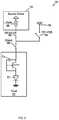
- FIG. 1is a diagram of an exemplary display system 10 .
- the display system 10includes a gate driver 12 , a source driver 14 , a digital controller 16 , a memory storage 18 , and display panel 20 .
- the display panel 20includes an array of pixels 22 arranged in rows and columns. Each of the pixels 22 is individually programmable to emit light with individually programmable luminance values.
- the controller 16receives digital data indicative of information to be displayed on the display panel 20 .
- the controller 16sends signals 32 to the source driver 14 and scheduling signals 34 to the gate driver 12 to drive the pixels 22 in the display panel 20 to display the information indicated.
- the plurality of pixels 22 associated with the display panel 20thus comprise a display array (“display screen”) adapted to dynamically display information according to the input digital data received by the controller 16 .
- the display screencan display, for example, video information from a stream of video data received by the controller 16 .
- the supply voltage 24can provide a constant power voltage or can be an adjustable voltage supply that is controlled by signals from the controller 116 .
- the display system 10can also incorporate features from a current source or sink (not shown) to provide biasing currents to the pixels 22 in the display panel 20 to thereby decrease programming time for the pixels 22 .
- the display system 10 in FIG. 1is illustrated with only four pixels 22 in the display panel 20 . It is understood that the display system 10 can be implemented with a display screen that includes an array of similar pixels, such as the pixels 22 , and that the display screen is not limited to a particular number of rows and columns of pixels. For example, the display system 10 can be implemented with a display screen with a number of rows and columns of pixels commonly available in displays for mobile devices, monitor-based devices, and/or projection-devices.
- the pixel 22is operated by a driving circuit (“pixel circuit”) that generally includes a driving transistor and a light emitting device.
- pixel circuitcan optionally be an organic light emitting diode, but implementations of the present disclosure apply to pixel circuits having other electroluminescence devices, including current-driven light emitting devices.
- the driving transistor in the pixel 22can optionally be an n-type or p-type amorphous silicon thin-film transistor, but implementations of the present disclosure are not limited to pixel circuits having a particular polarity of transistor or only to pixel circuits having thin-film transistors.
- the pixel circuit 22can also include a storage capacitor for storing programming information and allowing the pixel circuit 22 to drive the light emitting device after being addressed.
- the display panel 20can be an active matrix display array.
- the pixel 22 illustrated as the top-left pixel in the display panel 20is coupled to a power enable (PE) signal line 40 , measurement (MEAS) signal line 42 , a supply line 26 i , a data line 23 j , and an enable measurement (EM) signal line 44 i .
- the supply line 26 imay be charged with VDD.
- the top-left pixel 22 in the display panel 20can correspond a pixel in the display panel in a “ith” row and “jth” column of the display panel 20 .
- the top-right pixel 22 in the display panel 20represents a “jth” row and “mth” column; the bottom-left pixel 22 represents an “nth” row and “jth” column; and the bottom-right pixel 22 represents an “nth” row and “mth” column.
- Each of the pixels 22is coupled to the PE signal line 40 , MEAS signal line 42 ; along with the appropriate supply lines (e.g., the supply lines 26 i and 26 n ), data lines (e.g., the data lines 23 j and 23 m ), and EM signal lines (e.g., the EM signal lines 44 i and 44 n ). It is noted that aspects of the present disclosure apply to pixels having additional connections, such as connections to a select line.
- PE signal line 40 and MEAS signal line 42are provided by the gate driver 12 , and can be utilized to enable, for example, a programming operation of the pixel 22 by activating a switch or transistor to allow the data line 23 j to program the pixel 22 .
- the data line 23 jconveys programming information from the source driver 14 to the pixel 22 .
- the data line 23 jcan be utilized to apply a programming voltage or a programming current to the pixel 22 in order to program the pixel 22 to emit a desired amount of luminance.
- the programming voltage (or programming current) supplied by the source driver 14 via the data line 23 jis a voltage (or current) appropriate to cause the pixel 22 to emit light with a desired amount of luminance according to the digital data received by the controller 16 .
- the programming voltage (or programming current)can be applied to the pixel 22 during a programming operation of the pixel 22 so as to charge a storage device within the pixel 22 , such as a storage capacitor, thereby enabling the pixel 22 to emit light with the desired amount of luminance during an emission operation following the programming operation.
- the storage device in the pixel 22can be charged during a programming operation to apply a voltage to one or more of a gate or a source terminal of the driving transistor during the emission operation, thereby causing the driving transistor to convey the driving current through the light emitting device according to the voltage stored on the storage device.
- the driving current that is conveyed through the light emitting device by the driving transistor during the emission operation of the pixel 22is a current that is supplied by the supply line 26 i .
- the supply line 26 ican provide a positive supply voltage (e.g., the voltage commonly referred to in circuit design as “VDD”).
- the display system 10also includes a readout circuit 15 which is integrated with the source driver 14 .
- the data line 23 jconnects the pixel 22 to the readout circuit 15 .
- the data line 23 jallows the readout circuit 15 to measure a current associated with the pixel 22 and hereby extract information indicative of a degradation of the pixel 22 .
- Readout circuit 15converts the associated current to a corresponding voltage. This voltage is converted into a 10 to 16 bit digital code and is sent to the digital control 16 for further processing or compensation.
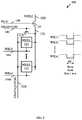
- FIG. 2is a circuit diagram of a simple individual driver circuit 50 which contains a pixel 22 , a source driver 14 and three switches controlling by MEAS 66 , EM 68 and PE 64 signal.
- the pixel 22 in FIG. 2include a drive transistor T 1 coupled to an organic light emitting device D 1 and a storage capacitor C s for storing programming information and allowing the pixel circuit 22 to drive the light emitting device after being addressed.
- circuit 50is in programming mode.
- the driver circuit 50includes a drive transistor T 1 coupled to an organic light emitting device D 1 , a storage capacitor C s for storing programming information and a source driver 14 and three switches controlling by MEAS 66 , EM 68 and PE 64 signal.
- the organic light emitting device D 1is a luminous organic material which is activated by current flow and whose brightness is a function of the magnitude of the current.
- a supply voltage input 54is coupled to the drain of the drive transistor T 1 . The supply voltage input 54 in conjunction with the drive transistor T 1 supplies current to the light emitting device D 1 .
- the current levelmay be controlled via the source driver 14 in FIG. 1 .
- the drive transistor T 1is a thin film transistor fabricated from hydrogenated amorphous silicon.
- LTPS-TFTlow-temperature polycrystalline-silicon thin-film transistor
- Other circuit componentssuch as capacitors and transistors (not shown) may be added to the simple driver circuit 50 to allow the pixel to operate with various enable, select and control signals such as those input by the gate driver 12 in FIG. 1 . Such components are used for faster programming of the pixels, holding the programming of the pixel during different frames and other functions.
- the gate of the drive transistor T 1is charged to a voltage where the transistor T 1 generates a corresponding current to flow through the organic light emitting device (OLED) D 1 , creating the required brightness.
- the voltage at the gate of the transistor T 1can be either created by direct charging of the node with a voltage or self-adjusted with an external current.
- rows of pixels 22are selected on a row by row basis.
- the datais converted to data current, referred to as I_DATA 56 and flows into pixel.
- This data current 56generates a Vgs voltage in T 1 transistor which is stored in C s capacitor.
- the voltage stored in C s capacitorgenerated a current in T 1 transistor which is equal to I_DATA 56 .
- FIG. 3is the circuit diagram of the simple individual driver circuit 50 as illustrated in FIG. 2 when in measurement mode.
- the pixel current, I_Pixel, 70flows into source driver 14 and is measured by a Readout Circuit (ROC) 15 .
- the ROC 15measures the pixel current 70 and converts it to a correspondence voltage. This voltage is converted to 10 to 16 bit digital code and is sent to digital processor to be used for further processing or compensation.
- Pixel current, I_Pixel, 70which is equal to the data current, I_Data, 56 flows into pixel 22 and OLED D 1 has a luminance correspondence to the Pixel current 70 .
- FIG. 5is the circuit diagram of the simple individual driver circuit 50 as illustrated in FIG. 2 when in programming mode but when the programming is directed toward another row.
- the programmingis performed on a row by row basis. The results in only one row of pixels 22 , i.e. the “ith” row, being connected to source driver 14 while the remaining rows of pixels 22 , i.e. the “jth” row, are off with no pixel current 70 .
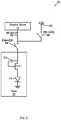
- FIG. 6is a diagram of an exemplary display system 100 .
- the display system 100includes a gate driver 112 , a source driver 114 , a digital controller 116 , a memory storage 118 , and display panel 120 and two TFT transistors 119 working as switches for each column.
- the display panel 120includes an array of pixels 122 arranged in rows and columns. Each of the pixels 122 is individually programmable to emit light with individually programmable luminance values.
- the controller 116receives digital data indicative of information to be displayed on the display panel 120 .
- the controller 116sends signals 132 to the source driver 114 and scheduling signals 134 to the gate driver 112 to drive the pixels 122 in the display panel 120 to display the information indicated.
- the plurality of pixels 122 associated with the display panel 120thus comprise a display array (“display screen”) adapted to dynamically display information according to the input digital data received by the controller 116 .
- the display screencan display, for example, video information from a stream of video data received by the controller 116 .
- the supply voltage 124can provide a constant power voltage or can be an adjustable voltage supply that is controlled by signals from the controller 116 .
- the display system 100 in FIG. 6is illustrated with only four pixels 122 in the display panel 120 . It is understood that the display system 100 can be implemented with a display screen that includes an array of similar pixels, such as the pixels 122 , and that the display screen is not limited to a particular number of rows and columns of pixels. For example, the display system 100 can be implemented with a display screen with a number of rows and columns of pixels commonly available in displays for mobile devices, monitor-based devices, and/or projection-devices.
- the pixel 122is operated by a driving circuit (“pixel circuit”) that generally includes a driving transistor and a light emitting device.
- the pixel 122may refer to the pixel circuit.
- the light emitting devicecan optionally be an organic light emitting diode (OLED), but implementations of the present disclosure apply to pixel circuits having other electroluminescence devices, including current-driven light emitting devices.
- the driving transistor in the pixel 122can optionally be an n-type or p-type amorphous silicon thin-film transistor, but implementations of the present disclosure are not limited to pixel circuits having a particular polarity of transistor or only to pixel circuits having thin-film transistors.
- the pixel circuit 122can also include a storage capacitor for storing programming information and allowing the pixel circuit 122 to drive the light emitting device after being addressed.
- the display panel 120can be an active matrix display array.
- the pixel 122 illustrated as the top-left pixel in the display panel 120is coupled to a power enable (PE) signal line 140 , measurement (MEAS) signal line 142 , a supply line 126 j , a data line 123 j , and a write (WR) signal line 144 i .
- the supply line 126 jmay be charged with VDD.
- the top-left pixel 122 in the display panel 120can correspond a pixel in the display panel in an “ith” row and “jth” column of the display panel 120 .
- the top-right pixel 122 in the display panel 120represents an “ith” row and “mth” column; the bottom-left pixel 122 represents an “nth” row and “jth” column; and the bottom-right pixel 122 represents an “nth” row and “mth” column.
- Each of the pixels columnsis connected to two TFTs 119 .
- One TFT 119is coupled between the data line ( 123 j and 123 m ) and pixel supply voltage line ( 1211 and 121 m ) and is controlled by the PE signal line 140 .
- the second TFTis coupled between pixel supply voltage line ( 121 j and 121 m ) and supply voltage line ( 126 j and 126 m ) and is controlled by the MEAS signal line 142 ;
- the display panel 120is also coupled with the appropriate supply lines (e.g., the supply lines 126 j and 126 m ), data lines (e.g., the data lines 123 j and 123 m ), and write WR signal lines (e.g., the WR signal lines 144 i and 144 n ). It is noted that aspects of the present disclosure apply to pixels having additional connections, such as connections to a select line or monitor line.
- PE signal line 140 , MEAS signal line 42 and W 1 R ( 144 i and 144 n ) write signalare provided by the gate driver 1121 and can be utilized to enable, for example, a programming operation of the pixel 122 by activating TFT transistors 119 and other switches or transistors in pixel 122 to allow the data line 123 j to program the pixel 122 .
- the data line 123 jconveys programming information from the source driver 114 to the pixel 122 .
- the data line 123 jcan be utilized to apply a programming voltage or a programming current to the pixel 122 in order to program the pixel 122 to emit a desired amount of luminance.
- the programming voltage (or programming current) supplied by the source driver 114 via the data line 123 jis a voltage (or current) appropriate to cause the pixel 122 to emit light with a desired amount of luminance according to the digital data received by the controller 116 .
- the programming voltage (or programming current)can be applied to the pixel 122 during a programming operation of the pixel 122 so as to charge a storage device within the pixel 122 , such as a storage capacitor, thereby enabling the pixel 122 to emit light with the desired amount of luminance during an emission operation following the programming operation.
- the storage device in the pixel 122can be charged during a programming operation to apply a voltage to one or more of a gate or a source terminal of the driving transistor during the emission operation, thereby causing the driving transistor to convey the driving current through the light emitting device according to the voltage stored on the storage device.
- the driving current that is conveyed through the light emitting device by the driving transistor during the emission operation of the pixel 122is a current that is supplied by the supply line 126 j .
- the supply line 126 jcan provide a positive supply voltage (e.g., the voltage commonly referred to in circuit design as “VDD”).
- the display system 100also includes a readout circuit 115 which is integrated with the source driver 114 .
- the data line 123 jconnects the pixel 122 to the readout circuit 115 .
- the data line 123 jallows the readout circuit 115 to measure a current associated with the pixel 122 and hereby extract information indicative of a degradation of the pixel 122 .
- Readout circuit 115converts the associated current to a corresponding voltage. This voltage is converted into a 10 to 16 bit digital code and is sent to the digital control 116 for further processing or compensation.
- FIG. 7is a circuit diagram of a simple individual driver circuit 200 which contains a pixel 122 which is connected to supply voltage VDD 154 , a data voltage VDATA 156 and is controlled by the write WR signal 158 .
- the pixel 122 in FIG. 2includes a switch transistor T 2 , a drive transistor T 1 coupled to an organic light emitting device (OLED) D 1 , the switch transistor T 2 and a storage capacitor C s for storing programming information and allowing the pixel circuit 122 to drive the light emitting device after being addressed.
- OLEDorganic light emitting device
- FIG. 7when the write WR signal 158 goes low, it enables the transistor T 2 and the VDATA 156 is stored on the capacitor C s .
- each pixel 122 in the display panel 120 in FIG. 6is driven by the method shown in the driver circuit 200 in FIG. 7 .
- the driver circuit 200includes a switch transistor T 2 , a drive transistor T 1 coupled to an organic light emitting device (OLED) D 1 , a storage capacitor C s for storing programming information.
- VDATA 156 voltagecomes from the source driver 114 and is stored on the capacitor C s .
- the switch transistor T 2is controlled by WR 58 signal.
- the organic light emitting device (OLED) D 1is a luminous organic material which is activated by current flow and whose brightness is a function of the magnitude of the current.
- a supply voltage input 154is coupled to the source (or drain) of the drive transistor T 1 .
- the supply voltage input 154 in conjunction with the drive transistor T 1supplies current to the light emitting device D 1 .
- the drive transistor T 1is a thin film transistor fabricated from hydrogenated amorphous silicon.
- LTPS-TFTlow-temperature polycrystalline-silicon thin-film transistor
- Other circuit componentssuch as capacitors and transistors (not shown) may be added to the simple driver circuit 200 to allow the pixel to operate with various enable, select and control signals such as those input by the gate driver 112 in FIG. 6 . Such components are used for faster programming of the pixels, holding the programming of the pixel during different frames and other functions.
- the gate of the drive transistor T 1is charged to a voltage where the transistor T 1 generates a corresponding current to flow through the organic light emitting device (OLED) D 1 , creating the required brightness.
- the voltage at the gate of the transistor T 1can be either created by direct charging of the node with a voltage or self-adjusted with an external current.
- rows of pixels 122are selected on a row by row basis.
- the data VDATA( 123 j and 123 m ) as a voltage (or can be a current) is stored on the capacitors C s inside pixels 122 .
- This datagenerates a Vgs voltage in T 1 transistor which is stored in C s capacitor.
- FIG. 8is a block diagram of an embodiment of a column of pixel circuit (“jth” column) 300 in programming modes.
- the write signal WR[ 1 ]is set to zero, i.e.
- the write signal WR[ 1 ]0, and the row 1 is connected to the source driver 114 and the data VDATA[j] 123 j is stored in capacitor C s in pixel in the row 1 and the “jth” column.
- the leakage currentis measured.
- the datais programmed on the row i. Finally, the row i is selected and the pixel current is measured.
- FIG. 9is a block diagram of an embodiment of a column of pixel circuit (“jth” column) 400 in programming mode.
- data line VDATA 123 jhas the same voltage as supply voltage VDD 126 j .
- All pixels 122 in the circuit 400are in write mode 401 .
- All capacitors' voltagesare set to zero and OLED devices D 1 show black color. Alternatively all of the pixels can be driven to black one at a time sequentially similar to how the video is driven onto the panel.
- FIG. 10is a block diagram of an embodiment of a column of pixel circuit (“jth” column) 500 in measurement mode.
- the leakage currentis measured immediately after setting the capacitors' voltages of all pixels in the circuit 500 to zero.
- the circuit 500is disconnected from the supply voltage and connected to the data line, VDATA 123 j .
- the leakage current of the pixels 122 in “jth” column(the circuit 500 ), I Leakage 190 flows into the source driver 114 and is measured by a Readout Circuit (ROC) 115 .
- the ROC 115measures the leakage current (I Leakage ) 190 and converts it to a correspondence voltage. This voltage is converted to 10 to 16 bit digital code and is sent to digital processor to be used for further processing or compensation.
- FIG. 11is a block diagram of an embodiment of a column of pixel circuit (“jth” column) 600 in programming mode.
- the “ith” rowis programmed.
- the pixel 122 in “ith” rowis programmed to VDATA 123 j and a current corresponded to it flows into the pixel. No current except for the leakage current flow into other pixel 122 in “jth” column.
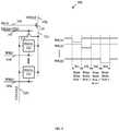
- FIG. 12is a block diagram of an embodiment of a column of pixel circuit (“jth” column) 700 in measurement mode.
- the pixel current of the “ith” row plus the leakage current of the other pixelsare measured in this mode.
- the circuit 700is disconnected from the supply voltage and connected to the data line, VDATA 123 j .
- the ROC 115measures the current 192 and converts it to a correspondence voltage. This voltage is converted to 10 to 16 bit digital code.
- step onethe data line is set to equal VDD and the capacitors' voltages inside pixels are set to zero.
- step twothe leakage current, I Leakage , 190 of the pixels is measured.
- step threethe “ith” row is selected and the data line VDATA 123 j is derived with lowest voltage. It causes the T 1 transistor inside the “ith” pixel 122 is pushed to the triode region and behaves like a switch.
- step fouras shown in FIG.
- the OLED D 1 of the “ith” pixel 122is connected to virtual ground 806 of an integrator 810 through the T 1 transistor inside the “ith” pixel 122 and the transistor 119 connected between the pixel supply voltage node 121 j and the data line 123 j and the switch 807 inside the ROC 115 .
- the OLED D 1 of the “ith” pixel 122will have the same voltage as the bias voltage V B 805 .
- the OLED current of the “ith” row pixel plus the leakage current of other pixels in “jth” column (the circuit 800 ), I Oled +I Leakage , 194flows into the source driver 114 and is measured by a ROC 115 .
- the ROC 115measures the current 194 and converts it to a correspondence voltage. This voltage is converted to 10 to 16 bit digital code 802 .
- the ROC 115 as shown in FIG. 13includes one switch 807 , an integrator 810 and an analog to digital converter (ADC) 801 .
- the integratorincludes a reset switch 808 , an integrating capacitor C I and a bias voltage V B 805 .
- the integratorintegrates the current coming from pixel 122 and converts it to a corresponding voltage. The voltage is converted to 10 to 16 bit digital code 802 by the ADC 801 .
Landscapes
- Engineering & Computer Science (AREA)
- Physics & Mathematics (AREA)
- General Physics & Mathematics (AREA)
- Computer Hardware Design (AREA)
- Theoretical Computer Science (AREA)
- Control Of Indicators Other Than Cathode Ray Tubes (AREA)
- Electroluminescent Light Sources (AREA)
Abstract
Description
Vgs=VDATA−VDD
IPixel=½k(VDATA−VDD−Vth)2
IPixel=½k(VDATA−VDD−Vth)2
Pixel current, Ipixel, flows into
IPixel=(current measured in step 4)−(current measured in step 2)
IPixel=(IPixel+ILeakage)−(ILeakage)
IOled=(current measured in step 4)−(current measured in step 2)
IOled=(IOled+ILeakage)−(ILeakage)
Claims (15)
Priority Applications (7)
| Application Number | Priority Date | Filing Date | Title |
|---|---|---|---|
| US16/028,073US10971078B2 (en) | 2018-02-12 | 2018-07-05 | Pixel measurement through data line |
| DE102019201746.0ADE102019201746A1 (en) | 2018-02-12 | 2019-02-11 | Pixel measurement via data line |
| CN202210358984.5ACN115273752A (en) | 2018-02-12 | 2019-02-12 | Method for determining a current flowing in a display system and display system |
| CN201910111102.3ACN110148378B (en) | 2018-02-12 | 2019-02-12 | Measure pixels through data lines |
| US17/205,639US11488541B2 (en) | 2018-02-12 | 2021-03-18 | Pixel measurement through data line |
| US17/952,781US11847976B2 (en) | 2018-02-12 | 2022-09-26 | Pixel measurement through data line |
| US18/503,373US20240071320A1 (en) | 2018-02-12 | 2023-11-07 | Pixel measurement through data line |
Applications Claiming Priority (3)
| Application Number | Priority Date | Filing Date | Title |
|---|---|---|---|
| US201862629450P | 2018-02-12 | 2018-02-12 | |
| US201815968134A | 2018-05-01 | 2018-05-01 | |
| US16/028,073US10971078B2 (en) | 2018-02-12 | 2018-07-05 | Pixel measurement through data line |
Related Parent Applications (1)
| Application Number | Title | Priority Date | Filing Date |
|---|---|---|---|
| US201815968134AContinuation-In-Part | 2018-02-12 | 2018-05-01 |
Related Child Applications (1)
| Application Number | Title | Priority Date | Filing Date |
|---|---|---|---|
| US17/205,639ContinuationUS11488541B2 (en) | 2018-02-12 | 2021-03-18 | Pixel measurement through data line |
Publications (2)
| Publication Number | Publication Date |
|---|---|
| US20190251909A1 US20190251909A1 (en) | 2019-08-15 |
| US10971078B2true US10971078B2 (en) | 2021-04-06 |
Family
ID=67399856
Family Applications (4)
| Application Number | Title | Priority Date | Filing Date |
|---|---|---|---|
| US16/028,073Active2038-05-08US10971078B2 (en) | 2018-02-12 | 2018-07-05 | Pixel measurement through data line |
| US17/205,639ActiveUS11488541B2 (en) | 2018-02-12 | 2021-03-18 | Pixel measurement through data line |
| US17/952,781ActiveUS11847976B2 (en) | 2018-02-12 | 2022-09-26 | Pixel measurement through data line |
| US18/503,373AbandonedUS20240071320A1 (en) | 2018-02-12 | 2023-11-07 | Pixel measurement through data line |
Family Applications After (3)
| Application Number | Title | Priority Date | Filing Date |
|---|---|---|---|
| US17/205,639ActiveUS11488541B2 (en) | 2018-02-12 | 2021-03-18 | Pixel measurement through data line |
| US17/952,781ActiveUS11847976B2 (en) | 2018-02-12 | 2022-09-26 | Pixel measurement through data line |
| US18/503,373AbandonedUS20240071320A1 (en) | 2018-02-12 | 2023-11-07 | Pixel measurement through data line |
Country Status (3)
| Country | Link |
|---|---|
| US (4) | US10971078B2 (en) |
| CN (2) | CN110148378B (en) |
| DE (1) | DE102019201746A1 (en) |
Cited By (1)
| Publication number | Priority date | Publication date | Assignee | Title |
|---|---|---|---|---|
| US20250182687A1 (en)* | 2023-12-05 | 2025-06-05 | Samsung Display Co., Ltd. | Pixel and display device including the same |
Families Citing this family (3)
| Publication number | Priority date | Publication date | Assignee | Title |
|---|---|---|---|---|
| US11513405B2 (en)* | 2018-04-26 | 2022-11-29 | Semiconductor Energy Laboratory Co., Ltd. | Display device and electronic device |
| US10984712B2 (en)* | 2018-12-10 | 2021-04-20 | Sharp Kabushiki Kaisha | TFT pixel circuit for OLED external compensation using an adjusted data voltage for component compensation |
| CN114299872B (en)* | 2022-01-04 | 2023-07-18 | 京东方科技集团股份有限公司 | A driving circuit, its driving method, and a display device |
Citations (392)
| Publication number | Priority date | Publication date | Assignee | Title |
|---|---|---|---|---|
| US4354162A (en) | 1981-02-09 | 1982-10-12 | National Semiconductor Corporation | Wide dynamic range control amplifier with offset correction |
| US4758831A (en) | 1984-11-05 | 1988-07-19 | Kabushiki Kaisha Toshiba | Matrix-addressed display device |
| GB2205431A (en) | 1986-09-27 | 1988-12-07 | Junichi Nishizawa | Color display device |
| US4963860A (en) | 1988-02-01 | 1990-10-16 | General Electric Company | Integrated matrix display circuitry |
| US4975691A (en) | 1987-06-16 | 1990-12-04 | Interstate Electronics Corporation | Scan inversion symmetric drive |
| US4996523A (en) | 1988-10-20 | 1991-02-26 | Eastman Kodak Company | Electroluminescent storage display with improved intensity driver circuits |
| US5051739A (en) | 1986-05-13 | 1991-09-24 | Sanyo Electric Co., Ltd. | Driving circuit for an image display apparatus with improved yield and performance |
| CA1294034C (en) | 1985-01-09 | 1992-01-07 | Hiromu Hosokawa | Color uniformity compensation apparatus for cathode ray tubes |
| CA2109951A1 (en) | 1991-05-24 | 1992-11-26 | Robert Hotto | Dc integrating display driver employing pixel status memories |
| US5222082A (en) | 1991-02-28 | 1993-06-22 | Thomson Consumer Electronics, S.A. | Shift register useful as a select line scanner for liquid crystal display |
| US5266515A (en) | 1992-03-02 | 1993-11-30 | Motorola, Inc. | Fabricating dual gate thin film transistors |
| WO1994025954A1 (en) | 1993-04-30 | 1994-11-10 | Prime View Hk Limited | Apparatus for recovery of threshold voltage shift in amorphous silicon thin-film transistor device |
| US5498880A (en) | 1995-01-12 | 1996-03-12 | E. I. Du Pont De Nemours And Company | Image capture panel using a solid state device |
| US5589847A (en) | 1991-09-23 | 1996-12-31 | Xerox Corporation | Switched capacitor analog circuits using polysilicon thin film technology |
| JPH0990405A (en) | 1995-09-21 | 1997-04-04 | Sharp Corp | Thin film transistor |
| US5619033A (en) | 1995-06-07 | 1997-04-08 | Xerox Corporation | Layered solid state photodiode sensor array |
| US5648276A (en) | 1993-05-27 | 1997-07-15 | Sony Corporation | Method and apparatus for fabricating a thin film semiconductor device |
| US5670973A (en) | 1993-04-05 | 1997-09-23 | Cirrus Logic, Inc. | Method and apparatus for compensating crosstalk in liquid crystal displays |
| US5684365A (en) | 1994-12-14 | 1997-11-04 | Eastman Kodak Company | TFT-el display panel using organic electroluminescent media |
| US5686935A (en) | 1995-03-06 | 1997-11-11 | Thomson Consumer Electronics, S.A. | Data line drivers with column initialization transistor |
| US5712653A (en) | 1993-12-27 | 1998-01-27 | Sharp Kabushiki Kaisha | Image display scanning circuit with outputs from sequentially switched pulse signals |
| US5714968A (en) | 1994-08-09 | 1998-02-03 | Nec Corporation | Current-dependent light-emitting element drive circuit for use in active matrix display device |
| US5747928A (en) | 1994-10-07 | 1998-05-05 | Iowa State University Research Foundation, Inc. | Flexible panel display having thin film transistors driving polymer light-emitting diodes |
| US5748160A (en) | 1995-08-21 | 1998-05-05 | Mororola, Inc. | Active driven LED matrices |
| JPH10153759A (en) | 1996-11-26 | 1998-06-09 | Matsushita Electric Ind Co Ltd | Liquid crystal display |
| US5784042A (en) | 1991-03-19 | 1998-07-21 | Hitachi, Ltd. | Liquid crystal display device and method for driving the same |
| CA2249592A1 (en) | 1997-01-28 | 1998-07-30 | Casio Computer Co., Ltd. | Active matrix electroluminescent display device and a driving method thereof |
| US5790234A (en) | 1995-12-27 | 1998-08-04 | Canon Kabushiki Kaisha | Eyeball detection apparatus |
| JPH10254410A (en) | 1997-03-12 | 1998-09-25 | Pioneer Electron Corp | Organic electroluminescent display device, and driving method therefor |
| US5815303A (en) | 1997-06-26 | 1998-09-29 | Xerox Corporation | Fault tolerant projective display having redundant light modulators |
| US5870071A (en) | 1995-09-07 | 1999-02-09 | Frontec Incorporated | LCD gate line drive circuit |
| US5874803A (en) | 1997-09-09 | 1999-02-23 | The Trustees Of Princeton University | Light emitting device with stack of OLEDS and phosphor downconverter |
| US5880582A (en) | 1996-09-04 | 1999-03-09 | Sumitomo Electric Industries, Ltd. | Current mirror circuit and reference voltage generating and light emitting element driving circuits using the same |
| US5899461A (en) | 1996-01-29 | 1999-05-04 | Nok Corporation | Sealing apparatus |
| US5903248A (en) | 1997-04-11 | 1999-05-11 | Spatialight, Inc. | Active matrix display having pixel driving circuits with integrated charge pumps |
| US5917280A (en) | 1997-02-03 | 1999-06-29 | The Trustees Of Princeton University | Stacked organic light emitting devices |
| US5923794A (en) | 1996-02-06 | 1999-07-13 | Polaroid Corporation | Current-mediated active-pixel image sensing device with current reset |
| JPH11231805A (en) | 1998-02-10 | 1999-08-27 | Sanyo Electric Co Ltd | Display device |
| EP0940796A1 (en) | 1997-08-21 | 1999-09-08 | Seiko Epson Corporation | Active matrix display |
| US5952789A (en) | 1997-04-14 | 1999-09-14 | Sarnoff Corporation | Active matrix organic light emitting diode (amoled) display pixel structure and data load/illuminate circuit therefor |
| WO1999048079A1 (en) | 1998-03-19 | 1999-09-23 | Holloman Charles J | Analog driver for led or similar display element |
| JPH11282419A (en) | 1998-03-31 | 1999-10-15 | Nec Corp | Element driving device and method and image display device |
| US6023259A (en) | 1997-07-11 | 2000-02-08 | Fed Corporation | OLED active matrix using a single transistor current mode pixel design |
| JP2000056847A (en) | 1998-08-14 | 2000-02-25 | Nec Corp | Constant current driving circuit |
| JP2000077192A (en) | 1998-09-01 | 2000-03-14 | Pioneer Electronic Corp | Organic electroluminescent panel and manufacture thereof |
| JP2000089198A (en) | 1998-09-11 | 2000-03-31 | Seiko Epson Corp | Compensation method for liquid crystal applied voltage of liquid crystal display device, liquid crystal display device, electronic device, and voltage detection method for liquid crystal layer |
| CA2242720C (en) | 1998-07-09 | 2000-05-16 | Ibm Canada Limited-Ibm Canada Limitee | Programmable led driver |
| US6069365A (en) | 1997-11-25 | 2000-05-30 | Alan Y. Chow | Optical processor based imaging system |
| CA2354018A1 (en) | 1998-12-14 | 2000-06-22 | Alan Richard | Portable microdisplay system |
| US6081131A (en) | 1997-11-12 | 2000-06-27 | Seiko Epson Corporation | Logical amplitude level conversion circuit, liquid crystal device and electronic apparatus |
| EP1028471A2 (en) | 1999-02-09 | 2000-08-16 | SANYO ELECTRIC Co., Ltd. | Electroluminescence display device |
| US6157583A (en) | 1999-03-02 | 2000-12-05 | Motorola, Inc. | Integrated circuit memory having a fuse detect circuit and method therefor |
| JP2000352941A (en) | 1999-06-14 | 2000-12-19 | Sony Corp | Display device |
| US6166489A (en) | 1998-09-15 | 2000-12-26 | The Trustees Of Princeton University | Light emitting device using dual light emitting stacks to achieve full-color emission |
| US6177915B1 (en) | 1990-06-11 | 2001-01-23 | International Business Machines Corporation | Display system having section brightness control and method of operating system |
| WO2001027910A1 (en) | 1999-10-12 | 2001-04-19 | Koninklijke Philips Electronics N.V. | Led display device |
| US6225846B1 (en) | 1997-01-23 | 2001-05-01 | Mitsubishi Denki Kabushiki Kaisha | Body voltage controlled semiconductor integrated circuit |
| US6229508B1 (en) | 1997-09-29 | 2001-05-08 | Sarnoff Corporation | Active matrix light emitting diode pixel structure and concomitant method |
| US6232939B1 (en) | 1997-11-10 | 2001-05-15 | Hitachi, Ltd. | Liquid crystal display apparatus including scanning circuit having bidirectional shift register stages |
| EP1103947A2 (en) | 1999-11-29 | 2001-05-30 | Sel Semiconductor Energy Laboratory Co., Ltd. | EL display device and electronic apparatus |
| US20010002703A1 (en) | 1999-11-30 | 2001-06-07 | Jun Koyama | Electric device |
| US6246180B1 (en) | 1999-01-29 | 2001-06-12 | Nec Corporation | Organic el display device having an improved image quality |
| US20010004190A1 (en) | 1999-12-15 | 2001-06-21 | Semiconductor Energy Laboratory Co., Ltd. | EL disply device |
| US6252248B1 (en) | 1998-06-08 | 2001-06-26 | Sanyo Electric Co., Ltd. | Thin film transistor and display |
| US6259424B1 (en) | 1998-03-04 | 2001-07-10 | Victor Company Of Japan, Ltd. | Display matrix substrate, production method of the same and display matrix circuit |
| US6274887B1 (en) | 1998-11-02 | 2001-08-14 | Semiconductor Energy Laboratory Co., Ltd. | Semiconductor device and manufacturing method therefor |
| US20010013806A1 (en) | 2000-02-15 | 2001-08-16 | Hiromi Notani | Semiconductor integrated circuit |
| US20010015653A1 (en) | 2000-02-23 | 2001-08-23 | U.S. Philips Corporation. | Integrated circuit with test interface |
| EP1130565A1 (en) | 1999-07-14 | 2001-09-05 | Sony Corporation | Current drive circuit and display comprising the same, pixel circuit, and drive method |
| US20010020926A1 (en) | 2000-02-15 | 2001-09-13 | Kuijk Karel Elbert | Display device |
| US20010026179A1 (en) | 2000-03-24 | 2001-10-04 | Takanori Saeki | Clock control circuit and clock control method |
| US20010026127A1 (en) | 1998-02-27 | 2001-10-04 | Kiyoshi Yoneda | Color display apparatus having electroluminescence elements |
| US20010026257A1 (en) | 2000-03-27 | 2001-10-04 | Hajime Kimura | Electro-optical device |
| US6300928B1 (en) | 1997-08-09 | 2001-10-09 | Lg Electronics Inc. | Scanning circuit for driving liquid crystal display |
| US6303963B1 (en) | 1998-12-03 | 2001-10-16 | Semiconductor Energy Laboratory Co., Ltd. | Electro-optical device and semiconductor circuit |
| US20010030323A1 (en) | 2000-03-29 | 2001-10-18 | Sony Corporation | Thin film semiconductor apparatus and method for driving the same |
| US6306694B1 (en) | 1999-03-12 | 2001-10-23 | Semiconductor Energy Laboratory Co., Ltd. | Process of fabricating a semiconductor device |
| US6307322B1 (en) | 1999-12-28 | 2001-10-23 | Sarnoff Corporation | Thin-film transistor circuitry with reduced sensitivity to variance in transistor threshold voltage |
| US20010033199A1 (en) | 2000-02-07 | 2001-10-25 | Yuuichi Aoki | Variable-gain circuit |
| US20010038098A1 (en) | 2000-02-29 | 2001-11-08 | Shunpei Yamazaki | Light-emitting device |
| US6316786B1 (en) | 1998-08-29 | 2001-11-13 | International Business Machines Corporation | Organic opto-electronic devices |
| US6320325B1 (en) | 2000-11-06 | 2001-11-20 | Eastman Kodak Company | Emissive display with luminance feedback from a representative pixel |
| US20010043173A1 (en) | 1997-09-04 | 2001-11-22 | Ronald Roy Troutman | Field sequential gray in active matrix led display using complementary transistor pixel circuits |
| US6323832B1 (en) | 1986-09-27 | 2001-11-27 | Junichi Nishizawa | Color display device |
| US6323631B1 (en) | 2001-01-18 | 2001-11-27 | Sunplus Technology Co., Ltd. | Constant current driver with auto-clamped pre-charge function |
| US20010045929A1 (en) | 2000-01-21 | 2001-11-29 | Prache Olivier F. | Gray scale pixel driver for electronic display and method of operation therefor |
| US20010052606A1 (en) | 2000-05-22 | 2001-12-20 | Koninklijke Philips Electronics N.V. | Display device |
| US20010052898A1 (en) | 2000-02-01 | 2001-12-20 | Semiconductor Energy Laboratory Co., Ltd. | Semiconductor display device and method of driving the same |
| US20020000576A1 (en) | 2000-06-22 | 2002-01-03 | Kazutaka Inukai | Display device |
| US20020011981A1 (en) | 2000-07-20 | 2002-01-31 | Koninklijke Philips Electronics N.V. | Display device |
| US20020011799A1 (en) | 2000-04-06 | 2002-01-31 | Semiconductor Energy Laboratory Co., Ltd. | Electronic device and driving method |
| US20020011796A1 (en) | 2000-05-08 | 2002-01-31 | Semiconductor Energy Laboratory Co., Ltd. | Light-emitting device, and electric device using the same |
| US6345085B1 (en) | 1999-11-05 | 2002-02-05 | Lg. Philips Lcd Co., Ltd. | Shift register |
| US20020015032A1 (en) | 2000-07-25 | 2002-02-07 | Jun Koyama | Driver circuit of a display device |
| US20020015031A1 (en) | 2000-07-24 | 2002-02-07 | Seiko Epson Corporation | Electro-optical panel, method for driving the same, electrooptical device, and electronic equipment |
| US6348835B1 (en) | 1999-05-27 | 2002-02-19 | Nec Corporation | Semiconductor device with constant current source circuit not influenced by noise |
| EP1184833A2 (en) | 2000-09-04 | 2002-03-06 | Sel Semiconductor Energy Laboratory Co., Ltd. | Method of driving EL display device |
| US20020030528A1 (en) | 2000-06-14 | 2002-03-14 | Shoichiro Matsumoto | Level shifter for use in active matrix display apparatus |
| US20020030647A1 (en) | 2000-06-06 | 2002-03-14 | Michael Hack | Uniform active matrix oled displays |
| JP2002091376A (en) | 2000-06-27 | 2002-03-27 | Hitachi Ltd | Image display device and driving method thereof |
| US6365917B1 (en) | 1998-11-25 | 2002-04-02 | Semiconductor Energy Laboratory Co., Ltd. | Semiconductor device |
| EP1194013A1 (en) | 2000-09-29 | 2002-04-03 | Eastman Kodak Company | A flat-panel display with luminance feedback |
| US20020048829A1 (en) | 2000-04-19 | 2002-04-25 | Shunpei Yamazaki | Light emitting device and fabricating method thereof |
| US20020050795A1 (en) | 2000-10-27 | 2002-05-02 | Nec Corporation | Active matrix organic el display device and method of forming the same |
| US6384427B1 (en) | 1999-10-29 | 2002-05-07 | Semiconductor Energy Laboratory Co., Ltd. | Electronic device |
| US20020053401A1 (en) | 2000-10-31 | 2002-05-09 | Nobuyuki Ishikawa | Organic luminescence display device and process for production thereof |
| US6392617B1 (en) | 1999-10-27 | 2002-05-21 | Agilent Technologies, Inc. | Active matrix light emitting diode display |
| US6399988B1 (en) | 1999-03-26 | 2002-06-04 | Semiconductor Energy Laboratory Co., Ltd. | Thin film transistor having lightly doped regions |
| US20020070909A1 (en) | 2000-11-22 | 2002-06-13 | Mitsuru Asano | Active matrix type display apparatus |
| US20020080108A1 (en) | 2000-12-26 | 2002-06-27 | Hannstar Display Corp. | Gate lines driving circuit and driving method |
| US6414661B1 (en) | 2000-02-22 | 2002-07-02 | Sarnoff Corporation | Method and apparatus for calibrating display devices and automatically compensating for loss in their efficiency over time |
| US20020084463A1 (en) | 2001-01-04 | 2002-07-04 | International Business Machines Corporation | Low-power organic light emitting diode pixel circuit |
| US6420988B1 (en) | 1998-12-03 | 2002-07-16 | Semiconductor Energy Laboratory Co., Ltd. | Digital analog converter and electronic device using the same |
| US6420758B1 (en) | 1998-11-17 | 2002-07-16 | Semiconductor Energy Laboratory Co., Ltd. | Semiconductor device having an impurity region overlapping a gate electrode |
| US6420834B2 (en) | 2000-03-27 | 2002-07-16 | Semiconductor Energy Laboratory Co., Ltd. | Light emitting device and a method of manufacturing the same |
| US20020101172A1 (en) | 2001-01-02 | 2002-08-01 | Bu Lin-Kai | Oled active driving system with current feedback |
| US20020101433A1 (en) | 1996-12-19 | 2002-08-01 | Mcknight Douglas | Display system having electrode modulation to alter a state of an electro-optic layer |
| CA2436451A1 (en) | 2001-02-05 | 2002-08-15 | International Business Machines Corporation | Liquid crystal display device |
| US20020113248A1 (en) | 2001-02-19 | 2002-08-22 | Semiconductor Energy Laboratory Co., Ltd. | Light emitting device and method of manufacturing the same |
| CA2438577A1 (en) | 2001-02-16 | 2002-08-29 | Ignis Innovation Inc. | Pixel current driver for organic light emitting diode displays |
| WO2002067327A2 (en) | 2001-02-16 | 2002-08-29 | Ignis Innovation Inc. | Pixel current driver for organic light emitting diode displays |
| US6445376B2 (en) | 1997-09-12 | 2002-09-03 | Sean T. Parrish | Alternative power for a portable computer via solar cells |
| US20020122308A1 (en) | 2001-03-05 | 2002-09-05 | Fuji Xerox Co., Ltd. | Apparatus for driving light emitting element and system for driving light emitting element |
| TW502233B (en) | 1999-06-17 | 2002-09-11 | Sony Corp | Image display apparatus |
| US20020130686A1 (en) | 2001-03-14 | 2002-09-19 | Micron Technology, Inc. | CMOS gate array with vertical transistors |
| JP2002268576A (en) | 2000-12-05 | 2002-09-20 | Matsushita Electric Ind Co Ltd | Image display device, method of manufacturing image display device, and image display driver IC |
| JP2002278513A (en) | 2001-03-19 | 2002-09-27 | Sharp Corp | Electro-optical device |
| US6468638B2 (en) | 1999-03-16 | 2002-10-22 | Alien Technology Corporation | Web process interconnect in electronic assemblies |
| US20020154084A1 (en) | 2000-06-16 | 2002-10-24 | Yukio Tanaka | Active matrix display device, its driving method, and display element |
| US20020158823A1 (en) | 1997-10-31 | 2002-10-31 | Matthew Zavracky | Portable microdisplay system |
| US20020167471A1 (en) | 2001-05-09 | 2002-11-14 | Everitt James W. | System for providing pulse amplitude modulation for oled display drivers |
| JP2002333862A (en) | 2001-02-21 | 2002-11-22 | Semiconductor Energy Lab Co Ltd | Light emission device and electronic equipment |
| US6489952B1 (en) | 1998-11-17 | 2002-12-03 | Semiconductor Energy Laboratory Co., Ltd. | Active matrix type semiconductor display device |
| US20020180369A1 (en) | 2001-02-21 | 2002-12-05 | Jun Koyama | Light emitting device and electronic appliance |
| US20020180721A1 (en) | 1997-03-12 | 2002-12-05 | Mutsumi Kimura | Pixel circuit display apparatus and electronic apparatus equipped with current driving type light-emitting device |
| US20020186214A1 (en) | 2001-06-05 | 2002-12-12 | Eastman Kodak Company | Method for saving power in an organic electroluminescent display using white light emitting elements |
| US20020190924A1 (en) | 2001-01-19 | 2002-12-19 | Mitsuru Asano | Active matrix display |
| US20020190332A1 (en) | 2001-06-15 | 2002-12-19 | Lg Electronics Inc. | Thin film transistor, and organic EL display thereof and method for fabricating the same |
| US20020190971A1 (en) | 2001-04-27 | 2002-12-19 | Kabushiki Kaisha Toshiba | Display apparatus, digital-to-analog conversion circuit and digital-to-analog conversion method |
| US20020195968A1 (en) | 2001-06-22 | 2002-12-26 | International Business Machines Corporation | Oled current drive pixel circuit |
| US20020195967A1 (en) | 2001-06-22 | 2002-12-26 | Kim Sung Ki | Electro-luminescence panel |
| US6501466B1 (en) | 1999-11-18 | 2002-12-31 | Sony Corporation | Active matrix type display apparatus and drive circuit thereof |
| US6501098B2 (en) | 1998-11-25 | 2002-12-31 | Semiconductor Energy Laboratory Co, Ltd. | Semiconductor device |
| JP2003022035A (en) | 2001-07-10 | 2003-01-24 | Sharp Corp | Organic EL panel and manufacturing method thereof |
| US6512271B1 (en) | 1998-11-16 | 2003-01-28 | Semiconductor Energy Laboratory Co., Ltd. | Semiconductor device |
| US20030020413A1 (en) | 2001-07-27 | 2003-01-30 | Masanobu Oomura | Active matrix display |
| US6518594B1 (en) | 1998-11-16 | 2003-02-11 | Semiconductor Energy Laboratory Co., Ltd. | Semiconductor devices |
| US20030030603A1 (en) | 2001-08-09 | 2003-02-13 | Nec Corporation | Drive circuit for display device |
| US6524895B2 (en) | 1998-12-25 | 2003-02-25 | Semiconductor Energy Laboratory Co., Ltd. | Semiconductor device and method of fabricating the same |
| US6531713B1 (en) | 1999-03-19 | 2003-03-11 | Semiconductor Energy Laboratory Co., Ltd. | Electro-optical device and manufacturing method thereof |
| JP2003076331A (en) | 2001-08-31 | 2003-03-14 | Seiko Epson Corp | Display device and electronic equipment |
| US20030062524A1 (en) | 2001-08-29 | 2003-04-03 | Hajime Kimura | Light emitting device, method of driving a light emitting device, element substrate, and electronic equipment |
| US20030071804A1 (en) | 2001-09-28 | 2003-04-17 | Semiconductor Energy Laboratory Co., Ltd. | Light emitting device and electronic apparatus using the same |
| US20030071821A1 (en) | 2001-10-11 | 2003-04-17 | Sundahl Robert C. | Luminance compensation for emissive displays |
| WO2003034389A2 (en) | 2001-10-19 | 2003-04-24 | Clare Micronix Integrated Systems, Inc. | System and method for providing pulse amplitude modulation for oled display drivers |
| US20030076048A1 (en) | 2001-10-23 | 2003-04-24 | Rutherford James C. | Organic electroluminescent display device driving method and apparatus |
| US6559594B2 (en) | 2000-02-03 | 2003-05-06 | Semiconductor Energy Laboratory Co., Ltd. | Light-emitting device |
| EP1310939A2 (en) | 2001-09-28 | 2003-05-14 | Sel Semiconductor Energy Laboratory Co., Ltd. | A light emitting device and electronic apparatus using the same |
| US20030090447A1 (en) | 2001-09-21 | 2003-05-15 | Hajime Kimura | Display device and driving method thereof |
| US20030090481A1 (en) | 2001-11-13 | 2003-05-15 | Hajime Kimura | Display device and method for driving the same |
| US20030090445A1 (en) | 2001-11-14 | 2003-05-15 | Industrial Technology Research Institute | Current driver for active matrix organic light emitting diode |
| JP2003150082A (en) | 2001-11-15 | 2003-05-21 | Matsushita Electric Ind Co Ltd | EL display device driving method, EL display device, manufacturing method thereof, and information display device |
| US20030095087A1 (en) | 2001-11-20 | 2003-05-22 | International Business Machines Corporation | Data voltage current drive amoled pixel circuit |
| US6573584B1 (en) | 1999-10-29 | 2003-06-03 | Kyocera Corporation | Thin film electronic device and circuit board mounting the same |
| US6573195B1 (en) | 1999-01-26 | 2003-06-03 | Semiconductor Energy Laboratory Co., Ltd. | Method for manufacturing a semiconductor device by performing a heat-treatment in a hydrogen atmosphere |
| US6576926B1 (en) | 1999-02-23 | 2003-06-10 | Semiconductor Energy Laboratory Co., Ltd. | Semiconductor device and fabrication method thereof |
| US6577302B2 (en) | 2000-03-31 | 2003-06-10 | Koninklijke Philips Electronics N.V. | Display device having current-addressed pixels |
| US20030107560A1 (en) | 2001-01-15 | 2003-06-12 | Akira Yumoto | Active-matrix display, active-matrix organic electroluminescent display, and methods of driving them |
| US6580408B1 (en) | 1999-06-03 | 2003-06-17 | Lg. Philips Lcd Co., Ltd. | Electro-luminescent display including a current mirror |
| US20030111966A1 (en) | 2001-12-19 | 2003-06-19 | Yoshiro Mikami | Image display apparatus |
| TW538650B (en) | 2000-09-29 | 2003-06-21 | Seiko Epson Corp | Driving method for electro-optical device, electro-optical device, and electronic apparatus |
| JP2003177709A (en) | 2001-12-13 | 2003-06-27 | Seiko Epson Corp | Pixel circuit for light emitting element |
| US6587086B1 (en) | 1999-10-26 | 2003-07-01 | Semiconductor Energy Laboratory Co., Ltd. | Electro-optical device |
| US6594606B2 (en) | 2001-05-09 | 2003-07-15 | Clare Micronix Integrated Systems, Inc. | Matrix element voltage sensing for precharge |
| WO2003063124A1 (en) | 2002-01-17 | 2003-07-31 | Nec Corporation | Semiconductor device incorporating matrix type current load driving circuits, and driving method thereof |
| US20030140958A1 (en) | 2002-01-28 | 2003-07-31 | Cheng-Chieh Yang | Solar photoelectric module |
| EP1335430A1 (en) | 2002-02-12 | 2003-08-13 | Eastman Kodak Company | A flat-panel light emitting pixel with luminance feedback |
| US6611108B2 (en) | 2000-04-26 | 2003-08-26 | Semiconductor Energy Laboratory Co., Ltd. | Electronic device and driving method thereof |
| US6617644B1 (en) | 1998-11-09 | 2003-09-09 | Semiconductor Energy Laboratory Co., Ltd. | Semiconductor device and method of manufacturing the same |
| US20030169219A1 (en) | 2001-10-19 | 2003-09-11 | Lechevalier Robert | System and method for exposure timing compensation for row resistance |
| WO2003077231A2 (en) | 2002-03-13 | 2003-09-18 | Koninklijke Philips Electronics N.V. | Two sided display device |
| US20030174152A1 (en) | 2002-02-04 | 2003-09-18 | Yukihiro Noguchi | Display apparatus with function which makes gradiation control easier |
| JP2003271095A (en) | 2002-03-14 | 2003-09-25 | Nec Corp | Driving circuit for current control element and image display device |
| US20030178617A1 (en) | 2002-03-20 | 2003-09-25 | International Business Machines Corporation | Self-aligned nanotube field effect transistor and method of fabricating same |
| CN1448908A (en) | 2002-03-29 | 2003-10-15 | 精工爱普生株式会社 | Electronic device, method for driving electronic device, electrooptical device and electronic apparatus |
| US20030197663A1 (en) | 2001-12-27 | 2003-10-23 | Lee Han Sang | Electroluminescent display panel and method for operating the same |
| JP2003308046A (en) | 2002-02-18 | 2003-10-31 | Sanyo Electric Co Ltd | Display device |
| US6641933B1 (en) | 1999-09-24 | 2003-11-04 | Semiconductor Energy Laboratory Co., Ltd. | Light-emitting EL display device |
| US20030206060A1 (en) | 2000-05-16 | 2003-11-06 | Fujitsu Limited | Operational amplifier circuit |
| US6661397B2 (en) | 2001-03-30 | 2003-12-09 | Hitachi, Ltd. | Emissive display using organic electroluminescent devices |
| US6661180B2 (en) | 2001-03-22 | 2003-12-09 | Semiconductor Energy Laboratory Co., Ltd. | Light emitting device, driving method for the same and electronic apparatus |
| EP1372136A1 (en) | 2002-06-12 | 2003-12-17 | Seiko Epson Corporation | Scan driver and a column driver for active matrix display device and corresponding method |
| WO2003105117A2 (en) | 2002-06-07 | 2003-12-18 | Casio Computer Co., Ltd. | Display device and its driving method |
| US20030230980A1 (en) | 2002-06-18 | 2003-12-18 | Forrest Stephen R | Very low voltage, high efficiency phosphorescent oled in a p-i-n structure |
| CA2483645A1 (en) | 2002-06-21 | 2003-12-31 | Josuke Nakata | Light-receiving or light-emitting device and its production method |
| TW569173B (en) | 2002-08-05 | 2004-01-01 | Etoms Electronics Corp | Driver for controlling display cycle of OLED and its method |
| WO2004003877A2 (en) | 2002-06-27 | 2004-01-08 | Casio Computer Co., Ltd. | Current drive apparatus and drive method thereof, and electroluminescent display apparatus using the circuit |
| US6677713B1 (en) | 2002-08-28 | 2004-01-13 | Au Optronics Corporation | Driving circuit and method for light emitting device |
| EP1381019A1 (en) | 2002-07-10 | 2004-01-14 | Pioneer Corporation | Automatic luminance adjustment device and method |
| CA2463653A1 (en) | 2002-07-09 | 2004-01-15 | Casio Computer Co., Ltd. | Driving device, display apparatus using the same, and driving method therefor |
| US6687266B1 (en) | 2002-11-08 | 2004-02-03 | Universal Display Corporation | Organic light emitting materials and devices |
| US6690344B1 (en) | 1999-05-14 | 2004-02-10 | Ngk Insulators, Ltd. | Method and apparatus for driving device and display |
| US20040027063A1 (en) | 2002-03-13 | 2004-02-12 | Ryuji Nishikawa | Organic EL panel and manufacturing method thereof |
| US6693610B2 (en) | 1999-09-11 | 2004-02-17 | Koninklijke Philips Electronics N.V. | Active matrix electroluminescent display device |
| US6697057B2 (en) | 2000-10-27 | 2004-02-24 | Semiconductor Energy Laboratory Co., Ltd. | Display device and method of driving the same |
| CA2498136A1 (en) | 2002-09-09 | 2004-03-18 | Matthew Stevenson | Organic electronic device having improved homogeneity |
| US20040056604A1 (en) | 2002-09-19 | 2004-03-25 | Jun-Ren Shih | Pixel structure for an active matrix OLED |
| US20040066357A1 (en) | 2002-09-02 | 2004-04-08 | Canon Kabushiki Kaisha | Drive circuit, display apparatus, and information display apparatus |
| US20040070557A1 (en) | 2002-10-11 | 2004-04-15 | Mitsuru Asano | Active-matrix display device and method of driving the same |
| WO2004034364A1 (en) | 2002-10-08 | 2004-04-22 | Koninklijke Philips Electronics N.V. | Electroluminescent display devices |
| US20040080262A1 (en) | 2002-10-29 | 2004-04-29 | Lg.Philips Lcd Co., Ltd. | Dual panel type organic electro luminescent display device and manufacturing method for the same |
| EP1418566A2 (en) | 2002-11-08 | 2004-05-12 | Tohoku Pioneer Corporation | Drive methods and drive devices for active type light emitting display panel |
| US20040090400A1 (en) | 2002-11-05 | 2004-05-13 | Yoo Juhn Suk | Data driving apparatus and method of driving organic electro luminescence display panel |
| US6738035B1 (en) | 1997-09-22 | 2004-05-18 | Nongqiang Fan | Active matrix LCD based on diode switches and methods of improving display uniformity of same |
| US6738034B2 (en) | 2000-06-27 | 2004-05-18 | Hitachi, Ltd. | Picture image display device and method of driving the same |
| US20040108518A1 (en) | 2002-03-29 | 2004-06-10 | Seiko Epson Corporation | Electronic device, method for driving the electronic device, electro-optical device, and electronic equipment |
| EP1429312A2 (en) | 2002-12-12 | 2004-06-16 | Seiko Epson Corporation | Electro-optical device, method of driving electro optical device, and electronic apparatus |
| US20040113903A1 (en) | 2002-12-11 | 2004-06-17 | Yoshiro Mikami | Low-power driven display device |
| US20040130516A1 (en) | 2001-02-16 | 2004-07-08 | Arokia Nathan | Organic light emitting diode display having shield electrodes |
| US20040135749A1 (en) | 2003-01-14 | 2004-07-15 | Eastman Kodak Company | Compensating for aging in OLED devices |
| EP1439520A2 (en) | 2003-01-20 | 2004-07-21 | SANYO ELECTRIC Co., Ltd. | Display device of active matrix drive type |
| US20040145547A1 (en) | 2003-01-21 | 2004-07-29 | Oh Choon-Yul | Luminescent display, and driving method and pixel circuit thereof, and display device |
| US6771028B1 (en) | 2003-04-30 | 2004-08-03 | Eastman Kodak Company | Drive circuitry for four-color organic light-emitting device |
| US20040150592A1 (en) | 2003-01-10 | 2004-08-05 | Eastman Kodak Company | Correction of pixels in an organic EL display device |
| US20040150594A1 (en) | 2002-07-25 | 2004-08-05 | Semiconductor Energy Laboratory Co., Ltd. | Display device and drive method therefor |
| US20040155841A1 (en) | 2002-11-27 | 2004-08-12 | Seiko Epson Corporation | Electro-optical device, method of driving electro-optical device, and electronic apparatus |
| US6780687B2 (en) | 2000-01-28 | 2004-08-24 | Semiconductor Energy Laboratory Co., Ltd. | Method of manufacturing a semiconductor device having a heat absorbing layer |
| US20040174349A1 (en) | 2003-03-04 | 2004-09-09 | Libsch Frank Robert | Driving circuits for displays |
| US20040174347A1 (en) | 2003-03-07 | 2004-09-09 | Wein-Town Sun | Data driver and related method used in a display device for saving space |
| US20040189627A1 (en) | 2003-03-05 | 2004-09-30 | Casio Computer Co., Ltd. | Display device and method for driving display device |
| EP1465143A2 (en) | 2003-04-01 | 2004-10-06 | Samsung SDI Co., Ltd. | Light emitting display, display panel, and driving method thereof |
| EP1467408A2 (en) | 2003-04-09 | 2004-10-13 | Eastman Kodak Company | An oled display with integrated photosensor |
| US20040201554A1 (en) | 2003-04-10 | 2004-10-14 | Shinichi Satoh | Method of driving display panel and drive for carrying out same |
| US6806638B2 (en) | 2002-12-27 | 2004-10-19 | Au Optronics Corporation | Display of active matrix organic light emitting diode and fabricating method |
| US20040207615A1 (en) | 1999-07-14 | 2004-10-21 | Akira Yumoto | Current drive circuit and display device using same pixel circuit, and drive method |
| CA2522396A1 (en) | 2003-04-25 | 2004-11-11 | Visioneered Image Systems, Inc. | Led illumination source/display with individual led brightness monitoring capability and calibration method |
| US20040233125A1 (en) | 2003-05-23 | 2004-11-25 | Gino Tanghe | Method for displaying images on a large-screen organic light-emitting diode display, and display used therefore |
| US20040239596A1 (en) | 2003-02-19 | 2004-12-02 | Shinya Ono | Image display apparatus using current-controlled light emitting element |
| US20040252089A1 (en) | 2003-05-16 | 2004-12-16 | Shinya Ono | Image display apparatus controlling brightness of current-controlled light emitting element |
| US20040257355A1 (en) | 2003-06-18 | 2004-12-23 | Nuelight Corporation | Method and apparatus for controlling an active matrix display |
| US20050007357A1 (en) | 2003-05-19 | 2005-01-13 | Sony Corporation | Pixel circuit, display device, and driving method of pixel circuit |
| US20050030267A1 (en) | 2003-08-07 | 2005-02-10 | Gino Tanghe | Method and system for measuring and controlling an OLED display element for improved lifetime and light output |
| US20050035709A1 (en) | 2003-08-11 | 2005-02-17 | Hitachi Displays, Ltd. | Organic electroluminescent display device |
| US20050041128A1 (en)* | 2003-08-22 | 2005-02-24 | Baker R. Jacob | Per column one-bit ADC for image sensors |
| US6861670B1 (en) | 1999-04-01 | 2005-03-01 | Semiconductor Energy Laboratory Co., Ltd. | Semiconductor device having multi-layer wiring |
| JP2005057217A (en) | 2003-08-07 | 2005-03-03 | Renesas Technology Corp | Semiconductor integrated circuit device |
| WO2005022498A2 (en) | 2003-09-02 | 2005-03-10 | Koninklijke Philips Electronics N.V. | Active matrix display devices |
| CA2443206A1 (en) | 2003-09-23 | 2005-03-23 | Ignis Innovation Inc. | Amoled display backplanes - pixel driver circuits, array architecture, and external compensation |
| EP1517290A2 (en) | 2003-08-29 | 2005-03-23 | Seiko Epson Corporation | Driving circuit for electroluminescent display device and its related method of operation |
| US6873320B2 (en) | 2000-09-05 | 2005-03-29 | Kabushiki Kaisha Toshiba | Display device and driving method thereof |
| US6873117B2 (en) | 2002-09-30 | 2005-03-29 | Pioneer Corporation | Display panel and display device |
| US20050067971A1 (en) | 2003-09-29 | 2005-03-31 | Michael Gillis Kane | Pixel circuit for an active matrix organic light-emitting diode display |
| US20050067970A1 (en) | 2003-09-26 | 2005-03-31 | International Business Machines Corporation | Active-matrix light emitting display and method for obtaining threshold voltage compensation for same |
| US20050068270A1 (en) | 2003-09-17 | 2005-03-31 | Hiroki Awakura | Display apparatus and display control method |
| EP1521203A2 (en) | 2003-10-02 | 2005-04-06 | Alps Electric Co., Ltd. | Capacitance detector circuit, capacitance detector method and fingerprint sensor using the same |
| US6878968B1 (en) | 1999-05-10 | 2005-04-12 | Semiconductor Energy Laboratory Co., Ltd. | Semiconductor device |
| WO2005034072A1 (en) | 2003-10-02 | 2005-04-14 | Pioneer Corporation | Display apparatus having active matrix display panel, and method for driving the same |
| US20050088085A1 (en) | 2003-09-30 | 2005-04-28 | Ryuji Nishikawa | Organic EL panel |
| US20050088103A1 (en) | 2003-10-28 | 2005-04-28 | Hitachi., Ltd. | Image display device |
| US20050110420A1 (en) | 2003-11-25 | 2005-05-26 | Eastman Kodak Company | OLED display with aging compensation |
| US20050117096A1 (en) | 2003-12-02 | 2005-06-02 | Motorola, Inc. | Color Display and Solar Cell Device |
| WO2005055185A1 (en) | 2003-11-25 | 2005-06-16 | Eastman Kodak Company | Aceing compensation in an oled display |
| US6909114B1 (en) | 1998-11-17 | 2005-06-21 | Semiconductor Energy Laboratory Co., Ltd. | Semiconductor device having LDD regions |
| US20050140610A1 (en) | 2002-03-14 | 2005-06-30 | Smith Euan C. | Display driver circuits |
| US20050140598A1 (en) | 2003-12-30 | 2005-06-30 | Kim Chang Y. | Electro-luminescence display device and driving method thereof |
| US20050156831A1 (en) | 2002-04-23 | 2005-07-21 | Semiconductor Energy Laboratory Co., Ltd. | Light emitting device and production system of the same |
| US20050168416A1 (en) | 2004-01-30 | 2005-08-04 | Nec Electronics Corporation | Display apparatus, and driving circuit for the same |
| US6937215B2 (en) | 2003-11-03 | 2005-08-30 | Wintek Corporation | Pixel driving circuit of an organic light emitting diode display panel |
| US6943500B2 (en) | 2001-10-19 | 2005-09-13 | Clare Micronix Integrated Systems, Inc. | Matrix element precharge voltage adjusting apparatus and method |
| US20050206590A1 (en) | 2002-03-05 | 2005-09-22 | Nec Corporation | Image display and Its control method |
| US6954194B2 (en) | 2002-04-04 | 2005-10-11 | Sanyo Electric Co., Ltd. | Semiconductor device and display apparatus |
| US20050225686A1 (en) | 2002-05-14 | 2005-10-13 | Hanna Brummack | Device comprising a solar cell arrangement and a liquid crystal display |
| US6956547B2 (en) | 2001-06-30 | 2005-10-18 | Lg.Philips Lcd Co., Ltd. | Driving circuit and method of driving an organic electroluminescence device |
| US20050260777A1 (en) | 2001-08-21 | 2005-11-24 | Brabec Christoph J | Organic luminous diode, method for the production thefeof and uses thereof |
| US20050269959A1 (en) | 2004-06-02 | 2005-12-08 | Sony Corporation | Pixel circuit, active matrix apparatus and display apparatus |
| US20050269960A1 (en) | 2004-06-07 | 2005-12-08 | Kyocera Corporation | Display with current controlled light-emitting device |
| CA2472671A1 (en) | 2004-06-29 | 2005-12-29 | Ignis Innovation Inc. | Voltage-programming scheme for current-driven amoled displays |
| US20050285825A1 (en) | 2004-06-29 | 2005-12-29 | Ki-Myeong Eom | Light emitting display and driving method thereof |
| US20050285822A1 (en) | 2004-06-29 | 2005-12-29 | Damoder Reddy | High-performance emissive display device for computers, information appliances, and entertainment systems |
| CA2567076A1 (en) | 2004-06-29 | 2006-01-05 | Ignis Innovation Inc. | Voltage-programming scheme for current-driven amoled displays |
| US20060007072A1 (en) | 2004-06-02 | 2006-01-12 | Samsung Electronics Co., Ltd. | Display device and driving method thereof |
| US20060012310A1 (en) | 2004-07-16 | 2006-01-19 | Zhining Chen | Circuit for driving an electronic component and method of operating an electronic device having the circuit |
| US6995510B2 (en) | 2001-12-07 | 2006-02-07 | Hitachi Cable, Ltd. | Light-emitting unit and method for producing same as well as lead frame used for producing light-emitting unit |
| US20060030084A1 (en) | 2002-08-24 | 2006-02-09 | Koninklijke Philips Electronics, N.V. | Manufacture of electronic devices comprising thin-film circuit elements |
| US20060038758A1 (en) | 2002-06-18 | 2006-02-23 | Routley Paul R | Display driver circuits |
| CA2526436A1 (en) | 2004-12-07 | 2006-02-28 | Ignis Innovation Inc. | Method and system for programming and driving active matrix light emitting device pixel |
| US20060044227A1 (en) | 2004-06-18 | 2006-03-02 | Eastman Kodak Company | Selecting adjustment for OLED drive voltage |
| JP2006065148A (en) | 2004-08-30 | 2006-03-09 | Sony Corp | Display device, and its driving method |
| US20060066527A1 (en) | 2004-09-24 | 2006-03-30 | Chen-Jean Chou | Active matrix light emitting device display pixel circuit and drive method |
| US7023408B2 (en) | 2003-03-21 | 2006-04-04 | Industrial Technology Research Institute | Pixel circuit for active matrix OLED and driving method |
| US7022556B1 (en) | 1998-11-11 | 2006-04-04 | Semiconductor Energy Laboratory Co., Ltd. | Exposure device, exposure method and method of manufacturing semiconductor device |
| US7027015B2 (en) | 2001-08-31 | 2006-04-11 | Intel Corporation | Compensating organic light emitting device displays for color variations |
| CA2526782A1 (en) | 2004-12-15 | 2006-04-20 | Ignis Innovation Inc. | Method and system for programming, calibrating and driving a light emitting device display |
| US7034793B2 (en) | 2001-05-23 | 2006-04-25 | Au Optronics Corporation | Liquid crystal display device |
| US20060092185A1 (en) | 2004-10-19 | 2006-05-04 | Seiko Epson Corporation | Electro-optical device, method of driving the same, and electronic apparatus |
| CN1776922A (en) | 2004-11-19 | 2006-05-24 | 株式会社日立制作所 | Manufacturing method of field effect transistor and field effect transistor manufactured by the method |
| WO2006053424A1 (en) | 2004-11-16 | 2006-05-26 | Ignis Innovation Inc. | System and driving method for active matrix light emitting device display |
| DE202006005427U1 (en) | 2006-04-04 | 2006-06-08 | Emde, Thomas | lighting device |
| WO2006063448A1 (en) | 2004-12-15 | 2006-06-22 | Ignis Innovation Inc. | Method and system for programming, calibrating and driving a light emitting device display |
| US7088051B1 (en) | 2005-04-08 | 2006-08-08 | Eastman Kodak Company | OLED display with control |
| US7116058B2 (en) | 2004-11-30 | 2006-10-03 | Wintek Corporation | Method of improving the stability of active matrix OLED displays driven by amorphous silicon thin-film transistors |
| US20060232522A1 (en) | 2005-04-14 | 2006-10-19 | Roy Philippe L | Active-matrix display, the emitters of which are supplied by voltage-controlled current generators |
| US7129914B2 (en) | 2001-12-20 | 2006-10-31 | Koninklijke Philips Electronics N. V. | Active matrix electroluminescent display device |
| US20060261841A1 (en) | 2004-08-20 | 2006-11-23 | Koninklijke Philips Electronics N.V. | Data signal driver for light emitting display |
| US20060264143A1 (en) | 2003-12-08 | 2006-11-23 | Ritdisplay Corporation | Fabricating method of an organic electroluminescent device having solar cells |
| US7141821B1 (en) | 1998-11-10 | 2006-11-28 | Semiconductor Energy Laboratory Co., Ltd. | Semiconductor device having an impurity gradient in the impurity regions and method of manufacture |
| US20060273997A1 (en) | 2005-04-12 | 2006-12-07 | Ignis Innovation, Inc. | Method and system for compensation of non-uniformities in light emitting device displays |
| US20060284801A1 (en) | 2005-06-20 | 2006-12-21 | Lg Philips Lcd Co., Ltd. | Driving circuit for organic light emitting diode, display device using the same and driving method of organic light emitting diode display device |
| WO2006137337A1 (en) | 2005-06-23 | 2006-12-28 | Tpo Hong Kong Holding Limited | Liquid crystal display having photoelectric converting function |
| US20070001937A1 (en) | 2005-06-30 | 2007-01-04 | Lg. Philips Lcd Co., Ltd. | Organic light emitting diode display |
| US7161566B2 (en) | 2003-01-31 | 2007-01-09 | Eastman Kodak Company | OLED display with aging compensation |
| US20070008297A1 (en) | 2005-04-20 | 2007-01-11 | Bassetti Chester F | Method and apparatus for image based power control of drive circuitry of a display pixel |
| WO2007003877A2 (en) | 2005-06-30 | 2007-01-11 | Dry Ice Limited | Cooling receptacle |
| US20070008268A1 (en) | 2005-06-25 | 2007-01-11 | Lg. Philips Lcd Co., Ltd. | Organic light emitting diode display |
| US20070046195A1 (en) | 2005-08-31 | 2007-03-01 | Univision Technology Inc. | Organic light-emitting display and fabricating method thereof |
| US7199516B2 (en) | 2002-01-25 | 2007-04-03 | Semiconductor Energy Laboratory Co., Ltd. | Display device and method for manufacturing thereof |
| US20070080905A1 (en) | 2003-05-07 | 2007-04-12 | Toshiba Matsushita Display Technology Co., Ltd. | El display and its driving method |
| US20070080918A1 (en) | 2001-11-29 | 2007-04-12 | Genshiro Kawachi | Display device |
| US7235810B1 (en) | 1998-12-03 | 2007-06-26 | Semiconductor Energy Laboratory Co., Ltd. | Semiconductor device and method of fabricating the same |
| WO2007079572A1 (en) | 2006-01-09 | 2007-07-19 | Ignis Innovation Inc. | Method and system for driving an active matrix display circuit |
| CN101032027A (en) | 2004-09-02 | 2007-09-05 | 卡西欧计算机株式会社 | Thin film transistor and its manufacturing method |
| US7274345B2 (en) | 2003-05-19 | 2007-09-25 | Seiko Epson Corporation | Electro-optical device and driving device thereof |
| US7274363B2 (en) | 2001-12-28 | 2007-09-25 | Pioneer Corporation | Panel display driving device and driving method |
| US20070273294A1 (en) | 2006-05-23 | 2007-11-29 | Canon Kabushiki Kaisha | Organic elecroluminescence display apparatus, method of producing the same, and method of repairing a defect |
| US7304621B2 (en) | 2003-04-09 | 2007-12-04 | Matsushita Electric Industrial Co., Ltd. | Display apparatus, source driver and display panel |
| US20070285359A1 (en) | 2006-05-16 | 2007-12-13 | Shinya Ono | Display apparatus |
| US7310092B2 (en) | 2002-04-24 | 2007-12-18 | Seiko Epson Corporation | Electronic apparatus, electronic system, and driving method for electronic apparatus |
| US20070296672A1 (en) | 2006-06-22 | 2007-12-27 | Lg.Philips Lcd Co., Ltd. | Organic light-emitting diode display device and driving method thereof |
| US7315295B2 (en) | 2000-09-29 | 2008-01-01 | Seiko Epson Corporation | Driving method for electro-optical device, electro-optical device, and electronic apparatus |
| US7317429B2 (en) | 2001-12-28 | 2008-01-08 | Casio Computer Co., Ltd. | Display panel and display panel driving method |
| US20080012835A1 (en) | 2006-07-12 | 2008-01-17 | N-Trig Ltd. | Hover and touch detection for digitizer |
| US7321348B2 (en) | 2000-05-24 | 2008-01-22 | Eastman Kodak Company | OLED display with aging compensation |
| CN101118923A (en) | 1999-10-12 | 2008-02-06 | 株式会社半导体能源研究所 | Electroluminescence display device and manufacturing method thereof |
| US20080042948A1 (en) | 2006-08-17 | 2008-02-21 | Sony Corporation | Display device and electronic equipment |
| US20080055209A1 (en) | 2006-08-30 | 2008-03-06 | Eastman Kodak Company | Method and apparatus for uniformity and brightness correction in an amoled display |
| US20080074413A1 (en) | 2006-09-26 | 2008-03-27 | Casio Computer Co., Ltd. | Display apparatus, display driving apparatus and method for driving same |
| US7355574B1 (en) | 2007-01-24 | 2008-04-08 | Eastman Kodak Company | OLED display with aging and efficiency compensation |
| US20080100545A1 (en)* | 2006-10-31 | 2008-05-01 | Soon Kwang Hong | Organic light emitting diode display and driving method thereof |
| US20080122803A1 (en) | 2006-11-27 | 2008-05-29 | Microsoft Corporation | Touch Sensing Using Shadow and Reflective Modes |
| US7402467B1 (en) | 1999-03-26 | 2008-07-22 | Semiconductor Energy Laboratory Co., Ltd. | Method of manufacturing a semiconductor device |
| CN101256293A (en) | 2007-03-02 | 2008-09-03 | 三星电子株式会社 | Display device including integrated touch sensor |
| US20080230118A1 (en) | 2005-11-28 | 2008-09-25 | Mitsubishi Electric Coporation | Printing Mask and Solar Cell |
| US7474285B2 (en) | 2002-05-17 | 2009-01-06 | Semiconductor Energy Laboratory Co., Ltd. | Display apparatus and driving method thereof |
| US20090032807A1 (en) | 2005-04-18 | 2009-02-05 | Seiko Epson Corporation | Method of Manufacturing Semiconductor Element, Semiconductor Element, Electronic Device, and Electronic Equipment |
| US20090051283A1 (en) | 2007-08-21 | 2009-02-26 | Cok Ronald S | Led device having improved contrast |
| US7502000B2 (en) | 2004-02-12 | 2009-03-10 | Canon Kabushiki Kaisha | Drive circuit and image forming apparatus using the same |
| US7535449B2 (en) | 2003-02-12 | 2009-05-19 | Seiko Epson Corporation | Method of driving electro-optical device and electronic apparatus |
| US20090160743A1 (en) | 2007-12-21 | 2009-06-25 | Sony Corporation | Self-luminous display device and driving method of the same |
| US20090162961A1 (en) | 2003-12-15 | 2009-06-25 | Koninklijke Philips Electronics, N.V. | Active matrix device with photo sensor |
| US20090174628A1 (en) | 2008-01-04 | 2009-07-09 | Tpo Display Corp. | OLED display, information device, and method for displaying an image in OLED display |
| US7569849B2 (en) | 2001-02-16 | 2009-08-04 | Ignis Innovation Inc. | Pixel driver circuit and pixel circuit having the pixel driver circuit |
| US20090213046A1 (en) | 2008-02-22 | 2009-08-27 | Lg Display Co., Ltd. | Organic light emitting diode display and method of driving the same |
| US7619594B2 (en) | 2005-05-23 | 2009-11-17 | Au Optronics Corp. | Display unit, array display and display panel utilizing the same and control method thereof |
| JP2009282158A (en) | 2008-05-20 | 2009-12-03 | Samsung Electronics Co Ltd | Display device |
| US20100052524A1 (en) | 2008-08-29 | 2010-03-04 | Fujifilm Corporation | Color display device and method for manufacturing the same |
| WO2010023270A1 (en) | 2008-09-01 | 2010-03-04 | Barco N.V. | Method and system for compensating ageing effects in light emitting diode display devices |
| US20100078230A1 (en) | 2008-09-30 | 2010-04-01 | Michael Nathaniel Rosenblatt | Integrated touch sensor and solar assembly |
| US7697052B1 (en) | 1999-02-17 | 2010-04-13 | Semiconductor Energy Laboratory Co., Ltd. | Electronic view finder utilizing an organic electroluminescence display |
| US20100097335A1 (en) | 2008-10-20 | 2010-04-22 | Samsung Electronics Co. Ltd. | Apparatus and method for determining input in computing equipment with touch screen |
| US20100133994A1 (en) | 2008-12-02 | 2010-06-03 | Song Jung-Bae | Organic light emitting diode display and method for manufacturing the same |
| US20100134456A1 (en) | 2007-03-22 | 2010-06-03 | Pioneer Corporation | Organic electroluminescent element, display incorporating electroluminescent element,and electrical generator |
| US20100140600A1 (en) | 2007-06-28 | 2010-06-10 | 3M Innovative Properties Company | Thin film transistors incorporating interfacial conductive clusters |
| US20100156279A1 (en) | 2008-12-19 | 2010-06-24 | Shinichiro Tamura | Organic emitting device |
| US20100194956A1 (en)* | 2009-02-05 | 2010-08-05 | The Hong Kong University Of Science And Technology | Apparatus and method for improving dynamic range and linearity of CMOS image sensor |
| US20100237374A1 (en) | 2009-03-20 | 2010-09-23 | Electronics And Telecommunications Research Institute | Transparent Organic Light Emitting Diode Lighting Device |
| US7859492B2 (en) | 2005-06-15 | 2010-12-28 | Global Oled Technology Llc | Assuring uniformity in the output of an OLED |
| EP2317499A2 (en) | 2009-10-09 | 2011-05-04 | Samsung Mobile Display Co., Ltd. | Organic light emitting display and method of driving the same |
| US7948170B2 (en) | 2003-02-24 | 2011-05-24 | Ignis Innovation Inc. | Pixel having an organic light emitting diode and method of fabricating the pixel |
| US20110133636A1 (en) | 2008-08-08 | 2011-06-09 | Sony Corporation | Display device and method of manufacturing same |
| US20110148801A1 (en) | 2009-12-18 | 2011-06-23 | Bateman Steven S | Touch panel region of interest reporting scheme |
| US7969390B2 (en) | 2005-09-15 | 2011-06-28 | Semiconductor Energy Laboratory Co., Ltd. | Display device and driving method thereof |
| US20110180825A1 (en) | 2010-01-27 | 2011-07-28 | Sang-Pil Lee | Organic light emitting device display and method of manufacturing the same |
| US8044893B2 (en) | 2005-01-28 | 2011-10-25 | Ignis Innovation Inc. | Voltage programmed pixel circuit, display system and driving method thereof |
| US20120212468A1 (en) | 2008-02-11 | 2012-08-23 | Qualcomm Mems Technologies, Inc. | Method and apparatus for sensing, measurement or characterization of display elements integrated with the display drive scheme, and system and applications using the same |
| CN102799331A (en) | 2012-08-14 | 2012-11-28 | 东莞宇龙通信科技有限公司 | Parameter setting device, parameter setting method and touch type display device |
| US20130009930A1 (en) | 2011-07-08 | 2013-01-10 | Se Hyoung Cho | Display device and driving method thereof |
| US20130032831A1 (en) | 2011-08-03 | 2013-02-07 | Ignis Innovation Inc. | Organic light emitting diode and method of manufacturing |
| US8378362B2 (en) | 2009-08-05 | 2013-02-19 | Lg Display Co., Ltd. | Organic light emitting diode display and method of manufacturing the same |
| CN102955600A (en) | 2011-08-25 | 2013-03-06 | 丽智科技股份有限公司 | Touch panel and dynamic driving control method thereof |
| US20130099692A1 (en)* | 2008-12-09 | 2013-04-25 | Ignis Innovation Inc. | System and method for fast compensation programming of pixels in a display |
| US20130113785A1 (en) | 2011-11-08 | 2013-05-09 | Chimei Innolux Corporation | Stereophonic display devices |
| TWM485337U (en) | 2014-05-29 | 2014-09-01 | Jin-Yu Guo | Bellows coupling device |
| US9385169B2 (en) | 2011-11-29 | 2016-07-05 | Ignis Innovation Inc. | Multi-functional active matrix organic light-emitting diode display |
| US20160203794A1 (en)* | 2015-01-13 | 2016-07-14 | Samsung Display Co., Ltd. | Pixel, display device comprising the same and driving method thereof |
| US9606607B2 (en) | 2011-05-17 | 2017-03-28 | Ignis Innovation Inc. | Systems and methods for display systems with dynamic power control |
| US9633597B2 (en) | 2006-04-19 | 2017-04-25 | Ignis Innovation Inc. | Stable driving scheme for active matrix displays |
| US9685119B2 (en)* | 2014-06-26 | 2017-06-20 | Lg Display Co., Ltd. | Organic light emitting display for compensating for variations in electrical characteristics of driving element |
| US9721505B2 (en) | 2013-03-08 | 2017-08-01 | Ignis Innovation Inc. | Pixel circuits for AMOLED displays |
| US20180082642A1 (en)* | 2015-04-02 | 2018-03-22 | Sharp Kabushiki Kaisha | Display device |
| US20180144674A1 (en)* | 2016-09-20 | 2018-05-24 | Apple Inc. | Sensing for compensation of pixel voltages |
| US10510277B2 (en)* | 2015-07-28 | 2019-12-17 | Samsung Display Co., Ltd. | Organic light emitting display device and repairing method thereof |
| US10665157B2 (en)* | 2018-04-18 | 2020-05-26 | Apple Inc. | Pre-compensation for pre-toggling-induced artifacts in electronic displays |
Family Cites Families (11)
| Publication number | Priority date | Publication date | Assignee | Title |
|---|---|---|---|---|
| JPH09115673A (en)* | 1995-10-13 | 1997-05-02 | Sony Corp | Light emission element or device, and driving method thereof |
| US6541508B2 (en) | 1999-09-13 | 2003-04-01 | Nobex Corporation | Taxane prodrugs |
| KR100748308B1 (en)* | 2004-09-15 | 2007-08-09 | 삼성에스디아이 주식회사 | Pixel, light emitting display device having same, and driving method thereof |
| JP5240538B2 (en)* | 2006-11-15 | 2013-07-17 | カシオ計算機株式会社 | Display driving device and driving method thereof, and display device and driving method thereof |
| US8390536B2 (en) | 2006-12-11 | 2013-03-05 | Matias N Troccoli | Active matrix display and method |
| US8358299B2 (en)* | 2008-12-09 | 2013-01-22 | Ignis Innovation Inc. | Low power circuit and driving method for emissive displays |
| KR101056317B1 (en)* | 2009-04-02 | 2011-08-11 | 삼성모바일디스플레이주식회사 | Pixel and organic light emitting display device using same |
| KR101493226B1 (en)* | 2011-12-26 | 2015-02-17 | 엘지디스플레이 주식회사 | Method and apparatus for measuring characteristic parameter of pixel driving circuit of organic light emitting diode display device |
| JP2014224904A (en)* | 2013-05-16 | 2014-12-04 | 三星ディスプレイ株式會社Samsung Display Co.,Ltd. | Electro-optic device and method of driving the same |
| US9734754B2 (en)* | 2013-09-10 | 2017-08-15 | Sharp Kabushiki Kaisha | Display device and method for driving same |
| JP6169191B2 (en)* | 2013-12-20 | 2017-07-26 | シャープ株式会社 | Display device and driving method thereof |
- 2018
- 2018-07-05USUS16/028,073patent/US10971078B2/enactiveActive
- 2019
- 2019-02-11DEDE102019201746.0Apatent/DE102019201746A1/enactivePending
- 2019-02-12CNCN201910111102.3Apatent/CN110148378B/enactiveActive
- 2019-02-12CNCN202210358984.5Apatent/CN115273752A/enactivePending
- 2021
- 2021-03-18USUS17/205,639patent/US11488541B2/enactiveActive
- 2022
- 2022-09-26USUS17/952,781patent/US11847976B2/enactiveActive
- 2023
- 2023-11-07USUS18/503,373patent/US20240071320A1/ennot_activeAbandoned
Patent Citations (475)
| Publication number | Priority date | Publication date | Assignee | Title |
|---|---|---|---|---|
| US4354162A (en) | 1981-02-09 | 1982-10-12 | National Semiconductor Corporation | Wide dynamic range control amplifier with offset correction |
| US4758831A (en) | 1984-11-05 | 1988-07-19 | Kabushiki Kaisha Toshiba | Matrix-addressed display device |
| CA1294034C (en) | 1985-01-09 | 1992-01-07 | Hiromu Hosokawa | Color uniformity compensation apparatus for cathode ray tubes |
| US5051739A (en) | 1986-05-13 | 1991-09-24 | Sanyo Electric Co., Ltd. | Driving circuit for an image display apparatus with improved yield and performance |
| GB2205431A (en) | 1986-09-27 | 1988-12-07 | Junichi Nishizawa | Color display device |
| US6323832B1 (en) | 1986-09-27 | 2001-11-27 | Junichi Nishizawa | Color display device |
| US4975691A (en) | 1987-06-16 | 1990-12-04 | Interstate Electronics Corporation | Scan inversion symmetric drive |
| US4963860A (en) | 1988-02-01 | 1990-10-16 | General Electric Company | Integrated matrix display circuitry |
| US4996523A (en) | 1988-10-20 | 1991-02-26 | Eastman Kodak Company | Electroluminescent storage display with improved intensity driver circuits |
| US6177915B1 (en) | 1990-06-11 | 2001-01-23 | International Business Machines Corporation | Display system having section brightness control and method of operating system |
| US5222082A (en) | 1991-02-28 | 1993-06-22 | Thomson Consumer Electronics, S.A. | Shift register useful as a select line scanner for liquid crystal display |
| US5784042A (en) | 1991-03-19 | 1998-07-21 | Hitachi, Ltd. | Liquid crystal display device and method for driving the same |
| CA2109951A1 (en) | 1991-05-24 | 1992-11-26 | Robert Hotto | Dc integrating display driver employing pixel status memories |
| US5589847A (en) | 1991-09-23 | 1996-12-31 | Xerox Corporation | Switched capacitor analog circuits using polysilicon thin film technology |
| US5266515A (en) | 1992-03-02 | 1993-11-30 | Motorola, Inc. | Fabricating dual gate thin film transistors |
| US5670973A (en) | 1993-04-05 | 1997-09-23 | Cirrus Logic, Inc. | Method and apparatus for compensating crosstalk in liquid crystal displays |
| WO1994025954A1 (en) | 1993-04-30 | 1994-11-10 | Prime View Hk Limited | Apparatus for recovery of threshold voltage shift in amorphous silicon thin-film transistor device |
| US5648276A (en) | 1993-05-27 | 1997-07-15 | Sony Corporation | Method and apparatus for fabricating a thin film semiconductor device |
| US5712653A (en) | 1993-12-27 | 1998-01-27 | Sharp Kabushiki Kaisha | Image display scanning circuit with outputs from sequentially switched pulse signals |
| US5714968A (en) | 1994-08-09 | 1998-02-03 | Nec Corporation | Current-dependent light-emitting element drive circuit for use in active matrix display device |
| US5747928A (en) | 1994-10-07 | 1998-05-05 | Iowa State University Research Foundation, Inc. | Flexible panel display having thin film transistors driving polymer light-emitting diodes |
| US5684365A (en) | 1994-12-14 | 1997-11-04 | Eastman Kodak Company | TFT-el display panel using organic electroluminescent media |
| US5498880A (en) | 1995-01-12 | 1996-03-12 | E. I. Du Pont De Nemours And Company | Image capture panel using a solid state device |
| US5686935A (en) | 1995-03-06 | 1997-11-11 | Thomson Consumer Electronics, S.A. | Data line drivers with column initialization transistor |
| US5619033A (en) | 1995-06-07 | 1997-04-08 | Xerox Corporation | Layered solid state photodiode sensor array |
| US5748160A (en) | 1995-08-21 | 1998-05-05 | Mororola, Inc. | Active driven LED matrices |
| US5870071A (en) | 1995-09-07 | 1999-02-09 | Frontec Incorporated | LCD gate line drive circuit |
| JPH0990405A (en) | 1995-09-21 | 1997-04-04 | Sharp Corp | Thin film transistor |
| US5790234A (en) | 1995-12-27 | 1998-08-04 | Canon Kabushiki Kaisha | Eyeball detection apparatus |
| US5899461A (en) | 1996-01-29 | 1999-05-04 | Nok Corporation | Sealing apparatus |
| US5923794A (en) | 1996-02-06 | 1999-07-13 | Polaroid Corporation | Current-mediated active-pixel image sensing device with current reset |
| US5880582A (en) | 1996-09-04 | 1999-03-09 | Sumitomo Electric Industries, Ltd. | Current mirror circuit and reference voltage generating and light emitting element driving circuits using the same |
| JPH10153759A (en) | 1996-11-26 | 1998-06-09 | Matsushita Electric Ind Co Ltd | Liquid crystal display |
| US20020101433A1 (en) | 1996-12-19 | 2002-08-01 | Mcknight Douglas | Display system having electrode modulation to alter a state of an electro-optic layer |
| US6225846B1 (en) | 1997-01-23 | 2001-05-01 | Mitsubishi Denki Kabushiki Kaisha | Body voltage controlled semiconductor integrated circuit |
| CA2249592A1 (en) | 1997-01-28 | 1998-07-30 | Casio Computer Co., Ltd. | Active matrix electroluminescent display device and a driving method thereof |
| US5990629A (en) | 1997-01-28 | 1999-11-23 | Casio Computer Co., Ltd. | Electroluminescent display device and a driving method thereof |
| US5917280A (en) | 1997-02-03 | 1999-06-29 | The Trustees Of Princeton University | Stacked organic light emitting devices |
| US20030063081A1 (en) | 1997-03-12 | 2003-04-03 | Seiko Epson Corporation | Pixel circuit, display apparatus and electronic apparatus equipped with current driving type light-emitting device |
| US20020180721A1 (en) | 1997-03-12 | 2002-12-05 | Mutsumi Kimura | Pixel circuit display apparatus and electronic apparatus equipped with current driving type light-emitting device |
| JPH10254410A (en) | 1997-03-12 | 1998-09-25 | Pioneer Electron Corp | Organic electroluminescent display device, and driving method therefor |
| US5903248A (en) | 1997-04-11 | 1999-05-11 | Spatialight, Inc. | Active matrix display having pixel driving circuits with integrated charge pumps |
| US5952789A (en) | 1997-04-14 | 1999-09-14 | Sarnoff Corporation | Active matrix organic light emitting diode (amoled) display pixel structure and data load/illuminate circuit therefor |
| US5815303A (en) | 1997-06-26 | 1998-09-29 | Xerox Corporation | Fault tolerant projective display having redundant light modulators |
| US6023259A (en) | 1997-07-11 | 2000-02-08 | Fed Corporation | OLED active matrix using a single transistor current mode pixel design |
| US6300928B1 (en) | 1997-08-09 | 2001-10-09 | Lg Electronics Inc. | Scanning circuit for driving liquid crystal display |
| EP0940796A1 (en) | 1997-08-21 | 1999-09-08 | Seiko Epson Corporation | Active matrix display |
| US6373453B1 (en) | 1997-08-21 | 2002-04-16 | Seiko Epson Corporation | Active matrix display |
| US20010043173A1 (en) | 1997-09-04 | 2001-11-22 | Ronald Roy Troutman | Field sequential gray in active matrix led display using complementary transistor pixel circuits |
| US5874803A (en) | 1997-09-09 | 1999-02-23 | The Trustees Of Princeton University | Light emitting device with stack of OLEDS and phosphor downconverter |
| US6445376B2 (en) | 1997-09-12 | 2002-09-03 | Sean T. Parrish | Alternative power for a portable computer via solar cells |
| US6738035B1 (en) | 1997-09-22 | 2004-05-18 | Nongqiang Fan | Active matrix LCD based on diode switches and methods of improving display uniformity of same |
| US6618030B2 (en) | 1997-09-29 | 2003-09-09 | Sarnoff Corporation | Active matrix light emitting diode pixel structure and concomitant method |
| US6229508B1 (en) | 1997-09-29 | 2001-05-08 | Sarnoff Corporation | Active matrix light emitting diode pixel structure and concomitant method |
| US20010024186A1 (en) | 1997-09-29 | 2001-09-27 | Sarnoff Corporation | Active matrix light emitting diode pixel structure and concomitant method |
| US20020158823A1 (en) | 1997-10-31 | 2002-10-31 | Matthew Zavracky | Portable microdisplay system |
| US6909419B2 (en) | 1997-10-31 | 2005-06-21 | Kopin Corporation | Portable microdisplay system |
| US6232939B1 (en) | 1997-11-10 | 2001-05-15 | Hitachi, Ltd. | Liquid crystal display apparatus including scanning circuit having bidirectional shift register stages |
| US6081131A (en) | 1997-11-12 | 2000-06-27 | Seiko Epson Corporation | Logical amplitude level conversion circuit, liquid crystal device and electronic apparatus |
| US6069365A (en) | 1997-11-25 | 2000-05-30 | Alan Y. Chow | Optical processor based imaging system |
| JPH11231805A (en) | 1998-02-10 | 1999-08-27 | Sanyo Electric Co Ltd | Display device |
| US20020036463A1 (en) | 1998-02-27 | 2002-03-28 | Kiyoshi Yoneda | Color display apparatus having electroluminescence elements |
| US20010026127A1 (en) | 1998-02-27 | 2001-10-04 | Kiyoshi Yoneda | Color display apparatus having electroluminescence elements |
| US6259424B1 (en) | 1998-03-04 | 2001-07-10 | Victor Company Of Japan, Ltd. | Display matrix substrate, production method of the same and display matrix circuit |
| WO1999048079A1 (en) | 1998-03-19 | 1999-09-23 | Holloman Charles J | Analog driver for led or similar display element |
| US6097360A (en) | 1998-03-19 | 2000-08-01 | Holloman; Charles J | Analog driver for LED or similar display element |
| CA2368386A1 (en) | 1998-03-19 | 1999-09-23 | Charles J. Holloman | Analog driver for led or similar display element |
| US6288696B1 (en) | 1998-03-19 | 2001-09-11 | Charles J Holloman | Analog driver for led or similar display element |
| JPH11282419A (en) | 1998-03-31 | 1999-10-15 | Nec Corp | Element driving device and method and image display device |
| US6091203A (en) | 1998-03-31 | 2000-07-18 | Nec Corporation | Image display device with element driving device for matrix drive of multiple active elements |
| US6252248B1 (en) | 1998-06-08 | 2001-06-26 | Sanyo Electric Co., Ltd. | Thin film transistor and display |
| CA2242720C (en) | 1998-07-09 | 2000-05-16 | Ibm Canada Limited-Ibm Canada Limitee | Programmable led driver |
| US6144222A (en) | 1998-07-09 | 2000-11-07 | International Business Machines Corporation | Programmable LED driver |
| JP2000056847A (en) | 1998-08-14 | 2000-02-25 | Nec Corp | Constant current driving circuit |
| US6316786B1 (en) | 1998-08-29 | 2001-11-13 | International Business Machines Corporation | Organic opto-electronic devices |
| JP2000077192A (en) | 1998-09-01 | 2000-03-14 | Pioneer Electronic Corp | Organic electroluminescent panel and manufacture thereof |
| JP2000089198A (en) | 1998-09-11 | 2000-03-31 | Seiko Epson Corp | Compensation method for liquid crystal applied voltage of liquid crystal display device, liquid crystal display device, electronic device, and voltage detection method for liquid crystal layer |
| US6166489A (en) | 1998-09-15 | 2000-12-26 | The Trustees Of Princeton University | Light emitting device using dual light emitting stacks to achieve full-color emission |
| US6274887B1 (en) | 1998-11-02 | 2001-08-14 | Semiconductor Energy Laboratory Co., Ltd. | Semiconductor device and manufacturing method therefor |
| US6617644B1 (en) | 1998-11-09 | 2003-09-09 | Semiconductor Energy Laboratory Co., Ltd. | Semiconductor device and method of manufacturing the same |
| US7279711B1 (en) | 1998-11-09 | 2007-10-09 | Semiconductor Energy Laboratory Co., Ltd. | Ferroelectric liquid crystal and goggle type display devices |
| US7141821B1 (en) | 1998-11-10 | 2006-11-28 | Semiconductor Energy Laboratory Co., Ltd. | Semiconductor device having an impurity gradient in the impurity regions and method of manufacture |
| US7022556B1 (en) | 1998-11-11 | 2006-04-04 | Semiconductor Energy Laboratory Co., Ltd. | Exposure device, exposure method and method of manufacturing semiconductor device |
| US6518594B1 (en) | 1998-11-16 | 2003-02-11 | Semiconductor Energy Laboratory Co., Ltd. | Semiconductor devices |
| US6512271B1 (en) | 1998-11-16 | 2003-01-28 | Semiconductor Energy Laboratory Co., Ltd. | Semiconductor device |
| US6909114B1 (en) | 1998-11-17 | 2005-06-21 | Semiconductor Energy Laboratory Co., Ltd. | Semiconductor device having LDD regions |
| US6420758B1 (en) | 1998-11-17 | 2002-07-16 | Semiconductor Energy Laboratory Co., Ltd. | Semiconductor device having an impurity region overlapping a gate electrode |
| US6489952B1 (en) | 1998-11-17 | 2002-12-03 | Semiconductor Energy Laboratory Co., Ltd. | Active matrix type semiconductor display device |
| US6365917B1 (en) | 1998-11-25 | 2002-04-02 | Semiconductor Energy Laboratory Co., Ltd. | Semiconductor device |
| US6501098B2 (en) | 1998-11-25 | 2002-12-31 | Semiconductor Energy Laboratory Co, Ltd. | Semiconductor device |
| US7235810B1 (en) | 1998-12-03 | 2007-06-26 | Semiconductor Energy Laboratory Co., Ltd. | Semiconductor device and method of fabricating the same |
| US6420988B1 (en) | 1998-12-03 | 2002-07-16 | Semiconductor Energy Laboratory Co., Ltd. | Digital analog converter and electronic device using the same |
| US6303963B1 (en) | 1998-12-03 | 2001-10-16 | Semiconductor Energy Laboratory Co., Ltd. | Electro-optical device and semiconductor circuit |
| CA2354018A1 (en) | 1998-12-14 | 2000-06-22 | Alan Richard | Portable microdisplay system |
| US6524895B2 (en) | 1998-12-25 | 2003-02-25 | Semiconductor Energy Laboratory Co., Ltd. | Semiconductor device and method of fabricating the same |
| US6573195B1 (en) | 1999-01-26 | 2003-06-03 | Semiconductor Energy Laboratory Co., Ltd. | Method for manufacturing a semiconductor device by performing a heat-treatment in a hydrogen atmosphere |
| US6246180B1 (en) | 1999-01-29 | 2001-06-12 | Nec Corporation | Organic el display device having an improved image quality |
| EP1028471A2 (en) | 1999-02-09 | 2000-08-16 | SANYO ELECTRIC Co., Ltd. | Electroluminescence display device |
| US6940214B1 (en) | 1999-02-09 | 2005-09-06 | Sanyo Electric Co., Ltd. | Electroluminescence display device |
| US7697052B1 (en) | 1999-02-17 | 2010-04-13 | Semiconductor Energy Laboratory Co., Ltd. | Electronic view finder utilizing an organic electroluminescence display |
| US6576926B1 (en) | 1999-02-23 | 2003-06-10 | Semiconductor Energy Laboratory Co., Ltd. | Semiconductor device and fabrication method thereof |
| US6157583A (en) | 1999-03-02 | 2000-12-05 | Motorola, Inc. | Integrated circuit memory having a fuse detect circuit and method therefor |
| US6306694B1 (en) | 1999-03-12 | 2001-10-23 | Semiconductor Energy Laboratory Co., Ltd. | Process of fabricating a semiconductor device |
| US6468638B2 (en) | 1999-03-16 | 2002-10-22 | Alien Technology Corporation | Web process interconnect in electronic assemblies |
| US6531713B1 (en) | 1999-03-19 | 2003-03-11 | Semiconductor Energy Laboratory Co., Ltd. | Electro-optical device and manufacturing method thereof |
| US7402467B1 (en) | 1999-03-26 | 2008-07-22 | Semiconductor Energy Laboratory Co., Ltd. | Method of manufacturing a semiconductor device |
| US6399988B1 (en) | 1999-03-26 | 2002-06-04 | Semiconductor Energy Laboratory Co., Ltd. | Thin film transistor having lightly doped regions |
| US6861670B1 (en) | 1999-04-01 | 2005-03-01 | Semiconductor Energy Laboratory Co., Ltd. | Semiconductor device having multi-layer wiring |
| US6878968B1 (en) | 1999-05-10 | 2005-04-12 | Semiconductor Energy Laboratory Co., Ltd. | Semiconductor device |
| US6690344B1 (en) | 1999-05-14 | 2004-02-10 | Ngk Insulators, Ltd. | Method and apparatus for driving device and display |
| US6348835B1 (en) | 1999-05-27 | 2002-02-19 | Nec Corporation | Semiconductor device with constant current source circuit not influenced by noise |
| US6580408B1 (en) | 1999-06-03 | 2003-06-17 | Lg. Philips Lcd Co., Ltd. | Electro-luminescent display including a current mirror |
| JP2000352941A (en) | 1999-06-14 | 2000-12-19 | Sony Corp | Display device |
| US6583775B1 (en) | 1999-06-17 | 2003-06-24 | Sony Corporation | Image display apparatus |
| TW502233B (en) | 1999-06-17 | 2002-09-11 | Sony Corp | Image display apparatus |
| US6859193B1 (en) | 1999-07-14 | 2005-02-22 | Sony Corporation | Current drive circuit and display device using the same, pixel circuit, and drive method |
| US20040207615A1 (en) | 1999-07-14 | 2004-10-21 | Akira Yumoto | Current drive circuit and display device using same pixel circuit, and drive method |
| EP1130565A1 (en) | 1999-07-14 | 2001-09-05 | Sony Corporation | Current drive circuit and display comprising the same, pixel circuit, and drive method |
| US6693610B2 (en) | 1999-09-11 | 2004-02-17 | Koninklijke Philips Electronics N.V. | Active matrix electroluminescent display device |
| US6641933B1 (en) | 1999-09-24 | 2003-11-04 | Semiconductor Energy Laboratory Co., Ltd. | Light-emitting EL display device |
| WO2001027910A1 (en) | 1999-10-12 | 2001-04-19 | Koninklijke Philips Electronics N.V. | Led display device |
| CN101118923A (en) | 1999-10-12 | 2008-02-06 | 株式会社半导体能源研究所 | Electroluminescence display device and manufacturing method thereof |
| US6587086B1 (en) | 1999-10-26 | 2003-07-01 | Semiconductor Energy Laboratory Co., Ltd. | Electro-optical device |
| US6392617B1 (en) | 1999-10-27 | 2002-05-21 | Agilent Technologies, Inc. | Active matrix light emitting diode display |
| US6670637B2 (en) | 1999-10-29 | 2003-12-30 | Semiconductor Energy Laboratory Co., Ltd. | Electronic device |
| US6384427B1 (en) | 1999-10-29 | 2002-05-07 | Semiconductor Energy Laboratory Co., Ltd. | Electronic device |
| US6573584B1 (en) | 1999-10-29 | 2003-06-03 | Kyocera Corporation | Thin film electronic device and circuit board mounting the same |
| US6345085B1 (en) | 1999-11-05 | 2002-02-05 | Lg. Philips Lcd Co., Ltd. | Shift register |
| US6501466B1 (en) | 1999-11-18 | 2002-12-31 | Sony Corporation | Active matrix type display apparatus and drive circuit thereof |
| US6680577B1 (en) | 1999-11-29 | 2004-01-20 | Semiconductor Energy Laboratory Co., Ltd. | EL display device and electronic apparatus |
| EP1103947A2 (en) | 1999-11-29 | 2001-05-30 | Sel Semiconductor Energy Laboratory Co., Ltd. | EL display device and electronic apparatus |
| US20010002703A1 (en) | 1999-11-30 | 2001-06-07 | Jun Koyama | Electric device |
| US20010004190A1 (en) | 1999-12-15 | 2001-06-21 | Semiconductor Energy Laboratory Co., Ltd. | EL disply device |
| US6593691B2 (en) | 1999-12-15 | 2003-07-15 | Semiconductor Energy Laboratory Co., Ltd. | EL display device |
| US6307322B1 (en) | 1999-12-28 | 2001-10-23 | Sarnoff Corporation | Thin-film transistor circuitry with reduced sensitivity to variance in transistor threshold voltage |
| US20010045929A1 (en) | 2000-01-21 | 2001-11-29 | Prache Olivier F. | Gray scale pixel driver for electronic display and method of operation therefor |
| US6780687B2 (en) | 2000-01-28 | 2004-08-24 | Semiconductor Energy Laboratory Co., Ltd. | Method of manufacturing a semiconductor device having a heat absorbing layer |
| US20010052898A1 (en) | 2000-02-01 | 2001-12-20 | Semiconductor Energy Laboratory Co., Ltd. | Semiconductor display device and method of driving the same |
| US6559594B2 (en) | 2000-02-03 | 2003-05-06 | Semiconductor Energy Laboratory Co., Ltd. | Light-emitting device |
| US20010033199A1 (en) | 2000-02-07 | 2001-10-25 | Yuuichi Aoki | Variable-gain circuit |
| US20010020926A1 (en) | 2000-02-15 | 2001-09-13 | Kuijk Karel Elbert | Display device |
| US20010013806A1 (en) | 2000-02-15 | 2001-08-16 | Hiromi Notani | Semiconductor integrated circuit |
| US6414661B1 (en) | 2000-02-22 | 2002-07-02 | Sarnoff Corporation | Method and apparatus for calibrating display devices and automatically compensating for loss in their efficiency over time |
| US20010015653A1 (en) | 2000-02-23 | 2001-08-23 | U.S. Philips Corporation. | Integrated circuit with test interface |
| US8493295B2 (en) | 2000-02-29 | 2013-07-23 | Semiconductor Energy Laboratory Co., Ltd. | Light-emitting device |
| US6583776B2 (en) | 2000-02-29 | 2003-06-24 | Semiconductor Energy Laboratory Co., Ltd. | Light-emitting device |
| US20010038098A1 (en) | 2000-02-29 | 2001-11-08 | Shunpei Yamazaki | Light-emitting device |
| JP2001318627A (en) | 2000-02-29 | 2001-11-16 | Semiconductor Energy Lab Co Ltd | Light emitting device |
| US7129917B2 (en) | 2000-02-29 | 2006-10-31 | Semiconductor Energy Laboratory Co., Ltd. | Light-emitting device |
| US20040080470A1 (en) | 2000-02-29 | 2004-04-29 | Semiconductor Energy Laboratory Co., Ltd., A Japan Corporation | Light-emitting device |
| US7995010B2 (en) | 2000-02-29 | 2011-08-09 | Semiconductor Energy Laboratory Co., Ltd. | Light-emitting device |
| US20010026179A1 (en) | 2000-03-24 | 2001-10-04 | Takanori Saeki | Clock control circuit and clock control method |
| US20020163314A1 (en) | 2000-03-27 | 2002-11-07 | Semiconductor Energy Laboratory Co., Ltd., A Japan Corporation | Light emitting device and a method of manufacturing the same |
| US20010026257A1 (en) | 2000-03-27 | 2001-10-04 | Hajime Kimura | Electro-optical device |
| US6420834B2 (en) | 2000-03-27 | 2002-07-16 | Semiconductor Energy Laboratory Co., Ltd. | Light emitting device and a method of manufacturing the same |
| US20010030323A1 (en) | 2000-03-29 | 2001-10-18 | Sony Corporation | Thin film semiconductor apparatus and method for driving the same |
| US6577302B2 (en) | 2000-03-31 | 2003-06-10 | Koninklijke Philips Electronics N.V. | Display device having current-addressed pixels |
| US20020011799A1 (en) | 2000-04-06 | 2002-01-31 | Semiconductor Energy Laboratory Co., Ltd. | Electronic device and driving method |
| US20020048829A1 (en) | 2000-04-19 | 2002-04-25 | Shunpei Yamazaki | Light emitting device and fabricating method thereof |
| US6611108B2 (en) | 2000-04-26 | 2003-08-26 | Semiconductor Energy Laboratory Co., Ltd. | Electronic device and driving method thereof |
| US20020011796A1 (en) | 2000-05-08 | 2002-01-31 | Semiconductor Energy Laboratory Co., Ltd. | Light-emitting device, and electric device using the same |
| US20030206060A1 (en) | 2000-05-16 | 2003-11-06 | Fujitsu Limited | Operational amplifier circuit |
| US6806857B2 (en) | 2000-05-22 | 2004-10-19 | Koninklijke Philips Electronics N.V. | Display device |
| US20010052606A1 (en) | 2000-05-22 | 2001-12-20 | Koninklijke Philips Electronics N.V. | Display device |
| CN1381032A (en) | 2000-05-22 | 2002-11-20 | 皇家菲利浦电子有限公司 | Active matrix electroluminescent display device |
| US7321348B2 (en) | 2000-05-24 | 2008-01-22 | Eastman Kodak Company | OLED display with aging compensation |
| US20020030647A1 (en) | 2000-06-06 | 2002-03-14 | Michael Hack | Uniform active matrix oled displays |
| US20020030528A1 (en) | 2000-06-14 | 2002-03-14 | Shoichiro Matsumoto | Level shifter for use in active matrix display apparatus |
| US20020154084A1 (en) | 2000-06-16 | 2002-10-24 | Yukio Tanaka | Active matrix display device, its driving method, and display element |
| US20020000576A1 (en) | 2000-06-22 | 2002-01-03 | Kazutaka Inukai | Display device |
| JP2002091376A (en) | 2000-06-27 | 2002-03-27 | Hitachi Ltd | Image display device and driving method thereof |
| US6738034B2 (en) | 2000-06-27 | 2004-05-18 | Hitachi, Ltd. | Picture image display device and method of driving the same |
| US20020011981A1 (en) | 2000-07-20 | 2002-01-31 | Koninklijke Philips Electronics N.V. | Display device |
| US20020015031A1 (en) | 2000-07-24 | 2002-02-07 | Seiko Epson Corporation | Electro-optical panel, method for driving the same, electrooptical device, and electronic equipment |
| US20020015032A1 (en) | 2000-07-25 | 2002-02-07 | Jun Koyama | Driver circuit of a display device |
| EP1184833A2 (en) | 2000-09-04 | 2002-03-06 | Sel Semiconductor Energy Laboratory Co., Ltd. | Method of driving EL display device |
| US20020047852A1 (en) | 2000-09-04 | 2002-04-25 | Kazutaka Inukai | Method of driving EL display device |
| US6873320B2 (en) | 2000-09-05 | 2005-03-29 | Kabushiki Kaisha Toshiba | Display device and driving method thereof |
| EP1194013A1 (en) | 2000-09-29 | 2002-04-03 | Eastman Kodak Company | A flat-panel display with luminance feedback |
| US7315295B2 (en) | 2000-09-29 | 2008-01-01 | Seiko Epson Corporation | Driving method for electro-optical device, electro-optical device, and electronic apparatus |
| TW538650B (en) | 2000-09-29 | 2003-06-21 | Seiko Epson Corp | Driving method for electro-optical device, electro-optical device, and electronic apparatus |
| US20020050795A1 (en) | 2000-10-27 | 2002-05-02 | Nec Corporation | Active matrix organic el display device and method of forming the same |
| US6697057B2 (en) | 2000-10-27 | 2004-02-24 | Semiconductor Energy Laboratory Co., Ltd. | Display device and method of driving the same |
| US20020053401A1 (en) | 2000-10-31 | 2002-05-09 | Nobuyuki Ishikawa | Organic luminescence display device and process for production thereof |
| US6320325B1 (en) | 2000-11-06 | 2001-11-20 | Eastman Kodak Company | Emissive display with luminance feedback from a representative pixel |
| US20020070909A1 (en) | 2000-11-22 | 2002-06-13 | Mitsuru Asano | Active matrix type display apparatus |
| JP2002268576A (en) | 2000-12-05 | 2002-09-20 | Matsushita Electric Ind Co Ltd | Image display device, method of manufacturing image display device, and image display driver IC |
| US20020080108A1 (en) | 2000-12-26 | 2002-06-27 | Hannstar Display Corp. | Gate lines driving circuit and driving method |
| US6433488B1 (en) | 2001-01-02 | 2002-08-13 | Chi Mei Optoelectronics Corp. | OLED active driving system with current feedback |
| US20020101172A1 (en) | 2001-01-02 | 2002-08-01 | Bu Lin-Kai | Oled active driving system with current feedback |
| US20020084463A1 (en) | 2001-01-04 | 2002-07-04 | International Business Machines Corporation | Low-power organic light emitting diode pixel circuit |
| US6580657B2 (en) | 2001-01-04 | 2003-06-17 | International Business Machines Corporation | Low-power organic light emitting diode pixel circuit |
| US20030179626A1 (en) | 2001-01-04 | 2003-09-25 | International Business Machines Corporation | Low-power organic light emitting diode pixel circuit |
| US6777712B2 (en) | 2001-01-04 | 2004-08-17 | International Business Machines Corporation | Low-power organic light emitting diode pixel circuit |
| US20030107560A1 (en) | 2001-01-15 | 2003-06-12 | Akira Yumoto | Active-matrix display, active-matrix organic electroluminescent display, and methods of driving them |
| US6323631B1 (en) | 2001-01-18 | 2001-11-27 | Sunplus Technology Co., Ltd. | Constant current driver with auto-clamped pre-charge function |
| US7432885B2 (en) | 2001-01-19 | 2008-10-07 | Sony Corporation | Active matrix display |
| US20020190924A1 (en) | 2001-01-19 | 2002-12-19 | Mitsuru Asano | Active matrix display |
| CA2436451A1 (en) | 2001-02-05 | 2002-08-15 | International Business Machines Corporation | Liquid crystal display device |
| US20060027807A1 (en) | 2001-02-16 | 2006-02-09 | Arokia Nathan | Pixel current driver for organic light emitting diode displays |
| US7569849B2 (en) | 2001-02-16 | 2009-08-04 | Ignis Innovation Inc. | Pixel driver circuit and pixel circuit having the pixel driver circuit |
| US7414600B2 (en) | 2001-02-16 | 2008-08-19 | Ignis Innovation Inc. | Pixel current driver for organic light emitting diode displays |
| US7248236B2 (en) | 2001-02-16 | 2007-07-24 | Ignis Innovation Inc. | Organic light emitting diode display having shield electrodes |
| US20040129933A1 (en) | 2001-02-16 | 2004-07-08 | Arokia Nathan | Pixel current driver for organic light emitting diode displays |
| WO2002067327A2 (en) | 2001-02-16 | 2002-08-29 | Ignis Innovation Inc. | Pixel current driver for organic light emitting diode displays |
| US20040130516A1 (en) | 2001-02-16 | 2004-07-08 | Arokia Nathan | Organic light emitting diode display having shield electrodes |
| CA2438577A1 (en) | 2001-02-16 | 2002-08-29 | Ignis Innovation Inc. | Pixel current driver for organic light emitting diode displays |
| US7485478B2 (en) | 2001-02-19 | 2009-02-03 | Semiconductor Energy Laboratory Co., Ltd. | Light emitting device and method of manufacturing the same |
| US7825419B2 (en) | 2001-02-19 | 2010-11-02 | Semiconductor Energy Laboratory Co., Ltd. | Light emitting device and method of manufacturing the same |
| US8497525B2 (en) | 2001-02-19 | 2013-07-30 | Semiconductor Energy Laboratory Co., Ltd. | Light emitting device and method of manufacturing the same |
| US7264979B2 (en) | 2001-02-19 | 2007-09-04 | Semiconductor Energy Laboratory Co., Ltd. | Method of manufacturing light emitting device |
| US20020113248A1 (en) | 2001-02-19 | 2002-08-22 | Semiconductor Energy Laboratory Co., Ltd. | Light emitting device and method of manufacturing the same |
| JP2002333862A (en) | 2001-02-21 | 2002-11-22 | Semiconductor Energy Lab Co Ltd | Light emission device and electronic equipment |
| US20020180369A1 (en) | 2001-02-21 | 2002-12-05 | Jun Koyama | Light emitting device and electronic appliance |
| US20020122308A1 (en) | 2001-03-05 | 2002-09-05 | Fuji Xerox Co., Ltd. | Apparatus for driving light emitting element and system for driving light emitting element |
| US20020130686A1 (en) | 2001-03-14 | 2002-09-19 | Micron Technology, Inc. | CMOS gate array with vertical transistors |
| US6597203B2 (en) | 2001-03-14 | 2003-07-22 | Micron Technology, Inc. | CMOS gate array with vertical transistors |
| JP2002278513A (en) | 2001-03-19 | 2002-09-27 | Sharp Corp | Electro-optical device |
| US6661180B2 (en) | 2001-03-22 | 2003-12-09 | Semiconductor Energy Laboratory Co., Ltd. | Light emitting device, driving method for the same and electronic apparatus |
| US6661397B2 (en) | 2001-03-30 | 2003-12-09 | Hitachi, Ltd. | Emissive display using organic electroluminescent devices |
| US20020190971A1 (en) | 2001-04-27 | 2002-12-19 | Kabushiki Kaisha Toshiba | Display apparatus, digital-to-analog conversion circuit and digital-to-analog conversion method |
| US20020167471A1 (en) | 2001-05-09 | 2002-11-14 | Everitt James W. | System for providing pulse amplitude modulation for oled display drivers |
| US6594606B2 (en) | 2001-05-09 | 2003-07-15 | Clare Micronix Integrated Systems, Inc. | Matrix element voltage sensing for precharge |
| US7034793B2 (en) | 2001-05-23 | 2006-04-25 | Au Optronics Corporation | Liquid crystal display device |
| US20020186214A1 (en) | 2001-06-05 | 2002-12-12 | Eastman Kodak Company | Method for saving power in an organic electroluminescent display using white light emitting elements |
| US20020190332A1 (en) | 2001-06-15 | 2002-12-19 | Lg Electronics Inc. | Thin film transistor, and organic EL display thereof and method for fabricating the same |
| US20020195967A1 (en) | 2001-06-22 | 2002-12-26 | Kim Sung Ki | Electro-luminescence panel |
| US20020195968A1 (en) | 2001-06-22 | 2002-12-26 | International Business Machines Corporation | Oled current drive pixel circuit |
| US6734636B2 (en) | 2001-06-22 | 2004-05-11 | International Business Machines Corporation | OLED current drive pixel circuit |
| US6956547B2 (en) | 2001-06-30 | 2005-10-18 | Lg.Philips Lcd Co., Ltd. | Driving circuit and method of driving an organic electroluminescence device |
| JP2003022035A (en) | 2001-07-10 | 2003-01-24 | Sharp Corp | Organic EL panel and manufacturing method thereof |
| US20030020413A1 (en) | 2001-07-27 | 2003-01-30 | Masanobu Oomura | Active matrix display |
| US6693388B2 (en) | 2001-07-27 | 2004-02-17 | Canon Kabushiki Kaisha | Active matrix display |
| US20030030603A1 (en) | 2001-08-09 | 2003-02-13 | Nec Corporation | Drive circuit for display device |
| US6809706B2 (en) | 2001-08-09 | 2004-10-26 | Nec Corporation | Drive circuit for display device |
| US20050260777A1 (en) | 2001-08-21 | 2005-11-24 | Brabec Christoph J | Organic luminous diode, method for the production thefeof and uses thereof |
| US20030062524A1 (en) | 2001-08-29 | 2003-04-03 | Hajime Kimura | Light emitting device, method of driving a light emitting device, element substrate, and electronic equipment |
| US7027015B2 (en) | 2001-08-31 | 2006-04-11 | Intel Corporation | Compensating organic light emitting device displays for color variations |
| JP2003076331A (en) | 2001-08-31 | 2003-03-14 | Seiko Epson Corp | Display device and electronic equipment |
| US20030090447A1 (en) | 2001-09-21 | 2003-05-15 | Hajime Kimura | Display device and driving method thereof |
| US20030071804A1 (en) | 2001-09-28 | 2003-04-17 | Semiconductor Energy Laboratory Co., Ltd. | Light emitting device and electronic apparatus using the same |
| EP1310939A2 (en) | 2001-09-28 | 2003-05-14 | Sel Semiconductor Energy Laboratory Co., Ltd. | A light emitting device and electronic apparatus using the same |
| US20030071821A1 (en) | 2001-10-11 | 2003-04-17 | Sundahl Robert C. | Luminance compensation for emissive displays |
| WO2003034389A2 (en) | 2001-10-19 | 2003-04-24 | Clare Micronix Integrated Systems, Inc. | System and method for providing pulse amplitude modulation for oled display drivers |
| US20030169219A1 (en) | 2001-10-19 | 2003-09-11 | Lechevalier Robert | System and method for exposure timing compensation for row resistance |
| US6943500B2 (en) | 2001-10-19 | 2005-09-13 | Clare Micronix Integrated Systems, Inc. | Matrix element precharge voltage adjusting apparatus and method |
| US20030076048A1 (en) | 2001-10-23 | 2003-04-24 | Rutherford James C. | Organic electroluminescent display device driving method and apparatus |
| US20030090481A1 (en) | 2001-11-13 | 2003-05-15 | Hajime Kimura | Display device and method for driving the same |
| US20030090445A1 (en) | 2001-11-14 | 2003-05-15 | Industrial Technology Research Institute | Current driver for active matrix organic light emitting diode |
| JP2003150082A (en) | 2001-11-15 | 2003-05-21 | Matsushita Electric Ind Co Ltd | EL display device driving method, EL display device, manufacturing method thereof, and information display device |
| US20030095087A1 (en) | 2001-11-20 | 2003-05-22 | International Business Machines Corporation | Data voltage current drive amoled pixel circuit |
| US20070080918A1 (en) | 2001-11-29 | 2007-04-12 | Genshiro Kawachi | Display device |
| US6995510B2 (en) | 2001-12-07 | 2006-02-07 | Hitachi Cable, Ltd. | Light-emitting unit and method for producing same as well as lead frame used for producing light-emitting unit |
| JP2003177709A (en) | 2001-12-13 | 2003-06-27 | Seiko Epson Corp | Pixel circuit for light emitting element |
| US20030122745A1 (en) | 2001-12-13 | 2003-07-03 | Seiko Epson Corporation | Pixel circuit for light emitting element |
| US20030111966A1 (en) | 2001-12-19 | 2003-06-19 | Yoshiro Mikami | Image display apparatus |
| US7129914B2 (en) | 2001-12-20 | 2006-10-31 | Koninklijke Philips Electronics N. V. | Active matrix electroluminescent display device |
| US20030197663A1 (en) | 2001-12-27 | 2003-10-23 | Lee Han Sang | Electroluminescent display panel and method for operating the same |
| US7317429B2 (en) | 2001-12-28 | 2008-01-08 | Casio Computer Co., Ltd. | Display panel and display panel driving method |
| US7274363B2 (en) | 2001-12-28 | 2007-09-25 | Pioneer Corporation | Panel display driving device and driving method |
| US20050145891A1 (en) | 2002-01-17 | 2005-07-07 | Nec Corporation | Semiconductor device provided with matrix type current load driving circuits, and driving method thereof |
| WO2003063124A1 (en) | 2002-01-17 | 2003-07-31 | Nec Corporation | Semiconductor device incorporating matrix type current load driving circuits, and driving method thereof |
| US7199516B2 (en) | 2002-01-25 | 2007-04-03 | Semiconductor Energy Laboratory Co., Ltd. | Display device and method for manufacturing thereof |
| US20030140958A1 (en) | 2002-01-28 | 2003-07-31 | Cheng-Chieh Yang | Solar photoelectric module |
| US20030174152A1 (en) | 2002-02-04 | 2003-09-18 | Yukihiro Noguchi | Display apparatus with function which makes gradiation control easier |
| US20030151569A1 (en) | 2002-02-12 | 2003-08-14 | Eastman Kodak Company | Flat-panel light emitting pixel with luminance feedback |
| EP1335430A1 (en) | 2002-02-12 | 2003-08-13 | Eastman Kodak Company | A flat-panel light emitting pixel with luminance feedback |
| US6720942B2 (en) | 2002-02-12 | 2004-04-13 | Eastman Kodak Company | Flat-panel light emitting pixel with luminance feedback |
| JP2003308046A (en) | 2002-02-18 | 2003-10-31 | Sanyo Electric Co Ltd | Display device |
| US20050206590A1 (en) | 2002-03-05 | 2005-09-22 | Nec Corporation | Image display and Its control method |
| US7876294B2 (en) | 2002-03-05 | 2011-01-25 | Nec Corporation | Image display and its control method |
| US20100328294A1 (en) | 2002-03-05 | 2010-12-30 | Isao Sasaki | Image display apparatus and control method therefor |
| US20110090210A1 (en) | 2002-03-05 | 2011-04-21 | Isao Sasaki | Image display apparatus and control method therefor |
| WO2003077231A2 (en) | 2002-03-13 | 2003-09-18 | Koninklijke Philips Electronics N.V. | Two sided display device |
| US20040027063A1 (en) | 2002-03-13 | 2004-02-12 | Ryuji Nishikawa | Organic EL panel and manufacturing method thereof |
| JP2003271095A (en) | 2002-03-14 | 2003-09-25 | Nec Corp | Driving circuit for current control element and image display device |
| US20050140610A1 (en) | 2002-03-14 | 2005-06-30 | Smith Euan C. | Display driver circuits |
| US20030178617A1 (en) | 2002-03-20 | 2003-09-25 | International Business Machines Corporation | Self-aligned nanotube field effect transistor and method of fabricating same |
| CN1448908A (en) | 2002-03-29 | 2003-10-15 | 精工爱普生株式会社 | Electronic device, method for driving electronic device, electrooptical device and electronic apparatus |
| US20040108518A1 (en) | 2002-03-29 | 2004-06-10 | Seiko Epson Corporation | Electronic device, method for driving the electronic device, electro-optical device, and electronic equipment |
| US6954194B2 (en) | 2002-04-04 | 2005-10-11 | Sanyo Electric Co., Ltd. | Semiconductor device and display apparatus |
| US20050156831A1 (en) | 2002-04-23 | 2005-07-21 | Semiconductor Energy Laboratory Co., Ltd. | Light emitting device and production system of the same |
| US7310092B2 (en) | 2002-04-24 | 2007-12-18 | Seiko Epson Corporation | Electronic apparatus, electronic system, and driving method for electronic apparatus |
| US20050225686A1 (en) | 2002-05-14 | 2005-10-13 | Hanna Brummack | Device comprising a solar cell arrangement and a liquid crystal display |
| US7474285B2 (en) | 2002-05-17 | 2009-01-06 | Semiconductor Energy Laboratory Co., Ltd. | Display apparatus and driving method thereof |
| WO2003105117A2 (en) | 2002-06-07 | 2003-12-18 | Casio Computer Co., Ltd. | Display device and its driving method |
| EP1372136A1 (en) | 2002-06-12 | 2003-12-17 | Seiko Epson Corporation | Scan driver and a column driver for active matrix display device and corresponding method |
| US20030230980A1 (en) | 2002-06-18 | 2003-12-18 | Forrest Stephen R | Very low voltage, high efficiency phosphorescent oled in a p-i-n structure |
| US20060038758A1 (en) | 2002-06-18 | 2006-02-23 | Routley Paul R | Display driver circuits |
| CA2483645A1 (en) | 2002-06-21 | 2003-12-31 | Josuke Nakata | Light-receiving or light-emitting device and its production method |
| US7220997B2 (en) | 2002-06-21 | 2007-05-22 | Josuke Nakata | Light receiving or light emitting device and itsd production method |
| WO2004003877A2 (en) | 2002-06-27 | 2004-01-08 | Casio Computer Co., Ltd. | Current drive apparatus and drive method thereof, and electroluminescent display apparatus using the circuit |
| US20040263437A1 (en) | 2002-06-27 | 2004-12-30 | Casio Computer Co., Ltd. | Current drive circuit and drive method thereof, and electroluminescent display apparatus using the circuit |
| US20040196275A1 (en) | 2002-07-09 | 2004-10-07 | Casio Computer Co., Ltd. | Driving device, display apparatus using the same, and driving method therefor |
| CA2463653A1 (en) | 2002-07-09 | 2004-01-15 | Casio Computer Co., Ltd. | Driving device, display apparatus using the same, and driving method therefor |
| EP1381019A1 (en) | 2002-07-10 | 2004-01-14 | Pioneer Corporation | Automatic luminance adjustment device and method |
| US7245277B2 (en) | 2002-07-10 | 2007-07-17 | Pioneer Corporation | Display panel and display device |
| US20040150594A1 (en) | 2002-07-25 | 2004-08-05 | Semiconductor Energy Laboratory Co., Ltd. | Display device and drive method therefor |
| TW569173B (en) | 2002-08-05 | 2004-01-01 | Etoms Electronics Corp | Driver for controlling display cycle of OLED and its method |
| US20060030084A1 (en) | 2002-08-24 | 2006-02-09 | Koninklijke Philips Electronics, N.V. | Manufacture of electronic devices comprising thin-film circuit elements |
| US6677713B1 (en) | 2002-08-28 | 2004-01-13 | Au Optronics Corporation | Driving circuit and method for light emitting device |
| US20040066357A1 (en) | 2002-09-02 | 2004-04-08 | Canon Kabushiki Kaisha | Drive circuit, display apparatus, and information display apparatus |
| CA2498136A1 (en) | 2002-09-09 | 2004-03-18 | Matthew Stevenson | Organic electronic device having improved homogeneity |
| US20040183759A1 (en) | 2002-09-09 | 2004-09-23 | Matthew Stevenson | Organic electronic device having improved homogeneity |
| US20040056604A1 (en) | 2002-09-19 | 2004-03-25 | Jun-Ren Shih | Pixel structure for an active matrix OLED |
| US6873117B2 (en) | 2002-09-30 | 2005-03-29 | Pioneer Corporation | Display panel and display device |
| WO2004034364A1 (en) | 2002-10-08 | 2004-04-22 | Koninklijke Philips Electronics N.V. | Electroluminescent display devices |
| US7554512B2 (en) | 2002-10-08 | 2009-06-30 | Tpo Displays Corp. | Electroluminescent display devices |
| US20040070557A1 (en) | 2002-10-11 | 2004-04-15 | Mitsuru Asano | Active-matrix display device and method of driving the same |
| US20040080262A1 (en) | 2002-10-29 | 2004-04-29 | Lg.Philips Lcd Co., Ltd. | Dual panel type organic electro luminescent display device and manufacturing method for the same |
| US20040090400A1 (en) | 2002-11-05 | 2004-05-13 | Yoo Juhn Suk | Data driving apparatus and method of driving organic electro luminescence display panel |
| EP1418566A2 (en) | 2002-11-08 | 2004-05-12 | Tohoku Pioneer Corporation | Drive methods and drive devices for active type light emitting display panel |
| US7193589B2 (en) | 2002-11-08 | 2007-03-20 | Tohoku Pioneer Corporation | Drive methods and drive devices for active type light emitting display panel |
| US6687266B1 (en) | 2002-11-08 | 2004-02-03 | Universal Display Corporation | Organic light emitting materials and devices |
| US20040155841A1 (en) | 2002-11-27 | 2004-08-12 | Seiko Epson Corporation | Electro-optical device, method of driving electro-optical device, and electronic apparatus |
| US7319465B2 (en) | 2002-12-11 | 2008-01-15 | Hitachi, Ltd. | Low-power driven display device |
| US20040113903A1 (en) | 2002-12-11 | 2004-06-17 | Yoshiro Mikami | Low-power driven display device |
| EP1429312A2 (en) | 2002-12-12 | 2004-06-16 | Seiko Epson Corporation | Electro-optical device, method of driving electro optical device, and electronic apparatus |
| US20040150595A1 (en) | 2002-12-12 | 2004-08-05 | Seiko Epson Corporation | Electro-optical device, method of driving electro-optical device, and electronic apparatus |
| US6806638B2 (en) | 2002-12-27 | 2004-10-19 | Au Optronics Corporation | Display of active matrix organic light emitting diode and fabricating method |
| US20040150592A1 (en) | 2003-01-10 | 2004-08-05 | Eastman Kodak Company | Correction of pixels in an organic EL display device |
| US20040135749A1 (en) | 2003-01-14 | 2004-07-15 | Eastman Kodak Company | Compensating for aging in OLED devices |
| EP1439520A2 (en) | 2003-01-20 | 2004-07-21 | SANYO ELECTRIC Co., Ltd. | Display device of active matrix drive type |
| US20040145547A1 (en) | 2003-01-21 | 2004-07-29 | Oh Choon-Yul | Luminescent display, and driving method and pixel circuit thereof, and display device |
| US7161566B2 (en) | 2003-01-31 | 2007-01-09 | Eastman Kodak Company | OLED display with aging compensation |
| US7535449B2 (en) | 2003-02-12 | 2009-05-19 | Seiko Epson Corporation | Method of driving electro-optical device and electronic apparatus |
| US7358941B2 (en) | 2003-02-19 | 2008-04-15 | Kyocera Corporation | Image display apparatus using current-controlled light emitting element |
| US20040239596A1 (en) | 2003-02-19 | 2004-12-02 | Shinya Ono | Image display apparatus using current-controlled light emitting element |
| US7948170B2 (en) | 2003-02-24 | 2011-05-24 | Ignis Innovation Inc. | Pixel having an organic light emitting diode and method of fabricating the pixel |
| US20040174349A1 (en) | 2003-03-04 | 2004-09-09 | Libsch Frank Robert | Driving circuits for displays |
| US20040189627A1 (en) | 2003-03-05 | 2004-09-30 | Casio Computer Co., Ltd. | Display device and method for driving display device |
| US20040174347A1 (en) | 2003-03-07 | 2004-09-09 | Wein-Town Sun | Data driver and related method used in a display device for saving space |
| US7023408B2 (en) | 2003-03-21 | 2006-04-04 | Industrial Technology Research Institute | Pixel circuit for active matrix OLED and driving method |
| US6919871B2 (en) | 2003-04-01 | 2005-07-19 | Samsung Sdi Co., Ltd. | Light emitting display, display panel, and driving method thereof |
| EP1465143A2 (en) | 2003-04-01 | 2004-10-06 | Samsung SDI Co., Ltd. | Light emitting display, display panel, and driving method thereof |
| US7304621B2 (en) | 2003-04-09 | 2007-12-04 | Matsushita Electric Industrial Co., Ltd. | Display apparatus, source driver and display panel |
| EP1467408A2 (en) | 2003-04-09 | 2004-10-13 | Eastman Kodak Company | An oled display with integrated photosensor |
| US20040201554A1 (en) | 2003-04-10 | 2004-10-14 | Shinichi Satoh | Method of driving display panel and drive for carrying out same |
| CA2522396A1 (en) | 2003-04-25 | 2004-11-11 | Visioneered Image Systems, Inc. | Led illumination source/display with individual led brightness monitoring capability and calibration method |
| US6771028B1 (en) | 2003-04-30 | 2004-08-03 | Eastman Kodak Company | Drive circuitry for four-color organic light-emitting device |
| US20070080905A1 (en) | 2003-05-07 | 2007-04-12 | Toshiba Matsushita Display Technology Co., Ltd. | El display and its driving method |
| US20040252089A1 (en) | 2003-05-16 | 2004-12-16 | Shinya Ono | Image display apparatus controlling brightness of current-controlled light emitting element |
| US7274345B2 (en) | 2003-05-19 | 2007-09-25 | Seiko Epson Corporation | Electro-optical device and driving device thereof |
| US20050007357A1 (en) | 2003-05-19 | 2005-01-13 | Sony Corporation | Pixel circuit, display device, and driving method of pixel circuit |
| US20040233125A1 (en) | 2003-05-23 | 2004-11-25 | Gino Tanghe | Method for displaying images on a large-screen organic light-emitting diode display, and display used therefore |
| US20040257355A1 (en) | 2003-06-18 | 2004-12-23 | Nuelight Corporation | Method and apparatus for controlling an active matrix display |
| US7106285B2 (en) | 2003-06-18 | 2006-09-12 | Nuelight Corporation | Method and apparatus for controlling an active matrix display |
| US20070069998A1 (en) | 2003-06-18 | 2007-03-29 | Naugler W Edward Jr | Method and apparatus for controlling pixel emission |
| US20050030267A1 (en) | 2003-08-07 | 2005-02-10 | Gino Tanghe | Method and system for measuring and controlling an OLED display element for improved lifetime and light output |
| JP2005057217A (en) | 2003-08-07 | 2005-03-03 | Renesas Technology Corp | Semiconductor integrated circuit device |
| US20050035709A1 (en) | 2003-08-11 | 2005-02-17 | Hitachi Displays, Ltd. | Organic electroluminescent display device |
| US20050041128A1 (en)* | 2003-08-22 | 2005-02-24 | Baker R. Jacob | Per column one-bit ADC for image sensors |
| EP1517290A2 (en) | 2003-08-29 | 2005-03-23 | Seiko Epson Corporation | Driving circuit for electroluminescent display device and its related method of operation |
| WO2005022498A2 (en) | 2003-09-02 | 2005-03-10 | Koninklijke Philips Electronics N.V. | Active matrix display devices |
| US20050068270A1 (en) | 2003-09-17 | 2005-03-31 | Hiroki Awakura | Display apparatus and display control method |
| US20070080908A1 (en) | 2003-09-23 | 2007-04-12 | Arokia Nathan | Circuit and method for driving an array of light emitting pixels |
| CA2443206A1 (en) | 2003-09-23 | 2005-03-23 | Ignis Innovation Inc. | Amoled display backplanes - pixel driver circuits, array architecture, and external compensation |
| US20070182671A1 (en) | 2003-09-23 | 2007-08-09 | Arokia Nathan | Pixel driver circuit |
| WO2005029455A1 (en) | 2003-09-23 | 2005-03-31 | Ignis Innovation Inc. | Pixel driver circuit |
| US20050067970A1 (en) | 2003-09-26 | 2005-03-31 | International Business Machines Corporation | Active-matrix light emitting display and method for obtaining threshold voltage compensation for same |
| US20050067971A1 (en) | 2003-09-29 | 2005-03-31 | Michael Gillis Kane | Pixel circuit for an active matrix organic light-emitting diode display |
| US20050088085A1 (en) | 2003-09-30 | 2005-04-28 | Ryuji Nishikawa | Organic EL panel |
| WO2005034072A1 (en) | 2003-10-02 | 2005-04-14 | Pioneer Corporation | Display apparatus having active matrix display panel, and method for driving the same |
| EP1521203A2 (en) | 2003-10-02 | 2005-04-06 | Alps Electric Co., Ltd. | Capacitance detector circuit, capacitance detector method and fingerprint sensor using the same |
| US20070080906A1 (en) | 2003-10-02 | 2007-04-12 | Pioneer Corporation | Display apparatus with active matrix display panel, and method for driving same |
| US20050088103A1 (en) | 2003-10-28 | 2005-04-28 | Hitachi., Ltd. | Image display device |
| US6937215B2 (en) | 2003-11-03 | 2005-08-30 | Wintek Corporation | Pixel driving circuit of an organic light emitting diode display panel |
| US20050110420A1 (en) | 2003-11-25 | 2005-05-26 | Eastman Kodak Company | OLED display with aging compensation |
| WO2005055185A1 (en) | 2003-11-25 | 2005-06-16 | Eastman Kodak Company | Aceing compensation in an oled display |
| US6995519B2 (en) | 2003-11-25 | 2006-02-07 | Eastman Kodak Company | OLED display with aging compensation |
| US7339636B2 (en) | 2003-12-02 | 2008-03-04 | Motorola, Inc. | Color display and solar cell device |
| US20050117096A1 (en) | 2003-12-02 | 2005-06-02 | Motorola, Inc. | Color Display and Solar Cell Device |
| US20060264143A1 (en) | 2003-12-08 | 2006-11-23 | Ritdisplay Corporation | Fabricating method of an organic electroluminescent device having solar cells |
| US20090162961A1 (en) | 2003-12-15 | 2009-06-25 | Koninklijke Philips Electronics, N.V. | Active matrix device with photo sensor |
| US20050140598A1 (en) | 2003-12-30 | 2005-06-30 | Kim Chang Y. | Electro-luminescence display device and driving method thereof |
| US20050168416A1 (en) | 2004-01-30 | 2005-08-04 | Nec Electronics Corporation | Display apparatus, and driving circuit for the same |
| US20070001939A1 (en) | 2004-01-30 | 2007-01-04 | Nec Electronics Corporation | Display apparatus, and driving circuit for the same |
| US7502000B2 (en) | 2004-02-12 | 2009-03-10 | Canon Kabushiki Kaisha | Drive circuit and image forming apparatus using the same |
| US20070103419A1 (en) | 2004-06-02 | 2007-05-10 | Sony Corporation | Pixel circuit, active matrix apparatus and display apparatus |
| US20050269959A1 (en) | 2004-06-02 | 2005-12-08 | Sony Corporation | Pixel circuit, active matrix apparatus and display apparatus |
| US20060007072A1 (en) | 2004-06-02 | 2006-01-12 | Samsung Electronics Co., Ltd. | Display device and driving method thereof |
| US20050269960A1 (en) | 2004-06-07 | 2005-12-08 | Kyocera Corporation | Display with current controlled light-emitting device |
| US20060044227A1 (en) | 2004-06-18 | 2006-03-02 | Eastman Kodak Company | Selecting adjustment for OLED drive voltage |
| US8115707B2 (en) | 2004-06-29 | 2012-02-14 | Ignis Innovation Inc. | Voltage-programming scheme for current-driven AMOLED displays |
| CA2567076A1 (en) | 2004-06-29 | 2006-01-05 | Ignis Innovation Inc. | Voltage-programming scheme for current-driven amoled displays |
| US20050285822A1 (en) | 2004-06-29 | 2005-12-29 | Damoder Reddy | High-performance emissive display device for computers, information appliances, and entertainment systems |
| US20050285825A1 (en) | 2004-06-29 | 2005-12-29 | Ki-Myeong Eom | Light emitting display and driving method thereof |
| CA2472671A1 (en) | 2004-06-29 | 2005-12-29 | Ignis Innovation Inc. | Voltage-programming scheme for current-driven amoled displays |
| US20060012310A1 (en) | 2004-07-16 | 2006-01-19 | Zhining Chen | Circuit for driving an electronic component and method of operating an electronic device having the circuit |
| US20060261841A1 (en) | 2004-08-20 | 2006-11-23 | Koninklijke Philips Electronics N.V. | Data signal driver for light emitting display |
| JP2006065148A (en) | 2004-08-30 | 2006-03-09 | Sony Corp | Display device, and its driving method |
| CN101032027A (en) | 2004-09-02 | 2007-09-05 | 卡西欧计算机株式会社 | Thin film transistor and its manufacturing method |
| US20060066527A1 (en) | 2004-09-24 | 2006-03-30 | Chen-Jean Chou | Active matrix light emitting device display pixel circuit and drive method |
| US20060092185A1 (en) | 2004-10-19 | 2006-05-04 | Seiko Epson Corporation | Electro-optical device, method of driving the same, and electronic apparatus |
| WO2006053424A1 (en) | 2004-11-16 | 2006-05-26 | Ignis Innovation Inc. | System and driving method for active matrix light emitting device display |
| CN1776922A (en) | 2004-11-19 | 2006-05-24 | 株式会社日立制作所 | Manufacturing method of field effect transistor and field effect transistor manufactured by the method |
| US7116058B2 (en) | 2004-11-30 | 2006-10-03 | Wintek Corporation | Method of improving the stability of active matrix OLED displays driven by amorphous silicon thin-film transistors |
| CA2526436A1 (en) | 2004-12-07 | 2006-02-28 | Ignis Innovation Inc. | Method and system for programming and driving active matrix light emitting device pixel |
| US9741292B2 (en) | 2004-12-07 | 2017-08-22 | Ignis Innovation Inc. | Method and system for programming and driving active matrix light emitting device pixel having a controllable supply voltage |
| WO2006063448A1 (en) | 2004-12-15 | 2006-06-22 | Ignis Innovation Inc. | Method and system for programming, calibrating and driving a light emitting device display |
| CA2526782A1 (en) | 2004-12-15 | 2006-04-20 | Ignis Innovation Inc. | Method and system for programming, calibrating and driving a light emitting device display |
| US7619597B2 (en) | 2004-12-15 | 2009-11-17 | Ignis Innovation Inc. | Method and system for programming, calibrating and driving a light emitting device display |
| US8044893B2 (en) | 2005-01-28 | 2011-10-25 | Ignis Innovation Inc. | Voltage programmed pixel circuit, display system and driving method thereof |
| US9728135B2 (en) | 2005-01-28 | 2017-08-08 | Ignis Innovation Inc. | Voltage programmed pixel circuit, display system and driving method thereof |
| US7088051B1 (en) | 2005-04-08 | 2006-08-08 | Eastman Kodak Company | OLED display with control |
| US20060273997A1 (en) | 2005-04-12 | 2006-12-07 | Ignis Innovation, Inc. | Method and system for compensation of non-uniformities in light emitting device displays |
| US20060232522A1 (en) | 2005-04-14 | 2006-10-19 | Roy Philippe L | Active-matrix display, the emitters of which are supplied by voltage-controlled current generators |
| US20090032807A1 (en) | 2005-04-18 | 2009-02-05 | Seiko Epson Corporation | Method of Manufacturing Semiconductor Element, Semiconductor Element, Electronic Device, and Electronic Equipment |
| US20070008297A1 (en) | 2005-04-20 | 2007-01-11 | Bassetti Chester F | Method and apparatus for image based power control of drive circuitry of a display pixel |
| US7619594B2 (en) | 2005-05-23 | 2009-11-17 | Au Optronics Corp. | Display unit, array display and display panel utilizing the same and control method thereof |
| US7859492B2 (en) | 2005-06-15 | 2010-12-28 | Global Oled Technology Llc | Assuring uniformity in the output of an OLED |
| US20060284801A1 (en) | 2005-06-20 | 2006-12-21 | Lg Philips Lcd Co., Ltd. | Driving circuit for organic light emitting diode, display device using the same and driving method of organic light emitting diode display device |
| WO2006137337A1 (en) | 2005-06-23 | 2006-12-28 | Tpo Hong Kong Holding Limited | Liquid crystal display having photoelectric converting function |
| US20100079711A1 (en) | 2005-06-23 | 2010-04-01 | TPO Hong Holding Limited | Liquid crystal display device equipped with a photovoltaic conversion function |
| US20070008268A1 (en) | 2005-06-25 | 2007-01-11 | Lg. Philips Lcd Co., Ltd. | Organic light emitting diode display |
| US20070001937A1 (en) | 2005-06-30 | 2007-01-04 | Lg. Philips Lcd Co., Ltd. | Organic light emitting diode display |
| WO2007003877A2 (en) | 2005-06-30 | 2007-01-11 | Dry Ice Limited | Cooling receptacle |
| US20070046195A1 (en) | 2005-08-31 | 2007-03-01 | Univision Technology Inc. | Organic light-emitting display and fabricating method thereof |
| US7969390B2 (en) | 2005-09-15 | 2011-06-28 | Semiconductor Energy Laboratory Co., Ltd. | Display device and driving method thereof |
| US20080230118A1 (en) | 2005-11-28 | 2008-09-25 | Mitsubishi Electric Coporation | Printing Mask and Solar Cell |
| US20080088549A1 (en) | 2006-01-09 | 2008-04-17 | Arokia Nathan | Method and system for driving an active matrix display circuit |
| WO2007079572A1 (en) | 2006-01-09 | 2007-07-19 | Ignis Innovation Inc. | Method and system for driving an active matrix display circuit |
| DE202006005427U1 (en) | 2006-04-04 | 2006-06-08 | Emde, Thomas | lighting device |
| US9633597B2 (en) | 2006-04-19 | 2017-04-25 | Ignis Innovation Inc. | Stable driving scheme for active matrix displays |
| US20070285359A1 (en) | 2006-05-16 | 2007-12-13 | Shinya Ono | Display apparatus |
| US20070273294A1 (en) | 2006-05-23 | 2007-11-29 | Canon Kabushiki Kaisha | Organic elecroluminescence display apparatus, method of producing the same, and method of repairing a defect |
| US20070296672A1 (en) | 2006-06-22 | 2007-12-27 | Lg.Philips Lcd Co., Ltd. | Organic light-emitting diode display device and driving method thereof |
| US20080012835A1 (en) | 2006-07-12 | 2008-01-17 | N-Trig Ltd. | Hover and touch detection for digitizer |
| US20080042948A1 (en) | 2006-08-17 | 2008-02-21 | Sony Corporation | Display device and electronic equipment |
| US20080055209A1 (en) | 2006-08-30 | 2008-03-06 | Eastman Kodak Company | Method and apparatus for uniformity and brightness correction in an amoled display |
| US20080074413A1 (en) | 2006-09-26 | 2008-03-27 | Casio Computer Co., Ltd. | Display apparatus, display driving apparatus and method for driving same |
| US20080100545A1 (en)* | 2006-10-31 | 2008-05-01 | Soon Kwang Hong | Organic light emitting diode display and driving method thereof |
| US20080122803A1 (en) | 2006-11-27 | 2008-05-29 | Microsoft Corporation | Touch Sensing Using Shadow and Reflective Modes |
| US7355574B1 (en) | 2007-01-24 | 2008-04-08 | Eastman Kodak Company | OLED display with aging and efficiency compensation |
| CN101256293A (en) | 2007-03-02 | 2008-09-03 | 三星电子株式会社 | Display device including integrated touch sensor |
| US20100134456A1 (en) | 2007-03-22 | 2010-06-03 | Pioneer Corporation | Organic electroluminescent element, display incorporating electroluminescent element,and electrical generator |
| US20100140600A1 (en) | 2007-06-28 | 2010-06-10 | 3M Innovative Properties Company | Thin film transistors incorporating interfacial conductive clusters |
| US20090051283A1 (en) | 2007-08-21 | 2009-02-26 | Cok Ronald S | Led device having improved contrast |
| US7868859B2 (en) | 2007-12-21 | 2011-01-11 | Sony Corporation | Self-luminous display device and driving method of the same |
| US20090160743A1 (en) | 2007-12-21 | 2009-06-25 | Sony Corporation | Self-luminous display device and driving method of the same |
| US20090174628A1 (en) | 2008-01-04 | 2009-07-09 | Tpo Display Corp. | OLED display, information device, and method for displaying an image in OLED display |
| US20120212468A1 (en) | 2008-02-11 | 2012-08-23 | Qualcomm Mems Technologies, Inc. | Method and apparatus for sensing, measurement or characterization of display elements integrated with the display drive scheme, and system and applications using the same |
| US20090213046A1 (en) | 2008-02-22 | 2009-08-27 | Lg Display Co., Ltd. | Organic light emitting diode display and method of driving the same |
| JP2009282158A (en) | 2008-05-20 | 2009-12-03 | Samsung Electronics Co Ltd | Display device |
| US20110133636A1 (en) | 2008-08-08 | 2011-06-09 | Sony Corporation | Display device and method of manufacturing same |
| CN102113039A (en) | 2008-08-08 | 2011-06-29 | 索尼公司 | Display device and method of manufacturing same |
| US20100052524A1 (en) | 2008-08-29 | 2010-03-04 | Fujifilm Corporation | Color display device and method for manufacturing the same |
| WO2010023270A1 (en) | 2008-09-01 | 2010-03-04 | Barco N.V. | Method and system for compensating ageing effects in light emitting diode display devices |
| US20100078230A1 (en) | 2008-09-30 | 2010-04-01 | Michael Nathaniel Rosenblatt | Integrated touch sensor and solar assembly |
| CN101727237A (en) | 2008-10-20 | 2010-06-09 | 三星电子株式会社 | Apparatus and method for determining input in a computiing equipment with touch screen |
| US20100097335A1 (en) | 2008-10-20 | 2010-04-22 | Samsung Electronics Co. Ltd. | Apparatus and method for determining input in computing equipment with touch screen |
| US20100133994A1 (en) | 2008-12-02 | 2010-06-03 | Song Jung-Bae | Organic light emitting diode display and method for manufacturing the same |
| US20130099692A1 (en)* | 2008-12-09 | 2013-04-25 | Ignis Innovation Inc. | System and method for fast compensation programming of pixels in a display |
| US20100156279A1 (en) | 2008-12-19 | 2010-06-24 | Shinichiro Tamura | Organic emitting device |
| US20100194956A1 (en)* | 2009-02-05 | 2010-08-05 | The Hong Kong University Of Science And Technology | Apparatus and method for improving dynamic range and linearity of CMOS image sensor |
| US20100237374A1 (en) | 2009-03-20 | 2010-09-23 | Electronics And Telecommunications Research Institute | Transparent Organic Light Emitting Diode Lighting Device |
| US8378362B2 (en) | 2009-08-05 | 2013-02-19 | Lg Display Co., Ltd. | Organic light emitting diode display and method of manufacturing the same |
| EP2317499A2 (en) | 2009-10-09 | 2011-05-04 | Samsung Mobile Display Co., Ltd. | Organic light emitting display and method of driving the same |
| US20110148801A1 (en) | 2009-12-18 | 2011-06-23 | Bateman Steven S | Touch panel region of interest reporting scheme |
| US20110180825A1 (en) | 2010-01-27 | 2011-07-28 | Sang-Pil Lee | Organic light emitting device display and method of manufacturing the same |
| US9606607B2 (en) | 2011-05-17 | 2017-03-28 | Ignis Innovation Inc. | Systems and methods for display systems with dynamic power control |
| US20130009930A1 (en) | 2011-07-08 | 2013-01-10 | Se Hyoung Cho | Display device and driving method thereof |
| US20130032831A1 (en) | 2011-08-03 | 2013-02-07 | Ignis Innovation Inc. | Organic light emitting diode and method of manufacturing |
| CN102955600A (en) | 2011-08-25 | 2013-03-06 | 丽智科技股份有限公司 | Touch panel and dynamic driving control method thereof |
| US20130113785A1 (en) | 2011-11-08 | 2013-05-09 | Chimei Innolux Corporation | Stereophonic display devices |
| US9385169B2 (en) | 2011-11-29 | 2016-07-05 | Ignis Innovation Inc. | Multi-functional active matrix organic light-emitting diode display |
| CN102799331A (en) | 2012-08-14 | 2012-11-28 | 东莞宇龙通信科技有限公司 | Parameter setting device, parameter setting method and touch type display device |
| US9721505B2 (en) | 2013-03-08 | 2017-08-01 | Ignis Innovation Inc. | Pixel circuits for AMOLED displays |
| TWM485337U (en) | 2014-05-29 | 2014-09-01 | Jin-Yu Guo | Bellows coupling device |
| US9685119B2 (en)* | 2014-06-26 | 2017-06-20 | Lg Display Co., Ltd. | Organic light emitting display for compensating for variations in electrical characteristics of driving element |
| US20160203794A1 (en)* | 2015-01-13 | 2016-07-14 | Samsung Display Co., Ltd. | Pixel, display device comprising the same and driving method thereof |
| US20180082642A1 (en)* | 2015-04-02 | 2018-03-22 | Sharp Kabushiki Kaisha | Display device |
| US10510277B2 (en)* | 2015-07-28 | 2019-12-17 | Samsung Display Co., Ltd. | Organic light emitting display device and repairing method thereof |
| US20180144674A1 (en)* | 2016-09-20 | 2018-05-24 | Apple Inc. | Sensing for compensation of pixel voltages |
| US10665157B2 (en)* | 2018-04-18 | 2020-05-26 | Apple Inc. | Pre-compensation for pre-toggling-induced artifacts in electronic displays |
Non-Patent Citations (82)
| Title |
|---|
| Ahnood et al.: "Effect of threshold voltage instability on field effect mobility in thin film transistors deduced from constant current measurements"; dated Aug. 2009 (3 pages). |
| Alexander et al.: "Pixel circuits and drive schemes for glass and elastic AMOLED displays"; dated Jul. 2005 (9 pages). |
| Alexander et al.: "Unique Electrical Measurement Technology for Compensation, Inspection, and Process Diagnostics of AMOLED HDTV"; dated May 2010 (4 pages). |
| Ashtiani et al.: "AMOLED Pixel Circuit With Electronic Compensation of Luminance Degradation"; dated Mar. 2007 (4 pages). |
| Chaji et al.: "A Current-Mode Comparator for Digital Calibration of Amorphous Silicon AMOLED Displays"; dated Jul. 2008 (5 pages). |
| Chaji et al.: "A fast settling current driver based on the CCII for AMOLED displays"; dated Dec. 2009 (6 pages). |
| Chaji et al.: "A Low-Cost Stable Amorphous Silicon AMOLED Display with Full V˜T- and V˜O˜L˜E˜D Shift Compensation"; dated May 2007 (4 pages). |
| Chaji et al.: "A low-power driving scheme for a-Si:H active-matrix organic light-emitting diode displays"; dated Jun. 2005 (4 pages). |
| Chaji et al.: "A low-power high-performance digital circuit for deep submicron technologies"; dated Jun. 2005 (4 pages). |
| Chaji et al.: "A novel a-Si:H AMOLED pixel circuit based on short-term stress stability of a-Si:H TFTs"; dated Oct. 2005 (3 pages). |
| Chaji et al.: "A Novel Driving Scheme and Pixel Circuit for AMOLED Displays"; dated Jun. 2006 (4 pages). |
| Chaji et al.: "A novel driving scheme for high-resolution large-area a-Si:H AMOLED displays"; dated Aug. 2005 (4 pages). |
| Chaji et al.: "A Stable Voltage-Programmed Pixel Circuit for a-Si:H AMOLED Displays"; dated Dec. 2006 (12 pages). |
| Chaji et al.: "A Sub-μA fast-settling current-programmed pixel circuit for AMOLED displays"; dated Sep. 2007. |
| Chaji et al.: "An Enhanced and Simplified Optical Feedback Pixel Circuit for AMOLED Displays"; dated Oct. 2006. |
| Chaji et al.: "Compensation technique for DC and transient instability of thin film transistor circuits for large-area devices"; dated Aug. 2008. |
| Chaji et al.: "Driving scheme for stable operation of 2-TFT a-Si AMOLED pixel"; dated Apr. 2005 (2 pages). |
| Chaji et al.: "Dynamic-effect compensating technique for stable a-Si:H AMOLED displays"; dated Aug. 2005 (4 pages). |
| Chaji et al.: "Electrical Compensation of OLED Luminance Degradation"; dated Dec. 2007 (3 pages). |
| Chaji et al.: "eUTDSP: a design study of a new VLIW-based DSP architecture"; dated My 2003 (4 pages). |
| Chaji et al.: "Fast and Offset-Leakage Insensitive Current-Mode Line Driver for Active Matrix Displays and Sensors"; dated Feb. 2009 (8 pages). |
| Chaji et al.: "High Speed Low Power Adder Design With a New Logic Style: Pseudo Dynamic Logic (SDL)"; dated Oct. 2001 (4 pages). |
| Chaji et al.: "High-precision, fast current source for large-area current-programmed a-Si flat panels"; dated Sep. 2006 (4 pages). |
| Chaji et al.: "Low-Cost AMOLED Television with IGNIS Compensating Technology"; dated May 2008 (4 pages). |
| Chaji et al.: "Low-Cost Stable a-Si:H AMOLED Display for Portable Applications"; dated Jun. 2006 (4 pages). |
| Chaji et al.: "Low-Power Low-Cost Voltage-Programmed a-Si:H AMOLED Display"; dated Jun. 2008 (5 pages). |
| Chaji et al.: "Merged phototransistor pixel with enhanced near infrared response and flicker noise reduction for biomolecular imaging"; dated Nov. 2008 (3 pages). |
| Chaji et al.: "Parallel Addressing Scheme for Voltage-Programmed Active-Matrix OLED Displays"; dated May 2007 (6 pages). |
| Chaji et al.: "Pseudo dynamic logic (SDL): a high-speed and low-power dynamic logic family"; dated 2002 (4 pages). |
| Chaji et al.: "Stable a-Si:H circuits based on short-term stress stability of amorphous silicon thin film transistors"; dated May 2006 (4 pages). |
| Chaji et al.: "Stable Pixel Circuit for Small-Area High-Resolution a-Si:H AMOLED Displays"; dated Oct. 2008 (6 pages). |
| Chaji et al.: "Stable RGBW AMOLED display with OLED degradation compensation using electrical feedback"; dated Feb. 2010 (2 pages). |
| Chaji et al.: "Thin-Film Transistor Integration for Biomedical Imaging and AMOLED Displays"; dated 2008 (177 pages). |
| European Search Report and Written Opinion for Application No. 08 86 5338 dated Nov. 2, 2011 (7 pages). |
| European Search Report dated Mar. 26, 2012 in corresponding European Patent Application No. 10000421.7 (6 pages). |
| European Search Report for European Application No. EP 04 78 6661 dated Mar. 9, 2009. |
| European Search Report for European Application No. EP 05 75 9141 dated Oct. 30, 2009. |
| European Search Report for European Application No. EP 05 82 1114 dated Mar. 27, 2009 (2 pages). |
| European Search Report for European Application No. EP 07 71 9579 dated May 20, 2009. |
| Extended European Search Report dated Apr. 27, 2011 issued during prosecution of European patent application No. 09733076.5 (13 pages). |
| Extended European Search Report for Application No. EP 14181848.4, dated Mar. 5, 2015, (9 pages). |
| Extended European Search Report for Application No. EP 16192749.6, dated Dec. 15, 2016 (16 pages). |
| Goh et al., "A New a-Si:H Thin Film Transistor Pixel Circul for Active-Matrix Organic Light-Emitting Diodes", IEEE Electron Devices Letters, vol. 24, No. 9, Sep. 2003, 4 pages. |
| International Search Report dated Jul. 30, 2009 for International Application No. PCT/CA2009/000501 (4 pages). |
| International Search Report for Application No. PCT/IB2014/059409, Canadian Intellectual Property Office, dated Jun. 12, 2014 (4 pages). |
| International Search Report for International Application No. PCT/CA02/00180 dated Jul. 31, 2002 (3 pages). |
| International Search Report for International Application No. PCT/CA2004/001741 dated Feb. 21, 2005. |
| International Search Report for International Application No. PCT/CA2005/001007 dated Oct. 18, 2005. |
| International Search Report for International Application No. PCT/CA2005/001844 dated Mar. 28, 2006 (2 pages). |
| International Search Report for International Application No. PCT/CA2007/000652 dated Jul. 25, 2007. |
| International Search Report for International Application No. PCT/CA2008/002307, dated Apr. 28, 2009 (3 pages). |
| International Search Report for International Application No. PCT/IB2011/055135, Canadian Patent Office, dated Apr. 16, 2012 (5 pages). |
| Jafarabadiashtiani et al.: "A New Driving Method for a-Si AMOLED Displays Based on Voltage Feedback"; dated 2005 (4 pages). |
| Lee et al.: "Ambipolar Thin-Film Transistors Fabricated by PECVD Nanocrystalline Silicon"; dated 2006 (6 pages). |
| Ma e y et al: "Organic Light-Emitting Diode/Thin Film Transistor Integration for foldable Displays" Conference record of the 1997 International display research conference and international workshops on LCD technology and emissive technology. Toronto, Sep. 15-19, 1997 (6 pages). |
| Matsueda y et al.: "35.1: 2.5-in. AMOLED with Integrated 6-bit Gamma Compensated Digital Data Driver"; dated May 2004. |
| Nathan et al., "Amorphous Silicon Thin Film Transistor Circuit Integration for Organic LED Displays on Glass and Plastic", IEEE Journal of Solid-State Circuits, vol. 39, No. 9, Sep. 2004, pp. 1477-1486. |
| Nathan et al.: "Backplane Requirements for Active Matrix Organic Light Emitting Diode Displays"; dated 2006 (16 pages). |
| Nathan et al.: "Call for papers second international workshop on compact thin-film transistor (TFT) modeling for circuit simulation"; dated Sep. 2009 (1 page). |
| Nathan et al.: "Driving schemes for a-Si and LTPS AMOLED displays"; dated Dec. 2005 (11 pages). |
| Nathan et al.: "Invited Paper: a-Si for AMOLED—Meeting the Performance and Cost Demands of Display Applications (Cell Phone to HDTV)"; dated 2006 (4 pages). |
| Nathan et al.: "Thin film imaging technology on glass and plastic" ICM 2000, Proceedings of the 12th International Conference on Microelectronics, (IEEE Cat. No. 00EX453), Tehran Iran, dated Oct. 31-Nov. 2, 2000, pp. 11-14, ISBN: 964-360-057-2, p. 13, col. 1, line 11-48; (4 pages). |
| Office Action issued in Chinese Patent Application 200910246264.4 dated Jul. 5, 2013; 8 pages. |
| Patent Abstracts of Japan, vol. 2000, No. 09, dated Oct. 13, 2000—JP 2000 172199 A, dated Jun. 3, 2000, abstract. |
| Patent Abstracts of Japan, vol. 2002, No. 03, Apr. 3, 2002 (Apr. 4, 2004 & JP 2001 318627 A (Semiconductor EnergyLab DO LTD), Nov. 16, 2001, abstract, paragraphs '01331-01801, paragraph '01691, paragraph '01701, paragraph'01721 and figure 10. |
| Philipp: "Charge transfer sensing" Sensor Review, vol. 19, No. 2, Dec. 31, 1999 (Dec. 31, 1999), 10 pages. |
| Rafati et al.: "Comparison of a 17 b multiplier in Dual-rail domino and in Dual-rail D L (D L) logic styles"; dated 2002 (4 pages). |
| Safavaian et al.: "Three-TFT image sensor for real-time digital X-ray imaging"; dated Feb. 2, 2006 (2 pages). |
| Safavian et al.: "3-TFT active pixel sensor with correlated double sampling readout circuit for real-time medical x-ray imaging"; dated Jun. 2006 (4 pages). |
| Safavian et al.: "A novel current scaling active pixel sensor with correlated double sampling readout circuit for real time medical x-ray imaging"; dated May 2007 (7 pages). |
| Safavian et al.: "A novel hybrid active-passive pixel with correlated double sampling CMOS readout circuit for medical x-ray imaging"; dated May 2008 (4 pages). |
| Safavian et al.: "Self-compensated a-Si:H detector with current-mode readout circuit for digital X-ray fluoroscopy"; dated Aug. 2005 (4 pages). |
| Safavian et al.: "TFT active image sensor with current-mode readout circuit for digital x-ray fluoroscopy [5969D-82]"; dated Sep. 2005 (9 pages). |
| Sanford, James L., et al., "4.2 TFT AMOLED Pixel Circuits and Driving Methods", SID 03 Digest, ISSN/0003, 2003, pp. 10-13. |
| Stewart M. et al., "Polysilicon TFT technology for active matrix OLED displays" IEEE transactions on electron devices, vol. 48, No. 5; Dated May 2001 (7 pages). |
| Tatsuya Sasaoka et al., 24.4L; Late-News Paper: A 13.0-inch AM-Oled Display with Top Emitting Structure and Adaptive Current Mode Programmed Pixel Circuit (TAC)', SID 01 Digest, (2001), pp. 384-387. |
| Vygranenko et al.: "Stability of indium-oxide thin-film transistors by reactive ion beam assisted deposition"; dated 2009. |
| Wang et al.: "Indium oxides by reactive ion beam assisted evaporation: From material study to device application"; dated Mar. 2009 (6 pages). |
| Written Opinion dated Jul. 30, 2009 for International Application No. PCT/CA2009/000501 (6 pages). |
| Written Opinion for Application No. PCT/IB2014/059409, Canadian Intellectual Property Office, dated Jun. 12, 2014 (5 pages). |
| Yi He et al., "Current-Source a-Si:H Thin Film Transistor Circuit for Active-Matrix Organic Light-Emitting Displays", IEEE Electron Device Letters, vol. 21, No. 12, Dec. 2000, pp. 590-592. |
| Zhiguo Meng et al; "24.3: Active-Matrix Organic Light-Emitting Diode Display implemented Using Metal-Induced Unilaterally Crystallized Polycrystalline Silicon Thin-Film Transistors", SID 01Digest, (2001), pp. 380-383. |
Cited By (1)
| Publication number | Priority date | Publication date | Assignee | Title |
|---|---|---|---|---|
| US20250182687A1 (en)* | 2023-12-05 | 2025-06-05 | Samsung Display Co., Ltd. | Pixel and display device including the same |
Also Published As
| Publication number | Publication date |
|---|---|
| DE102019201746A1 (en) | 2019-08-14 |
| US20210210024A1 (en) | 2021-07-08 |
| US11488541B2 (en) | 2022-11-01 |
| US20190251909A1 (en) | 2019-08-15 |
| US20230008299A1 (en) | 2023-01-12 |
| CN110148378B (en) | 2022-04-29 |
| US20240071320A1 (en) | 2024-02-29 |
| CN110148378A (en) | 2019-08-20 |
| US11847976B2 (en) | 2023-12-19 |
| CN115273752A (en) | 2022-11-01 |
Similar Documents
| Publication | Publication Date | Title |
|---|---|---|
| US10885849B2 (en) | Pixel circuits for AMOLED displays | |
| US11663975B2 (en) | Pixel circuit, display, and method | |
| US11783773B2 (en) | Pixel circuits for AMOLED displays | |
| US10593263B2 (en) | Pixel circuits for AMOLED displays | |
| US11488541B2 (en) | Pixel measurement through data line | |
| US11749143B2 (en) | Pixel circuit, display, and method | |
| US10515585B2 (en) | Pixel circuits for AMOLED displays | |
| US20230377494A1 (en) | Display, pixel circuit, and method | |
| US20230162681A1 (en) | Display, method, and 5t1c n-type pixel circuit | |
| CN110415647B (en) | System for driving a display | |
| HK40082359A (en) | Method of determining a current flowing in a display system and display system |
Legal Events
| Date | Code | Title | Description |
|---|---|---|---|
| FEPP | Fee payment procedure | Free format text:ENTITY STATUS SET TO UNDISCOUNTED (ORIGINAL EVENT CODE: BIG.); ENTITY STATUS OF PATENT OWNER: LARGE ENTITY | |
| AS | Assignment | Owner name:IGNIS INNOVATION INC., CANADA Free format text:ASSIGNMENT OF ASSIGNORS INTEREST;ASSIGNORS:TALEBZADEH, JAFAR;LEERENTVELD, RAY;REEL/FRAME:046308/0829 Effective date:20180502 | |
| STPP | Information on status: patent application and granting procedure in general | Free format text:FINAL REJECTION MAILED | |
| STPP | Information on status: patent application and granting procedure in general | Free format text:ADVISORY ACTION MAILED | |
| STPP | Information on status: patent application and granting procedure in general | Free format text:DOCKETED NEW CASE - READY FOR EXAMINATION | |
| STPP | Information on status: patent application and granting procedure in general | Free format text:NON FINAL ACTION MAILED | |
| STPP | Information on status: patent application and granting procedure in general | Free format text:PUBLICATIONS -- ISSUE FEE PAYMENT RECEIVED | |
| STPP | Information on status: patent application and granting procedure in general | Free format text:PUBLICATIONS -- ISSUE FEE PAYMENT VERIFIED | |
| STCF | Information on status: patent grant | Free format text:PATENTED CASE | |
| AS | Assignment | Owner name:IGNIS INNOVATION INC., VIRGIN ISLANDS, BRITISH Free format text:ASSIGNMENT OF ASSIGNORS INTEREST;ASSIGNOR:IGNIS INNOVATION INC.;REEL/FRAME:063706/0406 Effective date:20230331 | |
| FEPP | Fee payment procedure | Free format text:MAINTENANCE FEE REMINDER MAILED (ORIGINAL EVENT CODE: REM.); ENTITY STATUS OF PATENT OWNER: LARGE ENTITY | |
| FEPP | Fee payment procedure | Free format text:SURCHARGE FOR LATE PAYMENT, LARGE ENTITY (ORIGINAL EVENT CODE: M1554); ENTITY STATUS OF PATENT OWNER: LARGE ENTITY | |
| MAFP | Maintenance fee payment | Free format text:PAYMENT OF MAINTENANCE FEE, 4TH YEAR, LARGE ENTITY (ORIGINAL EVENT CODE: M1551); ENTITY STATUS OF PATENT OWNER: LARGE ENTITY Year of fee payment:4 |