US10969370B2 - Measuring semiconductor doping using constant surface potential corona charging - Google Patents
Measuring semiconductor doping using constant surface potential corona chargingDownload PDFInfo
- Publication number
- US10969370B2 US10969370B2US14/731,677US201514731677AUS10969370B2US 10969370 B2US10969370 B2US 10969370B2US 201514731677 AUS201514731677 AUS 201514731677AUS 10969370 B2US10969370 B2US 10969370B2
- Authority
- US
- United States
- Prior art keywords
- charge
- semiconductor
- surface potential
- semiconductor sample
- corona
- Prior art date
- Legal status (The legal status is an assumption and is not a legal conclusion. Google has not performed a legal analysis and makes no representation as to the accuracy of the status listed.)
- Active, expires
Links
- 239000004065semiconductorSubstances0.000titleabstract5
- 238000000151depositionMethods0.000abstract2
- 238000000034methodMethods0.000abstract2
Images


Classifications
- G—PHYSICS
- G01—MEASURING; TESTING
- G01N—INVESTIGATING OR ANALYSING MATERIALS BY DETERMINING THEIR CHEMICAL OR PHYSICAL PROPERTIES
- G01N33/00—Investigating or analysing materials by specific methods not covered by groups G01N1/00 - G01N31/00
- G—PHYSICS
- G01—MEASURING; TESTING
- G01R—MEASURING ELECTRIC VARIABLES; MEASURING MAGNETIC VARIABLES
- G01R29/00—Arrangements for measuring or indicating electric quantities not covered by groups G01R19/00 - G01R27/00
- G01R29/12—Measuring electrostatic fields or voltage-potential
- G—PHYSICS
- G01—MEASURING; TESTING
- G01N—INVESTIGATING OR ANALYSING MATERIALS BY DETERMINING THEIR CHEMICAL OR PHYSICAL PROPERTIES
- G01N27/00—Investigating or analysing materials by the use of electric, electrochemical, or magnetic means
- G01N27/02—Investigating or analysing materials by the use of electric, electrochemical, or magnetic means by investigating impedance
- G01N27/22—Investigating or analysing materials by the use of electric, electrochemical, or magnetic means by investigating impedance by investigating capacitance
- G01N27/221—Investigating or analysing materials by the use of electric, electrochemical, or magnetic means by investigating impedance by investigating capacitance by investigating the dielectric properties
- G—PHYSICS
- G01—MEASURING; TESTING
- G01N—INVESTIGATING OR ANALYSING MATERIALS BY DETERMINING THEIR CHEMICAL OR PHYSICAL PROPERTIES
- G01N33/00—Investigating or analysing materials by specific methods not covered by groups G01N1/00 - G01N31/00
- G01N33/0095—Semiconductive materials
- G01N2033/0095—
Definitions
- This disclosurerelates to systems and methods for measuring a semiconductor doping concentration, in particular, using constant surface potential corona charging.
- Doping a semiconductor with donor or acceptor impuritieschanges the semiconductor electrical conductivity.
- electrical conductivityis generally an important characteristic of a semiconductor material, for quality control purposes, it can be beneficial to measure or monitor a semiconductor doping concentration (e.g., the concentration of doping atoms per volume of the semiconductor) during the production of semiconductor materials and devices.
- a manufacturing processcan include steps for monitoring the doping concentration of semiconductor wafers sliced from semiconductor crystals, monitoring the doping concentration of thin epitaxial layers grown or deposited on bulk wafers, and monitoring the doping concentration of semiconductors after the performance of deliberate doping processes (e.g., after impurity diffusion or ion implantation processes).
- a method of characterizing a semiconductor sampleincludes measuring an initial value, V in , of a surface potential at a region of a surface of the semiconductor sample, biasing the semiconductor sample to have a target surface potential value (V 0 ) of 2V or less, and depositing a monitored amount of corona charge ( ⁇ Q 1 ) on the region of the surface after adjusting the surface potential to the target value.
- Implementations of this aspectmay include or more of the following features.
- the corona charge ⁇ Q kcan be corrected by a calibration function F(V, I) to obtain a charge density ( ⁇ Q ck ) under a probe used for measuring the surface potential.
- a quality of the calibration functioncan be determined using the capacitance charge factor C ck Q ck .
- the methodcan further include performing a charge density calibration using a semiconductor calibrating sample with a known doping density over a distance W under a surface of the semiconductor calibrating sample. The corona charge deposition and surface potential adjustment steps can be repeated until a target doping monitoring depth is reached.
- a polarity of the corona chargingcan be such that it creates a depletion surface space charge region in the semiconductor sample.
- the semiconductor samplecan be an n-type semiconductor and the corona charge is deposited using a negative charging polarity.
- the semiconductor samplecan be a p-type semiconductor and the corona charge is deposited using a positive charging polarity.
- characterizing the semiconductor samplecan include determining a doping density and/or a doping profile.
- the semiconductor samplecan include a wide bandgap semiconductor.
- the semiconductor samplecan include a semiconductor selected from the group consisting of SiC, GaN, ZnO, ZnS, and ZnSe.
- the surface potential measurementscan be performed using a non-contact vibrating probe.
- surface potential measurementscan be performed using a capacitive electrode.
- V 0can be 0.5 V or less.
- V 0can be approximately 0 V.
- the deposited corona chargecan be photo-neutralized and removed from the semiconductor surface using illumination with light of photon energy sufficient to generate excess carriers in the semiconductor sample.
- the methodcan further include repeating characterization of the semiconductor sample after photo-neutralizing the deposited corona charge prior to each repetition.
- a methodin general, in another aspect, includes repeatedly depositing a corona charge at a region of a surface of a sample after biasing a surface potential at the region to have the same target value.
- embodimentsmay be used to measure the doping concentration of a semiconductor sample without fabricating any permanent or temporary metal-semiconductor diodes and without any invasive electrical contacts.
- measurementscan be obtained relatively quickly, and the semiconductor wafer can be further processed or used after the doping measurement is performed.
- electrical chargescan be deposited onto a surface of a semiconductor sample incrementally and according to a constant compensated surface potential value (e.g., biased to zero or some other constant value), such that the effects of electrostatic charge repulsion are reduced, or in some cases, practically eliminated.
- implementations of these techniquescan be performed without the use of mercury, a hazardous material that is often subject to environment regulation or other usage restrictions.
- FIG. 1Ais a schematic diagram of an example system for measuring doping concentrations of semiconductor samples in a first configuration.
- FIG. 1Bis a schematic diagram of the example system shown in FIG. 1A in a second configuration.
- FIG. 1Cis a schematic diagram of the example system shown in FIG. 1A in a third configuration.
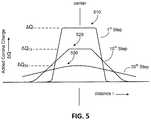
- FIG. 5shows example charge profiles for a semiconductor wafer after an initial deposition of charge, after a sequence of ten depositions of charge, and after a sequence of twenty depositions of charge.
- FIG. 6shows an example method of characterizing a semiconductor sample.
- FIG. 7shows an example method of depositing a corona charge at a region of a surface of a sample.
- the present disclosurepertains to measuring doping concentrations of a semiconductor using accurate, fast-feedback, non-invasive, and non-contact techniques. Implementations of these techniques include measuring the surface potential at a test site of a semiconductor, applying a bias voltage to the semiconductor in order to obtain a particular surface potential at the test site (e.g., zero, substantially zero, or some other constant value), and depositing a charge on the test site of the semiconductor surface (e.g., using corona discharge in air).
- This sequence of surface potential measurement, surface potential compensation, and charge depositioncan be repeated multiple times in order to create a precisely controlled depletion surface space charge layer, similar to that of a Schottky barrier in metal contact diodes.
- the semiconductor depletion space charge capacitance Ccan then be measured to determine the doping concentration of the semiconductor in the depletion space charge layer, and to obtain doping depth profiles beneath the semiconductor surface.
- the product of the semiconductor depletion space charge capacitance and the total charge deposited at the test site, CQcan be used as a measurement quality factor for precise doping depth profiling.
- the depletion space charge layercan be formed without fabrication of any permanent or temporary metal-semiconductor diodes and without any invasive electrical contacts, measurements can be obtained relatively quickly, and the semiconductor wafer can be further processed or used after the doping measurement is performed. Further, in general, implementations of these techniques can be performed without the use of mercury, a hazardous material that is often subject to environment regulation or other usage restrictions.
- Implementations of these techniquescan be used to measure doping concentrations of semiconductor materials capable of retaining corona deposited charge.
- semiconductor materialscapable of retaining corona deposited charge.
- Thiscan include, for example, wide bandgap semiconductors (e.g., SiC, GaN, or ZnO semiconductors that are not exposed to short wavelength illumination).
- Thiscan also include, for example, semiconductors that have been coated with dielectric films that prevent corona charge neutralization (e.g., SiO 2 , or Si 3 N 4 films).
- implementations of these techniquescan be used to improve the manufacturing of semiconductor wafers used for a variety of applications.
- these techniquescan extend the range of corona-induced depletion voltages to relatively high voltages (e.g., hundreds of volts), which can be advantageous for conducting doping profiling in SiC and GaN semiconductor wafers for high voltage power devices.
- these techniquecan be used to improve the manufacturing of semiconductor wafers that are used for optoelectronic applications.
- the described techniquesalso can be applied to other corona charge-based characterization processes, including the measurement of dielectrics and interface on wafers and micro-test sites.
- FIG. 1AAn example system 100 for measuring the doping concentration of a semiconductor sample is shown in FIG. 1A .
- the system 100includes a stage assembly 110 , a Kelvin probe 120 , a corona charging station 130 , a voltage compensation assembly 140 , and a processing module 150 .
- a semiconductor sample 160is placed on the stage assembly 110 and is positioned for examination by the Kelvin probe 120 .
- the Kelvin probe 120measures the surface potential of a test site 162 on the front surface of the semiconductor sample 160 .
- the voltage assembly 140then applies a bias voltage to the semiconductor sample 160 (e.g., at the back surface 164 of semiconductor sample 160 ) to compensate the surface potential of the test site to a particular value (e.g., zero volts, 0.5V or less, or some other value).
- the semiconductor sample 160is then repositioned beneath the corona charging station 130 , which deposits a charge on the test site 162 of the semiconductor sample 160 .
- the processing module 150determines the doping concentration of the semiconductor and/or doping depth profiles beneath the semiconductor surface.
- the semiconductor sample 160can be shielded from stray illumination (e.g., by enclosing all or part of the system 100 in a light-shielded housing or facility).
- the stage assembly 110supports and positions the semiconductor sample 160 during examination by the system 100 .
- the stage assembly 110includes a chuck 112 capable of conducting electric charge to and from the semiconductor sample (e.g., a semiconductor wafer).
- the chuck 112can be composed of one or more electrically conductive materials.
- the chuck 112can be composed of aluminum, and coated with titanium nitride. In practice, other conductive materials are also possible, depending on the implementation.
- the semiconductor sample 160(e.g., semiconductor wafer) is secured to the chuck 112 such that electrical contact is provided between the semiconductor sample 160 (e.g., the back surface 164 ) and the chuck 112 .
- the semiconductor sample 160can be non-invasively secured to the chuck 112 .
- the semiconductor sample 160can be secured to the chuck 112 through suction applied by a vacuum 114 .
- a vacuum 114is shown in FIG. 1A , in practice, other securing mechanisms (e.g., pins, brackets, and/or ties) are also possible, depending on the implementation.
- the stage assembly 110can move along one or more axes, such that the semiconductor sample 160 can be translated in relation to the Kelvin probe 120 and the charging station 130 .
- the chuck 112can move along the x, y, and/or z axes of a Cartesian coordinate system in order to move the semiconductor sample 160 along any of three dimensions in relation to the other components of the system 100 .
- the stage assembly 110initially positions the semiconductor sample 160 beneath the Kelvin probe 120 , such that the Kelvin probe 120 can measure the surface potential of the test site 162 . Measurements obtained by the Kelvin probe 120 are transmitted to the processing module 150 for analysis.
- the Kelvin probe 120can measure the surface potential of the test site 162 without contacting the semiconductor sample 160 .
- the surface potentialcan be obtained by measuring the constant potential difference (CPD) between a reference probe having a known work function, and the semiconductor surface having an unknown work function.
- CPDconstant potential difference
- the probeis placed above the surface of the semiconductor test site and is vibrated, which causes a periodic variation in capacitance between the probe and the semiconductor test site and causes a time-varying current into the probe.
- This currentmay be measured and nullified by applying an opposite voltage on the probe or semiconductor surface.
- This voltageknown as the backing potential, results in zero current when it is equal to the CPD between the probe and the semiconductor surface.
- This voltagecan be determined, for example, using a measuring system 122 .
- a vibrating Kelvin probe 120is shown in FIG. 1A , in practice, other non-contact vibrating probes or measurement systems also can be used, depending on the implementation. For example, in some cases, a Monroe probe can be used instead of a Kelvin probe
- the vibrating probe 120can have a particular diameter (e.g., 1 mm, 2 mm, or some other diameter).
- the Kelvin probe 120can move with respect to the semiconductor sample (e.g., move laterally across the semiconductor sample) in order to measure the surface potential of several test sites on the semiconductor sample.
- the voltage compensation assembly 140is configured to electrically ground the back surface 164 of the semiconductor sample 160 .
- the voltage compensation assembly 140includes a direct current (DC) voltage source 142 coupled to the chuck 112 through a switch 148 a , and an input capacitor 146 coupled the chuck 112 through a switch 148 b .
- the switch 148 ais open, and the switch 148 b is in position A.
- the chuck 112 and the back surface 164 of the semiconductor sample 160are both electrically grounded.
- the system 100compensates the test site surface potential by applying a bias voltage to the back surface 164 of the semiconductor sample 160 .
- this bias voltageis applied by electrically coupling the input capacitor 146 to the back surface 164 of the semiconductor sample 160 , and charging the input capacitor 146 until a particular bias voltage is obtained across it.
- thiscan be performed by closing the switch 148 a and toggling the switch 148 b to position B.
- the DC voltage source 142 and the input capacitor 146are each electrically coupled together and to the chuck 112 .
- the DC voltage sources 142electrically charges the input capacitor 146 .
- the voltage across the input capacitor 146biases the test site surface potential.
- the bias voltage of the input capacitor 146can be monitored using a measuring system 170 in parallel with the input capacitor 146 . Measurements obtained by the measuring system 170 can be transmitted to the processing module 150 for analysis.
- the DC voltage source 142can be configured to charge the input capacitor 146 to a particular bias voltage in order to compensate the surface potential at the test site 162 .
- the DC voltage source 142can be configured to achieve a zero, or substantially zero surface potential at the test site 162 .
- the DC voltage source 142can charge the input capacitor 146 such that the bias voltage across the input capacitor 146 is the opposite of the surface voltage that was measured by the Kelvin probe 120 .
- the Kelvin probe 120measured a surface voltage of V 0 while the back surface 164 was electrically grounded (e.g., while the switch 148 a was open and the switch 148 b was in position A), while the switch 148 b is closed and the switch 148 b is in position B, the DC voltage source 142 can apply a voltage of ⁇ V 0 across the input capacitor 146 .
- the surface potential at the test site 162is compensated to zero once the input capacitor 146 is charged and a bias voltage of ⁇ V 0 is obtained across it.
- an electrical chargeis deposited onto the test site 162 according to the biased surface potential condition.
- the semiconductor sample 160is repositioned by the stage assembly 110 , such that the test site 162 is positioned beneath the corona charging station 130 .
- the corona charging station 130then deposits a charge on the test site 162 .
- the switch 148 ais in an open position, and the switch 148 b is in position B.
- the input capacitor 146continues to bias the test site's surface potential during charge deposition.
- the corona charging station 130deposits charge onto the test site 162 through corona discharge in air.
- the corona charging station 130includes a high voltage source 132 , and a corona charging gun 134 with a discharge needle electrode. High voltage creates corona discharge and the ions generated by the corona discharge are directed from the charging gun 134 towards the test site 162 , and are deposited on the surface of the test site 162 . As a result of the charge deposition, a slight change of voltage is induced across the input capacitor 146 .
- This change in voltagecan be measured using the measuring system 170 in parallel with the input capacitor 146 . Measurements obtained by the measuring system 170 can be transmitted to the processing module 150 for analysis.
- the corona charging station 130is configured to deposit charge within a particular region (e.g., a circular region having, e.g., a diameter of approximately 8-10 mm), and the Kelvin probe 120 can be configured to measure the surface potential of a smaller sub-region within the charge deposition region (e.g., a circular sub-region having a diameter of approximately 2 mm). This can be beneficial, for example, to ensure that charge is being uniformly deposited across the entirety of the region being measured by the Kelvin probe 120 .
- a particular regione.g., a circular region having, e.g., a diameter of approximately 8-10 mm
- the Kelvin probe 120can be configured to measure the surface potential of a smaller sub-region within the charge deposition region (e.g., a circular sub-region having a diameter of approximately 2 mm). This can be beneficial, for example, to ensure that charge is being uniformly deposited across the entirety of the region being measured by the Kelvin probe 120 .
- the sequence of surface potential measurement, surface potential compensation, and charge deposition shown in FIGS. 1A-1Ccan be repeated one or more times in order to vary, in a precisely controlled manner, the surface depletion space charge layer at the test site 162 .
- the system 100can be returned to the configuration shown in FIG. 1A , and a new surface voltage measurement V 1 can be determined for the test site 162 .
- the system 100can again be switched to the configuration shown in FIG.
- the system 100can again be switched to the configuration shown in FIG. 1C , such that charge can again be deposited onto the test site 162 according to the biased surface potential condition. In this manner, charge can be incrementally deposited onto the test site 162 according to a consistent or substantially consistent surface potential. Further still, the voltage change that is induced during each charge deposition step can be observed and used as an in situ measure of the deposited charge.
- the processing module 150can be implemented using digital electronic circuitry, or in computer software, firmware, or hardware, or in combinations of one or more of them.
- the processing module 150can be implemented, at least in part, as one or more computer programs (e.g., one or more modules of computer program instructions, encoded on computer storage medium for execution by, or to control the operation of, a data processing apparatus).
- a computer storage mediumcan be, or can be included in, a computer-readable storage device, a computer-readable storage substrate, a random or serial access memory array or device, or a combination of one or more of them.
- processing apparatusencompasses all kinds of apparatus, devices, and machines for processing data, including by way of example a programmable processor, a computer, a system on a chip, or multiple ones, or combinations, of the foregoing.
- the apparatuscan include special purpose logic circuitry, e.g., an FPGA (field programmable gate array) or an ASIC (application specific integrated circuit).
- the apparatuscan also include, in addition to hardware, code that creates an execution environment for the computer program in question, e.g., code that constitutes processor firmware, a protocol stack, a database management system, an operating system, a cross-platform runtime environment, a virtual machine, or a combination of one or more of them.
- the apparatus and execution environmentcan realize various different computing model infrastructures, such as web services, distributed computing and grid computing infrastructures.
- the processing module 150can also control the operation one or more of the other components of the system 100 .
- the processing module 150can be communicatively coupled to the stage assembly 110 , the Kelvin probe 120 , the corona charging station 130 , and/or the voltage compensation assembly 140 in order to control each of these components.
- the sequence of surface potential measurement, surface potential compensation, and charge depositioncan be repeated any number of times in order to create a particular surface depletion layer. For instance, in some cases, the sequence can be repeated for a prescribed number repetitions (e.g., 10 repetitions, 20 repetitions, 30 repetitions, or any other number of repetitions) or until a desired width of the surface depletion layer W is obtained. In some cases, a larger number of incremental charging steps (e.g., 10 or more, 20 or more) can be used for doping depth profiling and for corona charge calibration.
- a bias voltagee.g., ⁇ V O
- a dose of charge having a charge density ⁇ Q 1is then deposited at the test site.
- the bias voltageis removed, and the surface potential value V 1 is determined for the test site.
- the surface potential of the test siteis then compensated by applying a new bias voltage (e.g., ⁇ V 1 ) to the semiconductor sample.
- a second dose of charge having a charge density ⁇ Q 2is then deposited at the test site.
- the bias voltageis removed, and the surface potential value V 2 is determined for the test site.
- a series of consecutive monitored corona charge deposition stepscan be performed, and the surface potential at the test site can be adjusted to a particular target value (e.g., zero volts, 0.5 V or less, or some other value) before each deposition step.
- the semiconductor samplecan be characterized based on the values for V 0 , V k , ⁇ V k , Q k and C k .
- the deposited chargecan be removed after the doping concentration of the semiconductor is determined.
- corona deposited chargecan be photo-neutralized and removed from the semiconductor surface using illumination with photon light energy sufficient to generate excess carriers in a semiconductor sample (e.g., blue light having photon energy above 3.3 eV for SiC, GaN or ZnO semiconductors).
- the doping concentration of a test sitecan be measured multiple times by removing deposited charges between each measurement, and repeating the deposition of charge.
- Measuring the doping concentration of a semiconductoroften requires a particular depletion barrier voltage (e.g., 10V, 20V, 50V, 100V, 200V or more). Without compensation, high surface potentials can often hinder corona charge deposition due to the electrostatic forces that exist between the deposited and incoming corona ions. For example, in some cases, electrostatic repulsion between the deposited and incoming corona ions can limit the density of charge deposition. In addition, in many cases, the forces acting on corona ions can direct incoming ions away from the center of the charging site, causing non-uniform lateral distribution of charge density.
- a particular depletion barrier voltagee.g. 10V, 20V, 50V, 100V, 200V or more.
- the surface depletion layeris created due to net electrical neutrality of the semiconductor surface and the underlying surface space charge region. Accordingly, an electric charge placed on the semiconductor surface is mirrored by the opposite charge in the surface space charge region.
- negative corona chargeis deposited on an n-type semiconductor and positive corona charge is deposited on a p-type semiconductor.
- the depletion layerforms a capacitor with the capacitance C D per unit area:
- a doping measurementcan be obtained based on the capacitance times charge factor CQ. This can used for two purposes: i) for calibration of corona deposited charge density Q, and ii) for determination of the doping concentration N.
- Corona charge calibrationcan be used to precisely determine the incremental charge density ⁇ Q deposited per unit surface area at the test site. By compensating the surface potential of a semiconductor test site and depositing charge at the test site according to constant compensated surface potential, the surface of the semiconductor can be charged more precisely and/or more uniformly.
- the calibration function F(V, I)can be determined empirically.
- a charge density calibrationcan be performed using a semiconductor calibrating sample having a known doping density with a constant doping depth profile over a known distance W under the surface.
- a 1/C 2 ⁇ V techniquecan be used.
- the calculation of doping density Ncan be made using a plot of 1/C ck 2 versus the surface voltage V k based on the follow relationship, where the corrected space charge capacitance C ck can be used in place of C:
- the plotis a straight line and the doping density is determined from the slope of the line as:
- N2 ⁇ S ⁇ ⁇ o ⁇ ( slope - 1 )
- N2.37 ⁇ 10 17 cm ⁇ 3
- erroneous bending of the lineis observed.
- a very large overestimation of N up to 50%can be made in higher voltage range by using uncorrected corona charge.
- a need for charge correctioncan be apparent for surface voltages exceeding about 8V. This effect demonstrates the importance of electrostatic force effects in corona-charging, even for relatively low surface potentials.
- Q ck 22 q ⁇ s ⁇ o N
- N1 2 ⁇ q ⁇ ⁇ ⁇ S ⁇ ⁇ o ⁇ ⁇ ( slope ) ⁇
- the cumulative total charge used in the Q 2 ⁇ V techniquecan be more sensitive to charge dose errors and to corresponding corona charge neutralization by leakage current, compared to a single charge increment ⁇ Q ck used in the capacitance measurement and the 1/C 2 ⁇ V technique. In cases of negligible leakage and proper correction of charge dose for electrostatic force effect, both techniques can provide similar results.
- the capacitance-charge product, CQ, of a semiconductoralso can be used to determine the doping concentration N.
- the error in Nis about 35% by not using corrected corona charge.
- the CQ factorcan be a constant for a sample with a uniform dopant depth profile (e.g., as illustrated in FIG.
- semiconductors having non-uniform dopant depth profilecan be distinguished by identifying semiconductors exhibiting a varying or non-constant CQ profile.
- FIG. 5shows charge profiles for a semiconductor wafer after an initial deposition of charge (profile 510 ) nominally at a center location on a surface, after a sequence of ten depositions of charge (profile 520 ) at the same location, and after a sequence of twenty depositions of charge (profile 530 ) at the same location.
- the surface potential of the semiconductor waferwas not adjusted to a constant target value prior to each deposition of charge.
- system 100can have other arrangements, depending on the implementation.
- the stage assembly 110does not move during doping concentration measurement. Instead, one or more of the other components of the system 100 (e.g., the Kelvin probe 120 and/or the corona charging station 130 ) can move with respect to the semiconductor sample 160 in order to perform doping concentration measurements.
- the other components of the system 100e.g., the Kelvin probe 120 and/or the corona charging station 130 .
- FIG. 6shows an example method 600 of characterizing a semiconductor sample.
- FIG. 7shows an example method 700 of depositing a corona charge at a region of a surface of a sample.
Landscapes
- Chemical & Material Sciences (AREA)
- Life Sciences & Earth Sciences (AREA)
- General Physics & Mathematics (AREA)
- Physics & Mathematics (AREA)
- Health & Medical Sciences (AREA)
- General Health & Medical Sciences (AREA)
- Analytical Chemistry (AREA)
- Biochemistry (AREA)
- Immunology (AREA)
- Pathology (AREA)
- Electrochemistry (AREA)
- Chemical Kinetics & Catalysis (AREA)
- Engineering & Computer Science (AREA)
- Food Science & Technology (AREA)
- Medicinal Chemistry (AREA)
- Testing Or Measuring Of Semiconductors Or The Like (AREA)
- Investigating Or Analyzing Materials By The Use Of Electric Means (AREA)
Abstract
Description
Qck2=2qεsεoN|Vk−Vo|
Claims (18)
Priority Applications (5)
| Application Number | Priority Date | Filing Date | Title |
|---|---|---|---|
| US14/731,677US10969370B2 (en) | 2015-06-05 | 2015-06-05 | Measuring semiconductor doping using constant surface potential corona charging |
| HUE16804449AHUE059396T2 (en) | 2015-06-05 | 2016-06-02 | Method of characterizing a semiconductor sample using constant surface potential corona charging |
| PCT/US2016/035545WO2016196813A1 (en) | 2015-06-05 | 2016-06-02 | Measuring semiconductor doping using constant surface potential corona charging |
| EP16804449.3AEP3304063B1 (en) | 2015-06-05 | 2016-06-02 | Method of characterizing a semiconductor sample using constant surface potential corona charging |
| JP2018515182AJP6829253B2 (en) | 2015-06-05 | 2016-06-02 | Measurement of semiconductor doping with constant surface potential corona charging |
Applications Claiming Priority (1)
| Application Number | Priority Date | Filing Date | Title |
|---|---|---|---|
| US14/731,677US10969370B2 (en) | 2015-06-05 | 2015-06-05 | Measuring semiconductor doping using constant surface potential corona charging |
Publications (2)
| Publication Number | Publication Date |
|---|---|
| US20160356750A1 US20160356750A1 (en) | 2016-12-08 |
| US10969370B2true US10969370B2 (en) | 2021-04-06 |
Family
ID=57442269
Family Applications (1)
| Application Number | Title | Priority Date | Filing Date |
|---|---|---|---|
| US14/731,677Active2038-09-17US10969370B2 (en) | 2015-06-05 | 2015-06-05 | Measuring semiconductor doping using constant surface potential corona charging |
Country Status (5)
| Country | Link |
|---|---|
| US (1) | US10969370B2 (en) |
| EP (1) | EP3304063B1 (en) |
| JP (1) | JP6829253B2 (en) |
| HU (1) | HUE059396T2 (en) |
| WO (1) | WO2016196813A1 (en) |
Cited By (2)
| Publication number | Priority date | Publication date | Assignee | Title |
|---|---|---|---|---|
| US20230369139A1 (en)* | 2021-07-16 | 2023-11-16 | Taiwan Semiconductor Manufacturing Company Ltd. | Method of testing semiconductor package |
| US12027430B1 (en)* | 2023-03-17 | 2024-07-02 | Semilab Semiconductor Physics Laboratory Co., Ltd. | Semiconductor doping characterization method using photoneutralization time constant of corona surface charge |
Families Citing this family (5)
| Publication number | Priority date | Publication date | Assignee | Title |
|---|---|---|---|---|
| CN117276345A (en)* | 2019-02-27 | 2023-12-22 | 株式会社电装 | Silicon carbide semiconductor device manufacturing method |
| JP7140148B2 (en)* | 2019-02-27 | 2022-09-21 | 株式会社デンソー | Silicon carbide semiconductor device and manufacturing method thereof |
| TWI821750B (en)* | 2020-10-07 | 2023-11-11 | 台灣愛司帝科技股份有限公司 | Electronic component measuring equipment, electronic component measuring method, and led manufacturing method |
| JP7521407B2 (en) | 2020-12-16 | 2024-07-24 | 住友電気工業株式会社 | Silicon carbide epitaxial substrate inspection method, silicon carbide epitaxial substrate manufacturing method, and silicon carbide epitaxial substrate inspection device |
| JP7621308B2 (en)* | 2021-05-14 | 2025-01-24 | 東京エレクトロン株式会社 | Plasma processing apparatus and plasma processing method |
Citations (73)
| Publication number | Priority date | Publication date | Assignee | Title |
|---|---|---|---|---|
| US4812756A (en)* | 1987-08-26 | 1989-03-14 | International Business Machines Corporation | Contactless technique for semicondutor wafer testing |
| US5216362A (en)* | 1991-10-08 | 1993-06-01 | International Business Machines Corporation | Contactless technique for measuring epitaxial dopant concentration profiles in semiconductor wafers |
| US5485091A (en)* | 1995-05-12 | 1996-01-16 | International Business Machines Corporation | Contactless electrical thin oxide measurements |
| US5498974A (en)* | 1994-12-30 | 1996-03-12 | International Business Machines Corporation | Contactless corona-oxide-semiconductor Q-V mobile charge measurement method and apparatus |
| US5639357A (en)* | 1994-05-12 | 1997-06-17 | Applied Materials | Synchronous modulation bias sputter method and apparatus for complete planarization of metal films |
| US5644223A (en) | 1995-05-12 | 1997-07-01 | International Business Machines Corporation | Uniform density charge deposit source |
| US5773989A (en)* | 1995-07-14 | 1998-06-30 | University Of South Florida | Measurement of the mobile ion concentration in the oxide layer of a semiconductor wafer |
| US5807467A (en)* | 1996-01-22 | 1998-09-15 | Micron Technology, Inc. | In situ preclean in a PVD chamber with a biased substrate configuration |
| US5963783A (en)* | 1995-11-13 | 1999-10-05 | Advanced Micro Devices, Inc. | In-line detection and assessment of net charge in PECVD silicon dioxide (oxide) layers |
| US6011404A (en)* | 1997-07-03 | 2000-01-04 | Lucent Technologies Inc. | System and method for determining near--surface lifetimes and the tunneling field of a dielectric in a semiconductor |
| US6034535A (en)* | 1997-02-14 | 2000-03-07 | Semitest Inc. | Method utilizing a modulated light beam for determining characteristics such as the doping concentration profile of a specimen of semiconductor material |
| US6037797A (en)* | 1997-07-11 | 2000-03-14 | Semiconductor Diagnostics, Inc. | Measurement of the interface trap charge in an oxide semiconductor layer interface |
| US6097196A (en)* | 1997-04-23 | 2000-08-01 | Verkuil; Roger L. | Non-contact tunnelling field measurement for a semiconductor oxide layer |
| US6097205A (en)* | 1997-02-14 | 2000-08-01 | Semitest, Inc. | Method and apparatus for characterizing a specimen of semiconductor material |
| US6127289A (en)* | 1997-09-05 | 2000-10-03 | Lucent Technologies, Inc. | Method for treating semiconductor wafers with corona charge and devices using corona charging |
| US6191605B1 (en)* | 1997-08-18 | 2001-02-20 | Tom G. Miller | Contactless method for measuring total charge of an insulating layer on a substrate using corona charge |
| US20010014520A1 (en)* | 2000-02-16 | 2001-08-16 | Tatehito Usui | Process monitoring methods in a plasma processing apparatus, monitoring units, and a sample processing method using the monitoring units |
| US20020006740A1 (en)* | 1995-03-01 | 2002-01-17 | Emil Kamieniecki | Real-time in-line testing of semiconductor wafers |
| US6395437B1 (en)* | 1999-10-29 | 2002-05-28 | Advanced Micro Devices, Inc. | Junction profiling using a scanning voltage micrograph |
| US20020125900A1 (en)* | 2001-01-26 | 2002-09-12 | Alexander Savtchouk | Steady state method for measuring the thickness and the capacitance of ultra thin dielectric in the presence of substantial leakage current |
| US20020130674A1 (en)* | 2001-01-26 | 2002-09-19 | Jacek Lagowski | Steady state method for measuring the thickness and the capacitance of ultra thin dielectric in the presence of substantial leakage current |
| US20020189938A1 (en)* | 2001-03-16 | 2002-12-19 | 4Wave, Inc. | System and method for performing sputter deposition with multiple targets using independent ion and electron sources and independent target biasing with DC pulse signals |
| US20030024807A1 (en)* | 2001-03-16 | 2003-02-06 | 4Wave, Inc. | System and method for performing thin film deposition or chemical treatment using an energetic flux of neutral reactive molecular fragments, atoms or radicals |
| US6538462B1 (en)* | 1999-11-30 | 2003-03-25 | Semiconductor Diagnostics, Inc. | Method for measuring stress induced leakage current and gate dielectric integrity using corona discharge |
| US6569691B1 (en)* | 2000-03-29 | 2003-05-27 | Semiconductor Diagnostics, Inc. | Measurement of different mobile ion concentrations in the oxide layer of a semiconductor wafer |
| US20040019442A1 (en)* | 2002-07-22 | 2004-01-29 | Dainippon Screen Mfg. Co., Ltd. | Film thickness measuring method, relative dielectric constant measuring method, film thickness measuring apparatus, and relative dielectric constant measuring apparatus |
| US6734696B2 (en)* | 2001-11-01 | 2004-05-11 | Kla-Tencor Technologies Corp. | Non-contact hysteresis measurements of insulating films |
| US20040112764A1 (en)* | 2002-12-13 | 2004-06-17 | Stokes Edward B. | Sensor device for detection of dissolved hydrocarbon gases in oil filled high-voltage electrical equipment |
| US20040191936A1 (en)* | 2003-03-28 | 2004-09-30 | Qc Solutions, Inc. | Real-time in-line testing of semiconductor wafers |
| US20040241890A1 (en)* | 2003-02-03 | 2004-12-02 | Qcept Technologies, Inc. | Wafer inspection system |
| US20050006226A1 (en)* | 2001-03-16 | 2005-01-13 | Baldwin David Alan | System and method for performing sputter etching using independent ion and electron sources and a substrate biased with an a-symmetric bi-polar DC pulse signal |
| US20050059174A1 (en)* | 2003-02-03 | 2005-03-17 | Steele M. Brandon | Inspection system and apparatus |
| US20050174135A1 (en)* | 2002-06-17 | 2005-08-11 | Ryuichi Matsuda | Method and device for measuring wafer potential or temperature |
| US6937050B1 (en)* | 1997-04-30 | 2005-08-30 | Min-Su Fung | Non-contact mobile charge measurement with leakage band-bending and dipole correction |
| US20050196882A1 (en)* | 2004-03-05 | 2005-09-08 | Kenneth Steeples | Real-time in-line testing of semiconductor wafers |
| US20050239224A1 (en)* | 2004-04-26 | 2005-10-27 | Dainippon Screen Mfg. Co., Ltd. | Method and apparatus for measuring relative dielectric constant |
| US7012438B1 (en)* | 2002-07-10 | 2006-03-14 | Kla-Tencor Technologies Corp. | Methods and systems for determining a property of an insulating film |
| US20060097193A1 (en)* | 2002-06-26 | 2006-05-11 | Horsky Thomas N | Ion implantation device and a method of semiconductor manufacturing by the implantation of boron hydride cluster ions |
| US7103848B2 (en)* | 2001-09-13 | 2006-09-05 | International Business Machines Corporation | Handheld electronic book reader with annotation and usage tracking capabilities |
| US7110238B1 (en)* | 2003-06-24 | 2006-09-19 | Kla-Tencor Technologies Corp. | Systems and methods for using non-contact voltage sensors and corona discharge guns |
| US20060267622A1 (en)* | 2005-05-31 | 2006-11-30 | Jacek Lagowski | Non-contact method for acquiring charge-voltage data on miniature test areas of semiconductor product wafers |
| US20070018674A1 (en)* | 2005-07-20 | 2007-01-25 | Sung-Chan Cho | Apparatus and method for testing semiconductor device |
| US20070069759A1 (en)* | 2005-08-19 | 2007-03-29 | Kla-Tencor Technologies Corp. | Systems and Methods for Controlling Deposition of a Charge on a Wafer for Measurement of One or More Electrical Properties of the Wafer |
| US7230443B1 (en)* | 1997-04-30 | 2007-06-12 | Kla-Tencor Corporation | Non-contact mobile charge measurement with leakage band-bending and dipole correction |
| US20070148795A1 (en)* | 2005-12-27 | 2007-06-28 | Dainippon Screen Mfg. Co., Ltd. | Insulator film characteristic measuring method and insulator film characteristic measuring apparatus |
| US20070181830A1 (en)* | 2002-06-26 | 2007-08-09 | Semequip, Inc. | Ion implantation device and a method of semiconductor manufacturing by the implantation of boron hydride cluster ions |
| US20070273400A1 (en)* | 2002-12-13 | 2007-11-29 | Emil Kamieniecki | Apparatus and Method for Electrical Characterization of Semiconductors |
| US20080174918A1 (en)* | 2007-01-19 | 2008-07-24 | Nanochip, Inc. | Method and system for writing and reading a charge-trap media with a probe tip |
| US7405580B2 (en) | 2005-03-16 | 2008-07-29 | Semiconductor Diagnostics, Inc. | Self-calibration in non-contact surface photovoltage measurement of depletion capacitance and dopant concentration |
| US20080260398A1 (en)* | 2007-04-18 | 2008-10-23 | Canon Kabushiki Kaisha | Image forming apparatus |
| US20080297189A1 (en)* | 2007-05-29 | 2008-12-04 | Interuniversitair Microelektronica Centrum Vzw (Imec) | Mobility measurements of inversion charge carriers |
| US20080299681A1 (en)* | 2007-05-31 | 2008-12-04 | Roland Jaeger | Multi-step deposition control |
| US20080305598A1 (en)* | 2007-06-07 | 2008-12-11 | Horsky Thomas N | Ion implantation device and a method of semiconductor manufacturing by the implantation of ions derived from carborane molecular species |
| US7521946B1 (en) | 2005-04-06 | 2009-04-21 | Kla-Tencor Technologies Corporation | Electrical measurements on semiconductors using corona and microwave techniques |
| US7538333B1 (en)* | 2002-11-04 | 2009-05-26 | Kla-Tencor Technologies Corporation | Contactless charge measurement of product wafers and control of corona generation and deposition |
| US20100008015A1 (en)* | 2008-07-07 | 2010-01-14 | Jean-Paul Booth | Capacitively-coupled electrostatic (cce) probe arrangement for detecting dechucking in a plasma processing chamber and methods thereof |
| US20100032587A1 (en)* | 2008-07-17 | 2010-02-11 | Hosch Jimmy W | Electron beam exciter for use in chemical analysis in processing systems |
| US20100060307A1 (en)* | 2008-09-08 | 2010-03-11 | Emil Kamieniecki | Electrical Characterization of Semiconductor Materials |
| US7772866B2 (en)* | 2007-03-07 | 2010-08-10 | International Business Machines Corporation | Structure and method of mapping signal intensity to surface voltage for integrated circuit inspection |
| US8004290B1 (en)* | 2007-04-04 | 2011-08-23 | Kla-Tencor Corporation | Method and apparatus for determining dielectric layer properties |
| US20120176146A1 (en)* | 2011-01-06 | 2012-07-12 | University Of South Florida | Noncontact determination of interface trap density for semiconductor-dielectric interface structures |
| US20120283973A1 (en)* | 2011-05-05 | 2012-11-08 | Imec | Plasma probe and method for plasma diagnostics |
| US20120321335A1 (en)* | 2011-06-14 | 2012-12-20 | Toshiba Tec Kabushiki Kaisha | Fixing device and image forming apparatus |
| US20130068963A1 (en)* | 2008-02-14 | 2013-03-21 | The Regents Of The University Of California | Shielded capacitive electrode |
| US20130082241A1 (en)* | 2011-09-29 | 2013-04-04 | Francis J. Kub | Graphene on Semiconductor Detector |
| US20130164665A1 (en)* | 2011-12-26 | 2013-06-27 | Masayuki Ishii | Toner, developer, image forming apparatus, and process cartridge |
| US20130257472A1 (en)* | 2012-03-29 | 2013-10-03 | Emil Kamieniecki | Electrical characterization of semiconductor materials |
| US20140147134A1 (en)* | 2012-11-28 | 2014-05-29 | Xerox Corporation | Monitoring a Condition of a Solid State Charge Device in Electrostatic Printing |
| US8909365B2 (en)* | 2009-11-19 | 2014-12-09 | Lam Research Corporation | Methods and apparatus for controlling a plasma processing system |
| US20150020972A1 (en)* | 2010-01-21 | 2015-01-22 | Kla-Tencor Corporation | Process condition sensing device and method for plasma chamber |
| US20150061714A1 (en)* | 2013-09-04 | 2015-03-05 | Kla-Tencor Corporation | Apparatus and Method for Accurate Measurement and Mapping of Forward and Reverse-Bias Current-Voltage Characteristics of Large Area Lateral P-N Junctions |
| US20150098161A1 (en)* | 2013-10-09 | 2015-04-09 | Hamilton Sundstrand Corporation | Integrated corona fault detection |
| US9084334B1 (en)* | 2014-11-10 | 2015-07-14 | Illinois Tool Works Inc. | Balanced barrier discharge neutralization in variable pressure environments |
- 2015
- 2015-06-05USUS14/731,677patent/US10969370B2/enactiveActive
- 2016
- 2016-06-02JPJP2018515182Apatent/JP6829253B2/enactiveActive
- 2016-06-02HUHUE16804449Apatent/HUE059396T2/enunknown
- 2016-06-02EPEP16804449.3Apatent/EP3304063B1/enactiveActive
- 2016-06-02WOPCT/US2016/035545patent/WO2016196813A1/ennot_activeCeased
Patent Citations (105)
| Publication number | Priority date | Publication date | Assignee | Title |
|---|---|---|---|---|
| US4812756A (en)* | 1987-08-26 | 1989-03-14 | International Business Machines Corporation | Contactless technique for semicondutor wafer testing |
| JPS6469024A (en) | 1987-08-26 | 1989-03-15 | Ibm | Non-contact test method of semiconductor wafer |
| US5216362A (en)* | 1991-10-08 | 1993-06-01 | International Business Machines Corporation | Contactless technique for measuring epitaxial dopant concentration profiles in semiconductor wafers |
| JPH05206243A (en) | 1991-10-08 | 1993-08-13 | Internatl Business Mach Corp <Ibm> | Method for noncontact measurement of dopant concentration |
| US5639357A (en)* | 1994-05-12 | 1997-06-17 | Applied Materials | Synchronous modulation bias sputter method and apparatus for complete planarization of metal films |
| US5498974A (en)* | 1994-12-30 | 1996-03-12 | International Business Machines Corporation | Contactless corona-oxide-semiconductor Q-V mobile charge measurement method and apparatus |
| JPH08236591A (en) | 1994-12-30 | 1996-09-13 | Internatl Business Mach Corp <Ibm> | Method and equipment for nontouch corona oxide semiconductorq-v movement electric charge measurement |
| US20020006740A1 (en)* | 1995-03-01 | 2002-01-17 | Emil Kamieniecki | Real-time in-line testing of semiconductor wafers |
| US5485091A (en)* | 1995-05-12 | 1996-01-16 | International Business Machines Corporation | Contactless electrical thin oxide measurements |
| US5644223A (en) | 1995-05-12 | 1997-07-01 | International Business Machines Corporation | Uniform density charge deposit source |
| US5773989A (en)* | 1995-07-14 | 1998-06-30 | University Of South Florida | Measurement of the mobile ion concentration in the oxide layer of a semiconductor wafer |
| US5963783A (en)* | 1995-11-13 | 1999-10-05 | Advanced Micro Devices, Inc. | In-line detection and assessment of net charge in PECVD silicon dioxide (oxide) layers |
| US5807467A (en)* | 1996-01-22 | 1998-09-15 | Micron Technology, Inc. | In situ preclean in a PVD chamber with a biased substrate configuration |
| US6051121A (en)* | 1996-01-22 | 2000-04-18 | Micron Technology Inc | Deposition chamber with a biased substrate configuration |
| US6267852B1 (en)* | 1996-01-22 | 2001-07-31 | Micron Technology, Inc. | Method of forming a sputtering apparatus |
| US6034535A (en)* | 1997-02-14 | 2000-03-07 | Semitest Inc. | Method utilizing a modulated light beam for determining characteristics such as the doping concentration profile of a specimen of semiconductor material |
| US6097205A (en)* | 1997-02-14 | 2000-08-01 | Semitest, Inc. | Method and apparatus for characterizing a specimen of semiconductor material |
| US6097196A (en)* | 1997-04-23 | 2000-08-01 | Verkuil; Roger L. | Non-contact tunnelling field measurement for a semiconductor oxide layer |
| US6937050B1 (en)* | 1997-04-30 | 2005-08-30 | Min-Su Fung | Non-contact mobile charge measurement with leakage band-bending and dipole correction |
| US7230443B1 (en)* | 1997-04-30 | 2007-06-12 | Kla-Tencor Corporation | Non-contact mobile charge measurement with leakage band-bending and dipole correction |
| US6011404A (en)* | 1997-07-03 | 2000-01-04 | Lucent Technologies Inc. | System and method for determining near--surface lifetimes and the tunneling field of a dielectric in a semiconductor |
| US6037797A (en)* | 1997-07-11 | 2000-03-14 | Semiconductor Diagnostics, Inc. | Measurement of the interface trap charge in an oxide semiconductor layer interface |
| US20010000651A1 (en)* | 1997-08-18 | 2001-05-03 | Miller Tom G. | Contactless total charge measurement with corona |
| US6191605B1 (en)* | 1997-08-18 | 2001-02-20 | Tom G. Miller | Contactless method for measuring total charge of an insulating layer on a substrate using corona charge |
| US20020008536A1 (en)* | 1997-08-18 | 2002-01-24 | Miller Tom G. | Contactless total charge measurement with corona |
| US6448804B2 (en)* | 1997-08-18 | 2002-09-10 | Tom G. Miller | Contactless total charge measurement with corona |
| US6335630B2 (en)* | 1997-08-18 | 2002-01-01 | Tom G. Miller | Contactless method for measuring total charge of an oxide layer on a semiconductor wafer using corona charge |
| US6127289A (en)* | 1997-09-05 | 2000-10-03 | Lucent Technologies, Inc. | Method for treating semiconductor wafers with corona charge and devices using corona charging |
| US6395437B1 (en)* | 1999-10-29 | 2002-05-28 | Advanced Micro Devices, Inc. | Junction profiling using a scanning voltage micrograph |
| US6538462B1 (en)* | 1999-11-30 | 2003-03-25 | Semiconductor Diagnostics, Inc. | Method for measuring stress induced leakage current and gate dielectric integrity using corona discharge |
| US20010014520A1 (en)* | 2000-02-16 | 2001-08-16 | Tatehito Usui | Process monitoring methods in a plasma processing apparatus, monitoring units, and a sample processing method using the monitoring units |
| US6569691B1 (en)* | 2000-03-29 | 2003-05-27 | Semiconductor Diagnostics, Inc. | Measurement of different mobile ion concentrations in the oxide layer of a semiconductor wafer |
| US20020125900A1 (en)* | 2001-01-26 | 2002-09-12 | Alexander Savtchouk | Steady state method for measuring the thickness and the capacitance of ultra thin dielectric in the presence of substantial leakage current |
| US20020130674A1 (en)* | 2001-01-26 | 2002-09-19 | Jacek Lagowski | Steady state method for measuring the thickness and the capacitance of ultra thin dielectric in the presence of substantial leakage current |
| US20030024807A1 (en)* | 2001-03-16 | 2003-02-06 | 4Wave, Inc. | System and method for performing thin film deposition or chemical treatment using an energetic flux of neutral reactive molecular fragments, atoms or radicals |
| US7316764B2 (en)* | 2001-03-16 | 2008-01-08 | 4 Wave, Inc. | System and method for performing sputter etching using independent ion and electron sources and a substrate biased with an a-symmetric bi-polar DC pulse signal |
| US6723209B2 (en)* | 2001-03-16 | 2004-04-20 | 4-Wave, Inc. | System and method for performing thin film deposition or chemical treatment using an energetic flux of neutral reactive molecular fragments, atoms or radicals |
| US20050006226A1 (en)* | 2001-03-16 | 2005-01-13 | Baldwin David Alan | System and method for performing sputter etching using independent ion and electron sources and a substrate biased with an a-symmetric bi-polar DC pulse signal |
| US6679976B2 (en)* | 2001-03-16 | 2004-01-20 | 4Wave, Inc. | System and method for performing sputter deposition with multiple targets using independent ion and electron sources and independent target biasing with DC pulse signals |
| US20020189938A1 (en)* | 2001-03-16 | 2002-12-19 | 4Wave, Inc. | System and method for performing sputter deposition with multiple targets using independent ion and electron sources and independent target biasing with DC pulse signals |
| US7103848B2 (en)* | 2001-09-13 | 2006-09-05 | International Business Machines Corporation | Handheld electronic book reader with annotation and usage tracking capabilities |
| US6734696B2 (en)* | 2001-11-01 | 2004-05-11 | Kla-Tencor Technologies Corp. | Non-contact hysteresis measurements of insulating films |
| US7335315B2 (en)* | 2002-06-17 | 2008-02-26 | Mitsubishi Heavy Industries, Ltd. | Method and device for measuring wafer potential or temperature |
| US20050174135A1 (en)* | 2002-06-17 | 2005-08-11 | Ryuichi Matsuda | Method and device for measuring wafer potential or temperature |
| US20120076475A1 (en)* | 2002-06-26 | 2012-03-29 | Semequip, Inc. | Ion implantation device and a method of semiconductor manufacturing by the implantation of boron hydride cluster ions |
| US7491953B2 (en)* | 2002-06-26 | 2009-02-17 | Semequip, Inc. | Ion implantation device and a method of semiconductor manufacturing by the implantation of boron hydride cluster ions |
| US7960709B2 (en)* | 2002-06-26 | 2011-06-14 | Semequip, Inc. | Ion implantation device and a method of semiconductor manufacturing by the implantation of boron hydride cluster ions |
| US8410459B2 (en)* | 2002-06-26 | 2013-04-02 | Semequip, Inc. | Ion implantation device and a method of semiconductor manufacturing by the implantation of boron hydride cluster ions |
| US20060097193A1 (en)* | 2002-06-26 | 2006-05-11 | Horsky Thomas N | Ion implantation device and a method of semiconductor manufacturing by the implantation of boron hydride cluster ions |
| US20070181830A1 (en)* | 2002-06-26 | 2007-08-09 | Semequip, Inc. | Ion implantation device and a method of semiconductor manufacturing by the implantation of boron hydride cluster ions |
| US20090090872A1 (en)* | 2002-06-26 | 2009-04-09 | Horsky Thomas N | Ion implantation device and a method of semiconductor manufacturing by the implantation of boron hydride cluster ions |
| US8618514B2 (en)* | 2002-06-26 | 2013-12-31 | Semequip, Inc. | Ion implantation device and a method of semiconductor manufacturing by the implantation of boron hydride cluster ions |
| US20070194252A1 (en)* | 2002-06-26 | 2007-08-23 | Semequip, Inc. | Ion implantation device and a method of semiconductor manufacturing by the implantation of boron hydride cluster ions |
| US20140061816A1 (en)* | 2002-06-26 | 2014-03-06 | Semequip, Inc. | Ion implantation device and a method of semiconductor manufacturing by the implantation of boron hydride cluster ions |
| US20110226969A1 (en)* | 2002-06-26 | 2011-09-22 | Semequip, Inc. | Ion implantation device and a method of semiconductor manufacturing by the implantation of boron hydride cluster ions |
| US8071958B2 (en)* | 2002-06-26 | 2011-12-06 | Semequip, Inc. | Ion implantation device and a method of semiconductor manufacturing by the implantation of boron hydride cluster ions |
| US7358748B1 (en) | 2002-07-10 | 2008-04-15 | Kla-Tencor Technologies Corp. | Methods and systems for determining a property of an insulating film |
| US7012438B1 (en)* | 2002-07-10 | 2006-03-14 | Kla-Tencor Technologies Corp. | Methods and systems for determining a property of an insulating film |
| US20040019442A1 (en)* | 2002-07-22 | 2004-01-29 | Dainippon Screen Mfg. Co., Ltd. | Film thickness measuring method, relative dielectric constant measuring method, film thickness measuring apparatus, and relative dielectric constant measuring apparatus |
| US7538333B1 (en)* | 2002-11-04 | 2009-05-26 | Kla-Tencor Technologies Corporation | Contactless charge measurement of product wafers and control of corona generation and deposition |
| US20040112764A1 (en)* | 2002-12-13 | 2004-06-17 | Stokes Edward B. | Sensor device for detection of dissolved hydrocarbon gases in oil filled high-voltage electrical equipment |
| US7663385B2 (en)* | 2002-12-13 | 2010-02-16 | Nanometrics Incorporated | Apparatus and method for electrical characterization by selecting and adjusting the light for a target depth of a semiconductor |
| US8232817B2 (en)* | 2002-12-13 | 2012-07-31 | Nanometrics Incorporated | Apparatus and method for electrical characterization by selecting and adjusting the light for a target depth of a semiconductor |
| US20070273400A1 (en)* | 2002-12-13 | 2007-11-29 | Emil Kamieniecki | Apparatus and Method for Electrical Characterization of Semiconductors |
| US20050059174A1 (en)* | 2003-02-03 | 2005-03-17 | Steele M. Brandon | Inspection system and apparatus |
| US20040241890A1 (en)* | 2003-02-03 | 2004-12-02 | Qcept Technologies, Inc. | Wafer inspection system |
| US20040191936A1 (en)* | 2003-03-28 | 2004-09-30 | Qc Solutions, Inc. | Real-time in-line testing of semiconductor wafers |
| US7110238B1 (en)* | 2003-06-24 | 2006-09-19 | Kla-Tencor Technologies Corp. | Systems and methods for using non-contact voltage sensors and corona discharge guns |
| US20050196882A1 (en)* | 2004-03-05 | 2005-09-08 | Kenneth Steeples | Real-time in-line testing of semiconductor wafers |
| US20050239224A1 (en)* | 2004-04-26 | 2005-10-27 | Dainippon Screen Mfg. Co., Ltd. | Method and apparatus for measuring relative dielectric constant |
| US7405580B2 (en) | 2005-03-16 | 2008-07-29 | Semiconductor Diagnostics, Inc. | Self-calibration in non-contact surface photovoltage measurement of depletion capacitance and dopant concentration |
| US7521946B1 (en) | 2005-04-06 | 2009-04-21 | Kla-Tencor Technologies Corporation | Electrical measurements on semiconductors using corona and microwave techniques |
| US7202691B2 (en)* | 2005-05-31 | 2007-04-10 | Semiconductor Diagnostics, Inc. | Non-contact method for acquiring charge-voltage data on miniature test areas of semiconductor product wafers |
| US20060267622A1 (en)* | 2005-05-31 | 2006-11-30 | Jacek Lagowski | Non-contact method for acquiring charge-voltage data on miniature test areas of semiconductor product wafers |
| US20070018674A1 (en)* | 2005-07-20 | 2007-01-25 | Sung-Chan Cho | Apparatus and method for testing semiconductor device |
| US20070069759A1 (en)* | 2005-08-19 | 2007-03-29 | Kla-Tencor Technologies Corp. | Systems and Methods for Controlling Deposition of a Charge on a Wafer for Measurement of One or More Electrical Properties of the Wafer |
| US7893703B2 (en)* | 2005-08-19 | 2011-02-22 | Kla-Tencor Technologies Corp. | Systems and methods for controlling deposition of a charge on a wafer for measurement of one or more electrical properties of the wafer |
| US20070148795A1 (en)* | 2005-12-27 | 2007-06-28 | Dainippon Screen Mfg. Co., Ltd. | Insulator film characteristic measuring method and insulator film characteristic measuring apparatus |
| US20080174918A1 (en)* | 2007-01-19 | 2008-07-24 | Nanochip, Inc. | Method and system for writing and reading a charge-trap media with a probe tip |
| US7772866B2 (en)* | 2007-03-07 | 2010-08-10 | International Business Machines Corporation | Structure and method of mapping signal intensity to surface voltage for integrated circuit inspection |
| US8004290B1 (en)* | 2007-04-04 | 2011-08-23 | Kla-Tencor Corporation | Method and apparatus for determining dielectric layer properties |
| US20080260398A1 (en)* | 2007-04-18 | 2008-10-23 | Canon Kabushiki Kaisha | Image forming apparatus |
| US20080297189A1 (en)* | 2007-05-29 | 2008-12-04 | Interuniversitair Microelektronica Centrum Vzw (Imec) | Mobility measurements of inversion charge carriers |
| US20080299681A1 (en)* | 2007-05-31 | 2008-12-04 | Roland Jaeger | Multi-step deposition control |
| US20120160415A1 (en)* | 2007-05-31 | 2012-06-28 | Advanced Micro Devices, Inc. | Multi-step deposition control |
| US8163571B2 (en)* | 2007-05-31 | 2012-04-24 | Advanced Micro Devices, Inc. | Multi-step deposition control |
| US8585877B2 (en)* | 2007-05-31 | 2013-11-19 | Advanced Micro Devices, Inc. | Multi-step deposition control |
| US20080305598A1 (en)* | 2007-06-07 | 2008-12-11 | Horsky Thomas N | Ion implantation device and a method of semiconductor manufacturing by the implantation of ions derived from carborane molecular species |
| US20130068963A1 (en)* | 2008-02-14 | 2013-03-21 | The Regents Of The University Of California | Shielded capacitive electrode |
| US20100008015A1 (en)* | 2008-07-07 | 2010-01-14 | Jean-Paul Booth | Capacitively-coupled electrostatic (cce) probe arrangement for detecting dechucking in a plasma processing chamber and methods thereof |
| US20100032587A1 (en)* | 2008-07-17 | 2010-02-11 | Hosch Jimmy W | Electron beam exciter for use in chemical analysis in processing systems |
| US20100060307A1 (en)* | 2008-09-08 | 2010-03-11 | Emil Kamieniecki | Electrical Characterization of Semiconductor Materials |
| US8909365B2 (en)* | 2009-11-19 | 2014-12-09 | Lam Research Corporation | Methods and apparatus for controlling a plasma processing system |
| US20150020972A1 (en)* | 2010-01-21 | 2015-01-22 | Kla-Tencor Corporation | Process condition sensing device and method for plasma chamber |
| US20120176146A1 (en)* | 2011-01-06 | 2012-07-12 | University Of South Florida | Noncontact determination of interface trap density for semiconductor-dielectric interface structures |
| US20140132286A1 (en)* | 2011-01-06 | 2014-05-15 | University Of South Florida | Noncontact determination of interface trap density for semiconductor-dielectric interface structures |
| US20120283973A1 (en)* | 2011-05-05 | 2012-11-08 | Imec | Plasma probe and method for plasma diagnostics |
| US20120321335A1 (en)* | 2011-06-14 | 2012-12-20 | Toshiba Tec Kabushiki Kaisha | Fixing device and image forming apparatus |
| US20130082241A1 (en)* | 2011-09-29 | 2013-04-04 | Francis J. Kub | Graphene on Semiconductor Detector |
| US20130164665A1 (en)* | 2011-12-26 | 2013-06-27 | Masayuki Ishii | Toner, developer, image forming apparatus, and process cartridge |
| US20130257472A1 (en)* | 2012-03-29 | 2013-10-03 | Emil Kamieniecki | Electrical characterization of semiconductor materials |
| US20140147134A1 (en)* | 2012-11-28 | 2014-05-29 | Xerox Corporation | Monitoring a Condition of a Solid State Charge Device in Electrostatic Printing |
| US20150061714A1 (en)* | 2013-09-04 | 2015-03-05 | Kla-Tencor Corporation | Apparatus and Method for Accurate Measurement and Mapping of Forward and Reverse-Bias Current-Voltage Characteristics of Large Area Lateral P-N Junctions |
| US20150098161A1 (en)* | 2013-10-09 | 2015-04-09 | Hamilton Sundstrand Corporation | Integrated corona fault detection |
| US9084334B1 (en)* | 2014-11-10 | 2015-07-14 | Illinois Tool Works Inc. | Balanced barrier discharge neutralization in variable pressure environments |
Non-Patent Citations (10)
| Title |
|---|
| "www.keithly.com applications guide: C-V Testing for Components and Semiconductor Devices" (Year: 2014).* |
| Czett, A. et al., Non-contact High Precision Alternative to Hg Probe for Dopant Profiling in SiC, Phys. Status Solidi C 11, pp. 1601-1605 (2013), DOI: 10, 1002/pssc201400057. |
| EP Extended European Search Report Issued in European Application No. 16804449.3, dated Feb. 18, 2019, 8 pages. |
| JP Office Action in Japanese Appln. No. 2018-515182, dated May 19, 2020, 11 pages (with English translation). |
| Marinskiy, D., et al., "A Novel Approach to Measuring Doping in SiC by Micro Spot Corona-Kelvin Method", Materials Science Forum, vols. 821-823, pp. 273-276 (2015). |
| Marinskiy, D., et al., "A Novel Approach to Measuring Doping in SiC by Micro Spot Corona—Kelvin Method", Materials Science Forum, vols. 821-823, pp. 273-276 (2015). |
| Savtchouk, S. et al., "Non-contact Doping Profiling in Epitaxial SiC", Materials Science Forum, vols. 457-460, pp. 755-758 (2004). |
| Schroeder, D.K., "Charge-Based and Probe Characterization", Semiconductor Material and Device Characterization, (2006), Ch. 9, pp. 523-527. |
| Verkuil, R.I. et al., "Contactless Silicon Doping Measurements by Means of a Corona-Oxide-Semiconductor (COS) Technique", Extended Abstracts, vol. 88-2, Abstract No. 438, Electrochemical Society Meeting, Chicago, IL (1988), pp. 643-644. |
| Wikipedia Entry for Capacitance (Year: 2019).* |
Cited By (5)
| Publication number | Priority date | Publication date | Assignee | Title |
|---|---|---|---|---|
| US20230369139A1 (en)* | 2021-07-16 | 2023-11-16 | Taiwan Semiconductor Manufacturing Company Ltd. | Method of testing semiconductor package |
| US12243788B2 (en)* | 2021-07-16 | 2025-03-04 | Taiwan Semiconductor Manufacturing Company Ltd. | Method of testing semiconductor package |
| US12027430B1 (en)* | 2023-03-17 | 2024-07-02 | Semilab Semiconductor Physics Laboratory Co., Ltd. | Semiconductor doping characterization method using photoneutralization time constant of corona surface charge |
| WO2024196595A1 (en) | 2023-03-17 | 2024-09-26 | Semilab Semiconductor Physics Laboratory Co., Ltd. | Semiconductor doping characterization method using photoneutralization time constant of corona surface charge |
| US12154833B2 (en) | 2023-03-17 | 2024-11-26 | Semilab Semiconductor Physics Laboratory Co., Ltd. | Semiconductor doping characterization method using photoneutralization time constant of corona surface charge |
Also Published As
| Publication number | Publication date |
|---|---|
| EP3304063A4 (en) | 2019-03-20 |
| EP3304063B1 (en) | 2022-03-30 |
| US20160356750A1 (en) | 2016-12-08 |
| EP3304063A1 (en) | 2018-04-11 |
| HUE059396T2 (en) | 2022-11-28 |
| WO2016196813A1 (en) | 2016-12-08 |
| JP2018518063A (en) | 2018-07-05 |
| JP6829253B2 (en) | 2021-02-10 |
Similar Documents
| Publication | Publication Date | Title |
|---|---|---|
| US10969370B2 (en) | Measuring semiconductor doping using constant surface potential corona charging | |
| US6680621B2 (en) | Steady state method for measuring the thickness and the capacitance of ultra thin dielectric in the presence of substantial leakage current | |
| TWI458850B (en) | Rf-biased capacitively-coupled electrostatic (rfb-cce) probe arrangement for characterizing a film in a plasma processing chamber | |
| EP0304632A2 (en) | A contacless technique for semiconductor wafer testing | |
| US20060279311A1 (en) | Semiconductor wafer metrology apparatus and methods | |
| US6522158B1 (en) | Non-contact mobile charge measurement with leakage band-bending and dipole correction | |
| CN109643669B (en) | Method for manufacturing resistivity standard sample and method for measuring resistivity of epitaxial wafer | |
| Wilson et al. | Recent Advancement in Charge-and Photo-Assisted Non-Contact Electrical Characterization of SiC, GaN, and AlGaN/GaN HEMT | |
| US20050196882A1 (en) | Real-time in-line testing of semiconductor wafers | |
| CN114216939B (en) | Silicon carbide surface defect state energy distribution measuring method, system and storage medium | |
| US20240347399A1 (en) | Semiconductor doping characterization method using photoneutralization time constant of corona surface charge | |
| CN109449095B (en) | Method for monitoring ion implantation doping concentration | |
| US7521946B1 (en) | Electrical measurements on semiconductors using corona and microwave techniques | |
| US7405580B2 (en) | Self-calibration in non-contact surface photovoltage measurement of depletion capacitance and dopant concentration | |
| US6937050B1 (en) | Non-contact mobile charge measurement with leakage band-bending and dipole correction | |
| TWI601213B (en) | Methods for characterisation of shallow junctions for use in semiconductor devices | |
| US7230443B1 (en) | Non-contact mobile charge measurement with leakage band-bending and dipole correction | |
| Wilson et al. | Noncontact Measurement of Doping with Enhanced Throughput and High Precision for Wide Bandgap Wafer Manufacturing | |
| JP3823911B2 (en) | Semiconductor depletion layer capacitance calculation device and CV characteristic measurement device | |
| US7037734B2 (en) | Method and apparatus for determining generation lifetime of product semiconductor wafers | |
| US11561254B2 (en) | Topside contact device and method for characterization of high electron mobility transistor (HEMT) heterostructure on insulating and semi-insulating substrates | |
| Savtchouk et al. | Non-contact doping profiling in epitaxial SiC | |
| Stacey et al. | Using surface charge analysis to characterize the radiation response of Si/SiO/sub 2/structures | |
| Smith | Surface Characterization Of Thin Film Zno Capacitors By Capacitance-voltage Measurements | |
| JPH0531824B2 (en) |
Legal Events
| Date | Code | Title | Description |
|---|---|---|---|
| AS | Assignment | Owner name:SEMILAB SDI LLC, FLORIDA Free format text:ASSIGNMENT OF ASSIGNORS INTEREST;ASSIGNORS:LAGOWSKI, JACEK;WILSON, MARSHALL;SAVTCHOUK, ALEXANDRE;AND OTHERS;REEL/FRAME:037281/0677 Effective date:20150608 Owner name:SEMILAB SDI LLC, FLORIDA Free format text:ASSIGNMENT OF ASSIGNORS INTEREST;ASSIGNOR:BUDAY, CSABA;REEL/FRAME:037281/0752 Effective date:20150611 | |
| AS | Assignment | Owner name:SEMILAB SEMICONDUCTOR PHYSICS LABORATORY CO., LTD., HUNGARY Free format text:ASSIGNMENT OF ASSIGNORS INTEREST;ASSIGNOR:SEMILAB SDI LLC;REEL/FRAME:044285/0025 Effective date:20171121 Owner name:SEMILAB SEMICONDUCTOR PHYSICS LABORATORY CO., LTD. Free format text:ASSIGNMENT OF ASSIGNORS INTEREST;ASSIGNOR:SEMILAB SDI LLC;REEL/FRAME:044285/0025 Effective date:20171121 | |
| FEPP | Fee payment procedure | Free format text:ENTITY STATUS SET TO UNDISCOUNTED (ORIGINAL EVENT CODE: BIG.); ENTITY STATUS OF PATENT OWNER: LARGE ENTITY | |
| STPP | Information on status: patent application and granting procedure in general | Free format text:NON FINAL ACTION MAILED | |
| STPP | Information on status: patent application and granting procedure in general | Free format text:RESPONSE TO NON-FINAL OFFICE ACTION ENTERED AND FORWARDED TO EXAMINER | |
| STPP | Information on status: patent application and granting procedure in general | Free format text:FINAL REJECTION MAILED | |
| STCV | Information on status: appeal procedure | Free format text:NOTICE OF APPEAL FILED | |
| STPP | Information on status: patent application and granting procedure in general | Free format text:RESPONSE TO NON-FINAL OFFICE ACTION ENTERED AND FORWARDED TO EXAMINER | |
| STPP | Information on status: patent application and granting procedure in general | Free format text:NON FINAL ACTION MAILED | |
| STPP | Information on status: patent application and granting procedure in general | Free format text:RESPONSE TO NON-FINAL OFFICE ACTION ENTERED AND FORWARDED TO EXAMINER | |
| STPP | Information on status: patent application and granting procedure in general | Free format text:AWAITING TC RESP., ISSUE FEE NOT PAID | |
| STPP | Information on status: patent application and granting procedure in general | Free format text:PUBLICATIONS -- ISSUE FEE PAYMENT VERIFIED | |
| STCF | Information on status: patent grant | Free format text:PATENTED CASE | |
| MAFP | Maintenance fee payment | Free format text:PAYMENT OF MAINTENANCE FEE, 4TH YEAR, LARGE ENTITY (ORIGINAL EVENT CODE: M1551); ENTITY STATUS OF PATENT OWNER: LARGE ENTITY Year of fee payment:4 | |
| AS | Assignment | Owner name:SEMILAB SDI, FLORIDA Free format text:ASSIGNMENT OF ASSIGNORS INTEREST;ASSIGNOR:SEMILAB SEMICONDUCTOR PHYSICS LABORATORY CO., LTD.;REEL/FRAME:070349/0780 Effective date:20250125 |