US10969205B2 - Electrically-activated pressure vessels for fracturing frangible structures - Google Patents
Electrically-activated pressure vessels for fracturing frangible structuresDownload PDFInfo
- Publication number
- US10969205B2 US10969205B2US16/403,131US201916403131AUS10969205B2US 10969205 B2US10969205 B2US 10969205B2US 201916403131 AUS201916403131 AUS 201916403131AUS 10969205 B2US10969205 B2US 10969205B2
- Authority
- US
- United States
- Prior art keywords
- vessel
- bonding
- pressure device
- initiator
- gas
- Prior art date
- Legal status (The legal status is an assumption and is not a legal conclusion. Google has not performed a legal analysis and makes no representation as to the accuracy of the status listed.)
- Active, expires
Links
- 239000000463materialSubstances0.000claimsabstractdescription97
- 239000003999initiatorSubstances0.000claimsabstractdescription56
- 230000004913activationEffects0.000claimsabstractdescription17
- 239000007767bonding agentSubstances0.000claimsabstractdescription14
- 239000011521glassSubstances0.000claimsdescription34
- 238000000034methodMethods0.000claimsdescription13
- 239000000853adhesiveSubstances0.000claimsdescription10
- 230000001070adhesive effectEffects0.000claimsdescription10
- 238000004519manufacturing processMethods0.000claimsdescription10
- 229910052751metalInorganic materials0.000claimsdescription8
- 239000002184metalSubstances0.000claimsdescription8
- 230000001698pyrogenic effectEffects0.000claimsdescription8
- 230000004044responseEffects0.000claimsdescription6
- NIXOWILDQLNWCW-UHFFFAOYSA-Nacrylic acid groupChemical groupC(C=C)(=O)ONIXOWILDQLNWCW-UHFFFAOYSA-N0.000claimsdescription5
- 239000004033plasticSubstances0.000claimsdescription5
- 229920003023plasticPolymers0.000claimsdescription5
- 239000004593EpoxySubstances0.000claimsdescription4
- VYPSYNLAJGMNEJ-UHFFFAOYSA-NSilicium dioxideChemical compoundO=[Si]=OVYPSYNLAJGMNEJ-UHFFFAOYSA-N0.000claimsdescription4
- PXIPVTKHYLBLMZ-UHFFFAOYSA-NSodium azideChemical compound[Na+].[N-]=[N+]=[N-]PXIPVTKHYLBLMZ-UHFFFAOYSA-N0.000claimsdescription4
- 238000005520cutting processMethods0.000claimsdescription4
- FGIUAXJPYTZDNR-UHFFFAOYSA-Npotassium nitrateChemical compound[K+].[O-][N+]([O-])=OFGIUAXJPYTZDNR-UHFFFAOYSA-N0.000claimsdescription4
- 239000005341toughened glassSubstances0.000claimsdescription4
- 239000002023woodSubstances0.000claimsdescription4
- 239000000919ceramicSubstances0.000claimsdescription3
- 150000001875compoundsChemical class0.000claimsdescription3
- 238000003801millingMethods0.000claimsdescription3
- PAWQVTBBRAZDMG-UHFFFAOYSA-N2-(3-bromo-2-fluorophenyl)acetic acidChemical compoundOC(=O)CC1=CC=CC(Br)=C1FPAWQVTBBRAZDMG-UHFFFAOYSA-N0.000claimsdescription2
- GDDNTTHUKVNJRA-UHFFFAOYSA-N3-bromo-3,3-difluoroprop-1-eneChemical compoundFC(F)(Br)C=CGDDNTTHUKVNJRA-UHFFFAOYSA-N0.000claimsdescription2
- 229920001651CyanoacrylatePolymers0.000claimsdescription2
- JOYRKODLDBILNP-UHFFFAOYSA-NEthyl urethaneChemical compoundCCOC(N)=OJOYRKODLDBILNP-UHFFFAOYSA-N0.000claimsdescription2
- DGAQECJNVWCQMB-PUAWFVPOSA-MIlexoside XXIXChemical compoundC[C@@H]1CC[C@@]2(CC[C@@]3(C(=CC[C@H]4[C@]3(CC[C@@H]5[C@@]4(CC[C@@H](C5(C)C)OS(=O)(=O)[O-])C)C)[C@@H]2[C@]1(C)O)C)C(=O)O[C@H]6[C@@H]([C@H]([C@@H]([C@H](O6)CO)O)O)O.[Na+]DGAQECJNVWCQMB-PUAWFVPOSA-M0.000claimsdescription2
- XUIMIQQOPSSXEZ-UHFFFAOYSA-NSiliconChemical compound[Si]XUIMIQQOPSSXEZ-UHFFFAOYSA-N0.000claimsdescription2
- 239000005358alkali aluminosilicate glassSubstances0.000claimsdescription2
- 229910045601alloyInorganic materials0.000claimsdescription2
- 239000000956alloySubstances0.000claimsdescription2
- 239000005354aluminosilicate glassSubstances0.000claimsdescription2
- BRUFJXUJQKYQHA-UHFFFAOYSA-Oammonium dinitramideChemical compound[NH4+].[O-][N+](=O)[N-][N+]([O-])=OBRUFJXUJQKYQHA-UHFFFAOYSA-O0.000claimsdescription2
- 239000005388borosilicate glassSubstances0.000claimsdescription2
- DQXBYHZEEUGOBF-UHFFFAOYSA-Nbut-3-enoic acid;etheneChemical compoundC=C.OC(=O)CC=CDQXBYHZEEUGOBF-UHFFFAOYSA-N0.000claimsdescription2
- 239000004568cementSubstances0.000claimsdescription2
- 239000004927claySubstances0.000claimsdescription2
- 238000010276constructionMethods0.000claimsdescription2
- 239000005038ethylene vinyl acetateSubstances0.000claimsdescription2
- 239000000945fillerSubstances0.000claimsdescription2
- 229910052602gypsumInorganic materials0.000claimsdescription2
- 239000010440gypsumSubstances0.000claimsdescription2
- 239000005355lead glassSubstances0.000claimsdescription2
- 229910001120nichromeInorganic materials0.000claimsdescription2
- 229920001200poly(ethylene-vinyl acetate)Polymers0.000claimsdescription2
- 229920001296polysiloxanePolymers0.000claimsdescription2
- 229910052573porcelainInorganic materials0.000claimsdescription2
- 235000010333potassium nitrateNutrition0.000claimsdescription2
- 239000004323potassium nitrateSubstances0.000claimsdescription2
- 238000004382pottingMethods0.000claimsdescription2
- 239000005060rubberSubstances0.000claimsdescription2
- 239000004576sandSubstances0.000claimsdescription2
- 229910052710siliconInorganic materials0.000claimsdescription2
- 239000010703siliconSubstances0.000claimsdescription2
- 239000005361soda-lime glassSubstances0.000claimsdescription2
- 239000011734sodiumSubstances0.000claimsdescription2
- 229910052708sodiumInorganic materials0.000claimsdescription2
- 229910000679solderInorganic materials0.000claimsdescription2
- 239000000758substrateSubstances0.000claimsdescription2
- 229920001169thermoplasticPolymers0.000claimsdescription2
- 229920001187thermosetting polymerPolymers0.000claimsdescription2
- 239000004416thermosoftening plasticSubstances0.000claimsdescription2
- 238000003466weldingMethods0.000claimsdescription2
- 239000010410layerSubstances0.000claims10
- 239000002356single layerSubstances0.000claims2
- MWCLLHOVUTZFKS-UHFFFAOYSA-NMethyl cyanoacrylateChemical compoundCOC(=O)C(=C)C#NMWCLLHOVUTZFKS-UHFFFAOYSA-N0.000claims1
- 230000003213activating effectEffects0.000claims1
- 238000013459approachMethods0.000description6
- 238000010586diagramMethods0.000description6
- 239000007789gasSubstances0.000description5
- 230000008569processEffects0.000description4
- 229910052782aluminiumInorganic materials0.000description3
- XAGFODPZIPBFFR-UHFFFAOYSA-NaluminiumChemical compound[Al]XAGFODPZIPBFFR-UHFFFAOYSA-N0.000description3
- 239000011248coating agentSubstances0.000description3
- 238000000576coating methodMethods0.000description3
- 238000000465mouldingMethods0.000description3
- 239000002699waste materialSubstances0.000description3
- 239000000654additiveSubstances0.000description2
- 230000000996additive effectEffects0.000description2
- 230000015572biosynthetic processEffects0.000description2
- 239000012634fragmentSubstances0.000description2
- 238000007639printingMethods0.000description2
- 238000004064recyclingMethods0.000description2
- 239000007787solidSubstances0.000description2
- RYGMFSIKBFXOCR-UHFFFAOYSA-NCopperChemical compound[Cu]RYGMFSIKBFXOCR-UHFFFAOYSA-N0.000description1
- 241000408659DarpaSpecies0.000description1
- WHXSMMKQMYFTQS-UHFFFAOYSA-NLithiumChemical compound[Li]WHXSMMKQMYFTQS-UHFFFAOYSA-N0.000description1
- 230000004075alterationEffects0.000description1
- 229910052570clayInorganic materials0.000description1
- 238000004891communicationMethods0.000description1
- 229910052802copperInorganic materials0.000description1
- 239000010949copperSubstances0.000description1
- NLCKLZIHJQEMCU-UHFFFAOYSA-Ncyano prop-2-enoateChemical classC=CC(=O)OC#NNLCKLZIHJQEMCU-UHFFFAOYSA-N0.000description1
- 230000006378damageEffects0.000description1
- -1e.g.Substances0.000description1
- 125000003700epoxy groupChemical group0.000description1
- 238000013467fragmentationMethods0.000description1
- 238000006062fragmentation reactionMethods0.000description1
- 238000001746injection mouldingMethods0.000description1
- 238000005342ion exchangeMethods0.000description1
- 238000003698laser cuttingMethods0.000description1
- 229910052744lithiumInorganic materials0.000description1
- 238000012986modificationMethods0.000description1
- 230000004048modificationEffects0.000description1
- 230000003287optical effectEffects0.000description1
- 230000000704physical effectEffects0.000description1
- 229920000647polyepoxidePolymers0.000description1
- 238000010791quenchingMethods0.000description1
- 230000000171quenching effectEffects0.000description1
- 238000012827research and developmentMethods0.000description1
- 239000000126substanceSubstances0.000description1
- 230000001960triggered effectEffects0.000description1
Images
Classifications
- F—MECHANICAL ENGINEERING; LIGHTING; HEATING; WEAPONS; BLASTING
- F42—AMMUNITION; BLASTING
- F42B—EXPLOSIVE CHARGES, e.g. FOR BLASTING, FIREWORKS, AMMUNITION
- F42B3/00—Blasting cartridges, i.e. case and explosive
- F42B3/04—Blasting cartridges, i.e. case and explosive for producing gas under pressure
- B—PERFORMING OPERATIONS; TRANSPORTING
- B63—SHIPS OR OTHER WATERBORNE VESSELS; RELATED EQUIPMENT
- B63B—SHIPS OR OTHER WATERBORNE VESSELS; EQUIPMENT FOR SHIPPING
- B63B85/00—Dismantling or scrapping vessels
- F—MECHANICAL ENGINEERING; LIGHTING; HEATING; WEAPONS; BLASTING
- F42—AMMUNITION; BLASTING
- F42B—EXPLOSIVE CHARGES, e.g. FOR BLASTING, FIREWORKS, AMMUNITION
- F42B3/00—Blasting cartridges, i.e. case and explosive
- F42B3/10—Initiators therefor
- F42B3/12—Bridge initiators
- F42B3/124—Bridge initiators characterised by the configuration or material of the bridge
- F—MECHANICAL ENGINEERING; LIGHTING; HEATING; WEAPONS; BLASTING
- F42—AMMUNITION; BLASTING
- F42B—EXPLOSIVE CHARGES, e.g. FOR BLASTING, FIREWORKS, AMMUNITION
- F42B3/00—Blasting cartridges, i.e. case and explosive
- F42B3/10—Initiators therefor
- F42B3/195—Manufacture
- B—PERFORMING OPERATIONS; TRANSPORTING
- B63—SHIPS OR OTHER WATERBORNE VESSELS; RELATED EQUIPMENT
- B63B—SHIPS OR OTHER WATERBORNE VESSELS; EQUIPMENT FOR SHIPPING
- B63B22/00—Buoys
- B63B2022/006—Buoys specially adapted for measuring or watch purposes
- H—ELECTRICITY
- H01—ELECTRIC ELEMENTS
- H01L—SEMICONDUCTOR DEVICES NOT COVERED BY CLASS H10
- H01L23/00—Details of semiconductor or other solid state devices
- H01L23/57—Protection from inspection, reverse engineering or tampering
Definitions
- This disclosurerelates generally to devices comprising self-destructing structures and to related methods and systems.
- Systems capable of physically self-destructing in a controlled, triggerable mannerare useful in a variety of applications, such as reducing waste, maintaining supply chain integrity, and/or recycling waste products.
- Some embodimentsare directed to an apparatus that includes a pressure device bonded to the surface of a structure at a bonding location.
- the vesselcomprises an interior space within the vessel and a bonding surface.
- a bonding agentbonds the bonding surface of the vessel to a surface of the structure.
- a gas-emitting materialis disposed within the interior space of the vessel and an initiator is arranged to activate the gas-emitting material. Upon activation of the gas-emitting material by the initiator, the pressure device produces a localized force that breaks the structure.
- a pressure deviceincludes a vessel having an interior space and a bonding surface configured to provide for bonding of the vessel to a surface of a structure.
- the pressure devicefurther includes a gas-emitting material disposed within the interior space and an initiator arranged to activate the gas-emitting material.
- the pressure deviceis configured to produce a localized force that breaks the structure in response to activation of the gas-emitting material by the initiator.
- Some embodimentsinvolve a method in which a pressure device is bonded to a bonding location on a surface of a structure.
- the pressure devicecomprises a vessel including an interior space and a bonding surface, a gas-emitting material disposed within the interior space, and an initiator arranged to activate the gas-emitting material.
- the initiatoris energized and, in response to energizing the initiator, the gas-material is activated. Activation of the gas-emitting material produces a localized force that causes the structure to break.
- Some embodimentsare directed to a method of fabricating an apparatus.
- An interior space of a vesselis partially or fully filled with a gas-emitting material.
- An initiatoris arranged in proximity to the gas-emitting material.
- the vesselis bonded to a surface of a structure with a bonding force sufficient to withstand pressure generated in response to activation of the gas-emitting material by the initiator.
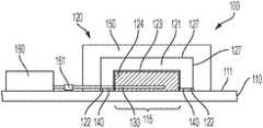
- FIG. 1Ashows a side cross sectional view of a portion of an apparatus in accordance with some embodiments
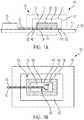
- FIG. 1Bshows a bottom view of the apparatus of FIG. 1A without the gas-emitting material and from the perspective of looking through a clear structure;
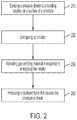
- FIG. 2is a flow diagram illustrating an approach for fracturing a structure in a controlled, triggerable manner in accordance with some embodiments
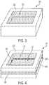
- FIG. 3illustrates a vessel suitable for use in a pressure device in accordance with some configurations
- FIG. 4depicts a multi-piece vessel suitable for use in a pressure device in accordance with some configurations
- FIG. 5is a flow diagram of a method of making an apparatus in accordance with some embodiments.
- FIGS. 6A through 6Eare a series of diagrams that illustrate formation of a pressure device in accordance with some embodiments.
- FIGS. 7A and 7Billustrate fabrication of an apparatus that includes a pressure device in accordance with one example.
- Embodiments disclosed hereinrelate to approaches for fracturing structures into smaller pieces in a controlled, triggerable manner.
- Frangible glass structuresespecially when tempered; e.g., by chemical ion-exchange or by thermal quenching, are structurally very strong and become increasingly difficult to fracture with increasing thickness. Many applications require the robustness or stiffness of thicker glass.
- devices capable of reliably and controllably fracturing the thick structuresinclude pressure devices with electrical initiators.
- the pressure devices disclosed hereincan be physically small and light weight yet provide mechanical and operational robustness that avoids unintentional triggering.
- the controlled fracturingcan reduce the volume of waste at the end of a structure's useful life and/or can facilitate recycling the structure materials.
- the disclosed approachescan be used for fragmentation and/or destruction of various planar and 3D structures, such as mechanical parts, enclosures, aerospace components, windows, ocean buoys, electronic substrates, among other structures.
- FIG. 1Ashows a side cross sectional view of a portion of an apparatus 100 in accordance with some embodiments.
- the apparatus 100includes a structure 110 to which a pressure vessel 120 is mounted.
- FIG. 1Bshows a bottom view of the apparatus 100 from the perspective of looking through a clear structure 110 .
- the gas-emitting material 124 shown in FIG. 1Ais absent in FIG. 1B .
- the structure 110may be any type of structure and have any suitable geometrical configuration.
- the structure 110may be made of a brittle or frangible material such as glass, ceramic, plastic, laminated fillers of wood, metal or gypsum, clay, porcelain, and/or metal.
- the frangible materialmay be disposed at least at the bonding location 115 where the pressure device 120 is bonded to the structure 110 .
- the structure 110is glass.
- a glass structurecan comprise one or more of cast glass, slumped glass, untempered glass, tempered glass, thermally tempered glass, ion-exchanged glass, soda-lime glass, lead glass, borosilicate glass, aluminosilicate glass, alkali-aluminosilicate glass, silica glass, and sodium-rich glass.
- the pressure device 120can be configured to fracture a glass structure that is more than about 0.5 mm thick at the bonding location 115 of the structure 110 .
- the thickness of the structure 110 at the bonding location 115may be about 1 mm thick, about 2 mm thick or even greater than 2 mm thick.
- the pressure device 120comprises a vessel 121 having a bonding surface 122 and an interior space 123 .
- the bonding surface 122bonds the vessel 121 to a surface 111 of the structure 110 at a bonding location 115 of the structure 110 .
- a bonding agent 140is disposed between the bonding surface 122 of the vessel 121 and the surface 111 of the structure 110 at the bonding location 115 .
- the vessel 121may be made of a material comprising one or more of a metal, acrylic, plastic, rubber, ceramic, cement, thermoplastic, compacted sand, wood, and glass, for example.
- the bonding agent 140may comprise one or more of various types of epoxies, cyanoacrylates, structural adhesives, steel-reinforced adhesives, silicone, thermoset plastics, acrylic, urethane, UV curable adhesives, ethylene vinyl acetate, solder, welding interface material, and construction adhesives.
- the bonding agent 140 and the bonding surface 122are configured to bond the vessel 121 to the bonding location 115 on the surface 111 of the structure 110 with a bonding force greater than a fracture limit of the structure 110 over a cross-sectional area 199 bounded by an inner perimeter 125 of the interior space 123 of the vessel 121 at the bonding surface 122 .
- the fracture limitis the force at which the structure 110 fractures.
- the fracture limit of the structure 110 at the bonding location 115may be greater than about 5 MPa.
- an optional backing material 150may be disposed at least partially over the vessel 121 .
- the backing material 150may be disposed over surfaces 127 of the vessel 121 opposite and/or adjacent to the bonding surface 122 .
- the backing material 150bonds the vessel 121 to the surface 111 of the structure 110 and may work in conjunction with the bonding agent 140 to hold the pressure vessel 120 against the structure 110 .
- Suitable materials for the backing material 150may comprise at least one of concrete, structural adhesives, and an epoxy potting compound, for example.
- a gas-emitting material 124comprising chemical compounds such as potassium nitrate, sodium azide, ammonium perchlorate, ammonium nitrate, or ammonium dinitramide, is contained within the interior space 123 of the vessel 121 .
- the gas-emitting material 124is in contact with or in close proximity to one or both of the surface 111 of the structure 110 and the interior surface of the vessel 121 .
- An electrical initiator 130is arranged to activate the gas-emitting material 124 .
- the gas-emitting material 124is in contact or in close proximity to the electrical initiator 130 but not in contact with either surface 111 of the structure 110 or the interior surface of vessel 121 .
- Gas-emitting material 124may occupy a very small percentage of the volume of interior space 123 or may fully fill the interior space 123 .
- the initiator 130may be disposed within the interior space 123 of the vessel 121 and/or may be arranged to be in contact with the gas-emitting material 124 .
- the initiator 130can be embedded within the gas-emitting material 123 in some implementations with leads (wires 131 ) extending from the vessel 121 as shown in FIGS. 1A and 1B .
- the electrical initiator 130is energized by a current flowing through a pair of electrically conductive wires 131 that are electrically connected by an electrically conductive bridge 132 .
- the bridge 132comprises a material having a higher electrical resistance than the wires 131 .
- the bridge 132may be a nichrome alloy and the wires 131 may be copper or aluminum.
- the bridge 132 and/or the wires 131are coated with a pyrogenic material.
- the pyrogenic material coating the bridge 132 and/or wires 131may be the same as or different from the gas-emitting material 124 that is disposed within the interior space 123 of the vessel 121 .
- the pyrogenic coatingenhances the heat from the electrical bridge 132 to more effectively activate the gas-emitting material 124 .
- initiator 130When initiator 130 is energized by an electric current flowing through the electrically conductive elements 131 , 132 of the initiator 130 , the gas-emitting material 124 is heated by the wires 131 , bridge 132 and/or additional pyrogenic material coating the wires 131 and/or bridge 132 to an activation temperature of the gas-emitting material 124 .
- Activation of the gas-emitting material 124causes a rapid release of gas.
- the rapid release of gas within the vessel 121which is tightly bonded to the surface 111 of the structure 110 , produces a localized pressure that breaks the structure 110 .
- the apparatus 100includes a current source 160 , such as a battery, configured to supply the electrical current to the initiator 130 .
- a switch 161electrically connects the source 160 to the initiator 130 .
- the switch 161(shown in FIG. 1A ) can be remotely controlled allowing fracture of the structure 110 to be triggered from a location remote from the structure 110 .
- a wireless signalactivates the switch 161 to connect the current source 160 to the initiator 130 .
- the switch 161is a MOSFET transistor that can be turned on or off by applying a bias voltage at the transistor's gate.
- the switch 161is a silicon-controlled rectifier that can be turned on by applying a small current at one of its terminals.
- the switch 161can be a mechanical relay switch.
- FIG. 2is a flow diagram illustrating an approach for fracturing a structure in a controlled, triggerable manner in accordance with some embodiments.
- At least one pressure deviceis bonded 210 to a surface of the structure.
- the pressure devicemay be a compact modular self-contained unit that can be attached to the frangible glass structure by a bonding agent, such as an adhesive, as previously discussed.
- the pressure deviceincludes a vessel having a gas-emitting material disposed therein.
- An electrical initiator arranged to activate the gas-emitting materialis energized 220 with an electrical current, resulting in activation 230 of a gas-emitting material.
- the electrical current flowing through the resistive bridgeheats the bridge to a high temperature.
- the heated bridgee.g., a small, low-cost Ni-chrome wire, activates the gas-emitting material.
- Both the gas-emitting material and the initiatorare confined within the small localized interior space of the vessel attached to the glass.
- gasesare rapidly generated by the activated gas-emitting material producing 240 a localized pressure in the area of the bonding location. The rapid pressure build-up at bonding location causes the structure to fracture.
- the temperature rise caused by electrical current flowing through the heater bridge aloneis insufficient to activate the gas-emitting material.
- the heater bridgeis coated with a pyrogenic material that can be ignited at a lower threshold temperature. Electrical current causes the heater bridge to ignite the pyrogenic material, which then burns at a high temperature to activate the gas-emitting material.
- Energizing the initiatormay comprise connecting an electrical source to the initiator such that the electrical source produces an electrical current through the initiator.
- Initiatorsmay be energized using simple 9V alkaline batteries, for example, or with voltage sources of as low as 0.1 V supplying electrical currents of about 100 mA. In implementations where ease of handling is important, the typical source voltages are 6 to 12 V supplying currents of 2 to 4 amps. Typical portable sources could be Alkaline or Lithium-based batteries.
- the initiatormay be remotely energized, or may be energized when a timer circuit reaches a predetermined time or elapsed time.
- FIGS. 3 and 4illustrate vessels 321 , 421 suitable for use in a pressure device in accordance with various configurations.
- the vessels a 321 , 421are designed to withstand the impact pressure of the rapidly released gases that occurs upon activation of the gas-emitting material.
- FIG. 3illustrates a vessel 321 suitable for use in a pressure device in accordance with some configurations.
- the vessel 321is a unitary structure that can be fabricated by subtractive, additive, and/or deformative manufacturing processes to remove, add, and/or deform the material of the vessel 321 such that the vessel 321 includes the interior space 323 and bonding surface 322 .
- vessel 321may be fabricated from a relatively thick solid piece by removing material, e.g., by milling, and/or cutting to form the interior space 323 and/or bonding surface 322 .
- Additive manufacturing processes that can optionally be used to form the vessel 321include molding and/or printing.
- the vessel 321may be molded by an injection molding process or other molding processes.
- the vessel 321may formed from a relatively thinner solid piece by stamping or otherwise deforming the original piece to form the interior space 323 and/or the bonding surface 322 .
- the vessel 421may comprise several pieces 421 a , 421 b that are bonded together by a bonding agent 429 .
- Vessel 421may be formed by first piece 421 a having a through hole 427 and a second piece 421 b that is bonded to the first piece 421 a forming a cover for the hole 427 in the first piece 421 a .
- the first and second pieces 421 a , 421 bmay be made by any suitable manufacturing process such as water-jet cutting, laser cutting, or processes including those previously discussed in connection with FIG. 3 , e.g., milling, cutting, stamping, molding, printing, etc.
- the bonding agent 429may be the same as or different from the bonding material used to bond the vessel to the structure.
- FIG. 5is a flow diagram of a method of making an apparatus as illustrated in FIGS. 1A and 1B .
- pressure devices used to fracture glass structuresinclude vessels constructed of low-cost laser-cut acrylic materials or water-jet-cut aluminum. The vessels themselves can be designed to withstand the impact pressure upon activation of the gas-emitting material.
- the apparatusis configured such that activation of the pressure device destroys the structure by causing the structure to fracture.
- the methodinvolves forming 510 a pressure device and bonding 520 the pressure device to the surface of a structure.
- Forming 510 the pressure deviceincludes fabricating or otherwise providing 511 a vessel having an interior space and a bonding surface.
- An initiatoris arranged 512 within the interior space of the vessel and may be affixed in the interior space. The wires of the initiator may extend through a wall of the vessel.
- the initiatormay be pre-coated with a gas-emitting material before it is arranged within the interior space of the vessel.
- the interior spaceis partially or completely filled with one or more additional gas-emitting materials 513 .
- the gas-emitting material used to partially or completely fill the interior spacemay be the same as or different from the gas-emitting material that coats the initiator.
- step 513may be optional and can be eliminated.
- FIGS. 6A through 6Eare a series of diagrams that illustrate formation of a pressure device 620 in accordance with some embodiments.
- FIG. 6Ashows a two-piece vessel 621 comprising first and second pieces 621 a , 621 b similar to the configuration shown in FIG. 4 .
- the vessel 621has an interior space 623 and bonding surface 622 .
- the interior space 623is defined by the interior surfaces of the walls 625 and back 626 of the vessel 621 .
- the front of the vessel 621is open in this example.
- One wall 625 of the vessel 621includes a channel 621 c that provides a pass through for wires of the initiator.
- the vessel 621has outer dimensions of 25 mm ⁇ 18 mm with wall thickness of 5 mm as illustrated in FIG. 6B .
- the thickness of the vessel 621may be about 5 mm.
- the ratio of the surface area of the bonding surface to the volume of the interior spaceis greater than about 0.05 cm ⁇ 1 . In some embodiments, the ratio of the surface area of the bonding surface to the volume of the interior space is greater than about 0.6 cm ⁇ 1 and less than about 5 cm ⁇ 1 .
- FIG. 6Cillustrates the pressure device 620 after the initiator 630 is placed inside the interior space 623 of the vessel 621 .
- One wall 625 of the vessel 621includes a channel 621 c providing a pass through for wires 631 of the initiator 630 .
- the wires 631are electrically connected by a bridge 632 which optionally has a pyrogenic material disposed thereon.
- FIG. 6Dillustrates the process of filling the interior space 623 with the gas-emitting material 624 .
- FIG. 6Eshows the completed pressure device 620 . In embodiments where bridge 632 has gas-emitting materials disposed there-on, the step illustrated in FIG. 6D may be omitted.
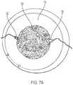
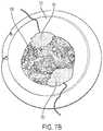
- FIGS. 7A and 7Billustrate fabrication of an apparatus that includes a pressure device in accordance with one example.
- the structureis a glass buoy meant to be deployed in the ocean.
- the buoycan be remotely scuttled when it is no longer needed.
- the buoyis made of a glass bowl that is bonded to a planar top plate cover to form an enclosure.
- the enclosurecontains sensors, control electronics, optical components, and radio communication devices.
- FIG. 7Ashows two pressure devices 720 such as those described herein bonded to an inside surface of glass bowl 710 of the buoy.
- the glass bowl 710is partially filled with concrete 780 that functions as ballast.
- an optional additional amount of concrete 781is added as a backing material that partially covers the pressure devices 710 and further bonds the pressure devices 720 to the bowl 710 .
- the buoyis not entirely made of glass.
- the enclosurecan be mostly plastic or metal that is outfitted with a glass window.
- the pressure deviceis bonded on the glass window. Activation of the pressure device causes the glass window to fracture, thereby breaching the enclosure and causing the buoy to sink.
- the gas-emitting material within the pressure devicesis activated causing a rapid expansion of gas that produces a force sufficient to fracture the buoy causing it to sink.
- the structure fractured by activation of the pressure devicemay break in to small fragments, e.g., fragments that have length, width, and height dimensions of less than about 10 mm, 900 ⁇ m, less than about 500 ⁇ m, or even less than about 100 ⁇ m.
- Pressure devices used to fracture glass structuresinclude vessels constructed of low-cost laser-cut acrylic, water-jet aluminum, or stamped metal.
- the vesselscan be designed to withstand the impact pressure upon trigger. Unlike most mechanical approaches, the disclosed approach is stable against unintentional trigger.
Landscapes
- Engineering & Computer Science (AREA)
- General Engineering & Computer Science (AREA)
- Manufacturing & Machinery (AREA)
- Chemical & Material Sciences (AREA)
- Combustion & Propulsion (AREA)
- Mechanical Engineering (AREA)
- Ocean & Marine Engineering (AREA)
- Disintegrating Or Milling (AREA)
- Lining Or Joining Of Plastics Or The Like (AREA)
- Air Bags (AREA)
- Processing Of Solid Wastes (AREA)
Abstract
Description
Claims (38)
Priority Applications (3)
| Application Number | Priority Date | Filing Date | Title |
|---|---|---|---|
| US16/403,131US10969205B2 (en) | 2019-05-03 | 2019-05-03 | Electrically-activated pressure vessels for fracturing frangible structures |
| JP2020068659AJP7362540B2 (en) | 2019-05-03 | 2020-04-06 | Electrically activated pressure vessel for destroying fragile structures |
| EP20171951.5AEP3741657A3 (en) | 2019-05-03 | 2020-04-28 | Electrically-activated pressure vessels for fracturing frangible structures |
Applications Claiming Priority (1)
| Application Number | Priority Date | Filing Date | Title |
|---|---|---|---|
| US16/403,131US10969205B2 (en) | 2019-05-03 | 2019-05-03 | Electrically-activated pressure vessels for fracturing frangible structures |
Publications (2)
| Publication Number | Publication Date |
|---|---|
| US20200348112A1 US20200348112A1 (en) | 2020-11-05 |
| US10969205B2true US10969205B2 (en) | 2021-04-06 |
Family
ID=70476091
Family Applications (1)
| Application Number | Title | Priority Date | Filing Date |
|---|---|---|---|
| US16/403,131Active2039-08-19US10969205B2 (en) | 2019-05-03 | 2019-05-03 | Electrically-activated pressure vessels for fracturing frangible structures |
Country Status (3)
| Country | Link |
|---|---|
| US (1) | US10969205B2 (en) |
| EP (1) | EP3741657A3 (en) |
| JP (1) | JP7362540B2 (en) |
Families Citing this family (2)
| Publication number | Priority date | Publication date | Assignee | Title |
|---|---|---|---|---|
| US11904986B2 (en)* | 2020-12-21 | 2024-02-20 | Xerox Corporation | Mechanical triggers and triggering methods for self-destructing frangible structures and sealed vessels |
| US12013043B2 (en) | 2020-12-21 | 2024-06-18 | Xerox Corporation | Triggerable mechanisms and fragment containment arrangements for self-destructing frangible structures and sealed vessels |
Citations (100)
| Publication number | Priority date | Publication date | Assignee | Title |
|---|---|---|---|---|
| US1839884A (en)* | 1929-08-27 | 1932-01-05 | Gen Fire Extinguisher Co | Frangible vessel and method of making the same |
| US2529210A (en) | 1947-05-23 | 1950-11-07 | Joseph F Butler | Cutting apparatus for wallboards and the like |
| US3397278A (en) | 1965-05-06 | 1968-08-13 | Mallory & Co Inc P R | Anodic bonding |
| US3601114A (en) | 1969-01-21 | 1971-08-24 | Norton Co | Method and apparatus for cutting complex shapes |
| US3666967A (en) | 1971-05-12 | 1972-05-30 | Us Navy | Self-destruct aluminum-tungstic oxide films |
| US3673667A (en) | 1970-11-23 | 1972-07-04 | Whittaker Corp | Method for producing complex shapes by filled billet extrusion |
| US3882323A (en) | 1973-12-17 | 1975-05-06 | Us Navy | Method and apparatus for protecting sensitive information contained in thin-film microelectonic circuitry |
| US4102664A (en) | 1977-05-18 | 1978-07-25 | Corning Glass Works | Method for making glass articles with defect-free surfaces |
| US4139359A (en) | 1977-11-02 | 1979-02-13 | Ppg Industries, Inc. | Method and apparatus for shaping glass sheets by roll forming |
| US4155307A (en) | 1976-11-30 | 1979-05-22 | Her Majesty The Queen In Right Of Canada, As Represented By The Minister Of National Defence | Scuttling method for marine markers |
| US4471895A (en) | 1982-04-28 | 1984-09-18 | Lisec Peter Jun | Process and apparatus for cutting laminated glass |
| US4558622A (en) | 1983-11-04 | 1985-12-17 | Russell Tausheck | Apparatus for cutting laminated glass |
| US4598274A (en) | 1983-08-18 | 1986-07-01 | Romag Holdings Ltd. | Security and protection panel |
| US4673453A (en) | 1983-05-04 | 1987-06-16 | Ab Hydro Betong | Method of making a structural body |
| US4739555A (en) | 1985-06-18 | 1988-04-26 | Werner Jurgens | Laminated glass cutter |
| US5374564A (en) | 1991-09-18 | 1994-12-20 | Commissariat A L'energie Atomique | Process for the production of thin semiconductor material films |
| US5584219A (en) | 1992-01-29 | 1996-12-17 | Dunn; Kenneth R. | Release device for multi glazing air cushion |
| US5791056A (en) | 1996-11-22 | 1998-08-11 | Messina; Gary D. | Emergency glass breaking tool |
| WO2001043228A1 (en) | 1999-12-07 | 2001-06-14 | Robert Bosch Gmbh | Leaky wave antenna |
| US6327978B1 (en)* | 1995-12-08 | 2001-12-11 | Kaman Aerospace Corporation | Exploding thin film bridge fracturing fragment detonator |
| US6418628B1 (en) | 2001-03-22 | 2002-07-16 | Task Force Tips, Inc. | Spring-loaded car window breaker and retractable safety sheath |
| US6441354B1 (en)* | 1998-09-18 | 2002-08-27 | Marc Seghatol | Microwave polymerization system for dentistry |
| US20030089755A1 (en) | 2001-11-10 | 2003-05-15 | Peers-Smith Roy Peter | Device for breaking glass |
| US20040031966A1 (en) | 2002-08-16 | 2004-02-19 | Forrest Stephen R. | Organic photonic integrated circuit using a photodetector and a transparent organic light emitting device |
| US20040222500A1 (en) | 2001-04-13 | 2004-11-11 | Bernard Aspar | Detachable substrate with controlled mechanical hold and method for production thereof |
| US20050061032A1 (en) | 2002-08-22 | 2005-03-24 | Hideo Yoshizawa | Method and device for forming multi-curved glass sheet |
| US20050084679A1 (en) | 2003-09-19 | 2005-04-21 | Universita ' Degli Studi Di Trento | ESP glass rupture disks, design and manufacture thereof |
| US20050082331A1 (en) | 2003-10-17 | 2005-04-21 | Chi-Hong Yang | Tempered glass breaker |
| US6926204B2 (en) | 2002-03-13 | 2005-08-09 | Commissariat A L'energie Atomique | Secure electronic device |
| US20050176573A1 (en) | 2003-03-05 | 2005-08-11 | Frank Thoma | Nondestructive ion exchange in phosphate glasses |
| DE102004015546A1 (en) | 2004-03-30 | 2005-10-20 | Infineon Technologies Ag | Semiconductor chip for security-relevant applications with integrated circuit has light-sensitive state change device that alters state stored in state storage device when light incident and stored state monitoring device |
| US7002517B2 (en) | 2003-06-20 | 2006-02-21 | Anritsu Company | Fixed-frequency beam-steerable leaky-wave microstrip antenna |
| US7068254B2 (en) | 2000-05-09 | 2006-06-27 | Semiconductor Energy Laboratory Co., Ltd. | User identity authentication system and user identity authentication method and mobile telephonic device |
| US20060138798A1 (en) | 2003-02-12 | 2006-06-29 | Saint-Gobain Glass France | Glazing comprising break lines |
| US20060270190A1 (en) | 2005-05-25 | 2006-11-30 | The Regents Of The University Of California | Method of transferring a thin crystalline semiconductor layer |
| US7153758B2 (en) | 2003-02-28 | 2006-12-26 | Hitachi, Ltd. | Anodic bonding method and electronic device having anodic bonding structure |
| US20070113886A1 (en) | 2005-11-18 | 2007-05-24 | Semiconductor Energy Laboratory Co., Ltd. | Photoelectric conversion device |
| US20080029195A1 (en) | 2006-07-05 | 2008-02-07 | Zhong-Hao Lu | Electrode Pattern For Resistance Heating Element and Wafer processing Apparatus |
| US20080311686A1 (en) | 2005-08-03 | 2008-12-18 | California Institute Of Technology | Method of Forming Semiconductor Layers on Handle Substrates |
| US20090086170A1 (en) | 2007-09-27 | 2009-04-02 | Ostendo Technologies, Inc. | Quantum Photonic Imagers and Methods of Fabrication Thereof |
| US7554085B2 (en) | 2003-10-09 | 2009-06-30 | Ocas Corp. | Bolometric infrared sensor having two-layer structure and method for manufacturing the same |
| US20100035038A1 (en) | 2008-08-08 | 2010-02-11 | Barefoot Kristen L | Strengthened glass articles and methods of making |
| US20100133641A1 (en) | 2008-12-03 | 2010-06-03 | Tae Gyu Kim | Image Sensor and Method for Manufacturing the Same |
| US20100225380A1 (en) | 2009-03-03 | 2010-09-09 | International Business Machines Corporation | Implementing Tamper Resistant Integrated Circuit Chips |
| US7880248B1 (en) | 2005-10-17 | 2011-02-01 | Teledyne Technologies Incorporated | Destructor integrated circuit chip, interposer electronic device and methods |
| US7896988B2 (en) | 2007-06-15 | 2011-03-01 | Spectre Enterprises, Inc. | Charge system for destroying chips on a circuit board and method for destroying chips on a circuit board |
| US20110048756A1 (en) | 2009-09-03 | 2011-03-03 | Shuxian Shi | Security protection device and method |
| US20110089506A1 (en) | 2008-06-13 | 2011-04-21 | Nxp B.V. | Intrusion protection using stress changes |
| US7944049B2 (en) | 2008-03-04 | 2011-05-17 | Elpida Memory, Inc. | Semiconductor device and manufacturing method thereof |
| US20110183116A1 (en) | 2010-01-27 | 2011-07-28 | Jeng-Jye Hung | Method for cutting tempered glass and preparatory tempered glass structure |
| US20120052252A1 (en) | 2010-08-26 | 2012-03-01 | Jeffrey Todd Kohli | Methods for extracting strengthened glass substrates from glass sheets |
| US8130072B2 (en) | 2009-05-14 | 2012-03-06 | Palo Alto Research Center Incorporated | Vanadium oxide thermal microprobes |
| US20120135177A1 (en) | 2010-11-30 | 2012-05-31 | Cornejo Ivan A | Methods for forming grooves and separating strengthened glass substrate sheets |
| US20120135195A1 (en) | 2010-11-30 | 2012-05-31 | Gregory Scott Glaesemann | Methods for separating glass articles from strengthened glass substrate sheets |
| US20120196071A1 (en) | 2011-02-01 | 2012-08-02 | Cornejo Ivan A | Strengthened glass substrate sheets and methods for fabricating glass panels from glass substrate sheets |
| US20120288676A1 (en) | 2009-12-01 | 2012-11-15 | Saint-Gobain Glass France | Method for structuring a surface by means of ion-beam etching, structured surface and uses |
| US20130000469A1 (en)* | 2011-07-01 | 2013-01-03 | Applied Explosives Technology Pty Limited | Shell destruction technique |
| US20130037308A1 (en) | 2011-08-12 | 2013-02-14 | Wintek Corporation | Reinforced glass cell and method for fabricating the same and cover glass having the reinforced glass cell |
| US20130082383A1 (en) | 2011-10-03 | 2013-04-04 | Texas Instruments Incorporated | Electronic assembly having mixed interface including tsv die |
| US8448554B2 (en)* | 2009-03-31 | 2013-05-28 | Kabushiki Kaisha Kobe Seiko Sho | Blast treatment method and blast treatment device |
| US20130140649A1 (en) | 2011-12-01 | 2013-06-06 | John A. Rogers | Transient devices designed to undergo programmable transformations |
| US8495944B2 (en)* | 2009-03-31 | 2013-07-30 | Kobe Steel, Ltd. | Blast treatment method and blast treatment device |
| US20130192305A1 (en) | 2011-08-10 | 2013-08-01 | Matthew L. Black | Methods for separating glass substrate sheets by laser-formed grooves |
| US20130273717A1 (en) | 2012-04-17 | 2013-10-17 | Taiwan Semiconductor Manufacturing Co., Ltd. | Apparatus and Method for the Singulation of a Semiconductor Wafer |
| US20140060347A1 (en)* | 2012-10-19 | 2014-03-06 | Javad Sahebkar Yazdi | Universal Recycling & Disposal Machine (URDM) |
| US8671814B2 (en)* | 2009-03-31 | 2014-03-18 | National Institute Of Advanced Industrial Science And Technology | Blast treatment method and blast treatment device |
| US20140091374A1 (en) | 2012-09-28 | 2014-04-03 | International Business Machines Corporation | STRESS ENGINEERED MULTI-LAYERS FOR INTEGRATION OF CMOS AND Si NANOPHOTONICS |
| US20140103957A1 (en) | 2012-10-17 | 2014-04-17 | International Business Machines Corporation | Reactive material for integrated circuit tamper detection and response |
| US8740030B2 (en) | 2007-09-08 | 2014-06-03 | Stephen Maher | Glass breaking device |
| US20140266946A1 (en) | 2013-03-15 | 2014-09-18 | Searete Llc | Surface scattering antenna improvements |
| US20140300520A1 (en) | 2011-04-07 | 2014-10-09 | Polyvalor, Limited Partnership | Full-space scanning end-switched crlh leaky-wave antenna |
| US20140323968A1 (en) | 2013-04-12 | 2014-10-30 | The Board Of Trustees Of The University Of Illinois | Materials, electronic systems and modes for active and passive transience |
| US20150001733A1 (en) | 2013-06-28 | 2015-01-01 | Omkar G. Karhade | Reliable microstrip routing for electronics components |
| US20150044445A1 (en) | 2013-08-07 | 2015-02-12 | Corning Incorporated | Laser controlled ion exchange process and glass articles formed therefrom |
| US20150076677A1 (en) | 2012-04-13 | 2015-03-19 | Silex Microsystems Ab | Cte matched interposer and method of making |
| US20150089977A1 (en) | 2009-11-30 | 2015-04-02 | Corning Incorporated | Methods for laser scribing and separating glass substrates |
| US20150102852A1 (en) | 2013-10-11 | 2015-04-16 | Palo Alto Research Center Incorporated | Stressed Substrates For Transient Electronic Systems |
| US20150121964A1 (en) | 2012-03-31 | 2015-05-07 | Luoy-Ang Landglass Technology Co., Ltd. | Method for manufacturing columnar curved tempered glass |
| US20150229028A1 (en) | 2010-10-15 | 2015-08-13 | Searete Llc | Surface scattering antennas |
| US20150232369A1 (en) | 2013-12-17 | 2015-08-20 | Corning Incorporated | Laser cutting of display glass compositions |
| US20150318618A1 (en) | 2014-05-02 | 2015-11-05 | Searete Llc | Surface scattering antennas with lumped elements |
| US20150348940A1 (en) | 2014-05-28 | 2015-12-03 | Invensas Corporation | Structure and method for integrated circuits packaging with increased density |
| US20150358021A1 (en) | 2013-10-11 | 2015-12-10 | Palo Alto Research Center Incorporated | Thermally Tempered Glass Substrate Using CTE Mismatched Layers And Paste Mixtures For Transient Electronic Systems |
| US20150372389A1 (en) | 2014-06-20 | 2015-12-24 | Searete Llc, A Limited Liability Corporation Of The State Of Delaware | Modulation patterns for surface scattering antennas |
| US9294098B2 (en) | 2013-11-26 | 2016-03-22 | Lawrence Livermore National Security, Llc | System and method for on demand, vanishing, high performance electronic systems |
| US20160122225A1 (en) | 2013-07-30 | 2016-05-05 | Nippon Electric Glass Co., Ltd. | Method for manufacturing glass plate having curved shape, glass plate having curved shape, and manufacturing apparatus for glass plate having curved shape |
| US20160137548A1 (en) | 2014-11-17 | 2016-05-19 | International Business Machines Corporation | Controlling fragmentation of chemically strengthened glass |
| EP3086363A1 (en) | 2015-04-23 | 2016-10-26 | Palo Alto Research Center Incorporated | Transient electronic device with ion-exchanged glass treated interposer |
| US20170036942A1 (en) | 2012-06-05 | 2017-02-09 | Corning Incorporated | Methods of cutting glass using a laser |
| US9577047B2 (en) | 2015-07-10 | 2017-02-21 | Palo Alto Research Center Incorporated | Integration of semiconductor epilayers on non-native substrates |
| US9630870B2 (en) | 2012-03-31 | 2017-04-25 | Luoyang Landglass Technology Co., Ltd | Method for manufacturing columnar curved tempered glass |
| US20170217818A1 (en) | 2014-07-24 | 2017-08-03 | Saint-Gobain Glass France | Method for breaking out a sheet of glass |
| US20170292546A1 (en) | 2016-04-06 | 2017-10-12 | Palo Alto Research Center Incorporated | Complex Stress-Engineered Frangible Structures |
| US20180033577A1 (en) | 2016-07-26 | 2018-02-01 | Palo Alto Research Center Incorporated | Self-Limiting Electrical Triggering for Initiating Fracture of Frangible Glass |
| US20180033742A1 (en) | 2016-07-26 | 2018-02-01 | Palo Alto Research Center Incorporated | Sensor and heater for stimulus-initiated self-destructing substrate |
| US20180114761A1 (en) | 2016-10-20 | 2018-04-26 | Palo Alto Research Center Incorporated | Pre-conditioned self-destructing substrate |
| US10026651B1 (en) | 2017-06-21 | 2018-07-17 | Palo Alto Research Center Incorporated | Singulation of ion-exchanged substrates |
| US20190106069A1 (en) | 2017-10-06 | 2019-04-11 | Ford Global Technologies, Llc | Monitoring of vehicle window vibrations for voice-command recognition |
| US10308543B2 (en) | 2012-08-08 | 2019-06-04 | Corning Precision Materials Co., Ltd. | Cutting method and cutting stage of toughened glass |
| US10717669B2 (en) | 2018-05-16 | 2020-07-21 | Palo Alto Research Center Incorporated | Apparatus and method for creating crack initiation sites in a self-fracturing frangible member |
Family Cites Families (5)
| Publication number | Priority date | Publication date | Assignee | Title |
|---|---|---|---|---|
| WO1986007000A1 (en)* | 1985-05-28 | 1986-12-04 | Explosive Developments Limited | Explosive cutting means |
| JPH0938950A (en)* | 1995-07-31 | 1997-02-10 | Hitachi Zosen Corp | Destruction device for objects to be destroyed |
| JPH10331446A (en)* | 1997-05-30 | 1998-12-15 | Hitachi Zosen Corp | Discharge impact destruction method and discharge impact destruction device |
| JP3328184B2 (en)* | 1998-03-06 | 2002-09-24 | 日立造船株式会社 | Destruction method |
| US8006621B1 (en)* | 2008-02-07 | 2011-08-30 | Cherry Christopher R | Linear explosive breaching apparatus and method |
- 2019
- 2019-05-03USUS16/403,131patent/US10969205B2/enactiveActive
- 2020
- 2020-04-06JPJP2020068659Apatent/JP7362540B2/enactiveActive
- 2020-04-28EPEP20171951.5Apatent/EP3741657A3/enactivePending
Patent Citations (109)
| Publication number | Priority date | Publication date | Assignee | Title |
|---|---|---|---|---|
| US1839884A (en)* | 1929-08-27 | 1932-01-05 | Gen Fire Extinguisher Co | Frangible vessel and method of making the same |
| US2529210A (en) | 1947-05-23 | 1950-11-07 | Joseph F Butler | Cutting apparatus for wallboards and the like |
| US3397278A (en) | 1965-05-06 | 1968-08-13 | Mallory & Co Inc P R | Anodic bonding |
| US3601114A (en) | 1969-01-21 | 1971-08-24 | Norton Co | Method and apparatus for cutting complex shapes |
| US3673667A (en) | 1970-11-23 | 1972-07-04 | Whittaker Corp | Method for producing complex shapes by filled billet extrusion |
| US3666967A (en) | 1971-05-12 | 1972-05-30 | Us Navy | Self-destruct aluminum-tungstic oxide films |
| US3882323A (en) | 1973-12-17 | 1975-05-06 | Us Navy | Method and apparatus for protecting sensitive information contained in thin-film microelectonic circuitry |
| US4155307A (en) | 1976-11-30 | 1979-05-22 | Her Majesty The Queen In Right Of Canada, As Represented By The Minister Of National Defence | Scuttling method for marine markers |
| US4102664A (en) | 1977-05-18 | 1978-07-25 | Corning Glass Works | Method for making glass articles with defect-free surfaces |
| US4139359A (en) | 1977-11-02 | 1979-02-13 | Ppg Industries, Inc. | Method and apparatus for shaping glass sheets by roll forming |
| US4471895A (en) | 1982-04-28 | 1984-09-18 | Lisec Peter Jun | Process and apparatus for cutting laminated glass |
| US4673453A (en) | 1983-05-04 | 1987-06-16 | Ab Hydro Betong | Method of making a structural body |
| US4598274A (en) | 1983-08-18 | 1986-07-01 | Romag Holdings Ltd. | Security and protection panel |
| US4558622A (en) | 1983-11-04 | 1985-12-17 | Russell Tausheck | Apparatus for cutting laminated glass |
| US4739555A (en) | 1985-06-18 | 1988-04-26 | Werner Jurgens | Laminated glass cutter |
| US5374564A (en) | 1991-09-18 | 1994-12-20 | Commissariat A L'energie Atomique | Process for the production of thin semiconductor material films |
| US5584219A (en) | 1992-01-29 | 1996-12-17 | Dunn; Kenneth R. | Release device for multi glazing air cushion |
| US6327978B1 (en)* | 1995-12-08 | 2001-12-11 | Kaman Aerospace Corporation | Exploding thin film bridge fracturing fragment detonator |
| US5791056A (en) | 1996-11-22 | 1998-08-11 | Messina; Gary D. | Emergency glass breaking tool |
| US6441354B1 (en)* | 1998-09-18 | 2002-08-27 | Marc Seghatol | Microwave polymerization system for dentistry |
| WO2001043228A1 (en) | 1999-12-07 | 2001-06-14 | Robert Bosch Gmbh | Leaky wave antenna |
| US7068254B2 (en) | 2000-05-09 | 2006-06-27 | Semiconductor Energy Laboratory Co., Ltd. | User identity authentication system and user identity authentication method and mobile telephonic device |
| US6418628B1 (en) | 2001-03-22 | 2002-07-16 | Task Force Tips, Inc. | Spring-loaded car window breaker and retractable safety sheath |
| US20040222500A1 (en) | 2001-04-13 | 2004-11-11 | Bernard Aspar | Detachable substrate with controlled mechanical hold and method for production thereof |
| US20030089755A1 (en) | 2001-11-10 | 2003-05-15 | Peers-Smith Roy Peter | Device for breaking glass |
| US6926204B2 (en) | 2002-03-13 | 2005-08-09 | Commissariat A L'energie Atomique | Secure electronic device |
| US20040031966A1 (en) | 2002-08-16 | 2004-02-19 | Forrest Stephen R. | Organic photonic integrated circuit using a photodetector and a transparent organic light emitting device |
| US20050061032A1 (en) | 2002-08-22 | 2005-03-24 | Hideo Yoshizawa | Method and device for forming multi-curved glass sheet |
| US20060138798A1 (en) | 2003-02-12 | 2006-06-29 | Saint-Gobain Glass France | Glazing comprising break lines |
| US7153758B2 (en) | 2003-02-28 | 2006-12-26 | Hitachi, Ltd. | Anodic bonding method and electronic device having anodic bonding structure |
| US20050176573A1 (en) | 2003-03-05 | 2005-08-11 | Frank Thoma | Nondestructive ion exchange in phosphate glasses |
| US7002517B2 (en) | 2003-06-20 | 2006-02-21 | Anritsu Company | Fixed-frequency beam-steerable leaky-wave microstrip antenna |
| US20050084679A1 (en) | 2003-09-19 | 2005-04-21 | Universita ' Degli Studi Di Trento | ESP glass rupture disks, design and manufacture thereof |
| US7554085B2 (en) | 2003-10-09 | 2009-06-30 | Ocas Corp. | Bolometric infrared sensor having two-layer structure and method for manufacturing the same |
| US20050082331A1 (en) | 2003-10-17 | 2005-04-21 | Chi-Hong Yang | Tempered glass breaker |
| DE102004015546A1 (en) | 2004-03-30 | 2005-10-20 | Infineon Technologies Ag | Semiconductor chip for security-relevant applications with integrated circuit has light-sensitive state change device that alters state stored in state storage device when light incident and stored state monitoring device |
| US20060270190A1 (en) | 2005-05-25 | 2006-11-30 | The Regents Of The University Of California | Method of transferring a thin crystalline semiconductor layer |
| US20080311686A1 (en) | 2005-08-03 | 2008-12-18 | California Institute Of Technology | Method of Forming Semiconductor Layers on Handle Substrates |
| US7880248B1 (en) | 2005-10-17 | 2011-02-01 | Teledyne Technologies Incorporated | Destructor integrated circuit chip, interposer electronic device and methods |
| US20070113886A1 (en) | 2005-11-18 | 2007-05-24 | Semiconductor Energy Laboratory Co., Ltd. | Photoelectric conversion device |
| US20080029195A1 (en) | 2006-07-05 | 2008-02-07 | Zhong-Hao Lu | Electrode Pattern For Resistance Heating Element and Wafer processing Apparatus |
| US7896988B2 (en) | 2007-06-15 | 2011-03-01 | Spectre Enterprises, Inc. | Charge system for destroying chips on a circuit board and method for destroying chips on a circuit board |
| US8740030B2 (en) | 2007-09-08 | 2014-06-03 | Stephen Maher | Glass breaking device |
| US20090086170A1 (en) | 2007-09-27 | 2009-04-02 | Ostendo Technologies, Inc. | Quantum Photonic Imagers and Methods of Fabrication Thereof |
| US7944049B2 (en) | 2008-03-04 | 2011-05-17 | Elpida Memory, Inc. | Semiconductor device and manufacturing method thereof |
| US20110089506A1 (en) | 2008-06-13 | 2011-04-21 | Nxp B.V. | Intrusion protection using stress changes |
| US20100035038A1 (en) | 2008-08-08 | 2010-02-11 | Barefoot Kristen L | Strengthened glass articles and methods of making |
| US20100133641A1 (en) | 2008-12-03 | 2010-06-03 | Tae Gyu Kim | Image Sensor and Method for Manufacturing the Same |
| US20100225380A1 (en) | 2009-03-03 | 2010-09-09 | International Business Machines Corporation | Implementing Tamper Resistant Integrated Circuit Chips |
| US8495944B2 (en)* | 2009-03-31 | 2013-07-30 | Kobe Steel, Ltd. | Blast treatment method and blast treatment device |
| US8671814B2 (en)* | 2009-03-31 | 2014-03-18 | National Institute Of Advanced Industrial Science And Technology | Blast treatment method and blast treatment device |
| US8448554B2 (en)* | 2009-03-31 | 2013-05-28 | Kabushiki Kaisha Kobe Seiko Sho | Blast treatment method and blast treatment device |
| US8130072B2 (en) | 2009-05-14 | 2012-03-06 | Palo Alto Research Center Incorporated | Vanadium oxide thermal microprobes |
| US20110048756A1 (en) | 2009-09-03 | 2011-03-03 | Shuxian Shi | Security protection device and method |
| US20150089977A1 (en) | 2009-11-30 | 2015-04-02 | Corning Incorporated | Methods for laser scribing and separating glass substrates |
| US20120288676A1 (en) | 2009-12-01 | 2012-11-15 | Saint-Gobain Glass France | Method for structuring a surface by means of ion-beam etching, structured surface and uses |
| US20110183116A1 (en) | 2010-01-27 | 2011-07-28 | Jeng-Jye Hung | Method for cutting tempered glass and preparatory tempered glass structure |
| US20120052252A1 (en) | 2010-08-26 | 2012-03-01 | Jeffrey Todd Kohli | Methods for extracting strengthened glass substrates from glass sheets |
| US20150229028A1 (en) | 2010-10-15 | 2015-08-13 | Searete Llc | Surface scattering antennas |
| US20120135195A1 (en) | 2010-11-30 | 2012-05-31 | Gregory Scott Glaesemann | Methods for separating glass articles from strengthened glass substrate sheets |
| US20120135177A1 (en) | 2010-11-30 | 2012-05-31 | Cornejo Ivan A | Methods for forming grooves and separating strengthened glass substrate sheets |
| US20120196071A1 (en) | 2011-02-01 | 2012-08-02 | Cornejo Ivan A | Strengthened glass substrate sheets and methods for fabricating glass panels from glass substrate sheets |
| US20140300520A1 (en) | 2011-04-07 | 2014-10-09 | Polyvalor, Limited Partnership | Full-space scanning end-switched crlh leaky-wave antenna |
| US20130000469A1 (en)* | 2011-07-01 | 2013-01-03 | Applied Explosives Technology Pty Limited | Shell destruction technique |
| US20130192305A1 (en) | 2011-08-10 | 2013-08-01 | Matthew L. Black | Methods for separating glass substrate sheets by laser-formed grooves |
| US20130037308A1 (en) | 2011-08-12 | 2013-02-14 | Wintek Corporation | Reinforced glass cell and method for fabricating the same and cover glass having the reinforced glass cell |
| US20130082383A1 (en) | 2011-10-03 | 2013-04-04 | Texas Instruments Incorporated | Electronic assembly having mixed interface including tsv die |
| US20130140649A1 (en) | 2011-12-01 | 2013-06-06 | John A. Rogers | Transient devices designed to undergo programmable transformations |
| US9630870B2 (en) | 2012-03-31 | 2017-04-25 | Luoyang Landglass Technology Co., Ltd | Method for manufacturing columnar curved tempered glass |
| US20150121964A1 (en) | 2012-03-31 | 2015-05-07 | Luoy-Ang Landglass Technology Co., Ltd. | Method for manufacturing columnar curved tempered glass |
| US20150076677A1 (en) | 2012-04-13 | 2015-03-19 | Silex Microsystems Ab | Cte matched interposer and method of making |
| US20130273717A1 (en) | 2012-04-17 | 2013-10-17 | Taiwan Semiconductor Manufacturing Co., Ltd. | Apparatus and Method for the Singulation of a Semiconductor Wafer |
| US20170036942A1 (en) | 2012-06-05 | 2017-02-09 | Corning Incorporated | Methods of cutting glass using a laser |
| US10308543B2 (en) | 2012-08-08 | 2019-06-04 | Corning Precision Materials Co., Ltd. | Cutting method and cutting stage of toughened glass |
| US20140091374A1 (en) | 2012-09-28 | 2014-04-03 | International Business Machines Corporation | STRESS ENGINEERED MULTI-LAYERS FOR INTEGRATION OF CMOS AND Si NANOPHOTONICS |
| US20140103957A1 (en) | 2012-10-17 | 2014-04-17 | International Business Machines Corporation | Reactive material for integrated circuit tamper detection and response |
| US20140060347A1 (en)* | 2012-10-19 | 2014-03-06 | Javad Sahebkar Yazdi | Universal Recycling & Disposal Machine (URDM) |
| US20140266946A1 (en) | 2013-03-15 | 2014-09-18 | Searete Llc | Surface scattering antenna improvements |
| US20140323968A1 (en) | 2013-04-12 | 2014-10-30 | The Board Of Trustees Of The University Of Illinois | Materials, electronic systems and modes for active and passive transience |
| US20150001733A1 (en) | 2013-06-28 | 2015-01-01 | Omkar G. Karhade | Reliable microstrip routing for electronics components |
| US20160122225A1 (en) | 2013-07-30 | 2016-05-05 | Nippon Electric Glass Co., Ltd. | Method for manufacturing glass plate having curved shape, glass plate having curved shape, and manufacturing apparatus for glass plate having curved shape |
| US9790128B2 (en) | 2013-08-07 | 2017-10-17 | Corning Incorporated | Laser controlled ion exchange process and glass articles formed therefrom |
| US20150044445A1 (en) | 2013-08-07 | 2015-02-12 | Corning Incorporated | Laser controlled ion exchange process and glass articles formed therefrom |
| US20150358021A1 (en) | 2013-10-11 | 2015-12-10 | Palo Alto Research Center Incorporated | Thermally Tempered Glass Substrate Using CTE Mismatched Layers And Paste Mixtures For Transient Electronic Systems |
| US9356603B2 (en) | 2013-10-11 | 2016-05-31 | Palo Alto Research Center Incorporated | Thermally tempered glass substrate using CTE mismatched layers and paste mixtures for transient electronic systems |
| US9154138B2 (en) | 2013-10-11 | 2015-10-06 | Palo Alto Research Center Incorporated | Stressed substrates for transient electronic systems |
| US20150102852A1 (en) | 2013-10-11 | 2015-04-16 | Palo Alto Research Center Incorporated | Stressed Substrates For Transient Electronic Systems |
| US9294098B2 (en) | 2013-11-26 | 2016-03-22 | Lawrence Livermore National Security, Llc | System and method for on demand, vanishing, high performance electronic systems |
| US20150232369A1 (en) | 2013-12-17 | 2015-08-20 | Corning Incorporated | Laser cutting of display glass compositions |
| US20150318618A1 (en) | 2014-05-02 | 2015-11-05 | Searete Llc | Surface scattering antennas with lumped elements |
| US20150348940A1 (en) | 2014-05-28 | 2015-12-03 | Invensas Corporation | Structure and method for integrated circuits packaging with increased density |
| US20150372389A1 (en) | 2014-06-20 | 2015-12-24 | Searete Llc, A Limited Liability Corporation Of The State Of Delaware | Modulation patterns for surface scattering antennas |
| US20170217818A1 (en) | 2014-07-24 | 2017-08-03 | Saint-Gobain Glass France | Method for breaking out a sheet of glass |
| US20160137548A1 (en) | 2014-11-17 | 2016-05-19 | International Business Machines Corporation | Controlling fragmentation of chemically strengthened glass |
| US9780044B2 (en) | 2015-04-23 | 2017-10-03 | Palo Alto Research Center Incorporated | Transient electronic device with ion-exchanged glass treated interposer |
| EP3086363A1 (en) | 2015-04-23 | 2016-10-26 | Palo Alto Research Center Incorporated | Transient electronic device with ion-exchanged glass treated interposer |
| US20180005963A1 (en) | 2015-04-23 | 2018-01-04 | Palo Alto Research Center Incorporated | Transient Electronic Device With Ion-Exchanged Glass Treated Interposer |
| US9577047B2 (en) | 2015-07-10 | 2017-02-21 | Palo Alto Research Center Incorporated | Integration of semiconductor epilayers on non-native substrates |
| US20180306218A1 (en) | 2016-04-06 | 2018-10-25 | Palo Alto Research Center Incorporated | Complex Stress-Engineered Frangible Structures |
| US10012250B2 (en) | 2016-04-06 | 2018-07-03 | Palo Alto Research Center Incorporated | Stress-engineered frangible structures |
| US20170292546A1 (en) | 2016-04-06 | 2017-10-12 | Palo Alto Research Center Incorporated | Complex Stress-Engineered Frangible Structures |
| US20180033742A1 (en) | 2016-07-26 | 2018-02-01 | Palo Alto Research Center Incorporated | Sensor and heater for stimulus-initiated self-destructing substrate |
| US10026579B2 (en) | 2016-07-26 | 2018-07-17 | Palo Alto Research Center Incorporated | Self-limiting electrical triggering for initiating fracture of frangible glass |
| US20180330907A1 (en) | 2016-07-26 | 2018-11-15 | Palo Alto Research Center Incorporated | Self-Limiting Electrical Triggering for Initiating Fracture of Frangible Glass |
| US20180033577A1 (en) | 2016-07-26 | 2018-02-01 | Palo Alto Research Center Incorporated | Self-Limiting Electrical Triggering for Initiating Fracture of Frangible Glass |
| US20180114761A1 (en) | 2016-10-20 | 2018-04-26 | Palo Alto Research Center Incorporated | Pre-conditioned self-destructing substrate |
| US10026651B1 (en) | 2017-06-21 | 2018-07-17 | Palo Alto Research Center Incorporated | Singulation of ion-exchanged substrates |
| US20190106069A1 (en) | 2017-10-06 | 2019-04-11 | Ford Global Technologies, Llc | Monitoring of vehicle window vibrations for voice-command recognition |
| US10717669B2 (en) | 2018-05-16 | 2020-07-21 | Palo Alto Research Center Incorporated | Apparatus and method for creating crack initiation sites in a self-fracturing frangible member |
Non-Patent Citations (22)
| Title |
|---|
| European Search Report from EP Application No. 201701951.5 dated Oct. 2, 2020, 12 pages. |
| File History for U.S. Appl. No. 14/796,440, 183 pages. |
| File History for U.S. Appl. No. 15/092,313, 195 pages. |
| File History for U.S. Appl. No. 15/220,164, 192 pages. |
| File History for U.S. Appl. No. 15/220,221, 198 pages. |
| File History for U.S. Appl. No. 15/229,385, filed Apr. 27, 2020, 425 pages. |
| File History for U.S. Appl. No. 15/299,385. |
| File History for U.S. Appl. No. 15/629,506, 121 pages. |
| File History for U.S. Appl. No. 15/689,566, 188 pages. |
| File History for U.S. Appl. No. 15/726,944, 130 pages. |
| File History for U.S. Appl. No. 15/981,328, filed Apr. 27, 2020, 243 pages. |
| File History for U.S. Appl. No. 15/981,328. |
| File History for U.S. Appl. No. 16/025,573, 153 pages. |
| File History for U.S. Appl. No. 16/033,783, 105 pages. |
| File History for U.S. Appl. No. 16/207,709, filed Jun. 4, 2020, 159 pages. |
| File History for U.S. Appl. No. 16/257,304, filed Jun. 4, 2020, 152 pages. |
| File History for U.S. Appl. No. 16/273,397, filed Apr. 27, 2020, 146 pages. |
| File History for U.S. Appl. No. 16/273,397. |
| File History for U.S. Appl. No. 16/433,603, filed Apr. 27, 2020, 113 pages. |
| Limb et al., U.S. Appl. No. 15/726,944, filed Oct. 6, 2017. |
| Limb et al., U.S. Appl. No. 16/025,573, filed Jul. 2, 2018. |
| Murphy et al., U.S. Appl. No. 15/981,328, filed May 16, 2018. |
Also Published As
| Publication number | Publication date |
|---|---|
| JP2020182932A (en) | 2020-11-12 |
| JP7362540B2 (en) | 2023-10-17 |
| EP3741657A2 (en) | 2020-11-25 |
| EP3741657A3 (en) | 2021-02-17 |
| US20200348112A1 (en) | 2020-11-05 |
Similar Documents
| Publication | Publication Date | Title |
|---|---|---|
| US10969205B2 (en) | Electrically-activated pressure vessels for fracturing frangible structures | |
| KR102796977B1 (en) | Triggerable mechanisms and fragment containment arrangements for self-destructing frangible structures and sealed vessels | |
| US11459266B2 (en) | Apparatus and method for creating crack initiation sites in a self-fracturing frangible member | |
| EP3316296A1 (en) | Pre-conditioned self-destructing substrate | |
| US11077650B2 (en) | Method for producing a composite pane for a motor vehicle | |
| MX9606207A (en) | Electrical devices. | |
| GB2364822B (en) | Actuator device | |
| TW200625509A (en) | Alumina member and manufacturing method thereof | |
| CN106098673A (en) | A kind of for IC chip self-distruction structure | |
| WO2003017364A1 (en) | Electronic device and production method therefor | |
| EP1627901A4 (en) | Primer, conductor foil with resin, laminate and process for producing the laminate | |
| HK1054399A1 (en) | Adherable fluorine-containing sheet and adhering method and adhesion structure using the same | |
| US20120085750A1 (en) | Covering Device for an Organic Substrate, Substrate with a Covering Device, and Method for Producing a Covering Device | |
| WO2004105440A3 (en) | Heating device and method for the production thereof and heatable object and method for the production thereof | |
| JP2020182932A5 (en) | ||
| US20130249349A1 (en) | Piezoelectric signal generator | |
| AU7343298A (en) | Metal bonding | |
| KR102832293B1 (en) | Mechanical triggers and triggering methods for self-destructing frangible structures and sealed vessels | |
| EP1587119A3 (en) | Liquid metal switch and method of manufacture therefor | |
| EP3523113A1 (en) | Method of activating adhesives | |
| CN109192422A (en) | A kind of manufacturing method and PTC device of PTC device | |
| US7485833B2 (en) | Rare earth element contained substrate for heat generating device | |
| JPH0917303A (en) | Flat type temperature fuse | |
| EP1546275A4 (en) | Method of adhesion of conductive materials, laminate, and adhesive composition | |
| JP2007207152A (en) | IC chip mounted card |
Legal Events
| Date | Code | Title | Description |
|---|---|---|---|
| FEPP | Fee payment procedure | Free format text:ENTITY STATUS SET TO UNDISCOUNTED (ORIGINAL EVENT CODE: BIG.); ENTITY STATUS OF PATENT OWNER: LARGE ENTITY | |
| AS | Assignment | Owner name:PALO ALTO RESEARCH CENTER INCORPORATED, CALIFORNIA Free format text:ASSIGNMENT OF ASSIGNORS INTEREST;ASSIGNORS:CHUA, CHRISTOPHER L.;CHANG, NORINE;RONCHETTO, ERICA;REEL/FRAME:049087/0423 Effective date:20190501 | |
| STPP | Information on status: patent application and granting procedure in general | Free format text:RESPONSE TO NON-FINAL OFFICE ACTION ENTERED AND FORWARDED TO EXAMINER | |
| STPP | Information on status: patent application and granting procedure in general | Free format text:PUBLICATIONS -- ISSUE FEE PAYMENT RECEIVED | |
| STPP | Information on status: patent application and granting procedure in general | Free format text:PUBLICATIONS -- ISSUE FEE PAYMENT VERIFIED | |
| STCF | Information on status: patent grant | Free format text:PATENTED CASE | |
| AS | Assignment | Owner name:SRI INTERNATIONAL, CALIFORNIA Free format text:ASSIGNMENT OF ASSIGNORS INTEREST;ASSIGNOR:PALO ALTO RESEARCH CENTER LLC;REEL/FRAME:066312/0509 Effective date:20231121 | |
| MAFP | Maintenance fee payment | Free format text:PAYMENT OF MAINTENANCE FEE, 4TH YEAR, LARGE ENTITY (ORIGINAL EVENT CODE: M1551); ENTITY STATUS OF PATENT OWNER: LARGE ENTITY Year of fee payment:4 |