US10964534B2 - Enhanced thin film deposition - Google Patents
Enhanced thin film depositionDownload PDFInfo
- Publication number
- US10964534B2 US10964534B2US16/411,957US201916411957AUS10964534B2US 10964534 B2US10964534 B2US 10964534B2US 201916411957 AUS201916411957 AUS 201916411957AUS 10964534 B2US10964534 B2US 10964534B2
- Authority
- US
- United States
- Prior art keywords
- deposition
- reactant
- metal
- ald
- enhancing agent
- Prior art date
- Legal status (The legal status is an assumption and is not a legal conclusion. Google has not performed a legal analysis and makes no representation as to the accuracy of the status listed.)
- Active, expires
Links
Images


Classifications
- C—CHEMISTRY; METALLURGY
- C23—COATING METALLIC MATERIAL; COATING MATERIAL WITH METALLIC MATERIAL; CHEMICAL SURFACE TREATMENT; DIFFUSION TREATMENT OF METALLIC MATERIAL; COATING BY VACUUM EVAPORATION, BY SPUTTERING, BY ION IMPLANTATION OR BY CHEMICAL VAPOUR DEPOSITION, IN GENERAL; INHIBITING CORROSION OF METALLIC MATERIAL OR INCRUSTATION IN GENERAL
- C23C—COATING METALLIC MATERIAL; COATING MATERIAL WITH METALLIC MATERIAL; SURFACE TREATMENT OF METALLIC MATERIAL BY DIFFUSION INTO THE SURFACE, BY CHEMICAL CONVERSION OR SUBSTITUTION; COATING BY VACUUM EVAPORATION, BY SPUTTERING, BY ION IMPLANTATION OR BY CHEMICAL VAPOUR DEPOSITION, IN GENERAL
- C23C16/00—Chemical coating by decomposition of gaseous compounds, without leaving reaction products of surface material in the coating, i.e. chemical vapour deposition [CVD] processes
- C23C16/22—Chemical coating by decomposition of gaseous compounds, without leaving reaction products of surface material in the coating, i.e. chemical vapour deposition [CVD] processes characterised by the deposition of inorganic material, other than metallic material
- C23C16/30—Deposition of compounds, mixtures or solid solutions, e.g. borides, carbides, nitrides
- C23C16/32—Carbides
- C—CHEMISTRY; METALLURGY
- C23—COATING METALLIC MATERIAL; COATING MATERIAL WITH METALLIC MATERIAL; CHEMICAL SURFACE TREATMENT; DIFFUSION TREATMENT OF METALLIC MATERIAL; COATING BY VACUUM EVAPORATION, BY SPUTTERING, BY ION IMPLANTATION OR BY CHEMICAL VAPOUR DEPOSITION, IN GENERAL; INHIBITING CORROSION OF METALLIC MATERIAL OR INCRUSTATION IN GENERAL
- C23C—COATING METALLIC MATERIAL; COATING MATERIAL WITH METALLIC MATERIAL; SURFACE TREATMENT OF METALLIC MATERIAL BY DIFFUSION INTO THE SURFACE, BY CHEMICAL CONVERSION OR SUBSTITUTION; COATING BY VACUUM EVAPORATION, BY SPUTTERING, BY ION IMPLANTATION OR BY CHEMICAL VAPOUR DEPOSITION, IN GENERAL
- C23C16/00—Chemical coating by decomposition of gaseous compounds, without leaving reaction products of surface material in the coating, i.e. chemical vapour deposition [CVD] processes
- C23C16/44—Chemical coating by decomposition of gaseous compounds, without leaving reaction products of surface material in the coating, i.e. chemical vapour deposition [CVD] processes characterised by the method of coating
- C23C16/455—Chemical coating by decomposition of gaseous compounds, without leaving reaction products of surface material in the coating, i.e. chemical vapour deposition [CVD] processes characterised by the method of coating characterised by the method used for introducing gases into reaction chamber or for modifying gas flows in reaction chamber
- C23C16/45523—Pulsed gas flow or change of composition over time
- C23C16/45525—Atomic layer deposition [ALD]
- C23C16/45527—Atomic layer deposition [ALD] characterized by the ALD cycle, e.g. different flows or temperatures during half-reactions, unusual pulsing sequence, use of precursor mixtures or auxiliary reactants or activations
- C23C16/45531—Atomic layer deposition [ALD] characterized by the ALD cycle, e.g. different flows or temperatures during half-reactions, unusual pulsing sequence, use of precursor mixtures or auxiliary reactants or activations specially adapted for making ternary or higher compositions
- C—CHEMISTRY; METALLURGY
- C23—COATING METALLIC MATERIAL; COATING MATERIAL WITH METALLIC MATERIAL; CHEMICAL SURFACE TREATMENT; DIFFUSION TREATMENT OF METALLIC MATERIAL; COATING BY VACUUM EVAPORATION, BY SPUTTERING, BY ION IMPLANTATION OR BY CHEMICAL VAPOUR DEPOSITION, IN GENERAL; INHIBITING CORROSION OF METALLIC MATERIAL OR INCRUSTATION IN GENERAL
- C23C—COATING METALLIC MATERIAL; COATING MATERIAL WITH METALLIC MATERIAL; SURFACE TREATMENT OF METALLIC MATERIAL BY DIFFUSION INTO THE SURFACE, BY CHEMICAL CONVERSION OR SUBSTITUTION; COATING BY VACUUM EVAPORATION, BY SPUTTERING, BY ION IMPLANTATION OR BY CHEMICAL VAPOUR DEPOSITION, IN GENERAL
- C23C16/00—Chemical coating by decomposition of gaseous compounds, without leaving reaction products of surface material in the coating, i.e. chemical vapour deposition [CVD] processes
- C23C16/44—Chemical coating by decomposition of gaseous compounds, without leaving reaction products of surface material in the coating, i.e. chemical vapour deposition [CVD] processes characterised by the method of coating
- C23C16/455—Chemical coating by decomposition of gaseous compounds, without leaving reaction products of surface material in the coating, i.e. chemical vapour deposition [CVD] processes characterised by the method of coating characterised by the method used for introducing gases into reaction chamber or for modifying gas flows in reaction chamber
- C23C16/45523—Pulsed gas flow or change of composition over time
- C23C16/45525—Atomic layer deposition [ALD]
- C23C16/45527—Atomic layer deposition [ALD] characterized by the ALD cycle, e.g. different flows or temperatures during half-reactions, unusual pulsing sequence, use of precursor mixtures or auxiliary reactants or activations
- C23C16/45534—Use of auxiliary reactants other than used for contributing to the composition of the main film, e.g. catalysts, activators or scavengers
- H—ELECTRICITY
- H01—ELECTRIC ELEMENTS
- H01L—SEMICONDUCTOR DEVICES NOT COVERED BY CLASS H10
- H01L21/00—Processes or apparatus adapted for the manufacture or treatment of semiconductor or solid state devices or of parts thereof
- H01L21/02—Manufacture or treatment of semiconductor devices or of parts thereof
- H01L21/02104—Forming layers
- H01L21/02107—Forming insulating materials on a substrate
- H01L21/02109—Forming insulating materials on a substrate characterised by the type of layer, e.g. type of material, porous/non-porous, pre-cursors, mixtures or laminates
- H01L21/02205—Forming insulating materials on a substrate characterised by the type of layer, e.g. type of material, porous/non-porous, pre-cursors, mixtures or laminates the layer being characterised by the precursor material for deposition
- H—ELECTRICITY
- H01—ELECTRIC ELEMENTS
- H01L—SEMICONDUCTOR DEVICES NOT COVERED BY CLASS H10
- H01L21/00—Processes or apparatus adapted for the manufacture or treatment of semiconductor or solid state devices or of parts thereof
- H01L21/02—Manufacture or treatment of semiconductor devices or of parts thereof
- H01L21/04—Manufacture or treatment of semiconductor devices or of parts thereof the devices having potential barriers, e.g. a PN junction, depletion layer or carrier concentration layer
- H01L21/18—Manufacture or treatment of semiconductor devices or of parts thereof the devices having potential barriers, e.g. a PN junction, depletion layer or carrier concentration layer the devices having semiconductor bodies comprising elements of Group IV of the Periodic Table or AIIIBV compounds with or without impurities, e.g. doping materials
- H01L21/28—Manufacture of electrodes on semiconductor bodies using processes or apparatus not provided for in groups H01L21/20 - H01L21/268
- H01L21/28008—Making conductor-insulator-semiconductor electrodes
- H01L21/28017—Making conductor-insulator-semiconductor electrodes the insulator being formed after the semiconductor body, the semiconductor being silicon
- H01L21/28026—Making conductor-insulator-semiconductor electrodes the insulator being formed after the semiconductor body, the semiconductor being silicon characterised by the conductor
- H01L21/28088—Making conductor-insulator-semiconductor electrodes the insulator being formed after the semiconductor body, the semiconductor being silicon characterised by the conductor the final conductor layer next to the insulator being a composite, e.g. TiN
- H—ELECTRICITY
- H01—ELECTRIC ELEMENTS
- H01L—SEMICONDUCTOR DEVICES NOT COVERED BY CLASS H10
- H01L21/00—Processes or apparatus adapted for the manufacture or treatment of semiconductor or solid state devices or of parts thereof
- H01L21/02—Manufacture or treatment of semiconductor devices or of parts thereof
- H01L21/04—Manufacture or treatment of semiconductor devices or of parts thereof the devices having potential barriers, e.g. a PN junction, depletion layer or carrier concentration layer
- H01L21/18—Manufacture or treatment of semiconductor devices or of parts thereof the devices having potential barriers, e.g. a PN junction, depletion layer or carrier concentration layer the devices having semiconductor bodies comprising elements of Group IV of the Periodic Table or AIIIBV compounds with or without impurities, e.g. doping materials
- H01L21/28—Manufacture of electrodes on semiconductor bodies using processes or apparatus not provided for in groups H01L21/20 - H01L21/268
- H01L21/283—Deposition of conductive or insulating materials for electrodes conducting electric current
- H01L21/285—Deposition of conductive or insulating materials for electrodes conducting electric current from a gas or vapour, e.g. condensation
- H01L21/28506—Deposition of conductive or insulating materials for electrodes conducting electric current from a gas or vapour, e.g. condensation of conductive layers
- H01L21/28512—Deposition of conductive or insulating materials for electrodes conducting electric current from a gas or vapour, e.g. condensation of conductive layers on semiconductor bodies comprising elements of Group IV of the Periodic Table
- H01L21/28556—Deposition of conductive or insulating materials for electrodes conducting electric current from a gas or vapour, e.g. condensation of conductive layers on semiconductor bodies comprising elements of Group IV of the Periodic Table by chemical means, e.g. CVD, LPCVD, PECVD, laser CVD
- H01L21/28562—Selective deposition
- H—ELECTRICITY
- H01—ELECTRIC ELEMENTS
- H01L—SEMICONDUCTOR DEVICES NOT COVERED BY CLASS H10
- H01L21/00—Processes or apparatus adapted for the manufacture or treatment of semiconductor or solid state devices or of parts thereof
- H01L21/02—Manufacture or treatment of semiconductor devices or of parts thereof
- H01L21/04—Manufacture or treatment of semiconductor devices or of parts thereof the devices having potential barriers, e.g. a PN junction, depletion layer or carrier concentration layer
- H01L21/18—Manufacture or treatment of semiconductor devices or of parts thereof the devices having potential barriers, e.g. a PN junction, depletion layer or carrier concentration layer the devices having semiconductor bodies comprising elements of Group IV of the Periodic Table or AIIIBV compounds with or without impurities, e.g. doping materials
- H01L21/30—Treatment of semiconductor bodies using processes or apparatus not provided for in groups H01L21/20 - H01L21/26
- H01L21/31—Treatment of semiconductor bodies using processes or apparatus not provided for in groups H01L21/20 - H01L21/26 to form insulating layers thereon, e.g. for masking or by using photolithographic techniques; After treatment of these layers; Selection of materials for these layers
- H01L21/314—Inorganic layers
- H01L21/3141—Deposition using atomic layer deposition techniques [ALD]
- H—ELECTRICITY
- H01—ELECTRIC ELEMENTS
- H01L—SEMICONDUCTOR DEVICES NOT COVERED BY CLASS H10
- H01L21/00—Processes or apparatus adapted for the manufacture or treatment of semiconductor or solid state devices or of parts thereof
- H01L21/02—Manufacture or treatment of semiconductor devices or of parts thereof
- H01L21/04—Manufacture or treatment of semiconductor devices or of parts thereof the devices having potential barriers, e.g. a PN junction, depletion layer or carrier concentration layer
- H01L21/18—Manufacture or treatment of semiconductor devices or of parts thereof the devices having potential barriers, e.g. a PN junction, depletion layer or carrier concentration layer the devices having semiconductor bodies comprising elements of Group IV of the Periodic Table or AIIIBV compounds with or without impurities, e.g. doping materials
- H01L21/30—Treatment of semiconductor bodies using processes or apparatus not provided for in groups H01L21/20 - H01L21/26
- H01L21/31—Treatment of semiconductor bodies using processes or apparatus not provided for in groups H01L21/20 - H01L21/26 to form insulating layers thereon, e.g. for masking or by using photolithographic techniques; After treatment of these layers; Selection of materials for these layers
- H01L21/314—Inorganic layers
- H01L21/316—Inorganic layers composed of oxides or glassy oxides or oxide based glass
- H01L21/31604—Deposition from a gas or vapour
- H01L21/31637—Deposition of Tantalum oxides, e.g. Ta2O5
- H—ELECTRICITY
- H01—ELECTRIC ELEMENTS
- H01L—SEMICONDUCTOR DEVICES NOT COVERED BY CLASS H10
- H01L21/00—Processes or apparatus adapted for the manufacture or treatment of semiconductor or solid state devices or of parts thereof
- H01L21/02—Manufacture or treatment of semiconductor devices or of parts thereof
- H01L21/04—Manufacture or treatment of semiconductor devices or of parts thereof the devices having potential barriers, e.g. a PN junction, depletion layer or carrier concentration layer
- H01L21/18—Manufacture or treatment of semiconductor devices or of parts thereof the devices having potential barriers, e.g. a PN junction, depletion layer or carrier concentration layer the devices having semiconductor bodies comprising elements of Group IV of the Periodic Table or AIIIBV compounds with or without impurities, e.g. doping materials
- H01L21/30—Treatment of semiconductor bodies using processes or apparatus not provided for in groups H01L21/20 - H01L21/26
- H01L21/31—Treatment of semiconductor bodies using processes or apparatus not provided for in groups H01L21/20 - H01L21/26 to form insulating layers thereon, e.g. for masking or by using photolithographic techniques; After treatment of these layers; Selection of materials for these layers
- H01L21/314—Inorganic layers
- H01L21/316—Inorganic layers composed of oxides or glassy oxides or oxide based glass
- H01L21/31604—Deposition from a gas or vapour
- H01L21/31641—Deposition of Zirconium oxides, e.g. ZrO2
- H—ELECTRICITY
- H01—ELECTRIC ELEMENTS
- H01L—SEMICONDUCTOR DEVICES NOT COVERED BY CLASS H10
- H01L21/00—Processes or apparatus adapted for the manufacture or treatment of semiconductor or solid state devices or of parts thereof
- H01L21/02—Manufacture or treatment of semiconductor devices or of parts thereof
- H01L21/04—Manufacture or treatment of semiconductor devices or of parts thereof the devices having potential barriers, e.g. a PN junction, depletion layer or carrier concentration layer
- H01L21/18—Manufacture or treatment of semiconductor devices or of parts thereof the devices having potential barriers, e.g. a PN junction, depletion layer or carrier concentration layer the devices having semiconductor bodies comprising elements of Group IV of the Periodic Table or AIIIBV compounds with or without impurities, e.g. doping materials
- H01L21/30—Treatment of semiconductor bodies using processes or apparatus not provided for in groups H01L21/20 - H01L21/26
- H01L21/31—Treatment of semiconductor bodies using processes or apparatus not provided for in groups H01L21/20 - H01L21/26 to form insulating layers thereon, e.g. for masking or by using photolithographic techniques; After treatment of these layers; Selection of materials for these layers
- H01L21/314—Inorganic layers
- H01L21/316—Inorganic layers composed of oxides or glassy oxides or oxide based glass
- H01L21/31604—Deposition from a gas or vapour
- H01L21/31645—Deposition of Hafnium oxides, e.g. HfO2
- H—ELECTRICITY
- H01—ELECTRIC ELEMENTS
- H01L—SEMICONDUCTOR DEVICES NOT COVERED BY CLASS H10
- H01L21/00—Processes or apparatus adapted for the manufacture or treatment of semiconductor or solid state devices or of parts thereof
- H01L21/02—Manufacture or treatment of semiconductor devices or of parts thereof
- H01L21/04—Manufacture or treatment of semiconductor devices or of parts thereof the devices having potential barriers, e.g. a PN junction, depletion layer or carrier concentration layer
- H01L21/18—Manufacture or treatment of semiconductor devices or of parts thereof the devices having potential barriers, e.g. a PN junction, depletion layer or carrier concentration layer the devices having semiconductor bodies comprising elements of Group IV of the Periodic Table or AIIIBV compounds with or without impurities, e.g. doping materials
- H01L21/30—Treatment of semiconductor bodies using processes or apparatus not provided for in groups H01L21/20 - H01L21/26
- H01L21/31—Treatment of semiconductor bodies using processes or apparatus not provided for in groups H01L21/20 - H01L21/26 to form insulating layers thereon, e.g. for masking or by using photolithographic techniques; After treatment of these layers; Selection of materials for these layers
- H01L21/3205—Deposition of non-insulating-, e.g. conductive- or resistive-, layers on insulating layers; After-treatment of these layers
- H01L21/32055—Deposition of semiconductive layers, e.g. poly - or amorphous silicon layers
- H—ELECTRICITY
- H01—ELECTRIC ELEMENTS
- H01L—SEMICONDUCTOR DEVICES NOT COVERED BY CLASS H10
- H01L21/00—Processes or apparatus adapted for the manufacture or treatment of semiconductor or solid state devices or of parts thereof
- H01L21/02—Manufacture or treatment of semiconductor devices or of parts thereof
- H01L21/04—Manufacture or treatment of semiconductor devices or of parts thereof the devices having potential barriers, e.g. a PN junction, depletion layer or carrier concentration layer
- H01L21/18—Manufacture or treatment of semiconductor devices or of parts thereof the devices having potential barriers, e.g. a PN junction, depletion layer or carrier concentration layer the devices having semiconductor bodies comprising elements of Group IV of the Periodic Table or AIIIBV compounds with or without impurities, e.g. doping materials
- H01L21/30—Treatment of semiconductor bodies using processes or apparatus not provided for in groups H01L21/20 - H01L21/26
- H01L21/31—Treatment of semiconductor bodies using processes or apparatus not provided for in groups H01L21/20 - H01L21/26 to form insulating layers thereon, e.g. for masking or by using photolithographic techniques; After treatment of these layers; Selection of materials for these layers
- H01L21/3205—Deposition of non-insulating-, e.g. conductive- or resistive-, layers on insulating layers; After-treatment of these layers
- H01L21/32056—Deposition of conductive or semi-conductive organic layers
- H—ELECTRICITY
- H01—ELECTRIC ELEMENTS
- H01L—SEMICONDUCTOR DEVICES NOT COVERED BY CLASS H10
- H01L21/00—Processes or apparatus adapted for the manufacture or treatment of semiconductor or solid state devices or of parts thereof
- H01L21/70—Manufacture or treatment of devices consisting of a plurality of solid state components formed in or on a common substrate or of parts thereof; Manufacture of integrated circuit devices or of parts thereof
- H01L21/71—Manufacture of specific parts of devices defined in group H01L21/70
- H01L21/768—Applying interconnections to be used for carrying current between separate components within a device comprising conductors and dielectrics
- H01L21/76838—Applying interconnections to be used for carrying current between separate components within a device comprising conductors and dielectrics characterised by the formation and the after-treatment of the conductors
- H01L21/76841—Barrier, adhesion or liner layers
- H01L21/76843—Barrier, adhesion or liner layers formed in openings in a dielectric
- C—CHEMISTRY; METALLURGY
- C23—COATING METALLIC MATERIAL; COATING MATERIAL WITH METALLIC MATERIAL; CHEMICAL SURFACE TREATMENT; DIFFUSION TREATMENT OF METALLIC MATERIAL; COATING BY VACUUM EVAPORATION, BY SPUTTERING, BY ION IMPLANTATION OR BY CHEMICAL VAPOUR DEPOSITION, IN GENERAL; INHIBITING CORROSION OF METALLIC MATERIAL OR INCRUSTATION IN GENERAL
- C23C—COATING METALLIC MATERIAL; COATING MATERIAL WITH METALLIC MATERIAL; SURFACE TREATMENT OF METALLIC MATERIAL BY DIFFUSION INTO THE SURFACE, BY CHEMICAL CONVERSION OR SUBSTITUTION; COATING BY VACUUM EVAPORATION, BY SPUTTERING, BY ION IMPLANTATION OR BY CHEMICAL VAPOUR DEPOSITION, IN GENERAL
- C23C16/00—Chemical coating by decomposition of gaseous compounds, without leaving reaction products of surface material in the coating, i.e. chemical vapour deposition [CVD] processes
- C23C16/44—Chemical coating by decomposition of gaseous compounds, without leaving reaction products of surface material in the coating, i.e. chemical vapour deposition [CVD] processes characterised by the method of coating
- C23C16/455—Chemical coating by decomposition of gaseous compounds, without leaving reaction products of surface material in the coating, i.e. chemical vapour deposition [CVD] processes characterised by the method of coating characterised by the method used for introducing gases into reaction chamber or for modifying gas flows in reaction chamber
- C23C16/45523—Pulsed gas flow or change of composition over time
- C23C16/45525—Atomic layer deposition [ALD]
- C23C16/45553—Atomic layer deposition [ALD] characterized by the use of precursors specially adapted for ALD
- H—ELECTRICITY
- H01—ELECTRIC ELEMENTS
- H01L—SEMICONDUCTOR DEVICES NOT COVERED BY CLASS H10
- H01L21/00—Processes or apparatus adapted for the manufacture or treatment of semiconductor or solid state devices or of parts thereof
- H01L21/02—Manufacture or treatment of semiconductor devices or of parts thereof
- H01L21/02104—Forming layers
- H01L21/02107—Forming insulating materials on a substrate
- H01L21/02225—Forming insulating materials on a substrate characterised by the process for the formation of the insulating layer
- H01L21/0226—Forming insulating materials on a substrate characterised by the process for the formation of the insulating layer formation by a deposition process
- H01L21/02263—Forming insulating materials on a substrate characterised by the process for the formation of the insulating layer formation by a deposition process deposition from the gas or vapour phase
- H01L21/02271—Forming insulating materials on a substrate characterised by the process for the formation of the insulating layer formation by a deposition process deposition from the gas or vapour phase deposition by decomposition or reaction of gaseous or vapour phase compounds, i.e. chemical vapour deposition
- H01L21/0228—Forming insulating materials on a substrate characterised by the process for the formation of the insulating layer formation by a deposition process deposition from the gas or vapour phase deposition by decomposition or reaction of gaseous or vapour phase compounds, i.e. chemical vapour deposition deposition by cyclic CVD, e.g. ALD, ALE, pulsed CVD
- H—ELECTRICITY
- H01—ELECTRIC ELEMENTS
- H01L—SEMICONDUCTOR DEVICES NOT COVERED BY CLASS H10
- H01L21/00—Processes or apparatus adapted for the manufacture or treatment of semiconductor or solid state devices or of parts thereof
- H01L21/02—Manufacture or treatment of semiconductor devices or of parts thereof
- H01L21/04—Manufacture or treatment of semiconductor devices or of parts thereof the devices having potential barriers, e.g. a PN junction, depletion layer or carrier concentration layer
- H01L21/18—Manufacture or treatment of semiconductor devices or of parts thereof the devices having potential barriers, e.g. a PN junction, depletion layer or carrier concentration layer the devices having semiconductor bodies comprising elements of Group IV of the Periodic Table or AIIIBV compounds with or without impurities, e.g. doping materials
- H01L21/30—Treatment of semiconductor bodies using processes or apparatus not provided for in groups H01L21/20 - H01L21/26
- H01L21/31—Treatment of semiconductor bodies using processes or apparatus not provided for in groups H01L21/20 - H01L21/26 to form insulating layers thereon, e.g. for masking or by using photolithographic techniques; After treatment of these layers; Selection of materials for these layers
- H01L21/312—Organic layers, e.g. photoresist
Definitions
- the present inventionrelates generally to processes for producing thin films with low impurity contents on a substrate by atomic layer deposition.
- the films produced by the atomic layer deposition (ALD) processes disclosed hereincan be used in metal gate and metal electrode applications in metal oxide semiconductor field effect transistors (MOSFETs) or as barrier layers in interconnect structures.
- MOSFETsmetal oxide semiconductor field effect transistors
- Atomic layer depositionis a self-limiting process, whereby alternated pulses of reaction precursors saturate a substrate surface and leave no more than one monolayer of material per pulse.
- the deposition conditions and precursorsare selected to ensure self-saturating reactions, such that an adsorbed layer in one pulse leaves a surface termination that is non-reactive with the gas phase reactants of the same pulse.
- a subsequent pulse of different reactantsreacts with the previous termination to enable continued deposition.
- each cycle of alternated pulsesleaves no more than about one molecular layer of the desired material.
- the principles of ALD type processeshave been presented by T. Suntola, e.g.
- one deposition cyclecomprises exposing the substrate to a first precursor, removing unreacted first reactant and reaction byproducts from the reaction chamber, exposing the substrate to a second precursor, followed by a second removal step.
- halide precursorssuch as TiCl 4 and HfCl 4
- H 2 O and NH 3are widely used for oxide and nitride deposition, respectively, as second precursors.
- ALD processestypically produce thin films that have lower impurity content at the same deposition temperature than chemical vapor deposition (CVD) processes. Despite the lower impurity levels in ALD films, the impurity content in ALD films can still be a problem. There are several possible reasons for the presence of impurities in thin films deposited by ALD. In some cases, the semiconductor process flow necessarily limits the maximum deposition temperature such that that some residues are left in the film. ALD films deposited from chloride or other halide-containing precursors (e.g., WF 6 ) at relatively low temperatures can comprise relatively high levels of halide residues. Halide impurities are present mainly at the interfaces, which can also lead to problems.
- chloride or other halide-containing precursorse.g., WF 6
- impurity contentscan be above the acceptable limit for some integrated circuit (IC) applications.
- ICintegrated circuit
- amorphous filmsare needed, which limits the growth temperature.
- residues remaining in the film as it is depositedmay block the growth and result in a lower growth rate.
- a high growth temperaturemay be chosen because the films are impure at low temperatures.
- the number of reactive active sites, such as —OH or —NH x groupsis higher at low temperatures As a result, the growth rate is substantially lowered by impurities.
- Harkonen et al.describes a method for ALD deposition of carbon-containing transition metal films.
- Harkonen et al.deposited carbon containing titanium films (example 1B) at a deposition temperature of about 500° C. using TiCl 4 and trimethylaluminum (TMA) as precursors.
- TMAtrimethylaluminum
- the disadvantage of this processis that it needs a substantially high deposition temperature in order to achieve low impurity contents, chlorine in their case.
- TMAtrimethylaluminum
- TMABy decomposing TMA, the uniqueness of ALD, i.e., saturated and surface controlled reactions, which leads to superb conformality and uniformity of ultra-thin films over the large-area substrates, may be lost. If the same carbon containing titanium film process is performed at temperatures below the decomposition temperature of TMA, for example at 350° C., the chlorine content of the film will be undesirably high.
- a deposition-enhancing agentis utilized in ALD processes for depositing a metal or silicon-containing film from a halide-containing precursor.
- the deposition-enhancing agentis selected from the group consisting of hydrocarbons, hydrogen, hydrogen plasma, hydrogen radicals, silanes, germanium compounds, nitrogen compounds, boron compounds and boranes.
- the deposition-enhancing agentis a hydrocarbon, preferably a hydrocarbon selected from the group consisting of alkanes, alkenes and alkynes.
- the deposition enhancing agentmay be provided in each ALD cycle, or at intervals during the deposition process.
- atomic layer deposition (ALD) processes for forming a metal-carbide thin filmare disclosed.
- the processespreferably comprise contacting a substrate in a reaction space with alternating and sequential pulses of a metal source chemical that comprises at least one halide ligand, a second source chemical comprising a metal and carbon and a third source chemical, wherein the third source chemical is a deposition-enhancing agent.
- the deposition enhancing agentis a hydrocarbon, preferably acetylene.
- the second source chemicalmay comprise an organic ligand, and in one embodiment is preferably TMA or TEA (triethylaluminum).
- ALD processes for forming a metal carbide filmin which alternating and self-saturating pulses of reactants are provided in a plurality of deposition cycles.
- Each cyclepreferably comprises contacting a substrate in a reaction space with alternating and sequential pulses of a first metal source chemical, preferably a halide compound, a second source chemical comprising carbon, and a third source chemical, wherein the third source chemical is a hydrocarbon.
- the third source chemicalis preferably selected from the group consisting of alkanes, alkenes and alkynes and in one embodiment is acetylene.
- atomic layer deposition (ALD) processesfor forming oxygen-containing thin films on a substrate are disclosed.
- the processespreferably comprise contacting the substrate with alternating and sequential pulses of a metal reactant, a second reactant comprising an oxygen source and a deposition-enhancing agent.
- the metal reactantis preferably a halide and typically comprises a metal selected from the group consisting of Ti, Zr, Hf, V, Nb, Ta, Cr, Mo, W and Al.
- the deposition enhancing agentis preferably a hydrocarbon, such as acetylene.
- the oxygen sourcemay be, for example, H 2 O, O 2 , ozone, oxygen radicals or oxygen plasma.
- atomic layer deposition (ALD) processesfor forming elemental thin films on a substrate are disclosed.
- the processespreferably comprise contacting the substrate with alternating and sequential pulses of a metal a deposition-enhancing agent, a metal source chemical and a reducing agent.
- the reducing agentis preferably selected from the group consisting of boranes and silanes.
- the deposition enhancing agentmay be, for example, a boron compound such as triethyl boron (TEB).
- atomic layer deposition (ALD) processes for forming a silicon-containing thin film, such as a metal silicide, on a substrateare disclosed.
- the processespreferably comprise contacting the substrate with alternating and sequential pulses of a metal source chemical, a silicon source chemical and a deposition-enhancing agent.
- the silicon source chemicalmay be, for example, a silane.
- the deposition enhancing agentis a boron compound, such as TEB.
- a semiconductor device structurecomprises a substrate and a thin film layer overlying the substrate, wherein the thin film layer is formed by atomic layer deposition (ALD) by contacting the substrate with alternating and sequential pulses of a metal source chemical, an oxygen, nitrogen, carbon, or silicon source chemical, and a deposition-enhancing agent.
- ALDatomic layer deposition
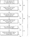
- FIG. 1is a flow chart generally illustrating a method of forming a binary compound by atomic layer deposition (ALD), in which supply of a deposition-enhancing agent follows removal of excess second reactant and by-products, in accordance with preferred embodiments of the invention;
- ALDatomic layer deposition
- FIG. 2is an x-ray photoelectron spectroscopy (XPS) sputtering time profile of a highly conductive tungsten silicide (WSi x ) film formed with pulsing sequence WF 6 /N 2 /Si 2 H 6 /N 2 /TEB/N 2 ;
- XPSx-ray photoelectron spectroscopy
- FIG. 3is a schematic cross-sectional side view of a electrode structure, comprising a layer of a conductive metal carbide, according to preferred embodiments of the invention.
- FIG. 4is a schematic cross-sectional side view of a dual damascene structure, comprising a metal carbide thin barrier layer formed over the trench and via, according to preferred embodiments of the invention.
- the present inventionadvantageously enables thin film formation at lower temperatures with reduced impurity levels by employing a deposition enhancing agent.
- the deposition enhancing agentsare hydrocarbons, more preferably unsaturated hydrocarbons such as alkanes, alkenes and alkynes.
- an ALD processgenerally refers to a process for producing thin films over a substrate in which a thin film is formed molecular layer by molecular layer due to self-saturating chemical reactions.
- ALDatomic layer deposition
- gaseous reactantsi.e., precursors
- ALD type reactorwhere they contact a substrate located in the chamber to provide a surface reaction.
- the pressure and the temperature of the reaction chamberare adjusted to a range where physisorption (i.e.
- reaction spaceis used to designate a reactor or reaction chamber, or an arbitrarily defined volume therein, in which conditions can be adjusted to effect thin film growth by ALD.
- the reaction spaceincludes surfaces subject to all reaction gas pulses from which gases or particles can flow to the substrate, by entrained flow or diffusion, during normal operation.
- the reaction spacecan be, for example, in a single-wafer ALD reactor or a batch ALD reactor, where deposition on multiple substrates takes place at the same time.
- Adsorptionis used to designate a chemical attachment of atoms or molecules on a surface.
- “Surface”is used to designate a boundary between the reaction space and a feature of a substrate.
- Thin filmmeans a film that is grown from elements or compounds that are transported as separate ions, atoms or molecules via vacuum, gaseous phase or liquid phase from the source to the substrate.
- the thickness of the filmdepends upon the application and may vary in a wide range, preferably from one atomic layer to 1,000 nm or more. In some embodiments, the thin film is less than about 20 nm in thickness, even more preferably less than about 10 nm and most preferably less than about 5 nm.
- Metallic thin filmdesignates a thin film that comprises metal.
- a metallic thin filmmay be an elemental metal thin film comprised essentially of elemental metal. Depending on the reducing agent, the elemental metal thin film may contain some metal carbide, metal nitride and/or metal oxide in an amount that does not have a negative effect on the characteristic metal properties of the film.
- a metallic thin filmmay be a compound metal thin film comprised essentially of compound metal, such as metal oxide, metal nitride, metal carbide, metal silicon compound, or metal nitride carbide (e.g., WN x C y ).
- Subscripts “x” and “y”are used to designate species that are not necessarily stoichiometric, having a wide range of phases with varying metal/oxygen, metal/carbon, metal/nitrogen, or metal/carbon/nitrogen ratios.
- thin filmsare deposited from halogen-containing chemicals. Geometrically challenging applications are also possible due to the self-limited nature of the surface reactions.
- an atomic layer deposition (ALD) type processis used to form thin films, preferably metallic thin films, on substrates, such as integrated circuit workpieces.
- the surfaces on which the thin films are depositedcan take a variety of forms. Examples include, but are not limited to, silicon, silicon oxide (SiO 2 ), coated silicon, dielectric materials, low-k materials, metals such as copper and aluminum, metal alloys, metal oxides and various nitrides, such as transition metal nitrides and silicon nitride or a combination of said materials.
- a substrate or workpiece placed in a reaction chamberis subjected to alternately repeated surface reactions.
- thin filmsare formed by repetition of a self-limiting ALD cycle.
- each ALD cyclecomprises at least three distinct phases.
- at least three different source chemicalsare alternatively employed, corresponding to the three phases.
- One reactantwill form no more than about one monolayer on the substrate surface and includes a metal species desired in the layer being deposited.
- This reactantalso referred to herein as “the metal reactant,” is preferably a halide, and thus the deposited monolayer is terminated with halogen ligands.
- a second reactantpreferably contains another species desired in the layer being deposited, such as nitrogen, carbon, silicon and/or oxygen. However, in some embodiments, such as the deposition of elemental metals, the second reactant does not contribute to the growing film.
- the second reactantis typically not a halide, although in some embodiments it may be.
- the second reactantcomprises a metal and carbon.
- the second reactantis TMA or TEA.
- the second reactantis water.
- the second reactantis a metal-containing source chemical comprising at least one ligand, such as a metalorganic compound.
- the second reactantcan also leave some amount of metal in the film being deposited. For example, in case of TMA or TEA, some amount of aluminum may be left in the film, depending on the particular reaction conditions.
- the third reactantis preferably a deposition-enhancing agent.
- the deposition-enhancing agentis capable of reducing the level of contaminants in the growing film.
- the third reactantis able to remove halides from the growing film and/or from the reaction space.
- the third reactantmay be a carbon compound, preferably one that is a strong reducer.
- the third reactantalso provides a species desired in the thin film, such as carbon, nitrogen, silicon or oxygen.
- the deposition-enhancing agentis preferably selected from the group consisting of hydrocarbons, hydrogen, hydrogen plasma, hydrogen radicals, silanes, germanium compounds, nitrogen compounds, boron compounds and boranes.
- the deposition-enhancing agentis a hydrocarbon selected from the group consisting of alkanes, alkenes and alkynes.
- the deposition-enhancing agentis triethyl boron (TEB) or acetylene (C 2 H 2 ).
- the deposition enhancing agentmay be provided in each ALD cycle or at intervals during the deposition process. For example, in some embodiments the deposition enhancing agent is provided every one to four ALD cycles. At the time the deposition enhancing agent is provided, the film grown in the most recent ALD cycles is preferably thin enough that the deposition enhancing agent can penetrate the film. In addition, if the deposition enhancing agent comprises radicals, it is preferably provided initially at a point in the deposition process such that it is not able to penetrate the deposited film and damage the underlying substrate material.
- the reactant or source chemical comprising a metal speciesis supplied to the reaction chamber and chemisorbs to the substrate surface.
- the reactant supplied in this phaseis selected such that, under the preferred conditions, the amount of reactant that can be bound to the surface is determined by the number of available binding sites and by the physical size of the chemisorbed species (including ligands).
- the chemisorbed layer left by a pulse of the metal reactantis self-terminated with a surface that is non-reactive with the remaining chemistry of that pulse. This phenomenon is referred to herein as “self-saturation.”
- This phenomenonis referred to herein as “self-saturation.”
- One of skill in the artwill recognize that the self-limiting nature of this phase makes the entire ALD cycle self-limiting. Excess reactant and reactant byproducts (if any) are removed from the reaction space, for example by purging with an inert gas and/or evacuation.
- the source chemicalpreferably comprises a species that is to be incorporated in the thin film, such as nitrogen, oxygen, silicon or carbon.
- the desired speciesis incorporated into the thin film by the interaction of the source chemical with the monolayer left by the metal reactant.
- the second phaseis referred to herein as “the second phase” or the “species-contributing phase.”
- the second source chemicalis a silicon, nitrogen, oxygen or carbon containing compound and its reaction with the chemisorbed metal species produces a metal silicide, nitride, oxide or carbide layer on the substrate.
- the second source chemicalis a metal source chemical, such as TMA, and metal is incorporated into the growing film.
- the species-contributing source chemicalcomprises metal and carbon.
- the second source chemicalis not incorporated in the film to any appreciable extent.
- the second reactantis a reducing agent that at least partially reduces the adsorbed first reactant to an elemental metal.
- the third phase of the ALD cyclecomprises providing a deposition-enhancing agent.
- the deposition enhancing agentis capable of removing halides or other contaminants or undesired reaction byproducts from the growing thin film and/or from the reaction chamber.
- the deposition-enhancing agentmay comprise a species that may be incorporated into the thin film, such as carbon, boron or silicon. This is referred to as the “third phase” or the “deposition-enhancing phase.”
- the initial ALD cyclemay be started with any of the three phases described above. However, one of skill in the art will recognize that if the initial ALD cycle does not begin with the metal reactant phase, at least two ALD cycles will typically need to be completed to deposit about a monolayer of the desired thin film.
- the order of the phasesmay be changed. That is, in some embodiments the deposition enhancing agent may be the next reactant provided after the second reactant, while in other embodiments the deposition enhancing agent may be the next reactant provided after the first metal source reactant.
- the third phaseprovision of the deposition-enhancing agent
- the first phaseprovision of the reactant comprising a metal species
- a phaseis generally considered to immediately follow another phase if only a purge or other reactant removal step intervenes.
- an ALD cyclecomprises:
- Step 5can be included in each ALD cycle, or steps 1-4 can be repeated several times before step 5 is introduced. In some embodiments steps 1-4 are repeated up to 10 times before step 5 is included. In other embodiments steps 1-4 are repeated up to 100 or even 1000 or more times before step 5 is included.
- a first reactant or source chemical pulseis supplied 102 to the substrate or workpiece.
- the first reactant pulsecomprises a carrier gas flow and a volatile halide species that is reactive with the workpiece surfaces of interest and further comprises a species that is to form part of the deposited layer. Accordingly, a halogen-containing species adsorbs upon the workpiece surfaces.
- the first reactantis a metal halide
- the thin film being formedcomprises a metallic material, preferably metal nitride, metal carbide, a metal silicon compound or metal oxide.
- the first reactant pulseself-saturates the workpiece surfaces such that any excess constituents of the first reactant pulse do not further react with the monolayer formed by this process. Self-saturation results due to halide tails terminating the monolayer, protecting the layer from further reaction.
- step 104merely entails stopping the flow of the first reactant or chemistry while continuing to flow a carrier gas for a sufficient time to diffuse or purge excess reactants and reactant by-products from the reaction space, preferably with greater than about two reaction chamber volumes of the purge gas, more preferably with greater than about three chamber volumes.
- the removal 104comprises continuing to flow purge gas for between about 0.1 seconds and 20 seconds after stopping the flow of the first reactant pulse. Inter-pulse purging is described in co-pending U.S. patent application having Ser. No. 09/392,371, filed Sep.
- the chambermay be pumped down between alternating chemistries. See, for example, PCT publication number WO 96/17107, published Jun. 6, 1996, entitled METHOD AND APPARATUS FOR GROWING THIN FILMS, the disclosure of which is incorporated herein by reference.
- the adsorption 102 and reactant removal 104represent a first phase 105 in an ALD cycle.
- the first phase in the illustrated ALD cycleis thus the metal phase.
- a second reactant or source chemical pulseis then supplied 106 to the workpiece.
- the second chemistrydesirably reacts with or adsorbs upon the monolayer left by the first reactant.
- this second reactant pulse 106comprises supplying a carrier gas with the second source gas to the workpiece.
- the first reactantcomprises a metal halide
- the second reactantleaves no more than about a monolayer of a metal-containing species.
- the second reactantpreferably removes at least some halide ligands from the adsorbed first reactant.
- the second reactant pulse 106also leaves a surface termination that operates to limit the deposition in a saturative reaction phase.
- any excess second reactantis removed 108 from the workpiece.
- this step 108preferably comprises stopping the flow of the second chemistry and continuing to flow carrier gas for a time period sufficient for excess reactants and volatile reaction by-products from the second reactant pulse to diffuse out of and be purged from the reaction space.
- the second reactant pulse 106 and removal 108represent a second phase 109 in the illustrated process, and can also be considered a non-metal species-contributing phase.
- the second phase 109can also be considered a non-halide species-contributing phase.
- a third reactant or source chemical pulseis preferably supplied to the workpiece 110 .
- the third reactantis a deposition-enhancing agent that is capable of removing halides from the substrate surface and/or the reaction space, such as hydrocarbons, hydrogen, hydrogen plasma, hydrogen radicals, silanes, germanium compounds, nitrogen compounds, boron compounds and boranes.
- the deposition-enhancing agentis preferably provided with an inert carrier gas. Temperature and pressure conditions are preferably arranged to avoid diffusion of the deposition-enhancing agent through the monolayer to underlying materials.
- excess unreacted deposition-enhancing agent and any reaction by-productsare removed 112 from the reaction space, preferably by a purge gas pulse.
- the removalcan be as described for step 104 .
- the deposition-enhancing agent pulse 110 and removal 112represent a third phase 113 of the illustrated ALD process, which can also be referred to as the deposition-enhancing phase.
- supply of deposition-enhancing agentimmediately follows the step of removing excess first reactant and by-products. After a time period sufficient to completely saturate and react the monolayer with the deposition-enhancing agent, excess unreacted deposition-enhancing agent and reaction by-products are removed from the reaction space, preferably by a purge gas pulse. The removal step is followed by supply of the second reactant pulse.
- the steps of supplying the deposition-enhancing agent and removing any excess deposition-enhancing agent and by-productsprecede the step of supplying the first reactant.
- the deposition-enhancing agentis not provided in every cycle.
- Carbon containing metal films or metal carbideshave varying applications, such as gate electrodes, electrodes in capacitors and barrier layers in damascene and dual damascene structures.
- a general pulsing sequence for carbon-containing metal or metal carbide thin film depositionis: (M 1 X y +purge+M 2 R 3 +purge+deposition-enhancing agent+purge) ⁇ m 1 or (M 1 X y +purge+deposition-enhancing agent+purge+M 2 R 3 +purge) ⁇ m 1 .
- M 1is a metal atom, preferably selected from the group consisting of Ti, Zr, Hf, V, Nb, Ta, Cr, Mo, W. However, in other embodiments M 1 is selected from the group consisting of Fe, Mn, Ni, Co, Cu, Zn, Cd, Ge, Si, Sn, Sb, Ga, Ru, Ir, Pd, Pt, Au, Rh, Re, B, In and Al.
- M 2is a metal atom, preferably selected from the group consisting of B, Al, In, Sn, Bi, Sn, Zn, Pb, Sb and Ga.
- Ris a ligand for M 2 and can be any ligand, preferably a metalorganic ligand, more preferably an organometallic ligand, most preferably an alkane ligand, such as ethyl ligand.
- X yis one or more ligands for M 1 .
- Each Xis preferably a halogen ligand selected from the group consisting of I, Br, Cl and F.
- at least one Xcan be a metalorganic ligand, such as a cyclopentadienyl (for example, cyclopentadienyl, methylcyclopentadienyl, pentamethylcyclopentadienyl, ethylcyclopentadienyl, isopropylcyclopentadienyl, tertbutylcyclopentadienyl, and indenyl), alkoxide (for example, methoxide, ethoxide, isopropoxide, and tertbutoxide), alkyl (for example, methyl, ethyl, propyl, and butyl), carbonyl, cyclo-octadiene, benzene or hydrogen ligand.
- X ymay comprise mixtures thereof.
- at least one of the X y ligandsis preferably a halogen.
- bis(cyclopentadienyl)hafnium dichloride or bis(cyclopentadienyl)tantalum(V) trichloridecan be used as a metal precursor in some embodiments.
- the deposition enhancing agentis preferably selected from the group consisting of hydrocarbons, hydrogen, hydrogen plasma, hydrogen radicals, silanes, germanium compounds, nitrogen compounds, boron compounds and boranes.
- the deposition-enhancing agentis a hydrocarbon selected from the group consisting of alkanes, alkenes and alkynes.
- M 2is a metals, preferably aluminum, and R is a carbon-containing ligand.
- M 2 R 3preferably has at least one metal-to-carbon bond. In some embodiments, M 2 R 3 may be considered a carbon source chemical.
- the growth rateis extremely high for an ALD process.
- the growth rate for TaC formationcan be over 2 ⁇ /cycle.
- annealingcan be performed after the metal carbide deposition for enhancing the properties of the film. Suitable atmospheres, such as N 2 or forming gas (N 2 /H 2 ), may be used during annealing.
- Exemplary pulsing sequences for TaC film formationinclude: (TaCl 5 +purge+trimethylaluminum (TMA) or triethylaluminum (TEA)+purge+C 2 H 2 +purge)] ⁇ m 2 or (TaCl 5 +purge+C 2 H 2 +purge+TMA or TEA+purge)] ⁇ m 2 ,
- m 2is the number of total cycles and C 2 H 2 is the deposition-enhancing agent.
- acetyleneC 2 H 2
- TaC formation processAs a deposition-enhancing agent as described above. Films deposited using acetylene contained about 40 times less chlorine than films deposited without the use of acetylene. This minor amount of chlorine is acceptable for device structures.
- tungsten carbide filmsare deposited.
- An exemplary pulsing sequencemay be: (TEB+purge+Si 2 H 6 +purge+WF 6 +purge)] ⁇ m 2 ,
- m 2is the number of total cycles
- WF6corresponds to M 1 X y
- TEBis M 2 R 3
- Si 2 H 6is the deposition enhancing agent.
- a tungsten-carbide (WC x ) filmcould be produced in the prior art from alternating and sequential pulses of WF 6 and TEB. Sequential and alternating pulses of WF 6 and TEB at about 300° C. produce low resistivity WC x films with hydrogen and fluorine impurities.
- a deposition enhancing agente.g., Si 2 H 6
- WF 6tungsten-carbide
- a deposition-enhancing agentis not utilized every cycle but only in some of the cycles.
- a general pulsing sequence for carbon-containing metal thin film depositioncan be: [ n 3 ⁇ (M 1 X y +purge+M 2 R 3 +purge)+ m 3 ⁇ (enhanced deposition agent+purge)] ⁇ k 3 ,
- M 1is a metal atom preferably selected from the group consisting of Ti, Zr, Hf, V, Nb, Ta, Cr, Mo, W, Si and Al. In other embodiments M 1 can be selected from the group consisting of Fe, Mn, Ni, Co, Cu, Zn, Cd, Ge, Si, Sn, Sb, Ga, Ru, Ir, Pd, Pt, Au, Rh, Re, B, In.
- M 2is a metal atom, preferably selected from the group consisting of B, Al, In, Sn, Bi, Zn, Pb, Sb and Ga.
- Ris a ligand for M 2 and can be any ligand.
- X yis one or more ligands for M 1 .
- Each Xis preferably a halogen ligand selected from the group consisting of I, Br, Cl and F.
- at least one Xcan be a metalorganic ligand, such as a cyclopentadienyl (for example, cyclopentadienyl, methylcyclopentadienyl, pentamethylcyclopentadienyl, ethylcyclopentadienyl, isopropylcyclopentadienyl, tertbutylcyclopentadienyl, and indenyl), alkoxide (for example, methoxide, ethoxide, isopropoxide, and tertbutoxide), alkyl (for example, methyl, ethyl, propyl, and butyl), carbonyl, cyclo-octadiene, benzene or hydrogen ligand.
- X ymay comprise mixtures thereof.
- at least one of the X y ligandsis preferably a halogen.
- bis(cyclopentadienyl)hafnium dichloride or bis(cyclopentadienyl)tantalum(V) trichloridecan be used as a metal precursor in some embodiments.
- a carbide filmis deposited by an ALD process comprising the following steps:
- transition metal halidee.g. TaCl 5 , TaF 5 , TiCl 4 or ZrCl 4
- step 5is included in each cycle, while in other embodiments steps 1-4 are repeated multiple cycles before introducing step 5. That is, the hydrogen radicals may be provided at intervals in the deposition cycle. Preferably the hydrogen radicals are initially provided at a point in the deposition process where the thin film is thick enough that the radicals can not penetrate the film and damage the underlying substrate.
- Silicon-containing metal films or metal silicidesare commonly used as conductive electrodes.
- Tungsten silicide(WSi x ) is an example of a metal silicide.
- a WSi x filmhas been formed by alternating and sequential pulses of WF 6 and Si 2 H 6 .
- this procedureundesirably leads to powder generation, producing films with properties unsuited for common applications.
- a deposition-enhancing agentsuch as TEB, in an ALD reaction with WF 6 and Si 2 H 6 can produce WSi x films with improved film properties (i.e., reduced impurity levels).
- silicon-containing metal or metal silicide thin filmare deposited by the following pulsing sequence: (MX y +purge+silicon source chemical+purge+deposition-enhancing agent+purge) ⁇ m 1 , or (MX y +purge+deposition-enhancing agent+purge+silicon source chemical+purge) ⁇ m 1
- Mis a metal atom, preferably selected from the group consisting of Ti, Zr, Hf, V, Nb, Ta, Cr, Mo, W and Al. In other embodiments, M is selected from the group consisting of Fe, Mn, Ni, Co, Cu, Zn, Cd, Ge, Si, Sn, Sb, Ga, Ru, Ir, Pd, Pt, Au, Rh, Re, B, In.
- X yis one or more ligands for M.
- Each Xis preferably a halogen ligand selected from the group consisting of I, Br, Cl and F.
- at least one Xcan be a metalorganic ligand, such as a cyclopentadienyl (for example, cyclopentadienyl, methylcyclopentadienyl, pentamethylcyclopentadienyl, ethylcyclopentadienyl, isopropylcyclopentadienyl, tertbutylcyclopentadienyl, and indenyl), alkoxide (for example, methoxide, ethoxide, isopropoxide, and tertbutoxide), alkyl (for example, methyl, ethyl, propyl, and butyl), carbonyl, cyclo-octadiene, benzene or hydrogen ligand.
- X ymay comprise mixtures thereof.
- at least one of the X y ligandsis preferably a halogen.
- bis(cyclopentadienyl)hafnium dichloride or bis(cyclopentadienyl)tantalum(V) trichloridecan be used as a metal precursor in some embodiments.
- the silicon source chemicalis a silane (Si x H y ).
- Other silicon source chemicals that can be usedwill be known to the skilled artisan.
- the deposition-enhancing agentis selected from the group consisting of hydrocarbons, hydrogen, hydrogen plasma, hydrogen radicals, silanes, germanium compounds, nitrogen compounds, boron compounds and boranes.
- the deposition-enhancing agentis a boron compound, more preferably triethyl boron (TEB).
- formation of a WSi x filmproceeds using the pulsing sequence: (WF 6 +purge+Si 2 H 6 +purge+TEB+purge)] ⁇ m 2 ,
- m 2is the number of total cycles and TEB is the deposition-enhancing agent.
- Metal oxideshave several important applications, such as insulators and transparent conductors. In future devices progressively thinner films are needed. In addition, they need to be grown conformally in narrow trenches. In some applications, such as optics, nanolaminates with sharp interfaces between materials are needed.
- a general pulsing sequence for oxygen-containing metal thin film depositionmay be: (MX y +purge+oxidizing reactant+purge+deposition-enhancing agent+purge) ⁇ m 1 or (MX y +purge+deposition-enhancing agent+purge+oxidizing reactant+purge) ⁇ m 1
- Mis a metal atom, preferably selected from the group consisting of Ti, Zr, Hf, V, Nb, Ta, Cr, Mo, W and Al.
- Mcan be selected from the group consisting of Fe, Mn, Ni, Co, Cu, Zn, Cd, Ge, Si, Sn, Sb, Ga, Ru, Ir, Pd, Pt, Au, Rh, Re, B, In.
- X yis one or more ligands for M.
- Each Xis preferably a halogen ligand selected from the group consisting of I, Br, Cl and F.
- at least one Xcan be a metalorganic ligand, such as a cyclopentadienyl (for example, cyclopentadienyl, methylcyclopentadienyl, pentamethylcyclopentadienyl, ethylcyclopentadienyl, isopropylcyclopentadienyl, tertbutylcyclopentadienyl, and indenyl), alkoxide (for example, methoxide, ethoxide, isopropoxide, and tertbutoxide), alkyl (for example, methyl, ethyl, propyl, and butyl), carbonyl, cyclo-octadiene, benzene or hydrogen ligand.
- X ymay comprise mixtures thereof.
- at least one of the X y ligandsis preferably a halogen.
- bis(cyclopentadienyl)hafnium dichloride or bis(cyclopentadienyl)tantalum(V) trichloridecan be used as a metal precursor in some embodiments.
- the oxidizing reactant or oxygen source chemicalis preferably selected from the group consisting of H 2 O, O 2 , ozone, oxygen radicals and oxygen plasma.
- the deposition-enhancing agentis preferably selected from the group consisting of hydrocarbons, hydrogen, hydrogen plasma, hydrogen radicals, silanes, germanium compounds, nitrogen compounds, boron compounds and boranes. More preferably, the deposition enhancing agent is selected from the group including, but not limited to hydrocarbons, such as alkanes, alkenes and alkynes. In some embodiments, the deposition-enhancing agent is acetylene (C 2 H 2 ).
- the acetylene pulsemay be applied before the water pulse: 2-OH(s)+WCl 6 (g) ⁇ —OWCl x (s)+HCl(g) —OWCl x (s)+C 2 H 2 (g) ⁇ —OW(s)+HCl(g) —OW(s)+H 2 O(g) ⁇ —W(OH) 2 (s)
- MoO xcan be grown using MoCl 5 , H 2 O and a deposition-enhancing agent, such as, e.g., C 2 H 2 : 2-OH(s)+MoCl 5 (g) ⁇ —OMoCl x (s)+HCl(g) —OMOCl x (s)+H 2 O(g) ⁇ —OMoOHCl x (s)+HCl(g) —OMoCl x (s)+C 2 H 2 (g) ⁇ —MoO 2 (s)+C 2 H 2 Cl 2 (g)
- a deposition-enhancing agentsuch as, e.g., C 2 H 2 : 2-OH(s)+MoCl 5 (g) ⁇ —OMoCl x (s)+HCl(g) —OMOCl x (s)+H 2 O(g) ⁇ —OMoOHCl x (s)+HCl(g) —OMoCl x (s)+C 2 H 2 (g)
- the acetylene pulsemay be applied before the water pulse: 2-OH(s)+MoCl 6 (g) ⁇ —OMoCl x (s)+HCl(g) —OMoCl x (s)+C 2 H 2 (g) ⁇ —OMo(s)+HCl(g) —OMo(s)+H 2 O(g) ⁇ —Mo(OH) 2 (s)
- a deposition-enhancing agent for oxygen-containing film growthhas beneficial consequences.
- the growth rate of In 2 O 3which is an important conductive oxide
- a deposition-enhancing agentsuch as, e.g., acetylene
- SnO 2is also an important conductive oxide.
- the combination of In 2 O 3 and SnO 2i.e., ITO is a very important conductive oxide.
- a TiO 2 filmwhich has a high permittivity ( ⁇ 80) usually has a high leakage current when deposited by previous processes, which limits its use as a dielectric. Oxygen deficiency has been speculated as the reason for the high leakage current. Carbon from acetylene used as a deposition-enhancing agent according to the present methods advantageously fills these vacancies and overcomes these problems.
- HfO 2is one of the key candidates as a gate oxide in MOSFET transistors.
- the best electrical resultshave been obtained using HfCl 4 and H 2 O.
- Acetylene-assisted growthcleans the interface and its use as a deposition enhancing agent in the methods disclosed above allows the deposition of pure HfO 2 films at low temperatures.
- Conformal ALD deposited elemental metal filmsare desirable in many semiconductor applications, such as diffusion barriers for Cu interconnects, metal electrodes for gate stacks and metal-insulator-metal (MIM) structures.
- MIMmetal-insulator-metal
- combination of a Cu diffusion barrier and a pure metal (e.g., W) with low resistivitycan be used for direct Cu plating.
- ALD of Wmay be achieved using sequential and alternating pulses of WF 6 and a reducing agent, such as Si 2 H 6 or B 2 H 6 .
- a reducing agentsuch as Si 2 H 6 or B 2 H 6 .
- the inventorshave observed that the formation of tungsten films using dilute Si 2 H 6 may lead to the production of powders, which makes use of this pulsing scheme in industrial practice undesirable due to the risk of particle generation.
- powder production in the deposition of metal filmscan be substantially reduced using a deposition-enhancing agent.
- a pulsing sequence for metal thin film deposition by ALDis: (deposition-enhancing agent+purge+MX y +purge+reducing agent+purge) ⁇ m 1 , or (MX y +purge deposition-enhancing agent+purge+reducing agent+purge) ⁇ m 1 ,
- Mis a metal atom, preferably selected from the group consisting of Ti, Zr, Hf, V, Nb, Ta, Cr, Mo, W and Al.
- Mcan be selected from the group consisting of Fe, Mn, Ni, Co, Cu, Zn, Cd, Ge, Si, Sn, Sb, Ga, Ru, Jr, Pd, Pt, Au, Rh, Re, B, and In.
- X yis one or more ligands for M.
- Each Xis preferably a halogen ligand selected from the group consisting of I, Br, Cl and F.
- at least one Xcan be a metalorganic ligand, such as a cyclopentadienyl (for example, cyclopentadienyl, methylcyclopentadienyl, pentamethylcyclopentadienyl, ethylcyclopentadienyl, isopropylcyclopentadienyl, tertbutylcyclopentadienyl, and indenyl), alkoxide (for example, methoxide, ethoxide, isopropoxide, and tertbutoxide), alkyl (for example, methyl, ethyl, propyl, and butyl), carbonyl, cyclo-octadiene, benzene or hydrogen ligand.
- X ymay comprise mixtures thereof.
- at least one of the X y ligandsis preferably a halogen.
- bis(cyclopentadienyl)hafnium dichloride or bis(cyclopentadienyl)tantalum(V) trichloridecan be used as a metal precursor in some embodiments.
- the reducing agentis preferably selected from the group including silanes (e.g., Si 2 H 6 ) and boranes (e.g., B 2 H 6 ); and the deposition-enhancing agent is selected from the group consisting of hydrocarbons, hydrogen, hydrogen plasma, hydrogen radicals, silanes, germanium compounds, nitrogen compounds, boron compounds and boranes.
- the deposition-enhancing agentis a boron compound, preferably TEB.
- a low resistivity W filmwas formed at a substrate temperature between about 200° C. and 350° C. using the following pulsing sequence: (TEB+purge+WF 6 +purge+Si 2 H 6 +purge)] ⁇ m 2
- m 2is the number of total cycles and TEB is the deposition-enhancing agent.
- XRDX-ray diffraction
- XPSx-ray photoelectron spectroscopy
- a electrodeis formed by ALD of conductive metal carbide.
- a silicon substrate 200is illustrated comprising a layer of high-k dielectric material 210 .
- the substratemay be treated prior to deposition of the high-k material.
- a thin interfacial layer(not shown) may be deposited prior to deposition of the high-k material.
- a thin chemical oxide or oxynitrideis formed on the surface.
- a thermal oxideis grown on the substrate.
- High-kgenerally refers to a dielectric material having a dielectric constant (k) value greater than that of silicon oxide.
- the high-k materialhas a dielectric constant greater than 5, more preferably greater than about 10.
- Exemplary high-k materialsinclude, without limitation, HfO 2 , ZrO 2 , Al 2 O 3 , TiO 2 , Ta 2 O 5 , Sc 2 O 3 , lanthanide oxides and mixtures thereof, silicates and materials such as YSZ (yttria-stabilized zirconia), barium strontium titanate (BST), strontium titanate (ST), strontium bismuth tantalate (SBT) and bismuth tantalate (BT).
- the high-k materialis also deposited by an ALD process.
- a layer or thin film of conductive metal carbide 220is deposited over the dielectric (high-k material) layer 210 by ALD, as described above, to form the illustrated structure. It will be appreciated that in the illustrated embodiment the layers are not necessarily drawn to scale.
- the metal carbide and underlying high-k materialare patterned to form an electrode.
- the metal carbide thin film 220is preferably deposited over the dielectric layer 210 by contacting the substrate with alternating pulses of a metal source chemical, carbon source chemical and a deposition-enhancing agent (not necessarily in this order), as described above.
- the metal source chemicalis preferably a halide compound (e.g., TaCl 5 ) and the carbon source chemical is preferably an organometallic compound, such as, e.g., trimethyl aluminum (TMA).
- the deposition-enhancing agentmay be a hydrocarbon selected from the group including, but not limited to, alkanes, alkenes and alkynes.
- the deposition-enhancing agentis acetylene. (C 2 H 2 ).
- the deposition-enhancing agentcomprises hydrogen radicals.
- Unreacted source chemicals and reaction by-productsare removed from the reaction chamber after each source chemical pulse, for example by evacuation and/or purging with an inert gas (e.g., N 2 ). In some embodiments, evacuation is achieved using a vacuum pump or a plurality of vacuum pumps.
- the pulsing cycleis repeated until a metal carbide layer of the desired thickness has been formed.
- the metal carbide layerhas a thickness between about 5 ⁇ and about 1000 ⁇ .
- the conductive metal carbides deposited to form the electrode in these embodimentsare preferably selected from the group consisting of Ti, Zr, Hf, V, Nb, Ta, Cr, Mo, W and Al carbides. Further non-conductive carbide SiC can also be deposited.
- the metal carbideforms the electrode.
- another conductive materialsuch as a metal or poly-Si, is deposited over the metal carbide.
- the additional conductive materialmay be deposited by ALD or by another deposition process, such as by CVD or PVD.
- the depositionmay be selective, or may be followed by patterning steps.
- annealingcan be performed after the metal carbide deposition. Suitable atmospheres, such as N 2 or forming gas (N 2 /H 2 ) are apparent to skilled artisan.
- Metal carbide thin filmcan be deposited by ALD to form a barrier layer for interconnect metallization.
- the substratemay comprise damascene or dual damascene structures, including high aspect ratio trenches and vias.
- a dual damascene structure 300comprises a trench 310 , via 320 , and dielectric layers 340 and 350 . In the illustrated embodiment, the layers are not necessarily drawn to scale.
- the structure 300is placed in an ALD reaction chamber and a metal carbide thin film barrier layer 360 is deposited over the trench 310 and via 320 by contacting the structure 300 with alternating pulses of a metal source chemical, carbon source chemical and deposition-enhancing agent (not necessarily in this order), as described above.
- the metal source chemicalis a halide compound
- the carbon sourceis an organometallic compound
- the deposition-enhancing agentis a hydrocarbon or hydrogen radicals.
- Unreacted source chemicals and reaction by-productsare removed from the reaction chamber after each pulse of source chemical, as described above.
- the pulsing cycleis repeated until a barrier layer of the desired thickness has been formed.
- the barrier layerhas a thickness between about 5 ⁇ and about 100 ⁇ .
- any element used in an embodimentcan interchangeably be used in another embodiment unless such a replacement is not feasible.
Landscapes
- Chemical & Material Sciences (AREA)
- Engineering & Computer Science (AREA)
- Manufacturing & Machinery (AREA)
- Physics & Mathematics (AREA)
- Computer Hardware Design (AREA)
- Microelectronics & Electronic Packaging (AREA)
- Power Engineering (AREA)
- Condensed Matter Physics & Semiconductors (AREA)
- General Physics & Mathematics (AREA)
- Chemical Kinetics & Catalysis (AREA)
- General Chemical & Material Sciences (AREA)
- Materials Engineering (AREA)
- Mechanical Engineering (AREA)
- Metallurgy (AREA)
- Organic Chemistry (AREA)
- Composite Materials (AREA)
- Inorganic Chemistry (AREA)
- Chemical Vapour Deposition (AREA)
Abstract
Description
The present application is a continuation of U.S. application Ser. No. 15/824,143, filed Nov. 28, 2017, now U.S. Pat. No. 10,297,444, which is a continuation of U.S. application Ser. No. 14/812,139, filed Jul. 29, 2015, now U.S. Pat. No. 9,831,094, which is a continuation of U.S. application Ser. No. 13/766,469, filed Feb. 13, 2013, now U.S. Pat. No. 9,127,351, which is a continuation of U.S. application Ser. No. 11/588,837, filed Oct. 27, 2006, now U.S. Pat. No. 8,993,055, which in turn claims priority to U.S. Provisional application No. 60/730,986, filed Oct. 27, 2005. Each of the priority applications is incorporated by reference herein.
The present invention relates generally to processes for producing thin films with low impurity contents on a substrate by atomic layer deposition. In some embodiments, the films produced by the atomic layer deposition (ALD) processes disclosed herein can be used in metal gate and metal electrode applications in metal oxide semiconductor field effect transistors (MOSFETs) or as barrier layers in interconnect structures.
Atomic layer deposition (ALD) is a self-limiting process, whereby alternated pulses of reaction precursors saturate a substrate surface and leave no more than one monolayer of material per pulse. The deposition conditions and precursors are selected to ensure self-saturating reactions, such that an adsorbed layer in one pulse leaves a surface termination that is non-reactive with the gas phase reactants of the same pulse. A subsequent pulse of different reactants reacts with the previous termination to enable continued deposition. Thus, each cycle of alternated pulses leaves no more than about one molecular layer of the desired material. The principles of ALD type processes have been presented by T. Suntola, e.g. in the Handbook of Crystal Growth 3, Thin Films and Epitaxy, Part B: Growth Mechanisms and Dynamics, Chapter 14, Atomic Layer Epitaxy, pp. 601-663, Elsevier Science B.V. 1994, the disclosure of which is incorporated herein by reference.
In a typical ALD process for depositing thin films, one deposition cycle comprises exposing the substrate to a first precursor, removing unreacted first reactant and reaction byproducts from the reaction chamber, exposing the substrate to a second precursor, followed by a second removal step. Typically, halide precursors, such as TiCl4and HfCl4, are used as precursors in ALD deposition because those precursors are inexpensive and relatively stable, but at the same time reactive towards different types of surface groups. H2O and NH3are widely used for oxide and nitride deposition, respectively, as second precursors.
ALD processes typically produce thin films that have lower impurity content at the same deposition temperature than chemical vapor deposition (CVD) processes. Despite the lower impurity levels in ALD films, the impurity content in ALD films can still be a problem. There are several possible reasons for the presence of impurities in thin films deposited by ALD. In some cases, the semiconductor process flow necessarily limits the maximum deposition temperature such that that some residues are left in the film. ALD films deposited from chloride or other halide-containing precursors (e.g., WF6) at relatively low temperatures can comprise relatively high levels of halide residues. Halide impurities are present mainly at the interfaces, which can also lead to problems. In some cases, like low temperature deposition of transition metal nitrides and transition metal carbides from halide containing precursors the, impurity contents can be above the acceptable limit for some integrated circuit (IC) applications. In another example, in some applications amorphous films are needed, which limits the growth temperature.
Another disadvantage of the residues remaining in the film as it is deposited is that they may block the growth and result in a lower growth rate. For example, a high growth temperature may be chosen because the films are impure at low temperatures. However, the number of reactive active sites, such as —OH or —NHxgroups, is higher at low temperatures As a result, the growth rate is substantially lowered by impurities.
U.S. Patent Application No. 2004/0208994 to Harkonen et al. describes a method for ALD deposition of carbon-containing transition metal films. As an example, Harkonen et al. deposited carbon containing titanium films (example 1B) at a deposition temperature of about 500° C. using TiCl4and trimethylaluminum (TMA) as precursors. The disadvantage of this process is that it needs a substantially high deposition temperature in order to achieve low impurity contents, chlorine in their case. Furthermore, it is widely known in art that TMA will decompose when used at such high temperatures. By decomposing TMA, the uniqueness of ALD, i.e., saturated and surface controlled reactions, which leads to superb conformality and uniformity of ultra-thin films over the large-area substrates, may be lost. If the same carbon containing titanium film process is performed at temperatures below the decomposition temperature of TMA, for example at 350° C., the chlorine content of the film will be undesirably high.
Accordingly, there is a need in the art for a low temperature ALD method for producing metal-containing films from halide (e.g., chlorine) containing metal precursors at low temperatures and with low halogen impurity levels in the films.
According to some embodiments of the invention, a deposition-enhancing agent is utilized in ALD processes for depositing a metal or silicon-containing film from a halide-containing precursor. In a preferred embodiment, the deposition-enhancing agent is selected from the group consisting of hydrocarbons, hydrogen, hydrogen plasma, hydrogen radicals, silanes, germanium compounds, nitrogen compounds, boron compounds and boranes. In a more preferred embodiment, the deposition-enhancing agent is a hydrocarbon, preferably a hydrocarbon selected from the group consisting of alkanes, alkenes and alkynes. The deposition enhancing agent may be provided in each ALD cycle, or at intervals during the deposition process.
In one embodiment of the invention, atomic layer deposition (ALD) processes for forming a metal-carbide thin film are disclosed. The processes preferably comprise contacting a substrate in a reaction space with alternating and sequential pulses of a metal source chemical that comprises at least one halide ligand, a second source chemical comprising a metal and carbon and a third source chemical, wherein the third source chemical is a deposition-enhancing agent. In one embodiment, the deposition enhancing agent is a hydrocarbon, preferably acetylene. The second source chemical may comprise an organic ligand, and in one embodiment is preferably TMA or TEA (triethylaluminum).
In another embodiment, ALD processes for forming a metal carbide film are disclosed, in which alternating and self-saturating pulses of reactants are provided in a plurality of deposition cycles. Each cycle preferably comprises contacting a substrate in a reaction space with alternating and sequential pulses of a first metal source chemical, preferably a halide compound, a second source chemical comprising carbon, and a third source chemical, wherein the third source chemical is a hydrocarbon. The third source chemical is preferably selected from the group consisting of alkanes, alkenes and alkynes and in one embodiment is acetylene.
In still another embodiment of the invention, atomic layer deposition (ALD) processes for forming oxygen-containing thin films on a substrate are disclosed. The processes preferably comprise contacting the substrate with alternating and sequential pulses of a metal reactant, a second reactant comprising an oxygen source and a deposition-enhancing agent. The metal reactant is preferably a halide and typically comprises a metal selected from the group consisting of Ti, Zr, Hf, V, Nb, Ta, Cr, Mo, W and Al. The deposition enhancing agent is preferably a hydrocarbon, such as acetylene. The oxygen source may be, for example, H2O, O2, ozone, oxygen radicals or oxygen plasma.
In yet another embodiment of the invention, atomic layer deposition (ALD) processes for forming elemental thin films on a substrate are disclosed. The processes preferably comprise contacting the substrate with alternating and sequential pulses of a metal a deposition-enhancing agent, a metal source chemical and a reducing agent. The reducing agent is preferably selected from the group consisting of boranes and silanes. The deposition enhancing agent may be, for example, a boron compound such as triethyl boron (TEB).
In yet another embodiment of the invention, atomic layer deposition (ALD) processes for forming a silicon-containing thin film, such as a metal silicide, on a substrate are disclosed. The processes preferably comprise contacting the substrate with alternating and sequential pulses of a metal source chemical, a silicon source chemical and a deposition-enhancing agent. The silicon source chemical may be, for example, a silane. In one embodiment the deposition enhancing agent is a boron compound, such as TEB.
In yet another embodiment of the invention, a semiconductor device structure is disclosed. The structure comprises a substrate and a thin film layer overlying the substrate, wherein the thin film layer is formed by atomic layer deposition (ALD) by contacting the substrate with alternating and sequential pulses of a metal source chemical, an oxygen, nitrogen, carbon, or silicon source chemical, and a deposition-enhancing agent.
The invention will be better understood from the Detailed Description of the Preferred Embodiments and from the appended drawings, which are meant to illustrate and not to limit the invention, and wherein:
The present invention advantageously enables thin film formation at lower temperatures with reduced impurity levels by employing a deposition enhancing agent. In some preferred embodiments, the deposition enhancing agents are hydrocarbons, more preferably unsaturated hydrocarbons such as alkanes, alkenes and alkynes.
In context of the present invention, “an ALD process” generally refers to a process for producing thin films over a substrate in which a thin film is formed molecular layer by molecular layer due to self-saturating chemical reactions. The general principles of ALD are disclosed, e.g., in U.S. Pat. Nos. 4,058,430 and 5,711,811, the disclosures of which are incorporated herein by reference. In an ALD process, gaseous reactants, i.e., precursors, are conducted into a reaction chamber of an ALD type reactor where they contact a substrate located in the chamber to provide a surface reaction. The pressure and the temperature of the reaction chamber are adjusted to a range where physisorption (i.e. condensation of gases) and thermal decomposition of the precursors are avoided. Consequently, only up to one monolayer (i.e. an atomic layer or a molecular layer) of material is deposited at a time during each pulsing cycle. The actual growth rate of the thin film, which is typically presented as Å/pulsing cycle, depends, for example, on the number of available reactive surface sites or active sites on the surface and bulkiness of the chemisorbing molecules. Gas phase reactions between precursors and any undesired reactions of by-products are inhibited because precursor pulses are separated from each other by time and the reaction chamber is purged with an inactive gas (e.g. nitrogen or argon) and/or evacuated using, e.g., a pump between precursor pulses to remove surplus gaseous reactants and reaction by-products from the chamber.
“Reaction space” is used to designate a reactor or reaction chamber, or an arbitrarily defined volume therein, in which conditions can be adjusted to effect thin film growth by ALD. Typically the reaction space includes surfaces subject to all reaction gas pulses from which gases or particles can flow to the substrate, by entrained flow or diffusion, during normal operation. The reaction space can be, for example, in a single-wafer ALD reactor or a batch ALD reactor, where deposition on multiple substrates takes place at the same time.
“Adsorption” is used to designate a chemical attachment of atoms or molecules on a surface.
“Surface” is used to designate a boundary between the reaction space and a feature of a substrate.
“Thin film” means a film that is grown from elements or compounds that are transported as separate ions, atoms or molecules via vacuum, gaseous phase or liquid phase from the source to the substrate. The thickness of the film depends upon the application and may vary in a wide range, preferably from one atomic layer to 1,000 nm or more. In some embodiments, the thin film is less than about 20 nm in thickness, even more preferably less than about 10 nm and most preferably less than about 5 nm.
“Metallic thin film” designates a thin film that comprises metal. A metallic thin film may be an elemental metal thin film comprised essentially of elemental metal. Depending on the reducing agent, the elemental metal thin film may contain some metal carbide, metal nitride and/or metal oxide in an amount that does not have a negative effect on the characteristic metal properties of the film. In addition, a metallic thin film may be a compound metal thin film comprised essentially of compound metal, such as metal oxide, metal nitride, metal carbide, metal silicon compound, or metal nitride carbide (e.g., WNxCy).
Subscripts “x” and “y” are used to designate species that are not necessarily stoichiometric, having a wide range of phases with varying metal/oxygen, metal/carbon, metal/nitrogen, or metal/carbon/nitrogen ratios.
Preferred ALD Methods
The methods presented herein allow deposition of conformal thin films on substrate surfaces. In preferred embodiments, thin films are deposited from halogen-containing chemicals. Geometrically challenging applications are also possible due to the self-limited nature of the surface reactions.
According to the preferred embodiments, an atomic layer deposition (ALD) type process is used to form thin films, preferably metallic thin films, on substrates, such as integrated circuit workpieces. The surfaces on which the thin films are deposited can take a variety of forms. Examples include, but are not limited to, silicon, silicon oxide (SiO2), coated silicon, dielectric materials, low-k materials, metals such as copper and aluminum, metal alloys, metal oxides and various nitrides, such as transition metal nitrides and silicon nitride or a combination of said materials.
In a preferred embodiment of the invention, a substrate or workpiece placed in a reaction chamber is subjected to alternately repeated surface reactions. In particular, thin films are formed by repetition of a self-limiting ALD cycle. Preferably, each ALD cycle comprises at least three distinct phases. In the case of compound metallic thin film deposition, at least three different source chemicals are alternatively employed, corresponding to the three phases. One reactant will form no more than about one monolayer on the substrate surface and includes a metal species desired in the layer being deposited. This reactant, also referred to herein as “the metal reactant,” is preferably a halide, and thus the deposited monolayer is terminated with halogen ligands.
A second reactant preferably contains another species desired in the layer being deposited, such as nitrogen, carbon, silicon and/or oxygen. However, in some embodiments, such as the deposition of elemental metals, the second reactant does not contribute to the growing film.
The second reactant is typically not a halide, although in some embodiments it may be. In a preferred embodiment the second reactant comprises a metal and carbon. In some embodiments, the second reactant is TMA or TEA. In other embodiments, the second reactant is water. In still other embodiments, the second reactant is a metal-containing source chemical comprising at least one ligand, such as a metalorganic compound. Further, in some embodiments the second reactant can also leave some amount of metal in the film being deposited. For example, in case of TMA or TEA, some amount of aluminum may be left in the film, depending on the particular reaction conditions.
The third reactant is preferably a deposition-enhancing agent. Preferably the deposition-enhancing agent is capable of reducing the level of contaminants in the growing film. Thus, in some embodiments the third reactant is able to remove halides from the growing film and/or from the reaction space. The third reactant may be a carbon compound, preferably one that is a strong reducer. Moreover, in some embodiments the third reactant also provides a species desired in the thin film, such as carbon, nitrogen, silicon or oxygen.
The deposition-enhancing agent is preferably selected from the group consisting of hydrocarbons, hydrogen, hydrogen plasma, hydrogen radicals, silanes, germanium compounds, nitrogen compounds, boron compounds and boranes. In a more preferred embodiment, the deposition-enhancing agent is a hydrocarbon selected from the group consisting of alkanes, alkenes and alkynes. In other embodiments the deposition-enhancing agent is triethyl boron (TEB) or acetylene (C2H2).
The deposition enhancing agent may be provided in each ALD cycle or at intervals during the deposition process. For example, in some embodiments the deposition enhancing agent is provided every one to four ALD cycles. At the time the deposition enhancing agent is provided, the film grown in the most recent ALD cycles is preferably thin enough that the deposition enhancing agent can penetrate the film. In addition, if the deposition enhancing agent comprises radicals, it is preferably provided initially at a point in the deposition process such that it is not able to penetrate the deposited film and damage the underlying substrate material.
In one phase of the ALD cycle (“the metal phase” or the “first phase”), the reactant or source chemical comprising a metal species is supplied to the reaction chamber and chemisorbs to the substrate surface. The reactant supplied in this phase is selected such that, under the preferred conditions, the amount of reactant that can be bound to the surface is determined by the number of available binding sites and by the physical size of the chemisorbed species (including ligands). The chemisorbed layer left by a pulse of the metal reactant is self-terminated with a surface that is non-reactive with the remaining chemistry of that pulse. This phenomenon is referred to herein as “self-saturation.” One of skill in the art will recognize that the self-limiting nature of this phase makes the entire ALD cycle self-limiting. Excess reactant and reactant byproducts (if any) are removed from the reaction space, for example by purging with an inert gas and/or evacuation.
Maximum step coverage on the workpiece surface is obtained when no more than about a single molecular layer of metal source chemical molecules is chemisorbed in each self-limiting pulse. Due to the size of the chemisorbed species and the number of reactive sites, somewhat less than a monolayer (ML) may be deposited in each pulse of metal reactant.
In the next phase of the cycle, a pulse of a second source chemical is provided that reacts with the molecules left on the substrate surface by the preceding pulse. In some embodiments the source chemical preferably comprises a species that is to be incorporated in the thin film, such as nitrogen, oxygen, silicon or carbon. Thus, the desired species is incorporated into the thin film by the interaction of the source chemical with the monolayer left by the metal reactant. This phase is referred to herein as “the second phase” or the “species-contributing phase.” In particular embodiments, the second source chemical is a silicon, nitrogen, oxygen or carbon containing compound and its reaction with the chemisorbed metal species produces a metal silicide, nitride, oxide or carbide layer on the substrate. In other embodiments the second source chemical is a metal source chemical, such as TMA, and metal is incorporated into the growing film. In some preferred embodiments the species-contributing source chemical comprises metal and carbon.
In still other embodiments the second source chemical is not incorporated in the film to any appreciable extent. For example, in some embodiments the second reactant is a reducing agent that at least partially reduces the adsorbed first reactant to an elemental metal.
Excess second source chemical and reaction byproducts, if any, are removed from the reaction space by purging and/or evacuation.
The third phase of the ALD cycle comprises providing a deposition-enhancing agent. In the preferred embodiments the deposition enhancing agent is capable of removing halides or other contaminants or undesired reaction byproducts from the growing thin film and/or from the reaction chamber. In addition, the deposition-enhancing agent may comprise a species that may be incorporated into the thin film, such as carbon, boron or silicon. This is referred to as the “third phase” or the “deposition-enhancing phase.”
Although referred to as the “first phase,” the “second phase” and the “third phase,” these labels are for convenience and do not indicate the actual order of the phases in each ALD cycle. Thus, the initial ALD cycle may be started with any of the three phases described above. However, one of skill in the art will recognize that if the initial ALD cycle does not begin with the metal reactant phase, at least two ALD cycles will typically need to be completed to deposit about a monolayer of the desired thin film.
In addition, the order of the phases may be changed. That is, in some embodiments the deposition enhancing agent may be the next reactant provided after the second reactant, while in other embodiments the deposition enhancing agent may be the next reactant provided after the first metal source reactant. For example, in some embodiments the third phase (provision of the deposition-enhancing agent) may immediately follow the first phase (provision of the reactant comprising a metal species), which in turn is followed by the species-contributing phase. A phase is generally considered to immediately follow another phase if only a purge or other reactant removal step intervenes.
In one embodiment, an ALD cycle comprises:
1. providing a metal halide to the reaction space;
2. purging and/or evacuation of excess transition metal halide and reaction byproducts;
3. providing a second reactant to the reaction space;
4. purging/and or evacuation of excess second reactant and reaction byproducts; and
5. providing a deposition-enhancing agent to the reaction space.
With reference toFIG. 1 , in an embodiment of the invention, after initial surface termination, if necessary, a first reactant or source chemical pulse is supplied102 to the substrate or workpiece. In accordance with a preferred embodiment, the first reactant pulse comprises a carrier gas flow and a volatile halide species that is reactive with the workpiece surfaces of interest and further comprises a species that is to form part of the deposited layer. Accordingly, a halogen-containing species adsorbs upon the workpiece surfaces. In the illustrated embodiment, the first reactant is a metal halide, and the thin film being formed comprises a metallic material, preferably metal nitride, metal carbide, a metal silicon compound or metal oxide. The first reactant pulse self-saturates the workpiece surfaces such that any excess constituents of the first reactant pulse do not further react with the monolayer formed by this process. Self-saturation results due to halide tails terminating the monolayer, protecting the layer from further reaction.
The first reactant is then removed104 from the reaction space. Preferably, step104 merely entails stopping the flow of the first reactant or chemistry while continuing to flow a carrier gas for a sufficient time to diffuse or purge excess reactants and reactant by-products from the reaction space, preferably with greater than about two reaction chamber volumes of the purge gas, more preferably with greater than about three chamber volumes. Preferably theremoval 104 comprises continuing to flow purge gas for between about 0.1 seconds and 20 seconds after stopping the flow of the first reactant pulse. Inter-pulse purging is described in co-pending U.S. patent application having Ser. No. 09/392,371, filed Sep. 8, 1999 and entitled IMPROVED APPARATUS AND METHOD FOR GROWTH OF A THIN FILM, the disclosure of which is incorporated herein by reference. In other arrangements, the chamber may be pumped down between alternating chemistries. See, for example, PCT publication number WO 96/17107, published Jun. 6, 1996, entitled METHOD AND APPARATUS FOR GROWING THIN FILMS, the disclosure of which is incorporated herein by reference. Together, theadsorption 102 andreactant removal 104 represent afirst phase 105 in an ALD cycle. The first phase in the illustrated ALD cycle is thus the metal phase.
With continued reference toFIG. 1 , a second reactant or source chemical pulse is then supplied106 to the workpiece. The second chemistry desirably reacts with or adsorbs upon the monolayer left by the first reactant. In the illustrated embodiment, thissecond reactant pulse 106 comprises supplying a carrier gas with the second source gas to the workpiece. In particular, where the first reactant comprises a metal halide, the second reactant leaves no more than about a monolayer of a metal-containing species. The second reactant preferably removes at least some halide ligands from the adsorbed first reactant. Thesecond reactant pulse 106 also leaves a surface termination that operates to limit the deposition in a saturative reaction phase.
After a time period sufficient to completely saturate and react the monolayer with thesecond reactant pulse 106, any excess second reactant is removed108 from the workpiece. As with theremoval 104 of the first reactant, thisstep 108 preferably comprises stopping the flow of the second chemistry and continuing to flow carrier gas for a time period sufficient for excess reactants and volatile reaction by-products from the second reactant pulse to diffuse out of and be purged from the reaction space. Together, thesecond reactant pulse 106 andremoval 108 represent asecond phase 109 in the illustrated process, and can also be considered a non-metal species-contributing phase. Thesecond phase 109 can also be considered a non-halide species-contributing phase.
When the excess reactants of the second reactant pulse have been removed108 from the chamber, a third reactant or source chemical pulse is preferably supplied to theworkpiece 110. Preferably the third reactant is a deposition-enhancing agent that is capable of removing halides from the substrate surface and/or the reaction space, such as hydrocarbons, hydrogen, hydrogen plasma, hydrogen radicals, silanes, germanium compounds, nitrogen compounds, boron compounds and boranes. The deposition-enhancing agent is preferably provided with an inert carrier gas. Temperature and pressure conditions are preferably arranged to avoid diffusion of the deposition-enhancing agent through the monolayer to underlying materials.
After a time period sufficient to completely saturate and react the monolayer with the third reactant, excess unreacted deposition-enhancing agent and any reaction by-products (preferably also volatile) are removed112 from the reaction space, preferably by a purge gas pulse. The removal can be as described forstep 104. Together, the deposition-enhancingagent pulse 110 andremoval 112 represent a third phase113 of the illustrated ALD process, which can also be referred to as the deposition-enhancing phase.
In an alternative embodiment of the invention (not shown), supply of deposition-enhancing agent immediately follows the step of removing excess first reactant and by-products. After a time period sufficient to completely saturate and react the monolayer with the deposition-enhancing agent, excess unreacted deposition-enhancing agent and reaction by-products are removed from the reaction space, preferably by a purge gas pulse. The removal step is followed by supply of the second reactant pulse.
In another alternative embodiment of the invention (not shown), the steps of supplying the deposition-enhancing agent and removing any excess deposition-enhancing agent and by-products precede the step of supplying the first reactant. In other alternative embodiments, the deposition-enhancing agent is not provided in every cycle.
The foregoing embodiments will be discussed in the context of specific thin film chemistries.
Deposition of Carbon-Containing Films
Carbon containing metal films or metal carbides have varying applications, such as gate electrodes, electrodes in capacitors and barrier layers in damascene and dual damascene structures.
In one embodiment, a general pulsing sequence for carbon-containing metal or metal carbide thin film deposition is:
(M1Xy+purge+M2R3+purge+deposition-enhancing agent+purge)×m1
or
(M1Xy+purge+deposition-enhancing agent+purge+M2R3+purge)×m1.
(M1Xy+purge+M2R3+purge+deposition-enhancing agent+purge)×m1
or
(M1Xy+purge+deposition-enhancing agent+purge+M2R3+purge)×m1.
wherein m1is the number of total cycles. M1is a metal atom, preferably selected from the group consisting of Ti, Zr, Hf, V, Nb, Ta, Cr, Mo, W. However, in other embodiments M1is selected from the group consisting of Fe, Mn, Ni, Co, Cu, Zn, Cd, Ge, Si, Sn, Sb, Ga, Ru, Ir, Pd, Pt, Au, Rh, Re, B, In and Al.
M2is a metal atom, preferably selected from the group consisting of B, Al, In, Sn, Bi, Sn, Zn, Pb, Sb and Ga. R is a ligand for M2and can be any ligand, preferably a metalorganic ligand, more preferably an organometallic ligand, most preferably an alkane ligand, such as ethyl ligand.
Xyis one or more ligands for M1. Each X is preferably a halogen ligand selected from the group consisting of I, Br, Cl and F. However, in some embodiments at least one X can be a metalorganic ligand, such as a cyclopentadienyl (for example, cyclopentadienyl, methylcyclopentadienyl, pentamethylcyclopentadienyl, ethylcyclopentadienyl, isopropylcyclopentadienyl, tertbutylcyclopentadienyl, and indenyl), alkoxide (for example, methoxide, ethoxide, isopropoxide, and tertbutoxide), alkyl (for example, methyl, ethyl, propyl, and butyl), carbonyl, cyclo-octadiene, benzene or hydrogen ligand. In other embodiments Xymay comprise mixtures thereof. However, at least one of the Xyligands is preferably a halogen. As an example, bis(cyclopentadienyl)hafnium dichloride or bis(cyclopentadienyl)tantalum(V) trichloride, can be used as a metal precursor in some embodiments.
The deposition enhancing agent is preferably selected from the group consisting of hydrocarbons, hydrogen, hydrogen plasma, hydrogen radicals, silanes, germanium compounds, nitrogen compounds, boron compounds and boranes. In a more preferred embodiment, the deposition-enhancing agent is a hydrocarbon selected from the group consisting of alkanes, alkenes and alkynes.
In preferred embodiments, M2is a metals, preferably aluminum, and R is a carbon-containing ligand. M2R3preferably has at least one metal-to-carbon bond. In some embodiments, M2R3may be considered a carbon source chemical.
One benefit of the present invention is that the growth rate is extremely high for an ALD process. For example, the growth rate for TaC formation can be over 2 Å/cycle. Further, annealing can be performed after the metal carbide deposition for enhancing the properties of the film. Suitable atmospheres, such as N2or forming gas (N2/H2), may be used during annealing.
Exemplary pulsing sequences for TaC film formation include:
(TaCl5+purge+trimethylaluminum (TMA) or triethylaluminum (TEA)+purge+C2H2+purge)]×m2
or
(TaCl5+purge+C2H2+purge+TMA or TEA+purge)]×m2,
(TaCl5+purge+trimethylaluminum (TMA) or triethylaluminum (TEA)+purge+C2H2+purge)]×m2
or
(TaCl5+purge+C2H2+purge+TMA or TEA+purge)]×m2,
wherein m2is the number of total cycles and C2H2is the deposition-enhancing agent.
To improve film properties, acetylene (C2H2) was introduced in the TaC formation process as a deposition-enhancing agent as described above. Films deposited using acetylene contained about 40 times less chlorine than films deposited without the use of acetylene. This minor amount of chlorine is acceptable for device structures.
In another embodiment, tungsten carbide films are deposited. An exemplary pulsing sequence may be:
(TEB+purge+Si2H6+purge+WF6+purge)]×m2,
(TEB+purge+Si2H6+purge+WF6+purge)]×m2,
wherein m2is the number of total cycles, WF6 corresponds to M1Xy, TEB is M2R3and Si2H6is the deposition enhancing agent.
A tungsten-carbide (WCx) film could be produced in the prior art from alternating and sequential pulses of WF6and TEB. Sequential and alternating pulses of WF6and TEB at about 300° C. produce low resistivity WCxfilms with hydrogen and fluorine impurities. By utilizing a deposition enhancing agent in the ALD cycle described above, alternating and sequential pulses of TEB, a deposition-enhancing agent (e.g., Si2H6) and WF6at a temperature between about 200° C. and 350° C. produced WCxfilms with no impurities (FIG. 3 ) and substantially lower resistivity.
In other embodiments, a deposition-enhancing agent is not utilized every cycle but only in some of the cycles. In this situation, a general pulsing sequence for carbon-containing metal thin film deposition can be:
[n3×(M1Xy+purge+M2R3+purge)+m3×(enhanced deposition agent+purge)]×k3,
[n3×(M1Xy+purge+M2R3+purge)+m3×(enhanced deposition agent+purge)]×k3,
wherein n3is the number of carbide cycles in one total cycle, m3is the number of cycles in which a deposition enhancing agent is used in one total cycle, and k3is the number of total cycles. M1is a metal atom preferably selected from the group consisting of Ti, Zr, Hf, V, Nb, Ta, Cr, Mo, W, Si and Al. In other embodiments M1can be selected from the group consisting of Fe, Mn, Ni, Co, Cu, Zn, Cd, Ge, Si, Sn, Sb, Ga, Ru, Ir, Pd, Pt, Au, Rh, Re, B, In. M2is a metal atom, preferably selected from the group consisting of B, Al, In, Sn, Bi, Zn, Pb, Sb and Ga. R is a ligand for M2and can be any ligand.
Xyis one or more ligands for M1. Each X is preferably a halogen ligand selected from the group consisting of I, Br, Cl and F. However, in some embodiments at least one X can be a metalorganic ligand, such as a cyclopentadienyl (for example, cyclopentadienyl, methylcyclopentadienyl, pentamethylcyclopentadienyl, ethylcyclopentadienyl, isopropylcyclopentadienyl, tertbutylcyclopentadienyl, and indenyl), alkoxide (for example, methoxide, ethoxide, isopropoxide, and tertbutoxide), alkyl (for example, methyl, ethyl, propyl, and butyl), carbonyl, cyclo-octadiene, benzene or hydrogen ligand. In other embodiments Xymay comprise mixtures thereof. However, at least one of the Xyligands is preferably a halogen. As an example, bis(cyclopentadienyl)hafnium dichloride or bis(cyclopentadienyl)tantalum(V) trichloride, can be used as a metal precursor in some embodiments.
A carbide film is deposited by an ALD process comprising the following steps:
1. providing a transition metal halide (e.g. TaCl5, TaF5, TiCl4or ZrCl4) to the reaction space;
2. removing excess transition metal halide from the reaction space by purging and/or evacuation;
3. providing an organometallic or metalorganic compound to the reaction space;
4. removing excess organometallic or metalorganic compound by purging and/or evacuation; and
5. providing hydrogen radicals to the reaction space.
In some embodiments step 5 is included in each cycle, while in other embodiments steps 1-4 are repeated multiple cycles before introducingstep 5. That is, the hydrogen radicals may be provided at intervals in the deposition cycle. Preferably the hydrogen radicals are initially provided at a point in the deposition process where the thin film is thick enough that the radicals can not penetrate the film and damage the underlying substrate.
Deposition of Silicon-Containing Films
Silicon-containing metal films or metal silicides are commonly used as conductive electrodes. Tungsten silicide (WSix) is an example of a metal silicide. A WSixfilm has been formed by alternating and sequential pulses of WF6and Si2H6. However, this procedure undesirably leads to powder generation, producing films with properties unsuited for common applications. It has been found that use of a deposition-enhancing agent, such as TEB, in an ALD reaction with WF6and Si2H6can produce WSixfilms with improved film properties (i.e., reduced impurity levels).
In some embodiments, silicon-containing metal or metal silicide thin film are deposited by the following pulsing sequence:
(MXy+purge+silicon source chemical+purge+deposition-enhancing agent+purge)×m1, or
(MXy+purge+deposition-enhancing agent+purge+silicon source chemical+purge)×m1
(MXy+purge+silicon source chemical+purge+deposition-enhancing agent+purge)×m1, or
(MXy+purge+deposition-enhancing agent+purge+silicon source chemical+purge)×m1
wherein m1is the number of total cycles. M is a metal atom, preferably selected from the group consisting of Ti, Zr, Hf, V, Nb, Ta, Cr, Mo, W and Al. In other embodiments, M is selected from the group consisting of Fe, Mn, Ni, Co, Cu, Zn, Cd, Ge, Si, Sn, Sb, Ga, Ru, Ir, Pd, Pt, Au, Rh, Re, B, In.
Xyis one or more ligands for M. Each X is preferably a halogen ligand selected from the group consisting of I, Br, Cl and F. However, in some embodiments at least one X can be a metalorganic ligand, such as a cyclopentadienyl (for example, cyclopentadienyl, methylcyclopentadienyl, pentamethylcyclopentadienyl, ethylcyclopentadienyl, isopropylcyclopentadienyl, tertbutylcyclopentadienyl, and indenyl), alkoxide (for example, methoxide, ethoxide, isopropoxide, and tertbutoxide), alkyl (for example, methyl, ethyl, propyl, and butyl), carbonyl, cyclo-octadiene, benzene or hydrogen ligand. In other embodiments Xymay comprise mixtures thereof. However, at least one of the Xyligands is preferably a halogen. As an example, bis(cyclopentadienyl)hafnium dichloride or bis(cyclopentadienyl)tantalum(V) trichloride, can be used as a metal precursor in some embodiments.
In preferred embodiments, the silicon source chemical is a silane (SixHy). Other silicon source chemicals that can be used will be known to the skilled artisan.
The deposition-enhancing agent is selected from the group consisting of hydrocarbons, hydrogen, hydrogen plasma, hydrogen radicals, silanes, germanium compounds, nitrogen compounds, boron compounds and boranes. In a more preferred embodiment, the deposition-enhancing agent is a boron compound, more preferably triethyl boron (TEB).
In one embodiment, formation of a WSixfilm proceeds using the pulsing sequence:
(WF6+purge+Si2H6+purge+TEB+purge)]×m2,
(WF6+purge+Si2H6+purge+TEB+purge)]×m2,
wherein m2is the number of total cycles and TEB is the deposition-enhancing agent. By controlling the concentrations of the silicon source chemical and deposition enhancing agent, highly conductive WSi, films with substantially reduced impurity content compared to prior art processes are produced.
Deposition of Oxygen-Containing Films
Metal oxides have several important applications, such as insulators and transparent conductors. In future devices progressively thinner films are needed. In addition, they need to be grown conformally in narrow trenches. In some applications, such as optics, nanolaminates with sharp interfaces between materials are needed.
In one embodiment, a general pulsing sequence for oxygen-containing metal thin film deposition may be:
(MXy+purge+oxidizing reactant+purge+deposition-enhancing agent+purge)×m1
or
(MXy+purge+deposition-enhancing agent+purge+oxidizing reactant+purge)×m1
(MXy+purge+oxidizing reactant+purge+deposition-enhancing agent+purge)×m1
or
(MXy+purge+deposition-enhancing agent+purge+oxidizing reactant+purge)×m1
wherein m1is the number of total cycles. M is a metal atom, preferably selected from the group consisting of Ti, Zr, Hf, V, Nb, Ta, Cr, Mo, W and Al. In other embodiments, M can be selected from the group consisting of Fe, Mn, Ni, Co, Cu, Zn, Cd, Ge, Si, Sn, Sb, Ga, Ru, Ir, Pd, Pt, Au, Rh, Re, B, In.
Xyis one or more ligands for M. Each X is preferably a halogen ligand selected from the group consisting of I, Br, Cl and F. However, in some embodiments at least one X can be a metalorganic ligand, such as a cyclopentadienyl (for example, cyclopentadienyl, methylcyclopentadienyl, pentamethylcyclopentadienyl, ethylcyclopentadienyl, isopropylcyclopentadienyl, tertbutylcyclopentadienyl, and indenyl), alkoxide (for example, methoxide, ethoxide, isopropoxide, and tertbutoxide), alkyl (for example, methyl, ethyl, propyl, and butyl), carbonyl, cyclo-octadiene, benzene or hydrogen ligand. In other embodiments Xymay comprise mixtures thereof. However, at least one of the Xyligands is preferably a halogen. As an example, bis(cyclopentadienyl)hafnium dichloride or bis(cyclopentadienyl)tantalum(V) trichloride, can be used as a metal precursor in some embodiments.
The oxidizing reactant or oxygen source chemical is preferably selected from the group consisting of H2O, O2, ozone, oxygen radicals and oxygen plasma. The deposition-enhancing agent is preferably selected from the group consisting of hydrocarbons, hydrogen, hydrogen plasma, hydrogen radicals, silanes, germanium compounds, nitrogen compounds, boron compounds and boranes. More preferably, the deposition enhancing agent is selected from the group including, but not limited to hydrocarbons, such as alkanes, alkenes and alkynes. In some embodiments, the deposition-enhancing agent is acetylene (C2H2).
As an example, when WCl6is used in a deposition reaction with H2O, the starting surface is chlorinated, causing poor film growth and properties. However, if a deposition enhancing agent, such as, for example, acetylene (C2H2), is used in the reaction in the cycle described above, film growth and properties are substantially improved. The film growth may be written:
2-OH(s)+WCl6(g)→—OWClx(s)+HCl(g)
—OWClx(s)+H2O(g)→—OWOHClx(s)+HCl(g)
—OWClx(s)+C2H2(g)→—WO2(s)+C2H2Cl2(g)
2-OH(s)+WCl6(g)→—OWClx(s)+HCl(g)
—OWClx(s)+H2O(g)→—OWOHClx(s)+HCl(g)
—OWClx(s)+C2H2(g)→—WO2(s)+C2H2Cl2(g)
As an alternative, the acetylene pulse may be applied before the water pulse:
2-OH(s)+WCl6(g)→—OWClx(s)+HCl(g)
—OWClx(s)+C2H2(g)→—OW(s)+HCl(g)
—OW(s)+H2O(g)→—W(OH)2(s)
2-OH(s)+WCl6(g)→—OWClx(s)+HCl(g)
—OWClx(s)+C2H2(g)→—OW(s)+HCl(g)
—OW(s)+H2O(g)→—W(OH)2(s)
As another example, MoOxcan be grown using MoCl5, H2O and a deposition-enhancing agent, such as, e.g., C2H2:
2-OH(s)+MoCl5(g)→—OMoClx(s)+HCl(g)
—OMOClx(s)+H2O(g)→—OMoOHClx(s)+HCl(g)
—OMoClx(s)+C2H2(g)→—MoO2(s)+C2H2Cl2(g)
2-OH(s)+MoCl5(g)→—OMoClx(s)+HCl(g)
—OMOClx(s)+H2O(g)→—OMoOHClx(s)+HCl(g)
—OMoClx(s)+C2H2(g)→—MoO2(s)+C2H2Cl2(g)
As an alternative, the acetylene pulse may be applied before the water pulse:
2-OH(s)+MoCl6(g)→—OMoClx(s)+HCl(g)
—OMoClx(s)+C2H2(g)→—OMo(s)+HCl(g)
—OMo(s)+H2O(g)→—Mo(OH)2(s)
2-OH(s)+MoCl6(g)→—OMoClx(s)+HCl(g)
—OMoClx(s)+C2H2(g)→—OMo(s)+HCl(g)
—OMo(s)+H2O(g)→—Mo(OH)2(s)
As discussed above, use of a deposition-enhancing agent for oxygen-containing film growth has beneficial consequences. For example, the growth rate of In2O3, which is an important conductive oxide, is typically low. However, use of a deposition-enhancing agent, such as, e.g., acetylene, allows removal of impurities at low temperatures. SnO2is also an important conductive oxide. In particular, the combination of In2O3and SnO2(i.e., ITO) is a very important conductive oxide.
As another example illustrating the beneficial consequences of deposition-enhancing agent usage, a TiO2film, which has a high permittivity (˜80), usually has a high leakage current when deposited by previous processes, which limits its use as a dielectric. Oxygen deficiency has been speculated as the reason for the high leakage current. Carbon from acetylene used as a deposition-enhancing agent according to the present methods advantageously fills these vacancies and overcomes these problems.
As yet another example, HfO2is one of the key candidates as a gate oxide in MOSFET transistors. The best electrical results have been obtained using HfCl4and H2O. However, even trace amounts of chlorine can cause device failure. Acetylene-assisted growth cleans the interface and its use as a deposition enhancing agent in the methods disclosed above allows the deposition of pure HfO2films at low temperatures.
Deposition of Elemental Metal Films
Conformal ALD deposited elemental metal films are desirable in many semiconductor applications, such as diffusion barriers for Cu interconnects, metal electrodes for gate stacks and metal-insulator-metal (MIM) structures. For example, combination of a Cu diffusion barrier and a pure metal (e.g., W) with low resistivity can be used for direct Cu plating.
ALD of W may be achieved using sequential and alternating pulses of WF6and a reducing agent, such as Si2H6or B2H6. The inventors have observed that the formation of tungsten films using dilute Si2H6may lead to the production of powders, which makes use of this pulsing scheme in industrial practice undesirable due to the risk of particle generation. However, powder production in the deposition of metal films can be substantially reduced using a deposition-enhancing agent.
In one embodiment, a pulsing sequence for metal thin film deposition by ALD is:
(deposition-enhancing agent+purge+MXy+purge+reducing agent+purge)×m1,
or
(MXy+purge deposition-enhancing agent+purge+reducing agent+purge)×m1,
(deposition-enhancing agent+purge+MXy+purge+reducing agent+purge)×m1,
or
(MXy+purge deposition-enhancing agent+purge+reducing agent+purge)×m1,
wherein m1is the number of total cycles. M is a metal atom, preferably selected from the group consisting of Ti, Zr, Hf, V, Nb, Ta, Cr, Mo, W and Al. In other embodiments, M can be selected from the group consisting of Fe, Mn, Ni, Co, Cu, Zn, Cd, Ge, Si, Sn, Sb, Ga, Ru, Jr, Pd, Pt, Au, Rh, Re, B, and In.
Xyis one or more ligands for M. Each X is preferably a halogen ligand selected from the group consisting of I, Br, Cl and F. However, in some embodiments at least one X can be a metalorganic ligand, such as a cyclopentadienyl (for example, cyclopentadienyl, methylcyclopentadienyl, pentamethylcyclopentadienyl, ethylcyclopentadienyl, isopropylcyclopentadienyl, tertbutylcyclopentadienyl, and indenyl), alkoxide (for example, methoxide, ethoxide, isopropoxide, and tertbutoxide), alkyl (for example, methyl, ethyl, propyl, and butyl), carbonyl, cyclo-octadiene, benzene or hydrogen ligand. In other embodiments Xymay comprise mixtures thereof. However, at least one of the Xyligands is preferably a halogen. As an example, bis(cyclopentadienyl)hafnium dichloride or bis(cyclopentadienyl)tantalum(V) trichloride, can be used as a metal precursor in some embodiments.
The reducing agent is preferably selected from the group including silanes (e.g., Si2H6) and boranes (e.g., B2H6); and the deposition-enhancing agent is selected from the group consisting of hydrocarbons, hydrogen, hydrogen plasma, hydrogen radicals, silanes, germanium compounds, nitrogen compounds, boron compounds and boranes. In a preferred embodiment the deposition-enhancing agent is a boron compound, preferably TEB.
As one example, a low resistivity W film was formed at a substrate temperature between about 200° C. and 350° C. using the following pulsing sequence:
(TEB+purge+WF6+purge+Si2H6+purge)]×m2
(TEB+purge+WF6+purge+Si2H6+purge)]×m2
wherein m2is the number of total cycles and TEB is the deposition-enhancing agent. X-ray diffraction (XRD) spectra and x-ray photoelectron spectroscopy (XPS) sputtering time profiles of low resistivity tungsten films formed according to the pulsing sequence above showed that there was no powder formation.
Semiconductor Device Applications
Methods of fabricating semiconductor device structures will now be discussed. Although described in terms of several specific contexts, one of skill in the art will recognize that the processes described herein are applicable to many other contexts as well.
Carbon-Containing Films as Electrodes
In some embodiments a electrode is formed by ALD of conductive metal carbide. With reference toFIG. 3 , asilicon substrate 200 is illustrated comprising a layer of high-k dielectric material 210. The substrate may be treated prior to deposition of the high-k material. For example, in some embodiments, a thin interfacial layer (not shown) may be deposited prior to deposition of the high-k material. In one embodiment a thin chemical oxide or oxynitride is formed on the surface. In other embodiments a thermal oxide is grown on the substrate.
“High-k” generally refers to a dielectric material having a dielectric constant (k) value greater than that of silicon oxide. Preferably, the high-k material has a dielectric constant greater than 5, more preferably greater than about 10. Exemplary high-k materials include, without limitation, HfO2, ZrO2, Al2O3, TiO2, Ta2O5, Sc2O3, lanthanide oxides and mixtures thereof, silicates and materials such as YSZ (yttria-stabilized zirconia), barium strontium titanate (BST), strontium titanate (ST), strontium bismuth tantalate (SBT) and bismuth tantalate (BT). Preferably, the high-k material is also deposited by an ALD process.
A layer or thin film ofconductive metal carbide 220 is deposited over the dielectric (high-k material)layer 210 by ALD, as described above, to form the illustrated structure. It will be appreciated that in the illustrated embodiment the layers are not necessarily drawn to scale. The metal carbide and underlying high-k material are patterned to form an electrode.
The metal carbidethin film 220 is preferably deposited over thedielectric layer 210 by contacting the substrate with alternating pulses of a metal source chemical, carbon source chemical and a deposition-enhancing agent (not necessarily in this order), as described above. The metal source chemical is preferably a halide compound (e.g., TaCl5) and the carbon source chemical is preferably an organometallic compound, such as, e.g., trimethyl aluminum (TMA).
The deposition-enhancing agent may be a hydrocarbon selected from the group including, but not limited to, alkanes, alkenes and alkynes. In one embodiment, the deposition-enhancing agent is acetylene. (C2H2). In other embodiments the deposition-enhancing agent comprises hydrogen radicals. Unreacted source chemicals and reaction by-products are removed from the reaction chamber after each source chemical pulse, for example by evacuation and/or purging with an inert gas (e.g., N2). In some embodiments, evacuation is achieved using a vacuum pump or a plurality of vacuum pumps. The pulsing cycle is repeated until a metal carbide layer of the desired thickness has been formed. Preferably, the metal carbide layer has a thickness between about 5 Å and about 1000 Å.
The conductive metal carbides deposited to form the electrode in these embodiments are preferably selected from the group consisting of Ti, Zr, Hf, V, Nb, Ta, Cr, Mo, W and Al carbides. Further non-conductive carbide SiC can also be deposited.
In some embodiments the metal carbide forms the electrode. In other embodiments (not shown) another conductive material, such as a metal or poly-Si, is deposited over the metal carbide. The additional conductive material may be deposited by ALD or by another deposition process, such as by CVD or PVD. The deposition may be selective, or may be followed by patterning steps. According to still another embodiment, annealing can be performed after the metal carbide deposition. Suitable atmospheres, such as N2or forming gas (N2/H2) are apparent to skilled artisan.
Further processing steps, such as spacer deposition and source/drain implantation, will be apparent to the skilled artisan.
Carbon-Containing Films as Barrier Layers
Metal carbide thin film can be deposited by ALD to form a barrier layer for interconnect metallization. The substrate may comprise damascene or dual damascene structures, including high aspect ratio trenches and vias. With reference toFIG. 4 , in one embodiment, adual damascene structure 300 comprises atrench 310, via320, anddielectric layers structure 300 is placed in an ALD reaction chamber and a metal carbide thinfilm barrier layer 360 is deposited over thetrench 310 and via320 by contacting thestructure 300 with alternating pulses of a metal source chemical, carbon source chemical and deposition-enhancing agent (not necessarily in this order), as described above.
In the preferred embodiment, the metal source chemical is a halide compound, the carbon source is an organometallic compound and the deposition-enhancing agent is a hydrocarbon or hydrogen radicals. Unreacted source chemicals and reaction by-products are removed from the reaction chamber after each pulse of source chemical, as described above. The pulsing cycle is repeated until a barrier layer of the desired thickness has been formed. Preferably, the barrier layer has a thickness between about 5 Å and about 100 Å.
In all of the aforesaid embodiments, any element used in an embodiment can interchangeably be used in another embodiment unless such a replacement is not feasible.
It will be understood by those of skill in the art that numerous and various modifications can be made without departing from the spirit of the present invention. Therefore, it should be clearly understood that the forms of the present invention are illustrative only and are not intended to limit the scope of the present invention. All modifications and changes are intended to fall within the scope of the invention, as defined by the appended claims.
Claims (20)
1. A process for forming an electrode structure comprising:
depositing a dielectric layer on a substrate by atomic layer deposition (ALD); and
subsequently depositing a carbon-containing metal film on the substrate by ALD to form a structure comprising the carbon-containing metal film over the dielectric layer,
wherein the dielectric layer has a dielectric constant greater than 5, and
wherein the carbon-containing metal film is deposited by a plurality of ALD cycles comprising contacting the substrate with alternating and sequential pulses of a first reactant that comprises a metal of the carbon-containing metal film and a second reactant comprising aluminum, indium or gallium and carbon.
2. The process ofclaim 1 , additionally comprising depositing a conductive material over the carbon-containing metal thin film.
3. The process ofclaim 2 , wherein the conductive material comprises metal or poly-Si.
4. The process ofclaim 3 , wherein the conductive material is deposited by ALD.
5. The process ofclaim 1 , wherein the structure is part of an electrode or gate structure.
6. The process ofclaim 1 , wherein the deposition of the carbon-containing metal film is selective.
7. The process ofclaim 1 , wherein the first reactant comprises a metal selected from the group consisting of Ti and Nb.
8. The process ofclaim 1 , wherein the first reactant comprises at least one halide ligand.
9. The process ofclaim 8 , wherein the first reactant is selected from the group consisting of TiCl4and NbCl5.
10. The process ofclaim 1 , wherein the second reactant comprises at least one organic ligand.
11. The process ofclaim 10 , wherein the second reactant comprises trimethylaluminum (TMA) or triethylaluminum (TEA).
12. The process ofclaim 1 , wherein the at least one of the plurality of deposition cycles comprises:
contacting the substrate in a reaction space with a Ti or Nb halide;
removing excess Ti or Nb halide from the reaction space;
contacting the substrate in the reaction space with an organometallic or metalorganic Al, Ga or In compound; and
removing excess organometallic or metalorganic Al, Ga or In compound from the reaction space.
13. The process ofclaim 1 , additionally comprising annealing the carbon-containing metal film after deposition.
14. The process ofclaim 1 , additionally comprising patterning the electrode structure.
15. The process ofclaim 1 , wherein at least one of the plurality of ALD cycles additionally comprises contacting the substrate with a third reactant comprising a silane or borane.
16. The process ofclaim 15 , wherein the third reactant comprises disilane.
17. The process ofclaim 15 , wherein at least one of the plurality of ALD cycles additionally comprises contacting the substrate with a third reactant comprising triethylboron (TEB).
18. The process ofclaim 15 , wherein the third reactant is not provided in each of the plurality of deposition cycles.
19. The process ofclaim 15 , wherein the first reactant comprises Ti, the second reactant comprises TMA or TEA and the third reactant comprises a silane.
20. The process ofclaim 19 , wherein the first reactant is TiCl4, the second reactant is TEA and the third reactant is a silane.
Priority Applications (1)
| Application Number | Priority Date | Filing Date | Title |
|---|---|---|---|
| US16/411,957US10964534B2 (en) | 2005-10-27 | 2019-05-14 | Enhanced thin film deposition |
Applications Claiming Priority (6)
| Application Number | Priority Date | Filing Date | Title |
|---|---|---|---|
| US73098605P | 2005-10-27 | 2005-10-27 | |
| US11/588,837US8993055B2 (en) | 2005-10-27 | 2006-10-27 | Enhanced thin film deposition |
| US13/766,469US9127351B2 (en) | 2005-10-27 | 2013-02-13 | Enhanced thin film deposition |
| US14/812,139US9831094B2 (en) | 2005-10-27 | 2015-07-29 | Enhanced thin film deposition |
| US15/824,143US10297444B2 (en) | 2005-10-27 | 2017-11-28 | Enhanced thin film deposition |
| US16/411,957US10964534B2 (en) | 2005-10-27 | 2019-05-14 | Enhanced thin film deposition |
Related Parent Applications (1)
| Application Number | Title | Priority Date | Filing Date |
|---|---|---|---|
| US15/824,143ContinuationUS10297444B2 (en) | 2005-10-27 | 2017-11-28 | Enhanced thin film deposition |
Publications (2)
| Publication Number | Publication Date |
|---|---|
| US20190267231A1 US20190267231A1 (en) | 2019-08-29 |
| US10964534B2true US10964534B2 (en) | 2021-03-30 |
Family
ID=38194130
Family Applications (5)
| Application Number | Title | Priority Date | Filing Date |
|---|---|---|---|
| US11/588,837Active2026-11-02US8993055B2 (en) | 2005-10-27 | 2006-10-27 | Enhanced thin film deposition |
| US13/766,469ActiveUS9127351B2 (en) | 2005-10-27 | 2013-02-13 | Enhanced thin film deposition |
| US14/812,139Active2027-03-05US9831094B2 (en) | 2005-10-27 | 2015-07-29 | Enhanced thin film deposition |
| US15/824,143ActiveUS10297444B2 (en) | 2005-10-27 | 2017-11-28 | Enhanced thin film deposition |
| US16/411,957Active2027-04-06US10964534B2 (en) | 2005-10-27 | 2019-05-14 | Enhanced thin film deposition |
Family Applications Before (4)
| Application Number | Title | Priority Date | Filing Date |
|---|---|---|---|
| US11/588,837Active2026-11-02US8993055B2 (en) | 2005-10-27 | 2006-10-27 | Enhanced thin film deposition |
| US13/766,469ActiveUS9127351B2 (en) | 2005-10-27 | 2013-02-13 | Enhanced thin film deposition |
| US14/812,139Active2027-03-05US9831094B2 (en) | 2005-10-27 | 2015-07-29 | Enhanced thin film deposition |
| US15/824,143ActiveUS10297444B2 (en) | 2005-10-27 | 2017-11-28 | Enhanced thin film deposition |
Country Status (1)
| Country | Link |
|---|---|
| US (5) | US8993055B2 (en) |
Cited By (2)
| Publication number | Priority date | Publication date | Assignee | Title |
|---|---|---|---|---|
| US20220277937A1 (en)* | 2013-02-01 | 2022-09-01 | Asm Ip Holding B.V. | Method for treatment of deposition reactor |
| US12359315B2 (en) | 2019-02-14 | 2025-07-15 | Asm Ip Holding B.V. | Deposition of oxides and nitrides |
Families Citing this family (440)
| Publication number | Priority date | Publication date | Assignee | Title |
|---|---|---|---|---|
| FI117979B (en)* | 2000-04-14 | 2007-05-15 | Asm Int | Process for making oxide thin films |
| US6951804B2 (en)* | 2001-02-02 | 2005-10-04 | Applied Materials, Inc. | Formation of a tantalum-nitride layer |
| US9076843B2 (en) | 2001-05-22 | 2015-07-07 | Novellus Systems, Inc. | Method for producing ultra-thin tungsten layers with improved step coverage |
| US8993055B2 (en) | 2005-10-27 | 2015-03-31 | Asm International N.V. | Enhanced thin film deposition |
| US7611751B2 (en)* | 2006-11-01 | 2009-11-03 | Asm America, Inc. | Vapor deposition of metal carbide films |
| US7713874B2 (en) | 2007-05-02 | 2010-05-11 | Asm America, Inc. | Periodic plasma annealing in an ALD-type process |
| US8012878B2 (en)* | 2007-06-30 | 2011-09-06 | Intel Corporation | Atomic layer volatilization process for metal layers |
| US7662693B2 (en)* | 2007-09-26 | 2010-02-16 | Micron Technology, Inc. | Lanthanide dielectric with controlled interfaces |
| KR101540077B1 (en)* | 2008-04-16 | 2015-07-28 | 에이에스엠 아메리카, 인코포레이티드 | Atomic layer deposition of metal carbide films using aluminum hydrocarbon compounds |
| US7666474B2 (en) | 2008-05-07 | 2010-02-23 | Asm America, Inc. | Plasma-enhanced pulsed deposition of metal carbide films |
| KR101436564B1 (en)* | 2008-05-07 | 2014-09-02 | 한국에이에스엠지니텍 주식회사 | Forming method of amorphous silicone thin film |
| US10378106B2 (en) | 2008-11-14 | 2019-08-13 | Asm Ip Holding B.V. | Method of forming insulation film by modified PEALD |
| TW201029155A (en)* | 2009-01-21 | 2010-08-01 | Nanya Technology Corp | Non-volatile memory cell and fabrication method thereof |
| WO2010114386A1 (en)* | 2009-03-30 | 2010-10-07 | Universitetet I Oslo | Thin films containing molybdenum oxide |
| US9394608B2 (en) | 2009-04-06 | 2016-07-19 | Asm America, Inc. | Semiconductor processing reactor and components thereof |
| US20100267230A1 (en) | 2009-04-16 | 2010-10-21 | Anand Chandrashekar | Method for forming tungsten contacts and interconnects with small critical dimensions |
| US9159571B2 (en)* | 2009-04-16 | 2015-10-13 | Lam Research Corporation | Tungsten deposition process using germanium-containing reducing agent |
| US10256142B2 (en) | 2009-08-04 | 2019-04-09 | Novellus Systems, Inc. | Tungsten feature fill with nucleation inhibition |
| US8802201B2 (en) | 2009-08-14 | 2014-08-12 | Asm America, Inc. | Systems and methods for thin-film deposition of metal oxides using excited nitrogen-oxygen species |
| DE112010003598T5 (en)* | 2009-09-09 | 2013-01-24 | Ulvac, Inc. | Method for operating a substrate processing device |
| WO2012039833A2 (en)* | 2010-09-24 | 2012-03-29 | Applied Materials, Inc. | Low temperature silicon carbide deposition process |
| US9163310B2 (en)* | 2011-02-18 | 2015-10-20 | Veeco Ald Inc. | Enhanced deposition of layer on substrate using radicals |
| US9312155B2 (en) | 2011-06-06 | 2016-04-12 | Asm Japan K.K. | High-throughput semiconductor-processing apparatus equipped with multiple dual-chamber modules |
| TWI545628B (en)* | 2011-06-20 | 2016-08-11 | 應用材料股份有限公司 | N-type metal film deposition with starting layer |
| US10364496B2 (en) | 2011-06-27 | 2019-07-30 | Asm Ip Holding B.V. | Dual section module having shared and unshared mass flow controllers |
| US10601074B2 (en) | 2011-06-29 | 2020-03-24 | Space Charge, LLC | Rugged, gel-free, lithium-free, high energy density solid-state electrochemical energy storage devices |
| US11996517B2 (en) | 2011-06-29 | 2024-05-28 | Space Charge, LLC | Electrochemical energy storage devices |
| US11527774B2 (en) | 2011-06-29 | 2022-12-13 | Space Charge, LLC | Electrochemical energy storage devices |
| US9853325B2 (en) | 2011-06-29 | 2017-12-26 | Space Charge, LLC | Rugged, gel-free, lithium-free, high energy density solid-state electrochemical energy storage devices |
| US10854498B2 (en) | 2011-07-15 | 2020-12-01 | Asm Ip Holding B.V. | Wafer-supporting device and method for producing same |
| US20130023129A1 (en) | 2011-07-20 | 2013-01-24 | Asm America, Inc. | Pressure transmitter for a semiconductor processing environment |
| JP6022228B2 (en) | 2011-09-14 | 2016-11-09 | 株式会社日立国際電気 | Semiconductor device manufacturing method, substrate processing method, substrate processing apparatus, and program |
| US9017481B1 (en) | 2011-10-28 | 2015-04-28 | Asm America, Inc. | Process feed management for semiconductor substrate processing |
| TWI602283B (en) | 2012-03-27 | 2017-10-11 | 諾發系統有限公司 | Tungsten feature fill |
| JP5959907B2 (en)* | 2012-04-12 | 2016-08-02 | 株式会社日立国際電気 | Semiconductor device manufacturing method, substrate processing method, substrate processing apparatus, and program |
| US9969622B2 (en) | 2012-07-26 | 2018-05-15 | Lam Research Corporation | Ternary tungsten boride nitride films and methods for forming same |
| US9659799B2 (en) | 2012-08-28 | 2017-05-23 | Asm Ip Holding B.V. | Systems and methods for dynamic semiconductor process scheduling |
| US10714315B2 (en) | 2012-10-12 | 2020-07-14 | Asm Ip Holdings B.V. | Semiconductor reaction chamber showerhead |
| US11043386B2 (en) | 2012-10-26 | 2021-06-22 | Applied Materials, Inc. | Enhanced spatial ALD of metals through controlled precursor mixing |
| US9230815B2 (en) | 2012-10-26 | 2016-01-05 | Appled Materials, Inc. | Methods for depositing fluorine/carbon-free conformal tungsten |
| TWI559381B (en) | 2013-02-19 | 2016-11-21 | 應用材料股份有限公司 | Atomic layer deposition of metal alloy thin films |
| US9484191B2 (en) | 2013-03-08 | 2016-11-01 | Asm Ip Holding B.V. | Pulsed remote plasma method and system |
| US9589770B2 (en) | 2013-03-08 | 2017-03-07 | Asm Ip Holding B.V. | Method and systems for in-situ formation of intermediate reactive species |
| US9412602B2 (en) | 2013-03-13 | 2016-08-09 | Asm Ip Holding B.V. | Deposition of smooth metal nitride films |
| US8846550B1 (en) | 2013-03-14 | 2014-09-30 | Asm Ip Holding B.V. | Silane or borane treatment of metal thin films |
| US8841182B1 (en) | 2013-03-14 | 2014-09-23 | Asm Ip Holding B.V. | Silane and borane treatments for titanium carbide films |
| KR20160031517A (en)* | 2013-07-16 | 2016-03-22 | 쓰리엠 이노베이티브 프로퍼티즈 컴파니 | Sheet coating method |
| US9240412B2 (en) | 2013-09-27 | 2016-01-19 | Asm Ip Holding B.V. | Semiconductor structure and device and methods of forming same using selective epitaxial process |
| US9224594B2 (en)* | 2013-11-18 | 2015-12-29 | Intermolecular, Inc. | Surface preparation with remote plasma |
| JP6554418B2 (en)* | 2013-11-27 | 2019-07-31 | 東京エレクトロン株式会社 | Tungsten film forming method and film forming apparatus |
| US9589808B2 (en) | 2013-12-19 | 2017-03-07 | Lam Research Corporation | Method for depositing extremely low resistivity tungsten |
| US9394609B2 (en) | 2014-02-13 | 2016-07-19 | Asm Ip Holding B.V. | Atomic layer deposition of aluminum fluoride thin films |
| US10683571B2 (en) | 2014-02-25 | 2020-06-16 | Asm Ip Holding B.V. | Gas supply manifold and method of supplying gases to chamber using same |
| US10167557B2 (en) | 2014-03-18 | 2019-01-01 | Asm Ip Holding B.V. | Gas distribution system, reactor including the system, and methods of using the same |
| US11015245B2 (en) | 2014-03-19 | 2021-05-25 | Asm Ip Holding B.V. | Gas-phase reactor and system having exhaust plenum and components thereof |
| US10643925B2 (en) | 2014-04-17 | 2020-05-05 | Asm Ip Holding B.V. | Fluorine-containing conductive films |
| US10858737B2 (en) | 2014-07-28 | 2020-12-08 | Asm Ip Holding B.V. | Showerhead assembly and components thereof |
| US9890456B2 (en) | 2014-08-21 | 2018-02-13 | Asm Ip Holding B.V. | Method and system for in situ formation of gas-phase compounds |
| US9997405B2 (en) | 2014-09-30 | 2018-06-12 | Lam Research Corporation | Feature fill with nucleation inhibition |
| US9657845B2 (en) | 2014-10-07 | 2017-05-23 | Asm Ip Holding B.V. | Variable conductance gas distribution apparatus and method |
| US10941490B2 (en) | 2014-10-07 | 2021-03-09 | Asm Ip Holding B.V. | Multiple temperature range susceptor, assembly, reactor and system including the susceptor, and methods of using the same |
| US10002936B2 (en) | 2014-10-23 | 2018-06-19 | Asm Ip Holding B.V. | Titanium aluminum and tantalum aluminum thin films |
| KR102263121B1 (en) | 2014-12-22 | 2021-06-09 | 에이에스엠 아이피 홀딩 비.브이. | Semiconductor device and manufacuring method thereof |
| US9953984B2 (en) | 2015-02-11 | 2018-04-24 | Lam Research Corporation | Tungsten for wordline applications |
| CN109023303A (en)* | 2015-02-13 | 2018-12-18 | 恩特格里斯公司 | Composite atomic layer deposition ALD coating on a substrate portion and method of forming a patterned ALD coating on a substrate portion |
| US10529542B2 (en) | 2015-03-11 | 2020-01-07 | Asm Ip Holdings B.V. | Cross-flow reactor and method |
| US10276355B2 (en) | 2015-03-12 | 2019-04-30 | Asm Ip Holding B.V. | Multi-zone reactor, system including the reactor, and method of using the same |
| US10199230B2 (en)* | 2015-05-01 | 2019-02-05 | Applied Materials, Inc. | Methods for selective deposition of metal silicides via atomic layer deposition cycles |
| US9978605B2 (en) | 2015-05-27 | 2018-05-22 | Lam Research Corporation | Method of forming low resistivity fluorine free tungsten film without nucleation |
| US9613818B2 (en) | 2015-05-27 | 2017-04-04 | Lam Research Corporation | Deposition of low fluorine tungsten by sequential CVD process |
| US9754824B2 (en) | 2015-05-27 | 2017-09-05 | Lam Research Corporation | Tungsten films having low fluorine content |
| US10458018B2 (en) | 2015-06-26 | 2019-10-29 | Asm Ip Holding B.V. | Structures including metal carbide material, devices including the structures, and methods of forming same |
| US10600673B2 (en) | 2015-07-07 | 2020-03-24 | Asm Ip Holding B.V. | Magnetic susceptor to baseplate seal |
| US9960072B2 (en) | 2015-09-29 | 2018-05-01 | Asm Ip Holding B.V. | Variable adjustment for precise matching of multiple chamber cavity housings |
| US9941425B2 (en) | 2015-10-16 | 2018-04-10 | Asm Ip Holdings B.V. | Photoactive devices and materials |
| US10211308B2 (en) | 2015-10-21 | 2019-02-19 | Asm Ip Holding B.V. | NbMC layers |
| US9988715B2 (en)* | 2015-11-06 | 2018-06-05 | Lam Research Corporation | Interface engineering during MGO deposition for magnetic tunnel junctions |
| US10322384B2 (en) | 2015-11-09 | 2019-06-18 | Asm Ip Holding B.V. | Counter flow mixer for process chamber |
| US9786492B2 (en) | 2015-11-12 | 2017-10-10 | Asm Ip Holding B.V. | Formation of SiOCN thin films |
| US9786491B2 (en) | 2015-11-12 | 2017-10-10 | Asm Ip Holding B.V. | Formation of SiOCN thin films |
| US11139308B2 (en) | 2015-12-29 | 2021-10-05 | Asm Ip Holding B.V. | Atomic layer deposition of III-V compounds to form V-NAND devices |
| US10468251B2 (en) | 2016-02-19 | 2019-11-05 | Asm Ip Holding B.V. | Method for forming spacers using silicon nitride film for spacer-defined multiple patterning |
| US10529554B2 (en) | 2016-02-19 | 2020-01-07 | Asm Ip Holding B.V. | Method for forming silicon nitride film selectively on sidewalls or flat surfaces of trenches |
| US10501866B2 (en) | 2016-03-09 | 2019-12-10 | Asm Ip Holding B.V. | Gas distribution apparatus for improved film uniformity in an epitaxial system |
| US10343920B2 (en) | 2016-03-18 | 2019-07-09 | Asm Ip Holding B.V. | Aligned carbon nanotubes |
| US9892913B2 (en) | 2016-03-24 | 2018-02-13 | Asm Ip Holding B.V. | Radial and thickness control via biased multi-port injection settings |
| US10865475B2 (en) | 2016-04-21 | 2020-12-15 | Asm Ip Holding B.V. | Deposition of metal borides and silicides |
| US10190213B2 (en) | 2016-04-21 | 2019-01-29 | Asm Ip Holding B.V. | Deposition of metal borides |
| US10032628B2 (en) | 2016-05-02 | 2018-07-24 | Asm Ip Holding B.V. | Source/drain performance through conformal solid state doping |
| US10367080B2 (en) | 2016-05-02 | 2019-07-30 | Asm Ip Holding B.V. | Method of forming a germanium oxynitride film |
| KR102378021B1 (en) | 2016-05-06 | 2022-03-23 | 에이에스엠 아이피 홀딩 비.브이. | Formation of SiOC thin films |
| KR102592471B1 (en) | 2016-05-17 | 2023-10-20 | 에이에스엠 아이피 홀딩 비.브이. | Method of forming metal interconnection and method of fabricating semiconductor device using the same |
| US11453943B2 (en) | 2016-05-25 | 2022-09-27 | Asm Ip Holding B.V. | Method for forming carbon-containing silicon/metal oxide or nitride film by ALD using silicon precursor and hydrocarbon precursor |
| US10388509B2 (en) | 2016-06-28 | 2019-08-20 | Asm Ip Holding B.V. | Formation of epitaxial layers via dislocation filtering |
| US10612137B2 (en) | 2016-07-08 | 2020-04-07 | Asm Ip Holdings B.V. | Organic reactants for atomic layer deposition |
| US9859151B1 (en) | 2016-07-08 | 2018-01-02 | Asm Ip Holding B.V. | Selective film deposition method to form air gaps |
| US10714385B2 (en) | 2016-07-19 | 2020-07-14 | Asm Ip Holding B.V. | Selective deposition of tungsten |
| KR102354490B1 (en) | 2016-07-27 | 2022-01-21 | 에이에스엠 아이피 홀딩 비.브이. | Method of processing a substrate |
| US9812320B1 (en) | 2016-07-28 | 2017-11-07 | Asm Ip Holding B.V. | Method and apparatus for filling a gap |
| US10395919B2 (en) | 2016-07-28 | 2019-08-27 | Asm Ip Holding B.V. | Method and apparatus for filling a gap |
| KR102532607B1 (en) | 2016-07-28 | 2023-05-15 | 에이에스엠 아이피 홀딩 비.브이. | Substrate processing apparatus and method of operating the same |
| US9887082B1 (en) | 2016-07-28 | 2018-02-06 | Asm Ip Holding B.V. | Method and apparatus for filling a gap |
| US10410943B2 (en) | 2016-10-13 | 2019-09-10 | Asm Ip Holding B.V. | Method for passivating a surface of a semiconductor and related systems |
| US10643826B2 (en) | 2016-10-26 | 2020-05-05 | Asm Ip Holdings B.V. | Methods for thermally calibrating reaction chambers |
| US10643904B2 (en) | 2016-11-01 | 2020-05-05 | Asm Ip Holdings B.V. | Methods for forming a semiconductor device and related semiconductor device structures |
| US10435790B2 (en) | 2016-11-01 | 2019-10-08 | Asm Ip Holding B.V. | Method of subatmospheric plasma-enhanced ALD using capacitively coupled electrodes with narrow gap |
| US10714350B2 (en) | 2016-11-01 | 2020-07-14 | ASM IP Holdings, B.V. | Methods for forming a transition metal niobium nitride film on a substrate by atomic layer deposition and related semiconductor device structures |
| US10229833B2 (en) | 2016-11-01 | 2019-03-12 | Asm Ip Holding B.V. | Methods for forming a transition metal nitride film on a substrate by atomic layer deposition and related semiconductor device structures |
| US10134757B2 (en) | 2016-11-07 | 2018-11-20 | Asm Ip Holding B.V. | Method of processing a substrate and a device manufactured by using the method |
| KR102546317B1 (en) | 2016-11-15 | 2023-06-21 | 에이에스엠 아이피 홀딩 비.브이. | Gas supply unit and substrate processing apparatus including the same |
| US10340135B2 (en) | 2016-11-28 | 2019-07-02 | Asm Ip Holding B.V. | Method of topologically restricted plasma-enhanced cyclic deposition of silicon or metal nitride |
| KR102762543B1 (en) | 2016-12-14 | 2025-02-05 | 에이에스엠 아이피 홀딩 비.브이. | Substrate processing apparatus |
| US11581186B2 (en) | 2016-12-15 | 2023-02-14 | Asm Ip Holding B.V. | Sequential infiltration synthesis apparatus |
| US11447861B2 (en) | 2016-12-15 | 2022-09-20 | Asm Ip Holding B.V. | Sequential infiltration synthesis apparatus and a method of forming a patterned structure |
| KR102700194B1 (en) | 2016-12-19 | 2024-08-28 | 에이에스엠 아이피 홀딩 비.브이. | Substrate processing apparatus |
| US10269558B2 (en) | 2016-12-22 | 2019-04-23 | Asm Ip Holding B.V. | Method of forming a structure on a substrate |
| US10867788B2 (en) | 2016-12-28 | 2020-12-15 | Asm Ip Holding B.V. | Method of forming a structure on a substrate |
| US11390950B2 (en) | 2017-01-10 | 2022-07-19 | Asm Ip Holding B.V. | Reactor system and method to reduce residue buildup during a film deposition process |
| US10655221B2 (en) | 2017-02-09 | 2020-05-19 | Asm Ip Holding B.V. | Method for depositing oxide film by thermal ALD and PEALD |
| US10468261B2 (en) | 2017-02-15 | 2019-11-05 | Asm Ip Holding B.V. | Methods for forming a metallic film on a substrate by cyclical deposition and related semiconductor device structures |
| US10529563B2 (en) | 2017-03-29 | 2020-01-07 | Asm Ip Holdings B.V. | Method for forming doped metal oxide films on a substrate by cyclical deposition and related semiconductor device structures |
| US10283353B2 (en) | 2017-03-29 | 2019-05-07 | Asm Ip Holding B.V. | Method of reforming insulating film deposited on substrate with recess pattern |
| US10847529B2 (en) | 2017-04-13 | 2020-11-24 | Asm Ip Holding B.V. | Substrate processing method and device manufactured by the same |
| KR102457289B1 (en) | 2017-04-25 | 2022-10-21 | 에이에스엠 아이피 홀딩 비.브이. | Method for depositing a thin film and manufacturing a semiconductor device |
| US10504901B2 (en) | 2017-04-26 | 2019-12-10 | Asm Ip Holding B.V. | Substrate processing method and device manufactured using the same |
| CN114875388A (en) | 2017-05-05 | 2022-08-09 | Asm Ip 控股有限公司 | Plasma enhanced deposition method for controlled formation of oxygen-containing films |
| US10770286B2 (en) | 2017-05-08 | 2020-09-08 | Asm Ip Holdings B.V. | Methods for selectively forming a silicon nitride film on a substrate and related semiconductor device structures |
| US10446393B2 (en) | 2017-05-08 | 2019-10-15 | Asm Ip Holding B.V. | Methods for forming silicon-containing epitaxial layers and related semiconductor device structures |
| US10892156B2 (en) | 2017-05-08 | 2021-01-12 | Asm Ip Holding B.V. | Methods for forming a silicon nitride film on a substrate and related semiconductor device structures |
| US10504742B2 (en) | 2017-05-31 | 2019-12-10 | Asm Ip Holding B.V. | Method of atomic layer etching using hydrogen plasma |
| US10886123B2 (en) | 2017-06-02 | 2021-01-05 | Asm Ip Holding B.V. | Methods for forming low temperature semiconductor layers and related semiconductor device structures |
| KR102332003B1 (en) | 2017-06-12 | 2021-12-01 | 가부시키가이샤 알박 | Thin film formation method |
| US12040200B2 (en) | 2017-06-20 | 2024-07-16 | Asm Ip Holding B.V. | Semiconductor processing apparatus and methods for calibrating a semiconductor processing apparatus |
| US11306395B2 (en) | 2017-06-28 | 2022-04-19 | Asm Ip Holding B.V. | Methods for depositing a transition metal nitride film on a substrate by atomic layer deposition and related deposition apparatus |
| US10685834B2 (en) | 2017-07-05 | 2020-06-16 | Asm Ip Holdings B.V. | Methods for forming a silicon germanium tin layer and related semiconductor device structures |
| KR20190005741A (en)* | 2017-07-07 | 2019-01-16 | 도쿄엘렉트론가부시키가이샤 | Method of manufacturing semiconductor device and method of forming metal oxide film |
| KR20190009245A (en) | 2017-07-18 | 2019-01-28 | 에이에스엠 아이피 홀딩 비.브이. | Methods for forming a semiconductor device structure and related semiconductor device structures |
| US10541333B2 (en) | 2017-07-19 | 2020-01-21 | Asm Ip Holding B.V. | Method for depositing a group IV semiconductor and related semiconductor device structures |
| US11018002B2 (en) | 2017-07-19 | 2021-05-25 | Asm Ip Holding B.V. | Method for selectively depositing a Group IV semiconductor and related semiconductor device structures |
| US11374112B2 (en) | 2017-07-19 | 2022-06-28 | Asm Ip Holding B.V. | Method for depositing a group IV semiconductor and related semiconductor device structures |
| US10312055B2 (en) | 2017-07-26 | 2019-06-04 | Asm Ip Holding B.V. | Method of depositing film by PEALD using negative bias |
| US10590535B2 (en) | 2017-07-26 | 2020-03-17 | Asm Ip Holdings B.V. | Chemical treatment, deposition and/or infiltration apparatus and method for using the same |
| US10605530B2 (en) | 2017-07-26 | 2020-03-31 | Asm Ip Holding B.V. | Assembly of a liner and a flange for a vertical furnace as well as the liner and the vertical furnace |
| TWI815813B (en) | 2017-08-04 | 2023-09-21 | 荷蘭商Asm智慧財產控股公司 | Showerhead assembly for distributing a gas within a reaction chamber |
| US10770336B2 (en) | 2017-08-08 | 2020-09-08 | Asm Ip Holding B.V. | Substrate lift mechanism and reactor including same |
| US10692741B2 (en) | 2017-08-08 | 2020-06-23 | Asm Ip Holdings B.V. | Radiation shield |
| US10249524B2 (en) | 2017-08-09 | 2019-04-02 | Asm Ip Holding B.V. | Cassette holder assembly for a substrate cassette and holding member for use in such assembly |
| US11139191B2 (en) | 2017-08-09 | 2021-10-05 | Asm Ip Holding B.V. | Storage apparatus for storing cassettes for substrates and processing apparatus equipped therewith |
| US11769682B2 (en) | 2017-08-09 | 2023-09-26 | Asm Ip Holding B.V. | Storage apparatus for storing cassettes for substrates and processing apparatus equipped therewith |
| WO2019036292A1 (en) | 2017-08-14 | 2019-02-21 | Lam Research Corporation | Metal fill process for three-dimensional vertical nand wordline |
| USD900036S1 (en) | 2017-08-24 | 2020-10-27 | Asm Ip Holding B.V. | Heater electrical connector and adapter |
| US11830730B2 (en) | 2017-08-29 | 2023-11-28 | Asm Ip Holding B.V. | Layer forming method and apparatus |
| KR102491945B1 (en) | 2017-08-30 | 2023-01-26 | 에이에스엠 아이피 홀딩 비.브이. | Substrate processing apparatus |
| US11056344B2 (en) | 2017-08-30 | 2021-07-06 | Asm Ip Holding B.V. | Layer forming method |
| US11295980B2 (en) | 2017-08-30 | 2022-04-05 | Asm Ip Holding B.V. | Methods for depositing a molybdenum metal film over a dielectric surface of a substrate by a cyclical deposition process and related semiconductor device structures |
| KR102401446B1 (en) | 2017-08-31 | 2022-05-24 | 에이에스엠 아이피 홀딩 비.브이. | Substrate processing apparatus |
| US10607895B2 (en) | 2017-09-18 | 2020-03-31 | Asm Ip Holdings B.V. | Method for forming a semiconductor device structure comprising a gate fill metal |
| JP7032781B2 (en)* | 2017-09-20 | 2022-03-09 | 株式会社高純度化学研究所 | Atomic layer deposition method for thin films containing gallium |
| KR102630301B1 (en) | 2017-09-21 | 2024-01-29 | 에이에스엠 아이피 홀딩 비.브이. | Method of sequential infiltration synthesis treatment of infiltrateable material and structures and devices formed using same |
| US10844484B2 (en) | 2017-09-22 | 2020-11-24 | Asm Ip Holding B.V. | Apparatus for dispensing a vapor phase reactant to a reaction chamber and related methods |
| CN109576672A (en)* | 2017-09-28 | 2019-04-05 | 北京北方华创微电子装备有限公司 | A kind of Atomic layer deposition method |
| US10658205B2 (en) | 2017-09-28 | 2020-05-19 | Asm Ip Holdings B.V. | Chemical dispensing apparatus and methods for dispensing a chemical to a reaction chamber |
| US10403504B2 (en) | 2017-10-05 | 2019-09-03 | Asm Ip Holding B.V. | Method for selectively depositing a metallic film on a substrate |
| US10319588B2 (en) | 2017-10-10 | 2019-06-11 | Asm Ip Holding B.V. | Method for depositing a metal chalcogenide on a substrate by cyclical deposition |
| US10923344B2 (en) | 2017-10-30 | 2021-02-16 | Asm Ip Holding B.V. | Methods for forming a semiconductor structure and related semiconductor structures |
| KR102103346B1 (en) | 2017-11-15 | 2020-04-22 | 에스케이트리켐 주식회사 | Precursor Solution for Vapor Deposition and Fabrication Method of Thin Film Using the Same |
| KR102443047B1 (en) | 2017-11-16 | 2022-09-14 | 에이에스엠 아이피 홀딩 비.브이. | Method of processing a substrate and a device manufactured by the same |
| US10910262B2 (en) | 2017-11-16 | 2021-02-02 | Asm Ip Holding B.V. | Method of selectively depositing a capping layer structure on a semiconductor device structure |
| US11022879B2 (en) | 2017-11-24 | 2021-06-01 | Asm Ip Holding B.V. | Method of forming an enhanced unexposed photoresist layer |
| WO2019103613A1 (en) | 2017-11-27 | 2019-05-31 | Asm Ip Holding B.V. | A storage device for storing wafer cassettes for use with a batch furnace |
| CN111344522B (en) | 2017-11-27 | 2022-04-12 | 阿斯莫Ip控股公司 | Including clean mini-environment device |
| TWI761636B (en) | 2017-12-04 | 2022-04-21 | 荷蘭商Asm Ip控股公司 | PLASMA ENHANCED ATOMIC LAYER DEPOSITION PROCESS AND METHOD OF DEPOSITING SiOC THIN FILM |
| US10290508B1 (en) | 2017-12-05 | 2019-05-14 | Asm Ip Holding B.V. | Method for forming vertical spacers for spacer-defined patterning |
| US10872771B2 (en) | 2018-01-16 | 2020-12-22 | Asm Ip Holding B. V. | Method for depositing a material film on a substrate within a reaction chamber by a cyclical deposition process and related device structures |
| KR102695659B1 (en) | 2018-01-19 | 2024-08-14 | 에이에스엠 아이피 홀딩 비.브이. | Method for depositing a gap filling layer by plasma assisted deposition |
| TWI799494B (en) | 2018-01-19 | 2023-04-21 | 荷蘭商Asm 智慧財產控股公司 | Deposition method |
| USD903477S1 (en) | 2018-01-24 | 2020-12-01 | Asm Ip Holdings B.V. | Metal clamp |
| US11018047B2 (en) | 2018-01-25 | 2021-05-25 | Asm Ip Holding B.V. | Hybrid lift pin |
| US10535516B2 (en) | 2018-02-01 | 2020-01-14 | Asm Ip Holdings B.V. | Method for depositing a semiconductor structure on a surface of a substrate and related semiconductor structures |
| USD880437S1 (en) | 2018-02-01 | 2020-04-07 | Asm Ip Holding B.V. | Gas supply plate for semiconductor manufacturing apparatus |
| US11081345B2 (en) | 2018-02-06 | 2021-08-03 | Asm Ip Holding B.V. | Method of post-deposition treatment for silicon oxide film |
| WO2019158960A1 (en) | 2018-02-14 | 2019-08-22 | Asm Ip Holding B.V. | A method for depositing a ruthenium-containing film on a substrate by a cyclical deposition process |
| US10896820B2 (en) | 2018-02-14 | 2021-01-19 | Asm Ip Holding B.V. | Method for depositing a ruthenium-containing film on a substrate by a cyclical deposition process |
| US10731249B2 (en) | 2018-02-15 | 2020-08-04 | Asm Ip Holding B.V. | Method of forming a transition metal containing film on a substrate by a cyclical deposition process, a method for supplying a transition metal halide compound to a reaction chamber, and related vapor deposition apparatus |
| US10658181B2 (en) | 2018-02-20 | 2020-05-19 | Asm Ip Holding B.V. | Method of spacer-defined direct patterning in semiconductor fabrication |
| KR102636427B1 (en) | 2018-02-20 | 2024-02-13 | 에이에스엠 아이피 홀딩 비.브이. | Substrate processing method and apparatus |
| US10975470B2 (en) | 2018-02-23 | 2021-04-13 | Asm Ip Holding B.V. | Apparatus for detecting or monitoring for a chemical precursor in a high temperature environment |
| US11473195B2 (en) | 2018-03-01 | 2022-10-18 | Asm Ip Holding B.V. | Semiconductor processing apparatus and a method for processing a substrate |
| WO2019173626A1 (en) | 2018-03-07 | 2019-09-12 | Space Charge, LLC | Thin-film solid-state energy-storage devices |
| US11629406B2 (en) | 2018-03-09 | 2023-04-18 | Asm Ip Holding B.V. | Semiconductor processing apparatus comprising one or more pyrometers for measuring a temperature of a substrate during transfer of the substrate |
| US11114283B2 (en) | 2018-03-16 | 2021-09-07 | Asm Ip Holding B.V. | Reactor, system including the reactor, and methods of manufacturing and using same |
| JP2019175911A (en)* | 2018-03-27 | 2019-10-10 | 株式会社Kokusai Electric | Semiconductor device manufacturing method, substrate processing apparatus, and program |
| KR102646467B1 (en) | 2018-03-27 | 2024-03-11 | 에이에스엠 아이피 홀딩 비.브이. | Method of forming an electrode on a substrate and a semiconductor device structure including an electrode |
| US11230766B2 (en) | 2018-03-29 | 2022-01-25 | Asm Ip Holding B.V. | Substrate processing apparatus and method |
| US10510536B2 (en) | 2018-03-29 | 2019-12-17 | Asm Ip Holding B.V. | Method of depositing a co-doped polysilicon film on a surface of a substrate within a reaction chamber |
| US11088002B2 (en) | 2018-03-29 | 2021-08-10 | Asm Ip Holding B.V. | Substrate rack and a substrate processing system and method |
| KR102501472B1 (en) | 2018-03-30 | 2023-02-20 | 에이에스엠 아이피 홀딩 비.브이. | Substrate processing method |
| KR102504958B1 (en)* | 2018-04-02 | 2023-03-03 | 삼성전자주식회사 | Layer deposition method and layer deposition apparatus |
| KR102600229B1 (en) | 2018-04-09 | 2023-11-10 | 에이에스엠 아이피 홀딩 비.브이. | Substrate supporting device, substrate processing apparatus including the same and substrate processing method |
| KR102806630B1 (en) | 2018-05-03 | 2025-05-12 | 램 리써치 코포레이션 | Method for depositing tungsten and other metals on 3D NAND structures |
| US12025484B2 (en) | 2018-05-08 | 2024-07-02 | Asm Ip Holding B.V. | Thin film forming method |
| TWI811348B (en) | 2018-05-08 | 2023-08-11 | 荷蘭商Asm 智慧財產控股公司 | Methods for depositing an oxide film on a substrate by a cyclical deposition process and related device structures |
| US12272527B2 (en) | 2018-05-09 | 2025-04-08 | Asm Ip Holding B.V. | Apparatus for use with hydrogen radicals and method of using same |
| KR20190129718A (en) | 2018-05-11 | 2019-11-20 | 에이에스엠 아이피 홀딩 비.브이. | Methods for forming a doped metal carbide film on a substrate and related semiconductor device structures |
| KR102596988B1 (en) | 2018-05-28 | 2023-10-31 | 에이에스엠 아이피 홀딩 비.브이. | Method of processing a substrate and a device manufactured by the same |
| US11718913B2 (en) | 2018-06-04 | 2023-08-08 | Asm Ip Holding B.V. | Gas distribution system and reactor system including same |
| TWI840362B (en) | 2018-06-04 | 2024-05-01 | 荷蘭商Asm Ip私人控股有限公司 | Wafer handling chamber with moisture reduction |
| US11286562B2 (en) | 2018-06-08 | 2022-03-29 | Asm Ip Holding B.V. | Gas-phase chemical reactor and method of using same |
| KR102568797B1 (en) | 2018-06-21 | 2023-08-21 | 에이에스엠 아이피 홀딩 비.브이. | Substrate processing system |
| US10797133B2 (en) | 2018-06-21 | 2020-10-06 | Asm Ip Holding B.V. | Method for depositing a phosphorus doped silicon arsenide film and related semiconductor device structures |
| TWI873894B (en)* | 2018-06-27 | 2025-02-21 | 荷蘭商Asm Ip私人控股有限公司 | Cyclic deposition methods for forming metal-containing material and films and structures including the metal-containing material |
| KR102854019B1 (en) | 2018-06-27 | 2025-09-02 | 에이에스엠 아이피 홀딩 비.브이. | Periodic deposition method for forming a metal-containing material and films and structures comprising the metal-containing material |
| US10612136B2 (en) | 2018-06-29 | 2020-04-07 | ASM IP Holding, B.V. | Temperature-controlled flange and reactor system including same |
| KR102686758B1 (en) | 2018-06-29 | 2024-07-18 | 에이에스엠 아이피 홀딩 비.브이. | Method for depositing a thin film and manufacturing a semiconductor device |
| US10755922B2 (en) | 2018-07-03 | 2020-08-25 | Asm Ip Holding B.V. | Method for depositing silicon-free carbon-containing film as gap-fill layer by pulse plasma-assisted deposition |
| US10388513B1 (en) | 2018-07-03 | 2019-08-20 | Asm Ip Holding B.V. | Method for depositing silicon-free carbon-containing film as gap-fill layer by pulse plasma-assisted deposition |
| US10767789B2 (en) | 2018-07-16 | 2020-09-08 | Asm Ip Holding B.V. | Diaphragm valves, valve components, and methods for forming valve components |
| US10483099B1 (en) | 2018-07-26 | 2019-11-19 | Asm Ip Holding B.V. | Method for forming thermally stable organosilicon polymer film |
| US11053591B2 (en) | 2018-08-06 | 2021-07-06 | Asm Ip Holding B.V. | Multi-port gas injection system and reactor system including same |
| US10883175B2 (en) | 2018-08-09 | 2021-01-05 | Asm Ip Holding B.V. | Vertical furnace for processing substrates and a liner for use therein |
| US10829852B2 (en) | 2018-08-16 | 2020-11-10 | Asm Ip Holding B.V. | Gas distribution device for a wafer processing apparatus |
| US11430674B2 (en) | 2018-08-22 | 2022-08-30 | Asm Ip Holding B.V. | Sensor array, apparatus for dispensing a vapor phase reactant to a reaction chamber and related methods |
| US11024523B2 (en) | 2018-09-11 | 2021-06-01 | Asm Ip Holding B.V. | Substrate processing apparatus and method |
| KR102707956B1 (en) | 2018-09-11 | 2024-09-19 | 에이에스엠 아이피 홀딩 비.브이. | Method for deposition of a thin film |
| US11049751B2 (en) | 2018-09-14 | 2021-06-29 | Asm Ip Holding B.V. | Cassette supply system to store and handle cassettes and processing apparatus equipped therewith |
| CN110970344B (en) | 2018-10-01 | 2024-10-25 | Asmip控股有限公司 | Substrate holding apparatus, system comprising the same and method of using the same |
| US11232963B2 (en) | 2018-10-03 | 2022-01-25 | Asm Ip Holding B.V. | Substrate processing apparatus and method |
| KR102592699B1 (en) | 2018-10-08 | 2023-10-23 | 에이에스엠 아이피 홀딩 비.브이. | Substrate support unit and apparatuses for depositing thin film and processing the substrate including the same |
| US10847365B2 (en) | 2018-10-11 | 2020-11-24 | Asm Ip Holding B.V. | Method of forming conformal silicon carbide film by cyclic CVD |
| US10811256B2 (en) | 2018-10-16 | 2020-10-20 | Asm Ip Holding B.V. | Method for etching a carbon-containing feature |
| KR102605121B1 (en) | 2018-10-19 | 2023-11-23 | 에이에스엠 아이피 홀딩 비.브이. | Substrate processing apparatus and substrate processing method |
| KR102546322B1 (en) | 2018-10-19 | 2023-06-21 | 에이에스엠 아이피 홀딩 비.브이. | Substrate processing apparatus and substrate processing method |
| USD948463S1 (en) | 2018-10-24 | 2022-04-12 | Asm Ip Holding B.V. | Susceptor for semiconductor substrate supporting apparatus |
| US10381219B1 (en) | 2018-10-25 | 2019-08-13 | Asm Ip Holding B.V. | Methods for forming a silicon nitride film |
| US12378665B2 (en) | 2018-10-26 | 2025-08-05 | Asm Ip Holding B.V. | High temperature coatings for a preclean and etch apparatus and related methods |
| US11087997B2 (en) | 2018-10-31 | 2021-08-10 | Asm Ip Holding B.V. | Substrate processing apparatus for processing substrates |
| KR102748291B1 (en) | 2018-11-02 | 2024-12-31 | 에이에스엠 아이피 홀딩 비.브이. | Substrate support unit and substrate processing apparatus including the same |
| US11572620B2 (en) | 2018-11-06 | 2023-02-07 | Asm Ip Holding B.V. | Methods for selectively depositing an amorphous silicon film on a substrate |
| US11031242B2 (en) | 2018-11-07 | 2021-06-08 | Asm Ip Holding B.V. | Methods for depositing a boron doped silicon germanium film |
| US10847366B2 (en) | 2018-11-16 | 2020-11-24 | Asm Ip Holding B.V. | Methods for depositing a transition metal chalcogenide film on a substrate by a cyclical deposition process |
| US10818758B2 (en) | 2018-11-16 | 2020-10-27 | Asm Ip Holding B.V. | Methods for forming a metal silicate film on a substrate in a reaction chamber and related semiconductor device structures |
| US10559458B1 (en) | 2018-11-26 | 2020-02-11 | Asm Ip Holding B.V. | Method of forming oxynitride film |
| US12040199B2 (en) | 2018-11-28 | 2024-07-16 | Asm Ip Holding B.V. | Substrate processing apparatus for processing substrates |
| US11217444B2 (en) | 2018-11-30 | 2022-01-04 | Asm Ip Holding B.V. | Method for forming an ultraviolet radiation responsive metal oxide-containing film |
| KR102636428B1 (en) | 2018-12-04 | 2024-02-13 | 에이에스엠 아이피 홀딩 비.브이. | A method for cleaning a substrate processing apparatus |
| US11158513B2 (en) | 2018-12-13 | 2021-10-26 | Asm Ip Holding B.V. | Methods for forming a rhenium-containing film on a substrate by a cyclical deposition process and related semiconductor device structures |
| TWI874340B (en) | 2018-12-14 | 2025-03-01 | 荷蘭商Asm Ip私人控股有限公司 | Method of forming device structure, structure formed by the method and system for performing the method |
| US11972952B2 (en) | 2018-12-14 | 2024-04-30 | Lam Research Corporation | Atomic layer deposition on 3D NAND structures |
| TWI866480B (en) | 2019-01-17 | 2024-12-11 | 荷蘭商Asm Ip 私人控股有限公司 | Methods of forming a transition metal containing film on a substrate by a cyclical deposition process |
| KR102727227B1 (en) | 2019-01-22 | 2024-11-07 | 에이에스엠 아이피 홀딩 비.브이. | Semiconductor processing device |
| CN111524788B (en) | 2019-02-01 | 2023-11-24 | Asm Ip私人控股有限公司 | Method for forming topologically selective films of silicon oxide |
| TWI845607B (en) | 2019-02-20 | 2024-06-21 | 荷蘭商Asm Ip私人控股有限公司 | Cyclical deposition method and apparatus for filling a recess formed within a substrate surface |
| TWI838458B (en) | 2019-02-20 | 2024-04-11 | 荷蘭商Asm Ip私人控股有限公司 | Apparatus and methods for plug fill deposition in 3-d nand applications |
| TWI873122B (en) | 2019-02-20 | 2025-02-21 | 荷蘭商Asm Ip私人控股有限公司 | Method of filling a recess formed within a surface of a substrate, semiconductor structure formed according to the method, and semiconductor processing apparatus |
| KR102626263B1 (en) | 2019-02-20 | 2024-01-16 | 에이에스엠 아이피 홀딩 비.브이. | Cyclical deposition method including treatment step and apparatus for same |
| TWI842826B (en) | 2019-02-22 | 2024-05-21 | 荷蘭商Asm Ip私人控股有限公司 | Substrate processing apparatus and method for processing substrate |
| KR102782593B1 (en) | 2019-03-08 | 2025-03-14 | 에이에스엠 아이피 홀딩 비.브이. | Structure Including SiOC Layer and Method of Forming Same |
| KR102858005B1 (en) | 2019-03-08 | 2025-09-09 | 에이에스엠 아이피 홀딩 비.브이. | Method for Selective Deposition of Silicon Nitride Layer and Structure Including Selectively-Deposited Silicon Nitride Layer |
| US11742198B2 (en) | 2019-03-08 | 2023-08-29 | Asm Ip Holding B.V. | Structure including SiOCN layer and method of forming same |
| JP2020167398A (en) | 2019-03-28 | 2020-10-08 | エーエスエム・アイピー・ホールディング・ベー・フェー | Door openers and substrate processing equipment provided with door openers |
| KR102809999B1 (en) | 2019-04-01 | 2025-05-19 | 에이에스엠 아이피 홀딩 비.브이. | Method of manufacturing semiconductor device |
| WO2020210260A1 (en) | 2019-04-11 | 2020-10-15 | Lam Research Corporation | High step coverage tungsten deposition |
| KR20200123380A (en) | 2019-04-19 | 2020-10-29 | 에이에스엠 아이피 홀딩 비.브이. | Layer forming method and apparatus |
| KR20200125453A (en) | 2019-04-24 | 2020-11-04 | 에이에스엠 아이피 홀딩 비.브이. | Gas-phase reactor system and method of using same |
| KR20200130121A (en) | 2019-05-07 | 2020-11-18 | 에이에스엠 아이피 홀딩 비.브이. | Chemical source vessel with dip tube |
| US11289326B2 (en) | 2019-05-07 | 2022-03-29 | Asm Ip Holding B.V. | Method for reforming amorphous carbon polymer film |
| KR20200130652A (en) | 2019-05-10 | 2020-11-19 | 에이에스엠 아이피 홀딩 비.브이. | Method of depositing material onto a surface and structure formed according to the method |
| JP7598201B2 (en) | 2019-05-16 | 2024-12-11 | エーエスエム・アイピー・ホールディング・ベー・フェー | Wafer boat handling apparatus, vertical batch furnace and method |
| JP7612342B2 (en) | 2019-05-16 | 2025-01-14 | エーエスエム・アイピー・ホールディング・ベー・フェー | Wafer boat handling apparatus, vertical batch furnace and method |
| USD947913S1 (en) | 2019-05-17 | 2022-04-05 | Asm Ip Holding B.V. | Susceptor shaft |
| USD975665S1 (en) | 2019-05-17 | 2023-01-17 | Asm Ip Holding B.V. | Susceptor shaft |
| US12237221B2 (en) | 2019-05-22 | 2025-02-25 | Lam Research Corporation | Nucleation-free tungsten deposition |
| USD935572S1 (en) | 2019-05-24 | 2021-11-09 | Asm Ip Holding B.V. | Gas channel plate |
| US10998209B2 (en) | 2019-05-31 | 2021-05-04 | Applied Materials, Inc. | Substrate processing platforms including multiple processing chambers |
| USD922229S1 (en) | 2019-06-05 | 2021-06-15 | Asm Ip Holding B.V. | Device for controlling a temperature of a gas supply unit |
| KR20200141002A (en) | 2019-06-06 | 2020-12-17 | 에이에스엠 아이피 홀딩 비.브이. | Method of using a gas-phase reactor system including analyzing exhausted gas |
| KR20200141931A (en) | 2019-06-10 | 2020-12-21 | 에이에스엠 아이피 홀딩 비.브이. | Method for cleaning quartz epitaxial chambers |
| KR20200143254A (en) | 2019-06-11 | 2020-12-23 | 에이에스엠 아이피 홀딩 비.브이. | Method of forming an electronic structure using an reforming gas, system for performing the method, and structure formed using the method |
| USD944946S1 (en) | 2019-06-14 | 2022-03-01 | Asm Ip Holding B.V. | Shower plate |
| USD931978S1 (en) | 2019-06-27 | 2021-09-28 | Asm Ip Holding B.V. | Showerhead vacuum transport |
| KR20210005515A (en) | 2019-07-03 | 2021-01-14 | 에이에스엠 아이피 홀딩 비.브이. | Temperature control assembly for substrate processing apparatus and method of using same |
| JP7499079B2 (en) | 2019-07-09 | 2024-06-13 | エーエスエム・アイピー・ホールディング・ベー・フェー | Plasma device using coaxial waveguide and substrate processing method |
| CN112216646A (en) | 2019-07-10 | 2021-01-12 | Asm Ip私人控股有限公司 | Substrate supporting assembly and substrate processing device comprising same |
| KR20210010307A (en) | 2019-07-16 | 2021-01-27 | 에이에스엠 아이피 홀딩 비.브이. | Substrate processing apparatus |
| KR20210010816A (en) | 2019-07-17 | 2021-01-28 | 에이에스엠 아이피 홀딩 비.브이. | Radical assist ignition plasma system and method |
| KR102860110B1 (en) | 2019-07-17 | 2025-09-16 | 에이에스엠 아이피 홀딩 비.브이. | Methods of forming silicon germanium structures |
| US11643724B2 (en) | 2019-07-18 | 2023-05-09 | Asm Ip Holding B.V. | Method of forming structures using a neutral beam |
| TWI839544B (en) | 2019-07-19 | 2024-04-21 | 荷蘭商Asm Ip私人控股有限公司 | Method of forming topology-controlled amorphous carbon polymer film |
| US11081343B2 (en)* | 2019-07-19 | 2021-08-03 | International Business Machines Corporation | Sub-stoichiometric metal-oxide thin films |
| KR20210010817A (en) | 2019-07-19 | 2021-01-28 | 에이에스엠 아이피 홀딩 비.브이. | Method of Forming Topology-Controlled Amorphous Carbon Polymer Film |
| TWI851767B (en) | 2019-07-29 | 2024-08-11 | 荷蘭商Asm Ip私人控股有限公司 | Methods for selective deposition utilizing n-type dopants and/or alternative dopants to achieve high dopant incorporation |
| CN112309899A (en) | 2019-07-30 | 2021-02-02 | Asm Ip私人控股有限公司 | Substrate processing apparatus |
| US12169361B2 (en) | 2019-07-30 | 2024-12-17 | Asm Ip Holding B.V. | Substrate processing apparatus and method |
| CN112309900A (en) | 2019-07-30 | 2021-02-02 | Asm Ip私人控股有限公司 | Substrate processing apparatus |
| US11227782B2 (en) | 2019-07-31 | 2022-01-18 | Asm Ip Holding B.V. | Vertical batch furnace assembly |
| US11587814B2 (en) | 2019-07-31 | 2023-02-21 | Asm Ip Holding B.V. | Vertical batch furnace assembly |
| US11587815B2 (en) | 2019-07-31 | 2023-02-21 | Asm Ip Holding B.V. | Vertical batch furnace assembly |
| US11932938B2 (en) | 2019-08-01 | 2024-03-19 | Applied Materials, Inc. | Corrosion resistant film on a chamber component and methods of depositing thereof |
| CN112323048B (en) | 2019-08-05 | 2024-02-09 | Asm Ip私人控股有限公司 | Liquid level sensor for chemical source container |
| CN114207184A (en) | 2019-08-06 | 2022-03-18 | 朗姆研究公司 | Thermal Atomic Layer Deposition of Silicon-Containing Films |
| CN112342526A (en) | 2019-08-09 | 2021-02-09 | Asm Ip私人控股有限公司 | Heater assembly including cooling device and method of using same |
| KR20220047333A (en) | 2019-08-12 | 2022-04-15 | 램 리써치 코포레이션 | Tungsten Deposition |
| USD965044S1 (en) | 2019-08-19 | 2022-09-27 | Asm Ip Holding B.V. | Susceptor shaft |
| USD965524S1 (en) | 2019-08-19 | 2022-10-04 | Asm Ip Holding B.V. | Susceptor support |
| JP2021031769A (en) | 2019-08-21 | 2021-03-01 | エーエスエム アイピー ホールディング ビー.ブイ. | Production apparatus of mixed gas of film deposition raw material and film deposition apparatus |
| USD930782S1 (en) | 2019-08-22 | 2021-09-14 | Asm Ip Holding B.V. | Gas distributor |
| USD949319S1 (en) | 2019-08-22 | 2022-04-19 | Asm Ip Holding B.V. | Exhaust duct |
| USD940837S1 (en) | 2019-08-22 | 2022-01-11 | Asm Ip Holding B.V. | Electrode |
| KR20210024423A (en) | 2019-08-22 | 2021-03-05 | 에이에스엠 아이피 홀딩 비.브이. | Method for forming a structure with a hole |
| USD979506S1 (en) | 2019-08-22 | 2023-02-28 | Asm Ip Holding B.V. | Insulator |
| KR20210024420A (en) | 2019-08-23 | 2021-03-05 | 에이에스엠 아이피 홀딩 비.브이. | Method for depositing silicon oxide film having improved quality by peald using bis(diethylamino)silane |
| US11286558B2 (en) | 2019-08-23 | 2022-03-29 | Asm Ip Holding B.V. | Methods for depositing a molybdenum nitride film on a surface of a substrate by a cyclical deposition process and related semiconductor device structures including a molybdenum nitride film |
| JP6860048B2 (en)* | 2019-08-30 | 2021-04-14 | 株式会社明電舎 | Atomic layer deposition method |
| KR102806450B1 (en) | 2019-09-04 | 2025-05-12 | 에이에스엠 아이피 홀딩 비.브이. | Methods for selective deposition using a sacrificial capping layer |
| KR102733104B1 (en) | 2019-09-05 | 2024-11-22 | 에이에스엠 아이피 홀딩 비.브이. | Substrate processing apparatus |
| US11562901B2 (en) | 2019-09-25 | 2023-01-24 | Asm Ip Holding B.V. | Substrate processing method |
| CN112593212B (en) | 2019-10-02 | 2023-12-22 | Asm Ip私人控股有限公司 | Method for forming topologically selective silicon oxide film by cyclic plasma enhanced deposition process |
| TW202128273A (en) | 2019-10-08 | 2021-08-01 | 荷蘭商Asm Ip私人控股有限公司 | Gas injection system, reactor system, and method of depositing material on surface of substratewithin reaction chamber |
| KR20210042810A (en) | 2019-10-08 | 2021-04-20 | 에이에스엠 아이피 홀딩 비.브이. | Reactor system including a gas distribution assembly for use with activated species and method of using same |
| TWI846953B (en) | 2019-10-08 | 2024-07-01 | 荷蘭商Asm Ip私人控股有限公司 | Substrate processing device |
| TWI846966B (en) | 2019-10-10 | 2024-07-01 | 荷蘭商Asm Ip私人控股有限公司 | Method of forming a photoresist underlayer and structure including same |
| US12009241B2 (en) | 2019-10-14 | 2024-06-11 | Asm Ip Holding B.V. | Vertical batch furnace assembly with detector to detect cassette |
| TWI834919B (en) | 2019-10-16 | 2024-03-11 | 荷蘭商Asm Ip私人控股有限公司 | Method of topology-selective film formation of silicon oxide |
| US11637014B2 (en) | 2019-10-17 | 2023-04-25 | Asm Ip Holding B.V. | Methods for selective deposition of doped semiconductor material |
| KR102845724B1 (en) | 2019-10-21 | 2025-08-13 | 에이에스엠 아이피 홀딩 비.브이. | Apparatus and methods for selectively etching films |
| KR20210050453A (en) | 2019-10-25 | 2021-05-07 | 에이에스엠 아이피 홀딩 비.브이. | Methods for filling a gap feature on a substrate surface and related semiconductor structures |
| US11646205B2 (en) | 2019-10-29 | 2023-05-09 | Asm Ip Holding B.V. | Methods of selectively forming n-type doped material on a surface, systems for selectively forming n-type doped material, and structures formed using same |
| KR20210054983A (en) | 2019-11-05 | 2021-05-14 | 에이에스엠 아이피 홀딩 비.브이. | Structures with doped semiconductor layers and methods and systems for forming same |
| US11501968B2 (en) | 2019-11-15 | 2022-11-15 | Asm Ip Holding B.V. | Method for providing a semiconductor device with silicon filled gaps |
| KR102861314B1 (en) | 2019-11-20 | 2025-09-17 | 에이에스엠 아이피 홀딩 비.브이. | Method of depositing carbon-containing material on a surface of a substrate, structure formed using the method, and system for forming the structure |
| US11450529B2 (en) | 2019-11-26 | 2022-09-20 | Asm Ip Holding B.V. | Methods for selectively forming a target film on a substrate comprising a first dielectric surface and a second metallic surface |
| CN112951697B (en) | 2019-11-26 | 2025-07-29 | Asmip私人控股有限公司 | Substrate processing apparatus |
| CN120432376A (en) | 2019-11-29 | 2025-08-05 | Asm Ip私人控股有限公司 | Substrate processing apparatus |
| CN112885692B (en) | 2019-11-29 | 2025-08-15 | Asmip私人控股有限公司 | Substrate processing apparatus |
| JP7527928B2 (en) | 2019-12-02 | 2024-08-05 | エーエスエム・アイピー・ホールディング・ベー・フェー | Substrate processing apparatus and substrate processing method |
| KR20210070898A (en) | 2019-12-04 | 2021-06-15 | 에이에스엠 아이피 홀딩 비.브이. | Substrate processing apparatus |
| US12051586B2 (en) | 2019-12-09 | 2024-07-30 | Samsung Electronics Co., Ltd. | Method of manufacturing semiconductor device |
| KR20210078405A (en) | 2019-12-17 | 2021-06-28 | 에이에스엠 아이피 홀딩 비.브이. | Method of forming vanadium nitride layer and structure including the vanadium nitride layer |
| KR20210080214A (en) | 2019-12-19 | 2021-06-30 | 에이에스엠 아이피 홀딩 비.브이. | Methods for filling a gap feature on a substrate and related semiconductor structures |
| JP7730637B2 (en) | 2020-01-06 | 2025-08-28 | エーエスエム・アイピー・ホールディング・ベー・フェー | Gas delivery assembly, components thereof, and reactor system including same |
| JP7636892B2 (en) | 2020-01-06 | 2025-02-27 | エーエスエム・アイピー・ホールディング・ベー・フェー | Channeled Lift Pins |
| US11993847B2 (en) | 2020-01-08 | 2024-05-28 | Asm Ip Holding B.V. | Injector |
| KR20210093163A (en) | 2020-01-16 | 2021-07-27 | 에이에스엠 아이피 홀딩 비.브이. | Method of forming high aspect ratio features |
| US12341005B2 (en) | 2020-01-17 | 2025-06-24 | Asm Ip Holding B.V. | Formation of SiCN thin films |
| US12142479B2 (en) | 2020-01-17 | 2024-11-12 | Asm Ip Holding B.V. | Formation of SiOCN thin films |
| KR102675856B1 (en) | 2020-01-20 | 2024-06-17 | 에이에스엠 아이피 홀딩 비.브이. | Method of forming thin film and method of modifying surface of thin film |
| TWI889744B (en) | 2020-01-29 | 2025-07-11 | 荷蘭商Asm Ip私人控股有限公司 | Contaminant trap system, and baffle plate stack |
| TW202513845A (en) | 2020-02-03 | 2025-04-01 | 荷蘭商Asm Ip私人控股有限公司 | Semiconductor structures and methods for forming the same |
| KR20210100010A (en) | 2020-02-04 | 2021-08-13 | 에이에스엠 아이피 홀딩 비.브이. | Method and apparatus for transmittance measurements of large articles |
| US11776846B2 (en) | 2020-02-07 | 2023-10-03 | Asm Ip Holding B.V. | Methods for depositing gap filling fluids and related systems and devices |
| TW202146691A (en) | 2020-02-13 | 2021-12-16 | 荷蘭商Asm Ip私人控股有限公司 | Gas distribution assembly, shower plate assembly, and method of adjusting conductance of gas to reaction chamber |
| KR20210103956A (en) | 2020-02-13 | 2021-08-24 | 에이에스엠 아이피 홀딩 비.브이. | Substrate processing apparatus including light receiving device and calibration method of light receiving device |
| TWI855223B (en) | 2020-02-17 | 2024-09-11 | 荷蘭商Asm Ip私人控股有限公司 | Method for growing phosphorous-doped silicon layer |
| CN113410160A (en) | 2020-02-28 | 2021-09-17 | Asm Ip私人控股有限公司 | System specially used for cleaning parts |
| KR20210113043A (en) | 2020-03-04 | 2021-09-15 | 에이에스엠 아이피 홀딩 비.브이. | Alignment fixture for a reactor system |
| US11876356B2 (en) | 2020-03-11 | 2024-01-16 | Asm Ip Holding B.V. | Lockout tagout assembly and system and method of using same |
| KR20210116240A (en) | 2020-03-11 | 2021-09-27 | 에이에스엠 아이피 홀딩 비.브이. | Substrate handling device with adjustable joints |
| KR102775390B1 (en) | 2020-03-12 | 2025-02-28 | 에이에스엠 아이피 홀딩 비.브이. | Method for Fabricating Layer Structure Having Target Topological Profile |
| US12173404B2 (en) | 2020-03-17 | 2024-12-24 | Asm Ip Holding B.V. | Method of depositing epitaxial material, structure formed using the method, and system for performing the method |
| KR102755229B1 (en) | 2020-04-02 | 2025-01-14 | 에이에스엠 아이피 홀딩 비.브이. | Thin film forming method |
| TWI887376B (en) | 2020-04-03 | 2025-06-21 | 荷蘭商Asm Ip私人控股有限公司 | Method for manufacturing semiconductor device |
| TWI888525B (en) | 2020-04-08 | 2025-07-01 | 荷蘭商Asm Ip私人控股有限公司 | Apparatus and methods for selectively etching silcon oxide films |
| US11821078B2 (en) | 2020-04-15 | 2023-11-21 | Asm Ip Holding B.V. | Method for forming precoat film and method for forming silicon-containing film |
| KR20210128343A (en) | 2020-04-15 | 2021-10-26 | 에이에스엠 아이피 홀딩 비.브이. | Method of forming chromium nitride layer and structure including the chromium nitride layer |
| US11996289B2 (en) | 2020-04-16 | 2024-05-28 | Asm Ip Holding B.V. | Methods of forming structures including silicon germanium and silicon layers, devices formed using the methods, and systems for performing the methods |
| KR20210130646A (en) | 2020-04-21 | 2021-11-01 | 에이에스엠 아이피 홀딩 비.브이. | Method for processing a substrate |
| CN113555279A (en) | 2020-04-24 | 2021-10-26 | Asm Ip私人控股有限公司 | Methods of forming vanadium nitride-containing layers and structures comprising the same |
| KR102866804B1 (en) | 2020-04-24 | 2025-09-30 | 에이에스엠 아이피 홀딩 비.브이. | Vertical batch furnace assembly comprising a cooling gas supply |
| KR20210132612A (en) | 2020-04-24 | 2021-11-04 | 에이에스엠 아이피 홀딩 비.브이. | Methods and apparatus for stabilizing vanadium compounds |
| KR20210132600A (en) | 2020-04-24 | 2021-11-04 | 에이에스엠 아이피 홀딩 비.브이. | Methods and systems for depositing a layer comprising vanadium, nitrogen, and a further element |
| TW202208671A (en) | 2020-04-24 | 2022-03-01 | 荷蘭商Asm Ip私人控股有限公司 | Methods of forming structures including vanadium boride and vanadium phosphide layers |
| KR102783898B1 (en) | 2020-04-29 | 2025-03-18 | 에이에스엠 아이피 홀딩 비.브이. | Solid source precursor vessel |
| KR20210134869A (en) | 2020-05-01 | 2021-11-11 | 에이에스엠 아이피 홀딩 비.브이. | Fast FOUP swapping with a FOUP handler |
| JP7726664B2 (en) | 2020-05-04 | 2025-08-20 | エーエスエム・アイピー・ホールディング・ベー・フェー | Substrate processing system for processing a substrate |
| KR102788543B1 (en) | 2020-05-13 | 2025-03-27 | 에이에스엠 아이피 홀딩 비.브이. | Laser alignment fixture for a reactor system |
| TW202146699A (en) | 2020-05-15 | 2021-12-16 | 荷蘭商Asm Ip私人控股有限公司 | Method of forming a silicon germanium layer, semiconductor structure, semiconductor device, method of forming a deposition layer, and deposition system |
| KR20210143653A (en) | 2020-05-19 | 2021-11-29 | 에이에스엠 아이피 홀딩 비.브이. | Substrate processing apparatus |
| KR20210145079A (en) | 2020-05-21 | 2021-12-01 | 에이에스엠 아이피 홀딩 비.브이. | Flange and apparatus for processing substrates |
| KR102795476B1 (en) | 2020-05-21 | 2025-04-11 | 에이에스엠 아이피 홀딩 비.브이. | Structures including multiple carbon layers and methods of forming and using same |
| TWI873343B (en) | 2020-05-22 | 2025-02-21 | 荷蘭商Asm Ip私人控股有限公司 | Reaction system for forming thin film on substrate |
| KR20210146802A (en) | 2020-05-26 | 2021-12-06 | 에이에스엠 아이피 홀딩 비.브이. | Method for depositing boron and gallium containing silicon germanium layers |
| TWI876048B (en) | 2020-05-29 | 2025-03-11 | 荷蘭商Asm Ip私人控股有限公司 | Substrate processing device |
| JP7440347B2 (en)* | 2020-06-01 | 2024-02-28 | 株式会社アルバック | Manufacturing method and manufacturing device for energizing heating wire |
| TW202212620A (en) | 2020-06-02 | 2022-04-01 | 荷蘭商Asm Ip私人控股有限公司 | Apparatus for processing substrate, method of forming film, and method of controlling apparatus for processing substrate |
| TW202208659A (en) | 2020-06-16 | 2022-03-01 | 荷蘭商Asm Ip私人控股有限公司 | Method for depositing boron containing silicon germanium layers |
| TW202218133A (en) | 2020-06-24 | 2022-05-01 | 荷蘭商Asm Ip私人控股有限公司 | Method for forming a layer provided with silicon |
| TWI873359B (en) | 2020-06-30 | 2025-02-21 | 荷蘭商Asm Ip私人控股有限公司 | Substrate processing method |
| US12431354B2 (en) | 2020-07-01 | 2025-09-30 | Asm Ip Holding B.V. | Silicon nitride and silicon oxide deposition methods using fluorine inhibitor |
| TW202202649A (en) | 2020-07-08 | 2022-01-16 | 荷蘭商Asm Ip私人控股有限公司 | Substrate processing method |
| US12080571B2 (en) | 2020-07-08 | 2024-09-03 | Applied Materials, Inc. | Substrate processing module and method of moving a workpiece |
| KR20220010438A (en) | 2020-07-17 | 2022-01-25 | 에이에스엠 아이피 홀딩 비.브이. | Structures and methods for use in photolithography |
| TWI878570B (en) | 2020-07-20 | 2025-04-01 | 荷蘭商Asm Ip私人控股有限公司 | Method and system for depositing molybdenum layers |
| KR20220011092A (en) | 2020-07-20 | 2022-01-27 | 에이에스엠 아이피 홀딩 비.브이. | Method and system for forming structures including transition metal layers |
| US11817331B2 (en) | 2020-07-27 | 2023-11-14 | Applied Materials, Inc. | Substrate holder replacement with protective disk during pasting process |
| US12322591B2 (en) | 2020-07-27 | 2025-06-03 | Asm Ip Holding B.V. | Thin film deposition process |
| US11749542B2 (en) | 2020-07-27 | 2023-09-05 | Applied Materials, Inc. | Apparatus, system, and method for non-contact temperature monitoring of substrate supports |
| CN115735261A (en) | 2020-07-28 | 2023-03-03 | 朗姆研究公司 | Impurity reduction in silicon-containing films |
| KR20220021863A (en) | 2020-08-14 | 2022-02-22 | 에이에스엠 아이피 홀딩 비.브이. | Method for processing a substrate |
| US12040177B2 (en) | 2020-08-18 | 2024-07-16 | Asm Ip Holding B.V. | Methods for forming a laminate film by cyclical plasma-enhanced deposition processes |
| TW202228863A (en) | 2020-08-25 | 2022-08-01 | 荷蘭商Asm Ip私人控股有限公司 | Method for cleaning a substrate, method for selectively depositing, and reaction system |
| US11725280B2 (en) | 2020-08-26 | 2023-08-15 | Asm Ip Holding B.V. | Method for forming metal silicon oxide and metal silicon oxynitride layers |
| TW202229601A (en) | 2020-08-27 | 2022-08-01 | 荷蘭商Asm Ip私人控股有限公司 | Method of forming patterned structures, method of manipulating mechanical property, device structure, and substrate processing system |
| US11600507B2 (en) | 2020-09-09 | 2023-03-07 | Applied Materials, Inc. | Pedestal assembly for a substrate processing chamber |
| TW202217045A (en) | 2020-09-10 | 2022-05-01 | 荷蘭商Asm Ip私人控股有限公司 | Methods for depositing gap filing fluids and related systems and devices |
| USD990534S1 (en) | 2020-09-11 | 2023-06-27 | Asm Ip Holding B.V. | Weighted lift pin |
| KR20220036866A (en) | 2020-09-16 | 2022-03-23 | 에이에스엠 아이피 홀딩 비.브이. | Silicon oxide deposition method |
| US11610799B2 (en) | 2020-09-18 | 2023-03-21 | Applied Materials, Inc. | Electrostatic chuck having a heating and chucking capabilities |
| USD1012873S1 (en) | 2020-09-24 | 2024-01-30 | Asm Ip Holding B.V. | Electrode for semiconductor processing apparatus |
| TWI889903B (en) | 2020-09-25 | 2025-07-11 | 荷蘭商Asm Ip私人控股有限公司 | Semiconductor processing method |
| US12009224B2 (en) | 2020-09-29 | 2024-06-11 | Asm Ip Holding B.V. | Apparatus and method for etching metal nitrides |
| KR20220045900A (en) | 2020-10-06 | 2022-04-13 | 에이에스엠 아이피 홀딩 비.브이. | Deposition method and an apparatus for depositing a silicon-containing material |
| CN114293174A (en) | 2020-10-07 | 2022-04-08 | Asm Ip私人控股有限公司 | Gas supply unit and substrate processing apparatus including the same |
| TW202229613A (en) | 2020-10-14 | 2022-08-01 | 荷蘭商Asm Ip私人控股有限公司 | Method of depositing material on stepped structure |
| TW202232565A (en) | 2020-10-15 | 2022-08-16 | 荷蘭商Asm Ip私人控股有限公司 | Method of manufacturing semiconductor device, and substrate treatment apparatus using ether-cat |
| US12431358B2 (en) | 2020-10-16 | 2025-09-30 | Applied Materials, Inc. | Methods and materials for enhanced barrier performance and reduced via resistance |
| TW202217037A (en) | 2020-10-22 | 2022-05-01 | 荷蘭商Asm Ip私人控股有限公司 | Method of depositing vanadium metal, structure, device and a deposition assembly |
| TW202223136A (en) | 2020-10-28 | 2022-06-16 | 荷蘭商Asm Ip私人控股有限公司 | Method for forming layer on substrate, and semiconductor processing system |
| TW202229620A (en) | 2020-11-12 | 2022-08-01 | 特文特大學 | Deposition system, method for controlling reaction condition, method for depositing |
| TW202229795A (en) | 2020-11-23 | 2022-08-01 | 荷蘭商Asm Ip私人控股有限公司 | A substrate processing apparatus with an injector |
| TW202235649A (en) | 2020-11-24 | 2022-09-16 | 荷蘭商Asm Ip私人控股有限公司 | Methods for filling a gap and related systems and devices |
| TW202235675A (en) | 2020-11-30 | 2022-09-16 | 荷蘭商Asm Ip私人控股有限公司 | Injector, and substrate processing apparatus |
| US12255053B2 (en) | 2020-12-10 | 2025-03-18 | Asm Ip Holding B.V. | Methods and systems for depositing a layer |
| TW202233884A (en) | 2020-12-14 | 2022-09-01 | 荷蘭商Asm Ip私人控股有限公司 | Method of forming structures for threshold voltage control |
| US11946137B2 (en) | 2020-12-16 | 2024-04-02 | Asm Ip Holding B.V. | Runout and wobble measurement fixtures |
| TW202232639A (en) | 2020-12-18 | 2022-08-16 | 荷蘭商Asm Ip私人控股有限公司 | Wafer processing apparatus with a rotatable table |
| TW202242184A (en) | 2020-12-22 | 2022-11-01 | 荷蘭商Asm Ip私人控股有限公司 | Precursor capsule, precursor vessel, vapor deposition assembly, and method of loading solid precursor into precursor vessel |
| TW202231903A (en) | 2020-12-22 | 2022-08-16 | 荷蘭商Asm Ip私人控股有限公司 | Transition metal deposition method, transition metal layer, and deposition assembly for depositing transition metal on substrate |
| TW202226899A (en) | 2020-12-22 | 2022-07-01 | 荷蘭商Asm Ip私人控股有限公司 | Plasma treatment device having matching box |
| US12195314B2 (en) | 2021-02-02 | 2025-01-14 | Applied Materials, Inc. | Cathode exchange mechanism to improve preventative maintenance time for cluster system |
| US11674227B2 (en) | 2021-02-03 | 2023-06-13 | Applied Materials, Inc. | Symmetric pump down mini-volume with laminar flow cavity gas injection for high and low pressure |
| USD980814S1 (en) | 2021-05-11 | 2023-03-14 | Asm Ip Holding B.V. | Gas distributor for substrate processing apparatus |
| USD1023959S1 (en) | 2021-05-11 | 2024-04-23 | Asm Ip Holding B.V. | Electrode for substrate processing apparatus |
| USD981973S1 (en) | 2021-05-11 | 2023-03-28 | Asm Ip Holding B.V. | Reactor wall for substrate processing apparatus |
| USD980813S1 (en) | 2021-05-11 | 2023-03-14 | Asm Ip Holding B.V. | Gas flow control plate for substrate processing apparatus |
| US12002668B2 (en) | 2021-06-25 | 2024-06-04 | Applied Materials, Inc. | Thermal management hardware for uniform temperature control for enhanced bake-out for cluster tool |
| USD990441S1 (en) | 2021-09-07 | 2023-06-27 | Asm Ip Holding B.V. | Gas flow control plate |
| USD1060598S1 (en) | 2021-12-03 | 2025-02-04 | Asm Ip Holding B.V. | Split showerhead cover |
| KR20240154023A (en)* | 2022-02-25 | 2024-10-24 | 메르크 파텐트 게엠베하 | High purity alkyne for selective deposition |
| US20230304147A1 (en)* | 2022-03-24 | 2023-09-28 | Micron Technology, Inc. | Methods of forming a metal carbide or a metal carbide material, methods of forming an electronic device, and related electronic devices and systems |
| US12439648B2 (en)* | 2022-03-29 | 2025-10-07 | Taiwan Semiconductor Manufacturing Co., Ltd. | Transistor gate structures and methods of forming thereof |
Citations (198)
| Publication number | Priority date | Publication date | Assignee | Title |
|---|---|---|---|---|
| US3708728A (en) | 1971-06-10 | 1973-01-02 | Int Standard Electric Corp | Electrolytic capacitor electrode comprising semiconductor core with film-forming metal coating |
| US3925337A (en) | 1969-07-31 | 1975-12-09 | Air Prod & Chem | Post chlorinated vinyl chloride copolymers |
| US4058430A (en) | 1974-11-29 | 1977-11-15 | Tuomo Suntola | Method for producing compound thin films |
| US4282267A (en) | 1979-09-20 | 1981-08-04 | Western Electric Co., Inc. | Methods and apparatus for generating plasmas |
| JPS5833841A (en) | 1981-08-24 | 1983-02-28 | Hitachi Ltd | Semiconductor device |
| US4389973A (en) | 1980-03-18 | 1983-06-28 | Oy Lohja Ab | Apparatus for performing growth of compound thin films |
| JPS6037041B2 (en) | 1977-08-08 | 1985-08-23 | エクソン リサ−チ アンド エンヂニアリング コムパニ− | Production of elemental sulfur |
| US4565747A (en) | 1983-11-11 | 1986-01-21 | Research Development Corporation | Boron nitride containing titanium nitride, method of producing the same and composite ceramics produced therefrom |
| US4747367A (en) | 1986-06-12 | 1988-05-31 | Crystal Specialties, Inc. | Method and apparatus for producing a constant flow, constant pressure chemical vapor deposition |
| US4761269A (en) | 1986-06-12 | 1988-08-02 | Crystal Specialties, Inc. | Apparatus for depositing material on a substrate |
| US4767494A (en) | 1986-07-04 | 1988-08-30 | Nippon Telegraph & Telephone Corporation | Preparation process of compound semiconductor |
| US4851095A (en) | 1988-02-08 | 1989-07-25 | Optical Coating Laboratory, Inc. | Magnetron sputtering apparatus and process |
| US4935661A (en) | 1985-06-29 | 1990-06-19 | Stc Plc | Pulsed plasma apparatus and process |
| EP0387403A1 (en) | 1988-10-27 | 1990-09-19 | Air Products And Chemicals, Inc. | Deposition of silicon oxide films using alkylsilane liquid sources |
| EP0394054A1 (en) | 1989-04-21 | 1990-10-24 | Nec Corporation | Method of manufacturing siliconboron nitride film having excellent step coverage characteristic |
| EP0442490A1 (en) | 1990-02-14 | 1991-08-21 | Sumitomo Electric Industries, Ltd. | Method for producing single crystal boron nitride film |
| US5071670A (en) | 1990-06-11 | 1991-12-10 | Kelly Michael A | Method for chemical vapor deposition under a single reactor vessel divided into separate reaction chambers each with its own depositing and exhausting means |
| US5166092A (en) | 1988-01-28 | 1992-11-24 | Fujitsu Limited | Method of growing compound semiconductor epitaxial layer by atomic layer epitaxy |
| EP0526779A1 (en) | 1991-08-05 | 1993-02-10 | International Business Machines Corporation | Pulsed gas plasma-enhanced chemical vapor deposition of silicon |
| EP0528779A1 (en) | 1991-08-21 | 1993-02-24 | Daifuku Co., Ltd. | Apparatus for storing articles |
| US5221556A (en) | 1987-06-24 | 1993-06-22 | Epsilon Technology, Inc. | Gas injectors for reaction chambers in CVD systems |
| EP0573033A1 (en) | 1992-06-03 | 1993-12-08 | Showa Shell Sekiyu Kabushiki Kaisha | Method of forming p-type silicon carbide |
| US5270247A (en) | 1991-07-12 | 1993-12-14 | Fujitsu Limited | Atomic layer epitaxy of compound semiconductor |
| US5281274A (en) | 1990-06-22 | 1994-01-25 | The United States Of America As Represented By The Secretary Of The Navy | Atomic layer epitaxy (ALE) apparatus for growing thin films of elemental semiconductors |
| JPH0669157A (en) | 1992-08-21 | 1994-03-11 | Sony Corp | Method for forming titanium film |
| US5306666A (en) | 1992-07-24 | 1994-04-26 | Nippon Steel Corporation | Process for forming a thin metal film by chemical vapor deposition |
| US5316793A (en) | 1992-07-27 | 1994-05-31 | Texas Instruments Incorporated | Directed effusive beam atomic layer epitaxy system and method |
| US5342652A (en) | 1992-06-15 | 1994-08-30 | Materials Research Corporation | Method of nucleating tungsten on titanium nitride by CVD without silane |
| JPH07230957A (en) | 1994-02-15 | 1995-08-29 | Nippon Steel Corp | Method for forming boron-containing polysilicon film |
| US5482262A (en) | 1991-12-20 | 1996-01-09 | Ntn Corporation | Hydraulic autotensioner |
| WO1996017107A1 (en) | 1994-11-28 | 1996-06-06 | Mikrokemia Oy | Method and apparatus for growing thin films |
| WO1996018756A1 (en) | 1994-12-16 | 1996-06-20 | Nkt Research Center A/S | A PA-CVD PROCESS FOR DEPOSITION OF A SOLID METAL-CONTAINING FILM ONTO A SUBSTRATE CONTAINING AT LEAST 50 % of Fe or WC |
| JPH08264530A (en) | 1995-03-20 | 1996-10-11 | Fujitsu Ltd | Semiconductor device manufacturing method and semiconductor device manufacturing apparatus |
| US5595784A (en) | 1995-08-01 | 1997-01-21 | Kaim; Robert | Titanium nitride and multilayers formed by chemical vapor deposition of titanium halides |
| US5603771A (en) | 1992-09-24 | 1997-02-18 | Office National D'etudes Et De Recherches Aerospatiales | Chemical vapor deposition apparatus activated by a microwave plasma |
| JPH0987857A (en) | 1995-09-27 | 1997-03-31 | Res Dev Corp Of Japan | Carbide coating method by plasma CVD |
| US5618395A (en) | 1989-10-11 | 1997-04-08 | U.S. Philips Corporation | Method of plasma-activated reactive deposition of electrically conducting multicomponent material from a gas phase |
| EP0774533A1 (en) | 1995-10-30 | 1997-05-21 | Dow Corning Corporation | Method for depositing Si-O containing coatings |
| US5691235A (en) | 1994-11-30 | 1997-11-25 | Micron Technology, Inc. | Method of depositing tungsten nitride using a source gas comprising silicon |
| US5693139A (en) | 1984-07-26 | 1997-12-02 | Research Development Corporation Of Japan | Growth of doped semiconductor monolayers |
| US5711811A (en) | 1994-11-28 | 1998-01-27 | Mikrokemia Oy | Method and equipment for growing thin films |
| US5723384A (en) | 1995-11-03 | 1998-03-03 | Samsung Electronics Co., Ltd. | Method for manufacturing a capacitor in a semiconductor device using selective tungsten nitride thin film |
| US5744254A (en) | 1995-05-24 | 1998-04-28 | Virginia Tech Intellectual Properties, Inc. | Composite materials including metallic matrix composite reinforcements |
| US5769950A (en) | 1985-07-23 | 1998-06-23 | Canon Kabushiki Kaisha | Device for forming deposited film |
| US5789024A (en) | 1996-05-15 | 1998-08-04 | New Jersey Institute Of Technology | Subnanoscale composite, N2-permselective membrane for the separation of volatile organic compounds |
| WO1998051838A1 (en) | 1997-05-16 | 1998-11-19 | Applied Materials, Inc. | Low resistivity w using b2h¿6? |
| US5855680A (en) | 1994-11-28 | 1999-01-05 | Neste Oy | Apparatus for growing thin films |
| JPH113864A (en)* | 1997-06-12 | 1999-01-06 | Daido Hoxan Inc | Manufacture of crystalline silicon film |
| EP0899779A2 (en) | 1997-08-28 | 1999-03-03 | Texas Instruments Incorporated | Method for fabricating thermally stable contacts |
| US5916365A (en) | 1996-08-16 | 1999-06-29 | Sherman; Arthur | Sequential chemical vapor deposition |
| WO1999037655A1 (en) | 1998-01-23 | 1999-07-29 | Advanced Technology Materials, Inc. | Tantalum amide precursors for deposition of tantalum nitride on a substrate |
| US5946598A (en) | 1996-11-18 | 1999-08-31 | United Microelectronics Corporation | Process of fabricating metal gate electrode |
| US5947710A (en) | 1995-12-07 | 1999-09-07 | Carrier Corporation | Rotary compressor with reduced lubrication sensitivity |
| US5965004A (en) | 1996-03-13 | 1999-10-12 | Sterling Pulp Chemicals, Ltd. | Chlorine dioxide generation for water treatment |
| US5964943A (en) | 1994-12-27 | 1999-10-12 | Siemens Aktiengesellschaft | Method of producing boron-doped monocrystalline silicon carbide |
| US5972430A (en) | 1997-11-26 | 1999-10-26 | Advanced Technology Materials, Inc. | Digital chemical vapor deposition (CVD) method for forming a multi-component oxide layer |
| US5973400A (en) | 1996-09-24 | 1999-10-26 | Sharp Kabushiki Kaisha | Semiconductor device having a copper wiring layer formed on a base via a barrier layer of amorphous tantalum carbide |
| US6006763A (en) | 1995-01-11 | 1999-12-28 | Seiko Epson Corporation | Surface treatment method |
| WO2000001006A1 (en) | 1998-06-26 | 2000-01-06 | The Regents Of The University Of California | Low resistance barrier layer for isolating, adhering, and passivating copper metal in semiconductor fabrication |
| WO2000004704A1 (en) | 1998-07-17 | 2000-01-27 | Heidelberger Druckmaschinen Ag | Method for controlling devices in the field of reproduction techniques |
| US6087257A (en) | 1996-11-12 | 2000-07-11 | Samsung Electronics Co., Ltd. | Methods of fabricating a selectively deposited tungsten nitride layer and metal wiring using a tungsten nitride layer |
| WO2000040772A1 (en) | 1999-01-04 | 2000-07-13 | Genus, Inc. | Processing chamber for atomic layer deposition processes |
| KR200188044Y1 (en) | 2000-01-25 | 2000-07-15 | 정형식 | A pressure of many ability |
| US6099904A (en) | 1997-12-02 | 2000-08-08 | Applied Materials, Inc. | Low resistivity W using B2 H6 nucleation step |
| US6104074A (en) | 1997-12-11 | 2000-08-15 | Apa Optics, Inc. | Schottky barrier detectors for visible-blind ultraviolet detection |
| WO2000047796A1 (en) | 1999-02-11 | 2000-08-17 | Hardide Limited | Tungsten carbide coatings and method for producing the same |
| WO2000047404A1 (en) | 1999-02-12 | 2000-08-17 | Gelest, Inc. | Chemical vapor deposition of tungsten nitride |
| US6113977A (en) | 1996-09-11 | 2000-09-05 | Planar International Oy Ltd. | Method of growing a ZnS:Mn phosphor layer for use in thin-film electroluminescent components |
| WO2000054320A1 (en) | 1999-03-11 | 2000-09-14 | Genus, Inc. | Radical-assisted sequential cvd |
| WO2000055895A1 (en) | 1999-03-16 | 2000-09-21 | Genitech, Inc. | Method of forming an aluminum oxide film |
| US6124158A (en) | 1999-06-08 | 2000-09-26 | Lucent Technologies Inc. | Method of reducing carbon contamination of a thin dielectric film by using gaseous organic precursors, inert gas, and ozone to react with carbon contaminants |
| WO2000063957A1 (en) | 1999-04-06 | 2000-10-26 | Genitech, Inc. | Method of forming a thin film |
| US6139700A (en) | 1997-10-01 | 2000-10-31 | Samsung Electronics Co., Ltd. | Method of and apparatus for forming a metal interconnection in the contact hole of a semiconductor device |
| US6139624A (en) | 1995-04-13 | 2000-10-31 | Siemens Aktiengesellschaft | Process for producing an electrical contact on a SIC surface |
| US6144060A (en) | 1997-07-31 | 2000-11-07 | Samsung Electronics Co., Ltd. | Integrated circuit devices having buffer layers therein which contain metal oxide stabilized by heat treatment under low temperature |
| US6162501A (en) | 1998-03-17 | 2000-12-19 | Samsung Electronics Co., Ltd. | Method for manufacturing thin films of multi-element group oxide or nitride |
| US6174809B1 (en) | 1997-12-31 | 2001-01-16 | Samsung Electronics, Co., Ltd. | Method for forming metal layer using atomic layer deposition |
| US6188134B1 (en) | 1998-08-20 | 2001-02-13 | The United States Of America As Represented By The Secretary Of The Navy | Electronic devices with rubidium barrier film and process for making same |
| US6194310B1 (en) | 2000-06-01 | 2001-02-27 | Sharp Laboratories Of America, Inc. | Method of forming amorphous conducting diffusion barriers |
| US6200389B1 (en) | 1994-07-18 | 2001-03-13 | Silicon Valley Group Thermal Systems Llc | Single body injector and deposition chamber |
| US6203613B1 (en) | 1999-10-19 | 2001-03-20 | International Business Machines Corporation | Atomic layer deposition with nitrate containing precursors |
| WO2001027347A1 (en) | 1999-10-15 | 2001-04-19 | Asm Microchemistry Oy | Method of depositing transition metal nitride thin films |
| WO2001029893A1 (en) | 1999-10-15 | 2001-04-26 | Asm America, Inc. | Method for depositing nanolaminate thin films on sensitive surfaces |
| WO2001029891A1 (en) | 1999-10-15 | 2001-04-26 | Asm America, Inc. | Conformal lining layers for damascene metallization |
| WO2001029280A1 (en) | 1999-10-15 | 2001-04-26 | Asm America, Inc. | Deposition of transition metal carbides |
| US6234646B1 (en) | 1998-07-24 | 2001-05-22 | Stanley Electric Co., Ltd. | Vehicular signal lamp having a plurality of light-emitting diodes |
| KR200231160Y1 (en) | 2001-02-01 | 2001-07-19 | 주식회사 은성산업 | A suction tube for compressor of cooling equipment |
| WO2001053565A1 (en) | 2000-01-21 | 2001-07-26 | Korea Advanced Institute Of Science And Technology | Process for preparing metal nitride thin film employing amine-adduct single-source precursor |
| US6270572B1 (en) | 1998-08-07 | 2001-08-07 | Samsung Electronics Co., Ltd. | Method for manufacturing thin film using atomic layer deposition |
| US6284646B1 (en) | 1997-08-19 | 2001-09-04 | Samsung Electronics Co., Ltd | Methods of forming smooth conductive layers for integrated circuit devices |
| US6287965B1 (en)* | 1997-07-28 | 2001-09-11 | Samsung Electronics Co, Ltd. | Method of forming metal layer using atomic layer deposition and semiconductor device having the metal layer as barrier metal layer or upper or lower electrode of capacitor |
| WO2001066832A2 (en) | 2000-03-07 | 2001-09-13 | Asm America, Inc. | Graded thin films |
| US20010024387A1 (en) | 1999-12-03 | 2001-09-27 | Ivo Raaijmakers | Conformal thin films over textured capacitor electrodes |
| WO2001078213A1 (en) | 2000-04-12 | 2001-10-18 | Robert Bosch Gmbh | Electromotor |
| US20010034097A1 (en) | 1997-09-29 | 2001-10-25 | Hyun-Seok Lim | Method of forming metal nitride film by chemical vapor deposition and method of forming metal contact and capacitor of semiconductor device using the same |
| WO2001088972A1 (en) | 2000-05-15 | 2001-11-22 | Asm Microchemistry Oy | Process for producing integrated circuits |
| EP1167567A1 (en) | 2000-06-28 | 2002-01-02 | Applied Materials, Inc. | Method and apparatus for depositing refractory metal layers employing sequential deposition techniques to form a nucleation layer |
| US6342277B1 (en) | 1996-08-16 | 2002-01-29 | Licensee For Microelectronics: Asm America, Inc. | Sequential chemical vapor deposition |
| US6355561B1 (en) | 2000-11-21 | 2002-03-12 | Micron Technology, Inc. | ALD method to improve surface coverage |
| US6391785B1 (en) | 1999-08-24 | 2002-05-21 | Interuniversitair Microelektronica Centrum (Imec) | Method for bottomless deposition of barrier layers in integrated circuit metallization schemes |
| US6416577B1 (en) | 1997-12-09 | 2002-07-09 | Asm Microchemistry Ltd. | Method for coating inner surfaces of equipment |
| US6420279B1 (en)* | 2001-06-28 | 2002-07-16 | Sharp Laboratories Of America, Inc. | Methods of using atomic layer deposition to deposit a high dielectric constant material on a substrate |
| US20020104481A1 (en) | 2000-12-06 | 2002-08-08 | Chiang Tony P. | System and method for modulated ion-induced atomic layer deposition (MII-ALD) |
| KR200287192Y1 (en) | 2002-05-06 | 2002-08-29 | 텔스타엔지니어링 주식회사 | The apparatus for intercepting the gas by timer |
| US6464779B1 (en) | 2001-01-19 | 2002-10-15 | Novellus Systems, Inc. | Copper atomic layer chemical vapor desposition |
| US6475276B1 (en)* | 1999-10-15 | 2002-11-05 | Asm Microchemistry Oy | Production of elemental thin films using a boron-containing reducing agent |
| US6482733B2 (en) | 2000-05-15 | 2002-11-19 | Asm Microchemistry Oy | Protective layers prior to alternating layer deposition |
| US20020182320A1 (en) | 2001-03-16 | 2002-12-05 | Markku Leskela | Method for preparing metal nitride thin films |
| KR20030005727A (en) | 2001-07-10 | 2003-01-23 | 주식회사 아펙스 | Ultraviolet Irradiation Apparatus |
| US6511539B1 (en) | 1999-09-08 | 2003-01-28 | Asm America, Inc. | Apparatus and method for growth of a thin film |
| US20030026989A1 (en) | 2000-06-21 | 2003-02-06 | George Steven M. | Insulating and functionalizing fine metal-containing particles with conformal ultra-thin films |
| US20030031793A1 (en) | 2001-03-20 | 2003-02-13 | Mattson Technology, Inc. | Method for depositing a coating having a relatively high dielectric constant onto a substrate |
| KR20030016346A (en) | 2003-01-29 | 2003-02-26 | 윤태식 | Automatic menagement system for car running |
| US20030049931A1 (en) | 2001-09-19 | 2003-03-13 | Applied Materials, Inc. | Formation of refractory metal nitrides using chemisorption techniques |
| US20030072975A1 (en) | 2001-10-02 | 2003-04-17 | Shero Eric J. | Incorporation of nitrogen into high k dielectric film |
| US20030082296A1 (en) | 2001-09-14 | 2003-05-01 | Kai Elers | Metal nitride deposition by ALD with reduction pulse |
| KR200314117Y1 (en) | 2003-02-05 | 2003-05-22 | 주식회사 동아밸브 | Multistage control type slow shut check valve |
| KR200314115Y1 (en) | 2003-01-29 | 2003-05-22 | 오진석 | Improved water supply valve |
| US6569529B1 (en) | 2000-10-10 | 2003-05-27 | Flex Product, Inc. | Titanium-containing interference pigments and foils with color shifting properties |
| US20030102691A1 (en) | 2001-08-07 | 2003-06-05 | Schlecht Werner P. | Protective device for a luggage area of a vehicle |
| US20030104126A1 (en) | 2001-10-10 | 2003-06-05 | Hongbin Fang | Method for depositing refractory metal layers employing sequential deposition techniques |
| US6576053B1 (en) | 1999-10-06 | 2003-06-10 | Samsung Electronics Co., Ltd. | Method of forming thin film using atomic layer deposition method |
| US20030123216A1 (en) | 2001-12-27 | 2003-07-03 | Yoon Hyungsuk A. | Deposition of tungsten for the formation of conformal tungsten silicide |
| KR20030057938A (en) | 2001-12-29 | 2003-07-07 | 주식회사 하이닉스반도체 | Method for manufacturing silicon nitride layer of semiconductor device |
| US20030127043A1 (en) | 2001-07-13 | 2003-07-10 | Applied Materials, Inc. | Pulsed nucleation deposition of tungsten layers |
| US6599572B2 (en) | 2000-01-18 | 2003-07-29 | Asm Microchemistry Oy | Process for growing metalloid thin films utilizing boron-containing reducing agents |
| US20030153181A1 (en) | 2002-02-11 | 2003-08-14 | Applied Materials, Inc. | Deposition of tungsten films |
| US20030157760A1 (en) | 2002-02-20 | 2003-08-21 | Applied Materials, Inc. | Deposition of tungsten films for dynamic random access memory (DRAM) applications |
| US20030161952A1 (en) | 2002-02-26 | 2003-08-28 | Applied Materials, Inc. | Cyclical deposition of tungsten nitride for metal oxide gate electrode |
| US6613383B1 (en) | 1999-06-21 | 2003-09-02 | Regents Of The University Of Colorado | Atomic layer controlled deposition on particle surfaces |
| US6616982B2 (en) | 1995-11-17 | 2003-09-09 | Massachusetts Institute Of Technology | Poly(ethylene oxide) coated surfaces |
| US20030181035A1 (en) | 2001-12-21 | 2003-09-25 | Applied Materials, Inc. | Selective deposition of abarrier layer on a metal film |
| US6632595B2 (en) | 2001-03-13 | 2003-10-14 | Fuji Photo Film Co., Ltd. | Silver halide photographic emulsion |
| US20030194825A1 (en) | 2002-04-10 | 2003-10-16 | Kam Law | Deposition of gate metallization for active matrix liquid crystal display (AMLCD) applications |
| US20030203616A1 (en) | 2002-04-24 | 2003-10-30 | Applied Materials, Inc. | Atomic layer deposition of tungsten barrier layers using tungsten carbonyls and boranes for copper metallization |
| US20030207593A1 (en) | 2002-05-02 | 2003-11-06 | Micron Technology, Inc. | Atomic layer deposition and conversion |
| KR200333234Y1 (en) | 2003-09-01 | 2003-11-12 | 송성찬 | A wrapper for a fruit basket |
| KR20030093575A (en) | 2002-06-03 | 2003-12-11 | 주식회사 하이닉스반도체 | Method for fabricating capacitor using high selectivity nitride |
| US20040005753A1 (en) | 2000-05-15 | 2004-01-08 | Juhana Kostamo | Method of growing electrical conductors |
| KR200340758Y1 (en) | 2003-10-23 | 2004-02-05 | 주식회사 은성산업 | A disinfector for the kitchen |
| US6727169B1 (en) | 1999-10-15 | 2004-04-27 | Asm International, N.V. | Method of making conformal lining layers for damascene metallization |
| KR20040060402A (en) | 2002-12-30 | 2004-07-06 | 주식회사 하이닉스반도체 | A method for forming a contact of a semiconductor device |
| WO2004077515A2 (en) | 2003-02-21 | 2004-09-10 | Gadgil, Prasad, N. | Apparatus and method for delivery of reactive chemical precursors to the surface to be treated |
| US20040185183A1 (en) | 1998-09-03 | 2004-09-23 | Anand Srinivasan | Methods of forming fluorine doped insulating materials |
| US20040208994A1 (en) | 2003-02-06 | 2004-10-21 | Planar Systems, Inc. | Deposition of carbon-and transition metal-containing thin films |
| US20040206008A1 (en) | 2001-07-16 | 2004-10-21 | Chien-Min Sung | SiCN compositions and methods |
| US20040224504A1 (en) | 2000-06-23 | 2004-11-11 | Gadgil Prasad N. | Apparatus and method for plasma enhanced monolayer processing |
| US20040231799A1 (en) | 2001-08-06 | 2004-11-25 | Lee Chun Soo | Plasma enhanced atomic layer deposition (peald) equipment and method of forming a conducting thin film using the same thereof |
| KR20040100767A (en) | 2003-05-24 | 2004-12-02 | 주식회사 하이닉스반도체 | method for forming low pressure-silicon nitride layer |
| US20040238876A1 (en) | 2003-05-29 | 2004-12-02 | Sunpil Youn | Semiconductor structure having low resistance and method of manufacturing same |
| KR20050000168A (en) | 2003-06-23 | 2005-01-03 | 주식회사 포스코 | Telemeter system of water process apparatus |
| US20050004386A1 (en) | 2001-08-06 | 2005-01-06 | Degussa Ag | Organosilicon compounds |
| US20050037557A1 (en) | 2003-08-15 | 2005-02-17 | Mark Doczy | Transition metal alloys for use as a gate electrode and devices incorporating these alloys |
| US20050106877A1 (en) | 1999-10-15 | 2005-05-19 | Kai-Erik Elers | Method for depositing nanolaminate thin films on sensitive surfaces |
| US6914335B2 (en)* | 2000-03-14 | 2005-07-05 | Intel Corporation | Semiconductor device having a low-K dielectric layer |
| US20050208754A1 (en) | 2003-08-04 | 2005-09-22 | Juhana Kostamo | Method of growing electrical conductors |
| US20050215008A1 (en) | 2004-03-26 | 2005-09-29 | Orlowski Marius K | Method for forming a semiconductor device having a notched control electrode and structure thereof |
| US20050271813A1 (en) | 2004-05-12 | 2005-12-08 | Shreyas Kher | Apparatuses and methods for atomic layer deposition of hafnium-containing high-k dielectric materials |
| US20060019494A1 (en) | 2002-03-04 | 2006-01-26 | Wei Cao | Sequential deposition of tantalum nitride using a tantalum-containing precursor and a nitrogen-containing precursor |
| US7015153B1 (en) | 2004-10-20 | 2006-03-21 | Freescale Semiconductor, Inc. | Method for forming a layer using a purging gas in a semiconductor process |
| US7045406B2 (en) | 2002-12-03 | 2006-05-16 | Asm International, N.V. | Method of forming an electrode with adjusted work function |
| US7064066B1 (en)* | 2004-12-07 | 2006-06-20 | Intel Corporation | Method for making a semiconductor device having a high-k gate dielectric and a titanium carbide gate electrode |
| US20060165892A1 (en) | 2005-01-27 | 2006-07-27 | Applied Materials, Inc. | Ruthenium containing layer deposition method |
| WO2006080782A1 (en) | 2005-01-26 | 2006-08-03 | Ips Ltd. | Method of depositing thin layer using atomic layer deposition |
| US20060211224A1 (en) | 2005-03-21 | 2006-09-21 | Tokyo Electron Limited | Plasma enhanced atomic layer deposition system and method |
| US20060223300A1 (en) | 2005-03-31 | 2006-10-05 | Harsono Simka | Organometallic precursors for the chemical phase deposition of metal films in interconnect applications |
| US20060240187A1 (en) | 2005-01-27 | 2006-10-26 | Applied Materials, Inc. | Deposition of an intermediate catalytic layer on a barrier layer for copper metallization |
| US20070026654A1 (en) | 2005-03-15 | 2007-02-01 | Hannu Huotari | Systems and methods for avoiding base address collisions |
| US20070036892A1 (en) | 2005-03-15 | 2007-02-15 | Haukka Suvi P | Enhanced deposition of noble metals |
| US20070054046A1 (en) | 2005-09-06 | 2007-03-08 | Tokyo Electron Limited | Method of forming a tantalum-containing layer from a metalorganic precursor |
| WO2007041089A2 (en) | 2005-09-29 | 2007-04-12 | Praxair Technology, Inc. | Organometallic compounds and methods of use thereof |
| US7211508B2 (en) | 2003-06-18 | 2007-05-01 | Applied Materials, Inc. | Atomic layer deposition of tantalum based barrier materials |
| US20070148350A1 (en) | 2005-10-27 | 2007-06-28 | Antti Rahtu | Enhanced thin film deposition |
| US20070166970A1 (en)* | 2006-01-13 | 2007-07-19 | Triyoso Dina H | ALD gate electrode |
| US7268078B2 (en) | 1996-01-02 | 2007-09-11 | Micron Technology, Inc. | Chemical vapor deposition of titanium from titanium tetrachloride and hydrocarbon reactants |
| US20070218670A1 (en) | 2006-03-20 | 2007-09-20 | Tokyo Electron Limited | Method of plasma enhanced atomic layer deposition of TaC and TaCN films having good adhesion to copper |
| TW200818395A (en) | 2006-07-20 | 2008-04-16 | Tokyo Electron Ltd | Manufacturing method and apparatus for semiconductor device, semiconductor device, computer program and storage medium |
| US20080102204A1 (en) | 2006-11-01 | 2008-05-01 | Kai-Erik Elers | Vapor deposition of metal carbide films |
| US20080113110A1 (en) | 2006-10-25 | 2008-05-15 | Asm America, Inc. | Plasma-enhanced deposition of metal carbide films |
| US7405158B2 (en) | 2000-06-28 | 2008-07-29 | Applied Materials, Inc. | Methods for depositing tungsten layers employing atomic layer deposition techniques |
| US20080182411A1 (en) | 2007-01-26 | 2008-07-31 | Asm America, Inc. | Plasma-enhanced ald of tantalum nitride films |
| US7416981B2 (en) | 2004-10-14 | 2008-08-26 | Samsung Electronics Co., Ltd. | Method of forming metal layer used in the fabrication of semiconductor device |
| US20080274617A1 (en) | 2007-05-02 | 2008-11-06 | Asm America, Inc. | Periodic plasma annealing in an ald-type process |
| US7489545B2 (en)* | 2002-07-08 | 2009-02-10 | Micron Technology, Inc. | Memory utilizing oxide-nitride nanolaminates |
| US20090081868A1 (en) | 2007-09-25 | 2009-03-26 | Applied Materials, Inc. | Vapor deposition processes for tantalum carbide nitride materials |
| US20090315093A1 (en)* | 2008-04-16 | 2009-12-24 | Asm America, Inc. | Atomic layer deposition of metal carbide films using aluminum hydrocarbon compounds |
| US20110315961A1 (en)* | 2010-06-29 | 2011-12-29 | International Business Machines Corporation | Ultrathin Spacer Formation for Carbon-Based FET |
| US20120292602A1 (en)* | 2011-05-19 | 2012-11-22 | International Business Machines Corporation | Self-aligned carbon electronics with embedded gate electrode |
| TW201250044A (en) | 2011-03-23 | 2012-12-16 | Hitachi Int Electric Inc | Method of manufacturing semiconductor device, substrate processing method and substrate processing apparatus |
| US20130043545A1 (en)* | 2011-08-19 | 2013-02-21 | Taiwan Semiconductor Manufacturing Company, Ltd. | Semiconductor device having high-k gate dielectric layer and manufacturing method thereof |
| US20130078454A1 (en) | 2011-09-23 | 2013-03-28 | Applied Materials, Inc. | Metal-Aluminum Alloy Films From Metal Amidinate Precursors And Aluminum Precursors |
| US20140030447A1 (en)* | 2012-01-17 | 2014-01-30 | Synos Technology, Inc. | Deposition of Graphene or Conjugated Carbons Using Radical Reactor |
| US8667654B2 (en)* | 2010-12-29 | 2014-03-11 | Stmicroelectronics (Crolles 2) Sas | Method for manufacturing a polycrystalline dielectric layer |
| US8841182B1 (en) | 2013-03-14 | 2014-09-23 | Asm Ip Holding B.V. | Silane and borane treatments for titanium carbide films |
| US8846550B1 (en) | 2013-03-14 | 2014-09-30 | Asm Ip Holding B.V. | Silane or borane treatment of metal thin films |
| JP6037041B2 (en) | 2013-10-18 | 2016-11-30 | 三菱電機株式会社 | Character string display device |
| JP6069157B2 (en) | 2013-09-30 | 2017-02-01 | Necパーソナルコンピュータ株式会社 | Information processing apparatus, control method, and program |
| US20170247256A1 (en)* | 2014-10-29 | 2017-08-31 | Peking University | Ultra-high density single-walled carbon nanotube horizontal array and its controllable preparation method |
Family Cites Families (13)
| Publication number | Priority date | Publication date | Assignee | Title |
|---|---|---|---|---|
| JPS5833841Y2 (en) | 1979-06-12 | 1983-07-29 | ヤンマー農機株式会社 | Line marker on rice transplanter |
| JPH0637041A (en) | 1992-07-15 | 1994-02-10 | Hitachi Ltd | Wiring member forming method |
| TW441088B (en)* | 1998-03-16 | 2001-06-16 | Hitachi Ltd | Semiconductor integrated circuit apparatus |
| KR20010088044A (en) | 2000-03-10 | 2001-09-26 | 윤종용 | Active antenna apparatus of satelite portable phone |
| US6873576B1 (en) | 2000-05-24 | 2005-03-29 | Koninklijke Philips Electronics N.V. | Method of thermally-assisted data recording and a recording apparatus |
| US6824816B2 (en)* | 2002-01-29 | 2004-11-30 | Asm International N.V. | Process for producing metal thin films by ALD |
| KR200305727Y1 (en) | 2002-11-29 | 2003-03-03 | 이진영 | Waste water electrolyzing apparatus having bubble generator |
| KR100494129B1 (en) | 2003-03-06 | 2005-06-10 | 주식회사 하이닉스반도체 | The method for forming electrode in semiconductor device |
| KR100511913B1 (en) | 2003-03-06 | 2005-09-02 | 주식회사 하이닉스반도체 | The method for forming bitline in semiconductor device |
| US6951813B2 (en)* | 2003-04-04 | 2005-10-04 | Micron Technology, Inc. | Methods of forming metal-containing layers including a metal bonded to halogens and trialkylaluminum |
| JP2006079159A (en)* | 2004-09-07 | 2006-03-23 | Masui Yoshiharu | Crime prevention device |
| EP1659511A1 (en) | 2004-11-18 | 2006-05-24 | Cedara Software Corp. | Image archiving system and method for handling new and legacy archives |
| US7776394B2 (en)* | 2005-08-08 | 2010-08-17 | E.I. Du Pont De Nemours And Company | Atomic layer deposition of metal-containing films using surface-activating agents |
- 2006
- 2006-10-27USUS11/588,837patent/US8993055B2/enactiveActive
- 2013
- 2013-02-13USUS13/766,469patent/US9127351B2/enactiveActive
- 2015
- 2015-07-29USUS14/812,139patent/US9831094B2/enactiveActive
- 2017
- 2017-11-28USUS15/824,143patent/US10297444B2/enactiveActive
- 2019
- 2019-05-14USUS16/411,957patent/US10964534B2/enactiveActive
Patent Citations (234)
| Publication number | Priority date | Publication date | Assignee | Title |
|---|---|---|---|---|
| US6482262B1 (en) | 1959-10-10 | 2002-11-19 | Asm Microchemistry Oy | Deposition of transition metal carbides |
| US3925337A (en) | 1969-07-31 | 1975-12-09 | Air Prod & Chem | Post chlorinated vinyl chloride copolymers |
| US3708728A (en) | 1971-06-10 | 1973-01-02 | Int Standard Electric Corp | Electrolytic capacitor electrode comprising semiconductor core with film-forming metal coating |
| US4058430A (en) | 1974-11-29 | 1977-11-15 | Tuomo Suntola | Method for producing compound thin films |
| JPS6037041B2 (en) | 1977-08-08 | 1985-08-23 | エクソン リサ−チ アンド エンヂニアリング コムパニ− | Production of elemental sulfur |
| US4282267A (en) | 1979-09-20 | 1981-08-04 | Western Electric Co., Inc. | Methods and apparatus for generating plasmas |
| US4389973A (en) | 1980-03-18 | 1983-06-28 | Oy Lohja Ab | Apparatus for performing growth of compound thin films |
| JPS5833841A (en) | 1981-08-24 | 1983-02-28 | Hitachi Ltd | Semiconductor device |
| US4565747A (en) | 1983-11-11 | 1986-01-21 | Research Development Corporation | Boron nitride containing titanium nitride, method of producing the same and composite ceramics produced therefrom |
| US5693139A (en) | 1984-07-26 | 1997-12-02 | Research Development Corporation Of Japan | Growth of doped semiconductor monolayers |
| US4935661A (en) | 1985-06-29 | 1990-06-19 | Stc Plc | Pulsed plasma apparatus and process |
| US5769950A (en) | 1985-07-23 | 1998-06-23 | Canon Kabushiki Kaisha | Device for forming deposited film |
| US4761269A (en) | 1986-06-12 | 1988-08-02 | Crystal Specialties, Inc. | Apparatus for depositing material on a substrate |
| US4747367A (en) | 1986-06-12 | 1988-05-31 | Crystal Specialties, Inc. | Method and apparatus for producing a constant flow, constant pressure chemical vapor deposition |
| US4767494A (en) | 1986-07-04 | 1988-08-30 | Nippon Telegraph & Telephone Corporation | Preparation process of compound semiconductor |
| US5221556A (en) | 1987-06-24 | 1993-06-22 | Epsilon Technology, Inc. | Gas injectors for reaction chambers in CVD systems |
| US5166092A (en) | 1988-01-28 | 1992-11-24 | Fujitsu Limited | Method of growing compound semiconductor epitaxial layer by atomic layer epitaxy |
| US4851095A (en) | 1988-02-08 | 1989-07-25 | Optical Coating Laboratory, Inc. | Magnetron sputtering apparatus and process |
| EP0387403A1 (en) | 1988-10-27 | 1990-09-19 | Air Products And Chemicals, Inc. | Deposition of silicon oxide films using alkylsilane liquid sources |
| EP0394054A1 (en) | 1989-04-21 | 1990-10-24 | Nec Corporation | Method of manufacturing siliconboron nitride film having excellent step coverage characteristic |
| US5618395A (en) | 1989-10-11 | 1997-04-08 | U.S. Philips Corporation | Method of plasma-activated reactive deposition of electrically conducting multicomponent material from a gas phase |
| EP0442490A1 (en) | 1990-02-14 | 1991-08-21 | Sumitomo Electric Industries, Ltd. | Method for producing single crystal boron nitride film |
| US5071670A (en) | 1990-06-11 | 1991-12-10 | Kelly Michael A | Method for chemical vapor deposition under a single reactor vessel divided into separate reaction chambers each with its own depositing and exhausting means |
| US5281274A (en) | 1990-06-22 | 1994-01-25 | The United States Of America As Represented By The Secretary Of The Navy | Atomic layer epitaxy (ALE) apparatus for growing thin films of elemental semiconductors |
| US5270247A (en) | 1991-07-12 | 1993-12-14 | Fujitsu Limited | Atomic layer epitaxy of compound semiconductor |
| EP0526779A1 (en) | 1991-08-05 | 1993-02-10 | International Business Machines Corporation | Pulsed gas plasma-enhanced chemical vapor deposition of silicon |
| EP0528779A1 (en) | 1991-08-21 | 1993-02-24 | Daifuku Co., Ltd. | Apparatus for storing articles |
| US5482262A (en) | 1991-12-20 | 1996-01-09 | Ntn Corporation | Hydraulic autotensioner |
| EP0573033A1 (en) | 1992-06-03 | 1993-12-08 | Showa Shell Sekiyu Kabushiki Kaisha | Method of forming p-type silicon carbide |
| US5342652A (en) | 1992-06-15 | 1994-08-30 | Materials Research Corporation | Method of nucleating tungsten on titanium nitride by CVD without silane |
| US5306666A (en) | 1992-07-24 | 1994-04-26 | Nippon Steel Corporation | Process for forming a thin metal film by chemical vapor deposition |
| US5316793A (en) | 1992-07-27 | 1994-05-31 | Texas Instruments Incorporated | Directed effusive beam atomic layer epitaxy system and method |
| JPH0669157A (en) | 1992-08-21 | 1994-03-11 | Sony Corp | Method for forming titanium film |
| US5603771A (en) | 1992-09-24 | 1997-02-18 | Office National D'etudes Et De Recherches Aerospatiales | Chemical vapor deposition apparatus activated by a microwave plasma |
| JPH07230957A (en) | 1994-02-15 | 1995-08-29 | Nippon Steel Corp | Method for forming boron-containing polysilicon film |
| US6200389B1 (en) | 1994-07-18 | 2001-03-13 | Silicon Valley Group Thermal Systems Llc | Single body injector and deposition chamber |
| US5711811A (en) | 1994-11-28 | 1998-01-27 | Mikrokemia Oy | Method and equipment for growing thin films |
| US5855680A (en) | 1994-11-28 | 1999-01-05 | Neste Oy | Apparatus for growing thin films |
| WO1996017107A1 (en) | 1994-11-28 | 1996-06-06 | Mikrokemia Oy | Method and apparatus for growing thin films |
| US6015590A (en) | 1994-11-28 | 2000-01-18 | Neste Oy | Method for growing thin films |
| US5691235A (en) | 1994-11-30 | 1997-11-25 | Micron Technology, Inc. | Method of depositing tungsten nitride using a source gas comprising silicon |
| WO1996018756A1 (en) | 1994-12-16 | 1996-06-20 | Nkt Research Center A/S | A PA-CVD PROCESS FOR DEPOSITION OF A SOLID METAL-CONTAINING FILM ONTO A SUBSTRATE CONTAINING AT LEAST 50 % of Fe or WC |
| US5964943A (en) | 1994-12-27 | 1999-10-12 | Siemens Aktiengesellschaft | Method of producing boron-doped monocrystalline silicon carbide |
| US6006763A (en) | 1995-01-11 | 1999-12-28 | Seiko Epson Corporation | Surface treatment method |
| JPH08264530A (en) | 1995-03-20 | 1996-10-11 | Fujitsu Ltd | Semiconductor device manufacturing method and semiconductor device manufacturing apparatus |
| US6139624A (en) | 1995-04-13 | 2000-10-31 | Siemens Aktiengesellschaft | Process for producing an electrical contact on a SIC surface |
| US5744254A (en) | 1995-05-24 | 1998-04-28 | Virginia Tech Intellectual Properties, Inc. | Composite materials including metallic matrix composite reinforcements |
| US5595784A (en) | 1995-08-01 | 1997-01-21 | Kaim; Robert | Titanium nitride and multilayers formed by chemical vapor deposition of titanium halides |
| JPH0987857A (en) | 1995-09-27 | 1997-03-31 | Res Dev Corp Of Japan | Carbide coating method by plasma CVD |
| EP0774533A1 (en) | 1995-10-30 | 1997-05-21 | Dow Corning Corporation | Method for depositing Si-O containing coatings |
| US5723384A (en) | 1995-11-03 | 1998-03-03 | Samsung Electronics Co., Ltd. | Method for manufacturing a capacitor in a semiconductor device using selective tungsten nitride thin film |
| US6616982B2 (en) | 1995-11-17 | 2003-09-09 | Massachusetts Institute Of Technology | Poly(ethylene oxide) coated surfaces |
| US5947710A (en) | 1995-12-07 | 1999-09-07 | Carrier Corporation | Rotary compressor with reduced lubrication sensitivity |
| US7268078B2 (en) | 1996-01-02 | 2007-09-11 | Micron Technology, Inc. | Chemical vapor deposition of titanium from titanium tetrachloride and hydrocarbon reactants |
| US5965004A (en) | 1996-03-13 | 1999-10-12 | Sterling Pulp Chemicals, Ltd. | Chlorine dioxide generation for water treatment |
| US5789024A (en) | 1996-05-15 | 1998-08-04 | New Jersey Institute Of Technology | Subnanoscale composite, N2-permselective membrane for the separation of volatile organic compounds |
| US5916365A (en) | 1996-08-16 | 1999-06-29 | Sherman; Arthur | Sequential chemical vapor deposition |
| US6342277B1 (en) | 1996-08-16 | 2002-01-29 | Licensee For Microelectronics: Asm America, Inc. | Sequential chemical vapor deposition |
| US6652924B2 (en) | 1996-08-16 | 2003-11-25 | Licensee For Microelectronics: Asm America, Inc. | Sequential chemical vapor deposition |
| US6113977A (en) | 1996-09-11 | 2000-09-05 | Planar International Oy Ltd. | Method of growing a ZnS:Mn phosphor layer for use in thin-film electroluminescent components |
| US5973400A (en) | 1996-09-24 | 1999-10-26 | Sharp Kabushiki Kaisha | Semiconductor device having a copper wiring layer formed on a base via a barrier layer of amorphous tantalum carbide |
| US6087257A (en) | 1996-11-12 | 2000-07-11 | Samsung Electronics Co., Ltd. | Methods of fabricating a selectively deposited tungsten nitride layer and metal wiring using a tungsten nitride layer |
| US5946598A (en) | 1996-11-18 | 1999-08-31 | United Microelectronics Corporation | Process of fabricating metal gate electrode |
| WO1998051838A1 (en) | 1997-05-16 | 1998-11-19 | Applied Materials, Inc. | Low resistivity w using b2h¿6? |
| US6156382A (en) | 1997-05-16 | 2000-12-05 | Applied Materials, Inc. | Chemical vapor deposition process for depositing tungsten |
| JPH113864A (en)* | 1997-06-12 | 1999-01-06 | Daido Hoxan Inc | Manufacture of crystalline silicon film |
| US6287965B1 (en)* | 1997-07-28 | 2001-09-11 | Samsung Electronics Co, Ltd. | Method of forming metal layer using atomic layer deposition and semiconductor device having the metal layer as barrier metal layer or upper or lower electrode of capacitor |
| US6144060A (en) | 1997-07-31 | 2000-11-07 | Samsung Electronics Co., Ltd. | Integrated circuit devices having buffer layers therein which contain metal oxide stabilized by heat treatment under low temperature |
| US6284646B1 (en) | 1997-08-19 | 2001-09-04 | Samsung Electronics Co., Ltd | Methods of forming smooth conductive layers for integrated circuit devices |
| EP0899779A2 (en) | 1997-08-28 | 1999-03-03 | Texas Instruments Incorporated | Method for fabricating thermally stable contacts |
| US20010034097A1 (en) | 1997-09-29 | 2001-10-25 | Hyun-Seok Lim | Method of forming metal nitride film by chemical vapor deposition and method of forming metal contact and capacitor of semiconductor device using the same |
| US6139700A (en) | 1997-10-01 | 2000-10-31 | Samsung Electronics Co., Ltd. | Method of and apparatus for forming a metal interconnection in the contact hole of a semiconductor device |
| US5972430A (en) | 1997-11-26 | 1999-10-26 | Advanced Technology Materials, Inc. | Digital chemical vapor deposition (CVD) method for forming a multi-component oxide layer |
| US6099904A (en) | 1997-12-02 | 2000-08-08 | Applied Materials, Inc. | Low resistivity W using B2 H6 nucleation step |
| US6206967B1 (en) | 1997-12-02 | 2001-03-27 | Applied Materials, Inc. | Low resistivity W using B2H6 nucleation step |
| US6416577B1 (en) | 1997-12-09 | 2002-07-09 | Asm Microchemistry Ltd. | Method for coating inner surfaces of equipment |
| US6104074A (en) | 1997-12-11 | 2000-08-15 | Apa Optics, Inc. | Schottky barrier detectors for visible-blind ultraviolet detection |
| US6174809B1 (en) | 1997-12-31 | 2001-01-16 | Samsung Electronics, Co., Ltd. | Method for forming metal layer using atomic layer deposition |
| WO1999037655A1 (en) | 1998-01-23 | 1999-07-29 | Advanced Technology Materials, Inc. | Tantalum amide precursors for deposition of tantalum nitride on a substrate |
| US6162501A (en) | 1998-03-17 | 2000-12-19 | Samsung Electronics Co., Ltd. | Method for manufacturing thin films of multi-element group oxide or nitride |
| US6380627B1 (en) | 1998-06-26 | 2002-04-30 | The Regents Of The University Of California | Low resistance barrier layer for isolating, adhering, and passivating copper metal in semiconductor fabrication |
| WO2000001006A1 (en) | 1998-06-26 | 2000-01-06 | The Regents Of The University Of California | Low resistance barrier layer for isolating, adhering, and passivating copper metal in semiconductor fabrication |
| WO2000004704A1 (en) | 1998-07-17 | 2000-01-27 | Heidelberger Druckmaschinen Ag | Method for controlling devices in the field of reproduction techniques |
| US6234646B1 (en) | 1998-07-24 | 2001-05-22 | Stanley Electric Co., Ltd. | Vehicular signal lamp having a plurality of light-emitting diodes |
| US6270572B1 (en) | 1998-08-07 | 2001-08-07 | Samsung Electronics Co., Ltd. | Method for manufacturing thin film using atomic layer deposition |
| US6188134B1 (en) | 1998-08-20 | 2001-02-13 | The United States Of America As Represented By The Secretary Of The Navy | Electronic devices with rubidium barrier film and process for making same |
| US20040185183A1 (en) | 1998-09-03 | 2004-09-23 | Anand Srinivasan | Methods of forming fluorine doped insulating materials |
| WO2000040772A1 (en) | 1999-01-04 | 2000-07-13 | Genus, Inc. | Processing chamber for atomic layer deposition processes |
| WO2000047796A1 (en) | 1999-02-11 | 2000-08-17 | Hardide Limited | Tungsten carbide coatings and method for producing the same |
| US6800383B1 (en) | 1999-02-11 | 2004-10-05 | Hardide Limited | Tungsten carbide coating and method for producing the same |
| EP1158070A1 (en) | 1999-02-11 | 2001-11-28 | Hardide Limited | Tungsten carbide coatings and method for producing the same |
| WO2000047404A1 (en) | 1999-02-12 | 2000-08-17 | Gelest, Inc. | Chemical vapor deposition of tungsten nitride |
| WO2000054320A1 (en) | 1999-03-11 | 2000-09-14 | Genus, Inc. | Radical-assisted sequential cvd |
| WO2000055895A1 (en) | 1999-03-16 | 2000-09-21 | Genitech, Inc. | Method of forming an aluminum oxide film |
| WO2000063957A1 (en) | 1999-04-06 | 2000-10-26 | Genitech, Inc. | Method of forming a thin film |
| US6124158A (en) | 1999-06-08 | 2000-09-26 | Lucent Technologies Inc. | Method of reducing carbon contamination of a thin dielectric film by using gaseous organic precursors, inert gas, and ozone to react with carbon contaminants |
| US6613383B1 (en) | 1999-06-21 | 2003-09-02 | Regents Of The University Of Colorado | Atomic layer controlled deposition on particle surfaces |
| US6391785B1 (en) | 1999-08-24 | 2002-05-21 | Interuniversitair Microelektronica Centrum (Imec) | Method for bottomless deposition of barrier layers in integrated circuit metallization schemes |
| US6511539B1 (en) | 1999-09-08 | 2003-01-28 | Asm America, Inc. | Apparatus and method for growth of a thin film |
| US6576053B1 (en) | 1999-10-06 | 2003-06-10 | Samsung Electronics Co., Ltd. | Method of forming thin film using atomic layer deposition method |
| WO2001029891A1 (en) | 1999-10-15 | 2001-04-26 | Asm America, Inc. | Conformal lining layers for damascene metallization |
| US6800552B2 (en) | 1999-10-15 | 2004-10-05 | Asm International, N.V. | Deposition of transition metal carbides |
| US20050106877A1 (en) | 1999-10-15 | 2005-05-19 | Kai-Erik Elers | Method for depositing nanolaminate thin films on sensitive surfaces |
| WO2001029280A1 (en) | 1999-10-15 | 2001-04-26 | Asm America, Inc. | Deposition of transition metal carbides |
| US6902763B1 (en) | 1999-10-15 | 2005-06-07 | Asm International N.V. | Method for depositing nanolaminate thin films on sensitive surfaces |
| US6821889B2 (en) | 1999-10-15 | 2004-11-23 | Asm International N.V. | Production of elemental thin films using a boron-containing reducing agent |
| US6727169B1 (en) | 1999-10-15 | 2004-04-27 | Asm International, N.V. | Method of making conformal lining layers for damascene metallization |
| WO2001029893A1 (en) | 1999-10-15 | 2001-04-26 | Asm America, Inc. | Method for depositing nanolaminate thin films on sensitive surfaces |
| US20060079090A1 (en) | 1999-10-15 | 2006-04-13 | Kai-Erik Elers | Method for depositing nanolaminate thin films on sensitive surfaces |
| US20040130029A1 (en) | 1999-10-15 | 2004-07-08 | Ivo Raaijmakers | Conformal lining layers for damascene metallization |
| WO2001027347A1 (en) | 1999-10-15 | 2001-04-19 | Asm Microchemistry Oy | Method of depositing transition metal nitride thin films |
| US6863727B1 (en) | 1999-10-15 | 2005-03-08 | Asm International N.V. | Method of depositing transition metal nitride thin films |
| US6475276B1 (en)* | 1999-10-15 | 2002-11-05 | Asm Microchemistry Oy | Production of elemental thin films using a boron-containing reducing agent |
| US6203613B1 (en) | 1999-10-19 | 2001-03-20 | International Business Machines Corporation | Atomic layer deposition with nitrate containing precursors |
| US6780704B1 (en) | 1999-12-03 | 2004-08-24 | Asm International Nv | Conformal thin films over textured capacitor electrodes |
| US20010024387A1 (en) | 1999-12-03 | 2001-09-27 | Ivo Raaijmakers | Conformal thin films over textured capacitor electrodes |
| US6794287B2 (en) | 2000-01-18 | 2004-09-21 | Asm International Nv | Process for growing metal or metal carbide thin films utilizing boron-containing reducing agents |
| US6599572B2 (en) | 2000-01-18 | 2003-07-29 | Asm Microchemistry Oy | Process for growing metalloid thin films utilizing boron-containing reducing agents |
| WO2001053565A1 (en) | 2000-01-21 | 2001-07-26 | Korea Advanced Institute Of Science And Technology | Process for preparing metal nitride thin film employing amine-adduct single-source precursor |
| KR200188044Y1 (en) | 2000-01-25 | 2000-07-15 | 정형식 | A pressure of many ability |
| US20010041250A1 (en) | 2000-03-07 | 2001-11-15 | Werkhoven Christian J. | Graded thin films |
| WO2001066832A2 (en) | 2000-03-07 | 2001-09-13 | Asm America, Inc. | Graded thin films |
| US6534395B2 (en) | 2000-03-07 | 2003-03-18 | Asm Microchemistry Oy | Method of forming graded thin films using alternating pulses of vapor phase reactants |
| US6914335B2 (en)* | 2000-03-14 | 2005-07-05 | Intel Corporation | Semiconductor device having a low-K dielectric layer |
| WO2001078213A1 (en) | 2000-04-12 | 2001-10-18 | Robert Bosch Gmbh | Electromotor |
| US6482740B2 (en) | 2000-05-15 | 2002-11-19 | Asm Microchemistry Oy | Method of growing electrical conductors by reducing metal oxide film with organic compound containing -OH, -CHO, or -COOH |
| US20020004293A1 (en) | 2000-05-15 | 2002-01-10 | Soininen Pekka J. | Method of growing electrical conductors |
| WO2001088972A1 (en) | 2000-05-15 | 2001-11-22 | Asm Microchemistry Oy | Process for producing integrated circuits |
| US20040005753A1 (en) | 2000-05-15 | 2004-01-08 | Juhana Kostamo | Method of growing electrical conductors |
| US6482733B2 (en) | 2000-05-15 | 2002-11-19 | Asm Microchemistry Oy | Protective layers prior to alternating layer deposition |
| US6194310B1 (en) | 2000-06-01 | 2001-02-27 | Sharp Laboratories Of America, Inc. | Method of forming amorphous conducting diffusion barriers |
| US20030026989A1 (en) | 2000-06-21 | 2003-02-06 | George Steven M. | Insulating and functionalizing fine metal-containing particles with conformal ultra-thin films |
| US20040224504A1 (en) | 2000-06-23 | 2004-11-11 | Gadgil Prasad N. | Apparatus and method for plasma enhanced monolayer processing |
| EP1167567A1 (en) | 2000-06-28 | 2002-01-02 | Applied Materials, Inc. | Method and apparatus for depositing refractory metal layers employing sequential deposition techniques to form a nucleation layer |
| US7405158B2 (en) | 2000-06-28 | 2008-07-29 | Applied Materials, Inc. | Methods for depositing tungsten layers employing atomic layer deposition techniques |
| US6569529B1 (en) | 2000-10-10 | 2003-05-27 | Flex Product, Inc. | Titanium-containing interference pigments and foils with color shifting properties |
| US6355561B1 (en) | 2000-11-21 | 2002-03-12 | Micron Technology, Inc. | ALD method to improve surface coverage |
| US20020104481A1 (en) | 2000-12-06 | 2002-08-08 | Chiang Tony P. | System and method for modulated ion-induced atomic layer deposition (MII-ALD) |
| US6464779B1 (en) | 2001-01-19 | 2002-10-15 | Novellus Systems, Inc. | Copper atomic layer chemical vapor desposition |
| KR200231160Y1 (en) | 2001-02-01 | 2001-07-19 | 주식회사 은성산업 | A suction tube for compressor of cooling equipment |
| US6632595B2 (en) | 2001-03-13 | 2003-10-14 | Fuji Photo Film Co., Ltd. | Silver halide photographic emulsion |
| US20020182320A1 (en) | 2001-03-16 | 2002-12-05 | Markku Leskela | Method for preparing metal nitride thin films |
| US6706115B2 (en) | 2001-03-16 | 2004-03-16 | Asm International N.V. | Method for preparing metal nitride thin films |
| US20030031793A1 (en) | 2001-03-20 | 2003-02-13 | Mattson Technology, Inc. | Method for depositing a coating having a relatively high dielectric constant onto a substrate |
| US6420279B1 (en)* | 2001-06-28 | 2002-07-16 | Sharp Laboratories Of America, Inc. | Methods of using atomic layer deposition to deposit a high dielectric constant material on a substrate |
| KR20030005727A (en) | 2001-07-10 | 2003-01-23 | 주식회사 아펙스 | Ultraviolet Irradiation Apparatus |
| US20030127043A1 (en) | 2001-07-13 | 2003-07-10 | Applied Materials, Inc. | Pulsed nucleation deposition of tungsten layers |
| US7211144B2 (en) | 2001-07-13 | 2007-05-01 | Applied Materials, Inc. | Pulsed nucleation deposition of tungsten layers |
| US20040206008A1 (en) | 2001-07-16 | 2004-10-21 | Chien-Min Sung | SiCN compositions and methods |
| US20050004386A1 (en) | 2001-08-06 | 2005-01-06 | Degussa Ag | Organosilicon compounds |
| US20040231799A1 (en) | 2001-08-06 | 2004-11-25 | Lee Chun Soo | Plasma enhanced atomic layer deposition (peald) equipment and method of forming a conducting thin film using the same thereof |
| US7138336B2 (en) | 2001-08-06 | 2006-11-21 | Asm Genitech Korea Ltd. | Plasma enhanced atomic layer deposition (PEALD) equipment and method of forming a conducting thin film using the same thereof |
| US20030102691A1 (en) | 2001-08-07 | 2003-06-05 | Schlecht Werner P. | Protective device for a luggage area of a vehicle |
| US20030082296A1 (en) | 2001-09-14 | 2003-05-01 | Kai Elers | Metal nitride deposition by ALD with reduction pulse |
| US6986914B2 (en) | 2001-09-14 | 2006-01-17 | Asm International N.V. | Metal nitride deposition by ALD with reduction pulse |
| US20030049931A1 (en) | 2001-09-19 | 2003-03-13 | Applied Materials, Inc. | Formation of refractory metal nitrides using chemisorption techniques |
| US20030072975A1 (en) | 2001-10-02 | 2003-04-17 | Shero Eric J. | Incorporation of nitrogen into high k dielectric film |
| US6797340B2 (en) | 2001-10-10 | 2004-09-28 | Applied Materials, Inc. | Method for depositing refractory metal layers employing sequential deposition techniques |
| US20030104126A1 (en) | 2001-10-10 | 2003-06-05 | Hongbin Fang | Method for depositing refractory metal layers employing sequential deposition techniques |
| US6809026B2 (en) | 2001-12-21 | 2004-10-26 | Applied Materials, Inc. | Selective deposition of a barrier layer on a metal film |
| US20030181035A1 (en) | 2001-12-21 | 2003-09-25 | Applied Materials, Inc. | Selective deposition of abarrier layer on a metal film |
| US20030123216A1 (en) | 2001-12-27 | 2003-07-03 | Yoon Hyungsuk A. | Deposition of tungsten for the formation of conformal tungsten silicide |
| KR20030057938A (en) | 2001-12-29 | 2003-07-07 | 주식회사 하이닉스반도체 | Method for manufacturing silicon nitride layer of semiconductor device |
| US6827978B2 (en) | 2002-02-11 | 2004-12-07 | Applied Materials, Inc. | Deposition of tungsten films |
| US20030153181A1 (en) | 2002-02-11 | 2003-08-14 | Applied Materials, Inc. | Deposition of tungsten films |
| US20030157760A1 (en) | 2002-02-20 | 2003-08-21 | Applied Materials, Inc. | Deposition of tungsten films for dynamic random access memory (DRAM) applications |
| US20030161952A1 (en) | 2002-02-26 | 2003-08-28 | Applied Materials, Inc. | Cyclical deposition of tungsten nitride for metal oxide gate electrode |
| US6833161B2 (en) | 2002-02-26 | 2004-12-21 | Applied Materials, Inc. | Cyclical deposition of tungsten nitride for metal oxide gate electrode |
| US20060019494A1 (en) | 2002-03-04 | 2006-01-26 | Wei Cao | Sequential deposition of tantalum nitride using a tantalum-containing precursor and a nitrogen-containing precursor |
| US20030194825A1 (en) | 2002-04-10 | 2003-10-16 | Kam Law | Deposition of gate metallization for active matrix liquid crystal display (AMLCD) applications |
| US20030203616A1 (en) | 2002-04-24 | 2003-10-30 | Applied Materials, Inc. | Atomic layer deposition of tungsten barrier layers using tungsten carbonyls and boranes for copper metallization |
| US20030207593A1 (en) | 2002-05-02 | 2003-11-06 | Micron Technology, Inc. | Atomic layer deposition and conversion |
| KR200287192Y1 (en) | 2002-05-06 | 2002-08-29 | 텔스타엔지니어링 주식회사 | The apparatus for intercepting the gas by timer |
| KR20030093575A (en) | 2002-06-03 | 2003-12-11 | 주식회사 하이닉스반도체 | Method for fabricating capacitor using high selectivity nitride |
| US7489545B2 (en)* | 2002-07-08 | 2009-02-10 | Micron Technology, Inc. | Memory utilizing oxide-nitride nanolaminates |
| US7045406B2 (en) | 2002-12-03 | 2006-05-16 | Asm International, N.V. | Method of forming an electrode with adjusted work function |
| KR20040060402A (en) | 2002-12-30 | 2004-07-06 | 주식회사 하이닉스반도체 | A method for forming a contact of a semiconductor device |
| KR20030016346A (en) | 2003-01-29 | 2003-02-26 | 윤태식 | Automatic menagement system for car running |
| KR200314115Y1 (en) | 2003-01-29 | 2003-05-22 | 오진석 | Improved water supply valve |
| KR200314117Y1 (en) | 2003-02-05 | 2003-05-22 | 주식회사 동아밸브 | Multistage control type slow shut check valve |
| US20040208994A1 (en) | 2003-02-06 | 2004-10-21 | Planar Systems, Inc. | Deposition of carbon-and transition metal-containing thin films |
| WO2004077515A2 (en) | 2003-02-21 | 2004-09-10 | Gadgil, Prasad, N. | Apparatus and method for delivery of reactive chemical precursors to the surface to be treated |
| KR20040100767A (en) | 2003-05-24 | 2004-12-02 | 주식회사 하이닉스반도체 | method for forming low pressure-silicon nitride layer |
| US20040238876A1 (en) | 2003-05-29 | 2004-12-02 | Sunpil Youn | Semiconductor structure having low resistance and method of manufacturing same |
| US7595263B2 (en) | 2003-06-18 | 2009-09-29 | Applied Materials, Inc. | Atomic layer deposition of barrier materials |
| US7211508B2 (en) | 2003-06-18 | 2007-05-01 | Applied Materials, Inc. | Atomic layer deposition of tantalum based barrier materials |
| US20070190780A1 (en) | 2003-06-18 | 2007-08-16 | Applied Materials, Inc. | Atomic layer deposition of barrier materials |
| KR20050000168A (en) | 2003-06-23 | 2005-01-03 | 주식회사 포스코 | Telemeter system of water process apparatus |
| US20050208754A1 (en) | 2003-08-04 | 2005-09-22 | Juhana Kostamo | Method of growing electrical conductors |
| US20050037557A1 (en) | 2003-08-15 | 2005-02-17 | Mark Doczy | Transition metal alloys for use as a gate electrode and devices incorporating these alloys |
| KR200333234Y1 (en) | 2003-09-01 | 2003-11-12 | 송성찬 | A wrapper for a fruit basket |
| KR200340758Y1 (en) | 2003-10-23 | 2004-02-05 | 주식회사 은성산업 | A disinfector for the kitchen |
| US20050215008A1 (en) | 2004-03-26 | 2005-09-29 | Orlowski Marius K | Method for forming a semiconductor device having a notched control electrode and structure thereof |
| US20050271813A1 (en) | 2004-05-12 | 2005-12-08 | Shreyas Kher | Apparatuses and methods for atomic layer deposition of hafnium-containing high-k dielectric materials |
| US7416981B2 (en) | 2004-10-14 | 2008-08-26 | Samsung Electronics Co., Ltd. | Method of forming metal layer used in the fabrication of semiconductor device |
| US7015153B1 (en) | 2004-10-20 | 2006-03-21 | Freescale Semiconductor, Inc. | Method for forming a layer using a purging gas in a semiconductor process |
| US7064066B1 (en)* | 2004-12-07 | 2006-06-20 | Intel Corporation | Method for making a semiconductor device having a high-k gate dielectric and a titanium carbide gate electrode |
| WO2006080782A1 (en) | 2005-01-26 | 2006-08-03 | Ips Ltd. | Method of depositing thin layer using atomic layer deposition |
| US20060240187A1 (en) | 2005-01-27 | 2006-10-26 | Applied Materials, Inc. | Deposition of an intermediate catalytic layer on a barrier layer for copper metallization |
| US20060165892A1 (en) | 2005-01-27 | 2006-07-27 | Applied Materials, Inc. | Ruthenium containing layer deposition method |
| US20070026654A1 (en) | 2005-03-15 | 2007-02-01 | Hannu Huotari | Systems and methods for avoiding base address collisions |
| US20070036892A1 (en) | 2005-03-15 | 2007-02-15 | Haukka Suvi P | Enhanced deposition of noble metals |
| US20060211224A1 (en) | 2005-03-21 | 2006-09-21 | Tokyo Electron Limited | Plasma enhanced atomic layer deposition system and method |
| US20060223300A1 (en) | 2005-03-31 | 2006-10-05 | Harsono Simka | Organometallic precursors for the chemical phase deposition of metal films in interconnect applications |
| US20070054046A1 (en) | 2005-09-06 | 2007-03-08 | Tokyo Electron Limited | Method of forming a tantalum-containing layer from a metalorganic precursor |
| WO2007041089A2 (en) | 2005-09-29 | 2007-04-12 | Praxair Technology, Inc. | Organometallic compounds and methods of use thereof |
| US10297444B2 (en)* | 2005-10-27 | 2019-05-21 | Asm International N.V. | Enhanced thin film deposition |
| US20070148350A1 (en) | 2005-10-27 | 2007-06-28 | Antti Rahtu | Enhanced thin film deposition |
| US20070166970A1 (en)* | 2006-01-13 | 2007-07-19 | Triyoso Dina H | ALD gate electrode |
| US20070218670A1 (en) | 2006-03-20 | 2007-09-20 | Tokyo Electron Limited | Method of plasma enhanced atomic layer deposition of TaC and TaCN films having good adhesion to copper |
| TW200818395A (en) | 2006-07-20 | 2008-04-16 | Tokyo Electron Ltd | Manufacturing method and apparatus for semiconductor device, semiconductor device, computer program and storage medium |
| US20090321936A1 (en) | 2006-07-20 | 2009-12-31 | Tokyo Electron Limited | Semiconductor device manufacturing method, semiconductor device manufacturing apparatus, semiconductor device, computer program and storage medium |
| US20080113110A1 (en) | 2006-10-25 | 2008-05-15 | Asm America, Inc. | Plasma-enhanced deposition of metal carbide films |
| US20080102204A1 (en) | 2006-11-01 | 2008-05-01 | Kai-Erik Elers | Vapor deposition of metal carbide films |
| US20080182411A1 (en) | 2007-01-26 | 2008-07-31 | Asm America, Inc. | Plasma-enhanced ald of tantalum nitride films |
| US20080274617A1 (en) | 2007-05-02 | 2008-11-06 | Asm America, Inc. | Periodic plasma annealing in an ald-type process |
| WO2008137399A1 (en) | 2007-05-02 | 2008-11-13 | Asm America, Inc. | Periodic plasma annealing in an ald-type process |
| US20090081868A1 (en) | 2007-09-25 | 2009-03-26 | Applied Materials, Inc. | Vapor deposition processes for tantalum carbide nitride materials |
| US20090315093A1 (en)* | 2008-04-16 | 2009-12-24 | Asm America, Inc. | Atomic layer deposition of metal carbide films using aluminum hydrocarbon compounds |
| US20110315961A1 (en)* | 2010-06-29 | 2011-12-29 | International Business Machines Corporation | Ultrathin Spacer Formation for Carbon-Based FET |
| US8667654B2 (en)* | 2010-12-29 | 2014-03-11 | Stmicroelectronics (Crolles 2) Sas | Method for manufacturing a polycrystalline dielectric layer |
| TW201250044A (en) | 2011-03-23 | 2012-12-16 | Hitachi Int Electric Inc | Method of manufacturing semiconductor device, substrate processing method and substrate processing apparatus |
| US20140051261A1 (en) | 2011-03-23 | 2014-02-20 | Hitachi Kokusai Electric Inc. | Method of manufacturing semiconductor device, substrate processing method and substrate processing apparatus |
| US20120292602A1 (en)* | 2011-05-19 | 2012-11-22 | International Business Machines Corporation | Self-aligned carbon electronics with embedded gate electrode |
| US20130043545A1 (en)* | 2011-08-19 | 2013-02-21 | Taiwan Semiconductor Manufacturing Company, Ltd. | Semiconductor device having high-k gate dielectric layer and manufacturing method thereof |
| US20130078454A1 (en) | 2011-09-23 | 2013-03-28 | Applied Materials, Inc. | Metal-Aluminum Alloy Films From Metal Amidinate Precursors And Aluminum Precursors |
| US20140030447A1 (en)* | 2012-01-17 | 2014-01-30 | Synos Technology, Inc. | Deposition of Graphene or Conjugated Carbons Using Radical Reactor |
| US8841182B1 (en) | 2013-03-14 | 2014-09-23 | Asm Ip Holding B.V. | Silane and borane treatments for titanium carbide films |
| US8846550B1 (en) | 2013-03-14 | 2014-09-30 | Asm Ip Holding B.V. | Silane or borane treatment of metal thin films |
| US9111749B2 (en) | 2013-03-14 | 2015-08-18 | Asm Ip Holdings B.V. | Silane or borane treatment of metal thin films |
| US9236247B2 (en) | 2013-03-14 | 2016-01-12 | Asm Ip Holding B.V. | Silane and borane treatments for titanium carbide films |
| JP6069157B2 (en) | 2013-09-30 | 2017-02-01 | Necパーソナルコンピュータ株式会社 | Information processing apparatus, control method, and program |
| JP6037041B2 (en) | 2013-10-18 | 2016-11-30 | 三菱電機株式会社 | Character string display device |
| US20170247256A1 (en)* | 2014-10-29 | 2017-08-31 | Peking University | Ultra-high density single-walled carbon nanotube horizontal array and its controllable preparation method |
Non-Patent Citations (92)
| Title |
|---|
| 1988RD-0296076 (Nov. 20, 1998), Field effect transistor structure with improved transconductant—contg. spacer-less conducting gate oxide, and tungsten deposited on source and drain, EAST Version 2.0.1.4 Patent-Assignee: Anonymous[ANON], Sep. 19, 2005. |
| Aarik et al., "Influence of substrate temperature on atomic layer growth and properties of HfO2 thin films", Thin Solid Films, vol. 340, 1999, pp. 110-116. |
| Alen et al., "Atomic Layer Deposition of Ta(Al)N(C) Thin Films Using Trimethylaluminum as a Reducing Agent", Journal of the Electrochemical Society, vol. 148, No. 10, pp. G566-G571, 2001. |
| Andricacos et al., Damascene copper electroplating for chip, IBM Jour. Research and Dev., 1998, vol. 42, Issue 5, pp. 567-574. |
| Bain et al., Deposition of tungsten by plasma enhanced chemical vapour deposition, J. Phys. IV France, 1999, vol. 9, pp. 827-833. |
| Boukhalfa et al., "Atomic layer deposition of vanadium oxide on carbon nanotubes for high-power supercapacitor electrodes", Energy Environ. Sci., May 2012, pp. 6872-6879. |
| Chang et al, "Chemical Vapor Deposition of Tantalum Carbide and Carbonitride Thin Films from Me3CE=Ta(CH2CMe3)3 (E=Ch, N)," J. Mater. Chem. 13:365-369 (2003). |
| Elers et al., NbC15 as a precursor in atomic layer epitaxy, Applied Surface Science, Jul. 9, 1994, vol. 82/83, pp. 468-474. |
| Favis et al., Atomic layer epitaxy of silicon, silicon/germanium and silicon carbide via extraction/exchange processes, Avail. NTIS. Report, 1991, pp. 33. |
| File History of U.S. Appl. No. 10/049,125, filed Aug. 20, 2002. |
| File History of U.S. Appl. No. 10/242,368, filed Sep. 12, 2002. |
| File History of U.S. Appl. No. 10/969,297, filed Oct. 19, 2004. |
| File History of U.S. Appl. No. 11/286,203, filed Nov. 22, 2005. |
| File History of U.S. Appl. No. 11/288,872, filed Nov. 28, 2005. |
| File History of U.S. Appl. No. 11/591,845, filed Nov. 1, 2006. |
| Fuyuki et al., Atomic layer epitaxy controlled by surface superstructures in silicon carbide, Thin Solid Films, 1993, vol. 225, Issue 1-2, pp. 225-229. |
| Fuyuki et al., Atomic layer epitaxy of cubic silicon carbide by gas source MBE using surface superstructure, J. Cryst. Growth, 1989, vol. 95, Issue 1-4, pp. 461-463. |
| Girolami et al., Tailored Organometallics as Low-Temperature CVD Precursors to Thin Films, Materials Research Society Symposium Proceedings, 1988, vol. 121, pp. 429-438. |
| Gordon et al., "A Kinetic Model for Step Coverage by Atomic Layer Deposition in Narrow Holes or Trenches", Chemical Vapor Deposition, 2003, vol. 9, No. 2, pp. 73-78. |
| Hara et al., Atomic layer control of .beta.-silicon carbide (001) surface, Springer Proc. Phys., 1992, pp. 90-95. |
| Hiltunen et al., Nitrides of titanium, niobium, tantalum and molybdenum grown as thin films by the atomic layer epitaxy method, Thin Solid Films, 1988, vol. 166, pp. 149-154. |
| Hong, Kijoo, et al., "Atomic Layer Deposition Encapsulated Activated Carbon Electrodes for High Voltage Stable Supercapacitors". ACS Appl. Mater. Interfaces, Jul. 2015, 1899-1906.* |
| Hultman et al., "Review of the Thermal and Mechanical Stability of TiN-based Thin Films" Zeitscrift Fur Metallkunde 90 (10): 803-813 (1999). |
| Ihanus et al., "ALE growth of ZnS1-xSex thin films by substituting surface sulfur with elemental selenium," Appl. Surface Sci., 112:154-158 (1997). |
| International Search Report and Written Opinion dated Apr. 7, 2008, Application No. PCT/US2007/082131. |
| Jaehoon et al., "Compatibility of dual metal gate electrodes with high-k dielectrics for CMOS," IEEE International Electron Devices Meeting 2003, Washington, DC, USA, 2003, pp. 13.5.1-13.5.4. |
| Jehn et al., Gmelin Handbook of Inorganic and Organometallic Chemistry, 8th Edition, 1993, vol. A 5b, Issue 54, pp. 131-154. |
| Jeon et al., A Study on the Characteristics of TiN Thin Film Deposited by Atomic Layer Chemical Vapor Deposition Method, J. Vac .Sci. Technol. A, 2000, vol. 18, Issue 4, pp. 1595-1598. |
| Juppo et al., Deposition of copper films by an alternate supply of CuCl and Zn, J. Vac. Sci. Technol A, Jul./Aug. 1997, vol. 15, Issue 4, pp. 2330-2333. |
| Kattelus et al., "Electrical Properties of Tantalum Based Composite Oxide Films," Mat. Res. Soc. Symp. Proc. vol. 284, pp. 511-516 (1993). |
| Kattelus et al., "Layered tantalum-aluminum oxide films deposited by atomic layer epitaxy," Thin Solid Films, Vo. 225, pp. 296-298 (1993). |
| Kim et al., "Novel capacitor technology for high density stand-alone and embedded DRAMs," ieee International Electron Devices Meeting, IEDM (2000). |
| Kim et al., Atomic-layer-depositied WNxCy thin films as diffusion barrier for copper metallization, Applied Physics Letters, Jun. 23, 2003, vol. 82, Issue 25, pp. 4486-4488. |
| Kirk-Othmer, Encyclopedia of Chemical Technology, John Wiley & Sons, Inc., 1992, vol. 4, pp. 841-878. |
| Klaus et al., Atomic layer deposition of tungsten and tungsten nitride using sequential surface reactions, AVS 46th International Symposium, 1999, Seattle, WA, US. |
| Klaus et al., Atomic Layer Deposition of Tungsten Nitride Films Using Sequential Surface Reactions, Journal of the Electrochemical Society, 2000, vol. 147, Issue 3, pp. 1175-1181. |
| Klaus et al., Atomic layer deposition of tungsten using sequential surface chemistry with a sacrificial stripping reaction, Thin Solid Films, 2000, vol. 360, pp. 145-153. |
| Klaus et al., Atomically controlled growth of tungsten and tungsten nitride using sequential surface reactions, Applied Surface Science, 2000, vol. 162-163, pp. 479-491. |
| Klug et al. "Atomic Layer Deposition of Amorphous Niobium Carbide-Based Thin Film Superconductors". Journal of Physical Chemistry C, 2011, 115, 25063-25071. |
| Kukli et al., Properties of (Nb1-xTax)2O5 Solid Solutions and (Nb1-xTax)2O5-ZrO2 Nanolaminates Growth by Atomic Layer Epitaxy, NanoStructured Materials, 1997, vol. 8, pp. 785-793. |
| Lai et al., Precursors for Organometallic Chemical Vapor Deposition of Tungsten Carbide Films, Chem. Mater., 1995, vol. 7, pp. 2284-2292. |
| Lakomaa et al., "Surface reactions in Al203 growth from trimethylaluminum and water by atomic layer epitaxy," Applied Surface Science, vol. 107, pp. 107-115 (1996). |
| Lee et al., "Metal Electrode/High-k Dielectric Gate-Stack Technology for Power Management", IEEE Transactions on Electron Devices, vol. 55, No. 1, Jan. 2008, pp. 8-20. |
| Lee, Sang-Yun, et al., "Atomic layer deposition of on W for metal-insulator—metal capacitor application". Appl. Phys. Lett. vol. 82, No. 17, pp. 2874-2876, (2003). https://doi.org/10.1063/1.1569985.* |
| Leskelä et al., ALD precursor chemistry: Evolution and future challenges, Jour. Phys. IV France, Sep. 1999, pp. 837-852. |
| Ludviksson et al., Low-Temperature Thermal CVD of Ti—Al Metal Films Using a Strong Reducing Agent, Chem. Vap. Deposition, 1998, vol. 4, Issue 4, pp. 129-132. |
| Martensson et al., Atomic Layer Epitaxy of Copper and Tantalum, Chemical Vapor Deposition, 1997, vol. 3, Issue 1, pp. 45-50. |
| Martensson et al., Cu(THD)2 As Copper Source in Atomic Layer Epitaxy, Electrochemical Society Proceedings, vol. 97-25, (1997) pp. 1529-1536. |
| Martensson, Use of atomic layer epitaxy for fabrication of Si/TiN/Cu structures, J. Vac. Sci. Technol. B, Sep./Oct. 1999, vol. 17, Issue 5, pp. 2122-2128. |
| Matsunami et al., Hetero-interface control and atomic layer epitaxy of SiC, Applied Surface Science, 1997, vol. 112, pp. 171-175. |
| Min et al., Atomic Layer Deposition of TiN Films by Alternate Supply of Tetrakis (ethylmethylamino)-Titanium and Ammonia, Jpn. J. Appl. Phys., 1998, vol. 37, pp. 4999-5004. |
| Min et al., Atomic Layer Deposition of TiN Thin Films by Sequential Introduction of Ti Precursor and HN3, Mat. Res. Soc. Symp. Proc., 1998, vol. 514, pp. 337-342. |
| Moon, Jungmin, et al., "The Work Function Behavior of Aluminum-Doped Titanium Carbide Grown by Atomic Layer Deposition". IEEE Transactions On Electron Devices, vol. 63, No. 4, Apr. 2016, pp. 1423-1427.* |
| Nakajima et al., Chemical Vapor Deposition of Tungsten Carbide, Molybdenum Carbide Nitride, and Molybdenum Nitride Films, J. Electrochem. Soc., Jun. 1997, vol. 144, Issue 6, pp. 2096-2100. |
| Notice of Allowance for U.S. Appl. No. 10/242,368 dated Jul. 19, 2005. |
| Notice of Allowance for U.S. Appl. No. 10/969,297 dated Sep. 18, 2007. |
| Notice of Allowance for U.S. Appl. No. 11/591,845 dated Sep. 4, 2009. |
| Office Action for U.S. Appl. No. 10/049,125 dated Apr. 8, 2004. |
| Office Action for U.S. Appl. No. 10/049,125 dated Jun. 18, 2003. |
| Office Action for U.S. Appl. No. 10/049,125 dated Oct. 27, 2003. |
| Office Action for U.S. Appl. No. 10/242,368 dated Apr. 27, 2004. |
| Office Action for U.S. Appl. No. 10/242,368 dated Oct. 20, 2004. |
| Office Action for U.S. Appl. No. 10/969,297 dated Apr. 12, 2007. |
| Office Action for U.S. Appl. No. 10/969,297 dated Oct. 11, 2006. |
| Office Action for U.S. Appl. No. 11/286,203 dated Sep. 28, 2007. |
| Office Action for U.S. Appl. No. 11/288,872 dated Aug. 20, 2009. |
| Office Action for U.S. Appl. No. 11/288,872 dated Dec. 4, 2008. |
| Office Action for U.S. Appl. No. 11/288,872 dated Jan. 30, 2008. |
| Office Action for U.S. Appl. No. 11/288,872 dated Jul. 2, 2007. |
| Office Action for U.S. Appl. No. 11/288,872 dated Sep. 9, 2008. |
| Office Action for U.S. Appl. No. 11/591,845 dated May 28, 2009. |
| Office Action for U.S. Appl. No. 11/591,845 dated Sep. 4, 2008. |
| Ovanesyan, Rafaiel A., et al., "Challenges in atomic layer deposition of carbon-containing silicon-based dielectrics". Journal of Vacuum Science & Technology A 35 (2), Mar./Apr. 2017, 021506 pp. 1-7 (2017); https://doi.org/10.1116/1.4973923.* |
| Ovanesyan, Rafaiel, et al., "Challenges in atomic layer deposition of carbon-containing silicon-based dielectrics". J. Vac. Sci. Technol. A 35(2), Mar./Apr. 2017, 021506, pp. 1-7. https://doi.org/10.1116/1.4973923.* |
| Oviroh, Peter Ozaveshe, et al., "New development of atomic layer deposition: processes, methods and applications". Science and Technology of Advanced Materials, (2019) 20:1,465-496. DOI: 10.1080/14686996.2019.1599694.* |
| Polyakov et al., Growth of GaBN Ternary Soloutions by Organometallic Vapor Phase Epitaxy, Journal of Electronic Materials, 1997, vol. 26, Issue 3, pp. 237-242. |
| Ritala et al., "Controlled Growth of TaN, Ta3N5, and TaOxNy Thin Films by Atomic Layer Deposition", Chem. Mater., 1999, vol. 11, pp. 1712-1718. |
| Ritala et al., Atomic Layer Epitaxy Growth of TiN Thin Films from Til4 and NH3, J. Electrochem. Soc., Aug. 1998, vol. 145, Issue 8, pp. 2914-2920. |
| Ritala et al., Atomic layer epitaxy growth of TiN thin films, J. Electrochem. Soc., 1995, vol. 142, Issue 8, pp. 2731-2737. |
| Ritala et al., Effects of intermediate zinc pulses on properties of TiN and NbN films deposited by atomic layer epitaxy, Appl. Surf. Sci., 1997, vol. 120, pp. 199-212. |
| Ritala et al., Perfectly conformal TiN and Al2O3 films deposited by atomic layer deposition, Chem. Vapor Deposition, 1999, vol. 5, pp. 7-9. |
| Ritala et al., Surface roughness reduction in atomic layer epitaxy grown of titanium dioxide thin films, Thin Solid Films, vol. 249, pp. 155-162 (1994). |
| Sadayuki et al., Sub-atomic layer growth of SiC at low temperatures, Japanese Journal of Applied Physics, 1995, vol. 34, Issue 11, pp. 6166-6170. |
| Senzaki et al., "Atomic Layer Deposition of High k Dielectric and Metal Gate Stacks for MOS Devices", CP 788, Characterization and Metrology for ULSI Technology 2005, edited by Seiler et al., pp. 69-72. |
| Sherman et al., Plasma enhanced atomic layer deposition of Ta for diffusion barrier applications, AVS 46th International Symposium, Oct. 26, 1999, Seattle, WA, US. |
| Song et al., "Formation of Tantalum Carbide and Nitride Phases in Atomic Layer Deposition Using Hydrogen Plasm and tert-Butylimido-tris(diethylamido)-tantalum (TBTDET), and its Effect on Material Properties", Chemical Vapor Deposition, 2008, vol. 14, pp. 334-338. |
| Suntola, "Atomic Layer Epitaxy," Handbook of Crystal Growth 3, Ch. 14, pp. 601-663 (1994). |
| Tulhoff et al., Ullmann's Encyclopedia of Industrial Chemistry, 5th, Completely Revised Edition, 1986, vol. A5, pp. 61-77. |
| Utriainen et al., "Controlled Electrical Conductivity in SnO2 Thin Films by Oxygen or Hydrocarbon Assisted Atomic Layer Epitaxy," J. Electrochem. Soc. 146(1):189-193 (1999). |
| Wong et al., Barriers for copper interconnections, Solid State Technology, 1999, pp. 1-7. |
| Yang et al., Atomic Layer Deposition of Tungsten Film from WF6/B2H6: Nucleation Layer for Advanced Semiconductor Devices, Advanced Metallization Conference 2001 (AMC 2001), Conference Proceedings ULSI XVII@2002 Materials Research Society, 2001, pp. 655-660. |
| Zhang et al., "High permittivity thin film nanolaminates," Journal of Applied Physics, vol. 87, No. 4, pp. 1921-1924 (2000). |
Cited By (3)
| Publication number | Priority date | Publication date | Assignee | Title |
|---|---|---|---|---|
| US20220277937A1 (en)* | 2013-02-01 | 2022-09-01 | Asm Ip Holding B.V. | Method for treatment of deposition reactor |
| US11967488B2 (en)* | 2013-02-01 | 2024-04-23 | Asm Ip Holding B.V. | Method for treatment of deposition reactor |
| US12359315B2 (en) | 2019-02-14 | 2025-07-15 | Asm Ip Holding B.V. | Deposition of oxides and nitrides |
Also Published As
| Publication number | Publication date |
|---|---|
| US9831094B2 (en) | 2017-11-28 |
| US20190267231A1 (en) | 2019-08-29 |
| US20130183445A1 (en) | 2013-07-18 |
| US20180130666A1 (en) | 2018-05-10 |
| US9127351B2 (en) | 2015-09-08 |
| US20070148350A1 (en) | 2007-06-28 |
| US20160118262A1 (en) | 2016-04-28 |
| US10297444B2 (en) | 2019-05-21 |
| US8993055B2 (en) | 2015-03-31 |
Similar Documents
| Publication | Publication Date | Title |
|---|---|---|
| US10964534B2 (en) | Enhanced thin film deposition | |
| US7611751B2 (en) | Vapor deposition of metal carbide films | |
| KR102712252B1 (en) | Structures including metal carbide material, devices including the structures, and methods of forming same | |
| US9583348B2 (en) | Silane and borane treatments for titanium carbide films | |
| US8268409B2 (en) | Plasma-enhanced deposition of metal carbide films | |
| US9631272B2 (en) | Atomic layer deposition of metal carbide films using aluminum hydrocarbon compounds | |
| US7666474B2 (en) | Plasma-enhanced pulsed deposition of metal carbide films | |
| Li | Recent developments of atomic layer deposition processes for metallization |
Legal Events
| Date | Code | Title | Description |
|---|---|---|---|
| FEPP | Fee payment procedure | Free format text:ENTITY STATUS SET TO UNDISCOUNTED (ORIGINAL EVENT CODE: BIG.); ENTITY STATUS OF PATENT OWNER: LARGE ENTITY | |
| STPP | Information on status: patent application and granting procedure in general | Free format text:DOCKETED NEW CASE - READY FOR EXAMINATION | |
| STPP | Information on status: patent application and granting procedure in general | Free format text:NON FINAL ACTION MAILED | |
| AS | Assignment | Owner name:ASM INTERNATIONAL, NETHERLANDS Free format text:ASSIGNMENT OF ASSIGNORS INTEREST;ASSIGNORS:RAHTU, ANTTI;TOIS, EVA;ELERS, KAI-ERIK;AND OTHERS;SIGNING DATES FROM 20070123 TO 20070215;REEL/FRAME:055353/0520 | |
| STPP | Information on status: patent application and granting procedure in general | Free format text:PUBLICATIONS -- ISSUE FEE PAYMENT VERIFIED | |
| STCF | Information on status: patent grant | Free format text:PATENTED CASE | |
| MAFP | Maintenance fee payment | Free format text:PAYMENT OF MAINTENANCE FEE, 4TH YEAR, LARGE ENTITY (ORIGINAL EVENT CODE: M1551); ENTITY STATUS OF PATENT OWNER: LARGE ENTITY Year of fee payment:4 |