US10961639B2 - Epitaxial growth of crystalline material - Google Patents
Epitaxial growth of crystalline materialDownload PDFInfo
- Publication number
- US10961639B2 US10961639B2US15/162,115US201615162115AUS10961639B2US 10961639 B2US10961639 B2US 10961639B2US 201615162115 AUS201615162115 AUS 201615162115AUS 10961639 B2US10961639 B2US 10961639B2
- Authority
- US
- United States
- Prior art keywords
- growth
- crystalline
- crystalline material
- epitaxial
- trench
- Prior art date
- Legal status (The legal status is an assumption and is not a legal conclusion. Google has not performed a legal analysis and makes no representation as to the accuracy of the status listed.)
- Active, expires
Links
- 239000002178crystalline materialSubstances0.000titleclaimsabstractdescription58
- 239000012212insulatorSubstances0.000claimsabstractdescription30
- 239000000758substrateSubstances0.000claimsdescription55
- 230000003746surface roughnessEffects0.000claimsdescription36
- 239000000463materialSubstances0.000claimsdescription34
- 150000001875compoundsChemical class0.000claimsdescription25
- 239000004065semiconductorSubstances0.000claimsdescription14
- 229910021480group 4 elementInorganic materials0.000claimsdescription5
- 229910045601alloyInorganic materials0.000claimsdescription2
- 239000000956alloySubstances0.000claimsdescription2
- 238000000034methodMethods0.000abstractdescription26
- 230000007547defectEffects0.000abstractdescription10
- 239000013078crystalSubstances0.000abstractdescription4
- 238000010420art techniqueMethods0.000abstractdescription3
- 241000894007speciesSpecies0.000description20
- 229910052710siliconInorganic materials0.000description18
- 238000005229chemical vapour depositionMethods0.000description17
- XUIMIQQOPSSXEZ-UHFFFAOYSA-NSiliconChemical compound[Si]XUIMIQQOPSSXEZ-UHFFFAOYSA-N0.000description16
- 239000010703siliconSubstances0.000description16
- VYPSYNLAJGMNEJ-UHFFFAOYSA-NSilicium dioxideChemical compoundO=[Si]=OVYPSYNLAJGMNEJ-UHFFFAOYSA-N0.000description10
- 238000000089atomic force micrographMethods0.000description9
- 229910052732germaniumInorganic materials0.000description8
- ZOXJGFHDIHLPTG-UHFFFAOYSA-NBoronChemical compound[B]ZOXJGFHDIHLPTG-UHFFFAOYSA-N0.000description7
- 238000004630atomic force microscopyMethods0.000description7
- 229910052796boronInorganic materials0.000description7
- 229910052698phosphorusInorganic materials0.000description7
- OAICVXFJPJFONN-UHFFFAOYSA-NPhosphorusChemical compound[P]OAICVXFJPJFONN-UHFFFAOYSA-N0.000description6
- 229910000577Silicon-germaniumInorganic materials0.000description6
- GNPVGFCGXDBREM-UHFFFAOYSA-Ngermanium atomChemical compound[Ge]GNPVGFCGXDBREM-UHFFFAOYSA-N0.000description6
- 239000011574phosphorusSubstances0.000description6
- 235000019592roughnessNutrition0.000description6
- 230000005641tunnelingEffects0.000description6
- 235000012431wafersNutrition0.000description6
- 229910052681coesiteInorganic materials0.000description5
- 229910052906cristobaliteInorganic materials0.000description5
- 238000009792diffusion processMethods0.000description5
- 238000005516engineering processMethods0.000description5
- 239000007789gasSubstances0.000description5
- 239000000377silicon dioxideSubstances0.000description5
- 229910052682stishoviteInorganic materials0.000description5
- 229910052905tridymiteInorganic materials0.000description5
- 230000015572biosynthetic processEffects0.000description4
- 230000005669field effectEffects0.000description4
- 238000001004secondary ion mass spectrometryMethods0.000description4
- 238000004544sputter depositionMethods0.000description4
- JBRZTFJDHDCESZ-UHFFFAOYSA-NAsGaChemical compound[As]#[Ga]JBRZTFJDHDCESZ-UHFFFAOYSA-N0.000description3
- 229910000530Gallium indium arsenideInorganic materials0.000description3
- GPXJNWSHGFTCBW-UHFFFAOYSA-NIndium phosphideChemical compound[In]#PGPXJNWSHGFTCBW-UHFFFAOYSA-N0.000description3
- 238000004458analytical methodMethods0.000description3
- 238000004581coalescenceMethods0.000description3
- 230000000694effectsEffects0.000description3
- 238000011534incubationMethods0.000description3
- 238000010884ion-beam techniqueMethods0.000description3
- 238000001020plasma etchingMethods0.000description3
- 235000012239silicon dioxideNutrition0.000description3
- SKJCKYVIQGBWTN-UHFFFAOYSA-N(4-hydroxyphenyl) methanesulfonateChemical compoundCS(=O)(=O)OC1=CC=C(O)C=C1SKJCKYVIQGBWTN-UHFFFAOYSA-N0.000description2
- PFNQVRZLDWYSCW-UHFFFAOYSA-N(fluoren-9-ylideneamino) n-naphthalen-1-ylcarbamateChemical compoundC12=CC=CC=C2C2=CC=CC=C2C1=NOC(=O)NC1=CC=CC2=CC=CC=C12PFNQVRZLDWYSCW-UHFFFAOYSA-N0.000description2
- IHGSAQHSAGRWNI-UHFFFAOYSA-N1-(4-bromophenyl)-2,2,2-trifluoroethanoneChemical compoundFC(F)(F)C(=O)C1=CC=C(Br)C=C1IHGSAQHSAGRWNI-UHFFFAOYSA-N0.000description2
- MARUHZGHZWCEQU-UHFFFAOYSA-N5-phenyl-2h-tetrazoleChemical compoundC1=CC=CC=C1C1=NNN=N1MARUHZGHZWCEQU-UHFFFAOYSA-N0.000description2
- 229910005542GaSbInorganic materials0.000description2
- 229910001218Gallium arsenideInorganic materials0.000description2
- 239000005083Zinc sulfideSubstances0.000description2
- 229910052782aluminiumInorganic materials0.000description2
- 238000013459approachMethods0.000description2
- 229910052733galliumInorganic materials0.000description2
- 238000001534heteroepitaxyMethods0.000description2
- 238000011065in-situ storageMethods0.000description2
- 229910052738indiumInorganic materials0.000description2
- WPYVAWXEWQSOGY-UHFFFAOYSA-Nindium antimonideChemical compound[Sb]#[In]WPYVAWXEWQSOGY-UHFFFAOYSA-N0.000description2
- 230000010354integrationEffects0.000description2
- 239000000203mixtureSubstances0.000description2
- 238000000206photolithographyMethods0.000description2
- 229910052984zinc sulfideInorganic materials0.000description2
- 229910017115AlSbInorganic materials0.000description1
- 229910000980Aluminium gallium arsenideInorganic materials0.000description1
- PIGFYZPCRLYGLF-UHFFFAOYSA-NAluminum nitrideChemical compound[Al]#NPIGFYZPCRLYGLF-UHFFFAOYSA-N0.000description1
- OKTJSMMVPCPJKN-UHFFFAOYSA-NCarbonChemical compound[C]OKTJSMMVPCPJKN-UHFFFAOYSA-N0.000description1
- 241001101998GaliumSpecies0.000description1
- JMASRVWKEDWRBT-UHFFFAOYSA-NGallium nitrideChemical compound[Ga]#NJMASRVWKEDWRBT-UHFFFAOYSA-N0.000description1
- UFHFLCQGNIYNRP-UHFFFAOYSA-NHydrogenChemical compound[H][H]UFHFLCQGNIYNRP-UHFFFAOYSA-N0.000description1
- LVQULNGDVIKLPK-UHFFFAOYSA-Naluminium antimonideChemical compound[Sb]#[Al]LVQULNGDVIKLPK-UHFFFAOYSA-N0.000description1
- MDPILPRLPQYEEN-UHFFFAOYSA-Naluminium arsenideChemical compound[As]#[Al]MDPILPRLPQYEEN-UHFFFAOYSA-N0.000description1
- 238000000137annealingMethods0.000description1
- 229910052785arsenicInorganic materials0.000description1
- QVGXLLKOCUKJST-UHFFFAOYSA-Natomic oxygenChemical compound[O]QVGXLLKOCUKJST-UHFFFAOYSA-N0.000description1
- NWAIGJYBQQYSPW-UHFFFAOYSA-NazanylidyneindiganeChemical compound[In]#NNWAIGJYBQQYSPW-UHFFFAOYSA-N0.000description1
- 230000009286beneficial effectEffects0.000description1
- AQCDIIAORKRFCD-UHFFFAOYSA-Ncadmium selenideChemical compound[Cd]=[Se]AQCDIIAORKRFCD-UHFFFAOYSA-N0.000description1
- NCMHKCKGHRPLCM-UHFFFAOYSA-Ncaesium(1+)Chemical compound[Cs+]NCMHKCKGHRPLCM-UHFFFAOYSA-N0.000description1
- 239000012159carrier gasSubstances0.000description1
- 238000012512characterization methodMethods0.000description1
- 238000004140cleaningMethods0.000description1
- 230000000295complement effectEffects0.000description1
- 230000008878couplingEffects0.000description1
- 238000010168coupling processMethods0.000description1
- 238000005859coupling reactionMethods0.000description1
- 229910021419crystalline siliconInorganic materials0.000description1
- 238000000151depositionMethods0.000description1
- 230000008021depositionEffects0.000description1
- 238000009795derivationMethods0.000description1
- 239000002019doping agentSubstances0.000description1
- 238000001473dynamic force microscopyMethods0.000description1
- NBVXSUQYWXRMNV-UHFFFAOYSA-NfluoromethaneChemical groupFCNBVXSUQYWXRMNV-UHFFFAOYSA-N0.000description1
- VTGARNNDLOTBET-UHFFFAOYSA-Ngallium antimonideChemical compound[Sb]#[Ga]VTGARNNDLOTBET-UHFFFAOYSA-N0.000description1
- 229910000078germaneInorganic materials0.000description1
- QUZPNFFHZPRKJD-UHFFFAOYSA-NgermaneChemical compound[GeH4]QUZPNFFHZPRKJD-UHFFFAOYSA-N0.000description1
- 229910052986germanium hydrideInorganic materials0.000description1
- 229910002804graphiteInorganic materials0.000description1
- 239000010439graphiteSubstances0.000description1
- BHEPBYXIRTUNPN-UHFFFAOYSA-Nhydridophosphorus(.) (triplet)Chemical compound[PH]BHEPBYXIRTUNPN-UHFFFAOYSA-N0.000description1
- 239000001257hydrogenSubstances0.000description1
- 229910052739hydrogenInorganic materials0.000description1
- RPQDHPTXJYYUPQ-UHFFFAOYSA-Nindium arsenideChemical compound[In]#[As]RPQDHPTXJYYUPQ-UHFFFAOYSA-N0.000description1
- 238000004519manufacturing processMethods0.000description1
- 238000005259measurementMethods0.000description1
- 238000001451molecular beam epitaxyMethods0.000description1
- 230000005693optoelectronicsEffects0.000description1
- 230000003647oxidationEffects0.000description1
- 238000007254oxidation reactionMethods0.000description1
- 239000001301oxygenSubstances0.000description1
- 229910052760oxygenInorganic materials0.000description1
- 238000005498polishingMethods0.000description1
- 239000002243precursorSubstances0.000description1
- 239000010453quartzSubstances0.000description1
- 239000000376reactantSubstances0.000description1
- 229910052594sapphireInorganic materials0.000description1
- 239000010980sapphireSubstances0.000description1
- 239000000126substanceSubstances0.000description1
- 238000012876topographyMethods0.000description1
- XLYOFNOQVPJJNP-UHFFFAOYSA-NwaterSubstancesOXLYOFNOQVPJJNP-UHFFFAOYSA-N0.000description1
- 238000009736wettingMethods0.000description1
- DRDVZXDWVBGGMH-UHFFFAOYSA-Nzinc;sulfideChemical compound[S-2].[Zn+2]DRDVZXDWVBGGMH-UHFFFAOYSA-N0.000description1
Images


Classifications
- C—CHEMISTRY; METALLURGY
- C30—CRYSTAL GROWTH
- C30B—SINGLE-CRYSTAL GROWTH; UNIDIRECTIONAL SOLIDIFICATION OF EUTECTIC MATERIAL OR UNIDIRECTIONAL DEMIXING OF EUTECTOID MATERIAL; REFINING BY ZONE-MELTING OF MATERIAL; PRODUCTION OF A HOMOGENEOUS POLYCRYSTALLINE MATERIAL WITH DEFINED STRUCTURE; SINGLE CRYSTALS OR HOMOGENEOUS POLYCRYSTALLINE MATERIAL WITH DEFINED STRUCTURE; AFTER-TREATMENT OF SINGLE CRYSTALS OR A HOMOGENEOUS POLYCRYSTALLINE MATERIAL WITH DEFINED STRUCTURE; APPARATUS THEREFOR
- C30B25/00—Single-crystal growth by chemical reaction of reactive gases, e.g. chemical vapour-deposition growth
- C30B25/02—Epitaxial-layer growth
- C30B25/18—Epitaxial-layer growth characterised by the substrate
- C30B25/186—Epitaxial-layer growth characterised by the substrate being specially pre-treated by, e.g. chemical or physical means
- H—ELECTRICITY
- H01—ELECTRIC ELEMENTS
- H01L—SEMICONDUCTOR DEVICES NOT COVERED BY CLASS H10
- H01L21/00—Processes or apparatus adapted for the manufacture or treatment of semiconductor or solid state devices or of parts thereof
- H01L21/02—Manufacture or treatment of semiconductor devices or of parts thereof
- H01L21/02104—Forming layers
- H01L21/02365—Forming inorganic semiconducting materials on a substrate
- H01L21/02367—Substrates
- H01L21/0237—Materials
- C—CHEMISTRY; METALLURGY
- C30—CRYSTAL GROWTH
- C30B—SINGLE-CRYSTAL GROWTH; UNIDIRECTIONAL SOLIDIFICATION OF EUTECTIC MATERIAL OR UNIDIRECTIONAL DEMIXING OF EUTECTOID MATERIAL; REFINING BY ZONE-MELTING OF MATERIAL; PRODUCTION OF A HOMOGENEOUS POLYCRYSTALLINE MATERIAL WITH DEFINED STRUCTURE; SINGLE CRYSTALS OR HOMOGENEOUS POLYCRYSTALLINE MATERIAL WITH DEFINED STRUCTURE; AFTER-TREATMENT OF SINGLE CRYSTALS OR A HOMOGENEOUS POLYCRYSTALLINE MATERIAL WITH DEFINED STRUCTURE; APPARATUS THEREFOR
- C30B25/00—Single-crystal growth by chemical reaction of reactive gases, e.g. chemical vapour-deposition growth
- C30B25/02—Epitaxial-layer growth
- C30B25/04—Pattern deposit, e.g. by using masks
- C—CHEMISTRY; METALLURGY
- C30—CRYSTAL GROWTH
- C30B—SINGLE-CRYSTAL GROWTH; UNIDIRECTIONAL SOLIDIFICATION OF EUTECTIC MATERIAL OR UNIDIRECTIONAL DEMIXING OF EUTECTOID MATERIAL; REFINING BY ZONE-MELTING OF MATERIAL; PRODUCTION OF A HOMOGENEOUS POLYCRYSTALLINE MATERIAL WITH DEFINED STRUCTURE; SINGLE CRYSTALS OR HOMOGENEOUS POLYCRYSTALLINE MATERIAL WITH DEFINED STRUCTURE; AFTER-TREATMENT OF SINGLE CRYSTALS OR A HOMOGENEOUS POLYCRYSTALLINE MATERIAL WITH DEFINED STRUCTURE; APPARATUS THEREFOR
- C30B29/00—Single crystals or homogeneous polycrystalline material with defined structure characterised by the material or by their shape
- C30B29/02—Elements
- C30B29/08—Germanium
- C—CHEMISTRY; METALLURGY
- C30—CRYSTAL GROWTH
- C30B—SINGLE-CRYSTAL GROWTH; UNIDIRECTIONAL SOLIDIFICATION OF EUTECTIC MATERIAL OR UNIDIRECTIONAL DEMIXING OF EUTECTOID MATERIAL; REFINING BY ZONE-MELTING OF MATERIAL; PRODUCTION OF A HOMOGENEOUS POLYCRYSTALLINE MATERIAL WITH DEFINED STRUCTURE; SINGLE CRYSTALS OR HOMOGENEOUS POLYCRYSTALLINE MATERIAL WITH DEFINED STRUCTURE; AFTER-TREATMENT OF SINGLE CRYSTALS OR A HOMOGENEOUS POLYCRYSTALLINE MATERIAL WITH DEFINED STRUCTURE; APPARATUS THEREFOR
- C30B29/00—Single crystals or homogeneous polycrystalline material with defined structure characterised by the material or by their shape
- C30B29/10—Inorganic compounds or compositions
- C30B29/40—AIIIBV compounds wherein A is B, Al, Ga, In or Tl and B is N, P, As, Sb or Bi
- C30B29/403—AIII-nitrides
- H—ELECTRICITY
- H01—ELECTRIC ELEMENTS
- H01L—SEMICONDUCTOR DEVICES NOT COVERED BY CLASS H10
- H01L21/00—Processes or apparatus adapted for the manufacture or treatment of semiconductor or solid state devices or of parts thereof
- H01L21/02—Manufacture or treatment of semiconductor devices or of parts thereof
- H01L21/02104—Forming layers
- H01L21/02365—Forming inorganic semiconducting materials on a substrate
- H01L21/02367—Substrates
- H01L21/0237—Materials
- H01L21/02373—Group 14 semiconducting materials
- H01L21/02381—Silicon, silicon germanium, germanium
- H—ELECTRICITY
- H01—ELECTRIC ELEMENTS
- H01L—SEMICONDUCTOR DEVICES NOT COVERED BY CLASS H10
- H01L21/00—Processes or apparatus adapted for the manufacture or treatment of semiconductor or solid state devices or of parts thereof
- H01L21/02—Manufacture or treatment of semiconductor devices or of parts thereof
- H01L21/02104—Forming layers
- H01L21/02365—Forming inorganic semiconducting materials on a substrate
- H01L21/02367—Substrates
- H01L21/02433—Crystal orientation
- H—ELECTRICITY
- H01—ELECTRIC ELEMENTS
- H01L—SEMICONDUCTOR DEVICES NOT COVERED BY CLASS H10
- H01L21/00—Processes or apparatus adapted for the manufacture or treatment of semiconductor or solid state devices or of parts thereof
- H01L21/02—Manufacture or treatment of semiconductor devices or of parts thereof
- H01L21/02104—Forming layers
- H01L21/02365—Forming inorganic semiconducting materials on a substrate
- H01L21/02518—Deposited layers
- H01L21/02521—Materials
- H01L21/02524—Group 14 semiconducting materials
- H01L21/02532—Silicon, silicon germanium, germanium
- H—ELECTRICITY
- H01—ELECTRIC ELEMENTS
- H01L—SEMICONDUCTOR DEVICES NOT COVERED BY CLASS H10
- H01L21/00—Processes or apparatus adapted for the manufacture or treatment of semiconductor or solid state devices or of parts thereof
- H01L21/02—Manufacture or treatment of semiconductor devices or of parts thereof
- H01L21/02104—Forming layers
- H01L21/02365—Forming inorganic semiconducting materials on a substrate
- H01L21/02518—Deposited layers
- H01L21/02521—Materials
- H01L21/02538—Group 13/15 materials
- H—ELECTRICITY
- H01—ELECTRIC ELEMENTS
- H01L—SEMICONDUCTOR DEVICES NOT COVERED BY CLASS H10
- H01L21/00—Processes or apparatus adapted for the manufacture or treatment of semiconductor or solid state devices or of parts thereof
- H01L21/02—Manufacture or treatment of semiconductor devices or of parts thereof
- H01L21/02104—Forming layers
- H01L21/02365—Forming inorganic semiconducting materials on a substrate
- H01L21/02612—Formation types
- H01L21/02617—Deposition types
- H01L21/0262—Reduction or decomposition of gaseous compounds, e.g. CVD
- H—ELECTRICITY
- H01—ELECTRIC ELEMENTS
- H01L—SEMICONDUCTOR DEVICES NOT COVERED BY CLASS H10
- H01L21/00—Processes or apparatus adapted for the manufacture or treatment of semiconductor or solid state devices or of parts thereof
- H01L21/02—Manufacture or treatment of semiconductor devices or of parts thereof
- H01L21/02104—Forming layers
- H01L21/02365—Forming inorganic semiconducting materials on a substrate
- H01L21/02612—Formation types
- H01L21/02617—Deposition types
- H01L21/02636—Selective deposition, e.g. simultaneous growth of mono- and non-monocrystalline semiconductor materials
- H01L29/0684—
- H01L29/165—
- H01L29/34—
- H—ELECTRICITY
- H10—SEMICONDUCTOR DEVICES; ELECTRIC SOLID-STATE DEVICES NOT OTHERWISE PROVIDED FOR
- H10D—INORGANIC ELECTRIC SEMICONDUCTOR DEVICES
- H10D62/00—Semiconductor bodies, or regions thereof, of devices having potential barriers
- H10D62/10—Shapes, relative sizes or dispositions of the regions of the semiconductor bodies; Shapes of the semiconductor bodies
- H10D62/124—Shapes, relative sizes or dispositions of the regions of semiconductor bodies or of junctions between the regions
- H—ELECTRICITY
- H10—SEMICONDUCTOR DEVICES; ELECTRIC SOLID-STATE DEVICES NOT OTHERWISE PROVIDED FOR
- H10D—INORGANIC ELECTRIC SEMICONDUCTOR DEVICES
- H10D62/00—Semiconductor bodies, or regions thereof, of devices having potential barriers
- H10D62/50—Physical imperfections
- H10D62/57—Physical imperfections the imperfections being on the surface of the semiconductor body, e.g. the body having a roughened surface
- H—ELECTRICITY
- H10—SEMICONDUCTOR DEVICES; ELECTRIC SOLID-STATE DEVICES NOT OTHERWISE PROVIDED FOR
- H10D—INORGANIC ELECTRIC SEMICONDUCTOR DEVICES
- H10D62/00—Semiconductor bodies, or regions thereof, of devices having potential barriers
- H10D62/80—Semiconductor bodies, or regions thereof, of devices having potential barriers characterised by the materials
- H10D62/82—Heterojunctions
- H10D62/822—Heterojunctions comprising only Group IV materials heterojunctions, e.g. Si/Ge heterojunctions
Definitions
- the present inventionrelates to epitaxial growth of a crystalline material.
- the improved growthmay occur within a confined area, such as within an opening or trench formed in an insulator.
- lattice-mismatched materialshas many practical applications.
- Heteroepitaxial growth of group IV materials or compounds, and III-V, III-N and II-VI compounds on a crystalline substrate, such as siliconhas many applications such as photovoltaics, resonant tunneling diodes (RTD's), transistors (e.g., FET (which can be planar or 3D (i.e., finFET), HEMT, etc.), light-emitting diodes and laser diodes.
- RTD'sresonant tunneling diodes
- transistorse.g., FET (which can be planar or 3D (i.e., finFET), HEMT, etc.
- light-emitting diodesand laser diodes.
- heteroepitaxy of germanium on siliconis considered a promising path for high performance p-channel metal-oxide-semiconductor (MOS) field-effect transistors (FET) and for integrating optoelectronic devices with silicon complementary MOS (CMOS) technology.
- MOSmetal-oxide-semiconductor
- CMOSsilicon complementary MOS
- Heteroepitaxially growing Ge on Sialso is a path for providing a substitute for Ge wafers for many other applications such as photovoltaics, light-emitting diodes, and laser diodes provided that a sufficiently high-quality Ge surface can be obtained cost-effectively.
- Heteroepitaxy growth of other materialse.g., of group III-V, III-N, and II-VI compounds and other group IV materials or compounds
- other materialse.g., of group III-V, III-N, and II-VI compounds and other group IV materials or compounds
- the dislocation density of the epitaxially grown materialcan be unacceptably high for many applications.
- the dislocation density of germanium directly grown on siliconcan be as high as 10 8 -10 9 cm ⁇ 2 due to the 4.2% lattice mismatch between the two materials—unacceptable for most device applications.
- Various approaches to reducing the defect densityhave been pursued, including compositional grading, and post-epi high-temperature annealing.
- these approachesmay not be optimal for integration with silicon-based CMOS technology due to requirements for thick epi-layers and/or high thermal budgets, or due to incompatibility with selective growth at a density suitable for CMOS integration.
- ARTAspect Ratio Trapping
- ARTor “aspect ratio trapping” refers generally to the technique(s) of causing defects to terminate at non-crystalline, e.g., dielectric sidewalls, where the sidewalls are sufficiently high relative to the size of the growth area so as to trap most, if not all, of the defects.
- ARTutilizes high aspect ratio openings, such as trenches or holes, to trap dislocations, preventing them from reaching the epitaxial film surface, and greatly reduces the surface dislocation density within the ART opening.
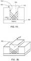
- FIGS. 7A and 7Brespectively show a cross section and perspective view of an epitaxially grown crystalline material 140 using ART.
- a crystalline material 140is epitaxially grown on substrate 100 (here, on the (001) surface of a silicon substrate).
- substrate 100here, on the (001) surface of a silicon substrate.
- defects 150 formed while epitaxially growing the crystalline material 140travel to and end at the insulator sidewalls 130 .
- the crystalline material 140continues to grow without the continued growth of the defects 150 , thereby producing crystal with reduced defects.
- This techniquehas been shown to be effective for growing low defectivity materials such as Ge, InP and GaAs selectively on Si in trenches as wide as 400 nm and of arbitrary length—an area large enough for devices such as a FET, for example.
- a devicewhich includes an active portion of the crystal material within an opening of surrounding dielectric
- a high surface roughness of the surface of a lower layere.g., an n-doped crystalline layer
- an upper layere.g., a p-doped crystalline layer
- These interface variancesaffect the functionality of the interface from one device to another device on the same substrate (e.g., differences in diode devices formed by p-n junctions differ from variances of the junctions, or interfaces, of the p and n crystalline materials).
- the same devices produced on the same substratemay undesirably vary in their operational characteristics. This may result in requiring higher operating tolerances and possibly device failure.
- two-step growthwhich comprises a thin low temperature buffer (330-450° C.) followed by a thick high temperature layer (600-850° C.) has been utilized.
- a thin low temperature buffer330-450° C.
- a thick high temperature layer600-850° C.
- none of these processeswere shown to be able to create smooth surfaces of Ge in a confined location, such as an opening or trench in an insulator.
- the selective growthe.g., in an opening or trench
- growth at the lower temperatureswas performed by molecular beam epitaxy, which is currently undesirable for commercial applications.
- Chemical mechanical polishing (CMP) of the selectively grown crystalline materialmay not be an option to smooth the surface of the crystalline material if it is not desired to grind the surrounding dielectric layer to the same height. Further, known processes which obtain acceptable surface roughness for blanket expitaxial grown materials have been found to obtain higher surface roughness for selective epitaxial grown materials.
- one embodiment the inventionprovides a process for the low temperature growth of crystalline material. Such growth may be done with a CVD process.
- one embodiment of the inventionprovides a process for the epitaxial growth of a crystalline material where the dominant growth component is provided by the lateral supply of the crystalline material containing species, such as from sidewalls of an insulator.
- the growth component of the crystalline material containing species from the growth ambientmay be substantially reduced.
- ART devicesincluding but not limited to a mixed signal application device, a field effect transistor, a quantum tunneling device, a light emitting diode, a laser diode, a resonant tunneling diode and a photovoltaic device.
- the ART devicesmay have crystalline material epitaxially grown in openings or confined areas with an aspect ratio (depth/width)>1, or otherwise suitable for trapping most defects.
- FIG. 1illustrates 5 ⁇ m ⁇ 5 ⁇ m AFM of Ge layers grown at 600° C. for 15 seconds.
- FIG. 1( a )illustrates the AFM at the edge of 6 mm ⁇ 6 mm Si window in oxide-field which was removed using a dilute HF.
- FIG. 1( b )illustrates the AFM at 80 ⁇ m from this edge, and
- FIG. 1( c )illustrates the AFM at 150 ⁇ m from oxide-field.
- FIG. 1( d )illustrates a 5 ⁇ m ⁇ 5 ⁇ m AFM of a Ge layer grown at 600° C. for 15 seconds on blanket Si.
- FIG. 2comprises FIGS. 2( a )-2( f ) .
- FIGS. 2( a )-( c )illustrates three-dimensional AFM images of Ge layers grown at 600° C. on blanket Si for 15 sec ( FIG. 2( a ) ), 90 sec ( FIG. 2( b ) ), and 180 sec ( FIG. 2( c ) ).
- FIGS. 2( d )-( f )illustrate three-dimensional AFM images of Ge layers grown at 600° C. on Si within 350-nm-wide oxide-trenches after oxide removal for 15 sec ( FIG. 2( d ) ), 90 sec ( FIG. 2( e ) ), and 180 sec ( FIG. 2( f ) ).
- Scan size of growth on blanket Si( FIGS. 2( a )-( c ) ) is 2 ⁇ m ⁇ 2 ⁇ m, and scan size of growth within oxide trenches ( FIGS. 2( d )-( f ) ) is 5 ⁇ m ⁇ 5 ⁇ m.
- Vertical scale and root-mean-square roughness (Rms)are shown on the left and right bottom of each image, respectively. Rms of the Ge on oxide-trench was calculated only on the Ge area and did not include Si where oxide was removed.
- FIG. 3comprises FIGS. 3( a )-3( f ) .
- FIGS. 3( a )-( c )illustrate three-dimensional AFM images of Ge layers grown at 400 ° C. on blanket Si for 270 sec ( FIG. 3( a ) ), 360 sec ( FIG. 3( b ) ), and 540 sec ( FIG. 3( c ) ).
- FIGS. 3( d )-( f )illustrate three-dimensional AFM images of Ge layers grown at 400° C. on Si within 350-nm-wide oxide-trenches after oxide removal for 270 sec ( FIG. 3( d ) ), 360 sec ( FIG. 3( e ) ), and 540 sec ( FIG. 3( f ) ).
- FIGS. 3( a )-( c )Scan size of growth on blanket Si ( FIGS. 3( a )-( c ) ) is 2 ⁇ m ⁇ 2 ⁇ m and scan size of growth within oxide trenches ( FIGS. 3( d )-( f ) ) is 5 ⁇ m ⁇ 5 ⁇ m.
- Vertical scale and root-mean-square roughness (Rms)are shown on the left and right bottom of each image, respectively. Rms of the Ge on oxide-trench was calculated only on the Ge area and did not include Si where oxide was removed.
- FIG. 4comprises FIGS. 4( a )-4( d ) .
- FIGS. 4( a ) and ( b )illustrate three-dimensional AFM images of Ge layers grown at 350° C. on blanket Si for 750 sec ( FIG. 4( a ) ) and 2000 sec ( FIG. 4( b ) ).
- FIGS. 4( c ) and ( d )illustrate three-dimensional AFM images of Ge layers grown at 350° C. on Si within 350-nm-wide oxide-trenches after oxide removal for 320 sec ( FIG. 4( c ) ) and 2000 sec ( FIG. 4( d ) ). Scan size of growth on blanket Si ( FIGS.
- FIGS. 4( a ) and ( b ) )is 2 ⁇ m ⁇ 2 ⁇ m and scan size of growth within oxide trenches ( FIGS. 4( c ) and ( d ) ) is 5 ⁇ m ⁇ 5 ⁇ m.
- Vertical scale and root-mean-square roughness (Rms)are shown on the left and right bottom of each image, respectively. Rms of the Ge on oxide-trench was calculated only on the Ge area and did not include Si where oxide was removed.
- the inset in FIG. ( c )is a 300 ⁇ m ⁇ 300 ⁇ m AFM image obtained on Ge inside the trench.
- FIG. 5comprising FIGS. 5( a )-5( d ) , illustrates SIMS depth profiles of (a) phosphorus and (b) boron in Ge inside the trenches after oxide removal and (c) phosphorus and (d) boron in Ge on blanket Si. Ge layers were deposited in two-steps at 400° C. for 540 sec and then at 600° C. for 1050 sec.
- FIGS. 6A, 6B and 6Cillustrate example configurations of a crystalline material grown on a substrate according to the invention.
- FIGS. 7A and 7Brespectively show a cross section and perspective view of an epitaxially grown crystalline material 140 using ART.
- FIG. 8illustrates another example of the confined area in which crystalline material may be epitaxially grown.
- FIG. 6Ashows one example, illustrating a cross section of a portion of the device.
- the exampleincludes a crystalline material 140 grown on a substrate 100 in an opening 120 defined in an insulator 110 .
- the substrate 100may be a crystalline material such as silicon, Ge or sapphire.
- Insulator 110is preferably a non-crystalline material such as SiO 2 .
- the crystalline materialat least at some stage during its growth has a surface, for example surface 160 , below the top surface of insulator 110 .
- the surface 160has a surface roughness Rms (root mean square, also sometimes denoted as “Rrms” and “Rq”) of less than or equal to 5 nm.
- the surface roughness (Rms) of surface 160may be less than or equal to 3 nm, or less than or equal to about 1 nm.
- the surface roughness (Rms) of surface 160may also be no greater than 0.55 nm
- the width of the opening 120may be 400 nm or less, 350 nm or less or 200 nm or less, 100 nm or less, or 50 nm or less; these sizes have been shown to be effective for ART (of course these sizes do not need to be used with ART).
- the width of the openingmay be 5 ⁇ m or less.
- the width of the openingmay be 1 ⁇ m or less.
- the openingmay be as great as 200 ⁇ m or less, as shown by the following description.
- the openingmay be formed as a trench (with the length of the trench running perpendicular to the cross section shown in FIG. 6A ) in which case the width would be considered to be perpendicular to its length and height.
- the length of the trenchmay be arbitrary.
- the length of the trenchmay be substantially larger than the width of the trench, for example greater than 10 times larger, or greater than 100 times larger. In one example, the length of the trench is 6 mm.
- the opening 120is used to trap defects when epitaxially growing the crystalline material 140 using ART (aspect ratio trapping) techniques.
- the aspect ratio(AR—height/width) may be greater than 1, although it possible for the aspect ratio to be lower in ART devices, for example as low as 0.5.
- Aspect ratio “AR”is defined for trenches as the ratio of the trench height/trench width.
- FIG. 6Aillustrates the crystalline material 140 with a continuous non-faceted surface extending between the sidewalls 130 of insulator 110 which form opening 120 .
- the surface 160 of crystalline material 140may include facets 160 a as shown in FIG. 6B .
- “Facet”is used herein to denote any major surface of the epitaxial material that is not parallel to an underlying surface of substrate surface 100 .
- the surface of crystalline material 140may only include faceted surfaces 160 a (i.e., not include any surface parallel to the surface of substrate 100 ), as exemplified by surface 160 ′′′. Unless otherwise noted, when measuring surface roughness of surfaces including facets, deviation of the surface height due to the faceting is included in calculating surface roughness for the faceted surface.
- FIG. 6Calso illustrates an implementation of the invention where additional epitaxial growth of the crystalline material 140 occurs above the initial surface 160 .
- FIG. 6Cshows surfaces 160 ′, 160 ′′ and 160 ′′′ subsequently grown above an initial surface 160 . These additional surfaces may grow in a single epitaxial growth process with no change to process parameters. Alternatively, the process parameters may be changed to alter the characteristics of the subsequently grown crystalline material 140 . For example, doping levels and/or doping type may be altered during the growth process (e.g., to obtain a p-n junction or a p-i-n quantum device).
- one or more of the surfacesmay have the surface roughness parameters described above with respect to FIG. 6A . It is also possible to use several different processes to obtain the multiple surfaces. Although not shown in FIGS. 6A-6C , it is of course possible to form (epitaxially grow or deposit by sputtering or CVD) a different material altogether on surface 160 . As is obvious from this discussion, in this disclosure, a “surface” of an epitaxially grown crystalline material indicates a boundary of the epitaxially grown material during some period of its growth.
- Such a “surface”does not cease to exist simply due to the forming of additional material on this surface, whether or not such additional material is homogeneous with the material on which it is deposited, and whether or not the additional material is deposited in the same process with the same process parameters
- the surfaces 160 of the crystalline material 140 of the examples illustrated in FIGS. 6A, 6B and 6Care all below the height of the top surface of insulator 110 .
- one or more the surfaces 160 of the crystalline materialmay partly or fully extend past the top surface of insulator 110 .
- the one or more surfaces obtained from the epitaxial growth of the crystalline materialmay have a surface roughness Rms less than or equal to 5 nm, may be less than or equal to 3 nm, or may be less than or equal to about 1 nm.
- the surface roughness of surface of this/these surface(s) 160may also be no greater than 0.55 nm.
- the substrate 100 in the above examplesmay include a group IV element or compound, such as germanium and/or silicon, e.g., (100) silicon.
- the crystalline material 140may include at least one of a group IV element or compound, a III-V or III-N compound, or a II-VI compound. Examples of group IV elements include Ge and Si, and examples of group IV compounds include SiGe.
- III-V compoundsinclude aluminum phosphide (AlP), galium phosphide (GaP), indium phosphide (InP), aluminum arsenide (AlAs), gallium arsenide (GaAs), indium arsenide (InAs), aluminum antimonide (AlSb), gallium antimonide (GaSb), indium antimonide (InSb), and their ternary and quaternary compounds.
- III-N compoundsinclude aluminum nitride (AlN), gallium nitride (GaN), indium nitride (InN), and their ternary and quaternary compounds.
- II-VI compoundsincludes zinc selenide (ZnSe), zinc telluride (ZnTe), cadmium selenide (CdSe), cadmium telluride (CdTe), zinc sulfide (ZnS), and their ternary and quaternary compounds.
- the layer of insulatorneed not be formed as a substantially planar layer.
- the insulatormay be formed of a thin layer which conforms to an undulating surface of the substrate on which it is deposited.
- FIG. 8illustrates on example including a substrate which has openings/trenches etched into the substrate.
- An insulating layer 110has been formed across the substrate 100 conforming to the surface topography of the etched substrate 100 .
- the insulating layer 110has portions at the bottom of the openings/trenches to expose portions of the substrate 100 on which the crystalline material will be grown.
- the sidewalls of the insulatorare formed from the outer surface of the insulator 110 after its deposition and are not formed by a separate photolithography and etch process.
- FIGS. 1-4explains examples of how the surfaces of the crystalline material grown within a confined space (e.g., in opening 120 in insulator 110 ) may be obtained with reduced surface roughnesses.
- a confined spacee.g., in opening 120 in insulator 110
- this descriptionis in connection with specific materials and process parameters, it will be apparent that the description is exemplary only, and should not be considered to limit the invention to such materials and process parameters.
- the following materials and process parameterswere used for all of the Ge grown as discussed in connection with FIGS. 1-5 .
- the starting substrates used in this workwere crystalline silicon, 200 mm diameter, p-type, and (001) oriented.
- a 500-nm-thick thermal oxidewas grown on the substrate.
- the oxide layerwas patterned into trenches along [ 110 ] direction of the silicon substrate having 350 nm width and 6 mm length.
- a section of the waferhad 6 mm ⁇ 6 mm exposed Si area in the oxide-field which was used to characterize selective Ge growth as a function of the distance from the oxide-field.
- the trencheswere formed using conventional photolithography techniques and a reactive ion etching (RIE) step.
- RIEreactive ion etching
- the patterned substrateswere then cleaned in Pirana, SC2, and dilute HF solutions sequentially. Removal of fluorocarbon residues caused by RIE was accomplished using a 25-nm-thick sacrificial oxidation and subsequent HF oxide etch. The final trench height was 490 nm after this cleaning procedure.
- Ge layerswere grown by chemical vapor deposition (CVD) on the exposed Si substrate (either in the trenches, in the 6 mm ⁇ 6 m section, or on a blanket Si substrate (i.e., a bare Si wafer)) in an industrial ASM Epsilon E2000 system.
- This CVD systemis a horizontal, cold-wall, single wafer, load-locked reactor with a lamp-heated graphite susceptor in a quartz tube.
- the substrateswere cleaned in a diluted HF solution and rinsed in DI (deionized) water.
- the substrateswere loaded into the growth chamber and baked in H2 for 1 minute at 870° C.
- the pressure during the bakewas set the same value as used in the subsequent growth step, 80 Torr.
- the growth stepused a 30 sccm germane (GeH4) source gas flow diluted to 25% in a 20 slm hydrogen carrier gas flow.
- 100 ppm B2H6 and 1000 ppm PH3 balanced in H2were used for in-situ boron and phosphorus doping, respectively.
- growth temperaturewas varied from 350° C. to 600° C., as was the time for growth.
- the 490-nm-thick oxide which formed the trencheswas removed using a diluted HF to enable material characterization.
- the sample roughnesswas characterized by tapping-mode atomic force microscopy (AFM) with a Veeco Dimension 3100.
- the boron and phosphorous doping levelwas measured with secondary ion mass spectrometry (SIMS) with an IMS 6-f using an oxygen and cesium ion beam, respectively.
- FIGS. 1( a )-1( c )show the AFM images of Ge layers grown at 600° C. for 15 seconds on the very edge of 6 mm ⁇ 6 mm Si window in the oxide-field ( FIG. 1( a ) ) and at 80 ⁇ m ( FIG. 1( b ) ) and 150 ⁇ m ( FIG. 1( c ) ) distances from the oxide-edge.
- An AFM image of Ge grown at 600° C. for 15 seconds on blanket Siis also shown in FIG. 1( d ) for comparison. Close to the oxide-field, the Ge islands are all connected to one another [ FIG. 1( a ) ].
- FIGS. 2( a )-2( c )illustrate the surface morphology of Ge layers grown at 600° C. on blanket Si substrates.
- FIGS. 2( d )-2( f )illustrate the surface morphology of Ge layers grown at 600° C. on Si located at the bottom of the oxide-trench described above.
- FIGS. 2( a ) and 2( d )illustrate results for Ge growth for 15 seconds.
- FIGS. 2( b ) and 2( e )illustrate Ge growth for 90 seconds.
- FIGS. 2( c ) and 2( f )illustrate Ge growth for 180 seconds.
- a 15 sec growth of Ge on blanket Si at 600° C.exhibits an island growth [ FIG.
- Ge islandswere preferentially nucleated and grown at the edge of the trenches after 15 sec growth as indicated by arrows in FIG. 2( d ) .
- the lateral diffusion length of Ge containing species from the oxide sidewallwas in the range of ⁇ 100 ⁇ m as discussed above.
- the selective Ge growth inside the 350-nm-wide trencheshas a substantial component provided by the lateral supply of Ge-containing species from the oxide sidewall, in addition to a growth component due to direct supply of Ge-containing species from the growth ambient.
- the preferential formation of Ge islands at the edge of trench adjacent the oxide sidewallsis consistent with previous reports showing that Ge dots grown at 700° C.
- FIGS. 3( a )-( c )illustrate the surface morphology of Ge layers grown at 400° C. on blanket Si substrates for time periods of 270 seconds, 360 seconds, and 540 seconds, respectively.
- FIGS. 3( d )-3( f )illustrate the surface morphology of Ge layers grown at 400° C. on Si located at the bottom of the oxide-trench described above for time periods of 270 seconds, 360 seconds, and 540 seconds, respectively.
- Ge layer grown on blanket Si at 400° C.shows higher island density with smaller size than the one at 600° C. [ FIG. 3( a ) ].
- FIGS. 4( a )-4( d )give very interesting results.
- FIGS. 4( a ) and 4( b )illustrate the surface morphology of Ge layers grown at 350° C. on blanket Si substrates for time periods of 750 seconds and 2000, respectively.
- FIGS. 4( c ) and 4( d )illustrate the surface morphology of Ge layers grown at 350° C. on Si located at the bottom of an oxide-trench as described above for time periods of 320 seconds and 2000 seconds, respectively.
- At this low temperatureonly a very limited amount of Ge is thermally decomposed, and the growth rate is impractically low with a long incubation time on blanket Si.
- growth on the blanket silicon substrate in FIGS. 4( a ) and 4( b )is dominated by the component of direct supply of Ge-containing species from the growth ambient. Since the silicon substrate within the oxide trenches will also be directly exposed to the Ge growth ambient, the Ge within the trenches should also have some growth component from the direct supply of Ge-containing species from the growth ambient. However, this component of growth will be minor in the trench Ge growth.
- the Ge growth in the oxide trenchesis dominated by the component of the lateral supply of Ge-containing species for the oxide sidewall.
- We can estimate the relative contribution of the direct exposure component to the lateral supply componentby estimating growth rates of FIGS. 4( a ) and 4( b ) (growth component from direct exposure to Ge-containing species only) to those of FIGS. 4( c ) and 4( d ) (growth components due to direct exposure and lateral supply of Ge-containing species).
- the thickness of the Ge layers in FIGS. 4( a ) and 4( b )can be estimated to be about ⁇ 1 nm and ⁇ 5 nm, respectively. It should be noted that in FIG. 4( a ) there are only Ge islands and continuous layers were not even formed due to low growth rate, but based on the area density of the islands, it was estimated to be about 2 equivalent monolayers of Ge, which corresponds to ⁇ 1 nm thickness.
- the thickness of the Ge layers in FIGS. 4( c ) and 4( d )is about 15 nm and 55 nm, respectively.
- While these examplesare directed to the CVD growth of germanium on silicon, other materials may be used.
- a growth temperature of 500-800° C.is normally used to obtain sufficient growth rates on a blanket substrate.
- compounds of Group III (Al, Ga, In) and Group V (Sb)such as GaSb, AlSb and InSb are epitaxially grown by CVD on a blanket substrate with a growth temperature in the range of 400-700° C.
- a growth temperaturein the range of 400-700° C.
- Group II-N compoundsare epitaxially grown by CVD on a blanket substrate with a growth temperature in the range of 500-1100° C.
- a growth temperaturein the range of 500-1100° C.
- Group II-VI compoundsare epitaxially grown by CVD on a blanket substrate with a growth temperature in the range of 250-600° C.
- a growth temperaturein the range of 250-600° C.
- Group IV elements and compoundsare epitaxially grown by CVD on a blanket substrate with a growth temperature in the range of 400-1000° C.
- a growth temperaturein the range of 400-1000° C.
- dopingis non-significantly effected as compared to Ge growth on a blanket substrate (with a dominant growth component due to the direct supply of Ge-containing species from the growth ambient).
- In-situ dopingboron and phosphorus doping levels were evaluated on Ge grown on oxide-trench Si and on blanket Si. To measure the doping level of Ge inside the trench, 500 nm thick boron- or phosphorus-doped Ge was grown inside the trench. The Ge was grown by CVD (using the same shared process parameters discussed above with respect to FIGS. 1-4 ) for 540 sec at 400° C.
- FIGS. 5( a ) and 5( b )Depth profiles of Ge on blanket Si grown at the same conditions are shown for comparison in FIGS. 5( c ) and 5( d ) .
- the incoming sputtering ion beamwas set at an angle of 60 degree from the surface normal of the Si so that the Ge pillars are sputtered at least for the initial part of the pillar.
- the channel to detect signalswas oriented perpendicular to the ion beam.
- the dopant speciesare normalized point by point to the Ge signal intensity to quantify the signals.
- both boron and phosphorus doping levels of Ge inside the trenchwere roughly half of those on blanket grown at the same conditions.
- this analysisdemonstrates that the doping level in trenches does not show a significant difference of more than an order of magnitude from that on blanket silicon for identical growth process parameters.
- this inventionhas a wide variety of applications. While not limited to ART technology, this invention has many applications within ART technology. For example, use of this invention may be used to create strained Ge over a SiGe alloy grown in an opening within an insulator. One or both of the Ge and SiGe layers may be grown in accordance with the invention and/or may have a surface of reduced roughness.
- a wide variety of devicesmay incorporate the invention. While not limiting to these devices, the invention may be particularly applicable to mixed signal applications, field effect transistors, quantum tunneling devices, light emitting diodes, laser diodes, resonant tunneling diodes and photovoltaic devices, especially those using ART technology.
- Coupledand “connect” (and derivations thereof are used to connote both direct and indirect connections/couplings.
- “having” and “including”, derivatives thereof and similar transitional terms or phrasesare used synonymously with “comprising” (i.e., all are considered “open ended” terms)-only the phrases “consisting of” and “consisting essentially of” should be considered as “close ended”. Claims are not intended to be interpreted under 112 sixth paragraph unless the phrase “means for” and an associated function appear in a claim and the claim fails to recite sufficient structure to perform such function.
Landscapes
- Engineering & Computer Science (AREA)
- Chemical & Material Sciences (AREA)
- Microelectronics & Electronic Packaging (AREA)
- Power Engineering (AREA)
- Condensed Matter Physics & Semiconductors (AREA)
- General Physics & Mathematics (AREA)
- Manufacturing & Machinery (AREA)
- Computer Hardware Design (AREA)
- Physics & Mathematics (AREA)
- Materials Engineering (AREA)
- Crystallography & Structural Chemistry (AREA)
- Metallurgy (AREA)
- Organic Chemistry (AREA)
- Inorganic Chemistry (AREA)
- Chemical Kinetics & Catalysis (AREA)
- General Chemical & Material Sciences (AREA)
- Recrystallisation Techniques (AREA)
Abstract
Description
Claims (18)
Priority Applications (1)
| Application Number | Priority Date | Filing Date | Title |
|---|---|---|---|
| US15/162,115US10961639B2 (en) | 2008-06-03 | 2016-05-23 | Epitaxial growth of crystalline material |
Applications Claiming Priority (5)
| Application Number | Priority Date | Filing Date | Title |
|---|---|---|---|
| US5854208P | 2008-06-03 | 2008-06-03 | |
| US12/476,460US8183667B2 (en) | 2008-06-03 | 2009-06-02 | Epitaxial growth of crystalline material |
| US13/342,626US8822248B2 (en) | 2008-06-03 | 2012-01-03 | Epitaxial growth of crystalline material |
| US14/447,081US9365949B2 (en) | 2008-06-03 | 2014-07-30 | Epitaxial growth of crystalline material |
| US15/162,115US10961639B2 (en) | 2008-06-03 | 2016-05-23 | Epitaxial growth of crystalline material |
Related Parent Applications (1)
| Application Number | Title | Priority Date | Filing Date |
|---|---|---|---|
| US14/447,081DivisionUS9365949B2 (en) | 2008-06-03 | 2014-07-30 | Epitaxial growth of crystalline material |
Publications (2)
| Publication Number | Publication Date |
|---|---|
| US20160265139A1 US20160265139A1 (en) | 2016-09-15 |
| US10961639B2true US10961639B2 (en) | 2021-03-30 |
Family
ID=41446371
Family Applications (4)
| Application Number | Title | Priority Date | Filing Date |
|---|---|---|---|
| US12/476,460ActiveUS8183667B2 (en) | 2008-06-03 | 2009-06-02 | Epitaxial growth of crystalline material |
| US13/342,626ActiveUS8822248B2 (en) | 2008-06-03 | 2012-01-03 | Epitaxial growth of crystalline material |
| US14/447,081ActiveUS9365949B2 (en) | 2008-06-03 | 2014-07-30 | Epitaxial growth of crystalline material |
| US15/162,115Active2030-10-19US10961639B2 (en) | 2008-06-03 | 2016-05-23 | Epitaxial growth of crystalline material |
Family Applications Before (3)
| Application Number | Title | Priority Date | Filing Date |
|---|---|---|---|
| US12/476,460ActiveUS8183667B2 (en) | 2008-06-03 | 2009-06-02 | Epitaxial growth of crystalline material |
| US13/342,626ActiveUS8822248B2 (en) | 2008-06-03 | 2012-01-03 | Epitaxial growth of crystalline material |
| US14/447,081ActiveUS9365949B2 (en) | 2008-06-03 | 2014-07-30 | Epitaxial growth of crystalline material |
Country Status (1)
| Country | Link |
|---|---|
| US (4) | US8183667B2 (en) |
Families Citing this family (58)
| Publication number | Priority date | Publication date | Assignee | Title |
|---|---|---|---|---|
| US8324660B2 (en) | 2005-05-17 | 2012-12-04 | Taiwan Semiconductor Manufacturing Company, Ltd. | Lattice-mismatched semiconductor structures with reduced dislocation defect densities and related methods for device fabrication |
| US9153645B2 (en) | 2005-05-17 | 2015-10-06 | Taiwan Semiconductor Manufacturing Company, Ltd. | Lattice-mismatched semiconductor structures with reduced dislocation defect densities and related methods for device fabrication |
| WO2007112066A2 (en) | 2006-03-24 | 2007-10-04 | Amberwave Systems Corporation | Lattice-mismatched semiconductor structures and related methods for device fabrication |
| US8173551B2 (en) | 2006-09-07 | 2012-05-08 | Taiwan Semiconductor Manufacturing Co., Ltd. | Defect reduction using aspect ratio trapping |
| WO2008039534A2 (en) | 2006-09-27 | 2008-04-03 | Amberwave Systems Corporation | Quantum tunneling devices and circuits with lattice- mismatched semiconductor structures |
| US8502263B2 (en) | 2006-10-19 | 2013-08-06 | Taiwan Semiconductor Manufacturing Company, Ltd. | Light-emitter-based devices with lattice-mismatched semiconductor structures |
| US20080173895A1 (en)* | 2007-01-24 | 2008-07-24 | Sharp Laboratories Of America, Inc. | Gallium nitride on silicon with a thermal expansion transition buffer layer |
| US8304805B2 (en) | 2009-01-09 | 2012-11-06 | Taiwan Semiconductor Manufacturing Company, Ltd. | Semiconductor diodes fabricated by aspect ratio trapping with coalesced films |
| US8237151B2 (en) | 2009-01-09 | 2012-08-07 | Taiwan Semiconductor Manufacturing Company, Ltd. | Diode-based devices and methods for making the same |
| US7825328B2 (en) | 2007-04-09 | 2010-11-02 | Taiwan Semiconductor Manufacturing Company, Ltd. | Nitride-based multi-junction solar cell modules and methods for making the same |
| WO2008124154A2 (en) | 2007-04-09 | 2008-10-16 | Amberwave Systems Corporation | Photovoltaics on silicon |
| US8329541B2 (en) | 2007-06-15 | 2012-12-11 | Taiwan Semiconductor Manufacturing Company, Ltd. | InP-based transistor fabrication |
| JP2010538495A (en) | 2007-09-07 | 2010-12-09 | アンバーウェーブ・システムズ・コーポレーション | Multi-junction solar cell |
| US8183667B2 (en) | 2008-06-03 | 2012-05-22 | Taiwan Semiconductor Manufacturing Co., Ltd. | Epitaxial growth of crystalline material |
| US8274097B2 (en) | 2008-07-01 | 2012-09-25 | Taiwan Semiconductor Manufacturing Company, Ltd. | Reduction of edge effects from aspect ratio trapping |
| US8981427B2 (en)* | 2008-07-15 | 2015-03-17 | Taiwan Semiconductor Manufacturing Company, Ltd. | Polishing of small composite semiconductor materials |
| EP2335273A4 (en) | 2008-09-19 | 2012-01-25 | Taiwan Semiconductor Mfg | FORMATION OF DEVICES BY GROWTH OF EPITAXIAL LAYERS |
| US20100072515A1 (en) | 2008-09-19 | 2010-03-25 | Amberwave Systems Corporation | Fabrication and structures of crystalline material |
| US8253211B2 (en) | 2008-09-24 | 2012-08-28 | Taiwan Semiconductor Manufacturing Company, Ltd. | Semiconductor sensor structures with reduced dislocation defect densities |
| US8629446B2 (en) | 2009-04-02 | 2014-01-14 | Taiwan Semiconductor Manufacturing Company, Ltd. | Devices formed from a non-polar plane of a crystalline material and method of making the same |
| CN101866834B (en)* | 2009-12-11 | 2011-09-14 | 清华大学 | Method for preparing SiGe material of high-Ge content |
| CN102543746B (en)* | 2010-12-31 | 2015-03-25 | 中国科学院微电子研究所 | Semiconductor device and method for manufacturing the same |
| US9064808B2 (en) | 2011-07-25 | 2015-06-23 | Synopsys, Inc. | Integrated circuit devices having features with reduced edge curvature and methods for manufacturing the same |
| US8609550B2 (en)* | 2011-09-08 | 2013-12-17 | Synopsys, Inc. | Methods for manufacturing integrated circuit devices having features with reduced edge curvature |
| KR101867999B1 (en) | 2011-10-31 | 2018-06-18 | 삼성전자주식회사 | Method of forming III-V group material layer, semiconductor device comprising III-V group material layer and method of manufacturing the same |
| US9053930B2 (en) | 2012-04-17 | 2015-06-09 | International Business Machines Corporation | Heterogeneous integration of group III nitride on silicon for advanced integrated circuits |
| US8680576B2 (en)* | 2012-05-16 | 2014-03-25 | Taiwan Semiconductor Manufacturing Company, Ltd. | CMOS device and method of forming the same |
| US9142400B1 (en) | 2012-07-17 | 2015-09-22 | Stc.Unm | Method of making a heteroepitaxial layer on a seed area |
| US8716751B2 (en) | 2012-09-28 | 2014-05-06 | Intel Corporation | Methods of containing defects for non-silicon device engineering |
| US9099381B2 (en) | 2012-11-15 | 2015-08-04 | International Business Machines Corporation | Selective gallium nitride regrowth on (100) silicon |
| US9048173B2 (en) | 2012-11-15 | 2015-06-02 | International Business Machines Corporation | Dual phase gallium nitride material formation on (100) silicon |
| US9059044B2 (en) | 2012-11-15 | 2015-06-16 | International Business Machines Corporation | On-chip diode with fully depleted semiconductor devices |
| US20140342533A1 (en)* | 2013-05-15 | 2014-11-20 | Applied Materials, Inc. | Method of strain and defect control in thin semiconductor films |
| US9484423B2 (en) | 2013-11-01 | 2016-11-01 | Samsung Electronics Co., Ltd. | Crystalline multiple-nanosheet III-V channel FETs |
| US9570609B2 (en) | 2013-11-01 | 2017-02-14 | Samsung Electronics Co., Ltd. | Crystalline multiple-nanosheet strained channel FETs and methods of fabricating the same |
| US20150171206A1 (en)* | 2013-12-18 | 2015-06-18 | Taiwan Semiconductor Manufacturing Company, Ltd. | Epitaxially Growing III-V Contact Plugs for MOSFETs |
| KR102168969B1 (en) | 2014-02-28 | 2020-10-22 | 삼성전자주식회사 | Semiconductor device and method for fabricating the same |
| US20150263161A1 (en)* | 2014-03-12 | 2015-09-17 | Kabushiki Kaisha Toshiba | Semiconductor storage device and method of manufacturing the same |
| US9391140B2 (en)* | 2014-06-20 | 2016-07-12 | Globalfoundries Inc. | Raised fin structures and methods of fabrication |
| US9647098B2 (en) | 2014-07-21 | 2017-05-09 | Samsung Electronics Co., Ltd. | Thermionically-overdriven tunnel FETs and methods of fabricating the same |
| GB201415119D0 (en)* | 2014-08-27 | 2014-10-08 | Ibm | Method for fabricating a semiconductor structure |
| US9293530B1 (en) | 2014-11-14 | 2016-03-22 | International Business Machines Corporation | High aspect ratio trapping semiconductor with uniform height and isolated from bulk substrate |
| US9564494B1 (en) | 2015-11-18 | 2017-02-07 | International Business Machines Corporation | Enhanced defect reduction for heteroepitaxy by seed shape engineering |
| US10026843B2 (en) | 2015-11-30 | 2018-07-17 | Taiwan Semiconductor Manufacturing Co., Ltd. | Fin structure of semiconductor device, manufacturing method thereof, and manufacturing method of active region of semiconductor device |
| US9570297B1 (en)* | 2015-12-09 | 2017-02-14 | International Business Machines Corporation | Elimination of defects in long aspect ratio trapping trench structures |
| WO2019066766A1 (en)* | 2017-09-26 | 2019-04-04 | Intel Corporation | Iii-n nanostructures formed via cavity fill |
| US10217761B1 (en) | 2017-11-22 | 2019-02-26 | Macronix International Co., Ltd. | Semiconductor structure and manufacturing method thereof |
| US11139402B2 (en) | 2018-05-14 | 2021-10-05 | Synopsys, Inc. | Crystal orientation engineering to achieve consistent nanowire shapes |
| US10840093B2 (en) | 2018-09-11 | 2020-11-17 | International Business Machines Corporation | Fabrication of semiconductor substrates |
| US11264458B2 (en) | 2019-05-20 | 2022-03-01 | Synopsys, Inc. | Crystal orientation engineering to achieve consistent nanowire shapes |
| US11742203B2 (en) | 2020-02-26 | 2023-08-29 | The Hong Kong University Of Science And Technology | Method for growing III-V compound semiconductor thin films on silicon-on-insulators |
| US12119367B2 (en)* | 2020-07-24 | 2024-10-15 | University Of Southern California | Composite substrate for fabricating III-V photodetector arrays |
| US11610979B2 (en)* | 2020-08-13 | 2023-03-21 | Taiwan Semiconductor Manufacturing Co., Ltd. | Profile control in forming epitaxy regions for transistors |
| US20220108888A1 (en)* | 2020-10-04 | 2022-04-07 | Applied Materials, Inc. | Selective Deposition of Germanium |
| US12077880B2 (en) | 2021-04-28 | 2024-09-03 | Applied Materials, Inc. | In-situ film growth rate monitoring apparatus, systems, and methods for substrate processing |
| US11776809B2 (en) | 2021-07-28 | 2023-10-03 | International Business Machines Corporation | Fabrication of a semiconductor device |
| TWI771140B (en)* | 2021-08-04 | 2022-07-11 | 行政院原子能委員會核能研究所 | Indium phosphide virtual substrate and fabrication method thereof |
| EP4393015A4 (en)* | 2021-08-24 | 2025-08-06 | Univ Michigan Regents | SEMICONDUCTOR HETEROSTRACTURES WITH SCANDIUM III NITRIDE LAYER |
Citations (394)
| Publication number | Priority date | Publication date | Assignee | Title |
|---|---|---|---|---|
| JPS515974A (en) | 1974-05-31 | 1976-01-19 | Itt | |
| US4307510A (en) | 1980-03-12 | 1981-12-29 | The United States Of America As Represented By The Administrator Of The National Aeronautics & Space Administration | Computer circuit card puller |
| US4322253A (en) | 1980-04-30 | 1982-03-30 | Rca Corporation | Method of making selective crystalline silicon regions containing entrapped hydrogen by laser treatment |
| US4370510A (en) | 1980-09-26 | 1983-01-25 | California Institute Of Technology | Gallium arsenide single crystal solar cell structure and method of making |
| US4545109A (en) | 1983-01-21 | 1985-10-08 | Rca Corporation | Method of making a gallium arsenide field effect transistor |
| US4551394A (en) | 1984-11-26 | 1985-11-05 | Honeywell Inc. | Integrated three-dimensional localized epitaxial growth of Si with localized overgrowth of GaAs |
| US4651179A (en) | 1983-01-21 | 1987-03-17 | Rca Corporation | Low resistance gallium arsenide field effect transistor |
| US4727047A (en) | 1980-04-10 | 1988-02-23 | Massachusetts Institute Of Technology | Method of producing sheets of crystalline material |
| US4774205A (en) | 1986-06-13 | 1988-09-27 | Massachusetts Institute Of Technology | Monolithic integration of silicon and gallium arsenide devices |
| US4789643A (en) | 1986-09-25 | 1988-12-06 | Mitsubishi Denki Kabushiki Kaisha | Method of manufacturing a heterojunction bipolar transistor involving etch and refill |
| US4826784A (en) | 1987-11-13 | 1989-05-02 | Kopin Corporation | Selective OMCVD growth of compound semiconductor materials on silicon substrates |
| US4860081A (en) | 1984-06-28 | 1989-08-22 | Gte Laboratories Incorporated | Semiconductor integrated circuit structure with insulative partitions |
| GB2215514A (en) | 1988-03-04 | 1989-09-20 | Plessey Co Plc | Terminating dislocations in semiconductor epitaxial layers |
| US4876210A (en) | 1987-04-30 | 1989-10-24 | The University Of Delaware | Solution growth of lattice mismatched and solubility mismatched heterostructures |
| EP0352472A2 (en) | 1988-07-25 | 1990-01-31 | Texas Instruments Incorporated | Heteroepitaxy of lattice-mismatched semiconductor materials |
| JPH0262090A (en) | 1988-08-29 | 1990-03-01 | Matsushita Electric Ind Co Ltd | Method for manufacturing optical semiconductor devices |
| US4948456A (en) | 1989-06-09 | 1990-08-14 | Delco Electronics Corporation | Confined lateral selective epitaxial growth |
| US4963508A (en) | 1985-09-03 | 1990-10-16 | Daido Tokushuko Kabushiki Kaisha | Method of making an epitaxial gallium arsenide semiconductor wafer using a strained layer superlattice |
| US5032893A (en) | 1988-04-01 | 1991-07-16 | Cornell Research Foundation, Inc. | Method for reducing or eliminating interface defects in mismatched semiconductor eiplayers |
| US5034337A (en) | 1989-02-10 | 1991-07-23 | Texas Instruments Incorporated | Method of making an integrated circuit that combines multi-epitaxial power transistors with logic/analog devices |
| US5061644A (en) | 1988-12-22 | 1991-10-29 | Honeywell Inc. | Method for fabricating self-aligned semiconductor devices |
| US5079616A (en) | 1988-02-11 | 1992-01-07 | Gte Laboratories Incorporated | Semiconductor structure |
| US5091767A (en) | 1991-03-18 | 1992-02-25 | At&T Bell Laboratories | Article comprising a lattice-mismatched semiconductor heterostructure |
| US5091333A (en) | 1983-09-12 | 1992-02-25 | Massachusetts Institute Of Technology | Reducing dislocations in semiconductors utilizing repeated thermal cycling during multistage epitaxial growth |
| US5093699A (en) | 1990-03-12 | 1992-03-03 | Texas A & M University System | Gate adjusted resonant tunnel diode device and method of manufacture |
| US5098850A (en) | 1989-06-16 | 1992-03-24 | Canon Kabushiki Kaisha | Process for producing substrate for selective crystal growth, selective crystal growth process and process for producing solar battery by use of them |
| US5105247A (en) | 1990-08-03 | 1992-04-14 | Cavanaugh Marion E | Quantum field effect device with source extension region formed under a gate and between the source and drain regions |
| US5108947A (en) | 1989-01-31 | 1992-04-28 | Agfa-Gevaert N.V. | Integration of gaas on si substrates |
| US5156995A (en) | 1988-04-01 | 1992-10-20 | Cornell Research Foundation, Inc. | Method for reducing or eliminating interface defects in mismatched semiconductor epilayers |
| US5159413A (en) | 1990-04-20 | 1992-10-27 | Eaton Corporation | Monolithic integrated circuit having compound semiconductor layer epitaxially grown on ceramic substrate |
| US5166767A (en) | 1987-04-14 | 1992-11-24 | National Semiconductor Corporation | Sidewall contact bipolar transistor with controlled lateral spread of selectively grown epitaxial layer |
| US5223043A (en) | 1991-02-11 | 1993-06-29 | The United States Of America As Represented By The United States Department Of Energy | Current-matched high-efficiency, multijunction monolithic solar cells |
| US5236546A (en) | 1987-01-26 | 1993-08-17 | Canon Kabushiki Kaisha | Process for producing crystal article |
| US5238869A (en) | 1988-07-25 | 1993-08-24 | Texas Instruments Incorporated | Method of forming an epitaxial layer on a heterointerface |
| US5256594A (en) | 1989-06-16 | 1993-10-26 | Intel Corporation | Masking technique for depositing gallium arsenide on silicon |
| US5269876A (en) | 1987-01-26 | 1993-12-14 | Canon Kabushiki Kaisha | Process for producing crystal article |
| US5269852A (en) | 1991-05-27 | 1993-12-14 | Canon Kabushiki Kaisha | Crystalline solar cell and method for producing the same |
| US5272105A (en) | 1988-02-11 | 1993-12-21 | Gte Laboratories Incorporated | Method of manufacturing an heteroepitaxial semiconductor structure |
| US5281283A (en) | 1987-03-26 | 1994-01-25 | Canon Kabushiki Kaisha | Group III-V compound crystal article using selective epitaxial growth |
| US5285086A (en) | 1990-08-02 | 1994-02-08 | At&T Bell Laboratories | Semiconductor devices with low dislocation defects |
| US5295150A (en) | 1992-12-11 | 1994-03-15 | Eastman Kodak Company | Distributed feedback-channeled substrate planar semiconductor laser |
| EP0600276A2 (en) | 1992-12-04 | 1994-06-08 | Siemens Aktiengesellschaft | Process for production of a laterally limited monocrystal area by selective epitaxy and its application for production of a bipolar transistor as well as well as a MOS-transistor |
| US5403751A (en) | 1990-11-29 | 1995-04-04 | Canon Kabushiki Kaisha | Process for producing a thin silicon solar cell |
| US5405453A (en) | 1993-11-08 | 1995-04-11 | Applied Solar Energy Corporation | High efficiency multi-junction solar cell |
| US5407491A (en) | 1993-04-08 | 1995-04-18 | University Of Houston | Tandem solar cell with improved tunnel junction |
| US5410167A (en) | 1992-07-10 | 1995-04-25 | Fujitsu Limited | Semiconductor device with reduced side gate effect |
| US5417180A (en) | 1991-10-24 | 1995-05-23 | Rohm Co., Ltd. | Method for forming SOI structure |
| US5427976A (en) | 1991-03-27 | 1995-06-27 | Nec Corporation | Method of producing a semiconductor on insulating substrate, and a method of forming a transistor thereon |
| US5438018A (en) | 1992-12-07 | 1995-08-01 | Fujitsu Limited | Method of making semiconductor device by selective epitaxial growth |
| JPH07230952A (en) | 1994-02-16 | 1995-08-29 | Ricoh Co Ltd | Recrystallization method |
| US5461243A (en) | 1993-10-29 | 1995-10-24 | International Business Machines Corporation | Substrate for tensilely strained semiconductor |
| US5518953A (en) | 1991-09-24 | 1996-05-21 | Rohm Co., Ltd. | Method for manufacturing semiconductor device having grown layer on insulating layer |
| US5528209A (en) | 1995-04-27 | 1996-06-18 | Hughes Aircraft Company | Monolithic microwave integrated circuit and method |
| US5545586A (en) | 1990-11-27 | 1996-08-13 | Nec Corporation | Method of making a transistor having easily controllable impurity profile |
| US5548129A (en) | 1994-01-10 | 1996-08-20 | Hughes Aircraft Company | Quantum well structure with self-aligned gate and method of making the same |
| US5589696A (en) | 1991-10-15 | 1996-12-31 | Nec Corporation | Tunnel transistor comprising a semiconductor film between gate and source/drain |
| US5621227A (en) | 1995-07-18 | 1997-04-15 | Discovery Semiconductors, Inc. | Method and apparatus for monolithic optoelectronic integrated circuit using selective epitaxy |
| US5640022A (en) | 1993-08-27 | 1997-06-17 | Sanyo Electric Co., Inc. | Quantum effect device |
| EP0817096A2 (en) | 1996-04-02 | 1998-01-07 | Texas Instruments Incorporated | Integrated circuit |
| US5710436A (en) | 1994-09-27 | 1998-01-20 | Kabushiki Kaisha Toshiba | Quantum effect device |
| US5717709A (en) | 1993-06-04 | 1998-02-10 | Sharp Kabushiki Kaisha | Semiconductor light-emitting device capable of having good stability in fundamental mode of oscillation, decreasing current leakage, and lowering oscillation threshold limit, and method of making the same |
| JPH10126010A (en) | 1996-10-23 | 1998-05-15 | Ricoh Co Ltd | Method of manufacturing semiconductor laser device |
| US5792679A (en) | 1993-08-30 | 1998-08-11 | Sharp Microelectronics Technology, Inc. | Method for forming silicon-germanium/Si/silicon dioxide heterostructure using germanium implant |
| US5825049A (en) | 1996-10-09 | 1998-10-20 | Sandia Corporation | Resonant tunneling device with two-dimensional quantum well emitter and base layers |
| US5825240A (en) | 1994-11-30 | 1998-10-20 | Massachusetts Institute Of Technology | Resonant-tunneling transmission line technology |
| JPH10284507A (en) | 1997-04-04 | 1998-10-23 | Matsushita Electric Ind Co Ltd | Semiconductor device |
| JPH10284436A (en) | 1997-04-11 | 1998-10-23 | Matsushita Electric Ind Co Ltd | Ohmic electrode formation method |
| US5849077A (en) | 1994-04-11 | 1998-12-15 | Texas Instruments Incorporated | Process for growing epitaxial silicon in the windows of an oxide-patterned wafer |
| US5853497A (en) | 1996-12-12 | 1998-12-29 | Hughes Electronics Corporation | High efficiency multi-junction solar cells |
| US5869845A (en) | 1997-06-26 | 1999-02-09 | Texas Instruments Incorporated | Resonant tunneling memory |
| US5883549A (en) | 1997-06-20 | 1999-03-16 | Hughes Electronics Corporation | Bipolar junction transistor (BJT)--resonant tunneling diode (RTD) oscillator circuit and method |
| US5886385A (en) | 1996-08-22 | 1999-03-23 | Kabushiki Kaisha Toshiba | Semiconductor device and manufacturing method thereof |
| US5903170A (en) | 1997-06-03 | 1999-05-11 | The Regents Of The University Of Michigan | Digital logic design using negative differential resistance diodes and field-effect transistors |
| US5953361A (en) | 1995-05-31 | 1999-09-14 | Siemens Aktiengesellschaft | DFB laser diode structure having complex optical grating coupling |
| JPH11251684A (en) | 1998-02-26 | 1999-09-17 | Nichia Chem Ind Ltd | Nitride semiconductor device |
| US5963822A (en) | 1996-04-12 | 1999-10-05 | Kabushiki Kaisha Toshiba | Method of forming selective epitaxial film |
| US5966620A (en) | 1996-11-15 | 1999-10-12 | Canon Kabshiki Kaisha | Process for producing semiconductor article |
| JPH11307866A (en) | 1998-04-24 | 1999-11-05 | Nec Corp | Nitride compound semiconductor laser element |
| US5998781A (en) | 1997-04-30 | 1999-12-07 | Sandia Corporation | Apparatus for millimeter-wave signal generation |
| US6011271A (en) | 1994-04-28 | 2000-01-04 | Fujitsu Limited | Semiconductor device and method of fabricating the same |
| US6015979A (en) | 1997-08-29 | 2000-01-18 | Kabushiki Kaisha Toshiba | Nitride-based semiconductor element and method for manufacturing the same |
| JP2000021789A (en) | 1997-08-29 | 2000-01-21 | Toshiba Corp | Nitride-based semiconductor device, light-emitting device and method of manufacturing the same |
| US6049098A (en) | 1995-04-27 | 2000-04-11 | Nec Corporation | Bipolar transistor having an emitter region formed of silicon carbide |
| US6083598A (en) | 1995-12-20 | 2000-07-04 | Kabushiki Kaisha Toshiba | Information recording medium, method for manufacturing the medium, and apparatus for manufacturing the medium |
| JP2000216432A (en) | 1999-01-20 | 2000-08-04 | Nichia Chem Ind Ltd | Gallium nitride based compound semiconductor device |
| US6100106A (en) | 1997-11-17 | 2000-08-08 | Nec Corporation | Fabrication of nitride semiconductor light-emitting device |
| US6111288A (en) | 1997-03-18 | 2000-08-29 | Kabushiki Kaisha Toshiba | Quantum tunneling effect device and semiconductor composite substrate |
| US6110813A (en) | 1997-04-04 | 2000-08-29 | Matsushita Electric Industrial Co., Ltd. | Method for forming an ohmic electrode |
| US6121542A (en) | 1996-05-17 | 2000-09-19 | Canon Kabushiki Kaisha | Photovoltaic device |
| JP2000286449A (en) | 1999-03-31 | 2000-10-13 | Toyoda Gosei Co Ltd | Iii nitride compound semiconductor device and its manufacture |
| JP2000299532A (en) | 1999-02-10 | 2000-10-24 | Nichia Chem Ind Ltd | Nitride semiconductor laser element |
| DE10017137A1 (en) | 1999-04-14 | 2000-10-26 | Siemens Ag | Novel silicon structure, used for solar cells or LCD TFTs, comprises a crystalline textured silicon thin film over a biaxially textured lattice-matched diffusion barrier buffer layer on a thermal expansion-matched inert substrate |
| US6150242A (en) | 1998-03-25 | 2000-11-21 | Texas Instruments Incorporated | Method of growing crystalline silicon overlayers on thin amorphous silicon oxide layers and forming by method a resonant tunneling diode |
| US6153010A (en) | 1997-04-11 | 2000-11-28 | Nichia Chemical Industries Ltd. | Method of growing nitride semiconductors, nitride semiconductor substrate and nitride semiconductor device |
| WO2000072383A1 (en) | 1999-05-25 | 2000-11-30 | The University Court Of The University Of Glasgow | Improved optoelectronic device |
| WO2001001465A1 (en) | 1999-06-25 | 2001-01-04 | Massachusetts Institute Of Technology | Cyclic thermal anneal for dislocation reduction |
| JP2001007447A (en) | 1999-06-18 | 2001-01-12 | Nichia Chem Ind Ltd | Nitride semiconductor laser element |
| US6191432B1 (en) | 1996-09-02 | 2001-02-20 | Kabushiki Kaisha Toshiba | Semiconductor device and memory device |
| JP2001102678A (en) | 1999-09-29 | 2001-04-13 | Toshiba Corp | Gallium nitride based compound semiconductor device |
| US6225650B1 (en) | 1997-03-25 | 2001-05-01 | Mitsubishi Cable Industries, Ltd. | GAN group crystal base member having low dislocation density, use thereof and manufacturing methods thereof |
| US6228691B1 (en) | 1999-06-30 | 2001-05-08 | Intel Corp. | Silicon-on-insulator devices and method for producing the same |
| US6229153B1 (en) | 1996-06-21 | 2001-05-08 | Wisconsin Alumni Research Corporation | High peak current density resonant tunneling diode |
| US6252261B1 (en) | 1998-09-30 | 2001-06-26 | Nec Corporation | GaN crystal film, a group III element nitride semiconductor wafer and a manufacturing process therefor |
| US6252287B1 (en) | 1999-05-19 | 2001-06-26 | Sandia Corporation | InGaAsN/GaAs heterojunction for multi-junction solar cells |
| US20010006249A1 (en) | 1997-09-16 | 2001-07-05 | Eugene A Fitzgerald | Co-planar si and ge composite substrate and method of producing same |
| US6271551B1 (en) | 1995-12-15 | 2001-08-07 | U.S. Philips Corporation | Si-Ge CMOS semiconductor device |
| JP2001257351A (en) | 2000-03-10 | 2001-09-21 | Toshiba Corp | Semiconductor device and manufacturing method thereof |
| US6300650B1 (en) | 1996-08-30 | 2001-10-09 | Ricoh Company, Ltd. | Optical semiconductor device having a multilayer reflection structure |
| US20010045604A1 (en) | 2000-05-25 | 2001-11-29 | Hitachi, Ltd. | Semiconductor device and manufacturing method |
| US6325850B1 (en) | 1997-10-20 | 2001-12-04 | CENTRE NATIONAL DE LA RECHERCHé SCIENTIFIQUE (CNRS) | Method for producing a gallium nitride epitaxial layer |
| US6339232B1 (en) | 1999-09-20 | 2002-01-15 | Kabushika Kaisha Toshiba | Semiconductor device |
| US6342404B1 (en) | 1999-03-31 | 2002-01-29 | Toyoda Gosei Co., Ltd. | Group III nitride compound semiconductor device and method for producing |
| WO2002009187A2 (en) | 2000-07-24 | 2002-01-31 | Motorola, Inc. | Heterojunction tunneling diodes and process for fabricating same |
| US20020011612A1 (en) | 2000-07-31 | 2002-01-31 | Kabushiki Kaisha Toshiba | Semiconductor device and method for manufacturing the same |
| US20020017642A1 (en) | 2000-08-01 | 2002-02-14 | Mitsubishi Materials Corporation | Semiconductor substrate, field effect transistor, method of forming SiGe layer and method of forming strained Si layer using same, and method of manufacturing field effect transistor |
| US6348096B1 (en) | 1997-03-13 | 2002-02-19 | Nec Corporation | Method for manufacturing group III-V compound semiconductors |
| US20020022290A1 (en) | 1999-10-14 | 2002-02-21 | Hua-Shuang Kong | Single step pendeo-and lateral epitaxial overgrowth of group III-nitride epitaxial layers with group III-nitride buffer layer and resulting structures |
| US20020030246A1 (en) | 2000-06-28 | 2002-03-14 | Motorola, Inc. | Structure and method for fabricating semiconductor structures and devices not lattice matched to the substrate |
| US6362071B1 (en) | 2000-04-05 | 2002-03-26 | Motorola, Inc. | Method for forming a semiconductor device with an opening in a dielectric layer |
| US20020036290A1 (en) | 2000-09-28 | 2002-03-28 | Kabushiki Kaisha Toshiba | Semiconductor device having MIS field effect transistors or three-dimensional structure |
| JP2002118255A (en) | 2000-07-31 | 2002-04-19 | Toshiba Corp | Semiconductor device and manufacturing method thereof |
| US20020047155A1 (en) | 2000-09-21 | 2002-04-25 | Babcock Jeffrey A. | Programmable neuron MOSFET on SOI |
| US6380051B1 (en) | 1998-06-24 | 2002-04-30 | Sharp Kabushiki Kaisha | Layered structure including a nitride compound semiconductor film and method for making the same |
| US6380590B1 (en) | 2001-02-22 | 2002-04-30 | Advanced Micro Devices, Inc. | SOI chip having multiple threshold voltage MOSFETs by using multiple channel materials and method of fabricating same |
| US6384423B1 (en)* | 1998-09-18 | 2002-05-07 | Trw Inc. | Process for reducing surface roughness of superconductor integrated circuit having a ground plane of niobium nitride of improved smoothness |
| JP2002141553A (en) | 1995-02-23 | 2002-05-17 | Nichia Chem Ind Ltd | Nitride semiconductor light emitting device |
| US6403451B1 (en) | 2000-02-09 | 2002-06-11 | Noerh Carolina State University | Methods of fabricating gallium nitride semiconductor layers on substrates including non-gallium nitride posts |
| US20020084000A1 (en) | 1997-06-24 | 2002-07-04 | Eugene A. Fitzgerald | Controlling threading dislocation densities in Ge on Si using graded GeSi layers and planarization |
| JP2002241192A (en) | 2001-02-14 | 2002-08-28 | Toyoda Gosei Co Ltd | Semiconductor crystal manufacturing method and semiconductor light emitting device |
| US20020127427A1 (en) | 2001-01-02 | 2002-09-12 | Eastman Kodak Company | Organic light emitting diode devices with improved luminance efficiency |
| US6456214B1 (en) | 2000-09-27 | 2002-09-24 | Raytheon Company | High-speed comparator utilizing resonant tunneling diodes and associated method |
| US6458614B1 (en) | 1998-03-26 | 2002-10-01 | Murata Manufacturing Co., | Opto-electronic integrated circuit |
| JP2002293698A (en) | 2001-03-30 | 2002-10-09 | Toyoda Gosei Co Ltd | Semiconductor substrate manufacturing method and semiconductor element |
| WO2002086952A1 (en) | 2001-04-23 | 2002-10-31 | Motorola Inc. | Mixed-signal semiconductor structure |
| US6475869B1 (en) | 2001-02-26 | 2002-11-05 | Advanced Micro Devices, Inc. | Method of forming a double gate transistor having an epitaxial silicon/germanium channel region |
| WO2002088834A2 (en) | 2001-04-25 | 2002-11-07 | The University Court Of The University Of Glasgow | Optoelectronic device |
| US20020168844A1 (en) | 2001-03-07 | 2002-11-14 | Nec Corporation | Group III-V compound semiconductor crystal structure and method of epitaxial growth of the same as well as semiconductor device including the same |
| US20020168802A1 (en) | 2001-05-14 | 2002-11-14 | Hsu Sheng Teng | SiGe/SOI CMOS and method of making the same |
| US20020179005A1 (en) | 1999-05-10 | 2002-12-05 | Masayoshi Koike | Method for manufacturing group III nitride compound semiconductor and a light-emitting device using group III nitride compound semiconductor |
| US6492216B1 (en) | 2002-02-07 | 2002-12-10 | Taiwan Semiconductor Manufacturing Company | Method of forming a transistor with a strained channel |
| US6500257B1 (en) | 1998-04-17 | 2002-12-31 | Agilent Technologies, Inc. | Epitaxial material grown laterally within a trench and method for producing same |
| US6503610B2 (en) | 2000-03-24 | 2003-01-07 | Sumitomo Chemical Company, Limited | Group III-V compound semiconductor and method of producing the same |
| US6512252B1 (en) | 1999-11-15 | 2003-01-28 | Matsushita Electric Industrial Co., Ltd. | Semiconductor device |
| US20030030117A1 (en) | 2001-05-22 | 2003-02-13 | Hitachi, Ltd. | Semiconductor device |
| US6521514B1 (en) | 1999-11-17 | 2003-02-18 | North Carolina State University | Pendeoepitaxial methods of fabricating gallium nitride semiconductor layers on sapphire substrates |
| US20030045017A1 (en) | 2001-09-06 | 2003-03-06 | Kazumasa Hiramatsu | Method for fabricating III-V Group compound semiconductor |
| US20030057486A1 (en) | 2001-09-27 | 2003-03-27 | International Business Machines Corporation | Fin field effect transistor with self-aligned gate |
| US20030064535A1 (en) | 2001-09-28 | 2003-04-03 | Kub Francis J. | Method of manufacturing a semiconductor device having a thin GaN material directly bonded to an optimized substrate |
| US20030070707A1 (en) | 2001-10-12 | 2003-04-17 | King Richard Roland | Wide-bandgap, lattice-mismatched window layer for a solar energy conversion device |
| US6552259B1 (en) | 1999-10-18 | 2003-04-22 | Sharp Kabushiki Kaisha | Solar cell with bypass function and multi-junction stacked type solar cell with bypass function, and method for manufacturing these devices |
| US20030087462A1 (en) | 2001-11-02 | 2003-05-08 | Norikatsu Koide | Semiconductor light emitting device and method for producing the same |
| CN2550906Y (en) | 2002-05-27 | 2003-05-14 | 李映华 | Stereo light double side junction light battery |
| US20030089899A1 (en) | 2000-08-22 | 2003-05-15 | Lieber Charles M. | Nanoscale wires and related devices |
| US6566284B2 (en) | 2001-08-07 | 2003-05-20 | Hrl Laboratories, Llc | Method of manufacture for 80 nanometer diameter resonant tunneling diode with improved peak-to-valley ratio and resonant tunneling diode therefrom |
| JP2003163370A (en) | 2001-09-11 | 2003-06-06 | Toyoda Gosei Co Ltd | Manufacturing method of semiconductor crystal |
| US6576532B1 (en) | 2001-11-30 | 2003-06-10 | Motorola Inc. | Semiconductor device and method therefor |
| US6579463B1 (en) | 2000-08-18 | 2003-06-17 | The Regents Of The University Of Colorado | Tunable nanomasks for pattern transfer and nanocluster array formation |
| TW544930B (en) | 2001-09-11 | 2003-08-01 | Toyoda Gosei Kk | Method for producing semiconductor crystal |
| US6603172B1 (en) | 1996-06-17 | 2003-08-05 | Matsushita Electric Industrial Co., Ltd. | Semiconductor device and method of manufacturing the same |
| KR20030065631A (en) | 2002-01-30 | 2003-08-09 | 한국과학기술원 | Double-Gate FinFET |
| US6606335B1 (en) | 1998-07-14 | 2003-08-12 | Fujitsu Limited | Semiconductor laser, semiconductor device, and their manufacture methods |
| US20030155586A1 (en) | 1999-05-21 | 2003-08-21 | Toyoda Gosei Co., Ltd. | Methods and devices using group III nitride compound semiconductor |
| WO2003073517A1 (en) | 2002-02-27 | 2003-09-04 | Midwest Research Institute | Monolithic photovoltaic energy conversion device |
| US6617643B1 (en) | 2002-06-28 | 2003-09-09 | Mcnc | Low power tunneling metal-oxide-semiconductor (MOS) device |
| US20030168002A1 (en) | 2001-11-16 | 2003-09-11 | Zaidi Saleem H. | Nanostructures for hetero-expitaxial growth on silicon substrates |
| US20030178677A1 (en) | 2002-03-19 | 2003-09-25 | International Business Machines Corporation | Strained fin fets structure and method |
| US20030183827A1 (en) | 2001-06-13 | 2003-10-02 | Matsushita Electric Industrial Co., Ltd. | Nitride semiconductor, method for manufacturing the same and nitride semiconductor device |
| US20030203531A1 (en) | 2001-05-09 | 2003-10-30 | Vitaly Shchukin | Defect-free semiconductor templates for epitaxial growth and method of making same |
| US6645797B1 (en) | 2002-12-06 | 2003-11-11 | Advanced Micro Devices, Inc. | Method for forming fins in a FinFET device using sacrificial carbon layer |
| US20030227036A1 (en) | 2002-02-22 | 2003-12-11 | Naoharu Sugiyama | Semiconductor device |
| US20040005740A1 (en) | 2002-06-07 | 2004-01-08 | Amberwave Systems Corporation | Strained-semiconductor-on-insulator device structures |
| WO2004004927A2 (en) | 2002-07-08 | 2004-01-15 | Btg International Limited | Nanostructures and methods for manufacturing the same |
| US20040012037A1 (en) | 2002-07-18 | 2004-01-22 | Motorola, Inc. | Hetero-integration of semiconductor materials on silicon |
| US6686245B1 (en) | 2002-12-20 | 2004-02-03 | Motorola, Inc. | Vertical MOSFET with asymmetric gate structure |
| US20040031979A1 (en) | 2002-06-07 | 2004-02-19 | Amberwave Systems Corporation | Strained-semiconductor-on-insulator device structures |
| US20040041932A1 (en) | 2002-08-27 | 2004-03-04 | Calvin Chao | Photoconductor-on-active-pixel (POAP) sensor utilizing a multi-layered radiation absorbing structure |
| US20040043584A1 (en) | 2002-08-27 | 2004-03-04 | Thomas Shawn G. | Semiconductor device and method of making same |
| US6703253B2 (en) | 2001-11-15 | 2004-03-09 | Sharp Kabushiki Kaisha | Method for producing semiconductor light emitting device and semiconductor light emitting device produced by such method |
| WO2004023536A1 (en) | 2002-09-03 | 2004-03-18 | University Of Warwick | Formation of lattice-tuning semiconductor substrates |
| US6710368B2 (en) | 2001-10-01 | 2004-03-23 | Ken Scott Fisher | Quantum tunneling transistor |
| US6709982B1 (en) | 2002-11-26 | 2004-03-23 | Advanced Micro Devices, Inc. | Double spacer FinFET formation |
| JP3515974B2 (en) | 2001-06-13 | 2004-04-05 | 松下電器産業株式会社 | Nitride semiconductor, manufacturing method thereof and nitride semiconductor device |
| US6720196B2 (en) | 2001-05-11 | 2004-04-13 | Sanyo Electric Co., Ltd. | Nitride-based semiconductor element and method of forming nitride-based semiconductor |
| US20040072410A1 (en) | 1997-10-30 | 2004-04-15 | Kensaku Motoki | GaN single crystal substrate and method of making the same |
| US20040075105A1 (en) | 2002-08-23 | 2004-04-22 | Amberwave Systems Corporation | Semiconductor heterostructures having reduced dislocation pile-ups and related methods |
| US6727523B2 (en) | 1999-12-16 | 2004-04-27 | Sony Corporation | Method of manufacturing crystal of iii-v compounds of the nitride system, crystal substrate of iii-v compounds of the nitride system, crystal film of iii-v compounds of the nitride system, and method of manufacturing device |
| US20040087051A1 (en) | 2001-12-20 | 2004-05-06 | Matsushita Electric Industrial Co., Ltd. | Method of fabricating nitride based semiconductor substrate and method of fabricating nitride based semiconductor device |
| US20040118451A1 (en) | 2002-05-24 | 2004-06-24 | Wladyslaw Walukiewicz | Broad spectrum solar cell |
| US20040121507A1 (en) | 2002-12-18 | 2004-06-24 | Bude Jeffrey Devin | Semiconductor devices with reduced active region deffects and unique contacting schemes |
| US20040123796A1 (en) | 2001-02-14 | 2004-07-01 | Seiji Nagai | Production method for semiconductor crystal and semiconductor luminous element |
| US6762483B1 (en) | 2003-01-23 | 2004-07-13 | Advanced Micro Devices, Inc. | Narrow fin FinFET |
| JP2004200375A (en) | 2002-12-18 | 2004-07-15 | Matsushita Electric Ind Co Ltd | Semiconductor laser device and method of manufacturing the same |
| US20040142503A1 (en) | 2003-01-21 | 2004-07-22 | Samsung Electronics Co., Ltd. | Method of manufacturing highly efficient semiconductor device |
| US20040155249A1 (en) | 2003-01-28 | 2004-08-12 | Sony Corporation | Optical semiconductor apparatus |
| DE10320160A1 (en) | 2003-02-14 | 2004-08-26 | Osram Opto Semiconductors Gmbh | Production of semiconductor bodies for e.g. optoelectronic components comprises forming a mask layer on the substrate or on an initial layer having windows to the substrate, back-etching, and further processing |
| US6787864B2 (en) | 2002-09-30 | 2004-09-07 | Advanced Micro Devices, Inc. | Mosfets incorporating nickel germanosilicided gate and methods for their formation |
| US20040173812A1 (en) | 2003-03-07 | 2004-09-09 | Amberwave Systems Corporation | Shallow trench isolation process |
| US6794718B2 (en) | 2002-12-19 | 2004-09-21 | International Business Machines Corporation | High mobility crystalline planes in double-gate CMOS technology |
| US20040185665A1 (en) | 2003-03-07 | 2004-09-23 | Fuji Electric Holdings Co., Ltd. | Fabrication method of semiconductor wafer |
| US20040183078A1 (en) | 2003-03-21 | 2004-09-23 | Wang Tien Yang | Semiconductor light-emitting device and method for manufacturing the same |
| US20040188791A1 (en) | 2003-03-31 | 2004-09-30 | Ray-Hua Horng | Light emitting diode and method for producing the same |
| US6800910B2 (en) | 2002-09-30 | 2004-10-05 | Advanced Micro Devices, Inc. | FinFET device incorporating strained silicon in the channel region |
| US20040195624A1 (en) | 2003-04-04 | 2004-10-07 | National Taiwan University | Strained silicon fin field effect transistor |
| US6803598B1 (en) | 1999-05-07 | 2004-10-12 | University Of Delaware | Si-based resonant interband tunneling diodes and method of making interband tunneling diodes |
| US6812495B2 (en) | 2002-06-19 | 2004-11-02 | Massachusetts Institute Of Technology | Ge photodetectors |
| US6815241B2 (en) | 2002-09-25 | 2004-11-09 | Cao Group, Inc. | GaN structures having low dislocation density and methods of manufacture |
| US6815738B2 (en) | 2003-02-28 | 2004-11-09 | International Business Machines Corporation | Multiple gate MOSFET structure with strained Si Fin body |
| US20040227187A1 (en) | 2003-02-13 | 2004-11-18 | Zhiyuan Cheng | Integrated semiconductor device and method to make same |
| US6825534B2 (en) | 1999-06-04 | 2004-11-30 | International Business Machines Corporation | Semiconductor device on a combination bulk silicon and silicon-on-insulator (SOI) substrate |
| US6831350B1 (en) | 2003-10-02 | 2004-12-14 | Freescale Semiconductor, Inc. | Semiconductor structure with different lattice constant materials and method for forming the same |
| US20040256647A1 (en) | 2003-06-23 | 2004-12-23 | Sharp Laboratories Of America Inc. | Strained silicon finFET device |
| US20040256613A1 (en) | 2003-06-18 | 2004-12-23 | Katsuya Oda | Semiconductor device, semiconductor circuit module and manufacturing method of the same |
| US6835618B1 (en) | 2003-08-05 | 2004-12-28 | Advanced Micro Devices, Inc. | Epitaxially grown fin for FinFET |
| US20040262617A1 (en) | 2003-06-24 | 2004-12-30 | Hahm Hun Joo | White light emitting diode and method for manufacturing the same |
| US6838322B2 (en) | 2003-05-01 | 2005-01-04 | Freescale Semiconductor, Inc. | Method for forming a double-gated semiconductor device |
| US20050003572A1 (en) | 2003-04-30 | 2005-01-06 | Osram Opto Semiconductors Gmbh | Method for fabricating a plurality of semiconductor chips |
| US20050001216A1 (en) | 2000-10-18 | 2005-01-06 | Adkisson James W. | Method of fabricating semiconductor side wall fin |
| US6841808B2 (en) | 2000-06-23 | 2005-01-11 | Toyoda Gosei Co., Ltd. | Group III nitride compound semiconductor device and method for producing the same |
| US6841410B2 (en) | 2001-09-03 | 2005-01-11 | Nec Corporation | Method for forming group-III nitride semiconductor layer and group-III nitride semiconductor device |
| US20050009304A1 (en) | 1998-06-10 | 2005-01-13 | Tsvetanka Zheleva | Methods of fabricating gallium nitride semiconductor layers by lateral growth into trenches |
| US20050017351A1 (en) | 2003-06-30 | 2005-01-27 | Ravi Kramadhati V. | Silicon on diamond wafers and devices |
| US6849077B2 (en) | 2000-02-11 | 2005-02-01 | Evysio Medical Devices Ulc | Stent delivery system and method of use |
| US6849487B2 (en) | 2003-05-27 | 2005-02-01 | Motorola, Inc. | Method for forming an electronic structure using etch |
| WO2005013375A1 (en) | 2003-08-05 | 2005-02-10 | Fujitsu Limited | Semiconductor device and its manufacturing method |
| US6855583B1 (en) | 2003-08-05 | 2005-02-15 | Advanced Micro Devices, Inc. | Method for forming tri-gate FinFET with mesa isolation |
| US6855990B2 (en) | 2002-11-26 | 2005-02-15 | Taiwan Semiconductor Manufacturing Co., Ltd | Strained-channel multiple-gate transistor |
| US6855982B1 (en) | 2004-02-02 | 2005-02-15 | Advanced Micro Devices, Inc. | Self aligned double gate transistor having a strained channel region and process therefor |
| US20050035410A1 (en) | 2003-08-15 | 2005-02-17 | Yee-Chia Yeo | Semiconductor diode with reduced leakage |
| US20050040444A1 (en) | 2003-08-22 | 2005-02-24 | International Business Machines Corporation | Strained-channel fin field effect transistor (FET) with a uniform channel thickness and separate gates |
| US20050045983A1 (en) | 2003-07-28 | 2005-03-03 | Takafumi Noda | Semiconductor device and method for manufacturing the same |
| US20050054180A1 (en) | 2003-09-09 | 2005-03-10 | Sang Han | Threading-dislocation-free nanoheteroepitaxy of Ge on Si using self-directed touch-down of Ge through a thin SiO2 layer |
| US20050054164A1 (en) | 2003-09-09 | 2005-03-10 | Advanced Micro Devices, Inc. | Strained silicon MOSFETs having reduced diffusion of n-type dopants |
| US6867433B2 (en) | 2003-04-30 | 2005-03-15 | Taiwan Semiconductor Manufacturing Company, Ltd. | Semiconductor-on-insulator chip incorporating strained-channel partially-depleted, fully-depleted, and multiple-gate transistors |
| US20050056827A1 (en) | 2003-09-15 | 2005-03-17 | Agency For Science, Technology And Research | CMOS compatible low band offset double barrier resonant tunneling diode |
| US20050056892A1 (en) | 2003-09-15 | 2005-03-17 | Seliskar John J. | Fully-depleted castellated gate MOSFET device and method of manufacture thereof |
| US6873009B2 (en) | 1999-05-13 | 2005-03-29 | Hitachi, Ltd. | Vertical semiconductor device with tunnel insulator in current path controlled by gate electrode |
| US20050072995A1 (en) | 2003-10-06 | 2005-04-07 | Anthony Thomas C. | Magnetic memory |
| US20050073028A1 (en) | 2003-10-02 | 2005-04-07 | Grant John M. | Semiconductor device incorporating a defect controlled strained channel structure and method of making the same |
| US6882051B2 (en) | 2001-03-30 | 2005-04-19 | The Regents Of The University Of California | Nanowires, nanostructures and devices fabricated therefrom |
| US6887773B2 (en) | 2002-06-19 | 2005-05-03 | Luxtera, Inc. | Methods of incorporating germanium within CMOS process |
| US6888181B1 (en) | 2004-03-18 | 2005-05-03 | United Microelectronics Corp. | Triple gate device having strained-silicon channel |
| US20050093154A1 (en) | 2003-07-25 | 2005-05-05 | Interuniversitair Microelektronica Centrum (Imec Vzw) | Multiple gate semiconductor device and method for forming same |
| US20050093021A1 (en) | 2003-10-31 | 2005-05-05 | Ouyang Qiqing C. | High mobility heterojunction complementary field effect transistors and methods thereof |
| US20050104156A1 (en) | 2003-11-13 | 2005-05-19 | Texas Instruments Incorporated | Forming a semiconductor structure in manufacturing a semiconductor device using one or more epitaxial growth processes |
| US20050104152A1 (en) | 2003-09-19 | 2005-05-19 | Snyder John P. | Schottky barrier integrated circuit |
| WO2005048330A1 (en) | 2003-11-12 | 2005-05-26 | Advancesis Limited | Formation of lattice-tuning semiconductor substrates |
| US6900070B2 (en) | 2002-04-15 | 2005-05-31 | The Regents Of The University Of California | Dislocation reduction in non-polar gallium nitride thin films |
| US6900502B2 (en) | 2003-04-03 | 2005-05-31 | Taiwan Semiconductor Manufacturing Company, Ltd. | Strained channel on insulator device |
| US20050118793A1 (en) | 2003-10-03 | 2005-06-02 | Snyder John P. | Schottky-barrier MOSFET manufacturing method using isotropic etch process |
| US20050118825A1 (en) | 2002-02-28 | 2005-06-02 | Kazuki Nishijima | Process for producing group III nitride compound semiconductor |
| US6902991B2 (en) | 2002-10-24 | 2005-06-07 | Advanced Micro Devices, Inc. | Semiconductor device having a thick strained silicon layer and method of its formation |
| US6902965B2 (en) | 2003-10-31 | 2005-06-07 | Taiwan Semiconductor Manufacturing Company, Ltd. | Strained silicon structure |
| US20050121688A1 (en) | 2003-12-03 | 2005-06-09 | Sumitomo Electric Industries, Ltd. | Light emitting device |
| US20050127451A1 (en) | 2003-12-05 | 2005-06-16 | Yoshinori Tsuchiya | Semiconductor device |
| US6909186B2 (en) | 2003-05-01 | 2005-06-21 | International Business Machines Corporation | High performance FET devices and methods therefor |
| US20050136626A1 (en) | 2003-06-30 | 2005-06-23 | Mike Morse | Methods of forming a high germanium concentration silicon germanium alloy by epitaxial lateral overgrowth and structures formed thereby |
| US20050139860A1 (en) | 2003-10-22 | 2005-06-30 | Snyder John P. | Dynamic schottky barrier MOSFET device and method of manufacture |
| EP1551063A1 (en) | 2002-06-04 | 2005-07-06 | Nitride Semiconductors Co., Ltd. | Gallium nitride compound semiconductor device and manufacturing method |
| US20050148161A1 (en) | 2004-01-02 | 2005-07-07 | Huajie Chen | Method of preventing surface roughening during hydrogen prebake of SiGe substrates |
| US20050145941A1 (en) | 2004-01-07 | 2005-07-07 | International Business Machines Corporation | High performance strained silicon FinFETs device and method for forming same |
| US20050145954A1 (en) | 2004-01-05 | 2005-07-07 | International Business Machines Corporation | Structures and methods for making strained mosfets |
| US6917068B1 (en) | 2002-06-21 | 2005-07-12 | Advanced Micro Devices, Inc. | Semiconductor device having conductive structures formed near a gate electrode |
| US6920159B2 (en) | 2002-11-29 | 2005-07-19 | Optitune Plc | Tunable optical source |
| US20050156202A1 (en) | 2004-01-17 | 2005-07-21 | Hwa-Sung Rhee | At least penta-sided-channel type of FinFET transistor |
| US6921673B2 (en) | 2001-03-27 | 2005-07-26 | Sony Corporation | Nitride semiconductor device and method of manufacturing the same |
| US6921982B2 (en) | 2003-07-21 | 2005-07-26 | International Business Machines Corporation | FET channel having a strained lattice structure along multiple surfaces |
| US20050164475A1 (en) | 2004-01-23 | 2005-07-28 | Martin Peckerar | Technique for perfecting the active regions of wide bandgap semiconductor nitride devices |
| US20050181549A1 (en) | 2004-02-17 | 2005-08-18 | Barr Alexander L. | Semiconductor structure having strained semiconductor and method therefor |
| US20050184302A1 (en) | 2000-04-04 | 2005-08-25 | Toshimasa Kobayashi | Nitride semiconductor device and method of manufacturing the same |
| US6936875B2 (en) | 2002-10-02 | 2005-08-30 | Renesas Technology Corp. | Insulated-gate field-effect transistor, method of fabricating same, and semiconductor device employing same |
| US6943407B2 (en) | 2003-06-17 | 2005-09-13 | International Business Machines Corporation | Low leakage heterojunction vertical transistors and high performance devices thereof |
| US6946683B2 (en) | 2002-01-28 | 2005-09-20 | Nichia Corporation | Opposed terminal structure having a nitride semiconductor element |
| US6949769B2 (en) | 2002-09-17 | 2005-09-27 | Taiwan Semiconductor Manufacturing Company, Ltd. | Suppression of MOSFET gate leakage current |
| US20050212051A1 (en) | 2003-04-16 | 2005-09-29 | Sarnoff Corporation | Low voltage silicon controlled rectifier (SCR) for electrostatic discharge (ESD) protection of silicon-on-insulator technologies |
| US20050211291A1 (en) | 2004-03-23 | 2005-09-29 | The Boeing Company | Solar cell assembly |
| US6951819B2 (en) | 2002-12-05 | 2005-10-04 | Blue Photonics, Inc. | High efficiency, monolithic multijunction solar cells containing lattice-mismatched materials and methods of forming same |
| US20050217565A1 (en) | 2002-05-28 | 2005-10-06 | Hacene Lahreche | Method for epitaxial growth of a gallium nitride film separated from its substrate |
| US6955969B2 (en) | 2003-09-03 | 2005-10-18 | Advanced Micro Devices, Inc. | Method of growing as a channel region to reduce source/drain junction capacitance |
| WO2005098963A1 (en) | 2004-03-31 | 2005-10-20 | Intel Corporation | A bulk non-planar transistor having a strained channel with enhanced mobility and methods of fabrication |
| US6958254B2 (en) | 2001-05-08 | 2005-10-25 | Btg International Limited | Method to produce germanium layers |
| US20050245095A1 (en) | 2002-04-15 | 2005-11-03 | The Regents Of The University Of California | Growth of planar reduced dislocation density m-plane gallium nitride by hydride vapor phase epitaxy |
| US20050263751A1 (en) | 2004-02-27 | 2005-12-01 | Hall Kimberley C | Non-magnetic semiconductor spin transistor |
| US6974733B2 (en) | 2003-06-16 | 2005-12-13 | Intel Corporation | Double-gate transistor with enhanced carrier mobility |
| US20050274409A1 (en) | 2004-06-15 | 2005-12-15 | The Boeing Company | Multijunction solar cell having a lattice mismatched GrIII-GrV-X layer and a composition-graded buffer layer |
| US6977194B2 (en) | 2003-10-30 | 2005-12-20 | International Business Machines Corporation | Structure and method to improve channel mobility by gate electrode stress modification |
| WO2005122267A2 (en) | 2004-06-03 | 2005-12-22 | The Regents Of The University Of California | Growth of planar reduced dislocation density m-plane gallium nitride by hydride vapor phase epitaxy |
| US6982204B2 (en) | 2002-07-16 | 2006-01-03 | Cree, Inc. | Nitride-based transistors and methods of fabrication thereof using non-etched contact recesses |
| US6984571B1 (en) | 1999-10-01 | 2006-01-10 | Ziptronix, Inc. | Three dimensional device integration method and integrated device |
| US20060019462A1 (en) | 2004-07-23 | 2006-01-26 | International Business Machines Corporation | Patterned strained semiconductor substrate and device |
| US6991998B2 (en) | 2004-07-02 | 2006-01-31 | International Business Machines Corporation | Ultra-thin, high quality strained silicon-on-insulator formed by elastic strain transfer |
| US6994751B2 (en) | 2001-02-27 | 2006-02-07 | Sanyo Electric Co., Ltd. | Nitride-based semiconductor element and method of forming nitride-based semiconductor |
| US6995456B2 (en) | 2004-03-12 | 2006-02-07 | International Business Machines Corporation | High-performance CMOS SOI devices on hybrid crystal-oriented substrates |
| US6998684B2 (en) | 2004-03-31 | 2006-02-14 | International Business Machines Corporation | High mobility plane CMOS SOI |
| US7002175B1 (en) | 2004-10-08 | 2006-02-21 | Agency For Science, Technology And Research | Method of making resonant tunneling diodes and CMOS backend-process-compatible three dimensional (3-D) integration |
| US7001804B2 (en) | 2004-01-30 | 2006-02-21 | Atmel Germany Gmbh | Method of producing active semiconductor layers of different thicknesses in an SOI wafer |
| US20060049409A1 (en) | 2002-12-18 | 2006-03-09 | Rafferty Conor S | Method for forming integrated circuit utilizing dual semiconductors |
| WO2006025407A1 (en) | 2004-08-31 | 2006-03-09 | Akihiko Kikuchi | Light emitting element and its manufacturing method |
| US7015497B1 (en) | 2002-08-27 | 2006-03-21 | The Ohio State University | Self-aligned and self-limited quantum dot nanoswitches and methods for making same |
| US20060073681A1 (en) | 2004-09-08 | 2006-04-06 | Han Sang M | Nanoheteroepitaxy of Ge on Si as a foundation for group III-V and II-VI integration |
| US7033936B1 (en) | 1999-08-17 | 2006-04-25 | Imperial Innovations Limited | Process for making island arrays |
| US7033436B2 (en) | 2001-04-12 | 2006-04-25 | Sony Corporation | Crystal growth method for nitride semiconductor and formation method for semiconductor device |
| US7041178B2 (en) | 2000-02-16 | 2006-05-09 | Ziptronix, Inc. | Method for low temperature bonding and bonded structure |
| US20060105533A1 (en) | 2004-11-16 | 2006-05-18 | Chong Yung F | Method for engineering hybrid orientation/material semiconductor substrate |
| US20060113603A1 (en) | 2004-12-01 | 2006-06-01 | Amberwave Systems Corporation | Hybrid semiconductor-on-insulator structures and related methods |
| US20060112986A1 (en) | 2004-10-21 | 2006-06-01 | Aonex Technologies, Inc. | Multi-junction solar cells and methods of making same using layer transfer and bonding techniques |
| US20060128124A1 (en) | 2002-12-16 | 2006-06-15 | Haskell Benjamin A | Growth of reduced dislocation density non-polar gallium nitride by hydride vapor phase epitaxy |
| US20060131606A1 (en) | 2004-12-18 | 2006-06-22 | Amberwave Systems Corporation | Lattice-mismatched semiconductor structures employing seed layers and related fabrication methods |
| US20060145264A1 (en) | 2005-01-05 | 2006-07-06 | Internaional Business Machines Corporation | Stressed field effect transistors on hybrid orientation substrate |
| US20060144435A1 (en) | 2002-05-21 | 2006-07-06 | Wanlass Mark W | High-efficiency, monolithic, multi-bandgap, tandem photovoltaic energy converters |
| US7078299B2 (en) | 2003-09-03 | 2006-07-18 | Advanced Micro Devices, Inc. | Formation of finFET using a sidewall epitaxial layer |
| US7078731B2 (en) | 2002-12-27 | 2006-07-18 | General Electric Company | Gallium nitride crystals and wafers and method of making |
| US20060160291A1 (en) | 2005-01-19 | 2006-07-20 | Sharp Laboratories Of America, Inc. | Integration of biaxial tensile strained NMOS and uniaxial compressive strained PMOS on the same wafer |
| US20060166437A1 (en) | 2005-01-26 | 2006-07-27 | Micron Technology, Inc. | Isolation regions for semiconductor devices and their formation |
| US20060162768A1 (en) | 2002-05-21 | 2006-07-27 | Wanlass Mark W | Low bandgap, monolithic, multi-bandgap, optoelectronic devices |
| US7084441B2 (en) | 2004-05-20 | 2006-08-01 | Cree, Inc. | Semiconductor devices having a hybrid channel layer, current aperture transistors and methods of fabricating same |
| US7084051B2 (en) | 2002-06-07 | 2006-08-01 | Sharp Kabushiki Kaisha | Manufacturing method for semiconductor substrate and manufacturing method for semiconductor device |
| US20060169987A1 (en) | 2005-01-13 | 2006-08-03 | Makoto Miura | Semiconductor device and manufacturing method thereof |
| US7087965B2 (en) | 2004-04-22 | 2006-08-08 | International Business Machines Corporation | Strained silicon CMOS on hybrid crystal orientations |
| US7088143B2 (en) | 2003-05-22 | 2006-08-08 | The Regents Of The University Of Michigan | Dynamic circuits having improved noise tolerance and method for designing same |
| US20060175601A1 (en) | 2000-08-22 | 2006-08-10 | President And Fellows Of Harvard College | Nanoscale wires and related devices |
| US7091561B2 (en) | 2003-06-13 | 2006-08-15 | Kabushiki Kaisha Toshiba | Field effect transistor and method of manufacturing the same |
| US20060189056A1 (en) | 2003-08-12 | 2006-08-24 | Chih-Hsin Ko | Strained channel complementary field-effect transistors and methods of manufacture |
| US7098508B2 (en) | 2003-08-25 | 2006-08-29 | International Business Machines Corporation | Ultra-thin silicon-on-insulator and strained-silicon-direct-on-insulator with hybrid crystal orientations |
| US20060202276A1 (en) | 2005-03-08 | 2006-09-14 | Seiko Epson Corporation | Semiconductor device and method of making semiconductor devices |
| US20060205197A1 (en) | 2005-03-09 | 2006-09-14 | Siltron Inc. | Compound semiconductor devices and methods of manufacturing the same |
| US20060211210A1 (en) | 2004-08-27 | 2006-09-21 | Rensselaer Polytechnic Institute | Material for selective deposition and etching |
| US7119402B2 (en) | 2003-09-05 | 2006-10-10 | Kabushiki Kaisha Toshiba | Field effect transistor and manufacturing method thereof |
| US7118987B2 (en) | 2004-01-29 | 2006-10-10 | Taiwan Semiconductor Manufacturing Co., Ltd. | Method of achieving improved STI gap fill with reduced stress |
| US7122733B2 (en) | 2002-09-06 | 2006-10-17 | The Boeing Company | Multi-junction photovoltaic cell having buffer layers for the growth of single crystal boron compounds |
| US7125785B2 (en) | 2004-06-14 | 2006-10-24 | International Business Machines Corporation | Mixed orientation and mixed material semiconductor-on-insulator wafer |
| US7132691B1 (en) | 1998-09-10 | 2006-11-07 | Rohm Co., Ltd. | Semiconductor light-emitting device and method for manufacturing the same |
| US7138292B2 (en) | 2003-09-10 | 2006-11-21 | Lsi Logic Corporation | Apparatus and method of manufacture for integrated circuit and CMOS device including epitaxially grown dielectric on silicon carbide |
| US7138302B2 (en) | 2004-01-12 | 2006-11-21 | Advanced Micro Devices, Inc. | Method of fabricating an integrated circuit channel region |
| WO2006125040A2 (en) | 2005-05-17 | 2006-11-23 | Amberwave Systems Corporation | Lattice-mismatched semiconductor structures with reduced dislocation defect densities related methods for device fabrication |
| US20060267047A1 (en) | 2005-05-26 | 2006-11-30 | Matsushita Electric Industrial Co., Ltd. | Hetero-junction bipolar transistor and manufacturing method of the same |
| US20060266281A1 (en) | 2004-05-18 | 2006-11-30 | Bernard Beaumont | Manufacturing gallium nitride substrates by lateral overgrowth through masks and devices fabricated thereof |
| US7145167B1 (en) | 2000-03-11 | 2006-12-05 | International Business Machines Corporation | High speed Ge channel heterostructures for field effect devices |
| US7160753B2 (en) | 2004-03-16 | 2007-01-09 | Voxtel, Inc. | Silicon-on-insulator active pixel sensors |
| US7164183B2 (en) | 2003-06-09 | 2007-01-16 | Canon Kabushiki Kaisha | Semiconductor substrate, semiconductor device, and method of manufacturing the same |
| US20070025670A1 (en)* | 2005-08-01 | 2007-02-01 | Dong Pan | Method of fabricating Ge or SiGe/Si waveguide or photonic crystal structures by selective growth |
| US20070029643A1 (en) | 2003-03-21 | 2007-02-08 | Johnson Mark A L | Methods for nanoscale structures from optical lithography and subsequent lateral growth |
| US7176522B2 (en) | 2003-11-25 | 2007-02-13 | Taiwan Semiconductor Manufacturing Company, Ltd. | Semiconductor device having high drive current and method of manufacturing thereof |
| US7180134B2 (en) | 2004-01-30 | 2007-02-20 | Taiwan Semiconductor Manufacturing Company, Ltd. | Methods and structures for planar and multiple-gate transistors formed on SOI |
| US20070054467A1 (en)* | 2005-09-07 | 2007-03-08 | Amberwave Systems Corporation | Methods for integrating lattice-mismatched semiconductor structure on insulators |
| US20070054465A1 (en)* | 2005-09-07 | 2007-03-08 | Amberwave Systems Corporation | Lattice-mismatched semiconductor structures on insulators |
| US7198995B2 (en) | 2003-12-12 | 2007-04-03 | International Business Machines Corporation | Strained finFETs and method of manufacture |
| US7205604B2 (en) | 2001-03-13 | 2007-04-17 | International Business Machines Corporation | Ultra scalable high speed heterojunction vertical n-channel MISFETs and methods thereof |
| US20070099315A1 (en) | 2005-10-27 | 2007-05-03 | Sharp Laboratories Of America, Inc. | Germanium photo detector having planar surface through germanium epitaxial overgrowth |
| US20070105256A1 (en) | 2005-11-01 | 2007-05-10 | Massachusetts Institute Of Technology | Monolithically integrated light emitting devices |
| US20070102721A1 (en) | 2005-11-04 | 2007-05-10 | Denbaars Steven P | High light extraction efficiency light emitting diode (LED) |
| US7224033B2 (en) | 2005-02-15 | 2007-05-29 | International Business Machines Corporation | Structure and method for manufacturing strained FINFET |
| US7244958B2 (en) | 2004-06-24 | 2007-07-17 | International Business Machines Corporation | Integration of strained Ge into advanced CMOS technology |
| US7247534B2 (en) | 2003-11-19 | 2007-07-24 | International Business Machines Corporation | Silicon device on Si:C-OI and SGOI and method of manufacture |
| US20070181977A1 (en) | 2005-07-26 | 2007-08-09 | Amberwave Systems Corporation | Solutions for integrated circuit integration of alternative active area materials |
| US20070187668A1 (en) | 2006-02-16 | 2007-08-16 | Takashi Noguchi | Crystal substrates and methods of fabricating the same |
| US20070187796A1 (en) | 2006-02-10 | 2007-08-16 | Noble Device Technologies Corp. | Semiconductor photonic devices with enhanced responsivity and reduced stray light |
| US20070196987A1 (en) | 2006-02-21 | 2007-08-23 | Dureseti Chidambarrao | Pseudomorphic Si/SiGe/Si body device with embedded SiGe source/drain |
| US7262117B1 (en) | 2003-06-10 | 2007-08-28 | Luxtera, Inc. | Germanium integrated CMOS wafer and method for manufacturing the same |
| US7268058B2 (en) | 2004-01-16 | 2007-09-11 | Intel Corporation | Tri-gate transistors and methods to fabricate same |
| US20070267722A1 (en) | 2006-05-17 | 2007-11-22 | Amberwave Systems Corporation | Lattice-mismatched semiconductor structures with reduced dislocation defect densities and related methods for device fabrication |
| US20080001169A1 (en) | 2006-03-24 | 2008-01-03 | Amberwave Systems Corporation | Lattice-mismatched semiconductor structures and related methods for device fabrication |
| US20080048300A1 (en) | 2004-09-29 | 2008-02-28 | Sumco Corporation | Silicon epitaxial wafer and method for manufacturing the same |
| US20080070355A1 (en) | 2006-09-18 | 2008-03-20 | Amberwave Systems Corporation | Aspect ratio trapping for mixed signal applications |
| US20080073641A1 (en) | 2006-09-27 | 2008-03-27 | Amberwave Systems Corporation | Quantum tunneling devices and circuits with lattice-mismatched semiconductor structures |
| US20080073667A1 (en) | 2006-09-27 | 2008-03-27 | Amberwave Systems Corporation | Tri-gate field-effect transistors formed by aspect ratio trapping |
| US7361576B2 (en) | 2005-05-31 | 2008-04-22 | The Regents Of The University Of California | Defect reduction of non-polar and semi-polar III-Nitrides with sidewall lateral epitaxial overgrowth (SLEO) |
| US20080093622A1 (en) | 2006-10-19 | 2008-04-24 | Amberwave Systems Corporation | Light-Emitter-Based Devices with Lattice-Mismatched Semiconductor Structures |
| US20080099785A1 (en) | 2006-09-07 | 2008-05-01 | Amberwave Systems Coporation | Defect Reduction Using Aspect Ratio Trapping |
| US20080154197A1 (en) | 2006-12-20 | 2008-06-26 | Joel Brian Derrico | System and method for regulating the temperature of a fluid injected into a patient |
| US20080163814A1 (en)* | 2006-12-12 | 2008-07-10 | The Regents Of The University Of California | CRYSTAL GROWTH OF M-PLANE AND SEMIPOLAR PLANES OF (Al, In, Ga, B)N ON VARIOUS SUBSTRATES |
| US20080194078A1 (en) | 2007-02-08 | 2008-08-14 | Shin-Etsu Chemical Co., Ltd. | Method for manufacturing semiconductor substrate |
| US20080245400A1 (en) | 2007-04-09 | 2008-10-09 | Amberwave Systems Corporation | Nitride-based multi-junction solar cell modules and methods for making the same |
| WO2008124154A2 (en) | 2007-04-09 | 2008-10-16 | Amberwave Systems Corporation | Photovoltaics on silicon |
| US20080286957A1 (en) | 2007-05-18 | 2008-11-20 | Samsung Electronics Co., Ltd. | Method forming epitaxial silicon structure |
| KR20090010284A (en) | 2007-07-23 | 2009-01-30 | 엘지이노텍 주식회사 | Semiconductor light emitting device and manufacturing method thereof |
| US20090039361A1 (en) | 2005-05-17 | 2009-02-12 | Amberwave Systems Corporation | Lattice-mismatched semiconductor structures with reduced dislocation defect densities and related methods for device fabrication |
| US20090042344A1 (en) | 2007-06-15 | 2009-02-12 | Amberwave Systems Corporation | InP-Based Transistor Fabrication |
| US20090065047A1 (en) | 2007-09-07 | 2009-03-12 | Amberwave Systems Corporation | Multi-Junction Solar Cells |
| US20090072284A1 (en) | 2002-12-18 | 2009-03-19 | Noble Peak Vision Corp. | Image sensor comprising isolated germanium photodetectors integrated with a silicon substrate and silicon circuitry |
| US20090110898A1 (en) | 2007-10-31 | 2009-04-30 | International Business Machines Corporation | High resistivity soi base wafer using thermally annealed substrate |
| JP2009177167A (en) | 2007-12-28 | 2009-08-06 | Sumitomo Chemical Co Ltd | Semiconductor substrate, semiconductor substrate manufacturing method, and electronic device |
| US7582498B2 (en) | 2003-10-24 | 2009-09-01 | Momentive Performance Materials Inc. | Resonant cavity light emitting devices and associated method |
| US20090321882A1 (en) | 2008-06-03 | 2009-12-31 | Amberwave Systems Corporation | Epitazial growth of crystalline material |
| US20100012976A1 (en) | 2008-07-15 | 2010-01-21 | Amberwave Systems Corporation | Polishing of small composite semiconductor materials |
| US7655960B2 (en) | 2001-09-19 | 2010-02-02 | Sumito Electric Industries, Ltd. | A1xInyGa1-x-yN mixture crystal substrate, method of growing same and method of producing same |
| US20100025683A1 (en) | 2008-07-01 | 2010-02-04 | Amberwave Systems Corporation | Reduction of edge effects from aspect ration trapping |
| US20100072515A1 (en) | 2008-09-19 | 2010-03-25 | Amberwave Systems Corporation | Fabrication and structures of crystalline material |
| US20100078680A1 (en) | 2008-09-24 | 2010-04-01 | Amberwave Systems Corporation | Semiconductor sensor structures with reduced dislocation defect densities and related methods for the same |
| US20100176371A1 (en) | 2009-01-09 | 2010-07-15 | Taiwan Semiconductor Manufacturing Company, Ltd. | Semiconductor Diodes Fabricated by Aspect Ratio Trapping with Coalesced Films |
| US20100176375A1 (en) | 2009-01-09 | 2010-07-15 | Taiwan Semiconductor Manufacturing Company, Ltd. | Diode-Based Devices and Methods for Making the Same |
| US20100216277A1 (en) | 2008-09-19 | 2010-08-26 | Taiwan Semiconductor Manufacturing Company, Ltd. | Formation of Devices by Epitaxial Layer Overgrowth |
| US20100252861A1 (en) | 2009-04-02 | 2010-10-07 | Taiwan Semiconductor Manufacturing Company, Ltd. | Devices Formed from a Non-Polar Plane of a Crystalline Material and Method of Making the Same |
| US20110049568A1 (en) | 2005-05-17 | 2011-03-03 | Taiwan Semiconductor Manufacturing Company, Ltd. | Lattice-Mismatched Semiconductor Structures with Reduced Dislocation Defect Densities and Related Methods for Device Fabrication |
| JP3202223U (en) | 2015-11-09 | 2016-01-28 | 株式会社千葉武道具 | Kendo hand |
- 2009
- 2009-06-02USUS12/476,460patent/US8183667B2/enactiveActive
- 2012
- 2012-01-03USUS13/342,626patent/US8822248B2/enactiveActive
- 2014
- 2014-07-30USUS14/447,081patent/US9365949B2/enactiveActive
- 2016
- 2016-05-23USUS15/162,115patent/US10961639B2/enactiveActive
Patent Citations (487)
| Publication number | Priority date | Publication date | Assignee | Title |
|---|---|---|---|---|
| JPS515974A (en) | 1974-05-31 | 1976-01-19 | Itt | |
| US4307510A (en) | 1980-03-12 | 1981-12-29 | The United States Of America As Represented By The Administrator Of The National Aeronautics & Space Administration | Computer circuit card puller |
| US4727047A (en) | 1980-04-10 | 1988-02-23 | Massachusetts Institute Of Technology | Method of producing sheets of crystalline material |
| US4322253A (en) | 1980-04-30 | 1982-03-30 | Rca Corporation | Method of making selective crystalline silicon regions containing entrapped hydrogen by laser treatment |
| US4370510A (en) | 1980-09-26 | 1983-01-25 | California Institute Of Technology | Gallium arsenide single crystal solar cell structure and method of making |
| US4545109A (en) | 1983-01-21 | 1985-10-08 | Rca Corporation | Method of making a gallium arsenide field effect transistor |
| US4651179A (en) | 1983-01-21 | 1987-03-17 | Rca Corporation | Low resistance gallium arsenide field effect transistor |
| US5091333A (en) | 1983-09-12 | 1992-02-25 | Massachusetts Institute Of Technology | Reducing dislocations in semiconductors utilizing repeated thermal cycling during multistage epitaxial growth |
| US4860081A (en) | 1984-06-28 | 1989-08-22 | Gte Laboratories Incorporated | Semiconductor integrated circuit structure with insulative partitions |
| US4551394A (en) | 1984-11-26 | 1985-11-05 | Honeywell Inc. | Integrated three-dimensional localized epitaxial growth of Si with localized overgrowth of GaAs |
| US4963508A (en) | 1985-09-03 | 1990-10-16 | Daido Tokushuko Kabushiki Kaisha | Method of making an epitaxial gallium arsenide semiconductor wafer using a strained layer superlattice |
| US4774205A (en) | 1986-06-13 | 1988-09-27 | Massachusetts Institute Of Technology | Monolithic integration of silicon and gallium arsenide devices |
| US4789643A (en) | 1986-09-25 | 1988-12-06 | Mitsubishi Denki Kabushiki Kaisha | Method of manufacturing a heterojunction bipolar transistor involving etch and refill |
| US5236546A (en) | 1987-01-26 | 1993-08-17 | Canon Kabushiki Kaisha | Process for producing crystal article |
| US5269876A (en) | 1987-01-26 | 1993-12-14 | Canon Kabushiki Kaisha | Process for producing crystal article |
| US5281283A (en) | 1987-03-26 | 1994-01-25 | Canon Kabushiki Kaisha | Group III-V compound crystal article using selective epitaxial growth |
| US5166767A (en) | 1987-04-14 | 1992-11-24 | National Semiconductor Corporation | Sidewall contact bipolar transistor with controlled lateral spread of selectively grown epitaxial layer |
| US4876210A (en) | 1987-04-30 | 1989-10-24 | The University Of Delaware | Solution growth of lattice mismatched and solubility mismatched heterostructures |
| US4826784A (en) | 1987-11-13 | 1989-05-02 | Kopin Corporation | Selective OMCVD growth of compound semiconductor materials on silicon substrates |
| US5079616A (en) | 1988-02-11 | 1992-01-07 | Gte Laboratories Incorporated | Semiconductor structure |
| US5272105A (en) | 1988-02-11 | 1993-12-21 | Gte Laboratories Incorporated | Method of manufacturing an heteroepitaxial semiconductor structure |
| GB2215514A (en) | 1988-03-04 | 1989-09-20 | Plessey Co Plc | Terminating dislocations in semiconductor epitaxial layers |
| US5032893A (en) | 1988-04-01 | 1991-07-16 | Cornell Research Foundation, Inc. | Method for reducing or eliminating interface defects in mismatched semiconductor eiplayers |
| US5156995A (en) | 1988-04-01 | 1992-10-20 | Cornell Research Foundation, Inc. | Method for reducing or eliminating interface defects in mismatched semiconductor epilayers |
| US5959308A (en) | 1988-07-25 | 1999-09-28 | Texas Instruments Incorporated | Epitaxial layer on a heterointerface |
| EP0352472A2 (en) | 1988-07-25 | 1990-01-31 | Texas Instruments Incorporated | Heteroepitaxy of lattice-mismatched semiconductor materials |
| US5238869A (en) | 1988-07-25 | 1993-08-24 | Texas Instruments Incorporated | Method of forming an epitaxial layer on a heterointerface |
| JPH0262090A (en) | 1988-08-29 | 1990-03-01 | Matsushita Electric Ind Co Ltd | Method for manufacturing optical semiconductor devices |
| US5061644A (en) | 1988-12-22 | 1991-10-29 | Honeywell Inc. | Method for fabricating self-aligned semiconductor devices |
| US5108947A (en) | 1989-01-31 | 1992-04-28 | Agfa-Gevaert N.V. | Integration of gaas on si substrates |
| US5034337A (en) | 1989-02-10 | 1991-07-23 | Texas Instruments Incorporated | Method of making an integrated circuit that combines multi-epitaxial power transistors with logic/analog devices |
| US4948456A (en) | 1989-06-09 | 1990-08-14 | Delco Electronics Corporation | Confined lateral selective epitaxial growth |
| US5256594A (en) | 1989-06-16 | 1993-10-26 | Intel Corporation | Masking technique for depositing gallium arsenide on silicon |
| US5098850A (en) | 1989-06-16 | 1992-03-24 | Canon Kabushiki Kaisha | Process for producing substrate for selective crystal growth, selective crystal growth process and process for producing solar battery by use of them |
| US5093699A (en) | 1990-03-12 | 1992-03-03 | Texas A & M University System | Gate adjusted resonant tunnel diode device and method of manufacture |
| US5159413A (en) | 1990-04-20 | 1992-10-27 | Eaton Corporation | Monolithic integrated circuit having compound semiconductor layer epitaxially grown on ceramic substrate |
| US5356831A (en) | 1990-04-20 | 1994-10-18 | Eaton Corporation | Method of making a monolithic integrated circuit having compound semiconductor layer epitaxially grown on ceramic substrate |
| US5164359A (en) | 1990-04-20 | 1992-11-17 | Eaton Corporation | Monolithic integrated circuit having compound semiconductor layer epitaxially grown on ceramic substrate |
| US5285086A (en) | 1990-08-02 | 1994-02-08 | At&T Bell Laboratories | Semiconductor devices with low dislocation defects |
| US5105247A (en) | 1990-08-03 | 1992-04-14 | Cavanaugh Marion E | Quantum field effect device with source extension region formed under a gate and between the source and drain regions |
| US5545586A (en) | 1990-11-27 | 1996-08-13 | Nec Corporation | Method of making a transistor having easily controllable impurity profile |
| US5403751A (en) | 1990-11-29 | 1995-04-04 | Canon Kabushiki Kaisha | Process for producing a thin silicon solar cell |
| US5223043A (en) | 1991-02-11 | 1993-06-29 | The United States Of America As Represented By The United States Department Of Energy | Current-matched high-efficiency, multijunction monolithic solar cells |
| US5091767A (en) | 1991-03-18 | 1992-02-25 | At&T Bell Laboratories | Article comprising a lattice-mismatched semiconductor heterostructure |
| US5427976A (en) | 1991-03-27 | 1995-06-27 | Nec Corporation | Method of producing a semiconductor on insulating substrate, and a method of forming a transistor thereon |
| US5269852A (en) | 1991-05-27 | 1993-12-14 | Canon Kabushiki Kaisha | Crystalline solar cell and method for producing the same |
| US5518953A (en) | 1991-09-24 | 1996-05-21 | Rohm Co., Ltd. | Method for manufacturing semiconductor device having grown layer on insulating layer |
| US5589696A (en) | 1991-10-15 | 1996-12-31 | Nec Corporation | Tunnel transistor comprising a semiconductor film between gate and source/drain |
| US5417180A (en) | 1991-10-24 | 1995-05-23 | Rohm Co., Ltd. | Method for forming SOI structure |
| US5410167A (en) | 1992-07-10 | 1995-04-25 | Fujitsu Limited | Semiconductor device with reduced side gate effect |
| US5622891A (en) | 1992-07-10 | 1997-04-22 | Fujitsu Limited | Method of manufacturing semiconductor device with reduced side gate effect |
| EP0600276A2 (en) | 1992-12-04 | 1994-06-08 | Siemens Aktiengesellschaft | Process for production of a laterally limited monocrystal area by selective epitaxy and its application for production of a bipolar transistor as well as well as a MOS-transistor |
| US5432120A (en) | 1992-12-04 | 1995-07-11 | Siemens Aktiengesellschaft | Method for producing a laterally limited single-crystal region with selective epitaxy and the employment thereof for manufacturing a bipolar transistor as well as a MOS transistor |
| US5438018A (en) | 1992-12-07 | 1995-08-01 | Fujitsu Limited | Method of making semiconductor device by selective epitaxial growth |
| US5295150A (en) | 1992-12-11 | 1994-03-15 | Eastman Kodak Company | Distributed feedback-channeled substrate planar semiconductor laser |
| US5407491A (en) | 1993-04-08 | 1995-04-18 | University Of Houston | Tandem solar cell with improved tunnel junction |
| US5717709A (en) | 1993-06-04 | 1998-02-10 | Sharp Kabushiki Kaisha | Semiconductor light-emitting device capable of having good stability in fundamental mode of oscillation, decreasing current leakage, and lowering oscillation threshold limit, and method of making the same |
| US5640022A (en) | 1993-08-27 | 1997-06-17 | Sanyo Electric Co., Inc. | Quantum effect device |
| US5792679A (en) | 1993-08-30 | 1998-08-11 | Sharp Microelectronics Technology, Inc. | Method for forming silicon-germanium/Si/silicon dioxide heterostructure using germanium implant |
| US5461243A (en) | 1993-10-29 | 1995-10-24 | International Business Machines Corporation | Substrate for tensilely strained semiconductor |
| US5405453A (en) | 1993-11-08 | 1995-04-11 | Applied Solar Energy Corporation | High efficiency multi-junction solar cell |
| US5548129A (en) | 1994-01-10 | 1996-08-20 | Hughes Aircraft Company | Quantum well structure with self-aligned gate and method of making the same |
| JPH07230952A (en) | 1994-02-16 | 1995-08-29 | Ricoh Co Ltd | Recrystallization method |
| US5849077A (en) | 1994-04-11 | 1998-12-15 | Texas Instruments Incorporated | Process for growing epitaxial silicon in the windows of an oxide-patterned wafer |
| US6011271A (en) | 1994-04-28 | 2000-01-04 | Fujitsu Limited | Semiconductor device and method of fabricating the same |
| US6235547B1 (en) | 1994-04-28 | 2001-05-22 | Fujitsu Limited | Semiconductor device and method of fabricating the same |
| US5710436A (en) | 1994-09-27 | 1998-01-20 | Kabushiki Kaisha Toshiba | Quantum effect device |
| US5825240A (en) | 1994-11-30 | 1998-10-20 | Massachusetts Institute Of Technology | Resonant-tunneling transmission line technology |
| JP2002141553A (en) | 1995-02-23 | 2002-05-17 | Nichia Chem Ind Ltd | Nitride semiconductor light emitting device |
| US6049098A (en) | 1995-04-27 | 2000-04-11 | Nec Corporation | Bipolar transistor having an emitter region formed of silicon carbide |
| US5528209A (en) | 1995-04-27 | 1996-06-18 | Hughes Aircraft Company | Monolithic microwave integrated circuit and method |
| US5953361A (en) | 1995-05-31 | 1999-09-14 | Siemens Aktiengesellschaft | DFB laser diode structure having complex optical grating coupling |
| US5621227A (en) | 1995-07-18 | 1997-04-15 | Discovery Semiconductors, Inc. | Method and apparatus for monolithic optoelectronic integrated circuit using selective epitaxy |
| US6271551B1 (en) | 1995-12-15 | 2001-08-07 | U.S. Philips Corporation | Si-Ge CMOS semiconductor device |
| US6083598A (en) | 1995-12-20 | 2000-07-04 | Kabushiki Kaisha Toshiba | Information recording medium, method for manufacturing the medium, and apparatus for manufacturing the medium |
| EP0817096A2 (en) | 1996-04-02 | 1998-01-07 | Texas Instruments Incorporated | Integrated circuit |
| US5963822A (en) | 1996-04-12 | 1999-10-05 | Kabushiki Kaisha Toshiba | Method of forming selective epitaxial film |
| US6121542A (en) | 1996-05-17 | 2000-09-19 | Canon Kabushiki Kaisha | Photovoltaic device |
| US6603172B1 (en) | 1996-06-17 | 2003-08-05 | Matsushita Electric Industrial Co., Ltd. | Semiconductor device and method of manufacturing the same |
| US6229153B1 (en) | 1996-06-21 | 2001-05-08 | Wisconsin Alumni Research Corporation | High peak current density resonant tunneling diode |
| US20040016921A1 (en) | 1996-06-21 | 2004-01-29 | Wisconsin Alumni Research Foundation | High peak current density resonant tunneling diode |
| US5886385A (en) | 1996-08-22 | 1999-03-23 | Kabushiki Kaisha Toshiba | Semiconductor device and manufacturing method thereof |
| US6300650B1 (en) | 1996-08-30 | 2001-10-09 | Ricoh Company, Ltd. | Optical semiconductor device having a multilayer reflection structure |
| US6191432B1 (en) | 1996-09-02 | 2001-02-20 | Kabushiki Kaisha Toshiba | Semiconductor device and memory device |
| US5825049A (en) | 1996-10-09 | 1998-10-20 | Sandia Corporation | Resonant tunneling device with two-dimensional quantum well emitter and base layers |
| JPH10126010A (en) | 1996-10-23 | 1998-05-15 | Ricoh Co Ltd | Method of manufacturing semiconductor laser device |
| US5966620A (en) | 1996-11-15 | 1999-10-12 | Canon Kabshiki Kaisha | Process for producing semiconductor article |
| US5853497A (en) | 1996-12-12 | 1998-12-29 | Hughes Electronics Corporation | High efficiency multi-junction solar cells |
| US6348096B1 (en) | 1997-03-13 | 2002-02-19 | Nec Corporation | Method for manufacturing group III-V compound semiconductors |
| US20020066403A1 (en) | 1997-03-13 | 2002-06-06 | Nec Corporation | Method for manufacturing group III-V compound semiconductors |
| US6111288A (en) | 1997-03-18 | 2000-08-29 | Kabushiki Kaisha Toshiba | Quantum tunneling effect device and semiconductor composite substrate |
| US6320220B1 (en) | 1997-03-18 | 2001-11-20 | Kabushiki Kaisha Toshiba | Quantum tunneling effect device and semiconductor composite substrate |
| US6225650B1 (en) | 1997-03-25 | 2001-05-01 | Mitsubishi Cable Industries, Ltd. | GAN group crystal base member having low dislocation density, use thereof and manufacturing methods thereof |
| JPH10284507A (en) | 1997-04-04 | 1998-10-23 | Matsushita Electric Ind Co Ltd | Semiconductor device |
| US6110813A (en) | 1997-04-04 | 2000-08-29 | Matsushita Electric Industrial Co., Ltd. | Method for forming an ohmic electrode |
| US6274889B1 (en) | 1997-04-04 | 2001-08-14 | Matsushita Electric Industrial Co., Ltd. | Method for forming ohmic electrode, and semiconductor device |
| JPH10284436A (en) | 1997-04-11 | 1998-10-23 | Matsushita Electric Ind Co Ltd | Ohmic electrode formation method |
| US6756611B2 (en) | 1997-04-11 | 2004-06-29 | Nichia Chemical Industries, Ltd. | Nitride semiconductor growth method, nitride semiconductor substrate, and nitride semiconductor device |
| US6153010A (en) | 1997-04-11 | 2000-11-28 | Nichia Chemical Industries Ltd. | Method of growing nitride semiconductors, nitride semiconductor substrate and nitride semiconductor device |
| US20020046693A1 (en) | 1997-04-11 | 2002-04-25 | Nichia Chemical Industries, Ltd. | Nitride semiconductor growth method, nitride semiconductor substrate, and nitride semiconductor device |
| US5998781A (en) | 1997-04-30 | 1999-12-07 | Sandia Corporation | Apparatus for millimeter-wave signal generation |
| US5903170A (en) | 1997-06-03 | 1999-05-11 | The Regents Of The University Of Michigan | Digital logic design using negative differential resistance diodes and field-effect transistors |
| US5883549A (en) | 1997-06-20 | 1999-03-16 | Hughes Electronics Corporation | Bipolar junction transistor (BJT)--resonant tunneling diode (RTD) oscillator circuit and method |
| US20020084000A1 (en) | 1997-06-24 | 2002-07-04 | Eugene A. Fitzgerald | Controlling threading dislocation densities in Ge on Si using graded GeSi layers and planarization |
| US7250359B2 (en) | 1997-06-24 | 2007-07-31 | Massachusetts Institute Of Technology | Controlling threading dislocation densities in Ge on Si using graded GeSi layers and planarization |
| US5869845A (en) | 1997-06-26 | 1999-02-09 | Texas Instruments Incorporated | Resonant tunneling memory |
| JP2000021789A (en) | 1997-08-29 | 2000-01-21 | Toshiba Corp | Nitride-based semiconductor device, light-emitting device and method of manufacturing the same |
| US6015979A (en) | 1997-08-29 | 2000-01-18 | Kabushiki Kaisha Toshiba | Nitride-based semiconductor element and method for manufacturing the same |
| US20010006249A1 (en) | 1997-09-16 | 2001-07-05 | Eugene A Fitzgerald | Co-planar si and ge composite substrate and method of producing same |
| US6325850B1 (en) | 1997-10-20 | 2001-12-04 | CENTRE NATIONAL DE LA RECHERCHé SCIENTIFIQUE (CNRS) | Method for producing a gallium nitride epitaxial layer |
| US20040072410A1 (en) | 1997-10-30 | 2004-04-15 | Kensaku Motoki | GaN single crystal substrate and method of making the same |
| US6100106A (en) | 1997-11-17 | 2000-08-08 | Nec Corporation | Fabrication of nitride semiconductor light-emitting device |
| JPH11251684A (en) | 1998-02-26 | 1999-09-17 | Nichia Chem Ind Ltd | Nitride semiconductor device |
| US6150242A (en) | 1998-03-25 | 2000-11-21 | Texas Instruments Incorporated | Method of growing crystalline silicon overlayers on thin amorphous silicon oxide layers and forming by method a resonant tunneling diode |
| US6458614B1 (en) | 1998-03-26 | 2002-10-01 | Murata Manufacturing Co., | Opto-electronic integrated circuit |
| US6500257B1 (en) | 1998-04-17 | 2002-12-31 | Agilent Technologies, Inc. | Epitaxial material grown laterally within a trench and method for producing same |
| JPH11307866A (en) | 1998-04-24 | 1999-11-05 | Nec Corp | Nitride compound semiconductor laser element |
| US20050009304A1 (en) | 1998-06-10 | 2005-01-13 | Tsvetanka Zheleva | Methods of fabricating gallium nitride semiconductor layers by lateral growth into trenches |
| US7195993B2 (en) | 1998-06-10 | 2007-03-27 | North Carolina State University | Methods of fabricating gallium nitride semiconductor layers by lateral growth into trenches |
| US6380051B1 (en) | 1998-06-24 | 2002-04-30 | Sharp Kabushiki Kaisha | Layered structure including a nitride compound semiconductor film and method for making the same |
| US6606335B1 (en) | 1998-07-14 | 2003-08-12 | Fujitsu Limited | Semiconductor laser, semiconductor device, and their manufacture methods |
| US7132691B1 (en) | 1998-09-10 | 2006-11-07 | Rohm Co., Ltd. | Semiconductor light-emitting device and method for manufacturing the same |
| US6384423B1 (en)* | 1998-09-18 | 2002-05-07 | Trw Inc. | Process for reducing surface roughness of superconductor integrated circuit having a ground plane of niobium nitride of improved smoothness |
| US6252261B1 (en) | 1998-09-30 | 2001-06-26 | Nec Corporation | GaN crystal film, a group III element nitride semiconductor wafer and a manufacturing process therefor |
| JP2000216432A (en) | 1999-01-20 | 2000-08-04 | Nichia Chem Ind Ltd | Gallium nitride based compound semiconductor device |
| JP2000299532A (en) | 1999-02-10 | 2000-10-24 | Nichia Chem Ind Ltd | Nitride semiconductor laser element |
| JP2000286449A (en) | 1999-03-31 | 2000-10-13 | Toyoda Gosei Co Ltd | Iii nitride compound semiconductor device and its manufacture |
| US6982435B2 (en) | 1999-03-31 | 2006-01-03 | Toyoda Gosei Co., Ltd. | Group III nitride compound semiconductor device and method for producing the same |
| US6342404B1 (en) | 1999-03-31 | 2002-01-29 | Toyoda Gosei Co., Ltd. | Group III nitride compound semiconductor device and method for producing |
| US20020070383A1 (en) | 1999-03-31 | 2002-06-13 | Naoki Shibata | Group III nitride compound semiconductor device and method for producing the same |
| DE10017137A1 (en) | 1999-04-14 | 2000-10-26 | Siemens Ag | Novel silicon structure, used for solar cells or LCD TFTs, comprises a crystalline textured silicon thin film over a biaxially textured lattice-matched diffusion barrier buffer layer on a thermal expansion-matched inert substrate |
| US6803598B1 (en) | 1999-05-07 | 2004-10-12 | University Of Delaware | Si-based resonant interband tunneling diodes and method of making interband tunneling diodes |
| US6645295B1 (en) | 1999-05-10 | 2003-11-11 | Toyoda Gosei Co., Ltd. | Method for manufacturing group III nitride compound semiconductor and a light-emitting device using group III nitride compound semiconductor |
| US20020179005A1 (en) | 1999-05-10 | 2002-12-05 | Masayoshi Koike | Method for manufacturing group III nitride compound semiconductor and a light-emitting device using group III nitride compound semiconductor |
| US6873009B2 (en) | 1999-05-13 | 2005-03-29 | Hitachi, Ltd. | Vertical semiconductor device with tunnel insulator in current path controlled by gate electrode |
| US6252287B1 (en) | 1999-05-19 | 2001-06-26 | Sandia Corporation | InGaAsN/GaAs heterojunction for multi-junction solar cells |
| US20030155586A1 (en) | 1999-05-21 | 2003-08-21 | Toyoda Gosei Co., Ltd. | Methods and devices using group III nitride compound semiconductor |
| WO2000072383A1 (en) | 1999-05-25 | 2000-11-30 | The University Court Of The University Of Glasgow | Improved optoelectronic device |
| US6825534B2 (en) | 1999-06-04 | 2004-11-30 | International Business Machines Corporation | Semiconductor device on a combination bulk silicon and silicon-on-insulator (SOI) substrate |
| JP2001007447A (en) | 1999-06-18 | 2001-01-12 | Nichia Chem Ind Ltd | Nitride semiconductor laser element |
| US6352942B1 (en) | 1999-06-25 | 2002-03-05 | Massachusetts Institute Of Technology | Oxidation of silicon on germanium |
| WO2001001465A1 (en) | 1999-06-25 | 2001-01-04 | Massachusetts Institute Of Technology | Cyclic thermal anneal for dislocation reduction |
| US6635110B1 (en) | 1999-06-25 | 2003-10-21 | Massachusetts Institute Of Technology | Cyclic thermal anneal for dislocation reduction |
| US6228691B1 (en) | 1999-06-30 | 2001-05-08 | Intel Corp. | Silicon-on-insulator devices and method for producing the same |
| US7033936B1 (en) | 1999-08-17 | 2006-04-25 | Imperial Innovations Limited | Process for making island arrays |
| US6339232B1 (en) | 1999-09-20 | 2002-01-15 | Kabushika Kaisha Toshiba | Semiconductor device |
| JP2001102678A (en) | 1999-09-29 | 2001-04-13 | Toshiba Corp | Gallium nitride based compound semiconductor device |
| US6984571B1 (en) | 1999-10-01 | 2006-01-10 | Ziptronix, Inc. | Three dimensional device integration method and integrated device |
| US6812053B1 (en) | 1999-10-14 | 2004-11-02 | Cree, Inc. | Single step pendeo- and lateral epitaxial overgrowth of Group III-nitride epitaxial layers with Group III-nitride buffer layer and resulting structures |
| US6955977B2 (en) | 1999-10-14 | 2005-10-18 | Cree, Inc. | Single step pendeo-and lateral epitaxial overgrowth of group III-nitride epitaxial layers with group III-nitride buffer layer and resulting structures |
| US20020022290A1 (en) | 1999-10-14 | 2002-02-21 | Hua-Shuang Kong | Single step pendeo-and lateral epitaxial overgrowth of group III-nitride epitaxial layers with group III-nitride buffer layer and resulting structures |
| US20030207518A1 (en) | 1999-10-14 | 2003-11-06 | Hua-Shuang Kong | Single step pendeo- and lateral epitaxial overgrowth of Group III-nitride epitaxial layers with Group III-nitride buffer layer and resulting structures |
| US20040082150A1 (en) | 1999-10-14 | 2004-04-29 | Hua-Shuang Kong | Single step pendeo-and lateral epitaxial overgrowth of group III-nitride epitaxial layers with group III-nitride buffer layer and resulting structures |
| US6552259B1 (en) | 1999-10-18 | 2003-04-22 | Sharp Kabushiki Kaisha | Solar cell with bypass function and multi-junction stacked type solar cell with bypass function, and method for manufacturing these devices |
| US7205586B2 (en) | 1999-11-15 | 2007-04-17 | Matsushita Electric Industrial Co., Ltd. | Semiconductor device having SiGe channel region |
| US6512252B1 (en) | 1999-11-15 | 2003-01-28 | Matsushita Electric Industrial Co., Ltd. | Semiconductor device |
| US6753555B2 (en) | 1999-11-15 | 2004-06-22 | Matsushita Electric Industrial Co., Ltd. | DTMOS device having low threshold voltage |
| US6521514B1 (en) | 1999-11-17 | 2003-02-18 | North Carolina State University | Pendeoepitaxial methods of fabricating gallium nitride semiconductor layers on sapphire substrates |
| US6727523B2 (en) | 1999-12-16 | 2004-04-27 | Sony Corporation | Method of manufacturing crystal of iii-v compounds of the nitride system, crystal substrate of iii-v compounds of the nitride system, crystal film of iii-v compounds of the nitride system, and method of manufacturing device |
| US6403451B1 (en) | 2000-02-09 | 2002-06-11 | Noerh Carolina State University | Methods of fabricating gallium nitride semiconductor layers on substrates including non-gallium nitride posts |
| US6849077B2 (en) | 2000-02-11 | 2005-02-01 | Evysio Medical Devices Ulc | Stent delivery system and method of use |
| US7041178B2 (en) | 2000-02-16 | 2006-05-09 | Ziptronix, Inc. | Method for low temperature bonding and bonded structure |
| JP2001257351A (en) | 2000-03-10 | 2001-09-21 | Toshiba Corp | Semiconductor device and manufacturing method thereof |
| US7145167B1 (en) | 2000-03-11 | 2006-12-05 | International Business Machines Corporation | High speed Ge channel heterostructures for field effect devices |
| US6503610B2 (en) | 2000-03-24 | 2003-01-07 | Sumitomo Chemical Company, Limited | Group III-V compound semiconductor and method of producing the same |
| US20050184302A1 (en) | 2000-04-04 | 2005-08-25 | Toshimasa Kobayashi | Nitride semiconductor device and method of manufacturing the same |
| US6362071B1 (en) | 2000-04-05 | 2002-03-26 | Motorola, Inc. | Method for forming a semiconductor device with an opening in a dielectric layer |
| US20010045604A1 (en) | 2000-05-25 | 2001-11-29 | Hitachi, Ltd. | Semiconductor device and manufacturing method |
| US6841808B2 (en) | 2000-06-23 | 2005-01-11 | Toyoda Gosei Co., Ltd. | Group III nitride compound semiconductor device and method for producing the same |
| US20020030246A1 (en) | 2000-06-28 | 2002-03-14 | Motorola, Inc. | Structure and method for fabricating semiconductor structures and devices not lattice matched to the substrate |
| WO2002009187A2 (en) | 2000-07-24 | 2002-01-31 | Motorola, Inc. | Heterojunction tunneling diodes and process for fabricating same |
| JP2002118255A (en) | 2000-07-31 | 2002-04-19 | Toshiba Corp | Semiconductor device and manufacturing method thereof |
| US20020011612A1 (en) | 2000-07-31 | 2002-01-31 | Kabushiki Kaisha Toshiba | Semiconductor device and method for manufacturing the same |
| US20020017642A1 (en) | 2000-08-01 | 2002-02-14 | Mitsubishi Materials Corporation | Semiconductor substrate, field effect transistor, method of forming SiGe layer and method of forming strained Si layer using same, and method of manufacturing field effect transistor |
| US6579463B1 (en) | 2000-08-18 | 2003-06-17 | The Regents Of The University Of Colorado | Tunable nanomasks for pattern transfer and nanocluster array formation |
| US20030089899A1 (en) | 2000-08-22 | 2003-05-15 | Lieber Charles M. | Nanoscale wires and related devices |
| US20060175601A1 (en) | 2000-08-22 | 2006-08-10 | President And Fellows Of Harvard College | Nanoscale wires and related devices |
| US6407425B1 (en) | 2000-09-21 | 2002-06-18 | Texas Instruments Incorporated | Programmable neuron MOSFET on SOI |
| US20020047155A1 (en) | 2000-09-21 | 2002-04-25 | Babcock Jeffrey A. | Programmable neuron MOSFET on SOI |
| US6456214B1 (en) | 2000-09-27 | 2002-09-24 | Raytheon Company | High-speed comparator utilizing resonant tunneling diodes and associated method |
| US20020036290A1 (en) | 2000-09-28 | 2002-03-28 | Kabushiki Kaisha Toshiba | Semiconductor device having MIS field effect transistors or three-dimensional structure |
| US20050001216A1 (en) | 2000-10-18 | 2005-01-06 | Adkisson James W. | Method of fabricating semiconductor side wall fin |
| US20020127427A1 (en) | 2001-01-02 | 2002-09-12 | Eastman Kodak Company | Organic light emitting diode devices with improved luminance efficiency |
| US20040123796A1 (en) | 2001-02-14 | 2004-07-01 | Seiji Nagai | Production method for semiconductor crystal and semiconductor luminous element |
| JP2002241192A (en) | 2001-02-14 | 2002-08-28 | Toyoda Gosei Co Ltd | Semiconductor crystal manufacturing method and semiconductor light emitting device |
| US6380590B1 (en) | 2001-02-22 | 2002-04-30 | Advanced Micro Devices, Inc. | SOI chip having multiple threshold voltage MOSFETs by using multiple channel materials and method of fabricating same |
| US6475869B1 (en) | 2001-02-26 | 2002-11-05 | Advanced Micro Devices, Inc. | Method of forming a double gate transistor having an epitaxial silicon/germanium channel region |
| US6994751B2 (en) | 2001-02-27 | 2006-02-07 | Sanyo Electric Co., Ltd. | Nitride-based semiconductor element and method of forming nitride-based semiconductor |
| US6809351B2 (en) | 2001-03-07 | 2004-10-26 | Nec Corporation | Group III-V compound semiconductor crystal structure and method of epitaxial growth of the same as well as semiconductor device including the same |
| US20020168844A1 (en) | 2001-03-07 | 2002-11-14 | Nec Corporation | Group III-V compound semiconductor crystal structure and method of epitaxial growth of the same as well as semiconductor device including the same |
| US7205604B2 (en) | 2001-03-13 | 2007-04-17 | International Business Machines Corporation | Ultra scalable high speed heterojunction vertical n-channel MISFETs and methods thereof |
| US6921673B2 (en) | 2001-03-27 | 2005-07-26 | Sony Corporation | Nitride semiconductor device and method of manufacturing the same |
| US6996147B2 (en) | 2001-03-30 | 2006-02-07 | The Regents Of The University Of California | Methods of fabricating nanostructures and nanowires and devices fabricated therefrom |
| US6882051B2 (en) | 2001-03-30 | 2005-04-19 | The Regents Of The University Of California | Nanowires, nanostructures and devices fabricated therefrom |
| JP2002293698A (en) | 2001-03-30 | 2002-10-09 | Toyoda Gosei Co Ltd | Semiconductor substrate manufacturing method and semiconductor element |
| US7033436B2 (en) | 2001-04-12 | 2006-04-25 | Sony Corporation | Crystal growth method for nitride semiconductor and formation method for semiconductor device |
| WO2002086952A1 (en) | 2001-04-23 | 2002-10-31 | Motorola Inc. | Mixed-signal semiconductor structure |
| US20040247218A1 (en) | 2001-04-25 | 2004-12-09 | Ironside Charles Norman | Optoelectronic device |
| WO2002088834A2 (en) | 2001-04-25 | 2002-11-07 | The University Court Of The University Of Glasgow | Optoelectronic device |
| US6958254B2 (en) | 2001-05-08 | 2005-10-25 | Btg International Limited | Method to produce germanium layers |
| US7101444B2 (en) | 2001-05-09 | 2006-09-05 | Nl Nanosemiconductor Gmbh | Defect-free semiconductor templates for epitaxial growth |
| US20040150001A1 (en) | 2001-05-09 | 2004-08-05 | Vitaly Shchukin | Defect-free semiconductor templates for epitaxial growth |
| US6784074B2 (en) | 2001-05-09 | 2004-08-31 | Nsc-Nanosemiconductor Gmbh | Defect-free semiconductor templates for epitaxial growth and method of making same |
| US20030203531A1 (en) | 2001-05-09 | 2003-10-30 | Vitaly Shchukin | Defect-free semiconductor templates for epitaxial growth and method of making same |
| US6720196B2 (en) | 2001-05-11 | 2004-04-13 | Sanyo Electric Co., Ltd. | Nitride-based semiconductor element and method of forming nitride-based semiconductor |
| US20020168802A1 (en) | 2001-05-14 | 2002-11-14 | Hsu Sheng Teng | SiGe/SOI CMOS and method of making the same |
| US20030030117A1 (en) | 2001-05-22 | 2003-02-13 | Hitachi, Ltd. | Semiconductor device |
| JP3515974B2 (en) | 2001-06-13 | 2004-04-05 | 松下電器産業株式会社 | Nitride semiconductor, manufacturing method thereof and nitride semiconductor device |
| US20030183827A1 (en) | 2001-06-13 | 2003-10-02 | Matsushita Electric Industrial Co., Ltd. | Nitride semiconductor, method for manufacturing the same and nitride semiconductor device |
| US6566284B2 (en) | 2001-08-07 | 2003-05-20 | Hrl Laboratories, Llc | Method of manufacture for 80 nanometer diameter resonant tunneling diode with improved peak-to-valley ratio and resonant tunneling diode therefrom |
| US20030230759A1 (en) | 2001-08-07 | 2003-12-18 | Stephen Thomas | 80 nanometer diameter resonant tunneling diode with improved peak-to-valley ratio |
| US6841410B2 (en) | 2001-09-03 | 2005-01-11 | Nec Corporation | Method for forming group-III nitride semiconductor layer and group-III nitride semiconductor device |
| US20030045017A1 (en) | 2001-09-06 | 2003-03-06 | Kazumasa Hiramatsu | Method for fabricating III-V Group compound semiconductor |
| JP2003163370A (en) | 2001-09-11 | 2003-06-06 | Toyoda Gosei Co Ltd | Manufacturing method of semiconductor crystal |
| TW544930B (en) | 2001-09-11 | 2003-08-01 | Toyoda Gosei Kk | Method for producing semiconductor crystal |
| US7655960B2 (en) | 2001-09-19 | 2010-02-02 | Sumito Electric Industries, Ltd. | A1xInyGa1-x-yN mixture crystal substrate, method of growing same and method of producing same |
| US20030057486A1 (en) | 2001-09-27 | 2003-03-27 | International Business Machines Corporation | Fin field effect transistor with self-aligned gate |
| US20040092060A1 (en) | 2001-09-27 | 2004-05-13 | Gambino Jeffrey P. | FIN field effect transistor with self-aligned gate |
| US20030064535A1 (en) | 2001-09-28 | 2003-04-03 | Kub Francis J. | Method of manufacturing a semiconductor device having a thin GaN material directly bonded to an optimized substrate |
| US6710368B2 (en) | 2001-10-01 | 2004-03-23 | Ken Scott Fisher | Quantum tunneling transistor |
| US20030070707A1 (en) | 2001-10-12 | 2003-04-17 | King Richard Roland | Wide-bandgap, lattice-mismatched window layer for a solar energy conversion device |
| US20030087462A1 (en) | 2001-11-02 | 2003-05-08 | Norikatsu Koide | Semiconductor light emitting device and method for producing the same |
| US6703253B2 (en) | 2001-11-15 | 2004-03-09 | Sharp Kabushiki Kaisha | Method for producing semiconductor light emitting device and semiconductor light emitting device produced by such method |
| US6835246B2 (en) | 2001-11-16 | 2004-12-28 | Saleem H. Zaidi | Nanostructures for hetero-expitaxial growth on silicon substrates |
| US20030168002A1 (en) | 2001-11-16 | 2003-09-11 | Zaidi Saleem H. | Nanostructures for hetero-expitaxial growth on silicon substrates |
| US6576532B1 (en) | 2001-11-30 | 2003-06-10 | Motorola Inc. | Semiconductor device and method therefor |
| US20040087051A1 (en) | 2001-12-20 | 2004-05-06 | Matsushita Electric Industrial Co., Ltd. | Method of fabricating nitride based semiconductor substrate and method of fabricating nitride based semiconductor device |
| US6946683B2 (en) | 2002-01-28 | 2005-09-20 | Nichia Corporation | Opposed terminal structure having a nitride semiconductor element |
| KR20030065631A (en) | 2002-01-30 | 2003-08-09 | 한국과학기술원 | Double-Gate FinFET |
| US6492216B1 (en) | 2002-02-07 | 2002-12-10 | Taiwan Semiconductor Manufacturing Company | Method of forming a transistor with a strained channel |
| US20030227036A1 (en) | 2002-02-22 | 2003-12-11 | Naoharu Sugiyama | Semiconductor device |
| WO2003073517A1 (en) | 2002-02-27 | 2003-09-04 | Midwest Research Institute | Monolithic photovoltaic energy conversion device |
| US7128846B2 (en) | 2002-02-28 | 2006-10-31 | Toyoda Gosei Co., Ltd. | Process for producing group III nitride compound semiconductor |
| US20050118825A1 (en) | 2002-02-28 | 2005-06-02 | Kazuki Nishijima | Process for producing group III nitride compound semiconductor |
| US20030178681A1 (en) | 2002-03-19 | 2003-09-25 | Clark William F. | Strained fin FETs structure and method |
| US6767793B2 (en) | 2002-03-19 | 2004-07-27 | International Business Machines Corporation | Strained fin FETs structure and method |
| US20030178677A1 (en) | 2002-03-19 | 2003-09-25 | International Business Machines Corporation | Strained fin fets structure and method |
| US6849884B2 (en) | 2002-03-19 | 2005-02-01 | International Business Machines Corporation | Strained Fin FETs structure and method |
| US6900070B2 (en) | 2002-04-15 | 2005-05-31 | The Regents Of The University Of California | Dislocation reduction in non-polar gallium nitride thin films |
| US20050245095A1 (en) | 2002-04-15 | 2005-11-03 | The Regents Of The University Of California | Growth of planar reduced dislocation density m-plane gallium nitride by hydride vapor phase epitaxy |
| US20060162768A1 (en) | 2002-05-21 | 2006-07-27 | Wanlass Mark W | Low bandgap, monolithic, multi-bandgap, optoelectronic devices |
| US20060144435A1 (en) | 2002-05-21 | 2006-07-06 | Wanlass Mark W | High-efficiency, monolithic, multi-bandgap, tandem photovoltaic energy converters |
| US7217882B2 (en) | 2002-05-24 | 2007-05-15 | Cornell Research Foundation, Inc. | Broad spectrum solar cell |
| US20040118451A1 (en) | 2002-05-24 | 2004-06-24 | Wladyslaw Walukiewicz | Broad spectrum solar cell |
| CN2550906Y (en) | 2002-05-27 | 2003-05-14 | 李映华 | Stereo light double side junction light battery |
| US20050217565A1 (en) | 2002-05-28 | 2005-10-06 | Hacene Lahreche | Method for epitaxial growth of a gallium nitride film separated from its substrate |
| US7372066B2 (en) | 2002-06-04 | 2008-05-13 | Nitride Semiconductors Co., Ltd. | Gallium nitride compound semiconductor device and manufacturing method |
| EP1551063A1 (en) | 2002-06-04 | 2005-07-06 | Nitride Semiconductors Co., Ltd. | Gallium nitride compound semiconductor device and manufacturing method |
| US20060197123A1 (en) | 2002-06-07 | 2006-09-07 | Amberwave Systems Corporation | Methods for forming strained-semiconductor-on-insulator bipolar device structures |
| US7109516B2 (en) | 2002-06-07 | 2006-09-19 | Amberwave Systems Corporation | Strained-semiconductor-on-insulator finFET device structures |
| US20040005740A1 (en) | 2002-06-07 | 2004-01-08 | Amberwave Systems Corporation | Strained-semiconductor-on-insulator device structures |
| US7084051B2 (en) | 2002-06-07 | 2006-08-01 | Sharp Kabushiki Kaisha | Manufacturing method for semiconductor substrate and manufacturing method for semiconductor device |
| US20060197126A1 (en) | 2002-06-07 | 2006-09-07 | Amberwave Systems Corporation | Methods for forming structures including strained-semiconductor-on-insulator devices |
| US20050280103A1 (en) | 2002-06-07 | 2005-12-22 | Amberwave Systems Corporation | Strained-semiconductor-on-insulator finFET device structures |
| US6995430B2 (en) | 2002-06-07 | 2006-02-07 | Amberwave Systems Corporation | Strained-semiconductor-on-insulator device structures |
| US7074623B2 (en) | 2002-06-07 | 2006-07-11 | Amberwave Systems Corporation | Methods of forming strained-semiconductor-on-insulator finFET device structures |
| US20060197124A1 (en) | 2002-06-07 | 2006-09-07 | Amberwave Systems Corporation | Double gate strained-semiconductor-on-insulator device structures |
| US20040031979A1 (en) | 2002-06-07 | 2004-02-19 | Amberwave Systems Corporation | Strained-semiconductor-on-insulator device structures |
| US20060186510A1 (en) | 2002-06-07 | 2006-08-24 | Amberwave Systems Corporation | Strained-semiconductor-on-insulator bipolar device structures |
| US7420201B2 (en) | 2002-06-07 | 2008-09-02 | Amberwave Systems Corporation | Strained-semiconductor-on-insulator device structures with elevated source/drain regions |
| US6887773B2 (en) | 2002-06-19 | 2005-05-03 | Luxtera, Inc. | Methods of incorporating germanium within CMOS process |
| US6812495B2 (en) | 2002-06-19 | 2004-11-02 | Massachusetts Institute Of Technology | Ge photodetectors |
| US7012298B1 (en) | 2002-06-21 | 2006-03-14 | Advanced Micro Devices, Inc. | Non-volatile memory device |
| US6917068B1 (en) | 2002-06-21 | 2005-07-12 | Advanced Micro Devices, Inc. | Semiconductor device having conductive structures formed near a gate electrode |
| US6617643B1 (en) | 2002-06-28 | 2003-09-09 | Mcnc | Low power tunneling metal-oxide-semiconductor (MOS) device |
| WO2004004927A2 (en) | 2002-07-08 | 2004-01-15 | Btg International Limited | Nanostructures and methods for manufacturing the same |
| US20040075464A1 (en) | 2002-07-08 | 2004-04-22 | Btg International Limited | Nanostructures and methods for manufacturing the same |
| US6982204B2 (en) | 2002-07-16 | 2006-01-03 | Cree, Inc. | Nitride-based transistors and methods of fabrication thereof using non-etched contact recesses |
| US20040012037A1 (en) | 2002-07-18 | 2004-01-22 | Motorola, Inc. | Hetero-integration of semiconductor materials on silicon |
| US7049627B2 (en) | 2002-08-23 | 2006-05-23 | Amberwave Systems Corporation | Semiconductor heterostructures and related methods |
| US20060009012A1 (en) | 2002-08-23 | 2006-01-12 | Amberwave Systems Corporation | Methods of fabricating semiconductor heterostructures |
| US20040075105A1 (en) | 2002-08-23 | 2004-04-22 | Amberwave Systems Corporation | Semiconductor heterostructures having reduced dislocation pile-ups and related methods |
| US20040041932A1 (en) | 2002-08-27 | 2004-03-04 | Calvin Chao | Photoconductor-on-active-pixel (POAP) sensor utilizing a multi-layered radiation absorbing structure |
| US20040043584A1 (en) | 2002-08-27 | 2004-03-04 | Thomas Shawn G. | Semiconductor device and method of making same |
| US7015497B1 (en) | 2002-08-27 | 2006-03-21 | The Ohio State University | Self-aligned and self-limited quantum dot nanoswitches and methods for making same |
| US7179727B2 (en) | 2002-09-03 | 2007-02-20 | Advancesis Limited | Formation of lattice-tuning semiconductor substrates |
| WO2004023536A1 (en) | 2002-09-03 | 2004-03-18 | University Of Warwick | Formation of lattice-tuning semiconductor substrates |
| US7122733B2 (en) | 2002-09-06 | 2006-10-17 | The Boeing Company | Multi-junction photovoltaic cell having buffer layers for the growth of single crystal boron compounds |
| US6949769B2 (en) | 2002-09-17 | 2005-09-27 | Taiwan Semiconductor Manufacturing Company, Ltd. | Suppression of MOSFET gate leakage current |
| US6815241B2 (en) | 2002-09-25 | 2004-11-09 | Cao Group, Inc. | GaN structures having low dislocation density and methods of manufacture |
| US6787864B2 (en) | 2002-09-30 | 2004-09-07 | Advanced Micro Devices, Inc. | Mosfets incorporating nickel germanosilicided gate and methods for their formation |
| US6800910B2 (en) | 2002-09-30 | 2004-10-05 | Advanced Micro Devices, Inc. | FinFET device incorporating strained silicon in the channel region |
| US6936875B2 (en) | 2002-10-02 | 2005-08-30 | Renesas Technology Corp. | Insulated-gate field-effect transistor, method of fabricating same, and semiconductor device employing same |
| US6902991B2 (en) | 2002-10-24 | 2005-06-07 | Advanced Micro Devices, Inc. | Semiconductor device having a thick strained silicon layer and method of its formation |
| US6855990B2 (en) | 2002-11-26 | 2005-02-15 | Taiwan Semiconductor Manufacturing Co., Ltd | Strained-channel multiple-gate transistor |
| US6709982B1 (en) | 2002-11-26 | 2004-03-23 | Advanced Micro Devices, Inc. | Double spacer FinFET formation |
| US6920159B2 (en) | 2002-11-29 | 2005-07-19 | Optitune Plc | Tunable optical source |
| US6951819B2 (en) | 2002-12-05 | 2005-10-04 | Blue Photonics, Inc. | High efficiency, monolithic multijunction solar cells containing lattice-mismatched materials and methods of forming same |
| US6645797B1 (en) | 2002-12-06 | 2003-11-11 | Advanced Micro Devices, Inc. | Method for forming fins in a FinFET device using sacrificial carbon layer |
| US20060128124A1 (en) | 2002-12-16 | 2006-06-15 | Haskell Benjamin A | Growth of reduced dislocation density non-polar gallium nitride by hydride vapor phase epitaxy |
| US20060057825A1 (en) | 2002-12-18 | 2006-03-16 | Agere Systems Inc. | Semiconductor devices with reduced active region defects and unique contacting schemes |
| US20040121507A1 (en) | 2002-12-18 | 2004-06-24 | Bude Jeffrey Devin | Semiconductor devices with reduced active region deffects and unique contacting schemes |
| US7012314B2 (en) | 2002-12-18 | 2006-03-14 | Agere Systems Inc. | Semiconductor devices with reduced active region defects and unique contacting schemes |
| US20060049409A1 (en) | 2002-12-18 | 2006-03-09 | Rafferty Conor S | Method for forming integrated circuit utilizing dual semiconductors |
| JP2004200375A (en) | 2002-12-18 | 2004-07-15 | Matsushita Electric Ind Co Ltd | Semiconductor laser device and method of manufacturing the same |
| US7297569B2 (en) | 2002-12-18 | 2007-11-20 | Noble Device Technologies Corporation | Semiconductor devices with reduced active region defects and unique contacting schemes |
| US20090072284A1 (en) | 2002-12-18 | 2009-03-19 | Noble Peak Vision Corp. | Image sensor comprising isolated germanium photodetectors integrated with a silicon substrate and silicon circuitry |
| US6794718B2 (en) | 2002-12-19 | 2004-09-21 | International Business Machines Corporation | High mobility crystalline planes in double-gate CMOS technology |
| US6686245B1 (en) | 2002-12-20 | 2004-02-03 | Motorola, Inc. | Vertical MOSFET with asymmetric gate structure |
| US7078731B2 (en) | 2002-12-27 | 2006-07-18 | General Electric Company | Gallium nitride crystals and wafers and method of making |
| US20040142503A1 (en) | 2003-01-21 | 2004-07-22 | Samsung Electronics Co., Ltd. | Method of manufacturing highly efficient semiconductor device |
| US6921963B2 (en) | 2003-01-23 | 2005-07-26 | Advanced Micro Devices, Inc | Narrow fin FinFET |
| US6762483B1 (en) | 2003-01-23 | 2004-07-13 | Advanced Micro Devices, Inc. | Narrow fin FinFET |
| US20040155249A1 (en) | 2003-01-28 | 2004-08-12 | Sony Corporation | Optical semiconductor apparatus |
| US20040227187A1 (en) | 2003-02-13 | 2004-11-18 | Zhiyuan Cheng | Integrated semiconductor device and method to make same |
| DE10320160A1 (en) | 2003-02-14 | 2004-08-26 | Osram Opto Semiconductors Gmbh | Production of semiconductor bodies for e.g. optoelectronic components comprises forming a mask layer on the substrate or on an initial layer having windows to the substrate, back-etching, and further processing |
| US6815738B2 (en) | 2003-02-28 | 2004-11-09 | International Business Machines Corporation | Multiple gate MOSFET structure with strained Si Fin body |
| US20040185665A1 (en) | 2003-03-07 | 2004-09-23 | Fuji Electric Holdings Co., Ltd. | Fabrication method of semiconductor wafer |
| US6960781B2 (en) | 2003-03-07 | 2005-11-01 | Amberwave Systems Corporation | Shallow trench isolation process |
| US20040173812A1 (en) | 2003-03-07 | 2004-09-09 | Amberwave Systems Corporation | Shallow trench isolation process |
| US20050205859A1 (en) | 2003-03-07 | 2005-09-22 | Amberwave Systems Corporation | Shallow trench isolation process |
| US20070029643A1 (en) | 2003-03-21 | 2007-02-08 | Johnson Mark A L | Methods for nanoscale structures from optical lithography and subsequent lateral growth |
| US20040183078A1 (en) | 2003-03-21 | 2004-09-23 | Wang Tien Yang | Semiconductor light-emitting device and method for manufacturing the same |
| US7061065B2 (en) | 2003-03-31 | 2006-06-13 | National Chung-Hsing University | Light emitting diode and method for producing the same |
| US20040188791A1 (en) | 2003-03-31 | 2004-09-30 | Ray-Hua Horng | Light emitting diode and method for producing the same |
| US6900502B2 (en) | 2003-04-03 | 2005-05-31 | Taiwan Semiconductor Manufacturing Company, Ltd. | Strained channel on insulator device |
| US20040195624A1 (en) | 2003-04-04 | 2004-10-07 | National Taiwan University | Strained silicon fin field effect transistor |
| US20050212051A1 (en) | 2003-04-16 | 2005-09-29 | Sarnoff Corporation | Low voltage silicon controlled rectifier (SCR) for electrostatic discharge (ESD) protection of silicon-on-insulator technologies |
| US20050003572A1 (en) | 2003-04-30 | 2005-01-06 | Osram Opto Semiconductors Gmbh | Method for fabricating a plurality of semiconductor chips |
| US6867433B2 (en) | 2003-04-30 | 2005-03-15 | Taiwan Semiconductor Manufacturing Company, Ltd. | Semiconductor-on-insulator chip incorporating strained-channel partially-depleted, fully-depleted, and multiple-gate transistors |
| US6838322B2 (en) | 2003-05-01 | 2005-01-04 | Freescale Semiconductor, Inc. | Method for forming a double-gated semiconductor device |
| US20050156169A1 (en) | 2003-05-01 | 2005-07-21 | International Business Machines Corporation | High performance FET devices and methods thereof |
| US20050161711A1 (en) | 2003-05-01 | 2005-07-28 | International Business Machines Corporation | High performance FET devices and methods thereof |
| US6909186B2 (en) | 2003-05-01 | 2005-06-21 | International Business Machines Corporation | High performance FET devices and methods therefor |
| US7088143B2 (en) | 2003-05-22 | 2006-08-08 | The Regents Of The University Of Michigan | Dynamic circuits having improved noise tolerance and method for designing same |
| US6849487B2 (en) | 2003-05-27 | 2005-02-01 | Motorola, Inc. | Method for forming an electronic structure using etch |
| US7164183B2 (en) | 2003-06-09 | 2007-01-16 | Canon Kabushiki Kaisha | Semiconductor substrate, semiconductor device, and method of manufacturing the same |
| US7262117B1 (en) | 2003-06-10 | 2007-08-28 | Luxtera, Inc. | Germanium integrated CMOS wafer and method for manufacturing the same |
| US7091561B2 (en) | 2003-06-13 | 2006-08-15 | Kabushiki Kaisha Toshiba | Field effect transistor and method of manufacturing the same |
| US6974733B2 (en) | 2003-06-16 | 2005-12-13 | Intel Corporation | Double-gate transistor with enhanced carrier mobility |
| US6943407B2 (en) | 2003-06-17 | 2005-09-13 | International Business Machines Corporation | Low leakage heterojunction vertical transistors and high performance devices thereof |
| US20040256613A1 (en) | 2003-06-18 | 2004-12-23 | Katsuya Oda | Semiconductor device, semiconductor circuit module and manufacturing method of the same |
| US7095043B2 (en) | 2003-06-18 | 2006-08-22 | Hitachi, Ltd. | Semiconductor device, semiconductor circuit module and manufacturing method of the same |
| US7045401B2 (en) | 2003-06-23 | 2006-05-16 | Sharp Laboratories Of America, Inc. | Strained silicon finFET device |
| US20040256647A1 (en) | 2003-06-23 | 2004-12-23 | Sharp Laboratories Of America Inc. | Strained silicon finFET device |
| US20040262617A1 (en) | 2003-06-24 | 2004-12-30 | Hahm Hun Joo | White light emitting diode and method for manufacturing the same |
| US20050136626A1 (en) | 2003-06-30 | 2005-06-23 | Mike Morse | Methods of forming a high germanium concentration silicon germanium alloy by epitaxial lateral overgrowth and structures formed thereby |
| US20050017351A1 (en) | 2003-06-30 | 2005-01-27 | Ravi Kramadhati V. | Silicon on diamond wafers and devices |
| US6921982B2 (en) | 2003-07-21 | 2005-07-26 | International Business Machines Corporation | FET channel having a strained lattice structure along multiple surfaces |
| US20050093154A1 (en) | 2003-07-25 | 2005-05-05 | Interuniversitair Microelektronica Centrum (Imec Vzw) | Multiple gate semiconductor device and method for forming same |
| US20050045983A1 (en) | 2003-07-28 | 2005-03-03 | Takafumi Noda | Semiconductor device and method for manufacturing the same |
| WO2005013375A1 (en) | 2003-08-05 | 2005-02-10 | Fujitsu Limited | Semiconductor device and its manufacturing method |
| US6835618B1 (en) | 2003-08-05 | 2004-12-28 | Advanced Micro Devices, Inc. | Epitaxially grown fin for FinFET |
| US7449379B2 (en) | 2003-08-05 | 2008-11-11 | Fujitsu Limited | Semiconductor device and method for fabricating the same |
| US6855583B1 (en) | 2003-08-05 | 2005-02-15 | Advanced Micro Devices, Inc. | Method for forming tri-gate FinFET with mesa isolation |
| US20060189056A1 (en) | 2003-08-12 | 2006-08-24 | Chih-Hsin Ko | Strained channel complementary field-effect transistors and methods of manufacture |
| US20050035410A1 (en) | 2003-08-15 | 2005-02-17 | Yee-Chia Yeo | Semiconductor diode with reduced leakage |
| US20050040444A1 (en) | 2003-08-22 | 2005-02-24 | International Business Machines Corporation | Strained-channel fin field effect transistor (FET) with a uniform channel thickness and separate gates |
| US20050205932A1 (en) | 2003-08-22 | 2005-09-22 | International Business Machines Corporation | Strained-channel Fin field effect transistor (FET) with a uniform channel thickness and separate gates |
| US7098508B2 (en) | 2003-08-25 | 2006-08-29 | International Business Machines Corporation | Ultra-thin silicon-on-insulator and strained-silicon-direct-on-insulator with hybrid crystal orientations |
| US7078299B2 (en) | 2003-09-03 | 2006-07-18 | Advanced Micro Devices, Inc. | Formation of finFET using a sidewall epitaxial layer |
| US6955969B2 (en) | 2003-09-03 | 2005-10-18 | Advanced Micro Devices, Inc. | Method of growing as a channel region to reduce source/drain junction capacitance |
| US7119402B2 (en) | 2003-09-05 | 2006-10-10 | Kabushiki Kaisha Toshiba | Field effect transistor and manufacturing method thereof |
| US20050054164A1 (en) | 2003-09-09 | 2005-03-10 | Advanced Micro Devices, Inc. | Strained silicon MOSFETs having reduced diffusion of n-type dopants |
| US20050054180A1 (en) | 2003-09-09 | 2005-03-10 | Sang Han | Threading-dislocation-free nanoheteroepitaxy of Ge on Si using self-directed touch-down of Ge through a thin SiO2 layer |
| US7138292B2 (en) | 2003-09-10 | 2006-11-21 | Lsi Logic Corporation | Apparatus and method of manufacture for integrated circuit and CMOS device including epitaxially grown dielectric on silicon carbide |
| US20050056827A1 (en) | 2003-09-15 | 2005-03-17 | Agency For Science, Technology And Research | CMOS compatible low band offset double barrier resonant tunneling diode |
| US20050056892A1 (en) | 2003-09-15 | 2005-03-17 | Seliskar John J. | Fully-depleted castellated gate MOSFET device and method of manufacture thereof |
| US7211864B2 (en) | 2003-09-15 | 2007-05-01 | Seliskar John J | Fully-depleted castellated gate MOSFET device and method of manufacture thereof |
| US20050104152A1 (en) | 2003-09-19 | 2005-05-19 | Snyder John P. | Schottky barrier integrated circuit |
| US6831350B1 (en) | 2003-10-02 | 2004-12-14 | Freescale Semiconductor, Inc. | Semiconductor structure with different lattice constant materials and method for forming the same |
| US6919258B2 (en) | 2003-10-02 | 2005-07-19 | Freescale Semiconductor, Inc. | Semiconductor device incorporating a defect controlled strained channel structure and method of making the same |
| US20050073028A1 (en) | 2003-10-02 | 2005-04-07 | Grant John M. | Semiconductor device incorporating a defect controlled strained channel structure and method of making the same |
| US7015517B2 (en) | 2003-10-02 | 2006-03-21 | Freescale Semiconductor, Inc. | Semiconductor device incorporating a defect controlled strained channel structure and method of making the same |
| US20050118793A1 (en) | 2003-10-03 | 2005-06-02 | Snyder John P. | Schottky-barrier MOSFET manufacturing method using isotropic etch process |
| US20050072995A1 (en) | 2003-10-06 | 2005-04-07 | Anthony Thomas C. | Magnetic memory |
| US20050139860A1 (en) | 2003-10-22 | 2005-06-30 | Snyder John P. | Dynamic schottky barrier MOSFET device and method of manufacture |
| US7582498B2 (en) | 2003-10-24 | 2009-09-01 | Momentive Performance Materials Inc. | Resonant cavity light emitting devices and associated method |
| US6977194B2 (en) | 2003-10-30 | 2005-12-20 | International Business Machines Corporation | Structure and method to improve channel mobility by gate electrode stress modification |
| US20050093021A1 (en) | 2003-10-31 | 2005-05-05 | Ouyang Qiqing C. | High mobility heterojunction complementary field effect transistors and methods thereof |
| US6902965B2 (en) | 2003-10-31 | 2005-06-07 | Taiwan Semiconductor Manufacturing Company, Ltd. | Strained silicon structure |
| WO2005048330A1 (en) | 2003-11-12 | 2005-05-26 | Advancesis Limited | Formation of lattice-tuning semiconductor substrates |
| US20050104156A1 (en) | 2003-11-13 | 2005-05-19 | Texas Instruments Incorporated | Forming a semiconductor structure in manufacturing a semiconductor device using one or more epitaxial growth processes |
| US7247534B2 (en) | 2003-11-19 | 2007-07-24 | International Business Machines Corporation | Silicon device on Si:C-OI and SGOI and method of manufacture |
| US7176522B2 (en) | 2003-11-25 | 2007-02-13 | Taiwan Semiconductor Manufacturing Company, Ltd. | Semiconductor device having high drive current and method of manufacturing thereof |
| US20050121688A1 (en) | 2003-12-03 | 2005-06-09 | Sumitomo Electric Industries, Ltd. | Light emitting device |
| US20050127451A1 (en) | 2003-12-05 | 2005-06-16 | Yoshinori Tsuchiya | Semiconductor device |
| US7198995B2 (en) | 2003-12-12 | 2007-04-03 | International Business Machines Corporation | Strained finFETs and method of manufacture |
| US20050148161A1 (en) | 2004-01-02 | 2005-07-07 | Huajie Chen | Method of preventing surface roughening during hydrogen prebake of SiGe substrates |
| US20050145954A1 (en) | 2004-01-05 | 2005-07-07 | International Business Machines Corporation | Structures and methods for making strained mosfets |
| US7247912B2 (en) | 2004-01-05 | 2007-07-24 | International Business Machines Corporation | Structures and methods for making strained MOSFETs |
| US20050145941A1 (en) | 2004-01-07 | 2005-07-07 | International Business Machines Corporation | High performance strained silicon FinFETs device and method for forming same |
| US7138302B2 (en) | 2004-01-12 | 2006-11-21 | Advanced Micro Devices, Inc. | Method of fabricating an integrated circuit channel region |
| US7268058B2 (en) | 2004-01-16 | 2007-09-11 | Intel Corporation | Tri-gate transistors and methods to fabricate same |
| US20050156202A1 (en) | 2004-01-17 | 2005-07-21 | Hwa-Sung Rhee | At least penta-sided-channel type of FinFET transistor |
| US20050164475A1 (en) | 2004-01-23 | 2005-07-28 | Martin Peckerar | Technique for perfecting the active regions of wide bandgap semiconductor nitride devices |
| US7118987B2 (en) | 2004-01-29 | 2006-10-10 | Taiwan Semiconductor Manufacturing Co., Ltd. | Method of achieving improved STI gap fill with reduced stress |
| US7180134B2 (en) | 2004-01-30 | 2007-02-20 | Taiwan Semiconductor Manufacturing Company, Ltd. | Methods and structures for planar and multiple-gate transistors formed on SOI |
| US7001804B2 (en) | 2004-01-30 | 2006-02-21 | Atmel Germany Gmbh | Method of producing active semiconductor layers of different thicknesses in an SOI wafer |
| US6855982B1 (en) | 2004-02-02 | 2005-02-15 | Advanced Micro Devices, Inc. | Self aligned double gate transistor having a strained channel region and process therefor |
| US20050181549A1 (en) | 2004-02-17 | 2005-08-18 | Barr Alexander L. | Semiconductor structure having strained semiconductor and method therefor |
| US20050263751A1 (en) | 2004-02-27 | 2005-12-01 | Hall Kimberley C | Non-magnetic semiconductor spin transistor |
| US6995456B2 (en) | 2004-03-12 | 2006-02-07 | International Business Machines Corporation | High-performance CMOS SOI devices on hybrid crystal-oriented substrates |
| US7160753B2 (en) | 2004-03-16 | 2007-01-09 | Voxtel, Inc. | Silicon-on-insulator active pixel sensors |
| US6888181B1 (en) | 2004-03-18 | 2005-05-03 | United Microelectronics Corp. | Triple gate device having strained-silicon channel |
| US20050211291A1 (en) | 2004-03-23 | 2005-09-29 | The Boeing Company | Solar cell assembly |
| US7154118B2 (en) | 2004-03-31 | 2006-12-26 | Intel Corporation | Bulk non-planar transistor having strained enhanced mobility and methods of fabrication |
| WO2005098963A1 (en) | 2004-03-31 | 2005-10-20 | Intel Corporation | A bulk non-planar transistor having a strained channel with enhanced mobility and methods of fabrication |
| US6998684B2 (en) | 2004-03-31 | 2006-02-14 | International Business Machines Corporation | High mobility plane CMOS SOI |
| US7087965B2 (en) | 2004-04-22 | 2006-08-08 | International Business Machines Corporation | Strained silicon CMOS on hybrid crystal orientations |
| US20060266281A1 (en) | 2004-05-18 | 2006-11-30 | Bernard Beaumont | Manufacturing gallium nitride substrates by lateral overgrowth through masks and devices fabricated thereof |
| US7084441B2 (en) | 2004-05-20 | 2006-08-01 | Cree, Inc. | Semiconductor devices having a hybrid channel layer, current aperture transistors and methods of fabricating same |
| WO2005122267A2 (en) | 2004-06-03 | 2005-12-22 | The Regents Of The University Of California | Growth of planar reduced dislocation density m-plane gallium nitride by hydride vapor phase epitaxy |
| US7125785B2 (en) | 2004-06-14 | 2006-10-24 | International Business Machines Corporation | Mixed orientation and mixed material semiconductor-on-insulator wafer |
| US20050274409A1 (en) | 2004-06-15 | 2005-12-15 | The Boeing Company | Multijunction solar cell having a lattice mismatched GrIII-GrV-X layer and a composition-graded buffer layer |
| US7244958B2 (en) | 2004-06-24 | 2007-07-17 | International Business Machines Corporation | Integration of strained Ge into advanced CMOS technology |
| US6991998B2 (en) | 2004-07-02 | 2006-01-31 | International Business Machines Corporation | Ultra-thin, high quality strained silicon-on-insulator formed by elastic strain transfer |
| US20060019462A1 (en) | 2004-07-23 | 2006-01-26 | International Business Machines Corporation | Patterned strained semiconductor substrate and device |
| US20060211210A1 (en) | 2004-08-27 | 2006-09-21 | Rensselaer Polytechnic Institute | Material for selective deposition and etching |
| EP1796180A1 (en) | 2004-08-31 | 2007-06-13 | Akihiko Kikuchi | Light emitting element and its manufacturing method |
| WO2006025407A1 (en) | 2004-08-31 | 2006-03-09 | Akihiko Kikuchi | Light emitting element and its manufacturing method |
| US20070248132A1 (en) | 2004-08-31 | 2007-10-25 | Akihiko Kikuchi | Light Emitting Element and Method of Manufacturing the Same |
| US20060073681A1 (en) | 2004-09-08 | 2006-04-06 | Han Sang M | Nanoheteroepitaxy of Ge on Si as a foundation for group III-V and II-VI integration |
| US20080048300A1 (en) | 2004-09-29 | 2008-02-28 | Sumco Corporation | Silicon epitaxial wafer and method for manufacturing the same |
| US7002175B1 (en) | 2004-10-08 | 2006-02-21 | Agency For Science, Technology And Research | Method of making resonant tunneling diodes and CMOS backend-process-compatible three dimensional (3-D) integration |
| US20060112986A1 (en) | 2004-10-21 | 2006-06-01 | Aonex Technologies, Inc. | Multi-junction solar cells and methods of making same using layer transfer and bonding techniques |
| US20060105533A1 (en) | 2004-11-16 | 2006-05-18 | Chong Yung F | Method for engineering hybrid orientation/material semiconductor substrate |
| US20060113603A1 (en) | 2004-12-01 | 2006-06-01 | Amberwave Systems Corporation | Hybrid semiconductor-on-insulator structures and related methods |
| US20060131606A1 (en) | 2004-12-18 | 2006-06-22 | Amberwave Systems Corporation | Lattice-mismatched semiconductor structures employing seed layers and related fabrication methods |
| US20060145264A1 (en) | 2005-01-05 | 2006-07-06 | Internaional Business Machines Corporation | Stressed field effect transistors on hybrid orientation substrate |
| US20060169987A1 (en) | 2005-01-13 | 2006-08-03 | Makoto Miura | Semiconductor device and manufacturing method thereof |
| US20060160291A1 (en) | 2005-01-19 | 2006-07-20 | Sharp Laboratories Of America, Inc. | Integration of biaxial tensile strained NMOS and uniaxial compressive strained PMOS on the same wafer |
| US20060166437A1 (en) | 2005-01-26 | 2006-07-27 | Micron Technology, Inc. | Isolation regions for semiconductor devices and their formation |
| US7344942B2 (en) | 2005-01-26 | 2008-03-18 | Micron Technology, Inc. | Isolation regions for semiconductor devices and their formation |
| US7224033B2 (en) | 2005-02-15 | 2007-05-29 | International Business Machines Corporation | Structure and method for manufacturing strained FINFET |
| US20060202276A1 (en) | 2005-03-08 | 2006-09-14 | Seiko Epson Corporation | Semiconductor device and method of making semiconductor devices |
| US20060205197A1 (en) | 2005-03-09 | 2006-09-14 | Siltron Inc. | Compound semiconductor devices and methods of manufacturing the same |
| US20090039361A1 (en) | 2005-05-17 | 2009-02-12 | Amberwave Systems Corporation | Lattice-mismatched semiconductor structures with reduced dislocation defect densities and related methods for device fabrication |
| US20110049568A1 (en) | 2005-05-17 | 2011-03-03 | Taiwan Semiconductor Manufacturing Company, Ltd. | Lattice-Mismatched Semiconductor Structures with Reduced Dislocation Defect Densities and Related Methods for Device Fabrication |
| WO2006125040A2 (en) | 2005-05-17 | 2006-11-23 | Amberwave Systems Corporation | Lattice-mismatched semiconductor structures with reduced dislocation defect densities related methods for device fabrication |
| US20060292719A1 (en) | 2005-05-17 | 2006-12-28 | Amberwave Systems Corporation | Lattice-mismatched semiconductor structures with reduced dislocation defect densities and related methods for device fabrication |
| US20060267047A1 (en) | 2005-05-26 | 2006-11-30 | Matsushita Electric Industrial Co., Ltd. | Hetero-junction bipolar transistor and manufacturing method of the same |
| US7361576B2 (en) | 2005-05-31 | 2008-04-22 | The Regents Of The University Of California | Defect reduction of non-polar and semi-polar III-Nitrides with sidewall lateral epitaxial overgrowth (SLEO) |
| US7626246B2 (en) | 2005-07-26 | 2009-12-01 | Amberwave Systems Corporation | Solutions for integrated circuit integration of alternative active area materials |
| US20070181977A1 (en) | 2005-07-26 | 2007-08-09 | Amberwave Systems Corporation | Solutions for integrated circuit integration of alternative active area materials |
| US20070025670A1 (en)* | 2005-08-01 | 2007-02-01 | Dong Pan | Method of fabricating Ge or SiGe/Si waveguide or photonic crystal structures by selective growth |
| US20070054467A1 (en)* | 2005-09-07 | 2007-03-08 | Amberwave Systems Corporation | Methods for integrating lattice-mismatched semiconductor structure on insulators |
| US7638842B2 (en) | 2005-09-07 | 2009-12-29 | Amberwave Systems Corporation | Lattice-mismatched semiconductor structures on insulators |
| US20070054465A1 (en)* | 2005-09-07 | 2007-03-08 | Amberwave Systems Corporation | Lattice-mismatched semiconductor structures on insulators |
| US20070099329A1 (en) | 2005-10-27 | 2007-05-03 | Sharp Laboratories Of America, Inc. | Method of fabricating a germanium photo detector on a high quality germanium epitaxial overgrowth layer |
| US20070099315A1 (en) | 2005-10-27 | 2007-05-03 | Sharp Laboratories Of America, Inc. | Germanium photo detector having planar surface through germanium epitaxial overgrowth |
| US20070105335A1 (en) | 2005-11-01 | 2007-05-10 | Massachusetts Institute Of Technology | Monolithically integrated silicon and III-V electronics |
| US20070105256A1 (en) | 2005-11-01 | 2007-05-10 | Massachusetts Institute Of Technology | Monolithically integrated light emitting devices |
| US20070105274A1 (en) | 2005-11-01 | 2007-05-10 | Massachusetts Institute Of Technology | Monolithically integrated semiconductor materials and devices |
| US20070102721A1 (en) | 2005-11-04 | 2007-05-10 | Denbaars Steven P | High light extraction efficiency light emitting diode (LED) |
| US20070187796A1 (en) | 2006-02-10 | 2007-08-16 | Noble Device Technologies Corp. | Semiconductor photonic devices with enhanced responsivity and reduced stray light |
| US20070187668A1 (en) | 2006-02-16 | 2007-08-16 | Takashi Noguchi | Crystal substrates and methods of fabricating the same |
| US20070196987A1 (en) | 2006-02-21 | 2007-08-23 | Dureseti Chidambarrao | Pseudomorphic Si/SiGe/Si body device with embedded SiGe source/drain |
| US20100213511A1 (en) | 2006-03-24 | 2010-08-26 | Taiwan Semiconductor Manufacturing Company, Ltd. | Lattice-Mismatched Semiconductor Structures and Related Methods for Device Fabrication |
| US7777250B2 (en) | 2006-03-24 | 2010-08-17 | Taiwan Semiconductor Manufacturing Company, Ltd. | Lattice-mismatched semiconductor structures and related methods for device fabrication |
| US20080001169A1 (en) | 2006-03-24 | 2008-01-03 | Amberwave Systems Corporation | Lattice-mismatched semiconductor structures and related methods for device fabrication |
| US20070267722A1 (en) | 2006-05-17 | 2007-11-22 | Amberwave Systems Corporation | Lattice-mismatched semiconductor structures with reduced dislocation defect densities and related methods for device fabrication |
| US20080099785A1 (en) | 2006-09-07 | 2008-05-01 | Amberwave Systems Coporation | Defect Reduction Using Aspect Ratio Trapping |
| US20080070355A1 (en) | 2006-09-18 | 2008-03-20 | Amberwave Systems Corporation | Aspect ratio trapping for mixed signal applications |
| US20080073641A1 (en) | 2006-09-27 | 2008-03-27 | Amberwave Systems Corporation | Quantum tunneling devices and circuits with lattice-mismatched semiconductor structures |
| US7875958B2 (en) | 2006-09-27 | 2011-01-25 | Taiwan Semiconductor Manufacturing Company, Ltd. | Quantum tunneling devices and circuits with lattice-mismatched semiconductor structures |
| US20080073667A1 (en) | 2006-09-27 | 2008-03-27 | Amberwave Systems Corporation | Tri-gate field-effect transistors formed by aspect ratio trapping |
| US20110086498A1 (en) | 2006-09-27 | 2011-04-14 | Taiwan Semiconductor Manufacturing Company, Ltd. | Quantum Tunneling Devices and Circuits with Lattice-Mismatched Semiconductor Structures |
| US7799592B2 (en) | 2006-09-27 | 2010-09-21 | Taiwan Semiconductor Manufacturing Company, Ltd. | Tri-gate field-effect transistors formed by aspect ratio trapping |
| US20080093622A1 (en) | 2006-10-19 | 2008-04-24 | Amberwave Systems Corporation | Light-Emitter-Based Devices with Lattice-Mismatched Semiconductor Structures |
| US20080187018A1 (en) | 2006-10-19 | 2008-08-07 | Amberwave Systems Corporation | Distributed feedback lasers formed via aspect ratio trapping |
| US20080163814A1 (en)* | 2006-12-12 | 2008-07-10 | The Regents Of The University Of California | CRYSTAL GROWTH OF M-PLANE AND SEMIPOLAR PLANES OF (Al, In, Ga, B)N ON VARIOUS SUBSTRATES |
| US20080154197A1 (en) | 2006-12-20 | 2008-06-26 | Joel Brian Derrico | System and method for regulating the temperature of a fluid injected into a patient |
| US20080194078A1 (en) | 2007-02-08 | 2008-08-14 | Shin-Etsu Chemical Co., Ltd. | Method for manufacturing semiconductor substrate |
| US20080257409A1 (en) | 2007-04-09 | 2008-10-23 | Amberwave Systems Corporation | Photovoltaics on silicon |
| WO2008124154A2 (en) | 2007-04-09 | 2008-10-16 | Amberwave Systems Corporation | Photovoltaics on silicon |
| US20110011438A1 (en) | 2007-04-09 | 2011-01-20 | Taiwan Semiconductor Manufacturing Company, Ltd. | Nitride-Based Multi-Junction Solar Cell Modules and Methods for Making the Same |
| US7825328B2 (en) | 2007-04-09 | 2010-11-02 | Taiwan Semiconductor Manufacturing Company, Ltd. | Nitride-based multi-junction solar cell modules and methods for making the same |
| US20080245400A1 (en) | 2007-04-09 | 2008-10-09 | Amberwave Systems Corporation | Nitride-based multi-junction solar cell modules and methods for making the same |
| US20080286957A1 (en) | 2007-05-18 | 2008-11-20 | Samsung Electronics Co., Ltd. | Method forming epitaxial silicon structure |
| US20090042344A1 (en) | 2007-06-15 | 2009-02-12 | Amberwave Systems Corporation | InP-Based Transistor Fabrication |
| KR20090010284A (en) | 2007-07-23 | 2009-01-30 | 엘지이노텍 주식회사 | Semiconductor light emitting device and manufacturing method thereof |
| US20090065047A1 (en) | 2007-09-07 | 2009-03-12 | Amberwave Systems Corporation | Multi-Junction Solar Cells |
| US20090110898A1 (en) | 2007-10-31 | 2009-04-30 | International Business Machines Corporation | High resistivity soi base wafer using thermally annealed substrate |
| US20100308376A1 (en) | 2007-12-28 | 2010-12-09 | Sumitomo Chemical Company, Limited | Semiconductor wafer, semiconductor wafer manufacturing method, and electronic device |
| JP2009177167A (en) | 2007-12-28 | 2009-08-06 | Sumitomo Chemical Co Ltd | Semiconductor substrate, semiconductor substrate manufacturing method, and electronic device |
| US20090321882A1 (en) | 2008-06-03 | 2009-12-31 | Amberwave Systems Corporation | Epitazial growth of crystalline material |
| US20100025683A1 (en) | 2008-07-01 | 2010-02-04 | Amberwave Systems Corporation | Reduction of edge effects from aspect ration trapping |
| US20100012976A1 (en) | 2008-07-15 | 2010-01-21 | Amberwave Systems Corporation | Polishing of small composite semiconductor materials |
| US20100072515A1 (en) | 2008-09-19 | 2010-03-25 | Amberwave Systems Corporation | Fabrication and structures of crystalline material |
| US20100216277A1 (en) | 2008-09-19 | 2010-08-26 | Taiwan Semiconductor Manufacturing Company, Ltd. | Formation of Devices by Epitaxial Layer Overgrowth |
| US8034697B2 (en) | 2008-09-19 | 2011-10-11 | Taiwan Semiconductor Manufacturing Company, Ltd. | Formation of devices by epitaxial layer overgrowth |
| US20100078680A1 (en) | 2008-09-24 | 2010-04-01 | Amberwave Systems Corporation | Semiconductor sensor structures with reduced dislocation defect densities and related methods for the same |
| US20100176375A1 (en) | 2009-01-09 | 2010-07-15 | Taiwan Semiconductor Manufacturing Company, Ltd. | Diode-Based Devices and Methods for Making the Same |
| US20100176371A1 (en) | 2009-01-09 | 2010-07-15 | Taiwan Semiconductor Manufacturing Company, Ltd. | Semiconductor Diodes Fabricated by Aspect Ratio Trapping with Coalesced Films |
| US20100252861A1 (en) | 2009-04-02 | 2010-10-07 | Taiwan Semiconductor Manufacturing Company, Ltd. | Devices Formed from a Non-Polar Plane of a Crystalline Material and Method of Making the Same |
| JP3202223U (en) | 2015-11-09 | 2016-01-28 | 株式会社千葉武道具 | Kendo hand |
Non-Patent Citations (277)
| Title |
|---|
| "Communication pursuant to Article 94(3) EPC," Application No. 06 770 525.1-2203, Applicant: Taiwan Semiconductor Company, Ltd., dated Feb. 17, 2011, 4 pages. |
| 68 Applied Physics Letters 7, 1999, pp. 774-779 (trans. of relevant portions attached). |
| Ames, "Intel Says More Efficient Chips are Coming," PC World, available at: http://www.pcworld.com/printable/article/id,126044/printable.html (Jun. 12, 2006); 4 pages. |
| Asano et al., "AlGaInN laser diodes grown on an ELO-GaN substrate vs. on a sapphire substrate," Semiconductor Laser Conference (2000) Conference Digest, IEEE 17th International, 2000, pp. 109-110. |
| Asaoka, et al.,"Observation of 1 x/noise of GaInP/GaAs triple barrier resonant tunneling diodes," AIP Conf. Proc., vol. 780, Issue I, 2005, pp. 492-495. |
| Ashby, et al., "Low-dislocation-density GaN from a single growth on a textured substrate," Applied Physics Letters, vol. 77, No. 20, Nov. 13, 2000, pp. 3233-3235. |
| Ashley, et al., "Heternogeneous InSb Quantum Well Transistors on Silicon for Ultra-High Speed, Low Power Logic Applications," 43 Electronics Letters Jul. 14, 2007, 2 pages. |
| Bai et al., "Study of the Defect Elimination Mechanisms in Aspect Ratio Trapping Ge Growth," Applied Physics Letters, vol. 90, 2007, 3 pages. |
| Bakkers et al., "Epitaxial Growth on InP Nanowires on Germanium," Nature Materials, vol. 3, Nov. 2004, pp. 769-773. |
| Baron et al., "Chemical Vapor Deposition of Ge Nanocrystals on SiO2," Applied Physics Letters, vol. 83, No. 7, Aug. 18, 2003, pp. 1444-1446. |
| Bean et al., "GexSi1-x/Si strained-later Superlattice grown by molecular beam Epitaxy," Journal of Vacuum Science.Technology A2 (2), Jun. 1984, pp. 436-440. |
| Beckett et al., "Towards a reconfigurable nanocomputer platform," ACM International Conference Proceeding Series, vol. 19, 2002, pp. 141-150. |
| Beltz et al., "A Theoretical Model for Threading Dislocation Reduction During Selective Area Growth," Materials Science and Engineering, A234-236, 1997, pp. 794-797. |
| Belyaev, et al., "Resonance and current instabilities in AIN/GaN resonant tunneling diodes," 21 Physica E 2-4, 2004, pp. 752-755. |
| Berg, J., "Electrical Characterization of Silicon Nanogaps," Doktorsavhandlingar vid Chalmers Tekniska Hagskola, 2005, No. 2355, 2 pages. |
| Bergman et al., "RTD/CMOS Nanoelectronic Circuits: Thin-Film InP-based Resonant Tunneling Diodes Integrated with CMOS circuits," 20 Electron Device Letters 3, 1999, pp. 119-122. |
| Blakeslee, "The Use of Superlattices to Block the Propagation of Dislocations in Semiconductors," Mat. Res. Soc. Symposium Proceedings 148, 1989, pp. 217-227. |
| Bogumilowicz et al., "Chemical Vapour Etching of Si, SiGe and Ge with HCL: Applications to the Formation of Thin Relaxed SiGe Buffers and to the Revelation of Threading Dislocations," 20 Semicond. Sci. Tech. 2005, pp. 127-134. |
| Borland, "Novel Device structures by selective epitaxial growth (SEG)," Electron Devices Meeting, vol. 33, 1987, pp. 12-15. |
| Bryskiewicz, "Dislocation filtering in SiGe and IGaAs buffer layers grown by selective lateral overgrowth method," Applied Physics Letters, vol. 66, No. 10, Mar. 6, 1995, pp. 1237-1239. |
| Burenkov et al., "Corner Effect in Double and Triple Gate FinFETs"European solid-state device research, 33rd Conference on Essderc '03 Sep. 16-18, 2003, Piscataway, NJ, USA, IEEE, vol. 16, pp. 135-138, XPo10676716. |
| Bushroa et al., "Lateral epitaxial overgrowth and reduction in defect density of 3C-SiC on patterned Si substrates," Journal of Crystal Growth, vol. 271, No. 1-2, Oct. 15 2004, pp. 200-206. |
| Calado, et al., "Modeling of a resonant tunneling diode optical modulator," University of Algarve, Department of Electronics and Electrical Engineering, 2005, pp. 96-99. |
| Campo et al., "Comparison of Etching Processes of Silicon and Germanium in SF6-O2 Radio-Frequency Plasma," 13 Journal of Vac. Sci. Tech., B-2, 1995, pp. 235-241. |
| Cannon et al., "Monolithic Si-based Technology for Optical Receiver Circuits," Proceedings of SPIE, vol. 4999, 2003, pp. 145-155. |
| Cehn et al., "Dislocation reduction in GaN thin films via lateral overgrowth from trenches," Applied Physics Letters, vol. 75, No. 14, Oct. 4 1999, pp. 2062-2063. |
| Chan et al., "Influence of Metalorganic Sources on the Composition Uniformity of Selectively Grown GaxIn1-xP," Japan Journal of Applied Physics, vol. 33, 1994, pp. 4812-4819. |
| Chang et al. "3-D simulation of strained Si/SiGe heterojunction FinFETs" Semiconductor Device Research Symposium, Dec. 10-12, 2003, pp. 176-177. |
| Chang et al., "Effect of growth temperature on epitaxial lateral overgrowth of GaAs on Si substrate," Journal of Crystal Growth, vol. 174, No. 1-4, Apr. 1997, pp. 630-634. |
| Chang et al., "Epitaxial Lateral Overgrowth of Wide Dislocation-Free GaAs on Si Substrates," Electrochemical Society Proceedings, vol. 97-21, May 13, 1998, pp. 196-200. |
| Chau et al., Opportunities and Challenges of III-V Nanoelectronics for Future High-Speed, Low Power Logic Applications, IEEE CSIC Digest, 2005, pp. 17-20. |
| Chengrong, et al., "DBRTD with a high PVCR and a peak current density at room temperature," Chinese Journal of Semiconductors vol. 26, No. 10, Oct. 2005, pp. 1871-1874. |
| Choi et al., "Monolithic Integration GaAs/AlGaAs LED and Si Driver Circuit," 9 Electron Device Letters 10, Oct. 1988, 3 pages. |
| Choi et al., "Monolithic Integration of GaAs/AlGaAs Double-Heterostructure LEDs and Si MOSFETs," Electron Device Letters, vol. EDL-7, No. 9, Sep. 1986, 3 pages. |
| Choi et al., "Monolithic Integration of Si MOSFETs and GaAs MESFETs," Electron Device Letters, vol. EDL-7, No. 4, Apr. 1986, 3 pages. |
| Choi, et al., "Low-voltage low-power K-band balanced RTD-based MMIC VCO," 2006 IEEE, Department of EECS, Korea Advanced Institute of Science and Technology, 2006, pp. 743-746. |
| Cloutier et al., "Optical gain and stimulated emission in periodic nanopatterned crystalline silicon," Nature Materials, Nov. 2005, 5 pages. |
| Currie et al., "Carrier Mobilities and Process Stability of Strained Si n- and p-MOSFETs on SiGe Virtual Substrates," J. Vacuum Science Technology, B, vol. 19, No. 6, 2001, pp. 2268-2279. |
| Dadgar et al., "MOVPE growth of GaN on Si (111) substrates," Journal of Crystal Growth, vol. 248, Feb. 1, 2003, pp. 556-562. |
| Datta et al., "Silicon and III-V Nanoelectronics," IEEE International Conference on Indium Phosphide & Related Materials, 2005, pp. 7-8. |
| Datta et al., "Ultrahigh-Speed 0.5 V Supply Voltage In0.7Ga0.3As Quantum-Well Transistors on Silicon Substrate," 28 Electron Device Letters 8, 2007, pp. 685-687. |
| Davis et al., "Lateral epitaxial overgrowth of and defect reduction in GaN thin films,"Lasers and Electro-Optics Society Annual Meeting (1998) LEOS '98. IEEE, vol. 1, Dec. 1-4, 1998, pp. 360-361. |
| De Boeck et al., "The fabrication on a novel composite GaAs/SiO2 nucleation layer on silicon for heteroepitaxial overgrowth by molecular beam Epitaxy," Material Science and Engineering, B9, 1991, pp. 137-141. |
| Donaton et al., "Design and Fabrication of MOSFETs with a Reverse Embedded SiGe (Rev. e-SiGe) Structure," 2006 IEDM, pp. 465-468. |
| Dong et al., "Selective area growth of InP through narrow openings by MOCVD and its application to inP HBT," Indium Phosphide and Related Materials, International Conference, May 12-16, 2003, pp. 389-392. |
| Dong, Y., et al, "Selective area growth of InP through narrow openings by MOCVD and its application to InP HBT," 2003 International Conference on Indium Phosphide and Related Materials, May 12-16, 2003, pp. 389-392. |
| European Patent Office, Extended European Search Report and Search Opinion dated Jan. 26, 2011 in EP Patent Application No. 10003084.0-2203 (9 pages). |
| European Search Report issued by the European Patent Office dated Dec. 15, 2010 in European Patent Application No. 10002884.4 (10 pages). |
| Examination Report in European Patent Application No. 06800414.2, dated Mar. 5, 2009, 3 pages. |
| Fang et al., "Electrically pumped hybrid AlGaInAs-silicon evanescent laser," 14 Optics Express 20, 2006, pp. 9203-9210. |
| Feltin et al., "Epitaxial lateral overgrowth of GaN on Si (111)," Journal of Applied Physics, vol. 93, No. 1, Jan. 1, 2003, pp. 182-185. |
| Feng et al., "Integration of Germanium-on Insulator and Silicon Substrate," 27 Electron Device Letters 11, 2006, pp. 911-913. |
| Fiorenza et al., "Film Thickness Constraints for Manufacturable Strained Silicon CMOS," 19 Semiconductor Science Technology, 2004, p. L4. |
| Fischer et al., "Elastic stress relaxation in SiGe epilayers on patterned Si substrates," 75 Journal of Applied Physics 1, 1994, pp. 657-659. |
| Fischer et al., "State of stress and critical thickness of Strained small-area SiGe layers,"Phys. Stat. Sol. (a) vol. 171, 1999, pp. 475-485. |
| Fitzgerald et al., "Elimination of Dislocations in Heteroepitaxial MBE and RTCVD GexSi1-x Grown on Patterned Si Substrates," Journal of Electronic Materials, vol. 19, No. 9, 1990, pp. 949-955. |
| Fitzgerald et al., "Epitaxial Necking in GaAs Growth on Pre-patterned Si Substrates," Journal of Electronic Materials, vol. 20, No. 10, 1991, pp. 839-853. |
| Fitzgerald et al., "Nucleation Mechanisms and the Elimination of Misfit Dislocations at Mismatched Interfaces by Reduction in Growth Areas," Journal of Applied Physics, vol. 65, No. 6, Mar. 15, 1989, pp. 2220-2237. |
| Fitzgerald et al., "Structure and recombination in InGaAs/GaAs heterostructures," 63 Journal of Applied Physics, vol. 3, 1988, pp. 693-703. |
| Fitzgerald et al., "Totally relaxed GexSi1-x layers with low threading dislocation densities grown on Si Substrates," vol. 59, Applied Physics Letters 7, 1991, pp. 811-813. |
| Fitzgerald, "The Effect of Substrate Growth Area on Misfit and Threading Dislocation Densities in Mismatched Heterostructures," Journal of Vacuum Science Technology, vol. 7, No. 4, Jul./Aug. 1989, pp. 782-788. |
| Gallagher et al., "Development of the magnetic tunnel junction MRAM at IBM: From first junctions to a 16-Mb MRAM demonstrator chip," 50 IBM J. Research & Dev. 1, Jan. 2006, pp. 5-23A. |
| Gallas et al., "Influence of Doping on Facet Formation at the SiO2/Si Interface," Surface Sci. 440, 1999, pp. 41-48. |
| Geppert, "Quantum transistors: toward nanoelectronics," IEEE Spectrum, Sep. 2000, pp. 46-51. |
| Gibbon et al., "Selective-area low-pressure MOCVD of GaInAsP and related materials on planar InP substrates," Semicond. Sci. Tech. vol. 8, 1993, pp. 998-1010. |
| Glew et al., "New DFB grating structure using dopant-induced refractive index step," J. Crystal Growth 261, 2004, pp. 349-354. |
| Golka, et al., "Negative differential resistance in dislocation-free GaN/AlGan double-barrier diodes grown on bulk GaN," 88 Applied Physics Letters 17, Apr. 2006, pp. 172106-1-172106-3. |
| Goodnick, S.M., "Radiation Physics and Reliability Issues in III-V Compound Semiconductor Nanoscale Heterostructure Devices," Final Technical Report, Arizona State Univ. Dept. Electrical & Computer Eng, 80 pages, 1996-1999. |
| Gould et al., "Magnetic resonant tunneling diodes as voltage-controlled spin selectors," 241 Phys. Stat. Sol. (B), vol. 3,2004, pp. 700-703. |
| Groenert et al., "Monolithic integration of room-temperature cw GaAs/AlGaAs lasers on Si substrates via relaxed graded GeSi buffer layers," 93 Journal of Applied Physics, No. 362, Jan. 2003, pp. 362-367. |
| Gruber, et al., "Semimagnetic Resonant Tunneling Diodes for Electron Spin Manipulation," Nanostructures: Physics & Technology, 8th International Symposium, 2000, pp. 483-486. |
| Gustafsson et al., "Cathodoluminescence from relaxed GexSi1-x grown by heteroepitaxial lateral overgrowth," Journal of Crystal Growth 141, 1994, pp. 363-370. |
| Gustafsson et al., "Investigations of high quality GexSi1-x grown by heteroepitaxial lateral overgrowth using cathodoluminescence," Inst. Phys. Conf. Ser., No. 134, Section 11, Apr. 1993, pp. 675-678. |
| Hammerschmidt, "Intel to Use Trigate Transistors from 2009 on," EETIMES Online, available at: http://www.eetimes.com/showArticle.jhtml?articleID=189400035 (Jun. 12, 2006). 1 page. |
| Hasegawa, et al., "Sensing Terahertz Signals with III-V Quantum Nanostructures," Quantum Sensing: Evolution and.Revolution from Past to Future, SPIE 2003, pp. 96-105. |
| Hayafuji et al., Japan, Journal of Applied Physics, vol. 29, 1990, pp. 2371. |
| Hersee et al., "The Controlled Growth of GaN Nanowires," Nano Letters, vol. 6, No. 8, 2006, pp. 1808-1811. |
| Hiramatsu et al., "Fabrication and characterization of low defect density GaN using facet-controlled epitaxial lateral overgrowth (FACELO)," Journal of Crystal Growth, vol. 221, Dec. 2000, pp. 316-326. |
| Hollander et al., "Strain and Misfit Dislocation Density in Finite Lateral Size Si1-xGex/Si Films Grown by Selective Epitaxy," Thin Solid Films, vol. 292, 1997, pp. 213-217. |
| Hu et al., "Growth of Well-Aligned Carbon Nanotube arrays on Silicon Substrates Using Porous Alumina Film as a Nanotemplate," 79 Applied Physics Letters 19, 2001, 3 pages. |
| Huang et al., "Electron and Hole Mobility Enhancement in Strained SOI by Wafer Bonding," 49 IEEE Transactions on Electron Devices 9, 2002, pp. 1566-1570. |
| Hydrick et al., "Chemical Mechanical Polishing of Epitaxial Germanium on Si02—patterned Si(001) Substrates," ECS Transactions, 16 (10), 2008, (pp. 237-248). |
| Intel Press Release, "Intel's Tri-Gate Transistor to Enable Next Era in Energy-Efficient Performance," Intel Corporation (Jun. 12, 2006). 2 pages. |
| Intel to Develop Tri-Gate Transistors Based Processors, available at: http://news.techwhack.com/3822/tri-gate-transistors/ (Jun. 13, 2006) 6 pages. |
| International Preliminary Report on Patentability for International Application No. PCT/US2006/019152 dated Nov. 29, 2007, 2 pages. |
| International Preliminary Report on Patentability for International Application No. PCT/US2006/029247 dated Feb. 7, 2008, 12 pages. |
| International Preliminary Report on Patentability for International Application No. PCT/US2006/033859 dated Mar. 20, 2008, 14 pages. |
| International Preliminary Report on Patentability for International Application No. PCT/US2007/019568 dated Mar. 19, 2009, 10 pages. |
| International Preliminary Report on Patentability for International Application No. PCT/US2007/020181 dated Apr. 2, 2009, 9 pages. |
| International Preliminary Report on Patentability for International Application No. PCT/US2007/020777 dated Apr. 9, 2009, 12 pages. |
| International Preliminary Report on Patentability for International Application No. PCT/US2007/021023 dated Apr. 9, 2009, 8 pages. |
| International Preliminary Report on Patentability for International Application No. PCT/US2007/022392 dated Apr. 30, 2009, 14 pages. |
| International Search Report and Written Opinion for International Application No. PCT/US2006/019152 dated Oct. 19, 2006, 11 pages. |
| International Search Report and Written Opinion for International Application No. PCT/US2006/029247 dated May 7, 2007, 19 pages. |
| International Search Report and Written Opinion for International Application No. PCT/US2006/033859 dated Sep. 12, 2007, 22 pages. |
| International Search Report and Written Opinion for International Application No. PCT/US2007/007373, dated Oct. 5, 2007, 13 pages. |
| International Search Report and Written Opinion for International Application No. PCT/US2007/019568 dated Feb. 6, 2008, 13 pages. |
| International Search Report and Written Opinion for International Application No. PCT/US2007/020181 dated Jan. 25, 2008, 15 pages. |
| International Search Report and Written Opinion for International Application No. PCT/US2007/020777 dated Feb. 8, 2008, 18 pages. |
| International Search Report and Written Opinion for International Application No. PCT/US2007/021023 dated Jun. 6, 2008, 10 pages. |
| International Search Report and Written Opinion for International Application No. PCT/US2007/022392 dated Apr. 11, 2008, 20 pages. |
| International Search Report and Written Opinion for International Application No. PCT/US2008/068377, dated Jul. 6, 2009, 19 pages. |
| International Search Report for International Application No. PCT/US2006/019152, dated May 17, 2005. 11 pages. |
| International Technology Roadmap for Semiconductors—Front End Processes, pp. 1-62 (2005). |
| Ipri et al., "MONO/POLY technology for fabricating low-capacitance CMOS integrated circuits," Electron Devices, IEEE Transactions, vol. 35, No. 8, Aug. 1988 pp. 1382-1383. |
| Ishibashi, et al., "3rd Topical Workshop on Heterostructure Microelectronics for Information Systems Applications," Aug.-Sep. 1998, 115 pages. |
| Ishitani et al., "Facet Formation in Selective Silicon Epitaxial Growth," 24 Japan, Journal of Applied Physics, vol. 10, 1985, pp. 1267-1269. |
| Ismail et al., "High-quality GaAs on Sawtooth-patterned Si Substrates," 59 Applied Physics Letters 19, 1991, pp. 2418-2420. |
| Jain et al., "Stresses in strained GeSi stripes and quantum structures: calculation using the finite element method and determination using micro-Raman and other measurements," Thin Solid Films 292, 1997, pp. 218-226. |
| Jeong, et al., "Performance improvement of InP-based differential HBT VCO using the resonant tunneling diode," 2006 International Conf. on Indium Phosphide and Related Mat. Conf. Proc., pp. 42-45. |
| Ju et al., "Epitaxial lateral overgrowth of gallium nitride on silicon substrate," Journal of Crystal Growth, vol. 263, No. 1-4, Mar. 1, 2004, pp. 30-34. |
| Kamins et al., "Kinetics of Selective Epitaxial Depostion of Si1-xGex," Hewlett-Packard Company, Palo Alto, CA, Appl. Phys. Lett. 61 (6), Aug. 10, 1992 (pp. 669-671). |
| Kamiyama, et al., "UV laser diode with 350.9-nm-lasing wavelength grown by hetero-epitaxial-lateral overgrowth technology," Selected Topics in Quantum Electronics, IEEE Journal of Selected Topics in Quantum Electronics, vol. 11. |
| Kamiyama, et al., "UV light-emitting diode fabricated on hetero-ELO-grown Al0.22Ga0.78N with low dislocation density," Physica Status Solidi A, vol. 192, No. 2, Aug. 2002, pp. 296-300. |
| Kawai, et al., "Epitaxial Growth of InN Films and InN Nano-Columns by RF-MBE," The Institute of Electronics, Information and Communication Engineers, Gijutsu Kenkyu, vol. 13, No. 343 (CPM2003 102-116), 2003, pp. 33-37. |
| Kazi et al., "Realization of GaAs/AlGaAs Lasers on Si Substrates Using Epitaxial Lateral Overgrowth by Metalorganic Chemical Vapor Deposition," Japan, Journal of Applied Physics, vol. 40, 2001, pp. 4903-4906. |
| Kidoguchi et al., "Air-bridged lateral epitaxial overgrowth of GaN thin Films," Applied Physics Letters, vol. 76, No. 25, Jun. 19, 2000, pp. 3768-3770. |
| Kim et al., "GaN nano epitaxial lateral overgrowth on holographically patterned substrates," School of Physics and Inter-University Semiconductor Research Center, Seoul National University, Aug. 25-27, 2003, pp. 27-28. |
| Kim et al., "Silicon-Based Field-Induced Band-to-Band Tunneling Effect Transistor," IEEE Electron Device Letters, No. 25, No. 6, 2004, pp. 439-441. |
| Kimura et al., "Vibronic Fine Structure Found in the Blue Luminescence from Silicon Nanocolloids," Japan, Journal of Applied Physics, vol. 38, 1999, pp. 609-612. |
| Klapper, "Generation and Propagation of Dislocations During Crystal Growth," Mat. Chem. and Phys. vol. 66, 2000, pp. 101-109. |
| Knall et al., "Threading Dislocations in GaAs Grown with Free Sidewalls on Si mesas," Journal of Vac. Sci. Technol. B, vol. 12, No. 6, Nov./Dec. 1994, pp. 3069-3074. |
| Kollonitsch, et al., "Improved Structure and Performance of the GaAsSb/InP Interface in a Resonant Tunneling Diode," Journal of Crystal Growth, vol. 287, 2006, pp. 536-540. |
| Krishnamurthy, et al., "I-V characteristics in resonant tunneling devices: Difference Equation Method," Journal of.Applied Physics, vol. 84, Issue 9, Condensed Matter: Electrical and Magnetic Properties (PACS 71-76), 1998, 9 pages. |
| Krost et al., "GaN-based Optoelectronics on Silicon Substrates," Materials Science & Engineering, B93, 2002, pp. 77-84. |
| Kusakabe, K. et al., Characterization of Overgrown GaN layers on Nano-Columns Grown by RF-Molecular Beam Epitaxy, Japan, Journal of Applied Physics, Part 2, vol. 40, No. 3A, 2001, pp. L192-194. |
| Kushida et al., "Epitaxial growth of PbTiO3 films on SrTiO3 by RF magnetron sputtering," Ultrasonics, Ferroelectrics and Frequency Control, IEEE Transactions on Ultrasonics Ferroelectrics and Frequency Control, vol. 38, No. 6, Nov. 1991, pp. 656-662. |
| Kwok K. Ng, "Resonant-Tunneling Diode," Complete Guide to Semiconductor Devices, Chapter 10. Nov. 3, 2010, pp. 75-83. |
| Kwok, "Barrier-Injection Transit Time Diode," Complete Guide to Semiconductor Devices, 2nd ed., Chapter 18, 2002, pp. 137-144. |
| Lammers, "Trigate and High-k stack up vs. planar," EETIMES Online, available at: http://www.eetimes.com/showArticle.jhtml?articleID=188703323&pgno=2&printable=true (Jun. 12, 2006). 2 pages. |
| Langdo et al., "High Quality Ge on Si by Epitaxial Necking," Applied Physics Letters, vol. 76, No. 25, Jun. 19, 2000, pp. 3700-3702. |
| Langdo, "Selective SiGe Nanostructures," PhD Thesis, Massachusetts Institute of Technology, Jun. 2001, 215 pages. |
| Lee et al., "Growth of GaN on a nanoscale periodic faceted Si substrate by metal organic vapor phase epitaxy," Compound Semiconductors: Post-Conference Proceedings, Aug. 25-27, 2003, pp. 15-21. |
| Lee et al., "Strain-relieved, Dislocation-free InxGa1-xAs/GaAs(001) Heterostructure by Nanoscale-patterned Growth," Applied Physics Letters, vol. 85, No. 18, Nov. 1, 2004, pp. 4181-4183. |
| Li et al., "Defect Reduction of GasAs Epitaxy on Si (001) Using Selective Aspect Ratio Trapping," 91 Applied Physics Letters, 2007, pp. 021114-1-021114-3. |
| Li et al., "Heteroepitaxy of High-quality Ge on Si by Nanoscale Ge seeds Grown through a Thin Layer of SiO2," Applied Physics Letters, vol. 85, No. 11, Sep. 13, 2004, pp. 1928-1930. |
| Li et al., "Monolithic Integration of GaAs/InGaAs Lasers on Virtual Ge Substrates via Aspect-Ratio Trapping," Journal of The Electrochemical Society, vol. 156, No. 7, 2009, pp. H574-H578. |
| Li et al., "Morphological Evolution and Strain Relaxation of Ge Islands Grown on Chemically Oxidized Si (100) by Molecular-Beam Epitaxy," Journal of Applied Physics, vol. 98, 2005, pp. 073504-1-073504-8. |
| Li et al., "Selective Growth of Ge on Si (100) through Vias of Si02 Nanotemplate Using Solid Source Molecular Beam Epitaxy," Applied Physics Letters, vol. 83, No. 24, Dec. 15, 2003, pp. 5032-5034. |
| Liang et al., "Critical Thickness enhancement of Epitaxial SiGe films Grown on Small Structures," Journal of Applied Physics, vol. 97, 2005, pp. 043519-1-043519-7. |
| Lim et al., "Facet Evolution in Selective Epitaxial Growth of Si by cold-wall ultrahigh vacuum chemical vapor deposition," Journal of Vac. Sci. Tech., vol. B 22, No. 2, 2004, pp. 682. |
| Liu et al., "High Quality Single-crystal Ge on Insulator by Liquid-phase Epitaxy on Si Substrates," Applied Physics Letters, vol. 84, No. 14, Apr. 4, 2004, pp. 2563-2565. |
| Liu et al., "Rapid Melt Growth of Germanium Crystals with Self Aligned Microcrucibles on Si Substrates," Journal of the Electrochemical Society, vol. 152, No. 8, 2005, pp. G688-G693. |
| Loo et al., "Successful Selective Epitaxial Si1-xGex Deposition Process for HBT-BiCMOS and High Mobility Heterojunction pMOS Applications," 150 Journal of Electrochemical Society 10, 2003, pp. G638-G647. |
| Lourdudoss et al., "Semi-insulating epitaxial layers for optoelectronic devices," Semiconducting and Insulating Materials Conference, SIMC-XI, 2000, pp. 171-178. |
| Luan et al., "High-quality Ge Epilayers on Si with Low Threading-dislocation Densities," Applied Physics Letters, vol. 75, No. 19, Nov. 8, 1999, pp. 2909-2911. |
| Luan, "Ge Photodetectors for Si Microphotonics," PhD Thesis, Massachusetts Institute of Technology, Department of Materials Science & Engineering, Jan. 12, 2001, 155 pages. |
| Lubnow et al., "Effect of III/V-Compound Epitaxy on Si Metal-Oxide-Semiconductor Circuits," Japan, Journal of Applied Physics, vol. 33, 1994, pp. 3628-3634. |
| Luo et al., Enhancement of (IN,Ga)N Light-Emitting Diode Performance by Laser Liftoff and Transfer From Sapphire to Silicon, IEEE Photonics Technology Letters, vol. 14, No. 10, 2002, pp. 1400-1402. |
| Luryi et al., "New Approach to the High Quality Epitaxial Growth of Latticed-Mismatched Materials," Applied Physics Letters, vol. 49, No. 3, Jul. 21, 1986, pp. 140-142. |
| Ma, et al., "A small signal equivalent circuit model for resonant tunneling diode," Chinese Physics Letters, vol. 23, No. 8, Aug. 2006, pp. 2292-2295. |
| Ma, et al., "Fabrication of an AlAs/In0.53/Ga0.47/As/InAs resonant tunneling diode on InP substrate for high-speed circuit applications," 27 Chinese J. Semiconductors 6, Jun. 2006, pp. 959-962. |
| Maekawa, et al., "High PVCR Si/Si1-x/Gex DW RTD formed with a new triple-layer buffer," Materials Science in Semiconductor Processing, vol. 8, 2005, pp. 417-421. |
| Maezawa, et al., "InP-based resonant tunneling diode/HEMT integrated circuits for ultrahigh-speed operation," IEEE Nagoya University, Institute for Advanced Research, 2006, pp. 252-257. |
| Maezawa, et al., "Metamorphic resonant tunneling diodes and its application to chaos generator ICs,"44 Jap. J. Applied Physics, Part 1, No. 7A, Jul. 2005, pp. 4790-4794. |
| Martinez et al., "Characterization of GaAs Conformal Layers Grown by Hydride Vapour Phase Epitaxy on Si Substrates by Microphotoluminescence Cathodoluminescence and MicroRaman," Journal of Crystal Growth, vol. 210, 2000, pp. 198-202. |
| Matsunaga et al., "A New Way to Achieve Dislocation-Free Heteroepitaxial Growth by Molecular Beam Epitaxy: Vertical Microchannel Epitaxy," Journal of Crystal Growth, vol. 237-239, 2002, pp. 1460-1465. |
| Matthews et al., "Defects in Epitaxial Multilayers—Misfit Dislocations," Journal of Crystal Growth, vol. 27, 1974, pp. 118-125. |
| Monroy, et al., "High UV/visible Contrast Photodiodes Based on Epitaxial Lateral Overgrown GaN layers," Electronics Letters, vol. 35, No. 17, Aug. 19, 1999, pp. 1488-1489. |
| Nakano et al., "Epitaxial Lateral Overgrowth of AIN Layers on Patterned Sapphire Substrates," Source: Physica Status Solidi A, vol. 203, No. 7, May 2006, pp. 1632-1635. |
| Nam et al., "Lateral Epitaxy of Low Defect Density GaN Layers via Organometallic Vapor Phase Epitaxy," Applied Physics Letters, vol. 71, No. 18, Nov. 3, 1997, pp. 2638-2640. |
| Naoi et al., "Epitaxial Lateral Overgrowth of GaN on Selected-area Si (111) Substrate with Nitrided Si Mask," Journal of Crystal Growth, vol. 248, 2003, pp. 573-577. |
| Naritsuka et al., "InP Layer Grown on (001) Silicon Substrate by Epitaxial Lateral Overgrowth," Japan, Journal of Applied Physics, vol. 34, 1995, pp. L1432-L1435. |
| Naritsuka et al., "Vertical Cavity Surface Emitting Laser Fabricated on GaAs Laterally Grown on Si Substrate," Electrochemical Society Proceedings, vol. 97, No. 21, pp. 86-90. |
| Neudeck, et al., "Novel silicon Epitaxy for advanced MOSFET devices," Electron Devices Meeting, IEDM Technical Digest International, 2000, pp. 169-172. |
| Neumann et al., "Growth of III-V Resonant Tunneling Diode on Si Substrate with LP-MOVPE," Journal of Crystal Growth, vol. 248, 2003, pp. 380-383. |
| Noborisaka, J., et al., "Catalyst-free growth of GaAs nanowires by selective-area metalorganic vapor-phase epitaxy," Applied Physics Letters, vol. 86, May 16, 2005, pp. 213102-1-213102-3. |
| Noborisaka, J., et al., "Fabrication and characterization of freestanding GaAs/AlGaAs core-shell nanowires and AlGaAs nanotubes by suing selective-area metalorganic vapor phase epitaxy," Applied Physics Letters, vol. 87, Aug. 24, 2005, pp. 093109-1-093109-3. |
| Noda, et al., "Current-voltage characteristics in double-barrier resonant tunneling diodes with embedded GaAs quantum rings," Physica E 32, 2006, pp. 550-553. |
| Norman, et al., "Characterization of MOCVD Lateral Epitaxial Overgrown III-V Semiconductor Layers on GaAs Substrates," Compound Semiconductors, Aug. 25-27, 2003, pp. 45-46. |
| Notification of Transmittal of the International Search Report and the Written Opinion of the International Searching Authority for PCT/US2010/029552, Applicant: Taiwan Semiconductor Manufacturing Company, Ltd., dated May 26, 2010, 14 pages. |
| Oehrlein et al., "Studies of the Reactive Ion Etching of SiGe Alloys," J. Vac. Sci. Tech, A9, No. 3, May/Jun. 1991, pp. 768-774. |
| Orihashi, et al., "Experimental and theoretical characteristics of sub-terahertz and terahertz oscillations of resonant tunneling diodes integrated with slot antennas," 44 Jap. J. Applied Physics, Part 1, No. 11, Nov. 2005, pp. 7809-7815. |
| Pae, et al., "Multiple Layers of Silicon-on-Insulator Islands Fabrication by Selective Epitaxial Growth," Electron Device Letters, IEEE, vol. 20, No. 5, May 1999, pp. 194-196. |
| Parillaud et al., "High Quality InP on Si by Conformal Growth," Applied Physics Letters, vol. 68, No. 19, May 6, 1996, pp. 2654-2656. |
| Park et al., "Defect Reduction and its Mechanism of Selective Ge Epitaxy in Trenches on Si(001) Substrates Using Aspect Ratio Trapping," Mat. Res. Society Symp. Proc., vol. 994, 2007, 6 pages. |
| Park et al., "Defect Reduction of Selective Ge Epitaxy in Trenches on Si (001) Substrates Using Aspect Ratio Trapping," Applied Physics Letters 90, 052113, Feb. 2, 2007, 3 pages. |
| Park et al., "Fabrication of Low-Defectivity, Compressively Strained Geon Si0.2Ge0.8 Structures Using Aspect Ratio Trapping," Journal of The Electrochemical Society, vol. 156, No. 4, 2009, pp. H249-H254. |
| Park et al., "Growth of Ge Thick Layers on Si (001) Substrates Using Reduced Pressure Chemical Vapor Deposition," 45 Japan, Journal of Applied Physics, vol. 11, 2006, pp. 8581-8585. |
| Partial International Search for International Application No. PCT/US2006/033859 dated Jun. 22, 2007, 7 pages. |
| Partial International Search Report for International Application No. PCT/US2008/004564 completed Jul. 22, 2009, dated Oct. 16, 2009, 5 pages. |
| Partial International Search Report for International Application No. PCT/US2008/068377, completed Mar. 19, 2008, dated Apr. 22, 2008, 3 pages. |
| PCT International Search Report of PCT/US2009/057493, from PCT/ISA/210, dated Mar. 22, 2010, Applicant: Amberwave System Corporation et al., 2 pages. |
| Pidin et al., "MOSFET Current Drive Optimization Using Silicon Nitride Capping Layer for 65-nm Technology Node," Symposium on VLSI Technology, Dig. Tech. Papers, 2004, pp. 54-55. |
| Piffault et al., "Assessment of the Strain of InP Films on Si Obtained by HVPE Conformal Growth," Indium Phosphide and Related Materials, Conference Proceedings, Sixth International Conference on Mar. 27-31, 1994, pp. 155-158. |
| Pribat et al., "High Quality GaAs on Si by Conformal Growth," Applied Physics Letters, vol. 60, No. 17, Apr. 27, 1992, pp. 2144-2146. |
| Prost, ed. "QUDOS Technical Report," 2002-2004, 77 pages. |
| Prost, et al., "High-speed InP-based resonant tunneling diode on silicon substrate," Proceedings of the 31st European Solid-State Device Research Conf., 2005, pp. 257-260. |
| Radulovic, et al., "Transient Quantum Drift-Diffusion Modelling of Resonant Tunneling Heterostructure Nanodevices," Physics of Semiconductors: 27th International Conference on the Physics of Semiconductors—ICPS—Jun. 27, 2005 AIP Conf. Proc., pp. 1485-1486. |
| Reed et al., "Realization of a Three-Terminal Resonant Tunneling Device: The Bipolar Quantum Resonant Tunneling.Transistor," 54 Applied Physics Letters 11, 1989, p. 1034. |
| Ren et al., "Low-dislocation-density, Nonplanar GaN Templates for Buried Heterostructure Lasers Grown by Lateral Epitaxial Overgrowth," Applied Physics Letters, vol. 86, No. 11, Mar. 14, 2005, pp. 111901-1-3. |
| Rim et al., "Enhanced Hole Mobilities in Surface-Channel Strained-Si p-MOSFETs," 1995 IEDM, pp. 517-520. |
| Rim et al., "Fabrication and Mobility Characteristics of Ultra-thin Strained Si Directly on Insulator (SDOI) MOSFETs," IEDM Tech. Dig., 2003, pp. 49-52. |
| Ringel et al., "Single-junction InGaP/GaAs Solar Cells Grown on Si Substrates with SiGe Buffer Layers," Prog. Photovolt., Res. & Applied, vol. 10, 2002, pp. 417-426. |
| Rosenblad et al., "A Plasma Process for Ultrafast Deposition of SiGe Graded Buffer Layers," 76 Applied Physics Letters 4, 2000, pp. 427-429. |
| Sakai, "Defect Structure in Selectively Grown GaN Films with Low Threading Dislocation Density," Applied Physics Letters 71, vol. 16, 1997, pp. 2259-2261. |
| Sakai, "Transmission Electron Microscopy of Defects in GaN Films Formed by Epitaxial Lateral Overgrowth," 73 Applied Physics Letters 4, 1998, pp. 481-483. |
| Sakawa et al., "Effect of Si Doping on Epitaxial Lateral Overgrowth of GaAs on GaAs-Coated Si Substrate," Japan, Journal of Applied Physics, vol. 31, 1992, pp. L359-361. |
| Sass, et al., "Strain in GaP/GaAs and GaAs/GaP resonant tunneling heterostructures," Journal of Crystal Growth, vol. 248, Feb. 2003, pp. 375-379. |
| Schaub, et al., "Resonant-Cavity-Enhanced High-Speed Si photodiode Grown by Epitaxial Lateral Overgrowth," Photonics Technology Letters, IEEE, vol. 11, No. 12, Dec. 1999, pp. 1647-1649. |
| Seabaugh et al., "Promise of Tunnel Diode Integrated Circuits," Tunnel Diode and CMOS/HBT Integration Workshop, Naval Research Laboratory, Dec. 9, 1999, 13 pages. |
| Shahidi, et al., "Fabrication of CMOS on Ultrathin SOI Obtained by Epitaxial Lateral Overgrowth and Chemical-Mechanical Polishing," Electron Devices Meeting, Technical Digest, International, Dec. 9-12, 1990, pp. 587-590. |
| Shichijo et al., "Co-Integration of GaAs MESFET & Si CMOS Circuits," 9 Elec. Device Letters 9, Sep. 1988, pp. 444-446. |
| Shubert, E.F., "Resonant tunneling diode (RTD) structures," Rensselear Polytechnic Institute, 2003, pp. 1-14. |
| Siekkinen, et al., "Selective Epitaxial Growth Silicon Bipolar Transistors for Material Characterization," Electron Devices, IEEE Transactions on Electron Devices, vol. 35, No. 10, Oct. 1988, pp. 1640-1644. |
| Su et al., "Catalytic Growth of Group III-nitride Nanowires and Nanostructures by Metalorganic Chemical Vapor Deposition," Applied Physics Letters, vol. 86, 2005, pp. 013105-1-013105-3. |
| Su et al., "New Planar Self-Aligned Double-Gate Fully-depleted P-MOSFETs Using Epitaxial Lateral Overgrowth (ELO) and selectively grown source/drain (S/D)," 2000 IEEE Int'l SOI Conf., pp. 110-111. |
| Sudirgo et al., "Si-Based Resonant Interband Tunnel Diode/CMOS Integrated Memory Circuits," Rochester Institute of Technology, IEEE, 2006, pp. 109-112. |
| Suhara, et al, "Characterization of argon fast atom beam source and its application to the fabrication of resonant tunneling diodes," 2005 International Microprocesses and Nanotechnology Conf. Di. Of Papers, 2005, pp. 132-133. |
| Sun et al., "Electron resonant tunneling through InAs/GaAs quantum dots embedded in a Schottky diode with an AlAs insertion layer," 153 J. Electrochemical Society 153, 2006, pp. G703-706. |
| Sun et al., "InGaAsP Multi-Quantum Wells at 1.5 /splmu/m Wavelength Grown on Indium Phosphide Templates on Silicon," Indium Phosphide and Related Materials, May 12-16, 2003, pp. 277-280. |
| Sun et al., "Room-temperature observation of electron resonant tunneling through InAs/AlAs quantum dots," 9 Electrochemical and Solid-State Letters 5, May 2006, pp. G167-170. |
| Sun et al., "Selective Area Growth of InP on InP Precoated Silicon Substrate by Hydride Vapor Phase epitaxy," Indium Phosphide and Related Materials Conference, IPRM. 14th, 2002, pp. 339-342. |
| Sun et al., "Sulfur Doped Indium Phosphide on Silicon Substrate Grown by Epitaxial Lateral Overgrowth," Indium Phosphide and Related Materials 16th IPRM, May 31-Jun. 4, 2004, pp. 334-337. |
| Sun et al., "Temporally Resolved Growth of InP in the Opening Off-Oriented from [110] Direction," Idium Phosphide and Related Materials, Conference Proceedings, 2000 International Conference, pp. 227-230. |
| Sun et al., "Thermal Strain in Indium Phosphide on Silicon Obtained by Epitaxial Lateral Overgrowth," 94 Journal of Applied Physics 4, 2003, pp. 2746-2748. |
| Suryanarayanan et al., "Microstructure of Lateral Epitaxial Overgrown InAs on (100) GaAs Substrates," Applied Physics Letters, vol. 83, No. 10, Sep. 8, 2003, pp. 1977-1979. |
| Suzuki, et al., "Mutual injection locking between sub-THz oscillating resonant tunneling diodes," Japan Science and Technology Agency, IEEE, Joint 30th International Conference on Infrared and Millimeter Waves & 13th International Conference on Terahertz Electronics, 2005, pp. 150-151. |
| Takasuka et al., "AlGaAs/InGaAs DFB Laser by One-Time Selective MOCVD Growth on a Grating Substrate," 43 Japan, Journal of Applied Physics, 4B, 2004, pp. 2019-2022. |
| Takasuka et al., "InGaAs/AlGaAs Quantum Wire DFB Buried HeteroStructure Laser Diode by One-Time Selective MOCVD on Ridge Substrate," 44 Japan, Journal of Applied Physics, 4B, 2005, pp. 2546-2548. |
| Tamura et al., "Heteroepitaxy on High-Quality GaAs on Si for Optical Interconnections on Si Chip," Proceedings of the SPIE, vol. 2400, 1995, pp. 128-139. |
| Tamura et al., "Threading Dislocations in GaAs on Pre-patterned Si and in Post-patterned GaAs on Si," Journal of Crystal Growth, vol. 147, 1995, pp. 264-273. |
| Tanaka et al., "Structural Characterization of GaN Lateral Overgrown on a (111) Si Substrate," Applied Physics Letters, vol. 79, No. 7, Aug. 13, 2001, pp. 955-957. |
| Thean et al., "Uniaxial-Biaxial Hybridization for Super-Critical Strained-Si Directly on Insulator (SC-SSOI) PMOS with Different Channel Orientations," IEEE, 2005, pp. 1-4. |
| Thelander, et al., "Heterostructures incorporated in one-dimensional semiconductor materials and devices," Physics of Semiconductors, vol. 171, 2002, 1 page. Abstract Only. |
| Thompson et al., "A Logic Nanotechnology Featuring Strained-Silicon," 25 IEEE Electron Device Letters 4, 2004, pp. 191-193. |
| Ting, et al., "Modeling Spin-Dependent Transport in InAS/GaSb/AlSb Resonant Tunneling Structures," 1 J. Computational Electronics, 2002, pp. 147-151. |
| Tomiya et al., "Dislocation Related Issues in the Degradation of GaN-Based Laser Diodes," Selected Topics in Quantum Electronics, IEEE Journal of Selected Topics in Quantum Electronics, vol. 10, No. 6, Nov./Dec. 2004, pp. 1277-1286. |
| Tomiya, "Dependency of crystallographic tilt and defect distribution of mask material in epitaxial lateral overgrown GaN layers," Applied Physics Letters vol. 77, No. 5, pp. 636-638. |
| Tran et al., "Growth and Characterization of InP on Silicon by MOCVD," Journal of Crystal Growth, vol. 121, 1992, pp. 365-372. |
| Tsai, et al., "InP/InGaAs resonant tunneling diode with six-route negative differential resistances," 13th European Gallium Arsenide and other Compound Semiconductors Application Symp., 2006, pp. 421-423. |
| Tsang et al., "The heteroepitaxial Ridge-Overgrown Distributed Feedback Laser," Quantum Electronics, IEEE Journal of Quantum Electronics, vol. 21, No. 6, Jun. 1985, pp. 519-526. |
| Tsaur, et al., "Low-Dislocation-Density GaAs epilayers Grown on Ge-Coated Si substrates by Means of Lateral Epitaxial Overgrowth," Applied Physics Letters, vol. 41, No. 15, Aug. 1982, pp. 347-349. |
| Tseng et al., "Effects of Isolation Materials on Facet Formation for Silicon Selective Epitaxial Growth," 71 Applied Physics Letters 16, 1997, pp. 2328. |
| Tsuji et al., Selective Epitaxial Growth of GaAs on Si with Strained Sort-period Superlattices by Molecular Beam Epitaxy under Atomic Hydrogen Irradiation, J. Vac. Sci. Technol. B, vol. 22, No. 3, May/Jun. 2004, pp. 1428-1431. |
| Ujiie, et al., Epitaxial Lateral Overgrowth of GaAs on a Si Substrate, 28, Japan, Journal of Applied Physics, vol. 3, Mar. 1989, pp. L337-L339. |
| Usuda et al., "Strain Relaxation of Strained-Si Layers on SiGe-on-Insulator (SGOI) Structures After Mesa Isolation," Applied Surface Science, vol. 224, 2004, pp. 113-116. |
| Usui et al., "Thick GaN Epitaxial Growth with Low Dislocation Density by Hydride Vapor Phase Epitaxy," vol. 36, Japan, Journal of Applied Physics, 1997, pp. L899-L902. |
| Vanamu et al,. "Growth of High Quality Ge/Si1-xGex on Nano-scale Patterned Si Structures," J. Vac. Sci. Technology. B, vol. 23, No. 4, Jul./Aug. 2005, pp. 1622-1629. |
| Vanamu et al., "Epitaxial Growth of High-Quality Ge Films on Nanostructured Silicon Substrates," Applied Physics Letters, vol. 88, 2006, pp. 204104.1-204-104.3. |
| Vanamu et al., "Heteroepitaxial Growth on Microscale Patterned Silicon Structures," Journal of Crystal Growth, vol. 280, 2005, pp. 66-74. |
| Vanamu et al., "Improving Ge SisGe1-x Film Quality through Growth onto Patterned Silicon Substrates,"Advances in Electronics Manufacturing Technology, Nov. 8, 2004, pp. 1-4. |
| Vescan et al., "Lateral Confinement by Low Pressure Chemical Vapor Deposition-Based Selective Epitaxial Growth of Si1-xGex/Si Nanostructures," No. 81, Journal of Applied Physics 10, 1997, pp. 6709-6715. |
| Vetury et al., "First Demonstration of AIGaN/GaN Heterostructure Field Effect Transistor on GaN Grown by Lateral Epitaxial Overgrowth (ELO)," Inst. Phys. Conf. Ser. No. 162: Ch. 5, Oct. 1998, pp. 177-183. |
| Walker, et al., "Magnetotunneling spectroscopy of ring-shaped (InGa)As quantum dots: Evidence of excited states with 2pz character," 32 Physica E 1-2, May 2006, pp. 57-60. |
| Wang et al, "Fabrication of Patterned Sapphire Substrate by Wet Chemical Etching for Maskless Lateral Overgrowth of GaN," Journal of Electrochemical Society, vol. 153, No. 3, Mar. 2006, pp. C182-85. |
| Watanabe, et al., "Fluoride resonant tunneling diodes on Si substrates," IEEE International Semiconductor Device Research Symp. Dec. 2005, pp. 177-178. |
| Wernersson et al., "InAs Epitaxial Lateral Growth of W Marks," Journal of Crystal Growth, vol. 280, 2005, pp. 81-86. |
| Williams et al., "Etch Rates for Micromachining Processing—Part II," Journal of Microelectromechanical Systems, vol. 4, 1996, pp. 761-778. |
| Williams et al., "Etch Rates for Micromachining Processing—Part II," Journal of Microelectromechnical Systems, vol. 5, No. 4, Dec. 1996, pp. 256-269. |
| Wu et al., "Enhancement-mode InP n-channel metal-oxide-semiconductor field-effect-transistors with atomic-layer-deposited Al2O3 dielectrics," Applied Physics Letters 91, 022108-022110 (2007). |
| Wu et al., "Inversion-type enhancement-mode InP MOSFETs with ALD Al2O3, HfAlO nanolaminates as high-k gate dielectrics," Proceedings of the 65th Device Research Conf., 2007, pp. 49-52. |
| Wu et al., Gross-Sectional Scanning/Tunneling Microscopy Investigations of Cleaned III-V Heterostructures, Technical.report, Dec. 1996, 7 pages. |
| Wuu et al., "Defect Reduction and Efficiency Improvement of Near-Ultraviolet Emitters via Laterally Overgrown GaN on a GaN/Patterned Sapphire Template," Applied Physics Letters, vol. 89, No. 16, Oct. 16, 2006, pp. 161105-1-3. |
| Xie et al., "From Porous Si to Patterned Si Substrate: Can Misfit Strain Energy in a Continuous Heteropitaxial Film Be Reduced?" Journal of Vacuum Science Technology, B, vol. 8, No. 2, Mar./Apr. 1990, pp. 227-231. |
| Xu et al., "Spin-Filter Devices Based on Resonant Tunneling Antisymmetrical Magnetic Semiconductor Hybrid Structures," vol. 84, Applied Physics Letters 11, 2004, pp. 1955-1957. |
| Yamaguchi et al., "Analysis for Dislocation Density Reduction in Selective Area Growth GaAs Films on Si Substrates," Applied Physics Letters, vol. 56, No. 1, Jan. 1, 1990, pp. 27-29. |
| Yamaguchi et al., "Defect Reduction Effects in GaAs on Si Substrates by Thermal Annealing," Applied Physics Letters vol. 53, No. 23, 1998, pp. 2293. |
| Yamaguchi et al., "Super-High-Efficiency Multi-junction Solar Cells," Prog. Photovolt.: Res. Appl., vol. 13, 2005, pp. 125-132. |
| Yamaguchi et al., GaAs Solar Cells Grown on Si Substrates for Space Use: Prog. Photovolt.: Res. Appl., vol. 9, 2001; pp. 191-201. |
| Yamamoto et al., "Optimization of InP/Si Heteroepitaxial Growth Conditions Using Organometallic Vapor Phase Epitaxy," Journal of Crystal Growth, vol. 96, 1989, pp. 369-377. |
| Yang et al., "High Performance CMOS Fabricated on Hybrid Substrate with Different Crystal Orientations," IEDM Tech. Dig., 2003, pp. 453-456. |
| Yang et al., "Selective Area Deposited Blue GaN—InGaN Multiple-quantum Well Light Emitting Diodes over Silicon Substrates," Applied Physics Letter, vol. 76, No. 3, Jan. 17, 2000, pp. 273-275. |
| Yanlong, et al., "Monolithically fabricated OEICs using RTD and MSM," Chinese Journal Semiconductors vol. 27, No. 4, Apr. 2006, pp. 641-645. |
| Yili, et al., "Physics-based hydrodynamic simulation of direct current characteristics in DBRTD," 29 Chinese J. Electron.Devices 2, Jun. 2006, pp. 365-368. |
| Yin et al., "Ultrathin Strained-SOI by Stress Balance on Compliant Substrates and FET Performance," 52 IEEE Trans. On Electron Devices 10, 2005, pp. 2207-2214. |
| Ying-Long, et al., "Resonant tunneling diodes and high electron mobility transistors integrated on GaAs substrates," Chinese Physics Letters 23, vol. 3, Mar. 2006, pp. 697-700. |
| Yoon et al., "Selective Growth of Ge Islands on Nanometer-scale Patterned SiO2/Si Substrate by Molecular Beam.Epitaxy," Applied Physics Letters, vol. 89, 2006, pp. 063107.1-063107.3. |
| Yoshizawa et al., "Growth of self-Organized GaN Nanostructures on Al 2O3 (0001) by RF-Radial Source Molecular Beam Epitaxy," Japan, Journal of Applied Physics, Part 2, vol. 36, No. 4B, 1997, pp. L459-462. |
| Zamir et al., Thermal Microcrack Distribution Control in GaN Layers on Si Substrates by Lateral Confined Epitaxy, Applied Physics Letters, vol. 78, No. 3, Jan. 15, 2001, pp. 288-290. |
| Zang et al., "Nanoheteroepitaxial lateral overgrowth of GaN on nanoporous Si (111)," Applied Physics Letters, vol. 88, No. 14, Apr. 3, 2006, pp. 141925. |
| Zang et al., "Nanoscale lateral epitaxial overgrowth of GaN on Si (111)," Applied Physics Letters, vol. 87, No. 19 (Nov. 7, 2005) pp. 193106.1-193106.3. |
| Zela et al., "Single-crystalline Ge Grown Epitaxially on Oxidized and Reduced Ge/Si (100) Islands," Journal of Crystal Growth, vol. 263, 2004, pp. 90-93. |
| Zhang et al., "Removal of Threading Dislocations from Patterned Heteroepitaxial Semiconductors by Glide to Sidewalls," Journal of Electronic Materials, vol. 27, No. 11, 1998, pp. 1248-1253. |
| Zhang et al., "Strain Status of Self-Assembled InAs Quantum Dots," Applied Physics Letters, vol. 77, No. 9, Aug. 28, 2000, pp. 1295-1297. |
| Zheleva et al., "Lateral Epitaxy and Dislocation Density Reduction in Selectively Grown GaN Structures," Journal of Crystal Growth, vol. 222, No. 4, Feb. 4, 2001, pp. 706-718. |
| Zubia et al., "Initial Nanoheteroepitaxial Growth of GaAs on Si (100) by OMVPE," Journal of Electronic Materials, vol. 30, No. 7, 2001, pp. 812-816. |
Also Published As
| Publication number | Publication date |
|---|---|
| US9365949B2 (en) | 2016-06-14 |
| US20160265139A1 (en) | 2016-09-15 |
| US20090321882A1 (en) | 2009-12-31 |
| US8183667B2 (en) | 2012-05-22 |
| US20120098034A1 (en) | 2012-04-26 |
| US20140332850A1 (en) | 2014-11-13 |
| US8822248B2 (en) | 2014-09-02 |
Similar Documents
| Publication | Publication Date | Title |
|---|---|---|
| US10961639B2 (en) | Epitaxial growth of crystalline material | |
| US9984872B2 (en) | Fabrication and structures of crystalline material | |
| US9818819B2 (en) | Defect reduction using aspect ratio trapping | |
| US11251272B2 (en) | Lattice-mismatched semiconductor structures with reduced dislocation defect densities and related methods for device fabrication | |
| US9640395B2 (en) | Reduction of edge effects from aspect ratio trapping | |
| JP5063594B2 (en) | Lattice-mismatched semiconductor structure with low dislocation defect density and related device manufacturing method | |
| US7964482B2 (en) | Deposition of group III-nitrides on Ge | |
| EP2299475A1 (en) | Improved fabrication and structures of crystalline material | |
| US7968438B2 (en) | Ultra-thin high-quality germanium on silicon by low-temperature epitaxy and insulator-capped annealing | |
| US8314016B2 (en) | Low-defect density gallium nitride semiconductor structures and fabrication methods | |
| US8846503B1 (en) | Self-aligned and lateral-assembly method for integrating heterogeneous material structures on the same plane | |
| Cantoro et al. | Towards the monolithic integration of III-V compound semiconductors on Si: Selective area growth in high aspect ratio structures vs. strain relaxed buffer-mediated epitaxy | |
| HK1133324A (en) | Defect reduction using aspect ratio trapping | |
| HK1133324B (en) | Defect reduction using aspect ratio trapping |
Legal Events
| Date | Code | Title | Description |
|---|---|---|---|
| STCV | Information on status: appeal procedure | Free format text:APPEAL BRIEF (OR SUPPLEMENTAL BRIEF) ENTERED AND FORWARDED TO EXAMINER | |
| STCV | Information on status: appeal procedure | Free format text:EXAMINER'S ANSWER TO APPEAL BRIEF MAILED | |
| STCV | Information on status: appeal procedure | Free format text:ON APPEAL -- AWAITING DECISION BY THE BOARD OF APPEALS | |
| STCV | Information on status: appeal procedure | Free format text:BOARD OF APPEALS DECISION RENDERED | |
| STPP | Information on status: patent application and granting procedure in general | Free format text:NOTICE OF ALLOWANCE MAILED -- APPLICATION RECEIVED IN OFFICE OF PUBLICATIONS | |
| STPP | Information on status: patent application and granting procedure in general | Free format text:NOTICE OF ALLOWANCE MAILED -- APPLICATION RECEIVED IN OFFICE OF PUBLICATIONS | |
| STPP | Information on status: patent application and granting procedure in general | Free format text:AWAITING TC RESP., ISSUE FEE NOT PAID | |
| STPP | Information on status: patent application and granting procedure in general | Free format text:PUBLICATIONS -- ISSUE FEE PAYMENT VERIFIED | |
| STCF | Information on status: patent grant | Free format text:PATENTED CASE | |
| MAFP | Maintenance fee payment | Free format text:PAYMENT OF MAINTENANCE FEE, 4TH YEAR, LARGE ENTITY (ORIGINAL EVENT CODE: M1551); ENTITY STATUS OF PATENT OWNER: LARGE ENTITY Year of fee payment:4 |