US10957674B2 - Manufacturing method - Google Patents
Manufacturing methodDownload PDFInfo
- Publication number
- US10957674B2 US10957674B2US16/699,805US201916699805AUS10957674B2US 10957674 B2US10957674 B2US 10957674B2US 201916699805 AUS201916699805 AUS 201916699805AUS 10957674 B2US10957674 B2US 10957674B2
- Authority
- US
- United States
- Prior art keywords
- light
- layer
- emitting component
- lateral surface
- wavelength conversion
- Prior art date
- Legal status (The legal status is an assumption and is not a legal conclusion. Google has not performed a legal analysis and makes no representation as to the accuracy of the status listed.)
- Active
Links
Images


Classifications
- H—ELECTRICITY
- H10—SEMICONDUCTOR DEVICES; ELECTRIC SOLID-STATE DEVICES NOT OTHERWISE PROVIDED FOR
- H10H—INORGANIC LIGHT-EMITTING SEMICONDUCTOR DEVICES HAVING POTENTIAL BARRIERS
- H10H20/00—Individual inorganic light-emitting semiconductor devices having potential barriers, e.g. light-emitting diodes [LED]
- H10H20/80—Constructional details
- H10H20/85—Packages
- H—ELECTRICITY
- H01—ELECTRIC ELEMENTS
- H01L—SEMICONDUCTOR DEVICES NOT COVERED BY CLASS H10
- H01L25/00—Assemblies consisting of a plurality of semiconductor or other solid state devices
- H01L25/03—Assemblies consisting of a plurality of semiconductor or other solid state devices all the devices being of a type provided for in a single subclass of subclasses H10B, H10D, H10F, H10H, H10K or H10N, e.g. assemblies of rectifier diodes
- H01L25/04—Assemblies consisting of a plurality of semiconductor or other solid state devices all the devices being of a type provided for in a single subclass of subclasses H10B, H10D, H10F, H10H, H10K or H10N, e.g. assemblies of rectifier diodes the devices not having separate containers
- H01L25/075—Assemblies consisting of a plurality of semiconductor or other solid state devices all the devices being of a type provided for in a single subclass of subclasses H10B, H10D, H10F, H10H, H10K or H10N, e.g. assemblies of rectifier diodes the devices not having separate containers the devices being of a type provided for in group H10H20/00
- H01L25/0753—Assemblies consisting of a plurality of semiconductor or other solid state devices all the devices being of a type provided for in a single subclass of subclasses H10B, H10D, H10F, H10H, H10K or H10N, e.g. assemblies of rectifier diodes the devices not having separate containers the devices being of a type provided for in group H10H20/00 the devices being arranged next to each other
- H01L33/502—
- H01L33/505—
- H01L33/508—
- H01L33/54—
- H01L33/56—
- H01L33/60—
- H—ELECTRICITY
- H10—SEMICONDUCTOR DEVICES; ELECTRIC SOLID-STATE DEVICES NOT OTHERWISE PROVIDED FOR
- H10H—INORGANIC LIGHT-EMITTING SEMICONDUCTOR DEVICES HAVING POTENTIAL BARRIERS
- H10H20/00—Individual inorganic light-emitting semiconductor devices having potential barriers, e.g. light-emitting diodes [LED]
- H10H20/80—Constructional details
- H10H20/85—Packages
- H10H20/851—Wavelength conversion means
- H10H20/8511—Wavelength conversion means characterised by their material, e.g. binder
- H10H20/8512—Wavelength conversion materials
- H10H20/8513—Wavelength conversion materials having two or more wavelength conversion materials
- H—ELECTRICITY
- H10—SEMICONDUCTOR DEVICES; ELECTRIC SOLID-STATE DEVICES NOT OTHERWISE PROVIDED FOR
- H10H—INORGANIC LIGHT-EMITTING SEMICONDUCTOR DEVICES HAVING POTENTIAL BARRIERS
- H10H20/00—Individual inorganic light-emitting semiconductor devices having potential barriers, e.g. light-emitting diodes [LED]
- H10H20/80—Constructional details
- H10H20/85—Packages
- H10H20/851—Wavelength conversion means
- H10H20/8514—Wavelength conversion means characterised by their shape, e.g. plate or foil
- H—ELECTRICITY
- H10—SEMICONDUCTOR DEVICES; ELECTRIC SOLID-STATE DEVICES NOT OTHERWISE PROVIDED FOR
- H10H—INORGANIC LIGHT-EMITTING SEMICONDUCTOR DEVICES HAVING POTENTIAL BARRIERS
- H10H20/00—Individual inorganic light-emitting semiconductor devices having potential barriers, e.g. light-emitting diodes [LED]
- H10H20/80—Constructional details
- H10H20/85—Packages
- H10H20/851—Wavelength conversion means
- H10H20/8516—Wavelength conversion means having a non-uniform spatial arrangement or non-uniform concentration, e.g. patterned wavelength conversion layer or wavelength conversion layer with a concentration gradient
- H—ELECTRICITY
- H10—SEMICONDUCTOR DEVICES; ELECTRIC SOLID-STATE DEVICES NOT OTHERWISE PROVIDED FOR
- H10H—INORGANIC LIGHT-EMITTING SEMICONDUCTOR DEVICES HAVING POTENTIAL BARRIERS
- H10H20/00—Individual inorganic light-emitting semiconductor devices having potential barriers, e.g. light-emitting diodes [LED]
- H10H20/80—Constructional details
- H10H20/85—Packages
- H10H20/852—Encapsulations
- H10H20/853—Encapsulations characterised by their shape
- H—ELECTRICITY
- H10—SEMICONDUCTOR DEVICES; ELECTRIC SOLID-STATE DEVICES NOT OTHERWISE PROVIDED FOR
- H10H—INORGANIC LIGHT-EMITTING SEMICONDUCTOR DEVICES HAVING POTENTIAL BARRIERS
- H10H20/00—Individual inorganic light-emitting semiconductor devices having potential barriers, e.g. light-emitting diodes [LED]
- H10H20/80—Constructional details
- H10H20/85—Packages
- H10H20/852—Encapsulations
- H10H20/854—Encapsulations characterised by their material, e.g. epoxy or silicone resins
- H—ELECTRICITY
- H10—SEMICONDUCTOR DEVICES; ELECTRIC SOLID-STATE DEVICES NOT OTHERWISE PROVIDED FOR
- H10H—INORGANIC LIGHT-EMITTING SEMICONDUCTOR DEVICES HAVING POTENTIAL BARRIERS
- H10H20/00—Individual inorganic light-emitting semiconductor devices having potential barriers, e.g. light-emitting diodes [LED]
- H10H20/80—Constructional details
- H10H20/85—Packages
- H10H20/855—Optical field-shaping means, e.g. lenses
- H10H20/856—Reflecting means
- H—ELECTRICITY
- H01—ELECTRIC ELEMENTS
- H01L—SEMICONDUCTOR DEVICES NOT COVERED BY CLASS H10
- H01L2224/00—Indexing scheme for arrangements for connecting or disconnecting semiconductor or solid-state bodies and methods related thereto as covered by H01L24/00
- H01L2224/01—Means for bonding being attached to, or being formed on, the surface to be connected, e.g. chip-to-package, die-attach, "first-level" interconnects; Manufacturing methods related thereto
- H01L2224/10—Bump connectors; Manufacturing methods related thereto
- H01L2224/15—Structure, shape, material or disposition of the bump connectors after the connecting process
- H01L2224/16—Structure, shape, material or disposition of the bump connectors after the connecting process of an individual bump connector
- H01L2224/161—Disposition
- H01L2224/16151—Disposition the bump connector connecting between a semiconductor or solid-state body and an item not being a semiconductor or solid-state body, e.g. chip-to-substrate, chip-to-passive
- H01L2224/16221—Disposition the bump connector connecting between a semiconductor or solid-state body and an item not being a semiconductor or solid-state body, e.g. chip-to-substrate, chip-to-passive the body and the item being stacked
- H01L2224/16225—Disposition the bump connector connecting between a semiconductor or solid-state body and an item not being a semiconductor or solid-state body, e.g. chip-to-substrate, chip-to-passive the body and the item being stacked the item being non-metallic, e.g. insulating substrate with or without metallisation
- H01L2933/0033—
- H01L2933/0041—
- H01L2933/005—
- H01L2933/0058—
- H01L33/486—
- H01L33/62—
- H—ELECTRICITY
- H10—SEMICONDUCTOR DEVICES; ELECTRIC SOLID-STATE DEVICES NOT OTHERWISE PROVIDED FOR
- H10H—INORGANIC LIGHT-EMITTING SEMICONDUCTOR DEVICES HAVING POTENTIAL BARRIERS
- H10H20/00—Individual inorganic light-emitting semiconductor devices having potential barriers, e.g. light-emitting diodes [LED]
- H10H20/01—Manufacture or treatment
- H10H20/036—Manufacture or treatment of packages
- H10H20/0361—Manufacture or treatment of packages of wavelength conversion means
- H—ELECTRICITY
- H10—SEMICONDUCTOR DEVICES; ELECTRIC SOLID-STATE DEVICES NOT OTHERWISE PROVIDED FOR
- H10H—INORGANIC LIGHT-EMITTING SEMICONDUCTOR DEVICES HAVING POTENTIAL BARRIERS
- H10H20/00—Individual inorganic light-emitting semiconductor devices having potential barriers, e.g. light-emitting diodes [LED]
- H10H20/01—Manufacture or treatment
- H10H20/036—Manufacture or treatment of packages
- H10H20/0362—Manufacture or treatment of packages of encapsulations
- H—ELECTRICITY
- H10—SEMICONDUCTOR DEVICES; ELECTRIC SOLID-STATE DEVICES NOT OTHERWISE PROVIDED FOR
- H10H—INORGANIC LIGHT-EMITTING SEMICONDUCTOR DEVICES HAVING POTENTIAL BARRIERS
- H10H20/00—Individual inorganic light-emitting semiconductor devices having potential barriers, e.g. light-emitting diodes [LED]
- H10H20/01—Manufacture or treatment
- H10H20/036—Manufacture or treatment of packages
- H10H20/0363—Manufacture or treatment of packages of optical field-shaping means
- H—ELECTRICITY
- H10—SEMICONDUCTOR DEVICES; ELECTRIC SOLID-STATE DEVICES NOT OTHERWISE PROVIDED FOR
- H10H—INORGANIC LIGHT-EMITTING SEMICONDUCTOR DEVICES HAVING POTENTIAL BARRIERS
- H10H20/00—Individual inorganic light-emitting semiconductor devices having potential barriers, e.g. light-emitting diodes [LED]
- H10H20/80—Constructional details
- H10H20/85—Packages
- H10H20/8506—Containers
- H—ELECTRICITY
- H10—SEMICONDUCTOR DEVICES; ELECTRIC SOLID-STATE DEVICES NOT OTHERWISE PROVIDED FOR
- H10H—INORGANIC LIGHT-EMITTING SEMICONDUCTOR DEVICES HAVING POTENTIAL BARRIERS
- H10H20/00—Individual inorganic light-emitting semiconductor devices having potential barriers, e.g. light-emitting diodes [LED]
- H10H20/80—Constructional details
- H10H20/85—Packages
- H10H20/857—Interconnections, e.g. lead-frames, bond wires or solder balls
Definitions
- the disclosurerelates in general to a manufacturing method, and more particularly to a manufacturing method having a reflective layer.
- Conventional light-emitting deviceincludes a phosphor glue and a light-emitting component, wherein the phosphor glue covers an upper surface and a lateral surface of the light-emitting component.
- the high temperature generated by the light-emitting componentwhen illuminating, will negatively affect the phosphor glue, speed up the deterioration of the phosphor glue and change the light color.
- the disclosureprovides a manufacturing method capable of relieving the deterioration of the phosphor glue.
- a manufacturing methodincludes the following steps: providing a substrate and a light-emitting component, wherein the light-emitting component is disposed on the substrate; providing a wavelength conversion layer, wherein the wavelength conversion layer includes a high-density phosphor layer and a low-density phosphor layer; adhering the high-density phosphor layer to the light-emitting component by an adhesive; and forming a reflective layer above the substrate, wherein the reflective layer covers a lateral surface of the light-emitting component, a lateral surface of the adhesive and a lateral surface of the wavelength conversion layer.
- FIG. 1illustrates a cross-sectional view of a light-emitting device according to an embodiment of the invention
- FIG. 2illustrates a cross sectional view of a light-emitting device according to another embodiment of the invention
- FIG. 3illustrates a cross sectional view of a light-emitting device according to another embodiment of the invention
- FIG. 4illustrates a cross sectional view of a light-emitting device according to another embodiment of the invention
- FIGS. 5A to 5Hillustrate manufacturing processes of the light-emitting device of FIG. 1 ;
- FIGS. 6A to 6Cillustrate another manufacturing processes of the light-emitting device of FIG. 1 ;
- FIGS. 7A to 7Cillustrate manufacturing processes of the light-emitting device of FIG. 2 ;
- FIGS. 8A to 8Cillustrate manufacturing processes of the light-emitting device of FIG. 3 ;
- FIGS. 9A to 9Fillustrate manufacturing processes of the light-emitting device of FIG. 4 .
- FIG. 1illustrates a cross-sectional view of a light-emitting device 100 according to an embodiment of the invention.
- the light-emitting device 100includes a substrate 110 , a light-emitting component 120 , a wavelength conversion layer 130 , an adhesive layer 140 and a reflective layer 150 .
- the substrate 110is, for example, a ceramic substrate.
- the substrate 110includes a base 111 , a third electrode 112 , a fourth electrode 113 , a first pad 114 , a second pad 115 , a first conductive pillar 116 and a second conductive pillar 117 .
- the base 111is made of a material such as silicon-based material.
- the base 111has a first surface 111 u and a second surface 111 b opposite to the first surface 111 u .
- the third electrode 112 and the fourth electrode 113are formed on the first surface 111 u of the base 111
- the first pad 114 and the second pad 115are formed on the second surface 111 b of the base 111 .
- the first conductive pillar 116 and the second conductive pillar 117pass through the base 111 , wherein the first conductive pillar 116 connects the third electrode 112 to the first pad 114 for electrically connecting the third electrode 112 to the first pad 114 , and the second conductive pillar 117 connects the fourth electrode 113 to the second pad 115 for electrically connecting the fourth electrode 113 to the second pad 115 .
- the light-emitting component 120is disposed on the substrate 110 .
- the light-emitting component 120includes a first electrode 121 and a second electrode 122 , wherein the first electrode 121 and the second electrode 122 are electrically connected to the third electrode 112 and the fourth electrode 113 respectively.
- the light-emitting component 120is, for example, a light-emitting diode.
- the light-emitting component 120may further include a first type semiconductor layer, a second type semiconductor layer and a light emitting layer, wherein the light emitting layer is formed between the first type semiconductor layer and the second type semiconductor layer.
- the first type semiconductor layeris realized by such as an N-type semiconductor layer
- the second type semiconductor layeris realized by such as a P-type semiconductor layer.
- the first type semiconductor layeris realized by such as a P-type semiconductor layer
- the second type semiconductor layeris realized by such as an N-type semiconductor layer.
- the P-type semiconductoris realized by a GaN-based semiconductor doped with trivalent elements such as a gallium nitride based semiconductor layer which is doped with Beryllium (Be), zinc (Zn), manganese (Mn), chromium (Cr), magnesium (Mg), calcium (Ca), etc.
- the N-type semiconductoris realized by a GaN-based semiconductor doped with doped with silicon (Si), germanium (Ge), tin (Sn), sulfur (S), oxygen (O), titanium (Ti) and or zirconium (Zr), etc.
- the first electrode 121may be realized by a single-layered structure or a multi-layered structure which is made of at least one of materials including gold, aluminum, silver, copper, rhodium (Rh), ruthenium (Ru), palladium (Pd), iridium (Ir), platinum (Pt), chromium, tin, nickel, titanium, tungsten (W), chromium alloys, titanium tungsten alloys, nickel alloys, copper silicon alloy, aluminum silicon copper alloy, aluminum silicon alloy, gold tin alloy, but is not limited thereto.
- the second electrode 122may be realized by a single-layered structure or a multi-layered structure.
- the second electrode 122may be made of a material similar to that of the first electrode 121 .
- the wavelength conversion layer 130includes a high-density phosphor layer 131 and a low-density phosphor layer 132 .
- the wavelength conversion layer 130includes a plurality of phosphor particles, wherein a region whose phosphor particle density is higher is defined as the high-density phosphor layer 131 , and a region whose phosphor particle density is lower is defined as the low-density phosphor layer 132 .
- a ratio of a phosphor particle density of the high-density phosphor layer 131 and a phosphor particle density of the low-density phosphor layer 132ranges between 1 and 10 15 , wherein the range may contain or may not contain 1 and 10 15 .
- the high-density phosphor layer 131is located between the light-emitting component 120 and the low-density phosphor layer 132 . That is, the light emitted from the light-emitting component 120 first passes through the high-density phosphor layer 131 , and then is emitted out of the wavelength conversion layer 130 through the low-density phosphor layer 132 . Due the design of the high-density phosphor layer 131 , the light color of the light-emitting device 100 can be collectively distributed in the chromaticity coordinate. As a result, the yield of the light-emitting device 100 may be increased.
- the low-density phosphor layer 132may increase a light mixing probability.
- the wavelength conversion layer 130covers the entire upper surface 120 u of the light-emitting component 120 . That is, in the present embodiment, the area of the wavelength conversion layer 130 viewed from the top view is larger than the area of the light-emitting component 120 viewed from the top view. In an embodiment, a ratio of the area of the wavelength conversion layer 130 viewed from the top view and the area of the light-emitting component 120 viewed from the top view ranges between 1 and 1.35, however less than 1 or larger than 1.35 is also feasible.
- the wavelength conversion layer 130may be made of a material including sulfide, Yttrium aluminum garnet (YAG), LuAG, silicate, nitride, oxynitride, fluoride, TAG, KSF, KTF, etc.
- the adhesive layer 140is, for example, a transparent adhesive.
- the adhesive layer 140includes a first lateral portion 141 and a heat resistance layer 142 .
- the first lateral portion 141covers a portion of a lateral surface 120 s of the light-emitting component 120 , and another portion or the other portion of the lateral surface 120 s of the light-emitting component 120 is covered by the reflective layer 150 .
- the first lateral portion 141is shaped into a closed ring shape which surrounds the entire lateral surface 120 s of the light-emitting component 120 .
- the first lateral portion 141may be shaped into an open ring shape.
- the heat resistance layer 142 of the adhesive layer 140is formed between the high-density phosphor layer 131 and the light-emitting component 120 , and accordingly it can increase the heat resistance between the light-emitting component 120 and the wavelength conversion layer 130 to slows the degrading speed of the wavelength conversion layer 130 .
- the heat generated from the light-emitting component 120is easily transmitted to the wavelength conversion layer 130 , it will speed up the deterioration of the phosphor particles within the wavelength conversion layer 130 .
- the thickness of the heat resistance layer 142may range between 1 and 1000, wherein the range may contain or may not contain 1 and 1000.
- the reflective layer 150is formed above the substrate 110 and covers the lateral surface 120 s of the light-emitting component 120 , a lateral surface 141 s of the first lateral portion 141 of the adhesive layer 140 and a lateral surface 130 s of the wavelength conversion layer 130 , and accordingly it can advantageously protect the light-emitting component 120 and the wavelength conversion layer 130 from being exposed to be damaged.
- the reflective layer 150may reflect the light L 1 emitted from the lateral surface 120 s of the light-emitting component 120 to the wavelength conversion layer 130 , and accordingly it can increase the luminous efficiency of the light-emitting device 100 .
- the reflective layer 150further covers a lateral surface of the first electrode 121 , a lateral surface of the second electrode 122 , a lateral surface of the third electrode 112 and a lateral surface of the fourth electrode 113 . As a result, it can prevent the first electrode 121 , the second electrode 122 , the third electrode 112 and the fourth electrode 113 from being exposed and damaged by the environment, such as oxidation, humidity, etc.
- the reflective layer 150includes a filling portion 152 , and the first gap G 1 and/or the second gap G 2 is filled with the filling portion 152 .
- the reflective layer 150includes a first reflective portion 151 which surrounds the lateral surface 120 s of the light-emitting component 120 .
- the first reflective portion 151has a first reflective surface 151 s facing the lateral surface 120 s of the light-emitting component 120 and/or the wavelength conversion layer 130 for reflecting the light L 1 emitted from the lateral surface 120 s of the light-emitting component 120 to the wavelength conversion layer 130 .
- the first reflective surface 151 sis a convex surface facing the lateral surface 120 s of the light-emitting component 120 and/or the wavelength conversion layer 130 .
- the first reflective surface 151 smay be a concave surface.
- the convex first reflective surface 151 sconnects a lower surface 130 b of the wavelength conversion layer 130 to the lateral surface 120 s of the light-emitting component 120 .
- itcan increase the probability of the light L 1 emitted from the light-emitting component 120 contacting the convex surface, such that the light L 1 emitted from the light-emitting component 120 almost or completely is reflected by the reflective layer 150 to the wavelength conversion layer 130 and then is emitted out of the light-emitting device 100 , and accordingly it can increase the luminous efficiency of the light-emitting device 100 .
- the reflective layer 150has a reflectivity larger than 90%.
- the reflective layer 150may be made of a material including Poly phthalic amide (PPA), polyamide (PA), polyethylene terephthalate (PTT), polyethylene terephthalate (PET), polyethylene terephthalate 1,4-cyclohexane dimethylene terephthalate (PCT), epoxy compound (EMC), silicone compound (SMC) or other resin/ceramic material having high reflectivity.
- the reflective layer 150may be a white glue.
- the luminous area of the light-emitting device 100can increase by 40% and the brightness of the light-emitting device 100 can increase by 15%.
- FIG. 2illustrates a cross sectional view of a light-emitting device 200 according to another embodiment of the invention.
- the light-emitting device 200includes the substrate 110 , the light-emitting component 120 , the wavelength conversion layer 130 , the adhesive layer 140 and the reflective layer 150 .
- the top-viewed area of the wavelength conversion layer 130 of the light-emitting device 200is substantially equal to the top-viewed area of the light-emitting component 120 of the light-emitting device 200 , that is, the ratio of the top-viewed area of the wavelength conversion layer 130 and the top-viewed area of the light-emitting component 120 is about 1.
- the entire lateral surface 120 s of the light-emitting component 120 and the entire lateral surface 142 s of the heat resistance layer 142 of the adhesive layer 140are exposed, and accordingly the entire lateral surface 120 s of the light-emitting component 120 and the entire lateral surface 142 s of the heat resistance layer 142 of the adhesive layer 140 can be covered by the reflective layer 150 .
- the lateral surface 120 s of the light-emitting component 120the lateral surface 130 s of the wavelength conversion layer 130 and the lateral surface 142 s of the heat resistance layer 142 of the adhesive layer 140 can be formed in the same singulation process, the lateral surface 120 s , the lateral surface 130 s and the lateral surface 142 s are substantially aligned or flush with each other.
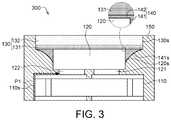
- FIG. 3illustrates a cross sectional view of a light-emitting device 300 according to another embodiment of the invention.
- the light-emitting device 300includes the substrate 110 , the light-emitting component 120 , the wavelength conversion layer 130 , the adhesive layer 140 and the reflective layer 150 .
- the reflective layer 150 of the light-emitting device 300further covers a lateral surface 110 s of the substrate 110 , and accordingly it can prevent or reduce the damage by the exterior environmental factors (such as air, water, gas, etc.) through the lateral surface 110 s of the substrate 110 . Furthermore, due to the reflective layer 150 covering the lateral surface 110 s of the substrate 110 , it can increase a length of a path P 1 from the exterior environmental to the electrode (the first electrode 121 and/or the second electrode 122 ) of the light-emitting component 120 (in comparison with the path P 1 of FIG. 1 , the length of the path P 1 of the present embodiment is longer), and accordingly it can reduce the probability of the light-emitting component 120 being damaged by the environmental factors for increasing the reliability and life of the light-emitting device 300 .
- the top-viewed area of the wavelength conversion layer 130 of the light-emitting device 300is substantially equal to the top-viewed area of the light-emitting component 120 .
- Such structureis similar to the structure of the light-emitting device 200 , and the similarities are not repeated.
- FIG. 4illustrates a cross sectional view of a light-emitting device 400 according to another embodiment of the invention.
- the light-emitting device 400includes the substrate 110 , a plurality of the light-emitting components 120 , the wavelength conversion layer 130 , the adhesive layer 140 and the reflective layer 150 .
- the light-emitting components 120are disposed on the substrate 110 .
- the adhesive layer 140covers at least a portion of the lateral surface 120 s of each light-emitting component 120 .
- a portion of the adhesive layer 140 of the light-emitting device 400is further formed between adjacent two light-emitting components 120 .
- the adhesive layer 140further includes a second lateral portion 143 located between two light-emitting components 120 , and the second lateral portion 143 has a lower surface 143 s , wherein the lower surface 143 s is a convex surface or a concave surface.
- the reflective layer 150is formed between adjacent two light-emitting components 120 .
- the reflective layer 150further includes a second reflective portion 153 , wherein the second reflective portion 153 is located between adjacent two light-emitting components 120 .
- the second reflective portion 153has a second reflective surface 153 s complying with the lower surface 143 s , and accordingly the second reflective surface 153 s is a concave surface.
- the lower surface 143 smay be a concave surface
- the second reflective surface 153 sis a convex surface.
- the second reflective surface 153 smay reflect the light L 1 emitted by the light-emitting component 120 to the wavelength conversion layer 130 , and accordingly it can increase the luminous efficiency of the light-emitting device 400 .
- the reflective layer 150 of the light-emitting device 400may further cover the lateral surface 110 s of the substrate 110 .
- Such structureis similar to the structure of the light-emitting device 300 , and the similarities are not repeated.
- the top-viewed area of the wavelength conversion layer 130 of the light-emitting device 400is substantially equal to the top-viewed area of the light-emitting component 120 .
- Such structureis similar to the structure of the light-emitting device 200 , and the similarities are not repeated.
- FIGS. 5A to 5Hillustrate manufacturing processes of the light-emitting device 100 of FIG. 1 .
- a wavelength conversion resin 130 ′is formed on a carrier 10 by way of, for example, dispensing.
- the wavelength conversion resin 130 ′contains a plurality of the phosphor particles 133 .
- the polarity of the carrier 10 and the polarity of the wavelength conversion resin 130 ′are different, and accordingly the wavelength conversion resin 130 ′ and the carrier 10 may be easily detached.
- the carrier 10may include a double-sided adhesive layer and a carrier plate, wherein the double-sided adhesive layer is adhered to the carrier plate for carrying the wavelength conversion resin 130 ′.
- the wavelength conversion resin 130 ′As illustrated in FIG. 5B , after the wavelength conversion resin 130 ′ is stood for a period such as 24 hours, most of the phosphor particles 133 precipitate on a bottom of the wavelength conversion resin 130 ′ to form the high-density phosphor layer 131 , wherein the other of the phosphor particles 133 are distributed within the other portion of the wavelength conversion layer material 130 ′ to form the low-density phosphor layer 132 .
- the high-density phosphor layer 131 and the low-density phosphor layer 132form the wavelength conversion layer 130 .
- the wavelength conversion layer 130is cured.
- the positions of the phosphor particles 133can be fixed, and accordingly it can prevent the density distribution of the phosphor particles 133 within the wavelength conversion layer 130 from being easily changed.
- the carrier 10 and the wavelength conversion layer 130are separated to expose the high-density phosphor layer 131 of the wavelength conversion layer 130 .
- the substrate 110 and at least one light-emitting component 120are provided, wherein the light-emitting component 120 is disposed on the substrate 110 .
- the substrate 110may be disposed on another carrier 10 ′, wherein the carrier 10 ′ has a structure similar to that of the carrier 10 , and the similarities are not repeated.
- the high-density phosphor layer 131 of the wavelength conversion layer 130is adhered to the light-emitting component 120 by the adhesive layer 140 .
- the adhesive layer 140is formed on the upper surface 120 u of the light-emitting component 120 by way of, for example, applying or dispensing.
- the wavelength conversion layer 130is disposed on the adhesive layer 140 , such that the adhesive layer 140 adheres the light-emitting component 120 to the high-density phosphor layer 131 of the wavelength conversion layer 130 . Since the wavelength conversion layer 130 extrudes the adhesive layer 140 , the adhesive layer 140 flow toward two sides of the light-emitting component 120 to form the first lateral portion 141 . Due to surface tension, the lateral surface 141 s of the first lateral portion 141 forms a concave surface. Depending on the amount of the adhesive layer 140 and/or the property of the adhesive layer 140 , the lateral surface 141 s may form a convex surface. In addition, depending on the amount of the adhesive layer 140 and/or the property of the adhesive layer 140 , the first lateral portion 141 may cover at least a portion of the lateral surface 120 s of the light-emitting component 120 .
- a portion of the adhesive layer 140 which remains on between the wavelength conversion layer 130 and the light-emitting component 120forms the heat resistance layer 142 .
- the heat resistance layer 142may reduce the heat of transmitting to the wavelength conversion layer 130 from the light-emitting component 120 , and accordingly it can slow the degrading speed of the wavelength conversion layer 130 .
- At least one first singulation path W 1 passing through the wavelength conversion layer 130is formed to cut off the wavelength conversion layer 130 .
- the first singulation path W 1does not pass through the first lateral portion 141 of the adhesive layer 140 .
- the first singulation path W 1may pass through a portion of the first lateral portion 141 .
- the lateral surface 130 s of the wavelength conversion layer 130is formed by the first singulation path W 1 , wherein the lateral surface 130 s may be a plane or a curved surface.
- the cutting width for forming the first singulation path W 1may be substantially equal to the width of the first singulation path W 1 .
- the double-sided adhesive layer (not illustrated) disposed on the carrier 10 ′may be stretched to increase an interval between adjacent two light-emitting components 120 .
- the first singulation path W 1may be formed using a thin blade.
- the fluid reflective layer 150is formed above the substrate 110 by way of, for example, compression molding, wherein the reflective layer 150 covers a portion of the lateral surface 120 s of the light-emitting component 120 , the lateral surface 130 s of the wavelength conversion layer 130 , the lateral surface 141 s of the first lateral portion 141 of the adhesive layer 140 , the lateral surface of the third electrode 112 of the substrate 110 , the lateral surface of the fourth electrode 113 of the substrate 110 , the lateral surface of the first electrode 121 of the light-emitting component 120 and the lateral surface of the second electrode 122 of the light-emitting component 120 .
- the reflective layer 150includes the first reflective portion 151 surrounding the entire lateral surface 120 s of the light-emitting component 120 .
- the first reflective portion 151has the first reflective surface 151 s . Due to the lateral surface 141 s of the adhesive layer 140 being a concave surface, the first reflective surface 151 s covering the lateral surface 141 s is a convex surface facing the wavelength conversion layer 130 and the light-emitting component 120 .
- the convex first reflective surface 151 scan reflect the light L 1 emitted from the lateral surface 120 s to the wavelength conversion layer 130 , and accordingly it can increase the luminous efficiency of the light-emitting device 100 .
- the first reflective surface 151 s of the reflective layer 150can contact the lower surface 130 b of the wavelength conversion layer 130 .
- the convex first reflective surface 151 sconnects the lower surface 130 b of the wavelength conversion layer 130 to the lateral surface 120 s of the light-emitting component 120 , and accordingly it can increase the contacting area of the light L 1 emitted from the light-emitting component 120 and the convex surface (the first reflective surface 151 s ).
- the reflective layer 150is cured by way of heating.
- At least one second singulation path W 2 passing through the reflective layer 150 and the substrate 110is formed to form the light-emitting device 100 of FIG. 1 .
- the first reflective surface 151 s of the reflective layer 150 and the lateral surface 110 s of the substrate 110are formed by the second singulation path W 2 , wherein the first reflective surface 151 s and the lateral surface 110 s are substantially aligned or flush with each other.
- the second singulation path W 2may pass through the wavelength conversion layer 130 , the reflective layer 150 and the substrate 110 , such that the wavelength conversion layer 130 , the reflective layer 150 and the substrate 110 form the lateral surface 130 s , the lateral surface 150 s and lateral surface 110 s respectively, wherein the lateral surface 130 s , the lateral surface 150 s and lateral surface 110 s are substantially aligned or flush with each other.
- the cutting width for forming the second singulation path W 2may be substantially equal to the width of the second singulation path W 2 .
- the double-sided adhesive layer (not illustrated) disposed on the carrier 10 ′may be stretched to increase an interval between adjacent two light-emitting components 120 .
- the second singulation path W 2may be formed using a thin blade.
- FIGS. 6A to 6Cillustrate another manufacturing processes of the light-emitting device 100 of FIG. 1 .
- the adhesive layer 140is formed on the high-density phosphor layer 131 of the wavelength conversion layer 130 by way of, for example, applying or dispensing.
- the substrate 110 and the light-emitting component 120 of FIG. 5Care disposed on the adhesive layer 140 , wherein the light-emitting component 120 contacts with the adhesive layer 140 , such that the adhesive layer 140 adheres the light-emitting component 120 to the high-density phosphor layer 131 of the wavelength conversion layer 130 .
- the adhesive layer 140flows toward two sides of the light-emitting component 120 to form the first lateral portion 141 . Due to surface tension, the lateral surface 141 s of the first lateral portion 141 forms a concave surface. Depending on the amount of the adhesive layer 140 and/or the property of the adhesive layer 140 , the first lateral portion 141 may cover at least a portion of the lateral surface 120 s of the light-emitting component 120 . In addition, as illustrated in an enlargement view of FIG. 6B , a portion of the adhesive layer 140 which remains on between the wavelength conversion layer 130 and the light-emitting component 120 forms the heat resistance layer 142 . The heat resistance layer 142 may reduce the heat of transmitting to the wavelength conversion layer 130 from the light-emitting component 120 , and accordingly it can slow the degrading speed of the wavelength conversion layer 130 .
- the light-emitting components 120 , the wavelength conversion layer 130 and the substrate 110are inverted, such that the wavelength conversion layer 130 faces upwardly.
- FIGS. 7A to 7Cillustrate manufacturing processes of the light-emitting device 200 of FIG. 2 .
- the structure of FIG. 5Eis formed by using the processes of FIG. 5A to 5E
- the structure of FIG. 6Cis formed by using the processes of FIG. 6A to 6C .
- At least one first singulation path W 1 passing through the wavelength conversion layer 130 and the first lateral portion 141 which covers the lateral surface 120 s of the light-emitting component 120is formed, by way of cutting, to cut off the wavelength conversion layer 130 and remove the first lateral portion 141 . Since the first singulation path W 1 cuts off the first lateral portion 141 , such that the entire lateral surface 120 s of the light-emitting component 120 and the entire lateral surface 142 s of the heat resistance layer 142 are be formed and exposed.
- the fluid reflective layer 150is formed above the substrate 110 by way of, for example, compression molding, wherein the reflective layer 150 covers the entire lateral surface 120 s of the light-emitting component 120 , the entire lateral surface 142 s of the heat resistance layer 142 , the entire lateral surface 130 s of the wavelength conversion layer 130 , the lateral surface of the third electrode 112 of the substrate 110 , the lateral surface of the fourth electrode 113 of the substrate 110 , the lateral surface of the first electrode 121 of the light-emitting component 120 and the lateral surface of the second electrode 122 of the light-emitting component 120 .
- the reflective layer 150is cured by way of heating.
- At least one second singulation path W 2 passing through the reflective layer 150 and the substrate 110is formed, by way of cutting, to form the light-emitting device 200 of FIG. 2 .
- the lateral surface 150 s of the reflective layer 150 and the lateral surface 110 s of the substrate 110are formed by the second singulation path W 2 , wherein the lateral surface 150 s and the lateral surface 110 s are substantially aligned or flush with each other.
- FIGS. 8A to 8Cillustrate manufacturing processes of the light-emitting device 300 of FIG. 3 .
- the structure of FIG. 5Eis formed by using the processes of FIG. 5A to 5E
- the structure of FIG. 6Cis formed by using the processes of FIG. 6A to 6C .
- At least one first singulation path W 1 passing through the wavelength conversion layer 130 and the substrate 110is formed, by way of cutting, to cut off the wavelength conversion layer 130 and the substrate 110 .
- the lateral surface 130 s of the wavelength conversion layer 130 and the lateral surface 110 s of the substrate 110are formed by the first singulation path W 1 , wherein the lateral surface 130 s and the lateral surface 110 s are substantially aligned or flush with each other.
- the fluid reflective layer 150is formed above the substrate 110 by way of, for example, dispensing, wherein the reflective layer 150 covers a portion of the lateral surface 120 s of the light-emitting component 120 , the lateral surface 130 s of the wavelength conversion layer 130 , the lateral surface 141 s of the first lateral portion 141 of the adhesive layer 140 , the lateral surface 110 s of the substrate 110 , the lateral surface of the third electrode 112 of the substrate 110 , the lateral surface of the fourth electrode 113 of the substrate 110 , the lateral surface of the first electrode 121 of the light-emitting component 120 and the lateral surface of the second electrode 122 of the light-emitting component 120 .
- the reflective layer 150is cured by way of heating.
- At least one second singulation path W 2 passing through the reflective layer 150is formed to form the light-emitting device 300 of FIG. 3 , wherein the lateral surface 150 s and the reflective layer 150 is formed by the second singulation path W 2 .
- the second singulation path W 2may pass through the wavelength conversion layer 130 , the reflective layer 150 and the substrate 110 , such that the wavelength conversion layer 130 , the reflective layer 150 and the substrate 110 form the lateral surface 130 s , the lateral surface 150 s and lateral surface 110 s respectively, wherein the lateral surface 130 s , the lateral surface 150 s and lateral surface 110 s are substantially aligned or flush with each other.
- FIGS. 9A to 9Fillustrate manufacturing processes of the light-emitting device 400 of FIG. 4 .
- the substrate 110 and a plurality of the light-emitting components 120are provided, wherein the light-emitting components 120 are disposed on the substrate 110 .
- the substrate 110 and the light-emitting components 120are disposed on the carrier 10 ′.
- the adhesive layer 140is formed on the upper surface 120 u of the light-emitting component 120 by way of, for example, applying or dispensing.
- the wavelength conversion layer 130is disposed on the adhesive layer 140 , such that the adhesive layer 140 adheres each light-emitting component 120 to the high-density phosphor layer 131 of the wavelength conversion layer 130 . Since the wavelength conversion layer 130 extrudes the adhesive layer 140 , the adhesive layer 140 flow toward two sides of the light-emitting component 120 to form the first lateral portion 141 .
- the first lateral portion 141has the lateral surface 141 s . Due to surface tension, the lateral surface 141 s is a concave surface. However, depending on the amount of the adhesive layer 140 and/or the property of the adhesive layer 140 , the lateral surface 141 s may form a convex surface facing substrate 110 . In addition, depending on the amount of the adhesive layer 140 and/or the property of the adhesive layer 140 , the first lateral portion 141 may cover at least a portion of the lateral surface 120 s of the light-emitting component 120 .
- a portion of the adhesive layer 140 which remains on between the wavelength conversion layer 130 and the light-emitting component 120forms the heat resistance layer 142 .
- the heat resistance layer 142can increase the heat resistance between the light-emitting component 120 and the wavelength conversion layer 130 , and accordingly it can slow the degrading speed of the wavelength conversion layer 130 .
- the adhesive layer 140further includes the second lateral portion 143 which is formed between adjacent two light-emitting components 120 .
- the second lateral portion 143has the lower surface 143 s . Due to surface tension, the lower surface 143 s forms a concave surface facing the substrate 110 . However, depending on the amount of the adhesive layer 140 and/or the property of the adhesive layer 140 , the lower surface 143 s may be a concave surface facing the substrate 110 .
- At least one first singulation path W 1 passing through the wavelength conversion layer 130is formed to cut off the wavelength conversion layer 130 .
- the first singulation path W 1does not pass through the first lateral portion 141 of the adhesive layer 140 .
- the first singulation path W 1may pass through a portion of the first lateral portion 141 or the entire first lateral portion 141 .
- the fluid reflective layer 150is formed above the substrate 110 by way of, for example, dispensing, wherein the reflective layer 150 covers a portion of the lateral surface 120 s of the light-emitting component 120 , the lateral surface 130 s of the wavelength conversion layer 130 , the lateral surface 141 s of the first lateral portion 141 of the adhesive layer 140 , the lower surface 143 s of the second lateral portion 143 , the lateral surface of the third electrode 112 of the substrate 110 , the lateral surface of the fourth electrode 113 of the substrate 110 , the lateral surface of the first electrode 121 of the light-emitting component 120 and the lateral surface of the second electrode 122 of the light-emitting component 120 through the first singulation path W 1 .
- the reflective layer 150includes the first reflective portion 151 and the second reflective portion 153 , wherein the first reflective portion 151 covers the first lateral portion 141 , and the second reflective portion 153 covers the second lateral portion 143 .
- the first reflective portion 151has the first reflective surface 151 s complying with the lateral surface 141 s , and the first reflective surface 151 s is a convex surface due to the lateral surface 141 s being a concave surface.
- the second reflective portion 153has the second reflective surface 153 s complying with the lower surface 143 s , and the second reflective surface 153 s is a concave surface due to the lateral surface 141 s being a convex surface.
- the reflective layer 150is cured by way of heating.
- At least one second singulation path W 2 passing through the reflective layer 150 and the substrate 110is formed to form the light-emitting device 400 of FIG. 4 .
- the lateral surface 150 s of the reflective layer 150 and the lateral surface 110 s of the substrate 110are formed by the second singulation path W 2 , wherein the lateral surface 150 s and the lateral surface 110 s are substantially aligned or flush with each other.
- the second singulation path W 2may pass through the wavelength conversion layer 130 , the reflective layer 150 and the substrate 110 , such that the wavelength conversion layer 130 , the reflective layer 150 and the substrate 110 form the lateral surface 130 s , the lateral surface 150 s and lateral surface 110 s respectively, wherein the lateral surface 130 s , the lateral surface 150 s and lateral surface 110 s are substantially aligned or flush with each other.
- the reflective layer 150 of the light-emitting device 400may cover the lateral surface 120 s of at least one light-emitting component 120 , the lateral surface 142 s of the heat resistance layer 142 and the lateral surface 130 s of the wavelength conversion layer 130 by using processes of FIGS. 7A to 7C .
- the reflective layer 150 of the light-emitting device 400may cover the lateral surface 110 s of the substrate 110 by using processes of FIGS. 8A to 8B .
Landscapes
- Engineering & Computer Science (AREA)
- Power Engineering (AREA)
- Microelectronics & Electronic Packaging (AREA)
- Physics & Mathematics (AREA)
- Condensed Matter Physics & Semiconductors (AREA)
- General Physics & Mathematics (AREA)
- Computer Hardware Design (AREA)
- Led Device Packages (AREA)
Abstract
Description
Claims (11)
Priority Applications (1)
| Application Number | Priority Date | Filing Date | Title |
|---|---|---|---|
| US16/699,805US10957674B2 (en) | 2015-09-18 | 2019-12-02 | Manufacturing method |
Applications Claiming Priority (7)
| Application Number | Priority Date | Filing Date | Title |
|---|---|---|---|
| US201562220249P | 2015-09-18 | 2015-09-18 | |
| US201562241729P | 2015-10-14 | 2015-10-14 | |
| TW104144809ATWI583027B (en) | 2015-09-18 | 2015-12-31 | Light-emitting device and manufacturing method thereof |
| TW104144809 | 2015-12-31 | ||
| US15/268,681US9922963B2 (en) | 2015-09-18 | 2016-09-19 | Light-emitting device |
| US15/924,461US10497681B2 (en) | 2015-09-18 | 2018-03-19 | Light-emitting device |
| US16/699,805US10957674B2 (en) | 2015-09-18 | 2019-12-02 | Manufacturing method |
Related Parent Applications (1)
| Application Number | Title | Priority Date | Filing Date |
|---|---|---|---|
| US15/924,461ContinuationUS10497681B2 (en) | 2015-09-18 | 2018-03-19 | Light-emitting device |
Publications (2)
| Publication Number | Publication Date |
|---|---|
| US20200105725A1 US20200105725A1 (en) | 2020-04-02 |
| US10957674B2true US10957674B2 (en) | 2021-03-23 |
Family
ID=58283210
Family Applications (3)
| Application Number | Title | Priority Date | Filing Date |
|---|---|---|---|
| US15/268,681ActiveUS9922963B2 (en) | 2015-09-18 | 2016-09-19 | Light-emitting device |
| US15/924,461ActiveUS10497681B2 (en) | 2015-09-18 | 2018-03-19 | Light-emitting device |
| US16/699,805ActiveUS10957674B2 (en) | 2015-09-18 | 2019-12-02 | Manufacturing method |
Family Applications Before (2)
| Application Number | Title | Priority Date | Filing Date |
|---|---|---|---|
| US15/268,681ActiveUS9922963B2 (en) | 2015-09-18 | 2016-09-19 | Light-emitting device |
| US15/924,461ActiveUS10497681B2 (en) | 2015-09-18 | 2018-03-19 | Light-emitting device |
Country Status (2)
| Country | Link |
|---|---|
| US (3) | US9922963B2 (en) |
| CN (3) | CN106549092A (en) |
Families Citing this family (51)
| Publication number | Priority date | Publication date | Assignee | Title |
|---|---|---|---|---|
| US9997676B2 (en) | 2014-05-14 | 2018-06-12 | Genesis Photonics Inc. | Light emitting device and manufacturing method thereof |
| US10439111B2 (en) | 2014-05-14 | 2019-10-08 | Genesis Photonics Inc. | Light emitting device and manufacturing method thereof |
| TWI557952B (en) | 2014-06-12 | 2016-11-11 | 新世紀光電股份有限公司 | Light-emitting element |
| CN106549092A (en) | 2015-09-18 | 2017-03-29 | 新世纪光电股份有限公司 | Light emitting device and method for manufacturing the same |
| CN107689409B (en)* | 2016-08-03 | 2019-09-20 | 展晶科技(深圳)有限公司 | led |
| JP6955135B2 (en)* | 2016-10-19 | 2021-10-27 | 日亜化学工業株式会社 | Light emitting device and its manufacturing method |
| CN107968142A (en)* | 2016-10-19 | 2018-04-27 | 新世纪光电股份有限公司 | Light-emitting device and its manufacture method |
| US10971663B2 (en)* | 2016-11-08 | 2021-04-06 | Stanley Electric Co., Ltd. | Semiconductor light emitting device |
| CN108231974B (en) | 2016-12-21 | 2022-09-02 | 日亚化学工业株式会社 | Method for manufacturing light emitting device |
| JP6939133B2 (en)* | 2017-06-22 | 2021-09-22 | 豊田合成株式会社 | Light emitting device |
| CN109148674B (en)* | 2017-06-28 | 2023-05-16 | 日亚化学工业株式会社 | light emitting device |
| JP6699634B2 (en)* | 2017-07-28 | 2020-05-27 | 日亜化学工業株式会社 | Method for manufacturing light emitting device |
| TWI757315B (en)* | 2017-07-28 | 2022-03-11 | 晶元光電股份有限公司 | Light-emitting device and manufacturing method thereof |
| US10361349B2 (en) | 2017-09-01 | 2019-07-23 | Cree, Inc. | Light emitting diodes, components and related methods |
| CN109494289B (en)* | 2017-09-11 | 2020-08-11 | 行家光电股份有限公司 | Light emitting device using quantum dot color conversion and method of manufacturing the same |
| KR102392013B1 (en)* | 2017-09-15 | 2022-04-28 | 쑤저우 레킨 세미컨덕터 컴퍼니 리미티드 | Light emitting device package |
| CN109712967B (en)* | 2017-10-25 | 2020-09-29 | 隆达电子股份有限公司 | Light emitting diode device and manufacturing method thereof |
| WO2019088704A1 (en)* | 2017-10-31 | 2019-05-09 | 엘지이노텍 주식회사 | Light emitting device package and lighting device having same |
| CN109994458B (en) | 2017-11-05 | 2022-07-01 | 新世纪光电股份有限公司 | light-emitting device |
| TW202249306A (en) | 2017-11-05 | 2022-12-16 | 新世紀光電股份有限公司 | Light emitting apparatus |
| JP7221659B2 (en)* | 2017-11-17 | 2023-02-14 | スタンレー電気株式会社 | semiconductor light emitting device |
| DE102017128717B4 (en)* | 2017-12-04 | 2023-03-09 | OSRAM Opto Semiconductors Gesellschaft mit beschränkter Haftung | Process for producing an optoelectronic component |
| CN110112123A (en)* | 2018-02-01 | 2019-08-09 | 晶元光电股份有限公司 | Light emitting device and its manufacturing method |
| TWI775608B (en)* | 2018-02-01 | 2022-08-21 | 晶元光電股份有限公司 | Light-emitting device |
| JP6760321B2 (en)* | 2018-03-20 | 2020-09-23 | 日亜化学工業株式会社 | Light emitting device and manufacturing method of light emitting device |
| JP7082279B2 (en)* | 2018-03-29 | 2022-06-08 | 日亜化学工業株式会社 | Light emitting device and its manufacturing method |
| WO2019210486A1 (en)* | 2018-05-03 | 2019-11-07 | Xi' An Raysees Technology Co. Ltd | Cob led and method for packaging cob led |
| KR20190134941A (en)* | 2018-05-24 | 2019-12-05 | 서울반도체 주식회사 | Light emitting device |
| US10371325B1 (en) | 2018-06-25 | 2019-08-06 | Intematix Corporation | Full spectrum white light emitting devices |
| JP7007589B2 (en)* | 2018-07-24 | 2022-01-24 | 日亜化学工業株式会社 | Luminescent device |
| JP7161100B2 (en)* | 2018-09-25 | 2022-10-26 | 日亜化学工業株式会社 | Light-emitting device and manufacturing method thereof |
| JP6959548B2 (en)* | 2018-10-04 | 2021-11-02 | 日亜化学工業株式会社 | Light emitting device and its manufacturing method |
| CN111009603A (en)* | 2018-10-04 | 2020-04-14 | 日亚化学工业株式会社 | light-emitting device |
| CN109273579B (en)* | 2018-11-22 | 2022-04-22 | 江西省晶能半导体有限公司 | Preparation method of LED lamp beads |
| CN111312866A (en)* | 2018-12-12 | 2020-06-19 | 蚌埠三颐半导体有限公司 | Packaging method and packaging structure of light emitting diode chip |
| US11205743B2 (en) | 2018-12-21 | 2021-12-21 | Lumileds Llc | High luminance light emitting device and method for creating a high luminance light emitting device |
| JP6947989B2 (en)* | 2019-03-28 | 2021-10-13 | 日亜化学工業株式会社 | Linear light source and planar light emitting device |
| CN111063783A (en)* | 2019-12-30 | 2020-04-24 | 江西省晶能半导体有限公司 | Preparation method of fluorescent diaphragm and preparation method of LED lamp bead |
| CN111092142A (en)* | 2019-12-30 | 2020-05-01 | 江西省晶能半导体有限公司 | White light LED chip and preparation method thereof |
| CN111063784A (en)* | 2019-12-30 | 2020-04-24 | 江西省晶能半导体有限公司 | Preparation method of LED lamp beads |
| JP7054020B2 (en)* | 2020-04-28 | 2022-04-13 | 日亜化学工業株式会社 | Light emitting device |
| US11348400B2 (en)* | 2020-10-08 | 2022-05-31 | SG Gaming. Inc. | Gaming systems and methods with emotive lighting |
| JP7594881B2 (en)* | 2020-10-22 | 2024-12-05 | スタンレー電気株式会社 | Semiconductor light emitting device and semiconductor light emitting module |
| CN112951815A (en)* | 2021-01-14 | 2021-06-11 | 日月光半导体制造股份有限公司 | Semiconductor structure and manufacturing method thereof |
| US20220254962A1 (en)* | 2021-02-11 | 2022-08-11 | Creeled, Inc. | Optical arrangements in cover structures for light emitting diode packages and related methods |
| CN115172556A (en)* | 2021-06-17 | 2022-10-11 | 厦门三安光电有限公司 | Light emitting diode chip, light emitting device and display device |
| USD996377S1 (en) | 2022-02-17 | 2023-08-22 | Creeled, Inc. | Light-emitting diode package |
| USD996378S1 (en) | 2022-03-09 | 2023-08-22 | Creeled, Inc. | Light-emitting diode package |
| US12355013B2 (en) | 2022-04-21 | 2025-07-08 | Creeled, Inc. | Emission height arrangements in light-emitting diode packages and related devices and methods |
| EP4411842A1 (en)* | 2023-02-06 | 2024-08-07 | Bridgelux, Inc. | Full spectrum white light emitting devices |
| US20240363815A1 (en)* | 2023-04-25 | 2024-10-31 | Seoul Semiconductor Co., Ltd. | Light emitting device |
Citations (152)
| Publication number | Priority date | Publication date | Assignee | Title |
|---|---|---|---|---|
| US6155699A (en) | 1999-03-15 | 2000-12-05 | Agilent Technologies, Inc. | Efficient phosphor-conversion led structure |
| CN1366715A (en) | 2000-04-24 | 2002-08-28 | 罗姆股份有限公司 | Edge-emitting light-emitting semiconductor device and method of manufacturing thereof |
| US20030006509A1 (en) | 2001-07-05 | 2003-01-09 | Takehiro Suzuki | Semiconductor device |
| US20030067070A1 (en) | 2001-10-05 | 2003-04-10 | Samsung Electronics Co., Ltd. | Semiconductor package |
| US20040119402A1 (en) | 2002-12-18 | 2004-06-24 | Shiang Joseph John | Luminaire for light extraction from a flat light source |
| US20040239242A1 (en) | 2002-12-26 | 2004-12-02 | Rohm Co., Ltd. | LIght-emitting unit and illuminator utilizing the same |
| US20050045897A1 (en) | 2003-08-27 | 2005-03-03 | Shen-Hong Chou | Light emitting apparatus |
| CN1652366A (en) | 2004-02-04 | 2005-08-10 | 西铁城电子股份有限公司 | led |
| CN1674316A (en) | 2004-03-25 | 2005-09-28 | 西铁城电子股份有限公司 | Semiconductor light-emitting device |
| US20060055309A1 (en) | 2004-09-14 | 2006-03-16 | Masato Ono | Light emitting device |
| US7045828B2 (en) | 2001-08-09 | 2006-05-16 | Matsushita Electric Industrial Co., Ltd. | Card-type LED illumination source |
| US20060169994A1 (en) | 2005-02-03 | 2006-08-03 | United Epitaxy Company, Ltd. | Light emitting device and manufacture method thereof |
| US20060186427A1 (en) | 2005-02-18 | 2006-08-24 | Nichia Corporation | Side-view type light emitting device |
| US20070012940A1 (en) | 2005-07-14 | 2007-01-18 | Samsung Electro-Mechanics Co., Ltd. | Wavelength-convertible light emitting diode package |
| US7190004B2 (en) | 2003-12-03 | 2007-03-13 | Sumitomo Electric Industries, Ltd. | Light emitting device |
| US20070114552A1 (en) | 2005-11-23 | 2007-05-24 | Samsung Electro-Mechanics Co., Ltd. | Vertical gallium-nitride based light emitting diode |
| CN1971957A (en) | 2005-11-22 | 2007-05-30 | 夏普株式会社 | Light emitting element, production method thereof, backlight unit having the light emitting element, and production method thereof |
| US20070236940A1 (en) | 2005-01-31 | 2007-10-11 | Toppan Printing Co., Ltd. | Optical sheet, and backlight unit and display using the same |
| US20080123024A1 (en) | 2006-11-24 | 2008-05-29 | Lg.Philips Lcd Co., Ltd. | Backlight unit of liquid crystal display device |
| US20080122343A1 (en) | 2006-11-28 | 2008-05-29 | Dowa Electronics Materials Co., Ltd. | Light-emitting device and manufacturing method thereof |
| US20080150119A1 (en) | 2006-12-22 | 2008-06-26 | Stats Chippac Ltd. | Integrated circuit package system employing mold flash prevention technology |
| US20080246902A1 (en) | 2007-04-09 | 2008-10-09 | Chu-Liang Cheng | Lcd panel |
| TW200929615A (en) | 2007-08-23 | 2009-07-01 | Philips Lumileds Lighting Co | Light source including reflective wavelength-converting layer |
| CN101515621A (en) | 2009-02-19 | 2009-08-26 | 旭丽电子(广州)有限公司 | Light emitting diode chip, manufacturing method and packaging method |
| US20090242917A1 (en) | 2008-03-28 | 2009-10-01 | Toyoda Gosei Co., Ltd. | Light-emitting device including light-emitting diode |
| CN101578479A (en) | 2007-01-12 | 2009-11-11 | 松下电器产业株式会社 | Light-emitting device and illumination apparatus using the same |
| US20090296389A1 (en) | 2008-05-30 | 2009-12-03 | Chia-Liang Hsu | Light source module, related light bar and related liquid crystal display |
| JP4411892B2 (en) | 2003-07-09 | 2010-02-10 | 日亜化学工業株式会社 | Light source device and vehicle headlamp using the same |
| US20100052001A1 (en) | 2006-07-24 | 2010-03-04 | Hsiao-Chiao Li | Led packaging structure |
| US20100066236A1 (en) | 2008-09-12 | 2010-03-18 | Bridgelux, Inc. | Method and Apparatus for Generating Phosphor Film with Textured Surface |
| TW201017934A (en) | 2008-08-29 | 2010-05-01 | Philips Lumileds Lighting Co | Light source including a wavelength-converted semiconductor light emitting device and a filter |
| US20100117530A1 (en) | 2008-11-10 | 2010-05-13 | Tzu-Han Lin | Light-emitting diode device and method for fabricating the same |
| CN101855735A (en) | 2007-11-19 | 2010-10-06 | 松下电器产业株式会社 | Semiconductor light emitting device and method for manufacturing semiconductor light emitting device |
| US20100258419A1 (en) | 2009-04-10 | 2010-10-14 | Avago Technologies Ecbu Ip (Singapore) Pte. Ltd. | Light guide film with cut lines |
| CN101867003A (en) | 2009-04-20 | 2010-10-20 | 日亚化学工业株式会社 | light emitting device |
| CN101878540A (en) | 2007-11-29 | 2010-11-03 | 日亚化学工业株式会社 | Light emitting device and manufacturing method thereof |
| US20110001157A1 (en) | 2008-01-28 | 2011-01-06 | Photonstar Led Limited | Light emitting module with optically-transparent thermally-conductive element |
| US20110018017A1 (en) | 2009-07-23 | 2011-01-27 | Koninklijke Philips Electronics N.V. | Led with molded reflective sidewall coating |
| US20110025190A1 (en) | 2008-03-21 | 2011-02-03 | Koninklijke Philips Electronics N.V. | Luminous device |
| US20110079805A1 (en) | 2009-10-02 | 2011-04-07 | Yu Kuohui | Light-emitting diode and method for manufacturing the same |
| TW201114072A (en) | 2009-05-22 | 2011-04-16 | Panasonic Corp | Semiconductor light-emitting device and light source device using the same |
| US20110102883A1 (en) | 2006-11-17 | 2011-05-05 | Rensselaer Polytechnic Institute | High-power white leds and manufacturing method thereof |
| CN102074639A (en) | 2009-11-24 | 2011-05-25 | 展晶科技(深圳)有限公司 | Light emitting diode and manufacturing process thereof |
| US20110170303A1 (en) | 2010-01-14 | 2011-07-14 | Shang-Yi Wu | Chip package and fabrication method thereof |
| CN102132428A (en) | 2008-09-02 | 2011-07-20 | 普瑞光电股份有限公司 | Phosphor Converted Light Emitting Diodes |
| CN201910421U (en) | 2010-12-01 | 2011-07-27 | 宝创科技股份有限公司 | Planar Structure of Light Emitting Diode Devices |
| WO2011093454A1 (en) | 2010-01-29 | 2011-08-04 | シチズン電子株式会社 | Method for producing light-emitting device and light emitting device |
| US20110198780A1 (en) | 2010-02-16 | 2011-08-18 | Koninklijke Philips Electronics N.V. | Light emitting device with molded wavelength converting layer |
| CN102214623A (en) | 2010-04-07 | 2011-10-12 | 精材科技股份有限公司 | Chip package and method for forming the same |
| CN102222757A (en) | 2010-04-15 | 2011-10-19 | 三星Led株式会社 | Light emitting diode package, lighting apparatus having the same, and method for manufacturing light emitting diode package |
| CN102263194A (en) | 2011-04-13 | 2011-11-30 | 日月光半导体制造股份有限公司 | Semiconductor package and method of manufacturing the same |
| US20110297980A1 (en)* | 2010-06-03 | 2011-12-08 | Kabushiki Kaisha Toshiba | Semiconductor light emitting device and method for manufacturing same |
| CN102290500A (en) | 2010-06-16 | 2011-12-21 | 斯坦雷电气株式会社 | Semiconductor light-emitting device and manufacturing method |
| US20110309398A1 (en) | 2010-06-22 | 2011-12-22 | Nitto Denko Corporation | Composite film and semiconductor light emitting device using the same |
| CN102299237A (en) | 2010-06-22 | 2011-12-28 | 日东电工株式会社 | Semiconductor light emitting device |
| CN102315354A (en) | 2010-06-29 | 2012-01-11 | 展晶科技(深圳)有限公司 | Packaging structure of light emitting diode |
| US20120025247A1 (en) | 2010-07-27 | 2012-02-02 | Nitto Denko Corporation | Component for light-emitting device, light-emitting device and producing method thereof |
| US20120025218A1 (en)* | 2010-08-02 | 2012-02-02 | Ito Kosaburo | Semiconductor light-emitting device and manufacturing method |
| US20120061700A1 (en) | 2010-09-09 | 2012-03-15 | Andreas Eder | Method and system for providing a reliable light emitting diode semiconductor device |
| US20120077292A1 (en) | 2010-09-23 | 2012-03-29 | Advanced Optoelectronic Technology, Inc. | Method of manufacturing light emitting diode package |
| TW201220534A (en) | 2010-06-07 | 2012-05-16 | Toshiba Kk | Semiconductor light emitting device and method for manufacturing same |
| CN102468417A (en) | 2010-11-10 | 2012-05-23 | 三星Led株式会社 | Light emitting device package and method of manufacturing the same |
| US20120161164A1 (en) | 2010-12-24 | 2012-06-28 | Hyung-Kun Kim | Light-emitting device package and method of manufacturing the same |
| US20120181569A1 (en) | 2011-01-13 | 2012-07-19 | Ki-Won Choi | Light-emitting device package |
| US20120223351A1 (en) | 2011-03-06 | 2012-09-06 | Viagan Ltd. | Light emitting diode package and method of manufacture |
| US20120235126A1 (en) | 2011-03-18 | 2012-09-20 | Semiconductor Energy Laboratory Co., Ltd. | Light-Emitting Device and Manufacturing Method Thereof |
| US20120236582A1 (en)* | 2011-01-24 | 2012-09-20 | Waragaya Takeshi | Semiconductor light emitting device and manufacturing method |
| US20120235188A1 (en) | 2011-03-15 | 2012-09-20 | Avago Technologies Ecbu Ip (Singapore) Pte. Ltd. | Method and Apparatus for a Flat Top Light Source |
| US20120250320A1 (en) | 2011-03-31 | 2012-10-04 | Xicato, Inc. | Color conversion cavities for led-based illumination modules |
| TW201242108A (en) | 2011-04-14 | 2012-10-16 | Nitto Denko Corp | Producing method of light emitting element transfer sheet, producing method of light emitting device, light emitting element transfer sheet, and light emitting device |
| CN102738368A (en) | 2011-04-14 | 2012-10-17 | 日东电工株式会社 | Phosphor reflecting sheet, light emitting diode device, and producing method thereof |
| JP2012227470A (en) | 2011-04-22 | 2012-11-15 | Citizen Holdings Co Ltd | Semiconductor light emitting device and manufacturing method of the same |
| CN102804426A (en) | 2009-06-22 | 2012-11-28 | 日亚化学工业株式会社 | light emitting device |
| US20120305942A1 (en) | 2011-05-31 | 2012-12-06 | Aceplux Optotech Inc. | Epitaxial substrate, light-emitting diode, and methods for making the epitaxial substrate and the light-emitting diode |
| TW201249898A (en) | 2011-06-01 | 2012-12-16 | Nitto Denko Corp | Reflecting material and light emitting diode device |
| US20130001605A1 (en) | 2011-07-01 | 2013-01-03 | Citizen Holdings Co., Ltd. | Light-emitting device |
| US20130037842A1 (en) | 2010-02-09 | 2013-02-14 | Motokazu Yamada | Light emitting device and method for manufacturing light emitting device |
| US20130050982A1 (en) | 2011-03-15 | 2013-02-28 | Avago Technologies General Ip (Singapore) Pte. Ltd | Method And Apparatus For A Light Source |
| US20130062648A1 (en) | 2011-09-12 | 2013-03-14 | Olympus Corporation | Light-emitting device and light-emitting device manufacturing method |
| CN103022010A (en) | 2011-09-21 | 2013-04-03 | 西铁城电子株式会社 | Light-emitting device, lighting device and method of manufacturing the light-emitting device |
| CN103050601A (en) | 2009-03-11 | 2013-04-17 | 晶元光电股份有限公司 | light emitting device |
| US20130093313A1 (en) | 2011-10-13 | 2013-04-18 | Citizen Holdings Co., Ltd. | Light-emitting device |
| US20130094177A1 (en) | 2011-10-13 | 2013-04-18 | Intematix Corporation | Wavelength conversion component with improved thermal conductive characteristics for remote wavelength conversion |
| US20130105978A1 (en) | 2011-10-26 | 2013-05-02 | Episil Technologies Inc. | Silicon submount for light emitting diode and method of forming the same |
| US20130121000A1 (en) | 2011-11-16 | 2013-05-16 | Song Eun Lee | Light emitting device and lighting apparatus having the same |
| TWM453969U (en) | 2012-12-26 | 2013-05-21 | Genesis Photonics Inc | Light emitting device |
| CN103137571A (en) | 2013-01-22 | 2013-06-05 | 日月光半导体制造股份有限公司 | Semiconductor package structure and manufacturing method thereof |
| US8482016B2 (en) | 2011-02-14 | 2013-07-09 | Stanley Electric Co., Ltd. | Semiconductor light-emitting device and manufacturing method |
| CN103199183A (en) | 2013-04-08 | 2013-07-10 | 厦门市三安光电科技有限公司 | Packaging structure enhancing brightness of vertical light-emitting diode (LED) chip |
| US20130194794A1 (en) | 2012-02-01 | 2013-08-01 | Samsung Electronics Co., Ltd. | Light emitting device |
| US20130207142A1 (en) | 2012-02-13 | 2013-08-15 | Jesse Colin Reiherzer | Light emitter devices having improved chemical and physical resistance and related methods |
| US20130207141A1 (en) | 2012-02-13 | 2013-08-15 | Cree, Inc. | Lighting device including multiple encapsulant material layers |
| US8523626B2 (en) | 2006-09-12 | 2013-09-03 | Toyoda Gosei Co., Ltd. | Method of making a light emitting device |
| US20130256711A1 (en) | 2012-03-30 | 2013-10-03 | Cree, Inc. | Substrate based light emitter devices, components, and related methods |
| US20130277093A1 (en) | 2012-04-24 | 2013-10-24 | Genesis Photonics Inc. | Substrate structure |
| CN103378279A (en) | 2012-04-27 | 2013-10-30 | 展晶科技(深圳)有限公司 | Light emitting diode packaging structure and manufacturing method thereof |
| US20130285091A1 (en) | 2012-04-27 | 2013-10-31 | Kabushiki Kaisha Toshiba | Semiconductor light emitting device and method for manufacturing same |
| CN103403890A (en) | 2011-01-14 | 2013-11-20 | 株式会社东芝 | Light emitting device, light emitting module, and method for manufacturing light emitting device |
| US20130313594A1 (en) | 2003-07-04 | 2013-11-28 | Epistar Corporation | Optoelectronic element and manufacturing method thereof |
| TW201401565A (en) | 2012-06-29 | 2014-01-01 | Advanced Optoelectronic Tech | Light-emitting diode package structure and manufacturing method thereof |
| US20140009060A1 (en) | 2012-06-29 | 2014-01-09 | Nitto Denko Corporation | Phosphor layer-covered led, producing method thereof, and led device |
| TW201403873A (en) | 2012-07-05 | 2014-01-16 | Advanced Optoelectronic Tech | Method for manufacturing light emitting diode package structure |
| CN103531725A (en) | 2013-10-16 | 2014-01-22 | 上海和辉光电有限公司 | Electroluminescent component and packaging method thereof |
| CN103534822A (en) | 2011-04-20 | 2014-01-22 | 株式会社Elm | Light emitting device and method for manufacturing same |
| US20140021493A1 (en) | 2012-07-20 | 2014-01-23 | Peter Andrews | Solid state lighting component package with layer |
| US20140054621A1 (en)* | 2012-08-23 | 2014-02-27 | Stanley Electric Co., Ltd. | Semiconductor light-emitting device including transparent plate with slanted side surface |
| CN103682038A (en) | 2012-08-31 | 2014-03-26 | 日亚化学工业株式会社 | Light emitting device and method for manufacturing same |
| US20140117396A1 (en) | 2011-05-18 | 2014-05-01 | Osram Opto Semiconductors Gmbh | Optoelectronic semiconductor chip, optoelectronic semiconductor component, and a method for producing an optoelectronic semiconductor component |
| US20140124812A1 (en) | 2011-05-16 | 2014-05-08 | Nichia Corporation | Light emitting device and method for manufacturing the same |
| US20140131753A1 (en) | 2012-11-09 | 2014-05-15 | Nichia Corporation | Method for manufacturing light emitting device and light emitting device |
| US20140138725A1 (en) | 2012-11-12 | 2014-05-22 | Citizen Electronics Co., Ltd. | Semiconductor light-emitting device and producing method thereof |
| US20140153238A1 (en) | 2012-12-04 | 2014-06-05 | Toshiba Lighting & Technology Corporation | Light Emitting Device and Luminaire |
| US20140186979A1 (en) | 2005-02-03 | 2014-07-03 | Epistar Corporation | Light emitting device and manufacture method thereof |
| US20140203451A1 (en) | 2013-01-22 | 2014-07-24 | Samsung Electronics Co., Ltd. | Electronic device package and packaging substrate for the same |
| US20140252389A1 (en) | 2013-03-05 | 2014-09-11 | Kabushiki Kaisha Toshiba | Semiconductor light emitting device and method for manufacturing the same |
| US8860061B2 (en)* | 2012-01-23 | 2014-10-14 | Stanley Electric Co., Ltd. | Semiconductor light-emitting device, manufacturing method for the same and vehicle headlight |
| CN203910851U (en) | 2014-05-23 | 2014-10-29 | 晶科电子(广州)有限公司 | White light LED chip |
| TWI462340B (en) | 2010-09-08 | 2014-11-21 | Epistar Corp | Light-emitting structure and manufacturing method thereof |
| CN104253194A (en) | 2014-09-18 | 2014-12-31 | 易美芯光(北京)科技有限公司 | Structure and method for packaging of chip-size white LED (light emitting diode) |
| US20150014720A1 (en) | 2013-07-10 | 2015-01-15 | Lextar Electronics Corporation | Light emitting diode package structure |
| CN104347610A (en) | 2013-07-23 | 2015-02-11 | 深圳市瑞丰光电子股份有限公司 | Embedded LED device, manufacture method thereof, and luminescence device |
| CN204155931U (en) | 2014-06-25 | 2015-02-11 | 常州欧密格光电科技有限公司 | A kind of extra small ultra-thin specular removal Quartering shot type highlighted white light polycrystalline LED element |
| TW201507209A (en) | 2013-08-01 | 2015-02-16 | Genesis Photonics Inc | Light emitting diode package structure and manufacturing method thereof |
| CN104465936A (en) | 2013-09-13 | 2015-03-25 | 展晶科技(深圳)有限公司 | Light emitting diode |
| US20150085527A1 (en) | 2013-09-26 | 2015-03-26 | Seoul Semiconductor Co., Ltd. | Light source module, fabrication method therefor, and backlight unit including the same |
| CN104521015A (en) | 2012-08-08 | 2015-04-15 | 欧司朗光电半导体有限公司 | Optoelectronic semiconductor component, conversion-medium lamina and method for producing a conversion-medium lamina |
| US20150102373A1 (en) | 2013-10-10 | 2015-04-16 | Samsung Electronics Co., Ltd. | Light emitting diode package and method of manufacturing the same |
| US20150102377A1 (en) | 2013-10-14 | 2015-04-16 | Genesis Photonics Inc. | Flip chip light emitting diode package structure |
| TW201515273A (en) | 2013-08-21 | 2015-04-16 | Advanced Optoelectronic Tech | Method for manufacturing light emitting diode |
| US20150115300A1 (en) | 2013-10-28 | 2015-04-30 | Kabushiki Kaisha Toshiba | Semiconductor light emitting device |
| US9029893B2 (en) | 2013-02-18 | 2015-05-12 | Kabushiki Kaisha Toshiba | Semiconductor light emitting device and method for manufacturing the same |
| CN204387807U (en) | 2013-09-26 | 2015-06-10 | 首尔半导体株式会社 | Light source module and the back light unit comprising this light source module |
| US9065033B2 (en) | 2013-02-22 | 2015-06-23 | Samsung Electronics Co., Ltd. | Light emitting device package |
| US20150179901A1 (en) | 2013-12-23 | 2015-06-25 | Jung-Tae OK | Method of fabricating white led devices |
| US20150188004A1 (en) | 2013-12-27 | 2015-07-02 | Nichia Corporation | Semiconductor light emitting device |
| WO2015101899A1 (en) | 2014-01-06 | 2015-07-09 | Koninklijke Philips N.V. | Thin led flash for camera |
| US20150200338A1 (en) | 2014-01-13 | 2015-07-16 | Tae Gyu Kim | Semiconductor light emitting device |
| CN104916753A (en) | 2014-03-14 | 2015-09-16 | 株式会社东芝 | Light emitting device |
| US20150263242A1 (en) | 2014-03-11 | 2015-09-17 | Kabushiki Kaisha Toshiba | Semiconductor light emitting device |
| US20150280078A1 (en) | 2014-03-31 | 2015-10-01 | SemiLEDs Optoelectronics Co., Ltd. | White flip chip light emitting diode (fc led) and fabrication method |
| US20150311405A1 (en) | 2012-12-10 | 2015-10-29 | Citizen Holding Co., Ltd. | Led device and manufacturing method thereof |
| TW201541674A (en) | 2014-04-23 | 2015-11-01 | Lite On Opto Technology Changzhou Co Ltd | LED carrier and manufacturing method thereof |
| CN204857783U (en) | 2015-04-09 | 2015-12-09 | 江西省晶瑞光电有限公司 | A side-emitting LED |
| US20160013373A1 (en) | 2014-07-11 | 2016-01-14 | Cree, Inc. | Method to form primary optic with variable shapes and/or geometries without a substrate |
| US20160079496A1 (en) | 2013-10-14 | 2016-03-17 | Genesis Photonics Inc. | Light-emitting diode package structure |
| US20160155915A1 (en) | 2014-12-02 | 2016-06-02 | Achrolux Inc. | Method of manufacturing light emitting diode package structure |
| US20160155900A1 (en) | 2013-03-14 | 2016-06-02 | Commissariat A L'energie Atomique Et Aux Energies Alternatives | Process for forming light-emitting diodes |
| US20160181476A1 (en) | 2014-12-17 | 2016-06-23 | Apple Inc. | Micro led with dielectric side mirror |
| US20160190406A1 (en) | 2014-12-24 | 2016-06-30 | Epistar Corporation | Light-emitting device and manufacturing method thereof |
| CN105742468A (en) | 2012-04-27 | 2016-07-06 | 九尊城网络科技(深圳)有限公司 | Light emitting diode encapsulating structure and manufacturing method thereof |
| US9419189B1 (en) | 2013-11-04 | 2016-08-16 | Soraa, Inc. | Small LED source with high brightness and high efficiency |
| US9922963B2 (en) | 2015-09-18 | 2018-03-20 | Genesis Photonics Inc. | Light-emitting device |
Family Cites Families (1)
| Publication number | Priority date | Publication date | Assignee | Title |
|---|---|---|---|---|
| TWI473305B (en)* | 2011-03-10 | 2015-02-11 | Formosa Epitaxy Inc | Light emitting diode structure |
- 2016
- 2016-09-19CNCN201610830051.6Apatent/CN106549092A/enactivePending
- 2016-09-19CNCN202010033258.7Apatent/CN111211206A/enactivePending
- 2016-09-19USUS15/268,681patent/US9922963B2/enactiveActive
- 2016-09-19CNCN202010033941.0Apatent/CN111223975A/enactivePending
- 2018
- 2018-03-19USUS15/924,461patent/US10497681B2/enactiveActive
- 2019
- 2019-12-02USUS16/699,805patent/US10957674B2/enactiveActive
Patent Citations (201)
| Publication number | Priority date | Publication date | Assignee | Title |
|---|---|---|---|---|
| US6155699A (en) | 1999-03-15 | 2000-12-05 | Agilent Technologies, Inc. | Efficient phosphor-conversion led structure |
| CN1366715A (en) | 2000-04-24 | 2002-08-28 | 罗姆股份有限公司 | Edge-emitting light-emitting semiconductor device and method of manufacturing thereof |
| US6919586B2 (en) | 2000-04-24 | 2005-07-19 | Rohm Co., Ltd. | Side-emission type semiconductor light-emitting device and manufacturing method thereof |
| US20030006509A1 (en) | 2001-07-05 | 2003-01-09 | Takehiro Suzuki | Semiconductor device |
| US7045828B2 (en) | 2001-08-09 | 2006-05-16 | Matsushita Electric Industrial Co., Ltd. | Card-type LED illumination source |
| US20030067070A1 (en) | 2001-10-05 | 2003-04-10 | Samsung Electronics Co., Ltd. | Semiconductor package |
| US20040119402A1 (en) | 2002-12-18 | 2004-06-24 | Shiang Joseph John | Luminaire for light extraction from a flat light source |
| US20040239242A1 (en) | 2002-12-26 | 2004-12-02 | Rohm Co., Ltd. | LIght-emitting unit and illuminator utilizing the same |
| US20130313594A1 (en) | 2003-07-04 | 2013-11-28 | Epistar Corporation | Optoelectronic element and manufacturing method thereof |
| JP4411892B2 (en) | 2003-07-09 | 2010-02-10 | 日亜化学工業株式会社 | Light source device and vehicle headlamp using the same |
| US20050045897A1 (en) | 2003-08-27 | 2005-03-03 | Shen-Hong Chou | Light emitting apparatus |
| US7190004B2 (en) | 2003-12-03 | 2007-03-13 | Sumitomo Electric Industries, Ltd. | Light emitting device |
| CN1624944B (en) | 2003-12-03 | 2010-04-28 | 住友电气工业株式会社 | Light emitting device |
| US7491977B2 (en) | 2004-02-04 | 2009-02-17 | Citizen Electronics Co., Ltd. | Light emitting diode |
| CN1652366A (en) | 2004-02-04 | 2005-08-10 | 西铁城电子股份有限公司 | led |
| US20050219835A1 (en) | 2004-03-25 | 2005-10-06 | Citizen Electronics Co. Ltd. | Light-emitting diode |
| CN1674316A (en) | 2004-03-25 | 2005-09-28 | 西铁城电子股份有限公司 | Semiconductor light-emitting device |
| US20060055309A1 (en) | 2004-09-14 | 2006-03-16 | Masato Ono | Light emitting device |
| US20070236940A1 (en) | 2005-01-31 | 2007-10-11 | Toppan Printing Co., Ltd. | Optical sheet, and backlight unit and display using the same |
| US20140186979A1 (en) | 2005-02-03 | 2014-07-03 | Epistar Corporation | Light emitting device and manufacture method thereof |
| US20060169994A1 (en) | 2005-02-03 | 2006-08-03 | United Epitaxy Company, Ltd. | Light emitting device and manufacture method thereof |
| US20060186427A1 (en) | 2005-02-18 | 2006-08-24 | Nichia Corporation | Side-view type light emitting device |
| US20070012940A1 (en) | 2005-07-14 | 2007-01-18 | Samsung Electro-Mechanics Co., Ltd. | Wavelength-convertible light emitting diode package |
| CN1971957A (en) | 2005-11-22 | 2007-05-30 | 夏普株式会社 | Light emitting element, production method thereof, backlight unit having the light emitting element, and production method thereof |
| US20070114552A1 (en) | 2005-11-23 | 2007-05-24 | Samsung Electro-Mechanics Co., Ltd. | Vertical gallium-nitride based light emitting diode |
| US20100052001A1 (en) | 2006-07-24 | 2010-03-04 | Hsiao-Chiao Li | Led packaging structure |
| US8523626B2 (en) | 2006-09-12 | 2013-09-03 | Toyoda Gosei Co., Ltd. | Method of making a light emitting device |
| US20110102883A1 (en) | 2006-11-17 | 2011-05-05 | Rensselaer Polytechnic Institute | High-power white leds and manufacturing method thereof |
| US20080123024A1 (en) | 2006-11-24 | 2008-05-29 | Lg.Philips Lcd Co., Ltd. | Backlight unit of liquid crystal display device |
| US20080122343A1 (en) | 2006-11-28 | 2008-05-29 | Dowa Electronics Materials Co., Ltd. | Light-emitting device and manufacturing method thereof |
| US20080150119A1 (en) | 2006-12-22 | 2008-06-26 | Stats Chippac Ltd. | Integrated circuit package system employing mold flash prevention technology |
| CN101578479A (en) | 2007-01-12 | 2009-11-11 | 松下电器产业株式会社 | Light-emitting device and illumination apparatus using the same |
| US20090316384A1 (en) | 2007-01-12 | 2009-12-24 | Panasonic Corporation | Light-emitting device and illumination apparatus using the same |
| TW200841089A (en) | 2007-04-09 | 2008-10-16 | Chu-Liang Cheng | Light source module and liquid crystal display |
| US20080246902A1 (en) | 2007-04-09 | 2008-10-09 | Chu-Liang Cheng | Lcd panel |
| US7810956B2 (en) | 2007-08-23 | 2010-10-12 | Koninklijke Philips Electronics N.V. | Light source including reflective wavelength-converting layer |
| TW200929615A (en) | 2007-08-23 | 2009-07-01 | Philips Lumileds Lighting Co | Light source including reflective wavelength-converting layer |
| US20100258830A1 (en) | 2007-11-19 | 2010-10-14 | Yoshiyuki Ide | Semiconductor light-emitting device and manufacturing method of the same |
| CN101855735A (en) | 2007-11-19 | 2010-10-06 | 松下电器产业株式会社 | Semiconductor light emitting device and method for manufacturing semiconductor light emitting device |
| US8552444B2 (en) | 2007-11-19 | 2013-10-08 | Panasonic Corporation | Semiconductor light-emitting device and manufacturing method of the same |
| CN101878540A (en) | 2007-11-29 | 2010-11-03 | 日亚化学工业株式会社 | Light emitting device and manufacturing method thereof |
| US20110001157A1 (en) | 2008-01-28 | 2011-01-06 | Photonstar Led Limited | Light emitting module with optically-transparent thermally-conductive element |
| US20110025190A1 (en) | 2008-03-21 | 2011-02-03 | Koninklijke Philips Electronics N.V. | Luminous device |
| CN101978516A (en) | 2008-03-21 | 2011-02-16 | 皇家飞利浦电子股份有限公司 | A luminous device |
| US20090242917A1 (en) | 2008-03-28 | 2009-10-01 | Toyoda Gosei Co., Ltd. | Light-emitting device including light-emitting diode |
| US20090296389A1 (en) | 2008-05-30 | 2009-12-03 | Chia-Liang Hsu | Light source module, related light bar and related liquid crystal display |
| US7888691B2 (en) | 2008-08-29 | 2011-02-15 | Koninklijke Philips Electronics N.V. | Light source including a wavelength-converted semiconductor light emitting device and a filter |
| TW201017934A (en) | 2008-08-29 | 2010-05-01 | Philips Lumileds Lighting Co | Light source including a wavelength-converted semiconductor light emitting device and a filter |
| CN102132428A (en) | 2008-09-02 | 2011-07-20 | 普瑞光电股份有限公司 | Phosphor Converted Light Emitting Diodes |
| US20100066236A1 (en) | 2008-09-12 | 2010-03-18 | Bridgelux, Inc. | Method and Apparatus for Generating Phosphor Film with Textured Surface |
| US20100117530A1 (en) | 2008-11-10 | 2010-05-13 | Tzu-Han Lin | Light-emitting diode device and method for fabricating the same |
| CN101515621A (en) | 2009-02-19 | 2009-08-26 | 旭丽电子(广州)有限公司 | Light emitting diode chip, manufacturing method and packaging method |
| US8766281B2 (en) | 2009-02-19 | 2014-07-01 | Lite-On Electronics (Guangzhou) Limited | Light emitting diode chip, and methods for manufacturing and packaging the same |
| CN103050601A (en) | 2009-03-11 | 2013-04-17 | 晶元光电股份有限公司 | light emitting device |
| US20100258419A1 (en) | 2009-04-10 | 2010-10-14 | Avago Technologies Ecbu Ip (Singapore) Pte. Ltd. | Light guide film with cut lines |
| CN101867003A (en) | 2009-04-20 | 2010-10-20 | 日亚化学工业株式会社 | light emitting device |
| US9006763B2 (en) | 2009-05-22 | 2015-04-14 | Panasonic Intellectual Property Management Co., Ltd. | Semiconductor light-emitting device and light source device using the same |
| TW201114072A (en) | 2009-05-22 | 2011-04-16 | Panasonic Corp | Semiconductor light-emitting device and light source device using the same |
| US8552453B2 (en) | 2009-06-22 | 2013-10-08 | Nichia Corporation | Light emitting device |
| CN102804426A (en) | 2009-06-22 | 2012-11-28 | 日亚化学工业株式会社 | light emitting device |
| US20110018017A1 (en) | 2009-07-23 | 2011-01-27 | Koninklijke Philips Electronics N.V. | Led with molded reflective sidewall coating |
| US20110079805A1 (en) | 2009-10-02 | 2011-04-07 | Yu Kuohui | Light-emitting diode and method for manufacturing the same |
| CN102074639A (en) | 2009-11-24 | 2011-05-25 | 展晶科技(深圳)有限公司 | Light emitting diode and manufacturing process thereof |
| CN102130071A (en) | 2010-01-14 | 2011-07-20 | 精材科技股份有限公司 | Chip package and method for forming the same |
| US20110170303A1 (en) | 2010-01-14 | 2011-07-14 | Shang-Yi Wu | Chip package and fabrication method thereof |
| WO2011093454A1 (en) | 2010-01-29 | 2011-08-04 | シチズン電子株式会社 | Method for producing light-emitting device and light emitting device |
| US20130037842A1 (en) | 2010-02-09 | 2013-02-14 | Motokazu Yamada | Light emitting device and method for manufacturing light emitting device |
| US9887329B2 (en) | 2010-02-09 | 2018-02-06 | Nichia Corporation | Light emitting device and method for manufacturing light emitting device |
| US20160035952A1 (en) | 2010-02-09 | 2016-02-04 | Nichia Corporation | Light emitting device and method for manufacturing light emitting device |
| US8771577B2 (en) | 2010-02-16 | 2014-07-08 | Koninklijke Philips N.V. | Light emitting device with molded wavelength converting layer |
| US20110198780A1 (en) | 2010-02-16 | 2011-08-18 | Koninklijke Philips Electronics N.V. | Light emitting device with molded wavelength converting layer |
| TW201133956A (en) | 2010-02-16 | 2011-10-01 | Koninkl Philips Electronics Nv | Light emitting device with molded wavelength converting layer |
| US8362515B2 (en) | 2010-04-07 | 2013-01-29 | Chia-Ming Cheng | Chip package and method for forming the same |
| CN102214623A (en) | 2010-04-07 | 2011-10-12 | 精材科技股份有限公司 | Chip package and method for forming the same |
| CN102222757A (en) | 2010-04-15 | 2011-10-19 | 三星Led株式会社 | Light emitting diode package, lighting apparatus having the same, and method for manufacturing light emitting diode package |
| US20110297980A1 (en)* | 2010-06-03 | 2011-12-08 | Kabushiki Kaisha Toshiba | Semiconductor light emitting device and method for manufacturing same |
| TW201145612A (en) | 2010-06-03 | 2011-12-16 | Toshiba Kk | Semiconductor light emitting device and method for manufacturing same |
| US9620669B2 (en) | 2010-06-03 | 2017-04-11 | Kabushiki Kaisha Toshiba | Semiconductor light emitting device and method for manufacturing same |
| TW201220534A (en) | 2010-06-07 | 2012-05-16 | Toshiba Kk | Semiconductor light emitting device and method for manufacturing same |
| US8350283B2 (en) | 2010-06-07 | 2013-01-08 | Kabushiki Kaisha Toshiba | Semiconductor light emitting device and method for manufacturing same |
| CN102290500A (en) | 2010-06-16 | 2011-12-21 | 斯坦雷电气株式会社 | Semiconductor light-emitting device and manufacturing method |
| US8461610B2 (en) | 2010-06-16 | 2013-06-11 | Stanley Electric Co., Ltd. | Semiconductor light emitting device having a reflective material with a side slant surface and method of manufacturing |
| TW201210819A (en) | 2010-06-22 | 2012-03-16 | Nitto Denko Corp | Composite film and semiconductor light emitting device using the same |
| CN102299237A (en) | 2010-06-22 | 2011-12-28 | 日东电工株式会社 | Semiconductor light emitting device |
| US9608178B2 (en) | 2010-06-22 | 2017-03-28 | Nitto Denko Corporation | Semiconductor light emitting device |
| US20110309398A1 (en) | 2010-06-22 | 2011-12-22 | Nitto Denko Corporation | Composite film and semiconductor light emitting device using the same |
| CN102315354A (en) | 2010-06-29 | 2012-01-11 | 展晶科技(深圳)有限公司 | Packaging structure of light emitting diode |
| US8288789B2 (en) | 2010-06-29 | 2012-10-16 | Advanced Optoelectronic Technology, Inc. | LED package |
| US20120025247A1 (en) | 2010-07-27 | 2012-02-02 | Nitto Denko Corporation | Component for light-emitting device, light-emitting device and producing method thereof |
| CN102347423A (en) | 2010-07-27 | 2012-02-08 | 日东电工株式会社 | Component for light-emitting device, light-emitting device and producing method thereof |
| US20120025218A1 (en)* | 2010-08-02 | 2012-02-02 | Ito Kosaburo | Semiconductor light-emitting device and manufacturing method |
| CN102347427A (en) | 2010-08-02 | 2012-02-08 | 斯坦雷电气株式会社 | Light-emitting device and manufacturing method thereof |
| US9748456B2 (en) | 2010-09-08 | 2017-08-29 | Epistar Corporation | Light emitting structure and a manufacturing method thereof |
| TWI462340B (en) | 2010-09-08 | 2014-11-21 | Epistar Corp | Light-emitting structure and manufacturing method thereof |
| US20120061700A1 (en) | 2010-09-09 | 2012-03-15 | Andreas Eder | Method and system for providing a reliable light emitting diode semiconductor device |
| US20120077292A1 (en) | 2010-09-23 | 2012-03-29 | Advanced Optoelectronic Technology, Inc. | Method of manufacturing light emitting diode package |
| US8890188B2 (en) | 2010-11-10 | 2014-11-18 | Samsung Electronics Co., Ltd. | Light emitting device surrounded by reflection wall and covered with fluorescent film |
| CN102468417A (en) | 2010-11-10 | 2012-05-23 | 三星Led株式会社 | Light emitting device package and method of manufacturing the same |
| CN201910421U (en) | 2010-12-01 | 2011-07-27 | 宝创科技股份有限公司 | Planar Structure of Light Emitting Diode Devices |
| US20120161164A1 (en) | 2010-12-24 | 2012-06-28 | Hyung-Kun Kim | Light-emitting device package and method of manufacturing the same |
| US20120181569A1 (en) | 2011-01-13 | 2012-07-19 | Ki-Won Choi | Light-emitting device package |
| CN103403890A (en) | 2011-01-14 | 2013-11-20 | 株式会社东芝 | Light emitting device, light emitting module, and method for manufacturing light emitting device |
| US8957434B2 (en) | 2011-01-14 | 2015-02-17 | Kabushiki Kaisha Toshiba | Light emitting device, light emitting module, and method for manufacturing light emitting device |
| US20120236582A1 (en)* | 2011-01-24 | 2012-09-20 | Waragaya Takeshi | Semiconductor light emitting device and manufacturing method |
| US8482016B2 (en) | 2011-02-14 | 2013-07-09 | Stanley Electric Co., Ltd. | Semiconductor light-emitting device and manufacturing method |
| US20120223351A1 (en) | 2011-03-06 | 2012-09-06 | Viagan Ltd. | Light emitting diode package and method of manufacture |
| US20120235188A1 (en) | 2011-03-15 | 2012-09-20 | Avago Technologies Ecbu Ip (Singapore) Pte. Ltd. | Method and Apparatus for a Flat Top Light Source |
| US20130050982A1 (en) | 2011-03-15 | 2013-02-28 | Avago Technologies General Ip (Singapore) Pte. Ltd | Method And Apparatus For A Light Source |
| US20120235126A1 (en) | 2011-03-18 | 2012-09-20 | Semiconductor Energy Laboratory Co., Ltd. | Light-Emitting Device and Manufacturing Method Thereof |
| US20120250320A1 (en) | 2011-03-31 | 2012-10-04 | Xicato, Inc. | Color conversion cavities for led-based illumination modules |
| US20120261689A1 (en) | 2011-04-13 | 2012-10-18 | Bernd Karl Appelt | Semiconductor device packages and related methods |
| CN102263194A (en) | 2011-04-13 | 2011-11-30 | 日月光半导体制造股份有限公司 | Semiconductor package and method of manufacturing the same |
| US8877528B2 (en) | 2011-04-14 | 2014-11-04 | Nitto Denko Corporation | Producing method of light emitting element transfer sheet, producing method of light emitting device, light emitting element transfer sheet, and light emitting device |
| TW201242108A (en) | 2011-04-14 | 2012-10-16 | Nitto Denko Corp | Producing method of light emitting element transfer sheet, producing method of light emitting device, light emitting element transfer sheet, and light emitting device |
| US20120261700A1 (en) | 2011-04-14 | 2012-10-18 | Nitto Denko Corporation | Phosphor reflecting sheet, light emitting diode device, and producing method thereof |
| CN102738368A (en) | 2011-04-14 | 2012-10-17 | 日东电工株式会社 | Phosphor reflecting sheet, light emitting diode device, and producing method thereof |
| US20140042481A1 (en) | 2011-04-20 | 2014-02-13 | Elm Inc. | Light emitting device and method for manufacturing same |
| CN103534822A (en) | 2011-04-20 | 2014-01-22 | 株式会社Elm | Light emitting device and method for manufacturing same |
| JP2012227470A (en) | 2011-04-22 | 2012-11-15 | Citizen Holdings Co Ltd | Semiconductor light emitting device and manufacturing method of the same |
| US20140124812A1 (en) | 2011-05-16 | 2014-05-08 | Nichia Corporation | Light emitting device and method for manufacturing the same |
| US20140117396A1 (en) | 2011-05-18 | 2014-05-01 | Osram Opto Semiconductors Gmbh | Optoelectronic semiconductor chip, optoelectronic semiconductor component, and a method for producing an optoelectronic semiconductor component |
| US20120305942A1 (en) | 2011-05-31 | 2012-12-06 | Aceplux Optotech Inc. | Epitaxial substrate, light-emitting diode, and methods for making the epitaxial substrate and the light-emitting diode |
| US8723167B2 (en) | 2011-06-01 | 2014-05-13 | Nitto Denko Corporation | Reflecting material and light emitting diode device |
| TW201249898A (en) | 2011-06-01 | 2012-12-16 | Nitto Denko Corp | Reflecting material and light emitting diode device |
| US20130001605A1 (en) | 2011-07-01 | 2013-01-03 | Citizen Holdings Co., Ltd. | Light-emitting device |
| US20130062648A1 (en) | 2011-09-12 | 2013-03-14 | Olympus Corporation | Light-emitting device and light-emitting device manufacturing method |
| CN103022010A (en) | 2011-09-21 | 2013-04-03 | 西铁城电子株式会社 | Light-emitting device, lighting device and method of manufacturing the light-emitting device |
| US9022828B2 (en) | 2011-09-21 | 2015-05-05 | Citizen Electronics Co., Ltd. | Light-emitting device, lighting device including the light-emitting device, and method of manufacturing the light-emitting device |
| US20130094177A1 (en) | 2011-10-13 | 2013-04-18 | Intematix Corporation | Wavelength conversion component with improved thermal conductive characteristics for remote wavelength conversion |
| US20130093313A1 (en) | 2011-10-13 | 2013-04-18 | Citizen Holdings Co., Ltd. | Light-emitting device |
| TW201319460A (en) | 2011-10-13 | 2013-05-16 | Intematix Corp | Wavelength conversion component with improved thermal conductive characteristics for remote wavelength conversion |
| US20130105978A1 (en) | 2011-10-26 | 2013-05-02 | Episil Technologies Inc. | Silicon submount for light emitting diode and method of forming the same |
| US20130121000A1 (en) | 2011-11-16 | 2013-05-16 | Song Eun Lee | Light emitting device and lighting apparatus having the same |
| US8860061B2 (en)* | 2012-01-23 | 2014-10-14 | Stanley Electric Co., Ltd. | Semiconductor light-emitting device, manufacturing method for the same and vehicle headlight |
| US20130194794A1 (en) | 2012-02-01 | 2013-08-01 | Samsung Electronics Co., Ltd. | Light emitting device |
| US20130207141A1 (en) | 2012-02-13 | 2013-08-15 | Cree, Inc. | Lighting device including multiple encapsulant material layers |
| US20130207142A1 (en) | 2012-02-13 | 2013-08-15 | Jesse Colin Reiherzer | Light emitter devices having improved chemical and physical resistance and related methods |
| US20130256711A1 (en) | 2012-03-30 | 2013-10-03 | Cree, Inc. | Substrate based light emitter devices, components, and related methods |
| US20130277093A1 (en) | 2012-04-24 | 2013-10-24 | Genesis Photonics Inc. | Substrate structure |
| CN103378279A (en) | 2012-04-27 | 2013-10-30 | 展晶科技(深圳)有限公司 | Light emitting diode packaging structure and manufacturing method thereof |
| US20130285097A1 (en) | 2012-04-27 | 2013-10-31 | Advanced Optoelectronic Technology, Inc. | Side-view light emitting diode package and method for manufacturing the same |
| US20130285091A1 (en) | 2012-04-27 | 2013-10-31 | Kabushiki Kaisha Toshiba | Semiconductor light emitting device and method for manufacturing same |
| CN105742468A (en) | 2012-04-27 | 2016-07-06 | 九尊城网络科技(深圳)有限公司 | Light emitting diode encapsulating structure and manufacturing method thereof |
| US20140009060A1 (en) | 2012-06-29 | 2014-01-09 | Nitto Denko Corporation | Phosphor layer-covered led, producing method thereof, and led device |
| TW201401565A (en) | 2012-06-29 | 2014-01-01 | Advanced Optoelectronic Tech | Light-emitting diode package structure and manufacturing method thereof |
| US20140001504A1 (en) | 2012-06-29 | 2014-01-02 | Advanced Optoelectronic Technology, Inc. | Light emitting diode package and method for manufacturing the same |
| TW201403873A (en) | 2012-07-05 | 2014-01-16 | Advanced Optoelectronic Tech | Method for manufacturing light emitting diode package structure |
| US20140021493A1 (en) | 2012-07-20 | 2014-01-23 | Peter Andrews | Solid state lighting component package with layer |
| US9406847B2 (en) | 2012-08-08 | 2016-08-02 | Osram Opto Semiconductors Gmbh | Optoelectronic semiconductor component, conversion-medium lamina and method for producing a conversion-medium lamina |
| CN104521015A (en) | 2012-08-08 | 2015-04-15 | 欧司朗光电半导体有限公司 | Optoelectronic semiconductor component, conversion-medium lamina and method for producing a conversion-medium lamina |
| US20140054621A1 (en)* | 2012-08-23 | 2014-02-27 | Stanley Electric Co., Ltd. | Semiconductor light-emitting device including transparent plate with slanted side surface |
| US9337405B2 (en) | 2012-08-31 | 2016-05-10 | Nichia Corporation | Light emitting device and method for manufacturing the same |
| CN103682038A (en) | 2012-08-31 | 2014-03-26 | 日亚化学工业株式会社 | Light emitting device and method for manufacturing same |
| US20140131753A1 (en) | 2012-11-09 | 2014-05-15 | Nichia Corporation | Method for manufacturing light emitting device and light emitting device |
| US8987774B2 (en) | 2012-11-12 | 2015-03-24 | Citizen Holdings Co., Ltd. | Semiconductor light-emitting device and producing method thereof |
| CN203774363U (en) | 2012-11-12 | 2014-08-13 | 西铁城控股株式会社 | Semiconductor light-emitting device |
| US20140138725A1 (en) | 2012-11-12 | 2014-05-22 | Citizen Electronics Co., Ltd. | Semiconductor light-emitting device and producing method thereof |
| US20140153238A1 (en) | 2012-12-04 | 2014-06-05 | Toshiba Lighting & Technology Corporation | Light Emitting Device and Luminaire |
| US9490398B2 (en) | 2012-12-10 | 2016-11-08 | Citizen Holdings Co., Ltd. | Manufacturing method of light emitting device in a flip-chip configuration with reduced package size |
| US20150311405A1 (en) | 2012-12-10 | 2015-10-29 | Citizen Holding Co., Ltd. | Led device and manufacturing method thereof |
| TWM453969U (en) | 2012-12-26 | 2013-05-21 | Genesis Photonics Inc | Light emitting device |
| US20140203451A1 (en) | 2013-01-22 | 2014-07-24 | Samsung Electronics Co., Ltd. | Electronic device package and packaging substrate for the same |
| CN103137571A (en) | 2013-01-22 | 2013-06-05 | 日月光半导体制造股份有限公司 | Semiconductor package structure and manufacturing method thereof |
| US9029893B2 (en) | 2013-02-18 | 2015-05-12 | Kabushiki Kaisha Toshiba | Semiconductor light emitting device and method for manufacturing the same |
| US9065033B2 (en) | 2013-02-22 | 2015-06-23 | Samsung Electronics Co., Ltd. | Light emitting device package |
| US20140252389A1 (en) | 2013-03-05 | 2014-09-11 | Kabushiki Kaisha Toshiba | Semiconductor light emitting device and method for manufacturing the same |
| US20160155900A1 (en) | 2013-03-14 | 2016-06-02 | Commissariat A L'energie Atomique Et Aux Energies Alternatives | Process for forming light-emitting diodes |
| CN103199183A (en) | 2013-04-08 | 2013-07-10 | 厦门市三安光电科技有限公司 | Packaging structure enhancing brightness of vertical light-emitting diode (LED) chip |
| US20150014720A1 (en) | 2013-07-10 | 2015-01-15 | Lextar Electronics Corporation | Light emitting diode package structure |
| CN104347610A (en) | 2013-07-23 | 2015-02-11 | 深圳市瑞丰光电子股份有限公司 | Embedded LED device, manufacture method thereof, and luminescence device |
| TW201507209A (en) | 2013-08-01 | 2015-02-16 | Genesis Photonics Inc | Light emitting diode package structure and manufacturing method thereof |
| TW201515273A (en) | 2013-08-21 | 2015-04-16 | Advanced Optoelectronic Tech | Method for manufacturing light emitting diode |
| CN104465936A (en) | 2013-09-13 | 2015-03-25 | 展晶科技(深圳)有限公司 | Light emitting diode |
| CN104515040A (en) | 2013-09-26 | 2015-04-15 | 首尔半导体株式会社 | Light source module, fabrication method therefor, and backlight unit including the same |
| US20150085527A1 (en) | 2013-09-26 | 2015-03-26 | Seoul Semiconductor Co., Ltd. | Light source module, fabrication method therefor, and backlight unit including the same |
| CN204387807U (en) | 2013-09-26 | 2015-06-10 | 首尔半导体株式会社 | Light source module and the back light unit comprising this light source module |
| US20150102373A1 (en) | 2013-10-10 | 2015-04-16 | Samsung Electronics Co., Ltd. | Light emitting diode package and method of manufacturing the same |
| TW201515282A (en) | 2013-10-14 | 2015-04-16 | Genesis Photonics Inc | Flip-chip LED package structure |
| US20160079496A1 (en) | 2013-10-14 | 2016-03-17 | Genesis Photonics Inc. | Light-emitting diode package structure |
| US20150102377A1 (en) | 2013-10-14 | 2015-04-16 | Genesis Photonics Inc. | Flip chip light emitting diode package structure |
| CN103531725A (en) | 2013-10-16 | 2014-01-22 | 上海和辉光电有限公司 | Electroluminescent component and packaging method thereof |
| US20150115300A1 (en) | 2013-10-28 | 2015-04-30 | Kabushiki Kaisha Toshiba | Semiconductor light emitting device |
| US9419189B1 (en) | 2013-11-04 | 2016-08-16 | Soraa, Inc. | Small LED source with high brightness and high efficiency |
| US20150179901A1 (en) | 2013-12-23 | 2015-06-25 | Jung-Tae OK | Method of fabricating white led devices |
| US20150188004A1 (en) | 2013-12-27 | 2015-07-02 | Nichia Corporation | Semiconductor light emitting device |
| WO2015101899A1 (en) | 2014-01-06 | 2015-07-09 | Koninklijke Philips N.V. | Thin led flash for camera |
| US20150200338A1 (en) | 2014-01-13 | 2015-07-16 | Tae Gyu Kim | Semiconductor light emitting device |
| US20150263242A1 (en) | 2014-03-11 | 2015-09-17 | Kabushiki Kaisha Toshiba | Semiconductor light emitting device |
| CN104916753A (en) | 2014-03-14 | 2015-09-16 | 株式会社东芝 | Light emitting device |
| US20150263243A1 (en) | 2014-03-14 | 2015-09-17 | Kabushiki Kaisha Toshiba | Light emitting device |
| US20150280078A1 (en) | 2014-03-31 | 2015-10-01 | SemiLEDs Optoelectronics Co., Ltd. | White flip chip light emitting diode (fc led) and fabrication method |
| TW201541674A (en) | 2014-04-23 | 2015-11-01 | Lite On Opto Technology Changzhou Co Ltd | LED carrier and manufacturing method thereof |
| CN203910851U (en) | 2014-05-23 | 2014-10-29 | 晶科电子(广州)有限公司 | White light LED chip |
| CN204155931U (en) | 2014-06-25 | 2015-02-11 | 常州欧密格光电科技有限公司 | A kind of extra small ultra-thin specular removal Quartering shot type highlighted white light polycrystalline LED element |
| US20160013373A1 (en) | 2014-07-11 | 2016-01-14 | Cree, Inc. | Method to form primary optic with variable shapes and/or geometries without a substrate |
| CN104253194A (en) | 2014-09-18 | 2014-12-31 | 易美芯光(北京)科技有限公司 | Structure and method for packaging of chip-size white LED (light emitting diode) |
| US20160155915A1 (en) | 2014-12-02 | 2016-06-02 | Achrolux Inc. | Method of manufacturing light emitting diode package structure |
| US20160181476A1 (en) | 2014-12-17 | 2016-06-23 | Apple Inc. | Micro led with dielectric side mirror |
| US20160190406A1 (en) | 2014-12-24 | 2016-06-30 | Epistar Corporation | Light-emitting device and manufacturing method thereof |
| CN204857783U (en) | 2015-04-09 | 2015-12-09 | 江西省晶瑞光电有限公司 | A side-emitting LED |
| US9922963B2 (en) | 2015-09-18 | 2018-03-20 | Genesis Photonics Inc. | Light-emitting device |
Non-Patent Citations (47)
| Title |
|---|
| Chinese language office action dated Nov. 1, 2018, issued in application No. CN 201610157140.9. |
| Chinese language office action dated Nov. 2, 2018, issued in application No. CN 201610156914.6. |
| Chinese Office Action dated Dec. 25, 2019, issued in China application No. 201910110303.1. |
| CN Office Action dated Apr. 20, 2018 in Chinese application (No. 201410362787.6). |
| CN Office Action dated Apr. 27, 2018 in Chinese application (No. 201510244596.4). |
| CN Office Action dated Dec. 3, 2018 in Chinese application (No. 201610157182.2). |
| CN Office Action dated Dec. 4, 2018 in Chinese application (No. 201610089097.7). |
| CN Office Action dated Jan. 22, 2019 in Chinese application (No. 201610293182.5). |
| CN Office Action dated Mar. 21, 2019 in Chinese application (No. 201610830051.6). |
| CN Office Action dated Nov. 26, 2020 in Chinese application (No. 202010033941.0). |
| CN Office Action dated Nov. 27, 2020 in Chinese application (No. 202010089309.8). |
| CN Office Action dated Nov. 28, 2018 in Chinese application (No. 201610156784.6). |
| CN Office Action dated Nov. 3, 2020 in Chinese application (No. 202010033258.7). |
| CN Office Action dated Sep. 27, 2019 in Chinese application (No. 201610830051.6). |
| Final Office Action issued in U.S. Appl. No. 15/045,471, filed Feb. 17, 2016, dated Feb. 22, 2017. |
| Final Office Action issued in U.S. Appl. No. 15/657,299, filed Jul. 24, 2017, dated Oct. 2, 2018. |
| Non-Final Office Action issued in U.S. Appl. No. 14/711,798, filed May 14, 2015, dated Dec. 16, 2016. |
| Non-Final Office Action issued in U.S. Appl. No. 15/045,471, filed Feb. 17, 2016, dated Oct. 25, 2016. |
| Non-Final Office Action issued in U.S. Appl. No. 15/073,672, filed Mar. 18, 2016, dated Mar. 10, 2017. |
| Non-Final Office Action issued in U.S. Appl. No. 15/073,673, filed Feb. 17, 2016, dated Mar. 31, 2017. |
| Non-Final Office Action issued in U.S. Appl. No. 15/073,707, filed Mar. 18, 2016, dated May 1, 2017. |
| Non-Final Office Action issued in U.S. Appl. No. 15/168,218, filed May 30, 2016, dated Nov. 4, 2016. |
| Non-Final Office Action issued in U.S. Appl. No. 15/657,299, filed Jul. 24, 2017, dated May 16, 2018. |
| Non-Final Office Action issued in U.S. Appl. No. 15/787,811, filed Oct. 19, 2017, dated Oct. 18, 2018. |
| Non-Final Office Action issued in U.S. Appl. No. 15/823,480, filed Nov. 27, 2017, dated Dec. 31, 2018. |
| Non-Final Office Action issued in U.S. Appl. No. 15/881,802, filed Jan. 29, 2018, dated Aug. 10, 2018. |
| Non-Final Office Action issued in U.S. Appl. No. 15/908,779, filed Feb. 28, 2018, dated Apr. 4, 2018. |
| Non-Final Office Action issued in U.S. Appl. No. 15/959,534, filed Apr. 23, 2018, dated Jun. 21, 2018. |
| Non-Final Office Action issued in U.S. Appl. No. 16/004,445, filed Jun. 11, 2018, dated Sep. 27, 2018. |
| Non-Final Office Action issued in U.S. Appl. No. 16/180,071, filed Nov. 5, 2018, dated Jan. 8, 2020. |
| Non-Final Office Action issued in U.S. Appl. No. 16/595,414, filed Oct. 7, 2019, dated Dec. 11, 2019. |
| Notice of Allowance issued in U.S. Appl. No. 15/823,480, filed Nov. 27, 2017, dated Apr. 12, 2019. |
| Office action dated Nov. 29, 2018, issued in U.S. Appl. No. 15/973,552. |
| Office Action issued in U.S. Appl. No. 15/073,673, filed Mar. 18, 2016, dated Feb. 8, 2018. |
| SIPO Office Action dated May 22, 2017 in Chinese application (No. 201410362787.6). |
| Taiwan Intellectual Property Office Action dated Dec. 25, 2019, issued in Taiwan application No. 10821229200. |
| TIPO Office Action dated Dec. 6, 2018 in Taiwan application (No. 107119063). |
| TIPO Office Action dated Jan. 16, 2018 in Taiwan application (No. 106131096). |
| TIPO Office Action dated Jan. 9, 2018 in Taiwan application (No. 106135995). |
| TIPO Office Action dated Jun. 11, 2018 in Taiwan application (No. 107117295). |
| TIPO Office Action dated Jun. 18, 2019 in Taiwan application (No. 105108594). |
| TIPO Office Action dated Jun. 28, 2019 in Taiwan Application # 105104666, pp. 1-6. |
| TIPO Office Action dated Nov. 17, 2016 in corresponding Taiwan application (No. 104144809). |
| TIPO Office Action dated Nov. 7, 2019 in Taiwan application (No. 105114037). |
| TIPO Office Action dated Oct. 5, 2018 in Taiwan application (No. 104131083). |
| TIPO Office Action dated Sep. 20, 2018 in Taiwan application (No. 104125226). |
| TW Office Action dated Apr. 20, 2020 in Taiwan application (No. 105114037). |
Also Published As
| Publication number | Publication date |
|---|---|
| US20180211942A1 (en) | 2018-07-26 |
| CN106549092A (en) | 2017-03-29 |
| US20200105725A1 (en) | 2020-04-02 |
| US10497681B2 (en) | 2019-12-03 |
| CN111211206A (en) | 2020-05-29 |
| CN111223975A (en) | 2020-06-02 |
| US20170084587A1 (en) | 2017-03-23 |
| US9922963B2 (en) | 2018-03-20 |
Similar Documents
| Publication | Publication Date | Title |
|---|---|---|
| US10957674B2 (en) | Manufacturing method | |
| US10388838B2 (en) | Light-emitting device and manufacturing method thereof | |
| US12176472B2 (en) | Light-emitting diode packages | |
| CN102194932B (en) | Light emitting diode and fabrication method thereof | |
| TWI462335B (en) | Illuminating device | |
| US20110089440A1 (en) | Light emitting device and light emitting device package having the same | |
| CN102820404A (en) | Light-emitting diode package | |
| US20150228867A1 (en) | Light emitting diode package and light emitting device using the same | |
| CN102956793A (en) | Light emitting device package and lighting system | |
| EP2365541A2 (en) | Light emitting device, method of manufacturing the light emitting device, light emitting device package, and lighting unit | |
| KR20130140417A (en) | Light emitting device and method for fabricating the same | |
| TWI697136B (en) | Light-emitting device | |
| TW202327132A (en) | Light-emitting module | |
| KR102119817B1 (en) | Light emitting device | |
| JP2016119464A (en) | Light emitting device | |
| KR20130014716A (en) | Light emitting device | |
| KR20140099682A (en) | Light emitting device and method for fabricating the same |
Legal Events
| Date | Code | Title | Description |
|---|---|---|---|
| AS | Assignment | Owner name:GENESIS PHOTONICS INC., TAIWAN Free format text:ASSIGNMENT OF ASSIGNORS INTEREST;ASSIGNORS:HUNG, CHENG-WEI;CHANG, JUI-FU;HUNG, CHIN-HUA;AND OTHERS;REEL/FRAME:051147/0658 Effective date:20160910 | |
| FEPP | Fee payment procedure | Free format text:ENTITY STATUS SET TO UNDISCOUNTED (ORIGINAL EVENT CODE: BIG.); ENTITY STATUS OF PATENT OWNER: LARGE ENTITY | |
| STPP | Information on status: patent application and granting procedure in general | Free format text:NON FINAL ACTION MAILED | |
| STPP | Information on status: patent application and granting procedure in general | Free format text:RESPONSE TO NON-FINAL OFFICE ACTION ENTERED AND FORWARDED TO EXAMINER | |
| STCF | Information on status: patent grant | Free format text:PATENTED CASE | |
| AS | Assignment | Owner name:NICHIA CORPORATION, JAPAN Free format text:ASSIGNMENT OF ASSIGNORS INTEREST;ASSIGNOR:GENESIS PHOTONICS INC.;REEL/FRAME:066044/0807 Effective date:20231123 Owner name:GENESIS PHOTONICS INC., TAIWAN Free format text:ADDRESS CHANGE REGISTRATION FORM;ASSIGNOR:GENESIS PHOTONICS INC.;REEL/FRAME:066044/0133 Effective date:20221201 | |
| MAFP | Maintenance fee payment | Free format text:PAYMENT OF MAINTENANCE FEE, 4TH YEAR, LARGE ENTITY (ORIGINAL EVENT CODE: M1551); ENTITY STATUS OF PATENT OWNER: LARGE ENTITY Year of fee payment:4 |