US10943808B2 - Ceramic electrostatic chuck having a V-shape seal band - Google Patents
Ceramic electrostatic chuck having a V-shape seal bandDownload PDFInfo
- Publication number
- US10943808B2 US10943808B2US15/361,365US201615361365AUS10943808B2US 10943808 B2US10943808 B2US 10943808B2US 201615361365 AUS201615361365 AUS 201615361365AUS 10943808 B2US10943808 B2US 10943808B2
- Authority
- US
- United States
- Prior art keywords
- seal band
- substrate support
- support assembly
- electrostatic chuck
- cooling plate
- Prior art date
- Legal status (The legal status is an assumption and is not a legal conclusion. Google has not performed a legal analysis and makes no representation as to the accuracy of the status listed.)
- Active
Links
- 239000000919ceramicSubstances0.000title1
- 239000000758substrateSubstances0.000claimsabstractdescription66
- 238000001816coolingMethods0.000claimsabstractdescription48
- 239000012790adhesive layerSubstances0.000claimsabstractdescription24
- 239000010410layerSubstances0.000claimsabstractdescription23
- 239000000463materialSubstances0.000claimsdescription19
- 230000006835compressionEffects0.000claimsdescription15
- 238000007906compressionMethods0.000claimsdescription15
- 239000000945fillerSubstances0.000claimsdescription6
- 229920006169PerfluoroelastomerPolymers0.000claimsdescription5
- 229910052731fluorineInorganic materials0.000claimsdescription4
- 239000011737fluorineSubstances0.000claimsdescription3
- 239000011800void materialSubstances0.000claimsdescription3
- QVGXLLKOCUKJST-UHFFFAOYSA-Natomic oxygenChemical compound[O]QVGXLLKOCUKJST-UHFFFAOYSA-N0.000claimsdescription2
- 229910052760oxygenInorganic materials0.000claimsdescription2
- 239000001301oxygenSubstances0.000claimsdescription2
- QQONPFPTGQHPMA-UHFFFAOYSA-NpropyleneNatural productsCC=CQQONPFPTGQHPMA-UHFFFAOYSA-N0.000claimsdescription2
- BFKJFAAPBSQJPD-UHFFFAOYSA-NtetrafluoroetheneChemical groupFC(F)=C(F)FBFKJFAAPBSQJPD-UHFFFAOYSA-N0.000claimsdescription2
- PXGOKWXKJXAPGV-UHFFFAOYSA-NFluorineChemical compoundFFPXGOKWXKJXAPGV-UHFFFAOYSA-N0.000claims1
- 239000007789gasSubstances0.000description12
- 238000005336crackingMethods0.000description7
- 230000003628erosive effectEffects0.000description6
- 238000009434installationMethods0.000description5
- 239000013529heat transfer fluidSubstances0.000description4
- 238000002347injectionMethods0.000description4
- 239000007924injectionSubstances0.000description4
- -1perfluoro compoundChemical class0.000description4
- 238000005516engineering processMethods0.000description3
- 238000004519manufacturing processMethods0.000description3
- 238000000034methodMethods0.000description3
- 239000004065semiconductorSubstances0.000description3
- YCKRFDGAMUMZLT-UHFFFAOYSA-NFluorine atomChemical compound[F]YCKRFDGAMUMZLT-UHFFFAOYSA-N0.000description2
- PNEYBMLMFCGWSK-UHFFFAOYSA-Naluminium oxideInorganic materials[O-2].[O-2].[O-2].[Al+3].[Al+3]PNEYBMLMFCGWSK-UHFFFAOYSA-N0.000description2
- 230000015572biosynthetic processEffects0.000description2
- 230000015556catabolic processEffects0.000description2
- 238000005229chemical vapour depositionMethods0.000description2
- 230000001010compromised effectEffects0.000description2
- 238000011109contaminationMethods0.000description2
- 230000007423decreaseEffects0.000description2
- 238000006731degradation reactionMethods0.000description2
- 229920001971elastomerPolymers0.000description2
- 239000000806elastomerSubstances0.000description2
- 239000013536elastomeric materialSubstances0.000description2
- 238000005530etchingMethods0.000description2
- 238000010438heat treatmentMethods0.000description2
- 230000010354integrationEffects0.000description2
- 238000005468ion implantationMethods0.000description2
- 238000010943off-gassingMethods0.000description2
- 230000036961partial effectEffects0.000description2
- 238000005240physical vapour depositionMethods0.000description2
- 229920003223poly(pyromellitimide-1,4-diphenyl ether)Polymers0.000description2
- BLTXWCKMNMYXEA-UHFFFAOYSA-N1,1,2-trifluoro-2-(trifluoromethoxy)etheneChemical compoundFC(F)=C(F)OC(F)(F)FBLTXWCKMNMYXEA-UHFFFAOYSA-N0.000description1
- PIGFYZPCRLYGLF-UHFFFAOYSA-NAluminum nitrideChemical compound[Al]#NPIGFYZPCRLYGLF-UHFFFAOYSA-N0.000description1
- OKTJSMMVPCPJKN-UHFFFAOYSA-NCarbonChemical compound[C]OKTJSMMVPCPJKN-UHFFFAOYSA-N0.000description1
- 239000004696Poly ether ether ketoneSubstances0.000description1
- 239000004698PolyethyleneSubstances0.000description1
- 239000004642PolyimideSubstances0.000description1
- XUIMIQQOPSSXEZ-UHFFFAOYSA-NSiliconChemical compound[Si]XUIMIQQOPSSXEZ-UHFFFAOYSA-N0.000description1
- 229920006355TefzelPolymers0.000description1
- 239000000853adhesiveSubstances0.000description1
- 230000001070adhesive effectEffects0.000description1
- 229910052782aluminiumInorganic materials0.000description1
- XAGFODPZIPBFFR-UHFFFAOYSA-NaluminiumChemical compound[Al]XAGFODPZIPBFFR-UHFFFAOYSA-N0.000description1
- 238000000137annealingMethods0.000description1
- 230000000712assemblyEffects0.000description1
- 238000000429assemblyMethods0.000description1
- 239000006227byproductSubstances0.000description1
- 229910010293ceramic materialInorganic materials0.000description1
- 229910052593corundumInorganic materials0.000description1
- 230000008878couplingEffects0.000description1
- 238000010168coupling processMethods0.000description1
- 238000005859coupling reactionMethods0.000description1
- 230000003247decreasing effectEffects0.000description1
- 230000032798delaminationEffects0.000description1
- 230000003028elevating effectEffects0.000description1
- QHSJIZLJUFMIFP-UHFFFAOYSA-Nethene;1,1,2,2-tetrafluoroetheneChemical compoundC=C.FC(F)=C(F)FQHSJIZLJUFMIFP-UHFFFAOYSA-N0.000description1
- 239000012530fluidSubstances0.000description1
- 229910002804graphiteInorganic materials0.000description1
- 239000010439graphiteSubstances0.000description1
- 229920006247high-performance elastomerPolymers0.000description1
- 239000012212insulatorSubstances0.000description1
- 230000000670limiting effectEffects0.000description1
- 239000007788liquidSubstances0.000description1
- 239000007769metal materialSubstances0.000description1
- 230000000149penetrating effectEffects0.000description1
- 230000035515penetrationEffects0.000description1
- 238000009832plasma treatmentMethods0.000description1
- 229920006260polyaryletherketonePolymers0.000description1
- 229920002530polyetherether ketonePolymers0.000description1
- 229920000573polyethylenePolymers0.000description1
- 229920001721polyimidePolymers0.000description1
- 229920000642polymerPolymers0.000description1
- 229920001296polysiloxanePolymers0.000description1
- 230000002028prematureEffects0.000description1
- 238000005086pumpingMethods0.000description1
- 230000002829reductive effectEffects0.000description1
- 238000007789sealingMethods0.000description1
- 229910052710siliconInorganic materials0.000description1
- 239000010703siliconSubstances0.000description1
- 239000003039volatile agentSubstances0.000description1
- 230000004580weight lossEffects0.000description1
- 229910001845yogo sapphireInorganic materials0.000description1
Images


Classifications
- H—ELECTRICITY
- H01—ELECTRIC ELEMENTS
- H01L—SEMICONDUCTOR DEVICES NOT COVERED BY CLASS H10
- H01L21/00—Processes or apparatus adapted for the manufacture or treatment of semiconductor or solid state devices or of parts thereof
- H01L21/67—Apparatus specially adapted for handling semiconductor or electric solid state devices during manufacture or treatment thereof; Apparatus specially adapted for handling wafers during manufacture or treatment of semiconductor or electric solid state devices or components ; Apparatus not specifically provided for elsewhere
- H01L21/67005—Apparatus not specifically provided for elsewhere
- H01L21/67011—Apparatus for manufacture or treatment
- H01L21/67098—Apparatus for thermal treatment
- H01L21/67109—Apparatus for thermal treatment mainly by convection
- H—ELECTRICITY
- H01—ELECTRIC ELEMENTS
- H01L—SEMICONDUCTOR DEVICES NOT COVERED BY CLASS H10
- H01L21/00—Processes or apparatus adapted for the manufacture or treatment of semiconductor or solid state devices or of parts thereof
- H01L21/67—Apparatus specially adapted for handling semiconductor or electric solid state devices during manufacture or treatment thereof; Apparatus specially adapted for handling wafers during manufacture or treatment of semiconductor or electric solid state devices or components ; Apparatus not specifically provided for elsewhere
- H01L21/683—Apparatus specially adapted for handling semiconductor or electric solid state devices during manufacture or treatment thereof; Apparatus specially adapted for handling wafers during manufacture or treatment of semiconductor or electric solid state devices or components ; Apparatus not specifically provided for elsewhere for supporting or gripping
- H01L21/6831—Apparatus specially adapted for handling semiconductor or electric solid state devices during manufacture or treatment thereof; Apparatus specially adapted for handling wafers during manufacture or treatment of semiconductor or electric solid state devices or components ; Apparatus not specifically provided for elsewhere for supporting or gripping using electrostatic chucks
- H01L21/6833—Details of electrostatic chucks
- F—MECHANICAL ENGINEERING; LIGHTING; HEATING; WEAPONS; BLASTING
- F16—ENGINEERING ELEMENTS AND UNITS; GENERAL MEASURES FOR PRODUCING AND MAINTAINING EFFECTIVE FUNCTIONING OF MACHINES OR INSTALLATIONS; THERMAL INSULATION IN GENERAL
- F16B—DEVICES FOR FASTENING OR SECURING CONSTRUCTIONAL ELEMENTS OR MACHINE PARTS TOGETHER, e.g. NAILS, BOLTS, CIRCLIPS, CLAMPS, CLIPS OR WEDGES; JOINTS OR JOINTING
- F16B47/00—Suction cups for attaching purposes; Equivalent means using adhesives
- F—MECHANICAL ENGINEERING; LIGHTING; HEATING; WEAPONS; BLASTING
- F16—ENGINEERING ELEMENTS AND UNITS; GENERAL MEASURES FOR PRODUCING AND MAINTAINING EFFECTIVE FUNCTIONING OF MACHINES OR INSTALLATIONS; THERMAL INSULATION IN GENERAL
- F16J—PISTONS; CYLINDERS; SEALINGS
- F16J15/00—Sealings
- F16J15/02—Sealings between relatively-stationary surfaces
- F16J15/021—Sealings between relatively-stationary surfaces with elastic packing
- F16J15/022—Sealings between relatively-stationary surfaces with elastic packing characterised by structure or material
- F—MECHANICAL ENGINEERING; LIGHTING; HEATING; WEAPONS; BLASTING
- F16—ENGINEERING ELEMENTS AND UNITS; GENERAL MEASURES FOR PRODUCING AND MAINTAINING EFFECTIVE FUNCTIONING OF MACHINES OR INSTALLATIONS; THERMAL INSULATION IN GENERAL
- F16J—PISTONS; CYLINDERS; SEALINGS
- F16J15/00—Sealings
- F16J15/02—Sealings between relatively-stationary surfaces
- F16J15/06—Sealings between relatively-stationary surfaces with solid packing compressed between sealing surfaces
- F16J15/10—Sealings between relatively-stationary surfaces with solid packing compressed between sealing surfaces with non-metallic packing
- F16J15/102—Sealings between relatively-stationary surfaces with solid packing compressed between sealing surfaces with non-metallic packing characterised by material
- F—MECHANICAL ENGINEERING; LIGHTING; HEATING; WEAPONS; BLASTING
- F16—ENGINEERING ELEMENTS AND UNITS; GENERAL MEASURES FOR PRODUCING AND MAINTAINING EFFECTIVE FUNCTIONING OF MACHINES OR INSTALLATIONS; THERMAL INSULATION IN GENERAL
- F16J—PISTONS; CYLINDERS; SEALINGS
- F16J15/00—Sealings
- F16J15/02—Sealings between relatively-stationary surfaces
- F16J15/06—Sealings between relatively-stationary surfaces with solid packing compressed between sealing surfaces
- F16J15/10—Sealings between relatively-stationary surfaces with solid packing compressed between sealing surfaces with non-metallic packing
- F16J15/104—Sealings between relatively-stationary surfaces with solid packing compressed between sealing surfaces with non-metallic packing characterised by structure
- H—ELECTRICITY
- H01—ELECTRIC ELEMENTS
- H01L—SEMICONDUCTOR DEVICES NOT COVERED BY CLASS H10
- H01L21/00—Processes or apparatus adapted for the manufacture or treatment of semiconductor or solid state devices or of parts thereof
- H01L21/67—Apparatus specially adapted for handling semiconductor or electric solid state devices during manufacture or treatment thereof; Apparatus specially adapted for handling wafers during manufacture or treatment of semiconductor or electric solid state devices or components ; Apparatus not specifically provided for elsewhere
- H01L21/67005—Apparatus not specifically provided for elsewhere
- H01L21/67011—Apparatus for manufacture or treatment
- H01L21/67098—Apparatus for thermal treatment
- H01L21/67103—Apparatus for thermal treatment mainly by conduction
- H—ELECTRICITY
- H01—ELECTRIC ELEMENTS
- H01L—SEMICONDUCTOR DEVICES NOT COVERED BY CLASS H10
- H01L21/00—Processes or apparatus adapted for the manufacture or treatment of semiconductor or solid state devices or of parts thereof
- H01L21/67—Apparatus specially adapted for handling semiconductor or electric solid state devices during manufacture or treatment thereof; Apparatus specially adapted for handling wafers during manufacture or treatment of semiconductor or electric solid state devices or components ; Apparatus not specifically provided for elsewhere
- H01L21/67005—Apparatus not specifically provided for elsewhere
- H01L21/67011—Apparatus for manufacture or treatment
- H01L21/67126—Apparatus for sealing, encapsulating, glassing, decapsulating or the like
- H—ELECTRICITY
- H01—ELECTRIC ELEMENTS
- H01L—SEMICONDUCTOR DEVICES NOT COVERED BY CLASS H10
- H01L21/00—Processes or apparatus adapted for the manufacture or treatment of semiconductor or solid state devices or of parts thereof
- H01L21/67—Apparatus specially adapted for handling semiconductor or electric solid state devices during manufacture or treatment thereof; Apparatus specially adapted for handling wafers during manufacture or treatment of semiconductor or electric solid state devices or components ; Apparatus not specifically provided for elsewhere
- H01L21/683—Apparatus specially adapted for handling semiconductor or electric solid state devices during manufacture or treatment thereof; Apparatus specially adapted for handling wafers during manufacture or treatment of semiconductor or electric solid state devices or components ; Apparatus not specifically provided for elsewhere for supporting or gripping
- H01L21/6831—Apparatus specially adapted for handling semiconductor or electric solid state devices during manufacture or treatment thereof; Apparatus specially adapted for handling wafers during manufacture or treatment of semiconductor or electric solid state devices or components ; Apparatus not specifically provided for elsewhere for supporting or gripping using electrostatic chucks
- H—ELECTRICITY
- H01—ELECTRIC ELEMENTS
- H01L—SEMICONDUCTOR DEVICES NOT COVERED BY CLASS H10
- H01L21/00—Processes or apparatus adapted for the manufacture or treatment of semiconductor or solid state devices or of parts thereof
- H01L21/67—Apparatus specially adapted for handling semiconductor or electric solid state devices during manufacture or treatment thereof; Apparatus specially adapted for handling wafers during manufacture or treatment of semiconductor or electric solid state devices or components ; Apparatus not specifically provided for elsewhere
- H01L21/683—Apparatus specially adapted for handling semiconductor or electric solid state devices during manufacture or treatment thereof; Apparatus specially adapted for handling wafers during manufacture or treatment of semiconductor or electric solid state devices or components ; Apparatus not specifically provided for elsewhere for supporting or gripping
- H01L21/687—Apparatus specially adapted for handling semiconductor or electric solid state devices during manufacture or treatment thereof; Apparatus specially adapted for handling wafers during manufacture or treatment of semiconductor or electric solid state devices or components ; Apparatus not specifically provided for elsewhere for supporting or gripping using mechanical means, e.g. chucks, clamps or pinches
- H01L21/68714—Apparatus specially adapted for handling semiconductor or electric solid state devices during manufacture or treatment thereof; Apparatus specially adapted for handling wafers during manufacture or treatment of semiconductor or electric solid state devices or components ; Apparatus not specifically provided for elsewhere for supporting or gripping using mechanical means, e.g. chucks, clamps or pinches the wafers being placed on a susceptor, stage or support
- H01L21/68785—Apparatus specially adapted for handling semiconductor or electric solid state devices during manufacture or treatment thereof; Apparatus specially adapted for handling wafers during manufacture or treatment of semiconductor or electric solid state devices or components ; Apparatus not specifically provided for elsewhere for supporting or gripping using mechanical means, e.g. chucks, clamps or pinches the wafers being placed on a susceptor, stage or support characterised by the mechanical construction of the susceptor, stage or support
Definitions
- Implementations described hereingenerally relate to semiconductor manufacturing and more particularly to a substrate support assembly suitable for high temperature semiconductor manufacturing.
- VLSIvery large scale integration
- ULSIultra large-scale integration
- Reliably producing nanometer and smaller featuresis one of the key technology challenges for next generation very large scale integration (VLSI) and ultra large-scale integration (ULSI) of semiconductor devices.
- VLSIvery large scale integration
- ULSIultra large-scale integration
- Reliable formation of gate structures on the substrateis important to VLSI and ULSI success and to the continued effort to increase circuit density and quality of individual substrates and die.
- ICintegrated chip
- ESCelectrostatic chucks
- the bondmay be protected with a seal.
- the electrostatic chuckmay experience bonding problems within the substrate support assemblies due to fluorine radical penetration etching away the bonding layer once the seal has been compromised. Loss of bond material accelerates delamination of the ESC from the cooling plate. Additionally, a compromised seal may cause the bond material to outgas into the processing volume, thereby causing contamination in the chamber.
- the chambermay require down time to repair or replace the substrate support assembly, effecting costs, yield and performance.
- Implementations described hereinprovide a substrate support assembly having a seal band protecting a bonding layer.
- the substrate support assemblyincludes an electrostatic chuck having a workpiece supporting surface and a bottom surface, and a cooling plate having a top surface and a bonding layer securing the bottom surface of the electrostatic chuck and the top surface of the cooling plate.
- the bonding layerhas an adhesive layer and a seal band circumscribing the adhesive layer.
- the seal bandprovides a seal between the electrostatic chuck and the cooling plate.
- the seal bandhas a ring shaped body.
- the bodyhas an inner surface, a top surface and a bottom surface connected by the inner surface to the top surface, and an outer surface.
- the top surface and the bottom surfaceare angled less than 85 degrees from the inner surface.
- the outer surfacehas an indent formed therein. The outer surface connects the top surface to the bottom surface.
- FIG. 1is a cross-sectional schematic side view of a processing chamber having one embodiment of a substrate support assembly.
- FIG. 2Ais a top plan view of a seal for the substrate support assembly.
- FIG. 2Bis a cross sectional view of the seal taken across section line B-B in FIG. 2A .
- FIG. 3is a partial cross-sectional schematic side view of the substrate support assembly detailing one embodiment of the seal disposed between an electrostatic substrate support and a cooling plate.
- Implementations described hereinprovide a substrate support assembly that includes a seal band.
- the seal bandprotects an adhesive layer that is disposed between an electrostatic chuck (ESC) and a cooling plate of the substrate support assembly.
- the seal bandis particularly advantageous for ESC applications that are exposed to high temperature operation.
- High temperatureis intended to refer to temperatures in excess of about 150 degrees Celsius, for example, temperatures in excess of about 250 degrees Celsius, such as temperatures of about 250 degrees Celsius to about 300 degrees Celsius.
- the seal bandis disposed on the outer perimeter of the bonding layer to prevent the bonding material from outgassing or being attacked by the harsh chamber environment.
- the seal bandis configured to have increased contact area for maintaining the integrity and longevity of the seal.
- the substrate support assemblyis described below in an etch processing chamber, the substrate support assembly may be utilized in other types of plasma processing chambers, such as physical vapor deposition chambers, chemical vapor deposition chambers, ion implantation chambers, among others, and other systems where protection of the bonding layer is desirable.
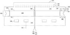
- FIG. 1is a cross-sectional schematic view of an exemplary plasma processing chamber 100 , shown configured as an etch chamber, having a substrate support assembly 126 .
- the substrate support assembly 126may be utilized in other types of processing plasma chambers, for example plasma treatment chambers, annealing chambers, physical vapor deposition chambers, chemical vapor deposition chambers, and ion implantation chambers, among others, as well as other systems where the ability to control processing uniformity for a surface or workpiece, such as a substrate, is desirable.
- the plasma processing chamber 100includes a chamber body 102 having sidewalls 104 , a bottom 106 and a lid 108 that enclose a processing region 110 .
- An injection apparatus 112is coupled to the sidewalls 104 and/or lid 108 of the chamber body 102 .
- a gas panel 114is coupled to the injection apparatus 112 to allow process gases to be provided into the processing region 110 .
- the injection apparatus 112may be one or more nozzle or inlet ports, or alternatively a showerhead. Processing gas, along with any processing by-products, are removed from the processing region 110 through an exhaust port 128 formed in the sidewalls 104 or bottom 106 of the chamber body 102 .
- the exhaust port 128is coupled to a pumping system 132 , which includes throttle valves and pumps utilized to control the vacuum levels within the processing region 110 .
- the processing gasmay be energized to form a plasma within the processing region 110 .
- the processing gasmay be energized by capacitively or inductively coupling RF power to the processing gases.
- a plurality of coils 116are disposed above the lid 108 of the plasma processing chamber 100 and coupled through a matching circuit 118 to an RF power source 120 .
- the substrate support assembly 126is disposed in the processing region 110 below the injection apparatus 112 .
- the substrate support assembly 126includes an electrostatic chuck 174 and a cooling plate 130 .
- the cooling plate 130is supported by a base plate 176 .
- the base plate 176is supported by one of the sidewalls 104 or bottom 106 of the processing chamber.
- the substrate support assembly 126may additionally include a heater assembly (not shown). Additionally, the substrate support assembly 126 may include a facility plate 145 and/or an insulator plate (not shown) disposed between the cooling plate 130 and the base plate 176 .
- the cooling plate 130may be formed from a metal material or other suitable material.
- the cooling plate 130may be formed from aluminum (Al).
- the cooling plate 130may include cooling channels 190 formed therein.
- the cooling channels 190may be connected to a heat transfer fluid source 122 .
- the heat transfer fluid source 122provides a heat transfer fluid, such as a liquid, gas or combination thereof, which is circulated through one or more cooling channels 190 disposed in the cooling plate 130 .
- the fluid flowing through neighboring cooling channels 190may be isolated to enabling local control of the heat transfer between the electrostatic chuck 174 and different regions of the cooling plate 130 , which assists in controlling the lateral temperature profile of the substrate 124 .
- the heat transfer fluid circulating through the cooling channels 190 of the cooling plate 130maintains the cooling plate 130 at a temperature between about 90 degrees Celsius and about 80 degrees Celsius, or at a temperature lower than 90 degrees Celsius.
- the electrostatic chuck 174includes a chucking electrode 186 disposed in a dielectric body 175 .
- the dielectric body 175has a workpiece support surface 137 and a bottom surface 133 opposite the workpiece support surface 137 .
- the dielectric body 175 of the electrostatic chuck 174may be fabricated from a ceramic material, such as alumina (Al 2 O 3 ), aluminum nitride (AlN) or other suitable material.
- the dielectric body 175may be fabricated from a polymer, such as polyimide, polyetheretherketone, polyaryletherketone and the like.
- the dielectric body 175may also include one or more resistive heaters 188 embedded therein.
- the resistive heaters 188may be provided to elevate the temperature of the substrate support assembly 126 to a temperature suitable for processing a substrate 124 disposed on the workpiece support surface 137 of the substrate support assembly 126 .
- the resistive heaters 188are coupled through the facility plate 145 to a heater power source 189 .
- the heater power source 189may provide 900 watts or more power to the resistive heaters 188 .
- a controller(not shown) may control the operation of the heater power source 189 , which is generally set to heat the substrate 124 to a predefined temperature.
- the resistive heaters 188include a plurality of laterally separated heating zones, wherein the controller enables at least one zone of the resistive heaters 188 to be preferentially heated relative to the resistive heaters 188 located in one or more of the other zones.
- the resistive heaters 188may be arranged concentrically in a plurality of separated heating zones.
- the resistive heaters 188may maintain the substrate 124 at a temperature suitable for processing. In some embodiments utilizing elevated processing temperatures, the resistive heaters 188 may maintain the substrate 124 at a temperature between about 180 degrees Celsius to about 500 degrees Celsius.
- the electrostatic chuck 174generally includes a chucking electrode 186 embedded in the dielectric body 175 .
- the chucking electrode 186may be configured as a mono polar or bipolar electrode, or other suitable arrangement.
- the chucking electrode 186is coupled through an RF filter to a chucking power source 187 , which provides a RF or DC power to electrostatically secure the substrate 124 to the workpiece support surface 137 of the electrostatic chuck 174 .
- the RF filterprevents RF power utilized to form a plasma (not shown) within the plasma processing chamber 100 from damaging electrical equipment or presenting an electrical hazard outside the chamber.
- the workpiece support surface 137 of the electrostatic chuck 174may include gas passages (not shown) for providing backside heat transfer gas to the interstitial space defined between the substrate 124 and the workpiece support surface 137 of the electrostatic chuck 174 .
- the electrostatic chuck 174may also include lift pin holes for accommodating lift pins (not shown) for elevating the substrate 124 above the workpiece support surface 137 of the electrostatic chuck 174 to facilitate robotic transfer into and out of the plasma processing chamber 100 .
- a bonding layer 150is disposed between the electrostatic chuck 174 and the cooling plate 130 .
- the bonding layer 150may be formed from several layers which provide for different thermal expansions of the electrostatic chuck 174 and the cooling plate 130 .
- the bonding layer 150includes an adhesive layer (shown as 308 in FIG. 3 ) and a seal band 140 .
- the seal band 140is configured to protect the adhesive material forming the adhesive layer of bonding layer 150 disposed between the electrostatic chuck 174 and the cooling plate 130 from the gases and plasma present in the processing region 110 .
- FIG. 2Ais a top plan view of the seal band 140 .
- the seal band 140has a ring shaped body 201 .
- the ring shaped body 201has a center 202 about which the seal band 140 is substantially congruent.
- the ring shaped body 201has an inner surface 212 and an outer surface 210 .
- the outer surface 210 of the ring shaped body 201has a diameter 208 that defines the outside diameter of the seal band 140 .
- the diameter 208may be between about 306 mm and about 310 mm, such as about 308 mm.
- the diameter 208may be between about 206 mm and about 210 mm, such as about 208 mm.
- the diameter 208may be between about 456 mm and about 460 mm, such as about 458 mm.
- the seal band 140may be formed from a soft elastomeric material, for example, having a Shore D hardness of between about 60 and about 80, such as about 72.
- the seal band 140may additionally have a tensile strength between about 10 Mpa and about 15 Mpa, such as about 11.1 Mpa.
- the elastomeric material forming the seal band 140may be elongated to about 160% of its original size prior to breaking.
- the seal band 140may be formed from a high performance elastomer such as a tetrafluoro ethylene/propylene, a perfluoroelastomer such as Fluoritz-TR® or Perlast G67P®, or other suitable material. In one embodiment, the seal band 140 is formed from Fluoritz-TR®.
- the material of the seal band 140is void of fillers and is resistant to fluorine and oxygen chemistries for enhanced resistance to cracking and plasma radicals.
- the absence of filler materialprevents premature crack formation that happens to conventional filled seals at the filler's material boundaries where the base elastomer has etched away. There may be an increase in the material erosion rate in absence of the filler material, but the larger contact and absence of cracks beneficially improves the service life of the seal band 140 .
- FIG. 2Bis a cross sectional view of the seal band 140 taken across section line B-B in FIG. 2A .
- the seal band 140has a top surface 254 and a bottom surface 252 .
- the top surface 254 and the bottom surface 252are connected by the inner surface 212 .
- An imaginary normal line 253may be disposed at 90° from the inner surface 212 .
- An angle 220may be formed between the imaginary normal line 253 and the bottom surface 252 .
- the top surface 254may be similarly angled with the imaginary normal line 253 as the bottom surface 252 .
- the angled 220may be between about 10 degrees and about 30 degrees, such as about 20 degrees.
- the top surface 254 and the bottom surface 252may have an angled 221 from the inner surface 212 of between about 100° and about 120°, such as more than about 110°.
- the top surface 254 and the bottom surface 252may have a length 262 measured along the normal between the inner surface 212 and the outer surface 210 .
- the length 262may be between about 1.55 mm and about 1.25 mm such as about 1.40 mm.
- the outer surface 210may have a height 264 extending between the top surface 254 to the bottom surface 252 .
- the height 264may be between about 2.075 mm and about 2.125 mm such as about 2.100 mm.
- the outer surface 210may have an indent 230 formed therein.
- the indent 230may produce a V-shaped profile for the seal band 140 .
- the indent 230may have a depth 232 between about 0.30 mm and about 0.50 mm such as about 0.40 mm.
- the indent 230permits the seal band 140 to be easily compressed for ease of installation, and to orientate the top surface 254 and bottom surface 252 in a substantially parallel orientation that enhances the contact area with the electrostatic chuck 174 and the cooling plate 130 when making a seal therebetween when disposed in the substrate support assembly 127 .
- the seal band 140is symmetrical about an imaginary line bifurcating the indent 230 and inner surface 212 .
- FIG. 3is a partial cross-sectional schematic side view of the substrate support assembly 126 detailing one embodiment of the seal band 140 disposed between an electrostatic chuck 174 and the cooling plate 130 .
- the bonding layer 150 disposed between the electrostatic chuck 174 and the cooling plate 130may be formed from different materials.
- An electrical socket 360may provide connections to the resistive heaters 188 and chucking electrode 186 embedded in the dielectric body 175 .
- the resistive heaters 188may heat the bottom 133 of the electrostatic chuck 174 to temperatures above 250° Celsius.
- the bonding layer 150may extend to about an outer diameter 352 of the electrostatic chuck 174 or the cooling plate 130 .
- the bonding layer 150is flexible to account for thermal expansion between the electrostatic chuck 174 and the cooling plate 130 , to substantially prevent cracking, and to reduce the potential for the electrostatic chuck 174 delaminating from the cooling plate 130 .
- the bonding layer 150includes at least one adhesive layer 308 .
- the adhesive layer 308may be formed from a perfluoro compound, silicone, porous graphite, an acrylic compound, perfluoromethyl vinyl ether, alkoxy vinyl ether, CIRLEX®, TEFZEL®, KAPTON®, VESPEL®, KERIMID®, polyethylene, or other suitable material.
- the adhesive layer 308may have a thickness 302 of about 1 mm to about 5 mm, such as about 1.75 mm.
- the adhesive layer 308may have a thermal conductivity between about 0.1 W/mK and about 1 W/mK, such as about 0.17 W/mK.
- a notch 342is formed between an outer periphery 350 of the adhesive layer 308 and the outer diameter 352 of the electrostatic chuck 174 .
- the diameter 208 of the seal band 140is less than the outer diameter 352 of the electrostatic chuck 174 . Additionally, the diameter 208 of the seal band 140 is less than the outer diameter of the cooling plate 130 .
- the seal band 140disposed about, i.e., circumscribes, the outer periphery 350 of the adhesive layer 308 .
- the notch 342may be sized to permit the seal band 140 to sealingly engage the electrostatic chuck 174 and cooling plate 130 .
- the seal band 140may optionally form a vacuum tight seal between the electrostatic chuck 174 and the cooling plate 130 , the primary function of the seal is to protect the exposed outer periphery 350 of the adhesive layer 308 from the environment within the processing region 110 .
- the seal band 140prevents the process gas exposure to the bond material (adhesive layer 308 ) of the substrate support assembly 126 . That is, the seal band 140 protects the inner portions of the substrate support assembly 126 from exposure to the plasma environment. The seal band 140 prevents volatized gases from the adhesive layer 308 from contaminating the plasma environment. The seal band 140 protects the adhesive layer 308 and other internal structures of the substrate support assembly 127 from the plasma environment.
- the seal band 140may be V-shaped.
- the shape of the seal band 140provides a contact surface 310 for sealing which is substantially larger than conventional O-ring seals. Additionally, the V-shaped provides for easier installation of the seal band 140 .
- the force required to install the seal band 140is decreased by about 40% compared to the force required to install a conventional O-ring.
- the seal band 140has an installation force of about 0.63 N/mm whereas conventional O-rings have an installation force of about 1.00 N/mm.
- the contact surface 310 of the seal band 140having the V-shaped, is substantially larger (in width) compared to the contact area of traditional O-rings.
- the contact surface 310 of the seal band 140is about 30% greater than the contact area of conventional O-rings. As the temperature increases from 0 degrees Celsius to 50 degrees Celsius, the contact surface 310 of the seal band 140 increases from about 0.62 mm to about 0.74 mm.
- a compression load on the seal band 140varies with the temperature of the seal band 140 .
- the seal band 140may be compressed as much as 20%.
- the increase in compression of the seal band 140 at the higher temperatureimproves the seal-ability even after some erosion.
- the erosion profile of the seal band 140may be indicative of the longevity for the seal band 140 .
- the erosion profile at 800 RF hours and 1700 RF hourshave shown little wear requiring replacement of the seal band 140 .
- the compression loadis not linear as thermal expansion of the seal band 140 leads to an increase squeeze of the seal band 140 resulting in an increase compression load.
- the material of the seal band 140is softened by the heat and results in a decrease in the compression load.
- the compression load on the seal band 140is about 0.23 N/mm; at 25 degrees Celsius, the compression load on the seal band 140 increases to about 0.26 N/mm; and at 50 degrees Celsius, the compression load on the seal band 140 decreases to about 0.15 N/mm.
- the resistance of the seal band 140 to initial crackingwas tested on a metallic drum.
- the seal band 140was stretched 28% on the metallic drum.
- the seal band 140was exposed to plasma having O 2 and CF 4 flowing at a 196:4 ratio by weight.
- the seal band 140 formed from Fluoritz-TRdemonstrated a greater than 100% increase in longevity from cracking compared to seal bands 140 formed from Fluoritz-T20, transparent perfluoro-elastomers (FFKM) B or D, white FFKM F, K or L, and POR. Additionally, the weight loss due to erosion was less than all the aforementioned materials except for Fuoritz-T20.
- the compression load and material of the seal band 140significantly reduced cracking which may compromise the seal. For example, after 320 RF hours and 600 RF hours, the seal band 140 formed from Fluoritz-TR had no visible signs of erosion or cracking.
- the seal band 140 having a V-shapedsubstantially prevents cracking or degradation of the seal from harsh radical chemistries in the processing chamber, such as fluorine radicals penetrating and etching away the seal protecting the bonding layer.
- the seal band 140 having a V-shapedsubstantially minimizes the degradation of the bond between the ESC and the cooling plate while substantially preventing volatiles outgassing from the bonding layer from entering the processing environment.
- the seal band 140 having a V-shapedprevents contamination in the chamber and reduces chamber downtime which may affect process yields and costs of operations.
Landscapes
- Engineering & Computer Science (AREA)
- Microelectronics & Electronic Packaging (AREA)
- Condensed Matter Physics & Semiconductors (AREA)
- General Physics & Mathematics (AREA)
- Manufacturing & Machinery (AREA)
- Computer Hardware Design (AREA)
- Physics & Mathematics (AREA)
- Power Engineering (AREA)
- General Engineering & Computer Science (AREA)
- Mechanical Engineering (AREA)
- Container, Conveyance, Adherence, Positioning, Of Wafer (AREA)
- Drying Of Semiconductors (AREA)
- Chemical Vapour Deposition (AREA)
- Feeding Of Articles By Means Other Than Belts Or Rollers (AREA)
Abstract
Description
Claims (20)
Priority Applications (11)
| Application Number | Priority Date | Filing Date | Title |
|---|---|---|---|
| US15/361,365US10943808B2 (en) | 2016-11-25 | 2016-11-25 | Ceramic electrostatic chuck having a V-shape seal band |
| KR1020197018196AKR102471167B1 (en) | 2016-11-25 | 2017-09-26 | Ceramic electrostatic chuck with V-shaped sealing band |
| CN201780065037.4ACN109844928B (en) | 2016-11-25 | 2017-09-26 | Ceramic electrostatic chuck with V-shaped sealing band |
| JP2019524432AJP7225093B2 (en) | 2016-11-25 | 2017-09-26 | Ceramic electrostatic chuck with V-shaped seal band |
| KR1020227040913AKR102630741B1 (en) | 2016-11-25 | 2017-09-26 | Ceramic electrostatic chuck having a v-shaped seal band |
| CN202311219601.7ACN117267243A (en) | 2016-11-25 | 2017-09-26 | Ceramic electrostatic chuck with V-shaped sealing band |
| PCT/US2017/053470WO2018097888A1 (en) | 2016-11-25 | 2017-09-26 | Ceramic electrostatic chuck having a v-shaped seal band |
| TW106135236ATWI786067B (en) | 2016-11-25 | 2017-10-16 | Ceramic electrostatic chuck having a v-shaped seal band |
| TW111143123ATWI865958B (en) | 2016-11-25 | 2017-10-16 | A v-shape seal band for a semiconductor processing chamber |
| US17/184,454US20210183680A1 (en) | 2016-11-25 | 2021-02-24 | V-shape seal band for a semiconductor processing chamber |
| JP2022199235AJP7728739B2 (en) | 2016-11-25 | 2022-12-14 | Ceramic electrostatic chuck with V-shaped seal band |
Applications Claiming Priority (1)
| Application Number | Priority Date | Filing Date | Title |
|---|---|---|---|
| US15/361,365US10943808B2 (en) | 2016-11-25 | 2016-11-25 | Ceramic electrostatic chuck having a V-shape seal band |
Related Child Applications (1)
| Application Number | Title | Priority Date | Filing Date |
|---|---|---|---|
| US17/184,454ContinuationUS20210183680A1 (en) | 2016-11-25 | 2021-02-24 | V-shape seal band for a semiconductor processing chamber |
Publications (2)
| Publication Number | Publication Date |
|---|---|
| US20180151402A1 US20180151402A1 (en) | 2018-05-31 |
| US10943808B2true US10943808B2 (en) | 2021-03-09 |
Family
ID=62191168
Family Applications (2)
| Application Number | Title | Priority Date | Filing Date |
|---|---|---|---|
| US15/361,365ActiveUS10943808B2 (en) | 2016-11-25 | 2016-11-25 | Ceramic electrostatic chuck having a V-shape seal band |
| US17/184,454AbandonedUS20210183680A1 (en) | 2016-11-25 | 2021-02-24 | V-shape seal band for a semiconductor processing chamber |
Family Applications After (1)
| Application Number | Title | Priority Date | Filing Date |
|---|---|---|---|
| US17/184,454AbandonedUS20210183680A1 (en) | 2016-11-25 | 2021-02-24 | V-shape seal band for a semiconductor processing chamber |
Country Status (6)
| Country | Link |
|---|---|
| US (2) | US10943808B2 (en) |
| JP (2) | JP7225093B2 (en) |
| KR (2) | KR102630741B1 (en) |
| CN (2) | CN109844928B (en) |
| TW (2) | TWI865958B (en) |
| WO (1) | WO2018097888A1 (en) |
Cited By (1)
| Publication number | Priority date | Publication date | Assignee | Title |
|---|---|---|---|---|
| US12140228B2 (en)* | 2021-12-01 | 2024-11-12 | Mitsubishi Cable Industries, Ltd. | Protective ring, adhesion surface protective structure including the same, and adhesion surface protection method |
Families Citing this family (20)
| Publication number | Priority date | Publication date | Assignee | Title |
|---|---|---|---|---|
| US10943808B2 (en)* | 2016-11-25 | 2021-03-09 | Applied Materials, Inc. | Ceramic electrostatic chuck having a V-shape seal band |
| KR102555765B1 (en)* | 2017-09-29 | 2023-07-17 | 스미토모 오사카 세멘토 가부시키가이샤 | electrostatic chuck device |
| US11626310B2 (en)* | 2018-10-30 | 2023-04-11 | Toto Ltd. | Electrostatic chuck |
| CN110289241B (en)* | 2019-07-04 | 2022-03-22 | 北京北方华创微电子装备有限公司 | Electrostatic chuck, manufacturing method thereof, process chamber and semiconductor processing equipment |
| US11501993B2 (en)* | 2019-07-29 | 2022-11-15 | Applied Materials, Inc. | Semiconductor substrate supports with improved high temperature chucking |
| KR102188261B1 (en)* | 2019-08-02 | 2020-12-09 | 세미기어, 인코포레이션 | Apparatus and method for cooling substrate |
| JP7319153B2 (en)* | 2019-09-24 | 2023-08-01 | 日本特殊陶業株式会社 | holding device |
| JP7362400B2 (en)* | 2019-10-01 | 2023-10-17 | 東京エレクトロン株式会社 | Mounting table and plasma processing equipment |
| KR102344265B1 (en)* | 2019-12-11 | 2021-12-27 | 세메스 주식회사 | Component for protecting bonding layer and system for treating substrate with the component |
| JP7445420B2 (en)* | 2019-12-23 | 2024-03-07 | 日本特殊陶業株式会社 | Parts for semiconductor manufacturing equipment |
| US12334315B2 (en)* | 2020-04-30 | 2025-06-17 | Applied Materials, Inc. | Cooled substrate support assembly for radio frequency environments |
| CN114464550A (en)* | 2020-11-09 | 2022-05-10 | 东京毅力科创株式会社 | Substrate processing system |
| JP7386189B2 (en)* | 2021-01-15 | 2023-11-24 | 日本特殊陶業株式会社 | Composite parts, retention devices, and adhesive structures |
| TWI776380B (en)* | 2021-01-29 | 2022-09-01 | 得立亞科技有限公司 | Method for bonding dielectric material of electrostatic chuck and device thereof |
| KR20240045368A (en)* | 2021-09-02 | 2024-04-05 | 어플라이드 머티어리얼스, 인코포레이티드 | Replaceable electrostatic chuck outer ring for edge arc discharge mitigation |
| JP2023183628A (en)* | 2022-06-16 | 2023-12-28 | 新光電気工業株式会社 | Substrate fixing device and method for manufacturing the substrate fixing device |
| WO2024059276A1 (en)* | 2022-09-16 | 2024-03-21 | Lam Research Corporation | Spring-loaded seal cover band for protecting a substrate support |
| WO2024097077A1 (en)* | 2022-11-04 | 2024-05-10 | Lam Research Corporation | Electrostatic chuck e-seal with offset sealing surface |
| US20250118586A1 (en)* | 2023-10-06 | 2025-04-10 | Applied Materials, Inc. | Electrostatically secured substrate support assembly |
| JP7639953B1 (en) | 2024-01-25 | 2025-03-05 | Toto株式会社 | Electrostatic Chuck |
Citations (15)
| Publication number | Priority date | Publication date | Assignee | Title |
|---|---|---|---|---|
| US2547185A (en) | 1947-05-27 | 1951-04-03 | Yuba Mfg Company | Shaft seal |
| US3825272A (en) | 1971-05-19 | 1974-07-23 | Townsend Engineering Co | Face seal for food processing equipment |
| JPS53149218U (en) | 1977-04-28 | 1978-11-24 | ||
| JPS619644U (en) | 1984-06-25 | 1986-01-21 | 株式会社 江沼チエン製作所 | Waterproof roller chain |
| JP2005083414A (en) | 2003-09-05 | 2005-03-31 | Yamamoto Suiatsu Kogyosho:Kk | Seal ring |
| WO2008048518A1 (en) | 2006-10-13 | 2008-04-24 | Applied Materials | Detachable electrostatic chuck having sealing assembly |
| US20080193068A1 (en) | 2005-07-06 | 2008-08-14 | Schaeffler Kg | Seal For A Clamping System Bearing Lug |
| US20090014323A1 (en) | 2007-07-13 | 2009-01-15 | Boris Yendler | High temperature cathode for plasma etching |
| US20100027188A1 (en) | 2008-07-30 | 2010-02-04 | Hsi-Shui Liu | Replaceable Electrostatic Chuck Sidewall Shield |
| US20110253667A1 (en)* | 2007-10-29 | 2011-10-20 | Ludwig Hiss | Expansion Seal, Especially for Gases |
| US20130097840A1 (en) | 2011-10-20 | 2013-04-25 | Lam Research Corporation | Edge seal for lower electrode assembly |
| WO2013162641A1 (en) | 2012-04-26 | 2013-10-31 | Applied Materials, Inc. | Methods and apparatus toward preventing esc bonding adhesive erosion |
| US20140065835A1 (en) | 2008-02-08 | 2014-03-06 | Lam Research Corporation | Protective coating for a plasma processing chamber part and a method of use |
| US20150170942A1 (en) | 2013-12-17 | 2015-06-18 | Lam Research Corporation | Installation fixture for elastomer bands |
| US20190242480A1 (en) | 2016-09-09 | 2019-08-08 | Valqua, Ltd. | Seal member |
Family Cites Families (28)
| Publication number | Priority date | Publication date | Assignee | Title |
|---|---|---|---|---|
| US2081040A (en)* | 1932-06-17 | 1937-05-18 | J S Abercrombie | Packing |
| US2204507A (en)* | 1940-05-04 | 1940-06-11 | Vickers Inc | Sealing ring |
| US2326489A (en)* | 1941-02-20 | 1943-08-10 | Crane Packing Co | Liquid seal |
| US3028166A (en)* | 1957-10-09 | 1962-04-03 | Chicago Rawhide Mfg Co | Component gasket type seal |
| GB1025704A (en)* | 1962-03-13 | 1966-04-14 | Dowty Seals Ltd | Improvements in sealing devices |
| US3447819A (en)* | 1966-12-30 | 1969-06-03 | Adolph W Borsum | Push-pull connector having combined seal and locking ring |
| DE2443918C2 (en)* | 1974-09-13 | 1982-12-09 | FAG Kugelfischer Georg Schäfer & Co, 8720 Schweinfurt | Rolling bearing raceway split in the axial direction |
| DE3245338C2 (en)* | 1982-12-08 | 1985-10-31 | Fa. Carl Freudenberg, 6940 Weinheim | poetry |
| US4934715A (en)* | 1989-01-09 | 1990-06-19 | Johnson Roy E | Gasket for use with manhole covers |
| JP3810341B2 (en)* | 2002-05-20 | 2006-08-16 | 京セラ株式会社 | Electrostatic chuck |
| CN100363654C (en)* | 2003-03-26 | 2008-01-23 | 哈尔滨工业大学 | metal rubber sealing ring |
| JP4352789B2 (en)* | 2003-07-16 | 2009-10-28 | Toto株式会社 | Electrostatic chuck |
| US6946403B2 (en)* | 2003-10-28 | 2005-09-20 | Axcelis Technologies, Inc. | Method of making a MEMS electrostatic chuck |
| JP4458995B2 (en) | 2004-09-10 | 2010-04-28 | 京セラ株式会社 | Wafer support member |
| EP1967773B1 (en)* | 2007-03-07 | 2009-12-02 | Le Joint Francais | Y-Seal, method of manufacturing such a seal and its use to reduce the forces for fitting a connector |
| JP2011138902A (en)* | 2009-12-28 | 2011-07-14 | Tokyo Electron Ltd | Mounting method and mounting device |
| JP5291039B2 (en)* | 2010-03-31 | 2013-09-18 | 大日本スクリーン製造株式会社 | Substrate holding and rotating device and substrate processing apparatus |
| US8691702B2 (en)* | 2011-03-14 | 2014-04-08 | Plasma-Therm Llc | Method and apparatus for plasma dicing a semi-conductor wafer |
| JP5477672B2 (en) | 2011-03-31 | 2014-04-23 | 住友電気工業株式会社 | Cell frame for electrolyte flow type battery, cell stack for electrolyte flow type battery, and electrolyte flow type battery |
| US9349621B2 (en)* | 2011-05-23 | 2016-05-24 | Lam Research Corporation | Vacuum seal arrangement useful in plasma processing chamber |
| US9869392B2 (en)* | 2011-10-20 | 2018-01-16 | Lam Research Corporation | Edge seal for lower electrode assembly |
| US8677586B2 (en)* | 2012-04-04 | 2014-03-25 | Lam Research Corporation | Installation fixture for elastomer bands and methods of using the same |
| US10808317B2 (en)* | 2013-07-03 | 2020-10-20 | Lam Research Corporation | Deposition apparatus including an isothermal processing zone |
| JP6207988B2 (en)* | 2013-11-26 | 2017-10-04 | 株式会社ミツトヨ | Micrometer and measuring instrument |
| DE102014112013A1 (en)* | 2014-08-22 | 2016-02-25 | Knorr-Bremse Systeme für Nutzfahrzeuge GmbH | Sealing ring for the axial sealing of two axially relative to each other movably arranged parts and sealing system with the sealing ring |
| TWI613753B (en)* | 2015-02-16 | 2018-02-01 | Improved seal for electrostatically adsorbing the side wall of the retainer | |
| CN107258012B (en)* | 2015-03-20 | 2021-04-16 | 应用材料公司 | Ceramic electrostatic chuck bonded to metal substrate with high temperature polymer cement |
| US10943808B2 (en)* | 2016-11-25 | 2021-03-09 | Applied Materials, Inc. | Ceramic electrostatic chuck having a V-shape seal band |
- 2016
- 2016-11-25USUS15/361,365patent/US10943808B2/enactiveActive
- 2017
- 2017-09-26JPJP2019524432Apatent/JP7225093B2/enactiveActive
- 2017-09-26WOPCT/US2017/053470patent/WO2018097888A1/ennot_activeCeased
- 2017-09-26KRKR1020227040913Apatent/KR102630741B1/enactiveActive
- 2017-09-26KRKR1020197018196Apatent/KR102471167B1/enactiveActive
- 2017-09-26CNCN201780065037.4Apatent/CN109844928B/enactiveActive
- 2017-09-26CNCN202311219601.7Apatent/CN117267243A/enactivePending
- 2017-10-16TWTW111143123Apatent/TWI865958B/enactive
- 2017-10-16TWTW106135236Apatent/TWI786067B/enactive
- 2021
- 2021-02-24USUS17/184,454patent/US20210183680A1/ennot_activeAbandoned
- 2022
- 2022-12-14JPJP2022199235Apatent/JP7728739B2/enactiveActive
Patent Citations (18)
| Publication number | Priority date | Publication date | Assignee | Title |
|---|---|---|---|---|
| US2547185A (en) | 1947-05-27 | 1951-04-03 | Yuba Mfg Company | Shaft seal |
| US3825272A (en) | 1971-05-19 | 1974-07-23 | Townsend Engineering Co | Face seal for food processing equipment |
| JPS53149218U (en) | 1977-04-28 | 1978-11-24 | ||
| JPS619644U (en) | 1984-06-25 | 1986-01-21 | 株式会社 江沼チエン製作所 | Waterproof roller chain |
| JP2005083414A (en) | 2003-09-05 | 2005-03-31 | Yamamoto Suiatsu Kogyosho:Kk | Seal ring |
| US20080193068A1 (en) | 2005-07-06 | 2008-08-14 | Schaeffler Kg | Seal For A Clamping System Bearing Lug |
| WO2008048518A1 (en) | 2006-10-13 | 2008-04-24 | Applied Materials | Detachable electrostatic chuck having sealing assembly |
| US20090014323A1 (en) | 2007-07-13 | 2009-01-15 | Boris Yendler | High temperature cathode for plasma etching |
| US20110253667A1 (en)* | 2007-10-29 | 2011-10-20 | Ludwig Hiss | Expansion Seal, Especially for Gases |
| US20140065835A1 (en) | 2008-02-08 | 2014-03-06 | Lam Research Corporation | Protective coating for a plasma processing chamber part and a method of use |
| US20100027188A1 (en) | 2008-07-30 | 2010-02-04 | Hsi-Shui Liu | Replaceable Electrostatic Chuck Sidewall Shield |
| US20130097840A1 (en) | 2011-10-20 | 2013-04-25 | Lam Research Corporation | Edge seal for lower electrode assembly |
| WO2013162641A1 (en) | 2012-04-26 | 2013-10-31 | Applied Materials, Inc. | Methods and apparatus toward preventing esc bonding adhesive erosion |
| US20130286530A1 (en) | 2012-04-26 | 2013-10-31 | Xing Lin | Methods and apparatus toward preventing esc bonding adhesive erosion |
| JP2015515760A (en) | 2012-04-26 | 2015-05-28 | アプライド マテリアルズ インコーポレイテッドApplied Materials,Incorporated | Method and apparatus for preventing erosion of ESC adhesives |
| US20150183187A1 (en) | 2012-04-26 | 2015-07-02 | Applied Materials, Inc. | Methods and apparatus toward preventing esc bonding adhesive erosion |
| US20150170942A1 (en) | 2013-12-17 | 2015-06-18 | Lam Research Corporation | Installation fixture for elastomer bands |
| US20190242480A1 (en) | 2016-09-09 | 2019-08-08 | Valqua, Ltd. | Seal member |
Non-Patent Citations (3)
| Title |
|---|
| International Preliminary Report on Patentability from PCT/JP2017/031907. |
| International Search Report and Written Opinion for PCT/US2017/053470 dated Jan. 5, 2018. |
| International Search Report dated Nov. 28, 2017 from PCT/JP2017/031907. |
Cited By (1)
| Publication number | Priority date | Publication date | Assignee | Title |
|---|---|---|---|---|
| US12140228B2 (en)* | 2021-12-01 | 2024-11-12 | Mitsubishi Cable Industries, Ltd. | Protective ring, adhesion surface protective structure including the same, and adhesion surface protection method |
Also Published As
| Publication number | Publication date |
|---|---|
| US20210183680A1 (en) | 2021-06-17 |
| JP2019537262A (en) | 2019-12-19 |
| TW201834108A (en) | 2018-09-16 |
| JP7225093B2 (en) | 2023-02-20 |
| KR20220162854A (en) | 2022-12-08 |
| CN117267243A (en) | 2023-12-22 |
| CN109844928B (en) | 2023-10-10 |
| CN109844928A (en) | 2019-06-04 |
| JP2023030013A (en) | 2023-03-07 |
| TWI786067B (en) | 2022-12-11 |
| KR102471167B1 (en) | 2022-11-24 |
| JP7728739B2 (en) | 2025-08-25 |
| KR20190078656A (en) | 2019-07-04 |
| KR102630741B1 (en) | 2024-01-29 |
| TWI865958B (en) | 2024-12-11 |
| TW202310235A (en) | 2023-03-01 |
| US20180151402A1 (en) | 2018-05-31 |
| WO2018097888A1 (en) | 2018-05-31 |
Similar Documents
| Publication | Publication Date | Title |
|---|---|---|
| US20210183680A1 (en) | V-shape seal band for a semiconductor processing chamber | |
| CN107258012B (en) | Ceramic electrostatic chuck bonded to metal substrate with high temperature polymer cement | |
| KR102785891B1 (en) | Sis and temperature control of the process kit within the substrate processing chamber | |
| KR102537309B1 (en) | Showerhead with reduced backside plasma ignition | |
| US20200035535A1 (en) | Metal bonded electrostatic chuck for high power application | |
| US11894255B2 (en) | Sheath and temperature control of process kit | |
| KR20250053999A (en) | Electrostatic chuck assembly for cryogenic applications | |
| US20230118651A1 (en) | Replaceable electrostatic chuck outer ring for edge arcing mitigation | |
| WO2025071902A1 (en) | Metal bonded esc with outer ceramic vacuum isolation ring for cryogenic service | |
| US20250183093A1 (en) | Hybrid seal for semiconductor processing chambers | |
| US20240371607A1 (en) | Pressure seal method and apparatus | |
| US12331984B2 (en) | Cryogenic micro-zone electrostatic chuck connector assembly | |
| TW202531480A (en) | Hybrid seal for semiconductor processing chambers | |
| CN117859200A (en) | Replaceable electrostatic chuck outer ring for mitigating edge arcing |
Legal Events
| Date | Code | Title | Description |
|---|---|---|---|
| AS | Assignment | Owner name:APPLIED MATERIALS, INC., CALIFORNIA Free format text:ASSIGNMENT OF ASSIGNORS INTEREST;ASSIGNOR:NOORBAKHSH, HAMID;REEL/FRAME:040591/0865 Effective date:20161206 | |
| STPP | Information on status: patent application and granting procedure in general | Free format text:RESPONSE TO NON-FINAL OFFICE ACTION ENTERED AND FORWARDED TO EXAMINER | |
| STPP | Information on status: patent application and granting procedure in general | Free format text:FINAL REJECTION MAILED | |
| STPP | Information on status: patent application and granting procedure in general | Free format text:RESPONSE AFTER FINAL ACTION FORWARDED TO EXAMINER | |
| STPP | Information on status: patent application and granting procedure in general | Free format text:ADVISORY ACTION MAILED | |
| STPP | Information on status: patent application and granting procedure in general | Free format text:DOCKETED NEW CASE - READY FOR EXAMINATION | |
| STPP | Information on status: patent application and granting procedure in general | Free format text:NOTICE OF ALLOWANCE MAILED -- APPLICATION RECEIVED IN OFFICE OF PUBLICATIONS | |
| STPP | Information on status: patent application and granting procedure in general | Free format text:DOCKETED NEW CASE - READY FOR EXAMINATION | |
| STPP | Information on status: patent application and granting procedure in general | Free format text:AWAITING TC RESP., ISSUE FEE NOT PAID | |
| AS | Assignment | Owner name:VALQUA, LTD., JAPAN Free format text:ASSIGNMENT OF ASSIGNORS INTEREST;ASSIGNORS:NAKAGAWA, IPPEI;YOSHIDA, NOBUHIRO;REEL/FRAME:054929/0824 Effective date:20201208 | |
| AS | Assignment | Owner name:APPLIED MATERIALS, INC., CALIFORNIA Free format text:ASSIGNMENT OF ASSIGNORS INTEREST;ASSIGNOR:VALQUA, LTD.;REEL/FRAME:054989/0421 Effective date:20210115 | |
| STCF | Information on status: patent grant | Free format text:PATENTED CASE | |
| MAFP | Maintenance fee payment | Free format text:PAYMENT OF MAINTENANCE FEE, 4TH YEAR, LARGE ENTITY (ORIGINAL EVENT CODE: M1551); ENTITY STATUS OF PATENT OWNER: LARGE ENTITY Year of fee payment:4 |