US10938346B2 - Frequency multiplexed resonator input and/or output for a superconducting device - Google Patents
Frequency multiplexed resonator input and/or output for a superconducting deviceDownload PDFInfo
- Publication number
- US10938346B2 US10938346B2US15/572,731US201615572731AUS10938346B2US 10938346 B2US10938346 B2US 10938346B2US 201615572731 AUS201615572731 AUS 201615572731AUS 10938346 B2US10938346 B2US 10938346B2
- Authority
- US
- United States
- Prior art keywords
- superconducting
- microwave
- resonator
- input
- squid
- Prior art date
- Legal status (The legal status is an assumption and is not a legal conclusion. Google has not performed a legal analysis and makes no representation as to the accuracy of the status listed.)
- Active, expires
Links
Images


Classifications
- H—ELECTRICITY
- H03—ELECTRONIC CIRCUITRY
- H03B—GENERATION OF OSCILLATIONS, DIRECTLY OR BY FREQUENCY-CHANGING, BY CIRCUITS EMPLOYING ACTIVE ELEMENTS WHICH OPERATE IN A NON-SWITCHING MANNER; GENERATION OF NOISE BY SUCH CIRCUITS
- H03B15/00—Generation of oscillations using galvano-magnetic devices, e.g. Hall-effect devices, or using superconductivity effects
- H03B15/003—Generation of oscillations using galvano-magnetic devices, e.g. Hall-effect devices, or using superconductivity effects using superconductivity effects
- G—PHYSICS
- G06—COMPUTING OR CALCULATING; COUNTING
- G06N—COMPUTING ARRANGEMENTS BASED ON SPECIFIC COMPUTATIONAL MODELS
- G06N10/00—Quantum computing, i.e. information processing based on quantum-mechanical phenomena
- G06N10/20—Models of quantum computing, e.g. quantum circuits or universal quantum computers
- G—PHYSICS
- G06—COMPUTING OR CALCULATING; COUNTING
- G06N—COMPUTING ARRANGEMENTS BASED ON SPECIFIC COMPUTATIONAL MODELS
- G06N10/00—Quantum computing, i.e. information processing based on quantum-mechanical phenomena
- G06N10/40—Physical realisations or architectures of quantum processors or components for manipulating qubits, e.g. qubit coupling or qubit control
- H01L39/223—
- H—ELECTRICITY
- H01—ELECTRIC ELEMENTS
- H01P—WAVEGUIDES; RESONATORS, LINES, OR OTHER DEVICES OF THE WAVEGUIDE TYPE
- H01P7/00—Resonators of the waveguide type
- H01P7/08—Strip line resonators
- H—ELECTRICITY
- H01—ELECTRIC ELEMENTS
- H01P—WAVEGUIDES; RESONATORS, LINES, OR OTHER DEVICES OF THE WAVEGUIDE TYPE
- H01P7/00—Resonators of the waveguide type
- H01P7/10—Dielectric resonators
- H01P7/105—Multimode resonators
- H—ELECTRICITY
- H03—ELECTRONIC CIRCUITRY
- H03H—IMPEDANCE NETWORKS, e.g. RESONANT CIRCUITS; RESONATORS
- H03H7/00—Multiple-port networks comprising only passive electrical elements as network components
- H03H7/01—Frequency selective two-port networks
- H—ELECTRICITY
- H10—SEMICONDUCTOR DEVICES; ELECTRIC SOLID-STATE DEVICES NOT OTHERWISE PROVIDED FOR
- H10N—ELECTRIC SOLID-STATE DEVICES NOT OTHERWISE PROVIDED FOR
- H10N60/00—Superconducting devices
- H10N60/10—Junction-based devices
- H10N60/12—Josephson-effect devices
- G—PHYSICS
- G06—COMPUTING OR CALCULATING; COUNTING
- G06N—COMPUTING ARRANGEMENTS BASED ON SPECIFIC COMPUTATIONAL MODELS
- G06N10/00—Quantum computing, i.e. information processing based on quantum-mechanical phenomena
- H—ELECTRICITY
- H03—ELECTRONIC CIRCUITRY
- H03B—GENERATION OF OSCILLATIONS, DIRECTLY OR BY FREQUENCY-CHANGING, BY CIRCUITS EMPLOYING ACTIVE ELEMENTS WHICH OPERATE IN A NON-SWITCHING MANNER; GENERATION OF NOISE BY SUCH CIRCUITS
- H03B2201/00—Aspects of oscillators relating to varying the frequency of the oscillations
- H03B2201/02—Varying the frequency of the oscillations by electronic means
Definitions
- This disclosuregenerally relates to input and/or output systems and methods for superconducting devices such as superconducting quantum computers and superconducting classical computers, and, more specifically, to systems and methods for inputting data to a superconducting quantum processor and/or measuring the state of a qubit in the superconducting quantum processor.
- Superconducting microwave resonatorshave been used in a variety of fields including, but not limited to, quantum computation and astronomy. For example, in quantum computation, superconducting resonators have been used to detect the state of qubits. In astronomy, superconducting microwave resonators have been used in Microwave Kinetic Inductance Detectors (MKIDs). In both cases, many resonators (detectors) can be coupled to a common transmission line and integrated through frequency domain multiplexing. Frequency domain multiplexing (FDM) is a technique in which a communication bandwidth is divided into a number of non-overlapping sub-bands, each sub-band used to carry a separate signal.
- FDMFrequency domain multiplexing
- superconducting resonators of different resonant frequenciescan be used for readout of multiple qubits.
- the resonatorscan share a common microwave transmission line by using frequency domain multiplexing.
- Frequency Multiplexed Resonator (FMR) technologycan be used to readout many single flux quanta simultaneously and has applications in both superconducting quantum computing and superconducting classical computing. FMR technology also has applications in inputting data to a superconducting quantum processor, for example via a Quantum Flux Parametron (QFP) device.
- QFPQuantum Flux Parametron
- quantum computingit is desirable to be able to measure the state of a qubit, and it is also desirable that the readout technology is scalable to large numbers of qubits. Similarly, it is desirable for the technology for inputting data to the superconducting quantum processor to be scalable.
- NDROnon-dissipative readout
- Additional NDRO linesincrease the thermal load on the fridge, raising its base temperature.
- the increased power driven on-chipcan increase the chip's heat load. Since performance of the processor can depend on low chip temperature, there can be a trade-off between processor performance and readout speed. Furthermore, adding more lines increases the cost of the hardware.
- the performance of a superconducting quantum processorcan be limited by the number and bandwidth of input lines.
- the superconducting quantum processorcan be accessed via approximately 200 lines each having a bandwidth of 30 MHz.
- the number and bandwidth of the input linescan, at least in part, determine the rate at which the system can encode new problems on the quantum processor.
- Increasing the number and bandwidth of linesis not a scalable approach. Adding more lines can create a number of demands on the system including the need for a larger sample space, and the need for more contact pads on the periphery of the processor chip. Increasing the number of lines can also increase the thermal load on the processor. Moreover, an increase in the number of lines can open up more pathways for non-thermal photons.
- the present disclosuredescribes input/output systems and methods that are able to tune frequency and sensitivity (the change in resonant frequency per unit flux bias of the DC SQUID) independently, and consequently able to use the available bandwidth more efficiently than would typically be feasible without independent sensitivity control.
- the present disclosuredescribes input/output systems and methods that are able to scale to large processor sizes, and provide improved performance, by increasing the rate at which data can be input and/or output to the processor without increasing the number of input/output lines to the processor.
- a superconducting readout systemmay be summarized as including: a microwave transmission line; at least one microwave superconducting resonator communicatively coupled to the microwave transmission line, each microwave superconducting resonator respectively including: a capacitance coupled between the microwave transmission line and a first node via a superconductive path; an inductance coupled between the microwave transmission line and the first node via a superconductive path, the inductance in parallel with the capacitance of the respective microwave superconducting resonator; a first DC superconducting quantum interference device (SQUID) coupled between the inductance and the first node via a superconductive path, in parallel with the capacitance of the respective microwave superconducting resonator and in series with the inductance of the respective microwave superconducting resonator; and a second DC superconducting quantum interference device (SQUID) coupled between the first DC SQUID and the first node via a superconductive path, in parallel with the capacitance of the respective microwave superconducting
- the second DC SQUIDmay be inductively coupled to the QFP.
- the QFPmay be a shift register and the second DC SQUID may be communicatively coupled to an endpoint of the shift register, the shift register comprising a plurality of stages.
- the at least one microwave superconducting resonatormay include a plurality of microwave superconducting resonators, each of the plurality of microwave superconducting resonators communicatively coupled to the microwave transmission line.
- the superconducting readout systemmay be a frequency multiplex resonant readout system.
- the superconducting readout systemmay further include: a digital electronics subsystem that generates and detects a baseband signal, the digital electronics subsystem comprising: a Field Programmable Gate Array (FPGA); at least one Digital-to-Analog Converter (DAC) communicatively coupled to an output of the FPGA; and at least one Analog-to-Digital Converter (ADC) communicatively coupled to an input of the FPGA.
- a digital electronics subsystemthat generates and detects a baseband signal
- the digital electronics subsystemcomprising: a Field Programmable Gate Array (FPGA); at least one Digital-to-Analog Converter (DAC) communicatively coupled to an output of the FPGA; and at least one Analog-to-Digital Converter (ADC) communicatively coupled to an input of the FPGA.
- FPGAField Programmable Gate Array
- DACDigital-to-Analog Converter
- ADCAnalog-to-Digital Converter
- the superconducting readout systemmay further include: a microwave subsystem that generates and receives a microwave signal, the microwave subsystem comprising: a pair of complex mixers, a first one of the complex mixers communicatively coupled to the at least one DAC and a second one of the complex mixers communicatively coupled to the at least one ADC; a reference microwave signal generator communicatively coupled to provide a reference microwave signal to at least one of the complex mixers; a programmable attenuator communicatively coupled to the complex mixers; and a microwave switch operable to control passage of the signals between the first one of the complex mixers and the programmable attenuator; and at least one amplifier communicatively coupled to receive a signal from the programmable attenuator.
- a microwave subsystemthat generates and receives a microwave signal
- the microwave subsystemcomprising: a pair of complex mixers, a first one of the complex mixers communicatively coupled to the at least one DAC and a second one of the
- the first flux bias applied by the first interfacemay tune the resonant frequency of the first microwave resonator, and the second flux bias applied by the second interface may tune the sensitivity of the first microwave resonator.
- the capacitancemay include a parallel plate capacitor.
- the inductancemay include a spiral inductor.
- a method for frequency multiplexed resonant readout of a superconducting devicemay be summarized as including: tuning the resonant frequency of a superconducting resonator by applying a first flux bias to a first DC superconducting quantum interference device (SQUID); and tuning the sensitivity of the superconducting resonator by applying a second bias to a second DC superconducting quantum interference device (SQUID).
- SQUIDDC superconducting quantum interference device
- the methodmay further include: stimulating an interaction of the superconducting resonator with a Quantum Flux Parametron (QFP) at a nominal resonant frequency; and detecting a shifted resonant frequency of the superconducting resonator resulting from the interaction of the superconducting resonator with the QFP, wherein the shifted resonant frequency is indicative of a state of the QFP.
- QFPQuantum Flux Parametron
- the frequency multiplexed resonant readoutmay include a plurality of non-overlapping sub-bands, a first of the plurality of sub-bands allocated to the superconducting resonator; and the tuning of the resonant frequency of the superconducting resonator and the tuning of the sensitivity of the superconducting resonator may cause the nominal resonant frequency of the superconducting resonator and the shifted resonant frequency of the superconducting resonator to lie within the first of the plurality of sub-bands.
- a method of fabricating a superconducting parallel plate capacitormay be summarized as including: depositing a first superconductive layer, the first superconductive layer comprising a material that is superconductive in a range of critical temperatures; depositing a first dielectric layer to overlie at least part of the first superconductive layer; depositing a second superconductive layer to overlie at least part of the dielectric layer, the second superconductive layer comprising a material that is superconductive in the range of critical temperatures; removing a portion of the second superconductive layer to form at least one structure from the second superconductive layer and to expose at least part of the first dielectric layer; depositing a second dielectric layer to overlie at least part of the second superconductive layer and at least part of the first dielectric layer; planarizing the second dielectric layer; removing at least part of the second dielectric layer to form a first via exposing at least part of the second superconductive layer; removing at least part of the second dielectric layer and at least part of the first dielectric layer to form a second via exposing at least part of the first
- the first and the second superconductive layersmay include niobium.
- the first dielectric layermay include silicon nitride.
- the second dielectric layercomprises silicon dioxide.
- the third superconductive layercomprises niobium.
- the thickness of the first and the second superconductive layersmay be in the range of about 100 nm to 400 nm, the thickness of the first dielectric layer may be in the range of about 10 nm to 100 nm, and the thickness of the second dielectric layer may be in the range of about 100 nm to 300 nm.
- a superconducting input/output systemmay be summarized as including a microwave transmission line; at least one microwave superconducting resonator communicatively coupled to the microwave transmission line, each microwave superconducting resonator respectively comprising: a capacitance coupled between the microwave transmission line and a first node via a superconductive path; an inductance coupled between the microwave transmission line and the first node via a superconductive path, the inductance in parallel with the capacitance of the respective microwave superconducting resonator; a first DC superconducting quantum interference device (SQUID) coupled between the inductance and the first node via a superconductive path, in parallel with the capacitance of the respective microwave superconducting resonator and in series with the inductance of the respective microwave superconducting resonator; and a second DC superconducting quantum interference device (SQUID) coupled between the first DC SQUID and the first node via a superconductive path, in parallel with the capacitance of the respective microwave superconduct
- the second DC SQUIDmay be inductively coupled to the QFP.
- the QFPmay be a shift register and the second DC SQUID may be communicatively coupled to an endpoint of the shift register, the shift register including a plurality of stages.
- the at least one microwave superconducting resonatormay include a plurality of microwave superconducting resonators, each of the plurality of microwave superconducting resonators communicatively coupled to the microwave transmission line.
- the superconducting input/output systemmay be a frequency multiplexed resonator transceiver selectively operable to readout data from the QFP and load data into the QFP.
- the superconducting input/output systemmay further include a microwave subsystem operable to generate a microwave signal for transmission on the microwave transmission line, and operable to receive a microwave signal via the microwave transmission line, the microwave subsystem comprising: a pair of complex mixers, a first one of the complex mixers communicatively coupled to the at least one DAC and a second one of the complex mixers communicatively coupled to the at least one ADC; a reference microwave signal generator communicatively coupled to provide a reference microwave signal to at least one of the complex mixers; a programmable attenuator communicatively coupled to the complex mixers; and a microwave switch operable to control passage of the signals between the first one of the complex mixers and the programmable attenuator; and at least one amplifier communicatively coupled to receive a signal from the programmable attenuator.
- a microwave subsystemoperable to generate a microwave signal for transmission on the microwave transmission line, and operable to receive a microwave signal via the microwave transmission line
- the superconducting input/output systemmay further include a digital electronics subsystem operable to generate a baseband signal for input to the microwave subsystem, and operable to detect a baseband signal received from the microwave subsystem, the digital electronics subsystem including a Field Programmable Gate Array (FPGA); at least one Digital-to-Analog Converter (DAC) communicatively coupled to an output of the FPGA; and at least one Analog-to-Digital Converter (ADC) communicatively coupled to an input of the FPGA.
- FPGAField Programmable Gate Array
- DACDigital-to-Analog Converter
- ADCAnalog-to-Digital Converter
- the third flux bias applied by the third interfacemay cause partial annealing. Partial annealing may include lowering the potential barrier between two stable energy states of the QFP.
- the capacitancemay include a parallel plate capacitor.
- the inductancemay include a spiral inductor.
- the superconducting input/output systemmay be a superconducting readout system operable to read out the states of one or more superconducting devices. At least one of the one or more superconducting devices may be a superconducting qubit.
- the superconducting input/output systemmay be a superconducting data input system operable to load data into one or more superconducting devices. At least one of the one or more superconducting devices may be a DAC.
- the QFPmay be a final stage of a shift register.
- the shift registermay be communicatively coupled to a DAC.
- a method for frequency multiplexed transmission of a data to a superconducting device, the data including a sequence of bits, the superconducting device communicatively coupled to a superconducting resonatorwherein the method may be summarized as including initializing the superconducting device to a first state; applying a flux bias to the superconducting device via a first flux bias line to generate a preference for a second state; lowering a potential barrier in the superconducting device via a second flux bias line; determining whether a first bit in the sequence of bits is represented by a second state; upon determining the first bit is represented by the second state, sending a tone via a microwave transmission line to the superconducting resonator; raising the potential barrier in the superconducting device via the second flux bias line.
- Initializing the superconducting devicemay include initializing a QFP.
- Initializing the QFPmay include initializing a last stage of a shift register communicatively coupled to a DAC.
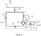
- FIG. 1Ais a schematic diagram illustrating an example embodiment of a superconducting circuit comprising a superconducting resonator able to tune a resonator frequency.
- FIG. 1Bis an example graph illustrating the use of SQUID flux bias to tune the resonator frequency.
- FIG. 1Cis a plot illustrating schematically part of a Frequency Multiplexed Resonator (FMR) spectrum.
- FMRFrequency Multiplexed Resonator
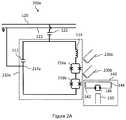
- FIG. 2Ais a schematic diagram illustrating a first example embodiment of a superconducting circuit comprising a superconducting resonator with two SQUID loops, able to independently tune the resonator frequency and sensitivity.
- FIG. 2Bis a schematic diagram illustrating a second example embodiment of a superconducting circuit comprising a superconducting resonator with two SQUID loops, able to independently tune the resonator frequency and sensitivity.
- FIG. 2Cis a schematic diagram illustrating a third example embodiment of a superconducting circuit comprising a superconducting resonator with two SQUID loops, able to independently tune the resonator frequency and sensitivity.
- FIG. 3is a plot of the modulation curve for a superconducting circuit comprising a superconducting resonator with two SQUID loops such as the superconducting circuit of FIG. 2A .
- FIG. 4is a schematic diagram illustrating an example embodiment of a superconducting circuit comprising the superconducting resonator of FIG. 1A and able to independently tune the resonator frequency and sensitivity.
- FIG. 5is a schematic diagram illustrating an example embodiment of a readout system for a superconducting circuit.
- FIG. 6is a flow chart illustrating a method of operation of the readout system of FIG. 5 .
- FIG. 7is a schematic diagram of an exemplary hybrid computing system, including a digital computer and a quantum computer, that may incorporate FMR technology as described herein.
- FIG. 8is a schematic diagram illustrating a first arrangement of superconducting resonators in an example embodiment of a superconducting quantum processor.
- FIG. 9is a schematic diagram illustrating a second arrangement of superconducting resonators in an example embodiment of a superconducting quantum processor.
- FIGS. 10A to 10Fare each respective cross-sectional views of a superconducting integrated circuit at sequential phases of a fabrication process, according to one illustrated embodiment.
- FIG. 11Ais a flow chart illustrating a method for using frequency multiplexed resonator technology to transmit data to a superconducting device according to at least one implementation.
- FIG. 11Bis a flow chart illustrating a method for using frequency multiplexed resonator technology to transmit data to a superconducting device according to at least another implementation.
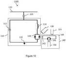
- FIG. 12is a schematic diagram illustrating a frequency multiplexed resonator transceiver according to at least one exemplary implementation.
- FIG. 13Ais a schematic diagram illustrating a frequency multiplexed resonator transceiver comprising a superconducting resonator with two SQUID loops according to at least one exemplary implementation.
- FIG. 13Bis a schematic diagram illustrating a frequency multiplexed resonator transceiver comprising a superconducting resonator with two SQUID loops according to at least another exemplary implementation.
- FIG. 13Cis a schematic diagram illustrating a frequency multiplexed resonator transceiver comprising a superconducting resonator with two SQUID loops according to at least another exemplary implementation.
- FIG. 14is a schematic diagram illustrating a frequency multiplexed resonator transceiver comprising the superconducting resonator of FIG. 12 .
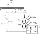
- FIG. 1Ashows a superconducting circuit 100 comprising a superconducting resonator 110 according to at least a first exemplary implementation.
- Superconducting resonator 110comprises a capacitance 112 , and an inductance 114 , which may or may not take the form of discrete capacitors and inductors, respectively.
- Superconducting resonator 110further comprises a single SQUID loop 116 .
- SQUID loop 116is a DC SQUID and comprises a pair of Josephson junctions in parallel with one another in a superconducting loop.
- SQUID loop 116enables tuning of the resonance frequency of superconducting resonator 110 by adjusting the SQUID flux bias as explained below.
- the resonance frequency ⁇ of superconducting resonator 110can be determined by the following formula for an LC circuit:
- ⁇ ⁇ ⁇ ⁇- ⁇ ⁇ ⁇ C 2 ⁇ C + - ⁇ ⁇ ⁇ L 2 ⁇ L
- superconducting resonator 110is a distributed resonator.
- a distributed resonatorhas capacitance and inductance that cannot be isolated into separate lumped element capacitors and inductors.
- An advantage of a distributed resonatoris that it can be designed to be insensitive to layer thickness.
- a distributed resonatorcan also be more tolerant to variations in fabrication.
- a distributed resonatorcan exhibit harmonics at every octave which can be a disadvantage in an implementation using more than one octave of bandwidth.
- superconducting resonator 110is a lumped element design.
- a lumped element designcan advantageously provide a bandwidth greater than one octave, and can reduce or minimize the extent of the resonator's electric field. Since the loss tangent of superconducting resonator 110 can depend on the volume of lossy dielectric exposed to the resonator's electric field, it can be beneficial to use a lumped element design.
- capacitance 112can be implemented using one or more capacitors.
- the capacitorscan be interdigitated capacitors and/or parallel plate capacitors.
- capacitance 112is implemented using a parallel plate capacitor.
- the capacitance of the parallel plate capacitoris approximately 2 pF.
- the capacitance C of a parallel plate capacitoris given by:
- area Amay be defined by lithography, and fractional errors in area A are expected to be small relative to other errors.
- the thickness of the dielectriccan vary and can contribute significantly to variations in capacitance C and in the resonance frequency ⁇ of a resonator comprising capacitance C. The dependence on variations in dielectric thickness is as follows:
- inductance 114can be implemented using one or more inductors.
- inductance 114is implemented using a niobium spiral inductor.
- the geometric inductance of the spiral inductoris approximately 1 nH.
- inductance 114is implemented using a spiral inductor comprising a high kinetic inductance material such as TiN or WSi.
- the total inductance in superconducting resonator 110is a sum of the geometric inductance, the kinetic inductance, and the inductance of SQUID loop 116 .
- Circuit 100further comprises a transmission line 120 , a coupling capacitance 122 , and a last or final shift register stage 140 .
- Last shift register stage 140comprises inductances 142 and 144 , SQUID loop 146 and interface 150 .
- Last or final shift register stage 140may, for example, take the form of a Quantum Flux Parametron (QFP).
- Last or final shift register stage 140is the endpoint of a shift register comprising one or more stages.
- Last or final shift register stage 140is a stage that can be communicatively coupled to superconducting resonator 110 for the purposes of reading out the state of a superconducting device.
- superconducting resonator 110is fed by a flux shift register which, in turn, is fed by a flux qubit.
- the quantum flux parametronis a superconducting Josephson junction device similar in structure to a compound rf-SQUID.
- Quantum flux parametronencompasses both the operation and the structure of the Josephson junction device, not simply structure alone.
- Interface 130can provide a flux bias to SQUID loop 116 and can be controlled by a flux DAC (not shown in FIG. 1A ) or by an analog line. Using a flux DAC reduces the number of low-frequency analog control lines to the superconducting circuit.
- a flux DACis an example of an on-chip control circuitry. Further examples can be found in U.S. Pat. Nos. 7,876,248; 7,843,209; 8,018,244; 8,098,179; 8,169,231; and 8,786,476.
- Superconducting resonator 110can be coupled to transmission line 120 via coupling capacitance 122 (e.g., a discrete capacitor).
- Transmission line 120can optionally be coupled to one or more other superconducting resonators (not shown in FIG. 1A ).
- Superconducting resonator 110is connected at node 115 to ground.
- Superconducting resonator 110comprising single SQUID loop 116 does not enable independent tuning of the resonance frequency and the sensitivity of superconducting resonator 110 .
- FIG. 1Bis an example graph illustrating the variation of resonator frequency with SQUID flux bias.
- the SQUID flux biascan be used to tune the resonator frequency.
- the resonator frequencyis 5 GHz at zero flux bias, corresponding to point 160 on the graph.
- Increasing the flux biastunes the resonator down in frequency.
- the resonatorcan be tuned down by 50 MHz to a frequency of 4.95 GHz by increasing the flux from zero to ⁇ 1 , the result indicated by point 162 on the graph.
- the sensitivityis proportional to the slope of the graph shown in FIG. 1B .
- a smaller increase in flux biaswill cause the same frequency shift at lower frequencies. This is illustrated by points 164 and 166 on the graph shown in FIG. 1B .
- An increase in flux bias from ⁇ 2 to ⁇ 3causes the resonator frequency to shift 50 MHz from 4.7 GHz to 4.65 GHz.
- the sensitivityis not independently tunable and can vary significantly with flux bias. This can result in an undesirable tuning-dependent frequency shift for the same flux modulation from the last or final shift register stage coupled to the resonator. It is desirable to have a superconducting resonator in which resonator frequency and sensitivity can be independently adjusted to provide a suitable operating point. For example, independent adjustment of resonant frequency and sensitivity can be used to compensate for frequency shifts arising from variations occurring during fabrication of superconducting circuits such as circuit 100 of FIG. 1A .
- FIG. 1Cis a plot illustrating schematically part of an FMR spectrum.
- the FMR spectrumis a plot of resonant amplitude versus frequency.
- the FMR spectrumcomprises spectrum from three resonators shown in their various states.
- Frequency f nomis the resonator frequency when no flux bias is applied to SQUID loop 116 of FIG. 1A .
- Frequency f 1is the resonator frequency when attached QFP 140 is in a positive latched state.
- Frequency f 2is the resonator frequency when attached QFP 140 is in a negative latched state.
- the change in frequency for a given resonance between when attached QFP 140 is in a positive state and a negative stateis ⁇ f QFP .
- Adjacent resonatorsare separated by frequency difference B bin .
- f nom (i)can be selected to lie approximately at the center between f ⁇ 1 (i) and f 1 (i+1) .
- Adjacent resonancescan be separated by a guard band.
- adjacent resonatorsare separated by three times the linewidth of an individual resonance, and B bin is four times ⁇ f QFP .
- the flux DACs for superconducting circuit 100(not shown in FIG. 1A ) can be used to position the resonances within the bandwidth to sufficient precision.
- FIG. 2Ashows a superconducting circuit 200 a according to at least one implementation, comprising a superconducting resonator 210 a with two SQUID loops, able to independently tune the resonator frequency and sensitivity.
- Superconducting resonator 210 acomprises two SQUID loops 216 a and 216 b.
- Each of SQUID loops 216 a and 216 bis a DC SQUID and comprises a pair of Josephson junctions in parallel with one another in a superconducting loop.
- SQUID loops 216 a and 216 badvantageously enable independent tuning of the resonance frequency and the sensitivity of superconducting resonator 210 a by adjusting the flux bias in SQUID loops 216 a and 216 b as explained below.
- superconducting circuit 200 alabeled with the same numbers as in superconducting circuit 100 of FIG. 1A are similar or even identical to those described in reference to FIG. 1A .
- capacitance 112 of superconducting circuit 200 acan be a parallel plate capacitor
- inductance 114 of superconducting circuit 200 acan be a niobium spiral inductor.
- Superconducting resonator 210 ais connected at node 215 a to ground, for example to the ground 121 of transmission line 120 .
- Interfaces 230 a and 230 bcan provide flux bias to SQUID loops 216 a and 216 b respectively. Once a suitable operating point has been found (see below), the flux biases provided by interfaces 230 a and 230 b can be static. This advantageously allows the circuit to use an array of flux DACs requiring only a few wires to program. The two tunable SQUID loops 216 a and 216 b do not need an independent analog control line for each superconducting resonator 210 a.
- FIG. 2Bshows a superconducting circuit 200 b according to at least another implementation, comprising a superconducting resonator 210 b with two SQUID loops, advantageously operable to independently tune the resonator frequency and sensitivity.
- Superconducting resonator 210 bcomprises two SQUID loops 216 a and 216 b.
- Each of SQUID loops 216 a and 216 bis a DC SQUID and comprises a pair of Josephson junctions in parallel in a superconducting loop.
- SQUID loop 216 bfurther comprises inductances 218 a through 218 d.
- SQUID loops 216 a and 216 benable independent tuning of the resonance frequency and the sensitivity of superconducting resonator 210 a by adjusting the flux bias in SQUID loops 216 a and 216 b as explained below.
- SQUID loop 218 bis galvanically coupled to a last or final shift register stage comprising DC SQUID 146 and inductance 144 .
- Interfaces 150 and 152can provide flux bias to DC SQUIDs 146 and 148 respectively.
- Superconducting resonator 210 bis connected at node 215 b to ground, for example to the ground 121 of transmission line 120 .
- capacitor 112 of superconducting circuit 200 bcan be a parallel plate capacitor
- inductance 114 of superconducting circuit 200 bcan be a niobium spiral inductor.
- Interfaces 230 a and 230 bcan provide flux bias to SQUID loops 216 a and 216 b respectively.
- FIG. 2Cshows a superconducting circuit 200 c according to at least another implementation, comprising a superconducting resonator 210 c with two SQUID loops, advantageously operable to independently tune the resonator frequency and sensitivity.
- Superconducting circuit 200 cis connected at node 215 c to the ground 121 of transmission line 120 via a coupling capacitor 124 .
- superconducting circuit 200 cis the same as or similar to superconducting circuit 200 b.
- Components of superconducting circuit 200 c labeled with the same numbers as in superconducting circuit 100 of FIG. 1Acan be as described in reference to FIG. 1A .
- capacitance 112 of superconducting circuit 200 acan be a parallel plate capacitor
- inductance 114 of superconducting circuit 200 ccan be a niobium spiral inductor.
- a superconducting resonatorcomprising a fixed geometric inductance, a capacitance and a single SQUID loop (such as superconducting resonator 110 of FIG. 1A ) does not enable independent tuning of resonance frequency and sensitivity.
- adding a second SQUID loop to the superconducting resonatorprovides an additional degree of freedom, and enables independent tuning of resonance frequency and sensitivity.
- FIG. 3is a plot of the modulation curve for a superconducting circuit comprising a superconducting resonator with two SQUID loops such as the superconducting circuit of FIG. 2A .
- Plot 300shows contours of constant frequency including example contours 310 and 315 .
- Plot 300includes a first axis denoting the flux bias in a first SQUID loop, and a second axis denoting the flux bias in a second SQUID loop.
- the frequency at the origin of the plotis 4.932 GHz.
- Contours 310 and 315are at 4.926 GHz and 4.922 GHz respectively, separated by 4 MHz. Flux sensitivity can be adjusted by changing location of an operating point of superconducting circuit 200 a along a given contour of constant frequency. Since only one of the two SQUID loops 216 a and 216 b of FIG. 2A is coupled to last or final shift register stage 140 , a change in the shift register state results in either a vertical shift or a horizontal shift in plot 300 of FIG. 3 . The direction of the shift depends on which SQUID loop ( 216 a or 216 b ) is coupled to last or final shift register stage 140 . In FIG. 2A , SQUID loop 216 b is coupled to last or final shift register 140 , and the shift will be in the horizontal direction i.e. parallel to the x-axis of plot 300 of FIG. 3 .
- the change in flux bias required to cause a given frequency shiftwill depend on the location of the operating point on the contour. For example, a horizontal shift from location A on contour 310 to location B on contour 315 requires a smaller change in flux bias than a shift from location C on contour 310 to location D on contour 315 .
- the frequency shiftis the same in both cases.
- the frequency shift per unit flux biasis known as the sensitivity. The sensitivity is greater when the operating point is at location A on contour 310 than at location C on location 310 .
- the SQUID bias for loop 216 ais denoted by ⁇ a and the SQUID bias for loop 216 b is denoted by ⁇ b .
- ⁇ ais kept at zero while ⁇ b is increased from zero until a desired operating frequency is found.
- the shift registeris then operated and the frequency shift between the two possible states (i.e., the flux sensitivity) is measured.
- the processis then repeated while ⁇ b is kept at zero and ⁇ a is increased from zero until the desired operating frequency is achieved.
- the flux sensitivityis again measured. If a desired flux sensitivity lies between the bounds set by the first two measurements described above, then an iterative approach can be used to find the preferred operating point.
- the calibration process to determine the preferred operating pointsteps through possible values of ⁇ b , adjusting ⁇ a to achieve the desired frequency and then measuring sensitivity.
- a binomial searchcan be used to determine the preferred values of ⁇ a and ⁇ b .
- other suitable search methodscan be used.
- FIG. 4shows a superconducting circuit 400 according to at least one implementation, comprising superconducting resonator 110 of FIG. 1A and advantageously operable to independently tune the resonator frequency and sensitivity.
- Superconducting circuitfurther comprises interface 130 and last or final shift register stage 140 , both as described with reference to FIG. 1A .
- Superconducting circuit 400further comprises a tunable coupler 440 in between superconducting resonator 110 and last or final shift register stage (or QFP) 140 .
- Superconducting circuit 400enables independent tuning of the resonance frequency and the sensitivity to QFP flux, provided the variable loading of superconducting resonator 110 by tunable coupler 440 is taken into account.
- Tunable coupler 440comprises inductances 442 and 444 , and DC SQUID 446 .
- Superconducting circuit 400further comprises interface 450 .
- FIG. 5shows a readout system 500 for a superconducting circuit 510 according to at least one exemplary implementation.
- superconducting circuit 510comprises one or more superconducting resonators (not shown in FIG. 5 ) such as superconducting resonator 210 a of FIG. 2A .
- superconducting circuit 510comprises a superconducting quantum processor.
- superconducting circuit 510comprises a superconducting classical processor.
- Readout system 500comprises a digital board 520 and a microwave board 530 .
- Digital board 520comprises a Field Programmable Gate Array (FPGA) 522 (such as a Xilinx Kintex-7 FPGA from Xilinx, Inc. of San Jose, Calif., US), two Digital-to-Analog Converters (DACs) 524 a and 524 b, and two Analog-to-Digital Converters (ADCs) 526 a and 526 b.
- FPGAField Programmable Gate Array
- DACsDigital-to-Analog Converters
- ADCsAnalog-to-Digital Converters
- digital board 520comprises two FPGAs, one providing output to DACs 524 a and 524 b, and the other providing output to ADCs 526 a and 526 b.
- each of DACs 524 a and 524 bcan be implemented using an Analog Devices 9129 DAC which is a dual-channel 14-bit DAC operating at up to about 5.6 Gsps (Giga samplesper second).
- ADCs 526 a and 526 bcan be implemented using a multi-channel device such as an E2V EV10AQ190 which is a quad-channel 10-bit ADC capable of operating in dual-channel mode at up to about 2.5 Gsps.
- Readout system 500advantageously enables independent addressing of the two side-bands of the FMR spectrum.
- the FMR spectrumis computed as follows:
- the second term in the argument of the sine functiondepends on ⁇ and can be used to compensate for the phase imbalance between the two mixer channels that results from the analog nature of the mixer.
- Digital board 520further comprises two loopback lines 529 a and 529 b, and a sync/clock connection 528 .
- Loopback line 529 aconnects the output of DAC 524 a to the input of ADC 526 a.
- Loopback line 529 bconnects the output of DAC 524 b to the input of ADC 526 b.
- Microwave subsystem or microwave board 530further comprises a loopback line 572 .
- Loopback line 572connects the input and output to cryogenic subsystem (not shown in FIG. 5 ) used to cool superconducting device 510 to temperatures as low as a few mK.
- Loopback lines 529 a and 529 b on digital board 520 , and loopback line 572 on microwave board 530are optional, and used when required to bypass other elements of readout system 500 .
- Readout system 500further comprises two reconstruction filters 525 a and 525 b, and two anti-aliasing filters 527 a and 527 b.
- Reconstruction filters 525 a and 525 bare low-pass analog filters that can be used to produce a band-limited analog signal from a digital input.
- Anti-aliasing filters 527 a and 527 bare low-pass analog filters that can be used to band-limit a received signal in order to satisfy or approximately satisfy the sampling theorem over a band of interest.
- Microwave board 530comprises a Voltage-Controlled Oscillator (VCO)/Phase Locked Loop (PLL) 540 which provides a reference microwave signal, mixers 550 and 560 , and programmable attenuators 570 .
- Microwave board 530further comprises amplifiers 562 , 564 , 566 and 575 .
- Amplifiers 562 , 564 , 566 and 575can be used to provide level control on the signal received from superconducting circuit 510 .
- amplifier 566can be a Miteq AFS4-02000800-30-22P-4
- amplifier 575can be a Miteq AFD3-040080-28-LN low-noise amplifier. These exemplary amplifiers are available from Miteq Inc., of Hauppauge, N.Y., US.
- Microwave board 530further comprises a microwave switch 555 controlled by a signal from FPGA 522 on digital board 520 .
- mixers 550 and 560are complex mixers.
- the illustrated readout system 500further comprises amplifier 580 , attenuators 581 and 582 , circulators 583 and 584 , and DC blocks 585 and 586 .
- DC blocks 585 and 586are used as a thermal break on each of the input and output lines to superconducting circuit 510 .
- amplifier 580can be a LNF-3611-28-04000800 low-noise cryogenic amplifier.
- Amplifier 580 and attenuator 581can operate at 4 K.
- Attenuator 582can operate at 0.6 K.
- Circulators 583 and 584 , and DC blocks 585 and 586can operate at 8 mK.
- cryogenic circulators 583 and 584can each be implemented using a Quinstar CTH0408KC, and DC blocks 585 and 586 can each be implemented using an Aeroflex/Inmet 8039.
- a data rate of approximately 600 Mbpscan be achieved for a shift register stage (SRS) operation time of 25 ns.
- SRSshift register stage
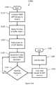
- FIG. 6shows a method 600 of operation of readout system 500 of FIG. 5 , according to at least one implementation.
- Method 600starts at 605 , for example in response to a powering up of readout system 500 or invocation of a routine.
- readout system 500provides a flux signal for readout. In one implementation, readout system 500 increments the shift register (not shown in FIG. 5 ) at 610 .
- readout system 500outputs a frequency comb of DACs 524 a and 524 b.
- readout system 500opens microwave switch 555 .
- readout system 500collects data via ADCs 526 a and 526 b.
- readout system 500closes microwave switch 555 .
- FPGA 522performs a DFT on the data output by ADCs 526 a and 526 b, and returns the values of the FMR spectrum.
- Method 600loops through 610 to 660 until the readout is complete, and then ends at 665 until invoked again.
- FIG. 7shows a hybrid computing system 700 according to at least one exemplary implementation, including a digital computer 705 and a quantum computer 750 , that may incorporate FMR technology as described above.
- Digital computer 705comprises CPU 710 , user interface elements 711 , 712 , 713 and 714 , disk 715 , controller 716 , bus 717 and memory 720 .
- Memory 720comprises modules 721 , 723 , 727 , 731 , 737 and 735 .
- Quantum computer 750comprises quantum processor 740 , readout control system 760 , qubit control system 765 and coupler control system 770 .
- Quantum computer 750can incorporate FMR technology comprising superconducting resonators (such as superconducting resonator 210 a of FIG. 2A ).
- Computing system 700can comprise a readout system such as readout system 500 of FIG. 5 .
- FIG. 8shows a first arrangement of superconducting resonators in an example implementation of a superconducting quantum processor 800 .
- Processor 800comprises 64 unit cells (not shown in FIG. 8 ) with four sets of superconducting resonators 810 a through 810 d, 820 a through 820 d, 830 a through 830 d, and 840 a through 840 d, coupled to outer shift registers 850 a through 850 d respectively.
- Processor 800comprises eight vertically oriented inner shift registers 860 and eight horizontally oriented inner shift registers 870 .
- All four set of superconducting resonators 810 a through 810 d, 820 a through 820 d, 830 a through 830 d, and 840 a through 840 dare coupled to a single common transmission line such as line 120 of FIG. 2A (not shown in FIG. 8 ).
- FIG. 9shows a second arrangement of superconducting resonators in an example implementation of a superconducting quantum processor 900 .
- Processor 900comprises 64 qubits (not shown in FIG. 9 ) with four sets of superconducting resonators 910 a through 910 h, 920 a through 920 h, 930 a through 930 h and 940 a through 940 h.
- Processor 900comprises eight vertically oriented inner shift registers 960 and eight horizontally oriented inner shift registers 970 .
- Two sets of superconducting resonators 910 a through 910 h and 940 a through 940 hare coupled to a first transmission line such as line 120 of FIG. 2A (not shown in FIG. 9 ).
- the other two sets of superconducting resonators 920 a through 920 h and 930 a through 930 hare coupled to a second transmission line (also not shown in FIG. 9 ).
- outer shift registers(such as outer shift registers 850 a through 850 d of FIG. 8 ) are not needed. With eight resonators on a side, one for each of the inner shift registers (horizontal or vertical), there is sufficient fault tolerance provided by the cross-over stages of the horizontally and vertically oriented inner shift registers.
- the capacitance in the superconducting resonator(for example, capacitance 112 in resonator 210 a of FIG. 2A ) to have a high quality factor (Q).
- a lumped element resonatorcan be implemented using an interdigitated capacitor or a transmission line resonator, fabricated directly on a crystalline dielectric.
- the resonatorcan be designed to reduce capacitor dielectric loss, for example by spreading the fingers of the interdigitated capacitor widely, and by causing the electric field to propagate through the crystalline dielectric rather than be exposed to surface oxides that can dominate the loss.
- a disadvantage of existing techniques to fabricate high Q superconducting capacitorsis that those techniques cannot readily be integrated in a heterogeneous, multi-layer fabrication stack while maintaining low loss.
- One approachis to use a distributed microstrip resonator fabricated with amorphous silicon as a deposited dielectric.
- a disadvantage of this approachis that the capacitance is spread out along the length of the resonator and incorporates a larger volume of dielectric than an equivalent parallel plate capacitor, resulting in higher losses than for a lumped element parallel plate capacitor.
- Another disadvantageis that the microstrip resonator has a large distributed inductance that needs to be accounted for during design.
- the technology described in this disclosurecomprises a superconducting parallel plate capacitor with a thin, high-permittivity dielectric.
- a parallel-plate design with a thin dielectriccan reduce the volume of dielectric for a given capacitance value. It can also provide a reduced capacitor footprint which is an advantage because chip space is at a premium.
- a benefit of a parallel-plate capacitor with a thin dielectric layeris that it can decrease the microwave power required to saturate the loss centers in the dielectric, and consequently can allow high resonator quality factors to be achieved at the operating power typically used with FMR technology.
- the inventorshave observed that decreasing the volume of lossy dielectric can lead to a decrease in the required power to saturate a superconducting resonator such as superconducting resonator 110 of FIG. 1A .
- the capacitancecan be sensitive to variations in the thickness of the dielectric. Variations in thickness can be introduced during fabrication, for example during planarization of the dielectric. A method for producing a superconducting parallel plate thin-layer capacitor that can be integrated in a heterogeneous multi-layer planarized fabrication stack with deposited dielectrics is described in the next section.
- FIGS. 10A to 10Fare each respective cross-sectional views of a superconducting integrated circuit 1000 at sequential phases of a fabrication process, according to one illustrated embodiment.
- the sequence of FIGS. 10A to 10Fdefines a method for fabricating a thin-layer capacitor suitable for use in a superconducting resonator such as superconducting resonator 210 a of FIG. 2A .
- Trilayer 1005comprises a first layer 1010 of a superconducting metal, a layer 1020 of a dielectric and a second layer 1030 of a superconducting metal.
- the first and second layers 1010 and 1030 , respectively, of superconducting metalcomprise niobium.
- the first and second layers 1010 and 1030respectively, comprise Al, TiN, or WSi.
- Layer 1020can comprise Si, SiN, amorphous SiH or other suitable inter-layer low-loss dielectric.
- semiconductor fabrication equipmentpatterns trilayer 1005 using an etch process.
- Layer 1030 of superconducting metalcan be removed during patterning except where the upper plate of the thin-layer capacitor is needed.
- layer 1040comprises SiO2.
- semiconductor fabrication equipmentplanarizes layer 1040 (e.g., CMP).
- Via 1015is a via to the first layer 1010 of superconducting metal, and is a via to the lower plate of the thin-layer capacitor.
- Via 1035is a via to the second layer 1030 of superconducting metal, and is a via to the upper plate of the thin-layer capacitor.
- semiconductor fabrication equipmentdeposits a third layer 1050 of superconducting metal.
- the third layer 1050 of superconducting metalmay, for example, comprise niobium.
- Semiconductor fabrication equipmentpatterns third layer 1050 to form a first region 1050 a and a second region 1050 b.
- First region 1050 acan be a contact to the upper plate of the thin-layer capacitor
- second region 1050 bcan be a contact to the lower plate of the thin-layer capacitor.
- First region 1050 a and second region 1050 bcan be electrically isolated from each other.
- First region 1050 a and second region 1050 bare a first portion of third layer 1050 and a second portion of third layer 1050 , respectively.
- the thickness of each of the first and second layers of superconducting metal 1010 and 1030is about 300 nm, and the thickness of dielectric layer 1020 is about 50 nm.
- dielectric layer 1020can be sufficiently thin that parasitic capacitance in regions of the circuit other than at the capacitors is relatively small.
- FIG. 11Ais a flow chart illustrating a method 1100 a for using frequency multiplexed resonator technology to transmit data to a superconducting device, according to at least one exemplary implementation.
- the superconducting devicecan, for example, be an element of a superconducting classical processor.
- the superconducting devicecan, for example, be an element of a superconducting quantum processor.
- method 1100is executed by a computing system, such as a hybrid computing system comprising a digital computer and an analog computer.
- Method 1100includes acts 1105 - 1165 , though those skilled in the art will appreciate that in alternative implementations certain acts may be omitted and/or additional acts may be added. Those skilled in the art will appreciate that the order of the acts is shown for exemplary purposes only and may change in alternative implementations.
- the computing systeminitializes the QFP devices to a “0” state.
- the computing systemapplies a flux bias using a flux bias line such as flux bias line 155 of FIGS. 12 through 14 to create a preference for a “1” state.
- the computing systemreduces the barrier of the QFP devices.
- the computing systemdecides whether to send a tone to a frequency multiplexed resonator, and, if so, sends the tone to the resonator. The presence of a tone allows the QFP to relax into the “1” state. The absence of a tone causes the QFP to stay in the “0” state.
- the computing systemdetermines if there is another resonator. If the computing system determines there is another resonator at 1145 , then method 1100 returns to 1140 . Method 1100 successively loops around 1140 and 1145 until there are no more resonators to consider, and method 1100 proceeds to 1150 .
- the computing systemfully raises the barrier of each of the QFP devices.
- the quantum processoruses the data, for example through classical QFP logic. Using the data can include transferring the data to a superconducting processor via a shift register, for example. Method 1100 ends at 1165 , for example until called or invoked again.
- FIG. 11Bis a flow chart illustrating a method 1100 b for using frequency multiplexed resonator technology to transmit data to a superconducting device according to another exemplary implementation. Acts 1140 and 1145 of FIG. 11A can be combined into a single act 1148 as shown in FIG. 11B . With reference to FIG. 11B , at 1148 , the computing system decides whether to send a tone to each of the superconducting resonators, and then transmits a microwave signal via the transmission line to all the superconducting resonators. The frequency multiplexed microwave signal stimulates the superconducting resonators in parallel.
- the present technologycan load data into a shift register on a quantum processor chip using a frequency multiplexed resonator.
- the frequency multiplexed resonator readout described above(with reference to FIGS. 1A, 1B, 1C, 2A, 2B, 2C, 3, 4, 5, and 6 ) can be run in reverse to allow data to be passed to the processor.
- the first stage QFPcan be used to rectify a microwave signal in the resonator if a signal is present.
- the present technologycan be used to input data to the processor as well as to readout qubit states from the processor.
- the same linescan be used for both input and readout.
- the devicecan reduce, or minimize, the impact of microwave currents in the resonator on the attached QFP.
- a large SENSE SQUIDflux biascan be used to break the symmetry of the device, to allow a microwave flux signal to bias the body of the QFP.
- a portion of the resonator inductancecan be used to bias the QFP directly with the resonator current. A benefit of the latter approach is that it can separate the DC flux coupling between the QFP and the SENSE SQUID from the microwave flux coupling between the resonator and the body of the QFP.
- the QFPcan be read out immediately.
- the datacan be loaded with up to 100% fidelity. Errors can be corrected by repeating the loading sequence.
- FIG. 12is a schematic diagram illustrating a superconducting transceiver circuit 1200 according to at least one exemplary implementation.
- Superconducting transceiver circuit 1200comprises a superconducting resonator able to tune a resonator frequency.
- Superconducting transceiver circuit 1200is operable as a frequency multiplexed resonator transceiver.
- Superconducting transceiver circuit 1200comprises the elements described above in reference to FIG. 1A , and further comprises a flux bias line 155 operable to apply a flux bias to the last or final shift register stage 140 .
- Shift register stage 140can, for example, comprise a QFP, and can be communicatively coupled to superconducting resonator 110 for the purposes of reading out the state of a superconducting device and/or loading data into a superconducting device.
- datacan be loaded into a shift register via the last or final shift register stage 140 , and the shift register can be communicatively coupled to a Digital to Analog Converter (DAC) (not shown in FIG. 12 ).
- DACDigital to Analog Converter
- the DACcan be used to apply a bias to a superconducting qubit.
- FIG. 13Ais a schematic diagram illustrating a superconducting transceiver circuit 1300 a comprising a superconducting resonator with two SQUID loops according to at least one exemplary implementation.
- Superconducting transceiver circuit 1300 ais operable as a frequency multiplexed resonant transceiver.
- SQUID loops 216 a and 216 badvantageously enable independent tuning of the resonance frequency and the sensitivity of superconducting resonator 210 a by adjusting the flux bias in SQUID loops 216 a and 216 b.
- capacitor 112 of superconducting circuit 1300 acan be a parallel plate capacitor
- inductance 114 of superconducting circuit 1300 acan be a niobium spiral inductor.
- interfaces 230 a and 230 bcan provide flux bias to SQUID loops 216 a and 216 b respectively.
- the flux biases provided by interfaces 230 a and 230 bcan be static. This advantageously allows the circuit to use an array of flux DACs requiring only a few wires to program.
- the two tunable SQUID loops 216 a and 216 bdo not need an independent analog control line for each superconducting resonator 210 a.
- Superconducting transceiver circuit 1300 acomprises the elements of FIG. 2A .
- Superconducting transceiver circuit 1300 afurther comprises an interface 155 operable to apply a flux bias to QFP 140 , as described with reference to FIG. 11 .
- FIG. 13Bis a schematic diagram illustrating a superconducting transceiver circuit 1300 b comprising a superconducting resonator with two SQUID loops according to at least another exemplary implementation.
- Superconducting transceiver circuit 1300 bis operable as a frequency multiplexed resonator transceiver.
- Superconducting transceiver circuit 1300 bcomprises the elements of FIG. 2B .
- Superconducting transceiver circuit 1300 bfurther comprises an interface 155 operable to apply a flux bias to a last stage QFP 140 a, as described with reference to FIG. 11 .
- the coupling between SQUID loop 216 b (known as the SENSE SQUID) and last stage QFP 140 ais galvanic coupling.
- the SENSE SQUIDWhen there is no flux in the SENSE SQUID, microwave current will be evenly split on both sides of the SQUID. Since the galvanic coupling to the QFP is symmetric, the result is zero flux coupling into last stage QFP 140 a. The symmetry can be broken by introducing a large flux bias into the SENSE SQUID. The circulating current will combine with the microwave current in a manner that depends on the non-linearity of the SQUID junctions. The result can be a net flux signal into last stage QFP 140 a.
- the resonatoris coupled directly to the QFP.
- the couplingis sufficient to load the QFP deterministically when in a metastable state while not destroying data when in a fully latched state.
- the superconducting deviceis stimulated after partial annealing (reduction of the barrier) at the resonant frequency.
- the resonatoris stimulated after partial annealing using a fast sweep by a Vector Network Analyzer (VNA).
- VNAVector Network Analyzer
- the sweep of the VNAcan be centered, or least approximately centered, on the resonance frequency of the resonator.
- the bandwidth of the sweepcan be set to a value that is less than the resonator linewidth, and the sweep can use a handful of points within the resonance.
- the bandwidth of the sweepcan be selected to avoid, or at least reduce, overlap with the linewidth of an adjacent resonance.
- the sweepcan be achieved with a trigger signal output from a DAC card, and sent to the VNA.
- the waveformcan include a sufficiently long delay to allow the sweep to finish before full annealing and readout.
- the delaycan be a few milliseconds.
- FIG. 13Cis a schematic diagram illustrating a superconducting transceiver circuit 1300 c comprising a superconducting resonator with two SQUID loops according to at least another exemplary implementation.
- Superconducting transceiver circuit 1300 cis operable as a frequency multiplexed resonator transceiver, and is able to tune the resonator frequency and sensitivity independently of each other.
- Superconducting transceiver circuit 1300 ccomprises the elements of FIG. 2C .
- Superconducting transceiver circuit 1300 cfurther comprises an interface 155 operable to apply a flux bias to a last stage QFP 140 a, as described with reference to FIG. 11 .
- Superconducting transceiver circuit 1300 cis connected at node 215 c to the ground 121 of transmission line 120 via a coupling capacitor 124 . In other respects, superconducting transceiver circuit 1300 c is the same as or similar to superconducting transceiver circuit 1300 b.
- Components of superconducting transceiver circuits 1300 a, 1300 b, and 1300 c of FIGS. 13A, 13B, and 13C , respectively, labeled with the same numbers as in superconducting circuit 100 of FIG. 1Acan be similar or even identical to those as described in reference to FIG. 1A .
- capacitance 112 of superconducting circuits 1300 a, 1300 b, and 1300 ccan be a parallel plate capacitor
- inductance 114 of superconducting transceiver circuits 1300 a, 1300 b, and 1300 ccan be a niobium spiral inductor.
- superconducting resonator 210 ais connected at node 215 a to ground, for example to the ground 121 of transmission line 120 .
- superconducting resonator 210 ais connected at node 215 a to ground via capacitor 124 .
- FIG. 14is a schematic diagram illustrating an example embodiment of a superconducting transceiver circuit 1400 comprising superconducting resonator 110 of FIG. 12 .
- Superconducting transceiver circuit 1400is operable as a frequency multiplexed resonator transceiver, and is advantageously operable to independently tune the resonator frequency and sensitivity.
- Superconducting transceiver circuitfurther comprises interface 130 and last or final shift register stage 140 , both as described with reference to FIG. 1A .
- Superconducting transceiver circuit 1400comprises the elements of superconducting circuit 400 of FIG. 4 .
- Superconducting transceiver circuit 1400further comprises a tunable coupler 440 in between superconducting resonator 110 and last or final shift register stage (or QFP) 140 .
- Superconducting transceiver circuit 1400enables independent tuning of the resonance frequency and the sensitivity to QFP flux, provided the variable loading of superconducting resonator 110 by tunable coupler 440 is taken into account.
- Tunable coupler 440comprises, for example, inductances 442 and 444 , and DC SQUID 446 .
- Superconducting transceiver circuit 400further comprises interface 450 operable to apply a flux bias to tunable coupler 440 , and thereby to adjust the strength of coupling between SQUID loop 216 b and last stage QFP 140 .
- the frequency multiplexed resonator input system described abovewhich can be used to input data to superconducting devices, is used in combination with the frequency multiplexed resonator readout system also described in the present disclosure (with reference to FIGS. 1A, 1B, 1C, 2A, 2B, 2C, 3, 4, 5, and 6 ).
- the frequency multiplexed resonator input system described aboveis used in combination with other readout systems or circuits.
- the frequency multiplexed resonator input systemis used in combination with the superconducting flux qubit readout system described in U.S. Pat. No. 8,854,074.
- FIG. 5An example embodiment of a frequency multiplexed resonator input/output system is illustrated in FIG. 5 (described above with reference to the readout system).
- the return pathway in FIG. 5comprises DC block 585 , circulators 584 and 583 , amplifiers 575 , 566 , 564 , and 562 , attenuator 570 , mixer 560 , filters 527 a and 527 b, and ADC 526 a and 526 b. If the system is to be used for inputting data to the superconducting devices only (and no readout), then the return pathway is not required.
Landscapes
- Engineering & Computer Science (AREA)
- General Physics & Mathematics (AREA)
- Theoretical Computer Science (AREA)
- Physics & Mathematics (AREA)
- Mathematical Analysis (AREA)
- Data Mining & Analysis (AREA)
- Evolutionary Computation (AREA)
- Condensed Matter Physics & Semiconductors (AREA)
- Computational Mathematics (AREA)
- Mathematical Optimization (AREA)
- Pure & Applied Mathematics (AREA)
- Computing Systems (AREA)
- General Engineering & Computer Science (AREA)
- Mathematical Physics (AREA)
- Software Systems (AREA)
- Artificial Intelligence (AREA)
- Superconductor Devices And Manufacturing Methods Thereof (AREA)
Abstract
Description
where C is the value of
where ∈ is the permittivity of the dielectric separating the plates, A is the area of one of the plates and d is the thickness of the dielectric.
x(n)=I(n)+jQ(n)
where I(n) is the output of
for k ∈ 0,1,2,3 . . . N-1. The second term in the argument of the sine function depends on τ and can be used to compensate for the phase imbalance between the two mixer channels that results from the analog nature of the mixer.
Claims (19)
Priority Applications (1)
| Application Number | Priority Date | Filing Date | Title |
|---|---|---|---|
| US15/572,731US10938346B2 (en) | 2015-05-14 | 2016-05-11 | Frequency multiplexed resonator input and/or output for a superconducting device |
Applications Claiming Priority (4)
| Application Number | Priority Date | Filing Date | Title |
|---|---|---|---|
| US201562161780P | 2015-05-14 | 2015-05-14 | |
| US201662288251P | 2016-01-28 | 2016-01-28 | |
| PCT/US2016/031885WO2016183213A1 (en) | 2015-05-14 | 2016-05-11 | Frequency multiplexed resonator input and/or output for a superconducting device |
| US15/572,731US10938346B2 (en) | 2015-05-14 | 2016-05-11 | Frequency multiplexed resonator input and/or output for a superconducting device |
Related Parent Applications (1)
| Application Number | Title | Priority Date | Filing Date |
|---|---|---|---|
| PCT/US2016/031885A-371-Of-InternationalWO2016183213A1 (en) | 2015-05-14 | 2016-05-11 | Frequency multiplexed resonator input and/or output for a superconducting device |
Related Child Applications (1)
| Application Number | Title | Priority Date | Filing Date |
|---|---|---|---|
| US17/158,484DivisionUS12034404B2 (en) | 2015-05-14 | 2021-01-26 | Method of fabricating a superconducting parallel plate capacitor |
Publications (2)
| Publication Number | Publication Date |
|---|---|
| US20180145631A1 US20180145631A1 (en) | 2018-05-24 |
| US10938346B2true US10938346B2 (en) | 2021-03-02 |
Family
ID=57248516
Family Applications (3)
| Application Number | Title | Priority Date | Filing Date |
|---|---|---|---|
| US15/572,731Active2037-09-03US10938346B2 (en) | 2015-05-14 | 2016-05-11 | Frequency multiplexed resonator input and/or output for a superconducting device |
| US17/158,484Active2038-08-18US12034404B2 (en) | 2015-05-14 | 2021-01-26 | Method of fabricating a superconducting parallel plate capacitor |
| US18/733,612PendingUS20250023518A1 (en) | 2015-05-14 | 2024-06-04 | Frequency Multiplexed Resonator Input and/or Output for a Superconducting Device |
Family Applications After (2)
| Application Number | Title | Priority Date | Filing Date |
|---|---|---|---|
| US17/158,484Active2038-08-18US12034404B2 (en) | 2015-05-14 | 2021-01-26 | Method of fabricating a superconducting parallel plate capacitor |
| US18/733,612PendingUS20250023518A1 (en) | 2015-05-14 | 2024-06-04 | Frequency Multiplexed Resonator Input and/or Output for a Superconducting Device |
Country Status (4)
| Country | Link |
|---|---|
| US (3) | US10938346B2 (en) |
| EP (1) | EP3266063B1 (en) |
| CN (1) | CN107580752B (en) |
| WO (1) | WO2016183213A1 (en) |
Cited By (17)
| Publication number | Priority date | Publication date | Assignee | Title |
|---|---|---|---|---|
| US11526463B2 (en) | 2004-12-23 | 2022-12-13 | D-Wave Systems Inc. | Analog processor comprising quantum devices |
| US11809839B2 (en) | 2022-01-18 | 2023-11-07 | Robert Lyden | Computer language and code for application development and electronic and optical communication |
| US11856871B2 (en) | 2018-11-13 | 2023-12-26 | D-Wave Systems Inc. | Quantum processors |
| US11874344B2 (en) | 2018-06-05 | 2024-01-16 | D-Wave Systems Inc. | Dynamical isolation of a cryogenic processor |
| US11930721B2 (en) | 2012-03-08 | 2024-03-12 | 1372934 B.C. Ltd. | Systems and methods for fabrication of superconducting integrated circuits |
| US11957065B2 (en) | 2017-02-01 | 2024-04-09 | 1372934 B.C. Ltd. | Systems and methods for fabrication of superconducting integrated circuits |
| US12020116B2 (en) | 2018-05-11 | 2024-06-25 | 1372934 B.C. Ltd. | Single flux quantum source for projective measurements |
| US12034404B2 (en) | 2015-05-14 | 2024-07-09 | 1372934 B.C. Ltd. | Method of fabricating a superconducting parallel plate capacitor |
| US12087503B2 (en) | 2021-06-11 | 2024-09-10 | SeeQC, Inc. | System and method of flux bias for superconducting quantum circuits |
| US12102017B2 (en) | 2019-02-15 | 2024-09-24 | D-Wave Systems Inc. | Kinetic inductance for couplers and compact qubits |
| US12204002B2 (en) | 2018-05-16 | 2025-01-21 | D-Wave Systems Inc. | Systems and methods for addressing devices in a superconducting circuit |
| US12206385B2 (en) | 2018-02-27 | 2025-01-21 | D-Wave Systems Inc. | Systems and methods for coupling a superconducting transmission line to an array of resonators |
| US12301225B2 (en) | 2021-07-23 | 2025-05-13 | 1372934 B.C. Ltd. | Systems and methods for tuning capacitance in quantum devices |
| US12367412B2 (en) | 2019-12-05 | 2025-07-22 | 1372934 B.C. Ltd. | Systems and methods for fabricating flux trap mitigating superconducting integrated circuits |
| US12376501B2 (en) | 2020-05-11 | 2025-07-29 | 1372934 B.C. Ltd. | Kinetic inductance devices, methods for fabricating kinetic inductance devices, and articles employing the same |
| US12373167B2 (en) | 2020-01-27 | 2025-07-29 | 1372934 B.C. Ltd. | Systems and methods for variable bandwidth annealing |
| US12392823B2 (en) | 2021-11-05 | 2025-08-19 | D-Wave Systems Inc. | Systems and methods for on-chip noise measurements |
Families Citing this family (68)
| Publication number | Priority date | Publication date | Assignee | Title |
|---|---|---|---|---|
| JP2010524064A (en) | 2007-04-05 | 2010-07-15 | ディー−ウェイブ システムズ,インコーポレイテッド | Physical realization of general adiabatic quantum computer |
| US10755190B2 (en) | 2015-12-21 | 2020-08-25 | D-Wave Systems Inc. | Method of fabricating an electrical filter for use with superconducting-based computing systems |
| GB2566189B (en) | 2016-05-03 | 2020-09-02 | D Wave Systems Inc | Systems and methods for superconducting devices used in superconducting circuits and scalable computing |
| CN109716360B (en) | 2016-06-08 | 2023-08-15 | D-波系统公司 | Systems and methods for quantum computing |
| US11263547B2 (en) | 2017-01-30 | 2022-03-01 | D-Wave Systems Inc. | Quantum annealing debugging systems and methods |
| WO2018169585A1 (en)* | 2017-03-13 | 2018-09-20 | Google Llc | Integrating circuit elements in a stacked quantum computing device |
| US10062829B1 (en)* | 2017-05-05 | 2018-08-28 | International Business Machines Corporation | Isolator based on nondegenerate three-wave mixing Josephson devices |
| US10608157B2 (en)* | 2017-05-18 | 2020-03-31 | International Business Machines Corporation | Qubit network non-volatile identification |
| JP6896272B2 (en)* | 2017-05-22 | 2021-06-30 | 国立研究開発法人産業技術総合研究所 | Frequency division multiplexing and its design method |
| US10235635B1 (en) | 2017-10-19 | 2019-03-19 | International Business Machines Corporation | Capacitively-shunted asymmetric DC-SQUID for qubit readout and reset |
| US10158343B1 (en)* | 2018-01-11 | 2018-12-18 | Northrop Grumman Systems Corporation | Push-pull tunable coupling |
| WO2019144118A1 (en) | 2018-01-22 | 2019-07-25 | D-Wave Systems Inc. | Systems and methods for improving performance of an analog processor |
| US11100418B2 (en) | 2018-02-28 | 2021-08-24 | D-Wave Systems Inc. | Error reduction and, or, correction in analog computing including quantum processor-based computing |
| US10097186B1 (en)* | 2018-03-02 | 2018-10-09 | Northrop Grumman Systems Corporation | Robust tunable coupling between superconductive circuits |
| US10354198B1 (en)* | 2018-03-21 | 2019-07-16 | International Business Machines Corporation | Fast quantum gates with first-order transitions via frequency-modulated tunable coupling element |
| US10672971B2 (en)* | 2018-03-23 | 2020-06-02 | International Business Machines Corporation | Vertical transmon qubit device with microstrip waveguides |
| US10256392B1 (en)* | 2018-03-23 | 2019-04-09 | International Business Machines Corporation | Vertical transmon qubit device |
| WO2019222514A1 (en)* | 2018-05-16 | 2019-11-21 | D-Wave Systems Inc. | Systems and methods for addressing devices in a superconducting circuit |
| US10447278B1 (en) | 2018-07-17 | 2019-10-15 | Northrop Grumman Systems Corporation | JTL-based superconducting logic arrays and FPGAs |
| US11847534B2 (en)* | 2018-08-31 | 2023-12-19 | D-Wave Systems Inc. | Systems and methods for operation of a frequency multiplexed resonator input and/or output for a superconducting device |
| US10818346B2 (en) | 2018-09-17 | 2020-10-27 | Northrop Grumman Systems Corporation | Quantizing loop memory cell system |
| US11121302B2 (en) | 2018-10-11 | 2021-09-14 | SeeQC, Inc. | System and method for superconducting multi-chip module |
| AU2019377959B2 (en)* | 2018-11-12 | 2025-05-08 | Diraq Pty Ltd | A signal combiner |
| US20200167684A1 (en)* | 2018-11-26 | 2020-05-28 | International Business Machines Corporation | Qubit tuning by magnetic fields in superconductors |
| US11900264B2 (en) | 2019-02-08 | 2024-02-13 | D-Wave Systems Inc. | Systems and methods for hybrid quantum-classical computing |
| FI128904B (en)* | 2019-03-14 | 2021-02-26 | Aalto Univ Foundation Sr | Vector signal generator operating on microwave frequencies, and method for generating time-controlled vector signals on microwave frequencies |
| US11621386B2 (en)* | 2019-04-02 | 2023-04-04 | International Business Machines Corporation | Gate voltage-tunable electron system integrated with superconducting resonator for quantum computing device |
| US11288073B2 (en) | 2019-05-03 | 2022-03-29 | D-Wave Systems Inc. | Systems and methods for calibrating devices using directed acyclic graphs |
| US11422958B2 (en) | 2019-05-22 | 2022-08-23 | D-Wave Systems Inc. | Systems and methods for efficient input and output to quantum processors |
| US12039465B2 (en) | 2019-05-31 | 2024-07-16 | D-Wave Systems Inc. | Systems and methods for modeling noise sequences and calibrating quantum processors |
| JP7579273B2 (en)* | 2019-06-11 | 2024-11-07 | ディー-ウェイブ システムズ インコーポレイテッド | Input/output system and method for superconducting devices - Patents.com |
| CA3090429A1 (en)* | 2019-06-28 | 2020-12-28 | Google Llc | Tunable qubit coupler |
| JP7600149B2 (en) | 2019-07-12 | 2024-12-16 | ディー-ウェイブ システムズ インコーポレイテッド | System and method for simulating a quantum processor |
| US12267042B2 (en)* | 2019-07-19 | 2025-04-01 | Nec Corporation | Oscillation apparatus, quantum computer, and control method |
| CN110324018B (en)* | 2019-07-25 | 2024-06-14 | 本源量子计算科技(合肥)股份有限公司 | Microwave signal annular transmission structure |
| US11839164B2 (en) | 2019-08-19 | 2023-12-05 | D-Wave Systems Inc. | Systems and methods for addressing devices in a superconducting circuit |
| SE1951451A1 (en)* | 2019-12-13 | 2021-03-02 | Andrey Danilov | Tunable microwave resonator |
| US11024791B1 (en) | 2020-01-27 | 2021-06-01 | Northrop Grumman Systems Corporation | Magnetically stabilized magnetic Josephson junction memory cell |
| US12022749B2 (en)* | 2020-03-04 | 2024-06-25 | International Business Machines Corporation | Flux bias line local heating device |
| US11937516B2 (en)* | 2020-03-04 | 2024-03-19 | International Business Machines Corporation | Fabrication of a flux bias line local heating device |
| US10985701B1 (en)* | 2020-03-16 | 2021-04-20 | International Business Machines Corporation | Magnetic flux bias for pulse shaping of microwave signals |
| CN111600608B (en)* | 2020-04-17 | 2021-10-26 | 中国计量科学研究院 | Superconducting quantum digital-to-analog conversion circuit |
| US11409343B2 (en) | 2020-05-02 | 2022-08-09 | International Business Machines Corporation | Quantum computing array |
| US11182690B1 (en) | 2020-05-02 | 2021-11-23 | International Business Machines Corporation | High fidelity waveform generator for qubit controller |
| US11574228B2 (en) | 2020-05-02 | 2023-02-07 | International Business Machines Corporation | Low power quantum controller |
| EP3907669A1 (en)* | 2020-05-07 | 2021-11-10 | IQM Finland Oy | Selective frequency shifting of qubits |
| CN111641397B (en)* | 2020-06-10 | 2024-04-26 | 北京量子信息科学研究院 | Josephson traveling wave amplifier and preparation method thereof |
| CN112563700B (en)* | 2020-08-13 | 2022-01-04 | 中国科学院国家天文台 | Superconducting bandpass filter array system and implementation method for submillimeter wave multi-band imaging |
| US11750175B2 (en)* | 2020-09-18 | 2023-09-05 | International Business Machines Corporation | Multiplexing resonator induced phase gate drive signals |
| WO2022066176A1 (en)* | 2020-09-25 | 2022-03-31 | Intel Corporation | Quantum computing systems, apparatus, and methods |
| US20240305256A1 (en)* | 2020-11-11 | 2024-09-12 | Yissum Research Development Company Of The Hebrew University Of Jerusalem Ltd. | Traveling Wave Kinetic Inductance Parametric Amplifier |
| CA3197616A1 (en)* | 2020-11-24 | 2022-06-02 | George E.G. Sterling | Systems, articles, and methods for a tunable capacitor |
| EP4278308A4 (en)* | 2021-01-13 | 2024-12-18 | 1372934 B.C. Ltd. | SYSTEMS AND METHODS FOR CONTROLLING QUANTUM COMPONENTS |
| US20240135225A1 (en)* | 2021-03-04 | 2024-04-25 | Iqm Finland Oy | Tunable dissipative circuits for low temperature frequency shifters, and methods for making a frequency shift at low temperature |
| US11621387B2 (en)* | 2021-03-11 | 2023-04-04 | International Business Machines Corporation | Quantum device with low surface losses |
| US12081278B2 (en) | 2021-05-10 | 2024-09-03 | Microsoft Technology Licensing, Llc | Transmitting frequency multiplexed signals from a superconducting domain |
| JP7524142B2 (en)* | 2021-07-30 | 2024-07-29 | 株式会社東芝 | Coupler and computing device |
| US11539347B1 (en) | 2021-09-03 | 2022-12-27 | International Business Machines Corporation | Current-mode frequency translation circuit with programmable gain |
| AU2022450360A1 (en)* | 2021-09-16 | 2024-05-02 | Rigetti & Co, Llc | Connecting quantum processor chips in a modular quantum processing unit |
| US12388452B2 (en) | 2021-11-03 | 2025-08-12 | 1372934 B.C. Ltd. | Systems and methods for duty cycle compensation of a digital to analog converter (DAC) |
| US11751489B2 (en) | 2021-12-03 | 2023-09-05 | International Business Machines Corporation | Quantum entangling gate between multi-mode qubits |
| CN114252905B (en)* | 2021-12-10 | 2025-02-07 | 中国空间技术研究院 | A calibration method for superconducting dynamic inductance X-ray detector |
| US12118433B2 (en) | 2021-12-15 | 2024-10-15 | International Business Machines Corporation | Space-saving coupler arm arrangement for superconducting qubits |
| US12353955B2 (en)* | 2022-02-11 | 2025-07-08 | ColdQuanta, Inc. | Time-multiplexed superpixel-based quantum-array readout system |
| CN115207201A (en)* | 2022-07-12 | 2022-10-18 | 中国人民解放军战略支援部队信息工程大学 | Three-dimensional extension method and packaging structure of modular superconducting quantum computing chip |
| WO2025032642A1 (en)* | 2023-08-04 | 2025-02-13 | 富士通株式会社 | Control device and control method |
| DE102024107622A1 (en) | 2024-03-18 | 2025-09-18 | Physikalisch-Technische Bundesanstalt Braunschweig Und Berlin | Device for measuring at least one electrical property of an electrical arrangement and a method for calibrating such a device |
| CN117891108B (en)* | 2024-03-18 | 2024-05-28 | 南京大学 | On-chip superconducting microwave frequency comb and preparation method thereof |
Citations (31)
| Publication number | Priority date | Publication date | Assignee | Title |
|---|---|---|---|---|
| US4785426A (en)* | 1984-09-21 | 1988-11-15 | Hitachi, Ltd. | Superconducting switching circuit, memory cell and memory circuit, with resonance damping resistors |
| US5528202A (en) | 1992-08-27 | 1996-06-18 | Motorola, Inc. | Distributed capacitance transmission line |
| US6356078B1 (en) | 2000-06-16 | 2002-03-12 | Honeywell International Inc. | Frequency multiplexed flux locked loop architecture providing an array of DC SQUIDS having both shared and unshared components |
| US20020190381A1 (en) | 2001-06-15 | 2002-12-19 | Herr Quentin P. | Capacitor for signal propagation across ground plane boundaries in superconductor integrated circuits |
| US20040155728A1 (en) | 2003-02-07 | 2004-08-12 | Cheung Tak Shun | Transmission lines and components with wavelength reduction and shielding |
| US20040170047A1 (en) | 2001-06-01 | 2004-09-02 | D-Wave Systems, Inc. | Methods for controlling qubits |
| WO2005109565A1 (en) | 2004-05-12 | 2005-11-17 | Filtronic Comtek Oy | Band stop filter |
| US20090082209A1 (en) | 2007-05-14 | 2009-03-26 | Bunyk Paul I | Systems, methods and apparatus for digital-to-analog conversion of superconducting magnetic flux signals |
| US20090206871A1 (en) | 2007-08-03 | 2009-08-20 | Northrop Grumman Systems Corporation | Arbitrary quantum operations with a common coupled resonator |
| US7624088B2 (en) | 2005-08-03 | 2009-11-24 | D-Wave Systems Inc. | Analog processor comprising quantum devices |
| US20090319757A1 (en) | 2007-04-25 | 2009-12-24 | Andrew Joseph Berkley | Architecture for local programming of quantum processor elements using latching qubits |
| US7876248B2 (en) | 2006-12-05 | 2011-01-25 | D-Wave Systems Inc. | Systems, methods and apparatus for local programming of quantum processor elements |
| US20110060780A1 (en) | 2008-05-20 | 2011-03-10 | D-Wave Systems Inc. | Systems, methods, and apparatus for calibrating, controlling, and operating a quantum processor |
| US7932514B2 (en)* | 2008-05-23 | 2011-04-26 | International Business Machines Corporation | Microwave readout for flux-biased qubits |
| US8169231B2 (en) | 2007-09-24 | 2012-05-01 | D-Wave Systems Inc. | Systems, methods, and apparatus for qubit state readout |
| US8536566B2 (en) | 2008-09-03 | 2013-09-17 | D-Wave Systems Inc. | Systems, methods and apparatus for active compensation of quantum processor elements |
| WO2014135749A1 (en) | 2013-03-05 | 2014-09-12 | Teknologian Tutkimuskeskus Vtt | Superconducting thermal detector (bolometer) of terahertz (sub-millimeter wave) radiation |
| US8854074B2 (en) | 2010-11-11 | 2014-10-07 | D-Wave Systems Inc. | Systems and methods for superconducting flux qubit readout |
| US8933695B1 (en) | 2008-08-18 | 2015-01-13 | Hypres, Inc. | High linearity superconducting radio frequency magnetic field detector |
| US20150032994A1 (en) | 2013-07-24 | 2015-01-29 | D-Wave Systems Inc. | Systems and methods for improving the performance of a quantum processor by reducing errors |
| US8951808B2 (en) | 2009-02-27 | 2015-02-10 | D-Wave Systems Inc. | Systems and methods for fabrication of superconducting integrated circuits |
| US20150111754A1 (en) | 2013-10-22 | 2015-04-23 | D-Wave Systems Inc. | Universal adiabatic quantum computing with superconducting qubits |
| US20150119252A1 (en) | 2012-03-08 | 2015-04-30 | D-Wave Systems Inc. | Systems and methods for fabrication of superconducting integrated circuits |
| US20160079968A1 (en) | 2014-09-12 | 2016-03-17 | Northrop Grumman Systems Corporation | Tunable transmon circuit assembly |
| US20160112031A1 (en) | 2014-08-07 | 2016-04-21 | International Business Machines Corporation | Tunable superconducting notch filter |
| US20160233860A1 (en) | 2015-02-06 | 2016-08-11 | Northrop Grumman Systems Corporation | Superconducting single-pole double-throw switch system |
| US9509274B2 (en)* | 2014-09-18 | 2016-11-29 | Northrop Grumman Systems Corporation | Superconducting phase-shift system |
| US10050630B2 (en)* | 2016-08-19 | 2018-08-14 | Rigetti & Co, Inc. | Flux-tunable qubit device with multiple Josephson junctions |
| US10333047B2 (en) | 2011-03-30 | 2019-06-25 | Ambatrue, Inc. | Electrical, mechanical, computing/ and/or other devices formed of extremely low resistance materials |
| US10381542B2 (en) | 2015-04-30 | 2019-08-13 | International Business Machines Corporation | Trilayer Josephson junction structure with small air bridge and no interlevel dielectric for superconducting qubits |
| US10404214B2 (en)* | 2015-02-27 | 2019-09-03 | Yale University | Techniques for producing quantum amplifiers and related systems and methods |
Family Cites Families (94)
| Publication number | Priority date | Publication date | Assignee | Title |
|---|---|---|---|---|
| SU539333A1 (en) | 1974-12-11 | 1976-12-15 | Предприятие П/Я А-1631 | Switch element |
| US4275314A (en) | 1979-04-30 | 1981-06-23 | Bell Telephone Laboratories, Incorporated | Josephson Atto-Weber switch |
| US4947118A (en) | 1988-11-21 | 1990-08-07 | Fujitsu Limited | Digital squid system adaptive for integrated circuit construction and having high accuracy |
| US5153171A (en) | 1990-09-17 | 1992-10-06 | Trw Inc. | Superconducting variable phase shifter using squid's to effect phase shift |
| US5248941A (en) | 1991-04-17 | 1993-09-28 | Hewlett-Packard Company | Superconducting magnetic field sensing apparatus having digital output, on-chip quantum flux packet feedback and high bias margins |
| WO2000030255A2 (en) | 1998-11-10 | 2000-05-25 | The Board Of Trustees Of The Leland Stanford Junior University | Crystal lattice quantum computer |
| US7015499B1 (en) | 1999-12-01 | 2006-03-21 | D-Wave Systems, Inc. | Permanent readout superconducting qubit |
| US6627915B1 (en) | 2000-08-11 | 2003-09-30 | D-Wave Systems, Inc. | Shaped Josephson junction qubits |
| GB2382892B (en) | 2000-09-26 | 2004-11-03 | Robert Raussendorf | Method for quantum computing |
| US6987282B2 (en) | 2000-12-22 | 2006-01-17 | D-Wave Systems, Inc. | Quantum bit with a multi-terminal junction and loop with a phase shift |
| EP1386283A2 (en) | 2001-03-09 | 2004-02-04 | Wisconsin Alumni Research Foundation | Solid-state quantum dot devices and quantum computing using nanostructured logic dates |
| US6627916B2 (en) | 2001-03-31 | 2003-09-30 | D-Wave Systems, Inc. | High sensitivity, directional DC-squid magnetometer |
| US6979836B2 (en) | 2001-08-29 | 2005-12-27 | D-Wave Systems, Inc. | Superconducting low inductance qubit |
| US20030107033A1 (en) | 2001-12-06 | 2003-06-12 | Alexander Tzalenchuk | Trilayer heterostructure junctions |
| US6614047B2 (en) | 2001-12-17 | 2003-09-02 | D-Wave Systems, Inc. | Finger squid qubit device |
| US20040016918A1 (en) | 2001-12-18 | 2004-01-29 | Amin Mohammad H. S. | System and method for controlling superconducting qubits |
| US20030121028A1 (en) | 2001-12-22 | 2003-06-26 | Michael Coury | Quantum computing integrated development environment |
| US7365534B2 (en) | 2002-02-26 | 2008-04-29 | Cardiomag Imaging, Inc. | Apparatus for measuring magnetic fields using a superconducting quantum interference device |
| US7332738B2 (en) | 2002-03-16 | 2008-02-19 | D-Wave Systems Inc. | Quantum phase-charge coupled device |
| US6670630B2 (en) | 2002-03-16 | 2003-12-30 | D-Wave Systems, Inc. | Quantum phase-charge coupled device |
| US7307275B2 (en) | 2002-04-04 | 2007-12-11 | D-Wave Systems Inc. | Encoding and error suppression for superconducting quantum computers |
| US6911664B2 (en) | 2002-04-15 | 2005-06-28 | D-Wave Systems, Inc. | Extra-substrate control system |
| US6900454B2 (en) | 2002-04-20 | 2005-05-31 | D-Wave Systems, Inc. | Resonant controlled qubit system |
| FR2839389B1 (en) | 2002-05-03 | 2005-08-05 | Commissariat Energie Atomique | JOSEPHSON JUNCTION SUPERCONDUCTING QUANTIC BIT DEVICE |
| US6885325B2 (en) | 2002-05-24 | 2005-04-26 | D-Wave Systems, Inc. | Sub-flux quantum generator |
| US7018852B2 (en) | 2002-08-01 | 2006-03-28 | D-Wave Systems, Inc. | Methods for single qubit gate teleportation |
| US6943368B2 (en) | 2002-11-25 | 2005-09-13 | D-Wave Systems, Inc. | Quantum logic using three energy levels |
| US6984846B2 (en) | 2003-08-27 | 2006-01-10 | International Business Machines Corporation | Gradiometer-based flux qubit for quantum computing and method therefor |
| CA2537602A1 (en) | 2003-09-05 | 2005-03-17 | D-Wave Systems, Inc. | Superconducting phase-charge qubits |
| US7321884B2 (en) | 2004-02-23 | 2008-01-22 | International Business Machines Corporation | Method and structure to isolate a qubit from the environment |
| US7135701B2 (en) | 2004-03-29 | 2006-11-14 | D-Wave Systems Inc. | Adiabatic quantum computation with superconducting qubits |
| US7109593B2 (en) | 2004-07-30 | 2006-09-19 | Microsoft Corporation | Systems and methods for performing quantum computations |
| US7253654B2 (en) | 2004-11-08 | 2007-08-07 | D-Wave Systems Inc. | Superconducting qubits having a plurality of capacitive couplings |
| US7533068B2 (en) | 2004-12-23 | 2009-05-12 | D-Wave Systems, Inc. | Analog processor comprising quantum devices |
| US7619437B2 (en) | 2004-12-30 | 2009-11-17 | D-Wave Systems, Inc. | Coupling methods and architectures for information processing |
| US7898282B2 (en) | 2005-04-26 | 2011-03-01 | D-Wave Systems Inc. | Systems, devices, and methods for controllably coupling qubits |
| US7639035B2 (en) | 2005-04-26 | 2009-12-29 | D-Wave Systems, Inc. | Qubit state copying |
| JP4525947B2 (en)* | 2005-04-27 | 2010-08-18 | 株式会社村田製作所 | Thin film capacitor manufacturing method |
| WO2010148120A2 (en) | 2009-06-17 | 2010-12-23 | D-Wave Systems Inc. | Systems and methods for solving computational problems |
| DE102005046454B3 (en) | 2005-09-23 | 2007-04-19 | Institut für Physikalische Hochtechnologie e.V. | Superconducting quantum interference device (SQUID) arrangement for measuring the changes of a magnetic field comprises a direct current SQUID which produces a magnetizing field |
| US7863892B2 (en) | 2005-10-07 | 2011-01-04 | Florida State University Research Foundation | Multiple SQUID magnetometer |
| WO2007085074A1 (en) | 2006-01-27 | 2007-08-02 | D-Wave Systems, Inc. | Methods of adiabatic quantum computation |
| WO2008022410A1 (en) | 2006-08-25 | 2008-02-28 | Commonwealth Scientific And Industrial Research Organisation | Method and apparatus for nano-scale squid |
| WO2008083498A1 (en) | 2007-01-12 | 2008-07-17 | D-Wave Systems, Inc. | Systems, devices and methods for interconnected processor topology |
| US7981759B2 (en)* | 2007-07-11 | 2011-07-19 | Paratek Microwave, Inc. | Local oxidation of silicon planarization for polysilicon layers under thin film structures |
| KR101161178B1 (en) | 2007-09-07 | 2012-07-02 | 타이완 세미콘덕터 매뉴팩쳐링 컴퍼니 리미티드 | An electronic component, and a method of manufacturing an electronic component |
| US20090070402A1 (en) | 2007-09-11 | 2009-03-12 | Geordie Rose | Systems, methods, and apparatus for a distributed network of quantum computers |
| US7880529B2 (en) | 2007-09-25 | 2011-02-01 | D-Wave Systems Inc. | Systems, devices, and methods for controllably coupling qubits |
| WO2009052635A1 (en) | 2007-10-22 | 2009-04-30 | D-Wave Systems Inc. | Systems, methods, and apparatus for superconducting magnetic shielding |
| US8228688B2 (en) | 2007-10-31 | 2012-07-24 | D-Wave Systems Inc. | Systems, methods, and apparatus for combined superconducting magnetic shielding and radiation shielding |
| US8190548B2 (en) | 2007-11-08 | 2012-05-29 | D-Wave Systems Inc. | Systems, devices, and methods for analog processing |
| US8355765B2 (en) | 2008-01-31 | 2013-01-15 | D-Wave Systems Inc. | Magnetic vacuum systems and devices for use with superconducting-based computing systems |
| EP2263166B1 (en) | 2008-03-24 | 2020-02-19 | D-Wave Systems Inc. | Systems, devices, and methods for analog processing |
| JP5584691B2 (en) | 2008-10-09 | 2014-09-03 | ディー−ウェイブ システムズ,インコーポレイテッド | System, method and apparatus for magnetic field measurement |
| US8494993B2 (en) | 2009-06-26 | 2013-07-23 | D-Wave Systems Inc. | Systems and methods for quantum computation using real physical hardware |
| US8878626B2 (en) | 2010-10-20 | 2014-11-04 | California Institute Of Technology | Dispersion-engineered traveling wave kinetic inductance parametric amplifier |
| US8631367B2 (en) | 2010-12-16 | 2014-01-14 | Northrop Grumman Systems Corporation | Methods of increasing fidelity of quantum operations |
| WO2012155329A1 (en) | 2011-05-16 | 2012-11-22 | Nokia Corporation | Method and apparatus for holistic modeling of user item rating with tag information in a recommendation system |
| WO2014123980A1 (en) | 2013-02-05 | 2014-08-14 | D-Wave Systems, Inc. | Systems and methods for error correction in quantum computation |
| JP6300830B2 (en) | 2013-02-08 | 2018-03-28 | ディー−ウェイブ システムズ,インコーポレイテッド | System and method for calibrating elements of a quantum processor |
| US9471880B2 (en) | 2013-04-12 | 2016-10-18 | D-Wave Systems Inc. | Systems and methods for interacting with a quantum computing system |
| EP3025278B1 (en) | 2013-07-23 | 2018-09-05 | D-Wave Systems Inc. | Systems and methods for achieving orthogonal control of non-orthogonal qubit parameters |
| US9183508B2 (en) | 2013-08-07 | 2015-11-10 | D-Wave Systems Inc. | Systems and devices for quantum processor architectures |
| EP3828782A1 (en) | 2014-02-28 | 2021-06-02 | Rigetti & Co., Inc. | Operating a multi-dimensional array of qubit devices |
| CN205959773U (en)* | 2014-08-06 | 2017-02-15 | 株式会社村田制作所 | Composite electronic component |
| US9501748B2 (en) | 2014-11-04 | 2016-11-22 | Northrop Grumman Systems Corporation | Mixed coupling between a qubit and resonator |
| WO2016127021A1 (en) | 2015-02-06 | 2016-08-11 | Massachusetts, University Of | Squid-based traveling wave parametric amplifier |
| US10938346B2 (en) | 2015-05-14 | 2021-03-02 | D-Wave Systems Inc. | Frequency multiplexed resonator input and/or output for a superconducting device |
| US9524470B1 (en) | 2015-06-12 | 2016-12-20 | International Business Machines Corporation | Modular array of vertically integrated superconducting qubit devices for scalable quantum computing |
| US10097143B2 (en) | 2015-06-29 | 2018-10-09 | International Business Machines Corporation | Josephson-coupled resonator amplifier (JRA) |
| EP3113084B1 (en) | 2015-06-29 | 2020-12-09 | Parity Quantum Computing GmbH | Quantum processing device and method |
| US9893262B2 (en) | 2015-07-06 | 2018-02-13 | Rigetti & Co., Inc. | Lumped-element device for quantum information processing systems |
| US9698749B2 (en) | 2015-09-04 | 2017-07-04 | Nxp Usa, Inc. | Impedance matching device with coupled resonator structure |
| WO2017075246A1 (en) | 2015-10-27 | 2017-05-04 | D-Wave Systems Inc. | Systems and methods for degeneracy mitigation in a quantum processor |
| US10755190B2 (en) | 2015-12-21 | 2020-08-25 | D-Wave Systems Inc. | Method of fabricating an electrical filter for use with superconducting-based computing systems |
| GB2566189B (en) | 2016-05-03 | 2020-09-02 | D Wave Systems Inc | Systems and methods for superconducting devices used in superconducting circuits and scalable computing |
| US20170344898A1 (en) | 2016-05-26 | 2017-11-30 | 1Qb Information Technologies Inc. | Methods and systems for setting a system of super conducting qubits having a hamiltonian representative of a polynomial on a bounded integer domain |
| US10528886B2 (en) | 2016-10-06 | 2020-01-07 | D-Wave Systems Inc. | Quantum flux parametron based structures (e.g., muxes, demuxes, shift registers), addressing lines and related methods |
| CA3046616A1 (en) | 2016-12-13 | 2018-06-21 | Google Llc | Compensation pulses for qubit readout |
| US10074792B1 (en) | 2017-03-10 | 2018-09-11 | Northrop Grumman Systems Corporation | ZZZ coupler for superconducting qubits |
| US10608157B2 (en) | 2017-05-18 | 2020-03-31 | International Business Machines Corporation | Qubit network non-volatile identification |
| US11295225B2 (en) | 2017-07-07 | 2022-04-05 | D-Wave Systems Inc. | Superconducting quantum processor and method of operating same |
| US10366340B2 (en) | 2017-07-12 | 2019-07-30 | Northrop Grumman Systems Corporation | System and method for qubit readout |
| US10235635B1 (en) | 2017-10-19 | 2019-03-19 | International Business Machines Corporation | Capacitively-shunted asymmetric DC-SQUID for qubit readout and reset |
| US11424521B2 (en) | 2018-02-27 | 2022-08-23 | D-Wave Systems Inc. | Systems and methods for coupling a superconducting transmission line to an array of resonators |
| CN112424800B (en) | 2018-05-11 | 2024-06-18 | D-波系统公司 | Single-flux quantum source for projection measurement |
| US10811588B2 (en) | 2018-08-06 | 2020-10-20 | International Business Machines Corporation | Vertical dispersive readout of qubits of a lattice surface code architecture |
| GB2582900A (en) | 2019-03-18 | 2020-10-14 | Pqshield Ltd | Cryptography using a cryptographic state |
| US11728011B2 (en) | 2019-04-29 | 2023-08-15 | International Business Machines Corporation | System and method for molecular design on a quantum computer |
| US10998869B2 (en) | 2019-05-02 | 2021-05-04 | SreeQC Inc. | Superconducting traveling-wave parametric amplifier |
| US11422958B2 (en) | 2019-05-22 | 2022-08-23 | D-Wave Systems Inc. | Systems and methods for efficient input and output to quantum processors |
| JP7579273B2 (en) | 2019-06-11 | 2024-11-07 | ディー-ウェイブ システムズ インコーポレイテッド | Input/output system and method for superconducting devices - Patents.com |
| JP2024542459A (en) | 2021-11-17 | 2024-11-15 | ディー-ウェイブ システムズ インコーポレイテッド | Systems and methods for superconducting flux qubit readout - Patents.com |
| WO2023107955A1 (en) | 2021-12-08 | 2023-06-15 | D-Wave Systems Inc. | Systems and methods for tunable parametric amplification |
- 2016
- 2016-05-11USUS15/572,731patent/US10938346B2/enactiveActive
- 2016-05-11EPEP16793459.5Apatent/EP3266063B1/enactiveActive
- 2016-05-11CNCN201680026361.0Apatent/CN107580752B/enactiveActive
- 2016-05-11WOPCT/US2016/031885patent/WO2016183213A1/ennot_activeCeased
- 2021
- 2021-01-26USUS17/158,484patent/US12034404B2/enactiveActive
- 2024
- 2024-06-04USUS18/733,612patent/US20250023518A1/enactivePending
Patent Citations (35)
| Publication number | Priority date | Publication date | Assignee | Title |
|---|---|---|---|---|
| US4785426A (en)* | 1984-09-21 | 1988-11-15 | Hitachi, Ltd. | Superconducting switching circuit, memory cell and memory circuit, with resonance damping resistors |
| US5528202A (en) | 1992-08-27 | 1996-06-18 | Motorola, Inc. | Distributed capacitance transmission line |
| US6356078B1 (en) | 2000-06-16 | 2002-03-12 | Honeywell International Inc. | Frequency multiplexed flux locked loop architecture providing an array of DC SQUIDS having both shared and unshared components |
| US20040170047A1 (en) | 2001-06-01 | 2004-09-02 | D-Wave Systems, Inc. | Methods for controlling qubits |
| US20020190381A1 (en) | 2001-06-15 | 2002-12-19 | Herr Quentin P. | Capacitor for signal propagation across ground plane boundaries in superconductor integrated circuits |
| US20040155728A1 (en) | 2003-02-07 | 2004-08-12 | Cheung Tak Shun | Transmission lines and components with wavelength reduction and shielding |
| WO2005109565A1 (en) | 2004-05-12 | 2005-11-17 | Filtronic Comtek Oy | Band stop filter |
| US7624088B2 (en) | 2005-08-03 | 2009-11-24 | D-Wave Systems Inc. | Analog processor comprising quantum devices |
| US7876248B2 (en) | 2006-12-05 | 2011-01-25 | D-Wave Systems Inc. | Systems, methods and apparatus for local programming of quantum processor elements |
| US8018244B2 (en) | 2007-04-25 | 2011-09-13 | D-Wave Systems Inc. | Architecture for local programming of quantum processor elements using latching qubits |
| US20090319757A1 (en) | 2007-04-25 | 2009-12-24 | Andrew Joseph Berkley | Architecture for local programming of quantum processor elements using latching qubits |
| US7843209B2 (en) | 2007-04-25 | 2010-11-30 | D-Wave Systems Inc. | Architecture for local programming of quantum processor elements using latching qubits |
| US20090082209A1 (en) | 2007-05-14 | 2009-03-26 | Bunyk Paul I | Systems, methods and apparatus for digital-to-analog conversion of superconducting magnetic flux signals |
| US8786476B2 (en) | 2007-05-14 | 2014-07-22 | D-Wave Systems Inc. | Systems, methods and apparatus for digital-to-analog conversion of superconducting magnetic flux signals |
| US8098179B2 (en) | 2007-05-14 | 2012-01-17 | D-Wave Systems Inc. | Systems, methods and apparatus for digital-to-analog conversion of superconducting magnetic flux signals |
| US20090206871A1 (en) | 2007-08-03 | 2009-08-20 | Northrop Grumman Systems Corporation | Arbitrary quantum operations with a common coupled resonator |
| US8169231B2 (en) | 2007-09-24 | 2012-05-01 | D-Wave Systems Inc. | Systems, methods, and apparatus for qubit state readout |
| US20110060780A1 (en) | 2008-05-20 | 2011-03-10 | D-Wave Systems Inc. | Systems, methods, and apparatus for calibrating, controlling, and operating a quantum processor |
| US7932514B2 (en)* | 2008-05-23 | 2011-04-26 | International Business Machines Corporation | Microwave readout for flux-biased qubits |
| US8933695B1 (en) | 2008-08-18 | 2015-01-13 | Hypres, Inc. | High linearity superconducting radio frequency magnetic field detector |
| US8536566B2 (en) | 2008-09-03 | 2013-09-17 | D-Wave Systems Inc. | Systems, methods and apparatus for active compensation of quantum processor elements |
| US8951808B2 (en) | 2009-02-27 | 2015-02-10 | D-Wave Systems Inc. | Systems and methods for fabrication of superconducting integrated circuits |
| US8854074B2 (en) | 2010-11-11 | 2014-10-07 | D-Wave Systems Inc. | Systems and methods for superconducting flux qubit readout |
| US10333047B2 (en) | 2011-03-30 | 2019-06-25 | Ambatrue, Inc. | Electrical, mechanical, computing/ and/or other devices formed of extremely low resistance materials |
| US20150119252A1 (en) | 2012-03-08 | 2015-04-30 | D-Wave Systems Inc. | Systems and methods for fabrication of superconducting integrated circuits |
| WO2014135749A1 (en) | 2013-03-05 | 2014-09-12 | Teknologian Tutkimuskeskus Vtt | Superconducting thermal detector (bolometer) of terahertz (sub-millimeter wave) radiation |
| US20150032994A1 (en) | 2013-07-24 | 2015-01-29 | D-Wave Systems Inc. | Systems and methods for improving the performance of a quantum processor by reducing errors |
| US20150111754A1 (en) | 2013-10-22 | 2015-04-23 | D-Wave Systems Inc. | Universal adiabatic quantum computing with superconducting qubits |
| US20160112031A1 (en) | 2014-08-07 | 2016-04-21 | International Business Machines Corporation | Tunable superconducting notch filter |
| US20160079968A1 (en) | 2014-09-12 | 2016-03-17 | Northrop Grumman Systems Corporation | Tunable transmon circuit assembly |
| US9509274B2 (en)* | 2014-09-18 | 2016-11-29 | Northrop Grumman Systems Corporation | Superconducting phase-shift system |
| US20160233860A1 (en) | 2015-02-06 | 2016-08-11 | Northrop Grumman Systems Corporation | Superconducting single-pole double-throw switch system |
| US10404214B2 (en)* | 2015-02-27 | 2019-09-03 | Yale University | Techniques for producing quantum amplifiers and related systems and methods |
| US10381542B2 (en) | 2015-04-30 | 2019-08-13 | International Business Machines Corporation | Trilayer Josephson junction structure with small air bridge and no interlevel dielectric for superconducting qubits |
| US10050630B2 (en)* | 2016-08-19 | 2018-08-14 | Rigetti & Co, Inc. | Flux-tunable qubit device with multiple Josephson junctions |
Non-Patent Citations (29)
| Title |
|---|
| Barends, R. et al., "Coherent Josephson qubit suitable for scalable quantum integrated circuits," arXiv:1304.2322v1 [quant-ph], Apr. 8, 2013, 10 pages. |
| Bronn, Nicholas T. et al., "Reducing Spontaneous Emission in Circuit Quantum Electrodynamics by a Combined Readout/Filter Technique," arXiv:1504.04353v1 [quant-ph], Apr. 16, 2015, 8 pages |
| Bunyk, P.I. et al., "Architectural considerations in the design of a superconducting quantum annealing processor," arXiv:1401.5504v1 [quant-ph], Jan. 21, 2014, 9 pages. |
| Casas, J. et al., "A Quantum Flux Parametron (QFP) 12-Bit Shift Register Capable of Stable Microwave Frequency Operation," Japanese Journal of Applied Physics vol. 30, No. 12B, Dec. 1991, pp. 3939-3942. |
| Chen, Y. et al., "Multiplexed dispersive readout of superconducting phase qubits," arXiv:1209.1781v1 [cond-mat.supr-con], Sep. 9, 2012, 4 pages. |
| Colless, J.I. et al, "Cryogenic High-Frequency Readout and Control Platform for Spin Qubits," arXiv:1111.6440v2 [cond-mat.mes-hall], Nov. 29, 2011, 8 pages. |
| Day, P. et al., "A broadband superconducting detector suitable for use in large arrays," Letters to Nature, Nature, vol. 425, Oct. 23, 2003, pp. 817-821. |
| DiCarlo, L. et al., "Preparation and Measurement of Three-Qubit Entanglement in a Superconducting Circuit," arXiv:1004.4324v1 [cond-mat.mes-hall,] Apr. 25, 2010, 9 pages. |
| Gao, J. "The Physics of Superconducting Microwave Resonators," Thesis, In Partial Fulfillment of the Requirements for the Degree of Doctor of Philosophy, California Institute of Technology Pasadena, California, May 28, 2008, 197 pages. |
| Hornibrook, J. M. et al., "Frequency multiplexing for readout of spin qubits," Applied Physics Letters 104, 103108, 2014, 4 pages. |
| International Search Report, dated Sep. 30, 2016, for PCT/US2016/031885, 4 pages. |
| Jeffrey, E. et al., "Fast Scalable State Measurement with Superconducting Qubits," arXiv:1401.0257v3 [quant-ph], 17 Jan 2014, 9 pages. |
| Jerger, M. et al., "Frequency division multiplexing readout and simultaneous manipulation of an array of flux qubits," Applied Physics Letter 101, 042604 (2012), 5 pages. |
| Jerger, M. et al., "Spectroscopy of a Qubit Array via a Single Transmission Line," arXiv:1102.0404v1 [cond-mat.supr-con], Feb. 2, 2011, 3 pages. |
| Johnson, M. W. et al., "A scalable control system for a superconducting adiabatic quantum optimization processor," arXiv:0907.3757v2 [quant-ph], Mar. 24, 2010, 14 pages. |
| Majer, J. et al., "Coupling Superconducting Qubits via a Cavity Bus," arXiv:0709.2135v1 [cond-mat.mes-hall], Sep. 13, 2007, 6 pages. |
| Manzin, B. et al. "Digital readouts for large microwave low-temperature detector arrays," Nuclear Instruments and Methods in Physics Research, Section A, 2006, 3 pages. |
| McClure, D. T. et al., "Rapid Driven Reset of a Qubit Readout Resonator," arXiv:1503.01456v1 [quant-ph], Mar. 4, 2015, 5 pages. |
| Michotte, S., "Qubit dispersive readout scheme with a microstrip squid amplifier," arXiv:0812.0220v1 [cond-mat.supr-con], Dec. 1, 2008, 4 pages. |
| Monfardini, A. et al., "Nika: A millimeter-wave kinetic inductance camera," Astronomy & Astrophysics, 521, A29 2010, 6 pages. |
| Palacios-Laloy, A. et al., "Tunable resonators for quantum circuits," arXiv:0712.0221v1 [quant-ph] Dec. 3, 2007, 8 pages. |
| Palacios-Laloy, A. et al., "Tunable Resonators for Quantum Circuits," J Low Temp Phys (2008) 151: 1034-1042. |
| Petersan, P. et al., "Measurement of resonant frequency and quality factor of microwave resonators: Comparison of methods," Journal of Applied Physics, vol. 84, No. 6, Sep. 15, 1998, 11 pages. |
| Robertson, T. L. et al., "Superconducting quantum interference device with frequency-dependent damping: Readout of flux qubits,"Physical Review B 72, 024513 (2005), 9 pages. |
| Swenson, L. J. et al., "Operation of a titanium nitride superconducting microresonator detector in the nonlinear regime," arXiv:1305.4281v1 [cond-mat.supr-con], May 18, 2013, 11 pages. |
| Swenson, L.J. et al., "Mako: A pathfinder instrument for on-sky demonstration of low-cost 350 micron imaging arrays," arXiv:1211.0315v1 [astro-ph.IM] Nov. 1, 2012, 10 pages. |
| Wang, Z. L et al., "Quantum state characterization of a fast tunable superconducting resonator," Applied Physics Letters 102, 163503 (2013), 4 pages. |
| Written Opinion, dated Sep. 30, 2016, for PCT/US2016/031885, 9 pages. |
| Yates, S. J. C. et al., "Faster Fourier transform spectrometer readout for large arrays of microwave kinetic inductance detectors," University of Groningen, Applied Physics Letters, 2009, 5 pages. |
Cited By (18)
| Publication number | Priority date | Publication date | Assignee | Title |
|---|---|---|---|---|
| US11526463B2 (en) | 2004-12-23 | 2022-12-13 | D-Wave Systems Inc. | Analog processor comprising quantum devices |
| US11930721B2 (en) | 2012-03-08 | 2024-03-12 | 1372934 B.C. Ltd. | Systems and methods for fabrication of superconducting integrated circuits |
| US12034404B2 (en) | 2015-05-14 | 2024-07-09 | 1372934 B.C. Ltd. | Method of fabricating a superconducting parallel plate capacitor |
| US11957065B2 (en) | 2017-02-01 | 2024-04-09 | 1372934 B.C. Ltd. | Systems and methods for fabrication of superconducting integrated circuits |
| US12206385B2 (en) | 2018-02-27 | 2025-01-21 | D-Wave Systems Inc. | Systems and methods for coupling a superconducting transmission line to an array of resonators |
| US12020116B2 (en) | 2018-05-11 | 2024-06-25 | 1372934 B.C. Ltd. | Single flux quantum source for projective measurements |
| US12204002B2 (en) | 2018-05-16 | 2025-01-21 | D-Wave Systems Inc. | Systems and methods for addressing devices in a superconducting circuit |
| US11874344B2 (en) | 2018-06-05 | 2024-01-16 | D-Wave Systems Inc. | Dynamical isolation of a cryogenic processor |
| US11856871B2 (en) | 2018-11-13 | 2023-12-26 | D-Wave Systems Inc. | Quantum processors |
| US12102017B2 (en) | 2019-02-15 | 2024-09-24 | D-Wave Systems Inc. | Kinetic inductance for couplers and compact qubits |
| US12367412B2 (en) | 2019-12-05 | 2025-07-22 | 1372934 B.C. Ltd. | Systems and methods for fabricating flux trap mitigating superconducting integrated circuits |
| US12373167B2 (en) | 2020-01-27 | 2025-07-29 | 1372934 B.C. Ltd. | Systems and methods for variable bandwidth annealing |
| US12376501B2 (en) | 2020-05-11 | 2025-07-29 | 1372934 B.C. Ltd. | Kinetic inductance devices, methods for fabricating kinetic inductance devices, and articles employing the same |
| US12087503B2 (en) | 2021-06-11 | 2024-09-10 | SeeQC, Inc. | System and method of flux bias for superconducting quantum circuits |
| US12301225B2 (en) | 2021-07-23 | 2025-05-13 | 1372934 B.C. Ltd. | Systems and methods for tuning capacitance in quantum devices |
| US12392823B2 (en) | 2021-11-05 | 2025-08-19 | D-Wave Systems Inc. | Systems and methods for on-chip noise measurements |
| US12223294B2 (en) | 2022-01-18 | 2025-02-11 | Robert Lyden | Computer language and code for application development and electronic and optical communication |
| US11809839B2 (en) | 2022-01-18 | 2023-11-07 | Robert Lyden | Computer language and code for application development and electronic and optical communication |
Also Published As
| Publication number | Publication date |
|---|---|
| EP3266063A4 (en) | 2018-11-07 |
| US20210218367A1 (en) | 2021-07-15 |
| EP3266063B1 (en) | 2020-03-18 |
| US20180145631A1 (en) | 2018-05-24 |
| US12034404B2 (en) | 2024-07-09 |
| US20250023518A1 (en) | 2025-01-16 |
| EP3266063A1 (en) | 2018-01-10 |
| CN107580752B (en) | 2023-03-24 |
| WO2016183213A1 (en) | 2016-11-17 |
| CN107580752A (en) | 2018-01-12 |
Similar Documents
| Publication | Publication Date | Title |
|---|---|---|
| US12034404B2 (en) | Method of fabricating a superconducting parallel plate capacitor | |
| US12206385B2 (en) | Systems and methods for coupling a superconducting transmission line to an array of resonators | |
| US11847534B2 (en) | Systems and methods for operation of a frequency multiplexed resonator input and/or output for a superconducting device | |
| US20200266234A1 (en) | Systems and methods for fabrication of superconducting devices | |
| US11177912B2 (en) | Quantum circuit assemblies with on-chip demultiplexers | |
| US11839164B2 (en) | Systems and methods for addressing devices in a superconducting circuit | |
| US11879950B2 (en) | Systems and methods for addressing devices in a superconducting circuit | |
| Dober et al. | A microwave SQUID multiplexer optimized for bolometric applications | |
| US12362716B2 (en) | Parametric traveling wave amplifier for qubits | |
| US12033033B2 (en) | Input/output systems and methods for superconducting devices | |
| US20190273197A1 (en) | Superconducting qubit device packages | |
| US20190074801A1 (en) | Four wave mixing transmission line | |
| US20250038722A1 (en) | Systems and methods for tunable parametric amplification | |
| US20250180673A1 (en) | Systems and methods for addressing devices in a superconducting circuit | |
| Masluk | Reducing the losses of the fluxonium artificial atom | |
| Hattori et al. | Adaptation of frequency-domain readout for Transition Edge Sensor bolometers for the POLARBEAR-2 Cosmic Microwave Background experiment | |
| Defrance et al. | Low two-level-system noise in hydrogenated amorphous silicon | |
| Truitt et al. | Commercially Fabricated Low Loss Superconducting Resonators Integrated With Detectors for Frequency Domain Multiplexing Readout of Future Cosmic Microwave Background Experiments | |
| Rafique | Towards Superconducting Monolithic Microwave Integrated Circuits | |
| Kimishima et al. | A Small Size 100MHz to 13.4 GHz Fractional-N RF Synthesizer for RF ATE Based on 13-band VCOs and 48-bit ΔΣ Modulator |
Legal Events
| Date | Code | Title | Description |
|---|---|---|---|
| FEPP | Fee payment procedure | Free format text:ENTITY STATUS SET TO UNDISCOUNTED (ORIGINAL EVENT CODE: BIG.); ENTITY STATUS OF PATENT OWNER: LARGE ENTITY | |
| STPP | Information on status: patent application and granting procedure in general | Free format text:DOCKETED NEW CASE - READY FOR EXAMINATION | |
| STPP | Information on status: patent application and granting procedure in general | Free format text:NON FINAL ACTION MAILED | |
| STPP | Information on status: patent application and granting procedure in general | Free format text:RESPONSE TO NON-FINAL OFFICE ACTION ENTERED AND FORWARDED TO EXAMINER | |
| STPP | Information on status: patent application and granting procedure in general | Free format text:DOCKETED NEW CASE - READY FOR EXAMINATION | |
| STPP | Information on status: patent application and granting procedure in general | Free format text:NOTICE OF ALLOWANCE MAILED -- APPLICATION RECEIVED IN OFFICE OF PUBLICATIONS | |
| AS | Assignment | Owner name:D-WAVE SYSTEMS INC., CANADA Free format text:ASSIGNMENT OF ASSIGNORS INTEREST;ASSIGNORS:BERKLEY, ANDREW J.;SWENSON, LOREN J.;VOLKMANN, MARK H.;AND OTHERS;SIGNING DATES FROM 20200428 TO 20200810;REEL/FRAME:054950/0219 | |
| STCF | Information on status: patent grant | Free format text:PATENTED CASE | |
| AS | Assignment | Owner name:PSPIB UNITAS INVESTMENTS II INC., CANADA Free format text:SECURITY INTEREST;ASSIGNOR:D-WAVE SYSTEMS INC.;REEL/FRAME:059317/0871 Effective date:20220303 | |
| AS | Assignment | Owner name:D-WAVE SYSTEMS INC., CANADA Free format text:RELEASE BY SECURED PARTY;ASSIGNOR:PSPIB UNITAS INVESTMENTS II INC., IN ITS CAPACITY AS COLLATERAL AGENT;REEL/FRAME:061493/0694 Effective date:20220915 | |
| AS | Assignment | Owner name:PSPIB UNITAS INVESTMENTS II INC., AS COLLATERAL AGENT, CANADA Free format text:INTELLECTUAL PROPERTY SECURITY AGREEMENT;ASSIGNORS:D-WAVE SYSTEMS INC.;1372934 B.C. LTD.;REEL/FRAME:063340/0888 Effective date:20230413 | |
| MAFP | Maintenance fee payment | Free format text:PAYMENT OF MAINTENANCE FEE, 4TH YEAR, LARGE ENTITY (ORIGINAL EVENT CODE: M1551); ENTITY STATUS OF PATENT OWNER: LARGE ENTITY Year of fee payment:4 | |
| AS | Assignment | Owner name:1372934 B.C. LTD., CANADA Free format text:RELEASE BY SECURED PARTY;ASSIGNOR:PSPIB UNITAS INVESTMENTS II INC.;REEL/FRAME:070470/0098 Effective date:20241212 Owner name:D-WAVE SYSTEMS INC., CANADA Free format text:RELEASE BY SECURED PARTY;ASSIGNOR:PSPIB UNITAS INVESTMENTS II INC.;REEL/FRAME:070470/0098 Effective date:20241212 |