US10931249B2 - Amplifier with adjustable high-frequency gain using varactor diodes - Google Patents
Amplifier with adjustable high-frequency gain using varactor diodesDownload PDFInfo
- Publication number
- US10931249B2 US10931249B2US16/378,461US201916378461AUS10931249B2US 10931249 B2US10931249 B2US 10931249B2US 201916378461 AUS201916378461 AUS 201916378461AUS 10931249 B2US10931249 B2US 10931249B2
- Authority
- US
- United States
- Prior art keywords
- dac
- pair
- high frequency
- capacitance
- tunable
- Prior art date
- Legal status (The legal status is an assumption and is not a legal conclusion. Google has not performed a legal analysis and makes no representation as to the accuracy of the status listed.)
- Active
Links
- 239000003990capacitorSubstances0.000claimsdescription29
- 238000000034methodMethods0.000claimsdescription13
- 230000005540biological transmissionEffects0.000claimsdescription4
- XUIMIQQOPSSXEZ-UHFFFAOYSA-NSiliconChemical compound[Si]XUIMIQQOPSSXEZ-UHFFFAOYSA-N0.000claimsdescription3
- 238000002955isolationMethods0.000claimsdescription3
- 229910052710siliconInorganic materials0.000claimsdescription3
- 239000010703siliconSubstances0.000claimsdescription3
- 230000003321amplificationEffects0.000claims11
- 238000003199nucleic acid amplification methodMethods0.000claims11
- 229910044991metal oxideInorganic materials0.000claims2
- 150000004706metal oxidesChemical class0.000claims2
- 238000001514detection methodMethods0.000abstractdescription4
- 230000011664signalingEffects0.000abstractdescription2
- 239000011159matrix materialSubstances0.000abstract2
- 230000001965increasing effectEffects0.000description11
- 238000010586diagramMethods0.000description7
- 230000004044responseEffects0.000description7
- 230000003247decreasing effectEffects0.000description5
- 238000013461designMethods0.000description5
- 230000008901benefitEffects0.000description4
- 230000001419dependent effectEffects0.000description4
- 239000002184metalSubstances0.000description4
- 230000003071parasitic effectEffects0.000description3
- 238000001228spectrumMethods0.000description3
- 238000003491arrayMethods0.000description2
- 230000000694effectsEffects0.000description2
- 230000008569processEffects0.000description2
- 238000012545processingMethods0.000description2
- 238000004458analytical methodMethods0.000description1
- 230000009286beneficial effectEffects0.000description1
- 230000008859changeEffects0.000description1
- 230000000295complement effectEffects0.000description1
- 230000007850degenerationEffects0.000description1
- 230000001939inductive effectEffects0.000description1
- 238000004519manufacturing processMethods0.000description1
- 230000004048modificationEffects0.000description1
- 238000012986modificationMethods0.000description1
- 238000011084recoveryMethods0.000description1
- 230000009467reductionEffects0.000description1
- 239000000758substrateSubstances0.000description1
Images


Classifications
- H—ELECTRICITY
- H03—ELECTRONIC CIRCUITRY
- H03F—AMPLIFIERS
- H03F3/00—Amplifiers with only discharge tubes or only semiconductor devices as amplifying elements
- H03F3/45—Differential amplifiers
- H03F3/45071—Differential amplifiers with semiconductor devices only
- H03F3/45076—Differential amplifiers with semiconductor devices only characterised by the way of implementation of the active amplifying circuit in the differential amplifier
- H03F3/45179—Differential amplifiers with semiconductor devices only characterised by the way of implementation of the active amplifying circuit in the differential amplifier using MOSFET transistors as the active amplifying circuit
- H03F3/45197—Pl types
- H03F3/45201—Non-folded cascode stages
- H—ELECTRICITY
- H03—ELECTRONIC CIRCUITRY
- H03G—CONTROL OF AMPLIFICATION
- H03G3/00—Gain control in amplifiers or frequency changers
- H03G3/20—Automatic control
- H03G3/30—Automatic control in amplifiers having semiconductor devices
- H03G3/3005—Automatic control in amplifiers having semiconductor devices in amplifiers suitable for low-frequencies, e.g. audio amplifiers
- H03G3/3026—Automatic control in amplifiers having semiconductor devices in amplifiers suitable for low-frequencies, e.g. audio amplifiers the gain being discontinuously variable, e.g. controlled by switching
- H—ELECTRICITY
- H03—ELECTRONIC CIRCUITRY
- H03F—AMPLIFIERS
- H03F3/00—Amplifiers with only discharge tubes or only semiconductor devices as amplifying elements
- H03F3/45—Differential amplifiers
- H03F3/45071—Differential amplifiers with semiconductor devices only
- H—ELECTRICITY
- H03—ELECTRONIC CIRCUITRY
- H03F—AMPLIFIERS
- H03F3/00—Amplifiers with only discharge tubes or only semiconductor devices as amplifying elements
- H03F3/45—Differential amplifiers
- H03F3/45071—Differential amplifiers with semiconductor devices only
- H03F3/45076—Differential amplifiers with semiconductor devices only characterised by the way of implementation of the active amplifying circuit in the differential amplifier
- H03F3/45475—Differential amplifiers with semiconductor devices only characterised by the way of implementation of the active amplifying circuit in the differential amplifier using IC blocks as the active amplifying circuit
- H—ELECTRICITY
- H03—ELECTRONIC CIRCUITRY
- H03F—AMPLIFIERS
- H03F3/00—Amplifiers with only discharge tubes or only semiconductor devices as amplifying elements
- H03F3/72—Gated amplifiers, i.e. amplifiers which are rendered operative or inoperative by means of a control signal
- H—ELECTRICITY
- H03—ELECTRONIC CIRCUITRY
- H03G—CONTROL OF AMPLIFICATION
- H03G1/00—Details of arrangements for controlling amplification
- H03G1/0005—Circuits characterised by the type of controlling devices operated by a controlling current or voltage signal
- H03G1/0017—Circuits characterised by the type of controlling devices operated by a controlling current or voltage signal the device being at least one of the amplifying solid-state elements
- H03G1/0029—Circuits characterised by the type of controlling devices operated by a controlling current or voltage signal the device being at least one of the amplifying solid-state elements using field-effect transistors [FET]
- H—ELECTRICITY
- H03—ELECTRONIC CIRCUITRY
- H03G—CONTROL OF AMPLIFICATION
- H03G3/00—Gain control in amplifiers or frequency changers
- H03G3/001—Digital control of analog signals
- H—ELECTRICITY
- H03—ELECTRONIC CIRCUITRY
- H03G—CONTROL OF AMPLIFICATION
- H03G5/00—Tone control or bandwidth control in amplifiers
- H03G5/16—Automatic control
- H03G5/24—Automatic control in frequency-selective amplifiers
- H03G5/28—Automatic control in frequency-selective amplifiers having semiconductor devices
- H—ELECTRICITY
- H03—ELECTRONIC CIRCUITRY
- H03M—CODING; DECODING; CODE CONVERSION IN GENERAL
- H03M1/00—Analogue/digital conversion; Digital/analogue conversion
- H03M1/66—Digital/analogue converters
- H—ELECTRICITY
- H04—ELECTRIC COMMUNICATION TECHNIQUE
- H04L—TRANSMISSION OF DIGITAL INFORMATION, e.g. TELEGRAPHIC COMMUNICATION
- H04L25/00—Baseband systems
- H04L25/02—Details ; arrangements for supplying electrical power along data transmission lines
- H04L25/03—Shaping networks in transmitter or receiver, e.g. adaptive shaping networks
- H04L25/03878—Line equalisers; line build-out devices
- H04L25/03885—Line equalisers; line build-out devices adaptive
- H—ELECTRICITY
- H03—ELECTRONIC CIRCUITRY
- H03F—AMPLIFIERS
- H03F2203/00—Indexing scheme relating to amplifiers with only discharge tubes or only semiconductor devices as amplifying elements covered by H03F3/00
- H03F2203/45—Indexing scheme relating to differential amplifiers
- H03F2203/45472—Indexing scheme relating to differential amplifiers the CSC comprising one or more diodes
- H—ELECTRICITY
- H03—ELECTRONIC CIRCUITRY
- H03F—AMPLIFIERS
- H03F2203/00—Indexing scheme relating to amplifiers with only discharge tubes or only semiconductor devices as amplifying elements covered by H03F3/00
- H03F2203/45—Indexing scheme relating to differential amplifiers
- H03F2203/45488—Indexing scheme relating to differential amplifiers the CSC being a pi circuit and a capacitor being used at the place of the resistor
- H—ELECTRICITY
- H03—ELECTRONIC CIRCUITRY
- H03F—AMPLIFIERS
- H03F2203/00—Indexing scheme relating to amplifiers with only discharge tubes or only semiconductor devices as amplifying elements covered by H03F3/00
- H03F2203/45—Indexing scheme relating to differential amplifiers
- H03F2203/45686—Indexing scheme relating to differential amplifiers the LC comprising one or more potentiometers, which are not shunting potentiometers
- H—ELECTRICITY
- H03—ELECTRONIC CIRCUITRY
- H03F—AMPLIFIERS
- H03F2203/00—Indexing scheme relating to amplifiers with only discharge tubes or only semiconductor devices as amplifying elements covered by H03F3/00
- H03F2203/45—Indexing scheme relating to differential amplifiers
- H03F2203/45688—Indexing scheme relating to differential amplifiers the LC comprising one or more shunting potentiometers
- H—ELECTRICITY
- H03—ELECTRONIC CIRCUITRY
- H03F—AMPLIFIERS
- H03F2203/00—Indexing scheme relating to amplifiers with only discharge tubes or only semiconductor devices as amplifying elements covered by H03F3/00
- H03F2203/45—Indexing scheme relating to differential amplifiers
- H03F2203/45691—Indexing scheme relating to differential amplifiers the LC comprising one or more transistors as active loading resistors
- H—ELECTRICITY
- H03—ELECTRONIC CIRCUITRY
- H03M—CODING; DECODING; CODE CONVERSION IN GENERAL
- H03M1/00—Analogue/digital conversion; Digital/analogue conversion
- H03M1/66—Digital/analogue converters
- H03M1/74—Simultaneous conversion
- H03M1/78—Simultaneous conversion using ladder network
- H03M1/785—Simultaneous conversion using ladder network using resistors, i.e. R-2R ladders
- H—ELECTRICITY
- H03—ELECTRONIC CIRCUITRY
- H03M—CODING; DECODING; CODE CONVERSION IN GENERAL
- H03M1/00—Analogue/digital conversion; Digital/analogue conversion
- H03M1/66—Digital/analogue converters
- H03M1/74—Simultaneous conversion
- H03M1/80—Simultaneous conversion using weighted impedances
- H03M1/808—Simultaneous conversion using weighted impedances using resistors
Definitions
- An amplifier circuit incorporating configurable frequency compensationis described, suitable for use as a continuous-time linear equalizer (CTLE) for communications receiver input signals.
- CTLcontinuous-time linear equalizer
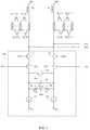
- FIG. 1is a circuit diagram of a CTLE amplifier utilizing NMOS transistors in accordance with some embodiments.
- FIG. 2is a circuit diagram illustrating how multiple instances of an embodiment such as that of FIG. 1 may be combined to provide increased configurability.
- FIG. 3Ais a circuit diagram of a digital-to-analog converter utilizing PMOS transistors suitable for use in producing analog control signals, in accordance with some embodiments.
- FIG. 3Bis a circuit diagram including transmission gate implementations of the transistors shown in FIG. 3A .
- FIG. 4shows an alternative embodiment of the circuit of FIG. 1 utilizing PMOS transistors.
- FIG. 5is a frequency spectrum of an adjustable high frequency peaking CTLE, in accordance with some embodiments.
- FIG. 6is a frequency spectrum illustrating CTLE gain without and with a fixed capacitor connected in parallel to varactor capacitors, in accordance with some embodiments.
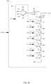
- FIG. 7is a block diagram of a digital-to-analog converter (DAC) circuit generating control signals for setting an equalization range of an Amplifier, in accordance with some embodiments.
- DACdigital-to-analog converter
- FIG. 8is a diagram illustrating multiple equalization ranges for different coding schemes, in accordance with some embodiments.
- CTLEContinuous-time Linear Equalization circuits are well known in the art.
- One common designis based on a conventional differential amplifier circuit utilizing a matched transistor pair having individual source loads but common drain connections to a fixed current sink. Splitting the current sink into two, one for each transistor drain, allows the drains to be cross-coupled with a frequency-dependent impedance such as a parallel RC network, modifying the essentially flat gain-vs-frequency characteristic of the basic differential amplifier into one having distinctly different low- and high-frequency gains.
- a frequency-dependent impedancesuch as a parallel RC network
- such a CTLE circuitis typically configured to provide increased high-frequency gain, to equalize or compensate for the inevitable high frequency loss of most communications media.
- careful configuration of amplitude and equalization functionsis performed to facilitate accurate signal detection and/or clock recovery by subsequent circuits.
- a CTLE circuit in which both the gain characteristics and the frequency break points of such frequency-dependent compensationmay be adjusted or configured.
- FIG. 1shows one embodiment of a configurable CTLE circuit utilizing NMOS transistors as gain elements.
- An equivalent embodiment utilizing PMOS transistorsis shown as FIG. 4 . Without implying limitation, reference will be made to the circuit of FIG. 1 in the following descriptions.
- Vdd and Vssmay typically provide one volt or less of operating voltage, thus microampere current flows imply path impedances of many thousands to millions of ohms. As resistances of these magnitudes may require substantial surface area in some integrated circuit processes, active circuit elements such as transistors may be preferable to passive element embodiments.
- inductive loadcomposed of inductors L 0 and L 1 shunt peaking at high frequency, allowing a high frequency peaking of more than 10 dB.
- the corresponding load impedancesare provided by resistor arrays generating load impedances R L0 and R L1 .
- each resistor arraymay receive a multi-bit thermometer code load resistance control input R L ⁇ n-1:0>, and may selectively connect successive resistors in the parallel network to set a load resistance RL.
- adjusting the load resistancemay be beneficial to adjust the common mode of the subsequent processing stage, e.g., a variable gain amplifier.
- circuit slice 100includes transistors 112 and 122 are a matched differential pair, accepting input signals Vin+ and Vin ⁇ and producing output signals Vout ⁇ and Vout+, respectively.
- Cascoded transistors 111 and 121may be configured to receive a gate voltage of Vcasc, and may provide isolation of the input from the output while inherently helping to reduce the input miller capacitance seen at the input.
- Identical current sources 113 and 123set the allowable current flow, and may be adjusted to adjust the magnitude of the high frequency peaking, as described below.
- the source R s resistance provided by transistor 131 and the capacitance provided by the combination of fixed capacitor 132 and varactor capacitors 133 and 134determine the frequency-dependent gain characteristics of the equalizer.
- voltage Vswis configurable, allowing the impedance of transistor 131 to be adjusted. In other embodiments voltage Vsw is fixed, with that voltage and the physical transistor channel dimensions determining the resulting impedance.
- voltage Vswmay be set to one of two different predetermined values (i.e. a binary selection) as subsequently described.
- Vswcauses transistor 131 to be switched “on” (e.g., low impedance)
- circuit 100is configured into a first or “flat” operational mode in which the frequency domain zero produced by capacitors 132 , 133 , 134 is minimized, and the DC equalization is less relative to the peak equalization.
- FIG. 5illustrates a frequency response of a CTLE providing high-frequency peaking, in accordance with some embodiments.
- FIG. 5includes 4 points of interest, first zero A (w zero ), first pole B (w p0 ), peak frequency C (w peak ), and second pole D (w p1 ).
- the values for each point of interestare given in Eqns. 1-4 below:
- R sis the source resistance provided by transistor 131
- C sis the source capacitance, which may be equal C Dom +C vc0/1
- C Domis the dominant capacitance of fixed capacitor 132
- C vc0/1is the capacitance of one of varactor diodes 133 or 134 .
- the notation “0/1”may correspond to the value of one element ‘0’ or ‘1’ in the set of ⁇ 0 1 ⁇ , as may be common in half circuit analysis.
- the capacitances of the fixed capacitor and varactorsmay be designed accordingly, e.g., a large fixed capacitance with varactors configured to fine tune via smaller capacitances, or alternatively may be broken up into separate capacitance elements.
- the first pole wp0may be calculated as follows:
- the peak frequency w peakmay be calculated as follows:
- dampening factor of the systemmay be determined as follows:
- capacitances 133 and 134are provided by voltage-variable capacitors, which may include varactor or other P-N junction diodes, and the voltage-dependent body capacitance of MOS transistor devices whose channels change and are also non-linear and can be a function of time, depending on the manufacturing process used. Charge density in active devices changes over time and is much more noticeable in small channel length devices.
- varactors 133 and 134are connected back-to-back, to minimize the unwanted modulation of the resulting capacitance by signal voltage, with analog control voltage Vctrl used to adjust the overall capacitance.
- Use of varactorssignificantly reduces area occupancy on a chip as compared to e.g., a switched capacitor bank.
- FIG. 6includes two frequency spectrums illustrating CTLE gain with respect to frequency. The top graph illustrates tuning the frequency of the first pole by tuning the varactors 133 and 134 without fixed capacitor 132 connected in parallel, and the bottom graph illustrates tuning of the frequency of the first pole by tuning the varactors 133 and 134 with fixed capacitor 132 connected in parallel.
- the fixed capacitor 132results in high non-linearity between tuning steps of the varactor, while including the fixed capacitor 132 makes the curves much more linear. Furthermore, it should be noted that the peak remains more constant when including the fixed capacitor 132 . The zero contribution is more constant with fixed capacitor 132 and more towards an expected 20 dB/dec. Without the fixed capacitor 132 , the zero changes slope with respect to frequency.
- the capacitance of fixed capacitor 132may allow use of a MOS ladder DAC, e.g., the MOS ladder DAC of FIG. 3A , which may result in further reduction in power and chip area compared to e.g., a resistor ladder DAC.
- MOS ladder DACsmay suffer from differential non-linearity (DNL) and integral non-linearity (INL)
- the fixed capacitor 132helps eliminate such effects similar to how fixed capacitor eliminates the non-linearity of the varactor diodes.
- the fixed capacitormay be split into two parts.
- a source degeneration capmay be used instead of large (or multiple) varactors, which take up a lot of area.
- the MIM/MOM capacitorsmay be vertically stacked in the layers, where the bottom silicon layer contains the varactors while the top metal layers contain the MIM/MOM capacitors. Such capacitors may be useful in applications where a large capacitance is used to move the zero to a smaller frequency.
- FIG. 2shows a collection of parallel slices of identical CTLE circuits 100 to take advantage of the previously-described binary mode selection by control voltage Vsw.
- the parallel slices 100may each be connected to a common load inductance (e.g., inductors L 0 and L 1 ) and load impedance (e.g., load impedances R L0 and R L1 ).
- load impedances R L0 and R L1load impedances
- eight slices of circuit 100are shown, each controlled by a single binary value taken from Vsw ⁇ 7 : 0 >, which may be considered as a single variable encoded as a “thermometer” or unary count value, from 0 (all low) to 7 (all high).
- each instance of circuit 100With all instances of transistor 131 controlled by Vsw “open”, each instance of circuit 100 will be in its first or “high frequency” operational mode, thus the resulting DC equalization relative to the peak will be at a maximum, and DC gain will be at a minimum.
- Vsw valuesare set to selectively “short” transistors 131 , increasing numbers of 100 instances will enter their second or “wideband” operational mode, resulting in increasing DC gain and thus DC equalization relative to the peak will start to decrease.
- all instances of Vsw “shorted”all instances of 100 will be in their second operational mode, and DC gain will be at a maximum, and DC equalization relative to the peak will be at a minimum.
- the use of such a parallel-slice configuration to control the DC equalization relative to the peakmay reduce wideband noises, e.g., thermal noise, and may introduce less parasitic capacitance.
- NMOS transistors 131may be configured to operate in between the “high frequency” and “wideband” operational modes by providing source impedance control signals Vsw ⁇ 7 : 0 > as inputs to transistors 131 to cause transistors 131 to operate in the linear region.
- FIG. 7is a block diagram of a DAC 705 configured to provide multiple voltages of a range of voltages as the source impedance control signals Vsw ⁇ 7 : 0 >.
- voltages from 0 mV to 1000 mVare provided in 200 mV increments using a resistor-ladder DAC 710 , however such numbers should be considered non-limiting, and a DAC 705 may be designed to have any set of values.
- the DAC 705should not be considered to be limited to the R-ladder DAC 710 shown; other types of DACs known to those of skill in the art may be used as well.
- the value of the voltage output by the DAC to the transistors 131 / 431acts as a “coarse” adjustment to set an equalization range, while the number of enabled parallel slices 100 acts as a “fine” adjustment to finely tune the equalization within the set equalization range.
- FIG. 8is a frequency response for two equalization ranges, in accordance with some embodiments. As shown, FIG. 8 includes equalization ranges 802 and 805 .
- the DAC 705may be configured to output a relatively higher voltage provided as source impedance control signals Vsw ⁇ 7 : 0 > to NMOS transistors 131 in enabled parallel slices 100 to configure the amplifier in equalization range 802
- DAC 705may be configured to output a relatively lower voltage provided as control signals to transistors 131 in enabled parallel slices 100 to configure the amplifier in equalization range 805 .
- the DACmay be configured to output source impedance control signals having a higher respective voltage to PMOS transistors 431 in enabled parallel slices 100 to set the amplifier in equalization range 802 , and a lower respective voltage to the enabled parallel slices 100 to set the amplifier in equalization range 805 .
- Such embodiments for configuring the amplifier to operate in multiple equalization rangesmay accommodate factors including different types of coding schemes, different cable/channel lengths, and/or a combination of various other factors.
- a non-return to zero (NRZ) coding schememay be configured to have a max equalization of ⁇ 7 dB
- an ensemble non-return-to-zero (ENRZ) orthogonal differential vector signaling code schememay be configured to have a max equalization of ⁇ 10 dB.
- ENRZensemble non-return-to-zero
- This configuration of numbers of essentially parallel amplifier slices into a first or a second operational modeprovides direct control over the resulting differential gain between the low-frequency and high-frequency regions of the aggregate system's gain-vs-frequency curve.
- both the amplitude and corner frequency of the high frequency “peaking”may be configured independently.
- These adjustmentsmay be combined with other control methods, including varying circuit DC current by adjustment of current sources 113 and 123 , and modification of effective load impedance by adjustment of R L0 and R L1 via the parallel resistor networks controlled by R L ⁇ n-1:0>.
- the use of multiple parallel slicesprovides an option to independently control the varactor capacitances in each slice individually, increasing granularity at the cost of a multi-bit control signal Vctrl ⁇ 7 : 0 >, as shown in FIG. 2 .
- some embodimentsmay provide the same control signal Vctrl to every slice.
- the circuits of FIGS. 1 and 2may have multiple degrees of control.
- the first zero w zeromay be controlled by controlling the voltage across the varactors using Vctrl, which adjusts the source capacitance C s .
- the DC equalization relative to the peakmay be controlled by selecting how many parallel slices 100 are switched “off” or “open” (high frequency mode) vs switched “on” or “shorted” (wideband mode). Such adjustments are illustrated in FIG. 5 by the 8 horizontal lines 505 .
- each horizontal linemay correspond to a various step of the 8 steps of the thermometer code described with respect to FIG. 2 .
- the lowest horizontal line of 505e.g., where the DC gain is at a minimum and thus DC equalization relative to the peak is at a maximum
- every transistor 131 being switched “on” or “shorted”may correspond to the highest horizontal line of 505 , indicating that DC gain is at a maximum, and thus DC equalization relative to the peak is at a minimum.
- the second pole w p1 of the frequency responsemay be adjusted by adjusting the effective load impedance via load resistors R L0 and R L1 .
- the effective load impedancemay be set via tunable resistors (not shown). Having adjustment of the zero and pole allows adjustment of the desired frequency band (width and location) of the high frequency peaking, as well as the gain of the high frequency peaking. Such embodiments are useful in backwards compatibility with some legacy designs, as well as dynamic adjustment in response to changes in channel response. Another degree of control may correspond to adjusting bias current in current sources 113 and 123 , which may control the magnitude of the peak by increasing or decreasing gm.
- the common mode provided to the following signal processing stagemay be adjusted by controlling the load impedances R L0 and R L1 , e.g., via the resistor banks shown in FIG. 1 .
- FIG. 3Ashows an embodiment of a PMOS-ladder DAC optimized for minimal integrated circuit area and low current utilization.
- the PMOS-ladder DACis well-suited with the PMOS circuit of FIG. 4 , as the PMOS-ladder DAC may utilize the same substrate that circuit 100 is disposed on, resulting in significant savings in overall circuit area.
- the channel resistance of PMOS transistorsare used instead, as seen at 351 through 358 .
- all of 351 - 358will be identical PMOS transistors, designed with sufficiently narrow channels to provide the desired series resistance or “R” value in a conventional R-2R ladder structure.
- the ratio of the width-to-length (W/L) of transistors 351 - 358may be twice the W/L ratio of transistor 313 , resulting in a halved resistance ‘R’, as increasing width with respect to length reduces the resistance.
- gate bias Vssis applied to insure each such transistor is in its resistive channel state.
- Each driving element 300 for the laddercorresponding to a switch-selected voltage source in series with a “R” resistance transistors 351 - 358 , the exception being transistor 313 having resistance 2R, is shown as a MUX composed of two identical MOS transistors 311 and 312 , with 311 selecting voltage Vrefh and 312 selecting voltage Vrefl, the desired high and low values for the DAC output range.
- transistor 313will have a channel resistance twice that of transistors 351 - 358 .
- the Vrefh and Vreflmay range from 700-900 mV.
- the voltage rangemay be lower, e.g., 0-200 mV, as NMOS transistors are more proficient in passing lower voltages.
- Transistors 311 and 312are driven by complementary control signals, here shown as derived from binary control input Vc 7 , one value taken from control word Vc ⁇ 0 : 7 > and the other the inverted version of VC 7 , VC 7 .
- binary control input Vc 7one value taken from control word Vc ⁇ 0 : 7 >
- the binary control input for each instanceis derived from a different bit value in control word Vc ⁇ 0 : 7 >, with Vc 7 controlling the most-significant bit of the ladder, and Vc 0 controlling the least-significant bit.
- control word Vc ⁇ 0 : 7 >are differential, thus for example control value Vc 7 is inherently available as both Vc 7 and its compliment VC 7 , which may directly control transistors 311 and 312 .
- each instance of 310incorporates buffer/inverter gates to provide the appropriate drive signals to 311 and 312 from a single digital control value.
- DAC 300 producing analog output Vctrlwas sufficiently compact to be physically collocated with or near the variable capacitance diodes 133 and 134 it controlled, minimizing the introduction of unwanted parasitic loads into analog circuit 100 .
- PMOS transistorsare shown in FIG. 3A
- an equivalent embodimentmay be produced using NMOS transistors.
- Such single-transistor embodimentsmay be useful for implementations outputting a narrow range of voltages near Vss (e.g., 0-200 mV) for NMOS designs, and voltages near Vdd (e.g., 700-900 mV) for PMOS designs.
- the varactorsmay respond particularly well to the control voltages provided near Vdd, however such embodiments should not be considered limiting.
- FIG. 3Bincludes a MUX element 310 utilizing Tx gates, where the selection inputs Vc 7 and VC 7 control NMOS and PMOS transistors connected to Vrefh, respectively, and control PMOS and NMOS transistors connected to Vrefl, respectively.
- transistor circuit 313an NMOS connected to Vdd and a PMOS connected to Vss are connected in parallel.
- the NMOS transistoris proficient in passing lower voltages whereas the PMOS transistor is proficient in passing higher voltages.
- Such embodimentsmay increase the voltage range provided at Vrefh and Vrefl.
- the PMOS only MOS laddermay receive a range of 700-900 mV
- the Tx gate versionmay receive a range of 0-900 mV.
- MOS ladder DACsmay provide significant advantages in terms of power savings and chip area savings, it should be noted that other DACs, e.g, R-2R ladders utilizing resistors instead of transistors may be utilized as well to provide the various control signals.
Landscapes
- Engineering & Computer Science (AREA)
- Power Engineering (AREA)
- Computer Networks & Wireless Communication (AREA)
- Signal Processing (AREA)
- Theoretical Computer Science (AREA)
- Multimedia (AREA)
- Amplifiers (AREA)
- Networks Using Active Elements (AREA)
Abstract
Description
This Application claims the benefit of U.S. Provisional Application No. 62/683,964, filed Jun. 12, 2018, naming Suhas Rattan, entitled “Amplifier with Adjustable High-Frequency Gain Using Varactor Diodes”, which is hereby incorporated herein by reference in its entirety for all purposes.
An amplifier circuit incorporating configurable frequency compensation is described, suitable for use as a continuous-time linear equalizer (CTLE) for communications receiver input signals. Elements of the design facilitate compact circuit layout with the configurable elements closely integrated with the analog devices they control.
Continuous-time Linear Equalization (CTLE) circuits are well known in the art. One common design is based on a conventional differential amplifier circuit utilizing a matched transistor pair having individual source loads but common drain connections to a fixed current sink. Splitting the current sink into two, one for each transistor drain, allows the drains to be cross-coupled with a frequency-dependent impedance such as a parallel RC network, modifying the essentially flat gain-vs-frequency characteristic of the basic differential amplifier into one having distinctly different low- and high-frequency gains.
In communications system receivers, such a CTLE circuit is typically configured to provide increased high-frequency gain, to equalize or compensate for the inevitable high frequency loss of most communications media. In some embodiments, careful configuration of amplitude and equalization functions is performed to facilitate accurate signal detection and/or clock recovery by subsequent circuits. In some embodiments, a CTLE circuit in which both the gain characteristics and the frequency break points of such frequency-dependent compensation may be adjusted or configured.
It should be noted that these embodiments are intended for use in an integrated circuit environment requiring extremely high frequency signals to be processed with minimal power consumption. The available power rails Vdd and Vss may typically provide one volt or less of operating voltage, thus microampere current flows imply path impedances of many thousands to millions of ohms. As resistances of these magnitudes may require substantial surface area in some integrated circuit processes, active circuit elements such as transistors may be preferable to passive element embodiments.
InFIG. 1 , inductive load composed of inductors L0and L1shunt peaking at high frequency, allowing a high frequency peaking of more than 10 dB. The corresponding load impedances are provided by resistor arrays generating load impedances RL0and RL1. As shown, each resistor array may receive a multi-bit thermometer code load resistance control input RL<n-1:0>, and may selectively connect successive resistors in the parallel network to set a load resistance RL. In some embodiments, adjusting the load resistance may be beneficial to adjust the common mode of the subsequent processing stage, e.g., a variable gain amplifier. Alternatively, load resistance may be adjusted to tweak the magnitude of the high frequency peaking and the location of the second pole of the response, described in more detail below with respect toFIG. 5 . As shown inFIG. 1 ,circuit slice 100 includestransistors Cascoded transistors current sources transistor 131 and the capacitance provided by the combination offixed capacitor 132 andvaractor capacitors
In some embodiments, voltage Vsw is configurable, allowing the impedance oftransistor 131 to be adjusted. In other embodiments voltage Vsw is fixed, with that voltage and the physical transistor channel dimensions determining the resulting impedance.
In a further embodiment, voltage Vsw may be set to one of two different predetermined values (i.e. a binary selection) as subsequently described. In one such embodiment, when Vsw causestransistor 131 to be switched “on” (e.g., low impedance),circuit 100 is configured into a first or “flat” operational mode in which the frequency domain zero produced bycapacitors transistor 131 to be switched “off” or high impedance, that impedance along withcapacitances circuit 100 being configured into a second or high frequency “peaking” operational mode, increasing the DC equalization relative to the peaking equalization.
where Rsis the source resistance provided bytransistor 131, and Csis the source capacitance, which may be equal CDom+Cvc0/1, where CDomis the dominant capacitance offixed capacitor 132 and Cvc0/1is the capacitance of one ofvaractor diodes varactor diodes
The first pole wp0 may be calculated as follows:
The peak frequency wpeakmay be calculated as follows:
and the first zero may be determined as follows:
and the second zero may be determined as follows:
and finally the dampening factor of the system may be determined as follows:
In some embodiments,capacitances varactors capacitor 132 in parallel with the variable capacitance of133 and134 further reduces these unwanted signal distortion effects due to the varactors described above by reducing the adjustable range to a suitable amount.FIG. 6 includes two frequency spectrums illustrating CTLE gain with respect to frequency. The top graph illustrates tuning the frequency of the first pole by tuning thevaractors capacitor 132 connected in parallel, and the bottom graph illustrates tuning of the frequency of the first pole by tuning thevaractors capacitor 132 connected in parallel. As shown, omitting the fixedcapacitor 132 results in high non-linearity between tuning steps of the varactor, while including the fixedcapacitor 132 makes the curves much more linear. Furthermore, it should be noted that the peak remains more constant when including the fixedcapacitor 132. The zero contribution is more constant withfixed capacitor 132 and more towards an expected 20 dB/dec. Without the fixedcapacitor 132, the zero changes slope with respect to frequency.
As an added benefit, the capacitance of fixedcapacitor 132 may allow use of a MOS ladder DAC, e.g., the MOS ladder DAC ofFIG. 3A , which may result in further reduction in power and chip area compared to e.g., a resistor ladder DAC. While MOS ladder DACs may suffer from differential non-linearity (DNL) and integral non-linearity (INL), the fixedcapacitor 132 helps eliminate such effects similar to how fixed capacitor eliminates the non-linearity of the varactor diodes. Furthermore, the fixed capacitor may be split into two parts. A source degeneration cap may be used instead of large (or multiple) varactors, which take up a lot of area. In such cases, half the capacitance may be handled by the varactor while the other half may be incorporated using a metal-insulator-metal (MIM) capacitor or a metal over metal (MOM) capacitor. thus, the MIM/MOM capacitors may be vertically stacked in the layers, where the bottom silicon layer contains the varactors while the top metal layers contain the MIM/MOM capacitors. Such capacitors may be useful in applications where a large capacitance is used to move the zero to a smaller frequency.
In some embodiments,NMOS transistors 131 may be configured to operate in between the “high frequency” and “wideband” operational modes by providing source impedance control signals Vsw<7:0> as inputs totransistors 131 to causetransistors 131 to operate in the linear region.FIG. 7 is a block diagram of aDAC 705 configured to provide multiple voltages of a range of voltages as the source impedance control signals Vsw<7:0>. InFIG. 7 , voltages from 0 mV to 1000 mV are provided in 200 mV increments using a resistor-ladder DAC 710, however such numbers should be considered non-limiting, and aDAC 705 may be designed to have any set of values. Further, theDAC 705 should not be considered to be limited to the R-ladder DAC 710 shown; other types of DACs known to those of skill in the art may be used as well.
As one will note, increasing the gate voltage of an NMOS transistor, e.g., via a source impedance control signal Vsw<0> provided toNMOS transistor 131 inFIG. 1 , will decrease the channel resistance oftransistor 131, thus decreasing the equalization, and vice versa with regards to decreasing the gate voltage to decrease the channel resistance ofNMOS transistor 131. Conversely, decreasing the voltage provided to a PMOS transistor, e.g.,transistor 431 inFIG. 4 , will decrease the channel resistance ofPMOS transistor 431, decreasing the equalization, and vice versa with regards to increasing the gate voltage to increase channel resistance ofPMOS transistor 431. In such embodiments, the value of the voltage output by the DAC to thetransistors 131/431 acts as a “coarse” adjustment to set an equalization range, while the number of enabledparallel slices 100 acts as a “fine” adjustment to finely tune the equalization within the set equalization range.
Such embodiments for configuring the amplifier to operate in multiple equalization ranges may accommodate factors including different types of coding schemes, different cable/channel lengths, and/or a combination of various other factors. In one particular example, a non-return to zero (NRZ) coding scheme may be configured to have a max equalization of ˜7 dB, while an ensemble non-return-to-zero (ENRZ) orthogonal differential vector signaling code scheme may be configured to have a max equalization of ˜10 dB. Thus, by selecting an output voltage from the DAC, the correct equalization range may be selected depending on use of ENRZ or NRZ coding schemes, while enabling and disablingparallel slices 100 may finely tune the desired equalization within the selected equalization range.
This configuration of numbers of essentially parallel amplifier slices into a first or a second operational mode provides direct control over the resulting differential gain between the low-frequency and high-frequency regions of the aggregate system's gain-vs-frequency curve. Combined with the previously described control of the variable capacitance elements of each amplifier slice, both the amplitude and corner frequency of the high frequency “peaking” may be configured independently. These adjustments may be combined with other control methods, including varying circuit DC current by adjustment ofcurrent sources FIG. 2 . However, some embodiments may provide the same control signal Vctrl to every slice.
Based on Eqns. 1-4 and the descriptions above regarding the varactor diodes for adjusting source capacitance Csand multiple parallel slice configuration for adjusting source impedance Rs, it follows based on the frequency response ofFIG. 5 that the circuits ofFIGS. 1 and 2 may have multiple degrees of control. The first zero wzeromay be controlled by controlling the voltage across the varactors using Vctrl, which adjusts the source capacitance Cs. The DC equalization relative to the peak may be controlled by selecting how manyparallel slices 100 are switched “off” or “open” (high frequency mode) vs switched “on” or “shorted” (wideband mode). Such adjustments are illustrated inFIG. 5 by the 8horizontal lines 505. In505, each horizontal line may correspond to a various step of the 8 steps of the thermometer code described with respect toFIG. 2 . As described inFIG. 2 , the lowest horizontal line of505 (e.g., where the DC gain is at a minimum and thus DC equalization relative to the peak is at a maximum) may correspond to thetransistors 131 in every slice being switched “off” or “open”. Alternatively, everytransistor 131 being switched “on” or “shorted” may correspond to the highest horizontal line of505, indicating that DC gain is at a maximum, and thus DC equalization relative to the peak is at a minimum. Further, the second pole wp1of the frequency response may be adjusted by adjusting the effective load impedance via load resistors RL0and RL1. In some embodiments, the effective load impedance may be set via tunable resistors (not shown). Having adjustment of the zero and pole allows adjustment of the desired frequency band (width and location) of the high frequency peaking, as well as the gain of the high frequency peaking. Such embodiments are useful in backwards compatibility with some legacy designs, as well as dynamic adjustment in response to changes in channel response. Another degree of control may correspond to adjusting bias current incurrent sources FIG. 1 .
Adjustment of these various configurable elements may utilize multiple control elements, such as digital-to-analog converters (DACs), that increase system power consumption and layout area.FIG. 3A shows an embodiment of a PMOS-ladder DAC optimized for minimal integrated circuit area and low current utilization. In some embodiments, the PMOS-ladder DAC is well-suited with the PMOS circuit ofFIG. 4 , as the PMOS-ladder DAC may utilize the same substrate thatcircuit 100 is disposed on, resulting in significant savings in overall circuit area. As fixed value resistors may occupy significant layout area in some integrated circuit processes, the channel resistance of PMOS transistors are used instead, as seen at351 through358. In a practical embodiment, all of351-358 will be identical PMOS transistors, designed with sufficiently narrow channels to provide the desired series resistance or “R” value in a conventional R-2R ladder structure. In such embodiments, the ratio of the width-to-length (W/L) of transistors351-358 may be twice the W/L ratio oftransistor 313, resulting in a halved resistance ‘R’, as increasing width with respect to length reduces the resistance. In some embodiments, gate bias Vss is applied to insure each such transistor is in its resistive channel state.
Each drivingelement 300 for the ladder, corresponding to a switch-selected voltage source in series with a “R” resistance transistors351-358, theexception being transistor 313 havingresistance 2R, is shown as a MUX composed of twoidentical MOS transistors transistor 313 will have a channel resistance twice that of transistors351-358. In some embodiments, the Vrefh and Vrefl may range from 700-900 mV. In embodiments utilizing NMOS transistors, the voltage range may be lower, e.g., 0-200 mV, as NMOS transistors are more proficient in passing lower voltages.
In one particular integrated circuit embodiment,DAC 300 producing analog output Vctrl was sufficiently compact to be physically collocated with or near thevariable capacitance diodes analog circuit 100.
Although PMOS transistors are shown inFIG. 3A , an equivalent embodiment may be produced using NMOS transistors. Such single-transistor embodiments may be useful for implementations outputting a narrow range of voltages near Vss (e.g., 0-200 mV) for NMOS designs, and voltages near Vdd (e.g., 700-900 mV) for PMOS designs. In the above described embodiments, the varactors may respond particularly well to the control voltages provided near Vdd, however such embodiments should not be considered limiting. Depending on the relative voltages of Vrefh and Vrefl compared to Vdd, Vss, and the particular transistor gate thresholds, NMOS, PMOS, or even hybrid embodiments in which MUXstructures 310 are implemented using transmission gates may be desirable. Such an embodiment in which MUXelements 310, andtransistor elements 313 and351-358 are Tx gates is shown inFIG. 3B .FIG. 3B includes aMUX element 310 utilizing Tx gates, where the selection inputs Vc7 andVC7 control NMOS and PMOS transistors connected to Vrefh, respectively, and control PMOS and NMOS transistors connected to Vrefl, respectively. Intransistor circuit 313, an NMOS connected to Vdd and a PMOS connected to Vss are connected in parallel. In such embodiments utilizing Tx gates, the NMOS transistor is proficient in passing lower voltages whereas the PMOS transistor is proficient in passing higher voltages. Such embodiments may increase the voltage range provided at Vrefh and Vrefl. Whereas the PMOS only MOS ladder may receive a range of 700-900 mV, the Tx gate version may receive a range of 0-900 mV.
While MOS ladder DACs may provide significant advantages in terms of power savings and chip area savings, it should be noted that other DACs, e.g, R-2R ladders utilizing resistors instead of transistors may be utilized as well to provide the various control signals.
Claims (20)
1. An apparatus comprising:
a plurality of differential pairs connected in parallel to a pair of output nodes, the plurality of differential pairs configured to receive a differential input signal and to responsively generate an amplified output signal on the pair of output nodes;
a digital-to-analog converter (DAC) configured to generate an analog source impedance control signal, the analog source impedance control signal comprising an analog voltage on a selectable number of DAC outputs in accordance with a thermometer code;
a tunable source impedance connected to each differential pair of the plurality of differential pairs, the tunable source impedance connected to a respective DAC output, wherein the analog voltage sets a coarse setting of a direct-current (DC) equalization of a high frequency amplification applied to the differential input signal and the selectable number of DAC outputs sets a fine setting of the DC equalization of the high frequency amplification applied to the differential input signal; and
a tunable capacitance connected to each differential pair of the plurality of differential pairs, each tunable capacitance configured to adjust the high frequency amplification applied to the differential input signal, the tunable capacitance comprising:
a pair of series-connected varactor diodes connected to the differential pair configured to receive a control signal at a common node to adjust a frequency of the high frequency amplification; and
a fixed capacitance connected in parallel to the pair of series-connected varactors, the fixed capacitor having a capacitance larger than a capacitance of the series-connected varactors configured to offset changes in charge density of channels in the series-connected varactor diodes.
2. The apparatus ofclaim 1 , further comprising isolation transistors connected to the pair of output nodes.
3. The apparatus ofclaim 1 , further comprising a tunable load impedance connected to the pair of output nodes.
4. The apparatus ofclaim 3 , wherein the tunable load impedance comprises a switched resistor bank configured to receive a load impedance control signal and to selectively enable one or more resistors in the switched resistor bank.
5. The apparatus ofclaim 1 , wherein each tunable source impedance comprises a transistor biased via the analog voltage into a linear region.
6. The apparatus ofclaim 1 , wherein the DAC is a resistor ladder DAC.
7. The apparatus ofclaim 1 , further comprising a second digital-to-analog converter (DAC) configured to generate the control signal.
8. The apparatus ofclaim 7 , wherein the second DAC is a metal oxide silicon (MOS) ladder DAC.
9. The apparatus ofclaim 7 , wherein the second DAC comprises transmission gates arranged in an R-2R ladder.
10. The apparatus ofclaim 1 , further comprising an adjustable current source configured to adjust a magnitude of the high frequency amplification.
11. A method comprising:
receiving a differential input signal at a plurality of differential pairs, and responsively generating an amplified output signal on a pair of output nodes;
generating an analog voltage using a digital-to-analog converter (DAC);
providing the analog voltage to a selectable number of tunable source impedances according to a thermometer code, each tunable source impedance connected to a respective differential pair of the plurality of differential pairs, the analog voltage setting a coarse tuning of a direct-current (DC) equalization of a high frequency amplification applied to the differential input signal and the selectable number of tunable source impedances setting a fine tuning of the DC equalization of the high frequency amplification applied to the differential input signal; and
adjusting the high frequency amplification applied to the differential input signal using a tunable capacitance, wherein adjusting the high frequency amplification comprises:
receiving a control signal at a common node of a pair of series-connected varactor diodes connected to the differential pair, the pair of series-connected varactor diodes adjusting a frequency of the high frequency amplification; and
offsetting changes in charge density of channels in the series-connected varactor diodes using a fixed capacitance connected in parallel to the pair of series-connected varactors, the fixed capacitor having a capacitance larger than a capacitance of the series-connected varactors.
12. The method ofclaim 11 , further comprising isolating the differential input signal from the amplified output signal via isolation transistors connected to the pair of output nodes.
13. The method ofclaim 11 , wherein a tunable load impedance is connected to the pair of output nodes.
14. The method ofclaim 13 , further comprising receiving a load impedance control signal to selectively enable one or more resistors in the switched resistor bank.
15. The method ofclaim 11 , wherein each tunable source impedance is a transistor, and wherein the analog voltage biases the transistor in a linear region.
16. The method ofclaim 11 , wherein the DAC is a resistor ladder DAC.
17. The method ofclaim 11 , wherein the control signal is generated using a second DAC.
18. The method ofclaim 17 , wherein the second DAC is a metal oxide silicon (MOS) ladder DAC.
19. The method ofclaim 11 , wherein the DAC comprises transmission gates arranged in an R-2R ladder.
20. The method ofclaim 11 , further comprising adjusting a magnitude of the high frequency amplification using an adjustable current source.
Priority Applications (6)
| Application Number | Priority Date | Filing Date | Title |
|---|---|---|---|
| US16/378,461US10931249B2 (en) | 2018-06-12 | 2019-04-08 | Amplifier with adjustable high-frequency gain using varactor diodes |
| KR1020217000688AKR102579592B1 (en) | 2018-06-12 | 2019-06-10 | Amplifier with adjustable high-frequency gain using varactor diodes |
| CN201980048412.3ACN112805916B (en) | 2018-06-12 | 2019-06-10 | Amplifier with adjustable high frequency gain using varactors |
| EP19734569.7AEP3807991A1 (en) | 2018-06-12 | 2019-06-10 | Amplifier with adjustable high-frequency gain using varactor diodes |
| PCT/US2019/036384WO2019241150A1 (en) | 2018-06-12 | 2019-06-10 | Amplifier with adjustable high-frequency gain using varactor diodes |
| US17/183,100US11502658B2 (en) | 2018-06-12 | 2021-02-23 | Amplifier with adjustable high-frequency gain using varactor diodes |
Applications Claiming Priority (2)
| Application Number | Priority Date | Filing Date | Title |
|---|---|---|---|
| US201862683964P | 2018-06-12 | 2018-06-12 | |
| US16/378,461US10931249B2 (en) | 2018-06-12 | 2019-04-08 | Amplifier with adjustable high-frequency gain using varactor diodes |
Related Child Applications (1)
| Application Number | Title | Priority Date | Filing Date |
|---|---|---|---|
| US17/183,100ContinuationUS11502658B2 (en) | 2018-06-12 | 2021-02-23 | Amplifier with adjustable high-frequency gain using varactor diodes |
Publications (2)
| Publication Number | Publication Date |
|---|---|
| US20190379340A1 US20190379340A1 (en) | 2019-12-12 |
| US10931249B2true US10931249B2 (en) | 2021-02-23 |
Family
ID=68764324
Family Applications (2)
| Application Number | Title | Priority Date | Filing Date |
|---|---|---|---|
| US16/378,461ActiveUS10931249B2 (en) | 2018-06-12 | 2019-04-08 | Amplifier with adjustable high-frequency gain using varactor diodes |
| US17/183,100Active2039-06-30US11502658B2 (en) | 2018-06-12 | 2021-02-23 | Amplifier with adjustable high-frequency gain using varactor diodes |
Family Applications After (1)
| Application Number | Title | Priority Date | Filing Date |
|---|---|---|---|
| US17/183,100Active2039-06-30US11502658B2 (en) | 2018-06-12 | 2021-02-23 | Amplifier with adjustable high-frequency gain using varactor diodes |
Country Status (5)
| Country | Link |
|---|---|
| US (2) | US10931249B2 (en) |
| EP (1) | EP3807991A1 (en) |
| KR (1) | KR102579592B1 (en) |
| CN (1) | CN112805916B (en) |
| WO (1) | WO2019241150A1 (en) |
Cited By (3)
| Publication number | Priority date | Publication date | Assignee | Title |
|---|---|---|---|---|
| US11303484B1 (en) | 2021-04-02 | 2022-04-12 | Kandou Labs SA | Continuous time linear equalization and bandwidth adaptation using asynchronous sampling |
| US11374800B1 (en) | 2021-04-14 | 2022-06-28 | Kandou Labs SA | Continuous time linear equalization and bandwidth adaptation using peak detector |
| US11456708B1 (en) | 2021-04-30 | 2022-09-27 | Kandou Labs SA | Reference generation circuit for maintaining temperature-tracked linearity in amplifier with adjustable high-frequency gain |
Families Citing this family (14)
| Publication number | Priority date | Publication date | Assignee | Title |
|---|---|---|---|---|
| WO2020047425A1 (en)* | 2018-08-31 | 2020-03-05 | Texas Instruments Incorporated | Methods and apparatus for voltage buffering |
| US10892717B2 (en)* | 2019-03-05 | 2021-01-12 | Realtek Semiconductor Corp. | Highly linear transconductance amplifier and method thereof |
| US10608849B1 (en) | 2019-04-08 | 2020-03-31 | Kandou Labs, S.A. | Variable gain amplifier and sampler offset calibration without clock recovery |
| CN112039526B (en)* | 2020-08-19 | 2022-07-12 | 北京无线电测量研究所 | Numerical control switch driving circuit applied to digital-to-analog converter |
| CN112737561A (en)* | 2020-12-05 | 2021-04-30 | 西安翔腾微电子科技有限公司 | High-speed output HCSL level driving circuit |
| US12309007B2 (en)* | 2020-12-18 | 2025-05-20 | Intel Corporation | Analog equalization with peaking and slope control |
| US11277108B1 (en)* | 2020-12-28 | 2022-03-15 | Analog Devices International Unlimited Company | Variable gain amplifiers with cross-couple switching arrangements |
| CN114864609A (en)* | 2021-01-20 | 2022-08-05 | 京东方科技集团股份有限公司 | Active pixel sensor and flat panel detector |
| KR20230032191A (en)* | 2021-08-30 | 2023-03-07 | 에스케이하이닉스 주식회사 | Buffer circuit capable of adjuting a gain, receiving circuit and semiconductor apparatus including the same |
| WO2023046121A1 (en)* | 2021-09-24 | 2023-03-30 | 武汉联影生命科学仪器有限公司 | Tuning device for receiving coil, low-temperature probe, and magnetic resonance device |
| KR102557685B1 (en)* | 2021-10-15 | 2023-07-19 | 고려대학교 산학협력단 | Single signal method recevier with active inductor continuous time linear equalizer and reference voltage selection equalizer and operation method thereof |
| US12355409B2 (en) | 2022-03-24 | 2025-07-08 | Kandou Labs SA | Variable gain amplifier with cross-coupled common mode reduction |
| CN117792308A (en)* | 2023-12-27 | 2024-03-29 | 尚睿微电子(上海)有限公司 | RF power amplifiers and electronic equipment |
| CN118399895B (en)* | 2024-06-27 | 2024-10-25 | 瑞纳智能设备股份有限公司 | Oscillator circuit, parameter estimation method, frequency adjustment method, and water processor |
Citations (140)
| Publication number | Priority date | Publication date | Assignee | Title |
|---|---|---|---|---|
| US3636463A (en) | 1969-12-12 | 1972-01-18 | Shell Oil Co | Method of and means for gainranging amplification |
| US3824494A (en) | 1973-06-08 | 1974-07-16 | Motorola Inc | Temperature stable relaxation oscillator having controllable output frequency |
| US3939468A (en) | 1974-01-08 | 1976-02-17 | Whitehall Corporation | Differential charge amplifier for marine seismic applications |
| US4276543A (en) | 1979-03-19 | 1981-06-30 | Trw Inc. | Monolithic triple diffusion analog to digital converter |
| US4774498A (en) | 1987-03-09 | 1988-09-27 | Tektronix, Inc. | Analog-to-digital converter with error checking and correction circuits |
| US4897657A (en) | 1988-06-13 | 1990-01-30 | Integrated Device Technology, Inc. | Analog-to-digital converter having error detection and correction |
| EP0425064A2 (en) | 1989-10-26 | 1991-05-02 | Conner Peripherals, Inc. | Method and apparatus for automatic write current calibration in a streaming tape drive |
| US5017924A (en) | 1989-05-03 | 1991-05-21 | Thomson Composants Microondes | Sample-and-hold unit with high sampling frequency |
| US5459465A (en) | 1993-10-21 | 1995-10-17 | Comlinear Corporation | Sub-ranging analog-to-digital converter |
| US5510736A (en) | 1993-07-22 | 1996-04-23 | U.S. Philips Corporation | Differential sampler circuit |
| US5748948A (en) | 1994-09-10 | 1998-05-05 | Holtek Microelectronics Inc. | Reset signal generator |
| US5793254A (en) | 1996-09-24 | 1998-08-11 | Brookhaven Science Associates Llc | Monolithic amplifier with stable, high resistance feedback element and method for fabricating the same |
| US5945935A (en) | 1996-11-21 | 1999-08-31 | Matsushita Electric Industrial Co., Ltd. | A/D converter and A/D conversion method |
| US6226330B1 (en) | 1998-07-16 | 2001-05-01 | Silicon Graphics, Inc. | Eigen-mode encoding of signals in a data group |
| US6232908B1 (en) | 1997-09-29 | 2001-05-15 | Nec Corporation | A/D converter having a dynamic encoder |
| US20010006538A1 (en) | 1999-05-25 | 2001-07-05 | Simon Thomas D. | Symbol-based signaling device for an elctromagnetically-coupled bus system |
| US6346907B1 (en) | 1998-08-07 | 2002-02-12 | Agere Systems Guardian Corp. | Analog-to-digital converter having voltage to-time converter and time digitizer, and method for using same |
| US20020050861A1 (en)* | 2000-02-15 | 2002-05-02 | Nguyen Thinh Cat | Variable transconductance variable gain amplifier utilizing a degenerated differential pair |
| US6384758B1 (en) | 2000-11-27 | 2002-05-07 | Analog Devices, Inc. | High-speed sampler structures and methods |
| US6396329B1 (en) | 1999-10-19 | 2002-05-28 | Rambus, Inc | Method and apparatus for receiving high speed signals with low latency |
| US6400302B1 (en) | 2001-02-26 | 2002-06-04 | Analog Devices, Inc. | Quasi-differential successive-approximation structures and methods for converting analog signals into corresponding digital signals |
| US6462584B1 (en) | 1999-02-13 | 2002-10-08 | Integrated Device Technology, Inc. | Generating a tail current for a differential transistor pair using a capacitive device to project a current flowing through a current source device onto a node having a different voltage than the current source device |
| US20020149508A1 (en) | 2001-02-27 | 2002-10-17 | Asahi Kasei Microsystems Co., Ltd. | Fully differential sampling circuit |
| US20020158789A1 (en) | 2001-03-09 | 2002-10-31 | Fujitsu Limited | 09756089a/d converter with higher speed and accuracy and lower power consumption |
| US20020174373A1 (en) | 2001-05-15 | 2002-11-21 | Chi Chang | Data transmission system using a pair of complementary signals as an edge-aligned strobe signal and input/output buffers therein |
| US20030016763A1 (en) | 2001-07-19 | 2003-01-23 | Fujitsu Limited | Receiver circuit, signal transmission system, and receiver circuit device used for high-speed signal transmission |
| US20030085763A1 (en) | 2000-03-29 | 2003-05-08 | Karl Schrodinger | Electronic output stage |
| US6563382B1 (en) | 2000-10-10 | 2003-05-13 | International Business Machines Corporation | Linear variable gain amplifiers |
| US20030132791A1 (en) | 2002-01-16 | 2003-07-17 | Kuo-Chiang Hsieh | High-sensitivity differential data latch system |
| US20030160749A1 (en) | 2002-02-25 | 2003-08-28 | Nec Corporation | Differential circuit, amplifier circuit, driver circuit and display device using those circuits |
| US20030174023A1 (en) | 2002-03-12 | 2003-09-18 | Tokio Miyasita | Analog summing and differencing circuit, optical receiving circuit, optical transmitting circuit, automatic gain control amplifier, automatic frequency compensation amplifier, and limiting amplifier |
| US6624699B2 (en) | 2001-10-25 | 2003-09-23 | Broadcom Corporation | Current-controlled CMOS wideband data amplifier circuits |
| US20030184459A1 (en) | 2000-02-04 | 2003-10-02 | Bernhard Engl | Devices and methods for calibrating amplifier stages and for compensating for errors in amplifier stages of series-connected components |
| US20030218558A1 (en) | 2002-05-24 | 2003-11-27 | Jan Mulder | High speed analog to digital converter |
| US20040027185A1 (en) | 2002-08-09 | 2004-02-12 | Alan Fiedler | High-speed differential sampling flip-flop |
| US20040169529A1 (en) | 2000-02-02 | 2004-09-02 | Afghahi Morteza Cyrus | Single-ended sense amplifier with sample-and-hold reference |
| US6838951B1 (en)* | 2002-06-12 | 2005-01-04 | Rf Micro Devices, Inc. | Frequency synthesizer having VCO bias current compensation |
| US6839587B2 (en) | 2000-08-15 | 2005-01-04 | Cardiac Pacemakers, Inc. | Electrocardiograph leads-off indicator |
| US20050008099A1 (en) | 2003-07-08 | 2005-01-13 | Brown William W. | PAM-4 data slicer having symmetrical offset |
| US20050057379A1 (en) | 2002-03-25 | 2005-03-17 | Infineon Technologies Ag | A/D converter calibration |
| US6879816B2 (en) | 1998-11-12 | 2005-04-12 | Broadcom Corporation | Integrated switchless programmable attenuator and low noise amplifier |
| US20050270098A1 (en) | 2004-06-02 | 2005-12-08 | Xuejun Zhang | General-purpose wideband amplifier |
| US20060036668A1 (en) | 2002-01-07 | 2006-02-16 | Jaussi James E | High speed multiplier |
| US20060097786A1 (en) | 2004-11-08 | 2006-05-11 | Jiong-Guang Su | Low noise and high gain low noise amplifier |
| US20060103463A1 (en) | 2004-11-16 | 2006-05-18 | Industrial Technology Research Institute | Programmable gain current amplifier |
| US20060192598A1 (en) | 2001-06-25 | 2006-08-31 | Baird Rex T | Technique for expanding an input signal |
| US20060194598A1 (en) | 2004-12-30 | 2006-08-31 | Lg Electronics Inc. | Method of updating channel information by a mobile station that is in power saving mode |
| US20070009018A1 (en) | 2005-06-02 | 2007-01-11 | Yuanlong Wang | Signaling system |
| US7167523B2 (en) | 1997-11-17 | 2007-01-23 | Silicon Graphics, Inc. | Spacial derivative bus encoder and decoder |
| US7188199B2 (en) | 2003-06-03 | 2007-03-06 | Silicon Labs Cp, Inc. | DMA controller that restricts ADC from memory without interrupting generation of digital words when CPU accesses memory |
| US7199728B2 (en) | 2005-01-21 | 2007-04-03 | Rambus, Inc. | Communication system with low power, DC-balanced serial link |
| US20070097579A1 (en) | 2003-06-16 | 2007-05-03 | Nec Corporation | Logic circuit with restrained leak current to differential circuit |
| US20070104299A1 (en) | 2005-11-08 | 2007-05-10 | Cahn Charles R | Sampling threshold and gain for satellite navigation receiver |
| US20070146088A1 (en)* | 2005-12-26 | 2007-06-28 | Izumi Arai | Oscillation circuit and a semiconductor circuit device having the oscillation circuit |
| US20070176708A1 (en) | 2006-01-30 | 2007-08-02 | Kanji Otsuka | Narrow impedance conversion device |
| US20070182487A1 (en) | 2002-10-08 | 2007-08-09 | Matsushita Electric Industrial Co., Ltd. | Differential amplifer and operational amplifier |
| US20070188367A1 (en) | 2006-02-10 | 2007-08-16 | Oki Electric Industry Co., Ltd. | Analog-digital converter circuit |
| US20070201546A1 (en) | 2002-09-19 | 2007-08-30 | Silicon Image, Inc., | Equalizer with controllably weighted parallel high pass and low pass filters and receiver including such an equalizer |
| US7269212B1 (en) | 2000-09-05 | 2007-09-11 | Rambus Inc. | Low-latency equalization in multi-level, multi-line communication systems |
| US7285977B2 (en) | 2004-06-28 | 2007-10-23 | Samsung Electronics Co., Ltd. | Impedance control circuits and methods of controlling impedance |
| US20080001626A1 (en) | 2006-06-29 | 2008-01-03 | Samsung Electronics Co., Ltd | Majority voter circuits and semiconductor devices including the same |
| US20080107209A1 (en) | 2006-11-03 | 2008-05-08 | Yu Cheng | Slicer circuit capable of judging input signal correctly |
| US7372295B1 (en) | 2006-12-22 | 2008-05-13 | Altera Corporation | Techniques for calibrating on-chip termination impedances |
| US7397302B2 (en) | 2004-04-03 | 2008-07-08 | International Business Machines Corporation | Variable gain amplifier |
| US20080165841A1 (en) | 2007-01-10 | 2008-07-10 | Cortina Systems, Inc. | System and method for recovering data received over a communication channel |
| US20080187037A1 (en) | 2007-02-07 | 2008-08-07 | John Francis Bulzacchelli | Methods and apparatus for calibrating output voltage levels associated with current-integrating summing amplifier |
| US20090090333A1 (en) | 2007-09-14 | 2009-04-09 | Spadafora Peter J | Injection control system |
| US7528758B2 (en) | 2005-03-25 | 2009-05-05 | Kabushiki Kaisha Toshiba | Flash-type analog to digital conversion circuit for comparing an analog input voltage with a plurality of reference voltages |
| US20090115523A1 (en) | 2007-11-05 | 2009-05-07 | Panasonic Corporation | Discrete time amplifier circuit and analog-digital converter |
| US20090146719A1 (en) | 2007-12-05 | 2009-06-11 | Mobius Microsystems, Inc. | Control Voltage Generator for a Clock, Frequency Reference, and Other Reference Signal Generator |
| US7635990B1 (en) | 2008-07-18 | 2009-12-22 | Xilinx, Inc. | Methods and apparatus for implementing an output circuit |
| US20090323864A1 (en) | 2008-06-30 | 2009-12-31 | Telefonaktiebolaget Lm Ericsson (Publ) | Single ended multiband feedback linearized rf amplifier and mixer with dc-offset and im2 suppression feedback loop |
| US20100033259A1 (en)* | 2008-08-11 | 2010-02-11 | Kabushiki Kaisha Toshiba | Semiconductor integrated circuit device |
| US7683720B1 (en) | 2007-06-08 | 2010-03-23 | Integrated Device Technology, Inc. | Folded-cascode amplifier with adjustable continuous time equalizer |
| US7697915B2 (en) | 2004-09-10 | 2010-04-13 | Qualcomm Incorporated | Gain boosting RF gain stage with cross-coupled capacitors |
| US20100156691A1 (en) | 2008-09-22 | 2010-06-24 | Robert Callaghan Taft | Unified architecture for folding ADC |
| US20100219781A1 (en) | 2007-10-23 | 2010-09-02 | Rohm Co., Ltd. | Motor drive circuit |
| US20100235673A1 (en) | 2007-10-01 | 2010-09-16 | Rambus Inc. | Simplified receiver for use in multi-wire communication |
| US7804361B2 (en) | 2008-02-22 | 2010-09-28 | Samsung Electronics, Co., Ltd. | Low noise amplifier |
| US20100271107A1 (en) | 2008-05-12 | 2010-10-28 | Kelvin Tran | Analog finite impulse response filter |
| US7839229B2 (en)* | 2007-01-19 | 2010-11-23 | Hitachi, Ltd. | Voltage-controlled oscillator and communication device using the same |
| US20110028089A1 (en) | 2009-07-28 | 2011-02-03 | Sony Corporation | Amplifying circuit, semiconductor integrated circuit, wireless transmission system, and communication apparatus |
| US20110032977A1 (en) | 2009-08-05 | 2011-02-10 | Chiao-Wei Hsiao | Dual-Port Input Equalizer |
| US20110051854A1 (en) | 2008-03-06 | 2011-03-03 | Rambus Inc. | Error detection and offset cancellation during multi-wire communication |
| US20110057727A1 (en) | 2009-09-10 | 2011-03-10 | International Business Machines Corporation | Adaptive common mode bias for differential amplifier input circuits |
| US20110096054A1 (en) | 2009-10-27 | 2011-04-28 | Silicon Works Co., Ltd | Liquid crystal display panel driving circuit |
| US20110103508A1 (en) | 2009-11-03 | 2011-05-05 | Telefonaktiebolaget Lm Ericsson (Publ) | Digital Affine Transformation Modulated Power Amplifier for Wireless Communications |
| US7957472B2 (en) | 2007-05-07 | 2011-06-07 | Oracle America, Inc. | Enhanced signaling sensitivity using multiple references |
| US20110133816A1 (en) | 2009-12-03 | 2011-06-09 | Nxp B.V. | Switch-body pmos switch with switch-body dummies |
| US20110156819A1 (en) | 2008-07-18 | 2011-06-30 | Tae Youn Kim | Low-Noise High Efficiency Bias Generation Circuits and Method |
| US8000664B2 (en) | 2002-07-23 | 2011-08-16 | Broadcom Corporation | Linear high powered integrated circuit amplifier |
| US8030999B2 (en) | 2004-09-20 | 2011-10-04 | The Trustees Of Columbia University In The City Of New York | Low voltage operational transconductance amplifier circuits |
| US8106806B2 (en) | 2009-04-20 | 2012-01-31 | Sony Corporation | AD converter |
| US20120025911A1 (en) | 2010-08-01 | 2012-02-02 | Quintic Holdings | Low Noise Amplifier with Current Bleeding Branch |
| US20120044021A1 (en) | 2010-08-20 | 2012-02-23 | Ili Technology Corporation | Differential amplifier circuit |
| US8159376B2 (en) | 2007-12-07 | 2012-04-17 | Rambus Inc. | Encoding and decoding techniques for bandwidth-efficient communication |
| US8183930B2 (en) | 2010-02-26 | 2012-05-22 | Renesas Electronics Corporation | Power amplifier device |
| US20120133438A1 (en) | 2010-11-29 | 2012-05-31 | Renesas Electronics Corporation | Differential amplifier and data driver |
| US20120200364A1 (en)* | 2011-02-09 | 2012-08-09 | Renesas Electronics Corporation | Oscillator and semiconductor integrated circuit device |
| US20130106513A1 (en) | 2011-11-02 | 2013-05-02 | Marvell World Trade Ltd. | Differential amplifier |
| US20130114663A1 (en) | 2011-11-04 | 2013-05-09 | Weiqi Ding | Flexible receiver architecture |
| US20130147553A1 (en) | 2011-12-09 | 2013-06-13 | Fuji Electric Co., Ltd. | Auto-zero amplifier and feedback amplifier circuit using the auto-zero amplifier |
| US20130195155A1 (en) | 2012-01-31 | 2013-08-01 | Mingde Pan | Multi-level amplitude signaling receiver |
| US20130215954A1 (en) | 2012-02-17 | 2013-08-22 | International Business Machines Corporation | Analog signal current integrators with tunable peaking function |
| US8547272B2 (en) | 2010-08-18 | 2013-10-01 | Analog Devices, Inc. | Charge sharing analog computation circuitry and applications |
| US20130259113A1 (en) | 2012-03-29 | 2013-10-03 | Rajendra Kumar | Systems and methods for adaptive blind mode equalization |
| US8581824B2 (en) | 2009-02-13 | 2013-11-12 | Samsung Electronics Co., Ltd | Hybrid digital to analog converter, source driver, and liquid crystal display device |
| US8604879B2 (en) | 2012-03-30 | 2013-12-10 | Integrated Device Technology Inc. | Matched feedback amplifier with improved linearity |
| US20130334985A1 (en) | 2012-06-13 | 2013-12-19 | Samsung Electronics Co., Ltd. | Output buffer circuit, devices including the same, and operating method of the output buffer circuit |
| US8643437B2 (en) | 2011-08-29 | 2014-02-04 | Novatek Microelectronics Corp. | Multi-input differential amplifier with dynamic transconductance compensation |
| US8674861B2 (en) | 2012-03-05 | 2014-03-18 | Kabushiki Kaisha Toshiba | Analog-to-digital converter |
| US8687968B2 (en) | 2008-08-18 | 2014-04-01 | Nippon Telegraph And Telephone Corporation | Vector sum phase shifter, optical transceiver, and control circuit |
| US20140119479A1 (en) | 2012-10-26 | 2014-05-01 | Em Microelectronic-Marin S. A. | Receiver system |
| US20140177696A1 (en) | 2012-12-24 | 2014-06-26 | SK Hynix Inc. | Receiver circuit with de-emphasis function |
| US20140176354A1 (en) | 2012-10-23 | 2014-06-26 | Ipgoal Microelectronics (Sichuan) Co., Ltd. | Sampling circuit for ADC |
| US20140203794A1 (en) | 2013-01-24 | 2014-07-24 | Stefano Pietri | Methods and structures for dynamically calibrating reference voltage |
| US8791735B1 (en) | 2013-04-03 | 2014-07-29 | Fujitsu Limited | Receiving circuit and control method of receiving circuit |
| US20140266440A1 (en) | 2013-03-15 | 2014-09-18 | Megachips Corporation | Offset cancellation with minimum noise impact and gain-bandwidth degradation |
| US8841936B2 (en) | 2012-07-26 | 2014-09-23 | Kabushiki Kaisha Toshiba | Differential output circuit and semiconductor integrated circuit |
| US8860590B2 (en) | 2013-01-15 | 2014-10-14 | Imagination Technologies, Limited | Automatic gain control system for an analog to digital converter |
| US20140312876A1 (en) | 2011-07-03 | 2014-10-23 | Scott Hanson | Low Power Tunable Reference Voltage Generator |
| US20150070201A1 (en) | 2013-09-12 | 2015-03-12 | Fujitsu Semiconductor Limited | Circuitry and methods for use in mixed-signal circuitry |
| US20150146771A1 (en) | 2013-11-22 | 2015-05-28 | Kandou Labs SA | Multiwire Linear Equalizer for Vector Signaling Code Receiver |
| US9069995B1 (en) | 2013-02-21 | 2015-06-30 | Kandou Labs, S.A. | Multiply accumulate operations in the analog domain |
| US20150198647A1 (en) | 2014-01-16 | 2015-07-16 | International Business Machines Corporation | On-chip test for integrated ac coupling capacitors |
| US9148087B1 (en) | 2014-05-16 | 2015-09-29 | Kandou Labs, S.A. | Symmetric is linear equalization circuit with increased gain |
| US9178503B2 (en) | 2010-05-28 | 2015-11-03 | Xilinx, Inc. | Differential comparator circuit having a wide common mode input range |
| US20160013954A1 (en) | 2014-07-10 | 2016-01-14 | Kandou Labs S.A. | Vector Signaling Codes with Increased Signal to Noise Characteristics |
| US9281785B2 (en) | 2011-08-11 | 2016-03-08 | Telefonaktiebolaget L M Ericsson (Publ) | Low-noise amplifier, receiver, method and computer program |
| US9292716B2 (en) | 2011-12-15 | 2016-03-22 | Marvell World Trade Ltd. | Method and apparatus for detecting an output power of a radio frequency transmitter using a multiplier circuit |
| US9300503B1 (en) | 2010-05-20 | 2016-03-29 | Kandou Labs, S.A. | Methods and systems for skew tolerance in and advanced detectors for vector signaling codes for chip-to-chip communication |
| US20160197747A1 (en) | 2010-05-20 | 2016-07-07 | Kandou Labs, S.A. | Circuits for efficient detection of vector signaling codes for chip-to-chip communication |
| US20170085239A1 (en) | 2015-09-17 | 2017-03-23 | Qualcomm Incorporated | Amplifier with boosted peaking |
| US20170104458A1 (en) | 2015-10-08 | 2017-04-13 | Dsp Group Ltd. | Pvt robust closed loop cmos bias for linear power amplifier |
| US20170214374A1 (en) | 2016-01-25 | 2017-07-27 | Kandou Labs, S.A. | Voltage sampler driver with enhanced high-frequency gain |
| US20170302237A1 (en) | 2016-04-13 | 2017-10-19 | Broadcom Corporation | Linearized dynamic amplifier |
| WO2018052657A1 (en) | 2016-09-16 | 2018-03-22 | Qualcomm Incorporated | Variable gain amplifier with coupled degeneration resistance and capacitance |
| US10326623B1 (en) | 2017-12-08 | 2019-06-18 | Kandou Labs, S.A. | Methods and systems for providing multi-stage distributed decision feedback equalization |
| US20190199557A1 (en) | 2017-12-13 | 2019-06-27 | Micron Technology, Inc. | Decision feedback equalizer |
| US20190221153A1 (en) | 2016-02-26 | 2019-07-18 | Lapis Semiconductor Co., Ltd. | Semiconductor device |
Family Cites Families (34)
| Publication number | Priority date | Publication date | Assignee | Title |
|---|---|---|---|---|
| JPH09181605A (en) | 1995-12-27 | 1997-07-11 | Sony Corp | Analog/digital conversion and digital/analog conversion device |
| US6094075A (en) | 1997-08-29 | 2000-07-25 | Rambus Incorporated | Current control technique |
| US6546063B1 (en) | 1998-02-10 | 2003-04-08 | Agere Systems Inc. | Asynchronous clock for adaptive equalization |
| US6343024B1 (en)* | 2000-06-20 | 2002-01-29 | Stmicroelectronics, Inc. | Self-adjustable impedance line driver with hybrid |
| WO2002102047A2 (en)* | 2001-06-08 | 2002-12-19 | Broadcom Corporation | Integrated upstream amplifier for cable modems and cable set-top boxes |
| US7688887B2 (en) | 2003-09-02 | 2010-03-30 | Gennum Corporation | Precision adaptive equalizer |
| US7822113B2 (en) | 2003-12-19 | 2010-10-26 | Broadcom Corporation | Integrated decision feedback equalizer and clock and data recovery |
| US7049889B2 (en) | 2004-03-31 | 2006-05-23 | Analog Devices, Inc. | Differential stage voltage offset trim circuitry |
| US7560957B2 (en) | 2005-07-12 | 2009-07-14 | Agere Systems Inc. | High-speed CML circuit design |
| US7598811B2 (en)* | 2005-07-29 | 2009-10-06 | Broadcom Corporation | Current-controlled CMOS (C3MOS) fully differential integrated wideband amplifier/equalizer with adjustable gain and frequency response without additional power or loading |
| US7482863B2 (en) | 2005-08-12 | 2009-01-27 | Roberts Retrovalve, Inc. | Expanded performance and functions for vacuum tube replacement devices |
| KR100819119B1 (en) | 2006-01-09 | 2008-04-04 | 삼성전자주식회사 | CMOS amplifier of filter for ultra wideband application and method |
| GB0807149D0 (en)* | 2008-04-18 | 2008-05-21 | Elonics Ltd | Low noise amplifier |
| WO2011043284A1 (en) | 2009-10-06 | 2011-04-14 | 株式会社日立製作所 | Semiconductor integrated circuit device |
| JP5638134B2 (en)* | 2010-07-19 | 2014-12-10 | ナショナル セミコンダクター コーポレーションNational Semiconductor Corporation | Adaptive signal equalizer with segmented coarse and fine control |
| JP5719259B2 (en)* | 2011-09-06 | 2015-05-13 | ルネサスエレクトロニクス株式会社 | High frequency power amplifier |
| US8704583B2 (en) | 2012-02-17 | 2014-04-22 | International Business Machines Corporation | Capacitive level-shifting circuits and methods for adding DC offsets to output of current-integrating amplifier |
| US9281744B2 (en)* | 2012-04-30 | 2016-03-08 | Infineon Technologies Ag | System and method for a programmable voltage source |
| US8537886B1 (en) | 2012-07-05 | 2013-09-17 | Altera Corporation | Reconfigurable equalization architecture for high-speed receivers |
| US8861583B2 (en) | 2012-12-14 | 2014-10-14 | Altera Corporation | Apparatus and methods for equalizer adaptation |
| US9281974B1 (en) | 2013-02-04 | 2016-03-08 | Altera Corporation | Equalizer circuitry having digitally controlled impedances |
| CN104242839B (en) | 2013-07-05 | 2018-01-02 | 西安电子科技大学 | Programmable fully differential gain bootstrap trsanscondutance amplifier |
| JP6294691B2 (en) | 2014-02-07 | 2018-03-14 | ルネサスエレクトロニクス株式会社 | Semiconductor device |
| US9106462B1 (en) | 2014-07-21 | 2015-08-11 | Avago Technologies General Ip (Singapore) Pte. Ltd. | Reduced power SERDES receiver using selective adaptation of equalizer parameters in response to supply voltage and operating temperature variations and technique for measuring same |
| CN105681238B (en) | 2016-02-03 | 2018-11-09 | 晨星半导体股份有限公司 | an analog equalizer |
| US9755600B1 (en)* | 2016-02-22 | 2017-09-05 | Xilinx, Inc. | Linear gain code interleaved automatic gain control circuit |
| CN107800654B (en) | 2016-08-31 | 2021-09-21 | 美国莱迪思半导体公司 | Line driver apparatus with combined feed-through capacitance and feed-forward equalization |
| US10242749B2 (en) | 2016-04-22 | 2019-03-26 | Kandou Labs, S.A. | Calibration apparatus and method for sampler with adjustable high frequency gain |
| US9705708B1 (en) | 2016-06-01 | 2017-07-11 | Altera Corporation | Integrated circuit with continuously adaptive equalization circuitry |
| US10033555B2 (en) | 2016-09-14 | 2018-07-24 | Analog Devices, Inc. | Equalizer circuit optimization using coarse frequency detection |
| US9954495B1 (en) | 2016-10-24 | 2018-04-24 | Synaptics Incorporated | PVT invariant peaking stage for continuous time linear equalizer |
| KR102707165B1 (en) | 2018-06-12 | 2024-09-13 | 칸도우 랩스 에스에이 | Passive multi-input comparator for orthogonal codes on multi-wire buses |
| US11128129B2 (en) | 2019-04-08 | 2021-09-21 | Kandou Labs, S.A. | Distributed electrostatic discharge scheme to improve analog front-end bandwidth of receiver in high-speed signaling system |
| US11204888B2 (en) | 2020-02-12 | 2021-12-21 | Samsung Display Co., Ltd. | System and method for controlling CDR and CTLE parameters |
- 2019
- 2019-04-08USUS16/378,461patent/US10931249B2/enactiveActive
- 2019-06-10EPEP19734569.7Apatent/EP3807991A1/enactivePending
- 2019-06-10WOPCT/US2019/036384patent/WO2019241150A1/ennot_activeCeased
- 2019-06-10CNCN201980048412.3Apatent/CN112805916B/enactiveActive
- 2019-06-10KRKR1020217000688Apatent/KR102579592B1/enactiveActive
- 2021
- 2021-02-23USUS17/183,100patent/US11502658B2/enactiveActive
Patent Citations (150)
| Publication number | Priority date | Publication date | Assignee | Title |
|---|---|---|---|---|
| US3636463A (en) | 1969-12-12 | 1972-01-18 | Shell Oil Co | Method of and means for gainranging amplification |
| US3824494A (en) | 1973-06-08 | 1974-07-16 | Motorola Inc | Temperature stable relaxation oscillator having controllable output frequency |
| US3939468A (en) | 1974-01-08 | 1976-02-17 | Whitehall Corporation | Differential charge amplifier for marine seismic applications |
| US4276543A (en) | 1979-03-19 | 1981-06-30 | Trw Inc. | Monolithic triple diffusion analog to digital converter |
| US4774498A (en) | 1987-03-09 | 1988-09-27 | Tektronix, Inc. | Analog-to-digital converter with error checking and correction circuits |
| US4897657A (en) | 1988-06-13 | 1990-01-30 | Integrated Device Technology, Inc. | Analog-to-digital converter having error detection and correction |
| US5017924A (en) | 1989-05-03 | 1991-05-21 | Thomson Composants Microondes | Sample-and-hold unit with high sampling frequency |
| EP0425064A2 (en) | 1989-10-26 | 1991-05-02 | Conner Peripherals, Inc. | Method and apparatus for automatic write current calibration in a streaming tape drive |
| US5510736A (en) | 1993-07-22 | 1996-04-23 | U.S. Philips Corporation | Differential sampler circuit |
| US5459465A (en) | 1993-10-21 | 1995-10-17 | Comlinear Corporation | Sub-ranging analog-to-digital converter |
| US5748948A (en) | 1994-09-10 | 1998-05-05 | Holtek Microelectronics Inc. | Reset signal generator |
| US5793254A (en) | 1996-09-24 | 1998-08-11 | Brookhaven Science Associates Llc | Monolithic amplifier with stable, high resistance feedback element and method for fabricating the same |
| US5945935A (en) | 1996-11-21 | 1999-08-31 | Matsushita Electric Industrial Co., Ltd. | A/D converter and A/D conversion method |
| US6232908B1 (en) | 1997-09-29 | 2001-05-15 | Nec Corporation | A/D converter having a dynamic encoder |
| US7167523B2 (en) | 1997-11-17 | 2007-01-23 | Silicon Graphics, Inc. | Spacial derivative bus encoder and decoder |
| US6226330B1 (en) | 1998-07-16 | 2001-05-01 | Silicon Graphics, Inc. | Eigen-mode encoding of signals in a data group |
| US6346907B1 (en) | 1998-08-07 | 2002-02-12 | Agere Systems Guardian Corp. | Analog-to-digital converter having voltage to-time converter and time digitizer, and method for using same |
| US6879816B2 (en) | 1998-11-12 | 2005-04-12 | Broadcom Corporation | Integrated switchless programmable attenuator and low noise amplifier |
| US6462584B1 (en) | 1999-02-13 | 2002-10-08 | Integrated Device Technology, Inc. | Generating a tail current for a differential transistor pair using a capacitive device to project a current flowing through a current source device onto a node having a different voltage than the current source device |
| US20010006538A1 (en) | 1999-05-25 | 2001-07-05 | Simon Thomas D. | Symbol-based signaling device for an elctromagnetically-coupled bus system |
| US7075996B2 (en) | 1999-05-25 | 2006-07-11 | Intel Corporation | Symbol-based signaling device for an electromagnetically-coupled bus system |
| US6396329B1 (en) | 1999-10-19 | 2002-05-28 | Rambus, Inc | Method and apparatus for receiving high speed signals with low latency |
| US20040169529A1 (en) | 2000-02-02 | 2004-09-02 | Afghahi Morteza Cyrus | Single-ended sense amplifier with sample-and-hold reference |
| US20030184459A1 (en) | 2000-02-04 | 2003-10-02 | Bernhard Engl | Devices and methods for calibrating amplifier stages and for compensating for errors in amplifier stages of series-connected components |
| US20020050861A1 (en)* | 2000-02-15 | 2002-05-02 | Nguyen Thinh Cat | Variable transconductance variable gain amplifier utilizing a degenerated differential pair |
| US20030085763A1 (en) | 2000-03-29 | 2003-05-08 | Karl Schrodinger | Electronic output stage |
| US6839587B2 (en) | 2000-08-15 | 2005-01-04 | Cardiac Pacemakers, Inc. | Electrocardiograph leads-off indicator |
| US7269212B1 (en) | 2000-09-05 | 2007-09-11 | Rambus Inc. | Low-latency equalization in multi-level, multi-line communication systems |
| US6563382B1 (en) | 2000-10-10 | 2003-05-13 | International Business Machines Corporation | Linear variable gain amplifiers |
| US6384758B1 (en) | 2000-11-27 | 2002-05-07 | Analog Devices, Inc. | High-speed sampler structures and methods |
| US6400302B1 (en) | 2001-02-26 | 2002-06-04 | Analog Devices, Inc. | Quasi-differential successive-approximation structures and methods for converting analog signals into corresponding digital signals |
| US20020149508A1 (en) | 2001-02-27 | 2002-10-17 | Asahi Kasei Microsystems Co., Ltd. | Fully differential sampling circuit |
| US20020158789A1 (en) | 2001-03-09 | 2002-10-31 | Fujitsu Limited | 09756089a/d converter with higher speed and accuracy and lower power consumption |
| US20020174373A1 (en) | 2001-05-15 | 2002-11-21 | Chi Chang | Data transmission system using a pair of complementary signals as an edge-aligned strobe signal and input/output buffers therein |
| US20060192598A1 (en) | 2001-06-25 | 2006-08-31 | Baird Rex T | Technique for expanding an input signal |
| US20030016763A1 (en) | 2001-07-19 | 2003-01-23 | Fujitsu Limited | Receiver circuit, signal transmission system, and receiver circuit device used for high-speed signal transmission |
| US6624699B2 (en) | 2001-10-25 | 2003-09-23 | Broadcom Corporation | Current-controlled CMOS wideband data amplifier circuits |
| US20060036668A1 (en) | 2002-01-07 | 2006-02-16 | Jaussi James E | High speed multiplier |
| US20030132791A1 (en) | 2002-01-16 | 2003-07-17 | Kuo-Chiang Hsieh | High-sensitivity differential data latch system |
| US20030160749A1 (en) | 2002-02-25 | 2003-08-28 | Nec Corporation | Differential circuit, amplifier circuit, driver circuit and display device using those circuits |
| US20030174023A1 (en) | 2002-03-12 | 2003-09-18 | Tokio Miyasita | Analog summing and differencing circuit, optical receiving circuit, optical transmitting circuit, automatic gain control amplifier, automatic frequency compensation amplifier, and limiting amplifier |
| US20050057379A1 (en) | 2002-03-25 | 2005-03-17 | Infineon Technologies Ag | A/D converter calibration |
| US6972701B2 (en) | 2002-03-25 | 2005-12-06 | Infineon Technologies Ag | A/D converter calibration |
| US6888483B2 (en) | 2002-05-24 | 2005-05-03 | Broadcom Corporation | High speed analog to digital converter |
| US20030218558A1 (en) | 2002-05-24 | 2003-11-27 | Jan Mulder | High speed analog to digital converter |
| US6838951B1 (en)* | 2002-06-12 | 2005-01-04 | Rf Micro Devices, Inc. | Frequency synthesizer having VCO bias current compensation |
| US8000664B2 (en) | 2002-07-23 | 2011-08-16 | Broadcom Corporation | Linear high powered integrated circuit amplifier |
| US20040027185A1 (en) | 2002-08-09 | 2004-02-12 | Alan Fiedler | High-speed differential sampling flip-flop |
| US20070201546A1 (en) | 2002-09-19 | 2007-08-30 | Silicon Image, Inc., | Equalizer with controllably weighted parallel high pass and low pass filters and receiver including such an equalizer |
| US20070182487A1 (en) | 2002-10-08 | 2007-08-09 | Matsushita Electric Industrial Co., Ltd. | Differential amplifer and operational amplifier |
| US7188199B2 (en) | 2003-06-03 | 2007-03-06 | Silicon Labs Cp, Inc. | DMA controller that restricts ADC from memory without interrupting generation of digital words when CPU accesses memory |
| US20070097579A1 (en) | 2003-06-16 | 2007-05-03 | Nec Corporation | Logic circuit with restrained leak current to differential circuit |
| US20050008099A1 (en) | 2003-07-08 | 2005-01-13 | Brown William W. | PAM-4 data slicer having symmetrical offset |
| US7397302B2 (en) | 2004-04-03 | 2008-07-08 | International Business Machines Corporation | Variable gain amplifier |
| US20050270098A1 (en) | 2004-06-02 | 2005-12-08 | Xuejun Zhang | General-purpose wideband amplifier |
| US7285977B2 (en) | 2004-06-28 | 2007-10-23 | Samsung Electronics Co., Ltd. | Impedance control circuits and methods of controlling impedance |
| US7697915B2 (en) | 2004-09-10 | 2010-04-13 | Qualcomm Incorporated | Gain boosting RF gain stage with cross-coupled capacitors |
| US8030999B2 (en) | 2004-09-20 | 2011-10-04 | The Trustees Of Columbia University In The City Of New York | Low voltage operational transconductance amplifier circuits |
| US20060097786A1 (en) | 2004-11-08 | 2006-05-11 | Jiong-Guang Su | Low noise and high gain low noise amplifier |
| US20060103463A1 (en) | 2004-11-16 | 2006-05-18 | Industrial Technology Research Institute | Programmable gain current amplifier |
| US20060194598A1 (en) | 2004-12-30 | 2006-08-31 | Lg Electronics Inc. | Method of updating channel information by a mobile station that is in power saving mode |
| US7199728B2 (en) | 2005-01-21 | 2007-04-03 | Rambus, Inc. | Communication system with low power, DC-balanced serial link |
| US7528758B2 (en) | 2005-03-25 | 2009-05-05 | Kabushiki Kaisha Toshiba | Flash-type analog to digital conversion circuit for comparing an analog input voltage with a plurality of reference voltages |
| US20070009018A1 (en) | 2005-06-02 | 2007-01-11 | Yuanlong Wang | Signaling system |
| US7656321B2 (en) | 2005-06-02 | 2010-02-02 | Rambus Inc. | Signaling system |
| US20070104299A1 (en) | 2005-11-08 | 2007-05-10 | Cahn Charles R | Sampling threshold and gain for satellite navigation receiver |
| US20070146088A1 (en)* | 2005-12-26 | 2007-06-28 | Izumi Arai | Oscillation circuit and a semiconductor circuit device having the oscillation circuit |
| US20070176708A1 (en) | 2006-01-30 | 2007-08-02 | Kanji Otsuka | Narrow impedance conversion device |
| US20070188367A1 (en) | 2006-02-10 | 2007-08-16 | Oki Electric Industry Co., Ltd. | Analog-digital converter circuit |
| US7372390B2 (en) | 2006-02-10 | 2008-05-13 | Oki Electric Industry Co., Ltd | Analog-digital converter circuit |
| US20080001626A1 (en) | 2006-06-29 | 2008-01-03 | Samsung Electronics Co., Ltd | Majority voter circuits and semiconductor devices including the same |
| US7688102B2 (en) | 2006-06-29 | 2010-03-30 | Samsung Electronics Co., Ltd. | Majority voter circuits and semiconductor devices including the same |
| US20100148819A1 (en) | 2006-06-29 | 2010-06-17 | Seung-Jun Bae | Majority voter circuits and semiconductor device including the same |
| US20080107209A1 (en) | 2006-11-03 | 2008-05-08 | Yu Cheng | Slicer circuit capable of judging input signal correctly |
| US7372295B1 (en) | 2006-12-22 | 2008-05-13 | Altera Corporation | Techniques for calibrating on-chip termination impedances |
| US20080165841A1 (en) | 2007-01-10 | 2008-07-10 | Cortina Systems, Inc. | System and method for recovering data received over a communication channel |
| US7839229B2 (en)* | 2007-01-19 | 2010-11-23 | Hitachi, Ltd. | Voltage-controlled oscillator and communication device using the same |
| US20080187037A1 (en) | 2007-02-07 | 2008-08-07 | John Francis Bulzacchelli | Methods and apparatus for calibrating output voltage levels associated with current-integrating summing amplifier |
| US7957472B2 (en) | 2007-05-07 | 2011-06-07 | Oracle America, Inc. | Enhanced signaling sensitivity using multiple references |
| US7683720B1 (en) | 2007-06-08 | 2010-03-23 | Integrated Device Technology, Inc. | Folded-cascode amplifier with adjustable continuous time equalizer |
| US20090090333A1 (en) | 2007-09-14 | 2009-04-09 | Spadafora Peter J | Injection control system |
| US8159375B2 (en) | 2007-10-01 | 2012-04-17 | Rambus Inc. | Simplified receiver for use in multi-wire communication |
| US20100235673A1 (en) | 2007-10-01 | 2010-09-16 | Rambus Inc. | Simplified receiver for use in multi-wire communication |
| US20100219781A1 (en) | 2007-10-23 | 2010-09-02 | Rohm Co., Ltd. | Motor drive circuit |
| US20090115523A1 (en) | 2007-11-05 | 2009-05-07 | Panasonic Corporation | Discrete time amplifier circuit and analog-digital converter |
| US20090146719A1 (en) | 2007-12-05 | 2009-06-11 | Mobius Microsystems, Inc. | Control Voltage Generator for a Clock, Frequency Reference, and Other Reference Signal Generator |
| US8159376B2 (en) | 2007-12-07 | 2012-04-17 | Rambus Inc. | Encoding and decoding techniques for bandwidth-efficient communication |
| US7804361B2 (en) | 2008-02-22 | 2010-09-28 | Samsung Electronics, Co., Ltd. | Low noise amplifier |
| US20110051854A1 (en) | 2008-03-06 | 2011-03-03 | Rambus Inc. | Error detection and offset cancellation during multi-wire communication |
| US20100271107A1 (en) | 2008-05-12 | 2010-10-28 | Kelvin Tran | Analog finite impulse response filter |
| US20090323864A1 (en) | 2008-06-30 | 2009-12-31 | Telefonaktiebolaget Lm Ericsson (Publ) | Single ended multiband feedback linearized rf amplifier and mixer with dc-offset and im2 suppression feedback loop |
| US7635990B1 (en) | 2008-07-18 | 2009-12-22 | Xilinx, Inc. | Methods and apparatus for implementing an output circuit |
| US20110156819A1 (en) | 2008-07-18 | 2011-06-30 | Tae Youn Kim | Low-Noise High Efficiency Bias Generation Circuits and Method |
| US20100033259A1 (en)* | 2008-08-11 | 2010-02-11 | Kabushiki Kaisha Toshiba | Semiconductor integrated circuit device |
| US8687968B2 (en) | 2008-08-18 | 2014-04-01 | Nippon Telegraph And Telephone Corporation | Vector sum phase shifter, optical transceiver, and control circuit |
| US20100156691A1 (en) | 2008-09-22 | 2010-06-24 | Robert Callaghan Taft | Unified architecture for folding ADC |
| US8581824B2 (en) | 2009-02-13 | 2013-11-12 | Samsung Electronics Co., Ltd | Hybrid digital to analog converter, source driver, and liquid crystal display device |
| US8106806B2 (en) | 2009-04-20 | 2012-01-31 | Sony Corporation | AD converter |
| US20110028089A1 (en) | 2009-07-28 | 2011-02-03 | Sony Corporation | Amplifying circuit, semiconductor integrated circuit, wireless transmission system, and communication apparatus |
| US20110032977A1 (en) | 2009-08-05 | 2011-02-10 | Chiao-Wei Hsiao | Dual-Port Input Equalizer |
| US20110057727A1 (en) | 2009-09-10 | 2011-03-10 | International Business Machines Corporation | Adaptive common mode bias for differential amplifier input circuits |
| US20110096054A1 (en) | 2009-10-27 | 2011-04-28 | Silicon Works Co., Ltd | Liquid crystal display panel driving circuit |
| US20110103508A1 (en) | 2009-11-03 | 2011-05-05 | Telefonaktiebolaget Lm Ericsson (Publ) | Digital Affine Transformation Modulated Power Amplifier for Wireless Communications |
| US20110133816A1 (en) | 2009-12-03 | 2011-06-09 | Nxp B.V. | Switch-body pmos switch with switch-body dummies |
| US8183930B2 (en) | 2010-02-26 | 2012-05-22 | Renesas Electronics Corporation | Power amplifier device |
| US20160197747A1 (en) | 2010-05-20 | 2016-07-07 | Kandou Labs, S.A. | Circuits for efficient detection of vector signaling codes for chip-to-chip communication |
| US9300503B1 (en) | 2010-05-20 | 2016-03-29 | Kandou Labs, S.A. | Methods and systems for skew tolerance in and advanced detectors for vector signaling codes for chip-to-chip communication |
| US9178503B2 (en) | 2010-05-28 | 2015-11-03 | Xilinx, Inc. | Differential comparator circuit having a wide common mode input range |
| US20120025911A1 (en) | 2010-08-01 | 2012-02-02 | Quintic Holdings | Low Noise Amplifier with Current Bleeding Branch |
| US8547272B2 (en) | 2010-08-18 | 2013-10-01 | Analog Devices, Inc. | Charge sharing analog computation circuitry and applications |
| US20120044021A1 (en) | 2010-08-20 | 2012-02-23 | Ili Technology Corporation | Differential amplifier circuit |
| US20120133438A1 (en) | 2010-11-29 | 2012-05-31 | Renesas Electronics Corporation | Differential amplifier and data driver |
| US20120200364A1 (en)* | 2011-02-09 | 2012-08-09 | Renesas Electronics Corporation | Oscillator and semiconductor integrated circuit device |
| US20140312876A1 (en) | 2011-07-03 | 2014-10-23 | Scott Hanson | Low Power Tunable Reference Voltage Generator |
| US9281785B2 (en) | 2011-08-11 | 2016-03-08 | Telefonaktiebolaget L M Ericsson (Publ) | Low-noise amplifier, receiver, method and computer program |
| US8643437B2 (en) | 2011-08-29 | 2014-02-04 | Novatek Microelectronics Corp. | Multi-input differential amplifier with dynamic transconductance compensation |
| US20130106513A1 (en) | 2011-11-02 | 2013-05-02 | Marvell World Trade Ltd. | Differential amplifier |
| US20130114663A1 (en) | 2011-11-04 | 2013-05-09 | Weiqi Ding | Flexible receiver architecture |
| US20130147553A1 (en) | 2011-12-09 | 2013-06-13 | Fuji Electric Co., Ltd. | Auto-zero amplifier and feedback amplifier circuit using the auto-zero amplifier |
| US9292716B2 (en) | 2011-12-15 | 2016-03-22 | Marvell World Trade Ltd. | Method and apparatus for detecting an output power of a radio frequency transmitter using a multiplier circuit |
| US20130195155A1 (en) | 2012-01-31 | 2013-08-01 | Mingde Pan | Multi-level amplitude signaling receiver |
| US20130215954A1 (en) | 2012-02-17 | 2013-08-22 | International Business Machines Corporation | Analog signal current integrators with tunable peaking function |
| US8674861B2 (en) | 2012-03-05 | 2014-03-18 | Kabushiki Kaisha Toshiba | Analog-to-digital converter |
| US20130259113A1 (en) | 2012-03-29 | 2013-10-03 | Rajendra Kumar | Systems and methods for adaptive blind mode equalization |
| US8604879B2 (en) | 2012-03-30 | 2013-12-10 | Integrated Device Technology Inc. | Matched feedback amplifier with improved linearity |
| US20130334985A1 (en) | 2012-06-13 | 2013-12-19 | Samsung Electronics Co., Ltd. | Output buffer circuit, devices including the same, and operating method of the output buffer circuit |
| US8841936B2 (en) | 2012-07-26 | 2014-09-23 | Kabushiki Kaisha Toshiba | Differential output circuit and semiconductor integrated circuit |
| US20140176354A1 (en) | 2012-10-23 | 2014-06-26 | Ipgoal Microelectronics (Sichuan) Co., Ltd. | Sampling circuit for ADC |
| US20140119479A1 (en) | 2012-10-26 | 2014-05-01 | Em Microelectronic-Marin S. A. | Receiver system |
| US20140177696A1 (en) | 2012-12-24 | 2014-06-26 | SK Hynix Inc. | Receiver circuit with de-emphasis function |
| US8860590B2 (en) | 2013-01-15 | 2014-10-14 | Imagination Technologies, Limited | Automatic gain control system for an analog to digital converter |
| US20140203794A1 (en) | 2013-01-24 | 2014-07-24 | Stefano Pietri | Methods and structures for dynamically calibrating reference voltage |
| US9069995B1 (en) | 2013-02-21 | 2015-06-30 | Kandou Labs, S.A. | Multiply accumulate operations in the analog domain |
| US20140266440A1 (en) | 2013-03-15 | 2014-09-18 | Megachips Corporation | Offset cancellation with minimum noise impact and gain-bandwidth degradation |
| US8791735B1 (en) | 2013-04-03 | 2014-07-29 | Fujitsu Limited | Receiving circuit and control method of receiving circuit |
| US20150070201A1 (en) | 2013-09-12 | 2015-03-12 | Fujitsu Semiconductor Limited | Circuitry and methods for use in mixed-signal circuitry |
| US9106465B2 (en) | 2013-11-22 | 2015-08-11 | Kandou Labs, S.A. | Multiwire linear equalizer for vector signaling code receiver |
| US20150146771A1 (en) | 2013-11-22 | 2015-05-28 | Kandou Labs SA | Multiwire Linear Equalizer for Vector Signaling Code Receiver |
| US20150198647A1 (en) | 2014-01-16 | 2015-07-16 | International Business Machines Corporation | On-chip test for integrated ac coupling capacitors |
| US9148087B1 (en) | 2014-05-16 | 2015-09-29 | Kandou Labs, S.A. | Symmetric is linear equalization circuit with increased gain |
| US20160013954A1 (en) | 2014-07-10 | 2016-01-14 | Kandou Labs S.A. | Vector Signaling Codes with Increased Signal to Noise Characteristics |
| US20170085239A1 (en) | 2015-09-17 | 2017-03-23 | Qualcomm Incorporated | Amplifier with boosted peaking |
| US20170104458A1 (en) | 2015-10-08 | 2017-04-13 | Dsp Group Ltd. | Pvt robust closed loop cmos bias for linear power amplifier |
| US20170214374A1 (en) | 2016-01-25 | 2017-07-27 | Kandou Labs, S.A. | Voltage sampler driver with enhanced high-frequency gain |
| US10003315B2 (en) | 2016-01-25 | 2018-06-19 | Kandou Labs S.A. | Voltage sampler driver with enhanced high-frequency gain |
| US20190221153A1 (en) | 2016-02-26 | 2019-07-18 | Lapis Semiconductor Co., Ltd. | Semiconductor device |
| US20170302237A1 (en) | 2016-04-13 | 2017-10-19 | Broadcom Corporation | Linearized dynamic amplifier |
| WO2018052657A1 (en) | 2016-09-16 | 2018-03-22 | Qualcomm Incorporated | Variable gain amplifier with coupled degeneration resistance and capacitance |
| US10326623B1 (en) | 2017-12-08 | 2019-06-18 | Kandou Labs, S.A. | Methods and systems for providing multi-stage distributed decision feedback equalization |
| US20190199557A1 (en) | 2017-12-13 | 2019-06-27 | Micron Technology, Inc. | Decision feedback equalizer |
Non-Patent Citations (11)
| Title |
|---|
| Anadigm , "Using the Anadigm Multiplier CAM", Design Brief 208, www.anadigm.com, Copyright 2002, 2002, (6 pages). |
| Dickson, Timothy , et al., "A 1.8 pJ/bit 16x16 Gb/s Source-Sychronous Parallel Interface in 32 nm SOR CMOS with Receiver Redundancy for Link Recalibration", IEEE Journal of Solid-State Circuits, vol. 51, No. 8, Jul. 8, 2016, 1744-1755 (12 pages). |
| International Search Report and Written Opinion for PCT/US2019/036384, dated Aug. 1, 2019, 1-11 (11 pages). |
| Kim, Kyu-Young , et al., "8 mW 1.65-Gbps continuous-time equalizer with clock attenuation detection for digital Display interface", Analog Integrated Circuits and Signal Processing, Kluwer Academic Publishers, vol. 63, No. 2, Oct. 11, 2009, 329-337 (9 pages). |
| Palmisano, G. , et al., "A Replica Biasing for Constant-Gain CMOS Open-Loop Amplifiers", Circuits and Systems, IEEE International Symposium in Monterey, CA, May 31, 1998, 363-366 (4 pages). |
| Schneider, J. , et al., ""ELEC301 Project: Building an Analog Computer"", http://www.clear.rice.edu/elec301/Projects99/anlgcomp/, Dec. 19, 1999, (9 pages). |
| Shekhar, S. , et al., "Design Considerations for Low-Power Receiver Front-End in High-Speed Data Links", Proceedings of the IEEE 2013 Custom Integrated Circuits Conference, Sep. 22, 2013, 1-8 (8 pages). |
| Takahashi, Masayoshi , et al., "A 2-GHz Gain Equalizer for Analog Signal Transmission Using Feedforward Compensation by a Low-Pass Filter", IEICE Transactions on Fundamentals of Electronics, vol. E94A, No. 2, Feb. 2011, 611-616 (6 pages). |
| Terzopoulos, Nikolaos , et al., "A 5-Gbps USB3.0 Transmitter and Receiver Liner Equalizer", International Journal of Circuit Theory and Applications, vol. 43, No. 7, Feb. 28, 2014, 900-916 (17 pages). |
| Tierney, J. , "A Digital Frequency Synthesizer", Audio and Electroacoustics, IEEE Transactions, pp. 48-57, vol. 19, No. 1, Abstract, Mar. 1971, (1 page). |
| Wang, Hui , et al., "Equalization Techniques for High-Speed Serial Interconnect Transceivers", Solid-State and Integrated-Circuit Technology, 9th International Conference on ICSICT, Piscataway, NJ, Oct. 20, 2008, 1-4 (4 pages). |
Cited By (9)
| Publication number | Priority date | Publication date | Assignee | Title |
|---|---|---|---|---|
| US11303484B1 (en) | 2021-04-02 | 2022-04-12 | Kandou Labs SA | Continuous time linear equalization and bandwidth adaptation using asynchronous sampling |
| US11575549B2 (en) | 2021-04-02 | 2023-02-07 | Kandou Labs SA | Continuous time linear equalization and bandwidth adaptation using asynchronous sampling |
| US11838156B2 (en) | 2021-04-02 | 2023-12-05 | Kandou Labs SA | Continuous time linear equalization and bandwidth adaptation using asynchronous sampling |
| US11374800B1 (en) | 2021-04-14 | 2022-06-28 | Kandou Labs SA | Continuous time linear equalization and bandwidth adaptation using peak detector |
| WO2022221520A1 (en) | 2021-04-14 | 2022-10-20 | Kandou Labs SA | Continuous time linear equalization and bandwidth adaptation using peak detector |
| US11722341B2 (en) | 2021-04-14 | 2023-08-08 | Kandou Labs SA | Continuous time linear equalization and bandwidth adaptation using peak detector |
| US11456708B1 (en) | 2021-04-30 | 2022-09-27 | Kandou Labs SA | Reference generation circuit for maintaining temperature-tracked linearity in amplifier with adjustable high-frequency gain |
| WO2022232474A1 (en) | 2021-04-30 | 2022-11-03 | Kandou Labs SA | Reference generation circuit for maintaining temperature-tracked linearity in amplifier with adjustable high-frequency gain |
| US12224715B2 (en) | 2021-04-30 | 2025-02-11 | Kandou Labs SA | Reference generation circuit for maintaining temperature-tracked linearity in amplifier with adjustable high-frequency gain |
Also Published As
| Publication number | Publication date |
|---|---|
| EP3807991A1 (en) | 2021-04-21 |
| CN112805916A (en) | 2021-05-14 |
| CN112805916B (en) | 2024-02-02 |
| US20210175867A1 (en) | 2021-06-10 |
| US20190379340A1 (en) | 2019-12-12 |
| KR102579592B1 (en) | 2023-09-18 |
| KR20210018937A (en) | 2021-02-18 |
| WO2019241150A1 (en) | 2019-12-19 |
| US11502658B2 (en) | 2022-11-15 |
Similar Documents
| Publication | Publication Date | Title |
|---|---|---|
| US11502658B2 (en) | Amplifier with adjustable high-frequency gain using varactor diodes | |
| US9755600B1 (en) | Linear gain code interleaved automatic gain control circuit | |
| US7400203B2 (en) | Circuit with Q-enhancement cell having feedback loop | |
| US7782136B2 (en) | Digitally adjusted variable gain amplifier (VGA) using switchable differential pairs | |
| US8558611B2 (en) | Peaking amplifier with capacitively-coupled parallel input stages | |
| US9467313B2 (en) | Continuous-time linear equalizer for high-speed receiving unit | |
| US7034606B2 (en) | VGA-CTF combination cell for 10 Gb/s serial data receivers | |
| US9473330B1 (en) | Continuous time linear equalizer with a programmable negative feedback amplification loop | |
| US20050110569A1 (en) | Digitally controlled transconductance cell | |
| US7812641B2 (en) | Wireline transmission circuit | |
| US20020163384A1 (en) | Transconductor and filter circuit using the same | |
| JP2019527983A (en) | Voltage mode driver impedance and swing control | |
| JP6307980B2 (en) | Differential amplifier circuit and semiconductor integrated circuit | |
| US11601309B1 (en) | Multi-stage continuous time linear equalizer with reconfigurable inductor scheme | |
| US8081031B2 (en) | Equalization system with stabilized peaking gain for a communication system | |
| US20240039495A1 (en) | Equalizer circuit | |
| US12224715B2 (en) | Reference generation circuit for maintaining temperature-tracked linearity in amplifier with adjustable high-frequency gain | |
| US20100184399A1 (en) | Switched current resistor programmable gain array for low-voltage wireless lan and method using the same | |
| US10644662B2 (en) | Tunable gain amplifier | |
| US12119792B2 (en) | Variable gain amplifier circuit and semiconductor integrated circuit | |
| US20210376808A1 (en) | Circuits, equalizers and related methods | |
| US20060244519A1 (en) | Digitally controlled uniform step size CTF |
Legal Events
| Date | Code | Title | Description |
|---|---|---|---|
| FEPP | Fee payment procedure | Free format text:ENTITY STATUS SET TO UNDISCOUNTED (ORIGINAL EVENT CODE: BIG.); ENTITY STATUS OF PATENT OWNER: SMALL ENTITY | |
| FEPP | Fee payment procedure | Free format text:ENTITY STATUS SET TO SMALL (ORIGINAL EVENT CODE: SMAL); ENTITY STATUS OF PATENT OWNER: SMALL ENTITY | |
| AS | Assignment | Owner name:KANDOU LABS, S.A., SWITZERLAND Free format text:ASSIGNMENT OF ASSIGNORS INTEREST;ASSIGNORS:RATTAN, SUHAS;GHARIBDOUST, KIARASH;SIGNING DATES FROM 20190409 TO 20190505;REEL/FRAME:050181/0353 | |
| STPP | Information on status: patent application and granting procedure in general | Free format text:RESPONSE TO NON-FINAL OFFICE ACTION ENTERED AND FORWARDED TO EXAMINER | |
| STCF | Information on status: patent grant | Free format text:PATENTED CASE |