US10928953B2 - Capacitance to code converter with sigma-delta modulator - Google Patents
Capacitance to code converter with sigma-delta modulatorDownload PDFInfo
- Publication number
- US10928953B2 US10928953B2US15/955,862US201815955862AUS10928953B2US 10928953 B2US10928953 B2US 10928953B2US 201815955862 AUS201815955862 AUS 201815955862AUS 10928953 B2US10928953 B2US 10928953B2
- Authority
- US
- United States
- Prior art keywords
- capacitance
- sensor
- capacitor
- sensing electrode
- sigma
- Prior art date
- Legal status (The legal status is an assumption and is not a legal conclusion. Google has not performed a legal analysis and makes no representation as to the accuracy of the status listed.)
- Active
Links
Images


Classifications
- G—PHYSICS
- G06—COMPUTING OR CALCULATING; COUNTING
- G06F—ELECTRIC DIGITAL DATA PROCESSING
- G06F3/00—Input arrangements for transferring data to be processed into a form capable of being handled by the computer; Output arrangements for transferring data from processing unit to output unit, e.g. interface arrangements
- G06F3/01—Input arrangements or combined input and output arrangements for interaction between user and computer
- G06F3/03—Arrangements for converting the position or the displacement of a member into a coded form
- G06F3/041—Digitisers, e.g. for touch screens or touch pads, characterised by the transducing means
- G06F3/0416—Control or interface arrangements specially adapted for digitisers
- G06F3/04166—Details of scanning methods, e.g. sampling time, grouping of sub areas or time sharing with display driving
- G—PHYSICS
- G06—COMPUTING OR CALCULATING; COUNTING
- G06F—ELECTRIC DIGITAL DATA PROCESSING
- G06F3/00—Input arrangements for transferring data to be processed into a form capable of being handled by the computer; Output arrangements for transferring data from processing unit to output unit, e.g. interface arrangements
- G06F3/01—Input arrangements or combined input and output arrangements for interaction between user and computer
- G06F3/03—Arrangements for converting the position or the displacement of a member into a coded form
- G06F3/041—Digitisers, e.g. for touch screens or touch pads, characterised by the transducing means
- G06F3/044—Digitisers, e.g. for touch screens or touch pads, characterised by the transducing means by capacitive means
- G06F3/0446—Digitisers, e.g. for touch screens or touch pads, characterised by the transducing means by capacitive means using a grid-like structure of electrodes in at least two directions, e.g. using row and column electrodes
- H—ELECTRICITY
- H03—ELECTRONIC CIRCUITRY
- H03M—CODING; DECODING; CODE CONVERSION IN GENERAL
- H03M11/00—Coding in connection with keyboards or like devices, i.e. coding of the position of operated keys
- H03M11/02—Details
Definitions
- This inventionrelates to the field of user interface devices and, in particular, to capacitive touch-sensor devices.
- Computing devicessuch as notebook computers, personal data assistants (PDAs), and mobile handsets, have user interface devices, which are also known as human interface device (HID).
- HIDhuman interface device
- One user interface device that has become more commonis a touch-sensor pad.
- a basic notebook touch-sensor pademulates the function of a personal computer (PC) mouse.
- a touch-sensor padis typically embedded into a PC notebook for built-in portability.
- a touch-sensor padreplicates mouse x/y movement by using two defined axes which contain a collection of sensor elements that detect the position of a conductive object, such as a finger.
- Mouse right/left button clickscan be replicated by two mechanical buttons, located in the vicinity of the touchpad, or by tapping commands on the touch-sensor pad itself.
- the touch-sensor padprovides a user interface device for performing such functions as positioning a pointer, or selecting an item on a display.
- These touch-sensor padsmay include multi-dimensional sensor arrays for detecting movement in multiple axes.
- the sensor arraymay include a one-dimensional sensor array, detecting movement in one axis.
- the sensor arraymay also be two dimensional, detecting movements in two axes.
- Touch screensalso known as touchscreens, touch panels, or touchscreen panels are display overlays which are typically either pressure-sensitive (resistive), electrically-sensitive (capacitive), acoustically-sensitive (SAW—surface acoustic wave) or photo-sensitive (infra-red).
- SAWsurface acoustic wave
- photo-sensitiveinfra-red
- Touch screenscan be attached to computers or, as terminals, to networks.
- touch screen technologysuch as optical imaging, resistive, surface wave, capacitive, infrared, dispersive signal, and strain gauge technologies.
- Touch screenshave become familiar in retail settings, on point of sale systems, on ATMs, on mobile handsets, on game consoles, and on PDAs where a stylus is sometimes used to manipulate the graphical user interface (GUI) and to enter data.
- GUIgraphical user interface
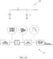
- FIG. 1Aillustrates a conventional touch-sensor pad.
- the touch-sensor pad 100includes a sensing surface 101 on which a conductive object may be used to position a pointer in the x- and y-axes, or to select an item on a display.
- Touch-sensor pad 100may also include two buttons, left and right buttons 102 and 103 , respectively. These buttons are typically mechanical buttons, and operate much like a left and right button on a mouse. These buttons permit a user to select items on a display or send other commands to the computing device.
- FIG. 1Billustrates a conventional linear touch-sensor slider.
- the linear touch-sensor slider 110includes a surface area 111 on which a conductive object may be used to position a pointer in the x-axes (or alternatively in the y-axes).
- the construct of touch-sensor slider 110may be the same as that of touch-sensor pad 100 .
- Touch-sensor slider 110may include a one-dimensional sensor array.
- the slider structuremay include one or more sensor elements that may be conductive traces. Each trace may be connected between a conductive line and a ground. By being in contact or in proximity on a particular portion of the slider structure, the capacitance between the conductive lines and ground varies and can be detected.
- the capacitance variationmay be sent as a signal on the conductive line to a processing device. For example, by detecting the capacitance variation of each sensor element, the position of the changing capacitance can be pinpointed. In other words, it can be determined which sensor element has detected the presence of the conductive object, and it can also be determined the motion and/or the position of the conductive object over multiple sensor elements.
- touch-sensor slidersmay be how the signals are processed after detecting the conductive objects.
- touch-sensor slideris not necessarily used to convey absolute positional information of a conducting object (e.g., to emulate a mouse in controlling pointer positioning on a display) but, rather, may be used to actuate one or more functions associated with the sensing elements of the sensing device.
- FIG. 1Cillustrates a conventional sensing device having three touch-sensor buttons.
- Conventional sensing device 120includes button 121 , button 122 , and button 123 . These buttons may be capacitive touch-sensor buttons. These three buttons may be used for user input using a conductive object, such as a finger.
- capacitive touch sensorsare intended to replace mechanical buttons, knobs, and other similar mechanical user interface controls.
- Capacitive sensorallows eliminating the complicated mechanical switches and buttons, providing the reliable operation under harsh conditions. Also, capacitive sensors are widely used in the modern customer applications, providing new user interface options in the exiting products.
- FIG. 1Dillustrates a conventional relaxation oscillator for capacitance measurement.
- the relaxation oscillator 150is formed by the capacitance to be measured on capacitor 151 , a charging current source 152 , a comparator 153 , and a reset switch 154 .
- capacitor 151is representative of the capacitance measured on a sensor element of a sensor array.
- the relaxation oscillatoris coupled to drive a charging current (Ic) 157 in a single direction onto sensing capacitor Cx, capacitor 151 .
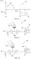
- FIG. 1Eillustrates a variant of the conventional relaxation oscillator of FIG. 1D .
- Relaxation oscillator 160includes a hysteresis comparator 153 , and inverter 161 .
- Comparator 153operates as similar to the comparator describe above.
- the inverter 161is configured to control the switches 162 , which are configured to charge and discharge of the sensor element (e.g., capacitor 151 ).
- the capacitance changecauses the output frequency variation, which can be easily detected, such as using a digital counter.
- the disadvantage of using these conventional relaxation oscillatorsis that they operate at a fixed frequency and include high-impedance signal paths (for example, current source that charges small sensing capacitor Cx.
- FIG. 1Fillustrates another conventional method for measuring capacitance is by phase shift measurement.
- the circuit 170includes a voltage source, resistor, and phase shift meter, which are coupled to the capacitance sensor element.
- the changing of the capacitance on the sensor elementvaries the phase shift between a reference signal and a measured signal.
- the output of the phase shift metercan be converted to a code.
- Driving the capacitance through a fixed-value resistoryields voltage and current waveforms that are out of phase by a predictable amount.
- the drive frequencycan be adjusted to keep the phase measurement in a readily measured range.
- FIG. 1Gillustrates another conventional capacitance measurement scheme based on charging the sensor capacitor from constant current source.
- Circuit 180includes a comparator, a constant current source, and a time measurement circuit, such as a counter or a timer.
- the capacitoris charged from the constant current source, and the time required for getting the demanded threshold voltage is measured by using the counter or timer.
- Another similar conventional capacitance sensing devicebased on charging the sensor capacitor from constant current source charges and discharges the capacitor using the constant current source.
- FIG. 1Hillustrates a conventional capacitive voltage divider circuit 190 for capacitance sensing.
- Capacitive voltage dividerMultiple implementations are possible for the capacitive voltage divider circuit, but FIG. 1H illustrates only one of these implementations.
- the circuitincludes an AC source and two capacitors connected in series. In this case, the voltage on sensing capacitor is inversely proportional to the capacitance.
- FIG. 1Hincludes a conventional peak detector circuit 191 for measuring the voltage. It should be noted that in some implementations where a DC source is used instead AC source, the capacitors should be reset before DC voltage applying using some switches.
- the resistor-capacitor charge timingmay include charging the capacitor through a fixed resistor and measuring timing on the voltage ramp. Small capacitor values may require very large resistors for reasonable timing.
- the capacitive bridge dividermay include driving the capacitor under test through a fixed reference capacitor. The reference capacitor and the capacitor under test form a voltage divider. The voltage signal is recovered with a synchronous demodulator, which may be done in a processing device.
- Another class of methods for measuring capacitance on a sensor elementis switching capacitor methods.
- the sensing capacitoris charged at one phase and is discharged to some charge reception device at a second stage.
- a subclass of this classis charge accumulation.
- Methods of charge accumulation methodsinclude transferring charge accumulated on the sensing capacitor to the charge-accumulation capacitor or integrator with capacitor in the feedback loop. These methods may have a key advantage in that charge-accumulation circuits have low sensitivity for radio-frequency (RF) fields and noise because the sensing capacitor is charged from a low-impedance source and charge is transferred to a low-impedance accumulator (e.g., integrator capacitor or charge-accumulation capacitor).
- RFradio-frequency
- FIG. 1Iillustrates a conventional charge-accumulation circuit 192 .
- the conventional charge-accumulation circuit 192includes the sensing circuit 194 , the integration capacitor 195 , switches 196 and 197 , and the voltage source 193 .
- the conventional charge-accumulation circuit 192is described in U.S. Pat. No. 5,730,165.
- Switches SW 1 and SW 2 196are operating in the non-overlapping way, providing series of sensing capacitor Cx 194 cycles. Capacitance measurement is implemented in the several steps. First, the integration capacitor C int 195 is reset in the initial stage by using the some external switch Sw 3 197 .
- the switches Sw 1 , Sw 2 196start to operate in two non-overlapping phases, providing charge-discharge cycles to the sensing capacitor Cx 194 . Consequently, the integration capacitor C int 195 voltage starts rising.
- the sensed capacitance valueis determined by measuring number of cycles, required for the voltage accumulated on the integration capacitor C int 195 to a reference threshold voltage or by measuring the voltage on the integration capacitor C int 195 after a predefined number of charge transfer cycles.
- the voltage on the integration capacitor C int 195is represented by the following Equation (1):
- V CintV dd ⁇ ( 1 - e - N ⁇ C x C int ) ( 1 )
- V Cintthe voltage on the integration capacitor C int 195
- Nthe cycle count
- C xthe sensing capacitance value
- Cintthe integrator capacitor value
- V ddthe power supply voltage
- FIG. 1Jillustrates another conventional charge-accumulation circuit 198 , including an integrator.
- Charge-accumulation circuit 198is described in U.S. Pat. No. 6,323,846.
- the charge-accumulation circuit 198 of FIG. 1Joperates similarly to the charge-accumulation circuit 192 of FIG. 1I ; however, the integration capacitor voltage rises in the linear way with respect to the number of cycles by placing the integration capacitor in the feedback of an operational amplifier.
- FIG. 1Killustrates another conventional charge-accumulation circuit 199 , including an integrating low-pass filter.
- Charge-accumulation circuit 198is described in U.S. Pat. No. 6 , 323 , 846 .
- the charge-accumulation circuit 199 of FIG. 1Koperates similarly to the charge-accumulation circuit 192 of FIGS. 1I and 198 of FIG. 1J ; however, the charge-accumulation circuit 199 operates as capacitance to the voltage converter of the integrating low-pass filter output voltage that is measured by an analog-to-digital (ADC).
- ADCanalog-to-digital
- the conventional charge-accumulation circuit 199 of FIG. 1Krequires an additional ADC, which increases the total system complexity and cost. Furthermore, the additional ADC may introduce additional noise, such as quantization noise. Also, an additional operation amplifier is required for the integrator that increases the total cost of implementation.
- FIG. 1Lillustrates another switching capacitor design, called the successful approximation.
- Switches SW 1 and SW 2 and the capacitance sensor CXform a switched capacitor network with an equivalent circuit of a resistor to ground.
- the iDACset to a calibrated level, and SW 1 and SW 2 switching, the average voltage on CMOD settles at a level that varies with the value of capacitance on the capacitance sensor C X .
- Setting the iDAC to a low current level with SW 2 openthe voltage on CMOD ramps up.
- the time for the ramp voltage on CMOD to reach VREFis an indication of the value of Cx.
- the timer on the output of the comparatorconverts the ramp time to a digital value.
- Self-calibration of the systemis accomplished through a successive approximation binary search to determine iDAC setting necessary to keep voltage on CMOD at VREF when no finger is present. Individual calibrated iDAC settings are stored for all sensors. When a finger is present, the voltage on CMOD settles at a lower voltage, requiring more time to reach the threshold voltage VREF, as shown in FIG. 1M . If (t 2 -t 1 ) is long enough, the button state is in finger present state, otherwise the button is in the finger absent state.
- the conventional charge-accumulation circuits and methods described aboveoperate in a cycle-based mode (e.g., FIGS. 1I and 1J ), including resetting, integrating, measuring.
- the cycle-based modedoes not allow flexibility in changes to the conversion time.
- the cycle-based modealso does not allow for tracking dynamic capacitance changes, which are common in game accessories, for example.
- FIG. 1NAnother conventional charge accumulation design includes a sigma-delta modulator for capacitance measurement, as described in U.S. Pat. No. 6,970,126. This design is illustrated in FIG. 1N .
- This modulatorincludes the switching signal generator 59 that forms the phase switching signals. These signals are used for setting the sensing capacitor drive switches 86 and 88 for setting levels Vh and V 1 during different phases.
- the sensing capacitor c_sensoris placed between the excitation source switches 86 and 88 and the modulator input switches 44 and 46 .
- the excitation source switches 86 and 88 and the modulator input switches 44 and 46are controlled by the switching signal generator 59 f .
- the output of the modulatoris feedback to the voltage reference 30 f to control the polarity of the reference voltage applied to the reference capacitor Cref 24 f .
- the sensing capacitor c_sensor 90 fis not in the feedback loop of the modulator.
- the sensing capacitor chargeis integrated using the differential integrator 20 and passed to the zero-cross detector comparator 12 .
- the zero cross detector comparatorcontrols the reference capacitor switching using switches 32 / 34 and controlled reference voltage source Vref+.
- the modulator bitstreamis passed to the digital filter.
- the two-electrode systemrequires one wire for exciting the sensing capacitor (e.g., excitation bus) and one wire for sensing the capacitance (e.g., sense line).
- This designcannot work in a single wire configuration.
- the full-scale range of this conventional solutionis set by using the reference capacitor Cref value. This makes design less useful for applications when the full scale should be changed dynamically during device operation or large capacitance values need to be measured, taking into account that capacitors require more die space during IC manufacturing.
- This designrequires a multiphase clock source, multiple switches, a differential integrator, a comparator, etc, which increase the hardware complexity, as well as the die space and overall cost of the end design.
- FIG. 1Aillustrates a conventional touch-sensor pad.
- FIG. 1Billustrates a conventional linear touch-sensor slider.
- FIG. 1Cillustrates a conventional sensing device having three touch-sensor buttons.
- FIG. 1Dillustrates a conventional relaxation oscillator for capacitance measurement.
- FIG. 1Eillustrates a variant of the conventional relaxation oscillator of FIG. 1D .
- FIG. 1Fillustrates another conventional method for measuring capacitance is by phase shift measurement.
- FIG. 1Gillustrates another conventional capacitance measurement scheme based on charging the sensor capacitor from constant current source.
- FIG. 1Hillustrates a conventional capacitive voltage divider circuit 190 for capacitance sensing.
- FIG. 1Iillustrates a conventional charge-accumulation circuit.
- FIG. 1Jillustrates another conventional charge-accumulation circuit, including an integrator.
- FIG. 1Killustrates another conventional charge-accumulation circuit, including an integrating low-pass filter.
- FIG. 1Lillustrates another switching capacitor design, called the successful approximation.
- FIG. 1Millustrates conventional successful approximation method to measure the capacitance
- FIG. 1Nillustrates a conventional solution with sigma-delta modulator
- FIG. 2illustrates a block diagram of one embodiment of an electronic system having a processing device for detecting a presence of a conductive object.
- FIG. 3Aillustrates a varying capacitance sensor element.
- FIG. 3Billustrates one embodiment of a sensing device coupled to a processing device.
- FIG. 4illustrates a block diagram of one embodiment of an electronic device including a processing device that includes capacitance sensor with a sigma-delta modulator for measuring the capacitance on a senor array.
- FIG. 5illustrates a block diagram of one embodiment of a capacitance sensor including a sigma-delta modulator.
- FIG. 6Aillustrates a schematic of one embodiment of a circuit including a sigma-delta modulator and a digital filter for measuring capacitance on a sensor element.
- FIG. 6Billustrates a schematic of another embodiment of a circuit including a sigma-delta modulator and a digital filter for measuring capacitance on a sensor element.
- FIG. 6Cillustrates a schematic of another embodiment of a circuit including a sigma-delta modulator and a digital filter for measuring capacitance on a sensor element.
- FIG. 6Dillustrates a schematic of another embodiment of a circuit including a sigma-delta modulator and a digital filter for measuring capacitance on a sensor element.
- FIG. 7Aillustrates a schematic of one embodiment of a circuit including a sigma-delta modulator for measuring capacitance on a sensor element.
- FIG. 7Billustrates a schematic of another embodiment of a circuit including a sigma-delta modulator for measuring capacitance on a sensor element.
- FIG. 7Cillustrates a schematic of another embodiment of a circuit including a sigma-delta modulator for measuring capacitance on a sensor element.
- FIG. 7Dillustrates a schematic of another embodiment of a circuit including a sigma-delta modulator and for measuring capacitance on a sensor element.
- FIG. 8Aillustrates a schematic of another embodiment of a circuit including a sigma-delta modulator, a clock generation circuit, and a counter-based digital filter for measuring capacitance on a sensor element.
- FIG. 8Billustrates a schematic of another embodiment of a circuit including a sigma-delta modulator and a decimator-type digital filter for measuring capacitance on a sensor element.
- FIG. 9Aillustrate cross-sectional and top-side views of one embodiment of a water drop on a sensing device including multiple sensor elements and a shielding electrode.
- FIG. 9Billustrates one embodiment of a switching circuit and switching capacitor coupled to a shielding electrode.
- FIG. 10Aillustrates one embodiment of a single layer, four-wire ITO touch panel.
- FIG. 10Billustrates another embodiment of a single layer, four-wire ITO touch panel.
- FIG. 10Cillustrates various embodiments of upper switch placements of the switches of a one-dimensional touch panel.
- FIG. 10Dillustrates various embodiments of lower switch placements of the switches of a one-dimensional touch panel.
- FIG. 10Eillustrates two graphs of two embodiment of the transfer function of the ITO touch panel of FIG. 10C .
- FIG. 11illustrates one embodiment of a two-dimensional, four-wire resistive touch panel.
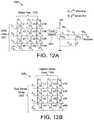
- FIG. 12Aillustrates one embodiment of a matrix scanning device.
- FIG. 12Billustrates another embodiment of a matrix scanning device.
- Described hereinis a method and apparatus converting a capacitance measured on a sensor element to a digital code.
- the following descriptionsets forth numerous specific details such as examples of specific systems, components, methods, and so forth, in order to provide a good understanding of several embodiments of the present invention. It will be apparent to one skilled in the art, however, that at least some embodiments of the present invention may be practiced without these specific details. In other instances, well-known components or methods are not described in detail or are presented in simple block diagram format in order to avoid unnecessarily obscuring the present invention. Thus, the specific details set forth are merely exemplary. Particular implementations may vary from these exemplary details and still be contemplated to be within the spirit and scope of the present invention.
- Embodiments of a method and apparatusare described to convert a capacitance measured on a sensor element to a digital code.
- the methodmay include measuring a capacitance on a sensor element of a sensing device using a sigma-delta modulator, and converting the capacitance measured on the sensor element to a digital code.
- the apparatusmay include a switching capacitor as a sensor element of a sensing device, and a sigma-delta modulator coupled to the sensor element to convert a capacitance measured on the sensor element to a digital code.
- the switching capacitoris in a feedback loop of the sigma-delta modulator.
- the output of the sigma-delta modulatoris used to control the switching operation of the switching capacitor, instead of using an external switching signal generator, as done conventionally.
- the switching capacitoris place between the inputs of the sigma-delta modulator and ground, instead of between an excitation source and the inputs of the sigma-delta modulator, as done conventionally.
- the embodiments described hereinmay use a one-wire configuration for exciting the sensing capacitor and one wire for sensing the capacitance, instead of a two-wire configuration as done conventionally in the configurations where both ends of the sensing capacitor are used.
- the proposed inventionuses the sigma-delta modulator with sensing capacitor, connected by one terminal to ground.
- the embodiments described hereindo not include an operational amplifier with feedback capacitors (e.g., integrator), and a separate comparator.
- the embodiments described hereindo not include a separate terminal for excitation voltage supply, as done conventionally.
- the delta-sigma modulatoroperates continuously, permitting adjustments to the conversion time versus resolution. Also, the modulator bit stream data can be passed to different digital filters at same time, one can track the fast capacitance changes at low resolution, second perform high-precision absolute values measurement, which is not possible with the conventional charge accumulation methods described above.
- the methodincludes measuring the capacitance on a sensor element. This may include charging the capacitance on the sensor element on a line coupled to one end of the switching capacitor, measuring the capacitance using the same line that is coupled to the one end of the switching capacitor.
- the switching capacitoris switched in and out of the feedback loop of the sigma-delta modulator using a switching circuit.
- the switching circuitmay be controlled by the output of the sigma-delta modulator.
- the switching circuitmay be controlled by a clock source, such as a spread spectrum clock source, in conjunction with the output of the sigma-delta modulator.
- FIG. 2illustrates a block diagram of one embodiment of an electronic system having a processing device for detecting a presence of a conductive object.
- Electronic system 200includes processing device 210 , touch-sensor pad 220 , touch-sensor slider 230 , touch-sensor buttons 240 , host processor 250 , embedded controller 260 , and non-capacitance sensor elements 270 .
- the processing device 210may include analog and/or digital general purpose input/output (“GPIO”) ports 207 .
- GPIO ports 207may be programmable.
- GPIO ports 207may be coupled to a Programmable Interconnect and Logic (“PIL”), which acts as an interconnect between GPIO ports 207 and a digital block array of the processing device 210 (not illustrated).
- PILProgrammable Interconnect and Logic
- the digital block arraymay be configured to implement a variety of digital logic circuits (e.g., DAC, digital filters, digital control systems, etc.) using, in one embodiment, configurable user modules (“UMs”).
- the digital block arraymay be coupled to a system bus.
- Processing device 210may also include memory, such as random access memory (RAM) 205 and program flash 204 .
- RAM 205may be static RAM (SRAM), and program flash 204 may be a non-volatile storage, which may be used to store firmware (e.g., control algorithms executable by processing core 202 to implement operations described herein).
- Processing device 210may also include a memory controller unit (MCU) 203 coupled to memory and the processing core 202 .
- MCUmemory controller unit
- the processing device 210may also include an analog block array (not illustrated).
- the analog block arrayis also coupled to the system bus.
- Analog block arrayalso may be configured to implement a variety of analog circuits (e.g., ADC, analog filters, etc.) using, in one embodiment, configurable UMs.
- the analog block arraymay also be coupled to the GPIO 207 .
- capacitance sensor 201may be integrated into processing device 210 .
- Capacitance sensor 201may include analog I/O for coupling to an external component, such as touch-sensor pad 220 , touch-sensor slider 230 , touch-sensor buttons 240 , and/or other devices.
- Capacitance sensor 201 and processing device 202are described in more detail below.
- the embodiments described hereinare not limited to touch-sensor pads for notebook implementations, but can be used in other capacitive sensing implementations, for example, the sensing device may be a touch screen, a touch-sensor slider 230 , or a touch-sensor button 240 (e.g., capacitance sensing button). It should also be noted that the embodiments described herein may be implemented in other sensing technologies than capacitive sensing, such as resistive, optical imaging, surface wave, infrared, dispersive signal, and strain gauge technologies. Similarly, the operations described herein are not limited to notebook pointer operations, but can include other operations, such as lighting control (dimmer), volume control, graphic equalizer control, speed control, or other control operations requiring gradual or discrete adjustments.
- capacitive sensing implementationsmay be used in conjunction with non-capacitive sensing elements, including but not limited to pick buttons, sliders (ex. display brightness and contrast), scroll-wheels, multi-media control (ex. volume, track advance, etc) handwriting recognition and numeric keypad operation.
- non-capacitive sensing elementsincluding but not limited to pick buttons, sliders (ex. display brightness and contrast), scroll-wheels, multi-media control (ex. volume, track advance, etc) handwriting recognition and numeric keypad operation.
- the electronic system 200includes a touch-sensor pad 220 coupled to the processing device 210 via bus 221 .
- Touch-sensor pad 220may include a multi-dimension sensor array.
- the multi-dimension sensor arrayincludes multiple sensor elements, organized as rows and columns.
- the electronic system 200includes a touch-sensor slider 230 coupled to the processing device 210 via bus 231 .
- Touch-sensor slider 230may include a single-dimension sensor array.
- the single-dimension sensor arrayincludes multiple sensor elements, organized as rows, or alternatively, as columns.
- the electronic system 200includes a touch-sensor button 240 coupled to the processing device 210 via bus 241 .
- Touch-sensor button 240may include a single-dimension or multi-dimension sensor array.
- the single- or multi-dimension sensor arrayincludes multiple sensor elements.
- the sensor elementsmay be coupled together to detect a presence of a conductive object over the entire surface of the sensing device.
- the touch-sensor button 240has a single sensor element to detect the presence of the conductive object.
- the touch-sensor button 240may be a capacitance sensor element. Capacitance sensor elements may be used as non-contact sensor elements. These sensor elements, when protected by an insulating layer, offer resistance to severe environments.
- the electronic system 200may include any combination of one or more of the touch-sensor pad 220 , touch-sensor slider 230 , and/or touch-sensor button 240 .
- the electronic system 200may also include non-capacitance sensor elements 270 coupled to the processing device 210 via bus 271 .
- the non-capacitance sensor elements 270may include buttons, light emitting diodes (LEDs), and other user interface devices, such as a mouse, a keyboard, or other functional keys that do not require capacitance sensing.
- buses 271 , 241 , 231 , and 221may be a single bus. Alternatively, these buses may be configured into any combination of one or more separate buses.
- the processing devicemay also provide value-added functionality such as keyboard control integration, LEDs, battery charger and general purpose I/O, as illustrated as non-capacitance sensor elements 270 .
- Non-capacitance sensor elements 270are coupled to the GPIO 207 .
- Processing device 210may include internal oscillator/clocks 206 and communication block 208 .
- the oscillator/clocks block 206provides clock signals to one or more of the components of processing device 210 .
- Communication block 208may be used to communicate with an external component, such as a host processor 250 , via host interface (I/F) line 251 .
- processing block 210may also be coupled to embedded controller 260 to communicate with the external components, such as host 250 .
- Interfacing to the host 250can be through various methods. In one exemplary embodiment, interfacing with the host 250 may be done using a standard PS/2 interface to connect to an embedded controller 260 , which in turn sends data to the host 250 via low pin count (LPC) interface.
- LPClow pin count
- interfacingmay be done using a universal serial bus (USB) interface directly coupled to the host 250 via host interface line 251 .
- the processing device 210may communicate to external components, such as the host 250 using industry standard interfaces, such as USB, PS/2, inter-integrated circuit (I2C) bus, or system packet interfaces (SPI).
- the host 250 and/or embedded controller 260may be coupled to the processing device 210 with a ribbon or flex cable from an assembly, which houses the sensing device and processing device.
- the processing device 210is configured to communicate with the embedded controller 260 or the host 250 to send and/or receive data.
- the datamay be a command or alternatively a signal.
- the electronic system 200may operate in both standard-mouse compatible and enhanced modes.
- the standard-mouse compatible modeutilizes the HID class drivers already built into the Operating System (OS) software of host 250 . These drivers enable the processing device 210 and sensing device to operate as a standard pointer control user interface device, such as a two-button PS/2 mouse.
- the enhanced modemay enable additional features such as scrolling (reporting absolute position) or disabling the sensing device, such as when a mouse is plugged into the notebook.
- the processing device 210may be configured to communicate with the embedded controller 260 or the host 250 , using non-OS drivers, such as dedicated touch-sensor pad drivers, or other drivers known by those of ordinary skill in the art.
- the processing device 210may operate to communicate data (e.g., commands or signals) using hardware, software, and/or firmware, and the data may be communicated directly to the processing device of the host 250 , such as a host processor, or alternatively, may be communicated to the host 250 via drivers of the host 250 , such as OS drivers, or other non-OS drivers. It should also be noted that the host 250 may directly communicate with the processing device 210 via host interface 251 .
- the data sent to the host 250 from the processing device 210includes click, double-click, movement of the pointer, scroll-up, scroll-down, scroll-left, scroll-right, step Back, and step Forward.
- the data sent to the host 250include the position or location of the conductive object on the sensing device.
- other user interface device commandsmay be communicated to the host 250 from the processing device 210 . These commands may be based on gestures occurring on the sensing device that are recognized by the processing device, such as tap, push, hop, and zigzag gestures. Alternatively, other commands may be recognized. Similarly, signals may be sent that indicate the recognition of these operations.
- a tap gesturemay be when the finger (e.g., conductive object) is on the sensing device for less than a threshold time. If the time the finger is placed on the touchpad is greater than the threshold time it may be considered to be a movement of the pointer, in the x- or y-axes. Scroll-up, scroll-down, scroll-left, and scroll-right, step back, and step-forward may be detected when the absolute position of the conductive object is within a pre-defined area, and movement of the conductive object is detected.
- Processing device 210may reside on a common carrier substrate such as, for example, an integrated circuit (IC) die substrate, a multi-chip module substrate, or the like. Alternatively, the components of processing device 210 may be one or more separate integrated circuits and/or discrete components. In one exemplary embodiment, processing device 210 may be a Programmable System on a Chip (PSoCTM) processing device, manufactured by Cypress Semiconductor Corporation, San Jose, Calif. Alternatively, processing device 210 may be one or more other processing devices known by those of ordinary skill in the art, such as a microprocessor or central processing unit, a controller, special-purpose processor, digital signal processor (DSP), an application specific integrated circuit (ASIC), a field programmable gate array (FPGA), or the like. In an alternative embodiment, for example, the processing device may be a network processor having multiple processors including a core unit and multiple microengines. Additionally, the processing device may include any combination of general-purpose processing device(s) and special-purpose processing device(s).
- POPTMProgrammable
- processing device 210may also be done in the host.
- the method and apparatus described hereinmay be implemented in a fully self-contained touch-sensor pad, which outputs fully processed x/y movement and gesture data signals or data commands to a host.
- the method and apparatusmay be implemented in be a touch-sensor pad, which outputs x/y movement data and also finger presence data to a host, and where the host processes the received data to detect gestures.
- the method and apparatusmay be implemented in a touch-sensor pad, which outputs raw capacitance data to a host, where the host processes the capacitance data to compensate for quiescent and stray capacitance, and calculates x/y movement and detects gestures by processing the capacitance data.
- the method and apparatusmay be implemented in a touch-sensor pad, which outputs pre-processed capacitance data to a host, where the touchpad processes the capacitance data to compensate for quiescent and stray capacitance, and the host calculates x/y movement and detects gestures from the pre-processed capacitance data.
- the electronic system that includes the embodiments described hereinmay be implemented in a conventional laptop touch-sensor pad.
- the embodimentsmay be implemented in a wired or wireless keyboard integrating a touch-sensor pad, which is itself connected to a host.
- the processing described above as being performed by the “host”may be performed in part or in whole by the keyboard controller, which may then pass fully processed, pre-processed or unprocessed data to the system host.
- the embodimentsmay be implemented in a mobile handset (e.g., cellular phone or mobile phone) or other electronic devices where the touch-sensor pad may operate in one of two or more modes.
- the touch-sensor padmay operate either as a touch-sensor pad for x/y positioning and gesture recognition, or as a keypad or other array of touch-sensor buttons and/or sliders.
- Capacitance sensor 201may be integrated into the IC of the processing device 210 , or alternatively, in a separate IC. Alternatively, descriptions of capacitance sensor 201 may be generated and compiled for incorporation into other integrated circuits. For example, behavioral level code describing capacitance sensor 201 , or portions thereof, may be generated using a hardware descriptive language, such as VHDL or Verilog, and stored to a machine-accessible medium (e.g., CD-ROM, hard disk, floppy disk, etc.). Furthermore, the behavioral level code can be compiled into register transfer level (“RTL”) code, a netlist, or even a circuit layout and stored to a machine-accessible medium. The behavioral level code, the RTL code, the netlist, and the circuit layout all represent various levels of abstraction to describe capacitance sensor 201 .
- VHDLhardware descriptive language
- Verilogmachine-accessible medium
- the behavioral level codecan be compiled into register transfer level (“RTL”) code, a netlist, or even a circuit
- electronic system 200may include all the components described above. Alternatively, electronic system 200 may include only some of the components described above.
- electronic system 200may be used in a notebook computer.
- the electronic devicemay be used in other applications, such as a mobile handset, a personal data assistant (PDA), a keyboard, a television, a remote control, a monitor, a handheld multi-media device, a handheld video player, a handheld gaming device, or a control panel.
- PDApersonal data assistant
- capacitance sensor 201may be a capacitance-to-code converter with a sigma-delta modulator (CCSD).
- the CCSDmay have an array of capacitive touch sensor elements using a sigma-delta modulator, an analog multiplexer, digital counting functions, and high-level software routines to compensate for environmental and physical sensor element variations.
- the sensor arraymay include combinations of independent sensor elements, sliding sensor elements (e.g., touch-sensor slider), and touch-sensor sensor element pads (e.g., touch pad) implemented as a pair of orthogonal sliding sensor elements.
- the CCSDmay include physical, electrical, and software components.
- the physical componentmay include the physical sensor element itself, typically a pattern constructed on a printed circuit board (PCB) with an insulating cover, a flexible membrane, or a transparent overlay.
- the electrical componentmay include an oscillator or other means to convert a charged capacitance into a measured signal.
- the electrical componentmay also include a counter or timer to measure the oscillator output.
- the software componentmay include detection and compensation software algorithms to convert the count value into a sensor element detection decision (also referred to as switch detection decision). For example, in the case of slider sensor elements or X-Y touch-sensor sensor element pads, a calculation for finding position of the conductive object to greater resolution than the physical pitch of the sensor elements may be used.
- FIG. 3Aillustrates a varying capacitance sensor element.
- a capacitive sensor element 300is a pair of adjacent plates 301 and 302 .
- a conductive object 303e.g., finger
- the capacitance between the electrodes when no conductive object 303 is presentis the base capacitance Cp. This may be stored as a baseline value.
- the baseline capacitance value Cpmay be subtracted from the total capacitance when the conductive object 303 is present to determine the change in capacitance (e.g., capacitance variation Cf) when the conductive object 303 is present and when the conductive object 303 is not present on the sensor element.
- the capacitance variation Cfmay include a capacitance caused by the capacitance with respect to a floating ground of a human body. The values introduced by the human body may range between approximately 100-300 pF.
- Capacitive sensor element 300may be used in a capacitance sensor array.
- the capacitance sensor arrayis a set of capacitors where one side of each is grounded to a system ground.
- the active capacitor(as represented in FIG. 3C as capacitor 351 ) has only one accessible side.
- the presence of the conductive object 303increases the capacitance (Cp+Cf) of the sensor element 300 . Determining sensor element activation is then a matter of measuring change in the capacitance (Cf) or capacitance variation.
- Sensor element 300is also known as a grounded variable capacitor.
- Cpmay range from approximately 10-300 picofarads (pF), and Cf may be approximately 0.5% of Cp.
- Cfmay be orders of magnitude smaller than Cp.
- other ranges and values, such as Cfmay range between 0.1 to 30 pF, may be used.
- capacitance sensor elementis able to operate without surrounding ground plane because human has own relatively large capacitance that can be considered connected between sensing electrode and some internal net that has fixed potential.
- the conductive object 303 in this embodimenthas been illustrated as a finger.
- this techniquemay be applied to any conductive object, for example, a conductive door switch, position sensor, or conductive pen in a stylus tracking system (e.g., stylus).
- FIG. 3Billustrates one embodiment of a capacitive sensor element 307 coupled to a processing device 210 .
- Capacitive sensor element 307illustrates the capacitance as seen by the processing device 210 on the capacitance sensing pin 306 .
- a conductive object 303e.g., finger
- Cfcapacitance between the metal plate and the conductive object 303 with respect to ground.
- This groundmay be a floating ground.
- Cpthere is a capacitance, between the two metal plates, with one of the metal plates being ground to a system ground.
- the ground platemay be coupled to the processing device 210 using GPIO pin 308 .
- the ground platemay be an adjacent sensor element.
- the ground platemay be other grounding mechanisms, such as a surrounding ground plane.
- the processing device 210can measure the change in capacitance, capacitance variation Cf, as the conductive object is in proximity to the metal plate 305 .
- dielectric material 304Above and below the metal plate that is closest to the conductive object 303 is dielectric material 304 .
- the dielectric material 304 above the metal plate 305can be the overlay, as described in more detail below.
- the overlaymay be non-conductive material used to protect the circuitry from environmental conditions and to insulate the user's finger (e.g., conductive object) from the circuitry.
- Capacitance sensor element 307may be a sensor element of a touch-sensor pad, a touch-sensor slider, or a touch-sensor button.
- FIG. 4illustrates a block diagram of one embodiment of an electronic device 400 including a processing device that includes capacitance sensor 201 with a sigma-delta modulator for measuring the capacitance on a senor array 410 .
- the electronic device 400 of FIG. 4includes a sensor array 410 (also known as a switch array), processing device 210 , and host 250 .
- Sensor array 410includes sensor elements 355 ( 1 )- 355 (N), where N is a positive integer value that represents the number of rows (or alternatively columns) of the sensor array 410 .
- Each sensor elementis represented as a capacitor, as described above with respect to FIG. 3B .
- the sensor array 410is coupled to processing device 210 via an analog bus 401 having multiple pins 401 ( 1 )- 401 (N).
- the sensor array 410may be a single-dimension sensor array including the sensor elements 355 ( 1 )- 355 (N), where N is a positive integer value that represents the number of sensor elements of the single-dimension sensor array.
- the single-dimension sensor array 410provides output data to the analog bus 401 of the processing device 210 (e.g., via lines 231 ).
- the sensor array 410may be a multi-dimension sensor array including the sensor elements 355 ( 1 )- 355 (N), where N is a positive integer value that represents the number of sensor elements of the multi-dimension sensor array.
- the multi-dimension sensor array 410provides output data to the analog bus 401 of the processing device 210 (e.g., via bus 221 ).
- the capacitance sensor 201includes a selection circuit (not illustrated).
- the selection circuitis coupled to the sensor elements 355 ( 1 )- 355 (N) and the sigma-delta modulator of the capacitance sensor 201 .
- Selection circuitmay be used to allow the sigma-delta modulator to measure capacitance on multiple sensor elements (e.g., rows or columns).
- the selection circuitmay be configured to sequentially select a sensor element of the multiple sensor elements to provide the charge current and to measure the capacitance of each sensor element.
- the selection circuitis a multiplexer array.
- selection circuitmay be other circuitry inside or outside the capacitance sensor 201 to select the sensor element to be measured.
- the capacitance sensor 201may include one sigma-delta modulator for measuring capacitance on all of the sensor elements of the sensor array.
- capacitance sensor 201may include multiple sigma-delta modulator to measure capacitance on the sensor elements of the sensor array, for example, one sigma-delta modulator per sensor array.
- the multiplexer arraymay also be used to ground the sensor elements that are not being measured. This may be done in conjunction with a dedicated pin in the GP 10 port 207 .
- the capacitance sensor 201may be configured to simultaneously scan the sensor elements, as opposed to being configured to sequentially scan the sensor elements as described above.
- the sensing devicemay include a sensor array having multiple rows and columns. The rows may be scanned simultaneously, and the columns may be scanned simultaneously.
- the voltages on all of the rows of the sensor arrayare simultaneously moved, while the voltages of the columns are held at a constant voltage, with the complete set of sampled points simultaneously giving a profile of the conductive object in a first dimension.
- the voltages on all of the rowsare held at a constant voltage, while the voltages on all the rows are simultaneously moved, to obtain a complete set of sampled points simultaneously giving a profile of the conductive object in the other dimension.
- the voltages on all of the rows of the sensor arrayare simultaneously moved in a positive direction, while the voltages of the columns are moved in a negative direction.
- the voltages on all of the rows of the sensor arrayare simultaneously moved in a negative direction, while the voltages of the columns are moved in a positive direction.
- the processing device 210further includes a decision logic block 402 .
- the operations of decision logic block 402may be implemented in firmware; alternatively, it may be implemented in hardware or software.
- the decision logic block 402may be configured to receive the digital code or counts from the capacitance sensor 201 , and to determine the state of the sensor array 410 , such as whether a conductive object is detected on the sensor array, where the conductive object was detected on the sensor array (e.g., determining the X-, Y-coordinates of the presence of the conductive object), determining absolute or relative position of the conductive object, whether the conductive object is performing a pointer operation, whether a gesture has been recognized on the sensor array 410 (e.g., click, double-click, movement of the pointer, scroll-up, scroll-down, scroll-left, scroll-right, step Back, step Forward, tap, push, hop, zigzag gestures, or the like), or the like.
- the processing device 201may send the raw data to the host 250 , as described above.
- Host 250may include decision logic 451 .
- the operations of decision logic 451may also be implemented in firmware, hardware, and/or software.
- the hostmay include high-level APIs in applications 452 that perform routines on the received data, such as compensating for sensitivity differences, other compensation algorithms, baseline update routines, start-up and/or initialization routines, interpolations operations, scaling operations, or the like.
- the operations described with respect to the decision logic 402may be implemented in decision logic 451 , applications 452 , or in other hardware, software, and/or firmware external to the processing device 210 .
- the processing device 210may also include a non-capacitance sensing actions block 403 .
- This blockmay be used to process and/or receive/transmit data to and from the host 250 .
- additional componentsmay be implemented to operate with the processing device 210 along with the sensor array 410 (e.g., keyboard, keypad, mouse, trackball, LEDs, displays, or the like).
- FIG. 5illustrates a block diagram of one embodiment of a capacitance sensor 201 including a sigma-delta modulator 420 .
- Capacitance sensor 201couples to sensor array 410 via analog bus 401 , as previously described.
- Capacitance sensor 201includes sigma-delta modulator 420 , digital filter 430 , switching circuit 450 , and clock generation circuit 440 .
- sensor arrayhas one or more sensor elements (represented as capacitors) on which capacitance can be measured.
- the switching capacitoris also referred to as a sensing capacitor, variable-switch capacitor, or variable sensing capacitor.
- the sigma-delta modulator 420includes a modulator capacitor, which is configured to receive a transferred charge, accumulated on the switching capacitor (e.g., sensor element). Transferring charge, accumulated on the switching capacitor to the modulator capacitor may provide an advantage because modulator circuits have low sensitivity for RF fields and noise because the sensing capacitor is charged from a low-impedance source and charge is transferred to a low-impedance modulator capacitor.
- a modulator capacitorwhich is configured to receive a transferred charge, accumulated on the switching capacitor (e.g., sensor element). Transferring charge, accumulated on the switching capacitor to the modulator capacitor may provide an advantage because modulator circuits have low sensitivity for RF fields and noise because the sensing capacitor is charged from a low-impedance source and charge is transferred to a low-impedance modulator capacitor.
- the sigma-delta modulator 420may also include a comparator.
- the output of the comparatormay be configured to toggle when the voltage on the modulator capacitor crosses a reference voltage.
- the reference voltagemay be a pre-programmed value, and may be configured to be adjustable.
- the sigma-delta modulator 420may also include a latch coupled to the output of the comparator.
- the latchmay be configured to latch the output of the comparator based on a clock signal from the clock generation circuit 440 .
- the sigma-delta modulator 420may include a synchronized latch that operates to latch an output of the comparator for a length of time.
- the output of the comparatormay be latched for measuring or sampling the output signal of the comparator by the digital filter 430 .
- the latchmay be used to set the sigma-delta modulator sample frequency.
- the sigma-delta modulator 420may also include additional components as described below in the various embodiments.
- Clock source circuit 440is configured to provide the clock to the switching circuit for the switching operation of the switching capacitor.
- the clock generation circuit 440may also provide a clock signal to the sigma-delta modulator 420 for latching the output of the comparator.
- the clock circuit 440may be configured to set a sample frequency and/or an output bitstream frequency of the sigma-delta modulator.
- the clock circuit 440may include a clock source, such as an oscillator, or a pseudo-random signal (PRS) counter.
- PRSpseudo-random signal
- the clock circuit 440may also include additional components as described below in the various embodiments. In one embodiment, to minimize noise, the same number of switching capacitor cycles can be implemented in each conversion cycle. This may be achieved by using a single clock source for the modulator and the switching capacitor circuit, without requiring any synchronization circuit.
- the modulator outputis single bit bit-stream, which can be filtered and converted to the numerical values using a digital filter.
- the digital filter 430is coupled to receive the output 421 of the sigma-delta modulator 420 .
- the digital filter 430is configured to obtain desired characteristics, such as resolution, sample rate, low-pass or high-pass type filtering, or the like.
- the output 421may be a single bit bit-stream, which can be filtered and/or converted by the digital filter 430 to numerical values, such as multi-bit values.
- the digital filteris a single integrator (e.g., counter).
- other standard ADC digital filterscan be used, for example, SincN filter (where N is the order of the Sinc filter), or the like.
- the sigma-delta modulator 420operates as a capacitance-to-duty-cycle converter. As the capacitance on the switching capacitor increase or decrease, the duty-cycle of the sigma-delta modulator subsequently changes. The duty cycle of the sigma-delta modulator 420 may be measured by the digital filter to provide a digital code 431 .
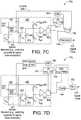
- FIG. 6Aillustrates a schematic of one embodiment of a circuit 600 including a sigma-delta modulator 420 and a digital filter 430 for measuring capacitance on a sensor element 611 .
- Circuit 600includes a switching circuit 450 , clock source 440 , sigma-delta modulator 420 , and digital filter 430 for measuring the capacitance on sensor element 611 .
- Sensor element 611may be a sensor element of sensor array 410 , and is represented as a switching capacitor 611 in the modulator feedback loop. Alternatively, sensor element 611 may be a single element, such as a touch-sensor button.
- Switching circuit 450includes two switches Sw 1 651 and Sw 2 652 .
- the switches Sw 1 651 and Sw 2 652operate in two, non-overlapping phases (also known as break-before-make configuration). These switches together with sensing capacitor C x 611 form the switching capacitor equivalent resistor, which provides the modulator capacitor C mod 623 of sigma-delta modulator 420 charge current (as illustrated in FIG. 6A ) or discharge current (as illustrated in FIG. 6B ) during one of the two phases.
- the sigma-delta modulator 430includes the comparator 621 , latch 622 , modulator capacitor Cmod 623 , modulator feedback resistor 625 , which may also be referred to as bias resistor 625 , and voltage source 626 .
- the output of the comparatormay be configured to toggle when the voltage on the modulator capacitor 623 crosses a reference voltage 624 .
- the reference voltage 624may be a pre-programmed value, and may be configured to be adjustable.
- the sigma-delta modulator 420also includes a latch 622 coupled to the output of the comparator 621 to latch the output of the comparator 621 for a given amount of time, and provide as an output, output 421 .
- the latchmay be configured to latch the output of the comparator based on a clock signal from the gate circuit 440 (e.g., oscillator signal from the oscillator 641 ).
- the sigma-delta modulator 420may include a synchronized latch that operates to latch an output of the comparator for a pre-determined length of time. The output of the comparator may be latched for measuring or sampling the output signal of the comparator 621 by the digital filter 430 .
- Sigma-delta modulator 420is configured to keep the voltage on the modulator capacitor 623 close to reference voltage Vref 624 by alternatively connecting the switching capacitor resistor (e.g., switches Sw 1 651 and Sw 2 652 and sensing capacitor C x 611 ) to the modulator capacitor 623 .
- the output 421 of the sigma-delta modulator 420(e.g., output of latch 622 ) is feedback to the gate circuit 440 , which controls the timing of the switching operations of switches Sw 1 651 and Sw 2 652 of switching circuit 450 .
- the clock source circuit 440includes an oscillator 641 and gate 642 .
- the output 421 of the sigma-delta modulator 420is used with an oscillator signal to gate a control signal 643 , which switches the switches Sw 1 651 and Sw 2 652 in a non-overlapping manner (e.g., two, non-overlapping phases).
- the output 421 of the sigma-delta modulator 420is also output to digital filter 430 , which filters and/or converts the output into the digital code 431 .
- the modulator capacitor 623has zero voltage and switching capacitor resistor (formed by sensing capacitor Cx 611 , and switches Sw 1 651 and Sw 2 652 ) is connected between Vdd line 626 and modulator capacitor 623 .
- This connectionallows the voltage on the modulator capacitor 623 to rise.
- V ref 624the comparator 621 toggles and gates the control signal 643 of the switches Sw 1 651 and Sw 2 652 , stopping the charge current. Because the current via bias resistors R b 625 continues to flow, the voltage on modulator capacitor 623 starts dropping.
- the output of the comparator 621switches again, enabling the modulator 623 to start charging.
- the latch 622 and the comparator 621set sample frequency of the sigma-delta modulator 420 .
- the digital filter 430is coupled to receive the output 421 of the sigma-delta modulator 420 .
- the output 421 of the sigma-delta modulator 420may be a single bit bit-stream, which can be filtered and/or converted to the numerical values using a digital filter 430 .
- the digital filter 430is a counter.
- the standard Sinc digital filtercan be used.
- other digital filtersmay be used for filtering and/or converting the output 421 of the sigma-delta modulator 420 to provide the digital code 431 .
- the output 421may be output to the decision logic 402 or other components of the processing device 210 , or to the decision logic 451 or other components of the host 250 to process the bitstream output of the sigma-delta modulator 420 .
- the sigma-delta modulator 420keeps these currents equal in the average by keeping the voltage on the modulator 623 equal to, or close to, the reference voltage V ref 624 .
- the current of the bias resistor R b 625is:
- I cd mod ⁇ V dd - V C ⁇ ⁇ mod R c ( 4 )
- I RbI c
- V CmodV ref or:
- V ref R bd mod ⁇ V dd - V ref R c ( 5 ) or taking into account that the reference voltage 624 is part of supply voltage:
- Equation (5)can be rewritten in the following form:
- Equation (7)determines the minimum sensing capacitance value, which can be measured with the proposed method at given parameters set:
- ⁇ ⁇ C xmin1 f s ⁇ R b ⁇ k d 1 - k d ( 8 )
- the resolution of this methodmay be determined by the sigma-delta modulator duty cycle measurement resolution, which is represented in the following equations:
- the duty cyclehas a 12-bit resolution and the capacitance resolution is 0.036 pF.
- other types of digital filtersmay be used, for example, by using the Sinc2 filter, the scanning time at the same resolution may be reduced approximately 4 times. To do this the sensing method should have suitable measurement speed.
- a good measurement ratemay be accomplished by using a double integrator as the digital filter 430 .
- FIG. 6Billustrates a schematic of another embodiment of a circuit 625 including a sigma-delta modulator 420 and a digital filter 430 for measuring capacitance on a sensor element 611 .
- Circuit 625is similar to the circuit 600 , as describe above, except the bias resistor 627 is located between the V dd voltage line 626 and the modulator capacitor 623 , instead of between ground and the modulator capacitor 623 (as illustrated in FIG. 6A ). Even though this configuration includes a lower switch configuration, it can still have the same positive effect on the noise immunity of the system.
- FIG. 6Cillustrates a schematic of another embodiment of a circuit 650 including a sigma-delta modulator 420 and a digital filter 430 for measuring capacitance on a sensor element 611 .
- Circuit 650is similar to the circuit 600 , as describe above, except the bias resistor 625 is switched in and out by a third switch Sw 3 628 , which is controlled by the output 421 of the sigma-delta modulator 420 via control line 629 .
- Circuit 650is also dissimilar to circuit 600 in that the clock generation 440 includes a clock source 644 (instead of gate 642 ) and the oscillator 641 .
- the clock source 644is a conventional frequency divider or counter.
- the clock source 644may be a spread-spectrum clock source, such as a pseudo-random signal (PRS) source, which includes a PRS generator.
- PRSpseudo-random signal
- other clock sourcesmay be used, such as clock dithering, or the like.
- the oscillator 641generates an oscillator signal and outputs it to the PRS source 644 , which generates control signal 643 .
- the switches Sw 1 651 and Sw 2 652 of switching circuit 440operate in two, non-overlapping phases, as controlled by the control signal 643 .
- the switching circuit 440operates to provide a charge current to the switching capacitor 611 in one phase (e.g., activating switch Sw 1 651 ), and to transfer charge from the switching capacitor 611 in a second phase (e.g., activating switch Sw 2 652 ).
- the sigma-delta modulator 420operates to switch, in and out, the connection of bias resistor 625 to the charge modulator capacitor 623 to discharge and charge the modulator capacitor 623 .
- the circuits described with respect to FIG. 6Cdiffer from the embodiments described above in that they differ in operational capacitance range and resolution. In the embodiments of FIGS.
- the duty cycleis inversely proportional to the sensing capacitance and the resolution is not constant.
- the embodiments of FIG. 6C and FIG. 6Dinclude a duty cycle that is linearly proportional to the sensing capacitance and the resolution is constant. These embodiments may be used to keep the resolution constant in the operational capacitance range.
- FIGS. 6A and 6Cuse the upper switch placements, while the embodiments of FIGS. 6B and 6D use lower switch placements; however, their operations may be the same.
- the switching capacitor 611has equivalent resistance accordingly to the Equation (11).
- the averaged current via bias resistor R b 625is:
- I Rbd mod ⁇ V Cint R b ( 12 ) sigma-delta modulator 420 keeps these currents equal in the average by keeping the voltage on the modulator capacitor 623 equal to, or close to, the reference voltage V ref 624 .
- I cI Rb and taking into account the equation (6) we can obtain:
- Equation (13)determines the maximum sensing capacitance value, which can be measured with the proposed method at given parameters set: d mod ⁇ 1, or:
- the embodiment described with respect to FIG. 6Cmay include some advantages. These advantages may include that the duty cycle of the sigma-delta modulator 420 is linearly proportional to the capacitance on the sensor element 611 , and that the sensitivity is constant regardless the capacitance value.
- the control signal 643is from a spread source, such as the PRS source 644 , to provide some electromagnetic interference (EMI) immunity.
- EMImay be an electrical disturbance in a system due to natural phenomena, low-frequency waves from electromechanical devices or high-frequency waves (RFI) from chips and other electronic devices.
- RFIhigh-frequency waves
- other spread-clock sourcescan be used, such as voltage-controlled oscillators with an analog noise source, or the like.
- FIG. 6Dillustrates a schematic of another embodiment of a sigma-delta modulator and a digital filter.
- Circuit 675is similar to the circuit 650 , as describe above, except the bias resistor 627 is located between the Vdd voltage line 626 and the modulator capacitor 623 , instead of between ground and the modulator capacitor 623 (as illustrated in FIG. 6C ).
- This embodimentis similar to the embodiment of FIG. 6C , however, the modulator capacitor in FIG. 6D is charged by the feedback resistor and discharged by the switching capacitor, while the modulator capacitor in FIG. 6C is charged from the switching capacitor and is discharged by the feedback resistor.
- the bias resistor 625 or 627 and the modulator capacitor 623are external components to the sigma-delta modulator 420 , which resides in the processing device 210 . This may allow modifications to be made to these components without modifications to the processing device 210 . In another embodiment, these components reside within the sigma-delta modulator 420 and the sigma-delta modulator 420 may reside external to the processing device 210 . Alternatively, all components reside in the processing device 210 . Similarly, in other embodiments, the components described herein may reside on a common carrier substrate such as, for example, an integrated circuit (IC) die substrate, a multi-chip module substrate, or the like. Alternatively, the components of circuits of FIGS.
- ICintegrated circuit
- the voltage divider 829including the two resistors R 1 and R 2 are external components to the sigma-delta modulator 420 , as illustrated in FIG. 8A .
- the voltage divider 829is configured to divide the voltage on the voltage source line 626 to provide as output, the reference voltage 624 .
- the reference voltage 624may be provided by a bandgap voltage 824 .
- other circuits known by those of ordinary skill in the artmay be used to supply the circuit with the reference voltage 624 .
- the reference voltage 624 of FIGS. 6A-6Dis derived from a voltage divider using two resistors (e.g., R 1 and R 2 ) and the voltage source on Vdd line 626 .
- the reference voltage 624may be set using other methods known by those of ordinary skill in the art, such as a separate voltage source, filtered PWM signal, or the like.
- FIGS. 6A-6Dare simplified schematics, and the additional components may be included in the circuits of FIGS. 6A-6D . Alternatively, the schematics may include only the components illustrated in FIGS. 6A-6D .
- the bias resistore.g., bias resistor 625 or 627 of FIGS. 6A and 6C , and FIGS. 6B and 6D , respectively
- the charging currentmay be generated in a register programmable current output DAC (also known as IDAC).
- the current sourcemay be a current DAC or IDAC.
- the IDAC output currentmay be set by an 8-bit value provided by the processing device 210 , such as from the processing core 202 .
- the 8-bit valuemay be stored in a register or in memory.
- other types of current sourcesmay be used.
- One advantage of using a current sourcemay be that it can be programmable with a wide range of values, for example, the current source may be programmed in the firmware of the processing device 210 .
- currents sourcemay be unstable, and may have limited output impedance.
- One advantage of using resistors and the voltage sourceis it may have less dependence on the power supply voltage change.
- one of the switches 651 or 652can be replaced by a resistor. This however, may result in performance degradation, but allows the circuit to be implement on a processing device with limited resources.
- FIG. 7Aillustrates a schematic of one embodiment of a circuit including a sigma-delta modulator for measuring capacitance on a sensor element.
- Circuit 700is similar to the circuit 600 with respect to the switching circuit and the sigma-delta modulator 420 .
- the output of the sigma-delta modulator 420is coupled to receive a clock signal to latch 622 from a frequency divider 741 (also referred to as a prescaler), which divides an oscillator signal from oscillator 641 .
- the output of the latch 622is input into the enable input of a first flip-flop 742 , which provides a control signal 629 to the switching circuit 450 .
- the output of the latch 622is also input into one input of gate 744 , which also receives on the other input a signal from the pulse width modulator (PWM) 745 , which generates variable-length pulses to represent the amplitude of an analog input signal).
- PWMpulse width modulator
- the output of the gateis input into the enable input of a second flip-flop 743 , which receives the clock signal from the frequency divider 741 .
- the output of the second flip-flop 743includes the digital code 431 ,
- FIG. 7Billustrates a schematic of another embodiment of a circuit including a sigma-delta modulator for measuring capacitance on a sensor element.
- Circuit 725is similar to the circuit 700 , as describe above, except a PRS source 644 is coupled between the oscillator 641 and the first flip-flop 742 . As described above, the PRS source provides spread-spectrum operations.
- FIG. 7Cillustrates a schematic of another embodiment of a circuit including a sigma-delta modulator and a decimator type digital filter for measuring capacitance on a sensor element.
- Circuit 750is similar to the circuit 700 , as describe above, except a decimator 746 is coupled to the output of the latch 622 of the sigma-delta modulator 420 , instead of the PWM 745 , gate 744 , and second flip-flop 743 .
- the decimator 746is configured to provide the digital code 431 .
- the frequency divider 741is a 1 / 8 frequency divider. Alternatively, other values may be used.
- FIG. 7Dillustrates a schematic of another embodiment of a circuit including a sigma-delta modulator and a synchronizing and filter circuit for measuring capacitance on a sensor element.
- Circuit 775is similar to the circuit 700 with respect to the switching circuit and the sigma-delta modulator 420 .
- the output of the sigma-delta modulator 420is coupled to receive a clock signal to latch 622 from a frequency divider 741 , which divides an oscillator signal from oscillator 641 .
- the output of the latch 622is input to one input of gate 744 , which also receives on the other input the output of PWM 745 , which receives the same clock signal from the frequency divider 741 .
- the output of the gate 744is input as the enable input to the flip-flop 742 , which receives the input of the PWM 745 .
- the output of the flip-flop 742includes the digital code 431 .
- this embodimentincludes a PRS source 644 is placed between the oscillator 641 and the switching circuit 450 to provide the control signal 629 , instead of the first flip-flop 742 of circuit 700 of FIG. 7A .
- FIG. 8Aillustrates a schematic of another embodiment of a circuit including a sigma-delta modulator, a clock generation circuit, and a counter-based digital filter for measuring capacitance on a sensor element.
- Circuit 800includes the sigma-delta modulator 420 , the switching circuit 450 , the sensor element 611 , as described with respect to the embodiments above of FIGS. 6A-6D, and 7A-7D .
- the clock generation circuit 440 and the digital filter 430include different elements than the circuits described above.
- the digital filter 430includes the PWM 745 , a gate 831 , and counter 832 .
- the digital filter 430may be a simple single integrator, based on the counter 832 with enabled input.
- the gatereceives, as inputs, the output of the sigma-delta modulator 420 (e.g., from latch 622 ) and the output of the PWM 745 , and provides, as output, an enable signal for the counter 832 .
- the counter 832is clocked by the clock signal received from the VC 1 842 of the synchronizing circuit 440 .
- the counter 832provides, as output, the digital code 643 to the decision logic, such as decision logic 402 or 451 .
- FIG. 8Billustrates a schematic of another embodiment of a circuit including a sigma-delta modulator and a decimator-type digital filter for measuring capacitance on a sensor element.
- the circuit 825is similar to the circuit 800 , as describe above, except the digital filter 430 includes a decimator 833 .
- the decimator 833is a hardware decimator, second order Sinc type digital filter.
- other types of decimatorsmay be used. Decimators are known by those of ordinary skill in the art, and according, a detailed description regarding them has not been included.
- the digital filter 430may not include the gate 831 and PWM 745 .
- the clock generation circuit 440includes an internal main oscillator (IMO) 841 , clock source 844 , and a frequency divider 741 (also referred to as a prescaler).
- the output of the clock source 844provides the control signal 629 to control the switching operations of the switching circuit 450 (e.g., two non-overlapping switches). Alternatively, the control signal may be provided to the switching circuit 440 using other embodiments described herein.
- the internal main oscillator (IMO) 841forms all clock signals.
- the modulator latch signalcomes from frequency divider 741 (also referred to as a prescaler).
- the switches clock sourcemay be built around a pseudo-random sequence (PRS) generator that is used for spread-spectrum operation.
- PRSpseudo-random sequence
- Embodiments described hereinmay include one or more of the following advantages.
- the embodimentsmay include higher sensitivity and higher resolution than conventional capacitance measuring techniques (e.g., relaxation oscillator), and better noise immunity than conventional designs because the switching capacitor 611 is charged from low-impedance source (voltage source 626 ) at one phase, which output impedance is less than approximately 1K Ohm, and is discharged to the low-impedance current recipient (e.g., modulator capacitor 623 is a larger value capacitor than the switching capacitor 611 ) at second phase.
- the embodiments described hereinmay have the ability to operate with thicker overlays than the conventional capacitance measuring techniques (e.g., thicknesses greater than approximately 5 mm).
- the embodiments described hereinmay have an improved EMI immunity than conventional designs when a spread spectrum source is used for the switching capacitor operation.
- the spread spectrum sourceallows the system to operate in a wide frequency range with the presence of noise, as compared to the fixed operation frequency systems of the conventional designs that can easily be disturbed by noise when the noise frequency is close to the operation frequency.
- the embodiments described hereinmay have low sensitivity to the sensing element resistance in series, which allows operations with high-resistive conductive materials (e.g., larger than 100 ⁇ /square, for example ITO panels.
- ITO panels which have a larger sensing zonecan be used because the summarized resistance is less than 1K Ohms, as compared to a thin and long ITO line that has a resistance about 30-100K Ohms, which makes capacitance sensing more difficult, especially when a high operational frequency is used.
- the embodiments described hereinmay also be expandable to the linear position sensing through conductive materials (e.g., two-wire touch-sensor sliders, three-wire rotation wheel touch-sensor slider, or a four-wire touch-sensor pad).
- the embodiments of the method described hereinmay also include advantages over the conventional capacitance sensing methods, such as flexible configuration measurement resolution versus conversion time, flexible capacitance measurement resolution versus time, such as by properly configuring the digital filter for “decimation” ratio; provides continuous type operation.
- Another advantagemay include filtering the modulator bitstream in the parallel by several digital filters, one can be integration digital filter with long accumulation interval for high-resolution absolute values capacitance measurements, and a second can be digital filter for tracking fast capacitance change, for example.
- the sigma-delta modulator output bit-streamis passed to through a low-pass digital filter, which attenuates the noise during measurement phase, which may provide an additional advantage over conventional methods.
- the switching signalis modulated by sigma-delta modulator output, providing some spectrum spreading in the circuit of FIG. 6A .
- using the PRS source as switches clock source (e.g., control signal 643 ) for the spread spectrum operationprovides a circuit that is more robust to external noise signals.
- embodiments described hereinmay be configured so that no precision external capacitors are used, and there may be no demands for the stable charge-accumulation capacitor to be resistant to the sharp temperature changes, as in the existing charge transfer methods.
- a threshold operation modemay be supported.
- the devicein the circuits 600 and 625 of FIGS. 6A and 6B , may be configured to set the reference voltage at a level (e.g., voltage on at which if sensing capacitance on the switching capacitor 611 is too low (e.g., the comparator input voltage is less than the reference voltage by a pre-determined value), the device can be put in a low-power or standby mode, and a subsequent touch (e.g., presence of a conductive object) brings the device from the standby mode to normal operation mode.
- This modemay be configured to be used as an automatic device wake-up operation, for example.
- the embodiments described hereinmay be easy to manufacture on silicon (e.g., Easy to silicon implementations), for example, for the analog resources may be minimal (e.g., only one analog comparator with couple resistors). Also, the additional components, such as the PRS (or other spread spectrum sources), counters, decimators may be easy to manufacture using modern silicon process.
- the embodimentsare implemented in one digital block and one analog block of the (PSoCTM) processing device, manufactured by Cypress Semiconductor Corporation, San Jose, Calif. Also, by selecting the switching frequency properly, good environmental factor compensation may be possible, such as for humidity, water films, or the like). For example, the water influence can be reduced by using the higher operation frequencies (12 MHz or more), where water dielectric constant is reduced.
- the embodiments described hereinmay be implemented in various capacitance sensing applications, such as linear slider sensing, plane sensing, key matrix switches implementation, and the like. Some of these embodiments have been described in additional detail below.
- the embodiments described hereinmay be implemented in a one-dimensional position sensing device, such as two-pin sliders, three-pin rotation wheel slider, keyboards by connection keys, level sensing devices (e.g., water level sensing, etc), and other one-dimensional position sensing devices.
- the embodiments described hereinmay also be implemented in multi-dimensional position sensing devices, such as various touch-sensor pads, transparent touch screens, keyboards (e.g., personal computer (PC) keyboards, industrial controller keyboards, remotes, or the like), game accessories, or other multi-dimensional position sensing devices.
- the embodiments described hereinmay be implemented to measure capacitance on a single sensor element, such as a touch-sensor button.
- the embodiments described hereinmay be with conductive materials of position sensing, such as ITO materials for both single and multi-dimensional sensing devices.
- the embodimentsmay be implemented in a dual layer, matrix-scanning application, such as illustrate in FIG. 9 .
- the dual layer ITO panel exampleconsists of non-interlaced row and column sensing zones.
- the ITO panelmay scan the rows and columns in series (e.g., sequentially), or alternatively, in parallel (e.g., simultaneously).
- This designmay have the following advantages over the oscillator-based methods: the capacitance measurements have no dependence on the resistor in series, which is important for scanning via high-resistance conductive materials.
- the transmitted charge amount between cyclesdoes not depend on the resistor in series if equilibrium state is reached within each cycle.
- the operational frequency of the switching circuitshould be selected in such as way as to provide complete row or column line re-charge each switching cycle.
- the operation frequencycan be selected to be less than 1 MHz, such as 300-400 kHz for a 50 ⁇ 50 mm panel with 10 mils connection and inter-segment tracks, made from 400 ⁇ /square ITO material.
- other higher receptivity materialscan be used, which use lower operation frequency.
- Some applications of capacitance sensing devicesrequire the reliable operation in the presence of the water films or drops on the sensing device.
- various applicationssuch as household appliances, automotive applications, industrial application, need sensor elements that do not provide false triggering when the presence of water, ice, humidity, or the like exists and/or changes on the sensor elements.
- a separate shielding electrodecan be used.
- FIG. 9Aillustrate cross-sectional and top-side views of one embodiment of a water drop on a sensing device including multiple sensor elements and a shielding electrode.
- the sensing device 900includes sensor elements 901 and a shielding electrode 902 on a printed circuit board 903 .
- the printed circuit boardincluding an overlay 904 , upon which a water drop 905 is disposed.
- the shielding electrode 902may be located on the same layer of the sensor elements 901 , or alternatively, on a separate layer of the PCB 903 .
- the shielding electrode 902may surround the sensor elements 901 , or alternatively, may be adjacent to the sensor elements 901
- the coupling between the shielding electrode 902 and the sensor elements 901is increased.
- the C pis increased and modulator current is reduced.
- the increase of coupling between the sensor elements and the shielding electrodemay increase the raw counts measured by the processing device. This may result in false triggering of button activation when no button has been pressed.
- the modulator reference voltageis increased by an API in such way that the raw count increase caused from the water drops can be corrected (e.g., calibrated to be close to zero, or alternatively, slightly negative).
- shielding electrode planecovers button.
- the shielding electrodecan be located at the opposite PCB layer, including the plane under button.
- a hatch patternas illustrated in FIG. 9A , may be used for the shielding electrode.
- the fill ratio of the shielding electrode to sensor elementis approximately 30-40%. Alternatively, other patterns and ratios may be used.
- the shield electrodemay be in a transparent touchpad device. This may be useful to block the noise influence of the LCD drive electrodes and reduce the stray capacitance at the same time.
- FIG. 9Billustrates one embodiment of a switching circuit and switching capacitor coupled to a shielding electrode.
- the same clock signal that is used to precharge the sensor element 901is supplied to shielding electrode 902 .
- the sensor capacitance C xis the capacitance on the sensor element (e.g., switching capacitor) and the parasitic capacitance C p is between the shielding electrode 902 and sensor element 901 .
- the first and third switches Sw 1 and Sw 3are on at on at phase 1 , Phi 1 phase, and the second and fourth switches Sw 2 and Sw 4 are on at phase 2 , Phi 2 .
- the C paris discharged at Ph 1 phase and is charged at Ph 2 phase.
- the modulator currentis reduced with coupling increasing between electrodes, which allows separate signals from water and conductive object 303 (e.g., finger). Water drops may decrease the modulator current, and the finger touch may increase the modulator current. This may simplify the decision logic operation.
- FIG. 10Aillustrates one embodiment of a single layer, four-wire ITO touch panel.
- the ITO touch panel 1000includes solid ITO coating with the electric filed linearization electrodes. It should be noted that some embodiments may not use the field linearization electrodes, and alternatively, the linearization may be in firmware of the processing device.
- FIG. 10Billustrates another embodiment of a single layer, four-wire ITO touch panel.
- the ITO touch panel 1010includes multiple resistive sliders, connected in the parallel, that provide linear electric field gradient over the panel 1010 .
- this topologymay not use the field linearization electrodes, and the linearization may be done in firmware of the processing device.
- FIG. 10Cillustrates various embodiments of upper switch placements of the switches of a one-dimensional touch panel.
- the operation ideais charging the resistive material to some voltage at Ph 1 .
- one edge of resistive materialis connected to the ground or fixed voltage source, the second edge is connected to the sigma-delta modulator capacitor.
- This connectionforms the resistive network that provides the modulator filter capacitor current flow path. The current value depends on the touch capacitance and its position on slider.
- Stage 1 and Stage 2the A edge of conductive material is connected to the fixed potential net at Ph 2 operation cycle and current is sensed from side B of conductive strip.
- Stage 2the B edge of conductive material is connected to the fixed voltage net and signal from edge A is passed to the modulator filtering capacitor.
- the touch positioncan be found by doing relatively simple math calculations as described below.
- Capacitor C xindicates the capacity of slider and capacity introduced by finger in the touch point. This discussion, however does not consider the slider distributed parasitic capacitance and its influence on the measurement results for math simplification. It should be noted that the influence of the parasitic capacitance should be constant over one-dimensional strip during measurement cycle.
- the capacitor C xis charged by fixed voltage V dd . Charge time should be enough for transient process finalization. At the Ph 2 the C x is discharged. Discharge time is limited by Ph 2 duration period, mark as t r .
- the sigma-delta modulatorkeeps the input voltage close to V ref and this voltage can be assumed constant during operation. Quantity of charge, passed through resistor R x will be equal to integral of current passed through this resistor, as represented in the following equations:
- V Cx ⁇ ( t )R x ⁇ R x ⁇ ⁇ 1 R x + R x ⁇ ⁇ 1 ⁇ C x ⁇ dV Cx dt + R x ⁇ ⁇ 1 R x + R x ⁇ ⁇ 1 ⁇ V ref ( 19 )
- V Cx (0)V dd
- V refconstant
- V Cx ⁇ ( t )R x ⁇ ⁇ 1 R x + R x ⁇ ⁇ 1 ⁇ V ref + ( V dd - R x ⁇ ⁇ 1 R x + R x ⁇ ⁇ 1 ⁇ V ref ) ⁇ exp ⁇ ( - R x + R x ⁇ ⁇ 1 R x + R x ⁇ ⁇ 1 ⁇ t r C x ) ( 20 )
- the following equationincludes the resistive divider on R x , R x1 . We can simplify it by using the following substitutions:
- V Cx ⁇ ( t )K ⁇ V ref + ( V dd - K ⁇ V ref ) ⁇ exp ⁇ ( - 1 K ⁇ ( 1 - K ) ⁇ R ⁇ t C x ) ( 22 )
- I sw1 R ⁇ V ref + K ⁇ C x t r ⁇ ( V dd - K ⁇ V ref ) ⁇ ( exp ⁇ [ - 1 K ⁇ ( 1 - K ) ⁇ R ⁇ t r C x ] - 1 ) ( 24 )
- This equationrepresents two components.
- One componentcovers the resistive strip DC current (left term, that is inversely proportional to the R), and second component is caused by the presence of the conductive object (e.g., touch influence).
- the sigma-delta modulatorconverts the I sw current in the duty cycle.
- FIG. 10Dillustrates various embodiments of lower switch placements of the switches of a one-dimensional touch panel. The operation of these embodiments is similar to those described above with respect to the upper switch placements, and is apparent to one of ordinary skill in the art. Accordingly, additional details regarding their operation have not been included.
- FIG. 10Eillustrates two graphs of two embodiment of the transfer function of the ITO touch panel of FIG. 10C .
- the transfer functionbecomes more linear when reference voltage is lowered. For example, in the left graph the reference voltage is 1.3 V and the right graph the reference voltage is 0.05 volts, and the resulting transfer function of the graph on the right is more linear than the transfer function on the left graph.
- the resistive material current componentis reduced.
- the configurationincludes connecting the second end of resistive strip to net with same potential as the modulator reference voltage V ref . This may provide the linear transfer characteristic and no dependence from resistive strip absolute resistance value.
- the description abovemay be extended for two dimension operation by increasing the number of parallel operation channels (e.g., using two or more sigma-delta modulators, operating in parallel) or by sensing the two dimensional panel as a set of one dimension sliders.
- the two panel edgeseffectively are a one-dimensional slider with A,B terminals.
- the left two edge connectorscan be left non-connected or be connected to the modulator reference voltage source, forming the different measurement schemes.
- a 4-wire ITO panel configurationmay include four modulators with four separate digital filters, which are used at same time. If two sigma-delta modulators are running in parallel, slider touch position may be determined in one single stage, eliminating the need for two separate stages, Stage 1 and Stage 2 . Running several modulators in parallel may reduce scan time and improve SNR. One disadvantage may be an increase in cost of hardware resources. Alternatively, other configurations are possible.
- FIG. 11illustrates one embodiment of a two-dimensional, four-wire resistive touch panel.
- the two coordinatescan be evaluated by doing the several measurements in series using one sigma-delta modulator.
- the eight conversionsmay be used for high-accuracy position calculation and touch capacitance compensation. If two sigma-delta modulators running in parallel modulators are used, only four measurements are made. Running four sigma-delta modulators allows the touch panel position to be made using a single conversion.
- the embodiments described hereinmay be implemented in a matrix-scanning device, such as a keyboard.
- FIG. 12Aillustrates one embodiment of a matrix-scanning device.
- Matrix scanningusing the embodiments described herein, may reduce the number of connection lines for a keyboard, and may be useful for multi-button scanning applications, such as PC keyboards, or the like.
- the scanning matrix 1200includes the N drive lines 1201 and M sense lines 1202 , and each capacitive key is located at drive/sense line intersection. It should be noted that multiple implementations are possible for forming the drive signals and sensing strategy depending on the available hardware resources.
- the drive signalis applied to the N drive lines 1201 in series or sequentially using a clock source 1203 , and the M sensing lines 1202 are sensed in parallel. Alternatively, other excitation signal sources may be used.
- the drive signalsare applied to each drive line 1201 in series, and each sense line 1201 is scanned in series as well.
- the DC voltage source(Vdc) is used for parasitic capacitance compensation.
- the value of Vdcmay be adjusted such that there is minimal or no modulator current when there is not presence of the conductive object (e.g., no touch is being detected).
- the DC source voltagecan be selected to be equal to zero, or alternatively, equal to V dd (e.g., bottom lead of the third switch Sw 3 is connected to ground or V dd ).
- the DC source voltagemay be equal to the reference voltage V ref .
- the switchcan be connected to the V dd or V ss lines of the PSoCTM processing device, manufactured by Cypress Semiconductor Corporation, San Jose, Calif.
- DC voltage source to the first switch Sw 1which may allow offset compensation in a circuit that includes two analog buses, such as the PSoCTM processing device, manufactured by Cypress Semiconductor Corporation, San Jose, Calif.
- FIG. 12Billustrates another matrix scanning device 1250 (e.g., keyboard matrix) that does not use the excitation signal source.
- the matrixis formed by column and row sense lines 1204 and 1205 .
- the touched keyis determined as intersection detected row and column touched sensors.
- an insulated sensor element and a sigma-delta modulatormay be used a liquid level metering device.
- the insulated sensor elementmay be placed inside a tank with liquid.
- the sensor capacitancemay be configured to increase linearly in response to an increase in level of the liquid in the tank.
- the embodiments described hereindescribe a capacitance-to-code converter that allows continuous type operation by providing a continuous output bitstream that can be filtered by one or more filters, (e.g., parallel multiple digital filters) to obtain desired characteristics, such as resolution, sample rate, low-pass or high-pass filtering, or the like.
- filterse.g., parallel multiple digital filters
- the embodiments describe hereinmay also be configured to provide a direct capacitance-to-code conversion using a sigma-delta modulator with linear transfer characteristic and fixed measurement time, for example, using a decimator, whose output code is directly proportional to the capacitance.
- the embodiments described hereinmay have the advantage of keeping all benefits of existing charge transfer/accumulation methods (especially in the high immunity for RF/EMI noise signals), and may be configured for easy implementation in existing devices from hardware and software perspectives, as well as in future devices.
- Embodiments of the present inventioninclude various operations. These operations may be performed by hardware components, software, firmware, or a combination thereof.
- the term “coupled to”may mean coupled directly or indirectly through one or more intervening components. Any of the signals provided over various buses described herein may be time multiplexed with other signals and provided over one or more common buses. Additionally, the interconnection between circuit components or blocks may be shown as buses or as single signal lines. Each of the buses may alternatively be one or more single signal lines and each of the single signal lines may alternatively be buses.
- Certain embodimentsmay be implemented as a computer program product that may include instructions stored on a machine-readable medium. These instructions may be used to program a general-purpose or special-purpose processor to perform the described operations.
- a machine-readable mediumincludes any mechanism for storing or transmitting information in a form (e.g., software, processing application) readable by a machine (e.g., a computer).
- the machine-readable mediummay include, but is not limited to, magnetic storage medium (e.g., floppy diskette); optical storage medium (e.g., CD-ROM); magneto-optical storage medium; read-only memory (ROM); random-access memory (RAM); erasable programmable memory (e.g., EPROM and EEPROM); flash memory; electrical, optical, acoustical, or other form of propagated signal (e.g., carrier waves, infrared signals, digital signals, etc.); or another type of medium suitable for storing electronic instructions.
- magnetic storage mediume.g., floppy diskette
- optical storage mediume.g., CD-ROM
- magneto-optical storage mediume.g., magneto-optical storage medium
- ROMread-only memory
- RAMrandom-access memory
- EPROM and EEPROMerasable programmable memory
- flash memoryelectrical, optical, acoustical, or other form of propagated signal (e.g., carrier waves, in
- some embodimentsmay be practiced in distributed computing environments where the machine-readable medium is stored on and/or executed by more than one computer system.
- the information transferred between computer systemsmay either be pulled or pushed across the communication medium connecting the computer systems.
Landscapes
- Engineering & Computer Science (AREA)
- Theoretical Computer Science (AREA)
- General Engineering & Computer Science (AREA)
- Human Computer Interaction (AREA)
- Physics & Mathematics (AREA)
- General Physics & Mathematics (AREA)
- Position Input By Displaying (AREA)
- Measurement Of Resistance Or Impedance (AREA)
- Compression, Expansion, Code Conversion, And Decoders (AREA)
- Electronic Switches (AREA)
Abstract
Description
where the term VCintis the voltage on the
The
where fsis the operation frequency of the switches (e.g., switching circuit450). If the
In the operation mode, IRb=Ic, VCmod=Vrefor:
or taking into account that the
The Equation (5) can be rewritten in the following form:
or after rewriting relatively ΔCx, we obtain:
Ic=Cxfs(Vdd−VCint) (11)
The averaged current via
sigma-
Imod=IC−ICpar=fsCx(Vdd−VCmod)−fxCparVCmod (16)
For the initial conditions: VCx(0)=Vdd, Vref=constant, the solution of equation (19) will be:
The following equation includes the resistive divider on Rx, Rx1. We can simplify it by using the following substitutions:
Now, changing equation 21, taking into account equation 20 for resistive tap, the following equation is derived:
By dividing the equation (23) on Ph2duration time tr, one can determine the current value via switching capacitor slider, as represented in the following equation:
This equation represents two components. One component covers the resistive strip DC current (left term, that is inversely proportional to the R), and second component is caused by the presence of the conductive object (e.g., touch influence). The sigma-delta modulator converts the Iswcurrent in the duty cycle.
Claims (20)
Priority Applications (1)
| Application Number | Priority Date | Filing Date | Title |
|---|---|---|---|
| US15/955,862US10928953B2 (en) | 2006-11-14 | 2018-04-18 | Capacitance to code converter with sigma-delta modulator |
Applications Claiming Priority (5)
| Application Number | Priority Date | Filing Date | Title |
|---|---|---|---|
| US11/600,255US8547114B2 (en) | 2006-11-14 | 2006-11-14 | Capacitance to code converter with sigma-delta modulator |
| US13/049,798US9154160B2 (en) | 2006-11-14 | 2011-03-16 | Capacitance to code converter with sigma-delta modulator |
| US13/917,528US9166621B2 (en) | 2006-11-14 | 2013-06-13 | Capacitance to code converter with sigma-delta modulator |
| US14/832,529US9977551B2 (en) | 2006-11-14 | 2015-08-21 | Capacitance to code converter with sigma-delta modulator |
| US15/955,862US10928953B2 (en) | 2006-11-14 | 2018-04-18 | Capacitance to code converter with sigma-delta modulator |
Related Parent Applications (1)
| Application Number | Title | Priority Date | Filing Date |
|---|---|---|---|
| US14/832,529ContinuationUS9977551B2 (en) | 2006-11-14 | 2015-08-21 | Capacitance to code converter with sigma-delta modulator |
Publications (2)
| Publication Number | Publication Date |
|---|---|
| US20180284928A1 US20180284928A1 (en) | 2018-10-04 |
| US10928953B2true US10928953B2 (en) | 2021-02-23 |
Family
ID=39368717
Family Applications (5)
| Application Number | Title | Priority Date | Filing Date |
|---|---|---|---|
| US11/600,255Active2030-02-28US8547114B2 (en) | 2006-11-14 | 2006-11-14 | Capacitance to code converter with sigma-delta modulator |
| US13/049,798Active2033-06-10US9154160B2 (en) | 2006-11-14 | 2011-03-16 | Capacitance to code converter with sigma-delta modulator |
| US13/917,528ActiveUS9166621B2 (en) | 2006-11-14 | 2013-06-13 | Capacitance to code converter with sigma-delta modulator |
| US14/832,529Active2027-11-06US9977551B2 (en) | 2006-11-14 | 2015-08-21 | Capacitance to code converter with sigma-delta modulator |
| US15/955,862ActiveUS10928953B2 (en) | 2006-11-14 | 2018-04-18 | Capacitance to code converter with sigma-delta modulator |
Family Applications Before (4)
| Application Number | Title | Priority Date | Filing Date |
|---|---|---|---|
| US11/600,255Active2030-02-28US8547114B2 (en) | 2006-11-14 | 2006-11-14 | Capacitance to code converter with sigma-delta modulator |
| US13/049,798Active2033-06-10US9154160B2 (en) | 2006-11-14 | 2011-03-16 | Capacitance to code converter with sigma-delta modulator |
| US13/917,528ActiveUS9166621B2 (en) | 2006-11-14 | 2013-06-13 | Capacitance to code converter with sigma-delta modulator |
| US14/832,529Active2027-11-06US9977551B2 (en) | 2006-11-14 | 2015-08-21 | Capacitance to code converter with sigma-delta modulator |
Country Status (1)
| Country | Link |
|---|---|
| US (5) | US8547114B2 (en) |
Families Citing this family (340)
| Publication number | Priority date | Publication date | Assignee | Title |
|---|---|---|---|---|
| US8144125B2 (en) | 2006-03-30 | 2012-03-27 | Cypress Semiconductor Corporation | Apparatus and method for reducing average scan rate to detect a conductive object on a sensing device |
| US8040142B1 (en) | 2006-03-31 | 2011-10-18 | Cypress Semiconductor Corporation | Touch detection techniques for capacitive touch sense systems |
| US8004497B2 (en) | 2006-05-18 | 2011-08-23 | Cypress Semiconductor Corporation | Two-pin buttons |
| US8547114B2 (en) | 2006-11-14 | 2013-10-01 | Cypress Semiconductor Corporation | Capacitance to code converter with sigma-delta modulator |
| US8159462B1 (en)* | 2006-11-15 | 2012-04-17 | Cypress Semiconductor Corporation | Reference voltage offset for capacitive touch-sensor measurement |
| US8089288B1 (en) | 2006-11-16 | 2012-01-03 | Cypress Semiconductor Corporation | Charge accumulation capacitance sensor with linear transfer characteristic |
| US8058937B2 (en) | 2007-01-30 | 2011-11-15 | Cypress Semiconductor Corporation | Setting a discharge rate and a charge rate of a relaxation oscillator circuit |
| WO2008106764A1 (en)* | 2007-03-05 | 2008-09-12 | Arokia Nathan | Sensor pixels, arrays and array systems and methods therefor |
| US8243043B2 (en)* | 2007-03-29 | 2012-08-14 | Cirque Corporation | Driven shield for capacitive touchpads |
| TWI340911B (en)* | 2007-04-13 | 2011-04-21 | Generalplus Technology Inc | Capacitance touch sensor |
| US8144126B2 (en) | 2007-05-07 | 2012-03-27 | Cypress Semiconductor Corporation | Reducing sleep current in a capacitance sensing system |
| US20080309353A1 (en)* | 2007-06-14 | 2008-12-18 | Man Kit Jacky Cheung | Capacitive touch sensor |
| US9500686B1 (en) | 2007-06-29 | 2016-11-22 | Cypress Semiconductor Corporation | Capacitance measurement system and methods |
| US8169238B1 (en) | 2007-07-03 | 2012-05-01 | Cypress Semiconductor Corporation | Capacitance to frequency converter |
| US8089289B1 (en) | 2007-07-03 | 2012-01-03 | Cypress Semiconductor Corporation | Capacitive field sensor with sigma-delta modulator |
| US8570053B1 (en)* | 2007-07-03 | 2013-10-29 | Cypress Semiconductor Corporation | Capacitive field sensor with sigma-delta modulator |
| JP2010533288A (en)* | 2007-07-11 | 2010-10-21 | マリミルス オーワイ | Method and apparatus for detecting the volume of an object |
| TW200905538A (en)* | 2007-07-31 | 2009-02-01 | Elan Microelectronics Corp | Touch position detector of capacitive touch panel and method of detecting the touch position |
| US8248081B2 (en) | 2007-09-06 | 2012-08-21 | Cypress Semiconductor Corporation | Calibration of single-layer touch-sensor device |
| US20090174676A1 (en) | 2008-01-04 | 2009-07-09 | Apple Inc. | Motion component dominance factors for motion locking of touch sensor data |
| US8525798B2 (en) | 2008-01-28 | 2013-09-03 | Cypress Semiconductor Corporation | Touch sensing |
| US8319505B1 (en) | 2008-10-24 | 2012-11-27 | Cypress Semiconductor Corporation | Methods and circuits for measuring mutual and self capacitance |
| US8358142B2 (en) | 2008-02-27 | 2013-01-22 | Cypress Semiconductor Corporation | Methods and circuits for measuring mutual and self capacitance |
| US9104273B1 (en) | 2008-02-29 | 2015-08-11 | Cypress Semiconductor Corporation | Multi-touch sensing method |
| US9007310B1 (en)* | 2008-02-29 | 2015-04-14 | Cypress Semiconductor Corporation | Single layer touch sensor with improved sensitivity and accuracy |
| US20090225044A1 (en)* | 2008-03-06 | 2009-09-10 | Leadis Technology, Inc. | Determining touch on keys of touch sensitive input device |
| FI121979B (en)* | 2008-03-26 | 2011-06-30 | Elsi Technologies Oy | Adapter component for measuring system |
| TW200951793A (en)* | 2008-06-13 | 2009-12-16 | Asustek Comp Inc | Touch panel device and control method thereof |
| US8228306B2 (en) | 2008-07-23 | 2012-07-24 | Flextronics Ap, Llc | Integration design for capacitive touch panels and liquid crystal displays |
| US9128568B2 (en) | 2008-07-30 | 2015-09-08 | New Vision Display (Shenzhen) Co., Limited | Capacitive touch panel with FPC connector electrically coupled to conductive traces of face-to-face ITO pattern structure in single plane |
| US8502801B2 (en)* | 2008-08-28 | 2013-08-06 | Stmicroelectronics Asia Pacific Pte Ltd. | Capacitive touch sensor system |
| US8963843B2 (en)* | 2008-08-28 | 2015-02-24 | Stmicroelectronics Asia Pacific Pte. Ltd. | Capacitive touch sensor system |
| US8321174B1 (en) | 2008-09-26 | 2012-11-27 | Cypress Semiconductor Corporation | System and method to measure capacitance of capacitive sensor array |
| US8487639B1 (en) | 2008-11-21 | 2013-07-16 | Cypress Semiconductor Corporation | Receive demodulator for capacitive sensing |
| US8209861B2 (en) | 2008-12-05 | 2012-07-03 | Flextronics Ap, Llc | Method for manufacturing a touch screen sensor assembly |
| US8274486B2 (en) | 2008-12-22 | 2012-09-25 | Flextronics Ap, Llc | Diamond pattern on a single layer |
| US8922521B2 (en) | 2009-02-02 | 2014-12-30 | Apple Inc. | Switching circuitry for touch sensitive display |
| US8866500B2 (en) | 2009-03-26 | 2014-10-21 | Cypress Semiconductor Corporation | Multi-functional capacitance sensing circuit with a current conveyor |
| US8593410B2 (en) | 2009-04-10 | 2013-11-26 | Apple Inc. | Touch sensor panel design |
| KR100933037B1 (en)* | 2009-04-22 | 2009-12-21 | 에이디반도체(주) | Multi-Touch Resistive Touch Screen Recognizing Multi-Touch Coordinates Through Capacitor Charging Time |
| US8957874B2 (en) | 2009-06-29 | 2015-02-17 | Apple Inc. | Touch sensor panel design |
| TWI395125B (en)* | 2009-07-14 | 2013-05-01 | Sonix Technology Co Ltd | Capacitive touch sensing circuit |
| US9069405B2 (en)* | 2009-07-28 | 2015-06-30 | Cypress Semiconductor Corporation | Dynamic mode switching for fast touch response |
| US8723827B2 (en) | 2009-07-28 | 2014-05-13 | Cypress Semiconductor Corporation | Predictive touch surface scanning |
| US9298303B2 (en)* | 2009-12-31 | 2016-03-29 | Google Technology Holdings LLC | Duty cycle modulation of periodic time-synchronous receivers for noise reduction |
| US9285929B2 (en) | 2010-03-30 | 2016-03-15 | New Vision Display (Shenzhen) Co., Limited | Touchscreen system with simplified mechanical touchscreen design using capacitance and acoustic sensing technologies, and method therefor |
| CN102207804B (en)* | 2010-03-31 | 2014-09-17 | 意法半导体亚太私人有限公司 | Capacitive sensing analog front end |
| US9203489B2 (en) | 2010-05-05 | 2015-12-01 | Google Technology Holdings LLC | Method and precoder information feedback in multi-antenna wireless communication systems |
| WO2011138530A1 (en)* | 2010-05-07 | 2011-11-10 | Stmicroelectronics (Rousset) Sas | Method and device for characterizing or measuring a floating capacitor |
| TWI410853B (en)* | 2010-05-07 | 2013-10-01 | Novatek Microelectronics Corp | Capacitance measurement device for a touch control device |
| US20110279424A1 (en)* | 2010-05-11 | 2011-11-17 | Himax Technologies Limited | Display device and driving circuit thereof |
| TWI427927B (en)* | 2010-06-14 | 2014-02-21 | Au Optronics Corp | Readout circuit method thereof for converting sensing voltage |
| KR101031498B1 (en)* | 2010-07-09 | 2011-04-29 | 주식회사 켐트로닉스 | Recording medium recording method of capacitive change detection, apparatus and program executing the method, and recording medium recording touch sensing method using the method, the apparatus and the program executing the method |
| WO2012008633A1 (en)* | 2010-07-15 | 2012-01-19 | (주)실리콘인사이드 | Capacitive touch sensor |
| TWI407358B (en)* | 2010-07-28 | 2013-09-01 | Elan Microelectronics Corp | Sensing Circuit and Method of Capacitive Touchpad |
| CN102576276B (en) | 2010-08-23 | 2017-05-10 | 谱瑞科技股份有限公司 | Capacitive Scan Proximity Detection |
| US20120074961A1 (en)* | 2010-09-29 | 2012-03-29 | Kopin Corporation | Capacitive sensor with active shield electrode |
| US8344928B2 (en)* | 2010-11-10 | 2013-01-01 | Stmicroelectronics Asia Pacific Pte Ltd. | Method and apparatus for capacitance sensing |
| US20120127120A1 (en)* | 2010-11-22 | 2012-05-24 | Himax Technologies Limited | Touch device and touch position locating method thereof |
| US8525532B2 (en)* | 2010-12-23 | 2013-09-03 | Stmicroelectronics Asia Pacific Pte Ltd. | Sync signal generator for a capacitive sensor |
| US8970230B2 (en)* | 2011-02-28 | 2015-03-03 | Cypress Semiconductor Corporation | Capacitive sensing button on chip |
| US9268441B2 (en) | 2011-04-05 | 2016-02-23 | Parade Technologies, Ltd. | Active integrator for a capacitive sense array |
| US8681122B2 (en)* | 2011-04-19 | 2014-03-25 | Cypress Semiconductor Corporation | Capacitive sensing with programmable logic for touch sense arrays |
| US9857921B2 (en)* | 2011-05-13 | 2018-01-02 | Synaptics Incorporated | Input signal correction architecture |
| TWI481169B (en)* | 2011-05-27 | 2015-04-11 | Leadtrend Tech Corp | Method for controlling voltage crossing power switch of switched-mode power converter and the circuit using the same |
| US8928336B2 (en) | 2011-06-09 | 2015-01-06 | Ford Global Technologies, Llc | Proximity switch having sensitivity control and method therefor |
| US8975903B2 (en) | 2011-06-09 | 2015-03-10 | Ford Global Technologies, Llc | Proximity switch having learned sensitivity and method therefor |
| US8487909B2 (en) | 2011-07-27 | 2013-07-16 | Cypress Semiconductor Corporation | Method and apparatus for parallel scanning and data processing for touch sense arrays |
| US10004286B2 (en) | 2011-08-08 | 2018-06-26 | Ford Global Technologies, Llc | Glove having conductive ink and method of interacting with proximity sensor |
| US9143126B2 (en) | 2011-09-22 | 2015-09-22 | Ford Global Technologies, Llc | Proximity switch having lockout control for controlling movable panel |
| US9257980B2 (en) | 2011-10-06 | 2016-02-09 | Microchip Technology Incorporated | Measuring capacitance of a capacitive sensor with a microcontroller having digital outputs for driving a guard ring |
| US9437093B2 (en) | 2011-10-06 | 2016-09-06 | Microchip Technology Incorporated | Differential current measurements to determine ION current in the presence of leakage current |
| US9467141B2 (en)* | 2011-10-07 | 2016-10-11 | Microchip Technology Incorporated | Measuring capacitance of a capacitive sensor with a microcontroller having an analog output for driving a guard ring |
| US9252769B2 (en) | 2011-10-07 | 2016-02-02 | Microchip Technology Incorporated | Microcontroller with optimized ADC controller |
| CN103049153B (en) | 2011-10-14 | 2016-08-17 | 禾瑞亚科技股份有限公司 | Device and method for detecting touch screen |
| KR101434004B1 (en)* | 2011-10-21 | 2014-08-27 | 삼성전기주식회사 | Device and method for sensing touch input |
| US10112556B2 (en) | 2011-11-03 | 2018-10-30 | Ford Global Technologies, Llc | Proximity switch having wrong touch adaptive learning and method |
| US8994228B2 (en) | 2011-11-03 | 2015-03-31 | Ford Global Technologies, Llc | Proximity switch having wrong touch feedback |
| US8878438B2 (en) | 2011-11-04 | 2014-11-04 | Ford Global Technologies, Llc | Lamp and proximity switch assembly and method |
| US9189940B2 (en) | 2011-12-14 | 2015-11-17 | Microchip Technology Incorporated | Method and apparatus for detecting smoke in an ion chamber |
| US9176088B2 (en) | 2011-12-14 | 2015-11-03 | Microchip Technology Incorporated | Method and apparatus for detecting smoke in an ion chamber |
| US9207209B2 (en) | 2011-12-14 | 2015-12-08 | Microchip Technology Incorporated | Method and apparatus for detecting smoke in an ion chamber |
| TWI460625B (en)* | 2011-12-15 | 2014-11-11 | Innolux Corp | Touch apparatus and driving method thereof |
| US9823280B2 (en) | 2011-12-21 | 2017-11-21 | Microchip Technology Incorporated | Current sensing with internal ADC capacitor |
| US9482633B2 (en)* | 2011-12-30 | 2016-11-01 | Lexmark International, Inc. | Capacitive measurement multiplexing circuit and method |
| US8525955B2 (en) | 2012-01-31 | 2013-09-03 | Multek Display (Hong Kong) Limited | Heater for liquid crystal display |
| US8432170B1 (en)* | 2012-03-14 | 2013-04-30 | Cypress Semiconductor Corporation | Integrated capacitance model circuit |
| US8922184B2 (en)* | 2012-03-22 | 2014-12-30 | Realtek Semiconductor Corp. | Integrated switch-capacitor DC-DC converter and method thereof |
| US9065447B2 (en) | 2012-04-11 | 2015-06-23 | Ford Global Technologies, Llc | Proximity switch assembly and method having adaptive time delay |
| US9831870B2 (en) | 2012-04-11 | 2017-11-28 | Ford Global Technologies, Llc | Proximity switch assembly and method of tuning same |
| US9287864B2 (en) | 2012-04-11 | 2016-03-15 | Ford Global Technologies, Llc | Proximity switch assembly and calibration method therefor |
| US9660644B2 (en) | 2012-04-11 | 2017-05-23 | Ford Global Technologies, Llc | Proximity switch assembly and activation method |
| US9184745B2 (en) | 2012-04-11 | 2015-11-10 | Ford Global Technologies, Llc | Proximity switch assembly and method of sensing user input based on signal rate of change |
| US9944237B2 (en) | 2012-04-11 | 2018-04-17 | Ford Global Technologies, Llc | Proximity switch assembly with signal drift rejection and method |
| US9219472B2 (en) | 2012-04-11 | 2015-12-22 | Ford Global Technologies, Llc | Proximity switch assembly and activation method using rate monitoring |
| US9559688B2 (en) | 2012-04-11 | 2017-01-31 | Ford Global Technologies, Llc | Proximity switch assembly having pliable surface and depression |
| US9568527B2 (en) | 2012-04-11 | 2017-02-14 | Ford Global Technologies, Llc | Proximity switch assembly and activation method having virtual button mode |
| US9197206B2 (en) | 2012-04-11 | 2015-11-24 | Ford Global Technologies, Llc | Proximity switch having differential contact surface |
| US9520875B2 (en) | 2012-04-11 | 2016-12-13 | Ford Global Technologies, Llc | Pliable proximity switch assembly and activation method |
| US9531379B2 (en) | 2012-04-11 | 2016-12-27 | Ford Global Technologies, Llc | Proximity switch assembly having groove between adjacent proximity sensors |
| US8933708B2 (en) | 2012-04-11 | 2015-01-13 | Ford Global Technologies, Llc | Proximity switch assembly and activation method with exploration mode |
| US9329723B2 (en) | 2012-04-16 | 2016-05-03 | Apple Inc. | Reconstruction of original touch image from differential touch image |
| US9372582B2 (en)* | 2012-04-19 | 2016-06-21 | Atmel Corporation | Self-capacitance measurement |
| US9136840B2 (en) | 2012-05-17 | 2015-09-15 | Ford Global Technologies, Llc | Proximity switch assembly having dynamic tuned threshold |
| US8981602B2 (en) | 2012-05-29 | 2015-03-17 | Ford Global Technologies, Llc | Proximity switch assembly having non-switch contact and method |
| US9921683B2 (en)* | 2012-05-30 | 2018-03-20 | Silicon Laboratories Inc. | Detection of defects in touch sensors |
| US9337832B2 (en) | 2012-06-06 | 2016-05-10 | Ford Global Technologies, Llc | Proximity switch and method of adjusting sensitivity therefor |
| US9641172B2 (en) | 2012-06-27 | 2017-05-02 | Ford Global Technologies, Llc | Proximity switch assembly having varying size electrode fingers |
| US9979389B2 (en)* | 2012-07-13 | 2018-05-22 | Semtech Corporation | Capacitive body proximity sensor system |
| JP5734927B2 (en)* | 2012-07-18 | 2015-06-17 | 株式会社東海理化電機製作所 | Input device |
| WO2014031782A2 (en)* | 2012-08-21 | 2014-02-27 | Cirque Corporation | Method for increasing a scanning rate on a capacitance sensitive touch sensor having an xy electrode grid |
| US8922340B2 (en) | 2012-09-11 | 2014-12-30 | Ford Global Technologies, Llc | Proximity switch based door latch release |
| US9389256B2 (en) | 2012-09-14 | 2016-07-12 | Stmicroelectronics Asia Pacific Pte Ltd | High signal to noise ratio capacitive sensing analog front-end |
| US9128573B2 (en)* | 2012-09-14 | 2015-09-08 | STMicroelectronics S.r.l.; | High signal to noise ratio capacitive sensing analog front-end |
| US8796575B2 (en) | 2012-10-31 | 2014-08-05 | Ford Global Technologies, Llc | Proximity switch assembly having ground layer |
| US9813262B2 (en) | 2012-12-03 | 2017-11-07 | Google Technology Holdings LLC | Method and apparatus for selectively transmitting data using spatial diversity |
| US9591508B2 (en) | 2012-12-20 | 2017-03-07 | Google Technology Holdings LLC | Methods and apparatus for transmitting data between different peer-to-peer communication groups |
| US9979531B2 (en) | 2013-01-03 | 2018-05-22 | Google Technology Holdings LLC | Method and apparatus for tuning a communication device for multi band operation |
| US8810263B1 (en) | 2013-03-12 | 2014-08-19 | Cypress Semiconductor Corporation | Adaptive resolution circuit |
| US10229697B2 (en) | 2013-03-12 | 2019-03-12 | Google Technology Holdings LLC | Apparatus and method for beamforming to obtain voice and noise signals |
| US8779783B1 (en) | 2013-03-12 | 2014-07-15 | Cypress Semiconductor Corporation | Mutual capacitance sensing using a self-capacitance sensing device |
| US9311204B2 (en) | 2013-03-13 | 2016-04-12 | Ford Global Technologies, Llc | Proximity interface development system having replicator and method |
| US9778074B2 (en) | 2013-03-14 | 2017-10-03 | Rosemount Inc. | Process measurement system with variable amplitude sensor excitation |
| US20140285444A1 (en)* | 2013-03-22 | 2014-09-25 | Bernard J. Hermes | Touch Sensing Having Increased Immunity to the Presence of a Fluid Layer |
| KR101963317B1 (en)* | 2013-04-08 | 2019-03-28 | 주식회사 지2터치 | Capacitive type touch detecting means and method |
| JP5563698B1 (en)* | 2013-05-10 | 2014-07-30 | 株式会社東海理化電機製作所 | Touch input device |
| TWI549043B (en)* | 2013-05-15 | 2016-09-11 | 友達光電股份有限公司 | Sensing circuit for touch panel and applied touch module, electronic apparatus and control method thereof |
| CN103279244B (en)* | 2013-06-06 | 2016-08-31 | 敦泰科技有限公司 | A kind of capacitive touch screen |
| CN103279246B (en)* | 2013-06-06 | 2016-05-25 | 敦泰科技有限公司 | Capacitive type touch pad |
| US9886141B2 (en)* | 2013-08-16 | 2018-02-06 | Apple Inc. | Mutual and self capacitance touch measurements in touch panel |
| US8836669B1 (en)* | 2013-09-13 | 2014-09-16 | Cypress Semiconductor Corporation | High resolution capacitance to code converter |
| CN105849680B (en)* | 2013-09-13 | 2019-03-01 | 谱瑞科技有限公司 | High-resolution capacitor is to code converter |
| US9386542B2 (en) | 2013-09-19 | 2016-07-05 | Google Technology Holdings, LLC | Method and apparatus for estimating transmit power of a wireless device |
| US10282014B2 (en) | 2013-09-30 | 2019-05-07 | Apple Inc. | Operating multiple functions in a display of an electronic device |
| GB2518871A (en)* | 2013-10-03 | 2015-04-08 | Nokia Technologies Oy | Sensing |
| KR101394465B1 (en)* | 2013-10-15 | 2014-05-13 | 주식회사 아나패스 | Driving method of touch sensing apparatus and touch sensing apparatus using the same |
| CN104636010B (en)* | 2013-11-08 | 2018-07-10 | 禾瑞亚科技股份有限公司 | transmitter and transmitting method thereof |
| WO2015074272A1 (en)* | 2013-11-25 | 2015-05-28 | 华为终端有限公司 | Information processing method and electronic device |
| US9164137B2 (en)* | 2013-12-05 | 2015-10-20 | Parade Technologies, Ltd. | Tunable baseline compensation scheme for touchscreen controllers |
| US9549290B2 (en) | 2013-12-19 | 2017-01-17 | Google Technology Holdings LLC | Method and apparatus for determining direction information for a wireless device |
| US9726922B1 (en) | 2013-12-20 | 2017-08-08 | Apple Inc. | Reducing display noise in an electronic device |
| JP2015135622A (en)* | 2014-01-17 | 2015-07-27 | 株式会社ジャパンディスプレイ | Touch detection device, display device with touch detection function, and electronic device |
| CN103780096A (en)* | 2014-01-24 | 2014-05-07 | 上海新进半导体制造有限公司 | Switch power source, control chip and method for voltage compensation for charging cable |
| EP2930851B1 (en) | 2014-04-09 | 2018-09-12 | Ams Ag | Capacitance-to-digital converter and method for providing a digital output signal |
| US9491007B2 (en) | 2014-04-28 | 2016-11-08 | Google Technology Holdings LLC | Apparatus and method for antenna matching |
| WO2015178920A1 (en) | 2014-05-22 | 2015-11-26 | Onamp Research Llc | Panel bootstrapping architectures for in-cell self-capacitance |
| US9478847B2 (en) | 2014-06-02 | 2016-10-25 | Google Technology Holdings LLC | Antenna system and method of assembly for a wearable electronic device |
| US10289251B2 (en) | 2014-06-27 | 2019-05-14 | Apple Inc. | Reducing floating ground effects in pixelated self-capacitance touch screens |
| US9746974B2 (en)* | 2014-08-21 | 2017-08-29 | Cypress Semiconductor Corporation | Providing a baseline capacitance for a capacitance sensing channel |
| US10429998B2 (en) | 2014-07-23 | 2019-10-01 | Cypress Semiconductor Corporation | Generating a baseline compensation signal based on a capacitive circuit |
| US10444862B2 (en) | 2014-08-22 | 2019-10-15 | Synaptics Incorporated | Low-profile capacitive pointing stick |
| US9880655B2 (en) | 2014-09-02 | 2018-01-30 | Apple Inc. | Method of disambiguating water from a finger touch on a touch sensor panel |
| BR112017005012B1 (en)* | 2014-09-15 | 2021-03-30 | Eltek S.P.A. | SENSOR TO DETECT THE LEVEL OF A MEDIA CONTAINED IN A CONTAINER, METHOD TO CONTROL A SENSOR TO DETECT THE LEVEL OF A MEDIA CONTAINED IN A CONTAINER, CONTAINER, AND METHOD CHARACTERIZED BY THE FACT THAT IS TO CONTROL A SENSOR TO DETECT THE LEVEL OF A CONTAINER QUITE |
| WO2016048269A1 (en) | 2014-09-22 | 2016-03-31 | Onamp Research Llc | Ungrounded user signal compensation for pixelated self-capacitance touch sensor panel |
| US10038443B2 (en) | 2014-10-20 | 2018-07-31 | Ford Global Technologies, Llc | Directional proximity switch assembly |
| EP3213173A4 (en) | 2014-10-27 | 2018-06-06 | Apple Inc. | Pixelated self-capacitance water rejection |
| US9628594B2 (en)* | 2014-10-31 | 2017-04-18 | Semtech Corporation | Method and device for capacitive near-field communication in mobile devices |
| LU92592B1 (en)* | 2014-11-06 | 2016-05-09 | Iee Sarl | |
| DE102014016422A1 (en)* | 2014-11-07 | 2016-05-12 | Trw Automotive Safety Systems Gmbh | Device and method for detecting a steering wheel touch |
| US9310953B1 (en) | 2014-11-25 | 2016-04-12 | Cypress Semiconductor Corporation | Full-wave synchronous rectification for self-capacitance sensing |
| US10795488B2 (en) | 2015-02-02 | 2020-10-06 | Apple Inc. | Flexible self-capacitance and mutual capacitance touch sensing system architecture |
| WO2016130766A1 (en)* | 2015-02-12 | 2016-08-18 | University Of Florida Research Foundation, Inc. | Mems capacitive shear sensor system having an interface circuit |
| US10296123B2 (en) | 2015-03-06 | 2019-05-21 | Apple Inc. | Reducing noise in a force signal in an electronic device |
| US10185397B2 (en) | 2015-03-08 | 2019-01-22 | Apple Inc. | Gap sensor for haptic feedback assembly |
| US10488992B2 (en) | 2015-03-10 | 2019-11-26 | Apple Inc. | Multi-chip touch architecture for scalability |
| US9628104B2 (en)* | 2015-03-13 | 2017-04-18 | Rosemount Inc. | High resolution sigma delta modulator for capacitance sensor terminal displacement measurement |
| US9654103B2 (en) | 2015-03-18 | 2017-05-16 | Ford Global Technologies, Llc | Proximity switch assembly having haptic feedback and method |
| US10063214B2 (en)* | 2015-03-26 | 2018-08-28 | Pixart Imaging Inc. | Programmable band-pass filter circuit of analog front-end used for capacitance detection |
| US9976924B2 (en)* | 2015-04-20 | 2018-05-22 | Infineon Technologies Ag | System and method for a MEMS sensor |
| EP3093653B1 (en)* | 2015-05-13 | 2018-09-26 | ams AG | Sensor circuit and method for measuring a physical or chemical quantity |
| US9548733B2 (en) | 2015-05-20 | 2017-01-17 | Ford Global Technologies, Llc | Proximity sensor assembly having interleaved electrode configuration |
| US9864455B2 (en)* | 2015-05-29 | 2018-01-09 | Synaptics Incorporated | Matched filter for a first order sigma delta capacitance measurement system and a method to determine the same |
| CN106249970B (en)* | 2015-06-05 | 2020-11-27 | 恩智浦美国有限公司 | Capacitive sensor with noise suppression |
| CN106325632B (en) | 2015-06-15 | 2020-12-15 | 恩智浦美国有限公司 | Capacitive sensor with noise suppression |
| US11269455B1 (en) | 2020-10-23 | 2022-03-08 | Sigmasense, Llc. | Enhanced mutual capacitance touch screen display with noise compensation and methods for use therewith |
| CN107077264B (en) | 2015-06-22 | 2020-06-16 | 西格玛森斯科技有限公司 | Multi-touch sensor and electrostatic pen digitizer system utilizing simultaneous functionality to achieve improved performance |
| US10664098B2 (en) | 2015-06-22 | 2020-05-26 | Sigmasense, Llc. | Channel driver circuit |
| US11397492B2 (en) | 2015-06-22 | 2022-07-26 | Sigmasense, Llc. | Enhanced mutual capacitance touch screen display with shape detection and methods for use therewith |
| US11907484B2 (en) | 2015-06-22 | 2024-02-20 | Sigmasense, Llc. | Function and orientation identification for input/output (I/O) operative touch sensor device (TSD) |
| CN106716314B (en) | 2015-07-06 | 2020-02-28 | 3轴数据有限责任公司 | Pen system with internal pressure inclined rotation |
| CN106374884B (en) | 2015-07-22 | 2021-05-07 | 恩智浦美国有限公司 | Spread spectrum clock generator |
| US9927905B2 (en)* | 2015-08-19 | 2018-03-27 | Apple Inc. | Force touch button emulation |
| US9639226B2 (en)* | 2015-08-31 | 2017-05-02 | Cypress Semiconductor Corporation | Differential sigma-delta capacitance sensing devices and methods |
| US10416811B2 (en) | 2015-09-24 | 2019-09-17 | Apple Inc. | Automatic field calibration of force input sensors |
| US10365773B2 (en) | 2015-09-30 | 2019-07-30 | Apple Inc. | Flexible scan plan using coarse mutual capacitance and fully-guarded measurements |
| US10128866B2 (en)* | 2015-10-16 | 2018-11-13 | Sony Semiconductor Solutions Corporation | Fast current mode sigma-delta analog-to-digital converter |
| WO2017068955A1 (en)* | 2015-10-19 | 2017-04-27 | 富士フイルム株式会社 | Instruction reception device, information processing device, signal processing method, and program |
| TWI563441B (en) | 2015-11-11 | 2016-12-21 | Focaltech Electronics Ltd | Touch apparatus, capacitive touch detecting circuit thereof and touch detecting method using the same |
| JP6418136B2 (en)* | 2015-11-18 | 2018-11-07 | カシオ計算機株式会社 | Image processing apparatus, image selection method, and program |
| US9983246B2 (en)* | 2016-01-15 | 2018-05-29 | Cypress Semiconductor Corporation | Quasi-differential mutual capacitance measurement |
| TWI581167B (en)* | 2016-03-29 | 2017-05-01 | 矽創電子股份有限公司 | Noise suppression circuit |
| US9749733B1 (en)* | 2016-04-07 | 2017-08-29 | Harman Intenational Industries, Incorporated | Approach for detecting alert signals in changing environments |
| US9819360B1 (en)* | 2016-04-29 | 2017-11-14 | Cypress Semiconductor Corporation | Ratio-metric self-capacitance-to-code convertor |
| US10819366B1 (en) | 2016-06-01 | 2020-10-27 | Agency For Science, Technology And Research | Delta sigma modulator for and method of generating a digital output voltage |
| LU93124B1 (en)* | 2016-06-27 | 2018-01-09 | Iee Sa | Capacitive measurement circuit with offset compensation |
| US10061415B2 (en)* | 2016-06-30 | 2018-08-28 | Synaptics Incorporated | Input device receiver with delta-sigma modulator |
| EP3273231A1 (en)* | 2016-07-22 | 2018-01-24 | Ostbayerische Technische Hochschule Regensburg | Arrangement for measuring capacitance |
| US12194344B2 (en) | 2016-08-18 | 2025-01-14 | Sigmasense, Llc. | Plurality of layers of pressure sensors within a foot force detection system |
| US12225979B2 (en) | 2016-08-18 | 2025-02-18 | Sigmasense, Llc. | Variable sampling rate within a foot force detection system |
| US12181352B2 (en) | 2021-06-03 | 2024-12-31 | Sigmasense, Llc. | Insole XYZ force detection system |
| US12121773B2 (en) | 2016-08-18 | 2024-10-22 | Sigmasense, Llc. | Personal athlete monitoring system |
| US12207703B2 (en) | 2016-08-18 | 2025-01-28 | Sigmasense, Llc. | Shoe to shoe communication within a foot force detection system |
| US12226674B2 (en) | 2016-08-18 | 2025-02-18 | Sigmasense, Llc. | Power harvesting in a foot force detection system |
| US20180049671A1 (en) | 2016-08-18 | 2018-02-22 | Timothy W. Markison | Wireless in-shoe physical activity monitoring dongle |
| KR101844848B1 (en)* | 2016-08-31 | 2018-04-03 | (주)멜파스 | Touch Detection Method and Touch Detection Apparatus |
| AU2017208277B2 (en) | 2016-09-06 | 2018-12-20 | Apple Inc. | Back of cover touch sensors |
| DE102016011272A1 (en) | 2016-09-17 | 2018-03-22 | Leopold Kostal Gmbh & Co. Kg | Method for detecting a contact of a capacitive sensor element |
| WO2018076204A1 (en)* | 2016-10-26 | 2018-05-03 | 深圳市汇顶科技股份有限公司 | Capacitance variation detection circuit, touch screen, and touch detection method |
| AT519401B1 (en)* | 2016-11-23 | 2018-08-15 | Keba Ag | Control for an electrically controlled machine, and a method for entering a command in the control of the electrically controlled machine |
| KR102596607B1 (en)* | 2016-12-20 | 2023-11-01 | 엘지디스플레이 주식회사 | Touch circuit, touch sensing device, and touch sensing method |
| US10162467B2 (en)* | 2017-03-08 | 2018-12-25 | Cypress Semiconductor Corporation | Ratiometric mutual-capacitance-to-code converter |
| US10642418B2 (en) | 2017-04-20 | 2020-05-05 | Apple Inc. | Finger tracking in wet environment |
| DE102017110976B8 (en)* | 2017-05-19 | 2018-12-06 | Infineon Technologies Austria Ag | Self-oscillating multi-ramp converter and method for converting a capacitance into a digital signal |
| DE102017113661B4 (en)* | 2017-06-21 | 2021-03-04 | Bcs Automotive Interface Solutions Gmbh | Motor vehicle operating device |
| US10838530B2 (en) | 2017-09-15 | 2020-11-17 | Sigmasense, Llc. | Touchscreen display with concurrent touch and display operations |
| US10936125B2 (en)* | 2017-10-23 | 2021-03-02 | Haier Us Appliance Solutions, Inc. | Capacitive touch sensors and methods of operating capacitive touch sensors |
| US10585539B2 (en)* | 2017-10-26 | 2020-03-10 | Novatek Microelectronics Corp. | High sensitivity readout circuit for touch panel |
| CN107980115B (en)* | 2017-11-08 | 2021-01-29 | 深圳市汇顶科技股份有限公司 | Capacitance detection device, touch device and terminal equipment |
| CN108075779A (en)* | 2017-11-29 | 2018-05-25 | 四川知微传感技术有限公司 | High-order capacitive sensor detecting system |
| US10014879B1 (en)* | 2017-11-30 | 2018-07-03 | Cirrus Logic, Inc. | Capacitance-to-digital converter |
| US10181861B1 (en) | 2017-12-29 | 2019-01-15 | Texas Instruments Incorporated | Reference voltage control circuit for a two-step flash analog-to-digital converter |
| CN108092657B (en)* | 2018-01-04 | 2021-09-03 | 无锡市瀚为科技有限公司 | Capacitive touch switch with structured touch electrode and triggering method thereof |
| US10545614B2 (en) | 2018-01-22 | 2020-01-28 | Cypress Semiconductor Corporation | Two-electrode touch button with a multi-phase capacitance measurement process |
| US11054942B2 (en)* | 2018-04-05 | 2021-07-06 | Synaptics Incorporated | Noise suppression circuit |
| US11863062B2 (en)* | 2018-04-27 | 2024-01-02 | Raytheon Company | Capacitor discharge circuit |
| WO2020023640A1 (en) | 2018-07-24 | 2020-01-30 | Shapirten Laboratories Llc | Power efficient stylus for an electronic device |
| US12007421B2 (en) | 2018-08-27 | 2024-06-11 | Sigmasense, Llc. | Load sensing circuit employing sink and sense configuration |
| US11429226B2 (en) | 2018-08-27 | 2022-08-30 | Sigmasense, Llc. | Analog-digital drive sense circuit |
| US11003205B2 (en) | 2019-02-04 | 2021-05-11 | Sigmasense, Llc. | Receive analog to digital circuit of a low voltage drive circuit data communication system |
| US11099032B2 (en) | 2018-08-27 | 2021-08-24 | Sigmasense, Llc. | Drive sense circuit with drive-sense line |
| US10554215B1 (en) | 2019-03-26 | 2020-02-04 | Sigmasense, Llc. | Analog to digital conversion circuit with very narrow bandpass digital filtering |
| US11644860B2 (en) | 2018-08-27 | 2023-05-09 | Sigmasense, Llc. | Configuring a programmable drive sense unit |
| US11914812B2 (en) | 2018-08-27 | 2024-02-27 | Sigmasense, Llc. | Current reference operative drive-sense circuit (DSC) |
| US11822358B2 (en) | 2018-08-27 | 2023-11-21 | Sigmasense, Llc. | Drive-sense circuit to determine effects of different electrical characteristics on load |
| US11513543B2 (en) | 2018-08-27 | 2022-11-29 | Sigmasense, Llc. | Impedance detect drive sense circuit |
| US11550426B2 (en) | 2018-08-27 | 2023-01-10 | Sigmasense, Llc. | Sensor monitoring system |
| US10895867B2 (en) | 2018-08-27 | 2021-01-19 | Sigmasense, Llc. | Analog world interfacing for automated systems |
| US11635396B2 (en) | 2018-08-27 | 2023-04-25 | Sigmasense, Llc. | Sensing device with drive sense circuit and particle sensor and methods for use therewith |
| US10908718B2 (en) | 2018-09-14 | 2021-02-02 | Sigmasense, Llc. | Large touch screen display with integrated electrodes |
| US11789555B2 (en) | 2018-09-14 | 2023-10-17 | Sigmasense, Llc. | Touch sense control circuit with noise suppression |
| US10845985B2 (en) | 2018-09-14 | 2020-11-24 | Sigmasense, Llc. | Identification in touch systems |
| US11875005B2 (en) | 2018-09-14 | 2024-01-16 | Sigmasense, Llc. | Touch screen display with touchless indications and methods for use therewith |
| US11899867B2 (en) | 2018-09-14 | 2024-02-13 | Sigmasense, Llc. | Touch screen display with touchless gestures and methods for use therewith |
| US11372510B2 (en) | 2018-11-02 | 2022-06-28 | Sigmasense, Llc. | Multi-conductor touch system |
| US10935585B2 (en) | 2018-11-19 | 2021-03-02 | Sigmasense, Llc. | Drive sense circuit with transient suppression |
| US10852857B2 (en) | 2018-11-19 | 2020-12-01 | Sigmasense, Llc. | Frequency diverse e-pen for touch sensor and e-pen systems |
| KR20200078992A (en)* | 2018-12-24 | 2020-07-02 | (주)엘센 | Smart sensing system using the pressure sensor |
| US10996728B2 (en) | 2019-01-04 | 2021-05-04 | Sigmasense, Llc. | Power supply signal conditioning system based on drive-sense circuit (DSC) processing |
| US10915483B2 (en) | 2019-01-14 | 2021-02-09 | Sigmasense, Llc. | Low voltage drive circuit with variable oscillating characteristics and methods for use therewith |
| US11327917B2 (en) | 2019-01-14 | 2022-05-10 | Sigmasense, Llc. | Low voltage drive circuit and communication system |
| US10831226B2 (en) | 2019-01-14 | 2020-11-10 | Sigmasense, Llc | Low voltage drive circuit with variable oscillating frequencies and methods for use therewith |
| US10826747B2 (en) | 2019-01-14 | 2020-11-03 | Sigmasense, Llc. | Low voltage drive circuit with digital to digital conversion and methods for use therewith |
| US10733133B1 (en) | 2019-01-14 | 2020-08-04 | Sigmasense, Llc. | Low voltage drive circuit with range limits and methods for use therewith |
| US10831690B2 (en) | 2019-01-14 | 2020-11-10 | Sigmasense, Llc. | Channel allocation among low voltage drive circuits |
| US10884967B2 (en) | 2019-01-14 | 2021-01-05 | Sigmasense, Llc. | Low voltage drive circuit with variable frequency characteristics and methods for use therewith |
| US10684977B1 (en) | 2019-01-14 | 2020-06-16 | Sigmasense, Llc. | Low voltage drive circuit with bus isolation and methods for use therewith |
| CN109525239B (en)* | 2019-01-24 | 2023-08-18 | 桂林电子科技大学 | A digital output two-stage double-precision biomedical capacitive sensor interface circuit |
| US20200257404A1 (en)* | 2019-02-12 | 2020-08-13 | Sigmasense, Llc. | Touch screen with multi-way touch sensing |
| EP3940735B1 (en)* | 2019-03-12 | 2024-06-05 | Alps Alpine Co., Ltd. | Detection device |
| US11061082B2 (en) | 2019-03-18 | 2021-07-13 | Sigmasense, Llc. | Single line hall effect sensor drive and sense |
| US10671034B1 (en) | 2019-03-18 | 2020-06-02 | Sigmasense, Llc. | Motor drive input adaptation with in-line drive-sense circuit |
| US12046214B2 (en) | 2019-03-22 | 2024-07-23 | Sigmasense, Llc. | Display controller with row enable based on drive settle detection |
| US11029782B2 (en) | 2019-05-03 | 2021-06-08 | Sigmasense, Llc. | Light emitting diode (LED) touch display circuit |
| US11056930B2 (en) | 2019-05-31 | 2021-07-06 | Sigmasense, Llc. | Wireless power transfer and communications |
| US10756578B1 (en) | 2019-05-31 | 2020-08-25 | Sigmasense, Llc. | Wireless power transfer with in-line sensing and control |
| US11131714B2 (en) | 2019-05-31 | 2021-09-28 | Sigmasense, Llc. | Battery monitoring and characterization during charging |
| US11221709B2 (en) | 2019-06-10 | 2022-01-11 | Sigmasense, Llc. | Electronic writing apparatus with ring-back and other functionalities |
| US11029769B2 (en) | 2019-06-10 | 2021-06-08 | Sigmasense, Llc. | Pen for use with a touch screen |
| US11126297B2 (en) | 2019-06-10 | 2021-09-21 | Sigmasense, Llc. | Electronic pen with ring-back and other functionalities |
| US11054920B2 (en) | 2019-06-10 | 2021-07-06 | Sigmasense, Llc. | Pen for use with a touch screen |
| US11216133B2 (en) | 2019-06-10 | 2022-01-04 | Sigmasense, Llc. | Device for use with a touch screen |
| US11555687B2 (en) | 2019-08-08 | 2023-01-17 | Sigmasense, Llc. | Capacitive imaging glove |
| US10976837B2 (en) | 2019-08-20 | 2021-04-13 | Sigmasense, Llc. | User input passive device for use with an interactive display device |
| US11157109B1 (en) | 2019-09-06 | 2021-10-26 | Apple Inc. | Touch sensing with water rejection |
| US11017845B2 (en) | 2019-09-11 | 2021-05-25 | Sigmasense, Llc. | RAM cell processing circuit for concurrency of refresh and read |
| US10908641B1 (en) | 2019-10-09 | 2021-02-02 | Sigmasense, Llc. | Display generated data transmission from user device to touchscreen via user |
| TWI729541B (en)* | 2019-10-25 | 2021-06-01 | 新唐科技股份有限公司 | Control circuit and operation system |
| US11429222B2 (en)* | 2019-10-25 | 2022-08-30 | Nuvoton Technology Corporation | Control circuit and display apparatus utilizing the same |
| US11429216B2 (en)* | 2019-10-25 | 2022-08-30 | Nuvoton Technology Corporation | Control circuit and display apparatus utilizing the same |
| US11221980B2 (en) | 2019-10-31 | 2022-01-11 | Sigmasense, Llc. | Low voltage drive circuit operable to convey data via a bus |
| US11190205B2 (en) | 2019-11-08 | 2021-11-30 | Sigmasense, Llc. | Single-ended direct interface dual DAC feedback photo-diode sensor |
| US11709189B2 (en) | 2019-11-08 | 2023-07-25 | Sigmasense, Llc. | Two-element high accuracy impedance sensing circuit with increased signal to noise ratio (SNR) |
| US10862492B1 (en) | 2019-11-08 | 2020-12-08 | Sigmasense, Llc. | Current operative analog to digital converter (ADC) |
| US11133811B2 (en) | 2019-11-08 | 2021-09-28 | Sigmasense, Llc. | High resolution analog to digital converter (ADC) with improved bandwidth |
| US11935397B2 (en) | 2019-12-30 | 2024-03-19 | Sigmasense, Llc. | Organic and inorganic test system |
| US12352713B2 (en) | 2019-12-30 | 2025-07-08 | Sigmasense, Llc. | Organic and/or inorganic material test system using differential drive-sense circuits |
| US11216109B2 (en) | 2020-01-07 | 2022-01-04 | Sigmasense, Llc. | Drive-sense control for extended sensor panels |
| US11221704B2 (en) | 2020-02-05 | 2022-01-11 | Sigmasense, Llc. | Screen-to-screen communication via touch sense elements |
| US11079888B1 (en) | 2020-02-18 | 2021-08-03 | Sigmasense, Llc. | Sensitivity region of interest processing (ROIP) for input/output (I/O) operative touch sensor device (TSD) |
| US11144160B1 (en) | 2020-03-30 | 2021-10-12 | Sigmasense, Llc. | Three-dimensional data reduction method and system |
| CN115552361A (en) | 2020-03-31 | 2022-12-30 | 夏皮滕实验室有限责任公司 | Electrostatic discharge protection for high-efficiency stylus for electronic devices |
| US11768564B2 (en)* | 2020-04-07 | 2023-09-26 | Cypress Semiconductor Corporation | Low-noise, high-resolution ratiometric capacitive baseliner |
| US11182038B2 (en) | 2020-04-08 | 2021-11-23 | Sigmasense, Llc. | Encoded data pattern touchscreen sensing system |
| US11048361B1 (en)* | 2020-04-09 | 2021-06-29 | Alps Alpine Co., Ltd. | Systems and methods to create offset signal using sinewave generator with programmable amplitude and phase |
| US11340995B2 (en) | 2020-05-21 | 2022-05-24 | Sigmasense, Llc. | Integrated circuit with programmable input/output module |
| US11662867B1 (en) | 2020-05-30 | 2023-05-30 | Apple Inc. | Hover detection on a touch sensor panel |
| CN111726113B (en)* | 2020-06-01 | 2025-02-07 | 芯海科技(深圳)股份有限公司 | Capacitance detection circuit, integrated circuit and capacitance detection method |
| US11439812B2 (en) | 2020-06-03 | 2022-09-13 | Sigmasense, Llc. | Array operative to perform distributed/patterned sensing and/or stimulation across patient bodily section |
| US11504535B2 (en) | 2020-06-03 | 2022-11-22 | Sigmasense, Llc. | Pacemaker operative to deliver impulses of pace signal and sense cardiac response via single conductor of pacemaker lead |
| US11573775B2 (en) | 2020-06-17 | 2023-02-07 | Bank Of America Corporation | Software code converter for resolving redundancy during code development |
| US11782685B2 (en) | 2020-06-17 | 2023-10-10 | Bank Of America Corporation | Software code vectorization converter |
| US11347500B2 (en) | 2020-06-17 | 2022-05-31 | Bank Of America Corporation | Software code converter for resolving conflicts during code development |
| US11372497B2 (en)* | 2020-08-11 | 2022-06-28 | Samsung Electro-Mechanics Co., Ltd. | Touch sensing device and reference signal generation circuit |
| US11304002B2 (en) | 2020-08-12 | 2022-04-12 | Sigmasense, Llc. | Single transducer audio in/out device |
| EP4204933A1 (en) | 2020-08-27 | 2023-07-05 | Shapirten Laboratories Llc | Mechanically sensitive power efficient stylus for an electronic device |
| US11442578B2 (en)* | 2020-08-31 | 2022-09-13 | Cypress Semiconductor Corporation | Ratio-metric multi-sensing convertor |
| US11997777B2 (en) | 2020-09-24 | 2024-05-28 | Apple Inc. | Electrostatic discharge robust design for input device |
| US11287926B1 (en)* | 2020-09-25 | 2022-03-29 | Apple Inc. | System and machine learning method for detecting input device distance from touch sensitive surfaces |
| US11722137B1 (en)* | 2020-10-02 | 2023-08-08 | Meta Platforms Technologies, Llc | Variable-distance proximity detector |
| US20220197844A1 (en)* | 2020-12-23 | 2022-06-23 | Intel Corporation | Bootstrapping circuit, sampling apparatuses, receiver, base station, mobile device and method of operating a bootstrapping circuit |
| CN112834826B (en)* | 2021-01-08 | 2024-03-01 | 胜达克半导体科技(上海)股份有限公司 | Method for measuring capacitance by using digital test channel |
| US11374587B1 (en) | 2021-02-25 | 2022-06-28 | Sigmasense, Llc. | Batteryless wireless sensor system |
| CN115079871A (en)* | 2021-03-12 | 2022-09-20 | 新唐科技股份有限公司 | Control circuit and display device |
| JP7706902B2 (en)* | 2021-03-16 | 2025-07-14 | キヤノンメディカルシステムズ株式会社 | automatic analyzer |
| US11989378B2 (en) | 2021-04-23 | 2024-05-21 | Sigmasense, Llc. | Passive pen with variable capacitor for pressure indication |
| US11474650B1 (en)* | 2021-05-03 | 2022-10-18 | Image Match Design Inc. | Fingerprint recognition device and fingerprint recognition method thereof |
| US11620017B2 (en)* | 2021-05-20 | 2023-04-04 | Himax Technologies Limited | Touch controllers capable of reducing noise interference |
| US11575850B2 (en) | 2021-05-28 | 2023-02-07 | Sigmasense, Llc. | Imaging device with drive-sense circuit(s) and methods for use therewith |
| US11575851B2 (en) | 2021-05-28 | 2023-02-07 | Sigmasense, Llc. | Handheld communication device with drive-sense circuit based imaging array and methods for use therewith |
| US12085618B2 (en) | 2021-06-01 | 2024-09-10 | Sigmasense, Llc. | Battery serving network with multiple loads with individual voltage sensing at each load |
| US12373070B2 (en) | 2021-06-28 | 2025-07-29 | Sigmasense, Llc. | System for detecting and validating multiuser interaction with interface elements via signaling through users bodies |
| US11679678B2 (en) | 2021-06-28 | 2023-06-20 | Sigmasense, Llc. | Vehicle system for detecting and visually conveying vehicle button interaction |
| US12360641B2 (en) | 2021-06-28 | 2025-07-15 | Sigmasense, Llc. | System for detecting and validating multiuser interaction with interface elements via perimeter sensors |
| US11733818B2 (en) | 2021-07-19 | 2023-08-22 | Sigmasense, Llc. | Identifying capacitively coupled devices |
| US11556298B1 (en) | 2021-07-30 | 2023-01-17 | Sigmasense, Llc | Generation and communication of user notation data via an interactive display device |
| US11592874B1 (en) | 2021-08-04 | 2023-02-28 | Sigmasense, Llc. | Touch sensing in a flexible/foldable touch screen display |
| US11467693B1 (en)* | 2021-08-06 | 2022-10-11 | Cypress Semiconductor Corporation | Impedance sensing methods |
| US11797139B2 (en) | 2021-09-21 | 2023-10-24 | Sigmasense, Llc. | Fingerprint scanning device incorporating drive-sense circuitry |
| US11435864B1 (en) | 2021-09-28 | 2022-09-06 | Sigmasense, Llc. | Differential touch screen display |
| US11709563B2 (en) | 2021-10-26 | 2023-07-25 | Sigmasense, Llc. | Touch-based device with interlaced electrode grids |
| CN114465613A (en)* | 2022-01-25 | 2022-05-10 | 深圳市敏锐微电子有限公司 | A high-speed and low-power capacitive touch detection circuit, method and chip |
| US12271550B2 (en) | 2022-04-28 | 2025-04-08 | Sigmasense, Llc. | Multi-frequency character transmission and detection |
| US12360630B2 (en) | 2022-06-03 | 2025-07-15 | Sigmasense, Llc. | Touch sensor device with differentiated priority sensing region |
| US11740752B1 (en) | 2022-07-13 | 2023-08-29 | Sigmasense, Llc. | Device with signal generator |
| US12175039B2 (en) | 2022-07-13 | 2024-12-24 | Sigmasense, Llc. | Touch icon offset based on touch data samples |
| US11928290B2 (en) | 2022-07-21 | 2024-03-12 | Cypress Semiconductor Corporation | Unintentional touch detection |
| US12242695B1 (en) | 2022-09-06 | 2025-03-04 | Apple Inc. | System and method for stylus detection |
| US12050740B2 (en) | 2022-11-29 | 2024-07-30 | Sigmasense, Llc. | Passive device with compressible pressure assembly for Z-direction capacitance detection |
| CN116185236B (en)* | 2022-12-27 | 2024-07-05 | 珠海市英思集成电路设计有限公司 | Spaced touch system with high anti-interference capability |
| US12135852B1 (en) | 2023-04-28 | 2024-11-05 | Sigmasense, Llc. | Spatial filtering a touch signal of a touch screen display |
Citations (17)
| Publication number | Priority date | Publication date | Assignee | Title |
|---|---|---|---|---|
| US5386584A (en) | 1990-06-14 | 1995-01-31 | Chips And Technologies, Inc. | Interrupt-generating keyboard scanner using an image RAM |
| US5412387A (en) | 1993-04-06 | 1995-05-02 | Analog Devices, Inc. | Error reduction in switched capacitor digital-to-analog converter systems by balanced sampling |
| US5659314A (en) | 1994-10-28 | 1997-08-19 | Sharp Kabushiki Kaisha | Delta sigma modulator using a switched capacitor |
| US20030058053A1 (en) | 2001-09-25 | 2003-03-27 | Samsung Electronics Co., Ltd. | Phase locked loop for reducing electromagnetic interference |
| US20030184065A1 (en) | 1992-05-05 | 2003-10-02 | Breed David S. | Rear view mirror monitor |
| US20030209893A1 (en) | 1992-05-05 | 2003-11-13 | Breed David S. | Occupant sensing system |
| US20040039298A1 (en) | 1996-09-04 | 2004-02-26 | Abreu Marcio Marc | Noninvasive measurement of chemical substances |
| US20040047110A1 (en) | 2000-11-17 | 2004-03-11 | Alain Friederich | Variable capacitance voltag-controlllable by use of coulomb barrier phenomenon |
| US20040129478A1 (en) | 1992-05-05 | 2004-07-08 | Breed David S. | Weight measuring systems and methods for vehicles |
| US20040173028A1 (en) | 2001-04-27 | 2004-09-09 | Robert Rix | Electroconductive textile sensor |
| US20040209591A1 (en) | 2003-04-21 | 2004-10-21 | Quorum Systems, Inc. | Reconfigurable baseband filter |
| US20050140422A1 (en)* | 2003-12-24 | 2005-06-30 | Nikolaus Klemmer | Switched capacitor circuit compensation apparatus and method |
| US20070046299A1 (en)* | 2005-06-03 | 2007-03-01 | Kirk Hargreaves | Methods and systems for detecting a capacitance using sigma-delta measurement techniques |
| US20070152977A1 (en)* | 2005-12-30 | 2007-07-05 | Apple Computer, Inc. | Illuminated touchpad |
| US20070229464A1 (en)* | 2006-03-30 | 2007-10-04 | Apple Computer, Inc. | Force Imaging Input Device and System |
| US20070296013A1 (en)* | 2006-06-26 | 2007-12-27 | Taiwan Semiconductor Manufacturing Company, Ltd. | Semiconductor device structure for reducing mismatch effects |
| US20080006453A1 (en)* | 2006-07-06 | 2008-01-10 | Apple Computer, Inc., A California Corporation | Mutual capacitance touch sensing device |
Family Cites Families (493)
| Publication number | Priority date | Publication date | Assignee | Title |
|---|---|---|---|---|
| US3660801A (en)* | 1971-01-11 | 1972-05-02 | Noma World Wide Inc | One-piece socket for decorative light |
| US3979745A (en)* | 1974-02-22 | 1976-09-07 | Westronics, Inc. | System and method for linearizing analog measurements during analog-to-digital conversion |
| US3921167A (en)* | 1974-06-14 | 1975-11-18 | Ibm | Capacitive circuitboard |
| US4090092A (en)* | 1976-07-16 | 1978-05-16 | General Electric Company | Shielding arrangement for a capacitive touch switch device |
| US4039940A (en) | 1976-07-30 | 1977-08-02 | General Electric Company | Capacitance sensor |
| US4103252A (en)* | 1976-11-26 | 1978-07-25 | Xerox Corporation | Capacitive touch-activated transducer system including a plurality of oscillators |
| US4113378A (en)* | 1977-03-02 | 1978-09-12 | Itek Corporation | Linear exposure control system |
| US4145748A (en) | 1977-12-23 | 1979-03-20 | General Electric Company | Self-optimizing touch pad sensor circuit |
| US4193063A (en)* | 1978-05-15 | 1980-03-11 | Leeds & Northrup Company | Differential capacitance measuring circuit |
| US4264903A (en) | 1978-06-12 | 1981-04-28 | General Electric Company | Capacitive touch control and display |
| US4283713A (en) | 1979-01-15 | 1981-08-11 | Tektronix, Inc. | Waveform acquisition circuit |
| US4293734A (en)* | 1979-02-23 | 1981-10-06 | Peptek, Incorporated | Touch panel system and method |
| US4266144A (en)* | 1979-05-14 | 1981-05-05 | Emhart Industries, Inc. | Detection means for multiple capacitive sensing devices |
| US4305135A (en) | 1979-07-30 | 1981-12-08 | International Business Machines Corp. | Program controlled capacitive keyboard variable threshold sensing system |
| US4238711A (en)* | 1979-08-20 | 1980-12-09 | General Electric Company | Circuit for selective individual operation of multiple arc discharge lamps |
| US4292604A (en)* | 1979-08-20 | 1981-09-29 | Bell Telephone Laboratories, Incorporated | Relaxation oscillator with plural constant current sources |
| US4686332A (en) | 1986-06-26 | 1987-08-11 | International Business Machines Corporation | Combined finger touch and stylus detection system for use on the viewing surface of a visual display device |
| US4438404A (en) | 1982-01-04 | 1984-03-20 | Tektronix, Inc. | Signal sampling system |
| FR2520954B1 (en) | 1982-01-29 | 1985-11-29 | Commissariat Energie Atomique | CAPACITIVE KEYBOARD STRUCTURE |
| US4497575A (en) | 1982-11-01 | 1985-02-05 | Tektronix, Inc. | Optical fiber test instrument calibrator |
| US4475151A (en) | 1982-11-04 | 1984-10-02 | Harald Philipp | Switching amplifier circuit |
| JPS6020341A (en) | 1983-07-14 | 1985-02-01 | Nippon Kogaku Kk <Nikon> | Reflective type magneto-optic reproducing device after phase correction |
| US4558274A (en) | 1983-09-14 | 1985-12-10 | Johnson Service Company | Apparatus and method determining the value of a capacitance |
| US4876013A (en) | 1983-12-20 | 1989-10-24 | Membrex Incorporated | Small volume rotary filter |
| US4560830A (en) | 1983-12-22 | 1985-12-24 | Schlumberger Technology Corporation | Digitizer tablet with coarse and fine position determination |
| US4586260A (en) | 1984-05-29 | 1986-05-06 | The L. S. Starrett Company | Capacitive displacement measuring instrument |
| US6037930A (en) | 1984-11-28 | 2000-03-14 | The Whitaker Corporation | Multimodal touch sensitive peripheral device |
| US4935728A (en) | 1985-01-02 | 1990-06-19 | Altra Corporation | Computer control |
| US4736191A (en)* | 1985-08-02 | 1988-04-05 | Karl E. Matzke | Touch activated control method and apparatus |
| US4879508A (en) | 1986-04-04 | 1989-11-07 | Mitutoyo Corporation | Capacitance-type measuring device for absolute measurement of positions |
| JPS62235504A (en) | 1986-04-04 | 1987-10-15 | Mitsutoyo Corp | Capacity-type position measuring transducer |
| US4802103A (en) | 1986-06-03 | 1989-01-31 | Synaptics, Inc. | Brain learning and recognition emulation circuitry and method of recognizing events |
| US4728932A (en) | 1986-07-25 | 1988-03-01 | Honeywell Inc. | Detector for capacitive sensing devices |
| US4879505A (en)* | 1986-12-23 | 1989-11-07 | Analog Devices, Inc. | Temperature and power supply compensation circuit for integrated circuits |
| US4742331A (en)* | 1986-12-23 | 1988-05-03 | Analog Devices, Inc. | Digital-to-time converter |
| US4736097A (en) | 1987-02-02 | 1988-04-05 | Harald Philipp | Optical motion sensor |
| US4831325A (en) | 1987-04-01 | 1989-05-16 | General Signal Corporation | Capacitance measuring circuit |
| US4772983A (en)* | 1987-04-20 | 1988-09-20 | Linear Measurements, Inc. | Method and article for a nearly zero temperature coefficient pressure transducer |
| US4876534A (en) | 1988-02-05 | 1989-10-24 | Synaptics Incorporated | Scanning method and apparatus for current signals having large dynamic range |
| US4879461A (en) | 1988-04-25 | 1989-11-07 | Harald Philipp | Energy field sensor using summing means |
| US5270963A (en) | 1988-08-10 | 1993-12-14 | Synaptics, Incorporated | Method and apparatus for performing neighborhood operations on a processing plane |
| US4920399A (en)* | 1988-09-12 | 1990-04-24 | Linear Integrated Systems, Inc. | Conductance-modulated integrated transistor structure |
| US4825147A (en) | 1988-09-14 | 1989-04-25 | Sencore, Inc. | Capacitance measuring method and apparatus |
| US4977480A (en) | 1988-09-14 | 1990-12-11 | Fuji Koki Mfg. Co., Ltd. | Variable-capacitance type sensor and variable-capacitance type sensor system using the same |
| US5068622A (en) | 1988-12-09 | 1991-11-26 | Synaptics, Incorporated | CMOS amplifier with offset adaptation |
| US5119038A (en) | 1988-12-09 | 1992-06-02 | Synaptics, Corporation | CMOS current mirror with offset adaptation |
| US5331215A (en) | 1988-12-09 | 1994-07-19 | Synaptics, Incorporated | Electrically adaptable neural network with post-processing circuitry |
| US5109261A (en) | 1988-12-09 | 1992-04-28 | Synaptics, Incorporated | CMOS amplifier with offset adaptation |
| US5146106A (en) | 1988-12-09 | 1992-09-08 | Synaptics, Incorporated | CMOS winner-take all circuit with offset adaptation |
| US5381515A (en) | 1988-12-09 | 1995-01-10 | Synaptics, Incorporated | Two layer neural network comprised of neurons with improved input range and input offset |
| US5049758A (en) | 1988-12-09 | 1991-09-17 | Synaptics, Incorporated | Adaptable CMOS winner-take all circuit |
| US5073759A (en) | 1988-12-09 | 1991-12-17 | Synaptics, Incorporated | Adaptable current mirror |
| US5059920A (en) | 1988-12-09 | 1991-10-22 | Synaptics, Incorporated | CMOS amplifier with offset adaptation |
| US5160899A (en) | 1988-12-09 | 1992-11-03 | Synaptics, Incorporated | Adaptable MOS current mirror |
| US4935702A (en) | 1988-12-09 | 1990-06-19 | Synaptics, Inc. | Subthreshold CMOS amplifier with offset adaptation |
| US5122800A (en) | 1989-01-26 | 1992-06-16 | Harald Philipp | Variable successive approximation converter |
| US5120996A (en) | 1989-03-10 | 1992-06-09 | Synaptics, Incorporated | Synaptic element and array |
| US5083044A (en) | 1989-03-10 | 1992-01-21 | Synaptics, Incorporated | Synaptic element and array |
| US4918262A (en) | 1989-03-14 | 1990-04-17 | Ibm Corporation | Touch sensing display screen signal processing apparatus and method |
| US4962342A (en) | 1989-05-04 | 1990-10-09 | Synaptics, Inc. | Dynamic synapse for neural network |
| US4940980A (en)* | 1989-05-05 | 1990-07-10 | Analog Devices, Inc. | Input stage for flash A/D converter |
| US4953928A (en) | 1989-06-09 | 1990-09-04 | Synaptics Inc. | MOS device for long-term learning |
| US5305017A (en)* | 1989-08-16 | 1994-04-19 | Gerpheide George E | Methods and apparatus for data input |
| US5159335A (en) | 1990-01-19 | 1992-10-27 | Siecor Corporation | Switched capacitance automatic meter reading device |
| US5055827A (en) | 1990-02-20 | 1991-10-08 | Harald Philipp | Fiber optic security system |
| US5008497A (en) | 1990-03-22 | 1991-04-16 | Asher David J | Touch controller |
| US5095284A (en) | 1990-09-10 | 1992-03-10 | Synaptics, Incorporated | Subthreshold CMOS amplifier with wide input voltage range |
| US5107149A (en) | 1990-12-18 | 1992-04-21 | Synaptics, Inc. | Linear, continuous-time, two quadrant multiplier |
| US5165054A (en) | 1990-12-18 | 1992-11-17 | Synaptics, Incorporated | Circuits for linear conversion between currents and voltages |
| US5126685A (en) | 1990-12-18 | 1992-06-30 | Synaptics, Incorporated | Circuits for linear conversion between voltages and currents |
| US5260592A (en) | 1991-02-19 | 1993-11-09 | Synaptics, Incorporated | Integrating photosensor and imaging system having wide dynamic range with varactors |
| US5276407A (en) | 1991-02-19 | 1994-01-04 | Synaptics, Incorporated | Sense amplifier |
| US5324958A (en) | 1991-02-19 | 1994-06-28 | Synaptics, Incorporated | Integrating imaging systgem having wide dynamic range with sample/hold circuits |
| US5097305A (en) | 1991-02-19 | 1992-03-17 | Synaptics Corporation | Integrating photosensor and imaging system having wide dynamic range |
| JP3171866B2 (en) | 1991-03-08 | 2001-06-04 | パイオニア株式会社 | Pattern input device |
| US5089757A (en) | 1991-03-15 | 1992-02-18 | Maxtor Corporation | Synchronous digital detection of position error signal |
| US5541878A (en) | 1991-05-09 | 1996-07-30 | Synaptics, Incorporated | Writable analog reference voltage storage device |
| US5166562A (en) | 1991-05-09 | 1992-11-24 | Synaptics, Incorporated | Writable analog reference voltage storage device |
| US5243554A (en) | 1991-05-09 | 1993-09-07 | Synaptics, Incorporated | Writable analog reference voltage storage device |
| US5248873A (en) | 1991-06-10 | 1993-09-28 | Synaptics, Incorporated | Integrated device for recognition of moving objects |
| JP2821714B2 (en)* | 1991-07-09 | 1998-11-05 | マイクロ・リニア・コーポレーション | Power MOSFET drive circuit to reduce cross conduction current |
| US5237879A (en) | 1991-10-11 | 1993-08-24 | At&T Bell Laboratories | Apparatus for dynamically varying the resolution of a tactile sensor array |
| JPH0769767B2 (en) | 1991-10-16 | 1995-07-31 | インターナショナル・ビジネス・マシーンズ・コーポレイション | Touch overlay for detecting finger touch or stylus position, and detection system |
| CA2082136C (en) | 1991-11-08 | 1998-01-06 | Hiroshi Tsujioka | Coordinates input device |
| US6597347B1 (en) | 1991-11-26 | 2003-07-22 | Itu Research Inc. | Methods and apparatus for providing touch-sensitive input in multiple degrees of freedom |
| US5303329A (en) | 1991-12-10 | 1994-04-12 | Synaptics, Incorporated | Continuous synaptic weight update mechanism |
| US5204549A (en) | 1992-01-28 | 1993-04-20 | Synaptics, Incorporated | Synaptic element including weight-storage and weight-adjustment circuit |
| US5294889A (en)* | 1992-03-27 | 1994-03-15 | Tandy Corporation | Battery operated capacitance measurement circuit |
| FR2690544B1 (en) | 1992-04-24 | 1994-06-17 | Sextant Avionique | METHOD FOR OPERATING A CAPACITIVE TOUCH KEYBOARD. |
| US5336936A (en) | 1992-05-06 | 1994-08-09 | Synaptics, Incorporated | One-transistor adaptable analog storage element and array |
| US5214388A (en) | 1992-05-28 | 1993-05-25 | The United States Of America As Represented By The Administrator Of The National Aeronautics And Space Administration | Phase discriminating capacitive array sensor system |
| US5543591A (en) | 1992-06-08 | 1996-08-06 | Synaptics, Incorporated | Object position detector with edge motion feature and gesture recognition |
| US6239389B1 (en)* | 1992-06-08 | 2001-05-29 | Synaptics, Inc. | Object position detection system and method |
| US5861583A (en) | 1992-06-08 | 1999-01-19 | Synaptics, Incorporated | Object position detector |
| US5543590A (en)* | 1992-06-08 | 1996-08-06 | Synaptics, Incorporated | Object position detector with edge motion feature |
| US5543588A (en) | 1992-06-08 | 1996-08-06 | Synaptics, Incorporated | Touch pad driven handheld computing device |
| US5488204A (en) | 1992-06-08 | 1996-01-30 | Synaptics, Incorporated | Paintbrush stylus for capacitive touch sensor pad |
| US6028271A (en)* | 1992-06-08 | 2000-02-22 | Synaptics, Inc. | Object position detector with edge motion feature and gesture recognition |
| US5914465A (en) | 1992-06-08 | 1999-06-22 | Synaptics, Inc. | Object position detector |
| US5880411A (en)* | 1992-06-08 | 1999-03-09 | Synaptics, Incorporated | Object position detector with edge motion feature and gesture recognition |
| US7911456B2 (en) | 1992-06-08 | 2011-03-22 | Synaptics Incorporated | Object position detector with edge motion feature and gesture recognition |
| US5942733A (en)* | 1992-06-08 | 1999-08-24 | Synaptics, Inc. | Stylus input capacitive touchpad sensor |
| US7532205B2 (en) | 1992-06-08 | 2009-05-12 | Synaptics, Inc. | Object position detector with edge motion feature and gesture recognition |
| DE69324067T2 (en) | 1992-06-08 | 1999-07-15 | Synaptics Inc | Object position detector |
| US5889236A (en) | 1992-06-08 | 1999-03-30 | Synaptics Incorporated | Pressure sensitive scrollbar feature |
| US5565658A (en) | 1992-07-13 | 1996-10-15 | Cirque Corporation | Capacitance-based proximity with interference rejection apparatus and methods |
| US5861875A (en) | 1992-07-13 | 1999-01-19 | Cirque Corporation | Methods and apparatus for data input |
| AT400769B (en) | 1992-10-16 | 1996-03-25 | Avl Verbrennungskraft Messtech | MEASURING DEVICE FOR DETECTING COMBUSTION PROCESSES |
| US5339213A (en) | 1992-11-16 | 1994-08-16 | Cirque Corporation | Portable computer touch pad attachment |
| US5572205A (en)* | 1993-03-29 | 1996-11-05 | Donnelly Technology, Inc. | Touch control system |
| US5323158A (en)* | 1993-04-06 | 1994-06-21 | Analog Devices, Inc. | Switched capacitor one-bit digital-to-analog converter |
| JP2986047B2 (en) | 1993-04-29 | 1999-12-06 | インターナショナル・ビジネス・マシーンズ・コーポレイション | Digital input display device and input processing device and method |
| US5424756A (en) | 1993-05-14 | 1995-06-13 | Ho; Yung-Lung | Track pad cursor positioning device and method |
| US5408194A (en) | 1993-06-25 | 1995-04-18 | Synaptics, Incorporated | Adaptive analog minimum/maximum selector and subtractor circuit |
| US5349303A (en) | 1993-07-02 | 1994-09-20 | Cirque Corporation | Electrical charge transfer apparatus |
| US5373245A (en) | 1993-07-12 | 1994-12-13 | The United States Of America As Represented By The Administrator Of The National Aeronautics And Space Administration | Capaciflector camera |
| US5461321A (en) | 1993-09-17 | 1995-10-24 | Penberthy, Inc. | Apparatus and method for measuring capacitance from the duration of a charge-discharge charge cycle |
| CA2134930A1 (en) | 1993-11-18 | 1995-05-19 | Charles Gerston | Body detector |
| US5479103A (en) | 1994-01-18 | 1995-12-26 | Air Communications, Inc. | Non-linear voltage measuring implementing capacitor charging time |
| GB9406702D0 (en) | 1994-04-05 | 1994-05-25 | Binstead Ronald P | Multiple input proximity detector and touchpad system |
| US20030062889A1 (en) | 1996-12-12 | 2003-04-03 | Synaptics (Uk) Limited | Position detector |
| US6249234B1 (en)* | 1994-05-14 | 2001-06-19 | Absolute Sensors Limited | Position detector |
| US5694063A (en) | 1994-08-11 | 1997-12-02 | Ltx Corporation | High speed IDDQ monitor circuit |
| US6476798B1 (en) | 1994-08-22 | 2002-11-05 | International Game Technology | Reduced noise touch screen apparatus and method |
| JP2626595B2 (en) | 1994-11-17 | 1997-07-02 | 日本電気株式会社 | Active matrix type liquid crystal display integrated tablet and driving method thereof |
| US5566702A (en) | 1994-12-30 | 1996-10-22 | Philipp; Harald | Adaptive faucet controller measuring proximity and motion |
| US5757368A (en) | 1995-03-27 | 1998-05-26 | Cirque Corporation | System and method for extending the drag function of a computer pointing device |
| JP3015276B2 (en) | 1995-04-11 | 2000-03-06 | 株式会社ワコム | Sensor coil scanning method for coordinate input device |
| US5812698A (en) | 1995-05-12 | 1998-09-22 | Synaptics, Inc. | Handwriting recognition system and method |
| US5555907A (en) | 1995-06-02 | 1996-09-17 | Philipp; Harald | Divided box for valve controller |
| US5684487A (en)* | 1995-06-05 | 1997-11-04 | Analog Devices, Incorporated | A/D converter with charge-redistribution DAC and split summation of main and correcting DAC outputs |
| US5801340A (en) | 1995-06-29 | 1998-09-01 | Invotronics Manufacturing | Proximity sensor |
| US5760852A (en) | 1995-11-03 | 1998-06-02 | Hughes Electronics Corporation | Laser-hardened eye protection goggles |
| JP3727399B2 (en) | 1996-02-19 | 2005-12-14 | ミサワホーム株式会社 | Screen display type key input device |
| US5767457A (en) | 1995-11-13 | 1998-06-16 | Cirque Corporation | Apparatus and method for audible feedback from input device |
| US6473069B1 (en)* | 1995-11-13 | 2002-10-29 | Cirque Corporation | Apparatus and method for tactile feedback from input device |
| AT1157U1 (en) | 1995-12-15 | 1996-11-25 | Avl Verbrennungskraft Messtech | METHOD FOR THE OPTICAL MEASUREMENT OF GAS BUBBLES IN A COOLANT |
| US5730165A (en)* | 1995-12-26 | 1998-03-24 | Philipp; Harald | Time domain capacitive field detector |
| US5825352A (en) | 1996-01-04 | 1998-10-20 | Logitech, Inc. | Multiple fingers contact sensing method for emulating mouse buttons and mouse operations on a touch sensor pad |
| US5920309A (en) | 1996-01-04 | 1999-07-06 | Logitech, Inc. | Touch sensing method and apparatus |
| US5796183A (en) | 1996-01-31 | 1998-08-18 | Nartron Corporation | Capacitive responsive electronic switching circuit |
| US5680070A (en) | 1996-02-05 | 1997-10-21 | Motorola, Inc. | Programmable analog array and method for configuring the same |
| JP3251489B2 (en) | 1996-02-16 | 2002-01-28 | シャープ株式会社 | Coordinate input device |
| US5682032A (en) | 1996-02-22 | 1997-10-28 | Philipp; Harald | Capacitively coupled identity verification and escort memory apparatus |
| US5914708A (en) | 1996-04-04 | 1999-06-22 | Cirque Corporation | Computer input stylus method and apparatus |
| US5672959A (en)* | 1996-04-12 | 1997-09-30 | Micro Linear Corporation | Low drop-out voltage regulator having high ripple rejection and low power consumption |
| US5763924A (en)* | 1996-05-09 | 1998-06-09 | Linear Technology Corporation | Circuits and methods for compensating non-linear capacitances to minimize harmonic distortion |
| US5670915A (en) | 1996-05-24 | 1997-09-23 | Microchip Technology Incorporated | Accurate RC oscillator having peak - to - peak voltage control |
| JPH09318704A (en) | 1996-05-30 | 1997-12-12 | Ando Electric Co Ltd | Ic testing apparatus |
| US6788221B1 (en) | 1996-06-28 | 2004-09-07 | Synaptics (Uk) Limited | Signal processing apparatus and method |
| US5748185A (en) | 1996-07-03 | 1998-05-05 | Stratos Product Development Group | Touchpad with scroll and pan regions |
| US5844265A (en) | 1996-07-11 | 1998-12-01 | Synaptics, Incorporated | Sense amplifier for high-density imaging array |
| US6288707B1 (en)* | 1996-07-29 | 2001-09-11 | Harald Philipp | Capacitive position sensor |
| JP3588201B2 (en) | 1996-08-30 | 2004-11-10 | アルプス電気株式会社 | Coordinate input device and control method thereof |
| US6380929B1 (en)* | 1996-09-20 | 2002-04-30 | Synaptics, Incorporated | Pen drawing computer input device |
| FR2755269B1 (en) | 1996-10-25 | 1998-12-04 | Asulab Sa | DEVICE FOR IDENTIFYING A MANUAL ACTION ON A SURFACE, ESPECIALLY FOR A WATCHMAKING PIECE |
| US5854625A (en) | 1996-11-06 | 1998-12-29 | Synaptics, Incorporated | Force sensing touchpad |
| US5926566A (en)* | 1996-11-15 | 1999-07-20 | Synaptics, Inc. | Incremental ideographic character input method |
| US5920310A (en) | 1996-11-15 | 1999-07-06 | Synaptics, Incorporated | Electronic device employing a touch sensitive transducer |
| US6067019A (en) | 1996-11-25 | 2000-05-23 | Hill-Rom, Inc. | Bed exit detection apparatus |
| US5949264A (en) | 1996-11-29 | 1999-09-07 | Lo; Dennis C. | Digital phase detector and charge pump system reset and balanced current source matching methods and systems |
| US6430305B1 (en)* | 1996-12-20 | 2002-08-06 | Synaptics, Incorporated | Identity verification methods |
| US6222528B1 (en)* | 1997-03-07 | 2001-04-24 | Cirque Corporation | Method and apparatus for data input |
| US5872561A (en) | 1997-03-31 | 1999-02-16 | Allen-Bradley Company, Llc | Fast scanning switch matrix |
| WO1998054545A2 (en) | 1997-05-28 | 1998-12-03 | Absolute Sensors Limited | Position transducer and method of manufacture |
| US5943052A (en)* | 1997-08-12 | 1999-08-24 | Synaptics, Incorporated | Method and apparatus for scroll bar control |
| GB9720954D0 (en)* | 1997-10-02 | 1997-12-03 | Scient Generics Ltd | Commutators for motors |
| GB9721891D0 (en)* | 1997-10-15 | 1997-12-17 | Scient Generics Ltd | Symmetrically connected spiral transducer |
| GB9724542D0 (en)* | 1997-11-21 | 1998-01-21 | Philipp Harald | Electronic Smart Hammer |
| US7800592B2 (en) | 2005-03-04 | 2010-09-21 | Apple Inc. | Hand held electronic device with multiple touch sensing devices |
| KR100595922B1 (en) | 1998-01-26 | 2006-07-05 | 웨인 웨스터만 | Method and apparatus for integrating manual input |
| US8479122B2 (en) | 2004-07-30 | 2013-07-02 | Apple Inc. | Gestures for touch sensitive input devices |
| US7614008B2 (en) | 2004-07-30 | 2009-11-03 | Apple Inc. | Operation of a computer with touch screen interface |
| US7663607B2 (en) | 2004-05-06 | 2010-02-16 | Apple Inc. | Multipoint touchscreen |
| US20060033724A1 (en) | 2004-07-30 | 2006-02-16 | Apple Computer, Inc. | Virtual input device placement on a touch screen user interface |
| US6185450B1 (en) | 1998-01-26 | 2001-02-06 | Physio-Control Manufacturing Corporation | Digital sliding pole fast-restore for an electrocardiograph display |
| US5969513A (en)* | 1998-03-24 | 1999-10-19 | Volterra Semiconductor Corporation | Switched capacitor current source for use in switching regulators |
| AT2774U1 (en) | 1998-05-04 | 1999-04-26 | Inocon Technologie Gmbh | METHOD AND DEVICE FOR PARTLY MELTING OBJECTS |
| JP3264884B2 (en) | 1998-05-11 | 2002-03-11 | 三菱電機株式会社 | Capacitance detection circuit |
| GB9811151D0 (en)* | 1998-05-22 | 1998-07-22 | Scient Generics Ltd | Rotary encoder |
| US6560734B1 (en) | 1998-06-19 | 2003-05-06 | Texas Instruments Incorporated | IC with addressable test port |
| US6262717B1 (en)* | 1998-07-02 | 2001-07-17 | Cirque Corporation | Kiosk touch pad |
| US6188391B1 (en)* | 1998-07-09 | 2001-02-13 | Synaptics, Inc. | Two-layer capacitive touchpad and method of making same |
| AT2910U1 (en)* | 1998-07-09 | 1999-06-25 | Avl List Gmbh | OPTOELECTRONIC MEASURING DEVICE FOR DETECTING COMBUSTION PROCESSES |
| US6480921B1 (en) | 1998-07-22 | 2002-11-12 | Micron Technology, Inc. | Reducing internal bus speed in a bus system without reducing readout rate |
| DE19833211C2 (en) | 1998-07-23 | 2000-05-31 | Siemens Ag | Method for determining very small capacities and use |
| US20060117274A1 (en) | 1998-08-31 | 2006-06-01 | Tseng Ping-Sheng | Behavior processor system and method |
| US6271720B1 (en)* | 1998-09-02 | 2001-08-07 | Linear Technology Corporation | Operational filter building block |
| US6271719B1 (en)* | 1998-09-02 | 2001-08-07 | Linear Technology Corporation | Operational filter building block |
| US6271835B1 (en) | 1998-09-03 | 2001-08-07 | Nortel Networks Limited | Touch-screen input device |
| US6292173B1 (en) | 1998-09-11 | 2001-09-18 | Stmicroelectronics S.R.L. | Touchpad computer input system and method |
| FR2784916B1 (en) | 1998-10-24 | 2004-09-24 | Smw Autoblok Spannsysteme Gmbh | MEMBRANE TIGHTENING CHUCK |
| US6466036B1 (en)* | 1998-11-25 | 2002-10-15 | Harald Philipp | Charge transfer capacitance measurement circuit |
| HK1040795B (en)* | 1998-11-27 | 2003-12-24 | Synaptics (Uk) Limited | Position sensor |
| US6060957A (en) | 1998-12-08 | 2000-05-09 | Stmicroelectronics S.A. | Relaxation oscillator with low phase noise |
| US6563231B1 (en) | 1998-12-30 | 2003-05-13 | Automotive Systems Laboratory, Inc. | Occupant sensor |
| US20010012667A1 (en) | 1999-01-15 | 2001-08-09 | Yi Ma | Clustered system and method for formation of integrated circuit devices |
| US7906875B2 (en) | 1999-01-19 | 2011-03-15 | Touchsensor Technologies, Llc | Touch switches and practical applications therefor |
| US6535200B2 (en)* | 1999-01-25 | 2003-03-18 | Harald Philipp | Capacitive position sensor |
| US6452514B1 (en)* | 1999-01-26 | 2002-09-17 | Harald Philipp | Capacitive sensor and array |
| EP1379886A2 (en) | 1999-01-27 | 2004-01-14 | Richard A. Wenman | Method and device for measuring the acidity or basicity of insulating fluids, particularly mineral and synthetic oils |
| US6280391B1 (en) | 1999-02-08 | 2001-08-28 | Physio-Control Manufacturing Corporation | Method and apparatus for removing baseline wander from an egg signal |
| US7392431B2 (en) | 1999-02-19 | 2008-06-24 | Texas Instruments Incorporated | Emulation system with peripherals recording emulation frame when stop generated |
| US6377129B1 (en) | 1999-04-30 | 2002-04-23 | Conexant Systems, Inc. | Programmable relaxation oscillator |
| US6730863B1 (en) | 1999-06-22 | 2004-05-04 | Cirque Corporation | Touchpad having increased noise rejection, decreased moisture sensitivity, and improved tracking |
| US7151528B2 (en) | 1999-06-22 | 2006-12-19 | Cirque Corporation | System for disposing a proximity sensitive touchpad behind a mobile phone keypad |
| GB2351619A (en) | 1999-07-01 | 2001-01-03 | Ericsson Telefon Ab L M | A frequency trimmable oscillator with insensitivity to power supply variations and parasitic capacitance |
| US6191723B1 (en) | 1999-07-22 | 2001-02-20 | Fluke Corporation | Fast capacitance measurement |
| US6249447B1 (en)* | 1999-08-13 | 2001-06-19 | Tyco Electronics Logistics Ag | System and method for determining output current and converter employing the same |
| EP1121943B1 (en)* | 1999-08-17 | 2007-07-04 | Taki Chemical Co., Ltd. | Biological materials |
| GB9920301D0 (en)* | 1999-08-27 | 1999-11-03 | Philipp Harald | Level sensing |
| US6377009B1 (en)* | 1999-09-08 | 2002-04-23 | Harald Philipp | Capacitive closure obstruction sensor |
| US6404578B1 (en) | 1999-09-28 | 2002-06-11 | Koninklijke Philips Electronics N.V. | Circuit for reduction and optimization of write-to-read settling times in magnetic medium storage devices |
| AT3845U1 (en)* | 1999-09-28 | 2000-08-25 | Avl List Gmbh | OPTOELECTRONIC MEASURING DEVICE |
| US6424338B1 (en) | 1999-09-30 | 2002-07-23 | Gateway, Inc. | Speed zone touchpad |
| US7030860B1 (en) | 1999-10-08 | 2006-04-18 | Synaptics Incorporated | Flexible transparent touch sensing system for electronic devices |
| US6731121B1 (en) | 1999-10-15 | 2004-05-04 | Microsensors Corp. | Highly configurable capacitive transducer interface circuit |
| US6587093B1 (en) | 1999-11-04 | 2003-07-01 | Synaptics Incorporated | Capacitive mouse |
| US6445257B1 (en)* | 1999-11-23 | 2002-09-03 | Micro Linear Corporation | Fuse-trimmed tank circuit for an integrated voltage-controlled oscillator |
| US6441682B1 (en)* | 1999-11-23 | 2002-08-27 | Micro Linear Corporation | Active polyphase filter with transconductor cross-coupling of filter sections |
| MXPA02005431A (en) | 1999-12-02 | 2003-02-12 | Elo Touchsystems Inc | Apparatus and method to improve resolution of infrared touch systems. |
| US6366099B1 (en) | 1999-12-21 | 2002-04-02 | Conrad Technologies, Inc. | Differential capacitance sampler |
| WO2001052416A1 (en)* | 2000-01-11 | 2001-07-19 | Cirque Corporation | Flexible touchpad sensor grid for conforming to arcuate surfaces |
| US7342405B2 (en) | 2000-01-18 | 2008-03-11 | Formfactor, Inc. | Apparatus for reducing power supply noise in an integrated circuit |
| AU2001232876A1 (en)* | 2000-01-19 | 2001-07-31 | Synaptics, Inc. | Capacitive pointing stick |
| US6839052B1 (en) | 2000-01-19 | 2005-01-04 | Stmicroelectronics, Inc. | Two dimensional solid state capacitive sensor array |
| JP4352562B2 (en) | 2000-03-02 | 2009-10-28 | 株式会社デンソー | Signal processing device |
| GB2365133B (en) | 2000-03-30 | 2002-07-17 | Electrotextiles Co Ltd | Input device |
| JP4401529B2 (en) | 2000-04-10 | 2010-01-20 | パナソニック株式会社 | Laminate voltage measuring device |
| WO2001078238A1 (en)* | 2000-04-11 | 2001-10-18 | Cirque Corporation | Efficient entry of characters into a portable information appliance |
| US6825673B1 (en) | 2000-05-19 | 2004-11-30 | Oht Inc. | Method and apparatus for circuit board continuity test, tool for continuity test, and recording medium |
| EP1158303A1 (en) | 2000-05-25 | 2001-11-28 | Semiconductor Ideas to The Market (ItoM) BV | A circuit for measuring absolute spread in capacitors implemented in planary technology |
| JP2001356869A (en) | 2000-06-13 | 2001-12-26 | Alps Electric Co Ltd | Input device |
| AU2001270274A1 (en) | 2000-06-30 | 2002-01-14 | Bsquare Corporation | Method and apparatus for touch screen noise immunity improvement |
| JP3910019B2 (en) | 2000-07-04 | 2007-04-25 | アルプス電気株式会社 | Input device |
| DE60142101D1 (en)* | 2000-08-11 | 2010-06-24 | Alps Electric Co Ltd | Input device with key input operation and coordinate input operation |
| DE60108212T2 (en)* | 2000-08-30 | 2005-12-08 | Kabushiki Kaisha Toshiba | Monocrystalline nickel-based alloys and methods of making and high temperature components of a gas turbine engineered therefrom |
| JP4148639B2 (en)* | 2000-08-31 | 2008-09-10 | 独立行政法人物質・材料研究機構 | How to use steel members and how to set them |
| US6342817B1 (en)* | 2000-10-06 | 2002-01-29 | Linear Technology Corporation | Precision oscillator circuits and methods with switched capacitor frequency control and frequency-setting resistor |
| US6614313B2 (en)* | 2000-10-06 | 2003-09-02 | Linear Technology Corporation | Precision oscillator circuits and methods with switched capacitor frequency control and frequency-setting resistor |
| US6344773B1 (en)* | 2000-10-20 | 2002-02-05 | Linear Technology Corporation | Flexible monolithic continuous-time analog low-pass filter with minimal circuitry |
| US6674383B2 (en)* | 2000-11-01 | 2004-01-06 | Onix Microsystems, Inc. | PWM-based measurement interface for a micro-machined electrostatic actuator |
| WO2002047942A2 (en) | 2000-11-16 | 2002-06-20 | Donnelly Corporation | Vehicle compartment occupancy detection system |
| JP2002168893A (en)* | 2000-11-30 | 2002-06-14 | Agilent Technologies Japan Ltd | High accuracy capacity measurement device and method |
| EP2056209B1 (en)* | 2000-12-11 | 2013-02-13 | Linear Technology Corporation | Circuits and methods for interconnecting bus systems |
| US6975123B1 (en) | 2000-12-20 | 2005-12-13 | Maxtor Corporation | Method and apparatus for calibrating piezoelectric driver in dual actuator disk drive |
| US6661239B1 (en) | 2001-01-02 | 2003-12-09 | Irobot Corporation | Capacitive sensor systems and methods with increased resolution and automatic calibration |
| US6498720B2 (en)* | 2001-01-04 | 2002-12-24 | Cirque Corporation | Connector and support system for a touchpad keyboard for use with portable electronic appliances |
| US6829727B1 (en) | 2001-01-12 | 2004-12-07 | Metalink Corp. | In-circuit emulation of single chip microcontrollers |
| US6677932B1 (en)* | 2001-01-28 | 2004-01-13 | Finger Works, Inc. | System and method for recognizing touch typing under limited tactile feedback conditions |
| WO2002063320A1 (en) | 2001-02-02 | 2002-08-15 | Haase Wayne C | Digital measurement circuit and system using a grounded capacitive sensor |
| US6624640B2 (en) | 2001-02-07 | 2003-09-23 | Fluke Corporation | Capacitance measurement |
| US6592067B2 (en) | 2001-02-09 | 2003-07-15 | Georgia-Pacific Corporation | Minimizing paper waste carousel-style dispenser apparatus, sensor, method and system with proximity sensor |
| US6570557B1 (en)* | 2001-02-10 | 2003-05-27 | Finger Works, Inc. | Multi-touch system and method for emulating modifier keys via fingertip chords |
| US6522187B1 (en)* | 2001-03-12 | 2003-02-18 | Linear Technology Corporation | CMOS switch with linearized gate capacitance |
| US6847706B2 (en) | 2001-03-20 | 2005-01-25 | Saied Bozorgui-Nesbat | Method and apparatus for alphanumeric data entry using a keypad |
| US6879930B2 (en) | 2001-03-30 | 2005-04-12 | Microsoft Corporation | Capacitance touch slider |
| US7730401B2 (en) | 2001-05-16 | 2010-06-01 | Synaptics Incorporated | Touch screen with user interface enhancement |
| US20050024341A1 (en) | 2001-05-16 | 2005-02-03 | Synaptics, Inc. | Touch screen with user interface enhancement |
| US6490203B1 (en) | 2001-05-24 | 2002-12-03 | Edn Silicon Devices, Inc. | Sensing scheme of flash EEPROM |
| US6904570B2 (en) | 2001-06-07 | 2005-06-07 | Synaptics, Inc. | Method and apparatus for controlling a display of data on a display screen |
| US20030014239A1 (en) | 2001-06-08 | 2003-01-16 | Ichbiah Jean D. | Method and system for entering accented and other extended characters |
| WO2002101929A2 (en) | 2001-06-08 | 2002-12-19 | Intier Automative Closures, Inc. | Non-contact proximity sensor |
| US6888453B2 (en) | 2001-06-22 | 2005-05-03 | Pentagon Technologies Group, Inc. | Environmental monitoring system |
| US6459321B1 (en)* | 2001-06-28 | 2002-10-01 | Linear Technology Corporation | Gate protection clamping circuits and techniques with controlled output discharge current |
| US6499359B1 (en)* | 2001-07-09 | 2002-12-31 | Nartron Corporation | Compressible capacitance sensor for determining the presence of an object |
| JP4336066B2 (en) | 2001-07-11 | 2009-09-30 | 株式会社豊田中央研究所 | Capacitive sensor device |
| US6448911B1 (en) | 2001-07-30 | 2002-09-10 | Cirrus Logic, Inc. | Circuits and methods for linearizing capacitor calibration and systems using the same |
| CN1275131C (en) | 2001-08-22 | 2006-09-13 | 夏普株式会社 | Touch sensor, display device with touch sensor and position data generation method |
| US7202857B2 (en) | 2001-08-29 | 2007-04-10 | Microsoft Corporation | Manual controlled scrolling |
| US6999009B2 (en) | 2001-08-31 | 2006-02-14 | Logitech Europe S.A. | Sensing keys for keyboard |
| US6714817B2 (en) | 2001-08-31 | 2004-03-30 | Medtronic Physio-Control Manufacturing Corp. | Hard paddle for an external defibrillator |
| JP3553535B2 (en) | 2001-09-28 | 2004-08-11 | ユーディナデバイス株式会社 | Capacitive element and method of manufacturing the same |
| HUP0104057A2 (en) | 2001-10-02 | 2003-06-28 | MTA Műszaki Fizikai és Anyagtudományi Kutatóintézet | Measuring arrangement and method for the fast quantitative topographical examination of semi-conductor slices and other mirror-like surfaces |
| US7254775B2 (en) | 2001-10-03 | 2007-08-07 | 3M Innovative Properties Company | Touch panel system and method for distinguishing multiple touch inputs |
| US7046230B2 (en) | 2001-10-22 | 2006-05-16 | Apple Computer, Inc. | Touch pad handheld device |
| US7476204B2 (en) | 2001-10-24 | 2009-01-13 | Pressure Profile Systems, Inc. | Visualization of values of a physical property detected in an organism over time |
| JP4035418B2 (en) | 2001-10-31 | 2008-01-23 | 株式会社本田電子技研 | Proximity switch and object detection device |
| US6522083B1 (en)* | 2001-11-08 | 2003-02-18 | Linear Technology Corp. | Driver circuitry with tuned output impedance |
| JP2003148906A (en) | 2001-11-13 | 2003-05-21 | Toko Inc | Capacitive sensor device |
| US6762752B2 (en) | 2001-11-29 | 2004-07-13 | N-Trig Ltd. | Dual function input device and method |
| US6864691B2 (en) | 2001-12-14 | 2005-03-08 | I F M Electronic Gmbh | Circuit arrangement for detecting the capacitance or capacitance change of a capacitive circuit element or component |
| US7298124B2 (en) | 2004-12-01 | 2007-11-20 | Semiconductor Components Industries, L.L.C. | PWM regulator with discontinuous mode and method therefor |
| JP2003296015A (en) | 2002-01-30 | 2003-10-17 | Casio Comput Co Ltd | Electronics |
| US6720777B2 (en) | 2002-02-15 | 2004-04-13 | Rosemount Inc. | Bridged capacitor sensor measurement circuit |
| JP3808785B2 (en) | 2002-02-21 | 2006-08-16 | 株式会社東芝 | Pre-pit signal generation circuit, semiconductor integrated circuit, recording / reproducing apparatus, and pre-pit signal generation method |
| JP3642053B2 (en) | 2002-02-25 | 2005-04-27 | 日本電気株式会社 | Symbol data conversion circuit |
| GB2403017A (en) | 2002-03-05 | 2004-12-22 | Synaptics | Position sensor |
| JP2003271311A (en) | 2002-03-18 | 2003-09-26 | Alps Electric Co Ltd | Coordinate input device and liquid crystal display device using the same |
| JP2003282743A (en) | 2002-03-22 | 2003-10-03 | Nec Electronics Corp | Semiconductor device and manufacturing method thereof |
| JP4014432B2 (en) | 2002-03-28 | 2007-11-28 | ユーディナデバイス株式会社 | Interdigital capacitor and method for adjusting capacitance thereof |
| JP4024572B2 (en) | 2002-03-28 | 2007-12-19 | ユーディナデバイス株式会社 | Device with interdigital capacitor |
| EP1351389A1 (en) | 2002-04-02 | 2003-10-08 | Dialog Semiconductor GmbH | Method and circuit for compensating mosfet capacitance variations in integrated circuits |
| US7466307B2 (en)* | 2002-04-11 | 2008-12-16 | Synaptics Incorporated | Closed-loop sensor on a solid-state object position detector |
| GB0208655D0 (en) | 2002-04-16 | 2002-05-29 | Koninkl Philips Electronics Nv | Electronic device with display panel and user input function |
| US6853566B2 (en) | 2002-04-18 | 2005-02-08 | Ricoh Company, Ltd. | Charge pump circuit and power supply circuit |
| US7006078B2 (en) | 2002-05-07 | 2006-02-28 | Mcquint, Inc. | Apparatus and method for sensing the degree and touch strength of a human body on a sensor |
| US6879215B1 (en)* | 2002-05-10 | 2005-04-12 | Linear Technology Corporation | Synthetic circuit component and amplifier applications |
| US6809275B1 (en) | 2002-05-13 | 2004-10-26 | Synaptics, Inc. | Rotary and push type input device |
| US20030232507A1 (en) | 2002-06-12 | 2003-12-18 | Macronix International Co., Ltd. | Method for fabricating a semiconductor device having an ONO film |
| US7327352B2 (en) | 2002-06-14 | 2008-02-05 | 3M Innovative Properties Company | Linearized conductive surface |
| CN1275392C (en) | 2002-06-18 | 2006-09-13 | 模拟设备股份有限公司 | Switched capacitor stage and pipelined analog-to-digital converter |
| US7129714B2 (en) | 2002-07-02 | 2006-10-31 | Baxter Larry K | Capacitive measurement system |
| US6891531B2 (en) | 2002-07-05 | 2005-05-10 | Sentelic Corporation | Sensing an object with a plurality of conductors |
| DE60301831T2 (en)* | 2002-07-12 | 2006-08-10 | Philipp, Harald, Southampton | Capacitive keyboard with reduced ambiguity in input |
| US7821425B2 (en) | 2002-07-12 | 2010-10-26 | Atmel Corporation | Capacitive keyboard with non-locking reduced keying ambiguity |
| US6998545B2 (en) | 2002-07-19 | 2006-02-14 | E.G.O. North America, Inc. | Touch and proximity sensor control systems and methods with improved signal and noise differentiation |
| US20040125143A1 (en) | 2002-07-22 | 2004-07-01 | Kenneth Deaton | Display system and method for displaying a multi-dimensional file visualizer and chooser |
| AU2003258027A1 (en) | 2002-08-02 | 2004-02-23 | Cirque Corporation | Single-layer touchpad having touch zones |
| US6882338B2 (en) | 2002-08-16 | 2005-04-19 | Leapfrog Enterprises, Inc. | Electrographic position location apparatus |
| TWI234105B (en) | 2002-08-30 | 2005-06-11 | Ren-Guang King | Pointing device, and scanner, robot, mobile communication device and electronic dictionary using the same |
| JP4496328B2 (en) | 2002-09-10 | 2010-07-07 | 独立行政法人物質・材料研究機構 | Hologram recording medium and hologram recording / reproducing apparatus |
| JP4164324B2 (en) | 2002-09-19 | 2008-10-15 | スパンション エルエルシー | Manufacturing method of semiconductor device |
| EP1408443B1 (en) | 2002-10-07 | 2006-10-18 | Sony France S.A. | Method and apparatus for analysing gestures produced by a human, e.g. for commanding apparatus by gesture recognition |
| US6690066B1 (en) | 2002-10-18 | 2004-02-10 | Texas Instruments Incorporated | Minimization and linearization of ESD parasitic capacitance in integrated circuits |
| US8125453B2 (en) | 2002-10-20 | 2012-02-28 | Immersion Corporation | System and method for providing rotational haptic feedback |
| US7075523B2 (en) | 2002-10-28 | 2006-07-11 | Semtech New York Corporation | Data acquisition from capacitive touch pad |
| JP2006504948A (en) | 2002-10-31 | 2006-02-09 | フィリップ、ハラルド | Capacitive position sensor using charge transfer |
| AU2003279414A1 (en) | 2002-11-19 | 2004-06-15 | Baolab Microsystems S.L. | Miniature relay and corresponding uses thereof |
| US7271608B1 (en) | 2002-11-25 | 2007-09-18 | Ridgetop Group, Inc. | Prognostic cell for predicting failure of integrated circuits |
| US6893724B2 (en) | 2003-03-11 | 2005-05-17 | Grand Tek Advance Material Science Co., Ltd. | Silicone-polyester-polysilicate hybrid compositions for thermal resistance coating |
| US6969978B2 (en) | 2003-03-17 | 2005-11-29 | Rf Micro Devices, Inc. | DC-DC converter with reduced electromagnetic interference |
| US6897673B2 (en) | 2003-03-19 | 2005-05-24 | Lsi Logic Corporation | Method and integrated circuit for capacitor measurement with digital readout |
| US6806693B1 (en) | 2003-04-14 | 2004-10-19 | National Semiconductor Corporation | Method and system for improving quiescent currents at low output current levels |
| JP4009953B2 (en) | 2003-05-14 | 2007-11-21 | オムロン株式会社 | Object detection sensor |
| US20040239616A1 (en) | 2003-05-28 | 2004-12-02 | Collins Ryan V. | Methods and apparatus for receiving user input via time domain reflectometry |
| DE10324579A1 (en) | 2003-05-30 | 2004-12-16 | Daimlerchrysler Ag | operating device |
| US7129935B2 (en) | 2003-06-02 | 2006-10-31 | Synaptics Incorporated | Sensor patterns for a capacitive sensing apparatus |
| US7580030B2 (en) | 2003-06-13 | 2009-08-25 | Semtech Corporation | Sensor for capacitive touch pad pointing device |
| FR2856475B1 (en) | 2003-06-20 | 2005-10-14 | Commissariat Energie Atomique | CAPACITIVE MEASUREMENT SENSOR AND MEASUREMENT METHOD THEREOF |
| US6847203B1 (en) | 2003-07-02 | 2005-01-25 | International Business Machines Corporation | Applying parametric test patterns for high pin count ASICs on low pin count testers |
| GB0317370D0 (en) | 2003-07-24 | 2003-08-27 | Synaptics Uk Ltd | Magnetic calibration array |
| JP3741282B2 (en) | 2003-07-28 | 2006-02-01 | セイコーエプソン株式会社 | INPUT DEVICE, ELECTRONIC DEVICE, AND DRIVE METHOD FOR INPUT DEVICE |
| DE10336335B4 (en) | 2003-08-08 | 2015-03-12 | Huf Hülsbeck & Fürst Gmbh & Co. Kg | Locking device for vehicles |
| US7499040B2 (en) | 2003-08-18 | 2009-03-03 | Apple Inc. | Movable touch pad with added functionality |
| US7036096B1 (en) | 2003-09-08 | 2006-04-25 | Sun Microsystems, Inc. | Estimating capacitances using information including feature sizes extracted from a netlist |
| US7075316B2 (en) | 2003-10-02 | 2006-07-11 | Alps Electric Co., Ltd. | Capacitance detector circuit, capacitance detection method, and fingerprint sensor using the same |
| AU2004293750B2 (en) | 2003-10-07 | 2009-07-23 | Quasar Federal Systems, Inc. | Integrated sensor system for measuring electric and/or magnetic field vector components |
| GB0323570D0 (en) | 2003-10-08 | 2003-11-12 | Harald Philipp | Touch-sensitivity control panel |
| US6873203B1 (en) | 2003-10-20 | 2005-03-29 | Tyco Electronics Corporation | Integrated device providing current-regulated charge pump driver with capacitor-proportional current |
| US7495659B2 (en) | 2003-11-25 | 2009-02-24 | Apple Inc. | Touch pad for handheld device |
| DE10358738B3 (en) | 2003-12-11 | 2005-06-02 | Smiths Heimann Biometrics Gmbh | Method and arrangement for electronically recording unrolled fingerprints |
| US20050134485A1 (en) | 2003-12-22 | 2005-06-23 | Hein David A. | Touch pad for motor vehicle and sensor therewith |
| EP1548409A1 (en) | 2003-12-23 | 2005-06-29 | Dialog Semiconductor GmbH | Differential capacitance measurement |
| TWI277111B (en) | 2004-01-16 | 2007-03-21 | Via Tech Inc | Apparatus and method of interruptible analog input |
| US6958594B2 (en)* | 2004-01-21 | 2005-10-25 | Analog Devices, Inc. | Switched noise filter circuit for a DC-DC converter |
| JP4173111B2 (en) | 2004-01-29 | 2008-10-29 | 株式会社テージーケー | Control valve for variable capacity compressor |
| KR101098635B1 (en) | 2004-02-13 | 2011-12-23 | 큐알쥐 리미티드 | Capacitive Sensor |
| US7358826B2 (en) | 2004-03-22 | 2008-04-15 | Mobius Microsystems, Inc. | Discrete clock generator and timing/frequency reference |
| JP4310695B2 (en) | 2004-03-30 | 2009-08-12 | アイシン精機株式会社 | Capacitance change detection device |
| US7078916B2 (en) | 2004-04-06 | 2006-07-18 | Analog Devices, Inc. | Linearity enhancement for capacitive sensors |
| US7256588B2 (en) | 2004-04-16 | 2007-08-14 | General Electric Company | Capacitive sensor and method for non-contacting gap and dielectric medium measurement |
| US7068039B2 (en) | 2004-04-28 | 2006-06-27 | Agilent Technologies, Inc. | Test structure embedded in a shipping and handling cover for integrated circuit sockets and method for testing integrated circuit sockets and circuit assemblies utilizing same |
| US6914547B1 (en)* | 2004-05-04 | 2005-07-05 | Analog Devices, Inc. | Triple resistor string DAC architecture |
| JP4437699B2 (en) | 2004-05-14 | 2010-03-24 | 富士通マイクロエレクトロニクス株式会社 | Sensor |
| US20050275382A1 (en) | 2004-06-09 | 2005-12-15 | Stessman Nicholas J | Charge consumption monitor for electronic device |
| US6970120B1 (en) | 2004-06-12 | 2005-11-29 | Nordic Semiconductor Asa | Method and apparatus for start-up of analog-to-digital converters |
| US7006938B2 (en) | 2004-06-16 | 2006-02-28 | Ami Semiconductor, Inc. | Reactive sensor modules using Pade' Approximant based compensation and providing module-sourced excitation |
| US6970126B1 (en)* | 2004-06-25 | 2005-11-29 | Analog Devices, Inc. | Variable capacitance switched capacitor input system and method |
| US7158056B2 (en) | 2004-07-08 | 2007-01-02 | Cypress Semiconductor Corporation | Method and apparatus for scanning a key or button matrix |
| WO2006006173A2 (en) | 2004-07-15 | 2006-01-19 | N-Trig Ltd. | Automatic switching for a dual mode digitizer |
| US7649524B2 (en) | 2004-07-15 | 2010-01-19 | N-Trig Ltd. | Tracking window for a digitizer system |
| JP4473669B2 (en) | 2004-07-28 | 2010-06-02 | 株式会社リコー | Constant voltage circuit, constant current source, amplifier and power supply circuit using the constant voltage circuit |
| US7653883B2 (en) | 2004-07-30 | 2010-01-26 | Apple Inc. | Proximity detector in handheld device |
| US7498822B2 (en) | 2004-08-16 | 2009-03-03 | Ying Lau Lee | Linear capacitance measurement and touchless switch |
| US7323886B2 (en) | 2004-08-16 | 2008-01-29 | Ying Lau Lee | Linear capacitance measurement and touchless switch |
| WO2006023569A1 (en) | 2004-08-16 | 2006-03-02 | Fingerworks, Inc. | A method of increasing the spatial resolution of touch sensitive devices |
| JP2006071579A (en) | 2004-09-06 | 2006-03-16 | Alps Electric Co Ltd | Capacitance-detecting circuit and capacitance-detecting method |
| US7719522B2 (en)* | 2004-09-24 | 2010-05-18 | Apple Inc. | Raw data track pad device and system |
| TW200611287A (en) | 2004-09-24 | 2006-04-01 | Holtek Semiconductor Inc | Capacitance induction device |
| US7635828B2 (en) | 2004-09-30 | 2009-12-22 | Siemens Energy & Automation, Inc. | Methods for correcting slow roll |
| US7323879B2 (en) | 2004-09-30 | 2008-01-29 | United Microelectronics Corp. | Method and circuit for measuring capacitance and capacitance mismatch |
| US20060097992A1 (en) | 2004-10-25 | 2006-05-11 | Motorola, Inc. | Apparatus and method of determining a user selection in a user interface |
| GB2419950A (en) | 2004-11-09 | 2006-05-10 | Sharp Kk | Capacitance measuring apparatus for LCD touch screen |
| US7282905B2 (en) | 2004-12-10 | 2007-10-16 | Texas Instruments Incorporated | System and method for IDDQ measurement in system on a chip (SOC) design |
| US7031886B1 (en) | 2004-12-14 | 2006-04-18 | Synaptics Incorporated | Methods and systems for detecting noise in a position sensor using minor shifts in sensing frequency |
| US7570290B2 (en) | 2004-12-27 | 2009-08-04 | Sony Corporation | Drive method for solid-state imaging device, solid-state imaging device, and imaging apparatus |
| US7352200B2 (en) | 2005-01-12 | 2008-04-01 | International Business Machines Corporation | Functional and stress testing of LGA devices |
| US7288977B2 (en) | 2005-01-21 | 2007-10-30 | Freescale Semiconductor, Inc. | High resolution pulse width modulator |
| JP4604739B2 (en) | 2005-01-28 | 2011-01-05 | アイシン精機株式会社 | Capacitance detection device |
| US7539513B2 (en) | 2005-02-02 | 2009-05-26 | National Telephone Products, Inc. | Portable phone with ergonomic image projection system |
| WO2006086695A2 (en) | 2005-02-10 | 2006-08-17 | Cirque Corporation | Expanded electrode grid of a capacitance sensitive touchpad by using demultiplexing of signals to the grid as controlled by binary patterns from a touch sensor circuit |
| US7952564B2 (en) | 2005-02-17 | 2011-05-31 | Hurst G Samuel | Multiple-touch sensor |
| US7831070B1 (en) | 2005-02-18 | 2010-11-09 | Authentec, Inc. | Dynamic finger detection mechanism for a fingerprint sensor |
| JP4024814B2 (en) | 2005-02-24 | 2007-12-19 | シャープ株式会社 | Charge pump type DC / DC converter circuit |
| EP1861723B1 (en) | 2005-03-09 | 2017-04-19 | Analog Devices, Inc. | One terminal capacitor interface circuit |
| US7151276B2 (en) | 2005-03-09 | 2006-12-19 | 3M Innovative Properties Company | Semiconductors containing perfluoroether acyl oligothiophene compounds |
| GB0505941D0 (en) | 2005-03-23 | 2005-04-27 | Patel Sanjay | Human-to-mobile interfaces |
| US20060221061A1 (en) | 2005-03-31 | 2006-10-05 | Tyco Electronic Corporation | Touch sensor and control with random pulse spacing |
| US7504833B1 (en) | 2005-04-01 | 2009-03-17 | Cypress Semiconductor Corporation | Automatically balanced sensing device and method for multiple capacitive sensors |
| US7598822B2 (en) | 2005-04-07 | 2009-10-06 | Texas Instruments Incorporated | Process, supply, and temperature insensitive integrated time reference circuit |
| US20060227117A1 (en) | 2005-04-07 | 2006-10-12 | Microsoft Corporation | Circular touch sensor |
| TWI271645B (en) | 2005-04-19 | 2007-01-21 | Elan Microelectronics Corp | Capacitive touchpad with a physical key function |
| US20060258390A1 (en) | 2005-05-12 | 2006-11-16 | Yanqing Cui | Mobile communication terminal, system and method |
| US20060256090A1 (en) | 2005-05-12 | 2006-11-16 | Apple Computer, Inc. | Mechanical overlay |
| US7359816B2 (en) | 2005-05-25 | 2008-04-15 | Analog Devices, Inc. | Sensor calibration method and apparatus |
| US7567240B2 (en) | 2005-05-31 | 2009-07-28 | 3M Innovative Properties Company | Detection of and compensation for stray capacitance in capacitive touch sensors |
| US7439962B2 (en) | 2005-06-01 | 2008-10-21 | Synaptics Incorporated | Touch pad with flexible substrate |
| US7449895B2 (en) | 2005-06-03 | 2008-11-11 | Synaptics Incorporated | Methods and systems for detecting a capacitance using switched charge transfer techniques |
| JP5395429B2 (en) | 2005-06-03 | 2014-01-22 | シナプティクス インコーポレイテッド | Method and system for detecting capacitance using sigma delta measurement |
| US7902842B2 (en) | 2005-06-03 | 2011-03-08 | Synaptics Incorporated | Methods and systems for switched charge transfer capacitance measuring using shared components |
| US7288946B2 (en) | 2005-06-03 | 2007-10-30 | Synaptics Incorporated | Methods and systems for detecting a capacitance using sigma-delta measurement techniques |
| TW200701082A (en) | 2005-06-23 | 2007-01-01 | Elan Microelectronics Corp | Scroll control method used in the touch panel |
| GB2428306B (en) | 2005-07-08 | 2007-09-26 | Harald Philipp | Two-dimensional capacitive position sensor |
| US7417411B2 (en) | 2005-09-14 | 2008-08-26 | Advanced Power Technologies, Llc | Apparatus and method for monitoring tap positions of load tap changer |
| US7375535B1 (en) | 2005-09-19 | 2008-05-20 | Cypress Semiconductor Corporation | Scan method and topology for capacitive sensing |
| US7728377B2 (en) | 2005-09-23 | 2010-06-01 | Agile Rf, Inc. | Varactor design using area to perimeter ratio for improved tuning range |
| US7945297B2 (en) | 2005-09-30 | 2011-05-17 | Atmel Corporation | Headsets and headset power management |
| US8045727B2 (en) | 2005-09-30 | 2011-10-25 | Atmel Corporation | Headset power management |
| US20070074913A1 (en) | 2005-10-05 | 2007-04-05 | Geaghan Bernard O | Capacitive touch sensor with independently adjustable sense channels |
| KR100720643B1 (en) | 2005-10-20 | 2007-05-21 | 삼성전자주식회사 | Secondary intermodulation distortion correction circuit |
| US7225090B2 (en) | 2005-10-28 | 2007-05-29 | Agilent Technologies, Inc. | Method for measuring capacitance and equivalent parallel resistance |
| US7307485B1 (en) | 2005-11-14 | 2007-12-11 | Cypress Semiconductor Corporation | Capacitance sensor using relaxation oscillators |
| US20070132737A1 (en) | 2005-12-09 | 2007-06-14 | Mulligan Roger C | Systems and methods for determining touch location |
| US20070152983A1 (en) | 2005-12-30 | 2007-07-05 | Apple Computer, Inc. | Touch pad with symbols based on mode |
| US7312616B2 (en) | 2006-01-20 | 2007-12-25 | Cypress Semiconductor Corporation | Successive approximate capacitance measurement circuit |
| US20070176903A1 (en) | 2006-01-31 | 2007-08-02 | Dahlin Jeffrey J | Capacitive touch sensor button activation |
| US7612786B2 (en) | 2006-02-10 | 2009-11-03 | Microsoft Corporation | Variable orientation input mode |
| WO2007097380A1 (en) | 2006-02-21 | 2007-08-30 | Nikon Corporation | Pattern forming apparatus, pattern forming method, mobile object driving system, mobile body driving method, exposure apparatus, exposure method and device manufacturing method |
| US8067948B2 (en) | 2006-03-27 | 2011-11-29 | Cypress Semiconductor Corporation | Input/output multiplexer bus |
| US20070235231A1 (en) | 2006-03-29 | 2007-10-11 | Tekscan, Inc. | Control circuit for sensor array and related methods |
| US8144125B2 (en) | 2006-03-30 | 2012-03-27 | Cypress Semiconductor Corporation | Apparatus and method for reducing average scan rate to detect a conductive object on a sensing device |
| US7342212B2 (en) | 2006-03-31 | 2008-03-11 | Micron Technology, Inc. | Analog vertical sub-sampling in an active pixel sensor (APS) image sensor |
| US20070229469A1 (en) | 2006-03-31 | 2007-10-04 | Ryan Seguine | Non-planar touch sensor pad |
| US8040142B1 (en) | 2006-03-31 | 2011-10-18 | Cypress Semiconductor Corporation | Touch detection techniques for capacitive touch sense systems |
| US20070229470A1 (en) | 2006-03-31 | 2007-10-04 | Warren Snyder | Capacitive touch sense device having polygonal shaped sensor elements |
| CN1832349A (en) | 2006-04-19 | 2006-09-13 | 北京希格玛晶华微电子有限公司 | Capacitor measuring touch sensing identifying method and implementing device |
| US7428191B1 (en) | 2006-05-01 | 2008-09-23 | Klein Dennis L | Electronic timepiece with inverted digital display |
| GB2437827B (en) | 2006-05-05 | 2008-03-26 | Harald Philipp | Touch screen element |
| KR101374887B1 (en) | 2006-05-16 | 2014-03-13 | 삼성디스플레이 주식회사 | Display panel |
| US8004497B2 (en) | 2006-05-18 | 2011-08-23 | Cypress Semiconductor Corporation | Two-pin buttons |
| US8089472B2 (en) | 2006-05-26 | 2012-01-03 | Cypress Semiconductor Corporation | Bidirectional slider with delete function |
| CN102981678B (en) | 2006-06-09 | 2015-07-22 | 苹果公司 | Touch screen liquid crystal display |
| US8259078B2 (en) | 2006-06-09 | 2012-09-04 | Apple Inc. | Touch screen liquid crystal display |
| KR100839696B1 (en) | 2006-06-20 | 2008-06-19 | 엘지전자 주식회사 | Input device |
| US8068097B2 (en) | 2006-06-27 | 2011-11-29 | Cypress Semiconductor Corporation | Apparatus for detecting conductive material of a pad layer of a sensing device |
| US8022935B2 (en) | 2006-07-06 | 2011-09-20 | Apple Inc. | Capacitance sensing electrode with integrated I/O mechanism |
| US20080007529A1 (en) | 2006-07-07 | 2008-01-10 | Tyco Electronics Corporation | Touch sensor |
| US8040321B2 (en) | 2006-07-10 | 2011-10-18 | Cypress Semiconductor Corporation | Touch-sensor with shared capacitive sensors |
| US7253643B1 (en)* | 2006-07-19 | 2007-08-07 | Cypress Semiconductor Corporation | Uninterrupted radial capacitive sense interface |
| US9507465B2 (en) | 2006-07-25 | 2016-11-29 | Cypress Semiconductor Corporation | Technique for increasing the sensitivity of capacitive sensor arrays |
| US20080036473A1 (en) | 2006-08-09 | 2008-02-14 | Jansson Hakan K | Dual-slope charging relaxation oscillator for measuring capacitance |
| US20080047764A1 (en) | 2006-08-28 | 2008-02-28 | Cypress Semiconductor Corporation | Temperature compensation method for capacitive sensors |
| US20080068100A1 (en) | 2006-09-12 | 2008-03-20 | Goodnow Kenneth J | Power management architecture and method of modulating oscillator frequency based on voltage supply |
| US7703057B2 (en) | 2006-09-18 | 2010-04-20 | Cadence Design Systems, Inc. | Systems and methods to determine ground capacitances of non-floating nets |
| US7965281B2 (en) | 2006-10-03 | 2011-06-21 | Synaptics, Inc. | Unambiguous capacitance sensing using shared inputs |
| US20080088595A1 (en) | 2006-10-12 | 2008-04-17 | Hua Liu | Interconnected two-substrate layer touchpad capacitive sensing device |
| US8547114B2 (en) | 2006-11-14 | 2013-10-01 | Cypress Semiconductor Corporation | Capacitance to code converter with sigma-delta modulator |
| US8089288B1 (en) | 2006-11-16 | 2012-01-03 | Cypress Semiconductor Corporation | Charge accumulation capacitance sensor with linear transfer characteristic |
| US7479788B2 (en) | 2006-12-14 | 2009-01-20 | Synaptics Incorporated | Capacitive sensing device tuning |
| US8072429B2 (en) | 2006-12-22 | 2011-12-06 | Cypress Semiconductor Corporation | Multi-axial touch-sensor device with multi-touch resolution |
| US7812827B2 (en) | 2007-01-03 | 2010-10-12 | Apple Inc. | Simultaneous sensing arrangement |
| US7848825B2 (en) | 2007-01-03 | 2010-12-07 | Apple Inc. | Master/slave mode for sensor processing devices |
| US8049732B2 (en) | 2007-01-03 | 2011-11-01 | Apple Inc. | Front-end signal compensation |
| US8232970B2 (en) | 2007-01-03 | 2012-07-31 | Apple Inc. | Scan sequence generator |
| US8144129B2 (en) | 2007-01-05 | 2012-03-27 | Apple Inc. | Flexible touch sensing circuits |
| US8054299B2 (en) | 2007-01-08 | 2011-11-08 | Apple Inc. | Digital controller for a true multi-point touch surface useable in a computer system |
| US8058937B2 (en) | 2007-01-30 | 2011-11-15 | Cypress Semiconductor Corporation | Setting a discharge rate and a charge rate of a relaxation oscillator circuit |
| US20080180399A1 (en) | 2007-01-31 | 2008-07-31 | Tung Wan Cheng | Flexible Multi-touch Screen |
| US20080196945A1 (en) | 2007-02-21 | 2008-08-21 | Jason Konstas | Preventing unintentional activation of a sensor element of a sensing device |
| TW200907823A (en) | 2007-04-11 | 2009-02-16 | Silverbrook Res Pty Co Ltd | Sensing device having capacitive force sensor |
| WO2008135713A1 (en) | 2007-05-07 | 2008-11-13 | Qrg Limited | Two-dimensional position sensor |
| US8144126B2 (en) | 2007-05-07 | 2012-03-27 | Cypress Semiconductor Corporation | Reducing sleep current in a capacitance sensing system |
| US8400408B2 (en) | 2007-06-13 | 2013-03-19 | Apple Inc. | Touch screens with transparent conductive material resistors |
| US7804307B1 (en) | 2007-06-29 | 2010-09-28 | Cypress Semiconductor Corporation | Capacitance measurement systems and methods |
| US8436263B2 (en) | 2007-06-29 | 2013-05-07 | Cypress Semiconductor Corporation | Noise resistant capacitive sensor |
| US8089289B1 (en) | 2007-07-03 | 2012-01-03 | Cypress Semiconductor Corporation | Capacitive field sensor with sigma-delta modulator |
| US8169238B1 (en) | 2007-07-03 | 2012-05-01 | Cypress Semiconductor Corporation | Capacitance to frequency converter |
| US7667468B1 (en) | 2007-07-24 | 2010-02-23 | Cypress Semiconductor Corporation | Capacitive sensor with ratiometric voltage references |
| US20100073318A1 (en) | 2008-09-24 | 2010-03-25 | Matsushita Electric Industrial Co., Ltd. | Multi-touch surface providing detection and tracking of multiple touch points |
| WO2009060454A2 (en) | 2007-11-07 | 2009-05-14 | N-Trig Ltd. | Multi-point detection on a single-point detection digitizer |
| US8093914B2 (en) | 2007-12-14 | 2012-01-10 | Cypress Semiconductor Corporation | Compensation circuit for a TX-RX capacitive sensor |
| US8082566B2 (en) | 2007-12-19 | 2011-12-20 | Verizon Patent And Licensing Inc. | Input based function preview apparatuses, systems, and methods |
| US9075483B2 (en) | 2007-12-21 | 2015-07-07 | Apple Inc. | Negative pixel compensation |
| US8358142B2 (en) | 2008-02-27 | 2013-01-22 | Cypress Semiconductor Corporation | Methods and circuits for measuring mutual and self capacitance |
| US20090273579A1 (en) | 2008-04-30 | 2009-11-05 | N-Trig Ltd. | Multi-touch detection |
| US20090322351A1 (en) | 2008-06-27 | 2009-12-31 | Mcleod Scott C | Adaptive Capacitive Sensing |
| US8508495B2 (en) | 2008-07-03 | 2013-08-13 | Apple Inc. | Display with dual-function capacitive elements |
| TWI442293B (en) | 2008-07-09 | 2014-06-21 | Egalax Empia Technology Inc | Method and device for capacitive sensing |
| TWI375901B (en) | 2008-08-05 | 2012-11-01 | Elan Microelectronics Corp | Touch screen and method for positioning coordinate |
| TWI387914B (en) | 2008-08-13 | 2013-03-01 | Au Optronics Corp | Projective capacitive touch apparatus, and method for identifying multi-touched positions |
| US7982723B2 (en) | 2008-09-18 | 2011-07-19 | Stmicroelectronics Asia Pacific Pte. Ltd. | Multiple touch location in a three dimensional touch screen sensor |
| US8692776B2 (en) | 2008-09-19 | 2014-04-08 | Apple Inc. | Correction of parasitic capacitance effect in touch sensor panels |
| TWI459250B (en) | 2008-10-09 | 2014-11-01 | Au Optronics Corp | Method for detecting multiple touch positions on touch panel |
| US8659557B2 (en) | 2008-10-21 | 2014-02-25 | Atmel Corporation | Touch finding method and apparatus |
| TW201019194A (en) | 2008-11-07 | 2010-05-16 | Univ Nat Chiao Tung | Multi-sensing method of capacitive touch panel |
| JP5283519B2 (en) | 2009-01-20 | 2013-09-04 | グローリー株式会社 | Giveaway unit, giveaway device, and giveaway system |
| JP5193942B2 (en) | 2009-05-14 | 2013-05-08 | 京セラディスプレイ株式会社 | Capacitive touch panel device |
| TWI528250B (en) | 2009-06-25 | 2016-04-01 | Elan Microelectronics Corp | Object Detector and Method for Capacitive Touchpad |
| US9069405B2 (en) | 2009-07-28 | 2015-06-30 | Cypress Semiconductor Corporation | Dynamic mode switching for fast touch response |
| TWI447625B (en) | 2009-09-14 | 2014-08-01 | Au Optronics Corp | Capacitive touch detection system and detection signal receiving and waveform shaping module |
| TWI434207B (en) | 2010-03-25 | 2014-04-11 | Novatek Microelectronics Corp | Touch sensing system, electronic touch apparatus, and touch sensing method |
| US9116581B2 (en) | 2011-08-24 | 2015-08-25 | Cypress Semiconductor Corporation | Edge accuracy in a capacitive sense array |
- 2006
- 2006-11-14USUS11/600,255patent/US8547114B2/enactiveActive
- 2011
- 2011-03-16USUS13/049,798patent/US9154160B2/enactiveActive
- 2013
- 2013-06-13USUS13/917,528patent/US9166621B2/enactiveActive
- 2015
- 2015-08-21USUS14/832,529patent/US9977551B2/enactiveActive
- 2018
- 2018-04-18USUS15/955,862patent/US10928953B2/enactiveActive
Patent Citations (18)
| Publication number | Priority date | Publication date | Assignee | Title |
|---|---|---|---|---|
| US5386584A (en) | 1990-06-14 | 1995-01-31 | Chips And Technologies, Inc. | Interrupt-generating keyboard scanner using an image RAM |
| US20040129478A1 (en) | 1992-05-05 | 2004-07-08 | Breed David S. | Weight measuring systems and methods for vehicles |
| US20030184065A1 (en) | 1992-05-05 | 2003-10-02 | Breed David S. | Rear view mirror monitor |
| US20030209893A1 (en) | 1992-05-05 | 2003-11-13 | Breed David S. | Occupant sensing system |
| US5412387A (en) | 1993-04-06 | 1995-05-02 | Analog Devices, Inc. | Error reduction in switched capacitor digital-to-analog converter systems by balanced sampling |
| US5659314A (en) | 1994-10-28 | 1997-08-19 | Sharp Kabushiki Kaisha | Delta sigma modulator using a switched capacitor |
| US20040039298A1 (en) | 1996-09-04 | 2004-02-26 | Abreu Marcio Marc | Noninvasive measurement of chemical substances |
| US20040047110A1 (en) | 2000-11-17 | 2004-03-11 | Alain Friederich | Variable capacitance voltag-controlllable by use of coulomb barrier phenomenon |
| US20040173028A1 (en) | 2001-04-27 | 2004-09-09 | Robert Rix | Electroconductive textile sensor |
| US20030058053A1 (en) | 2001-09-25 | 2003-03-27 | Samsung Electronics Co., Ltd. | Phase locked loop for reducing electromagnetic interference |
| US20040209591A1 (en) | 2003-04-21 | 2004-10-21 | Quorum Systems, Inc. | Reconfigurable baseband filter |
| US20050140422A1 (en)* | 2003-12-24 | 2005-06-30 | Nikolaus Klemmer | Switched capacitor circuit compensation apparatus and method |
| US20070046299A1 (en)* | 2005-06-03 | 2007-03-01 | Kirk Hargreaves | Methods and systems for detecting a capacitance using sigma-delta measurement techniques |
| US7301350B2 (en) | 2005-06-03 | 2007-11-27 | Synaptics Incorporated | Methods and systems for detecting a capacitance using sigma-delta measurement techniques |
| US20070152977A1 (en)* | 2005-12-30 | 2007-07-05 | Apple Computer, Inc. | Illuminated touchpad |
| US20070229464A1 (en)* | 2006-03-30 | 2007-10-04 | Apple Computer, Inc. | Force Imaging Input Device and System |
| US20070296013A1 (en)* | 2006-06-26 | 2007-12-27 | Taiwan Semiconductor Manufacturing Company, Ltd. | Semiconductor device structure for reducing mismatch effects |
| US20080006453A1 (en)* | 2006-07-06 | 2008-01-10 | Apple Computer, Inc., A California Corporation | Mutual capacitance touch sensing device |
Non-Patent Citations (24)
| Title |
|---|
| USPTO Non Final Rejection for U.S. Appl. No. 13/917,528 dated Nov. 15, 2013; 12 pages. |
| USPTO Non Final Rejection for U.S. Appl. No. 14/832,529 dated Oct. 13, 2017; 15 pages. |
| USPTO Non-Final Rejection for U.S. Appl. No. 11/600,255 dated Mar. 29, 2010; 10 pages. |
| USPTO Non-Final Rejection for U.S. Appl. No. 13/049,798 dated Nov. 20, 2013; 12 pages. |
| USPTO Notice of Allowability for U.S. Appl. No. 14/832,529 dated Mar. 29, 2018; 10 pages. |
| USPTO Notice of Allowance for U.S. Appl. No. 11/600,255 dated Apr. 12, 2012; 7 pages. |
| USPTO Notice of Allowance for U.S. Appl. No. 11/600,255 dated Apr. 20, 2011; 7 pages. |
| USPTO Notice of Allowance for U.S. Appl. No. 11/600,255 dated Dec. 9, 2010; 6 pages. |
| USPTO Notice of Allowance for U.S. Appl. No. 11/600,255 dated Feb. 5, 2013; 7 pages. |
| USPTO Notice of Allowance for U.S. Appl. No. 11/600,255 dated Jul. 27, 2010; 6 pages. |
| USPTO Notice of Allowance for U.S. Appl. No. 11/600,255 dated Jun. 16, 2011; 7 pages. |
| USPTO Notice of Allowance for U.S. Appl. No. 11/600,255 dated Jun. 24, 2013; 8 pages. |
| USPTO Notice of Allowance for U.S. Appl. No. 11/600,255 dated Mar. 11, 2013; 7 pages. |
| USPTO Notice of Allowance for U.S. Appl. No. 11/600,255 dated May 30, 2012; 7 pages. |
| USPTO Notice of Allowance for U.S. Appl. No. 13/049,798 dated Aug. 29, 2014; 7 pages. |
| USPTO Notice of Allowance for U.S. Appl. No. 13/049,798 dated Jan. 30, 2015; 14 pages. |
| USPTO Notice of Allowance for U.S. Appl. No. 13/049,798 dated May 28, 2014; 11 pages. |
| USPTO Notice of Allowance for U.S. Appl. No. 13/049,798 dated May 28, 2015; 7 pages. |
| USPTO Notice of Allowance for U.S. Appl. No. 13/917,528 dated Apr. 16, 2014; 8 pages. |
| USPTO Notice of Allowance for U.S. Appl. No. 13/917,528 dated Feb. 4, 2015; 13 pages. |
| USPTO Notice of Allowance for U.S. Appl. No. 13/917,528 dated Jul. 7, 2014; 7 pages. |
| USPTO Notice of Allowance for U.S. Appl. No. 13/917,528 dated May 26, 2015; 7 pages. |
| USPTO Notice of Allowance for U.S. Appl. No. 13/917,528 dated Oct. 24, 2014; 7 pages. |
| USPTO Notice of Allowance for U.S. Appl. No. 14/832,529 dated Mar. 13, 2018; 13 pages. |
Also Published As
| Publication number | Publication date |
|---|---|
| US9154160B2 (en) | 2015-10-06 |
| US9977551B2 (en) | 2018-05-22 |
| US20120043973A1 (en) | 2012-02-23 |
| US20160004354A1 (en) | 2016-01-07 |
| US20080111714A1 (en) | 2008-05-15 |
| US8547114B2 (en) | 2013-10-01 |
| US9166621B2 (en) | 2015-10-20 |
| US20180284928A1 (en) | 2018-10-04 |
| US20130278447A1 (en) | 2013-10-24 |
Similar Documents
| Publication | Publication Date | Title |
|---|---|---|
| US10928953B2 (en) | Capacitance to code converter with sigma-delta modulator | |
| US12181943B2 (en) | Reducing sleep current in a capacitance sensing system | |
| US8878811B1 (en) | Integrated normal sensing and proximity sensing on a multi-dimensional sensor array | |
| US8902173B2 (en) | Pointing device using capacitance sensor | |
| US10248266B1 (en) | Two-pin buttons | |
| US8068097B2 (en) | Apparatus for detecting conductive material of a pad layer of a sensing device | |
| US20080143681A1 (en) | Circular slider with center button | |
| US8058937B2 (en) | Setting a discharge rate and a charge rate of a relaxation oscillator circuit | |
| US9152284B1 (en) | Apparatus and method for reducing average scan rate to detect a conductive object on a sensing device | |
| US8040321B2 (en) | Touch-sensor with shared capacitive sensors | |
| US8121283B2 (en) | Tapered capacitive sensing structure | |
| US8599144B2 (en) | Grounded button for capacitive sensor | |
| US20080196945A1 (en) | Preventing unintentional activation of a sensor element of a sensing device | |
| US20080036473A1 (en) | Dual-slope charging relaxation oscillator for measuring capacitance | |
| US20090008161A1 (en) | Capacitive sensor array and gesture recognition | |
| US20070273660A1 (en) | Multi-function slider in touchpad | |
| US8085252B1 (en) | Method and apparatus to determine direction of motion in a sensor array of a touch sensing device |
Legal Events
| Date | Code | Title | Description |
|---|---|---|---|
| FEPP | Fee payment procedure | Free format text:ENTITY STATUS SET TO UNDISCOUNTED (ORIGINAL EVENT CODE: BIG.); ENTITY STATUS OF PATENT OWNER: LARGE ENTITY | |
| AS | Assignment | Owner name:CYPRESS SEMICONDUCTOR CORPORATION, CALIFORNIA Free format text:ASSIGNMENT OF ASSIGNORS INTEREST;ASSIGNOR:KREMIN, VIKTOR;REEL/FRAME:047455/0014 Effective date:20061110 | |
| STPP | Information on status: patent application and granting procedure in general | Free format text:FINAL REJECTION MAILED | |
| STPP | Information on status: patent application and granting procedure in general | Free format text:DOCKETED NEW CASE - READY FOR EXAMINATION | |
| STPP | Information on status: patent application and granting procedure in general | Free format text:NON FINAL ACTION MAILED | |
| STPP | Information on status: patent application and granting procedure in general | Free format text:RESPONSE TO NON-FINAL OFFICE ACTION ENTERED AND FORWARDED TO EXAMINER | |
| AS | Assignment | Owner name:MUFG UNION BANK, N.A., CALIFORNIA Free format text:SECURITY INTEREST;ASSIGNOR:CYPRESS SEMICONDUCTOR CORPORATION;REEL/FRAME:049917/0093 Effective date:20190731 | |
| STPP | Information on status: patent application and granting procedure in general | Free format text:FINAL REJECTION MAILED | |
| STCV | Information on status: appeal procedure | Free format text:NOTICE OF APPEAL FILED | |
| STPP | Information on status: patent application and granting procedure in general | Free format text:NOTICE OF ALLOWANCE MAILED -- APPLICATION RECEIVED IN OFFICE OF PUBLICATIONS | |
| STCF | Information on status: patent grant | Free format text:PATENTED CASE | |
| AS | Assignment | Owner name:SPANSION LLC, CALIFORNIA Free format text:RELEASE BY SECURED PARTY;ASSIGNOR:MUFG UNION BANK, N.A.;REEL/FRAME:059410/0438 Effective date:20200416 Owner name:CYPRESS SEMICONDUCTOR CORPORATION, CALIFORNIA Free format text:RELEASE BY SECURED PARTY;ASSIGNOR:MUFG UNION BANK, N.A.;REEL/FRAME:059410/0438 Effective date:20200416 | |
| MAFP | Maintenance fee payment | Free format text:PAYMENT OF MAINTENANCE FEE, 4TH YEAR, LARGE ENTITY (ORIGINAL EVENT CODE: M1551); ENTITY STATUS OF PATENT OWNER: LARGE ENTITY Year of fee payment:4 |