US10923885B2 - Surge protection component and method for producing a surge protection component - Google Patents
Surge protection component and method for producing a surge protection componentDownload PDFInfo
- Publication number
- US10923885B2 US10923885B2US15/763,003US201615763003AUS10923885B2US 10923885 B2US10923885 B2US 10923885B2US 201615763003 AUS201615763003 AUS 201615763003AUS 10923885 B2US10923885 B2US 10923885B2
- Authority
- US
- United States
- Prior art keywords
- inner electrode
- surge protection
- protection component
- electrode
- lateral face
- Prior art date
- Legal status (The legal status is an assumption and is not a legal conclusion. Google has not performed a legal analysis and makes no representation as to the accuracy of the status listed.)
- Active, expires
Links
- 238000004519manufacturing processMethods0.000titleclaimsabstractdescription11
- 239000000919ceramicSubstances0.000claimsabstractdescription18
- 238000000034methodMethods0.000claimsdescription31
- 238000005530etchingMethods0.000claimsdescription29
- 230000015556catabolic processEffects0.000claimsdescription14
- RYGMFSIKBFXOCR-UHFFFAOYSA-NCopperChemical compound[Cu]RYGMFSIKBFXOCR-UHFFFAOYSA-N0.000claimsdescription12
- 229910052802copperInorganic materials0.000claimsdescription12
- 239000010949copperSubstances0.000claimsdescription12
- TWNQGVIAIRXVLR-UHFFFAOYSA-Noxo(oxoalumanyloxy)alumaneChemical compoundO=[Al]O[Al]=OTWNQGVIAIRXVLR-UHFFFAOYSA-N0.000claimsdescription8
- QAOWNCQODCNURD-UHFFFAOYSA-NSulfuric acidChemical compoundOS(O)(=O)=OQAOWNCQODCNURD-UHFFFAOYSA-N0.000claimsdescription6
- RBTARNINKXHZNM-UHFFFAOYSA-Kiron trichlorideChemical compoundCl[Fe](Cl)ClRBTARNINKXHZNM-UHFFFAOYSA-K0.000claimsdescription6
- WFKWXMTUELFFGS-UHFFFAOYSA-NtungstenChemical compound[W]WFKWXMTUELFFGS-UHFFFAOYSA-N0.000claimsdescription6
- 229910052721tungstenInorganic materials0.000claimsdescription6
- 239000010937tungstenSubstances0.000claimsdescription6
- 239000011521glassSubstances0.000claimsdescription4
- RVTZCBVAJQQJTK-UHFFFAOYSA-Noxygen(2-);zirconium(4+)Chemical compound[O-2].[O-2].[Zr+4]RVTZCBVAJQQJTK-UHFFFAOYSA-N0.000claimsdescription4
- 229910052709silverInorganic materials0.000claimsdescription4
- 239000004332silverSubstances0.000claimsdescription4
- 229910001928zirconium oxideInorganic materials0.000claimsdescription4
- LCPVQAHEFVXVKT-UHFFFAOYSA-N2-(2,4-difluorophenoxy)pyridin-3-amineChemical compoundNC1=CC=CN=C1OC1=CC=C(F)C=C1FLCPVQAHEFVXVKT-UHFFFAOYSA-N0.000claimsdescription3
- 229910021578Iron(III) chlorideInorganic materials0.000claimsdescription3
- 238000005245sinteringMethods0.000claimsdescription3
- CHQMHPLRPQMAMX-UHFFFAOYSA-Lsodium persulfateSubstances[Na+].[Na+].[O-]S(=O)(=O)OOS([O-])(=O)=OCHQMHPLRPQMAMX-UHFFFAOYSA-L0.000claimsdescription3
- 239000007789gasSubstances0.000description24
- 239000000463materialSubstances0.000description8
- 238000001465metallisationMethods0.000description4
- 239000012298atmosphereSubstances0.000description3
- 239000004922lacquerSubstances0.000description3
- 230000001681protective effectEffects0.000description3
- XKRFYHLGVUSROY-UHFFFAOYSA-NArgonChemical compound[Ar]XKRFYHLGVUSROY-UHFFFAOYSA-N0.000description2
- IJGRMHOSHXDMSA-UHFFFAOYSA-NAtomic nitrogenChemical compoundN#NIJGRMHOSHXDMSA-UHFFFAOYSA-N0.000description2
- 239000004020conductorSubstances0.000description2
- 238000007667floatingMethods0.000description2
- 239000000203mixtureSubstances0.000description2
- 239000012299nitrogen atmosphereSubstances0.000description2
- 238000005192partitionMethods0.000description2
- 230000001960triggered effectEffects0.000description2
- UFHFLCQGNIYNRP-UHFFFAOYSA-NHydrogenChemical compound[H][H]UFHFLCQGNIYNRP-UHFFFAOYSA-N0.000description1
- 229910052786argonInorganic materials0.000description1
- 238000010276constructionMethods0.000description1
- 230000002950deficientEffects0.000description1
- 238000007598dipping methodMethods0.000description1
- 238000009713electroplatingMethods0.000description1
- 238000010304firingMethods0.000description1
- 239000001257hydrogenSubstances0.000description1
- 229910052739hydrogenInorganic materials0.000description1
- 229910052754neonInorganic materials0.000description1
- GKAOGPIIYCISHV-UHFFFAOYSA-Nneon atomChemical compound[Ne]GKAOGPIIYCISHV-UHFFFAOYSA-N0.000description1
- 229910052757nitrogenInorganic materials0.000description1
- 229910052756noble gasInorganic materials0.000description1
- 239000000126substanceSubstances0.000description1
- 238000003631wet chemical etchingMethods0.000description1
Images


Classifications
- H—ELECTRICITY
- H01—ELECTRIC ELEMENTS
- H01T—SPARK GAPS; OVERVOLTAGE ARRESTERS USING SPARK GAPS; SPARKING PLUGS; CORONA DEVICES; GENERATING IONS TO BE INTRODUCED INTO NON-ENCLOSED GASES
- H01T4/00—Overvoltage arresters using spark gaps
- H01T4/10—Overvoltage arresters using spark gaps having a single gap or a plurality of gaps in parallel
- H01T4/12—Overvoltage arresters using spark gaps having a single gap or a plurality of gaps in parallel hermetically sealed
- H—ELECTRICITY
- H01—ELECTRIC ELEMENTS
- H01G—CAPACITORS; CAPACITORS, RECTIFIERS, DETECTORS, SWITCHING DEVICES, LIGHT-SENSITIVE OR TEMPERATURE-SENSITIVE DEVICES OF THE ELECTROLYTIC TYPE
- H01G4/00—Fixed capacitors; Processes of their manufacture
- H01G4/002—Details
- H01G4/005—Electrodes
- H—ELECTRICITY
- H01—ELECTRIC ELEMENTS
- H01T—SPARK GAPS; OVERVOLTAGE ARRESTERS USING SPARK GAPS; SPARKING PLUGS; CORONA DEVICES; GENERATING IONS TO BE INTRODUCED INTO NON-ENCLOSED GASES
- H01T21/00—Apparatus or processes specially adapted for the manufacture or maintenance of spark gaps or sparking plugs
- H01T21/06—Adjustment of spark gaps
- H—ELECTRICITY
- H01—ELECTRIC ELEMENTS
- H01T—SPARK GAPS; OVERVOLTAGE ARRESTERS USING SPARK GAPS; SPARKING PLUGS; CORONA DEVICES; GENERATING IONS TO BE INTRODUCED INTO NON-ENCLOSED GASES
- H01T4/00—Overvoltage arresters using spark gaps
- H01T4/16—Overvoltage arresters using spark gaps having a plurality of gaps arranged in series
- H—ELECTRICITY
- H02—GENERATION; CONVERSION OR DISTRIBUTION OF ELECTRIC POWER
- H02H—EMERGENCY PROTECTIVE CIRCUIT ARRANGEMENTS
- H02H9/00—Emergency protective circuit arrangements for limiting excess current or voltage without disconnection
- H02H9/04—Emergency protective circuit arrangements for limiting excess current or voltage without disconnection responsive to excess voltage
- H02H9/041—Emergency protective circuit arrangements for limiting excess current or voltage without disconnection responsive to excess voltage using a short-circuiting device
- H—ELECTRICITY
- H02—GENERATION; CONVERSION OR DISTRIBUTION OF ELECTRIC POWER
- H02H—EMERGENCY PROTECTIVE CIRCUIT ARRANGEMENTS
- H02H9/00—Emergency protective circuit arrangements for limiting excess current or voltage without disconnection
- H02H9/04—Emergency protective circuit arrangements for limiting excess current or voltage without disconnection responsive to excess voltage
- H02H9/06—Emergency protective circuit arrangements for limiting excess current or voltage without disconnection responsive to excess voltage using spark-gap arresters
Definitions
- the present inventionrelates to a surge protection component and to a method for producing a surge protection component.
- Surge protection componentscan be used as short-circuiting switches in the event of an overvoltage and thus serve to protect a circuit arrangement connected to them from being damaged by an overvoltage.
- the object of the present inventionis to make available an improved surge protection component and a method for producing the latter.
- This objectis achieved by a surge protection component according to claim 1 .
- the objectis moreover achieved by a method according to the second independent claim.
- a surge protection componenthaving a main body which has at least one inner electrode arranged between two ceramic layers, wherein the at least one inner electrode is set back from at least one lateral face of the main body, wherein a gas-filled cavity is provided between the at least one inner electrode and the at least one lateral face, and wherein an outer electrode is respectively arranged on two mutually opposite lateral faces of the main body.
- the surge protection componentcan have more than one inner electrode, in which case each inner electrode is arranged between two ceramic layers.
- Each of the inner electrodesis set back from at least one lateral face of the main body, wherein a gas-filled cavity is provided between each of the respective inner electrode and the lateral face.
- the gas-filled cavitycan be used in particular as a spark gap. Accordingly, the gas-filled cavity has an insulating action if a voltage between the inner electrode and the outer electrodes does not exceed a predetermined breakdown voltage. If the breakdown voltage is exceeded, the gas arranged in the gas-filled cavity is ionized and the outer electrodes are connected conductively to each other via the inner electrode and the spark gap now formed in the cavity. A short circuit can thus occur. Since this short circuit is triggered in the surge protection component, a circuit arrangement connected to the surge protection component can be protected from damage.
- the gascan be nitrogen or a noble gas, for example.
- the gascan be air or a gas mixture, for example.
- the gas mixturecan have one or more of the substances argon, neon and hydrogen.
- the surge protection component described aboveis characterized by a structure that takes up little space. Since the inner electrodes are set back from the lateral face, the spark gap can be integrated in the main body of the surge protection component.
- the set-back of the inner electrodescan be realized by a selective etching process in which the inner electrodes are set back in a deliberate manner from the lateral face by means of material of the inner electrodes being removed. This method makes it possible to produce very small cavities with a high degree of precision. For example, cavities with a length of between 5 and 20 ⁇ m, preferably with a length of 10 ⁇ m, can be produced. The desired breakdown voltages can be set in this way.
- the surge protection componentcan have several inner electrodes arranged over each other in a stacking direction. According to this alternative embodiment, the surge protection component can have an improved current-carrying capacity. Moreover, in the surge protection component according to the alternative embodiment, a breakdown can occur several times before the surge protection component becomes defective and has to be replaced.
- a spark gapcan be formed between the at least one inner electrode and the outer electrode arranged on the at least one lateral face. The spark gap can be triggered such that a short circuit of the two outer electrodes occurs when a voltage lying between the two outer electrodes exceeds the breakdown voltage.
- the surge protection componentcan thus be constructed in such a way that the gas arranged in the cavity connects the two outer electrodes conductively to each other by means of a spark gap and by means of the at least one inner electrode when a voltage between the outer electrodes is greater than a breakdown voltage.
- the at least one inner electrodecan be set back from the respective lateral face on two mutually opposite lateral faces of the main body, wherein a gas-filled cavity is arranged between each of the at least one inner electrode and the respective lateral face.
- a surge protection componentcan be produced in a simple etching method in which the inner electrode is exposed to an etching solution on both lateral faces of the main body.
- the other lateral facehas to be covered with a protective lacquer during the etching step. This method thus requires the additional steps of applying and removing the protective lacquer.
- a surge protection component with at least one inner electrode set back precisely from one lateral facecan be produced by dipping the surge protection component into an etching solution. The component can be dipped in such a way that the second lateral face does not come into contact with the etching solution.
- a surge protection component in which the inner electrode is set back from both sides of the main bodyis characterized in that the breakdown voltage has no directional dependence, since the component has a symmetrical construction.
- the inner electrodecan have copper or consist of copper.
- the inner electrodecan have tungsten or consist of tungsten.
- the outer electrodescan have copper or silver or consist of one of these materials.
- the ceramic layerscan have aluminum oxide, or aluminum oxide with added glass frit, or zirconium oxide. Ceramic layers which have aluminum oxide, or aluminum oxide with added glass frit, or zirconium oxide, are particularly suitable for the surge protection component since they tolerate the sintering process, are gas-tight and are moreover compatible with process of etching of the inner electrodes. Moreover, a surge protection component with a low capacitance is advantageous. For this reason, ceramic layers that have aluminum oxide, or aluminum oxide with added glass frit, or zirconium oxide, are suitable, since these materials have a low dielectric constant.
- the main bodycan have a base surface whose side lengths each lie in a range of 0.1 mm to 3.0 mm.
- Base surfacedesignates the surface whose surface normal is parallel to the stacking direction of the main body.
- the side lengths of the base surfacecan be 0.7 mm and 1.5 mm. It can be a 0603 component, a 0402 component, a 0201 component or a 01005 component.
- These codesrelate to a definition of the dimensions of the component according to the EIA standard in force at the date of filing.
- the code 01005indicates that the component has a length of 0.4 mm and a width of 0.2 mm.
- the surge protection componentcan be a surface mounted device (SMD). Accordingly, the surge protection component can be provided to be soldered on a printed circuit board.
- the surge protection componentcan have solderable attachment surfaces which can be formed, for example, by the outer electrodes.
- the outer electrodescan have an electroplated layer. This electroplated layer can be applied in an electroplating process after firing-in of an outer metallization.
- a further aspect of the present inventionrelates to a method for producing a surge protection component.
- the lattercan be the surge protection component described above. Accordingly, each structural or functional feature that has been disclosed in connection with the surge protection component can also pertain to the method. Conversely, each feature disclosed in connection with the method can pertain to the surge protection component.
- the methodhas the steps of:
- the stepscan preferably be carried out in the sequence indicated here.
- the cavitycan be encapsulated.
- the cavitycan be produced in a simple way.
- the etchingallows the cavity to be produced with a high degree of precision at the desired depth.
- the methodcan further have the step of filling the cavity with a gas.
- the gascan be a process gas which is enclosed in the firing-in of the outer electrodes.
- the firing-inhas to take place under a reducing atmosphere, for example a nitrogen atmosphere.
- the firingtakes place under a reducing atmosphere, for example a nitrogen atmosphere, since the inner electrodes can have copper or tungsten and these materials require a reduced atmosphere.
- the at least one inner electrodecan be etched on two mutually opposite lateral faces of the main body. Alternatively, the inner electrode can also be etched only on one lateral face of the main body.
- the methodcan further have the step of sintering the main body, wherein this step is carried out before the etching of the inner electrodes.
- the step of etching the inner electrodescan be carried out using an etching solution, which can be a solution based on sodium persulfate, sulfuric acid or iron(III) chloride.
- FIG. 1shows a surge protection component according to a first illustrative embodiment
- FIG. 2shows a surge protection component according to a second illustrative embodiment
- FIG. 3shows a surge protection component during a production method
- FIG. 4shows the surge protection component at a later time during the production method
- FIG. 5shows the surge protection component at a still later time of the method
- FIG. 6shows the surge protection component in an alternative method setup.
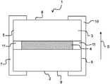
- FIG. 1shows a surge protection component 1 according to a first illustrative embodiment.
- the surge protection component 1has a main body 2 .
- the main body 2has two ceramic layers 3 .
- the main body 2has an inner electrode 4 , which is arranged in a stacking direction S between the two ceramic layers 3 .
- the main body 2has a first lateral face 5 and a second lateral face 6 , wherein the second lateral face 6 lies opposite the first lateral face 5 .
- a first outer electrode 7is arranged on the first lateral face 5 of the main body 2 .
- the first outer electrode 7covers the first lateral face 5 completely and moreover covers a top 8 and a bottom 9 of the main body 2 in each case partially.
- a second outer electrode 10is arranged on the second lateral face 6 of the main body 2 .
- the second outer electrode 10covers the second lateral face 6 of the main body 2 completely and likewise partially covers the top 8 and the bottom 9 of the main body 2 .
- the first and the second lateral face 5 , 6are each oriented in such a way that their surface normals are perpendicular to the stacking direction S.
- the top 8 and the bottom 9are oriented in such a way that their surface normals are parallel to the stacking direction S.
- the top 8 and the bottom 9are parallel to the inner electrode 4 .
- the inner electrode 4is set back from the first lateral face 5 of the main body 2 . Accordingly, a cavity 11 is formed between the first outer electrode 7 and the inner electrode 4 . This cavity 11 is filled with a gas.
- the inner electrode 4is also set back from the second lateral face 6 , such that a cavity 11 is likewise formed between the second outer electrode 10 and the inner electrode 4 .
- This cavity 11is also filled with a gas.
- the surge protection component 1can be used in particular as an arrester. It thus serves as a short-circuiting switch in the event of an overvoltage.
- the surge protection component 1permits surge protection for a further circuit arrangement connected to it.
- a short circuit in the surge protection componentcan be realized by a spark gap which is configured in the gas-filled cavities 11 .
- the first outer electrode 7 and the second outer electrode 10can each be connected to the associated switch arrangement. Accordingly, an electrical potential can lie at the first outer electrode 7 and at the second outer electrode 10 .
- the inner electrode 4can be used as what is called a floating electrode, such that no electrical potential lies on it.
- the gas arranged in the gas-filled cavity 11initially has an insulating action. However, if the potential difference between one of the outer electrodes 7 , 10 and the inner electrode 4 exceeds a breakdown voltage, the gas is ionized and forms a spark gap via which the respective outer electrode 7 , 10 is connected conductively to the inner electrode 4 . If the potential difference between the respective other outer electrode 7 , 10 and the inner electrode 4 is also greater than the breakdown voltage, the gas in the respective other cavity 11 is also ionized and a further spark gap is formed. The two outer electrodes 7 , 10 can now be connected to each other conductively via the spark gaps and the inner electrode 4 . This can result in a short circuit.
- the breakdown voltageis defined by the distance between the inner electrode 4 and the two outer electrode 7 , 10 , the used filling gas and the filling pressure.
- the breakdown voltagecan be calculated using Paschen's law.
- the surge protection component 1can be designed for a breakdown voltage of 100 V or more.
- the inner electrode 4can have copper or consist of copper. Alternatively, the inner electrode 4 can have tungsten or consist of tungsten. In the surge protection component 1 shown in FIG. 1 , the outer electrodes 7 , 10 are not connected directly to the inner electrode 4 . Therefore, another material can be used for the outer electrodes 7 , 10 than for the inner electrode 4 .
- the outer electrodes 7 , 10can have silver for example.
- FIG. 2shows a surge protection component 1 according to a second illustrative embodiment.
- the surge protection component 1 according to the second illustrative embodimentdiffers from the surge protection component 1 shown in FIG. 1 in that a cavity 11 is provided only between the inner electrode 4 and the first outer electrode 7 .
- the inner electrode 4is routed as far as the second lateral face 6 of the main body 2 and accordingly bears on the second outer electrode 10 .
- the second outer electrode 10 and the inner electrode 4are electrically contacted to each other.
- the inner electrode 4is not therefore used as a floating electrode. Instead, the same potential lies at the inner electrode 4 as at the second outer electrode 10 .
- the surge protection component 1 according to the second illustrative embodimentis characterized by a low limit voltage.
- the spark gaphere only has to overcome one cavity 11 in order to short-circuit the two outer electrode 7 , 10 to each other. Therefore, this is possible at a lower voltage than in the first illustrative embodiment.
- outer electrodes 7 , 10can preferably be used that have the same material as the inner electrode 4 .
- the inner electrode 4 and the outer electrodes 7 , 10have copper, for example.
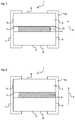
- a method for producing the surge protection component 1 according to the first illustrative embodimentis described below with reference to FIGS. 3 to 5 .
- FIG. 3shows a printed green sheet 12 from which a multiplicity of surge protection components 1 are produced.
- a ceramic layer 3 of the main body 2is later produced from the green sheet 12 .
- Strips of an electrically conductive material 13are printed onto the green sheet 12 and from them the inner electrodes 4 of the surge protection component 1 are produced.
- the material 13can be a copper paste.
- each component 1can have one or more printed sheets.
- a stackis formed from a printed green sheet and an unprinted green sheet.
- several printed green sheetscan be stacked on top of each other.
- the stack of printed green sheets 12is pressed.
- the green sheets 12are singulated along the partition line 14 indicated by broken lines in FIG. 3 .
- FIG. 4shows a surge protection component 1 after these two steps.
- the inner electrodes 4are etched on at least one lateral face 5 , 6 of the main body 2 , such that a cavity 11 forms between the at least one lateral face 5 , 6 of the main body 2 and the inner electrode 4 .
- FIG. 5shows a component 1 after this step has been carried out, wherein the inner electrode 4 has been etched here on the first lateral face 5 and on the second lateral face 6 .
- the etching stepis carried out in such a way that material is removed from the inner electrode 4 . This results in an etching trench which forms the cavity 11 in the surge protection component 1 .
- the depth of the etching trenchcan be set to a desired value.
- the componentis subjected to an etching solution, for example a solution based on sodium persulfate, sulfuric acid or iron(III) chloride.
- an etching solutionfor example a solution based on sodium persulfate, sulfuric acid or iron(III) chloride.
- the length of the set-back region, which corresponds to the length of the cavity 11can be between 5 and 20 um, for example.
- the methodcan be a wet-chemical etching method.
- the outer electrodes 7 , 10are now applied to the first lateral face 5 and the second lateral face 6 .
- the outer electrodes 7 , 10can be generated, for example, by the stack shown in FIG. 4 being dipped into a metallization paste and by the metallization paste then being fired in.
- the metallization pastecould be electroplated in order to generate an electroplated layer on the outer electrode.
- the cavities 11are encapsulated. Accordingly, in this method step, the cavities 11 must also be filled with the gas. This results in the surge protection component 1 shown in FIG. 1 .
- FIG. 6shows the surge protection component 1 after an alternative etching method has been carried out in which the inner electrode 4 has been etched selectively only on the first lateral face 5 .
- the second lateral face 6 of the main bodyis masked prior to the etching process.
- the main body 2can be dipped with the second lateral face 6 into a protective lacquer prior to the etching process.
- the main body 2can be dipped only with the first lateral face 5 into an etching solution, such that the second lateral face 6 does not come into contact with the etching solution and, accordingly, the inner electrode 4 is not etched on the second lateral face 6 .
- the inner electrode 4thus ends flush with the second lateral face 6 and is set back from the first lateral face 5 .
- the surge protection component shown in FIG. 6has several inner electrodes 4 arranged over each other, wherein a ceramic layer 3 is arranged between two inner electrodes 4 in each case.
Landscapes
- Engineering & Computer Science (AREA)
- Manufacturing & Machinery (AREA)
- Power Engineering (AREA)
- Microelectronics & Electronic Packaging (AREA)
- Thermistors And Varistors (AREA)
Abstract
Description
- manufacturing a main body having at least one inner electrode arranged between two ceramic layers, wherein the at least one inner electrode reaches to the lateral faces of the main body, and
- etching the at least one inner electrode on at least one lateral face of the main body, such that a cavity is formed between the at least one lateral face of the main body and the inner electrode,
- applying two outer electrodes to two mutually opposite lateral faces of the main body.
- 1 surge protection component
- 2 main body
- 3 ceramic layer
- 4 inner electrode
- 5 first lateral face
- 6 second lateral face
- 7 first outer electrode
- 8 top
- 9 bottom
- 10 second outer electrode
- 11 cavity
- 12 green sheet
- 13 electrically conductive material
- 14 partition line
- S stacking direction
Claims (12)
Applications Claiming Priority (4)
| Application Number | Priority Date | Filing Date | Title |
|---|---|---|---|
| DE102015116278 | 2015-09-25 | ||
| DE102015116278.4ADE102015116278A1 (en) | 2015-09-25 | 2015-09-25 | Overvoltage protection device and method for producing an overvoltage protection device |
| DE102015116278.4 | 2015-09-25 | ||
| PCT/EP2016/071110WO2017050579A1 (en) | 2015-09-25 | 2016-09-07 | Surge protection component and method for producing a surge protection component |
Publications (2)
| Publication Number | Publication Date |
|---|---|
| US20180278026A1 US20180278026A1 (en) | 2018-09-27 |
| US10923885B2true US10923885B2 (en) | 2021-02-16 |
Family
ID=56883800
Family Applications (1)
| Application Number | Title | Priority Date | Filing Date |
|---|---|---|---|
| US15/763,003Active2037-10-11US10923885B2 (en) | 2015-09-25 | 2016-09-07 | Surge protection component and method for producing a surge protection component |
Country Status (6)
| Country | Link |
|---|---|
| US (1) | US10923885B2 (en) |
| EP (1) | EP3353863B1 (en) |
| JP (1) | JP6711904B2 (en) |
| CN (1) | CN108028514B (en) |
| DE (1) | DE102015116278A1 (en) |
| WO (1) | WO2017050579A1 (en) |
Citations (44)
| Publication number | Priority date | Publication date | Assignee | Title |
|---|---|---|---|---|
| JPH03230487A (en) | 1990-02-05 | 1991-10-14 | Okaya Electric Ind Co Ltd | Discharge type surge absorbing element |
| JPH09190868A (en) | 1996-01-10 | 1997-07-22 | Alps Electric Co Ltd | Surge absorber |
| JPH10312786A (en) | 1997-05-13 | 1998-11-24 | Japan Vilene Co Ltd | Alkaline battery separator |
| JPH11354249A (en) | 1998-06-05 | 1999-12-24 | Tokin Corp | Surge absorbing element |
| US6008717A (en)* | 1997-03-04 | 1999-12-28 | Murata Manufacturing Co., Ltd. | NTC thermistor elements |
| JP2000068029A (en) | 1998-08-25 | 2000-03-03 | Mitsubishi Materials Corp | Chip-type surge absorber |
| JP2000133409A (en) | 1998-10-20 | 2000-05-12 | Mitsubishi Materials Corp | Chip type surge absorber |
| US20020089409A1 (en)* | 2000-11-02 | 2002-07-11 | Takehiko Ishii | Chip-type resistor element |
| US20040165331A1 (en)* | 2003-02-25 | 2004-08-26 | Mcdonald James Neil | Integrated gas tube holder for gas tube surge arrestors |
| US20060133009A1 (en)* | 2004-12-22 | 2006-06-22 | Choi Kee J | Capacitor and method for manufacturing the same |
| US20060279172A1 (en)* | 2003-10-31 | 2006-12-14 | Yasunori Ito | Lamination-type resistance element |
| US20070285866A1 (en)* | 2003-02-28 | 2007-12-13 | Mitsubishi Materials Corporation | Surge Absorber and Production Method Therefor |
| US20090067113A1 (en)* | 2007-05-28 | 2009-03-12 | Murata Manufacturing Co., Ltd. | Esd protection device |
| US20090236692A1 (en)* | 2008-03-24 | 2009-09-24 | Sheng-Fu Su | Rc filtering device having air gap construction for over voltage protection |
| US20090296294A1 (en)* | 2008-06-02 | 2009-12-03 | Inpaq Technology Co., Ltd. | Electro-static discharge protection device with low temperature co-fire ceramic and manufacturing method thereof |
| US20100254052A1 (en)* | 2007-11-27 | 2010-10-07 | Hidenori Katsumura | Static electricity countermeasure component and method for manufacturing the static electricity countermeasure component |
| US20100309595A1 (en)* | 2008-02-05 | 2010-12-09 | Murata Manufacturing Co., Ltd. | Esd protection device |
| US20110216456A1 (en)* | 2008-11-26 | 2011-09-08 | Murata Manufacturing Co., Ltd. | Esd protection device |
| US20110222203A1 (en)* | 2008-11-26 | 2011-09-15 | Murata Manufacturing Co., Ltd. | Esd protection device and method for manufacturing the same |
| US20110222197A1 (en)* | 2008-11-26 | 2011-09-15 | Murata Manufacturing Co., Ltd. | Esd protection device and method for manufacturing the same |
| US20110227196A1 (en)* | 2008-12-10 | 2011-09-22 | Murata Manufacturing Co., Ltd. | Esd protection device |
| US20120134059A1 (en)* | 2009-08-27 | 2012-05-31 | Murata Manufacturing Co., Ltd. | Esd protection device and manufacturing method thereof |
| US20120162838A1 (en)* | 2009-09-30 | 2012-06-28 | Murata Manufacturing Co., Ltd. | Esd protection device and manufacturing method therefor |
| US20120169452A1 (en)* | 2009-09-30 | 2012-07-05 | Murata Manufacturing Co., Ltd. | Esd protection device and manufacturing method therefor |
| WO2012093081A1 (en) | 2011-01-04 | 2012-07-12 | Oc Oerlikon Balzers Ag | Method for manufacturing high performance multi layer ceramic capacitors |
| US20120236450A1 (en)* | 2011-03-14 | 2012-09-20 | Murata Manufacturing Co., Ltd. | Esd protection device and method for producing the same |
| US20120300355A1 (en)* | 2011-05-25 | 2012-11-29 | Tdk Corporation | Electrostatic protection component |
| WO2013009661A2 (en) | 2011-07-08 | 2013-01-17 | Kemet Electronics Corporation | Overvoltage protection component |
| US20130077199A1 (en)* | 2010-05-20 | 2013-03-28 | Murata Manufacturing Co., Ltd. | Esd protection device |
| JP2013069561A (en) | 2011-09-22 | 2013-04-18 | Tdk Corp | Electrostatic protective element |
| US8471672B2 (en)* | 2009-02-23 | 2013-06-25 | Epcos Ag | Electrical multilayer component |
| US20130207770A1 (en)* | 2010-09-09 | 2013-08-15 | Epcos Ag | Resistance Component and Method for Producing a Resistance Component |
| DE102012105059A1 (en) | 2012-06-12 | 2013-12-12 | Epcos Ag | Method for producing a multilayer component and multilayer component |
| CN103652271A (en) | 2012-09-07 | 2014-03-26 | 内蒙古伊利实业集团股份有限公司 | Frozen beverage added with alfalfa and preparation method thereof |
| US20140198422A1 (en)* | 2011-07-07 | 2014-07-17 | Kemet Electronics Corporation | Integrated EMI Filter and Surge Protection Component |
| US20140232485A1 (en) | 2011-07-08 | 2014-08-21 | Kemet Electronics Corporation | Discharge Capacitor |
| US20140240878A1 (en)* | 2011-11-01 | 2014-08-28 | Murata Manufacturing Co., Ltd. | Esd protective device |
| US20160105948A1 (en)* | 2013-07-03 | 2016-04-14 | Murata Manufacturing Co., Ltd. | Surge protection device, method for manufacturing the same, and electronic component including the same |
| US20160218502A1 (en)* | 2015-01-22 | 2016-07-28 | Littelfuse, Inc. | Surface-mountable electrical circuit protection device |
| US20170244223A1 (en)* | 2014-12-18 | 2017-08-24 | Murata Manufacturing Co., Ltd. | Esd protection device and manufacturing method for same |
| US9853619B2 (en)* | 2011-10-24 | 2017-12-26 | Dexerials Corporation | Electrostatic capacitance element and resonance circuit |
| US20180062354A1 (en)* | 2015-06-22 | 2018-03-01 | Murata Manufacturing Co., Ltd. | Esd protection device and manufacturing method for esd protection device |
| US20180114647A1 (en)* | 2015-08-07 | 2018-04-26 | Murata Manufacturing Co., Ltd. | Capacitor and method for manufacturing the capacitor |
| US20200083570A1 (en)* | 2017-05-31 | 2020-03-12 | Tdk Electronics Ag | Circuit Board Having Power Supply, Electrical Device Having Circuit Board, and Method for Producing a Circuit Board |
Family Cites Families (2)
| Publication number | Priority date | Publication date | Assignee | Title |
|---|---|---|---|---|
| JPH10312876A (en)* | 1997-05-12 | 1998-11-24 | Mitsubishi Materials Corp | Surge absorber |
| CN100539338C (en)* | 2003-02-28 | 2009-09-09 | 三菱麻铁里亚尔株式会社 | Surge absorber and manufacture method thereof |
- 2015
- 2015-09-25DEDE102015116278.4Apatent/DE102015116278A1/ennot_activeWithdrawn
- 2016
- 2016-09-07USUS15/763,003patent/US10923885B2/enactiveActive
- 2016-09-07WOPCT/EP2016/071110patent/WO2017050579A1/ennot_activeCeased
- 2016-09-07JPJP2018515495Apatent/JP6711904B2/enactiveActive
- 2016-09-07CNCN201680055600.5Apatent/CN108028514B/enactiveActive
- 2016-09-07EPEP16762807.2Apatent/EP3353863B1/enactiveActive
Patent Citations (49)
| Publication number | Priority date | Publication date | Assignee | Title |
|---|---|---|---|---|
| JPH03230487A (en) | 1990-02-05 | 1991-10-14 | Okaya Electric Ind Co Ltd | Discharge type surge absorbing element |
| JPH09190868A (en) | 1996-01-10 | 1997-07-22 | Alps Electric Co Ltd | Surge absorber |
| US6008717A (en)* | 1997-03-04 | 1999-12-28 | Murata Manufacturing Co., Ltd. | NTC thermistor elements |
| JPH10312786A (en) | 1997-05-13 | 1998-11-24 | Japan Vilene Co Ltd | Alkaline battery separator |
| JPH11354249A (en) | 1998-06-05 | 1999-12-24 | Tokin Corp | Surge absorbing element |
| JP2000068029A (en) | 1998-08-25 | 2000-03-03 | Mitsubishi Materials Corp | Chip-type surge absorber |
| JP2000133409A (en) | 1998-10-20 | 2000-05-12 | Mitsubishi Materials Corp | Chip type surge absorber |
| US20020089409A1 (en)* | 2000-11-02 | 2002-07-11 | Takehiko Ishii | Chip-type resistor element |
| US20040165331A1 (en)* | 2003-02-25 | 2004-08-26 | Mcdonald James Neil | Integrated gas tube holder for gas tube surge arrestors |
| US20070285866A1 (en)* | 2003-02-28 | 2007-12-13 | Mitsubishi Materials Corporation | Surge Absorber and Production Method Therefor |
| US20060279172A1 (en)* | 2003-10-31 | 2006-12-14 | Yasunori Ito | Lamination-type resistance element |
| US20060133009A1 (en)* | 2004-12-22 | 2006-06-22 | Choi Kee J | Capacitor and method for manufacturing the same |
| US20090067113A1 (en)* | 2007-05-28 | 2009-03-12 | Murata Manufacturing Co., Ltd. | Esd protection device |
| US7633735B2 (en)* | 2007-05-28 | 2009-12-15 | Murata Manufacturing Co., Ltd. | ESD protection device |
| US20100254052A1 (en)* | 2007-11-27 | 2010-10-07 | Hidenori Katsumura | Static electricity countermeasure component and method for manufacturing the static electricity countermeasure component |
| US20100309595A1 (en)* | 2008-02-05 | 2010-12-09 | Murata Manufacturing Co., Ltd. | Esd protection device |
| US8238069B2 (en)* | 2008-02-05 | 2012-08-07 | Murata Manufacturing Co., Ltd. | ESD protection device |
| US20090236692A1 (en)* | 2008-03-24 | 2009-09-24 | Sheng-Fu Su | Rc filtering device having air gap construction for over voltage protection |
| US20090296294A1 (en)* | 2008-06-02 | 2009-12-03 | Inpaq Technology Co., Ltd. | Electro-static discharge protection device with low temperature co-fire ceramic and manufacturing method thereof |
| US20110216456A1 (en)* | 2008-11-26 | 2011-09-08 | Murata Manufacturing Co., Ltd. | Esd protection device |
| US20110222203A1 (en)* | 2008-11-26 | 2011-09-15 | Murata Manufacturing Co., Ltd. | Esd protection device and method for manufacturing the same |
| US20110222197A1 (en)* | 2008-11-26 | 2011-09-15 | Murata Manufacturing Co., Ltd. | Esd protection device and method for manufacturing the same |
| US20110227196A1 (en)* | 2008-12-10 | 2011-09-22 | Murata Manufacturing Co., Ltd. | Esd protection device |
| US8471672B2 (en)* | 2009-02-23 | 2013-06-25 | Epcos Ag | Electrical multilayer component |
| US20120134059A1 (en)* | 2009-08-27 | 2012-05-31 | Murata Manufacturing Co., Ltd. | Esd protection device and manufacturing method thereof |
| US20120169452A1 (en)* | 2009-09-30 | 2012-07-05 | Murata Manufacturing Co., Ltd. | Esd protection device and manufacturing method therefor |
| US20120162838A1 (en)* | 2009-09-30 | 2012-06-28 | Murata Manufacturing Co., Ltd. | Esd protection device and manufacturing method therefor |
| US20130077199A1 (en)* | 2010-05-20 | 2013-03-28 | Murata Manufacturing Co., Ltd. | Esd protection device |
| US20130207770A1 (en)* | 2010-09-09 | 2013-08-15 | Epcos Ag | Resistance Component and Method for Producing a Resistance Component |
| WO2012093081A1 (en) | 2011-01-04 | 2012-07-12 | Oc Oerlikon Balzers Ag | Method for manufacturing high performance multi layer ceramic capacitors |
| US20120236450A1 (en)* | 2011-03-14 | 2012-09-20 | Murata Manufacturing Co., Ltd. | Esd protection device and method for producing the same |
| US20120300355A1 (en)* | 2011-05-25 | 2012-11-29 | Tdk Corporation | Electrostatic protection component |
| US20140198422A1 (en)* | 2011-07-07 | 2014-07-17 | Kemet Electronics Corporation | Integrated EMI Filter and Surge Protection Component |
| US20140232485A1 (en) | 2011-07-08 | 2014-08-21 | Kemet Electronics Corporation | Discharge Capacitor |
| WO2013009661A2 (en) | 2011-07-08 | 2013-01-17 | Kemet Electronics Corporation | Overvoltage protection component |
| US8885324B2 (en)* | 2011-07-08 | 2014-11-11 | Kemet Electronics Corporation | Overvoltage protection component |
| CN103650071A (en) | 2011-07-08 | 2014-03-19 | 凯米特电子公司 | Overvoltage protection component |
| JP2014523648A (en) | 2011-07-08 | 2014-09-11 | ケメット エレクトロニクス コーポレーション | Overvoltage protection component |
| JP2013069561A (en) | 2011-09-22 | 2013-04-18 | Tdk Corp | Electrostatic protective element |
| US9853619B2 (en)* | 2011-10-24 | 2017-12-26 | Dexerials Corporation | Electrostatic capacitance element and resonance circuit |
| US20140240878A1 (en)* | 2011-11-01 | 2014-08-28 | Murata Manufacturing Co., Ltd. | Esd protective device |
| DE102012105059A1 (en) | 2012-06-12 | 2013-12-12 | Epcos Ag | Method for producing a multilayer component and multilayer component |
| CN103652271A (en) | 2012-09-07 | 2014-03-26 | 内蒙古伊利实业集团股份有限公司 | Frozen beverage added with alfalfa and preparation method thereof |
| US20160105948A1 (en)* | 2013-07-03 | 2016-04-14 | Murata Manufacturing Co., Ltd. | Surge protection device, method for manufacturing the same, and electronic component including the same |
| US20170244223A1 (en)* | 2014-12-18 | 2017-08-24 | Murata Manufacturing Co., Ltd. | Esd protection device and manufacturing method for same |
| US20160218502A1 (en)* | 2015-01-22 | 2016-07-28 | Littelfuse, Inc. | Surface-mountable electrical circuit protection device |
| US20180062354A1 (en)* | 2015-06-22 | 2018-03-01 | Murata Manufacturing Co., Ltd. | Esd protection device and manufacturing method for esd protection device |
| US20180114647A1 (en)* | 2015-08-07 | 2018-04-26 | Murata Manufacturing Co., Ltd. | Capacitor and method for manufacturing the capacitor |
| US20200083570A1 (en)* | 2017-05-31 | 2020-03-12 | Tdk Electronics Ag | Circuit Board Having Power Supply, Electrical Device Having Circuit Board, and Method for Producing a Circuit Board |
Non-Patent Citations (1)
| Title |
|---|
| International Search Report in International Application No. PCT/EP2016/071110, dated Nov. 16, 2016, with English translation (5 pages). |
Also Published As
| Publication number | Publication date |
|---|---|
| JP2018535510A (en) | 2018-11-29 |
| EP3353863A1 (en) | 2018-08-01 |
| CN108028514A (en) | 2018-05-11 |
| DE102015116278A1 (en) | 2017-03-30 |
| CN108028514B (en) | 2020-10-27 |
| US20180278026A1 (en) | 2018-09-27 |
| JP6711904B2 (en) | 2020-06-17 |
| EP3353863B1 (en) | 2022-11-02 |
| WO2017050579A1 (en) | 2017-03-30 |
Similar Documents
| Publication | Publication Date | Title |
|---|---|---|
| KR101808799B1 (en) | Laminated device and electronic device having the same | |
| JP2010146779A (en) | Overvoltage protection component | |
| US9208947B2 (en) | Multilayer ceramic capacitor and board having multilayer ceramic capacitor embedded therein | |
| US9826611B2 (en) | ESD protection device | |
| JP2010532069A (en) | Devices and modules for protection against lightning strikes and overvoltages | |
| JP2004014466A (en) | Chip type surge absorber and its manufacturing method | |
| US10923885B2 (en) | Surge protection component and method for producing a surge protection component | |
| JP2009238563A (en) | Overvoltage protection component, electric circuit using the same and overvoltage protection method | |
| JP2009152348A (en) | Antistatic parts | |
| US10511158B2 (en) | Method for producing a multiplicity of surge arresters in an assembly, surge arrester and surge arrester assembly | |
| JP2011119568A (en) | Overvoltage protection component and method of manufacturing the same | |
| US11640877B2 (en) | Electronic component and board having the same | |
| JP2011028968A (en) | Overvoltage protection component | |
| US10389105B2 (en) | Overvoltage protection element and method for producing an overvoltage protection element | |
| US9780533B2 (en) | ESD protective device | |
| US10944243B2 (en) | Method for producing an arrester, and arrester | |
| JP2010040242A (en) | Overvoltage protection component, electric circuit using same, and overvoltage protection method | |
| JP2006313877A (en) | Antistatic parts | |
| JPS60124381A (en) | Lightning tube | |
| US11011890B2 (en) | Arrester and method for manufacturing an arrester | |
| WO2017036511A1 (en) | Electric multilayer component for surface-mount technology and method of producing an electric multilayer component | |
| JP2010097791A (en) | Overvoltage protection component | |
| WO2016203976A1 (en) | Esd protection device | |
| JP2004127615A (en) | Surge absorber and manufacturing method of same | |
| JP2010231909A (en) | Overvoltage protection component and manufacturing method thereof |
Legal Events
| Date | Code | Title | Description |
|---|---|---|---|
| FEPP | Fee payment procedure | Free format text:ENTITY STATUS SET TO UNDISCOUNTED (ORIGINAL EVENT CODE: BIG.); ENTITY STATUS OF PATENT OWNER: LARGE ENTITY | |
| AS | Assignment | Owner name:EPCOS AG, GERMANY Free format text:ASSIGNMENT OF ASSIGNORS INTEREST;ASSIGNOR:RINNER, FRANZ, DR.;REEL/FRAME:046626/0827 Effective date:20180427 | |
| STPP | Information on status: patent application and granting procedure in general | Free format text:DOCKETED NEW CASE - READY FOR EXAMINATION | |
| STPP | Information on status: patent application and granting procedure in general | Free format text:NON FINAL ACTION MAILED | |
| STPP | Information on status: patent application and granting procedure in general | Free format text:NOTICE OF ALLOWANCE MAILED -- APPLICATION RECEIVED IN OFFICE OF PUBLICATIONS | |
| STCF | Information on status: patent grant | Free format text:PATENTED CASE | |
| AS | Assignment | Owner name:TDK ELECTRONICS AG, GERMANY Free format text:CHANGE OF NAME;ASSIGNOR:EPCOS AG;REEL/FRAME:063085/0832 Effective date:20181001 | |
| MAFP | Maintenance fee payment | Free format text:PAYMENT OF MAINTENANCE FEE, 4TH YEAR, LARGE ENTITY (ORIGINAL EVENT CODE: M1551); ENTITY STATUS OF PATENT OWNER: LARGE ENTITY Year of fee payment:4 |