US10923413B2 - Hard IP blocks with physically bidirectional passageways - Google Patents
Hard IP blocks with physically bidirectional passagewaysDownload PDFInfo
- Publication number
- US10923413B2 US10923413B2US16/426,515US201916426515AUS10923413B2US 10923413 B2US10923413 B2US 10923413B2US 201916426515 AUS201916426515 AUS 201916426515AUS 10923413 B2US10923413 B2US 10923413B2
- Authority
- US
- United States
- Prior art keywords
- hard
- block
- interconnects
- keepout
- keepout zones
- Prior art date
- Legal status (The legal status is an assumption and is not a legal conclusion. Google has not performed a legal analysis and makes no representation as to the accuracy of the status listed.)
- Active, expires
Links
Images


Classifications
- H—ELECTRICITY
- H01—ELECTRIC ELEMENTS
- H01L—SEMICONDUCTOR DEVICES NOT COVERED BY CLASS H10
- H01L23/00—Details of semiconductor or other solid state devices
- H01L23/48—Arrangements for conducting electric current to or from the solid state body in operation, e.g. leads, terminal arrangements ; Selection of materials therefor
- H01L23/481—Internal lead connections, e.g. via connections, feedthrough structures
- G—PHYSICS
- G06—COMPUTING OR CALCULATING; COUNTING
- G06F—ELECTRIC DIGITAL DATA PROCESSING
- G06F13/00—Interconnection of, or transfer of information or other signals between, memories, input/output devices or central processing units
- G06F13/38—Information transfer, e.g. on bus
- G06F13/40—Bus structure
- G06F13/4004—Coupling between buses
- G06F13/4027—Coupling between buses using bus bridges
- H—ELECTRICITY
- H01—ELECTRIC ELEMENTS
- H01L—SEMICONDUCTOR DEVICES NOT COVERED BY CLASS H10
- H01L23/00—Details of semiconductor or other solid state devices
- H01L23/52—Arrangements for conducting electric current within the device in operation from one component to another, i.e. interconnections, e.g. wires, lead frames
- H01L23/522—Arrangements for conducting electric current within the device in operation from one component to another, i.e. interconnections, e.g. wires, lead frames including external interconnections consisting of a multilayer structure of conductive and insulating layers inseparably formed on the semiconductor body
- H01L23/528—Layout of the interconnection structure
- Y—GENERAL TAGGING OF NEW TECHNOLOGICAL DEVELOPMENTS; GENERAL TAGGING OF CROSS-SECTIONAL TECHNOLOGIES SPANNING OVER SEVERAL SECTIONS OF THE IPC; TECHNICAL SUBJECTS COVERED BY FORMER USPC CROSS-REFERENCE ART COLLECTIONS [XRACs] AND DIGESTS
- Y02—TECHNOLOGIES OR APPLICATIONS FOR MITIGATION OR ADAPTATION AGAINST CLIMATE CHANGE
- Y02D—CLIMATE CHANGE MITIGATION TECHNOLOGIES IN INFORMATION AND COMMUNICATION TECHNOLOGIES [ICT], I.E. INFORMATION AND COMMUNICATION TECHNOLOGIES AIMING AT THE REDUCTION OF THEIR OWN ENERGY USE
- Y02D10/00—Energy efficient computing, e.g. low power processors, power management or thermal management
Definitions
- Computationis gated by how fast data can be processed, and limited by the speed at which processors can get data in and out.
- processorshave become faster, up to approximately 3-4 GHz.
- further advanced computersincluded multiple processing cores, rather than further increasing speed of individual processors.
- processorscan be physically positioned in close proximity to memory. This results in higher bandwidth access to data.
- bonding techniquessuch as direct dielectric bonding, non-adhesive techniques, such as a ZiBond® direct bonding technique or a DBI® hybrid bonding technique, both available from Invensas Bonding Technologies, Inc. (formerly Ziptronix, Inc.), a subsidiary of Xperi Corp.
- processorscan be physically positioned in close proximity to memory. This results in higher bandwidth access to data.
- a Serializer/Deserializerincludes one or more pairs of functional blocks commonly used in high speed communications to compensate for limited input/output. These blocks convert data between serial data and parallel interfaces in each direction. SerDes have been used in computing devices, switches, routers, and the like. Existing SerDes operate at 28 Gbps, 56 Gbps, and faster speeds are in development.
- FIGS. 1A-Billustrate an example of a conventional die 110 hosting a plurality of SerDes chiplets 120 , where FIG. 1A is a top view and FIG. 1B is a side view. As shown, the die 110 is also hosting larger memory chiplet 130 and other chiplets 140 , which may be any of a variety of types of chips, including analog.
- the SerDes chiplets 120communicate signals from bond pads 125 to nodes external to the host die 110 , such as to chips on a second die. To do so requires a redistribution layer 152 that goes beyond the chiplet 120 and then to pillars 154 .
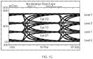
- FIG. 1Cillustrates an example eye diagram for a PAM4 signal, the signal including four levels (Level 0-Level 3).
- an eyeis created, such as eye 0/1 between Level 0 and Level 1, eye1/2 between Level 1 and Level 2, etc.
- eye 0/1between Level 0 and Level 1
- eye1/2between Level 1 and Level 2
- the eyes of the waveformsare relatively distinct. However, a greater load would cause the switching between levels to be more gradual, and thus the eyes would shrink. Accordingly, signal transmission begins to fail.
- FIGS. 1A-Billustrate this problem with a face-to-face die
- a similar problemexists using wafer-to-wafer designs.
- a through-silicon viawould need to extend outside a perimeter of the SerDes chiplet, thereby creating a large resistive capacitive load, which impacts signal quality.
- the present disclosureprovides for hard IP blocks, such as SerDes chips, designed with keepout zones beneath the interconnects.
- the keepout zonesare discrete areas or spaces within an active circuitry layer of the chip where there is no routing or active circuitry.
- circuitry used to (de)serialize and drive signal bumpsare positioned beneath a surface of the SerDes chip but are not located in an area directly below a region of the interconnect that faces the host die.
- Surface interconnectsmay be placed on an upper or lower surface of the SerDes chip in relation to the keepout zones, wherein the surface interconnections can interface with external devices. Accordingly, redistribution layers routing around an outer periphery of the SerDes chip are no longer needed, and the resistive capacitive load remains low so as not to adversely impact transmitted signals.
- some surface interconnectsmay have keepout zones beneath them, while others do not.
- transmit and receive bumpsmay be made with keepout zones beneath them
- power bumpsmay have a power mesh below them
- ground bumpsmay have ground below them.
- One aspect of the disclosureprovides a hard IP block defined by a base having a top surface and a bottom surface, the hard IP block comprising a circuitry layer within the base adjacent the top surface, one or more keepout zones within the circuitry layer, the one or more keepout zones defining spaces exclusive of circuitry, and one or more surface interconnects, each of the one or more surface interconnects being positioned on at least one of the top surface or the bottom surface of the hard IP block and in relation to the one or more keepout zones.
- Each of the one or more surface interconnectsmay be, for example, bumps, pads, or pillars positioned in longitudinal alignment with a corresponding one of the one or more keepout zones.
- each of the one or more surface interconnectsmay be positioned at the top surface of the hard IP block.
- the one or more surface interconnectsmay alternatively or additionally be positioned at a bottom surface of the hard IP blocks, and one or more through-hole interconnects may extend from a connection point to the one or more surface interconnects at the top surface of the hard IP block, longitudinally through a corresponding one of the one or more keepout zones, and to the bottom surface of the hard IP block.
- the through-hole interconnectsmay be, for example, vias terminating at the one or more surface interconnects.
- the one or more keepout zonesmay be sized to have a keepout zone diameter that is based on a diameter of the one or more through-hole interconnects.
- the hard IP blockmay be, for example, a SerDes chiplet, gearbox, memory, analog block, or processing element.
- a systemcomprising a hard IP block defined by a base having a top surface and a bottom surface.
- the hard IP blockincludes a circuitry layer within the base adjacent the top surface, one or more keepout zones within the circuitry layer, the one or more keepout zones defining spaces exclusive of circuitry and one or more surface interconnects, each of the one or more surface interconnects being positioned in relation to the one or more keepout zones.
- the systemmay further include a memory chiplet and a host die, wherein the hard IP block and the memory chiplet are positioned on the host die.
- the hard IP blockmay be face-to-face bonded to the host die, such as using non-adhesive direct bonding techniques.
- Each of the one or more surface interconnectsmay be positioned in longitudinal alignment with a corresponding one of the one or more keepout zones.
- the hard IP blockmay further comprise one or more through-hole interconnects, each of the one or more through-hole interconnects extending from a connection point to the surface interconnects at the top surface of the hard IP block, longitudinally through a corresponding one of the one or more keepout zones, and to the bottom surface of the hard IP block.
- the one or more surface interconnectsmay also be positioned at the bottom surface of the hard IP block and electrically connect with the through-hole interconnects.
- a 3D structurecomprising a hard IP block defined by a base having a top surface and a bottom surface, the hard IP block comprising a circuitry layer within the base adjacent the top surface, one or more keepout zones within the circuitry layer, the one or more keepout zones defining spaces exclusive of circuitry, one or more through-hole interconnects, each of the one or more through-hole interconnects extending from the top surface of the hard IP block, longitudinally through a corresponding one of the one or more keepout zones, and to the bottom surface of the hard IP block, and one or more surface interconnects, each of the one or more surface interconnects being positioned at the bottom surface of the hard IP block in longitudinal alignment with a corresponding one of the one or more keepout zones and being electrically connected to a corresponding one of the one or more through-hole interconnects.
- the 3D structurefurther comprises a host die, wherein the hard IP block is face-to-face bonded with the host die, such that the bottom surface and the one or more surface interconnects face away from the host die, and a second layer device coupled to the one or more surface interconnects at the bottom surface of the hard IP block.
- FIGS. 1A-Bare top and side view of SerDes chiplets on a host die according to the prior art.
- FIG. 1Cis an example of a conventional PAM4 eye diagram.
- FIG. 2is a top view of an example SerDes chiplet according to aspects of the disclosure.
- FIG. 3Ais a cutaway side view of an example SerDes chiplet according to aspects of the disclosure.
- FIG. 3Bis a cutaway bottom view of the example SerDes chiplet of FIG. 3A .
- FIG. 4Ais a cutaway side view of another example SerDes chiplet according to aspects of the disclosure.
- FIG. 4Bis a cutaway bottom view of the example SerDes chiplet of FIG. 4A .
- FIG. 5is a side view of an example SerDes chiplet face-to-face bonded with a host die according to aspects of the disclosure.
- FIG. 6is a flow diagram illustrating a method of fabricating SerDes chips according to aspects of the disclosure.
- FIG. 2illustrates a top view of an example configuration of a hard IP block, particularly a SerDes chip 220 , including a plurality of surface interconnects 260 .
- the surface interconnects 260may be bumps, pads, or any other type of interconnect.
- Such interconnectsinclude core power 261 , power 262 , ground 265 , transmit pairs 263 - 264 , receive pairs 266 - 267 , positive and negative clocks, etc.
- a first side 222 of the chip 220is referred to as a “core side” and is used for communicating with a core 280 . As shown, the core side includes dense interconnects 223 .
- a second side 224is a die edge 224 , and faces a periphery of the die hosting the SerDes block 220 .
- the second side 224may include much fewer interconnects than the core side 222 , and maybe used to interface with external devices 290 .
- the SerDes chip 220is able to take more highly-parallel, low-speed, low-voltage signals from the core side 222 , serialize the received signals together, send the serialized signals out to the external node 290 through different transmit/receive pairs at a faster data rate.
- the transmit/receive pairsmay also be used to deserialize signals received from the external node 290 to a lower data rate, and transmit such deserialized signals to the core 280 .
- the surface interconnects 260may be any device for establishing electrical contact.
- the surface interconnects 260may be bumps, pads, pillars, or any other type of interconnect. While in some examples herein such interconnects are referred to as bumps, but it should be understood that other types of interconnects may alternatively or additionally be used.
- signalsmay also be transmitted through the bumps 261 - 267 in a direction perpendicular to a plane extending along a top surface of the SerDes chip 220 .
- the SerDes chip 220is configured to be bonded to further structures, such as to create a 3D design.
- FIG. 3Aillustrates a cutaway side view of such SerDes chip allowing for transmission of signals in a direction that is orthogonal to a plane extending along a top surface 226 of the SerDes chip 220 .
- the SerDes chip 220includes a base 250 , which may be a silicon substrate or other semiconductor material, such as Gallium Arsinide, Indium Phosphide, or other similar material.
- Circuitry 270extends across the base 250 .
- the circuitry 270may include active circuitry for the chip 220 , and/or routing. While the circuitry 270 is illustrated in FIG. 3A as a single layer, it should be understood that the circuitry 270 may be multiple layers, such as a routing layer and an active circuitry layer. In other examples the routing and active circuitry may be interspersed in the same layer.
- circuitry 270extends beneath the top surface 226 of the chip 220
- a plurality of keepout zones 302are positioned within the circuitry 270 and in relation to the interconnects 262 , 265 , 266 , 267 , etc.
- the keepout zones 302may be positioned directly beneath the interconnects 260 .
- the keepout zones 302are discrete areas or spaces within the layer of circuitry 270 where there is no active circuitry or routing.
- circuitry used to serialize and deserialize and drive signal bumpsare positioned beneath a surface of the chip 220 , but are not located in an area directly below a region of the interconnect that faces the host die.
- a layout of the chipis designed such that the circuitry 270 is positioned around the keepout zones 302 , as shown in FIG. 3B discussed further below.
- the keepout zones 302may extend a depth towards a bottom surface of the chip 220 , wherein the depth is as least as deep as a depth of the circuitry 270 .
- circuitry keepout zonesthat are distinct from routing keepout zones.
- some surface interconnectsmay have circuitry keepout zones beneath them if only active circuitry is positioned beneath such interconnects, while other surface interconnects of the same hard IP block have only routing keepout zones if only routing is positioned beneath such interconnects.
- the circuitry keepout zonesmay be the same size and shape, or differently sized and shaped, as compared to the routing keepout zones.
- the keepout zones 302may be filled with material having low or no conductivity, such as a dielectric.
- the dielectricmay form a layer over the base, and routes in a routing layer extend through the dielectic.
- the dieletricmay include, for example, undoped silicate glass (USG), silicon oxide, silicon nitride, high-k, low-k, or the like.
- USGundoped silicate glass
- the dielectric or other materialsmay be removed as needed, such as by etching or the like.
- FIG. 3Bprovides a planar cross-sectional view from an under side of the SerDes chip 220 , such as along line A-A of FIG. 3A .
- FIG. 3Billustrates the keepout zones 302 through circuitry 270 , in relation to surface interconnects 260 at a top surface of the chip 220 .
- the keepout zones 302are illustrated as having a radial cross-section, for example, the keepout zones 302 may be substantially cylindrical.
- the keepout zones 302may have different shapes.
- a cross-section of the keepout zonemay be substantially square, rectangular, octagonal, or other shape.
- the keepout zonesmay be substantially cubical, rectangular prism, octahedron, etc.
- a size or shape of the keepout zones 302may change from one cross-section to another within the same keepout zone, or from one keepout zone to another.
- the SerDes chipmay be designed by specifying a minimum distance from a center position for the keepout zone, and the remainder of the shape for the keepout zone may be determined by efficient circuitry placement.
- the keepout zones 302may be designed based on a planned diameter of a via to be placed therein.
- the diameter of the keepout zone 302may be a multiple of the via diameter, such as 1.5 times the diameter of the via, 3 times the diameter, 5 times, etc.
- a keepout zone for a Sum via with a circular cross-sectionmay be about 15 um with an octagonal cross-section.
- the size of the keepout zone 302may be varied based on, for example, an amount of stress induced on an active silicon area by a change in material between silicon and the via materials (e.g., copper or other via materials).
- the keepout zone size for the circuitsmay be different than the keepout zone size for routing.
- vias or other types of through-hole interconnectsmay extend through the keepout zones from the surface interconnects on one surface of the chip to an opposing surface. Routing may be positioned closer to the vias, as they are less sensitive to the stress induced by the vias than the circuitry may be.
- keepout zonesthere may be different keepout zones per layers stacked in the chip 220 .
- the front end of line (FEOL)such as the circuit layers and first few routing layers, may have one set of constraints
- back end of line (BEOL)may have a different set of constraints.
- the keepout zonesmay be different.
- the keepout zone for a first routing layermay have different size constraints than the keepout zone for a second routing layer.
- the SerDes chip 220includes a keepout zone 302 for each surface interconnect 260
- the keepout zones 302may only be placed in relation to selected surface interconnects.
- transmit and receive pairsmay have keepout zones beneath them, while power and ground do not.
- only selected transmit and receive pairsmay have keepout zones beneath them, while other transmit and receive pairs do not.
- FIG. 4Aillustrates a cutaway side view of another embodiment where through-hole interconnects 404 are placed within keepout zones 402 , and extend longitudinally through chip 420 .
- the through-hole interconnects 404create a path through the chip 420 for electrical connection between interconnects at top surface 426 and a bottom surface 428 .
- surface interconnectsare not shown at the top surface 426 , and instead surface interconnects 460 are positioned at the bottom surface 428 of the chip 420 .
- the surface interconnects 460may be the same as the surface interconnects 260 of FIG. 3A , but moved to a different position.
- the surface interconnects 260may be moved to a backside of the chiplet in a mirror image of what is seen on a face of the chiplet.
- through-hole interconnect 404includes a through-silicon via (TSV) 406 that extends through a base 450 of the chip 420 up to routing/active layers 470 .
- the routing/active layersmay include, for example, an implant layer and multiple layers of routing and active circuitry.
- the routing/active layers 470may include up to 18 layers or more.
- the TSV 406may extend up to the implant layer, 1 st layer, 2 nd layer, 3 rd layer, etc.
- the TSV 406may then couple to interconnects 408 in the layers of the routing/active layers 470 above it. Such interconnects 408 may couple to surface interconnects at the top surface of the chip.
- the hard IP blockmay include routing under each surface interconnect, but not circuitry.
- a viamay be vertically aligned each surface interconnect on the front surface and/or the back surface.
- a signalmay jog around the routing to couple the via to the surface interconnect.
- the viamay not be vertically aligned with the surface interconnect. Rather, the via may be slightly displaced in a lateral direction. In this regard, an electrically short redistribution may couple the via to the surface interconnects. The surface interconnects would remain aligned with each other with the via slightly displaced.
- the through-hole interconnects 404may each be a continuous via, wherein a first end of the via remains available for coupling at the top surface 426 of the chip 420 and extends through keepout zones 402 , and a second end of the via couples to the surface interconnects 460 positioned at the bottom surface 428 of the SerDes chip 420 .
- such through-hole interconnects 404are available to be connected at the first end to another device, such as a host die, a substrate, or any other device.
- the through-hole interconnects 404may be coupled using bonding techniques such as Zibond or DBI.
- signalsmay be transmitted through the chip 420 by the through-hole interconnects 404 in a direction extending from the top surface 426 to the bottom surface 428 , and vice versa.
- the through-hole interconnects 404may be made of, for example, a conductive metal, such as copper, silver, gold, aluminum, brass, nickel, or any other conductive metal.
- a conductive metalsuch as copper, silver, gold, aluminum, brass, nickel, or any other conductive metal.
- the viamay have a liner around an inner portion creating a passageway, and/or around an outer portion between the via and a periphery of the keepout zone.
- the linermay be made of a material with lower or no conductivity, such as silicon oxide, or any of a variety of other materials.
- the linermay include multiple layers where at least one of the layers is electrically nonconductive or barely conducting.
- the through-hole interconnects 404are shown as having a circular cross-section and the keepout zones 402 are shown as having octagonal cross-sections.
- the keepout zones 402may have any of a variety of different shaped cross-sections, or different shaped profiles, etc.
- the through-hole interconnects 404may alternatively have rectangular cross-sections or may have any of a variety of shapes.
- the surface interconnects 460are then ready for a next level of integration, such as bonding to a package.
- the chip 420may be bonded to a host die or other device using a non-adhesive or direct bonding technique or hybrid bonding technique, such as Zibond or DBI.
- the top surface 426may be bonded to the host device, such that the surface interconnects 460 may be used for interconnection to an external device, such as a device in another level of a 3D stack.
- an external devicemay include a system on chip (SoC), processor, graphics processor, neural network, microcontroller, or other similar device.
- SoCsystem on chip
- FIG. 5illustrates an example of multiple SerDes chiplets 520 bonded to a host die 510 using the techniques described above in FIGS. 3A-4B .
- the SerDes chiplets 520are face-to-face bonded with the host die 510 .
- the host die 510may be any package substrate or die or wafer. Signals from the host die 510 may be transmitted through through-hole interconnects 504 extending through the chiplets 520 from a first surface at a face of the chiplet to a second surface at a back of the chiplet.
- Such through-hole interconnects 504are made possible by keepout zones (not shown) formed in the SerDes chiplets 520 , the keepout zones providing areas free of circuitry such that the through-hole interconnects 504 may be formed therethrough.
- Surface interconnects 560are positioned at the second surface of the chiplet at an end of the through-hole interconnects 504 , such surface interconnects 560 enabling further interconnection with other devices in a next level of integration.
- chipletssuch as memory 530
- the memory 530 memorymay be larger in size and use the through-hole interconnects to supply power and ground.
- the memory 530 or other chipletsmay also be directly bonded to the host die 510 .
- such other chipletsmay also be designed with keepout zones, allowing for through-hole interconnects to extend therethrough for transmission of signals through the other chiplets.
- the SerDes chiplets 520are face-to-face bonded with the die 510
- the chipletsmay alternatively be face-to-back bonded, such that the bottom surface of the SerDes chip is bonded to a top surface of the die.
- thismay cause the dense core-side interconnects to be in a less optimal position.
- a method 600 of fabricating a hard IP block having keepout zonesis described. While the operations associated with the method 600 are described in a particular order, it should be understood that they may be performed in a different order or simultaneously. Moreover, operations may be added or omitted.
- keepout zonesare defined in relation to surface interconnects of a hard IP block.
- the keepout zonesmay be defined using, for example, a computer-assisted drawing (CAD) tool that lays out the components of the hard IP block for creation through an automated or semi-automated process, such as a wafer fabrication tooling process capable of submicron feature definition.
- the keepoutsmay be defined using one or more sets of rules or instructions, such that each time a surface interconnect placement is selected or other defined, a keepout zone is automatically created underneath the surface interconnect.
- the rules or instructionsmay set parameters that define a size and shape of the keepouts, such as parameters based on other components (e.g., vias, circuitry, materials, etc.). Alternatively, placement of the keepout zones may be manually defined by an operator.
- a base for the hard IP blockmay be formed, such as by depositing silicon or other dielectric material in an additive process.
- the silicon or other dielectricmay be added as a film, spun-on, or chemical vapor deposited, etc.
- the silicon or other dielectric materialmay be deposited into the defined keepout zones.
- circuitryis positioned on the base in areas around the keepout zones.
- the circuitryis positioned such that it does not extend into any of the defined keepout zones.
- the silicon or other dielectric material in the keepout zonesmay serve as guideposts for positioning the circuitry, and may also serve as a barrier for preventing the circuitry from being positioned in the keepout zones.
- automatic routersmay be programmed to avoid the areas defined as keepout zones.
- Positioning the circuitrymay also include forming interconnects, such as dense core interconnects and/or die side interconnects.
- through-hole interconnectsare formed through the keepout zones, the through-hole interconnects extending from a bottom surface of the base to a top surface beyond the circuitry.
- the through-hole interconnectsmay be formed by depositing copper within a portion of the keepout zones. Where the keepout zones were temporarily filled with a material, such material may be partially or wholly removed prior to or during depositing of the through-hole interconnects.
- surface interconnectsmay also be formed, such as at a top surface of the hard IP block or a bottom surface of the hard IP block, relative to the keepout zones and the through-hole interconnects.
- Designing hard IP blocks in this mannerallows for them to be used in a monolithic layout, a 2D layout, or in further stacked arrays.
- a resistive capacitive loadis significantly reduced as compared to routing signals around the hard IP blocks in a redistribution layer.
- signalsmay be transmitted with greater speed and accuracy and with reduced power consumption.
Landscapes
- Engineering & Computer Science (AREA)
- Physics & Mathematics (AREA)
- Computer Hardware Design (AREA)
- General Physics & Mathematics (AREA)
- General Engineering & Computer Science (AREA)
- Theoretical Computer Science (AREA)
- Condensed Matter Physics & Semiconductors (AREA)
- Microelectronics & Electronic Packaging (AREA)
- Power Engineering (AREA)
- Geometry (AREA)
- Internal Circuitry In Semiconductor Integrated Circuit Devices (AREA)
Abstract
Description
This application claims the benefit of the filing date of U.S. Provisional Patent Application No. 62/678,206 filed May 30, 2018, the disclosure of which is hereby incorporated herein by reference.
Computation is gated by how fast data can be processed, and limited by the speed at which processors can get data in and out. Over the years, processors have become faster, up to approximately 3-4 GHz. To increase efficiencies between processors communicating with memories, further advanced computers included multiple processing cores, rather than further increasing speed of individual processors.
Using bonding techniques such as direct dielectric bonding, non-adhesive techniques, such as a ZiBond® direct bonding technique or a DBI® hybrid bonding technique, both available from Invensas Bonding Technologies, Inc. (formerly Ziptronix, Inc.), a subsidiary of Xperi Corp. (see for example, U.S. Pat. Nos. 6,864,585 and 7,485,968), processors can be physically positioned in close proximity to memory. This results in higher bandwidth access to data. However, there are challenges with getting processed data into the processor and out of the processor to an external node at high speeds comparable with the increased computing speeds.
A Serializer/Deserializer (SerDes) includes one or more pairs of functional blocks commonly used in high speed communications to compensate for limited input/output. These blocks convert data between serial data and parallel interfaces in each direction. SerDes have been used in computing devices, switches, routers, and the like. Existing SerDes operate at 28 Gbps, 56 Gbps, and faster speeds are in development.
WhileFIGS. 1A-B illustrate this problem with a face-to-face die, a similar problem exists using wafer-to-wafer designs. For example, a through-silicon via (TSV) would need to extend outside a perimeter of the SerDes chiplet, thereby creating a large resistive capacitive load, which impacts signal quality.
The present disclosure provides for hard IP blocks, such as SerDes chips, designed with keepout zones beneath the interconnects. The keepout zones are discrete areas or spaces within an active circuitry layer of the chip where there is no routing or active circuitry. In this regard, circuitry used to (de)serialize and drive signal bumps are positioned beneath a surface of the SerDes chip but are not located in an area directly below a region of the interconnect that faces the host die. Surface interconnects may be placed on an upper or lower surface of the SerDes chip in relation to the keepout zones, wherein the surface interconnections can interface with external devices. Accordingly, redistribution layers routing around an outer periphery of the SerDes chip are no longer needed, and the resistive capacitive load remains low so as not to adversely impact transmitted signals.
According to some examples, some surface interconnects may have keepout zones beneath them, while others do not. For example, while transmit and receive bumps may be made with keepout zones beneath them, power bumps may have a power mesh below them, and ground bumps may have ground below them.
One aspect of the disclosure provides a hard IP block defined by a base having a top surface and a bottom surface, the hard IP block comprising a circuitry layer within the base adjacent the top surface, one or more keepout zones within the circuitry layer, the one or more keepout zones defining spaces exclusive of circuitry, and one or more surface interconnects, each of the one or more surface interconnects being positioned on at least one of the top surface or the bottom surface of the hard IP block and in relation to the one or more keepout zones. Each of the one or more surface interconnects may be, for example, bumps, pads, or pillars positioned in longitudinal alignment with a corresponding one of the one or more keepout zones. For example, each of the one or more surface interconnects may be positioned at the top surface of the hard IP block. The one or more surface interconnects may alternatively or additionally be positioned at a bottom surface of the hard IP blocks, and one or more through-hole interconnects may extend from a connection point to the one or more surface interconnects at the top surface of the hard IP block, longitudinally through a corresponding one of the one or more keepout zones, and to the bottom surface of the hard IP block. The through-hole interconnects may be, for example, vias terminating at the one or more surface interconnects. The one or more keepout zones may be sized to have a keepout zone diameter that is based on a diameter of the one or more through-hole interconnects. The hard IP block may be, for example, a SerDes chiplet, gearbox, memory, analog block, or processing element.
Another aspect of the disclosure provides a system, comprising a hard IP block defined by a base having a top surface and a bottom surface. The hard IP block includes a circuitry layer within the base adjacent the top surface, one or more keepout zones within the circuitry layer, the one or more keepout zones defining spaces exclusive of circuitry and one or more surface interconnects, each of the one or more surface interconnects being positioned in relation to the one or more keepout zones. The system may further include a memory chiplet and a host die, wherein the hard IP block and the memory chiplet are positioned on the host die. The hard IP block may be face-to-face bonded to the host die, such as using non-adhesive direct bonding techniques. Each of the one or more surface interconnects may be positioned in longitudinal alignment with a corresponding one of the one or more keepout zones. The hard IP block may further comprise one or more through-hole interconnects, each of the one or more through-hole interconnects extending from a connection point to the surface interconnects at the top surface of the hard IP block, longitudinally through a corresponding one of the one or more keepout zones, and to the bottom surface of the hard IP block. The one or more surface interconnects may also be positioned at the bottom surface of the hard IP block and electrically connect with the through-hole interconnects.
Yet another aspect of the disclosure provides a 3D structure, comprising a hard IP block defined by a base having a top surface and a bottom surface, the hard IP block comprising a circuitry layer within the base adjacent the top surface, one or more keepout zones within the circuitry layer, the one or more keepout zones defining spaces exclusive of circuitry, one or more through-hole interconnects, each of the one or more through-hole interconnects extending from the top surface of the hard IP block, longitudinally through a corresponding one of the one or more keepout zones, and to the bottom surface of the hard IP block, and one or more surface interconnects, each of the one or more surface interconnects being positioned at the bottom surface of the hard IP block in longitudinal alignment with a corresponding one of the one or more keepout zones and being electrically connected to a corresponding one of the one or more through-hole interconnects. The 3D structure further comprises a host die, wherein the hard IP block is face-to-face bonded with the host die, such that the bottom surface and the one or more surface interconnects face away from the host die, and a second layer device coupled to the one or more surface interconnects at the bottom surface of the hard IP block.
The surface interconnects260 may be any device for establishing electrical contact. For example, the surface interconnects260 may be bumps, pads, pillars, or any other type of interconnect. While in some examples herein such interconnects are referred to as bumps, but it should be understood that other types of interconnects may alternatively or additionally be used.
According to the present disclosure, and as described further below, signals may also be transmitted through the bumps261-267 in a direction perpendicular to a plane extending along a top surface of theSerDes chip 220. As such, theSerDes chip 220 is configured to be bonded to further structures, such as to create a 3D design.
While thecircuitry 270 extends beneath thetop surface 226 of thechip 220, a plurality ofkeepout zones 302 are positioned within thecircuitry 270 and in relation to theinterconnects keepout zones 302 may be positioned directly beneath theinterconnects 260. Thekeepout zones 302 are discrete areas or spaces within the layer ofcircuitry 270 where there is no active circuitry or routing. In this regard, circuitry used to serialize and deserialize and drive signal bumps are positioned beneath a surface of thechip 220, but are not located in an area directly below a region of the interconnect that faces the host die. For example, a layout of the chip is designed such that thecircuitry 270 is positioned around thekeepout zones 302, as shown inFIG. 3B discussed further below. Accordingly, thekeepout zones 302 may extend a depth towards a bottom surface of thechip 220, wherein the depth is as least as deep as a depth of thecircuitry 270.
According to some examples, there may be circuitry keepout zones that are distinct from routing keepout zones. For example, for a given surface interconnect, there may be a routing keepout zone within a routing layer beneath the given surface interconnect, and a distinct circuitry keepout zone within an active circuitry layer beneath the surface interconnect. In other examples, some surface interconnects may have circuitry keepout zones beneath them if only active circuitry is positioned beneath such interconnects, while other surface interconnects of the same hard IP block have only routing keepout zones if only routing is positioned beneath such interconnects. In either example, the circuitry keepout zones may be the same size and shape, or differently sized and shaped, as compared to the routing keepout zones.
Thekeepout zones 302 may be filled with material having low or no conductivity, such as a dielectric. For example, the dielectric may form a layer over the base, and routes in a routing layer extend through the dielectic. The dieletric may include, for example, undoped silicate glass (USG), silicon oxide, silicon nitride, high-k, low-k, or the like. The dielectric or other materials may be removed as needed, such as by etching or the like.
According to some examples, thekeepout zones 302 may be designed based on a planned diameter of a via to be placed therein. For example, the diameter of the keepoutzone 302 may be a multiple of the via diameter, such as 1.5 times the diameter of the via, 3 times the diameter, 5 times, etc. By way of example only, a keepout zone for a Sum via with a circular cross-section may be about 15 um with an octagonal cross-section. The size of the keepoutzone 302 may be varied based on, for example, an amount of stress induced on an active silicon area by a change in material between silicon and the via materials (e.g., copper or other via materials).
Moreover, the keepout zone size for the circuits may be different than the keepout zone size for routing. For example, as discussed further below, vias or other types of through-hole interconnects may extend through the keepout zones from the surface interconnects on one surface of the chip to an opposing surface. Routing may be positioned closer to the vias, as they are less sensitive to the stress induced by the vias than the circuitry may be.
In addition, there may be different keepout zones per layers stacked in thechip 220. For example, the front end of line (FEOL), such as the circuit layers and first few routing layers, may have one set of constraints, while back end of line (BEOL) may have a different set of constraints. Further, within the FEOL or BEOL, the keepout zones may be different. For example, the keepout zone for a first routing layer may have different size constraints than the keepout zone for a second routing layer.
While inFIG. 3B , theSerDes chip 220 includes akeepout zone 302 for eachsurface interconnect 260, in other examples thekeepout zones 302 may only be placed in relation to selected surface interconnects. By way of example, transmit and receive pairs may have keepout zones beneath them, while power and ground do not. In other examples, only selected transmit and receive pairs may have keepout zones beneath them, while other transmit and receive pairs do not.
As shown, through-hole interconnect 404 includes a through-silicon via (TSV)406 that extends through abase 450 of thechip 420 up to routing/active layers 470. The routing/active layers may include, for example, an implant layer and multiple layers of routing and active circuitry. For example, the routing/active layers 470 may include up to 18 layers or more. TheTSV 406 may extend up to the implant layer, 1stlayer, 2ndlayer, 3rdlayer, etc. TheTSV 406 may then couple tointerconnects 408 in the layers of the routing/active layers 470 above it.Such interconnects 408 may couple to surface interconnects at the top surface of the chip.
According to some embodiments, the hard IP block may include routing under each surface interconnect, but not circuitry. In such embodiments, a via may be vertically aligned each surface interconnect on the front surface and/or the back surface. However, in a region of the keepout zone, a signal may jog around the routing to couple the via to the surface interconnect.
According to a further embodiment, the via may not be vertically aligned with the surface interconnect. Rather, the via may be slightly displaced in a lateral direction. In this regard, an electrically short redistribution may couple the via to the surface interconnects. The surface interconnects would remain aligned with each other with the via slightly displaced.
According to some other examples, the through-hole interconnects 404 may each be a continuous via, wherein a first end of the via remains available for coupling at thetop surface 426 of thechip 420 and extends throughkeepout zones 402, and a second end of the via couples to the surface interconnects460 positioned at thebottom surface 428 of theSerDes chip 420.
Accordingly, such through-hole interconnects 404 are available to be connected at the first end to another device, such as a host die, a substrate, or any other device. For example, the through-hole interconnects 404 may be coupled using bonding techniques such as Zibond or DBI. In this regard, signals may be transmitted through thechip 420 by the through-hole interconnects 404 in a direction extending from thetop surface 426 to thebottom surface 428, and vice versa.
The through-hole interconnects 404 may be made of, for example, a conductive metal, such as copper, silver, gold, aluminum, brass, nickel, or any other conductive metal. For example, where the through-hole interconnect 404 includes a via, the via may have a liner around an inner portion creating a passageway, and/or around an outer portion between the via and a periphery of the keepout zone. The liner may be made of a material with lower or no conductivity, such as silicon oxide, or any of a variety of other materials. In some examples, the liner may include multiple layers where at least one of the layers is electrically nonconductive or barely conducting.
In this illustration ofFIG. 4B , the through-hole interconnects 404 are shown as having a circular cross-section and thekeepout zones 402 are shown as having octagonal cross-sections. However, as discussed above in connection withFIGS. 3A-B , thekeepout zones 402 may have any of a variety of different shaped cross-sections, or different shaped profiles, etc. Similarly, the through-hole interconnects 404 may alternatively have rectangular cross-sections or may have any of a variety of shapes.
While the disclosure primarily describes an electrically conductive bidirectional passageway through thekeepout zones 402 as vias, it should be understood that other types of interconnections between the top and bottom surfaces of the chip are possible. For example, pillars, electrical traces, wirebonding, or other techniques may be used in addition, or in the alternative, to vias.
The surface interconnects460 are then ready for a next level of integration, such as bonding to a package. For example, thechip 420 may be bonded to a host die or other device using a non-adhesive or direct bonding technique or hybrid bonding technique, such as Zibond or DBI. For example, thetop surface 426 may be bonded to the host device, such that the surface interconnects460 may be used for interconnection to an external device, such as a device in another level of a 3D stack. By way of example only, such external device may include a system on chip (SoC), processor, graphics processor, neural network, microcontroller, or other similar device.
Though not shown inFIG. 5 , in some examples other chiplets, such asmemory 530, may have surface interconnects as well. For example, thememory 530 memory may be larger in size and use the through-hole interconnects to supply power and ground. Accordingly, in such examples thememory 530 or other chiplets may also be directly bonded to the host die510. Further, such other chiplets may also be designed with keepout zones, allowing for through-hole interconnects to extend therethrough for transmission of signals through the other chiplets.
While inFIG. 5 the SerDes chiplets520 are face-to-face bonded with thedie 510, in other embodiments the chiplets may alternatively be face-to-back bonded, such that the bottom surface of the SerDes chip is bonded to a top surface of the die. In this regard, an active side of the SerDes chip available for coupling to a next level, a package substrate, or other device as it is open-facing. However, this may cause the dense core-side interconnects to be in a less optimal position.
InFIG. 6 , a method600 of fabricating a hard IP block having keepout zones is described. While the operations associated with the method600 are described in a particular order, it should be understood that they may be performed in a different order or simultaneously. Moreover, operations may be added or omitted.
Instep 610 keepout zones are defined in relation to surface interconnects of a hard IP block. The keepout zones may be defined using, for example, a computer-assisted drawing (CAD) tool that lays out the components of the hard IP block for creation through an automated or semi-automated process, such as a wafer fabrication tooling process capable of submicron feature definition. According to some examples, the keepouts may be defined using one or more sets of rules or instructions, such that each time a surface interconnect placement is selected or other defined, a keepout zone is automatically created underneath the surface interconnect. The rules or instructions may set parameters that define a size and shape of the keepouts, such as parameters based on other components (e.g., vias, circuitry, materials, etc.). Alternatively, placement of the keepout zones may be manually defined by an operator.
Instep 620, a base for the hard IP block may be formed, such as by depositing silicon or other dielectric material in an additive process. For example, the silicon or other dielectric may be added as a film, spun-on, or chemical vapor deposited, etc. The silicon or other dielectric material may be deposited into the defined keepout zones.
Instep 630, circuitry is positioned on the base in areas around the keepout zones. In other words, the circuitry is positioned such that it does not extend into any of the defined keepout zones. The silicon or other dielectric material in the keepout zones may serve as guideposts for positioning the circuitry, and may also serve as a barrier for preventing the circuitry from being positioned in the keepout zones. According to the example where automated or semi-automated processes are used for fabricating the hard IP blocks, automatic routers may be programmed to avoid the areas defined as keepout zones. Positioning the circuitry may also include forming interconnects, such as dense core interconnects and/or die side interconnects.
Inblock 640, through-hole interconnects are formed through the keepout zones, the through-hole interconnects extending from a bottom surface of the base to a top surface beyond the circuitry. For example, the through-hole interconnects may be formed by depositing copper within a portion of the keepout zones. Where the keepout zones were temporarily filled with a material, such material may be partially or wholly removed prior to or during depositing of the through-hole interconnects. Though not shown inFIG. 6 , surface interconnects may also be formed, such as at a top surface of the hard IP block or a bottom surface of the hard IP block, relative to the keepout zones and the through-hole interconnects.
The techniques described herein may be applied to die-to-wafer implementations, wafer-to-wafer implementations, etc. While the techniques described above are primarily described in connection with SerDes chips, it should be understood that such techniques may be implemented in any type of hard IP block, including gearbox, memory, analog block, processing element, or the like.
Designing hard IP blocks in this manner allows for them to be used in a monolithic layout, a 2D layout, or in further stacked arrays. By creating a direct physical bidirectional passageway through the hard IP blocks, a resistive capacitive load is significantly reduced as compared to routing signals around the hard IP blocks in a redistribution layer. In this regard, signals may be transmitted with greater speed and accuracy and with reduced power consumption.
Although the invention herein has been described with reference to particular embodiments, it is to be understood that these embodiments are merely illustrative of the principles and applications of the present invention. It is therefore to be understood that numerous modifications may be made to the illustrative embodiments and that other arrangements may be devised without departing from the spirit and scope of the present invention as defined by the appended claims.
Claims (18)
1. A hard IP block defined by a base having a top surface and a bottom surface, the hard IP block comprising:
a circuitry layer within the base adjacent the top surface;
one or more keepout zones within the circuitry layer, the one or more keepout zones defining spaces exclusive of circuitry; and
one or more surface interconnects, each of the one or more surface interconnects being positioned on at least one of the top surface or the bottom surface of the hard IP block and in relation to the one or more keepout zones.
2. The hard IP block ofclaim 1 , wherein each of the one or more surface interconnects is positioned in longitudinal alignment with a corresponding one of the one or more keepout zones.
3. The hard IP block ofclaim 2 , wherein each of the one or more surface interconnects is positioned at the top surface of the hard IP block.
4. The hard IP block ofclaim 2 , further comprising:
one or more through-hole interconnects, each of the one or more through-hole interconnects extending from a connection point to the one or more surface interconnects at the top surface of the hard IP block, longitudinally through a corresponding one of the one or more keepout zones, and to the bottom surface of the hard IP block.
5. The hard IP block ofclaim 4 , wherein the one or more surface interconnects are also positioned at the bottom surface of the hard IP block and electrically connect with the through-hole interconnects.
6. The hard IP block ofclaim 4 , wherein the one or more through-hole interconnects are vias terminating at the one or more surface interconnects.
7. The hard IP block ofclaim 4 , wherein the one or more keepout zones are sized to have a keepout zone diameter that is based on a diameter of the one or more through-hole interconnects.
8. The hard IP block ofclaim 1 , wherein the one or more surface interconnects are one of bumps, pads, or pillars.
9. The hard IP block ofclaim 1 , wherein the keepout zones comprise dielectric.
10. The hard IP block ofclaim 1 , wherein the hard IP block is one of a SerDes chiplet, gearbox, memory, analog block, and processing element.
11. A system, comprising:
a hard IP block defined by a base having a top surface and a bottom surface, the hard IP block comprising:
a circuitry layer within the base adjacent the top surface;
one or more keepout zones within the circuitry layer, the one or more keepout zones defining spaces exclusive of circuitry; and
one or more surface interconnects, each of the one or more surface interconnects being positioned on at least one of the top surface or the bottom surface of the hard IP block and in relation to the one or more keepout zones;
a memory chiplet; and
a host die, wherein the hard IP block and the memory chiplet are positioned on the host die.
12. The system ofclaim 11 , wherein the hard IP block is face-to-face bonded to the host die.
13. The system ofclaim 12 , wherein the hard IP block is bonded to the host die using a non-adhesive direct bonding technique.
14. The system ofclaim 11 , wherein each of the one or more surface interconnects is positioned in longitudinal alignment with a corresponding one of the one or more keepout zones.
15. The system ofclaim 14 , wherein the hard IP block further comprises one or more through-hole interconnects, each of the one or more through-hole interconnects extending from a connection point to one or more surface interconnects at the top surface of the hard IP block, longitudinally through a corresponding one of the one or more keepout zones, and to the bottom surface of the hard IP block.
16. The system ofclaim 15 , wherein the one or more surface interconnects are also positioned at the bottom surface of the hard IP block and electrically connect with the through-hole interconnects.
17. The system ofclaim 11 , wherein the hard IP block is face-to-back bonded to the host die, such that a back of the hard IP block is bonded to a face of the die.
18. A 3D structure, comprising:
a hard IP block defined by a base having a top surface and a bottom surface, the hard IP block comprising:
a circuitry layer within the base adjacent the top surface;
one or more keepout zones within the circuitry layer, the one or more keepout zones defining spaces exclusive of circuitry;
one or more through-hole interconnects, each of the one or more through-hole interconnects extending from the top surface of the hard IP block, longitudinally through a corresponding one of the one or more keepout zones, and to the bottom surface of the hard IP block; and
one or more surface interconnects, each of the one or more surface interconnects being positioned at the bottom surface of the hard IP block in longitudinal alignment with a corresponding one of the one or more keepout zones and being electrically connected to a corresponding one of the one or more through-hole interconnects;
a host die, wherein the hard IP block is face-to-face bonded with the host die, such that the bottom surface and the one or more surface interconnects face away from the host die; and
a second layer device coupled to the one or more surface interconnects at the bottom surface of the hard IP block.
Priority Applications (3)
| Application Number | Priority Date | Filing Date | Title |
|---|---|---|---|
| US16/426,515US10923413B2 (en) | 2018-05-30 | 2019-05-30 | Hard IP blocks with physically bidirectional passageways |
| US17/172,756US12074092B2 (en) | 2018-05-30 | 2021-02-10 | Hard IP blocks with physically bidirectional passageways |
| US18/783,034US20250062191A1 (en) | 2018-05-30 | 2024-07-24 | Hard ip blocks with physically bidirectional passageways |
Applications Claiming Priority (2)
| Application Number | Priority Date | Filing Date | Title |
|---|---|---|---|
| US201862678206P | 2018-05-30 | 2018-05-30 | |
| US16/426,515US10923413B2 (en) | 2018-05-30 | 2019-05-30 | Hard IP blocks with physically bidirectional passageways |
Related Child Applications (1)
| Application Number | Title | Priority Date | Filing Date |
|---|---|---|---|
| US17/172,756ContinuationUS12074092B2 (en) | 2018-05-30 | 2021-02-10 | Hard IP blocks with physically bidirectional passageways |
Publications (2)
| Publication Number | Publication Date |
|---|---|
| US20190371708A1 US20190371708A1 (en) | 2019-12-05 |
| US10923413B2true US10923413B2 (en) | 2021-02-16 |
Family
ID=68692793
Family Applications (3)
| Application Number | Title | Priority Date | Filing Date |
|---|---|---|---|
| US16/426,515Active2039-08-15US10923413B2 (en) | 2018-05-30 | 2019-05-30 | Hard IP blocks with physically bidirectional passageways |
| US17/172,756Active2040-08-02US12074092B2 (en) | 2018-05-30 | 2021-02-10 | Hard IP blocks with physically bidirectional passageways |
| US18/783,034PendingUS20250062191A1 (en) | 2018-05-30 | 2024-07-24 | Hard ip blocks with physically bidirectional passageways |
Family Applications After (2)
| Application Number | Title | Priority Date | Filing Date |
|---|---|---|---|
| US17/172,756Active2040-08-02US12074092B2 (en) | 2018-05-30 | 2021-02-10 | Hard IP blocks with physically bidirectional passageways |
| US18/783,034PendingUS20250062191A1 (en) | 2018-05-30 | 2024-07-24 | Hard ip blocks with physically bidirectional passageways |
Country Status (1)
| Country | Link |
|---|---|
| US (3) | US10923413B2 (en) |
Cited By (75)
| Publication number | Priority date | Publication date | Assignee | Title |
|---|---|---|---|---|
| US11621246B2 (en) | 2019-03-29 | 2023-04-04 | Adeia Semiconductor Technologies Llc | Diffused bitline replacement in stacked wafer memory |
| US11626363B2 (en) | 2016-12-29 | 2023-04-11 | Adeia Semiconductor Bonding Technologies Inc. | Bonded structures with integrated passive component |
| US11631647B2 (en) | 2020-06-30 | 2023-04-18 | Adeia Semiconductor Bonding Technologies Inc. | Integrated device packages with integrated device die and dummy element |
| US11631586B2 (en) | 2012-08-30 | 2023-04-18 | Adeia Semiconductor Bonding Technologies Inc. | Heterogeneous annealing method |
| US11652083B2 (en) | 2017-05-11 | 2023-05-16 | Adeia Semiconductor Bonding Technologies Inc. | Processed stacked dies |
| US11658173B2 (en) | 2016-05-19 | 2023-05-23 | Adeia Semiconductor Bonding Technologies Inc. | Stacked dies and methods for forming bonded structures |
| US11664357B2 (en) | 2018-07-03 | 2023-05-30 | Adeia Semiconductor Bonding Technologies Inc. | Techniques for joining dissimilar materials in microelectronics |
| US11670615B2 (en) | 2016-12-21 | 2023-06-06 | Adeia Semiconductor Bonding Technologies Inc. | Bonded structures |
| US11694925B2 (en) | 2017-10-06 | 2023-07-04 | Adeia Semiconductor Bonding Technologies Inc. | Diffusion barrier collar for interconnects |
| US11710718B2 (en) | 2015-07-10 | 2023-07-25 | Adeia Semiconductor Technologies Llc | Structures and methods for low temperature bonding using nanoparticles |
| US11715730B2 (en) | 2017-03-16 | 2023-08-01 | Adeia Semiconductor Technologies Llc | Direct-bonded LED arrays including optical elements configured to transmit optical signals from LED elements |
| US11721653B2 (en) | 2019-12-23 | 2023-08-08 | Adeia Semiconductor Bonding Technologies Inc. | Circuitry for electrical redundancy in bonded structures |
| US11728313B2 (en) | 2018-06-13 | 2023-08-15 | Adeia Semiconductor Bonding Technologies Inc. | Offset pads over TSV |
| US11728273B2 (en) | 2020-09-04 | 2023-08-15 | Adeia Semiconductor Bonding Technologies Inc. | Bonded structure with interconnect structure |
| US11735523B2 (en) | 2020-05-19 | 2023-08-22 | Adeia Semiconductor Bonding Technologies Inc. | Laterally unconfined structure |
| US11742315B2 (en) | 2017-04-21 | 2023-08-29 | Adeia Semiconductor Bonding Technologies Inc. | Die processing |
| US11742314B2 (en) | 2020-03-31 | 2023-08-29 | Adeia Semiconductor Bonding Technologies Inc. | Reliable hybrid bonded apparatus |
| US11756880B2 (en) | 2018-10-22 | 2023-09-12 | Adeia Semiconductor Bonding Technologies Inc. | Interconnect structures |
| US11764177B2 (en) | 2020-09-04 | 2023-09-19 | Adeia Semiconductor Bonding Technologies Inc. | Bonded structure with interconnect structure |
| US11760059B2 (en) | 2003-05-19 | 2023-09-19 | Adeia Semiconductor Bonding Technologies Inc. | Method of room temperature covalent bonding |
| US11764189B2 (en) | 2018-07-06 | 2023-09-19 | Adeia Semiconductor Bonding Technologies Inc. | Molded direct bonded and interconnected stack |
| US11762200B2 (en) | 2019-12-17 | 2023-09-19 | Adeia Semiconductor Bonding Technologies Inc. | Bonded optical devices |
| US11791307B2 (en) | 2018-04-20 | 2023-10-17 | Adeia Semiconductor Bonding Technologies Inc. | DBI to SI bonding for simplified handle wafer |
| US11790219B2 (en) | 2017-08-03 | 2023-10-17 | Adeia Semiconductor Inc. | Three dimensional circuit implementing machine trained network |
| US11804377B2 (en) | 2018-04-05 | 2023-10-31 | Adeia Semiconductor Bonding Technologies, Inc. | Method for preparing a surface for direct-bonding |
| US11817409B2 (en) | 2019-01-14 | 2023-11-14 | Adeia Semiconductor Bonding Technologies Inc. | Directly bonded structures without intervening adhesive and methods for forming the same |
| US11842894B2 (en) | 2019-12-23 | 2023-12-12 | Adeia Semiconductor Bonding Technologies Inc. | Electrical redundancy for bonded structures |
| US11848284B2 (en) | 2019-04-12 | 2023-12-19 | Adeia Semiconductor Bonding Technologies Inc. | Protective elements for bonded structures |
| US11855064B2 (en) | 2018-02-15 | 2023-12-26 | Adeia Semiconductor Bonding Technologies Inc. | Techniques for processing devices |
| US11862602B2 (en) | 2019-11-07 | 2024-01-02 | Adeia Semiconductor Technologies Llc | Scalable architecture for reduced cycles across SOC |
| US11860415B2 (en) | 2018-02-26 | 2024-01-02 | Adeia Semiconductor Bonding Technologies Inc. | Integrated optical waveguides, direct-bonded waveguide interface joints, optical routing and interconnects |
| US11862604B2 (en) | 2018-06-22 | 2024-01-02 | Adeia Semiconductor Inc. | Systems and methods for releveled bump planes for chiplets |
| US11876076B2 (en) | 2019-12-20 | 2024-01-16 | Adeia Semiconductor Technologies Llc | Apparatus for non-volatile random access memory stacks |
| US11881454B2 (en) | 2016-10-07 | 2024-01-23 | Adeia Semiconductor Inc. | Stacked IC structure with orthogonal interconnect layers |
| US11894326B2 (en) | 2017-03-17 | 2024-02-06 | Adeia Semiconductor Bonding Technologies Inc. | Multi-metal contact structure |
| US11894345B2 (en) | 2018-08-28 | 2024-02-06 | Adeia Semiconductor Inc. | Integrated voltage regulator and passive components |
| US11901281B2 (en) | 2019-03-11 | 2024-02-13 | Adeia Semiconductor Bonding Technologies Inc. | Bonded structures with integrated passive component |
| US11908739B2 (en) | 2017-06-05 | 2024-02-20 | Adeia Semiconductor Technologies Llc | Flat metal features for microelectronics applications |
| US11916054B2 (en) | 2018-05-15 | 2024-02-27 | Adeia Semiconductor Bonding Technologies Inc. | Stacked devices and methods of fabrication |
| US11929347B2 (en) | 2020-10-20 | 2024-03-12 | Adeia Semiconductor Technologies Llc | Mixed exposure for large die |
| US11948847B2 (en) | 2017-12-22 | 2024-04-02 | Adeia Semiconductor Bonding Technologies Inc. | Bonded structures |
| US11955445B2 (en) | 2018-06-13 | 2024-04-09 | Adeia Semiconductor Bonding Technologies Inc. | Metal pads over TSV |
| US11955393B2 (en) | 2018-05-14 | 2024-04-09 | Adeia Semiconductor Bonding Technologies Inc. | Structures for bonding elements including conductive interface features |
| US11955463B2 (en) | 2019-06-26 | 2024-04-09 | Adeia Semiconductor Bonding Technologies Inc. | Direct bonded stack structures for increased reliability and improved yield in microelectronics |
| US11967575B2 (en) | 2018-08-29 | 2024-04-23 | Adeia Semiconductor Bonding Technologies Inc. | Bond enhancement structure in microelectronics for trapping contaminants during direct-bonding processes |
| US11973056B2 (en) | 2016-10-27 | 2024-04-30 | Adeia Semiconductor Technologies Llc | Methods for low temperature bonding using nanoparticles |
| US11978681B2 (en) | 2019-04-22 | 2024-05-07 | Adeia Semiconductor Bonding Technologies Inc. | Mitigating surface damage of probe pads in preparation for direct bonding of a substrate |
| US12009338B2 (en) | 2020-03-19 | 2024-06-11 | Adeia Semiconductor Bonding Technologies Inc. | Dimension compensation control for directly bonded structures |
| US12046482B2 (en) | 2018-07-06 | 2024-07-23 | Adeia Semiconductor Bonding Technologies, Inc. | Microelectronic assemblies |
| US12046571B2 (en) | 2018-04-11 | 2024-07-23 | Adeia Semiconductor Bonding Technologies Inc. | Low temperature bonded structures |
| US12051621B2 (en) | 2016-12-28 | 2024-07-30 | Adeia Semiconductor Bonding Technologies Inc. | Microelectronic assembly from processed substrate |
| US12074092B2 (en)* | 2018-05-30 | 2024-08-27 | Adeia Semiconductor Inc. | Hard IP blocks with physically bidirectional passageways |
| US12080672B2 (en) | 2019-09-26 | 2024-09-03 | Adeia Semiconductor Bonding Technologies Inc. | Direct gang bonding methods including directly bonding first element to second element to form bonded structure without adhesive |
| US12100676B2 (en) | 2018-04-11 | 2024-09-24 | Adeia Semiconductor Bonding Technologies Inc. | Low temperature bonded structures |
| US12113054B2 (en) | 2019-10-21 | 2024-10-08 | Adeia Semiconductor Technologies Llc | Non-volatile dynamic random access memory |
| US12136605B2 (en) | 2018-08-31 | 2024-11-05 | Adeia Semiconductor Bonding Technologies Inc. | Layer structures for making direct metal-to-metal bonds at low temperatures in microelectronics and method for forming the same |
| US12142528B2 (en) | 2016-10-07 | 2024-11-12 | Adeia Semiconductor Inc. | 3D chip with shared clock distribution network |
| US12154880B2 (en) | 2018-12-18 | 2024-11-26 | Adeia Semiconductor Bonding Technologies Inc. | Method and structures for low temperature device bonding |
| US12176303B2 (en) | 2019-04-12 | 2024-12-24 | Adeia Semiconductor Bonding Technologies Inc. | Wafer-level bonding of obstructive elements |
| US12174246B2 (en) | 2019-05-23 | 2024-12-24 | Adeia Semiconductor Bonding Technologies Inc. | Security circuitry for bonded structures |
| US12191267B2 (en) | 2019-03-01 | 2025-01-07 | Adeia Semiconductor Technologies, LLC | Nanowire bonding interconnect for fine-pitch microelectronics |
| US12211809B2 (en) | 2020-12-30 | 2025-01-28 | Adeia Semiconductor Bonding Technologies Inc. | Structure with conductive feature and method of forming same |
| US12272730B2 (en) | 2018-03-29 | 2025-04-08 | Adeia Semiconductor Inc. | Transistor level interconnection methodologies utilizing 3D interconnects |
| US12270970B2 (en) | 2018-03-20 | 2025-04-08 | Adeia Semiconductor Bonding Technologies Inc. | Direct-bonded lamination for improved image clarity in optical devices |
| US12300634B2 (en) | 2021-08-02 | 2025-05-13 | Adeia Semiconductor Bonding Technologies Inc. | Protective semiconductor elements for bonded structures |
| US12322667B2 (en) | 2017-03-21 | 2025-06-03 | Adeia Semiconductor Bonding Technologies Inc. | Seal for microelectronic assembly |
| US12341083B2 (en) | 2023-02-08 | 2025-06-24 | Adeia Semiconductor Bonding Technologies Inc. | Electronic device cooling structures bonded to semiconductor elements |
| US12374656B2 (en) | 2017-06-15 | 2025-07-29 | Adeia Semiconductor Bonding Technologies Inc. | Multi-chip modules formed using wafer-level processing of a reconstituted wafer |
| US12374556B2 (en) | 2016-12-28 | 2025-07-29 | Adeia Semiconductor Bonding Technologies Inc. | Processing stacked substrates |
| US12374641B2 (en) | 2019-06-12 | 2025-07-29 | Adeia Semiconductor Bonding Technologies Inc. | Sealed bonded structures and methods for forming the same |
| US12381128B2 (en) | 2020-12-28 | 2025-08-05 | Adeia Semiconductor Bonding Technologies Inc. | Structures with through-substrate vias and methods for forming the same |
| US12381173B2 (en) | 2017-09-24 | 2025-08-05 | Adeia Semiconductor Bonding Technologies Inc. | Direct hybrid bonding of substrates having microelectronic components with different profiles and/or pitches at the bonding interface |
| US12381168B2 (en) | 2015-08-25 | 2025-08-05 | Adeia Semiconductor Bonding Technologies Inc. | Conductive barrier direct hybrid bonding |
| US12406959B2 (en) | 2018-07-26 | 2025-09-02 | Adeia Semiconductor Bonding Technologies Inc. | Post CMP processing for hybrid bonding |
| US12424584B2 (en) | 2020-10-29 | 2025-09-23 | Adeia Semiconductor Bonding Technologies Inc. | Direct bonding methods and structures |
Families Citing this family (3)
| Publication number | Priority date | Publication date | Assignee | Title |
|---|---|---|---|---|
| US12051679B2 (en) | 2020-12-15 | 2024-07-30 | Google Llc | Backside interconnection interface die for integrated circuits package |
| US11894356B2 (en)* | 2021-08-17 | 2024-02-06 | Macronix International Co., Ltd. | Chip having multiple functional units and semiconductor structure using the same |
| US20240258272A1 (en)* | 2023-01-26 | 2024-08-01 | Marvell Asia Pte Ltd | Integrated circuit device with stacked interface chiplets |
Citations (3)
| Publication number | Priority date | Publication date | Assignee | Title |
|---|---|---|---|---|
| US7581197B2 (en)* | 2005-05-26 | 2009-08-25 | Synopsys, Inc. | Relative positioning of circuit elements in circuit design |
| US9432298B1 (en)* | 2011-12-09 | 2016-08-30 | P4tents1, LLC | System, method, and computer program product for improving memory systems |
| US20160335376A1 (en)* | 2011-08-17 | 2016-11-17 | Synopsys, Inc. | Method and apparatus for automatic relative placement generation for clock trees |
Family Cites Families (214)
| Publication number | Priority date | Publication date | Assignee | Title |
|---|---|---|---|---|
| EP0651449B1 (en) | 1993-11-01 | 2002-02-13 | Matsushita Electric Industrial Co., Ltd. | Electronic component and method for producing the same |
| KR960009074A (en) | 1994-08-29 | 1996-03-22 | 모리시다 요이치 | Semiconductor device and manufacturing method thereof |
| JP3880676B2 (en)* | 1997-02-21 | 2007-02-14 | 株式会社ルネサステクノロジ | Integrated circuit device |
| US6097096A (en) | 1997-07-11 | 2000-08-01 | Advanced Micro Devices | Metal attachment method and structure for attaching substrates at low temperatures |
| JP3532788B2 (en) | 1999-04-13 | 2004-05-31 | 唯知 須賀 | Semiconductor device and manufacturing method thereof |
| US6984571B1 (en) | 1999-10-01 | 2006-01-10 | Ziptronix, Inc. | Three dimensional device integration method and integrated device |
| US6902987B1 (en) | 2000-02-16 | 2005-06-07 | Ziptronix, Inc. | Method for low temperature bonding and bonded structure |
| US6423640B1 (en) | 2000-08-09 | 2002-07-23 | Taiwan Semiconductor Manufacturing Co., Ltd. | Headless CMP process for oxide planarization |
| US6887769B2 (en) | 2002-02-06 | 2005-05-03 | Intel Corporation | Dielectric recess for wafer-to-wafer and die-to-die metal bonding and method of fabricating the same |
| US6762076B2 (en) | 2002-02-20 | 2004-07-13 | Intel Corporation | Process of vertically stacking multiple wafers supporting different active integrated circuit (IC) devices |
| US7105980B2 (en) | 2002-07-03 | 2006-09-12 | Sawtek, Inc. | Saw filter device and method employing normal temperature bonding for producing desirable filter production and performance characteristics |
| JP4083502B2 (en) | 2002-08-19 | 2008-04-30 | 株式会社フジミインコーポレーテッド | Polishing method and polishing composition used therefor |
| US7023093B2 (en) | 2002-10-24 | 2006-04-04 | International Business Machines Corporation | Very low effective dielectric constant interconnect Structures and methods for fabricating the same |
| US6962835B2 (en) | 2003-02-07 | 2005-11-08 | Ziptronix, Inc. | Method for room temperature metal direct bonding |
| TWI239629B (en) | 2003-03-17 | 2005-09-11 | Seiko Epson Corp | Method of manufacturing semiconductor device, semiconductor device, circuit substrate and electronic apparatus |
| US6908027B2 (en) | 2003-03-31 | 2005-06-21 | Intel Corporation | Complete device layer transfer without edge exclusion via direct wafer bonding and constrained bond-strengthening process |
| US7109092B2 (en) | 2003-05-19 | 2006-09-19 | Ziptronix, Inc. | Method of room temperature covalent bonding |
| US6867073B1 (en) | 2003-10-21 | 2005-03-15 | Ziptronix, Inc. | Single mask via method and device |
| US20060057945A1 (en) | 2004-09-16 | 2006-03-16 | Chia-Lin Hsu | Chemical mechanical polishing process |
| US8278738B2 (en) | 2005-02-17 | 2012-10-02 | Sharp Kabushiki Kaisha | Method of producing semiconductor device and semiconductor device |
| US7485968B2 (en) | 2005-08-11 | 2009-02-03 | Ziptronix, Inc. | 3D IC method and device |
| US7193423B1 (en) | 2005-12-12 | 2007-03-20 | International Business Machines Corporation | Wafer-to-wafer alignments |
| US7750488B2 (en) | 2006-07-10 | 2010-07-06 | Tezzaron Semiconductor, Inc. | Method for bonding wafers to produce stacked integrated circuits |
| US7803693B2 (en) | 2007-02-15 | 2010-09-28 | John Trezza | Bowed wafer hybridization compensation |
| US8349635B1 (en) | 2008-05-20 | 2013-01-08 | Silicon Laboratories Inc. | Encapsulated MEMS device and method to form the same |
| US9893004B2 (en) | 2011-07-27 | 2018-02-13 | Broadpak Corporation | Semiconductor interposer integration |
| US8476165B2 (en) | 2009-04-01 | 2013-07-02 | Tokyo Electron Limited | Method for thinning a bonding wafer |
| US8482132B2 (en) | 2009-10-08 | 2013-07-09 | International Business Machines Corporation | Pad bonding employing a self-aligned plated liner for adhesion enhancement |
| JP5517800B2 (en) | 2010-07-09 | 2014-06-11 | キヤノン株式会社 | Member for solid-state imaging device and method for manufacturing solid-state imaging device |
| FR2966283B1 (en) | 2010-10-14 | 2012-11-30 | Soi Tec Silicon On Insulator Tech Sa | METHOD FOR PRODUCING A COLLAGE STRUCTURE |
| US8377798B2 (en) | 2010-11-10 | 2013-02-19 | Taiwan Semiconductor Manufacturing Co., Ltd | Method and structure for wafer to wafer bonding in semiconductor packaging |
| US8620164B2 (en) | 2011-01-20 | 2013-12-31 | Intel Corporation | Hybrid III-V silicon laser formed by direct bonding |
| US8501537B2 (en) | 2011-03-31 | 2013-08-06 | Soitec | Methods for bonding semiconductor structures involving annealing processes, and bonded semiconductor structures formed using such methods |
| US8716105B2 (en) | 2011-03-31 | 2014-05-06 | Soitec | Methods for bonding semiconductor structures involving annealing processes, and bonded semiconductor structures and intermediate structures formed using such methods |
| KR101828063B1 (en)* | 2011-05-17 | 2018-02-09 | 삼성전자주식회사 | Semiconductor device and method of forming the same |
| EP2717300B1 (en) | 2011-05-24 | 2020-03-18 | Sony Corporation | Semiconductor device |
| JP5982748B2 (en) | 2011-08-01 | 2016-08-31 | ソニー株式会社 | SEMICONDUCTOR DEVICE, SEMICONDUCTOR DEVICE MANUFACTURING METHOD, AND ELECTRONIC DEVICE |
| US8697493B2 (en) | 2011-07-18 | 2014-04-15 | Soitec | Bonding surfaces for direct bonding of semiconductor structures |
| US8441131B2 (en) | 2011-09-12 | 2013-05-14 | Globalfoundries Inc. | Strain-compensating fill patterns for controlling semiconductor chip package interactions |
| CN103377911B (en) | 2012-04-16 | 2016-09-21 | 中国科学院微电子研究所 | Method for Improving Uniformity of Chemical Mechanical Planarization Process |
| US9142517B2 (en) | 2012-06-05 | 2015-09-22 | Taiwan Semiconductor Manufacturing Company, Ltd. | Hybrid bonding mechanisms for semiconductor wafers |
| US8809123B2 (en) | 2012-06-05 | 2014-08-19 | Taiwan Semiconductor Manufacturing Company, Ltd. | Three dimensional integrated circuit structures and hybrid bonding methods for semiconductor wafers |
| US8772946B2 (en) | 2012-06-08 | 2014-07-08 | Invensas Corporation | Reduced stress TSV and interposer structures |
| US8735219B2 (en) | 2012-08-30 | 2014-05-27 | Ziptronix, Inc. | Heterogeneous annealing method and device |
| US8859425B2 (en)* | 2012-10-15 | 2014-10-14 | Micron Technology, Inc. | Devices, systems, and methods related to forming through-substrate vias with sacrificial plugs |
| US20140175655A1 (en) | 2012-12-22 | 2014-06-26 | Industrial Technology Research Institute | Chip bonding structure and manufacturing method thereof |
| US8946784B2 (en) | 2013-02-18 | 2015-02-03 | Taiwan Semiconductor Manufacturing Company, Ltd. | Method and apparatus for image sensor packaging |
| US9443796B2 (en) | 2013-03-15 | 2016-09-13 | Taiwan Semiconductor Manufacturing Company, Ltd. | Air trench in packages incorporating hybrid bonding |
| US8802538B1 (en) | 2013-03-15 | 2014-08-12 | Taiwan Semiconductor Manufacturing Company, Ltd. | Methods for hybrid wafer bonding |
| US9064937B2 (en) | 2013-05-30 | 2015-06-23 | International Business Machines Corporation | Substrate bonding with diffusion barrier structures |
| US9929050B2 (en) | 2013-07-16 | 2018-03-27 | Taiwan Semiconductor Manufacturing Company, Ltd. | Mechanisms for forming three-dimensional integrated circuit (3DIC) stacking structure |
| US9087821B2 (en)* | 2013-07-16 | 2015-07-21 | Taiwan Semiconductor Manufacturing Co., Ltd. | Hybrid bonding with through substrate via (TSV) |
| KR102114340B1 (en)* | 2013-07-25 | 2020-05-22 | 삼성전자주식회사 | Integrated circuit device having through-silicon via structure and decoupling capacitor and method of manufacturing the same |
| US9723716B2 (en) | 2013-09-27 | 2017-08-01 | Infineon Technologies Ag | Contact pad structure, an electronic component, and a method for manufacturing a contact pad structure |
| US9257399B2 (en) | 2013-10-17 | 2016-02-09 | Taiwan Semiconductor Manufacturing Company, Ltd. | 3D integrated circuit and methods of forming the same |
| US9059163B2 (en)* | 2013-10-17 | 2015-06-16 | International Business Machines Corporation | Structure for logic circuit and serializer-deserializer stack |
| JP2015115446A (en) | 2013-12-11 | 2015-06-22 | 株式会社東芝 | Manufacturing method of semiconductor device |
| US9437572B2 (en) | 2013-12-18 | 2016-09-06 | Taiwan Semiconductor Manufacturing Company, Ltd. | Conductive pad structure for hybrid bonding and methods of forming same |
| US20150262902A1 (en) | 2014-03-12 | 2015-09-17 | Invensas Corporation | Integrated circuits protected by substrates with cavities, and methods of manufacture |
| US9230941B2 (en) | 2014-03-28 | 2016-01-05 | Taiwan Semiconductor Manufacturing Company, Ltd. | Bonding structure for stacked semiconductor devices |
| US9299736B2 (en) | 2014-03-28 | 2016-03-29 | Taiwan Semiconductor Manufacturing Company, Ltd. | Hybrid bonding with uniform pattern density |
| US9472458B2 (en) | 2014-06-04 | 2016-10-18 | Semiconductor Components Industries, Llc | Method of reducing residual contamination in singulated semiconductor die |
| KR102275705B1 (en) | 2014-07-11 | 2021-07-09 | 삼성전자주식회사 | Wafer-to-wafer bonding structure |
| US9536848B2 (en) | 2014-10-16 | 2017-01-03 | Globalfoundries Inc. | Bond pad structure for low temperature flip chip bonding |
| US9394161B2 (en) | 2014-11-14 | 2016-07-19 | Taiwan Semiconductor Manufacturing Co., Ltd. | MEMS and CMOS integration with low-temperature bonding |
| US11069734B2 (en) | 2014-12-11 | 2021-07-20 | Invensas Corporation | Image sensor device |
| US9899442B2 (en) | 2014-12-11 | 2018-02-20 | Invensas Corporation | Image sensor device |
| US9741620B2 (en) | 2015-06-24 | 2017-08-22 | Invensas Corporation | Structures and methods for reliable packages |
| US9656852B2 (en) | 2015-07-06 | 2017-05-23 | Taiwan Semiconductor Manufacturing Company Ltd. | CMOS-MEMS device structure, bonding mesa structure and associated method |
| US10886250B2 (en) | 2015-07-10 | 2021-01-05 | Invensas Corporation | Structures and methods for low temperature bonding using nanoparticles |
| US10075657B2 (en) | 2015-07-21 | 2018-09-11 | Fermi Research Alliance, Llc | Edgeless large area camera system |
| US9728521B2 (en) | 2015-07-23 | 2017-08-08 | Taiwan Semiconductor Manufacturing Co., Ltd. | Hybrid bond using a copper alloy for yield improvement |
| US9559081B1 (en) | 2015-08-21 | 2017-01-31 | Apple Inc. | Independent 3D stacking |
| US9953941B2 (en) | 2015-08-25 | 2018-04-24 | Invensas Bonding Technologies, Inc. | Conductive barrier direct hybrid bonding |
| US9496239B1 (en) | 2015-12-11 | 2016-11-15 | International Business Machines Corporation | Nitride-enriched oxide-to-oxide 3D wafer bonding |
| US9852988B2 (en) | 2015-12-18 | 2017-12-26 | Invensas Bonding Technologies, Inc. | Increased contact alignment tolerance for direct bonding |
| US9923011B2 (en) | 2016-01-12 | 2018-03-20 | Taiwan Semiconductor Manufacturing Co., Ltd. | Semiconductor device structure with stacked semiconductor dies |
| US10446532B2 (en) | 2016-01-13 | 2019-10-15 | Invensas Bonding Technologies, Inc. | Systems and methods for efficient transfer of semiconductor elements |
| US10026716B2 (en) | 2016-04-15 | 2018-07-17 | Taiwan Semiconductor Manufacturing Company, Ltd. | 3DIC formation with dies bonded to formed RDLs |
| US10204893B2 (en) | 2016-05-19 | 2019-02-12 | Invensas Bonding Technologies, Inc. | Stacked dies and methods for forming bonded structures |
| KR102505856B1 (en) | 2016-06-09 | 2023-03-03 | 삼성전자 주식회사 | wafer-to-wafer bonding structure |
| US9941241B2 (en) | 2016-06-30 | 2018-04-10 | International Business Machines Corporation | Method for wafer-wafer bonding |
| US9917009B2 (en)* | 2016-08-04 | 2018-03-13 | Globalfoundries Inc. | Methods of forming a through-substrate-via (TSV) and a metallization layer after formation of a semiconductor device |
| US9892961B1 (en) | 2016-08-09 | 2018-02-13 | International Business Machines Corporation | Air gap spacer formation for nano-scale semiconductor devices |
| US10446487B2 (en) | 2016-09-30 | 2019-10-15 | Invensas Bonding Technologies, Inc. | Interface structures and methods for forming same |
| US11176450B2 (en) | 2017-08-03 | 2021-11-16 | Xcelsis Corporation | Three dimensional circuit implementing machine trained network |
| US10672663B2 (en) | 2016-10-07 | 2020-06-02 | Xcelsis Corporation | 3D chip sharing power circuit |
| US10580735B2 (en) | 2016-10-07 | 2020-03-03 | Xcelsis Corporation | Stacked IC structure with system level wiring on multiple sides of the IC die |
| US10163750B2 (en) | 2016-12-05 | 2018-12-25 | Taiwan Semiconductor Manufacturing Company, Ltd. | Package structure for heat dissipation |
| US10453832B2 (en) | 2016-12-15 | 2019-10-22 | Taiwan Semiconductor Manufacturing Co., Ltd. | Seal ring structures and methods of forming same |
| US10002844B1 (en) | 2016-12-21 | 2018-06-19 | Invensas Bonding Technologies, Inc. | Bonded structures |
| US20180182665A1 (en) | 2016-12-28 | 2018-06-28 | Invensas Bonding Technologies, Inc. | Processed Substrate |
| CN117878055A (en) | 2016-12-28 | 2024-04-12 | 艾德亚半导体接合科技有限公司 | Stacking substrate processing |
| US20180190583A1 (en) | 2016-12-29 | 2018-07-05 | Invensas Bonding Technologies, Inc. | Bonded structures with integrated passive component |
| TWI837879B (en) | 2016-12-29 | 2024-04-01 | 美商艾德亞半導體接合科技有限公司 | Bonded structures with integrated passive component |
| US10276909B2 (en) | 2016-12-30 | 2019-04-30 | Invensas Bonding Technologies, Inc. | Structure comprising at least a first element bonded to a carrier having a closed metallic channel waveguide formed therein |
| US10431614B2 (en) | 2017-02-01 | 2019-10-01 | Semiconductor Components Industries, Llc | Edge seals for semiconductor packages |
| EP3580166A4 (en) | 2017-02-09 | 2020-09-02 | Invensas Bonding Technologies, Inc. | Bonded structures |
| WO2018169968A1 (en) | 2017-03-16 | 2018-09-20 | Invensas Corporation | Direct-bonded led arrays and applications |
| US10515913B2 (en) | 2017-03-17 | 2019-12-24 | Invensas Bonding Technologies, Inc. | Multi-metal contact structure |
| US10508030B2 (en) | 2017-03-21 | 2019-12-17 | Invensas Bonding Technologies, Inc. | Seal for microelectronic assembly |
| JP6640780B2 (en) | 2017-03-22 | 2020-02-05 | キオクシア株式会社 | Semiconductor device manufacturing method and semiconductor device |
| US10784191B2 (en) | 2017-03-31 | 2020-09-22 | Invensas Bonding Technologies, Inc. | Interface structures and methods for forming same |
| US10269756B2 (en) | 2017-04-21 | 2019-04-23 | Invensas Bonding Technologies, Inc. | Die processing |
| US10580823B2 (en) | 2017-05-03 | 2020-03-03 | United Microelectronics Corp. | Wafer level packaging method |
| US10879212B2 (en) | 2017-05-11 | 2020-12-29 | Invensas Bonding Technologies, Inc. | Processed stacked dies |
| US10446441B2 (en) | 2017-06-05 | 2019-10-15 | Invensas Corporation | Flat metal features for microelectronics applications |
| US10217720B2 (en) | 2017-06-15 | 2019-02-26 | Invensas Corporation | Multi-chip modules formed using wafer-level processing of a reconstitute wafer |
| US10840205B2 (en) | 2017-09-24 | 2020-11-17 | Invensas Bonding Technologies, Inc. | Chemical mechanical polishing for hybrid bonding |
| US11195748B2 (en) | 2017-09-27 | 2021-12-07 | Invensas Corporation | Interconnect structures and methods for forming same |
| US11031285B2 (en) | 2017-10-06 | 2021-06-08 | Invensas Bonding Technologies, Inc. | Diffusion barrier collar for interconnects |
| US11251157B2 (en) | 2017-11-01 | 2022-02-15 | Taiwan Semiconductor Manufacturing Company, Ltd. | Die stack structure with hybrid bonding structure and method of fabricating the same and package |
| US11011503B2 (en) | 2017-12-15 | 2021-05-18 | Invensas Bonding Technologies, Inc. | Direct-bonded optoelectronic interconnect for high-density integrated photonics |
| US11380597B2 (en) | 2017-12-22 | 2022-07-05 | Invensas Bonding Technologies, Inc. | Bonded structures |
| US10923408B2 (en) | 2017-12-22 | 2021-02-16 | Invensas Bonding Technologies, Inc. | Cavity packages |
| US11127738B2 (en) | 2018-02-09 | 2021-09-21 | Xcelsis Corporation | Back biasing of FD-SOI circuit blocks |
| US10727219B2 (en) | 2018-02-15 | 2020-07-28 | Invensas Bonding Technologies, Inc. | Techniques for processing devices |
| US11169326B2 (en) | 2018-02-26 | 2021-11-09 | Invensas Bonding Technologies, Inc. | Integrated optical waveguides, direct-bonded waveguide interface joints, optical routing and interconnects |
| US11256004B2 (en) | 2018-03-20 | 2022-02-22 | Invensas Bonding Technologies, Inc. | Direct-bonded lamination for improved image clarity in optical devices |
| US10991804B2 (en) | 2018-03-29 | 2021-04-27 | Xcelsis Corporation | Transistor level interconnection methodologies utilizing 3D interconnects |
| US11056348B2 (en) | 2018-04-05 | 2021-07-06 | Invensas Bonding Technologies, Inc. | Bonding surfaces for microelectronics |
| US10790262B2 (en) | 2018-04-11 | 2020-09-29 | Invensas Bonding Technologies, Inc. | Low temperature bonded structures |
| US10964664B2 (en) | 2018-04-20 | 2021-03-30 | Invensas Bonding Technologies, Inc. | DBI to Si bonding for simplified handle wafer |
| US10403577B1 (en) | 2018-05-03 | 2019-09-03 | Invensas Corporation | Dielets on flexible and stretchable packaging for microelectronics |
| US11004757B2 (en) | 2018-05-14 | 2021-05-11 | Invensas Bonding Technologies, Inc. | Bonded structures |
| US11276676B2 (en) | 2018-05-15 | 2022-03-15 | Invensas Bonding Technologies, Inc. | Stacked devices and methods of fabrication |
| US10923413B2 (en)* | 2018-05-30 | 2021-02-16 | Xcelsis Corporation | Hard IP blocks with physically bidirectional passageways |
| US11171117B2 (en) | 2018-06-12 | 2021-11-09 | Invensas Bonding Technologies, Inc. | Interlayer connection of stacked microelectronic components |
| US11393779B2 (en) | 2018-06-13 | 2022-07-19 | Invensas Bonding Technologies, Inc. | Large metal pads over TSV |
| KR20210009426A (en) | 2018-06-13 | 2021-01-26 | 인벤사스 본딩 테크놀로지스 인코포레이티드 | TV as a pad |
| US10910344B2 (en) | 2018-06-22 | 2021-02-02 | Xcelsis Corporation | Systems and methods for releveled bump planes for chiplets |
| WO2020010056A1 (en) | 2018-07-03 | 2020-01-09 | Invensas Bonding Technologies, Inc. | Techniques for joining dissimilar materials in microelectronics |
| US11462419B2 (en) | 2018-07-06 | 2022-10-04 | Invensas Bonding Technologies, Inc. | Microelectronic assemblies |
| US11158606B2 (en) | 2018-07-06 | 2021-10-26 | Invensas Bonding Technologies, Inc. | Molded direct bonded and interconnected stack |
| US12406959B2 (en) | 2018-07-26 | 2025-09-02 | Adeia Semiconductor Bonding Technologies Inc. | Post CMP processing for hybrid bonding |
| US11515291B2 (en) | 2018-08-28 | 2022-11-29 | Adeia Semiconductor Inc. | Integrated voltage regulator and passive components |
| US20200075533A1 (en) | 2018-08-29 | 2020-03-05 | Invensas Bonding Technologies, Inc. | Bond enhancement in microelectronics by trapping contaminants and arresting cracks during direct-bonding processes |
| US11011494B2 (en) | 2018-08-31 | 2021-05-18 | Invensas Bonding Technologies, Inc. | Layer structures for making direct metal-to-metal bonds at low temperatures in microelectronics |
| US11158573B2 (en) | 2018-10-22 | 2021-10-26 | Invensas Bonding Technologies, Inc. | Interconnect structures |
| US11244920B2 (en) | 2018-12-18 | 2022-02-08 | Invensas Bonding Technologies, Inc. | Method and structures for low temperature device bonding |
| CN113330557A (en) | 2019-01-14 | 2021-08-31 | 伊文萨思粘合技术公司 | Bonding structure |
| US11387202B2 (en) | 2019-03-01 | 2022-07-12 | Invensas Llc | Nanowire bonding interconnect for fine-pitch microelectronics |
| US11901281B2 (en) | 2019-03-11 | 2024-02-13 | Adeia Semiconductor Bonding Technologies Inc. | Bonded structures with integrated passive component |
| US10854578B2 (en) | 2019-03-29 | 2020-12-01 | Invensas Corporation | Diffused bitline replacement in stacked wafer memory |
| US11610846B2 (en) | 2019-04-12 | 2023-03-21 | Adeia Semiconductor Bonding Technologies Inc. | Protective elements for bonded structures including an obstructive element |
| US11373963B2 (en) | 2019-04-12 | 2022-06-28 | Invensas Bonding Technologies, Inc. | Protective elements for bonded structures |
| US11205625B2 (en) | 2019-04-12 | 2021-12-21 | Invensas Bonding Technologies, Inc. | Wafer-level bonding of obstructive elements |
| US11355404B2 (en) | 2019-04-22 | 2022-06-07 | Invensas Bonding Technologies, Inc. | Mitigating surface damage of probe pads in preparation for direct bonding of a substrate |
| US11385278B2 (en) | 2019-05-23 | 2022-07-12 | Invensas Bonding Technologies, Inc. | Security circuitry for bonded structures |
| US12374641B2 (en) | 2019-06-12 | 2025-07-29 | Adeia Semiconductor Bonding Technologies Inc. | Sealed bonded structures and methods for forming the same |
| US11296053B2 (en) | 2019-06-26 | 2022-04-05 | Invensas Bonding Technologies, Inc. | Direct bonded stack structures for increased reliability and improved yield in microelectronics |
| US12080672B2 (en) | 2019-09-26 | 2024-09-03 | Adeia Semiconductor Bonding Technologies Inc. | Direct gang bonding methods including directly bonding first element to second element to form bonded structure without adhesive |
| US12113054B2 (en) | 2019-10-21 | 2024-10-08 | Adeia Semiconductor Technologies Llc | Non-volatile dynamic random access memory |
| US11862602B2 (en) | 2019-11-07 | 2024-01-02 | Adeia Semiconductor Technologies Llc | Scalable architecture for reduced cycles across SOC |
| US11762200B2 (en) | 2019-12-17 | 2023-09-19 | Adeia Semiconductor Bonding Technologies Inc. | Bonded optical devices |
| US11876076B2 (en) | 2019-12-20 | 2024-01-16 | Adeia Semiconductor Technologies Llc | Apparatus for non-volatile random access memory stacks |
| CN115088068A (en) | 2019-12-23 | 2022-09-20 | 伊文萨思粘合技术公司 | Electrical redundancy for bonded structures |
| US11721653B2 (en) | 2019-12-23 | 2023-08-08 | Adeia Semiconductor Bonding Technologies Inc. | Circuitry for electrical redundancy in bonded structures |
| US20210242152A1 (en) | 2020-02-05 | 2021-08-05 | Invensas Bonding Technologies, Inc. | Selective alteration of interconnect pads for direct bonding |
| WO2021188846A1 (en) | 2020-03-19 | 2021-09-23 | Invensas Bonding Technologies, Inc. | Dimension compensation control for directly bonded structures |
| US11742314B2 (en) | 2020-03-31 | 2023-08-29 | Adeia Semiconductor Bonding Technologies Inc. | Reliable hybrid bonded apparatus |
| WO2021236361A1 (en) | 2020-05-19 | 2021-11-25 | Invensas Bonding Technologies, Inc. | Laterally unconfined structure |
| US11631647B2 (en) | 2020-06-30 | 2023-04-18 | Adeia Semiconductor Bonding Technologies Inc. | Integrated device packages with integrated device die and dummy element |
| US11728273B2 (en) | 2020-09-04 | 2023-08-15 | Adeia Semiconductor Bonding Technologies Inc. | Bonded structure with interconnect structure |
| US11764177B2 (en) | 2020-09-04 | 2023-09-19 | Adeia Semiconductor Bonding Technologies Inc. | Bonded structure with interconnect structure |
| US11264357B1 (en) | 2020-10-20 | 2022-03-01 | Invensas Corporation | Mixed exposure for large die |
| KR20230097121A (en) | 2020-10-29 | 2023-06-30 | 아데이아 세미컨덕터 본딩 테크놀로지스 인코포레이티드 | Direct bonding method and structure |
| TW202236439A (en) | 2020-10-29 | 2022-09-16 | 美商英帆薩斯邦德科技有限公司 | Direct bonding methods and structures |
| JP2024501017A (en) | 2020-12-28 | 2024-01-10 | アデイア セミコンダクター ボンディング テクノロジーズ インコーポレイテッド | Structure with through-substrate via and method for forming the same |
| KR20230125309A (en) | 2020-12-28 | 2023-08-29 | 아데이아 세미컨덕터 본딩 테크놀로지스 인코포레이티드 | Structures having through-substrate vias and methods for forming the same |
| US20220208723A1 (en) | 2020-12-30 | 2022-06-30 | Invensas Bonding Technologies, Inc. | Directly bonded structures |
| JP2024501559A (en) | 2020-12-30 | 2024-01-12 | アデイア セミコンダクター ボンディング テクノロジーズ インコーポレイテッド | Structures with conductive features and methods of forming the same |
| KR20230153446A (en) | 2021-03-03 | 2023-11-06 | 아데이아 세미컨덕터 본딩 테크놀로지스 인코포레이티드 | Contact structure for direct coupling |
| WO2022212596A1 (en) | 2021-03-31 | 2022-10-06 | Invensas Bonding Technologies, Inc. | Direct bonding methods and structures |
| JP2024515032A (en) | 2021-03-31 | 2024-04-04 | アデイア セミコンダクター ボンディング テクノロジーズ インコーポレイテッド | Direct bonding and peeling of carriers |
| WO2022212594A1 (en) | 2021-03-31 | 2022-10-06 | Invensas Bonding Technologies, Inc. | Direct bonding and debonding of carrier |
| EP4364194A4 (en) | 2021-06-30 | 2025-05-28 | Adeia Semiconductor Bonding Technologies Inc. | ELEMENT WITH ROUTING STRUCTURE IN THE LINK LAYER |
| KR20240036032A (en) | 2021-07-16 | 2024-03-19 | 아데이아 세미컨덕터 본딩 테크놀로지스 인코포레이티드 | Optically blocking protective elements in bonded structures |
| KR20240036698A (en) | 2021-08-02 | 2024-03-20 | 아데이아 세미컨덕터 본딩 테크놀로지스 인코포레이티드 | Protective semiconductor elements for combined structures |
| CN118302858A (en) | 2021-09-01 | 2024-07-05 | 美商艾德亚半导体科技有限责任公司 | Stacked structure with interposer |
| US20230067677A1 (en) | 2021-09-01 | 2023-03-02 | Invensas Bonding Technologies, Inc. | Sequences and equipment for direct bonding |
| EP4402717A1 (en) | 2021-09-14 | 2024-07-24 | Adeia Semiconductor Bonding Technologies Inc. | Method of bonding thin substrates |
| KR20240059637A (en) | 2021-09-24 | 2024-05-07 | 아데이아 세미컨덕터 본딩 테크놀로지스 인코포레이티드 | Combination structure with active interposer |
| JP2024538179A (en) | 2021-10-18 | 2024-10-18 | アデイア セミコンダクター テクノロジーズ リミテッド ライアビリティ カンパニー | Reducing parasitic capacitance in coupling structures |
| EP4420165A4 (en) | 2021-10-19 | 2025-08-13 | Adeia Semiconductor Bonding Technologies Inc | Stacked inductors in multi-chip stacking |
| WO2023070033A1 (en) | 2021-10-22 | 2023-04-27 | Adeia Semiconductor Technologies Llc | Radio frequency device packages |
| CN118355491A (en) | 2021-10-25 | 2024-07-16 | 美商艾德亚半导体接合科技有限公司 | Power Distribution in Stacked Electronics |
| US20230125395A1 (en) | 2021-10-27 | 2023-04-27 | Adeia Semiconductor Bonding Technologies Inc. | Stacked structures with capacitive coupling connections |
| US20230140107A1 (en) | 2021-10-28 | 2023-05-04 | Adeia Semiconductor Bonding Technologies Inc. | Direct bonding methods and structures |
| JP2024539325A (en) | 2021-10-28 | 2024-10-28 | アデイア セミコンダクター ボンディング テクノロジーズ インコーポレイテッド | Diffusion barrier and method for forming the same - Patents.com |
| US20230142680A1 (en) | 2021-10-28 | 2023-05-11 | Adeia Semiconductor Bonding Technologies Inc. | Stacked electronic devices |
| KR20240094026A (en) | 2021-11-05 | 2024-06-24 | 아데이아 세미컨덕터 본딩 테크놀로지스 인코포레이티드 | Multi-channel device stacking |
| CN118476024A (en) | 2021-11-17 | 2024-08-09 | 美商艾德亚半导体接合科技有限公司 | Thermal bypass for stacked die |
| WO2023091485A1 (en) | 2021-11-18 | 2023-05-25 | Adeia Semiconductor Bonding Technologies Inc. | Fluid cooling for die stacks |
| US20230187264A1 (en) | 2021-12-13 | 2023-06-15 | Adeia Semiconductor Technologies Llc | Methods for bonding semiconductor elements |
| KR20240122826A (en) | 2021-12-13 | 2024-08-13 | 아데이아 세미컨덕터 본딩 테크놀로지스 인코포레이티드 | Interconnected structure |
| KR20240118874A (en) | 2021-12-17 | 2024-08-05 | 아데이아 세미컨덕터 본딩 테크놀로지스 인코포레이티드 | Structures with conductive features for direct bonding and methods of forming the same |
| KR20240127407A (en) | 2021-12-20 | 2024-08-22 | 아데이아 세미컨덕터 본딩 테크놀로지스 인코포레이티드 | Direct bonding and debonding of elements |
| US20230197559A1 (en) | 2021-12-20 | 2023-06-22 | Adeia Semiconductor Bonding Technologies Inc. | Thermoelectric cooling for die packages |
| CN118614163A (en) | 2021-12-20 | 2024-09-06 | 美商艾德亚半导体接合科技有限公司 | Thermoelectric Cooling in Microelectronics |
| EP4454006A1 (en) | 2021-12-22 | 2024-10-30 | Adeia Semiconductor Bonding Technologies Inc. | Low stress direct hybrid bonding |
| KR20240128928A (en) | 2021-12-23 | 2024-08-27 | 아데이아 세미컨덕터 본딩 테크놀로지스 인코포레이티드 | Device and method for die bonding control |
| EP4454008A1 (en) | 2021-12-23 | 2024-10-30 | Adeia Semiconductor Bonding Technologies Inc. | Direct bonding on package substrates |
| JP2024545467A (en) | 2021-12-23 | 2024-12-06 | アデイア セミコンダクター ボンディング テクノロジーズ インコーポレイテッド | Joint structure with interconnect assembly |
| EP4457860A1 (en) | 2021-12-27 | 2024-11-06 | Adeia Semiconductor Bonding Technologies Inc. | Directly bonded frame wafers |
| KR20240144961A (en) | 2022-01-31 | 2024-10-04 | 아데이아 세미컨덕터 본딩 테크놀로지스 인코포레이티드 | Heat dissipation systems for electronic devices |
| WO2023164564A1 (en) | 2022-02-24 | 2023-08-31 | Adeia Semiconductor Bonding Technologies Inc. | Bonded structures |
| EP4494184A1 (en) | 2022-03-16 | 2025-01-22 | Adeia Semiconductor Bonding Technologies Inc. | Expansion control for bonding |
| CN119096348A (en) | 2022-04-25 | 2024-12-06 | 美商艾德亚半导体接合科技有限公司 | Expansion control structure for direct bonding and method of forming the same |
| US20230360950A1 (en) | 2022-05-05 | 2023-11-09 | Adeia Semiconductor Bonding Technologies Inc. | Gang-flipping of dies prior to bonding |
| CN119110988A (en) | 2022-05-05 | 2024-12-10 | 美商艾德亚半导体接合科技有限公司 | Low temperature direct bonding |
| US20230369136A1 (en) | 2022-05-13 | 2023-11-16 | Adeia Semiconductor Bonding Technologies Inc. | Bonding surface validation on dicing tape |
| US20230375613A1 (en) | 2022-05-23 | 2023-11-23 | Adeia Semiconductor Bonding Technologies Inc. | Testing elements for bonded structures |
| US20240038702A1 (en) | 2022-07-27 | 2024-02-01 | Adeia Semiconductor Bonding Technologies Inc. | High-performance hybrid bonded interconnect systems |
- 2019
- 2019-05-30USUS16/426,515patent/US10923413B2/enactiveActive
- 2021
- 2021-02-10USUS17/172,756patent/US12074092B2/enactiveActive
- 2024
- 2024-07-24USUS18/783,034patent/US20250062191A1/enactivePending
Patent Citations (3)
| Publication number | Priority date | Publication date | Assignee | Title |
|---|---|---|---|---|
| US7581197B2 (en)* | 2005-05-26 | 2009-08-25 | Synopsys, Inc. | Relative positioning of circuit elements in circuit design |
| US20160335376A1 (en)* | 2011-08-17 | 2016-11-17 | Synopsys, Inc. | Method and apparatus for automatic relative placement generation for clock trees |
| US9432298B1 (en)* | 2011-12-09 | 2016-08-30 | P4tents1, LLC | System, method, and computer program product for improving memory systems |
Cited By (124)
| Publication number | Priority date | Publication date | Assignee | Title |
|---|---|---|---|---|
| US11760059B2 (en) | 2003-05-19 | 2023-09-19 | Adeia Semiconductor Bonding Technologies Inc. | Method of room temperature covalent bonding |
| US12199069B2 (en) | 2012-08-30 | 2025-01-14 | Adeia Semiconductor Bonding Technologies Inc. | Heterogeneous annealing method and device |
| US11631586B2 (en) | 2012-08-30 | 2023-04-18 | Adeia Semiconductor Bonding Technologies Inc. | Heterogeneous annealing method |
| US11710718B2 (en) | 2015-07-10 | 2023-07-25 | Adeia Semiconductor Technologies Llc | Structures and methods for low temperature bonding using nanoparticles |
| US12381168B2 (en) | 2015-08-25 | 2025-08-05 | Adeia Semiconductor Bonding Technologies Inc. | Conductive barrier direct hybrid bonding |
| US11837596B2 (en) | 2016-05-19 | 2023-12-05 | Adeia Semiconductor Bonding Technologies Inc. | Stacked dies and methods for forming bonded structures |
| US11658173B2 (en) | 2016-05-19 | 2023-05-23 | Adeia Semiconductor Bonding Technologies Inc. | Stacked dies and methods for forming bonded structures |
| US12113056B2 (en) | 2016-05-19 | 2024-10-08 | Adeia Semiconductor Bonding Technologies Inc. | Stacked dies and methods for forming bonded structures |
| US12266650B2 (en) | 2016-05-19 | 2025-04-01 | Adeia Semiconductor Bonding Technologies Inc. | Stacked dies and methods for forming bonded structures |
| US12218059B2 (en) | 2016-10-07 | 2025-02-04 | Adeia Semiconductor Inc. | Stacked IC structure with orthogonal interconnect layers |
| US12142528B2 (en) | 2016-10-07 | 2024-11-12 | Adeia Semiconductor Inc. | 3D chip with shared clock distribution network |
| US11881454B2 (en) | 2016-10-07 | 2024-01-23 | Adeia Semiconductor Inc. | Stacked IC structure with orthogonal interconnect layers |
| US12027487B2 (en) | 2016-10-27 | 2024-07-02 | Adeia Semiconductor Technologies Llc | Structures for low temperature bonding using nanoparticles |
| US11973056B2 (en) | 2016-10-27 | 2024-04-30 | Adeia Semiconductor Technologies Llc | Methods for low temperature bonding using nanoparticles |
| US12100684B2 (en) | 2016-12-21 | 2024-09-24 | Adeia Semiconductor Bonding Technologies Inc. | Bonded structures |
| US11670615B2 (en) | 2016-12-21 | 2023-06-06 | Adeia Semiconductor Bonding Technologies Inc. | Bonded structures |
| US12051621B2 (en) | 2016-12-28 | 2024-07-30 | Adeia Semiconductor Bonding Technologies Inc. | Microelectronic assembly from processed substrate |
| US12374556B2 (en) | 2016-12-28 | 2025-07-29 | Adeia Semiconductor Bonding Technologies Inc. | Processing stacked substrates |
| US11626363B2 (en) | 2016-12-29 | 2023-04-11 | Adeia Semiconductor Bonding Technologies Inc. | Bonded structures with integrated passive component |
| US12057383B2 (en) | 2016-12-29 | 2024-08-06 | Adeia Semiconductor Bonding Technologies Inc. | Bonded structures with integrated passive component |
| US11715730B2 (en) | 2017-03-16 | 2023-08-01 | Adeia Semiconductor Technologies Llc | Direct-bonded LED arrays including optical elements configured to transmit optical signals from LED elements |
| US12166024B2 (en) | 2017-03-16 | 2024-12-10 | Adeia Semiconductor Technologies Llc | Direct-bonded LED arrays drivers |
| US12199082B2 (en) | 2017-03-16 | 2025-01-14 | Adeia Semiconductor Technologies Llc | Method of direct-bonded optoelectronic devices |
| US11894326B2 (en) | 2017-03-17 | 2024-02-06 | Adeia Semiconductor Bonding Technologies Inc. | Multi-metal contact structure |
| US12322667B2 (en) | 2017-03-21 | 2025-06-03 | Adeia Semiconductor Bonding Technologies Inc. | Seal for microelectronic assembly |
| US12381119B2 (en) | 2017-03-21 | 2025-08-05 | Adeia Semiconductor Bonding Technologies Inc. | Seal for microelectronic assembly |
| US12431460B2 (en) | 2017-04-21 | 2025-09-30 | Adeia Semiconductor Bonding Technologies Inc. | Die processing |
| US11742315B2 (en) | 2017-04-21 | 2023-08-29 | Adeia Semiconductor Bonding Technologies Inc. | Die processing |
| US12068278B2 (en) | 2017-05-11 | 2024-08-20 | Adeia Semiconductor Bonding Technologies Inc. | Processed stacked dies |
| US11652083B2 (en) | 2017-05-11 | 2023-05-16 | Adeia Semiconductor Bonding Technologies Inc. | Processed stacked dies |
| US11908739B2 (en) | 2017-06-05 | 2024-02-20 | Adeia Semiconductor Technologies Llc | Flat metal features for microelectronics applications |
| US12374656B2 (en) | 2017-06-15 | 2025-07-29 | Adeia Semiconductor Bonding Technologies Inc. | Multi-chip modules formed using wafer-level processing of a reconstituted wafer |
| US11790219B2 (en) | 2017-08-03 | 2023-10-17 | Adeia Semiconductor Inc. | Three dimensional circuit implementing machine trained network |
| US12248869B2 (en) | 2017-08-03 | 2025-03-11 | Adeia Semiconductor Inc. | Three dimensional circuit implementing machine trained network |
| US12381173B2 (en) | 2017-09-24 | 2025-08-05 | Adeia Semiconductor Bonding Technologies Inc. | Direct hybrid bonding of substrates having microelectronic components with different profiles and/or pitches at the bonding interface |
| US12198981B2 (en) | 2017-10-06 | 2025-01-14 | Adeia Semiconductor Bonding Technologies Inc. | Diffusion barrier collar for interconnects |
| US12322650B2 (en) | 2017-10-06 | 2025-06-03 | Adeia Semiconductor Bonding Technologies Inc. | Diffusion barrier for interconnects |
| US11694925B2 (en) | 2017-10-06 | 2023-07-04 | Adeia Semiconductor Bonding Technologies Inc. | Diffusion barrier collar for interconnects |
| US11948847B2 (en) | 2017-12-22 | 2024-04-02 | Adeia Semiconductor Bonding Technologies Inc. | Bonded structures |
| US12406975B2 (en) | 2018-02-15 | 2025-09-02 | Adeia Semiconductor Bonding Technologies Inc. | Techniques for processing devices |
| US11855064B2 (en) | 2018-02-15 | 2023-12-26 | Adeia Semiconductor Bonding Technologies Inc. | Techniques for processing devices |
| US11860415B2 (en) | 2018-02-26 | 2024-01-02 | Adeia Semiconductor Bonding Technologies Inc. | Integrated optical waveguides, direct-bonded waveguide interface joints, optical routing and interconnects |
| US12271032B2 (en) | 2018-02-26 | 2025-04-08 | Adeia Semiconductor Bonding Technologies Inc. | Integrated optical waveguides, direct-bonded waveguide interface joints, optical routing and interconnects |
| US12270970B2 (en) | 2018-03-20 | 2025-04-08 | Adeia Semiconductor Bonding Technologies Inc. | Direct-bonded lamination for improved image clarity in optical devices |
| US12272730B2 (en) | 2018-03-29 | 2025-04-08 | Adeia Semiconductor Inc. | Transistor level interconnection methodologies utilizing 3D interconnects |
| US11804377B2 (en) | 2018-04-05 | 2023-10-31 | Adeia Semiconductor Bonding Technologies, Inc. | Method for preparing a surface for direct-bonding |
| US12341018B2 (en) | 2018-04-05 | 2025-06-24 | Adeia Semiconductor Bonding Technologies Inc. | Method for preparing a surface for direct-bonding |
| US12132020B2 (en) | 2018-04-11 | 2024-10-29 | Adeia Semiconductor Bonding Technologies Inc. | Low temperature bonded structures |
| US12100676B2 (en) | 2018-04-11 | 2024-09-24 | Adeia Semiconductor Bonding Technologies Inc. | Low temperature bonded structures |
| US12046571B2 (en) | 2018-04-11 | 2024-07-23 | Adeia Semiconductor Bonding Technologies Inc. | Low temperature bonded structures |
| US12300662B2 (en) | 2018-04-20 | 2025-05-13 | Adeia Semiconductor Bonding Technologies Inc. | DBI to SI bonding for simplified handle wafer |
| US11791307B2 (en) | 2018-04-20 | 2023-10-17 | Adeia Semiconductor Bonding Technologies Inc. | DBI to SI bonding for simplified handle wafer |
| US12438122B2 (en) | 2018-04-20 | 2025-10-07 | Adeia Semiconductor Bonding Technologies Inc. | DBI to Si bonding for simplified handle wafer |
| US11955393B2 (en) | 2018-05-14 | 2024-04-09 | Adeia Semiconductor Bonding Technologies Inc. | Structures for bonding elements including conductive interface features |
| US12347820B2 (en) | 2018-05-15 | 2025-07-01 | Adeia Semiconductor Bonding Technologies Inc. | Stacked devices and methods of fabrication |
| US12401011B2 (en) | 2018-05-15 | 2025-08-26 | Adeia Semiconductor Bonding Technologies Inc. | Stacked devices and methods of fabrication |
| US11916054B2 (en) | 2018-05-15 | 2024-02-27 | Adeia Semiconductor Bonding Technologies Inc. | Stacked devices and methods of fabrication |
| US12074092B2 (en)* | 2018-05-30 | 2024-08-27 | Adeia Semiconductor Inc. | Hard IP blocks with physically bidirectional passageways |
| US11955445B2 (en) | 2018-06-13 | 2024-04-09 | Adeia Semiconductor Bonding Technologies Inc. | Metal pads over TSV |
| US11728313B2 (en) | 2018-06-13 | 2023-08-15 | Adeia Semiconductor Bonding Technologies Inc. | Offset pads over TSV |
| US11749645B2 (en) | 2018-06-13 | 2023-09-05 | Adeia Semiconductor Bonding Technologies Inc. | TSV as pad |
| US12243851B2 (en) | 2018-06-13 | 2025-03-04 | Adeia Semiconductor Bonding Technologies Inc. | Offset pads over TSV |
| US12205926B2 (en) | 2018-06-13 | 2025-01-21 | Adeia Semiconductor Bonding Technologies Inc. | TSV as pad |
| US11862604B2 (en) | 2018-06-22 | 2024-01-02 | Adeia Semiconductor Inc. | Systems and methods for releveled bump planes for chiplets |
| US11664357B2 (en) | 2018-07-03 | 2023-05-30 | Adeia Semiconductor Bonding Technologies Inc. | Techniques for joining dissimilar materials in microelectronics |
| US11764189B2 (en) | 2018-07-06 | 2023-09-19 | Adeia Semiconductor Bonding Technologies Inc. | Molded direct bonded and interconnected stack |
| US12046482B2 (en) | 2018-07-06 | 2024-07-23 | Adeia Semiconductor Bonding Technologies, Inc. | Microelectronic assemblies |
| US12266640B2 (en) | 2018-07-06 | 2025-04-01 | Adeia Semiconductor Bonding Technologies Inc. | Molded direct bonded and interconnected stack |
| US12341025B2 (en) | 2018-07-06 | 2025-06-24 | Adeia Semiconductor Bonding Technologies Inc. | Microelectronic assemblies |
| US11837582B2 (en) | 2018-07-06 | 2023-12-05 | Adeia Semiconductor Bonding Technologies Inc. | Molded direct bonded and interconnected stack |
| US12406959B2 (en) | 2018-07-26 | 2025-09-02 | Adeia Semiconductor Bonding Technologies Inc. | Post CMP processing for hybrid bonding |
| US12278215B2 (en) | 2018-08-28 | 2025-04-15 | Adeia Semiconductor Inc. | Integrated voltage regulator and passive components |
| US11894345B2 (en) | 2018-08-28 | 2024-02-06 | Adeia Semiconductor Inc. | Integrated voltage regulator and passive components |
| US11967575B2 (en) | 2018-08-29 | 2024-04-23 | Adeia Semiconductor Bonding Technologies Inc. | Bond enhancement structure in microelectronics for trapping contaminants during direct-bonding processes |
| US12136605B2 (en) | 2018-08-31 | 2024-11-05 | Adeia Semiconductor Bonding Technologies Inc. | Layer structures for making direct metal-to-metal bonds at low temperatures in microelectronics and method for forming the same |
| US11756880B2 (en) | 2018-10-22 | 2023-09-12 | Adeia Semiconductor Bonding Technologies Inc. | Interconnect structures |
| US12125784B2 (en) | 2018-10-22 | 2024-10-22 | Adeia Semiconductor Bonding Technologies Inc. | Interconnect structures |
| US12154880B2 (en) | 2018-12-18 | 2024-11-26 | Adeia Semiconductor Bonding Technologies Inc. | Method and structures for low temperature device bonding |
| US11817409B2 (en) | 2019-01-14 | 2023-11-14 | Adeia Semiconductor Bonding Technologies Inc. | Directly bonded structures without intervening adhesive and methods for forming the same |
| US12191267B2 (en) | 2019-03-01 | 2025-01-07 | Adeia Semiconductor Technologies, LLC | Nanowire bonding interconnect for fine-pitch microelectronics |
| US11901281B2 (en) | 2019-03-11 | 2024-02-13 | Adeia Semiconductor Bonding Technologies Inc. | Bonded structures with integrated passive component |
| US11621246B2 (en) | 2019-03-29 | 2023-04-04 | Adeia Semiconductor Technologies Llc | Diffused bitline replacement in stacked wafer memory |
| US12170268B2 (en) | 2019-03-29 | 2024-12-17 | Adeia Semiconductor Technologies Llc | Embedded metal lines |
| US11978724B2 (en) | 2019-03-29 | 2024-05-07 | Adeia Semiconductor Technologies Llc | Diffused bitline replacement in memory |
| US11848284B2 (en) | 2019-04-12 | 2023-12-19 | Adeia Semiconductor Bonding Technologies Inc. | Protective elements for bonded structures |
| US12176303B2 (en) | 2019-04-12 | 2024-12-24 | Adeia Semiconductor Bonding Technologies Inc. | Wafer-level bonding of obstructive elements |
| US11978681B2 (en) | 2019-04-22 | 2024-05-07 | Adeia Semiconductor Bonding Technologies Inc. | Mitigating surface damage of probe pads in preparation for direct bonding of a substrate |
| US12417950B2 (en) | 2019-04-22 | 2025-09-16 | Adeia Semiconductor Bonding Technologies Inc. | Mitigating surface damage of probe pads in preparation for direct bonding of a substrate |
| US12174246B2 (en) | 2019-05-23 | 2024-12-24 | Adeia Semiconductor Bonding Technologies Inc. | Security circuitry for bonded structures |
| US12374641B2 (en) | 2019-06-12 | 2025-07-29 | Adeia Semiconductor Bonding Technologies Inc. | Sealed bonded structures and methods for forming the same |
| US11955463B2 (en) | 2019-06-26 | 2024-04-09 | Adeia Semiconductor Bonding Technologies Inc. | Direct bonded stack structures for increased reliability and improved yield in microelectronics |
| US12272677B2 (en) | 2019-06-26 | 2025-04-08 | Adeia Semiconductor Bonding Technologies Inc. | Direct bonded stack structures for increased reliability and improved yield in microelectronics |
| US12080672B2 (en) | 2019-09-26 | 2024-09-03 | Adeia Semiconductor Bonding Technologies Inc. | Direct gang bonding methods including directly bonding first element to second element to form bonded structure without adhesive |
| US12113054B2 (en) | 2019-10-21 | 2024-10-08 | Adeia Semiconductor Technologies Llc | Non-volatile dynamic random access memory |
| US11862602B2 (en) | 2019-11-07 | 2024-01-02 | Adeia Semiconductor Technologies Llc | Scalable architecture for reduced cycles across SOC |
| US12255176B2 (en) | 2019-11-07 | 2025-03-18 | Adeia Semiconductor Technologies Llc | Scalable architecture for reduced cycles across SOC |
| US12153222B2 (en) | 2019-12-17 | 2024-11-26 | Adeia Semiconductor Bonding Technologies Inc. | Bonded optical devices |
| US11762200B2 (en) | 2019-12-17 | 2023-09-19 | Adeia Semiconductor Bonding Technologies Inc. | Bonded optical devices |
| US12288771B2 (en) | 2019-12-20 | 2025-04-29 | Adeia Semiconductor Technologies Llc | Apparatus for non-volatile random access memory stacks |
| US11876076B2 (en) | 2019-12-20 | 2024-01-16 | Adeia Semiconductor Technologies Llc | Apparatus for non-volatile random access memory stacks |
| US11842894B2 (en) | 2019-12-23 | 2023-12-12 | Adeia Semiconductor Bonding Technologies Inc. | Electrical redundancy for bonded structures |
| US11721653B2 (en) | 2019-12-23 | 2023-08-08 | Adeia Semiconductor Bonding Technologies Inc. | Circuitry for electrical redundancy in bonded structures |
| US12308332B2 (en) | 2019-12-23 | 2025-05-20 | Adeia Semiconductor Bonding Technologies Inc. | Circuitry for electrical redundancy in bonded structures |
| US12046583B2 (en) | 2019-12-23 | 2024-07-23 | Adeia Semiconductor Bonding Technologies Inc. | Electrical redundancy for bonded structures |
| US12218107B2 (en) | 2019-12-23 | 2025-02-04 | Adeia Semiconductor Bonding Technologies Inc. | Electrical redundancy for bonded structures |
| US12431449B2 (en) | 2019-12-23 | 2025-09-30 | Adeia Semiconductor Bonding Technologies Inc. | Circuitry for electrical redundancy in bonded structures |
| US12009338B2 (en) | 2020-03-19 | 2024-06-11 | Adeia Semiconductor Bonding Technologies Inc. | Dimension compensation control for directly bonded structures |
| US12341125B2 (en) | 2020-03-19 | 2025-06-24 | Adeia Semiconductor Bonding Technologies Inc. | Dimension compensation control for directly bonded structures |
| US11742314B2 (en) | 2020-03-31 | 2023-08-29 | Adeia Semiconductor Bonding Technologies Inc. | Reliable hybrid bonded apparatus |
| US12300661B2 (en) | 2020-03-31 | 2025-05-13 | Adeia Semiconductor Bonding Technologies Inc. | Reliable hybrid bonded apparatus |
| US12033943B2 (en) | 2020-05-19 | 2024-07-09 | Adeia Semiconductor Bonding Technologies Inc. | Laterally unconfined structure |
| US11735523B2 (en) | 2020-05-19 | 2023-08-22 | Adeia Semiconductor Bonding Technologies Inc. | Laterally unconfined structure |
| US12046569B2 (en) | 2020-06-30 | 2024-07-23 | Adeia Semiconductor Bonding Technologies Inc. | Integrated device packages with integrated device die and dummy element |
| US11631647B2 (en) | 2020-06-30 | 2023-04-18 | Adeia Semiconductor Bonding Technologies Inc. | Integrated device packages with integrated device die and dummy element |
| US11764177B2 (en) | 2020-09-04 | 2023-09-19 | Adeia Semiconductor Bonding Technologies Inc. | Bonded structure with interconnect structure |
| US11728273B2 (en) | 2020-09-04 | 2023-08-15 | Adeia Semiconductor Bonding Technologies Inc. | Bonded structure with interconnect structure |
| US12322718B2 (en) | 2020-09-04 | 2025-06-03 | Adeia Semiconductor Bonding Technologies Inc. | Bonded structure with interconnect structure |
| US12176294B2 (en) | 2020-09-04 | 2024-12-24 | Adeia Semiconductor Bonding Technologies, Inc. | Bonded structure with interconnect structure |
| US11929347B2 (en) | 2020-10-20 | 2024-03-12 | Adeia Semiconductor Technologies Llc | Mixed exposure for large die |
| US12424584B2 (en) | 2020-10-29 | 2025-09-23 | Adeia Semiconductor Bonding Technologies Inc. | Direct bonding methods and structures |
| US12381128B2 (en) | 2020-12-28 | 2025-08-05 | Adeia Semiconductor Bonding Technologies Inc. | Structures with through-substrate vias and methods for forming the same |
| US12211809B2 (en) | 2020-12-30 | 2025-01-28 | Adeia Semiconductor Bonding Technologies Inc. | Structure with conductive feature and method of forming same |
| US12300634B2 (en) | 2021-08-02 | 2025-05-13 | Adeia Semiconductor Bonding Technologies Inc. | Protective semiconductor elements for bonded structures |
| US12341083B2 (en) | 2023-02-08 | 2025-06-24 | Adeia Semiconductor Bonding Technologies Inc. | Electronic device cooling structures bonded to semiconductor elements |
Also Published As
| Publication number | Publication date |
|---|---|
| US20190371708A1 (en) | 2019-12-05 |
| US20250062191A1 (en) | 2025-02-20 |
| US12074092B2 (en) | 2024-08-27 |
| US20210166995A1 (en) | 2021-06-03 |
Similar Documents
| Publication | Publication Date | Title |
|---|---|---|
| US12074092B2 (en) | Hard IP blocks with physically bidirectional passageways | |
| JP7375025B2 (en) | Combined semiconductor device with programmable logic device and dynamic random access memory, and method for forming the same | |
| KR102684056B1 (en) | Bonding semiconductor device with programmable logic device and NAND flash memory and method of forming same | |
| EP3891797B1 (en) | Bonded semiconductor devices having programmable logic device and dynamic random-access memory and methods for forming the same | |
| TWI672787B (en) | Semiconductor packages with interposers and methods of manufacturing the same | |
| TWI856176B (en) | Selective interconnects in back-end-of-line metallization stacks of integrated circuitry | |
| US7489025B2 (en) | Device and method for fabricating double-sided SOI wafer scale package with optical through via connections | |
| US6897125B2 (en) | Methods of forming backside connections on a wafer stack | |
| US20210175211A1 (en) | Bonded semiconductor devices having programmable logic device and dynamic random-access memory and methods for forming the same | |
| JP2022519662A (en) | Combined semiconductor devices with programmable logic devices and NAND flash memory, and methods for forming them. | |
| CN104867892B (en) | Si-glass mixes insert layer circuit | |
| CN103219325A (en) | Multi-dimensional integrated circuit structures and methods of forming the same | |
| CN113410223B (en) | Chip set and method for manufacturing the same | |
| US9553080B1 (en) | Method and process for integration of TSV-middle in 3D IC stacks | |
| TWI713125B (en) | System-on-chip, method of manufacturing system on chip (soc) having a plurality of components, and method of partitioning a plurality of compoents of a system-on-chip | |
| US10204863B2 (en) | Semiconductor package structure | |
| CN104733381A (en) | Wafer through silicon via interconnection process | |
| CN104766806A (en) | Wafer three-dimensional integration method | |
| TWI497677B (en) | Semiconductor structure having lateral through silicon via and manufacturing method thereof | |
| CN115312493B (en) | Semiconductor structure and forming method thereof | |
| TW202240842A (en) | Multi-tier backside power delivery network for dense gate-on-gate 3d logic | |
| CN104766828A (en) | Wafer three-dimensional integration method | |
| KR102686026B1 (en) | Integrated circuit die and integrated circuit package including the same | |
| US12255177B2 (en) | Stacked semiconductor device | |
| EP4379795A1 (en) | Semiconductor device having through-via structure |
Legal Events
| Date | Code | Title | Description |
|---|---|---|---|
| AS | Assignment | Owner name:XCELSIS CORPORATION, CALIFORNIA Free format text:ASSIGNMENT OF ASSIGNORS INTEREST;ASSIGNOR:DELACRUZ, JAVIER A.;REEL/FRAME:049324/0235 Effective date:20190530 | |
| FEPP | Fee payment procedure | Free format text:ENTITY STATUS SET TO UNDISCOUNTED (ORIGINAL EVENT CODE: BIG.); ENTITY STATUS OF PATENT OWNER: LARGE ENTITY | |
| STPP | Information on status: patent application and granting procedure in general | Free format text:DOCKETED NEW CASE - READY FOR EXAMINATION | |
| STCF | Information on status: patent grant | Free format text:PATENTED CASE | |
| MAFP | Maintenance fee payment | Free format text:PAYMENT OF MAINTENANCE FEE, 4TH YEAR, LARGE ENTITY (ORIGINAL EVENT CODE: M1551); ENTITY STATUS OF PATENT OWNER: LARGE ENTITY Year of fee payment:4 |