US10923408B2 - Cavity packages - Google Patents
Cavity packagesDownload PDFInfo
- Publication number
- US10923408B2 US10923408B2US16/212,471US201816212471AUS10923408B2US 10923408 B2US10923408 B2US 10923408B2US 201816212471 AUS201816212471 AUS 201816212471AUS 10923408 B2US10923408 B2US 10923408B2
- Authority
- US
- United States
- Prior art keywords
- integrated device
- cavity
- antenna structure
- device package
- die
- Prior art date
- Legal status (The legal status is an assumption and is not a legal conclusion. Google has not performed a legal analysis and makes no representation as to the accuracy of the status listed.)
- Active
Links
Images


Classifications
- H—ELECTRICITY
- H01—ELECTRIC ELEMENTS
- H01L—SEMICONDUCTOR DEVICES NOT COVERED BY CLASS H10
- H01L23/00—Details of semiconductor or other solid state devices
- H01L23/02—Containers; Seals
- H01L23/10—Containers; Seals characterised by the material or arrangement of seals between parts, e.g. between cap and base of the container or between leads and walls of the container
- H—ELECTRICITY
- H01—ELECTRIC ELEMENTS
- H01L—SEMICONDUCTOR DEVICES NOT COVERED BY CLASS H10
- H01L23/00—Details of semiconductor or other solid state devices
- H01L23/02—Containers; Seals
- H01L23/04—Containers; Seals characterised by the shape of the container or parts, e.g. caps, walls
- H—ELECTRICITY
- H01—ELECTRIC ELEMENTS
- H01L—SEMICONDUCTOR DEVICES NOT COVERED BY CLASS H10
- H01L23/00—Details of semiconductor or other solid state devices
- H01L23/58—Structural electrical arrangements for semiconductor devices not otherwise provided for, e.g. in combination with batteries
- H01L23/64—Impedance arrangements
- H01L23/66—High-frequency adaptations
- H—ELECTRICITY
- H01—ELECTRIC ELEMENTS
- H01L—SEMICONDUCTOR DEVICES NOT COVERED BY CLASS H10
- H01L2223/00—Details relating to semiconductor or other solid state devices covered by the group H01L23/00
- H01L2223/58—Structural electrical arrangements for semiconductor devices not otherwise provided for
- H01L2223/64—Impedance arrangements
- H01L2223/66—High-frequency adaptations
- H01L2223/6605—High-frequency electrical connections
- H01L2223/6616—Vertical connections, e.g. vias
- H—ELECTRICITY
- H01—ELECTRIC ELEMENTS
- H01L—SEMICONDUCTOR DEVICES NOT COVERED BY CLASS H10
- H01L2223/00—Details relating to semiconductor or other solid state devices covered by the group H01L23/00
- H01L2223/58—Structural electrical arrangements for semiconductor devices not otherwise provided for
- H01L2223/64—Impedance arrangements
- H01L2223/66—High-frequency adaptations
- H01L2223/6661—High-frequency adaptations for passive devices
- H01L2223/6677—High-frequency adaptations for passive devices for antenna, e.g. antenna included within housing of semiconductor device
- H—ELECTRICITY
- H01—ELECTRIC ELEMENTS
- H01L—SEMICONDUCTOR DEVICES NOT COVERED BY CLASS H10
- H01L2224/00—Indexing scheme for arrangements for connecting or disconnecting semiconductor or solid-state bodies and methods related thereto as covered by H01L24/00
- H01L2224/01—Means for bonding being attached to, or being formed on, the surface to be connected, e.g. chip-to-package, die-attach, "first-level" interconnects; Manufacturing methods related thereto
- H01L2224/02—Bonding areas; Manufacturing methods related thereto
- H01L2224/07—Structure, shape, material or disposition of the bonding areas after the connecting process
- H01L2224/08—Structure, shape, material or disposition of the bonding areas after the connecting process of an individual bonding area
- H01L2224/081—Disposition
- H01L2224/0812—Disposition the bonding area connecting directly to another bonding area, i.e. connectorless bonding, e.g. bumpless bonding
- H01L2224/08151—Disposition the bonding area connecting directly to another bonding area, i.e. connectorless bonding, e.g. bumpless bonding the bonding area connecting between a semiconductor or solid-state body and an item not being a semiconductor or solid-state body, e.g. chip-to-substrate, chip-to-passive
- H01L2224/08221—Disposition the bonding area connecting directly to another bonding area, i.e. connectorless bonding, e.g. bumpless bonding the bonding area connecting between a semiconductor or solid-state body and an item not being a semiconductor or solid-state body, e.g. chip-to-substrate, chip-to-passive the body and the item being stacked
- H01L2224/08225—Disposition the bonding area connecting directly to another bonding area, i.e. connectorless bonding, e.g. bumpless bonding the bonding area connecting between a semiconductor or solid-state body and an item not being a semiconductor or solid-state body, e.g. chip-to-substrate, chip-to-passive the body and the item being stacked the item being non-metallic, e.g. insulating substrate with or without metallisation
- H—ELECTRICITY
- H01—ELECTRIC ELEMENTS
- H01L—SEMICONDUCTOR DEVICES NOT COVERED BY CLASS H10
- H01L2224/00—Indexing scheme for arrangements for connecting or disconnecting semiconductor or solid-state bodies and methods related thereto as covered by H01L24/00
- H01L2224/01—Means for bonding being attached to, or being formed on, the surface to be connected, e.g. chip-to-package, die-attach, "first-level" interconnects; Manufacturing methods related thereto
- H01L2224/42—Wire connectors; Manufacturing methods related thereto
- H01L2224/47—Structure, shape, material or disposition of the wire connectors after the connecting process
- H01L2224/48—Structure, shape, material or disposition of the wire connectors after the connecting process of an individual wire connector
- H01L2224/4805—Shape
- H01L2224/4809—Loop shape
- H01L2224/48091—Arched
- H—ELECTRICITY
- H01—ELECTRIC ELEMENTS
- H01L—SEMICONDUCTOR DEVICES NOT COVERED BY CLASS H10
- H01L2224/00—Indexing scheme for arrangements for connecting or disconnecting semiconductor or solid-state bodies and methods related thereto as covered by H01L24/00
- H01L2224/80—Methods for connecting semiconductor or other solid state bodies using means for bonding being attached to, or being formed on, the surface to be connected
- H01L2224/80001—Methods for connecting semiconductor or other solid state bodies using means for bonding being attached to, or being formed on, the surface to be connected by connecting a bonding area directly to another bonding area, i.e. connectorless bonding, e.g. bumpless bonding
- H01L2224/80009—Pre-treatment of the bonding area
- H01L2224/8001—Cleaning the bonding area, e.g. oxide removal step, desmearing
- H01L2224/80011—Chemical cleaning, e.g. etching, flux
- H—ELECTRICITY
- H01—ELECTRIC ELEMENTS
- H01L—SEMICONDUCTOR DEVICES NOT COVERED BY CLASS H10
- H01L24/00—Arrangements for connecting or disconnecting semiconductor or solid-state bodies; Methods or apparatus related thereto
- H01L24/80—Methods for connecting semiconductor or other solid state bodies using means for bonding being attached to, or being formed on, the surface to be connected
- H—ELECTRICITY
- H01—ELECTRIC ELEMENTS
- H01L—SEMICONDUCTOR DEVICES NOT COVERED BY CLASS H10
- H01L2924/00—Indexing scheme for arrangements or methods for connecting or disconnecting semiconductor or solid-state bodies as covered by H01L24/00
- H01L2924/15—Details of package parts other than the semiconductor or other solid state devices to be connected
- H01L2924/161—Cap
- H01L2924/1615—Shape
- H01L2924/16152—Cap comprising a cavity for hosting the device, e.g. U-shaped cap
- H01L2924/1616—Cavity shape
- H—ELECTRICITY
- H01—ELECTRIC ELEMENTS
- H01L—SEMICONDUCTOR DEVICES NOT COVERED BY CLASS H10
- H01L2924/00—Indexing scheme for arrangements or methods for connecting or disconnecting semiconductor or solid-state bodies as covered by H01L24/00
- H01L2924/15—Details of package parts other than the semiconductor or other solid state devices to be connected
- H01L2924/181—Encapsulation
Definitions
- the fieldgenerally relates to integrated device packages having cavities, and in particular, to radio frequency (RF) packages having air cavities.
- RFradio frequency
- RF devicesare in high demand today.
- the performance of an RF devicecan refer to its gain, bandwidth, directivity, etc.
- itcan be difficult to manufacture high performance RF devices due to challenges associated with incorporating cavities in the device and providing precise dimensions for the cavity. Accordingly, there remains a continuing need for improved RF devices.
- FIG. 1Ais a schematic cross sectional view of an integrated device package that includes an element that comprises a frame and an antenna structure disposed on or near a top surface of the element, and a device die that is in electrical connection with the antenna structure via an interconnect.
- FIG. 1Bis a schematic cross sectional view of the integrated device package with the antenna structure disposed on or near an upper surface of a cavity formed between the antenna structure and the device die.
- FIG. 2is a schematic cross-sectional view of the integrated device package that shows the element comprising a plurality of frame portions bonded together.
- FIG. 3Ais a schematic cross sectional view of the integrated device package that includes a first interconnect extending from the die to the antenna structure through the cavity.
- FIG. 3Bis a schematic cross sectional view of the integrated device package that includes a second interconnect extending from the die to the antenna structure.
- FIG. 4Ais a schematic cross-sectional views of the integrated device package having an active circuitry near a bottom surface of the device die and the cavity in the element.
- FIG. 4Ba schematic cross-sectional views of the integrated device package having an active circuitry near a bottom surface of the device die and the cavity in the device die.
- FIG. 5is a schematic cross sectional zoomed in view of the integrated device package around the cavity showing exaggerated view of uneven and/or scalloped surfaces of the walls.
- FIG. 6Ais a cross sectional view of the element prior to making a recess for forming the cavity.
- FIG. 6Bis a cross sectional view of the element after making a recess for forming the cavity.
- FIG. 6Cis a cross sectional view of the integrated device package after bonding the element of FIG. 6B to the device die.
- FIG. 7Ais a schematic cross-sectional view of an integrated device package having a first antenna structure on or near the top surface of the element and a second antenna structure on or near the lower surface of the cavity.
- FIG. 7Bis a schematic cross-sectional view of an integrated device package 1 having a first antenna structure on or near the top surface of the element and a second antenna structure under the lower surface of the cavity.
- FIG. 8is a schematic diagram of an electronic system incorporating one or more bonded structures, according to various embodiments.
- frequenciescan be on the order of at least a few GHz.
- new standardse.g., a 5G standard
- frequenciescan be substantially higher, for example, at least 25 GHz, at least 50 GHz, at least 75 GHz, etc.
- Different antenna structurescan be more suitable for these new technologies with higher frequencies.
- An important objective in designing new antenna structuresis to create a more efficient structure that consumes less energy, e.g., an antenna structure with higher gain is desirable.
- planar antenna structurethat can operate over wider frequency range
- planar antennasuch as patch antenna has inherently smaller bandwidth compared to other types of antenna.
- antenna structures with cavities that provide a resonance structurecan be useful.
- the cavityis typically smaller and may utilize more accurate and/or precise dimensions. Accordingly, there is a demand for improved structures for antenna packages.
- the integrated device packagescan comprise device dies that are stacked to define the cavities.
- an RF packagecan comprise an antenna structure coupled to or formed with an element (e.g., a semiconductor element), a device die, and a cavity between the antenna structure and the device die.
- the semiconductor elementcan comprise the cavity and the device die can comprise an active die that is in electrical connection with the antenna structure, e.g., via a vertical interconnect.
- the RF performancecan be improved by including a cavity in an antenna package of the RF device, in some embodiments.
- a relatively small, precisely dimensioned cavity in the antenna packagecan be useful for improving, for example, the bandwidth of such devices especially with high frequency antennas.
- reducing a horizontal dimension of the antenna packagecan allow the RF device to adapt for higher frequency applications.
- Further precise horizontal and/or vertical dimensionscan be important in improving the performance of the RF device by, for example, allowing more narrowband applications with higher gains, or enabling more wider bandwidth applications with acceptable gains.
- Compact vertical interconnects to connect the antenna structure and an active dieThe element and antenna structure can be stacked on the device die to reduce the horizontal dimension of the antenna package.
- manufacturing a precisely dimensioned cavity, and stacking the element with the antenna and the active diecan be challenging.
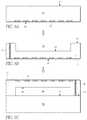
- FIG. 1Ais a schematic cross sectional view of the integrated device package 1 that includes an element 10 that comprises a frame 11 , an antenna structure 32 , and a device die 18 that is in electrical connection with the antenna structure 32 via an interconnect 36 .
- the antenna structure 32can electrically connect to the interconnect 36 by way of conductive traces (not shown) disposed in or on the element 10 .
- the device package 1comprises a cavity between the element 10 and the device die 18 .
- the frame 11 of the element 10can comprise a semiconductor material or other dielectric material (e.g., silicon, GaAs, glass, etc.).
- interconnect 36e.g., through silicon via (TSV), or through glass via (TGV), etc.
- TSVthrough silicon via
- TSVthrough glass via
- an electrically conductive materiale.g., copper, gold, etc.
- the framemay include more than one interconnect 36 .
- the interconnect 36 illustrated in FIG. 1Ais illustrated as being disposed within the frame 11 .
- the interconnect 36may be formed at any location of the element 10 including the edge and/or side wall of the element 10 .
- the cavity fillercan comprise a low loss dielectric constant or low loss tangent filler e.g., a filler having a loss tangent below around 0.0001.
- the cavity fillercan comprise a gas, such as an inert gas, air, nitrogen, etc.
- a dry gase.g., an inert dry gas
- the cavity fillercan comprise a dielectric material.
- the cavity fillermay comprise any combination of such filling materials or gases.
- the cavity filler(e.g., filling materials or gases) may be disposed in the cavity 30 in any suitable manner. It should be understood that the dimensions of the cavity 30 for a certain application can be determined at least in part by the properties of the cavity filler. It can also be beneficial to have the cavity filler with a known loss tangent in the cavity 30 for precise measurements.
- the cavity 30can comprise coatings (not shown) on or at its inner periphery.
- a first wall 40 , a second wall 42 , an upper surface 44 and/or an lower surface 46can be coated with metal and/or an additional dielectric layer.
- itcan be important to provide a hermetically sealed cavity 30 to isolate the cavity 30 from outside environ to have a known gas or material in the cavity 30 .
- the cavitymay also provide mechanical support for the antenna structures 32 , 34 , in some embodiments.
- the cavitycan be defined by, for example, etching the frame 11 of the element 10 (See FIG. 5 ).
- the cavity 30can comprise the first wall 40 and the second wall 42 .
- the first wall 40 and the second wall 42can comprise two opposing sides of the cavity 30 .
- the cavity 30can also comprise the upper surface 44 and the lower surface 46 .
- a portion of the element 10can comprise the upper surface 44 and a portion of the device die 18 can comprise the lower surface 46 .
- the cavity 30 illustrated in FIG. 1Ahas a rectangular shape as seen in the cross-sectional view, the cavity 30 may form any other suitable shape.
- the antenna structure 32can be disposed on or near a top surface 48 of the element 10 .
- the antenna structure 32can be at least partially embedded in the frame 11 .
- the antenna structure 32can be disposed on top of the frame 11 , e.g., deposited on exterior surfaces of the frame 11 .
- the antenna structure 32may be disposed at a different location of the integrated package 1 . (See, for example, FIG. 1B ).
- the antenna structure 32may be disposed near the upper surface of the cavity 30 , between the upper surface of the cavity 30 and the top surface of the element 10 , near the lower surface 46 of the cavity 30 , etc. As shown in FIG.
- the antenna structure 32can comprise a plurality of laterally spaced antenna structure elements.
- the antenna structure 32can comprise a phased array antenna that can include array of antennas. Each of the antennas of the phased array antenna can be independently controlled. A signal that is phase shifted can be applied to each of the antennas of the phased array antenna and can provide for a constructive or destructive interference. Each of the antennas can correspond to the antenna structure elements that are spaced laterally. The spacing between the antenna structure elements can be optimized to provide a desired interference coupling.
- the antenna structure 32can comprise a patch antenna. The patch antenna can be configured to transmit and/or receive signals at different frequencies which may be individually routed.
- the device die 18may comprise a splitter that may filter the bandwidth of interest for each split.
- the element 10can comprise multiple antenna structures. In some embodiments, the multiple antenna structures may be disposed at different portions of the element 10 .
- the element 10 and the device die 18can be directly bonded together at a bonding surface 22 without an intervening adhesive.
- Directly bonding the element 10 and the device die 18can be beneficial, in some embodiments.
- directly bonding the element 10 and the device die 18can provide a better sealing without increasing footprint or thickness of the package 1 than bonding using other methods of bonding, such as bonding using an adhesive.
- bonding using an adhesivebecause direct bonding does not include an underfill between the element 10 and the device die 18 , leakage of the underfill is avoided.
- the element 10 and the device die 18can be bonded with an adhesive.
- Preparation of the direct bonding surfacescan include provision of nonconductive layers such as silicon oxide.
- the bonding surfaces of the element 10 and the device die 18can be polished to a very high degree of smoothness (e.g., less than 20 nm surface roughness, or more particularly, less than 1 nm surface roughness) e.g., by chemical mechanical polishing (CMP).
- CMPchemical mechanical polishing
- the surfaces to be bondedmay be terminated with a suitable species and activated prior to bonding.
- the bonding surfaces of the bonding layer to be bondedsuch as silicon oxide material, may be very slightly etched for activation and exposed to a nitrogen-containing solution and terminated with a nitrogen-containing species.
- the surfaces to be bondedmay be exposed to an ammonia dip after a very slight etch, and/or a nitrogen-containing plasma (with or without a separate etch).
- the bonding surfacessuch as silicon oxide
- the bonding surfacescan be brought into contact.
- the interaction of the activated surfacescan cause the bonding surface of the first element 10 to directly bond with the bonding surface of the device die 18 without an intervening adhesive, without application of external pressure, without application of voltage, and at room temperature.
- the bonding forces of the nonconductive regionscan include covalent bonds that are greater than Van der Waals bonds and exert significant forces between the conductive features.
- the bonding energy of the dielectric-dielectric surfacecan be in a range from 150-300 mJ/m 2 , which can increase to 1500-4000 mJ/m 2 after a period of heat treatment. Additional details of the direct bonding processes used in conjunction with each of the disclosed embodiments may be found throughout U.S. Pat. Nos. 7,126,212; 8,153,505; 7,622,324; 7,602,070; 8,163,373; 8,389,378; and 8,735,219, and throughout U.S. Patent Application Publication Nos. 2017/0062366; 2016/0314346; 2017/0200711, the contents of each of which are hereby incorporated by reference herein in their entirety and for all purposes.
- the cavity 30can have a width w from the first wall 40 to the second wall 42 .
- a dimension of the width wcan depend on the frequency of electromagnetic signals used in a system that integrates the integrated package 1 .
- the width wcan be about 6 mm and for a frequency of 128 GHz, the width w can be about 1 mm, in some embodiments.
- the frequency of the electromagnetic signalscan be in a range of 24 GHz to 128 GHz.
- the frequencycan be in a range of 24 GHz to 75 GHz, in a range of 50 GHz to 128 GHz, in a range of 50 GHz to 75 GHz, etc.
- the width wcan be in a range of 0.5 mm to 14 mm, in some embodiments.
- the width wcan be in a range of 0.5 mm to 5 mm, in a range of 4 mm to 14 mm, in a range of 4 mm to 5 mm, etc.
- the width wmay have a tolerance due to, for example, uneven surfaces of the first and second walls 40 , 42 that can have a roughness r (see FIG. 5 ) of 1 ⁇ m to 2 ⁇ m, in some embodiments.
- the roughness rcan be, for example, in a range of 0.1 ⁇ m to 2 ⁇ m.
- the roughness rcan be less than 0.1% of the width w, in some embodiments.
- the cavity 30can have a height h from the lower surface 46 to the upper surface 44 .
- a dimension of the height hcan depend on operation frequency (wavelength) and/or signal strength.
- the height hcan be half of the wavelength of the operation frequency. Smaller height tends to have lower signal radiation strength.
- the height hcan be determined with the consideration of both height design limit and signal strength requirement, for example, a desired magnitude of the signals to be communicated.
- the height hcan be in a range of 5 ⁇ m to 500 ⁇ m, some embodiments.
- the height hcan be in a range of 5 ⁇ m to 250 ⁇ m, a range of 50 ⁇ m to 250 ⁇ m, a range of 150 ⁇ m to 500 ⁇ m, a range of 150 ⁇ m to 250 ⁇ m, etc.
- the height hmay have a roughness of less than 0.5 ⁇ m some embodiments.
- the roughnesscan be less than 0.05 ⁇ m.
- the roughnesscan be less than about 0.2%, for example, less than 0.1% to 0.5% of the height h, in some embodiments.
- semiconductor or dielectric materialse.g., silicon, glass, etc.
- the embodiments disclosed hereincan provide accurately dimensioned cavities for high frequency RF applications.
- FIG. 1Bis a schematic cross sectional view of the integrated device package 1 that includes an element 10 that comprises a frame 11 and an antenna structure 34 , and a device die 18 that is in electrical connection with the antenna structure 34 via an interconnect 38 .
- the components of FIG. 1Bmay be the same as or generally similar to like-numbered components of FIG. 1A .
- the antenna structure 34can be disposed on or near the upper surface 44 of the cavity 30 .
- the antenna structurecan be embedded in the frame 11 and/or disposed on top of the frame 11 .
- the interconnect 38 of FIG. 1Bextends from the device die 18 to the antenna structure 34 on or near the upper surface 44 of the cavity 30 .
- the interconnect 38 illustrated in FIG. 1Bis disposed along the second surface 42 of the cavity 30 .
- antenna structure 32there may be various benefits to having the antenna structure 32 on or near the top surface 48 of the element 10 as shown in FIG. 1A or having the antenna structure 34 on or near the upper surface 44 of the cavity 30 as shown in FIG. 1B .
- forming the antenna structure 32 on the top surface 48may be easier and less expensive than forming the antenna structure 34 on the upper surface 44 of the cavity 30 .
- providing the antenna structure 34 on the upper surface 44 of the cavity 30can place the antenna structure 34 closer to the cavity 30 and/or the device die 18 , providing improved performance.
- the antenna structure 34is shown to be embedded within the material of the frame 11 near the upper surface 44 of the cavity 30 , antenna structure 34 may also be deposited on top of the material of the frame 11 near the upper surface 44 of the cavity 30 .
- element 10may have one or more antenna structures 32 on or near the top surface 48 or one or may antenna structures 34 on the upper surface 44 of the cavity 30 or one or more antenna structures 32 and 34 simultaneously at both the locations.
- one elementmay include both the antenna structure 32 illustrated in FIG. 1A and the antenna structure 34 illustrated in FIG. 1B .
- the elementmay also include the interconnects 36 and 38 .
- the elementmay include more antenna structures at various portions of the element.
- FIG. 2is a schematic cross-sectional view of the integrated device package 1 that shows the element 10 comprising a plurality of frame portions 12 , 14 , 16 bonded together at second and third bonding surfaces 24 , 26 .
- the integrated device package of FIG. 2includes the antenna structure 32 disposed on or near the top surface 48 .
- the integrated device package 1 of FIG. 2can include the antenna structure on or near the upper surface 44 of the cavity 30 as illustrated in FIG. 1B or at any other suitable location.
- the components of FIG. 2may be the same as or generally similar to like-numbered components of FIGS. 1A and 1B .
- the element 10can comprise the frame 11 having a plurality of frame portions bonded together (e.g., directly bonded without an intervening adhesive).
- the frame 11can comprise, for example, first, second, and third frame portions 12 , 14 , 16 .
- the first and second frame portions 12 , 14can be directly bonded at a second bonding surface 24
- the second and third frame portions 14 , 16can be directly bonded at a third bonding surface 26 to form the frame 11 for the element 10 .
- sections of the first frame portion 12can comprise the upper surface 44 of the cavity 30 and the top surface 48 of the element 10
- sections of the second frame portion 14can comprise the first and second walls 40 , 42
- a section of the third frame portion 16can comprise the lower surface 46 of the cavity 30 .
- the third portion 16may be omitted and a planar portion of the die 18 may comprise the lower surface 46 of the cavity 30 , in some embodiments.
- the via 36may not be a single homogenous via.
- the viamay comprise separate portions bonded at interfaces, such as the second and the third bonding surfaces 24 , 26 .
- the portions of the via 36 in the respective frame portions 12 , 14 , 16may be offset from one another.
- the offset portions of the via 36can be electrically connected by way of a redistribution layer.
- the first and second frame portions 12 , 14can comprise a unitary structure eliminating the second bonding interface 24 .
- the second frame portion 14can extend from the first frame portion 12 .
- the unitary structurecan be bonded to the third frame portion 16 at the third bonding surface 26 .
- the unitary structurecan be bonded to the device die 18 without the third frame portion 16 .
- the second and third frame portions 14 , 16can comprise a unitary structure eliminating the third bonding interface 26 .
- the second frame portion 14can extend from the third frame portion 16 .
- the unitary structurecan be bonded together with the first frame portion 12 at the second bonding surface 24 .
- the third frame portion 16 illustrated as a portion of the frame 11can be a portion of the integrated device die 18 separate from a first die portion 20 .
- the second frame portion 14 illustrated as a portion of the frame 11can be a portion of the integrated device die 18 .
- FIG. 3Ais a schematic cross sectional view of the integrated device package 1 that includes a first interconnect 60 extending from the die 18 to the antenna structure 32 through the cavity 30 .
- FIG. 3Bis a schematic cross sectional view of the integrated device package 1 that includes a second interconnect 62 extending from the die 18 to the antenna structure 34 .
- the components of FIGS. 3A and 3Bmay be the same as or generally similar to like-numbered components of FIGS. 1A, 1B and 2 .
- the first and second interconnects 60 , 62can be connected to the antenna structures 32 , 34 , respectively, to electrically connect circuitry of the die 18 to the antenna structures 32 , 34 .
- the interconnects 36 , 38 of FIGS. 1A and 1Bcan be omitted.
- the interconnect 60can extend from the lower surface 46 of the cavity 30 (e.g., the upper surface of the die 18 ), through the cavity 30 , and through a thickness of the frame portion 12 to connect to the antenna element 32 .
- the interconnect 62can extend from the lower surface of the cavity 30 (e.g., the upper surface of the die 18 ), and through the cavity 30 to connect to the antenna element 32 at the upper surface 44 of the cavity 30 .
- interconnects 60 , 62as the electrical interconnect instead of the interconnects 36 , 38 can be beneficial in some embodiments.
- using the interconnects 60 , 62can obviate the steps of etching through the frame to form the hole in which the conductive material is to be disposed.
- forming the interconnect 62can be easier and/or faster than forming the interconnect 38 .
- having the interconnect 60 , 62 laterally within the cavity 30may reduce an overall lateral dimension of the integrated device package 1 .
- the interconnect 62can act as a resonator without being connected to the upper surface 44 .
- the interconnects 60 , 62can comprise posts that extends upwardly from the lower surface 46 of the cavity 30 .
- the interconnects 60 , 62can be formed by various processes.
- the interconnects 60 , 62can be formed as a part of a same unitary structure as the cavity 30 .
- the interconnects 60 , 62can be formed during joining of the frame portions 12 , 14 .
- the interconnects 60 , 62can be formed by forming a hole in a pre-cavity unitary piece of the frame, (e.g., by etching, drilling, etc.) and filling the hole with a conducive material.
- the holecan be filled with the conductive material by, for example, plating, or in any suitable way.
- the forming processmay be followed by etching the cavity 30 around the interconnect 60 , 62 .
- a cavityis etched in the pre-cavity unitary piece of the frame, followed by the deposition of the antenna 34 on or near the upper surface 44 of the cavity 30 , filling the cavity 30 with a resist, making a hole in the resist and filling the hole with a conducive material.
- the conductive materialcan be filled in the hole by, for example, plating or any other suitable way to form the interconnect 62 and removing the resist.
- the interconnects 60 and 62may have a short length for a thin cavity structure.
- the thin cavity structurecan have the height h in a range of, for example, 5 ⁇ m to 10 ⁇ m.
- the interconnect 62can comprise a copper post formed on the device die 18 .
- FIGS. 4A and 4Bare schematic cross-sectional views of an integrated device package 1 having the cavity 30 in different portions of the integrated device package 1 .
- the antenna structure 32 of FIGS. 4A and 4Bis shown on or near the top surface 48 , in other embodiments the antenna structure 34 can be provided on or near the upper surface 44 , as disclosed in other embodiments, such as in FIG. 1B .
- the components of FIGS. 4A and 4Bmay be the same as or generally similar to like-numbered components of FIGS. 1A to 3B .
- the cavity 30is defined by a recess formed in the element 10 and a lower surface 46 which may be defined by, for example, etching the frame 11 of the element 10 and bonding the device die 18 to the element 10 .
- the cavity 30can be defined by other portions of the integrated device package 1 , for example, by a recess formed in the device die 18 and a portion of a planar portion 45 of the element 10 , which defines the upper surface 44 of the cavity 30 .
- the cavity 30can be defined by recesses in both the element 10 and the device die 18 .
- active circuitry 19can be disposed at or near the bottom surface 50 of the device die 18 , as illustrated in FIGS. 4A and 4B . In some embodiments, the active circuitry 19 can be electrically connected to the antenna structure 32 via the interconnect 36 . However, it should be understood that the active circuitry 19 may be disposed anywhere in the device die 18 (e.g., near the bonding surface 22 , or embedded within the die 18 ). Beneficially, in FIG. 4B , it may be easier to form the antenna structure at or near the upper surface 44 of the cavity than in other arrangements because the upper surface 44 is not recessed from the planar portion 45 of the element 10 .
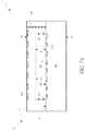
- FIG. 5is a schematic cross sectional zoomed in view of the integrated device package 1 around the cavity 30 showing exaggerated view of uneven and/or scalloped surfaces 54 , 56 of the walls 40 , 42 .
- the components of FIG. 5may be the same as or generally similar to like-numbered components of FIGS. 1A to 4B .
- the scalloped surfaces 54 , 56can comprise markings indicative of an etching process, e.g., deep reactive ion etching (DRIE). It can be desirable to have the roughness r of the scalloped surfaces 54 , 56 below a certain level to provide better performance for the antenna structure.
- DRIEdeep reactive ion etching
- the etching processcan etch from the lower surface 46 of the cavity 30 .
- a curved surface 55(which can be small) is formed.
- n curved surfaces on the scalloped surfaces 54 , 56there can be n curved surfaces on the scalloped surfaces 54 , 56 . It should be understood that each curve can be unique and may have different roughness r from the other curved surfaces.
- the roughness rcan be in a range of 0.1 ⁇ m to 2 ⁇ m and/or less than 0.1% of the width w.
- a oxide layerfor example, a thin thermal oxide layer that is thicker than the roughness r or the scalloped surfaces
- This oxide layercan be etched away to form a significantly smoother cavity side walls than without the use of the thermal oxide layer.
- FIGS. 6A to 6Cshow steps of making the cavity 30 in the integrated device die 1 .
- the components of FIGS. 6A to 6Cmay be the same as or generally similar to like-numbered components of FIGS. 1A to 5 .
- the antenna structure 32is formed prior to bonding and forming the cavity 30 .
- the antenna structure 32can be formed after forming the cavity 30 .
- the element 10 that comprises the frame 11 and the antenna structure 32can be provided, as shown in FIG. 6A .
- the frame 11can have an etching surface 47 opposite the top surface 48 .
- the framecan be etched from the etching surface 47 to form a recess 31 having the upper surface 44 (see FIG. 6B ).
- the interconnect 36can also be formed by making a hole by way of, for example etching or drilling, and disposing a conductive material (e.g., copper, gold, etc.) in the hole, in some embodiments.
- the interconnect 36may be formed, for example, prior to forming the cavity 31 .
- the interconnect 36may be formed, for example, after bonding the element 10 with the device die 18 .
- the element 10can be flipped upside down and bonded (e.g., directly bonded without an intervening adhesive in some embodiments) to the device die 18 at the bonding surface 26 , defining the cavity 30 with the recess 31 and the lower surface 46 of the cavity 30 .
- the framemay comprise a plurality of frame portions as discussed above with respect to FIG. 2 .
- the interconnect 36can be electrically connected to one or more metal pads of the device die 18 .
- the electrical connection between the interconnect 36 and the one or more metal pads of the device die 18may be formed by, for example, a hybrid bond and/or a direct bond when interconnect 36 is formed prior to bonding.
- the hole in frame 11may be opened to be accessible to the one or more electrical pads on the top surface 46 of device 18 , and the hole can be filled with a conductive material by, for example, electroplating etc. to form the interconnect 36 in via-last approach when the interconnect 36 is formed after bonding the frame 11 to the device die 18 .
- FIG. 7Ais a schematic cross-sectional view of an integrated device package 1 having a first antenna structure 32 a at or near the top surface 48 of the element 10 and a second antenna structure 32 b at or near the lower surface 46 of the cavity 30 .
- the components of FIG. 7Amay be the same as or generally similar to like-numbered components of FIGS. 1A to 6C .
- the first and second antenna structures 32 a , 32 bcan be electrically connected to define one antenna structure.
- the interconnect 36can connect to the antenna structure 32 a , 32 b by way of respective conductive traces formed in the element 10 and/or the die 18 .
- the first antenna structure 32 acan comprise a parasitic patch and the second antenna structure 32 b can comprise a feed patch.
- the second antenna structure 32 bcan be connected to a feeding via or a trace with an excitation signal.
- the first antenna structure 32 acan be driven by a resonant radiation signal from the second antenna structure 32 b .
- an arrangement of the cavity 30 between the first and second antenna structures 32 a , 32 bcan enhance the signal resonant radiation, such that the gains and/or bandwidth may be improved.
- FIG. 7Bis a schematic cross-sectional view of an integrated device package 1 having a first antenna structure 32 a and a second antenna structure 32 b .
- the components of FIG. 7Bmay be the same as or generally similar to like-numbered components of FIGS. 1A to 7A .
- the second antenna structure 32 b of the integrated device package 1 of FIG. 7Bis disposed under the lower surface 46 of the cavity 30 , such that the second antenna structure 32 b is embedded in the die 18 .
- the element 10can comprise a frame having a plurality of frame portions bonded together as shown in FIG. 2 and the second antenna structure 32 b may be disposed between the third portion 16 (see, for example, FIG. 2 ) and the die 18 .
- the first antenna structure 32 amay be disposed near the upper surface 44 of the cavity or anywhere between the top surface 48 of the element 11 and the upper surface 44 of the cavity 33 .
- FIG. 8is a schematic diagram of an electronic system 80 incorporating one or more integrated device packages 1 , according to various embodiments.
- the system 80can comprise any suitable type of electronic device, such as a mobile electronic device (e.g., a smartphone, a tablet computing device, a laptop computer, etc.), a desktop computer, an automobile or components thereof, a stereo system, a medical device, a camera, or any other suitable type of system.
- the electronic system 80can comprise a microprocessor, a graphics processor, an electronic recording device, or digital memory.
- the system 80can include one or more device packages 82 which are mechanically and electrically connected to the system 80 , e.g., by way of one or more motherboards. Each package 82 can comprise one or more integrated device packages 1 .
- the system 80 shown in FIG. 8can comprise any of the integrated device packages 1 and associated seals shown and described herein.
- an integrated device packagein one aspect, includes an integrated device die and an element.
- the elementcomprises an antenna structure.
- the elementis attached to a surface of the integrated device die.
- the integrated device packagealso includes a cavity that is disposed between the integrated device die and at least a portion of the antenna structure.
- the integrated device packagefurther includes an electrical interconnect that connects the integrated device die and the antenna structure.
- the elementincludes a frame that is directly bonded to the integrated device die without an intervening adhesive.
- the framecan include silicon.
- the integrated device diecan include radio-frequency (RF) circuitry.
- the cavitycan be defined by the element and the integrated device die.
- the cavitycan be defined by a planar device die surface and a recess in the element.
- the recesscan be formed by etching a portion of the element.
- the cavitycan be defined by a planar element surface and the recess in the element.
- the integrated device diecan be mounted on a package substrate.
- the integrated device packagecan further include a metal layer disposed in the cavity.
- the framecan include a plurality of frame portions bonded together.
- the cavityis filled with air.
- the integrated device packagefurther includes a resonator that is at least partially disposed in the cavity.
- the cavityincludes a first wall surface indicative of an etching process.
- the cavitycan include a second wall.
- the first wall and the second wallcan comprise two opposing sides of the cavity.
- the cavitycan have a width from the first wall to the second wall.
- the widthcan be dimensioned to receive or transmit electromagnetic radiation at a frequency range of 24 GHz to 128 GHz.
- the widthcan be in a range of 0.5 mm to 12 mm.
- the first and second wallscan be constructed such that the dimension has a maximum roughness in a range of 1 ⁇ m to 2 ⁇ m.
- the first and second wallscan be constructed such that the dimension has a maximum roughness in a range of 0.1 ⁇ m to 1 ⁇ m.
- the antenna structureis disposed on or near an upper surface of the cavity or a top surface of the element away from the cavity.
- the antenna structurecomprises a parasitic patch and a feed patch.
- the portion of the antenna structurecan comprise the parasitic patch and the cavity can be disposed between the parasitic patch and the feed patch.
- the parasitic patch and the feed patchcan be in electrical connection.
- an integrated device packagein one aspect, includes a package housing that comprises a semiconductor material.
- the package housingincludes an integrated device, an antenna structure, and a cavity that is disposed between the integrated device and at least a portion of the antenna structure.
- the integrated device packagealso includes an electrical interconnect that connects the integrated device and the antenna structure.
- the semiconductor materialcomprises silicon
- the cavityis formed by etching the semiconductor material.
- the antenna structureincludes a plurality of antennas.
- the package housingincludes a plurality of housing portions bonded together.
- a method of manufacturing an integrated device packageincludes forming a recess in a semiconductor element comprising an antenna structure, and bonding the semiconductor element with an integrated device die such that the recess is disposed between the antenna structure and the integrated device die.
- the forming the recessincludes etching a portion of the semiconductor element.
- the forming the recessincludes coating portions of the recess with metal.
- the etching the portioncan include etching a frame portion comprising silicon of the semiconductor element.
- the bonding the semiconductor element with the integrated device dieincludes bonding the semiconductor element directly to the integrated device die without an intervening adhesive.
- the bonding the semiconductor element with the integrated device dieincludes making an electrical connection between interconnects comprised in the semiconductor element and the integrated device die.
- the forming the recessalso includes filling the recess with air.
Landscapes
- Physics & Mathematics (AREA)
- Condensed Matter Physics & Semiconductors (AREA)
- General Physics & Mathematics (AREA)
- Engineering & Computer Science (AREA)
- Computer Hardware Design (AREA)
- Microelectronics & Electronic Packaging (AREA)
- Power Engineering (AREA)
- Variable-Direction Aerials And Aerial Arrays (AREA)
- Details Of Aerials (AREA)
- Encapsulation Of And Coatings For Semiconductor Or Solid State Devices (AREA)
Abstract
Description
Claims (17)
Priority Applications (9)
| Application Number | Priority Date | Filing Date | Title |
|---|---|---|---|
| US16/212,471US10923408B2 (en) | 2017-12-22 | 2018-12-06 | Cavity packages |
| PCT/US2018/064982WO2019125828A1 (en) | 2017-12-22 | 2018-12-11 | Cavity packages |
| TW114105780ATW202527250A (en) | 2017-12-22 | 2018-12-13 | Cavity packages |
| TW113104679ATWI878019B (en) | 2017-12-22 | 2018-12-13 | Cavity packages |
| TW111117017ATWI800370B (en) | 2017-12-22 | 2018-12-13 | Cavity packages |
| TW107145028ATWI767099B (en) | 2017-12-22 | 2018-12-13 | Cavity packages |
| TW112110060ATWI835598B (en) | 2017-12-22 | 2018-12-13 | Cavity packages |
| US17/146,304US11600542B2 (en) | 2017-12-22 | 2021-01-11 | Cavity packages |
| US18/147,239US20230260858A1 (en) | 2017-12-22 | 2022-12-28 | Cavity packages |
Applications Claiming Priority (2)
| Application Number | Priority Date | Filing Date | Title |
|---|---|---|---|
| US201762609682P | 2017-12-22 | 2017-12-22 | |
| US16/212,471US10923408B2 (en) | 2017-12-22 | 2018-12-06 | Cavity packages |
Related Child Applications (1)
| Application Number | Title | Priority Date | Filing Date |
|---|---|---|---|
| US17/146,304DivisionUS11600542B2 (en) | 2017-12-22 | 2021-01-11 | Cavity packages |
Publications (2)
| Publication Number | Publication Date |
|---|---|
| US20190198407A1 US20190198407A1 (en) | 2019-06-27 |
| US10923408B2true US10923408B2 (en) | 2021-02-16 |
Family
ID=66951410
Family Applications (3)
| Application Number | Title | Priority Date | Filing Date |
|---|---|---|---|
| US16/212,471ActiveUS10923408B2 (en) | 2017-12-22 | 2018-12-06 | Cavity packages |
| US17/146,304ActiveUS11600542B2 (en) | 2017-12-22 | 2021-01-11 | Cavity packages |
| US18/147,239PendingUS20230260858A1 (en) | 2017-12-22 | 2022-12-28 | Cavity packages |
Family Applications After (2)
| Application Number | Title | Priority Date | Filing Date |
|---|---|---|---|
| US17/146,304ActiveUS11600542B2 (en) | 2017-12-22 | 2021-01-11 | Cavity packages |
| US18/147,239PendingUS20230260858A1 (en) | 2017-12-22 | 2022-12-28 | Cavity packages |
Country Status (3)
| Country | Link |
|---|---|
| US (3) | US10923408B2 (en) |
| TW (5) | TWI878019B (en) |
| WO (1) | WO2019125828A1 (en) |
Cited By (70)
| Publication number | Priority date | Publication date | Assignee | Title |
|---|---|---|---|---|
| US11195748B2 (en) | 2017-09-27 | 2021-12-07 | Invensas Corporation | Interconnect structures and methods for forming same |
| US11205600B2 (en) | 2014-03-12 | 2021-12-21 | Invensas Corporation | Integrated circuits protected by substrates with cavities, and methods of manufacture |
| US11205625B2 (en) | 2019-04-12 | 2021-12-21 | Invensas Bonding Technologies, Inc. | Wafer-level bonding of obstructive elements |
| US11244920B2 (en) | 2018-12-18 | 2022-02-08 | Invensas Bonding Technologies, Inc. | Method and structures for low temperature device bonding |
| US11257727B2 (en) | 2017-03-21 | 2022-02-22 | Invensas Bonding Technologies, Inc. | Seal for microelectronic assembly |
| US11373963B2 (en) | 2019-04-12 | 2022-06-28 | Invensas Bonding Technologies, Inc. | Protective elements for bonded structures |
| US11380597B2 (en) | 2017-12-22 | 2022-07-05 | Invensas Bonding Technologies, Inc. | Bonded structures |
| US11385278B2 (en) | 2019-05-23 | 2022-07-12 | Invensas Bonding Technologies, Inc. | Security circuitry for bonded structures |
| US11515279B2 (en) | 2018-04-11 | 2022-11-29 | Adeia Semiconductor Bonding Technologies Inc. | Low temperature bonded structures |
| US11600542B2 (en) | 2017-12-22 | 2023-03-07 | Adeia Semiconductor Bonding Technologies Inc. | Cavity packages |
| US11610846B2 (en) | 2019-04-12 | 2023-03-21 | Adeia Semiconductor Bonding Technologies Inc. | Protective elements for bonded structures including an obstructive element |
| US11621246B2 (en) | 2019-03-29 | 2023-04-04 | Adeia Semiconductor Technologies Llc | Diffused bitline replacement in stacked wafer memory |
| US11631586B2 (en) | 2012-08-30 | 2023-04-18 | Adeia Semiconductor Bonding Technologies Inc. | Heterogeneous annealing method |
| US11664357B2 (en) | 2018-07-03 | 2023-05-30 | Adeia Semiconductor Bonding Technologies Inc. | Techniques for joining dissimilar materials in microelectronics |
| US11670615B2 (en) | 2016-12-21 | 2023-06-06 | Adeia Semiconductor Bonding Technologies Inc. | Bonded structures |
| US11694925B2 (en) | 2017-10-06 | 2023-07-04 | Adeia Semiconductor Bonding Technologies Inc. | Diffusion barrier collar for interconnects |
| US11705410B2 (en) | 2020-12-11 | 2023-07-18 | Nxp Usa, Inc. | Semiconductor device having integrated antenna and method therefor |
| US11710718B2 (en) | 2015-07-10 | 2023-07-25 | Adeia Semiconductor Technologies Llc | Structures and methods for low temperature bonding using nanoparticles |
| US11715730B2 (en) | 2017-03-16 | 2023-08-01 | Adeia Semiconductor Technologies Llc | Direct-bonded LED arrays including optical elements configured to transmit optical signals from LED elements |
| US11721653B2 (en) | 2019-12-23 | 2023-08-08 | Adeia Semiconductor Bonding Technologies Inc. | Circuitry for electrical redundancy in bonded structures |
| US11735523B2 (en) | 2020-05-19 | 2023-08-22 | Adeia Semiconductor Bonding Technologies Inc. | Laterally unconfined structure |
| US11742315B2 (en) | 2017-04-21 | 2023-08-29 | Adeia Semiconductor Bonding Technologies Inc. | Die processing |
| US11742314B2 (en) | 2020-03-31 | 2023-08-29 | Adeia Semiconductor Bonding Technologies Inc. | Reliable hybrid bonded apparatus |
| US11762200B2 (en) | 2019-12-17 | 2023-09-19 | Adeia Semiconductor Bonding Technologies Inc. | Bonded optical devices |
| US11760059B2 (en) | 2003-05-19 | 2023-09-19 | Adeia Semiconductor Bonding Technologies Inc. | Method of room temperature covalent bonding |
| US11791307B2 (en) | 2018-04-20 | 2023-10-17 | Adeia Semiconductor Bonding Technologies Inc. | DBI to SI bonding for simplified handle wafer |
| US11790219B2 (en) | 2017-08-03 | 2023-10-17 | Adeia Semiconductor Inc. | Three dimensional circuit implementing machine trained network |
| US11842894B2 (en) | 2019-12-23 | 2023-12-12 | Adeia Semiconductor Bonding Technologies Inc. | Electrical redundancy for bonded structures |
| US11855064B2 (en) | 2018-02-15 | 2023-12-26 | Adeia Semiconductor Bonding Technologies Inc. | Techniques for processing devices |
| US11860415B2 (en) | 2018-02-26 | 2024-01-02 | Adeia Semiconductor Bonding Technologies Inc. | Integrated optical waveguides, direct-bonded waveguide interface joints, optical routing and interconnects |
| US11862602B2 (en) | 2019-11-07 | 2024-01-02 | Adeia Semiconductor Technologies Llc | Scalable architecture for reduced cycles across SOC |
| US11862604B2 (en) | 2018-06-22 | 2024-01-02 | Adeia Semiconductor Inc. | Systems and methods for releveled bump planes for chiplets |
| US11876076B2 (en) | 2019-12-20 | 2024-01-16 | Adeia Semiconductor Technologies Llc | Apparatus for non-volatile random access memory stacks |
| US11881454B2 (en) | 2016-10-07 | 2024-01-23 | Adeia Semiconductor Inc. | Stacked IC structure with orthogonal interconnect layers |
| US11894326B2 (en) | 2017-03-17 | 2024-02-06 | Adeia Semiconductor Bonding Technologies Inc. | Multi-metal contact structure |
| US11894345B2 (en) | 2018-08-28 | 2024-02-06 | Adeia Semiconductor Inc. | Integrated voltage regulator and passive components |
| US11908739B2 (en) | 2017-06-05 | 2024-02-20 | Adeia Semiconductor Technologies Llc | Flat metal features for microelectronics applications |
| US11916054B2 (en) | 2018-05-15 | 2024-02-27 | Adeia Semiconductor Bonding Technologies Inc. | Stacked devices and methods of fabrication |
| US11929347B2 (en) | 2020-10-20 | 2024-03-12 | Adeia Semiconductor Technologies Llc | Mixed exposure for large die |
| US11955393B2 (en) | 2018-05-14 | 2024-04-09 | Adeia Semiconductor Bonding Technologies Inc. | Structures for bonding elements including conductive interface features |
| US11955463B2 (en) | 2019-06-26 | 2024-04-09 | Adeia Semiconductor Bonding Technologies Inc. | Direct bonded stack structures for increased reliability and improved yield in microelectronics |
| US11967575B2 (en) | 2018-08-29 | 2024-04-23 | Adeia Semiconductor Bonding Technologies Inc. | Bond enhancement structure in microelectronics for trapping contaminants during direct-bonding processes |
| US11973056B2 (en) | 2016-10-27 | 2024-04-30 | Adeia Semiconductor Technologies Llc | Methods for low temperature bonding using nanoparticles |
| US11978681B2 (en) | 2019-04-22 | 2024-05-07 | Adeia Semiconductor Bonding Technologies Inc. | Mitigating surface damage of probe pads in preparation for direct bonding of a substrate |
| US12009338B2 (en) | 2020-03-19 | 2024-06-11 | Adeia Semiconductor Bonding Technologies Inc. | Dimension compensation control for directly bonded structures |
| US12046482B2 (en) | 2018-07-06 | 2024-07-23 | Adeia Semiconductor Bonding Technologies, Inc. | Microelectronic assemblies |
| US12046569B2 (en) | 2020-06-30 | 2024-07-23 | Adeia Semiconductor Bonding Technologies Inc. | Integrated device packages with integrated device die and dummy element |
| US12051621B2 (en) | 2016-12-28 | 2024-07-30 | Adeia Semiconductor Bonding Technologies Inc. | Microelectronic assembly from processed substrate |
| US12068278B2 (en) | 2017-05-11 | 2024-08-20 | Adeia Semiconductor Bonding Technologies Inc. | Processed stacked dies |
| US12074092B2 (en) | 2018-05-30 | 2024-08-27 | Adeia Semiconductor Inc. | Hard IP blocks with physically bidirectional passageways |
| US12100676B2 (en) | 2018-04-11 | 2024-09-24 | Adeia Semiconductor Bonding Technologies Inc. | Low temperature bonded structures |
| US12113056B2 (en) | 2016-05-19 | 2024-10-08 | Adeia Semiconductor Bonding Technologies Inc. | Stacked dies and methods for forming bonded structures |
| US12113054B2 (en) | 2019-10-21 | 2024-10-08 | Adeia Semiconductor Technologies Llc | Non-volatile dynamic random access memory |
| US12142528B2 (en) | 2016-10-07 | 2024-11-12 | Adeia Semiconductor Inc. | 3D chip with shared clock distribution network |
| US12176294B2 (en) | 2020-09-04 | 2024-12-24 | Adeia Semiconductor Bonding Technologies, Inc. | Bonded structure with interconnect structure |
| US12191267B2 (en) | 2019-03-01 | 2025-01-07 | Adeia Semiconductor Technologies, LLC | Nanowire bonding interconnect for fine-pitch microelectronics |
| US12211809B2 (en) | 2020-12-30 | 2025-01-28 | Adeia Semiconductor Bonding Technologies Inc. | Structure with conductive feature and method of forming same |
| US12266640B2 (en) | 2018-07-06 | 2025-04-01 | Adeia Semiconductor Bonding Technologies Inc. | Molded direct bonded and interconnected stack |
| US12272730B2 (en) | 2018-03-29 | 2025-04-08 | Adeia Semiconductor Inc. | Transistor level interconnection methodologies utilizing 3D interconnects |
| US12270970B2 (en) | 2018-03-20 | 2025-04-08 | Adeia Semiconductor Bonding Technologies Inc. | Direct-bonded lamination for improved image clarity in optical devices |
| US12300634B2 (en) | 2021-08-02 | 2025-05-13 | Adeia Semiconductor Bonding Technologies Inc. | Protective semiconductor elements for bonded structures |
| US12322718B2 (en) | 2020-09-04 | 2025-06-03 | Adeia Semiconductor Bonding Technologies Inc. | Bonded structure with interconnect structure |
| US12341083B2 (en) | 2023-02-08 | 2025-06-24 | Adeia Semiconductor Bonding Technologies Inc. | Electronic device cooling structures bonded to semiconductor elements |
| US12374656B2 (en) | 2017-06-15 | 2025-07-29 | Adeia Semiconductor Bonding Technologies Inc. | Multi-chip modules formed using wafer-level processing of a reconstituted wafer |
| US12374641B2 (en) | 2019-06-12 | 2025-07-29 | Adeia Semiconductor Bonding Technologies Inc. | Sealed bonded structures and methods for forming the same |
| US12374556B2 (en) | 2016-12-28 | 2025-07-29 | Adeia Semiconductor Bonding Technologies Inc. | Processing stacked substrates |
| US12381128B2 (en) | 2020-12-28 | 2025-08-05 | Adeia Semiconductor Bonding Technologies Inc. | Structures with through-substrate vias and methods for forming the same |
| US12381173B2 (en) | 2017-09-24 | 2025-08-05 | Adeia Semiconductor Bonding Technologies Inc. | Direct hybrid bonding of substrates having microelectronic components with different profiles and/or pitches at the bonding interface |
| US12406959B2 (en) | 2018-07-26 | 2025-09-02 | Adeia Semiconductor Bonding Technologies Inc. | Post CMP processing for hybrid bonding |
| US12424584B2 (en) | 2020-10-29 | 2025-09-23 | Adeia Semiconductor Bonding Technologies Inc. | Direct bonding methods and structures |
Families Citing this family (20)
| Publication number | Priority date | Publication date | Assignee | Title |
|---|---|---|---|---|
| US7485968B2 (en) | 2005-08-11 | 2009-02-03 | Ziptronix, Inc. | 3D IC method and device |
| US11069734B2 (en) | 2014-12-11 | 2021-07-20 | Invensas Corporation | Image sensor device |
| US9741620B2 (en) | 2015-06-24 | 2017-08-22 | Invensas Corporation | Structures and methods for reliable packages |
| US9953941B2 (en) | 2015-08-25 | 2018-04-24 | Invensas Bonding Technologies, Inc. | Conductive barrier direct hybrid bonding |
| US9852988B2 (en) | 2015-12-18 | 2017-12-26 | Invensas Bonding Technologies, Inc. | Increased contact alignment tolerance for direct bonding |
| US10446532B2 (en) | 2016-01-13 | 2019-10-15 | Invensas Bonding Technologies, Inc. | Systems and methods for efficient transfer of semiconductor elements |
| US10446487B2 (en) | 2016-09-30 | 2019-10-15 | Invensas Bonding Technologies, Inc. | Interface structures and methods for forming same |
| TWI837879B (en) | 2016-12-29 | 2024-04-01 | 美商艾德亞半導體接合科技有限公司 | Bonded structures with integrated passive component |
| EP3580166A4 (en) | 2017-02-09 | 2020-09-02 | Invensas Bonding Technologies, Inc. | Bonded structures |
| US10784191B2 (en) | 2017-03-31 | 2020-09-22 | Invensas Bonding Technologies, Inc. | Interface structures and methods for forming same |
| US11056348B2 (en) | 2018-04-05 | 2021-07-06 | Invensas Bonding Technologies, Inc. | Bonding surfaces for microelectronics |
| US10366966B1 (en)* | 2018-05-17 | 2019-07-30 | Taiwan Semiconductor Manufacturing Co., Ltd. | Method of manufacturing integrated fan-out package |
| US11393779B2 (en) | 2018-06-13 | 2022-07-19 | Invensas Bonding Technologies, Inc. | Large metal pads over TSV |
| KR20210009426A (en) | 2018-06-13 | 2021-01-26 | 인벤사스 본딩 테크놀로지스 인코포레이티드 | TV as a pad |
| US11011494B2 (en) | 2018-08-31 | 2021-05-18 | Invensas Bonding Technologies, Inc. | Layer structures for making direct metal-to-metal bonds at low temperatures in microelectronics |
| US11158573B2 (en) | 2018-10-22 | 2021-10-26 | Invensas Bonding Technologies, Inc. | Interconnect structures |
| CN113330557A (en) | 2019-01-14 | 2021-08-31 | 伊文萨思粘合技术公司 | Bonding structure |
| US11901281B2 (en) | 2019-03-11 | 2024-02-13 | Adeia Semiconductor Bonding Technologies Inc. | Bonded structures with integrated passive component |
| US12080672B2 (en) | 2019-09-26 | 2024-09-03 | Adeia Semiconductor Bonding Technologies Inc. | Direct gang bonding methods including directly bonding first element to second element to form bonded structure without adhesive |
| US11152707B1 (en)* | 2020-07-02 | 2021-10-19 | International Business Machines Corporation | Fast radio frequency package |
Citations (183)
| Publication number | Priority date | Publication date | Assignee | Title |
|---|---|---|---|---|
| US4998665A (en) | 1988-09-07 | 1991-03-12 | Nec Corporation | Bonding structure of substrates and method for bonding substrates |
| US5087585A (en) | 1989-07-11 | 1992-02-11 | Nec Corporation | Method of stacking semiconductor substrates for fabrication of three-dimensional integrated circuit |
| US5322593A (en) | 1991-11-21 | 1994-06-21 | Nec Corporation | Method for manufacturing polyimide multilayer wiring substrate |
| US5753536A (en) | 1994-08-29 | 1998-05-19 | Matsushita Electric Industrial Co., Ltd. | Semiconductor device and associated fabrication method |
| US5771555A (en) | 1993-11-01 | 1998-06-30 | Matsushita Electric Industrial Co., Ltd. | Method for producing an electronic component using direct bonding |
| US5985739A (en) | 1994-09-19 | 1999-11-16 | Fraunhofer-Gesellschaft Zur Forderung Der Angewandten Forschung E.V. | Semiconductor structures having advantageous high-frequency characteristics and processes for producing such semiconductor structures |
| US5998808A (en) | 1997-06-27 | 1999-12-07 | Sony Corporation | Three-dimensional integrated circuit device and its manufacturing method |
| US6008126A (en) | 1992-04-08 | 1999-12-28 | Elm Technology Corporation | Membrane dielectric isolation IC fabrication |
| JP2000100679A (en) | 1998-09-22 | 2000-04-07 | Canon Inc | Micro-region solid-state bonding method between substrates by thinning and device structure |
| US6080640A (en) | 1997-07-11 | 2000-06-27 | Advanced Micro Devices, Inc. | Metal attachment method and structure for attaching substrates at low temperatures |
| JP2001102479A (en) | 1999-09-27 | 2001-04-13 | Toshiba Corp | Semiconductor integrated circuit device and method of manufacturing the same |
| JP2001148436A (en) | 1999-11-22 | 2001-05-29 | Ngk Spark Plug Co Ltd | Ceramic package and its manufacturing method |
| US6265775B1 (en) | 1997-01-24 | 2001-07-24 | Micron Technology, Inc. | Flip chip technique for chip assembly |
| US20020000328A1 (en) | 2000-06-22 | 2002-01-03 | Kabushiki Kaisha Toshiba | Printed wiring board and manufacturing method thereof |
| US20020003307A1 (en) | 2000-07-05 | 2002-01-10 | Tadatomo Suga | Semiconductor device and method for fabricating the device |
| US6374770B1 (en) | 1995-10-26 | 2002-04-23 | Applied Materials, Inc. | Apparatus for improving film stability of halogen-doped silicon oxide films |
| US6423640B1 (en) | 2000-08-09 | 2002-07-23 | Taiwan Semiconductor Manufacturing Co., Ltd. | Headless CMP process for oxide planarization |
| US6465892B1 (en) | 1999-04-13 | 2002-10-15 | Oki Electric Industry Co., Ltd. | Interconnect structure for stacked semiconductor device |
| US20020179921A1 (en) | 2001-06-02 | 2002-12-05 | Cohn Michael B. | Compliant hermetic package |
| JP2002353416A (en) | 2001-05-25 | 2002-12-06 | Sony Corp | Semiconductor storage device and method of manufacturing the same |
| US20030098060A1 (en) | 2001-10-29 | 2003-05-29 | Naoki Yoshimi | Solar battery sealing film and method of manufacturing solar battery panel using the same |
| US20040084414A1 (en) | 2002-08-19 | 2004-05-06 | Kenji Sakai | Polishing method and polishing composition used for polishing |
| US20040259325A1 (en) | 2003-06-19 | 2004-12-23 | Qing Gan | Wafer level chip scale hermetic package |
| US20050009246A1 (en) | 2002-09-25 | 2005-01-13 | Ziptronix, Inc. | Wafer bonding hermetic encapsulation |
| US6876062B2 (en) | 2002-06-27 | 2005-04-05 | Taiwan Semiconductor Manufacturing Co., Ltd | Seal ring and die corner stress relief pattern design to protect against moisture and metallic impurities |
| US6887769B2 (en) | 2002-02-06 | 2005-05-03 | Intel Corporation | Dielectric recess for wafer-to-wafer and die-to-die metal bonding and method of fabricating the same |
| WO2005043584A2 (en) | 2003-10-21 | 2005-05-12 | Ziptronix, Inc. | Single mask via method and device |
| US6908027B2 (en) | 2003-03-31 | 2005-06-21 | Intel Corporation | Complete device layer transfer without edge exclusion via direct wafer bonding and constrained bond-strengthening process |
| KR20050101324A (en) | 2003-02-07 | 2005-10-21 | 집트로닉스 인코퍼레이티드 | Room temperature metal direct bonding |
| US20060001123A1 (en) | 2004-06-30 | 2006-01-05 | John Heck | Module integrating MEMS and passive components |
| US6998712B2 (en) | 2003-02-03 | 2006-02-14 | Nec Electronics Corporation | Semiconductor device and method for manufacturing the same |
| US20060057945A1 (en) | 2004-09-16 | 2006-03-16 | Chia-Lin Hsu | Chemical mechanical polishing process |
| US7045453B2 (en) | 2002-10-24 | 2006-05-16 | International Business Machines Corporation | Very low effective dielectric constant interconnect structures and methods for fabricating the same |
| US20060115323A1 (en) | 2004-11-04 | 2006-06-01 | Coppeta Jonathan R | Compression and cold weld sealing methods and devices |
| US7057274B2 (en) | 2001-10-17 | 2006-06-06 | Hymite A/S | Semiconductor structures having through-holes sealed with feed-through metalization |
| US20060197215A1 (en) | 2005-03-03 | 2006-09-07 | Stellar Microdevices, Inc. | Hermetic MEMS package and method of manufacture |
| US7105980B2 (en) | 2002-07-03 | 2006-09-12 | Sawtek, Inc. | Saw filter device and method employing normal temperature bonding for producing desirable filter production and performance characteristics |
| US20060208326A1 (en) | 2005-03-18 | 2006-09-21 | Nasiri Steven S | Method of fabrication of ai/ge bonding in a wafer packaging environment and a product produced therefrom |
| WO2006100444A1 (en) | 2005-03-22 | 2006-09-28 | Cambridge Display Technology Limited | Apparatus and method for increased device lifetime in an organic electro-luminescent device. |
| US20070029562A1 (en) | 2005-07-05 | 2007-02-08 | Naoyuki Koizumi | Semiconductor device and method of manufacturing a semiconductor device |
| US20070045781A1 (en) | 2005-08-26 | 2007-03-01 | Innovative Micro Technology | Hermetic interconnect structure and method of manufacture |
| US20070045795A1 (en) | 2005-08-31 | 2007-03-01 | Mcbean Ronald V | MEMS package and method of forming the same |
| US7193423B1 (en) | 2005-12-12 | 2007-03-20 | International Business Machines Corporation | Wafer-to-wafer alignments |
| US20070096294A1 (en) | 2003-06-06 | 2007-05-03 | Sanyo Electric Co., Ltd. | Semiconductor device and manufacturing method of the same |
| US20070111386A1 (en) | 2002-02-20 | 2007-05-17 | Kim Sarah E | Process of vertically stacking multiple wafers supporting different active integrated circuit (IC) devices |
| US20070222048A1 (en) | 2006-03-24 | 2007-09-27 | Advanced Semiconductor Engineering, Inc. | Package structure |
| US20070295456A1 (en) | 2006-03-28 | 2007-12-27 | Innovative Micro Technology | Wafer bonding material with embedded conductive particles |
| US7354798B2 (en) | 2002-12-20 | 2008-04-08 | International Business Machines Corporation | Three-dimensional device fabrication method |
| US7359591B2 (en) | 2001-12-19 | 2008-04-15 | Intel Corporation | Electrical/optical integration scheme using direct copper bonding |
| US20080124835A1 (en) | 2006-11-03 | 2008-05-29 | International Business Machines Corporation | Hermetic seal and reliable bonding structures for 3d applications |
| US20080296709A1 (en) | 2007-05-30 | 2008-12-04 | Tessera, Inc. | Chip assembly |
| US7467897B2 (en) | 2004-02-12 | 2008-12-23 | Hymite A/S | Light transmitting modules with optical power monitoring |
| US20090053855A1 (en) | 2006-05-15 | 2009-02-26 | Innovative Micro Technology | Indented lid for encapsulated devices and method of manufacture |
| US20090186446A1 (en) | 2007-11-29 | 2009-07-23 | Samsung Electronics Co., Ltd. | Semiconductor device packages and methods of fabricating the same |
| JP2009238905A (en) | 2008-03-26 | 2009-10-15 | Nippon Telegr & Teleph Corp <Ntt> | Mounting structure and mounting method for semiconductor element |
| US20100096713A1 (en) | 2006-12-07 | 2010-04-22 | Electronic And Telecommunications Research Institute | Mems package and packaging method thereof |
| US7750488B2 (en) | 2006-07-10 | 2010-07-06 | Tezzaron Semiconductor, Inc. | Method for bonding wafers to produce stacked integrated circuits |
| US7803693B2 (en) | 2007-02-15 | 2010-09-28 | John Trezza | Bowed wafer hybridization compensation |
| US20100288525A1 (en) | 2009-05-12 | 2010-11-18 | Alcatel-Lucent Usa, Incorporated | Electronic package and method of manufacture |
| US20100301432A1 (en) | 2009-05-29 | 2010-12-02 | Gjermund Kittilsland | Gap control for die or layer bonding using intermediate layers |
| US20110115092A1 (en) | 2008-07-31 | 2011-05-19 | Masamoto Tago | Semiconductor device and method of manufacturing same |
| US20110290552A1 (en) | 2004-09-27 | 2011-12-01 | Qualcomm Mems Technologies, Inc. | Method and system for packaging mems devices with incorporated getter |
| US20120097733A1 (en) | 2009-04-30 | 2012-04-26 | Silex Microsystems Ab | Novel bonding process and bonded structures |
| US20120100657A1 (en) | 2009-07-03 | 2012-04-26 | Stmicroelectronics (Crolles 2) Sas | Simplified copper-copper bonding |
| US20120142144A1 (en) | 2010-12-03 | 2012-06-07 | Babak Taheri | Wafer Level Structures and Methods for Fabricating and Packaging MEMS |
| US8241961B2 (en) | 2008-12-09 | 2012-08-14 | Young Hae KIM | Method for manufacturing hetero-bonded wafer |
| US20120212384A1 (en) | 2011-02-17 | 2012-08-23 | International Business Machines Corporation | Integrated antenna for rfic package applications |
| US8269671B2 (en) | 2009-01-27 | 2012-09-18 | International Business Machines Corporation | Simple radio frequency integrated circuit (RFIC) packages with integrated antennas |
| US20120286380A1 (en) | 2011-02-25 | 2012-11-15 | Evigia Systems | Processes and mounting fixtures for fabricating electromechanical devices and devices formed therewith |
| US8314007B2 (en) | 2009-12-23 | 2012-11-20 | Soitec | Process for fabricating a heterostructure with minimized stress |
| US20120326248A1 (en) | 2011-06-27 | 2012-12-27 | Invensense, Inc. | Methods for cmos-mems integrated devices with multiple sealed cavities maintained at various pressures |
| US8349635B1 (en) | 2008-05-20 | 2013-01-08 | Silicon Laboratories Inc. | Encapsulated MEMS device and method to form the same |
| US8357931B2 (en) | 2004-02-27 | 2013-01-22 | Nvidia Corporation | Flip chip semiconductor die internal signal access system and method |
| JP2013033786A (en) | 2011-08-01 | 2013-02-14 | Sony Corp | Semiconductor device and semiconductor device manufacturing method |
| US8377798B2 (en) | 2010-11-10 | 2013-02-19 | Taiwan Semiconductor Manufacturing Co., Ltd | Method and structure for wafer to wafer bonding in semiconductor packaging |
| US8395229B2 (en) | 2011-03-11 | 2013-03-12 | Institut National D'optique | MEMS-based getter microdevice |
| US8411444B2 (en) | 2010-09-15 | 2013-04-02 | International Business Machines Corporation | Thermal interface material application for integrated circuit cooling |
| US8441131B2 (en) | 2011-09-12 | 2013-05-14 | Globalfoundries Inc. | Strain-compensating fill patterns for controlling semiconductor chip package interactions |
| US8476165B2 (en) | 2009-04-01 | 2013-07-02 | Tokyo Electron Limited | Method for thinning a bonding wafer |
| US8476146B2 (en) | 2010-12-03 | 2013-07-02 | Taiwan Semiconductor Manufacturing Company, Ltd. | Reducing wafer distortion through a low CTE layer |
| US8482132B2 (en) | 2009-10-08 | 2013-07-09 | International Business Machines Corporation | Pad bonding employing a self-aligned plated liner for adhesion enhancement |
| US20130187245A1 (en) | 2012-01-19 | 2013-07-25 | Taiwan Semiconductor Manufacturing Company, Ltd. | Micro electro mechanical system structures |
| US8501537B2 (en) | 2011-03-31 | 2013-08-06 | Soitec | Methods for bonding semiconductor structures involving annealing processes, and bonded semiconductor structures formed using such methods |
| US8530997B1 (en) | 2012-07-31 | 2013-09-10 | Taiwan Semiconductor Manufacturing Company, Ltd. | Double seal ring |
| US8546928B2 (en) | 2006-04-06 | 2013-10-01 | Fraunhofer-Gesellschaft Zur Foerderung Der Angewandten Forschung E. V. | Micromechanical housing comprising at least two cavities having different internal pressure and/or different gas compositions and method for the production thereof |
| US20130277774A1 (en) | 2012-04-24 | 2013-10-24 | Robert Bosch Gmbh | Method for manufacturing a hybrid integrated component |
| US20130293428A1 (en) | 2012-05-03 | 2013-11-07 | Commissariat A L'energie Atomique Et Aux Ene Alt | Microelectronic wireless transmission device |
| US8620164B2 (en) | 2011-01-20 | 2013-12-31 | Intel Corporation | Hybrid III-V silicon laser formed by direct bonding |
| US8647987B2 (en) | 2012-04-16 | 2014-02-11 | The Institute of Microelectronics, Chinese Academy of Science | Method for improving uniformity of chemical-mechanical planarization process |
| US8697493B2 (en) | 2011-07-18 | 2014-04-15 | Soitec | Bonding surfaces for direct bonding of semiconductor structures |
| US8716105B2 (en) | 2011-03-31 | 2014-05-06 | Soitec | Methods for bonding semiconductor structures involving annealing processes, and bonded semiconductor structures and intermediate structures formed using such methods |
| WO2014074403A1 (en) | 2012-11-12 | 2014-05-15 | Memsic, Inc. | Monolithic sensor package |
| US20140175655A1 (en) | 2012-12-22 | 2014-06-26 | Industrial Technology Research Institute | Chip bonding structure and manufacturing method thereof |
| US20140217557A1 (en) | 2013-02-05 | 2014-08-07 | Taiwan Semiconductor Manufacturing Company, Ltd. | Method and Apparatus for a Seal Ring Structure |
| US8802538B1 (en) | 2013-03-15 | 2014-08-12 | Taiwan Semiconductor Manufacturing Company, Ltd. | Methods for hybrid wafer bonding |
| US20140225206A1 (en) | 2013-02-11 | 2014-08-14 | Yizhen Lin | Pressure level adjustment in a cavity of a semiconductor die |
| US20140225795A1 (en) | 2013-02-08 | 2014-08-14 | Sj Antenna Design | Shielding module integrating antenna and integrated circuit component |
| US8809123B2 (en) | 2012-06-05 | 2014-08-19 | Taiwan Semiconductor Manufacturing Company, Ltd. | Three dimensional integrated circuit structures and hybrid bonding methods for semiconductor wafers |
| US8841002B2 (en) | 2003-05-19 | 2014-09-23 | Ziptronix, Inc. | Method of room temperature covalent bonding |
| EP2813465A1 (en) | 2013-06-12 | 2014-12-17 | Tronics Microsystems S.A. | MEMS device with getter layer |
| US8916448B2 (en) | 2013-01-09 | 2014-12-23 | International Business Machines Corporation | Metal to metal bonding for stacked (3D) integrated circuits |
| US20150068666A1 (en) | 2012-05-18 | 2015-03-12 | Panasonic Intellectual Property Management Co., Ltd. | Production method of multiple panes |
| US20150091153A1 (en) | 2013-09-30 | 2015-04-02 | Taiwan Semiconductor Manufacturing Co., Ltd. | Wafer level sealing methods with different vacuum levels for mems sensors |
| US20150137345A1 (en) | 2013-11-21 | 2015-05-21 | Samsung Electronics Co., Ltd. | Semiconductor package having heat spreader |
| US9093350B2 (en) | 2010-07-09 | 2015-07-28 | Canon Kabushiki Kaisha | Member for solid-state image pickup device and method for manufacturing solid-state image pickup device having first and second wiring structures with a concave portion between first and second substrates |
| KR20150097798A (en) | 2012-12-21 | 2015-08-26 | 테사 소시에타스 유로파에아 | Adhesive tape containing getter material |
| US9142517B2 (en) | 2012-06-05 | 2015-09-22 | Taiwan Semiconductor Manufacturing Company, Ltd. | Hybrid bonding mechanisms for semiconductor wafers |
| US9171756B2 (en) | 2005-08-11 | 2015-10-27 | Ziptronix, Inc. | 3D IC method and device |
| US9184125B2 (en) | 2012-08-30 | 2015-11-10 | Ziptronix, Inc. | Heterogeneous annealing method and device |
| US20150336790A1 (en) | 2014-04-04 | 2015-11-26 | Analog Devices, Inc. | Fabrication of Tungsten MEMS Structures |
| US9224704B2 (en) | 2010-10-14 | 2015-12-29 | Soitec | Process for realizing a connecting structure |
| US9230941B2 (en) | 2014-03-28 | 2016-01-05 | Taiwan Semiconductor Manufacturing Company, Ltd. | Bonding structure for stacked semiconductor devices |
| US9257399B2 (en) | 2013-10-17 | 2016-02-09 | Taiwan Semiconductor Manufacturing Company, Ltd. | 3D integrated circuit and methods of forming the same |
| US9299736B2 (en) | 2014-03-28 | 2016-03-29 | Taiwan Semiconductor Manufacturing Company, Ltd. | Hybrid bonding with uniform pattern density |
| US9312229B2 (en) | 2013-03-15 | 2016-04-12 | Taiwan Semiconductor Manufacturing Company, Ltd. | Hybrid bonding with air-gap structure |
| US9337235B2 (en) | 2013-02-18 | 2016-05-10 | Taiwan Semiconductor Manufacturing Company, Ltd. | Method and apparatus for image sensor packaging |
| US20160137492A1 (en) | 2014-11-14 | 2016-05-19 | Taiwan Semiconductor Manufacturing Co., Ltd. | Mems and cmos integration with low-temperature bonding |
| US9386688B2 (en) | 2010-11-12 | 2016-07-05 | Freescale Semiconductor, Inc. | Integrated antenna package |
| US9391143B2 (en) | 2000-02-16 | 2016-07-12 | Ziptronix, Inc. | Method for low temperature bonding and bonded structure |
| US20160229685A1 (en) | 2013-07-08 | 2016-08-11 | Motion Engine Inc. | Mems components and method of wafer-level manufacturing thereof |
| US20160240495A1 (en)* | 2009-01-30 | 2016-08-18 | Infineon Technologies Ag | Integrated antennas in wafer level package |
| US9431368B2 (en) | 1999-10-01 | 2016-08-30 | Ziptronix, Inc. | Three dimensional device integration method and integrated device |
| US9437572B2 (en) | 2013-12-18 | 2016-09-06 | Taiwan Semiconductor Manufacturing Company, Ltd. | Conductive pad structure for hybrid bonding and methods of forming same |
| US9461007B2 (en) | 2014-07-11 | 2016-10-04 | Samsung Electronics Co., Ltd. | Wafer-to-wafer bonding structure |
| US9496239B1 (en) | 2015-12-11 | 2016-11-15 | International Business Machines Corporation | Nitride-enriched oxide-to-oxide 3D wafer bonding |
| US20160343682A1 (en) | 2013-12-11 | 2016-11-24 | Kabushiki Kaisha Toshiba | Semiconductor device |
| US9536848B2 (en) | 2014-10-16 | 2017-01-03 | Globalfoundries Inc. | Bond pad structure for low temperature flip chip bonding |
| US20170008757A1 (en) | 2015-07-06 | 2017-01-12 | Taiwan Semiconductor Manufacturing Company Ltd. | Cmos-mems device structure, bonding mesa structure and associated method |
| US9559081B1 (en) | 2015-08-21 | 2017-01-31 | Apple Inc. | Independent 3D stacking |
| US20170062366A1 (en) | 2015-08-25 | 2017-03-02 | Ziptronix, Inc. | Conductive barrier direct hybrid bonding |
| US9620464B2 (en)* | 2014-08-13 | 2017-04-11 | International Business Machines Corporation | Wireless communications package with integrated antennas and air cavity |
| US9620481B2 (en) | 2013-05-30 | 2017-04-11 | Globalfoundries Inc. | Substrate bonding with diffusion barrier structures |
| US20170137281A1 (en) | 2014-07-18 | 2017-05-18 | Ulis | Method for Manufacturing a Device Comprising a Hermetically Sealed Vacuum Housing and Getter |
| WO2017100256A1 (en) | 2015-12-08 | 2017-06-15 | Skyworks Solutions, Inc. | Transient liquid phase material bonding and sealing structures and methods of forming same |
| US20170194271A1 (en) | 2016-01-06 | 2017-07-06 | Mediatek Inc. | Semiconductor package with three-dimensional antenna |
| US20170200711A1 (en) | 2016-01-13 | 2017-07-13 | Ziptronix, Inc. | Systems and methods for efficient transfer of semiconductor elements |
| US9723716B2 (en) | 2013-09-27 | 2017-08-01 | Infineon Technologies Ag | Contact pad structure, an electronic component, and a method for manufacturing a contact pad structure |
| US9728521B2 (en) | 2015-07-23 | 2017-08-08 | Taiwan Semiconductor Manufacturing Co., Ltd. | Hybrid bond using a copper alloy for yield improvement |
| US9741620B2 (en) | 2015-06-24 | 2017-08-22 | Invensas Corporation | Structures and methods for reliable packages |
| WO2017151442A1 (en) | 2016-02-29 | 2017-09-08 | Invensas Corporation | Correction die for wafer/die stack |
| KR20170108143A (en) | 2015-01-30 | 2017-09-26 | 인벤사스 코포레이션 | Localized sealing of interconnect structures in small gaps |
| US9799587B2 (en) | 2011-05-24 | 2017-10-24 | Sony Corporation | Semiconductor device |
| US20170338214A1 (en) | 2016-05-19 | 2017-11-23 | Ziptronix, Inc. | Stacked dies and methods for forming bonded structures |
| US9852988B2 (en) | 2015-12-18 | 2017-12-26 | Invensas Bonding Technologies, Inc. | Increased contact alignment tolerance for direct bonding |
| US9893004B2 (en) | 2011-07-27 | 2018-02-13 | Broadpak Corporation | Semiconductor interposer integration |
| US20180047682A1 (en) | 2016-08-15 | 2018-02-15 | Taiwan Semiconductor Manufacturing Co., Ltd. | Composite bond structure in stacked semiconductor structure |
| US9929050B2 (en) | 2013-07-16 | 2018-03-27 | Taiwan Semiconductor Manufacturing Company, Ltd. | Mechanisms for forming three-dimensional integrated circuit (3DIC) stacking structure |
| US20180096931A1 (en) | 2016-09-30 | 2018-04-05 | Invensas Bonding Technologies, Inc. | Interface structures and methods for forming same |
| US9941243B2 (en) | 2016-06-09 | 2018-04-10 | Samsung Electronics Co., Ltd. | Wafer-to-wafer bonding structure |
| US9941241B2 (en) | 2016-06-30 | 2018-04-10 | International Business Machines Corporation | Method for wafer-wafer bonding |
| US10002844B1 (en) | 2016-12-21 | 2018-06-19 | Invensas Bonding Technologies, Inc. | Bonded structures |
| US20180175012A1 (en) | 2016-12-15 | 2018-06-21 | Taiwan Semiconductor Manufacturing Co., Ltd. | Seal ring structures and methods of forming same |
| US20180182639A1 (en) | 2016-12-28 | 2018-06-28 | Invensas Bonding Technologies, Inc. | Processing Stacked Substrates |
| US20180182666A1 (en) | 2016-12-28 | 2018-06-28 | Invensas Bonding Technologies, Inc. | Microelectronic assembly from processed substrate |
| US20180190580A1 (en) | 2016-12-29 | 2018-07-05 | Invensas Bonding Technologies, Inc. | Bonded structures with integrated passive component |
| US20180190583A1 (en) | 2016-12-29 | 2018-07-05 | Invensas Bonding Technologies, Inc. | Bonded structures with integrated passive component |
| US20180191047A1 (en) | 2016-12-30 | 2018-07-05 | Invensas Bonding Technologies, Inc. | Structure with integrated metallic waveguide |
| US10026605B2 (en) | 2014-06-04 | 2018-07-17 | Semiconductor Components Industries, Llc | Method of reducing residual contamination in singulated semiconductor die |
| US20180219038A1 (en) | 2017-02-01 | 2018-08-02 | Semiconductor Components Industries, Llc | Edge seals for semiconductor packages |
| US20180226375A1 (en) | 2017-02-09 | 2018-08-09 | Invensas Bonding Technologies, Inc. | Bonded structures |
| US10075657B2 (en) | 2015-07-21 | 2018-09-11 | Fermi Research Alliance, Llc | Edgeless large area camera system |
| US20180269161A1 (en) | 2017-03-17 | 2018-09-20 | Taiwan Semiconductor Manufacturing Co., Ltd. | Metal line design for hybrid-bonding application |
| US20180273377A1 (en) | 2017-03-21 | 2018-09-27 | Invensas Bonding Technologies, Inc. | Seal for microelectronic assembly |
| US20180286805A1 (en) | 2017-03-31 | 2018-10-04 | Invensas Bonding Technologies, Inc. | Interface structures and methods for forming same |
| JP2018160519A (en) | 2017-03-22 | 2018-10-11 | 東芝メモリ株式会社 | Semiconductor device manufacturing method and semiconductor device |
| US20180323227A1 (en) | 2017-05-03 | 2018-11-08 | United Microelectronics Corp. | Wafer level packaging method |
| US20180323177A1 (en) | 2016-04-15 | 2018-11-08 | Taiwan Semiconductor Manufacturing Company, Ltd. | 3DIC Formation with Dies Bonded to Formed RDLs |
| US20180331066A1 (en) | 2017-05-11 | 2018-11-15 | Invensas Bonding Technologies, Inc. | Processed stacked dies |
| US20190096741A1 (en) | 2017-09-27 | 2019-03-28 | Invensas Corporation | Interconnect structures and methods for forming same |
| US20190096842A1 (en) | 2017-09-24 | 2019-03-28 | Invensas Bonding Technologies, Inc. | Chemical mechanical polishing for hybrid bonding |
| US20190115277A1 (en) | 2016-12-05 | 2019-04-18 | Taiwan Semiconductor Manufacturing Company, Ltd. | Package Structure for Heat Dissipation |
| US10269756B2 (en) | 2017-04-21 | 2019-04-23 | Invensas Bonding Technologies, Inc. | Die processing |
| US10276619B2 (en) | 2016-01-12 | 2019-04-30 | Taiwan Semiconductor Manufacturing Co., Ltd. | Semiconductor device structure with a conductive feature passing through a passivation layer |
| US20190131277A1 (en) | 2017-11-01 | 2019-05-02 | Taiwan Semiconductor Manufacturing Co., Ltd. | Die stack structure and method of fabricating the same and package |
| US20190164914A1 (en) | 2017-11-30 | 2019-05-30 | Taiwan Semiconductor Manufacturing Company, Ltd. | Seal Ring for Hybrid-Bond |
| US20190198409A1 (en) | 2017-12-22 | 2019-06-27 | Invensas Bonding Technologies, Inc. | Bonded structures |
| US10446456B2 (en) | 2014-03-12 | 2019-10-15 | Invensas Corporation | Integrated circuits protected by substrates with cavities, and methods of manufacture |
| US20190333550A1 (en) | 2018-04-30 | 2019-10-31 | Invensas Corporation | Multi-die module with low power operation |
| US20190348336A1 (en) | 2018-05-14 | 2019-11-14 | Invensas Bonding Technologies, Inc. | Structures for bonding elements |
| US20190385966A1 (en) | 2018-06-13 | 2019-12-19 | Invensas Bonding Technologies, Inc. | Large metal pads over tsv |
| US20200013637A1 (en) | 2018-07-06 | 2020-01-09 | Invensas Bonding Technologies, Inc. | Microelectronic assemblies |
| US20200075534A1 (en) | 2018-08-31 | 2020-03-05 | Invensas Bonding Technologies, Inc. | Layer structures for making direct metal-to-metal bonds at low temperatures in microelectronics |
| US20200227367A1 (en) | 2019-01-14 | 2020-07-16 | Invensas Bonding Technologies, Inc. | Bonded structures |
Family Cites Families (97)
| Publication number | Priority date | Publication date | Assignee | Title |
|---|---|---|---|---|
| JPH10112517A (en) | 1996-10-03 | 1998-04-28 | Ngk Spark Plug Co Ltd | Electronic components housing package |
| US6872984B1 (en) | 1998-07-29 | 2005-03-29 | Silicon Light Machines Corporation | Method of sealing a hermetic lid to a semiconductor die at an angle |
| US6900549B2 (en) | 2001-01-17 | 2005-05-31 | Micron Technology, Inc. | Semiconductor assembly without adhesive fillets |
| KR20050094082A (en)* | 2004-03-22 | 2005-09-27 | (주)알에프캠프 | Eyelet for a radio frequency identification |
| US7952189B2 (en) | 2004-05-27 | 2011-05-31 | Chang-Feng Wan | Hermetic packaging and method of manufacture and use therefore |
| KR100498708B1 (en) | 2004-11-08 | 2005-07-01 | 옵토팩 주식회사 | Electronic package for semiconductor device and packaging method thereof |
| EP1770603A1 (en)* | 2005-10-03 | 2007-04-04 | Assa Abloy Identification Technology Group AB | Encapsulated transponder and method for manufacturing the same |
| US7288458B2 (en) | 2005-12-14 | 2007-10-30 | Freescale Semiconductor, Inc. | SOI active layer with different surface orientation |
| US20070188054A1 (en) | 2006-02-13 | 2007-08-16 | Honeywell International Inc. | Surface acoustic wave packages and methods of forming same |
| US20080002460A1 (en) | 2006-03-01 | 2008-01-03 | Tessera, Inc. | Structure and method of making lidded chips |
| US7430359B2 (en) | 2006-10-02 | 2008-09-30 | Miradia, Inc. | Micromechanical system containing a microfluidic lubricant channel |
| JP4983219B2 (en) | 2006-11-22 | 2012-07-25 | 株式会社村田製作所 | Component built-in board |
| JP4792143B2 (en) | 2007-02-22 | 2011-10-12 | 株式会社デンソー | Semiconductor device and manufacturing method thereof |
| US8513791B2 (en) | 2007-05-18 | 2013-08-20 | International Business Machines Corporation | Compact multi-port CAM cell implemented in 3D vertical integration |
| US8129828B2 (en) | 2008-09-29 | 2012-03-06 | Ngk Spark Plug Co., Ltd. | Wiring substrate with reinforcement |
| US8089144B2 (en) | 2008-12-17 | 2012-01-03 | Denso Corporation | Semiconductor device and method for manufacturing the same |
| CN101554988B (en) | 2009-04-30 | 2011-03-30 | 华中科技大学 | Wafer-level vacuum packaging method for micro-electromechanical systems |
| FR2953679B1 (en) | 2009-12-04 | 2012-06-01 | Thales Sa | HERMETIC ELECTRONIC HOUSING AND METHOD FOR HERMETICALLY ASSEMBLING A HOUSING |
| JP5115618B2 (en) | 2009-12-17 | 2013-01-09 | 株式会社デンソー | Semiconductor device |
| JP5568786B2 (en) | 2009-12-24 | 2014-08-13 | 新光電気工業株式会社 | Semiconductor package manufacturing method and semiconductor package |
| JP4900498B2 (en) | 2010-04-26 | 2012-03-21 | セイコーエプソン株式会社 | Electronic components |
| US8330559B2 (en) | 2010-09-10 | 2012-12-11 | Taiwan Semiconductor Manufacturing Company, Ltd. | Wafer level packaging |
| EP2514713B1 (en) | 2011-04-20 | 2013-10-02 | Tronics Microsystems S.A. | A micro-electromechanical system (MEMS) device |
| KR102282833B1 (en) | 2011-06-17 | 2021-07-27 | 가부시키가이샤 한도오따이 에네루기 켄큐쇼 | Transistor |
| TWI426572B (en) | 2011-10-20 | 2014-02-11 | Ind Tech Res Inst | Structure and process for microelectromechanical system-based sensor |
| EA038017B1 (en) | 2011-11-03 | 2021-06-23 | Фасткэп Системз Корпорейшн | Production logging instrument |
| ES2524427T3 (en)* | 2012-01-16 | 2014-12-09 | Assa Abloy Ab | Method for producing a bar-shaped label and label produced by said procedure |
| US9139420B2 (en) | 2012-04-18 | 2015-09-22 | Taiwan Semiconductor Manufacturing Company, Ltd. | MEMS device structure and methods of forming same |
| JP2013243333A (en) | 2012-04-24 | 2013-12-05 | Tadatomo Suga | Chip-on wafer bonding method and bonding device and structure including chip and wafer |
| US9048283B2 (en) | 2012-06-05 | 2015-06-02 | Taiwan Semiconductor Manufacturing Company, Ltd. | Hybrid bonding systems and methods for semiconductor wafers |
| US9511994B2 (en) | 2012-11-28 | 2016-12-06 | Invensense, Inc. | Aluminum nitride (AlN) devices with infrared absorption structural layer |
| US8564076B1 (en) | 2013-01-30 | 2013-10-22 | Invensense, Inc. | Internal electrical contact for enclosed MEMS devices |
| US9452920B2 (en) | 2013-01-30 | 2016-09-27 | Invensense, Inc. | Microelectromechanical system device with internal direct electric coupling |
| US9469527B2 (en) | 2013-03-14 | 2016-10-18 | Taiwan Semiconductor Manufacturing Company, Ltd. | MEMS pressure sensor and microphone devices having through-vias and methods of forming same |
| US9119313B2 (en) | 2013-04-25 | 2015-08-25 | Intel Corporation | Package substrate with high density interconnect design to capture conductive features on embedded die |
| JP6020341B2 (en) | 2013-05-09 | 2016-11-02 | 株式会社デンソー | Capacitive physical quantity sensor and manufacturing method thereof |
| US9136233B2 (en) | 2013-06-06 | 2015-09-15 | STMicroelctronis (Crolles 2) SAS | Process for fabricating a three-dimensional integrated structure with improved heat dissipation, and corresponding three-dimensional integrated structure |
| CN104249991B (en) | 2013-06-26 | 2016-08-10 | 中芯国际集成电路制造(上海)有限公司 | MEMS and preparation method thereof |
| KR20160036666A (en) | 2013-09-27 | 2016-04-04 | 인텔 코포레이션 | Die package with superposer substrate for passive components |
| US9617150B2 (en) | 2013-10-09 | 2017-04-11 | Taiwan Semiconductor Manufacturing Co., Ltd. | Micro-electro mechanical system (MEMS) device having a blocking layer formed between closed chamber and a dielectric layer of a CMOS substrate |
| JP2015100886A (en) | 2013-11-26 | 2015-06-04 | セイコーエプソン株式会社 | Electronic devices and electronic equipment |
| US9773742B2 (en)* | 2013-12-18 | 2017-09-26 | Intel Corporation | Embedded millimeter-wave phased array module |
| US9899442B2 (en) | 2014-12-11 | 2018-02-20 | Invensas Corporation | Image sensor device |
| JP5931246B1 (en) | 2015-04-03 | 2016-06-08 | 田中貴金属工業株式会社 | Package manufacturing method and package manufactured by the method |
| US9738516B2 (en) | 2015-04-29 | 2017-08-22 | Taiwan Semiconductor Manufacturing Co., Ltd. | Structure to reduce backside silicon damage |
| US9650241B2 (en) | 2015-09-17 | 2017-05-16 | Invensense, Inc. | Method for providing a MEMS device with a plurality of sealed enclosures having uneven standoff structures and MEMS device thereof |
| US10273141B2 (en) | 2016-04-26 | 2019-04-30 | Taiwan Semiconductor Manufacturing Co., Ltd. | Rough layer for better anti-stiction deposition |
| US9892961B1 (en) | 2016-08-09 | 2018-02-13 | International Business Machines Corporation | Air gap spacer formation for nano-scale semiconductor devices |
| US9834435B1 (en) | 2016-11-29 | 2017-12-05 | Taiwan Semiconductor Manufacturing Co., Ltd. | Structure and formation method of semiconductor device structure |
| US10515913B2 (en) | 2017-03-17 | 2019-12-24 | Invensas Bonding Technologies, Inc. | Multi-metal contact structure |
| US10217720B2 (en) | 2017-06-15 | 2019-02-26 | Invensas Corporation | Multi-chip modules formed using wafer-level processing of a reconstitute wafer |
| KR20190018812A (en)* | 2017-08-16 | 2019-02-26 | 삼성전기주식회사 | Semiconductor package and electronic device having the same |
| EP3669420B1 (en)* | 2017-08-18 | 2025-10-01 | Telefonaktiebolaget LM Ericsson (publ) | Radio-frequency three-dimensional electronic-photonic integrated circuit with integrated antennas and transceivers |
| US11031285B2 (en) | 2017-10-06 | 2021-06-08 | Invensas Bonding Technologies, Inc. | Diffusion barrier collar for interconnects |
| US10923408B2 (en) | 2017-12-22 | 2021-02-16 | Invensas Bonding Technologies, Inc. | Cavity packages |
| US10727219B2 (en) | 2018-02-15 | 2020-07-28 | Invensas Bonding Technologies, Inc. | Techniques for processing devices |
| US11169326B2 (en) | 2018-02-26 | 2021-11-09 | Invensas Bonding Technologies, Inc. | Integrated optical waveguides, direct-bonded waveguide interface joints, optical routing and interconnects |
| US11256004B2 (en) | 2018-03-20 | 2022-02-22 | Invensas Bonding Technologies, Inc. | Direct-bonded lamination for improved image clarity in optical devices |
| US11056348B2 (en) | 2018-04-05 | 2021-07-06 | Invensas Bonding Technologies, Inc. | Bonding surfaces for microelectronics |
| US10790262B2 (en) | 2018-04-11 | 2020-09-29 | Invensas Bonding Technologies, Inc. | Low temperature bonded structures |
| US10964664B2 (en) | 2018-04-20 | 2021-03-30 | Invensas Bonding Technologies, Inc. | DBI to Si bonding for simplified handle wafer |
| US11276676B2 (en) | 2018-05-15 | 2022-03-15 | Invensas Bonding Technologies, Inc. | Stacked devices and methods of fabrication |
| US11171117B2 (en) | 2018-06-12 | 2021-11-09 | Invensas Bonding Technologies, Inc. | Interlayer connection of stacked microelectronic components |
| KR20210009426A (en) | 2018-06-13 | 2021-01-26 | 인벤사스 본딩 테크놀로지스 인코포레이티드 | TV as a pad |
| WO2020010056A1 (en) | 2018-07-03 | 2020-01-09 | Invensas Bonding Technologies, Inc. | Techniques for joining dissimilar materials in microelectronics |
| US11158606B2 (en) | 2018-07-06 | 2021-10-26 | Invensas Bonding Technologies, Inc. | Molded direct bonded and interconnected stack |
| US12406959B2 (en) | 2018-07-26 | 2025-09-02 | Adeia Semiconductor Bonding Technologies Inc. | Post CMP processing for hybrid bonding |
| US20200075533A1 (en) | 2018-08-29 | 2020-03-05 | Invensas Bonding Technologies, Inc. | Bond enhancement in microelectronics by trapping contaminants and arresting cracks during direct-bonding processes |
| US11158573B2 (en) | 2018-10-22 | 2021-10-26 | Invensas Bonding Technologies, Inc. | Interconnect structures |
| US11235969B2 (en) | 2018-10-30 | 2022-02-01 | Taiwan Semiconductor Manufacturing Company, Ltd. | CMOS-MEMS integration with through-chip via process |
| US11244920B2 (en) | 2018-12-18 | 2022-02-08 | Invensas Bonding Technologies, Inc. | Method and structures for low temperature device bonding |
| US11387202B2 (en) | 2019-03-01 | 2022-07-12 | Invensas Llc | Nanowire bonding interconnect for fine-pitch microelectronics |
| US11901281B2 (en) | 2019-03-11 | 2024-02-13 | Adeia Semiconductor Bonding Technologies Inc. | Bonded structures with integrated passive component |
| US11610846B2 (en) | 2019-04-12 | 2023-03-21 | Adeia Semiconductor Bonding Technologies Inc. | Protective elements for bonded structures including an obstructive element |
| US11205625B2 (en) | 2019-04-12 | 2021-12-21 | Invensas Bonding Technologies, Inc. | Wafer-level bonding of obstructive elements |
| US11373963B2 (en) | 2019-04-12 | 2022-06-28 | Invensas Bonding Technologies, Inc. | Protective elements for bonded structures |
| US11355404B2 (en) | 2019-04-22 | 2022-06-07 | Invensas Bonding Technologies, Inc. | Mitigating surface damage of probe pads in preparation for direct bonding of a substrate |
| US11385278B2 (en) | 2019-05-23 | 2022-07-12 | Invensas Bonding Technologies, Inc. | Security circuitry for bonded structures |
| US12374641B2 (en) | 2019-06-12 | 2025-07-29 | Adeia Semiconductor Bonding Technologies Inc. | Sealed bonded structures and methods for forming the same |
| US11296053B2 (en) | 2019-06-26 | 2022-04-05 | Invensas Bonding Technologies, Inc. | Direct bonded stack structures for increased reliability and improved yield in microelectronics |
| US12080672B2 (en) | 2019-09-26 | 2024-09-03 | Adeia Semiconductor Bonding Technologies Inc. | Direct gang bonding methods including directly bonding first element to second element to form bonded structure without adhesive |
| US11762200B2 (en) | 2019-12-17 | 2023-09-19 | Adeia Semiconductor Bonding Technologies Inc. | Bonded optical devices |
| US11721653B2 (en) | 2019-12-23 | 2023-08-08 | Adeia Semiconductor Bonding Technologies Inc. | Circuitry for electrical redundancy in bonded structures |
| CN115088068A (en) | 2019-12-23 | 2022-09-20 | 伊文萨思粘合技术公司 | Electrical redundancy for bonded structures |
| US20210242152A1 (en) | 2020-02-05 | 2021-08-05 | Invensas Bonding Technologies, Inc. | Selective alteration of interconnect pads for direct bonding |
| WO2021188846A1 (en) | 2020-03-19 | 2021-09-23 | Invensas Bonding Technologies, Inc. | Dimension compensation control for directly bonded structures |
| US11742314B2 (en) | 2020-03-31 | 2023-08-29 | Adeia Semiconductor Bonding Technologies Inc. | Reliable hybrid bonded apparatus |
| WO2021236361A1 (en) | 2020-05-19 | 2021-11-25 | Invensas Bonding Technologies, Inc. | Laterally unconfined structure |
| US11631647B2 (en) | 2020-06-30 | 2023-04-18 | Adeia Semiconductor Bonding Technologies Inc. | Integrated device packages with integrated device die and dummy element |
| US11764177B2 (en) | 2020-09-04 | 2023-09-19 | Adeia Semiconductor Bonding Technologies Inc. | Bonded structure with interconnect structure |
| US11728273B2 (en) | 2020-09-04 | 2023-08-15 | Adeia Semiconductor Bonding Technologies Inc. | Bonded structure with interconnect structure |
| TW202236439A (en) | 2020-10-29 | 2022-09-16 | 美商英帆薩斯邦德科技有限公司 | Direct bonding methods and structures |
| KR20230097121A (en) | 2020-10-29 | 2023-06-30 | 아데이아 세미컨덕터 본딩 테크놀로지스 인코포레이티드 | Direct bonding method and structure |
| JP2024501017A (en) | 2020-12-28 | 2024-01-10 | アデイア セミコンダクター ボンディング テクノロジーズ インコーポレイテッド | Structure with through-substrate via and method for forming the same |
| KR20230125309A (en) | 2020-12-28 | 2023-08-29 | 아데이아 세미컨덕터 본딩 테크놀로지스 인코포레이티드 | Structures having through-substrate vias and methods for forming the same |
| JP2024501559A (en) | 2020-12-30 | 2024-01-12 | アデイア セミコンダクター ボンディング テクノロジーズ インコーポレイテッド | Structures with conductive features and methods of forming the same |
| US20220208723A1 (en) | 2020-12-30 | 2022-06-30 | Invensas Bonding Technologies, Inc. | Directly bonded structures |
- 2018
- 2018-12-06USUS16/212,471patent/US10923408B2/enactiveActive
- 2018-12-11WOPCT/US2018/064982patent/WO2019125828A1/ennot_activeCeased
- 2018-12-13TWTW113104679Apatent/TWI878019B/enactive
- 2018-12-13TWTW107145028Apatent/TWI767099B/enactive
- 2018-12-13TWTW111117017Apatent/TWI800370B/enactive
- 2018-12-13TWTW114105780Apatent/TW202527250A/enunknown
- 2018-12-13TWTW112110060Apatent/TWI835598B/enactive
- 2021
- 2021-01-11USUS17/146,304patent/US11600542B2/enactiveActive
- 2022
- 2022-12-28USUS18/147,239patent/US20230260858A1/enactivePending
Patent Citations (208)
| Publication number | Priority date | Publication date | Assignee | Title |
|---|---|---|---|---|
| US4998665A (en) | 1988-09-07 | 1991-03-12 | Nec Corporation | Bonding structure of substrates and method for bonding substrates |
| US5087585A (en) | 1989-07-11 | 1992-02-11 | Nec Corporation | Method of stacking semiconductor substrates for fabrication of three-dimensional integrated circuit |
| US5322593A (en) | 1991-11-21 | 1994-06-21 | Nec Corporation | Method for manufacturing polyimide multilayer wiring substrate |
| US6008126A (en) | 1992-04-08 | 1999-12-28 | Elm Technology Corporation | Membrane dielectric isolation IC fabrication |
| US5771555A (en) | 1993-11-01 | 1998-06-30 | Matsushita Electric Industrial Co., Ltd. | Method for producing an electronic component using direct bonding |
| US5753536A (en) | 1994-08-29 | 1998-05-19 | Matsushita Electric Industrial Co., Ltd. | Semiconductor device and associated fabrication method |
| US5985739A (en) | 1994-09-19 | 1999-11-16 | Fraunhofer-Gesellschaft Zur Forderung Der Angewandten Forschung E.V. | Semiconductor structures having advantageous high-frequency characteristics and processes for producing such semiconductor structures |
| US6374770B1 (en) | 1995-10-26 | 2002-04-23 | Applied Materials, Inc. | Apparatus for improving film stability of halogen-doped silicon oxide films |
| US6265775B1 (en) | 1997-01-24 | 2001-07-24 | Micron Technology, Inc. | Flip chip technique for chip assembly |
| US5998808A (en) | 1997-06-27 | 1999-12-07 | Sony Corporation | Three-dimensional integrated circuit device and its manufacturing method |
| US6080640A (en) | 1997-07-11 | 2000-06-27 | Advanced Micro Devices, Inc. | Metal attachment method and structure for attaching substrates at low temperatures |
| JP2000100679A (en) | 1998-09-22 | 2000-04-07 | Canon Inc | Micro-region solid-state bonding method between substrates by thinning and device structure |
| US6465892B1 (en) | 1999-04-13 | 2002-10-15 | Oki Electric Industry Co., Ltd. | Interconnect structure for stacked semiconductor device |
| JP2001102479A (en) | 1999-09-27 | 2001-04-13 | Toshiba Corp | Semiconductor integrated circuit device and method of manufacturing the same |
| US9431368B2 (en) | 1999-10-01 | 2016-08-30 | Ziptronix, Inc. | Three dimensional device integration method and integrated device |
| JP2001148436A (en) | 1999-11-22 | 2001-05-29 | Ngk Spark Plug Co Ltd | Ceramic package and its manufacturing method |
| US9391143B2 (en) | 2000-02-16 | 2016-07-12 | Ziptronix, Inc. | Method for low temperature bonding and bonded structure |
| US20020000328A1 (en) | 2000-06-22 | 2002-01-03 | Kabushiki Kaisha Toshiba | Printed wiring board and manufacturing method thereof |
| US7078811B2 (en) | 2000-07-05 | 2006-07-18 | Tadatomo Suga | Semiconductor device and method for fabricating the device |
| US20020003307A1 (en) | 2000-07-05 | 2002-01-10 | Tadatomo Suga | Semiconductor device and method for fabricating the device |
| US6423640B1 (en) | 2000-08-09 | 2002-07-23 | Taiwan Semiconductor Manufacturing Co., Ltd. | Headless CMP process for oxide planarization |
| JP2002353416A (en) | 2001-05-25 | 2002-12-06 | Sony Corp | Semiconductor storage device and method of manufacturing the same |
| US20020179921A1 (en) | 2001-06-02 | 2002-12-05 | Cohn Michael B. | Compliant hermetic package |
| US7057274B2 (en) | 2001-10-17 | 2006-06-06 | Hymite A/S | Semiconductor structures having through-holes sealed with feed-through metalization |
| US20030098060A1 (en) | 2001-10-29 | 2003-05-29 | Naoki Yoshimi | Solar battery sealing film and method of manufacturing solar battery panel using the same |
| US7359591B2 (en) | 2001-12-19 | 2008-04-15 | Intel Corporation | Electrical/optical integration scheme using direct copper bonding |
| US6887769B2 (en) | 2002-02-06 | 2005-05-03 | Intel Corporation | Dielectric recess for wafer-to-wafer and die-to-die metal bonding and method of fabricating the same |
| US20070111386A1 (en) | 2002-02-20 | 2007-05-17 | Kim Sarah E | Process of vertically stacking multiple wafers supporting different active integrated circuit (IC) devices |
| US6876062B2 (en) | 2002-06-27 | 2005-04-05 | Taiwan Semiconductor Manufacturing Co., Ltd | Seal ring and die corner stress relief pattern design to protect against moisture and metallic impurities |
| US7105980B2 (en) | 2002-07-03 | 2006-09-12 | Sawtek, Inc. | Saw filter device and method employing normal temperature bonding for producing desirable filter production and performance characteristics |
| US20040084414A1 (en) | 2002-08-19 | 2004-05-06 | Kenji Sakai | Polishing method and polishing composition used for polishing |
| US20050009246A1 (en) | 2002-09-25 | 2005-01-13 | Ziptronix, Inc. | Wafer bonding hermetic encapsulation |
| US7622324B2 (en) | 2002-09-25 | 2009-11-24 | Ziptronix | Wafer bonding hermetic encapsulation |
| US7045453B2 (en) | 2002-10-24 | 2006-05-16 | International Business Machines Corporation | Very low effective dielectric constant interconnect structures and methods for fabricating the same |
| US7354798B2 (en) | 2002-12-20 | 2008-04-08 | International Business Machines Corporation | Three-dimensional device fabrication method |
| US6998712B2 (en) | 2003-02-03 | 2006-02-14 | Nec Electronics Corporation | Semiconductor device and method for manufacturing the same |
| US9385024B2 (en) | 2003-02-07 | 2016-07-05 | Ziptronix, Inc. | Room temperature metal direct bonding |
| KR20050101324A (en) | 2003-02-07 | 2005-10-21 | 집트로닉스 인코퍼레이티드 | Room temperature metal direct bonding |
| US8524533B2 (en) | 2003-02-07 | 2013-09-03 | Ziptronix, Inc. | Room temperature metal direct bonding |
| US6908027B2 (en) | 2003-03-31 | 2005-06-21 | Intel Corporation | Complete device layer transfer without edge exclusion via direct wafer bonding and constrained bond-strengthening process |
| US20150064498A1 (en) | 2003-05-19 | 2015-03-05 | Ziptronix, Inc. | Method of room temperature covalent bonding |
| US8841002B2 (en) | 2003-05-19 | 2014-09-23 | Ziptronix, Inc. | Method of room temperature covalent bonding |
| US20070096294A1 (en) | 2003-06-06 | 2007-05-03 | Sanyo Electric Co., Ltd. | Semiconductor device and manufacturing method of the same |
| US20040259325A1 (en) | 2003-06-19 | 2004-12-23 | Qing Gan | Wafer level chip scale hermetic package |
| WO2005043584A2 (en) | 2003-10-21 | 2005-05-12 | Ziptronix, Inc. | Single mask via method and device |
| US7467897B2 (en) | 2004-02-12 | 2008-12-23 | Hymite A/S | Light transmitting modules with optical power monitoring |
| US8357931B2 (en) | 2004-02-27 | 2013-01-22 | Nvidia Corporation | Flip chip semiconductor die internal signal access system and method |
| US20060001123A1 (en) | 2004-06-30 | 2006-01-05 | John Heck | Module integrating MEMS and passive components |
| US20060057945A1 (en) | 2004-09-16 | 2006-03-16 | Chia-Lin Hsu | Chemical mechanical polishing process |
| US20110290552A1 (en) | 2004-09-27 | 2011-12-01 | Qualcomm Mems Technologies, Inc. | Method and system for packaging mems devices with incorporated getter |
| US20060115323A1 (en) | 2004-11-04 | 2006-06-01 | Coppeta Jonathan R | Compression and cold weld sealing methods and devices |
| US8191756B2 (en) | 2004-11-04 | 2012-06-05 | Microchips, Inc. | Hermetically sealing using a cold welded tongue and groove structure |
| US20060197215A1 (en) | 2005-03-03 | 2006-09-07 | Stellar Microdevices, Inc. | Hermetic MEMS package and method of manufacture |
| US20160002029A1 (en) | 2005-03-18 | 2016-01-07 | Invensense, Inc. | Method of fabrication of ai/ge bonding in a wafer packaging environment and a product produced therefrom |
| US20060208326A1 (en) | 2005-03-18 | 2006-09-21 | Nasiri Steven S | Method of fabrication of ai/ge bonding in a wafer packaging environment and a product produced therefrom |
| WO2006100444A1 (en) | 2005-03-22 | 2006-09-28 | Cambridge Display Technology Limited | Apparatus and method for increased device lifetime in an organic electro-luminescent device. |
| US20070029562A1 (en) | 2005-07-05 | 2007-02-08 | Naoyuki Koizumi | Semiconductor device and method of manufacturing a semiconductor device |
| US9171756B2 (en) | 2005-08-11 | 2015-10-27 | Ziptronix, Inc. | 3D IC method and device |
| US20070045781A1 (en) | 2005-08-26 | 2007-03-01 | Innovative Micro Technology | Hermetic interconnect structure and method of manufacture |
| US20070045795A1 (en) | 2005-08-31 | 2007-03-01 | Mcbean Ronald V | MEMS package and method of forming the same |
| US7193423B1 (en) | 2005-12-12 | 2007-03-20 | International Business Machines Corporation | Wafer-to-wafer alignments |
| US20070222048A1 (en) | 2006-03-24 | 2007-09-27 | Advanced Semiconductor Engineering, Inc. | Package structure |
| US7972683B2 (en) | 2006-03-28 | 2011-07-05 | Innovative Micro Technology | Wafer bonding material with embedded conductive particles |
| US20070295456A1 (en) | 2006-03-28 | 2007-12-27 | Innovative Micro Technology | Wafer bonding material with embedded conductive particles |
| US8546928B2 (en) | 2006-04-06 | 2013-10-01 | Fraunhofer-Gesellschaft Zur Foerderung Der Angewandten Forschung E. V. | Micromechanical housing comprising at least two cavities having different internal pressure and/or different gas compositions and method for the production thereof |
| US20090053855A1 (en) | 2006-05-15 | 2009-02-26 | Innovative Micro Technology | Indented lid for encapsulated devices and method of manufacture |
| US8183127B2 (en) | 2006-07-10 | 2012-05-22 | Tezzaron Semiconductor, Inc. | Method for bonding wafers to produce stacked integrated circuits |
| US7750488B2 (en) | 2006-07-10 | 2010-07-06 | Tezzaron Semiconductor, Inc. | Method for bonding wafers to produce stacked integrated circuits |
| US20080124835A1 (en) | 2006-11-03 | 2008-05-29 | International Business Machines Corporation | Hermetic seal and reliable bonding structures for 3d applications |
| US20100096713A1 (en) | 2006-12-07 | 2010-04-22 | Electronic And Telecommunications Research Institute | Mems package and packaging method thereof |
| US7803693B2 (en) | 2007-02-15 | 2010-09-28 | John Trezza | Bowed wafer hybridization compensation |
| US20080296709A1 (en) | 2007-05-30 | 2008-12-04 | Tessera, Inc. | Chip assembly |
| US20090186446A1 (en) | 2007-11-29 | 2009-07-23 | Samsung Electronics Co., Ltd. | Semiconductor device packages and methods of fabricating the same |
| JP2009238905A (en) | 2008-03-26 | 2009-10-15 | Nippon Telegr & Teleph Corp <Ntt> | Mounting structure and mounting method for semiconductor element |
| US8349635B1 (en) | 2008-05-20 | 2013-01-08 | Silicon Laboratories Inc. | Encapsulated MEMS device and method to form the same |
| US20110115092A1 (en) | 2008-07-31 | 2011-05-19 | Masamoto Tago | Semiconductor device and method of manufacturing same |
| US8241961B2 (en) | 2008-12-09 | 2012-08-14 | Young Hae KIM | Method for manufacturing hetero-bonded wafer |
| US8269671B2 (en) | 2009-01-27 | 2012-09-18 | International Business Machines Corporation | Simple radio frequency integrated circuit (RFIC) packages with integrated antennas |
| US20160240495A1 (en)* | 2009-01-30 | 2016-08-18 | Infineon Technologies Ag | Integrated antennas in wafer level package |
| US8476165B2 (en) | 2009-04-01 | 2013-07-02 | Tokyo Electron Limited | Method for thinning a bonding wafer |
| US20120097733A1 (en) | 2009-04-30 | 2012-04-26 | Silex Microsystems Ab | Novel bonding process and bonded structures |
| US20100288525A1 (en) | 2009-05-12 | 2010-11-18 | Alcatel-Lucent Usa, Incorporated | Electronic package and method of manufacture |
| US20100301432A1 (en) | 2009-05-29 | 2010-12-02 | Gjermund Kittilsland | Gap control for die or layer bonding using intermediate layers |
| US20120100657A1 (en) | 2009-07-03 | 2012-04-26 | Stmicroelectronics (Crolles 2) Sas | Simplified copper-copper bonding |
| US8482132B2 (en) | 2009-10-08 | 2013-07-09 | International Business Machines Corporation | Pad bonding employing a self-aligned plated liner for adhesion enhancement |
| US8314007B2 (en) | 2009-12-23 | 2012-11-20 | Soitec | Process for fabricating a heterostructure with minimized stress |
| US9093350B2 (en) | 2010-07-09 | 2015-07-28 | Canon Kabushiki Kaisha | Member for solid-state image pickup device and method for manufacturing solid-state image pickup device having first and second wiring structures with a concave portion between first and second substrates |
| US8411444B2 (en) | 2010-09-15 | 2013-04-02 | International Business Machines Corporation | Thermal interface material application for integrated circuit cooling |
| US9224704B2 (en) | 2010-10-14 | 2015-12-29 | Soitec | Process for realizing a connecting structure |
| US8377798B2 (en) | 2010-11-10 | 2013-02-19 | Taiwan Semiconductor Manufacturing Co., Ltd | Method and structure for wafer to wafer bonding in semiconductor packaging |
| US9386688B2 (en) | 2010-11-12 | 2016-07-05 | Freescale Semiconductor, Inc. | Integrated antenna package |
| US8476146B2 (en) | 2010-12-03 | 2013-07-02 | Taiwan Semiconductor Manufacturing Company, Ltd. | Reducing wafer distortion through a low CTE layer |
| US20120142144A1 (en) | 2010-12-03 | 2012-06-07 | Babak Taheri | Wafer Level Structures and Methods for Fabricating and Packaging MEMS |
| US8620164B2 (en) | 2011-01-20 | 2013-12-31 | Intel Corporation | Hybrid III-V silicon laser formed by direct bonding |
| US20120212384A1 (en) | 2011-02-17 | 2012-08-23 | International Business Machines Corporation | Integrated antenna for rfic package applications |
| US8988299B2 (en) | 2011-02-17 | 2015-03-24 | International Business Machines Corporation | Integrated antenna for RFIC package applications |
| US20120286380A1 (en) | 2011-02-25 | 2012-11-15 | Evigia Systems | Processes and mounting fixtures for fabricating electromechanical devices and devices formed therewith |
| US8395229B2 (en) | 2011-03-11 | 2013-03-12 | Institut National D'optique | MEMS-based getter microdevice |
| US8501537B2 (en) | 2011-03-31 | 2013-08-06 | Soitec | Methods for bonding semiconductor structures involving annealing processes, and bonded semiconductor structures formed using such methods |
| US8716105B2 (en) | 2011-03-31 | 2014-05-06 | Soitec | Methods for bonding semiconductor structures involving annealing processes, and bonded semiconductor structures and intermediate structures formed using such methods |
| US9799587B2 (en) | 2011-05-24 | 2017-10-24 | Sony Corporation | Semiconductor device |
| US20120326248A1 (en) | 2011-06-27 | 2012-12-27 | Invensense, Inc. | Methods for cmos-mems integrated devices with multiple sealed cavities maintained at various pressures |
| US8697493B2 (en) | 2011-07-18 | 2014-04-15 | Soitec | Bonding surfaces for direct bonding of semiconductor structures |
| US9893004B2 (en) | 2011-07-27 | 2018-02-13 | Broadpak Corporation | Semiconductor interposer integration |
| JP2013033786A (en) | 2011-08-01 | 2013-02-14 | Sony Corp | Semiconductor device and semiconductor device manufacturing method |
| US8441131B2 (en) | 2011-09-12 | 2013-05-14 | Globalfoundries Inc. | Strain-compensating fill patterns for controlling semiconductor chip package interactions |
| US20130187245A1 (en) | 2012-01-19 | 2013-07-25 | Taiwan Semiconductor Manufacturing Company, Ltd. | Micro electro mechanical system structures |
| US8647987B2 (en) | 2012-04-16 | 2014-02-11 | The Institute of Microelectronics, Chinese Academy of Science | Method for improving uniformity of chemical-mechanical planarization process |
| US20130277774A1 (en) | 2012-04-24 | 2013-10-24 | Robert Bosch Gmbh | Method for manufacturing a hybrid integrated component |
| US20130293428A1 (en) | 2012-05-03 | 2013-11-07 | Commissariat A L'energie Atomique Et Aux Ene Alt | Microelectronic wireless transmission device |
| US20150068666A1 (en) | 2012-05-18 | 2015-03-12 | Panasonic Intellectual Property Management Co., Ltd. | Production method of multiple panes |
| US8809123B2 (en) | 2012-06-05 | 2014-08-19 | Taiwan Semiconductor Manufacturing Company, Ltd. | Three dimensional integrated circuit structures and hybrid bonding methods for semiconductor wafers |
| US9142517B2 (en) | 2012-06-05 | 2015-09-22 | Taiwan Semiconductor Manufacturing Company, Ltd. | Hybrid bonding mechanisms for semiconductor wafers |
| US8530997B1 (en) | 2012-07-31 | 2013-09-10 | Taiwan Semiconductor Manufacturing Company, Ltd. | Double seal ring |
| US9184125B2 (en) | 2012-08-30 | 2015-11-10 | Ziptronix, Inc. | Heterogeneous annealing method and device |
| WO2014074403A1 (en) | 2012-11-12 | 2014-05-15 | Memsic, Inc. | Monolithic sensor package |
| KR20150097798A (en) | 2012-12-21 | 2015-08-26 | 테사 소시에타스 유로파에아 | Adhesive tape containing getter material |
| US20140175655A1 (en) | 2012-12-22 | 2014-06-26 | Industrial Technology Research Institute | Chip bonding structure and manufacturing method thereof |
| US8916448B2 (en) | 2013-01-09 | 2014-12-23 | International Business Machines Corporation | Metal to metal bonding for stacked (3D) integrated circuits |
| US20140217557A1 (en) | 2013-02-05 | 2014-08-07 | Taiwan Semiconductor Manufacturing Company, Ltd. | Method and Apparatus for a Seal Ring Structure |
| US20140225795A1 (en) | 2013-02-08 | 2014-08-14 | Sj Antenna Design | Shielding module integrating antenna and integrated circuit component |
| US9368866B2 (en) | 2013-02-08 | 2016-06-14 | Sj Antenna Design | Shielding module integrating antenna and integrated circuit component |
| US20140225206A1 (en) | 2013-02-11 | 2014-08-14 | Yizhen Lin | Pressure level adjustment in a cavity of a semiconductor die |
| US9337235B2 (en) | 2013-02-18 | 2016-05-10 | Taiwan Semiconductor Manufacturing Company, Ltd. | Method and apparatus for image sensor packaging |
| US8802538B1 (en) | 2013-03-15 | 2014-08-12 | Taiwan Semiconductor Manufacturing Company, Ltd. | Methods for hybrid wafer bonding |
| US9312229B2 (en) | 2013-03-15 | 2016-04-12 | Taiwan Semiconductor Manufacturing Company, Ltd. | Hybrid bonding with air-gap structure |
| US9443796B2 (en) | 2013-03-15 | 2016-09-13 | Taiwan Semiconductor Manufacturing Company, Ltd. | Air trench in packages incorporating hybrid bonding |
| US9960142B2 (en) | 2013-03-15 | 2018-05-01 | Taiwan Semiconductor Manufacturing Company, Ltd. | Hybrid bonding with air-gap structure |
| US9620481B2 (en) | 2013-05-30 | 2017-04-11 | Globalfoundries Inc. | Substrate bonding with diffusion barrier structures |
| EP2813465A1 (en) | 2013-06-12 | 2014-12-17 | Tronics Microsystems S.A. | MEMS device with getter layer |
| US20160229685A1 (en) | 2013-07-08 | 2016-08-11 | Motion Engine Inc. | Mems components and method of wafer-level manufacturing thereof |
| US9929050B2 (en) | 2013-07-16 | 2018-03-27 | Taiwan Semiconductor Manufacturing Company, Ltd. | Mechanisms for forming three-dimensional integrated circuit (3DIC) stacking structure |
| US9723716B2 (en) | 2013-09-27 | 2017-08-01 | Infineon Technologies Ag | Contact pad structure, an electronic component, and a method for manufacturing a contact pad structure |
| US20150091153A1 (en) | 2013-09-30 | 2015-04-02 | Taiwan Semiconductor Manufacturing Co., Ltd. | Wafer level sealing methods with different vacuum levels for mems sensors |
| US9257399B2 (en) | 2013-10-17 | 2016-02-09 | Taiwan Semiconductor Manufacturing Company, Ltd. | 3D integrated circuit and methods of forming the same |
| US20150137345A1 (en) | 2013-11-21 | 2015-05-21 | Samsung Electronics Co., Ltd. | Semiconductor package having heat spreader |
| US20160343682A1 (en) | 2013-12-11 | 2016-11-24 | Kabushiki Kaisha Toshiba | Semiconductor device |
| US9437572B2 (en) | 2013-12-18 | 2016-09-06 | Taiwan Semiconductor Manufacturing Company, Ltd. | Conductive pad structure for hybrid bonding and methods of forming same |
| US20200043817A1 (en) | 2014-03-12 | 2020-02-06 | Invensas Corporation | Integrated circuits protected by substrates with cavities, and methods of manufacture |
| US10446456B2 (en) | 2014-03-12 | 2019-10-15 | Invensas Corporation | Integrated circuits protected by substrates with cavities, and methods of manufacture |
| US9299736B2 (en) | 2014-03-28 | 2016-03-29 | Taiwan Semiconductor Manufacturing Company, Ltd. | Hybrid bonding with uniform pattern density |
| US9230941B2 (en) | 2014-03-28 | 2016-01-05 | Taiwan Semiconductor Manufacturing Company, Ltd. | Bonding structure for stacked semiconductor devices |
| US20150336790A1 (en) | 2014-04-04 | 2015-11-26 | Analog Devices, Inc. | Fabrication of Tungsten MEMS Structures |
| US10026605B2 (en) | 2014-06-04 | 2018-07-17 | Semiconductor Components Industries, Llc | Method of reducing residual contamination in singulated semiconductor die |
| US9461007B2 (en) | 2014-07-11 | 2016-10-04 | Samsung Electronics Co., Ltd. | Wafer-to-wafer bonding structure |
| US20170137281A1 (en) | 2014-07-18 | 2017-05-18 | Ulis | Method for Manufacturing a Device Comprising a Hermetically Sealed Vacuum Housing and Getter |
| US9620464B2 (en)* | 2014-08-13 | 2017-04-11 | International Business Machines Corporation | Wireless communications package with integrated antennas and air cavity |
| US9536848B2 (en) | 2014-10-16 | 2017-01-03 | Globalfoundries Inc. | Bond pad structure for low temperature flip chip bonding |
| US20160137492A1 (en) | 2014-11-14 | 2016-05-19 | Taiwan Semiconductor Manufacturing Co., Ltd. | Mems and cmos integration with low-temperature bonding |
| US9394161B2 (en) | 2014-11-14 | 2016-07-19 | Taiwan Semiconductor Manufacturing Co., Ltd. | MEMS and CMOS integration with low-temperature bonding |
| KR20170108143A (en) | 2015-01-30 | 2017-09-26 | 인벤사스 코포레이션 | Localized sealing of interconnect structures in small gaps |
| US9741620B2 (en) | 2015-06-24 | 2017-08-22 | Invensas Corporation | Structures and methods for reliable packages |
| US20170008757A1 (en) | 2015-07-06 | 2017-01-12 | Taiwan Semiconductor Manufacturing Company Ltd. | Cmos-mems device structure, bonding mesa structure and associated method |
| US9656852B2 (en) | 2015-07-06 | 2017-05-23 | Taiwan Semiconductor Manufacturing Company Ltd. | CMOS-MEMS device structure, bonding mesa structure and associated method |
| US10075657B2 (en) | 2015-07-21 | 2018-09-11 | Fermi Research Alliance, Llc | Edgeless large area camera system |
| US9728521B2 (en) | 2015-07-23 | 2017-08-08 | Taiwan Semiconductor Manufacturing Co., Ltd. | Hybrid bond using a copper alloy for yield improvement |
| US9559081B1 (en) | 2015-08-21 | 2017-01-31 | Apple Inc. | Independent 3D stacking |
| US20170062366A1 (en) | 2015-08-25 | 2017-03-02 | Ziptronix, Inc. | Conductive barrier direct hybrid bonding |
| US9953941B2 (en) | 2015-08-25 | 2018-04-24 | Invensas Bonding Technologies, Inc. | Conductive barrier direct hybrid bonding |
| WO2017100256A1 (en) | 2015-12-08 | 2017-06-15 | Skyworks Solutions, Inc. | Transient liquid phase material bonding and sealing structures and methods of forming same |
| US9496239B1 (en) | 2015-12-11 | 2016-11-15 | International Business Machines Corporation | Nitride-enriched oxide-to-oxide 3D wafer bonding |
| US9852988B2 (en) | 2015-12-18 | 2017-12-26 | Invensas Bonding Technologies, Inc. | Increased contact alignment tolerance for direct bonding |
| US9881882B2 (en) | 2016-01-06 | 2018-01-30 | Mediatek Inc. | Semiconductor package with three-dimensional antenna |
| US20170194271A1 (en) | 2016-01-06 | 2017-07-06 | Mediatek Inc. | Semiconductor package with three-dimensional antenna |
| US10276619B2 (en) | 2016-01-12 | 2019-04-30 | Taiwan Semiconductor Manufacturing Co., Ltd. | Semiconductor device structure with a conductive feature passing through a passivation layer |
| US20170200711A1 (en) | 2016-01-13 | 2017-07-13 | Ziptronix, Inc. | Systems and methods for efficient transfer of semiconductor elements |
| WO2017151442A1 (en) | 2016-02-29 | 2017-09-08 | Invensas Corporation | Correction die for wafer/die stack |
| US20180323177A1 (en) | 2016-04-15 | 2018-11-08 | Taiwan Semiconductor Manufacturing Company, Ltd. | 3DIC Formation with Dies Bonded to Formed RDLs |
| US10204893B2 (en) | 2016-05-19 | 2019-02-12 | Invensas Bonding Technologies, Inc. | Stacked dies and methods for forming bonded structures |
| US20170338214A1 (en) | 2016-05-19 | 2017-11-23 | Ziptronix, Inc. | Stacked dies and methods for forming bonded structures |
| US9941243B2 (en) | 2016-06-09 | 2018-04-10 | Samsung Electronics Co., Ltd. | Wafer-to-wafer bonding structure |
| US9941241B2 (en) | 2016-06-30 | 2018-04-10 | International Business Machines Corporation | Method for wafer-wafer bonding |
| US20180047682A1 (en) | 2016-08-15 | 2018-02-15 | Taiwan Semiconductor Manufacturing Co., Ltd. | Composite bond structure in stacked semiconductor structure |
| US20180096931A1 (en) | 2016-09-30 | 2018-04-05 | Invensas Bonding Technologies, Inc. | Interface structures and methods for forming same |
| US20190115277A1 (en) | 2016-12-05 | 2019-04-18 | Taiwan Semiconductor Manufacturing Company, Ltd. | Package Structure for Heat Dissipation |
| US20180175012A1 (en) | 2016-12-15 | 2018-06-21 | Taiwan Semiconductor Manufacturing Co., Ltd. | Seal ring structures and methods of forming same |
| US20180174995A1 (en) | 2016-12-21 | 2018-06-21 | Invensas Bonding Technologies Inc. | Bonded structures |
| US10002844B1 (en) | 2016-12-21 | 2018-06-19 | Invensas Bonding Technologies, Inc. | Bonded structures |
| US20180337157A1 (en) | 2016-12-21 | 2018-11-22 | Invensas Bonding Technologies, Inc. | Bonded structures |
| US20180182666A1 (en) | 2016-12-28 | 2018-06-28 | Invensas Bonding Technologies, Inc. | Microelectronic assembly from processed substrate |
| US20180182639A1 (en) | 2016-12-28 | 2018-06-28 | Invensas Bonding Technologies, Inc. | Processing Stacked Substrates |
| US20180190580A1 (en) | 2016-12-29 | 2018-07-05 | Invensas Bonding Technologies, Inc. | Bonded structures with integrated passive component |
| US20180190583A1 (en) | 2016-12-29 | 2018-07-05 | Invensas Bonding Technologies, Inc. | Bonded structures with integrated passive component |
| US20180191047A1 (en) | 2016-12-30 | 2018-07-05 | Invensas Bonding Technologies, Inc. | Structure with integrated metallic waveguide |
| US10276909B2 (en) | 2016-12-30 | 2019-04-30 | Invensas Bonding Technologies, Inc. | Structure comprising at least a first element bonded to a carrier having a closed metallic channel waveguide formed therein |
| US20180219038A1 (en) | 2017-02-01 | 2018-08-02 | Semiconductor Components Industries, Llc | Edge seals for semiconductor packages |
| US20200144217A1 (en) | 2017-02-09 | 2020-05-07 | Invensas Bonding Technologies, Inc. | Bonded structures |
| US20180226375A1 (en) | 2017-02-09 | 2018-08-09 | Invensas Bonding Technologies, Inc. | Bonded structures |
| US20180269161A1 (en) | 2017-03-17 | 2018-09-20 | Taiwan Semiconductor Manufacturing Co., Ltd. | Metal line design for hybrid-bonding application |
| US20180273377A1 (en) | 2017-03-21 | 2018-09-27 | Invensas Bonding Technologies, Inc. | Seal for microelectronic assembly |
| US20200140267A1 (en) | 2017-03-21 | 2020-05-07 | Invensas Bonding Technologies, Inc. | Seal for microelectronic assembly |
| US20200140268A1 (en) | 2017-03-21 | 2020-05-07 | Invensas Bonding Technologies, Inc. | Seal for microelectronic assembly |
| JP2018160519A (en) | 2017-03-22 | 2018-10-11 | 東芝メモリ株式会社 | Semiconductor device manufacturing method and semiconductor device |
| US20180286805A1 (en) | 2017-03-31 | 2018-10-04 | Invensas Bonding Technologies, Inc. | Interface structures and methods for forming same |
| US10269756B2 (en) | 2017-04-21 | 2019-04-23 | Invensas Bonding Technologies, Inc. | Die processing |
| US20180323227A1 (en) | 2017-05-03 | 2018-11-08 | United Microelectronics Corp. | Wafer level packaging method |
| US20180331066A1 (en) | 2017-05-11 | 2018-11-15 | Invensas Bonding Technologies, Inc. | Processed stacked dies |
| US20190096842A1 (en) | 2017-09-24 | 2019-03-28 | Invensas Bonding Technologies, Inc. | Chemical mechanical polishing for hybrid bonding |
| US20190096741A1 (en) | 2017-09-27 | 2019-03-28 | Invensas Corporation | Interconnect structures and methods for forming same |
| US20190131277A1 (en) | 2017-11-01 | 2019-05-02 | Taiwan Semiconductor Manufacturing Co., Ltd. | Die stack structure and method of fabricating the same and package |
| US20190164914A1 (en) | 2017-11-30 | 2019-05-30 | Taiwan Semiconductor Manufacturing Company, Ltd. | Seal Ring for Hybrid-Bond |
| US20190198409A1 (en) | 2017-12-22 | 2019-06-27 | Invensas Bonding Technologies, Inc. | Bonded structures |
| US20190333550A1 (en) | 2018-04-30 | 2019-10-31 | Invensas Corporation | Multi-die module with low power operation |
| US20190348336A1 (en) | 2018-05-14 | 2019-11-14 | Invensas Bonding Technologies, Inc. | Structures for bonding elements |
| US20190385966A1 (en) | 2018-06-13 | 2019-12-19 | Invensas Bonding Technologies, Inc. | Large metal pads over tsv |
| US20200013637A1 (en) | 2018-07-06 | 2020-01-09 | Invensas Bonding Technologies, Inc. | Microelectronic assemblies |
| US20200075534A1 (en) | 2018-08-31 | 2020-03-05 | Invensas Bonding Technologies, Inc. | Layer structures for making direct metal-to-metal bonds at low temperatures in microelectronics |
| US20200227367A1 (en) | 2019-01-14 | 2020-07-16 | Invensas Bonding Technologies, Inc. | Bonded structures |
Non-Patent Citations (79)
| Title |
|---|
| "The Advantages of Integrated MEMS to Enable the Internet of Moving Things", mCube, White Paper Jan. 2018. |
| Amirfeiz et al., "Formation of silicon structures by plasma-activated wafer bonding," Journal of The Electrochemical Society, 2000, vol. 147, No. 7, pp. 2693-2698. |
| Beer et al., "Coplanar 122GHz Antenna Array With Air Cavity Reflector for Integration in Plastic Packages", IEEE Antennas and Wireless Propagation Letters, 11:160-163, Jan. 2012. |
| Ceramic Microstructures: Control at the Atomic Level, Recent Progress in Surface Activated Bonding, 1998, pp. 385-389. |
| Chung et al., "Room temperature GaAseu + Si and InPeu + Si wafer direct bonding by the surface activate bonding method," Nuclear Instruments and Methods in Physics Research Section B: Beam Interactions with Materials and Atoms, Jan. 2, 1997, vol. 121, Issues 1-4, pp. 203-206. |
| Chung et al., "Wafer direct bonding of compound semiconductors and silicon at room temperature by the surface activated bonding method," Applied Surface Science, Jun. 2, 1997, vols. 117-118, pp. 808-812. |
| Daneman, "Applying the CMOS Test Flow to MEMS Manufacturing", InvenSense, Inc., accessed on Apr. 5, 2020. |
| Farrens et al., "Chemical free room temperature wafer to wafer direct bonding," J. Electrochem. Soc., The Electrochemical Society, Inc., Nov. 1995, vol. 142, No. 11. pp. 3949-3955. |
| Farrens et al., "Chemical free wafer bonding of silicon to glass and sapphire," Electrochemical Society Proceedings vol. 95-7, 1995, pp. 72-77. |
| Gösele et al., "Semiconductor Wafer Bonding: A flexible approach to materials combinations in microelectronics; micromechanics and optoelectronics," IEEE, 1997, pp. 23-32. |
| Gu et al., "A Multilayer Organic Package with 64 Dual-Polarized Antennas for 28GHz 5G Communication", IBM Research, pp. 1-3, 2017. |
| Hosoda et al., "Effect of the surface treatment on the room-temperature bonding of Al to Si and SiO2," Journal of Materials Science, Jan. 1, 1998, vol. 33, Issue 1, pp. 253-258. |
| Hosoda et al., "Room temperature GaAs-Si and InP-Si wafer direct bonding by the surface activated bonding method," Nuclear Inst. and Methods in Physics Research B, 1997, vol. 121, Nos. 1-4, pp. 203-206. |
| Hosoda et al., "Room temperature GaAs—Si and InP—Si wafer direct bonding by the surface activated bonding method," Nuclear Inst. and Methods in Physics Research B, 1997, vol. 121, Nos. 1-4, pp. 203-206. |
| Howlader et al., "A novel method for bonding of ionic wafers," Electronics Components and Technology Conference, 2006, IEEE, pp. 7-pp. |
| Howlader et al., "Bonding of p-Si/n-InP wafers through surface activated bonding method at room temperature," Indium Phosphide and Related Materials, 2001, IEEE International Conference On, pp. 272-275. |
| Howlader et al., "Characterization of the bonding strength and interface current of p-Si/ n-InP wafers bonded by surface activated bonding method at room temperature," Journal of Applied Physics, Mar. 1, 2002, vol. 91, No. 5, pp. 3062-3066. |
| Howlader et al., "Investigation of the bonding strength and interface current of p-SionGaAs wafers bonded by surface activated bonding at room temperature," J. Vac. Sci. Technol. B 19, Nov./Dec. 2001, pp. 2114-2118. |
| Inertial MEMS Manufacturing Trends 2014 Report by Yole Developpement Sample Report, Slide 11, https://www.slideshare.net/Yole_Developpement/yole-inertial-memsmanufacturingtrends2014sample. |
| International Search Report and Written Opinion dated Apr. 13, 2018 in International Application No. PCT/US2017/067742, 14 pages. |
| International Search Report and Written Opinion dated Apr. 16, 2018 in International Application No. PCT/US2017/067741, 17 pages. |
| International Search Report and Written Opinion dated Aug. 26, 2019 in International Application No. PCT/US2019/031113, 14 pages. |
| International Search Report and Written Opinion dated Mar. 7, 2019, in International Application No. PCT/US2018/060044, 14 pages. |
| International Search Report and Written Opinion dated May 31, 2018 in International Application No. PCT/US2018/022688, 2 pages. |
| International Search Report and Written Opinion, dated Apr. 22, 2019, for PCT Application No. PCT/US2018/064982, 13 pages. |
| Itoh et al., "Characteristics of fritting contacts utilized for micromachined wafer probe cards," 2000 American Institute of Physics, AIP Review of Scientific Instruments, vol. 71, 2000, pp. 2224. |
| Itoh et al., "Characteristics of low force contact process for MEMS probe cards," Sensors and Actuators A: Physical, Apr. 1, 2002, vols. 97-98, pp. 462-467. |
| Itoh et al., "Development of MEMS IC probe card utilizing fritting contact," Initiatives of Precision Engineering at the Beginning of a Millennium: 10th International Conference on Precision Engineering (ICPE) Jul. 18-20, 2001, Yokohama, Japan, 2002, Book Part 1, pp. 314-318. |
| Itoh et al., "Room temperature vacuum sealing using surface activated bonding method," The 12th International Conference on Solid State Sensors, Actuators and Microsystems, Boston, Jun. 8-12, 2003, 2003 IEEE, pp. 1828-1831. |
| Ker, Ming-Dou et al., "Fully Process-Compatible Layout Design on Bond Pad to Improve Wire Bond Reliability in CMOS ICs," IEEE Transactions on Components and Packaging Technologies, Jun. 2002, vol. 25, No. 2, pp. 309-316. |
| Kim et al., "Low temperature direct Cu-Cu bonding with low energy ion activation method," Electronic Materials and Packaging, 2001, IEEE, pp. 193-195. |
| Kim et al., "Room temperature Cu-Cu direct bonding using surface activated bonding method," J. Vac. Sci. Technol., 2003 American Vacuum Society, Mar./Apr. 2003, vol. 21, No. 2, pp. 449-453. |
| Kim et al., "Wafer-scale activated bonding of Cu-CU, Cu-Si, and Cu-SiO2 at low temperature," Proceedings-Electrochemical Society, 2003, vol. 19, pp. 239-247. |
| Kim et al., "Wafer-scale activated bonding of Cu—CU, Cu—Si, and Cu—SiO2 at low temperature," Proceedings—Electrochemical Society, 2003, vol. 19, pp. 239-247. |
| Matsuzawa et al., "Room-temperature interconnection of electroplated Au microbump by means of surface activated bonding method," Electornic Components and Technology Confererence, 2001, 51st Proceedings, IEEE, pp. 384-387. |
| Moriceau, H. et al., "Overview of Recent Direct Wafer Bonding Advances and Applications", Advances in Natural Sciences-Nanoscience and Nanotechnology, 2010, 12 pages. |
| Nakanishi, H. et al., "Studies on SiO2-SiO2 Bonding with Hydrofluoric Acid. Room Temperature and Low Stress Bonding Technique for MEMS," Tech. Research Lab., 200, Elsevier Science S.A., 8 pages. |
| Nakanishi, H. et al., "Studies on SiO2—SiO2 Bonding with Hydrofluoric Acid. Room Temperature and Low Stress Bonding Technique for MEMS," Tech. Research Lab., 200, Elsevier Science S.A., 8 pages. |
| Norton, Francis, "Permeation of gases through solids," Journal of Applied Physics, Jan. 1957, vol. 28, No. 1. |
| Oberhammer et al., "Sealing of Adhesive Bonded Devices on Wafer Level," in Sensors and Actuators A, vol. 110, No. 1-3, pp. 407-412, Feb. 29, 2004, see pp. 407-412; and figures 1(a)-1(l), 6 pages. |
| Onodera et al., "The effect of prebonding heat treatment on the separability of Au wire from Ag-plated Cu alloy substrate," Electronics Packaging Manufacturing, IEEE Transactions, Jan. 2002, vol. 25, Issue 1, pp. 5-12. |
| Plobi et al., "Wafer Direct Bonding: Tailoring Adhesion Between Brittle Materials," Materials Science and Engineering Review Journal, 1999, 88 pages. |
| Reiche et al., "The effect of a plasma pretreatment on the Si/Si bonding behaviouir," Electrochemical Society Proceedings, 1998, vol. 97-36, pp. 437-444. |
| Roberds et al., "Low temperature , in situ, plasma activated wafer bonding," Electrochecmical Society Proceedings, 1997, vol. 97-36, pp. 598-606. |
| Shigetou et al., "Room temperature bonding of ultra-fine pitch and low-profiled Cu electrodes for bump-less interconnect," 2003 Electronic Components and Technology Conference, pp. 848-852. |
| Shigetou et al., "Room-temperature direct bonding of CMP-Cu film for bumpless interconnection," Electronic Components and Technology Confererence, 51st Proceedings, 2001, IEEE, pp. 755-760. |
| Shingo et al., "Design and fabrication of an electrostatically actuated MEMS probe card," Tranducers, Solid-State Sensors, Actuators and Microsystems, 12th International Conference, Jun. 8-12, 2003, vol. 2, pp. 1522-1525. |
| Suga et al., "A new approach to Cu-Cu direct bump bonding," IEMT/IMC Symposium, 1997, Joint International Electronic Manufacturing Symposium and the International Microelectronics Conference, Apr. 16-18, 1997, IEEE, pp. 146-151. |
| Suga et al., "A new bumping process using lead-free solder paste," Electronics Packaging Manufacturing, IEEE Transactions on (vol. 25, Issue 4), IEEE, Oct. 2002, pp. 253-256. |
| Suga et al., "A new wafer-bonder of ultra-high precision using surface activated bonding (SAB) concept," Electronic Components and Technology Conference, 2001, IEEE, pp. 1013-1018. |
| Suga et al., "Bump-less interconnect for next generation system packaging," Electronic Components and Technology Conference, 2001, IEEE, pp. 1003-1008. |
| Suga et al., "Surface activated bonding for new flip chip and bumpless interconnect systems," Electronic Components and Technology Conference, 2002, IEEE, pp. 105-111. |
| Suga et al., "Surface activated bonding-an approach to joining at room temperature," Ceramic Transactions: Structural Ceramics Joining II, The American Ceramic Society, 1993, pp. 323-331. |
| Suga et al., "Surface activated bonding—an approach to joining at room temperature," Ceramic Transactions: Structural Ceramics Joining II, The American Ceramic Society, 1993, pp. 323-331. |
| Suga, "UHV room temperature joining by the surface activated bonding method," Advances in science and technology, Techna, Faenza, Italie, 1999, pp. C1079-C1089. |
| Suga, T., "Feasibility of surface activated bonding for ultra-fine pitch interconnection-A new concept of bump-less direct bonding for system level packaging," The University of Tokyo, Research Center for Science and Technology, 2000 Electronic Components and Technology Conference, 2000 IEEE, pp. 702-705. |
| Suga, T., "Room-temperature bonding on metals and ceramics," Proceedings of the Second International Symposium on Semiconductor Wafer Bonding: Science, Technology and Applications, The Electrochemical Society Proceedings, vol. 93-29 (1993), pp. 71-80. |
| Suga, T., "Feasibility of surface activated bonding for ultra-fine pitch interconnection—A new concept of bump-less direct bonding for system level packaging," The University of Tokyo, Research Center for Science and Technology, 2000 Electronic Components and Technology Conference, 2000 IEEE, pp. 702-705. |
| Takagi et al, "Wafer-scale room-temperature bonding between silicon and ceramic wafers by means of argon-beam surface activation," Micro Electro Mechanical Systems, 2001, MEMS 2001, The 14th IEEE International Conference, Jan. 25, 2001, IEEE, pp. 60-63. |
| Takagi et al., "Effect of surface roughness on room-temperature wafer bonding by Ar beam surface activation," Japanese Journal of Applied Physics, 1998, vol. 37, Part 1, No. 1, pp. 4197. |
| Takagi et al., "Low temperature direct bonding of silicon and silicon dioxide by the surface activation method," Solid State Sensors and Actuators, 1997, Transducers '97 Chicago, 1997 International Conference, vol. 1, pp. 657-660. |
| Takagi et al., "Room temperature silicon wafer direct bonding in vacuum by Ar beam irradiation," Micro Electro Mehcanical Systems, MEMS '97 Proceedings, 1997, IEEE, pp. 191-196. |
| Takagi et al., "Room-temperature bonding of lithium niobate and silicon wafers by argon-beam surface activation," Appl. Phys. Lett., 1999. vol. 74, pp. 2387. |
| Takagi et al., "Room-temperature wafer bonding of Si to LiNbO3, LiTaO3 and Gd3Ga5O12 by Ar-beam surface activation," Journal of Micromechanics and Microengineering, 2001, vol. 11, No. 4, pp. 348. |
| Takagi et al., "Room-temperature wafer bonding of silicon and lithium niobate by means of arbon-beam surface activation," Integrated Ferroelectrics: An International Journal, 2002, vol. 50, Issue 1, pp. 53-59. |
| Takagi et al., "Surface activated bonding silicon wafers at room temperature," Appl. Phys. Lett. 68, 2222 (1996). |
| Takagi et al., "Wafer-scale spontaneous bonding of silicon wafers by argon-beam surface activation at room temperature," Sensors and Actuators A: Physical, Jun. 15, 2003, vol. 105, Issue 1, pp. 98-102. |
| Tong et al., "Low temperature wafer direct bonding," Journal of Microelectomechanical systems, Mar. 1994, vol. 3, No. 1, pp. 29-35. |
| Topol et al., "Enabling technologies for wafer-level bonding of 3D MEMS and integrated circuit structures," 2004 Electronics Components and Technology Conference, 2004 IEEE, pp. 931-938. |
| Wang et al., "Reliability and microstructure of Au-Al and Au-Cu direct bonding fabricated by the Surface Activated Bonding," Electronic Components and Technology Conference, 2002, IEEE, pp. 915-919. |
| Wang et al., "Reliability of Au bump-Cu direct interconnections fabricated by means of surface activated bonding method," Microelectronics Reliability, May 2003, vol. 43, Issue 5, pp. 751-756. |
| Wang et al., "Reliability and microstructure of Au—Al and Au—Cu direct bonding fabricated by the Surface Activated Bonding," Electronic Components and Technology Conference, 2002, IEEE, pp. 915-919. |
| Wang et al., "Reliability of Au bump—Cu direct interconnections fabricated by means of surface activated bonding method," Microelectronics Reliability, May 2003, vol. 43, Issue 5, pp. 751-756. |
| Weldon et al., "Physics and chemistry of silicon wafer bonding investigated by infrared absorption spectroscopy," Journal of Vacuum Science & Technology B, Jul./Aug. 1996, vol. 14, No. 4, pp. 3095-3106. |
| Xu et al., "New Au-Al interconnect technology and its reliability by surface activated bonding," Electronic Packaging Technology Proceedings, Oct. 28-30, 2003, Shanghai, China, pp. 479-483. |
| Xu et al., "New Au—Al interconnect technology and its reliability by surface activated bonding," Electronic Packaging Technology Proceedings, Oct. 28-30, 2003, Shanghai, China, pp. 479-483. |
| Zhang et al., "Antenna-on-Chip and Antenna-in-Package Solutions to Highly Integrated Millimeter-Wave Devices for Wireless Communications", IEEE Transactions on Antennas and Propagation, 57(10):2830-2841, Oct. 2009. |
| Zhou et al., "A Wideband Circularly Polarized Patch Antenna for 60 GHz Wireless Communications", Wireless Engineering and Technology, 3:97-105, 2012. |
| Zoschke, K. et al., "Hermetic wafer level packaging of MEMS components using through silicon via and wafer to wafer bonding technologies," 2013 Electronic Components & Technology Conference, 2013 IEEE, pp. 1500-1507. |
Cited By (115)
| Publication number | Priority date | Publication date | Assignee | Title |
|---|---|---|---|---|
| US11760059B2 (en) | 2003-05-19 | 2023-09-19 | Adeia Semiconductor Bonding Technologies Inc. | Method of room temperature covalent bonding |
| US11631586B2 (en) | 2012-08-30 | 2023-04-18 | Adeia Semiconductor Bonding Technologies Inc. | Heterogeneous annealing method |
| US12199069B2 (en) | 2012-08-30 | 2025-01-14 | Adeia Semiconductor Bonding Technologies Inc. | Heterogeneous annealing method and device |
| US11205600B2 (en) | 2014-03-12 | 2021-12-21 | Invensas Corporation | Integrated circuits protected by substrates with cavities, and methods of manufacture |
| US11710718B2 (en) | 2015-07-10 | 2023-07-25 | Adeia Semiconductor Technologies Llc | Structures and methods for low temperature bonding using nanoparticles |
| US12113056B2 (en) | 2016-05-19 | 2024-10-08 | Adeia Semiconductor Bonding Technologies Inc. | Stacked dies and methods for forming bonded structures |
| US12266650B2 (en) | 2016-05-19 | 2025-04-01 | Adeia Semiconductor Bonding Technologies Inc. | Stacked dies and methods for forming bonded structures |
| US12142528B2 (en) | 2016-10-07 | 2024-11-12 | Adeia Semiconductor Inc. | 3D chip with shared clock distribution network |
| US11881454B2 (en) | 2016-10-07 | 2024-01-23 | Adeia Semiconductor Inc. | Stacked IC structure with orthogonal interconnect layers |
| US12218059B2 (en) | 2016-10-07 | 2025-02-04 | Adeia Semiconductor Inc. | Stacked IC structure with orthogonal interconnect layers |
| US12027487B2 (en) | 2016-10-27 | 2024-07-02 | Adeia Semiconductor Technologies Llc | Structures for low temperature bonding using nanoparticles |
| US11973056B2 (en) | 2016-10-27 | 2024-04-30 | Adeia Semiconductor Technologies Llc | Methods for low temperature bonding using nanoparticles |
| US12100684B2 (en) | 2016-12-21 | 2024-09-24 | Adeia Semiconductor Bonding Technologies Inc. | Bonded structures |
| US11670615B2 (en) | 2016-12-21 | 2023-06-06 | Adeia Semiconductor Bonding Technologies Inc. | Bonded structures |
| US12374556B2 (en) | 2016-12-28 | 2025-07-29 | Adeia Semiconductor Bonding Technologies Inc. | Processing stacked substrates |
| US12051621B2 (en) | 2016-12-28 | 2024-07-30 | Adeia Semiconductor Bonding Technologies Inc. | Microelectronic assembly from processed substrate |
| US12166024B2 (en) | 2017-03-16 | 2024-12-10 | Adeia Semiconductor Technologies Llc | Direct-bonded LED arrays drivers |
| US11715730B2 (en) | 2017-03-16 | 2023-08-01 | Adeia Semiconductor Technologies Llc | Direct-bonded LED arrays including optical elements configured to transmit optical signals from LED elements |
| US12199082B2 (en) | 2017-03-16 | 2025-01-14 | Adeia Semiconductor Technologies Llc | Method of direct-bonded optoelectronic devices |
| US11894326B2 (en) | 2017-03-17 | 2024-02-06 | Adeia Semiconductor Bonding Technologies Inc. | Multi-metal contact structure |
| US11417576B2 (en) | 2017-03-21 | 2022-08-16 | Invensas Bonding Technologies, Inc. | Seal for microelectronic assembly |
| US11257727B2 (en) | 2017-03-21 | 2022-02-22 | Invensas Bonding Technologies, Inc. | Seal for microelectronic assembly |
| US12381119B2 (en) | 2017-03-21 | 2025-08-05 | Adeia Semiconductor Bonding Technologies Inc. | Seal for microelectronic assembly |
| US12322667B2 (en) | 2017-03-21 | 2025-06-03 | Adeia Semiconductor Bonding Technologies Inc. | Seal for microelectronic assembly |
| US12431460B2 (en) | 2017-04-21 | 2025-09-30 | Adeia Semiconductor Bonding Technologies Inc. | Die processing |
| US11742315B2 (en) | 2017-04-21 | 2023-08-29 | Adeia Semiconductor Bonding Technologies Inc. | Die processing |
| US12068278B2 (en) | 2017-05-11 | 2024-08-20 | Adeia Semiconductor Bonding Technologies Inc. | Processed stacked dies |
| US11908739B2 (en) | 2017-06-05 | 2024-02-20 | Adeia Semiconductor Technologies Llc | Flat metal features for microelectronics applications |
| US12374656B2 (en) | 2017-06-15 | 2025-07-29 | Adeia Semiconductor Bonding Technologies Inc. | Multi-chip modules formed using wafer-level processing of a reconstituted wafer |
| US11790219B2 (en) | 2017-08-03 | 2023-10-17 | Adeia Semiconductor Inc. | Three dimensional circuit implementing machine trained network |
| US12248869B2 (en) | 2017-08-03 | 2025-03-11 | Adeia Semiconductor Inc. | Three dimensional circuit implementing machine trained network |
| US12381173B2 (en) | 2017-09-24 | 2025-08-05 | Adeia Semiconductor Bonding Technologies Inc. | Direct hybrid bonding of substrates having microelectronic components with different profiles and/or pitches at the bonding interface |
| US11195748B2 (en) | 2017-09-27 | 2021-12-07 | Invensas Corporation | Interconnect structures and methods for forming same |
| US11694925B2 (en) | 2017-10-06 | 2023-07-04 | Adeia Semiconductor Bonding Technologies Inc. | Diffusion barrier collar for interconnects |
| US12198981B2 (en) | 2017-10-06 | 2025-01-14 | Adeia Semiconductor Bonding Technologies Inc. | Diffusion barrier collar for interconnects |
| US12322650B2 (en) | 2017-10-06 | 2025-06-03 | Adeia Semiconductor Bonding Technologies Inc. | Diffusion barrier for interconnects |
| US11948847B2 (en) | 2017-12-22 | 2024-04-02 | Adeia Semiconductor Bonding Technologies Inc. | Bonded structures |
| US11380597B2 (en) | 2017-12-22 | 2022-07-05 | Invensas Bonding Technologies, Inc. | Bonded structures |
| US20230260858A1 (en)* | 2017-12-22 | 2023-08-17 | Adeia Semiconductor Bonding Technologies Inc. | Cavity packages |
| US11600542B2 (en) | 2017-12-22 | 2023-03-07 | Adeia Semiconductor Bonding Technologies Inc. | Cavity packages |
| US12406975B2 (en) | 2018-02-15 | 2025-09-02 | Adeia Semiconductor Bonding Technologies Inc. | Techniques for processing devices |
| US11855064B2 (en) | 2018-02-15 | 2023-12-26 | Adeia Semiconductor Bonding Technologies Inc. | Techniques for processing devices |
| US12271032B2 (en) | 2018-02-26 | 2025-04-08 | Adeia Semiconductor Bonding Technologies Inc. | Integrated optical waveguides, direct-bonded waveguide interface joints, optical routing and interconnects |
| US11860415B2 (en) | 2018-02-26 | 2024-01-02 | Adeia Semiconductor Bonding Technologies Inc. | Integrated optical waveguides, direct-bonded waveguide interface joints, optical routing and interconnects |
| US12270970B2 (en) | 2018-03-20 | 2025-04-08 | Adeia Semiconductor Bonding Technologies Inc. | Direct-bonded lamination for improved image clarity in optical devices |
| US12272730B2 (en) | 2018-03-29 | 2025-04-08 | Adeia Semiconductor Inc. | Transistor level interconnection methodologies utilizing 3D interconnects |
| US12100676B2 (en) | 2018-04-11 | 2024-09-24 | Adeia Semiconductor Bonding Technologies Inc. | Low temperature bonded structures |
| US12132020B2 (en) | 2018-04-11 | 2024-10-29 | Adeia Semiconductor Bonding Technologies Inc. | Low temperature bonded structures |
| US11515279B2 (en) | 2018-04-11 | 2022-11-29 | Adeia Semiconductor Bonding Technologies Inc. | Low temperature bonded structures |
| US12046571B2 (en) | 2018-04-11 | 2024-07-23 | Adeia Semiconductor Bonding Technologies Inc. | Low temperature bonded structures |
| US12438122B2 (en) | 2018-04-20 | 2025-10-07 | Adeia Semiconductor Bonding Technologies Inc. | DBI to Si bonding for simplified handle wafer |
| US11791307B2 (en) | 2018-04-20 | 2023-10-17 | Adeia Semiconductor Bonding Technologies Inc. | DBI to SI bonding for simplified handle wafer |
| US12300662B2 (en) | 2018-04-20 | 2025-05-13 | Adeia Semiconductor Bonding Technologies Inc. | DBI to SI bonding for simplified handle wafer |
| US11955393B2 (en) | 2018-05-14 | 2024-04-09 | Adeia Semiconductor Bonding Technologies Inc. | Structures for bonding elements including conductive interface features |
| US12347820B2 (en) | 2018-05-15 | 2025-07-01 | Adeia Semiconductor Bonding Technologies Inc. | Stacked devices and methods of fabrication |
| US12401011B2 (en) | 2018-05-15 | 2025-08-26 | Adeia Semiconductor Bonding Technologies Inc. | Stacked devices and methods of fabrication |
| US11916054B2 (en) | 2018-05-15 | 2024-02-27 | Adeia Semiconductor Bonding Technologies Inc. | Stacked devices and methods of fabrication |
| US12074092B2 (en) | 2018-05-30 | 2024-08-27 | Adeia Semiconductor Inc. | Hard IP blocks with physically bidirectional passageways |
| US11862604B2 (en) | 2018-06-22 | 2024-01-02 | Adeia Semiconductor Inc. | Systems and methods for releveled bump planes for chiplets |
| US11664357B2 (en) | 2018-07-03 | 2023-05-30 | Adeia Semiconductor Bonding Technologies Inc. | Techniques for joining dissimilar materials in microelectronics |
| US12341025B2 (en) | 2018-07-06 | 2025-06-24 | Adeia Semiconductor Bonding Technologies Inc. | Microelectronic assemblies |
| US12046482B2 (en) | 2018-07-06 | 2024-07-23 | Adeia Semiconductor Bonding Technologies, Inc. | Microelectronic assemblies |
| US12266640B2 (en) | 2018-07-06 | 2025-04-01 | Adeia Semiconductor Bonding Technologies Inc. | Molded direct bonded and interconnected stack |
| US12406959B2 (en) | 2018-07-26 | 2025-09-02 | Adeia Semiconductor Bonding Technologies Inc. | Post CMP processing for hybrid bonding |
| US11894345B2 (en) | 2018-08-28 | 2024-02-06 | Adeia Semiconductor Inc. | Integrated voltage regulator and passive components |
| US12278215B2 (en) | 2018-08-28 | 2025-04-15 | Adeia Semiconductor Inc. | Integrated voltage regulator and passive components |
| US11967575B2 (en) | 2018-08-29 | 2024-04-23 | Adeia Semiconductor Bonding Technologies Inc. | Bond enhancement structure in microelectronics for trapping contaminants during direct-bonding processes |
| US11244920B2 (en) | 2018-12-18 | 2022-02-08 | Invensas Bonding Technologies, Inc. | Method and structures for low temperature device bonding |
| US12154880B2 (en) | 2018-12-18 | 2024-11-26 | Adeia Semiconductor Bonding Technologies Inc. | Method and structures for low temperature device bonding |
| US12191267B2 (en) | 2019-03-01 | 2025-01-07 | Adeia Semiconductor Technologies, LLC | Nanowire bonding interconnect for fine-pitch microelectronics |
| US11621246B2 (en) | 2019-03-29 | 2023-04-04 | Adeia Semiconductor Technologies Llc | Diffused bitline replacement in stacked wafer memory |
| US12170268B2 (en) | 2019-03-29 | 2024-12-17 | Adeia Semiconductor Technologies Llc | Embedded metal lines |
| US11978724B2 (en) | 2019-03-29 | 2024-05-07 | Adeia Semiconductor Technologies Llc | Diffused bitline replacement in memory |
| US11848284B2 (en) | 2019-04-12 | 2023-12-19 | Adeia Semiconductor Bonding Technologies Inc. | Protective elements for bonded structures |
| US11728287B2 (en) | 2019-04-12 | 2023-08-15 | Adeia Semiconductor Bonding Technologies Inc. | Wafer-level bonding of obstructive elements |
| US11610846B2 (en) | 2019-04-12 | 2023-03-21 | Adeia Semiconductor Bonding Technologies Inc. | Protective elements for bonded structures including an obstructive element |
| US11205625B2 (en) | 2019-04-12 | 2021-12-21 | Invensas Bonding Technologies, Inc. | Wafer-level bonding of obstructive elements |
| US11373963B2 (en) | 2019-04-12 | 2022-06-28 | Invensas Bonding Technologies, Inc. | Protective elements for bonded structures |
| US12176303B2 (en) | 2019-04-12 | 2024-12-24 | Adeia Semiconductor Bonding Technologies Inc. | Wafer-level bonding of obstructive elements |
| US11978681B2 (en) | 2019-04-22 | 2024-05-07 | Adeia Semiconductor Bonding Technologies Inc. | Mitigating surface damage of probe pads in preparation for direct bonding of a substrate |
| US12417950B2 (en) | 2019-04-22 | 2025-09-16 | Adeia Semiconductor Bonding Technologies Inc. | Mitigating surface damage of probe pads in preparation for direct bonding of a substrate |
| US12174246B2 (en) | 2019-05-23 | 2024-12-24 | Adeia Semiconductor Bonding Technologies Inc. | Security circuitry for bonded structures |
| US11385278B2 (en) | 2019-05-23 | 2022-07-12 | Invensas Bonding Technologies, Inc. | Security circuitry for bonded structures |
| US12374641B2 (en) | 2019-06-12 | 2025-07-29 | Adeia Semiconductor Bonding Technologies Inc. | Sealed bonded structures and methods for forming the same |
| US11955463B2 (en) | 2019-06-26 | 2024-04-09 | Adeia Semiconductor Bonding Technologies Inc. | Direct bonded stack structures for increased reliability and improved yield in microelectronics |
| US12272677B2 (en) | 2019-06-26 | 2025-04-08 | Adeia Semiconductor Bonding Technologies Inc. | Direct bonded stack structures for increased reliability and improved yield in microelectronics |
| US12113054B2 (en) | 2019-10-21 | 2024-10-08 | Adeia Semiconductor Technologies Llc | Non-volatile dynamic random access memory |
| US12255176B2 (en) | 2019-11-07 | 2025-03-18 | Adeia Semiconductor Technologies Llc | Scalable architecture for reduced cycles across SOC |
| US11862602B2 (en) | 2019-11-07 | 2024-01-02 | Adeia Semiconductor Technologies Llc | Scalable architecture for reduced cycles across SOC |
| US11762200B2 (en) | 2019-12-17 | 2023-09-19 | Adeia Semiconductor Bonding Technologies Inc. | Bonded optical devices |
| US12153222B2 (en) | 2019-12-17 | 2024-11-26 | Adeia Semiconductor Bonding Technologies Inc. | Bonded optical devices |
| US11876076B2 (en) | 2019-12-20 | 2024-01-16 | Adeia Semiconductor Technologies Llc | Apparatus for non-volatile random access memory stacks |
| US12288771B2 (en) | 2019-12-20 | 2025-04-29 | Adeia Semiconductor Technologies Llc | Apparatus for non-volatile random access memory stacks |
| US11842894B2 (en) | 2019-12-23 | 2023-12-12 | Adeia Semiconductor Bonding Technologies Inc. | Electrical redundancy for bonded structures |
| US12431449B2 (en) | 2019-12-23 | 2025-09-30 | Adeia Semiconductor Bonding Technologies Inc. | Circuitry for electrical redundancy in bonded structures |
| US12308332B2 (en) | 2019-12-23 | 2025-05-20 | Adeia Semiconductor Bonding Technologies Inc. | Circuitry for electrical redundancy in bonded structures |
| US12218107B2 (en) | 2019-12-23 | 2025-02-04 | Adeia Semiconductor Bonding Technologies Inc. | Electrical redundancy for bonded structures |
| US12046583B2 (en) | 2019-12-23 | 2024-07-23 | Adeia Semiconductor Bonding Technologies Inc. | Electrical redundancy for bonded structures |
| US11721653B2 (en) | 2019-12-23 | 2023-08-08 | Adeia Semiconductor Bonding Technologies Inc. | Circuitry for electrical redundancy in bonded structures |
| US12341125B2 (en) | 2020-03-19 | 2025-06-24 | Adeia Semiconductor Bonding Technologies Inc. | Dimension compensation control for directly bonded structures |
| US12009338B2 (en) | 2020-03-19 | 2024-06-11 | Adeia Semiconductor Bonding Technologies Inc. | Dimension compensation control for directly bonded structures |
| US12300661B2 (en) | 2020-03-31 | 2025-05-13 | Adeia Semiconductor Bonding Technologies Inc. | Reliable hybrid bonded apparatus |
| US11742314B2 (en) | 2020-03-31 | 2023-08-29 | Adeia Semiconductor Bonding Technologies Inc. | Reliable hybrid bonded apparatus |
| US12033943B2 (en) | 2020-05-19 | 2024-07-09 | Adeia Semiconductor Bonding Technologies Inc. | Laterally unconfined structure |
| US11735523B2 (en) | 2020-05-19 | 2023-08-22 | Adeia Semiconductor Bonding Technologies Inc. | Laterally unconfined structure |
| US12046569B2 (en) | 2020-06-30 | 2024-07-23 | Adeia Semiconductor Bonding Technologies Inc. | Integrated device packages with integrated device die and dummy element |
| US12176294B2 (en) | 2020-09-04 | 2024-12-24 | Adeia Semiconductor Bonding Technologies, Inc. | Bonded structure with interconnect structure |
| US12322718B2 (en) | 2020-09-04 | 2025-06-03 | Adeia Semiconductor Bonding Technologies Inc. | Bonded structure with interconnect structure |
| US11929347B2 (en) | 2020-10-20 | 2024-03-12 | Adeia Semiconductor Technologies Llc | Mixed exposure for large die |
| US12424584B2 (en) | 2020-10-29 | 2025-09-23 | Adeia Semiconductor Bonding Technologies Inc. | Direct bonding methods and structures |
| US11705410B2 (en) | 2020-12-11 | 2023-07-18 | Nxp Usa, Inc. | Semiconductor device having integrated antenna and method therefor |
| US12381128B2 (en) | 2020-12-28 | 2025-08-05 | Adeia Semiconductor Bonding Technologies Inc. | Structures with through-substrate vias and methods for forming the same |
| US12211809B2 (en) | 2020-12-30 | 2025-01-28 | Adeia Semiconductor Bonding Technologies Inc. | Structure with conductive feature and method of forming same |
| US12300634B2 (en) | 2021-08-02 | 2025-05-13 | Adeia Semiconductor Bonding Technologies Inc. | Protective semiconductor elements for bonded structures |
| US12341083B2 (en) | 2023-02-08 | 2025-06-24 | Adeia Semiconductor Bonding Technologies Inc. | Electronic device cooling structures bonded to semiconductor elements |
Also Published As
| Publication number | Publication date |
|---|---|
| TW202527250A (en) | 2025-07-01 |
| WO2019125828A1 (en) | 2019-06-27 |
| TWI767099B (en) | 2022-06-11 |
| TW201929156A (en) | 2019-07-16 |
| TW202238860A (en) | 2022-10-01 |
| TW202425242A (en) | 2024-06-16 |
| US20210134689A1 (en) | 2021-05-06 |
| US20230260858A1 (en) | 2023-08-17 |
| US11600542B2 (en) | 2023-03-07 |
| TWI878019B (en) | 2025-03-21 |
| TW202333309A (en) | 2023-08-16 |
| TWI835598B (en) | 2024-03-11 |
| US20190198407A1 (en) | 2019-06-27 |
| TWI800370B (en) | 2023-04-21 |
Similar Documents
| Publication | Publication Date | Title |
|---|---|---|
| US11600542B2 (en) | Cavity packages | |
| US11508677B2 (en) | Semiconductor package for high-speed data transmission and manufacturing method thereof | |
| KR102136785B1 (en) | Stacked semiconductor die including inductor and associated method | |
| JP5770876B1 (en) | MMIC integrated module | |
| KR101894227B1 (en) | Multi-layer package with integrated antenna | |
| US10163825B1 (en) | Semiconductor structure and manufacturing method thereof | |
| US7960773B2 (en) | Capacitor device and method for manufacturing the same | |
| US8513061B2 (en) | Method of fabricating a TSV for 3D packaging of semiconductor device | |
| US20160352023A1 (en) | Integration of area efficient antennas for phased array or wafer scale array antenna applications | |
| TW201417221A (en) | Tunable composite interposer | |
| US11824021B2 (en) | Semiconductor package for high-speed data transmission and manufacturing method thereof | |
| US11522291B2 (en) | Antenna boards and communication devices | |
| CN114267662B (en) | A silicon-based gallium arsenide radio frequency chip packaging structure and preparation method thereof | |
| KR20220085706A (en) | Inter-component material in microelectronic assemblies having direct bonding | |
| US6784519B2 (en) | Semiconductor device | |
| CN107500243A (en) | Silicon substrate micro-system level Hermetic Package structure and preparation method based on through-silicon via structure | |
| US20240364000A1 (en) | Antenna module with capacitive coupling | |
| US11404799B2 (en) | Semiconductor device package and method of manufacturing the same | |
| TW202247302A (en) | Antenna package and method for manufacturing the same | |
| US11081776B2 (en) | Electronic package |
Legal Events
| Date | Code | Title | Description |
|---|---|---|---|
| FEPP | Fee payment procedure | Free format text:ENTITY STATUS SET TO UNDISCOUNTED (ORIGINAL EVENT CODE: BIG.); ENTITY STATUS OF PATENT OWNER: LARGE ENTITY | |
| AS | Assignment | Owner name:INVENSAS BONDING TECHNOLOGIES, INC., CALIFORNIA Free format text:ASSIGNMENT OF ASSIGNORS INTEREST;ASSIGNORS:HUANG, SHAOWU;DELACRUZ, JAVIER A.;WANG, LIANG;AND OTHERS;REEL/FRAME:048165/0358 Effective date:20190123 | |
| STPP | Information on status: patent application and granting procedure in general | Free format text:NON FINAL ACTION MAILED | |
| STPP | Information on status: patent application and granting procedure in general | Free format text:NON FINAL ACTION MAILED | |
| AS | Assignment | Owner name:BANK OF AMERICA, N.A., NORTH CAROLINA Free format text:SECURITY INTEREST;ASSIGNORS:ROVI SOLUTIONS CORPORATION;ROVI TECHNOLOGIES CORPORATION;ROVI GUIDES, INC.;AND OTHERS;REEL/FRAME:053468/0001 Effective date:20200601 | |
| STPP | Information on status: patent application and granting procedure in general | Free format text:NOTICE OF ALLOWANCE MAILED -- APPLICATION RECEIVED IN OFFICE OF PUBLICATIONS | |
| STCF | Information on status: patent grant | Free format text:PATENTED CASE | |
| MAFP | Maintenance fee payment | Free format text:PAYMENT OF MAINTENANCE FEE, 4TH YEAR, LARGE ENTITY (ORIGINAL EVENT CODE: M1551); ENTITY STATUS OF PATENT OWNER: LARGE ENTITY Year of fee payment:4 |