US10907245B2 - Linear evaporation source and deposition apparatus having the same - Google Patents
Linear evaporation source and deposition apparatus having the sameDownload PDFInfo
- Publication number
- US10907245B2 US10907245B2US16/457,722US201916457722AUS10907245B2US 10907245 B2US10907245 B2US 10907245B2US 201916457722 AUS201916457722 AUS 201916457722AUS 10907245 B2US10907245 B2US 10907245B2
- Authority
- US
- United States
- Prior art keywords
- crucible
- partition
- evaporation source
- opening
- length
- Prior art date
- Legal status (The legal status is an assumption and is not a legal conclusion. Google has not performed a legal analysis and makes no representation as to the accuracy of the status listed.)
- Active
Links
- 230000008021depositionEffects0.000titleclaimsabstractdescription82
- 230000008020evaporationEffects0.000titleclaimsabstractdescription57
- 238000001704evaporationMethods0.000titleclaimsabstractdescription57
- 238000005192partitionMethods0.000claimsabstractdescription63
- 239000000463materialSubstances0.000claimsabstractdescription53
- 239000000758substrateSubstances0.000claimsdescription33
- 238000000034methodMethods0.000claimsdescription25
- 239000007921spraySubstances0.000claimsdescription3
- 238000000151depositionMethods0.000description66
- 238000010438heat treatmentMethods0.000description5
- 238000004519manufacturing processMethods0.000description5
- 239000010409thin filmSubstances0.000description4
- 238000005137deposition processMethods0.000description3
- 229920002120photoresistant polymerPolymers0.000description3
- 239000011368organic materialSubstances0.000description2
- 238000000206photolithographyMethods0.000description2
- 238000001312dry etchingMethods0.000description1
- 238000005516engineering processMethods0.000description1
- 238000005530etchingMethods0.000description1
- 239000011521glassSubstances0.000description1
- 230000005484gravityEffects0.000description1
- 239000004973liquid crystal related substanceSubstances0.000description1
- 238000012986modificationMethods0.000description1
- 230000004048modificationEffects0.000description1
- 238000007665saggingMethods0.000description1
- 229910001220stainless steelInorganic materials0.000description1
- 239000010935stainless steelSubstances0.000description1
- 229920003002synthetic resinPolymers0.000description1
- 239000000057synthetic resinSubstances0.000description1
- 238000001039wet etchingMethods0.000description1
Images


Classifications
- C—CHEMISTRY; METALLURGY
- C23—COATING METALLIC MATERIAL; COATING MATERIAL WITH METALLIC MATERIAL; CHEMICAL SURFACE TREATMENT; DIFFUSION TREATMENT OF METALLIC MATERIAL; COATING BY VACUUM EVAPORATION, BY SPUTTERING, BY ION IMPLANTATION OR BY CHEMICAL VAPOUR DEPOSITION, IN GENERAL; INHIBITING CORROSION OF METALLIC MATERIAL OR INCRUSTATION IN GENERAL
- C23C—COATING METALLIC MATERIAL; COATING MATERIAL WITH METALLIC MATERIAL; SURFACE TREATMENT OF METALLIC MATERIAL BY DIFFUSION INTO THE SURFACE, BY CHEMICAL CONVERSION OR SUBSTITUTION; COATING BY VACUUM EVAPORATION, BY SPUTTERING, BY ION IMPLANTATION OR BY CHEMICAL VAPOUR DEPOSITION, IN GENERAL
- C23C14/00—Coating by vacuum evaporation, by sputtering or by ion implantation of the coating forming material
- C23C14/22—Coating by vacuum evaporation, by sputtering or by ion implantation of the coating forming material characterised by the process of coating
- C23C14/24—Vacuum evaporation
- C23C14/243—Crucibles for source material
- C—CHEMISTRY; METALLURGY
- C23—COATING METALLIC MATERIAL; COATING MATERIAL WITH METALLIC MATERIAL; CHEMICAL SURFACE TREATMENT; DIFFUSION TREATMENT OF METALLIC MATERIAL; COATING BY VACUUM EVAPORATION, BY SPUTTERING, BY ION IMPLANTATION OR BY CHEMICAL VAPOUR DEPOSITION, IN GENERAL; INHIBITING CORROSION OF METALLIC MATERIAL OR INCRUSTATION IN GENERAL
- C23C—COATING METALLIC MATERIAL; COATING MATERIAL WITH METALLIC MATERIAL; SURFACE TREATMENT OF METALLIC MATERIAL BY DIFFUSION INTO THE SURFACE, BY CHEMICAL CONVERSION OR SUBSTITUTION; COATING BY VACUUM EVAPORATION, BY SPUTTERING, BY ION IMPLANTATION OR BY CHEMICAL VAPOUR DEPOSITION, IN GENERAL
- C23C14/00—Coating by vacuum evaporation, by sputtering or by ion implantation of the coating forming material
- C23C14/22—Coating by vacuum evaporation, by sputtering or by ion implantation of the coating forming material characterised by the process of coating
- C23C14/24—Vacuum evaporation
- C23C14/26—Vacuum evaporation by resistance or inductive heating of the source
- C—CHEMISTRY; METALLURGY
- C23—COATING METALLIC MATERIAL; COATING MATERIAL WITH METALLIC MATERIAL; CHEMICAL SURFACE TREATMENT; DIFFUSION TREATMENT OF METALLIC MATERIAL; COATING BY VACUUM EVAPORATION, BY SPUTTERING, BY ION IMPLANTATION OR BY CHEMICAL VAPOUR DEPOSITION, IN GENERAL; INHIBITING CORROSION OF METALLIC MATERIAL OR INCRUSTATION IN GENERAL
- C23C—COATING METALLIC MATERIAL; COATING MATERIAL WITH METALLIC MATERIAL; SURFACE TREATMENT OF METALLIC MATERIAL BY DIFFUSION INTO THE SURFACE, BY CHEMICAL CONVERSION OR SUBSTITUTION; COATING BY VACUUM EVAPORATION, BY SPUTTERING, BY ION IMPLANTATION OR BY CHEMICAL VAPOUR DEPOSITION, IN GENERAL
- C23C16/00—Chemical coating by decomposition of gaseous compounds, without leaving reaction products of surface material in the coating, i.e. chemical vapour deposition [CVD] processes
- C23C16/44—Chemical coating by decomposition of gaseous compounds, without leaving reaction products of surface material in the coating, i.e. chemical vapour deposition [CVD] processes characterised by the method of coating
- C23C16/448—Chemical coating by decomposition of gaseous compounds, without leaving reaction products of surface material in the coating, i.e. chemical vapour deposition [CVD] processes characterised by the method of coating characterised by the method used for generating reactive gas streams, e.g. by evaporation or sublimation of precursor materials
- C23C16/4485—Chemical coating by decomposition of gaseous compounds, without leaving reaction products of surface material in the coating, i.e. chemical vapour deposition [CVD] processes characterised by the method of coating characterised by the method used for generating reactive gas streams, e.g. by evaporation or sublimation of precursor materials by evaporation without using carrier gas in contact with the source material
Definitions
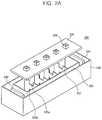
- a linear evaporation sourcewhich includes a crucible being open on one side thereof and storing a deposition material, a plurality of partitions dividing an internal space of the crucible and each having at least one through-hole in a lower portion thereof, a nozzle section located on the open side of the crucible and having a plurality of nozzles, a means for heating the crucible, and a housing accommodating the crucible, the nozzle section, and the heating means.
Landscapes
- Chemical & Material Sciences (AREA)
- Chemical Kinetics & Catalysis (AREA)
- Engineering & Computer Science (AREA)
- Materials Engineering (AREA)
- Mechanical Engineering (AREA)
- Metallurgy (AREA)
- Organic Chemistry (AREA)
- General Chemical & Material Sciences (AREA)
- Electroluminescent Light Sources (AREA)
- Physical Vapour Deposition (AREA)
Abstract
Description
Claims (20)
Priority Applications (1)
| Application Number | Priority Date | Filing Date | Title |
|---|---|---|---|
| US16/457,722US10907245B2 (en) | 2009-12-17 | 2019-06-28 | Linear evaporation source and deposition apparatus having the same |
Applications Claiming Priority (6)
| Application Number | Priority Date | Filing Date | Title |
|---|---|---|---|
| KR10-2009-126143 | 2009-12-17 | ||
| KR1020090126143AKR101094299B1 (en) | 2009-12-17 | 2009-12-17 | Linear evaporation source and deposition apparatus comprising the same |
| US12/972,327US8845807B2 (en) | 2009-12-17 | 2010-12-17 | Linear evaporation source and deposition apparatus having the same |
| US14/484,691US10081867B2 (en) | 2009-12-17 | 2014-09-12 | Linear evaporation source and deposition apparatus having the same |
| US15/884,236US10364488B2 (en) | 2009-12-17 | 2018-01-30 | Linear evaporation source and deposition apparatus having the same |
| US16/457,722US10907245B2 (en) | 2009-12-17 | 2019-06-28 | Linear evaporation source and deposition apparatus having the same |
Related Parent Applications (1)
| Application Number | Title | Priority Date | Filing Date |
|---|---|---|---|
| US15/884,236ContinuationUS10364488B2 (en) | 2009-12-17 | 2018-01-30 | Linear evaporation source and deposition apparatus having the same |
Publications (2)
| Publication Number | Publication Date |
|---|---|
| US20190323119A1 US20190323119A1 (en) | 2019-10-24 |
| US10907245B2true US10907245B2 (en) | 2021-02-02 |
Family
ID=44149291
Family Applications (4)
| Application Number | Title | Priority Date | Filing Date |
|---|---|---|---|
| US12/972,327Active2033-04-15US8845807B2 (en) | 2009-12-17 | 2010-12-17 | Linear evaporation source and deposition apparatus having the same |
| US14/484,691Active2032-04-24US10081867B2 (en) | 2009-12-17 | 2014-09-12 | Linear evaporation source and deposition apparatus having the same |
| US15/884,236ActiveUS10364488B2 (en) | 2009-12-17 | 2018-01-30 | Linear evaporation source and deposition apparatus having the same |
| US16/457,722ActiveUS10907245B2 (en) | 2009-12-17 | 2019-06-28 | Linear evaporation source and deposition apparatus having the same |
Family Applications Before (3)
| Application Number | Title | Priority Date | Filing Date |
|---|---|---|---|
| US12/972,327Active2033-04-15US8845807B2 (en) | 2009-12-17 | 2010-12-17 | Linear evaporation source and deposition apparatus having the same |
| US14/484,691Active2032-04-24US10081867B2 (en) | 2009-12-17 | 2014-09-12 | Linear evaporation source and deposition apparatus having the same |
| US15/884,236ActiveUS10364488B2 (en) | 2009-12-17 | 2018-01-30 | Linear evaporation source and deposition apparatus having the same |
Country Status (6)
| Country | Link |
|---|---|
| US (4) | US8845807B2 (en) |
| JP (1) | JP5409546B2 (en) |
| KR (1) | KR101094299B1 (en) |
| CN (1) | CN102102175B (en) |
| DE (1) | DE102010062937B4 (en) |
| TW (1) | TWI548763B (en) |
Families Citing this family (37)
| Publication number | Priority date | Publication date | Assignee | Title |
|---|---|---|---|---|
| KR101094299B1 (en) | 2009-12-17 | 2011-12-19 | 삼성모바일디스플레이주식회사 | Linear evaporation source and deposition apparatus comprising the same |
| KR101182265B1 (en)* | 2009-12-22 | 2012-09-12 | 삼성디스플레이 주식회사 | Evaporation Source and Deposition Apparatus having the same |
| DE102010055285A1 (en)* | 2010-12-21 | 2012-06-21 | Solarion Ag Photovoltaik | Evaporator source, evaporator chamber and coating process |
| JP5697500B2 (en)* | 2011-03-16 | 2015-04-08 | 株式会社アルバック | Vacuum deposition apparatus and thin film forming method |
| KR102124588B1 (en) | 2012-10-22 | 2020-06-22 | 삼성디스플레이 주식회사 | Linear evaporation source and vacuum deposition apparatus and having the same |
| CN104099570B (en)* | 2013-04-01 | 2016-10-05 | 上海和辉光电有限公司 | Single-point linear evaporation origin system |
| KR102182114B1 (en)* | 2013-12-16 | 2020-11-24 | 삼성디스플레이 주식회사 | Evaporation apparatus |
| KR102227546B1 (en)* | 2014-01-20 | 2021-03-15 | 주식회사 선익시스템 | Large capacity evaporation source and Deposition apparatus including the same |
| JP6241903B2 (en) | 2014-03-11 | 2017-12-06 | 株式会社Joled | Vapor deposition apparatus, vapor deposition method using vapor deposition apparatus, and device manufacturing method |
| CN103993268B (en)* | 2014-04-30 | 2017-02-15 | 京东方科技集团股份有限公司 | Crucible |
| KR20150145466A (en) | 2014-06-19 | 2015-12-30 | 최현범 | Linear evaporating source |
| CN104178734B (en) | 2014-07-21 | 2016-06-15 | 京东方科技集团股份有限公司 | Evaporation coating device |
| CN104233196B (en)* | 2014-09-01 | 2017-04-19 | 京东方科技集团股份有限公司 | Evaporation crucible and evaporation device |
| CN105779944A (en)* | 2014-12-23 | 2016-07-20 | 中国电子科技集团公司第十八研究所 | Linear evaporating source used for preparing CIGS solar battery |
| KR101640558B1 (en)* | 2014-12-29 | 2016-07-18 | (주)알파플러스 | Heating apparatus of linear type vacuum effusion cell |
| KR101642452B1 (en)* | 2015-01-23 | 2016-07-25 | 주식회사 파인에바 | Linear Evaporation Deposition Apparatus |
| CN107406970A (en)* | 2015-03-23 | 2017-11-28 | 纽升股份有限公司 | equipment for evaporating materials |
| KR102334408B1 (en)* | 2015-04-10 | 2021-12-03 | 삼성디스플레이 주식회사 | Deposition Apparatus |
| KR102376728B1 (en)* | 2015-07-07 | 2022-03-21 | 삼성디스플레이 주식회사 | Deposition sorce, deposition device including the same and method of manufacturing display device using the deposition device |
| CN105132866B (en)* | 2015-09-08 | 2018-02-16 | 京东方科技集团股份有限公司 | The heating source device and evaporator of a kind of evaporator |
| KR102608846B1 (en)* | 2015-10-06 | 2023-12-01 | 삼성디스플레이 주식회사 | Deposition sorce and method of manufacturing the same |
| WO2017069369A1 (en)* | 2015-10-23 | 2017-04-27 | 주식회사 파인에바 | Linear evaporation deposition apparatus |
| JP6573559B2 (en)* | 2016-03-03 | 2019-09-11 | 東京エレクトロン株式会社 | Vaporizing raw material supply apparatus and substrate processing apparatus using the same |
| US11926894B2 (en)* | 2016-09-30 | 2024-03-12 | Asm Ip Holding B.V. | Reactant vaporizer and related systems and methods |
| US10876205B2 (en) | 2016-09-30 | 2020-12-29 | Asm Ip Holding B.V. | Reactant vaporizer and related systems and methods |
| US10541386B2 (en)* | 2018-01-30 | 2020-01-21 | Wuhan China Star Optoelectronics Semiconductor Display Technology Co., Ltd. | Evaporation deposition equipment and evaporation deposition method |
| US11634812B2 (en) | 2018-08-16 | 2023-04-25 | Asm Ip Holding B.V. | Solid source sublimator |
| CN109411603A (en)* | 2018-10-17 | 2019-03-01 | 武汉华星光电技术有限公司 | Display panel, luminescent material evaporation coating method and device |
| CN110016647B (en)* | 2019-05-29 | 2020-09-08 | 昆山国显光电有限公司 | Evaporation source cleaning equipment and evaporation system |
| US11624113B2 (en) | 2019-09-13 | 2023-04-11 | Asm Ip Holding B.V. | Heating zone separation for reactant evaporation system |
| KR102783898B1 (en)* | 2020-04-29 | 2025-03-18 | 에이에스엠 아이피 홀딩 비.브이. | Solid source precursor vessel |
| CN111424240B (en)* | 2020-05-29 | 2022-06-03 | 云谷(固安)科技有限公司 | Evaporation crucible |
| CN112609160B (en)* | 2020-12-29 | 2023-06-06 | 尚越光电科技股份有限公司 | A kind of evaporation source heating structure of CIGS co-evaporation method |
| KR20240036712A (en)* | 2021-08-12 | 2024-03-20 | 어플라이드 머티어리얼스, 인코포레이티드 | Evaporator for effective surface area evaporation |
| KR102708291B1 (en)* | 2022-07-08 | 2024-09-23 | 엘지전자 주식회사 | Linear Deposition Source |
| CN115287478B (en)* | 2022-08-05 | 2023-03-28 | 太仓市王秀有色金属铸件厂 | Nickel-phosphorus alloy forming equipment |
| CN118064842B (en)* | 2024-04-22 | 2024-08-09 | 季华实验室 | Multi-evaporation-source interval evaporation device and coating method |
Citations (39)
| Publication number | Priority date | Publication date | Assignee | Title |
|---|---|---|---|---|
| US2664852A (en) | 1950-04-27 | 1954-01-05 | Nat Res Corp | Vapor coating apparatus |
| US3647197A (en) | 1970-04-27 | 1972-03-07 | Ford Motor Co | Vacuum deposition |
| US4023523A (en) | 1975-04-23 | 1977-05-17 | Xerox Corporation | Coater hardware and method for obtaining uniform photoconductive layers on a xerographic photoreceptor |
| JPS5322859A (en) | 1976-08-17 | 1978-03-02 | Taiei Shiyoukou Kk | Method of forming track groove of ball bearing |
| JPS6293368A (en) | 1985-10-17 | 1987-04-28 | Mitsubishi Electric Corp | evaporation source |
| US4700660A (en) | 1984-06-12 | 1987-10-20 | Kievsky Politekhnichesky Institut | Evaporator for depositing films in a vacuum |
| US4812326A (en) | 1986-08-22 | 1989-03-14 | Mitsubishi Denki Kabushiki Kaisha | Evaporation source with a shaped nozzle |
| US5253266A (en) | 1992-07-20 | 1993-10-12 | Intevac, Inc. | MBE effusion source with asymmetrical heaters |
| JPH0613258A (en) | 1991-12-20 | 1994-01-21 | Matsushita Electric Ind Co Ltd | Thin film multilayer capacitor pattern formation method |
| JPH0916960A (en) | 1995-06-30 | 1997-01-17 | Hitachi Maxell Ltd | Information recording medium manufacturing equipment |
| US6296894B1 (en) | 1998-08-26 | 2001-10-02 | Tdk Corporation | Evaporation source, apparatus and method for the preparation of organic El device |
| KR20020068039A (en) | 1999-10-22 | 2002-08-24 | 커트 제이. 레스커 컴파니 | Method and apparatus for coating a substrate in a vacuum |
| JP2004052113A (en) | 2002-07-23 | 2004-02-19 | Samsung Nec Mobile Display Co Ltd | Heating vessel and vapor deposition system using the same |
| JP2004068081A (en) | 2002-08-06 | 2004-03-04 | Canon Inc | Evaporation source container in vacuum evaporation equipment |
| JP2004259634A (en) | 2003-02-27 | 2004-09-16 | Nippon Seiki Co Ltd | Manufacturing method of organic el panel, and organic layer film forming apparatus used in the same |
| US6830626B1 (en) | 1999-10-22 | 2004-12-14 | Kurt J. Lesker Company | Method and apparatus for coating a substrate in a vacuum |
| US20050008799A1 (en) | 2003-07-08 | 2005-01-13 | Shizuo Tomiyasu | Solid organometallic compound-filled container and filling method thereof |
| US20050016463A1 (en) | 2003-06-13 | 2005-01-27 | Pioneer Corporation | Evaporative deposition method, evaporative deposition head, method for forming pattern of deposition material, and evaporative deposition material disk |
| KR20050083306A (en) | 2004-02-23 | 2005-08-26 | 엘지전자 주식회사 | Source for depositing organic el device |
| KR100545975B1 (en) | 2002-09-05 | 2006-01-25 | 산요덴키가부시키가이샤 | Manufacturing method of organic EL display apparatus |
| JP2006152440A (en) | 2004-11-26 | 2006-06-15 | Samsung Sdi Co Ltd | Evaporation source and vapor deposition apparatus equipped with the same |
| KR20060081943A (en) | 2005-01-11 | 2006-07-14 | 황창훈 | Linear Multipoint Crucible Apparatus for Large Area Organic Thin Film Fabrication |
| KR20060085494A (en) | 2005-01-24 | 2006-07-27 | 삼성에스디아이 주식회사 | Organics Evaporator |
| US20060185599A1 (en) | 2005-02-22 | 2006-08-24 | Bichrt Craig E | Effusion Cell Valve |
| KR20060094711A (en) | 2005-02-25 | 2006-08-30 | 삼성에스디아이 주식회사 | Side spray type linear evaporation source having a partition and vapor deposition apparatus having the evaporation source |
| WO2007026649A1 (en) | 2005-08-29 | 2007-03-08 | Matsushita Electric Industrial Co., Ltd. | Vapor deposition head device and method of coating by vapor deposition |
| WO2007034790A1 (en) | 2005-09-20 | 2007-03-29 | Tohoku University | Film forming apparatus, evaporating jig and measuring method |
| US20070077357A1 (en) | 2005-08-31 | 2007-04-05 | Min Jae Jeong | Source for inorganic layer and method for controlling heating source thereof |
| JP2007113077A (en) | 2005-10-20 | 2007-05-10 | Toshiba Matsushita Display Technology Co Ltd | Crucible |
| KR100767036B1 (en) | 2006-05-24 | 2007-10-12 | 세메스 주식회사 | Evaporation source with nozzle part |
| KR20080016720A (en) | 2008-02-12 | 2008-02-21 | 문대규 | Evaporation source |
| KR20080036294A (en) | 2006-10-23 | 2008-04-28 | 주식회사 야스 | Conical Multi-Nozzle Evaporation Source for Deposition Process |
| KR20080044775A (en) | 2006-11-16 | 2008-05-21 | 자이단호징 야마가타켄산교기쥬츠신코기코 | Evaporation source and vacuum deposition apparatus using the same |
| JP2008208443A (en) | 2007-02-28 | 2008-09-11 | Sony Corp | Vapor deposition film-forming apparatus, vapor deposition film formation method, and manufacturing method of display device |
| JP2008305560A (en) | 2007-06-05 | 2008-12-18 | Canon Inc | Manufacturing method of organic EL display device |
| US20090017192A1 (en) | 2007-07-12 | 2009-01-15 | Hiroyasu Matsuura | Vapor deposition method and apparatus |
| KR20090047953A (en) | 2007-11-09 | 2009-05-13 | 삼성모바일디스플레이주식회사 | Organic Linear Deposition Equipment |
| US20090142489A1 (en) | 2006-08-04 | 2009-06-04 | Soonchunhyang University Industry Academy Cooperation Foundation | Linear deposition sources for deposition processes |
| JP2011127217A (en) | 2009-12-17 | 2011-06-30 | Samsung Mobile Display Co Ltd | Linear evaporation source, and deposition apparatus having the same |
Family Cites Families (2)
| Publication number | Priority date | Publication date | Assignee | Title |
|---|---|---|---|---|
| KR100490371B1 (en) | 2002-11-05 | 2005-05-17 | 현대자동차주식회사 | Roof rack for automobile |
| EP2301349A2 (en) | 2005-02-25 | 2011-03-30 | The Trustees of The University of Pennsylvania | Facially amphiphilic polymers and oligomers, compositions thereof, and use thereof in methods of treating cancer |
- 2009
- 2009-12-17KRKR1020090126143Apatent/KR101094299B1/enactiveActive
- 2010
- 2010-08-12JPJP2010180880Apatent/JP5409546B2/enactiveActive
- 2010-12-13DEDE102010062937.5Apatent/DE102010062937B4/enactiveActive
- 2010-12-16TWTW099144328Apatent/TWI548763B/enactive
- 2010-12-17CNCN201010601144.4Apatent/CN102102175B/enactiveActive
- 2010-12-17USUS12/972,327patent/US8845807B2/enactiveActive
- 2014
- 2014-09-12USUS14/484,691patent/US10081867B2/enactiveActive
- 2018
- 2018-01-30USUS15/884,236patent/US10364488B2/enactiveActive
- 2019
- 2019-06-28USUS16/457,722patent/US10907245B2/enactiveActive
Patent Citations (45)
| Publication number | Priority date | Publication date | Assignee | Title |
|---|---|---|---|---|
| US2664852A (en) | 1950-04-27 | 1954-01-05 | Nat Res Corp | Vapor coating apparatus |
| US3647197A (en) | 1970-04-27 | 1972-03-07 | Ford Motor Co | Vacuum deposition |
| US4023523A (en) | 1975-04-23 | 1977-05-17 | Xerox Corporation | Coater hardware and method for obtaining uniform photoconductive layers on a xerographic photoreceptor |
| JPS5322859A (en) | 1976-08-17 | 1978-03-02 | Taiei Shiyoukou Kk | Method of forming track groove of ball bearing |
| US4700660A (en) | 1984-06-12 | 1987-10-20 | Kievsky Politekhnichesky Institut | Evaporator for depositing films in a vacuum |
| JPS6293368A (en) | 1985-10-17 | 1987-04-28 | Mitsubishi Electric Corp | evaporation source |
| US4812326A (en) | 1986-08-22 | 1989-03-14 | Mitsubishi Denki Kabushiki Kaisha | Evaporation source with a shaped nozzle |
| JPH0613258A (en) | 1991-12-20 | 1994-01-21 | Matsushita Electric Ind Co Ltd | Thin film multilayer capacitor pattern formation method |
| US5253266A (en) | 1992-07-20 | 1993-10-12 | Intevac, Inc. | MBE effusion source with asymmetrical heaters |
| JPH0916960A (en) | 1995-06-30 | 1997-01-17 | Hitachi Maxell Ltd | Information recording medium manufacturing equipment |
| US6296894B1 (en) | 1998-08-26 | 2001-10-02 | Tdk Corporation | Evaporation source, apparatus and method for the preparation of organic El device |
| KR20020068039A (en) | 1999-10-22 | 2002-08-24 | 커트 제이. 레스커 컴파니 | Method and apparatus for coating a substrate in a vacuum |
| CN1402800A (en) | 1999-10-22 | 2003-03-12 | 寇脱J·莱斯克公司 | Method and apparatus for coating a substrate in a vacuum |
| US6830626B1 (en) | 1999-10-22 | 2004-12-14 | Kurt J. Lesker Company | Method and apparatus for coating a substrate in a vacuum |
| JP2004052113A (en) | 2002-07-23 | 2004-02-19 | Samsung Nec Mobile Display Co Ltd | Heating vessel and vapor deposition system using the same |
| JP2004068081A (en) | 2002-08-06 | 2004-03-04 | Canon Inc | Evaporation source container in vacuum evaporation equipment |
| KR100545975B1 (en) | 2002-09-05 | 2006-01-25 | 산요덴키가부시키가이샤 | Manufacturing method of organic EL display apparatus |
| JP2004259634A (en) | 2003-02-27 | 2004-09-16 | Nippon Seiki Co Ltd | Manufacturing method of organic el panel, and organic layer film forming apparatus used in the same |
| US20050016463A1 (en) | 2003-06-13 | 2005-01-27 | Pioneer Corporation | Evaporative deposition method, evaporative deposition head, method for forming pattern of deposition material, and evaporative deposition material disk |
| US20050008799A1 (en) | 2003-07-08 | 2005-01-13 | Shizuo Tomiyasu | Solid organometallic compound-filled container and filling method thereof |
| KR20050083306A (en) | 2004-02-23 | 2005-08-26 | 엘지전자 주식회사 | Source for depositing organic el device |
| JP2006152440A (en) | 2004-11-26 | 2006-06-15 | Samsung Sdi Co Ltd | Evaporation source and vapor deposition apparatus equipped with the same |
| KR20060081943A (en) | 2005-01-11 | 2006-07-14 | 황창훈 | Linear Multipoint Crucible Apparatus for Large Area Organic Thin Film Fabrication |
| KR20060085494A (en) | 2005-01-24 | 2006-07-27 | 삼성에스디아이 주식회사 | Organics Evaporator |
| US20060185599A1 (en) | 2005-02-22 | 2006-08-24 | Bichrt Craig E | Effusion Cell Valve |
| KR20060094711A (en) | 2005-02-25 | 2006-08-30 | 삼성에스디아이 주식회사 | Side spray type linear evaporation source having a partition and vapor deposition apparatus having the evaporation source |
| WO2007026649A1 (en) | 2005-08-29 | 2007-03-08 | Matsushita Electric Industrial Co., Ltd. | Vapor deposition head device and method of coating by vapor deposition |
| US20070077357A1 (en) | 2005-08-31 | 2007-04-05 | Min Jae Jeong | Source for inorganic layer and method for controlling heating source thereof |
| CN101268210A (en) | 2005-09-20 | 2008-09-17 | 国立大学法人东北大学 | Film forming apparatus, evaporation jig, and measurement method |
| WO2007034790A1 (en) | 2005-09-20 | 2007-03-29 | Tohoku University | Film forming apparatus, evaporating jig and measuring method |
| US20090087545A1 (en) | 2005-09-20 | 2009-04-02 | Tadahiro Ohmi | Film Forming Apparatus, Evaporating Jig, and Measurement Method |
| JP2007113077A (en) | 2005-10-20 | 2007-05-10 | Toshiba Matsushita Display Technology Co Ltd | Crucible |
| KR100767036B1 (en) | 2006-05-24 | 2007-10-12 | 세메스 주식회사 | Evaporation source with nozzle part |
| US20090142489A1 (en) | 2006-08-04 | 2009-06-04 | Soonchunhyang University Industry Academy Cooperation Foundation | Linear deposition sources for deposition processes |
| KR20080036294A (en) | 2006-10-23 | 2008-04-28 | 주식회사 야스 | Conical Multi-Nozzle Evaporation Source for Deposition Process |
| KR20080044775A (en) | 2006-11-16 | 2008-05-21 | 자이단호징 야마가타켄산교기쥬츠신코기코 | Evaporation source and vacuum deposition apparatus using the same |
| EP1927674A2 (en) | 2006-11-16 | 2008-06-04 | Yamagata Promotional Organization for Industrial Technology | Evaporation source and vacuum evaporator using the same |
| JP2008121098A (en) | 2006-11-16 | 2008-05-29 | Yamagata Promotional Organization For Industrial Technology | Evaporation source and vacuum vapor deposition system using the same |
| US20080115729A1 (en) | 2006-11-16 | 2008-05-22 | Yamagata Promotional Organization For Industrial Technology | Evaporation source and vacuum evaporator using the same |
| JP2008208443A (en) | 2007-02-28 | 2008-09-11 | Sony Corp | Vapor deposition film-forming apparatus, vapor deposition film formation method, and manufacturing method of display device |
| JP2008305560A (en) | 2007-06-05 | 2008-12-18 | Canon Inc | Manufacturing method of organic EL display device |
| US20090017192A1 (en) | 2007-07-12 | 2009-01-15 | Hiroyasu Matsuura | Vapor deposition method and apparatus |
| KR20090047953A (en) | 2007-11-09 | 2009-05-13 | 삼성모바일디스플레이주식회사 | Organic Linear Deposition Equipment |
| KR20080016720A (en) | 2008-02-12 | 2008-02-21 | 문대규 | Evaporation source |
| JP2011127217A (en) | 2009-12-17 | 2011-06-30 | Samsung Mobile Display Co Ltd | Linear evaporation source, and deposition apparatus having the same |
Non-Patent Citations (6)
| Title |
|---|
| Japanese Notice of Allowance dated Oct. 8, 2013 for Japanese Patent Application No. JP 2010-180880. |
| Japanese Office Action dated Sep. 4, 2012 for Japanese Patent Application No. JP 2010-180880. |
| Korean Office Action dated Dec. 1, 2011 for Korean Patent Application No. KR 10-2009-0128890. |
| Korean Office Action dated May 16, 2011 for Korean Patent Application No. KR 10-2009-0126143. |
| U.S. Office Action dated Jul. 25, 2014 for U.S. Appl. No. 12/972,369, filed Dec. 17, 2010. |
| U.S. Office Action dated Oct. 10, 2013 for U.S. Appl. No. 12/972,369, filed Dec. 17, 2010. |
Also Published As
| Publication number | Publication date |
|---|---|
| US10364488B2 (en) | 2019-07-30 |
| KR20110069418A (en) | 2011-06-23 |
| US10081867B2 (en) | 2018-09-25 |
| DE102010062937A1 (en) | 2011-07-14 |
| TW201125995A (en) | 2011-08-01 |
| DE102010062937B4 (en) | 2021-07-15 |
| CN102102175B (en) | 2015-02-18 |
| JP2011127217A (en) | 2011-06-30 |
| US20140373784A1 (en) | 2014-12-25 |
| TWI548763B (en) | 2016-09-11 |
| US20190323119A1 (en) | 2019-10-24 |
| JP5409546B2 (en) | 2014-02-05 |
| US8845807B2 (en) | 2014-09-30 |
| KR101094299B1 (en) | 2011-12-19 |
| CN102102175A (en) | 2011-06-22 |
| US20110146579A1 (en) | 2011-06-23 |
| US20180155831A1 (en) | 2018-06-07 |
Similar Documents
| Publication | Publication Date | Title |
|---|---|---|
| US10907245B2 (en) | Linear evaporation source and deposition apparatus having the same | |
| US20110146575A1 (en) | Evaporation source and deposition apparatus having the same | |
| KR100687007B1 (en) | Organic thin film deposition apparatus used for manufacturing organic electroluminescent device | |
| KR101942471B1 (en) | Depositing apparatus and method for manufacturing organic light emitting diode display using the same | |
| KR20160112293A (en) | Evaporation source and Deposition apparatus including the same | |
| US10002914B2 (en) | Method of manufacturing a display apparatus having pixels areas with different thicknesses | |
| WO2015136857A1 (en) | Deposition apparatus, method for controlling same, deposition method using deposition apparatus, and device manufacturing method | |
| KR101599505B1 (en) | Evaporation source for deposition apparatus | |
| KR20190134367A (en) | Angle controlling plate for deposition and deposition apparatus including the same | |
| KR102371102B1 (en) | Evaporation source assembly and deposition apparatus including the same | |
| KR102666177B1 (en) | OLED Deposition Source having Multi Hole Structure | |
| KR20080061668A (en) | Organic thin film deposition apparatus | |
| KR20220093673A (en) | Evaporation source | |
| KR20180073058A (en) | Evaporation source and apparatus for deposition having the same | |
| KR101599509B1 (en) | Evaporation source | |
| KR20080002523A (en) | Organic light emitting device deposition apparatus |
Legal Events
| Date | Code | Title | Description |
|---|---|---|---|
| FEPP | Fee payment procedure | Free format text:ENTITY STATUS SET TO UNDISCOUNTED (ORIGINAL EVENT CODE: BIG.); ENTITY STATUS OF PATENT OWNER: LARGE ENTITY | |
| AS | Assignment | Owner name:SAMSUNG DISPLAY CO., LTD., KOREA, REPUBLIC OF Free format text:MERGER;ASSIGNOR:SAMSUNG MOBILE DISPLAY CO., LTD.;REEL/FRAME:049708/0419 Effective date:20120702 Owner name:SAMSUNG MOBILE DISPLAY CO., LTD., KOREA, REPUBLIC Free format text:ASSIGNMENT OF ASSIGNORS INTEREST;ASSIGNORS:SEO, MIN-GYU;HAN, SANG-JIN;ROH, CHEOL-LAE;AND OTHERS;REEL/FRAME:049705/0467 Effective date:20101210 Owner name:SAMSUNG MOBILE DISPLAY CO., LTD., KOREA, REPUBLIC OF Free format text:ASSIGNMENT OF ASSIGNORS INTEREST;ASSIGNORS:SEO, MIN-GYU;HAN, SANG-JIN;ROH, CHEOL-LAE;AND OTHERS;REEL/FRAME:049705/0467 Effective date:20101210 | |
| STPP | Information on status: patent application and granting procedure in general | Free format text:APPLICATION DISPATCHED FROM PREEXAM, NOT YET DOCKETED | |
| STPP | Information on status: patent application and granting procedure in general | Free format text:DOCKETED NEW CASE - READY FOR EXAMINATION | |
| STPP | Information on status: patent application and granting procedure in general | Free format text:NON FINAL ACTION MAILED | |
| STPP | Information on status: patent application and granting procedure in general | Free format text:RESPONSE TO NON-FINAL OFFICE ACTION ENTERED AND FORWARDED TO EXAMINER | |
| STPP | Information on status: patent application and granting procedure in general | Free format text:NOTICE OF ALLOWANCE MAILED -- APPLICATION RECEIVED IN OFFICE OF PUBLICATIONS | |
| STCF | Information on status: patent grant | Free format text:PATENTED CASE | |
| MAFP | Maintenance fee payment | Free format text:PAYMENT OF MAINTENANCE FEE, 4TH YEAR, LARGE ENTITY (ORIGINAL EVENT CODE: M1551); ENTITY STATUS OF PATENT OWNER: LARGE ENTITY Year of fee payment:4 |